KR20080098371A - Charge Balanced Insulated Gate Bipolar Transistors - Google Patents
Charge Balanced Insulated Gate Bipolar Transistors Download PDFInfo
- Publication number
- KR20080098371A KR20080098371A KR1020087019992A KR20087019992A KR20080098371A KR 20080098371 A KR20080098371 A KR 20080098371A KR 1020087019992 A KR1020087019992 A KR 1020087019992A KR 20087019992 A KR20087019992 A KR 20087019992A KR 20080098371 A KR20080098371 A KR 20080098371A
- Authority
- KR
- South Korea
- Prior art keywords
- conductivity type
- pillars
- fillers
- region
- doping concentration
- Prior art date
- Legal status (The legal status is an assumption and is not a legal conclusion. Google has not performed a legal analysis and makes no representation as to the accuracy of the status listed.)
- Ceased
Links
Images


Classifications
-
- H—ELECTRICITY
- H10—SEMICONDUCTOR DEVICES; ELECTRIC SOLID-STATE DEVICES NOT OTHERWISE PROVIDED FOR
- H10D—INORGANIC ELECTRIC SEMICONDUCTOR DEVICES
- H10D12/00—Bipolar devices controlled by the field effect, e.g. insulated-gate bipolar transistors [IGBT]
- H10D12/411—Insulated-gate bipolar transistors [IGBT]
- H10D12/441—Vertical IGBTs
-
- H—ELECTRICITY
- H10—SEMICONDUCTOR DEVICES; ELECTRIC SOLID-STATE DEVICES NOT OTHERWISE PROVIDED FOR
- H10P—GENERIC PROCESSES OR APPARATUS FOR THE MANUFACTURE OR TREATMENT OF DEVICES COVERED BY CLASS H10
- H10P10/00—Bonding of wafers, substrates or parts of devices
-
- H—ELECTRICITY
- H10—SEMICONDUCTOR DEVICES; ELECTRIC SOLID-STATE DEVICES NOT OTHERWISE PROVIDED FOR
- H10D—INORGANIC ELECTRIC SEMICONDUCTOR DEVICES
- H10D12/00—Bipolar devices controlled by the field effect, e.g. insulated-gate bipolar transistors [IGBT]
- H10D12/411—Insulated-gate bipolar transistors [IGBT]
- H10D12/441—Vertical IGBTs
- H10D12/461—Vertical IGBTs having non-planar surfaces, e.g. having trenches, recesses or pillars in the surfaces of the emitter, base or collector regions
- H10D12/481—Vertical IGBTs having non-planar surfaces, e.g. having trenches, recesses or pillars in the surfaces of the emitter, base or collector regions having gate structures on slanted surfaces, on vertical surfaces, or in grooves, e.g. trench gate IGBTs
-
- H—ELECTRICITY
- H10—SEMICONDUCTOR DEVICES; ELECTRIC SOLID-STATE DEVICES NOT OTHERWISE PROVIDED FOR
- H10D—INORGANIC ELECTRIC SEMICONDUCTOR DEVICES
- H10D62/00—Semiconductor bodies, or regions thereof, of devices having potential barriers
- H10D62/01—Manufacture or treatment
- H10D62/051—Forming charge compensation regions, e.g. superjunctions
- H10D62/054—Forming charge compensation regions, e.g. superjunctions by high energy implantations in bulk semiconductor bodies, e.g. forming pillars
-
- H—ELECTRICITY
- H10—SEMICONDUCTOR DEVICES; ELECTRIC SOLID-STATE DEVICES NOT OTHERWISE PROVIDED FOR
- H10D—INORGANIC ELECTRIC SEMICONDUCTOR DEVICES
- H10D62/00—Semiconductor bodies, or regions thereof, of devices having potential barriers
- H10D62/10—Shapes, relative sizes or dispositions of the regions of the semiconductor bodies; Shapes of the semiconductor bodies
- H10D62/102—Constructional design considerations for preventing surface leakage or controlling electric field concentration
- H10D62/103—Constructional design considerations for preventing surface leakage or controlling electric field concentration for increasing or controlling the breakdown voltage of reverse-biased devices
- H10D62/105—Constructional design considerations for preventing surface leakage or controlling electric field concentration for increasing or controlling the breakdown voltage of reverse-biased devices by having particular doping profiles, shapes or arrangements of PN junctions; by having supplementary regions, e.g. junction termination extension [JTE]
- H10D62/109—Reduced surface field [RESURF] PN junction structures
- H10D62/111—Multiple RESURF structures, e.g. double RESURF or 3D-RESURF structures
-
- H—ELECTRICITY
- H10—SEMICONDUCTOR DEVICES; ELECTRIC SOLID-STATE DEVICES NOT OTHERWISE PROVIDED FOR
- H10D—INORGANIC ELECTRIC SEMICONDUCTOR DEVICES
- H10D62/00—Semiconductor bodies, or regions thereof, of devices having potential barriers
- H10D62/10—Shapes, relative sizes or dispositions of the regions of the semiconductor bodies; Shapes of the semiconductor bodies
- H10D62/124—Shapes, relative sizes or dispositions of the regions of semiconductor bodies or of junctions between the regions
- H10D62/126—Top-view geometrical layouts of the regions or the junctions
- H10D62/127—Top-view geometrical layouts of the regions or the junctions of cellular field-effect devices, e.g. multicellular DMOS transistors or IGBTs
-
- H—ELECTRICITY
- H10—SEMICONDUCTOR DEVICES; ELECTRIC SOLID-STATE DEVICES NOT OTHERWISE PROVIDED FOR
- H10D—INORGANIC ELECTRIC SEMICONDUCTOR DEVICES
- H10D62/00—Semiconductor bodies, or regions thereof, of devices having potential barriers
- H10D62/10—Shapes, relative sizes or dispositions of the regions of the semiconductor bodies; Shapes of the semiconductor bodies
- H10D62/13—Semiconductor regions connected to electrodes carrying current to be rectified, amplified or switched, e.g. source or drain regions
- H10D62/141—Anode or cathode regions of thyristors; Collector or emitter regions of gated bipolar-mode devices, e.g. of IGBTs
- H10D62/142—Anode regions of thyristors or collector regions of gated bipolar-mode devices
-
- H—ELECTRICITY
- H10—SEMICONDUCTOR DEVICES; ELECTRIC SOLID-STATE DEVICES NOT OTHERWISE PROVIDED FOR
- H10D—INORGANIC ELECTRIC SEMICONDUCTOR DEVICES
- H10D62/00—Semiconductor bodies, or regions thereof, of devices having potential barriers
- H10D62/10—Shapes, relative sizes or dispositions of the regions of the semiconductor bodies; Shapes of the semiconductor bodies
- H10D62/17—Semiconductor regions connected to electrodes not carrying current to be rectified, amplified or switched, e.g. channel regions
- H10D62/393—Body regions of DMOS transistors or IGBTs
Landscapes
- Electrodes Of Semiconductors (AREA)
- Insulated Gate Type Field-Effect Transistor (AREA)
- Metal-Oxide And Bipolar Metal-Oxide Semiconductor Integrated Circuits (AREA)
Abstract
본 개시의 전하 균형 절연 게이트 양극성 트랜지스터(IGBT)의 요약에 있어서, 상기 IGBT는 콜렉터 영역 위의 제1 실리콘 영역 및 상기 제1 실리콘 영역 위에 번갈아 배열된 제1 및 제2 도전성 타입의 복수의 필러들(pillars)을 포함한다. 상기 IGBT는 각각이 제1 도전성 타입의 상기 필러들 중 하나의 필러의 위에서 연장되고 상기 하나의 필러와 전기적으로 접촉하는 복수의 웰 영역, 및 복수의 게이트 전극 - 상기 복수의 게이트 전극의 각각은, 대응되는 웰 영역의 일부분 위에서 연장됨 - 을 포함한다. 제1 및 제2 도전성 타입의 상기 필러들의 각각의 물리적 치수와, 제1 및 제2 도전성 타입의 상기 필러들의 각각의 전하 캐리어의 도핑 농도는, 제1 도전성의 각각의 필러 내의 순전하(net charge)와 당해 제1 도전성의 필러에 인접한 제2 도전성 타입의 필러 내의 순전하 사이에 전하 불균형을 야기하도록 선택된다.In a summary of the charge balanced insulated gate bipolar transistor (IGBT) of the present disclosure, the IGBT is a plurality of fillers of the first and second conductivity type arranged alternately over the first silicon region and the first silicon region. (pillars). The IGBT includes a plurality of well regions each extending over one of the pillars of the first conductivity type and in electrical contact with the one pillar, and a plurality of gate electrodes—each of the plurality of gate electrodes, Extending over a portion of the corresponding well region. The physical dimensions of each of the fillers of the first and second conductivity types, and the doping concentration of each charge carrier of the fillers of the first and second conductivity types, are determined by the net charge in each filler of the first conductivity. ) And the net charge in the filler of the second conductivity type adjacent the filler of the first conductivity.
Description
[관련 출원의 상호 참조][Cross Reference of Related Application]
본 출원은 2006년 2월 3일자의 미국 가출원 제60/765,261호를 우선권 주장의 기초로 하며, 상기 가출원의 개시 내용은 그 전체로서 참조에 의해 여하한 목적으로 본 명세서에 편입된다.This application is based on a priority claim of US Provisional Application No. 60 / 765,261, filed February 3, 2006, the disclosure of which is incorporated herein by reference in its entirety for any purpose.
본 발명은 전력 반도체 디바이스에 관한 것이고, 보다 구체적으로는 전하 균형 구조를 포함하는 절연 게이트 양극성 트랜지스터(insulated gate bipolar transistor; IGBT)를 형성하는 구조 및 방법에 관한 것이다.TECHNICAL FIELD The present invention relates to power semiconductor devices, and more particularly, to a structure and method for forming an insulated gate bipolar transistor (IGBT) comprising a charge balancing structure.
IGBT는 상업적으로 이용가능한 다수의 전력 반도체 디바이스 중 하나이다. 도 1은 기존의 IGBT의 단면도를 도시한다. 고농도로 도핑된 P-타입 콜렉터 영역 104가 콜렉터 전극 102에 전기적으로 접속된다. N-타입 드리프트 영역 106이 콜렉터 영역 104 위에 형성된다. 고농도로 도핑된 P-타입 웰 영역 108이 드리프트 영 역 106 내에 형성되고, 고농도로 도핑된 N-타입 소스 영역 110이 P-타입 웰 영역 108 내에 형성된다. 웰 영역 108과 소스 영역 110 모두는 이미터 전극 112에 전기적으로 접속된다. 평면형 게이트 114가 드리프트 영역 106의 상면 위와 웰 영역 108 내의 채널 영역 113 위에서 연장되고 상기 소스 영역 110과 중첩한다. 게이트 114는 그 아래에 놓인 영역들로부터 게이트 유전체층 116에 의해 절연된다.IGBTs are one of many commercially available power semiconductor devices. 1 shows a cross-sectional view of a conventional IGBT. Highly doped P-
도 1과 같은 기존의 IGBT의 서로 경쟁적인 다양한 성능 파라미터들을 최적화하는 것은, P-타입 콜렉터 영역의 고농도 도핑에 대한 요구 및 N-타입 드리프트 영역의 유한한 두께에 대한 요구를 포함하는 다수의 인자들에 의해 제한된다. 이러한 인자들은 다양한 트레이드-오프(trade-off) 성능 향상을 제한한다. 따라서, 트레이드-오프 성능 파라미터들의 개선을 가능하게 하면서 상기 파라미터들이 보다 잘 제어될 수 있는 개선된 IGBT가 요구된다.Optimizing the various competing performance parameters of an existing IGBT such as FIG. 1 includes a number of factors including the need for high concentration doping of the P-type collector region and the finite thickness of the N-type drift region. Limited by These factors limit various trade-off performance improvements. Thus, there is a need for an improved IGBT that allows for better control of the trade-off performance parameters while allowing the parameters to be better controlled.
본 발명의 일 실시예에 의하면, 절연 게이트 양극성 트랜지스터(IGBT)가 제1 도전성 타입의 콜렉터 영역, 및 상기 콜렉터 영역 위에서 연장되는 제2 도전성 타입의 제1 실리콘 영역을 포함한다. 제1 및 제2 도전성 타입의 복수의 필러들(pillars)이 상기 제1 실리콘 영역 위에 번갈아 배열된다. 제1 도전성 타입의 각각의 필러의 바닥면은 상기 콜렉터 영역의 최상면으로부터 수직 방향으로 이격된다. 상기 IGBT는, 각각이 제1 도전성 타입의 상기 필러들 중 하나의 필러 위에서 연장되고 상기 하나의 필러와 전기적으로 접촉하는 제1 도전성 타입의 복수의 웰 영역, 및 복수의 게이트 전극 - 상기 복수의 게이트 전극의 각각은, 대응되는 웰 영역의 일부분 위에서 연장됨 - 을 더 포함한다. 각각의 게이트 전극은 당해 게이트 전극 아래에 놓인 영역으로부터 게이트 유전체층에 의해 절연된다. 제1 및 제2 도전성 타입의 상기 필러들의 각각의 물리적 치수 및 제1 및 제2 도전성 타입의 상기 필러들의 각각의 전하 캐리어의 도핑 농도는, 제1 도전성의 각각의 필러 내의 순전하(net charge)와 당해 제1 도전성의 필러에 인접한 제2 도전성 타입의 필러 내의 순전하 사이에 전하 불균형을 야기하도록 선택된다.According to an embodiment of the present invention, an insulated gate bipolar transistor (IGBT) includes a collector region of a first conductivity type and a first silicon region of a second conductivity type extending over the collector region. A plurality of pillars of the first and second conductivity type are alternately arranged above the first silicon region. The bottom surface of each filler of the first conductivity type is spaced in the vertical direction from the top surface of the collector region. The IGBTs include: a plurality of well regions of a first conductivity type each extending over one of the fillers of the first conductivity type and in electrical contact with the one filler, and a plurality of gate electrodes—the plurality of gates Each of the electrodes further extending over a portion of the corresponding well region. Each gate electrode is insulated by a gate dielectric layer from an area underlying the gate electrode. The physical dimensions of each of the fillers of the first and second conductivity types and the doping concentration of each charge carrier of the fillers of the first and second conductivity types are net charge in each filler of the first conductivity. And a charge imbalance between the net charge in the filler of the second conductivity type adjacent the filler of the first conductivity.
본 발명의 다른 실시예에 의하면, IGBT가 제1 도전성 타입의 콜렉터 영역, 및 상기 콜렉터 영역 위에서 연장되는 제2 도전성 타입의 제1 실리콘 영역을 포함한다. 제1 및 제2 도전성 타입의 복수의 필러들이 상기 제1 실리콘 영역 위에 번갈아 배열된다. 제1 도전성 타입의 각각의 필러의 바닥면은 상기 콜렉터 영역의 최상면으로부터 수직 방향으로 이격된다. 제1 도전성 타입의 웰 영역이 제1 및 제2 도전성 타입의 상기 복수의 필러들 위에서 연장되고 상기 복수의 필러들과 전기적으로 접촉한다. 상기 IGBT는 복수의 게이트 트랜치를 더 포함하되, 상기 복수의 게이트 트랜치의 각각은, 상기 웰 영역을 통해 연장되고 제2 도전성 타입의 상기 필러들 중 하나의 내부에서 종단되며, 상기 각각의 게이트 트랜치는 게이트 전극을 포함한다. 제1 및 제2 도전성 타입의 상기 필러들의 각각의 물리적 치수 및 제1 및 제2 도전성 타입의 상기 필러들의 각각의 전하 캐리어의 도핑 농도는, 제1 도전성의 각각의 필러 내의 순전하와 당해 제1 도전성의 필러에 인접한 제2 도전성 타입의 상기 필러 내의 순전하 사이에 전하 불균형을 야기하도록 선택된다.According to another embodiment of the present invention, the IGBT includes a collector region of a first conductivity type and a first silicon region of a second conductivity type extending over the collector region. A plurality of fillers of the first and second conductivity types are alternately arranged above the first silicon region. The bottom surface of each filler of the first conductivity type is spaced in the vertical direction from the top surface of the collector region. A well region of a first conductivity type extends over the plurality of pillars of the first and second conductivity types and is in electrical contact with the plurality of pillars. The IGBT further includes a plurality of gate trenches, each of the plurality of gate trenches extending through the well region and terminating inside one of the pillars of a second conductivity type, wherein each gate trench And a gate electrode. The physical dimensions of each of the fillers of the first and second conductivity types and the doping concentration of each charge carrier of the fillers of the first and second conductivity types are the net charge in each filler of the first conductivity and the first It is selected to cause charge imbalance between the net charge in the filler of the second conductivity type adjacent to the conductive filler.
본 발명의 또 다른 실시예에 의하면, IBGT가 다음과 같이 형성된다. 에피택시층이 제1 도전성 타입의 콜렉터 영역 위에 형성되며, 상기 에피택시층은 제2 도전성 타입을 갖는다. 상기 에피택시층 내에 제1 도전성 타입의 복수의 제1 필러들이 형성되어, 상기 복수의 제1 필러들을 서로 분리시키는 상기 에피택시층의 부분들이 복수의 제2 필러들을 형성함으로써 도전성 타입이 번갈아 바뀌는 필러들이 형성되고, 상기 복수의 제1 필러들의 각각의 바닥면은 상기 콜렉터 영역의 최상면으로부터 이격된다. 상기 에피택시층 내에 제1 도전성 타입의 복수의 웰 영역이 형성되어, 각각의 웰 영역이 상기 복수의 제1 필러들 중 하나의 필러 위에서 연장되고 상기 하나의 필러와 전기적으로 접촉한다. 복수의 게이트 전극이 형성되며, 각각의 게이트 전극은 대응되는 웰 영역의 일부분 위에서 연장되고, 게이트 유전체층에 의해 당해 게이트 전극 아래에 놓인 영역으로부터 절연된다. 제1 및 제2 도전성 타입의 상기 필러들의 각각의 물리적 치수 및 제1 및 제2 도전성 타입의 상기 필러들의 각각의 전하 캐리어의 도핑 농도는, 복수의 제1 필러들의 각각의 필러 내의 순전하와 상기 복수의 제2 필러들 중 당해 제1 필러에 인접한 필러 내의 순전하 사이에 전하 불균형을 야기하도록 선택된다.According to another embodiment of the present invention, the IBGT is formed as follows. An epitaxy layer is formed over the collector region of the first conductivity type, and the epitaxy layer has a second conductivity type. A plurality of first pillars of a first conductivity type are formed in the epitaxy layer, and portions of the epitaxy layer separating the plurality of first pillars from each other form a plurality of second pillars so that the conductive type alternates Are formed, and the bottom surface of each of the plurality of first pillars is spaced apart from the top surface of the collector region. A plurality of well regions of a first conductivity type are formed in the epitaxy layer such that each well region extends over one of the plurality of first pillars and is in electrical contact with the one pillar. A plurality of gate electrodes are formed, each gate electrode extending over a portion of the corresponding well region and insulated from the region underlying the gate electrode by a gate dielectric layer. The physical dimensions of each of the fillers of the first and second conductivity types and the doping concentration of each of the charge carriers of the fillers of the first and second conductivity types are determined by the net charge in each filler of the plurality of first fillers and the One of the plurality of second fillers is selected to cause charge imbalance between the net charge in the filler adjacent to the first filler.
본 발명의 다른 실시예에 의하면, IGBT가 다음과 같이 형성된다. 제1 도전성 타입의 콜렉터 영역 위에 에피택시층이 형성되고, 제1 실리콘 영역은 제2 도전성 타입을 갖는다. 상기 에피택시층 내에 제1 도전성 타입의 복수의 제1 필러들이 형성되어, 상기 복수의 제1 필러들을 서로 분리시키는 상기 에피택시층의 부분들이 복수의 제2 필러들을 형성함으로써 도전성 타입이 번갈아 바뀌는 필러들이 형성되고, 상기 복수의 제1 필러들의 각각의 바닥면은 상기 콜렉터 영역의 최상면으로부터 이격된다. 상기 에피택시층 내에 제1 도전성 타입의 웰 영역이 형성되어, 상기 웰 영역은 상기 복수의 제1 및 제2 필러들 위에서 연장되고 상기 복수의 제1 및 제2 필러들과 전기적으로 접촉한다. 각각이 상기 웰 영역을 통해 연장되고 상기 복수의 제2 필러들 중 하나의 내부에서 종단되는 복수의 게이트 트랜치가 형성된다. 각각의 게이트 트랜치 내에 게이트 전극이 형성된다. 제1 및 제2 도전성 타입의 상기 필러들의 각각의 물리적 치수 및 제1 및 제2 도전성 타입의 상기 필러들의 각각의 전하 캐리어의 도핑 농도는, 복수의 제1 필러들의 각각의 필러 내의 순전하와 상기 복수의 제2 필러들 중 당해 제1 필러에 인접한 필러 내의 순전하 사이에 전하 불균형을 야기하도록 선택된다.According to another embodiment of the present invention, an IGBT is formed as follows. An epitaxy layer is formed over the collector region of the first conductivity type, and the first silicon region has a second conductivity type. A plurality of first pillars of a first conductivity type are formed in the epitaxy layer, and portions of the epitaxy layer separating the plurality of first pillars from each other form a plurality of second pillars so that the conductive type alternates Are formed, and the bottom surface of each of the plurality of first pillars is spaced apart from the top surface of the collector region. A well region of a first conductivity type is formed in the epitaxy layer such that the well region extends over the plurality of first and second pillars and is in electrical contact with the plurality of first and second pillars. A plurality of gate trenches are formed, each extending through the well region and terminating within one of the plurality of second pillars. A gate electrode is formed in each gate trench. The physical dimensions of each of the fillers of the first and second conductivity types and the doping concentration of each of the charge carriers of the fillers of the first and second conductivity types are determined by the net charge in each filler of the plurality of first fillers and the One of the plurality of second fillers is selected to cause charge imbalance between the net charge in the filler adjacent to the first filler.
본 발명의 다른 실시예에 의하면, IGBT가 다음과 같이 형성된다. 제1 도전성 타입의 기판 내에 제1 도전성 타입의 콜렉터 영역을 형성하기 위하여, 상기 기판의 배면(背面)을 따라 제1 도전성 타입의 도펀트가 주입된다. 상기 기판 내에 제1 도전성 타입의 복수의 제1 필러들이 형성되어, 상기 복수의 제1 필러들을 서로 분리시키는 상기 기판의 부분들이 복수의 제2 필러들을 형성함으로써 도전성 타입이 번갈아 바뀌는 필러들을 형성하며, 상기 복수의 제1 필러들의 각각의 바닥면은 상기 콜렉터 영역의 최상면으로부터 이격된다. 제1 및 제2 도전성 타입의 상기 필러들의 각각의 물리적 치수 및 제1 및 제2 도전성 타입의 상기 필러들의 각각의 전하 캐리어의 도핑 농도는, 복수의 제1 필러들의 각각의 필러 내의 순전하와 상기 복수의 제2 필러들 중 당해 제1 필러에 인접한 필러 내의 순전하 사이에 전하 불균형을 야기하도록 선택된다.According to another embodiment of the present invention, an IGBT is formed as follows. In order to form the collector region of the first conductivity type in the substrate of the first conductivity type, a dopant of the first conductivity type is implanted along the back surface of the substrate. A plurality of first pillars of a first conductivity type are formed in the substrate, and portions of the substrate separating the plurality of first pillars from each other form a plurality of second pillars to form pillars in which the conductivity type alternates, The bottom surface of each of the plurality of first pillars is spaced apart from the top surface of the collector region. The physical dimensions of each of the fillers of the first and second conductivity types and the doping concentration of each of the charge carriers of the fillers of the first and second conductivity types are determined by the net charge in each filler of the plurality of first fillers and the One of the plurality of second fillers is selected to cause charge imbalance between the net charge in the filler adjacent to the first filler.
본 발명의 다른 실시예에 의하면, IGBT가 다음과 같이 형성된다. 기판 위에 에피택시층이 형성된다. 상기 에피택시층의 배면을 노출시키기 위해 상기 기판이 완전히 제거된다. 상기 에피택시층 내에 제1 도전성 타입의 콜렉터 영역을 형성하기 위하여 상기 에피택시층의 상기 노출된 배면을 따라 제1 도전성 타입의 도펀트가 주입된다. 상기 에피택시층 내에 제1 도전성 타입의 복수의 제1 필러들이 형성되어, 상기 복수의 제1 필러들을 서로 분리시키는 상기 에피택시층의 부분들이 복수의 제2 필러들을 형성함으로써 도전성 타입이 번갈아 바뀌는 필러들을 형성하고, 상기 복수의 제1 필러들의 각각의 바닥면은 상기 콜렉터 영역의 최상면으로부터 이격된다. 제1 및 제2 도전성 타입의 상기 필러들의 각각의 물리적 치수 및 제1 및 제2 도전성 타입의 상기 필러들의 각각의 전하 캐리어의 도핑 농도는, 복수의 제1 필러들의 각각의 필러 내의 순전하와 상기 복수의 제2 필러들 중 당해 제1 필러에 인접한 필러 내의 순전하 사이에 전하 불균형을 야기하도록 선택된다.According to another embodiment of the present invention, an IGBT is formed as follows. An epitaxy layer is formed over the substrate. The substrate is completely removed to expose the backside of the epitaxy layer. A dopant of a first conductivity type is implanted along the exposed backside of the epitaxy layer to form a collector region of a first conductivity type in the epitaxy layer. A plurality of first pillars of a first conductivity type are formed in the epitaxy layer, and portions of the epitaxy layer separating the plurality of first pillars from each other form a plurality of second pillars so that the conductive type alternates And bottom surfaces of each of the plurality of first pillars are spaced apart from a top surface of the collector region. The physical dimensions of each of the fillers of the first and second conductivity types and the doping concentration of each of the charge carriers of the fillers of the first and second conductivity types are determined by the net charge in each filler of the plurality of first fillers and the One of the plurality of second fillers is selected to cause charge imbalance between the net charge in the filler adjacent to the first filler.
본 발명의 다른 실시예에 의하면, IGBT가 다음과 같이 형성된다. 기판 위에 에피택시층이 형성된다. 상기 기판이 그 배면을 통해 박층화(thinning down)되고, 상기 박층화된 기판 내에 수용된 제1 도전성 타입의 콜렉터 영역을 형성하기 위하여, 상기 박층화된 기판의 배면을 따라 제1 도전성 타입의 도펀트가 주입된다. 상기 기판 및 상기 에피택시층은 제2 도전성 타입을 갖는다. 상기 에피택시층 내에 제1 도전성 타입의 복수의 제1 필러들이 형성되어, 상기 복수의 제1 필러들을 서로 분리시키는 상기 에피택시층의 부분들이 복수의 제2 필러들을 형성함으로써 도전성 타입이 번갈아 바뀌는 필러들을 형성하며, 상기 복수의 제1 필러들의 각각의 바닥면은 상기 콜렉터 영역의 최상면으로부터 이격된다. 제1 및 제2 도전성 타입의 상기 필러들의 각각의 물리적 치수 및 제1 및 제2 도전성 타입의 상기 필러들의 각각의 전하 캐리어의 도핑 농도는, 복수의 제1 필러들의 각각의 필러 내의 순전하와 상기 복수의 제2 필러들 중 당해 제1 필러에 인접한 필러 내의 순전하 사이에 전하 불균형을 야기하도록 선택된다.According to another embodiment of the present invention, an IGBT is formed as follows. An epitaxy layer is formed over the substrate. A dopant of a first conductivity type is formed along the back surface of the thinned substrate so that the substrate is thinned down through the backside and to form a collector region of the first conductivity type received within the thinned substrate. Is injected. The substrate and the epitaxy layer have a second conductivity type. A plurality of first pillars of a first conductivity type are formed in the epitaxy layer, and portions of the epitaxy layer separating the plurality of first pillars from each other form a plurality of second pillars so that the conductive type alternates The bottom surface of each of the plurality of first pillars is spaced apart from the top surface of the collector region. The physical dimensions of each of the fillers of the first and second conductivity types and the doping concentration of each of the charge carriers of the fillers of the first and second conductivity types are determined by the net charge in each filler of the plurality of first fillers and the One of the plurality of second fillers is selected to cause charge imbalance between the net charge in the filler adjacent to the first filler.
본 발명의 본질 및 이점은 이하의 상세한 설명 및 첨부된 도면으로부터 보다 잘 이해될 수 있다.The nature and advantages of the present invention can be better understood from the following detailed description and the accompanying drawings.
도 1은, 기존의 평면형 게이트 IGBT의 단면도를 도시한다.1 shows a cross-sectional view of a conventional planar gate IGBT.
도 2는, 본 발명의 일 실시예에 의한 평면형 게이트 초접합 IGBT의 단면도를 도시한다.Figure 2 shows a cross-sectional view of a planar gate superjunction IGBT according to one embodiment of the present invention.
도 3은, 본 발명의 일 실시예에 의한, 도 2의 초접합 IGBT에 대하여 정공 캐리어 농도와 실리콘 표면으로부터의 거리의 관계를 그래프로 나타낸 시뮬레이션 결과를 도시한다.FIG. 3 shows simulation results graphically illustrating the relationship between hole carrier concentration and distance from silicon surface for the superjunction IGBT of FIG. 2, according to one embodiment of the invention.
도 4는, 기존의 IGBT 및 도 2와 유사한 구조를 갖는 두 가지 경우의 초접합 IGBT에 대하여, 턴-오프 에너지(Eoff)와 콜렉터-이미터 간 온 상태 전압 Vce(포화)의 관계를 그래프로 나타낸 시뮬레이션 결과를 도시한다.FIG. 4 is a graph showing the relationship between the turn-off energy Eoff and the collector-emitter on-state voltage Vce (saturation) for the conventional IGBT and the superjunction IGBT in two cases having a structure similar to that of FIG. 2. The simulation results shown are shown.
도 5 내지 18은, 본 발명의 예시적인 실시예들에 대하여, 전하 불균형 및 다 양한 트레이드-오프 성능에 대한 다양한 파라미터의 감도(sensitivity)를 나타내는 시뮬레이션 결과이다.5-18 are simulation results showing the sensitivity of various parameters to charge imbalance and various trade-off performances for exemplary embodiments of the present invention.
도 19 내지 22는, 본 발명의 실시예들에 의한, 다양한 초접합 IGBT의 단면도 및 그에 대응되는 도핑 프로파일(doping profile)을 도시한다.19-22 illustrate cross-sectional views of various superjunction IGBTs and corresponding doping profiles, in accordance with embodiments of the present invention.
도 23은, 본 발명의 일 실시예에 의한 트랜치 게이트 초접합 IGBT의 단면도를 도시한다.23 illustrates a cross-sectional view of a trench gate superjunction IGBT according to one embodiment of the present invention.
도 24는, 본 발명의 일 실시예에 의한 동심(同心)형 초접합 IGBT 설계에 대한 단순화된 레이아웃 평면도를 도시한다.24 shows a simplified layout plan view for a concentric superjunction IGBT design according to one embodiment of the present invention.
도 25는, 본 발명의 일 실시예에 의한 줄(stripe) 형태의 초접합 IGBT 설계에 대한 단순화된 레이아웃 평면도를 도시한다.Figure 25 shows a simplified layout plan view for a superjunction IGBT design in stripe form according to one embodiment of the present invention.
도 2는 본 발명의 일 실시예에 의한, 서로 경쟁적인 다양한 성능 파라미터들이 개선될 수 있는 향상된 초접합 IGBT의 단면도이다. 고농도로 도핑된 P-타입 콜렉터 영역 204가 콜렉터 전극 202에 전기적으로 접속된다. N-타입 필드 정지층(field stop layer; FSL) 205가 콜렉터 영역 204 위에서 연장되고, N-타입 영역 206a가 FSL 205 위에서 연장된다. 번갈아 배치된 P-필러들(pillars) 207과 N-필러들 206b를 포함하는 전하 균형 영역이, N-타입 영역 206a 위에서 연장된다. 다른 실시예에서는, 상기 전하 균형 영역의 영역 207은, 영역 207의 수직 경계면과 바닥 경계면을 따라 연장되는 P-타입 실리콘 라이너(liner)를 포함하며, 영역 207의 나 머지 부분은 N-타입 또는 진성 실리콘(intrinsic silicon)이다.2 is a cross-sectional view of an improved superjunction IGBT in which various performance parameters competing with one another may be improved, according to one embodiment of the invention. Highly doped P-
고농도로 도핑된 P-타입 웰 영역 208이 P-필러 207 위에서 연장되고, 고농도로 도핑된 N-타입 소스 영역 210이 웰 영역 208 내에 형성된다. 웰 영역 208과 소스 영역 210 모두는 이미터 전극 212에 전기적으로 접속된다. 평면형 게이트 214가 N-타입 영역 206c의 상면 위와 웰 영역 208 내의 채널 영역 213 위에서 연장되고, 소스 영역 210과 중첩한다. 게이트 214는 게이트 유전체층 216에 의해 상기 게이트 214 아래에 놓인 실리콘 영역들로부터 절연된다.A heavily doped P-
도 1의 기존의 IGBT 구조에 있어서, 높은 차단 전압(blocking voltage)을 견디기 위해 드리프트 영역 106의 두께가 두꺼워진다. 높은 역 바이어스 전압 하에서는 드리프트 영역 106 내의 전계가 삼각형으로 분포되고, 피크(peak) 전계가 웰 영역 108과 드리프트 영역 106 사이의 접합부에서 발생된다. 도 2에서, 번갈아 배치된 P-필러들 207 및 N-필러들 206b를 포함하는 전계 균형 구조물을 도입함으로써, 전계가 사다리꼴로 분포되고 피크 전계가 억제된다. 따라서, 드리프트 영역의 동일한 도핑 농도에 대하여 현저히 더 높은 항복 전압(breakdown voltage)이 달성된다. 또는, 동일한 항복 전압에 대하여, 드리프트 영역의 도핑 농도 증가 및 두께 감소 중 어느 하나 또는 모두가 이루어질 수 있고, 이로써 IGBT의 콜렉터-이미터 간 온-상태 전압 Vce(포화)이 개선된다.In the conventional IGBT structure of Figure 1, the thickness of the
나아가 P-타입 필러 207이, 저장된 정공 캐리어에 대한 콜렉터로서 기능함으로써, 트랜지스터 스위칭 속도를 개선한다는 점에서 유리하다. 또한, 상기 전하-균형 구조는 상기 IGBT의 정공 전류 성분(hole current component) 및 전자 전류 성분(electron current component)을 P-필러 및 N-필러 간에 각각 분배한다. 이는 트랜지스터에 래치-업(latch-up)이 일어나지 않도록 하고, 또한 열이 실리콘 내에 보다 균일하게 분산되는 것을 돕는다.Furthermore, the P-
또한, 필드 정지층 205는 공핍층이 콜렉터 영역 204로 전개되는 것을 막는다. 다른 실시예에서, N-타입 영역 206a가 P-타입 콜렉터 영역 204와 직접 접촉하도록 N-타입 필드 정지층 205가 제거된다. 이 다른 실시예에서는, N-타입 영역 206a가 버퍼층으로서 기능하며, 공핍층이 콜렉터 영역 204로 전개되는 것을 막도록 당해 버퍼층의 도핑 농도 및 두께 중 어느 하나 또는 모두가 조정된다.In addition, the
도 2의 초접합 IGBT는 다수의 방법으로 제조될 수 있다. 일 실시예에서, 에피택시층 206 내에 깊은 트랜치를 형성하고, SEG와 같은 기술을 이용하여 상기 트랜치를 P-타입 실리콘 물질로 채움으로써 P-필러가 형성된다. 또는, 에피택시층 206 내로의 초고에너지 주입 또는 다양한 에너지의 다중 주입을 이용하여 P-타입 필러가 형성될 수 있다. 또한, 본 내용에 비추어, 본 발명이 속하는 기술 분야에서 통상의 지식을 가진 자는 다른 처리들을 시사받을 수 있을 것이다. 다른 처리 실시예에서는, 깊은 트랜치 형성 이후에, 기존의 기술을 이용하여 트랜치 측벽과 바닥을 P-타입 실리콘으로 덮은 후, N-타입 또는 진성 실리콘으로 상기 트랜치를 채운다.The superjunction IGBT of FIG. 2 can be prepared in a number of ways. In one embodiment, a P-pillar is formed by forming a deep trench in
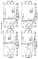
도 3은, 정공 캐리어와 실리콘 표면으로부터의 거리의 관계를 그래프로 나타내는 시뮬레이션 결과를 도시한다. 실질적으로 100㎛의 동일한 웨이퍼 두께에 대하여, P-필러의 중심을 따라 분포된 정공 캐리어 밀도(도 3에서 x=15㎛로 표시됨) 및 N-필러의 중심을 따라 분포된 정공 캐리어 밀도(도 3에서 x=0㎛로 표시됨)가, 80㎛의 P-필러 깊이(도 3에서, t필러=80㎛로 표시됨) 및 65㎛의 P-필러 깊이(도 3에서 t필러=65㎛로 표시됨)의 두 가지 경우에 대하여 그래프로 도시되어 있다. 정공 캐리어들의 대부분이 N-필러가 아닌 P-필러를 통해 흐른다는 것을 알 수 있다.3 shows simulation results graphically showing the relationship between the hole carrier and the distance from the silicon surface. For the same wafer thickness of substantially 100 μm, the hole carrier density distributed along the center of the P-pillar (indicated by x = 15 μm in FIG. 3) and the hole carrier density distributed along the center of the N-pillar (FIG. 3) In x = 0 μm), the P-filler depth of 80 μm (in Fig. 3, denoted by t filler = 80 μm) and the P-pillar depth of 65 μm (indicated by t filler = 65 μm in Fig. 3). The two cases are shown graphically. It can be seen that most of the hole carriers flow through the P-filler and not the N-filler.
도 4는, 기존의 IGBT와, 90㎛ 및 100㎛의 웨이퍼 두께를 갖는 두 가지 경우의 초접합 IGBT(도 2와 유사한 구조를 가짐)에 대하여, 턴-오프(turn-off) 에너지(Eoff)와 콜렉터-이미터 간 온-상태 전압 Vce(포화)의 관계를 그래프로 나타내는 시뮬레이션 결과를 도시한다. 도시된 바로부터 알 수 있듯이, 기존의 IGBT에 비해 초접합 IGBT에서 Vce(포화)/Eoff 간의 트레이드-오프(trade-off)가 현저히 개선된다.FIG. 4 shows the turn-off energy Eoff for the conventional IGBT and the superjunction IGBT (having a structure similar to that of FIG. 2) in two cases with wafer thicknesses of 90 μm and 100 μm. The simulation results plot the relationship between the on-state voltage Vce (saturation) between the and collector-emitters. As can be seen, the trade-off between Vce (saturation) / Eoff in the superjunction IGBT is significantly improved compared to the conventional IGBT.
상기 번갈아 배치된 필러 구조와 관련된 항복 전압 개선을 얻기 위해서는, N-필러 및 P-필러 모두가 완전히 공핍될 필요가 있다. 당해 공핍 영역에서 공간 전하(space charge)의 중성 상태가 유지될 필요가 있고, 이에 따라 P-타입 필러 내의 음전하와 N-타입 필러(드리프트 영역) 내의 양전하 사이에 전하 균형이 요구된다. 이는, N-타입 필러와 P-타입 필러의 도핑 및 물리적 특성을 신중하게 처리할 것을 요구한다. 그러나, 이하에 보다 충분히 기재된 바와 같이, 본 발명에 따른 초접합 IGBT는, 완벽한 전하 균형이 아닌 인접한 N 및 P 필러들 사이에 미리 정해진 양의 전하 불균형을 도입함으로써 다수의 트레이드-오프 성능들을 향상시키도록 설계된다.In order to obtain the breakdown voltage improvement associated with the alternately arranged filler structure, both the N-pillar and the P-pillar need to be fully depleted. In this depletion region, a neutral state of space charge needs to be maintained, thus requiring a charge balance between the negative charge in the P-type pillar and the positive charge in the N-type pillar (drift region). This requires careful handling of the doping and physical properties of the N-type and P-type fillers. However, as described more fully below, the superjunction IGBT according to the present invention improves a number of trade-off performances by introducing a predetermined amount of charge imbalance between adjacent N and P fillers, which is not a perfect charge balance. It is designed to be.
본 개시로부터 알 수 있듯이, P-필러 내에 더 많은 전하가 존재할 수 있도록 하는 5-20% 범위의 전하 불균형은 다양한 트레이드-오프 성능들을 향상시킬 수 있도록 한다. 일 실시예에서는, N-필러 내의 순전하(net charge)가 5×10¹⁰a/cm3 내지 1×10¹²a/cm3 범위가 되도록 하는 도핑 농도를 갖는 보다 얇은 에피택시층 206이 이용되는 한편, P-필러의 도핑 농도는 P-필러 내의 순전하가 N-필러보다 실질적으로 5-20% 더 크도록 설정된다. 줄(stripe) 형태의 설계에서, 각각의 N 및 P 필러 내의 순전하의 근사치는, 필러의 도핑 농도와 필러의 폭의 곱에 의해 개략적으로 구해질 수 있다(N 및 P 필러의 줄이 서로 동일한 깊이와 길이를 갖는다고 가정함).As can be seen from the present disclosure, charge imbalance in the 5-20% range that allows more charge to be present in the P-pillar allows to improve various trade-off performances. In one embodiment, a
도 5 내지 18에 도시된 시뮬레이션 결과에 나타난 바와 같이, 상기 번갈아 배치된 필러들과 초접합 구조물 내의 순전하를 최적화함으로써, 다양한 트레이드-오프 성능들이 제어되고 개선될 수 있다. 도 5와 6은, BVces 및 Vce(포화)의 전하 불균형에 대한 감도를 각각, 다양한 온도에서 1×10¹²a/cm3의 N-필러 전하에 대하여 나타낸 시뮬레이션 결과를 도시한다. 도 5와 6의 가로축을 따라 표시된 전하 불균형은, N-필러에 대한 P-필러의 전하량을 증가시키거나 감소시킴으로써 획득된다. 본 발명에 의하면, N 및 P 필러들은 보다 낮은 전하(예를 들면, 1×10¹²a/cm3보다 적거나 이와 같음)가 이용될 수 있도록 조정되고, 이는 Vce(포화) 및 BVces의 전하 불균형에 대한 감도를 극적으로 감소시킨다.As shown in the simulation results shown in FIGS. 5-18, by optimizing the net charge in the alternating fillers and the superjunction structure, various trade-off performances can be controlled and improved. 5 and 6 show simulation results showing the sensitivity to charge imbalance of BVces and Vce (saturated) for an N-filler charge of 1 × 10 12 a / cm 3 at various temperatures, respectively. Charge imbalances along the abscissa of FIGS. 5 and 6 are obtained by increasing or decreasing the amount of charge of the P-pillar to the N-pillar. According to the present invention, the N and P fillers are adjusted such that lower charges (e.g., less than or equal to 1x10 12 a / cm 3 ) can be used, which is the charge imbalance of Vce (saturated) and BVces. Dramatically reduce the sensitivity to
도 7과 8은, 단락 회로 저항 시간(short circuit withstand time; SCWT)의 전하 불균형에 대한 감도를 각각, 1×10¹²a/cm3의 N-필러 전하와 1V 및 1.7V의 Vce(포화)에 대하여 나타낸 시뮬레이션 결과를 도시한다. 도 9는, 1×10¹²a/cm3의 동일한 N-필러 전하에 대하여 턴-오프(turn-off) 에너지 Eoff의 감도를 나타낸 시뮬레이션 결과를 도시한다. 도 10과 11은, 1×10¹²a/cm3의 동일한 N-필러 및 P-필러 전하(즉, 전하 균형 구조)에 대한 Vce(포화)와 Eoff의 트레이드-오프의 관계 및 Vce(포화)와 SCWT 트레이드-오프의 관계를 도시한다. 이 도면들로부터 알 수 있듯이, 125℃에서 1.2V보다 낮은 Vce(포화)에서의 20μJ/A의 Eoff, 및 전하 불균형이 일어나지 않는 10μsec보다 긴 SCWT가 성취될 수 있다.7 and 8 show sensitivity to charge imbalance of short circuit withstand time (SCWT), respectively, with N-filler charge of 1 × 10 12 a / cm 3 and Vce (saturation) of 1V and 1.7V, respectively. The simulation results shown for FIG. 9 shows simulation results showing the sensitivity of the turn-off energy Eoff for the same N-filler charge of 1 × 10 12 a / cm 3 . Figures 10 and 11 show the trade-off and Vce (saturation) of Vce (saturation) and Eoff for the same N-filler and P-filler charge (i.e., charge balance structure) of 1x10 12 a / cm 3 . And the relationship between SCWT trade-offs. As can be seen from these figures, an Eoff of 20 μJ / A at Vce (saturation) lower than 1.2 V at 125 ° C., and an SCWT longer than 10 μsec without charge imbalance can be achieved.
P-필러 207이 정공 전류에 대한 싱크(sink)로서 기능하므로 상기 SCWT 성능이 개선된다. 이에 따라 상기 정공 전류는, 도 1의 기존 IGBT에서처럼 소스 영역 110 아래에서보다는, P-필러 207을 따라서 흐르기 쉽다. 이는 도 2의 초접합 IGBT가 SCWT 동안 NPN 래치-업에 영향을 받지 않도록 한다. 또한 이러한 전류 흐름은, 도 1의 기존 IGBT에서처럼 SCWT 동안 더욱 균일하며 국부화되지 않은 자기 발열(self heating)을 이끌어낸다. 나아가, 이는 도 2의 초접합 IGBT가 더욱 높은 PNP 이득으로 동작되도록 하고, 또한 정방향 접합에서 열적으로 발생된 누설 전류로 인해 PNP가 온(on) 상태가 되는 것에 따른 실패를 감소시킨다. 이는, 소수 캐리어 수명(minority carrier lifetime)의 온도 계수(temperature coefficient)가 양(positive)이므로 드리프트 영역에서의 온도 상승에 따라 상기 소수 캐리어 수명이 증가하기 때문에, 기존의 IGBT의 단점이 되었다. 정방향 접합에서의 응집된 고 온으로부터 열적으로 발생된 누설, 및 열적으로 증가된 PNP 이득은 PNP가 보다 빨리 온(on) 상태가 되도록 한다.The SCWT performance is improved because the P-
도 2의 초접합 IGBT의 다른 중요한 특징은, 게이트 저항 Rg를 변화시킴으로써 턴-오프 di/dt가 게이트 제어되는 턴-오프처럼 빠른 펀치-쓰루(quick punch through; QPT)를 용이하게 형성한다는 점이다. 도 12A 및 12B의 타이밍도(초접합 IGBT에 대한 시뮬레이션 결과임)에 도시된 바와 같이, 상기 QPT는 전류가 하강하기 시작할 때 유효 게이트 바이어스가 상기 IGBT의 문턱 전압 Vth 이상이 되도록 셀의 설계 내용(예를 들면, 게이트 구조 및 PNP 이득)에 따라 형성된다. 상기 QPT는 2004년 12월 14일 자로 등록되고 공동으로 양도된 미국 특허 제6,831,329호에 더욱 상세히 기재되어 있으며, 상기 미국 특허는 그 전체로서 참조에 의해 본 명세서에 편입된다.Another important feature of the superjunction IGBT of FIG. 2 is that by varying the gate resistance Rg, turn-off di / dt easily forms a quick punch-through as fast as gate-controlled turn-off. . As shown in the timing diagrams (simulation results for the superjunction IGBTs) of FIGS. 12A and 12B, the QPT is designed so that the effective gate bias is greater than or equal to the threshold voltage Vth of the IGBT when the current begins to fall. For example, gate structure and PNP gain). The QPT is described in more detail in US Pat. No. 6,831,329, registered and commonly assigned Dec. 14, 2004, which is incorporated herein by reference in its entirety.
도 13과 14는, 두 개의 Rg 값에 대하여, 1×10¹²a/cm3의 동일한 N-필러 전하 및 P-필러 전하에 대한 Vce(포화)와 di/dt의 트레이드-오프의 관계 및 Vce(포화)와 dv/dt의 트레이드-오프의 관계를 각각 도시한다. 도 15, 16, 17 및 18은, 1×10¹²a/cm3와 동일한 N-필러 전하와 두 개의 Rg 값에 대한, Eoff, 피크 Vce, di/dt 및 dv/dt의 전하 불균형에 대한 감도를 각각 도시한다. 도 10과 13으로부터 알 수 있듯이, 턴-오프 di/dt를 늦추는 것은 Eoff를 증가시키지만, 이는 EMI 성능을 위해 Eoff를 융통성 있게 트레이드-오프할 수 있도록 한다. 상기 초접합 IGBT의 dv/dt는 소수 캐리어의 빠른 3-D 스윕-아웃(sweep out)으로 인해 높은 값을 갖는다. QPT를 갖는 상기 초접합 IGBT는 전압이 상승하는 동안 최소의 턴-오프 손실을 갖는다. 또한, 상기 dv/dt는 도 14에 도시된 바와 같이 Rg를 이용하여 어느 정도 제어될 수 있다.13 and 14 show the relationship between the trade-off of Vce (saturated) and di / dt for the same N-filler charge and P-filler charge of 1 × 10 12 a / cm 3 for two Rg values, and Vce (Saturation) and the trade-off relationship of dv / dt are shown, respectively. Figures 15, 16, 17 and 18 show sensitivity to charge imbalance of Eoff, peak Vce, di / dt and dv / dt for N-filler charge equal to 1x10 12 a / cm 3 and two Rg values. Respectively. As can be seen from Figures 10 and 13, slowing the turn-off di / dt increases Eoff, but this allows for flexible trade-off of Eoff for EMI performance. The dv / dt of the superjunction IGBT has a high value due to the fast 3-D sweep out of minority carriers. The superjunction IGBT with QPT has minimal turn-off loss while the voltage is rising. In addition, the dv / dt may be controlled to some extent using Rg as shown in FIG. 14.
기존의 IGBT에서의 턴-오프 손실의 대부분은, 상기 전압이 상승하는 동안 주입된 캐리어의 느린 스윕-아웃과, 상기 전압이 버스 전압에 도달한 이후, 공핍되지 않은 나머지 드리프트 및 버퍼 영역 중 어느 하나 또는 모두에서의 캐리어들의 소수 캐리어 재결합을 그 원인으로 한다. 상기 전류 강하 di/dt가 게이트 방전에 의해 제어되고 기존의 IGBT보다 현저히 느리기 때문에, Eoff는 거의 완전히 상기 전류 강하로부터 발생된다. 실질적으로, 상기 초접합 IGBT의 턴-오프 손실의 대부분은 전류 강하에 기인하며, 상기 전류 강하는 di/dt를 Rg를 이용하여 조정함으로써 제어될 수 있다.Most of the turn-off losses in conventional IGBTs are either slow sweep-out of the injected carrier while the voltage is rising, or any of the remaining non-depleted drift and buffer regions after the voltage reaches the bus voltage. Or minor carrier recombination of carriers at all. Since the current drop di / dt is controlled by the gate discharge and is significantly slower than conventional IGBTs, Eoff is almost completely generated from the current drop. In practice, most of the turn-off losses of the superjunction IGBTs are due to the current drop, which can be controlled by adjusting di / dt with Rg.
도 19 내지 22는 본 발명의 실시예들에 의한 다양한 초접합 IGBT의 단면도 및 그에 대응되는 도핑 프로파일(doping profile)을 도시한다. 도 19A는 최초 웨이퍼가 P+ 기판 1904인 실시예를 도시하며, 상기 P+ 기판 1904 위에 N-에피택시 버퍼층 1905가 형성된다. 버퍼층 1905보다 낮은 도핑 농도의 상부 N-에피택시층 1906이 버퍼층 1905 위에 형성된다. 나머지 영역들 및 층들은 다수의 공지 기술 중 하나를 이용하여 형성된다. 예를 들면, P-타입 도펀트를 상기 상부 N-에피택시층 1906 내로 주입(고에너지를 이용함)하거나, 상기 상부 N-에피택시층 1906 내에 트랜치를 형성하고 상기 트랜치를 P-타입 실리콘으로 채움으로써, P-필러 1907이 형성될 수 있다. 또 다른 실시예에서는, 상기 상부 N-에피택시층 1906 대신 N-에 피택시의 다층이 형성되고, 각각의 N-에피택시층을 형성한 후 P-필러 1907의 대응되는 부분을 형성하기 위해 P-타입 주입이 수행된다. 본체 영역 1908과 소스 영역 1910이 공지된 기술을 이용하여 형성된다. 도 19B는, 도 19A의 구조물의 N-필러의 중심을 통과하는 수직선을 따라 분포된 예시적인 도핑 농도(상부 도면)와, P-필러의 중심을 통과하는 수직선을 따라 분포된 예시적인 도핑 농도(하부 도면)를 도시한다.19-22 illustrate cross-sectional views of various superjunction IGBTs and corresponding doping profiles according to embodiments of the invention. FIG. 19A shows an embodiment where the original wafer is a P +
도 20A에서, 영역 2006으로 도시된 하나 또는 다수의 N-에피택시층이 기판 위에 형성되고, 상기 하나 또는 다수의 에피택시층을 남겨두면서 상기 기판이 완전히 제거된다. 상기 에피택시층의 배면(背面)으로 P-타입 도펀트가 주입되어 콜렉터 영역 2004가 형성된다. 다른 실시예에서, N-에피택시층을 포함하지 않는 N-타입 기판이 이용되고, 상기 콜렉터 영역은 기판의 배면으로 도펀트를 주입합으로써 형성된다. P-필러 2007, 본체 영역 2008 및 소스 영역 2010이, 도 19A와 관련하여 기재된 다수의 기술들 중 어느 하나를 이용하여 형성된다. 도 20B는, N-필러의 중심을 통과하는 수직선을 따라 분포된 예시적인 도핑 농도(좌상부 도면)와, P-필러의 중심을 통과하는 수직선을 따라 분포된 예시적인 도핑 농도(우상부 도면)를 도시한다. 도 20B의 하부 도면은, 상기 N-타입 기판 또는 에피택시층(들)로부터 콜렉터 영역 2004까지 그리고 상기 콜렉터 영역 2004를 통과하는 전이 영역 내의 도핑 프로파일의 확장도를 도시한다.In FIG. 20A, one or multiple N-epitaxial layers, shown as
도 21A는, N-타입 필드 정지 영역이 상기 구조에 병합된다는 점을 제외하고는 도 20A와 유사한 단면도이다. 일 실시예에서, 하나 또는 다수의 N-에피택시층 이 기판 위에 형성되고, 상기 하나 또는 다수의 에피택시층을 남겨두면서 상기 기판이 완전히 제거된다. 상기 에피택시층의 배면으로 N-타입 도펀트가 주입되어 N-타입 필드 정지 영역이 형성된 후, 상기 필드 정지 영역의 배면으로 P-타입 도펀트 주입이 수행되어 상기 필드 정지 영역 내에 콜렉터 영역이 형성된다. 다른 실시예에서는, N-에피택시층을 포함하지 않는 N-타입 기판이 이용된다. P-필러 2107, 본체 영역 2108 및 소스 영역 2110은 도 19A와 관련하여 기재된 다수의 기술들 중 어느 하나를 이용하여 형성된다. 도 21B는, N-필러의 중심을 통과하는 수직선을 따라 분포된 예시적인 도핑 농도(좌상부 도면)와, P-필러의 중심을 통과하는 수직선을 따라 분포된 예시적인 도핑 농도(우상부 도면)를 도시한다. 도 21B의 하부 도면은, 상기 필드 정지 영역 및 콜렉터 영역을 통한 도핑 프로파일의 확장도를 도시한다.FIG. 21A is a sectional view similar to FIG. 20A except that an N-type field stop region is incorporated into the structure. In one embodiment, one or multiple N-epitaxial layers are formed over the substrate, and the substrate is completely removed leaving the one or more epitaxy layers. After the N-type dopant is implanted into the back of the epitaxy layer to form an N-type field stop region, the P-type dopant is implanted into the back of the field stop region to form a collector region in the field stop region. In another embodiment, an N-type substrate is used that does not include an N-epitaxial layer. P-
도 22A에서, 영역 2206으로 도시된 N-에피택시층(또는 다수의 N-에피택시층)이 N-타입 기판 위에 형성되고, 원하는 두께의 더 얇은 기판층이 남도록 상기 기판의 미리 정해진 두께 부분이 상기 기판의 배면에서 제거된다. 상기 기판은 N-에피택시층보다 낮은 저항을 갖는다. 상기 기판의 배면으로 P-타입 도펀트를 주입함으로써 콜렉터 영역이 형성되면서, 상기 기판의 나머지 부분은 사실상 필드 정지 영역을 형성한다. P-필러 2207, 본체 영역 2208 및 소스 영역 2210은 도 19A와 관련하여 기재된 다수의 기술들 중 어느 하나를 이용하여 형성된다. 도 22B는, N-필러의 중심을 통과하는 수직선을 따라 분포된 예시적인 도핑 농도(좌상부 도면)와, P-필러의 중심을 통과하는 수직선을 따라 분포된 예시적인 도핑 농도(우상부 도면)를 도시한다. 도 22B의 하부 도면은, 상기 필드 정지 영역 및 콜렉터 영역을 통한 도핑 프로파일의 확장도를 도시한다.In FIG. 22A, an N-epitaxial layer (or a plurality of N-epitaxial layers), shown as
본 발명의 다른 실시예에서, 상기 P-필러 내의 도핑 농도는, 상기 P-필러의 최상부를 따라 분포되는 더 높은 도핑 농도로부터, 상기 P-필러의 바닥을 따라 분포되는 더 낮은 도핑 농도로 점차 변하고, 상기 N-필러 내의 도핑 농도는 실질적으로 균일하다. 또 다른 실시예에서, 상기 N-필러 내의 도핑 농도는 상기 N-필러의 바닥을 따라 분포되는 더 높은 도핑 농도로부터, 상기 N-필러의 최상부를 따라 분포되는 더 낮은 도핑 농도로 점차 변하고, 상기 P-필러 내의 도핑 농도는 실질적으로 균일하다.In another embodiment of the present invention, the doping concentration in the P-pillar gradually changes from a higher doping concentration distributed along the top of the P-pillar to a lower doping concentration distributed along the bottom of the P-pillar. , The doping concentration in the N-filler is substantially uniform. In another embodiment, the doping concentration in the N-pillar gradually changes from a higher doping concentration distributed along the bottom of the N-pillar to a lower doping concentration distributed along the top of the N-pillar, and the P The doping concentration in the filler is substantially uniform.
도 23은 본 발명의 일 실시예에 의한 트랜치 게이트 초접합 IGBT의 단면도를 도시한다. 게이트 구조물과 그 주위 영역을 제외하고 도 23의 트랜치 게이트는 도 2의 평면형 게이트 IGBT와 구조적으로 유사하므로, 도 2의 평면형 게이트 IGBT와 그 변형예 및 대체적 실시예들과 관련하여 상기 기재된 것과 동일한 특징과 이점 중 상당수가 도 23의 트랜치 게이트 IGBT를 이용하여 실현될 수 있다. 도 23에서, 고농도로 도핑된 P-타입 콜렉터 영역 2304가 콜렉터 전극 2302에 전기적으로 접속된다. N-타입 필드 정지층(field stop layer; FSL) 2305가 콜렉터 영역 2304 위에서 연장되고, N-타입 영역 2306a가 FSL 2305 위에서 연장된다. 번갈아 배치된 P-필러들 2307 및 N-필러들 2306b를 포함하는 전하 균형 영역이 N-타입 영역 2306a 위에서 연장된다. 다른 실시예에서, 상기 전하 균형 영역의 영역 2307은, 영역 2307의 수직 경계면과 바닥 경계면을 따라 연장되는 P-타입 실리콘 라이너(liner) 를 포함하며, 영역 2307의 나머지 부분은 N-타입 또는 진성 실리콘이다. 23 illustrates a cross-sectional view of a trench gate superjunction IGBT according to one embodiment of the present invention. The trench gate of FIG. 23 except for the gate structure and its surroundings is structurally similar to the planar gate IGBT of FIG. 2, so that the same features as those described above in connection with the planar gate IGBT of FIG. 2 and variations and alternative embodiments thereof. Many of these and advantages can be realized using the trench gate IGBT of FIG. In FIG. 23, a heavily doped P-
고농도로 도핑된 P-타입 웰 영역 2308이 상기 전하 균형 구조물 위에서 연장되고, 게이트 트랜치가 상기 웰 영역 2308을 통해 연장되고 N-필러 2306b 내에서 종단된다. 고농도로 도핑된 N-타입 소스 영역 2310이 웰 영역 2308 내에 상기 게이트 트랜치의 각측에 위치된다. 웰 영역 2308과 소스 영역 2310은 이미터 전극 2312에 전기적으로 접속된다. 게이트 유전체 2316이 상기 트랜치의 측벽을 덮고, 게이트 2314(예를 들면, 폴리실리콘을 포함함)가 상기 트랜치를 채운다. 상기 트랜치 내에서 게이트 2314에 리세스가 형성되고, 유전체캡이 리세스(recessed) 게이트 위에서 상기 트랜치를 채운다. 이미터 도전체(예를 들면, 금속을 포함함)가 소스 영역, 본체 영역 및 트랜치 게이트 위에서 연장될 수 있다. 또한, 도 2의 상기 평면형 게이트 IGBT와 관련하여 상기 논의된 것과 동일한 고려 사항들 중 상당수가 도 23의 상기 게이트 트랜치 IGBT에 적용된다.A heavily doped P-
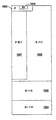
도 2의 상기 평면형 게이트 IGBT와 도 23의 상기 트랜치 게이트 IGBT 및 그 변형례들은, 다수의 서로 다른 방법들로 레이아웃(layout)이 정해질 수 있다. 두 가지의 예시적인 레이아웃 설계가 도 24와 25에 도시된다. 도 24는 동심(同心)형 게이트를 포함하는 동심형 필러 설계를 도시한다. 도시된 바와 같이, 다이의 중심으로부터 시작되고 서로 동일하게 이격된, 점차 커지는 사각형 링의 P-필러들 2407(무늬 없는 검정색의 링)이 형성된다. 사각형의 게이트 링 2414(빗금이 그려진 링)가 모든 두 개의 인접한 P-필러 링들 사이에 형성된다. 도시된 바와 같이, 전하 균형을 위하여 게이트는 가장 안쪽의 P-필러 링에 의해 둘러싸인 영역의 내 부, 즉, 안쪽의 처음 두 개의 P-필러 링들 사이에는 형성되지 않는다. 또한, 소스 및 본체 영역들(도시되지 않음)이 링의 형태를 갖지만, 래치-업을 방지하기 위하여 상기 소스 영역은 불연속적인 링, 또는 불연속적인 채널 영역을 수반한 연속적인 링 중 어느 하나일 필요가 있다. The planar gate IGBT of FIG. 2 and the trench gate IGBT of FIG. 23 and variations thereof may be layouted in a number of different ways. Two exemplary layout designs are shown in FIGS. 24 and 25. 24 illustrates a concentric filler design that includes concentric gates. As shown, gradually increasing rectangular ring P-pillars 2407 (stainless black ring) are formed, starting from the center of the die and equally spaced from each other. A rectangular gate ring 2414 (hatched ring) is formed between all two adjacent P-pillar rings. As shown, for charge balancing a gate is not formed inside the region surrounded by the innermost P-pillar ring, ie between the first two P-pillar rings inward. Also, although the source and body regions (not shown) have the form of a ring, the source region needs to be either a discontinuous ring or a continuous ring with discontinuous channel regions to prevent latch-up. There is.
게이트 링 2414는 P-필러 링 2407 위에서 연장되지 않는 것으로 도시되어 있지만, 다른 실시예에서는 상기 게이트 링이 P-필러 링과 중첩된다. 또한, 상기 동심형 P-필러 링 2407과 게이트 링 2414는 사각형인 것으로 도시되었지만, 직사각형, 다각형, 육각형, 원형, 또는 다른 기하학적 형태일 수 있다. 일 실시예에서는, 상기 동심형 P-필러 링 위에서 수직 또는 수평으로 연장되는 줄(stripe) 형태의 게이트가 동심형 게이트 링 대신 이용된다. 그러한 실시예는, 상기 게이트가 상기 동심형 게이트 링의 설계에서와 같이 P-타입 필러들에 적절하게 정렬되도록 요구되지 않는다는 점에서 유리하다. 또한 이러한 실시예는 피크 SCWT를 증가시킨다.
도 25는 줄 형태의 게이트와 줄 형태 필러의 설계를 도시한다. 도시된 바와 같이, 서로 동일하게 이격된 줄 형태의 P-필러 2507(무늬 없는 검정색의 줄)이 다이의 길이 방향으로 연장되면서, 줄 형태의 게이트 2514(빗금이 그려진 영역들)가 모든 두 개의 인접한 P-필러의 줄들의 사이에서 연장된다. 또한, 소스 및 본체 영역들(도시되지 않음)이 줄 형태를 갖는다. 또한 도 25는 다이의 우측 및 좌측을 따라 위치된 종단 영역의 일부분을 도시하는데, 상기 종단 영역의 일부분은 수직으로 연장되는 P-필러들 2507을 포함한다. 이러한 수직으로 연장되는 P-필러들은, 활성 영역과 종단 영역 사이의 전이 영역 내의 전하 균형을 유지하기 위하여, 상기 활성 영역 내의 수평으로 연장되는 P-필러들로부터 적절하게 이격된다.25 shows a design of a row gate and row pillars. As shown, the string-shaped P-pillar 2507 (black stripe without stripes) extends in the length direction of the die, so that the gate 2514 (hatched areas) in the form of strings are connected to all two adjacent ones. It extends between the rows of P-pillars. In addition, the source and body regions (not shown) have a row shape. FIG. 25 also shows a portion of the termination region located along the right and left sides of the die, wherein the portion of the termination region includes P-
게이트의 줄 2514는 P-필러의 줄 2507 위에서 연장되지 않는 것으로 도시되어 있지만, 다른 실시예에서는 상기 게이트의 줄이 상기 P-필러의 줄과 중첩한다. 또한, P-필러 2507에 평행하게 연장되는 게이트의 줄 2514가 도시되어 있지만, 다른 실시예에서는 상기 게이트의 줄이 상기 P-필러의 줄에 수직으로 연장된다. 그러한 실시예는, 서로 평행하게 연장되는 게이트 및 P-필러의 줄을 포함하는 실시예에서 요구되는 바와 같이 상기 게이트가 상기 P-필러에 적절하게 정렬될 것이 요구되지 않는다는 점에서 유리하다. 또한 당해 실시예는 피크 SCWT를 증가시킨다.
본 발명은 그 예시적인 실시예들과 관련하여 구체적으로 도시되고 기재되었지만, 본 발명이 속하는 기술 분야에서 통상의 지식을 가진 자라면, 본 발명의 정수(精髓) 및 범위로부터 벗어나지 않으면서 그 형태 및 세부 사항에 있어서 다양한 변경이 이루어질 수 있다는 점을 이해할 것이다. 다양한 치수, 도핑 농도 및 서로 다른 반도전층 또는 절연층들을 설명하기 위해 본 명세서에서 제공된 모든 물질 타입들은 단지 설명을 위한 것이고, 본 발명을 한정하도록 의도된 것이 아니다. 예를 들면, 본 명세서에 기재된 실시예들의 다양한 실리콘 영역들의 도핑 극성은, 특정 실시예의 다른 극성 타입의 디바이스를 획득하기 위해 반전될 수 있다. 따라서, 이들 및 다른 이유로, 상기 기재가 본 발명의 범위를 제한하도록 해석되어선 안되고, 본 발명의 범위는 첨부된 청구항들에 의해 정의된다.While the invention has been shown and described in detail in connection with exemplary embodiments thereof, those skilled in the art will appreciate that the present invention may be embodied without departing from the spirit and scope of the invention without departing from the spirit and scope of the invention. It will be understood that various changes in detail may be made. All material types provided herein to describe various dimensions, doping concentrations and different semiconducting or insulating layers are for illustration only and are not intended to limit the invention. For example, the doping polarity of the various silicon regions of the embodiments described herein may be reversed to obtain a device of another polarity type of the particular embodiment. Accordingly, for these and other reasons, the above description should not be interpreted as limiting the scope of the present invention, which is defined by the appended claims.
Claims (59)
Applications Claiming Priority (4)
| Application Number | Priority Date | Filing Date | Title |
|---|---|---|---|
| US76526106P | 2006-02-03 | 2006-02-03 | |
| US60/765,261 | 2006-02-03 | ||
| US11/408,812 | 2006-04-21 | ||
| US11/408,812 US20070181927A1 (en) | 2006-02-03 | 2006-04-21 | Charge balance insulated gate bipolar transistor |
Publications (1)
| Publication Number | Publication Date |
|---|---|
| KR20080098371A true KR20080098371A (en) | 2008-11-07 |
Family
ID=38333169
Family Applications (1)
| Application Number | Title | Priority Date | Filing Date |
|---|---|---|---|
| KR1020087019992A Ceased KR20080098371A (en) | 2006-02-03 | 2006-12-19 | Charge Balanced Insulated Gate Bipolar Transistors |
Country Status (8)
| Country | Link |
|---|---|
| US (1) | US20070181927A1 (en) |
| JP (1) | JP2009525610A (en) |
| KR (1) | KR20080098371A (en) |
| CN (1) | CN101336480B (en) |
| AT (1) | AT505499A2 (en) |
| DE (1) | DE112006003714T5 (en) |
| TW (1) | TWI433316B (en) |
| WO (1) | WO2007120345A2 (en) |
Families Citing this family (46)
| Publication number | Priority date | Publication date | Assignee | Title |
|---|---|---|---|---|
| US7638841B2 (en) | 2003-05-20 | 2009-12-29 | Fairchild Semiconductor Corporation | Power semiconductor devices and methods of manufacture |
| CN101868856B (en) | 2007-09-21 | 2014-03-12 | 飞兆半导体公司 | Super junction structure and manufacturing method for power device |
| US20120273916A1 (en) | 2011-04-27 | 2012-11-01 | Yedinak Joseph A | Superjunction Structures for Power Devices and Methods of Manufacture |
| JP4544360B2 (en) * | 2008-10-24 | 2010-09-15 | トヨタ自動車株式会社 | Manufacturing method of IGBT |
| US8174067B2 (en) | 2008-12-08 | 2012-05-08 | Fairchild Semiconductor Corporation | Trench-based power semiconductor devices with increased breakdown voltage characteristics |
| US8304829B2 (en) | 2008-12-08 | 2012-11-06 | Fairchild Semiconductor Corporation | Trench-based power semiconductor devices with increased breakdown voltage characteristics |
| US8227855B2 (en) | 2009-02-09 | 2012-07-24 | Fairchild Semiconductor Corporation | Semiconductor devices with stable and controlled avalanche characteristics and methods of fabricating the same |
| US8148749B2 (en) | 2009-02-19 | 2012-04-03 | Fairchild Semiconductor Corporation | Trench-shielded semiconductor device |
| US8049276B2 (en) | 2009-06-12 | 2011-11-01 | Fairchild Semiconductor Corporation | Reduced process sensitivity of electrode-semiconductor rectifiers |
| US8283213B2 (en) * | 2010-07-30 | 2012-10-09 | Alpha And Omega Semiconductor Incorporated | Method of minimizing field stop insulated gate bipolar transistor (IGBT) buffer and emitter charge variation |
| US9412854B2 (en) * | 2010-10-20 | 2016-08-09 | Infineon Technologies Austria Ag | IGBT module and a circuit |
| CN102738232B (en) * | 2011-04-08 | 2014-10-22 | 无锡维赛半导体有限公司 | Super junction power transistor structure and manufacturing method thereof |
| US8786010B2 (en) | 2011-04-27 | 2014-07-22 | Fairchild Semiconductor Corporation | Superjunction structures for power devices and methods of manufacture |
| US8772868B2 (en) | 2011-04-27 | 2014-07-08 | Fairchild Semiconductor Corporation | Superjunction structures for power devices and methods of manufacture |
| US8836028B2 (en) | 2011-04-27 | 2014-09-16 | Fairchild Semiconductor Corporation | Superjunction structures for power devices and methods of manufacture |
| US8673700B2 (en) | 2011-04-27 | 2014-03-18 | Fairchild Semiconductor Corporation | Superjunction structures for power devices and methods of manufacture |
| CN102270640B (en) * | 2011-06-20 | 2013-02-06 | 湖南大学 | IGBT and manufacturing method thereof with high-current full-wafer full-press flat-package |
| US9478646B2 (en) * | 2011-07-27 | 2016-10-25 | Alpha And Omega Semiconductor Incorporated | Methods for fabricating anode shorted field stop insulated gate bipolar transistor |
| US9224852B2 (en) * | 2011-08-25 | 2015-12-29 | Alpha And Omega Semiconductor Incorporated | Corner layout for high voltage semiconductor devices |
| US8680613B2 (en) | 2012-07-30 | 2014-03-25 | Alpha And Omega Semiconductor Incorporated | Termination design for high voltage device |
| US8785279B2 (en) | 2012-07-30 | 2014-07-22 | Alpha And Omega Semiconductor Incorporated | High voltage field balance metal oxide field effect transistor (FBM) |
| CN103137679B (en) * | 2011-11-21 | 2016-10-26 | 上海华虹宏力半导体制造有限公司 | Insulated-gate bipolar transistor device structure and preparation method thereof |
| KR101352766B1 (en) | 2011-12-08 | 2014-01-15 | 서강대학교산학협력단 | The planar gate IGBT with nMOS |
| CN103178102B (en) * | 2011-12-21 | 2016-02-10 | 上海华虹宏力半导体制造有限公司 | Igbt and preparation method thereof |
| CN103050408A (en) * | 2012-05-31 | 2013-04-17 | 上海华虹Nec电子有限公司 | Manufacture method of super junction |
| JP2014060299A (en) * | 2012-09-18 | 2014-04-03 | Toshiba Corp | Semiconductor device |
| US8975136B2 (en) | 2013-02-18 | 2015-03-10 | Infineon Technologies Austria Ag | Manufacturing a super junction semiconductor device |
| US9029944B2 (en) | 2013-02-18 | 2015-05-12 | Infineon Technologies Austria Ag | Super junction semiconductor device comprising implanted zones |
| CN103594502A (en) * | 2013-11-19 | 2014-02-19 | 西安永电电气有限责任公司 | High-voltage IGBT with super junction structure |
| CN103594504A (en) * | 2013-11-19 | 2014-02-19 | 西安永电电气有限责任公司 | IGBT with semi-super junction structure |
| WO2015127673A1 (en) * | 2014-02-28 | 2015-09-03 | 电子科技大学 | Bi-directional igbt component |
| JP6324805B2 (en) * | 2014-05-19 | 2018-05-16 | ルネサスエレクトロニクス株式会社 | Semiconductor device and manufacturing method thereof |
| US9245754B2 (en) * | 2014-05-28 | 2016-01-26 | Mark E. Granahan | Simplified charge balance in a semiconductor device |
| US9318587B2 (en) | 2014-05-30 | 2016-04-19 | Alpha And Omega Semiconductor Incorporated | Injection control in semiconductor power devices |
| JP6319454B2 (en) * | 2014-10-24 | 2018-05-09 | 富士電機株式会社 | Semiconductor device and manufacturing method of semiconductor device |
| CN108269858B (en) * | 2017-01-04 | 2021-07-16 | 深圳尚阳通科技有限公司 | A super junction device, chip and manufacturing method thereof |
| CN108198851B (en) * | 2017-12-27 | 2020-10-02 | 四川大学 | A superjunction IGBT with carrier storage effect |
| CN109037312B (en) * | 2018-08-23 | 2024-04-09 | 无锡市乾野微纳科技有限公司 | A super junction IGBT with shielded gate and manufacturing method thereof |
| CN109888004A (en) * | 2019-01-08 | 2019-06-14 | 上海华虹宏力半导体制造有限公司 | IGBT devices |
| CN112310205B (en) * | 2019-07-29 | 2022-04-19 | 广东美的白色家电技术创新中心有限公司 | Insulated gate bipolar transistor and manufacturing method thereof |
| JP7287998B2 (en) * | 2021-03-31 | 2023-06-06 | 本田技研工業株式会社 | BiMOS semiconductor device |
| JP7285277B2 (en) * | 2021-03-31 | 2023-06-01 | 本田技研工業株式会社 | BiMOS semiconductor device |
| CN114005877B (en) * | 2021-11-12 | 2025-12-23 | 上海超致半导体科技有限公司 | Ultrathin super-junction IGBT device and preparation method |
| CN114335143B (en) * | 2021-12-29 | 2025-08-12 | 深圳市千屹芯科技有限公司 | Super junction IGBT with low off-current tailing and manufacturing method thereof |
| CN116469910B (en) * | 2022-09-09 | 2024-02-02 | 苏州华太电子技术股份有限公司 | IGBT device |
| CN116666422B (en) * | 2022-09-23 | 2024-05-14 | 苏州华太电子技术股份有限公司 | IGBT device |
Family Cites Families (21)
| Publication number | Priority date | Publication date | Assignee | Title |
|---|---|---|---|---|
| DE69428894T2 (en) * | 1994-08-02 | 2002-04-25 | Consorzio Per La Ricerca Sulla Microelettronica Nel Mezzogiorno, Catania | Bipolar transistor with isolated control electrode |
| KR0163875B1 (en) * | 1994-11-30 | 1998-12-01 | 윤종용 | Semiconductor device and manufacturing method |
| DE19731495C2 (en) * | 1997-07-22 | 1999-05-20 | Siemens Ag | Bipolar transistor controllable by field effect and method for its production |
| JP3410949B2 (en) * | 1998-02-12 | 2003-05-26 | 株式会社東芝 | Semiconductor device |
| JP3523056B2 (en) * | 1998-03-23 | 2004-04-26 | 株式会社東芝 | Semiconductor device |
| JP3988262B2 (en) * | 1998-07-24 | 2007-10-10 | 富士電機デバイステクノロジー株式会社 | Vertical superjunction semiconductor device and manufacturing method thereof |
| TW502458B (en) * | 1999-06-09 | 2002-09-11 | Toshiba Corp | Bonding type semiconductor substrate, semiconductor light emission element and manufacturing method thereof |
| US6475864B1 (en) * | 1999-10-21 | 2002-11-05 | Fuji Electric Co., Ltd. | Method of manufacturing a super-junction semiconductor device with an conductivity type layer |
| JP2001210823A (en) * | 2000-01-21 | 2001-08-03 | Denso Corp | Semiconductor device |
| JP4088011B2 (en) * | 2000-02-16 | 2008-05-21 | 株式会社東芝 | Semiconductor device and manufacturing method thereof |
| JP4764987B2 (en) * | 2000-09-05 | 2011-09-07 | 富士電機株式会社 | Super junction semiconductor device |
| JP4843843B2 (en) * | 2000-10-20 | 2011-12-21 | 富士電機株式会社 | Super junction semiconductor device |
| CN1138307C (en) * | 2000-12-21 | 2004-02-11 | 北京工业大学 | Low power consumption semiconductor power switching device and manufacturing method thereof |
| JP3764343B2 (en) * | 2001-02-28 | 2006-04-05 | 株式会社東芝 | Manufacturing method of semiconductor device |
| JP3731523B2 (en) * | 2001-10-17 | 2006-01-05 | 富士電機デバイステクノロジー株式会社 | Semiconductor element |
| US6831329B2 (en) * | 2001-10-26 | 2004-12-14 | Fairchild Semiconductor Corporation | Quick punch through IGBT having gate-controllable DI/DT and reduced EMI during inductive turn off |
| JP4126915B2 (en) * | 2002-01-30 | 2008-07-30 | 富士電機デバイステクノロジー株式会社 | Semiconductor device |
| JP3634830B2 (en) * | 2002-09-25 | 2005-03-30 | 株式会社東芝 | Power semiconductor device |
| JP3966151B2 (en) * | 2002-10-10 | 2007-08-29 | 富士電機デバイステクノロジー株式会社 | Semiconductor element |
| JP4676708B2 (en) * | 2004-03-09 | 2011-04-27 | 新電元工業株式会社 | Manufacturing method of semiconductor device |
| JP2005322700A (en) * | 2004-05-06 | 2005-11-17 | Toshiba Corp | Semiconductor device and manufacturing method thereof |
-
2006
- 2006-04-21 US US11/408,812 patent/US20070181927A1/en not_active Abandoned
- 2006-12-19 DE DE112006003714T patent/DE112006003714T5/en not_active Withdrawn
- 2006-12-19 KR KR1020087019992A patent/KR20080098371A/en not_active Ceased
- 2006-12-19 AT AT0954006A patent/AT505499A2/en not_active Application Discontinuation
- 2006-12-19 JP JP2008553238A patent/JP2009525610A/en active Pending
- 2006-12-19 CN CN2006800522452A patent/CN101336480B/en not_active Expired - Fee Related
- 2006-12-19 WO PCT/US2006/062298 patent/WO2007120345A2/en not_active Ceased
- 2006-12-28 TW TW095149492A patent/TWI433316B/en not_active IP Right Cessation
Also Published As
| Publication number | Publication date |
|---|---|
| TWI433316B (en) | 2014-04-01 |
| JP2009525610A (en) | 2009-07-09 |
| US20070181927A1 (en) | 2007-08-09 |
| CN101336480B (en) | 2011-05-18 |
| WO2007120345A3 (en) | 2008-05-15 |
| CN101336480A (en) | 2008-12-31 |
| DE112006003714T5 (en) | 2009-03-05 |
| TW200746416A (en) | 2007-12-16 |
| AT505499A2 (en) | 2009-01-15 |
| WO2007120345A2 (en) | 2007-10-25 |
Similar Documents
| Publication | Publication Date | Title |
|---|---|---|
| KR20080098371A (en) | Charge Balanced Insulated Gate Bipolar Transistors | |
| US9087893B2 (en) | Superjunction semiconductor device with reduced switching loss | |
| USRE47198E1 (en) | Power semiconductor device | |
| JP5987990B2 (en) | Semiconductor device | |
| US9093522B1 (en) | Vertical power MOSFET with planar channel and vertical field plate | |
| US10319844B2 (en) | Semiconductor device | |
| WO2018164817A1 (en) | Vertical power mos-gated device with high dopant concentration n-well below p-well and with floating p-islands | |
| US20080308839A1 (en) | Insulated gate bipolar transistor | |
| EP3443595B1 (en) | Insulated gate power semiconductor device and method for manufacturing such a device | |
| WO2020078626A1 (en) | Insulated gate power semiconductor device and method for manufacturing such device | |
| JPH10209432A (en) | Improvement of semiconductor device | |
| US11139391B2 (en) | IGBT device | |
| US20250194134A1 (en) | Mos-gated trench device having shallow gate trenches and deep isolation trenches | |
| US8067797B2 (en) | Variable threshold trench IGBT with offset emitter contacts | |
| WO2022252654A1 (en) | Reverse conducting lateral insulated-gate bipolar transistor | |
| CN108365007A (en) | Insulated gate bipolar transistor | |
| US9306048B2 (en) | Dual depth trench-gated mos-controlled thyristor with well-defined turn-on characteristics | |
| KR101539880B1 (en) | Power semiconductor device | |
| KR20150069117A (en) | Power semiconductor device | |
| US9806181B2 (en) | Insulated gate power device using a MOSFET for turning off | |
| US20100025725A1 (en) | Semiconductor device and method for production thereof | |
| JP2014154739A (en) | Semiconductor device | |
| US20250081491A1 (en) | Trench-gated switch with epitaxial p-body layer having higher doped top portion | |
| KR20150061973A (en) | Power semiconductor device | |
| KR20160004563A (en) | Power semiconductor device and method of manufacturing the same |
Legal Events
| Date | Code | Title | Description |
|---|---|---|---|
| PA0105 | International application |
St.27 status event code: A-0-1-A10-A15-nap-PA0105 |
|
| P11-X000 | Amendment of application requested |
St.27 status event code: A-2-2-P10-P11-nap-X000 |
|
| P13-X000 | Application amended |
St.27 status event code: A-2-2-P10-P13-nap-X000 |
|
| R15-X000 | Change to inventor requested |
St.27 status event code: A-3-3-R10-R15-oth-X000 |
|
| R16-X000 | Change to inventor recorded |
St.27 status event code: A-3-3-R10-R16-oth-X000 |
|
| P11-X000 | Amendment of application requested |
St.27 status event code: A-2-2-P10-P11-nap-X000 |
|
| P13-X000 | Application amended |
St.27 status event code: A-2-2-P10-P13-nap-X000 |
|
| PG1501 | Laying open of application |
St.27 status event code: A-1-1-Q10-Q12-nap-PG1501 |
|
| A201 | Request for examination | ||
| PA0201 | Request for examination |
St.27 status event code: A-1-2-D10-D11-exm-PA0201 |
|
| P11-X000 | Amendment of application requested |
St.27 status event code: A-2-2-P10-P11-nap-X000 |
|
| P13-X000 | Application amended |
St.27 status event code: A-2-2-P10-P13-nap-X000 |
|
| R18-X000 | Changes to party contact information recorded |
St.27 status event code: A-3-3-R10-R18-oth-X000 |
|
| E902 | Notification of reason for refusal | ||
| PE0902 | Notice of grounds for rejection |
St.27 status event code: A-1-2-D10-D21-exm-PE0902 |
|
| P11-X000 | Amendment of application requested |
St.27 status event code: A-2-2-P10-P11-nap-X000 |
|
| P13-X000 | Application amended |
St.27 status event code: A-2-2-P10-P13-nap-X000 |
|
| E601 | Decision to refuse application | ||
| PE0601 | Decision on rejection of patent |
St.27 status event code: N-2-6-B10-B15-exm-PE0601 |
|
| R18-X000 | Changes to party contact information recorded |
St.27 status event code: A-3-3-R10-R18-oth-X000 |
|
| R18-X000 | Changes to party contact information recorded |
St.27 status event code: A-3-3-R10-R18-oth-X000 |
|
| P22-X000 | Classification modified |
St.27 status event code: A-2-2-P10-P22-nap-X000 |
|
| P22-X000 | Classification modified |
St.27 status event code: A-2-2-P10-P22-nap-X000 |