KR20060115911A - Irradiation apparatuses - Google Patents
Irradiation apparatuses Download PDFInfo
- Publication number
- KR20060115911A KR20060115911A KR1020067013236A KR20067013236A KR20060115911A KR 20060115911 A KR20060115911 A KR 20060115911A KR 1020067013236 A KR1020067013236 A KR 1020067013236A KR 20067013236 A KR20067013236 A KR 20067013236A KR 20060115911 A KR20060115911 A KR 20060115911A
- Authority
- KR
- South Korea
- Prior art keywords
- light
- optical
- solid state
- irradiation
- led dies
- Prior art date
Links
Images


Classifications
-
- G—PHYSICS
- G02—OPTICS
- G02B—OPTICAL ELEMENTS, SYSTEMS OR APPARATUS
- G02B6/00—Light guides; Structural details of arrangements comprising light guides and other optical elements, e.g. couplings
- G02B6/24—Coupling light guides
- G02B6/42—Coupling light guides with opto-electronic elements
- G02B6/4201—Packages, e.g. shape, construction, internal or external details
- G02B6/4249—Packages, e.g. shape, construction, internal or external details comprising arrays of active devices and fibres
-
- G—PHYSICS
- G02—OPTICS
- G02B—OPTICAL ELEMENTS, SYSTEMS OR APPARATUS
- G02B6/00—Light guides; Structural details of arrangements comprising light guides and other optical elements, e.g. couplings
- G02B6/24—Coupling light guides
- G02B6/42—Coupling light guides with opto-electronic elements
-
- F—MECHANICAL ENGINEERING; LIGHTING; HEATING; WEAPONS; BLASTING
- F21—LIGHTING
- F21V—FUNCTIONAL FEATURES OR DETAILS OF LIGHTING DEVICES OR SYSTEMS THEREOF; STRUCTURAL COMBINATIONS OF LIGHTING DEVICES WITH OTHER ARTICLES, NOT OTHERWISE PROVIDED FOR
- F21V29/00—Protecting lighting devices from thermal damage; Cooling or heating arrangements specially adapted for lighting devices or systems
- F21V29/50—Cooling arrangements
- F21V29/70—Cooling arrangements characterised by passive heat-dissipating elements, e.g. heat-sinks
- F21V29/80—Cooling arrangements characterised by passive heat-dissipating elements, e.g. heat-sinks with pins or wires
-
- G—PHYSICS
- G02—OPTICS
- G02B—OPTICAL ELEMENTS, SYSTEMS OR APPARATUS
- G02B6/00—Light guides; Structural details of arrangements comprising light guides and other optical elements, e.g. couplings
- G02B6/04—Light guides; Structural details of arrangements comprising light guides and other optical elements, e.g. couplings formed by bundles of fibres
- G02B6/06—Light guides; Structural details of arrangements comprising light guides and other optical elements, e.g. couplings formed by bundles of fibres the relative position of the fibres being the same at both ends, e.g. for transporting images
-
- G—PHYSICS
- G02—OPTICS
- G02B—OPTICAL ELEMENTS, SYSTEMS OR APPARATUS
- G02B6/00—Light guides; Structural details of arrangements comprising light guides and other optical elements, e.g. couplings
- G02B6/24—Coupling light guides
- G02B6/42—Coupling light guides with opto-electronic elements
- G02B6/43—Arrangements comprising a plurality of opto-electronic elements and associated optical interconnections
-
- G—PHYSICS
- G03—PHOTOGRAPHY; CINEMATOGRAPHY; ANALOGOUS TECHNIQUES USING WAVES OTHER THAN OPTICAL WAVES; ELECTROGRAPHY; HOLOGRAPHY
- G03F—PHOTOMECHANICAL PRODUCTION OF TEXTURED OR PATTERNED SURFACES, e.g. FOR PRINTING, FOR PROCESSING OF SEMICONDUCTOR DEVICES; MATERIALS THEREFOR; ORIGINALS THEREFOR; APPARATUS SPECIALLY ADAPTED THEREFOR
- G03F7/00—Photomechanical, e.g. photolithographic, production of textured or patterned surfaces, e.g. printing surfaces; Materials therefor, e.g. comprising photoresists; Apparatus specially adapted therefor
- G03F7/70—Microphotolithographic exposure; Apparatus therefor
- G03F7/70383—Direct write, i.e. pattern is written directly without the use of a mask by one or multiple beams
- G03F7/70391—Addressable array sources specially adapted to produce patterns, e.g. addressable LED arrays
-
- A—HUMAN NECESSITIES
- A61—MEDICAL OR VETERINARY SCIENCE; HYGIENE
- A61C—DENTISTRY; APPARATUS OR METHODS FOR ORAL OR DENTAL HYGIENE
- A61C19/00—Dental auxiliary appliances
- A61C19/003—Apparatus for curing resins by radiation
- A61C19/004—Hand-held apparatus, e.g. guns
-
- G—PHYSICS
- G02—OPTICS
- G02B—OPTICAL ELEMENTS, SYSTEMS OR APPARATUS
- G02B6/00—Light guides; Structural details of arrangements comprising light guides and other optical elements, e.g. couplings
- G02B6/24—Coupling light guides
- G02B6/36—Mechanical coupling means
- G02B6/3628—Mechanical coupling means for mounting fibres to supporting carriers
- G02B6/3632—Mechanical coupling means for mounting fibres to supporting carriers characterised by the cross-sectional shape of the mechanical coupling means
- G02B6/3644—Mechanical coupling means for mounting fibres to supporting carriers characterised by the cross-sectional shape of the mechanical coupling means the coupling means being through-holes or wall apertures
-
- G—PHYSICS
- G02—OPTICS
- G02B—OPTICAL ELEMENTS, SYSTEMS OR APPARATUS
- G02B6/00—Light guides; Structural details of arrangements comprising light guides and other optical elements, e.g. couplings
- G02B6/24—Coupling light guides
- G02B6/36—Mechanical coupling means
- G02B6/3628—Mechanical coupling means for mounting fibres to supporting carriers
- G02B6/3664—2D cross sectional arrangements of the fibres
- G02B6/3668—2D cross sectional arrangements of the fibres with conversion in geometry of the cross section
-
- G—PHYSICS
- G02—OPTICS
- G02B—OPTICAL ELEMENTS, SYSTEMS OR APPARATUS
- G02B6/00—Light guides; Structural details of arrangements comprising light guides and other optical elements, e.g. couplings
- G02B6/24—Coupling light guides
- G02B6/36—Mechanical coupling means
- G02B6/3628—Mechanical coupling means for mounting fibres to supporting carriers
- G02B6/3664—2D cross sectional arrangements of the fibres
- G02B6/3672—2D cross sectional arrangements of the fibres with fibres arranged in a regular matrix array
-
- G—PHYSICS
- G02—OPTICS
- G02B—OPTICAL ELEMENTS, SYSTEMS OR APPARATUS
- G02B6/00—Light guides; Structural details of arrangements comprising light guides and other optical elements, e.g. couplings
- G02B6/24—Coupling light guides
- G02B6/36—Mechanical coupling means
- G02B6/3628—Mechanical coupling means for mounting fibres to supporting carriers
- G02B6/368—Mechanical coupling means for mounting fibres to supporting carriers with pitch conversion between input and output plane, e.g. for increasing packing density
-
- G—PHYSICS
- G02—OPTICS
- G02B—OPTICAL ELEMENTS, SYSTEMS OR APPARATUS
- G02B6/00—Light guides; Structural details of arrangements comprising light guides and other optical elements, e.g. couplings
- G02B6/24—Coupling light guides
- G02B6/36—Mechanical coupling means
- G02B6/38—Mechanical coupling means having fibre to fibre mating means
- G02B6/3807—Dismountable connectors, i.e. comprising plugs
- G02B6/3873—Connectors using guide surfaces for aligning ferrule ends, e.g. tubes, sleeves, V-grooves, rods, pins, balls
- G02B6/3885—Multicore or multichannel optical connectors, i.e. one single ferrule containing more than one fibre, e.g. ribbon type
-
- G—PHYSICS
- G02—OPTICS
- G02B—OPTICAL ELEMENTS, SYSTEMS OR APPARATUS
- G02B6/00—Light guides; Structural details of arrangements comprising light guides and other optical elements, e.g. couplings
- G02B6/24—Coupling light guides
- G02B6/42—Coupling light guides with opto-electronic elements
- G02B6/4201—Packages, e.g. shape, construction, internal or external details
- G02B6/4204—Packages, e.g. shape, construction, internal or external details the coupling comprising intermediate optical elements, e.g. lenses, holograms
- G02B6/4206—Optical features
-
- G—PHYSICS
- G02—OPTICS
- G02B—OPTICAL ELEMENTS, SYSTEMS OR APPARATUS
- G02B6/00—Light guides; Structural details of arrangements comprising light guides and other optical elements, e.g. couplings
- G02B6/24—Coupling light guides
- G02B6/42—Coupling light guides with opto-electronic elements
- G02B6/4201—Packages, e.g. shape, construction, internal or external details
- G02B6/4219—Mechanical fixtures for holding or positioning the elements relative to each other in the couplings; Alignment methods for the elements, e.g. measuring or observing methods especially used therefor
Landscapes
- Physics & Mathematics (AREA)
- General Physics & Mathematics (AREA)
- Optics & Photonics (AREA)
- Engineering & Computer Science (AREA)
- General Engineering & Computer Science (AREA)
- Optical Couplings Of Light Guides (AREA)
- Heating, Cooling, Or Curing Plastics Or The Like In General (AREA)
- Physical Or Chemical Processes And Apparatus (AREA)
- Optical Integrated Circuits (AREA)
- Compositions Of Macromolecular Compounds (AREA)
- Processes Of Treating Macromolecular Substances (AREA)
- Non-Portable Lighting Devices Or Systems Thereof (AREA)
- Led Device Packages (AREA)
Abstract
Description
본 발명은 변형 장치, 시스템, 및 방법에 관한 것이다. 더욱 구체적으로, 본 발명은 현재의 고강도 지향성 광원을 대체할 수 있는 고체 광학 장치, 시스템, 및 방법과, 변성 용도로 사용되는 기술에 관한 것이다.The present invention relates to a modification apparatus, a system, and a method. More specifically, the present invention relates to solid-state optical devices, systems, and methods that can replace current high intensity directional light sources and techniques used for denaturing applications.
조명 시스템은 다양한 용도로 사용된다. 가정, 의료, 치과, 및 산업 용도는 종종 이용 가능하게 만들어지는 광을 요구한다. 유사하게, 항공기, 선박, 및 자동차 용도는 종종 고강도 조명 비임을 요구한다.Lighting systems are used for a variety of purposes. Home, medical, dental, and industrial applications often require light to be made available. Similarly, aircraft, ship, and automotive applications often require high intensity lighting beams.
전통적인 조명 시스템은 생성된 조명을 비임으로 지향시키기 위해 포커싱 렌즈 및/또는 반사 표면을 때때로 포함하는, 전력식 필라멘트 또는 아크 램프를 사용했다. 백열등 또는 방전등과 같은 전력식 필라멘트 또는 아크 램프에 기초한 일반적인 광원은 열과 빛을 360°로 방출한다. 일반적인 광원은 마이크로파 구동식 광원을 또한 포함한다. 따라서, 전통적인 용도에 대해, 사용되는 광학 장치는 고강도 (및 고열) 방전등에 의해 일어나는 일정한 가열 효과를 견디도록 설계 및/또는 특수 처리되어야 한다. 또한, 열이 조명 영역으로부터 제거되어야 하면, 고가의 복잡한 열전달 시스템이 채용되어야 한다.Traditional lighting systems have used powered filaments or arc lamps, which sometimes include focusing lenses and / or reflective surfaces to direct the generated light to the beam. Typical light sources based on powered filaments or arc lamps, such as incandescent or discharge lamps, emit heat and light at 360 °. Common light sources also include microwave driven light sources. Thus, for traditional applications, the optical devices used must be designed and / or specially treated to withstand the constant heating effects caused by high intensity (and high temperature) discharges and the like. In addition, if heat must be removed from the illumination area, an expensive and complex heat transfer system must be employed.
예를 들어, 일반적인 경화 시스템은 기판 및/또는 조성물의 왜곡 및/또는 파 괴를 최소화하기 위해 수냉식 롤을 이용한다. 다른 일반적인 시스템은 기판 바로 아래에 또는 그와 접촉하여 위치된 편평한 수냉식 플레이트를 이용한다.For example, typical curing systems utilize water cooled rolls to minimize distortion and / or fracture of the substrate and / or composition. Another common system utilizes flat water-cooled plates located directly under or in contact with a substrate.
경화와 같은 변성 용도에 대해, 적층식 LED 어레이가 현재 검토되고 있다 (예를 들어, 횡단 기계 방향(CMD) 및 기계 방향(MD)으로 "적층"될 수 있는 어레이). 그러나, 이러한 일반적인 시스템에서, 조도 및 수명은 LED 방출 파장이 더 짧아짐에 따라 빠르게 떨어진다. 이는 전형적으로 450 ㎚ 미만의 광선을 흡수하도록 조성된 광개시제에 의한 광선 흡수 및 응답에 의해 화학 반응을 개시하는 문제점으로 이어질 수 있다. 조도가 너무 낮으면, 중합 반응이 원하는 제품 특성을 산출하지 않을 수 있다.For modified applications such as curing, stacked LED arrays are currently under consideration (eg, arrays that can be "stacked" in the cross machine direction (CMD) and machine direction (MD)). In this general system, however, the illuminance and lifetime fall off rapidly as the LED emission wavelength becomes shorter. This can lead to the problem of initiating a chemical reaction by light absorption and response by photoinitiators, typically configured to absorb light below 450 nm. If the roughness is too low, the polymerization reaction may not yield the desired product properties.
낮은 조도를 상쇄하기 위해, 일반적인 기술은 LED들을 서로 가까이 위치시켜서 전체 조도를 증가시키고 원하는 경화를 얻는 것이다. 그러나, LED들을 그러한 방식으로 배열하는 것은 열 관리 및 전기 연결에 관련된 여러 문제를 일으킨다. LED들이 더욱 확산되면, 어레이를 가로지른 조도 균일성이 비이상적으로 될 수 있다. 반사기들이 때때로 LED 둘레에 장착되어 조도 수준을 개선하지만, 이러한 접근은 여전히 반사기 개방부를 가로지른 불균일성을 겪는다. 적절한 재료가 반사기 내에 사용되지 않으면, 조도는 또한 조사되는 표면까지의 거리의 제곱으로 떨어질 것이다.To offset low illuminance, a common technique is to place the LEDs close to each other to increase overall illuminance and achieve the desired curing. However, arranging the LEDs in such a manner causes various problems related to thermal management and electrical connection. As the LEDs spread further, the illuminance uniformity across the array may become non-ideal. Reflectors are sometimes mounted around the LED to improve the level of illuminance, but this approach still suffers from nonuniformity across the reflector opening. If no suitable material is used in the reflector, the roughness will also drop to the square of the distance to the surface to be irradiated.
본 발명의 제1 실시예에 따르면, 조사 장치는 제1 재료를 변성시키는 광선을 발생시키기 위한 복수의 고체 광원을 포함한다. 제어기는 복수의 고체 광원 각각을 선택적으로 그리고 개별적으로 활성화하기 위해 고체 광원과 전기적으로 연통한다. 복수의 광학 집광기가 포함되고, 각각의 집광기는 복수의 고체 광원들 중 하나 이상으로부터 광선을 수신한다. 복수의 광학 도파관이 포함되고, 각각의 복수의 광학 도파관은 제1 단부 및 제2 단부를 포함하고, 각각의 제1 단부는 복수의 광학 집광기들 중 하나 이상으로부터 광선을 수신한다. 지지 구조물이 복수의 광학 도파관들의 제2 단부들 중 적어도 제1 부분을 안정화하기 위하여 포함된다.According to a first embodiment of the present invention, the irradiation apparatus includes a plurality of solid state light sources for generating light rays that denature the first material. The controller is in electrical communication with the solid state light sources to selectively and individually activate each of the plurality of solid state light sources. A plurality of optical collectors are included, each collector receiving light rays from one or more of the plurality of solid state light sources. A plurality of optical waveguides are included, each of the plurality of optical waveguides including a first end and a second end, each first end receiving light from one or more of the plurality of optical concentrators. A support structure is included to stabilize at least a first portion of the second ends of the plurality of optical waveguides.
본 발명의 제2 실시예에 따르면, 조사 시스템은 광선-변성 화학 조성물을 변성시킬 수 있는 광선을 발생시키기 위한 복수의 LED 다이를 포함하는 고체 광원을 포함한다. 제어기는 복수의 LED 다이에 전기적으로 접속되어 복수의 LED 다이 각각을 선택적으로 그리고 개별적으로 활성화한다. 복수의 광학 집광기가 포함되고, 각각의 집광기는 LED 다이들 중 하나 이상으로부터 광선을 수신한다. 복수의 광섬유가 포함되고, 각각의 복수의 광섬유는 복수의 광학 집광기들 중 하나 이상으로부터 집광된 광선을 각각 수신하는 제1 단부와, 제2 단부를 포함한다. 기판은 광선-변성 화학 조성물을 지지하기 위하여 포함된다.According to a second embodiment of the invention, the irradiation system comprises a solid state light source comprising a plurality of LED dies for generating light rays capable of denaturing the light-modifying chemical composition. The controller is electrically connected to the plurality of LED dies to selectively and individually activate each of the plurality of LED dies. A plurality of optical collectors are included, each collector receiving light rays from one or more of the LED dies. A plurality of optical fibers are included, wherein each of the plurality of optical fibers includes a first end and a second end, respectively, for receiving light beams collected from one or more of the plurality of optical concentrators. The substrate is included to support the light-modifying chemical composition.
본 발명의 제3 실시예에 따르면, 조사 장치는 제1 재료를 변성시키는 광선을 발생시키기 위한 복수의 고체 광원을 포함한다. 제어기는 고체 광원과 전기적으로 연통하여 복수의 고체 광원 각각으로부터의 광선의 강도를 선택적으로 그리고 개별적으로 제어한다. 복수의 광학 집광기가 포함되고, 각각의 집광기는 복수의 고체 광원들 중 하나 이상으로부터 광선을 수신한다. 복수의 광학 도파관이 포함되고, 각각의 복수의 광학 도파관은 제1 단부 및 제2 단부를 포함하고, 각각의 제1 단부는 복수의 광학 집광기들 중 하나 이상으로부터 광선을 수신한다. 지지 구조물이 복수의 광학 도파관들의 제2 단부들 중 적어도 제1 부분을 안정화하기 위하여 포함된다.According to a third embodiment of the present invention, the irradiation apparatus includes a plurality of solid state light sources for generating light rays that denature the first material. The controller is in electrical communication with the solid state light source to selectively and individually control the intensity of light rays from each of the plurality of solid state light sources. A plurality of optical collectors are included, each collector receiving light rays from one or more of the plurality of solid state light sources. A plurality of optical waveguides are included, each of the plurality of optical waveguides including a first end and a second end, each first end receiving light from one or more of the plurality of optical concentrators. A support structure is included to stabilize at least a first portion of the second ends of the plurality of optical waveguides.
본 발명의 제4 실시예에 따르면, 조사 시스템은 광선-변성 화학 조성물을 변성시킬 수 있는 광선을 발생시키기 위한 복수의 LED 다이를 포함하는 고체 광원을 포함한다. 제어기는 복수의 LED 다이에 전기적으로 연결되어 복수의 LED 다이 각각으로부터의 광선의 강도를 선택적으로 그리고 개별적으로 제어한다. 복수의 광학 집광기가 포함되고, 각각의 집광기는 LED 다이들 중 하나 이상으로부터 광선을 수신한다. 복수의 광학 섬유가 포함되고, 각각의 광학 섬유는 복수의 광학 집광기들 중 하나 이상으로부터 집광된 광선을 각각 수신하는 제1 단부와, 제2 단부를 포함한다. 기판은 광선-변성 화학 조성물을 지지하기 위하여 포함된다.According to a fourth embodiment of the invention, the irradiation system comprises a solid state light source comprising a plurality of LED dies for generating light rays capable of denaturing the light-modifying chemical composition. The controller is electrically connected to the plurality of LED dies to selectively and individually control the intensity of light rays from each of the plurality of LED dies. A plurality of optical collectors are included, each collector receiving light rays from one or more of the LED dies. A plurality of optical fibers are included, each optical fiber including a first end and a second end, respectively, for receiving the light collected from one or more of the plurality of optical concentrators. The substrate is included to support the light-modifying chemical composition.
본 발명의 제5 실시예에 따르면, 조사 장치는 제1 재료를 변성시키는 광선을 발생시키기 위한 복수의 고체 광원을 포함한다. 복수의 광학 집광기가 포함되고, 각각의 집광기는 복수의 고체 광원들 중 하나 이상으로부터 광선을 수신한다. 복수의 광학 도파관이 포함되고, 각각의 복수의 광학 도파관은 복수의 광학 집광기들 중 하나 이상으로부터 광선을 각각 수신하는 제1 단부와, 제2 단부를 포함한다. 광 밸브가 도파관들의 제2 단부들 중 하나 이상으로부터 방사되는 광선의 경로 내에 배치된다. 지지 구조물이 복수의 광학 도파관들의 제2 단부들 중 적어도 제1 부분을 안정화하기 위하여 포함된다.According to a fifth embodiment of the present invention, the irradiation apparatus includes a plurality of solid state light sources for generating light rays that denature the first material. A plurality of optical collectors are included, each collector receiving light rays from one or more of the plurality of solid state light sources. A plurality of optical waveguides are included, each of the plurality of optical waveguides including a first end and a second end, respectively, for receiving light rays from one or more of the plurality of optical concentrators. A light valve is disposed in the path of light rays emitted from one or more of the second ends of the waveguides. A support structure is included to stabilize at least a first portion of the second ends of the plurality of optical waveguides.
본 발명의 제6 실시예에 따르면, 조사 시스템은 광선-변성 화학 조성물을 변성시킬 수 있는 광선을 발생시키기 위한 복수의 LED 다이을 포함하는 고체 광원을 포함한다. 복수의 광학 집광기가 포함되고, 각각의 집광기는 LED 다이들 중 하나 이상으로부터 광선을 수신한다. 복수의 광섬유가 포함되고, 각각의 복수의 광섬유는 복수의 광학 집광기들 중 하나 이상으로부터 집광된 광선을 각각 수신하는 제1 단부와, 제2 단부를 포함한다. 광 밸브는 도파관의 제2 단부들 중 하나 이상으로부터 방사되는 광선의 경로 내에 위치된다. 기판이 광선-변성 화학 조성물을 지지하기 위하여 포함된다.According to a sixth embodiment of the invention, the irradiation system comprises a solid state light source comprising a plurality of LED dies for generating light rays capable of denaturing the light-modifying chemical composition. A plurality of optical collectors are included, each collector receiving light rays from one or more of the LED dies. A plurality of optical fibers are included, wherein each of the plurality of optical fibers includes a first end and a second end, respectively, for receiving light beams collected from one or more of the plurality of optical concentrators. The light valve is located in the path of light rays emitted from one or more of the second ends of the waveguide. A substrate is included to support the light-modifying chemical composition.
본 발명의 상기 설명은 본 발명의 각각의 예시된 실시예 또는 모든 실시예를 설명하도록 의도되지 않았다. 다음의 도면 및 상세한 설명이 이러한 실시예들을 더욱 구체적으로 예시한다.The foregoing description of the invention is not intended to describe each illustrated embodiment or every embodiment of the present invention. The following figures and detailed description more particularly exemplify these embodiments.
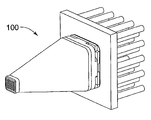
도1a 및 도1b는 본 발명의 예시적인 실시예에 따른 고체 광학 장치의 사시도 및 분해도를 도시한다.1A and 1B show a perspective view and an exploded view of a solid state optical device according to an exemplary embodiment of the present invention.
도2는 본 발명의 일 실시예에 따른 상호 연결 회로 상에 배치된 예시적인 LED 다이 어레이의 평면도를 도시한다.2 shows a top view of an exemplary LED die array disposed on an interconnect circuit in accordance with one embodiment of the present invention.
도3은 본 발명의 일 실시예에 따른 고체 광학 장치의 측면도를 도시한다.3 shows a side view of a solid-state optical device according to an embodiment of the present invention.
도4는 본 발명의 일 실시예에 따른 비촬상 광학 집광기에 의해 광섬유에 결합된 개별 LED 다이의 확대도를 도시한다.4 shows an enlarged view of an individual LED die coupled to an optical fiber by a non-photographic optical concentrator according to one embodiment of the present invention.
도5a 내지 도5f는 본 발명의 다른 실시예에 따른 다른 섬유 출력 패턴을 도시한다.5A-5F illustrate another fiber output pattern in accordance with another embodiment of the present invention.
도6a는 조향 가능한 출력을 위한 다른 섬유 출력 패턴을 도시하고, 도6b 및 도6c는 각각 본 발명의 다른 실시예에 따른 조향 가능한 출력을 위한 예시적인 밴딩 및 지지 구조물 실시예를 도시한다.FIG. 6A shows another fiber output pattern for steerable output, and FIGS. 6B and 6C respectively show exemplary banding and support structure embodiments for steerable output according to another embodiment of the present invention.
도7은 섬유들의 출력 단부들 중 일부가 본 발명의 다른 실시예에 따른 각진 연마 출력면을 갖는, 조향 가능한 출력을 위한 또 다른 출력 패턴을 도시한다.Figure 7 shows another output pattern for steerable output, with some of the output ends of the fibers having an angled abrasive output surface in accordance with another embodiment of the present invention.
도8은 본 발명의 일 실시예에 따른 섬유 어레이 커넥터에 대한 다른 구성을 도시한다.Figure 8 shows another configuration for a fiber array connector according to an embodiment of the present invention.
도9a는 본 발명의 다른 실시예에 따른 화소화를 위해 적응된 고체 조명 시스템을 도시한다.9A illustrates a solid state lighting system adapted for pixelation according to another embodiment of the present invention.
도9b는 본 발명의 다른 실시예에 따른 화소화를 위해 적응된 예시적인 제어기 회로를 도시한다.9B shows an exemplary controller circuit adapted for pixelization according to another embodiment of the present invention.
도10은 고체 광학 장치의 예시적인 실시예를 도시한다.10 illustrates an exemplary embodiment of a solid state optical device.
도11은 치과용 경화 장치의 일부로서 이용되는, 고체 광학 장치의 다른 예시적인 실시예를 도시한다.Figure 11 shows another exemplary embodiment of a solid state optical device, used as part of a dental curing device.
도12는 본 발명의 다른 예시적인 실시예에 따른 광선 경화 장치를 도시한다.Fig. 12 shows a light curing apparatus according to another exemplary embodiment of the present invention.
도13은 조향 가능한 출력 방출을 위한 다른 실시예를 도시한다.Figure 13 shows another embodiment for steerable output emission.
도14는 편광기를 포함하며, 기판 상에 배치된 광선-변성 재료를 처리하는 광선 변성 장치를 도시한다.Fig. 14 shows a light beam modification apparatus including a polarizer and processing a light beam-modifying material disposed on a substrate.
도15는 원통 렌즈 및 편광기를 포함하며, 기판 상에 배치된 광선-변성 재료를 처리하는 광선 변성 장치를 도시한다.Fig. 15 shows a light beam modification apparatus including a cylindrical lens and a polarizer and processing a light beam-modifying material disposed on a substrate.
도16a는 소형 렌즈 어레이 및 편광기를 포함하며, 기판 상에 배치된 광선-변성 재료를 처리하는 광선 변성 장치를 도시한다.Fig. 16A shows a light beam modification apparatus including a small lens array and a polarizer and processing a light beam-modifying material disposed on a substrate.
도16b는 도파관의 출력 단부에서 각각의 섬유 내에 형성된 렌즈 및 편광기를 포함하며, 기판 상에 배치된 광선-변성 재료를 처리하는 광선 변성 장치를 도시한다.Fig. 16B shows a light beam modification apparatus including a lens and a polarizer formed in each fiber at the output end of the waveguide, and processing the light-modifying material disposed on the substrate.
도17은 원통 렌즈와 조합된 렌즈형 어레이 및 편광기를 포함하며, 기판 상에 배치된 광선-변성 재료를 처리하는 광선 변성 장치를 도시한다.Fig. 17 shows a light beam modification apparatus including a lenticular array and a polarizer in combination with a cylindrical lens and processing a light beam-modifying material disposed on a substrate.
도18은 기판 상에 배치된 광선-변성 재료를 처리하는 다른 방식으로서 다른 광학 소자가 뒤따르는 편광기와 관련된 광학 소자를 포함하는 광선 변성 장치의 일례를 도시한다.FIG. 18 shows an example of a light modifying device that includes an optical element associated with a polarizer followed by another optical element as another way of treating the light-modifying material disposed on the substrate.
도19는 LED의 어레이가 광선-경화성 재료를 변성시키기 위한 펄스형 광선을 발생시키도록 하기 위한 펄스 발생기를 포함하는 펄스 제어 시스템의 제1 예의 개략도를 도시한다.19 shows a schematic diagram of a first example of a pulse control system including a pulse generator for causing an array of LEDs to generate pulsed light rays for denaturing light-curable material.
도20은 LED의 어레이가 광선-경화성 재료를 변성시키기 위한 펄스형 광선을 발생시키도록 하기 위한 LED 신호 제어기를 포함하는 펄스 제어 시스템의 제2 예의 개략도를 도시한다.20 shows a schematic diagram of a second example of a pulse control system including an LED signal controller for causing an array of LEDs to generate pulsed light rays for denaturing light-curable material.
도21은 LED의 어레이가 광선-경화성 재료를 변성시키기 위한 펄스형 광선을 발생시키도록 하기 위한 컴퓨터 구동식 출력을 포함하는 펄스 제어 시스템의 제3 예의 개략도를 도시한다.FIG. 21 shows a schematic diagram of a third example of a pulse control system including a computer driven output for causing an array of LEDs to generate pulsed light rays for denaturing light-curable material.
도22는 도9의 어댑터 회로에 비해 LED 어레이의 증가된 해상도를 위한 다른 어댑터 회로를 도시한다.FIG. 22 illustrates another adapter circuit for increased resolution of the LED array compared to the adapter circuit of FIG.
도23은 LED 어레이에 대한 증가된 강도 제어를 위한 다른 어댑터 회로를 도시한다.Figure 23 shows another adapter circuit for increased intensity control for the LED array.
도24는 도23의 어댑터 회로에 따른 불균일 구조물 상에 위치된 광선-변성 재료의 균일한 광선 변성을 도시한다.FIG. 24 illustrates uniform light beam modification of the light-modifying material located on the heterogeneous structure according to the adapter circuit of FIG.
도25는 기판 상에 배치된 가변 두께를 갖는 광선-변성 재료의 균일한 광선 변성을 도시한다.Figure 25 shows uniform ray modification of the ray-modifying material with variable thickness disposed on the substrate.
도26은 고해상도 변성을 제공하기 위해 광 밸브를 이용하는 광선 변성 장치를 도시한다.Figure 26 shows a light beam modification apparatus using a light valve to provide high resolution denaturation.
도27은 광선-변성 재료에 인가되는 강도 프로파일을 평탄화하기 위해 하나 이상의 광학 소자를 이용하는 광선 변성 장치를 도시한다.FIG. 27 illustrates a light beam modification apparatus using one or more optical elements to planarize the intensity profile applied to the light-modifying material.
도28은 패턴을 생성하기 위해 광선을 편향시키고 그리고/또는 편광기에 도달하는 고각을 감소시키기 위해 광 밸브를 이용하는 광선 변성 장치를 도시한다.FIG. 28 illustrates a light beam modifying device that utilizes a light valve to deflect the light beams to create a pattern and / or reduce the elevation reaching the polarizer.
본 발명이 다양한 변형 및 다른 형태로 보정 가능하지만, 그의 세부 사항은 도면에 예시적으로 도시되었고 상세하게 설명될 것이다. 그러나, 본 발명은 본 발명을 설명되는 특정 실시예로 제한하지 않는다는 것을 이해해야 한다. 대조적으로, 본 발명은 첨부된 청구범위에 의해 한정되는 본 발명의 범주 내에 드는 모든 변형, 등가물, 및 변경을 포함하는 것이다.While the invention is capable of correction in various modifications and other forms, details thereof are shown by way of example in the drawings and will be described in detail. However, it should be understood that the invention is not limited to the specific embodiments described. On the contrary, the invention is intended to cover all modifications, equivalents, and modifications falling within the scope of the invention as defined by the appended claims.
도1a는 예시적인 구성의 고체 광학 장치(100; 본원에서, 조명 장치 또는 광 자 방출 장치로도 불림)를 도시한다. 광학 장치(100)는 도1b에서 분해도로 도시되어 있다. "광"은 전자기 스펙트럼의 자외선, 가시광선, 및/또는 적외선 부분 내의 파장을 갖는 전자기 광선을 의미한다. 아래에서 설명되는 구성에서, 광학 장치(100)는 종래의 고강도 방전(HID)등과 비교하여 전체적으로 콤팩트한 크기를 가질 수 있고, 따라서 도로 조명, 스포트라이팅, 백라이팅, 영상 투사, 및 광선 활성화 경화를 포함한 다양한 용도에서 램프 장치에 대한 대체를 제공한다.1A illustrates a solid state optical device 100 (also referred to herein as an illumination device or photon emission device) in an exemplary configuration.
광학 장치(100)는 광선을 발생시키기 위한 고체 광원(104)의 어레이를 포함한다. 광선은 대응하는 집광기(120)의 어레이에 의해 수집되어 집광된다. 집광된 광선은 그 다음 지지 구조물(150)에 의해 지지되는 대응하는 도파관(130)의 어레이 내로 진출된다. 이러한 각각의 특징이 이제 더욱 상세하게 설명될 것이다.
예시적인 실시예에서, 고체 광원(104)은 어레이 패턴으로 배치된 복수의 분리된 LED 다이 또는 칩을 포함하지만, 레이저 다이오드를 포함한 다른 고체 광선도 적용될 수 있다. 분리된 LED 다이(104)들은 개별적으로 장착되고, (모든 LED들이 그들의 공통 반도체 기판에 의해 서로 연결되는 LED 어레이보다는) 작동 제어를 위한 독립된 전기 연결부를 갖는다. LED 다이는 대칭 광선 패턴을 생성할 수 있고, 전기 에너지를 광으로 변환하는데 있어서 효율적이다. 많은 LED 다이들이 과도하게 온도에 민감하지 않으므로, LED 다이는 많은 유형의 레이저 다이오드에 비해 적당한 방열 장치만으로도 적절하게 작동할 수 있다. 예시적인 실시예에서, 각각의 LED 다이는 그의 가장 가까운 이웃(들)로부터 적어도 LED 다이 폭보다 더 큰 거리만큼 이격된다. 다른 예시적인 실시예에서, 각각의 LED 다이는 그의 가장 가까운 이웃(들)로부터 적어도 6개의 LED 다이 폭보다 더 큰 거리만큼 이격된다. 이러한 예시적인 실시예들은 아래에서 더욱 상세하게 설명되는 바와 같이, 적합한 열 관리를 제공한다.In an exemplary embodiment, the solid state
또한, LED 다이(104)는 -40℃ 내지 125℃의 온도에서 작동될 수 있고, 대략 10,000시간의 최장 레이저 다이오드 수명 또는 대략 2,000시간의 UV 아크 램프 수명에 비해, 100,000시간 범위의 작동 수명을 가질 수 있다. 예시적인 실시예에서, LED 다이는 각각 약 50 루멘 이상의 출력 강도를 가질 수 있다. 분리된 고출력 LED 다이는 (크리(Cree)의 InGaN계 XBright™ 제품과 같은) 크리 및 오스람(Osram)과 같은 화사로부터 상업적으로 구입 가능한 GaN계 LED 다이일 수 있다. 한 가지 예시적인 실시예에서, 약 300 ㎛ x 300 ㎛의 방출 영역을 각각 갖는 (크리에 의해 제조되는) LED 다이의 어레이는 집광(소면적, 고출력) 광원을 제공하도록 사용될 수 있다. 사각형 또는 다른 다각형 형상과 같은 다른 발광 표면 형상도 이용될 수 있다. 또한, 다른 실시예에서, 이용되는 LED 다이의 방출 층은 상부 또는 하부 표면 상에 위치될 수 있다.In addition, the LED die 104 can be operated at temperatures between -40 ° C and 125 ° C and have an operating life in the range of 100,000 hours, relative to the longest laser diode life of approximately 10,000 hours or UV arc lamp life of approximately 2,000 hours. Can be. In an exemplary embodiment, the LED dies may each have an output intensity of at least about 50 lumens. The separate high power LED die may be a GaN based LED die commercially available from the company such as Cree and Osram (such as Cree's InGaN based XBright ™ product). In one exemplary embodiment, an array of LED dies (made by Cree) each having an emission area of about 300 μm × 300 μm may be used to provide a condensed (small area, high power) light source. Other light emitting surface shapes may also be used, such as square or other polygonal shapes. Also, in other embodiments, the emitting layer of the LED die used may be located on the top or bottom surface.
몇몇 예시적인 실시예에서, 복수의 순청색 또는 자외선(UV) LED 다이가 이용될 수 있다. 다른 예시적인 실시예에서, 하나 이상의 LED 다이가 청색 LED 다이에 대한 AG:Ce 인, 또는 UV LED 다이에서 이용되는 RGB(적색, 녹색, 청색) 인의 혼합물과 같은 (도시되지 않은) 인 층으로 양호하게는 발광 표면 상에서 코팅될 수 있다. 따라서, 인 층은 LED 다이의 출력을 상이한 메커니즘 하에서 "백색"광으로 변환하도록 사용될 수 있다. 인 층 배치 및 구성은 위에서 전체적으로 참조된, 공동 소유의 현재 출원 중이며 발명의 명칭이 "복수의 광원을 사용하는 조명 시스템"인 출원(정리 번호 58130US004)에 상세하게 설명되어 있다.In some exemplary embodiments, a plurality of pure blue or ultraviolet (UV) LED dies may be used. In another exemplary embodiment, the at least one LED die is good with a phosphorus layer (not shown), such as AG: Ce phosphorus for the blue LED die, or a mixture of RGB (red, green, blue) phosphorus used in the UV LED die. Preferably coated on a light emitting surface. Thus, the phosphor layer can be used to convert the output of the LED die into "white" light under different mechanisms. Phosphorous layer arrangements and configurations are described in detail in the co-owned, currently pending application, titled “Lighting System Using Multiple Light Sources” (Cor. No. 58130US004), referenced above in its entirety.
다른 실시예에서, 수집된 적색, 청색, 및 녹색 LED 다이들은 어레이로 선택적으로 위치될 수 있다. 결과적인 방출은 섬유들의 출력 단부로부터 방출된 광이 동시에 서로 홉합되었을 때 관찰자에 의해 유색광 또는 "백색"광으로 보이도록 섬유(130)들의 어레이에 의해 수집된다.In another embodiment, the collected red, blue, and green LED dies may be selectively positioned in an array. The resulting emission is collected by the array of
다른 실시예에서, LED 다이 어레이는 일반적으로 "백색"광을 포함하는 가시광 영역 내의 출력을 제공할 수 있는 수직 공동 표면 방출 레이저(VCSEL) 어레이로 대체될 수 있다.In other embodiments, the LED die array can be replaced with a vertical cavity surface emitting laser (VCSEL) array that can provide output in the visible region, which generally includes "white" light.
도1b에 도시된 바와 같이, LED 다이(104)로부터의 방출은 대응하는 어레이 패턴으로 배치된 복수의 집광기(120)에 의해 수신된다. 예시적인 실시예에서, 각각의 집광기는 LED 다이(104)들 중 대응하는 하나로부터 광선을 수신한다. 예시적인 실시예에서, 집광기(120)는 어레이로 배치된 비촬상 집광기(반사식 광 커플러로도 불림)를 포함한다. 집광기(120)의 반사 표면의 형상은 출력 밀도를 보존하기 위해 각각의 공급원(104)에 의해 방출되는 광선의 대부분을 포착하도록 설계된다. 또한, 집광된 출력은 광 수신 도파관의 수용각 기준에 대체로 부합하는 방식으로 설계될 수 있어서, 광선의 대부분은 도파관(130)에 의해 사용 가능하게 포착되어 그를 통해 안내된다. 예시적인 실시예에서, 비촬상 집광기(120)들의 어레이의 각각의 비촬상 집광기는 2차원(2-D) 표면에 일치하는 내부 반사 표면을 갖고, 적어도 내부 반사 표면의 제2 부분은 3차원(3-D) 표면에 일치한다. 이러한 그리고 다른 반사 표면 설계는 본원에서 전체적으로 참조된, 공동 소유이며 공동 계류되어 현재 출원 중인 발명의 명칭이 "반사식 광 커플러"인 출원(정리 번호 59121US002)에 상세하게 설명되어 있다.As shown in FIG. 1B, the emission from the LED die 104 is received by a plurality of
어레이(120) 내의 각각의 광학 집광기는 예를 들어 사출 성형, 전사 성형, 미세 성형, 스탬핑, 천공 또는 열성형에 의해 형성될 수 있다. 광학 집광기(120)들이 (개별적으로 또는 광학 집광기의 어레이의 일부로서) 형성될 수 있는 기판 또는 시트는 금속, 플라스틱, 열가소성 재료, 또는 (미네소타주 세인트 폴 소재의 쓰리엠 컴퍼니(3M Company)로부터 구입 가능한 인핸스트 스페큘라 리플렉터(ESR; Enhanced Specular Reflector) 필름과 같은) 다층 광학 필름(MOF)과 같은 다양한 재료를 포함할 수 있다. 광학 집광기(120)를 형성하도록 사용되는 기판 재료는 그의 반사율을 증가시키기 위해, 은, 알루미늄, 또는 무기 박막의 반사식 다층 적층체와 같은 반사 코팅으로 코팅될 수 있거나 단순히 연마될 수 있다.Each optical concentrator within
또한, 광학 집광기 기판은 광학 집광기의 어레이가 LED 다이 아래, 둘레, 또는 위에 배향될 수 있도록 배치될 수 있다. 예시적인 실시예에서, 광학 집광기 기판은 어레이(120)의 각각의 집광기가 각각의 LED 다이(104) 위에서 활주하도록 형성될 수 있도록 LED 어레이 상에 또는 그에 근접하게 배치되어, 광학 집광기의 하부 개방부(123; 도4 참조)가 LED 다이(104)의 주연부 둘레에서의 억지 끼워맞춤을 제공한다. 다른 집광기 설계는 LED 다이가 지지되는 기판 상에서의 반사 코팅의 추가적인 사용을 포함한다.In addition, the optical concentrator substrate can be arranged such that the array of optical concentrators can be oriented below, around, or above the LED die. In an exemplary embodiment, the optical condenser substrate is disposed on or in proximity to the LED array such that each condenser of the
도1b에 도시된 실시예의 태양은 각각의 광원, 대응하는 광학 집광기, 및 대 응하는 도파관 사이의 일대일 대응이다. 각각의 광학 집광기 표면은 몇몇 용도에서 인-코팅 LED 다이일 수 있는 대응하는 LED 다이로부터의 등방성 방출을 대응하는 광 수신 도파관의 수용각 기준을 만족시키는 비임으로 변환하도록 설계된다. 위에서 설명된 바와 같이, 이러한 집광기 표면 설계는 LED 다이로부터 방출되는 광의 출력 밀도를 보존하는 것을 돕는다.The aspect of the embodiment shown in FIG. 1B is a one-to-one correspondence between each light source, a corresponding optical concentrator, and a corresponding waveguide. Each optical concentrator surface is designed to convert isotropic emission from a corresponding LED die, which in some applications may be an in-coated LED die, into a beam that meets the acceptance angle criteria of the corresponding light receiving waveguide. As described above, this condenser surface design helps to preserve the power density of light emitted from the LED die.
다시 도1b를 참조하면, 집광된 출력 광선은 도1b에서 광섬유의 어레이로서 도시된 복수의 광학 도파관(130)에 의해 수신되고, 각각의 도파관은 입력 단부(132) 및 출력 단부(133)를 갖는다. 본 예시적인 실시예는 (미네소타주 세인트 폴 소재의 쓰리엠 컴퍼니로부터 TECS™의 상표로 시판되는 것과 같은) 대형 코어(예를 들어, 400 ㎛ 내지 1000 ㎛) 중합체 피복 실리카 섬유의 어레이(130)를 포함한다. 다른 예시적인 실시예에서, 각각의 광섬유(130)는 약 600 ㎛ 내지 650 ㎛의 코어 직경을 갖는 중합체 피복 실리카 섬유를 포함할 수 있다. 예시적인 실시예에서, 섬유의 종방향 길이는 약 1 내지 5 인치(2.5 ㎝ 내지 12.5 ㎝)의 길이일 수 있다. 예시적인 섬유들이 매우 가요성이므로, 이러한 짧은 거리는 여전히 섬유들을 출력 단부에서 타이트하고 패턴화된 다발로 위치시키는 능력을 제공한다. 또한, 짧은 길이는 일반적인 HID 램프의 크기에 비교할 만한 크기를 갖는 콤팩트한 장치를 제공한다. 당연히, 섬유 길이는 다른 용도에서 출력에 있어서 해로운 영향을 끼치지 않고서 증가될 수 있다.Referring again to FIG. 1B, the focused output light rays are received by a plurality of
일반적인 또는 특수한 유리 섬유와 같은 다른 유형의 광섬유도 예를 들어 LED 다이 광원의 출력 파장(들)과 같은 파라미터에 의존하여, 본 발명의 실시예에 따라 이용될 수 있다. 예를 들어, 중합체 섬유는 진청색 또는 UV 광원을 포함하는 용도에서 솔라리제이션(solarization) 및/또는 퇴색이 가능할 수 있다. 본 예시적인 실시예에서, 광 개시제 또는 조사되는 다른 경화성 재료의 유형에 기초하여, 450 ㎚ 이하의 파장에 대해 낮은 손실을 제공하는 광섬유/도파관이 이용될 수 있다.Other types of optical fibers, such as general or special glass fibers, may also be used in accordance with embodiments of the present invention, depending on parameters such as, for example, the output wavelength (s) of the LED die light source. For example, the polymer fibers may be capable of solarization and / or fading in applications involving dark blue or UV light sources. In this exemplary embodiment, based on the type of photoinitiator or other curable material being irradiated, an optical fiber / waveguide can be used that provides a low loss for wavelengths up to 450 nm.
또는, 본 설명이 주어지면 당업자에게 명백한 바와 같이, 평탄 도파관, 중합체 도파관, 가요성 중합체 도파관 등과 같은 다른 도파관 유형도 본 개시 내용에 따라 이용될 수 있다.Alternatively, other waveguide types, such as flat waveguides, polymer waveguides, flexible polymer waveguides, and the like, may be used in accordance with the present disclosure, as will be apparent to those skilled in the art given the present description.
LED 다이에 의해 방출된 광이 집광기에 의해 광 수신 섬유 내로 수집되어 재지향되면, 섬유(들)은 광을 내부 전반사에 의해 낮은 광학 손실로 특정 위치로 전달하도록 사용될 수 있다. 그러나, 광 수신 섬유는 조밀 충진 섬유 다발과 같이, 섬유들을 출력 개구에서 LED 다이 어레이의 더 넓은 간격으로부터 더 조밀한 간격 또는 간격들로 병진 이동시킴으로써 단지 광을 전달하도록 역할하는 것은 아니며, (상대적으로) 확산된 LED 어레이로부터의 광은 매우 작은 영역 내로 효과적으로 집광될 수 있다. 또한, 예시적인 광 수신 섬유 코어 및 클래딩의 광학 설계는 입력 단부 및 출력 단부에서의 섬유의 개구수(NA)에 의해 결속된 단부들로부터 방출되는 광선을 성형하는 것을 제공한다. 본원에서 설명되는 바와 같이, 광 수신 섬유는 광 전달은 물론 집광 및 비임 성형을 수행한다.Once the light emitted by the LED die is collected and redirected into the light receiving fiber by the condenser, the fiber (s) can be used to deliver the light to a specific location with low optical loss by total internal reflection. However, the optical receiving fiber, like the densely packed fiber bundle, does not serve to merely transmit light by translating the fibers from the wider spacing of the LED die array to the denser spacing or spacing at the output opening, and (relatively Light from the diffused LED array can be effectively focused into very small areas. In addition, the optical design of the exemplary light receiving fiber core and cladding provides for shaping the light rays emitted from the ends bound by the numerical aperture (NA) of the fibers at the input and output ends. As described herein, the light receiving fiber performs light transmission as well as condensing and beam shaping.
광섬유(132)는 광섬유들의 출력 단부(133)들 중 하나 이상에서 섬유 렌즈를 더 포함할 수 있다. 유사하게, 광섬유(130)들의 광 수신 단부(132)들은 각각 섬유 렌즈를 더 포함할 수 있다. 섬유 렌즈 제조 및 실시예는 본원에서 전체적으로 참조된, 공동 소유되어 공동 계류 중인 미국 특허 출원 제10/317,734호 및 10/670,63호에 설명되어 있다. 또는, 렌즈, 소형 렌즈, 거울, 편광기와 같은 광학 소자(들)이 광선을 포커싱, 확산, 시준, 또는 편광시키도록 섬유(들)의 제2 단부(들)이 인접하여 위치될 수 있다. 광학 소자는 다중 섬유를 가로질러 연속적이거나 불연속적일 수 있다.The
섬유 어레이 커넥터(134)가 어레이(130)의 각각의 광섬유의 제1 단부를 지지하도록 이용될 수 있다. 예시적인 실시예에서, 섬유 어레이 커넥터(134)는 집광기(120)의 패턴에 대응하는 패턴을 갖는 복수의 개구를 구비한, 성형 플라스틱 재료와 같은 강성 재료를 포함한다. 각각의 개구는 어레이(130)의 광섬유의 입력 단부(132)를 수납하고, 그에 대한 직접적인 결합을 제공할 수 있다.
예시적인 실시예에서, 강성 또는 가요성의 상호 연결 회로 층이 LED 다이(104)에 대한 열관리 및 전기적 연결을 제공하도록 이용될 수 있다. 도1b에 도시된 바와 같이, 상호 연결 회로 층은 미네소타주 세인트 폴 소재의 쓰리엠 컴퍼니로부터 구입 가능한 3M™ 플렉시블(Flexible) (또는 플렉스(Flex)) 회로와 같은 다층 구조물을 포함할 수 있다. 예를 들어, 다층 상호 연결 층은 예를 들어 구리 또는 다른 열 전도성 재료로 만들어진 금속 장착 기판(112)과, 전기 절연 유전 층(114)과, 패턴화된 전도성 층(113)을 포함할 수 있고, LED 다이는 전도성 층(113)의 (도시되지 않은) 결합 패드에 작동식으로 연결된다. 전기 절연 유전 층(114)은 예를 들어 폴리이미드, 폴리에스터, 폴리에틸렌테레프탈레이트(PET), 폴 리카보네이트, 폴리설폰, 또는 FR4 에폭시 복합재를 포함한 다양한 적합한 재료로 구성될 수 있다. 전기 및 열 전도 층(113)은 예를 들어 구리, 니켈, 금, 알루미늄, 주석, 납, 및 이들의 조합을 포함한 다양한 적합한 재료로 구성될 수 있다.In an exemplary embodiment, a rigid or flexible interconnect circuit layer can be used to provide thermal management and electrical connection to the LED die 104. As shown in FIG. 1B, the interconnect circuit layer may include a multi-layered structure, such as a 3M ™ Flexible (or Flex) circuit, available from 3M Company, St. Paul, Minn. For example, the multilayer interconnection layer may include a
예시적인 실시예에서 그리고 아래에서 더욱 상세하게 설명되는 바와 같이, 하나 이상의 LED 다이(104) 그룹들이 서로 상호 연결되지만, 다른 LED 다이 그룹으로부터 분리되어, 화소화된 광선 출력을 제공한다. (도시되지 않은) 관통부가 유전 층(114)을 통해 연장되도록 사용될 수 있다. 금속 장착 기판(112)은 방열 장치 또는 발열 조립체(140) 상에 장착될 수 있다. 기판(112)은 전기적으로 절연되고 열적으로 전도성인 재료의 층(116)에 의해 방열 장치(140)로부터 분리될 수 있다. 예시적인 실시예에서, 방열 장치(140)는 작동 중에 LED 다이 어레이로부터 열을 더욱 흡인하기 위해 일련의 열 전도체 핀(pin)을 더 포함할 수 있다.In an exemplary embodiment and as described in more detail below, one or more groups of LED dies 104 are interconnected with one another, but are separated from other LED die groups to provide pixelated light output. A through portion (not shown) can be used to extend through the
한 가지 예시적인 실시예에서, 각각의 LED 다이(104)는 금속/회로 층(113) 상에 직접, 유전 표면(114)의 리세스 부분 내에 존재할 수 있다. 상호 연결 회로의 예시적인 실시예는 본원에서 전체적으로 참조된, 현재 계류 중이며 공동 소유인 발명이 명칭이 "가요성 회로 LED 열 패키징"인 출원(정리 번호 59333US002)에 설명되어 있다.In one exemplary embodiment, each LED die 104 may be in a recessed portion of the
다른 실시예에서, 더욱 강성인 RF4 에폭시계 인쇄 배선 보드 구조물이 전기적 상호 연결을 위해 이용될 수 있다. 또 다른 실시예에서, 저비용 회로가 LED 다이 어레이를 연결시키도록 요구되는 바와 같이 적합한 기판 상으로 전도성 에폭시 또는 전도성 잉크를 패턴화함으로써 준비될 수 있다.In other embodiments, more rigid RF4 epoxy based printed wiring board structures may be used for electrical interconnection. In another embodiment, low cost circuitry can be prepared by patterning conductive epoxy or conductive ink onto a suitable substrate as required to connect the LED die array.
고체 광학 장치(100)는 지지 구조물을 더 포함한다. 도1b의 예시적인 실시예에서, 지지 구조물은 입력 개구(152) 및 출력 개구(154)를 갖는 하우징(150)으로서 구성된다. 하우징(150)은 도파관(130)의 어레이에 대한 스트레인 제거를 제공하고, 외부 원인으로부터의 도파관(130)에 대한 손상을 방지할 수 있다. 또한, 하우징(150)은 아래에서 더욱 상세하게 설명되는 바와 같은 차량 용도에 대해 양호한 강성 지지를 제공할 수 있다. 선택적으로, 도파관(130)이 광섬유일 때, 지지 구조물은 도파관(130)들의 제2 단부들의 주연 부분과 접촉하여 배치되는 밴딩(156; banding)을 더 포함할 수 있다. 밴딩(156)은 아래에서 더욱 상세하게 설명되는 바와 같이, 도파관(130)들의 출력 단부(134)들을 선택된 출력 패턴으로 분포시키는 것을 도울 수 있다.The solid state
또한, 섬유 어레이 커넥터(134)는 하우징(150)의 입력 개구(152)를 수납하기 위한 리지 또는 만입부를 포함할 수 있다. 하우징(150)이 섬유 어레이 커넥터(134)에 결합되거나 달리 부착될 수 있지만, 예시적인 실시예에서, 하우징(150)은 섬유 어레이 커넥터(134) 상에 스냅 결합된다.In addition, the
예시적인 구성 방법에서, 섬유들은 먼저 섬유 어레이 커넥터 내로 박혀서 커넥터에 결합된다. (도시되지 않은) 고정구가 섬유들을 순서대로 그룹화하기 위해 줄지어 그룹화하도록 이용될 수 있다. 고정구는 각각의 섬유를 입력 단부로부터 출력 단부로 반복적으로 위치시키는 다중 구획을 포함할 수 있다. 또한, 고정구는 섬유들이 서로 교차하지 않고서 출력 단부에 대해 예측 가능한 위치를 갖도록 설계될 수 있다. 출력 단부를 고정시키기 위해, 강성 또는 가요성 밴딩, 예를 들어 중 합체 재료가 섬유들의 위치를 원하는 출력 패턴 내로 고정시키도록 이용된다. 스트레인 제거/지지 하우징은 그 다음 섬유 및 밴딩 위로 활주되어 섬유 어레이 커넥터에 고정될 수 있다. 밴딩은 일반적인 접착제 또는 결합 요소의 사용을 통해 하우징의 출력 개구 내에 고정될 수 있다. 또는, 지지 구조물은 섬유 다발(들) 전반에 걸쳐 둘레에 형성된 캡슐화 재료를 포함할 수 있다.In an exemplary construction method, the fibers are first embedded into the fiber array connector and joined to the connector. Fixtures (not shown) can be used to group the fibers in order to group them in order. The fixture may include multiple compartments that repeatedly position each fiber from the input end to the output end. The fixture can also be designed such that the fibers have a predictable position relative to the output end without intersecting with each other. To fix the output end, a rigid or flexible banding, for example a polymer material, is used to fix the position of the fibers into the desired output pattern. The strain relief / support housing can then slide over the fibers and banding and secure to the fiber array connector. The banding can be fixed in the output opening of the housing through the use of a common adhesive or bonding element. Alternatively, the support structure may comprise encapsulation material formed circumferentially throughout the fiber bundle (s).
또는 지지 구조물(150)은 도파관(130)들의 일부에 도포될 수 있는 결합용 에폭시와 같은 접착 재료를 포함할 수 있어서, 접착제가 응고되면, 도파관들이 원하는 패턴으로 고정된다.Alternatively, the
전체적인 정렬은 섬유 어레이 커넥터(134), 집광기 어레이(120), 상호 연결 회로 층(110), 및 방열 장치(140)를 상호 정렬시키도록 사용될 수 있는 하나 이상의 정렬 핀(160)에 의해 제공될 수 있다. 도2에 도시된 정렬 구멍(162)과 같은 일련의 정렬 구멍들이 정렬 핀(160)을 수납하도록 장치(100)의 각각의 전술한 부품들 내에 형성될 수 있다. 상호 연결 회로 층에 대한 광학 집광기 어레이(120)의 정렬은 (도시되지 않은) 기준의 사용을 통해 달성될 수 있다.Global alignment may be provided by one or more alignment pins 160 that may be used to align the
도2는 고체 광학 장치(100)의 풋프린트를 도시한다. 이러한 예시적인 구성에서, 60개의 LED 다이(104)들의 어레이가 대체로 사각형 어레이 패턴으로, 방열 장치(140) 상에 장착된 상호 연결 회로 층(110) 상에 제공될 수 있다. 당연히, 본 발명에 따르면, LED 다이들의 어레이는 대체로 더 많거나 더 적은 개수의 LED 다이(104)를 포함할 수 있다. 그러나, 각각의 LED 다이가 약 300 ㎛의 폭을 가지며 각각의 LED 다이(104)가 그의 가장 가까운 이웃으로부터 LED 다이 폭보다 더 크게 이격될 수 있으므로, 본 발명의 고체 광학 장치는 높은 총출력 밀도, 콤팩트한 풋프린트 면적(약 1 in2 내지 4 in2, 또는 6.5 ㎠ 내지 26 ㎠), 및 적절한 열 제어를 제공할 수 있다. 또한, 섬유들의 출력 단부(133; 도1b)들의 풋프린트는 예시적인 실시예에서 약 0.1 in2 내지 1 in2 (0.65 ㎠ 내지 6.5 ㎠) 정도로 훨씬 더 콤팩트할 수 있다. 또는, 출력 단부들의 풋프린트는 아래에서 설명되는 실시예들 중 하나 이상에 도시되는 바와 같이, 일 방향에서 다른 것에 비해 훨씬 더 길 수 있다.2 shows the footprint of the solid state
고체 광학 장치(100)의 측면도가 도3에 도시되어 있다. 이러한 예시적인 실시예에서, (LED 다이들이 그 위에 장착된) 상호 연결 회로 층(110)은 출력 개구(154)로부터의 반대 방향으로 연장되는 발열 핀(142)을 더 포함하는 방열 장치(140) 상에 배치된다. 또한, 위에서 설명된 바와 같이, 하우징(150)은 섬유 어레이 커넥터(134) 상으로의 스냅 결합을 허용하기 위한 돌출부(153)를 포함할 수 있다. 광학 집광기(120)들의 어레이는 섬유 어레이 커넥터(134)와 상호 연결 층(110) 사이에 배치된다. 이러한 실시예에서, 섬유(130)들은 섬유 어레이 커넥터(134)와 하우징(150)의 출력 개구(154) 내에 배치된 밴딩(156)에 의해 지지된다.A side view of the solid state
도4에 더욱 상세하게 도시된 바와 같이, 고체 광학 장치의 예시적인 구성은 섬유 어레이의 개별 광섬유(131)와 집광기 어레이의 개별 광섬유 광학 집광기(121) 사이의 오정렬을 감소시키는 섬유-집광기 정렬 메커니즘을 포함한다. 특히, 섬유 어레이 커넥터(134)는 광학 집광기 어레이 기판의 만입 부분(125) 내에 맞물리는 돌출 부분(135)을 더 포함할 수 있다. 따라서, 섬유(131)는 섬유 어레이 커넥 터(134)의 개구 내에 수납된다. 섬유 어레이 커넥터는 그 다음 돌출부(135)가 만입부(125)에 의해 수납되도록 광학 집광기 기판 상에 배치된다. 이러한 방식으로, 광학 집광기(121)의 출력 개구(126)는 섬유(131)의 입력 단부와 대체로 동일 평면일 수 있다. 또한, 이러한 예시적인 설계에서, 섬유들의 다중 입력 단부들은 섬유 단부들이 광학 집광기에 대해 위치되도록 동시에 연마될 수 있다.As shown in more detail in FIG. 4, an exemplary configuration of a solid state optical device employs a fiber-condenser alignment mechanism that reduces misalignment between individual
도4의 예시적인 구성에서, 광학 집광기(121)의 수신 개구(123)는 대응하는 LED 다이(104)의 방출 표면의 주연부에 근접하여 또는 그를 둘러싸도록 배치될 수 있다. 도시되지는 않았지만, 광학 집광기 기판과 상호 연결 회로 층 사이에 위치된 스페이서가 이들 두 구성요소들 사이에 적절한 간격을 설정할 수 있다. 광학 집광기 기판은 그 다음 일반적인 기술을 사용하여 스페이서에 고정되거나 그렇지 않으면 상호 연결 회로 층에 결합될 수 있다.In the example configuration of FIG. 4, the receiving
도4는 또한 LED 다이(104)를 상호 연결 층(110)에 결합시키기 위한 전도성 에폭시(115)를 포함하는, 예시적인 다층 상호 연결부(110)의 단면을 도시한다. (예를 들어, 니켈 및 금, 또는 다른 전도성 재료를 포함할 수 있는) 제1 및 제2 전기 전도성 층(113, 111)들이 어레이 내의 각각의 LED 다이에 전기 트레이스를 제공하고, 유전 층(114; 예를 들어, 폴리이미드)이 전기 절연을 제공하도록 배치된다. 기판(112; 예를 들어, 구리)이 전도성 및 절연 층들을 지지하고, 아울러 열을 방출 방향으로부터 멀리 전도시키기 위해 방열 장치(140)에 대한 열 전도를 제공하도록 제공된다.4 also shows a cross-section of an
본원에서 설명된 원리에 따르면, 고체 광학 장치는 고도로 지향적이며 그리 고/또는 성형된 출력 방출을 하나 이상의 방향으로 동시에 제공할 수 있다. 도1a 및 도1b에 도시된 바와 같이, 섬유 어레이(130)의 출력 단부(133)들은 사각형 또는 정사각형 출력을 제공하도록 패턴화될 수 있다. 도5a 내지 도5f는 특정 용도에 대해 요구되는 조명의 유형에 따라 채용될 수 있는 섬유 어레이에 대한 다른 재구성 가능한 출력 단부 패턴을 도시한다. 예를 들어, 도5a는 육각형 출력 섬유 패턴(133A)을 도시하고, 도5b는 원형 출력 섬유 패턴(133B)을 도시하고, 도5c는 링형 출력 섬유 패턴(133C)을 도시하고, 도5d는 삼각형 출력 섬유 패턴(133D)을 도시하고, 도5e는 선형 출력 섬유 패턴(133E)을 도시한다. 또한, 도5f에 도시된 바와 같이, 다른 예시적인 실시예에서, 세그먼트형 출력 패턴(133F)이 제공될 수 있고, 여기서 다중의 분리된 섬유 출력 그룹들이 특정 목표 조명을 위해 이용될 수 있다. 섬유들의 출력 단부들을 고정시키는 밴딩이 납, 주석, 및 아연계 재료 및 합금과 같은 가요성을 갖는 재료로부터 형성될 수 있으므로, 몇몇 용도에서, 섬유 출력 패턴은 재구성 가능할 수 있다.In accordance with the principles described herein, solid-state optical devices can simultaneously provide highly directed and / or shaped output emission in one or more directions. As shown in FIGS. 1A and 1B, the output ends 133 of the
도6a 내지 도6c에 도시된 바와 같이, 고체 광학 장치의 출력은 조향 가능하여, 하나 이상의 상이한 방향들이 동시에 또는 교대로 조명될 수 있다. 도6a는 예들 들어 3개의 상이한 그룹(233A, 233B, 233C)으로 배열된 섬유 출력 단부(233)들을 도시한다. 예를 들어, 고체 광학 장치는 정상 작동 하에서 출력 단부(233A)를 통해 전방 방향으로의 출력 조명을 제공할 수 있다. 개시 신호의 경우에, 출력 섬유(233B)들에 대응하는 LED 다이들이 활성화될 수 있어서, 추가의 조명이 출력 섬유(233B)들을 통해 그러한 측면 방향으로 제공될 수 있다. 유사하게, 출력 섬 유(233C)들에 대응하는 LED 다이들이 활성화될 수 있어서, 추가의 조명이 그러한 다른 측면 방향으로 제공될 수 있다.As shown in Figures 6A-6C, the output of the solid-state optical device is steerable, so that one or more different directions can be illuminated simultaneously or alternately. 6A shows fiber output ends 233 arranged in three
경화 장치에서, 아래에서 도12에 대해 설명되는 바와 같이, 섬유 출력의 "조향"은 복잡한 3차원 부품 및 구조물의 광선 경화를 용이하게 할 수 있다. 이러한 유형의 구조는 가리움 효과가 불균일 경화를 생성하는 바와 같이, 일반적인 광원에 의한 "대량" 경화에 대해 적합하지 않다. 또한, 강성 회로 보드 상에 배열된 패키징된 LED들의 종래의 어레이는 복잡한 형상을 수용하도록 쉽게 구부러지지 않는다.In the curing apparatus, as described below with respect to FIG. 12, the “steering” of the fiber output can facilitate light curing of complex three-dimensional parts and structures. This type of structure is not suitable for "bulk" curing with a common light source, as the hiding effect produces nonuniform curing. In addition, conventional arrays of packaged LEDs arranged on rigid circuit boards are not easily bent to accommodate complex shapes.
또는, 조향 가능한 조명 시스템이 도5e에 도시된 바와 같이 섬유들의 측방향으로 연장되는 출력 배열을 이용하여 제공될 수 있고, 이에 의해 아래에서 설명되는 화소화 제어 회로(예를 들어, 도9a 및 도9b 참조)가 일 측면으로부터 타 측면으로의 조명되는 섬유들의 블록을 활성화할 수 있다. 이러한 방식으로, 출력 조명은 용도에 따라 특정 방향을 향해 (또는 그로부터 멀리) 지향될 수 있다.Alternatively, a steerable illumination system may be provided using a laterally extending output arrangement of fibers as shown in FIG. 5E, whereby a pixelation control circuit (eg, FIGS. 9A and FIG. 9b) may activate a block of illuminated fibers from one side to the other. In this way, the output illumination can be directed towards (or away from) a particular direction, depending on the application.
이러한 방식으로, 비기계적인 접근이 고체 광학 장치로부터 조향 가능한 출력 조명을 제공하도록 사용될 수 있다. 또는, 본 설명이 주어지면 당업자에게 명백한 바와 같이, 더 많거나 더 적은 섬유 그룹이 이용될 수 있다. 또한, 그룹들은 상이한 상대 배향을 가질 수 있다.In this way, a non-mechanical approach can be used to provide steerable output illumination from the solid state optics. Alternatively, more or fewer groups of fibers may be used, as will be apparent to one skilled in the art given the present description. In addition, the groups may have different relative orientations.
도6b에서, 상이한 섬유 그룹들을 안정화하고 지지하도록 이용될 수 있는 구성이 도시되어 있다. 예를 들어, 밴딩(256)이 광섬유들의 출력 단부에 제공된다. 밴딩(256)은 제1 개구(254), 제2 개구(254A), 및 제3 개구(254B)를 제공할 수 있으며, 개구(254A, 254B) 내에 배치된 섬유들은 개구(254) 내에 배치된 섬유와 다른 방향으로 광을 출력할 것이다. 또한, 도6c에 도시된 바와 같이, 밴딩(256)은 고체 광학 장치용 지지 구조물의 일부로서, 하우징(250)에 연결되거나 그와 일체일 수 있다.In FIG. 6B, a configuration that can be used to stabilize and support different fiber groups is shown. For example, banding 256 is provided at the output end of the optical fibers.
또는, 도7에 도시된 바와 같이, 고체 광학 장치는 섬유 출력 단부들의 단일 다발로부터 조향 가능한 광을 발생시킬 수 있다. 예를 들어, 섬유 출력 단부(133)들은 도6b로부터의 출력 개구(254)와 같이, 동일한 위치에 제공될 수 있다. 이러한 예시적인 실시예에서, 섬유 출력 단부(129)로 식별된 이러한 출력 단부들 중 일부는 나머지 섬유 출력 단부(133)들과 다른 각도, 또는 실질적으로 다른 각도(예를 들어, 섬유축에 대해 10 내지 50°)로 각지게 연마된다. 결과적인 방출은 섬유 단부(133)들의 출력과 다른 방향으로 지향될 것이다. 따라서, 도6a 내지 도6c에 대해 위에서 설명된 용도와 유사하게, 고체 광학 장치는 (출력 단부(133)를 통한) 전방 방향 및 (출력 섬유(129)를 통한) 측면 방향으로의 출력 조명을 제공할 수 있다.Alternatively, as shown in FIG. 7, the solid state optical device can generate steerable light from a single bundle of fiber output ends. For example, the fiber output ends 133 may be provided at the same location, such as the
도13에 도시된 조향 가능한 조명을 제공하기 위한 다른 실시예에서, 섬유 어레이 커넥터(734)로부터 연장되는 섬유들은 다중의 오프셋 섬유 다발인, 중심 다발(730A) 및 측면 다발(730B, 730C)로 결속될 수 있다. 섬유 다발의 출력 단부에 의해 방출되는 광은 비구면 렌즈와 같은 다초점 렌즈(750)에 의해 수신되고, 이는 오프셋 다발로부터의 출력을 원하는 다른 조명 영역(751A, 751B, 751C) 내로 지향시킨다. In another embodiment for providing steerable illumination shown in FIG. 13, the fibers extending from the
본 발명의 예시적인 실시예에서, 고체 광학 장치는 방전식 광원에 대한 전구 대체물로서 이용될 수 있다. 예를 들어, 기존의 리셉터클에 대한 부착은 도8에 도시된 플랜지(139)의 사용을 통해 달성될 수 있다. 플랜지(139)는 예를 들어 섬유 어레이 커넥터(134)의 주연 부분 상에 배치될 수 있다. 플랜지는 그러한 리셉터클의 로킹 슬롯 내에 맞물리도록 설계될 수 있다. 또는, 플랜지는 하우징 또는 광학 집광기 기판과 같은 고체 광학 장치의 다른 구성요소 상에 형성될 수 있다.In an exemplary embodiment of the invention, the solid state optical device can be used as a bulb replacement for a discharge light source. For example, attachment to existing receptacles may be accomplished through the use of
본 발명의 다른 실시예에 따르면, 도9a에 도시된 바와 같이, 개구 성형 및/또는 동적 비임 이동을 위해 사용될 수 있는 화소화된 광 제어를 허용하는 조명 시스템(300)이 제공된다. 시스템(300)은 위에서 설명된 고체 광원(100)과 유사한 방식으로 구성된 고체 광원(301)을 포함한다. 제어기(304)가 상호 연결 회로 층에 연결될 수 있는 배선(302) 및 커넥터(310)를 거쳐 고체 광원(301)에 결합된다. 전원(306)이 제어기(304)에 결합되어, 고체 광원(301)으로 전력/전류를 제공한다.According to another embodiment of the present invention, as shown in FIG. 9A, an
예시적인 실시예에서, 제어기(304)는 고체 광원(301) 내에 포함된 개별 LED 다이 또는 LED 다이의 그룹을 선택적으로 활성화하도록 구성된다. 또한, 광 수신 도파관이 LED 다이와 일대일 대응으로 제공되므로, 조명 시스템(300)은 화소화된 출력을 제공할 수 있다. 이러한 유형의 화소화된 제어는 상이한 색깔(예를 들어, RGB 출력을 위한 적색, 녹색, 및 청색) 또는 유사한 색깔(예를 들어, 백색, 청색, UV) LED 다이의 제어를 허용한다.In an exemplary embodiment, the
도9b는 고체 광원 내에 포함된 LED 다이들의 어레이에 화소화를 제공할 수 있는 예시적인 제어 회로(305)를 도시한다. 이러한 예에서, 60개의 LED 다이(LD1 내지 LD60)가 LED 다이 어레이 내에 제공되고, 이들은 각각 20개의 LED 다이의 3개 의 대그룹(314A 내지 314C)으로 그룹화되고, 이들은 또한 각각 5개의 LED 다이의 더 작은 하위 그룹 또는 채널(예를 들어, LD1 내지 LD5)로 분할된다. 전체적으로, 각각 5개의 LED 다이의 12개의 채널이 이러한 예시적인 실시예에서 분리되어 제어될 수 있다. 한 가지 예시적인 실시예에서, RGB 출력 용도에서, LED 다이의 제1 그룹은 적색 방출 LED 다이를 포함할 수 있고, LED 다이의 제2 그룹은 청색 방출 LED 다이를 포함할 수 있고, LED 다이의 제3 그룹은 녹색 방출 LED 다이를 포함할 수 있다. 또는, 다른 예시적인 실시예에서, LED 다이의 제1, 제2, 및 제3 그룹은 "백색" 방출 LED 다이를 포함할 수 있다.9B shows an
또한, 상호 연결 회로 층은 상이한 LED 다이 그룹에 대한 분리된 상호 연결을 제공하도록 설계된다. 상이한 유형의 LED 다이 그룹들, 및 더 많거나 더 적은 개수의 LED 다이가 본원에서 설명되는 원리에 따라 이용될 수도 있다. 이러한 구성에서, 분리된 RGB LED 다이 채널들은 "백색" 또는 다른 유색 출력을 제공하도록 구동될 수 있다. 또한, 특정 다이오드 채널이 LED 다이 열화로 인해 고장나거나 감광되면, 인접한 채널들이 출력 조명이 변하지 않고서 유지되게 보이도록, 더 높은 전류로 구동될 수 있다. (상대적으로) 넓은 LED 다이 간격 및/또는 상호 연결 층의 열 관리 능력 때문에, LED 다이 채널들 중 일부에 대한 더 큰 구동 전류는 전체 성능에 악영향을 주지 않을 것이다.In addition, the interconnect circuit layer is designed to provide separate interconnections for different LED die groups. Different types of LED die groups, and more or fewer LED dies may be used in accordance with the principles described herein. In this configuration, separate RGB LED die channels can be driven to provide a "white" or other colored output. In addition, if a particular diode channel fails or is dimmed due to LED die degradation, adjacent channels can be driven at higher currents so that the output illumination remains unchanged. Because of the (relatively) wide LED die spacing and / or thermal management capability of the interconnect layer, larger drive currents for some of the LED die channels will not adversely affect overall performance.
더욱 상세하게는, 전압이 전원(306)을 통해 회로(305)에 제공된다. 전압은 승압 변환기 칩(312A 내지 312C) 및 (도시되지 않은) 그의 관련 전자 장치에 의해 조절된 출력 전류/전압 공급으로 변환된다. 이러한 방식으로, LED 다이로 공급되 는 전류/전압이 조절된 수준으로 유지되면서, 전원(306)으로부터의 전압 변동이 완화될 수 있다. 칩(312A 내지 312C)은 예를 들어 내셔널 세미컨덕터(National Semiconductor)로부터 구입 가능한 LM2733 칩을 포함할 수 있다. 이러한 예시적인 실시예에서, 구동 전압/전류 파라미터는 80 내지 100 mA에서 약 20 V일 수 있고, 따라서 전체 LED 다이 어레이에 대해 총 약 1.0 내지 1.2 A를 제공한다. 구동 전류/전압은 그 다음 어레이 내의 상이한 LED 다이 채널들로 공급된다. 이러한 예에서, 각각의 LED 다이는 보통 약 20 mA 바이어스 전류를 요구하고, 전류가 증가함에 따라 증가하는 바이어스 역치는 전형적인 GaN계 LED 다이 어레이에 대해 약 4.0V에 접근한다. 당연히, 상이한 LED 다이 효율 또는 구성은 상이한 바이어스 및 구동 수준을 요구할 수 있다.More specifically, voltage is provided to
또한, 저항/써미스터 체인(316)이 각각의 LED 다이 채널에 대한 전체 최대 전류를 설정하기 위해 회로(305) 내에 포함될 수 있다. 더욱이, 대응하는 개수의 LED 다이 채널 전자 스위치를 포함하는 스위치 세트(318)가 제공될 수 있고, 이에 의해 각각의 LED 다이 채널은 각각의 특정 LED 다이 채널을 활성화하기 위해 (스위치 세트(318)에 대한 LED 배향에 따라) 접지부 (또는 전력부)에 결합/분리된다. 스위치 세트(318)는 특정 용도에 대해 요구되는 조명 파라미터에 기초하여, (도시되지 않은) 마이크로 제어기 또는 원격 스위치에 의해 자동으로 제어될 수 있다. 당연히, 이러한 회로 구조는 본 설명이 주어지면 당업자에게 명백한 바와 같이, 많은 실시 및 변경을 허용한다. 예를 들어, 제어 회로(305)는 모든 LED 다이를 동일한 전류로 구동하도록 실시될 수 있거나, 또는 주어진 LED 다이 채널이 자동으로 또는 명령에 따라 온/오프될 수 있다. 스위치 세트의 스위치 레그에 고정 또는 가변 저항을 추가함으로써, 상이한 전류가 각각의 채널에 인가될 수 있다.In addition, a resistor /
도10은 스폿 경화용으로 사용될 수 있는 램프 장치 내에서 이용되는 예시적인 고체 광학 장치(401)의 개략도를 도시한다. 예를 들어, 위에서 설명된 실시예에 따라 구성될 수 있는 고체 광학 장치(401)는 구획(402) 내에 배치된다. 광학 장치(401)는 리셉터클의 슬롯(438) 내에서 활주하여 로킹되도록 구성된 활주식으로 맞물리는 플랜지(439)의 사용을 통해 구획(402) 내에 고정될 수 있다. 따라서, 열을 광 출력의 방향으로부터 멀리 흡인하는 방열 장치(440)는 분리된 구획(404) 내에 위치된다. 비임형 출력 조명은 광학 소자(415)에 의해 요구에 기초한 조명 패턴으로 수집/포커싱될 수 있다. 광학 소자(415)는 적용 가능한 표준에 부합하는 선택된 출력 패턴을 제공하도록 설계될 수 있다. 예시적인 광학 소자는 구면/비구면 광학 소자, 및/또는 비연속 및/또는 비분석(스플라인) 광학 소자를 포함할 수 있다.10 shows a schematic diagram of an exemplary solid state
이러한 접근에서, 구획(402) 내에 배치되는 복잡한 반사 광학 장치의 사용이 회피될 수 있다. 또한, 열이 구획(402)으로부터 멀리 흡인되므로, 구획(402) 내의 모든 나머지 광학 소자들을 특별히 열처리할 필요가 없고, 따라서 연속적인 고강도 열에 대한 노출에 의해 야기되는 잠재적인 성능 열화를 회피한다. 더욱이, 고체 광학 장치(401)가 위에서 도6a 내지 6c에 도시된 바와 같은 출력 섬유 및 출력 개구 구조를 구비하면, 조향 가능한 출력 조명이 일반적인 HID 램프로부터의 출력을 조향할 때 현재 채용되어야 하는 이동 거울, 전구, 및/또는 렌즈 메커니즘을 이용 할 필요가 없이 달성될 수 있다.In this approach, the use of complex reflective optics disposed within
본원에서 설명되는 고체 광학 장치는 다른 용도로 이용될 수도 있다. 예를 들어, 도11은 (도1a 및 도1b에 도시된 구성 및/또는 본원의 다른 실시예와 유사한 구성을 갖는) 고체 광학 장치(501)가 경화 장치(500) 내에 포함된, 개략적인 고도로 국소화된 (예를 들어, 치과용) 경화 장치를 도시한다. 고체 광학 장치(501)는 경화 장치(500)의 손잡이 부분(510) 내에 배치될 수 있다. 또한, LED 다이 또는 다른 고체 광원으로부터의 출력을 수신하여 안내하도록 사용되는 출력 섬유들은 경화성 재료 위에 직접 위치될 수 있는 광 송출 아암(525)을 통해 연장될 수 있다. 이러한 용도에서, UV 및/또는 청색 광원이 조명을 받는 재료의 경화 양태에 따라 이용될 수 있다.The solid-state optical device described herein may be used for other purposes. For example, FIG. 11 is a schematic, highly schematic, incorporating solid state
도12에 도시된 예시적인 실시예에서, 웨브 경화 스테이션과 같은 예시적인 재료 경화 장치가 제공된다. 예를 들어, 접착제, 테이프, 또는 웨브에 기초한 제조 시에, 광선 경화제는 종종 상이한 재료 또는 기판 상에서 경화되어야 하는 청색/UV 경화성 재료이다. 일반적인 방법에서, 고강도 방전, 아크 램프, 및 마이크로파 구동식 램프가 경화 공정을 수행하기 위해 종종 이용된다. 그러나, 이러한 일반적인 램프는 빛과 열을 360°로 방사하고, 그러므로 복잡한 열교환 및/또는 냉각 메커니즘을 요구한다. 또는, 기판 재료 및 UV 경화제는 몇몇의 일반적인 접근에서 고강도의 열을 견디도록 적응되어야 한다.In the example embodiment shown in Figure 12, an exemplary material curing apparatus is provided, such as a web curing station. For example, in manufacturing based on adhesives, tapes, or webs, light curing agents are often blue / UV curable materials that must be cured on different materials or substrates. In a general method, high intensity discharges, arc lamps, and microwave driven lamps are often used to perform the curing process. However, these common lamps emit light and heat at 360 ° and therefore require complex heat exchange and / or cooling mechanisms. Alternatively, the substrate material and the UV curing agent must be adapted to withstand high intensity heat in some general approaches.
경화 스테이션(600)이 (도1a 및 도1b에서와 같이, 위에서 설명된 실시예와 유사하게 구성된) 고체 광학 장치(604)를 포함하는 일반적인 경화 시스템에서 발견 되는 가열 문제점에 대한 해결책이 도12에 개략적으로 도시되어 있으며, 여기서 고체 광학 장치의 발열 또는 방열 구성요소는 열교환 유닛(602)에 결합되거나 그에 의해 대체될 수 있다. 위에서 설명된 바와 같이, 고체 광학 장치의 광원에 의해 발생되는 열은 적절한 LED 다이 간격, 열 전도성 상호 연결 회로, 및/또는 방열 장치에 의해 광 출력의 방향으로부터 멀리 흡인된다. 경화 스테이션(600)은 연속적인 경화 작업 및/또는 단편 부품, 스폿 경화, 또는 시트에 대해 이용될 수 있다.A solution to the heating problem found in a typical curing system in which the curing
또한, 고체 광학 장치(604)는 광선-경화성 재료에 고도로 집광된 광선을 송출할 수 있고, 따라서 광선 경화를 위한 일반적인 LED 어레이를 사용할 때 분명히 나타날 수 있는 조악한 경화 깊이에 의해 야기되는 해로운 영향을 감소시킨다. 예를 들어, 도1a, 도1b, 및 도2에 대해 위에서 설명된 바와 같이, LED 다이 풋프린트는 원래의 LED 다이 어레이 영역 중 작은 부분에 집중될 수 있다. 예를 들어, 출력 단부들의 풋프린트는 섬유 어레이의 단부에서 단위 면적당 (커플링 손실을 포함한) 대응하는 강도 증가에서, LED 다이 어레이의 풋프린트보다 2 내지 5배 작은 비율일 수 있다. 예를 들어, 각각의 LED 다이는 공칭 365 ㎚ 광선의 다이에 대해 100 mW/㎠에 접근하는 출력 밀도를 구비한 GaN계 LED 다이일 수 있다. 결과적인 조사값은 전형적으로 약 2 W/㎠의 공칭 365 ㎚ 광선을 출력하는 일반적인 고출력(600 W/in)의 포커싱된 수은 자외선 램프의 출력에 접근하거나 훨씬 초과할 수 있다.In addition, the solid-state
LED 다이 또는 다른 광선 발생원의 집광된 출력은 스트레인 제거 하우징(630) 내에 배치된 도파관 어레이에 의해 수집되고 안내되어, 광선-경화성 재료 또는 조성물(650)로 송출될 수 있다. 광선-경화성 재료는 예를 들어 적합한 광개시제 또는 혼합물을 구비한 아크릴레이트 또는 에폭시 단량체 및/또는 소중합체를 포함할 수 있다. 광선-경화성 재료 또는 조성물(650)은 기판(652) 상에 배치될 수 있다. 예시적인 기판은 연속된 중합체, 직물, 금속성 포일 등을 포함할 수 있다.The focused output of the LED die or other light source may be collected and guided by a waveguide array disposed within the
다량의 재료의 시트 또는 연속된 경화를 제공하기 위해, 기판(652)은 이동 플랫폼 또는 컨베이어 벨트와 같은 플랫폼 상에 배치될 수 있거나, 기판(652)은 (도시되지 않은) 이동 롤러들 사이에 현수될 수 있다. 도5a 내지 도5f에 대해 위에서 설명된 바와 같이, 도파관, 예를 들어 광섬유들의 출력 단부들은 복수의 상이한 재구성 가능한 패턴으로 배열될 수 있고, 따라서 고체 광학 장치를 매우 다양한 형상, 및/또는 경화 깊이 요건을 갖는 경화 재료에 대해 적합하게 만든다.In order to provide a sheet of material or continuous curing, the
예를 들어, 위에서 설명된 바와 같이, 섬유들의 출력 단부들은 선택된 패턴으로 배열될 수 있다. 경화 용도에서, 선택된 패턴은 코너, 균열, 및 일반적인 "대량" 공급원으로부터 균일한 경화 광선을 수신하지 않는 다른 구조를 갖는 단편 부품형 기판의 경화를 제공하도록 선택될 수 있다. 이러한 방식으로, 가리움 효과는 섬유들의 출력 단부들의 적절한 배열에 의해 감소될 수 있다.For example, as described above, the output ends of the fibers can be arranged in a selected pattern. In hardening applications, the selected pattern can be selected to provide hardening of the piece part substrate with corners, cracks, and other structures that do not receive uniform hardening light rays from a common “bulk” source. In this way, the hiding effect can be reduced by proper arrangement of the output ends of the fibers.
또한, 장치(600)는 고체 광원(604)에 결합된 제어기(670)를 더 포함할 수 있다. 단일 제어기 유닛 또는 제어기 유닛들의 세트로서 실시될 수 있는 제어기(670)는 예시적인 광개시제의 양호한 흡수 대역에 대응하는 광선을 방출하고 그리고/또는 상이한 유형의 조성물들을 경화시키도록 LED 다이 어레이의 상이한 LED 다이들을 선택적으로 활성화하도록 적응될 수 있다. 예를 들어, 제어기(670)는 고 체 광원(604)의 LED 다이 어레이 내의 상이한 LED 다이 섹션 또는 개별(독립)적인 채널에 대응하는 복수의 상이한 제어 섹션(예를 들어, 제어 섹션(670a - 670d))을 포함할 수 있다. 또는, 복수의 독립적인 제어기 유닛들은 각각의 LED 다이 채널을 개별적으로 제어하도록 사용될 수 있다. 제어는 전기식 또는 기계식 스위치, 예를 들어 (도시되지 않은) 토글 스위치를 사용하여 달성될 수 있다.In addition, the
각각의 LED 다이 섹션은 예를 들어 다른 LED 다이 세트와 다른 파장의 광선을 방출하고 그리고/또는 광선 경화성 재료(650)의 다른 섹션을 조사하는 LED 다이 세트를 포함할 수 있다. 따라서, 위에서 설명된 예시적인 화소화 회로를 사용하여, 장치(600)는 동일한 경화 장치를 사용하여 상이한 유형의 재료들을 경화시키는데 있어서 더 큰 유연성을 제공할 수 있다. 예를 들어, 하나 이상의 LED 다이 그룹이 경화성 재료 내의 하나 이상의 광개시제(들)을 수용하도록 선택적으로 활성화, 예를 들어 켜지거나 꺼질 수 있다.Each LED die section may include, for example, a set of LED dies that emit light of a different wavelength from another set of LED dies and / or irradiate another section of light
본 발명의 이러한 예시적인 실시예에서, 복수의 고체 광원으로부터 방출된 광선은 조사되는 표면이 서로에 대해 밀접하게 위치된 상기 광원들 및 상기 조사되는 표면에서 얻어질 수 있는 것보다 훨씬 더 높은 강도를 수신하도록 소정의 패턴으로 집중될 수 있다. 위에서 설명된 경화 장치는 연속 기판, 시트, 단편 부품, 점 경화, 및/또는 3차원 광선-경화 공정에 대해 이용될 수 있다.In this exemplary embodiment of the present invention, the light rays emitted from the plurality of solid state light sources produce much higher intensities than can be obtained in the light sources and the light sources in which the surfaces to be irradiated are closely positioned relative to each other. Can be concentrated in a predetermined pattern to receive. The curing apparatus described above can be used for continuous substrates, sheets, piece parts, point curing, and / or three-dimensional light-curing processes.
램프를 사용하는 일반적인 경화 장치에 비해, 도12의 경화 장치(600)는 (열 민감성 제품 제작에 대해 특별히 중요한) 기판 및/또는 화학 약품으로 방출되는 적외선 광선이 거의 없거나 없이, 더 긴 수명, 더 낮은 전력 요건, 더 큰 효율, (조 밀 간극 경화 용도에 대한) 작은 형상 계수를 제공할 수 있다.Compared to a conventional curing device using a lamp, the
본 발명의 이러한 예시적인 실시예에 따르면, 높은 조사 수준이 출력이 선택적으로 패턴화될 수 있는, 광학 도파관과 결합된 광학 집광 소자의 사용을 통해 단파장(<500 ㎚), 저강도 LED 다이로부터 얻어질 수 있다. 이러한 방식으로, 더 짧은 파장의 LED 다이가 일반적인 낮은 조사의 문제점을 겪지 않고서 이용될 수 있다. 또한, 광범위한 광개시제 또는 광개시제 혼합물이 경화 재료(650) 내에 사용될 수 있다. 예시적인 광개시제는 (비들-쏘이어(Biddle-Sawyer)로부터 구입 가능한) ITX 및 캠퍼 퀴논(Camphor Quinone), (바스프(BASF)로부터 구입 가능한) TPO-L, 및(시바 스페셜티 케미컬즈(Ciba Specialty Chemicals)로부터 구입 가능한) 이르가큐어(IRGACURE) 및 다로큐어(DAROCUR)를 포함할 수 있다.According to this exemplary embodiment of the present invention, a high radiation level is obtained from a short wavelength (<500 nm), low intensity LED die through the use of an optical condensing element combined with an optical waveguide, in which the output can be selectively patterned. Can lose. In this way, shorter wavelength LED dies can be used without suffering from the problems of general low irradiation. In addition, a wide range of photoinitiators or photoinitiator mixtures may be used in the curing
또한, 위에서 설명된 광섬유-집광기 구성을 사용함으로써, LED 다이들은 직접적인 열 관리 및 전기적 연결에 대해 적합한 거리(예를 들어, 적어도 6개의 다이 폭 이상)로 이격될 수 있다. 결과적으로 효율적인 발열이 LED 다이의 수명을 효과적으로 연장시키고 더 높은 조사를 유지한다. 또한, LED 다이마다의 전류/전력 구동 요건은 더 많은 LED 다이들이 상대적으로 작은 풋프린트 내에서 이용될 수 있으므로, 조사 수준에 영향을 주지 않고서 감소될 수 있다. 따라서, 더 긴 다이의 총수명이 본 발명의 예시적인 실시예에 따라 달성될 수 있다.In addition, by using the fiber-condenser configuration described above, the LED dies can be spaced at a suitable distance (eg, at least six die widths or more) for direct thermal management and electrical connection. As a result, efficient heat effectively extends the life of the LED die and maintains higher irradiation. In addition, the current / power driving requirements per LED die can be reduced without affecting the level of irradiation, as more LED dies can be used within a relatively small footprint. Thus, the total life of the longer die can be achieved according to an exemplary embodiment of the present invention.
낮은 조사와 관련된 문제점은 조사가 너무 낮으면 비교적 두꺼운 광선-경화성 조성물의 바닥을 향한 경화 속도가 감소되는 것이다. 그러므로, 경화 및 부착의 깊이가 몇몇의 일반적인 LED에 기초한 접근에서 문제가 될 수 있다. 경화의 깊 이에서의 문제점은 조성물이 산란 중심 또는 광선 흡수 입자, 안료, 또는 염료를 포함할 때 강화된다. 또한, 다른 문제점은 광선이 조성물에 도달하기 전에 캐리어 필름 또는 롤을 통과해야 할 때 발생할 수 있다.A problem associated with low radiation is that too low the radiation reduces the rate of cure towards the bottom of the relatively thick light-curable composition. Therefore, the depth of curing and adhesion can be a problem in some common LED based approaches. Problems at the depth of cure are intensified when the composition comprises scattering centers or light absorbing particles, pigments, or dyes. In addition, other problems may arise when the light must pass through a carrier film or roll before reaching the composition.
해결책으로서, 경화되는 재료 또는 조성물로의 광선을 더욱 집광시키거나 시준하기 위해, 장치(600)는 렌즈를 더 포함할 수 있고, 복수의 렌즈들이 섬유들의 단부와 일체로 형성되거나 (예를 들어, 섬유 렌즈) 그로부터 분리되어 위치될 수 있다. 그러한 렌즈는 비교적 두껍고 그리고/또는 높은 흡수 및/또는 산란형 조성물의 경화와, 조사되는 조성물 내의 구성요소(들)의 배향을 용이하게 할 수 있다. 예를 들어, (도면에 도시되지 않은) 렌즈 또는 렌즈 어레이가 섬유/도파관의 출력 단부로부터 선택된 거리에 배치될 수 있다. 앞서 설명된 바와 같이, 광원으로부터 발생된 열이 방출 방향으로부터 멀리 흡인되므로, 추가의 출력 시준/포커싱 렌즈는 연속적인 열 노출에 대해 특별히 처리될 필요가 없다.As a solution, in order to further focus or collimate the light rays to the cured material or composition, the
또한, 본 발명의 이러한 예시적인 실시예에 따르면, 장치(600)는 집광된 패턴을 횡단 기계 방향(CMD) 및/또는 기계 방향(MD) 어레이로 연장시킴으로써 더욱 균일한 경화 비임을 제공할 수 있다. 일반적인 램프에 기초한 시스템에서, 램프는 그의 길이를 가로질러 적어도 15%의 변동을 갖는다. 몇몇의 경우에, 램프에 대한 균일성 변동은 시간에 걸쳐 30 내지 40%로 열화될 수 있다. 일반적인 LED에 기초한 접근에서, 어레이 내의 LED들은 분리되고, 분리는 어레이를 가로지른 조사 불균일성으로 이어진다. 이러한 불균일성은 불균일 경화로 인해 최종 제품 특성에 대해 잠재적으로 해로운 영향을 일으킬 수 있다.Furthermore, according to this exemplary embodiment of the present invention, the
본 발명의 경화 장치는 도9a 및 도9b에서 위에서 설명된 화소화 회로를 통해 제어될 수 있는 상이한 유형의 LED 다이들의 어레이를 이용할 수도 있다. 예를 들어, 섬유들의 출력 단부들이 타이트하게 결합될 수 있으므로, (예를 들어, 가변 강도 및/또는 파장의) 상이한 유형의 LED 다이들이 LED 다이 어레이 내로 통합될 수 있고, 이에 의해 기계 및 횡단 기계 방향으로의 균일성의 최소 손실로, 파장 및/또는 강도 선택성 경화 장치를 생성한다. 또한, 상이한 파장의 LED 다이들을 LED 다이 어레이 내로 통합하는 것은 예를 들어 ITX 및 TPO-L과 같은 예시적인 광개시제들의 양호한 흡수 대역에 일치하는 선택된 파장에서 광선을 방출하도록 이용될 수 있다.The curing apparatus of the present invention may utilize an array of different types of LED dies that can be controlled via the pixelation circuit described above in FIGS. 9A and 9B. For example, as the output ends of the fibers can be tightly coupled, different types of LED dies (eg, of varying intensity and / or wavelength) can be integrated into the LED die array, whereby the machine and the traversing machine With minimal loss of uniformity in the direction, a wavelength and / or intensity selective curing device is produced. In addition, incorporating LED dies of different wavelengths into the LED die array can be used to emit light at selected wavelengths that match the good absorption bands of exemplary photoinitiators such as, for example, ITX and TPO-L.
따라서, 경화 장치(600)는 동일한 경화 장치가 상이한 유형의 조성물을 경화시키도록 사용될 수 있도록 상이한 파장 및/또는 강도로 경화시키도록 설계될 수 있어서, 장치(600)를 상이한 광선 파장 및 강도를 요구하는 상이한 조성물을 처리하는 실험실, 실험용, 및 제작 라인에 대해 적합하게 만든다. 또한, 본원에서 설명되는 화소화 제어기 회로에 의해, 장치(600)는 경화되는 재료의 유형에 따라 특정 LED 다이 또는 LED 다이 그룹을 선택적으로 활성화하도록 제어될 수 있다. 대조적으로, 일반적인 접근에서, LED 어레이는 보통 하나의 특정 유형의 LED로만 구성된다. 따라서, 상이한 파장 또는 강도가 일반적인 시스템에서 필요하면, 새로운 어레이가 조성물 흡수를 수용하도록 요구된다. 이는 더 많은 설비 비용 및 더 많은 잠재적인 유지 보수를 요구하는 추가의 모듈로 이어진다.Thus, the
장치(600)는 또한 패턴, 3차원 구조, 리소그래피, 및 마스킹의 고해상도 경 화에 대해 적합하다. 예를 들어, 섬유들의 출력 단부들이 도1b의 밴딩(156)과 같은 재구성 가능한 밴딩 내에 고정될 수 있으므로, 섬유들의 출력 단부들은 특정 3차원 구도물 및/또는 부품을 경화시키기 위한 패턴으로 배열될 수 있다. 또한, 기판에 기초한 공정에 대해, 장치(600)는 횡단 기계 및 기계 방향에서의 고해상도 조사 프로파일 경화를 제공할 수 있다. 섬유들의 출력 단부들이 타이트하게 결속되거나 타이트하게 패턴화될 수 있으므로, LED 다이들은 섬유 직경 정도의 해상도로, 매끄러운 강도 프로파일을 생성하도록 가변 강도로 구동될 수 있다. 대조적으로, (열적인 목적으로) 더 멀리 이격된 일반적인 LED 어레이들은 가변 강도 프로파일을 제공한다.
이제 도14를 참조하면, 도파관(802)으로부터 방출된 광이 광선 편광성 재료에 부딪하기 전에 편광되는 변성 장치 구성의 일례가 도시되어 있다. 도14 및 아래에서 설명되는 도15 내지 도18에 도시된 바와 같이, 도파관(802)은 선형이지만, 2차원 어레이도 적용 가능하다는 것이 이해될 것이다. 도파관(802)은 전자기 에너지파가 무작위적으로 정렬되도록 편광되지 않은 광(808)을 출력한다. 그러나, 몇몇 변성 용도에 대해, 편광된 광으로 광선-변성 재료를 처리하는 것이 양호하다. 그러한 변성 용도의 일례는 액정 재료의 처리이다. 다른 예는 고분자 체인의 처리이다. 이러한 경우에, 액정 또는 고분자 체인 결합이 특정 방식으로 정렬되도록 요구된다. 액정 또는 고분자 결합은 대상 재료에 부딪히는 광선의 전자기 에너지파의 정렬에 따라 정렬된다. 그러므로, 대상 재료에 부딪히기 전에 광을 편광시키는 것은 정렬된 파에 의해 정렬되는 액정 또는 고분자 결합을 생성한다.Referring now to FIG. 14, an example of a denaturing device configuration is shown in which light emitted from
도14의 예에서, 도파관(802)으로부터 방출된 광(808)은 편광기(804)로 직접 방사되어 본질적으로 원형 영역(812)을 덮는다. 도파관(802)으로부터 직접 방출된 광(808)이 비교적 넓은 방출각을 가지므로, 편광기(804)는 도파관(802)으로부터 방출된 광을 낭비하는 것을 피하기 위해 넓은 수용 원추(cone)를 가져야 한다. 특정 파장의 광선에 대해 효율적인 편광기에서도, 편광기(804)를 통과하여 광선-변성 재료가 배치된 기판(806)에 부딪히는 편광된 광은 비교적 낮은 강도를 갖는다.In the example of FIG. 14, light 808 emitted from
다양한 편광기 설계가 적용 가능하다. 적외선 및 가시광선 파장에 대해, 허용 가능한 편광기는 브루스터(Brewster) 적층체, 코팅 플레이트, 다층 광학 필름, 흡수 편광기, 및 프리즘을 포함하지만 그에 제한되지 않는다. 그러나, UV 파장에 대해, 허용 가능한 편광기는 아래에서 설명되는 바와 같이, 전형적으로 도파관으로부터의 광의 발산각이 좁아지도록 요구하는 좁은 수용 원추를 갖는다. UV 용도에 적합한 편광기의 예는 브루스터 적층체, 다층 코팅 광학 장치, 와이어 그리드, 및 몇몇의 프리즘을 포함한다.Various polarizer designs are applicable. For infrared and visible wavelengths, acceptable polarizers include, but are not limited to, Brewster stacks, coating plates, multilayer optical films, absorbing polarizers, and prisms. However, for UV wavelengths, acceptable polarizers typically have narrow receiving cones that require a narrow angle of divergence of light from the waveguide, as described below. Examples of polarizers suitable for UV applications include Brewster laminates, multilayer coated optics, wire grids, and some prisms.
도15는 도파관(902)으로부터 방출된 광이 편광되기 전에 먼저 포커싱되는 변성 장치 구서의 일례를 도시한다. 이러한 예에서, 도파관(902)으로부터 방출된 광(908)은 광선의 경로 내에서 도파관(902)과 편광기(906) 사이에 위치된 원통 렌즈(914)의 축을 따른 선으로 포커싱된다. 편광기(906)에 도달한 광은 방출된 광의 전체 원추보다 더 높은 강도를 갖는 선(912)을 형성한다. 그러므로, 광선-변성 재료가 배치된 기판(906)에 도달한 편광된 광은 더 높은 강도를 가질 것이다.FIG. 15 shows an example of a denaturing device phrase focused first before light emitted from
원통 렌즈가 도파관(902)의 각각의 섬유 단부로부터의 광을 선으로 포커싱했 을 때, 원통 렌즈(914)로부터 방사된 광(910)은 원통 렌즈(914)의 축을 따른 넓은 발산각을 계속 갖는다. 그러므로, 편광기(904)는 또한 도파관(902)으로부터 방출된 광을 낭비하는 것을 피하기 위해, 적어도 그러한 동일한 축을 따라 넓은 수용 원추를 가져야 한다. 위에서 설명된 바와 같이, UV 용도에 대해, 허용 가능한 편광기는 아래에서 설명되는 바와 같이 광의 발산각이 감소될 것을 요구하는 더 작은 수용 원추를 갖는다.When the cylindrical lens has focused the light from each fiber end of the
도16a는 도파관(1002)으로부터 방출된 광이 편광되기 전에 먼저 시준되는 변성 장치 구성의 일례를 도시한다. 광을 시준하는 한 가지 이점은 UV 편광기가 사용될 수 있다는 것이다. 이러한 예에서, 도파관(1002)으로부터 방출된 광(1008)은 도파관(1002)의 섬유들의 '섬유 원추'의 개수 및 발산각에 정합되는 개수의 소형 렌즈를 갖는 소형 렌즈 어레이(1014)에 의해 시준된다. 편광기(1004)의 요구되는 수용 원추는 섬유 특징에 의해서만 결정되는 것에 반해, 어레이(1014)의 각각의 소형 렌즈의 초점 길이 및 도파관(1002)의 각각의 섬유의 크기의 함수로서 결정된다. 따라서, 소형 렌즈 어레이(1014)는 편광기(1004)에 대해 요구되는 수용 원추가 UV 광에 대해 허용 가능한 것을 포함한 많은 편광기에 대해 허용 가능한 양으로 감소되도록 광을 시준한다.FIG. 16A shows an example of a denaturing device configuration in which light emitted from
시준된 광(1010)은 그 다음 편광기에 도달하여, 각각의 소형 렌즈로부터의 시준된 광(1010)은 편광기에 부딪혀서 각각의 소형 렌즈에 의해 한정된 형상에 따라 성형된 영역(1012)을 덮는다. 도18을 참조하여 아래에서 설명되는 바와 같이, 원통 렌즈가 광을 더 큰 강도의 선으로 포커싱하기 위해 편광기(1004)와 광선-변성 재료가 배치된 기판(1006) 사이에 포함된다.The collimated light 1010 then reaches the polarizer such that the collimated light 1010 from each miniature lens hits the polarizer and covers the shaped
도16b는 소형 렌즈 어레이가 불필요하도록 렌즈가 도파관(1003)의 각각의 섬유의 단부 내에 형성된 것을 제외하고는 도16a와 유사한 구성을 도시한다. 각각의 섬유의 렌즈는 섬유로부터의 광을 시준하여, 시준된 광(1009)은 편광기(1005)에 부딪힐 때 감소된 원추를 가져서, 각각의 섬유의 렌즈에 의해 한정된 바와 같이 성형된 영역(1011)을 덮는다. 다시, 원통 렌즈가 편광된 광이 광선-변성 재료가 배치된 기판(1007)에 부딪히기 전에 광을 더 큰 강도의 선으로 포커싱하기 위해 편광기(1005)의 각 측면 상에 위치될 수 있다.FIG. 16B shows a configuration similar to that of FIG. 16A except that a lens is formed in the end of each fiber of the
도17은 도파관(1102)으로부터 방출된 광이 편광되기 전에 먼저 시준되고 그 다음 선으로 포커싱되는 변성 장치 구성의 일례를 도시한다. 이러한 예에서, 광(1108)은 원통 렌즈(1116)와 조합된 렌즈형 어레이(1114)에 의해 시준된다. 렌즈형 어레이(1114)는 각각의 섬유에 대한 렌즈를 갖고, 섬유의 크기 및 렌즈의 초점 길이는 편광기(1104)에 대해 요구되는 수용 원추를 결정한다는 것이 이해될 것이다. 다시, 렌즈형 어레이(1114)는 편광기(1104)에 대해 요구되는 수용 원추가 UV 광에 대해 허용 가능한 것을 포함한 많은 편광기에 대해 적용 가능한 양으로 감소되도록 광을 시준한다.FIG. 17 shows an example of a denaturing device configuration in which light emitted from
시준된 광(1110)은 편광기(1104)에 부딪혀서, 비교적 포커싱된 선형 영역(1112)을 덮는다. 편광된 광은 그 다음 광선-변성 재료가 배치된 기판(1106)에 부딪힌다. 도18을 참조하여 아래에서 설명되는 바와 같이, 원통 렌즈가 광을 더 큰 강도의 선으로 더욱 포커싱하기 위해 편광기(1104)와 기판(1106) 사이에 포함될 수 있다. 또한, 렌즈형 어레이(1114)가 가요성 재료로 만들어진 실시예에서, 렌즈형 어레이(1114)는 원통 렌즈(1116)의 포커싱 기능을 수행하기 위한 만곡된 형상으로 구부러질 수 있다.Collimated light 1110 strikes polarizer 1104 and covers relatively focused
도18은 도16 및 도17의 구성에 대한 대안적인 구성을 도시한다. 이러한 구성에서, 도파관(1202)은 도16의 소형 렌즈 어레이 또는 도17의 렌즈형 어레이와 같은 광학 소자(1218)에 도달하는 광(1208)을 방사한다. 광학 소자(1218)는 광을 시준하고, 시준된 광(1210)은 그 다음 편광기(1204)에 도달한다. 다시, 광(1210)이 시준되었기 때문에, 편광기(1204)에 대해 요구되는 수용 원추가 감소되어, UV 광에 대해 허용 가능한 것을 포함한 편광기가 선택되도록 허용한다. 편광기(1204)로부터 방사된 편광된 광(1212)은 그 다음 원통 렌즈와 같은 제2 광학 소자(1214)에 부딪힌다. 원통 렌즈의 경우에, 편광된 광(1216)은 선으로 포커싱되고, 이는 그 다음 광선-변성 재료가 배치된 기판(1206)에 부딪힌다.FIG. 18 shows an alternative configuration to that of FIGS. 16 and 17. FIG. In this configuration,
이러한 구성과 관련하여, 렌즈 및 편광기에 대한 파라미터들은 조합되어, 강도 및 편광의 균일성을 최적화하고 광 손실을 최소화하도록 선택될 수 있다. 렌즈를 고려한 파라미터는 도파관의 단부로부터의 렌즈의 거리 및 렌즈의 직경을 포함한다. 이러한 파라미터는 도파관의 각각의 섬유의 섬유 코어 직경(Dfiber), 각각의 섬유의 개구수(NAfiber), 및 선택된 편광기의 수용 원추를 포함하는 공지된 값과 관련하여 선택될 수 있다.In connection with this configuration, the parameters for the lens and polarizer can be combined to be selected to optimize the uniformity of intensity and polarization and to minimize light loss. Parameters that take into account the lens include the distance of the lens from the end of the waveguide and the diameter of the lens. Such parameters may be selected in relation to known values including the fiber core diameter (D fiber ) of each fiber of the waveguide, the numerical aperture (NA fiber ) of each fiber , and the receiving cone of the selected polarizer.
예를 들어, 선택된 도파관에 대해, 섬유 코어 직경(Dfiber)은 600 ㎛일 수 있 고, 개구수(NAfiber)는 0.39이다. 선택된 편광기는 원하는 편광 상태를 달성하기 위해 5°의 전체 수용 원추를 가질 수 있다. 렌즈를 최적화하기 위해, Dfiber 또는 600 ㎛는 원하는 발산각의 절반(5° 이하의 절반)의 접선각의 2배에 의해 나누어지고, 이는 0.086 이하이다. 이는 도파관으로부터의 초점 길이 상에 위치될 때 편광기의 수용 원추의 원추각과 정합하는 원추각을 갖는 광을 산출하는 렌즈에 대한 최소의 허용 가능한 초점 길이를 제공한다. 이러한 예에서, 이러한 최소 거리는 6.97 mm이다. 다음으로, 도파관을 떠나는 광을 한정하기 위해 필요한 렌즈의 최소 직경은 NAfiber 또는 0.78을 계산된 거리 또는 6.97 mm에 의해 두번 곱함으로써 근사화된다. 이러한 예에 대한 결과적인 직경은 5.44 mm이다. 이러한 최소 파라미터에 대한 공차를 제공하기 위해, 렌즈까지의 거리는 7 mm로 선택될 수 있고 렌즈의 직경은 5.5 mm로 선택된다. 더 긴 초점 길이의 렌즈를 선택하는 것은 더 작은 발산을 생성하지만, 렌즈의 F-수는 이러한 경우에 도파관으로부터의 모든 광을 한정하기 위해 NAfiber 또는 1.28의 두배의 역수보다 작게 유지되어야 한다.For example, for the selected waveguide, the fiber core diameter (D fiber ) can be 600 μm and the numerical aperture (NA fiber ) is 0.39. The selected polarizer may have an overall receiving cone of 5 ° to achieve the desired polarization state. To optimize the lens, D fiber or 600 μm is divided by twice the tangential angle of half the desired divergence angle (half of 5 ° or less), which is 0.086 or less. This provides a minimum allowable focal length for the lens that, when positioned on the focal length from the waveguide, yields light with a cone angle that matches the cone angle of the receiving cone of the polarizer. In this example, this minimum distance is 6.97 mm. Next, the minimum diameter of the lens needed to confine the light leaving the waveguide is approximated by multiplying the NA fiber or 0.78 twice by the calculated distance or 6.97 mm. The resulting diameter for this example is 5.44 mm. To provide a tolerance for this minimum parameter, the distance to the lens can be chosen to be 7 mm and the diameter of the lens to 5.5 mm. Choosing a lens with a longer focal length produces smaller divergence, but the F-number of the lens must be kept less than NA fiber or reciprocal of 1.28 to limit all light from the waveguide in this case.
도19 내지 도21은 렌즈 및/또는 편광기가 있거나 없는 것을 포함한, 위에서 설명된 임의의 것과 같은 장치의 LED 다이들의 펄스화를 허용하는 제어기 구성을 도시한다. 도9b와 관련하여 위에서 설명된 바와 같이 그리고 아래에서 더욱 상세하게 설명되는 바와 같이, 제어기는 각각의 개별 다이가 다른 것으로부터 분리되어 펄스화될 수 있으며 다른 것과 다른 강도로 펄스화될 수 있도록 개별 다이를 제어할 수 있다. 어레이의 LED 다이들의 활성화 및 강도를 개별적으로 제어하는 것은 도22 내지 도25를 참조하여 아래에서 더욱 상세하게 설명된다.19-21 show a controller configuration that allows for pulsed LED dies of an apparatus such as any of those described above, including or without a lens and / or polarizer. As described above in connection with FIG. 9B and as described in more detail below, the controller allows the individual die to be pulsed separately from each other and pulsed at different intensities from the other. Can be controlled. Individually controlling the activation and intensity of the LED dies of the array is described in more detail below with reference to FIGS. 22-25.
경화 장치의 LED들의 펄스화는 정상 상태 LED 광선의 인가에 비해 많은 장점을 갖는다. 더 높은 순간 조사가 LED를 펄스화함으로써 달성될 수 있고, 이는 공기 중에서의 아크릴레이트의 경화를 허용하며 두꺼운 코팅의 경화를 제공한다. 또한, LED의 펄스화는 코팅 내의 국소화된 피크 온도를 증가시키면서 코팅 내에서 전체적인 열을 더 적게 발생시킨다. 더 높은 조사를 달성하기 위해, 전류는 펄스의 지속 시간 동안 증가된다. LED에 대한 손상을 방지하기 위해, 펄스들 중간에 꺼져서 냉각된다. 펄스형 LED 경화의 장점은 증가된 경화 깊이, 증가된 반응 속도, 추가된 산소 감소, 및 중합 반응을 시작하기 위한 자유 라디칼의 증가된 확산을 포함한다. 경화되는 재료가 펄스들 사이의 시간 중에 광을 받지 않아서 라디칼-라디칼 소멸이 최소화되는 암흑 경화에 대한 장점도 있다. 구체적으로, LED 다이가 UV 광선을 방출하는 경우에, LED들을 펄스화하는 것은 고분자량 제품의 제작 시에 극에 달하는 이러한 장점을 발생시킨다.The pulsing of the LEDs of the curing device has many advantages over the application of steady state LED light rays. Higher instantaneous irradiation can be achieved by pulsing the LED, which allows curing of acrylate in air and provides curing of thick coatings. In addition, pulsed LEDs generate less overall heat in the coating while increasing the localized peak temperature in the coating. To achieve higher irradiation, the current is increased for the duration of the pulse. To prevent damage to the LED, it is turned off and cooled in the middle of the pulses. Advantages of pulsed LED curing include increased curing depth, increased reaction rate, added oxygen reduction, and increased diffusion of free radicals to initiate the polymerization reaction. There is also an advantage to dark cure where the material to be cured does not receive light during the time between the pulses so that radical-radical extinction is minimized. Specifically, in the case where the LED die emits UV light, pulsed LEDs generate these advantages, which are at their extreme in the manufacture of high molecular weight products.
도19의 제어기 구성은 공기 중에서의 아크릴레이트의 경화 및 비교적 두꺼운 코팅의 경화를 포함한 다양한 변성에 유용한 주파수가 높고 지속 시간이 짧은 펄스를 제공하는 구성이다. 이러한 구성은 고체 전환 소자(1304)에 전력을 제공하는 가변 전압 DC 전원(1302)을 포함한다. LED 다이들의 개별 펄스화를 위해, 고체 전환 소자(1304)는 LED 어레이(1308)의 각각의 LED 다이에 대해 개별적인 전환을 제공할 수 있다. 고체 스위치(1304)는 펄스 발생기(1306)에 의해 구동된다. 펄스 발생기는 가변 펄스형 주파수 및 가변 펄스 폭을 갖도록 선택될 수 있다.The controller configuration of FIG. 19 is a configuration that provides high frequency, short duration pulses useful for various denaturing, including curing of acrylates in air and curing of relatively thick coatings. This configuration includes a variable voltage
DC 전원(1302)의 출력 전압은 고체 스위치(1304)를 통해 LED 어레이에 원하는 양의 구동 전류를 제공하도록 조정 가능할 수 있다. 고체 스위치(1304)의 일례는 펄스 발생기(1306)로부터의 입력을 수신하는 구동기 회로를 구비한 전력 트랜지스터, 예를 들어 전계 효과 트랜지스터(전력 FET)이다. 펄스 발생기는 애질런트 테크놀로지스(Agilent Technologies)의 모델 811101A와 같은 다양한 상업적으로 구입 가능한 장치들 중 하나일 수 있다. 이러한 특정 펄스 발생기는 1 ㎒ 내지 50 ㎒범위의 주파수를 갖고, 10 ns 정도로 낮은 펄스 폭을 갖는다. 크리 옵토일렉트로닉스(Cree Optoeletronics)에 의해 제공되는 것과 같은 UV LED의 광학 상승 시간은 30 ns 정도라는 것이 공지되어 있다.The output voltage of the
도20의 제어기 구성은 주파수가 낮고 지속 시간이 긴 펄스화를 제공한다. 이러한 구성은 펄스화를 제공하기 위해 상업적으로 구입 가능한 LED 신호 제어기(1404)를 프로그램하도록 사용되는 개인용 컴퓨터(1402)를 포함한다. LED 신호 제어기(1404)는 그 다음 LED 매트릭스 어레이(1406)가 점멸하는 LED 신호인 것처럼 LED 매트릭스 어레이(1406)의 각각의 LED를 펄스화한다. LED 신호 제어기(1404)가 가시 신호를 제어하도록 설계되기 때문에, 펄스 주파수는 훨씬 더 낮은 25 ㎐ 정도이다.The controller configuration of FIG. 20 provides pulsed low frequency and long duration. This configuration includes a
도21은 중간 주파수 및 지속 시간의 펄스화를 제공하는 또 다른 제어기 구성을 도시한다. 이러한 구성은 고체 전환 소자 또는 전환 어레이(1504)에 전력을 제공하는 가변 전압 DC 전원(1502)을 포함한다. 고체 전환 어레이(1504)는 개인용 컴퓨터(1506)에 의해 제어되는 X 및 Y 어레이로서 구성된 디지털 출력 보드(1508) 에 의해 구동된다. 개인용 컴퓨터(1506)는 내셔널 인스트루먼츠(National Instruments) 디지털 출력 보드(1508)를 제어하기 위해 내셔널 인스트루먼츠 랩뷰 버추얼 인스트루먼트(LabVIEW Virtual Instrument) 프로그램과 같은 제어 프로그램을 실시할 수 있다. 프로그램은 LED들이 무작위적으로 또는 전형적으로 킬로헤르쯔 범위 내의 특정 주파수로 펄스화되도록 허용한다.Figure 21 shows another controller configuration that provides pulsed intermediate frequency and duration. This configuration includes a variable voltage
도22는 개별 LED 다이가 그 자신의 채널을 형성하여 경화 또는 다른 변성이 앞서 도12와 관련하여 위에서 설명된 바와 같이 고해상도로 행해질 수 있는 회로의 일례를 도시한다. 각각의 LED는 어레이의 다른 LED 다이와 관련하여 선택적으로 그리고 개별적으로 활성화될 수 있다. 따라서, 패턴은 어레이의 모든 LED에 반해, 패턴을 생성하는데 필요한 LED만을 활성화함으로써 광선-변성 재료 내에 생성될 수 있다. 도22는 도9b와 관련하여 위에서 설명된 것과 같은 승압기 회로(1604)에 전력을 제공하는 Vcc 전원(1602)을 포함한다. 승압기 회로(1604)는 그 다음 각각의 채널이 단일 LED 다이인 개별 채널(1606A 내지 1606F)에 전력을 공급한다. 스위치 어레이 세트(1608)가 그 다음 채널들 중 하나 이상을 선택적으로 활성화하고, 이는 결국 하나 이상의 개별 LED 다이를 선택적으로 활성화한다. 따라서, 스위치 어레이 세트(1608)는 원하는 패턴을 생성하는데 필요한 채널만을 활성화하도록 구성될 수 있다.FIG. 22 shows an example of a circuit in which an individual LED die forms its own channel so that hardening or other denaturation can be done at high resolution as described above in connection with FIG. 12 above. Each LED may be selectively and individually activated with respect to other LED dies in the array. Thus, the pattern can be created in the light-modifying material by activating only the LEDs needed to create the pattern as opposed to all the LEDs in the array. FIG. 22 includes a
이러한 회로는 위에서 설명된 기술들 중 하나와 관련하여 사용될 수 있다. 예를 들어, 이러한 회로는 렌즈 및/또는 편광기와 관련하여 그리고/또는 관련되지 않고서 사용될 수 있다. 또한, 이러한 회로는 펄스화 제어기와 함께 또는 그가 없 이 사용될 수 있다. 펄스화 제어기가 포함되면, 스위치 세트(1608)는 전류가 제공된 펄스화 신호에 따라 선택된 LED 다이를 통과하도록 허용한다.Such a circuit can be used in connection with one of the techniques described above. For example, such a circuit can be used in conjunction with and / or without a lens and / or polarizer. In addition, this circuit can be used with or without a pulsed controller. If a pulsed controller is included, the switch set 1608 allows current to pass through the selected LED die in accordance with the provided pulsed signal.
도23은 개별 LED 다이(1706A 내지 1706C)가 그 자신의 채널을 형성하여 경화가 고해상도로 행해질 수 있으며 각각의 채널은 Vcc 전원(1702)에 연결된 그의 전력 제어 회로(1704A 내지 1704C)를 가져서 강도가 각각의 개별 LED 다이에 대해 제어될 수 있는 회로의 일례를 도시한다. 각각의 LED 다이(1706A 내지 1706C)의 강도를 각각의 개별 승압기 회로(1704A 내지 1704C)를 통해 개별적으로 제어하는 것은 프로파일 경화 또는 다른 프로파일 변성이 수행되도록 허용하고, 이 때 도파관을 가로질러 제공되는 조사는 균일하지 않은 목표물과 정합하도록 균일하지 않다.23 shows that individual LED dies 1706A through 1706C form their own channels so that curing can be done at high resolution and each channel has its
이러한 회로는 위에서 설명된 기술들 중 하나와 관련하여 사용될 수도 있다. 예를 들어, 이러한 회로는 렌즈 및/또는 편광기와 관련하여 그리고/또는 관련되지 않고서, 그리고 펄스화 제어기와 함께 또는 그가 없이 사용될 수 있다.Such a circuit may be used in connection with one of the techniques described above. For example, such a circuit can be used with and without a lens and / or polarizer, and with or without a pulsed controller.
도24는 균일하지 않은 목표물의 일례를 도시한다. 이러한 예에서, 목표물은 불균일 구조물(1810) 상에 위치된 경화성 재료(1808)이다. 구체적으로, 이러한 예의 구조물(1810)은 U-형상이어서, 광선 경화성 재료는 단부에서보다 중심에서 도파관으로부터 더 멀다. 따라서, 균일한 조사가 도파관(1802)을 가로질러 제공되면, 재료(1808)의 표면은 비교적 균일한 조사를 수신하지 않는다. 대신에, 단부는 중심의 조사보다 더 큰 강도의 조사를 수신한다.24 shows an example of a non-uniform target. In this example, the target is
U-형상 구조물(1810)를 상쇄하기 위해, 도파관(1802)은 도파관(1802)에서 균일하지 않은 조사를 출력한다. 단부 상에서의 조사 비임(1804A, 1804B)의 강도는 도파관에서 중심 내의 조사 비임(1806A, 1806B)보다 더 낮다. 따라서, 재료(1808)에 도달하는 조사 및 결과적인 경화는 측면을 따라 더욱 균일하다.To offset the
도25는 균일하지 않은 목표물의 다른 예를 도시한다. 그러나, 이러한 예에서, 목표물은 일 단부로부터 타 단부로 가변 투과성, 구체적으로 두께를 갖는 경화성 재료(1910)이다. 그러므로, 도파관(1902)에서의 조사가 균일하면, 재료의 표면에서의 조사는 얇은 단부(1914)에 비해 두꺼운 단부(1912)에서 덜 효과적이어서, 코팅 전체에 걸친 경화는 비교적 균일하지 않을 수 있다.25 shows another example of a non-uniform target. However, in this example, the target is a
재료(1910)의 투과성의 변동을 상쇄하기 위해, 도파관(1902)은 도파관(1902)에서 균일하지 않은 조사를 출력한다. 두꺼운 단부(1912)를 향한 조사 비임(1904)의 강도는 최고이다. 재료의 중간 부분을 향한 조사 비임(1906)의 강도는 비임(1904)보다 더 낮은 강도를 갖지만, 얇은 단부(1814)를 향한 조사 비임(1908)보다 더 높은 강도를 갖는다. 그러므로, 재료(1910)의 경화는 측면을 따라 더욱 균일하다.To counteract variations in the permeability of
도26은 도파관(2002)으로부터 광선-변성 재료(2006)로의 광선의 인가를 제어하는 다른 방식을 도시한다. 도파관(2002)의 개별 섬유로부터의 광선은 도파관(2002)으로부터 방사되는 광선의 경로 내에 위치된 광 밸브 구조물(2012)에 의해 제어될 수 있다. 광 밸브 구조물(2012)은 변성 가능 재료에 대한 광의 통과를 제어하도록 작동한다. 도시된 바와 같이, 광 밸브(2012)는 주어진 섬유로부터의 거의 모든 광선을 통과시키기 위해, 또는 주어진 섬유로부터의 광선의 강도의 연속적으로 가변적인 감소를 적용하기 위해, 주어진 섬유로부터의 광선을 차단하도록 편 광기(2003, 2004)의 세트와 관련하여 작동할 수 있다. 또한, 광 밸브는 정적 또는 마스크 상태로 구성될 수 있거나, 광 밸브는 동적으로 제어 가능할 수 있다.FIG. 26 illustrates another manner of controlling the application of light rays from
도시된 바와 같이, 광 밸브 구조물(2012)은 광 밸브 셀(2016)들의 1차원 어레이이고, 각각의 광 밸브 셀(2016)은 개별적으로 제어 가능하여 수신된 광선의 통과를 동적으로 제어한다. 본원에서 사용되는 바와 같이, 광 밸브라는 용어는 통상 복수의 광 밸브 셀(2016)을 포함하는 광 밸브 구조물(2012) 또는 개별 광 밸브 셀(2016)을 말한다. 완전한 광 밸브 구조물(2012) 또는 단지 개별적인 광 밸브 셀(2016)이 광선의 경로 내에 위치될 수 있다는 것이 이해될 것이다.As shown, the
사용될 수 있는 다양한 형태의 광 밸브가 있다. 도26에 도시된 바와 같이, 액정 디스플레이("LCD") 어레이가 제공될 수 있다. LCD 어레이는 개별 광 밸브 셀(2016)로서 LCD 셀을 사용한다. (도시되지 않은) 표준 LCD 제어기는 통과하는 광의 편광 회전을 제어하도록 개별 LCD 셀을 선택적으로 제어한다. 광 밸브의 다른 예는 격자형 광 밸브 및 디지털 거울 장치를 포함한다. 격자형 광 밸브는 회절 격자를 형성하는 복수의 정전기적으로 제어되는 반사 리본을 포함하는 광 밸브 셀을 사용한다. 격자형 광 밸브 예는 LCD 광 밸브에 대해 도시된 바와 같은 직선 접근에 반해, 개별 광 밸브 셀에 의해 제공되는 반사를 처리하기 위해 도파관(2002) 및 재료(2206)에 대한 광 밸브들의 정렬을 채용한다. 광의 강도를 제어하기 위해 편향에 의존하는 격자형 광 밸브 또는 디지털 거울 장치를 이용하는 구성의 예는 도28을 참조하여 아래에서 더욱 상세하게 설명된다.There are various types of light valves that can be used. As shown in Fig. 26, a liquid crystal display ("LCD") array may be provided. LCD arrays use LCD cells as individual
도26의 LCD 광 밸브는 최초 편광기(2003) 및 최종 편광기(2004)와 관련하여 작용함으로써 변성 가능 재료에 도달하는 광의 강도를 제어한다. 최초 편광기(2003)는 광에 특정 편광을 제공한다. LCD 광 밸브(2012)는 그 다음 편광기를 0 내지 180° 사이에서 주어진 양만큼 회전시킨다. 광선은 그 다음 최종 편광기(2004)를 통과해야 한다. 그러나, 적절한 편광 상태를 가진 광만이 정상 강도로 최종 편광기(2004)를 통과한다. 편광 상태가 최종 편광기(2004)에 대해 요구되는 편광으로부터 90°이면, 광선은 통과하지 않는다. 따라서, LCD 광 밸브(2012)는 편광 상태를 원하는 대로 회전시켜서 최종 편광기(2004)를 통과할 광선의 양을 제어하도록 이용될 수 있다. 개별 LCD 셀(2016)들이 독립적으로 제어될 수 있기 때문에, 일부 LCD 셀을 통과하는 광선은 광선의 패턴이 최종 편광기(2004)로부터 방사되도록, 다른 LCD 셀을 통과하는 광선과 다른 편광 회전이 주어져야 한다.The LCD light valve of FIG. 26 acts in conjunction with the
광 밸브가 광선-변성 재료에 도달하는 광선의 강도를 제어하므로, 광 밸브는 재료 내에 패턴을 생성하기 위해, 또는 고도로 불균일한 재료 또는 도24 및 도25에 도시된 바와 같은 재료 위치에 대한 경화 또는 다른 변성의 균일성을 개선하기 위해 사용될 수 있다. 광 밸브를 통과하는 광의 강도는 원하는 패턴, 또는 광 밸브를 가로지른 강도 프로파일에 대한 변경을 생성하도록 제어된다. 따라서, 개별 섬유로부터의 강도는 도22 내지 도25와 관련하여 위에서 설명된 바와 같이 각각의 섬유로부터의 활성화 및/또는 강도를 제어하는 것에 반해, 대체로 균일할 수 있다.Since the light valve controls the intensity of the light rays reaching the light-modifying material, the light valve is used to create a pattern in the material, or to cure a highly non-uniform material or material location as shown in FIGS. 24 and 25. It can be used to improve the uniformity of other denaturation. The intensity of light passing through the light valve is controlled to produce a change in the desired pattern, or intensity profile across the light valve. Thus, the strength from the individual fibers may be generally uniform as opposed to controlling the activation and / or strength from each fiber as described above in connection with FIGS. 22-25.
설명된 바와 같이, 도26의 이러한 예는 광 밸브 셀(2016)들의 1차원 어레이를 도시한다. 다른 어레이 차원이 적용될 수도 있다는 것이 이해될 것이다. 그러나, 이러한 예에 도시된 바와 같이, 광학 소자를 사용함으로써 도파관(2002)으로부 터 방사된 광을 어레이(2012) 상으로 포커싱하기 위해 1차원 어레이(2012)와 같은 어레이를 적용하는 것이 바람직할 수 있다. 광은 도파관(2002)으로부터 방사된 거의 모든 광이 재료(2006)에 도달하기 전에 광 밸브 구조물(2012)을 통과하도록 포커싱된다. 도시된 예에서, 원통 렌즈(2014)가 도파관(2002)으로부터 방사되는 광선(2008)의 경로 내에 위치되어, 원통 렌즈(2014)로부터 방사되는 광(2010)은 광 밸브(2012) 상에 포커싱된다.As described, this example of FIG. 26 shows a one-dimensional array of
또한, 제2 편광기(2004)로부터 방사되는 광선의 경로를 추가로 바꾸는 것도 유익할 수 있다. 도시된 예에서, 제2 광학 소자(2020)가 편광기(2004)와 변성 가능 재료(2006) 사이에 포함된다. 구체적으로, 이러한 예의 이러한 제2 광학 소자는 편광기로부터 발산되는 광을 취하여 이를 다시 변성 가능 재료(2006) 상의 점(2024)을 향해 포커싱하는 투사 렌즈이다. 점(2024)들의 집합은 광 밸브(2012)에 의해 유도된 바와 같은 패턴 또는 강도 프로파일을 따르는 선을 형성한다.It may also be beneficial to further change the path of the light rays emitted from the
다중 치수를 갖는 광 밸브와 관련하여 사용될 수 있는 다른 향상은 (도시되지 않은) 프리즘형 필름과 같은 각도 제어 소자를 포함한다. 프리즘형 필름은 도파관(2002)을 떠나는 고각 광을 더 잘 이용하도록 도파관(2002)과 광 밸브(2012) 사이에 위치된다.Other improvements that can be used in conjunction with light valves having multiple dimensions include angle control elements such as prismatic films (not shown). The prismatic film is positioned between the
도27은 광선-변성 재료에 인가되는 강도 프로파일을 평탄화하기 위한 광학 장치를 이용하는 광선-변성 구성을 도시한다. 도파관(2102)이 소형 렌즈 어레이와 같은 광학 소자(2106)를 향해 광선을 출력한다. 무한 도파관(2102)의 효과를 제공하기 위해, 거울(2104A, 2104B)이 잘못된 광선을 다시 광학 소자(2106)를 향해 반 사하도록 포함될 수 있다. 이러한 예에서, 소형 렌즈 어레이와 같은 선택적인 제2 광학 소자(2108) 또한 제1 광학 소자(2106)로부터 방사된 광을 추가로 시준하도록 포함된다. 선택적인 흐림 필터(2110)가 제2 광학 소자(2108)와 광선-변성 재료(2112) 사이에 배치된다.Figure 27 shows a light-modifying configuration using an optical device for flattening the intensity profile applied to the light-modifying material.
여러 광선 경로의 각도 및 비광선 경로의 각도가 평탄화 효과를 보여주기 위해 도27에 도시되어 있다. 비광선 경로(2114)는 광선이 방사되는 않는 도파관(2102)의 섬유들 사이의 작은 영역으로부터 연장된다. 도시된 바와 같이, 이러한 경로(2114)는 변성 가능 재료(2112) 상의 점(2116)로 연장된다. 그러나, 이러한 점(2116)이 광선에 노출되지 않기 보다는, 광선 경로(2118)는 섬유의 중심 영역으로부터 점(2116)으로 연장되어, 그렇지 않은 경우에 노광되지 않는 점(2116)이 광선을 수신한다. 유사하게, 점(2224)은 고각 경로(2122)를 거쳐 광선을 수신하지 않는다. 그러나, 점(2224)은 경로(2120)를 포함하는 경로를 거쳐 광선을 수신한다. 따라서, 광학 소자(2106, 선택적으로 2108)는 도파관(2102)으로부터 방사된 광이 직접 촬상되기 보다는 재료(2112)에서 흐려지는 비촬상 구성을 생성한다. 흐림 필터(2110)는 강도 프로파일을 평탄화하기 위해 광선을 추가로 흐려지게 하도록 포함될 수 있다.The angles of the various light paths and the angles of the non-light paths are shown in FIG. 27 to show the planarization effect.
도28은 패턴을 생성하기 위해 광을 편향시키고 그리고/또는 편광기에 대한 광선 접근 각도를 감소시키기 위해 광 밸브를 이용하는 광선 변성 구성을 도시한다. 도파관(2202)이 소형 렌즈 어레이와 같은 광학 소자(2206)를 향해 광선을 출력한다. 도26의 구성에서와 같이, 무한 도파관(2202)의 효과를 제공하기 위해, 거 울(2204A, 2204B)이 잘못된 광선을 다시 광학 소자(2206)를 향해 반사하도록 포함될 수 있다. 이러한 예에서, 소형 렌즈 어레이와 같은 제2 광학 소자(2208) 또한 제1 광학 소자(2206)로부터 방사된 광을 추가로 시준하도록 포함된다.FIG. 28 shows a light beam denaturing arrangement using a light valve to deflect light to create a pattern and / or to reduce light beam access angle to the polarizer.
이러한 구성은 제1 광학 소자(2206)와 제2 광학 소자(2208) 사이에 위치된 편향 광 밸브(2210)를 또한 포함한다. 편향 광 밸브(2210)는 격자형 광 밸브 또는 디지털 거울 장치일 수 있다. 편향 광 밸브(2210)는 원하는 패턴을 생성하도록 광을 선택적으로 편향시키기 위해 개별적으로 제어 가능하다.This configuration also includes a deflection
여러 광선 경로의 각도 및 비광선 경로의 각도가 편향을 보여주기 위해 도29에 도시되어 있고, 평탄화 또한 도시되어 있다. 비광선 경로(2214)는 광선이 방사되지 않는 도파관(2202)의 섬유들 사이의 작은 영역으로부터 연장된다. 도시된 바와 같이, 이러한 경로(2214)는 변성 가능 재료(2212) 상의 점(2216)으로 연장된다. 그러나, 이러한 점(2216)이 광선에 노출되지 않기 보다는, 광선 경로(2218)는 섬유의 중심 영역으로부터 점(2216)으로 연장되어, 그렇지 않은 경우에 노광되지 않는 점(2216)이 광선을 수신한다. 그러나, 이러한 예에서, 편향 광 밸브(2210)는 점(2224)이 편향된 경로(2220)를 포함하는 경로를 거쳐 광선을 수신하도록 활성화된다. 편향은 광선을 원하는 대로 재지향시키고, 이는 광선-변성 재료(2212) 내에 패턴을 생성하도록 사용될 수 있다. 또한, 편향은 광선의 접근 각도를 감소시키고, 이는 (이러한 도면에 도시되지 않은) 편광기가 광학 소자(2206)와 재료(2212) 사이의 점에 위치된 경우에 유용하다.The angles of the various light paths and the angles of the non-light paths are shown in FIG. 29 to show deflection, and planarization is also shown.
본 발명이 예시적인 양호한 실시예를 참조하여 설명되었지만, 본 발명은 본 발명의 범주로부터 벗어나지 않고서 다른 특정 형태로 실시될 수 있다. 따라서, 본원에서 설명되고 도시된 실시예들은 단지 예시적이며 본 발명의 범주를 제한하는 것으로 고려되지 않아야 한다는 것을 이해해야 한다. 다른 변경 및 변형이 본 발명의 범주에 따라 이루어질 수 있다.Although the invention has been described with reference to exemplary preferred embodiments, the invention may be embodied in other specific forms without departing from the scope of the invention. Accordingly, it should be understood that the embodiments described and illustrated herein are exemplary only and should not be considered as limiting the scope of the invention. Other changes and modifications can be made in accordance with the scope of the invention.
Claims (31)
Applications Claiming Priority (8)
| Application Number | Priority Date | Filing Date | Title |
|---|---|---|---|
| US10/726,257 | 2003-12-02 | ||
| US10/726,257 US7250611B2 (en) | 2003-12-02 | 2003-12-02 | LED curing apparatus and method |
| US10/869,235 US7202489B2 (en) | 2003-12-02 | 2004-06-16 | LED modifying apparatus and method |
| US10/869,236 | 2004-06-16 | ||
| US10/869,237 US7189983B2 (en) | 2003-12-02 | 2004-06-16 | LED modifying apparatus and method |
| US10/869,235 | 2004-06-16 | ||
| US10/869,236 US7202490B2 (en) | 2003-12-02 | 2004-06-16 | LED modifying apparatus and method |
| US10/869,237 | 2004-06-16 |
Publications (1)
| Publication Number | Publication Date |
|---|---|
| KR20060115911A true KR20060115911A (en) | 2006-11-10 |
Family
ID=34682359
Family Applications (3)
| Application Number | Title | Priority Date | Filing Date |
|---|---|---|---|
| KR1020067013235A KR20060115910A (en) | 2003-12-02 | 2004-12-01 | Irradiation systems |
| KR1020067013236A KR20060115911A (en) | 2003-12-02 | 2004-12-01 | Irradiation apparatuses |
| KR1020067013233A KR20060121264A (en) | 2003-12-02 | 2004-12-01 | Led modifying apparatus and method |
Family Applications Before (1)
| Application Number | Title | Priority Date | Filing Date |
|---|---|---|---|
| KR1020067013235A KR20060115910A (en) | 2003-12-02 | 2004-12-01 | Irradiation systems |
Family Applications After (1)
| Application Number | Title | Priority Date | Filing Date |
|---|---|---|---|
| KR1020067013233A KR20060121264A (en) | 2003-12-02 | 2004-12-01 | Led modifying apparatus and method |
Country Status (6)
| Country | Link |
|---|---|
| EP (3) | EP1697682A2 (en) |
| JP (3) | JP2007512954A (en) |
| KR (3) | KR20060115910A (en) |
| BR (3) | BRPI0417172A (en) |
| MX (3) | MXPA06006280A (en) |
| WO (3) | WO2005057669A2 (en) |
Families Citing this family (25)
| Publication number | Priority date | Publication date | Assignee | Title |
|---|---|---|---|---|
| DE102005019386B4 (en) * | 2005-04-26 | 2010-07-29 | Ivoclar Vivadent Ag | Apparatus for polymerizing polymerizable dental material and method for determining the degree of polymerization |
| US8016470B2 (en) | 2007-10-05 | 2011-09-13 | Dental Equipment, Llc | LED-based dental exam lamp with variable chromaticity |
| US8459852B2 (en) | 2007-10-05 | 2013-06-11 | Dental Equipment, Llc | LED-based dental exam lamp |
| FR2909276A1 (en) * | 2006-12-04 | 2008-06-06 | Satelec Sa | Photopolymerization device for e.g. filling material, in dental field, has unit measuring intensity of light reflected by material, and control circuit to automatically control power and lighting duration of source based on measurement |
| DE102007028860A1 (en) * | 2007-06-22 | 2008-12-24 | Josef Lindthaler | Device for contact exposure of a printing stencil |
| JP5248903B2 (en) * | 2008-04-18 | 2013-07-31 | リコー光学株式会社 | Line illumination device, line illumination method, optical inspection device, and optical processing device |
| JP2011041879A (en) * | 2009-08-19 | 2011-03-03 | Panasonic Electric Works Co Ltd | Ultraviolet irradiation device |
| JP5258715B2 (en) * | 2009-09-14 | 2013-08-07 | 株式会社フジクラ | Irradiation device and light source unit |
| DE102009049057B4 (en) * | 2009-10-12 | 2018-10-25 | Osram Gmbh | LED module, method of operating this LED module and lighting device with this LED module |
| JP5232815B2 (en) | 2010-02-10 | 2013-07-10 | シャープ株式会社 | Vehicle headlamp |
| US8733996B2 (en) | 2010-05-17 | 2014-05-27 | Sharp Kabushiki Kaisha | Light emitting device, illuminating device, and vehicle headlamp |
| KR101752421B1 (en) * | 2010-09-17 | 2017-06-29 | 엘지이노텍 주식회사 | Lamp apparatus |
| KR101742678B1 (en) * | 2010-09-17 | 2017-06-01 | 엘지이노텍 주식회사 | Lamp apparatus |
| US9816677B2 (en) | 2010-10-29 | 2017-11-14 | Sharp Kabushiki Kaisha | Light emitting device, vehicle headlamp, illumination device, and laser element |
| EP2694870A4 (en) * | 2011-04-08 | 2015-05-06 | Brite Shot Inc | Led array lighting assembly |
| US9258551B2 (en) * | 2012-04-24 | 2016-02-09 | Koninklijke Philips N.V. | Auto-stereoscopic display device and driving method |
| JP6413570B2 (en) * | 2014-09-30 | 2018-10-31 | 東芝ライテック株式会社 | Light source device |
| GB201601974D0 (en) | 2016-02-03 | 2016-03-16 | Heraeus Noblelight Ltd | Pulsed light system |
| WO2018001747A1 (en) | 2016-07-01 | 2018-01-04 | Asml Netherlands B.V. | Illumination system for a lithographic or inspection apparatus |
| US10663657B2 (en) | 2016-07-15 | 2020-05-26 | Light Field Lab, Inc. | Selective propagation of energy in light field and holographic waveguide arrays |
| KR101877421B1 (en) * | 2017-03-09 | 2018-07-11 | 한국광기술원 | Light curing apparatus for dental clini |
| EP3737982B1 (en) | 2018-01-14 | 2024-01-10 | Light Field Lab, Inc. | Energy field three-dimensional printing system |
| US11181749B2 (en) | 2018-01-14 | 2021-11-23 | Light Field Lab, Inc. | Systems and methods for transverse energy localization in energy relays using ordered structures |
| WO2020091097A1 (en) * | 2018-10-30 | 2020-05-07 | 덴탈에이스 주식회사 | Lighting device for dental treatment |
| KR102117914B1 (en) * | 2019-02-13 | 2020-06-02 | 김동환 | Lighting device for medical treatment |
Family Cites Families (23)
| Publication number | Priority date | Publication date | Assignee | Title |
|---|---|---|---|---|
| JPS6019564A (en) * | 1983-07-13 | 1985-01-31 | Fuji Photo Film Co Ltd | Side printer |
| CA1254261A (en) * | 1984-11-08 | 1989-05-16 | James M. Forsyth | Long life x-ray source target |
| JPH02142695A (en) * | 1988-07-13 | 1990-05-31 | Sony Corp | Laser beam machine |
| US5212710A (en) * | 1990-07-19 | 1993-05-18 | Sony Corporation | Laser light beam synthesizing apparatus |
| DE4301716C2 (en) * | 1992-02-04 | 1999-08-12 | Hitachi Ltd | Projection exposure device and method |
| WO1995020811A1 (en) * | 1994-01-31 | 1995-08-03 | Sdl, Inc. | Laser illuminated display system |
| US5580471A (en) * | 1994-03-30 | 1996-12-03 | Panasonic Technologies, Inc. | Apparatus and method for material treatment and inspection using fiber-coupled laser diode |
| DE4429913C1 (en) * | 1994-08-23 | 1996-03-21 | Fraunhofer Ges Forschung | Device and method for plating |
| DE19626176A1 (en) * | 1996-06-29 | 1998-01-08 | Deutsche Forsch Luft Raumfahrt | Lithography exposure device and lithography method |
| US6200134B1 (en) * | 1998-01-20 | 2001-03-13 | Kerr Corporation | Apparatus and method for curing materials with radiation |
| AU6875200A (en) * | 1999-09-10 | 2001-04-17 | Nikon Corporation | Exposure device with laser device |
| US6625351B2 (en) * | 2000-02-17 | 2003-09-23 | Microfab Technologies, Inc. | Ink-jet printing of collimating microlenses onto optical fibers |
| US6224216B1 (en) * | 2000-02-18 | 2001-05-01 | Infocus Corporation | System and method employing LED light sources for a projection display |
| JP4575565B2 (en) * | 2000-08-30 | 2010-11-04 | Hoya株式会社 | Endoscope light source unit |
| US20020126479A1 (en) * | 2001-03-08 | 2002-09-12 | Ball Semiconductor, Inc. | High power incoherent light source with laser array |
| EP1286533B1 (en) * | 2001-03-14 | 2011-09-14 | Ricoh Company, Ltd. | Light-emission modulation having effective scheme of creating gray scale on image |
| US20020171047A1 (en) * | 2001-03-28 | 2002-11-21 | Chan Kin Foeng | Integrated laser diode array and applications |
| US20030068113A1 (en) * | 2001-09-12 | 2003-04-10 | Siegfried Janz | Method for polarization birefringence compensation in a waveguide demultiplexer using a compensator with a high refractive index capping layer. |
| US20030091277A1 (en) * | 2001-11-15 | 2003-05-15 | Wenhui Mei | Flattened laser scanning system |
| US6928226B2 (en) * | 2002-03-14 | 2005-08-09 | Corning Incorporated | Fiber and lens grippers, optical devices and methods of manufacture |
| US7095922B2 (en) * | 2002-03-26 | 2006-08-22 | Ngk Insulators, Ltd. | Lensed fiber array and production method thereof |
| WO2003085457A1 (en) * | 2002-04-10 | 2003-10-16 | Fuji Photo Film Co., Ltd. | Exposure head, exposure apparatus, and its application |
| US20030231843A1 (en) * | 2002-06-13 | 2003-12-18 | Colombo Joseph G. | Fiber optic light compressor for a curing instrument |
-
2004
- 2004-12-01 WO PCT/US2004/039962 patent/WO2005057669A2/en active Search and Examination
- 2004-12-01 BR BRPI0417172-1A patent/BRPI0417172A/en not_active Application Discontinuation
- 2004-12-01 WO PCT/US2004/040182 patent/WO2005057670A2/en active Application Filing
- 2004-12-01 MX MXPA06006280A patent/MXPA06006280A/en unknown
- 2004-12-01 MX MXPA06006281A patent/MXPA06006281A/en not_active Application Discontinuation
- 2004-12-01 EP EP04812660A patent/EP1697682A2/en not_active Withdrawn
- 2004-12-01 MX MXPA06006279A patent/MXPA06006279A/en not_active Application Discontinuation
- 2004-12-01 BR BRPI0417190-0A patent/BRPI0417190A/en not_active Application Discontinuation
- 2004-12-01 KR KR1020067013235A patent/KR20060115910A/en not_active Application Discontinuation
- 2004-12-01 EP EP04812483A patent/EP1690302A2/en not_active Withdrawn
- 2004-12-01 BR BRPI0417183-7A patent/BRPI0417183A/en not_active Application Discontinuation
- 2004-12-01 KR KR1020067013236A patent/KR20060115911A/en not_active Application Discontinuation
- 2004-12-01 WO PCT/US2004/040201 patent/WO2005057671A2/en active Application Filing
- 2004-12-01 JP JP2006542701A patent/JP2007512954A/en not_active Withdrawn
- 2004-12-01 KR KR1020067013233A patent/KR20060121264A/en not_active Application Discontinuation
- 2004-12-01 JP JP2006542703A patent/JP2007515270A/en not_active Withdrawn
- 2004-12-01 EP EP04812644A patent/EP1697681A2/en not_active Withdrawn
- 2004-12-01 JP JP2006542662A patent/JP2007521622A/en not_active Withdrawn
Also Published As
| Publication number | Publication date |
|---|---|
| WO2005057671A2 (en) | 2005-06-23 |
| KR20060121264A (en) | 2006-11-28 |
| BRPI0417183A (en) | 2007-03-06 |
| BRPI0417172A (en) | 2007-03-06 |
| MXPA06006279A (en) | 2006-08-25 |
| MXPA06006281A (en) | 2006-08-25 |
| WO2005057669A3 (en) | 2007-02-08 |
| WO2005057670A3 (en) | 2005-11-03 |
| EP1697681A2 (en) | 2006-09-06 |
| BRPI0417190A (en) | 2007-03-06 |
| EP1697682A2 (en) | 2006-09-06 |
| MXPA06006280A (en) | 2006-08-25 |
| EP1690302A2 (en) | 2006-08-16 |
| JP2007515270A (en) | 2007-06-14 |
| KR20060115910A (en) | 2006-11-10 |
| WO2005057671A3 (en) | 2005-12-01 |
| WO2005057670A2 (en) | 2005-06-23 |
| WO2005057669A2 (en) | 2005-06-23 |
| JP2007512954A (en) | 2007-05-24 |
| JP2007521622A (en) | 2007-08-02 |
Similar Documents
| Publication | Publication Date | Title |
|---|---|---|
| US7202490B2 (en) | LED modifying apparatus and method | |
| KR20060115911A (en) | Irradiation apparatuses | |
| US7329887B2 (en) | Solid state light device | |
| KR101159381B1 (en) | Phosphor based illumination system having a long pass reflector and method of making same | |
| KR101115765B1 (en) | Phosphor based illumination system having a plurality of light guides and a display using same | |
| KR101318582B1 (en) | Phosphor based illumination system having a long pass reflector and method of making same | |
| EP3392917B1 (en) | Light-emitting device with remote scattering element and total internal reflection extractor element | |
| JP2007515684A (en) | Display including solid state light device and method of use thereof | |
| KR20070033448A (en) | Fluorescent lighting system having short pass reflector and manufacturing method thereof | |
| KR20070028601A (en) | Phosphor based illumination system having a plurality of light guides and a display using same | |
| KR20070028599A (en) | Phosphor based illumination system having a short pass reflector and method of making same | |
| WO2006007388A1 (en) | Solid state light device |
Legal Events
| Date | Code | Title | Description |
|---|---|---|---|
| WITN | Application deemed withdrawn, e.g. because no request for examination was filed or no examination fee was paid |