KR102408821B1 - Method and system for producing graphene on copper substrates by modified chemical vapor deposition (AP-CVD) - Google Patents
Method and system for producing graphene on copper substrates by modified chemical vapor deposition (AP-CVD) Download PDFInfo
- Publication number
- KR102408821B1 KR102408821B1 KR1020197002936A KR20197002936A KR102408821B1 KR 102408821 B1 KR102408821 B1 KR 102408821B1 KR 1020197002936 A KR1020197002936 A KR 1020197002936A KR 20197002936 A KR20197002936 A KR 20197002936A KR 102408821 B1 KR102408821 B1 KR 102408821B1
- Authority
- KR
- South Korea
- Prior art keywords
- cylinder chamber
- glass cylinder
- copper sheets
- graphene
- copper
- Prior art date
Links
- OKTJSMMVPCPJKN-UHFFFAOYSA-N Carbon Chemical compound [C] OKTJSMMVPCPJKN-UHFFFAOYSA-N 0.000 title claims abstract description 67
- RYGMFSIKBFXOCR-UHFFFAOYSA-N Copper Chemical compound [Cu] RYGMFSIKBFXOCR-UHFFFAOYSA-N 0.000 title claims abstract description 62
- 239000010949 copper Substances 0.000 title claims abstract description 62
- 229910021389 graphene Inorganic materials 0.000 title claims abstract description 62
- 229910052802 copper Inorganic materials 0.000 title claims abstract description 61
- 238000000034 method Methods 0.000 title claims abstract description 30
- 238000005229 chemical vapour deposition Methods 0.000 title claims abstract description 20
- 239000000758 substrate Substances 0.000 title claims abstract description 19
- VNWKTOKETHGBQD-UHFFFAOYSA-N methane Chemical compound C VNWKTOKETHGBQD-UHFFFAOYSA-N 0.000 claims abstract description 48
- XKRFYHLGVUSROY-UHFFFAOYSA-N Argon Chemical compound [Ar] XKRFYHLGVUSROY-UHFFFAOYSA-N 0.000 claims abstract description 40
- 239000011521 glass Substances 0.000 claims abstract description 37
- 230000005674 electromagnetic induction Effects 0.000 claims abstract description 23
- 229910052786 argon Inorganic materials 0.000 claims abstract description 21
- 238000010438 heat treatment Methods 0.000 claims abstract description 12
- 229910010293 ceramic material Inorganic materials 0.000 claims abstract description 9
- 238000001816 cooling Methods 0.000 claims abstract description 8
- 239000000203 mixture Substances 0.000 claims abstract description 8
- 238000012544 monitoring process Methods 0.000 claims abstract description 5
- 238000004519 manufacturing process Methods 0.000 claims description 10
- QTBSBXVTEAMEQO-UHFFFAOYSA-N Acetic acid Chemical compound CC(O)=O QTBSBXVTEAMEQO-UHFFFAOYSA-N 0.000 claims description 9
- LFQSCWFLJHTTHZ-UHFFFAOYSA-N Ethanol Chemical compound CCO LFQSCWFLJHTTHZ-UHFFFAOYSA-N 0.000 claims description 6
- 239000000463 material Substances 0.000 claims description 6
- VYPSYNLAJGMNEJ-UHFFFAOYSA-N silicon dioxide Inorganic materials O=[Si]=O VYPSYNLAJGMNEJ-UHFFFAOYSA-N 0.000 claims description 6
- 239000010453 quartz Substances 0.000 claims description 5
- 230000005855 radiation Effects 0.000 claims description 5
- 239000000919 ceramic Substances 0.000 claims description 4
- RZVAJINKPMORJF-UHFFFAOYSA-N Acetaminophen Chemical compound CC(=O)NC1=CC=C(O)C=C1 RZVAJINKPMORJF-UHFFFAOYSA-N 0.000 claims description 3
- 239000005297 pyrex Substances 0.000 claims description 3
- 238000001505 atmospheric-pressure chemical vapour deposition Methods 0.000 claims 4
- 238000001237 Raman spectrum Methods 0.000 description 15
- 230000015572 biosynthetic process Effects 0.000 description 13
- 238000003786 synthesis reaction Methods 0.000 description 11
- 239000007789 gas Substances 0.000 description 8
- 239000002356 single layer Substances 0.000 description 8
- 229910004298 SiO 2 Inorganic materials 0.000 description 6
- 239000010410 layer Substances 0.000 description 6
- 241000894007 species Species 0.000 description 6
- UFHFLCQGNIYNRP-UHFFFAOYSA-N Hydrogen Chemical compound [H][H] UFHFLCQGNIYNRP-UHFFFAOYSA-N 0.000 description 5
- 229910052760 oxygen Inorganic materials 0.000 description 5
- 238000001069 Raman spectroscopy Methods 0.000 description 4
- QVGXLLKOCUKJST-UHFFFAOYSA-N atomic oxygen Chemical compound [O] QVGXLLKOCUKJST-UHFFFAOYSA-N 0.000 description 4
- 229910052799 carbon Inorganic materials 0.000 description 4
- 239000001301 oxygen Substances 0.000 description 4
- 239000002131 composite material Substances 0.000 description 3
- 238000000354 decomposition reaction Methods 0.000 description 3
- 239000001257 hydrogen Substances 0.000 description 3
- 229910052739 hydrogen Inorganic materials 0.000 description 3
- 239000002243 precursor Substances 0.000 description 3
- IJGRMHOSHXDMSA-UHFFFAOYSA-N Atomic nitrogen Chemical compound N#N IJGRMHOSHXDMSA-UHFFFAOYSA-N 0.000 description 2
- 238000006243 chemical reaction Methods 0.000 description 2
- 230000007547 defect Effects 0.000 description 2
- 238000001000 micrograph Methods 0.000 description 2
- 238000001228 spectrum Methods 0.000 description 2
- QPLDLSVMHZLSFG-UHFFFAOYSA-N Copper oxide Chemical compound [Cu]=O QPLDLSVMHZLSFG-UHFFFAOYSA-N 0.000 description 1
- 239000005751 Copper oxide Substances 0.000 description 1
- 229910003481 amorphous carbon Inorganic materials 0.000 description 1
- 239000003575 carbonaceous material Substances 0.000 description 1
- 238000012512 characterization method Methods 0.000 description 1
- 239000003638 chemical reducing agent Substances 0.000 description 1
- 239000003426 co-catalyst Substances 0.000 description 1
- 239000011889 copper foil Substances 0.000 description 1
- 229910000431 copper oxide Inorganic materials 0.000 description 1
- 230000001066 destructive effect Effects 0.000 description 1
- 230000001627 detrimental effect Effects 0.000 description 1
- 238000010586 diagram Methods 0.000 description 1
- 238000009792 diffusion process Methods 0.000 description 1
- 230000000694 effects Effects 0.000 description 1
- 239000002360 explosive Substances 0.000 description 1
- 230000005669 field effect Effects 0.000 description 1
- 238000005984 hydrogenation reaction Methods 0.000 description 1
- 239000011261 inert gas Substances 0.000 description 1
- 230000014759 maintenance of location Effects 0.000 description 1
- 230000037230 mobility Effects 0.000 description 1
- 229910052757 nitrogen Inorganic materials 0.000 description 1
- 238000005086 pumping Methods 0.000 description 1
- 239000012495 reaction gas Substances 0.000 description 1
- 229910052814 silicon oxide Inorganic materials 0.000 description 1
- 230000001360 synchronised effect Effects 0.000 description 1
Images


Classifications
-
- C—CHEMISTRY; METALLURGY
- C01—INORGANIC CHEMISTRY
- C01B—NON-METALLIC ELEMENTS; COMPOUNDS THEREOF; METALLOIDS OR COMPOUNDS THEREOF NOT COVERED BY SUBCLASS C01C
- C01B32/00—Carbon; Compounds thereof
- C01B32/15—Nano-sized carbon materials
- C01B32/182—Graphene
- C01B32/184—Preparation
- C01B32/186—Preparation by chemical vapour deposition [CVD]
-
- C—CHEMISTRY; METALLURGY
- C23—COATING METALLIC MATERIAL; COATING MATERIAL WITH METALLIC MATERIAL; CHEMICAL SURFACE TREATMENT; DIFFUSION TREATMENT OF METALLIC MATERIAL; COATING BY VACUUM EVAPORATION, BY SPUTTERING, BY ION IMPLANTATION OR BY CHEMICAL VAPOUR DEPOSITION, IN GENERAL; INHIBITING CORROSION OF METALLIC MATERIAL OR INCRUSTATION IN GENERAL
- C23C—COATING METALLIC MATERIAL; COATING MATERIAL WITH METALLIC MATERIAL; SURFACE TREATMENT OF METALLIC MATERIAL BY DIFFUSION INTO THE SURFACE, BY CHEMICAL CONVERSION OR SUBSTITUTION; COATING BY VACUUM EVAPORATION, BY SPUTTERING, BY ION IMPLANTATION OR BY CHEMICAL VAPOUR DEPOSITION, IN GENERAL
- C23C16/00—Chemical coating by decomposition of gaseous compounds, without leaving reaction products of surface material in the coating, i.e. chemical vapour deposition [CVD] processes
- C23C16/44—Chemical coating by decomposition of gaseous compounds, without leaving reaction products of surface material in the coating, i.e. chemical vapour deposition [CVD] processes characterised by the method of coating
- C23C16/46—Chemical coating by decomposition of gaseous compounds, without leaving reaction products of surface material in the coating, i.e. chemical vapour deposition [CVD] processes characterised by the method of coating characterised by the method used for heating the substrate
- C23C16/463—Cooling of the substrate
-
- C—CHEMISTRY; METALLURGY
- C23—COATING METALLIC MATERIAL; COATING MATERIAL WITH METALLIC MATERIAL; CHEMICAL SURFACE TREATMENT; DIFFUSION TREATMENT OF METALLIC MATERIAL; COATING BY VACUUM EVAPORATION, BY SPUTTERING, BY ION IMPLANTATION OR BY CHEMICAL VAPOUR DEPOSITION, IN GENERAL; INHIBITING CORROSION OF METALLIC MATERIAL OR INCRUSTATION IN GENERAL
- C23C—COATING METALLIC MATERIAL; COATING MATERIAL WITH METALLIC MATERIAL; SURFACE TREATMENT OF METALLIC MATERIAL BY DIFFUSION INTO THE SURFACE, BY CHEMICAL CONVERSION OR SUBSTITUTION; COATING BY VACUUM EVAPORATION, BY SPUTTERING, BY ION IMPLANTATION OR BY CHEMICAL VAPOUR DEPOSITION, IN GENERAL
- C23C16/00—Chemical coating by decomposition of gaseous compounds, without leaving reaction products of surface material in the coating, i.e. chemical vapour deposition [CVD] processes
- C23C16/22—Chemical coating by decomposition of gaseous compounds, without leaving reaction products of surface material in the coating, i.e. chemical vapour deposition [CVD] processes characterised by the deposition of inorganic material, other than metallic material
- C23C16/26—Deposition of carbon only
-
- C—CHEMISTRY; METALLURGY
- C23—COATING METALLIC MATERIAL; COATING MATERIAL WITH METALLIC MATERIAL; CHEMICAL SURFACE TREATMENT; DIFFUSION TREATMENT OF METALLIC MATERIAL; COATING BY VACUUM EVAPORATION, BY SPUTTERING, BY ION IMPLANTATION OR BY CHEMICAL VAPOUR DEPOSITION, IN GENERAL; INHIBITING CORROSION OF METALLIC MATERIAL OR INCRUSTATION IN GENERAL
- C23C—COATING METALLIC MATERIAL; COATING MATERIAL WITH METALLIC MATERIAL; SURFACE TREATMENT OF METALLIC MATERIAL BY DIFFUSION INTO THE SURFACE, BY CHEMICAL CONVERSION OR SUBSTITUTION; COATING BY VACUUM EVAPORATION, BY SPUTTERING, BY ION IMPLANTATION OR BY CHEMICAL VAPOUR DEPOSITION, IN GENERAL
- C23C16/00—Chemical coating by decomposition of gaseous compounds, without leaving reaction products of surface material in the coating, i.e. chemical vapour deposition [CVD] processes
- C23C16/02—Pretreatment of the material to be coated
-
- C—CHEMISTRY; METALLURGY
- C23—COATING METALLIC MATERIAL; COATING MATERIAL WITH METALLIC MATERIAL; CHEMICAL SURFACE TREATMENT; DIFFUSION TREATMENT OF METALLIC MATERIAL; COATING BY VACUUM EVAPORATION, BY SPUTTERING, BY ION IMPLANTATION OR BY CHEMICAL VAPOUR DEPOSITION, IN GENERAL; INHIBITING CORROSION OF METALLIC MATERIAL OR INCRUSTATION IN GENERAL
- C23C—COATING METALLIC MATERIAL; COATING MATERIAL WITH METALLIC MATERIAL; SURFACE TREATMENT OF METALLIC MATERIAL BY DIFFUSION INTO THE SURFACE, BY CHEMICAL CONVERSION OR SUBSTITUTION; COATING BY VACUUM EVAPORATION, BY SPUTTERING, BY ION IMPLANTATION OR BY CHEMICAL VAPOUR DEPOSITION, IN GENERAL
- C23C16/00—Chemical coating by decomposition of gaseous compounds, without leaving reaction products of surface material in the coating, i.e. chemical vapour deposition [CVD] processes
- C23C16/44—Chemical coating by decomposition of gaseous compounds, without leaving reaction products of surface material in the coating, i.e. chemical vapour deposition [CVD] processes characterised by the method of coating
- C23C16/46—Chemical coating by decomposition of gaseous compounds, without leaving reaction products of surface material in the coating, i.e. chemical vapour deposition [CVD] processes characterised by the method of coating characterised by the method used for heating the substrate
-
- C—CHEMISTRY; METALLURGY
- C23—COATING METALLIC MATERIAL; COATING MATERIAL WITH METALLIC MATERIAL; CHEMICAL SURFACE TREATMENT; DIFFUSION TREATMENT OF METALLIC MATERIAL; COATING BY VACUUM EVAPORATION, BY SPUTTERING, BY ION IMPLANTATION OR BY CHEMICAL VAPOUR DEPOSITION, IN GENERAL; INHIBITING CORROSION OF METALLIC MATERIAL OR INCRUSTATION IN GENERAL
- C23C—COATING METALLIC MATERIAL; COATING MATERIAL WITH METALLIC MATERIAL; SURFACE TREATMENT OF METALLIC MATERIAL BY DIFFUSION INTO THE SURFACE, BY CHEMICAL CONVERSION OR SUBSTITUTION; COATING BY VACUUM EVAPORATION, BY SPUTTERING, BY ION IMPLANTATION OR BY CHEMICAL VAPOUR DEPOSITION, IN GENERAL
- C23C16/00—Chemical coating by decomposition of gaseous compounds, without leaving reaction products of surface material in the coating, i.e. chemical vapour deposition [CVD] processes
- C23C16/44—Chemical coating by decomposition of gaseous compounds, without leaving reaction products of surface material in the coating, i.e. chemical vapour deposition [CVD] processes characterised by the method of coating
- C23C16/54—Apparatus specially adapted for continuous coating
-
- H—ELECTRICITY
- H01—ELECTRIC ELEMENTS
- H01L—SEMICONDUCTOR DEVICES NOT COVERED BY CLASS H10
- H01L21/00—Processes or apparatus adapted for the manufacture or treatment of semiconductor or solid state devices or of parts thereof
-
- H—ELECTRICITY
- H01—ELECTRIC ELEMENTS
- H01L—SEMICONDUCTOR DEVICES NOT COVERED BY CLASS H10
- H01L21/00—Processes or apparatus adapted for the manufacture or treatment of semiconductor or solid state devices or of parts thereof
- H01L21/02—Manufacture or treatment of semiconductor devices or of parts thereof
- H01L21/04—Manufacture or treatment of semiconductor devices or of parts thereof the devices having potential barriers, e.g. a PN junction, depletion layer or carrier concentration layer
- H01L21/18—Manufacture or treatment of semiconductor devices or of parts thereof the devices having potential barriers, e.g. a PN junction, depletion layer or carrier concentration layer the devices having semiconductor bodies comprising elements of Group IV of the Periodic Table or AIIIBV compounds with or without impurities, e.g. doping materials
- H01L21/28—Manufacture of electrodes on semiconductor bodies using processes or apparatus not provided for in groups H01L21/20 - H01L21/268
- H01L21/283—Deposition of conductive or insulating materials for electrodes conducting electric current
- H01L21/285—Deposition of conductive or insulating materials for electrodes conducting electric current from a gas or vapour, e.g. condensation
-
- B—PERFORMING OPERATIONS; TRANSPORTING
- B82—NANOTECHNOLOGY
- B82Y—SPECIFIC USES OR APPLICATIONS OF NANOSTRUCTURES; MEASUREMENT OR ANALYSIS OF NANOSTRUCTURES; MANUFACTURE OR TREATMENT OF NANOSTRUCTURES
- B82Y30/00—Nanotechnology for materials or surface science, e.g. nanocomposites
-
- B—PERFORMING OPERATIONS; TRANSPORTING
- B82—NANOTECHNOLOGY
- B82Y—SPECIFIC USES OR APPLICATIONS OF NANOSTRUCTURES; MEASUREMENT OR ANALYSIS OF NANOSTRUCTURES; MANUFACTURE OR TREATMENT OF NANOSTRUCTURES
- B82Y40/00—Manufacture or treatment of nanostructures
Landscapes
- Chemical & Material Sciences (AREA)
- Engineering & Computer Science (AREA)
- Materials Engineering (AREA)
- Organic Chemistry (AREA)
- Metallurgy (AREA)
- Mechanical Engineering (AREA)
- Chemical Kinetics & Catalysis (AREA)
- General Chemical & Material Sciences (AREA)
- General Physics & Mathematics (AREA)
- Physics & Mathematics (AREA)
- Condensed Matter Physics & Semiconductors (AREA)
- Nanotechnology (AREA)
- Inorganic Chemistry (AREA)
- Manufacturing & Machinery (AREA)
- Computer Hardware Design (AREA)
- Power Engineering (AREA)
- Microelectronics & Electronic Packaging (AREA)
- Crystallography & Structural Chemistry (AREA)
- Composite Materials (AREA)
- Carbon And Carbon Compounds (AREA)
- Chemical Vapour Deposition (AREA)
- General Induction Heating (AREA)
Abstract
- 평행한 방식으로 배열되고, 세라믹 물질(30)에 의해 분리된 두 개의 구리 시트(40)를 제공하는 단계;
- 상기 두 개의 구리 시트(40)를 유리 실린더 챔버(10)에 의해 구성된 오픈 챔버로 도입하는 단계;
- 사전결정된 온도에서 전자기 유도 가열기(20)를 사용함으로써 두 개의 구리 시트(40)를 가열하는 단계;
- 상기 유리 실린더 챔버(10)의 상부 표면(18) 내에 메탄 및 아르곤 스트림의 혼합물을 제공하는 단계;
- 두 개의 구리 시트(40)의 온도를 연속적으로 모니터링하는 단계;
- 사전결정된 기간 동안 전자기 유도 가열기(20)를 사용함으로써 약 1000℃로 가열하는 단계; 및
- 동일한 메탄 및 아르곤 스트림으로 실온으로 냉각시키는 단계
를 포함하는, 변형된 화학적 기상 증착법(AP-CVD)에 의해 구리 기판 상에 그래핀을 생성하는 방법 및 시스템. - providing two copper sheets (40) arranged in a parallel manner and separated by a ceramic material (30);
- introducing the two copper sheets (40) into an open chamber constituted by a glass cylinder chamber (10);
- heating the two copper sheets 40 by using an electromagnetic induction heater 20 at a predetermined temperature;
- providing a mixture of methane and argon streams in the upper surface (18) of the glass cylinder chamber (10);
- continuously monitoring the temperature of the two copper sheets 40;
- heating to about 1000° C. by using an electromagnetic induction heater 20 for a predetermined period; and
-cooling to room temperature with the same stream of methane and argon
A method and system for producing graphene on a copper substrate by modified chemical vapor deposition (AP-CVD), comprising:
Description
본 발명은 변형된 화학적 기상 증착법(AP-CVD)에 의해 대기압에서 구리 상에 그래핀(graphene)을 생성하는 것에 관한 것이다. 더 구체적으로, 변형된 화학적 기상 증착법(AP-CVD)에 의해 구리 기판 상에 그래핀을 생성하는 방법 및 시스템이 제공된다. The present invention relates to the production of graphene on copper at atmospheric pressure by modified chemical vapor deposition (AP-CVD). More specifically, methods and systems for producing graphene on copper substrates by modified chemical vapor deposition (AP-CVD) are provided.
오늘날, 화학적 기상 증착법에 의해 그래핀을 형성하는 것은 합성된 그래핀의 질, 비용 및 확장성(scalability)의 측면에서 탁월한 결과를 나타낸다. Today, forming graphene by chemical vapor deposition shows excellent results in terms of quality, cost, and scalability of the synthesized graphene.
Johnson 등의 "Large-Scale Graphene Sheet: Articles, Compositions, Methods and Devices Incorporating Same (대규모 그래핀 시트: 이를 통합한 물품, 조성물, 방법 및 장치)"이라는 제목의 2013년 8월 22일자 미국 특허 출원 US2013217222는 대기압에서(AP) 화학적 기상 증착법(CVD)을 사용하여 평면화된 기판 상에 큰 크기의 균일한 그래핀 층을 성장시키기 위한 방법을 개시하고; 상기 방법에 따라 생성된 그래핀은 95% 이하의 단층 함량을 가질 수 있다. 발명의 공정에 의해 제조된 전계 효과 트랜지스터는 상업적으로 입수가능한 구리 호일 기판 상에 성장된 샘플에 대하여 측정한 것보다 2 내지 5배 더 큰 실온 정공 이동도(hole mobilities)를 가진다. US Patent Application US2013217222, filed Aug. 22, 2013, titled "Large-Scale Graphene Sheet: Articles, Compositions, Methods and Devices Incorporating Same" to Johnson et al. discloses a method for growing large sized, uniform graphene layers on planarized substrates using chemical vapor deposition (CVD) at atmospheric pressure (AP); The graphene produced according to the method may have a monolayer content of 95% or less. Field effect transistors fabricated by the process of the invention have room temperature hole mobilities that are two to five times greater than those measured for samples grown on commercially available copper foil substrates.
Bertran Serra Enric 등의 "Method for the Controlled Production of Graphene Under Very Low Pressure and Device for Carrying Out Said Method (매우 낮은 압력 하에서 그래핀의 제어된 생성 방법 및 상기 방법을 수행하기 위한 장치)"라는 제목의 2014년 10월 30일자 PCT 국제 특허 출원 WO2014174133은, 10-4 내지 10- 5 Pa의 진공 압력에서, 사전결정된 기판 상에 화학적 기상 증착법(CVD)에 의해 1 내지 5층의 그래핀 구조를 제조하고 층들의 수를 조절하기 위한 방법 및 장치를 개시하고, 온도는 펄스의 동기화된 시퀀스를 가진 전구체 탄소 기체를 사용하는 것을 기반으로, 500 내지 1050℃의 범위이다. 각 펄스는 펌핑의 결과로서 전구체 기체를 위한 특정한 탈출 시간을 가지고, 압력 펄스는 밸브의 즉각적인 개방의 결과로서 즉각적인 압력 증가에 이어서, 기하급수적인 압력 감소, 층의 양에 따른 펄스의 수 및 전구체 탄소 기체의 특정한 탈출 시간에 따른 펄스 사이의 시간으로 이루어진다. Bertran Serra Enric et al. 2014 entitled "Method for the Controlled Production of Graphene Under Very Low Pressure and Device for Carrying Out Said Method" PCT International Patent Application WO2014174133, dated October 30, 2014, prepared a graphene structure of 1 to 5 layers by chemical vapor deposition (CVD) on a predetermined substrate at a vacuum pressure of 10 −4 to 10 − 5 Pa and layered A method and apparatus for controlling the number of these are disclosed, wherein the temperature ranges from 500 to 1050° C., based on using a precursor carbon gas with a synchronized sequence of pulses. Each pulse has a specific escape time for the precursor gas as a result of pumping, and the pressure pulses are followed by an immediate pressure increase as a result of the immediate opening of the valve, followed by an exponential pressure decrease, the number of pulses depending on the amount of layer and the precursor carbon It consists of the time between pulses according to the specific escape time of the gas.
Zhoug Zhaohui 등의 "Uniform Multilayer Graphene by Chemical Vapor Deposition (화학적 기상 증착법에 의한 균일한 다층 그래핀)"라는 제목의 2012년 3월 8일자 PCT 국제 특허 출원 WO2012031238은 화학적 기상 증착법(CVD)에 의한 균일한 다층 그래핀의 생성 방법을 개시한다. 상기 방법은 CVD 반응 챔버 크기에 의하여 단지 크기 면에서 제한되고, 실질적으로 전체 필름을 통해 그래핀의 층의 동일한 수를 가지는 웨이퍼 스케일 상에 다층 그래핀 필름을 생성하도록 확장될 수 있다. 균일한 이층 그래핀이 독립적으로 생성된 단층 그래핀의 조립을 요구하지 않는 방법을 사용함으로써 생성될 수 있다. 상기 방법은 반응 기체가 통상적인 공정과 대비하면 상대적으로 낮은 압력에서 챔버에서 유동되고, 반응 챔버에서 온도가 통상적인 공정과 대비하면 상대적으로 느리게 감소되는 CVD 공정을 포함한다."Uniform Multilayer Graphene by Chemical Vapor Deposition" by Zhoug Zhaohui et al. PCT International Patent Application WO2012031238, entitled "(Uniform multilayer graphene by chemical vapor deposition method)" on March 8, 2012, discloses a method for producing uniform multilayer graphene by chemical vapor deposition (CVD). The method is limited in size only by the CVD reaction chamber size and can be extended to produce multilayer graphene films on wafer scale having substantially the same number of layers of graphene throughout the entire film. It can be produced by using a method that does not require the assembly of this independently produced monolayer graphene, in which the reaction gas flows in the chamber at a relatively low pressure compared to the conventional process, and the temperature in the reaction chamber is It includes a CVD process that is reduced relatively slowly compared to conventional processes.
모든 인용된 문헌은, 약 1000℃에서 전자기 유도를 통해 가열됨에 따라 그들 사이에 메탄을 분해하여 두 개의 평행한 구리 시트에 의해 구성되는 기판 배치에 의해 단일 단계에서, 및 수소 첨가 없이 오픈-챔버 조건에서 수행되는 것과 같이, 화학적 기상 증착법(CVD)에 의해 구리 기판 상에 고품질의 SLG(단층 그래핀) 및 BLG(이층 그래핀)를 형성하기 위한 방법 및 시스템을 개시하거나 교시하는데에 실패한다. All cited documents are open-chamber conditions without hydrogenation and in a single step with a substrate arrangement constituted by two parallel copper sheets by decomposing methane between them as they are heated via electromagnetic induction at about 1000°C. fails to disclose or teach a method and system for forming high quality SLG (Single Layer Graphene) and BLG (Bilayer Graphene) on copper substrates by chemical vapor deposition (CVD).
본 발명의 첫 번째 목적은 하기 단계를 포함하는 변형된 화학적 기상 증착법(AP-CVD)에 의해 구리 기판 상에 그래핀을 생성하는 방법이다: A first object of the present invention is a method for producing graphene on a copper substrate by modified chemical vapor deposition (AP-CVD) comprising the steps of:
- 평행한 방식으로 배열되고, 세라믹 물질에 의해 분리된 두 개의 구리 시트를 제공하는 단계; - providing two copper sheets arranged in a parallel manner and separated by a ceramic material;
- 상기 두 개의 구리 시트를 유리 실린더 챔버에 의해 구성된 오픈 챔버로 도입하는 단계로, 여기서 그의 축방향 축은 수직으로 배향되고, 여기서 유리 실린더 챔버는 그의 하부 표면에서 완전히 개방되는 것인 단계; - introducing the two copper sheets into an open chamber constituted by a glass cylinder chamber, the axial axis of which is oriented vertically, wherein the glass cylinder chamber is completely open at its lower surface;
- 사전결정된 온도에서 전자기 유도 가열기를 사용함으로써 두 개의 구리 시트를 가열하는 단계; - heating the two copper sheets by using an electromagnetic induction heater at a predetermined temperature;
- 상기 유리 실린더 챔버의 상부 표면에 메탄 및 아르곤 스트림의 혼합물을 제공하는 단계; - providing a mixture of methane and argon streams to the upper surface of the glass cylinder chamber;
- 유리 실린더 챔버의 상부 표면에 배열된 쿼츠(quartz) 윈도우를 통해 복사 고온계(radiation pyrometer)를 사용함으로써 두 개의 구리 시트의 온도를 연속적으로 모니터링하는 단계; - continuously monitoring the temperature of the two copper sheets by using a radiation pyrometer through a quartz window arranged on the upper surface of the glass cylinder chamber;
- 사전결정된 기간 동안 전자기 유도 가열기를 사용함으로써 약 1000℃로 가열하는 단계; 및 - heating to about 1000° C. by using an electromagnetic induction heater for a predetermined period; and
- 동일한 메탄 및 아르곤 스트림으로 실온으로 냉각시키는 단계. -cooling to room temperature with the same stream of methane and argon.
여기서 전자기 유도 가열기를 사용함으로써 평행한 방식으로 배열되고 세라믹 물질에 의해 분리된 두 개의 구리 시트를 가열하기 위한 사전결정된 온도는 1000℃이다. 그리고, 유리 실린더 챔버 내부에 배열된 두 개의 원형 구리 시트는 99.8% 순도로 직경 30mm 및 두께 0.1mm을 가지고, 평행하고 분리된 방식으로 위치되고, 직경 3.5mm 및 길이 30mm의 세 개의 세라믹 기둥에 의해 지지되고, 상기 기둥은 동일한 물질로 제조된 베이스에 고정된다. 전자기 유도 가열기는 코일, 바람직하게 2.5μH인 코일로 구성되고, 이는 유리 실린더 챔버에서 외부로 감아 올라가고, 바람직하게 250KHz에서, 주파수 발진기에 의해 생성된 교류가 코일에 공급된다. 유리 실린더 챔버로 도입되기 전에, 두 개의 구리 시트는 2분 동안 아세트산으로 처리되고, 에탄올로 헹궈진다. 추가적으로, 구리 시트는 2분 동안 각각 1.0L/분 및 0.1L/분의 메탄 및 아르곤 스트림 하에서 유지되고, 약 5초 동안 1000℃ 내지 600℃의 냉각 감소로 동일한 메탄 및 아르곤 스트림으로 냉각된다. 전자기 유도 가열기를 사용함으로써 약 1000℃로 가열하기 위한 사전결정된 기간은 15분이다. 유리 실린더 챔버의 물질은 바람직하게 직경 40mm 및 길이 110mm인 파이렉스(Pyrex)이다. Here, a predetermined temperature for heating two copper sheets arranged in a parallel manner and separated by a ceramic material by using an electromagnetic induction heater is 1000°C. Then, two circular copper sheets arranged inside the glass cylinder chamber, having a diameter of 30 mm and a thickness of 0.1 mm with 99.8% purity, were positioned in a parallel and separated manner, and were formed by three ceramic pillars of 3.5 mm in diameter and 30 mm in length. supported, and the post is fixed to a base made of the same material. The electromagnetic induction heater consists of a coil, preferably a coil of 2.5 μH, which is wound up in a glass cylinder chamber, preferably at 250 KHz, an alternating current generated by a frequency oscillator is supplied to the coil. Before being introduced into the glass cylinder chamber, two copper sheets were treated with acetic acid for 2 minutes and rinsed with ethanol. Additionally, the copper sheet is held under a stream of methane and argon at 1.0 L/min and 0.1 L/min, respectively, for 2 minutes, and cooled with the same stream of methane and argon with a cooling reduction of 1000° C. to 600° C. for about 5 seconds. The predetermined period for heating to about 1000° C. by using an electromagnetic induction heater is 15 minutes. The material of the glass cylinder chamber is preferably Pyrex with a diameter of 40 mm and a length of 110 mm.
본 발명의 두 번째 목적은, 평행한 방식으로 배열되고 세라믹 물질에 의해 분리된 두 개의 구리 시트, 상기 두 개의 구리 시트는 유리 실린더 챔버에 의해 구성되는 오픈 챔버로 도입되고, 여기서 그의 축방향 축은 수직으로 배향되고, 여기서 유리 실린더 챔버는 그의 하부 표면에서 완전히 개방되는 것인 구리 시트; 사전결정된 기간 동안 두 개의 구리 시트를 사전결정된 온도에서 가열하는 전자기 유도 가열기; 상기 유리 실린더 챔버의 상부 표면에서 메탄 및 아르곤 스트림의 혼합물의 제공; 및 유리 실린더 챔버의 상부 표면에 배열된 쿼츠 윈도우를 통해 두 개의 구리 시트의 온도를 연속적으로 모니터링하는 복사 고온계를 포함하는, 변형된 화학적 기상 증착법(AP-CVD)에 의해 구리 기판 상에 그래핀을 생성하기 위한 시스템이다. A second object of the invention is to provide two copper sheets arranged in a parallel manner and separated by a ceramic material, said two copper sheets being introduced into an open chamber constituted by a glass cylinder chamber, the axial axis of which is perpendicular a sheet of copper oriented with the glass cylinder chamber being completely open at its lower surface; an electromagnetic induction heater that heats the two copper sheets at a predetermined temperature for a predetermined period of time; providing a mixture of methane and argon streams at the upper surface of the glass cylinder chamber; and a radiation pyrometer continuously monitoring the temperature of the two copper sheets through a quartz window arranged on the upper surface of the glass cylinder chamber. A system for creating
본 발명의 명세서에 포함됨.Included in the specification of the present invention.
도 1은 본 발명의 시스템의 개략도를 개시한다.
도 2는 본 발명의 그래핀 합성을 위한 구리 시트의 배열을 개시하고, 532-nm 라만(Raman) 스펙트럼은 본 발명의 합성으로부터 구리 시트의 내부 및 외부 표면 상에 직접 획득된다.
도 3은 구리 시트의 내부 표면 중의 하나 상에 성장된 그래핀의 514-nm 라만 스펙트럼을 개시한다.
도 4는 실리콘 산화물로 전이된 그래핀의 현미경 사진을 개시하고, 여기서 532-nm 라만 스펙트럼에 기반한 그래핀 단층 및 이층 영역이 관측된다.
도 5는 구리 시트 내부 표면 중의 하나 상에 성장되고, SiO2/Si 기판 상에 전이된 그래핀의 647-nm 파장 라만 스펙트럼을 개시한다.
도 6은 구리 시트 내부 표면 중의 하나 상에 그래핀의 488-nm 라만 스펙트럼을 개시한다.
도 7은 구리 시트 내부 표면 중의 하나 상에 성장되고, 기판의 10개의 상이한 지점에서 방사상으로 SiO2/Si 상에 전이된 그래핀의 514-nm 라만 스펙트럼을 개시한다.
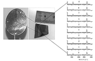
도 8은 2D/G 및 반치전폭(FWHW, Full Width at Half Maximum)의 함수로서 시트의 노출 시간 변화(time-of-exposure variation)를 나타낸다.
도 9는 FWHM 2D/G의 함수로서 온도 변화를 나타낸다.
도 10은 2D/G, D/G의 함수로서, 합성 동안 시트 갭에서 거리 변화를 나타내며, 커브 "b"가 FWHM의 함수로서 삽입된다. 1 discloses a schematic diagram of a system of the present invention.
Figure 2 discloses the arrangement of a copper sheet for the graphene synthesis of the present invention, and 532-nm Raman spectra are obtained directly on the inner and outer surfaces of the copper sheet from the synthesis of the present invention.
3 discloses a 514-nm Raman spectrum of graphene grown on one of the inner surfaces of a copper sheet.
4 discloses a micrograph of graphene transferred to silicon oxide, in which graphene monolayer and bilayer regions based on a 532-nm Raman spectrum are observed.
5 discloses a 647-nm wavelength Raman spectrum of graphene grown on one of the inner surfaces of a copper sheet and transferred onto a SiO 2 /Si substrate.
6 discloses a 488-nm Raman spectrum of graphene on one of the inner surfaces of a copper sheet.
7 discloses a 514-nm Raman spectrum of graphene grown on one of the inner surfaces of a copper sheet and transferred onto SiO 2 /Si radially at ten different points of the substrate.
8 shows the time-of-exposure variation of the sheet as a function of 2D/G and Full Width at Half Maximum (FWHW).
9 is a FWHM It represents the temperature change as a function of 2D/G.
Figure 10 shows the distance change in the sheet gap during compositing as a function of 2D/G, D/G, and curve “b” is inserted as a function of FWHM.
기술의 현 상태에서, 그래핀은 LP(낮은 압력)-CVD 및 HP(높은 압력)-CVD와 같이 상이한 압력 조건 하에서 CVD에 의해 합성된다. AP(주변 압력)-CVD에 대하여, 합성 기체 및 기판 내에 존재하는 대기 산소, 예컨대 천연 산화물은 그래핀의 형성을 손상시키고 억제하는 경향을 가지기 때문에, 진공 시스템 및 펌프, 챔버 비우기 및 불활성 기체로 채우기 사이클은 필수적이다. 따라서, 환원제 및 공-촉매(co-catalyst)로서 상이한 양으로 수소 기체 첨가로 인해, 그래핀 합성에서 다수의 단계(가열, 성장 및 냉각)가 취해진다. In the current state of the art, graphene is synthesized by CVD under different pressure conditions, such as LP (low pressure)-CVD and HP (high pressure)-CVD. For AP (ambient pressure)-CVD, vacuum system and pump, empty chamber and fill with inert gas, as atmospheric oxygen present in synthesis gas and substrate, such as native oxide, tends to impair and inhibit the formation of graphene. Cycles are essential. Therefore, due to the addition of hydrogen gas in different amounts as reducing agent and co-catalyst, multiple steps (heating, growth and cooling) are taken in graphene synthesis.
반대로, 본 발명에서 그래핀 합성은 오직 아르곤 및 메탄을 사용함으로써 수소 기체 첨가 없이 오픈 챔버에서 단일 단계로 개발된다. 추가적으로, 합성의 종료까지, 새로운 그래핀 성장 공정을 위한 조건은 시스템에 의해 재빨리 충족된다. Conversely, in the present invention, graphene synthesis is developed in a single step in an open chamber without hydrogen gas addition by using only argon and methane. Additionally, until the end of the synthesis, the conditions for a new graphene growth process are quickly met by the system.
본 발명은 평행한 방식으로 배열되고 세라믹 물질(30)에 의해 분리된 두 개의 구리 시트(40)에 의해 구성되는 새로운 기판 배치에 의해 그래핀을 생성하고, 이는 1000℃의 온도에서 전자기 유도(20)를 통해 가열된다. 시트 사이에 형성된 갭, 또는 계면 지역은, 잔류 산소의 활동을 억제하고 이 지역에서 Cu 표면으로부터 천연 산화물을 감소시키는, 분해된 종, 수소 및 중간 종을 보유한다. 추가적으로, 이들 종은 탄소 흡수를 가져와 시트의 내부 표면에서 그래핀의 성장을 야기한다. The present invention produces graphene by means of a novel substrate arrangement consisting of two
이 모든 것들은 에너지 및 합성 기체를 절약함으로써 생성 비용을 감소시키고, 뿐만 아니라 수소와 같은 폭발성 기체의 취급에서 어려움을 감소시킨다. 산업 규모로 생산 확장성이 본 발명에 의해 촉진된다. All this reduces the cost of production by saving energy and synthesis gas, as well as reduces the difficulty in handling explosive gases such as hydrogen. Production scalability on an industrial scale is facilitated by the present invention.
도 1에서 도시된 바와 같이 오픈 챔버 AP-CVD에서 그래핀(100)을 생성하기 위한 시스템은 유리 실린더 챔버(10), 바람직하게 직경 40mm 및 길이 110mm의 파이렉스에 의해 제조되고, 여기서 그의 축방향 축은 수직으로 배향되고, 유리 실린더 챔버(10)는 그의 하부 표면(15)에서 완전히 개방되고, 그의 상부 표면(18)은 메탄 및 아르곤의 혼합물이 공급된다.The system for producing
유리 실린더 챔버(10)의 내부에서, 직경 30mm 및 두께 0.1mm이고, 99.8% 순도인 두 개의 원형 구리 시트(40)는 평행이고 분리된 방식으로 배열되고, 직경 3.5mm 및 길이 30mm인 세 개의 세라믹 기둥(30)에 의해 지지되고, 이는 동일한 물질로 만들어진 베이스(35)에 고정된다. Inside the
두 개의 구리 시트(40)는 유리 실린더 챔버(10)를 외부로 감아 올라가는 코일, 바람직하게 2.5μH의 코일로 구성된 전자기 유도 가열기(20)를 사용함으로써 전자기 유도를 통해 가열되고, 여기서 전자기 유도 가열기(20) 코일은, 바람직하게 250 KHz와 동등한 주파수 발진기(미도시됨)에 의해 생성된 교류에 의해 공급된다. 이 주파수는 원형 구리 시트(40)의 고전기 전도성으로 인해 설정된다. The two
두 개의 구리 시트(40)의 온도는 유리 실린더 챔버(10)의 상부 표면(18) 상에 배열된 쿼츠 윈도우(60)를 통해 복사 고온계(50)에 의해 연속적으로 모니터링되고, 따라서 전자기 유도 가열기(20)로 전원 공급에 의해 온도를 제어하는 것이 가능해진다. The temperature of the two
유리 실린더 챔버(10)로 도입하기 전에, 두 개의 구리 시트(40)는 2분 동안 아세트산으로 처리되고, 에탄올로 헹궈진다. 따라서, 구리 시트(40)는 2분 동안 각각 1.0L/min 및 0.1L/min의 메탄 및 아르곤 스트림 하에서 유리 실린더 챔버(10) 내에서 유지된다. 결과적으로, 이는 15분 동안 전자기 유도 가열기(20)를 사용함으로써 약 1000℃로 가열된다. 이 단계의 종료까지, 이는 동일한 메탄 및 아르곤 스트림으로 실온으로 냉각되도록 방치되므로써, 약 5초 내에 1000℃ 내지 600℃의 냉각을 획득한다. Prior to introduction into the
평행한 방식으로 배열되고 세라믹 물질(30)에 의해 분리된 두 개의 구리 시트(40)의 이 구성으로부터 1000℃의 온도에서 전자기 유도를 통해 가열된다. 구리 시트(40) 및 챔버 사이에 형성된 갭은 구배 방향으로 분자 중량에 기반하여 기체를 분리하는 경향을 가지는 표시된 열적 구배를 설정한다. 이러한 열적 확산은 더 가벼운 분자(분해로부터의 메탄 및 다른 것들)에 대해 가장 높은 온도 지역인 계면 지역으로 보내지는 반면에, 가장 무거운 기체(Ar, O2, N)들은 이 지역 밖에 머무른다. 따라서, 성장하는 그래핀에 유해할 수 있는 산소는 계면 지역 밖으로 가는 경향이 있다. 추가적으로, 이 지역에서 메탄 및 분해 종의 체류는 외부 표면에서 보다 높고, 따라서 시트와 더 높은 충돌 밀도를 야기하고, 메탄의 분해 가능성이 증가한다. From this configuration of two
한편, 분해 생성물, 수소 및 중간 종은 잔류 산소의 활동을 억제하고, 구리 시트(40)의 내부 표면으로부터 천연 산화물을 감소시킨다. 추가적으로, 이들 종은 시트의 내부 표면에서 탄소 흡수를 야기하고, 따라서 상기 표면에서 그래핀의 성장을 일으킨다. On the other hand, decomposition products, hydrogen and intermediate species inhibit the activity of residual oxygen and reduce native oxides from the inner surface of the
라만 분광분석법은 그래핀 및 탄소-계 물질의 확인 및 특성분석을 위해 폭넓게 사용되는 강력한 비파괴 기술이다. 그래핀에 대하여 라만 분광분석법에서 강조된 특징은 D~1350 cm-1, D* ~1622 cm-1, G~ 1580 cm-1, 및 2D~2700 cm-1 밴드이다. G 밴드는 sp2 결합의 신장 움직임에 관계된다. D 및 D* 밴드는 유도된 결점에 연관된다. 마지막으로, 2D 밴드는 D 밴드의 배음(overtone)으로, 그래핀 층의 수를 구체화기 위해 유용하다. D/G 강도 사이의 비(ratio)는 그래핀 결점을 특성분석하기 위해 폭넓게 사용된다. 추가적으로, 2D/G 비 강도는 그래핀 층의 수에 대한 측정이다. 단층 그래핀에 대해, 비는 2보다 높다. Raman spectroscopy is a powerful non-destructive technique widely used for the identification and characterization of graphene and carbon-based materials. Characteristics highlighted in Raman spectroscopy for graphene are the D~1350 cm -1 , D* -1622 cm -1 , G-1580 cm -1 , and 2D-2700 cm -1 bands. The G band is involved in the stretching motion of sp2 bonds. D and D* bands are associated with induced defects. Finally, the 2D band is an overtone of the D band, which is useful for specifying the number of graphene layers. The ratio between D/G intensities is widely used to characterize graphene defects. Additionally, the 2D/G ratio intensity is a measure of the number of graphene layers. For monolayer graphene, the ratio is higher than 2.
본 발명에 따라 형성된 그래핀은 514, 532, 및 647nm의 파장에서 라만 분광분석기를 사용함으로써 확인되고 특성분석된다.Graphene formed according to the present invention is identified and characterized by using Raman spectroscopy at wavelengths of 514, 532, and 647 nm.
도 2는 두 개의 구리 시트(40) 내부 표면으로부터 직접적으로 획득된 라만 스펙트럼을 개시한다. 그래프에서 도시된 바와 같이 D 밴드가 부재하는 전형적인 단층 및 이층 그래핀 스펙트럼이 관측되고, 따라서 고품질의 그래핀 성장, 및 질소 도핑과 연관된 D* 밴드의 부재를 나타낸다. 그러나 시트의 외부 표면에서, 스펙트럼은 비정질 탄소 형성 및 218cm-1 및 540cm-1 피크와 같이 구리 산화물에 연관된 피크를 도시한다. 2 discloses Raman spectra obtained directly from the inner surfaces of two
도 3은 1mm의 두 개의 구리 시트(40) 사이의 갭 거리로 15분 동안 970℃에서 합성되는 SiO2/Si 기판으로 전이된 그래핀 표면의 현미경 사진을 도시하고; 획득된 라만 스펙트럼은 4보다 큰 2D/G 비를 도시한다. 또한, 2D 피크의 FWHM은 약 24cm-1이고; 따라서, 단층 그래핀 성장이 추정된다. D/G 비는 약 0.1이다.3 shows a photomicrograph of the graphene surface transferred to a SiO 2 /Si substrate synthesized at 970° C. for 15 minutes with a gap distance between two
도 4는 단층 및 이층 그래핀 영역이 삽입에서 라만 스펙트럼을 기반으로 주목되는 SiO2/Si 기판으로 전이된 그래핀 표면의 현미경 사진을 도시한다. Figure 4 shows micrographs of the graphene surface transferred to a SiO 2 /Si substrate where monolayer and bilayer graphene regions are noted based on Raman spectra in the inset.
도 5는 D/G 비가 약 0.03이어서 고품질의 그래핀을 나타내는 SiO2/Si 기판으로 전이된 그래핀 상에 647nm의 파장에서 라만 스펙트럼을 도시한다. 5 shows a Raman spectrum at a wavelength of 647 nm on graphene transferred to a SiO 2 /Si substrate with a D/G ratio of about 0.03 indicating high-quality graphene.
도 6은 514nm에서 라만 분광분석기를 사용함으로써 계면 지역에서 구리 시트 중의 하나 상에 직접적으로 획득된 전형적인 그래핀 라만 스펙트럼을 도시한다. 6 shows a typical graphene Raman spectrum obtained directly on one of the copper sheets in the interfacial region by using a Raman spectrometer at 514 nm.
도 7은 내부 표면 상에 합성에 노출된 시트 중의 하나의 사진을 도시한다. 이어서, 성장된 그래핀은 SiO2/Si 기판 상에 전이되고, 여기서 라만 스펙트럼은 방사상 방향으로 10개의 상이한 위치로부터 획득되었다. 7 shows a photograph of one of the sheets exposed to the composite on the inner surface. Then, the grown graphene was transferred onto a SiO 2 /Si substrate, where Raman spectra were acquired from 10 different positions in the radial direction.
도 8은 2D/G 및 FWHM의 함수로서 시트 내에서 노출 시간 변화를 도시하고, 여기서 합성 파라미터는 다음과 같다: 1mm의 시트 사이의 갭 거리, 970℃의 온도, 1 및 0.1L/min의 아르곤 및 메탄의 각각의 유동 속도. 532-nm 라만 스펙트럼은 9개의 상이한 위치에서 구리 시트의 내부 표면 중의 하나에서 직접적으로 획득되고, 따라서, 개별적인 2D/G, D/G 및 FWHM 비는 획득되어 최종적으로 평균됨으로써, 약 15분의 최적 합성 시간이 관측된다. 8 shows the exposure time variation within the sheets as a function of 2D/G and FWHM, where the composite parameters are: a gap distance between the sheets of 1 mm, a temperature of 970° C., and argon at 1 and 0.1 L/min. and the respective flow rates of methane. 532-nm Raman spectra were obtained directly at one of the inner surfaces of the copper sheet at nine different locations, and thus individual 2D/G, D/G and FWHM ratios were obtained and finally averaged, resulting in an optimum of about 15 min. The synthesis time is observed.
도 9는 2D/G 및 FWHM의 함수로서 온도 변화를 도시하고, 여기서 합성 파라미터는 다음와 같다: 10분의 노출 시간, 1mm의 시트 사이의 갭 거리, 및 1 및 0.1L/min의 아르곤 및 메탄의 각각의 유동 속도. 532-nm 라만 스펙트럼은 9개의 상이한 위치에서 구리 시트의 내부 표면 중의 하나 상에 직접적으로 획득되고, 따라서 개별적인 2D/G, D/G, 및 FWHM 비는 획득되어 최종적으로 평균된다. 이로써, 970℃의 최적 합성 온도가 관측된다. 9 shows the temperature change as a function of 2D/G and FWHM, where the synthesis parameters are: exposure time of 10 min, gap distance between sheets of 1 mm, and of argon and methane of 1 and 0.1 L/min. each flow rate. 532-nm Raman spectra are acquired directly on one of the inner surfaces of the copper sheet at nine different locations, and thus individual 2D/G, D/G, and FWHM ratios are acquired and finally averaged. Thus, an optimum synthesis temperature of 970°C is observed.
도 10은 커브 "a"에서 2D/G, D/G의 함수로서, 및 FWHM의 함수로서 커브 "b" 삽입물에서, 합성 동안 시트 사이에 갭 거리 변화를 도시하고, 여기서 합성 노출 시간은 10분이고, 합성 온도는 970℃이고, 및 아르곤 및 메탄의 유동 속도는 각각 1 및 0.1L/min이다. 532-nm 라만 스펙트럼은 9개의 다른 지점에서 구리 시트 내부 표면 중의 하나에서 직접적으로 획득되고, 따라서 개별적인 2D/G, D/G, 및 FWHM 비는 획득되어 최종적으로 평균되고, 따라서 약 1mm의 최적 갭 거리가 관측된다.Figure 10 shows the change in gap distance between sheets during compositing, in curve “b” inserts as a function of 2D/G, D/G, and as a function of FWHM in curve “a”, where the composite exposure time is 10 min. , the synthesis temperature is 970 °C, and the flow rates of argon and methane are 1 and 0.1 L/min, respectively. 532-nm Raman spectra were acquired directly at one of the inner surfaces of the copper sheet at nine different points, so the individual 2D/G, D/G, and FWHM ratios were acquired and finally averaged, thus providing an optimal gap of about 1 mm. distance is observed.
Claims (17)
- 상기 두 개의 구리 시트(40)를 유리 실린더 챔버(10)에 의해 구성된 오픈 챔버로 도입하는 단계로서, 여기서 유리 실린더 챔버(10)의 축방향 축은 수직으로 배향되고, 여기서 유리 실린더 챔버(10)는 그의 하부 표면(15)에서 완전히 개방되는 것인 단계;
- 사전결정된 온도에서 전자기 유도 가열기(20)를 사용함으로써 두 개의 구리 시트(40)를 가열하는 단계;
- 상기 유리 실린더 챔버(10)의 상부 표면(18) 내에 메탄 및 아르곤 스트림의 혼합물을 제공하는 단계;
- 유리 실린더 챔버(10)의 상부 표면(18)에 배열된 쿼츠 윈도우(60)(quartz window)를 통해 복사 고온계(50)를 사용함으로써 두 개의 구리 시트(40)의 온도를 연속적으로 모니터링하는 단계;
- 사전결정된 기간 동안 전자기 유도 가열기(20)를 사용함으로써 1000℃로 가열하는 단계; 및
- 동일한 메탄 및 아르곤 스트림으로 실온으로 냉각시키는 단계
를 포함하는 대기압에서 화학적 기상 증착법(AP-CVD, atmospheric pressure-chemical vapor deposition)에 의해 구리 기판 상에 그래핀을 생성하는 방법. - providing two copper sheets (40) arranged in a parallel manner and separated by a ceramic material (30);
- introducing the two copper sheets (40) into an open chamber constituted by a glass cylinder chamber (10), wherein the axial axis of the glass cylinder chamber (10) is oriented vertically, wherein the glass cylinder chamber (10) is completely open at its lower surface (15);
- heating the two copper sheets 40 by using an electromagnetic induction heater 20 at a predetermined temperature;
- providing a mixture of methane and argon streams in the upper surface (18) of the glass cylinder chamber (10);
- continuously monitoring the temperature of the two copper sheets 40 by using a radiation pyrometer 50 through a quartz window 60 arranged on the upper surface 18 of the glass cylinder chamber 10; ;
- heating to 1000° C. by using an electromagnetic induction heater 20 for a predetermined period; and
-cooling to room temperature with the same stream of methane and argon
A method for producing graphene on a copper substrate by a chemical vapor deposition method (AP-CVD, atmospheric pressure-chemical vapor deposition) at atmospheric pressure comprising a.
전자기 유도 가열기(20)를 사용함으로써 평행한 방식으로 배열되고 세라믹 물질(30)에 의해 분리된 두 개의 구리 시트(40)를 가열하기 위한 사전결정된 온도는 1000℃인 것인 그래핀을 생성하는 방법. The method of claim 1,
A method for producing graphene, wherein a predetermined temperature for heating two copper sheets 40 arranged in a parallel manner and separated by a ceramic material 30 by using an electromagnetic induction heater 20 is 1000° C. .
유리 실린더 챔버(10) 내부에 배열된 두 개의 구리 시트(40)는 99.8% 순도로 직경 30mm 및 두께 0.1mm이고, 평행하고 분리된 방식으로 배열되고, 직경 3.5mm 및 길이 30mm의 세 개의 세라믹 기둥(30)에 의해 지지되고, 상기 기둥은 동일한 물질로 제조된 베이스(35)에 고정된 것인 그래핀을 생성하는 방법. The method of claim 1,
The two copper sheets 40 arranged inside the glass cylinder chamber 10 are 30 mm in diameter and 0.1 mm thick at 99.8% purity, arranged in a parallel and separate manner, and three ceramic pillars 3.5 mm in diameter and 30 mm long A method for producing graphene supported by (30), wherein the pillars are fixed to a base (35) made of the same material.
전자기 유도 가열기(20)는 2.5μH인 코일로 구성되고, 이는 유리 실린더 챔버(10)에서 외부로 감아 올라가고, 250KHz에서, 주파수 발진기에 의해 생성된 교류가 코일에 공급되는 것인 그래핀을 생성하는 방법. The method of claim 1,
The electromagnetic induction heater 20 consists of a coil of 2.5 μH, which is wound up in a glass cylinder chamber 10, and at 250 KHz, an alternating current generated by a frequency oscillator is supplied to the coil to produce graphene. Way.
유리 실린더 챔버(10)로 도입되기 전에, 두 개의 구리 시트(40)는 2분 동안 아세트산으로 처리되고, 에탄올로 헹궈지는 것인 그래핀을 생성하는 방법. The method of claim 1,
Before being introduced into the glass cylinder chamber (10), two copper sheets (40) are treated with acetic acid for 2 minutes and rinsed with ethanol.
메탄 및 아르곤 스트림의 혼합물을 제공한 후, 구리 시트(40)는 2분 동안 각각 1.0L/min 및 0.1L/min의 메탄 및 아르곤 스트림 하에서 유지되는 것인 그래핀을 생성하는 방법.The method of claim 1,
After providing a mixture of methane and argon streams, the copper sheet (40) is maintained under methane and argon streams of 1.0 L/min and 0.1 L/min, respectively, for 2 minutes.
동일한 메탄 및 아르곤 스트림으로 냉각함으로써, 냉각 감소는 5초 동안 1000℃ 내지 600℃인 것인 그래핀을 생성하는 방법. The method of claim 1,
By cooling with the same methane and argon streams, the cooling reduction is from 1000°C to 600°C for 5 seconds.
전자기 유도 가열기(20)를 사용함으로써 1000℃로 가열하기 위한 사전결정된 기간은 15분인 것인 그래핀을 생성하는 방법.The method of claim 1,
A method for producing graphene, wherein the predetermined period for heating to 1000° C. by using an electromagnetic induction heater (20) is 15 minutes.
사전결정된 기간 동안 두 개의 구리 시트(40)를 사전결정된 온도에서 가열하는 전자기 유도 가열기(20);
상기 유리 실린더 챔버(10)의 상부 표면(18)으로, 메탄 및 아르곤 스트림의 혼합물의 제공받는 상부 표면(18); 및
유리 실린더 챔버(10)의 상부 표면(18)에 배열된 쿼츠 윈도우(60)를 통해 두 개의 구리 시트(40)의 온도를 연속적으로 모니터링하는 복사 고온계(50);
를 포함하는, 대기압에서 화학적 기상 증착법(AP-CVD; atmospheric pressure-chemical vapor deposition)에 의해 구리 기판 상에 그래핀을 생성하기 위한 시스템. With two copper sheets 40 arranged in a parallel manner and separated by a ceramic material 30 , the two copper sheets 40 are introduced into an open chamber constituted by a glass cylinder chamber 10 , wherein The axial axis of the glass cylinder chamber 10 is oriented vertically, wherein the glass cylinder chamber 10 is fully open at its lower surface 15;
an electromagnetic induction heater 20 for heating the two copper sheets 40 at a predetermined temperature for a predetermined period of time;
an upper surface (18) of the glass cylinder chamber (10), the upper surface (18) being provided with a mixture of methane and argon streams; and
a radiation pyrometer (50) for continuously monitoring the temperature of the two copper sheets (40) through a quartz window (60) arranged on the upper surface (18) of the glass cylinder chamber (10);
A system for producing graphene on a copper substrate by atmospheric pressure-chemical vapor deposition (AP-CVD) at atmospheric pressure, comprising:
유리 실린더 챔버(10) 내부에 배열된 두 개의 구리 시트(40)는 99.8% 순도로 직경 30mm 및 두께 0.1mm이고, 평행하고 분리된 방식으로 배열되고, 직경 3.5mm 및 길이 30mm의 세 개의 세라믹 기둥(30)에 의해 지지되고, 상기 기둥은 동일한 물질로 제조된 베이스(35)에 고정된 것인 그래핀을 생성하기 위한 시스템.10. The method of claim 9,
The two copper sheets 40 arranged inside the glass cylinder chamber 10 are 30 mm in diameter and 0.1 mm thick at 99.8% purity, arranged in a parallel and separate manner, and three ceramic pillars 3.5 mm in diameter and 30 mm long A system for producing graphene supported by (30), wherein the pillars are fixed to a base (35) made of the same material.
전자기 유도 가열기(20)는 2.5μH인 코일로 구성되고, 이는 유리 실린더 챔버(10)에서 외부로 감아 올라가고, 250KHz에서, 주파수 발진기에 의해 생성된 교류가 코일에 공급되는 것인 그래핀을 생성하기 위한 시스템.10. The method of claim 9,
The electromagnetic induction heater 20 consists of a coil of 2.5 μH, which is wound up in a glass cylinder chamber 10, and at 250 KHz, an alternating current generated by a frequency oscillator is supplied to the coil to produce graphene. system for.
유리 실린더 챔버(10) 물질은 직경 40mm 및 길이 110mm인 파이렉스(Pyrex®)인 그래핀을 생성하기 위한 시스템.10. The method of claim 9,
A system for producing graphene, wherein the glass cylinder chamber 10 material is Pyrex ® with a diameter of 40 mm and a length of 110 mm.
Applications Claiming Priority (3)
| Application Number | Priority Date | Filing Date | Title |
|---|---|---|---|
| CL1858-2016 | 2016-07-21 | ||
| CL2016001858A CL2016001858A1 (en) | 2016-07-21 | 2016-07-21 | Method and system to produce graphene on a copper substrate by deposition of chemical vapors (ap_cvd) modified |
| PCT/CL2017/050032 WO2018014143A1 (en) | 2016-07-21 | 2017-07-18 | A method and system for producing graphene on a copper substrate by modified chemical vapour deposition (ap-cvd) |
Publications (2)
| Publication Number | Publication Date |
|---|---|
| KR20190032401A KR20190032401A (en) | 2019-03-27 |
| KR102408821B1 true KR102408821B1 (en) | 2022-06-14 |
Family
ID=59858379
Family Applications (1)
| Application Number | Title | Priority Date | Filing Date |
|---|---|---|---|
| KR1020197002936A KR102408821B1 (en) | 2016-07-21 | 2017-07-18 | Method and system for producing graphene on copper substrates by modified chemical vapor deposition (AP-CVD) |
Country Status (6)
| Country | Link |
|---|---|
| US (1) | US11624114B2 (en) |
| EP (1) | EP3489194A4 (en) |
| JP (1) | JP7039051B2 (en) |
| KR (1) | KR102408821B1 (en) |
| CL (1) | CL2016001858A1 (en) |
| WO (1) | WO2018014143A1 (en) |
Cited By (1)
| Publication number | Priority date | Publication date | Assignee | Title |
|---|---|---|---|---|
| CN115744886A (en) * | 2022-11-24 | 2023-03-07 | 广东墨睿科技有限公司 | Graphene growth support and graphene growth method |
Families Citing this family (7)
| Publication number | Priority date | Publication date | Assignee | Title |
|---|---|---|---|---|
| CL2016001858A1 (en) | 2016-07-21 | 2017-02-17 | Univ Técnica Federico Santa Mar+Ia | Method and system to produce graphene on a copper substrate by deposition of chemical vapors (ap_cvd) modified |
| WO2021067118A1 (en) * | 2019-09-30 | 2021-04-08 | Lam Research Corporation | Selective graphene deposition using remote plasma |
| CN115433920B (en) * | 2021-06-03 | 2024-05-14 | 上海新池能源科技有限公司 | Process method for growing single-layer graphene |
| CN113566044A (en) * | 2021-07-30 | 2021-10-29 | 重庆大学 | Heating method for obtaining continuous high-temperature chlorine |
| CN113699503B (en) * | 2021-08-31 | 2022-09-09 | 上海交通大学 | Graphene preparation method and device with multiphase composite carbon source on metal surface |
| CN114459336A (en) * | 2022-03-04 | 2022-05-10 | 广东粤港澳大湾区国家纳米科技创新研究院 | Graphene strain sensor and preparation method of graphene strain sensor |
| CN115125524A (en) * | 2022-07-05 | 2022-09-30 | 常州第六元素半导体有限公司 | Sectional type roll-to-roll CVD graphene continuous growth equipment |
Citations (1)
| Publication number | Priority date | Publication date | Assignee | Title |
|---|---|---|---|---|
| WO2014038803A1 (en) | 2012-09-04 | 2014-03-13 | Samsung Techwin Co., Ltd | Catalyst metal film-supporting device and method and apparatus for synthesizing multiple graphene films |
Family Cites Families (7)
| Publication number | Priority date | Publication date | Assignee | Title |
|---|---|---|---|---|
| JP4698354B2 (en) | 2005-09-15 | 2011-06-08 | 株式会社リコー | CVD equipment |
| US20100301212A1 (en) * | 2009-05-18 | 2010-12-02 | The Regents Of The University Of California | Substrate-free gas-phase synthesis of graphene sheets |
| KR101912798B1 (en) | 2011-01-31 | 2018-10-30 | 한화에어로스페이스 주식회사 | Apparatus and method for manufacturing graphene |
| CN104159736B (en) | 2012-01-06 | 2016-11-09 | Ut-巴特勒有限公司 | The extensive monolayer of high-quality and multi-layer graphene by means of chemical gaseous phase deposition produce |
| GB201215579D0 (en) | 2012-08-31 | 2012-10-17 | Univ Leiden | Thin film formation |
| US20150140211A1 (en) * | 2013-11-19 | 2015-05-21 | Cvd Equipment Corporation | Scalable 2D-Film CVD Synthesis |
| CL2016001858A1 (en) | 2016-07-21 | 2017-02-17 | Univ Técnica Federico Santa Mar+Ia | Method and system to produce graphene on a copper substrate by deposition of chemical vapors (ap_cvd) modified |
-
2016
- 2016-07-21 CL CL2016001858A patent/CL2016001858A1/en unknown
-
2017
- 2017-07-18 US US16/318,193 patent/US11624114B2/en active Active
- 2017-07-18 WO PCT/CL2017/050032 patent/WO2018014143A1/en unknown
- 2017-07-18 KR KR1020197002936A patent/KR102408821B1/en active IP Right Grant
- 2017-07-18 JP JP2019524490A patent/JP7039051B2/en active Active
- 2017-07-18 EP EP17830164.4A patent/EP3489194A4/en not_active Withdrawn
Patent Citations (1)
| Publication number | Priority date | Publication date | Assignee | Title |
|---|---|---|---|---|
| WO2014038803A1 (en) | 2012-09-04 | 2014-03-13 | Samsung Techwin Co., Ltd | Catalyst metal film-supporting device and method and apparatus for synthesizing multiple graphene films |
Cited By (2)
| Publication number | Priority date | Publication date | Assignee | Title |
|---|---|---|---|---|
| CN115744886A (en) * | 2022-11-24 | 2023-03-07 | 广东墨睿科技有限公司 | Graphene growth support and graphene growth method |
| CN115744886B (en) * | 2022-11-24 | 2024-04-19 | 广东墨睿科技有限公司 | Graphene growth bracket and graphene growth method |
Also Published As
| Publication number | Publication date |
|---|---|
| EP3489194A4 (en) | 2020-04-22 |
| WO2018014143A1 (en) | 2018-01-25 |
| JP2019529323A (en) | 2019-10-17 |
| KR20190032401A (en) | 2019-03-27 |
| EP3489194A1 (en) | 2019-05-29 |
| US20190233942A1 (en) | 2019-08-01 |
| JP7039051B2 (en) | 2022-03-22 |
| CL2016001858A1 (en) | 2017-02-17 |
| US11624114B2 (en) | 2023-04-11 |
Similar Documents
| Publication | Publication Date | Title |
|---|---|---|
| KR102408821B1 (en) | Method and system for producing graphene on copper substrates by modified chemical vapor deposition (AP-CVD) | |
| Deng et al. | Toward mass production of CVD graphene films | |
| Rybin et al. | Efficient nitrogen doping of graphene by plasma treatment | |
| KR101828528B1 (en) | Manufacturing apparatus and method of graphene | |
| TWI498206B (en) | Apparatus and method for continuous synthesis of carbon film or inorganic material film | |
| Chan et al. | Low-temperature synthesis of graphene on Cu using plasma-assisted thermal chemical vapor deposition | |
| Lavin-Lopez et al. | Synthesis and characterization of graphene: influence of synthesis variables | |
| CN102995119B (en) | Large-sized sexangle bilayer graphene single crystal domains and preparation method thereof | |
| CN103352202B (en) | A kind of controllable method for preparing of normal-pressure chemical-vapor-deposlarge-area large-area high-quality double-layer graphene film | |
| Wang | Laser based fabrication of graphene | |
| Lavin-Lopez et al. | Thickness control of graphene deposited over polycrystalline nickel | |
| Yang et al. | Growth of monolayer MoS2 films in a quasi-closed crucible encapsulated substrates by chemical vapor deposition | |
| KR101154416B1 (en) | Single crystal method | |
| Rouessac et al. | Preparation of silica membranes inside macroporous alumina tubes by PECVD for hydrogen selectivity | |
| KR20130107117A (en) | Apparatus for synthesizing graphene | |
| TWI535887B (en) | Apparatus and method for the synthesis of high-quality of carbon film or inorganic material film | |
| JPH03274275A (en) | Device for forming thin film utilizing organometallic gas | |
| JP6944699B2 (en) | Method for manufacturing hexagonal boron nitride film | |
| de Obaldia et al. | Photoluminescence in raman scattering: Effects of HfO2 template layer on ultrananocrystalline diamond (UNCD) films grown on stainless steel substrates | |
| Alrefae et al. | Thermal analysis and optimization of graphene deposition in a roll-to-roll plasma CVD process | |
| RU196377U1 (en) | Device for producing structured graphene | |
| Aoki et al. | ZnO film deposition by plasma enhanced CVD using zinc-acetylacetonate | |
| KR20130092053A (en) | Fabrication methods of antimony-telluride thermoelectric thin film | |
| JPH04173976A (en) | Thin film forming device | |
| RU2578104C1 (en) | Method for gas-phase carbidisation of surface of monocrystalline silicon of orientation (111), (100) |
Legal Events
| Date | Code | Title | Description |
|---|---|---|---|
| PA0105 | International application |
Patent event date: 20190129 Patent event code: PA01051R01D Comment text: International Patent Application |
|
| PG1501 | Laying open of application | ||
| A201 | Request for examination | ||
| PA0201 | Request for examination |
Patent event code: PA02012R01D Patent event date: 20200715 Comment text: Request for Examination of Application |
|
| E902 | Notification of reason for refusal | ||
| PE0902 | Notice of grounds for rejection |
Comment text: Notification of reason for refusal Patent event date: 20211217 Patent event code: PE09021S01D |
|
| E701 | Decision to grant or registration of patent right | ||
| PE0701 | Decision of registration |
Patent event code: PE07011S01D Comment text: Decision to Grant Registration Patent event date: 20220411 |
|
| GRNT | Written decision to grant | ||
| PR0701 | Registration of establishment |
Comment text: Registration of Establishment Patent event date: 20220609 Patent event code: PR07011E01D |
|
| PR1002 | Payment of registration fee |
Payment date: 20220610 End annual number: 3 Start annual number: 1 |
|
| PG1601 | Publication of registration |