KR101762043B1 - Oxide sintered body and sputtering target - Google Patents
Oxide sintered body and sputtering target Download PDFInfo
- Publication number
- KR101762043B1 KR101762043B1 KR1020157006265A KR20157006265A KR101762043B1 KR 101762043 B1 KR101762043 B1 KR 101762043B1 KR 1020157006265 A KR1020157006265 A KR 1020157006265A KR 20157006265 A KR20157006265 A KR 20157006265A KR 101762043 B1 KR101762043 B1 KR 101762043B1
- Authority
- KR
- South Korea
- Prior art keywords
- oxide
- phase
- sintered body
- sno
- ingazno
- Prior art date
Links
Images


Classifications
-
- C—CHEMISTRY; METALLURGY
- C04—CEMENTS; CONCRETE; ARTIFICIAL STONE; CERAMICS; REFRACTORIES
- C04B—LIME, MAGNESIA; SLAG; CEMENTS; COMPOSITIONS THEREOF, e.g. MORTARS, CONCRETE OR LIKE BUILDING MATERIALS; ARTIFICIAL STONE; CERAMICS; REFRACTORIES; TREATMENT OF NATURAL STONE
- C04B35/00—Shaped ceramic products characterised by their composition; Ceramics compositions; Processing powders of inorganic compounds preparatory to the manufacturing of ceramic products
- C04B35/01—Shaped ceramic products characterised by their composition; Ceramics compositions; Processing powders of inorganic compounds preparatory to the manufacturing of ceramic products based on oxide ceramics
- C04B35/453—Shaped ceramic products characterised by their composition; Ceramics compositions; Processing powders of inorganic compounds preparatory to the manufacturing of ceramic products based on oxide ceramics based on zinc, tin, or bismuth oxides or solid solutions thereof with other oxides, e.g. zincates, stannates or bismuthates
-
- H—ELECTRICITY
- H01—ELECTRIC ELEMENTS
- H01J—ELECTRIC DISCHARGE TUBES OR DISCHARGE LAMPS
- H01J37/00—Discharge tubes with provision for introducing objects or material to be exposed to the discharge, e.g. for the purpose of examination or processing thereof
- H01J37/32—Gas-filled discharge tubes
- H01J37/34—Gas-filled discharge tubes operating with cathodic sputtering
- H01J37/3411—Constructional aspects of the reactor
- H01J37/3414—Targets
- H01J37/3426—Material
- H01J37/3429—Plural materials
-
- C—CHEMISTRY; METALLURGY
- C04—CEMENTS; CONCRETE; ARTIFICIAL STONE; CERAMICS; REFRACTORIES
- C04B—LIME, MAGNESIA; SLAG; CEMENTS; COMPOSITIONS THEREOF, e.g. MORTARS, CONCRETE OR LIKE BUILDING MATERIALS; ARTIFICIAL STONE; CERAMICS; REFRACTORIES; TREATMENT OF NATURAL STONE
- C04B35/00—Shaped ceramic products characterised by their composition; Ceramics compositions; Processing powders of inorganic compounds preparatory to the manufacturing of ceramic products
- C04B35/01—Shaped ceramic products characterised by their composition; Ceramics compositions; Processing powders of inorganic compounds preparatory to the manufacturing of ceramic products based on oxide ceramics
- C04B35/453—Shaped ceramic products characterised by their composition; Ceramics compositions; Processing powders of inorganic compounds preparatory to the manufacturing of ceramic products based on oxide ceramics based on zinc, tin, or bismuth oxides or solid solutions thereof with other oxides, e.g. zincates, stannates or bismuthates
- C04B35/457—Shaped ceramic products characterised by their composition; Ceramics compositions; Processing powders of inorganic compounds preparatory to the manufacturing of ceramic products based on oxide ceramics based on zinc, tin, or bismuth oxides or solid solutions thereof with other oxides, e.g. zincates, stannates or bismuthates based on tin oxides or stannates
-
- C—CHEMISTRY; METALLURGY
- C04—CEMENTS; CONCRETE; ARTIFICIAL STONE; CERAMICS; REFRACTORIES
- C04B—LIME, MAGNESIA; SLAG; CEMENTS; COMPOSITIONS THEREOF, e.g. MORTARS, CONCRETE OR LIKE BUILDING MATERIALS; ARTIFICIAL STONE; CERAMICS; REFRACTORIES; TREATMENT OF NATURAL STONE
- C04B35/00—Shaped ceramic products characterised by their composition; Ceramics compositions; Processing powders of inorganic compounds preparatory to the manufacturing of ceramic products
- C04B35/622—Forming processes; Processing powders of inorganic compounds preparatory to the manufacturing of ceramic products
- C04B35/64—Burning or sintering processes
-
- C—CHEMISTRY; METALLURGY
- C23—COATING METALLIC MATERIAL; COATING MATERIAL WITH METALLIC MATERIAL; CHEMICAL SURFACE TREATMENT; DIFFUSION TREATMENT OF METALLIC MATERIAL; COATING BY VACUUM EVAPORATION, BY SPUTTERING, BY ION IMPLANTATION OR BY CHEMICAL VAPOUR DEPOSITION, IN GENERAL; INHIBITING CORROSION OF METALLIC MATERIAL OR INCRUSTATION IN GENERAL
- C23C—COATING METALLIC MATERIAL; COATING MATERIAL WITH METALLIC MATERIAL; SURFACE TREATMENT OF METALLIC MATERIAL BY DIFFUSION INTO THE SURFACE, BY CHEMICAL CONVERSION OR SUBSTITUTION; COATING BY VACUUM EVAPORATION, BY SPUTTERING, BY ION IMPLANTATION OR BY CHEMICAL VAPOUR DEPOSITION, IN GENERAL
- C23C14/00—Coating by vacuum evaporation, by sputtering or by ion implantation of the coating forming material
- C23C14/06—Coating by vacuum evaporation, by sputtering or by ion implantation of the coating forming material characterised by the coating material
- C23C14/08—Oxides
- C23C14/086—Oxides of zinc, germanium, cadmium, indium, tin, thallium or bismuth
-
- C—CHEMISTRY; METALLURGY
- C23—COATING METALLIC MATERIAL; COATING MATERIAL WITH METALLIC MATERIAL; CHEMICAL SURFACE TREATMENT; DIFFUSION TREATMENT OF METALLIC MATERIAL; COATING BY VACUUM EVAPORATION, BY SPUTTERING, BY ION IMPLANTATION OR BY CHEMICAL VAPOUR DEPOSITION, IN GENERAL; INHIBITING CORROSION OF METALLIC MATERIAL OR INCRUSTATION IN GENERAL
- C23C—COATING METALLIC MATERIAL; COATING MATERIAL WITH METALLIC MATERIAL; SURFACE TREATMENT OF METALLIC MATERIAL BY DIFFUSION INTO THE SURFACE, BY CHEMICAL CONVERSION OR SUBSTITUTION; COATING BY VACUUM EVAPORATION, BY SPUTTERING, BY ION IMPLANTATION OR BY CHEMICAL VAPOUR DEPOSITION, IN GENERAL
- C23C14/00—Coating by vacuum evaporation, by sputtering or by ion implantation of the coating forming material
- C23C14/22—Coating by vacuum evaporation, by sputtering or by ion implantation of the coating forming material characterised by the process of coating
- C23C14/34—Sputtering
- C23C14/3407—Cathode assembly for sputtering apparatus, e.g. Target
- C23C14/3414—Metallurgical or chemical aspects of target preparation, e.g. casting, powder metallurgy
-
- H—ELECTRICITY
- H01—ELECTRIC ELEMENTS
- H01J—ELECTRIC DISCHARGE TUBES OR DISCHARGE LAMPS
- H01J37/00—Discharge tubes with provision for introducing objects or material to be exposed to the discharge, e.g. for the purpose of examination or processing thereof
- H01J37/32—Gas-filled discharge tubes
- H01J37/34—Gas-filled discharge tubes operating with cathodic sputtering
- H01J37/3411—Constructional aspects of the reactor
- H01J37/3414—Targets
- H01J37/3426—Material
-
- H—ELECTRICITY
- H01—ELECTRIC ELEMENTS
- H01L—SEMICONDUCTOR DEVICES NOT COVERED BY CLASS H10
- H01L21/00—Processes or apparatus adapted for the manufacture or treatment of semiconductor or solid state devices or of parts thereof
- H01L21/02—Manufacture or treatment of semiconductor devices or of parts thereof
- H01L21/02104—Forming layers
- H01L21/02365—Forming inorganic semiconducting materials on a substrate
- H01L21/02518—Deposited layers
- H01L21/02521—Materials
- H01L21/02551—Group 12/16 materials
- H01L21/02554—Oxides
-
- C—CHEMISTRY; METALLURGY
- C04—CEMENTS; CONCRETE; ARTIFICIAL STONE; CERAMICS; REFRACTORIES
- C04B—LIME, MAGNESIA; SLAG; CEMENTS; COMPOSITIONS THEREOF, e.g. MORTARS, CONCRETE OR LIKE BUILDING MATERIALS; ARTIFICIAL STONE; CERAMICS; REFRACTORIES; TREATMENT OF NATURAL STONE
- C04B2235/00—Aspects relating to ceramic starting mixtures or sintered ceramic products
- C04B2235/02—Composition of constituents of the starting material or of secondary phases of the final product
- C04B2235/30—Constituents and secondary phases not being of a fibrous nature
- C04B2235/32—Metal oxides, mixed metal oxides, or oxide-forming salts thereof, e.g. carbonates, nitrates, (oxy)hydroxides, chlorides
- C04B2235/3284—Zinc oxides, zincates, cadmium oxides, cadmiates, mercury oxides, mercurates or oxide forming salts thereof
-
- C—CHEMISTRY; METALLURGY
- C04—CEMENTS; CONCRETE; ARTIFICIAL STONE; CERAMICS; REFRACTORIES
- C04B—LIME, MAGNESIA; SLAG; CEMENTS; COMPOSITIONS THEREOF, e.g. MORTARS, CONCRETE OR LIKE BUILDING MATERIALS; ARTIFICIAL STONE; CERAMICS; REFRACTORIES; TREATMENT OF NATURAL STONE
- C04B2235/00—Aspects relating to ceramic starting mixtures or sintered ceramic products
- C04B2235/02—Composition of constituents of the starting material or of secondary phases of the final product
- C04B2235/30—Constituents and secondary phases not being of a fibrous nature
- C04B2235/32—Metal oxides, mixed metal oxides, or oxide-forming salts thereof, e.g. carbonates, nitrates, (oxy)hydroxides, chlorides
- C04B2235/3286—Gallium oxides, gallates, indium oxides, indates, thallium oxides, thallates or oxide forming salts thereof, e.g. zinc gallate
-
- C—CHEMISTRY; METALLURGY
- C04—CEMENTS; CONCRETE; ARTIFICIAL STONE; CERAMICS; REFRACTORIES
- C04B—LIME, MAGNESIA; SLAG; CEMENTS; COMPOSITIONS THEREOF, e.g. MORTARS, CONCRETE OR LIKE BUILDING MATERIALS; ARTIFICIAL STONE; CERAMICS; REFRACTORIES; TREATMENT OF NATURAL STONE
- C04B2235/00—Aspects relating to ceramic starting mixtures or sintered ceramic products
- C04B2235/02—Composition of constituents of the starting material or of secondary phases of the final product
- C04B2235/30—Constituents and secondary phases not being of a fibrous nature
- C04B2235/32—Metal oxides, mixed metal oxides, or oxide-forming salts thereof, e.g. carbonates, nitrates, (oxy)hydroxides, chlorides
- C04B2235/3293—Tin oxides, stannates or oxide forming salts thereof, e.g. indium tin oxide [ITO]
-
- C—CHEMISTRY; METALLURGY
- C04—CEMENTS; CONCRETE; ARTIFICIAL STONE; CERAMICS; REFRACTORIES
- C04B—LIME, MAGNESIA; SLAG; CEMENTS; COMPOSITIONS THEREOF, e.g. MORTARS, CONCRETE OR LIKE BUILDING MATERIALS; ARTIFICIAL STONE; CERAMICS; REFRACTORIES; TREATMENT OF NATURAL STONE
- C04B2235/00—Aspects relating to ceramic starting mixtures or sintered ceramic products
- C04B2235/60—Aspects relating to the preparation, properties or mechanical treatment of green bodies or pre-forms
- C04B2235/604—Pressing at temperatures other than sintering temperatures
-
- C—CHEMISTRY; METALLURGY
- C04—CEMENTS; CONCRETE; ARTIFICIAL STONE; CERAMICS; REFRACTORIES
- C04B—LIME, MAGNESIA; SLAG; CEMENTS; COMPOSITIONS THEREOF, e.g. MORTARS, CONCRETE OR LIKE BUILDING MATERIALS; ARTIFICIAL STONE; CERAMICS; REFRACTORIES; TREATMENT OF NATURAL STONE
- C04B2235/00—Aspects relating to ceramic starting mixtures or sintered ceramic products
- C04B2235/65—Aspects relating to heat treatments of ceramic bodies such as green ceramics or pre-sintered ceramics, e.g. burning, sintering or melting processes
- C04B2235/656—Aspects relating to heat treatments of ceramic bodies such as green ceramics or pre-sintered ceramics, e.g. burning, sintering or melting processes characterised by specific heating conditions during heat treatment
- C04B2235/6562—Heating rate
-
- C—CHEMISTRY; METALLURGY
- C04—CEMENTS; CONCRETE; ARTIFICIAL STONE; CERAMICS; REFRACTORIES
- C04B—LIME, MAGNESIA; SLAG; CEMENTS; COMPOSITIONS THEREOF, e.g. MORTARS, CONCRETE OR LIKE BUILDING MATERIALS; ARTIFICIAL STONE; CERAMICS; REFRACTORIES; TREATMENT OF NATURAL STONE
- C04B2235/00—Aspects relating to ceramic starting mixtures or sintered ceramic products
- C04B2235/70—Aspects relating to sintered or melt-casted ceramic products
- C04B2235/74—Physical characteristics
- C04B2235/77—Density
-
- C—CHEMISTRY; METALLURGY
- C04—CEMENTS; CONCRETE; ARTIFICIAL STONE; CERAMICS; REFRACTORIES
- C04B—LIME, MAGNESIA; SLAG; CEMENTS; COMPOSITIONS THEREOF, e.g. MORTARS, CONCRETE OR LIKE BUILDING MATERIALS; ARTIFICIAL STONE; CERAMICS; REFRACTORIES; TREATMENT OF NATURAL STONE
- C04B2235/00—Aspects relating to ceramic starting mixtures or sintered ceramic products
- C04B2235/70—Aspects relating to sintered or melt-casted ceramic products
- C04B2235/74—Physical characteristics
- C04B2235/78—Grain sizes and shapes, product microstructures, e.g. acicular grains, equiaxed grains, platelet-structures
- C04B2235/786—Micrometer sized grains, i.e. from 1 to 100 micron
-
- C—CHEMISTRY; METALLURGY
- C04—CEMENTS; CONCRETE; ARTIFICIAL STONE; CERAMICS; REFRACTORIES
- C04B—LIME, MAGNESIA; SLAG; CEMENTS; COMPOSITIONS THEREOF, e.g. MORTARS, CONCRETE OR LIKE BUILDING MATERIALS; ARTIFICIAL STONE; CERAMICS; REFRACTORIES; TREATMENT OF NATURAL STONE
- C04B2235/00—Aspects relating to ceramic starting mixtures or sintered ceramic products
- C04B2235/70—Aspects relating to sintered or melt-casted ceramic products
- C04B2235/80—Phases present in the sintered or melt-cast ceramic products other than the main phase
-
- H—ELECTRICITY
- H01—ELECTRIC ELEMENTS
- H01J—ELECTRIC DISCHARGE TUBES OR DISCHARGE LAMPS
- H01J2237/00—Discharge tubes exposing object to beam, e.g. for analysis treatment, etching, imaging
- H01J2237/32—Processing objects by plasma generation
- H01J2237/33—Processing objects by plasma generation characterised by the type of processing
- H01J2237/332—Coating
- H01J2237/3322—Problems associated with coating
-
- H—ELECTRICITY
- H01—ELECTRIC ELEMENTS
- H01L—SEMICONDUCTOR DEVICES NOT COVERED BY CLASS H10
- H01L21/00—Processes or apparatus adapted for the manufacture or treatment of semiconductor or solid state devices or of parts thereof
- H01L21/02—Manufacture or treatment of semiconductor devices or of parts thereof
- H01L21/02104—Forming layers
- H01L21/02365—Forming inorganic semiconducting materials on a substrate
- H01L21/02518—Deposited layers
- H01L21/02521—Materials
- H01L21/02565—Oxide semiconducting materials not being Group 12/16 materials, e.g. ternary compounds
-
- H—ELECTRICITY
- H01—ELECTRIC ELEMENTS
- H01L—SEMICONDUCTOR DEVICES NOT COVERED BY CLASS H10
- H01L21/00—Processes or apparatus adapted for the manufacture or treatment of semiconductor or solid state devices or of parts thereof
- H01L21/02—Manufacture or treatment of semiconductor devices or of parts thereof
- H01L21/02104—Forming layers
- H01L21/02365—Forming inorganic semiconducting materials on a substrate
- H01L21/02612—Formation types
- H01L21/02617—Deposition types
- H01L21/02631—Physical deposition at reduced pressure, e.g. MBE, sputtering, evaporation
Landscapes
- Chemical & Material Sciences (AREA)
- Engineering & Computer Science (AREA)
- Materials Engineering (AREA)
- Organic Chemistry (AREA)
- Ceramic Engineering (AREA)
- Manufacturing & Machinery (AREA)
- Chemical Kinetics & Catalysis (AREA)
- Mechanical Engineering (AREA)
- Metallurgy (AREA)
- Structural Engineering (AREA)
- Physics & Mathematics (AREA)
- Plasma & Fusion (AREA)
- Analytical Chemistry (AREA)
- Condensed Matter Physics & Semiconductors (AREA)
- General Physics & Mathematics (AREA)
- Computer Hardware Design (AREA)
- Microelectronics & Electronic Packaging (AREA)
- Power Engineering (AREA)
- Inorganic Chemistry (AREA)
- Compositions Of Oxide Ceramics (AREA)
- Physical Vapour Deposition (AREA)
- Conductive Materials (AREA)
Abstract
산화아연과, 산화인듐과, 산화갈륨과, 산화주석을 혼합 및 소결하여 얻어지는 산화물 소결체. 상기 산화물 소결체의 상대 밀도가 85% 이상이며, 상기 산화물 소결체를 X선 회절하였을 때, Zn2SnO4상과 InGaZnO4상이 소정의 비율로 포함되어 있다.An oxide sintered body obtained by mixing and sintering zinc oxide, indium oxide, gallium oxide and tin oxide. The relative density of the oxide-sintered body is 85% or more, and when the oxide-sintered body is subjected to X-ray diffraction, the Zn 2 SnO 4 phase and the InGaZnO 4 phase are contained at a predetermined ratio.
Description
본 발명은 액정 디스플레이나 유기 EL 디스플레이 등의 표시 장치에 사용되는 박막 트랜지스터(TFT)의 산화물 반도체 박막을 스퍼터링법으로 성막할 때에 사용되는 산화물 소결체 및 스퍼터링 타깃에 관한 것이다.The present invention relates to an oxide sintered body and a sputtering target used for forming an oxide semiconductor thin film of a thin film transistor (TFT) used in a display device such as a liquid crystal display or an organic EL display by a sputtering method.
TFT에 사용되는 아몰퍼스(비정질) 산화물 반도체는, 범용의 아몰퍼스 실리콘(a-Si)에 비해 높은 캐리어 이동도를 갖고, 광학 밴드 갭이 크고, 저온에서 성막할 수 있다. 그로 인해, 대형·고해상도·고속 구동이 요구되는 차세대 디스플레이나, 내열성이 낮은 수지 기판 등에의 적용이 기대되고 있다. 이들 용도에 적합한 산화물 반도체의 조성으로서, 예를 들어 In 함유의 비정질 산화물 반도체[In-Ga-Zn-O(IGZO) 등]가 제안되고 있다.Amorphous oxide semiconductors used in TFTs have a higher carrier mobility than that of general-purpose amorphous silicon (a-Si), have a large optical bandgap, and can be formed at low temperatures. Therefore, it is expected to be applied to a next generation display requiring a large size, high resolution, high-speed driving, a resin substrate having low heat resistance, and the like. For example, an In-containing amorphous oxide semiconductor (In-Ga-Zn-O (IGZO) or the like) has been proposed as a composition of an oxide semiconductor suitable for these applications.
상기 산화물 반도체(막)의 형성에 있어서는, 당해 막과 동일한 재료의 스퍼터링 타깃(이하, 「타깃재」라 하는 경우가 있음)을 스퍼터링하는 스퍼터링법이 적절하게 사용되고 있다. 스퍼터링법에서는, 제품인 박막의 특성의 안정화, 제조의 효율화를 위해, 스퍼터링 중의 이상 방전의 방지 등이 중요하며, 다양한 기술이 제안되고 있다.In the formation of the oxide semiconductor film, a sputtering method of sputtering a sputtering target of the same material as the film (hereinafter sometimes referred to as a " target material ") is suitably used. In the sputtering method, in order to stabilize the properties of the thin film as a product and to improve the production efficiency, prevention of abnormal discharge during sputtering is important, and various techniques have been proposed.
예를 들어 특허문헌 1에는, ITO 타깃에 대해, 결정립의 평균 결정입경을 미세화함으로써 이상 방전을 억제하는 기술이 제안되고 있다.For example, Patent Document 1 proposes a technique of suppressing an abnormal discharge by making an average crystal grain size of an ITO target finer.
또한 특허문헌 2에는, In-Zn-O계의 복합 산화물을 소결 후에 환원 분위기 중에서 어닐링 처리함으로써, 타깃재의 도전율을 향상시키고, 스퍼터링 중의 이상 방전을 억제하는 기술이 제안되고 있다.Patent Document 2 proposes a technique for improving the conductivity of a target material and suppressing an abnormal discharge during sputtering by annealing an In-Zn-O-based composite oxide in a reducing atmosphere after sintering.
최근의 표시 장치의 고성능화에 수반하여, 산화물 반도체 박막의 특성의 향상이나 특성의 안정화가 요구되고 있음과 함께, 표시 장치의 생산을 한층 더 효율화하는 것이 요구되고 있다. 그로 인해, 표시 장치용 산화물 반도체막의 제조에 사용되는 스퍼터링 타깃, 및 그 소재인 산화물 소결체는, 요구되는 높은 캐리어 이동도에 대응한 조성인 것이 요망되고 있지만, 생산성이나 제조 비용 등을 고려하면, 스퍼터링 공정에서의 이상 방전(아킹)을 한층 더 억제하는 것도 중요하며, 이를 위해서는 타깃재, 및 그 소재로 되는 산화물 소결체의 개선이 요구되고 있다.With recent improvements in the performance of display devices, it is required to improve the characteristics of the oxide semiconductor thin film and to stabilize the characteristics thereof, and to further improve the production of display devices. Therefore, the sputtering target used in the production of the oxide semiconductor film for a display and the oxide sintered body as a material thereof are required to have a composition corresponding to the required high carrier mobility. However, in consideration of productivity and manufacturing cost, It is also important to further suppress the abnormal discharge (arcing) in the process. For this purpose, improvement of the target material and the oxide sintered body of the material is required.
본 발명은 상기 사정에 비추어 이루어진 것이며, 그 목적은, 표시 장치용 산화물 반도체막의 제조에 적절하게 사용되는 산화물 소결체 및 스퍼터링 타깃이며, 산화물 반도체막을, 이상 방전을 억제하면서, 스퍼터링법으로 안정적으로 성막 가능한 산화물 소결체 및 스퍼터링 타깃을 제공하는 데 있다.The object of the present invention is to provide an oxide sintered body and a sputtering target which are suitably used for manufacturing an oxide semiconductor film for a display device and which can stably form an oxide semiconductor film by a sputtering method while suppressing anomalous discharge. An oxide sintered body and a sputtering target.
본 발명은 이하의 산화물 소결체 및 스퍼터링 타깃을 제공한다.The present invention provides the following oxide-sintered bodies and sputtering targets.
<1> 산화아연과, 산화인듐과, 산화갈륨과, 산화주석을 혼합 및 소결하여 얻어지는 산화물 소결체이며,≪ 1 > An oxide-sintered body obtained by mixing and sintering zinc oxide, indium oxide, gallium oxide, and tin oxide,
상기 산화물 소결체의 상대 밀도가 85% 이상이며,The relative density of the oxide-sintered body is 85% or more,
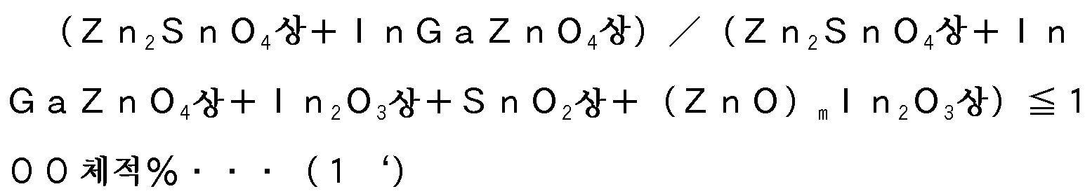
상기 산화물 소결체를 X선 회절하였을 때, Zn2SnO4상과 InGaZnO4상의 체적비가 각각 하기 식 (1)∼(3)을 만족하는 것인 것을 특징으로 하는 산화물 소결체.Wherein the volume ratio of the Zn 2 SnO 4 phase and the InGaZnO 4 phase satisfies the following formulas (1) to (3) when the oxide-sintered body is subjected to X-ray diffraction.


(식 중, m은 2 이상 5 이하의 정수를 나타냄)(Wherein m represents an integer of 2 or more and 5 or less)
<2> 상기 산화물 소결체에 포함되는 전체 금속 원소에 대한 아연, 인듐, 갈륨, 주석의 함유량의 비율(원자%)을 각각, [Zn], [In], [Ga], [Sn]으로 하였을 때, 하기 식 (4)∼(6)을 만족하는 것인 <1>에 기재된 산화물 소결체.<2> When the ratio (atomic%) of the contents of zinc, indium, gallium and tin to the total metal elements contained in the oxide-sintered body is [Zn], [In], [Ga], and [Sn] , And the following formulas (4) to (6) are satisfied.
![]()
![]()
![]()
![]()
(단, [In]은 4원자% 이상, [Ga]는 5원자% 이상)([In] is 4 atomic% or more, and [Ga] is 5 atomic% or more)
![]()
![]()
<3> 상기 상대 밀도가 110% 이하인 <1> 또는 <2>에 기재된 산화물 소결체.<3> The oxide sintered body according to <1> or <2>, wherein the relative density is 110% or less.
<4> 상기 Zn2SnO4상과 InGaZnO4상의 체적비가 하기 식 (1‘)을 만족하는 <1>∼<3> 중 어느 하나에 기재된 산화물 소결체.<4> The oxide-sintered body according to any one of <1> to <3>, wherein the volume ratio of the Zn 2 SnO 4 phase and the InGaZnO 4 phase satisfies the following formula (1 ').
<5> 상기 Zn2SnO4상의 체적비가 하기 식 (2‘)를 만족하는 <1>∼<4> 중 어느 하나에 기재된 산화물 소결체.<5> The oxide-sintered body according to any one of <1> to <4>, wherein the volume ratio of the Zn 2 SnO 4 phase satisfies the following formula (2 ').

<6> 상기 InGaZnO4상의 체적비가 하기 식 (3‘)을 만족하는 <1>∼<5> 중 어느 하나에 기재된 산화물 소결체.<6> The oxide-sintered body according to any one of <1> to <5>, wherein the volume ratio of the InGaZnO 4 phase satisfies the following formula (3 ').

<7> 상기 산화물 소결체의 평균 결정입경이 30㎛ 이하인 <1>∼<6> 중 어느 하나에 기재된 산화물 소결체.<7> The oxide-sintered body according to any one of <1> to <6>, wherein the oxide-sintered body has an average crystal grain size of 30 μm or less.
<8> 상기 산화물 소결체의 평균 결정입경이 3㎛ 이상인 <7>에 기재된 산화물 소결체.<8> The oxide-sintered body according to <7>, wherein the oxide-sintered body has an average crystal grain size of 3 μm or more.
<9> <1>∼<8> 중 어느 하나에 기재된 산화물 소결체를 사용하여 얻어지는 스퍼터링 타깃이며, 비저항이 1Ω·㎝ 이하인 것을 특징으로 하는 스퍼터링 타깃.<9> A sputtering target obtained by using the oxide-sintered body according to any one of <1> to <8>, wherein the sputtering target has a specific resistance of 1 Ω · cm or less.
<10> 상기 비저항이 10- 7Ω·㎝ 이상인 <9>에 기재된 스퍼터링 타깃.<10> The specific resistance of 10 - sputtering target according to <9> less than 7 Ω · ㎝.
본 발명에 따르면, 산화물 반도체막의 성막에 있어서의 이상 방전을 억제하고, 스퍼터링법에 의한 안정된 성막이 가능한 산화물 소결체 및 스퍼터링 타깃을 제공하는 것이 가능하다.According to the present invention, it is possible to provide an oxide-sintered body and a sputtering target capable of suppressing anomalous discharge in film formation of an oxide semiconductor film and capable of stable film formation by a sputtering method.
도 1은 본 발명의 산화물 소결체 및 스퍼터링 타깃을 제조하기 위한 기본적인 공정을 나타내는 도면이다.
도 2는 본 발명의 제조 방법에 사용되는 소결 공정의 일례를 나타내는 그래프이다.BRIEF DESCRIPTION OF THE DRAWINGS FIG. 1 is a view showing a basic process for producing an oxide-sintered body and a sputtering target of the present invention. FIG.
2 is a graph showing an example of a sintering process used in the production method of the present invention.
본 발명자들은, 산화물 소결체에 대해, 스퍼터링 중의 이상 방전을 억제함으로써 장시간의 안정된 성막이 가능하고, 또한 캐리어 이동도가 높은 산화물 반도체막을 성막하는 데 적합한 스퍼터링 타깃용 산화물 소결체를 제공하기 위해, 검토를 거듭해 왔다.The present inventors have repeatedly studied to provide an oxide sintered body for a sputtering target suitable for forming an oxide semiconductor film capable of forming a stable film for a long time by suppressing an abnormal discharge during sputtering and having a high carrier mobility for the oxide sintered body come.
그 결과, 산화아연과, 산화인듐과, 산화갈륨과, 산화주석을 혼합 및 소결하여 얻어지는 산화물 소결체이며, 산화물 소결체를 X선 회절하였을 때, 주상으로서 Zn2SnO4상과 InGaZnO4상을 소정의 비율로 포함하고, 또한 상대 밀도 85% 이상인 구성으로 하였을 때에 소기의 목적이 달성되는 것을 발견하였다.As a result, it is an oxide-sintered body obtained by mixing and sintering zinc oxide, indium oxide, gallium oxide and tin oxide. When the oxide-sintered body is subjected to X-ray diffraction, the Zn 2 SnO 4 phase and the InGaZnO 4 phase By weight and a relative density of 85% or more.
또한 상기 목적의 달성에는, 또한 산화물 소결체에 포함되는 금속 원소의 함유량을 각각 적절하게 제어하는 것이나, 평균 결정입경을 제어하는 것도 유효한 것을 발견하였다.It has also been found that it is also effective to control the content of the metal element contained in the oxide-sintered body appropriately and to control the average crystal grain size in order to achieve the above object.
상세하게는, (a) 산화아연, 산화인듐, 산화갈륨 및 산화주석을 포함하는 산화물 소결체는, X선 회절하였을 때의 상 구성에 대해, Zn2SnO4상과 InGaZnO4상의 비율을 제어함으로써 스퍼터링 중의 이상 방전을 억제하는 효과가 있는 것, (b) 상대 밀도를 높임으로써 스퍼터링 중의 이상 방전의 발생의 억제 효과를 한층 더 향상시킬 수 있는 것을 밝혀냈다. 그리고, (c) 이러한 상 구성을 갖는 산화물 소결체를 얻기 위해서는, 산화물 소결체에 포함되는 금속 원소의 함유량을 각각 적절하게 제어하는 것이 바람직한 것, (d) 산화물 소결체의 평균 결정입경을 미세화하면 이상 방전 억제에, 한층 더 효과가 있는 것을 발견하고, 본 발명에 이르렀다.More specifically, (a) an oxide sintered body containing zinc oxide, indium oxide, gallium oxide and tin oxide is subjected to sputtering by controlling the ratio of Zn 2 SnO 4 phase and InGaZnO 4 phase to the phase structure when X- (B) the effect of suppressing the generation of the abnormal discharge during sputtering can be further improved by increasing the relative density. In order to obtain the oxide-sintered body (c) having such a phase structure, it is preferable that the content of the metal element contained in the oxide-sintered body is appropriately controlled, and (d) if the average crystal grain size of the oxide- The present invention has been accomplished.
본 발명에 관한 산화물 소결체는, 산화아연과, 산화인듐과, 산화갈륨과, 산화주석을 혼합 및 소결하여 얻어지는 산화물 소결체(IGZTO)이다. 이 소결체는, 종래의 In-Ga-Zn-O(IGZO)에 비해, 성막한 산화물 반도체막이 높은 캐리어 이동도나 높은 내에칭 특성을 나타내는 경향이 있다.The oxide-sintered body according to the present invention is an oxide-sintered body (IGZTO) obtained by mixing and sintering zinc oxide, indium oxide, gallium oxide and tin oxide. This sintered body tends to exhibit high carrier mobility and high anti-etching properties, compared with the conventional In-Ga-Zn-O (IGZO).
또한 이러한 산화물 소결체의 화합물상의 구성이나 상대 밀도를 적절하게 제어함으로써, 스퍼터링 중의 이상 방전을 억제하면서, 캐리어 이동도가 한층 더 높은 산화물 반도체막을 성막할 수 있다.Further, by appropriately controlling the composition and relative density of the compound phase of the oxide-sintered body, it is possible to form an oxide semiconductor film having higher carrier mobility while suppressing the abnormal discharge during sputtering.
다음으로, 본 발명에 관한 산화물 소결체의 구성에 대해, 상세하게 설명한다. 본 발명은 상기 산화물 소결체를 X선 회절하였을 때, Zn2SnO4상, InGaZnO4상을 소정의 비율로 포함하는 주상으로 한 점에 특징이 있다.Next, the structure of the oxide-sintered body according to the present invention will be described in detail. The present invention is characterized in that, when the oxide-sintered body is subjected to X-ray diffraction, it is formed into a pillar-shaped phase containing Zn 2 SnO 4 phase and InGaZnO 4 phase at a predetermined ratio.
본 발명에 있어서의 X선 회절 조건은, 이하와 같다.The X-ray diffraction conditions in the present invention are as follows.
분석 장치:리가꾸덴끼(理學電機)제 「X선 회절 장치 RINT-1500」Analytical Apparatus: "X-ray Diffraction Apparatus RINT-1500" manufactured by Rigaku Denki Co.,
분석 조건Analysis condition
타깃:CuTarget: Cu
단색화:모노크로메이터를 사용(Kα)Monochromator: Monochromator is used (K α )
타깃 출력:40㎸-200㎃Target output: 40kV-200mA
(연속 소 측정)θ/2θ 주사(Continuous measurement) &thetas; / 2 &thetas;
슬릿:발산 1/2°, 산란 1/2°, 수광 0.15㎜Slit: divergence 1/2 °, scattering 1/2 °, receiving 0.15 mm
모노크로메이터 수광 슬릿:0.6㎜Monochromator Receiving slit: 0.6 mm
주사 속도:2°/minScanning speed: 2 ° / min
샘플링 폭:0.02°Sampling width: 0.02 °
측정 각도(2θ):5∼90°Measuring angle (2?): 5 to 90
이 측정에서 얻어진 회절 피크에 대해, ICDD(International Center for Diffraction Data) 카드에 기재되어 있는 결정 구조를 갖는 화합물상을 특정한다. 각 화합물상과 카드 번호의 대응은 이하와 같다.For the diffraction peaks obtained in this measurement, the compound phase having the crystal structure described in the ICDD (International Center for Diffraction Data) card is specified. The correspondence between each compound phase and the card number is as follows.
Zn2SnO4상:24-1470Zn 2 SnO 4 phase: 24-1470
InGaZnO4상:38-1104InGaZnO 4 phase: 38-1104
In2O3상:06-0416In 2 O 3 phase: 06-0416
SnO2상:41-1445SnO 2 phase: 41-1445
(ZnO)mIn2O3상:20-1442(m=2), 20-1439(m=3), 20-1438(m=4), 20-1440(m=5)(ZnO) m In 2 O 3 phase: 20-1442 (m = 2), 20-1439 (m = 3), 20-1438 (m = 4)
또한, (ZnO)mIn2O3상의 m은 2∼5의 정수이다. m을 규정한 것은 ZnO상과 In2O3상이 결합한 화합물에 있어서, ZnO가 In2O3와의 관계에서 임의의 비율을 나타내기 때문이다.Also, m on the (ZnO) m In 2 O 3 phase is an integer of 2 to 5. m is defined as the reason why ZnO shows an arbitrary ratio in relation to In 2 O 3 in a compound in which a ZnO phase and an In 2 O 3 phase are combined.
다음으로 상기 X선 회절에 의해 검출되는 본 발명을 특정하는 화합물에 대해 상세하게 설명한다.Next, the compound that specifies the present invention detected by the X-ray diffraction will be described in detail.
(Zn2SnO4 화합물 및 InGaZnO4 화합물에 대해)(For Zn 2 SnO 4 compound and InGaZnO 4 compound)
Zn2SnO4 화합물(상)은, 본 발명의 산화물 소결체를 구성하는 ZnO와 SnO2가 결합하여 형성되는 것이다. 또한 InGaZnO4 화합물(상)은, 본 발명의 산화물 소결체를 구성하는 In과 Ga와 Zn이 결합하여 형성되는 산화물이다. 발명에 있어서 상기 화합물은, 산화물 소결체의 상대 밀도의 향상과 비저항의 저감에 크게 기여하는 것이다. 그 결과, 안정된 직류 방전이 계속하여 얻어지고, 이상 방전 억제 효과가 향상된다.The Zn 2 SnO 4 compound (phase) is formed by bonding ZnO and SnO 2 constituting the oxide-sintered body of the present invention. The InGaZnO 4 compound (phase) is an oxide formed by combining In, Ga and Zn constituting the oxide-sintered body of the present invention. In the invention, the compound contributes greatly to the improvement of the relative density and the resistivity of the oxide-sintered body. As a result, stable DC discharge is continuously obtained, and the effect of suppressing the abnormal discharge is improved.
본 발명에서는, 상기 Zn2SnO4상과 InGaZnO4상을 주상으로서 포함하고 있다. 여기서 「주상」이라 함은, Zn2SnO4상과 InGaZnO4상의 합계 비율이 상기 X선 회절에 의해 검출되는 전체 화합물 중, 가장 비율이 많은 화합물을 의미하고 있다.In the present invention, the Zn 2 SnO 4 phase and the InGaZnO 4 phase are contained as a main phase. Here, the term " columnar phase " means a compound in which the ratio of Zn 2 SnO 4 phase and InGaZnO 4 phase is the largest among all the compounds detected by X-ray diffraction.
또한 본 발명의 상기 Zn2SnO4상, InGaZnO4상에는, Zn2SnO4, InGaZnO4에, 각각 In, Ga 및/또는 Sn이 고용되어 있는 것도 포함된다.Also it includes those in which the Zn 2 SnO 4 phase, InGaZnO 4 formed on, Zn 2 SnO 4, the InGaZnO 4, respectively, In, Ga and / or Sn in the present invention are employed.
이상 방전을 억제하면서, 스퍼터링법으로 안정적으로 성막 가능한 산화물 소결체로 하기 위해서는, 상기 X선 회절에서 특정한 상기 화합물상[Zn2SnO4상, InGaZnO4상, In2O3상, SnO2상 및 (ZnO)mIn2O3상](m은 2 이상 5 이하의 정수)의 합계에 대한 Zn2SnO4상, InGaZnO4상의 체적비가, 하기 (1)∼(3)을 만족하는 것이 필요하다.In order to obtain an oxide sintered body capable of forming a stable oxide film by sputtering while suppressing the abnormal discharge, it is preferable to use the Zn 2 SnO 4 phase, InGaZnO 4 phase, In 2 O 3 phase, SnO 2 phase and ZnO) m in 2 O 3 phase] (m is necessary to the Zn 2 SnO 4-phase, the volume ratio on the InGaZnO 4 to the sum of two or more five integer less), satisfies the following (1) to (3).
(1):[Zn2SnO4]+[InGaZnO4]의 비[(Zn2SnO4상+InGaZnO4상)/(Zn2SnO4상+InGaZnO4상+In2O3상+SnO2상+(ZnO)mIn2O3상);이하, 비율 (1)이라 함]≥75체적%(이하, 각 상의 「체적%」를 단순히 「%」라고 표기함)(Zn 2 SnO 4 phase + InGaZnO 4 phase) / (Zn 2 SnO 4 phase + InGaZnO 4 phase + In 2 O 3 phase + SnO 2 phase + (ZnO) 4 ) of [Zn 2 SnO 4 ] + [InGaZnO 4 ] m In 2 O 3 phase); hereinafter referred to as the title, the ratio (1) shall mean] ≥75% by volume (hereinafter referred to simply as "%" for "% by volume" of each)
비율 (1)이 작아지면 이상 방전 발생률이 높아지므로, 75% 이상으로 할 필요가 있고, 바람직하게는 80% 이상, 보다 바람직하게는 85% 이상이다. 한편, 상한에 대해서는, 성능상은 높을수록 좋고, 예를 들어 100%여도 되지만, 제조 용이성의 관점에서 바람직하게는 95% 이하, 보다 바람직하게는 90% 이하이다.Since the rate of occurrence of anomalous discharge increases when the ratio (1) becomes small, it is required to be 75% or more, preferably 80% or more, and more preferably 85% or more. On the other hand, regarding the upper limit, the higher the performance, the better the performance is, for example, 100%, but it is preferably 95% or less, more preferably 90% or less from the viewpoint of ease of manufacture.
(2):[Zn2SnO4]의 비[Zn2SnO4상/(Zn2SnO4상+InGaZnO4상+In2O3상+SnO2상+(ZnO)mIn2O3상);이하, 비율 (2)라 함]≥30%(Zn 2 SnO 4 phase / (Zn 2 SnO 4 phase + InGaZnO 4 phase + In 2 O 3 phase + SnO 2 phase + (ZnO) m In 2 O 3 phase) of [Zn 2 SnO 4 ] Ratio (2)] ≥ 30%
상기 비율 (1)을 만족하고 있어도 비율 (2)가 작으면, 이상 방전 억제 효과가 충분히 얻어지지 않는 경우가 있으므로, 30% 이상으로 할 필요가 있고, 바람직하게는 40% 이상, 보다 바람직하게는 50% 이상, 더욱 바람직하게는 55% 이상이다. 한편, 상한에 대해서는 특별히 한정되지 않지만, InGaZnO4상을 확보하는 관점에서 바람직하게는 90% 이하, 보다 바람직하게는 80% 이하, 더욱 바람직하게는 70% 이하이다.Even if the ratio (1) is satisfied, if the ratio (2) is small, the effect of suppressing the abnormal discharge may not be sufficiently obtained. Therefore, the ratio should be 30% or more, preferably 40% 50% or more, and more preferably 55% or more. On the other hand, although the upper limit is not particularly limited, it is preferably not more than 90%, more preferably not more than 80%, further preferably not more than 70% from the viewpoint of ensuring the InGaZnO 4 phase.
(3):[InGaZnO4]의 비[InGaZnO4상/(Zn2SnO4상+InGaZnO4상+In2O3상+SnO2상+(ZnO)mIn2O3상);이하, 비율 (3)이라 함]≥10%(3): [InGaZnO 4] ratio [InGaZnO 4 phase / (Zn 2 SnO 4 a + InGaZnO 4 a + In 2 O 3 phase + SnO 2 Phase + (ZnO) m In 2 O 3 phase); or less, the ratio (3) Gt; 10% <
상기 비율 (1) 및/또는 비율 (2)를 만족하고 있어도 비율 (3)이 작으면, 상대 밀도를 높일 수 없고, 이상 방전 억제 효과가 충분히 얻어지지 않는 경우가 있으므로, 10% 이상으로 할 필요가 있고, 바람직하게는 12% 이상, 보다 바람직하게는 15% 이상이다. 한편, 상한에 대해서는 특별히 한정되지 않지만, Zn2SnO4상을 확보하는 관점에서 바람직하게는 60% 이하이며, 또한 제조 용이성의 관점에서는, 보다 바람직하게는 30% 이하, 더욱 바람직하게는 25% 이하이다.If the ratio (3) is smaller than the above ratio (1) and / or the ratio (2), the relative density can not be increased and the effect of suppressing the abnormal discharge may not be sufficiently obtained. , Preferably at least 12%, more preferably at least 15%. On the other hand, although the upper limit is not particularly limited, it is preferably not more than 60% from the viewpoint of securing the Zn 2 SnO 4 phase, more preferably not more than 30%, further preferably not more than 25% to be.
본 발명의 산화물 소결체의 화합물상은, 실질적으로 Zn2SnO4상, InGaZnO4상, In2O3상, SnO2상 및 (ZnO)mIn2O3상(m은 2 이상 5 이하의 정수)으로 구성되어 있는 것이 바람직하고, 전체 화합물상에 차지하는 이들 화합물상의 비율이 75% 이상인 것이 바람직하다. 또한, 이들 화합물상 중, In2O3상, SnO2상 및 (ZnO)mIn2O3상(m은 2 이상 5 이하의 정수)은 포함되어 있지 않아도 된다. 다른 포함할 수 있는 화합물상으로서는 제조상 불가피적으로 생성되는 InGaZn2O5상, ZnGa2O4상, (ZnO)mIn2O3상(m은 6 이상의 정수) 등을 25% 이하의 비율로 포함하고 있어도 된다. 이들 화합물상 중, InGaZn2O5상은 포함되어 있지 않은 것이 바람직하다. 또한, 불가피적으로 생성되는 화합물상의 비율은, XRD에 의해 측정할 수 있다.The compound phase of the oxide-sintered body of the present invention is substantially composed of Zn 2 SnO 4 phase, InGaZnO 4 phase, In 2 O 3 phase, SnO 2 phase and (ZnO) m In 2 O 3 phase (m is an integer of 2 to 5) , And it is preferable that the proportion of these compounds in the total compound phase is 75% or more. Of these compound phases, In 2 O 3 phase, SnO 2 phase, and (ZnO) m In 2 O 3 phase (m is an integer of 2 or more and 5 or less) may not be included. Other possible compound phases include InGaZn 2 O 5 phase, ZnGa 2 O 4 phase, (ZnO) m In 2 O 3 phase (m is an integer of 6 or more) which are inevitably produced in the process, . Of these compound phases, it is preferable that the InGaZn 2 O 5 phase is not included. In addition, the ratio of the inevitably generated compound phase can be measured by XRD.
또한 본 발명의 산화물 소결체의 상대 밀도는 85% 이상이다. 산화물 소결체의 상대 밀도를 높임으로써 상기 이상 방전의 발생 억제 효과를 한층 더 향상시킬 수 있을 뿐만 아니라, 안정된 방전을 타깃 라이프까지 연속하여 유지하는 등의 이점을 초래한다. 이러한 효과를 얻기 위해 본 발명의 산화물 소결체는 상대 밀도를 적어도 85% 이상으로 할 필요가 있고, 바람직하게는 90% 이상이며, 보다 바람직하게는 95% 이상이다. 또한, 상대 밀도는 110% 이하인 것이 바람직하고, 105% 이하인 것이 보다 바람직하다.The relative density of the oxide-sintered body of the present invention is 85% or more. By increasing the relative density of the oxide sintered body, the effect of suppressing the generation of the abnormal discharge can be further improved, and the stable discharge can be continuously maintained to the target life. To obtain such effects, the oxide-sintered body of the present invention needs to have a relative density of at least 85% or more, preferably 90% or more, and more preferably 95% or more. The relative density is preferably 110% or less, and more preferably 105% or less.
산화물 소결체의 상대 밀도는 아르키메데스법에 의해 구해지는 것이다.The relative density of the oxide-sintered body is obtained by the Archimedes method.
또한 높은 캐리어 이동도와 이상 방전 발생 억제 효과를 갖는 상기 상 구성의 산화물 소결체를 얻기 위해서는, 산화물 소결체에 포함되는 금속 원소의 함유량을 각각 적절하게 제어하는 것이 바람직하다.In order to obtain the oxide sintered body of the above-mentioned constitution having a high carrier mobility and an abnormal discharge generation inhibiting effect, it is preferable to appropriately control the content of the metal element contained in the oxide sintered body.
구체적으로는 산화물 소결체에 포함되는 산소를 제외하는 전체 금속 원소에 대한 각 금속 원소(아연, 인듐, 갈륨, 주석)의 함유량(원자%)의 비율을 각각, [Zn], [In], [Ga], [Sn]으로 하였을 때, 하기 식 (4)∼(6)을 만족하는 것이 바람직하다.Specifically, the ratio of the content (atomic%) of each metal element (zinc, indium, gallium, tin) to the total metal element excluding oxygen contained in the oxide sintered body is expressed by [Zn], [In] ] And [Sn], it is preferable that the following formulas (4) to (6) are satisfied.
![]()
![]()
![]()
![]()
(단, [In]은 4원자% 이상, [Ga]는 5원자% 이상)([In] is 4 atomic% or more, and [Ga] is 5 atomic% or more)
![]()
![]()
본 명세서에 있어서 [Zn]이라 함은, 산소(O)를 제외하는 전체 금속 원소(Zn, In, Ga 및 Sn)에 대한 Zn의 함유량(원자%;이하, 각 금속 원소의 함유량 「원자%」를 단순히 「%」라고 표기함)을 의미한다. 마찬가지로 [In], [Ga] 및 [Sn]은 각각, 산소(O)를 제외하는 전체 금속 원소(Zn, In, Ga 및 Sn)에 대한 In, Ga 및 Sn의 각 함유량의 비율(원자%)을 의미한다.In this specification, "Zn" refers to a content (% by atom) of Zn with respect to all metal elements (Zn, In, Ga and Sn) excluding oxygen (O) Quot; is simply referred to as "% "). Likewise, [In], [Ga] and [Sn] represent the ratio (atomic%) of each content of In, Ga and Sn to the total metal elements (Zn, In, Ga and Sn) excluding oxygen (O) .
우선, 상기 식 (4)는, 전체 금속 원소 중의 Zn비([Zn])를 규정한 것이며, 주로 상기 Zn2SnO4상, InGaZnO4상을 상기 소정의 비율 (1)∼(3)으로 제어하는 관점에서 설정된 것이다. [Zn]이 지나치게 적으면, 상기 화합물상의 비율 (1)∼(3)을 만족하는 것이 어려워지고, 이상 방전 억제 효과가 충분히 얻어지지 않는다. 따라서 [Zn]은, 40% 이상으로 하는 것이 바람직하고, 보다 바람직하게는 42% 이상이다. 한편, [Zn]이 지나치게 높아지면 상대적으로 In, Ga, Sn의 비율이 저하되어 오히려 원하는 화합물상의 비율이 얻어지지 않게 되므로, 바람직하게는 50% 이하, 보다 바람직하게는 48% 이하이다.First, the formula (4) defines the Zn ratio ([Zn]) in the total metal elements and mainly controls the Zn 2 SnO 4 phase and the InGaZnO 4 phase to the predetermined ratios (1) to (3) . When [Zn] is too small, it is difficult to satisfy the above-mentioned proportions (1) to (3) of the compound, and the effect of suppressing the abnormal discharge is not sufficiently obtained. Therefore, [Zn] is preferably 40% or more, more preferably 42% or more. On the other hand, when [Zn] is too high, the proportion of In, Ga, and Sn is relatively lowered and the proportion of the desired compound phase can not be obtained, so that it is preferably 50% or less, more preferably 48% or less.
또한 상기 식 (5)는, 전체 금속 원소 중의 In비와 Ga비의 합계([In]+[Ga])를 규정한 것이며, 주로 InGaZnO4상을 상기 소정의 비율 (1), (3)으로 제어하는 관점에서 설정된 것이다. [In]+[Ga]가 지나치게 적으면 상기 화합물상의 비율 (1), (3)을 만족하는 것이 어려워진다. 따라서 [In]+[Ga]는, 바람직하게는 30% 이상, 보다 바람직하게는 32% 이상이다. 한편, [In]+[Ga]가 지나치게 많아지면, 상기 화합물상의 비율 (2)가 상대적으로 저하되므로, 바람직하게는 45% 이하, 보다 바람직하게는 43% 이하이다.The formula (5) defines the sum of the In and Ga ratios ([In] + [Ga]) in the total metal elements. The InGaZnO 4 phase is mainly defined by the above- It is set in terms of control. When [In] + [Ga] is excessively small, it is difficult to satisfy the ratios (1) and (3) of the compound phase. Therefore, [In] + [Ga] is preferably 30% or more, and more preferably 32% or more. On the other hand, when [In] + [Ga] is excessively large, the proportion (2) of the compound phase is relatively lowered, and therefore it is preferably 45% or less, more preferably 43% or less.
또한, In 및 Ga는 모두 필수의 원소이며, [In]은 4% 이상인 것이 바람직하고, 보다 바람직하게는 5% 이상이다. [In]이 지나치게 적으면 산화물 소결체의 상대 밀도 향상 효과나 비저항의 저감을 달성할 수 없고, 성막 후의 산화물 반도체막의 캐리어 이동도도 낮아진다.In and Ga are both essential elements, and [In] is preferably 4% or more, and more preferably 5% or more. If [In] is too small, the effect of improving the relative density of the oxide-sintered body and the reduction of the resistivity can not be achieved, and the carrier mobility of the oxide semiconductor film after film formation also becomes low.
또한 [Ga]는 5% 이상인 것이 바람직하고, 보다 바람직하게는 10% 이상이다. [Ga]가 지나치게 적으면 상기 화합물상의 비율 (3)이 상대적으로 저하되는 경우가 있다.[Ga] is preferably 5% or more, and more preferably 10% or more. When [Ga] is too small, the ratio (3) of the compound phase may be relatively lowered.
상기 식 (6)은, 전체 금속 원소 중의 Sn비([Sn])를 규정한 것이며, 주로 상기 Zn2SnO4상을 상기 소정의 비율 (1), (2)로 제어하는 관점에서 설정된 것이다. [Sn]이 지나치게 적으면, 상기 화합물상의 비율 (1), (2)를 만족하는 것이 어려워지는 경우가 있으므로, 바람직하게는 15% 이상, 보다 바람직하게는 16% 이상이다. 한편, [Sn]이 지나치게 많으면 상기 화합물상의 비율 (3)이 상대적으로 저하되므로, 바람직하게는 25% 이하, 보다 바람직하게는 22% 이하이다.The formula (6) defines the Sn ratio ([Sn]) in the total metal elements and is set mainly from the viewpoint of controlling the Zn 2 SnO 4 phase to the predetermined ratios (1) and (2). When [Sn] is too small, it may be difficult to satisfy the ratios (1) and (2) of the above-mentioned compounds. Therefore, it is preferably 15% or more, and more preferably 16% or more. On the other hand, if the amount of [Sn] is excessively large, the proportion (3) of the compound phase is relatively lowered, so that it is preferably 25% or less, more preferably 22%
금속 원소의 함유량은 상기 범위 내로 제어되어 있으면 되고, 또한 본 발명의 산화물 소결체에는, 제조상 불가피적으로 생성되는 산화물을 포함해도 되는 취지이다.The content of the metal element may be controlled within the above range, and the oxide sintered body of the present invention may contain an oxide which is inevitably produced in the production.
또한 이상 방전 억제 효과를 한층 더 높이기 위해서는, 산화물 소결체의 결정립의 평균 결정입경을 미세화하는 것이 바람직하다. 구체적으로는 산화물 소결체(혹은 상기 산화물 소결체를 사용한 스퍼터링 타깃)의 파단면(산화물 소결체를 임의의 위치에서 두께 방향으로 절단하고, 그 절단면 표면의 임의의 위치)에 있어서 SEM(주사형 전자 현미경)에 의해 관찰되는 결정립의 평균 결정입경을 바람직하게는 30㎛ 이하로 함으로써, 이상 방전의 발생을 한층 더 억제할 수 있다. 보다 바람직한 평균 결정입경은 25㎛ 이하, 더욱 바람직하게는 20㎛ 이하이다. 한편, 평균 결정입경의 하한은 특별히 한정되지 않지만, 결정립을 지나치게 미세화시키면, 상대 밀도가 저하되는 경우가 있으므로, 평균 결정입경의 바람직한 하한은 3㎛ 정도, 보다 바람직하게는 5㎛ 이상이다.In order to further enhance the abnormal discharge suppressing effect, it is preferable to make the average crystal grain size of the oxide-sintered body finer. Concretely, the fracture surface of the oxide-sintered body (or the sputtering target using the oxide-sintered body) (the oxide-sintered body is cut in an arbitrary position in the thickness direction and an arbitrary position on the surface of the cut surface) is subjected to SEM (scanning electron microscope) The occurrence of the abnormal discharge can be further suppressed by setting the average crystal grain size of the crystal grains to be observed to be preferably 30 mu m or less. The average crystal grain size is more preferably 25 占 퐉 or less, and more preferably 20 占 퐉 or less. On the other hand, the lower limit of the average crystal grain size is not particularly limited. However, when the crystal grains are excessively refined, the relative density may be lowered. Therefore, the preferable lower limit of the average crystal grain size is about 3 占 퐉 and more preferably 5 占 퐉 or more.
결정립의 평균 결정입경은, 산화물 소결체(또는 스퍼터링 타깃) 파단면의 조직을 SEM(배율:400배)으로 관찰하고, 임의의 방향으로 100㎛의 길이의 직선을 긋고, 이 직선 내에 포함되는 결정립의 수(N)를 구하고, [100/N]으로부터 산출되는 값을 당해 직선 상에서의 평균 결정입경으로 한다. 본 발명에서는 20㎛ 이상의 간격으로 직선을 20개 작성하여 「각 직선 상에서의 평균 결정입경」을 산출하고, 또한 [각 직선 상에서의 평균 결정입경의 합계/20]으로부터 산출되는 값을 결정립의 평균 결정입경으로 한다.The average crystal grain size of the crystal grains was measured by observing the structure of the fracture surface of the oxide-sintered body (or the sputtering target) with an SEM (magnification: 400 times), drawing a straight line having a length of 100 탆 in an arbitrary direction, The number (N) is obtained, and the value calculated from [100 / N] is taken as the average crystal grain size on the straight line. In the present invention, 20 straight lines are formed at intervals of 20 탆 or more to calculate " average crystal grain size on each straight line ", and a value calculated from [sum of average crystal grain sizes on each straight line / 20] Diameter.
또한 본 발명의 산화물 소결체를 사용하여 얻어지는 스퍼터링 타깃은, 비저항 1Ω·㎝ 이하이며, 바람직하게는 10- 1Ω·㎝ 이하, 보다 바람직하게는 10- 2Ω·㎝ 이하, 더욱 바람직하게는 10- 3Ω·㎝ 이하인 점에 특징이 있다. 이에 의해, 한층 더 스퍼터링 중에서의 이상 방전을 억제한 성막이 가능해지고, 스퍼터링 타깃을 사용한 물리 증착(스퍼터링법)을 표시 장치의 생산 라인에서 효율적으로 행할 수 있다. 또한, 스퍼터링 타깃의 비저항은, 10- 7Ω·㎝ 이상인 것이 바람직하고, 10- 6Ω·㎝ 이상인 것이 보다 바람직하고, 10-5Ω·㎝ 이상인 것이 더욱 바람직하다.In addition, a sputtering target obtained by using the oxide-sintered body of the present invention, the specific resistance is less than 1Ω · ㎝, preferably 10 - 1 Ω · ㎝ or less, more preferably 10 2 Ω · ㎝ or less, more preferably 10 - 3 Ω · cm or less. This makes it possible to form a film suppressing abnormal discharge during sputtering, and to perform physical vapor deposition (sputtering) using a sputtering target in a production line of a display device. The specific resistance of the sputtering target is preferably 10 - 7 Ω · cm or more, more preferably 10 - 6 Ω · cm or more, and still more preferably 10 -5 Ω · cm or more.
스퍼터링 타깃의 비저항은 4단자법에 의해 구해지는 것이다.The resistivity of the sputtering target is obtained by the four-terminal method.
다음으로, 본 발명의 산화물 소결체를 제조하는 방법에 대해 설명한다.Next, a method for producing the oxide-sintered body of the present invention will be described.
본 발명의 산화물 소결체는, 산화아연과, 산화인듐과, 산화갈륨과, 산화주석을 혼합 및 소결하여 얻어지는 것이며, 또한 스퍼터링 타깃은 산화물 소결체를 가공함으로써 제조할 수 있다. 도 1에는, 산화물의 분말을 (a) 혼합·분쇄→(b) 건조·조립(造粒)→(c) 예비 성형→(d) 탈지→(e) 대기 소결하여 얻어진 산화물 소결체를, (f) 가공→(g) 본딩하여 스퍼터링 타깃을 얻을 때까지의 기본 공정을 나타내고 있다. 상기 공정 중 본 발명에서는, 이하에 상세하게 설명하는 바와 같이 소결 조건을 적절하게 제어한 점에 특징이 있고, 그 이외의 공정은 특별히 한정되지 않고, 통상 사용되는 공정을 적절히 선택할 수 있다. 이하, 각 공정을 설명하지만, 본 발명은 이것에 한정하는 취지는 아니다.The oxide-sintered body of the present invention is obtained by mixing and sintering zinc oxide, indium oxide, gallium oxide and tin oxide, and the sputtering target can be produced by processing the oxide-sintered body. 1 shows an oxide sintered body obtained by mixing and crushing an oxide powder with (a) mixing and crushing (b) drying, granulating, (c) preforming, (d) degreasing, ) Processing → (g) bonding to obtain a sputtering target. Among the above processes, the present invention is characterized in that sintering conditions are suitably controlled as will be described in detail below. The other processes are not particularly limited, and the commonly used processes can be appropriately selected. Hereinafter, each process will be described, but the present invention is not limited thereto.
우선, 산화아연 분말과, 산화인듐 분말과, 산화갈륨 분말과, 산화주석 분말을 소정의 비율로 배합하고, 혼합·분쇄한다. 사용되는 각 원료 분말의 순도는 각각, 약 99.99% 이상이 바람직하다. 미량의 불순물 원소가 존재하면, 산화물 반도체막의 반도체 특성을 손상시킬 우려가 있기 때문이다. 각 원료 분말의 배합 비율은, 비율이 상술한 범위 내로 되도록 제어하는 것이 바람직하다.First, a zinc oxide powder, an indium oxide powder, a gallium oxide powder, and a tin oxide powder are mixed at a predetermined ratio and mixed and pulverized. The purity of each raw material powder used is preferably about 99.99% or more. The presence of a trace amount of the impurity element may deteriorate the semiconductor characteristics of the oxide semiconductor film. The mixing ratio of each raw material powder is preferably controlled so that the ratio is within the above-mentioned range.
(a) 혼합·분쇄는, 볼 밀을 사용하고, 원료 분말을 물과 함께 투입하여 행하는 것이 바람직하다. 이들 공정에 사용되는 볼이나 비즈는, 예를 들어 나일론, 알루미나, 지르코니아 등의 재질의 것이 바람직하게 사용된다. 이때, 균일하게 혼합하는 목적으로 분산재나, 이후의 성형 공정의 용이성을 확보하기 위해 바인더를 혼합해도 된다.(a) Mixing and pulverizing are preferably carried out by using a ball mill and feeding the raw material powder together with water. The balls or beads used in these processes are preferably made of materials such as nylon, alumina, and zirconia. At this time, for the purpose of uniform mixing, a binder may be mixed in order to ensure the ease of the dispersing material and the subsequent molding process.
다음으로, 상기 공정에서 얻어진 혼합 분말에 대해 예를 들어 스프레이 드라이어 등으로 (b) 건조·조립을 행하는 것이 바람직하다.Next, it is preferable that the mixed powder obtained in the above process is dried and assembled with, for example, (b) a spray dryer or the like.
건조·조립 후, (c) 예비 성형을 한다. 성형에 있어서는, 건조·조립 후의 분말을 소정 치수의 금형에 충전하고, 금형 프레스로 예비 성형한다. 이 예비 성형은, 세트할 때의 핸들링성을 향상시키는 목적으로 행해지므로, 0.5∼1.0tonf/㎠ 정도의 가압력을 가하여 성형체로 하면 된다. 그 후, CIP(냉간 정수압)로 성형(본성형)을 행한다. 소결체의 상대 밀도를 상승시키기 위해서는, 성형 시의 압력은 약 1tonf/㎠ 이상으로 제어하는 것이 바람직하다.After drying and assembly, (c) Preforming is performed. In molding, the dried and assembled powder is filled into a mold having a predetermined size, and preformed by a mold press. This preforming is performed for the purpose of improving the handling property at the time of setting, so that a pressing force of about 0.5 to 1.0 tonf / cm 2 may be applied to form a preform. Thereafter, molding (main molding) is performed with CIP (cold isostatic pressure). In order to increase the relative density of the sintered body, it is preferable to control the pressure at the time of molding to about 1 ton / cm 2 or more.
또한, 혼합 분말에 분산재나 바인더를 첨가한 경우에는, 분산재나 바인더를 제거하기 위해 성형체를 가열하여 (d) 탈지를 행하는 것이 바람직하다. 가열 조건은 탈지 목적을 달성할 수 있으면 특별히 한정되지 않지만, 예를 들어 대기 중, 대략 500℃ 정도에서, 5시간 정도 유지하면 된다.When a dispersing agent or a binder is added to the mixed powder, it is preferable to perform the degreasing (d) by heating the formed body to remove the dispersing agent and the binder. The heating conditions are not particularly limited as long as the purpose of degreasing can be achieved. For example, the heating conditions may be maintained at about 500 캜 for about 5 hours in the air.
탈지 후, 원하는 형상의 흑연형에 성형체를 세트하여 (e) 대기 소결에 의해 소결을 행한다.After the degreasing, the formed body is set in a graphite mold having a desired shape, and (e) sintering is performed by air sintering.
본 발명에서는 소결 온도:1350∼1600℃, 상기 온도에서의 유지 시간:1∼50시간으로 소결을 행하는 것이 바람직하다(도 2). 이들 온도 범위 및 유지 시간으로 함으로써, 상기 비율 (1)∼(3)을 만족하는 화합물상이 얻어진다. 또한, 소결 온도가 낮으면, 충분히 치밀화할 수 없고 이상 방전 억제의 효과가 얻어지지 않는다. 한편, 소결 온도가 지나치게 높아지면, 결정립이 조대화되어 버려, 결정립의 평균 결정입경을 소정의 범위로 제어할 수 없게 되고, 이상 방전을 억제할 수 없게 된다. 따라서 소결 온도는 바람직하게는 1350℃ 이상, 보다 바람직하게는 1400℃ 이상, 더욱 바람직하게는 1500℃ 이상이며, 바람직하게는 1600℃ 이하, 보다 바람직하게는 1550℃ 이하, 더욱 바람직하게는 1500℃ 이하로 한다.In the present invention, sintering is preferably performed at a sintering temperature of 1350 to 1600 占 폚 and a holding time at the above temperature of 1 to 50 hours (Fig. 2). By using these temperature ranges and the holding time, a compound phase satisfying the above ratios (1) to (3) is obtained. In addition, when the sintering temperature is low, it can not be sufficiently densified and the effect of suppressing the abnormal discharge can not be obtained. On the other hand, if the sintering temperature is excessively high, the crystal grains become coarse, and the average crystal grain size of the crystal grains can not be controlled within a predetermined range, and the abnormal discharge can not be suppressed. Therefore, the sintering temperature is preferably 1350 DEG C or higher, more preferably 1400 DEG C or higher, even more preferably 1500 DEG C or higher, preferably 1600 DEG C or lower, more preferably 1550 DEG C or lower, still more preferably 1500 DEG C or lower .
또한 상기 소결 온도에서의 유지 시간이 지나치게 길어지면 결정립이 성장하여 조대화되므로, 결정립의 평균 결정입경을 소정의 범위로 제어할 수 없게 된다. 한편, 유지 시간이 지나치게 짧으면 충분히 치밀화할 수 없게 된다. 따라서 유지 시간은 바람직하게는 1시간 이상, 보다 바람직하게는 8시간 이상, 더욱 바람직하게는 12시간 이상이며, 바람직하게는 50시간 이하, 보다 바람직하게는 40시간 이하, 더욱 바람직하게는 30시간 이하로 한다.When the holding time at the sintering temperature is too long, the crystal grains grow and coarsen, so that the average crystal grain size of the crystal grains can not be controlled within a predetermined range. On the other hand, if the holding time is too short, the densification can not be sufficiently performed. Therefore, the holding time is preferably 1 hour or more, more preferably 8 hours or more, still more preferably 12 hours or more, preferably 50 hours or less, more preferably 40 hours or less, further preferably 30 hours or less .
또한 본 발명에서는 성형 후, 상기 소결 온도까지의 평균 승온 속도(HR)를 100℃/hr 이하로 하는 것이 바람직하다. 평균 승온 속도가 100℃/hr를 초과하면, 결정립의 이상 성장이 일어난다. 또한 상대 밀도를 충분히 높일 수 없는 경우가 있다. 보다 바람직한 평균 승온 속도는 80℃/hr 이하, 더욱 바람직하게는 50℃/hr 이하이다. 한편, 평균 승온 속도의 하한은 특별히 한정되지 않지만, 생산성의 관점에서는 10℃/hr 이상으로 하는 것이 바람직하고, 보다 바람직하게는 20℃/hr 이상이다.Further, in the present invention, it is preferable that the average heating rate HR up to the sintering temperature after molding is set to 100 ° C / hr or less. When the average heating rate exceeds 100 ° C / hr, abnormal growth of crystal grains occurs. The relative density may not be sufficiently increased. More preferably, the average heating rate is 80 ° C / hr or less, and more preferably 50 ° C / hr or less. On the other hand, the lower limit of the average temperature raising rate is not particularly limited, but is preferably 10 ° C / hr or higher, more preferably 20 ° C / hr or higher, from the viewpoint of productivity.
소결 공정에서는, 소결 분위기를 산소 가스 분위기(예를 들어 대기 분위기), 산소 가스 가압하 분위기로 하는 것이 바람직하다. 또한 분위기 가스의 압력은, 증기압이 높은 산화아연의 증발을 억제하기 위해 대기압으로 하는 것이 바람직하다. 상기와 같이 하여 얻어진 산화물 소결체는 상대 밀도가 85% 이상이다.In the sintering step, the sintering atmosphere is preferably an atmosphere under an oxygen gas atmosphere (for example, an atmospheric atmosphere) or under an oxygen gas atmosphere. Further, it is preferable that the atmospheric pressure is set to the atmospheric pressure in order to suppress evaporation of zinc oxide having a high vapor pressure. The oxide-sintered body obtained as described above has a relative density of 85% or more.
상기와 같이 하여 산화물 소결체를 얻은 후, 통상법에 의해, (f) 가공→(g) 본딩을 행하면 본 발명의 스퍼터링 타깃이 얻어진다. 이와 같이 하여 얻어지는 스퍼터링 타깃의 비저항도, 매우 양호한 것이며, 비저항은 대략 1Ω·㎝ 이하이다.After obtaining the oxide-sintered body as described above, the sputtering target of the present invention is obtained by performing (f) processing (g) bonding by a conventional method. The specific resistance of the sputtering target thus obtained is also very good, and the specific resistance is approximately 1? 占 ㎝ m or less.
실시예Example
이하, 실시예를 들어 본 발명을 보다 구체적으로 설명하지만, 본 발명은 하기 실시예에 한정되지 않고, 본 발명의 취지에 적합할 수 있는 범위에서 적절하게 변경을 가하여 실시하는 것도 가능하며, 그들은 모두 본 발명의 기술적 범위에 포함된다.Hereinafter, the present invention will be described in more detail with reference to examples. However, it is to be understood that the present invention is not limited to the following examples, but may be appropriately modified within the scope of the invention, And are included in the technical scope of the present invention.
(스퍼터링 타깃의 제작)(Fabrication of sputtering targets)
순도 99.99%의 산화인듐 분말(In2O3), 순도 99.99%의 산화아연 분말(ZnO), 순도 99.99%의 산화갈륨 분말(Ga2O3), 순도 99.99%의 산화주석 분말(SnO2)을 표 2에 나타내는 비율로 배합하고, 물과 분산제(폴리카르본산암모늄)를 첨가하여 지르코니아 볼 밀로 24시간 혼합하였다. 다음으로, 상기 공정에서 얻어진 혼합 분말을 건조하여 조립을 행하였다.(In 2 O 3 ) having a purity of 99.99%, zinc oxide powder (ZnO) having a purity of 99.99%, gallium oxide powder having a purity of 99.99% (Ga 2 O 3 ), tin oxide powder having a purity of 99.99% (SnO 2 ) And water and a dispersant (ammonium polycarboxylate) were added, and the mixture was mixed with a zirconia ball mill for 24 hours. Next, the mixed powder obtained in the above step was dried and assembled.
이와 같이 하여 얻어진 분말을 금형 프레스에 의해 예비 성형한 후(성형 압력:1.0ton/㎠, 성형체 사이즈:φ110×t13㎜, t는 두께), CIP(냉간 정수압)에 의해 성형 압력 3tonf/㎠로 본성형을 행하였다.The thus obtained powder was preformed by a die press (molding pressure: 1.0 ton / cm 2, formed body size:? 110.times.t13 mm, t is thickness), preformed by a die press at a molding pressure of 3 ton / Molding was carried out.
이와 같이 하여 얻어진 성형체를, 상압에 의해 대기 분위기하에서 500℃로 승온시키고, 상기 온도에서 5시간 유지하여 탈지하였다.The thus obtained molded body was heated to 500 DEG C under atmospheric pressure in an atmospheric pressure and maintained at the above temperature for 5 hours to be degreased.
이와 같이 하여 얻어진 성형체를 소결노에 세트하고, 표 3에 나타내는 조건(A∼F)에서 소결을 행하였다. 얻어진 소결체를 기계 가공하여 φ100×t5㎜로 마무리하고, Cu제 백킹 플레이트에 본딩하고, 스퍼터링 타깃을 제작하였다.The compact thus obtained was set in a sintering furnace and sintered under the conditions (A to F) shown in Table 3. The obtained sintered body was machined, finished to 100 mm t5 mm, and bonded to a Cu backing plate to prepare a sputtering target.
(박막 트랜지스터의 제작)(Fabrication of Thin Film Transistor)
이와 같이 하여 얻어진 스퍼터링 타깃을 스퍼터링 장치에 장착하고, DC(직류) 마그네트론 스퍼터링법으로, 유리 기판(사이즈:100㎜×100㎜×0.50㎜) 상에, 산화물 반도체막을 형성하였다. 스퍼터링 조건은, DC 스퍼터링 파워 150W, Ar/0.1체적% O2 분위기, 압력 0.8mTorr로 하였다. 또한 이 조건에서 성막한 박막을 사용하여, 채널 길이 10㎛, 채널 폭 100㎛의 박막 트랜지스터를 제작하였다.The sputtering target thus obtained was mounted on a sputtering apparatus and an oxide semiconductor film was formed on a glass substrate (size: 100 mm x 100 mm x 0.50 mm) by DC (direct current) magnetron sputtering. The sputtering conditions were DC sputtering power of 150 W, Ar / 0.1 vol% O 2 atmosphere, and pressure of 0.8 mTorr. A thin film transistor having a channel length of 10 mu m and a channel width of 100 mu m was fabricated using the thin film formed under this condition.
(상대 밀도의 측정)(Measurement of relative density)
상대 밀도는, 스퍼터링 후, 타깃을 백킹 플레이트로부터 제거하여 연마하고, 아르키메데스법에 의해 산출하였다. 상대 밀도는 85% 이상을 합격이라고 평가하였다[표 4 중, 「상대 밀도(%)」 참조].The relative density was calculated by the Archimedes method after the sputtering, the target was removed from the backing plate and polished. Relative density was evaluated to be at least 85% acceptable (see Table 4, "relative density (%)").
또한, 상대 밀도는, 아르키메데스법에 의해 측정한 밀도(g/㎤)를 이론 밀도 ρ(g/㎤)로 나눈 백분율의 값이며, 이론 밀도 ρ는 이하와 같이 계산된다.The relative density is a value obtained by dividing the density (g / cm 3) measured by the Archimedes method by the theoretical density ρ (g / cm 3), and the theoretical density ρ is calculated as follows.
[수 1][Number 1]

여기서, W1:ZnO의 배합량[wt%], W2:In2O3의 배합량[wt%], W3:Ga2O3의 배합량[wt%], W4:SnO2의 배합량[wt%]이다.Here, W 1: ZnO amount [wt%], W 2 of: In 2 O 3 amount [wt%], W 3 of the: amount [wt%] of the Ga 2 O 3, W 4: The amount of SnO 2 [wt %]to be.
(비저항의 측정)(Measurement of Resistivity)
소결체의 비저항은, 상기 제작한 스퍼터링 타깃에 대해 4단자법에 의해 측정하였다. 비저항은 1Ω·㎝ 이하를 합격이라고 평가하였다.Resistivity of the sintered body was measured by the four-terminal method for the sputtering target produced above. The resistivity was rated as 1 Ω · cm or less.
(결정립의 평균 결정입경)(Average crystal grain size of crystal grains)
결정립의 평균 결정입경은, 산화물 소결체 파단면(산화물 소결체를 임의의 위치에서 두께 방향으로 절단하고, 그 절단면 표면의 임의의 위치)의 조직을 SEM(배율:400배)으로 관찰하고, 임의의 방향으로 100㎛의 길이의 직선을 긋고, 이 직선 내에 포함되는 결정립의 수(N)를 구하고, [100/N]으로부터 산출되는 값을 당해 직선 상에서의 평균 결정입경으로 하였다. 마찬가지로 20∼30㎛의 간격으로 직선을 20개 작성하여 각 직선 상에서의 평균 결정입경을 산출하고, 또한 [각 직선 상에서의 평균 결정입경의 합계/20]으로부터 산출되는 값을 결정립의 평균 결정입경으로 하였다. 결정립은 평균 결정입경 30㎛ 이하를 합격이라고 평가하였다[표 4 중, 「평균 입경(㎛) 참조」].The average crystal grain size of the crystal grains was measured by observing the structure of the fracture surface of the oxide-sintered body (the oxide-sintered body was cut in a thickness direction at an arbitrary position and an arbitrary position on the surface of the cut surface) with an SEM (magnification: 400x) (N) of the crystal grains contained in the straight line, and the value calculated from [100 / N] was taken as the average crystal grain size on the straight line. Similarly, 20 straight lines are formed at intervals of 20 to 30 占 퐉 to calculate an average crystal grain size on each straight line, and a value calculated from [sum of the average crystal grain sizes on each straight line / 20] Respectively. The average grain size of the crystal grains was evaluated to be 30 占 퐉 or less (see "Average grain size (占 퐉)" in Table 4).
(화합물상의 비율)(Ratio of compound phase)
각 화합물상의 비율은, 스퍼터링 후, 타깃을 백킹 플레이트로부터 제거하여 10 제곱 밀리미터(㎜)인 시험편을 잘라내고, X선 회절로 회절선의 강도를 측정하여 구하였다.The ratio of each compound phase was obtained by sputtering, removing the target from the backing plate, cutting out a test piece having a size of 10 square millimeters (mm), and measuring the intensity of the diffraction line by X-ray diffraction.
분석 장치:리가꾸덴끼제 「X선 회절 장치 RINT-1500」Analytical Apparatus: X-ray diffractometer RINT-1500 manufactured by Rigaku Denki Co.,
분석 조건:Analysis conditions:
타깃:CuTarget: Cu
단색화:모노크로메이터를 사용(Kα)Monochromator: Monochromator is used (K α )
타깃 출력:40㎸-200㎃Target output: 40kV-200mA
(연속 소 측정)θ/2θ 주사(Continuous measurement) &thetas; / 2 &thetas;
슬릿:발산 1/2°, 산란 1/2°, 수광 0.15㎜Slit: divergence 1/2 °, scattering 1/2 °, receiving 0.15 mm
모노크로메이터 수광 슬릿:0.6㎜Monochromator Receiving slit: 0.6 mm
주사 속도:2°/minScanning speed: 2 ° / min
샘플링 폭:0.02°Sampling width: 0.02 °
측정 각도(2θ):5∼90°Measuring angle (2?): 5 to 90
이 측정에서 얻어진 회절 피크에 대해, ICDD(International Center for Diffraction Data) 카드에 기초하여 표 1에 나타내는 각 화합물상의 피크를 동정하고, 회절 피크의 높이를 측정하였다. 이들 피크는, 당해 화합물상에서 회절 강도가 높고, 다른 화합물상의 피크와의 중복이 가능한 한 적은 피크를 선택하였다. 각 화합물상의 지정 피크에서의 피크 높이의 측정값을 각각 I[Zn2SnO4], I[InGaZnO4], I[InGaZn2O5], I[In2O3], I[SnO2], I[(ZnO)mIn2O3]로 하고(「I」는 측정값인 것을 나타내는 의미), 하기 식에 의해 체적 비율을 구하였다[표 4 중, A, B, A+B의 체적 비율(%)].Peaks of the respective compound phases shown in Table 1 were identified based on ICDD (International Center for Diffraction Data) card for the diffraction peaks obtained in this measurement, and the height of diffraction peaks was measured. These peaks were selected so that the diffraction intensity on the compound was high and the number of peaks overlapping with the peaks on other compounds was as small as possible. I [InGaZnO 4 ], I [InGaZn 2 O 5 ], I [In 2 O 3 ], I [SnO 2 ] and I [Zn 2 SnO 4 ] (Volume ratio (%) of A, B, and A + B in Table 4) was calculated from the following formula: I [(ZnO) m In 2 O 3 ] )].

또한, m=2, 3, 4의 (ZnO)mIn2O3상의 피크는 어느 시료에 있어서도 무시할 수 있는 정도였으므로, I[(ZnO)5In2O3]를 I[(ZnO)mIn2O3]로 하였다. 또한, 상기 이외의 화합물상의 피크도 거의 관찰되지 않았다.In addition, the peak in the m = 2, 3, 4 ( ZnO) m In 2 O 3 is because it was negligible even in the samples, I [(ZnO) 5 In 2 O 3] to I [(ZnO) m In 2 O 3 ]. Further, no peak of the compound other than the above was observed.
화합물상의 비율은 [Zn2SnO4]가 30% 이상이고 또한 [InGaZnO4]가 10% 이상이며, [Zn2SnO4]+[InGaZnO4]가 75% 이상인 것을 합격이라고 평가하였다(표 4 중 「A」, 「B」, 「A+B」 참조).Proportion of the compound of [Zn 2 SnO 4] is not less than 30% and also [InGaZnO 4] is 10% or more were evaluated as pass is not less than [Zn 2 SnO 4] + [ InGaZnO 4] is 75% (Table 4 A "," B "," A + B ").
(이상 방전의 평가)(Evaluation of abnormal discharge)
상기 소결체를 직경 4인치, 두께 5㎜의 형상으로 가공하고, 백킹 플레이트에 본딩하여 스퍼터링 타깃을 얻는다. 그와 같이 하여 얻어진 스퍼터링 타깃을 스퍼터링 장치에 장착하고, DC(직류) 마그네트론 스퍼터링을 행한다. 스퍼터링의 조건은, DC 스퍼터링 파워 150W, Ar/0.1체적% O2 분위기, 압력 0.8mTorr로 한다. 이때의 100분당 아킹의 발생 횟수를 카운트하고 2회 이하를 합격이라고 평가하였다(표 4 중, 「이상 방전 횟수」 참조).The sintered body is processed into a shape having a diameter of 4 inches and a thickness of 5 mm, and bonded to a backing plate to obtain a sputtering target. The thus obtained sputtering target is mounted on a sputtering apparatus and subjected to DC (direct current) magnetron sputtering. The sputtering conditions are DC sputtering power of 150 W, Ar / 0.1 vol% O 2 atmosphere, and pressure of 0.8 mTorr. At this time, the number of occurrences of arcing per 100 minutes was counted, and it was evaluated that two or less occurrences were acceptable (see " abnormal discharge frequency " in Table 4).
결과를 표 4에 나타낸다.The results are shown in Table 4.


본 발명의 바람직한 조성, 제조 조건을 만족하는 No.1∼3, 7은 이상 방전이 억제되어 있었다. 즉, 스퍼터링을 행한 바, 이상 방전의 발생은 2회 이하이며, 안정적으로 방전하는 것이 확인되었다. 또한 이와 같이 하여 얻어진 스퍼터링 타깃의 상대 밀도 및 비저항도 양호한 결과가 얻어졌다.Nos. 1 to 3 and 7, which satisfied the preferred composition and manufacturing conditions of the present invention, were suppressed from abnormal discharge. That is, when sputtering was performed, it was confirmed that the generation of the abnormal discharge was two or less, and the discharge was stably performed. Further, the relative density and specific resistance of the sputtering target thus obtained were also good.
한편, 본 발명의 바람직한 제조 조건을 만족하지 않는 No.4∼6, 및 바람직한 조성을 만족하지 않는 No.8, 9에 대해서는, 이상 방전이 많이 발생하는 등 원하는 효과를 얻을 수 없었다.On the other hand, for Nos. 4 to 6 which do not satisfy the preferred manufacturing conditions of the present invention and Nos. 8 and 9 which do not satisfy the desired composition, a desired effect such as a large number of abnormal discharges can not be obtained.
구체적으로는, No.4는 소결 공정에 있어서의 유지 시간 t가 본 발명의 규정을 벗어나는 예이며, 소결체의 상대 밀도가 낮고, 또한 화합물상의 체적 비율([Zn2SnO4]상+[InGaZnO4]상)도 낮았으므로, 이상 방전의 횟수가 많았다. No.5는 소결 공정에 있어서의 소결 온도 T가 본 발명의 규정을 벗어나는 예이며, 소결체의 상대 밀도가 낮고, 또한 화합물상의 체적 비율([Zn2SnO4]상+[InGaZnO4]상, [Zn2SnO4]상)도 낮았으므로, 비저항이 높고, 또한 이상 방전의 횟수가 많았다. No.6은 평균 승온 속도 HR이 본 발명의 규정을 벗어나고, 평균 결정입경이 크게 되어 있는 예이며, 이상 방전의 횟수가 많았다.Concretely, No. 4 is an example in which the retention time t in the sintering process is out of the specification of the present invention and the relative density of the sintered body is low and the volume ratio of the compound phase ([Zn 2 SnO 4 ] + [InGaZnO 4 ] Phase) was low, the number of abnormal discharges was large. No. 5 is an example in which the sintering temperature T in the sintering process is out of the specification of the present invention and the relative density of the sintered body is low and the volume ratio of the compound phase ([Zn 2 SnO 4 ] + [InGaZnO 4 ] Zn 2 SnO 4 ] phase) was low, the resistivity was high and the number of abnormal discharges was large. No. 6 is an example in which the average heating rate HR deviates from the specification of the present invention and the average crystal grain size is large and the number of abnormal discharges is large.
No.8, 9의 조성은, 모두 금속 원소의 함유 비율이 소정의 범위를 벗어남과 함께, 화합물상의 체적 비율([Zn2SnO4]상, [InGaZnO4]상)이 본원 발명의 규정을 벗어나 있었다. 그 결과, No.8, 9는 이상 방전의 횟수가 많았다.The compositions of No. 8 and No. 9 were such that the content ratio of the metal element exceeded the predetermined range and the volume ratio of the compound phase ([Zn 2 SnO 4 ] phase, [InGaZnO 4 ] phase) there was. As a result, Nos. 8 and 9 had a large number of abnormal discharges.
본 출원을 상세하게 또한 특정한 실시 형태를 참조하여 설명하였지만, 본 발명의 정신과 범위를 일탈하는 일 없이 다양한 변형이나 수정을 가할 수 있는 것은 당업자에게 있어서 명백하다.Although the present application has been described in detail with reference to specific embodiments, it will be apparent to those skilled in the art that various changes and modifications can be made without departing from the spirit and scope of the present invention.
본 출원은, 2012년 9월 14일 출원의 일본 특허 출원(일본 특허 출원 제2012-203577호)에 기초하는 것이고, 그 내용은 여기에 참조로서 포함된다.The present application is based on Japanese Patent Application (Japanese Patent Application No. 2012-203577) filed on September 14, 2012, the content of which is incorporated herein by reference.
본 발명에 따르면, 산화물 반도체막의 성막에 있어서의 이상 방전을 억제하고, 스퍼터링법에 의한 안정된 성막이 가능한 산화물 소결체 및 스퍼터링 타깃을 제공하는 것이 가능하다.According to the present invention, it is possible to provide an oxide-sintered body and a sputtering target capable of suppressing anomalous discharge in film formation of an oxide semiconductor film and capable of stable film formation by a sputtering method.
Claims (10)
상기 산화물 소결체의 상대 밀도가 85% 이상이며,
상기 산화물 소결체의 평균 결정입경이 30㎛ 이하이고,
상기 산화물 소결체를 X선 회절하였을 때,
Zn2SnO4상, InGaZnO4상, In2O3상, SnO2상 및 (ZnO)mIn2O3상의 합계 비율은 전체 화합물상에 대하여 75%이상이고,
Zn2SnO4상과 InGaZnO4상의 체적비가 각각 하기 식 (1)∼(3)을 만족하는 것이며,
상기 산화물 소결체에 포함되는 전체 금속 원소에 대한 아연, 인듐, 갈륨, 주석의 함유량의 비율(원자%)을 각각, [Zn], [In], [Ga], [Sn]으로 하였을 때, 하기 식 (4)∼(6)을 만족하는 것을 특징으로 하는 산화물 소결체.


(식 중, m은 2 이상 5 이하의 정수를 나타냄)
(단, [In]은 4원자% 이상, [Ga]는 5원자% 이상)
The relative density of the oxide-sintered body is 85% or more,
Wherein the oxide-sintered body has an average crystal grain size of 30 탆 or less,
When the oxide-sintered body is subjected to X-ray diffraction,
Zn 2 SnO 4 phase, InGaZnO 4 phase, In 2 O 3 phase, SnO 2 phase and (ZnO) m In 2 O 3 phase is 75% or more with respect to the total compound phase,
The volume ratio of the Zn 2 SnO 4 phase and the InGaZnO 4 phase satisfies the following formulas (1) to (3)
(Zn), [In], [Ga], and [Sn] of the contents of zinc, indium, gallium, and tin in the total metal elements contained in the oxide- (4) to (6).
(Wherein m represents an integer of 2 or more and 5 or less)
([In] is 4 atomic% or more, and [Ga] is 5 atomic% or more)


Applications Claiming Priority (3)
| Application Number | Priority Date | Filing Date | Title |
|---|---|---|---|
| JPJP-P-2012-203577 | 2012-09-14 | ||
| JP2012203577A JP5883368B2 (en) | 2012-09-14 | 2012-09-14 | Oxide sintered body and sputtering target |
| PCT/JP2013/074340 WO2014042139A1 (en) | 2012-09-14 | 2013-09-10 | Oxide sintered body and sputtering target |
Publications (2)
| Publication Number | Publication Date |
|---|---|
| KR20150041137A KR20150041137A (en) | 2015-04-15 |
| KR101762043B1 true KR101762043B1 (en) | 2017-07-26 |
Family
ID=50278250
Family Applications (1)
| Application Number | Title | Priority Date | Filing Date |
|---|---|---|---|
| KR1020157006265A KR101762043B1 (en) | 2012-09-14 | 2013-09-10 | Oxide sintered body and sputtering target |
Country Status (6)
| Country | Link |
|---|---|
| US (1) | US9905403B2 (en) |
| JP (1) | JP5883368B2 (en) |
| KR (1) | KR101762043B1 (en) |
| CN (1) | CN104619673B (en) |
| TW (1) | TWI507374B (en) |
| WO (1) | WO2014042139A1 (en) |
Families Citing this family (12)
| Publication number | Priority date | Publication date | Assignee | Title |
|---|---|---|---|---|
| WO2015068535A1 (en) * | 2013-11-06 | 2015-05-14 | 三井金属鉱業株式会社 | Sputtering target and method for producing same |
| WO2015080271A1 (en) * | 2013-11-29 | 2015-06-04 | 株式会社コベルコ科研 | Sintered oxide and sputtering target, and method for producing same |
| JP6398645B2 (en) * | 2014-11-20 | 2018-10-03 | Tdk株式会社 | Sputtering target, transparent conductive oxide thin film, and conductive film |
| TWI577032B (en) * | 2015-04-24 | 2017-04-01 | 群創光電股份有限公司 | Display device |
| JP6144858B1 (en) * | 2016-04-13 | 2017-06-07 | 株式会社コベルコ科研 | Oxide sintered body, sputtering target, and production method thereof |
| WO2017183263A1 (en) * | 2016-04-19 | 2017-10-26 | 株式会社コベルコ科研 | Oxide sintered body, sputtering target, and methods for manufacturing same |
| JP6254308B2 (en) * | 2016-04-19 | 2017-12-27 | 株式会社コベルコ科研 | Oxide sintered body, sputtering target, and production method thereof |
| JP6364561B1 (en) * | 2017-05-18 | 2018-07-25 | 株式会社コベルコ科研 | Oxide sintered body and sputtering target |
| JP6364562B1 (en) * | 2017-05-19 | 2018-07-25 | 株式会社コベルコ科研 | Oxide sintered body and sputtering target |
| CN108642458A (en) * | 2018-06-20 | 2018-10-12 | 江苏瑞尔光学有限公司 | A kind of ITO plated films target and preparation method thereof |
| CN109659411B (en) * | 2018-12-11 | 2020-02-14 | 中山大学 | Gallium oxide semiconductor laminated structure and preparation method thereof |
| CN112537954B (en) * | 2020-12-17 | 2022-04-15 | 中山智隆新材料科技有限公司 | Preparation method of IGZO target material |
Citations (3)
| Publication number | Priority date | Publication date | Assignee | Title |
|---|---|---|---|---|
| WO2009142289A1 (en) | 2008-05-22 | 2009-11-26 | 出光興産株式会社 | Sputtering target, method for forming amorphous oxide thin film using the same, and method for manufacturing thin film transistor |
| JP2012114367A (en) * | 2010-11-26 | 2012-06-14 | Idemitsu Kosan Co Ltd | Amorphous oxide thin film including tin and thin film transistor |
| JP2012158512A (en) | 2011-01-14 | 2012-08-23 | Kobelco Kaken:Kk | Oxide sintered body and sputtering target |
Family Cites Families (6)
| Publication number | Priority date | Publication date | Assignee | Title |
|---|---|---|---|---|
| JPH07243036A (en) | 1994-03-07 | 1995-09-19 | Japan Energy Corp | Ito sputtering target |
| JP3746094B2 (en) | 1995-06-28 | 2006-02-15 | 出光興産株式会社 | Target and manufacturing method thereof |
| JP4198918B2 (en) | 2002-02-14 | 2008-12-17 | 日鉱金属株式会社 | Sputtering target mainly composed of zinc sulfide and method for producing the sputtering target |
| JP5145513B2 (en) * | 2008-12-12 | 2013-02-20 | 出光興産株式会社 | Composite oxide sintered body and sputtering target comprising the same |
| JP5591523B2 (en) * | 2009-11-19 | 2014-09-17 | 出光興産株式会社 | In-Ga-Zn-O-based oxide sintered sputtering target excellent in stability during long-term film formation |
| JP2013070010A (en) | 2010-11-26 | 2013-04-18 | Kobe Steel Ltd | Semiconductor layer oxide and spattering target for thin film transistor, and thin film transistor |
-
2012
- 2012-09-14 JP JP2012203577A patent/JP5883368B2/en active Active
-
2013
- 2013-09-10 WO PCT/JP2013/074340 patent/WO2014042139A1/en active Application Filing
- 2013-09-10 US US14/427,761 patent/US9905403B2/en active Active
- 2013-09-10 KR KR1020157006265A patent/KR101762043B1/en active IP Right Grant
- 2013-09-10 CN CN201380047313.6A patent/CN104619673B/en active Active
- 2013-09-14 TW TW102133373A patent/TWI507374B/en active
Patent Citations (3)
| Publication number | Priority date | Publication date | Assignee | Title |
|---|---|---|---|---|
| WO2009142289A1 (en) | 2008-05-22 | 2009-11-26 | 出光興産株式会社 | Sputtering target, method for forming amorphous oxide thin film using the same, and method for manufacturing thin film transistor |
| JP2012114367A (en) * | 2010-11-26 | 2012-06-14 | Idemitsu Kosan Co Ltd | Amorphous oxide thin film including tin and thin film transistor |
| JP2012158512A (en) | 2011-01-14 | 2012-08-23 | Kobelco Kaken:Kk | Oxide sintered body and sputtering target |
Also Published As
| Publication number | Publication date |
|---|---|
| WO2014042139A8 (en) | 2015-03-12 |
| US9905403B2 (en) | 2018-02-27 |
| KR20150041137A (en) | 2015-04-15 |
| TW201420544A (en) | 2014-06-01 |
| WO2014042139A1 (en) | 2014-03-20 |
| US20150235819A1 (en) | 2015-08-20 |
| TWI507374B (en) | 2015-11-11 |
| JP5883368B2 (en) | 2016-03-15 |
| CN104619673B (en) | 2016-07-13 |
| CN104619673A (en) | 2015-05-13 |
| JP2014058416A (en) | 2014-04-03 |
Similar Documents
| Publication | Publication Date | Title |
|---|---|---|
| KR101762043B1 (en) | Oxide sintered body and sputtering target | |
| KR101695578B1 (en) | Oxide sintered body and sputtering target, and method for producing same | |
| KR101469401B1 (en) | Oxide sintered body and sputtering target | |
| KR101622530B1 (en) | Sintered oxide and sputtering target, and method for producing same | |
| JP5750063B2 (en) | Oxide sintered body and sputtering target | |
| KR20130133004A (en) | Oxide sintered compact and sputtering target | |
| KR20130105735A (en) | Oxide sintered body, and sputtering target | |
| TWI627150B (en) | Oxide sintered body and sputtering target composed of the oxide sintered body | |
| JP5337224B2 (en) | Oxide sintered body, sputtering target, and manufacturing method thereof | |
| KR102099197B1 (en) | Oxide sintered bodies and sputtering targets, and methods for manufacturing them | |
| TWI720188B (en) | Oxide sintered body, sputtering target and oxide semiconductor film | |
| WO2013065784A1 (en) | Oxide sintered compact and sputtering target, and method for producing same | |
| JP6774624B2 (en) | Oxide target material | |
| KR102091554B1 (en) | Oxide sintered bodies and sputtering targets, and their production methods | |
| JP5255685B2 (en) | Oxide sintered body, sputtering target, and manufacturing method thereof | |
| KR102106849B1 (en) | Oxide sintered body and sputtering target | |
| US11104615B2 (en) | Oxide sintered body and sputtering target |
Legal Events
| Date | Code | Title | Description |
|---|---|---|---|
| A201 | Request for examination | ||
| E902 | Notification of reason for refusal | ||
| E902 | Notification of reason for refusal | ||
| E701 | Decision to grant or registration of patent right | ||
| GRNT | Written decision to grant |