KR101551416B1 - Semiconductor device fabrication using a multiple exposure and block mask approach to reduce design rule violations - Google Patents
Semiconductor device fabrication using a multiple exposure and block mask approach to reduce design rule violations Download PDFInfo
- Publication number
- KR101551416B1 KR101551416B1 KR1020127011717A KR20127011717A KR101551416B1 KR 101551416 B1 KR101551416 B1 KR 101551416B1 KR 1020127011717 A KR1020127011717 A KR 1020127011717A KR 20127011717 A KR20127011717 A KR 20127011717A KR 101551416 B1 KR101551416 B1 KR 101551416B1
- Authority
- KR
- South Korea
- Prior art keywords
- pattern
- tip
- photoresist features
- layer
- mask
- Prior art date
Links
Images


Classifications
-
- H—ELECTRICITY
- H01—ELECTRIC ELEMENTS
- H01L—SEMICONDUCTOR DEVICES NOT COVERED BY CLASS H10
- H01L21/00—Processes or apparatus adapted for the manufacture or treatment of semiconductor or solid state devices or of parts thereof
- H01L21/02—Manufacture or treatment of semiconductor devices or of parts thereof
- H01L21/027—Making masks on semiconductor bodies for further photolithographic processing not provided for in group H01L21/18 or H01L21/34
- H01L21/0271—Making masks on semiconductor bodies for further photolithographic processing not provided for in group H01L21/18 or H01L21/34 comprising organic layers
- H01L21/0273—Making masks on semiconductor bodies for further photolithographic processing not provided for in group H01L21/18 or H01L21/34 comprising organic layers characterised by the treatment of photoresist layers
- H01L21/0274—Photolithographic processes
-
- H—ELECTRICITY
- H01—ELECTRIC ELEMENTS
- H01L—SEMICONDUCTOR DEVICES NOT COVERED BY CLASS H10
- H01L21/00—Processes or apparatus adapted for the manufacture or treatment of semiconductor or solid state devices or of parts thereof
- H01L21/02—Manufacture or treatment of semiconductor devices or of parts thereof
- H01L21/04—Manufacture or treatment of semiconductor devices or of parts thereof the devices having at least one potential-jump barrier or surface barrier, e.g. PN junction, depletion layer or carrier concentration layer
- H01L21/18—Manufacture or treatment of semiconductor devices or of parts thereof the devices having at least one potential-jump barrier or surface barrier, e.g. PN junction, depletion layer or carrier concentration layer the devices having semiconductor bodies comprising elements of Group IV of the Periodic System or AIIIBV compounds with or without impurities, e.g. doping materials
- H01L21/30—Treatment of semiconductor bodies using processes or apparatus not provided for in groups H01L21/20 - H01L21/26
- H01L21/31—Treatment of semiconductor bodies using processes or apparatus not provided for in groups H01L21/20 - H01L21/26 to form insulating layers thereon, e.g. for masking or by using photolithographic techniques; After treatment of these layers; Selection of materials for these layers
- H01L21/3105—After-treatment
- H01L21/311—Etching the insulating layers by chemical or physical means
- H01L21/31144—Etching the insulating layers by chemical or physical means using masks
-
- H—ELECTRICITY
- H01—ELECTRIC ELEMENTS
- H01L—SEMICONDUCTOR DEVICES NOT COVERED BY CLASS H10
- H01L21/00—Processes or apparatus adapted for the manufacture or treatment of semiconductor or solid state devices or of parts thereof
- H01L21/02—Manufacture or treatment of semiconductor devices or of parts thereof
- H01L21/027—Making masks on semiconductor bodies for further photolithographic processing not provided for in group H01L21/18 or H01L21/34
- H01L21/033—Making masks on semiconductor bodies for further photolithographic processing not provided for in group H01L21/18 or H01L21/34 comprising inorganic layers
-
- H—ELECTRICITY
- H01—ELECTRIC ELEMENTS
- H01L—SEMICONDUCTOR DEVICES NOT COVERED BY CLASS H10
- H01L21/00—Processes or apparatus adapted for the manufacture or treatment of semiconductor or solid state devices or of parts thereof
- H01L21/70—Manufacture or treatment of devices consisting of a plurality of solid state components formed in or on a common substrate or of parts thereof; Manufacture of integrated circuit devices or of parts thereof
- H01L21/71—Manufacture of specific parts of devices defined in group H01L21/70
- H01L21/768—Applying interconnections to be used for carrying current between separate components within a device comprising conductors and dielectrics
- H01L21/76801—Applying interconnections to be used for carrying current between separate components within a device comprising conductors and dielectrics characterised by the formation and the after-treatment of the dielectrics, e.g. smoothing
- H01L21/76802—Applying interconnections to be used for carrying current between separate components within a device comprising conductors and dielectrics characterised by the formation and the after-treatment of the dielectrics, e.g. smoothing by forming openings in dielectrics
- H01L21/76816—Aspects relating to the layout of the pattern or to the size of vias or trenches
-
- H—ELECTRICITY
- H01—ELECTRIC ELEMENTS
- H01L—SEMICONDUCTOR DEVICES NOT COVERED BY CLASS H10
- H01L21/00—Processes or apparatus adapted for the manufacture or treatment of semiconductor or solid state devices or of parts thereof
- H01L21/70—Manufacture or treatment of devices consisting of a plurality of solid state components formed in or on a common substrate or of parts thereof; Manufacture of integrated circuit devices or of parts thereof
- H01L21/71—Manufacture of specific parts of devices defined in group H01L21/70
- H01L21/768—Applying interconnections to be used for carrying current between separate components within a device comprising conductors and dielectrics
- H01L21/76838—Applying interconnections to be used for carrying current between separate components within a device comprising conductors and dielectrics characterised by the formation and the after-treatment of the conductors
- H01L21/76895—Local interconnects; Local pads, as exemplified by patent document EP0896365
-
- H—ELECTRICITY
- H01—ELECTRIC ELEMENTS
- H01L—SEMICONDUCTOR DEVICES NOT COVERED BY CLASS H10
- H01L21/00—Processes or apparatus adapted for the manufacture or treatment of semiconductor or solid state devices or of parts thereof
- H01L21/70—Manufacture or treatment of devices consisting of a plurality of solid state components formed in or on a common substrate or of parts thereof; Manufacture of integrated circuit devices or of parts thereof
- H01L21/71—Manufacture of specific parts of devices defined in group H01L21/70
- H01L21/768—Applying interconnections to be used for carrying current between separate components within a device comprising conductors and dielectrics
- H01L21/76897—Formation of self-aligned vias or contact plugs, i.e. involving a lithographically uncritical step
-
- H—ELECTRICITY
- H10—SEMICONDUCTOR DEVICES; ELECTRIC SOLID-STATE DEVICES NOT OTHERWISE PROVIDED FOR
- H10B—ELECTRONIC MEMORY DEVICES
- H10B10/00—Static random access memory [SRAM] devices
Landscapes
- Engineering & Computer Science (AREA)
- Microelectronics & Electronic Packaging (AREA)
- Condensed Matter Physics & Semiconductors (AREA)
- General Physics & Mathematics (AREA)
- Manufacturing & Machinery (AREA)
- Computer Hardware Design (AREA)
- Physics & Mathematics (AREA)
- Power Engineering (AREA)
- Chemical & Material Sciences (AREA)
- Inorganic Chemistry (AREA)
- Exposure And Positioning Against Photoresist Photosensitive Materials (AREA)
- Preparing Plates And Mask In Photomechanical Process (AREA)
- Semiconductor Memories (AREA)
- Exposure Of Semiconductors, Excluding Electron Or Ion Beam Exposure (AREA)
- Electron Beam Exposure (AREA)
Abstract
반도체 디바이스(400)를 제작하는 방법이 반도체 물질 층(402) 및 반도체 물질 층(402) 위의 절연 물질 층(404)을 포함하는 기판 위에, 하드 마스크 물질 층(408)이 절연 물질 층(404) 위에 놓이도록 하드 마스크 물질 층(408)을 형성함으로써 시작된다. 하드 마스크 물질 층(408) 위에 포토레지스트 피쳐들의 결합된 패턴을 생성하기 위하여 다중 노광 포토리쏘그래피 과정이 수행되며, 포토레지스트 피쳐들의 결합된 패턴을 사용하여, 리세스 라인 패턴이 하드 마스크 물질 내에 있게된다. 리세스 라인 패턴(422)의 지정된 부분들을 포토레지스트 피쳐들의 블로킹 패턴(442)으로 덮고, 절연 물질(404) 내에 트렌치들의 패턴(452)을 형성함으로서 방법이 계속되며, 트렌치들의 패턴(452)은 포토레지스트 피쳐들의 블로킹 패턴(442) 및 하드 마스크(408)에 의해 정의된다. 그후, 전기 전도성 물질(472)이 트렌치들(452) 내에 증착되어, 결과적으로 반도체 디바이스를 위한 전도성 라인들이 형성된다.A method of fabricating a semiconductor device 400 includes depositing a hard mask material layer 408 over a substrate comprising a layer of semiconductor material 402 and an insulating material layer 404 over the semiconductor material layer 402, Lt; RTI ID = 0.0 > 408 < / RTI > A multiple exposure photolithography process is performed to create a combined pattern of photoresist features on the hardmask material layer 408 using a combined pattern of photoresist features so that the recessed line pattern is within the hardmask material do. The method continues by covering the designated portions of the recessed line pattern 422 with the blocking pattern 442 of photoresist features and forming the pattern of trenches 452 in the insulating material 404 and the pattern 452 of trenches Is defined by blocking pattern 442 and hard mask 408 of photoresist features. Electrically conductive material 472 is then deposited within the trenches 452, resulting in the formation of conductive lines for the semiconductor device.
Description
본 출원의 내용은 본 출원과 동시에 출원되어 함께 계류중인 미국 특허 출원 제12/617,421호의 내용에 관련된다. The contents of the present application relate to the contents of co-pending U. S. Patent Application No. 12 / 617,421, filed concurrently herewith.
여기에 기술된 내용의 실시예들은 일반적으로 반도체 디바이스 제조 기법 및 기술에 관한 것이다. 보다 구체적으로는, 본 내용의 실시예들은 반도체 디바이스의 제조 중에 설계 규칙 위반들을 줄이기 위한 포토리쏘그래픽 마스크의 설계, 제작 및 사용에 관한 것이다. Embodiments of the teachings described herein relate generally to semiconductor device fabrication techniques and techniques. More specifically, embodiments of the present disclosure relate to the design, fabrication and use of photolithographic masks to reduce design rule violations during fabrication of semiconductor devices.
반도체 산업은 기능성을 향상시키고 제조 비용을 절감하기 위하여 더 작은 칩 영역 위에 더 높은 밀도의 반도체 디바이스들을 가진 집적 회로를 제조하려 도모한다. 큰 스케일의 집적에 대한 이러한 요구는 회로 치수 및 디바이스 피쳐들이 지속적으로 축소되게 하여 왔다. 전계 효과 트랜지스터들의 게이트 길이 및 전도성 라인들의 폭과 같은 구조들의 사이즈를 감소시키는 것은 리쏘그래픽 성능에 의해 가능하게 된다.The semiconductor industry seeks to manufacture integrated circuits with higher density semiconductor devices over smaller chip areas to improve functionality and reduce manufacturing costs. This demand for large-scale integration has resulted in continued reductions in circuit dimensions and device features. Reducing the size of structures such as the gate length of field effect transistors and the width of the conductive lines is made possible by the lithographic performance.
종래의 포토리쏘그래피 시스템들에서는, 방사선이 마스크 또는 레티클을 통하여 제공되거나 마스크 또는 레티클에 반사되어 반도체 웨이퍼 위에 이미지를 형성한다. 일반적으로, 포토레지스트 물질과 같은 물질층을 노광시키고 및 패터닝하기 위하여 이미지가 웨이퍼 상에 포커싱된다. 이 포토레지스트 물질은, 반도체 웨이퍼의 하나 이상의 층들에 도핑 영역들, 증착 영역들, 식각 영역들, 또는 다른 구조들 및 피처들을 정의하는데 사용된다. 포토레지스트 물질은 또한 반도체 디바이스의 금속 층들과 관련된 전도성 라인들 또는 전도성 패드들을 정의할 수 있다. 또한, 포토레지스트 물질은 격리 영역들, 트랜지스터 게이트들, 또는 다른 트랜지스터 구조들 및 소자들을 정의할 수 있다. In conventional photolithography systems, radiation is provided through a mask or reticle or reflected on a mask or reticle to form an image on a semiconductor wafer. Generally, an image is focused on a wafer to expose and pattern a layer of material, such as a photoresist material. The photoresist material is used to define doped regions, deposition regions, etch regions, or other structures and features in one or more layers of a semiconductor wafer. The photoresist material may also define conductive lines or conductive pads associated with metal layers of a semiconductor device. The photoresist material may also define isolation regions, transistor gates, or other transistor structures and elements.
극도로 작으며 조밀하게 패킹된 피쳐들의 포토레지스트 패턴들을 형성하기 위하여 두개 이상의 포토리쏘그래픽 서브-공정들을 사용하는 다중 노광/패턴 공정이 사용될 수 있다. 이중 노광 공정의 한가지 유형은 제1 포토레지스트 패턴을 형성하고, 제1 포토레지스트 패턴을 사용하여 웨이퍼를 식각하고, 후속적으로 제2 포토레지스트 패턴을 형성하고, 그리고 제2 포토레지스트 패턴을 사용하여 웨이퍼를 식각한다. 이중 노광 공정의 또 다른 유형은 제1 포토레지스트 패턴을 형성하고, 제1 포토레지스트 패턴을 제 2 포토레지스트층으로 코팅하고, 제2 포토레지스트 층을 노광 및 현상하고, 그리고 웨이퍼를 식각한다. 이 이중 노광 공정은 때때로 이중 노광 단일 식각 공정이라 지칭된다. Multiple exposure / pattern processes using two or more photolithographic sub-processes may be used to form photoresist patterns of extremely small and densely packed features. One type of dual exposure process involves forming a first photoresist pattern, etching the wafer using the first photoresist pattern, subsequently forming a second photoresist pattern, and using a second photoresist pattern The wafer is etched. Another type of dual exposure process involves forming a first photoresist pattern, coating the first photoresist pattern with a second photoresist layer, exposing and developing the second photoresist layer, and etching the wafer. This double exposure process is sometimes referred to as a dual exposure single etch process.
반도체 산업에서 현재 사용가능한 포토리쏘그래피 툴들은 약 80 나노미터의 라인 해상도를 달성할 수 있다. 보다 구체적으로, 193 나노미터 침지 스테퍼(immersion stepper) 기술은 단일 마스크 상에 80 나노미터 만큼 짧은 피치를 달성할 수 있다. 실제로, 80 나노미터 미만의 피치들을 가진 디바이스 피쳐들이 위에서 언급된 것과 같은 이중 노광/패턴 공정들을 사용하여 달성될 수 있다. 안타깝게도, 복수의 노광 과정들이 사용된다하더라도 피치 또는 라인 분리의 하향 스케일링은 포토리쏘그래픽 툴들의 실제 성능 능력들에 의해 종국적으로 제한된다. 결과적으로, 요구되는 반도체 디바이스 피쳐들의 실행가능성(viability) 및 제조성(manufacturability)을 검사하기 위하여 특정 설계 규칙들이 흔히 사용된다. 예를 들어, 로컬 상호연결들과 같은 전도성 트레이스들의 제안된 레이아웃에서의 잠재적인 팁-대-팁(tip-to-tip) 및/또는 팁-대-라인(tip-to-line) 위반을 식별하기 위하여 설계 규칙 검사(DRC) 방법론이 적용될 수 있다. 따라서, 제안된 레이아웃이 특정 포토리쏘그래픽 툴에 대해 너무 짧은 팁-대-팁 또는 팁-대-라인 이격(spacing)을 포함한다면, 몇개의 전도성 트레이스들을 함께 단락시키지 않고는 제안된 레이아웃을 사용하여 디바이스들을 제조하는 것이 불가능할 수 있다. Photolithography tools currently available in the semiconductor industry can achieve line resolutions of about 80 nanometers. More specifically, the 193 nm immersion stepper technique can achieve a pitch as short as 80 nanometers on a single mask. In fact, device features with pitches of less than 80 nanometers can be achieved using dual exposure / pattern processes such as those mentioned above. Unfortunately, even though multiple exposure processes are used, the downscaling of the pitch or line separation is ultimately limited by the actual performance capabilities of the photolithographic tools. As a result, certain design rules are often used to check the viability and manufacturability of the required semiconductor device features. For example, identifying potential tip-to-tip and / or tip-to-line violations in the proposed layout of conductive traces, such as local interconnects The design rule checking (DRC) methodology can be applied. Thus, if the proposed layout includes too short tip-to-tip or tip-to-line spacing for a particular photolithographic tool, then using the proposed layout without shorting several conductive traces together It may be impossible to manufacture devices.
반도체 디바이스 구조 상에 디바이스 피쳐들을 생성하는 방법이 제시된다. 본 방법은, 반도체 디바이스 구조의 타겟 물질 위에 포토레지스트 피쳐들의 제1 패턴을 생성하는 단계를 포함하며, 포토레지스트 제1 피쳐들의 패턴은 제1 컴포넌트 포토리쏘그래픽 마스크에 의해 정의된다. 본 방법은 또한 타겟 물질 위에 포토레지스트 피쳐들의 제2 패턴을 생성하며, 포토레지스트 피쳐들의 제2 패턴은 제2 컴포넌트 포토리쏘그래픽 마스크에 의해 정의된다. 포토레지스트 피쳐들의 제1 패턴 및 포토레지스트 피쳐들의 제2 패턴은 함께 포토레지스트 피쳐들의 결합된 패턴을 형성한다. 본 방법은 포토레지스트 피쳐들의 결합된 패턴을 식각 마스크로서 사용하여, 타겟 물질을 선택적으로 식각함으로써 계속된다. 이는 결과적으로 타겟 물질 내에 리세스 라인 패턴이 형성되게 한다. 본 방법은 그후 리세스 라인 패턴의 지정된 부분들을 덮는 포토레지스트 피쳐들의 제3 패턴을 형성한다. A method for generating device features on a semiconductor device structure is presented. The method includes generating a first pattern of photoresist features on a target material of a semiconductor device structure, wherein the pattern of photoresist first features is defined by a first component photolithographic mask. The method also produces a second pattern of photoresist features on the target material, wherein the second pattern of photoresist features is defined by a second component photolithographic mask. The first pattern of photoresist features and the second pattern of photoresist features together form a combined pattern of photoresist features. The method continues by using a combined pattern of photoresist features as an etch mask to selectively etch the target material. This results in the formation of a recess line pattern in the target material. The method then forms a third pattern of photoresist features covering specified portions of the recessed line pattern.
반도체 디바이스를 제조하는 방법이 또한 제공된다. 이 방법은 반도체 물질 층 및 상기 반도체 물질 층 위에 놓인 절연 물질 층을 포함하는 반도체 디바이스 구조를 제공함으로써 시작된다. 본 방법은 절연 물질 층 위에 하드 마스크 물질 층을 형성하고, 하드 마스크 물질 층 위에 포토레지스트 피쳐들의 결합된 패턴을 생성함으로써 진행된다. 포토레지스트 피쳐들의 결합된 패턴은 제1 포토리쏘그래픽 마스크를 사용하여 형성된 제1 포토레지스트 피쳐들 및 제2 포토리쏘그래픽 마스크를 사용하여 형성된 제2 포토리쏘그래픽 피쳐들을 포함한다. 본 방법은 포토레지스트 피쳐들의 결합된 패턴을 식각 마스크로서 사용하여 하드 마스크 물질의 층을 선택적으로 식각함으로써 계속되어, 결과적으로 하드 마스크 물질 내에 양각 하드 마스크 패턴 및 음각 리세스 라인 패턴이 정의된다. 본 방법은 또한 절연 물질 위에 추가적인 포토레지스트 피쳐들의 패턴을 생성한다. 이 추가적인 포토레지스트 피쳐들은 음각의 리세스 라인 패턴에 정의된 하나 이상의 리세스 라인들과 교차한다. A method of manufacturing a semiconductor device is also provided. The method begins by providing a semiconductor device structure comprising a layer of semiconductor material and a layer of insulating material overlying the layer of semiconductor material. The method proceeds by forming a layer of hard mask material over the layer of insulating material and creating a combined pattern of photoresist features over the layer of hard mask material. The combined pattern of photoresist features includes first photoresist features formed using a first photolithographic mask and second photolithographic features formed using a second photolithographic mask. The method continues by selectively etching a layer of hard mask material using a combined pattern of photoresist features as an etch mask, resulting in a burying hard mask pattern and a recessed recess line pattern in the hard mask material. The method also produces additional patterns of photoresist features on the insulating material. These additional photoresist features intersect one or more recessed lines defined in the recessed line pattern of the engraved.
반도체 디바이스를 제조하는 또 다른 방법이 제공된다. 이 방법은 반도체 물질 층 및 반도체 물질 층 위에 놓인 절연 물질 층을 포함하는 기판 위에 하드 마스크 물질 층을 형성하며, 하드 마스크 물질 층은 절연 물질 층 위에 놓인다. 이 방법 하드 마스크 물질 층 위에 포토레지스트 피쳐들의 결합된 패턴을 생성하기 위하여 다중 노광 포토리쏘그래피 과정을 수행하고, 그리고 하드 마스크 물질 내에 리세스 라인 패턴을 형성함으로써 계속된다. 리세스 라인 패턴은 포토레지스트 피쳐들의 결합된 패턴에 의해 정의된다. 이 방법은 그후 리세스 라인 패턴의 지정된 부분들을 포토레지스트 피쳐들의 블로킹 패턴으로 덮고, 그리고 절연 물질 내에 트렌치들의 패턴을 형성한다. 트렌치들의 패턴은 포토레지스트 피쳐들의 블로킹 패턴 및 하드 마스크 물질에 의해 정의된다. 이 방법은 그후 트렌치들 내에 전기 전도성(electrically conductive) 물질을 증착하여, 결과적으로 반도체 디바이스를 위한 전도성 라인들을 형성한다. Another method of manufacturing a semiconductor device is provided. The method forms a layer of hard mask material on a substrate comprising a layer of semiconductor material and a layer of insulating material overlying the layer of semiconductor material, wherein the hard mask material layer is overlying the layer of insulating material. This method continues by performing a multiple exposure photolithography process to create a combined pattern of photoresist features over the hardmask material layer, and then forming a recessed line pattern in the hardmask material. The recess line pattern is defined by the combined pattern of photoresist features. The method then covers the designated portions of the recessed line pattern with a blocking pattern of photoresist features and forms a pattern of trenches in the insulating material. The pattern of trenches is defined by the blocking pattern of the photoresist features and the hard mask material. The method then deposits an electrically conductive material within the trenches, thereby forming conductive lines for the semiconductor device.
감소된 팁-대-팁 및 팁-대-라인 위반들을 지닌 반도체 디바이스 피쳐들을 위한 포토리쏘그래픽 마스크들을 생성하는 방법이 제공된다. 본 방법은 요구되는 마스크 패턴을 나타내는 예비 데이터를 제공하고, 그리고 요구되는 마스크 패턴 내의 팁-대-팁 및 팁-대-라인 위반들을 식별하기 위하여 이 예비데이터를 분석한다. 본 방법은 수정된 마스크 패턴을 나타내는 갱신된 데이터를 얻기 위히여 식별된 위반들에 따라 예비 데이터를 수정한다. 수정된 마스크 패턴에는 팁-대-팁 및 팁-대-라인 위반들이 없다. 본 방법은 그후 갱신된 데이터를 사용하여, 수정된 마스크 패턴을 가진 포토리쏘그래픽 마스크를 생성한다. A method for generating photolithographic masks for semiconductor device features having reduced tip-to-tip and tip-to-line violations is provided. The method provides preliminary data indicative of the required mask pattern and analyzes this preliminary data to identify tip-to-tip and tip-to-line violations within the required mask pattern. The method modifies the preliminary data according to the identified violations to obtain updated data representing the modified mask pattern. There are no tip-to-tip and tip-to-line violations in the modified mask pattern. The method then uses the updated data to create a photolithographic mask with a modified mask pattern.
감소된 설계 규칙 위반들을 지닌 반도체 디바이스 피쳐들을 위한 포토리쏘그래픽 마스크들을 생성하는 또 다른 방법이 제공된다. 본 방법은 전체 마스크 패턴을 나타내는 예비 데이터를 제공하고, 이 예비 데이터를 처리하여 전체 마스크 패턴을 복수의 컴포넌트 마스크 패턴들로 분해하고, 그리고 복수의 컴포넌트 마스크 패턴들에서 팁-대-팁 및 팁-대-라인 위반들을 식별하기 위하여 복수의 컴포넌트 마스크 패턴들에 대해 설계 규칙 검사를 수행한다. 이는 결과적으로 위반들이 식별되게 한다. 본 방법은, 컴포넌트 마스크 패턴들의 수정된 세트를 얻기 위하여 식별된 위반들에 따라 복수의 컴포넌트 마스크 패턴들 중 적어도 하나를 수정함으로써 계속되며, 컴포넌트 마스크 패턴들의 수정된 새트 내의 각각의 마스크 패턴에는 팁-대-팁 및 팁-대-라인 위반들이 없다. 이 방법은 그후 컴포넌트 마스크 패턴들의 수정된 세트에 대해 포토리쏘그래픽 마스크들을 생성한다. Another method of creating photolithographic masks for semiconductor device features with reduced design rule violations is provided. The method includes providing preliminary data indicative of the entire mask pattern, processing the preliminary data to decompose the entire mask pattern into a plurality of component mask patterns, and processing the tip-to-tip and tip- And performs design rule checking on a plurality of component mask patterns to identify over-line violations. This results in violations being identified. The method continues by modifying at least one of the plurality of component mask patterns according to the identified violations to obtain a modified set of component mask patterns, wherein each mask pattern in the modified set of component mask patterns includes a tip- There are no vs-tip and tip-to-line violations. The method then creates photolithographic masks for the modified set of component mask patterns.
설계 규칙 위반들이 줄어든 반도체 피쳐들을 위한 포토리쏘그래피 방법이 또한 제공된다. 이 방법은 전체 마스크 패턴(overall mask pattern)을 제공함으로써 시작된다. 전체 마스크 패턴은 제1 컴포넌트 마스크 패턴 및 제2 컴포넌트 마스크 패턴으로 분해된다. 이 방법은, 적어도 제1 컴포넌트 마스크 패턴에서 설계 규칙 위반들을 식별함으로써 계속되며, 결과적으로 위반들이 식별된다. 이 방법은 그후 수정된 제1 컴포넌트 마스크 패턴을 얻기 위하여 식별된 위반들에 따라 제1 컴포넌트 마스크 패턴을 수정하며, 수정된 제1 컴포넌트 마스크 패턴에는 설계 규칙 위반들이 없다. 이 방법은 또한 식별된 위반들에 따라 블록 마스크 패턴(블록 마스크 패턴에는 설계 규칙 위반들이 없음)을 생성하고, 그리고 수정된 제1 컴포넌트 마스크 패턴, 제2 컴포넌트 마스크 패턴, 및 블록 마스크 패턴에 대응하는 포토리쏘그래픽 마스크들을 생성한다. A photolithography method is also provided for semiconductor features with reduced design rule violations. This method begins by providing an overall mask pattern. The entire mask pattern is decomposed into a first component mask pattern and a second component mask pattern. The method continues by identifying design rule violations in at least the first component mask pattern, and as a result violations are identified. The method then modifies the first component mask pattern according to the identified violations to obtain a modified first component mask pattern, wherein the modified first component mask pattern has no design rule violations. The method also includes generating a block mask pattern (no design rule violations in the block mask pattern) according to the identified violations, and generating a modified first component mask pattern, a second component mask pattern, Create photolithographic masks.
본 요약은 하기의 상세한 설명에서 더 설명되는 각종 개념들을 간략화된 형태로 소개한다. 본 요약은 청구된 내용의 키 피쳐들 또는 주요 피쳐들을 식별하도록 의도된 것이 아니며, 또한 청구된 내용의 범주 결정에 있어서의 보조수단으로 사용되도록 의도된 것도 아니다.The present summary introduces various concepts in a simplified form that are further described in the following detailed description. This Summary is not intended to identify key features or key features of the claimed subject matter nor is it intended to be used as an aid in determining the category of claimed content.
본 내용은 상세한 설명 및 청구항들을 하기의 도면들과 함께 고려하여 참조함으로써 더욱 완전하게 이해될 수 있을 것이며, 도면들에서 유사한 도면부호들은 도면들 전체에 걸쳐 유사한 구성요소들을 나타낸다.
도 1은 양방향 로컬 상호연결들의 레이아웃을 보여주는, 예시적인 정적 랜덤 액세스 메모리(SRAM) 셀의 평면 및 부분적인 국부 투시도이다.
도 2는 도 1에 도시된 SRAM 셀을 기반으로한 SRAM 셀들의 3X2 어레이의 평면 및 부분적인 국부 투시도이다.
도 3은 대안적인 SRAM 셀 레이아웃을 기반으로한 SRAM 셀들의 3X2 어레이의 평면 및 부분적인 국부 투시도이다.
도 4는 마스크 생성 공정의 예시적인 실시예를 도시하는 흐름도이다.
도 5는 제1 컴포넌트 마스크 패턴의 평면도이다.
도 6은 제2 컴포넌트 마스크 패턴의 평면도이다.
도 7은 블록 마스크 패턴의 평면도이다.
도 8은 도 6에 도시된 제2 컴포넌트 마스크 패턴의 수정된 버전의 평면도이다.
도 9-20은 예시적인 제조 공정을 거치는 반도체 디바이스 구조를 도시하는 단면도 및 평면도이다. The present disclosure may be more fully understood by reference to the following detailed description and claims taken in conjunction with the following drawings, wherein like reference numerals designate like elements throughout the figures.
1 is a plan and partial local perspective view of an exemplary static random access memory (SRAM) cell showing the layout of bi-directional local interconnections.
2 is a plan and partial local perspective view of a 3X2 array of SRAM cells based on the SRAM cell shown in FIG.
3 is a plan and partial local perspective view of a 3X2 array of SRAM cells based on an alternative SRAM cell layout.
4 is a flow chart illustrating an exemplary embodiment of a mask generation process.
5 is a plan view of the first component mask pattern.
6 is a plan view of the second component mask pattern.
7 is a plan view of the block mask pattern.
Figure 8 is a top view of a modified version of the second component mask pattern shown in Figure 6;
Figures 9-20 are cross-sectional and top-down views illustrating a semiconductor device structure through an exemplary fabrication process.
하기의 설명은 단시 예시적인 특성의 것이며 본 발명의 실시예들 또는 그러한 실시예들의 응용 및 사용을 제한하도록 의도된 것이 아니다. 여기에서 사용되는 용어 "예시적인"은 "실시예, 예시, 또는 설명으로서 기능하는"의 의미이다. 여기에 예로서 기술된 어떠한 실시예가 다른 실시예들에 비해 선호되거나 유익한 것으로서 해석되어야 하는 것은 아니다. 또한, 선행하는 기술 분야, 배경기술, 요약 또는 하기의 상세한 설명에 제시된 임의의 명시적 또는 암시적 이론에 의해 본 발명을 제한하려 의도하지 않는다. The following description is merely exemplary in nature and is not intended to limit the embodiments of the invention or the application and uses of such embodiments. As used herein, the term "exemplary" means "serving as an example, instance, or illustration. Any embodiment described herein as an example is not necessarily to be construed as preferred or advantageous over other embodiments. It is also not intended to limit the present invention by any explicit or implied theory presented in the preceding technical field, background, summary, or the following detailed description.
본 명세서에서 특정한 기법들 및 기술들이 다양한 컴퓨팅 컴포넌트 또는 디바이스에 의해 수행될 수 있는 동작들, 공정 작업들 및 기능들에 대한 기호적인 표현을 참조로 기술될 수 있다. 그러한 동작들, 작업들, 및 기능들은 때때로 컴퓨터로-실행되는, 컴퓨터화된, 소프트웨어-구현된, 또는 컴퓨터로-구현된 것으로서 지칭된다. 실제로, 하나 이상의 프로세서 디바이스들이, 시스템 메모리 내의 메모리 위치들에 있는 데이터 비트들을 나타내는 전기 신호들을 조종함으로써 그리고 신호들에 대해 다른 처리를 함으로써, 기술된 동작들, 작업들 및 기능들을 수행할 수 있다. 소프트웨어 또는 펌웨어에서 실행될 때, 본 명세서에 기술된 특정 방법들은 다양한 작업들을 수행하는 코드 세그먼트들 또는 명령들에 의해 나타내어질 수 있다. 프로그램 또는 코드 세그먼트들은 프로세서-판독가능 매체 내에 저장되거나 전송 매체 또는 통신 경로를 통해 캐리어 웨이브 내에 구현된 컴퓨터 데이터 신호에 의해 전송될 수 있다. 이와 관련하여, "프로세서-판독가능 매체" 또는 "기계-판독가능 매체"는 정보를 저장 또는 전송할 수 있는 임의의 매체를 포함할 수 있다. 프로세서-판독가능 매체의 예는, 전자 회로, 반도체 메모리 디바이스, ROM, 플래시 메모리, 소거가능 ROM(EROM), 플로피 디스켓, CD-ROM, 광학 디스크, 하드 디스크, 또는 이와 유사한 것들을 제한 없이 포함한다. Certain techniques and techniques herein may be described with reference to symbolic representations of operations, processes, and functions that may be performed by the various computing components or devices. Such operations, operations, and functions are sometimes referred to as being computer-executed, computerized, software-implemented, or computer-implemented. In effect, one or more processor devices may perform the described operations, tasks, and functions by manipulating electrical signals representing data bits in memory locations within the system memory and by performing other processing on the signals. When executed in software or firmware, the specific methods described herein may be represented by code segments or instructions that perform various tasks. The program or code segments may be stored in a processor-readable medium or transmitted by a computer data signal embodied in a carrier wave via a transmission medium or communication path. In this regard, "processor-readable medium" or "machine-readable medium" may include any medium capable of storing or transmitting information. Examples of processor-readable media include, without limitation, electronic circuitry, semiconductor memory devices, ROM, flash memory, erasable ROM (EROM), floppy diskettes, CD-ROMs, optical disks, hard disks, or the like.
반도체 디바이스의 제조 동안에 프로리쏘그래피 및 다양한 포토리쏘그래픽 기법들이 사용된다. 그러한 기법들은 반도체 웨이퍼 위에 포토레지스트 물질의 패턴들을 형성하기 위하여 사용될 수 있으며, 여기서 이러한 패턴들은 형성, 처리 또는 공정될 피쳐들, 영역들, 그리고/또는 에어리어들의 경계들을 정의한다. 예를 들어, 로컬 상호연결들, 액티브 반도체 영역들, 게이트 구조들, 측벽 스페이서들, 식각 마스크들, 이온 주입 마스크들, 또는 이와 유사한 것들의 레이아웃을 정의하기 위하여 포토리쏘그래피가 사용될 수 있다. 이와 관련하여, 전형적인 포토리쏘그래픽 시스템은 포토리쏘그래피 처리되는 웨이퍼를 위하여, 방사 소스(radiation source), 광학장치들(예를 들어, 렌즈, 거울, 또는 물과 같은 액체), 마스크, 및 스테이지(stage)를 사용한다. 이러한 포토리소그래픽 시스템은 마스크 상에 제공된 패턴 또는 이미지를 웨이퍼의 타겟 물질 또는 표면에 전사(transfer)하도록 되어있다. During the fabrication of semiconductor devices, pro-lithography and various photolithographic techniques are used. Such techniques may be used to form patterns of photoresist material on a semiconductor wafer, where such patterns define features, areas, and / or boundaries of areas to be formed, processed, or processed. For example, photolithography can be used to define the layout of local interconnects, active semiconductor regions, gate structures, sidewall spacers, etch masks, ion implant masks, or the like. In this regard, a typical photolithographic system includes, for a photolithographically processed wafer, a radiation source, an optical device (e.g., a liquid such as a lens, mirror, or water), a mask, stage. Such a photolithographic system is adapted to transfer the pattern or image provided on the mask to a target material or surface of the wafer.
웨이퍼의 의도된 타겟 물질 위에 포토레지스트 층이 형성된다. 타겟 물질은 절연성 층, 전도성 층, 장벽 층, 또는 식각, 도핑, 처리, 공정, 또는 적층될 임의의 타겟 물질일 수 있다. 예를 들어, 타겟 물질은, 제한 없이, 폴리크리스탈린 실리콘; 실리사이드 물질; 실리콘 질화물과 같은 하드 마스크층; 반-반사(anti-reflective) 코팅; 또는 임의의 적절한 전도성, 반전도성(semiconductive) 또는 절연성(insulative) 물질일 수 있다. 포토레지스트 층은 리쏘그래픽 응용에 적합한 다양한 포토레지스트 물질, 조성, 또는 화학제를 포함할 수 있다. 포토레지스트층은 방사 소스로부터 방출된 전자기 방사에 응답하여 광화학 반응들을 가지도록, 그리고 포토레지스트 층에 대한 유용한 패터닝을 허용하기 위하여 전자기 방사에 충분한 투명도(transparency)를 가지도록 선택된다. 포토레지스트층을 위해 적합한 물질들은, 다른 것들도 있지만 그중에서도 특히, 매트릭스 물질 또는 수지, 감광제(sensitizer) 또는 억제제(inhibitor) 그리고 용제(solvent)를 포함할 수 있다. 포토레지스트 층은 화학 증폭형(chemically amplified), 포지티브 또는 네거티브 톤(positive or negative tone), 유기계(organic-based) 포토레지스트일 수 있다. 포토레지스트층은 또한 실리콘-함유 포토레지스트일 수 있다. 예를 들어, 포토레지스트층은, 아크릴레이트계(acrylate-based) 중합체, 알리시클릭계(alicyclic-based) 중합체, 또는 폐놀계(phenolic-based) 중합체일 수 있으나, 이에 제한되는 것은 아니다. A photoresist layer is formed on the intended target material of the wafer. The target material may be an insulating layer, a conductive layer, a barrier layer, or any target material to be etched, doped, treated, processed, or laminated. For example, the target material may include, without limitation, polycrystalline silicon; Silicide material; A hard mask layer such as silicon nitride; Anti-reflective coating; Or may be any suitable conductive, semiconductive or insulative material. The photoresist layer may comprise a variety of photoresist materials, compositions, or chemicals suitable for lithographic applications. The photoresist layer is selected to have sufficient transparency to the electromagnetic radiation to have photochemical reactions in response to the electromagnetic radiation emitted from the radiation source and to permit useful patterning for the photoresist layer. Suitable materials for the photoresist layer may include, among others, a matrix material or resin, a sensitizer or inhibitor, and a solvent. The photoresist layer may be a chemically amplified, positive or negative tone, or an organic-based photoresist. The photoresist layer may also be a silicon-containing photoresist. For example, the photoresist layer can be, but is not limited to, an acrylate-based polymer, an alicyclic-based polymer, or a phenolic-based polymer.
여기에 기술된 다양한 실시예들에서, 임의의 적절한 기법, 예를 들어, 스핀 코팅에 의한 증착을 사용하여, 포토레지스트 물질의 층이 타겟 물질 또는 반도체 디바이스 구조의 층 위에 형성될 수 있다. 주어진 포토레지스트층의 두께는 특정한 리쏘그래픽 기법에 따라, 예를 들어, 진공 자외선(VUV) 리쏘그래피, 짙은 자외선(DUV; deep ultraviolet) 리쏘그래피, 및/또는 (예를 들어, 193 nm, 157 nm, 126 nm, 또는 13.4 nm의 파장을 가진 노광 광을 사용하는) 극자외선 리쏘그래피에서 사용하도록 선택된다. 이와 관련하여, 특정 포토레지스트층은 15-1000 nm 범위의 두께를 가질 수 있으며, 바람직하게는 50-500 nm 범위의 두께를 가질 수 있다. In various embodiments described herein, a layer of photoresist material may be formed over a layer of a target material or semiconductor device structure, using any suitable technique, for example, deposition by spin coating. The thickness of a given photoresist layer may be varied according to particular lithographic techniques, for example, vacuum ultraviolet (VUV) lithography, deep ultraviolet lithography, and / or (e.g., 193 nm, 157 nm , 126 nm, or 13.4 nm) in the ultraviolet lithography. In this regard, certain photoresist layers may have a thickness in the range of 15-1000 nm, and preferably in the range of 50-500 nm.
포토리쏘그래피 시스템에 의해 사용되는 광학장치들은 방사선의 패턴(즉, 마스크 상에 제공된 패턴 또는 이미지에 의해 수정된 것과 같은 방사선 소스로부터의 방사선)을 포토레지스트층 위에 포커싱 및 지향하도록 적절하게 구성된다. 특정한 실시예들에서, 마스크는 투명 또는 반투명 기판(예를 들어, 유리 또는 수정) 및 그 위의 불투명(opaque) 또는 패턴된 층(크로뮴 또는 산화 크로뮴으로부터 형성될 수 있음)을 포함하는 바이너리 마스크이다. 불투명 층은 포토레지스트 층 위에 투사될 요구되는 회로 패턴, 피쳐들, 또는 디바이스들과 관련된 패턴 또는 이미지를 제공한다. 대안적으로, 마스크는 감쇠 위상 시프트 마스크(attenuating phase shift mask), 교번형 위상 시프트 마스크(alternating phase shift mask), 또는 다른 타입의 마스크일 수 있다.The optical devices used by the photolithography system are suitably configured to focus and direct a pattern of radiation (i. E. Radiation from a radiation source such as a pattern provided on the mask or modified by an image) onto the photoresist layer. In certain embodiments, the mask is a binary mask comprising a transparent or translucent substrate (e.g., glass or quartz) and an opaque or patterned layer thereon (which may be formed from chromium or chromium oxide) . The opaque layer provides a pattern or image associated with the desired circuit pattern, features, or devices to be projected onto the photoresist layer. Alternatively, the mask may be an attenuating phase shift mask, an alternating phase shift mask, or another type of mask.
다수의 반도체 트랜지스터 제조 공정들은 게이트 피쳐들에 대한 자기-정렬된 컨택 및/또는 게이트 피쳐들에 대한 자기-정렬된 로컬 상호연결과 같은 자기-정렬된 피쳐들을 필요로 한다. 자기 정렬은 컨택-대-게이트 단락들을 방지하기 위하여 그리고 소형 노드 기술들(예를 들어, 20nm 및 더 작은 기술들)에서 채널 길이 스케일링을 허용하기 위하여 사용된다. 여기에 기술된 기법들 및 기술들은 자기-정렬된 양방향 로컬 상호연결 패턴과의 공정 흐름의 이점을 취하여, 결과적으로 두개의 포토리쏘그래피 마스크들을 사용하는 종래의 로컬 상호연결 패턴 기법들에 비해 더 조밀한 팁-대-팁 그리고 팁-대-라인 이격이 되게 한다.Many semiconductor transistor fabrication processes require self-aligned features such as self-aligned contacts for gate features and / or self-aligned local interconnects for gate features. Self-alignment is used to prevent contact-to-gate shorts and to allow channel length scaling in small node technologies (e.g., 20 nm and smaller techniques). The techniques and techniques described herein take advantage of the process flow with a self-aligned bidirectional local interconnect pattern, resulting in a denser and more compact package than conventional local interconnect pattern techniques using two photolithographic masks One tip-to-tip and tip-to-line spacing.
현재의 포토리쏘그래픽 툴들(예를 들어, 193nm 침지 스텝퍼)을 사용하여, 80nm 미만의 피치들을 가진 디바이스 피쳐들이 잘 알려진 이중 패터닝 기법들에 의해 생성될 수 있다. 그러나, 이중 패터닝 기법을 사용하여 80nm 미만의 피치들을 달성하는 해법들은 각각의 개별 포토리쏘그래피 마스크를 위한 팁-대-팁 및 팁-대-라인 이격 요건들에 의해 제한된다. 여기에서 사용되는 바와 같이, "팁-대-팁"은 두개의 인접한 피쳐들의 팁들 또는 단부들 사이의 거리 또는 길이를 지칭하며, 이 단부들 또는 팁들은 일반적으로 동축 방식(coaxial manner)으로 배향된다. 여기에서 사용되는 바와 같이, "팁-대-라인"은 일 피쳐의 단부 또는 팁과 또 다른 피쳐의 측면 에지 사이의 길이의 거리를 지칭하며, 제1 피쳐의 단부 또는 팁은 제2 피쳐의 측면 에지에 일반적으로 직교로(orthogonally) 배향된다. 팁-대-팁 및 팁-대-라인 위반과 관련된 제한들을 해소하기 위하여, 3-마스크 기법이 여기에 제공된다. 3-마스크 기법은 (하드 마스크 재료의 이중 패터닝을 위해 사용되는) 2개의 마스크들을, 훨씬 더 작은 팁-대-팁 및 팁-대-라인 이격이 될 수 있게 하기 위한 블로킹 마스크(blocking mask)와 함께 사용한다. 이 3-마스크 기법은, 예를 들어, EUV 기법을 사용할 필요 없이 비용 효율적인 해법을 가능하게 하도록 SRAM 비트 셀을 스케일링하기 위하여 사용될 수 있는데, 이 기법은 현재는 반도체 디바이스들의 대량 생산을 위해 적절하게 준비되어있지 않다. Using current photolithographic tools (e.g., a 193 nm immersion stepper), device features with pitches of less than 80 nm can be generated by well known double patterning techniques. However, solutions for achieving pitches of less than 80 nm using the double patterning technique are limited by the tip-to-tip and tip-to-line spacing requirements for each individual photolithographic mask. As used herein, "tip-to-tip" refers to the distance or length between the tips or ends of two adjacent features, which ends or tips are generally oriented in a coaxial manner . As used herein, a "tip-to-line" refers to the distance between the end of one feature or the length of a tip and the side edge of another feature, wherein the end or tip of the first feature Lt; RTI ID = 0.0 > orthogonally < / RTI > In order to overcome the limitations associated with tip-to-tip and tip-to-line violations, a 3-mask technique is provided herein. The 3-mask technique uses two masks (used for dual patterning of the hard mask material) with a blocking mask to allow much smaller tip-to-tip and tip-to-line spacing Used together. This 3-mask technique can be used, for example, to scale SRAM bit cells to enable a cost-effective solution without the need to use an EUV technique, which is now suitable for mass production of semiconductor devices .
본 명세서에 기술된 기법들이 반도체 디바이스 또는 웨이퍼 상에 다양한 피쳐들, 영역들, 구성요소들, 그리고/또는 구조들을 생성하기 위하여 사용될 수 있으나, 하기에 제시된 예시적인 실시예들은 SRAM 디바이스를 위한 양방향 로컬 상호연결 패턴들의 형성에 관련된다. 이 예시적인 실시예들은, 본 발명의 모든 실시예들을 포괄하는 것이 아니며, 기술된 내용의 범주 또는 응용을 제한하거나 한정하려 의도된 것이 아니다. 로컬 상호연결 패턴들은 종래의 반도체 디바이스 제조 기법들을 사용하여서는 스케일링하기가 상대적으로 어렵기 때문에 여기에서는 로컬 상호연결 패턴들이 예시된다.Although the techniques described herein can be used to create various features, areas, components, and / or structures on a semiconductor device or wafer, the exemplary embodiments presented below provide a bidirectional local And relates to the formation of interconnect patterns. These exemplary embodiments are not intended to limit all embodiments of the invention and are not intended to limit or limit the scope or application of the described subject matter. Local interconnect patterns are exemplified herein because local interconnect patterns are relatively difficult to scale using conventional semiconductor device fabrication techniques.
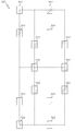
도 1은 양방향 로컬 상호연결들의 레이아웃을 보여주는, 예시적인 6T SRAM 셀(100)의 평면 및 부분적인 국부 투시도이다. 6T 셀이 도시되나, 본 명세서에 기술된 기법들 및 개념들은 또한 다른 SRAM 셀 토폴로지들, 예를 들어, 4T, 8T, 10T, 등에도 적용될 수 있다. 도 1은 여기에 제시된 개념들을 가장 잘 설명하는 간략화된 국부 투시도로 SRAM 셀(100)의 피쳐들을 도시한다. 또한, SRAM 셀(100)의 구체적인 레이아웃은 단지 예시적인 것이며 도시된 레이아웃은 기술된 내용의 범위를 제한하거나 한정하려 의도딘 것이 아니다. SRAM 셀(100)의 이 실시예는 6개의 트랜지스터 디바이스들을 형성하도록 협력하는 4개의 액티브 반도체 영역들(102) 및 4개의 게이트 구조들(104)을 포함한다. 비록 도 1의 국부 투시도로부터 쉽게 분명해지지는 않지만, 잘 이해되는 바와 같이, 게이트 구조들(104)은 액티브 반도체 영역들(102) 위에 형성된다. 게이트 구조들(104)은 이것들 모두가 일반적으로 동일한 방향(도 1에서 수직 방향)으로 배향되므로 단방향인 것으로 여겨진다. 1 is a plan and partial local perspective view of an exemplary
SRAM 셀(100)은 또한, 텅스텐 물질 또는 임의의 적합한 금속 물질과 같은 전기 전도성 물질로부터 형성되는 복수의 로컬 상호연결들을 포함한다. 이 특정 실시예는, 게이트 구조(104a)에 결합되는 로컬 상호연결(106), 액티브 반도체 영역(102a)에 결합되는 2개의 로컬 상호연결들(108/110); 게이트 구조(104c), 액티브 반도체 영역(102b), 및 액티브 반도체 영역(102a)에 결합되는 양방향 로컬 상호연결(112); 액티브 반도체 영역(102b)에 결합되는 로컬 상호연결(114); 액티브 반도체 영역(102c)에 결합되는 로컬 상호연결(116); 게이트 구조(104b), 액티브 반도체 영역(102c), 및 액티브 반도체 영역(102d)에 결합되는 양방향 로컬 상호연결(118); 액티브 반도체 영역(102d)에 결합되는 2개의 로컬 상호연결들(120/122); 및 게이트 구조(104d)에 결합되는 로컬 상호연결(124)을 포함한다. 비록 도 1의 국부 투시도로부터 쉽게 분명해지지는 않지만, 로컬 상호연결들은 액티브 반도체 영역들(102) 위에, 게이트 구조들(104) 위에, 그리고/또는 반도체 기판의 다른 영역들(도 1에서, 이러한 다른 영역들은 어떠한 구분가능한 디바이스 피쳐들을 가지고 있지 않음) 위에 형성된다. 로컬 상호연결들(112, 118)은 각각 일반적으로 2개의 상이한 방향들로(도 1에서 수직으로 그리고 수평으로) 배향되므로 양방향인 것으로 여겨진다. SRAM 셀(100)의 레이아웃 및 구체적인 전기적 결합들은 6T SRAM 셀의 동작에 대해 잘 알려진 원리 및 요건들을 만족시키며, SRAM 셀(100)의 동작은 여기에서 자세하게 기술되지는 않을 것이다. The
실제로, 높은 양의 메모리 용량을 제공하기 위하여 단일 SRAM 셀이 단일 반도체 기판 위에 여러 번 제조될 것이다. 예를 들어, SRAM 셀(100)은 단일 반도체 디바이스 구조 상의 SRAM 셀들의 어레이만큼 여러 번 복제될 수 있다. 이와 관련하여, 도 2는 SRAM 셀(100)을 기반으로 하는 SRAM 셀들의 3x2 어레이(150)의 평면 및 국부 투시도이다. SRAM 셀들(150)의 어레이는 도 1에 도시된 것과 동일한 레이아웃을 가지는 3개의 SRAM 셀들(100a), 및 도 1에 도시된 것의 미러 이미지 레이아웃을 가지는 3개의 SRAM 셀들(100b)을 포함한다. 이는 SRAM 셀들의 어레이(150) 내의 이웃하는 셀들이 특정한 피쳐들 또는 소자들을 공유할 수 있게 한다. 예를 들어, 이웃하는 셀들은 특정한 액티브 반도체 영역들 및/또는 특정한 로컬 상호연결들을 공유할 수 있다. Indeed, a single SRAM cell will be fabricated multiple times on a single semiconductor substrate to provide a high amount of memory capacity. For example,
실제의 SRAM 디바이스는 수백만개의 셀들의 어레이를 사용할 수 있으며, 제조업자들은 SRAM 디바이스들의 물리적 사이즈를 줄이기 위해 노력하고 있다. (실제적인 제조 공차 및 제약들에 근거한) 특정한 설계 규칙들은 일부 피쳐들이 하향으로 스케일링될 수 있는 양을 제한한다. 예를 들어, 설계 규칙들은 피쳐들이 함께 단락(short) 또는 병합(merge)되는 것(이는 포토리쏘그래피 툴들이 실제적인 한계들(practical limitations)에 의해 야기될 수 있음)을 방지하기 위하여 인접한 마스크 피쳐들 간의 최소의 팁-대-팁 및 팁-대-라인 이격공간을 지시한다. 따라서, SRAM 디바이스에 대한 제시된 레이아웃을 제조하는 것은, 이 제시된 레이아웃이 잠재적인 설계 규칙 위반들(예를 들어, 팁-대-팁 또는 팁-라인 위반들)을 포함하고 있는 경우에는 실제적이지 않거나 실현가능하지 않을 수 있다. 이와 관련하여, 도 2는 SRAM 셀들의 어레이(150)를 위한 단일의 포토리소그래픽 마스크와 관련되는 몇개의 잠재적인 팁-대-팁 위반들(152)을 식별한다. 도 2의 원형 영역들은 이 팁-대-팁 위반들(152)에 대응한다. 도 2에서, 팁-대-팁 위반들(152) 전부는 수평적으로 배향되는 로컬 상호연결 피쳐들에 관련된다. 비록 본 명세서에 기술된 기법들은 팁-대-라인 위반들을 해소하기 위하여 그리고 팁-대-팁 위반들과 팁-대-라인 위반들의 임의의 조합을 해소하기 위하여 사용될 수 있지만, 이 예에서, SRAM 셀들의 어레이(150)는 팁-대-라인 위반들을 포함하지 않는다. Actual SRAM devices can use arrays of millions of cells, and manufacturers are trying to reduce the physical size of SRAM devices. Certain design rules (based on actual manufacturing tolerances and constraints) limit the amount by which some features can be scaled down. For example, the design rules may be used to prevent features from being shorted or merge together (which may be caused by practical limitations of photolithography tools) Tip-to-tip and tip-to-line spacing space between the tip-to-tip spacing. Thus, manufacturing a presented layout for an SRAM device is not practical or realizable if the presented layout includes potential design rule violations (e.g., tip-to-tip or tip-line violations) It may not be possible. In this regard, FIG. 2 identifies several potential tip-to-
도 3은 대안적인 SRAM 셀 레이아웃에 근거한 SRAM 셀들의 또 다른 3X2 어레이(160)의 평면 및 부분적인 국부 투시도이다. SRAM 셀들의 어레이(160)는 (3개의 미러 이미지 버전을 포함하여) SRAM 셀(162)의 6번의 반복들을 포함한다. SRAM 셀들의 어레이(160)의 전체 레이아웃은 도 2에 도시된 SRAM 셀들의 어레이(150)의 레이아웃과 일반적으로 유사하다. 그러나, SRAM 셀들의 어레이(150)와 달리, SRAM 셀들의 어레이(160)는 수직적으로 배향되는 잠재적인 팁-대-팁 위반들을 포함한다. 따라서, 도 3은 몇개의 수직적인 팁-대-팁 위반들(166)에 부가하여 다수의 수평적인 팁-대-팁 위반들(164)을 도시한다. 특히, 수평적인 팁-대-팁 위반들(164)이 일 포토리쏘그래픽 마스크와 관련되는 한편, 수직적인 팁-대-팁 위반들(166)이 또 다른 포토리쏘그래픽 마스크와 관련된다. 이러한 양상은 하기에서 더 자세히 설명될 것이다.3 is a plan and partial local perspective view of another
설계 규칙 위반들의 존재로 인해 인접한 로컬 상호연결 피쳐들 사이의 단락을 야기함이 없이 종래의 기법들을 사용하여 SRAM 셀들의 어레이(150) 또는 SRAM 셀들의 어레이(160)를 제조하는 것이 불가능할 수 있다. 하기에서 기술된 마스크 생성 및 반도체 제조 기법들 및 기술들은 이러한 문제들을 해소하며, 복수의 패터닝 포토리쏘그래피 중에 마스크들 내의 잠재적인 팁-대-팁 및 팁-대-라인 위반들을 없앰으로써 반도체 디바이스들(예컨대, SRAM 디바이스들)을 서브-80 나노미터 해상도로 제조하기에 용이하게 한다.It may be impossible to fabricate the array of
여기에서 설명된 예시적인 복수 마스크 기법은 반도체 디바이스 구조에 대한 복수의 패터닝 절차를 위해 적어도 두개의 마스크들을 사용한다. 하드 마스크 및 후속적인 블록 마스크의 생성은 어떠한 포토리쏘그래픽 마스크에도 설계 규칙 위반을 야기함이 없이 더 가까운 팁-대-팁 및 팁-대-라인 이격이 될 수 있게 해준다. 이와 관련하여, 도 4는 반도체 제조 공정 중에 사용하기 위한 포토리쏘그래피 마스크들의 세트를 생성하기 위하여 실행될 수 있는 마스크 생성 공정(200)의 예시적인 실시예를 보여주는 흐름도이다. 공정(200)은 (종래의 기법들에 비해) 설계 규칙 위반들이 줄어든 반도체 디바이스 피쳐들을 위한 포토리쏘그래픽 마스크의 생성 방법의 예를 나타낸다. 공정(200)과 관련되어 수행되는 다양한 태스크들은 소프트웨어, 하드웨어, 펌웨어, 또는 이것들의 임의의 조합에 의해 수행될 수 있다. 실제로, 공정(200)의 부분들은, 실행시 호스트 컴퓨팅 디바이스 또는 프로세서로 하여금 기술된 작업들을 수행할 수 있게 하는 컴퓨터-판독가능 및/또는 프로세서-실행가능 명령들을 지닌 적합한 소프트웨어 프로그램을 실행하도록 적절하게 구성된 하나 이상의 컴퓨팅 디바이스들, 컴퓨터 시스템들, 또는 프로세싱 하드웨어에 의해 수행될 수 있다. 예를 들어, 공정(200)은 반도체 디바이스 설계에서 사용하기에 적절한 컴퓨터-활용 설계 애플리케이션, 반도체 디바이스 설계에 적합한 설계 규칙 검사 애플리케이션, 등에 통합 또는 집적될 수 있다. 공정(200)은 임의의 개수의 추가적인 또는 대안적인 태스크들을 포함할 수 있으며, 도 4에 도시된 태스크들은 도시된 순서대로 수행될 필요가 없으며, 공정(200)이 본 명세서에 자세히 기술되지 않은 추가적인 기능성을 가진 더욱 광범위한 절차 또는 공정에 통합될 수 있음이 이해되어야 한다. 또한, 공정(200)의 실시예는 (전체적인 기능성이 유지되는한) 도 4에 도시된 하나 이상의 작업들을 생략할 수 있다.The exemplary multiple mask technique described herein uses at least two masks for a plurality of patterning procedures for a semiconductor device structure. The creation of hard masks and subsequent block masks allows for closer tip-to-tip and tip-to-line spacing without causing design rule violations to any photolithographic mask. In this regard, FIG. 4 is a flow chart illustrating an exemplary embodiment of a mask generation process 200 that may be performed to generate a set of photolithographic masks for use during a semiconductor manufacturing process. The process 200 illustrates an example of a method for generating a photolithographic mask for semiconductor device features (as compared to conventional techniques) where design rule violations are reduced. The various tasks performed in connection with the process 200 may be performed by software, hardware, firmware, or any combination thereof. In practice, portions of the process 200 may be executed by a host computing device or processor as appropriate to execute an appropriate software program having computer-readable and / or processor-executable instructions that enable it to perform the described tasks May be performed by one or more computing devices, computer systems, or processing hardware configured. For example, process 200 may be integrated or integrated into a computer-usable design application suitable for use in semiconductor device design, a design rule checking application suitable for semiconductor device design, and the like. Processes 200 may include any number of additional or alternative tasks, and the tasks depicted in FIG. 4 need not be performed in the order shown, It should be understood that the invention may be incorporated into a wider range of procedures or processes having functionality. In addition, embodiments of the process 200 may omit one or more tasks shown in FIG. 4 (as long as overall functionality is maintained).
공정(200)은 전체적인 요구되는 마스크 패턴(작업(202))을 위한 초기 설계를 획득, 생성, 또는 제공함으로써 시작될 수 있다. 특정한 CAD 배치에 있어서, 태스크(202)는 요구되는 마스크 패턴을 나타내는 예비 데이터를 제공할 수 있으며, 이 데이터는 (잘 이해되는 바와 같이, 임의의 적절한 기준 또는 좌표 시스템을 사용하여) 전체 마스크 패턴에 의해 정의되는 피쳐들의 레이아웃, 치수, 배열, 배향 및 상대적인 위치를 나타낸다. 이 예는 도 2에 도시된 SRAM 셀들의 어레이(150)를 위한 로컬 상호연결들의 생성을 고려한다. 따라서, 작업(202)은, SRAM 셀(100)의 요구되는 로컬 상호연결 레이아웃(도 1) 및/또는 SRAM 셀들의 어레이(150)의 상호연결 레이아웃을 나타내는 데이터(도 2)를 제공, 획득, 또는 저장할 수 있다. Process 200 may be initiated by acquiring, creating, or providing an initial design for the overall required mask pattern (job 202). For a particular CAD layout, the
공정(200)의 이 실시예는, 전체 마스크 패턴이 복수의 노광/패턴 절차(예를 들어, LLE(litho-litho-etch) 절차, LELE(litho-etch-litho-etch) 절차, LFLE(litho-freeze-litho-etch) 절차, 또는 기타)를 사용하여 생성될 것이라고 가정한다. 특정한 실제 실시예들에서, 공정(200)은 LELE 절차를 사용하는바, 이는 LELE가 어느정도 강건하며 확립된 기술이기 때문이다. 따라서, 전체적인 마스크 패턴은 복수의 서로 다른 컴포넌트 마스크 패턴들로 분해된다(태스크(204)). 실제로, 태스크(204)는, 분해를 행하기에 적합한 방식으로, 전체적인 마스크 패턴을 나타내는 예비적인 데이터를 처리 또는 분석할 수 있다. 임의의 개수의 컴포넌트 마스크 패턴들이 생성될 수 있으나, 이 예는 전체 마스크 패턴을 제1 컴포넌트 마스크 패턴 및 제2 컴포넌트 마스크 패턴으로 분해한다. 공정(200)은 기존의 또는 종래의 분해 기법들, 소프트웨어 애플리케이션들, 및 기술들을 레버리지(leverage)할 수 있다. 따라서, 태스크(204)에 의해 사용되는 구체적인 분해 기법은 여기에서 자세히 설명되지 않을 것이다. This embodiment of the process 200 allows the entire mask pattern to be subjected to a plurality of exposure / pattern procedures (e.g., a litho-litho-etch procedure, a litho-etch- litho-etch -freeze-litho-etch) procedure, or otherwise). In certain practical embodiments, the process 200 uses the LELE procedure because the LELE is a rather robust and established technique. Thus, the overall mask pattern is decomposed into a plurality of different component mask patterns (task 204). In practice, the task 204 may process or analyze the preliminary data representing the overall mask pattern in a manner suitable for performing decomposition. Any number of component mask patterns may be generated, but this example decomposes the entire mask pattern into a first component mask pattern and a second component mask pattern. The process 200 may leverage existing or conventional decomposition techniques, software applications, and techniques. Thus, the specific decomposition techniques used by task 204 will not be described in detail here.
태스크(204)에 의해 생성되는 예시적인 컴포넌트 마스크 패턴들은 도 5 및 도 6에 표시되며, 여기서 도 5는 제1 컴포넌트 마스크 패턴(300)의 평면도이고 도 6은 제2 컴포넌트 마스크 패턴(302)의 평면도이다. 제1 컴포넌트 마스크 패턴(300)은 개별 SRAM 셀들의 경계에 있는 짧은 수직으로 배향된 로컬 상호연결들을 정의한다. 제1 컴포넌트 마스크 패턴(300)의 마스크 피쳐들(301)은 또한 도 2에 도시된 SRAM 셀들의 어레이(150) 내에서 발견된다. 제2 컴포넌트 마스크 패턴(302)은 개별 SRAM 셀들의 경계에 있는 수평적으로 배향된 로컬 상호연결을 정의하는 마스크 피쳐들(304)을 포함한다. 제2 컴포넌트 마스크 패턴(302)은 또한 개별 SRAM 셀들의 경계 내에 있는 양방향 로컬 상호연결들을 정의하는 마스크 피쳐들(306)을 포함한다. 마스크 피쳐들(304/306)은 또한 도 2에 도시된 SRAM 셀들의 어레이(150) 내에서 발견된다. 이 두 마스크 패턴들 위의 피쳐들은 "음각"인데, 그 이유는 반도체 기판 위에 형성되는 포토레지스트 물질의 결과적인 패턴들이 마스크 피쳐들(301/304/406)에 대응하는 윤곽들을 가지는 스페이스들 또는 홀들을 포함할 것이기 때문이다. 다른 말로 하면, 도 5 및 도 6에서 마스크 피쳐들(301/304/306)이 나타난 곳 어디 곳이든 포토레지스트 물질이 결여될 것이다. 5 and 6, wherein FIG. 5 is a plan view of the first
공정(200)은 그후, 컴포넌트 마스크 패턴들에서의 특정한 설계 규칙 위반들을 식별하기 위하여 컴포넌트 마스크 패턴들을 분석함으로써 진행될 수 있다(태스크(206)). 현 세대의 193nm 침지 스텝퍼 툴들에 대해, 약 90-112nm 미만의 팁-대-팁 또는 팁-대-라인 이격이 설계 규칙 위반으로 여겨진다. 실제로, 태스크(206)는 컴포넌트 마스크 패턴들 내의 팁-대-팁 및/또는 팁-대-라인 위반의 존재를 결정하는 적절한 설계 규칙 검사(DRC) 절차와 관련될 수 있다. 따라서, 태스크(206)는 적절한 DRC 애플리케이션, 프로그램, 또는 알고리즘을 사용하여 컴포넌트 마스크 패턴들을 나타내는 데이터를 분석하는 적합한 처리 하드웨어에 의해 수행될 수 있다. 이 예는 제1 컴포넌트 마스크 패턴(300)이 임의의 팁-대-팁 또는 팁-대-라인 위반들로부터 자유롭다는 것을 가정한다. 반면, 이 예는 태스크(206)가 제2 컴포넌트 마스크 패턴(302)에서 몇 개의 팁-대-팁 위반들을 식별한다고 가정한다(제2 컴포넌트 마스크 패턴(302) 내에 팁-대-라인 위반들이 없음). 도 6에서, 식별된 위반들(308)은 양방향의 화살표로 나타내어진다. 도 6은 또한 화살표들 및 타원들을 사용하여 몇몇 식별된 위반들(310)을 표시하며, 이 식별된 위반들(310)은 어레이의 외부 경계에 위치해있고, 인접 셀들의 존재시에 발생될 실제 위반들(actual violations)을 고려한다. 공정(200)은, 전체 마스크 패턴의 특정 레이아웃에 따라 그리고 태스크(204)가 전체 마스크 패턴들을 그것의 컴포넌트 마스크 패턴들로 분해하는 방식에 따라, 컴포넌트 마스크 패턴들 중 단 하나에서, 컴포넌트 마스크 패턴들 모두에서, 또는 컴포넌트 마스크 패널들 모두는 아니지만 일부에서 설계 규칙 위반들을 발견할 수 있다는 것이 이해되어야 한다. The process 200 may then proceed by analyzing the component mask patterns (task 206) to identify specific design rule violations in the component mask patterns. For current generation 193 nm immersion stepper tools, tip-to-tip or tip-to-line spacing of less than about 90-112 nm is considered a design rule violation. In practice,
특정 실시예들에서, 태스크(206)는, 예를 들어, 전체 마스크 패턴에 대해 이용된 것과 동일한 기준, 좌표, 또는 측정 시스템을 사용하여, 식별된 위반들의 치수, 장소, 위치, 및/또는 배열을 결정할 수 있다. 이 정보는 포토리쏘그래픽 블록 마스크 패턴을 유도 또는 생성하기 위하여 사용될 수 있다(태스크(208)). 이와 관련하여, 블록 마스크 패턴은, 식별된 위반들의 치수들로부터 유발되거나 얻어지거나 또는 그렇지 않다면 이 치수들에 의해 영향받는 피쳐들을 가질 것이다. 실제로, 태스크(208)는 식별된 위반들에 따라 블록 마스크 데이터를 유발하는 적절한 처리 하드웨어에 의해 수행될 수 있다. 하기에서 보다 자세히 기술될 바와 같이, 블록 마스크 패턴은 제조 공정 중에 반도체 디바이스 구조 상에 피쳐들의 형성을 선택적으로 블록하는데 사용된다. 도 7은 태스크(208) 중에 생성될 수 있는 일 예시적인 블록 마스크 패턴(320)의 평면도이다. 태스크(208)는 (도 7에 도시된 것과 같이)요구되는 어레이에 대응하는 블록 마스크 패턴을 생성할 수 있거나, 또는 단지 일 셀에 대응하는 블록 마스크 패턴을 생성할 수 있다는 것이 이해되어야 한다.In certain embodiments, the
블록 마스크 패턴(320)은 식별된 설계 규칙 위반들(도 6 참조)에 대응하는 마스크 피쳐들(322)을 포함한다. 도 5 및 도 6에 표시된 마스크 피쳐들(301/304/306)에 대비하여, 반도체 기판 위에 형성된 포토레지스트 물질의 결과적인 패턴이 마스크 피쳐들(322)에 대응할 것이기 때문에 블록 마스크 패턴(320) 상의 마스크 피쳐들은 "양각"이다. 다른 말로 하면, 포토레지스트 물질은 마스크 피쳐들(322)이 존재하는 곳에는 어디든지 남아있을 것이다. 각각의 마스크 피쳐(322)의 위치 및 폭은 그것의 각각의 설계 규칙 위반의 위치 및 폭에 근거한다. 실제로, 마스크 피쳐들(322)의 치수는 식별된 설계 규칙 위반의 각각의 치수와 동일할 수 있다. 대안적으로, 공정 편차들 및/또는 제조 툴들의 특성들을 해소하기 위하여 필요로 된다면, 마스크 피쳐들(322)의 치수들이 식별된 설계 규칙 위반들의 각각의 치수들과 동일하지 않게끔 마스크 피쳐들(322)이 스케일링 될 수 있다. 예를 들어, 마스크 피쳐들(322)을 그것들의 대응 위반들보다 약간 크게/작게 하는 것이 바람직할 수 있다(실제로, 마스크 피쳐들(322)은 일반적으로 스케일 업, 즉, 대응 위반들의 사이즈보다 약간 크게된다). 또한, 팁-대-팁 및 팁-대-라인 위반들이 고려될 때, 식별된 위반들이 일반적으로 1 차원, 즉, 두 개의 인접 팁들 사이의 이격 또는 팁과 라인 사이의 이격을 규정할 것이다. 그러나, 블록 마스크 패턴(320)은 2차원으로 정의된 마스크 피쳐들(322)을 포함한다. 이 예에서, 마스크 피쳐들(322)의 수평 치수는 식별된 위반들의 치수에 대응한다. 태스크(208)는 또한 컴포넌트 마스크 패턴들에서 발견된 마스크 피쳐들과의 원치 않는 간섭을 피하기 위하여 마스크 피쳐들(322)의 수직 치수들을 계산하며, 그 이유는 하기의 설명으로부터 명백해질 것이다.The
특정 실시예들에서, 태스크(208) 동안 생성된 블록 마스크는, 블록 마스크 자체에서의 설계 규칙 위반들에 대해 검사하기 위하여 DRC 과정(태스크(210))을 겪게된다. 따라서, 태스크(210)는 블록 마스크 내의 임의의 팁-대-팁 및/또는 팁-대-라인 위반들을 식별하기 위하여 적절한 DRC 애플리케이션, 프로그램, 또는 알고리즘을 사용하여 블록 마스크 데이터를 분석하는 적절한 프로세싱 하드웨어에 의해 수행될 수 있다. 블록 마스크가 팁-대-팁 또는 팁-대-라인 위반들을 포함한다면(쿼리 태스크(212)), 프로세스(200)는 종료하거나, 전체 마스크 패턴의 재설계를 개시하거나, 전체 마스크 패턴을 상이한 방식으로 분해하려 시도하거나, 적합한 다른 동작을 취할 수 있다. 또한, 본 명세서에 자세히 기술되지는 않았으나, 위에서 언급된 기법들 및 방법들을 사용하여 하나보다 많은 블록 마스크 패턴을 생성 및 사용하는 것이 바람직하거나 필요할 수 있다. 예를 들어, 어떠한 위반들 없이 단일 블록 마스크 패턴이 생성될 수 없다면 복수의 블록 마스크 패턴들이 사용될 수 있다.In certain embodiments, the block mask created during task 208 undergoes a DRC process (task 210) to check for design rule violations in the block mask itself. Accordingly,
블록 마스크에 대한 DRC 결과가 무결(clean)하고 블록 마스크에 설계 규칙 위반들이 없으면, 공정(200)은 블록 마스크 패턴에 따라 그리고/또는 식별된 위반들에 따라 컴포넌트 마스크 패턴들 중 적어도 하나를 수정함으로써 계속될 수 있다(태스크(214)). 실행될 때, 태스크(214)는, 수정된 마스크 패턴을 나타내는 갱신된 데이터를 얻기 위하여, 요구되는 마스크 패턴(예를 들어, 도 6에 도시된 제2 컴포넌트 마스크 패턴(302))에 대응하는 예비 데이터를 수정할 것이다. 태스크(214)는 수정된 마스크 패턴에 팁-대-팁 위반들 및 팁-대-라인 위반들과 같은 설계 규칙 위반들이 없게끔 실행된다. 따라서, 태스크(214) 동안 수행되는 수정은 블록 마스크 패턴에서의 식별된 위반들의 치수들 및/또는 피쳐들의 치수들에 의해 영향을 받을 것이다. If the DRC result for the block mask is clean and there are no design rule violations in the block mask, the process 200 may modify at least one of the component mask patterns according to the block mask pattern and / (Task 214). When executed, the task 214 generates preliminary data corresponding to the required mask pattern (e.g., the second
공정(200)은, 전체 마스크 패턴의 특정 레이아웃에 따라 그리고 태스크(204)가 전체 마스크 패턴을 그것의 컴포넌트 마스크 패턴들로 분해하는 방식에 따라, 컴포넌트 마스크 패턴들 중 단 하나, 컴포넌트 마스크 패턴들 모두, 또는 컴포넌트 마스크 패턴들 모두가 아니라 일부를 수정할 수 있다. 여기에 기술된 간단한 예시는 제1 컴포넌트 마스크 패턴(도 2)이 수정되지 않은채 남아있고 제2 컴포넌트 패턴(302)(도 3)만이 수정되는 것을 가정한다. 이와 관련하여, 도 8은 제2 컴포넌트 마스크 패턴(302)의 수정된 버전의 평면도이다. 수정된 마스크 패턴(340)의 예시적인 실시예는, 식별된 위반들(308/310)에 대응하는 스페이스 또는 갭들을 "충전하는(fill in)" 추가적인 마스크 피쳐들과 함께, 제2 컴포넌트 마스크 패턴(302)의 마스크 피쳐들 모두를 포함한다. 따라서, 제2 컴포넌트 마스크 패턴(302)을 위한 예비 데이터는, 갱신된 데이터가 식별된 위반들(308/310) 대신에 정의된 피쳐들을 가지는 제2 컴포넌트 마스크 패턴(302)의 병합된 또는 블렌딩된 버전을 나타내게끔 수정된다. 다른 말로 하면, 본래의 제2 컴포넌트 마스크 패턴(302)은 식별된 위반들(308/310)을 정의된 피쳐들로 대체함으로써 수정된 마스크 패턴(340)으로 처리 및 변경될 수 있다. The process 200 may be performed in accordance with a particular layout of the entire mask pattern and depending on the manner in which the task 204 decomposes the entire mask pattern into its component mask patterns, , Or some of the component mask patterns, but not both. The simple example described herein assumes that the first component mask pattern (FIG. 2) remains unmodified and only the second component pattern 302 (FIG. 3) is modified. In this regard, FIG. 8 is a top view of a modified version of the second
도 8을 참조하면, 수정된 마스크 패턴(340)은 각각이 제2 컴포넌트 마스크 패턴(302)에서 발견되는 2개의 마스크 피쳐들(304)을 아우르는(emcompass) 3개의 병합된 마스크 피쳐들(342)을 포함한다. 특히, 병합된 마스크 피쳐들(342) 각각은 팁-대-팁 또는 팁-대-라인 위반을 가지지 않은 단일의 연속적인(continuous) 피쳐이다. 수정된 마스크 패턴(340)은 또한 각각이 제2 컴포넌트 마스크 패턴(302)에서 발견되는 마스크 피쳐들(306) 중 두 개를 아우르는 4개의 U-형 병합 마스크 피쳐들(344)을 포함한다. 특히, U형 병합 마스크 피쳐들(344) 각각은 팁-대-팁 또는 팁-대-라인 위반을 가지지 않은 단일의 연속적인(continuous) 피쳐이다. 수정된 마스크 패턴(340)은 또한 세개의 연장된 마스크 피쳐들(346)을 포함하며, 이들 각각은 제2 컴포넌트 마스크 패턴(302)의 경계 부근에 위치된 각각의 마스크 피쳐(304)의 연장된 버전을 나타낸다. 마찬가지로, 수정된 마스크 패턴(340)은 4개의 연장된 L형 마스크 피쳐들(348)을 포함하며, 이들 각각은 제2 컴포넌트 마스크 패턴(302)의 경계 부근에 위치된 각각의 마스크 피쳐(306)의 연장된 버전을 나타낸다. 반도체 기판 위에 형성되는 포토레지스트 물질의 결과적인 패턴이 마스크 피쳐들(342/344/346/348)에 대응하는 외곽선들을 가진 공간들 또는 홀들을 포함할 것이므로, 수정된 마스크 패턴(340) 상의 피쳐들은 "음각"이다. 다른 말로하면, 마스크 피쳐들(342/344/346/348)이 존재하는 곳은 어디든 포토레지스트 물질이 결여될 것이다. 수정된 마스크 패턴(340)에는 어떠한 설계 규칙 위반도 없으며 수정된 마스크 패턴(340)에 대한 DRC는 무결의 결과들(clean results)을 반환할 것이다. Referring to Figure 8, the modified
도 4를 다시 참조하면, 태스크(214)의 실행은 결과적으로 컴포넌트 마스크 패턴들의 세트가 수정되게 하며, 이 수정된 세트 내의 각각의 마스크 패턴에는 팁-대-팁 및 팁-대-라인 위반들이 없다. 공정(200)은 그후 본래의 컴포넌트 마스크 패턴들, 수정된 마스크 패턴(들), 및 블록 마스크 패턴(들)에 대응하는 데이터를 저장할 수 있다(태스크(216)). 이 데이터는 그후 블록 마스크 패턴(들)에 대해 그리고 컴포넌트 마스크 패턴들의 수정된 세트에 대해 포토리쏘그래픽 마스크들을 발생/생성하는데 사용될 수 있다. 이 예에서, 본래의 제1 컴포넌트 마스크 패턴(300)을 정의하는 마스크; 수정된 마스크 패턴(340)을 정의하는 마스크; 그리고 블록 마스크 패턴(320)을 정의하는 마스크의 3개의 상이한 포토리쏘그래픽 마스크들이 생성될 것이다. 이 마스크들은 그후 반도체 디바이스(예를 들어, SRAM 디바이스)의 제조 중에 특정한 반도체 디바이스 피쳐들을 형성하기 위하여 사용된다. 이와 관련하여, 예시적인 제조 공정이 도 9-20을 참조로 하기에서 기술된다. Referring again to Figure 4, the execution of task 214 results in the modification of the set of component mask patterns, with each mask pattern in the modified set having no tip-to-tip and tip-to-line violations . The process 200 may then store data corresponding to the original component mask patterns, the modified mask pattern (s), and the block mask pattern (s) (task 216). This data can then be used to generate / generate photolithographic masks for the block mask pattern (s) and for a modified set of component mask patterns. In this example, a mask defining the original first
도 9 내지 20은 복수의 노광/패턴 제조 공정을 겪는 반도체 디바이스 구조의 단면도 및 평면도를 포함한다. 이 제조 공정은 디바이스 피쳐들 사이에 극도로 조밀한 공차들(close tolerances) 및/또는 매우 좁은 라인 폭을 가지는 반도체 디바이스를 제조하기 위하여 사용될 수 있다. 간결성 및 일관성을 위하여, 이 제조 공정은 위에서 기술된 3개의 포토리쏘그래픽 마스크들, 즉, 제1 컴포넌트 마스크, 수정된 마스크, 블록 마스크를 사용한다. 따라서, 여기에 기술된 예시적인 제조 공정은 SRAM 디바이스 구조 상에 디바이스 피쳐들을 생성하는데 사용될 수 있다. Figures 9-20 include cross-sectional and plan views of a semiconductor device structure undergoing a plurality of exposure / pattern fabrication processes. This fabrication process can be used to fabricate semiconductor devices with extremely tight tolerances and / or very narrow line widths between device features. For simplicity and consistency, this manufacturing process uses the three photolithographic masks described above, i.e., a first component mask, a modified mask, and a block mask. Thus, the exemplary fabrication process described herein can be used to create device features on an SRAM device structure.
도 9는 타겟 물질이 반도체 디바이스 구조 위에 형성된 후의 예시적인 반도체 디바이스 구조(400)를 도시한다. 공정의 이 시점에서, 반도체 디바이스 구조(400)는, 반도체 물질 층(402); 반도체 물질 층(402) 위에 놓인 제1 절연 물질 층(404); 제1 절연 물질 층(404) 위에 형성된 2개의 게이트 구조들(405); 제1 절연 물질 층(404) 위에 놓이며 게이트 구조(405)를 덮는 제2 절연 물질 층(406); 그리고 제2 절연 물질 층 위의 하드 마스크 물질 층(408)을 제한없이 포함한다. 도 2를 참조하면, 도 9-20에 포함된 단면도들은 2개의 게이트 구조들에 인접한 팁-대-팁 로컬 상호연결 영역에 대응하지만, 여기서 로컬 상호연결들의 팁들 사이에는 어떠한 액티브 반도체 영역도 위치되지 않는다. 반도체 디바이스 구조(400)의 단면 구성은 게이트 구조를 포함하지 않는 영역들, 액티브 반도체 영역을 포함하는 영역들, 등에서 상이할 수 있음이 이해되어야 한다. Figure 9 illustrates an exemplary
반도체 물질(402)은 반도체 산업에서 일반적으로 사용되는 것과 같은 실리콘 물질, 예를 들어, 비교적 순수한 실리콘 그리고 게르마늄, 탄소 등과 같은 다른 요소들과 혼합된 실리콘인 것이 바람직하다. 대안적으로, 반도체 물질(402)은, 게르마늄, 갈륨 아세나이드 등일 수 있다. 반도체 물질(402)은 N-형 또는 P-형일 수 있으나, 일반적으로 P형이며, 그 내부에는 적합한 타입의 우물들이 형성되어 있다. 반도체 물질(402)은 벌크 반도체 기판으로서 제공되거나, 또는 지지 기판, 지지 기판 위의 절연체 층, 그리고 절연체 층 위의 실리콘 물질 층을 포함하는 실리콘-온-절연체(SOI) 기판 위에 제공될 수 있다. The
이 실시예에서, 제1 절연 물질 층(404)은 반도체 디바이스 구조를 위한 얕은 트렌치 격리(STI)를 나타낸다. 특정 실시예들에서, 제1 절연 물질(404)을 위해 사용되는 STI 물질은, TEOS(tetraethyl orthosilicate) 산화물, 고밀도 플라즈마 산화물 등과 같은 산화물이다. 제2 절연 물질층(406)은 로컬 상호연결들의 요구되는 패턴을 생성하도록 충전되는 트렌치들을 형성하기 위하여 사용된다. 제조 공정의 이 시점에서, 제2 절연 물질 층(406)은 게이트 구조들(405)(게이트 구조들(405)은, 잘 이해되는 바와 같이, 실제로는 게이트 구조들(405) 각각이 다양한 물질 층들의 스택으로서 실현될 수 있으나, 간단하게 블록들로 표시된다)을 캡슐화(encapsulation)한다. 실시예에 따라, 제2 절연 물질의 층(406)은, TEOS 산화물과 같은 산화물을 제한없이 포함할 수 있다. 반도체 디바이스 구조가 일반적으로 제1 절연 물질 층(404)과 제2 절연 물질 층(406) 사이에 얇은 컨택 식각 정지층(예를 들어, 질화물층)을 포함할 것이라는 것이 이해되어야 한다. 이 얇은 컨택 식각 정지 층은 도 9에는 도시되지 않는다. 필요하다면 다른 두께가 사용될 수 있지만, 일반적인 실시예들에서, 제2 절연 물질 층(406)은 약 100nm 내지 약 250 nm 범위의 두께를 가진다. In this embodiment, the first layer of insulating
하드 마스크 물질층(408)은, 예를 들어, 화학 기상 증착(CVD), 저압 CVD(LPCVD), 플라즈마 인핸스드 CVD(PECVD), 대기압 CVD(APCVD), 물리 기상 증착(PVC), 원자층 증착(ALD), 등과 같은 적절한 증착 기법을 사용하여 제2 절연 물질 층(406) 위에 형성된다. 몇몇 실시예들에서, 비반사 코팅 층(도시되지 않음)이 하드마스크 물질층(408) 위에 형성될 수 있다. 다양한 실시예들에서, 비반사 코팅은 하나 이상의 유기 BARC(bottom anti-reflective coating) 층, 무기 BARC 층, 그리고 하이브리드 유기-무기 BARC 층을 포함할 수 있다. 바람직한 실시예들은 CVD 물질을 사용하지만, 대안적인 실시예들에서, 하드 마스크 물질(408)은 열적으로 성장된 물질 일 수 있다. 실제로, 하드 마스크 물질(408)은 질화물, 바람직하게는 실리콘 질화물과 같은 유전체 물질이고, 하드 마스크 물질(408)은 약 20nm 내지 500nm의 전형적인 두께로 형성되나, 실시예에 따라, 두께가 이 전형적인 범위 바깥에 있을 수 있다. 하드 마스크 물질(408)은 또한 하나 이상의 실리콘 카바이드, 산소 도핑 실리콘 카바이드, 질소 도핑 실리콘 카바이드, 산소 도핑 실리콘 질화물, 탄소 도핑 실리콘 질화물, 그리고 산소 및 탄소 도핑 실리콘 질화물을 포함할 수 있다. The
하드 마스크 물질 층(408)을 제공한 후, 적합한 포토리쏘그래픽 마스크들을 사용하여, 다중 노광/패턴 포토리쏘그래피 절차를 수행함으로써 제조 공정이 계속될 수 있다. 이 예에서, 제1 컴포넌트 마스크 패턴(300) 및 수정된 마스크 패턴(340)에 대응하는 마스크들이 반도체 디바이스 구조(400) 상에 초기 포토레지스트 피쳐들을 형성하기 위하여 사용된다. 도 10은 하드 마스크 물질 층(408) 위의 포토레지스트 물질(414) 내에 결합된 피쳐들의 패턴이 형성된 후의 반도체 디바이스 구조(412)의 평면도이고, 도 11은 도 10의 선 11-11으로부터 보여지는 것과 같은 반도체 디바이스 구조(412)의 단면도이다. 도 11은 포토레지스트 물질(414) 내에 형성된 음각의 마스크 피쳐(416)를 도시한다. 도 10에 도시된 바와 같이, 이 음각의 마스크 피쳐(416)는 수정된 마스크 패턴과 관련된 병합된 수평 피쳐들 중 하나를 나타낸다. 도 10에 도시된 바와 같이, 포토레지스트 물질(414)은 그 내부에 형성된 복수의 음각 마스크 피쳐들을 포함한다. 위에서 언급된 이유들로 인하여, 포토리쏘그래피 단계들은 결과적으로, 팁-대-팁 및 팁-대-라인 설계 규칙 위반들이 없는 포토레지스트 피쳐들의 결합된 패턴이 되게 한다. After providing the hard
삭제delete
그후 제조 공정은 식각 마스크로서 포토레지스트 피쳐들의 결합된 패턴을 사용하여 하드 마스크 물질 층(408)을 선택적으로 식각함으로써 계속될 수 있다. 도 12는 하드 마스크 물질 층(408)이 식각된 후 반도체 디바이스 구조(420)를 도시한다. 이 단계 중에 사용되는 식각 기법 및 식각 화학제는 포토레지스트 물질(414) 및 하부에 놓인 제2 절연 물질 층(406)이 온전하게 유지되는 상태에서 하드 마스크 물질(예를 들어, 질화물) 층(408)이 선택적으로 제거되게끔 하는 것으로 선택된다. 불소계 플라즈마 식각; 반응성 이온 식각; 불소계 화학약품 식각(fluorine-based chemistry etching), 대안적으로 아르곤 및 산소를 제한 없이 포함하는 적절한 화학적 및/또는 물리적 식각 기법들 그리고 식각 화학제들이 사용될 수 있다. 이 식각 단계는 결과적으로 하드 마스크 물질 층(408) 내에 리세스 라인 패턴(422)이 형성되게 한다. 이와 관련하여, 남아있는 하드 마스크 물질(408)은, 음각의 리세스 라인 패턴(422)이 내부에 정의된 양각의 하드 마스크 패턴에 대응한다. 도 12에 도시된 바와 같이, 리세스 라인 패턴(422)은 포토레지스트 물질(414) 내에 존재하는 피쳐들과 자기 정렬된 방식으로 형성된다. 다른 말로 하면, 리세스 라인 패턴(422)이 포토레지스트 피쳐들의 결합된 패턴에 의해 정의될 것이다. 결과적으로, 리세스 라인 패턴(422)의 평면도는 도 10에 도시된 것과 동일한 일반적인 외형을 가질 것이며, 리세스 라인 패턴(422)의 적어도 일부는 양방향 리세스 라인들을 포함할 것이다. The fabrication process may then continue by selectively etching the
제조 공정은 하드 마스크 물질(408)로부터 포토레지스트 물질(414)을 제거함으로써 계속되어, 결과적으로 도 13에 도시된 반도체 디바이스 구조(430)가 된다. 포토레지스트 물질(414)의 제거 후 리세스 라인 패턴(422)은 하드 마스크 물질(408) 내에 정의된채 남겨진다. 그후, 제조 공정은 리세스 라인 패턴(422)의 지정된 부분들을 덮은 포토레지스트 피쳐들의 블로킹 패턴을 형성한다. 도 14는 포토레지스트 피쳐들의 블로킹 패턴(422)의 형성 후 반도체 디바이스 구조(440)의 상태를 도시한다. 이 실시예에서, 하드 마스크 식각 단계가 제2 절연 물질(406)의 일부를 노출시키고, 한편, 제2 절연 물질의 다른 부분들은 포토레지스트 물질(414)에 의해 보호된채 남겨진다. 도 14에 도시된 바와 같이, 포토레지스트 피쳐들의 블로킹 패턴(442)은 제2 절연 물질(406)의 노출된 부분들의 부분들 위에 또는 위에 놓이도록 형성된다. The fabrication process continues by removing the
이러한 포토레지스트 피쳐들의 블로킹 패턴(442)은 도 7에 도시된 블록 마스크 패턴(320)에 대응하는 포토리쏘그래픽 마스크를 사용하여 포토레지스트 물질의 층을 노광시킴으로써 생성될 수 있다. 노광된 포토레지스트 물질이 현상된 후, 남아있는 포토레지스트 물질은 포토레지스트 피쳐들의 블로킹 패턴(442)을 나타낸다. 위에서 언급된 이유들로 인하여, 포토레지스트 피쳐들의 블로킹 패턴(442)에는 팁-대-팁 및 팁-대-라인 설계 규칙 위반들이 없을 것이다. 도 15는 포토레지스트 피쳐들(442)의 블로킹 패턴의 생성 후의 반도체 디바이스 구조(440)의 평면도이다. 도 15는 도 14의 투시면(perspective)을 표시하는 단면선 14-14을 포함한다. 특히, 포토레지스트 피쳐들의 블로킹 패턴(442)은 다수의 개별 블록들을 포함하며, 이 개별 블록들 각각은 절연 물질(406)의 제2 층 위에 있다. 또한, 포토레지스트 피쳐들의 블로킹 패턴(442)은 리세스 라인 패턴(422) 내에 정의된 하나 이상의 리세스 라인들과 교차한다. 도 15에 도시된 실시예에서, 블록들은 리세스 라인들에 오버랩되고 (인접 피쳐들과의 간섭 없이) 팁-대-팁 위반들의 차원들(dimensions)에 직교(orthogonal)하는 방향으로 리세스 라인들의 경계부들 너머로 연장된다.The blocking
제조 공정은 하드 마스크 물질(408) 및 포토레지스트 피쳐들의 블로킹 패턴(442)을 식각 마스크로서 사용하여 제2 절연 물질 층(406)을 선택적으로 식각함으로써 진행될 수 있다. 도 16은 제2 절연 물질 층(206)이 식각된 후의 반도체 디바이스 구조(450)를 도시한다. 이 단계 동안 사용되는 식각 기법 및 식각 화학제는, 하드 마스크 물질(408), 포토레지스트 피쳐들(442)의 블로킹 패턴에 사용되는 포토레지스트 물질, 게이트 구조(405), 및 제1 절연 물질 층(404)이 실질적으로 온전하게 유지되면서 제2 절연 물질(예를 들어, 산화물) 층(406)이 선택적으로 식각되게끔 선택된다. 도 16에 도시된 트렌치들(452)은 그것들이 제1 절연 물질 층(404)에서 또는 그 근처에서 종단되게끔 형성된다. 실제로, 이 식각 단계는 제1 절연 물질 층(404) 내에 몇개의 경미한 리세스들(slight recesses)을 형성할 수 있으나, 이 리세스들은 이것들이 전체 제조 공정 또는 결과적인 디바이스들의 성능에 부정적인 영향을 주지 않게끔 제어될 수 있다. 일례로서, 적절한 식각 기법 및 식각 화학제는, 불소계 화학약품 식각을 제한 없이 포함한다. 이 식각 단계는 제2 절연 물질 층(406) 내에 트렌치들(452)의 패턴이 형성되게 한다. 도 16에 도시된 바와 같이, 트렌치들(452)의 패턴은 하드 마스크 물질(408) 및 포토레지스트 피쳐들의 블로킹 패턴(442)과 자기 정렬된 방식으로 형성된다. 다시 말해서, 트렌치들(452)의 패턴이 포토레지스트 피쳐들(442)의 블로킹 패턴 및 하드 마스크 물질(408)에 의해 정의될 것이다. 결과적으로, 트렌치들(452)의 패턴의 평면도는 도 15의 평면도에 도시된 것과 동일한 일반적인 외형을 가질 것이며, 트렌치들(452)의 패턴의 트렌치들 중 적어도 하나는 양방향일 것이다. The fabrication process may proceed by selectively etching the second insulating
특히, 포토레지스트 피쳐들(442)의 블로킹 패턴은, 수정된 마스크 패턴(340)(도 8)에 정의된 피쳐들 모두가 실제로 실현되지 않게끔, 절연 물질(406)의 제2 층의 영역들을 보호한다. 또한, 포토레지스트 피쳐들(442)의 블로킹 패턴은 식별된 위반들(308/310)(도 6)에 근거한 것이므로, 결과적인 트렌치들(452)의 패턴은 반도체 디바이스에 대해 본래 설계된 전체 마스크 패턴에 대응한다. In particular, the blocking pattern of the photoresist features 442 is such that all of the features defined in the modified mask pattern 340 (FIG. 8) are not actually realized, the regions of the second layer of insulating
앞에서 언급된 바와 같이, 도 16의 단면도는 하부에 놓인 액티브 반도체 영역을 포함하지 않는 반도체 디바이스 구조(450) 상의 위치에 대응한다. 하부에 놓인 액티브 반도체 영역을 포함하지 않는 반도체 디바이스 구조(450)의 영역들에 대해, 트렌치들(452)의 패턴은 (도 16에 도시된 것과는 다른 단면 위치, 예를 들어, 도 16의 페이지 내의 또는 바깥의 지점에 대응하는 위치에 위치될) 기판의 하나 이상의 추가적인 층들 또는 영역들로 연장될 수 있다. 예를 들어, 반도체 디바이스 구조(450)의 특정 영역에서, 적어도 하나의 트렌치는 게이트 구조가 그 트렌치 내에 위치되지 않게끔 형성될 수 있다. 또 다른 예로서, 반도체 디바이스 구조(450)의 특정 영역들 내에서, 적어도 하나의 트렌치를 액티브 트랜지스터 영역(예를 들어, 소스 영역 또는 드레인 영역)에서 종단되게끔 형성하는 것이 필요할 수 있다. As noted above, the cross-sectional view of Figure 16 corresponds to a location on
제조 공정은 포토레지스트 피쳐들(442)의 블로킹 패턴 및 하스 마스크 물질(408)을 제거함으로써 진행되어, 결과적으로, 도 17에 도시된 반도체 디바이스 구조(460)가 된다. 실제로, 포토레지스트 피쳐들(442)의 블로킹 패턴은, 예를 들어, 선택적 습식 화학 식각을 사용하여 제거되며, 하드 마스크 물질(408)은, 예를 들어, 선택적 플라즈마 또는 화학 식각을 사용하여 제거된다. 사용되는 특정한 물질들에 따라, 단일 식각 공정을 사용하여 포토레지스트 피쳐들(442)의 블로킹 패턴 및 하드 마스크 물질(408)을 제거하는 것이 가능할 수 있다. The fabrication process proceeds by removing the blocking pattern of the photoresist features 442 and the
제조 공정은, 트렌치들을 전기 전도성 물질로 적어도 부분적으로 충전함으로써 계속된다. 특정 실시예들에서, 트렌치들은 전기 전도성 물질로 완전히 충전된다. 대신, 제조 공정은, 일반적으로 트렌치들을 "과충전"할 것이며, 결과적으로, 어느정도의 과도한 물질(overburden material)이 제1 절연 물질 층(406) 위에 놓이게 된다. 결과적인 반도체 디바이스 구조(470)는 도 18에 도시된다. 도 18에 도시된 바와 같이, 트렌치들은 전기 전도성 물질(472a)로 충전되었으며, 전기 전도성 물질(472b)의 일부가 또한 제1 절연 물질 층(406) 위에 형성된다. 또한, 전기 전도성 물질(472a)은 게이트 구조들(405)들 위에 놓여 게이트 구조들(405)을 덮는다(따라서, 게이트 구조들(405)의 전기 전도성 요소들, 예를 들어, 실리사이드 컨택 영역들이 전기 전도성인 물질(472a)에 전기적으로 결합될 것이다). 특정 실시예들에서, 전기 전도성인 물질(472)은 예를 들어, CVD 공정, 스퍼터링 공정, 또는 이와 유사한 것을 사용하여 증착되는 금속 물질(예를 들어, 텅스텐 물질, 구리 물질, 등)이다. The fabrication process continues by at least partially filling the trenches with an electrically conductive material. In certain embodiments, the trenches are fully filled with an electrically conductive material. Instead, the fabrication process will typically "overcharge" the trenches, resulting in some overburden material overlying the first layer of insulating
전기 전도성 물질(472)이 증착된 후, 제조 공정은 전기 전도성 물질(472b)의 과도 부분을 제거하며, 이는 결과적으로 도 19에 도시된 반도체 디바이스 구조(480)가 되게 한다. 전기 전도성 물질(472b)의 과도 부분은, 예를 들어, 제2 절연 물질 층(406)의 상부 표면이 노출된 후 정지하는 화학 기계적 연마 과정을 사용하여 제거된다. 따라서, 전기 전도성 물질(472a)의 노출 표면은 제2 절연 물질 층(406)의 노출 표면과 실질적으로 평행(planar)하다. After the electrically conductive material 472 is deposited, the manufacturing process removes the excess portion of the electrically
반도체 디바이스 구조(480) 상의 전기 전도성 물질(472a)의 결과적인 레이아웃은 반도체 디바이스의 전도성 로컬 상호연결의 요구되는 패턴을 나타낸다. 도 20은 로컬 상호연결 생성 후의 반도체 디바이스 구조(480)의 평면도이며, 이는 전기 전도성 물질(472)을 포함한다. 도 20은 도 19의 국부 투시도를 나타내는 단면 라인19-19을 포함한다. 특히, 로컬 상호 연결들의 패턴은 제2 절연 물질 층(406)의 영역들에 의해 둘러싸이는 전기 전도성인 물질(472)의 많은 개별 부분들(segments)을 포함한다. 도 20에 도시된 로컬 상호연결들의 패턴은 도 2에 도시된 SRAM 셀들의 어레이(150)를 위해 사용되는 패턴에 대응한다. The resulting layout of the electrically
반도체 디바이스 구조(480)를 위해 로컬 상호연결들이 생성된 후, 기판 위에 반도체 디바이스 또는 디바이스들의 제조를 완료하기 위하여 임의의 개수의 추가적인 공정 단계들이 수행될 수 있다. 이러한 백엔드 공정 단계들은 여기에서 자세히 기술되지 않을 것이다. After local interconnects are created for the
적어도 하나의 예시적인 단계가 위의 상세한 설명에 제시되었으나, 많은 변경들이 존재할 것임이 이해되어야 한다. 또한, 여기에 기술된 예시적인 실시예 또는 실시예들은, 청구된 내용의 범주, 응용가능성, 또는 구성을 어떠한 식으로든 제한하려 의도된 것이 아님이 이해되어야 한다. 오히려, 위의 상세한 설명은 본 기술분야의 기술자들에게 요구되는 실시예 또는 실시예들을 구현하기 위한 편리한 로드 맵을 제공한다. 청구항들에 의해 정의된 범주로부터 벗어남이 없이, 본 발명의 출원시에 알려진 등가물들 및 예측가능한 등가물들을 포함하는 구성요소들의 기능 및 배열에서의 다양한 변경들이 이루어질 수 있음이 이해되어야 한다.While at least one exemplary step is set forth in the foregoing description, it should be understood that many modifications will be apparent to those skilled in the art. It is also to be understood that the exemplary embodiments or embodiments described herein are not intended to limit the scope, applicability, or configuration of the claimed subject matter in any way. Rather, the above detailed description provides a convenient road map for implementing the embodiments or embodiments required by those skilled in the art. It should be understood that various changes in the functionality and arrangement of elements, including known equivalents and predictable equivalents, may be made therein without departing from the scope defined by the claims.
Claims (18)
포토리쏘그래픽 툴을 이용하여, 상기 반도체 디바이스 구조의 타겟 물질 위에 음각(negative) 포토레지스트 피쳐들의 제1 패턴을 생성하는 단계와, 상기 음각 포토레지스트 피쳐들의 제1 패턴은 상기 제1 컴포넌트 포토리쏘그래픽 마스크에 의해 정의되고, 상기 음각 포토레지스트 피쳐들의 제1 패턴은 상기 포토리쏘그래픽 툴에 대한 팁-대-팁(tip-to-tip) 및 팁-대-라인(tip-to-line) 설계 규칙 위반(design rule violation)이 없으며;
상기 포토리쏘그래픽 툴을 이용하여, 상기 타겟 물질 위에 음각 포토레지스트 피쳐들의 제2 패턴을 생성하는 단계와, 상기 음각 포토레지스트 피쳐들의 제2 패턴은 제2 컴포넌트 포토리쏘그래픽 마스크에 의해 정의되고, 상기 음각 포토레지스트 피쳐들의 제1 패턴 및 상기 음각 포토레지스트 피쳐들의 제2 패턴은 함께 음각 포토레지스트 피쳐들의 결합된 패턴(combined pattern)을 형성하며, 상기 음각 포토지스트 피쳐들의 제2 패턴은 상기 포토리쏘그래픽 툴에 대한 팁-대-팁 및 팁-대-라인 설계 규칙 위반이 없고, 상기 음각 포토레지스트 피쳐들의 결합된 패턴은 상기 포토리쏘그래픽 툴에 대한 팁-대-팁 및 팁-대-라인 설계 규칙 위반이 없으며;
상기 음각 포토레지스트 피쳐들의 결합된 패턴을 식각 마스크로서 사용하여, 상기 타겟 물질을 선택적으로(selectively) 식각하여, 결과적으로 상기 타겟 물질 내에 리세스 라인 패턴이 형성되게 하는 단계와;
상기 타겟 물질을 선택적으로 식각한 후, 상기 리세스 라인 패턴의 지정된 부분들과 교차하고(intersect) 상기 지정된 부분들을 덮는 양각(positive) 포토레지스트 피쳐들의 제3 패턴을 형성하는 단계를 포함하며, 상기 양각 포토레지스트 피쳐들의 제3 패턴은 상기 포토리쏘그래픽 툴에 대한 팁-대-팁 및 팁-대-라인 설계 규칙 위반이 없는 것을 특징으로 하는 반도체 디바이스 구조 위에 디바이스 피쳐들을 생성하는 방법.CLAIMS What is claimed is: 1. A method for creating device features on a semiconductor device structure,
Using a photolithographic tool, to create a first pattern of negative photoresist features over a target material of the semiconductor device structure, and wherein the first pattern of intaglio photoresist features comprises a first component photoresist Wherein a first pattern of intaglio photoresist features is defined by a tip-to-tip and a tip-to-line design rule for the photolithographic tool, There is no violation (design rule violation);
Creating a second pattern of intaglio photoresist features on the target material using the photolithographic tool; and defining a second pattern of intaglio photoresist features by a second component photolithographic mask, Wherein a first pattern of intaglio photoresist features and a second pattern of intaglio photoresist features together form a combined pattern of intaglio photoresist features, There is no tip-to-tip and tip-to-line design rule violation for the tool, and the combined pattern of intaglio photoresist features is a tip-to-tip and tip-to-line design rule for the photolithographic tool There is no violation;
Using the combined pattern of intrinsic photoresist features as an etch mask to selectively etch the target material so that a recessed line pattern is formed in the target material;
Forming a third pattern of positive photoresist features that intersect designated portions of the recessed line pattern to cover the designated portions after selectively etching the target material, Wherein the third pattern of embossed photoresist features is free of tip-to-tip and tip-to-line design rule violations for the photolithographic tool.
상기 타겟 물질은 제2 물질의 층 위에 형성되며;
상기 타겟 물질을 선택적으로 식각하는 것은 상기 제2 물질의 일부를 노출시키고; 그리고
상기 형성하는 단계는 상기 제2 물질의 노출된 부분들 위에 상기 양각 포토레지스트 피쳐들의 제3 패턴을 형성하는 것을 특징으로 하는 반도체 디바이스 구조 위에 디바이스 피쳐들을 생성하는 방법.The method according to claim 1,
The target material is formed on a layer of a second material;
Selectively etching the target material exposes a portion of the second material; And
Wherein the forming step forms a third pattern of the relief photoresist features over the exposed portions of the second material.
반도체 물질의 층 및 상기 반도체 물질의 층 위에 놓인 절연 물질의 층을 포함하는 반도체 디바이스 구조를 제공하는 단계와;
상기 절연 물질의 층 위에 하드 마스크 물질의 층을 형성하는 단계와;
상기 하드 마스크 물질의 층 위에 음각 포토레지스트 피쳐들의 결합된 패턴을 생성하는 단계와, 상기 음각 포토레지스트 피쳐들의 결합된 패턴은 제1 포토리쏘그래픽 마스크를 사용하여 형성된 제1 음각 포토레지스트 피쳐들과 제2 포토리쏘그래픽 마스크를 사용하여 형성된 제2 음각 포토레지스트 피쳐들을 포함하며, 상기 제1 음각 포토레지스트 피쳐들, 상기 제2 음각 포토레지스트 피쳐들 및 상기 음각 포토레지스트 피쳐들의 결합된 패턴 각각은 상기 결합된 패턴을 생성하는 데 사용되는 포토리쏘그래픽 툴에 대한 팁-대-팁 및 팁-대-라인 설계 규칙 위반이 없고;
상기 음각 포토레지스트 피쳐들의 결합된 패턴을 식각 마스크로서 사용하여 상기 하드 마스크 물질의 층을 선택적으로 식각하여, 상기 하드 마스크 물질 내에 양각 하드 마스크 패턴 및 음각 리세스 라인 패턴이 정의되게 하는 단계와; 그리고
상기 하드 마스크 물질의 층을 선택적으로 식각한 후, 상기 절연 물질의 층 위에 양각 포토레지스트 피쳐들의 패턴을 생성하는 단계를 포함하며, 상기 양각 포토레지스트 피쳐들의 패턴은 상기 음각의 리세스 라인 패턴 내에 정의된 하나 이상의 리세스 라인들과 교차(intersection)하고 상기 하나 이상의 리세스 라인들을 덮으며, 상기 양각 포토레지스트 피쳐들의 패턴은 상기 포토리쏘그래픽 툴에 대한 팁-대-팁 및 팁-대-라인 설계 규칙 위반이 없는 것을 특징으로 하는 반도체 디바이스를 제작하는 방법.A method of fabricating a semiconductor device,
Providing a semiconductor device structure comprising a layer of semiconductor material and a layer of insulating material overlying the layer of semiconductor material;
Forming a layer of hard mask material over the layer of insulating material;
The method comprising the steps of: creating a combined pattern of intaglio photoresist features over the layer of hard mask material; and combining the intaglio photoresist features with first intaglio photoresist features formed using a first photolithographic mask, 2 photoresist features, wherein each of the first intaglio photoresist features, the second intaglio photoresist features, and the combined pattern of the intaglio photoresist features is formed by the combination Tips for photolithographic tools used to create patterned-to-tip and tip-to-line design rule violations;
Selectively etching a layer of the hard mask material using the combined pattern of intaglio photoresist features as an etch mask to define a relief pattern and a recessed recess line pattern in the hard mask material; And
Selectively etching the layer of hard mask material and then creating a pattern of embossed photoresist features on the layer of insulating material, wherein the pattern of embossed photoresist features is defined within the recess line pattern of the embossed angle Wherein the pattern of embossed photoresist features is selected from the group consisting of a tip-to-tip and a tip-to-line design for the photolithographic tool, wherein the pattern of embossed photoresist features intersects the at least one recessed line and covers the at least one recessed line. Wherein no violation of the rule is established.
상기 반도체 디바이스 구조로부터 상기 양각 하드 마스크 패턴을 제거하는 단계와; 그리고
상기 반도체 디바이스 구조로부터 상기 양각 포토레지스트 피쳐들을 제거하는 단계를 더 포함하는 것을 특징으로 하는 반도체 디바이스를 제작하는 방법.8. The method of claim 7,
Removing the embossed hard mask pattern from the semiconductor device structure; And
Further comprising removing the relief photoresist features from the semiconductor device structure. ≪ Desc / Clms Page number 17 >
반도체 물질의 층 및 상기 반도체 물질의 층 위에 놓인 절연 물질의 층을 포함하는 기판 상에 하드 마스크 물질의 층을 형성하는 단계와, 상기 하드 마스크 물질의 층은 상기 절연 물질의 층 위에 놓여 있고;
상기 하드 마스크 물질의 층 위에 놓인 음각 포토레지스트 피쳐들의 결합된 패턴을 생성하기 위해 다중 노광 포토리쏘그래피 절차(procedure)를 수행하는 단계와, 상기 음각 포토레지스트 피쳐들의 겹합된 패턴은 상기 결합된 패턴을 생성하는 데 사용되는 포토리쏘그래픽 툴에 대한 팁-대-팁 및 팁-대-라인 설계 규칙 위반이 없으며;
상기 하드 마스크 물질에 리세스 라인 패턴을 형성하는 단계와, 상기 리세스 라인 패턴은 음각 포토레지스트 피쳐들의 결합된 패턴에 의해 정의되고;
양각 포토레지스트 피쳐들의 블록킹 패턴으로 상기 리세스 라인 패턴의 지정된 부분들과 교차하고 상기 지정된 부분들을 덮는 단계와, 상기 양각 포토레지스트 피쳐들의 블록킹 패턴은 상기 포토리쏘그래픽 툴에 대한 팁-대-팁 및 팁-대-라인 설계 규칙 위반이 없으며;
상기 절연 물질에 트랜치들의 패턴을 형성하는 단계와, 상기 트랜치들의 패턴은 상기 하드 마스크 물질 내에 상기 양각 포토레지스트 피쳐들의 블록킹 패턴 및 상기 리세스 라인 패턴에 의해 정의되고; 그리고
상기 트랜치들에 전기 전도성 물질을 증착하여, 상기 반도체 디바이스에 대한 전도성 라인들을 생성하는 단계를 포함하는 것을 특징으로 하는 반도체 디바이스를 제작하는 방법.A method of fabricating a semiconductor device,
Forming a layer of hardmask material on a substrate comprising a layer of semiconductor material and a layer of insulating material overlying the layer of semiconductor material; and wherein the layer of hardmask material overlies the layer of insulating material;
Performing a multiple exposure photolithography procedure to produce a combined pattern of intaglio photoresist features overlying the layer of hardmask material; and the combined pattern of the intaglio photoresist features forming the combined pattern Tips for photolithographic tools used to create - versus - tip and tip - to - line design rule violations;
Forming a recessed line pattern in the hard mask material; and the recessed line pattern is defined by a combined pattern of intaglio photoresist features;
Crossing specified portions of the recessed line pattern with a blocking pattern of embossed photoresist features and covering the designated portions; and wherein the blocking pattern of embossed photoresist features comprises a tip-to- No tip-to-line design rule violation;
Forming a pattern of trenches in the insulating material; and wherein a pattern of the trenches is defined by the blocking pattern of the relief photoresist features and the recess line pattern in the hard mask material; And
Depositing an electrically conductive material on the trenches to produce conductive lines for the semiconductor device. ≪ Desc / Clms Page number 17 >
상기 리세스 라인 패턴을 형성하는 것은 상기 음각 포토레지스트 피쳐들의 결합된 패턴을 식각 마스크로서 사용하여 상기 하드 마스크 물질의 층을 식각하는 것을 포함하는 것을 특징으로 하는 반도체 디바이스를 제작하는 방법.12. The method of claim 11,
Wherein forming the recessed line pattern comprises etching a layer of the hard mask material using the combined pattern of intrinsic photoresist features as an etch mask.
상기 트랜치들의 패턴을 형성하는 것은 상기 양각 포토레지스트 피쳐들의 블록킹 패턴 및 상기 하드 마스크 물질을 식각 마스크로서 사용하여 상기 절연 물질의 층을 식각하는 것을 포함하는 것을 특징으로 하는 반도체 디바이스를 제작하는 방법.12. The method of claim 11,
Wherein forming the pattern of trenches comprises using a blocking pattern of the relief photoresist features and etching the layer of insulating material using the hard mask material as an etch mask.
상기 트랜치들의 패턴을 형성하는 것은 상기 양각 포토레지스트 피쳐들의 블록킹 패턴 및 상기 하드 마스크 물질을 식각 마스크로서 사용하여 상기 절연 물질의 층 아래 놓인 절연 물질의 제2 층을 식각하는 것을 포함하는 것을 특징으로 하는 반도체 디바이스를 제작하는 방법.14. The method of claim 13,
Wherein forming the pattern of trenches comprises etching the second layer of insulating material underlying the layer of insulating material using a blocking pattern of the relief photoresist features and the hard mask material as an etch mask A method of fabricating a semiconductor device.
상기 트랜치들의 패턴을 형성하는 것은 트랜치가 상기 반도체 디바이스의 트랜지스터 게이트 구조에서 종단되도록(terminate) 적어도 하나의 트랜치를 형성하는 것을 포함하는 것을 특징으로 하는 반도체 디바이스를 제작하는 방법.12. The method of claim 11,
Wherein forming the pattern of trenches comprises forming at least one trench that terminates in a transistor gate structure of the semiconductor device.
상기 트랜치들의 패턴을 형성하는 것은 트랜치가 상기 반도체 디바이스의 액티브 트랜지스터 영역에서 종단되도록 적어도 하나의 트랜치를 형성하는 것을 포함하는 것을 특징으로 하는 반도체 디바이스를 제작하는 방법.12. The method of claim 11,
Wherein forming the pattern of trenches comprises forming at least one trench such that a trench is terminated in an active transistor region of the semiconductor device.
상기 트랜치들의 패턴을 형성하는 것은 트랜치가 상기 절연 물질의 층 아래 놓인 절연 물질의 제2 층에서 종단되도록 적어도 하나의 트랜치를 형성하는 것을 포함하는 것을 특징으로 하는 반도체 디바이스를 제작하는 방법.12. The method of claim 11,
Wherein forming the pattern of trenches comprises forming at least one trench such that a trench is terminated in a second layer of insulating material underlying the layer of insulating material.
상기 리세스 라인 패턴을 형성하는 것은 양방향 리세스 라인들의 패턴을 형성하는 것을 포함하는 것을 특징으로 하는 반도체 디바이스를 제작하는 방법.12. The method of claim 11,
Wherein forming the recessed line pattern comprises forming a pattern of bi-directional recessed lines.
Applications Claiming Priority (2)
| Application Number | Priority Date | Filing Date | Title |
|---|---|---|---|
| US12/617,429 | 2009-11-12 | ||
| US12/617,429 US8304172B2 (en) | 2009-11-12 | 2009-11-12 | Semiconductor device fabrication using a multiple exposure and block mask approach to reduce design rule violations |
Publications (2)
| Publication Number | Publication Date |
|---|---|
| KR20120099428A KR20120099428A (en) | 2012-09-10 |
| KR101551416B1 true KR101551416B1 (en) | 2015-09-08 |
Family
ID=43858116
Family Applications (1)
| Application Number | Title | Priority Date | Filing Date |
|---|---|---|---|
| KR1020127011717A KR101551416B1 (en) | 2009-11-12 | 2010-11-09 | Semiconductor device fabrication using a multiple exposure and block mask approach to reduce design rule violations |
Country Status (6)
| Country | Link |
|---|---|
| US (1) | US8304172B2 (en) |
| EP (1) | EP2499660B1 (en) |
| JP (1) | JP5493009B2 (en) |
| KR (1) | KR101551416B1 (en) |
| CN (1) | CN102754186B (en) |
| WO (1) | WO2011059961A2 (en) |
Families Citing this family (12)
| Publication number | Priority date | Publication date | Assignee | Title |
|---|---|---|---|---|
| US8739095B2 (en) * | 2010-03-08 | 2014-05-27 | Cadence Design Systems, Inc. | Method, system, and program product for interactive checking for double pattern lithography violations |
| KR101948222B1 (en) * | 2012-06-15 | 2019-02-14 | 에스케이하이닉스 주식회사 | Mask pattern for hole patterning and method for fabricating semiconductor device using the same |
| US10283437B2 (en) * | 2012-11-27 | 2019-05-07 | Advanced Micro Devices, Inc. | Metal density distribution for double pattern lithography |
| US9236300B2 (en) * | 2012-11-30 | 2016-01-12 | Taiwan Semiconductor Manufacturing Company, Ltd. | Contact plugs in SRAM cells and the method of forming the same |
| WO2014110574A1 (en) | 2013-01-14 | 2014-07-17 | Incyte Corporation | Bicyclic aromatic carboxamide compounds useful as pim kinase inhibitors |
| US8910090B2 (en) | 2013-02-27 | 2014-12-09 | Globalfoundries Inc. | Methods involving pattern matching to identify and resolve potential non-double-patterning-compliant patterns in double patterning applications |
| EP3084823A4 (en) * | 2013-12-17 | 2017-08-02 | Texas Instruments Incorporated | Elongated contacts using litho-freeze-litho-etch process |
| US9472653B2 (en) * | 2014-11-26 | 2016-10-18 | Samsung Electronics Co., Ltd. | Method for fabricating semiconductor device |
| US10430544B2 (en) * | 2016-09-02 | 2019-10-01 | Taiwan Semiconductor Manufacturing Co., Ltd. | Multi-patterning graph reduction and checking flow method |
| US11764062B2 (en) * | 2017-11-13 | 2023-09-19 | Taiwan Semiconductor Manufacturing Company, Ltd. | Method of forming semiconductor structure |
| CN116819906B (en) * | 2023-08-25 | 2023-11-28 | 深圳国微福芯技术有限公司 | Design rule checking method and optical proximity correction method |
| CN117153677B (en) * | 2023-10-27 | 2024-03-01 | 合肥晶合集成电路股份有限公司 | Method for manufacturing semiconductor structure |
Citations (1)
| Publication number | Priority date | Publication date | Assignee | Title |
|---|---|---|---|---|
| US20070231743A1 (en) | 2006-03-31 | 2007-10-04 | Richard Selinfreund | Optical media device with minipulatable read capability |
Family Cites Families (13)
| Publication number | Priority date | Publication date | Assignee | Title |
|---|---|---|---|---|
| US6204187B1 (en) * | 1999-01-06 | 2001-03-20 | Infineon Technologies North America, Corp. | Contact and deep trench patterning |
| TW436933B (en) * | 1999-12-30 | 2001-05-28 | Taiwan Semiconductor Mfg | Method for defining a pattern |
| JP2002182363A (en) * | 2000-12-12 | 2002-06-26 | Matsushita Electric Ind Co Ltd | Mask and mask pattern forming method |
| JP2004247606A (en) * | 2003-02-14 | 2004-09-02 | Fujitsu Ltd | Photomask, semiconductor device, and its manufacturing method |
| JP2005259991A (en) * | 2004-03-11 | 2005-09-22 | Sony Corp | Patterning method |
| JP2006294942A (en) * | 2005-04-12 | 2006-10-26 | Toshiba Corp | Semiconductor device and its manufacturing method |
| KR100642886B1 (en) * | 2005-06-27 | 2006-11-03 | 주식회사 하이닉스반도체 | Method of forming a micro pattern in a semiconductor device |
| US20070231748A1 (en) * | 2006-03-29 | 2007-10-04 | Swaminathan Sivakumar | Patterning trenches in a photoresist layer with tight end-to-end separation |
| JP2008153373A (en) * | 2006-12-15 | 2008-07-03 | Toshiba Corp | Method for manufacturing semiconductor device |
| US7759235B2 (en) * | 2007-06-07 | 2010-07-20 | Infineon Technologies Ag | Semiconductor device manufacturing methods |
| KR20090050699A (en) * | 2007-11-16 | 2009-05-20 | 주식회사 동부하이텍 | Forming method of fine pattern and method for fabricating semiconductor device |
| KR100944348B1 (en) * | 2008-05-16 | 2010-03-02 | 주식회사 하이닉스반도체 | Method for forming semiconductor device |
| JP5319247B2 (en) * | 2008-11-14 | 2013-10-16 | 株式会社東芝 | Manufacturing method of semiconductor device |
-
2009
- 2009-11-12 US US12/617,429 patent/US8304172B2/en active Active
-
2010
- 2010-11-09 JP JP2012538886A patent/JP5493009B2/en active Active
- 2010-11-09 WO PCT/US2010/055977 patent/WO2011059961A2/en active Application Filing
- 2010-11-09 EP EP10779618.7A patent/EP2499660B1/en active Active
- 2010-11-09 KR KR1020127011717A patent/KR101551416B1/en not_active IP Right Cessation
- 2010-11-09 CN CN201080050771.1A patent/CN102754186B/en active Active
Patent Citations (1)
| Publication number | Priority date | Publication date | Assignee | Title |
|---|---|---|---|---|
| US20070231743A1 (en) | 2006-03-31 | 2007-10-04 | Richard Selinfreund | Optical media device with minipulatable read capability |
Also Published As
| Publication number | Publication date |
|---|---|
| EP2499660A2 (en) | 2012-09-19 |
| CN102754186B (en) | 2016-04-13 |
| EP2499660B1 (en) | 2019-10-02 |
| KR20120099428A (en) | 2012-09-10 |
| US8304172B2 (en) | 2012-11-06 |
| WO2011059961A2 (en) | 2011-05-19 |
| CN102754186A (en) | 2012-10-24 |
| JP2013511153A (en) | 2013-03-28 |
| WO2011059961A3 (en) | 2012-04-05 |
| JP5493009B2 (en) | 2014-05-14 |
| US20110111348A1 (en) | 2011-05-12 |
Similar Documents
| Publication | Publication Date | Title |
|---|---|---|
| US8219939B2 (en) | Method of creating photolithographic masks for semiconductor device features with reduced design rule violations | |
| KR101551416B1 (en) | Semiconductor device fabrication using a multiple exposure and block mask approach to reduce design rule violations | |
| US10878162B2 (en) | Metal with buried power for increased IC device density | |
| US10283437B2 (en) | Metal density distribution for double pattern lithography | |
| US10553429B2 (en) | Method of forming pattern of semiconductor device | |
| US8835323B1 (en) | Method for integrated circuit patterning | |
| US20150287596A1 (en) | Method to Define Multiple Layer Patterns with a Single Exposure by Charged Particle Beam Lithography | |
| KR20000047486A (en) | Printing sublithographic images using a shadow mandrel and off-axis exposure | |
| US9564371B2 (en) | Method for forming semiconductor device | |
| KR101831035B1 (en) | Lithographic technique for feature cut by line-end shrink | |
| KR100885786B1 (en) | Method of fabricating bit line of semiconductor memory device | |
| US8101516B2 (en) | Method of forming contact hole pattern in semiconductor integrated circuit device | |
| US20160300754A1 (en) | Methods for fabricating integrated circuits using multi-patterning processes | |
| US20230114558A1 (en) | Integrated circuit, system and method of forming the same | |
| US9911606B2 (en) | Mandrel spacer patterning in multi-pitch integrated circuit manufacturing | |
| US20230395503A1 (en) | Method of making integrated circuit with backside interconnections | |
| US11404553B2 (en) | Semiconductor device and manufacturing method thereof | |
| US11569168B2 (en) | Integrated circuit, system and method of forming the same | |
| US20230260878A1 (en) | Integrated circuit and method of forming the same | |
| KR20060134234A (en) | Method of forming a fine pattern |
Legal Events
| Date | Code | Title | Description |
|---|---|---|---|
| A201 | Request for examination | ||
| A302 | Request for accelerated examination | ||
| E902 | Notification of reason for refusal | ||
| E701 | Decision to grant or registration of patent right | ||
| GRNT | Written decision to grant | ||
| LAPS | Lapse due to unpaid annual fee |