KR101352732B1 - Barrier for use in 3-d integration of circuits - Google Patents
Barrier for use in 3-d integration of circuits Download PDFInfo
- Publication number
- KR101352732B1 KR101352732B1 KR1020087023823A KR20087023823A KR101352732B1 KR 101352732 B1 KR101352732 B1 KR 101352732B1 KR 1020087023823 A KR1020087023823 A KR 1020087023823A KR 20087023823 A KR20087023823 A KR 20087023823A KR 101352732 B1 KR101352732 B1 KR 101352732B1
- Authority
- KR
- South Korea
- Prior art keywords
- integrated circuit
- inter
- opening
- circuit
- trace
- Prior art date
Links
- 230000004888 barrier function Effects 0.000 title claims abstract description 30
- 230000010354 integration Effects 0.000 title description 6
- 238000000034 method Methods 0.000 claims abstract description 32
- 239000004065 semiconductor Substances 0.000 claims abstract description 29
- 239000000463 material Substances 0.000 claims abstract description 22
- PXHVJJICTQNCMI-UHFFFAOYSA-N Nickel Chemical compound [Ni] PXHVJJICTQNCMI-UHFFFAOYSA-N 0.000 claims abstract description 20
- 229910052759 nickel Inorganic materials 0.000 claims abstract description 10
- 229910017052 cobalt Inorganic materials 0.000 claims abstract description 9
- 239000010941 cobalt Substances 0.000 claims abstract description 9
- GUTLYIVDDKVIGB-UHFFFAOYSA-N cobalt atom Chemical compound [Co] GUTLYIVDDKVIGB-UHFFFAOYSA-N 0.000 claims abstract description 9
- 239000011231 conductive filler Substances 0.000 claims description 6
- 235000012431 wafers Nutrition 0.000 description 42
- 238000005530 etching Methods 0.000 description 9
- 230000008901 benefit Effects 0.000 description 7
- RYGMFSIKBFXOCR-UHFFFAOYSA-N Copper Chemical compound [Cu] RYGMFSIKBFXOCR-UHFFFAOYSA-N 0.000 description 5
- 229910052802 copper Inorganic materials 0.000 description 5
- 239000010949 copper Substances 0.000 description 5
- KDLHZDBZIXYQEI-UHFFFAOYSA-N Palladium Chemical compound [Pd] KDLHZDBZIXYQEI-UHFFFAOYSA-N 0.000 description 4
- 238000002955 isolation Methods 0.000 description 4
- BASFCYQUMIYNBI-UHFFFAOYSA-N platinum Chemical compound [Pt] BASFCYQUMIYNBI-UHFFFAOYSA-N 0.000 description 4
- 238000011282 treatment Methods 0.000 description 4
- 229910052698 phosphorus Inorganic materials 0.000 description 3
- 239000011574 phosphorus Substances 0.000 description 3
- VYPSYNLAJGMNEJ-UHFFFAOYSA-N Silicium dioxide Chemical compound O=[Si]=O VYPSYNLAJGMNEJ-UHFFFAOYSA-N 0.000 description 2
- 230000015572 biosynthetic process Effects 0.000 description 2
- 229910052796 boron Inorganic materials 0.000 description 2
- 238000003486 chemical etching Methods 0.000 description 2
- 239000003989 dielectric material Substances 0.000 description 2
- 238000012986 modification Methods 0.000 description 2
- 230000004048 modification Effects 0.000 description 2
- 229910052763 palladium Inorganic materials 0.000 description 2
- 238000005240 physical vapour deposition Methods 0.000 description 2
- 229910052697 platinum Inorganic materials 0.000 description 2
- 229910052814 silicon oxide Inorganic materials 0.000 description 2
- 229910052581 Si3N4 Inorganic materials 0.000 description 1
- XUIMIQQOPSSXEZ-UHFFFAOYSA-N Silicon Chemical compound [Si] XUIMIQQOPSSXEZ-UHFFFAOYSA-N 0.000 description 1
- RTAQQCXQSZGOHL-UHFFFAOYSA-N Titanium Chemical compound [Ti] RTAQQCXQSZGOHL-UHFFFAOYSA-N 0.000 description 1
- LFGFZXXKZPSRMB-UHFFFAOYSA-N [B].[Mo].[Co] Chemical compound [B].[Mo].[Co] LFGFZXXKZPSRMB-UHFFFAOYSA-N 0.000 description 1
- CPJYFACXEHYLFS-UHFFFAOYSA-N [B].[W].[Co] Chemical compound [B].[W].[Co] CPJYFACXEHYLFS-UHFFFAOYSA-N 0.000 description 1
- FEBFYWHXKVOHDI-UHFFFAOYSA-N [Co].[P][W] Chemical compound [Co].[P][W] FEBFYWHXKVOHDI-UHFFFAOYSA-N 0.000 description 1
- CKQGJVKHBSPKST-UHFFFAOYSA-N [Ni].P#[Mo] Chemical compound [Ni].P#[Mo] CKQGJVKHBSPKST-UHFFFAOYSA-N 0.000 description 1
- AXFKVYBBROZOGA-UHFFFAOYSA-N [P].[Mo].[Co] Chemical compound [P].[Mo].[Co] AXFKVYBBROZOGA-UHFFFAOYSA-N 0.000 description 1
- 229910045601 alloy Inorganic materials 0.000 description 1
- 239000000956 alloy Substances 0.000 description 1
- IJIMPXOIJZHGTP-UHFFFAOYSA-N boranylidynemolybdenum nickel Chemical compound [Ni].B#[Mo] IJIMPXOIJZHGTP-UHFFFAOYSA-N 0.000 description 1
- IGLTYURFTAWDMX-UHFFFAOYSA-N boranylidynetungsten nickel Chemical compound [Ni].B#[W] IGLTYURFTAWDMX-UHFFFAOYSA-N 0.000 description 1
- 230000003197 catalytic effect Effects 0.000 description 1
- 238000005229 chemical vapour deposition Methods 0.000 description 1
- 239000004020 conductor Substances 0.000 description 1
- 238000009713 electroplating Methods 0.000 description 1
- 239000012530 fluid Substances 0.000 description 1
- 230000014509 gene expression Effects 0.000 description 1
- 239000011810 insulating material Substances 0.000 description 1
- 230000000873 masking effect Effects 0.000 description 1
- 238000010297 mechanical methods and process Methods 0.000 description 1
- 229910052751 metal Inorganic materials 0.000 description 1
- 239000002184 metal Substances 0.000 description 1
- JMANVNJQNLATNU-UHFFFAOYSA-N oxalonitrile Chemical compound N#CC#N JMANVNJQNLATNU-UHFFFAOYSA-N 0.000 description 1
- 229910052710 silicon Inorganic materials 0.000 description 1
- 239000010703 silicon Substances 0.000 description 1
- HQVNEWCFYHHQES-UHFFFAOYSA-N silicon nitride Chemical compound N12[Si]34N5[Si]62N3[Si]51N64 HQVNEWCFYHHQES-UHFFFAOYSA-N 0.000 description 1
- 239000000126 substance Substances 0.000 description 1
- 229910052715 tantalum Inorganic materials 0.000 description 1
- GUVRBAGPIYLISA-UHFFFAOYSA-N tantalum atom Chemical compound [Ta] GUVRBAGPIYLISA-UHFFFAOYSA-N 0.000 description 1
- 239000010936 titanium Substances 0.000 description 1
- 229910052719 titanium Inorganic materials 0.000 description 1
- WFKWXMTUELFFGS-UHFFFAOYSA-N tungsten Chemical compound [W] WFKWXMTUELFFGS-UHFFFAOYSA-N 0.000 description 1
- 229910052721 tungsten Inorganic materials 0.000 description 1
- 239000010937 tungsten Substances 0.000 description 1
Images


Classifications
-
- H—ELECTRICITY
- H01—ELECTRIC ELEMENTS
- H01L—SEMICONDUCTOR DEVICES NOT COVERED BY CLASS H10
- H01L21/00—Processes or apparatus adapted for the manufacture or treatment of semiconductor or solid state devices or of parts thereof
- H01L21/70—Manufacture or treatment of devices consisting of a plurality of solid state components formed in or on a common substrate or of parts thereof; Manufacture of integrated circuit devices or of parts thereof
- H01L21/71—Manufacture of specific parts of devices defined in group H01L21/70
- H01L21/768—Applying interconnections to be used for carrying current between separate components within a device comprising conductors and dielectrics
- H01L21/76898—Applying interconnections to be used for carrying current between separate components within a device comprising conductors and dielectrics formed through a semiconductor substrate
-
- H—ELECTRICITY
- H01—ELECTRIC ELEMENTS
- H01L—SEMICONDUCTOR DEVICES NOT COVERED BY CLASS H10
- H01L23/00—Details of semiconductor or other solid state devices
- H01L23/48—Arrangements for conducting electric current to or from the solid state body in operation, e.g. leads, terminal arrangements ; Selection of materials therefor
- H01L23/481—Internal lead connections, e.g. via connections, feedthrough structures
-
- H—ELECTRICITY
- H01—ELECTRIC ELEMENTS
- H01L—SEMICONDUCTOR DEVICES NOT COVERED BY CLASS H10
- H01L23/00—Details of semiconductor or other solid state devices
- H01L23/52—Arrangements for conducting electric current within the device in operation from one component to another, i.e. interconnections, e.g. wires, lead frames
-
- H—ELECTRICITY
- H01—ELECTRIC ELEMENTS
- H01L—SEMICONDUCTOR DEVICES NOT COVERED BY CLASS H10
- H01L24/00—Arrangements for connecting or disconnecting semiconductor or solid-state bodies; Methods or apparatus related thereto
- H01L24/91—Methods for connecting semiconductor or solid state bodies including different methods provided for in two or more of groups H01L24/80 - H01L24/90
- H01L24/92—Specific sequence of method steps
-
- H—ELECTRICITY
- H01—ELECTRIC ELEMENTS
- H01L—SEMICONDUCTOR DEVICES NOT COVERED BY CLASS H10
- H01L24/00—Arrangements for connecting or disconnecting semiconductor or solid-state bodies; Methods or apparatus related thereto
- H01L24/93—Batch processes
- H01L24/94—Batch processes at wafer-level, i.e. with connecting carried out on a wafer comprising a plurality of undiced individual devices
-
- H—ELECTRICITY
- H01—ELECTRIC ELEMENTS
- H01L—SEMICONDUCTOR DEVICES NOT COVERED BY CLASS H10
- H01L25/00—Assemblies consisting of a plurality of individual semiconductor or other solid state devices ; Multistep manufacturing processes thereof
- H01L25/50—Multistep manufacturing processes of assemblies consisting of devices, each device being of a type provided for in group H01L27/00 or H01L29/00
-
- H—ELECTRICITY
- H01—ELECTRIC ELEMENTS
- H01L—SEMICONDUCTOR DEVICES NOT COVERED BY CLASS H10
- H01L21/00—Processes or apparatus adapted for the manufacture or treatment of semiconductor or solid state devices or of parts thereof
- H01L21/70—Manufacture or treatment of devices consisting of a plurality of solid state components formed in or on a common substrate or of parts thereof; Manufacture of integrated circuit devices or of parts thereof
- H01L21/71—Manufacture of specific parts of devices defined in group H01L21/70
- H01L21/768—Applying interconnections to be used for carrying current between separate components within a device comprising conductors and dielectrics
- H01L21/76801—Applying interconnections to be used for carrying current between separate components within a device comprising conductors and dielectrics characterised by the formation and the after-treatment of the dielectrics, e.g. smoothing
- H01L21/76802—Applying interconnections to be used for carrying current between separate components within a device comprising conductors and dielectrics characterised by the formation and the after-treatment of the dielectrics, e.g. smoothing by forming openings in dielectrics
- H01L21/76805—Applying interconnections to be used for carrying current between separate components within a device comprising conductors and dielectrics characterised by the formation and the after-treatment of the dielectrics, e.g. smoothing by forming openings in dielectrics the opening being a via or contact hole penetrating the underlying conductor
-
- H—ELECTRICITY
- H01—ELECTRIC ELEMENTS
- H01L—SEMICONDUCTOR DEVICES NOT COVERED BY CLASS H10
- H01L2224/00—Indexing scheme for arrangements for connecting or disconnecting semiconductor or solid-state bodies and methods related thereto as covered by H01L24/00
- H01L2224/80—Methods for connecting semiconductor or other solid state bodies using means for bonding being attached to, or being formed on, the surface to be connected
- H01L2224/83—Methods for connecting semiconductor or other solid state bodies using means for bonding being attached to, or being formed on, the surface to be connected using a layer connector
- H01L2224/8319—Arrangement of the layer connectors prior to mounting
- H01L2224/83191—Arrangement of the layer connectors prior to mounting wherein the layer connectors are disposed only on the semiconductor or solid-state body
-
- H—ELECTRICITY
- H01—ELECTRIC ELEMENTS
- H01L—SEMICONDUCTOR DEVICES NOT COVERED BY CLASS H10
- H01L2224/00—Indexing scheme for arrangements for connecting or disconnecting semiconductor or solid-state bodies and methods related thereto as covered by H01L24/00
- H01L2224/91—Methods for connecting semiconductor or solid state bodies including different methods provided for in two or more of groups H01L2224/80 - H01L2224/90
- H01L2224/92—Specific sequence of method steps
- H01L2224/9202—Forming additional connectors after the connecting process
-
- H—ELECTRICITY
- H01—ELECTRIC ELEMENTS
- H01L—SEMICONDUCTOR DEVICES NOT COVERED BY CLASS H10
- H01L2225/00—Details relating to assemblies covered by the group H01L25/00 but not provided for in its subgroups
- H01L2225/03—All the devices being of a type provided for in the same subgroup of groups H01L27/00 - H01L33/648 and H10K99/00
- H01L2225/04—All the devices being of a type provided for in the same subgroup of groups H01L27/00 - H01L33/648 and H10K99/00 the devices not having separate containers
- H01L2225/065—All the devices being of a type provided for in the same subgroup of groups H01L27/00 - H01L33/648 and H10K99/00 the devices not having separate containers the devices being of a type provided for in group H01L27/00
- H01L2225/06503—Stacked arrangements of devices
- H01L2225/06513—Bump or bump-like direct electrical connections between devices, e.g. flip-chip connection, solder bumps
-
- H—ELECTRICITY
- H01—ELECTRIC ELEMENTS
- H01L—SEMICONDUCTOR DEVICES NOT COVERED BY CLASS H10
- H01L2225/00—Details relating to assemblies covered by the group H01L25/00 but not provided for in its subgroups
- H01L2225/03—All the devices being of a type provided for in the same subgroup of groups H01L27/00 - H01L33/648 and H10K99/00
- H01L2225/04—All the devices being of a type provided for in the same subgroup of groups H01L27/00 - H01L33/648 and H10K99/00 the devices not having separate containers
- H01L2225/065—All the devices being of a type provided for in the same subgroup of groups H01L27/00 - H01L33/648 and H10K99/00 the devices not having separate containers the devices being of a type provided for in group H01L27/00
- H01L2225/06503—Stacked arrangements of devices
- H01L2225/06541—Conductive via connections through the device, e.g. vertical interconnects, through silicon via [TSV]
-
- H—ELECTRICITY
- H01—ELECTRIC ELEMENTS
- H01L—SEMICONDUCTOR DEVICES NOT COVERED BY CLASS H10
- H01L27/00—Devices consisting of a plurality of semiconductor or other solid-state components formed in or on a common substrate
- H01L27/02—Devices consisting of a plurality of semiconductor or other solid-state components formed in or on a common substrate including semiconductor components specially adapted for rectifying, oscillating, amplifying or switching and having at least one potential-jump barrier or surface barrier; including integrated passive circuit elements with at least one potential-jump barrier or surface barrier
- H01L27/04—Devices consisting of a plurality of semiconductor or other solid-state components formed in or on a common substrate including semiconductor components specially adapted for rectifying, oscillating, amplifying or switching and having at least one potential-jump barrier or surface barrier; including integrated passive circuit elements with at least one potential-jump barrier or surface barrier the substrate being a semiconductor body
- H01L27/06—Devices consisting of a plurality of semiconductor or other solid-state components formed in or on a common substrate including semiconductor components specially adapted for rectifying, oscillating, amplifying or switching and having at least one potential-jump barrier or surface barrier; including integrated passive circuit elements with at least one potential-jump barrier or surface barrier the substrate being a semiconductor body including a plurality of individual components in a non-repetitive configuration
- H01L27/0688—Integrated circuits having a three-dimensional layout
-
- H—ELECTRICITY
- H01—ELECTRIC ELEMENTS
- H01L—SEMICONDUCTOR DEVICES NOT COVERED BY CLASS H10
- H01L2924/00—Indexing scheme for arrangements or methods for connecting or disconnecting semiconductor or solid-state bodies as covered by H01L24/00
- H01L2924/01—Chemical elements
- H01L2924/01005—Boron [B]
-
- H—ELECTRICITY
- H01—ELECTRIC ELEMENTS
- H01L—SEMICONDUCTOR DEVICES NOT COVERED BY CLASS H10
- H01L2924/00—Indexing scheme for arrangements or methods for connecting or disconnecting semiconductor or solid-state bodies as covered by H01L24/00
- H01L2924/01—Chemical elements
- H01L2924/01006—Carbon [C]
-
- H—ELECTRICITY
- H01—ELECTRIC ELEMENTS
- H01L—SEMICONDUCTOR DEVICES NOT COVERED BY CLASS H10
- H01L2924/00—Indexing scheme for arrangements or methods for connecting or disconnecting semiconductor or solid-state bodies as covered by H01L24/00
- H01L2924/01—Chemical elements
- H01L2924/01019—Potassium [K]
-
- H—ELECTRICITY
- H01—ELECTRIC ELEMENTS
- H01L—SEMICONDUCTOR DEVICES NOT COVERED BY CLASS H10
- H01L2924/00—Indexing scheme for arrangements or methods for connecting or disconnecting semiconductor or solid-state bodies as covered by H01L24/00
- H01L2924/01—Chemical elements
- H01L2924/01029—Copper [Cu]
-
- H—ELECTRICITY
- H01—ELECTRIC ELEMENTS
- H01L—SEMICONDUCTOR DEVICES NOT COVERED BY CLASS H10
- H01L2924/00—Indexing scheme for arrangements or methods for connecting or disconnecting semiconductor or solid-state bodies as covered by H01L24/00
- H01L2924/01—Chemical elements
- H01L2924/01033—Arsenic [As]
-
- H—ELECTRICITY
- H01—ELECTRIC ELEMENTS
- H01L—SEMICONDUCTOR DEVICES NOT COVERED BY CLASS H10
- H01L2924/00—Indexing scheme for arrangements or methods for connecting or disconnecting semiconductor or solid-state bodies as covered by H01L24/00
- H01L2924/01—Chemical elements
- H01L2924/01042—Molybdenum [Mo]
-
- H—ELECTRICITY
- H01—ELECTRIC ELEMENTS
- H01L—SEMICONDUCTOR DEVICES NOT COVERED BY CLASS H10
- H01L2924/00—Indexing scheme for arrangements or methods for connecting or disconnecting semiconductor or solid-state bodies as covered by H01L24/00
- H01L2924/01—Chemical elements
- H01L2924/01046—Palladium [Pd]
-
- H—ELECTRICITY
- H01—ELECTRIC ELEMENTS
- H01L—SEMICONDUCTOR DEVICES NOT COVERED BY CLASS H10
- H01L2924/00—Indexing scheme for arrangements or methods for connecting or disconnecting semiconductor or solid-state bodies as covered by H01L24/00
- H01L2924/01—Chemical elements
- H01L2924/01073—Tantalum [Ta]
-
- H—ELECTRICITY
- H01—ELECTRIC ELEMENTS
- H01L—SEMICONDUCTOR DEVICES NOT COVERED BY CLASS H10
- H01L2924/00—Indexing scheme for arrangements or methods for connecting or disconnecting semiconductor or solid-state bodies as covered by H01L24/00
- H01L2924/01—Chemical elements
- H01L2924/01074—Tungsten [W]
-
- H—ELECTRICITY
- H01—ELECTRIC ELEMENTS
- H01L—SEMICONDUCTOR DEVICES NOT COVERED BY CLASS H10
- H01L2924/00—Indexing scheme for arrangements or methods for connecting or disconnecting semiconductor or solid-state bodies as covered by H01L24/00
- H01L2924/01—Chemical elements
- H01L2924/01075—Rhenium [Re]
-
- H—ELECTRICITY
- H01—ELECTRIC ELEMENTS
- H01L—SEMICONDUCTOR DEVICES NOT COVERED BY CLASS H10
- H01L2924/00—Indexing scheme for arrangements or methods for connecting or disconnecting semiconductor or solid-state bodies as covered by H01L24/00
- H01L2924/01—Chemical elements
- H01L2924/01078—Platinum [Pt]
-
- H—ELECTRICITY
- H01—ELECTRIC ELEMENTS
- H01L—SEMICONDUCTOR DEVICES NOT COVERED BY CLASS H10
- H01L2924/00—Indexing scheme for arrangements or methods for connecting or disconnecting semiconductor or solid-state bodies as covered by H01L24/00
- H01L2924/10—Details of semiconductor or other solid state devices to be connected
- H01L2924/11—Device type
- H01L2924/14—Integrated circuits
Abstract
반도체 디바이스(30)를 형성하는 방법은, 랜딩 패드(24)를 갖는 제1 집적 회로(10)를 제공하는 단계와, 적어도 하나의 본딩층(42)을 이용하여, 제1 집적 회로(10)에 제2 집적 회로를 부착하는 단계를 포함한다. 제2 집적 회로는 회로간 트레이스(38)를 가지며, 회로간 트레이스(38)는 회로간 트레이스 개구(40)를 가진다. 상기 방법은, 제2 집적 회로를 관통하는 개구(58)를 형성하는 단계와 - 개구(58)는 회로간 트레이스 개구를 통해 연장됨 -, 개구(58) 내의 회로간 트레이스의 노출 부분 상에 선택 장벽을 형성하는 단계와, 적어도 하나의 본딩층(42)을 통해 개구(58)를 랜딩 패드(42)까지 연장하는 단계와, 개구(58)를 도전성 충전 재료(64)로 충전하는 단계를 더 포함한다. 선택 장벽층은 코발트 또느 니켈 중 적어도 하나를 포함하며, 도전성 충전 재료(64)는 회로간 트레이스(38)와 랜딩 패드(24)를 전기적으로 접속시킨다.A method of forming a semiconductor device 30 includes providing a first integrated circuit 10 having a landing pad 24 and using at least one bonding layer 42 to form the first integrated circuit 10. Attaching a second integrated circuit to the second integrated circuit. The second integrated circuit has an inter-circuit trace 38 and the inter-circuit trace 38 has an inter-circuit trace opening 40. The method includes forming an opening 58 through a second integrated circuit, the opening 58 extending through the intercircuit trace opening, and a selection barrier on the exposed portion of the intercircuit trace within the opening 58. Forming a hole, extending the opening 58 to the landing pad 42 through the at least one bonding layer 42, and filling the opening 58 with the conductive filling material 64. do. The selection barrier layer comprises at least one of cobalt or nickel, and the conductive fill material 64 electrically connects the inter-circuit traces 38 and the landing pads 24.
웨이퍼, 본딩, 코발트, 니켈, 집적 회로, 장벽층 Wafer, Bonding, Cobalt, Nickel, Integrated Circuit, Barrier Layer
Description
본 발명은 전반적으로 회로의 3-D 집적에 관한 것으로, 특히, 회로의 3-D 집적용 장벽에 관한 것이다.The present invention relates generally to 3-D integration of circuits, and more particularly, to barriers for 3-D integration of circuits.
전통적으로, 회로의 3-D 집적은 억셉터 웨이퍼(acceptor wafers)과 도너 웨이퍼(donner wafers)와 같은 웨이퍼들, 또는 다이들(dies)의 면대면 본딩(face-to-face bonding)을 이용하여 달성된다. 억셉터 웨이퍼는 전형적으로 하부 웨이퍼이고, 도너 웨이퍼는 전형적으로 상부 웨이퍼이다. 본딩된 웨이퍼들 또는 다이들의 상호접속(interconnects)은 스티치 비아(stitch vias) 등의 여러 가지 기술을 이용하여 접속된다. 그러나, 스티치 비아의 형성- 전형적으로 도너 웨이퍼의 배면 상에 형성됨 -은 시간 소모적이며, 웨이퍼들 또는 다이들의 3-D 집적을 달성하기 위해 부가적인 단계를 필요로 한다. 특히, 예를 들어, 스티치 비아의 형성에는, 도너 웨이퍼의 배면 상에서 링크되는, 길이가 다른 2개의 위이퍼간 비아(inter-wafer vias)가 필요하다.Traditionally, 3-D integration of circuits uses face-to-face bonding of wafers, such as acceptor wafers and donor wafers, or dies. Is achieved. Acceptor wafers are typically bottom wafers and donor wafers are typically top wafers. Interconnects of bonded wafers or dies are connected using various techniques, such as stitch vias. However, the formation of stitch vias-typically formed on the backside of the donor wafer-are time consuming and require additional steps to achieve 3-D integration of wafers or dies. In particular, for example, the formation of stitch vias requires two inter-wafer vias of different lengths that are linked on the backside of the donor wafer.
또한, 웨이퍼간 비아의 에칭은 에칭 처리 동안 몇 가지 문제를 야기할 수 있다. 예를 들어, 저유전율 유전체(low-K dielectric) 웨이퍼에서의 그러한 웨이퍼간 비아의 에칭은, 저유전율 유전체를 포함하는 실리콘 질화물(silicon nitride), 실리콘 탄소 질화물(silcon carbon-nitride), 실리콘 산화물(silicon oxide), 및 SiCOH와 같은 다수 유형의 유전체 재료를 통한 에칭을 필요로 한다. 이는 순서대로 물리 및 화학적 에칭 처리 양자와 같은 광범위한 에칭 처리를 필요로 한다. 소정의 물리 및 화학적 에칭 처리는 유천체층 내에 구리를 재분배(redistribute)할 수 있다. 이 문제는, 예를 들어, 특히 웨이퍼간 접속들이 내장형 에칭 마스크(embeded etch mask)로서 사용되는 경우에 발생한다.In addition, etching of inter-wafer vias can cause some problems during the etching process. For example, etching of such inter-wafer vias in low-K dielectric wafers may include silicon nitride, silicon carbon-nitride, and silicon oxide (including low-k dielectrics). silicon oxide), and etching through many types of dielectric materials such as SiCOH. This in turn requires extensive etching treatments such as both physical and chemical etching treatments. Certain physical and chemical etching processes may redistribute copper in the fluid layer. This problem arises, for example, especially when inter-wafer connections are used as an embedded etch mask.
따라서, 회로의 개선된 3-D 집적에 대한 필요성이 존재한다.Thus, there is a need for improved 3-D integration of circuits.
첨부 도면을 참조함으로써, 본 발명을 더 잘 이해할 수 있으며, 본 발명의 수많은 객체, 특징 및 이점이 당업자에게 명백해 질 것이다.By referring to the accompanying drawings, the present invention can be better understood, and numerous objects, features and advantages of the present invention will become apparent to those skilled in the art.
도 1은 본 발명의 일 실시예에 따른, 처리 단계 동안 예시적 억셉터 웨이퍼의 일 실시예의 부분 측면도이다.1 is a partial side view of one embodiment of an exemplary acceptor wafer during a processing step, according to one embodiment of the invention.
도 2는 본 발명의 일 실시예에 따른, 예시적 억셉터 웨이퍼의 일 실시예의 부분 측면도이다.2 is a partial side view of one embodiment of an exemplary acceptor wafer, in accordance with an embodiment of the present invention.
도 3은 본 발명의 일 실시예에 따른, 처리 단계 동안 반도체 디바이스의 일 실시예의 부분 측면도이다. 3 is a partial side view of one embodiment of a semiconductor device during a processing step, in accordance with an embodiment of the present invention.
도 4는 본 발명의 일 실시예에 따른, 처리 단계 동안 반도체 디바이스의 일 실시예의 부분 측면도이다. 4 is a partial side view of one embodiment of a semiconductor device during a processing step, in accordance with an embodiment of the present invention.
도 5는 본 발명의 일 실시예에 따른, 처리 단계 동안 반도체 디바이스의 일 실시예의 부분 측면도이다. 5 is a partial side view of one embodiment of a semiconductor device during a processing step, in accordance with one embodiment of the present invention.
도 6은 본 발명의 일 실시예에 따른, 처리 단계 동안 반도체 디바이스의 일 실시예의 부분 측면도이다. 6 is a partial side view of one embodiment of a semiconductor device during a processing step, in accordance with an embodiment of the present invention.
도 7은 본 발명의 일 실시예에 따른, 처리 단계 동안 반도체 디바이스의 일 실시예의 부분 측면도이다. 7 is a partial side view of one embodiment of a semiconductor device during a processing step, in accordance with an embodiment of the present invention.
도 8은 본 발명의 일 실시예에 따른, 처리 단계 동안 반도체 디바이스의 일 실시예의 부분 측면도이다. 8 is a partial side view of one embodiment of a semiconductor device during a processing step, in accordance with an embodiment of the present invention.
도 9는 본 발명의 일 실시예에 따른, 처리 단계 동안 반도체 디바이스의 일 실시예의 부분 측면도이다.9 is a partial side view of one embodiment of a semiconductor device during a processing step, in accordance with an embodiment of the present invention.
당업자는, 도면의 엘리먼트들이 단순 및 명료하게 도시되어 있으며, 본래 크기로 도시되어 있지 않을 수도 있다는 것을 이해할 것이다. 예를 들어, 도면의 일부 엘리먼트들의 치수는 본 발명의 실시예들의 이해를 향상시키는 것을 돕기 위해 다른 엘리먼트들에 비해 과장되어 있을 수 있다.Those skilled in the art will understand that the elements of the figures are shown simply and clearly, and may not be drawn to their original size. For example, the dimensions of some elements in the figures may be exaggerated relative to other elements to help improve understanding of embodiments of the present invention.
이하, 본 발명을 수행하는 모드에 대한 상세한 설명이 기술된다. 상기 설명은 본 발명의 설명하기 위한 것이며, 본 발명은 한정하는 것으로 해석되어서는 안될 것이다.Hereinafter, a detailed description of the modes in which the present invention is carried out is described. The above description is for illustrative purposes only and the present invention should not be construed as limiting.
일 양태에서, 반도체 디바이스를 형성하는 방법이 제공된다. 상기 방법은 랜딩 패드를 갖는 제1 집적 회로를 제공하는 단계와, 적어도 하나의 본딩층을 사용하여 제1 집적 회로에 제2 집적 회로를 부착하는 단계를 포함한다. 제2 집적 회로는 회로간 트레이스를 가지며, 회로간 트레이스는 회로간 트레이스 개구를 갖는다. 상기 방법은 제2 집적 회로를 관통하는 개구를 형성하는 단계 - 개구는 회로간 트레이스 개구를 통해 연장됨 - 와, 상기 개구에서 상기 회로간 트레이스의 노출된 부분 상에 선택 장벽을 형성하는 단계와, 개구를 적어도 하나의 본딩층을 통해 랜딩 패드까지 연장하는 단계와, 개구를 도전성 충전 재료로 충전하는 단계를 더 포함한다. 선택 장벽층은 적어도 하나의 코발트 또는 니켈을 포함하고, 도전성 충전 재료는 회로간 트레이스와 랜딩 패드를 전기적으로 접속시킨다.In one aspect, a method of forming a semiconductor device is provided. The method includes providing a first integrated circuit having a landing pad and attaching a second integrated circuit to the first integrated circuit using at least one bonding layer. The second integrated circuit has an inter circuit trace and the inter circuit trace has an inter circuit trace opening. The method includes forming an opening through a second integrated circuit, the opening extending through the inter-circuit trace opening, and forming a selection barrier on the exposed portion of the inter-circuit trace at the opening; And extending through the at least one bonding layer to the landing pad, and filling the opening with a conductive filler material. The selection barrier layer comprises at least one cobalt or nickel, and the conductive fill material electrically connects the inter-circuit traces and the landing pad.
다른 양태에서, 반도체 디바이스를 형성하는 방법이 제공된다. 상기 방법은 랜딩 패드를 갖는 제1 집적 회로를 제공하는 단계를 포함한다. 상기 방법은 적어도 하나의 본딩층을 사용하여 제1 집적 회로에 제2 집적 회로를 부착시키는 단계 - 상기 제2 집적 회로는 회로간 트레이스를 갖고, 회로간 트레이스는 개구를 가짐 -를 더 포함한다. 상기 방법은 제2 집적 회로를 관통하는 개구를 형성하는 단계 - 개구는 회로간 트레이스 개구를 통해 연장함 - 를 더 포함한다. 상기 방법은 개구내의 회로간 트레이스의 노출된 부분 상에서 선택 장벽을 형성하는 단계 - 선택 장벽은 코발트 및 니켈로 이루어진 그룹으로부터 선택된 적어도 하나의 재료를 포함함 - 를 더 포함한다. 상기 방법은 개구를 적어도 하나의 본딩층을 통해 랜딩 패드까지 연장하는 단계를 더 포함한다. 상기 방법은 개구를 연장하는 단계 이후에, 개구를 도전성 충전 재료로 충전하는 단계를 더 포함하며, 여기서 도전성 충전은 회로간 트레이스 및 랜딩 패드에 전기적으로 접속된다.In another aspect, a method of forming a semiconductor device is provided. The method includes providing a first integrated circuit having a landing pad. The method further includes attaching a second integrated circuit to the first integrated circuit using at least one bonding layer, wherein the second integrated circuit has an inter-circuit trace and the inter-circuit trace has an opening. The method further includes forming an opening through the second integrated circuit, the opening extending through the inter-circuit trace opening. The method further includes forming a selection barrier on the exposed portion of the intercircuit trace in the opening, the selection barrier comprising at least one material selected from the group consisting of cobalt and nickel. The method further includes extending the opening through the at least one bonding layer to the landing pad. The method further includes filling the opening with a conductive fill material after extending the opening, where the conductive fill is electrically connected to the inter-circuit traces and the landing pad.
또 다른 양태에서, 랜딩 패드와, 랜딩 패드 위에 적어도 하나의 본딩층을 갖는 제1 집적 회로를 포함하는 반도체 디바이스가 제공된다. 상기 반도체 디바이스는 회로간 트레이스와, 회로간 트레이스 위에 적어도 하나의 본딩층을 갖는 제2 집적 회로를 더 포함하며, 여기서 제2 집적 회로의 적어도 하나의 본딩층은 제1 집적 회로의 적어도 하나의 본딩층에 부착된다. 상기 반도체 디바이스는 제2 집적 회로, 회로간 트레이스 내의 개구, 제2 집적 회로의 적어도 하나의 본딩층, 및 제1 집적 회로의 적어도 하나의 본딩층을 통해 랜딩 패드까지 연장하는 도전성 상호접속을 더 포함한다. 상기 반도체 디아비스는, 회로간 트레이스와 도전성 상호접속 사이에서, 코발트 및 니켈로 이루어지는 그룹으로부터 선택되는 적어도 하나의 재료를 포함하는 회로간 트레이스에 인접하며, 회로간 트레이스의 개구 내에 위치하는 장벽층을 더 포함한다.In another aspect, a semiconductor device is provided that includes a landing pad and a first integrated circuit having at least one bonding layer over the landing pad. The semiconductor device further comprises a second integrated circuit having an inter-circuit trace and at least one bonding layer over the inter-circuit trace, wherein at least one bonding layer of the second integrated circuit is at least one bonding of the first integrated circuit. Attached to the layer. The semiconductor device further comprises a conductive interconnect extending through the second integrated circuit, the opening in the inter-circuit trace, at least one bonding layer of the second integrated circuit, and at least one bonding layer of the first integrated circuit to the landing pad. do. The semiconductor diavis is disposed between the inter-circuit traces and the conductive interconnects, the barrier layer being located in the opening of the inter-circuit traces, adjacent to the inter-circuit traces comprising at least one material selected from the group consisting of cobalt and nickel. It includes more.
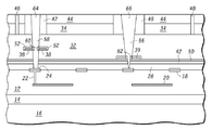
도 1은 본 발명의 일 실시예에 따른, 처리 단계 동안 억셉터 웨이퍼의 일 실시예의 부분 측면도이다. 억셉터 웨이퍼(10)는 상호 접속층(12), 활성층(14), 및 반도체층(16)을 포함할 수 있다. 상호접속층(12)은 상호접속(20) 및 비아(22)를 포함할 수 있다. 랜딩 패드(18)와 같은 랜딩 피처(landing feature)도 상호접속층(12)의 일부로서 형성될 수 있다. 예로써, 코발트 또는 니켈을 갖는 도전성 장벽(24)이 랜딩 패드의 상부에 형성될 수 있다. 비록 도 1은 상호접속층(12), 활성층(14) 및 반도체층(16) 중 각각 하나씩만을 도시하지만, 억셉터 웨이퍼(10)는 그러한 층들을 부가적으로 포함할 수 있다. 또, 도 2에 도시한 바와 같이, 본딩층(26)은 상호접속층(12)의 상부 상에 형성될 수 있다.1 is a partial side view of one embodiment of an acceptor wafer during a processing step, in accordance with an embodiment of the present invention.
도 3을 참고하면, 도너 웨이퍼(30)는 억셉터 웨이퍼(10)와 면대면으로 본딩될(face-to-face bonded) 수 있다. 도너 웨이퍼(30)는 억셉터 웨이퍼(10)와 유사한 층들을 포함할 수 있다. 예로써, 도너 웨이퍼(30)는 상호접속층(32), 활성층(34) 및 반도체층(36)을 포함할 수 있다. 상호접속층(32)은 웨이퍼간 접속 트레이스(38)를, 웨이퍼간 접속 트레이스(38) 내에 형성되는 개구(40)와 함께 포함할 수 있다. 웨이퍼간 접속 트레이스(38)는, 내부에 홀을 갖는 라인(line)처럼 보인다. 웨이퍼간 접속 트레이스(38)는 구리 또는 다른 적절한 도전성 재료를 이용하여 형성될 수 있다. 웨이퍼에 대하여 기술하였지만, 웨이퍼간 접속 트레이스(38)는 웨이퍼 또는 다이 내에서 회로간 트레이스로서 작용할 수 있다. 도너 웨이퍼(30)는 상호접속층(32) 상에 형성되는 에칭 정지층(50)을 가질 수 있다. 본딩층(42)은 에칭 정지층(50) 위에 형성될 수 있다. 도 3은 개별적으로 형성된 본딩층(42) 및 에칭 정지층(50)을 도시하지만, 에칭 정지층은 본딩층(42)의 일부로서 형성될 수 있다. 대안적으로, 본딩층(42)은 에칭 정지층으로서 작용할 수 있다. 게다가, 억셉터 웨이퍼(10)와 도너 웨이퍼(30) 중 어느 한쪽만이 본딩층을 가질 수 있다.Referring to FIG. 3, the donor wafer 30 may be face-to-face bonded with the
또한, 도 3에 도시된 바와 같이, 활성층(34) 및 반도체층(36)은, 예를 들어, 상호접속층(32) 내의 특징(feature)을 찾기 위해 사용될 수 있는 얼라인-키(align-keys)(46, 48)를 포함할 수 있다. 특히, 정렬-키(46, 48)는 본딩된 웨이퍼의 상면인, 도너 웨이퍼(30)의 배면 상의 패턴을 정렬하는데 사용될 수 있다. 비록 도 3은 정렬-키(46, 48)를 도시하지만, 이들은 활성층(34) 및 반도체층(36)을 통해 특징이 보일 수 있는 SOI 웨이퍼 내에 반드시 필요한 것은 아니다. 아이솔레이션 윈도우(47, 49)는, 도너 웨이퍼(30)의 활성 층(34) 및 반도체층(36) 내에 형성될 수 있다. 아이솔레이션 윈도우(47, 49)는, 도 8 및 9에 대하여 추가로 설명되는 바와 같이, 비아 내에 형성되는 도전성 충전 재료를 격리시키는데 사용될 수 있다. 아이솔레이션 윈도우(47, 49)는 산화물과 같은 절연 재료를 포함할 수 있다. 도 3은 상호접속층(32), 활성층(34) 및 반도체층(36)을 각각 하나씩만 도시하고 있지만, 도너 웨이퍼(30)는 그러한 층들을 부가적으로 포함할 수 있다. 또한, 도 3은 억셉터 웨이퍼(10)와 도너 웨이퍼(30)의 면대면 본딩을 도시하고 있지만, 그들은 다른 구성으로도 본딩될 수 있다.In addition, as shown in FIG. 3, the
계속해서 도 3을 참조하면, 장벽층(52)은 웨이퍼간 접속 트레이스(38)의 적어도 상부 및 측면 상에 형성될 수 있다. 장벽층(52)은 탄탈륨(tantalum), 티타늄(titanium), 텅스텐(tungsten) 또는 그들의 합금을 이용하여 형성될 수 있다. 도 3은 다른 상호접속 트레이스(예를 들어, 20) 위에 형성되는 장벽층(52)을 도시하고 있지 않지만, 장벽층(52)은 억셉터 웨이퍼(10)와 도너 웨이퍼(30) 내의 다른 상호접속 트레이스 위에 형성될 수도 있다.With continued reference to FIG. 3,
도 4를 참조하면, 도너 웨이퍼(30)의 반도체층(36)은 기계-화학 또는 화학-기계적 프로세스를 이용하여 박막화되어, 박막화된 반도체층(44)을 형성할 수 있다. 다음으로, 도 5에 도시된 바와 같이, 패터닝된 마스킹층(masking layer)(54)은 박막화된 반도체층(44) 위에 형성될 수 있다. 다음으로, 도 6에 도시된 바와 같이, 에칭과 에칭-정지층(50)을 이용함으로써, 도너 웨이퍼(30) 내의 개구(40)를 통해 연장하는 개구(58)(도 5에 도시됨)가 형성될 수 있다. 비록, 에칭-정지층(50)이 본딩층(42)에 바로 인접한 것으로 도 4에 도시되어 있지만, 에칭 정지층(50)은 도너 웨이퍼(30) 내에서 상이한 위치에 배치될 수 있다. 예를 들어, 상호접속층(32)이 웨이퍼간 접속 트레이스(39)를 가지지 않거나, 웨이퍼간 접속 트레이스(39)가 웨이퍼간 접속 트레이스(38)와 동일한 레벨에 있는 경우, 에칭 정지층(50)은 웨이퍼간 접속 트레이스(38) 바로 아래에 배치될 수 있다. 따라서, 예로서, 에칭 정지층은 웨이퍼의 본딩면에 가장 인접한 상호접속층, 가령, 상호접속층(32)의 웨이퍼간 접속 트레이스 바로 아래에 항상 배치될 수 있다. 필요한 경우에는, 부가적인 개구가 형성될 수 있다. 예를 들어, 도 6은 부가적인 개구(56)를 도시한다. 개구(56, 58)는 웨이퍼간 접속 트레이스(38, 39)의 일부를 노출시킬 수 있다. 특히, 에칭 처리는 장벽층(52)의 일부를 에칭하여, 웨이퍼간 접속 트레이스(38, 39)의 일부를 노출시킬 수 있다.Referring to FIG. 4, the
다음으로, 도 7에 도시된 바와 같이, 장벽(60, 62)은 웨이퍼간 접속 트레이스(38, 39)의 노출된 부분 상에 선택적으로 형성될 수 있다. 일 실시예에선, 장벽(60, 62)은 웨이퍼간 접속 트레이스(39, 39)의 노출된 부분 상에서만 형성될 수 있다. 일 실시예에서, 장벽(60, 62)을 형성하기에 앞서, 웨이퍼간 접속 트레이스(38, 39)의 노출된 부분이 처리될 수 있다. 그러한 처리는 장벽층(52)을 완전히 또는 부분적으로 제거하는 것, 또는 팔라듐(palladium) 또는 플라티늄과 같은 촉매 재료(catalytic materials)로 노출된 부분을 처리하는 것을 포함할 수 있다. 웨이퍼간 접속 트레이스(38, 39)의 노출된 부분은, 노출된 구리와 같은 트레이스 재료로 귀결될 수 있다. 장벽(60, 62)은 가령 노출된 구리 상에 직접적으로 형성될 수 있다. 장벽(60, 62)은 코발트-텅스텐-붕소, 코발트-텅스텐-인, 코발트-몰리브덴-붕소, 코발트-몰리브덴-인, 코발트-레늄-붕소, 코발트-레늄-인, 니켈-텅스텐-붕소, 니켈-텅스텐-인, 니켈-몰리브덴-붕소, 니켈-몰리브덴-인, 니켈-레늄-붕소, 니켈-레늄-인와 같은 코발트 또는 니켈 함유 재료이거나, 다른 적절한 에칭 저항성 재료일 수 있다. 다른 실시예에서도, 웨이퍼간 접속 트레이스(38, 39)의 노출된 부분은, 적어도 구리의 일부가 노출된 상태로, 장벽층(52)의 부분을 가질 수 있다. 웨이퍼간 접속 트레이스(38, 39)의 노출된 부분은 장벽층을 성장시키는데 사용될 수 있다. 웨이퍼간 접속 트레이스(38, 39)의 노출된 부분은, 장벽층을 성장시키기 이전에, 팔라듐 및/또는 플라티늄을 이용하여 먼저 처리될 수 있다.Next, as shown in FIG. 7,
다음으로, 도 8에 도시된 바와 같이, 제2 에칭 처리를 이용하여, 개구(58)가 랜딩 패드(가령, 랜딩 패드(18)과 유사한 랜딩 패드)까지 연장될 수 있다. 유사하게, 제2 에칭 처리의 일부로서, 개구(56)는 다른 랜딩 패드까지 연장될 수 있다. 비록 도 8은 개구(56, 58)가 랜딩 패드까지 연장하는 것으로 도시하고 있지만, 이 개구들은 억셉트 웨이퍼(10)의 임의의 금속 라인까지 연장하여, 적절한 상호접속을 형성할 수 있다.Next, as shown in FIG. 8, using a second etching process, the
도 9를 참조하면, 억셉터 웨이퍼(10) 및 도너 웨이퍼(30)를 전기적으로 상호접속시키기 위해, 도전성 충전 재료(64, 66)를 개구(58, 56) 내에 각각 채울 수 있다. 도전성 충전 재료(64, 66)는 전기도금과 같은 처리를 이용하여 충전될 수 있다. 아이솔레이션 윈도우(47, 49)는 활성층(34) 및 박막화된 반도체층(44)이 도전성 충전 재료로부터 전기적으로 격리되도록 할 수 있다. 도시되지는 않았지만, 도전성 충전 재료(64, 66)을 이 개구들 내에 충전하기 이전에, 라인너 및 시드층(liner and seed layer)을 개구(56, 58) 내에 형성할 수 있다. 이 층들은 화학 기상 증착 또는 물리 기상 증착 처리를 이용하여 형성될 수 있다. 리스퍼터 처리(re-sputter process)와 함께 물리적 기상 증착 처리가 사용되는 경우, 선택적 장벽(60)에 의해 형성되는 소형의 레지(ledge)는 라이너 및 시드층의 우수한 하부 측벽 커버리지로 귀결된다. 또한, 도시되지 않았지만, 가령, 단일화된 집적 회로(singulated integrated circuit)를 생성하는 부가적 단계가 후속하여 수행될 수 있다.Referring to FIG. 9,
전술한 내용에서, 본 발명은 특정 실시예를 참조하여 설명되었다. 그러나, 당업자는 이하 청구범위에 기술된 본 발명의 범주를 벗어남이 없이, 다양한 변경 및 변형이 이루어질 수 있음을 이해할 것이다. 따라서, 명세서 및 도면은 제한적인 의미보다는 설명을 위한 것으로 간주되어야 하며, 그럼한 모든 변형은 본 발명의 범주에 포함되는 것으로 이해되어야 한다.In the foregoing description, the invention has been described with reference to specific embodiments. However, one of ordinary skill in the art appreciates that various changes and modifications can be made without departing from the scope of the present invention as set forth in the claims below. The specification and drawings are, accordingly, to be regarded in an illustrative rather than a restrictive sense, and all such modifications are intended to be included within the scope of present invention.
이익, 다른 이점, 및 문제에 대한 솔루션이 특정 실시예를 차고하여 기술되었다. 그러나, 이익, 이점, 및 문제에 대한 솔루션과, 임의의 이익, 이점 또는 솔루션이 발생하거나 더 공지되게 할 수 있는 임의의 엘리먼트(들)은 청구항의 일부 또는 전부의 필수적, 필연적, 또는 본질적인 특징 또는 엘리먼트로서 해석되어서는 안 된다. 본 명세서에서 사용된 바와 같이, "포함한다", "포함하는", 또는 임의의 그 다른 표현은, 엘리먼트의 리스트를 포함하는 처리, 방법, 물품, 또는 장치가 단지 이 엘리먼트만을 포함하는 것이 아니라 그러한 처리, 방법, 물품, 또는 장치에 명백히 리스트 또는 고착되지 않는 다른 엘리먼트도 포함할 수 있도록, 비배타적인 포함을 커버하기 위해 의도된 것이다.Benefits, other advantages, and solutions to problems have been described with specific embodiments in mind. However, solutions to benefits, advantages, and problems, and any element (s) that can cause any benefit, advantage, or solution to occur or become more known, are essential, necessary, or essential features of some or all of the claims, or It should not be interpreted as an element. As used herein, “comprises”, “comprising”, or any other expressions include, but are not limited to, a process, method, article, or apparatus that includes a list of elements, rather than including only these elements. It is intended to cover non-exclusive inclusion so that it may also include other elements that are not explicitly listed or affixed to the treatment, method, article, or apparatus.
Claims (20)
Applications Claiming Priority (3)
| Application Number | Priority Date | Filing Date | Title |
|---|---|---|---|
| US11/278,042 | 2006-03-30 | ||
| US11/278,042 US7378339B2 (en) | 2006-03-30 | 2006-03-30 | Barrier for use in 3-D integration of circuits |
| PCT/US2007/062538 WO2007130731A2 (en) | 2006-03-30 | 2007-02-22 | Barrier for use in 3-d integration of circuits |
Publications (2)
| Publication Number | Publication Date |
|---|---|
| KR20090004895A KR20090004895A (en) | 2009-01-12 |
| KR101352732B1 true KR101352732B1 (en) | 2014-01-16 |
Family
ID=38559646
Family Applications (1)
| Application Number | Title | Priority Date | Filing Date |
|---|---|---|---|
| KR1020087023823A KR101352732B1 (en) | 2006-03-30 | 2007-02-22 | Barrier for use in 3-d integration of circuits |
Country Status (5)
| Country | Link |
|---|---|
| US (2) | US7378339B2 (en) |
| JP (1) | JP2009532874A (en) |
| KR (1) | KR101352732B1 (en) |
| TW (1) | TWI416691B (en) |
| WO (1) | WO2007130731A2 (en) |
Families Citing this family (8)
| Publication number | Priority date | Publication date | Assignee | Title |
|---|---|---|---|---|
| KR101030299B1 (en) * | 2008-08-08 | 2011-04-20 | 주식회사 동부하이텍 | Semiconductor device and method for manufacturing the device |
| JP5985136B2 (en) | 2009-03-19 | 2016-09-06 | ソニー株式会社 | SEMICONDUCTOR DEVICE, ITS MANUFACTURING METHOD, AND ELECTRONIC DEVICE |
| US9406561B2 (en) * | 2009-04-20 | 2016-08-02 | International Business Machines Corporation | Three dimensional integrated circuit integration using dielectric bonding first and through via formation last |
| US9293366B2 (en) | 2010-04-28 | 2016-03-22 | Taiwan Semiconductor Manufacturing Company, Ltd. | Through-substrate vias with improved connections |
| JP5577965B2 (en) * | 2010-09-02 | 2014-08-27 | ソニー株式会社 | SEMICONDUCTOR DEVICE, ITS MANUFACTURING METHOD, AND ELECTRONIC DEVICE |
| US9142581B2 (en) | 2012-11-05 | 2015-09-22 | Omnivision Technologies, Inc. | Die seal ring for integrated circuit system with stacked device wafers |
| US10367031B2 (en) * | 2016-09-13 | 2019-07-30 | Imec Vzw | Sequential integration process |
| JP6905040B2 (en) * | 2018-08-08 | 2021-07-21 | キヤノン株式会社 | Semiconductor device manufacturing method |
Citations (3)
| Publication number | Priority date | Publication date | Assignee | Title |
|---|---|---|---|---|
| KR20020010974A (en) * | 2000-07-31 | 2002-02-07 | 박종섭 | Method for forming FeRAM capable of reducing steps of metal wire forming |
| WO2005043584A2 (en) | 2003-10-21 | 2005-05-12 | Ziptronix, Inc. | Single mask via method and device |
| KR20050105223A (en) * | 2003-02-18 | 2005-11-03 | 유니티브 일렉트로닉스 아이엔씨. | Methods for selectively bumping integrated circuit substrates and related structures |
Family Cites Families (11)
| Publication number | Priority date | Publication date | Assignee | Title |
|---|---|---|---|---|
| DE4433845A1 (en) * | 1994-09-22 | 1996-03-28 | Fraunhofer Ges Forschung | Method of manufacturing a three-dimensional integrated circuit |
| US5756395A (en) * | 1995-08-18 | 1998-05-26 | Lsi Logic Corporation | Process for forming metal interconnect structures for use with integrated circuit devices to form integrated circuit structures |
| US6902987B1 (en) * | 2000-02-16 | 2005-06-07 | Ziptronix, Inc. | Method for low temperature bonding and bonded structure |
| JP2001291720A (en) * | 2000-04-05 | 2001-10-19 | Hitachi Ltd | Semiconductor integrated circuit device and its manufacturing method |
| US20030143853A1 (en) * | 2002-01-31 | 2003-07-31 | Celii Francis G. | FeRAM capacitor stack etch |
| US6656748B2 (en) * | 2002-01-31 | 2003-12-02 | Texas Instruments Incorporated | FeRAM capacitor post stack etch clean/repair |
| US6642081B1 (en) * | 2002-04-11 | 2003-11-04 | Robert Patti | Interlocking conductor method for bonding wafers to produce stacked integrated circuits |
| US20040262772A1 (en) * | 2003-06-30 | 2004-12-30 | Shriram Ramanathan | Methods for bonding wafers using a metal interlayer |
| US6924232B2 (en) * | 2003-08-27 | 2005-08-02 | Freescale Semiconductor, Inc. | Semiconductor process and composition for forming a barrier material overlying copper |
| EP1553625B1 (en) * | 2004-01-12 | 2014-05-07 | Infineon Technologies AG | Method for fabrication of a contact structure |
| US7485968B2 (en) * | 2005-08-11 | 2009-02-03 | Ziptronix, Inc. | 3D IC method and device |
-
2006
- 2006-03-30 US US11/278,042 patent/US7378339B2/en active Active
-
2007
- 2007-02-22 JP JP2009503112A patent/JP2009532874A/en active Pending
- 2007-02-22 WO PCT/US2007/062538 patent/WO2007130731A2/en active Application Filing
- 2007-02-22 KR KR1020087023823A patent/KR101352732B1/en active IP Right Grant
- 2007-03-16 TW TW096109128A patent/TWI416691B/en active
-
2008
- 2008-04-25 US US12/110,009 patent/US20080197497A1/en not_active Abandoned
Patent Citations (3)
| Publication number | Priority date | Publication date | Assignee | Title |
|---|---|---|---|---|
| KR20020010974A (en) * | 2000-07-31 | 2002-02-07 | 박종섭 | Method for forming FeRAM capable of reducing steps of metal wire forming |
| KR20050105223A (en) * | 2003-02-18 | 2005-11-03 | 유니티브 일렉트로닉스 아이엔씨. | Methods for selectively bumping integrated circuit substrates and related structures |
| WO2005043584A2 (en) | 2003-10-21 | 2005-05-12 | Ziptronix, Inc. | Single mask via method and device |
Also Published As
| Publication number | Publication date |
|---|---|
| WO2007130731A3 (en) | 2008-09-18 |
| TWI416691B (en) | 2013-11-21 |
| JP2009532874A (en) | 2009-09-10 |
| US20080197497A1 (en) | 2008-08-21 |
| TW200742022A (en) | 2007-11-01 |
| KR20090004895A (en) | 2009-01-12 |
| US7378339B2 (en) | 2008-05-27 |
| US20070231950A1 (en) | 2007-10-04 |
| WO2007130731A2 (en) | 2007-11-15 |
Similar Documents
| Publication | Publication Date | Title |
|---|---|---|
| KR101352732B1 (en) | Barrier for use in 3-d integration of circuits | |
| US9978708B2 (en) | Wafer backside interconnect structure connected to TSVs | |
| JP5366833B2 (en) | Conductive via formation using electroplating | |
| KR101137624B1 (en) | via structure and via etching process of forming the same | |
| CN101740484B (en) | Method of forming through-silicon vias | |
| US9449906B2 (en) | Devices, systems, and methods related to forming through-substrate vias with sacrificial plugs | |
| US7541677B2 (en) | Semiconductor device comprising through-electrode interconnect | |
| US20160133518A1 (en) | Semiconductor device and fabricating method thereof | |
| US20120083116A1 (en) | Cost-Effective TSV Formation | |
| KR20100100629A (en) | Three-dimensional system-in-package architecture | |
| TWI447850B (en) | Through-substrate via and fabrication method thereof | |
| KR101427015B1 (en) | Vias and conductive routing layers in semiconductor substrates | |
| US9401323B1 (en) | Protected through semiconductor via (TSV) | |
| KR20100037015A (en) | Methods of forming electrical interconnects using electroless plating techniques that inhibit void formation | |
| CN113284841A (en) | Method for forming three-dimensional semiconductor structure | |
| US10515852B2 (en) | Structure and formation method of semiconductor device with resistive element | |
| KR100691051B1 (en) | Dual damascene bond pad structure for lowering stress and allowing circuitry under pads and a process to form the same | |
| TW201351587A (en) | Through-silicon via and fabrication method thereof | |
| TWI546866B (en) | Semiconductor device and fabricating method thereof | |
| US20220165618A1 (en) | 3d bonded semiconductor device and method of forming the same | |
| JP2000195951A (en) | Manufacture of double damask structure in integrated circuit having multiple level mutually connected structures | |
| TW201324726A (en) | Through silicon via and method of manufacturing the same |
Legal Events
| Date | Code | Title | Description |
|---|---|---|---|
| A201 | Request for examination | ||
| E902 | Notification of reason for refusal | ||
| E701 | Decision to grant or registration of patent right | ||
| GRNT | Written decision to grant | ||
| FPAY | Annual fee payment |
Payment date: 20170102 Year of fee payment: 4 |
|
| FPAY | Annual fee payment |
Payment date: 20190102 Year of fee payment: 6 |
|
| FPAY | Annual fee payment |
Payment date: 20200102 Year of fee payment: 7 |