KR101324544B1 - Patterning substrates employing multiple chucks - Google Patents
Patterning substrates employing multiple chucks Download PDFInfo
- Publication number
- KR101324544B1 KR101324544B1 KR1020087016345A KR20087016345A KR101324544B1 KR 101324544 B1 KR101324544 B1 KR 101324544B1 KR 1020087016345 A KR1020087016345 A KR 1020087016345A KR 20087016345 A KR20087016345 A KR 20087016345A KR 101324544 B1 KR101324544 B1 KR 101324544B1
- Authority
- KR
- South Korea
- Prior art keywords
- substrate
- chuck
- nanoimprint
- mold assembly
- substrates
- Prior art date
Links
Images


Classifications
-
- G—PHYSICS
- G03—PHOTOGRAPHY; CINEMATOGRAPHY; ANALOGOUS TECHNIQUES USING WAVES OTHER THAN OPTICAL WAVES; ELECTROGRAPHY; HOLOGRAPHY
- G03F—PHOTOMECHANICAL PRODUCTION OF TEXTURED OR PATTERNED SURFACES, e.g. FOR PRINTING, FOR PROCESSING OF SEMICONDUCTOR DEVICES; MATERIALS THEREFOR; ORIGINALS THEREFOR; APPARATUS SPECIALLY ADAPTED THEREFOR
- G03F7/00—Photomechanical, e.g. photolithographic, production of textured or patterned surfaces, e.g. printing surfaces; Materials therefor, e.g. comprising photoresists; Apparatus specially adapted therefor
- G03F7/0002—Lithographic processes using patterning methods other than those involving the exposure to radiation, e.g. by stamping
-
- B—PERFORMING OPERATIONS; TRANSPORTING
- B29—WORKING OF PLASTICS; WORKING OF SUBSTANCES IN A PLASTIC STATE IN GENERAL
- B29C—SHAPING OR JOINING OF PLASTICS; SHAPING OF MATERIAL IN A PLASTIC STATE, NOT OTHERWISE PROVIDED FOR; AFTER-TREATMENT OF THE SHAPED PRODUCTS, e.g. REPAIRING
- B29C59/00—Surface shaping of articles, e.g. embossing; Apparatus therefor
- B29C59/02—Surface shaping of articles, e.g. embossing; Apparatus therefor by mechanical means, e.g. pressing
- B29C59/022—Surface shaping of articles, e.g. embossing; Apparatus therefor by mechanical means, e.g. pressing characterised by the disposition or the configuration, e.g. dimensions, of the embossments or the shaping tools therefor
-
- B—PERFORMING OPERATIONS; TRANSPORTING
- B82—NANOTECHNOLOGY
- B82Y—SPECIFIC USES OR APPLICATIONS OF NANOSTRUCTURES; MEASUREMENT OR ANALYSIS OF NANOSTRUCTURES; MANUFACTURE OR TREATMENT OF NANOSTRUCTURES
- B82Y10/00—Nanotechnology for information processing, storage or transmission, e.g. quantum computing or single electron logic
-
- B—PERFORMING OPERATIONS; TRANSPORTING
- B82—NANOTECHNOLOGY
- B82Y—SPECIFIC USES OR APPLICATIONS OF NANOSTRUCTURES; MEASUREMENT OR ANALYSIS OF NANOSTRUCTURES; MANUFACTURE OR TREATMENT OF NANOSTRUCTURES
- B82Y40/00—Manufacture or treatment of nanostructures
-
- H—ELECTRICITY
- H01—ELECTRIC ELEMENTS
- H01L—SEMICONDUCTOR DEVICES NOT COVERED BY CLASS H10
- H01L21/00—Processes or apparatus adapted for the manufacture or treatment of semiconductor or solid state devices or of parts thereof
- H01L21/67—Apparatus specially adapted for handling semiconductor or electric solid state devices during manufacture or treatment thereof; Apparatus specially adapted for handling wafers during manufacture or treatment of semiconductor or electric solid state devices or components ; Apparatus not specifically provided for elsewhere
- H01L21/683—Apparatus specially adapted for handling semiconductor or electric solid state devices during manufacture or treatment thereof; Apparatus specially adapted for handling wafers during manufacture or treatment of semiconductor or electric solid state devices or components ; Apparatus not specifically provided for elsewhere for supporting or gripping
- H01L21/687—Apparatus specially adapted for handling semiconductor or electric solid state devices during manufacture or treatment thereof; Apparatus specially adapted for handling wafers during manufacture or treatment of semiconductor or electric solid state devices or components ; Apparatus not specifically provided for elsewhere for supporting or gripping using mechanical means, e.g. chucks, clamps or pinches
-
- Y—GENERAL TAGGING OF NEW TECHNOLOGICAL DEVELOPMENTS; GENERAL TAGGING OF CROSS-SECTIONAL TECHNOLOGIES SPANNING OVER SEVERAL SECTIONS OF THE IPC; TECHNICAL SUBJECTS COVERED BY FORMER USPC CROSS-REFERENCE ART COLLECTIONS [XRACs] AND DIGESTS
- Y10—TECHNICAL SUBJECTS COVERED BY FORMER USPC
- Y10S—TECHNICAL SUBJECTS COVERED BY FORMER USPC CROSS-REFERENCE ART COLLECTIONS [XRACs] AND DIGESTS
- Y10S977/00—Nanotechnology
- Y10S977/84—Manufacture, treatment, or detection of nanostructure
- Y10S977/887—Nanoimprint lithography, i.e. nanostamp
Abstract
본 발명은 나노임프린트 리소그래피 시스템에서 제 1 및 제 2 기판을 패턴화하기 위한 방법에 관한 것으로서, 상기 방법은 특히 제 1 기판 척 위에 제 1 기판을 위치시키는 단계; 제 1 기판 위에 나노임프린트 재료를 위치시키는 단계; 제 1 기판과 나노임프린트 몰드 조립체 사이에 공간적 관계를 획득하고, 나노임프린트 몰드 조립체를 사용하여 제 1 기판 위의 나노임프린트 재료에 패턴을 임프린트하는 동시에, 제 2 기판 척 위에 제 2 기판을 위치시키는 단계; 제 1 기판 위의 나노임프린트 재료로부터 나노임프린트 몰드 조립체를 분리하는 단계; 제 2 기판 위에 나노임프린트 재료를 위치시키는 단계; 제 1 기판 척으로부터 제 1 기판을 제거하는 동시에, 제 2 기판과 나노임프린트 몰드 조립체 사이에 공간적 관계를 획득하고, 나노임프린트 몰드 조립체를 사용하여 제 2 기판 위의 나노임프린트 재료에 패턴을 임프린트하는 단계; 및 제 2 기판 위의 나노임프린트 재료로부터 나노임프린트 몰드 조립체를 분리하는 단계를 포함하며, 제 1 및 제 2 기판에는 실질적으로 동일한 공정 조건들이 행해진다.

나노임프린트, 몰드, 리소그래피, 기판, 패턴화
The present invention relates to a method for patterning a first and a second substrate in a nanoimprint lithography system, the method comprising in particular positioning a first substrate over a first substrate chuck; Positioning the nanoimprint material on the first substrate; Obtaining a spatial relationship between the first substrate and the nanoimprint mold assembly, imprinting a pattern in the nanoimprint material on the first substrate using the nanoimprint mold assembly, and simultaneously positioning the second substrate over the second substrate chuck ; Separating the nanoimprint mold assembly from the nanoimprint material on the first substrate; Positioning the nanoimprint material over the second substrate; Simultaneously removing the first substrate from the first substrate chuck, obtaining a spatial relationship between the second substrate and the nanoimprint mold assembly, and imprinting the pattern on the nanoimprint material on the second substrate using the nanoimprint mold assembly. ; And separating the nanoimprint mold assembly from the nanoimprint material on the second substrate, wherein substantially the same process conditions are applied to the first and second substrates.
Nanoimprint, Mold, Lithography, Substrate, Patterned
Description
관련 출원에 대한 상호 참조Cross-reference to related application
본 출원은 2006년 1월 20일자 제출된 미국 가 출원 제60/760,738호, 제목 "멀티-기판 척을 사용한 나노-임프린팅 장치 및 방법"과 2006년 9월 27일자 제출된 미국 가 출원 제60/827,125호, 제목 "멀티-기판 척을 사용한 나노-임프린팅 장치 및 방법"과 2006년 4월 3일자 제출된 미국 가 출원 제60/788,808호, 제목 "잔류 층 두께 측정 및 보정"에 대한 우선권을 주장하며, 본 출원은 2005년 12월 8일자 제출된 미국 가 출원 제60/748,430호, 제목 "양면 임프린팅을 위한 임프린팅, 정렬 및 분리 장치 및 방법"에 대한 우선권을 주장하는 2006년 11월 30일자 제출된 미국 특허출원 제11/565,350호, 제목 "기판의 양면 패턴화 방법 및 시스템"의 연속되는 출원으로서, 상기 언급된 출원은 모두 참고자료로서 본원에 포함된다.This application is directed to US Provisional Application No. 60 / 760,738, filed Jan. 20, 2006, entitled “Nano-imprinting Apparatus and Method Using Multi-Substrate Chuck,” and US Provisional Application No. 60, filed September 27, 2006. / 827,125, title "Nano-imprinting apparatus and method using multi-substrate chucks" and US Provisional Application No. 60 / 788,808, filed April 3, 2006, entitled "Residual Layer Thickness Measurement and Calibration" This application claims priority to US Provisional Application No. 60 / 748,430, entitled "Imprinting, Alignment and Separation Device for Two-Sided Imprinting," filed December 8, 2005. As a continual application of US patent application Ser. No. 11 / 565,350, filed on May 30, entitled "Methods and Systems for Duplex Patterning of Substrates," all of which are incorporated herein by reference.
배경기술Background technology
나노-제작은, 예를 들어 나노미터 이하 정도의 피쳐(feature)를 갖는, 아주 소형 구조의 제작을 포함한다. 나노-제작이 상당한 충격을 주었던 한 분야가 직접회로의 프로세싱이다. 기판 위에 형성되는 단위 면적당 회로 수가 증가하면서 반도체 프로세싱 산업이 더 높은 생산율을 위해 노력을 계속함에 따라, 나노-제작은 더욱 더 중요하게 되고 있다. 나노-제작은 더 큰 공정 제어를 제공하는 동시에 형성된 구조의 최소 피쳐 치수를 더욱 감소시킬 수 있다. 나노-제작이 사용되고 있는 다른 개발 분야는 생물공학, 광학기술, 기계 시스템 등을 포함한다.Nano-fabrication involves the fabrication of very compact structures, for example with features on the order of nanometers or less. One area where nano-fabrication has had a significant impact is the processing of integrated circuits. Nano-fabrication is becoming increasingly important as the semiconductor processing industry continues to strive for higher production rates as the number of circuits per unit area formed on a substrate increases. Nano-fabrication can further reduce the minimum feature dimensions of the formed structure while providing greater process control. Other developments where nano-fabrication is being used include biotechnology, optical technology, mechanical systems, and the like.
전형적인 나노-제작 기술을 보통 임프린트 리소그래피(imprint lithography)라고 한다. 전형적인 임프린트 리소그래피 공정은 미국특허출원 제10/264,960호로서 제출된 미국특허출원 공보 제2004/0065976호, 제목 "최소의 치수 변화성을 갖는 피쳐를 복사하기 위하여 기판 위에 피처를 배열하기 위한 방법 및 몰드"; 미국특허출원 제10/264,926호로서 제출된 미국특허출원 공보 제2004/0065252호, 제목 "계측 표준의 제작을 용이하게 하기 위하여 기판 위에 층을 형성하는 방법"; 및 미국특허 제6,936,194호, 제목 "임프린트 리소그래피 공정을 위한 기능적 패턴화 재료" 등의 많은 공보에 설명되어 있으며, 이들은 모두 본 발명의 양수인에게 양도된 것이다.Typical nano-fabrication techniques are commonly referred to as imprint lithography. A typical imprint lithography process is US Patent Application Publication No. 2004/0065976, entitled US Patent Application No. 10 / 264,960, entitled “Method and Mold for Arranging Features on a Substrate to Copy Features with Minimum Dimensional Variability”. "; US Patent Application Publication No. 2004/0065252, filed as US patent application Ser. No. 10 / 264,926, entitled “Method for Forming a Layer on a Substrate to Facilitate the Fabrication of Measurement Standards”; And US Pat. No. 6,936,194, entitled "Function Patterning Material for Imprint Lithography Processes", and the like, all of which are assigned to the assignee of the present invention.
전술한 미국특허출원 공보 및 미국특허에 각각 개시된 임프린트 리소그래피 기술은 중합성 층에 릴리프 패턴(relief pattern)을 형성하는 것과 이 릴리프 패턴에 상응하는 패턴을 아래쪽 기판에 전사하는 것을 포함한다. 모션 스테이지 위에 기판이 위치될 수 있으며, 이로써 바람직한 위치를 획득하여 패턴화를 용이하게 할 수 있다. 이를 위하여, 기판으로부터 이격되어 위치하는 템플릿이 사용되며, 템플릿과 기판 사이에는 형태화가 가능한 액체가 존재한다. 이 액체는 고화되어, 액체와 접촉하고 있는 템플릿의 표면 모양과 일치하는 패턴이 기록된 고화층을 형성한다. 다음에, 템플릿이 고화층으로부터 분리되어 템플릿과 기판이 서로 떨어진다. 다음에, 고화층에 있는 패턴에 상응하는 릴리프 이미지(relief image)를 기판으로 전사하기 위한 공정이 기판과 고화층에 행해진다. The imprint lithography techniques disclosed in the above-mentioned U.S. Patent Application Publications and U.S. Patents, respectively, include forming a relief pattern in the polymerizable layer and transferring a pattern corresponding to the relief pattern to the lower substrate. The substrate can be positioned above the motion stage, thereby obtaining the desired position to facilitate patterning. To this end, a template is used spaced apart from the substrate, and there is a formable liquid between the template and the substrate. This liquid solidifies to form a solidified layer on which a pattern is recorded that matches the surface shape of the template in contact with the liquid. Next, the template is separated from the solidified layer so that the template and the substrate are separated from each other. Next, a process for transferring a relief image corresponding to the pattern in the solidified layer to the substrate is performed on the substrate and the solidified layer.
도 1은 선행기술에 따른 몰드와 기판이 서로 이격되어 위치하는 리소그래피 시스템의 단순화한 측면도이다.1 is a simplified side view of a lithographic system in which a mold and a substrate are spaced apart from one another according to the prior art.
도 2는 도 1에 도시된 로봇 조종 기판의 하향도이다.FIG. 2 is a bottom view of the robot control board shown in FIG. 1.
도 3은 도 1에 도시된 기판의 패턴화 방법을 나타내는 순서도이다.FIG. 3 is a flowchart illustrating a patterning method of the substrate illustrated in FIG. 1.
도 4는 제 1 기판 척 및 제 2 기판 척에 각각 위치된 제 1 기판 및 제 2 기판과 몰드가 서로 이격되어 위치하는 리소그래피 시스템의 단순화한 측면도이다.4 is a simplified side view of a lithographic system in which a first substrate and a second substrate and a mold, respectively positioned on the first and second substrate chucks, are spaced apart from each other.
도 5는 도 4에 도시된 제 1 기판 및 제 2 기판의 패턴화 방법을 나타내는 순서도이다.FIG. 5 is a flowchart illustrating a patterning method of the first substrate and the second substrate illustrated in FIG. 4.
도 6은 도 4에 도시된 리소그래피 시스템의 단순화한 측면도로서, 로봇이 제 1 기판을 제 1 기판 척 위에 위치시키고 있다.FIG. 6 is a simplified side view of the lithographic system shown in FIG. 4, with a robot placing a first substrate over a first substrate chuck.
도 7은 도 6에 도시된 리소그래피 시스템의 단순화한 측면도로서, 제 1 기판 위에 재료가 위치한다.FIG. 7 is a simplified side view of the lithographic system shown in FIG. 6, with material located over a first substrate.
도 8은 도 7에 도시된 리소그래피 시스템의 단순화한 측면도로서, 몰드가 제 1 기판 위에 위치된 재료와 접촉하고 있고, 로봇이 제 2 기판을 제 2 기판 척 위에 위치시키고 있다.FIG. 8 is a simplified side view of the lithographic system shown in FIG. 7, in which a mold is in contact with a material located on a first substrate, and a robot is placing a second substrate on a second substrate chuck.
도 9는 도 8에 도시된 리소그래피 시스템의 단순화한 측면도로서, 몰드가 제 1 기판 위의 재료로부터 분리된다.FIG. 9 is a simplified side view of the lithographic system shown in FIG. 8, in which the mold is separated from the material on the first substrate.
도 10은 도 9에 도시된 리소그래피 시스템의 단순화한 측면도로서, 제 2 기 판 위에 재료가 위치한다.FIG. 10 is a simplified side view of the lithographic system shown in FIG. 9 in which material is located on a second substrate.
도 11은 도 10에 도시된 리소그래피 시스템의 단순화한 측면도로서, 몰드가 제 2 기판 위에 위치된 재료와 접촉하고 있고, 로봇이 제 1 기판 척으로부터 제 1 기판을 제거하고 있다.FIG. 11 is a simplified side view of the lithographic system shown in FIG. 10, in which a mold is in contact with a material located over a second substrate, and the robot is removing the first substrate from the first substrate chuck.
도 12는 도 11에 도시된 리소그래피 시스템의 단순화한 측면도로서, 몰드가 제 2 기판 위의 재료로부터 분리되고, 제 3 기판이 제 3 기판 척 위에 위치된다.FIG. 12 is a simplified side view of the lithographic system shown in FIG. 11, wherein the mold is separated from the material on the second substrate and the third substrate is positioned over the third substrate chuck.
도 13은 도 12에 도시된 리소그래피 시스템의 단순화한 측면도로서, 제 3 기판 위에 재료가 위치한다.FIG. 13 is a simplified side view of the lithographic system shown in FIG. 12 in which material is located on a third substrate.
도 14는 도 13에 도시된 리소그래피 시스템의 단순화한 측면도로서, 몰드가 제 3 기판 위에 위치된 재료와 접촉하고 있고, 로봇이 제 2 기판 척으로부터 제 2 기판을 제거하고 있다.FIG. 14 is a simplified side view of the lithographic system shown in FIG. 13, in which a mold is in contact with a material located over a third substrate, and the robot is removing the second substrate from the second substrate chuck.
도 15는 도 4에 도시된 제 1 및 제 2 기판의 제 1 및 제 2 면의 패턴화 방법을 나타내는 순서도이다.FIG. 15 is a flowchart illustrating a patterning method of first and second surfaces of the first and second substrates illustrated in FIG. 4.
도 16은 도 10에 도시된 리소그래피 시스템의 단순화한 측면도로서, 몰드가 제 2 기판 위에 위치된 재료와 접촉하고 있고, 로봇이 몰드에 대하여 제 1 기판을 뒤집고 있다.FIG. 16 is a simplified side view of the lithographic system shown in FIG. 10, in which a mold is in contact with a material located over a second substrate and the robot is flipping the first substrate against the mold.
도 17은 도 16에 도시된 리소그래피 시스템의 단순화한 측면도로서, 몰드가 제 2 기판 위의 재료로부터 분리되고, 제 1 기판이 제 2 위치에 있는 제 1 기판 척 위에 위치된다.FIG. 17 is a simplified side view of the lithographic system shown in FIG. 16, in which the mold is separated from the material on the second substrate and the first substrate is positioned over the first substrate chuck in a second position.
도 18은 도 17에 도시된 리소그래피 시스템의 단순화한 측면도로서, 제 1 기 판 위에 재료가 위치한다.FIG. 18 is a simplified side view of the lithographic system shown in FIG. 17, with material placed over a first substrate.
도 19는 도 18에 도시된 리소그래피 시스템의 단순화한 측면도로서, 몰드가 제 1 기판 위에 위치된 재료와 접촉하고 있고, 로봇이 몰드에 대하여 제 2 기판을 뒤집고 있다.FIG. 19 is a simplified side view of the lithographic system shown in FIG. 18, in which the mold is in contact with a material located over the first substrate and the robot is flipping the second substrate over the mold.
도 20은 도 19에 도시된 리소그래피 시스템의 단순화한 측면도로서, 몰드가 제 1 기판 위의 재료로부터 분리되고, 제 2 기판이 제 2 위치에 있는 제 2 기판 척 위에 위치된다.FIG. 20 is a simplified side view of the lithographic system shown in FIG. 19, in which the mold is separated from the material on the first substrate and the second substrate is positioned over the second substrate chuck in the second position.
도 21은 도 20에 도시된 리소그래피 시스템의 단순화한 측면도로서, 제 2 기판 위에 재료가 위치한다.FIG. 21 is a simplified side view of the lithographic system shown in FIG. 20, wherein material is placed over a second substrate.
도 22는 도 21에 도시된 리소그래피 시스템의 단순화한 측면도로서, 몰드가 제 2 기판 위에 위치된 재료와 접촉하고 있고, 로봇이 제 1 기판 척으로부터 제 1 기판을 제거하고 있다.FIG. 22 is a simplified side view of the lithographic system shown in FIG. 21, in which a mold is in contact with a material located over a second substrate, and the robot is removing the first substrate from the first substrate chuck.
도 23은 도 22에 도시된 리소그래피 시스템의 단순화한 측면도로서, 몰드가 제 2 기판 위의 재료로부터 분리되고, 제 3 기판이 제 1 기판 척 위에 위치된다.FIG. 23 is a simplified side view of the lithographic system shown in FIG. 22, in which the mold is separated from the material on the second substrate and the third substrate is positioned over the first substrate chuck.
도 24는 도 23에 도시된 리소그래피 시스템의 단순화한 측면도로서, 제 3 기판 위에 재료가 위치한다.FIG. 24 is a simplified side view of the lithographic system shown in FIG. 23, wherein material is placed over a third substrate.
도 25는 도 24에 도시된 리소그래피 시스템의 단순화한 측면도로서, 몰드가 제 3 기판 위에 위치된 재료와 접촉하고 있고, 로봇이 제 2 기판 척으로부터 제 2 기판을 제거하고 있다.FIG. 25 is a simplified side view of the lithographic system shown in FIG. 24, in which a mold is in contact with a material located over a third substrate, and the robot is removing the second substrate from the second substrate chuck.
도 26은 도 4에 도시된 리소그래피 시스템의 단순화한 하향도로서, 리소그래 피 시스템이 제 1 및 제 2 모듈을 가지며, 각 모듈은 제 1 및 제 2 기판 척을 포함하고, 제 1 기판들이 패턴화되고 있다.FIG. 26 is a simplified top down view of the lithographic system shown in FIG. 4, wherein the lithography system has first and second modules, each module comprising first and second substrate chucks, the first substrates being patterned It's getting mad.
도 27은 도 4에 도시된 리소그래피 시스템의 단순화한 하향도로서, 리소그래피 시스템이 제 1 및 제 2 모듈을 가지며, 각 모듈은 제 1 및 제 2 기판 척을 포함하고, 제 2 기판들이 패턴화되고 있다.FIG. 27 is a simplified top down view of the lithographic system shown in FIG. 4, wherein the lithographic system has first and second modules, each module comprising first and second substrate chucks, the second substrates being patterned and have.
도 28은 기판이 위에 위치되어 있는 기판 척의 단순화한 측면도이다.28 is a simplified side view of a substrate chuck with a substrate positioned thereon.
도 29는 도 4에 도시된 기판 부분의 분해조립도이다.FIG. 29 is an exploded view of the substrate portion shown in FIG. 4.
도 30은 도 4에 도시된 기판 척 부분의 분해조립도이다.30 is an exploded view of the substrate chuck shown in FIG. 4.
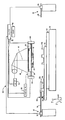
도 1에 관해, 제 1 기판(12a) 위에 릴리프 패턴을 형성하기 위한 시스템(10)이 도시된다. 제 1 기판(12a)은 제 1 기판 척(14a)과 결합될 수 있다. 제 1 기판 척(14a)은, 제한은 아니지만, 진공, 핀-타입, 홈-타입, 또는 전자기를 포함하는 어떤 척일 수 있으며, 본원에 참고자료로 포함되는 미국특허 제6,873,087호, 제목 "임프린트 리소그래피 공정을 위한 고-정밀 배향 정렬 및 갭 제어 단계들"에 설명된 것을 참조한다. 제 1 기판 척(14a)은 제 1 기판(12a)에 면하는 공동(16a)을 포함할 수 있다. 제 1 기판(12a) 및 제 1 기판 척(14a)은 제 1 스테이지(18) 및 제 2 스테이지(20) 위에 지지될 수 있고, 제 1 스테이지(18)는 제 1 기판 척(14a)과 제 2 스테이지(20) 사이에 위치된다. 또한, 제 1 및 제 2 스테이지(18 및 20)는 베이스(22) 위에 위치될 수 있다. 제 1 스테이지(18)는 제 1 축을 따른 동작을 제공할 수 있고, 제 2 스테이지(20)는 제 2 축을 따른 동작을 제공할 수 있으며, 제 2 축은 제 1 축과 직교하는데, 즉 제 1 및 제 2 축은 x 및 y 축이 된다. 본 발명에서 전형적인 스테이지는 Newport Corporation(캘리포니아 어빈)에서 나오는 품목번호 XM200L350 및 XM200S50를 이용할 수 있다. 제 1 기판(12a)은 통로(24a)를 더 포함할 수 있다. 그러나, 다른 구체예에서, 제 1 기판(12a)에는 통로(24a)가 실질적으로 존재하지 않을 수도 있다.1, a
템플릿(26)이 제 1 기판(12a)으로부터 이격되어 위치하며, 템플릿(26)으로부터 패턴화 표면(30)을 갖는 메사(28)가 제 1 기판(12a) 쪽으로 나와 있다. 또한, 메사(28)는 몰드(28)라고 할 수도 있다. 또한, 메사(28)는 나노임프린트 몰드(28)라고 할 수도 있다. 다른 구체예에서, 템플릿(26)에는 몰드(28)가 실질적으로 존재하지 않을 수도 있다. 템플릿(26) 및/또는 몰드(28)는, 제한은 아니지만, 용융-실리카, 석영, 규소, 유기 폴리머, 실록산 폴리머, 붕규산 유리, 플루오로카본 폴리머, 금속, 및 고강도 사파이어를 포함하는 재료로부터 형성될 수 있다. 나타낸 대로, 패턴화 표면(30)은 복수 개의 이격되어 위치하는 홈(32)과 돌출부(34)에 의해 한정된 피쳐를 포함한다. 그러나, 다른 구체예에서, 패턴화 표면(30)은 실질적으로 매끄럽고 및/또는 평면일 수 있다. 패턴화 표면(30)은 제 1 기판(12a) 위에 형성될 패턴의 기초를 형성하는 원 패턴을 한정할 수 있으며, 이것은 아래 더 설명된다. 템플릿(26)은 템플릿 척(36)과 결합될 수 있으며, 템플릿 척(36)은, 제한은 아니지만, 진공, 핀-타입, 홈-타입, 또는 전자기를 포함하는 어떤 척이며, 본원에 참고자료로 포함되는 미국특허 제6,873,087호, 제목 "임프린트 리소그래피 공정을 위한 고-정밀 배향 정렬 및 갭 제어 단계들"에 설명된 것을 참조한다. 또한, 템플릿 척(36)은 템플릿(26)과 몰드(28)의 움직임을 용이하게 하기 위해서 임프린트 헤드(38)에 결합될 수 있다. 예로서, 임프린트 헤드(38)는 3-보이스 코일 작동기(도시하지 않음) 또는 다른 선형 작동기(도시하지 않음)에 의해 제어되는 3 자유도(2가지 경사 동작과 1가지 병진 동작) 스테이지일 수 있다.The
시스템(10)은 제 1 유체 디스펜서(40a)를 더 포함한다. 제 1 유체 디스펜서 (40a)는 제 1 기판(12a)과 유체 연통함으로써 그 위에 폴리머 재료(42a)를 위치시킬 수 있으며, 이것은 아래 더 설명된다. 나타낸 대로, 제 1 유체 디스펜서(40a)는 템플릿 척(36)과 결합될 수 있다; 그러나, 다른 구체예에서, 제 1 유체 디스펜서(40a)는 시스템(10)의 어떤 부품과도, 즉 템플릿(26) 또는 임프린트 헤드(38)와도 결합될 수 있다. 또한, 시스템(10)은 다수의 유체 디스펜서를 포함할 수 있으며, 제 1 유체 디스펜서(40a)는 그 안에 복수 개의 디스펜싱 장치를 포함할 수 있다. 본 발명에서 전형적인 유체 디스펜서는 Xaar Corporation(영국 캠브릿지)에서 나오는 품목명 Leopard를 이용할 수 있다.
폴리머 재료(42a)는 어떤 공지의 기술, 예를 들어 드롭 디스펜스, 스핀-코팅, 딥-코팅, 박막 부착, 두꺼운 막 부착 기술 등을 이용하여 제 1 기판(12a) 위에 위치될 수 있다. 나타낸 대로, 폴리머 재료(42a)는 복수 개의 이격되어 위치하는 점적(44a)으로서 제 1 기판(12a) 위에 위치될 수 있다. 예로서, 점적(44a)들의 각 점적은 약 6 피코-리터의 단위 부피를 가질 수 있다. 폴리머 재료(42a)는 전형적으로 몰드(28)와 제 1 기판(12a) 사이에 바람직한 부피가 한정되기 전에 제 1 기판 (12a) 위에 위치될 수 있으며, 이것은 아래 더 설명된다. 그러나, 바람직한 부피가 획득된 후에 이 부피에 폴리머 재료(42a)가 충전될 수도 있다.The
시스템(10)은 진로(50)를 따라 에너지(48)를 내보내는 에너지(48)의 공급원 (46)을 더 포함한다. 임프린트 헤드(38)와 제 1 및 제 2 스테이지(18 및 20)는 몰드(28)와 제 1 기판(12a)이 각각 정합되어 진로(50) 안에 배치되도록 정렬시킬 수 있도록 배열되며, 이것은 아래 더 설명된다. 임프린트 헤드(38), 제 1 및 제 2 스테이지(18 및 20), 또는 상기한 것들의 조합에 의해 몰드(28)와 제 1 기판(12a) 사이의 거리를 변화시켜 이들 사이에 바람직한 부피를 한정할 수 있으며, 이 부피가 폴리머 재료(42a)에 의해 충전된다. 예로서, 공급원(46)은 300 내지 380nm 범위의 UV를 방출할 수 있는 He 램프 또는 He/Xe 램프 또는 LED 기반 공급원일 수 있다.The
도 1 및 도 2에 관해, 시스템(10)은 제 1 기판 척(14a) 위에 제 1 기판(12a)을 위치시키고 제 1 기판 척(14a)으로부터 제 1 기판(12a)을 제거하기 위한 로봇 (52)을 더 포함한다. 로봇(52)은 본 분야에 공지된 어떤 조종용 로봇일 수 있다. 예로서, 로봇(52)은 구동수단(56)과 결합된 암(54)을 포함한다. 암(54)에는 제 1 기판(12a)을 조종하기 위한 단부 작동기(58)가 결합되어 있다. 예로서, 단부 작동기(58)는 엣지-그립핑(edge-gripping) 또는 얇은 에어 캐비티(air cavity) 척일 수 있으며, 이것은 폴리머 재료(42a)가 위에 위치해 있는 제 1 기판(12a)의 영역, 즉 기판(12a)의 활성 영역과 접촉하지 않으면서 기판(12a)을 고정할 수 있다. 구동수단(56)은 암(54)을 뻗었다 오므렸다 할 수 있고, 암(54)을 수평 원 운동시킬 수 있고, 또는 암(54)의 어떤 바람직한 동작을 제공할 수 있다. 또한, 구동 수단(56)은 상기 언급된 제 1 및 제 2 축에 대한 동작을 제공할 수 있다. 또한, 구동수단(56)은 그것의 축에 대해, 즉 조인트(59)에 대해 회전할 수 있다. 암(54) 또한 축(55)에 대해 회전하여 제 1 기판(12a)을 몰드(28)에 대해 180도 뒤집을 수 있는데, 이것은 아래 더 설명된다. 더 나아가, 암(54)은 조인트(57)에 대해 회전할 수 있다. 더욱이, 로봇(52)은 제 1 기판 척(14a)과 기판 카세트(도시하지 않음) 사이에서 제 1 기판(12a)을 이송할 수 있다. 기판 카세트(도시하지 않음)는 그 안에 복수 개의 기판을 포함할 수 있다.1 and 2, the
도 1에 관해, 시스템(10)은 제 1 및 제 2 스테이지(18 및 20), 임프린트 헤드(38), 제 1 유체 디스펜서(40a), 공급원(46), 및 로봇(52)과 데이터 통신하는 프로세서(58)에 의해 조정될 수 있으며, 이것은 메모리(60)에 저장된 컴퓨터 판독 프로그램에 의해 운영된다.With reference to FIG. 1,
도 1 및 도 3에 관해, 선행기술에 따라서, 제 1 기판(12a)을 처리하는 공정 순서가 도시된다. 단계(70)에서 제 1 기판(12a)이 제 1 기판 척(14a) 위에 위치될 수 있다. 더 구체적으로, 제 1 및 제 2 스테이지(18 및 20)가 로봇(52)에 대하여 바람직한 공간적 관계에 놓이도록 제 1 기판 척(14a)을 위치시킬 수 있으며, 이로써 로봇(52)이 제 1 기판 척(14a) 위에 제 1 기판(12a)을 위치시킬 수 있다. 로봇 (52)이 기판 카세트(도시하지 않음)로부터 제 1 기판(12a)을 이송하여 그것을 제 1 기판 척(14a) 위에 위치시킬 수 있다. 단계(72)에서 제 1 및 제 2 스테이지(18 및 20)가 제 1 기판(12a)과 제 1 유체 디스펜서(40a) 사이에 바람직한 위치가 획득될 수 있도록 제 1 기판(12a)을 이동시킬 수 있다. 그 결과, 상기 언급된 대로, 제 1 유체 디스펜서(40a)가 제 1 기판(12a) 위에 폴리머 재료(42a)를 위치시킬 수 있다. 폴리머 재료(42a)는 나노임프린트 재료일 수 있다.1 and 3, in accordance with the prior art, a process sequence for treating the
단계(74)에서 제 1 기판(12a)과 몰드(28) 사이에 바람직한 공간적 관계가 획득될 수 있다. 더 구체적으로, 제 1 및 제 2 스테이지(18 및 20)와 임프린트 헤드 (38)가 제 1 기판(12a)과 몰드(28)가 정합되어 놓이도록 제 1 기판 척(14a)을 위치시킬 수 있으며, 또한 폴리머 재료(42a)로 제 1 기판(12a)과 몰드(28) 사이의 바람직한 부피가 충전될 수 있다. 홈(32)의 충전을 용이하게 하기 위해서, 몰드(28)와 점적(44a)의 접촉 전에, 몰드(28)와 점적(44a) 사이의 분위기를 헬륨으로 포화시킬 수 있으며, 또는 헬륨 분위기로 완전히 소기시키거나 부분적으로 소기시킨다. 더 나아가, 단계(74)에서 폴리머 재료(42a)로 바람직한 부피가 충전된 후, 공급원(46)이 에너지(48), 예를 들어 제 1 폴리머 재료(42a)를 제 1 기판(12a)과 몰드(28)의 패턴화 표면(30)의 모양에 일치하여 고화 및/또는 가교결합시킬 수 있는 광폭 자외선을 내보낼 수 있다.In step 74 a desired spatial relationship between the
단계(76)에서 몰드(28)가 제 1 기판(12a) 위에 위치된 폴리머 재료(42a)로부터 분리될 수 있다. 단계(78)에서 제 1 기판(12a)이 제 1 기판 척(14a)에서 해제된다. 더 구체적으로, 제 1 및 제 2 스테이지(18 및 20)가 로봇(52)에 대해 바람직한 공간적 관계에 놓이도록 제 1 기판(12a)을 위치시킬 수 있으며, 이로써 로봇 (52)이 제 1 기판 척(14a)으로부터 제 1 기판(12a)을 제거하여 그것을 기판 카세트 (도시하지 않음) 안에 위치시킬 수 있다.In
결과적으로, 예를 들어, 제 1 기판(12a)을 패턴화하기 위한 전술한 공정은 기판 당 34초의 총 공정 시간을 가질 수 있다. 더 구체적으로, 전술한 패턴화 공정의 각 단계에 걸리는 시간을 표 1에 더욱 분명히 나타낸다.As a result, for example, the above-described process for patterning the
제 1 기판(12a)과 제 1 유체 디스펜서(40a) 사이에
바람직한 공간적 관계를 획득함 To position the
Between the
Acquire the desired spatial relationship
획득하고, 제 1 기판(12a)과 몰드(28) 사이의 바람직한
부피를 폴리머 재료(42a)로 충전하고, 폴리머 재료(42a)를
고화 및/또는 가교결합시킴The desired spatial relationship between the
Is obtained, and is preferred between the
Fill the volume with the
Solidification and / or
이를 위하여, 제 1 기판(12a)을 처리하기 위해 전술한 방법의 단계들이 순차적으로 수행될 수 있다. 그 결과, 시스템(10)의 일부분은 전체 용량에서 작동하지 않고 있을 수 있는데, 즉 시스템(10)의 일부분은 시스템(10)의 나머지 부분에 대해 공전 상태로 있을 수 있다. 더 구체적으로, 1) 제 1 기판 척(14a) 위에 제 1 기판 (12a)을 위치시키는 단계(단계 1); 2) 제 1 기판(12a)과 몰드(28) 사이에 바람직한 공간적 관계를 획득하고, 제 1 기판(12a)과 몰드(28) 사이의 바람직한 부피를 폴리머 재료(42a)로 충전하고, 폴리머 재료(42a)를 고화 및/또는 가교결합시키는 단계; 및 3) 제 1 기판 척(14a)으로부터 제 1 기판(12a)을 제거하는 단계(단계 5)가 제 1 기판(12a)을 처리하는 공정 시간의 대부분을 포함한다. 그 결과, 특히, 임프린트 헤드(38) 및/또는 템플릿(26) 및/또는 몰드(28) 및/또는 로봇(52)이 전체 용량에서 작동하지 않고 있을 수 있는데, 즉 어떤 시간 기간 동안 공전 상태로 있을 수 있으며, 이것은 바람직하지 않을 수 있다. 결과적으로, 시스템(10)의 효율을 최대화하기 위하여, 전술한 기판 패턴화 방법의 최적화가 바람직할 수 있으며, 더 구체적으로 단계 1, 3, 및 5의 최적화가 바람직할 수 있다. 그 결과, 다수의 기판을 처리하는 전체적인 처리량의 증가(유사하게는 기판 당 총 공정 시간의 감소)가 획득될 수 있으며, 이것은 바람직할 수 있다. 이를 위하여, 다수의 기판을 동시에 처리하는 시스템 및 방법이 아래 설명된다.To this end, the steps of the above-described method may be sequentially performed to process the
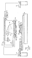
도 4에 관해, 제 1 구체예에서, 시스템(10')이 도시된다. 시스템(10')은 도 1에 관하여 상기 설명된 시스템(10)과 유사할 수 있지만, 시스템(10')은 제 2 기판 척(14b)과 결합된 제 2 기판(12b)을 포함할 수 있다. 제 2 기판(12b) 및 제 2 기판 척(14b)은 도 1에 관하여 상기 설명된 제 1 기판(12a) 및 제 1 기판 척(14a)과 유사할 수 있다. 제 2 기판 척(14b)은 제 2 기판(12b)에 면하는 공동(16b)을 포함할 수 있다. 제 2 기판(12b)과 제 2 기판 척(14b)은 제 1 및 제 2 스테이지(18 및 20) 위에 지지될 수 있다. 제 2 기판(12b)은 통로(24b)를 더 포함할 수 있다. 그러나, 다른 구체예에서, 제 2 기판(12b)에는 통로(24b)가 실질적으로 존재하지 않을 수도 있다.With respect to FIG. 4, in a first embodiment,
시스템(10')은 제 1 유체 디스펜서(40a)와 유사한 제 2 유체 디스펜서(40b)를 더 포함한다. 나타낸 대로, 제 2 유체 디스펜서(40b)는 템플릿 척(36)에 결합된다; 그러나, 다른 구체예에서, 제 2 유체 디스펜서(40b)는 시스템(10)의 다른 부품과도, 즉 템플릿(26) 또는 임프린트 헤드(38)와도 결합될 수 있다. 제 2 유체 디스펜서(40b)의 제어는 제 2 유체 디스펜서(40b)와 데이터 통신하는 프로세서(58)에 의해 조정될 수 있다. 그림을 단순화하기 위해 로봇(52)을 2개의 분리된 동체로서 도시하고 프로세서(58)와 제 1 및 제 2 스테이지(18 및 20) 사이의 결합은 도시하지 않았음에 유의한다.The
도 5 및 도 6에 관해, 제 1 및 제 2 기판(12a 및 12b)을 처리하기 위한 공정 순서도가 도시된다. 단계(100)에서 제 1 기판(12a)이 제 1 기판 척(14a) 위에 위치될 수 있다. 더 구체적으로, 제 1 및 제 2 스테이지(18 및 20)가 로봇(52)에 대하여 바람직한 공간적 관계에 놓이도록 제 1 기판 척(14a)을 위치시킬 수 있으며, 이로써 로봇(52)이 제 1 기판 척(14a) 위에 제 1 기판(12a)을 위치시킬 수 있다. 로봇(52)은 기판 카세트(도시하지 않음)로부터 제 1 기판(12a)을 이송하여 그것을 제 1 기판 척(14a) 위에 위치시킬 수 있다.5 and 6, a process flow chart for processing the first and
도 5 및 도 7에 관해, 단계(102)에서 제 1 기판(12a) 위에 폴리머 재료(42a)를 위치시키기 위하여 제 1 기판(12a)과 제 1 유체 디스펜서(40a) 사이에 바람직한 위치가 획득될 수 있도록 제 1 및 제 2 스테이지(18 및 20)가 제 1 기판 척(14a)을 이동시킬 수 있다.5 and 7, in
도 5 및 도 8에 관해, 단계(104)에서 제 1 기판(12a)과 몰드(28) 사이에 바람직한 공간적 관계가 획득될 수 있다. 더 구체적으로, 제 1 및 제 2 스테이지(18 및 20)와 임프린트 헤드(38)가 제 1 기판(12a)과 몰드(28)가 정합되어 놓이도록 제 1 기판 척(14a)을 위치시킬 수 있으며, 또한 폴리머 재료(42a)로 제 1 기판(12a)과 몰드(28) 사이의 바람직한 부피가 충전될 수 있다. 더 나아가, 단계(104)에서 바람직한 부피가 폴리머 재료(42a)로 충전된 후, 공급원(46)이 에너지(48), 예를 들어 제 1 기판(12a)과 몰드(28)의 패턴화 표면(30)의 모양에 일치하여 폴리머 재료 (42a)를 고화 및/또는 가교결합시킬 수 있는 광폭 자외선을 내보낼 수 있다. 결과적으로, 제 2 기판(12b)의 처리가 제 1 기판(12a)의 처리와 동시에 일어날 수 있다. 더 구체적으로, 단계(104)와 동시에 단계(106)에서 로봇(52)이 기판 카세트(도시하지 않음)로부터 제 2 기판(12b)을 이송하여 그것을 제 2 기판 척(14b) 위에 위치시킬 수 있다. 5 and 8, in step 104 a desired spatial relationship between the
도 5 및 도 9에 관해, 단계(108)에서 몰드(28)가 제 1 기판(12a) 위에 위치된 폴리머 재료(42a)로부터 분리될 수 있다. 다른 구체예에서, 단계(108)은 단계 (104) 및 단계(106)와 동시에 일어날 수 있다.5 and 9, in
도 5 및 10에 관해, 단계(110)에서 제 2 기판(12b) 위에 폴리머 재료(42b)를 위치시키기 위하여 제 2 기판(12b)과 제 2 유체 디스펜서(40b) 사이에 바람직한 위치가 획득될 수 있도록 제 1 및 제 2 스테이지(18 및 20)가 제 2 기판 척(14b)을 이동시킬 수 있다. 나타낸 대로, 폴리머 재료(42b)는 복수 개의 이격되어 위치하는 점적(44b)으로서 제 2 기판(12b) 위에 위치될 수 있다.5 and 10, a preferred position can be obtained between the
도 5 및 도 11에 관해, 단계(112)에서 제 2 기판(12b)과 몰드(28) 사이에 바람직한 공간적 관계가 획득될 수 있다. 더 구체적으로, 제 1 및 제 2 스테이지(18 및 20)와 임프린트 헤드(38)가 제 2 기판(12b)과 몰드(28)가 정합되어 놓이도록 제 2 기판 척(14b)을 위치시킬 수 있으며, 또한 폴리머 재료(42b)로 제 2 기판(12b)과 몰드(28) 사이의 바람직한 부피가 충전될 수 있다. 더 나아가, 단계(112)에서 바람직한 부피가 폴리머 재료(42b)로 충전된 후, 공급원(46)이 에너지(48), 예를 들어 제 2 기판(12b)과 몰드(28)의 패턴화 표면(30)의 모양에 일치하여 폴리머 재료 (42b)를 고화 및/또는 가교결합시킬 수 있는 광폭 자외선을 내보낼 수 있다. 단계 (112)와 동시에 단계(114)에서 로봇(52)이 제 1 기판 척(14a)으로부터 제 1 기판 (12a)을 제거하여 그것을 기판 카세트(도시하지 않음) 안에 위치시킬 수 있고, 또한 로봇(52)이 도 12에 도시된 대로 제 1 기판 척(14a) 위에 제 3 기판(12c)을 위치시킬 수 있다. 로봇(52)은, 도 12에 도시된 대로, 기판 카세트(도시하지 않음)로부터 제 3 기판(12c)을 이송하여 그것을 제 1 기판 척(14a) 위에 위치시킬 수 있다.5 and 11, in step 112 a desired spatial relationship between the
도 5 및 도 12에 관해, 단계(116)에서 몰드(28)가 제 2 기판(12b) 위에 위치된 폴리머 재료(42b)로부터 분리될 수 있다. 다른 구체예에서, 단계(116)는 단계 (112) 및 단계(114)와 동시에 일어날 수 있다.5 and 12, in
도 5 및 13에 관해, 단계(118)에서 제 3 기판(12c) 위에 폴리머 재료(42c)를 위치시키기 위하여 제 3 기판(12c)과 제 1 유체 디스펜서(40a) 사이에 바람직한 위치가 획득될 수 있도록 제 1 및 제 2 스테이지(18 및 20)가 제 3 기판(12c)을 이동시킬 수 있다. 나타낸 대로, 폴리머 재료(42c)는 복수 개의 이격되어 위치하는 점적(44c)으로서 제 3 기판(12c) 위에 위치될 수 있다.5 and 13, a preferred position can be obtained between the
도 5 및 도 14에 관해, 단계(120)에서 제 3 기판(12c)과 몰드(28) 사이에 바람직한 공간적 관계가 획득될 수 있다. 더 구체적으로, 제 1 및 제 2 스테이지(18 및 20)와 임프린트 헤드(38)가 제 3 기판(12c)과 몰드(28)가 정합되어 놓이도록 제 1 기판 척(14a)을 위치시킬 수 있으며, 또한 폴리머 재료(42c)로 제 3 기판(12c)과 몰드(28) 사이의 바람직한 부피가 충전될 수 있다. 더 나아가, 단계(120)에서 바람직한 부피가 폴리머 재료(42c)로 충전된 후, 공급원(46)이 에너지(48), 예를 들어 제 3 기판(42c)과 몰드(28)의 패턴화 표면(30)의 모양에 일치하여 폴리머 재료 (42c)를 고화 및/또는 가교결합시킬 수 있는 광폭 자외선을 내보낼 수 있다. 단계 (120)와 동시에 단계(122)에서 로봇(52)이 제 2 기판 척(14b)으로부터 제 2 기판 (12b)을 제거하여 그것을 기판 카세트(도시하지 않음) 안에 위치시킬 수 있고, 또한 로봇(52)은 제 2 기판 척(14b) 위에 제 4 기판(도시하지 않음)을 위치시킬 수 있다. 로봇 (52)은 기판 카세트(도시하지 않음)로부터 제 4 기판(도시하지 않음)을 이송하여 그것을 제 2 기판 척(14b) 위에 위치시킬 수 있다. 제 3 기판(12c) 및 제 4 기판(도시하지 않음)은 모두 제 1 기판(12a)과 유사하며, 제 1 기판 및 제 2 기판(12a 및 12b)에 대한 것과 유사하게 전술한 처리 조건을 행할 수 있다.5 and 14, in step 120 a desired spatial relationship between the
또한, 도 4 및 도 5에 관해, 제 1 기판(12a)을 패턴화하는 것과 동시에, 제 2 기판(12b)의 패턴화 전에, 추기의 기판(도시하지 않음)이 제 2 기판 척(14b) 위에서 패턴화될 수 있다. 더 구체적으로, 단계(100)와 동시에 단계(126)에서 이미 제 2 기판 척(14b)에 위치되어 있고 그 위에 폴리머 재료(도시하지 않음)가 위치되어 있는 추가 기판(도시하지 않음)이 도 11에 나타낸 단계(112)와 유사하게 기판 위에 패턴이 형성될 수 있다. 또한, 도 12에 나타낸 단계(116)와 유사하게, 단계 (128)에서 몰드(28)가 추가 기판(도시하지 않음) 위에 위치된 폴리머 재료(도시하지 않음)로부터 분리될 수 있다. 결과적으로, 도 14에 나타낸 단계(122)와 유사하게, 단계(106)이 추가 기판(도시하지 않음)을 제거하는 단계를 더 포함할 수 있다. 더욱이, 도 11에 나타낸 단계(114)와 유사하게, 단계(100)이 제 1 기판(12a)에 앞서 이미 패턴화되어 제 1 기판 척(14a) 위에 위치되어 있는 제 2 추가 기판(도시하지 않음)을 제거하는 단계를 더 포함할 수 있다. 4 and 5, at the same time as patterning the
다른 구체예에서, 제 1 및 제 2 유체 디스펜서(40a 및 40b)는 시스템(110)의 외부에 위치될 수 있으며, 이 경우 시스템(110)의 외부에서 제 1 및 제 2 기판(12a 및 12b) 위에 폴리머 재료(42a 및 42b)가 위치된다. 또 다른 구체예에서, 제 1 및 제 2 기판(12a 및 12b) 위에 폴리머 재료(42a 및 42b)를 위치시키는 것은 선택적일 수 있다.In other embodiments, the first and
결과적으로, 예를 들어, 제 1 및 제 2 기판(12a 및 12b)에 대한 전술한 패턴화 공정은 기판 당 20초의 총 공정 시간을 가질 수 있다. 더 구체적으로, 전술한 패턴화 공정의 각 단계에 걸리는 시간을 표 2에 더욱 분명히 나타낸다.As a result, for example, the aforementioned patterning process for the first and
시간
(초)fair
time
(second)
제 2 추가 기판을 제거함/
제1 기판 척(14a) 위에
제 1 기판(12a)을 위치시킴From the
Remove second additional substrate /
On the
Position the
바람직한 공간적 관계를
획득하고, 기판 위에 위치된
폴리머 재료로 추가 기판과
몰드(28) 사이의 바람직한 부피를
충전하고, 폴리머 재료를 고화
및/또는 가교결합시킴/폴리머
재료로부터 몰드(28)를 분리함Between the additional substrate and the
Good spatial relationship
Acquired, located on a substrate
Polymer substrates with additional substrates
The desired volume between the
Filling and solidifying polymer material
And / or crosslink / polymer
Separating
재료(42a)를 위치시킬 수 있도록
제 1 기판(12a)과 제 1 유체
디스펜서(40a) 사이에
바람직한 공간적 관계를 획득함 Polymer on
So that the
Between
Acquire the desired spatial relationship
사이에 바람직한 공간적 관계를
획득하고, 제 1 기판(12a)과
몰드(28) 사이의 바람직한 부피를
폴리머 재료(42a)로 충전하고,
폴리머 재료(42a)를 고화 및/또는
가교결합시킴/
폴리머 재료(42a)로부터
몰드(28)를 분리함
Between the desired spatial relationship
The
The desired volume between the
Filled with
Solidifying and / or
Crosslinking /
From
Removed mold (28)
기판을 제거함/
제 2 기판 척(14b) 위에
제 2 기판(12b)을 위치시킴Added from the
Remove board /
On the
Position the
재료(42b)를 위치시킬 수 있도록
제 2 기판(12b)과 제 2 유체
디스펜서(40b) 사이에
바람직한 공간적 관계를 획득함 Polymer on
To position material 42b
Between
Acquire the desired spatial relationship
제 1 기판(12a)을 제거함/
제 1 기판 척(14a) 위에
제 3 기판(12c)을 위치시킴From the
Remove
On the
Position the
사이에 바람직한 공간적 관계를
획득하고, 제 2 기판(12b)과
몰드(28) 사이의 바람직한 부피를
폴리머 재료(42b)로 충전하고,
폴리머 재료(42b)를 고화 및/또는
가교결합시킴/
폴리머 재료(42b)로부터
몰드(28)를 분리함
Between the desired spatial relationship
The
The desired volume between the
Filled with
Solidifying and / or
Crosslinking /
From
Removed mold (28)
이를 위하여, 제 1 및 제 2 기판(12a 및 12b)를 처리하기 위한 전술한 방법의 단계들은 병렬로 수행될 수 있다. 더 구체적으로, 1) 기판 척 위에 기판을 위치시키거나 기판 척으로부터 기판을 제거하는 단계 및 2) 기판과 몰드 사이에 바람직한 공간적 관계를 획득하고, 기판과 몰드 사이의 바람직한 부피를 폴리머 재료로 충전하고, 폴리머 재료를 고화 및/또는 가교결합시키거나 폴리머 재료로부터 몰드를 분리하는 단계가 병렬로 일어난다. 그 결과, 다수의 기판을 처리하는 전체적인 처리량의 증가(유사하게는 기판 당 총 공정 시간의 감소)가 획득될 수 있으며, 이것은 바람직할 수 있다. To this end, the steps of the method described above for processing the first and
도 4에 관해, 다른 구체예에서, 제 1 및 제 2 스테이지(18 및 20)가 제 1 및 제 2 스테이지(18 및 20)에 대해 직교하여 뻗어 있는 제 3 축, 즉 z 축에 대해 회전할 수 있으며, 180도 이상 회전할 수 있다.With respect to FIG. 4, in another embodiment, the first and
도 4 및 도 15에 관해, 상기 언급한 대로, 전술한 방법은 제 1 및 제 2 기판 (12a 및 12b)의 제 1 면(62a 및 62b) 위에 패턴을 형성하기 위해 사용될 수 있다. 이를 위하여, 다른 구체예에서, 제 1 및 제 2 기판(12a 및 12b)의 제 2 면(64a 및 64b) 위에 패턴을 형성하는 것이 바람직할 수 있으며, 이때 제 2 면(64a 및 64b)은 제 1 및 제 2 면(62a 및 62b)의 반대편에 위치한다.With reference to FIGS. 4 and 15, as mentioned above, the method described above may be used to form a pattern on the first faces 62a and 62b of the first and
도 6 및 도 15에 관해, 도 4에서 나타낸, 제 1 기판(12a)의 제 1 및 제 2 면 (62a 및 64a)과 제 2 기판(12b)의 제 1 및 제 2 면(62b 및 64b)을 처리하기 위한 공정 순서도가 도시된다. 이것은 패턴드 미디어 임프린팅(patterned media impri-nting) 영역에서 바람직할 수 있다. 단계(200)에서 제 1 기판(12a)이 제 1 기판 척 (14a) 위에 위치될 수 있다. 더 구체적으로, 제 1 및 제 2 스테이지(18 및 20)가 제 1 기판 척(14a)과 로봇(52)이 바람직한 공간적 관계에 놓이도록 제 1 기판 척 (14a)을 위치시킬 수 있으며, 이로써 로봇(52)이 제 1 기판 척(14a) 위에 제 1 기판(12a)을 위치시킬 수 있다. 로봇(52)이 기판 카세트(도시하지 않음)로부터 제 1 기판(12a)을 이송하고, 기판의 제 1 면(62a)이 제 1 기판 척(14a)의 면과 반대편에 위치되도록 제 1 기판(12a)을 제 1 기판 척(14a) 위에 위치시킬 수 있다.6 and 15, the first and
도 7 및 도 15에 관해, 단계(202)에서 제 1 기판(12a)의 제 1 면(62a) 위에 폴리머 재료(42a)를 위치시키기 위하여 제 1 기판(12a)과 제 1 유체 디스펜서(40a) 사이에 바람직한 위치가 획득될 수 있도록 제 1 및 제 2 스테이지(18 및 20)가 제 1 기판(12a)을 이동시킬 수 있다.7 and 15, the
도 8 및 도 15에 관해, 단계(204)에서 제 1 기판(12a)과 몰드(28) 사이에 바람직한 공간적 관계가 획득될 수 있다. 더 구체적으로, 제 1 및 제 2 스테이지(18 및 20)와 임프린트 헤드(38)가 제 1 기판(12a)과 몰드(28)가 정합되어 놓이도록 제 1 기판 척(14a)을 위치시킬 수 있으며, 또한 폴리머 재료(42a)로 제 1 기판(12a)과 몰드(28) 사이의 바람직한 부피가 충전될 수 있다. 더 나아가, 단계(104)에서, 바람직한 부피가 폴리머 재료(42a)로 충전된 후, 공급원(46)이 에너지(48), 예를 들어 폴리머 재료(42a)를 제 1 기판(12a)의 제 1 면(62a)과 몰드(28)의 패턴화 표면 (30)의 모양에 일치하여 고화 및/또는 가교결합시킬 수 있는 광폭 자외선을 내보낼 수 있다. 결과적으로, 제 2 기판(12b)의 처리가 제 1 기판(12a)의 처리와 동시에 일어날 수 있다. 더 구체적으로, 단계(204)와 동시에 단계(206)에서 로봇(52)이 기판 카세트(도시하지 않음)로부터 제 2 기판(12b)을 이송하고, 기판의 제 1 면(62b)이 제 2 기판 척(14b)의 면과 반대편에 위치되도록 제 2 기판(12b)을 제 1 기판 척 (14b) 위에 위치시킬 수 있다.8 and 15, in step 204 a desired spatial relationship between the
도 9 및 도 15에 관해, 단계(207)에서 몰드(28)가 제 1 기판(12a)의 제 1 면 (62a) 위에 위치된 폴리머 재료(42a)로부터 분리될 수 있다. 다른 구체예에서, 단계(207)은 단계(204) 및 단계(206)와 동시에 일어날 수 있다.9 and 15, in
도 10 및 도 15에 관해, 단계(208)에서 제 2 기판(12b)의 제 1 면(62b) 위에 폴리머 재료(42b)를 위치시키기 위하여 제 2 기판(12b)과 제 2 유체 디스펜서(40b) 사이에 바람직한 위치가 획득될 수 있도록 제 1 및 제 2 스테이지(18 및 20)가 제 2 기판(12b)을 이동시킬 수 있다. 나타낸 대로, 폴리머 재료(42b)는 복수 개의 이격되어 위치하는 점적(44b)으로서 제 2 기판(12b) 위에 위치될 수 있다.10 and 15, in
도 15 및 도 16에 관해, 단계(210)에서 제 2 기판(12b)과 몰드(28) 사이에 바람직한 공간적 관계가 획득될 수 있다. 더 구체적으로, 제 1 및 제 2 스테이지 (18 및 20)와 임프린트 헤드(38)가 제 2 기판(12b)과 몰드(28)가 정합되어 놓이도록 제 2 기판 척(14b)을 위치시킬 수 있으며, 또한 폴리머 재료(42b)로 제 2 기판 (12b)과 몰드(28) 사이의 바람직한 부피가 충전될 수 있다. 더 나아가, 단계(210)에서, 바람직한 부피가 폴리머 재료(42b)로 충전된 후, 공급원(46)이 에너지(48), 예를 들어 폴리머 재료(42b)를 제 2 기판(62b)의 제 1 면(62b)과 몰드(28)의 패턴화 표면(30)의 모양에 일치하여 고화 및/또는 가교결합시킬 수 있는 광폭 자외선을 내보낼 수 있다. 단계(210)과 동시에 단계(212)에서 로봇(52)이 제 1 기판 척(14a)으로부터 제 1 기판(12a)을 제거하고, 암(54)을 축 회전시켜 제 1 기판(12a)을 몰드(28)에 대해 180도 뒤집을 수 있으며, 또한 도 17에 도시된 대로, 로봇(52)이 기판의 제 2 면(64a)이 제 1 기판 척(14a)의 면과 반대편에 위치되도록 제 1 기판 척 (14a) 위에 제 1 기판(12a)을 위치시킬 수 있다. 또한, 예방될 수 없는 폴리머 재료(42a)에 대한 손상을 최소화하기 위하여 폴리머 재료(42a)가 제 1 기판척(14a)의 공동(16a) 안에 위치될 수 있다.15 and 16, in step 210 a desired spatial relationship between the
도 15 및 도 17에 관해, 단계(216)에서 몰드(28)가 제 2 기판(12b) 위에 위치된 폴리머 재료(42b)로부터 분리될 수 있다. 다른 구체예에서, 단계(216)은 단계(210) 및 단계(212)와 동시에 일어날 수 있다.15 and 17, in
도 15 및 18에 관해, 단계(218)에서 제 1 기판(12a) 위에 폴리머 재료(42a')를 위치시키기 위하여 제 1 기판(12a)과 제 1 유체 디스펜서(40a) 사이에 바람직한 위치가 획득될 수 있도록 제 1 및 제 2 스테이지(18 및 20)가 제 1 기판(12a)을 이동시킬 수 있다. 나타낸 대로, 폴리머 재료(42a')는 복수 개의 이격되어 위치하는 점적(44a')으로서 제 1 기판(12a) 위에 위치될 수 있다.15 and 18, in step 218 a desired position is obtained between the
도 15 및 도 19에 관해, 단계(220)에서 제 1 기판(12a)과 몰드(28) 사이에 바람직한 공간적 관계가 획득될 수 있다. 더 구체적으로, 제 1 및 제 2 스테이지 (18 및 20)와 임프린트 헤드(38)가 제 1 기판(12a)과 몰드(28)가 정합되어 놓이도록 제 1 기판 척(14a)을 위치시킬 수 있으며, 또한 폴리머 재료(42a')로 제 1 기판 (12a)과 몰드(28) 사이의 바람직한 부피가 충전될 수 있다. 더 나아가, 단계(220)에서, 바람직한 부피가 폴리머 재료(42a')로 충전된 후, 공급원(46)이 에너지(48), 예를 들어 폴리머 재료(42a')를 제 1 기판(12a)의 제 2 면(64a)과 몰드(28)의 패턴화 표면(30)의 모양에 일치하여 고화 및/또는 가교결합시킬 수 있는 광폭 자외선을 내보낼 수 있다. 단계(220)과 동시에 단계(222)에서 로봇(52)이 제 1 기판 척(14a)으로부터 제 1 기판(12a)을 제거하고, 암(54)을 축 회전시켜 제 2 기판(12b)을 몰드(28)에 대해 180도 뒤집을 수 있으며, 또한 도 20에 도시된 대로, 로봇(52)이 기판의 제 2 면(64b)이 제 2 기판 척(14b)의 면과 반대편에 위치되도록 제 2 기판 척 (14b) 위에 제 2 기판(12b)을 위치시킬 수 있다. 또한, 예방될 수 없는 폴리머 재료(42b)에 대한 손상을 최소화하기 위하여 폴리머 재료(42b)가 제 2 기판 척(14b)의 공동(16b) 안에 위치될 수 있다.15 and 19, in step 220 a desired spatial relationship between the
도 15 및 도 20에 관해, 단계(224)에서 몰드(28)가 제 1 기판(12a)의 제 2 면(64a) 위에 위치된 폴리머 재료(42a')로부터 분리될 수 있다. 다른 구체예에서, 단계(224)는 단계(220) 및 단계(222)와 동시에 일어날 수 있다.15 and 20, in
도 15 및 21에 관해, 단계(226)에서 제 2 기판(12b)의 제 2 면(64b) 위에 폴리머 재료(42b')를 위치시키기 위하여 제 2 기판(12b)과 제 2 유체 디스펜서(40b) 사이에 바람직한 위치가 획득될 수 있도록 제 1 및 제 2 스테이지(18 및 20)가 제 2 기판 척(14b)을 이동시킬 수 있다. 나타낸 대로, 폴리머 재료(42b')는 복수 개의 이격되어 위치하는 점적(44b')으로서 제 2 기판(12b) 위에 위치될 수 있다.15 and 21, in
도 15 및 도 22에 관해, 단계(228)에서 제 2 기판(12b)과 몰드(28) 사이에 바람직한 공간적 관계가 획득될 수 있다. 더 구체적으로, 제 1 및 제 2 스테이지 (18 및 20)와 임프린트 헤드(38)가 제 2 기판(12b)과 몰드(28)가 정합되어 놓이도록 제 2 기판 척(14b)을 위치시킬 수 있으며, 또한 폴리머 재료(42b')로 제 2 기판 (12b)과 몰드(28) 사이의 바람직한 부피가 충전될 수 있다. 더 나아가, 단계(228)에서, 바람직한 부피가 폴리머 재료(42b')로 충전된 후, 공급원(46)이 에너지(48), 예를 들어 폴리머 재료(42b')를 제 2 기판(12b)의 제 2 면(64b)과 몰드(28)의 패턴화 표면(30)의 모양에 일치하여 고화 및/또는 가교결합시킬 수 있는 광폭 자외선을 내보낼 수 있다. 단계(228)과 동시에 단계(230)에서 로봇(52)이 제 1 기판 척(14a)으로부터 제 1 기판(12a)을 제거하여 그것을 기판 카세트(도시하지 않음) 안에 위치시킬 수 있으며, 또한 로봇(52)은 제 1 기판 척(14a) 위에 제 3 기판(12c)을 위치시킬 수 있다. 로봇(52)은 기판 카세트(도시하지 않음)로부터 제 3 기판(12c)을 이송하고, 기판의 제 1 면(62c)이 제 1 기판 척(14a)의 면과 반대편에 위치되도록 제 1 기판 척(14a) 위에 제 3 기판(12c)을 위치시킬 수 있다.15 and 22, in step 228 a desired spatial relationship between the
도 15 및 도 23에 관해, 단계(232)에서 몰드(28)가 제 2 기판(12b) 위에 위치된 폴리머 재료(42b')로부터 분리될 수 있다. 다른 구체예에서, 단계(232)는 단계(228) 및 단계(230)과 동시에 일어날 수 있다.15 and 23, in
도 15 및 24에 관해, 단계(234)에서 제 3 기판(12c) 위에 폴리머 재료(42c)를 위치시키기 위하여 제 3 기판(12c)과 제 1 유체 디스펜서(40a) 사이에 바람직한 위치가 획득될 수 있도록 제 1 및 제 2 스테이지(18 및 20)가 제 3 기판(12c)을 이동시킬 수 있다. 나타낸 대로, 폴리머 재료(42c)는 복수 개의 이격되어 위치하는 점적(44c)으로서 제 3 기판(12c) 위에 위치될 수 있다.15 and 24, in
도 15 및 도 25에 관해, 단계(236)에서 제 3 기판(12c)과 몰드(28) 사이에 바람직한 공간적 관계가 획득될 수 있다. 더 구체적으로, 제 1 및 제 2 스테이지 (18 및 20)와 임프린트 헤드(38)가 제 3 기판(12c)과 몰드(28)가 정합되어 놓이도록 제 1 기판 척(14a)을 위치시킬 수 있으며, 또한 폴리머 재료(42c)로 제 3 기판 (12c)과 몰드(28) 사이의 바람직한 부피가 충전될 수 있다. 더 나아가, 단계(236)에서, 바람직한 부피가 폴리머 재료(42c)로 충전된 후, 공급원(46)이 에너지(48), 예를 들어 폴리머 재료(42c)를 제 3 기판(12c)의 제 1 면(62c)과 몰드(28)의 패턴화 표면(30)의 모양에 일치하여 고화 및/또는 가교결합시킬 수 있는 광폭 자외선을 내보낼 수 있다. 단계(236)과 동시에 단계(238)에서 로봇(52)이 제 2 기판 척(14b)으로부터 제 2 기판(12b)을 제거하여 그것을 기판 카세트(도시하지 않음) 안에 위치시킬 수 있고, 또한 로봇(52)이 제 2 기판 척(14b) 위에 추가 기판(도시하지 않음)을 위치시킬 수 있다. 로봇(52)은 기판 카세트(도시하지 않음)로부터 추가 기판(도시하지 않음)을 이송하여 그것을 제 2 기판 척(14b) 위에 위치시킬 수 있다. 제 3 기판(12c) 및 추가 기판은 제 1 및 제 2 기판(12a 및 12b)에 대한 것과 유사하게 전술한 처리 조건을 행할 수 있다.15 and 25, in step 236 a desired spatial relationship between the
또한, 도 4 및 도 15에 관해, 제 1 기판(12a)을 패턴화하는 것과 동시에, 제 2 기판(12b)의 패턴화 전에 추가 기판(도시하지 않음)이 제 2 기판 척(14b) 위에서 패턴화될 수 있다. 더 구체적으로, 단계(200)과 동시에 단계(240)에서 이미 제 2 기판 척(14b) 위에 위치되어 있고 그 위에 폴리머 재료(도시하지 않음)가 위치되어 있는 추가 기판이 도 22에 나타낸 단계(228)과 유사하게 제 2 면 위에 패턴 형성될 수 있다. 또한, 도 23에 도시된 단계(232)와 유사하게, 단계(242)에서 몰드(28)가 추가 기판(도시하지 않음) 위에 위치된 폴리머 재료(도시하지 않음)로부터 분리될 수 있다. 결과적으로, 도 25에 나타낸 단계(238)와 유사하게, 단계(206)이 추가 기판(도시하지 않음)을 제거하는 단계를 더 포함할 수 있다. 더욱이, 도 22에 나타낸 단계(230)과 유사하게, 단계(200)이 제 1 기판 (12a)에 앞서 이미 패턴화되어 제 1 기판 척(14a) 위에 위치되어 있는 제 2 추가 기판(도시하지 않음)을 제거하는 단계를 더 포함할 수 있다. 4 and 15, at the same time as patterning the
결과적으로, 예를 들어, 제 1 기판(12a)의 제 1 및 제 2 면(62a 및 64a)과 제 2 기판(12b)의 제 1 및 제 2 면(62b 및 64b)를 패턴화하기 위한 전술한 공정은 기판 당 40초의 총 공정 시간을 가질 수 있다. 더 구체적으로, 전술한 패턴화 공정의 각 단계에 걸리는 시간을 표 3에 더욱 분명히 나타낸다.As a result, for example, the above-mentioned for patterning the first and
시간
(초)fair
time
(second)
제 2 추가 기판을 제거함/
제 1 면(62a)이 몰드(28)와
마주하도록 제 1 기판 척(14a) 위에
제 1 기판(12a)을 위치시킴From the
Remove second additional substrate /
The
On the
Position the
바람직한 공간적 관계를 획득하고,
기판 위에 위치된 폴리머 재료로
추가 기판과 몰드(28) 사이의
바람직한 부피를 충전하고, 폴리머
재료를 고화 및/또는 가교결합시킴/폴리머 재료로부터 몰드(28)를
분리함Between the additional substrate and the
To obtain desirable spatial relationships,
With polymer material located on the substrate
Between the additional substrate and the
Filling the desired volume,
Solidifying and / or Crosslinking Material /
Detached
위에 폴리머 재료(42a)를 위치시킬
수 있도록 제 1 기판(12a)과 제 1
유체 디스펜서(40a) 사이에 바람직한
공간적 간계를 획득함
To place the
To allow the
Preferred between
Obtained spatial tricks
바람직한 공간적 관계를 획득하고,
폴리머 재료(42a)로 제 1 기판(12a)과 몰드(28) 사이의 바람직한 부피를
충전하고, 폴리머 재료(42a)를 고화
및/또는 가교결합시킴/폴리머
재료(42a)로부터 몰드(28)를 분리함Between the
To obtain desirable spatial relationships,
With the
Filling and solidifying the
And / or crosslink / polymer
Separating
기판을 제거함/제 1 면(62b)이
몰드(28)와 마주하도록 제 2 기판
척(14b) 위에 제 2 기판(12b)을
위치시킴Added from the
Remove substrate /
The second substrate to face the
The
Positioning
위에 폴리머 재료(42b)를 위치시킬
수 있도록 제 2 기판(12b)과 제 2
유체 디스펜서(40b) 사이에
바람직한 공간적 간계를 획득함
To place the
So that the
Between the
Obtain the desired spatial trick
기판(12a)을 제거함/제 1 기판(12a)을
뒤집음/제 2 면(64a)이 몰드(28)와
마주하도록 제 1 기판 척(14a) 위에
제 1 기판(12a)을 위치시킴First from
Removing
Flip /
On the
Position the
바람직한 공간적 관계를 획득하고,
폴리머 재료(42b)로 제 2 기판(12b)과 몰드(28) 사이의 바람직한
부피를 충전하고, 폴리머 재료(42b)를 고화 및/또는 가교결합시킴/
폴리머 재료(42b)로부터
몰드(28)를 분리함Between the
To obtain desirable spatial relationships,
Filling the volume and solidifying and / or crosslinking the
From
Removed mold (28)
위에 폴리머 재료(42a')를 위치시킬
수 있도록 제 1 기판(12a)과 제 1
유체 디스펜서(40a) 사이에 바람직한
공간적 간계를 획득함
To place the
To allow the
Preferred between
Obtained spatial tricks
바람직한 공간적 관계를 획득하고,
폴리머 재료(42a')로 제 1
기판(12a)과 몰드(28) 사이의
바람직한 부피를 충전하고, 폴리머
재료(42a')를 고화 및/또는
가교결합시킴/폴리머 재료(42a')
로부터 몰드(28)를 분리함Between the
To obtain desirable spatial relationships,
First with
Between the
Filling the desired volume,
Solidifying and / or
Crosslinking / Polymer Material (42a ')
Separating mold (28) from
기판(12b)을 제거함/
제 2 기판(12b)을 뒤집음/
제 2 면(64b)이 몰드(28)와
마주하도록 제 2 기판 척(14b)
위에 제 2 기판(12b)을 위치시킴Second from
Remove
Inverting the
The
Facing the
Position the
위에 폴리머 재료(42b')를 위치시킬
수 있도록 제 2 기판(12b)과 제 2
유체 디스펜서(40b) 사이에
바람직한 공간적 간계를 획득함
To place the
So that the
Between the
Obtain the desired spatial trick
이를 위하여, 제 1 기판(12a)의 제 1 및 제 2 면(62a 및 64a)과 제 2 기판 (12b)의 제 1 및 제 2 면(62b 및 64b)을 처리하기 위한 전술한 방법의 단계들은 병렬로 수행될 수 있다. 더 구체적으로, 표 2와 관련하여 상기 언급한 것과 유사하게, 1) 기판 척 위에 기판을 위치시키거나 기판 척으로부터 기판을 제거하는 단계 및 2) 기판과 몰드 사이에 바람직한 공간적 관계를 획득하고, 폴리머 재료로 기판과 몰드 사이의 바람직한 부피를 충전하고, 폴리머 재료를 고화 및/또는 가교결합시키거나 폴리머 재료로부터 몰드를 분리하는 단계가 병렬로 일어난다. 그 결과, 다수의 기판을 처리하는 전체적인 처리량의 증가(유사하게는 기판 당 총 공정 시간의 감소)가 획득될 수 있으며, 이것은 바람직할 수 있다. 결과적으로, 상기 언급한 공정들은 임프린트 리소그래피 시스템, 특히 스텝-앤-리피트(step-and-repeat) 시스템 및 홀 웨이퍼(whole wafer) 시스템을 포함하는 임프린트 리소그래피 시스템에서 사용될 수 있다. 시스템의 선택은 당업자에게 공지된 바이며, 전형적으로 원하는 특정 용도에 따른다.To this end, the steps of the method described above for treating the first and
다른 구체예로서, 도 26에 관해, 시스템(110)은 다수의 기판 척을 포함할 수 있다. 예로서, 시스템(110)은 제 1 및 제 2 모듈(66a 및 66b)을 포함할 수 있다. 제 1 모듈(66a)은 제 1 및 제 2 기판 척(14a 및 14b)을 포함할 수 있고, 제 2 모듈 (66b)은 제 3 및 제 4 기판 척(14c 및 14d)을 포함할 수 있다. 제 3 및 제 4 기판 척(14c 및 14d)은 도 4와 관련하여 상기 언급한 제 1 및 제 2 기판 척(14a 및 14b)와 각각 유사할 수 있다. 결과적으로, 도 4와 관련하여 상기 언급한 제 1 및 제 2 기판(12a 및 12b)과 유사하게, 제 3 및 제 4 기판 척(14c 및 14d) 위에는 제 3 및 제 4 기판(12c 및 12d)이 있을 수 있고, 도 15와 관련하여 상기 언급한 것과 실질적으로 동일한 처리 조건을 행할 수 있다. 더 구체적으로, 제 1 및 제 2 모듈(66a 및 66b)의 처리는 병렬로 일어날 수 있는데, 즉 제 1 및 제 2 모듈(66a 및 66b)의 각 모듈은 도 15와 관련하여 상기 언급한 공정을 동시에 수행할 수 있다.In another embodiment, with respect to FIG. 26,
예로서, 제 1 모듈(66a)의 제 1 및 제 2 기판(12a 및 12b) 중 한 기판과 제 2 모듈(66b)의 제 3 및 제 4 기판(12c 및 12d) 중 한 기판이 패턴화되는 동시에 제 1 모듈(66a)의 제 1 및 제 2 기판(12a 및 12b) 중 나머지 기판과 제 2 모듈(66b)의 제 3 및 제 4 기판(12c 및 12d) 중 나머지 기판은 인풋/아웃풋 공정에 있을 수 있다. 더 구체적으로, 제 1 기판(12a)은 도 8 및 도 15와 관련하여 상기 언급한 단계(204 및 206)과 유사하게 패턴화될 수 있고, 제 3 기판(12c)은 도 15 및 도 22와 관련하여 상기 언급한 단계(222 및 226)와 유사하게 패턴화될 수 있다. 동시에, 제 2 기판(12b)은 도 8 및 도 15와 관련하여 상기 언급한 단계(206)과 유사하게 제 2 기판 척(14b) 위에 위치될 수 있고, 제 4 기판(12d)는 도 15 및 도 25와 관련하여 상기 언급한 단계(230)과 유사하게(또는 도 15 및 도 19와 관련하여 상기 언급한 단계(222)와 유사하게) 제 4 기판 척(14d)으로부터 제거될 수 있다(또는 제거되고 뒤집힐 수 있다). 그림을 단순화하기 위해 템플릿(26)은 점선 직사각형으로 나타낸다.For example, one of the first and
다른 예로서, 도 27에 관해, 제 2 기판(12b)은 도 8 및 도 15와 관련하여 상기 언급한 단계(204) 및 단계(206)과 유사하게 패턴화될 수 있고, 제 4 기판(12d)은 도 15 및 도 22와 관련하여 상기 언급한 단계(226)과 유사하게 패턴화될 수 있다. 동시에, 제 1 기판(12a)은 도 8 및 도 15와 관련하여 상기 언급한 단계(206)와 유사하게 제 1 기판 척(14a) 위에 위치될 수 있고, 제 3 기판(12c)은 도 15 및 도 25와 관련하여 상기 언급한 단계(230)과 유사하게(또는 도 15 및 도 19와 관련하여 상기 언급한 단계(222)와 유사하게) 제 3 기판 척(14c)으로부터 제거될 수 있다(또는 제거되고 뒤집힐 수 있다).As another example, with respect to FIG. 27, the
결과적으로, 제 1 및 제 2 모듈(66a 및 66b)과 도 15와 관련하여 상기 언급한 공정을 이용하여, 제 1 및 제 2 면 위에 패턴이 형성된 기판이 n 초마다 형성될 수 있으며, 이때 n 초는 기판의 한 면을 패턴화하는데 걸리는 시간이다.As a result, using the first and
도 28에 관해, 제 1 기판(12a)이 위에 위치된 제 1 기판 척(14a)의 단면도가 도시된다. 제 1 기판 척(14a)은 제 1 기판(12a)의 활성 영역(80) 둘레에 위치된 복수 개의 랜드(68)를 포함할 수 있다. 제 1 기판 척(14a)은 공동(16a) 안에 바람직한 압력이 용이하게 획득될 수 있도록 펌프 시스템(84)과 유체 연통할 수 있는 통로(82)를 더 포함할 수 있다. 펌프 시스템(84)의 제어는 프로세서(58)에 의해 조정될 수 있다.With reference to FIG. 28, a cross-sectional view of the
또한, 제 1 및 제 2 기판(12a 및 12b)에 실질적으로 동일한 공정 조건을 행하는 것이 바람직할 수 있다. 이를 위하여, 도 29에 관해, 도 4에 도시된 제 1 기판의 부분(86)이 묘사되며, 이때 부분(86)은 제 1 기판(12a)의 제 1 면(62a)의 평면성의 수준을 표시한다. 제 1 면(62a)은 복수 개의 언덕과 골을 포함한다; 그러나, 1개 언덕(88)과 골(90)만이 도시된다. 제 1 면(62a)의 복수 개의 언덕과 골은 평면성을 가진 평균 면으로 묘사되며, 제 1 면(62a)의 평면 'a'로 표시된다. 그러나, 제 1 면(62a)의 복수 개의 언덕과 골은 크기의 차이는 있지만 평면 'a'로부터 벗어날 수 있으며, 여기서는 단순히 하기 위해서 각 편차가 Δdev1로 정의될 수 있다. 더 구체적으로, 언덕(88)의 정점은 크기 Δ1 만큼 평면 'a'로부터 벗어날 수 있고, 골(90)의 바닥은 크기 Δ2 만큼 평면 'a'로부터 벗어날 수 있다. 상기한 사항은 제 1 기판(12a)의 제 2 면(64a)과 제 2 기판(12b)의 제 1 및 제 2 면(62b 및 64b)에 대해서도 동등하게 적용될 수 있다. 도 30에 관해, 도 4에 도시된 제 1 기판 척(14a)의 부분(92)이 묘사되며, 이때 부분(92)은 제 1 기판 척(14a)의 표면 (94)의 평면성의 수준을 표시한다. 표면(94)은 복수 개의 언덕과 골을 포함한다; 그러나, 1개의 언덕(96)과 골(98)만이 도시된다. 표면(94)의 복수 개의 언덕과 골은 평면성을 가진 평균 면으로 묘사되며, 표면(94)의 평면 'b'로 표시된다. 그러나, 표면(94)의 복수 개의 언덕과 골은 크기의 차이는 있지만 평면 'b'로부터 벗어날 수 있으며, 여기서는 단순히 하기 위해서 각 편차가 Δdev2로 정의될 수 있다. 더 구체적으로, 언덕(96)의 정점은 크기 Δ3 만큼 평면 'b'로부터 벗어날 수 있고, 골(98)의 바닥은 크기 Δ4 만큼 평면 'b'로부터 벗어날 수 있다. 상기한 사항은 제 2 기판 척(14b)에도 동등하게 적용될 수 있다. 결과적으로, 기판 척(14b)의 표면(94)의 두께의 편차 Δdev2는 제 1 기판(12a)의 제 1 면(62a)(또는 제 2 면(64a)의 두께의 편차 Δdev1보다 작을 수 있다. 결과적으로, 제 1 및 제 2 기판(12a 및 12b)에 실질적으로 동일한 공정 조건을 행하는 것이 용이하게 될 수 있다.It may also be desirable to perform substantially the same process conditions on the first and
또한, 제 1 및 제 2 기판(12a 및 12b)에 실질적으로 동일한 공정 조건이 행해질 수 있도록 제 1 및 제 2 유체 디스펜서(40a 및 40b)가 서로에 대해 보정될 수 있다. 더 구체적으로, 제 1 유체 디스펜서(40a)는 제 1 기판(12a) 위에 부피 V1의 폴리머 재료(42a)를 위치시키도록 프로세서(58)에 의해서 명령받을 수 있다; 그러나, 제 1 유체 디스펜서(40a)는 제 1 기판(12a) 위에 부피 V2의 폴리머 재료(42a)를 위치시킬 수도 있는데, 이때 부피 V2는 부피 V1과 다르며, 부피 V1이 바람직한 부피이다. 이것은 제 1 유체 디스펜서(40a)의 잘못된 보정으로 인한 것일 수 있는데, 즉 명령된 것과 다른 부피의 유체를 디스펜싱하는 것이다. 결과적으로, 부피 V1과 V2의 차이가 보정될 수 있으며, 이로써 제 1 유체 디스펜서(40a)가 제 1 기판 (12a) 위에 부피 V3을 위치시키도록 메모리(60)에 저장된 컴퓨터 판독 프로그램에 의해 운영되는 프로세서(58)가 명령할 수 있게 되고 잘못된 보정이 상쇄되어, 제 1 유체 디스펜서(40a)가 제 1 기판(12a) 위에 부피 V1을 위치시킬 수 있게 된다. 상기한 사항은 제 2 유체 디스펜서(40b)에도 동등하게 적용될 수 있다. 결과적으로, 제 1 및 제 2 기판(12a 및 12b)에 실질적으로 동일한 공정을 행하는 것이 용이하게 될 수 있다.In addition, the first and
더욱이, 제 1 및 제 2 기판(12a 및 12b) 위에 각각 위치된 폴리머 재료(42a 및 42b)는 상이한 기판 척 위에 위치된 결과로서 상이한 증발 조건에 노출될 수 있으며, 따라서 폴리머 재료(42a 및 42b)의 부피가 달라질 수 있는데, 이것은 바람직하지 않다. 더 구체적으로, 폴리머 재료(42a), 제 1 기판(12a), 및 제 1 기판 척 (14a)과 관련된 환경의 기류 및 온도는 폴리머 재료(42b), 제 2 기판(42b), 및 제 2 기판 척(14b)과 관련된 환경의 기류 및 온도와 다를 수 있다. 그 결과, 전술한 증발 조건을 보상하기 위해, 제 1 유체 디스펜서(40a)는 제 1 기판(12a) 위에 부피 V4의 폴리머 재료를 위치시킬 수 있고, 제 2 유체 디스펜서(40b)는 제 2 기판(12b) 위에 부피 V4와는 다른 부피 V5의 폴리머 재료(42b)를 위치시킬 수 있으며, 이로써 증발 조건에 폴리머 재료(42a 및 42b)가 노출된 후, 폴리머 재료(42a 및 42b)는 각각 실질적으로 동일한 부피 V6 및 V7을 포함하게 된다.Moreover, the
또한, 제 1 및 제 2 기판(12a 및 12b)에 실질적으로 동일한 공정 조건을 행하는 것을 용이하게 하기 위해, 제 1 및 제 2 기판(12a 및 12b)에 대한 제 1 및 제 2 유체 디스펜서(40a 및 40b)의 각각의 기하학적 위치가 실질적으로 동일할 수 있다. 더 구체적으로, 제 1 유체 디스펜서(40a)와 제 1 기판(12a) 사이의 거리와 제 2 유체 디스펜서(40b)와 제 2 기판(40b) 사이의 거리는 실질적으로 동일할 수 있다.In addition, to facilitate performing substantially the same process conditions on the first and
제 1 및 제 2 기판(12a 및 12b)에 실질적으로 동일한 공정 조건을 행하는 것을 더욱 용이하게 하기 위해, 제 1 및 제 2 재료(42a 및 42b)의 고화 및/또는 가교결합이 실질적으로 동일할 수 있도록 제 1 및 제 2 기판 척(14a 및 14b)의 표면 (94)의 반사성이 실질적으로 동일할 수 있다.In order to make it easier to apply substantially the same process conditions to the first and
상기 설명된 본 발명의 구체예들은 예시이다. 본 발명의 범위 내에서 상기 인용된 명세서에 대한 많은 변화 및 변형이 만들어질 수 있다. 따라서, 본 발명의 범위는 상기 설명에 의해 제한되지 않으며, 전체 등가물 범위와 함께 첨부된 청구범위를 참조하여 결정되어야 한다.Embodiments of the invention described above are illustrative. Many changes and modifications to the above-cited specification can be made within the scope of the invention. Accordingly, the scope of the invention should not be limited by the foregoing description, but should be determined with reference to the appended claims, along with the full scope of equivalents.
Claims (33)
Applications Claiming Priority (9)
| Application Number | Priority Date | Filing Date | Title |
|---|---|---|---|
| US76073806P | 2006-01-20 | 2006-01-20 | |
| US60/760,738 | 2006-01-20 | ||
| US78880806P | 2006-04-03 | 2006-04-03 | |
| US60/788,808 | 2006-04-03 | ||
| US82712506P | 2006-09-27 | 2006-09-27 | |
| US60/827,125 | 2006-09-27 | ||
| US11/565,350 US7670529B2 (en) | 2005-12-08 | 2006-11-30 | Method and system for double-sided patterning of substrates |
| US11/565,350 | 2006-11-30 | ||
| PCT/US2007/001670 WO2007084774A2 (en) | 2006-01-20 | 2007-01-20 | Patterning substrates employing multiple chucks |
Publications (2)
| Publication Number | Publication Date |
|---|---|
| KR20080093414A KR20080093414A (en) | 2008-10-21 |
| KR101324544B1 true KR101324544B1 (en) | 2013-11-01 |
Family
ID=38284757
Family Applications (1)
| Application Number | Title | Priority Date | Filing Date |
|---|---|---|---|
| KR1020087016345A KR101324544B1 (en) | 2006-01-20 | 2007-01-20 | Patterning substrates employing multiple chucks |
Country Status (6)
| Country | Link |
|---|---|
| US (2) | US7670530B2 (en) |
| EP (1) | EP1973719A4 (en) |
| JP (1) | JP4472011B2 (en) |
| KR (1) | KR101324544B1 (en) |
| TW (1) | TWI341935B (en) |
| WO (1) | WO2007084774A2 (en) |
Families Citing this family (74)
| Publication number | Priority date | Publication date | Assignee | Title |
|---|---|---|---|---|
| US7162035B1 (en) | 2000-05-24 | 2007-01-09 | Tracer Detection Technology Corp. | Authentication method and system |
| US7019819B2 (en) | 2002-11-13 | 2006-03-28 | Molecular Imprints, Inc. | Chucking system for modulating shapes of substrates |
| US7077992B2 (en) | 2002-07-11 | 2006-07-18 | Molecular Imprints, Inc. | Step and repeat imprint lithography processes |
| US7442336B2 (en) * | 2003-08-21 | 2008-10-28 | Molecular Imprints, Inc. | Capillary imprinting technique |
| US7641840B2 (en) * | 2002-11-13 | 2010-01-05 | Molecular Imprints, Inc. | Method for expelling gas positioned between a substrate and a mold |
| US8211214B2 (en) | 2003-10-02 | 2012-07-03 | Molecular Imprints, Inc. | Single phase fluid imprint lithography method |
| US8334967B2 (en) * | 2004-05-28 | 2012-12-18 | Board Of Regents, The University Of Texas System | Substrate support system having a plurality of contact lands |
| US7768624B2 (en) * | 2004-06-03 | 2010-08-03 | Board Of Regents, The University Of Texas System | Method for obtaining force combinations for template deformation using nullspace and methods optimization techniques |
| KR101175108B1 (en) | 2004-06-03 | 2012-08-21 | 더 보드 오브 리전츠 오브 더 유니버시티 오브 텍사스 시스템 | System and method for improvement of alignment and overlay for microlithography |
| US20060062922A1 (en) | 2004-09-23 | 2006-03-23 | Molecular Imprints, Inc. | Polymerization technique to attenuate oxygen inhibition of solidification of liquids and composition therefor |
| US7635263B2 (en) * | 2005-01-31 | 2009-12-22 | Molecular Imprints, Inc. | Chucking system comprising an array of fluid chambers |
| US7636999B2 (en) * | 2005-01-31 | 2009-12-29 | Molecular Imprints, Inc. | Method of retaining a substrate to a wafer chuck |
| US7798801B2 (en) | 2005-01-31 | 2010-09-21 | Molecular Imprints, Inc. | Chucking system for nano-manufacturing |
| US8011915B2 (en) * | 2005-11-04 | 2011-09-06 | Asml Netherlands B.V. | Imprint lithography |
| US7878791B2 (en) * | 2005-11-04 | 2011-02-01 | Asml Netherlands B.V. | Imprint lithography |
| US7906058B2 (en) | 2005-12-01 | 2011-03-15 | Molecular Imprints, Inc. | Bifurcated contact printing technique |
| US7803308B2 (en) | 2005-12-01 | 2010-09-28 | Molecular Imprints, Inc. | Technique for separating a mold from solidified imprinting material |
| CN101535021A (en) * | 2005-12-08 | 2009-09-16 | 分子制模股份有限公司 | Method and system for double-sided patterning of substrates |
| US7802978B2 (en) * | 2006-04-03 | 2010-09-28 | Molecular Imprints, Inc. | Imprinting of partial fields at the edge of the wafer |
| WO2007117524A2 (en) * | 2006-04-03 | 2007-10-18 | Molecular Imprints, Inc. | Method of concurrently patterning a substrate having a plurality of fields and alignment marks |
| US20070231422A1 (en) * | 2006-04-03 | 2007-10-04 | Molecular Imprints, Inc. | System to vary dimensions of a thin template |
| US8142850B2 (en) * | 2006-04-03 | 2012-03-27 | Molecular Imprints, Inc. | Patterning a plurality of fields on a substrate to compensate for differing evaporation times |
| US8012395B2 (en) | 2006-04-18 | 2011-09-06 | Molecular Imprints, Inc. | Template having alignment marks formed of contrast material |
| US8215946B2 (en) | 2006-05-18 | 2012-07-10 | Molecular Imprints, Inc. | Imprint lithography system and method |
| US8540906B2 (en) * | 2007-06-14 | 2013-09-24 | Aji Co., Ltd. | Method of molding, process for producing lens, molding apparatus, process for producing stamper, master production apparatus, stamper production system, and stamper production apparatus |
| US20090014917A1 (en) * | 2007-07-10 | 2009-01-15 | Molecular Imprints, Inc. | Drop Pattern Generation for Imprint Lithography |
| US7837907B2 (en) * | 2007-07-20 | 2010-11-23 | Molecular Imprints, Inc. | Alignment system and method for a substrate in a nano-imprint process |
| US8119052B2 (en) * | 2007-11-02 | 2012-02-21 | Molecular Imprints, Inc. | Drop pattern generation for imprint lithography |
| US8945444B2 (en) * | 2007-12-04 | 2015-02-03 | Canon Nanotechnologies, Inc. | High throughput imprint based on contact line motion tracking control |
| US20090191723A1 (en) * | 2008-01-30 | 2009-07-30 | Chi-Ching Huang | Method of performing lithographic processes |
| US8361371B2 (en) | 2008-02-08 | 2013-01-29 | Molecular Imprints, Inc. | Extrusion reduction in imprint lithography |
| WO2009110596A1 (en) * | 2008-03-07 | 2009-09-11 | 昭和電工株式会社 | Uv nanoimprint method, resin replica mold and method for producing the same, magnetic recording medium and method for producing the same, and magnetic recording/reproducing apparatus |
| US7995196B1 (en) | 2008-04-23 | 2011-08-09 | Tracer Detection Technology Corp. | Authentication method and system |
| KR101502933B1 (en) * | 2008-07-17 | 2015-03-16 | 에이전시 포 사이언스, 테크놀로지 앤드 리서치 | A method of making an imprint on a polymer structure |
| US8075299B2 (en) * | 2008-10-21 | 2011-12-13 | Molecular Imprints, Inc. | Reduction of stress during template separation |
| US8586126B2 (en) | 2008-10-21 | 2013-11-19 | Molecular Imprints, Inc. | Robust optimization to generate drop patterns in imprint lithography which are tolerant of variations in drop volume and drop placement |
| US8512797B2 (en) * | 2008-10-21 | 2013-08-20 | Molecular Imprints, Inc. | Drop pattern generation with edge weighting |
| US8652393B2 (en) | 2008-10-24 | 2014-02-18 | Molecular Imprints, Inc. | Strain and kinetics control during separation phase of imprint process |
| US8309008B2 (en) * | 2008-10-30 | 2012-11-13 | Molecular Imprints, Inc. | Separation in an imprint lithography process |
| US20100112220A1 (en) * | 2008-11-03 | 2010-05-06 | Molecular Imprints, Inc. | Dispense system set-up and characterization |
| JP2010239118A (en) * | 2009-03-11 | 2010-10-21 | Canon Inc | Imprint apparatus and method |
| CN102438841A (en) * | 2009-03-23 | 2012-05-02 | 因特瓦克公司 | A process for optimization of island to trench ratio in patterned media |
| US9164375B2 (en) * | 2009-06-19 | 2015-10-20 | Canon Nanotechnologies, Inc. | Dual zone template chuck |
| JP2011009362A (en) * | 2009-06-24 | 2011-01-13 | Tokyo Electron Ltd | Imprint system, imprinting method, program, and computer storage medium |
| WO2011077882A1 (en) * | 2009-12-25 | 2011-06-30 | 株式会社日立ハイテクノロジーズ | Double-side imprint device |
| KR101568271B1 (en) | 2009-12-30 | 2015-11-12 | 엘지디스플레이 주식회사 | Apparatus and method of fabricating flat display device |
| WO2011100050A2 (en) | 2010-02-09 | 2011-08-18 | Molecular Imprints, Inc. | Process gas confinement for nano-imprinting |
| KR101093820B1 (en) | 2010-03-09 | 2011-12-20 | 한국기계연구원 | Imprint lithography apparatus |
| JP5491931B2 (en) * | 2010-03-30 | 2014-05-14 | 富士フイルム株式会社 | Nanoimprint method and mold manufacturing method |
| JP5032642B2 (en) * | 2010-09-30 | 2012-09-26 | 株式会社東芝 | Imprint lithography apparatus and method |
| JP5828626B2 (en) * | 2010-10-04 | 2015-12-09 | キヤノン株式会社 | Imprint method |
| JP2012109487A (en) * | 2010-11-19 | 2012-06-07 | Hitachi High-Technologies Corp | Double-sided imprint apparatus |
| DE102011011280A1 (en) | 2011-02-15 | 2012-08-16 | Euroimmun Medizinische Labordiagnostika Ag | Diagnostic kit and a method for examining a human patient sample for the presence of neuromyelitis optica-specific antibodies |
| CN102591143B (en) * | 2012-02-29 | 2014-04-16 | 青岛理工大学 | Device and method for large-area nano imprinting photoetching |
| JP5930832B2 (en) | 2012-04-27 | 2016-06-08 | キヤノン株式会社 | Method for producing photocured product |
| US20140205702A1 (en) * | 2013-01-24 | 2014-07-24 | Kabushiki Kaisha Toshiba | Template, manufacturing method of the template, and position measuring method in the template |
| US20140209567A1 (en) * | 2013-01-29 | 2014-07-31 | Kabushiki Kaisha Toshiba | Template, manufacturing method of the template, and strain measuring method in the template |
| US10331027B2 (en) | 2014-09-12 | 2019-06-25 | Canon Kabushiki Kaisha | Imprint apparatus, imprint system, and method of manufacturing article |
| JP6429573B2 (en) * | 2014-10-03 | 2018-11-28 | キヤノン株式会社 | Imprint apparatus, imprint method, and article manufacturing method |
| JP6833685B2 (en) | 2014-11-10 | 2021-02-24 | ブルックス オートメーション インコーポレイテッド | Tool automatic teaching method and equipment |
| JP6324363B2 (en) * | 2014-12-19 | 2018-05-16 | キヤノン株式会社 | Photocurable composition for imprint, method for producing film using the same, method for producing optical component, method for producing circuit board, method for producing electronic component |
| KR101678684B1 (en) * | 2015-02-27 | 2016-11-23 | 유주티엔씨(주) | The glass circuit board patterning equipment |
| JP2018534623A (en) * | 2015-11-20 | 2018-11-22 | エーエスエムエル ネザーランズ ビー.ブイ. | Imprint device |
| JP6655988B2 (en) * | 2015-12-25 | 2020-03-04 | キヤノン株式会社 | Adjustment method of imprint apparatus, imprint method, and article manufacturing method |
| JP2017157639A (en) * | 2016-02-29 | 2017-09-07 | キヤノン株式会社 | Imprint device and method for manufacturing article |
| EP3491466B1 (en) * | 2016-07-29 | 2021-08-04 | Molecular Imprints, Inc. | Substrate loading in microlithography |
| JP6945624B2 (en) | 2016-10-20 | 2021-10-06 | モレキュラー インプリンツ, インコーポレイテッドMolecular Imprints,Inc. | Positioning of the substrate in the imprint lithography process |
| CN109923658B (en) * | 2016-11-03 | 2022-11-04 | 分子印记公司 | Substrate loading system |
| CN111418051B (en) | 2017-11-10 | 2024-01-12 | 应用材料公司 | Patterning chuck for double sided processing |
| JP7105900B2 (en) * | 2018-02-20 | 2022-07-25 | アプライド マテリアルズ インコーポレイテッド | Patterned vacuum chuck for double-sided processing |
| KR102549429B1 (en) | 2018-05-31 | 2023-06-28 | 어플라이드 머티어리얼스, 인코포레이티드 | Multi-Substrate Processing on Digital Lithography Systems |
| KR20230047452A (en) * | 2020-08-07 | 2023-04-07 | 매직 립, 인코포레이티드 | Multi-object alignment management for imprinting |
| CN114002914B (en) * | 2021-11-09 | 2023-08-18 | 青岛天仁微纳科技有限责任公司 | Multifunctional nano imprinting system |
| CN113934111B (en) * | 2021-11-09 | 2023-07-18 | 青岛天仁微纳科技有限责任公司 | Nanometer impression equipment with two-sided impression function |
Citations (4)
| Publication number | Priority date | Publication date | Assignee | Title |
|---|---|---|---|---|
| KR970067667A (en) * | 1996-03-14 | 1997-10-13 | 김주용 | Polymer removal method |
| KR20050018643A (en) * | 2002-03-15 | 2005-02-23 | 프린스턴 유니버시티 | Laser assisted direct imprint lithography |
| KR20050036912A (en) * | 2002-05-24 | 2005-04-20 | 스티븐 와이. 추 | Method and apparatus of field-induced pressure imprint lithography |
| KR20050085630A (en) * | 2002-12-12 | 2005-08-29 | 몰레큘러 임프린츠 인코퍼레이티드 | Method and system for determining characteristics of substrates employing fluid geometries |
Family Cites Families (312)
| Publication number | Priority date | Publication date | Assignee | Title |
|---|---|---|---|---|
| GB1183056A (en) * | 1966-11-29 | 1970-03-04 | Bp Chemicals U K Ltd Formerly | Metering Process for Dispensing Measured Quantities of Liquefied Gas |
| US4022855A (en) * | 1975-03-17 | 1977-05-10 | Eastman Kodak Company | Method for making a plastic optical element having a gradient index of refraction |
| FR2325018A1 (en) * | 1975-06-23 | 1977-04-15 | Ibm | INTERVAL MEASURING DEVICE FOR DEFINING THE DISTANCE BETWEEN TWO OR MORE FACES |
| NL7710555A (en) | 1977-09-28 | 1979-03-30 | Philips Nv | METHOD AND DEVICE FOR MANUFACTURING INFORMATION CONTAINING PLATES. |
| US4208240A (en) | 1979-01-26 | 1980-06-17 | Gould Inc. | Method and apparatus for controlling plasma etching |
| DE3022709A1 (en) | 1980-06-18 | 1982-01-07 | Felix Schoeller jr. GmbH & Co KG, 4500 Osnabrück | WATERPROOF PHOTOGRAPHIC PAPER AND METHOD FOR THE PRODUCTION THEREOF |
| US4576900A (en) * | 1981-10-09 | 1986-03-18 | Amdahl Corporation | Integrated circuit multilevel interconnect system and method |
| DE3208081A1 (en) | 1982-03-06 | 1983-09-08 | Braun Ag, 6000 Frankfurt | METHOD FOR PRODUCING A SHEET-LIKE SHEAR FILM FOR AN ELECTRICALLY OPERATED DRY SHAVER WITH Raises On Its Face Facing The Skin |
| US4440804A (en) * | 1982-08-02 | 1984-04-03 | Fairchild Camera & Instrument Corporation | Lift-off process for fabricating self-aligned contacts |
| US4490409A (en) | 1982-09-07 | 1984-12-25 | Energy Sciences, Inc. | Process and apparatus for decorating the surfaces of electron irradiation cured coatings on radiation-sensitive substrates |
| US4551192A (en) | 1983-06-30 | 1985-11-05 | International Business Machines Corporation | Electrostatic or vacuum pinchuck formed with microcircuit lithography |
| US4637904A (en) * | 1983-11-14 | 1987-01-20 | Rohm And Haas Company | Process for molding a polymeric layer onto a substrate |
| US4506184A (en) | 1984-01-10 | 1985-03-19 | Varian Associates, Inc. | Deformable chuck driven by piezoelectric means |
| US4512848A (en) * | 1984-02-06 | 1985-04-23 | Exxon Research And Engineering Co. | Procedure for fabrication of microstructures over large areas using physical replication |
| US4559717A (en) | 1984-02-21 | 1985-12-24 | The United States Of America As Represented By The Secretary Of Commerce | Flexure hinge |
| US4908298A (en) * | 1985-03-19 | 1990-03-13 | International Business Machines Corporation | Method of creating patterned multilayer films for use in production of semiconductor circuits and systems |
| EP0228671A1 (en) | 1985-12-23 | 1987-07-15 | General Electric Company | Method for the production of a coated substrate with controlled surface characteristics |
| DE3767317D1 (en) | 1986-02-13 | 1991-02-21 | Philips Nv | DIE FOR AN IMPRESSION PROCESS. |
| US4676868A (en) | 1986-04-23 | 1987-06-30 | Fairchild Semiconductor Corporation | Method for planarizing semiconductor substrates |
| US4737425A (en) * | 1986-06-10 | 1988-04-12 | International Business Machines Corporation | Patterned resist and process |
| KR900004269B1 (en) | 1986-06-11 | 1990-06-18 | 가부시기가이샤 도시바 | Method and device for positioing 1st body and 2nd body |
| JPS6376330A (en) | 1986-09-18 | 1988-04-06 | Oki Electric Ind Co Ltd | Manufacture of semiconductor device |
| FR2604553A1 (en) | 1986-09-29 | 1988-04-01 | Rhone Poulenc Chimie | RIGID POLYMER SUBSTRATE FOR OPTICAL DISC AND OPTICAL DISCS OBTAINED FROM THE SUBSTRATE |
| US4707218A (en) | 1986-10-28 | 1987-11-17 | International Business Machines Corporation | Lithographic image size reduction |
| JPH06104375B2 (en) * | 1986-11-10 | 1994-12-21 | 松下電器産業株式会社 | Printing method |
| JP2823016B2 (en) | 1986-12-25 | 1998-11-11 | ソニー株式会社 | Method of manufacturing transmission screen |
| US5736424A (en) * | 1987-02-27 | 1998-04-07 | Lucent Technologies Inc. | Device fabrication involving planarization |
| US6048799A (en) * | 1987-02-27 | 2000-04-11 | Lucent Technologies Inc. | Device fabrication involving surface planarization |
| US6391798B1 (en) * | 1987-02-27 | 2002-05-21 | Agere Systems Guardian Corp. | Process for planarization a semiconductor substrate |
| US4731155A (en) * | 1987-04-15 | 1988-03-15 | General Electric Company | Process for forming a lithographic mask |
| US5028361A (en) | 1987-11-09 | 1991-07-02 | Takeo Fujimoto | Method for molding a photosensitive composition |
| US4936465A (en) | 1987-12-07 | 1990-06-26 | Zoeld Tibor | Method and apparatus for fast, reliable, and environmentally safe dispensing of fluids, gases and individual particles of a suspension through pressure control at well defined parts of a closed flow-through system |
| US5028366A (en) | 1988-01-12 | 1991-07-02 | Air Products And Chemicals, Inc. | Water based mold release compositions for making molded polyurethane foam |
| US4862019A (en) | 1988-04-20 | 1989-08-29 | Texas Instruments Incorporated | Single-level poly programmable bit circuit |
| US4866307A (en) | 1988-04-20 | 1989-09-12 | Texas Instruments Incorporated | Integrated programmable bit circuit using single-level poly construction |
| JPH0269936A (en) | 1988-07-28 | 1990-03-08 | Siemens Ag | Method of making resin structure on semiconductor material |
| US4921778A (en) * | 1988-07-29 | 1990-05-01 | Shipley Company Inc. | Photoresist pattern fabrication employing chemically amplified metalized material |
| JP2546350B2 (en) | 1988-09-09 | 1996-10-23 | キヤノン株式会社 | Alignment device |
| US4964945A (en) | 1988-12-09 | 1990-10-23 | Minnesota Mining And Manufacturing Company | Lift off patterning process on a flexible substrate |
| US5110514A (en) * | 1989-05-01 | 1992-05-05 | Soane Technologies, Inc. | Controlled casting of a shrinkable material |
| US5053318A (en) | 1989-05-18 | 1991-10-01 | Shipley Company Inc. | Plasma processing with metal mask integration |
| US4932358A (en) | 1989-05-18 | 1990-06-12 | Genus, Inc. | Perimeter wafer seal |
| CA2011927C (en) | 1989-06-02 | 1996-12-24 | Alan Lee Sidman | Microlithographic method for producing thick, vertically-walled photoresist patterns |
| US4919748A (en) * | 1989-06-30 | 1990-04-24 | At&T Bell Laboratories | Method for tapered etching |
| US5151754A (en) | 1989-10-06 | 1992-09-29 | Kabushiki Kaisha Toshiba | Method and an apparatus for measuring a displacement between two objects and a method and an apparatus for measuring a gap distance between two objects |
| US5362606A (en) | 1989-10-18 | 1994-11-08 | Massachusetts Institute Of Technology | Positive resist pattern formation through focused ion beam exposure and surface barrier silylation |
| US5073230A (en) | 1990-04-17 | 1991-12-17 | Arizona Board Of Regents Acting On Behalf Of Arizona State University | Means and methods of lifting and relocating an epitaxial device layer |
| US5003062A (en) * | 1990-04-19 | 1991-03-26 | Taiwan Semiconductor Manufacturing Co. | Semiconductor planarization process for submicron devices |
| US5328810A (en) | 1990-05-07 | 1994-07-12 | Micron Technology, Inc. | Method for reducing, by a factor or 2-N, the minimum masking pitch of a photolithographic process |
| US5451435A (en) | 1990-06-18 | 1995-09-19 | At&T Corp. | Method for forming dielectric |
| DE4029912A1 (en) | 1990-09-21 | 1992-03-26 | Philips Patentverwaltung | METHOD FOR FORMING AT LEAST ONE TRENCH IN A SUBSTRATE LAYER |
| US5331371A (en) | 1990-09-26 | 1994-07-19 | Canon Kabushiki Kaisha | Alignment and exposure method |
| US5126006A (en) | 1990-10-30 | 1992-06-30 | International Business Machines Corp. | Plural level chip masking |
| US5288436A (en) * | 1990-11-06 | 1994-02-22 | Colloptics, Inc. | Methods of fabricating a collagen lenticule precursor for modifying the cornea |
| US5362940A (en) | 1990-11-09 | 1994-11-08 | Litel Instruments | Use of Fresnel zone plates for material processing |
| US5240878A (en) | 1991-04-26 | 1993-08-31 | International Business Machines Corporation | Method for forming patterned films on a substrate |
| US5212147A (en) * | 1991-05-15 | 1993-05-18 | Hewlett-Packard Company | Method of forming a patterned in-situ high Tc superconductive film |
| FR2677043B1 (en) | 1991-05-29 | 1993-12-24 | Solems | METHOD, DEVICE AND APPARATUS FOR TREATING A SUBSTRATE WITH A LOW PRESSURE PLASMA. |
| JPH0521584A (en) | 1991-07-16 | 1993-01-29 | Nikon Corp | Retaining equipment |
| EP0524759A1 (en) | 1991-07-23 | 1993-01-27 | AT&T Corp. | Device fabrication process |
| US5357122A (en) | 1991-09-05 | 1994-10-18 | Sony Corporation | Three-dimensional optical-electronic integrated circuit device with raised sections |
| JPH0580530A (en) | 1991-09-24 | 1993-04-02 | Hitachi Ltd | Production of thin film pattern |
| US5277749A (en) * | 1991-10-17 | 1994-01-11 | International Business Machines Corporation | Methods and apparatus for relieving stress and resisting stencil delamination when performing lift-off processes that utilize high stress metals and/or multiple evaporation steps |
| US5263073A (en) | 1991-12-20 | 1993-11-16 | Board Of Supervisors Of Louisiana State University And Agricultural And Mechanical College | Scanning systems for high resolution E-beam and X-ray lithography |
| JP2867194B2 (en) | 1992-02-05 | 1999-03-08 | 東京エレクトロン株式会社 | Processing device and processing method |
| US5244818A (en) | 1992-04-08 | 1993-09-14 | Georgia Tech Research Corporation | Processes for lift-off of thin film materials and for the fabrication of three dimensional integrated circuits |
| US5545367A (en) | 1992-04-15 | 1996-08-13 | Soane Technologies, Inc. | Rapid prototype three dimensional stereolithography |
| US5246880A (en) | 1992-04-27 | 1993-09-21 | Eastman Kodak Company | Method for creating substrate electrodes for flip chip and other applications |
| JP3157605B2 (en) | 1992-04-28 | 2001-04-16 | 東京エレクトロン株式会社 | Plasma processing equipment |
| US5371822A (en) | 1992-06-09 | 1994-12-06 | Digital Equipment Corporation | Method of packaging and assembling opto-electronic integrated circuits |
| US5232874A (en) | 1992-06-22 | 1993-08-03 | Micron Technology, Inc. | Method for producing a semiconductor wafer having shallow and deep buried contacts |
| US5376810A (en) | 1992-06-26 | 1994-12-27 | California Institute Of Technology | Growth of delta-doped layers on silicon CCD/S for enhanced ultraviolet response |
| US5445195A (en) | 1992-07-15 | 1995-08-29 | Kim; Dae S. | Automatic computer-controlled liquid dispenser |
| US5601641A (en) * | 1992-07-21 | 1997-02-11 | Tse Industries, Inc. | Mold release composition with polybutadiene and method of coating a mold core |
| US5250472A (en) | 1992-09-03 | 1993-10-05 | Industrial Technology Research Institute | Spin-on-glass integration planarization having siloxane partial etchback and silicate processes |
| JPH06244269A (en) | 1992-09-07 | 1994-09-02 | Mitsubishi Electric Corp | Semiconductor manufacturing apparatus, wafer vacuum chuck device thereof, and gas cleaning and nitride film formation therefor |
| US5431777A (en) | 1992-09-17 | 1995-07-11 | International Business Machines Corporation | Methods and compositions for the selective etching of silicon |
| TW227628B (en) | 1992-12-10 | 1994-08-01 | Samsung Electronics Co Ltd | |
| DE69405451T2 (en) | 1993-03-16 | 1998-03-12 | Koninkl Philips Electronics Nv | Method and device for producing a structured relief image from cross-linked photoresist on a flat substrate surface |
| US5324683A (en) | 1993-06-02 | 1994-06-28 | Motorola, Inc. | Method of forming a semiconductor structure having an air region |
| JP2837063B2 (en) * | 1993-06-04 | 1998-12-14 | シャープ株式会社 | Method of forming resist pattern |
| US6776094B1 (en) | 1993-10-04 | 2004-08-17 | President & Fellows Of Harvard College | Kit For Microcontact Printing |
| US5449117A (en) | 1993-10-04 | 1995-09-12 | Technical Concepts, L.P. | Apparatus and method for controllably dispensing drops of liquid |
| US6180239B1 (en) * | 1993-10-04 | 2001-01-30 | President And Fellows Of Harvard College | Microcontact printing on surfaces and derivative articles |
| US5512131A (en) * | 1993-10-04 | 1996-04-30 | President And Fellows Of Harvard College | Formation of microstamped patterns on surfaces and derivative articles |
| US5776748A (en) | 1993-10-04 | 1998-07-07 | President And Fellows Of Harvard College | Method of formation of microstamped patterns on plates for adhesion of cells and other biological materials, devices and uses therefor |
| US5900160A (en) * | 1993-10-04 | 1999-05-04 | President And Fellows Of Harvard College | Methods of etching articles via microcontact printing |
| NL9401260A (en) * | 1993-11-12 | 1995-06-01 | Cornelis Johannes Maria Van Ri | Membrane for microfiltration, ultrafiltration, gas separation and catalysis, method for manufacturing such a membrane, mold for manufacturing such a membrane, as well as various separation systems comprising such a membrane. |
| US5434107A (en) | 1994-01-28 | 1995-07-18 | Texas Instruments Incorporated | Method for planarization |
| DE4408537A1 (en) * | 1994-03-14 | 1995-09-21 | Leybold Ag | Device for the transport of substrates |
| CN1120683A (en) * | 1994-03-15 | 1996-04-17 | 松下电器产业株式会社 | Exposure method and exposure apparatus |
| US5542605A (en) | 1994-04-07 | 1996-08-06 | Flow-Rite Controls, Ltd. | Automatic liquid dispenser |
| US5453157A (en) | 1994-05-16 | 1995-09-26 | Texas Instruments Incorporated | Low temperature anisotropic ashing of resist for semiconductor fabrication |
| US5515167A (en) * | 1994-09-13 | 1996-05-07 | Hughes Aircraft Company | Transparent optical chuck incorporating optical monitoring |
| US5686356A (en) | 1994-09-30 | 1997-11-11 | Texas Instruments Incorporated | Conductor reticulation for improved device planarity |
| US5563684A (en) | 1994-11-30 | 1996-10-08 | Sgs-Thomson Microelectronics, Inc. | Adaptive wafer modulator for placing a selected pattern on a semiconductor wafer |
| EP0715334B1 (en) | 1994-11-30 | 1999-04-14 | Applied Materials, Inc. | Plasma reactors for processing semiconductor wafers |
| US5458520A (en) | 1994-12-13 | 1995-10-17 | International Business Machines Corporation | Method for producing planar field emission structure |
| WO1996019577A1 (en) | 1994-12-22 | 1996-06-27 | Richard Collins | Vs ribozymes |
| US5628917A (en) * | 1995-02-03 | 1997-05-13 | Cornell Research Foundation, Inc. | Masking process for fabricating ultra-high aspect ratio, wafer-free micro-opto-electromechanical structures |
| US5843363A (en) | 1995-03-31 | 1998-12-01 | Siemens Aktiengesellschaft | Ablation patterning of multi-layered structures |
| US5849209A (en) | 1995-03-31 | 1998-12-15 | Johnson & Johnson Vision Products, Inc. | Mold material made with additives |
| US6342389B1 (en) | 1995-04-10 | 2002-01-29 | Roger S. Cubicciotti | Modified phycobilisomes and uses therefore |
| GB9509487D0 (en) * | 1995-05-10 | 1995-07-05 | Ici Plc | Micro relief element & preparation thereof |
| US5820769A (en) | 1995-05-24 | 1998-10-13 | Regents Of The University Of Minnesota | Method for making magnetic storage having discrete elements with quantized magnetic moments |
| US5948570A (en) | 1995-05-26 | 1999-09-07 | Lucent Technologies Inc. | Process for dry lithographic etching |
| US5654238A (en) | 1995-08-03 | 1997-08-05 | International Business Machines Corporation | Method for etching vertical contact holes without substrate damage caused by directional etching |
| US5849222A (en) | 1995-09-29 | 1998-12-15 | Johnson & Johnson Vision Products, Inc. | Method for reducing lens hole defects in production of contact lens blanks |
| US6518189B1 (en) * | 1995-11-15 | 2003-02-11 | Regents Of The University Of Minnesota | Method and apparatus for high density nanostructures |
| US6309580B1 (en) | 1995-11-15 | 2001-10-30 | Regents Of The University Of Minnesota | Release surfaces, particularly for use in nanoimprint lithography |
| US5772905A (en) | 1995-11-15 | 1998-06-30 | Regents Of The University Of Minnesota | Nanoimprint lithography |
| US6482742B1 (en) | 2000-07-18 | 2002-11-19 | Stephen Y. Chou | Fluid pressure imprint lithography |
| US20040036201A1 (en) * | 2000-07-18 | 2004-02-26 | Princeton University | Methods and apparatus of field-induced pressure imprint lithography |
| US20040137734A1 (en) | 1995-11-15 | 2004-07-15 | Princeton University | Compositions and processes for nanoimprinting |
| US7758794B2 (en) | 2001-10-29 | 2010-07-20 | Princeton University | Method of making an article comprising nanoscale patterns with reduced edge roughness |
| US5900062A (en) | 1995-12-28 | 1999-05-04 | Applied Materials, Inc. | Lift pin for dechucking substrates |
| US5923408A (en) | 1996-01-31 | 1999-07-13 | Canon Kabushiki Kaisha | Substrate holding system and exposure apparatus using the same |
| US5669303A (en) | 1996-03-04 | 1997-09-23 | Motorola | Apparatus and method for stamping a surface |
| US6355198B1 (en) * | 1996-03-15 | 2002-03-12 | President And Fellows Of Harvard College | Method of forming articles including waveguides via capillary micromolding and microtransfer molding |
| US20030179354A1 (en) | 1996-03-22 | 2003-09-25 | Nikon Corporation | Mask-holding apparatus for a light exposure apparatus and related scanning-exposure method |
| JPH09283621A (en) | 1996-04-10 | 1997-10-31 | Murata Mfg Co Ltd | Formation of t-type gate electrode of semiconductor device and structure thereof |
| US5942443A (en) * | 1996-06-28 | 1999-08-24 | Caliper Technologies Corporation | High throughput screening assay systems in microscale fluidic devices |
| US5888650A (en) * | 1996-06-03 | 1999-03-30 | Minnesota Mining And Manufacturing Company | Temperature-responsive adhesive article |
| US5779799A (en) | 1996-06-21 | 1998-07-14 | Micron Technology, Inc. | Substrate coating apparatus |
| US6074827A (en) | 1996-07-30 | 2000-06-13 | Aclara Biosciences, Inc. | Microfluidic method for nucleic acid purification and processing |
| DE69724269T2 (en) | 1996-09-06 | 2004-06-09 | Obducat Ab | METHOD FOR ANISOTROPE ETCHING STRUCTURES IN CONDUCTIVE MATERIALS |
| US5858580A (en) | 1997-09-17 | 1999-01-12 | Numerical Technologies, Inc. | Phase shifting circuit manufacture method and apparatus |
| US6228539B1 (en) | 1996-09-18 | 2001-05-08 | Numerical Technologies, Inc. | Phase shifting circuit manufacture method and apparatus |
| JPH10123534A (en) * | 1996-10-23 | 1998-05-15 | Toshiba Corp | Liquid crystal display element |
| JPH10172897A (en) | 1996-12-05 | 1998-06-26 | Nikon Corp | Substrate adaptor, substrate holder and method for holding substrate |
| US5895263A (en) * | 1996-12-19 | 1999-04-20 | International Business Machines Corporation | Process for manufacture of integrated circuit device |
| US5983906A (en) | 1997-01-24 | 1999-11-16 | Applied Materials, Inc. | Methods and apparatus for a cleaning process in a high temperature, corrosive, plasma environment |
| US5817579A (en) | 1997-04-09 | 1998-10-06 | Vanguard International Semiconductor Corporation | Two step plasma etch method for forming self aligned contact |
| US5948470A (en) | 1997-04-28 | 1999-09-07 | Harrison; Christopher | Method of nanoscale patterning and products made thereby |
| US5812629A (en) | 1997-04-30 | 1998-09-22 | Clauser; John F. | Ultrahigh resolution interferometric x-ray imaging |
| US5996415A (en) | 1997-04-30 | 1999-12-07 | Sensys Instruments Corporation | Apparatus and method for characterizing semiconductor wafers during processing |
| US5926690A (en) | 1997-05-28 | 1999-07-20 | Advanced Micro Devices, Inc. | Run-to-run control process for controlling critical dimensions |
| US5974150A (en) | 1997-09-30 | 1999-10-26 | Tracer Detection Technology Corp. | System and method for authentication of goods |
| US6019166A (en) * | 1997-12-30 | 2000-02-01 | Intel Corporation | Pickup chuck with an integral heatsink |
| US6150680A (en) | 1998-03-05 | 2000-11-21 | Welch Allyn, Inc. | Field effect semiconductor device having dipole barrier |
| JP4498601B2 (en) | 1998-03-05 | 2010-07-07 | オブデュキャット、アクチボラグ | Etching method |
| US6304424B1 (en) | 1998-04-03 | 2001-10-16 | Applied Materials Inc. | Method and apparatus for minimizing plasma destabilization within a semiconductor wafer processing system |
| JP3780700B2 (en) | 1998-05-26 | 2006-05-31 | セイコーエプソン株式会社 | Pattern forming method, pattern forming apparatus, pattern forming plate, pattern forming plate manufacturing method, color filter manufacturing method, conductive film manufacturing method, and liquid crystal panel manufacturing method |
| FI109944B (en) | 1998-08-11 | 2002-10-31 | Valtion Teknillinen | Optoelectronic component and manufacturing method |
| US5907782A (en) * | 1998-08-15 | 1999-05-25 | Acer Semiconductor Manufacturing Inc. | Method of forming a multiple fin-pillar capacitor for a high density dram cell |
| US6965506B2 (en) | 1998-09-30 | 2005-11-15 | Lam Research Corporation | System and method for dechucking a workpiece from an electrostatic chuck |
| US6713238B1 (en) | 1998-10-09 | 2004-03-30 | Stephen Y. Chou | Microscale patterning and articles formed thereby |
| US6726195B1 (en) | 1998-10-13 | 2004-04-27 | Dek International Gmbh | Method for ensuring planarity when using a flexible, self conforming, workpiece support system |
| US6218316B1 (en) * | 1998-10-22 | 2001-04-17 | Micron Technology, Inc. | Planarization of non-planar surfaces in device fabrication |
| US6665014B1 (en) | 1998-11-25 | 2003-12-16 | Intel Corporation | Microlens and photodetector |
| US6247986B1 (en) * | 1998-12-23 | 2001-06-19 | 3M Innovative Properties Company | Method for precise molding and alignment of structures on a substrate using a stretchable mold |
| US6521536B1 (en) * | 1999-01-11 | 2003-02-18 | Micron Technology, Inc. | Planarization process |
| JP4204128B2 (en) | 1999-01-18 | 2009-01-07 | 東京応化工業株式会社 | Substrate transport apparatus and substrate transport method |
| US6274294B1 (en) | 1999-02-03 | 2001-08-14 | Electroformed Stents, Inc. | Cylindrical photolithography exposure process and apparatus |
| US6741338B2 (en) * | 1999-02-10 | 2004-05-25 | Litel Instruments | In-situ source metrology instrument and method of use |
| US6198525B1 (en) * | 1999-02-19 | 2001-03-06 | International Business Machines Corporation | System for contact imaging both sides of a substrate |
| US6565928B2 (en) * | 1999-03-08 | 2003-05-20 | Tokyo Electron Limited | Film forming method and film forming apparatus |
| US6334960B1 (en) | 1999-03-11 | 2002-01-01 | Board Of Regents, The University Of Texas System | Step and flash imprint lithography |
| US6160430A (en) | 1999-03-22 | 2000-12-12 | Ati International Srl | Powerup sequence artificial voltage supply circuit |
| US6305677B1 (en) | 1999-03-30 | 2001-10-23 | Lam Research Corporation | Perimeter wafer lifting |
| US6387783B1 (en) * | 1999-04-26 | 2002-05-14 | International Business Machines Corporation | Methods of T-gate fabrication using a hybrid resist |
| US6255022B1 (en) * | 1999-06-17 | 2001-07-03 | Taiwan Semiconductor Manufacturing Company | Dry development process for a bi-layer resist system utilized to reduce microloading |
| EP1065567A3 (en) * | 1999-06-29 | 2001-05-16 | Applied Materials, Inc. | Integrated critical dimension control |
| US6220561B1 (en) * | 1999-06-30 | 2001-04-24 | Sandia Corporation | Compound floating pivot micromechanisms |
| US6242363B1 (en) | 1999-08-11 | 2001-06-05 | Adc Telecommunications, Inc. | Method of etching a wafer layer using a sacrificial wall to form vertical sidewall |
| US6809802B1 (en) | 1999-08-19 | 2004-10-26 | Canon Kabushiki Kaisha | Substrate attracting and holding system for use in exposure apparatus |
| US6383928B1 (en) * | 1999-09-02 | 2002-05-07 | Texas Instruments Incorporated | Post copper CMP clean |
| US6589889B2 (en) | 1999-09-09 | 2003-07-08 | Alliedsignal Inc. | Contact planarization using nanoporous silica materials |
| US6512401B2 (en) | 1999-09-10 | 2003-01-28 | Intel Corporation | Output buffer for high and low voltage bus |
| US6517995B1 (en) * | 1999-09-14 | 2003-02-11 | Massachusetts Institute Of Technology | Fabrication of finely featured devices by liquid embossing |
| US6329256B1 (en) | 1999-09-24 | 2001-12-11 | Advanced Micro Devices, Inc. | Self-aligned damascene gate formation with low gate resistance |
| US7432634B2 (en) | 2000-10-27 | 2008-10-07 | Board Of Regents, University Of Texas System | Remote center compliant flexure device |
| US6873087B1 (en) * | 1999-10-29 | 2005-03-29 | Board Of Regents, The University Of Texas System | High precision orientation alignment and gap control stages for imprint lithography processes |
| US6623579B1 (en) | 1999-11-02 | 2003-09-23 | Alien Technology Corporation | Methods and apparatus for fluidic self assembly |
| WO2001040875A1 (en) * | 1999-11-30 | 2001-06-07 | Silicon Valley Group, Inc. | Dual-stage lithography apparatus and method |
| WO2001047003A2 (en) * | 1999-12-23 | 2001-06-28 | University Of Massachusetts | Methods and apparatus for forming submicron patterns on films |
| US6498640B1 (en) | 1999-12-30 | 2002-12-24 | Koninklijke Philips Electronics N.V. | Method to measure alignment using latent image grating structures |
| US6376379B1 (en) * | 2000-02-01 | 2002-04-23 | Chartered Semiconductor Manufacturing Ltd. | Method of hard mask patterning |
| US6337262B1 (en) * | 2000-03-06 | 2002-01-08 | Chartered Semiconductor Manufacturing Ltd. | Self aligned T-top gate process integration |
| US6356337B1 (en) * | 2000-03-08 | 2002-03-12 | Anvik Corporation | Two-sided substrate imaging using single-approach projection optics |
| US6313567B1 (en) | 2000-04-10 | 2001-11-06 | Motorola, Inc. | Lithography chuck having piezoelectric elements, and method |
| US6387330B1 (en) * | 2000-04-12 | 2002-05-14 | George Steven Bova | Method and apparatus for storing and dispensing reagents |
| US7859519B2 (en) | 2000-05-01 | 2010-12-28 | Tulbert David J | Human-machine interface |
| JP2001358056A (en) * | 2000-06-15 | 2001-12-26 | Canon Inc | Exposure apparatus |
| US6593240B1 (en) | 2000-06-28 | 2003-07-15 | Infineon Technologies, North America Corp | Two step chemical mechanical polishing process |
| EP2264523A3 (en) | 2000-07-16 | 2011-11-30 | Board Of Regents, The University Of Texas System | A method of forming a pattern on a substrate in imprint lithographic processes |
| WO2002006902A2 (en) | 2000-07-17 | 2002-01-24 | Board Of Regents, The University Of Texas System | Method and system of automatic fluid dispensing for imprint lithography processes |
| US7211214B2 (en) * | 2000-07-18 | 2007-05-01 | Princeton University | Laser assisted direct imprint lithography |
| US20050037143A1 (en) * | 2000-07-18 | 2005-02-17 | Chou Stephen Y. | Imprint lithography with improved monitoring and control and apparatus therefor |
| US7717696B2 (en) | 2000-07-18 | 2010-05-18 | Nanonex Corp. | Apparatus for double-sided imprint lithography |
| US7635262B2 (en) | 2000-07-18 | 2009-12-22 | Princeton University | Lithographic apparatus for fluid pressure imprint lithography |
| US6326627B1 (en) | 2000-08-02 | 2001-12-04 | Archimedes Technology Group, Inc. | Mass filtering sputtered ion source |
| KR100350811B1 (en) * | 2000-08-19 | 2002-09-05 | 삼성전자 주식회사 | Metal Via Contact of Semiconductor Devices and Method of Forming it |
| EP1390975A2 (en) | 2000-08-21 | 2004-02-25 | The Board Of Regents, The University Of Texas System | Flexure based translation stage |
| US6718630B2 (en) | 2000-09-18 | 2004-04-13 | Matsushita Electric Industrial Co., Ltd. | Apparatus and method for mounting components on substrate |
| US6629292B1 (en) | 2000-10-06 | 2003-09-30 | International Business Machines Corporation | Method for forming graphical images in semiconductor devices |
| US7387508B2 (en) | 2004-06-01 | 2008-06-17 | Molecular Imprints Inc. | Compliant device for nano-scale manufacturing |
| US20060005657A1 (en) | 2004-06-01 | 2006-01-12 | Molecular Imprints, Inc. | Method and system to control movement of a body for nano-scale manufacturing |
| US20050274219A1 (en) | 2004-06-01 | 2005-12-15 | Molecular Imprints, Inc. | Method and system to control movement of a body for nano-scale manufacturing |
| KR101031528B1 (en) | 2000-10-12 | 2011-04-27 | 더 보드 오브 리전츠 오브 더 유니버시티 오브 텍사스 시스템 | Template for room temperature, low pressure micro- and nano- imprint lithography |
| US6879162B2 (en) * | 2000-11-07 | 2005-04-12 | Sri International | System and method of micro-fluidic handling and dispensing using micro-nozzle structures |
| TW525221B (en) * | 2000-12-04 | 2003-03-21 | Ebara Corp | Substrate processing method |
| US6612590B2 (en) | 2001-01-12 | 2003-09-02 | Tokyo Electron Limited | Apparatus and methods for manipulating semiconductor wafers |
| US6632742B2 (en) | 2001-04-18 | 2003-10-14 | Promos Technologies Inc. | Method for avoiding defects produced in the CMP process |
| US6620733B2 (en) | 2001-02-12 | 2003-09-16 | Lam Research Corporation | Use of hydrocarbon addition for the elimination of micromasking during etching of organic low-k dielectrics |
| US6841483B2 (en) | 2001-02-12 | 2005-01-11 | Lam Research Corporation | Unique process chemistry for etching organic low-k materials |
| US6387787B1 (en) | 2001-03-02 | 2002-05-14 | Motorola, Inc. | Lithographic template and method of formation and use |
| US6955767B2 (en) | 2001-03-22 | 2005-10-18 | Hewlett-Packard Development Company, Lp. | Scanning probe based lithographic alignment |
| US6517977B2 (en) * | 2001-03-28 | 2003-02-11 | Motorola, Inc. | Lithographic template and method of formation and use |
| US6541360B1 (en) * | 2001-04-30 | 2003-04-01 | Advanced Micro Devices, Inc. | Bi-layer trim etch process to form integrated circuit gate structures |
| US6534418B1 (en) * | 2001-04-30 | 2003-03-18 | Advanced Micro Devices, Inc. | Use of silicon containing imaging layer to define sub-resolution gate structures |
| US6964793B2 (en) | 2002-05-16 | 2005-11-15 | Board Of Regents, The University Of Texas System | Method for fabricating nanoscale patterns in light curable compositions using an electric field |
| JP2002348680A (en) | 2001-05-22 | 2002-12-04 | Sharp Corp | Pattern of metal film and manufacturing method therefor |
| US6847433B2 (en) | 2001-06-01 | 2005-01-25 | Agere Systems, Inc. | Holder, system, and process for improving overlay in lithography |
| TW488080B (en) | 2001-06-08 | 2002-05-21 | Au Optronics Corp | Method for producing thin film transistor |
| TWI285279B (en) | 2001-06-14 | 2007-08-11 | Himax Tech Ltd | Liquid crystal display panel having sealant |
| US7049049B2 (en) | 2001-06-27 | 2006-05-23 | University Of South Florida | Maskless photolithography for using photoreactive agents |
| CA2454570C (en) | 2001-07-25 | 2016-12-20 | The Trustees Of Princeton University | Nanochannel arrays and their preparation and use for high throughput macromolecular analysis |
| US6678038B2 (en) | 2001-08-03 | 2004-01-13 | Nikon Corporation | Apparatus and methods for detecting tool-induced shift in microlithography apparatus |
| US6898064B1 (en) | 2001-08-29 | 2005-05-24 | Lsi Logic Corporation | System and method for optimizing the electrostatic removal of a workpiece from a chuck |
| WO2003035932A1 (en) * | 2001-09-25 | 2003-05-01 | Minuta Technology Co., Ltd. | Method for forming a micro-pattern on a substrate by using capillary force |
| US20030080472A1 (en) * | 2001-10-29 | 2003-05-01 | Chou Stephen Y. | Lithographic method with bonded release layer for molding small patterns |
| US6716767B2 (en) | 2001-10-31 | 2004-04-06 | Brewer Science, Inc. | Contact planarization materials that generate no volatile byproducts or residue during curing |
| US6771372B1 (en) | 2001-11-01 | 2004-08-03 | Therma-Wave, Inc. | Rotational stage with vertical axis adjustment |
| JP2003202584A (en) | 2002-01-08 | 2003-07-18 | Toshiba Corp | Liquid crystal display device |
| US6621960B2 (en) | 2002-01-24 | 2003-09-16 | Oplink Communications, Inc. | Method of fabricating multiple superimposed fiber Bragg gratings |
| US6736408B2 (en) | 2002-01-25 | 2004-05-18 | Applied Materials Inc. | Rotary vacuum-chuck with venturi formed at base of rotating shaft |
| US7455955B2 (en) * | 2002-02-27 | 2008-11-25 | Brewer Science Inc. | Planarization method for multi-layer lithography processing |
| US6716754B2 (en) * | 2002-03-12 | 2004-04-06 | Micron Technology, Inc. | Methods of forming patterns and molds for semiconductor constructions |
| US7117583B2 (en) | 2002-03-18 | 2006-10-10 | International Business Machines Corporation | Method and apparatus using a pre-patterned seed layer for providing an aligned coil for an inductive head structure |
| US7223350B2 (en) | 2002-03-29 | 2007-05-29 | International Business Machines Corporation | Planarization in an encapsulation process for thin film surfaces |
| US6783717B2 (en) | 2002-04-22 | 2004-08-31 | International Business Machines Corporation | Process of fabricating a precision microcontact printing stamp |
| ATE439969T1 (en) * | 2002-04-24 | 2009-09-15 | Obducat Ab | APPARATUS AND METHOD FOR TRANSFERRING A PATTERN TO A SUBSTRATE |
| US6849558B2 (en) * | 2002-05-22 | 2005-02-01 | The Board Of Trustees Of The Leland Stanford Junior University | Replication and transfer of microstructures and nanostructures |
| US20030224116A1 (en) | 2002-05-30 | 2003-12-04 | Erli Chen | Non-conformal overcoat for nonometer-sized surface structure |
| EP1512049A1 (en) * | 2002-06-07 | 2005-03-09 | Obducat AB | Method for transferring a pattern |
| US7252492B2 (en) | 2002-06-20 | 2007-08-07 | Obducat Ab | Devices and methods for aligning a stamp and a substrate |
| US7179079B2 (en) | 2002-07-08 | 2007-02-20 | Molecular Imprints, Inc. | Conforming template for patterning liquids disposed on substrates |
| US6926929B2 (en) | 2002-07-09 | 2005-08-09 | Molecular Imprints, Inc. | System and method for dispensing liquids |
| US7077992B2 (en) | 2002-07-11 | 2006-07-18 | Molecular Imprints, Inc. | Step and repeat imprint lithography processes |
| US6908861B2 (en) | 2002-07-11 | 2005-06-21 | Molecular Imprints, Inc. | Method for imprint lithography using an electric field |
| US7019819B2 (en) | 2002-11-13 | 2006-03-28 | Molecular Imprints, Inc. | Chucking system for modulating shapes of substrates |
| US6932934B2 (en) * | 2002-07-11 | 2005-08-23 | Molecular Imprints, Inc. | Formation of discontinuous films during an imprint lithography process |
| US6900881B2 (en) | 2002-07-11 | 2005-05-31 | Molecular Imprints, Inc. | Step and repeat imprint lithography systems |
| US7442336B2 (en) | 2003-08-21 | 2008-10-28 | Molecular Imprints, Inc. | Capillary imprinting technique |
| US7070405B2 (en) | 2002-08-01 | 2006-07-04 | Molecular Imprints, Inc. | Alignment systems for imprint lithography |
| US6916584B2 (en) | 2002-08-01 | 2005-07-12 | Molecular Imprints, Inc. | Alignment methods for imprint lithography |
| US7071088B2 (en) | 2002-08-23 | 2006-07-04 | Molecular Imprints, Inc. | Method for fabricating bulbous-shaped vias |
| WO2004021083A1 (en) * | 2002-08-27 | 2004-03-11 | Obducat Ab | Device for transferring a pattern to an object |
| US20040065252A1 (en) * | 2002-10-04 | 2004-04-08 | Sreenivasan Sidlgata V. | Method of forming a layer on a substrate to facilitate fabrication of metrology standards |
| US8349241B2 (en) * | 2002-10-04 | 2013-01-08 | Molecular Imprints, Inc. | Method to arrange features on a substrate to replicate features having minimal dimensional variability |
| US6833325B2 (en) | 2002-10-11 | 2004-12-21 | Lam Research Corporation | Method for plasma etching performance enhancement |
| US6980282B2 (en) | 2002-12-11 | 2005-12-27 | Molecular Imprints, Inc. | Method for modulating shapes of substrates |
| US7641840B2 (en) | 2002-11-13 | 2010-01-05 | Molecular Imprints, Inc. | Method for expelling gas positioned between a substrate and a mold |
| US7750059B2 (en) | 2002-12-04 | 2010-07-06 | Hewlett-Packard Development Company, L.P. | Polymer solution for nanoimprint lithography to reduce imprint temperature and pressure |
| US7323130B2 (en) * | 2002-12-13 | 2008-01-29 | Molecular Imprints, Inc. | Magnification correction employing out-of-plane distortion of a substrate |
| JP4158514B2 (en) * | 2002-12-24 | 2008-10-01 | ウシオ電機株式会社 | Double-sided projection exposure system |
| US7113336B2 (en) | 2002-12-30 | 2006-09-26 | Ian Crosby | Microlens including wire-grid polarizer and methods of manufacture |
| US20040168613A1 (en) | 2003-02-27 | 2004-09-02 | Molecular Imprints, Inc. | Composition and method to form a release layer |
| JP4651390B2 (en) | 2003-03-27 | 2011-03-16 | コリア・インスティテュート・オブ・マシナリー・アンド・マテリアルズ | UV nanoimprint lithography using multiple relief element stamps |
| US7396475B2 (en) | 2003-04-25 | 2008-07-08 | Molecular Imprints, Inc. | Method of forming stepped structures employing imprint lithography |
| US6805054B1 (en) | 2003-05-14 | 2004-10-19 | Molecular Imprints, Inc. | Method, system and holder for transferring templates during imprint lithography processes |
| US6951173B1 (en) | 2003-05-14 | 2005-10-04 | Molecular Imprints, Inc. | Assembly and method for transferring imprint lithography templates |
| TWI228638B (en) | 2003-06-10 | 2005-03-01 | Ind Tech Res Inst | Method for and apparatus for bonding patterned imprint to a substrate by adhering means |
| US7157036B2 (en) | 2003-06-17 | 2007-01-02 | Molecular Imprints, Inc | Method to reduce adhesion between a conformable region and a pattern of a mold |
| US20050160934A1 (en) | 2004-01-23 | 2005-07-28 | Molecular Imprints, Inc. | Materials and methods for imprint lithography |
| US7150622B2 (en) | 2003-07-09 | 2006-12-19 | Molecular Imprints, Inc. | Systems for magnification and distortion correction for imprint lithography processes |
| US7790231B2 (en) * | 2003-07-10 | 2010-09-07 | Brewer Science Inc. | Automated process and apparatus for planarization of topographical surfaces |
| JP2005045168A (en) * | 2003-07-25 | 2005-02-17 | Tokyo Electron Ltd | In-print method and in-print device |
| US6879191B2 (en) | 2003-08-26 | 2005-04-12 | Intel Corporation | Voltage mismatch tolerant input/output buffer |
| US7090716B2 (en) | 2003-10-02 | 2006-08-15 | Molecular Imprints, Inc. | Single phase fluid imprint lithography method |
| US8211214B2 (en) | 2003-10-02 | 2012-07-03 | Molecular Imprints, Inc. | Single phase fluid imprint lithography method |
| US20050106321A1 (en) | 2003-11-14 | 2005-05-19 | Molecular Imprints, Inc. | Dispense geometery to achieve high-speed filling and throughput |
| JP4322096B2 (en) | 2003-11-14 | 2009-08-26 | Tdk株式会社 | RESIST PATTERN FORMING METHOD, MAGNETIC RECORDING MEDIUM, AND MAGNETIC HEAD MANUFACTURING METHOD |
| US7023238B1 (en) | 2004-01-07 | 2006-04-04 | Altera Corporation | Input buffer with selectable threshold and hysteresis option |
| US7329114B2 (en) * | 2004-01-20 | 2008-02-12 | Komag, Inc. | Isothermal imprint embossing system |
| US20050189676A1 (en) | 2004-02-27 | 2005-09-01 | Molecular Imprints, Inc. | Full-wafer or large area imprinting with multiple separated sub-fields for high throughput lithography |
| WO2005119802A2 (en) | 2004-05-28 | 2005-12-15 | Board Of Regents, The University Of Texas System | Adaptive shape substrate support system and method |
| KR20070032664A (en) | 2004-05-28 | 2007-03-22 | 보드 오브 리전츠, 더 유니버시티 오브 텍사스 시스템 | Substrate Support System and Method |
| US20050276919A1 (en) | 2004-06-01 | 2005-12-15 | Molecular Imprints, Inc. | Method for dispensing a fluid on a substrate |
| US20050275311A1 (en) | 2004-06-01 | 2005-12-15 | Molecular Imprints, Inc. | Compliant device for nano-scale manufacturing |
| US7768624B2 (en) | 2004-06-03 | 2010-08-03 | Board Of Regents, The University Of Texas System | Method for obtaining force combinations for template deformation using nullspace and methods optimization techniques |
| US20050270516A1 (en) | 2004-06-03 | 2005-12-08 | Molecular Imprints, Inc. | System for magnification and distortion correction during nano-scale manufacturing |
| DE602005022874D1 (en) | 2004-06-03 | 2010-09-23 | Molecular Imprints Inc | FLUID AND DROP EXPOSURE AS REQUIRED FOR MANUFACTURE IN THE NANO AREA |
| US20070228593A1 (en) | 2006-04-03 | 2007-10-04 | Molecular Imprints, Inc. | Residual Layer Thickness Measurement and Correction |
| US7673775B2 (en) | 2004-06-25 | 2010-03-09 | Cristian Penciu | Apparatus for mixing and dispensing fluids |
| US20060017876A1 (en) * | 2004-07-23 | 2006-01-26 | Molecular Imprints, Inc. | Displays and method for fabricating displays |
| US7105452B2 (en) | 2004-08-13 | 2006-09-12 | Molecular Imprints, Inc. | Method of planarizing a semiconductor substrate with an etching chemistry |
| US7282550B2 (en) | 2004-08-16 | 2007-10-16 | Molecular Imprints, Inc. | Composition to provide a layer with uniform etch characteristics |
| US7547504B2 (en) * | 2004-09-21 | 2009-06-16 | Molecular Imprints, Inc. | Pattern reversal employing thick residual layers |
| US20060062922A1 (en) | 2004-09-23 | 2006-03-23 | Molecular Imprints, Inc. | Polymerization technique to attenuate oxygen inhibition of solidification of liquids and composition therefor |
| US7244386B2 (en) * | 2004-09-27 | 2007-07-17 | Molecular Imprints, Inc. | Method of compensating for a volumetric shrinkage of a material disposed upon a substrate to form a substantially planar structure therefrom |
| WO2006060758A2 (en) | 2004-12-01 | 2006-06-08 | Molecular Imprints, Inc. | Methods of exposure for the purpose of thermal management for imprint lithography processes |
| US7357876B2 (en) | 2004-12-01 | 2008-04-15 | Molecular Imprints, Inc. | Eliminating printability of sub-resolution defects in imprint lithography |
| US7281919B2 (en) | 2004-12-07 | 2007-10-16 | Molecular Imprints, Inc. | System for controlling a volume of material on a mold |
| US7363854B2 (en) | 2004-12-16 | 2008-04-29 | Asml Holding N.V. | System and method for patterning both sides of a substrate utilizing imprint lithography |
| US20060145398A1 (en) | 2004-12-30 | 2006-07-06 | Board Of Regents, The University Of Texas System | Release layer comprising diamond-like carbon (DLC) or doped DLC with tunable composition for imprint lithography templates and contact masks |
| US7635263B2 (en) | 2005-01-31 | 2009-12-22 | Molecular Imprints, Inc. | Chucking system comprising an array of fluid chambers |
| US7798801B2 (en) | 2005-01-31 | 2010-09-21 | Molecular Imprints, Inc. | Chucking system for nano-manufacturing |
| US7636999B2 (en) | 2005-01-31 | 2009-12-29 | Molecular Imprints, Inc. | Method of retaining a substrate to a wafer chuck |
| US7670534B2 (en) * | 2005-09-21 | 2010-03-02 | Molecular Imprints, Inc. | Method to control an atmosphere between a body and a substrate |
| US7906058B2 (en) | 2005-12-01 | 2011-03-15 | Molecular Imprints, Inc. | Bifurcated contact printing technique |
| US7803308B2 (en) | 2005-12-01 | 2010-09-28 | Molecular Imprints, Inc. | Technique for separating a mold from solidified imprinting material |
| CN101535021A (en) | 2005-12-08 | 2009-09-16 | 分子制模股份有限公司 | Method and system for double-sided patterning of substrates |
| US7360851B1 (en) | 2006-02-15 | 2008-04-22 | Kla-Tencor Technologies Corporation | Automated pattern recognition of imprint technology |
| US7802978B2 (en) | 2006-04-03 | 2010-09-28 | Molecular Imprints, Inc. | Imprinting of partial fields at the edge of the wafer |
| US8142850B2 (en) | 2006-04-03 | 2012-03-27 | Molecular Imprints, Inc. | Patterning a plurality of fields on a substrate to compensate for differing evaporation times |
| JP4536148B2 (en) | 2006-04-03 | 2010-09-01 | モレキュラー・インプリンツ・インコーポレーテッド | Lithography imprint system |
| US8850980B2 (en) | 2006-04-03 | 2014-10-07 | Canon Nanotechnologies, Inc. | Tessellated patterns in imprint lithography |
| US20070231422A1 (en) | 2006-04-03 | 2007-10-04 | Molecular Imprints, Inc. | System to vary dimensions of a thin template |
| WO2007117524A2 (en) | 2006-04-03 | 2007-10-18 | Molecular Imprints, Inc. | Method of concurrently patterning a substrate having a plurality of fields and alignment marks |
| US7547398B2 (en) | 2006-04-18 | 2009-06-16 | Molecular Imprints, Inc. | Self-aligned process for fabricating imprint templates containing variously etched features |
-
2007
- 2007-01-19 US US11/625,082 patent/US7670530B2/en active Active
- 2007-01-20 KR KR1020087016345A patent/KR101324544B1/en active IP Right Grant
- 2007-01-20 JP JP2008551459A patent/JP4472011B2/en active Active
- 2007-01-20 WO PCT/US2007/001670 patent/WO2007084774A2/en active Application Filing
- 2007-01-20 EP EP07718012A patent/EP1973719A4/en not_active Withdrawn
- 2007-01-22 TW TW096102304A patent/TWI341935B/en active
-
2010
- 2010-01-08 US US12/684,538 patent/US8109753B2/en active Active
Patent Citations (4)
| Publication number | Priority date | Publication date | Assignee | Title |
|---|---|---|---|---|
| KR970067667A (en) * | 1996-03-14 | 1997-10-13 | 김주용 | Polymer removal method |
| KR20050018643A (en) * | 2002-03-15 | 2005-02-23 | 프린스턴 유니버시티 | Laser assisted direct imprint lithography |
| KR20050036912A (en) * | 2002-05-24 | 2005-04-20 | 스티븐 와이. 추 | Method and apparatus of field-induced pressure imprint lithography |
| KR20050085630A (en) * | 2002-12-12 | 2005-08-29 | 몰레큘러 임프린츠 인코퍼레이티드 | Method and system for determining characteristics of substrates employing fluid geometries |
Also Published As
| Publication number | Publication date |
|---|---|
| WO2007084774A2 (en) | 2007-07-26 |
| TW200734706A (en) | 2007-09-16 |
| US20070170617A1 (en) | 2007-07-26 |
| KR20080093414A (en) | 2008-10-21 |
| EP1973719A4 (en) | 2012-07-25 |
| EP1973719A2 (en) | 2008-10-01 |
| WO2007084774A3 (en) | 2008-01-03 |
| US20100112116A1 (en) | 2010-05-06 |
| US8109753B2 (en) | 2012-02-07 |
| TWI341935B (en) | 2011-05-11 |
| JP2009524249A (en) | 2009-06-25 |
| JP4472011B2 (en) | 2010-06-02 |
| US7670530B2 (en) | 2010-03-02 |
Similar Documents
| Publication | Publication Date | Title |
|---|---|---|
| KR101324544B1 (en) | Patterning substrates employing multiple chucks | |
| US7670529B2 (en) | Method and system for double-sided patterning of substrates | |
| US7691313B2 (en) | Method for expelling gas positioned between a substrate and a mold | |
| US7635263B2 (en) | Chucking system comprising an array of fluid chambers | |
| US8609326B2 (en) | Methods for exposure for the purpose of thermal management for imprint lithography processes | |
| USRE47483E1 (en) | Template having a varying thickness to facilitate expelling a gas positioned between a substrate and the template | |
| US7641840B2 (en) | Method for expelling gas positioned between a substrate and a mold | |
| US8142850B2 (en) | Patterning a plurality of fields on a substrate to compensate for differing evaporation times | |
| US8237133B2 (en) | Energy sources for curing in an imprint lithography system | |
| WO2007067469A2 (en) | Method for expelling gas positioned between a substrate and a mold | |
| US20070284779A1 (en) | Imprint lithography apparatus and methods | |
| JP2020043173A (en) | Molding apparatus and article manufacturing method |
Legal Events
| Date | Code | Title | Description |
|---|---|---|---|
| A201 | Request for examination | ||
| E902 | Notification of reason for refusal | ||
| E701 | Decision to grant or registration of patent right | ||
| GRNT | Written decision to grant | ||
| FPAY | Annual fee payment |
Payment date: 20161102 Year of fee payment: 4 |
|
| FPAY | Annual fee payment |
Payment date: 20171017 Year of fee payment: 5 |