KR101049441B1 - 기판 처리 장치 및 기판 처리 방법 - Google Patents
기판 처리 장치 및 기판 처리 방법 Download PDFInfo
- Publication number
- KR101049441B1 KR101049441B1 KR1020090015573A KR20090015573A KR101049441B1 KR 101049441 B1 KR101049441 B1 KR 101049441B1 KR 1020090015573 A KR1020090015573 A KR 1020090015573A KR 20090015573 A KR20090015573 A KR 20090015573A KR 101049441 B1 KR101049441 B1 KR 101049441B1
- Authority
- KR
- South Korea
- Prior art keywords
- substrate
- organic solvent
- supplied
- nozzle member
- spin head
- Prior art date
Links
Images


Classifications
-
- H—ELECTRICITY
- H01—ELECTRIC ELEMENTS
- H01L—SEMICONDUCTOR DEVICES NOT COVERED BY CLASS H10
- H01L21/00—Processes or apparatus adapted for the manufacture or treatment of semiconductor or solid state devices or of parts thereof
- H01L21/67—Apparatus specially adapted for handling semiconductor or electric solid state devices during manufacture or treatment thereof; Apparatus specially adapted for handling wafers during manufacture or treatment of semiconductor or electric solid state devices or components ; Apparatus not specifically provided for elsewhere
- H01L21/67005—Apparatus not specifically provided for elsewhere
- H01L21/67011—Apparatus for manufacture or treatment
- H01L21/67017—Apparatus for fluid treatment
- H01L21/67028—Apparatus for fluid treatment for cleaning followed by drying, rinsing, stripping, blasting or the like
- H01L21/6704—Apparatus for fluid treatment for cleaning followed by drying, rinsing, stripping, blasting or the like for wet cleaning or washing
- H01L21/67051—Apparatus for fluid treatment for cleaning followed by drying, rinsing, stripping, blasting or the like for wet cleaning or washing using mainly spraying means, e.g. nozzles
-
- H—ELECTRICITY
- H01—ELECTRIC ELEMENTS
- H01L—SEMICONDUCTOR DEVICES NOT COVERED BY CLASS H10
- H01L21/00—Processes or apparatus adapted for the manufacture or treatment of semiconductor or solid state devices or of parts thereof
- H01L21/02—Manufacture or treatment of semiconductor devices or of parts thereof
- H01L21/02041—Cleaning
- H01L21/02082—Cleaning product to be cleaned
- H01L21/0209—Cleaning of wafer backside
-
- H—ELECTRICITY
- H01—ELECTRIC ELEMENTS
- H01L—SEMICONDUCTOR DEVICES NOT COVERED BY CLASS H10
- H01L21/00—Processes or apparatus adapted for the manufacture or treatment of semiconductor or solid state devices or of parts thereof
- H01L21/67—Apparatus specially adapted for handling semiconductor or electric solid state devices during manufacture or treatment thereof; Apparatus specially adapted for handling wafers during manufacture or treatment of semiconductor or electric solid state devices or components ; Apparatus not specifically provided for elsewhere
- H01L21/67005—Apparatus not specifically provided for elsewhere
- H01L21/67011—Apparatus for manufacture or treatment
- H01L21/67017—Apparatus for fluid treatment
- H01L21/67028—Apparatus for fluid treatment for cleaning followed by drying, rinsing, stripping, blasting or the like
- H01L21/67034—Apparatus for fluid treatment for cleaning followed by drying, rinsing, stripping, blasting or the like for drying
Abstract
본 발명은 기판 처리 방법을 제공한다. 본 발명에 의하면, 회전되는 기판의 상면으로 이소프로필 알코올을 공급하여 기판의 상면을 건조하고, 이와 동시에 기판의 저면으로 순수를 공급하여 기판의 저면을 세정한다. 이로 인해 기판의 상면을 건조하는 동안 기판의 저면을 동시에 세정할 수 있어 기판의 저면에 대한 세정 효율을 향상시킬 수 있다. 또한, 기판의 저면으로 순수를 공급할 때 순수를 가열된 상태로 공급한다. 이로 인해 기판의 상면으로 이소프로필 알코올이 공급되는 동안 기판의 온도를 증가시킴으로써 건조 효율을 증대시킬 수 있다.
기판, 건조, 이소프로필 알코올, 가열, 세정, 순수
Description
본 발명은 반도체 소자 제조에 사용되는 웨이퍼 또는 평판 표시 소자 제조에 사용되는 유리 기판 등과 같은 기판에 대해 세정 또는 건조 등과 같은 공정을 수행하는 장치 및 방법에 관한 것이다.
일반적으로 평판 표시 소자 제조나 반도체 제조 공정에서 유리 기판이나 웨이퍼를 처리하는 공정에는 감광액 도포 공정(photoresist coating process), 현상 공정(developing process), 식각 공정(etching process), 화학기상증착 공정 (chemical vapor deposition process), 애싱 공정(ashing process) 등 다양한 공정이 수행된다.
또한, 각각의 공정을 수행하는 과정에서 기판에 부착된 각종 오염물을 제거하기 위해, 약액(chemical) 또는 순수(deionized water)를 이용한 세정 공정(wet cleaning process)과 기판 표면에 잔류하는 약액 또는 순수를 건조시키기 위한 건조(drying process) 공정이 수행된다.
일반적으로 건조 공정은 원심력만으로 기판을 건조하는 장치와 이소프로필 알코올(isopropyl alcohol)가 같은 유기용제를 이용하여 기판을 건조시키는 장치가 사용되고 있다. 유기용제를 이용하여 기판을 건조하는 일반적인 장치는 유기용제를 증기 상태로 기판에 공급하여 기판을 건조한다.
본 발명은 유기 용제를 이용하여 기판을 건조시 건조 효율을 향상시킬 수 있는 기판 처리 장치 및 방법을 제공하는 것을 목적으로 한다.
또한, 본 발명은 유기 용제를 이용하여 기판을 건조시, 소모되는 유기용제의 량을 줄일 수 있는 기판 처리 장치 및 방법을 제공하는 것을 목적으로 한다.
또한, 본 발명은 유기 용제를 이용하여 기판을 건조시 종래와는 상이한 새로운 건조 방법 및 이를 적용할 수 있는 기판 처리 장치를 제공하는 것을 목적으로 한다.
본 발명의 목적들은 이상에서 언급한 목적들로 제한되지 않으며, 언급되지 않은 또 다른 목적들은 아래의 기재로부터 당업자에게 명확하게 이해될 수 있을 것이다.
본 발명은 기판을 처리하는 방법을 제공한다. 본 발명의 기판 처리 방법은 상기 기판의 상면으로 유기용제 또는 상기 유기용제를 포함하는 혼합유체를 분사하여 기판의 상면을 건조하고 상기 유기용제 또는 혼합유체에 의해 기판의 상면이 건조되는 동안에 기판의 저면으로 세정액을 공급하여 기판의 저면을 세정하는 것을 포함한다.
상기 세정액은 상온보다 높은 온도로 가열되어 상기 기판의 저면으로 공급될 수 있다. 또한, 상기 세정액은 상기 유기용제 또는 상기 혼합유체보다 높은 온도로 가열되어 상기 기판의 저면으로 공급될 수 있다. 또한, 상기 세정액은 가열된 후 상기 기판의 저면으로 공급될 수 있다.
상기 유기용제는 액 상태로 공급될 수 있다. 또한, 상기 유기용제 또는 상기 혼합유체는 액 상태로 순수나 탈이온수와 같은 물과 혼합되어 공급될 수 있다.
상기 기판의 상면의 건조 및 상기 기판의 저면의 세정이 이루어지는 동안 상기 기판은 회전될 수 있다.
상기 유기용제는 이소프로필알코올이고, 상기 세정액은 순수일 수 있다.
또한, 본 발명의 다른 실시예에 의하면, 기판 처리 방법은 회전하는 기판의 상면으로 유기용제를 분사하고 이와 동시에 상기 기판의 저면으로 가열된 세정액을 분사하는 프리 토출 단계와와 상기 프리 토출 단계에서의 기판의 회전 속도보다 빠르게 상기 기판을 회전시키고, 상기 기판의 상면으로 상기 유기용제와 건조 가스를 동시에 분사하는 단계를 포함한다.
상기 프리 토출 단계는 상기 유기용제를 기판의 중심에서 가장자리로 그리고 기판의 가장자리에서 중심으로 2회 왕복 스캔 분사하며, 상기 최종 토출 단계는 상기 유기용제와 건조가스를 기판의 중심으로부터 가장자리까지 1회만 스캔 분사할 수 있다. 일 예에 의하면, 상기 프리 토출 단계에서 기판의 회전속도는 450-550rpm이며, 상기 최종 토출 단계에서 기판의 회전속도는 650-750rpm이다.
또한, 본 발명은 기판을 처리하는 장치를 제공한다. 기판 처리 장치는 기판을 지지하는 스핀 헤드, 상기 스핀 헤드에 놓인 기판의 상면으로 유기용제 또는 상기 유기용제를 포함하는 혼합 유체를 공급하도록 제공되는 상부 노즐, 상기 스핀 헤드에 놓인 기판의 저면으로 세정액을 공급하도록 제공되는 하부 노즐, 그리고 상기 하부 노즐로 유입되는 상기 세정액을 가열하는 가열기를 구비한다.
또한, 상기 기판 처리 장치는 상기 상부 노즐로 유기용제 또는 상기 유기용제를 포함하는 혼합 유체를 공급하는 용제 공급 부재를 더 포함할 수 있다. 일 예에 의하면, 상기 용제 공급 부재는 유기용제를 저장하는 유기용제 저장 용기, 물을 저장하는 물 저장 용기, 상기 유기용제와 상기 물을 혼합하는 혼합기, 상기 유기용제 저장 용기에서 상기 혼합기로 상기 유기용제가 공급되는 유기용제 공급관, 상기 물 저장 용기에서 상기 혼합기로 상기 물이 공급되는 물 공급관, 그리고 상기 혼합기로부터 상기 상부 노즐로 상기 유기용제와 상기 물의 혼합액을 공급하는 혼합액 공급관을 포함할 수 있다.
상기 하부 노즐은 상기 스핀 헤드 내에 제공될 수 있다.
본 발명에 의하면, 기판의 상면을 건조하는 동안 기판의 저면이 세정되므로 기판의 저면 세정이 우수하다.
또한, 본 발명에 의하면, 기판의 상면을 유기용제로 건조하는 동안 기판이 순수에 의해 가열되므로 기판의 건조에 소요되는 시간 및 유기용제의 사용량을 줄일 수 있고, 기판의 건조 효율을 향상시킬 수 있다.
또한, 본 발명에 의하면 유기용제를 액 상태로 공급하므로, 유기용제로부터 증기를 발생시키는 장치가 불필요하며, 따라서 설비의 구조가 간소하다.
또한, 본 발명에 의하면, 액 상의 유기용제가 순수와 혼합되어 기판의 상면 으로 공급되므로, 유기용제의 사용량을 줄일 수 있다.
또한, 본 발명에 의하면, 기판의 회전 속도를 450-550rpm 그리고 650-750rpm으로 제어할 경우 IPA 용액이 수분과 반응하면서 기화되는 시간을 충분히 제공해줄 뿐만 아니라 IPA 용액이 기판에 잔류하는 문제도 해결됨으로써 건조 공정 후 기판에 물반점이 형성되는 불량을 현저하게 감소시킬 수 있다.
본 발명의 효과들은 이상에서 언급한 효과들로 제한되지 않으며, 언급되지 않은 또 다른 효과들은 청구범위의 기재로부터 당업자에게 명확하게 이해될 수 있을 것이다.
이하, 본 발명의 실시 예를 첨부된 도면 도 1 내지 도 7b를 참조하여 더욱 상세히 설명한다. 본 발명의 실시 예는 여러 가지 형태로 변형될 수 있으며, 본 발명의 범위가 아래의 실시 예들로 한정되는 것으로 해석되어서는 안 된다. 본 실시 예는 당 업계에서 평균적인 지식을 가진 자에게 본 발명을 더욱 완전하게 설명하기 위해 제공되는 것이다. 따라서 도면에서의 요소의 형상은 보다 명확한 설명을 강조하기 위해 과장되었다.
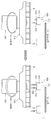
도 1은 유기용제를 이용한 기판 처리 장치를 개략적으로 보여주는 단면도이다. 일 예에 의하면, 유기용제로는 이소프로필 알코올(IPA)이 사용될 수 있다.
기판 처리 장치(10)는 용기(100), 승강부재(200), 지지부재(300), 상부 노즐 부재(400) 그리고 하부 노즐 부재(500)를 가진다. 지지부재(300)는 공정 진행시 기판을 지지한다. 용기(100)는 공정 진행시 사용된 약액, 순수, 유기용제가 외부로 튀는 것을 방지한다. 또한 용기(100)는 공정 진행시 사용된 약액이나 순수의 재사용이 가능하도록 이들을 회수한다. 승강부재(200)는 용기(100)와 지지부재(300) 간의 상대위치를 변경한다. 승강부재(200)는 용기(100) 또는 지지부재(300)를 상하로 승강시켜 용기(100) 내에서 지지부재(300)의 상대 높이를 변경한다. 상부 노즐 부재(400)는 기판의 상면으로 유기용제나 불활성 가스와 같은 건조가스를 공급한다. 하부 노즐 부재는 기판의 저면으로 세정액을 공급한다. 이하, 각각의 구성요소에 대해 상세히 설명한다.
(지지부재)
도 1을 참조하면, 지지부재(300)는 처리 공정시 기판(W)을 지지한다. 기판 지지부재(300)는 스핀 헤드(310), 스핀들(spindle)(320) 그리고 회전 부재(330)를 가진다.
스핀 헤드(310)는 상부에 기판(W)이 로딩(loading)되는 상부면(312a)을 가진다. 스핀 헤드(310)의 상부면(312a)는 대체로 원형으로 제공되며, 기판보다 큰 직경을 가진다. 또한, 스핀 헤드(310)는 지지 핀들(314) 및 척킹 핀들(316)을 가진다.
지지 핀들(314)는 기판(W)이 스핀 헤드(310)의 상부면(312a)으로부터 이격되도록 기판(W)의 저면을 지지한다. 지지 핀들(314)은 스핀 헤드의 상부면(312a)으로부터 상부로 돌출되도록 상부면(312a)에 설치된다.
척킹 핀들(316)은 공전 진행시 기판이 스핀 헤드의 측면을 지지한다. 척킹 핀들(316)은 스핀 헤드(310)가 회전될 때 원심력에 의해 기판(W)이 스핀 헤드(310) 상의 정해진 위치에서 측방향으로 이탈되는 것을 빙지한다. 척킹 핀들(316)은 스핀 헤드 상의 가장자리 영역에 위치한다. 척킹 핀들(316)은 3개 이상 제공되며, 환형으로 배치된다. 척킹 핀들(316)에 의해 제공되는 내부 공간이 기판(W)이 로딩 또는 언로딩시에는 기판(W)의 직경보다 크게 제공되고, 공정 진행시에 기판(W)의 측면과 접촉될 수 있도록 척킹 핀들(316)은 이동 가능하게 제공된다. 척킹 핀(316)은 스핀 헤드(310)의 상부면(312a)에서 그 반경 방향을 따라 직선 이동되도록 제공될 수 있다.
스핀들(320)은 스핀 헤드(310)의 하부면 중앙으로부터 아래 방향으로 연장되도록 스핀 헤드(310)에 고정 설치된다. 스핀들(310)은 그 내부가 비어 있는 중공축(hollow shaft) 형태를 가진다. 스핀들(310)은 회전 부재(330)의 회전력을 스핀 헤드(310)에 전달한다. 상세하게 도시하지는 않았지만, 회전 부재(330)는 회전력을 발생하는 모터와 같은 구동부와, 구동부로부터 발생된 회전력을 스핀들로 전달하는 벨트, 체인과 같은 동력 전달부 등을 가지는 메카니즘으로 제공될 수 있다.
(용기)
도 1을 참조하면, 용기(100)는 상부가 개방된 통 형상을 가진다. 용기(100)는 스핀 헤드(310) 주변을 감싸도록 배치된다. 용기(100)의 내부는 기판에 대해 공정이 수행되는 공간으로서 제공된다. 용기(100)는 공정시 사용된 약액, 세정액, 건조가스와 같은 유체를 용기 외부로 배출한다. 용기의 저면에는 개구가 형성된다. 상술한 스핀들(320)은 용기(100)의 바닥면에 형성된 개구를 통해 용기(100) 외부까지 연장된다.
일 예에 의하면, 용기(100)는 공정에 사용된 약액들이나 세정액의 재사용이 가능하도록 이들을 분리하여 회수할 수 있는 구조를 가진다. 용기(100)는 복수의 회수통들(110a, 110b, 110c)을 가진다. 각각의 회수통(110a, 110b, 110c)은 공정에 사용된 처리액들(약액 및 세정액) 중 서로 상이한 종류의 처리액을 회수한다. 본 실시 예에서 용기(100)는 3개의 회수통들을 가진다. 각각의 회수통들을 내부 회수통(110a), 중간 회수통(110b), 그리고 외부 회수통(110c)이라 칭한다.
내부 회수통(110a)은 스핀 헤드(310)를 감싸는 환형의 링 형상으로 제공되고, 중간 회수통(110b)은 내부 회수통(110a)을 감싸는 환형의 링 형상으로 제공되며, 외부 회수통(110c)은 중간 회수통(110b)을 감싸는 환형의 링 형상으로 제공된다. 각각의 회수통(110a, 110b, 110c)은 용기(110) 내에서 용기 내 공간(a)과 통하는 유입구(111a, 111b, 111c)를 가진다. 각각의 유입구(111a, 111b, 111c)는 스핀 헤드(310)의 둘레에 링 형상으로 제공된다. 기판(W)으로 분사되어 공정에 사용된 약액들은 기판(W)의 회전으로 인한 원심력에 의해 유입구(111a, 111b, 111c)를 통해 회수통(110a, 110b, 110c)으로 유입된다. 이렇게 유입된 약액들은 각각의 배출라인(115a,115b,115c)을 통해 외부로 배출된다.
상술한 바와 달리 용기는 단일의 통으로 제공되어 처리액 및 세정액의 분리 회수 없이 동일한 배출관을 통해 외부로 배출할 수 있다.
(승강유닛)
승강 유닛(200)은 용기(100)를 상하 방향으로 직선 이동시킨다. 용기(100)가 상하로 이동됨에 따라 용기(100) 내에서 용기(100)에 대핸 스핀 헤드(310)의 상대 높이가 변경된다. 승강 유닛(200)은 브라켓(210), 이동 축(220), 그리고 구동기(230)를 가진다. 브라켓(210)은 용기(100)의 외벽에 고정설치되고, 브라켓(210)에는 구동기(230)에 의해 상하 방향으로 이동되는 이동 축(220)이 고정결합된다. 기판(W)이 스핀 헤드(310)에 놓이거나, 스핀 헤드(310)로부터 들어올릴 때 스핀 헤드(310)가 용기(100)의 상부로 돌출되도록 스핀 헤드(310)는 하강한다. 또한, 공정이 진행시에는 기판(W)에 공급된 처리액의 종류에 따라 처리액이 기설정된 회수통(110a,110b,110c)으로 유입될 수 있도록 용기(100)의 높이가 조절한다. 상술한 바와 반대로, 승강 유닛(200)은 스핀 헤드(310)를 상하 방향으로 이동시킬 수 있다.
(상부 노즐 부재)
상부 노즐 부재(400)는 스핀 헤드(310)에 놓여진 기판(W) 상으로 건조 유체를 공급한다. 일 예에 의하면, 상부 노즐 부재(400)는 스핀 헤드(310)에 놓여진 기판(W)의 상면으로 유기용제와 건조가스 등을 분사한다. 기판(W)의 상면은 반도체 회로 패턴이 형성된 면일 수 있다.
상부 노즐 부재(400)는 복수의 노즐(412,414)들과, 복수의 노즐들(412, 424)이 설치되는 분사 헤드(410)를 포함한다. 분사 헤드(410)는 후술하는 이동부재(420)의 아암(422)에 연결되며, 기판(W)과 대향하는 면에는 복수의 노 즐(412,414)들이 설치된다. 분사 헤드(410)에는 제1노즐(412)과 제2노즐(414)이 설치된다. 제1노즐(412)은 이소프로필 알코올(isopropyl alcohol, 이하 IPA)과 같은 유기용제를 분사하고, 제2노즐(414)는 질소(N2) 가스와 같은 불활성 가스를 분사한다. 일 예에 의하면, IPA는 증기 상태로 공급된다.
IPA는 기판에 대한 수분의 부착력을 약화시키고, 기판에 부착된 수분과 치환되어 기판에 잔류한다. 뒤이어 공급되는 N2 가스는 기판 상에 잔류하는 IPA를 휘발시켜 기판으로부터 IPA를 제거한다.
상술한 예에서는 상부 노즐 부재에 2개의 노즐이 제공된 것을 예로 들어 설명하였다. 그러나 이와 달리 상부 노즐 부재에는 기판에 약액을 공급하는 노즐 및 순수와 같은 세정액을 공급하는 노즐이 더 제공될 수 있다. 선택적으로 기판의 상면으로 약액을 공급하는 노즐과 세정액을 공급하는 노즐은 상부 노즐 부재와는 별도로 제공될 수 있다.
건조 유체 공급부(430)는 건조 유체를 분사 헤드(410)에 공급한다. 건조 유체 공급부(430)는 IPA 공급원(432), 질소가스 공급원(434), IPA 공급원(432)과 제1노즐(412)을 연결하는 제1공급라인(435), 질소가스 공급원(434)과 제2노즐(414)을 연결하는 제2공급라인(436)을 가진다.
이동부재(420)는 분사 헤드(410)와 결합되어 분사 헤드(410)를 이동시킨다. 이동부재(420)는 아암(422), 지지축(424), 그리고 구동모터(426)를 가진다. 아암은 긴 로드 형상을 가진다. 아암(422)의 일단에는 분사 헤드(410)가 연결되며, 아 암(422)은 분사 헤드(410)를 지지한다. 아암(422)의 타단에는 지지축(424)이 연결된다. 지지축(424)은 구동모터(426)로부터 회전력을 전달받으며, 회전력을 이용하여 아암(422)에 연결된 분사 헤드(410)를 이동시킨다. 구동모터는 제어부(미도시됨)에 연결된다.
공정 진행시, 분사 헤드(410)는 기판(W)의 중심영역과 가장자리 영역을 왕복 이동하면서 기판(W) 상으로 건조 유체를 공급할 수 있다. 선택적으로 분사 헤드(410)는 기판(W)의 중심영역에서 가장자리 영역으로 1회 이동하면서 기판(W) 상으로 건조 유체를 공급할 수 있다. 선택적으로 공정 진행시 분사 헤드(410)는 기판(W)의 중심 영역에 고정되어 기판(W) 상으로 건조 유체를 공급할 수 있다. 공정 진행시 IPA와 N2 가스는 동시에 분사될 수 있다. 선택적으로 분사 헤드(410)가 기판(W)의 중심영역에서 가장자리 영역으로 이동시에는 IPA만 분사되고, 이후에 분사 헤드(410)가 다시 기판(W)의 중심영역에서 가장자리 영역으로 이동시에는 N2 가스만 공급될 수 있다.
분사 헤드(410)가 기판(W)의 중심영역에서 가장자리 영역으로 이동시, 도 2에 도시한 바와 같이, 분사 헤드(410)는 지지축(424)을 회전축으로 하여 회전 이동할 수 있다. 이때, 분사 헤드(410)은 기판의 중심(c)을 지나는 호(a)를 그리며, 제1 및 제2노즐(412,414)은 호(a)상에 배치될 수 있다. 특히, 제1노즐(412)은 분사 헤드(410)의 이동방향(화살표 방향)에 대하여 제2노즐(414)보다 선행하는 위치에 배치될 수 있다.
도 3에 도시한 바와 같이, 분사 헤드(410)는 이동부재(420)의 아암(422) 상에서 직선 이동할 수 있다. 이때, 상부 노즐 부재(400)는 기판의 중심(c)을 지나는 직선 상에 일렬로 배치된다. 제1노즐(412)은 제2노즐(414)에 비해 아암의 타단에 더 인접하게 위치될 수 있다. 제1노즐(412)은 분사 헤드(400)의 이동방향(화살표 방향)에 대하여 제2노즐(414)보다 선행하는 위치에 배치되므로, 기판의 일정 영역에 대해 IPA가 먼저 공급되고, 이후에 N2가스가 공급될 수 있다.
다른 예에 의하면, 도 6과 같이 제1노즐(412)은 유기용제 또는 유기용제를 포함한 혼합 유체를 기판으로 공급한다. 여기에서 유기용제는 액 상태로 공급될 수 있다. 예컨대, 혼합 유체는 액 상의 유기용제와 액 상의 순수(물)의 혼합액일 수 있다. 용제 공급 부재(450)는 상부 노즐 부재(400)의 제1노즐(412)로 유기용제 또는 유기용제를 포함하는 혼합 유체를 공급한다. 용제 공급 부재(450)는 유기용제를 저장하는 유기용제 저장 용기(452), 물을 저장하는 물 저장 용기(451), 유기용제와 물을 혼합하는 혼합기(455), 유기용제 저장 용기(452)에서 혼합기(455)로 유기용제가 공급되는 유기용제 공급관(454), 물 저장 용기(451)에서 혼합기(455)로 물이 공급되는 물 공급관(453), 그리고 혼합기(455)로부터 제1노즐(412)로 유기용제와 물의 혼합액을 공급하는 혼합액 공급관(456)을 가진다.
유기용제를 증기 상태로 기판으로 공급하는 경우, 유기용제의 일부는 기판 건조에 충분히 기여하지 못하고, 바로 휘발 될 수 있다. 그러나 유기용제를 액 상태로 기판에 공급하는 경우, 대부분의 유기용제가 기판 건조에 충분히 기여한다. 또한, 액 상의 유기용제를 순수와 혼합하여 기판에 공급하는 경우, 유기용제의 사용량을 더욱 절감할 수 있다.
(하부 노즐 부재)
하부 노즐 부재(500)는 기판(W)의 저면으로 세정 유체를 분사한다. 아래의 실시예에서는 세정유체로 액 상의 순수가 사용되는 것으로 설명한다.
다시 도 1을 참조하면, 하부 노즐 부재(500)는 스핀 헤드(310)의 상면 중앙에 설치된 하부 노즐(510)을 포함한다. 하부 노즐(510)은 순수 공급라인과 연결되어 스핀 헤드(310)의 중앙부에 위치된다. 하부 노즐(510)은 순수를 기판(W)의 저면으로 분사하기 위한 분사구(512)를 갖는다. 하부 노즐(510)에서 분사되는 순수는 기판(W)의 회전에 의해 기판(W)의 저면 중앙부에서 가장자리로 분산되면서 기판(W)의 저면을 세정한다.
하부 노즐 부재(500)에 분사되는 순수는 가열된 상태로 공급될 수 있다. 이는 하부 노즐 부재(500)에 의해 기판(W)의 저면이 세정되는 동안, 세정 효율을 향상시킬 뿐 만 아니라 기판(W)을 가열하는 기능을 수행한다.
세정 유체 공급부(520)는 순수 공급원(522), 가열기(524), 순수 공급라인(526), 그리고 드레인 라인(528)을 가진다. 가열기(524)는 순수 공급원(522)에 설치되어 순수 공급원(522)에 저장된 순수를 가열할 수 있다. 이와 달리 가열기(524)는 순수 공급라인(526) 상에 설치될 수 있다. 순수 공급라인(526)은 그 일단이 순수 공급원(522)에 연결되고 타단이 하부 노즐(510)에 연결된다. 순수 공급라인(526)은 스핀들(320)의 중공 부분(hollow section)을 통과하여 하부 노즐(510) 과 연결된다. 드레인 라인(528)은 순수 공급라인(526)으로부터 분기된다.
순수 공급라인(526)에는 온오프 밸브인 제1밸브(527a)와 하부 노즐(510)을 통해 토출된 직후 노즐에 남아 있는 가열된 순수를 역류시키는 서크백(SuckBack) 밸브(527b)가 설치된다. 드레인 라인(528)에는 온오프 밸브인 제2밸브(527c)가 설치된다. 순수 공급라인(526)은 소정의 배관으로 구성되는 것이 바람직하며, 스핀들(320)에서는 스핀들(320) 내부의 관 형태로 비어있는 공간으로도 정의될 수 있다. 순수 공급라인(526)에 정체되어 있는 가열된 순수는 시간이 지날수록 온도가 떨어진다. 낮은 온도의 순수가 기판으로 공급되는 경우, 그 기판(W)은 다른 기판(W)들에 대해 세정 효율이 저하될 수 있다. 드레인 라인(528)은 기판(W)의 저면으로 분사되는 가열된 순수의 공정 재연성을 확보하기 위해 순수 공급라인(526)에 잔류하는 순수를 배출하기 위해 사용될 수 있다. 즉, 가열된 순수가 기판(W)의 저면으로 공급되기 전에 순수 공급라인(526) 상에 정체되어 있는 순수는 일정시간 동안 드레인되며, 그 이후에 가열기(524)에 의해 기 설정온도로 가열된 순수만을 하부 노즐(510)로 제공된다.
순수는 상온보다 높은 온도로 가열되어 기판(W)으로 공급될 수 있다. 선택적으로 순수는 기판(W)으로 공급되는 IPA보다 높은 온도로 가열되어 기판(W)으로 공급될 수 있다. 일 예에 의하면, 순수는 60-80℃의 온도로 기판(W)의 저면으로 공급될 수 있다.
일 예에 의하면, 기판(W)의 상면으로 IPA가 공급되는 동안, 기판(W)의 저면으로 순수가 공급된다. 이로 인해 기판(W)의 상면에 대해 건조 공정이 수행되는 동 안 기판(W)의 저면에 대해 세정 공정이 동시에 수행된다. 또한, 기판(W)의 상면으로 IPA가 공급되는 동안, 기판(W)의 저면으로 순수가 가열된 상태로 공급된다. 가열된 순수는 기판(W)을 건조시키는 공정을 진행함에 있어서, IPA 용액의 증발에 따른 응축 냉각에 의한 기판(W) 표면의 급격한 온도 저하를 방지한다. 즉, 기판(W)의 표면으로 IPA 용액 및 N2 가스를 분사하여 기판(W)을 건조시키는 동안, 가열된 순수를 기판(W)의 저면으로 분사하여 기판(W) 전체의 온도를 60-80℃ 범위 내에서 일정하게 유지시키게 된다. 기판(W)의 저면으로 공급될 때 순수의 온도는 60-80℃가 되도록, 가열기(524)는 이보다 조금 더 높은 온도로 순수를 가열한다. 이 온도는 건조 공정의 진행 상태에 따라 변할 수 있다.
또한, IPA는 가열된 상태로 기판(W)으로 공급될 때 건조 효과가 더 크다. 그러나 액 상의 IPA 또는 그 혼합액을 공급시에 기판(W)으로 제공되는 IPA의 온도를 높이는 데에는 한계가 있다. 그러나 기판(W)의 상면으로 IPA가 공급되는 동안 가열된 순수를 기판(W)의 저면으로 공급하면, 기판(W)이 가열됨에 따라 고온의 IPA가 공급될 때와 유사한 효과를 얻을 수 있다. 물론 증기 상태의 IPA가 기판(W)의 상면으로 공급되는 경우에도 기판(W)의 저면으로 가열된 세정액을 공급하면, 상온의 세정액을 공급할 때에 비해 건조 효율이 증가된다.
또한, 건조 공정 동안 가열된 순수에 의해 기판(W)의 온도가 일정하게 유지됨으로써, 물반점 및 건조 불량에 따른 파티클의 발생을 방지할 수 있다.
또한, 기판(W) 전체가 급격한 온도 저하 없이 일정 온도로 유지되어 IPA 용 액에 의한 건조 시간이 줄어들게 되어 IPA 용액의 소모량을 감소시키는 효과가 있다.
상술한 예에서는 세정 유체로서 액 상의 가열된 순수가 사용된 경우를 설명하였다. 그러나 이와 달리 가열된 질소가스나, 증기나 미스트 상태의 가열된 순수가 사용될 수 있다.
상기와 같이 구성되는 본 발명에 따른 IPA를 이용한 기판 처리 장치에서의 작용을 설명하면 다음과 같다.
먼저, 기판(W)이 이송되어 스핀 헤드(310) 상에 놓여지면, 회전 부재(330)는 스핀 헤드(310)를 회전시킨다.
기판(W)이 회전하게 되면 식각액에 의한 식각 공정이 진행된다. 일반적으로, 습식 식각 공정에 있어서 기판(W) 상의 실리콘 막을 식각하기 위한 식각액으로는 HF(불산, Hydrofluoric Acid) 용액이 사용된다. HF 용액을 하우징 내로 분사하여 회전하는 기판(W) 표면의 실리콘막을 식각한다.
식각 공정이 끝난 후, 기판(W) 표면의 식각 잔류물을 제거하기 위하여, 기판(W)을 계속 회전시키면서 기판(W)의 상면으로 순수를 분사시킨다.
세정 공정이 끝난 후, 기판(W)의 상면을 건조시키는 건조 공정이 진행된다. 이와 동시에 기판(W)의 저면을 세정하는 공정이 병행된다. 이를 위해 기판의 상면으로 액 또는 증기 상태의 IPA 또는 IPA와 순수의 혼합액을 공급하고, 기판의 저면으로 가열된 순수가 공급된다. 도 5는 기판의 상면에 대한 건조 공정과 기판의 저면에 대한 세정 공정이 동시에 수행되는 것을 보여준다.
도 6은 일 실시예에 따른 건조 방법을 보여주는 플로우 챠트이고, 도 7은 도 6의 건조 방법을 단계적으로 보여주는 도면들이다.
도 6 및 도 7에 도시한 바와 같이, 건조 공정은 크게 프리 토출 단계(S610)와 최종 토출 단계(S620)를 가진다. 프리 토출 단계에서의 기판 회전 속도는 최종 토출 단계의 기판 회전속도보다 낮은 450-550rpm이다.
프리 토출 단계는 상부 노즐 부재(400)에서 IPA 용액을 분사한다. 또한, 기판의 온도를 높이기 위해 하부 노즐 부재(500)에서 가열된 순수를 분사한다. 상부 노즐 부재(400)는 회전하는 기판 상면의 중심으로부터 가장자리로 2회 왕복 스캔하면서 IPA 용액을 분사하게 된다. IPA 용액은 용액이 증발할 때의 휘발성을 이용하여 기판(W)을 건조시키는 데, IPA 용액이 기판(W)의 표면을 통과함에 따라 세정 공정 후에 기판(W) 표면에 잔류하는 순수의 수소와 치환반응을 일으켜 수분을 제거하게 된다. 여기서, 기판(W)의 원심력은 IPA 용액의 표면장력보다 크거나 같아야 하며, 기화력은 원심력보다 크거나 같은 것이 바람직하다. 기판(W)의 회전 속도가 너무 낮으면(400rpm이하) 원심력이 작아지면서 IPA 용액이 기판 상면에 잔류할 가능성이 매우 높아지고, 그 반대로 기판(W)의 회전 속도가 너무 빠르면(900rpm 이상) 원심력이 커지면서 IPA 용액이 기판(W) 상면으로부터 너무 빨리 제거되기 때문에 IPA용액이 증발하면서 수분을 제거해야 할 시간이 부족하여 수분 제거 효율이 떨어지면서 물반점이 발생되게 된다. 그러나, 기판(W)의 회전 속도를 450-550rpm 그리고 650-750rpm으로 제어할 경우 IPA 용액이 수분과 반응하면서 기화되는 시간을 충분히 제공해줄 뿐만 아니라 IPA 용액이 기판(W)에 잔류하는 문제도 해결됨으로써 건조 공정 후 기판(W)에 물반점이 형성되는 불량을 현저하게 감소시킬 수 있는 것이다.
최종 토출 단계(S620)는 프리 토출 단계보다 빠른 회전력으로 기판을 회전시키면서, 기판(W)의 상면으로 IPA 용액과 N2 가스를 분사하여 기판(W) 상면을 건조시킨다. 최종 토출 단계는, 상부 노즐 부재(400)가 기판(W)의 중심에서 가장자리로 1회 스캔하는 것으로 완료된다. IPA 용액에 의한 건조가 이루어지는 동안, 상부 노즐 부재(400)의 제2노즐(414)이 제1노즐(412)을 뒤따라 이동하면서, N2 가스를 분사하여 기판(W) 표면을 건조시킨다. N2 가스는 IPA 용액의 증발을 활성화시키는 역할을 한다.
상술한 예에서는 건조가 초기 토출 단계와 최종 토출 단계로 나누어져 분사되는 것으로 기재하였다. 그러나 이와 달리 초기 토출 단계 만으로 건조가 이루어질 수 있다.
건조 공정을 마친 후, 회전 부재(330)는 동작을 중지하여 스핀 헤드(310)의 회전을 멈추고, 기판(W)은 이송되거나, 다른 공정이 진행된다.
상기 기판(W)은 반도체 칩 제조에 사용되는 웨이퍼(wafer)에 한정되지 않고, 평판표시(Flat panel display) 패널에 사용되는 유리 기판과 같이 다른 종류의 기판일 수 있다.
도 1은 본 발명의 기판 처리 장치의 일 예를 개략적으로 보여주는 단면도이다.
도 2는 상부 노즐 부재의 일 예를 보여주는 도면이다.
도 3은 상부 노즐 부재의 다른 예를 보여주는 도면이다.
도 4는 도 1의 기판 처리 장치의 다른 예를 개략적으로 보여주는 단면도이다.
도 5는 도 4의 기판 처리 장치에서 공정이 수행되는 과정을 개략적으로 보여주는 도면이다.
도 6은 본 발명의 일 실시예에 따른 건조 방법을 보여주는 플로우챠트이다.
도 7은 각각 프리 토출 단계와 최종 토출 단계에서 건조 공정이 수행되는 것을 보여주는 도면들이다.
<도면의 주요 부분에 대한 부호의 설명>
100: 용기 200 : 승강부재
300 : 지지부재 400 : 상부 노즐 부재
500 : 하부 노즐 부재
Claims (15)
- 기판을 처리하는 장치에 있어서,기판을 지지하는 스핀 헤드와;상기 스핀 헤드에 놓인 기판의 상면으로 유기용제 또는 상기 유기용제를 포함하는 혼합 유체를 공급하도록 제공되는 상부 노즐 부재와;상기 스핀 헤드에 놓인 기판의 저면으로 세정액을 공급하도록 제공되는 하부 노즐 부재와; 그리고상기 하부 노즐 부재로 공급되는 상기 세정액을 가열하는 가열기를 구비하되,상기 하부 노즐 부재는 상기 스핀 헤드 내에 제공되는 것을 특징으로 하는 기판 처리 장치.
- 기판을 처리하는 장치에 있어서,기판을 지지하는 스핀 헤드와;상기 스핀 헤드에 놓인 기판의 상면으로 유기용제 또는 상기 유기용제를 포함하는 혼합 유체를 공급하도록 제공되는 상부 노즐 부재와;상기 스핀 헤드에 놓인 기판의 저면으로 세정액을 공급하도록 제공되는 하부 노즐 부재와;상기 하부 노즐 부재로 공급되는 상기 세정액을 가열하는 가열기와, 그리고상기 상부 노즐 부재로 유기용제 또는 상기 유기용제를 포함하는 혼합 유체를 공급하는 유기 용제 공급 부재를 더 포함하되,상기 유기 용제 공급 부재는,유기용제를 저장하는 유기용제 저장 용기와;물을 저장하는 물 저장 용기와;상기 유기용제와 상기 물을 혼합하는 혼합기와;상기 유기용제 저장 용기에서 상기 혼합기로 상기 유기용제가 공급되는 유기용제 공급관과;상기 물 저장 용기에서 상기 혼합기로 상기 물이 공급되는 물 공급관과; 그리고상기 혼합기로부터 상기 상부 노즐 부재로 상기 유기용제와 상기 물의 혼합액을 공급하는 혼합액 공급관을 더 포함하는 것을 특징으로 하는 기판 처리 장치.
- 제 2 항에 있어서,상기 하부 노즐 부재는 상기 스핀 헤드 내에 제공되는 것을 특징으로 하는 기판 처리 장치.
- 제 1 항 내지 제 3 항 중 어느 하나의 기판 처리 장치를 사용하여 기판을 처리하는 방법에 있어서,상기 상부 노즐 부재로부터 상기 기판의 상면으로 상기 유기용제 또는 상기 혼합유체를 분사하여 상기 기판의 상면을 건조하고,,상기 유기용제 또는 상기 혼합 유체에 의해 상기 기판의 상면이 건조되는 동안에 상기 하부 노즐 부재로부터 상기 기판의 저면으로 상기 세정액을 공급하여 상기 기판의 저면을 세정하는 것을 포함하는 것을 특징으로 하는 기판 처리 방법.
- 제 4 항에 있어서,상기 세정액은 상온보다 높은 온도로 가열되어 상기 기판의 저면으로 공급되는 것을 특징으로 하는 기판 처리 방법.
- 제 4 항에 있어서,상기 세정액은 상기 유기용제 또는 상기 혼합유체보다 높은 온도로 가열되어 상기 기판의 저면으로 공급되는 것을 특징으로 하는 기판 처리 방법.
- 제 4 항에 있어서,상기 유기용제 또는 상기 혼합유체는 액 상태로 공급되는 것을 특징으로 하는 기판 처리 방법.
- 제 4 항에 있어서,상기 유기용제는 액 상태로 물과 혼합되어 공급되는 것을 특징으로 하는 기판 처리 방법.
- 제 4 항에 있어서,상기 기판의 상면의 건조 및 상기 기판의 저면의 세정이 이루어지는 동안 상기 기판은 회전되는 것을 특징으로 하는 기판 처리 방법.
- 제 4 항에 있어서,상기 유기용제는 이소프로필알코올이고,상기 세정액은 물인 것을 특징으로 하는 기판 처리 방법.
- 기판을 처리하는 방법에 있어서,회전하는 기판의 상면으로 유기용제 또는 상기 유기용제를 포함하는 혼합유체를 분사하고 이와 동시에 상기 기판의 저면으로 세정액을 분사하는 프리 토출 단계와;상기 프리 토출 단계에서의 기판의 회전 속도보다 빠르게 상기 기판을 회전시키고, 상기 기판의 상면으로 상기 유기용제와 건조 가스를 동시에 분사하는 최종 토출 단계를 포함하는 것을 특징으로 하는 기판 처리 방법.
- 제 11 항에 있어서,상기 세정액은 가열된 상태로 공급되는 것을 특징으로 하는 기판 처리 방법.
- 제 11 항 또는 제 12 항에 있어서,상기 프리 토출 단계는상기 유기용제 또는 상기 혼합유체를 기판의 중심에서 가장자리로 그리고 기판의 가장자리에서 중심으로 2회 왕복 스캔 분사하며,상기 최종 토출 단계는상기 유기용제와 건조가스를 기판의 중심으로부터 가장자리까지 1회만 스캔 분사하는 것을 특징으로 하는 기판 처리 방법.
- 제 11 항 또는 제 12 항에 있어서,상기 프리 토출 단계에서 기판의 회전속도는 450-550rpm이며,상기 최종 토출 단계에서 기판의 회전속도는 650-750rpm인 것을 특징으로 하는 기판 처리 방법.
- 제 1 항 내지 제 3 항 중 어느 하나에 있어서,상기 스핀 헤드는 회전 가능하게 제공된 것을 특징으로 하는 기판 처리 장치.
Applications Claiming Priority (2)
| Application Number | Priority Date | Filing Date | Title |
|---|---|---|---|
| KR20080018380 | 2008-02-28 | ||
| KR1020080018380 | 2008-02-28 |
Related Child Applications (1)
| Application Number | Title | Priority Date | Filing Date |
|---|---|---|---|
| KR1020110009503A Division KR20110025803A (ko) | 2008-02-28 | 2011-01-31 | 기판 처리 장치 및 기판 처리 방법 |
Publications (2)
| Publication Number | Publication Date |
|---|---|
| KR20090093835A KR20090093835A (ko) | 2009-09-02 |
| KR101049441B1 true KR101049441B1 (ko) | 2011-07-15 |
Family
ID=41302282
Family Applications (2)
| Application Number | Title | Priority Date | Filing Date |
|---|---|---|---|
| KR1020090015573A KR101049441B1 (ko) | 2008-02-28 | 2009-02-25 | 기판 처리 장치 및 기판 처리 방법 |
| KR1020110009503A KR20110025803A (ko) | 2008-02-28 | 2011-01-31 | 기판 처리 장치 및 기판 처리 방법 |
Family Applications After (1)
| Application Number | Title | Priority Date | Filing Date |
|---|---|---|---|
| KR1020110009503A KR20110025803A (ko) | 2008-02-28 | 2011-01-31 | 기판 처리 장치 및 기판 처리 방법 |
Country Status (1)
| Country | Link |
|---|---|
| KR (2) | KR101049441B1 (ko) |
Families Citing this family (14)
| Publication number | Priority date | Publication date | Assignee | Title |
|---|---|---|---|---|
| KR101091314B1 (ko) | 2009-10-01 | 2011-12-07 | 주식회사 에스엘라이팅 | 측방 조사용 프로젝션 렌즈 및 이를 장착한 헤드램프 |
| KR101373748B1 (ko) * | 2010-04-19 | 2014-03-14 | 세메스 주식회사 | 기판 세정 방법 |
| KR101870666B1 (ko) * | 2011-08-04 | 2018-06-26 | 세메스 주식회사 | 기판 처리 장치 |
| KR101909480B1 (ko) * | 2011-08-04 | 2018-10-19 | 세메스 주식회사 | 기판 처리 장치 |
| US9355883B2 (en) * | 2011-09-09 | 2016-05-31 | Lam Research Ag | Method and apparatus for liquid treatment of wafer shaped articles |
| KR101236804B1 (ko) * | 2012-03-28 | 2013-02-25 | 세메스 주식회사 | 기판 세정 장치 및 기판 세정 방법 |
| KR20130142033A (ko) * | 2012-06-18 | 2013-12-27 | 주식회사 제우스 | 기판 처리 장치 |
| KR101517152B1 (ko) * | 2013-08-29 | 2015-04-30 | 주식회사 케이씨텍 | 기판 처리 장치 및 그 제어 방법 |
| KR102262112B1 (ko) * | 2014-05-26 | 2021-06-10 | 세메스 주식회사 | 기판처리장치 및 방법 |
| KR102279716B1 (ko) * | 2014-08-11 | 2021-07-21 | 세메스 주식회사 | 기판 처리 장치 및 기판 건조 방법 |
| KR101935949B1 (ko) * | 2016-10-07 | 2019-01-08 | 세메스 주식회사 | 기판 처리 장치 및 방법 |
| KR101955597B1 (ko) * | 2017-05-17 | 2019-05-31 | 세메스 주식회사 | 세정액 제조 장치 및 방법 |
| KR102040954B1 (ko) * | 2017-11-06 | 2019-11-05 | 세메스 주식회사 | 기판 처리 장치 |
| KR102622445B1 (ko) * | 2020-04-24 | 2024-01-09 | 세메스 주식회사 | 기판 처리 장치 및 액 공급 방법 |
Citations (3)
| Publication number | Priority date | Publication date | Assignee | Title |
|---|---|---|---|---|
| KR20060025836A (ko) * | 2004-09-17 | 2006-03-22 | 삼성전자주식회사 | 기판 세정 장치 및 기판 세정 방법 |
| KR100749544B1 (ko) * | 2006-04-06 | 2007-08-14 | 세메스 주식회사 | 기판세정장치 및 기판세정방법 |
| KR100794585B1 (ko) * | 2006-08-01 | 2008-01-17 | 세메스 주식회사 | 습식 세정 장치 및 방법 |
-
2009
- 2009-02-25 KR KR1020090015573A patent/KR101049441B1/ko not_active IP Right Cessation
-
2011
- 2011-01-31 KR KR1020110009503A patent/KR20110025803A/ko not_active Application Discontinuation
Patent Citations (3)
| Publication number | Priority date | Publication date | Assignee | Title |
|---|---|---|---|---|
| KR20060025836A (ko) * | 2004-09-17 | 2006-03-22 | 삼성전자주식회사 | 기판 세정 장치 및 기판 세정 방법 |
| KR100749544B1 (ko) * | 2006-04-06 | 2007-08-14 | 세메스 주식회사 | 기판세정장치 및 기판세정방법 |
| KR100794585B1 (ko) * | 2006-08-01 | 2008-01-17 | 세메스 주식회사 | 습식 세정 장치 및 방법 |
Also Published As
| Publication number | Publication date |
|---|---|
| KR20110025803A (ko) | 2011-03-11 |
| KR20090093835A (ko) | 2009-09-02 |
Similar Documents
| Publication | Publication Date | Title |
|---|---|---|
| KR101049441B1 (ko) | 기판 처리 장치 및 기판 처리 방법 | |
| JP4870837B2 (ja) | 基板乾燥装置及びその方法 | |
| TWI547765B (zh) | 基板處理方法及基板處理裝置 | |
| US20060086373A1 (en) | Apparatus and method for drying substrates used to manufacture semiconductor devices | |
| KR101373748B1 (ko) | 기판 세정 방법 | |
| KR20090012703A (ko) | 기판 세정 장치 및 방법 | |
| KR101022783B1 (ko) | 기판 건조 방법 | |
| KR101005889B1 (ko) | 구리 패턴이 노출된 기판을 건조하는 방법 및 이를 이용하는 금속 배선 형성 방법 | |
| KR20110131707A (ko) | 기판 세정 장치 및 그 장치에서의 기판 세정 방법 | |
| JP7209494B2 (ja) | 基板処理装置、処理液および基板処理方法 | |
| KR100968258B1 (ko) | 기판 건조 방법 | |
| KR20110091626A (ko) | 기판 건조 장치 및 방법 | |
| KR101236804B1 (ko) | 기판 세정 장치 및 기판 세정 방법 | |
| KR20140044132A (ko) | 스핀 헤드 및 이를 포함하는 기판 처리 장치, 그리고 상기 장치를 이용한 기판 처리 방법 | |
| KR101100277B1 (ko) | 기판 처리 장치 및 기판 처리 방법 | |
| KR20120078573A (ko) | 기판 처리 장치 및 방법 | |
| KR20100061042A (ko) | 기판 건조 장치 및 방법 | |
| KR102279716B1 (ko) | 기판 처리 장치 및 기판 건조 방법 | |
| JP2008034612A (ja) | 基板処理装置および基板処理方法 | |
| KR20120078574A (ko) | 기판 건조 장치 및 방법 | |
| KR20080009833A (ko) | 기판 세정 및 건조 방법 | |
| WO2007072571A1 (ja) | 基板の乾燥装置および洗浄装置並びに乾燥方法および洗浄方法 | |
| KR101256958B1 (ko) | 기판 세정 장치 및 기판 세정 방법 | |
| JP7126429B2 (ja) | 基板処理方法および基板処理装置 | |
| KR100497999B1 (ko) | 웨이퍼 건조 방법 및 장치 |
Legal Events
| Date | Code | Title | Description |
|---|---|---|---|
| A201 | Request for examination | ||
| E902 | Notification of reason for refusal | ||
| A107 | Divisional application of patent | ||
| E701 | Decision to grant or registration of patent right | ||
| GRNT | Written decision to grant | ||
| J204 | Invalidation trial for patent | ||
| J301 | Trial decision |
Free format text: TRIAL DECISION FOR INVALIDATION REQUESTED 20111014 Effective date: 20120620 |
|
| J2X1 | Appeal (before the patent court) |
Free format text: INVALIDATION |
|
| EXTG | Extinguishment | ||
| J302 | Written judgement (patent court) |
Free format text: JUDGMENT (PATENT COURT) FOR INVALIDATION REQUESTED 20120720 Effective date: 20121207 |