KR100906716B1 - Organic light emitting device and its manufacturing method - Google Patents
Organic light emitting device and its manufacturing method Download PDFInfo
- Publication number
- KR100906716B1 KR100906716B1 KR1020070066891A KR20070066891A KR100906716B1 KR 100906716 B1 KR100906716 B1 KR 100906716B1 KR 1020070066891 A KR1020070066891 A KR 1020070066891A KR 20070066891 A KR20070066891 A KR 20070066891A KR 100906716 B1 KR100906716 B1 KR 100906716B1
- Authority
- KR
- South Korea
- Prior art keywords
- light emitting
- organic light
- sealing layer
- substrate
- emitting device
- Prior art date
Links
- 238000004519 manufacturing process Methods 0.000 title claims description 16
- 238000007789 sealing Methods 0.000 claims abstract description 170
- 239000000758 substrate Substances 0.000 claims abstract description 139
- 238000005520 cutting process Methods 0.000 claims abstract description 12
- 238000005192 partition Methods 0.000 claims abstract 4
- 238000000034 method Methods 0.000 claims description 45
- 230000008569 process Effects 0.000 claims description 28
- 238000005336 cracking Methods 0.000 abstract description 12
- 239000010410 layer Substances 0.000 description 201
- 239000010408 film Substances 0.000 description 21
- 230000000052 comparative effect Effects 0.000 description 13
- 238000011156 evaluation Methods 0.000 description 13
- 150000002894 organic compounds Chemical class 0.000 description 12
- 230000006378 damage Effects 0.000 description 9
- XLYOFNOQVPJJNP-UHFFFAOYSA-N water Substances O XLYOFNOQVPJJNP-UHFFFAOYSA-N 0.000 description 9
- 230000011218 segmentation Effects 0.000 description 8
- 238000002834 transmittance Methods 0.000 description 8
- 239000007789 gas Substances 0.000 description 7
- 239000000463 material Substances 0.000 description 7
- XUIMIQQOPSSXEZ-UHFFFAOYSA-N Silicon Chemical compound [Si] XUIMIQQOPSSXEZ-UHFFFAOYSA-N 0.000 description 6
- 239000010703 silicon Substances 0.000 description 6
- 229910052710 silicon Inorganic materials 0.000 description 6
- 230000008859 change Effects 0.000 description 5
- 230000007797 corrosion Effects 0.000 description 5
- 238000005260 corrosion Methods 0.000 description 5
- 239000011521 glass Substances 0.000 description 5
- 239000012528 membrane Substances 0.000 description 5
- 230000035882 stress Effects 0.000 description 5
- 230000002745 absorbent Effects 0.000 description 4
- 239000002250 absorbent Substances 0.000 description 4
- QVGXLLKOCUKJST-UHFFFAOYSA-N atomic oxygen Chemical compound [O] QVGXLLKOCUKJST-UHFFFAOYSA-N 0.000 description 4
- 230000015572 biosynthetic process Effects 0.000 description 4
- 238000002955 isolation Methods 0.000 description 4
- 239000001301 oxygen Substances 0.000 description 4
- 229910052760 oxygen Inorganic materials 0.000 description 4
- 230000000149 penetrating effect Effects 0.000 description 4
- 238000005268 plasma chemical vapour deposition Methods 0.000 description 4
- 229910052581 Si3N4 Inorganic materials 0.000 description 3
- 239000000853 adhesive Substances 0.000 description 3
- 230000001070 adhesive effect Effects 0.000 description 3
- 230000006866 deterioration Effects 0.000 description 3
- 230000009545 invasion Effects 0.000 description 3
- 230000035699 permeability Effects 0.000 description 3
- HQVNEWCFYHHQES-UHFFFAOYSA-N silicon nitride Chemical compound N12[Si]34N5[Si]62N3[Si]51N64 HQVNEWCFYHHQES-UHFFFAOYSA-N 0.000 description 3
- IJGRMHOSHXDMSA-UHFFFAOYSA-N Atomic nitrogen Chemical compound N#N IJGRMHOSHXDMSA-UHFFFAOYSA-N 0.000 description 2
- UFHFLCQGNIYNRP-UHFFFAOYSA-N Hydrogen Chemical compound [H][H] UFHFLCQGNIYNRP-UHFFFAOYSA-N 0.000 description 2
- 239000004642 Polyimide Substances 0.000 description 2
- 239000012790 adhesive layer Substances 0.000 description 2
- 230000007547 defect Effects 0.000 description 2
- 239000007772 electrode material Substances 0.000 description 2
- 239000001257 hydrogen Substances 0.000 description 2
- 229910052739 hydrogen Inorganic materials 0.000 description 2
- 238000003384 imaging method Methods 0.000 description 2
- 238000002347 injection Methods 0.000 description 2
- 239000007924 injection Substances 0.000 description 2
- 239000004973 liquid crystal related substance Substances 0.000 description 2
- 230000003287 optical effect Effects 0.000 description 2
- 239000012044 organic layer Substances 0.000 description 2
- 230000035515 penetration Effects 0.000 description 2
- 229920001721 polyimide Polymers 0.000 description 2
- 238000004544 sputter deposition Methods 0.000 description 2
- 239000010409 thin film Substances 0.000 description 2
- VYPSYNLAJGMNEJ-UHFFFAOYSA-N Silicium dioxide Chemical compound O=[Si]=O VYPSYNLAJGMNEJ-UHFFFAOYSA-N 0.000 description 1
- 230000001464 adherent effect Effects 0.000 description 1
- 230000004888 barrier function Effects 0.000 description 1
- 230000005540 biological transmission Effects 0.000 description 1
- 230000000903 blocking effect Effects 0.000 description 1
- 230000015556 catabolic process Effects 0.000 description 1
- 239000000919 ceramic Substances 0.000 description 1
- 238000005229 chemical vapour deposition Methods 0.000 description 1
- 238000003776 cleavage reaction Methods 0.000 description 1
- 239000000356 contaminant Substances 0.000 description 1
- 238000001816 cooling Methods 0.000 description 1
- 238000006731 degradation reaction Methods 0.000 description 1
- 238000010586 diagram Methods 0.000 description 1
- 230000000694 effects Effects 0.000 description 1
- 230000007613 environmental effect Effects 0.000 description 1
- 238000005530 etching Methods 0.000 description 1
- 230000005284 excitation Effects 0.000 description 1
- 238000000605 extraction Methods 0.000 description 1
- 239000011888 foil Substances 0.000 description 1
- 230000005283 ground state Effects 0.000 description 1
- 238000009413 insulation Methods 0.000 description 1
- 238000010849 ion bombardment Methods 0.000 description 1
- 238000010030 laminating Methods 0.000 description 1
- 238000004020 luminiscence type Methods 0.000 description 1
- 239000000203 mixture Substances 0.000 description 1
- 230000004048 modification Effects 0.000 description 1
- 238000012986 modification Methods 0.000 description 1
- 229910052757 nitrogen Inorganic materials 0.000 description 1
- 125000004430 oxygen atom Chemical group O* 0.000 description 1
- 230000002093 peripheral effect Effects 0.000 description 1
- 230000009467 reduction Effects 0.000 description 1
- 230000007017 scission Effects 0.000 description 1
- 239000000565 sealant Substances 0.000 description 1
- 238000000926 separation method Methods 0.000 description 1
- 229910052814 silicon oxide Inorganic materials 0.000 description 1
- 239000000126 substance Substances 0.000 description 1
- 230000003685 thermal hair damage Effects 0.000 description 1
- 230000008646 thermal stress Effects 0.000 description 1
- 230000007704 transition Effects 0.000 description 1
- 238000007740 vapor deposition Methods 0.000 description 1
Images


Classifications
-
- H—ELECTRICITY
- H10—SEMICONDUCTOR DEVICES; ELECTRIC SOLID-STATE DEVICES NOT OTHERWISE PROVIDED FOR
- H10K—ORGANIC ELECTRIC SOLID-STATE DEVICES
- H10K71/00—Manufacture or treatment specially adapted for the organic devices covered by this subclass
-
- H—ELECTRICITY
- H05—ELECTRIC TECHNIQUES NOT OTHERWISE PROVIDED FOR
- H05B—ELECTRIC HEATING; ELECTRIC LIGHT SOURCES NOT OTHERWISE PROVIDED FOR; CIRCUIT ARRANGEMENTS FOR ELECTRIC LIGHT SOURCES, IN GENERAL
- H05B33/00—Electroluminescent light sources
- H05B33/10—Apparatus or processes specially adapted to the manufacture of electroluminescent light sources
-
- H—ELECTRICITY
- H05—ELECTRIC TECHNIQUES NOT OTHERWISE PROVIDED FOR
- H05B—ELECTRIC HEATING; ELECTRIC LIGHT SOURCES NOT OTHERWISE PROVIDED FOR; CIRCUIT ARRANGEMENTS FOR ELECTRIC LIGHT SOURCES, IN GENERAL
- H05B33/00—Electroluminescent light sources
- H05B33/02—Details
- H05B33/04—Sealing arrangements, e.g. against humidity
-
- H—ELECTRICITY
- H10—SEMICONDUCTOR DEVICES; ELECTRIC SOLID-STATE DEVICES NOT OTHERWISE PROVIDED FOR
- H10K—ORGANIC ELECTRIC SOLID-STATE DEVICES
- H10K50/00—Organic light-emitting devices
- H10K50/80—Constructional details
- H10K50/84—Passivation; Containers; Encapsulations
- H10K50/844—Encapsulations
-
- H—ELECTRICITY
- H10—SEMICONDUCTOR DEVICES; ELECTRIC SOLID-STATE DEVICES NOT OTHERWISE PROVIDED FOR
- H10K—ORGANIC ELECTRIC SOLID-STATE DEVICES
- H10K59/00—Integrated devices, or assemblies of multiple devices, comprising at least one organic light-emitting element covered by group H10K50/00
- H10K59/80—Constructional details
- H10K59/87—Passivation; Containers; Encapsulations
- H10K59/873—Encapsulations
Abstract
본 발명에 의하면, 무기 밀봉층이 형성된 유기발광장치 패널을 절단하는 공정에 있어서, 밀봉층의 박리나 균열을 억제하면서 유기발광장치 패널을 절단할 수 있는 유기발광장치가 제공된다. 상기 유기발광장치는 단부에 기판의 분할에 의해서 형성된 분할부를 포함하는 기판; 및 단부에 무기 밀봉층의 분할에 의해 형성되는 분할부를 포함하는 무기 밀봉층을 포함하며, 상기 무기 밀봉층의 분할부는 상기 기판의 분할부보다 유기발광장치의 면의 안쪽에 위치되어 있다.According to the present invention, in the step of cutting an organic light emitting device panel on which an inorganic sealing layer is formed, an organic light emitting device capable of cutting an organic light emitting device panel while suppressing peeling or cracking of the sealing layer is provided. The organic light emitting device includes a substrate including a divider formed at the end by dividing the substrate; And an inorganic sealing layer including a partition formed at the end by the division of the inorganic sealing layer, wherein the partition of the inorganic sealing layer is located inside the surface of the organic light emitting device than the partition of the substrate.
Description
본 발명은 플랫 소자 디스플레이 등에 이용되는 유기발광장치 및 그 제조 방법에 관한 것이다.The present invention relates to an organic light emitting device for use in flat element displays and the like and a method of manufacturing the same.
근년, 플랫 패널 디스플레이로서 자발-발광형 디바이스인 유기발광장치가 주목받고 있다. 유기발광장치는 기판상에 제 1 전극, 유기 화합물층 및 제 2 전극이 이 순서로 적층된 적층 구조체를 가진 유기 발광소자(유기 전계 발광 소자(유기 EL 소자))를 적어도 포함한다. 유기 발광소자는 수분이나 산소에 의해 특성 열화를 초래하기 쉽다. 소량의 수분에 의해 유기 화합물층과 전극층의 박리가 생겨 다크 스폿 발생의 원인이 된다. 그 때문에, 유기발광장치는 에칭 유리 커버로 덮고, 그 주변을 실란트로 붙이고, 그 내부에 흡습제를 삽입하고, 밀봉면으로부터 침투하는 수분을 흡습제로 흡습해서, 유기 발광소자의 수명을 확보하고 있다.In recent years, organic light emitting devices, which are self-luminous devices, have attracted attention as flat panel displays. The organic light emitting device includes at least an organic light emitting element (organic electroluminescent element (organic EL element)) having a laminated structure in which a first electrode, an organic compound layer and a second electrode are stacked in this order on a substrate. Organic light-emitting devices tend to cause deterioration of properties due to moisture or oxygen. A small amount of water causes peeling of the organic compound layer and the electrode layer, which causes dark spots. Therefore, the organic light emitting device is covered with an etching glass cover, the periphery is sealed with a sealant, a moisture absorbent is inserted therein, moisture absorbed from the sealing surface is absorbed with an absorbent, and the life of the organic light emitting element is secured.
유기 발광소자를 사용해서 두께와 공간을 감소시킨 유기발광장치를 실현하기 위해서는, 발광 영역 주변의 흡습제의 스페이스를 삭감할 필요가 있다. 흡습제를 필요로 하지 않는 유기발광장치의 밀봉 방법으로서는, 유기 발광소자의 제 2 전극 상에 밀봉층을 적층하는 방법이 있고, 이것은 수분이나 산소가 유기 화합물층에 침투하는 것을 방지하기 위한 고기능의 밀봉층을 필요로 한다.In order to realize an organic light emitting device having reduced thickness and space by using an organic light emitting element, it is necessary to reduce the space of the absorbent around the light emitting region. As a sealing method of the organic light emitting device that does not require a moisture absorbent, there is a method of laminating a sealing layer on the second electrode of the organic light emitting element, which is a high-performance sealing layer for preventing moisture or oxygen from penetrating into the organic compound layer. need.
유기발광장치의 밀봉층의 구체예로는, CVD법이나 스퍼터링법을 이용해서 형성한 산화 질화 실리콘층이나, 세라믹과 유기층을 적층시킨 밀봉층이 제안되어 있다. 이들 무기층을 포함하는 밀봉층을 이용해서, 유기 화합물층에 수분이나 산소가 침투하는 것을 막는 것이 가능해진다.As a specific example of the sealing layer of an organic light emitting device, the silicon oxynitride layer formed using the CVD method or the sputtering method, and the sealing layer which laminated | stacked the ceramic and organic layer are proposed. By using the sealing layer containing these inorganic layers, it becomes possible to prevent moisture and oxygen from penetrating into an organic compound layer.
그런데, 이와 같은 유기발광장치의 제조에 대해서는, 제조비의 저감의 관점에서, 대형 기판상에 복수의 유기발광장치를 제작한 후에, 이 대형 기판을 각 단위 유기발광장치로 절단한다.By the way, about manufacture of such an organic light-emitting device, after manufacturing several organic light-emitting device on a large sized board | substrate from a viewpoint of reduction of a manufacturing cost, this large sized board | substrate is cut into each unit organic light-emitting device.
다수의 유기발광장치가 형성된 대형 기판을 각 단위 유기발광장치로 절단하는 방법으로서 다음과 같은 방법이 제안되어 있다.As a method of cutting a large substrate on which a plurality of organic light emitting devices are formed, each unit organic light emitting device has been proposed.
일본국 특허 제 3042192호 공보에는 결합된 기판의 절단시 액정 표시판 양면으로부터 스크라이브(scribe) 및 브레이크(break: 즉, 가르기)를 차례로 진행함으로써, 절단 공정에서의 기판의 손상을 저감하는 발명이 개시되어 있다.Japanese Patent No. 3042192 discloses an invention for reducing damage to a substrate in a cutting process by sequentially scribing and breaking from both sides of the liquid crystal panel when cutting the bonded substrate. have.
일본국 공개특허 제2003-181825호 공보에는, 많은 유기 EL 패널을 하나의 유기 EL 베이스 기판으로 생산할 때에, 브레이크 공정에서 얻어진 압압력을 하나의 기판으로부터 다른 쪽의 기판으로 전달하기 위한 압압 전달부를 형성함으로써, 유기 EL 베이스 기판의 절단 불량을 제거하는 발명이 개시되어 있다.Japanese Laid-Open Patent Publication No. 2003-181825, when producing a large number of organic EL panels with one organic EL base substrate, forms a pressure transmission portion for transferring the pressure pressure obtained in the brake process from one substrate to the other substrate. Thereby, the invention which removes the cutting defect of an organic EL base substrate is disclosed.
일본국 공개특허 제2002-352951호 공보에는, 유기 EL층의 배치에 대응해서 복수의 밀봉 오목부가 형성된 유리제의 밀봉 부재를 접착제층을 개입시켜 기판에 접착하는 구성이 개시되어 있다. 그리고, 복수의 밀봉 오목부의 중간에 기판을 절단해서, 밀봉 부재를 기판의 절단 위치보다 유기 EL 층에 가까운 위치에서 절단하고 있다.Japanese Laid-Open Patent Publication No. 2002-352951 discloses a configuration in which a glass sealing member having a plurality of sealing recesses formed on a substrate is bonded to a substrate via an adhesive layer in correspondence with the arrangement of the organic EL layer. And the board | substrate is cut | disconnected in the middle of the some sealing recessed part, and the sealing member is cut | disconnected in the position closer to organic electroluminescent layer than the cutting position of a board | substrate.
그렇지만, 상기 특허 문헌들에 있어서와 같은 방법으로 형성된 유리 밀봉 부재를 유기 발광소자 상에 배치하는 경우와 달리, 무기층을 포함하는 밀봉층을 유기 발광소자 위에 형성한 후에 밀봉층을 분할하는 경우에는, 그 밀봉층이 분할될 때에 당해 밀봉층에 박리나 균열이 발생되기 쉽다. 특히, 일반적인 스크라이브 수법을 사용해서, 기판상에 유기 발광소자 및 무기 밀봉층이 형성된 부재(유기발광장치 패널)를 밀봉층 쪽 혹은 기판 쪽으로부터 한번에 분할했을 경우에는, 분할 위치에 있어 밀봉층에 박리나 균열이 발생하기 쉽다. 밀봉층에 박리나 균열이 발생한 결과, 유기 화합물층에 수분이나 가스 성분이 침투해서, 발광 열화를 초래한다. 상기 일본국 특허 제3042192호 및 상기 일본국 공개특허 제2003-181825호에서는 무기 밀봉층의 분할 위치에 있어서의 박리나 균열의 발생을 억제하는 대책은 개시되어 있지 않았다.However, unlike the case where the glass sealing member formed by the same method as in the above patent documents is disposed on the organic light emitting element, when the sealing layer including the inorganic layer is formed on the organic light emitting element, the sealing layer is divided. When the sealing layer is divided, peeling or cracking easily occurs in the sealing layer. In particular, when a member (organic light emitting device panel) in which an organic light emitting element and an inorganic sealing layer are formed on a substrate is divided at a time from the sealing layer side or the substrate side by using a common scribing method, the foil is placed on the sealing layer at the divided position. Rina cracks are likely to occur. As a result of peeling or cracking in the sealing layer, moisture and gas components penetrate into the organic compound layer, causing deterioration of luminescence. In Japanese Patent No. 3042192 and Japanese Patent Laid-Open No. 2003-181825, measures for suppressing the occurrence of peeling and cracking at the divided positions of the inorganic sealing layer have not been disclosed.
본 발명의 목적은 무기층을 함유하는 밀봉층이 형성된 유기발광장치 패널을 절단하는 공정에 있어서, 밀봉층의 박리나 균열을 억제하면서 유기발광장치 패널을 분할함으로써 얻어질 수 있는 유기발광장치; 및 그 제조 방법을 제공하는 데 있다.SUMMARY OF THE INVENTION An object of the present invention is an organic light emitting device which can be obtained by dividing an organic light emitting device panel while suppressing peeling or cracking of the sealing layer in a process of cutting an organic light emitting device panel on which a sealing layer containing an inorganic layer is formed; And a method for producing the same.
전술한 관련 기술의 과제를 해결하기 위해서, 일체로 형성된 복수의 유기발광장치를 분할함으로써 얻어진 본 발명의 유기발광장치는 단부에 기판의 분할에 의해서 형성된 분할부를 포함하는 기판; 상기 기판 위에 형성되어 있고, 상기 기판 위에 제 1 전극, 유기발광층 및 제 2 전극을 이 순서로 포함하는 유기 발광소자; 및 상기 유기 발광 소자를 덮기 위해 당해 유기발광소자 위에 형성된 층을 구비하고, 또, 단부에 무기 밀봉층의 분할에 의해 형성되는 분할부를 포함하는 무기 밀봉층을 포함하며, 상기 무기 밀봉층의 분할부는 상기 기판의 분할부보다 상기 유기발광장치의 면의 안쪽에 위치되어 있다.In order to solve the above-mentioned problems of the related art, the organic light emitting device of the present invention obtained by dividing a plurality of organic light emitting devices formed integrally includes a substrate including a divided portion formed by dividing the substrate at the end; An organic light emitting element formed on the substrate and including a first electrode, an organic light emitting layer, and a second electrode on the substrate in this order; And an inorganic sealing layer having a layer formed on the organic light emitting element so as to cover the organic light emitting element, and including a division formed at an end by division of the inorganic sealing layer. The portion is located inside the surface of the organic light emitting device than the divided portion of the substrate.
본 발명에 의한 유기발광장치의 제조 방법은 기판 위에 제 1 전극, 유기 발광층 및 제 2 전극을 이 순서로 포함하는 유기발광소자를 형성하는 공정; 상기 유기 발광소자를 덮도록 상기 제 2 전극 위에 무기 밀봉층을 형성하는 공정; 상기 무기 밀봉층을 상기 유기 발광소자의 주변에서 분할하는 공정; 및 상기 기판을 상기 유기 발광소자의 주변에서 분할하는 공정을 포함하고; 상기 무기 밀봉층의 분할은 상기 기판을 분할하는 위치보다 상기 유기발광장치의 면의 안쪽의 위치에서 수행되는 것을 특징으로 한다.A method of manufacturing an organic light emitting device according to the present invention comprises the steps of forming an organic light emitting device comprising a first electrode, an organic light emitting layer and a second electrode in this order on a substrate; Forming an inorganic sealing layer on the second electrode to cover the organic light emitting device; Dividing the inorganic sealing layer around the organic light emitting device; And dividing the substrate around the organic light emitting element; The division of the inorganic sealing layer may be performed at a position inside the surface of the organic light emitting device rather than at the position of dividing the substrate.
본 발명의 기타 특징은 첨부 도면을 참조한 이하의 예시적인 실시형태의 설명으로부터 명백해질 것이다.Other features of the present invention will become apparent from the following description of exemplary embodiments with reference to the accompanying drawings.
본 발명에 의하면, 무기 밀봉층이 형성된 유기발광장치 패널을 분할하는 공정에 있어서, 밀봉층에 예를 들어 박리나 균열과 같은 손상을 방지하면서 유기발광장치 패널을 분할하는 것이 가능하다. 그 결과, 유기 발광층에의 수분이나 가스 성분의 침입을 방지함으로써, 발광 열화를 억제하면서 보다 긴 수명을 가진 유기발광장치를 얻을 수 있다.According to the present invention, in the step of dividing the organic light emitting device panel on which the inorganic sealing layer is formed, it is possible to divide the organic light emitting device panel in the sealing layer while preventing damage such as peeling or cracking. As a result, an organic light emitting device having a longer lifetime can be obtained while preventing degradation of light emission by preventing the intrusion of moisture or gas components into the organic light emitting layer.
이하, 본 발명의 실시형태에 대해서, 도 1 내지 도 3을 참조해서 설명한다. 도 1 내지 도 3은 본 발명에 의한 유기발광장치의 구성의 일례에 대해서, 구성의 일부를 들어낸 상태에서 모식적으로 나타낸 것이다.EMBODIMENT OF THE INVENTION Hereinafter, embodiment of this invention is described with reference to FIGS. 1 to 3 schematically show an example of the configuration of the organic light emitting device according to the present invention in a state where a part of the configuration is lifted.
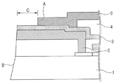
도 1은 그 구성의 일례로서 유기발광장치의 일부를 발광 영역의 단부에서 주변 영역에까지 모식적으로 예시한 단면도이다.1 is a cross-sectional view schematically showing a part of an organic light emitting device from an end portion of a light emitting region to a peripheral region as an example of the configuration.
유리 기판(이하, 단지 "기판"이라 생략할 경우가 있음)(1) 위에 TFT(박막 트랜지스터)(2), 절연층(3) 및 유기 평탄화막(4)이 이 순서로 형성되어 있다. 그 위에, 단위 화소(소자)가 되는 제 1 전극(5)이 형성되고, 그 각 화소의 주위가 폴리이미드로 이루어진 소자 분리막(8)으로 덮여 있다. 이 기판 위에, 정공 수송층, 발광층, 전자 수송층 및 전자 주입층이 순차 형성되어 이루어진 유기 화합물층(6)이 형성되어 있다. 상기 유기 화합물층 위에는, 제 2 전극(7)이 형성되고, 더욱 추출 전극을 제외한 제 2 전극(7), 유기 화합물층(6), 소자 분리막(8) 및 유기 평탄화층(4)을 완전하게 덮고 있는 무기 밀봉층(9)이 형성되어 있다. 그리고, 밀봉층(9)의 상부에 점착재(10)를 개입시켜 원편광판(11)이 설치되어 있다. 즉, 본 발명의 유기발광장치를 구성하는 유기 발광소자는, 제 1 전극(5), 제 2 전극(7) 및 제 1 전극(5)과 제 2 전극(7) 사이에 형성된 유기 화합물층(6)을 적어도 포함한다. 이들 두 전극 사이에 전류를 흘림으로써, 유기 발광층에 함유된 발광재료가 여기되고, 이에 따라, 기저 상태로 천이될 때에 발광을 일으킨다.On the glass substrate (hereinafter, simply referred to as "substrate") 1, a TFT (thin film transistor) 2, an
도 1에 나타낸 구성에 있어서, 기판(1)의 분할부(B)보다 밀봉층(9)의 분할 부(모서리가 돌출되어 있는 부분)(A)가 발광 영역 쪽에 가깝게 위치되어 있다. 발광 영역이란, 전류를 흘리는 것에 의해서 발광이 가능한 영역을 나타내고 있고, 도 1에 있어서 기호 (X)로 표시한 영역이다.In the structure shown in FIG. 1, the division part (part where the edge protrudes) A of the
본 발명의 유기발광장치를 구성하는 유기 발광소자의 제 1 전극(5)은 고도전성의 전극 재료로 이루어져 있는 한 특히 한정되지 않지만, 예를 들어, 고반사성 재료인 Cr, Al, Ag 등을 이용할 수 있다. ITO 또는 IZO 등의 투명 전극을 적층해서 이용할 수 있다.The
제 2 전극(7)은 높은 도전성의 전극 재료로 이루어져 있는 한 특히 한정되지 않지만, 예를 들어, 고투과성 혹은 반투과성의 재료로 이루어진 ITO 또는 IZO 등의 In을 함유하는 산화층이나, Ag 등을 이용할 수 있다.The second electrode 7 is not particularly limited as long as the second electrode 7 is made of a highly conductive electrode material. For example, an oxide layer containing In, such as ITO or IZO, Ag, or the like made of a highly permeable or semi-permeable material can be used. have.
밀봉층(9)은 수분이나 가스 성분의 차단 능력이 높은 것인 한 특히 한정되지 않지만, 일반적으로 수분 및 가스 장벽이 높은 층으로서 알려진 무기층, 즉 무기 밀봉층을 이용한다. 무기 밀봉층으로서 규소를 주로 함유하는 층이 바람직하게 이용된다. 구체적으로는, 질화 규소, 산화 질화 규소, 산화 규소 등이 바람직하게 이용된다. 이들 재료로 이루어진 층은 밀도가 높고 수분이나 가스 성분의 차단 능력이 높다. 또, 밀봉층에 요구되는 특성에 따라서는, 밀봉층으로서 무기 밀봉층뿐만 아니라 유기 밀봉층을 포함할 수 있다. 그러나, 유기발광장치의 분할 위치는 수분이나 가스 성분의 전파 경로가 되기 때문에, 이 분할 위치에 유기 밀봉층이 형성되어 있지 않은 것이 바람직하다.The sealing
밀봉층(9)의 층 두께는 수분이나 가스 성분의 차단 성능을 확보할 수 있는 한 특히 한정되지 않지만, 제 2 전극(7)의 표면 평활성이나 부착 오염물 등을 덮어 충분한 밀봉 성능을 얻기 위해서, 밀봉층(9)의 두께는 0.5 ㎛ 이상인 것이 바람직하다.Although the layer thickness of the
본 발명의 밀봉층(9)에 이용되는 무기층은 예를 들면, 플라스마 CVD에 의해 형성될 수 있다. 플라스마 CVD의 여기 주파수로서 30 ㎒에서 100 ㎒의 VHF대를 이용함으로써, 플라스마의 이온 충격을 감소시켜 소자의 열 손상을 억제할 수 있다. 또한, 치밀하고 결함이 없고, 경사면이나 요철의 커버리지(coverage)성이 양호하고, 방습성이 높고, 더욱 저응력의 양호한 무기층을 실현할 수 있다.The inorganic layer used for the
상기 무기층이 규소를 주성분으로 하는 경우, 규소, 질소, 수소 및 산소 원자의 총수에 대한 수소 농도가 12 내지 32 원자%인 것이 바람직하다. 이 경우에, 예를 들어, 무기층은 유기층을 기초층으로서 사용했을 경우에 높은 밀착성을 가지며, 요철의 커버리지성이 우수하고, 열응력의 완화에 효과적이어서, 유기발광장치의 발광에 의한 온도 상승에 효과가 크다.When the said inorganic layer has silicon as a main component, it is preferable that hydrogen concentration with respect to the total number of silicon, nitrogen, hydrogen, and oxygen atoms is 12-32 atomic%. In this case, for example, the inorganic layer has high adhesion when the organic layer is used as the base layer, is excellent in coverage of irregularities, and is effective in alleviating thermal stress, so that the temperature rise due to light emission of the organic light emitting device is increased. The effect is great.
본 발명에 이용하는 밀봉층(9)은 조성이 다른 2 종류 이상의 층을 함유하는 적층된 층을 포함할 수 있다.The
다음에, 밀봉층 분할부(A) 및 기판 분할부(B)에 대해서, 더욱 자세하게 설명한다.Next, the sealing layer dividing part A and the board | substrate dividing part B are demonstrated in more detail.
도 2는 밀봉층 분할부(A)와 기판 분할부(B) 간의 관계를 나타낸 확대한 모식도이다.FIG. 2 is an enlarged schematic diagram showing the relationship between the sealing layer dividing unit A and the substrate dividing unit B. FIG.
밀봉층 분할부(A) 및 기판 분할부(B)는 기판 및 밀봉층의 재질이나 분할 수 법에 의해, 기판 두께 방향에 대해서 기울기를 가진 상태로 형성될 수도 있다. 도 2는 기판(1)의 단부 및 상기 기판(1) 위에 형성된 TFT(2) 및 절연층(3)의 단부에 각각 기판(1)의 두께 방향에 대해서 기울기를 가진 채 기판 분할부(B)가 형성되고, 밀봉층 분할부(A)는, 거의 기판(1)의 두께 방향의 분할면이 밀봉층의 단부에 형성되도록 형성된 경우를 나타내고 있다. 실제의 유기발광장치에 있어서, 밀봉층 분할부(A) 및 기판 분할부(B)는 기판(1)의 두께 방향에 대해서 도 2와는 반대의 기울기를 가질 수도 있다.The sealing layer division part A and the board | substrate division part B may be formed in the state which has inclination with respect to the board | substrate thickness direction by the material of a board | substrate and a sealing layer, or a division method. FIG. 2 shows the substrate dividing portion B having an inclination with respect to the thickness direction of the
기판 테라스(C)는 기판 분할부(B)보다 유기발광장치의 면의 안쪽, 즉 발광 영역 쪽의 기판(1)의 표면 혹은 기판(1)상에 형성된 TFT(2) 및 절연층(3)의 표면 영역이다. 기판 테라스(C)는 기판 분할부(B)의 위치와 밀봉층 분할부(A)의 위치 간의 어긋남에 의해 규정되는 것이다.The substrate terrace C has a
본 발명의 유기발광장치에 있어서는, 밀봉층 분할부(A)가 기판 분할부(B)보다 발광 영역 쪽에 가깝게 위치되어, 기판 테라스(C)가 형성되는 것이 필요하다. 밀봉층 분할부(A)가 기판 분할부(B)보다 발광 영역 쪽에 가깝게 위치하고 있으면, 기판(1) 분할에 기인한 밀봉층(9)에의 손상이 억제되어, 밀봉층(9)의 박리나 균열의 발생을 방지할 수 있다. 더욱 구체적으로는, 본 발명의 밀봉층 분할부(A)가 미리 형성되어 있을 경우, 기판 분할부(B)가 형성될 때(즉, 기판을 미리 설정된 위치에서 분할할 때)에 밀봉층(9)에 발생하는 균열이나 박리의 진행이 밀봉층 분할부(A)에서 차단된다. 그 결과, 밀봉층(9)의 박리나 균열의 발생을 방지할 수 있다. 본 발명을 적용하지 않으면, 분할 위치에서 밀봉층(9)의 균열 발생이나 박리 등, 밀봉층(9)의 손상의 문제가 생긴다.In the organic light emitting device of the present invention, the sealing layer dividing portion A is located closer to the light emitting region than the substrate dividing portion B, so that the substrate terrace C is formed. When the sealing layer dividing part A is located closer to the light emitting region side than the substrate dividing part B, damage to the
기판 테라스(C)의 폭, 즉, 밀봉층 분할부(A)와 기판 분할부(B) 간의 거리는 일정할 필요는 없다. 기판의 분할 과정에 있어서 기판 테라스(C)가 밀봉층(9)에 손상을 주는 것이 아니면, 기판 테라스(C)의 폭은 특히 한정되지 않는다. 바람직하게는 기판 테라스(C)의 폭이 1 ㎛ 이상이 되도록 밀봉층 분할부(A) 및 기판 분할부(B)를 형성한다.The width of the substrate terrace C, that is, the distance between the sealing layer division A and the substrate division B need not be constant. The substrate terrace C is not particularly limited in width unless the substrate terrace C damages the
밀봉층 분할부(A), 기판 분할부(B) 및 기판 테라스(C)의 각각의 형상, 그리고 이들 간의 위치 관계는 주사 전자현미경(SEM)을 이용해서 확인할 수 있다. 본 발명의 분할부의 각 형상 및 분할부 간의 위치 관계는 5000배 이상으로 확대해서, 유기발광장치의 상부 표면 및 경사 방향으로부터 관찰하고 그들의 단면을 관찰함으로써 확인할 수 있다.The shape of each of the sealing layer division A, the substrate division B, and the substrate terrace C, and the positional relationship therebetween can be confirmed using a scanning electron microscope SEM. The positional relationship between each shape of the divided part and the divided part of the present invention can be confirmed by expanding at 5000 times or more, observing from the top surface and the oblique direction of the organic light emitting device, and observing their cross sections.
본 발명에 의한 유기발광장치는 면발광체로서 액정표시장치의 백 라이트에 바람직하게 이용될 수 있다.The organic light emitting device according to the present invention can be preferably used for the backlight of the liquid crystal display device as a surface light emitting body.
본 발명에 의한 유기발광장치는 텔레비전 수상기, PC 모니터, 휴대 전화 등의 표시부에 바람직하게 이용될 수 있다. 특히 폭넓은 온도와 습도를 가진 환경에서 사용되도록 상정되어 높은 내환경성을 필요로 하는 모바일 기기의 표시부에 바람직하게 이용할 수 있다. 본 발명의 유기발광장치를 표시부로서 포함하는 표시장치는 보다 장시간에 걸쳐서 고품질의 화상을 표시할 수 있다.The organic light emitting device according to the present invention can be suitably used for display units of television receivers, PC monitors, mobile phones and the like. In particular, it is assumed to be used in an environment having a wide temperature and humidity, and can be preferably used in a display portion of a mobile device requiring high environmental resistance. The display device including the organic light emitting device of the present invention as a display portion can display a high quality image for a longer time.
본 발명에 의한 유기발광장치는 디지털 카메라 등의 촬상 장치로서 바람직하게 이용할 수도 있다. 본 발명의 유기발광장치를 표시부로서 포함하는 촬상 장치 는 보다 장시간에 걸쳐서 고품질의 화상을 표시할 수 있다.The organic light emitting device according to the present invention can also be suitably used as an imaging device such as a digital camera. An imaging device including the organic light emitting device of the present invention as a display portion can display a high quality image for a longer time.
다음에, 본 발명에 의한 유기발광장치의 제조 방법에 대해 설명한다.Next, the manufacturing method of the organic light emitting device by this invention is demonstrated.
본 발명의 유기발광장치의 제조에 있어서는, 기판 테라스(C)를 형성하도록 밀봉층 분할부(A)와 기판 분할부(B)를 형성하는 것이 중요하다. 이 때문에, 기판(1)의 분할공정과 밀봉층(9)의 분할 공정은 개별적으로 수행된다.In manufacturing the organic light emitting device of the present invention, it is important to form the sealing layer dividing portion A and the substrate dividing portion B so as to form the substrate terrace C. FIG. For this reason, the dividing process of the board |
분할 공정은 일반적으로 분할 대상물에 수직 균열을 부여하는 스크라이브 공정과 스크라이브 위치에서 분할 대상물을 가르는 브레이크 공정으로 나눌 수 있다. 분할 수법 및 분할 조건에 따라서는, 브레이크 공정을 필요로 하지 않고, 스크라이브 공정만으로 기판(1)을 분할하는 것(브레이크레스(breakless) 공정)도 가능하다. 본 발명에 있어서, 브레이크레스 분할 수법을 이용했을 경우, 브레이크 공정과 스크라이브 공정은 동시에 수행된다.The dividing process can generally be divided into a scribe process for imparting vertical cracks to the dividing object and a break process for dividing the dividing object at the scribe position. Depending on the dividing method and the dividing conditions, it is also possible to divide the substrate 1 (breakless process) only by the scribing process without requiring a break process. In the present invention, when the breakless division technique is used, the brake process and the scribe process are performed at the same time.
본 발명에 의한 스크라이브를 위해서는, 커터 휠에 의한 스크라이브, 레이저스크라이브 등의 일반적인 스크라이브 수법을 이용할 수 있다.For scribing according to the present invention, a common scribing method such as scribing by a cutter wheel, laser scribing or the like can be used.
도 3은 유기 발광소자가 서로 인접하게 형성된 기판의 분할부의 확대 모식도이다.3 is an enlarged schematic view of a divided part of a substrate in which organic light emitting devices are adjacent to each other.
복수의 유기발광장치가 형성된 대형의 기판(1)을 각 단위 유기발광장치로 분할하는 공정에 있어서, 기판(1)은 분할 위치(E)에서 스크라이브를 실시하고, 밀봉층(9)은 발광 영역 쪽의 분할 위치(D)에서 스크라이브를 실시한다.In the step of dividing a
각 단위 유기발광장치로의 분할을 위해서, 상기 조건을 충족하여, 밀봉층(9)의 분할에 의한 박리나 균열을 일으키지 않는 방법이면 어느 방법이라도 이용할 수 있다. 예를 들어, 밀봉층(9)이 형성되어 있는 기판(1)의 분할에 있어서, 밀봉층(9)은 밀봉층 쪽으로부터 스크라이브를 실시하고, 기판(1)은 기판 쪽으로부터 스크라이브를 실시한다. 대안적으로는, 밀봉층(9)의 스크라이브 위치 및 기판(1)의 스크라이브 위치는 양쪽 모두 밀봉층 쪽으로부터 스크라이브되도록 변경한다.In order to divide into each unit organic light emitting device, any method can be used as long as it satisfies the above conditions and does not cause peeling or cracking due to division of the
밀봉층(9)의 스크라이브는, 밀봉층(9)이 강하게 스크라이브될 경우 밀봉층(9)에 박리나 균열이 발생할 수 있기 때문에 상세한 조건에 대한 설정을 필요로 한다. 밀봉층(9)에 대해서는 당해 밀봉층(9)을 관통하도록 스크라이브를 실시하지 않고, 밀봉층(9)의 층 두께보다 작은 크기의 수직 균열을 밀봉층(9)에 일으켜, 응력차에 의해 밀봉층(9)이 갈라지게 하는 것이 바람직하다. 다만, 밀봉층(9)에 응력을 가하는 방법은 본 발명의 유기발광장치를 형성할 수 있는 방법인 한, 특히 한정되지 않는다. 밀봉층(9)에 응력을 가하는 방법으로서는, 스크라이브에 의한 균열 위치에 열의 부여와 냉각을 이용하는 것도 가능하다.The scribe of the
밀봉층(9)의 스크라이브 공정과, 기판(1), TFT(2) 및 절연층(3)의 스크라이브 공정의 순서에 대해서는, 밀봉층(9), TFT(2) 및 절연층(3)의 스크라이브 공정 이후에 기판(1)의 스크라이브 공정을 수행하는 것이, 박리나 균열의 전파를 확실하게 방지할 수 있기 때문에 바람직하다. 그러나, 밀봉층(9)이 스크라이브에 의해 손상되지 않을 경우에는, 스크라이브 공정의 순서는 어는 것을 채용해도 무방하다.About the scribe process of the
다음에, 기판(1)은 분할 위치(E)에 형성된 선(스크라이브 라인)을 따라 가르고, 밀봉층(9)은 발광 영역 쪽의 분할 위치(D)에 형성된 선(스크라이브 라인)을 따라서 가른다. 기판(1) 및 밀봉층(9)의 가르기(브레이크)에 대해서는, 기판(1)을 가르는 공정은 밀봉층(9) 만을 가르는 공정 후에 수행될 수 있고, 또는 기판(1)을 가르는 공정과 밀봉층(9)을 가르는 공정은 동시에 수행해도 무방하다. 브레이크 공정에 대해서는, 기판(1)을 가를 때 가해지는 응력이 밀봉층(9)에도 전달되고, 기판(1)과 밀봉층(9)의 스크라이브 위치가 차이가 날 경우에도, 이들 기판(1)과 밀봉층(9)을 동시에 가를 수도 있다. 또한, 기판(1)을 가를 경우, 상기 기판(1)상에 형성된 TFT(2) 및 절연층(3)을 동시에 가른다.Next, the board |
본 발명의 제조 방법에 의해, 기판(1)의 스크라이브 및 브레이크 시 발생하는 큰 분할 손상으로 인해 밀봉층(9)에 박리나 균열을 발생시키는 일 없이, 대형 기판(1)을 각 단위 유기 발광 소자로 분할할 수 있다.According to the manufacturing method of the present invention, the large-
기판(1)의 분할 위치(E)와 밀봉층(9)의 분할 위치(D) 간의 거리는 가장 좁은 곳에서 10 ㎛ 이상인 것이 바람직하다. 이 거리는 스크라이브를 수행할 때의 위치 어긋남이나, 스크라이브 공정에서 기판(1) 혹은 밀봉층(9)을 깎아낼 수 있는 폭을 고려해서 결정된다.It is preferable that the distance between the dividing position E of the board |
기판(1) 및 밀봉층(9)의 분할 위치, 및 분할 위치 간의 관계에 대해서는, 광학 현미경과 주사 전자현미경(SEM)을 이용해서 확인될 수 있다. 분할 위치에 관해서는, 일반적인 스크라이브 수법을 적용했을 경우, 분할부에 스크라이브 자취가 남아, 500배 이상으로 확대해서, 유기발광장치의 상부 표면이나 경사 방향으로부터의 관찰, 또는 유기발광장치의 단면의 관찰에 의해 확인할 수 있다.The relationship between the divided positions of the
기판(1), 및 상기 기판(1) 위에 형성된 TFT(2) 및 절연층(3)의 분할에 대해서는 일반적인 분할 방법과 조건을 그대로 적용할 수 있다. 다만, 기판(1)의 분할 위치(E)는, 스크라이브에 의한 기판(1)의 수평 방향의 깎기 폭이나 손상 부여 폭, 및 스크라이버의 위치 결정 정밀도를 고려해서 결정하는 것이 필요하다.As to the division of the
이하, 발명의 실시형태에 대해서, 실시예를 취해서 더욱 자세하게 설명한다.EMBODIMENT OF THE INVENTION Hereinafter, embodiment of this invention is described in more detail, taking an Example.
(( 실시예Example 1) One)
본 발명의 실시예 1에 대해서 도 4A 및 도 4B를 참조하여 설명한다. 도 4A 및 도 4B는 각각 평가 샘플의 일부를 모식적으로 나타내고 있는 단면도 및 정면도이다.
본 실시예에서는, 도 4A 및 도 4B에 나타낸 바와 같이 평가 샘플을 제작해서, 분할 위치로부터의 수분의 침입 유무는 Ca 부식에 의한 투과율의 변화에 근거해서 평가했다. Ca 막은 물 및 산소와 반응함으로써, Ca 막의 투과율이 변화한다. 따라서, Ca 막의 투과율이 변화되었을 경우, 수분이 침투된 것으로 판단할 수 있는 반면, Ca 막의 투과율이 변화되지 않은 경우는 수분 침투가 없는 것으로 판단할 수 있다.In the present Example, as shown to FIG. 4A and FIG. 4B, the evaluation sample was produced and the presence or absence of the penetration | invasion of water from a division | segmentation position was evaluated based on the change of the transmittance | permeability by Ca corrosion. As the Ca membrane reacts with water and oxygen, the transmittance of the Ca membrane changes. Therefore, when the transmittance of the Ca membrane is changed, it can be determined that moisture has penetrated, whereas when the Ca membrane has not changed, it can be determined that there is no water penetration.
절연막이 형성된 기판의 중앙부에 있어서, Ca 막(12)을 진공 증착에 의해 1000 Å의 두께로 형성하였다. 계속해서, Ca 막(12)을 덮도록 VHF 플라스마 CVD로 질화 실리콘막을 5 ㎛의 두께로 형성해서, 밀봉층(9)을 형성하였다. 기판 투입으로부터 밀봉층의 형성까지의 전체 공정을 진공 중에서 수행하였다.In the center part of the board | substrate with which the insulating film was formed, the
다음에, Ca 막(12)의 단부로부터 0.25 ㎜ 떨어진 위치(D)에서, 커터 휠 블레이드를 이용해서 밀봉층 쪽으로부터 밀봉층(9)의 층 두께보다 적게 상기 밀봉층(9)의 스크라이브를 실시하였다. 이때, 최적인 조건을 설정함으로써, 질화 실리콘층 으로 이루어진 밀봉층(9)이 경질 막이기 때문에, 스크라이브 위치에서 밀봉층(9)을 관통하는 분할면이 생긴다. 다음에, Ca 막(12)의 단부로부터 0.3 ㎜ 떨어진 위치(E)에서, 고침투형의 휠 블레이드를 이용해서, 밀봉층(9) 쪽으로부터 기판을 스크라이브하고, 이어서 가르기를 실시해서, 평가 샘플을 제작하였다.Next, at the position D separated by 0.25 mm from the end of the
본 실시예의 샘플의 분할면에 대해서 SEM을 이용해서 관찰한 경우, 기판의 분할 위치(E)에서는, 밀봉층(9)의 박리나 균열의 발생을 확인할 수 있었다. 그러나, 밀봉층(9)의 분할 위치(D)로부터 발광 영역 쪽에 박리나 균열의 발생은 볼 수 없었다.When the dividing surface of the sample of the present Example was observed using SEM, peeling of the
본 실시예의 평가 샘플을 온도 60℃, 상대습도 90%RH의 항온항습조 내에 1000 시간 방치한 후에 관찰한 경우에도, Ca 막의 투과율은 변화하지 않았다. 따라서, 밀봉층(9)에 수분이 침입되지 않은 것으로 판정될 수 있다.Even when the evaluation sample of this example was observed after being left to stand in a constant temperature and humidity chamber at a temperature of 60 ° C. and a relative humidity of 90% RH for 1000 hours, the transmittance of the Ca membrane did not change. Therefore, it can be determined that moisture does not invade the
(( 비교예Comparative example 1) One)
이 비교예는 도 5를 참조해서 설명한다. 도 5는 평가 샘플의 일부를 모식적으로 나타낸 단면도이다.This comparative example is demonstrated with reference to FIG. It is sectional drawing which showed a part of evaluation sample typically.
본 비교예에서는, 도 5에 나타낸 바와 같이 평가 샘플을 제작해서, 분할 위치로부터의 수분의 침입 유무에 대해서, Ca 부식에 의해 초래된 투과율의 변화에 의거해서 평가했다.In this comparative example, as shown in FIG. 5, an evaluation sample was produced and evaluated based on the change of the transmittance | permeability caused by Ca corrosion about the presence or absence of the invasion of water from a division | segmentation position.
본 비교예의 평가 샘플은 실시예 1의 것과 동일한 공정에서 제작했지만, 밀봉층의 분할 위치(D)에서 밀봉층(9)의 분할은 실시하지 않고, 기판의 분할 위치(E)에서 밀봉층(9)과 기판의 분할을 실시하였다. 밀봉층(9)과 기판은 Ca 막(12)의 말 단으로부터 0.3 ㎜ 떨어진 위치에서 밀봉층(9) 쪽으로부터 분할을 실시하였다.Although the evaluation sample of this comparative example was produced in the same process as Example 1, the
본 비교예의 샘플의 분할 위치는 SEM을 이용해서 관찰한 바, 밀봉층(9)의 박리 및 균열이 발생하였다. 분할에 의한 밀봉층(9)에의 손상은 분할 위치로부터 0.5 ㎜ 이하 내에 존재하였다.When the division | segmentation position of the sample of this comparative example was observed using SEM, peeling and the crack of the
본 비교예의 평가 샘플을 온도 60℃, 상대습도 90%RH의 항온항습조 내에 1000시간 방치한 후에는, 분할 위치의 방향으로부터의 Ca 막의 부식 및 분할 위치로부터 약 25 ㎜ 내의 영역에 걸친 투과율의 저하가 관찰되었다. 따라서, 밀봉층(9)에 수분이 침입된 것으로 판정될 수 있다.After leaving the evaluation sample of this comparative example in a constant temperature and humidity chamber at a temperature of 60 ° C. and a relative humidity of 90% RH for 1000 hours, corrosion of the Ca film from the direction of the splitting position and a decrease in transmittance over a region within about 25 mm from the splitting position. Was observed. Therefore, it can be determined that moisture has penetrated the
(( 비교예Comparative example 2) 2)
본 비교예에서도, 도 5에 나타낸 바와 같은 평가 샘플을 제작해서, 분할 위치로부터의 수분의 침입 유무를 Ca 부식에 의해 초래된 투과율의 변화를 근거로 해서 평가하였다.Also in this comparative example, the evaluation sample as shown in FIG. 5 was produced, and the presence or absence of the invasion of water from the division | segmentation position was evaluated based on the change of the transmittance | permeability caused by Ca corrosion.
본 비교예의 평가 샘플은 실시예 1과 같은 공정으로 제작했지만, 밀봉층의 분할 위치(D)에서 밀봉층(9)의 분할은 실시하지 않고, 기판의 분할 위치(E)에서 밀봉층(9)과 기판의 분할을 실시하였다. 밀봉층(9)과 기판의 분할은 Ca 막(12)의 단부로부터 0.3 ㎜ 떨어진 위치에서 기판 쪽으로부터 실시하였다.Although the evaluation sample of this comparative example was produced by the process similar to Example 1, the
본 비교예의 샘플의 분할 위치를 SEM을 이용해서 관찰한 바, 비교예 1과는 달리 밀봉층(9)에서 균열을 제외하고 오로지 박리만이 발생하였다. 분할에 의해 초래된 밀봉층(9)에 대한 손상은 분할 위치로부터 0.3 ㎜ 이하 내에 존재하였다.When the division | segmentation position of the sample of this comparative example was observed using SEM, only peeling generate | occur | produced except the crack in the
본 비교예의 평가 샘플을 온도 60℃, 상대습도 90%RH의 항온항습조 내에 1000 시간 방치한 후에는, 분할 위치의 방향으로부터의 Ca 막의 부식 및 그 분할 위치로부터 약 15 ㎜ 이내의 영역에 걸친 투과율의 저하가 관찰되었다. 따라서, 밀봉층(9)에 수분이 침입된 것으로 판정될 수 있다.After leaving the evaluation sample of this comparative example in a constant temperature and humidity chamber at a temperature of 60 ° C. and a relative humidity of 90% RH for 1000 hours, corrosion of the Ca film from the direction of the splitting position and transmittance over an area within about 15 mm from the splitting position. A decrease of was observed. Therefore, it can be determined that moisture has penetrated the
(( 실시예Example 2) 2)
이하, 본 실시예 2는 도 1, 도 3 및 도 6을 참조해서 설명한다.Hereinafter, the second embodiment will be described with reference to FIGS. 1, 3, and 6.
본 실시예에서는 도 1에 나타낸 유기발광장치를 제작하고, 상기 유기발광장치의 발광 특성 평가를 실시했다.In this embodiment, the organic light emitting device shown in Fig. 1 was produced, and light emission characteristics of the organic light emitting device were evaluated.
본 실시예에서는, 대형 기판(1) 상에, 도 1에 나타낸 구성을 가지는 단위 유기발광장치를 서로 인접하게 해서 복수개 형성하고, 밀봉층(9)의 형성 후에 상기 단위 유기발광장치로 절단하였다. 도 6에 나타낸 바와 같이, 전원 부재 또는 신호 공급 패드(신호 공급 부재)(13)가 형성된 유기 발광장치의 한 변과, 그 대변에 대해서는, 밀봉층(9)이 형성되어 있지 않은 영역(기초 층-노출 영역)을 마련했다. 그 이유는, 전원 부재 또는 신호 공급 패드(13)가 형성된 변에 밀봉층(9)을 형성한 경우, 전원 부재 또는 신호 공급 패드는 FPC 등의 외부 접속 배선과 전기적으로 도통시킬 수 없고, 그 결과, 밀봉층을 박리하는 공정이 필요하게 되어 제조 프로세스가 더욱 복잡하게 되기 때문이다. 또, 상기 대변이 인접하는 유기발광장치의 전원 부재 또는 신호 공급 패드(13)가 형성된 변이 되는 경우에는, 인접하는 유기발광장치의 밀봉층의 형성과 동시에 밀봉층이 형성되어 있지 않는 영역(기초 층-노출 영역)을 처리할 수 있기 때문이다. 상기 변들 이외의 인접한 유기발광장치의 두 변에는, 인접하는 단위 유기발광장치에 연속하는 밀봉층(9)을 형성하고, 밀봉층(9)과 기판(1)을 분할해서 각 단위 유기발광장치로 절단하였다.In the present embodiment, a plurality of unit organic light emitting devices having the structure shown in FIG. 1 are formed adjacent to each other on the large-
구체적으로는, 본 실시예에 의한 유기발광장치는, 다음과 같은 방법으로 제조하였다. 즉, 대형 기판(1) 위에, 복수의 유기발광장치를 형성할 수 있도록, TFT(2), 절연층(3) 및 유기 평탄화막(4)을 순차 형성하였다. 다음에, 그 위에 제 1 전극(5)과 TFT(2) 간의 컨택트홀을 형성하였다. 계속해서, 제 1 전극(5)을 형성하고, 상기 제 1 전극(5) 주위에 폴리이미드로 이루어진 소자 분리막(8)을 형성해서, 절연하였다. 이 기판(1) 상에, FL03/DpyFL+sDTAB2/DFPH1/DFPH1+Cs2CO3의 유기 화합물층(6)을 증착하고, 상기 유기 화합물층(6)을 정공 수송층, 발광층, 전자 수송층 및 전자 주입층의 순서로 형성했다. 이 층의 상부에는, ITO로 이루어진 제 2 전극(7)을 스퍼터링에 의해 두께 60 ㎚를 가진 층을 형성함으로써, 화소를 형성했다. 또한, 유기 평탄화막(4), 제 1 전극(5), 유기 화합물층(6), 제 2 전극(7), 소자 분리막(8) 및 점착재층(10)을 덮도록, VHF 플라스마 CVD에 의해 질화 실리콘막을 5 ㎛의 두께로 형성함으로써, 밀봉층(9)을 형성하였다. 그 결과, 대형 기판(1)에 복수의 유기발광장치가 형성된 유기발광장치 패널이 제작되었다. 또한, 기판(1)의 투입으로부터 밀봉층(9)의 형성까지의 전체 공정은 진공 중에서 실시하였다.Specifically, the organic light emitting device according to the present Example was manufactured by the following method. That is, the
다음에, 실시예 1과 마찬가지 방법으로, 도 3의 밀봉층의 분할 위치(D)에서 상기 유기발광장치 패널을 분할했다. 즉, 커터 휠 블레이드를 이용해서 밀봉층 쪽으로부터 밀봉층(9)을 스크라이브했다. 계속해서, 기판의 분할 위치(E)에서, 고침 투형의 휠 블레이드를 이용해서, 밀봉층 쪽으로부터 기판(1), TFT(2) 및 절연층(3)을 스크라이브하고 나서 가름으로써, 각 단위 유기발광장치를 얻었다. 밀봉층의 분할 위치(D)는 기판의 분할 위치(E)로부터 발광 영역 쪽에 50 ㎛ 떨어진 위치에 대응한다.Next, in the same manner as in Example 1, the organic light emitting device panel was divided at the divided position D of the sealing layer in FIG. 3. That is, the
본 발명의 유기발광장치의 분할 위치를 광학 현미경 및 SEM으로 관찰한 바, 밀봉층의 분할 위치(D)보다 발광 영역에 가까운 밀봉층(9)에는 균열이나 박리는 확인되지 않았다.When the division | segmentation position of the organic light-emitting device of this invention was observed with the optical microscope and SEM, the crack and peeling were not recognized by the
마지막으로, 유기발광장치에 점착재(10)를 개입시켜 원편광판(11)을 고정하였다.Finally, the circular
본 실시예의 유기발광장치를 온도 60℃, 상대습도 90%RH의 항온항습조 내에 1000 시간 방치한 후에 평가한 바, VI특성 및 휘도의 열화는 확인되지 않았다. 또, 유기발광장치의 외주 영역으로부터의 휘도 변화 및 1 ㎛ 이상의 직경(Φ)을 가진 다크 스폿은 발생하지 않았고, 또한, 화소 주변으로부터의 휘도 열화 및 1 ㎛ 이상의 직경(Φ)을 가진 다크 스폿도 발생하지 않았다.The organic light emitting device of this example was evaluated after being left in a constant temperature and humidity chamber at a temperature of 60 ° C. and a relative humidity of 90% RH for 1000 hours. As a result, no deterioration in VI characteristics and luminance was confirmed. In addition, there was no change in luminance from the outer circumferential region of the organic light emitting device and dark spots having a diameter? Of 1 μm or more, and also a dark spot having a luminance? Did not occur.
이상, 본 발명은 예시적인 실시형태를 참조해서 설명하였으나, 본 발명은 개시된 예시적인 실시형태로 한정되지 않는 것임을 이해할 필요가 있다. 또, 이하의 특허청구범위는 이러한 모든 변형예와, 등가의 구성 및 기능을 망라하도록 최광의의 해석에 따를 필요가 있다.As mentioned above, although this invention was demonstrated with reference to the exemplary embodiment, it is necessary to understand that this invention is not limited to the disclosed exemplary embodiment. In addition, the following claims should comply with the broadest interpretation so as to encompass all such modifications and equivalent configurations and functions.
도 1은 본 발명의 유기발광장치의 일 실시형태에 의한 일례를 모식적으로 나타낸 단면도;1 is a cross-sectional view schematically showing an example according to an embodiment of an organic light emitting device of the present invention;
도 2는 본 발명의 유기발광장치에 있어서의 분할부 간의 관계의 일례를 모식적으로 나타낸 단면도;2 is a cross-sectional view schematically showing an example of the relationship between the divisions in the organic light emitting device of the present invention;
도 3은 본 발명의 유기발광장치에 있어서의 분할 위치 간의 관계의 일례를 모식적으로 나타낸 단면도;3 is a cross-sectional view schematically showing an example of the relationship between the split positions in the organic light emitting device of the present invention;
도 4A 및 도 4B는 본 발명의 실시예 1에 의한 평가 기판의 구성을 모식적으로 나타낸 단면도;4A and 4B are cross-sectional views schematically showing the configuration of an evaluation substrate according to Example 1 of the present invention;
도 5는 본 발명의 비교예 1에 의한 평가 기판의 구성을 모식적으로 나타낸 단면도;5 is a cross-sectional view schematically showing the configuration of an evaluation substrate according to Comparative Example 1 of the present invention;
도 6은 본 발명의 유기발광장치의 실시형태에 의한 일례를 나타낸 사시도.6 is a perspective view showing an example according to an embodiment of an organic light emitting device of the present invention.
<도면의 주요 부분에 대한 부호의 설명><Explanation of symbols for the main parts of the drawings>
1: 유리 기판 2: TFT(박막 트랜지스터) 1: Glass Substrate 2: TFT (Thin Film Transistor)
3: 절연층 4: 유기 평탄화막 3: insulation layer 4: organic planarization film
5: 제 1 전극 6: 적층 구조체 5: first electrode 6: laminated structure
7: 제 2 전극 8: 소자 분리막 7: second electrode 8: device separator
9: 밀봉층 10: 점착재 9: sealing layer 10: adhesive material
11: 원편광판 12: Ca 막 11: circular polarizer 12: Ca film
13: 전원 부재 및 신호 공급 패드 A: 밀봉층 분할부 13: power supply member and signal supply pad A: sealing layer division
B: 기판 분할부 C: 기판 테라스 B: Substrate Division C: Substrate Terrace
D: 밀봉층의 분할 위치 E 기판의 분할 위치D: Dividing Position of Sealing Layer E Dividing Position of Substrate
X: 발광 영역X: light emitting area
Claims (9)
Applications Claiming Priority (4)
| Application Number | Priority Date | Filing Date | Title |
|---|---|---|---|
| JPJP-P-2006-00185784 | 2006-07-05 | ||
| JP2006185784 | 2006-07-05 | ||
| JP2007146707A JP4869157B2 (en) | 2006-07-05 | 2007-06-01 | Manufacturing method of organic light emitting device |
| JPJP-P-2007-00146707 | 2007-06-01 |
Publications (2)
| Publication Number | Publication Date |
|---|---|
| KR20080004385A KR20080004385A (en) | 2008-01-09 |
| KR100906716B1 true KR100906716B1 (en) | 2009-07-14 |
Family
ID=39100757
Family Applications (1)
| Application Number | Title | Priority Date | Filing Date |
|---|---|---|---|
| KR1020070066891A KR100906716B1 (en) | 2006-07-05 | 2007-07-04 | Organic light emitting device and its manufacturing method |
Country Status (4)
| Country | Link |
|---|---|
| US (1) | US7641531B2 (en) |
| JP (1) | JP4869157B2 (en) |
| KR (1) | KR100906716B1 (en) |
| CN (1) | CN101102628B (en) |
Cited By (1)
| Publication number | Priority date | Publication date | Assignee | Title |
|---|---|---|---|---|
| US9356256B2 (en) | 2013-07-31 | 2016-05-31 | Samsung Display Co., Ltd. | Flexible display device and manufacturing method thereof |
Families Citing this family (9)
| Publication number | Priority date | Publication date | Assignee | Title |
|---|---|---|---|---|
| JP4750727B2 (en) * | 2006-03-28 | 2011-08-17 | キヤノン株式会社 | Organic light emitting device and manufacturing method thereof |
| US7977867B2 (en) * | 2007-06-13 | 2011-07-12 | Canon Kabushiki Kaisha | Organic EL panel |
| JP5017584B2 (en) * | 2007-08-02 | 2012-09-05 | 株式会社ジャパンディスプレイイースト | Organic EL display device |
| KR101621297B1 (en) * | 2010-03-04 | 2016-05-16 | 엘지디스플레이 주식회사 | Organic electro luminescent device |
| KR20120109081A (en) | 2011-03-24 | 2012-10-08 | 삼성디스플레이 주식회사 | Organic light emitting diode display |
| KR101801913B1 (en) * | 2012-03-23 | 2017-11-28 | 삼성디스플레이 주식회사 | Organic light emitting display device and the method for manufacturing the same |
| JP2015072770A (en) * | 2013-10-02 | 2015-04-16 | 株式会社ジャパンディスプレイ | Organic electroluminescent device and method for manufacturing the same |
| CN104576688B (en) | 2013-10-10 | 2018-11-09 | 精工爱普生株式会社 | Light-emitting device and electronic equipment |
| JP6803929B2 (en) | 2016-06-01 | 2020-12-23 | マイクロベンション インコーポレイテッドMicrovention, Inc. | Improved reinforced balloon catheter |
Citations (2)
| Publication number | Priority date | Publication date | Assignee | Title |
|---|---|---|---|---|
| KR20030090419A (en) * | 2002-05-23 | 2003-11-28 | 삼성에스디아이 주식회사 | Encapsulation method of organic electro luminescence device and organic electro luminescence panel using the same |
| JP2004303425A (en) | 2003-03-28 | 2004-10-28 | Tohoku Pioneer Corp | Organic el panel and its forming method |
Family Cites Families (14)
| Publication number | Priority date | Publication date | Assignee | Title |
|---|---|---|---|---|
| JPS5257783A (en) | 1975-11-06 | 1977-05-12 | Toshiba Corp | Semiconductor wafer |
| JP3042192B2 (en) * | 1992-07-29 | 2000-05-15 | 三星ダイヤモンド工業株式会社 | Method and apparatus for cutting laminated glass substrate |
| JP4222312B2 (en) * | 1996-10-22 | 2009-02-12 | セイコーエプソン株式会社 | Substrate for liquid crystal panel, liquid crystal panel, electronic apparatus using the same, and projection display device |
| JP2000258745A (en) * | 1999-03-08 | 2000-09-22 | Optrex Corp | Production of liquid crystal display device |
| JP4255187B2 (en) * | 1999-10-22 | 2009-04-15 | スタンレー電気株式会社 | Manufacturing method of organic EL display device and organic EL display device manufactured by the method |
| TWI226205B (en) | 2000-03-27 | 2005-01-01 | Semiconductor Energy Lab | Self-light emitting device and method of manufacturing the same |
| US6992439B2 (en) * | 2001-02-22 | 2006-01-31 | Semiconductor Energy Laboratory Co., Ltd. | Display device with sealing structure for protecting organic light emitting element |
| JP2002352951A (en) * | 2001-05-24 | 2002-12-06 | Tohoku Pioneer Corp | Organic el display panel and manufacturing method therefor |
| JP2003181825A (en) * | 2001-12-19 | 2003-07-02 | Sony Corp | Substrate dividing method and manufacturing method for organic el display |
| JP2003255362A (en) * | 2002-03-05 | 2003-09-10 | Citizen Watch Co Ltd | Cell and its production method and liquid crystal optical element using the cell |
| JP2003282236A (en) * | 2002-03-22 | 2003-10-03 | Nippon Seiki Co Ltd | Organic electroluminescence display device and method for producing the same |
| KR100637193B1 (en) * | 2004-11-25 | 2006-10-23 | 삼성에스디아이 주식회사 | Electro-luminescence display device and method for manufacturing the same |
| JP4592473B2 (en) * | 2005-03-31 | 2010-12-01 | 三洋電機株式会社 | LIGHT EMITTING PANEL MANUFACTURING METHOD, DISPLAY PANEL MANUFACTURING METHOD, AND DISPLAY PANEL |
| JP4533392B2 (en) | 2006-03-22 | 2010-09-01 | キヤノン株式会社 | Organic light emitting device |
-
2007
- 2007-06-01 JP JP2007146707A patent/JP4869157B2/en not_active Expired - Fee Related
- 2007-06-13 US US11/762,354 patent/US7641531B2/en not_active Expired - Fee Related
- 2007-07-04 KR KR1020070066891A patent/KR100906716B1/en active IP Right Grant
- 2007-07-05 CN CN2007101274598A patent/CN101102628B/en not_active Expired - Fee Related
Patent Citations (2)
| Publication number | Priority date | Publication date | Assignee | Title |
|---|---|---|---|---|
| KR20030090419A (en) * | 2002-05-23 | 2003-11-28 | 삼성에스디아이 주식회사 | Encapsulation method of organic electro luminescence device and organic electro luminescence panel using the same |
| JP2004303425A (en) | 2003-03-28 | 2004-10-28 | Tohoku Pioneer Corp | Organic el panel and its forming method |
Cited By (1)
| Publication number | Priority date | Publication date | Assignee | Title |
|---|---|---|---|---|
| US9356256B2 (en) | 2013-07-31 | 2016-05-31 | Samsung Display Co., Ltd. | Flexible display device and manufacturing method thereof |
Also Published As
| Publication number | Publication date |
|---|---|
| CN101102628B (en) | 2010-06-09 |
| US20080042559A1 (en) | 2008-02-21 |
| US7641531B2 (en) | 2010-01-05 |
| JP4869157B2 (en) | 2012-02-08 |
| JP2008034364A (en) | 2008-02-14 |
| CN101102628A (en) | 2008-01-09 |
| KR20080004385A (en) | 2008-01-09 |
Similar Documents
| Publication | Publication Date | Title |
|---|---|---|
| KR100906716B1 (en) | Organic light emitting device and its manufacturing method | |
| KR100859071B1 (en) | Organic light emitting apparatus and method of producing the same | |
| JP4533392B2 (en) | Organic light emitting device | |
| KR101759029B1 (en) | Method for manufacturing display device | |
| US8557067B2 (en) | Method for manufacturing organic electroluminescence panel | |
| JP2009049001A (en) | Organic light-emitting device and its manufacturing method | |
| US11101437B2 (en) | Display substrate motherboard, display substrate and display device | |
| US8102115B2 (en) | Organic EL display device and manufacturing method thereof | |
| JP2008098148A (en) | Organic light-emitting device | |
| US20090275158A1 (en) | Manufacturing method of display device | |
| CN104218188A (en) | Display device and method of manufacturing the same | |
| KR20150137239A (en) | Organic light emitting display device and manufacturing method of the same | |
| US11289675B2 (en) | Display panel with support structure and method of manufacturing the same | |
| WO2021035950A1 (en) | Flexible base substrate, and flexible display panel and manufacturing method thereof | |
| KR20140087435A (en) | Organic Light Emitting Diode Display Device and Method for Manufacturing The Same | |
| US11145832B2 (en) | Flexible base substrate, flexible display panel, and method for preparing the same | |
| CN113555396B (en) | Display panel | |
| KR20160063179A (en) | Organic light emitting display device and method of manufacturing the same | |
| CN117320515A (en) | Display module, manufacturing method thereof and display device | |
| JP2009104953A (en) | Organic el display panel | |
| JP2009104952A (en) | Organic el display panel | |
| KR20170025910A (en) | Organic light emitting diode display and manufacturing method of the same |
Legal Events
| Date | Code | Title | Description |
|---|---|---|---|
| A201 | Request for examination | ||
| E902 | Notification of reason for refusal | ||
| E902 | Notification of reason for refusal | ||
| E701 | Decision to grant or registration of patent right | ||
| GRNT | Written decision to grant | ||
| FPAY | Annual fee payment |
Payment date: 20130626 Year of fee payment: 5 |
|
| FPAY | Annual fee payment |
Payment date: 20140625 Year of fee payment: 6 |
|
| FPAY | Annual fee payment |
Payment date: 20150625 Year of fee payment: 7 |
|
| FPAY | Annual fee payment |
Payment date: 20160627 Year of fee payment: 8 |
|
| FPAY | Annual fee payment |
Payment date: 20180625 Year of fee payment: 10 |
|
| FPAY | Annual fee payment |
Payment date: 20190625 Year of fee payment: 11 |