KR100887893B1 - Novel ??? transimpedance amplifier - Google Patents
Novel ??? transimpedance amplifier Download PDFInfo
- Publication number
- KR100887893B1 KR100887893B1 KR1020010075633A KR20010075633A KR100887893B1 KR 100887893 B1 KR100887893 B1 KR 100887893B1 KR 1020010075633 A KR1020010075633 A KR 1020010075633A KR 20010075633 A KR20010075633 A KR 20010075633A KR 100887893 B1 KR100887893 B1 KR 100887893B1
- Authority
- KR
- South Korea
- Prior art keywords
- gain
- current
- gain stage
- voltage
- amplifier
- Prior art date
Links
- 238000000034 method Methods 0.000 claims abstract description 40
- 239000000872 buffer Substances 0.000 claims description 27
- 230000007246 mechanism Effects 0.000 claims description 19
- 238000012545 processing Methods 0.000 claims description 6
- 230000009467 reduction Effects 0.000 claims description 3
- 230000010076 replication Effects 0.000 claims description 3
- 230000007850 degeneration Effects 0.000 claims description 2
- 230000003362 replicative effect Effects 0.000 claims 3
- 230000001105 regulatory effect Effects 0.000 claims 1
- 230000003287 optical effect Effects 0.000 description 14
- 238000010586 diagram Methods 0.000 description 13
- 230000003321 amplification Effects 0.000 description 8
- 239000002131 composite material Substances 0.000 description 8
- 238000003199 nucleic acid amplification method Methods 0.000 description 8
- 239000004065 semiconductor Substances 0.000 description 8
- 230000002441 reversible effect Effects 0.000 description 7
- 238000011084 recovery Methods 0.000 description 6
- 230000008859 change Effects 0.000 description 5
- 238000013461 design Methods 0.000 description 5
- 230000002829 reductive effect Effects 0.000 description 5
- 230000000694 effects Effects 0.000 description 4
- 230000001052 transient effect Effects 0.000 description 4
- 238000013459 approach Methods 0.000 description 3
- 230000008901 benefit Effects 0.000 description 3
- 238000006243 chemical reaction Methods 0.000 description 3
- 230000007423 decrease Effects 0.000 description 3
- 239000003990 capacitor Substances 0.000 description 2
- 230000005284 excitation Effects 0.000 description 2
- 230000000670 limiting effect Effects 0.000 description 2
- 230000008569 process Effects 0.000 description 2
- 230000000630 rising effect Effects 0.000 description 2
- 230000035945 sensitivity Effects 0.000 description 2
- 239000007787 solid Substances 0.000 description 2
- 238000004458 analytical method Methods 0.000 description 1
- 230000002238 attenuated effect Effects 0.000 description 1
- 230000005540 biological transmission Effects 0.000 description 1
- 230000015556 catabolic process Effects 0.000 description 1
- 238000004891 communication Methods 0.000 description 1
- 230000003247 decreasing effect Effects 0.000 description 1
- 238000006731 degradation reaction Methods 0.000 description 1
- 238000005516 engineering process Methods 0.000 description 1
- 230000001747 exhibiting effect Effects 0.000 description 1
- 239000000284 extract Substances 0.000 description 1
- 239000000835 fiber Substances 0.000 description 1
- 230000005669 field effect Effects 0.000 description 1
- 230000006872 improvement Effects 0.000 description 1
- 238000004519 manufacturing process Methods 0.000 description 1
- 238000005259 measurement Methods 0.000 description 1
- 238000012986 modification Methods 0.000 description 1
- 230000004048 modification Effects 0.000 description 1
- 239000013307 optical fiber Substances 0.000 description 1
- 230000003071 parasitic effect Effects 0.000 description 1
- 238000000926 separation method Methods 0.000 description 1
- 230000000087 stabilizing effect Effects 0.000 description 1
- 239000002699 waste material Substances 0.000 description 1
Images


Classifications
-
- H—ELECTRICITY
- H03—ELECTRONIC CIRCUITRY
- H03F—AMPLIFIERS
- H03F3/00—Amplifiers with only discharge tubes or only semiconductor devices as amplifying elements
- H03F3/45—Differential amplifiers
- H03F3/45071—Differential amplifiers with semiconductor devices only
- H03F3/45076—Differential amplifiers with semiconductor devices only characterised by the way of implementation of the active amplifying circuit in the differential amplifier
- H03F3/4508—Differential amplifiers with semiconductor devices only characterised by the way of implementation of the active amplifying circuit in the differential amplifier using bipolar transistors as the active amplifying circuit
-
- H—ELECTRICITY
- H03—ELECTRONIC CIRCUITRY
- H03G—CONTROL OF AMPLIFICATION
- H03G3/00—Gain control in amplifiers or frequency changers
- H03G3/20—Automatic control
-
- H—ELECTRICITY
- H03—ELECTRONIC CIRCUITRY
- H03F—AMPLIFIERS
- H03F2203/00—Indexing scheme relating to amplifiers with only discharge tubes or only semiconductor devices as amplifying elements covered by H03F3/00
- H03F2203/45—Indexing scheme relating to differential amplifiers
- H03F2203/45394—Indexing scheme relating to differential amplifiers the AAC of the dif amp comprising FETs whose sources are not coupled, i.e. the AAC being a pseudo-differential amplifier
Landscapes
- Engineering & Computer Science (AREA)
- Power Engineering (AREA)
- Control Of Amplification And Gain Control (AREA)
- Amplifiers (AREA)
Abstract
입력과 출력 사이의 극 비율 (pole ratio)이 안정되도록 증폭기의 이득 제어 저항을 조정하고 출력 전류를 조정하는데 이득 보상 기술을 사용함으로서 넓은 동적 범위와 안정성이 이루어진다. 이득의 조정은 이득 스테이지와 입력 전압을 증폭하지 않은 더미 이득 스테이지 증폭기 (dummy gain stage amplifier) 사이의 피크 전압을 결정함으로서 실행된다. 피크 전압은 이득 제어 기준 전압에 비교되고, 비교 출력은 가변 이득과 이득 보상 모두를 조절하는데 사용된다. 가변 이득은 증폭기의 피드백 루프 (feedback loop)에서 FET 가변 저항기를 사용하여 실행된다. 이득 보상 기술은 전류 미러 (current mirror)의 입력에 제공되는 전류량을 조정하는 구동 트랜지스터의 전압 레벨을 조정하는데 FET 가변 저항기를 사용한다. 미러 전류(mirrored current)는 이어서 증폭기로부터 바이어스 (bias) 전류를 유출하는데 사용된다.

전류 미러, 더미, 이득, 피드백 루프
Wide dynamic range and stability are achieved by using gain compensation techniques to adjust the gain control resistance of the amplifier and adjust the output current so that the pole ratio between input and output is stable. The gain adjustment is performed by determining the peak voltage between the gain stage and a dummy gain stage amplifier that does not amplify the input voltage. The peak voltage is compared to the gain control reference voltage and the comparison output is used to adjust both the variable gain and the gain compensation. Variable gain is achieved using a FET variable resistor in the amplifier's feedback loop. Gain compensation techniques use FET variable resistors to adjust the voltage level of the drive transistor, which adjusts the amount of current provided to the input of the current mirror. The mirror current is then used to withdraw bias current from the amplifier.
Current Mirror, Dummy, Gain, Feedback Loop
Description
도 1a는 동적 이득을 증가시키는데 전형적인 분류 피드백 네트워크 (shunt feedback network)를 사용하는 전형적인 증폭기 회로의 블록도.1A is a block diagram of an exemplary amplifier circuit using a typical shunt feedback network to increase dynamic gain.
도 1b는 증폭기를 안정화시키기 위한 알려진 FET 배열의 회로도.1B is a circuit diagram of a known FET arrangement for stabilizing an amplifier.
도 2는 더 넓은 동적 범위를 이루도록 회로의 전체적인 이득을 변화시키는 또 다른 알려진 증폭기 회로의 블록도.2 is a block diagram of another known amplifier circuit that changes the overall gain of the circuit to achieve a wider dynamic range.
도 3은 증폭기의 동적 범위를 증가시키기 위한 특정한 실시의 회로도.3 is a circuit diagram of a particular implementation for increasing the dynamic range of an amplifier.
도 4는 반도체 트랜스듀서 (transducer) 입력 회로의 주요 임피던스들에 대한 회로 모델도.4 is a circuit model diagram of the main impedances of a semiconductor transducer input circuit.
도 5는 이득 스테이지 (트랜지스터 및 Rc) 및 피드백 저항기(Rf)의 출력을 구동하는 단위 이득 전압 버퍼를 갖는 전치증폭기 (preamplifier)의 회로도.5 is a circuit diagram of a preamplifier having a unity gain voltage buffer driving a gain stage (transistor and R c ) and an output of a feedback resistor (R f ).
도 6은 클램핑 (clamping)에 의해 발생된 왜곡을 설명하는 그래프.6 is a graph illustrating distortion caused by clamping.
도 7은 트라이오드 (triode)와 포화 영역들 사이의 분할을 도시한 FET 특성을 설명하는 그래프.FIG. 7 is a graph illustrating FET characteristics showing the division between triode and saturation regions. FIG.
도 8은 본 발명의 실시예를 구현한 회로도.8 is a circuit diagram embodying an embodiment of the present invention.
도 9는 극 비율 (pole ratio)에 영향을 주는 인자들 및 극 비율의 그래프. 9 is a graph of the factors and pole ratios affecting the pole ratio.
도 10a는 본 발명의 다른 이득 보상 실시예에 대한 회로 구성성분의 예를 갖는 블록도.10A is a block diagram with examples of circuit components for another gain compensation embodiment of the present invention.
도 10b는 본 발명의 다른 이득 보상 실시예를 구현한 회로도.10B is a circuit diagram implementing another gain compensation embodiment of the present invention.
도 11은 도 5에 도시된 종래 기술에 대한 fin:fout 극 비율, 바람직한 실시예에 대한 극 비율, 및 제 1의 다른 이득 보상 실시예에 대한 극 비율을 비교하는 그래프.FIG. 11 is a graph comparing the fin: fout pole ratio for the prior art shown in FIG. 5, the pole ratio for the preferred embodiment, and the pole ratio for the first, other gain compensation embodiment. FIG.
도 12는 도 5에 도시된 종래 기술에 대한 입력 증폭의 두 극단들(extremes)에서 과도 파형들을 도시하는 그래프.FIG. 12 is a graph showing transient waveforms at two extremes of input amplification for the prior art shown in FIG.
도 13은 바람직한 실시예 대한 입력 진폭의 똑같은 두 극단들에서 과도 파형들을 도시하는 그래프.13 is a graph showing transient waveforms at the same two extremes of input amplitude for the preferred embodiment.
도 14는 제 1의 다른 이득 보상 실시예에 대한 입력 진폭의 똑같은 두 극단들에서 과도 파형들을 도시하는 그래프.FIG. 14 is a graph showing transient waveforms at the same two extremes of input amplitude for a first alternative gain compensation embodiment. FIG.
* 도면의 주요부분에 대한 부호의 설명 *Explanation of symbols on the main parts of the drawings
100 : 이득 스테이지 110 : 버퍼 스테이지100: gain stage 110: buffer stage
120 : 분류 피드백 200 : 버퍼 스테이지120: classification feedback 200: buffer stage
800 : 더미 이득 스테이지 1084 : 증폭기800: dummy gain stage 1084: amplifier
본 발명은 전체적으로 참조문헌으로써 본 명세서에 포함되는 다음의 계류중 인 미국 예비 특허 출원의 우선권을 주장한다:This invention claims the priority of the following pending U.S. preliminary patent application, which is incorporated herein by reference in its entirety:
Chatwin, 예비 출원 일련 번호 제 60/250,611호, "새로운 AGC 트랜스임피던스 증폭기 (A Novel AGC Transimpedance Amplifier)", attorney docket no. SONY-10900, 2000년 12월 1일 출원.Chatwin, preliminary application Ser. No. 60 / 250,611, "A Novel AGC Transimpedance Amplifier," attorney docket no. Filed on SONY-10900, Dec. 1, 2000.
본 발명은 전자 회로 증폭기들에 관한 것이다. 본 발명은 특히 안정성을 유지하면서 증폭기들의 동적 범위를 증가시키는 것에 관한 것이다. 본 발명은 많은 종류의 회로들, 특히 광학 트랜스듀서 (optical transducer) 내에서 유용하다.The present invention relates to electronic circuit amplifiers. The present invention is particularly concerned with increasing the dynamic range of amplifiers while maintaining stability. The present invention is useful in many kinds of circuits, in particular optical transducers.
많은 종류의 전기 회로들은 입력 신호들을 수신하고, 이들 신호들을 또 다른 포맷으로 변환한다 (예를 들면, 광학적인 것에서 전기적, 레벨 변환들 등). 전형적인 광학 저장 장치 또는 전송 채널은 수신기에서 더 처리될 수 있도록 데이터 변조된 광을 대응하는 전기 신호로 변환하는데 일부 형태의 광학 대 전기 시스템을 사용할 수 있다. 한 종류의 변환 시스템은 전류 흐름이 이에 빛을 조사함으로서 변조되어 수신기로 출력되는 반도체 트랜스듀서를 사용한다. 그러나, 출력 전류 진폭이 너무 작아서 수신기에 데이터 회복 회로를 포함한 회로들에 유용하게 직접 인가될 수 없으므로, 일정 형태의 증폭이 실행되어야 한다. 출력 전류 진폭은 많은 인자들에 의존한다. 한가지 중요한 인자는 트랜스듀서에 입사되는 광진폭이다. 입사광은 전송 광의 크기, 광전송기와 수신 트랜스듀서 사이의 거리와 같은 인자에 의존하여 임의의 진폭이 될 수 있다. 그러나, 전형적인 증폭기는 회로들에 인가될 모든 출력 신호들을 증폭하기 위해 요구되는 동적 범위가 부족하다.Many types of electrical circuits receive input signals and convert these signals into another format (eg, optical to electrical, level conversions, etc.). Typical optical storage devices or transmission channels may use some form of optical to electrical system to convert data modulated light into corresponding electrical signals for further processing at the receiver. One type of conversion system uses a semiconductor transducer whose current flow is modulated by irradiation with light and output to the receiver. However, some form of amplification must be performed since the output current amplitude is so small that it cannot be usefully directly applied to circuits including data recovery circuits in the receiver. The output current amplitude depends on many factors. One important factor is the optical amplitude incident on the transducer. The incident light can be of any amplitude depending on factors such as the size of the transmitted light and the distance between the optical transmitter and the receiving transducer. However, a typical amplifier lacks the dynamic range required to amplify all output signals to be applied to the circuits.
실시예가 도 1a에 도시된 실시예인 미국 특허 제 5,532,471호는 이러한 증폭 요구조건들을 해결하도록 시도하는 것이다. 공통 이미터 이득 스테이지(100)는 입력으로의 분류 피드백 네트워크 (shunt feedback network; 120)를 구동시키도록 전압 버퍼(110)에 이어진다. 피드백 네트워크(120)는 가변 저항기 FET 디바이스와 병렬로 고정된 저항기를 포함한다. 피드백 네트워크의 유효 저항은 출력 신호의 평균 진폭에 의해 제어되는데, 그 목적은 동적 범위를 증가시키기 위한 것이다.U.S. Patent 5,532,471, the embodiment of which is shown in FIG. 1A, attempts to address these amplification requirements. The common
이러한 실시는 넓은 동적 범위를 이루지만, 복잡해진다. 증폭기(2)를 안정화시키기 위해, 추가 FET들이 피드백 저항기를 트래킹(tracking)하는데 사용된다. 하나는 다음의 비율이 최소 2.75 이상으로 보장될 수 있도록 Rc를 줄이는데 사용된다.This implementation achieves a wide dynamic range, but is complex. In order to stabilize the
![]()
![]()
다른 FET는 오픈 루프(open loop) 증폭기 이득 "a"를 더 감소시킴으로써 극 주파수 비율을 더 증가시키도록 이득 스테이지를 점차적으로 변질시키는데 사용된다. 추가 회로 복잡성은 도 1b에서 설명되고, 추가 반전 소자(118)에 대한 요구에서 그 자체를 명확히 나타낸다. (106)에 의해 발생되는 증가적인 이미터 변질은 입력 전압이 더 높은 입력 증폭으로 증가되게 한다. 이는 더 큰 전압이 합성 이미터 저항 (104, 106)을 통해 강하(drop)되므로 트랜스듀서에서 역바이어스 전압을 감소시킨다.Another FET is used to progressively alter the gain stage to further increase the pole frequency ratio by further reducing the open loop amplifier gain "a". The additional circuit complexity is described in FIG. 1B and clearly shows itself in the need for an additional inverting
미국 특허 5,737,111은 도 1a 및 도 1b와 유사하게, 피드백 저항기를 구동시키는 전압 버퍼 스테이지로 이어지는 똑같은 CE 이득 스테이지를 사용한다. 그러 나, 더 큰 입력 신호를 수용하기 위해, 이는 신호 진폭을 클램프(clamp) 처리하도록 피드백 저항기에 걸쳐 일부 형태의 제한 다이오드를 갖는다. 클램핑 메카니즘에 의해 주어지는 신호 왜곡을 극복하기 위해, 임의의 진폭 한계값이 교차될 때 더 큰 증폭 전류 입력 신호로부터 DC 전류를 감산함으로서, DC 회복 메카니즘이 주어진다.US Pat. No. 5,737,111 uses the same CE gain stage that leads to the voltage buffer stage driving the feedback resistor, similar to FIGS. 1A and 1B. However, to accommodate larger input signals, it has some form of limiting diode across the feedback resistor to clamp the signal amplitude. In order to overcome the signal distortion given by the clamping mechanism, a DC recovery mechanism is given by subtracting the DC current from the larger amplified current input signal when any amplitude threshold is crossed.
Meyer et al., IEEE Journal of Solid State Circuits, vol. 29, No. 6, 1994년 6월, 페이지 701, "광대역 저잡음 가변-이득 BiCMOS 트랜스임피던스 증폭기 (A Wideband Low-Noise Variable-Gain BiCMOS Transimpedence Amplifier)"는 보다 복잡한 실시이다. 도 2에 도시된 바와 같이, 전압 버퍼 스테이지(200)는 이득 스테이지(210)에 선행되고, 이는 넓은 동적 범위를 수용하도록 전체적인 이득을 변화시키는 설비를 갖는다. 그러나, 이는 주요 피드백 저항기(230)를 트래킹하는 가변 저항기로 4개의 FET를 사용하여 이루어진다.Meyer et al., IEEE Journal of Solid State Circuits, vol. 29, No. 6, June 1994, page 701, “A Wideband Low-Noise Variable-Gain BiCMOS Transimpedence Amplifier” is a more complex implementation. As shown in FIG. 2, the
특히, 도 3에 대해, Meyer에서, 주요 피드백 소자는 Rc이다. RD는 대역폭을 제어하고 입력 및 출력 극 사이의 분리를 유지함으로서 안전성을 보장하도록 Rc를 트래킹한다. RA는 입력 달링톤(input darlington)의 gm - 즉, 루프 이득 -을 더 감소시키는 국부적인 분기이다. RB는 입력 gm 스테이지를 변질시킴으로서 증폭기의 입력에서 큰 신호 처리 기능을 증가시키고 스테이지 gm을 감소시켜 RA와 유사한 목적을 이룬다. In particular, for FIG. 3, in Meyer, the main feedback element is R c . R D tracks R c to ensure safety by controlling bandwidth and maintaining separation between the input and output poles. R A is a local branch that further reduces the gm of the input darlington, ie the loop gain. R B serves a similar purpose as R A by altering the input gm stage, increasing the large signal processing capability at the input of the amplifier and reducing the stage gm.
마지막 가변 저항기 RE는 출력 스테이지의 차동 이득을 감소시킴으로서 출력 신호를 더 감쇠시키는데 사용된다.The last variable resistor R E is used to further attenuate the output signal by reducing the differential gain of the output stage.
Khoman Phang et al., IEEE Transactions on Circuits and Systems II: Analog and Digital Signal Processing, Vol. 46, No. 7, 1999년 7월 "무선 적외선 통신을 위한 CMOS 광학적 전치증폭기 (A CMOS Optical Preamplifier for Wireless Infrared Communications)"에서, 가변 이득 접근법이 사용된다. 이 접근법은 차동 구성으로 연결된 2개의 직렬 공통 소스 이득 스테이지를 포함한다.Khoman Phang et al., IEEE Transactions on Circuits and Systems II: Analog and Digital Signal Processing, Vol. 46, No. 7, July 1999 In "A CMOS Optical Preamplifier for Wireless Infrared Communications", a variable gain approach is used. This approach includes two series common source gain stages connected in a differential configuration.
IEEE Journal of Solid State Circuits, vol. 35, No. 9, 2000년 9월, 페이지 1260, "40-Gb/s 광섬유 TDM 링크에서 수신기를 위한 InP-기반의 HBT 기술에서의 고이득 트랜스임피던스 증폭기 (High-Gain Transimpedance Amplifier in InP-Based HBT Technology for the Receiver in 40-Gb/s Optical-Fiber TDM Links)", Jens Mullirich는 Phang와 유사한 접근법을 설명한다. 차동 증폭기를 갖고, 가변 이득 제어를 가지지 않지만, 평균 신호 검출기가 있다. 이때, 발생된 평균 전압 신호는 바이어스 전압으로 반대 증폭기 입력에 인가된다.IEEE Journal of Solid State Circuits, vol. 35, No. 9, September 2000, page 1260, "High-Gain Transimpedance Amplifier in InP-Based HBT Technology for the 40-Gb / s Fiber TDM Link for Receivers." Receiver in 40-Gb / s Optical-Fiber TDM Links) ", Jens Mullirich, describes a similar approach to Phang. It has a differential amplifier and does not have variable gain control, but there is an average signal detector. At this time, the generated average voltage signal is applied to the opposite amplifier input as a bias voltage.
상기 해결법 각각은 광학 트랜스듀서와 같은 응용에 대해 더 넓은 동적 범위를 제공한다. 그러나, 상이한 회로는 비용을 증가시킬 뿐만 아니라 대역폭과 잡음 사이의 최적 교환을 감소할 정도의 복잡성을 갖는다.Each of these solutions offers a wider dynamic range for applications such as optical transducers. However, different circuits not only increase the cost but also have the complexity to reduce the optimal exchange between bandwidth and noise.
본 발명자는 안정성을 나타내는 저비용 광역 동적 범위의 증폭기에 대한 필 요성을 실현하였다. 본 발명은 입력 및 출력 사이의 극 비율 (pole ratio)이 안정되도록 증폭기의 이득 제어 저항을 조정하고 이득 스테이지 바이어스 전류 및 스테이지 이득을 감소시키는데 이득 보상 기술을 사용함으로서 광역 동적 범위 및 안정성을 갖는 증폭기를 제공한다.We have realized the need for a low cost wide dynamic range amplifier that exhibits stability. The present invention provides an amplifier with wide dynamic range and stability by using a gain compensation technique to adjust the gain control resistance of the amplifier so that the pole ratio between input and output is stable and to reduce gain stage bias current and stage gain. to provide.
본 발명은 자동 이득 제어(automatic gain control, AGC) 회로로 실현되고, 이는 AGC 회로의 입력에 연결된 이득 스테이지 증폭기, 및 이득 스테이지 증폭기에 연결되고 이득 스테이지 증폭기의 이득을 변화시키도록 구성된 이득 제어 메카니즘을 갖는 이득 스테이지; 및 이득 스테이지 증폭기의 출력에 연결되고 이득 스테이지 증폭기의 출력에 기초하여 가변 이득 제어 메카니즘의 이득을 조정하는 전압을 출력하도록 구성된 이득 제어 회로를 구비한다.The invention is realized with an automatic gain control (AGC) circuit, which comprises a gain stage amplifier connected to the input of the AGC circuit and a gain control mechanism coupled to the gain stage amplifier and configured to vary the gain of the gain stage amplifier. A gain stage; And a gain control circuit coupled to the output of the gain stage amplifier and configured to output a voltage that adjusts the gain of the variable gain control mechanism based on the output of the gain stage amplifier.
본 발명은 자동 이득 제어(AGC) 회로로 실현되고, 이는 이득 스테이지 증폭기의 출력 전압 레벨에 기초하여 이득 스테이지 증폭기의 이득량을 변화시키는 수단; 및 이득 스테이지 증폭기의 출력 전압 레벨에 기초하여 이득 스테이지 증폭기의 바이어스 전류를 줄이는 수단을 구비한다.The present invention is realized with an automatic gain control (AGC) circuit, comprising: means for changing a gain amount of a gain stage amplifier based on an output voltage level of the gain stage amplifier; And means for reducing the bias current of the gain stage amplifier based on the output voltage level of the gain stage amplifier.
본 발명은 또한 이득 스테이지 증폭기에 인가되는 입력의 광역 동적 범위에 걸쳐 이득 스테이지 증폭기의 이득을 제어하는 방법을 포함하고, 이는 이득 스테이지 증폭기의 출력 전압 레벨에 기초하여 이득 스테이지 증폭기의 이득량을 변화시키는 단계, 및 이득 스테이지 증폭기의 출력 전압 레벨에 기초하여 이득 스테이지 증폭기의 바이어스 전류를 줄이는 단계를 구비한다.The invention also includes a method of controlling the gain of a gain stage amplifier over the wide dynamic range of the input applied to the gain stage amplifier, which changes the amount of gain of the gain stage amplifier based on the output voltage level of the gain stage amplifier. And reducing the bias current of the gain stage amplifier based on the output voltage level of the gain stage amplifier.
이후의 첨부된 도면과 관련한 상세한 설명을 참조하여 본 발명을 더욱 용이 하게 이해할 수 있으므로, 본 발명과 그 수반되는 이점을 보다 완전하게 인식할 수 있을 것이다.DETAILED DESCRIPTION Since the present invention may be more readily understood with reference to the following detailed description taken in conjunction with the accompanying drawings, the present invention and its accompanying advantages will be more fully appreciated.
이제는 본 발명에 기초한 기준을 참고로 증폭 회로의 관찰 및 분석이 논의된다. 상기에 기술된 바와 같이, 본 발명은 특히 광학 트랜스듀서 (optical transducer) 디바이스에서의 증폭 열할에 매우 적합하다. 광학 트랜스듀서는 광신호를 수신하고 이를 전류로 변환하여 입력 회로에 인가한다. 입력 회로에 인가된 전류는 너무 작아서 데이터 회복 회로에 유용하게 인가될 수 없으므로, 이들 입력 전류는 증폭될 필요가 있다.The observation and analysis of the amplifying circuit is now discussed with reference to the criteria based on the invention. As described above, the present invention is particularly well suited for amplification degradation in optical transducer devices. The optical transducer receives the optical signal, converts it into current and applies it to the input circuit. Since the current applied to the input circuit is so small that it cannot be usefully applied to the data recovery circuit, these input currents need to be amplified.
그러나, 광신호가 상당한 강도 변화를 가져 넓은 범위의 입력 전류가 주어질 수 있으므로, 증폭 회로는 수신된 광신호의 강도에 의존하여 광역 동적 범위의 입력 전류를 처리할 수 있을 필요가 있다. 수신된 신호 강도는 예를 들어, 전송기로부터의 거리, 회로 구성성분의 질 등의 함수로 변하게 된다. 대부분의 경우, 수신 시스템은 전송기로부터의 거리를 미리 알지 못하므로, 설계가 입력 신호 강도의 전체 범위를 수용하도록 탄력성을 갖는 것이 중요하다.However, since the optical signal can have a significant intensity change and can be given a wide range of input current, the amplifying circuit needs to be able to process the input current in the wide dynamic range depending on the intensity of the received optical signal. The received signal strength will vary as a function of, for example, distance from the transmitter, quality of circuit components, and the like. In most cases, the receiving system does not know the distance from the transmitter in advance, so it is important for the design to be flexible to accommodate the full range of input signal strength.
쇼트키 다이오드(schottky diode)로 전압 출력을 클램핑(clamping) 처리하는 것으로부터 이득 제어 회로를 실시하는 것과 같이, 다양한 해결법이 제안되었다. 그러나, 상기에 논의된 바와 같이, 이전에 제안된 해결법은 복잡하거나, 다른 불편한 점이 이상적이지 못한 해결법을 제공하게 된다.Various solutions have been proposed, such as implementing a gain control circuit from clamping the voltage output with a schottky diode. However, as discussed above, the previously proposed solution may provide a solution for which the complexity or other inconvenience is not ideal.
입력 회로의 또 다른 중요한 특성은 낮은 입력 임피던스이다. 반도체 트랜스듀서는 전형적으로 역바이어스 다이오드로, 큰 DC 저항을 갖는다. 반도체 트랜 스듀서와 증폭기 입력 사이의 연결은 대역이 제한된다.Another important characteristic of the input circuit is its low input impedance. Semiconductor transducers are typically reverse biased diodes with large DC resistance. The connection between the semiconductor transducer and the amplifier input is band-limited.
동일한 참고 번호가 동일한 또는 그에 대응하는 부분을 나타내는 도면들을 다시 참고로, 보다 특정하게 도 4를 참고로, 반도체 트랜스듀서 입력 회로(400)의 기본적인 임피던스에 대한 회로 모델이 설명된다. 입력 회로(400)는 반도체 트랜스듀서의 소스 저항 RS(410), 증폭기 입력 임피던스 RIN(420), 또한 트랜스듀서, 상호접속부, 및 증폭기와 연관된 캐패시턴스 CS(430)의 병렬 조합에 의해 결정되는 대역 제한 입력을 갖는다.Referring again to the drawings in which like reference numerals refer to the same or corresponding portions, more specifically with reference to FIG. 4, a circuit model for the fundamental impedance of semiconductor
입력 회로(400)에서, 트랜스듀서로부터 증폭기 입력까지의 연결에 대한 고주파수 롤 오프 (roll off) 주파수 fIN은 다음의 식으로 결정된다:In
![]()
![]()
이와 같이, 전형적인 값의 CS = 1pF, RS = 200Kohm, 100Kohm의 범위에 있는 RS와 RIN의 병렬 조합에 대해, -3dB 주파수는 1.6MHz의 범위에 있게 된다. 타켓 대역폭이 2GHz인 증폭기에서, 입력 임피던스 RIN는 RIN과 RS의 병렬 조합이 80ohm 정도가 되도록 감소되어야 한다. 그러나, 이 대역폭 개선에 대한 대가로, 증폭기 입력에서는 전압 진폭이 많이 감소된다.Thus, for a parallel combination of R S and R IN in the range of typical values C S = 1 pF, R S = 200 Kohm, 100 Kohm, the -3 dB frequency is in the range of 1.6 MHz. For amplifiers with a target bandwidth of 2 GHz, the input impedance R IN should be reduced so that the parallel combination of R IN and R S is around 80 ohms. However, in exchange for this bandwidth improvement, the voltage amplitude is greatly reduced at the amplifier input.
증폭 회로의 또 다른 중요 특성은 모든 조건하에서 안정된다는 것이다. 가변 이득 스테이지로 사용될 때, 증폭기는 모든 입력 진폭 및 이득에서 안정되어야 한다. 증폭기 회로(500)의 실질적인 실시는 이득 스테이지 (트랜지스터(510) 및 RC(520))와, 피드백 저항기 Rf(540)의 출력을 구동하는 단위 이득 전압 버퍼(530)를 갖는 전치증폭기 (preamplifier)의 형태로 도 5에 도시된다. 도 5에서, 피드백 네트워크는 증폭기 폐쇄 루프 이득을 설정하는데 사용된다. 그러나, 이는 또한 루프 이득의 인자 만큼 증폭기의 입력 임피던스 RIN를 감소시킨다. 회로(500)에는 2개의 주파수 극점들(frequency poles)이 존재한다 - 입력에 하나 (fIN) 및 출력에 하나 (fOUT). 회로 입력 저항 RIN (도 5의 RIN과 똑같은)은 다음과 같이 루프 이득에 의해 나누어진 RF로 지배되고:Another important characteristic of the amplification circuit is that it is stable under all conditions. When used with a variable gain stage, the amplifier must be stable at all input amplitudes and gains. A practical implementation of the
![]()
![]()
여기서, Av는 루프 이득이다. 그래서, 입력 극점은 주파수 fIN에서 다음과 같이 주어진다:Where A v is the loop gain. Thus, the input pole is given at frequency f IN as follows:
![]()
![]()
출력 극점 fOUT은 이득 스테이지 콜렉터 로드 RC 및 그와 연관된 여진량 CC에 의해 결정된다:The output pole f OUT is determined by the gain stage collector load R C and its associated excitation amount C C :

RF의 폭넓은 변화에 걸쳐 안정된 동작을 보장하기 위해, 이 극 비율 fOUT:fIN 은 모든 동적 조건에 걸쳐 2.75 이상이 되어야 한다. To ensure stable operation over a wide variation of R F , this pole ratio f OUT : f IN should be greater than 2.75 over all dynamic conditions.
극 비율을 대입하고 이득 스테이지 전압 이득으로 Av = gmRC를 정의함으로서(여기에서 gm은 디바이스(510)의 오픈 루프 이득 스테이지 트랜스컨덕턴스이다), 다음을 얻게 된다:By substituting the pole ratio and defining A v = g m R C as the gain stage voltage gain (where g m is the open loop gain stage transconductance of the device 510), we obtain:

이는 피드백 RF가 더 큰 입력 신호를 수용하도록 감소되면, 비율 fOUT:fIN이 감소되어 보다 쉽게 불안정해지게 됨을 나타낸다. 특히, RF에서의 5:1의 변화는 극 비율에서의 5:1 변화에 대응하게 된다. 그러므로, fIN = 2GHz 및 5:1의 동적 범위로 설정된 2GHz 최소 대역폭을 갖는 증폭기는 전체 동적 범위에 걸쳐 안정성을 유지하기 위해 fIN 보다 2.75x5배 더 크거나 27.5GHz인 fOUT을 요구한다. 이는 값비싼 처리 및/또는 큰 전력 낭비 및/또는 복잡한 회로 및/또는 다른 주요 매개변수 - 특히 잡음 -에서의 엄격한 교환을 요구한다.This indicates that as the feedback R F is reduced to accommodate larger input signals, the ratio f OUT : f IN is reduced, making it more unstable. In particular, a 5: 1 change in R F will correspond to a 5: 1 change in the pole ratio. Therefore, an amplifier with a 2 GHz minimum bandwidth set at f IN = 2 GHz and a dynamic range of 5: 1 requires f OUT to be 2.75x5 times larger or 27.5 GHz than f IN to maintain stability over the entire dynamic range. This requires rigorous exchange of expensive processing and / or large power waste and / or complex circuitry and / or other key parameters, especially noise.
증폭 회로의 또 다른 바람직한 특성은 적어도 잡음 대 신호량을 제시하는 것이다. 낮은 입력 임피던스 요구는 증폭기 입력에서의 전압 진폭이 실질적으로 감쇠되게 한다. 그래서, 20μA 피크-대-피크의 전형적인 입력 전류 진폭 is 및 100ohm의 RIN에 대해, 입력 전압은 2mV 피크-대-피크의 범위에 있게 된다. 이는 이어서 증폭기의 최대 감도를 결정하게 된다. 증폭기에 의해 부가되는 잡음이 작으면 작을수록, 소정의 최소 SNR을 유지하면서 최소 신호 진폭이 더 작아질 수 있으 므로, 대역폭과 감소 사이의 교환예에서 감도가 더 커진다.Another desirable characteristic of the amplifying circuit is to present at least the noise versus signal amount. Low input impedance requirements cause the voltage amplitude at the amplifier input to be substantially attenuated. Thus, for a typical input current amplitude i s of 20 μA peak-to-peak and R IN of 100 ohms, the input voltage is in the range of 2 mV peak-to-peak. This in turn determines the maximum sensitivity of the amplifier. The smaller the noise added by the amplifier, the smaller the minimum signal amplitude can be while maintaining a certain minimum SNR, so the sensitivity is greater in the trade-off between bandwidth and reduction.
바람직하게, 반도체 트랜스듀서에 걸친 최소 DC 바이어스 전압은 적어도 2V일 필요가 있다. 이 증폭기와 사용되는 반도체 광다이오드 (photodiode)는 전형적으로 최소 성능을 위해 역바이어스 전압을 요구한다. 이는 PN 접합의 어느 한측에 공핍 영역이 형성되도록 허용한다. 이는 여진 캐패시턴스 CS를 감소시켜 광다이오드의 고주파수 동작을 증진시키는 효과를 갖는다. 더 큰 역전압에 부가하여, 빛에서 전류로의 변환에 대한 광다이오드의 선형성이 증가된다. 통상적으로, 광다이오드 속도는 역바이어스를 감소시킴에 따라 감소되므로, 최소 역바이어스가 유지되어야 한다.Preferably, the minimum DC bias voltage across the semiconductor transducer needs to be at least 2V. Semiconductor photodiodes used with this amplifier typically require reverse bias voltages for minimum performance. This allows the depletion region to be formed on either side of the PN junction. This has the effect of reducing the excitation capacitance C S to enhance the high frequency operation of the photodiode. In addition to the larger reverse voltage, the linearity of the photodiode for light to current conversion is increased. Typically, the photodiode speed decreases with decreasing reverse bias, so a minimum reverse bias must be maintained.
증폭 회로의 동적 범위는 출력 전압을 제한함으로서 개선될 수 있다. 그러나, 클램프 회로에 의존하여, 증폭 출력 전압을 제한하면, 진폭 왜곡이 일어난다. 도 6을 참고로, 클램핑에 의해 발생되는 왜곡을 설명하는 그래프(600)가 도시된다. 단극성 전류는 병렬 RC를 통해 드롭되어 2Vpp 신호를 생성한다. DC 회복 회로로 실시된 결과의 파형은 "클램핑되지 않은 신호(UNCLAMPED SIGNAL)"(610)라 칭하여져 도시된다. 파형은 대칭적인 상승 및 하강 엣지 (615, 620)를 가짐을 주목한다. 또한, 음과 양의 진폭이 동일하게 반대된다.The dynamic range of the amplifier circuit can be improved by limiting the output voltage. However, depending on the clamp circuit, if the amplification output voltage is limited, amplitude distortion occurs. With reference to FIG. 6, a graph 600 is depicted that illustrates the distortion caused by clamping. Unipolar current is dropped through parallel R C to produce a 2Vpp signal. The resulting waveform implemented with the DC recovery circuit is shown referred to as " UNCLAMPED SIGNAL. &Quot; Note that the waveform has symmetrical rising and falling
RC 네트워크에 걸쳐 일반 다이오드를 적용함으로서, 클램프가 실시되었다. 이는 "클램핑된 신호(CLAMPED SIGNAL)"(630)이라 칭하여진 자취의 감소된 진폭에 의해 나타내질 수 있다. 불행하게도, 이는 상승 및 하강 엣지가 비대칭되게 한다. 즉, 0점 교차점들은 이제 클램핑되지 않은 신호(UMCLAMPED SIGNAL; 610)와 다르고, 펄스는 효과적으로 넓어졌다.By applying a common diode across the R C network, a clamp was implemented. This may be represented by the reduced amplitude of the trace, referred to as “CLAMPED SIGNAL” 630. Unfortunately, this causes the rising and falling edges to be asymmetric. That is, the zero crossings are now different from the unclamped signal (UMCLAMPED SIGNAL) 610, and the pulse is effectively widened.
이 펄스폭 또는 듀티 사이클 왜곡(duty cycle distortion)은 바람직하지 못하고 수신기 신호 경로에 문제점을 일으키게 된다. 그러므로, 클램핑이 대칭적으로 실행될 수 없으면, 클램핑이 DC 회복 루프를 포함하더라도, 덜 바람직한 형태의 이득 제어가 유지된다. DC 회복 루프는 긴 시간 주기 (수 천 데이터 비트 정도)에 걸쳐 평균화된 평균 출력 또는 일부 다른 기준 레벨이 0이 되도록 증폭기의 입력에 오프셋을 부가하게 노력한다. 목적은 "0점" 교차와 같이 그 입력이 들어오는 신호의 중간 부분에 중심을 두도록 증폭기에 바이어스 처리하는 것이다.This pulse width or duty cycle distortion is undesirable and causes a problem in the receiver signal path. Therefore, if clamping cannot be performed symmetrically, a less desirable form of gain control is maintained even if the clamping includes a DC recovery loop. The DC recovery loop seeks to add an offset to the input of the amplifier so that the averaged output or some other reference level is averaged over a long period of time (a few thousand data bits). The goal is to bias the amplifier so that its input is centered in the middle of the incoming signal, such as a "zero" crossing.
AGC 제어 루프 구현AGC control loop implementation
다른 이득 제어 메카니즘이 구현될 수 있지만, 본 발명에서는 AGC 증폭기의 이득이 바람직하게 합성 피드백 저항기로 제어된다. 이 합성 저항기는 고정된 저항기와 병렬로 연결된 전계 효과 트랜지스터 (Field Effect Transistor, FET)를 구비한다. 유효 저항은 FET 게이트 단자상의 전압에 의해 제어된다. AGC 제어 루프는 증폭기 출력에서의 진폭이 일부 일정한 기준 레벨에 있도록 제어하게 노력한다. 다른 말로 하면, AGC 루프는 동작할 때 이득을 제어하여 합성 피드백 저항기의 FET 부분에 걸쳐 일정한 피크 Vds를 유지하게 된다.Although other gain control mechanisms can be implemented, in the present invention the gain of the AGC amplifier is preferably controlled by a synthetic feedback resistor. This composite resistor has a Field Effect Transistor (FET) connected in parallel with a fixed resistor. The effective resistance is controlled by the voltage on the FET gate terminal. The AGC control loop tries to control the amplitude at the amplifier output to be at some constant reference level. In other words, the AGC loop controls gain when operating to maintain a constant peak V ds across the FET portion of the composite feedback resistor.
도 7은 다양한 게이트 전압에 대한 Id/Vds 특성을 도시한다. 낮은 왜곡을 유지하기 위해, FET는 입력 신호의 모든 부분에 대해 트라이오드 모드(triode mode)에 있어야 한다. 입력 신호로 인하여 임의의 부분의 파형에서 Vds가 Vds,sat 보다 더 커지면, 왜곡은 수용될 수 없는 레벨로 갑자기 증가하게 된다. 이와 같이, 아래 곡선을 사용하여, VGS = 1.0V 또는 1.5V와 같이, AGC가 이득을 1.0Vpp로 제한하도록 설정되면, FET는 그 신호 부분에 대해 트라이오드 모드로 동작하고, 다른 부분에 대해서는 포화 모드로 동작하게 된다. 이 왜곡은 두가지 동작 모드에서 매우 다른 채널 저항 특성으로 인하여 주어진다. 이들 VGS의 낮은 값들은 AGC 루프가 막 시작되어 이득에 걸친 제어를 실시할 때 발생된다. 그러므로, 제어 루프가 결코 낮은 값의 VGS로 시작되지 않도록 보장하거나 AGC 기준 진폭을 수십 내지 수백 mV의 매우 작은 Vds로 제한할 필요가 있다.7 shows I d / V ds characteristics for various gate voltages. To maintain low distortion, the FET must be in triode mode for all parts of the input signal. If V ds becomes larger than V ds, sat in any part of the waveform due to the input signal, the distortion suddenly increases to an unacceptable level. Thus, using the curve below, if AGC is set to limit the gain to 1.0Vpp, such as VGS = 1.0V or 1.5V, the FET operates in triode mode for that signal portion and saturates for the other portion. Will operate in mode. This distortion is due to very different channel resistance characteristics in both modes of operation. Low values of these VGS are generated when the AGC loop has just begun and controls over gain. Therefore, it is necessary to ensure that the control loop never starts with a low value of VGS or limit the AGC reference amplitude to very small V ds of tens to hundreds of mV.
이득을 제어하는데 평균적인 진폭 기술을 사용하는 AGC 루프에서, AGC 기준 전압은 Vds,sat 선 이하이지만, 아직까지 신호 진폭 일부가 Vds = Vds,sat 선과 교차하여 포화 영역에 들어가는 것이 가능하다. 그러나, 피크 Vds 진폭이 AGC를 제어하는데 사용되는 피크 진폭 기술을 사용하여, 이 효과가 최소화될 수 있다.In an AGC loop that uses the average amplitude technique to control gain, the AGC reference voltage is below the V ds, sat line , but it is still possible for some signal amplitude to cross the V ds = V ds, sat line and enter the saturation region. . However, using the peak amplitude technique in which the peak V ds amplitude is used to control the AGC, this effect can be minimized.
상기에 논의된 종래 기술에서, 이전 방법은 다른 크기를 갖는 두 FET의 합성 저항기를 병렬로 만들고 입력 진폭이 증가함에 따라 더 큰 것에 이어서 더 작은 것을 먼저 스위치 온 상태로 함으로서 이 비선형성을 극복한다. 그러나, 이는 복잡한 부품 배열이다.In the prior art discussed above, the previous method overcomes this nonlinearity by making the composite resistors of the two FETs of different sizes in parallel and switching on the larger first followed by the smaller as the input amplitude increases. However, this is a complicated part arrangement.
낮은 잡음, 넓은 대역폭, 및 설계 복잡성Low Noise, Wide Bandwidth, and Design Complexity
넓은 대역폭과 낮은 잡음은 서로 배타적인 요구조건이다. 이는 특정한 응용에 대해 최적의 협의에 이르도록 다른 것과 거래되어야 한다. 이 최적의 협의는 회로 복잡성, 제작 처리, 및 수개의 다른 인자들에 의존한다. 일반적으로, 신호 경로에 더 많은 구성성분이 있으면, 더 많은 잡음 소스가 주어진다. 부가하여, 이들 추가 구성성분이 피드백 루프의 일부이면, 전체 동작 조건에 걸쳐 안정화될 때 더 큰 어려움을 겪을 수 있다. 간략하게, 잡음과 안정성 모두에 있어서, 덜 복잡한 것이 더 좋다. 예를 들어, Meyer 등을 다시 참고로, 피드백 루프에서 2개의 버퍼 스테이지와 이득 스테이지가 사용되어, 기생 노드들(parasitic nodes)의 수를 증가시키고 회로 설계를 복잡하게 만든다. 유사하게, 5개의 FET는 이득을 제한하고 루프를 안전화시키도록 다양한 제어 기능을 실행한다.Wide bandwidth and low noise are mutually exclusive requirements. It must be traded with others to reach optimal consultation for a particular application. This optimal negotiation depends on circuit complexity, fabrication processing, and several other factors. In general, the more components in the signal path, the more noise sources are given. In addition, if these additional components are part of a feedback loop, greater difficulties may be encountered when they stabilize over the entire operating condition. In short, less complex is better for both noise and stability. For example, referring back to Meyer et al., Two buffer stages and a gain stage are used in the feedback loop, increasing the number of parasitic nodes and complicating the circuit design. Similarly, five FETs implement various control functions to limit the gain and secure the loop.
그러나, 본 발명은 회로 복잡성을 줄이고 스테이지를 더 적게 하여 이들 조건을 이룬다. 본 발명은 이상적으로 하나의 이득 스테이지와 가능한한 적은 신호 노드를 갖는 바람직한 옵션을 이루고 전체 이득에 걸쳐 일정한 fOUT:fIN 극 비율에 가깝게 유지함으로서 간단하게 안정화되는 기하형을 설계하도록 노력한다.However, the present invention achieves these conditions by reducing circuit complexity and having fewer stages. The present invention seeks to design a geometry that is simply stabilized by ideally achieving the desired option with one gain stage and as few signal nodes as possible and keeping it close to a constant f OUT : f IN pole ratio over the entire gain.
트랜스듀서 바이어스 전압Transducer bias voltage
이 특정한 디바이스는 낮은 3V 공급으로 동작하므로, 트랜스듀서에 걸쳐 최소 2V 바이어스를 유지하려면, 입력 단자 전압이 1V를 넘지 말아야 한다. 이는 트랜스듀서가 입력 단자로부터 양의 단자에 연결되도록 허용한다. 입력과 양의 공급 사이의 2V 역바이어스가 유지될 수 없으면, 증폭기 사용자는 트랜스듀서를 바이어스 처리하도록 더 높은 공급 전압을 추가로 제공할 필요가 있다 - 이것은 최적의 해결법이 아니다. 이 1V 입력 단자 전압을 최소 변형으로 유지하기 위해서는 입력 트랜스콘덕터 (transconductor)의 이미터 회로에서 사용되어야 한다.This particular device operates from a low 3V supply, so the input terminal voltage must not exceed 1V to maintain a minimum 2V bias across the transducer. This allows the transducer to be connected from the input terminal to the positive terminal. If the 2V reverse bias between the input and the positive supply cannot be maintained, the amplifier user needs to provide additional supply voltage higher to bias the transducer-this is not an optimal solution. To maintain this 1V input terminal voltage with minimal strain, it must be used in the emitter circuit of the input transconductor.
전체적인 기하형Overall geometry
도 8에는 본 발명의 한 실시예가 도시되고, 이는 예를 들어 입력 트랜지스터(Q1), 피드백 저항(RF1), 및 콜렉터 로드 저항기(RC1)로 구성되고 단자 'in'에서 입력 신호가 인가되는 이득 스테이지(800)로 구성된다. 각각이 공급, 온도, 및 처리 변화에 걸쳐 Q1, RF1, 및 RC1을 따라가는 Q2, RF2, 및 RC2로 구성된 더미 (dummy) 이득 스테이지(820)가 있다. 이득 스테이지 (800, 820)의 출력 신호는 이어서 차동 전압 버퍼(840)를 통해 연결된다. 다이오드 (D1, D2)는 레벨 쉬프터 (level shifter)로 동작한다. 차동 전압 버퍼(840)의 출력에서는 신호가 대칭적인 차동 신호 (out, outb)로 변환된다. 이 신호는 또한 차동 출력 스테이지(844)로 인가되기 이전에 이미터 폴로워 버퍼 (emitter follower buffer; 842)로 더 버퍼 처리된다.An embodiment of the invention is shown in FIG. 8, which is composed of an input transistor Q1, a feedback resistor RF1, and a collector load resistor RC1, for example, a gain stage to which an input signal is applied at terminal 'in'. It consists of 800. There is a
차동 전압 버퍼 출력 신호는 또한 신호의 피크 진폭을 측정하도록 피크 검출기(846)에 인가된다. 신호의 측정된 피크 진폭값은 이어서 기준 전압 VAGC과 비교되고, 증폭기(848)에 의해 증폭되어 게이트 전압(850)을 생성한다. 피크 검출기(846) 및 증폭기(848)의 조합은 이득 제어 회로를 구비한다. 게이트 전압(850)은 가변 저항기들 (802, 822, 832)에 인가된다. 본 실시예에서, 가변 저항기(802)는 피드백 저항기(RF1) 및 FET(M0)의 조합을 구비하는 합성 저항기이다. 가변 저항기(822)는 RF2 및 FET(M1)의 조합이고, 가변 저항기(832)는 RF3와 FET(M3)의 조합이다. 가변 저항기 (802, 822, 832)에서 대응하는 FET (M0, M1, 및 M3)의 게이트에 게이트 전압(850)을 인가하는 것은 전압(VAGC)에 의해 설정된 자동 이득 제어 루프를 실시한다. 피드백은 각 이득 스테이지(800) 및 더미 이득 스테이지(820)에서 M0 및 M1에 의해 각각 조정되고, 이득 보상은 M3에 의해 이득 보상 회로(830)에서 조정된다.The differential voltage buffer output signal is also applied to the peak detector 846 to measure the peak amplitude of the signal. The measured peak amplitude value of the signal is then compared to the reference voltage VAGC and amplified by the
가변 저항기 소자들은 N형 또는 P형 FET가 될 수 있다. 입력 트랜지스터 Q1는 NFET 디바이스로 대치될 수 있다. 부가하여, 회로는 예정되고 P형 디바이스가 Q1 대신에 사용될 수 있다. 본 설명에 기초하여, 당업자는 다양한 다른 부분을 대치하여 유사한 결과를 만들 수 있고, 이는 본 발명의 의도 및 범위에서 벗어나지 않는다.The variable resistor elements can be N-type or P-type FETs. Input transistor Q1 can be replaced with an NFET device. In addition, the circuit is scheduled and a P-type device can be used in place of Q1. Based on this description, those skilled in the art can substitute various other parts to produce similar results, which do not depart from the spirit and scope of the present invention.
제 1 스테이지 안정성1st stage stability
이제는 상세한 내용을 논의하여 제 1 스테이지 AC 특성 및 안정성을 계산한다. 입력 트랜지스터(Q1)의 트랜스콘덕턴스 (transconductance)(gm)는 포워드 (forward) 신호 경로이다. 신호 전류는 M0 및 RF1의 피드백 저항기 병렬 조합을 통해 Q1의 콜렉터로 흐른다. 그러므로, 신호 전류 진폭이 바이어싱 콜렉터 전류(IB)와 비교할 만할 때, Q1의 gm은 변조된다. 그래서, gm은 다음과 같이 표현된다:Now the details are discussed to calculate the first stage AC characteristics and stability. The transconductance g m of the input transistor Q1 is a forward signal path. The signal current flows to the collector of Q1 through a parallel combination of feedback resistors of M0 and RF1. Therefore, when the signal current amplitude is comparable with the biasing collector current IB, g m of Q1 is modulated. So g m is expressed as:

여기서, ![]()
![]()
AGC 루프는 회로의 출력에 일정한 피크 전압을 유지하도록 노력한다. 피크 전압은 평균 입력 전류의 2배인 것으로 가정된다. 그러므로, RF1 및 M0의 병렬 조합에 의해 발생되는 유효 피드백 저항은 다음과 같이 주어진다:The AGC loop tries to maintain a constant peak voltage at the output of the circuit. The peak voltage is assumed to be twice the average input current. Therefore, the effective feedback resistance generated by the parallel combination of RF1 and M0 is given by:
![]()
![]()
여기서, VAGC는 AGC 기준 전압이다.Where VAGC is an AGC reference voltage.
콜렉터 로드 회로에서의 임피던스는 다음과 같이 표현된다:The impedance in the collector load circuit is expressed as:

여기서, RC는 저항기 RC1이다.Where RC is resistor RC1.
이때, 전압 이득은 AV = gmRC,eff로 표현될 수 있다. 그러므로, 입력 저항은 간단히 루프 이득으로 나눈 유효 피드백 저항이다:In this case, the voltage gain may be expressed as A V = g m R C, eff . Therefore, the input resistor is simply the effective feedback resistor divided by the loop gain:

결과적으로, 대략적인 제 1 차 측정치의 안전성으로 사용되는 출력 극점에 대한 입력 극점의 주파수 비율은 다음과 같이 표현된다:As a result, the frequency ratio of the input pole to the output pole used as the approximate safety of the first measurement is expressed as:

괄호안의 항
그러므로, Iin이 Q1 바이어스 전류와 비교할 만 할 때 충분히 높은 극 비율을 유지하고 gm 변화를 보상하도록 추가 제어가 제공된다. 특히, 도 8의 Gm 보상 회로(830)는 바이어스 전류를 Q1으로 감소시키는데 사용되므로, 높은 입력 신호 진폭에서 gm을 감소시킨다.Therefore, additional control is provided to maintain a sufficiently high pole ratio and compensate for gm change when I in is comparable to the Q1 bias current. In particular, the
저항기(R10)는 합성 저항기 (RF3, M3)에 걸친 전압 강하를 설정하는 값 IX의 전류원으로 작용한다. 이 합성 저항기는 대략 똑같은 종류 및 크기이고 단자 전압이 유사할 때 다른 합성 피드백 저항기를 추적한다. Q6은 RF3, M3에 걸친 전압이 R7에 걸쳐지게 하여 Q6을 통한 콜렉터 전류가 대략 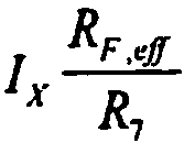

곱셈량 M은 최소 RF,eff의 조건하에서 Q1 및 Q2가 계속하여 요구되는 대역폭에 걸쳐 신호를 적절하게 전달하기에 충분한 바이어스 전류를 갖도록 정해져야 한다. 반대 극단에서, RF,eff가 최대값에 있을 때, Gm 보상 회로는 off 되어야 한다. 이는 예를 들어 RF,eff > R7일 때 일어난다. 이득 = M인 전류 미러의 입력측은 단지 전류만을 내려오게 할 수 있으므로, 차단된다.The multiplication amount M should be determined such that under conditions of at least R F, eff , Q1 and Q2 have sufficient bias current to adequately deliver the signal over the required bandwidth. At the opposite extreme, the Gm compensation circuit must be off when R F, eff is at its maximum. This happens , for example, when R F, eff > R 7 . The input side of the current mirror with gain = M can only bring down the current, so it is cut off.
이때, 극 비율은 다음의 표현식에 의해 결정된다:The pole ratio is then determined by the expression:

극 비율은 다음을 포함하는 다수의 인자들로 구성됨을 주목한다:Note that the pole rate consists of a number of factors, including:
모든 RF,eff에 걸쳐 고정된 캐패시터 비율 CS:CC;Fixed capacitor ratio across all R F, eff C S : C C ;
모든 RF,eff에 걸쳐 또한 고정된 νT:RC의 비율;The ratio of ν T : R C also fixed over all R F, eff ;
적절한 값의 Iin에 대해, 대략 RF,eff에 반비례하는 분모에 IB를 갖는 인자. 이 인자는 "1/IB..."로 나타내진다; 또한, 4의 값으로 제한되고 "RC/RF+..."로 나타내지는 RC/RF,eff를 갖는 인자.Factor with IB in the denominator approximately inversely proportional to R F, eff , for an appropriate value of Iin. This factor is represented by "1 / IB ..."; Furthermore, the factor with RC / R F, eff , limited to a value of 4 and represented by "RC / RF + ...".
이들 인자와 RF,eff 및 Iin에 대한 그들의 관계는 실시예에서 사용되는 전형적인 값을 가지고 도 9에서 설명된다. These factors and their relationship to R F, eff and I in are illustrated in FIG. 9 with typical values used in the examples.
실시예Example
이 설계는 NPN ft = 25GHz의 BiCMOS 처리에서 제작되었다. 회로 매개변수에서의 중재로, 구성성분의 값에 대해 다음을 선택하게 하였다:This design was fabricated in BiCMOS treatment with NPN ft = 25GHz. Arbitration in the circuit parameters led to the following choices for the component values:
대응하는 극 비율은 도 9에 도시되고, 10μA 내지 2mA까지의 피크 대 피크의 입력 전류값에 대해, 비율은 2.75내에 들지 않는 것으로 나타난다. 본 설명에 기초하여 실시자에게 명확한 바와 같이, 많은 다른 구성성분값이 대치되어 유사한 결과를 제공할 수 있다.The corresponding pole ratio is shown in FIG. 9 and for a peak to peak input current value of 10 μA to 2 mA, the ratio does not appear to be within 2.75. As will be apparent to the practitioner based on the present description, many other component values may be substituted to provide similar results.
그래서, 본 발명은 복잡하지 않은 구성성분의 배열로 넓은 동적 범위와 안정성을 제공한다. 대부분의 저잡음 신호 이득을 제공하는 증폭기의 제 1 스테이지는 루프에 추가 버퍼 또는 이득 스테이지를 포함하지 않고 최소 구성성분의 간략화된 회로로 실시된다.Thus, the present invention provides a wide dynamic range and stability with an arrangement of uncomplicated components. The first stage of the amplifier, which provides most of the low noise signal gain, is implemented in a simplified circuit of minimum components without including additional buffers or gain stages in the loop.
다른 이득 설정을 통한 루프 안정성은 2가지 기술을 사용하여 이루어진다: 보상 회로를 사용하여 입력 트랜지스터의 gm을 변화시키는 것과, 입력 트랜스콘덕터 Q1의 출력에 직접 피드백 저항기를 연결시킴으로서, 피드백 저항기가 자동적으로 루프 이득을 감소시키는 것. 이득 변화 및 루프 안정성은 모두 유사한 단자 전압 및 동작 조건하에서 동작하는 똑같은 가변 저항기의 3가지 예로 제어된다. 이는 트래킹을 용이하게 하여, 이득 제어 회로가 간략화될 수 있음을 의미한다.Loop stability through different gain settings is achieved using two techniques: by varying the gm of the input transistor using a compensation circuit and by connecting the feedback resistor directly to the output of the input transconductor Q1, the feedback resistor automatically Reducing loop gain. Gain variation and loop stability are all controlled by three examples of the same variable resistor operating under similar terminal voltages and operating conditions. This facilitates tracking, meaning that the gain control circuit can be simplified.
다시 도 8을 참고로, 본 발명의 바람직한 실시예에 대한 회로도가 설명된다. 회로는 이득 스테이지, 더미 스테이지, 및 차동 전압 버퍼를 포함한다. 차동 전압 버퍼는 여러 방법으로 구성될 수 있다. 바람직하게, 차동 전압 버퍼는 각 측면을 바이어스 처리하도록 이미터 변형 저항기 및 활성 전류원 (I0, I1)과 미분쌍으로 구성된다. 전류원은 동작하기 위해 약 500mV의 선두 여분 공간 (headroom)을 요구한다. 그러나, Q17, Q16의 베이스가 직접 제 1 및 더미 이득 스테이지의 출력에 연결되면, 예를 들어 Q1 및 Q2의 콜렉터에 연결되면, Q17, Q16의 이미터는 수십 mV 범위의 GND 전위에 가까워져 전류원이 동작될 수 없게 된다. 결과적으로, 레벨 쉬프트 다이오드 D1 및 D2는 전류원이 충분한 동작 선두 여분 공간을 갖도록 대략 700mV 만큼 차동 전압 버퍼의 공통 모드 입력 전압을 상승시키도록 요구된다. 이것이 수용가능한 성능을 제공하지만, 이는 약간 더 복잡해지고 (다이오드) 더 많은 신호 노드가 필요한 결점을 갖는다.Referring again to FIG. 8, a circuit diagram of a preferred embodiment of the present invention is described. The circuit includes a gain stage, a dummy stage, and a differential voltage buffer. Differential voltage buffers can be configured in several ways. Preferably, the differential voltage buffer is composed of differential pairs with emitter strain resistors and active current sources I0, I1 to bias each side. The current source requires about 500mV of headroom to operate. However, if the bases of Q17 and Q16 are directly connected to the outputs of the first and dummy gain stages, for example to the collectors of Q1 and Q2, the emitters of Q17 and Q16 are close to the GND potential in the range of several tens of mV so that the current source operates. It will not be possible. As a result, the level shift diodes D1 and D2 are required to raise the common mode input voltage of the differential voltage buffer by approximately 700 mV so that the current source has sufficient operating head spare space. Although this provides acceptable performance, it has the drawback that it is slightly more complicated (diode) and requires more signal nodes.
도 10a는 본 발명의 다른 이득 보상 실시예의 회로 구성성분예를 갖는 블록도이다. 다른 방법의 이득 보상 실시예는 이득 스테이지의 스케일 조정된 복제 스테이지(1080), 피드백 네트워크(1082), 증폭기(1084), 및 보상 전류 제공기 세트(1086)를 포함한다. 증폭기(1084)는 입력들 Input+, Input-, 및 Output을 갖는 전류 컨베이어로 배열된다.Fig. 10A is a block diagram having an example circuit component of another gain compensation embodiment of the present invention. Another method of gain compensation includes a scaled replication stage 1080, a feedback network 1082, an
증폭기(1084)는 공통 베이스 입력 (1003, 1004)을 갖는다. 증폭기 "output" 핀 전압은 "Input+"과 "Input-" 사이의 전압차가 증가될 때 증가된다. 증폭기는 (1004)의 활성 로드에 대해 전류원을 사용하므로 높은 이득을 갖는다.
피드백 네트워크는 피드백 저항기 (M3, RF3)로 완전한 이득/더미 스테이지 (Q4, R2)의 복제 스테이지를 구비한다. 디바이스(1008)는 증폭기 (1000 내지 1007)로부터의 출력 전압을 RF3//M3를 통해 흐르고 (1011)을 통해 출력되어 RF3//M3에 걸쳐 전압 강하를 일으키는 전류로 변환한다. 이 전압 강하는 이어서 증폭기 (1000 내지 1007)의 입력으로 피드백된다.The feedback network has a replica stage of the complete gain / dummy stages Q4, R2 with feedback resistors M3, RF3.
증폭기 (1000 내지 1007) 및 피드백 네트워크는 (1002)에 걸친 일정한 전압 강하가 RF3//M3 가변 저항기의 조합에 각인될 때 안정된 동작점에 이르도록 구성된다. 그래서, (1008)에 의해 RF3//M3를 통하여 주어지는 전류는 실제로 이득 제어 회로에 의해 제어되는 RF3//M3의 유효 저항으로 나눈 (1002)에 걸친 전압과 동일하다. 그러므로, (1008, 1009)를 통한 전류는 피크 입력 신호 전류의 배수와 똑같다. (1009)를 통한 전류는 이어서 이득 및 더미 스테이지에 인가되어, 이들 스테이지의 gm을 감소하고 전체적인 증폭기를 제어 및 안정화하는데 도움이 된다. 도표 1은 도 10a의 이득 보상 실시예에 대한 전형적인 구성성분값의 세트를 제공한다.The amplifiers 1000-1007 and the feedback network are configured to reach a stable operating point when a constant voltage drop across 1002 is imprinted on the combination of RF3 // M3 variable resistors. Thus, the current given through RF3 // M3 by 1008 is actually equal to the voltage across 1002 divided by the effective resistance of RF3 // M3 controlled by the gain control circuit. Therefore, the current through (1008, 1009) is equal to a multiple of the peak input signal current. Current through 1009 is then applied to the gain and dummy stages to help reduce the gm of these stages and to control and stabilize the overall amplifier. Table 1 provides a set of typical component values for the gain compensation embodiment of FIG. 10A.
도표 1
1000,1001,1005,1006 2μA 정전류원1000,1001,1005,1006 2μA constant current source
1002 150Kohm 저항기1002 150Kohm Resistors
1003,1004 일반 NPN 트랜지스터, 동일한 크기1003,1004 common NPN transistors, same size
1007 2pF 캐패시터1007 2pF Capacitors
1008,1009 W/L = 72u/1.2u PFET 트랜지스터1008,1009 W / L = 72u / 1.2u PFET Transistor
1010,1011 2mA를 전도할 수 있는 일반 NPN 트랜지스터 1010,1011 General NPN Transistors Capable of Conducting 2mA
1012,1013 일반 NPN 트랜지스터, 1010, 1011의 2배 면적1012,1013 common NPN transistors, twice the area of 1010, 1011
RC1,RC2,R2 220ohmRC1, RC2, R2 220ohm
Q1,Q2,Q4 5mA를 전도할 수 있는 일반 NPN 저잡음 트랜지스터Q1, Q2, Q4 Typical NPN Low-Noise Transistors Capable of Conducting 5mA
RF1,RF2,RF3 1KohmRF1, RF2, RF3 1Kohm
M0,M1,M3 W/L = 64u/1.1u NFET 트랜지스터M0, M1, M3 W / L = 64u / 1.1u NFET Transistor
도 10b는 본 발명의 제 1 다른 실시예를 실시한 회로도이다. 전류원은 차동 전압 버퍼로부터 제거되어, 레벨 쉬프트 다이오드에 대한 필요성을 없앴다. 차동 전압 버퍼의 제 1 다른 실시예는 이전의 이미터 변형 저항기를 2개 부분으로 분할하고 중심 탭을 GND에 단락시킨다. 따라서, 새로운 실시의 이미터 변형 저항기 - R12, R15 -가 변형 저항기 및 전류 소스로 동작한다. Q1의 콜렉터에 대한 신호 편위가 너무 느려서 Q17이 전도성으로부터 벗어나지 않도록 보장하기 위해 주의하여야 한다. 이 조건은 gm 보상 구조를 수정함으로서 지켜질 수 있다.Fig. 10B is a circuit diagram of another embodiment of the present invention. The current source is removed from the differential voltage buffer, eliminating the need for a level shift diode. A first alternative embodiment of the differential voltage buffer divides the previous emitter strain resistor into two parts and shorts the center tap to GND. Thus, a new embodiment emitter strain resistor-R12, R15-acts as strain resistor and current source. Care must be taken to ensure that the signal deviation for the collector of Q1 is too slow so that Q17 does not deviate from the conductivity. This condition can be followed by modifying the gm compensation structure.
도 10b는 또한 본 발명의 다른 이득 보상 구조에 대한 실시예의 회로도를 포함한다. 보상 전류는 콜렉터에서 전류를 추출하는 대신에 피드백 저항기를 통해 낮춤으로서 Q1 및 Q2로부터 바이어스 전류를 추출한다. 이 구조는 차동 전압 버퍼의 입력 트랜지스터가 Q1의 콜렉터에서 큰 신호 편위 동안 턴 오프되는 것을 방지한다. 예를 들어, 이 조건은 단지 레벨 쉬프트 다이오드가 주어지지 않을 때만 문제가 된다.Figure 10B also includes a circuit diagram of an embodiment of another gain compensation structure of the present invention. The compensation current extracts the bias current from Q1 and Q2 by lowering it through the feedback resistor instead of extracting the current from the collector. This structure prevents the input transistors of the differential voltage buffer from turning off during large signal excursions at the collector of Q1. For example, this condition is only a problem when no level shift diode is given.
반복하여, 다른 이득 보상 구조의 목적은 평균적인 입력 전류 진폭을 정확하게 측정하고 일부 최대치에 종속되는 입력 신호에서 배수를 공제하는 것이다. (1004, 1003, 1002, 1008)로 형성된 증폭기는 피드백 루프의 일부이다. M3, RF3, 및 Q4는 루프를 완성하는 피드백 소자를 형성한다. M3, RF3, Q4, 및 R2는 이득 스테이지 및 더미 이득 스테이지를 정확하게 스케일 조정하여 복제한 스테이지이다. 이는 M3 및 RF3의 병렬 조합이 신호 이득 스테이지와 정확하게 똑같은 특성을 가져야 함을 의미한다.In turn, the purpose of other gain compensation schemes is to accurately measure the average input current amplitude and subtract multiples from the input signal that depend on some maximum. The amplifier formed by (1004, 1003, 1002, 1008) is part of the feedback loop. M3, RF3, and Q4 form a feedback element that completes the loop. M3, RF3, Q4, and R2 are stages that accurately scale and replicate the gain stage and the dummy gain stage. This means that the parallel combination of M3 and RF3 must have exactly the same characteristics as the signal gain stage.
이와 같이, 피드백 루프 (1003, 1004, 1002, 1008, RF3, M3)는 M3 및 RF3의 병렬 조합에서 (1002)에 걸친 전압 강하를 각인하도록 노력한다. 전류원 (1000, 1001, 1005, 1006)은 Q4 바이어스 전류와 비교해 모두 작은 크기 (약 2μA)를 갖는다. 저항기(1002)는 그의 전압 강하가 AGC 전압의 일부 배수 m1과 동일하도록 선택된다. 이 전압 강하는 스케일 조정된 복제 스테이지 M3, RF3에 걸쳐 루프에 의해 강요된다. 이는 (1008)을 통한 전류가 피크 입력 신호 전류에 비례함을 의미한다. 이는 AGC 루프가 활성화될 때 M0, M1, M3 게이트 전압을 변조시킴으로서 RF1, M0에 걸쳐 일정한 피크 전압을 유지하도록 노력하기 때문이다.As such, the
(1008)에서의 비례적인 재생산 피크 신호 전류는 (1009)에 의해 복사되어 전류 미러 (1010, 1011, 1012, 1013)에 전달된다. 소스 (1012, 1013)는 이 미러 전류를 이득 스테이지 및 더미 이득 스테이지 베이스 밖으로 내려 Q1 및 Q2의 gm을 감소시킨다.Proportional reproduction peak signal current at 1008 is radiated by 1009 and delivered to
이는 증가된 입력 신호 진폭이 있을 때 Q1, Q2 콜렉터에서의 전압을 증가시키는 이점을 갖고, 전도성에서 벗어나는 것으로부터 다른 실시의 차동 전압 버퍼의 입력 디바이스를 보호하여 많은 신호 왜곡의 발생을 방지하는데 도움이 된다. 도 11은 큰 입력 신호 하에서의 안정성을 나타내어 극 비율에서 다른 회로 구성의 효과를 설명한다. 특히, 그래프 Y축은 유효 콜렉터 저항(RC,eff)에 대한 폐쇄 루프 입력 임피던스(Rin)의 비율이다. 이 인자는 fout:fin 극 비율에 비례한다. X축은 입력 신호 전류를 나타낸다.This has the advantage of increasing the voltage at the Q1 and Q2 collectors when there is an increased input signal amplitude, protecting the input device of the differential voltage buffers of other implementations from deriving from conductivity and helping to prevent the occurrence of much signal distortion. do. Fig. 11 shows stability under a large input signal to explain the effect of different circuit configurations on the pole ratio. In particular, the graph Y-axis is the ratio of the closed loop input impedance Rin to the effective collector resistance RC, eff. This argument is proportional to the fout: fin pole ratio. The X axis represents the input signal current.
가장 아래에 있는 자취는 특히 도 5에 도시된 종래 기술에서부터의 전형적인 특성을 도시한다. 이는 AGC가 활성화 상태일 때 (90μApp < 입력 전류 < 800μApp), 입력 전류 진폭이 증가함에 따라 극 비율이 비례하여 변하고 안정성이 저하됨을 명확하게 나타낸다. 이 효과는 도 12에서 과도 대안도를 참고로 더 설명된다. 낮은 입력 전류에서 (- 50μApp), 차동 출력 전압은 안정되게 보인다 - 오버슈트 (overshoot)나 공명 (ringing)이 없다. 그러나, 500μApp 입력 전류로는 차동 출력 전압이 실질적인 오버슈트 및 공명과 매우 다르게 보인다. 그래서, 안정성이 해결된다.The bottom trace shows the typical properties from the prior art, in particular shown in FIG. 5. This clearly indicates that when the AGC is active (90 μApp <input current <800 μApp), the pole ratio changes proportionally and stability decreases as the input current amplitude increases. This effect is further explained with reference to the transient alternatives in FIG. 12. At low input currents (-50μApp), the differential output voltage appears stable-no overshoot or ringing. However, with a 500μApp input current, the differential output voltage looks very different from the actual overshoot and resonance. Thus, stability is solved.
도 11을 다시 참고로, 위에 있는 자취는 바람직한 실시예 (도 8)에서의 극 비율에 비례한다. 일단 AGC가 활성화되면, 극 비율은 증가되고 1mApp 입력 전류 부근에서 피크가 된다. 전체 범위의 입력 전류에 걸친 변화는 종래 기술에 대한 것 보다 상당히 더 적다. 이는 전체 범위의 입력 전류에 걸쳐 훨씬 더 안정한 증폭기임을 나타낸다. 이는 낮은 입력 전류 (50μApp) 및 훨씬 더 높은 전류 500μApp에서 순간적인 대안도를 도시하는 도 13을 참고로 더 설명된다. 종래 기술과 유사하게, 50μApp 파형은 오버슈트나 공명 없이 안정된다. 그러나, 종래 기술과 다르게, 500μApp 파형도 또한 공명 및 미세 오버슈트 없이 매우 안정된다. Referring back to FIG. 11, the trace above is proportional to the pole ratio in the preferred embodiment (FIG. 8). Once AGC is activated, the pole ratio is increased and peaked around 1mApp input current. The variation over the full range of input current is significantly less than that for the prior art. This represents a much more stable amplifier over the full range of input current. This is further explained with reference to FIG. 13, which shows an instantaneous alternative at low input current (50μApp) and even higher current 500μApp. Similar to the prior art, the 50μApp waveform is stable without overshoot or resonance. However, unlike the prior art, the 500 μApp waveform is also very stable without resonance and fine overshoot.
마지막으로, 다시 도 11을 참고로, 중간에 있는 자취는 제 1 다른 (도 10) 극 비율에 비례한다. 이 자취는 다른 2개 보다 더 적은 변화를 갖는다. 이 회로는 도 14의 그래프를 조사하여 안정되는 것으로 설명될 수 있고, 여기서 이전의 2가지 경우와 같이, 50μApp 자취는 오버슈트나 공명을 나타내지 않고 안정된 증폭기로부터의 출력을 예시한다. 더 높은 입력 전류 (500μApp) 자취도 또한 공명 및 약간의 오버슈트도 없이 안정된다.Finally, referring again to FIG. 11, the trace in the middle is proportional to the first other (FIG. 10) pole ratio. This trace has fewer changes than the other two. This circuit can be described as being stabilized by examining the graph of FIG. 14, where, as in the previous two cases, a 50μApp trace illustrates the output from a stable amplifier without exhibiting overshoot or resonance. Higher input current (500μApp) traces also stabilize without resonance and slight overshoot.
여기서는 비록 광학 트랜스듀서의 증폭 응용을 주로 참고하여 본 발명이 설명되었지만, 본 발명은 특히 넓은 동적 범위에 걸쳐 입력을 갖는 회로에서 안정성으로부터 이득을 보는 임의의 회로에 폭넓은 응용성을 갖는다.Although the invention has been described herein with reference primarily to the amplification application of optical transducers, the invention has wide applicability in any circuit that benefits from stability, particularly in circuits having inputs over a wide dynamic range.
명확하게, 상기 지시에 대해 본 발명의 다양한 수정 및 변화가 가능하다. 그러므로, 첨부된 청구항의 범위내에서, 본 발명이 여기에 특정하게 설명된 것 이외의 방법으로 실시될 수 있는 것으로 이해되어야 한다.Clearly, various modifications and variations of the present invention are possible in light of the above indication. It is, therefore, to be understood that within the scope of the appended claims, the invention may be practiced in other than as specifically described herein.
입력과 출력 사이의 극 비율이 안정되도록 이득 보상 기술을 사용함으로써 넓은 동적 범위 및 안정성을 획득할 수 있다. A wide dynamic range and stability can be achieved by using gain compensation techniques to stabilize the pole ratio between the input and output.
Claims (30)
Applications Claiming Priority (4)
| Application Number | Priority Date | Filing Date | Title |
|---|---|---|---|
| US25061100P | 2000-12-01 | 2000-12-01 | |
| US60/250,611 | 2000-12-01 | ||
| US09/910,660 US6583671B2 (en) | 2000-12-01 | 2001-07-20 | Stable AGC transimpedance amplifier with expanded dynamic range |
| US09/910,660 | 2001-07-20 |
Publications (2)
| Publication Number | Publication Date |
|---|---|
| KR20020043189A KR20020043189A (en) | 2002-06-08 |
| KR100887893B1 true KR100887893B1 (en) | 2009-03-16 |
Family
ID=22948452
Family Applications (1)
| Application Number | Title | Priority Date | Filing Date |
|---|---|---|---|
| KR1020010075633A KR100887893B1 (en) | 2000-12-01 | 2001-12-01 | Novel ??? transimpedance amplifier |
Country Status (3)
| Country | Link |
|---|---|
| US (1) | US6583671B2 (en) |
| JP (1) | JP4032720B2 (en) |
| KR (1) | KR100887893B1 (en) |
Cited By (1)
| Publication number | Priority date | Publication date | Assignee | Title |
|---|---|---|---|---|
| KR20200062788A (en) * | 2018-11-27 | 2020-06-04 | 아주대학교산학협력단 | Circuit and method for real-time two-way data transmitting utilizing single line |
Families Citing this family (45)
| Publication number | Priority date | Publication date | Assignee | Title |
|---|---|---|---|---|
| US7078967B2 (en) * | 1999-12-30 | 2006-07-18 | Nokia Corporation | Control of bias voltage |
| SG93224A1 (en) * | 2000-02-02 | 2002-12-17 | Koninkl Philips Electronics Nv | Measuring antenna signal strength with automatic gain control receiver |
| US7171170B2 (en) | 2001-07-23 | 2007-01-30 | Sequoia Communications | Envelope limiting for polar modulators |
| US6798290B2 (en) * | 2001-08-31 | 2004-09-28 | Sequoia Communications | Translinear variable gain amplifier |
| US6985703B2 (en) | 2001-10-04 | 2006-01-10 | Sequoia Corporation | Direct synthesis transmitter |
| JP3857099B2 (en) * | 2001-10-09 | 2006-12-13 | 株式会社アドバンテスト | Data transmission device, photoelectric conversion circuit, and test device |
| EP1322036A1 (en) * | 2001-12-20 | 2003-06-25 | Koninklijke Philips Electronics N.V. | Arrangement with a symmetrical amplifier |
| KR100613141B1 (en) * | 2002-07-19 | 2006-08-17 | 인티그런트 테크놀로지즈(주) | Variable Gain Amplifier Having Improved Linearity |
| US7489916B1 (en) | 2002-06-04 | 2009-02-10 | Sequoia Communications | Direct down-conversion mixer architecture |
| US6882218B2 (en) * | 2002-08-26 | 2005-04-19 | Broadcom Corporation | Transimpedance amplifier and offset correction mechanism and method for lowering noise |
| US6980055B2 (en) * | 2003-08-11 | 2005-12-27 | Texas Instruments Incorporated | CMOS differential buffer circuit |
| US6894568B2 (en) * | 2003-08-20 | 2005-05-17 | Intel Corporation | Transimpedance amplifier with receive signal strength indicator |
| US6864751B1 (en) * | 2003-09-08 | 2005-03-08 | Texas Instruments Deutschland Gmbh | Transimpedance amplifier with adjustable output amplitude and wide input dynamic-range |
| US7609118B1 (en) | 2003-12-29 | 2009-10-27 | Sequoia Communications | Phase-locked loop calibration system |
| US7496338B1 (en) | 2003-12-29 | 2009-02-24 | Sequoia Communications | Multi-segment gain control system |
| US7522017B1 (en) | 2004-04-21 | 2009-04-21 | Sequoia Communications | High-Q integrated RF filters |
| US7332971B2 (en) * | 2004-06-10 | 2008-02-19 | Agency For Science, Technology And Research | Multi-gigabit/s transimpedance amplifier for optical networks |
| US7672648B1 (en) | 2004-06-26 | 2010-03-02 | Quintics Holdings | System for linear amplitude modulation |
| US7196582B2 (en) * | 2004-10-29 | 2007-03-27 | Broadcom Corporation | Method and system for low noise amplifier (LNA) and power amplifier (PA) gain control |
| US7548122B1 (en) | 2005-03-01 | 2009-06-16 | Sequoia Communications | PLL with switched parameters |
| US7479815B1 (en) | 2005-03-01 | 2009-01-20 | Sequoia Communications | PLL with dual edge sensitivity |
| US7675379B1 (en) | 2005-03-05 | 2010-03-09 | Quintics Holdings | Linear wideband phase modulation system |
| US7595626B1 (en) | 2005-05-05 | 2009-09-29 | Sequoia Communications | System for matched and isolated references |
| US20070205200A1 (en) * | 2006-03-02 | 2007-09-06 | Brain Box Concepts | Soap bar holder and method of supporting a soap bar |
| CN101496285A (en) | 2006-05-16 | 2009-07-29 | 巨杉通信公司 | A multi-mode vco for direct fm systems |
| US8269562B1 (en) | 2006-06-30 | 2012-09-18 | Ixys Ch Gmbh | Open-loop transimpedance amplifier for infrared diodes |
| US7679468B1 (en) | 2006-07-28 | 2010-03-16 | Quintic Holdings | KFM frequency tracking system using a digital correlator |
| US7522005B1 (en) | 2006-07-28 | 2009-04-21 | Sequoia Communications | KFM frequency tracking system using an analog correlator |
| US7894545B1 (en) | 2006-08-14 | 2011-02-22 | Quintic Holdings | Time alignment of polar transmitter |
| US7920033B1 (en) | 2006-09-28 | 2011-04-05 | Groe John B | Systems and methods for frequency modulation adjustment |
| US20090058531A1 (en) * | 2007-08-31 | 2009-03-05 | Nanoamp Solutions Inc. (Cayman) | Variable gain amplifier |
| US8081030B2 (en) * | 2008-12-19 | 2011-12-20 | Honeywell International Inc. | Multi-mode amplifier |
| US7893759B1 (en) | 2009-03-18 | 2011-02-22 | Honeywell International Inc. | Current conveyor based instrumentation amplifier |
| JP5475525B2 (en) * | 2010-04-01 | 2014-04-16 | 日本電信電話株式会社 | Variable gain amplifier and optical receiver |
| JP2013115562A (en) * | 2011-11-28 | 2013-06-10 | Sumitomo Electric Ind Ltd | Transimpedance amplifier |
| US9030263B2 (en) | 2013-03-15 | 2015-05-12 | Avago Technologies General Ip (Singapore) Pte. Ltd. | Transimpedance amplifier (TIA) circuit and method |
| US9112462B2 (en) | 2013-05-15 | 2015-08-18 | Honeywell International Inc. | Variable-gain dual-output transconductance amplifier-based instrumentation amplifiers |
| FR3026250A1 (en) * | 2014-09-19 | 2016-03-25 | St Microelectronics Sa | ELECTRONIC DEVICE FOR A RADIO FREQUENCY SIGNAL RECEIVING CHAIN, COMPRISING A LOW NOISE TRANSCONDUCTIVE AMPLIFIER STAGE |
| EP3334539B1 (en) * | 2015-08-11 | 2023-06-14 | Koninklijke Philips N.V. | Capacitive micromachined ultrasonic transducers with increased patient safety |
| CN106941379A (en) * | 2017-05-05 | 2017-07-11 | 烽火通信科技股份有限公司 | A kind of automatic gain control circuit for APD trans-impedance amplifiers |
| CN108173524B (en) * | 2018-02-08 | 2021-02-19 | 厦门亿芯源半导体科技有限公司 | Dual-loop automatic gain control circuit suitable for high-bandwidth TIA |
| CN110545083B (en) * | 2018-05-28 | 2024-06-11 | 深圳市芯波微电子有限公司 | Transimpedance amplifier |
| US10958177B2 (en) * | 2019-05-31 | 2021-03-23 | Dialog Semiconductor Inc. | Optocoupler current transfer ratio compensation |
| CN112039452B (en) * | 2020-09-07 | 2022-08-23 | 电子科技大学 | Broadband trans-impedance amplifier |
| CN112332791A (en) * | 2020-11-11 | 2021-02-05 | 苏州坤元微电子有限公司 | Variable gain amplifier |
Citations (7)
| Publication number | Priority date | Publication date | Assignee | Title |
|---|---|---|---|---|
| JPH0878980A (en) * | 1994-08-30 | 1996-03-22 | Oki Electric Ind Co Ltd | Gain variable amplifier circuit |
| US5801587A (en) * | 1996-09-26 | 1998-09-01 | Exar Corporation | Variable gain peak detector |
| KR19980068704A (en) * | 1997-02-22 | 1998-10-26 | 김광호 | Automatic Gain Controller Using Voltage Amplifier |
| US5844444A (en) * | 1997-02-14 | 1998-12-01 | Macronix International Co., Ltd. | Wide dynamic input range transconductor-based amplifier circuit for speech signal processing |
| KR19980086741A (en) * | 1997-05-06 | 1998-12-05 | 윌리엄 비. 켐플러 | Improved peak detector for automatic gain control |
| JPH11122188A (en) * | 1997-10-20 | 1999-04-30 | Fujitsu Ltd | Light signal reception device/method |
| JPH11234056A (en) * | 1997-11-13 | 1999-08-27 | Matsushita Electric Ind Co Ltd | Preamplifier for light reception and variable offset voltage peak detector |
Family Cites Families (8)
| Publication number | Priority date | Publication date | Assignee | Title |
|---|---|---|---|---|
| US3679986A (en) * | 1970-09-04 | 1972-07-25 | Ibm | Non-linear feedback gain control and peak detector system |
| JPS5721379Y2 (en) * | 1977-02-01 | 1982-05-10 | ||
| US4326226A (en) * | 1980-05-08 | 1982-04-20 | Storage Technology Corporation | Constant bandwidth automatic gain control |
| US5168148A (en) * | 1990-12-28 | 1992-12-01 | Symbol Technologies, Inc. | Automatic gain control circuit |
| KR0156021B1 (en) * | 1993-06-08 | 1998-12-15 | 쯔지 하루오 | Light receiving amplifying device |
| US5451901A (en) * | 1994-07-01 | 1995-09-19 | Cirrus Logic Inc. | Transconductance amplifiers and exponential variable gain amplifiers using the same |
| US5923164A (en) * | 1996-10-15 | 1999-07-13 | Balluff, Inc. | Apparatus and method for automatically tuning the gain of an amplifier |
| JPH10322152A (en) * | 1997-05-19 | 1998-12-04 | Fujitsu Ltd | Digital agc circuit |
-
2001
- 2001-07-20 US US09/910,660 patent/US6583671B2/en not_active Expired - Fee Related
- 2001-12-01 KR KR1020010075633A patent/KR100887893B1/en not_active IP Right Cessation
- 2001-12-03 JP JP2001369349A patent/JP4032720B2/en not_active Expired - Fee Related
Patent Citations (7)
| Publication number | Priority date | Publication date | Assignee | Title |
|---|---|---|---|---|
| JPH0878980A (en) * | 1994-08-30 | 1996-03-22 | Oki Electric Ind Co Ltd | Gain variable amplifier circuit |
| US5801587A (en) * | 1996-09-26 | 1998-09-01 | Exar Corporation | Variable gain peak detector |
| US5844444A (en) * | 1997-02-14 | 1998-12-01 | Macronix International Co., Ltd. | Wide dynamic input range transconductor-based amplifier circuit for speech signal processing |
| KR19980068704A (en) * | 1997-02-22 | 1998-10-26 | 김광호 | Automatic Gain Controller Using Voltage Amplifier |
| KR19980086741A (en) * | 1997-05-06 | 1998-12-05 | 윌리엄 비. 켐플러 | Improved peak detector for automatic gain control |
| JPH11122188A (en) * | 1997-10-20 | 1999-04-30 | Fujitsu Ltd | Light signal reception device/method |
| JPH11234056A (en) * | 1997-11-13 | 1999-08-27 | Matsushita Electric Ind Co Ltd | Preamplifier for light reception and variable offset voltage peak detector |
Cited By (2)
| Publication number | Priority date | Publication date | Assignee | Title |
|---|---|---|---|---|
| KR20200062788A (en) * | 2018-11-27 | 2020-06-04 | 아주대학교산학협력단 | Circuit and method for real-time two-way data transmitting utilizing single line |
| KR102147936B1 (en) * | 2018-11-27 | 2020-08-26 | 아주대학교산학협력단 | Circuit and method for real-time two-way data transmitting utilizing single line |
Also Published As
| Publication number | Publication date |
|---|---|
| US20020101285A1 (en) | 2002-08-01 |
| JP2002232244A (en) | 2002-08-16 |
| KR20020043189A (en) | 2002-06-08 |
| US6583671B2 (en) | 2003-06-24 |
| JP4032720B2 (en) | 2008-01-16 |
Similar Documents
| Publication | Publication Date | Title |
|---|---|---|
| KR100887893B1 (en) | Novel ??? transimpedance amplifier | |
| US6072366A (en) | Receiver capable of outputting a high quality signal without regard to an input signal level | |
| KR100900205B1 (en) | Wide dynamic range transimpedance amplifier | |
| US5844445A (en) | Feedback type pre-amplifier | |
| US4564818A (en) | Transimpedance amplifier having an improved gain/bandwidth product | |
| US7973602B2 (en) | Variable gain amplifier | |
| US6292058B1 (en) | Signal amplifying circuit connected to a transfer circuit having a known non-linear transfer characteristic | |
| US7948323B2 (en) | Linear transimpedance amplifier with wide dynamic range for high rate applications | |
| US10355655B2 (en) | Transimpedance amplifier (TIA) circuit having reduced power consumption, improved linearization and reduced peaking | |
| JP7115065B2 (en) | transimpedance amplifier | |
| JPH0563056B2 (en) | ||
| US4718119A (en) | AGC circuit including a precision voltage clamp and method | |
| US6879217B2 (en) | Triode region MOSFET current source to bias a transimpedance amplifier | |
| NL193076C (en) | Amplifier control chain. | |
| US5351012A (en) | Low input resistance current-mode feedback operational amplifier input stage | |
| CN113659949A (en) | Automatic gain control circuit and method of transimpedance amplifier circuit | |
| JPH0134501B2 (en) | ||
| US11349444B2 (en) | Transimpedance amplifier circuit | |
| US5874861A (en) | Amplifier circuit | |
| US7221229B2 (en) | Receiver circuit having an optical reception device | |
| CN116633284A (en) | High-gain transimpedance amplifier and high-gain photoelectric converter | |
| JP6706105B2 (en) | Transimpedance amplifier and optical signal receiver | |
| JP3844544B2 (en) | Optical receiver circuit | |
| US5119041A (en) | High gain differential current amplifier having a low output voltage | |
| JP4271364B2 (en) | Receiver amplifier circuit |
Legal Events
| Date | Code | Title | Description |
|---|---|---|---|
| A201 | Request for examination | ||
| E902 | Notification of reason for refusal | ||
| E902 | Notification of reason for refusal | ||
| E701 | Decision to grant or registration of patent right | ||
| GRNT | Written decision to grant | ||
| LAPS | Lapse due to unpaid annual fee |