KR100688972B1 - Display device and manufacturing method thereof - Google Patents
Display device and manufacturing method thereof Download PDFInfo
- Publication number
- KR100688972B1 KR100688972B1 KR1020060049549A KR20060049549A KR100688972B1 KR 100688972 B1 KR100688972 B1 KR 100688972B1 KR 1020060049549 A KR1020060049549 A KR 1020060049549A KR 20060049549 A KR20060049549 A KR 20060049549A KR 100688972 B1 KR100688972 B1 KR 100688972B1
- Authority
- KR
- South Korea
- Prior art keywords
- sealant
- thin film
- insulating substrate
- substrate
- encapsulation thin
- Prior art date
Links
- 238000004519 manufacturing process Methods 0.000 title claims abstract description 11
- 239000000758 substrate Substances 0.000 claims abstract description 162
- 239000000565 sealant Substances 0.000 claims abstract description 114
- 239000010409 thin film Substances 0.000 claims abstract description 68
- 238000005538 encapsulation Methods 0.000 claims abstract description 53
- 238000000034 method Methods 0.000 claims description 37
- 229910010272 inorganic material Inorganic materials 0.000 claims description 6
- 239000011147 inorganic material Substances 0.000 claims description 6
- 238000007650 screen-printing Methods 0.000 claims description 6
- 238000004544 sputter deposition Methods 0.000 claims description 6
- 229910004205 SiNX Inorganic materials 0.000 claims description 5
- 239000000853 adhesive Substances 0.000 claims description 5
- 230000001070 adhesive effect Effects 0.000 claims description 5
- 238000007735 ion beam assisted deposition Methods 0.000 claims description 5
- 238000001659 ion-beam spectroscopy Methods 0.000 claims description 5
- 229910052814 silicon oxide Inorganic materials 0.000 claims description 5
- 229910017107 AlOx Inorganic materials 0.000 claims description 4
- -1 SiONx Inorganic materials 0.000 claims description 4
- VYPSYNLAJGMNEJ-UHFFFAOYSA-N Silicium dioxide Chemical compound O=[Si]=O VYPSYNLAJGMNEJ-UHFFFAOYSA-N 0.000 claims description 4
- 230000008020 evaporation Effects 0.000 claims description 4
- 238000001704 evaporation Methods 0.000 claims description 4
- 238000002207 thermal evaporation Methods 0.000 claims description 4
- 238000000623 plasma-assisted chemical vapour deposition Methods 0.000 claims description 3
- 238000005566 electron beam evaporation Methods 0.000 claims 1
- QVGXLLKOCUKJST-UHFFFAOYSA-N atomic oxygen Chemical compound [O] QVGXLLKOCUKJST-UHFFFAOYSA-N 0.000 abstract description 28
- 229910052760 oxygen Inorganic materials 0.000 abstract description 28
- 239000001301 oxygen Substances 0.000 abstract description 28
- XLYOFNOQVPJJNP-UHFFFAOYSA-N water Substances O XLYOFNOQVPJJNP-UHFFFAOYSA-N 0.000 abstract description 3
- 238000007789 sealing Methods 0.000 description 7
- 238000002834 transmittance Methods 0.000 description 7
- 239000010408 film Substances 0.000 description 5
- 239000011368 organic material Substances 0.000 description 4
- 238000005192 partition Methods 0.000 description 4
- 230000000149 penetrating effect Effects 0.000 description 4
- 230000000903 blocking effect Effects 0.000 description 3
- 238000000151 deposition Methods 0.000 description 2
- 239000000463 material Substances 0.000 description 2
- 230000035515 penetration Effects 0.000 description 2
- 239000011347 resin Substances 0.000 description 2
- 229920005989 resin Polymers 0.000 description 2
- 229910018072 Al 2 O 3 Inorganic materials 0.000 description 1
- 229910004298 SiO 2 Inorganic materials 0.000 description 1
- 230000005540 biological transmission Effects 0.000 description 1
- 230000015572 biosynthetic process Effects 0.000 description 1
- 239000005388 borosilicate glass Substances 0.000 description 1
- 230000008021 deposition Effects 0.000 description 1
- 238000010894 electron beam technology Methods 0.000 description 1
- 238000000313 electron-beam-induced deposition Methods 0.000 description 1
- 238000005516 engineering process Methods 0.000 description 1
- 239000011521 glass Substances 0.000 description 1
- 230000010365 information processing Effects 0.000 description 1
- 238000009413 insulation Methods 0.000 description 1
- 239000005355 lead glass Substances 0.000 description 1
- 150000004767 nitrides Chemical class 0.000 description 1
- 239000005368 silicate glass Substances 0.000 description 1
- 239000005361 soda-lime glass Substances 0.000 description 1
Images


Classifications
-
- H—ELECTRICITY
- H10—SEMICONDUCTOR DEVICES; ELECTRIC SOLID-STATE DEVICES NOT OTHERWISE PROVIDED FOR
- H10K—ORGANIC ELECTRIC SOLID-STATE DEVICES
- H10K59/00—Integrated devices, or assemblies of multiple devices, comprising at least one organic light-emitting element covered by group H10K50/00
- H10K59/80—Constructional details
- H10K59/87—Passivation; Containers; Encapsulations
- H10K59/871—Self-supporting sealing arrangements
- H10K59/8722—Peripheral sealing arrangements, e.g. adhesives, sealants
-
- H—ELECTRICITY
- H10—SEMICONDUCTOR DEVICES; ELECTRIC SOLID-STATE DEVICES NOT OTHERWISE PROVIDED FOR
- H10K—ORGANIC ELECTRIC SOLID-STATE DEVICES
- H10K50/00—Organic light-emitting devices
- H10K50/80—Constructional details
- H10K50/84—Passivation; Containers; Encapsulations
- H10K50/842—Containers
- H10K50/8426—Peripheral sealing arrangements, e.g. adhesives, sealants
-
- H—ELECTRICITY
- H05—ELECTRIC TECHNIQUES NOT OTHERWISE PROVIDED FOR
- H05B—ELECTRIC HEATING; ELECTRIC LIGHT SOURCES NOT OTHERWISE PROVIDED FOR; CIRCUIT ARRANGEMENTS FOR ELECTRIC LIGHT SOURCES, IN GENERAL
- H05B33/00—Electroluminescent light sources
- H05B33/02—Details
- H05B33/04—Sealing arrangements, e.g. against humidity
-
- H—ELECTRICITY
- H05—ELECTRIC TECHNIQUES NOT OTHERWISE PROVIDED FOR
- H05B—ELECTRIC HEATING; ELECTRIC LIGHT SOURCES NOT OTHERWISE PROVIDED FOR; CIRCUIT ARRANGEMENTS FOR ELECTRIC LIGHT SOURCES, IN GENERAL
- H05B33/00—Electroluminescent light sources
- H05B33/10—Apparatus or processes specially adapted to the manufacture of electroluminescent light sources
-
- H—ELECTRICITY
- H01—ELECTRIC ELEMENTS
- H01L—SEMICONDUCTOR DEVICES NOT COVERED BY CLASS H10
- H01L2224/00—Indexing scheme for arrangements for connecting or disconnecting semiconductor or solid-state bodies and methods related thereto as covered by H01L24/00
- H01L2224/80—Methods for connecting semiconductor or other solid state bodies using means for bonding being attached to, or being formed on, the surface to be connected
- H01L2224/81—Methods for connecting semiconductor or other solid state bodies using means for bonding being attached to, or being formed on, the surface to be connected using a bump connector
Abstract
Description
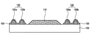
도 1은 본 발명의 제1실시예에 따른 표시장치의 구조를 설명하기 위한 도면이고,1 is a view for explaining the structure of a display device according to a first embodiment of the present invention;
도 2는 도 1의 Ⅱ-Ⅱ를 따른 단면도,2 is a cross-sectional view taken along II-II of FIG. 1;
도 3a 내지 도 3d는 본 발명의 제1실시예에 따른 표시장치의 제조방법을 설명하기 위한 도면,3A to 3D are views for explaining a method of manufacturing a display device according to a first embodiment of the present invention;
도 4는 본 발명의 제2실시예에 따른 표시장치의 구조를 설명하기 위한 도면이다.4 is a view for explaining the structure of a display device according to a second embodiment of the present invention.
* 도면의 주요부분의 부호에 대한 설명 *Explanation of Signs of Major Parts of Drawings
1 : OLED 100 : 절연기판1: OLED 100: Insulation Board
110 : 표시소자 120 : 커버기판110: display element 120: cover substrate
130 : 제1실런트 140 : 제2실런트130: first sealant 140: second sealant
150 : 봉지박막150: bag thin film
본 발명은, 표시장치와 이의 제조방법에 관한 것으로서, 더 자세하게는, 산소 및 수분의 투과율을 최소화할 할 수 있는 표시장치와 이의 제조방법에 관한 것이다. The present invention relates to a display device and a method for manufacturing the same, and more particularly, to a display device and a method for manufacturing the same that can minimize the transmittance of oxygen and moisture.
최근, 평판표시장치(flat panel display) 중 저전압 구동, 경량 박형, 광시야각 그리고 고속응답 등의 장점으로 인하여, 최근 OLED(organic light emitting diode)가 각광 받고 있다. 이러한 OLED는 게이트 전극, 소스 전극 및 드레인 전극을 포함하는 박막트랜지스터와, 박막트랜지스터와 연결되어 있는 화소전극과, 화소전극 간을 구분하고 있는 격벽과, 격벽 사이영역의 화소전극 상에 형성되어 있는 발광층 및 발광층 상에 형성되어 있는 공통전극을 포함한다.Recently, organic light emitting diodes (OLEDs) have come into the spotlight due to advantages such as low voltage driving, light weight thin film, wide viewing angle, and high-speed response among flat panel displays. The OLED includes a thin film transistor including a gate electrode, a source electrode, and a drain electrode, a pixel electrode connected to the thin film transistor, a partition wall separating the pixel electrode, and a light emitting layer formed on the pixel electrode between the partition walls. And a common electrode formed on the light emitting layer.
여기서, 발광층은 유기물질로 이루어진 자발광 소자로, 발광층의 성능 및 수명은 수분과 산소에 민감하다. 즉, 외부로부터 유입된 수분 및 산소에 의하여 발광층이 쉽게 열화될 수 있다. 이에, 유기발광층이 마련된 절연기판과 수분 및 산소의 유입을 방지하는 커버기판을 상호 접합시키는 밀봉공정을 수행한다. 그리고, 절연기판과 커버기판 사이에는 실런트와 같은 봉지수지를 개재 시켜 양 기판을 접합시킴과 동시에 외부로부터의 수분 및 산소의 유입을 차단한다.Here, the light emitting layer is a self-light emitting device made of an organic material, the performance and life of the light emitting layer is sensitive to moisture and oxygen. That is, the light emitting layer may be easily deteriorated by moisture and oxygen introduced from the outside. Accordingly, a sealing process of bonding the insulating substrate on which the organic light emitting layer is provided and the cover substrate to prevent inflow of moisture and oxygen are performed. In addition, the insulating substrate and the cover substrate are interposed between sealing substrates such as sealants to seal both substrates and prevent inflow of moisture and oxygen from the outside.
그러나, 실런트 등의 봉지수지는 그 재료의 특성상 수분 및 산소 투과율이 상대적으로 큰 단점이 있다. 이에 따라 양 기판 사이의 간격이 클수록 양 기판 사이로 침투되는 수분 및 산소의 양이 증가하는 문제점이 있다.However, the sealing resin such as sealant has a disadvantage in that the moisture and oxygen transmittance are relatively large due to the characteristics of the material. Accordingly, there is a problem in that the amount of moisture and oxygen that penetrates between both substrates increases as the distance between both substrates increases.
따라서 본 발명의 목적은 산소 및 수분의 투과율을 최소화할 할 수 있는 표 시장치를 제공하는 것이다.Accordingly, it is an object of the present invention to provide a table market that can minimize the transmission of oxygen and moisture.
본 발명의 다른 목적은 산소 및 수분의 투과율을 최소화할 할 수 있는 표시장치의 제조방법을 제공하는 것이다.Another object of the present invention is to provide a method of manufacturing a display device capable of minimizing the transmittance of oxygen and moisture.
상기 목적은, 본 발명에 따라, 표시소자가 마련되어 있는 절연기판과; 절연기판에 대향 접합되는 커버기판과; 절연기판과 커버기판 중 어느 하나의 가장자리를 따라 마련되어 있으며, 상호 이격 배치되어 있는 복수의 제1실런트와; 복수의 제1실런트 사이에 대응하여 절연기판과 커버기판 중 다른 하나의 가장자리를 따라 마련되어 있는 적어도 하나의 제2실런트와; 제1실런트와 제2실런트 사이에 개재되어 있는 봉지박막을 포함하는 것을 특징으로 하는 표시장치에 의하여 달성된다.According to the present invention, the above object is an insulating substrate provided with a display element; A cover substrate opposed to the insulating substrate; A plurality of first sealants disposed along one edge of the insulating substrate and the cover substrate and spaced apart from each other; At least one second sealant provided along an edge of the other of the insulating substrate and the cover substrate corresponding to the plurality of first sealants; It is achieved by a display device comprising an encapsulation thin film interposed between the first sealant and the second sealant.
여기서, 복수의 제1실런트와 제2실런트의 표면은 곡면형태일 수 있다.Here, the surfaces of the first and second sealants may be curved.
그리고, 봉지박막의 적어도 일부는 절연기판 및 커버기판 중 적어도 하나와 접하고 있을 수 있다.At least a portion of the encapsulation thin film may be in contact with at least one of the insulating substrate and the cover substrate.
또한, 서로 마주하는 상기 절연기판과 커버기판의 양면 사이의 거리는 제1실런트 및 제2실런트 중 어느 하나의 두께와 봉지박막의 두께의 합과 실질적으로 동일할 수 있다.In addition, the distance between both surfaces of the insulating substrate and the cover substrate facing each other may be substantially equal to the sum of the thickness of any one of the first sealant and the second sealant and the thickness of the encapsulation thin film.
여기서, 복수의 제1실런트와 제2실런트의 높이는 실질적으로 동일할 수 있다.Here, the heights of the first sealant and the second sealant may be substantially the same.
그리고, 복수의 제1실런트 사이의 이격된 거리는 제2실런트의 폭과 실질적으로 동일할 수 있다.The spaced distance between the plurality of first sealants may be substantially the same as the width of the second sealant.
또한, 봉지박막은 복수의 층으로 이루어져 있을 수 있다.In addition, the encapsulation thin film may be composed of a plurality of layers.
여기서, 봉지박막은 무기물질을 포함할 수 있으며, 봉지박막은 SiOx, SiNx, SiONx, AlOx, AlONx, 및 AlNx 중 적어도 하나를 포함할 수 있다.Here, the encapsulation thin film may include an inorganic material, and the encapsulation thin film may include at least one of SiOx, SiNx, SiONx, AlOx, AlONx, and AlNx.
그리고, 봉지박막은 절연기판과 커버기판 사이의 가장자리를 따라 형성되어 있을 수 있다.The encapsulation thin film may be formed along an edge between the insulating substrate and the cover substrate.
또한, 봉지박막은 표시소자를 덮고 있을 수 있다.In addition, the encapsulation thin film may cover the display device.
본 발명의 목적은, 절연기판, 커버기판, 절연기판과 상기 커버기판의 가장자리를 따라 형성되어 절연기판과 상기 커버기판을 부착시키는 접착부재를 포함하는 표시장치에 있어서, 접착부재는 절연기판 상에 상호 이격 배치되어 있는 복수의 제1실런트, 제1실런트 상에 형성되어 있으며 횡단면이 곡선패턴으로 형성되어 있는 봉지박막 및 봉지박막 상에 형성되어 커버기판과 접하는 제2실런트를 포함하는 것을 특징으로 하는 표시장치에 의하여 달성된다.SUMMARY OF THE INVENTION An object of the present invention is a display device comprising an insulating substrate, a cover substrate, an insulating substrate and an adhesive member formed along an edge of the cover substrate to adhere the insulating substrate and the cover substrate, wherein the adhesive member is formed on the insulating substrate. A plurality of first sealants disposed on the first sealant and spaced apart from each other, and a sealing thin film formed on a curved pattern in a cross-section and a second sealant formed on the sealing thin film and in contact with the cover substrate. Achieved by a display device.
그리고, 봉지박막의 적어도 일부는 절연기판 및 상기 커버기판 중 적어도 하나와 부분적으로 접하고 있을 수 있다.At least a portion of the encapsulation thin film may be partially in contact with at least one of the insulating substrate and the cover substrate.
또한, 봉지박막의 곡선패턴은 절연기판으로부터 커버기판을 향하여 연장되는 제1구간과, 커버기판으로부터 절연기판을 향하여 연장되는 제2구간을 포함하며, 제1구간과 제2구간은 복수개로 마련되며, 상호 반복 형성되어 있을 수 있다.In addition, the curved pattern of the encapsulation thin film includes a first section extending from the insulating substrate toward the cover substrate and a second section extending from the cover substrate toward the insulating substrate, and the first section and the second section are provided in plural. It may be repeated with each other.
본 발명의 다른 목적은, 커버기판과 표시소자가 마련된 절연기판을 준비하는 단계와; 절연기판과 커버기판 중 어느 하나의 가장자리를 따라 상호 이격되어 있는 복수의 제1실런트를 형성하는 단계와; 제1실런트를 경화시키는 단계와; 제1실런트 상에 봉지박막을 형성하는 단계와; 커버기판과 절연기판 중 다른 하나의 가장자리를 따라 제2실런트를 형성하는 단계와; 복수의 제1실런트 사이에 제2실런트가 대응하도록 절연기판과 상기 커버기판을 대향 접합시키는 단계와; 제2실런트를 경화시키는 단계를 포함하는 것을 특징으로 하는 표시장치의 제조방법에 의하여 달성된다.Another object of the present invention is to prepare an insulating substrate provided with a cover substrate and a display element; Forming a plurality of first sealants spaced apart from each other along an edge of one of an insulating substrate and a cover substrate; Curing the first sealant; Forming an encapsulation thin film on the first sealant; Forming a second sealant along an edge of the other of the cover substrate and the insulating substrate; Opposingly bonding the insulating substrate and the cover substrate such that a second sealant corresponds to a plurality of first sealants; It is achieved by a method of manufacturing a display device comprising the step of curing the second sealant.
여기서, 복수의 제1실런트와 제2실런트는 스크린 프린팅 방법 또는 디스펜싱 방법에 의하여 형성될 수 있다.Here, the plurality of first sealants and the second sealant may be formed by a screen printing method or a dispensing method.
그리고, 복수의 제1실런트와 제2실런트의 표면은 곡면형태일 수 있다.The surfaces of the first and second sealants may be curved.
또한, 복수의 제1실런트와 제2실런트는 열 및 광 중 어느 하나에 의하여 경화될 수 있다.In addition, the plurality of first sealants and the second sealant may be cured by any one of heat and light.
여기서, 봉지박막은 스퍼터링(sputtering), 이온빔 보조 증착(ion beam assisted deposition), 이온빔 스퍼터링(ion beam sputtering), 플라즈마화학증착법(plasma enhanced chemical vapor deposition), 열증착(thermal evaporation), 및 전자빔증착(e-beam evaporation) 중 어느 하나에 의하여 형성될 수 있다.Herein, the encapsulation thin film may be formed by sputtering, ion beam assisted deposition, ion beam sputtering, plasma enhanced chemical vapor deposition, thermal evaporation, and electron beam deposition. It may be formed by any one of e-beam evaporation.
그리고, 봉지박막은 표시소자를 덮도록 형성될 수 있다.The encapsulation thin film may be formed to cover the display device.
또한, 봉지박막은 절연기판과 커버기판 사이의 가장자리를 따라 형성될 수 있다.In addition, the encapsulation thin film may be formed along the edge between the insulating substrate and the cover substrate.
이하 첨부된 도면을 참조로 하여 본 발명을 더욱 상세히 설명하겠다. 여기서, 어떤 막(층)이 다른 막(층)의‘상에’형성되어(위치하고) 있다는 것은, 두 막(층)이 접해 있는 경우뿐만 아니라 두 막(층) 사이에 다른 막(층)이 존재하는 경우 도 포함한다. Hereinafter, the present invention will be described in more detail with reference to the accompanying drawings. Here, the fact that a film is formed (located) on the other film layer is not only when two films are in contact but also another film is between the two films. It also includes the case where it exists.
도 1은 본 발명의 제1실시예에 따른 표시장치의 구조를 설명하기 위한 도면이고, 도 2는 도 1의 Ⅱ-Ⅱ를 따른 단면도이다.1 is a view for explaining the structure of a display device according to a first embodiment of the present invention, and FIG. 2 is a cross-sectional view taken along line II-II of FIG. 1.
OLED(1)는 전기적인 신호를 받아 발광하는 유기물을 이용한 자발광형 소자로, 이와 같은 유기물의 성능과 수명은 수분과 산소에 취약하다. 그래서 유기물(유기발광층)로 침투되는 산소와 수분을 효과적으로 방지하는 밀봉방법이 중요하다. The OLED 1 is a self-luminous device using an organic material that emits light by receiving an electrical signal. The performance and lifespan of such an organic material are vulnerable to moisture and oxygen. Therefore, a sealing method that effectively prevents oxygen and moisture penetrating into the organic material (organic light emitting layer) is important.
본 발명의 제1실시예에 따른 OLED(1)는, 도1 및 도2에 도시된 바와 같이, 영상을 표시하기 위한 표시소자(110)가 마련된 절연기판(100), 절연기판(100)과 대향 접합되어 표시소자(110)로의 산소 또는/및 수분의 유입을 방지하는 커버기판(120), 절연기판(100)과 커버기판(120) 사이의 가장자리를 따라 형성되어 있는 접착부재를 포함한다. 접착부재는 절연기판(100)에 마련된 제1실런트(130), 커버기판(120)에 마련된 제2실런트(140), 및 제1실런트(130)와 제2실런트(140) 사이에 개재되어 있는 봉지박막(150)을 포함한다. As shown in FIGS. 1 and 2, the
절연기판(100)은 투명한 기판으로 유기기판 또는 플리스틱 기판일 수 있다. 그리고, 도시되지 않았으나, 절연기판(100)의 상면, 즉 표시소자(110)와 절연기판(100) 사이에는 차단층이 더 형성되어 있을 수 있다. 차단층은 절연기판(100)을 통하여 표시소자(110)로 유입될 수 있는 산소 또는 수분을 차단하며, SiON, SiO2, SiNx, Al2O3 등을 포함하여 이루어질 수 있다. 차단층은 스퍼터링 등의 방법에 의하여 형성될 수 있다. The
표시소자(110)는 공지에 방법에 의하여 마련되며, 게이트 전극, 소스 전극 및 드레인 전극을 포함하는 박막트랜지스터와, 박막트랜지스터와 연결되어 있는 화소전극과, 화소전극 간을 구분하고 있는 격벽과, 격벽 사이영역의 화소전극 상에 형성되어 있는 유기발광층 및 유기발광층 상에 형성되어 있는 공통전극 등을 포함한다. 그리고 표시소자(110)는 정보처리장치로부터 입력된 영상신호에 대응하는 영상을 표시한다. The
커버기판(120)은 절연기판(100)과 동일한 재질로 마련될 수 있으며, 또는 소다라임 유리기판(soda-lime glass substrate), 보로 실리케이트 유리기판(boro-silicate glass substrate), 실리케이트 유리기판(silicate glass substrate) 및 납 유리기판(lead glass substrate) 등이 사용될 수 있다. 커버기판(120)의 두께는 수분 또는 산소가 커버기판(120)을 통하여 표시소자(110)로 침투되는 것을 방지하기 위해 0.1mm 내지 10mm의 두께일 수 있으며, 바람직하게는 1mm 내지 10mm의 두께를 가질 수 있다.The
절연기판(100)과 커버기판(120) 사이의 가장자리를 따라 제1 실런트(130)와 제2실런트(140)가 형성되어 있다. 제1 및 제2실런트(130, 140)는 절연기판(100)과 커버기판(120)에 의하여 형성된 사이공간을 통하여 표시소자(110)로 산소 및 수분이 유입되는 것을 방지하는 밀봉수지이다. 제1실런트(130)는 절연기판(100)의 가장자리를 따라 복수개로 마련되어 있으며, 복수의 제1실런트(130)는 상호 소정간격 이격되어 있다. 그리고, 제2실런트(140)는 복수의 제1실런트(130) 사이에 대응하여 커버기판(120)의 가장자리를 따라 적어도 하나가 형성되어 있다. A
구체적으로, 도2에 도시된 바와 같이, 제1실런트(130)는 절연기판(100)의 바 깥쪽 가장자리를 따라 연장되어 있는 제1 부분(130a)과, 제1부분(130a)으로부터 소정간격 이격되어 제1부분(130a)의 안쪽에 위치하는 제2부분(130b)을 포함한다. 제1부분(130a)과 제2부분(130b)의 표면은 곡면형태로, 각이 져 있지 않도록 마련되어 있다. 이는, 후술할 봉지박막(150)이 제1부분(130a)과 제2부분(130b) 상에 형성되는 경우, 제1부분(130a)과 제2부분(130b)의 각진 표면에 의하여 봉지박막(150)에 오픈된 영역이 발생하는 것을 최소화하기 위한 것이다. 즉, 균일하고 면밀한 봉지박막(150)을 형성하기 위하여 제1부분(130a)과 제2부분(130b)의 표면은 곡면형태로 마련되는 것이 바람직하다. 제1부분(130a)과 제2부분(130b)의 횡단면은 대략 반원형상을 갖는다. Specifically, as shown in FIG. 2, the
제2실런트(140)는 제1부분(130a)과 제2부분(130b) 사이에 대응하여 커버기판(120)의 가장자리를 따라 형성되어 있는 제3부분(140a)과, 제3부분(140a)으로부터 소정간격 이격되어 제3부분(140a)의 안쪽에 위치하는 제4부분(140b)을 포함한다. 제3부분(140a)과 제4부분(140b) 사이의 이격공간에는 제2부분(130b)이 위치하게 된다. 즉, 제3부분(140a) 및 제4부분(140b)은 제1부분(130a) 및 제2부분(130b)과 엇갈리도록 배치되어 있다. The
제1실런트(130)와 제2실런트(140)의 높이(h1, h2)는 실질적으로 동일하며, 제1부분(130a)과 제2부분(130b) 사이의 이격된 거리(l)는 제2실런트(140)의 폭(w)과 실질적으로 동일하게 마련되어 있다. 여기서, 제1실런트(130)의 높이(h1)는 절연기판(100)의 표면으로부터 제1실런트(130)의 정상부까지의 거리이고, 제2실런트(140)의 높이(h2)는 커버기판(120)의 표면으로부터 제2실런트(140)의 정상부까지 의 거리이다. 그리고, 제1부분(130a)과 제2부분(130b) 사이의 이격된 거리(l)는 절연기판(100)에 인접한 영역에서 상호 마주하는 제1부분(130a)과 제2부분(130b) 간의 거리이고, 제2실런트(140)의 폭(w)은 커버기판(120)에 인접한 영역에서 제3부분(140a) 또는 제4부분(140b)의 폭이다.The heights h1 and h2 of the
제1실런트(130)와 제2실런트(140) 사이에는 봉지박막(150)이 개재되어 있다. 봉지박막(150)은 절연기판(100)과 커버기판(120) 사이의 가장자리를 따라 형성되어 있으며, 봉지박막(150)의 일부는 절연기판(100) 및 커버기판(120) 중 적어도 하나와 부분적으로 접하고 있다. 봉지박막(150)의 횡단면은 곡선패턴으로 마련되어 있으며, 곡선패턴은 절연기판(100)으로부터 커버기판(120)을 향하여 연장되는 제1구간(a)과, 커버기판(120)으로부터 절연기판(100)으로 향하는 제2구간(b)을 포함한다. 제1구간(a)과 제2구간(b)의 양단은 절연기판(100) 및 커버기판(120)과 부분적으로 접하고 있다. 도2에 도시된 바와 같이, 제1구간(a)과 제2구간(b)은 복수개로 마련될 수 있으며 상호 반복 형성되어 있다. 이러한 봉지박막(150)은 복수의 층을 마련될 수 있으며, 무기물질을 포함한다. 더욱 구체적으로, 봉지박막(150)은 SiOx, SiNx, SiONx, AlOx, AlONx 및 AlNx 중 어느 하나를 포함할 수 있다. 이러한 무기물질로 이루어진 봉지박막(150)은 수분 및 산소의 투과율이 아주 낮아 유기발광층을 효과적으로 보호할 수 있다. An encapsulation
이러한 구조에 의하여, 서로 마주하는 절연기판(100)과 커버기판(120)의 양면 사이의 거리(D)는 제1실런트(130) 및 제2실런트(140) 중 어느 하나의 두께(h1 또는 h2)와 봉지박막(150)의 두께(d)의 합과 실질적으로 동일해진다. 즉, 종래와 비교하여 절연기판(100)과 커버기판(120) 사이의 폭(D)이 줄어들게 되므로, 절연기판(100)과 커버기판(120) 사이로 침투할 수 있는 산소 및 수분의 양이 감소된다. 특히, 절연기판(100)과 커버기판(120) 사이로 침투하는 산소 및 수분은 봉지박막(150), 제1부분(130a), 봉지박막(150), 제3부분(140a), 봉지박막(150), 제2부분(130b), 봉지박막(150), 및 제4부분(140b)을 통과해야 유기발광층에 도달할 수 있게 되므로, 측면으로 침투가능한 산소 및 수분이 최소화된다. 이에 의하여, 표시장치의 성능이 개선되고 수명이 연장된다.With this structure, the distance D between both surfaces of the insulating
이하, 도 3a 내지 도 3d를 참조하여, 본 발명의 제1실시예에 따른 표시장치의 제조방법에 대하여 설명한다.Hereinafter, a method of manufacturing a display device according to a first embodiment of the present invention will be described with reference to FIGS. 3A to 3D.
우선, 도 3a에 도시된 바와 같이, 커버기판(120)의 가장자리를 따라 제1실런트(130)를 형성한다. 제1실런트(130)는 상호 소정간격 이격되어 있는 제1부분(130a)과 제2부분(130b)을 포함한다. 제1부분(130a)는 절연기판(100)의 바깥쪽 가장자리를 따라 연장되어 있고, 제2부분(130b)은 제1부분(130a)과 이격되어 제1부분(130a)의 안쪽에 위치하고 있다. 제1부분(130a)과 제2부분(130b)는 소정의 패턴이 마련된 마스크를 이용한 스크린 프린팅(screen printing)에 의하여 동시에 형성될 수 있으며, 디스펜싱(dispensing)법에 의하여 형성될 수도 있다. 스크린 프린팅 또는 디스펜싱에 의하여 형성된 제1부분(130a)과 제2부분(130b)은 자체 점도에 의한 유동성에 의하여 각진 표면이 아닌 부드러운 곡면형태를 이루게 된다. 이렇게 제1부분(130a)과 제2부분(130b)을 포함하는 제1실런트(130)가 완성되면, 제1실런트(130)에 광 및 열 중 적어도 하나를 가하여 제1실런트(130)를 경화시킨다.First, as shown in FIG. 3A, the
다음, 도 3b에 도시된 바와 같이, 제1실런트(130) 상에 봉지박막(150)을 형성한다. 봉지박막(150)은 복수의 층을 마련될 수 있으며, 산화물 및 질화물 계열과 같은 무기물질을 포함한다. 더욱 구체적으로, 봉지박막(150)은 SiOx, SiNx, SiONx, AlOx, AlONx 및 AlNx 중 어느 하나를 포함할 수 있다. 이러한 봉지박막(150)은 스퍼터링(sputtering), 이온빔 보조 증착(ion beam assisted deposition), 이온빔 스퍼터링(ion beam sputtering), 플라즈마화학증착법(plasma enhanced chemical vapor deposition), 열증착(thermal evaporation), 및 전자빔증착(e-beam evaporation) 중 어느 하나에 의하여 형성될 수 있다. 여기서, 이온빔 보조 증착법, 이온빔 스퍼터링법, 스퍼터링법은 높은 증착 종의 에너지를 가짐으로써 치밀한 박막 구조를 얻을 수 있다. 그러나 이러한 방법들은 표시소자(110)에 손상을 줄 가능성이 있기 때문에 표시소자(110) 이외의 절연기판(100)의 가장자리를 따라 형성되는 것이 바람직하다. 이러한 무기물질로 이루어진 봉지박막(150)은 수분 및 산소의 투과율이 아주 낮아 유기발광층을 효과적으로 보호할 수 있다.Next, as shown in FIG. 3B, an encapsulation
한편, 도 3c에 도시된 바와 같이, 제1실런트(130)의 형성과 병행하여 또는 별도의 공정으로, 커버기판(120)의 가장자리를 따라 제2실런트(140)를 형성한다. 제2실런트(140)는 제1부분(130a)과 제2부분(130b) 사이에 대응하여 커버기판(120)의 가장자리를 따라 형성되어 있는 제3부분(140a)과, 제3부분(140a)로부터 소정간격 이격되어 제3부분(140a)의 안쪽에 위치하는 제4부분(140b)을 포함한다. 제3부분(140a)과 제4부분(140b)은 제1실런트(130)와 같이 스크린 프린팅(screen printing)법 또는 디스펜싱(dispensing)법에 의하여 형성될 수 있다. 스크린 프린 팅시 제3부분(140a)과 제4부분(140b)은 제1부분(130a)과 제2부분(130b)의 형성에 사용되는 동일한 마스크를 사용할 수 있다. 제2실런트(140)는 아직 경화되지 않은 상태이다.Meanwhile, as illustrated in FIG. 3C, the
이어, 절연기판(100)과 커버기판(120)의 각각에 제1실런트(130)과 제2실런트(140)가 마련되면, 도3c에 도시된 바와 같이, 제1부분(130a)과 제2부분(130b) 사이에 제3부분(140a)이 위치하도록 절연기판(100)과 커버기판(120)을 정렬 배치한다. 즉, 제1부분(130a) 및 제2부분(130b)이 제3부분(140a) 및 제4부분(140b)과 상호 엇갈리도록 정렬 배치한다. Subsequently, when the
다음, 도 3d에 도시된 바와 같이, 양 기판(100, 120)을 상호 가압하여 접합시킨다. 양 기판(100, 120)이 접합된 상태에서 제2실런트(140)에 열 및 광 중 적어도 하나를 가하여 제2실런트(140)를 경화시킴으로써 양 기판(100, 120)을 상호 부착시킨다.Next, as shown in FIG. 3D, both
이러한 방법에 의하여, 제1부분(130a) 및 제2부분(130b)이 제3부분(140a) 및 제4부분(140b)과 상호 엇갈리도록 접합되므로, 종래와 비교하여 절연기판(100)과 커버기판(120) 사이의 폭이 줄어들게 된다. 이에 따라, 절연기판(100)과 커버기판(120) 사이로 침투할 수 있는 산소 및 수분의 양이 감소된다. 특히, 절연기판(100)과 커버기판(120) 사이로 침투하는 산소 및 수분은 봉지박막(150), 제1부분(130a), 봉지박막(150), 제3부분(140a), 봉지박막(150), 제2부분(130b), 봉지박막(150), 및 제4부분(140b)을 통과해야 유기발광층에 도달할 수 있게 되므로, 측면으로 침투가능한 산소 및 수분이 최소화된다. 이에 의하여, 표시장치의 성능이 개 선되고 수명이 연장된다. In this way, since the
이하, 도 4를 참조하여 본 발명의 제2실시예에 따른 표시장치 및 이의 제조방법에 대하여 설명한다. 제2실시예에서는 제1실시예와 다른 특징적인 부분만 발췌하여 설명하며, 설명이 생략된 부분은 상기 제1실시예 또는 공지의 기술에 따른다. 그리고, 설명의 편의를 위하여 동일한 구성요소에 대하여는 동일한 참조번호를 부여하여 설명한다.Hereinafter, a display device and a manufacturing method thereof according to the second embodiment of the present invention will be described with reference to FIG. 4. In the second embodiment, only the characteristic parts different from the first embodiment will be described and described, and the descriptions thereof will be omitted according to the first embodiment or known technology. In addition, for the convenience of description, the same components will be described with the same reference numerals.
도 4에 도시된 바와 같이, 봉지박막(150)은 표시소자(110)를 덮고 있으며, 제2실런트(140)는 제1부분(130a)과 제2부분(130b) 사이에 대응하는 하나의 부분으로 마련되어 있다. 즉, 제2실런트(140)는 적어도 하나 이상으로, 제1실런트(130)는 적어도 2개 이상으로 마련될 수 있다. 제1 및 제2실런트(130, 140)의 개수가 많을수록 측면으로 침투하는 수분 및 산소는 실런트(130, 140) 및 봉지박막(150)의 복수의 층을 통과해야 함으로, 측면으로 침투가능한 수분 및 산소의 양이 최소화 된다. 그리고, 표시소자(110)를 덮도록 봉지박막(150)을 형성하는 경우에는 열증착(thermal evaporation) 및 전자빔증착(e-beam evaporation) 중 어느 하나의 방법을 사용하는 것이 바람직하다. 제1실시예에서 상술한 바와 같이 이온빔 보조 증착법, 이온빔 스퍼터링법, 스퍼터링법과 같이 플라즈마를 이용하는 증착법은 표시소자(110)에 손상을 줄 수 있기 때문이다. As shown in FIG. 4, the encapsulation
한편, 도시된 바와 달리, 제1실런트(130)은 커버기판(120)에 마련되고, 제2실런트(140)도 절연기판(100)에 마련될 수도 있다. Meanwhile, unlike illustrated, the
이상 설명한 바와 같이, 본 발명에 따르면, 산소 및 수분의 투과율을 최소화할 할 수 있는 표시장치가 제공된다.As described above, according to the present invention, a display device capable of minimizing the transmittance of oxygen and moisture is provided.
또한, 산소 및 수분의 투과율을 최소화할 할 수 있는 표시장치의 제조방법이 제공된다.In addition, a method of manufacturing a display device capable of minimizing transmittance of oxygen and moisture is provided.
Claims (21)
Priority Applications (4)
| Application Number | Priority Date | Filing Date | Title |
|---|---|---|---|
| KR1020060049549A KR100688972B1 (en) | 2006-06-01 | 2006-06-01 | Display device and manufacturing method thereof |
| JP2007102483A JP4943921B2 (en) | 2006-06-01 | 2007-04-10 | Display device |
| US11/753,259 US7671959B2 (en) | 2006-06-01 | 2007-05-24 | Display device and manufacturing method thereof |
| CN2007101054780A CN101083277B (en) | 2006-06-01 | 2007-06-01 | Display device and manufacturing method thereof |
Applications Claiming Priority (1)
| Application Number | Priority Date | Filing Date | Title |
|---|---|---|---|
| KR1020060049549A KR100688972B1 (en) | 2006-06-01 | 2006-06-01 | Display device and manufacturing method thereof |
Publications (1)
| Publication Number | Publication Date |
|---|---|
| KR100688972B1 true KR100688972B1 (en) | 2007-03-08 |
Family
ID=38102266
Family Applications (1)
| Application Number | Title | Priority Date | Filing Date |
|---|---|---|---|
| KR1020060049549A KR100688972B1 (en) | 2006-06-01 | 2006-06-01 | Display device and manufacturing method thereof |
Country Status (4)
| Country | Link |
|---|---|
| US (1) | US7671959B2 (en) |
| JP (1) | JP4943921B2 (en) |
| KR (1) | KR100688972B1 (en) |
| CN (1) | CN101083277B (en) |
Cited By (1)
| Publication number | Priority date | Publication date | Assignee | Title |
|---|---|---|---|---|
| US9780327B2 (en) | 2014-10-16 | 2017-10-03 | Samsung Display Co., Ltd. | Organic light emitting display device |
Families Citing this family (26)
| Publication number | Priority date | Publication date | Assignee | Title |
|---|---|---|---|---|
| KR100875099B1 (en) * | 2007-06-05 | 2008-12-19 | 삼성모바일디스플레이주식회사 | Organic light emitting device and method for manufacturing same |
| JP4961271B2 (en) * | 2007-06-12 | 2012-06-27 | シャープ株式会社 | Liquid crystal display panel manufacturing method and liquid crystal display panel |
| KR101307550B1 (en) | 2007-12-31 | 2013-09-12 | 엘지디스플레이 주식회사 | Organic Light Emitting Display |
| KR101301180B1 (en) | 2008-11-21 | 2013-08-28 | 엘지디스플레이 주식회사 | Dual Plate Type Organic Electro-luminescent Device and the method for |
| KR101084175B1 (en) * | 2009-11-23 | 2011-11-17 | 삼성모바일디스플레이주식회사 | Organic light emitting display apparatus and the manufacturing method of the same |
| KR101084179B1 (en) * | 2009-12-28 | 2011-11-17 | 삼성모바일디스플레이주식회사 | Method for encapsulation of organic light emitting display device |
| KR101754916B1 (en) * | 2010-11-08 | 2017-07-20 | 삼성디스플레이 주식회사 | Organic light emitting diode display and manufacturing method of the same |
| CN102738089B (en) * | 2012-03-07 | 2018-02-23 | 苏州晶方半导体科技股份有限公司 | Semiconductor package and its module |
| CN103325960B (en) * | 2012-03-23 | 2016-03-16 | 昆山工研院新型平板显示技术中心有限公司 | The film encapsulation method of organic optoelectronic device |
| TW201347167A (en) * | 2012-05-15 | 2013-11-16 | Innocom Tech Shenzhen Co Ltd | Organic light emitting diode display |
| CN103794733A (en) * | 2012-10-31 | 2014-05-14 | 财团法人工业技术研究院 | Environment sensitive electronic element packaging body |
| KR101420332B1 (en) * | 2012-11-14 | 2014-07-16 | 삼성디스플레이 주식회사 | Organic light emitting display apparatus |
| CN102983290B (en) * | 2012-11-21 | 2015-12-02 | 京东方科技集团股份有限公司 | A kind of OLED method for packing and OLED display |
| TWI552331B (en) * | 2013-01-11 | 2016-10-01 | 財團法人工業技術研究院 | Package structure of electronic device |
| CN104051357B (en) | 2013-03-15 | 2017-04-12 | 财团法人工业技术研究院 | Environmentally sensitive electronic device and packaging method thereof |
| WO2015143389A1 (en) * | 2014-03-20 | 2015-09-24 | Arizona Science And Technology Enterprises, Llc | Pagophobic coating compositions, method of manufacture and methods of use |
| CN104201291A (en) * | 2014-08-26 | 2014-12-10 | 京东方科技集团股份有限公司 | Organic electroluminescent device and manufacturing method thereof |
| WO2016059497A1 (en) | 2014-10-17 | 2016-04-21 | Semiconductor Energy Laboratory Co., Ltd. | Light-emitting device, module, electronic device, and method for manufacturing light-emitting device |
| CN104576697A (en) * | 2014-12-24 | 2015-04-29 | 深圳市华星光电技术有限公司 | Double-sided OLED (organic light emitting diode) display device and manufacture method thereof |
| CN108738377B (en) * | 2015-07-30 | 2020-11-10 | 株式会社半导体能源研究所 | Method for manufacturing light-emitting device, module, and electronic apparatus |
| CN106887413A (en) * | 2015-12-16 | 2017-06-23 | 上海和辉光电有限公司 | A kind of encapsulating structure and preparation method thereof |
| US10501640B2 (en) | 2017-01-31 | 2019-12-10 | Arizona Board Of Regents On Behalf Of Arizona State University | Nanoporous materials, method of manufacture and methods of use |
| JP6817145B2 (en) * | 2017-05-29 | 2021-01-20 | エルジー ディスプレイ カンパニー リミテッド | Manufacturing method of organic electroluminescent device and organic electroluminescent device |
| CN109188789A (en) * | 2018-11-09 | 2019-01-11 | 京东方科技集团股份有限公司 | Display panel and preparation method thereof, display device |
| CN110379298B (en) * | 2019-07-19 | 2021-06-01 | 深圳市华星光电半导体显示技术有限公司 | Frame glue structure and manufacturing method of display panel |
| CN110429206B (en) * | 2019-08-07 | 2021-11-23 | 京东方科技集团股份有限公司 | Packaging cover plate, display device, display panel and packaging method of display panel |
Citations (1)
| Publication number | Priority date | Publication date | Assignee | Title |
|---|---|---|---|---|
| KR20030001156A (en) * | 2001-06-28 | 2003-01-06 | 주식회사 대한전광 | Organic electroluminescence device having multiple sheild cover plate |
Family Cites Families (9)
| Publication number | Priority date | Publication date | Assignee | Title |
|---|---|---|---|---|
| CN1215361C (en) * | 2002-07-30 | 2005-08-17 | Nec液晶技术株式会社 | Liquid crsytal device and manufacture thereof |
| SG142140A1 (en) * | 2003-06-27 | 2008-05-28 | Semiconductor Energy Lab | Display device and method of manufacturing thereof |
| JP4520226B2 (en) * | 2003-06-27 | 2010-08-04 | 株式会社半導体エネルギー研究所 | Display device and method for manufacturing display device |
| JP4831954B2 (en) * | 2003-11-14 | 2011-12-07 | 株式会社半導体エネルギー研究所 | Method for manufacturing display device |
| KR100992141B1 (en) | 2003-11-19 | 2010-11-04 | 삼성전자주식회사 | Ogranic light emitting display |
| KR100557728B1 (en) | 2003-12-27 | 2006-03-06 | 엘지.필립스 엘시디 주식회사 | The organic electro-luminescence device and method for fabricating of the same |
| JP2005340020A (en) | 2004-05-27 | 2005-12-08 | Hitachi Displays Ltd | Organic electroluminescent display device and manufacturing method of the same |
| KR100603350B1 (en) * | 2004-06-17 | 2006-07-20 | 삼성에스디아이 주식회사 | Electro-luminescence display device |
| US20070172971A1 (en) * | 2006-01-20 | 2007-07-26 | Eastman Kodak Company | Desiccant sealing arrangement for OLED devices |
-
2006
- 2006-06-01 KR KR1020060049549A patent/KR100688972B1/en active IP Right Grant
-
2007
- 2007-04-10 JP JP2007102483A patent/JP4943921B2/en not_active Expired - Fee Related
- 2007-05-24 US US11/753,259 patent/US7671959B2/en not_active Expired - Fee Related
- 2007-06-01 CN CN2007101054780A patent/CN101083277B/en not_active Expired - Fee Related
Patent Citations (1)
| Publication number | Priority date | Publication date | Assignee | Title |
|---|---|---|---|---|
| KR20030001156A (en) * | 2001-06-28 | 2003-01-06 | 주식회사 대한전광 | Organic electroluminescence device having multiple sheild cover plate |
Non-Patent Citations (1)
| Title |
|---|
| 한국공개특허공보 특2003-0001156호 |
Cited By (2)
| Publication number | Priority date | Publication date | Assignee | Title |
|---|---|---|---|---|
| US9780327B2 (en) | 2014-10-16 | 2017-10-03 | Samsung Display Co., Ltd. | Organic light emitting display device |
| US10505144B2 (en) | 2014-10-16 | 2019-12-10 | Samsung Display Co., Ltd. | Organic light emitting display device |
Also Published As
| Publication number | Publication date |
|---|---|
| US20070279571A1 (en) | 2007-12-06 |
| JP2007324121A (en) | 2007-12-13 |
| CN101083277B (en) | 2010-11-10 |
| CN101083277A (en) | 2007-12-05 |
| US7671959B2 (en) | 2010-03-02 |
| JP4943921B2 (en) | 2012-05-30 |
Similar Documents
| Publication | Publication Date | Title |
|---|---|---|
| KR100688972B1 (en) | Display device and manufacturing method thereof | |
| JP4960762B2 (en) | Display device and manufacturing method thereof | |
| US7999467B2 (en) | Display device and manufacturing method thereof for minimizing inflow of oxygen and moisture from the outside | |
| KR100840117B1 (en) | Light emitting display device and fabrication method for the same | |
| TWI389271B (en) | Package of environmental sensitive element and packaging method using the same | |
| JP6095301B2 (en) | Display device | |
| KR100666550B1 (en) | Flat panel displaye and fabrication method of the same | |
| JP6092714B2 (en) | Display device and manufacturing method thereof | |
| US7872255B2 (en) | Organic light-emitting device | |
| CN101257036A (en) | Organic electroluminescence display device | |
| US8269413B2 (en) | Organic light emitting display device with spacer on non-light emission region and manufacturing method of the same | |
| KR102100656B1 (en) | Organic light emitting display device and method of fabricating thereof | |
| KR100801623B1 (en) | Manufacturing method for display device and manufacturing appratus for the same and display device made by the same | |
| WO2018042960A1 (en) | Organic el display device | |
| KR20150018964A (en) | Organic light emitting display device and methode for manufacturing the same | |
| KR101948173B1 (en) | Organic light emitting display device | |
| KR100649942B1 (en) | Organic light emitting diodes and fabricating method thereof | |
| KR100730225B1 (en) | Flat panel display | |
| KR20070051650A (en) | Organic light emitting diode panel | |
| KR20070101635A (en) | Display device and manufacturing method thereof | |
| JP2007123023A (en) | Organic el display device | |
| KR100922349B1 (en) | Organic light emitting diode display | |
| KR100627900B1 (en) | Encapsulation cap of organic electro luminescence device | |
| KR100641023B1 (en) | Organic light emitting device panel | |
| KR100605153B1 (en) | Organic light emitting device panel |
Legal Events
| Date | Code | Title | Description |
|---|---|---|---|
| A201 | Request for examination | ||
| E701 | Decision to grant or registration of patent right | ||
| GRNT | Written decision to grant | ||
| FPAY | Annual fee payment |
Payment date: 20130213 Year of fee payment: 7 |
|
| FPAY | Annual fee payment |
Payment date: 20140129 Year of fee payment: 8 |
|
| FPAY | Annual fee payment |
Payment date: 20150130 Year of fee payment: 9 |
|
| FPAY | Annual fee payment |
Payment date: 20180201 Year of fee payment: 12 |
|
| FPAY | Annual fee payment |
Payment date: 20190129 Year of fee payment: 13 |
|
| FPAY | Annual fee payment |
Payment date: 20200203 Year of fee payment: 14 |