KR100650088B1 - Method and apparatus for erasing flash memory - Google Patents
Method and apparatus for erasing flash memory Download PDFInfo
- Publication number
- KR100650088B1 KR100650088B1 KR1020047019353A KR20047019353A KR100650088B1 KR 100650088 B1 KR100650088 B1 KR 100650088B1 KR 1020047019353 A KR1020047019353 A KR 1020047019353A KR 20047019353 A KR20047019353 A KR 20047019353A KR 100650088 B1 KR100650088 B1 KR 100650088B1
- Authority
- KR
- South Korea
- Prior art keywords
- voltage
- source
- negative
- erase
- positive
- Prior art date
Links
Images


Classifications
-
- G—PHYSICS
- G11—INFORMATION STORAGE
- G11C—STATIC STORES
- G11C16/00—Erasable programmable read-only memories
- G11C16/02—Erasable programmable read-only memories electrically programmable
- G11C16/06—Auxiliary circuits, e.g. for writing into memory
- G11C16/10—Programming or data input circuits
- G11C16/14—Circuits for erasing electrically, e.g. erase voltage switching circuits
- G11C16/16—Circuits for erasing electrically, e.g. erase voltage switching circuits for erasing blocks, e.g. arrays, words, groups
-
- G—PHYSICS
- G11—INFORMATION STORAGE
- G11C—STATIC STORES
- G11C16/00—Erasable programmable read-only memories
- G11C16/02—Erasable programmable read-only memories electrically programmable
- G11C16/06—Auxiliary circuits, e.g. for writing into memory
- G11C16/08—Address circuits; Decoders; Word-line control circuits
-
- G—PHYSICS
- G11—INFORMATION STORAGE
- G11C—STATIC STORES
- G11C16/00—Erasable programmable read-only memories
- G11C16/02—Erasable programmable read-only memories electrically programmable
- G11C16/06—Auxiliary circuits, e.g. for writing into memory
- G11C16/10—Programming or data input circuits
- G11C16/14—Circuits for erasing electrically, e.g. erase voltage switching circuits
-
- H—ELECTRICITY
- H10—SEMICONDUCTOR DEVICES; ELECTRIC SOLID-STATE DEVICES NOT OTHERWISE PROVIDED FOR
- H10B—ELECTRONIC MEMORY DEVICES
- H10B69/00—Erasable-and-programmable ROM [EPROM] devices not provided for in groups H10B41/00 - H10B63/00, e.g. ultraviolet erasable-and-programmable ROM [UVEPROM] devices
Landscapes
- Non-Volatile Memory (AREA)
- Semiconductor Memories (AREA)
- Read Only Memory (AREA)
- Techniques For Improving Reliability Of Storages (AREA)
Abstract
Description
본 발명은 전반적으로 비휘발성 메모리 장치를 소거하는 방법 및 장치에 관한 것으로, 특히 플래쉬 메모리 셀의 터널 산화물내에 트랩된 정공의 수를 줄일 수 있는 비휘발성 메모리 장치의 메모리 어레이의 소거 동작에 대한 방법 및 장치에 관한 것이다.The present invention relates generally to a method and apparatus for erasing a nonvolatile memory device, and more particularly, to an erase operation of a memory array of a nonvolatile memory device capable of reducing the number of holes trapped in a tunnel oxide of a flash memory cell. Relates to a device.
도 1은 통상적인 플래쉬 메모리 셀(100)의 단면도를 도시한다. 메모리 셀(100)은 기판(102), 소스(104), 제어 게이트(108), 실리콘 이산화물(SiO2)의 절연층(110)에 의해서 전기적으로 격리되는 플로팅 게이트(106) 및 드레인(112)을 포함한다. 따라서, 메모리 셀(100)은 기본적으로 플로팅 게이트가 추가된 n 채널 트랜지스터이다. 플로팅 게이트(106)의 전기적 액세스는 주변의 SiO2 층 및 소스(104), 드레인(112), 채널(105) 및 제어 게이트(108)의 캐패시터 네트워크를 통해서만 발생한다. 플로팅 게이트(106)상에 존재하는 전하는 고유의 Si-SiO2 에너지 장벽 높이에 기인하여 유지되며 이는 메모리 셀의 비휘발성 특성을 야기한다.1 shows a cross-sectional view of a typical
플래쉬 메모리 셀을 프로그래밍하는 것은 전하(즉, 전자)가 플로팅 게이트 (106)에 첨가되는 것을 의미한다. 높은 제어 게이트 전압과 함께 높은 드레인-소스 전압이 인가된다. 게이트 전압은 채널을 반전시키며, 드레인 바이어스는 드레인을 향하는 전하를 가속시킨다. 채널을 통과하는 프로세스에서, 다소의 전자들은 실리콘 격자와 충돌하여 Si-SiO2 계면을 향하여 다시 방향을 돌릴 것이다. 게이트 전압에 의해서 생성된 전기장(field)의 도움으로, 이들 전자들 중 몇몇은 산화물을 통과할 것이며, 플로팅 게이트에 첨가될 것이다. 프로그래밍이 완료된 후에, 플로팅 게이트에 첨가된 전자들은 셀의 문턱 전압을 상승시킬 것이다. 프로그래밍은 선택적인 동작이며, 각각의 개별적인 셀 상에서 수행된다.Programming the flash memory cell means that charge (ie, electrons) is added to the
플래쉬 메모리 셀의 판독은 아래와 같이 이루어진다. 프로그래밍된 셀들에 대하여, 셀들의 턴온 전압 Vt는 플로팅 게이트상의 증가된 전하에 의해서 증가된다. 제어 게이트 전압을 인가하고 드레인 전류를 모니터링함으로써, 플로팅 게이트상에 전하가 존재하는 셀들과 전하가 존재하지 않는 셀들 간의 차이가 결정될 수 있다. 감지 증폭기는 셀 드레인 전류를 기준 셀(전형적으로 제조 테스트 동안에 기준 레벨로 프로그래밍된 플래쉬 셀)의 드레인 전류와 비교한다. 소거된 셀은 기준 셀 보다 많은 셀 전류를 가지므로 논리값 "1"이 되며, 프로그래밍된 셀은 기준 셀 보다 적은 전류를 흐르게 하여 논리값 "0"이 된다.The read of the flash memory cell is performed as follows. For programmed cells, the turn on voltage V t of the cells is increased by the increased charge on the floating gate. By applying a control gate voltage and monitoring the drain current, the difference between cells with charge on the floating gate and cells without charge can be determined. The sense amplifier compares the cell drain current with the drain current of a reference cell (typically a flash cell programmed to a reference level during manufacturing test). Since the erased cell has more cell current than the reference cell, it becomes a logic value "1", and the programmed cell flows less current than the reference cell and becomes a logic value "0".
플래쉬 셀을 소거하는 것은 전자(전하)가 플로팅 게이트(106)로부터 제거되는 것을 의미한다. 플래쉬 메모리를 소거하는 것은 많은 셀에 동시에 전기적 전압을 인가함으로써 수행되어 셀들은 "순간"적으로 소거된다. 플래쉬 메모리내의 전형적인 소거 동작은 소스(104)에 포지티브 전압을 인가하고, 네가티브 또는 접지 전압을 제어 게이트(108)에 인가하며, 메모리 셀의 기판(102)을 접지에 유지함으로써 수행될 수 있을 것이다. 드레인(112)은 플로팅할 수 있다. 이러한 조건하에서, 높은 전장(8 - 10 ㎹/㎝)이 플로팅 게이트와 소스 사이에 존재한다. 소스 접합은 소거 동안에 게이트 다이오드 조건을 겪으며, SiO2를 몇 Å 뚫고 나온 전자들은 소스로 이동한다. 소거가 완료된 후에, 전자들이 플로팅 게이트로부터 제거되어, 셀 문턱 전압 Vt가 감소된다. 각각의 개별적인 셀에 대하여 프로그래밍이 선택적인 반면에, 많은 셀들이 동시에 소거되는 소거에 있어서는 그러하지 아니하다.Erasing a flash cell means that electrons (charges) are removed from the
플래쉬 메모리내의 스트레스 유도 누설 전류(SILC)는 비정상적으로 낮은 전압에서 플로팅 게이트로부터 이를 둘러싸는 절연 산화물을 통해서 터널링이 존재하는 경우에 발생한다. 이는 메모리 셀이 판독, 기록 및 소거 동작이 여러번 순환된 후에, 즉 스트레스를 받은 후에 플래쉬 메모리 셀의 터널 산화물내에 트랩되는 정공들로부터 기인할 수 있으며, 메모리의 성능을 심하게 저하시킬 수 있다. SLIC는 플래쉬 메모리 장치의 설계자 및 제조자에게 주된 도전의 대상이 되며, 장치 크기가 계속하여 감소되고 플로팅 게이트를 둘러싸는 절연 산화물이 보다 얇게되어감에 따라 보다 큰 도전의 대상이 될 것이다.Stress induced leakage current (SILC) in flash memory occurs when there is tunneling through the insulating oxide surrounding it from the floating gate at an abnormally low voltage. This may result from holes trapped in the tunnel oxide of the flash memory cell after the memory cell has been cycled through several read, write, and erase operations, i.e., stressed, and may severely degrade the performance of the memory. SLIC is a major challenge for designers and manufacturers of flash memory devices, and as device sizes continue to decrease and the insulating oxides surrounding the floating gates become thinner, they will be more challenging.
SILC의 문제점을 풀기위한 다양한 해결책이 제안되어왔다. 예컨대, 차례로 N 웰 내부에 있는 P 웰 내부에 메모리 셀이 제조되는 트리플 웰 채널 소거 플래쉬 메모리가 제안되었다. 불행하게도, 트리플 웰 구조는 프로세스 복잡도 및 메모리 영역을 증가시킨다. 따라서, 장치가 순환됨에 따라 SLIC를 줄이는 플래쉬 메모리 셀을 위한 방법 및 장치에 대한 요구가 존재하게 된다.Various solutions have been proposed to solve the problems of SILC. For example, a triple well channel erase flash memory has been proposed in which memory cells are fabricated inside P wells, which in turn are inside N wells. Unfortunately, the triple well structure increases process complexity and memory area. Thus, there is a need for a method and apparatus for flash memory cells that reduce SLIC as the apparatus is cycled.
상기된 이유 및 아래에 기술되는 추가적인 이유에 기인하여, 본 명세서를 읽고서 이해할 때에 플래쉬 메모리를 소거하는 개선된 방법 및 장치가 필요함이 본 발명의 기술분야의 당업자에게 자명해질 것이다. 통상적인 플래쉬 메모리의 상기된 문제점들 및 다른 문제점들이 본 발명에 의해서 적어도 부분적으로 해결되며, 이는 본 명세서를 읽고 연구함으로써 이해될 것이다.It will be apparent to those skilled in the art that, for the reasons described above and additional reasons described below, an improved method and apparatus for erasing flash memory is required when reading and understanding the specification. The above and other problems of conventional flash memory are at least partially solved by the present invention, which will be understood by reading and studying the present specification.
도 1은 종래 기술의 플래쉬 메모리 셀의 블럭도.1 is a block diagram of a flash memory cell of the prior art;
도 2는 본 발명의 일 실시예의 플래쉬 메모리의 간단화된 개략도.2 is a simplified schematic diagram of a flash memory of one embodiment of the present invention.
도 3은 통상적인 플래쉬 메모리의 소스 소거 동작에 대한 펄스 시퀀스의 예를 도시하는 그래프.3 is a graph showing an example of a pulse sequence for a source erase operation of a typical flash memory.
도 4는 플래쉬 메모리 셀의 어레이상의 연속적인 소거 프로그램 싸이클의 애플리케이션으로부터의 스트레스 유발 누설 전류(SILC)를 나타내는 그래프.4 is a graph showing stress induced leakage current (SILC) from the application of successive erase program cycles on an array of flash memory cells.
도 5는 채널 소거의 추가적인 단계를 나타내는 트리플 웰 내부에 형성된 플래쉬 메모리의 소거 동작에 대한 펄스 시퀀스의 종래 기술의 예.5 is a prior art example of a pulse sequence for an erase operation of a flash memory formed inside a triple well representing an additional step of channel erase.
도 6은 본 발명에 따른 트랩된 정공을 중화하기 위한 플래쉬 메모리의 소거 동작에 대한 펄스 시퀀스의 예를 도시하는 그래프.6 is a graph showing an example of a pulse sequence for an erase operation of a flash memory for neutralizing trapped holes according to the present invention.
도 7a는 본 발명에 따라 높은 네가티브 전압 소스를 요구하지 않는, 트랩된 정공을 중화하기 위한 플래쉬 메모리의 소거 동작에 대한 펄스 시퀀스의 예를 도시 하는 도면.FIG. 7A illustrates an example of a pulse sequence for an erase operation of a flash memory to neutralize trapped holes that does not require a high negative voltage source in accordance with the present invention. FIG.
도 7b는 본 발명에 따른 플래쉬 메모리의 소거 동작에 대한 펄스 시퀀스의 추가적인 예를 나타내는 그래프.7B is a graph showing further examples of pulse sequences for erase operations of flash memory according to the present invention;
도 7c는 플래쉬 메모리의 소거 동작에 대한 펄스 시퀀스의 추가적인 예를 도시하는 그래프.7C is a graph illustrating a further example of a pulse sequence for an erase operation of a flash memory.
도 8은 P 채널 워드선 드라이버를 가지는 플래쉬 메모리의 개략도.8 is a schematic diagram of a flash memory having a P-channel word line driver.
도 9는 기생 용량과 관련되는 구성요소를 나타내는 P 채널 트랜지스터의 측단면도.9 is a side cross-sectional view of a P-channel transistor showing components related to parasitic capacitance.
비록 특정 전자 소자를 이용하는 다양한 실시예가 본 명세서에 기술되지만, 본 기술분야의 당업자는 본 발명을 실시하는 데에 다른 회로 소자가 이용될 수 있으며, 본 발명이 본 명세서에 개시된 회로 소자의 장치에 한정되지는 않음을 이해할 것이다. 더우기, 본 기술 분야에서 본 발명이 플래쉬 메모리 회로가 아닌 다른 장치내의 메모리 소거에도 이용될 수 있음을 이해할 것이다. 따라서, 본 발명은 플래쉬 메모리를 소거하기 위한 방법 및 장치에 한정되지는 않는다.Although various embodiments using specific electronic devices are described herein, those skilled in the art may use other circuit devices to implement the invention, and the invention is limited to the devices of the circuit devices disclosed herein. Will be understood. Furthermore, it will be understood in the art that the present invention may be used for memory erase in devices other than flash memory circuits. Thus, the present invention is not limited to methods and apparatus for erasing flash memory.
도 1은 n+ 타입 소스(104), p 타입 채널(105), n+ 타입 드레인(112) 및 p 타입 기판(102)을 포함하는 통상적인 플로팅 게이트 메모리 셀(100)을 도시한다. 플로팅 게이트(106)는 채널(105) 위에서 절연 유전층(110)과 얇은 터널 산화물(114)사이에 개재된다. 플로팅 게이트(106)는 플래쉬 메모리내의 메모리 저장 소자이며, 메모리 셀의 다른 소자들과 전기적으로 절연되어 있다. 제어 게이트(108)는 절연 유전체(110) 상부에 위치하며, 플로팅 게이트(106) 위에 위치한다.1 illustrates a typical floating
도 2는 본 발명의 플래쉬 메모리(200)의 개략도를 도시한다. 플래쉬 메모리(200)는 판독, 기록 및 소거 같은 메모리의 동작을 제어하는 제어 회로(202), 열 디코더(204), 감지 증폭기/비트선 드라이버(206), 열 멀티플렉서(218), 워드선(212), 메모리 어레이(210), 비트선(208) 및 워드선 드라이버(216)를 가지는 행 디코더(214)를 포함한다.2 shows a schematic diagram of a flash memory 200 of the present invention. Flash memory 200 includes
통상적인 플래쉬 메모리 소거 동작의 전압 펄스 시퀀스의 예가 도 3에 도시되어 있다. 이로부터 알 수 있는 바와 같이, 소스-드레인 전압은 약 5 내지 6V까지 증가되는 반면에, 이와 동시에 게이트-기판 전압은 약 -10V까지 감소된다. 이러한 전위차는 약 10㎳동안 유지되며, 그 후에 급격하게 방전되어 0이 된다. 이러한 전압값들의 조합은 플로팅 게이트(106)와 소스(104)사이의 터널 산화물(114)에 전기장을 유도해서 전자들을 플로팅 게이트(106)로부터 외부로 이동시키는 터널링을 야기하여 메모리 셀을 효과적으로 소거한다. 그러나, 이와 동시에 바디(102)와 소스(104) 사이의 접합상의 역 바이어스는 터널 산화물(114)에 정공을 주입하고, 이들 정공들 중 몇몇은 터널 산화물(114)내에 트랩된다. 트랩된 정공들 중 몇몇은 소거 동작의 마지막에, 그리고/또는 이어지는 프로그래밍 후에도 중화되지 않은 상태로 남는다. 터널 산화물(114)내에 트랩된 정공들은 플로팅 게이트(106)로부터 터널 산화물(114)내로의 저전계 전자 주입에 대한 장벽을 효과적으로 감소시켜 플래쉬 셀에 대한 SILC 및 SILC 관련 전하 손실 또는 이득을 야기시킬 수 있다.An example of a voltage pulse sequence of a typical flash memory erase operation is shown in FIG. As can be seen from this, the source-drain voltage is increased to about 5-6V, while at the same time the gate-substrate voltage is reduced to about -10V. This potential difference is maintained for about 10 mA, after which it is rapidly discharged to zero. This combination of voltage values induces an electric field in the
병렬로 접속된 폴리실리콘 1 게이트를 가지는 4096 플래쉬 메모리 셀의 어레이 내의 SILC의 예가 도 4에 도시되어 있다. 곡선(201)은, 기판이 네가티브 전압이며 소스가 접지일때 어레이의 플래쉬 메모리 셀의 폴리실리콘 1 게이트의 전압 스위프(V 스위프)에서 스트레스받지 않은 플래쉬 어레이에 대한 터널 I-V 특성(IP1 대 VP1)을 나타낸다. 곡선(201)에 나타난 바와 같이, -10V의 게이트-기판 전위가 존재한 후에야 스트레스받지 않은 플래쉬 어레이내에서 누설 전류가 시작된다. 곡선(202)은 스트레스, 즉 플로팅 게이트의 셀 어레이상의 연속적인 소거 프로그램 싸이클의 적용의 결과를 나타낸다. 이러한 예에서, 스트레스는 일정한 전압 스트레스에 의해서 시뮬레이션되며, 여기서 게이트-기판은 -10V로 고정되고, 소스-기판은 6V로 고정되며, 높은 역접합 바이어스가 200초동안 유지된다. 곡선(202)은 누설 전류의 온셋(onset)이 어레이에 스트레스를 가한 후 약 -7V의 비정상적으로 낮은 전압에서 발생할 것임을 나타낸다. 곡선(203,204 및 205)은 스트레스 전압이 제거되고, 게이트 전압이 추가적인 네가티브 값으로 스위프(sweep)하고 기판 및 소스가 접지에 유지되는 연속적인 V 스위프를 나타낸다. 곡선(203, 204 및 205)은 소스-기판 접합 양단이 0V에서 어레이가 게이트 V 스위프를 겪은 후에 SILC가 억제되며, 터널링의 온셋이 바람직하게 보다 높은 네가티브 게이트-기판 전압으로 시프트됨을 나타낸다. 각각의 연속적인 V 스위프 곡선에서, 터널링의 온셋은 보다 높은 전압으로 뒤돌아가며, 따라서 SILC는 보다 효과적으로 억제된다.An example of an SILC in an array of 4096 flash memory cells with
상기된 결과에 근거하여, SILC의 생성 및 억제를 위한 양질의 모델이 설계될 수 있다. 게이팅된 소스 다이오드가 높은 역바이어스를 겪고, 게이트 산화물에 낮은 터널링 전류가 존재하는 경우에 SILC는 생성되며/생성되거나 개선된다. 이들 조건은 정공의 생성과 게이트 산화물 내부에의 주입에 유리하다. 반면에, 게이팅된 소스 다이오드가 게이트 산화물에서 높은 전자 터널링 전류를 겪게되고, 소스 접합에 대해서는 0 또는 낮은 역전류 바이어스가 걸리는 경우에 SILC는 억제될 수 있을 것이다.Based on the above results, a good quality model for the generation and suppression of SILC can be designed. SILC is generated and / or improved when gated source diodes suffer from high reverse bias and there is a low tunneling current in the gate oxide. These conditions are advantageous for the generation of holes and the injection into the gate oxide. On the other hand, SILC may be suppressed if the gated source diode is subjected to high electron tunneling currents in the gate oxide and zero or low reverse current bias is applied to the source junction.
상기 모델에 근거하여 다양한 접근 방법이 제안될 수 있을 것이다. 소거 펄스 동안 터널 산화물내에 트랩된 정공을 중화하기 위한 한가지 가능한 방법은 소거 펄스의 마지막에서 높은 네가티브 게이트 전압 및 낮거나 0인 포지티브 소스 전압으로 균일 터널링의 조건을 적용하는 것이다. 이러한 종래 기술의 접근 방식은 도 5에 도시된다. 이로부터 알 수 있는 바와 같이, 2개의 포지티브 6V 펄스가 각기 약 3㎳ 동안 10㎳의 소거 기간을 가지는 소스(Vs)에 인가된다. 또한, 포지티브 6V 펄스가 제 2의 포지티브 소스 펄스와 동시에 기판(Vsub)에 인가된다. 게이트-기판 전압(VG)은 전체 10㎳ 기간동안 네가티브 10V로 유지된다. 포지티브 전압 펄스를 기판에 인가하게 되면 소거 동작이 단일 단계 채널 소거내에서 수행될 수 있도록 한다. 그러나, 이것은 트리플 웰 내부에 메모리 어레이를 구성하는 복잡함 또한 요구한다.Various approaches may be proposed based on the model. One possible way to neutralize holes trapped in the tunnel oxide during the erase pulse is to apply the conditions of uniform tunneling with a high negative gate voltage and a low or zero positive source voltage at the end of the erase pulse. This prior art approach is shown in FIG. 5. As can be seen from this, two positive 6V pulses are applied to the source Vs each having an erase period of 10 ms for about 3 ms. In addition, a positive 6V pulse is applied to the substrate Vsub simultaneously with the second positive source pulse. The gate-substrate voltage VG is maintained at negative 10V for the entire 10㎳ period. Applying a positive voltage pulse to the substrate allows the erase operation to be performed within a single stage channel erase. However, this also requires the complexity of configuring the memory array inside the triple well.
채널 소거 조건은 정규의 소거 펄스 이후에 소스가 기판(접지)과 등전위로 바이어스되는 동안 높은 네가티브 값의 추가적인 전압 펄스를 게이트(워드선)에 인가함으로써 구현될 수도 있다. 이러한 절차가 도 6에 도시되어 있다. 이로부터 알 수 있는 바와 같이, 약 10㎳의 기간동안 약 5V의 포지티브 펄스가 소스와 기판 사이에 인가된다. 동시에, 게이트 기판 전압은 네가티브 10V까지 인가된다. 10㎳의 마지막 부분에서 소스-기판 전압이 0으로 감소될 때에, 게이트와 기판 사이의 전압은 네가티브 15V까지 증가되며, 이 전위로 추가적인 5㎳동안 유지된다. 이러한 접근 방식은 어레이를 둘러싸는 트리플 웰이 없더라도 플래쉬 메모리상에서 실시될 수 있지만, 추가적인 소거 시간 및 높은 네가티브 전압의 공급을 요구하는 단점을 가진다.The channel erase condition may be implemented by applying an additional voltage pulse of high negative value to the gate (word line) while the source is biased with the substrate (ground) after the normal erase pulse. This procedure is illustrated in FIG. 6. As can be seen from this, a positive pulse of about 5V is applied between the source and the substrate for a period of about 10 ms. At the same time, the gate substrate voltage is applied up to negative 10V. When the source-substrate voltage decreases to zero at the end of 10 kV, the voltage between the gate and the substrate increases to negative 15V and is held for an additional 5 kV at this potential. This approach can be implemented on flash memory even without the triple well surrounding the array, but has the disadvantage of requiring additional erase time and supply of high negative voltages.
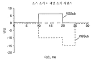
도 7a에 도시된 더 편리한 접근은 정규 소거 펄스의 끝에서 기판 전위(또는 다른 공통 전압 영역)를 향해 소스를 방전시키면서, 제어 게이트(워드선)에 대한 네가티브 전압은 그대로 유지하는 것이다. 도시된 바와 같이, 약 5V의 포지티브 펄스가 약 10ms 동안 소스와 기판 사이에 인가된다. 이와 동시에, 게이트-기판 전압은 -10V로 되어 10ms 기간 동안 유지된다. 10ms 기간의 종료시 소스-기판 전위는 수분의 1 ms 안에 급속히 방전되지만, 네가티브 게이트-기판 전압의 방전은 1-100ms의 범위의 시간 동안 지연된다. 이러한 기간 동안, 네가티브 전압의 플로팅이 허용되고, 네가티브 펌프에 의해 제공되는 전압의 임의의 조절이 불가능하게 된다. 이에 따라 발생하는 과잉 네가티브 워드선 전압은 이하의 단락들에서 “네가티브 게이트 부트스트랩(negative gate bootstrap)”이라 지칭한다. 이 경우, 빠르게 떨어지는 소스-기판 전압은 플로팅 게이트 및 제어 게이트(워드선)에 결합되어 결국 이들을 네가티브 펌프에 의해 제공되는 전압 이하로 더 네가티브하게 만든다. 따라서, 제로 전압의 소스 대 기판 바이어스와 함께 워드선 및 플로팅 게이트에 대한 비교적 높은 네가티브 전압의 바람직한 조건은 더 높은 네가티브 전압을 발생시키거나 소거 동작에 여분의 시간을 추가할 필요 없이 과도적으로 실현될 것 이다.A more convenient approach, shown in FIG. 7A, is to discharge the source towards the substrate potential (or other common voltage region) at the end of the normal erase pulse, while maintaining the negative voltage to the control gate (word line). As shown, a positive pulse of about 5 V is applied between the source and the substrate for about 10 ms. At the same time, the gate-substrate voltage becomes -10V and is maintained for 10ms period. At the end of the 10 ms period, the source-substrate potential rapidly discharges in 1 ms of minutes, but the discharge of the negative gate-substrate voltage is delayed for a time in the range of 1-100 ms. During this period, the floating of the negative voltage is allowed, and any adjustment of the voltage provided by the negative pump becomes impossible. The excess negative word line voltage resulting from this is referred to as "negative gate bootstrap" in the following paragraphs. In this case, the rapidly dropping source-substrate voltage is coupled to the floating gate and the control gate (word line) which in turn makes them more negative below the voltage provided by the negative pump. Thus, the desirable conditions of relatively high negative voltages for word lines and floating gates, with source-to-substrate bias of zero voltage, may be transiently realized without the need to generate higher negative voltages or add extra time to the erase operation. will be.
도 7a는 소스(VSSub)의 강제 방전이 수분의 1ms 또는 그 보다 빠르게 발생하는 경우 게이트 전압(VGSub)에 대한 예측 거동을 나타낸다. 소스(VSSub)의 방전 후, 그리고 게이트의 액티브 방전 전의 과잉 네가티브 게이트 전압의 양 및 이의 VGSub에 대한 파형의 점차적인 감쇠는 플로팅 상태로 남을 때 VSSub 과도 전류와 제어 게이트(워드선) 상의 전압에 대한 후속적인 자연 감쇠의 용량성 결합을 나타낸다. 감쇠율은 게이트들의 총 누설 전류에 의존하며, 총 누설 전류는 셀 제어 게이트 또는 워드선을 구동하는 메모리 어레이의 주변 회로의 트랜지스터들의 구조 및 레이아웃에 의해 결정된다. 도 4에 도시된 바와 같이 터널 산화막을 통한 제어 게이트의 임의의 누설은 제어 게이트에 대한 누설에 기여하지 않으므로 도 7a의 VGSub 감쇠율에 영향을 미치지 않는다.FIG. 7A shows the predicted behavior with respect to the gate voltage VGSub when the forced discharge of the source VSSub occurs 1 ms or faster of a few minutes. The amount of excess negative gate voltage after the discharge of the source (VSSub) and before the active discharge of the gate, and the gradual attenuation of the waveform to its VGSub, remains unchanged for the VSSub transient and for the voltage on the control gate (word line). The capacitive coupling of subsequent natural attenuation is shown. The attenuation rate depends on the total leakage current of the gates, which is determined by the structure and layout of the transistors of the peripheral circuits of the memory array driving the cell control gate or word line. As shown in FIG. 4, any leakage of the control gate through the tunnel oxide film does not contribute to leakage to the control gate and thus does not affect the VGSub attenuation rate of FIG. 7A.
주변 회로의 관련 워드선 드라이버들이 각 행 상의 메모리 셀들의 소스와 제어 게이트(워드선) 사이의 용량에 비해 낮은 기생 용량 및 낮은 누설 전류를 갖도록 고안된 정도로, 과잉 네가티브 전압(VGSub)은 실질적인 감쇠없이 더 크게 더 오래 유지될 수 있다. 미미한 기생 용량 및 VSSub의 고속 방전의 제한 내에서, 과잉 네가티브 게이트 전압의 최대 진폭은 소스 전압의 진폭과 동일한 절대값을 가질 것이다. 반면, 워드선 드라이버들의 누설 전류가 이상적으로 제로인 경우에는 과잉 네가티브 게이트 전압은 게이트가 외부 회로에 의해 접지 전위로 강제 방전되지 않는 한 무한히 감쇠 없이 유지되는 것으로 가정될 것이다. To the extent that the associated word line drivers of the peripheral circuit are designed to have low parasitic capacitance and low leakage current compared to the capacitance between the source and the control gate (word line) of the memory cells on each row, the excess negative voltage (VGSub) is further reduced without substantial attenuation. Can be significantly longer. Within the limits of insignificant parasitic capacitance and fast discharge of VSSub, the maximum amplitude of the excess negative gate voltage will have an absolute value equal to the amplitude of the source voltage. On the other hand, if the leakage current of word line drivers is ideally zero, the excess negative gate voltage will be assumed to remain indefinitely without attenuation unless the gate is forcibly discharged to ground potential by an external circuit.
따라서, 메모리 회로의 설계가 전술한 3가지 조건, 즉Therefore, the design of the memory circuit has the three conditions described above, namely
1. VSSub에 대한 1ms 보다 짧은 고속 방전,1. Fast discharge, shorter than 1ms for VSSub
2. 워드선 드라이버에 대한 1-10 fF 또는 그 이하 수준의 낮은 기생 용량, 및2. low parasitic capacitance of 1-10 fF or less for wordline drivers, and
3. 동 워드선 드라이버에 대한 pA 수준의 낮은 드레인 누설 전류3. Low drain leakage current at pA level for copper word line drivers
를 충족시키는 경우, 도 7a의 파형들에 의해 나타나는 각 소거 펄스는 소스 소거 및 채널 소거의 두 소거 메카니즘의 연속으로 간주될 수 있으며, 각 메카니즘에 대한 상대적인 지속 기간은 특정 메모리 설계에 대한 사양에 맞도록 설계자에 의해 조정될 수 있다. Satisfactory, each erase pulse represented by the waveforms of FIG. 7A can be regarded as a continuation of two erase mechanisms, source erase and channel erase, and the relative duration for each mechanism meets the specifications for a particular memory design. Can be adjusted by the designer.
특정 메모리 애플리케이션이 각 특정 셀에 대한 빠른 소거 및 매우 엄격하지 않은 유지 제한을 요구하는 경우, 이러한 메모리는 소스 소거 시간에 비해 짧은 채널 소거 시간을 갖도록 설계될 수 있다. 소스 소거는 동일 인가 전압에서 인가 전압에 대한 보다 양호한 결합 계수로 인하여 채널 소거보다 내재적으로 더 효율적이다. 따라서, 이러한 설계는 총 소거 시간을 더 짧게 하지만, 소스 소거 메카니즘에 의해 발생하는 정공들이 소거 펄스의 후속 채널 소거 부분에서 중화될 시간이 더 짧아지기 때문에 메모리 유지는 더 열악하게 된다. 이러한 설계는, 빠른 소거 프로그램 속도가 추구되고, 내재적으로 약한 유지를 보정하기 위하여 추가 패리티 코드와 같은 데이타 보정 수단이 사용될 수 있는 고밀도 데이타 저장 메모리에 이로울 수 있다. If a particular memory application requires a fast erase and very non-strict hold limit for each particular cell, such memory can be designed to have a short channel erase time compared to the source erase time. Source erase is inherently more efficient than channel erase due to a better coupling coefficient to the applied voltage at the same applied voltage. Thus, this design makes the total erase time shorter, but the memory retention becomes worse because the holes generated by the source erase mechanism will be shortened in the subsequent channel erase portion of the erase pulse. Such a design may be advantageous for high density data storage memories in which fast erase program speeds are sought and data correction means such as additional parity codes may be used to compensate for inherently weak retention.
스펙트럼의 다른 끝에서, 특정 메모리가 매우 양호한 유지를 필요로 하지만 소건 시간에 대해서는 엄격한 제한을 요구하지 않는 경우, 소거 펄스 내의 소스 소 거 시간은 1ms 이하로 줄고, 100ms 이상의 긴 채널 소거 시간이 이어질 수 있다. 이러한 방식으로, 각 셀의 플로팅 게이트에 저장된 전자들의 대부분은 소거 펄스의 채널 소거 부분 동안 터널링하여 빠져 나가며, 보다 긴 소거 시간으로 인하여 소스 소거와 관련된 정공 트랩핑 현상은 효과적으로 방지될 것이다. 이러한 접근은 소거 및 리프로그래밍 동작이 거의 발생하지 않고 빠른 시간 속도를 요구하지는 않지만 오랜 기간 동안 저장 데이타의 유지가 중요한 코드 저장 애플리케이션에 유용할 수 있다. At the other end of the spectrum, if a particular memory requires very good retention but does not require strict limits on the purge time, the source erase time in the erase pulse can be reduced to less than 1 ms, followed by long channel erase times of more than 100 ms have. In this way, most of the electrons stored in the floating gate of each cell tunnel out during the channel erased portion of the erase pulse, and due to the longer erase time, hole trapping associated with source erase will be effectively prevented. This approach may be useful for code storage applications where erase and reprogramming operations rarely occur and do not require fast time speeds, but where the retention of stored data for long periods is critical.
네가티브 게이트 소거는 모두 P 채널 워드선 드라이버 트랜지스터를 포함하거나 트리플 웰 내에 N 채널 풀다운 트랜지스터들을 구비한 CMOS 드라이버들을 포함하는 행 디코더를 사용하여 플래시 메모리에서 구현될 수 있다. 이하에서는, P 채널 워드선 드라이버들을 구비한 메모리에 대한 “네가티브 게이트 부트스트랩”의 가능한 구현이 설명된다. 동일한 아이디어가 조금 변경되어 트리플 웰 N 채널 워드선 드라이버들을 구비한 메모리에 적용될 수 있다. Negative gate erase can be implemented in flash memory using a row decoder that either includes P channel word line driver transistors or CMOS drivers with N channel pull down transistors in a triple well. In the following, a possible implementation of "negative gate bootstrap" for a memory with P channel word line drivers is described. The same idea can be changed slightly to apply to a memory with triple well N channel word line drivers.
도 8은 풀업 트랜지스터(702) 및 풀다운 트랜지스터(704)를 포함하는 도 2의 메모리(200)와 같은 메모리 장치에 대한 행 디코더에서 모두 P 채널 드라이버 회로를 갖는 설계를 나타낸다. 이 회로는 메모리 장치의 메모리 셀들(706)에 결합된 워드선(703)을 구동한다. 전압들(VH, VL)은 각각 “하이” 및 “로우” 전원 전압 레일을 나타낸다. 이들의 절대값은 판독, 프로그램 및 소거와 같은 각 메모리 기능에 특정되며, 이들의 상대적인 차이(VH-VL)는 항상 포지티브 값이다. A 및 B로 각각 표시된 풀업 및 풀다운 신호에 대한 값은 메모리 기능에, 그리고 특정 행의 선택 또는 비선택 조건에 특정된다.FIG. 8 illustrates a design with P channel driver circuits in a row decoder for a memory device such as memory 200 of FIG. 2 including pull-up
구체적으로, 메모리 블록의 모든 행은 소거 기능에서 선택되며, 따라서 신호 A 및 B는 소거될 블록 내의 모든 워드선에 대해 동일한 값을 취한다. 이러한 값들의 가능한 세트는Specifically, all rows of the memory block are selected in the erase function, so signals A and B take the same value for all word lines in the block to be erased. A possible set of these values
VH=3.3V, VL=-10V, A=3.3V, B=-10V이다.VH = 3.3V, VL = -10V, A = 3.3V, B = -10V.
이것은 워드선 전압이 P 채널 트랜지스터의 임계 전압에 따라 -8.5V 내지 -9V가 되게 한다.This causes the word line voltage to be -8.5V to -9V depending on the threshold voltage of the P channel transistor.
소거 모드에서 워드선에 대한 “네가티브 부트스트랩”의 상기 아이디어를 구현하기 위하여, 도 8의 개략도의 변수 VH, VL, A, B는 도 7b 또는 7c 아래의 역학을 따라 설정될 수 있다. In order to implement the above idea of “negative bootstrap” for the word line in the erase mode, the variables VH, VL, A, B in the schematic diagram of FIG. 8 can be set according to the dynamics below FIG.
도 8의 플래시 메모리 어레이 내의 용량 성분(Cws, Cwch)은 각각 모든 메모리 셀의 워드선과 소스 사이의 용량 및 모든 메모리 셀의 워드선과 채널 사이의 용량을 나타낸다. 소거 동안, 채널은 축적 상태가 되고, 따라서 블록 내의 모든 메모리 셀에 대한 공통 기판에 전기적으로 접속된다.The capacitance components C ws and C wch in the flash memory array of FIG. 8 respectively represent the capacitance between word lines and sources of all memory cells and the capacitance between word lines and channels of all memory cells. During erasing, the channel enters an accumulation state and is thus electrically connected to a common substrate for all memory cells in the block.
도 7a, 7b, 7c의 소스 펄스(VSSub)의 하강 에지는 Cws를 통한 용량 결합에 의해 VGSub 상에 네가티브 부트스트랩(네가티브 과전압)을 유도한다. 드라이버 트랜지스터의 기생 용량을 무시할 경우, 네가티브 전압 초과의 크기는 다음과 같이 계산될 수 있다.The falling edge of the source pulse VSSub of FIGS. 7A, 7B, 7C induces a negative bootstrap (negative overvoltage) on the VGSub by capacitive coupling through C ws . Neglecting the parasitic capacitance of the driver transistor, the magnitude of the negative voltage excess can be calculated as follows.
![]()
![]()
따라서, 네가티브 부트스트랩은 Cws가 증가할 때, 그리고/또는 Cwch가 감소할 때 향상된다.Thus, negative bootstrap improves when C ws increases and / or when C wch decreases.
도 7b에서와 같이 소거가 구현되는 경우, 도 8의 행 디코더 내의 모든 P 채널 트랜지스터에 대한 기생 용량 성분(Cgd, Cj)은 “네가티브 부트스트랩” 효과에서 워드선의 용량 결합을 강화하기 위하여 감소될 필요가 있다. 게이트-드레인 기생 용량(Cgd)은 게이트에 의한 드레인 확산의 중첩 성분 및 드레인 표면과 게이트 스택 측벽 사이의 가장자리 전계(fringing field)에 관련된 성분을 갖는다. 이들 성분은 모두 게이트 측벽과 인접 드레인 확산 사이에 위치하는 산화물 스페이서의 도움으로 감소될 수 있다. 드레인 확산을 위한 낮은 도핑 농도 및/또는 채널(N 웰) 내의 낮은 도핑 농도를 사용함으로써 낮은 드레인-바디 접합 용량(Cj)이 얻어질 수 있다. When erase is implemented as in FIG. 7B, the parasitic capacitance components C gd and C j for all P channel transistors in the row decoder of FIG. 8 are reduced to enhance the capacitive coupling of the word line in the “negative bootstrap” effect. Need to be. The gate-drain parasitic capacitance C gd has an overlapping component of drain diffusion by the gate and a component related to an edge fringing field between the drain surface and the gate stack sidewall. Both of these components can be reduced with the aid of oxide spacers located between the gate sidewalls and adjacent drain diffusions. Low drain-body junction capacitances C j can be obtained by using low doping concentrations for drain diffusion and / or low doping concentrations in the channel (N well).
한편, 도 7c의 역학은 소거를 위해 구현될 수 있다. 전압 VH 및 VL은 도 7c에서 VSSub 펄스의 끝에서 감소된다. 이 경우, 풀다운 트랜지스터(704)에 대한 Cgd(워드선과 신호 B 사이의 용량 결합)를 제외한 도 8의 모든 기생 용량은 사실 “네가티브 부트스트랩”을 위한 결합을 돕고 있으며, 최소화될 필요가 없다. 이 경우, 네가티브 부트스트랩을 위한 결합은 도 8에 도시된 바와 같이 회로 내의 VH 전원과 워드선 사이에 여분의 캐패시터(710)를 제공함으로서 더욱 증가될 수 있다. Meanwhile, the mechanics of FIG. 7C may be implemented for erasure. Voltages VH and VL are reduced at the end of the VSSub pulse in FIG. 7C. In this case, all parasitic capacitances in FIG. 8 except C gd (capacitance coupling between word line and signal B) for pull-
소거 펄스의 채널 소거 부분 동안 과잉 네가티브 전압(VGSub)의 유지는 워드 선을 구동하는 P 채널 트랜지스터의 드레인-바디 누설 전류에 의해 나쁜 영향을 받는다. 이러한 누설 전류는 도 8에서 트랜지스터(N 웰)의 소스/드레인 확산과 바디 사이의 가변 전류 발생기(708)로 표시된다. 실제로, 이러한 누설 전류의 중요한 성분은 게이트 유도 드레인 누설 전류(GIDL)로 알려져 있으며, 게이트와 드레인 사이의 전압 강하와 함께 크게 증가한다. 따라서, GIDL은 소거시 게이트-드레인 전압 강하가 큰 도 8의 풀업 P 채널 트랜지스터(702)에 대해서만 중요하다. 이러한 전압 강하는 도 7c에 따른 소거 역학에 대해 더 작으며, 이러한 방법은 과잉 네가티브 게이트 전압에 대한 결합 및 유지 양쪽에서 이점을 제공한다.The maintenance of the excess negative voltage VGSub during the channel erase portion of the erase pulse is adversely affected by the drain-body leakage current of the P channel transistors driving the word lines. This leakage current is represented in FIG. 8 by the variable
트랜지스터 구조의 측면에서, 게이트 스페이서 및/또는 드레인 확산을 위한 낮은 도핑 농도와 같이 기생 게이트-드레인 용량을 줄이기 위한 전술한 특징들은 GIDL을 줄이는 데에도 효과적이다. 도 9는 모든 성분들이 도시된 기생 용량들(Cgd, Cj)과 관련된 예시적인 P 채널 MOSFET 구조(802)를 나타낸다. 기생 용량을 최소화하고 GIDL을 줄이기 위하여, 워드선 구동 트랜지스터는 저농도 드레인(LDD) 영역이 도 9에 도시된 바와 같이 존재하여 기생용량을 최소화할 수 있도록 제조되어야 한다. 또한, 기생 용량을 줄이기 위하여 저유전율 SiO2 게이트 스페이서가 추가될 수 있다. 또한, 기생 용량을 줄이기 위하여 당업자들에게 친숙한 다른 기술들이 적용될 수도 있다. In terms of transistor structure, the aforementioned features for reducing parasitic gate-drain capacitance, such as low doping concentrations for gate spacer and / or drain diffusion, are also effective in reducing GIDL. 9 shows an example P-
따라서, 전술한 바로부터 알 수 있듯이, 메모리 장치는 일정한 지정 소거 시간 및 유지 성능에 따라 설계될 수 있다. 한편, 소스 소거 및 채널 소거의 각각의 지속 기간이 제어 파라미터 전용의 특수 기능 레지스터 또는 기타 불휘발성 메모리에 저장된 알고리즘 코드에 의해 조정될 수 있는 새로운 종류의 메모리가 설계될 수 있다. 이러한 방법으로, 제조자는 일반적인 메모리 부분을 구축할 수 있으며, 제조 테스트 시에 소거 메카니즘의 지속 기간을 조정하거나 장치가 최종 사용을 위해 시스템 내에 조립되기 전 또는 후에 사용자가 그러한 조정을 행하게 할 수 있다.Thus, as can be seen from the foregoing, the memory device can be designed in accordance with a constant designated erase time and sustain performance. On the other hand, a new kind of memory can be designed in which each duration of source erase and channel erase can be adjusted by algorithm codes stored in special function registers or other nonvolatile memories dedicated to control parameters. In this way, the manufacturer can build up a general memory portion and adjust the duration of the erase mechanism during manufacturing testing or allow the user to make such adjustments before or after the device is assembled into the system for final use.
결론conclusion
플래시 메모리를 소거하기 위한 방법 및 장치가 설명되었다. 본 방법은 소거 기간 동안 메모리 셀의 제어 게이트에 네가티브 전압 펄스를 공급하는 단계, 상기 소거 기간보다 지속 기간이 짧은 기간 동안 상기 메모리 셀의 소스에 포지티브 전압 펄스를 공급하는 단계 및 제2 기간의 종료시에 상기 포지티브 전압 펄스를 방전시키는 단계를 포함하고, 상기 제2 기간의 종료시에 상기 포지티브 전압 펄스를 방전시키는 단계는 상기 네가티브 전압 펄스의 크기를 효과적으로 증가시킨다.A method and apparatus for erasing flash memory have been described. The method includes supplying a negative voltage pulse to a control gate of a memory cell during an erase period, supplying a positive voltage pulse to a source of the memory cell for a duration shorter than the erase period and at the end of a second period. Discharging the positive voltage pulse, wherein discharging the positive voltage pulse at the end of the second period effectively increases the magnitude of the negative voltage pulse.
본 명세서에서 특정 실시예들이 도시되고 설명되었지만, 동일 목적을 달성할 수 있는 것으로 예측되는 임의의 구성이 도시된 특정 실시예를 대체할 수 있다는 것을 당업자는 이해할 것이다. 본 출원은 본 발명의 임의의 적응 또는 변형을 커버하는 것을 의도한다. 따라서, 본 발명은 명백히 청구범위 및 그 균등물에 의해서만 제한되는 것으로 의도된다.Although specific embodiments have been shown and described herein, those skilled in the art will understand that any configuration that is expected to achieve the same purpose may be substituted for the specific embodiments shown. This application is intended to cover any adaptations or variations of the present invention. Therefore, it is manifestly intended that this invention be limited only by the claims and the equivalents thereof.
Claims (52)
Applications Claiming Priority (3)
| Application Number | Priority Date | Filing Date | Title |
|---|---|---|---|
| US10/159,885 US6795348B2 (en) | 2002-05-29 | 2002-05-29 | Method and apparatus for erasing flash memory |
| US10/159,885 | 2002-05-29 | ||
| PCT/US2003/016856 WO2003102962A2 (en) | 2002-05-29 | 2003-05-29 | Method and apparatus for erasing flash memory |
Publications (2)
| Publication Number | Publication Date |
|---|---|
| KR20050013999A KR20050013999A (en) | 2005-02-05 |
| KR100650088B1 true KR100650088B1 (en) | 2006-11-27 |
Family
ID=29583053
Family Applications (1)
| Application Number | Title | Priority Date | Filing Date |
|---|---|---|---|
| KR1020047019353A KR100650088B1 (en) | 2002-05-29 | 2003-05-29 | Method and apparatus for erasing flash memory |
Country Status (10)
| Country | Link |
|---|---|
| US (15) | US6795348B2 (en) |
| EP (1) | EP1552529B1 (en) |
| JP (1) | JP4359560B2 (en) |
| KR (1) | KR100650088B1 (en) |
| CN (1) | CN100495574C (en) |
| AT (1) | ATE487219T1 (en) |
| AU (1) | AU2003247433A1 (en) |
| DE (1) | DE60334828D1 (en) |
| SG (1) | SG152042A1 (en) |
| WO (1) | WO2003102962A2 (en) |
Families Citing this family (40)
| Publication number | Priority date | Publication date | Assignee | Title |
|---|---|---|---|---|
| US6795348B2 (en) * | 2002-05-29 | 2004-09-21 | Micron Technology, Inc. | Method and apparatus for erasing flash memory |
| US6862216B1 (en) * | 2004-06-29 | 2005-03-01 | National Semiconductor Corporation | Non-volatile memory cell with gated diode and MOS transistor and method for using such cell |
| US7468299B2 (en) * | 2005-08-04 | 2008-12-23 | Macronix International Co., Ltd. | Non-volatile memory cells and methods of manufacturing the same |
| US7236404B2 (en) * | 2005-08-24 | 2007-06-26 | Macronix International Co. Ltd. | Structures and methods for enhancing erase uniformity in an NROM array |
| US20070047327A1 (en) * | 2005-08-31 | 2007-03-01 | Micron Technology, Inc. | Erase method for flash memory |
| US7567458B2 (en) * | 2005-09-26 | 2009-07-28 | Silicon Storage Technology, Inc. | Flash memory array having control/decode circuitry for disabling top gates of defective memory cells |
| US7151712B1 (en) * | 2005-10-19 | 2006-12-19 | Winbond Electronics Corp. | Row decoder with low gate induce drain leakage current |
| KR100704021B1 (en) * | 2005-11-08 | 2007-04-04 | 삼성전자주식회사 | Data erasing method of nonvolatile semiconductor memory device for improving the reliability |
| US7483311B2 (en) * | 2006-02-07 | 2009-01-27 | Micron Technology, Inc. | Erase operation in a flash memory device |
| US7277357B1 (en) * | 2006-06-05 | 2007-10-02 | Micron Technology, Inc. | Method and apparatus for reducing oscillation in synchronous circuits |
| KR100842401B1 (en) * | 2006-10-18 | 2008-07-01 | 삼성전자주식회사 | Non volatile memory device and method for fabricating the same |
| US7649783B2 (en) * | 2007-01-25 | 2010-01-19 | Micron Technology, Inc. | Delayed activation of selected wordlines in memory |
| US7778086B2 (en) | 2007-01-25 | 2010-08-17 | Micron Technology, Inc. | Erase operation control sequencing apparatus, systems, and methods |
| US7656740B2 (en) * | 2007-02-05 | 2010-02-02 | Micron Technology, Inc. | Wordline voltage transfer apparatus, systems, and methods |
| KR101348173B1 (en) * | 2007-05-25 | 2014-01-08 | 삼성전자주식회사 | Flash memory device, erase and program methods, and memory system including the same |
| US7701780B2 (en) * | 2007-05-31 | 2010-04-20 | Micron Technology, Inc. | Non-volatile memory cell healing |
| US20090003065A1 (en) * | 2007-06-26 | 2009-01-01 | Micron Technology, Inc. | Flash cell with improved program disturb |
| US7619931B2 (en) * | 2007-06-26 | 2009-11-17 | Micron Technology, Inc. | Program-verify method with different read and verify pass-through voltages |
| US7916543B2 (en) * | 2007-10-22 | 2011-03-29 | Micron Technology, Inc. | Memory cell operation |
| US7916544B2 (en) | 2008-01-25 | 2011-03-29 | Micron Technology, Inc. | Random telegraph signal noise reduction scheme for semiconductor memories |
| US7924623B2 (en) * | 2008-05-27 | 2011-04-12 | Micron Technology, Inc. | Method for memory cell erasure with a programming monitor of reference cells |
| US7995384B2 (en) | 2008-08-15 | 2011-08-09 | Macronix International Co., Ltd. | Electrically isolated gated diode nonvolatile memory |
| KR101478554B1 (en) * | 2008-10-02 | 2015-01-06 | 삼성전자 주식회사 | Method for producing overshoot voltage supplied at transistor and gate insulation degradation analysis used the same |
| US8692310B2 (en) | 2009-02-09 | 2014-04-08 | Spansion Llc | Gate fringing effect based channel formation for semiconductor device |
| US8169833B2 (en) * | 2009-10-01 | 2012-05-01 | Micron Technology, Inc. | Partitioning process to improve memory cell retention |
| CN102034539A (en) * | 2010-10-25 | 2011-04-27 | 上海宏力半导体制造有限公司 | Method for programming/erasing nanocrystalline device |
| US8553463B1 (en) | 2011-03-21 | 2013-10-08 | Lattice Semiconductor Corporation | Voltage discharge circuit having divided discharge current |
| US8829588B2 (en) * | 2011-07-26 | 2014-09-09 | Synopsys, Inc. | NVM bitcell with a replacement control gate and additional floating gate |
| US8743628B2 (en) | 2011-08-08 | 2014-06-03 | Micron Technology, Inc. | Line driver circuits, methods, and apparatuses |
| US9134602B2 (en) | 2013-07-29 | 2015-09-15 | Taiwan Semiconductor Manufacturing Co., Ltd. | Method of manufacturing an extreme ultraviolet (EUV) mask and the mask manufactured therefrom |
| CA2955398A1 (en) | 2014-08-21 | 2016-02-25 | W.C. Bradley Co. | High performance electric grill, method, and heat radiating module |
| US9728278B2 (en) | 2014-10-24 | 2017-08-08 | Micron Technology, Inc. | Threshold voltage margin analysis |
| US9349447B1 (en) * | 2015-03-02 | 2016-05-24 | HGST, Inc. | Controlling coupling in large cross-point memory arrays |
| US10453535B2 (en) * | 2015-10-26 | 2019-10-22 | Intel Corporation | Segmented erase in memory |
| US10164009B1 (en) | 2017-08-11 | 2018-12-25 | Micron Technology, Inc. | Memory device including voids between control gates |
| US10446572B2 (en) | 2017-08-11 | 2019-10-15 | Micron Technology, Inc. | Void formation for charge trap structures |
| US10680006B2 (en) * | 2017-08-11 | 2020-06-09 | Micron Technology, Inc. | Charge trap structure with barrier to blocking region |
| US10796729B2 (en) | 2019-02-05 | 2020-10-06 | Micron Technology, Inc. | Dynamic allocation of a capacitive component in a memory device |
| US11194726B2 (en) | 2019-02-25 | 2021-12-07 | Micron Technology, Inc. | Stacked memory dice for combined access operations |
| KR20210028307A (en) | 2019-09-03 | 2021-03-12 | 삼성전자주식회사 | Semiconductor devices and operating methods of the same |
Family Cites Families (86)
| Publication number | Priority date | Publication date | Assignee | Title |
|---|---|---|---|---|
| US2991195A (en) * | 1960-02-11 | 1961-07-04 | Lockheed Aircraft Corp | Method of metallizing holes and cavities with a refractory metal |
| US4016588A (en) * | 1974-12-27 | 1977-04-05 | Nippon Electric Company, Ltd. | Non-volatile semiconductor memory device |
| US4384349A (en) * | 1979-10-01 | 1983-05-17 | Texas Instruments Incorporated | High density electrically erasable floating gate dual-injection programmable memory device |
| US4503524A (en) * | 1980-06-02 | 1985-03-05 | Texas Instruments Incorporated | Electrically erasable dual-injector floating gate programmable memory device |
| US4384356A (en) * | 1981-04-03 | 1983-05-17 | Britsol Babcock Inc. | Wide band modem for high speed data transmission |
| JPS644077A (en) * | 1987-06-25 | 1989-01-09 | Mitsubishi Electric Corp | Memory cell |
| US5268319A (en) * | 1988-06-08 | 1993-12-07 | Eliyahou Harari | Highly compact EPROM and flash EEPROM devices |
| US5844842A (en) * | 1989-02-06 | 1998-12-01 | Hitachi, Ltd. | Nonvolatile semiconductor memory device |
| US5077691A (en) * | 1989-10-23 | 1991-12-31 | Advanced Micro Devices, Inc. | Flash EEPROM array with negative gate voltage erase operation |
| JP3204666B2 (en) * | 1990-11-21 | 2001-09-04 | 株式会社東芝 | Nonvolatile semiconductor memory device |
| US5265059A (en) * | 1991-05-10 | 1993-11-23 | Intel Corporation | Circuitry and method for discharging a drain of a cell of a non-volatile semiconductor memory |
| JPH05102438A (en) * | 1991-10-04 | 1993-04-23 | Mitsubishi Electric Corp | Nonvolatile semiconductor memory device |
| JPH06103798A (en) * | 1992-09-18 | 1994-04-15 | Fujitsu Ltd | Semiconductor memory |
| US5544103A (en) * | 1992-03-03 | 1996-08-06 | Xicor, Inc. | Compact page-erasable eeprom non-volatile memory |
| DE4311358C2 (en) * | 1992-04-07 | 1999-07-22 | Mitsubishi Electric Corp | Non-volatile semiconductor memory device and operating method for a non-volatile semiconductor memory device and method for programming information into a non-volatile semiconductor memory device |
| EP0596198B1 (en) * | 1992-07-10 | 2000-03-29 | Sony Corporation | Flash eprom with erase verification and address scrambling architecture |
| US5357463A (en) * | 1992-11-17 | 1994-10-18 | Micron Semiconductor, Inc. | Method for reverse programming of a flash EEPROM |
| US5399928A (en) * | 1993-05-28 | 1995-03-21 | Macronix International Co., Ltd. | Negative voltage generator for flash EPROM design |
| US5420798A (en) * | 1993-09-30 | 1995-05-30 | Macronix International Co., Ltd. | Supply voltage detection circuit |
| US5477499A (en) * | 1993-10-13 | 1995-12-19 | Advanced Micro Devices, Inc. | Memory architecture for a three volt flash EEPROM |
| KR970003845B1 (en) * | 1993-10-28 | 1997-03-22 | 금성일렉트론 주식회사 | Eeprom flash memory cell, memory device and manufacturing method thereof |
| US5521867A (en) * | 1993-12-01 | 1996-05-28 | Advanced Micro Devices, Inc. | Adjustable threshold voltage conversion circuit |
| DE69523743T2 (en) * | 1994-03-03 | 2002-08-01 | Rohm Corp | ERASER DETECTION IN A LOW VOLTAGE TRANSISTOR FLASH EEPROM CELL USING FOWLER-NORDHEIM PROGRAMMING AND ERASING |
| FR2718289B1 (en) * | 1994-03-30 | 1996-08-02 | Sgs Thomson Microelectronics | Electrically programmable memory cell. |
| EP0690452A3 (en) * | 1994-06-28 | 1999-01-07 | Advanced Micro Devices, Inc. | Electrically erasable memory and method of erasure |
| JPH08148580A (en) * | 1994-08-01 | 1996-06-07 | Seiko Instr Inc | Semiconductor integrated circuit device |
| US5485423A (en) * | 1994-10-11 | 1996-01-16 | Advanced Micro Devices, Inc. | Method for eliminating of cycling-induced electron trapping in the tunneling oxide of 5 volt only flash EEPROMS |
| US5808937A (en) * | 1994-12-16 | 1998-09-15 | National Semiconductor Corporation | Self-convergent method for programming FLASH and EEPROM memory cells that moves the threshold voltage from an erased threshold voltage range to one of a plurality of programmed threshold voltage ranges |
| US5491657A (en) * | 1995-02-24 | 1996-02-13 | Advanced Micro Devices, Inc. | Method for bulk (or byte) charging and discharging an array of flash EEPROM memory cells |
| US5617357A (en) * | 1995-04-07 | 1997-04-01 | Advanced Micro Devices, Inc. | Flash EEPROM memory with improved discharge speed using substrate bias and method therefor |
| US5650964A (en) * | 1995-06-07 | 1997-07-22 | Advanced Micro Devices, Inc. | Method of inhibiting degradation of ultra short channel charge-carrying devices during discharge |
| JP3878681B2 (en) * | 1995-06-15 | 2007-02-07 | 株式会社ルネサステクノロジ | Nonvolatile semiconductor memory device |
| US5576992A (en) * | 1995-08-30 | 1996-11-19 | Texas Instruments Incorporated | Extended-life method for soft-programming floating-gate memory cells |
| US5781477A (en) * | 1996-02-23 | 1998-07-14 | Micron Quantum Devices, Inc. | Flash memory system having fast erase operation |
| JP2833585B2 (en) * | 1996-05-17 | 1998-12-09 | 日本電気株式会社 | Semiconductor nonvolatile storage device |
| KR100192584B1 (en) * | 1996-06-05 | 1999-06-15 | 윤종용 | Erasing method of non-volatile semiconductor memory device |
| US6381670B1 (en) * | 1997-01-07 | 2002-04-30 | Aplus Flash Technology, Inc. | Flash memory array having maximum and minimum threshold voltage detection for eliminating over-erasure problem and enhancing write operation |
| JPH1055689A (en) * | 1996-08-13 | 1998-02-24 | Denso Corp | Erasing method for flash memory |
| JPH1083689A (en) * | 1996-09-10 | 1998-03-31 | Mitsubishi Electric Corp | Semiconductor non-volatile memory |
| US5852306A (en) * | 1997-01-29 | 1998-12-22 | Micron Technology, Inc. | Flash memory with nanocrystalline silicon film floating gate |
| JP2000504504A (en) * | 1997-02-12 | 2000-04-11 | ヒュンダイ エレクトロニクス アメリカ インコーポレイテッド | Non-volatile memory structure |
| US6097632A (en) * | 1997-04-18 | 2000-08-01 | Micron Technology, Inc. | Source regulation circuit for an erase operation of flash memory |
| US5726933A (en) * | 1997-05-15 | 1998-03-10 | Taiwan Semiconductor Manufacturing Company, Ltd. | Clipped sine shaped waveform to reduce the cycling-induced electron trapping in the tunneling oxide of flash EEPROM |
| JP3171235B2 (en) * | 1997-05-29 | 2001-05-28 | 日本電気株式会社 | Non-volatile semiconductor memory |
| US5862078A (en) * | 1997-08-11 | 1999-01-19 | Taiwan Semiconductor Manufacturing Company, Ltd. | Mixed mode erase method to improve flash eeprom write/erase threshold closure |
| JP3914340B2 (en) * | 1997-08-30 | 2007-05-16 | 株式会社ハイニックスセミコンダクター | Flash memory device |
| US5838618A (en) * | 1997-09-11 | 1998-11-17 | Taiwan Semiconductor Manufacturing Company Ltd. | Bi-modal erase method for eliminating cycling-induced flash EEPROM cell write/erase threshold closure |
| US5949717A (en) * | 1997-09-12 | 1999-09-07 | Taiwan Semiconductor Manufacturing Company, Ltd. | Method to improve flash EEPROM cell write/erase threshold voltage closure |
| US5903499A (en) * | 1997-09-12 | 1999-05-11 | Taiwan Semiconductor Manufacturing Company, Ltd. | Method to erase a flash EEPROM using negative gate source erase followed by a high negative gate erase |
| US5828605A (en) * | 1997-10-14 | 1998-10-27 | Taiwan Semiconductor Manufacturing Company Ltd. | Snapback reduces the electron and hole trapping in the tunneling oxide of flash EEPROM |
| US6055183A (en) * | 1997-10-24 | 2000-04-25 | Taiwan Semiconductor Manufacturing Company, Ltd. | Erase method of flash EEPROM by using snapback characteristic |
| KR100481841B1 (en) * | 1997-11-25 | 2005-08-25 | 삼성전자주식회사 | Flash memory device |
| US6026026A (en) * | 1997-12-05 | 2000-02-15 | Hyundai Electronics America, Inc. | Self-convergence of post-erase threshold voltages in a flash memory cell using transient response |
| US6243299B1 (en) * | 1998-02-27 | 2001-06-05 | Micron Technology, Inc. | Flash memory system having fast erase operation |
| FR2776820B1 (en) * | 1998-03-24 | 2000-05-26 | Sgs Thomson Microelectronics | MEMORY WITH ELECTRICALLY ERASABLE FLOATING GRID ORGANIZED IN WORDS |
| US6055184A (en) * | 1998-09-02 | 2000-04-25 | Texas Instruments Incorporated | Semiconductor memory device having programmable parallel erase operation |
| US6049484A (en) * | 1998-09-10 | 2000-04-11 | Taiwan Semiconductor Manufacturing Company | Erase method to improve flash EEPROM endurance by combining high voltage source erase and negative gate erase |
| US6064595A (en) * | 1998-12-23 | 2000-05-16 | Vantis Corporation | Floating gate memory apparatus and method for selected programming thereof |
| KR100301506B1 (en) * | 1998-12-28 | 2001-11-30 | 구자홍 | Oil feeder for linear compressor |
| US6049486A (en) * | 1999-01-04 | 2000-04-11 | Taiwan Semiconductor Manufacturing Company | Triple mode erase scheme for improving flash EEPROM cell threshold voltage (VT) cycling closure effect |
| JP3613072B2 (en) * | 1999-06-02 | 2005-01-26 | 株式会社デンソー | Method for evaluating charge retention life of nonvolatile semiconductor memory |
| JP3694422B2 (en) * | 1999-06-21 | 2005-09-14 | シャープ株式会社 | Row decoder circuit |
| US6172914B1 (en) * | 1999-08-13 | 2001-01-09 | Advanced Micro Devices, Inc. | Concurrent erase verify scheme for flash memory applications |
| US6236608B1 (en) | 1999-08-16 | 2001-05-22 | Alliance Semiconductor | Technique to improve the source leakage of flash EPROM cells during source erase |
| US6243298B1 (en) * | 1999-08-19 | 2001-06-05 | Azalea Microelectronics Corporation | Non-volatile memory cell capable of being programmed and erased through substantially separate areas of one of its drain-side and source-side regions |
| US6122201A (en) * | 1999-10-20 | 2000-09-19 | Taiwan Semiconductor Manufacturing Company | Clipped sine wave channel erase method to reduce oxide trapping charge generation rate of flash EEPROM |
| KR100319558B1 (en) * | 1999-11-01 | 2002-01-05 | 윤종용 | Nonvolatile semiconductor memory device which is capable of reducing read time |
| US6285588B1 (en) * | 1999-12-01 | 2001-09-04 | Advanced Micro Devices, Inc. | Erase scheme to tighten the threshold voltage distribution of EEPROM flash memory cells |
| US6160740A (en) * | 1999-12-17 | 2000-12-12 | Advanced Micro Devices, Inc. | Method to provide a reduced constant E-field during erase of EEPROMs for reliability improvement |
| US6518122B1 (en) * | 1999-12-17 | 2003-02-11 | Chartered Semiconductor Manufacturing Ltd. | Low voltage programmable and erasable flash EEPROM |
| US6485588B1 (en) * | 2000-01-20 | 2002-11-26 | Trw Inc. | Autoignition material additive |
| US6563741B2 (en) * | 2001-01-30 | 2003-05-13 | Micron Technology, Inc. | Flash memory device and method of erasing |
| US6456533B1 (en) * | 2001-02-28 | 2002-09-24 | Advanced Micro Devices, Inc. | Higher program VT and faster programming rates based on improved erase methods |
| US6671208B2 (en) * | 2001-07-27 | 2003-12-30 | Sharp Kabushiki Kaisha | Nonvolatile semiconductor storage device with limited consumption current during erasure and erase method therefor |
| JP3648185B2 (en) * | 2001-09-13 | 2005-05-18 | マクロニクス インターナショナル カンパニイ リミテッド | Method for programming a data pattern in a flash EPROM integrated circuit |
| US6515909B1 (en) * | 2001-10-05 | 2003-02-04 | Micron Technology Inc. | Flash memory device with a variable erase pulse |
| JP2004072060A (en) * | 2001-11-22 | 2004-03-04 | Innotech Corp | Transistor and semiconductor memory using the same, and method of driving the transistor |
| US6714458B2 (en) * | 2002-02-11 | 2004-03-30 | Micron Technology, Inc. | High voltage positive and negative two-phase discharge system and method for channel erase in flash memory devices |
| US6784480B2 (en) * | 2002-02-12 | 2004-08-31 | Micron Technology, Inc. | Asymmetric band-gap engineered nonvolatile memory device |
| US6614693B1 (en) | 2002-03-19 | 2003-09-02 | Taiwan Semiconductor Manufacturing Company | Combination erase waveform to reduce oxide trapping centers generation rate of flash EEPROM |
| US6795348B2 (en) * | 2002-05-29 | 2004-09-21 | Micron Technology, Inc. | Method and apparatus for erasing flash memory |
| US6894931B2 (en) * | 2002-06-20 | 2005-05-17 | Kabushiki Kaisha Toshiba | Nonvolatile semiconductor memory device |
| KR20040008526A (en) * | 2002-07-18 | 2004-01-31 | 주식회사 하이닉스반도체 | Erase method of flash memory cell |
| JP4086583B2 (en) * | 2002-08-08 | 2008-05-14 | シャープ株式会社 | Nonvolatile semiconductor memory device and data write control method |
| US6829166B2 (en) * | 2002-09-13 | 2004-12-07 | Ememory Technology Inc. | Method for controlling a non-volatile dynamic random access memory |
| US6903407B1 (en) * | 2003-10-14 | 2005-06-07 | Advanced Micro Devices, Inc. | Non volatile charge trapping dielectric memory cell structure with gate hole injection erase |
-
2002
- 2002-05-29 US US10/159,885 patent/US6795348B2/en not_active Expired - Lifetime
-
2003
- 2003-05-29 WO PCT/US2003/016856 patent/WO2003102962A2/en active Application Filing
- 2003-05-29 SG SG200500538-4A patent/SG152042A1/en unknown
- 2003-05-29 EP EP03756241A patent/EP1552529B1/en not_active Expired - Lifetime
- 2003-05-29 AU AU2003247433A patent/AU2003247433A1/en not_active Abandoned
- 2003-05-29 KR KR1020047019353A patent/KR100650088B1/en not_active IP Right Cessation
- 2003-05-29 JP JP2004509958A patent/JP4359560B2/en not_active Expired - Fee Related
- 2003-05-29 CN CNB038184400A patent/CN100495574C/en not_active Expired - Fee Related
- 2003-05-29 AT AT03756241T patent/ATE487219T1/en not_active IP Right Cessation
- 2003-05-29 DE DE60334828T patent/DE60334828D1/en not_active Expired - Lifetime
-
2004
- 2004-06-24 US US10/876,184 patent/US7099220B2/en not_active Expired - Lifetime
- 2004-06-24 US US10/875,453 patent/US7046557B2/en not_active Expired - Lifetime
- 2004-06-24 US US10/875,452 patent/US7215572B2/en not_active Expired - Lifetime
-
2005
- 2005-08-31 US US11/215,963 patent/US7203098B2/en not_active Expired - Lifetime
- 2005-08-31 US US11/215,969 patent/US7277326B2/en not_active Expired - Lifetime
- 2005-08-31 US US11/216,956 patent/US7277327B2/en not_active Expired - Lifetime
- 2005-09-01 US US11/217,828 patent/US7277328B2/en not_active Expired - Lifetime
- 2005-09-01 US US11/217,820 patent/US7200048B2/en not_active Expired - Lifetime
- 2005-09-01 US US11/219,020 patent/US7259996B2/en not_active Expired - Lifetime
- 2005-09-01 US US11/217,813 patent/US7099195B2/en not_active Expired - Lifetime
- 2005-09-01 US US11/217,825 patent/US7068543B2/en not_active Expired - Fee Related
- 2005-09-01 US US11/218,855 patent/US7057932B2/en not_active Expired - Fee Related
- 2005-09-01 US US11/217,952 patent/US7280395B2/en not_active Expired - Lifetime
- 2005-09-01 US US11/217,920 patent/US7272044B2/en not_active Expired - Lifetime
Also Published As
Similar Documents
| Publication | Publication Date | Title |
|---|---|---|
| KR100650088B1 (en) | Method and apparatus for erasing flash memory | |
| KR100585858B1 (en) | Nonvolatile semiconductor storage device and method for operating the same | |
| US5521867A (en) | Adjustable threshold voltage conversion circuit | |
| JP3762658B2 (en) | Driving method of nonvolatile semiconductor memory device | |
| JP2002544643A (en) | Slope or graded gate channel erase for flash memory applications | |
| US6760270B2 (en) | Erase of a non-volatile memory | |
| JP4641697B2 (en) | Method for providing a constant electric field reduced during erasure of EEPROM for improved reliability | |
| KR100342903B1 (en) | Non-volatile semiconductor memory device and method of rewriting data stored in non-volatile semiconductor memory device | |
| JPH0237597A (en) | Nonvolatile semiconductor memory | |
| US5841701A (en) | Method of charging and discharging floating gage transistors to reduce leakage current |
Legal Events
| Date | Code | Title | Description |
|---|---|---|---|
| A201 | Request for examination | ||
| E902 | Notification of reason for refusal | ||
| E701 | Decision to grant or registration of patent right | ||
| GRNT | Written decision to grant | ||
| FPAY | Annual fee payment |
Payment date: 20111102 Year of fee payment: 6 |
|
| FPAY | Annual fee payment |
Payment date: 20121019 Year of fee payment: 7 |
|
| LAPS | Lapse due to unpaid annual fee |