KR100329053B1 - Semiconductor light emitting device with high luminous efficiency - Google Patents
Semiconductor light emitting device with high luminous efficiency Download PDFInfo
- Publication number
- KR100329053B1 KR100329053B1 KR1019970075496A KR19970075496A KR100329053B1 KR 100329053 B1 KR100329053 B1 KR 100329053B1 KR 1019970075496 A KR1019970075496 A KR 1019970075496A KR 19970075496 A KR19970075496 A KR 19970075496A KR 100329053 B1 KR100329053 B1 KR 100329053B1
- Authority
- KR
- South Korea
- Prior art keywords
- light emitting
- impurity
- semiconductor
- base material
- substrate
- Prior art date
- Legal status (The legal status is an assumption and is not a legal conclusion. Google has not performed a legal analysis and makes no representation as to the accuracy of the status listed.)
- Expired - Fee Related
Links
Images


Classifications
-
- H—ELECTRICITY
- H10—SEMICONDUCTOR DEVICES; ELECTRIC SOLID-STATE DEVICES NOT OTHERWISE PROVIDED FOR
- H10H—INORGANIC LIGHT-EMITTING SEMICONDUCTOR DEVICES HAVING POTENTIAL BARRIERS
- H10H20/00—Individual inorganic light-emitting semiconductor devices having potential barriers, e.g. light-emitting diodes [LED]
- H10H20/80—Constructional details
- H10H20/81—Bodies
- H10H20/822—Materials of the light-emitting regions
- H10H20/824—Materials of the light-emitting regions comprising only Group III-V materials, e.g. GaP
- H10H20/8242—Materials of the light-emitting regions comprising only Group III-V materials, e.g. GaP characterised by the dopants
-
- H—ELECTRICITY
- H10—SEMICONDUCTOR DEVICES; ELECTRIC SOLID-STATE DEVICES NOT OTHERWISE PROVIDED FOR
- H10H—INORGANIC LIGHT-EMITTING SEMICONDUCTOR DEVICES HAVING POTENTIAL BARRIERS
- H10H20/00—Individual inorganic light-emitting semiconductor devices having potential barriers, e.g. light-emitting diodes [LED]
- H10H20/80—Constructional details
- H10H20/81—Bodies
- H10H20/819—Bodies characterised by their shape, e.g. curved or truncated substrates
- H10H20/821—Bodies characterised by their shape, e.g. curved or truncated substrates of the light-emitting regions, e.g. non-planar junctions
Landscapes
- Led Devices (AREA)
- Electroluminescent Light Sources (AREA)
Abstract
본 발명은, 발광층(4)이 반도체 기판(1)과 격자 부정합의 상태로 반도체 기판(1)상에 형성되어, 고 효율의 발광을 얻을 수 있는 반도체 발광장치를 제공한다. 발광층의 기재 물질로 사용된 반도체 물질은 발광 재결합 중심으로 작용하는 불순물로 도정된다. 반도체 기판은 GaP 기판이고 또 발광층(4)의 기재 물질인 반도체 물질은 (AlxGal-x)1-yInyP 이다. 이 (AlxGal-x)1-yInyP 물질은 도너 준위를 형성하는 제 1 불순물인 질소, 산소, 셀렌, 황 또는 텔루륨으로 도핑되고 또 억셉터 준위를 형성하는 제 2 불순물인 마그네슘, 아연 또는 카드뮴으로 도핑된다.The present invention provides a semiconductor light emitting device in which the light emitting layer 4 is formed on the semiconductor substrate 1 in a state of lattice mismatch with the semiconductor substrate 1, and can obtain high efficiency light emission. The semiconductor material used as the base material of the light emitting layer is coated with impurities serving as a light emitting recombination center. The semiconductor substrate is a GaP substrate and the semiconductor material which is the base material of the light emitting layer 4 is (Al x Ga lx ) 1-y In y P. This (Al x Ga lx ) 1-y In y P material is doped with nitrogen, oxygen, selenium, sulfur or tellurium, which are the first impurities forming the donor level, and magnesium, which is the second impurity forming the acceptor level, Doped with zinc or cadmium.
Description
본 발명은 반도체 발광장치에 관한 것이다. 보다 자세하게는, 본 발명은 AlGaInP물질로 제조된 발광층을 갖는 발광 다이오드에 관한 것이다.The present invention relates to a semiconductor light emitting device. More specifically, the present invention relates to a light emitting diode having a light emitting layer made of AlGaInP material.
본 명세서에서 "AlGaInP 물질'이란 (AlxGal-x)1-yInyP의 혼합 결정비 x, y가 0≤x, y ≤ 1 범위내에서 변화되는 것을 의미한다.As used herein, the term "AlGaInP material" means that the mixed crystal ratio x, y of (Al x Ga lx ) 1-y In y P is changed within a range of 0≤x, y≤1.
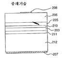
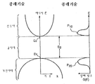
(AlxGal-x)1-yInyP 물질은 In 혼합 결정비 y = 0.51에서 GaAs 기판과 격자 정합을 나타낸다. 게다가, In 혼합 결정비 y = 0.51에 있어서, (AlxGa1-x)1-yInyP 물질은 Al 혼합 결정비 x = 0∼0.7 범위 내에서 직접 천이형으로 되어, 적색에서 녹색까지 의 넓은 파장에 걸쳐 고휘도의 발광을 얻을 수 있다. 그 결과, (AlxGa1-x)1-yInyP 물질은 최근 발광 다이오드의 재료로서 널리 사용되게 되었다. 예컨대 도 8에 예시 한 바와 같은 (AlxGa1-x)1-yInyP 계열의 발광 다이오드가 알려져 있는데, 이 발광 다이오드는 n-형 GaAs 버퍼층(211), n-형 (AlxGa1-x)1-yInyP 클래드층(203), 도핑되지않은 (AlxGa1-x)1-yInyP 활성층(210), p-형 (AlxGa1-x)1-yInyP 클래드층(205) 및 p-형 GaP 전류 확산층(206)을 n-형 GaAs 기판(212)상에 순서대로 적층한 것이다. 주입 캐리어를 활성층(210)에 효과적으로 가두어 두기(entraP) 위하여, 클래드층(203, 205)의 밴드 갭은 활성층(210) 의 밴드 갭 보다 크게 설정되어 있다(더블 헤테로 (DH) 구조). 또한, n-측 전극(207)이 GaAs 기판(212)의 바닥면에 제공되고 p-측 전극(208)은 전류 확산층(206)의 윗면에 제공된다. In 혼합 결정비 y는 GaAs 기판과 격자 정합하는 y = 0.51로 설정되어 있기 때문에, 발광에 기여하는 (AlxGa1-x)1-yInyP 물질(활성층(210)과 클래드층(203, 205))의 결정도가 양호하게 된다. 그 결과, 도 9A의 에너지 대로부터 알 수 있듯이, 활성층(210)의 전도대의 바닥(에너지값 Ec) 부근 및 가전자대의 상부(에너지 값 Ev) 부근은 모두 포물선 형상이며, 또 도 9B에 도시한 바와 같이 전도대 및 가전자대에서의 캐리어의 상태 밀도G(E)의 피이크(P10, P20)는 각각 전도대 및 가전자대의 단부(Ec, Ev)에 근접해 있다. 따라서, (AlxGa1-x)1-yInyP 활성층(210) 그 자체는 비교적 높은 내부 양자 효율(p-n 접합부 부근에서 전기가 광으로 변환되는 효율을 의미함)을 나타낼 수 있다.The (Al x Ga lx ) 1-y In y P material exhibits lattice matching with the GaAs substrate at an In mixed crystal ratio y = 0.51. In addition, at an In mixed crystal ratio y = 0.51, the (Al x Ga 1-x ) 1-y InyP material is directly transitioned in the Al mixed crystal ratio x = 0 to 0.7, and has a wide range from red to green. High luminance light emission can be obtained over the wavelength. As a result, (Al x Ga 1-x ) 1-y In y P materials have recently been widely used as materials for light emitting diodes. For example, as illustrated in FIG. 8, a (Al x Ga 1-x ) 1-y In y P series light emitting diode is known, which includes an n-type
그러나, 도 8의 구조에 의하면, GaAs 기판(212)의 밴드 갭이 1.42 eV이기 때문에 적색에서 녹색까지의 방출 광이 흡수되어 광 출력이 1/2 미만으로 저하되는 문제가 있다. 발광 물질이 GaP, GaAsP, AlGaAs 등으로 제조되는 경우, GaAs 기판이 발광 파장에 대하여 투명하기 때문에 기판의 광 흡수에 기인한 문제는 발생 가능성이 없었다. 그러나, 발광 물질이 (AlxGa1-x)1-yInyP로 제조되는 경우, GaAs 기판이 사용되는 한, 기판에 의한 광 흡수가 생겨서 외부 양자효율(광이 외부로 빠져 나가는 효율을 의미하며, 간단히 "효율" 또는 "발광 효율"이라고도 함)이 저하된다.However, according to the structure of FIG. 8, since the band gap of the
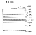
기판에 의한 광 흡수를 피하기 위하여, 도 10에 도시한 바와 같이 n-형 GaAs버퍼층(311), n-형 브래그 반사(DBR)층(313), n-형 (AlxGa1-x)1-yInyP 클래드층(303), 도핑되지 않은 (AlxGa1-x)1-yInyP 활성층(310), p-형 (AlxGa1-x)1-yInyP 클래드층(305) 및 p-형 GaP 전류 확산층(306)이 n-형 GaAs 기판(301)상에 순서대로 적층된 발광 다이오드(Appl. Phys. Lett., vol. 61, No. 15 (1992), pp. 1775-1777)가 제안되어 있다. 이 발광 다이오드는 GaAs 기판(301)과 n-형 클래드층(303) 사이에 굴절률이 따른 2종류의 반도체층물 적당한 두께로 교대로 조합하여 형성된 DBR 층(312)을 구비하여, 활성층(310)에 의해 방출된 광이 이 DBR층(313)에 의해 상방으로 반사되어 GaAs 기판(301)측에 도달하지 않도록 한 것이다. 또한 도 11에 도시한 바와 같이, n-형 (AlxGa1-x)1-yInyP 클래드층(403), 도핑되지 않은 (AlxGa1-x)1-yInyP 활성층(410), p-형 (AlxGal-x)1-yInyP 클래드층(405) 및 p-형 GaP 전류 확산층(406)을 도시되지 않은 GaAs 기판상에 순서대로 적층한 후, 에칭에 의해 GaAs 기판을 제거하고 클래드층(403)의 노출 표면(접합부)(420)에 적색에서 녹색까지의 발광 파장에 대하여 투명한 GaP 기판(414; 밴드 갭 2.27 eV)을 결합시켜 제조된 발광 다이오드(Appl. Phys. Lett., vol. 64, No. 21 (1994), pp. 2839-2841)가 제안되어 있다.In order to avoid light absorption by the substrate, as shown in FIG. 10, an n-type
그러나, 도 10의 발광 다이오드의 경우, 활성층(310)으로부터 하방으로 방출된 광 전부가 DBR 층(313)에 의해 반사될 수 없어 광의 일부가 DBR층(313)에 의해 전달되어 CaAs 기판(301)에 의해 흡수된다. 그 결과 도 10의 발광 다이오드는 도 8의 발광 다이오드에 비하여 발광 효율이 1.5배정도 향상될 뿐이다.However, in the light emitting diode of FIG. 10, not all of the light emitted downward from the
한편, 도 11의 발광 다이오드의 경우에는 GaP 기판(414)을 접합시키는 기술이 어렵기 때문에 대량 생산에 부적합하다.On the other hand, in the case of the light emitting diode of Fig. 11, the technique for joining the
이러한 배경하에서, (AlxGa1-x)1-yInyP 물질을 GaAs 기판상에 성장시키지 않고 (AlxGa1-x)1-yInyP 물질의 발광 파장(650-550 nm)에 대하여 투명한 기판, 대표적으로는 상술한 GaP 기판(밴드 갭 2.27 cV)상에 성장시키는 수단을 본원 명세서에서 고려하게 되었다. 즉, 도 6에 도시한 바와 같이, n-형 GaInP 버피층(104), n-형 (AlxGa1-x)1-yInyP 클래드층(103), 도핑되지 않은 (AlxGa1-x)1-yInyP 활성층(110), p-형 (AlxGa1-x)1-yInyP 클래드층(105) 및 p-형 GaP 전류 확산층(106)을 n-형 GaP 기판 (101)상에 성장시킨 발광 다이오드를 고안하게 되었다.Under this background, the emission wavelength (650-550 nm) of (Al x Ga 1-x ) 1-y In y P material without growing (Al x Ga 1-x ) 1-y In y P material on the GaAs substrate In the present specification, a means for growing on a transparent substrate, typically a GaP substrate (band gap 2.27 cV) described above, is considered. That is, as shown in Fig. 6, n-type
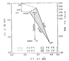
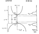
그러나, 도 5에 도시한 바와 같이, GaP의 격자 상수 5.451Å 근처에서는 (AlxGa1-x)1-yInyP 물질의 직접적인 천이를 허용하는 영역이 존재하지 않는다. 따라서, GaP 기판과 격자 정합하는 (AlxGa1-x)1-yInyP 물질을 GaP 기판(101)상에 성장시켰다 하더라도, 고효율의 발광은 기대할 수 없다. 한편, GaAs 기판의 격자 상수 5.653Å가 GaP 기판의 격자 상수 5.451Å 보다 약 3.6% 크기 때문에, GaAs 기판과격자 정합하는 (AlxGa1-x)1-yInyP 물질(103, 110 및 105)을 GaP 기판(101)상에 성장시킨 경우, 격자 상수 차를 완화시키기 위하여 GaInP 버퍼층(104)이 개재된다 하더라도 성장시킨 (AlxGa1-x)1-yInyP 물질(103, 110 및 105)에 소위 미스피트 전위(misfit dislocation; 격자 부정합에 따른 전위)가 증가하여 비발광 재결합 중심이 증가하고 발광의 천이 확률이 감소된다. 즉, 기판상에 격자 상수가 다른 결정들이 성장 되기 때문에, 성장한 결정 격자의 주기성에 장애가 발생하여 명확한 금지대가 존재할 수 없다. 그 결과, 도 7A에 도시한 바와 같이, 활성층(110)의 전도대의 바닥 (Ec) 근처 뿐만 아니라 가전자대의 상부(Ev) 근처가 포물선 형상을 이루지 않고, 수십 meV의 테일을 가지게 되어 도 7B에 도시한 바와 같이 테일의 팁 단부(Ec#, Ev#: 반드시 일정 위치에 존재하는 것은 아님)는 전도대 및 가전자대에서의 캐리어 상태 밀도 G(E)의 피이크(P10, P20)로부터 떨어지게 된다. 그 결과, 주입된 캐리어가 대(band) 단부(Ec, Ev)의 근처에서는 재결합하기 어려워져서 발광의 천이 확률이 작게 된다. 따라서, GaAs 기판과 격자 정합하는 (AlxGa1-x)1-yInyP 물질(103, 110 및 105)을 GaP 기판(101)상에 성장시켜 제조한 직접 천이형 발광 다이오드의 경우, 고효율의 발광을 얻기 어렵다. 실제로, 그 발광 효율은 도 8의 발광 다이오드에 비하여 2차수(2 order) 이상 감소된다.However, as shown in FIG. 5, there is no region allowing direct transition of the (Al x Ga 1-x ) 1-y In y P material near the lattice constant of 5.451 GHz of GaP. Therefore, even if a (Al x Ga 1-x ) 1-y In y P material lattice matched with the GaP substrate is grown on the
따라서, 반도체 기판이 발광 파장에 대하여 투명하다고 하더라도, 발광층(활성층)이 반도체 기판과 격자 정합되지 않는 상태로 성장된 반도체 발광장치로는 고효율의 발광을 얻을 수 없는 문제가 있다.Therefore, even if the semiconductor substrate is transparent with respect to the light emission wavelength, there is a problem that high-efficiency light emission cannot be obtained with a semiconductor light emitting device in which the light emitting layer (active layer) is grown in a lattice match with the semiconductor substrate.
본 발명의 목적은 발광층(활성층)을 반도체 기판과 격자 부정합의 상태로 반도체 기판상에 형성하여 고효율의 발광을 얻을 수 있는 반도체 발광장치를 제공하는 것이다.SUMMARY OF THE INVENTION An object of the present invention is to provide a semiconductor light emitting device in which a light emitting layer (active layer) is formed on a semiconductor substrate in a state of lattice mismatch with the semiconductor substrate to obtain high efficiency light emission.
특히, 본 발명의 목적은 GaP 기판상에 (AlxGa1-x)1-yInyP 물질을 기재물질로 하는 발광층을 형성하여 적색에서 녹색까지의 파장 영역에 걸쳐 고효율의 발광을 얻을 수 있는 반도체 발광장치를 제공하는 것이다.In particular, an object of the present invention is to form a light emitting layer based on (Al x Ga 1-x ) 1-y In y P material on a GaP substrate to obtain high efficiency light emission over a wavelength range from red to green. The present invention provides a semiconductor light emitting device.
도 1은 본 발명의 제 1 실시예에 따른 구조도,1 is a structural diagram according to a first embodiment of the present invention;
도 2A 및 도2B는 본 발명의 제 1 실시예에 따른 캐리어의 상태 밀도 분포를 나타내는 밴드 상태도,2A and 2B are band state diagrams showing a state density distribution of a carrier according to the first embodiment of the present invention;
도 3은 본 발명의 제 2 실시예에 따른 구조도,3 is a structural diagram according to a second embodiment of the present invention;
도 4A 및 도 4B는 본 발명의 제 2 실시예에 따른 캐리어의 상태 밀도 분포를 타내는 밴드 상태도,4A and 4B are band state diagrams showing a state density distribution of a carrier according to a second embodiment of the present invention;
도 5는 발광층의 반도체 물질과 기판의 격자 상수 및 에너지 갭 사이의 관계를 나타내는 차트,5 is a chart showing a relationship between a lattice constant and an energy gap of a semiconductor material of a light emitting layer and a substrate;
도 6은 GaP 기판상의 발광 다이오드의 구조도,6 is a structural diagram of a light emitting diode on a GaP substrate;
도 7A 및 도 7B는 GaP 기판상의 발광 다이오드중의 캐리어의 밴드 상태도 및 상태 밀도 분포도,7A and 7B are band state diagrams and state density distribution diagrams of carriers in light emitting diodes on a GaP substrate;
도 8은 종래 기술에 따른 발광 다이오드의 구조도,8 is a structural diagram of a light emitting diode according to the prior art;
도 9A 및 도 9B는 종래 기술에 따른 발광 다이오드중의 캐리어의 밴드 상태도.9A and 9B are band state diagrams of carriers in light emitting diodes according to the prior art;
도 10은 종래 기술에 따른 발광 다이오드의 구조도,10 is a structural diagram of a light emitting diode according to the prior art;
도 11은 종래 기술에 따른 발광 다이오드의 구조도.11 is a structural diagram of a light emitting diode according to the prior art.
*도면의 주요부분에 대한 부호의 설명* Explanation of symbols for main parts of the drawings
1,11: 기판 2,12: 버퍼층 3,13: 클래드층1,11
4,14: 활성층 6,16: 전류 확산층 7,17: n-측 전극4,14
8,18: p-측 전극8,18: p-side electrode
상기 목적을 달성하기 위하여, 본 발명은 반도체 기판에 의해 실질적으로 흡수되지 않는 파장의 광을 방출하는 발광층이 반도체 기판과 격자 부정합의 상태로 반도체 기판상에 형성되며, 발광층의 기재 물질로서 사용된 반도체 물질이 발광 재결합 중심으로서 작용하는 하나 이상의 불순물로 도정되는 것을 특징으로 하는 반도체 발광장치를 제공한다.In order to achieve the above object, the present invention provides a semiconductor in which a light emitting layer that emits light of a wavelength that is not substantially absorbed by the semiconductor substrate is formed on the semiconductor substrate in a state of lattice mismatch with the semiconductor substrate, and is used as a base material of the light emitting layer. Provided is a semiconductor light emitting device, characterized in that the material is coated with one or more impurities serving as a light emitting recombination center.
본 발명의 반도체 발광장치에서, 발광 재결합 중심으로서 작용하는 불순물은 발광충의 기재 물질로서 사용된 반도체 물질의 금지대의 단부로부터 떨어진 위치 및 금지대에서 불순물 준위를 형성할 수 있다. 이 경우, 발광층의 기재 물질로서 사용된 반도체 물질의 대 단부가 반도체 기판과 격자부정합에 의하여 테일을 갖더라도, 불순물 준위를 통한 발광 재결합은 테일에 의해 영향을 받지 않을 건이다. 따라서, 내부 양자 효율이 향상된다. 또한 발광층에 의해 방출된 광이 반도체 기판에 의해 실질적으로 흡수되지 않으며, 즉, 반도체 기판에서 가전자대의 상부에서부터 전도대의 하부로의 천이를 유발할 광 흡수를 유발하지 않으므로 외부 양자 효율도 감소되지 않을 것이다, 그러므로 발광 효율 전체가 향상된다.In the semiconductor light emitting device of the present invention, the impurity serving as the light emission recombination center can form the impurity level at a position away from the end of the prohibition band of the semiconductor material used as the base material of the light emitting insect. In this case, even if a large end of the semiconductor material used as the base material of the light emitting layer has a tail by lattice mismatch with the semiconductor substrate, the light emission recombination through the impurity level will not be affected by the tail. Thus, internal quantum efficiency is improved. In addition, the light emitted by the light emitting layer is not substantially absorbed by the semiconductor substrate, i.e., the external quantum efficiency will not be reduced as it does not cause light absorption which will cause a transition from the top of the valence band to the bottom of the conduction band in the semiconductor substrate. Therefore, the whole luminous efficiency is improved.
실시예로서, 발광층은 도너 준위를 형성하기 위한 제 1 불순물 및 억셉터 준위를 형성하기 위한 제 2 불순물을 포함하는 2종류의 불순물을 함유한다.As an embodiment, the light emitting layer contains two kinds of impurities including a first impurity for forming a donor level and a second impurity for forming an acceptor level.
상기 실시예의 반도체 발광장치에서는 제 1 불순물에 의해 형성된 도너 준위라 제 2 불순물에 의해 형성된 억셉터 준위 사이에서 발광 재결합이 생긴다. 따라서, 내부 양자 효율은 제 1 불순물 또는 제 2 불순물중의 하나만이 함유된 경우에 비하여 높게 되므로 발광 효율 전체는 향상된다.In the semiconductor light emitting device of the above embodiment, light emission recombination occurs between the donor level formed by the first impurity and the acceptor level formed by the second impurity. Therefore, since the internal quantum efficiency is higher than when only one of the first impurity or the second impurity is contained, the entire luminous efficiency is improved.
다른 실시예로서, 제 1 불순물에 의해 형성된 도너 준위는 기재 물질로서 사용된 반도체 물질의 전도대의 단부로부터 30 meV 내지 200 meV 범위내에서 위치하며, 또 제 2 불순물에 의해 형성된 억셉터 준위는 기재 물질로서 사용된 반도체 물질의 가전자대의 단부로부터 30 meV 내지 200 meV 범위내에서 위치한다.In another embodiment, the donor level formed by the first impurity is located within the range of 30 meV to 200 meV from the end of the conduction band of the semiconductor material used as the base material, and the acceptor level formed by the second impurity is the base material. It is located in the range of 30 meV to 200 meV from the end of the valence band of the semiconductor material used as.
상기 경우, 발광층의 기재 물질로서 사용된 반도체 물질의 전도대의 단부 및 가전자대의 단부를 각기 전도대의 단부 및 가전자대의 단부로 칭하며, 이 경우 발광층은 반도체 기판과 격자 정합되어 형성된다. 즉, 제 1 불순물에 의해 형성된 도너 준위과 제 2 불순물에 의해 형성된 억셉터 준위는 기재 물질로서 사용된 반도체 물질의 원래의 대 단부로 정의된다In this case, the end of the conduction band and the end of the valence band of the semiconductor material used as the base material of the light emitting layer are referred to as the end of the conduction band and the end of the valence band, respectively. In this case, the light emitting layer is formed by lattice matching with the semiconductor substrate. That is, the donor level formed by the first impurity and the acceptor level formed by the second impurity are defined as the original large ends of the semiconductor material used as the base material.
상기 실시예의 반도체 발광장치에서, 제 1 불순물에 의해 형성된 도너 준위는 기재 물질로서 사용된 반도체 물질의 전도대의 단부로부터 30 meV 떨어져 있고또 제 2 불순물에 의해 형성된 억셉터 준위는 기재 물질로서 사용된 반도체 물질의 가전자대의 단부로부터 30 meV 떨어져 있다. 그 결과, 기재 물질로서 사용된 반도체 물질의 전도대의 단부 및 가전자대의 단부가 각기 반도체 기판과 발광층 사이의 격자가 정합되지 않음으로 인한 수십 meV의 테일을 갖는다하더라도, 제 1 불순물에 의해 형성된 도너 준위와 제 2 불순물에 의해 형성된 억셉터 준위 사이의 발광 재결합은 테일에 의해 영향을 거의 받지 않는다. 또한 제 1 불순물에 의해 형성된 도너 준위는 기재 물질로서 사용된 반도체 물질의 전도대의 단부로부터 200 meV 내에 위치하고 또 제 2 불순물에 의해 형성된 억셉터 준위는 기재 물질로서 사용된 반도체 물질의 가전자대의 단부로부터 200 meV 내에 위치한다. 따라서, 이들 제 1 및 제 2 불순물은 각기 발광 재결합 중심으로서 효과적으로 작용한다. 따라서, 제 1 불순물에 의해 형성된 도너 준위와 제 2 불순물에 의해 형성된 억셉터 준위 사이의 발광 재결합에 의해 내부 양자 효율도 향상된다. 이 결과, 발광 효율 전체도 향상된다.In the semiconductor light emitting device of the above embodiment, the donor level formed by the first impurity is 30 meV away from the end of the conduction band of the semiconductor material used as the base material, and the acceptor level formed by the second impurity is the semiconductor used as the base material. 30 meV from the end of the valence band of the material. As a result, the donor level formed by the first impurity is formed even if the end of the conduction band and the valence band of the semiconductor material used as the base material each have a tail of tens of meV due to the mismatch of the lattice between the semiconductor substrate and the light emitting layer. Luminescence recombination between and the acceptor level formed by the second impurity is hardly affected by the tail. The donor level formed by the first impurity is also within 200 meV from the end of the conduction band of the semiconductor material used as the base material and the acceptor level formed by the second impurity is from the end of the valence band of the semiconductor material used as the base material. Located within 200 meV. Thus, these first and second impurities each effectively act as a light emitting recombination center. Therefore, the internal quantum efficiency is also improved by light emission recombination between the donor level formed by the first impurity and the acceptor level formed by the second impurity. As a result, the whole luminous efficiency is also improved.
본 발명은 기재 물질로서 A1GaInP 물질을 포함하는 발광충이 GaP 기판과 격자 정합되지 않는 상태로 GaP 기판상에서 성장하며, 또 발광층의 기재 물질로서 사용된 AlGaInP 물질은 도너 준위를 형성하기 위한 제 1 불순물로서 질소, 산소, 셀렌, 황 또는 텔루륨 그리고 억셉터 준위를 형성하기 위한 제 2 불순물로서 마그네슘, 아연 또는 카드뮴으로 도핑되는 것을 특징으로 하는 반도체 발광장치를 제공한다.The present invention grows on a GaP substrate in a state in which the luminescent insect including the A1GaInP material as a base material is not lattice matched with the GaP substrate, and the AlGaInP material used as the base material of the light emitting layer is nitrogen as a first impurity for forming a donor level. A semiconductor light emitting device is characterized in that it is doped with magnesium, zinc or cadmium as a second impurity for forming oxygen, selenium, sulfur or tellurium and acceptor levels.
본 발명의 반도체 발광장치에서, 제 1 불순물인 질소, 산소, 셀렌, 황 또는텔루륨은 기재 물질로서 사용된 AlGaInP 물질의 전도대의 단부로부터 30 meV 내지 200 meV 범위내에서 도너 준위를 형성하는 반면에, 마그네슘, 아연 또는 카드뮴은 기재 물질로서 사용된 AlGaInP 물질의 가전자대의 단부로부터 30 meV 내지 200 meV 범위내에서 억셉터 준위를 형성한다. 제 1 불순물에 의해 형성된 도너 준위는 기재 물질로서 사용된 AlGaInP 물질의 전도대의 단부로부터 30 meV 정도 떨어져 있고, 또 제 2 불순물에 의해 형성된 억셉터 준위는 기재 물질로서 사용된 AlGaInP 물질의 가전자대의 단부로부터 30 meV 정도 떨어져 있다. 따라서, 기재 물질로서 사용된 AlGaInP 물질의 전도대의 단부 및 가전자대의 단부가 각기 GaP 기판과 발광 층 사이의 격자 정합되지 않음으로 인한 약 수십 meV의 테일을 갖는다 하더라도, 제 1 불순물에 의해 형성된 도너 준위와 제 2 불순물에 의해 형성된 억셉터 준위 사이의 발광 재결합은 테일에 의해 거의 영향을 받지 않는다. 또한 제 1 불순물에 의해 형성된 도너 준위는 기재 물질로서 사용된 AlGaInP 물질의 전도대의 단부로부터 200 meV 내에 위치하고 또 제 2 불순물에 의해 형성된 억셉터 준위는 기재 물질로서 사용된 AlGaInP 물질의 가전자대의 단부로부터 200 meV내에 위치한다. 따라서 이들 제 1 및 제 2 불순물은 각기 발광 재결합 중심으로서 효과적으로 작용한다. 따라서 제 1 불순물에 의해 형성된 도너 준위와 제 2 불순물에 의해 형성된 억셉터 준위 사이의 발광 재결합에 의해 내부 양자 효율이 향상된다. 또한 제 1 불순물에 의해 형성된 도너 준위와 제 2 불순물에 의해 형성된 억셉터 준위 사이의 에너지 갭에 반응하여 발광층에 의해 방출된 적색에서 부터 녹색 까지의 파장의 광은 GaP 기판에 의해 실질적으로 흡수되지 않는다(GaP 기판은 AlGaInP 물질의 방출광 파장 650nm 내지 550 nm에 대하여 투명하다). 따라서, 외부 양자 효율도 감소되지 않을 것이다. 따라서, 발광 효율 전체는 향상되고, 또 적색에서 부터 녹색의 파장 밴드로 고 명도의 발광을 얻을 수 있다.In the semiconductor light emitting device of the present invention, the first impurity nitrogen, oxygen, selenium, sulfur or tellurium forms the donor level within the range of 30 meV to 200 meV from the end of the conduction band of the AlGaInP material used as the base material. , Magnesium, zinc or cadmium form acceptor levels within the range of 30 meV to 200 meV from the end of the valence band of the AlGaInP material used as the base material. The donor level formed by the first impurity is about 30 meV from the end of the conduction band of the AlGaInP material used as the base material, and the acceptor level formed by the second impurity is the end of the valence band of the AlGaInP material used as the base material. Is about 30 meV away. Thus, the donor level formed by the first impurity, although the end of the conduction band and the valence band of the AlGaInP material used as the base material each have a tail of about several tens of meV due to the lattice mismatch between the GaP substrate and the light emitting layer. Luminescence recombination between and the acceptor level formed by the second impurity is hardly affected by the tail. The donor level formed by the first impurity is also within 200 meV from the end of the conduction band of the AlGaInP material used as the base material and the acceptor level formed by the second impurity is from the end of the valence band of the AlGaInP material used as the base material. Located within 200 meV Thus, these first and second impurities effectively act as light emitting recombination centers, respectively. Therefore, the internal quantum efficiency is improved by light emission recombination between the donor level formed by the first impurity and the acceptor level formed by the second impurity. In addition, light of a wavelength from red to green emitted by the light emitting layer in response to the energy gap between the donor level formed by the first impurity and the acceptor level formed by the second impurity is not substantially absorbed by the GaP substrate. (The GaP substrate is transparent to the emission light wavelength of 650 nm to 550 nm of the AlGaInP material). Thus, no external quantum efficiency will be reduced. Therefore, the whole luminous efficiency is improved and high brightness light emission can be obtained in red to green wavelength band.
이하, 본 발명의 실시예를 자세하게 설명한다.Hereinafter, embodiments of the present invention will be described in detail.
(제 1 실시예)(First embodiment)
도 1은 본 발명의 제 1 실시예에 따른 AlGaInP 발광 다이오드의 횡단면도이다. 이 발광 다이오드는 (001) 면으로부터 [110] 방향으로 15°경사진 면을 갖는 n-형 GaP 기판(1)상에 예컨대 MOCVD법(유기금속 화학기상 성장법)에 의해 n-형 InGaP 버퍼층(2), Si 도핑된 (AlxGa1-x)1-yInyP (x=1.0, y= 0.51) 클래드층(3), 발광층인 질소-아연 도핑된 (AlxGa1-x)1-yInyP (x=0.5, y=0.51) 활성층(4), Zn 도핑된 (AlxGa1-x)1-yInyP (x=1.0, y=0.51) 클래드층(5) 및 Zn 도정된 GaP 전류 확산층(6)을 순서대로 성장시킨 후, GaP 기판(1)의 바닥면에 n-측 전극(7)을, 그리고 전류 확산 층(6)의 상부 표면에 p-측 전극(8)을 제공하는 단계를 통하여 형성된다. 15°기울어진 기판(1)이 사용되지만, (100)면 저스트(just) 기판이어도 좋다. 활성층(4)의 기재 물질로 사용된 (AlxGa1-x)1-yInyP 물질로의 불순물 도핑 농도는 도너 준위를 형성하는 제 1 불순물인 질소에 대해서는 1 × 10¹⁷- 1 × 1019cm-3범위내이고 억셉 터 준위를 형성하는 제 2 불순물인 아연에 대해서는 1 × 10¹⁷- 1 × 1018cm-3범위내이다.1 is a cross-sectional view of an AlGaInP light emitting diode according to a first embodiment of the present invention. The light emitting diode is formed on an n-type GaP substrate 1 having a surface inclined by 15 ° from the (001) plane to the [110] direction, for example, by the n-type InGaP buffer layer by MOCVD (organic metal chemical vapor deposition). 2), Si-doped (Al x Ga 1-x ) 1-y In y P (x = 1.0, y = 0.51)
GaP 기판(1)상에 격자 부정합의 상태로 (AlxGa1-x)1-yInyP 물질(3, 4 및 5)이 성장되기 때문에, 도 2A의 에너지대 도면에 나타낸 바와 같이 활성층(4)의 전도대의 하부(에너지 값 Ec) 근처뿐만 아니라 가전자대의 상부(에너지 값 Ev) 근처가 모두 포물선 형상으로 되지 않고 수십 meV의 테일을 가지므로 도 2B에 도시된 바와 같이 테일의 팁 단부(반드시 위치가 정해진 것은 아님)가 전도대 및 가전자대에서의 캐리어의 상태 밀도 G(E)의 퍼이크(P10, P20)로부터 떨어지게 된다. 이 때문에, 대 단부에서의 통상적인 발광의 천이 확률은 비교적 작다.Since (Al x Ga 1-x ) 1-y In y P materials (3, 4 and 5) are grown on the GaP substrate 1 in a state of lattice mismatch, the active layer as shown in the energy vs. diagram of FIG. 2A The tip end of the tail as shown in FIG. 2B because not only near the bottom of the conduction band (energy value Ec) of (4) but also near the top of the valence band (energy value Ev) has a tail of several tens of meV. (But not necessarily positioned) falls off the perc (P 10 , P 20 ) of the carrier's state density G (E) in the conduction and valence bands. For this reason, the transition probability of normal light emission at the large end is relatively small.
그러나, 상기 발광 다이오드에 의하면, 활성층(4)에 있어서 제 1 불순물인 질소가 기재 물질 (AlxGa1-x)1-yInyP (x=0.5, y=0.51)의 전도대의 단부(하부) Ec로부터 30 meV 떨어진 위치에서 도너 준위 E(N)를 형성하고 또 제 2 불순물인 아연이 기재 물질 (AlxGa1-x)1-yInyP (x=0.5, y=0.51)의 가전자대의 단부(상부)로부터 60 meV 떨어진 위치에서 억셉터 준위 E(zn)를 형성한다(도 2B중의 Pl, P2는 상기 도너 준위 E(N)와 억셉터 준위 E(zn)각각에 대응하는 상태 밀도 G(E)의 피이크를 나타낸다). 질소에 의해 형성된 도너 준위 E(N)과 아연에 의해 형성된 억셉터 준위 E(zn)은 각각 대(band) 단부 Ec 및 Ev 로부터 30 meV 이상 떨어져 있기 때문에, 질소에 의해 형성된 도너 준위 E(N)와 아연에 의해 형성된 억셉터 준위 E(zn)사이의 발광 재결합은 테일에 의해 거의 영향을 받지 않는다. 또한, 질소에 의해 형성된 도너 준위 E(N)와아연에 의해 형성된 억셉터 준위 E(zn)는 각각 대 단부 Ec 및 Ev 로부터 200 meV 내에 위치하기 때문에, 이들 질소와 아연은 발광 재결합 중심으로서 효과적으로 작용한다. 따라서, 질소에 의해 형성된 도너 준위 E(N)와 아연에 의해 형성된 억셉터 준위 E(zn)사이의 발광 재결합에 의해 내부 양자 효율이 향상된다. 활성층(4)는 질소에 의해 형성된 도너 준위 E(N)와 아연에 의해 형성된 억셉터 준위 E(Zn)사이의 에너지 갭 △E1에 상응하는 파장의 광을 방출하지만, 활성층(4)에 의해 방출된 광은 GaP 기판(1)에 의해 실질적으로 흡수되지 않아서 (GaP 기판은 AlGaInP 물질의 발광 파장인 650 nm - 550 nm에 대하여 투명하기 때문임), 외부 양자 효율이 감소되지 않는다. 따라서, 전체적으로 발광 효율이 향상될 수 있다.However, according to the light emitting diode, in the
실제로, 제 1 실시예의 발광 다이오드의 경우, 질소에 의해 형성된 도너 준위 E(N)과 아연에 의해 형성된 억셉터 준위 E(Zn)사이의 에너지 갭 △E1= 2.16 eV에 대응하여 발광 파장이 574 nm로 된다 이 경우, 1.0%의 발광 효율을 얻을 수 있었다. 이와 대조적으로, 도 8에 도시한 바와 같이 GaAs 기판상에 AlGaInP 물질을 성장시킨 격자 정합형의 발광 다이오드의 경우, 도핑되지 않은 (AlxGa1-x)1-yInyP 활성층(210)의 혼합 결정비가 x=0.5, y=0.51일 때 밴드 갭 Eg(=2.25 eV)에 대응하여 발광 파장은 550 nm로 된다. 이 경우, 발광 효율은 0.1%이다. 따라서, 활성층의 혼합 결정비 x, y를 동일하게 하여 비교한 경우, 제 1 실시예의 구조를 갖는 발광 다이오드는 도 8의 발광 다이오드에 비하여 발광 효율이 10배 향상될 수 있다는 것이밝혀졌다. 또한, 도 8에 도시한 바와 같이 GaAs 기판상에 AlGaInP 물질을 성장시킨 격자 정합형의 발광 다이오드의 경우, 도핑되지 않은 (AlxGa1-x)1-yInyP 활성층(210)의 혼합 결정비가 x=0.38, y=0.51일 때, 발광 파장은 572 nm로 된다. 이 경우, 발광 효율은 0.35% 이다. 따라서, 일반적으로 동일한 발광 파장 조건하에서 비교하면, 제 1 실시예의 구조를 갖는 발광 다이오드는 도 8의 발광 다이오드에 비하여 발광 효율이 약 3배 향상될 수 있다는 것이 밝혀졌다.In fact, in the case of the light emitting diode of the first embodiment, the emission wavelength is 574 corresponding to the energy gap ΔE 1 = 2.16 eV between the donor level E (N) formed by nitrogen and the acceptor level E (Zn) formed by zinc. In this case, 1.0% of the luminous efficiency was obtained. In contrast, in the case of a lattice matched light emitting diode in which an AlGaInP material is grown on a GaAs substrate as shown in FIG. 8, the undoped (Al x Ga 1-x ) 1-y In y P
활성층(4)에 질소를 도핑하는 것은 단파장화의 측면에서도 유리하다. 이는 활성층(4)의 Al 혼합 결정비를 x=0.75 정도로 크게 하여 간접 천이 영역(도 5 참조)으로 들어가게 하더라도, 질소의 도핑에 의해 등전자 준위가 형성되어 직접 천이를 유발시킴으로써 발광의 천이 확률이 향상되기 때문이다. 실제로, x=0.75, y=0.51 조건하에서 발광 파장이 555 nm일 때 0.2%의 발광 효율을 얻었다.Doping nitrogen to the
(제 2 실시예)(Second embodiment)
도 3은 본 발명의 제 2 실시예에 따른 ALGaInP 발광 다이오드의 횡단면도를 도시한다. 이 발광 다이오드는 (001) 면으로부터 [110] 방향으로 15°경사진 면을 갖는 n-형 GaP 기판(11)상에 예컨대 MOCVD법(유기금속 화학기상 성장법)에 의해 n형 InGaP 버퍼층(12), Si 도핑된 (AlxGa1-x)1-yInyP (x=1.0, y= 0.51) 클래드층(13), 발광층인 Se ·Mg 도핑된 (AlxGa1-x)1-yInyP (x=0.5, y=0.51) 활성층(14), Zn 도핑된 (AlxGa1-x)1-yInyP (x=1.0, y=0.51) 클래드층(15) 및 Zn 도핑된 GaP 전류 확산층(16)을 순서대로 성장시킨 후, GaP 기판(11)의 바닥면에 n-측 전극(17)을, 그리고 전류확산층(16)의 상부 표면에 p-측 전극(18)을 각각 제공하는 단계를 통하여 형성된다. 제 1 실시예에서와 마찬가지로 15°기울어진 기판(1)이 사용되지만, (100)면 저스트(just) 기판을 사용하여도 좋다. 활성층(14)의 기재 물질로서 사용된 (AlxGa1-x)1-yInyP 물질로의 불순물 도핑농도는 도너 준위를 형성하는 제 1 불순물인 Se에 대해서는 1 × 10¹⁷- 1 × 1019cm-3범위내이고 억셉터 준위를 형성하는 제 2 불 순물인 Mg에 대해서는 1 × 10¹⁷- 1 x 1018cm-3범위내이다.3 shows a cross-sectional view of an ALGaInP light emitting diode according to a second embodiment of the present invention. The light emitting diode is formed on the n-
GaP 기판(11)상에 격자 부정합의 상태로 (AlxGa1-x)1-yInyP 물질(13, 14 및 15)을 성장시키기 때문에, 도 4A의 에너지 밴드 도면에 도시된 바와 같이 활성층(14)의 전도대의 바닥(에너지 값 Ec) 근처뿐만 아니라 가전자대의 상부(에너지 값 Ev)의 근처가 모두 포물선 형상으로 되지 않고 약 수십 meV의 테일을 가지므로, 도 4B에 도시된 바와 같이 테일의 팁 단부(반드시 위치가 정해진 것은 아님)는 전도대와 가전자대에서의 캐리어의 상태 밀도 G(E)의 피이크(P10, P20)로부터 떨어지게 된다. 이 때문에, 대(band) 단부에서의 통상적인 발광의 천이 확률은 비교적 작다.Since (Al x Ga 1-x ) 1-y In y
그러나, 상기 발광 다이오드의 경우, 활성층(14)에 있어서 제 1 불순물인 Se가 기재 물질 (AlxGa1-x)1-yInyP (x=0.5, y=0.51)의 전도대의 단부(하부) Ec로부터 190 meV 떨어진 위치에서 도너 준위 E(Se)를 형성하고 또 제 2 불순물인 Mg가 기재물질 (AlxGa1-x)1-yInyP (x=0.5, y=0.51)의 가전자대의 단부(상부)로부터 64 meV 떨어진위치에서 억셉터 준위 E(Mg)를 형성한다 (도 4B중의 P1, P2는 상기 도너 준위 E(Se)와 억셉터 준위 E(Mg)각각에 대응하는 상태 밀도 G(E)의 피이크를 나타낸다). Se에 의해 형성된 도너 준위 E(Se)와 Mg에 의해 형성된 억셉터 준위 E(Mg)는 각각 대 단부 Ec 및 Ev 로부터 30 meV 이상 떨어져 있기 때문에 Se에 의해 형성된 도너 준위 E(Se)과 Mg에 의해 형성된 억셉터 준위 E(Mg)사이의 발광 재결합은 테일에 의해 거의 영향을 받지 않는다. 또한 Se에 의해 형성된 도너 준위 E(Se)와 Mg에 의해 형성된 억셉터 준위 E(Mg)는 각각 대 단부 Ec 및 Ev 로부터 200 meV 내에 위치하기 때문에, 이들 Se와 Mg는 발광 재결합 중심으로서 효과적으로 작용한다. 따라서, Se에 의해 형성된 도너 준위 E(Se)와 Mg에 의해 형성된 억셉터 준위 E(Mg)사이의 발광 재결합에 의해 내부 양자 효율이 향상된다. 또한, 활성층(14)은 Se에 의해 형성된 도너 준위 E(Se)와 Mg에 의해 형성된 억셉터 준위 E(Mg)사이의 에너지 갭 ΔE2에 상응하는 파장의 광을 방출하지만, 활성층(14)에 의해 방출된 광은 GaP 기판(11)에 실질적으로 흡수되지 않아서(GaP 기판은 AlGaInP 물질의 발광 파장인 650 - 550 nm에 대하여 투명하기 때문임), 외부 양자 효율이 감소하지 않는다. 따라서, 전체적으로 발광 효율이 향상될 수 있다.However, in the light emitting diode, the first impurity Se in the
실제로, 제 2 실시예의 발광 다이오드의 경우, Se에 의해 형성된 도너 준위 E(Se)와 Mg에 의해 형성된 억셉터 준위 E(Mg)사이의 에너지 갭 ΔE2=2.00에 eV에 대응하여 발광 파장은 621 nm로 된다. 이 경우, 4.5%의 발광 효율을 얻을 수 있었다. 이와 대조적으로, 도 8에 도시한 바와 같이 GaAs 기판상에 AlGaInP 물질을 성장시킨 격자 정합형의 발광 다이오드의 경우, 도핑되지 않은 (AlxGa1-x)1-yInyP 활성층(210)의 혼합 결정비가 x=0.5, y=0.51일 때, 밴드 갭 Eg(=2.25 eV)에 대응하여 발광 파장은 550 nm로 된다. 이 경우, 발광 효율은 0.1%이다. 따라서, 활성층의 혼합 결정비 x, y를 동일하게 하여 비교한 경우, 제 2 실시예의 구조를 갖는 발광 다 이오드는 도 8의 발광 다이오드에 비하여 발광 효율이 10배 향상될 수 있다는 것이 밝혀졌다. 또한 도 8에 도시한 바와 같이 GaAs 기판상에 AlGaInP 물질을 성장시킨 격자 정합형의 발광 다이오드의 경우, 도핑되지 않은 (AlxGa1-x)1-yInyP 활성층(210)의 혼합 결정비가 x=0.8, y=0.51일 때, 발광 파장은 635 nm로 된다. 이 경우, 발광 효율은 0.15% 이다. 따라서, 일반적으로 동일한 발광 파장 조건하에서 비교하면, 제 2 실시예의 구조를 갖는 발광 다이오드는 도 8의 발광 다이오드에 비하여 발광 효율을 약 3배 향상시킬 수 있다는 것이 밝혀졌다.In fact, in the case of the light emitting diode of the second embodiment, the emission wavelength is 621 corresponding to the energy gap ΔE 2 = 2.00 between the donor level E (Se) formed by Se and the acceptor level E (Mg) formed by Mg. nm. In this case, 4.5% of the light emission efficiency could be obtained. In contrast, in the case of a lattice matched light emitting diode in which an AlGaInP material is grown on a GaAs substrate as shown in FIG. 8, the undoped (Al x Ga 1-x ) 1-y In y P
또한, 질소 및 셀렌 이외에 황, 텔루륨 등이 도너 준위를 형성하는 제 1 불순물로서 사용될 수 있고, 아연 및 마그네슘 이외에 카드뮴 등이 억셉터 준위를 형성하는 제 2 불순물로서 사용될 수 있다.In addition, sulfur, tellurium, or the like, besides nitrogen and selenium, may be used as the first impurity to form the donor level, and cadmium, etc., besides zinc and magnesium, may be used as the second impurity to form the acceptor level.
또한, GaP 대신에 AlGaAs 등이 전류 확산층(6, 16) 물질로서 사용될 수 있다.In addition, instead of GaP, AlGaAs or the like may be used as the
제 1 및 제 2 실시예의 발광 다이오드는 활성층이 큰 에너지 갭을 갖는 클래드 층에 의해 둘러싸인 더블 헤테로 형의 다이오드로 하였지만, 당연히 본 발명은 이에 한정되지 않는다. 본 발명은 싱글 헤테로 형의 발광 다이오드나 호모접합형 (homojuntion type)의 발광 다이오드 및 기타 반도체 발광장치에 널리 적용될 수 있다.The light emitting diodes of the first and second embodiments are made of double hetero diodes in which the active layer is surrounded by a clad layer having a large energy gap, but the present invention is naturally not limited thereto. The present invention can be widely applied to a single hetero-type light emitting diode, a homojuntion type light emitting diode, and other semiconductor light emitting devices.
이상 설명한 바와 같이, 본 발명의 반도체 발광장치는, 반도체 기판상에 이 반도체 기판에 의해 실질적으로 흡수되지 않는 파장의 광을 방출하는 발광층이 반도체 기판과 격자 부정합의 상태로 형성되며, 또 발광 재결합 중심으로서 작용하는 불순물이 발광층의 기재 물질로 사용된 반도체 물질의 금지대 내에서 대 단부로부터 떨어진 위치에 불순물 준위를 형성한다. 따라서, 반도체 기판과의 격자 부정합에 의하여 발광층의 기재 물질로 사용된 반도체 물질의 대 단부가 테일을 갖는다. 하더라도, 불순물 준위를 매개로 하는 발광 재결합은 테일에 의해 영향을 받지 않는다. 그 결과, 내부 양자 효율이 향상된다. 또한, 발광층에 의해 방출된 광은 반도체 기판에 실질적으로 흡수되지 않아서, 외부 양자 효율도 감소되지 않는다. 따라서, 전체적으로 발광 효율이 향상될 수 있다.As described above, in the semiconductor light emitting device of the present invention, a light emitting layer that emits light having a wavelength that is not substantially absorbed by the semiconductor substrate is formed on the semiconductor substrate in a state of lattice mismatch with the semiconductor substrate, An impurity that acts as an impurity level is formed at a position away from the major end within the forbidden band of the semiconductor material used as the base material of the light emitting layer. Thus, a large end of the semiconductor material used as the base material of the light emitting layer due to lattice mismatch with the semiconductor substrate has a tail. Even though, the light emission recombination via the impurity level is not affected by the tail. As a result, the internal quantum efficiency is improved. In addition, the light emitted by the light emitting layer is not substantially absorbed by the semiconductor substrate, so that the external quantum efficiency is not reduced. Therefore, the luminous efficiency can be improved as a whole.
또한, 본 발명의 반도체 발광장치는, 2 종류의 불순물, 즉 도너 준위를 형성하는 제 1 불순물 및 억셉터 준위를 형성하는 제 2 불순물이 사용되기 때문에, 제 1 불순물에 의해 형성된 도너 준위와 제 2 불순물에 의해 형성된 억셉터 준위 사이에서 발광 재결합이 생긴다. 따라서, 제 1 불순물 또는 제 2 불순물중의 어느 하나만이 도핑된 경우에 비하여 내부 양자 효율이 높게 되므로 전체적으로 발광 효율이 더욱 향상된다.In addition, in the semiconductor light emitting device of the present invention, since two kinds of impurities are used, namely, a first impurity forming a donor level and a second impurity forming an acceptor level, the donor level formed by the first impurity and the second impurity are used. Luminescence recombination occurs between acceptor levels formed by impurities. Therefore, since the internal quantum efficiency is higher than when only one of the first impurity or the second impurity is doped, the luminous efficiency is further improved as a whole.
본 발명의 반도체 발광장치는, 제 1 불순물에 의해 형성된 도너 준위는 기재 물질로서 사용된 반도체 물질의 전도대의 단부로부터 30 meV 내지 200 meV 범위내에 위치하고, 또 제 2 불순물에 의해 형성된 억셉터 준위는 기재 물질로서 사용된 반도체 물질의 가전자대의 단부로부터 30 meV 내지 200 meV 범위내에 위치한다. 따라서, 반도체 기판과 발광층의 격자 부정합에 의하여 기재 물질로서 사용된 반도체 물질의 전도대의 단부 및 가전자대의 단부가 각각 약 수십 meV 정도의 테일을 가진 다하더라도, 제 1 불순물에 의해 형성된 도너 준위와 제 2 불순물에 의해 형성된 억셉터 준위 사이의 발광 재결합은 테일에 의하여 거의 영향을 받지 않는다. 또한 이들 제 1 및 제 2 불순물은 발광 재결합 중심으로서 효과적으로 작용한다. 따라 서, 제 1 불순물에 의해 형성된 도너 준위와 제 2 불순물에 의해 형성된 억셉터 준위 사이의 발광 재결합에 의해 내부 양자 효율이 더욱 향상된다. 그 결과, 전체적 으로 발광 효율이 더욱 향상될 수 있다.In the semiconductor light emitting device of the present invention, the donor level formed by the first impurity is located within the range of 30 meV to 200 meV from the end of the conduction band of the semiconductor material used as the base material, and the acceptor level formed by the second impurity is the base material. It is located in the range of 30 meV to 200 meV from the end of the valence band of the semiconductor material used as the material. Therefore, even when the end of the conduction band and the valence band of the semiconductor material used as the base material by lattice mismatch of the semiconductor substrate and the light emitting layer each have a tail of about several tens of meV, the donor level formed by the first impurity and the first Luminescence recombination between acceptor levels formed by two impurities is hardly affected by the tail. Also, these first and second impurities effectively act as luminescence recombination centers. Therefore, the internal quantum efficiency is further improved by light emission recombination between the donor level formed by the first impurity and the acceptor level formed by the second impurity. As a result, the luminous efficiency can be further improved as a whole.
본 발명의 반도체 발광장치는, GaP 기판상에 기재 물질인 AlGaInP 물질을 포함하는 발광층을 GaP 기판과 격자 부정합의 상태로 성장시키고, 또 발광층의 기재 물질로서 사용된 AlGaInP 물질에 질소, 산소, 셀렌, 황 또는 텔루륨이 도너 준위를 형성하는 제 1 불순물로서 도핑되며 또 마그네슘, 아연 또는 카드뮴이 억셉터 준위를 형성하는 제 2 불순물로서 도핑된다. 따라서, 제 1 불순물인 질소, 산소, 셀 렌, 황 또는 텔루륨은 기재 물질로 사용된 AlGaInP 물질의 전도대의 단부로부터 30 meV 내지 200 meV 범위내에서 도너 준위를 형성하고 또 제 2 불순물인 마그네슘, 아연 또는 카드뮴은 기재 물질로 사용된 AlGaInP 물질의 가전자대의 단부로부터 30meV 내지 200 meV 범위내에서 억셉터 준위를 형성한다. 그 결과, GaP 기판과 발광층 사이의 격자 부정합에 의하여 기재 물질로서 사용된 AlGaInP 물질의 전도대의 단부 및 가전자대의 단부가 각각 약 수십 meV의 테일을 갖는다 하더라도, 제 1 불순물에 의해 형성된 도너 준위와 제 2 불순물에 의해 형성된 도너 준위 사이의 발광 재결합은 테일에 의하여 거의 영향을 받지 않는다. 또한 이들 제 1 및 제 2 불순물은 각기 발광 재결합 중심으로서 효과적으로 작용한다. 따라서, 제 1 불순물에 의해 형성된 도너 준위와 제 2 불순물에 의해 형성된 억셉터 준위 사이의 발광 재결합에 의해 내부 양자 효율이 향상된다. 또한, 제 1 불순물에 의해 형성된 도너 준위와 제 2 불순물에 의해 형성된 억셉터 준위 사이의 에너지 갭에 대응하여, 발광층에 의해 방출된 적색에서 녹색까지의 파장의 광은 GaP 기판에 실질적으로 흡수되지 않아 외부 양자 효율도 저하되지 않는다. 따라서 전체적으로 발광 효율이 향상되고, 또 적색에서 녹색까지의 파장영역에서 고휘도의 발광을 얻을 수 있다.In the semiconductor light emitting device of the present invention, a light emitting layer comprising AlGaInP material as a base material is grown on a GaP substrate in a state of lattice mismatch with a GaP substrate, and nitrogen, oxygen, selenium, Sulfur or tellurium is doped as the first impurity forming the donor level and magnesium, zinc or cadmium is doped as the second impurity forming the acceptor level. Thus, the first impurity nitrogen, oxygen, selenium, sulfur or tellurium forms a donor level within the range of 30 meV to 200 meV from the end of the conduction band of the AlGaInP material used as the base material and magnesium, the second impurity, Zinc or cadmium form acceptor levels within the range of 30 meV to 200 meV from the end of the valence band of the AlGaInP material used as the base material. As a result, even when the end of the conduction band and the valence band of the AlGaInP material used as the base material by the lattice mismatch between the GaP substrate and the light emitting layer each have a tail of about several tens of meV, the donor level formed by the first impurity and the first The luminescence recombination between donor levels formed by two impurities is hardly affected by the tail. In addition, these first and second impurities each effectively act as a light emitting recombination center. Therefore, the internal quantum efficiency is improved by light emission recombination between the donor level formed by the first impurity and the acceptor level formed by the second impurity. In addition, in response to an energy gap between the donor level formed by the first impurity and the acceptor level formed by the second impurity, light of a wavelength from red to green emitted by the light emitting layer is not substantially absorbed by the GaP substrate. External quantum efficiency is also not degraded. Therefore, the luminous efficiency is improved as a whole, and light emission with high luminance can be obtained in the wavelength region from red to green.
본 발명을 상기와 같이 설명하였지만 다양한 방식으로 변경될 수 있다. 이러한 변경은 본 발명의 정신과 범위로부터 벗어나지 않은 것으로 보며 이러한 모든 변경은 이 분야의 숙련자에게 분명한 바와 같이 첨부한 특허청구의 범위내에 포함된다.Although the present invention has been described above, it can be changed in various ways. It is intended that such changes will be made without departing from the spirit and scope of the invention and all such modifications will fall within the scope of the appended claims as will be apparent to those skilled in the art.
본 발명에 따르면, 발광층(활성층)이 반도체 기판과 격자 부정합의 상태로 반도체 기판상에서 성장하고 이에 의해 고효율의 발광을 얻을 수 있는 반도체 발광 장치가 제공된다.According to the present invention, there is provided a semiconductor light emitting device in which a light emitting layer (active layer) grows on a semiconductor substrate in a state of lattice mismatch with the semiconductor substrate, whereby high efficiency light emission can be obtained.
Claims (3)
Applications Claiming Priority (2)
| Application Number | Priority Date | Filing Date | Title |
|---|---|---|---|
| JP34108596A JP3643665B2 (en) | 1996-12-20 | 1996-12-20 | Semiconductor light emitting device |
| JP96-341085 | 1996-12-20 |
Publications (2)
| Publication Number | Publication Date |
|---|---|
| KR19980064764A KR19980064764A (en) | 1998-10-07 |
| KR100329053B1 true KR100329053B1 (en) | 2002-08-27 |
Family
ID=18343119
Family Applications (1)
| Application Number | Title | Priority Date | Filing Date |
|---|---|---|---|
| KR1019970075496A Expired - Fee Related KR100329053B1 (en) | 1996-12-20 | 1997-12-20 | Semiconductor light emitting device with high luminous efficiency |
Country Status (6)
| Country | Link |
|---|---|
| US (1) | US6081540A (en) |
| JP (1) | JP3643665B2 (en) |
| KR (1) | KR100329053B1 (en) |
| CN (1) | CN1111913C (en) |
| DE (1) | DE19756856B4 (en) |
| TW (1) | TW350145B (en) |
Families Citing this family (27)
| Publication number | Priority date | Publication date | Assignee | Title |
|---|---|---|---|---|
| TW413972B (en) * | 1998-04-22 | 2000-12-01 | Matsushita Electric Industrial Co Ltd | Semiconductor laser device |
| JP3706026B2 (en) * | 1998-07-17 | 2005-10-12 | インフィネオン テクノロジース アクチエンゲゼルシャフト | Power semiconductor elements for high reverse voltage |
| US20010020703A1 (en) * | 1998-07-24 | 2001-09-13 | Nathan F. Gardner | Algainp light emitting devices with thin active layers |
| WO2000033388A1 (en) | 1998-11-24 | 2000-06-08 | Massachusetts Institute Of Technology | METHOD OF PRODUCING DEVICE QUALITY (Al)InGaP ALLOYS ON LATTICE-MISMATCHED SUBSTRATES |
| US6469314B1 (en) * | 1999-12-21 | 2002-10-22 | Lumileds Lighting U.S., Llc | Thin multi-well active layer LED with controlled oxygen doping |
| US6514782B1 (en) | 1999-12-22 | 2003-02-04 | Lumileds Lighting, U.S., Llc | Method of making a III-nitride light-emitting device with increased light generating capability |
| US6486499B1 (en) | 1999-12-22 | 2002-11-26 | Lumileds Lighting U.S., Llc | III-nitride light-emitting device with increased light generating capability |
| US6885035B2 (en) | 1999-12-22 | 2005-04-26 | Lumileds Lighting U.S., Llc | Multi-chip semiconductor LED assembly |
| US6903376B2 (en) * | 1999-12-22 | 2005-06-07 | Lumileds Lighting U.S., Llc | Selective placement of quantum wells in flipchip light emitting diodes for improved light extraction |
| US6573537B1 (en) | 1999-12-22 | 2003-06-03 | Lumileds Lighting, U.S., Llc | Highly reflective ohmic contacts to III-nitride flip-chip LEDs |
| JP2001291895A (en) * | 2000-04-06 | 2001-10-19 | Sharp Corp | Semiconductor light emitting device |
| US6744798B2 (en) * | 2000-10-10 | 2004-06-01 | Agency Of Industrial Science And Technology | Surface-type light amplifer device and method of manufacture thereof |
| WO2002065553A1 (en) * | 2001-02-09 | 2002-08-22 | Midwest Research Institute | Isoelectronic co-doping |
| US7180100B2 (en) * | 2001-03-27 | 2007-02-20 | Ricoh Company, Ltd. | Semiconductor light-emitting device, surface-emission laser diode, and production apparatus thereof, production method, optical module and optical telecommunication system |
| US7968362B2 (en) | 2001-03-27 | 2011-06-28 | Ricoh Company, Ltd. | Semiconductor light-emitting device, surface-emission laser diode, and production apparatus thereof, production method, optical module and optical telecommunication system |
| US6765232B2 (en) * | 2001-03-27 | 2004-07-20 | Ricoh Company, Ltd. | Semiconductor light-emitting device, surface-emission laser diode, and production apparatus thereof, production method, optical module and optical telecommunication system |
| US6563142B2 (en) * | 2001-07-11 | 2003-05-13 | Lumileds Lighting, U.S., Llc | Reducing the variation of far-field radiation patterns of flipchip light emitting diodes |
| US6987286B2 (en) | 2002-08-02 | 2006-01-17 | Massachusetts Institute Of Technology | Yellow-green epitaxial transparent substrate-LEDs and lasers based on a strained-InGaP quantum well grown on an indirect bandgap substrate |
| TW577184B (en) * | 2002-12-26 | 2004-02-21 | Epistar Corp | Light emitting layer having voltage/resistance interdependent layer |
| US7528417B2 (en) * | 2003-02-10 | 2009-05-05 | Showa Denko K.K. | Light-emitting diode device and production method thereof |
| DE10329079B4 (en) * | 2003-06-27 | 2014-10-23 | Osram Opto Semiconductors Gmbh | Radiation-emitting semiconductor component |
| JP4092658B2 (en) * | 2004-04-27 | 2008-05-28 | 信越半導体株式会社 | Method for manufacturing light emitting device |
| JP4154731B2 (en) * | 2004-04-27 | 2008-09-24 | 信越半導体株式会社 | Light emitting device manufacturing method and light emitting device |
| US20070096121A1 (en) * | 2005-10-28 | 2007-05-03 | Ni Ying C | Light emitting diode and method for manufacturing the same |
| JP4537936B2 (en) * | 2005-10-31 | 2010-09-08 | 関西電力株式会社 | Power semiconductor element |
| JP2008091862A (en) * | 2006-09-08 | 2008-04-17 | Sharp Corp | Nitride semiconductor light emitting device and method for manufacturing nitride semiconductor light emitting device |
| WO2012120798A1 (en) * | 2011-03-09 | 2012-09-13 | 信越半導体株式会社 | Compound semiconductor substrate, method for producing compound semiconductor substrate, and light-emitting element |
Citations (1)
| Publication number | Priority date | Publication date | Assignee | Title |
|---|---|---|---|---|
| JPH04257276A (en) * | 1991-02-08 | 1992-09-11 | Mitsubishi Cable Ind Ltd | Semiconductor element |
Family Cites Families (6)
| Publication number | Priority date | Publication date | Assignee | Title |
|---|---|---|---|---|
| JPS63226918A (en) * | 1987-03-16 | 1988-09-21 | Shin Etsu Handotai Co Ltd | Gallium phosphide arsenide mixed crystal epitaxial wafer |
| JP2680762B2 (en) * | 1991-12-25 | 1997-11-19 | シャープ株式会社 | Semiconductor light emitting device |
| JP3209786B2 (en) * | 1992-04-09 | 2001-09-17 | シャープ株式会社 | Semiconductor light emitting device |
| JP2560963B2 (en) * | 1993-03-05 | 1996-12-04 | 日亜化学工業株式会社 | Gallium nitride compound semiconductor light emitting device |
| JP2773597B2 (en) * | 1993-03-25 | 1998-07-09 | 信越半導体株式会社 | Semiconductor light emitting device and method of manufacturing the same |
| US6015719A (en) * | 1997-10-24 | 2000-01-18 | Hewlett-Packard Company | Transparent substrate light emitting diodes with directed light output |
-
1996
- 1996-12-20 JP JP34108596A patent/JP3643665B2/en not_active Expired - Lifetime
-
1997
- 1997-12-18 TW TW086119212A patent/TW350145B/en not_active IP Right Cessation
- 1997-12-18 US US08/992,635 patent/US6081540A/en not_active Expired - Lifetime
- 1997-12-19 DE DE19756856A patent/DE19756856B4/en not_active Expired - Lifetime
- 1997-12-20 KR KR1019970075496A patent/KR100329053B1/en not_active Expired - Fee Related
- 1997-12-20 CN CN97108578A patent/CN1111913C/en not_active Expired - Fee Related
Patent Citations (1)
| Publication number | Priority date | Publication date | Assignee | Title |
|---|---|---|---|---|
| JPH04257276A (en) * | 1991-02-08 | 1992-09-11 | Mitsubishi Cable Ind Ltd | Semiconductor element |
Also Published As
| Publication number | Publication date |
|---|---|
| CN1111913C (en) | 2003-06-18 |
| DE19756856A1 (en) | 1998-07-02 |
| CN1185663A (en) | 1998-06-24 |
| KR19980064764A (en) | 1998-10-07 |
| TW350145B (en) | 1999-01-11 |
| JPH10190052A (en) | 1998-07-21 |
| US6081540A (en) | 2000-06-27 |
| DE19756856B4 (en) | 2008-06-26 |
| JP3643665B2 (en) | 2005-04-27 |
Similar Documents
| Publication | Publication Date | Title |
|---|---|---|
| KR100329053B1 (en) | Semiconductor light emitting device with high luminous efficiency | |
| US6548834B2 (en) | Semiconductor light emitting element | |
| US6057562A (en) | High efficiency light emitting diode with distributed Bragg reflector | |
| US5466950A (en) | Semiconductor light emitting device with short wavelength light selecting means | |
| US5917201A (en) | Light emitting diode with asymmetrical energy band structure | |
| KR100385755B1 (en) | Light emitting diode | |
| US6617606B2 (en) | Light-emitting semiconductor element | |
| KR100631414B1 (en) | Semiconductor light emitting diode and method of manufacturing the same | |
| US7485902B2 (en) | Nitride-based semiconductor light-emitting device | |
| KR19990037429A (en) | Light emitting diode device and manufacturing method thereof | |
| US7528417B2 (en) | Light-emitting diode device and production method thereof | |
| JPH11274558A (en) | Semiconductor light emitting element and semiconductor light emitting device | |
| JP3152708B2 (en) | Semiconductor light emitting device | |
| JPH0897468A (en) | Semiconductor light emitting device | |
| US20090146163A1 (en) | High brightness light emitting diode structure | |
| JP4288030B2 (en) | Semiconductor structure using group III nitride quaternary material system | |
| JP3458007B2 (en) | Semiconductor light emitting device | |
| JP3442889B2 (en) | Semiconductor light emitting device | |
| US6066862A (en) | High brightness light emitting diode | |
| US12087877B2 (en) | Light-emitting element | |
| Chang et al. | AlGaInP multiquantum well light-emitting diodes | |
| JP3207618B2 (en) | Semiconductor device | |
| RU2819316C1 (en) | Semiconductor electroluminescent light source | |
| JP3635727B2 (en) | Semiconductor light emitting diode | |
| JP3057547B2 (en) | Green light emitting diode |
Legal Events
| Date | Code | Title | Description |
|---|---|---|---|
| A201 | Request for examination | ||
| PA0109 | Patent application |
St.27 status event code: A-0-1-A10-A12-nap-PA0109 |
|
| PA0201 | Request for examination |
St.27 status event code: A-1-2-D10-D11-exm-PA0201 |
|
| PA0201 | Request for examination |
St.27 status event code: A-1-2-D10-D11-exm-PA0201 |
|
| R17-X000 | Change to representative recorded |
St.27 status event code: A-3-3-R10-R17-oth-X000 |
|
| PG1501 | Laying open of application |
St.27 status event code: A-1-1-Q10-Q12-nap-PG1501 |
|
| PN2301 | Change of applicant |
St.27 status event code: A-3-3-R10-R13-asn-PN2301 St.27 status event code: A-3-3-R10-R11-asn-PN2301 |
|
| E902 | Notification of reason for refusal | ||
| PE0902 | Notice of grounds for rejection |
St.27 status event code: A-1-2-D10-D21-exm-PE0902 |
|
| R17-X000 | Change to representative recorded |
St.27 status event code: A-3-3-R10-R17-oth-X000 |
|
| T11-X000 | Administrative time limit extension requested |
St.27 status event code: U-3-3-T10-T11-oth-X000 |
|
| E601 | Decision to refuse application | ||
| PE0601 | Decision on rejection of patent |
St.27 status event code: N-2-6-B10-B15-exm-PE0601 |
|
| AMND | Amendment | ||
| J201 | Request for trial against refusal decision | ||
| P11-X000 | Amendment of application requested |
St.27 status event code: A-2-2-P10-P11-nap-X000 |
|
| P13-X000 | Application amended |
St.27 status event code: A-2-2-P10-P13-nap-X000 |
|
| PJ0201 | Trial against decision of rejection |
St.27 status event code: A-3-3-V10-V11-apl-PJ0201 |
|
| PB0901 | Examination by re-examination before a trial |
St.27 status event code: A-6-3-E10-E12-rex-PB0901 |
|
| E902 | Notification of reason for refusal | ||
| PE0902 | Notice of grounds for rejection |
St.27 status event code: A-1-2-D10-D21-exm-PE0902 |
|
| P11-X000 | Amendment of application requested |
St.27 status event code: A-2-2-P10-P11-nap-X000 |
|
| P13-X000 | Application amended |
St.27 status event code: A-2-2-P10-P13-nap-X000 |
|
| B701 | Decision to grant | ||
| PB0701 | Decision of registration after re-examination before a trial |
St.27 status event code: A-3-4-F10-F13-rex-PB0701 |
|
| GRNT | Written decision to grant | ||
| PR0701 | Registration of establishment |
St.27 status event code: A-2-4-F10-F11-exm-PR0701 |
|
| PR1002 | Payment of registration fee |
St.27 status event code: A-2-2-U10-U11-oth-PR1002 Fee payment year number: 1 |
|
| PG1601 | Publication of registration |
St.27 status event code: A-4-4-Q10-Q13-nap-PG1601 |
|
| PR1001 | Payment of annual fee |
St.27 status event code: A-4-4-U10-U11-oth-PR1001 Fee payment year number: 4 |
|
| PN2301 | Change of applicant |
St.27 status event code: A-5-5-R10-R13-asn-PN2301 St.27 status event code: A-5-5-R10-R11-asn-PN2301 |
|
| PR1001 | Payment of annual fee |
St.27 status event code: A-4-4-U10-U11-oth-PR1001 Fee payment year number: 5 |
|
| PR1001 | Payment of annual fee |
St.27 status event code: A-4-4-U10-U11-oth-PR1001 Fee payment year number: 6 |
|
| FPAY | Annual fee payment |
Payment date: 20080225 Year of fee payment: 7 |
|
| PR1001 | Payment of annual fee |
St.27 status event code: A-4-4-U10-U11-oth-PR1001 Fee payment year number: 7 |
|
| LAPS | Lapse due to unpaid annual fee | ||
| PC1903 | Unpaid annual fee |
St.27 status event code: A-4-4-U10-U13-oth-PC1903 Not in force date: 20090307 Payment event data comment text: Termination Category : DEFAULT_OF_REGISTRATION_FEE |
|
| PC1903 | Unpaid annual fee |
St.27 status event code: N-4-6-H10-H13-oth-PC1903 Ip right cessation event data comment text: Termination Category : DEFAULT_OF_REGISTRATION_FEE Not in force date: 20090307 |
|
| R18-X000 | Changes to party contact information recorded |
St.27 status event code: A-5-5-R10-R18-oth-X000 |
|
| P22-X000 | Classification modified |
St.27 status event code: A-4-4-P10-P22-nap-X000 |
|
| P22-X000 | Classification modified |
St.27 status event code: A-4-4-P10-P22-nap-X000 |