JPWO2020004512A1 - Solder paste - Google Patents
Solder paste Download PDFInfo
- Publication number
- JPWO2020004512A1 JPWO2020004512A1 JP2020527608A JP2020527608A JPWO2020004512A1 JP WO2020004512 A1 JPWO2020004512 A1 JP WO2020004512A1 JP 2020527608 A JP2020527608 A JP 2020527608A JP 2020527608 A JP2020527608 A JP 2020527608A JP WO2020004512 A1 JPWO2020004512 A1 JP WO2020004512A1
- Authority
- JP
- Japan
- Prior art keywords
- solder
- particles
- mass
- solder particles
- alloy
- Prior art date
- Legal status (The legal status is an assumption and is not a legal conclusion. Google has not performed a legal analysis and makes no representation as to the accuracy of the status listed.)
- Pending
Links
- 229910000679 solder Inorganic materials 0.000 title claims abstract description 345
- 239000002245 particle Substances 0.000 claims abstract description 241
- 230000004907 flux Effects 0.000 claims abstract description 29
- 229910045601 alloy Inorganic materials 0.000 claims description 29
- 239000000956 alloy Substances 0.000 claims description 29
- 229910001128 Sn alloy Inorganic materials 0.000 claims description 18
- 229910020830 Sn-Bi Inorganic materials 0.000 claims description 14
- 229910018728 Sn—Bi Inorganic materials 0.000 claims description 14
- 229910000846 In alloy Inorganic materials 0.000 claims description 10
- 229910017944 Ag—Cu Inorganic materials 0.000 claims description 8
- 229910020888 Sn-Cu Inorganic materials 0.000 claims description 7
- 229910019204 Sn—Cu Inorganic materials 0.000 claims description 7
- 229910052738 indium Inorganic materials 0.000 claims description 7
- APFVFJFRJDLVQX-UHFFFAOYSA-N indium atom Chemical compound [In] APFVFJFRJDLVQX-UHFFFAOYSA-N 0.000 claims description 7
- 229910016331 Bi—Ag Inorganic materials 0.000 claims description 6
- 229910020836 Sn-Ag Inorganic materials 0.000 claims description 6
- 229910020988 Sn—Ag Inorganic materials 0.000 claims description 6
- 229910018731 Sn—Au Inorganic materials 0.000 claims description 6
- 229910001152 Bi alloy Inorganic materials 0.000 claims description 4
- ATJFFYVFTNAWJD-UHFFFAOYSA-N Tin Chemical compound [Sn] ATJFFYVFTNAWJD-UHFFFAOYSA-N 0.000 claims description 4
- 229910052718 tin Inorganic materials 0.000 claims description 4
- 238000003892 spreading Methods 0.000 abstract description 5
- 230000007480 spreading Effects 0.000 abstract description 5
- 239000010419 fine particle Substances 0.000 description 96
- 238000002844 melting Methods 0.000 description 57
- 230000008018 melting Effects 0.000 description 57
- 239000000758 substrate Substances 0.000 description 45
- 238000000034 method Methods 0.000 description 40
- 238000004519 manufacturing process Methods 0.000 description 35
- 239000003795 chemical substances by application Substances 0.000 description 22
- IJGRMHOSHXDMSA-UHFFFAOYSA-N Atomic nitrogen Chemical compound N#N IJGRMHOSHXDMSA-UHFFFAOYSA-N 0.000 description 18
- 229920001187 thermosetting polymer Polymers 0.000 description 18
- RAXXELZNTBOGNW-UHFFFAOYSA-N imidazole Natural products C1=CNC=N1 RAXXELZNTBOGNW-UHFFFAOYSA-N 0.000 description 17
- 239000000203 mixture Substances 0.000 description 16
- 239000007789 gas Substances 0.000 description 15
- 150000001875 compounds Chemical class 0.000 description 13
- 239000010949 copper Substances 0.000 description 13
- 238000001723 curing Methods 0.000 description 13
- XKRFYHLGVUSROY-UHFFFAOYSA-N Argon Chemical compound [Ar] XKRFYHLGVUSROY-UHFFFAOYSA-N 0.000 description 12
- 239000000853 adhesive Substances 0.000 description 12
- 230000001070 adhesive effect Effects 0.000 description 12
- 239000000463 material Substances 0.000 description 11
- WNLRTRBMVRJNCN-UHFFFAOYSA-N adipic acid Chemical compound OC(=O)CCCCC(O)=O WNLRTRBMVRJNCN-UHFFFAOYSA-N 0.000 description 10
- 230000000052 comparative effect Effects 0.000 description 10
- 238000009413 insulation Methods 0.000 description 10
- 238000012360 testing method Methods 0.000 description 10
- RYGMFSIKBFXOCR-UHFFFAOYSA-N Copper Chemical compound [Cu] RYGMFSIKBFXOCR-UHFFFAOYSA-N 0.000 description 8
- 239000012298 atmosphere Substances 0.000 description 8
- IISBACLAFKSPIT-UHFFFAOYSA-N bisphenol A Chemical compound C=1C=C(O)C=CC=1C(C)(C)C1=CC=C(O)C=C1 IISBACLAFKSPIT-UHFFFAOYSA-N 0.000 description 8
- 229910052802 copper Inorganic materials 0.000 description 7
- 238000010586 diagram Methods 0.000 description 7
- 238000009826 distribution Methods 0.000 description 7
- 238000011156 evaluation Methods 0.000 description 7
- 239000011261 inert gas Substances 0.000 description 7
- 229910052757 nitrogen Inorganic materials 0.000 description 7
- 229910052786 argon Inorganic materials 0.000 description 6
- 239000011889 copper foil Substances 0.000 description 6
- BDAGIHXWWSANSR-UHFFFAOYSA-N methanoic acid Natural products OC=O BDAGIHXWWSANSR-UHFFFAOYSA-N 0.000 description 6
- 230000009467 reduction Effects 0.000 description 6
- 229910052709 silver Inorganic materials 0.000 description 6
- JIAARYAFYJHUJI-UHFFFAOYSA-L zinc dichloride Chemical compound [Cl-].[Cl-].[Zn+2] JIAARYAFYJHUJI-UHFFFAOYSA-L 0.000 description 6
- -1 ° C. Chemical class 0.000 description 6
- UFHFLCQGNIYNRP-UHFFFAOYSA-N Hydrogen Chemical compound [H][H] UFHFLCQGNIYNRP-UHFFFAOYSA-N 0.000 description 5
- 235000008331 Pinus X rigitaeda Nutrition 0.000 description 5
- 235000011613 Pinus brutia Nutrition 0.000 description 5
- 241000018646 Pinus brutia Species 0.000 description 5
- 239000001361 adipic acid Substances 0.000 description 5
- 235000011037 adipic acid Nutrition 0.000 description 5
- 239000003925 fat Substances 0.000 description 5
- 238000010438 heat treatment Methods 0.000 description 5
- 229910052751 metal Inorganic materials 0.000 description 5
- NBIIXXVUZAFLBC-UHFFFAOYSA-N Phosphoric acid Chemical compound OP(O)(O)=O NBIIXXVUZAFLBC-UHFFFAOYSA-N 0.000 description 4
- 239000012190 activator Substances 0.000 description 4
- 239000004020 conductor Substances 0.000 description 4
- 229910001873 dinitrogen Inorganic materials 0.000 description 4
- 239000003822 epoxy resin Substances 0.000 description 4
- 230000004927 fusion Effects 0.000 description 4
- 238000004898 kneading Methods 0.000 description 4
- 230000005012 migration Effects 0.000 description 4
- 238000013508 migration Methods 0.000 description 4
- WLJVNTCWHIRURA-UHFFFAOYSA-N pimelic acid Chemical compound OC(=O)CCCCCC(O)=O WLJVNTCWHIRURA-UHFFFAOYSA-N 0.000 description 4
- 229920000647 polyepoxide Polymers 0.000 description 4
- 238000003672 processing method Methods 0.000 description 4
- 229920005989 resin Polymers 0.000 description 4
- 239000011347 resin Substances 0.000 description 4
- 238000003756 stirring Methods 0.000 description 4
- OSWFIVFLDKOXQC-UHFFFAOYSA-N 4-(3-methoxyphenyl)aniline Chemical compound COC1=CC=CC(C=2C=CC(N)=CC=2)=C1 OSWFIVFLDKOXQC-UHFFFAOYSA-N 0.000 description 3
- 150000001412 amines Chemical class 0.000 description 3
- 229910052796 boron Inorganic materials 0.000 description 3
- 238000006243 chemical reaction Methods 0.000 description 3
- KRKNYBCHXYNGOX-UHFFFAOYSA-N citric acid Chemical compound OC(=O)CC(O)(C(O)=O)CC(O)=O KRKNYBCHXYNGOX-UHFFFAOYSA-N 0.000 description 3
- 230000000694 effects Effects 0.000 description 3
- 235000019253 formic acid Nutrition 0.000 description 3
- 239000001257 hydrogen Substances 0.000 description 3
- 229910052739 hydrogen Inorganic materials 0.000 description 3
- 239000002184 metal Substances 0.000 description 3
- 150000007524 organic acids Chemical class 0.000 description 3
- 229920006295 polythiol Polymers 0.000 description 3
- 238000002360 preparation method Methods 0.000 description 3
- 238000001878 scanning electron micrograph Methods 0.000 description 3
- 235000005074 zinc chloride Nutrition 0.000 description 3
- 239000011592 zinc chloride Substances 0.000 description 3
- RTBFRGCFXZNCOE-UHFFFAOYSA-N 1-methylsulfonylpiperidin-4-one Chemical compound CS(=O)(=O)N1CCC(=O)CC1 RTBFRGCFXZNCOE-UHFFFAOYSA-N 0.000 description 2
- BTXXTMOWISPQSJ-UHFFFAOYSA-N 4,4,4-trifluorobutan-2-one Chemical compound CC(=O)CC(F)(F)F BTXXTMOWISPQSJ-UHFFFAOYSA-N 0.000 description 2
- BQACOLQNOUYJCE-FYZZASKESA-N Abietic acid Natural products CC(C)C1=CC2=CC[C@]3(C)[C@](C)(CCC[C@@]3(C)C(=O)O)[C@H]2CC1 BQACOLQNOUYJCE-FYZZASKESA-N 0.000 description 2
- RSWGJHLUYNHPMX-UHFFFAOYSA-N Abietic-Saeure Natural products C12CCC(C(C)C)=CC2=CCC2C1(C)CCCC2(C)C(O)=O RSWGJHLUYNHPMX-UHFFFAOYSA-N 0.000 description 2
- 229910001316 Ag alloy Inorganic materials 0.000 description 2
- NLXLAEXVIDQMFP-UHFFFAOYSA-N Ammonia chloride Chemical compound [NH4+].[Cl-] NLXLAEXVIDQMFP-UHFFFAOYSA-N 0.000 description 2
- ISWSIDIOOBJBQZ-UHFFFAOYSA-N Phenol Chemical compound OC1=CC=CC=C1 ISWSIDIOOBJBQZ-UHFFFAOYSA-N 0.000 description 2
- YZCKVEUIGOORGS-IGMARMGPSA-N Protium Chemical compound [1H] YZCKVEUIGOORGS-IGMARMGPSA-N 0.000 description 2
- 229910000147 aluminium phosphate Inorganic materials 0.000 description 2
- JFCQEDHGNNZCLN-UHFFFAOYSA-N anhydrous glutaric acid Natural products OC(=O)CCCC(O)=O JFCQEDHGNNZCLN-UHFFFAOYSA-N 0.000 description 2
- 230000008901 benefit Effects 0.000 description 2
- WPYMKLBDIGXBTP-UHFFFAOYSA-N benzoic acid Chemical compound OC(=O)C1=CC=CC=C1 WPYMKLBDIGXBTP-UHFFFAOYSA-N 0.000 description 2
- 238000001816 cooling Methods 0.000 description 2
- 238000001514 detection method Methods 0.000 description 2
- 238000002296 dynamic light scattering Methods 0.000 description 2
- 238000010894 electron beam technology Methods 0.000 description 2
- JVTAAEKCZFNVCJ-UHFFFAOYSA-N lactic acid Chemical compound CC(O)C(O)=O JVTAAEKCZFNVCJ-UHFFFAOYSA-N 0.000 description 2
- 238000007561 laser diffraction method Methods 0.000 description 2
- 229910052745 lead Inorganic materials 0.000 description 2
- 238000003754 machining Methods 0.000 description 2
- 238000000691 measurement method Methods 0.000 description 2
- 238000005065 mining Methods 0.000 description 2
- NJPPVKZQTLUDBO-UHFFFAOYSA-N novaluron Chemical compound C1=C(Cl)C(OC(F)(F)C(OC(F)(F)F)F)=CC=C1NC(=O)NC(=O)C1=C(F)C=CC=C1F NJPPVKZQTLUDBO-UHFFFAOYSA-N 0.000 description 2
- 239000003921 oil Substances 0.000 description 2
- 230000003287 optical effect Effects 0.000 description 2
- 229910052763 palladium Inorganic materials 0.000 description 2
- 229920001721 polyimide Chemical class 0.000 description 2
- 238000007639 printing Methods 0.000 description 2
- 239000000047 product Substances 0.000 description 2
- 230000005855 radiation Effects 0.000 description 2
- 239000002994 raw material Substances 0.000 description 2
- 150000003839 salts Chemical class 0.000 description 2
- 238000004062 sedimentation Methods 0.000 description 2
- 239000010935 stainless steel Substances 0.000 description 2
- 229910001220 stainless steel Inorganic materials 0.000 description 2
- 238000003860 storage Methods 0.000 description 2
- TYFQFVWCELRYAO-UHFFFAOYSA-N suberic acid Chemical compound OC(=O)CCCCCCC(O)=O TYFQFVWCELRYAO-UHFFFAOYSA-N 0.000 description 2
- 239000000126 substance Substances 0.000 description 2
- KDYFGRWQOYBRFD-UHFFFAOYSA-N succinic acid Chemical compound OC(=O)CCC(O)=O KDYFGRWQOYBRFD-UHFFFAOYSA-N 0.000 description 2
- 229910052725 zinc Inorganic materials 0.000 description 2
- 239000011701 zinc Substances 0.000 description 2
- PTBDIHRZYDMNKB-UHFFFAOYSA-N 2,2-Bis(hydroxymethyl)propionic acid Chemical compound OCC(C)(CO)C(O)=O PTBDIHRZYDMNKB-UHFFFAOYSA-N 0.000 description 1
- JVYDLYGCSIHCMR-UHFFFAOYSA-N 2,2-bis(hydroxymethyl)butanoic acid Chemical compound CCC(CO)(CO)C(O)=O JVYDLYGCSIHCMR-UHFFFAOYSA-N 0.000 description 1
- UHAMPPWFPNXLIU-UHFFFAOYSA-N 2,2-bis(hydroxymethyl)pentanoic acid Chemical compound CCCC(CO)(CO)C(O)=O UHAMPPWFPNXLIU-UHFFFAOYSA-N 0.000 description 1
- 239000005711 Benzoic acid Substances 0.000 description 1
- 229910000881 Cu alloy Inorganic materials 0.000 description 1
- FEWJPZIEWOKRBE-JCYAYHJZSA-N Dextrotartaric acid Chemical compound OC(=O)[C@H](O)[C@@H](O)C(O)=O FEWJPZIEWOKRBE-JCYAYHJZSA-N 0.000 description 1
- 239000004593 Epoxy Chemical class 0.000 description 1
- WHUUTDBJXJRKMK-UHFFFAOYSA-N Glutamic acid Natural products OC(=O)C(N)CCC(O)=O WHUUTDBJXJRKMK-UHFFFAOYSA-N 0.000 description 1
- WHUUTDBJXJRKMK-VKHMYHEASA-N L-glutamic acid Chemical compound OC(=O)[C@@H](N)CCC(O)=O WHUUTDBJXJRKMK-VKHMYHEASA-N 0.000 description 1
- 239000004642 Polyimide Chemical class 0.000 description 1
- 235000021355 Stearic acid Nutrition 0.000 description 1
- FEWJPZIEWOKRBE-UHFFFAOYSA-N Tartaric acid Natural products [H+].[H+].[O-]C(=O)C(O)C(O)C([O-])=O FEWJPZIEWOKRBE-UHFFFAOYSA-N 0.000 description 1
- 150000008065 acid anhydrides Chemical class 0.000 description 1
- NIXOWILDQLNWCW-UHFFFAOYSA-N acrylic acid group Chemical class C(C=C)(=O)O NIXOWILDQLNWCW-UHFFFAOYSA-N 0.000 description 1
- 125000001931 aliphatic group Chemical group 0.000 description 1
- 235000019270 ammonium chloride Nutrition 0.000 description 1
- 235000010233 benzoic acid Nutrition 0.000 description 1
- 230000015572 biosynthetic process Effects 0.000 description 1
- 238000007664 blowing Methods 0.000 description 1
- MMCOUVMKNAHQOY-UHFFFAOYSA-N carbonoperoxoic acid Chemical compound OOC(O)=O MMCOUVMKNAHQOY-UHFFFAOYSA-N 0.000 description 1
- 125000003178 carboxy group Chemical group [H]OC(*)=O 0.000 description 1
- 150000001768 cations Chemical class 0.000 description 1
- 239000000919 ceramic Substances 0.000 description 1
- 230000008859 change Effects 0.000 description 1
- 235000015165 citric acid Nutrition 0.000 description 1
- 239000007822 coupling agent Substances 0.000 description 1
- 150000001991 dicarboxylic acids Chemical class 0.000 description 1
- 239000003085 diluting agent Substances 0.000 description 1
- 239000006185 dispersion Substances 0.000 description 1
- 239000012153 distilled water Substances 0.000 description 1
- 239000000835 fiber Substances 0.000 description 1
- 238000007667 floating Methods 0.000 description 1
- 239000011521 glass Substances 0.000 description 1
- 235000013922 glutamic acid Nutrition 0.000 description 1
- 239000004220 glutamic acid Substances 0.000 description 1
- 150000004820 halides Chemical class 0.000 description 1
- 238000013007 heat curing Methods 0.000 description 1
- 239000003779 heat-resistant material Substances 0.000 description 1
- 150000002429 hydrazines Chemical class 0.000 description 1
- 125000002887 hydroxy group Chemical group [H]O* 0.000 description 1
- 239000004615 ingredient Substances 0.000 description 1
- 239000003999 initiator Substances 0.000 description 1
- 229910001502 inorganic halide Inorganic materials 0.000 description 1
- 229910010272 inorganic material Inorganic materials 0.000 description 1
- 239000011147 inorganic material Substances 0.000 description 1
- 150000002500 ions Chemical class 0.000 description 1
- 239000004310 lactic acid Substances 0.000 description 1
- 235000014655 lactic acid Nutrition 0.000 description 1
- 238000010030 laminating Methods 0.000 description 1
- 238000001459 lithography Methods 0.000 description 1
- 230000007246 mechanism Effects 0.000 description 1
- 150000007522 mineralic acids Chemical class 0.000 description 1
- 239000004745 nonwoven fabric Substances 0.000 description 1
- QIQXTHQIDYTFRH-UHFFFAOYSA-N octadecanoic acid Chemical compound CCCCCCCCCCCCCCCCCC(O)=O QIQXTHQIDYTFRH-UHFFFAOYSA-N 0.000 description 1
- OQCDKBAXFALNLD-UHFFFAOYSA-N octadecanoic acid Natural products CCCCCCCC(C)CCCCCCCCC(O)=O OQCDKBAXFALNLD-UHFFFAOYSA-N 0.000 description 1
- 235000005985 organic acids Nutrition 0.000 description 1
- 239000011368 organic material Substances 0.000 description 1
- 239000003960 organic solvent Substances 0.000 description 1
- 150000002921 oxetanes Chemical class 0.000 description 1
- 150000002989 phenols Chemical class 0.000 description 1
- 238000000206 photolithography Methods 0.000 description 1
- 238000007747 plating Methods 0.000 description 1
- 238000000717 platinum sputter deposition Methods 0.000 description 1
- 229920001296 polysiloxane Chemical class 0.000 description 1
- 239000004814 polyurethane Chemical class 0.000 description 1
- 229920002635 polyurethane Chemical class 0.000 description 1
- 125000002924 primary amino group Chemical class [H]N([H])* 0.000 description 1
- 238000012545 processing Methods 0.000 description 1
- 238000005096 rolling process Methods 0.000 description 1
- 238000010079 rubber tapping Methods 0.000 description 1
- 239000004065 semiconductor Substances 0.000 description 1
- 230000035939 shock Effects 0.000 description 1
- 229910052710 silicon Inorganic materials 0.000 description 1
- 239000010703 silicon Substances 0.000 description 1
- 239000002356 single layer Substances 0.000 description 1
- 125000006850 spacer group Chemical group 0.000 description 1
- 239000008117 stearic acid Substances 0.000 description 1
- 239000001384 succinic acid Substances 0.000 description 1
- 239000006228 supernatant Substances 0.000 description 1
- 238000004381 surface treatment Methods 0.000 description 1
- 235000002906 tartaric acid Nutrition 0.000 description 1
- 239000011975 tartaric acid Substances 0.000 description 1
- 229920006305 unsaturated polyester Chemical class 0.000 description 1
- XLYOFNOQVPJJNP-UHFFFAOYSA-N water Chemical compound O XLYOFNOQVPJJNP-UHFFFAOYSA-N 0.000 description 1
- 238000009736 wetting Methods 0.000 description 1
- 229910052727 yttrium Inorganic materials 0.000 description 1
Images


Classifications
-
- B—PERFORMING OPERATIONS; TRANSPORTING
- B22—CASTING; POWDER METALLURGY
- B22F—WORKING METALLIC POWDER; MANUFACTURE OF ARTICLES FROM METALLIC POWDER; MAKING METALLIC POWDER; APPARATUS OR DEVICES SPECIALLY ADAPTED FOR METALLIC POWDER
- B22F1/00—Metallic powder; Treatment of metallic powder, e.g. to facilitate working or to improve properties
-
- B—PERFORMING OPERATIONS; TRANSPORTING
- B23—MACHINE TOOLS; METAL-WORKING NOT OTHERWISE PROVIDED FOR
- B23K—SOLDERING OR UNSOLDERING; WELDING; CLADDING OR PLATING BY SOLDERING OR WELDING; CUTTING BY APPLYING HEAT LOCALLY, e.g. FLAME CUTTING; WORKING BY LASER BEAM
- B23K35/00—Rods, electrodes, materials, or media, for use in soldering, welding, or cutting
- B23K35/22—Rods, electrodes, materials, or media, for use in soldering, welding, or cutting characterised by the composition or nature of the material
- B23K35/24—Selection of soldering or welding materials proper
- B23K35/26—Selection of soldering or welding materials proper with the principal constituent melting at less than 400 degrees C
-
- C—CHEMISTRY; METALLURGY
- C22—METALLURGY; FERROUS OR NON-FERROUS ALLOYS; TREATMENT OF ALLOYS OR NON-FERROUS METALS
- C22C—ALLOYS
- C22C12/00—Alloys based on antimony or bismuth
-
- C—CHEMISTRY; METALLURGY
- C22—METALLURGY; FERROUS OR NON-FERROUS ALLOYS; TREATMENT OF ALLOYS OR NON-FERROUS METALS
- C22C—ALLOYS
- C22C13/00—Alloys based on tin
-
- C—CHEMISTRY; METALLURGY
- C22—METALLURGY; FERROUS OR NON-FERROUS ALLOYS; TREATMENT OF ALLOYS OR NON-FERROUS METALS
- C22C—ALLOYS
- C22C28/00—Alloys based on a metal not provided for in groups C22C5/00 - C22C27/00
-
- H—ELECTRICITY
- H01—ELECTRIC ELEMENTS
- H01B—CABLES; CONDUCTORS; INSULATORS; SELECTION OF MATERIALS FOR THEIR CONDUCTIVE, INSULATING OR DIELECTRIC PROPERTIES
- H01B1/00—Conductors or conductive bodies characterised by the conductive materials; Selection of materials as conductors
-
- H—ELECTRICITY
- H01—ELECTRIC ELEMENTS
- H01B—CABLES; CONDUCTORS; INSULATORS; SELECTION OF MATERIALS FOR THEIR CONDUCTIVE, INSULATING OR DIELECTRIC PROPERTIES
- H01B1/00—Conductors or conductive bodies characterised by the conductive materials; Selection of materials as conductors
- H01B1/02—Conductors or conductive bodies characterised by the conductive materials; Selection of materials as conductors mainly consisting of metals or alloys
-
- H—ELECTRICITY
- H01—ELECTRIC ELEMENTS
- H01B—CABLES; CONDUCTORS; INSULATORS; SELECTION OF MATERIALS FOR THEIR CONDUCTIVE, INSULATING OR DIELECTRIC PROPERTIES
- H01B1/00—Conductors or conductive bodies characterised by the conductive materials; Selection of materials as conductors
- H01B1/20—Conductive material dispersed in non-conductive organic material
- H01B1/22—Conductive material dispersed in non-conductive organic material the conductive material comprising metals or alloys
-
- H—ELECTRICITY
- H01—ELECTRIC ELEMENTS
- H01B—CABLES; CONDUCTORS; INSULATORS; SELECTION OF MATERIALS FOR THEIR CONDUCTIVE, INSULATING OR DIELECTRIC PROPERTIES
- H01B5/00—Non-insulated conductors or conductive bodies characterised by their form
-
- H—ELECTRICITY
- H01—ELECTRIC ELEMENTS
- H01B—CABLES; CONDUCTORS; INSULATORS; SELECTION OF MATERIALS FOR THEIR CONDUCTIVE, INSULATING OR DIELECTRIC PROPERTIES
- H01B5/00—Non-insulated conductors or conductive bodies characterised by their form
- H01B5/16—Non-insulated conductors or conductive bodies characterised by their form comprising conductive material in insulating or poorly conductive material, e.g. conductive rubber
-
- H—ELECTRICITY
- H01—ELECTRIC ELEMENTS
- H01R—ELECTRICALLY-CONDUCTIVE CONNECTIONS; STRUCTURAL ASSOCIATIONS OF A PLURALITY OF MUTUALLY-INSULATED ELECTRICAL CONNECTING ELEMENTS; COUPLING DEVICES; CURRENT COLLECTORS
- H01R11/00—Individual connecting elements providing two or more spaced connecting locations for conductive members which are, or may be, thereby interconnected, e.g. end pieces for wires or cables supported by the wire or cable and having means for facilitating electrical connection to some other wire, terminal, or conductive member, blocks of binding posts
- H01R11/01—Individual connecting elements providing two or more spaced connecting locations for conductive members which are, or may be, thereby interconnected, e.g. end pieces for wires or cables supported by the wire or cable and having means for facilitating electrical connection to some other wire, terminal, or conductive member, blocks of binding posts characterised by the form or arrangement of the conductive interconnection between the connecting locations
-
- H—ELECTRICITY
- H05—ELECTRIC TECHNIQUES NOT OTHERWISE PROVIDED FOR
- H05K—PRINTED CIRCUITS; CASINGS OR CONSTRUCTIONAL DETAILS OF ELECTRIC APPARATUS; MANUFACTURE OF ASSEMBLAGES OF ELECTRICAL COMPONENTS
- H05K3/00—Apparatus or processes for manufacturing printed circuits
- H05K3/30—Assembling printed circuits with electric components, e.g. with resistor
- H05K3/32—Assembling printed circuits with electric components, e.g. with resistor electrically connecting electric components or wires to printed circuits
Landscapes
- Chemical & Material Sciences (AREA)
- Engineering & Computer Science (AREA)
- Mechanical Engineering (AREA)
- Metallurgy (AREA)
- Materials Engineering (AREA)
- Organic Chemistry (AREA)
- Physics & Mathematics (AREA)
- Microelectronics & Electronic Packaging (AREA)
- Dispersion Chemistry (AREA)
- Spectroscopy & Molecular Physics (AREA)
- Manufacturing & Machinery (AREA)
- Electric Connection Of Electric Components To Printed Circuits (AREA)
- Powder Metallurgy (AREA)
Abstract
本発明は、はんだ粒子と、フラックスとを含み、前記はんだ粒子が表面の一部に平面部を有する、はんだペーストに関する。表面の一部に平面部を有するはんだ粒子を用いることで、濡れ広がり性に優れるはんだペーストを得ることができる。The present invention relates to a solder paste containing solder particles and flux, wherein the solder particles have a flat portion on a part of the surface. By using solder particles having a flat surface on a part of the surface, a solder paste having excellent wettability and spreading property can be obtained.
Description
本発明は、はんだペーストに関する。 The present invention relates to a solder paste.
従来から、異方性導電フィルム、異方性導電ペースト等の異方性導電材料に配合される導電性粒子として、はんだ粒子の使用が検討されている。例えば、特許文献1には、熱硬化性成分と、特定の表面処理を施された複数のはんだ粒子と、を含む導電ペーストが記載されている。 Conventionally, the use of solder particles has been studied as conductive particles to be blended in anisotropic conductive materials such as anisotropic conductive films and anisotropic conductive pastes. For example,
本発明は、新規なはんだペーストを提供することを目的とする。 An object of the present invention is to provide a novel solder paste.
本発明の一側面は、はんだ粒子と、フラックスとを含み、前記はんだ粒子が表面の一部に平面部を有する、はんだペーストに関する。 One aspect of the present invention relates to a solder paste containing solder particles and flux, wherein the solder particles have a flat portion on a part of the surface.
一態様において、はんだ粒子の平均粒子径が1〜30μmであり、かつC.V.値が20%以下であってもよい。 In one embodiment, the average particle size of the solder particles is 1 to 30 μm, and C.I. V. The value may be 20% or less.
一態様において、はんだ粒子の直径Bに対する平面部の直径Aの比(A/B)が下記式を満たしていてもよい。
0.01<A/B<1.0In one aspect, the ratio (A / B) of the diameter A of the flat surface portion to the diameter B of the solder particles may satisfy the following formula.
0.01 <A / B <1.0
一態様において、はんだ粒子の投影像に外接する四角形を二対の平行線により作成した場合において、対向する辺間の距離をX及びY(但しY<X)としたときに、X及びYが下記式を満たしていてもよい。
0.8<Y/X<1.0In one aspect, when a quadrangle circumscribing the projected image of the solder particles is created by two pairs of parallel lines, and the distances between the opposing sides are X and Y (where Y <X), X and Y are The following formula may be satisfied.
0.8 <Y / X <1.0
一態様において、はんだ粒子がスズ、スズ合金、インジウム及びインジウム合金からなる群より選択される少なくとも一種を含んでいてもよい。 In one aspect, the solder particles may comprise at least one selected from the group consisting of tin, tin alloys, indium and indium alloys.
一態様において、はんだ粒子がIn−Sn合金、In−Sn−Ag合金、In−Bi合金、Sn−Au合金、Sn−Bi合金、Sn−Bi−Ag合金、Sn−Ag−Cu合金及びSn−Cu合金からなる群より選択される少なくとも一種のスズ合金を含んでいてもよい。 In one embodiment, the solder particles are In-Sn alloy, In-Sn-Ag alloy, In-Bi alloy, Sn-Au alloy, Sn-Bi alloy, Sn-Bi-Ag alloy, Sn-Ag-Cu alloy and Sn-. It may contain at least one tin alloy selected from the group consisting of Cu alloys.
本発明によれば、新規なはんだペーストが提供される。表面の一部に平面部を有するはんだ粒子を用いることで、濡れ広がり性に優れるはんだペーストを得ることができる。 According to the present invention, a novel solder paste is provided. By using solder particles having a flat surface on a part of the surface, a solder paste having excellent wettability and spreading property can be obtained.
以下、本発明の実施形態について説明する。本発明は以下の実施形態に限定されるものではない。なお、以下で例示する材料は、特に断らない限り、一種単独で用いてもよく、二種以上を組み合わせて用いてもよい。組成物中の各成分の含有量は、組成物中に各成分に該当する物質が複数存在する場合、特に断らない限り、組成物中に存在する当該複数の物質の合計量を意味する。「〜」を用いて示された数値範囲は、「〜」の前後に記載される数値をそれぞれ最小値及び最大値として含む範囲を示す。本明細書中に段階的に記載されている数値範囲において、ある段階の数値範囲の上限値又は下限値は、他の段階の数値範囲の上限値又は下限値に置き換えてもよい。本明細書中に記載されている数値範囲において、その数値範囲の上限値又は下限値は、実施例に示されている値に置き換えてもよい。 Hereinafter, embodiments of the present invention will be described. The present invention is not limited to the following embodiments. Unless otherwise specified, the materials exemplified below may be used alone or in combination of two or more. The content of each component in the composition means the total amount of the plurality of substances present in the composition when a plurality of substances corresponding to each component are present in the composition, unless otherwise specified. The numerical range indicated by using "~" indicates a range including the numerical values before and after "~" as the minimum value and the maximum value, respectively. In the numerical range described stepwise in the present specification, the upper limit value or the lower limit value of the numerical range of one step may be replaced with the upper limit value or the lower limit value of the numerical range of another step. In the numerical range described in the present specification, the upper limit value or the lower limit value of the numerical range may be replaced with the value shown in the examples.
<はんだペースト>
本実施形態に係るはんだペーストは、はんだ粒子とフラックスとを含む。同ペーストは、さらに熱硬化性成分、その他の成分を含んでいてもよい。<Solder paste>
The solder paste according to this embodiment contains solder particles and a flux. The paste may further contain a thermosetting component and other components.
(はんだ粒子)
はんだ粒子は、表面の一部に平面部を有する。はんだ粒子及びその製造方法の詳細については後述する。(Solder particles)
The solder particles have a flat surface on a part of the surface. Details of the solder particles and the method for producing the same will be described later.
はんだ粒子の含有量は、はんだペーストの全質量を基準として、1質量%以上であってもよく、2質量%以上、10質量%以上、20質量%以上又は30質量%以上であってもよい。また、同含有量は、はんだペーストの全質量を基準として、99質量%以下であってもよく、90質量%以下又は85質量%以下であってもよい。はんだ粒子の含有量が上記の範囲内であることで、電極上にはんだ粒子をより配置し易くなり、また、電極間にはんだ粒子を多く配置し易くなり、導通信頼性が向上する傾向がある。 The content of the solder particles may be 1% by mass or more, 10% by mass or more, 20% by mass or more, or 30% by mass or more based on the total mass of the solder paste. .. Further, the content may be 99% by mass or less, 90% by mass or less, or 85% by mass or less based on the total mass of the solder paste. When the content of the solder particles is within the above range, it becomes easier to arrange the solder particles on the electrodes, and it becomes easier to arrange a large amount of the solder particles between the electrodes, which tends to improve the conduction reliability. ..
(フラックス)
フラックスとしては、はんだ接合等に一般的に用いられている化合物が挙げられ、例えば、塩化亜鉛、塩化亜鉛及び無機ハロゲン化物の混合物、塩化亜鉛及び無機酸の混合物、溶融塩、リン酸、リン酸の誘導体、有機ハロゲン化物、ヒドラジン、有機酸、松脂等が挙げられる。これらフラックスは1種を単独で用いてもよく、2種以上を併用して用いてもよい。(flux)
Examples of the flux include compounds generally used for solder bonding and the like, for example, a mixture of zinc chloride, zinc chloride and an inorganic halide, a mixture of zinc chloride and an inorganic acid, a molten salt, phosphoric acid and phosphoric acid. Derivatives of, organic halides, hydrazines, organic acids, pine fats and the like. One of these fluxes may be used alone, or two or more of these fluxes may be used in combination.
なお、溶融塩としては、塩化アンモニウム等が挙げられる。有機酸としては、乳酸、クエン酸、ステアリン酸、グルタミン酸、グルタル酸等が挙げられる。松脂としては、活性化松脂、非活性化松脂等が挙げられる。また、松脂としては、より具体的にはアビエチン酸を主成分とするロジン類が挙げられる。フラックスは、ロジン類であることが好ましく、アビエチン酸であることがより好ましい。これらのフラックスの使用により、電極間の導通信頼性がより一層高くなる。 Examples of the molten salt include ammonium chloride and the like. Examples of the organic acid include lactic acid, citric acid, stearic acid, glutamic acid, glutaric acid and the like. Examples of pine fat include activated pine fat and non-activated pine fat. More specifically, examples of pine fat include rosins containing abietic acid as a main component. The flux is preferably rosins, more preferably abietic acid. The use of these fluxes further increases the reliability of conduction between the electrodes.
フラックスの融点は、50℃以上であってもよく、70℃以上又は80℃以上であってもよい。まだ、同融点は、200℃以下であってもよく、160℃以下、150℃以下又は140℃以下であってもよい。フラックスの融点が上記範囲内であると、フラックス効果が発揮され易く、はんだ粒子が電極上に効率的に配置される傾向がある。例えば、上記範囲内に融点を有するフラックスとしては、コハク酸(融点186℃)、グルタル酸(融点96℃)、アジピン酸(融点152℃)、ピメリン酸(融点104℃)、スベリン酸(融点142℃)等のジカルボン酸、安息香酸(融点122℃)、リンゴ酸(融点130℃)、などが挙げられる。 The melting point of the flux may be 50 ° C. or higher, 70 ° C. or higher, or 80 ° C. or higher. Still, the melting point may be 200 ° C. or lower, 160 ° C. or lower, 150 ° C. or lower, or 140 ° C. or lower. When the melting point of the flux is within the above range, the flux effect is likely to be exhibited, and the solder particles tend to be efficiently arranged on the electrode. For example, fluxes having a melting point within the above range include succinic acid (melting point 186 ° C.), glutaric acid (melting point 96 ° C.), adipic acid (melting point 152 ° C.), pimelic acid (melting point 104 ° C.), and suberic acid (melting point 142 ° C.). Dicarboxylic acids such as ° C., benzoic acid (melting point 122 ° C.), pimelic acid (melting point 130 ° C.), and the like can be mentioned.
また、フラックスとしては、水酸基及びカルボキシル基を有する有機酸を用いることができる。はんだ粒子の表面酸化膜を効率良く除去し、良好な接合信頼性を与える点から、脂肪族ジヒドロキシカルボン酸が好ましい。例えば、酒石酸、2,2−ビス(ヒドロキシメチル)プロピオン酸、2,2−ビス(ヒドロキシメチル)ブタン酸、2,2−ビス(ヒドロキシメチル)ペンタン酸等が挙げられる。 Further, as the flux, an organic acid having a hydroxyl group and a carboxyl group can be used. Aliphatic dihydroxycarboxylic acid is preferable from the viewpoint of efficiently removing the surface oxide film of the solder particles and giving good bonding reliability. For example, tartaric acid, 2,2-bis (hydroxymethyl) propionic acid, 2,2-bis (hydroxymethyl) butanoic acid, 2,2-bis (hydroxymethyl) pentanoic acid and the like can be mentioned.
フラックスははんだペースト中に含まれているだけでなく、はんだ粒子の表面に付着していてもよい。 The flux is not only contained in the solder paste, but may be attached to the surface of the solder particles.
フラックスの含有量は、はんだペーストの全質量を基準として、0.5質量%以上であってもよい。また、同含有量は、はんだペーストの全質量を基準として、30質量%以下であってもよく、25質量%以下であってもよい。フラックスの含有量が上記範囲内であると、はんだ及び電極の表面に酸化被膜が形成され難くなり、また、はんだ及び電極の表面に形成された酸化被膜を効果的に除去し易い。 The flux content may be 0.5% by mass or more based on the total mass of the solder paste. Further, the content may be 30% by mass or less, or 25% by mass or less, based on the total mass of the solder paste. When the flux content is within the above range, it becomes difficult for an oxide film to be formed on the surfaces of the solder and the electrode, and it is easy to effectively remove the oxide film formed on the surface of the solder and the electrode.
(熱硬化性成分)
熱硬化性成分は、熱硬化性化合物及び熱硬化剤を含むことができる。
熱硬化性化合物としては、オキセタン化合物、エポキシ化合物、エピスルフィド化合物、(メタ)アクリル化合物、フェノール化合物、アミノ化合物、不飽和ポリエステル化合物、ポリウレタン化合物、シリコーン化合物、ポリイミド化合物等が挙げられる。(Thermosetting component)
The thermosetting component can include a thermosetting compound and a thermosetting agent.
Examples of the thermosetting compound include oxetane compounds, epoxy compounds, episulfide compounds, (meth) acrylic compounds, phenol compounds, amino compounds, unsaturated polyester compounds, polyurethane compounds, silicone compounds, polyimide compounds and the like.
熱硬化性化合物の含有量は、はんだペーストの全質量を基準として、10質量%以上であってもよく、40質量%以上又は50質量%以上であってもよい。また、同含有量は、はんだペーストの全質量を基準として、99質量%以下であってもよく、98質量%以下、90質量%以下又は80質量%以下であってもよい。 The content of the thermosetting compound may be 10% by mass or more, 40% by mass or more, or 50% by mass or more based on the total mass of the solder paste. Further, the content may be 99% by mass or less, 98% by mass or less, 90% by mass or less, or 80% by mass or less based on the total mass of the solder paste.
熱硬化剤としては、イミダゾール硬化剤、アミン硬化剤、フェノール硬化剤、ポリチオール硬化剤、酸無水物、熱カチオン開始剤、熱ラジカル発生剤等が挙げられる。これら熱硬化剤は1種を単独で用いてもよく、2種以上を併用してもよい。 Examples of the heat curing agent include an imidazole curing agent, an amine curing agent, a phenol curing agent, a polythiol curing agent, an acid anhydride, a thermal cation initiator, a thermal radical generator and the like. One of these thermosetting agents may be used alone, or two or more thereof may be used in combination.
はんだペーストを低温で速やかに硬化させ易いという観点からは、熱硬化剤としてイミダゾール硬化剤、ポリチオール硬化剤、アミン硬化剤等を用いることができる。保存安定性の観点からは、潜在性の熱硬化剤を用いることができる。潜在性の硬化剤としては、潜在性イミダゾール硬化剤、潜在性ポリチオール硬化剤、潜在性アミン硬化剤等を用いることができる。 From the viewpoint that the solder paste can be easily cured at a low temperature, an imidazole curing agent, a polythiol curing agent, an amine curing agent and the like can be used as the thermosetting agent. From the viewpoint of storage stability, a latent thermosetting agent can be used. As the latent curing agent, a latent imidazole curing agent, a latent polythiol curing agent, a latent amine curing agent and the like can be used.
熱硬化剤の反応開始温度は、50℃以上であってもよく、70℃以上又は80℃以上であってもよい。また、同温度は、250℃以下であってもよく、200℃以下、150℃以下又は140℃以下であってもよい。熱硬化剤の反応開始温度が上記範囲内であると、はんだ粒子が電極上に効率的に配置され易い。本明細書において、熱硬化剤の反応開始温度とは、DSCでの発熱ピークの立ち上がり開始の温度を指す。 The reaction start temperature of the thermosetting agent may be 50 ° C. or higher, 70 ° C. or higher, or 80 ° C. or higher. Further, the same temperature may be 250 ° C. or lower, 200 ° C. or lower, 150 ° C. or lower, or 140 ° C. or lower. When the reaction start temperature of the thermosetting agent is within the above range, the solder particles are likely to be efficiently arranged on the electrodes. In the present specification, the reaction start temperature of the thermosetting agent refers to the temperature at which the exothermic peak starts to rise in DSC.
熱硬化剤の含有量は、熱硬化性化合物100質量部に対して、0.01質量部以上であってもよく、1質量部以上であってもよい。また、同含有量は、200質量部以下であってもよく、100質量部以下又は75質量部以下であってもよい。熱硬化剤の含有量が上記範囲内であると、はんだペーストを硬化させ易くなり、また、硬化後に硬化に関与しなかった余剰の熱硬化剤が残存し難くなりかつ硬化物の耐熱性が高くなる傾向がある。 The content of the thermosetting compound may be 0.01 part by mass or more or 1 part by mass or more with respect to 100 parts by mass of the thermosetting compound. Further, the content may be 200 parts by mass or less, 100 parts by mass or less, or 75 parts by mass or less. When the content of the thermosetting agent is within the above range, the solder paste is easily cured, and it is difficult for excess thermosetting agent that was not involved in curing to remain after curing, and the heat resistance of the cured product is high. Tends to be.
(その他の成分)
はんだペーストは、必要に応じて有機溶剤、チキソコントロール剤、カップリング剤、反応性希釈剤等を更に含んでいてもよい。(Other ingredients)
The solder paste may further contain an organic solvent, a thixotropy control agent, a coupling agent, a reactive diluent and the like, if necessary.
<はんだ粒子>
本実施形態に係るはんだ粒子は、表面の一部に平面部を有する。このとき当該平面部以外の表面は、球冠状であることが好ましい。すなわち、はんだ粒子は、平面部と、球冠状の曲面部と、を有するものであってよい。このようなはんだ粒子を用いて異方性導電材料を得た場合、優れた導通信頼性及び絶縁信頼性を実現することが可能である。以下、この理由について説明する。<Solder particles>
The solder particles according to this embodiment have a flat surface portion on a part of the surface. At this time, it is preferable that the surface other than the flat surface portion has a spherical crown shape. That is, the solder particles may have a flat surface portion and a spherical crown-shaped curved surface portion. When an anisotropic conductive material is obtained by using such solder particles, it is possible to realize excellent conduction reliability and insulation reliability. The reason for this will be described below.
まず、はんだ粒子が有する平面部が電極と接することで、当該平面部と電極との間で広い接触面積を確保することができる。例えば、はんだが濡れ広がり易い材料から形成された電極と、はんだが濡れ広がり難い材料から形成された電極とを接続する場合、後者の電極側にはんだ粒子の平面部が配置されるように調整することで、両電極間の接続を好適に行うことができる。 First, when the flat surface portion of the solder particles comes into contact with the electrode, a wide contact area can be secured between the flat surface portion and the electrode. For example, when connecting an electrode formed of a material in which solder easily wets and spreads and an electrode formed of a material in which solder does not easily wet and spread, adjustment is made so that a flat portion of solder particles is arranged on the latter electrode side. Therefore, the connection between the two electrodes can be preferably performed.
また、はんだ粒子と電極との接触面積が広いということは、はんだが濡れ広がり易くなる。例えば、電極(基板)上に配置したはんだ粒子を電極に濡れ広がらせるための方法として、フラックスをはんだ粒子自体又は電極上にあらかじめ塗布し、リフロー(加熱)によってはんだ粒子を溶解させる方法がある。このとき、はんだ粒子の酸化被膜が厚い場合、フラックスが弱い場合等は、はんだ粒子と電極との接触面積が狭いと、はんだが濡れ広がり難い。一方で、はんだ粒子の表面の一部に平面部があると、電極とはんだ粒子との接触面積が広くなり、濡れ広がり易い傾向がある。これは、酸化被膜の除去が進行しているときに、電極とはんだ粒子表面とが接触すると、薄くなった酸化被膜に亀裂が入り、溶解したはんだやフラックスが流動して、酸化被膜の除去が進行し易くなるためであると推察される。このように、はんだ粒子と電極との接触面積が広いと、電極とはんだ粒子表面との接触点が増えるため、濡れ広がりのタイミングが早くなり、濡れ広がり易くなる。なお、濡れ広がり易いはんだ粒子であることから、フラックス量を低減することができ、フラックスの残渣によるイオンマイグレーションの発生を抑制することができる。 Further, the large contact area between the solder particles and the electrodes makes it easy for the solder to get wet and spread. For example, as a method for wetting and spreading the solder particles arranged on the electrode (board) on the electrode, there is a method in which flux is applied to the solder particles themselves or the electrodes in advance and the solder particles are melted by reflow (heating). At this time, when the oxide film of the solder particles is thick, the flux is weak, or the like, if the contact area between the solder particles and the electrode is narrow, it is difficult for the solder to get wet and spread. On the other hand, if a flat portion is provided on a part of the surface of the solder particles, the contact area between the electrode and the solder particles becomes wide, and the solder particles tend to get wet and spread easily. This is because when the electrode and the surface of the solder particles come into contact with each other while the removal of the oxide film is in progress, the thinned oxide film is cracked and the melted solder or flux flows to remove the oxide film. It is presumed that this is because it becomes easier to proceed. As described above, when the contact area between the solder particles and the electrode is large, the contact points between the electrodes and the surface of the solder particles increase, so that the timing of wet spread becomes earlier and the wet spread becomes easier. Since the solder particles are easily wet and spread, the amount of flux can be reduced, and the occurrence of ion migration due to the residue of the flux can be suppressed.
さらに、平面部を有するはんだ粒子は座りが良いため、平面部と電極とが接するようにはんだ粒子が電極上に配置された場合、その安定した形状からはんだ粒子の位置ずれが生じ難い。すなわち、リフロー前にはんだ粒子が電極間外に転がり出ることで、対向する電極間の導通信頼性低下、及び隣接する電極間の絶縁信頼性低下を引き起こすことを抑制し易い。 Further, since the solder particles having a flat surface portion are comfortable to sit on, when the solder particles are arranged on the electrodes so that the flat surface portion and the electrode are in contact with each other, the stable shape of the solder particles makes it difficult for the solder particles to be displaced. That is, it is easy to prevent the solder particles from rolling out of the electrodes before reflow, causing a decrease in conduction reliability between the opposing electrodes and a decrease in insulation reliability between adjacent electrodes.
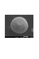
図1は、本実施形態に係るはんだ粒子1の一例を模式的に示す図である。図1に示すように、はんだ粒子1は、直径Bを有する球の表面の一部に直径Aの平面部11が形成された形状を有している。優れた導通信頼性及び絶縁信頼性を実現する観点から、はんだ粒子1の直径Bに対する平面部の直径Aの比(A/B)は、例えば0.01超1.0未満(0.01<A/B<1.0)であってよく、0.1〜0.9、0.1〜0.5、0.1〜0.3又は0.1〜0.2であってもよい。はんだ粒子の直径B及び平面部の直径Aは、例えば走査型電子顕微鏡等により観察することができる。
具体的には、任意の粒子を走査型電子顕微鏡により観察し、画像を撮影する。得られた画像からはんだ粒子の直径B及び平面部の直径Aを測定し、その粒子のA/Bを求める。この作業を300個のはんだ粒子に対して行って平均値を算出し、はんだ粒子のA/Bとする。FIG. 1 is a diagram schematically showing an example of
Specifically, arbitrary particles are observed with a scanning electron microscope and an image is taken. From the obtained image, the diameter B of the solder particles and the diameter A of the flat surface portion are measured, and the A / B of the particles is obtained. This operation is performed on 300 solder particles to calculate an average value, which is used as the A / B of the solder particles.
はんだ粒子1において、平均粒子径が1〜30μmであり、かつC.V.値が20%以下であってもよい。このようなはんだ粒子は小さい平均粒子径と狭い粒度分布とが両立されており、導電信頼性及び絶縁信頼性の高い異方性導電材料に適用する導電性粒子として好適に用いることができる。 In the
はんだ粒子の平均粒子径は、上記の範囲であれば特に限定されないが、好ましくは30μm以下、より好ましくは25μm以下、さらに好ましくは20μm以下である。また、はんだ粒子の平均粒子径は、好ましくは1μm以上、より好ましくは2μm以上、さらに好ましくは4μm以上である。 The average particle size of the solder particles is not particularly limited as long as it is in the above range, but is preferably 30 μm or less, more preferably 25 μm or less, and further preferably 20 μm or less. The average particle size of the solder particles is preferably 1 μm or more, more preferably 2 μm or more, and further preferably 4 μm or more.
はんだ粒子の平均粒子径は、サイズに合わせた各種方法を用いて測定することができる。例えば、動的光散乱法、レーザ回折法、遠心沈降法、電気的検知帯法、共振式質量測定法等の方法を利用できる。さらに、光学顕微鏡、電子顕微鏡等によって得られる画像から、粒子サイズを測定する方法を利用できる。具体的な装置としては、フロー式粒子像分析装置、マイクロトラック、コールターカウンター等が挙げられる。 The average particle size of the solder particles can be measured by using various methods according to the size. For example, a dynamic light scattering method, a laser diffraction method, a centrifugal sedimentation method, an electrical detection band method, a resonance type mass measurement method, or the like can be used. Further, a method of measuring the particle size from an image obtained by an optical microscope, an electron microscope, or the like can be used. Specific devices include a flow-type particle image analyzer, a microtrack, a Coulter counter, and the like.
はんだ粒子のC.V.値は、より優れた導電信頼性及び絶縁信頼性を実現できる観点から、好ましくは20%以下、より好ましくは10%以下、更に好ましくは7%以下、最も好ましくは5%以下である。また、はんだ粒子のC.V.値の下限は特に限定されない。例えば、はんだ粒子のC.V.値は1%以上であってよく、2%以上であってもよい。 C.I. of solder particles. V. The value is preferably 20% or less, more preferably 10% or less, still more preferably 7% or less, and most preferably 5% or less from the viewpoint of achieving more excellent conductivity reliability and insulation reliability. In addition, C.I. V. The lower limit of the value is not particularly limited. For example, C.I. V. The value may be 1% or more, and may be 2% or more.
はんだ粒子のC.V.値は、前述の方法によって測定された粒子径の標準偏差を平均粒子径で割った値に100を掛けることで算出される。 C.I. of solder particles. V. The value is calculated by dividing the standard deviation of the particle size measured by the method described above by the average particle size and multiplying by 100.
はんだ粒子の投影像に外接する四角形を二対の平行線により作成した場合において、対向する辺間の距離をX及びY(但しY<X)としたときに、Xに対するYの比(Y/X)が、0.8超1.0未満(0.8<Y/X<1.0)であってよく、0.81〜0.99又は0.81〜0.95であってもよい。このようなはんだ粒子はより真球に近い粒子ということができる。はんだ粒子を再度基体60の凹部62に収容する場合、はんだ粒子が球状に近いと、収容し易い傾向がある。また、はんだ粒子が真球に近いことで、対向する複数の電極間をはんだ粒子を介して電気的に接続させるときに、はんだ粒子と電極間接触にムラが生じ難く、安定した接続が得られる傾向がある。また、はんだ粒子を樹脂材料中に分散した導電性フィルムやペーストを作製したとき、高い分散性が得られ、製造時の分散安定性が得られる傾向がある。さらに、はんだ粒子を樹脂材料に分散したフィルムやペーストを、電極間の接続に用いる場合、樹脂中ではんだ粒子が回転しても、はんだ粒子が球体形状であれば、投影像で見たとき、はんだ粒子同士の投影面積が近い。そのため、電極同士を接続する際にばらつきの少ない、安定した電気接続を得易い傾向がある。上記の観点から、はんだ粒子の真円度(はんだ粒子の2つの同心円(最小外接円の半径r、最大内接円の半径R)の半径の比r/R)は、0.85以上であってよく、0.90以上であってもよい。 When a quadrangle circumscribing the projected image of solder particles is created by two pairs of parallel lines, and the distance between the opposing sides is X and Y (where Y <X), the ratio of Y to X (Y / X) may be more than 0.8 and less than 1.0 (0.8 <Y / X <1.0), and may be 0.81 to 0.99 or 0.81 to 0.95. .. Such solder particles can be said to be particles closer to a true sphere. When the solder particles are re-accommodated in the
図2は、はんだ粒子の投影像に外接する四角形を二対の平行線により作成した場合における、対向する辺間の距離X及びY(但しY<X)を示す図である。例えば、任意の粒子を走査型電子顕微鏡により観察して投影像を得る。得られた投影像に対し二対の平行線を描画し、一対の平行線は平行線の距離が最小となる位置に、もう一対の平行線は平行線の距離が最大となる位置に配し、その粒子のY/Xを求める。この作業を300個のはんだ粒子に対して行って平均値を算出し、はんだ粒子のY/Xとする。 FIG. 2 is a diagram showing distances X and Y (provided that Y <X) between opposite sides when a quadrangle circumscribing a projected image of solder particles is created by two pairs of parallel lines. For example, an arbitrary particle is observed with a scanning electron microscope to obtain a projected image. Two pairs of parallel lines are drawn with respect to the obtained projected image, and the pair of parallel lines are arranged at the position where the distance between the parallel lines is the minimum, and the other pair of parallel lines are arranged at the position where the distance between the parallel lines is the maximum. , Find the Y / X of the particle. This operation is performed on 300 solder particles, the average value is calculated, and the Y / X of the solder particles is obtained.
はんだ粒子は、スズ又はスズ合金を含むものであってよい。スズ合金としては、例えば、In−Sn合金、In−Sn−Ag合金、Sn−Au合金、Sn−Bi合金、Sn−Bi−Ag合金、Sn−Ag−Cu合金、Sn−Cu合金等を用いることができる。これらのスズ合金の具体例としては、下記の例が挙げられる。
・In−Sn(In52質量%、Bi48質量% 融点118℃)
・In−Sn−Ag(In20質量%、Sn77.2質量%、Ag2.8質量% 融点175℃)
・Sn−Bi(Sn43質量%、Bi57質量% 融点138℃)
・Sn−Bi−Ag(Sn42質量%、Bi57質量%、Ag1質量% 融点139℃)・Sn−Ag−Cu(Sn96.5質量%、Ag3質量%、Cu0.5質量% 融点217℃)
・Sn−Cu(Sn99.3質量%、Cu0.7質量% 融点227℃)
・Sn−Au(Sn21.0質量%、Au79.0質量% 融点278℃)
はんだ粒子は、インジウム又はインジウム合金を含むものであってよい。インジウム合金としては、例えば、In−Bi合金、In−Ag合金等を用いることができる。これらのインジウム合金の具体例としては、下記の例が挙げられる。
・In−Bi(In66.3質量%、Bi33.7質量% 融点72℃)
・In−Bi(In33.0質量%、Bi67.0質量% 融点109℃)
・In−Ag(In97.0質量%、Ag3.0質量% 融点145℃)The solder particles may contain tin or a tin alloy. As the tin alloy, for example, In-Sn alloy, In-Sn-Ag alloy, Sn-Au alloy, Sn-Bi alloy, Sn-Bi-Ag alloy, Sn-Ag-Cu alloy, Sn-Cu alloy and the like are used. be able to. Specific examples of these tin alloys include the following examples.
-In-Sn (In 52% by mass, Bi48% by mass, melting point 118 ° C)
-In-Sn-Ag (In 20% by mass, Sn77.2% by mass, Ag 2.8% by mass, melting point 175 ° C.)
-Sn-Bi (Sn43% by mass, Bi57% by mass, melting point 138 ° C.)
-Sn-Bi-Ag (Sn42% by mass, Bi57% by mass, Ag1% by mass, melting point 139 ° C.)-Sn-Ag-Cu (Sn96.5% by mass, Ag3% by mass, Cu0.5% by mass, melting point 217 ° C.)
-Sn-Cu (Sn99.3% by mass, Cu0.7% by mass, melting point 227 ° C)
-Sn-Au (Sn21.0% by mass, Au79.0% by mass, melting point 278 ° C)
The solder particles may contain indium or an indium alloy. As the indium alloy, for example, an In-Bi alloy, an In-Ag alloy, or the like can be used. Specific examples of these indium alloys include the following examples.
-In-Bi (In66.3% by mass, Bi33.7% by mass, melting point 72 ° C.)
-In-Bi (In33.0% by mass, Bi67.0% by mass, melting point 109 ° C)
-In-Ag (In97.0% by mass, Ag3.0% by mass, melting point 145 ° C)
はんだ粒子の用途(使用時の温度)等に応じて、上記スズ合金又はインジウム合金を選択することができる。例えば、低温での融着にはんだ粒子を用いる場合、In−Sn合金、Sn−Bi合金を採用すればよく、この場合、150℃以下で融着させることができる。Sn−Ag−Cu合金、Sn−Cu合金等の融点の高い材料を採用した場合、高温放置後においても高い信頼性を維持することができる。 The tin alloy or indium alloy can be selected according to the use of the solder particles (temperature at the time of use) and the like. For example, when solder particles are used for fusion at a low temperature, an In—Sn alloy or a Sn—Bi alloy may be adopted, and in this case, the solder particles can be fused at 150 ° C. or lower. When a material having a high melting point such as Sn-Ag-Cu alloy or Sn-Cu alloy is used, high reliability can be maintained even after being left at a high temperature.
はんだ粒子は、Ag、Cu、Ni、Bi、Zn、Pd、Pb、Au、P及びBから選ばれる一種以上を含んでもよい。これらの元素のうち、以下の観点からAg又はCuを含んでもよい。すなわち、はんだ粒子がAg又はCuを含むことで、はんだ粒子の融点を220℃程度まで低下させることができ、且つ、電極との接合強度がより向上するため、より良好な導通信頼性が得られ易くなる。 The solder particles may contain one or more selected from Ag, Cu, Ni, Bi, Zn, Pd, Pb, Au, P and B. Among these elements, Ag or Cu may be contained from the following viewpoints. That is, when the solder particles contain Ag or Cu, the melting point of the solder particles can be lowered to about 220 ° C., and the bonding strength with the electrode is further improved, so that better conduction reliability can be obtained. It will be easier.
はんだ粒子のCu含有率は例えば0.05〜10質量%であり、0.1〜5質量%又は0.2〜3質量%であってもよい。Cu含有率が0.05質量%以上であると、より良好なはんだ接続信頼性を達成し易くなる。また、Cu含有率が10質量%以下であると、融点が低く、濡れ性に優れたはんだ粒子となり易く、結果としてはんだ粒子による接合部の接続信頼性が良好となり易い。 The Cu content of the solder particles is, for example, 0.05 to 10% by mass, and may be 0.1 to 5% by mass or 0.2 to 3% by mass. When the Cu content is 0.05% by mass or more, it becomes easy to achieve better solder connection reliability. Further, when the Cu content is 10% by mass or less, the melting point is low and the solder particles tend to have excellent wettability, and as a result, the connection reliability of the joint portion by the solder particles tends to be good.
はんだ粒子のAg含有率は例えば0.05〜10質量%であり、0.1〜5質量%又は0.2〜3質量%であってもよい。Ag含有率が0.05質量%以上であると、より良好なはんだ接続信頼性を達成し易くなる。また、Ag含油率が10質量%以下であると、融点が低く、濡れ性に優れたはんだ粒子となり易く、結果としてはんだ粒子による接合部の接続信頼性が良好となり易い。 The Ag content of the solder particles is, for example, 0.05 to 10% by mass, and may be 0.1 to 5% by mass or 0.2 to 3% by mass. When the Ag content is 0.05% by mass or more, it becomes easy to achieve better solder connection reliability. Further, when the Ag oil content is 10% by mass or less, the melting point is low and the solder particles tend to have excellent wettability, and as a result, the connection reliability of the joint portion by the solder particles tends to be good.
はんだ粒子の用途は特に限定されず、例えば、異方性導電材料用の導電性粒子として好適に用いることができる。また、半導体集積回路の実装に広く用いられているボールグリッドアレイ接続方法(BGA接続)等の電気的に電極同士を接続する用途や、MEMS等の部品の封止や封管、ロウ付け、高さや隙間制御のスペーサ等の用途にも好適に用いることができる。すなわち、従来はんだが用いられる一般的な用途に、上記はんだ粒子を用いることができる。 The use of the solder particles is not particularly limited, and for example, they can be suitably used as conductive particles for an anisotropic conductive material. In addition, applications such as ball grid array connection method (BGA connection), which is widely used for mounting semiconductor integrated circuits, are used to electrically connect electrodes, and parts such as MEMS are sealed, sealed, brazed, and high. It can also be suitably used for applications such as a spacer for controlling a sheath gap. That is, the solder particles can be used for general applications in which conventional solder is used.
<はんだ粒子の製造方法>
本実施形態に係るはんだ粒子の製造方法は特に制限されないが、製造方法の一例を以下に説明する。例えば、本実施形態に係るはんだ粒子は、複数の凹部を有する基体とはんだ微粒子とを準備する準備工程と、はんだ微粒子の少なくとも一部を基体の凹部に収容する収容工程と、凹部に収容されたはんだ微粒子を融合させて、凹部の内部にはんだ粒子を形成する融合工程と、を備えるはんだ粒子の製造方法により製造することができる。この製造方法によれば、表面の一部に平面部を有するはんだ粒子が製造される。<Manufacturing method of solder particles>
The method for producing the solder particles according to the present embodiment is not particularly limited, but an example of the production method will be described below. For example, the solder particles according to the present embodiment are housed in a preparatory step of preparing a substrate having a plurality of recesses and solder fine particles, a storage step of storing at least a part of the solder fine particles in the recesses of the substrate, and a recess. It can be manufactured by a method for manufacturing solder particles, which comprises a fusion step of fusing the solder fine particles to form the solder particles inside the recess. According to this manufacturing method, solder particles having a flat surface portion on a part of the surface are manufactured.
以下、図3〜6を参照しながら、はんだ粒子の製造方法について説明する。 Hereinafter, a method for producing solder particles will be described with reference to FIGS. 3 to 6.
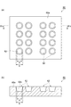
まず、はんだ微粒子と、はんだ微粒子を収容するための基体60を準備する。図3(a)は基体60の一例を模式的に示す平面図であり、図3(b)は図3(a)に示すIIIb−IIIb線における断面図である。図3(a)に示す基体60は、複数の凹部62を有している。複数の凹部62は所定のパターンで規則的に配置されていてよい。 First, the solder fine particles and the
基体60の凹部62は、凹部62の底部62a側から基体60の表面60a側に向けて開口面積が拡大するテーパ状に形成されていることが好ましい。すなわち、図3に示すように、凹部62の底部62aの幅(図3における幅a)は、凹部62の表面60aにおける開口の幅(図3における幅b)よりも狭いことが好ましい。そして、凹部62のサイズ(幅a、幅b、容積、テーパ角度及び深さ等)は、目的とするはんだ粒子のサイズに応じて設定すればよい。 The
なお、凹部62の形状は図3に示す形状以外の形状であってもよい。例えば、凹部62の表面60aにおける開口の形状は、図3に示すような円形以外に、楕円形、三角形、四角形、多角形等であってよい。 The shape of the
また、表面60aに対して垂直な断面における凹部62の形状は、例えば、図4に示すような形状であってよい。図4(a)〜(d)は、基体が有する凹部の断面形状の例を模式的に示す断面図である。図4(a)〜(d)に示すいずれの断面形状も底面が平らになっている。これにより、はんだ粒子の表面の一部に平面部が形成される。また、図4(a)〜(d)に示すいずれの断面形状も、凹部62の表面60aにおける開口の幅(幅b)が、断面形状における最大幅となっている。これにより、凹部62内に形成されたはんだ粒子が取り出し易くなり、作業性が向上する。 Further, the shape of the
基体60を構成する材料としては、例えば、シリコン、各種セラミックス、ガラス、ステンレススチール等の金属等の無機材料、並びに、各種樹脂等の有機材料を使用することができる。これらのうち、基体60は、はんだ微粒子の溶融温度で変質しない耐熱性を有する材質からなることが好ましい。また、基体60の凹部62は、フォトリソグラフ法、インプリント法、機械加工法、電子線加工法、放射線加工法等の公知の方法によって形成することができる。 As the material constituting the
準備工程で準備されるはんだ微粒子は、凹部62の表面60aにおける開口の幅(幅b)より小さい粒子径の微粒子を含むものであればよく、幅bより小さい粒子径の微粒子をより多く含むことが好ましい。例えば、はんだ微粒子は、粒度分布のD10粒子径が幅bより小さいことが好ましく、粒度分布のD30粒子径が幅bより小さいことがより好ましく、粒度分布のD50粒子径が幅bより小さいことが更に好ましい。 The solder fine particles prepared in the preparatory step may contain fine particles having a particle size smaller than the width (width b) of the opening on the
はんだ微粒子の粒度分布は、サイズに合わせた各種方法を用いて測定することができる。例えば、動的光散乱法、レーザ回折法、遠心沈降法、電気的検知帯法、共振式質量測定法等の方法を利用できる。さらに、光学顕微鏡、電子顕微鏡等によって得られる画像から、粒子サイズを測定する方法を利用できる。具体的な装置としては、フロー式粒子像分析装置、マイクロトラック、コールターカウンター等が挙げられる。 The particle size distribution of the solder fine particles can be measured by using various methods according to the size. For example, a dynamic light scattering method, a laser diffraction method, a centrifugal sedimentation method, an electrical detection band method, a resonance type mass measurement method, or the like can be used. Further, a method of measuring the particle size from an image obtained by an optical microscope, an electron microscope, or the like can be used. Specific devices include a flow-type particle image analyzer, a microtrack, a Coulter counter, and the like.
準備工程で準備されるはんだ微粒子のC.V.値は特に限定されないが、大小の微粒子の組み合わせによる凹部62への充填性が向上する観点から、C.V.値は高いことが好ましい。例えば、はんだ微粒子のC.V.値は、20%を超えていてよく、好ましくは25%以上、より好ましくは30%以上である。 C.I. of solder fine particles prepared in the preparation process. V. The value is not particularly limited, but from the viewpoint of improving the filling property into the
はんだ微粒子のC.V.値は、前述の方法によって測定された粒子径の標準偏差を平均粒子径(D50粒子径)で割った値に100を掛けることで算出される。 C.I. of solder fine particles. V. The value is calculated by dividing the standard deviation of the particle size measured by the above method by the average particle size (D50 particle size) and multiplying by 100.
はんだ微粒子は、スズ又はスズ合金を含むものであってよい。スズ合金としては、例えば、In−Sn合金、In−Sn−Ag合金、Sn−Au合金、Sn−Bi合金、Sn−Bi−Ag合金、Sn−Ag−Cu合金、Sn−Cu合金等を用いることができる。これらのスズ合金の具体例としては、下記の例が挙げられる。
・In−Sn(In52質量%、Bi48質量% 融点118℃)
・In−Sn−Ag(In20質量%、Sn77.2質量%、Ag2.8質量% 融点175℃)
・Sn−Bi(Sn43質量%、Bi57質量% 融点138℃)
・Sn−Bi−Ag(Sn42質量%、Bi57質量%、Ag1質量% 融点139℃)・Sn−Ag−Cu(Sn96.5質量%、Ag3質量%、Cu0.5質量% 融点217℃)
・Sn−Cu(Sn99.3質量%、Cu0.7質量% 融点227℃)
・Sn−Au(Sn21.0質量%、Au79.0質量% 融点278℃)
はんだ粒子は、インジウム又はインジウム合金を含むものであってよい。インジウム合金としては、例えば、In−Bi合金、In−Ag合金等を用いることができる。これらのインジウム合金の具体例としては、下記の例が挙げられる。
・In−Bi(In66.3質量%、Bi33.7質量% 融点72℃)
・In−Bi(In33.0質量%、Bi67.0質量% 融点109℃)
・In−Ag(In97.0質量%、Ag3.0質量% 融点145℃)The solder fine particles may contain tin or a tin alloy. As the tin alloy, for example, In-Sn alloy, In-Sn-Ag alloy, Sn-Au alloy, Sn-Bi alloy, Sn-Bi-Ag alloy, Sn-Ag-Cu alloy, Sn-Cu alloy and the like are used. be able to. Specific examples of these tin alloys include the following examples.
-In-Sn (In 52% by mass, Bi48% by mass, melting point 118 ° C)
-In-Sn-Ag (In 20% by mass, Sn77.2% by mass, Ag 2.8% by mass, melting point 175 ° C.)
-Sn-Bi (Sn43% by mass, Bi57% by mass, melting point 138 ° C.)
-Sn-Bi-Ag (Sn42% by mass, Bi57% by mass, Ag1% by mass, melting point 139 ° C.)-Sn-Ag-Cu (Sn96.5% by mass, Ag3% by mass, Cu0.5% by mass, melting point 217 ° C.)
-Sn-Cu (Sn99.3% by mass, Cu0.7% by mass, melting point 227 ° C)
-Sn-Au (Sn21.0% by mass, Au79.0% by mass, melting point 278 ° C)
The solder particles may contain indium or an indium alloy. As the indium alloy, for example, an In-Bi alloy, an In-Ag alloy, or the like can be used. Specific examples of these indium alloys include the following examples.
-In-Bi (In66.3% by mass, Bi33.7% by mass, melting point 72 ° C.)
-In-Bi (In33.0% by mass, Bi67.0% by mass, melting point 109 ° C)
-In-Ag (In97.0% by mass, Ag3.0% by mass, melting point 145 ° C)
はんだ粒子の用途(使用時の温度)等に応じて、上記スズ合金又はインジウム合金を選択することができる。例えば、低温での融着に用いるはんだ粒子を得たい場合、In−Sn合金、Sn−Bi合金を採用すればよく、この場合、150℃以下で融着可能なはんだ粒子が得られる。Sn−Ag−Cu合金、Sn−Cu合金等の融点の高い材料を採用した場合、高温放置後においても高い信頼性を維持可能なはんだ粒子を得ることができる。 The tin alloy or indium alloy can be selected according to the use of the solder particles (temperature at the time of use) and the like. For example, when it is desired to obtain solder particles used for fusion at a low temperature, an In—Sn alloy or a Sn—Bi alloy may be adopted. In this case, solder particles that can be fused at 150 ° C. or lower can be obtained. When a material having a high melting point such as Sn-Ag-Cu alloy or Sn-Cu alloy is used, solder particles capable of maintaining high reliability even after being left at a high temperature can be obtained.
はんだ微粒子は、Ag、Cu、Ni、Bi、Zn、Pd、Pb、Au、P及びBから選ばれる一種以上を含んでもよい。これらの元素のうち、以下の観点からAg又はCuを含んでもよい。すなわち、はんだ微粒子がAg又はCuを含むことで、得られるはんだ粒子の融点を220℃程度まで低下させることができる、電極との接合強度に優れたはんだ粒子が得られることによって良好な導通信頼性を得られる、という効果が奏される。 The solder fine particles may contain one or more selected from Ag, Cu, Ni, Bi, Zn, Pd, Pb, Au, P and B. Among these elements, Ag or Cu may be contained from the following viewpoints. That is, when the solder fine particles contain Ag or Cu, the melting point of the obtained solder particles can be lowered to about 220 ° C., and the solder particles having excellent bonding strength with the electrode can be obtained, so that good conduction reliability can be obtained. The effect of being able to obtain is achieved.
はんだ微粒子のCu含有率は例えば0.05〜10質量%であり、0.1〜5質量%又は0.2〜3質量%であってもよい。Cu含有率が0.05質量%以上であると、良好なはんだ接続信頼性を達成可能なはんだ粒子が得られ易くなる。また、Cu含有率が10質量%以下であると、融点が低く、濡れ性に優れたはんだ粒子が得られ易くなり、結果としてはんだ粒子による接合部の接続信頼性が良好となり易い。 The Cu content of the solder fine particles is, for example, 0.05 to 10% by mass, and may be 0.1 to 5% by mass or 0.2 to 3% by mass. When the Cu content is 0.05% by mass or more, it becomes easy to obtain solder particles capable of achieving good solder connection reliability. Further, when the Cu content is 10% by mass or less, solder particles having a low melting point and excellent wettability can be easily obtained, and as a result, the connection reliability of the joint portion by the solder particles tends to be good.
はんだ微粒子のAg含有率は例えば0.05〜10質量%であり、0.1〜5質量%又は0.2〜3質量%であってもよい。Ag含有率が0.05質量%以上であれば、良好なはんだ接続信頼性を達成可能なはんだ粒子が得られ易くなる。また、Ag含油率が10質量%以下であると、融点が低く、濡れ性に優れたはんだ粒子が得られ易くなり、結果としてはんだ粒子による接合部の接続信頼性が良好となり易い。 The Ag content of the solder fine particles is, for example, 0.05 to 10% by mass, and may be 0.1 to 5% by mass or 0.2 to 3% by mass. When the Ag content is 0.05% by mass or more, it becomes easy to obtain solder particles capable of achieving good solder connection reliability. Further, when the Ag oil content is 10% by mass or less, solder particles having a low melting point and excellent wettability can be easily obtained, and as a result, the connection reliability of the joint portion by the solder particles tends to be good.
収容工程では、基体60の凹部62のそれぞれに、準備工程で準備したはんだ微粒子を収容する。収容工程では、準備工程で準備したはんだ微粒子の全部を凹部62に収容する工程であってよく、準備工程で準備したはんだ微粒子の一部(例えば、はんだ微粒子のうち、凹部62の開口の幅bより小さいもの)を凹部62に収容する工程であってよい。 In the accommodating step, the solder fine particles prepared in the preparatory step are accommodating in each of the
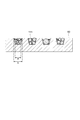
図5は、基体60の凹部62にはんだ微粒子111が収容された状態を模式的に示す断面図である。図5に示すように、複数の凹部62のそれぞれに、複数のはんだ微粒子111が収容される。 FIG. 5 is a cross-sectional view schematically showing a state in which the solder
凹部62に収容されたはんだ微粒子111の量は、例えば、凹部62の容積に対して20%以上であることが好ましく、30%以上であることがより好ましく、50%以上であることが更に好ましく、60%以上であることがもっとも好ましい。これにより、収容量のばらつきが抑えられ、粒度分布のより小さいはんだ粒子が得られ易くなる。 The amount of the solder
はんだ微粒子を凹部62に収容する方法は特に限定されない。収容方法は、乾式、湿式のいずれであってもよい。例えば、準備工程で準備したはんだ微粒子を基体60上に配置し、スキージを用いて基体60の表面60aを擦ることで、余分なはんだ微粒子を除去しつつ、凹部62内に十分なはんだ微粒子を収容することができる。凹部62の開口の幅bが凹部62の深さより大きい場合、凹部62の開口からはんだ微粒子が飛び出す場合がある。スキージを用いると、凹部62の開口から飛び出ているはんだ微粒子は除去される。余分なはんだ微粒子を除去する方法として、圧縮空気を吹き付ける、不織布又は繊維の束で基体60の表面60aを擦る、等の方法も挙げられる。これらの方法は、スキージと比べて物理的な力が弱いため、変形し易いはんだ微粒子を扱う上で好ましい。また、これらの方法では、凹部62の開口から飛び出ているはんだ微粒子を凹部内に残すこともできる。 The method of accommodating the solder fine particles in the
融合工程は、凹部62に収容されたはんだ粒子111を融合させて、凹部62の内部にはんだ粒子1を形成する工程である。図6は、基体60の凹部62にはんだ粒子1が形成された状態を模式的に示す断面図である。凹部62に収容されたはんだ微粒子111は、溶融することで合一化し、表面張力によって球状化する。このとき、凹部62の底部62aとの接触部では、溶融したはんだが底部62aに追従して平面部11を形成する。これにより、形成されるはんだ粒子1は、表面の一部に平面部11を有する形状となる。 The fusion step is a step of fusing the
図1は、図6における凹部62の開口部と反対側からはんだ粒子1を見た図である。 FIG. 1 is a view of the
凹部62に収容されたはんだ微粒子111を溶融させる方法としては、はんだ微粒子111をはんだの融点以上に加熱する方法が挙げられる。はんだ微粒子111は、酸化被膜の影響で融点以上の温度で加熱しても溶融しない場合や、濡れ拡がらない場合や、合一化しない場合がある。このため、はんだ微粒子111を還元雰囲気下にさらし、はんだ微粒子111の表面酸化被膜を除去した後に、はんだ微粒子111の融点以上の温度に加熱することで、はんだ微粒子111を溶融させ、濡れ拡がり、合一化させることができる。また、はんだ微粒子111の溶融は、還元雰囲気下で行うことが好ましい。はんだ微粒子111をはんだ微粒子111の融点以上に加熱し、かつ還元雰囲気とすることで、はんだ微粒子111の表面の酸化被膜が還元され、はんだ微粒子111の溶融、濡れ拡がり、合一化が効率的に進行し易くなる。 Examples of the method of melting the solder
還元雰囲気にする方法は、上述の効果が得られる方法であれば特に限定されず、例えば水素ガス、水素ラジカル、ギ酸ガス等を用いる方法がある。例えば、水素還元炉、水素ラジカル還元炉、ギ酸還元炉、又はこれらのコンベアー炉若しくは連続炉を用いることで、還元雰囲気下にはんだ微粒子111を溶融させることができる。これらの装置は、炉内に、加熱装置、不活性ガス(窒素、アルゴン等)を充填するチャンバー、チャンバー内を真空にする機構等を備えていてよく、これにより還元ガスの制御がより容易となる。また、チャンバー内を真空にできると、はんだ微粒子111の溶融及び合一化の後に、減圧によってボイドの除去を行うことができ、接続安定性に一層優れるはんだ粒子1を得ることができる。 The method for creating a reducing atmosphere is not particularly limited as long as the above-mentioned effect can be obtained, and for example, there is a method using hydrogen gas, hydrogen radical, formic acid gas and the like. For example, by using a hydrogen reduction furnace, a hydrogen radical reduction furnace, a formic acid reduction furnace, or a conveyor furnace or a continuous furnace thereof, the solder
はんだ微粒子111の還元、溶解条件、温度、炉内雰囲気調整などのプロファイルは、はんだ微粒子111の融点、粒度、凹部サイズ、基体60の材質などを勘案して適宜設定されてよい。例えば、はんだ微粒子111が凹部に充填された基体60を、炉内に挿入し、真空引きを行った後に、還元ガスを導入して、炉内を還元ガスで満たし、はんだ微粒子111の表面酸化被膜を除去した後、真空引きにて還元ガスを除去し、その後、はんだ微粒子111の融点以上に加熱して、はんだ微粒子を溶解及び合一化させて、凹部62内にはんだ粒子を形成した後、窒素ガスを充填してから炉内温度を室温に戻し、はんだ粒子1を得ることができる。また、例えば、はんだ微粒子111が凹部に充填された基体60を、炉内に挿入し、真空引きを行った後に、還元ガスを導入して、炉内を還元ガスで満たし、炉内加熱ヒーターによりはんだ微粒子111を加熱して、はんだ微粒子111の表面酸化被膜を除去した後、真空引きにて還元ガスを除去し、その後、はんだ微粒子111の融点以上に加熱して、はんだ微粒子を溶解及び合一化させて、凹部62内にはんだ粒子を形成した後、窒素ガスを充填してから炉内温度を室温に戻し、はんだ粒子1を得ることができる。還元雰囲気下で、はんだ微粒子を加熱することで、還元力が増し、はんだ微粒子の表面酸化被膜の除去が容易になる利点がある。 Profiles such as reduction, melting conditions, temperature, and atmosphere adjustment in the furnace of the solder
さらに、例えば、はんだ微粒子111が凹部に充填された基体60を、炉内に挿入し、真空引きを行った後に、還元ガスを導入して、炉内を還元ガスで満たし、炉内加熱ヒーターにより基体60をはんだ微粒子111の融点以上に加熱して、はんだ微粒子111の表面酸化被膜を還元により除去すると同時にはんだ微粒子を溶解及び合一化させて、凹部62内にはんだ粒子を形成し、真空引きにて還元ガスを除去し、さらにはんだ粒子内のボイドを減らした後、窒素ガスを充填してから炉内温度を室温に戻し、はんだ粒子1を得ることができる。この場合は、炉内温度の上昇、下降の調節がそれぞれ一回で良いため、短時間で処理出来る利点がある。 Further, for example, the
上述凹部62内にはんだ粒子を形成した後に、もう一度炉内を還元雰囲気にして、除去し切れなかった表面酸化被膜を除去する工程を加え、融合されずに残っていたはんだ微粒子や、融合されずに残っていた酸化被膜の一部などの残渣を減らすことができる。 After forming the solder particles in the
大気圧のコンベアー炉を用いる場合は、はんだ微粒子111が凹部に充填された基体60を搬送用コンベアーに載せ、複数のゾーンを連続して通過させてはんだ粒子1を得ることができる。例えば、はんだ微粒子111が凹部に充填された基体60を、一定の速度に設定したコンベアーに載せ、はんだ微粒子111の融点より低い温度の窒素やアルゴンなどの不活性ガスが充満したゾーンを通過させ、続いてはんだ微粒子111の融点より低い温度の蟻酸ガスなどの還元ガスが存在するゾーンを通過させて、はんだ微粒子111の表面酸化被膜を除去し、続いてはんだ微粒子111の融点以上の温度の窒素やアルゴンなどの不活性ガスが充満したゾーンを通過させてはんだ微粒子111を溶融、合一化させ、続いて窒素やアルゴンなどの不活性ガスが充満した冷却ゾーンを通過させて、はんだ粒子1を得ることができる。例えば、はんだ微粒子111が凹部に充填された基体60を、一定の速度に設定したコンベアーに載せ、はんだ微粒子111の融点以上の温度の窒素やアルゴンなどの不活性ガスが充満したゾーンを通過させ、続いてはんだ微粒子111の融点以上の温度の蟻酸ガスなどの還元ガスが存在するゾーンを通過させて、はんだ微粒子111の表面酸化被膜を除去し、溶融、合一化させ、続いて窒素やアルゴンなどの不活性ガスが充満した冷却ゾーンを通過させて、はんだ粒子1を得ることができる。前記のコンベアー炉は、大気圧での処理が可能であることから、フィルム状の材料をロールトゥロールで連続的に処理することもできる。例えば、はんだ微粒子111が凹部に充填された基体60の連続ロール品を作製し、コンベアー炉の入り口側にロール巻きだし機、コンベアー炉の出口側にロール巻き取り機を設置して、一定の速度で基体60を搬送し、コンベアー炉内の各ゾーンを通過させることで、凹部に充填されたはんだ微粒子111を融合させることができる。 When an atmospheric pressure conveyor furnace is used, the
形成されたはんだ粒子1は凹部62から取り出して回収され、はんだペーストの調製に供される。図7は、このようにして得られたはんだ粒子の一例を示すSEM像である。なお、はんだ粒子1は、基体60の凹部62に収容された状態で運搬・保管等してよい。 The formed
本実施形態の製造方法であれば、はんだ微粒子の材質及び形状によらず、均一なサイズのはんだ粒子を形成することができる。例えば、インジウム系はんだは、めっきによる析出が可能であるが、粒子状に析出させることは難しく、柔らかくて扱いが難しい。しかし、本実施形態の製造方法では、インジウム系はんだ微粒子を原料として用いることで、均一な粒子径を有するインジウム系はんだ粒子を容易に製造することができる。また、形成されたはんだ粒子1は、基体60の凹部62に収容された状態で取り扱うことができるため、はんだ粒子を変形させることなく運搬・保管等することができる。さらに、形成されたはんだ粒子1は、単に基体60の凹部62に収容された状態であるため、取り出しが容易であり、はんだ粒子を変形させることなく回収・表面処理等を行うことができる。 According to the manufacturing method of the present embodiment, solder particles having a uniform size can be formed regardless of the material and shape of the solder fine particles. For example, indium-based solder can be precipitated by plating, but it is difficult to precipitate it in the form of particles, and it is soft and difficult to handle. However, in the production method of the present embodiment, indium-based solder particles having a uniform particle size can be easily produced by using the indium-based solder fine particles as a raw material. Further, since the formed
また、はんだ微粒子111は、粒度分布にばらつきが大きくても、形状がいびつであってもよく、凹部62内に収容することができれば、本実施形態の製造方法の原料として用いることができる。 Further, the solder
また、本実施形態の製造方法において、基体60は、リソグラフィー法、インプリント法、電子線加工法、放射線加工法、機械加工法等によって凹部62の形状を自在に設計できる。はんだ粒子1のサイズは凹部62に収容されるはんだ微粒子111の量に依存するため、本実施形態の製造方法では、凹部62の設計によりはんだ粒子1のサイズを自在に設計できる。 Further, in the manufacturing method of the present embodiment, the shape of the
以上、本発明の好適な実施形態について説明したが、本発明は上記実施形態に限定されるものではない。 Although the preferred embodiment of the present invention has been described above, the present invention is not limited to the above embodiment.
以下、実施例によって本発明を更に詳細に説明するが、本発明はこれらの実施例に限定されるものではない。 Hereinafter, the present invention will be described in more detail with reference to Examples, but the present invention is not limited to these Examples.
<はんだ粒子の作製>
[実施例1]
(工程a1:はんだ微粒子の分級)
Sn−Biはんだ微粒子(5N Plus社製、融点139℃、Type8)100gを、蒸留水に浸漬し、超音波分散させた後、静置し、上澄みに浮遊するはんだ微粒子を回収した。この操作を繰り返して、10gのはんだ微粒子を回収した。得られたはんだ微粒子の平均粒子径は1.0μm、C.V.値は42%であった。
(工程b1:基体への配置)
開口径1.2μmφ、底部径1.0μmφ、深さ1.0μm(底部径1.0μmφは、開口部を上面からみると、開口径1.2μmφの中央に位置する)の凹部を複数有する基体(ポリイミドフィルム、厚さ100μm)を準備した。複数の凹部は、1.0μmの間隔で規則的に配列させた。工程aで得られたはんだ微粒子(平均粒子径1.0μm、C.V.値42%)を基体の凹部に配置した。なお、基体の凹部が形成された面側を微粘着ローラーでこすることで余分なはんだ微粒子を取り除き、凹部内のみにはんだ微粒子が配置された基体を得た。
(工程c1:はんだ粒子の形成)
工程b1で凹部にはんだ微粒子が配置された基体を、水素還元炉に入れ、真空引き後、水素ガスを炉内に導入して炉内を水素で満たした。その後、炉内を280℃で20分保った後、再び真空に引き、窒素を導入して大気圧に戻してから炉内の温度を室温まで下げることにより、はんだ粒子を形成した。<Manufacturing of solder particles>
[Example 1]
(Step a1: Classification of solder fine particles)
100 g of Sn-Bi solder fine particles (manufactured by 5N Plus, melting point 139 ° C., Type 8) were immersed in distilled water, ultrasonically dispersed, and then allowed to stand to recover the solder fine particles floating in the supernatant. This operation was repeated to recover 10 g of solder fine particles. The average particle size of the obtained solder fine particles was 1.0 μm, and C.I. V. The value was 42%.
(Step b1: Arrangement on the substrate)
A substrate having a plurality of recesses having an opening diameter of 1.2 μmφ, a bottom diameter of 1.0 μmφ, and a depth of 1.0 μm (the bottom diameter of 1.0 μmφ is located at the center of the opening diameter of 1.2 μmφ when the opening is viewed from the top surface). (Polyimide film, thickness 100 μm) was prepared. The plurality of recesses were regularly arranged at intervals of 1.0 μm. The solder fine particles (average particle diameter 1.0 μm, CV value 42%) obtained in step a were placed in the recesses of the substrate. By rubbing the surface side of the substrate on which the recesses were formed with a fine adhesive roller, excess solder fine particles were removed, and a substrate in which the solder fine particles were arranged only in the recesses was obtained.
(Step c1: Formation of solder particles)
The substrate in which the solder fine particles were arranged in the recesses in step b1 was placed in a hydrogen reduction furnace, evacuated, and then hydrogen gas was introduced into the furnace to fill the inside of the furnace with hydrogen. Then, after keeping the inside of the furnace at 280 ° C. for 20 minutes, the solder particles were formed by drawing a vacuum again, introducing nitrogen to return to atmospheric pressure, and then lowering the temperature inside the furnace to room temperature.
なお、工程c1を経た基体を凹部裏側よりタップすることで、凹部よりはんだ粒子を回収した。得られたはんだ粒子を下記の方法で観察した。走査型電子顕微鏡(SEM)観察用台座表面に固定した導電テープ上に、得られたはんだ粒子を載せ、厚さ5mmのステンレス板にSEM観察用台座をタップしてはんだ粒子を導電テープ上に万遍なく広げた。その後、導電テープ表面に圧縮窒素ガスを吹きかけ、はんだ粒子を導電テープ上に単層に固定した。観察結果を図7に示す。図7は、実施例1により得られたはんだ粒子のSEM像である。同図に示されるように、得られたはんだ粒子は、球の表面の一部に平面部が形成された形状を有していた。なお、その他の実施例で得られたはんだ粒子も同様の形状を有していた。 By tapping the substrate that had undergone step c1 from the back side of the recess, solder particles were recovered from the recess. The obtained solder particles were observed by the following method. Place the obtained solder particles on a conductive tape fixed to the surface of the scanning electron microscope (SEM) observation pedestal, and tap the SEM observation pedestal on a stainless steel plate with a thickness of 5 mm to spread the solder particles on the conductive tape. Spread evenly. Then, compressed nitrogen gas was sprayed on the surface of the conductive tape to fix the solder particles on the conductive tape in a single layer. The observation results are shown in FIG. FIG. 7 is an SEM image of the solder particles obtained in Example 1. As shown in the figure, the obtained solder particles had a shape in which a flat portion was formed on a part of the surface of the sphere. The solder particles obtained in the other examples also had the same shape.
<はんだ粒子の評価>
工程c1を経た基体の凹部に相対するように導電テープを貼り付け後、引き剥がすことで、はんだ粒子の平面部が導電テープ面に並行して配列している、観察用サンプルを得た。この観察用サンプルのはんだ粒子が配置されている面にPtスパッタを施した後、SEM観察を行った。300個のはんだ粒子を観察し、はんだ粒子の平均直径B(平均粒子径)、平面部の平均直径A、C.V.値、真円度、A/B及びY/Xを算出した。結果を表1に示す。
真円度:はんだ粒子の2つの同心円(最小外接円の半径r、最大内接円の半径R)の半径の比r/R。
A/B:はんだ粒子の直径Bに対する平面部の直径Aの比。
Y/X:はんだ粒子の投影像に外接する四角形を二対の平行線により作成した場合において、対向する辺間の距離をX及びY(但しY<X)としたときの、Xに対するYの比。<Evaluation of solder particles>
The conductive tape was attached so as to face the concave portion of the substrate that had undergone step c1 and then peeled off to obtain an observation sample in which the flat portions of the solder particles were arranged in parallel with the conductive tape surface. After Pt sputtering was applied to the surface of the observation sample on which the solder particles were arranged, SEM observation was performed. Observing 300 solder particles, the average diameter B (average particle diameter) of the solder particles, the average diameter A of the flat surface portion A, C.I. V. Values, roundness, A / B and Y / X were calculated. The results are shown in Table 1.
Roundness: The ratio r / R of the radii of two concentric circles (radius r of the minimum circumscribed circle, radius R of the maximum inscribed circle) of the solder particles.
A / B: The ratio of the diameter A of the flat surface to the diameter B of the solder particles.
Y / X: When a quadrangle circumscribing the projected image of the solder particles is created by two pairs of parallel lines, and the distance between the opposing sides is X and Y (where Y <X), Y with respect to X ratio.
[実施例2〜12]
凹部サイズを表1に記載のとおり変更したこと以外は、実施例1と同様にしてはんだ粒子を作製し、はんだ粒子の評価を実施した。[Examples 2 to 12]
Solder particles were produced in the same manner as in Example 1 except that the recess size was changed as shown in Table 1, and the solder particles were evaluated.
<はんだペーストの作製>
[作製例1]
YL980(三菱化学株式会社製、ビスフェノールA型エポキシ樹脂の商品名)16.0質量部と、2P4MHZ−PW(四国化成株式会社製、イミダゾール化合物の商品名)0.8質量部と、フラックス活性剤としてのアジピン酸3.2質量部とを混合し、混合物を3本ロールに3回通して、接着剤成分を調製した。<Making solder paste>
[Production Example 1]
YL980 (trade name of bisphenol A type epoxy resin manufactured by Mitsubishi Chemical Co., Ltd.) 16.0 parts by mass, 2P4MHZ-PW (trade name of imidazole compound manufactured by Shikoku Kasei Co., Ltd.) 0.8 parts by mass, and flux activator The mixture was mixed with 3.2 parts by mass of adipic acid, and the mixture was passed through three rolls three times to prepare an adhesive component.
次に、接着剤成分20質量部に対して、実施例1で作製した球の表面の一部に平面部が形成されたSn−Biはんだ粒子80質量部を加え、得られた混合物をプラネタリーミキサーで撹拌混練し、500Pa以下で10分間脱泡処理を行うことによりはんだペーストを得た。 Next, 80 parts by mass of Sn-Bi solder particles having a flat surface formed on a part of the surface of the sphere produced in Example 1 was added to 20 parts by mass of the adhesive component, and the obtained mixture was planetary. The solder paste was obtained by stirring and kneading with a mixer and performing a defoaming treatment at 500 Pa or less for 10 minutes.
[作製例2〜12]
実施例2〜12により得られた、球の表面の一部に平面部が形成されたSn−Biはんだ粒子を用いたこと以外は、作製例1と同じ方法ではんだペーストの作製を行った。[Production Examples 2 to 12]
A solder paste was produced by the same method as in Production Example 1 except that Sn-Bi solder particles having a flat surface formed on a part of the surface of the sphere obtained in Examples 2 to 12 were used.
[作製例13]
YL980(三菱化学株式会社製、ビスフェノールA型エポキシ樹脂の商品名)16.7質量部と、2P4MHZ−PW(四国化成株式会社製、イミダゾール化合物の商品名)0.8質量部と、フラックス活性剤としてのアジピン酸2.5質量部とを混合し、混合物を3本ロールに3回通して、接着剤成分を調製した。[Production Example 13]
YL980 (trade name of bisphenol A type epoxy resin manufactured by Mitsubishi Chemical Co., Ltd.) 16.7 parts by mass, 2P4MHZ-PW (trade name of imidazole compound manufactured by Shikoku Kasei Co., Ltd.) 0.8 parts by mass, and flux activator The mixture was mixed with 2.5 parts by mass of adipic acid as a compound, and the mixture was passed through three rolls three times to prepare an adhesive component.
次に、接着剤成分20質量部に対して、実施例5で作製した、球の表面の一部に平面部が形成されたSn−Biはんだ粒子80質量部を加え、得られた混合物をプラネタリーミキサーで撹拌混練し、500Pa以下で10分間脱泡処理を行うことによりはんだペーストを得た。 Next, 80 parts by mass of Sn-Bi solder particles having a flat surface formed on a part of the surface of the sphere, which was produced in Example 5, was added to 20 parts by mass of the adhesive component, and the obtained mixture was used as a planet. The solder paste was obtained by stirring and kneading with a Lee mixer and performing a defoaming treatment at 500 Pa or less for 10 minutes.
[比較作製例1]
球の表面の一部に平面部が形成されたSn−Biはんだ粒子に代えて、そのような平面部を有しないSnBiはんだ粒子(三井金属株式会社製「ST−3」)を用いたこと以外は、作製例1と同じ方法ではんだペーストの作製を行った。なお、当該SnBiはんだ粒子の平均粒子径は4μm、C.V.値は31%であった。[Comparative Production Example 1]
Except for the use of SnBi solder particles (“ST-3” manufactured by Mitsui Metal Co., Ltd.) that do not have such a flat surface instead of the Sn-Bi solder particles having a flat surface formed on a part of the surface of the sphere. Made a solder paste by the same method as in Production Example 1. The average particle size of the SnBi solder particles was 4 μm, and C.I. V. The value was 31%.
[比較作製例2]
球の表面の一部に平面部が形成されたSn−Biはんだ粒子に代えて、そのような平面部を有しないSnBiはんだ粒子(三井金属株式会社製「Type−4」)を用いたこと以外は、作製例1と同じ方法ではんだペーストの作製を行った。なお、当該SnBiはんだ粒子の平均粒子径は26μm、C.V.値は25%であった。[Comparative Production Example 2]
Except for the use of SnBi solder particles (“Type-4” manufactured by Mitsui Metal Co., Ltd.) that do not have such a flat surface instead of the Sn-Bi solder particles having a flat surface formed on a part of the surface of the sphere. Made a solder paste by the same method as in Production Example 1. The average particle size of the SnBi solder particles was 26 μm, and C.I. V. The value was 25%.
[比較作製例3]
YL980(三菱化学株式会社製、ビスフェノールA型エポキシ樹脂の商品名)15.4質量部と、2P4MHZ−PW(四国化成株式会社製、イミダゾール化合物の商品名)0.8質量部と、フラックス活性剤としてのアジピン酸3.9質量部とを混合し、混合物を3本ロールに3回通して、接着剤成分を調製した。[Comparative Production Example 3]
YL980 (trade name of bisphenol A type epoxy resin manufactured by Mitsubishi Chemical Co., Ltd.) 15.4 parts by mass, 2P4MHZ-PW (trade name of imidazole compound manufactured by Shikoku Kasei Co., Ltd.) 0.8 parts by mass, and flux activator Adipic acid (3.9 parts by mass) was mixed, and the mixture was passed through 3 rolls 3 times to prepare an adhesive component.
次に、接着剤成分20質量部に対して、上記のとおり平面部を有しないSnBiはんだ粒子(三井金属株式会社製「ST−3」)を80質量部加え、得られた混合物をプラネタリーミキサーで撹拌混練し、500Pa以下で10分間脱泡処理を行うことによりはんだペーストを得た。 Next, 80 parts by mass of SnBi solder particles (“ST-3” manufactured by Mitsui Mining & Smelting Co., Ltd.) having no flat surface portion were added to 20 parts by mass of the adhesive component, and the obtained mixture was mixed with a planetary mixer. The solder paste was obtained by stirring and kneading with and defoaming at 500 Pa or less for 10 minutes.
[比較作製例4]
YL980(三菱化学株式会社製、ビスフェノールA型エポキシ樹脂の商品名)16.7質量部と、2P4MHZ−PW(四国化成株式会社製、イミダゾール化合物の商品名)0.8質量部と、フラックス活性剤としてのアジピン酸2.5質量部とを混合し、混合物を3本ロールに3回通して、接着剤成分を調製した。[Comparative Production Example 4]
YL980 (trade name of bisphenol A type epoxy resin manufactured by Mitsubishi Chemical Co., Ltd.) 16.7 parts by mass, 2P4MHZ-PW (trade name of imidazole compound manufactured by Shikoku Kasei Co., Ltd.) 0.8 parts by mass, and flux activator The mixture was mixed with 2.5 parts by mass of adipic acid as a compound, and the mixture was passed through three rolls three times to prepare an adhesive component.
次に、接着剤成分20質量部に対して、上記のとおり平面部を有しないSnBiはんだ粒子(三井金属株式会社製「ST−3」)を80質量部加え、得られた混合物をプラネタリーミキサーで撹拌混練し、500Pa以下で10分間脱泡処理を行うことによりはんだペーストを得た。 Next, 80 parts by mass of SnBi solder particles (“ST-3” manufactured by Mitsui Mining & Smelting Co., Ltd.) having no flat surface portion were added to 20 parts by mass of the adhesive component, and the obtained mixture was mixed with a planetary mixer. The solder paste was obtained by stirring and kneading with and defoaming at 500 Pa or less for 10 minutes.
上記作製例及び比較作製例のはんだペーストの特性を下記の方法で測定した。その結果を表2にまとめて示す。 The characteristics of the solder pastes of the above-mentioned production examples and comparative production examples were measured by the following methods. The results are summarized in Table 2.
(1)接着強度の評価
銀めっき付き銅板(10mm×15mm、厚み:0.20mm)上にはんだペーストを0.5mg塗布し、この上に矩形平板状の錫めっき付き銅チップ(2mm×2mm、厚み0.25mm)を積層した後、ホットプレートを用いて、150℃、10分間の熱履歴を加えて、試験片を得た。この試験片に対し、ボンドテスター(DAGE社製、2400)を用いて、シェア速度500μm/sec、クリアランス100μmの条件にて、25℃におけるシェア強度を測定した。(1) Evaluation of Adhesive Strength 0.5 mg of solder paste was applied on a silver-plated copper plate (10 mm x 15 mm, thickness: 0.20 mm), and a rectangular flat plate-shaped tin-plated copper chip (2 mm x 2 mm, After laminating (thickness 0.25 mm), a test piece was obtained by applying a heat history at 150 ° C. for 10 minutes using a hot plate. For this test piece, the shear strength at 25 ° C. was measured using a bond tester (2400 manufactured by DAGE) under the conditions of a shear rate of 500 μm / sec and a clearance of 100 μm.
(2)温度サイクル試験
隣り合う2つの銅箔ランド(0.2mm×0.4mm)を備え、銅箔ランド間の距離が100μmである、100mm×50mm×0.5mmの矩形平板状の薄型FR4基板を準備した。次いで、銅箔ランド上にはんだペーストをメタルマスク(厚み100μm、開口寸法0.2mm×0.3mm)を用いて印刷し、電極間距離が100μmの小型チップ抵抗(0.2mm×0.4mm)を搭載した。この部品搭載基板に上記(1)と同様の熱履歴を加え、耐TCT性評価用の試験基板を得た。この試験基板の初期抵抗を簡易テスターを用いて確認した後、熱衝撃試験機(1サイクル:−55℃で30分間保持、125℃まで5分間で昇温、125℃で30分間保持、−55℃まで5分間で降温)に投入し、接続抵抗を測定した。耐TCT性の評価は、初期抵抗に対して±10%以内の抵抗変化率を示したサイクル数を指標とした。(2) Temperature cycle test A rectangular flat plate-shaped thin FR4 having two adjacent copper foil lands (0.2 mm × 0.4 mm) and having a distance between the copper foil lands of 100 μm of 100 mm × 50 mm × 0.5 mm. The board was prepared. Next, the solder paste was printed on the copper foil land using a metal mask (thickness 100 μm, opening size 0.2 mm × 0.3 mm), and a small chip resistor (0.2 mm × 0.4 mm) with an electrode-to-electrode distance of 100 μm was printed. Was installed. The same thermal history as in (1) above was added to this component mounting substrate to obtain a test substrate for TCT resistance evaluation. After confirming the initial resistance of this test substrate using a simple tester, a thermal shock tester (1 cycle: hold at -55 ° C for 30 minutes, heat up to 125 ° C in 5 minutes, hold at 125 ° C for 30 minutes, -55 The temperature was lowered to ℃ in 5 minutes), and the connection resistance was measured. The evaluation of TCT resistance was based on the number of cycles showing a resistance change rate within ± 10% of the initial resistance.
(3)絶縁抵抗試験
上記(2)と同様の方法で作製した部品搭載基板の絶縁抵抗値を測定した後、マイグレーション試験(温度60℃、湿度90%、50V印加)を実施した。耐マイグレーション性の評価は、電極間のリーク発生によって、絶縁抵抗値が109Ω以下を示した試験時間を指標とした。(3) Insulation resistance test After measuring the insulation resistance value of the component mounting substrate manufactured by the same method as in (2) above, a migration test (
作製例1〜13ではいずれも良好な接着強度を示し、温度サイクル試験、絶縁抵抗試験ともに良好な結果を示した。 In Production Examples 1 to 13, good adhesive strength was shown, and good results were shown in both the temperature cycle test and the insulation resistance test.
比較作製例1、2では接着強度が著しく低下し、温度サイクル耐性が低下していることが確認された。 In Comparative Preparation Examples 1 and 2, it was confirmed that the adhesive strength was remarkably lowered and the temperature cycle resistance was lowered.
比較作製例3ではフラックス成分増加による接続性の向上が見られたものの、マイグレーションによる絶縁性低下が確認された。 In Comparative Production Example 3, although the connectivity was improved due to the increase in the flux component, the decrease in the insulating property due to the migration was confirmed.
比較作製例4ではフラックス成分低減による絶縁信頼性の向上が見られたものの、はんだ濡れ性の低下による接続強度低下と、温度サイクル耐性の低下が確認された。 In Comparative Fabrication Example 4, although the insulation reliability was improved by reducing the flux component, it was confirmed that the connection strength was lowered due to the lowering of the solder wettability and the temperature cycle resistance was lowered.
作製例5と比較作製例1では平均粒子径4μmのはんだ粒子を用いているのにもかかわらず、はんだ粒子の濡れ広がり性に影響される接続強度、及び接続信頼性に差が見られた。作製例5と比較作製例1の濡れ広がり性を評価した。 Comparison between Fabrication Example 5 and Comparison Fabrication Example 1 shows a difference in connection strength and connection reliability, which are affected by the wettability and spreadability of the solder particles, even though solder particles having an average particle diameter of 4 μm are used. Wet spreadability of Production Example 5 and Comparative Production Example 1 was evaluated.
圧延銅箔(10mm×15mm、厚み:0.04mm)上に、印刷用メタルマスク(開口:5mm×5mm、厚み:0.1mm)を用いて、はんだペーストを所定量印刷し、ホットプレートを用いて、150℃、3分間の熱履歴を加えて、濡れ広がり性を評価した。濡れ広がり性評価結果を図8に示す。 A predetermined amount of solder paste is printed on a rolled copper foil (10 mm × 15 mm, thickness: 0.04 mm) using a printing metal mask (opening: 5 mm × 5 mm, thickness: 0.1 mm), and a hot plate is used. Then, a heat history of 150 ° C. for 3 minutes was added to evaluate the wet spreadability. The wett spreadability evaluation result is shown in FIG.
図8(a)は作製例5の濡れ広がり性を示す図である。印刷後の形状である正方形を維持しながら、銅箔に対して速やかに濡れ広がったことが確認できる。 FIG. 8A is a diagram showing the wettability and spreading property of Production Example 5. It can be confirmed that the copper foil was quickly wetted and spread while maintaining the square shape after printing.
図8(b)は比較作製例1の濡れ広がり性を示す図である。銅箔への濡れ広がり性が悪く、まばらに濡れ広がったことが確認できる。 FIG. 8B is a diagram showing the wettability and spreading property of Comparative Production Example 1. It can be confirmed that the wet spreadability to the copper foil is poor and the wet spread spreads sparsely.

1…はんだ粒子、11…平面部、111…はんだ微粒子、60…基体、60a…表面、62…凹部、62a…底部。 1 ... Solder particles, 11 ... Flat surface, 111 ... Solder fine particles, 60 ... Base, 60a ... Surface, 62 ... Recesses, 62a ... Bottom.
Claims (6)
前記はんだ粒子が表面の一部に平面部を有する、はんだペースト。Contains solder particles and flux,
A solder paste in which the solder particles have a flat portion on a part of the surface.
0.01<A/B<1.0The solder paste according to claim 1 or 2, wherein the ratio (A / B) of the diameter A of the flat surface portion to the diameter B of the solder particles satisfies the following formula.
0.01 <A / B <1.0
0.8<Y/X<1.0When a quadrangle circumscribing the projected image of the solder particles is created by two pairs of parallel lines, and the distance between the opposing sides is X and Y (where Y <X), X and Y have the following equations. The solder paste according to any one of claims 1 to 3.
0.8 <Y / X <1.0
The solder particles are In-Sn alloy, In-Sn-Ag alloy, In-Bi alloy, Sn-Au alloy, Sn-Bi alloy, Sn-Bi-Ag alloy, Sn-Ag-Cu alloy and Sn-Cu alloy. The solder paste according to claim 5, which comprises at least one tin alloy selected from the group consisting of.
Priority Applications (1)
| Application Number | Priority Date | Filing Date | Title |
|---|---|---|---|
| JP2023126468A JP2023153935A (en) | 2018-06-26 | 2023-08-02 | solder paste |
Applications Claiming Priority (5)
| Application Number | Priority Date | Filing Date | Title |
|---|---|---|---|
| JP2018121088 | 2018-06-26 | ||
| JP2018121088 | 2018-06-26 | ||
| JP2019014851 | 2019-01-30 | ||
| JP2019014851 | 2019-01-30 | ||
| PCT/JP2019/025498 WO2020004512A1 (en) | 2018-06-26 | 2019-06-26 | Solder paste |
Related Child Applications (1)
| Application Number | Title | Priority Date | Filing Date |
|---|---|---|---|
| JP2023126468A Division JP2023153935A (en) | 2018-06-26 | 2023-08-02 | solder paste |
Publications (1)
| Publication Number | Publication Date |
|---|---|
| JPWO2020004512A1 true JPWO2020004512A1 (en) | 2021-08-02 |
Family
ID=68985476
Family Applications (2)
| Application Number | Title | Priority Date | Filing Date |
|---|---|---|---|
| JP2020527608A Pending JPWO2020004512A1 (en) | 2018-06-26 | 2019-06-26 | Solder paste |
| JP2023126468A Pending JP2023153935A (en) | 2018-06-26 | 2023-08-02 | solder paste |
Family Applications After (1)
| Application Number | Title | Priority Date | Filing Date |
|---|---|---|---|
| JP2023126468A Pending JP2023153935A (en) | 2018-06-26 | 2023-08-02 | solder paste |
Country Status (3)
| Country | Link |
|---|---|
| JP (2) | JPWO2020004512A1 (en) |
| TW (1) | TW202000764A (en) |
| WO (1) | WO2020004512A1 (en) |
Families Citing this family (1)
| Publication number | Priority date | Publication date | Assignee | Title |
|---|---|---|---|---|
| JP7080939B2 (en) * | 2020-09-04 | 2022-06-06 | 株式会社新菱 | Low melting point bonding member and its manufacturing method, semiconductor electronic circuit and its mounting method |
Citations (4)
| Publication number | Priority date | Publication date | Assignee | Title |
|---|---|---|---|---|
| JPH01184201A (en) * | 1988-01-14 | 1989-07-21 | Electroplating Eng Of Japan Co | Metal powder and paste thereof |
| JPH0523887A (en) * | 1991-07-19 | 1993-02-02 | Matsushita Electric Ind Co Ltd | Method for forming metal ball |
| JP2010036234A (en) * | 2008-08-07 | 2010-02-18 | Mitsui Mining & Smelting Co Ltd | Solder powder and solder paste |
| JP2016126878A (en) * | 2014-12-26 | 2016-07-11 | 積水化学工業株式会社 | Conductive paste, connection structure and method for producing connection structure |
-
2019
- 2019-06-26 WO PCT/JP2019/025498 patent/WO2020004512A1/en active Application Filing
- 2019-06-26 TW TW108122478A patent/TW202000764A/en unknown
- 2019-06-26 JP JP2020527608A patent/JPWO2020004512A1/en active Pending
-
2023
- 2023-08-02 JP JP2023126468A patent/JP2023153935A/en active Pending
Patent Citations (4)
| Publication number | Priority date | Publication date | Assignee | Title |
|---|---|---|---|---|
| JPH01184201A (en) * | 1988-01-14 | 1989-07-21 | Electroplating Eng Of Japan Co | Metal powder and paste thereof |
| JPH0523887A (en) * | 1991-07-19 | 1993-02-02 | Matsushita Electric Ind Co Ltd | Method for forming metal ball |
| JP2010036234A (en) * | 2008-08-07 | 2010-02-18 | Mitsui Mining & Smelting Co Ltd | Solder powder and solder paste |
| JP2016126878A (en) * | 2014-12-26 | 2016-07-11 | 積水化学工業株式会社 | Conductive paste, connection structure and method for producing connection structure |
Also Published As
| Publication number | Publication date |
|---|---|
| TW202000764A (en) | 2020-01-01 |
| JP2023153935A (en) | 2023-10-18 |
| WO2020004512A1 (en) | 2020-01-02 |
Similar Documents
| Publication | Publication Date | Title |
|---|---|---|
| KR101678749B1 (en) | Reflow film, solder bump formation method, solder joint formation method, and semiconductor device | |
| JP5893528B2 (en) | Lead-free solder bump bonding structure | |
| JP7452418B2 (en) | Anisotropic conductive film and method for producing the same, and method for producing a connected structure | |
| JP2023153934A (en) | solder particles | |
| JP2023153935A (en) | solder paste | |
| TW201038349A (en) | Metal filler, low-temperature-bonding lead-free solder and bonded structure | |
| JP2013110403A (en) | Reflow film, method for forming solder bump, method for forming solder join, and semiconductor device | |
| JP7452419B2 (en) | Solder particles and method for producing solder particles | |
| JP2013110402A (en) | Reflow film, method for forming solder bump, method for forming solder join, and semiconductor device | |
| WO2021131620A1 (en) | Connection structure and manufucturing method therefor | |
| JP2010062256A (en) | Method of manufacturing semiconductor chip with bump | |
| WO2021206096A1 (en) | Solder particles, production method for solder particles, and substrate with solder particles | |
| JP2020175415A (en) | Metallic composition, adhesive, sintered body, joint structure, joint body and method for manufacture thereof, and support member with sintered body and method for manufacture thereof | |
| TWI835813B (en) | solder pellets | |
| JP7400465B2 (en) | Core-shell solder particles, method for producing core-shell solder particles, anisotropic conductive film, and method for producing anisotropic conductive film | |
| JP2013093471A (en) | Solder precoat and formation method thereof, and circuit board with solder precoat | |
| JP2021108347A (en) | Manufacturing method of connection structure | |
| JP2008027588A (en) | Conductive filler, and intermediate-temperature soldering material | |
| JP2021108309A (en) | Solder bump forming film and manufacturing method of electrode substrate with solder bump | |
| JP2013110405A (en) | Reflow film, method for forming solder bump, method for forming solder join, and semiconductor device | |
| KR20230141813A (en) | Method for manufacturing a solder bump attachment member, solder bump attachment member, and member for forming solder bumps | |
| BR102021010133B1 (en) | METHOD TO FORM A BALANCE ELECTRODE SUBSTRATE | |
| JP2024013641A (en) | Bonded structure and manufacturing method thereof | |
| JP2009200285A (en) | Bump and bump connection structure |
Legal Events
| Date | Code | Title | Description |
|---|---|---|---|
| A621 | Written request for application examination |
Free format text: JAPANESE INTERMEDIATE CODE: A621 Effective date: 20220517 |
|
| A131 | Notification of reasons for refusal |
Free format text: JAPANESE INTERMEDIATE CODE: A131 Effective date: 20230404 |
|
| A601 | Written request for extension of time |
Free format text: JAPANESE INTERMEDIATE CODE: A601 Effective date: 20230523 |
|
| A02 | Decision of refusal |
Free format text: JAPANESE INTERMEDIATE CODE: A02 Effective date: 20231003 |