JPWO2009081663A1 - Band elimination filter and connector with band elimination filter - Google Patents
Band elimination filter and connector with band elimination filter Download PDFInfo
- Publication number
- JPWO2009081663A1 JPWO2009081663A1 JP2009546986A JP2009546986A JPWO2009081663A1 JP WO2009081663 A1 JPWO2009081663 A1 JP WO2009081663A1 JP 2009546986 A JP2009546986 A JP 2009546986A JP 2009546986 A JP2009546986 A JP 2009546986A JP WO2009081663 A1 JPWO2009081663 A1 JP WO2009081663A1
- Authority
- JP
- Japan
- Prior art keywords
- electrodes
- electrode
- band elimination
- elimination filter
- metamaterial
- Prior art date
- Legal status (The legal status is an assumption and is not a legal conclusion. Google has not performed a legal analysis and makes no representation as to the accuracy of the status listed.)
- Granted
Links
Images


Classifications
-
- H—ELECTRICITY
- H01—ELECTRIC ELEMENTS
- H01P—WAVEGUIDES; RESONATORS, LINES, OR OTHER DEVICES OF THE WAVEGUIDE TYPE
- H01P1/00—Auxiliary devices
- H01P1/20—Frequency-selective devices, e.g. filters
-
- H—ELECTRICITY
- H01—ELECTRIC ELEMENTS
- H01G—CAPACITORS; CAPACITORS, RECTIFIERS, DETECTORS, SWITCHING DEVICES OR LIGHT-SENSITIVE DEVICES, OF THE ELECTROLYTIC TYPE
- H01G4/00—Fixed capacitors; Processes of their manufacture
- H01G4/35—Feed-through capacitors or anti-noise capacitors
-
- H—ELECTRICITY
- H01—ELECTRIC ELEMENTS
- H01G—CAPACITORS; CAPACITORS, RECTIFIERS, DETECTORS, SWITCHING DEVICES OR LIGHT-SENSITIVE DEVICES, OF THE ELECTROLYTIC TYPE
- H01G4/00—Fixed capacitors; Processes of their manufacture
- H01G4/38—Multiple capacitors, i.e. structural combinations of fixed capacitors
-
- H—ELECTRICITY
- H01—ELECTRIC ELEMENTS
- H01R—ELECTRICALLY-CONDUCTIVE CONNECTIONS; STRUCTURAL ASSOCIATIONS OF A PLURALITY OF MUTUALLY-INSULATED ELECTRICAL CONNECTING ELEMENTS; COUPLING DEVICES; CURRENT COLLECTORS
- H01R13/00—Details of coupling devices of the kinds covered by groups H01R12/70 or H01R24/00 - H01R33/00
- H01R13/66—Structural association with built-in electrical component
- H01R13/719—Structural association with built-in electrical component specially adapted for high frequency, e.g. with filters
- H01R13/7197—Structural association with built-in electrical component specially adapted for high frequency, e.g. with filters with filters integral with or fitted onto contacts, e.g. tubular filters
Landscapes
- Engineering & Computer Science (AREA)
- Power Engineering (AREA)
- Manufacturing & Machinery (AREA)
- Microelectronics & Electronic Packaging (AREA)
- Filters And Equalizers (AREA)
- Coils Or Transformers For Communication (AREA)
- Details Of Connecting Devices For Male And Female Coupling (AREA)
- Control Of Motors That Do Not Use Commutators (AREA)
Abstract
フィルタ(100)は、積層コンデンサ(110)を複数含む。積層コンデンサ(110)は、信号ライン(120)を軸とする円柱側面上に、放射状に配置されている。また、積層コンデンサ(110)の内部電極および外部電極の電極面は、信号ライン(120)を流れる電流(140)により発生する磁力線と略平行となるように配置されている。The filter (100) includes a plurality of multilayer capacitors (110). The multilayer capacitors (110) are arranged radially on the cylindrical side surface with the signal line (120) as an axis. In addition, the electrode surfaces of the internal electrode and the external electrode of the multilayer capacitor (110) are arranged so as to be substantially parallel to the lines of magnetic force generated by the current (140) flowing through the signal line (120).
Description
本発明は、特定の周波数の電磁波を除去する帯域除去フィルタ技術に関し、特に、メタマテリアルを用いた帯域除去フィルタ技術に関する。 The present invention relates to a band elimination filter technique for removing electromagnetic waves of a specific frequency, and more particularly to a band elimination filter technique using a metamaterial.
これまでに、電気ケーブルを流れるノイズ電流を除去するための帯域除去フィルタや、帯域除去フィルタを実装したノイズ除去機能付きコネクタは、数多く提案されており、その一部はすでに製品化もされている。 So far, many band elimination filters for removing noise currents flowing through electrical cables and connectors with noise elimination functions equipped with band elimination filters have been proposed, some of which have already been commercialized. .
そのようなフィルタ技術の一例として、貫通コンデンサやフェライトにより高周波ノイズを落とすものがある。特開2000−223881号公報(特許文献1)には、電波吸収材料からなる互いに平行な表・裏面を有する基板を含むコレクタ実装型ノイズフィルタが開示されている。基板には、該基板を貫通する複数のスルーホールが形成されている。
貫通コンデンサやフェライトを用いたフィルタは、ノイズを除去することはできる。しかし、これらのフィルタによるノイズ成分の減衰カーブは緩く、目的の周波数の電磁波だけを急峻に落とすことはできない。 A filter using a feedthrough capacitor or ferrite can remove noise. However, the attenuation curve of the noise component by these filters is gentle, and it is impossible to sharply drop only the electromagnetic wave of the target frequency.
また、これらのフィルタにより除去できる周波数帯には制限がある。例えば、フェライトはGHz帯以上の電磁波の除去はできないため、2.4GHzの電磁波を通過させて、5GHzの電磁波を除去するといった用途には使えない。 In addition, there is a limit to the frequency band that can be removed by these filters. For example, since ferrite cannot remove electromagnetic waves in the GHz band or higher, it cannot be used for applications such as passing 2.4 GHz electromagnetic waves and removing 5 GHz electromagnetic waves.
そのような必要性がある場合は、基板の信号線路上にチップ型のフィルタを搭載する方法がとられる。しかし、搭載のための実装エリアがとられるという問題がある。 When there is such a necessity, a method of mounting a chip type filter on the signal line of the substrate is taken. However, there is a problem that a mounting area for mounting is taken.
本発明は、上記のような問題を解決するためになされたものであって、目的の周波数の電磁波を急峻に除去できる帯域除去フィルタおよび帯域除去フィルタ付きコネクタを提供することを課題とする。 The present invention has been made to solve the above-described problems, and an object thereof is to provide a band elimination filter and a connector with a band elimination filter that can sharply remove an electromagnetic wave having a target frequency.
1つの局面に係る本願発明は、信号ラインを流れる電流の特定の周波数成分を除去する帯域除去フィルタであって、信号ラインを軸として放射状に配置されたメタマテリアルを備え、メタマテリアルは、周波数成分における透磁率が負になるように配置されている。 The present invention according to one aspect is a band elimination filter that removes a specific frequency component of a current flowing through a signal line, and includes a metamaterial arranged radially with the signal line as an axis. It arrange | positions so that the magnetic permeability in may become negative.
好ましくは、メタマテリアルは、各々が絶縁物を介して互いに対向する第1および第2電極からなる複数の電極対と、第1および第2電極を電気的に接続する接続体とを含み、第1および第2電極の各電極面は、電流によって形成される磁力線に対して実質的に平行となるように配置されている。 Preferably, the metamaterial includes a plurality of electrode pairs each including a first electrode and a second electrode facing each other via an insulator, and a connection body that electrically connects the first electrode and the second electrode, The electrode surfaces of the first and second electrodes are arranged so as to be substantially parallel to the magnetic field lines formed by the current.
さらに好ましくは、接続体は、電流によって形成される磁力線が第1および第2電極で挟まれた空間を通過することを妨げないように配置されている。 More preferably, the connection body is disposed so as not to prevent a magnetic field line formed by an electric current from passing through a space sandwiched between the first and second electrodes.
さらに好ましくは、接続体は、平行に対向して形成された2つの外部電極からなり、2つの外部電極の各電極面は、電流によって形成される磁力線に対し実質的に平行となるように配置されている。 More preferably, the connection body includes two external electrodes formed to face each other in parallel, and the electrode surfaces of the two external electrodes are arranged so as to be substantially parallel to the magnetic force lines formed by the current. Has been.
好ましくは、メタマテリアルは、絶縁物を介して互いに平行に配置された複数の平板電極と、複数の平板電極の偶数番目の平板電極と電気的に接続された第1接続電極と、複数の平板電極の奇数番目の平板電極と電気的に接続された第2接続電極とを含み、第1および第2接続電極の各電極面は、複数の平板電極の電極面に対して垂直に形成され、複数の平板電極の各電極面は、電流によって形成される磁力線に対して実質的に平行となるように配置されている。 Preferably, the metamaterial includes a plurality of plate electrodes arranged in parallel to each other via an insulator, a first connection electrode electrically connected to an even-numbered plate electrode of the plurality of plate electrodes, and a plurality of plates. A second connection electrode electrically connected to the odd-numbered plate electrode of the electrode, each electrode surface of the first and second connection electrode is formed perpendicular to the electrode surface of the plurality of plate electrodes, The electrode surfaces of the plurality of plate electrodes are arranged so as to be substantially parallel to the magnetic field lines formed by the current.
好ましくは、メタマテリアルは、各々が互いに平行する複数の電極面を有する第1および第2くし型電極を含み、第1くし型電極の最上層の電極面と第2くし型電極の最上層の電極面とが所定の間隔をもって平行に対向するように形成され、かつ、第1くし型電極の最下層の電極面と第2くし型電極の最下層の電極面とが所定の間隔をもって平行に対向するように形成され、第1および第2くし型電極の各電極面は、電流によって形成される磁力線に対して実質的に平行となるように配置されている。 Preferably, the metamaterial includes first and second comb electrodes each having a plurality of electrode surfaces parallel to each other, the uppermost electrode surface of the first comb electrode and the uppermost layer of the second comb electrode. The electrode surface is formed in parallel with a predetermined interval, and the lowermost electrode surface of the first comb electrode and the lowermost electrode surface of the second comb electrode are parallel with a predetermined interval. The electrode surfaces of the first and second comb electrodes are formed so as to face each other, and are arranged so as to be substantially parallel to the magnetic field lines formed by the current.
さらに好ましくは、信号ラインに対し垂直に立設されたドーナツ板をさらに備え、メタマテリアルはドーナツ板上に固定されている。 More preferably, it further includes a donut plate erected perpendicular to the signal line, and the metamaterial is fixed on the donut plate.
好ましくは、メタマテリアルは、信号ラインを軸とし、互いに径が異なる円筒面である複数の円筒型電極と、複数の円筒型電極の偶数番目の円筒型電極と電気的に接続された第1接続電極と、複数の円筒型電極の奇数番目の円筒型電極と電気的に接続された第2接続電極とを含む。 Preferably, the metamaterial has a plurality of cylindrical electrodes having cylindrical surfaces with different diameters around the signal line, and a first connection electrically connected to the even-numbered cylindrical electrodes of the plurality of cylindrical electrodes. And an electrode and a second connection electrode electrically connected to an odd-numbered cylindrical electrode of the plurality of cylindrical electrodes.
好ましくは、メタマテリアルは、複数の基材から成り、基材には、各々が絶縁物を介して互いに対向する第1および第2電極と、第1および第2電極を電気的に接続する接続体とが形成されている。 Preferably, the metamaterial includes a plurality of base materials, and the base material is electrically connected to the first and second electrodes, and the first and second electrodes each facing each other with an insulator interposed therebetween. The body is formed.
他の局面に係る本願発明は、信号ラインを流れる電流の特定の周波数成分を除去する帯域除去フィルタであって、信号ラインを軸として放射状に配置されたメタマテリアルを備え、メタマテリアルは、複数の第1電極と、複数の第1電極のそれぞれに対向する複数の第2電極と、複数の第1電極と複数の第2電極とを電気的に接続する接続体を含み、各前記第1電極および各前記第2電極の電極面は、信号ラインを軸として信号ラインを取り囲むように配置されている。 The present invention according to another aspect is a band elimination filter that removes a specific frequency component of a current flowing through a signal line, and includes a metamaterial arranged radially with the signal line as an axis. A first electrode; a plurality of second electrodes facing each of the plurality of first electrodes; and a connection body that electrically connects the plurality of first electrodes and the plurality of second electrodes, and each of the first electrodes And the electrode surface of each said 2nd electrode is arrange | positioned so that a signal line may be surrounded on a signal line as an axis | shaft.
さらに他の局面に係る本願発明は、信号ラインを流れる電流の特定の周波数成分を除去する帯域除去フィルタであって、信号ラインを軸として放射状に配置されたメタマテリアルを備え、メタマテリアルは、複数の第1の内部電極のそれぞれに対向する複数の第2電極と、複数の第1電極と複数の第2の内部電極とを電気的に接続する接続体を含み、各前記第1電極および各前記第2電極の電極面は、信号ラインに直交するように配置されている。 The present invention according to yet another aspect is a band elimination filter that removes a specific frequency component of a current flowing through a signal line, and includes a metamaterial arranged radially with the signal line as an axis. A plurality of second electrodes facing each of the first internal electrodes, and a connection body for electrically connecting the plurality of first electrodes and the plurality of second internal electrodes, each of the first electrodes and The electrode surface of the second electrode is disposed so as to be orthogonal to the signal line.
好ましくは、メタマテリアルの信号ラインに沿った長さは、所定の周波数成分に相当する1波長の1/4より短くなるように形成される。 Preferably, the length along the signal line of the metamaterial is shorter than 1/4 of one wavelength corresponding to a predetermined frequency component.
さらに他の局面に係る本願発明は、上述の帯域除去フィルタを内蔵する帯域除去フィルタ付きコネクタである。 The present invention according to still another aspect is a connector with a band elimination filter incorporating the band elimination filter described above.
本発明によれば、電線の周囲に配置されたメタマテリアルにより、電磁波の特定の周波数成分を急峻に減衰させることができる。 ADVANTAGE OF THE INVENTION According to this invention, the specific frequency component of electromagnetic waves can be steeply attenuated with the metamaterial arrange | positioned around the electric wire.
10 共振器、11a,11b 外部電極、12a,12b,13a,13b 内部電極、100 フィルタ、110 積層コンデンサ、112 内部電極、114a,114b 外部電極、120 信号ライン、130 外装部、140 電流、200 フィルタ、210 平板、220 筒、300 フィルタ、310 基材、320 電極、330 電極、340 ビア、350 導体板、400 フィルタ、410 円筒コンデンサ、420 内部電極、430a,430b 外部電極、1300 コネクタ。
DESCRIPTION OF
この発明の実施の形態について、図面を参照しながら詳細に説明する。なお、図中の同一または相当部分については、同一符号を付してその説明は繰り返さない。 Embodiments of the present invention will be described in detail with reference to the drawings. In addition, about the same or equivalent part in a figure, the same code | symbol is attached | subjected and the description is not repeated.
[概要]
本発明は、メタマテリアルを利用して、電流の帯域除去を行なう帯域除去フィルタあるいは帯域除去フィルタ付きコネクタを提供するものである。[Overview]
The present invention provides a band elimination filter that performs band elimination of current using a metamaterial or a connector with a band elimination filter.
メタマテリアル(metamaterial)とは、自然界に存在する物質が有さないような電磁気的あるいは光学的な特性をもつ人工物質である。このようなメタマテリアルの代表的な特性として、負の透磁率(μ<0)、負の誘電率(ε<0)、あるいは負の屈折率(透磁率および誘電率がいずれも負の場合)が挙げられる。なお、μ<0かつε>0の領域、またはμ>0かつε<0の領域は「エバネッセント解領域」とも称され、μ<0かつε<0の領域は「左手系領域」とも称される。 A metamaterial is an artificial material having electromagnetic or optical properties that a material existing in nature does not have. Typical properties of such metamaterials include negative permeability (μ <0), negative dielectric constant (ε <0), or negative refractive index (when both permeability and dielectric constant are negative) Is mentioned. The region of μ <0 and ε> 0, or the region of μ> 0 and ε <0 is also referred to as “evanescent solution region”, and the region of μ <0 and ε <0 is also referred to as “left-handed region”. The
図14は、透磁率μおよび誘電率εの符号別に媒質への入射波に対して現れる特性を示す4象限図である。自然界に存在する物質の大部分は、図14に示す第1象限に位置する右手系媒質に相当し、当該媒質に入射する波は、透磁率および誘電率によって定まる屈折率だけ屈折された後、入射方向に伝搬する。これに対して、図14に示す第2象限および第4象限(エバネッセント解領域)では、入射波は伝播することができない。また、図14に示す第3領域(左手系領域)では、屈折率が負となるため、当該媒質に入射した波は入射方向と逆方向に伝搬する。 FIG. 14 is a four-quadrant diagram showing characteristics appearing with respect to the incident wave to the medium for each sign of magnetic permeability μ and dielectric constant ε. Most of the substances existing in the natural world correspond to the right-handed medium located in the first quadrant shown in FIG. 14, and the wave incident on the medium is refracted by the refractive index determined by the magnetic permeability and the dielectric constant, Propagate in the incident direction. On the other hand, the incident wave cannot propagate in the second quadrant and the fourth quadrant (evanescent solution region) shown in FIG. Further, in the third region (left-handed region) shown in FIG. 14, since the refractive index is negative, the wave incident on the medium propagates in the direction opposite to the incident direction.
さて、メタマテリアルを利用すると、電子機器などから放射される不要な電磁波を抑制することができる。すなわち、負の透磁率が発現する媒質に磁束が入射すると、電子機器などから放射される不要な電磁波を反射あるいは抑制することができる。 By using a metamaterial, unnecessary electromagnetic waves radiated from electronic devices can be suppressed. That is, when a magnetic flux is incident on a medium that exhibits negative permeability, unnecessary electromagnetic waves radiated from an electronic device or the like can be reflected or suppressed.
以下の各実施の形態では、メタマテリアルとして、互いに所定間隔だけ離れて配置された複数の電極を含むデバイス(代表的に、積層コンデンサ)を用いる。このようなデバイスでは、当該電極間に生じる静電容量(キャパシタンス)を主体とした共振回路が形成される。この共振回路は、導体に交流電流が流れることで発生する電磁波の特定の周波数成分に感受性をもち、この周波数成分の電磁波を受けて電気的な共振現象を生じ得る。この共振現象によって、共振回路に与えられた磁束と逆向きの磁束が発生し、この発生する磁束によって、導体を流れる電流によって生じる電界を打ち消す方向に電界が誘導される。その結果、全体的に見れば、導体から放射される電磁波が反射あるいは抑制される。以下では、上述のようなデバイスを共振器と呼ぶ。 In each of the following embodiments, a device (typically, a multilayer capacitor) including a plurality of electrodes arranged at a predetermined distance from each other is used as a metamaterial. In such a device, a resonance circuit mainly composed of a capacitance generated between the electrodes is formed. This resonance circuit is sensitive to a specific frequency component of an electromagnetic wave generated by an alternating current flowing through the conductor, and can generate an electrical resonance phenomenon by receiving the electromagnetic wave of this frequency component. Due to this resonance phenomenon, a magnetic flux in the direction opposite to the magnetic flux applied to the resonant circuit is generated, and this generated magnetic flux induces an electric field in a direction that cancels the electric field generated by the current flowing through the conductor. As a result, as a whole, electromagnetic waves radiated from the conductor are reflected or suppressed. Hereinafter, the device as described above is referred to as a resonator.
図15は、共振周波数において共振器10で形成される共振回路を説明するための図である。ここでは、共振器10が積層コンデンサであるとして説明するが、他のデバイスに対しても共振回路の形成の仕組みは同様である。
FIG. 15 is a diagram for explaining a resonance circuit formed by the
図15を参照して、その電極面が磁界の磁力線に対して実質的に平行となるように配置される第1内部電極12a、13aおよび第2内部電極12b、13b、ならびに第1外部電極11aおよび第2外部電極11bは、その経路長さに応じたコイル(インダクタ)として作用する。
Referring to FIG. 15, first
共振器10では、第1内部電極のうち最上層の電極12aと、第1外部電極11aと、第1内部電極のうち最下層の電極13aとは互いに電気的に接続されており、これらを含む電流経路が形成される。同様に、第2内部電極のうち最上層の電極12bと、第2外部電極11bと、第2内部電極のうち最下層の電極13bとも互いに電気的に接続されており、これらを含む電流経路が形成される。ここで、電極12aと電極12bとの間の静電容量(キャパシタンスC1)と、電極13aと電極13bとの間の静電容量(キャパシタンスC2)とを介して、両電流経路は互いに電気的に接続され、キャパシタンスC1,C2と各電極によって生じるインダクタンスL1〜L6とを含む共振回路が形成される。したがって、本実施の形態に従う共振器10は、キャパシタンス(C1+C2)と、インダクタンス(L1+L2+L3+L4+L5+L6)とによって定まる共振周波数をもち、この共振周波数の電磁波が入射することで、透磁率共振が発現する。
In the
なお、積層コンデンサの場合、隣接する内部電極の間の各々で静電容量が発生するが、最上位の静電容量および最下位の静電容量を除いた他の静電容量は、この共振回路の形成への影響は小さい。これは、共振を起こす循環経路の最外層に電流が集中するためである。 In the case of multilayer capacitors, capacitance is generated between adjacent internal electrodes. The other capacitances except for the uppermost capacitance and the lowermost capacitance are the resonance circuit. The impact on the formation of is small. This is because current concentrates on the outermost layer of the circulation path causing resonance.
以下の各実施の形態では、上述のような共振器をメタマテリアルとして用いた帯域除去フィルタおよび帯域除去フィルタ付きコネクタについて例示する。 In each of the following embodiments, a band elimination filter using the above-described resonator as a metamaterial and a connector with a band elimination filter will be exemplified.
[第1の実施の形態]
この発明の第1の実施の形態では、一般的な積層コンデンサをメタマテリアルとして用いた帯域除去フィルタの構成について例示する。[First Embodiment]
In the first embodiment of the present invention, a configuration of a band elimination filter using a general multilayer capacitor as a metamaterial will be exemplified.
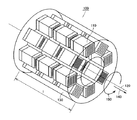
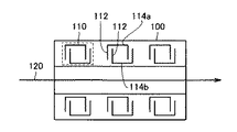
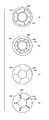
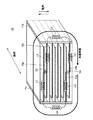
第1の実施の形態に係る帯域除去フィルタ(以下、フィルタ100という)の構成を図1を参照しつつ説明する。図1Aは、フィルタ100の構成を示す図である。
The configuration of the band elimination filter (hereinafter referred to as filter 100) according to the first embodiment will be described with reference to FIG. FIG. 1A is a diagram illustrating a configuration of the
フィルタ100は、積層コンデンサ110を複数含む。積層コンデンサ110は、信号ライン120を軸とする円柱側面上に、放射状に配置されている。積層コンデンサ110は、非磁性体である外装部130によって固定されている。なお、外装部130としては、テフロン(登録商標)等の樹脂材料が適している。外装部130の外側側面にはグランド(図示しない)が配置されていてもよい。
The
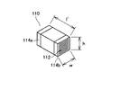
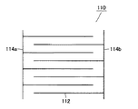
積層コンデンサ110の構成について図1Bおよび図2を用いて説明する。図1Bおよび図2は、それぞれ、積層コンデンサ110の構成を示す図である。図1Bおよび図2に示すように、積層コンデンサ110は、複数の内部電極112と、第1の外部電極114aと、第2の外部電極114bとを含む。内部電極112は、第1の外部電極114aおよび第2の外部電極114bから交互に引き出されている。第1の外部電極114aに接続されている内部電極112と、第2の外部電極114bに接続されている内部電極112とが、電極対を形成する。なお、図1Aおよび図1Bにおいては、理解を容易にするために内部電極を意図的に見えるように描いている。
The configuration of the
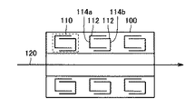
積層コンデンサ110は、図1、および、フィルタ100を信号ライン120を含む面で見た断面図である図3に示すように、内部電極112の電極面が、信号ライン120を流れる電流140により発生する磁力線150と略平行となるように配置されている。すなわち、内部電極112の電極面は、信号ライン120を軸として、信号ライン120を取り囲むように配置されている。また、第1の外部電極114aおよび第2の外部電極114bの電極面は、信号ライン120を流れる電流140により発生する磁力線150と略平行となるように配置されている。すなわち、第1の外部電極114aおよび第2の外部電極114bの電極面は、信号ライン120に直交するように配置されている。これらの外部電極は、信号ライン120やグランドに電気的に接続されていない。
In the
このように配置されているため、積層コンデンサ110は、負の透磁性を示す。すなわち、積層コンデンサ110の構造や配置により定まる共振周波数において、積層コンデンサ110は、負の透磁率を示す。このため、共振周波数の電磁場の伝播が阻害される。
Due to such arrangement, the
この積層コンデンサ110は、信号ライン120に電流140が流れると、該電流が発生する電磁波の特定の周波数成分(共振周波数)を受けて共振を生じる。積層コンデンサ110内での共振によって、積層コンデンサ110の内部に逆向きの磁束が発生し、この発生する磁束によって誘導される電界によって、当該電流が発生する電磁波が妨げられる。この結果、信号ライン120では、積層コンデンサ110における共振周波数成分の交流電流の流れが妨げられる。つまり、フィルタ100は、積層コンデンサ110の共振周波数成分を遮断する帯域遮断フィルタとして機能する。
When a current 140 flows through the
ところで、積層コンデンサ110に負の透磁率を発現させるためには、積層コンデンサ110の信号ライン120中の電流140の伝搬方向における長さl’が、共振周波数における電磁波の波長λに対して、少なくともλ/4より短い必要がある。さらに、積層コンデンサ110の長さl’は、λ/20以下であることが好ましい。
By the way, in order to develop negative magnetic permeability in the
例えば、長さl’=1.6mm、幅W=0.8mm、高さh=0.8mmの積層コンデンサ110を用いることを考える。この場合、λ/4=長さl’とすると、λ=6.4mmとなる。これは、空気中では、周波数fmax=46.875GHzに相当する。したがって、この積層コンデンサ110を、λ/4以下のピッチで並べると、フェライトでは実現できないギガヘルツ帯のメタマテリアルとして機能することが分かる。当然のことながら、適用すべき周波数領域に応じて、共振器の長さlを適宜設計することができる。
For example, consider using a
なお、図1、図2に示したフィルタ100あるいは積層コンデンサ110の構成は、適宜変更することができる。
The configuration of the
例えば、図2では、積層コンデンサ110は8層であるとしているが、層の数はこれに限られない。ただし、共振回路の形成のため、少なくとも2つの電極対は必要である。
For example, in FIG. 2, the
また、積層コンデンサ110の個数も図1に示したものに限られるわけではない。例えば、図1では、信号ライン120を中心に放射状に配置された積層コンデンサ群が3段にわたり配置されている例を示したが、この段数は適宜変更可能である。段数を増やすことによって減衰を大きくすることができる。このことは図6からも分かる。図6は、数種類のコンデンサの容量あるいは段数に対する、周波数と比透磁率との関係を示した図である。比透磁率とは、真空の透磁率に対する、透磁率の比を表わす。47pFの積層コンデンサを3段形成した場合よりも、5段形成したときのほうが比透磁率の変化が大きいことが分かる。また、図1では各積層コンデンサ群は、8つの積層コンデンサ110からなるとしたが、この個数も変更可能である。
The number of
さらに、積層コンデンサの容量を変更することで共振周波数を変更することができる。実際、図6に示すように、47pF、68pF、100pFの積層コンデンサ110に対する共振周波数は、異なる。
Furthermore, the resonance frequency can be changed by changing the capacitance of the multilayer capacitor. In fact, as shown in FIG. 6, the resonant frequencies for the 47 pF, 68 pF, and 100
さらに、積層コンデンサ110の信号ライン120に対する配置の仕方は、図3のものに限られるわけではない。例えば、図4のように配置してもよい。図4は、積層コンデンサ110の他の配置例を説明するための図である。図4は、図3と同様に、フィルタ100を、信号ライン120を含む面で見た断面図である。つまり、内部電極112の電極面を、信号ライン120と略直交する方向に配置し、第1の外部電極114aおよび第2の外部電極114bの電極面を、信号ライン120と平行な方向に配置してもよい。
Further, the arrangement of the
上述の説明では、内部電極112、ならびに第1の外部電極114aおよび第2の外部電極114bの各電極面が、信号ライン120を流れる電流によって発生する磁界の磁力線に対して平行となるように配置されることで、メタマテリアルとしての機能である負の透磁率を発現させることができることについて述べた。ただし、磁力線に対して、実質的に平行となるように配置されることでも、負の透磁率は発現する。ここで、「実質的に平行」とは、各電極面が磁界の磁力線と直交する状態を除外する意味であり、各電極面が磁界の磁力線とまったく平行である状態以外にも、磁力線に対して所定角度をもつ状態をも含む。実用上は、フィルタ100で発現する負の透磁率の大きさが適用アプリケーションなどの要求を満足できる値であれば、「実質的に平行」とみなすことができる。
In the above description, the electrode surfaces of the
実質的に平行な配置でも負の透磁率が発現することについて図5を用いて説明する。図5は、この発明の実施の形態1に従う積層コンデンサ110で生じる比透磁率の周波数特性を積層コンデンサ10の配向別にシミュレーションした結果を示す図である。
It will be described with reference to FIG. 5 that a negative magnetic permeability is exhibited even in a substantially parallel arrangement. FIG. 5 is a diagram showing a result of simulating frequency characteristics of relative permeability generated in
図5を参照して、配置(a)および配置(b)は、それぞれ図3、図4に示した配置に対応し、内部電極112、ならびに第1の外部電極114aおよび第2の外部電極114bの各電極面が磁界の磁力線に対して平行に配置された場合を示す。また、配置(c)は、内部電極112の各電極面が磁界の磁力線に対して45°の角度をもって配置された場合を示す。配置(d)は、第1の外部電極114aおよび第2の外部電極114bの各電極面が磁界の磁力線に対して直交するように配置された場合を示し、配置(e)は、内部電極112の各電極面が磁界の磁力線に対して直交するように配置された場合を示す。
Referring to FIG. 5, the arrangement (a) and the arrangement (b) correspond to the arrangements shown in FIGS. 3 and 4, respectively, and the
配置(a)および配置(b)では、共振周波数に僅かな違いがあるものの、比透磁率の周波数特性が示すように、十分に大きな負の透磁率が発現していることがわかる。また、配置(c)では、負の透磁率が発現しているものの、その大きさは配置(a)や配置(b)において発現する負の透磁率の大きさに比較して小さくなっていることがわかる。 In the arrangement (a) and the arrangement (b), although there is a slight difference in the resonance frequency, it can be seen that a sufficiently large negative permeability is exhibited as shown by the frequency characteristics of the relative permeability. Moreover, although the negative magnetic permeability is expressed in the arrangement (c), the magnitude thereof is smaller than the magnitude of the negative magnetic permeability expressed in the arrangement (a) and the arrangement (b). I understand that.
一方、配置(d)および配置(e)では、比透磁率の周波数特性が示すように、共振も生じておらず、負の透磁率も発現していない。 On the other hand, in the arrangement (d) and the arrangement (e), as shown by the frequency characteristics of the relative magnetic permeability, no resonance occurs and no negative magnetic permeability is exhibited.
以上のように、内部電極112、ならびに第1の外部電極114aおよび第2の外部電極114bのうち、いずれかの電極面が磁界の磁力線に対して直交して配置される場合には、負の透磁率が発現しないが、それ以外の配置であれば、各電極面が磁界の磁力線に対してまったくの平行でなくとも、負の透磁率が発現することが分かる。つまり、内部電極112で挟まれた空間を磁場が通過する配置であれば、積層コンデンサ110は、負の透磁率を発現することが分かる。
As described above, when any electrode surface of the
以上説明してきたフィルタ100は、共振周波数におけるメタマテリアルの透磁率が負であり、共振周波数の電磁波は、メタマテリアル中を伝播しないという現象を利用したものである。ここで、本実施の形態に従う積層コンデンサ110は、外部電源などからの電気エネルギーを必要とせず、電流140に伴って放射される電磁波(特に磁束)だけで共振を生じる、パッシブなデバイスである。そして、積層コンデンサ110は、このような共振を生じさせることによって、負の透磁率を発現させる。そのため、積層コンデンサ110は、伝送線路とGNDとの間で電気的に浮いていてよい。よって、フィルタ100は、伝送線路や周囲のGNDに接続させることなく、伝送線路を囲うように配置するだけで、フィルタ機能を発揮する。
The
また、例えば、貫通コンデンサを用いる場合は、伝送線路と周囲のGNDとの間に容量を持たせて、ノイズを伝送線路からGNDに落とすため、コンデンサは伝送線路とGNDの間に正しく配置されている必要があるが、本発明に係るフィルタは、伝送線路やGNDとの間の容量の有無に関わらず、フィルタとして機能する。したがって、挿入精度は必要ないため、後付けとしての利用が可能になる。減衰を調整するための増設も容易である。 For example, when a feedthrough capacitor is used, a capacitor is provided between the transmission line and GND so that a capacitance is provided between the transmission line and the surrounding GND so that noise is dropped from the transmission line to GND. However, the filter according to the present invention functions as a filter regardless of the presence or absence of capacitance between the transmission line and GND. Therefore, since insertion accuracy is not required, it can be used as a retrofit. Expansion to adjust the attenuation is easy.
以上では、積層コンデンサを用いたメタマテリアルフィルタについて説明してきたが、積層コンデンサはメタマテリアルの一例である。例えば、積層コンデンサ110のかわりに、負の透磁率を発現するように配置したスプリットリング共振器型を用いることもできる。
Although the metamaterial filter using the multilayer capacitor has been described above, the multilayer capacitor is an example of a metamaterial. For example, instead of the
[第2の実施の形態]
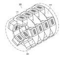
第2の実施の形態に係る帯域除去フィルタ(以下、フィルタ200という)の構成を図7を参照しつつ説明する。図7は、フィルタ200の構成を示す図である。[Second Embodiment]
Band-elimination filter according to the second embodiment (hereinafter, referred to as filter 200) will be described with reference to FIG. 7 the structure of. FIG. 7 is a diagram illustrating the configuration of the
フィルタ200は、複数の積層コンデンサ110がその上に固定されたドーナツ状の平板210を複数有する。このような積層コンデンサ110は、例えば、接着剤により平板210に固定される。平板210は、樹脂基板等で作成される。さらに、フィルタ200は、平板210を保持するための筒220を備えるものとする。ただし、筒220は必須ではない。
The
ここでは、積層コンデンサ110の信号ライン120に対する配置は、図4に示した配置であるとした。ただし、第1の実施の形態で説明したように、配置の仕方はこれに限られるものではない。
Here, the arrangement of the
フィルタ200の積層コンデンサ110の周囲の領域のうち平板210以外の部分は空気であるので、フィルタ200全体の誘電率は、第1の実施の形態に係るフィルタ100と比べると、小さい。
Since the portion other than the
この実施の形態に係るフィルタ200のサイズは、複数の積層コンデンサ110と、平板210とからなるユニットの枚数を増減することで、容易に変更することができる。したがって、コネクタの挿入可能な奥行きに応じたサイズ変更が可能である。また、ユニット枚数の増減により、容易に減衰量を調整することができる。
The size of the
[第3の実施の形態]
第3の実施の形態に係る帯域除去フィルタ(以下、フィルタ300という)の構成を図8および図9を参照しつつ説明する。[Third Embodiment]
A configuration of a band elimination filter (hereinafter referred to as filter 300) according to the third embodiment will be described with reference to FIGS.
図8は、フィルタ300の斜視図である。図8に示すように、フィルタ300は、3つの基材310からなる。ただし、基材310の個数はこれに限られるわけではない。基材310には、第1の電極320と、第2の電極330とが埋め込まれている。また、第1の電極320と第2の電極330は、樹脂基板中に形成されたビア340および導体板350により電気的に接続されている。
FIG. 8 is a perspective view of the
図9は、フィルタ300の断面図である。図9(a)〜(d)はそれぞれ、第1の電極320が存在する面、第2の電極330が存在する面、第2の電極330と導体板350との間の面、導体板350が存在する面での断面図である。
FIG. 9 is a cross-sectional view of the
基材310は、セラミック多層基板や樹脂基板に通常のプリント基板工法を施すことで作れる。したがって、本実施の形態に係るフィルタ300は、安価に製造できる。
The
また、本形態によれば、ドーナツ状や扇形の電極が形成できるので、四角柱の共振器を並べるよりも空間を有効に使える。したがって、フィルタ効果を高めることができる。 In addition, according to this embodiment, since a donut-shaped or fan-shaped electrode can be formed, a space can be used more effectively than arranging square column resonators. Therefore, the filter effect can be enhanced.
なお、ここでは、基材310として1対の電極のみが形成されている単板ユニットを利用する例を示した。この構成によれば、第2の実施の形態のように、必要な個数のユニットを用いることで、サイズの変更、減衰量の調整が容易になる。ただし、複数対の電極が形成された基材310を用いてもよい。
Here, an example in which a single plate unit in which only one pair of electrodes is formed as the
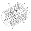
[第4の実施の形態]
第4の実施の形態に係る帯域除去フィルタ(以下、フィルタ400という)の構成を図10、図11、図12を参照しつつ説明する。[Fourth Embodiment]
The configuration of a band elimination filter (hereinafter referred to as filter 400) according to the fourth embodiment will be described with reference to FIGS. 10, 11, and 12. FIG.
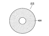
図10は、フィルタ400の斜視図である。図10に示すように、フィルタ400は、互いに径が異なる同心円筒面である複数の円筒型電極が形成された円筒コンデンサ410を複数含む。
FIG. 10 is a perspective view of the
図11は、軸を含む平面を切断面とする円筒コンデンサ410の断面図である。円筒コンデンサ410は、第1の外部電極430aと、第2の外部電極430bと、内部電極420とを含む。内部電極420のうち、図11の外側から奇数番目の内部電極は、第1の外部電極430aに接続され、偶数番目の内部電極は、第2の外部電極430bに接続されている。
FIG. 11 is a cross-sectional view of a
図12は、円筒コンデンサ410の径方向の断面図である。ここでは、円筒コンデンサ410は、7枚の内部電極を有するものとする。ただし、この枚数は特にこれに限られない。
FIG. 12 is a cross-sectional view of the
[第5の実施の形態]
第1の実施の形態から第4の実施の形態で説明した帯域除去フィルタは、いずれも、コネクタに実装することができる。[Fifth Embodiment]
Any of the band elimination filters described in the first to fourth embodiments can be mounted on a connector.
通常、コネクタ、ピン、誘電体で提供され、ユーザーが組み立てるSMAコネクタの場合、ユーザが必要に応じて、既存の誘電体部を、同形状のメタマテリアルフィルタに取り替えるだけで、フィルタ機能を付加する事が可能になる。 In the case of an SMA connector that is usually provided with connectors, pins, and dielectrics and is assembled by the user, a filter function can be added by simply replacing the existing dielectric part with a metamaterial filter of the same shape as required by the user. Things are possible.
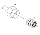
また、Nコネクタ、APC7MMコネクタ、Kコネクタなどのように、誘電体を使わず空気層となっているコネクタの場合、コネクタ部にメタマテリアルフィルタを内蔵するだけで、フィルタ機能を持たせる事ができる。例えば、第1の実施の形態に係るフィルタ100を、図13に示すようにコネクタ1300に挿入し、コネクタ1300内にシリコン樹脂等で固定することで、帯域除去機能付きコネクタを製作することができる。
In addition, in the case of a connector that is an air layer without using a dielectric material, such as an N connector, an APC7MM connector, or a K connector, a filter function can be provided only by incorporating a metamaterial filter in the connector portion. . For example, by inserting the
コネクタには、N型コネクタから形態の基板に使われる超小型コネクタまで様々あるが、各実施の形態で説明したような積層コンデンサなどを用いるのであれば、かなりの小型コネクタに対応できる。 There are various types of connectors, from N-type connectors to ultra-small connectors used for the substrate of the form, but if a multilayer capacitor as described in each embodiment is used, a considerably small connector can be handled.
今回開示された実施の形態はすべての点で例示であって制限的なものではないと考えられるべきである。本発明の範囲は上記した説明ではなくて請求の範囲によって示され、請求の範囲と均等の意味および範囲内でのすべての変更が含まれることが意図される。 The embodiment disclosed this time should be considered as illustrative in all points and not restrictive. The scope of the present invention is defined by the terms of the claims, rather than the description above, and is intended to include any modifications within the scope and meaning equivalent to the terms of the claims.
Claims (14)
前記信号ライン(120)を軸として放射状に配置されたメタマテリアル(110)を備え、
前記メタマテリアル(110)は、前記周波数成分における透磁率が負になるように配置されている帯域除去フィルタ。A band elimination filter that removes a specific frequency component of the current flowing through the signal line (120),
Wherein comprising a radially arranged metamaterial (110) signal line (120) as an axis,
The metamaterial (110) is a band elimination filter arranged so that the magnetic permeability in the frequency component is negative.
各々が絶縁物を介して互いに対向する第1および第2電極からなる複数の電極対(112)と、
前記第1および第2電極を電気的に接続する接続体とを含み、
前記第1および第2電極の各電極面は、前記電流によって形成される磁力線に対して実質的に平行となるように配置されている、請求の範囲第1項に記載の帯域除去フィルタ。The metamaterial (110) is
A plurality of electrode pairs, each consisting of first and second electrodes facing each other through an insulator (112),
A connection body for electrically connecting the first and second electrodes,
2. The band elimination filter according to claim 1, wherein the electrode surfaces of the first and second electrodes are arranged so as to be substantially parallel to the magnetic field lines formed by the current.
前記2つの外部電極(114a,114b)の各電極面は、前記電流によって形成される磁力線に対し実質的に平行となるように配置されている、請求の範囲第3項に記載の帯域除去フィルタ。The connector consists of two external electrodes formed in parallel to face (114a, 114b),
The band elimination filter according to claim 3, wherein each electrode surface of the two external electrodes (114a, 114b) is disposed so as to be substantially parallel to a magnetic force line formed by the current. .
絶縁物を介して互いに平行に配置された複数の平板電極(112)と、
前記複数の平板電極の偶数番目の平板電極と電気的に接続された第1接続電極(114a)と、
前記複数の平板電極の奇数番目の平板電極と電気的に接続された第2接続電極(114b)とを含み、
前記第1および第2接続電極(114a,114b)の各電極面は、前記複数の平板電極(112)の電極面に対して垂直に形成され、
前記複数の平板電極(112)の各電極面は、前記電流によって形成される磁力線に対して実質的に平行となるように配置されている、請求の範囲第1項に記載の帯域除去フィルタ。The metamaterial (110) is
A plurality of plate electrodes (112) arranged in parallel with each other through an insulator;
A first connection electrode (114a) electrically connected to the even-numbered plate electrodes of the plurality of plate electrodes;
A second connection electrode (114b) electrically connected to odd-numbered plate electrodes of the plurality of plate electrodes;
The electrode surfaces of the first and second connection electrodes (114a, 114b) are formed perpendicular to the electrode surfaces of the plurality of plate electrodes (112),
2. The band elimination filter according to claim 1, wherein each electrode surface of the plurality of flat plate electrodes (112) is disposed so as to be substantially parallel to a magnetic force line formed by the current.
前記メタマテリアル(110)は前記ドーナツ板(210)上に固定されている、請求の範囲第5項に記載の帯域除去フィルタ。Further comprising donut erected perpendicular to the signal line (120) to (210),
The band elimination filter according to claim 5, wherein the metamaterial (110) is fixed on the donut plate (210).
各々が互いに平行する複数の電極面を有する第1くし型電極(114a,112)および第2くし型電極(114b,112)を含み、
前記第1くし型電極(114a,112)の最上層の電極面と前記第2くし型電極(114b,112)の最上層の電極面とが所定の間隔をもって平行に対向するように形成され、かつ、前記第1くし型電極(114a,112)の最下層の電極面と前記第2くし型電極(114b,112)の最下層の電極面とが所定の間隔をもって平行に対向するように形成され、
前記第1くし型電極(114a,112)および第2くし型電極(114b,112)の各電極面は、前記電流によって形成される磁力線に対して実質的に平行となるように配置されている、請求の範囲第1項に記載の帯域除去フィルタ。The metamaterial (110) is
A first comb electrode (114a, 112) and a second comb electrode (114b, 112) each having a plurality of electrode surfaces parallel to each other;
The uppermost electrode surface of the first comb electrode (114a, 112) and the uppermost electrode surface of the second comb electrode (114b, 112) are formed to face each other in parallel with a predetermined interval, In addition, the lowermost electrode surface of the first comb electrode (114a, 112) and the lowermost electrode surface of the second comb electrode (114b, 112) are formed to face each other in parallel with a predetermined interval. And
The electrode surfaces of the first comb electrode (114a, 112) and the second comb electrode (114b, 112) are arranged so as to be substantially parallel to the lines of magnetic force formed by the current. The band elimination filter according to claim 1.
前記メタマテリアル(110)は前記ドーナツ板(210)上に固定されている、請求の範囲第7項に記載の帯域除去フィルタ。A donut plate (210) erected perpendicular to the signal line (120);
The band elimination filter according to claim 7, wherein the metamaterial (110) is fixed on the donut plate (210).
前記信号ライン(120)を軸とし、互いに径が異なる円筒面である複数の円筒型電極(420)と、
前記複数の円筒型電極(420)の偶数番目の円筒型電極と電気的に接続された第1接続電極(430a)と、
前記複数の円筒型電極(420)の奇数番目の円筒型電極と電気的に接続された第2接続電極(430b)とを含む、請求の範囲第1項に記載の帯域除去フィルタ。The metamaterial (110) is
A plurality of cylindrical electrodes (420) having cylindrical surfaces with different diameters around the signal line (120);
A first connection electrode (430a) electrically connected to an even-numbered cylindrical electrode of the plurality of cylindrical electrodes (420);
The band elimination filter according to claim 1, comprising a second connection electrode (430b) electrically connected to an odd-numbered cylindrical electrode of the plurality of cylindrical electrodes (420).
前記基材(310)には、
各々が絶縁物を介して互いに対向する第1および第2電極(310,320)と、
前記第1および第2電極(310,320)を電気的に接続する接続体(340,350)とが形成されている、請求の範囲第1項に記載の帯域除去フィルタ。The metamaterial (110) is composed of a plurality of substrates (310),
The substrate (310) includes
First and second electrodes (310, 320) each facing each other through an insulator;
The band elimination filter according to claim 1, wherein a connection body (340, 350) for electrically connecting the first and second electrodes (310, 320) is formed.
前記信号ライン(120)を軸として放射状に配置されたメタマテリアル(110)を備え、
前記メタマテリアル(110)は、
複数の第1電極(112)と、
前記複数の第1電極(112)のそれぞれに対向する複数の第2電極(112)と、
前記複数の第1電極(112)と前記複数の第2電極(112)とをそれぞれ電気的に接続する接続体(114a,114b)を含み、
各前記第1電極(112)および各前記第2電極(112)の電極面は、前記信号ライン(120)を軸として前記信号ライン(120)を取り囲むように配置されている、帯域除去フィルタ。A band elimination filter that removes a specific frequency component of the current flowing through the signal line (120),
Comprising metamaterials (110) arranged radially about the signal line (120);
The metamaterial (110) is
A plurality of first electrodes (112);
A plurality of second electrodes (112) facing each of the plurality of first electrodes (112);
A connection body (114a, 114b) for electrically connecting the plurality of first electrodes (112) and the plurality of second electrodes (112), respectively;
The band elimination filter, wherein electrode surfaces of the first electrodes (112) and the second electrodes (112) are disposed so as to surround the signal line (120) with the signal line (120) as an axis.
前記信号ライン(120)を軸として放射状に配置されたメタマテリアル(110)を備え、
前記メタマテリアル(110)は、
複数の第1電極(112)と、
前記複数の第1電極(112)のそれぞれに対向する複数の第2電極(112)と、
前記複数の第1電極(112)と前記複数の第2電極(112)とをそれぞれ電気的に接続する接続体(114a,114b)を含み、
各前記第1電極(112)および各前記第2電極(112)の電極面は、前記信号ライン(120)に直交するように配置されている、帯域除去フィルタ。A band elimination filter that removes a specific frequency component of the current flowing through the signal line (120),
Wherein comprising a radially arranged metamaterial (110) signal line (120) as an axis,
The metamaterial (110) is
A plurality of first electrodes (112);
A plurality of second electrodes (112) facing each of the plurality of first electrodes (112);
A connection body (114a, 114b) for electrically connecting the plurality of first electrodes (112) and the plurality of second electrodes (112), respectively;
The band elimination filter, wherein electrode surfaces of the first electrodes (112) and the second electrodes (112) are arranged to be orthogonal to the signal lines (120).
Priority Applications (1)
| Application Number | Priority Date | Filing Date | Title |
|---|---|---|---|
| JP2009546986A JP5218428B2 (en) | 2007-12-21 | 2008-11-10 | Band elimination filter and connector with band elimination filter |
Applications Claiming Priority (4)
| Application Number | Priority Date | Filing Date | Title |
|---|---|---|---|
| JP2007330513 | 2007-12-21 | ||
| JP2007330513 | 2007-12-21 | ||
| PCT/JP2008/070409 WO2009081663A1 (en) | 2007-12-21 | 2008-11-10 | Band elimination filter and connector provided with band elimination filter |
| JP2009546986A JP5218428B2 (en) | 2007-12-21 | 2008-11-10 | Band elimination filter and connector with band elimination filter |
Publications (2)
| Publication Number | Publication Date |
|---|---|
| JPWO2009081663A1 true JPWO2009081663A1 (en) | 2011-05-06 |
| JP5218428B2 JP5218428B2 (en) | 2013-06-26 |
Family
ID=40800979
Family Applications (1)
| Application Number | Title | Priority Date | Filing Date |
|---|---|---|---|
| JP2009546986A Expired - Fee Related JP5218428B2 (en) | 2007-12-21 | 2008-11-10 | Band elimination filter and connector with band elimination filter |
Country Status (2)
| Country | Link |
|---|---|
| JP (1) | JP5218428B2 (en) |
| WO (1) | WO2009081663A1 (en) |
Cited By (1)
| Publication number | Priority date | Publication date | Assignee | Title |
|---|---|---|---|---|
| US9754730B2 (en) * | 2015-03-13 | 2017-09-05 | Avx Corporation | Low profile multi-anode assembly in cylindrical housing |
Families Citing this family (4)
| Publication number | Priority date | Publication date | Assignee | Title |
|---|---|---|---|---|
| JP5218551B2 (en) * | 2008-04-18 | 2013-06-26 | 株式会社村田製作所 | Functional board |
| WO2010100801A1 (en) * | 2009-03-02 | 2010-09-10 | 株式会社村田製作所 | Electric device and partial structure of electric circuit |
| JP5482915B2 (en) * | 2011-02-10 | 2014-05-07 | 株式会社村田製作所 | Metamaterial, electrical device, and electrical device with metamaterial |
| JP2019033216A (en) * | 2017-08-09 | 2019-02-28 | 株式会社Soken | Film capacitor and manufacturing method thereof |
Family Cites Families (4)
| Publication number | Priority date | Publication date | Assignee | Title |
|---|---|---|---|---|
| US4424551B1 (en) * | 1982-01-25 | 1991-06-11 | Highly-reliable feed through/filter capacitor and method for making same | |
| KR100495871B1 (en) * | 1999-04-23 | 2005-06-16 | 익스팬테크주식회사 | Lead-through type filter with built-in square shape elements |
| JP4669744B2 (en) * | 2005-06-20 | 2011-04-13 | 独立行政法人理化学研究所 | OPTICAL MATERIAL, OPTICAL ELEMENT USING SAME, AND MANUFACTURING METHOD THEREOF |
| JP4535995B2 (en) * | 2005-12-05 | 2010-09-01 | 日本電気株式会社 | Via structure of multilayer printed circuit board and bandstop filter having the same |
-
2008
- 2008-11-10 WO PCT/JP2008/070409 patent/WO2009081663A1/en active Application Filing
- 2008-11-10 JP JP2009546986A patent/JP5218428B2/en not_active Expired - Fee Related
Cited By (1)
| Publication number | Priority date | Publication date | Assignee | Title |
|---|---|---|---|---|
| US9754730B2 (en) * | 2015-03-13 | 2017-09-05 | Avx Corporation | Low profile multi-anode assembly in cylindrical housing |
Also Published As
| Publication number | Publication date |
|---|---|
| WO2009081663A1 (en) | 2009-07-02 |
| JP5218428B2 (en) | 2013-06-26 |
Similar Documents
| Publication | Publication Date | Title |
|---|---|---|
| JP5440504B2 (en) | Metamaterial | |
| JP5287862B2 (en) | Metamaterial | |
| US8222975B2 (en) | Transmission line resonator, high-frequency filter using the same, high-frequency module, and radio device | |
| JP5218428B2 (en) | Band elimination filter and connector with band elimination filter | |
| WO2014171266A1 (en) | Inductor element, inductor bridge and high-frequency filter | |
| JP2008236027A (en) | Common mode current suppression ebg filter | |
| JP5961813B2 (en) | Common mode noise filter | |
| JP5104879B2 (en) | RESONATOR AND SUBSTRATE EQUIPPED WITH THE SAME, AND METHOD FOR GENERATING RESONANCE | |
| JP2015534760A (en) | Electromagnetic absorber | |
| US8576027B2 (en) | Differential-common mode resonant filters | |
| JP5218551B2 (en) | Functional board | |
| JP2008271204A (en) | Laminated electronic component | |
| JP2009088329A (en) | Coil component | |
| JP2017225086A (en) | Dielectric filter | |
| JP2008167157A (en) | High-pass filter | |
| ES2396773A1 (en) | Device comprising differential transmission lines with common-mode suppression | |
| JP4505440B2 (en) | Multilayer high-pass filter | |
| WO2003100800A1 (en) | Decoupling module for decoupling high-frequency signals from a power supply line | |
| JP2007227490A (en) | Lamination coil component | |
| JP5304883B2 (en) | Partial structure of electric parts and electric circuits | |
| WO2015129598A1 (en) | Laminated coil element and wireless communication module | |
| JP2007116554A (en) | Noise filter array | |
| JPWO2019082231A1 (en) | Polarization control board | |
| JP2012010150A (en) | Electric component, electric circuit board, impedance matching method, and partial structure of electric circuit | |
| KR20050080797A (en) | Multilayered lc filter array |
Legal Events
| Date | Code | Title | Description |
|---|---|---|---|
| A131 | Notification of reasons for refusal |
Free format text: JAPANESE INTERMEDIATE CODE: A131 Effective date: 20120821 |
|
| A521 | Written amendment |
Free format text: JAPANESE INTERMEDIATE CODE: A523 Effective date: 20121005 |
|
| A131 | Notification of reasons for refusal |
Free format text: JAPANESE INTERMEDIATE CODE: A131 Effective date: 20121106 |
|
| A521 | Written amendment |
Free format text: JAPANESE INTERMEDIATE CODE: A523 Effective date: 20130104 |
|
| TRDD | Decision of grant or rejection written | ||
| A01 | Written decision to grant a patent or to grant a registration (utility model) |
Free format text: JAPANESE INTERMEDIATE CODE: A01 Effective date: 20130205 |
|
| A61 | First payment of annual fees (during grant procedure) |
Free format text: JAPANESE INTERMEDIATE CODE: A61 Effective date: 20130218 |
|
| FPAY | Renewal fee payment (event date is renewal date of database) |
Free format text: PAYMENT UNTIL: 20160315 Year of fee payment: 3 |
|
| R150 | Certificate of patent or registration of utility model |
Ref document number: 5218428 Country of ref document: JP Free format text: JAPANESE INTERMEDIATE CODE: R150 Free format text: JAPANESE INTERMEDIATE CODE: R150 |
|
| LAPS | Cancellation because of no payment of annual fees |