JP7679136B2 - 収納容器、処理システム及びベースプレート - Google Patents
収納容器、処理システム及びベースプレート Download PDFInfo
- Publication number
- JP7679136B2 JP7679136B2 JP2021014289A JP2021014289A JP7679136B2 JP 7679136 B2 JP7679136 B2 JP 7679136B2 JP 2021014289 A JP2021014289 A JP 2021014289A JP 2021014289 A JP2021014289 A JP 2021014289A JP 7679136 B2 JP7679136 B2 JP 7679136B2
- Authority
- JP
- Japan
- Prior art keywords
- edge ring
- annular member
- ring
- base plate
- control unit
- Prior art date
- Legal status (The legal status is an assumption and is not a legal conclusion. Google has not performed a legal analysis and makes no representation as to the accuracy of the status listed.)
- Active
Links
Images


Classifications
-
- C—CHEMISTRY; METALLURGY
- C23—COATING METALLIC MATERIAL; COATING MATERIAL WITH METALLIC MATERIAL; CHEMICAL SURFACE TREATMENT; DIFFUSION TREATMENT OF METALLIC MATERIAL; COATING BY VACUUM EVAPORATION, BY SPUTTERING, BY ION IMPLANTATION OR BY CHEMICAL VAPOUR DEPOSITION, IN GENERAL; INHIBITING CORROSION OF METALLIC MATERIAL OR INCRUSTATION IN GENERAL
- C23C—COATING METALLIC MATERIAL; COATING MATERIAL WITH METALLIC MATERIAL; SURFACE TREATMENT OF METALLIC MATERIAL BY DIFFUSION INTO THE SURFACE, BY CHEMICAL CONVERSION OR SUBSTITUTION; COATING BY VACUUM EVAPORATION, BY SPUTTERING, BY ION IMPLANTATION OR BY CHEMICAL VAPOUR DEPOSITION, IN GENERAL
- C23C16/00—Chemical coating by decomposition of gaseous compounds, without leaving reaction products of surface material in the coating, i.e. chemical vapour deposition [CVD] processes
- C23C16/44—Chemical coating by decomposition of gaseous compounds, without leaving reaction products of surface material in the coating, i.e. chemical vapour deposition [CVD] processes characterised by the method of coating
- C23C16/54—Apparatus specially adapted for continuous coating
-
- H—ELECTRICITY
- H01—ELECTRIC ELEMENTS
- H01J—ELECTRIC DISCHARGE TUBES OR DISCHARGE LAMPS
- H01J37/00—Discharge tubes with provision for introducing objects or material to be exposed to the discharge, e.g. for the purpose of examination or processing thereof
- H01J37/32—Gas-filled discharge tubes
- H01J37/32431—Constructional details of the reactor
- H01J37/32733—Means for moving the material to be treated
-
- C—CHEMISTRY; METALLURGY
- C23—COATING METALLIC MATERIAL; COATING MATERIAL WITH METALLIC MATERIAL; CHEMICAL SURFACE TREATMENT; DIFFUSION TREATMENT OF METALLIC MATERIAL; COATING BY VACUUM EVAPORATION, BY SPUTTERING, BY ION IMPLANTATION OR BY CHEMICAL VAPOUR DEPOSITION, IN GENERAL; INHIBITING CORROSION OF METALLIC MATERIAL OR INCRUSTATION IN GENERAL
- C23C—COATING METALLIC MATERIAL; COATING MATERIAL WITH METALLIC MATERIAL; SURFACE TREATMENT OF METALLIC MATERIAL BY DIFFUSION INTO THE SURFACE, BY CHEMICAL CONVERSION OR SUBSTITUTION; COATING BY VACUUM EVAPORATION, BY SPUTTERING, BY ION IMPLANTATION OR BY CHEMICAL VAPOUR DEPOSITION, IN GENERAL
- C23C16/00—Chemical coating by decomposition of gaseous compounds, without leaving reaction products of surface material in the coating, i.e. chemical vapour deposition [CVD] processes
- C23C16/44—Chemical coating by decomposition of gaseous compounds, without leaving reaction products of surface material in the coating, i.e. chemical vapour deposition [CVD] processes characterised by the method of coating
- C23C16/458—Chemical coating by decomposition of gaseous compounds, without leaving reaction products of surface material in the coating, i.e. chemical vapour deposition [CVD] processes characterised by the method of coating characterised by the method used for supporting substrates in the reaction chamber
- C23C16/4582—Rigid and flat substrates, e.g. plates or discs
- C23C16/4583—Rigid and flat substrates, e.g. plates or discs the substrate being supported substantially horizontally
- C23C16/4585—Devices at or outside the perimeter of the substrate support, e.g. clamping rings, shrouds
-
- C—CHEMISTRY; METALLURGY
- C23—COATING METALLIC MATERIAL; COATING MATERIAL WITH METALLIC MATERIAL; CHEMICAL SURFACE TREATMENT; DIFFUSION TREATMENT OF METALLIC MATERIAL; COATING BY VACUUM EVAPORATION, BY SPUTTERING, BY ION IMPLANTATION OR BY CHEMICAL VAPOUR DEPOSITION, IN GENERAL; INHIBITING CORROSION OF METALLIC MATERIAL OR INCRUSTATION IN GENERAL
- C23C—COATING METALLIC MATERIAL; COATING MATERIAL WITH METALLIC MATERIAL; SURFACE TREATMENT OF METALLIC MATERIAL BY DIFFUSION INTO THE SURFACE, BY CHEMICAL CONVERSION OR SUBSTITUTION; COATING BY VACUUM EVAPORATION, BY SPUTTERING, BY ION IMPLANTATION OR BY CHEMICAL VAPOUR DEPOSITION, IN GENERAL
- C23C16/00—Chemical coating by decomposition of gaseous compounds, without leaving reaction products of surface material in the coating, i.e. chemical vapour deposition [CVD] processes
- C23C16/44—Chemical coating by decomposition of gaseous compounds, without leaving reaction products of surface material in the coating, i.e. chemical vapour deposition [CVD] processes characterised by the method of coating
- C23C16/50—Chemical coating by decomposition of gaseous compounds, without leaving reaction products of surface material in the coating, i.e. chemical vapour deposition [CVD] processes characterised by the method of coating using electric discharges
- C23C16/505—Chemical coating by decomposition of gaseous compounds, without leaving reaction products of surface material in the coating, i.e. chemical vapour deposition [CVD] processes characterised by the method of coating using electric discharges using radio frequency discharges
-
- H—ELECTRICITY
- H01—ELECTRIC ELEMENTS
- H01J—ELECTRIC DISCHARGE TUBES OR DISCHARGE LAMPS
- H01J37/00—Discharge tubes with provision for introducing objects or material to be exposed to the discharge, e.g. for the purpose of examination or processing thereof
- H01J37/32—Gas-filled discharge tubes
- H01J37/32431—Constructional details of the reactor
- H01J37/32623—Mechanical discharge control means
- H01J37/32642—Focus rings
-
- H—ELECTRICITY
- H01—ELECTRIC ELEMENTS
- H01J—ELECTRIC DISCHARGE TUBES OR DISCHARGE LAMPS
- H01J37/00—Discharge tubes with provision for introducing objects or material to be exposed to the discharge, e.g. for the purpose of examination or processing thereof
- H01J37/32—Gas-filled discharge tubes
- H01J37/32431—Constructional details of the reactor
- H01J37/32715—Workpiece holder
-
- H—ELECTRICITY
- H01—ELECTRIC ELEMENTS
- H01J—ELECTRIC DISCHARGE TUBES OR DISCHARGE LAMPS
- H01J37/00—Discharge tubes with provision for introducing objects or material to be exposed to the discharge, e.g. for the purpose of examination or processing thereof
- H01J37/32—Gas-filled discharge tubes
- H01J37/32431—Constructional details of the reactor
- H01J37/32733—Means for moving the material to be treated
- H01J37/32743—Means for moving the material to be treated for introducing the material into processing chamber
-
- H—ELECTRICITY
- H01—ELECTRIC ELEMENTS
- H01J—ELECTRIC DISCHARGE TUBES OR DISCHARGE LAMPS
- H01J37/00—Discharge tubes with provision for introducing objects or material to be exposed to the discharge, e.g. for the purpose of examination or processing thereof
- H01J37/32—Gas-filled discharge tubes
- H01J37/32431—Constructional details of the reactor
- H01J37/32798—Further details of plasma apparatus not provided for in groups H01J37/3244 - H01J37/32788; special provisions for cleaning or maintenance of the apparatus
- H01J37/32807—Construction (includes replacing parts of the apparatus)
-
- H—ELECTRICITY
- H01—ELECTRIC ELEMENTS
- H01L—SEMICONDUCTOR DEVICES NOT COVERED BY CLASS H10
- H01L21/00—Processes or apparatus adapted for the manufacture or treatment of semiconductor or solid state devices or of parts thereof
- H01L21/67—Apparatus specially adapted for handling semiconductor or electric solid state devices during manufacture or treatment thereof; Apparatus specially adapted for handling wafers during manufacture or treatment of semiconductor or electric solid state devices or components ; Apparatus not specifically provided for elsewhere
- H01L21/67005—Apparatus not specifically provided for elsewhere
- H01L21/67011—Apparatus for manufacture or treatment
- H01L21/67155—Apparatus for manufacturing or treating in a plurality of work-stations
- H01L21/67184—Apparatus for manufacturing or treating in a plurality of work-stations characterized by the presence of more than one transfer chamber
-
- H—ELECTRICITY
- H01—ELECTRIC ELEMENTS
- H01L—SEMICONDUCTOR DEVICES NOT COVERED BY CLASS H10
- H01L21/00—Processes or apparatus adapted for the manufacture or treatment of semiconductor or solid state devices or of parts thereof
- H01L21/67—Apparatus specially adapted for handling semiconductor or electric solid state devices during manufacture or treatment thereof; Apparatus specially adapted for handling wafers during manufacture or treatment of semiconductor or electric solid state devices or components ; Apparatus not specifically provided for elsewhere
- H01L21/673—Apparatus specially adapted for handling semiconductor or electric solid state devices during manufacture or treatment thereof; Apparatus specially adapted for handling wafers during manufacture or treatment of semiconductor or electric solid state devices or components ; Apparatus not specifically provided for elsewhere using specially adapted carriers or holders; Fixing the workpieces on such carriers or holders
- H01L21/67346—Apparatus specially adapted for handling semiconductor or electric solid state devices during manufacture or treatment thereof; Apparatus specially adapted for handling wafers during manufacture or treatment of semiconductor or electric solid state devices or components ; Apparatus not specifically provided for elsewhere using specially adapted carriers or holders; Fixing the workpieces on such carriers or holders characterized by being specially adapted for supporting a single substrate or by comprising a stack of such individual supports
-
- H—ELECTRICITY
- H01—ELECTRIC ELEMENTS
- H01L—SEMICONDUCTOR DEVICES NOT COVERED BY CLASS H10
- H01L21/00—Processes or apparatus adapted for the manufacture or treatment of semiconductor or solid state devices or of parts thereof
- H01L21/67—Apparatus specially adapted for handling semiconductor or electric solid state devices during manufacture or treatment thereof; Apparatus specially adapted for handling wafers during manufacture or treatment of semiconductor or electric solid state devices or components ; Apparatus not specifically provided for elsewhere
- H01L21/677—Apparatus specially adapted for handling semiconductor or electric solid state devices during manufacture or treatment thereof; Apparatus specially adapted for handling wafers during manufacture or treatment of semiconductor or electric solid state devices or components ; Apparatus not specifically provided for elsewhere for conveying, e.g. between different workstations
- H01L21/67739—Apparatus specially adapted for handling semiconductor or electric solid state devices during manufacture or treatment thereof; Apparatus specially adapted for handling wafers during manufacture or treatment of semiconductor or electric solid state devices or components ; Apparatus not specifically provided for elsewhere for conveying, e.g. between different workstations into and out of processing chamber
- H01L21/67748—Apparatus specially adapted for handling semiconductor or electric solid state devices during manufacture or treatment thereof; Apparatus specially adapted for handling wafers during manufacture or treatment of semiconductor or electric solid state devices or components ; Apparatus not specifically provided for elsewhere for conveying, e.g. between different workstations into and out of processing chamber horizontal transfer of a single workpiece
-
- H—ELECTRICITY
- H01—ELECTRIC ELEMENTS
- H01L—SEMICONDUCTOR DEVICES NOT COVERED BY CLASS H10
- H01L21/00—Processes or apparatus adapted for the manufacture or treatment of semiconductor or solid state devices or of parts thereof
- H01L21/67—Apparatus specially adapted for handling semiconductor or electric solid state devices during manufacture or treatment thereof; Apparatus specially adapted for handling wafers during manufacture or treatment of semiconductor or electric solid state devices or components ; Apparatus not specifically provided for elsewhere
- H01L21/677—Apparatus specially adapted for handling semiconductor or electric solid state devices during manufacture or treatment thereof; Apparatus specially adapted for handling wafers during manufacture or treatment of semiconductor or electric solid state devices or components ; Apparatus not specifically provided for elsewhere for conveying, e.g. between different workstations
- H01L21/67763—Apparatus specially adapted for handling semiconductor or electric solid state devices during manufacture or treatment thereof; Apparatus specially adapted for handling wafers during manufacture or treatment of semiconductor or electric solid state devices or components ; Apparatus not specifically provided for elsewhere for conveying, e.g. between different workstations the wafers being stored in a carrier, involving loading and unloading
- H01L21/67766—Mechanical parts of transfer devices
-
- H—ELECTRICITY
- H01—ELECTRIC ELEMENTS
- H01L—SEMICONDUCTOR DEVICES NOT COVERED BY CLASS H10
- H01L21/00—Processes or apparatus adapted for the manufacture or treatment of semiconductor or solid state devices or of parts thereof
- H01L21/67—Apparatus specially adapted for handling semiconductor or electric solid state devices during manufacture or treatment thereof; Apparatus specially adapted for handling wafers during manufacture or treatment of semiconductor or electric solid state devices or components ; Apparatus not specifically provided for elsewhere
- H01L21/677—Apparatus specially adapted for handling semiconductor or electric solid state devices during manufacture or treatment thereof; Apparatus specially adapted for handling wafers during manufacture or treatment of semiconductor or electric solid state devices or components ; Apparatus not specifically provided for elsewhere for conveying, e.g. between different workstations
- H01L21/67763—Apparatus specially adapted for handling semiconductor or electric solid state devices during manufacture or treatment thereof; Apparatus specially adapted for handling wafers during manufacture or treatment of semiconductor or electric solid state devices or components ; Apparatus not specifically provided for elsewhere for conveying, e.g. between different workstations the wafers being stored in a carrier, involving loading and unloading
- H01L21/67769—Storage means
-
- H—ELECTRICITY
- H01—ELECTRIC ELEMENTS
- H01L—SEMICONDUCTOR DEVICES NOT COVERED BY CLASS H10
- H01L21/00—Processes or apparatus adapted for the manufacture or treatment of semiconductor or solid state devices or of parts thereof
- H01L21/67—Apparatus specially adapted for handling semiconductor or electric solid state devices during manufacture or treatment thereof; Apparatus specially adapted for handling wafers during manufacture or treatment of semiconductor or electric solid state devices or components ; Apparatus not specifically provided for elsewhere
- H01L21/68—Apparatus specially adapted for handling semiconductor or electric solid state devices during manufacture or treatment thereof; Apparatus specially adapted for handling wafers during manufacture or treatment of semiconductor or electric solid state devices or components ; Apparatus not specifically provided for elsewhere for positioning, orientation or alignment
-
- H—ELECTRICITY
- H01—ELECTRIC ELEMENTS
- H01L—SEMICONDUCTOR DEVICES NOT COVERED BY CLASS H10
- H01L21/00—Processes or apparatus adapted for the manufacture or treatment of semiconductor or solid state devices or of parts thereof
- H01L21/67—Apparatus specially adapted for handling semiconductor or electric solid state devices during manufacture or treatment thereof; Apparatus specially adapted for handling wafers during manufacture or treatment of semiconductor or electric solid state devices or components ; Apparatus not specifically provided for elsewhere
- H01L21/683—Apparatus specially adapted for handling semiconductor or electric solid state devices during manufacture or treatment thereof; Apparatus specially adapted for handling wafers during manufacture or treatment of semiconductor or electric solid state devices or components ; Apparatus not specifically provided for elsewhere for supporting or gripping
- H01L21/6831—Apparatus specially adapted for handling semiconductor or electric solid state devices during manufacture or treatment thereof; Apparatus specially adapted for handling wafers during manufacture or treatment of semiconductor or electric solid state devices or components ; Apparatus not specifically provided for elsewhere for supporting or gripping using electrostatic chucks
- H01L21/6833—Details of electrostatic chucks
-
- H—ELECTRICITY
- H01—ELECTRIC ELEMENTS
- H01L—SEMICONDUCTOR DEVICES NOT COVERED BY CLASS H10
- H01L21/00—Processes or apparatus adapted for the manufacture or treatment of semiconductor or solid state devices or of parts thereof
- H01L21/67—Apparatus specially adapted for handling semiconductor or electric solid state devices during manufacture or treatment thereof; Apparatus specially adapted for handling wafers during manufacture or treatment of semiconductor or electric solid state devices or components ; Apparatus not specifically provided for elsewhere
- H01L21/683—Apparatus specially adapted for handling semiconductor or electric solid state devices during manufacture or treatment thereof; Apparatus specially adapted for handling wafers during manufacture or treatment of semiconductor or electric solid state devices or components ; Apparatus not specifically provided for elsewhere for supporting or gripping
- H01L21/687—Apparatus specially adapted for handling semiconductor or electric solid state devices during manufacture or treatment thereof; Apparatus specially adapted for handling wafers during manufacture or treatment of semiconductor or electric solid state devices or components ; Apparatus not specifically provided for elsewhere for supporting or gripping using mechanical means, e.g. chucks, clamps or pinches
- H01L21/68707—Apparatus specially adapted for handling semiconductor or electric solid state devices during manufacture or treatment thereof; Apparatus specially adapted for handling wafers during manufacture or treatment of semiconductor or electric solid state devices or components ; Apparatus not specifically provided for elsewhere for supporting or gripping using mechanical means, e.g. chucks, clamps or pinches the wafers being placed on a robot blade, or gripped by a gripper for conveyance
-
- H—ELECTRICITY
- H01—ELECTRIC ELEMENTS
- H01L—SEMICONDUCTOR DEVICES NOT COVERED BY CLASS H10
- H01L21/00—Processes or apparatus adapted for the manufacture or treatment of semiconductor or solid state devices or of parts thereof
- H01L21/67—Apparatus specially adapted for handling semiconductor or electric solid state devices during manufacture or treatment thereof; Apparatus specially adapted for handling wafers during manufacture or treatment of semiconductor or electric solid state devices or components ; Apparatus not specifically provided for elsewhere
- H01L21/683—Apparatus specially adapted for handling semiconductor or electric solid state devices during manufacture or treatment thereof; Apparatus specially adapted for handling wafers during manufacture or treatment of semiconductor or electric solid state devices or components ; Apparatus not specifically provided for elsewhere for supporting or gripping
- H01L21/687—Apparatus specially adapted for handling semiconductor or electric solid state devices during manufacture or treatment thereof; Apparatus specially adapted for handling wafers during manufacture or treatment of semiconductor or electric solid state devices or components ; Apparatus not specifically provided for elsewhere for supporting or gripping using mechanical means, e.g. chucks, clamps or pinches
- H01L21/68714—Apparatus specially adapted for handling semiconductor or electric solid state devices during manufacture or treatment thereof; Apparatus specially adapted for handling wafers during manufacture or treatment of semiconductor or electric solid state devices or components ; Apparatus not specifically provided for elsewhere for supporting or gripping using mechanical means, e.g. chucks, clamps or pinches the wafers being placed on a susceptor, stage or support
- H01L21/68735—Apparatus specially adapted for handling semiconductor or electric solid state devices during manufacture or treatment thereof; Apparatus specially adapted for handling wafers during manufacture or treatment of semiconductor or electric solid state devices or components ; Apparatus not specifically provided for elsewhere for supporting or gripping using mechanical means, e.g. chucks, clamps or pinches the wafers being placed on a susceptor, stage or support characterised by edge profile or support profile
-
- H—ELECTRICITY
- H01—ELECTRIC ELEMENTS
- H01L—SEMICONDUCTOR DEVICES NOT COVERED BY CLASS H10
- H01L21/00—Processes or apparatus adapted for the manufacture or treatment of semiconductor or solid state devices or of parts thereof
- H01L21/67—Apparatus specially adapted for handling semiconductor or electric solid state devices during manufacture or treatment thereof; Apparatus specially adapted for handling wafers during manufacture or treatment of semiconductor or electric solid state devices or components ; Apparatus not specifically provided for elsewhere
- H01L21/683—Apparatus specially adapted for handling semiconductor or electric solid state devices during manufacture or treatment thereof; Apparatus specially adapted for handling wafers during manufacture or treatment of semiconductor or electric solid state devices or components ; Apparatus not specifically provided for elsewhere for supporting or gripping
- H01L21/687—Apparatus specially adapted for handling semiconductor or electric solid state devices during manufacture or treatment thereof; Apparatus specially adapted for handling wafers during manufacture or treatment of semiconductor or electric solid state devices or components ; Apparatus not specifically provided for elsewhere for supporting or gripping using mechanical means, e.g. chucks, clamps or pinches
- H01L21/68714—Apparatus specially adapted for handling semiconductor or electric solid state devices during manufacture or treatment thereof; Apparatus specially adapted for handling wafers during manufacture or treatment of semiconductor or electric solid state devices or components ; Apparatus not specifically provided for elsewhere for supporting or gripping using mechanical means, e.g. chucks, clamps or pinches the wafers being placed on a susceptor, stage or support
- H01L21/68742—Apparatus specially adapted for handling semiconductor or electric solid state devices during manufacture or treatment thereof; Apparatus specially adapted for handling wafers during manufacture or treatment of semiconductor or electric solid state devices or components ; Apparatus not specifically provided for elsewhere for supporting or gripping using mechanical means, e.g. chucks, clamps or pinches the wafers being placed on a susceptor, stage or support characterised by a lifting arrangement, e.g. lift pins
Landscapes
- Engineering & Computer Science (AREA)
- Physics & Mathematics (AREA)
- Chemical & Material Sciences (AREA)
- Condensed Matter Physics & Semiconductors (AREA)
- General Physics & Mathematics (AREA)
- Manufacturing & Machinery (AREA)
- Computer Hardware Design (AREA)
- Microelectronics & Electronic Packaging (AREA)
- Power Engineering (AREA)
- Plasma & Fusion (AREA)
- Analytical Chemistry (AREA)
- General Chemical & Material Sciences (AREA)
- Chemical Kinetics & Catalysis (AREA)
- Materials Engineering (AREA)
- Mechanical Engineering (AREA)
- Metallurgy (AREA)
- Organic Chemistry (AREA)
- Robotics (AREA)
- Container, Conveyance, Adherence, Positioning, Of Wafer (AREA)
- Drying Of Semiconductors (AREA)
- Packaging For Recording Disks (AREA)
- Packaging Of Annular Or Rod-Shaped Articles, Wearing Apparel, Cassettes, Or The Like (AREA)
Description
図1を参照し、実施形態の処理システムの一例について説明する。図1に示されるように、処理システムPSは、基板にプラズマ処理等の各種処理を施すことが可能なシステムである。基板は、例えば半導体ウエハであってよい。
図2を参照し、図1の処理システムPSが備えるプロセスモジュールPM1~PM12として用いられるプラズマ処理装置の一例について説明する。
図3及び図4を参照し、図1の処理システムPSが備える収納モジュールSMの一例について説明する。
図5~図8を参照し、搬送ロボットTR2の上フォークFK21について説明する。なお、搬送ロボットTR2の下フォークFK22についても、上フォークFK21と同じ構成であってよい。また、搬送ロボットTR1の上フォークFK11及び下フォークFK12についても、搬送ロボットTR2の上フォークFK21と同じ構成であってよい。
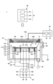
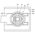
図9を更に参照し、収納モジュールSMが有するカセット78の一例として、エッジリングFRを収納するカセット78について説明する。図9は、収納モジュールSM内のカセット78の一例を示す概略斜視図である。なお、図9では、エッジリングFRが収納されていない状態のカセット78を示す。
図17及び図18を参照し、実施形態の処理システムPSにおける消耗部材の搬送方法の一例として、制御部CUが搬送ロボットTR2にエッジリングFR及びカバーリングCRを同時に搬送させる同時搬送モードを選択して実行する場合を説明する。以下では、制御部90が制御部CUに含まれており、制御部CUが搬送ロボットTR2及び昇降機構50を制御するものとして説明する。ただし、制御部90が制御部CUとは別に設けられ、制御部CUが搬送ロボットTR2を制御し、制御部90が昇降機構50を制御するようにしてもよい。なお、エッジリングFRの外周部とカバーリングCRの内周部とは平面視で重複する構成を有するものとする。
図22を参照し、実施形態の消耗部材の交換方法の一例について説明する。図22は、実施形態の消耗部材の交換方法の一例を示すフローチャートである。
11 基板支持部
112 静電チャック
113 リングアセンブリ
50 昇降機構
78 カセット
781 ベースプレート
782 ガイドピン
CR カバーリング
CRa 切欠き
CU 制御部
FR エッジリング
FRa 切欠き
PS 処理システム
TM1,TM2 真空搬送モジュール
TR1,TR2 搬送ロボット
W 基板
Claims (12)
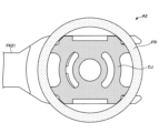
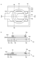
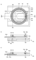
- 環状部材を収納する容器であって、
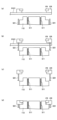
前記環状部材を載置するベースプレートを有し、
前記ベースプレートは、
前記環状部材を載置する載置面と、
前記載置面から突出する複数のガイドピンであり、前記環状部材を位置決めする複数のガイドピンと、
前記載置面の外周部において上方に突出する外枠部であり、該外枠部の上面に別のペースプレートの下面が分離可能に載置される該外枠部と、
を有する、
収納容器。 - 前記ベースプレートは、多段に設けられている、
請求項1に記載の収納容器。 - 前記ベースプレートは、
前記載置面に対して窪んでおり、前記環状部材を搬送する搬送ロボットのフォークが挿入されるフォーク挿入溝を含む、
請求項1又は2に記載の収納容器。 - 前記複数のガイドピンは、先端が先細りの円錐状を有する、
請求項1乃至3のいずれか一項に記載の収納容器。 - 前記環状部材は、外周に切欠きを有し、
前記複数のガイドピンの少なくとも1つは、前記環状部材の前記外周に接触することにより該環状部材を位置決めする、
請求項1乃至4のいずれか一項に記載の収納容器。 - 前記環状部材は、内周に切欠きを有し、
前記複数のガイドピンの少なくとも1つは、前記環状部材の前記内周に接触することにより該環状部材を位置決めする、
請求項1乃至5のいずれか一項に記載の収納容器。 - 前記環状部材は、プラズマ処理の際に基板の周囲に配置される部材である、
請求項1乃至6のいずれか一項に記載の収納容器。 - 前記環状部材は、周方向に互いに離間した複数の切欠きを有し、
前記複数のガイドピンは、前記複数の切欠きのそれぞれと係合する複数のピンを含む、
請求項1乃至7のいずれか一項に記載の収納容器。 - 前記環状部材は、外周及び内周の少なくとも一方に切欠きを有し、
前記切欠きは、平面視においてV字形状を有する、
請求項1乃至8のいずれか一項に記載の収納容器。 - 前記環状部材は、外周及び内周の少なくとも一方に切欠きを有し、
前記複数のガイドピンは、前記切欠きに係合するピンを含む、
請求項1乃至9のいずれか一項に記載の収納容器。 - 環状部材を収納する収納容器を含む収納モジュールと、
前記収納モジュールに接続される真空搬送モジュールであり、前記収納容器に前記環状部材を搬送する搬送ロボットを有する真空搬送モジュールと、
を備え、
前記収納容器は、前記環状部材を載置するベースプレートを有し、
前記ベースプレートは、
前記環状部材を載置する載置面と、
前記載置面から突出する複数のガイドピンであり、前記環状部材を位置決めする複数のガイドピンと、
前記載置面の外周部において上方に突出する外枠部であり、該外枠部の上面に別のペースプレートの下面が分離可能に載置される該外枠部と、
を有する、
処理システム。 - 環状部材を収納するベースプレートであって、
前記ベースプレートは、
前記環状部材を載置する載置面と、
前記載置面から突出し、前記環状部材を位置決めする複数のガイドピンと、
前記載置面の外周部において上方に突出する外枠部であり、該外枠部の上面に別のペースプレートの下面が分離可能に載置される該外枠部と、
を有する、
ベースプレート。
Priority Applications (5)
| Application Number | Priority Date | Filing Date | Title |
|---|---|---|---|
| JP2021014289A JP7679136B2 (ja) | 2021-02-01 | 2021-02-01 | 収納容器、処理システム及びベースプレート |
| TW111102022A TW202236493A (zh) | 2021-02-01 | 2022-01-18 | 收納容器及處理系統 |
| CN202210087175.5A CN114843168A (zh) | 2021-02-01 | 2022-01-25 | 收纳容器和处理系统 |
| KR1020220012428A KR20220111197A (ko) | 2021-02-01 | 2022-01-27 | 수납 용기 및 처리 시스템 |
| US17/589,907 US20220243336A1 (en) | 2021-02-01 | 2022-02-01 | Storage container and processing system |
Applications Claiming Priority (1)
| Application Number | Priority Date | Filing Date | Title |
|---|---|---|---|
| JP2021014289A JP7679136B2 (ja) | 2021-02-01 | 2021-02-01 | 収納容器、処理システム及びベースプレート |
Publications (2)
| Publication Number | Publication Date |
|---|---|
| JP2022117671A JP2022117671A (ja) | 2022-08-12 |
| JP7679136B2 true JP7679136B2 (ja) | 2025-05-19 |
Family
ID=82562620
Family Applications (1)
| Application Number | Title | Priority Date | Filing Date |
|---|---|---|---|
| JP2021014289A Active JP7679136B2 (ja) | 2021-02-01 | 2021-02-01 | 収納容器、処理システム及びベースプレート |
Country Status (5)
| Country | Link |
|---|---|
| US (1) | US20220243336A1 (ja) |
| JP (1) | JP7679136B2 (ja) |
| KR (1) | KR20220111197A (ja) |
| CN (1) | CN114843168A (ja) |
| TW (1) | TW202236493A (ja) |
Families Citing this family (5)
| Publication number | Priority date | Publication date | Assignee | Title |
|---|---|---|---|---|
| JP7503951B2 (ja) * | 2020-07-17 | 2024-06-21 | 東京エレクトロン株式会社 | エッチング処理装置、石英部材及びプラズマ処理方法 |
| JPWO2024071020A1 (ja) * | 2022-09-30 | 2024-04-04 | ||
| CN118891709A (zh) * | 2022-09-30 | 2024-11-01 | 东京毅力科创株式会社 | 基片处理系统 |
| WO2024075592A1 (ja) * | 2022-10-07 | 2024-04-11 | 東京エレクトロン株式会社 | 基板処理システム、および搬送方法 |
| WO2025253723A1 (ja) * | 2024-06-06 | 2025-12-11 | 東京エレクトロン株式会社 | 基板処理装置および搬送方法 |
Citations (5)
| Publication number | Priority date | Publication date | Assignee | Title |
|---|---|---|---|---|
| JP2003209153A (ja) | 2002-01-11 | 2003-07-25 | Hitachi Kokusai Electric Inc | 基板処理装置、及び半導体デバイスの製造方法 |
| JP2005340693A (ja) | 2004-05-31 | 2005-12-08 | Nec Kansai Ltd | プラズマエッチング装置 |
| JP2006054429A (ja) | 2004-08-13 | 2006-02-23 | Au Optronics Corp | ガラス基板用カセット |
| JP2015109479A (ja) | 2015-03-02 | 2015-06-11 | 東京エレクトロン株式会社 | エッチング方法、エッチング装置及びリング部材 |
| WO2020247146A1 (en) | 2019-06-06 | 2020-12-10 | Lam Research Corporation | Automated transfer of edge ring requiring rotational alignment |
Family Cites Families (10)
| Publication number | Priority date | Publication date | Assignee | Title |
|---|---|---|---|---|
| US6217663B1 (en) * | 1996-06-21 | 2001-04-17 | Kokusai Electric Co., Ltd. | Substrate processing apparatus and substrate processing method |
| JP4789566B2 (ja) * | 2005-09-30 | 2011-10-12 | ミライアル株式会社 | 薄板保持容器及び薄板保持容器用処理装置 |
| EP2840599B1 (en) * | 2012-04-16 | 2021-03-31 | Rorze Corporation | Accommodating container and wafer stocker using same |
| JP2014007344A (ja) * | 2012-06-26 | 2014-01-16 | Disco Abrasive Syst Ltd | 収容カセット |
| US9144901B2 (en) * | 2012-08-08 | 2015-09-29 | Weibing Yang | Storage device for multilayer substrate |
| JP7134104B2 (ja) | 2019-01-09 | 2022-09-09 | 東京エレクトロン株式会社 | プラズマ処理装置およびプラズマ処理装置の載置台 |
| US11823937B2 (en) * | 2019-08-19 | 2023-11-21 | Applied Materials, Inc. | Calibration of an aligner station of a processing system |
| KR102652834B1 (ko) * | 2020-08-07 | 2024-04-02 | 세메스 주식회사 | 용기 및 기판 처리 장치 |
| KR102523364B1 (ko) * | 2020-10-07 | 2023-04-21 | 세메스 주식회사 | 기판 처리 장치 |
| JP2022103995A (ja) * | 2020-12-28 | 2022-07-08 | 株式会社ディスコ | テープマウンタ |
-
2021
- 2021-02-01 JP JP2021014289A patent/JP7679136B2/ja active Active
-
2022
- 2022-01-18 TW TW111102022A patent/TW202236493A/zh unknown
- 2022-01-25 CN CN202210087175.5A patent/CN114843168A/zh active Pending
- 2022-01-27 KR KR1020220012428A patent/KR20220111197A/ko active Pending
- 2022-02-01 US US17/589,907 patent/US20220243336A1/en not_active Abandoned
Patent Citations (5)
| Publication number | Priority date | Publication date | Assignee | Title |
|---|---|---|---|---|
| JP2003209153A (ja) | 2002-01-11 | 2003-07-25 | Hitachi Kokusai Electric Inc | 基板処理装置、及び半導体デバイスの製造方法 |
| JP2005340693A (ja) | 2004-05-31 | 2005-12-08 | Nec Kansai Ltd | プラズマエッチング装置 |
| JP2006054429A (ja) | 2004-08-13 | 2006-02-23 | Au Optronics Corp | ガラス基板用カセット |
| JP2015109479A (ja) | 2015-03-02 | 2015-06-11 | 東京エレクトロン株式会社 | エッチング方法、エッチング装置及びリング部材 |
| WO2020247146A1 (en) | 2019-06-06 | 2020-12-10 | Lam Research Corporation | Automated transfer of edge ring requiring rotational alignment |
Also Published As
| Publication number | Publication date |
|---|---|
| JP2022117671A (ja) | 2022-08-12 |
| TW202236493A (zh) | 2022-09-16 |
| US20220243336A1 (en) | 2022-08-04 |
| CN114843168A (zh) | 2022-08-02 |
| KR20220111197A (ko) | 2022-08-09 |
Similar Documents
| Publication | Publication Date | Title |
|---|---|---|
| JP7679136B2 (ja) | 収納容器、処理システム及びベースプレート | |
| US12094696B2 (en) | Focus ring replacement method and plasma processing system | |
| JP7293517B2 (ja) | 基板処理システム及び搬送方法 | |
| JP7728062B2 (ja) | 処理システム及び搬送方法 | |
| US12198962B2 (en) | Maintenance device, vacuum processing system, and maintenance method | |
| KR20210027647A (ko) | 기판 처리 장치 및 핸드 위치 티칭 방법 | |
| TWI899346B (zh) | 處理系統及搬運方法 | |
| US20250046585A1 (en) | Substrate processing system and transfer method | |
| US20250232965A1 (en) | Substrate processing system | |
| JP2024108621A (ja) | 基板処理システム、および基板搬送方法 |
Legal Events
| Date | Code | Title | Description |
|---|---|---|---|
| A621 | Written request for application examination |
Free format text: JAPANESE INTERMEDIATE CODE: A621 Effective date: 20231024 |
|
| A977 | Report on retrieval |
Free format text: JAPANESE INTERMEDIATE CODE: A971007 Effective date: 20240830 |
|
| A131 | Notification of reasons for refusal |
Free format text: JAPANESE INTERMEDIATE CODE: A131 Effective date: 20240910 |
|
| A521 | Request for written amendment filed |
Free format text: JAPANESE INTERMEDIATE CODE: A523 Effective date: 20241108 |
|
| TRDD | Decision of grant or rejection written | ||
| A01 | Written decision to grant a patent or to grant a registration (utility model) |
Free format text: JAPANESE INTERMEDIATE CODE: A01 Effective date: 20250304 |
|
| A601 | Written request for extension of time |
Free format text: JAPANESE INTERMEDIATE CODE: A601 Effective date: 20250328 |
|
| A61 | First payment of annual fees (during grant procedure) |
Free format text: JAPANESE INTERMEDIATE CODE: A61 Effective date: 20250501 |
|
| R150 | Certificate of patent or registration of utility model |
Ref document number: 7679136 Country of ref document: JP Free format text: JAPANESE INTERMEDIATE CODE: R150 |