JP7649727B2 - Thermoelectric conversion material, thermoelectric conversion element, and thermoelectric conversion module - Google Patents
Thermoelectric conversion material, thermoelectric conversion element, and thermoelectric conversion module Download PDFInfo
- Publication number
- JP7649727B2 JP7649727B2 JP2021167520A JP2021167520A JP7649727B2 JP 7649727 B2 JP7649727 B2 JP 7649727B2 JP 2021167520 A JP2021167520 A JP 2021167520A JP 2021167520 A JP2021167520 A JP 2021167520A JP 7649727 B2 JP7649727 B2 JP 7649727B2
- Authority
- JP
- Japan
- Prior art keywords
- thermoelectric conversion
- conversion material
- type
- temperature side
- base material
- Prior art date
- Legal status (The legal status is an assumption and is not a legal conclusion. Google has not performed a legal analysis and makes no representation as to the accuracy of the status listed.)
- Active
Links
Images


Landscapes
- Powder Metallurgy (AREA)
- Silicon Compounds (AREA)
Description
本開示は、熱電変換材料、熱電変換素子および熱電変換モジュールに関するものである。 This disclosure relates to thermoelectric conversion materials, thermoelectric conversion elements, and thermoelectric conversion modules.
温度差(熱エネルギー)を電気に変換する熱電変換材料の製造方法が開示されている(例えば、特許文献1参照)。特許文献1によると、二種以上の金属原料を粉砕機に入れた後、該粉砕機内を真空にするか又は不活性ガスで置換する工程と、前記金属原料をその結晶化温度未満に保持しながら粉砕混合して合金粉末を得る工程と、前記合金粉末を加圧成形した後、該合金粉末の結晶化温度未満で熱処理する工程とを具備することを特徴としている。
A method for producing a thermoelectric conversion material that converts a temperature difference (thermal energy) into electricity has been disclosed (see, for example, Patent Document 1). According to
熱電変換材料は、温度差(熱エネルギー)を電気に変換する材料である。単位温度差あたりの発電量に相当するパワーファクター(以下、「PF」と略す場合もある。)は、以下の式(1)で示される。ここで、式(1)中において、Sはゼーベック係数であり、σは導電率である。 Thermoelectric conversion materials are materials that convert temperature differences (thermal energy) into electricity. The power factor (hereinafter sometimes abbreviated as "PF"), which corresponds to the amount of power generated per unit temperature difference, is shown in the following formula (1). In formula (1), S is the Seebeck coefficient, and σ is the electrical conductivity.
PF=S2×σ・・・(1) PF= S2 ×σ...(1)
効率的な熱電変換を行うためには、PFを増加させることが重要である。PFを増加させることができれば、熱電変換の効率を向上させることができる。 In order to perform efficient thermoelectric conversion, it is important to increase the PF. If the PF can be increased, the efficiency of thermoelectric conversion can be improved.
そこで、熱電変換の効率を向上させることができる熱電変換材料を提供することを目的の1つとする。 Therefore, one of our goals is to provide a thermoelectric conversion material that can improve the efficiency of thermoelectric conversion.
本開示に従った熱電変換材料は、半導体であるベース材料と、含有割合が0.01at%以上2.0at%以下である添加元素と、を含む。添加元素は、He、Ne、Ar、KrおよびXeのうちの少なくともいずれか一つを含む。 The thermoelectric conversion material according to the present disclosure includes a base material that is a semiconductor and an additive element whose content is 0.01 at% or more and 2.0 at% or less. The additive element includes at least one of He, Ne, Ar, Kr, and Xe.
上記熱電変換材料によれば、熱電変換の効率を向上させることができる。 The above thermoelectric conversion material can improve the efficiency of thermoelectric conversion.
[本開示の実施形態の説明]
最初に本開示の実施態様を列記して説明する。本開示に係る熱電変換材料は、半導体であるベース材料と、含有割合が0.01at%以上2.0at%以下である添加元素と、を含む。添加元素は、He、Ne、Ar、KrおよびXeのうちの少なくともいずれか一つを含む。
[Description of the embodiments of the present disclosure]
First, the embodiments of the present disclosure will be described. The thermoelectric conversion material according to the present disclosure includes a base material that is a semiconductor and an additive element whose content is 0.01 at% or more and 2.0 at% or less. The additive element includes at least one of He, Ne, Ar, Kr, and Xe.
本願発明者らは、PFを増加させて熱電変換の効率の向上を図ることに着目し、導電率の低下を抑制しながらゼーベック係数の増大を図る必要があると考え、本開示に係る熱電変換材料を構成するに至った。まず本願発明者らは、ゼーベック係数の増大を図るに際し、熱電変換材料を構成するベース材料中に添加元素を格子間原子として入り込ませて点欠陥を生じさせ、この点欠陥が作るポテンシャルの乱れによりエネルギーフィルタリング効果を発生させてゼーベック係数を大きくすればよいと考えた。ここで、点欠陥を生じさせるために用いる添加元素についても本願発明者らは鋭意検討し、半導体であるベース材料を構成する元素と結合や反応をせず、ベース材料の特性を劣化させるおそれが少ないものとして、He、Ne、Ar、KrおよびXeのうちの少なくともいずれか一つを含む添加元素を用いることを考えた。 The present inventors focused on increasing the PF to improve the efficiency of thermoelectric conversion, and considered the need to increase the Seebeck coefficient while suppressing the decrease in electrical conductivity, leading to the construction of the thermoelectric conversion material according to the present disclosure. First, the present inventors considered that in order to increase the Seebeck coefficient, an additive element should be inserted as an interstitial atom into the base material constituting the thermoelectric conversion material to generate point defects, and the potential disturbance created by this point defect should generate an energy filtering effect to increase the Seebeck coefficient. Here, the present inventors also conducted extensive research into the additive element used to generate point defects, and considered using an additive element containing at least one of He, Ne, Ar, Kr, and Xe, which does not bond or react with the elements constituting the base material, which is a semiconductor, and is unlikely to deteriorate the characteristics of the base material.
そして、添加元素の含有割合についても本願発明者らは鋭意検討し、添加元素の含有割合が少なすぎると、ゼーベック係数の十分な増大を図ることができないことに着目した。また、添加元素の含有割合が多すぎると、生じさせた点欠陥による電子の散乱が顕著となり、導電率が低下した結果、逆にPFが低下することを見出した。 The inventors of the present application also conducted extensive research into the content of the additive elements, and found that if the content of the additive elements is too low, the Seebeck coefficient cannot be increased sufficiently. They also found that if the content of the additive elements is too high, the scattering of electrons due to the generated point defects becomes significant, resulting in a decrease in electrical conductivity and, conversely, a decrease in PF.
本開示の熱電変換材料によると、半導体であるベース材料と、含有割合が0.01at%以上2.0at%以下である添加元素と、を含み、添加元素は、He(ヘリウム)、Ne(ネオン)、Ar(アルゴン)、Kr(クリプトン)およびXe(キセノン)のうちの少なくともいずれか一つを含む。このような熱電変換材料によると、導電率の低下を抑制しながら、ゼーベック係数を大きくして、PFを増大させることができる。したがって、このような熱電変換材料は、熱電変換の効率を向上させることができる。 The thermoelectric conversion material disclosed herein includes a base material that is a semiconductor and an additive element whose content is 0.01 at% or more and 2.0 at% or less, and the additive element includes at least one of He (helium), Ne (neon), Ar (argon), Kr (krypton), and Xe (xenon). With such a thermoelectric conversion material, it is possible to increase the Seebeck coefficient and increase the PF while suppressing a decrease in electrical conductivity. Therefore, such a thermoelectric conversion material can improve the efficiency of thermoelectric conversion.
上記熱電変換材料において、ベース材料は、半導体を構成する元素からなるナノ結晶相を含んでもよい。このようにすることにより、より熱電変換の効率を向上させることができる。ナノ結晶相とは、結晶粒界で囲まれた1つの結晶相において、その結晶相を含む最小サイズの球の直径が100nm以下となる結晶相である。 In the above thermoelectric conversion material, the base material may contain a nanocrystalline phase made of elements that constitute a semiconductor. This can further improve the efficiency of thermoelectric conversion. A nanocrystalline phase is a crystal phase in which the diameter of the smallest sphere containing a single crystal phase surrounded by grain boundaries is 100 nm or less.
上記熱電変換材料において、ベース材料は、アモルファス相を含んでもよい。このようにすることにより、より熱電変換の効率を向上させることができる。 In the above thermoelectric conversion material, the base material may contain an amorphous phase. This can further improve the efficiency of thermoelectric conversion.
上記熱電変換材料において、ベース材料は、SiGe系材料を含んでもよい。このようなベース材料は、熱電変換材料に用いる場合に好適である。ここで、SiGe系材料とは、SiGe、およびSiGeにおいてSiおよびGeの少なくとも一方の一部が他の元素、例えばC、Sn等に置き換えられた材料を意味する。 In the above thermoelectric conversion material, the base material may include a SiGe-based material. Such a base material is suitable for use as a thermoelectric conversion material. Here, SiGe-based material means SiGe and a material in which at least one of the Si and Ge in SiGe is partially replaced with another element, such as C or Sn.
上記熱電変換材料において、ベース材料は、ドーパントを含んでもよい。このようにすることにより、フェルミ準位を制御して、結果的に熱電変換の効率を向上させることができる。 In the above thermoelectric conversion material, the base material may contain a dopant. In this way, the Fermi level can be controlled, thereby improving the efficiency of thermoelectric conversion.
上記熱電変換材料において、添加元素の含有割合は、0.03at%以上1.0at%以下であってもよい。添加元素の含有割合としてこの数値範囲を採用すると、エネルギーフィルタリング効果により、ゼーベック係数が特に高い値を示す。したがって、熱電変換の効率を向上させることができる。 In the above thermoelectric conversion material, the content of the additive element may be 0.03 at% or more and 1.0 at% or less. When this numerical range is adopted as the content of the additive element, the Seebeck coefficient shows a particularly high value due to the energy filtering effect. Therefore, the efficiency of thermoelectric conversion can be improved.
本開示の熱電変換素子は、熱電変換材料部と、熱電変換材料部に接触して配置される第1電極と、熱電変換材料部に接触し、第1電極と離れて配置される第2電極と、を備える。熱電変換材料部を構成する材料は、導電型がp型またはn型となるように成分組成が調整された上記本開示の熱電変換材料である。 The thermoelectric conversion element of the present disclosure includes a thermoelectric conversion material portion, a first electrode arranged in contact with the thermoelectric conversion material portion, and a second electrode arranged in contact with the thermoelectric conversion material portion and spaced apart from the first electrode. The material constituting the thermoelectric conversion material portion is the thermoelectric conversion material of the present disclosure, the composition of which is adjusted so that the conductivity type is p-type or n-type.
本開示の熱電変換素子は、熱電変換材料部を構成する材料が、導電型がp型またはn型となるように成分組成が調整された上記熱電変換の効率の向上を図った熱電変換材料である。そのため、本開示の熱電変換素子によれば、熱電変換の効率の向上を図った熱電変換素子を提供することができる。 The thermoelectric conversion element of the present disclosure is a thermoelectric conversion material in which the composition of the material constituting the thermoelectric conversion material portion is adjusted so that the conductivity type is p-type or n-type, thereby improving the efficiency of the thermoelectric conversion. Therefore, the thermoelectric conversion element of the present disclosure can provide a thermoelectric conversion element with improved thermoelectric conversion efficiency.
本開示の熱電変換モジュールは、上記熱電変換素子を複数含む。本開示の熱電変換モジュールによれば、熱電変換の効率の向上を図った本開示の熱電変換素子を複数含むことにより、熱電変換の効率の向上を図った熱電変換モジュールを得ることができる。 The thermoelectric conversion module of the present disclosure includes a plurality of the above-described thermoelectric conversion elements. According to the thermoelectric conversion module of the present disclosure, by including a plurality of the thermoelectric conversion elements of the present disclosure that improve the efficiency of thermoelectric conversion, it is possible to obtain a thermoelectric conversion module that improves the efficiency of thermoelectric conversion.
[本開示の実施形態の詳細]
次に、本開示の熱電変換材料の一実施形態を、図面を参照しつつ説明する。以下の図面において同一または相当する部分には同一の参照符号を付しその説明は繰り返さない。
[Details of the embodiment of the present disclosure]
Next, an embodiment of the thermoelectric conversion material of the present disclosure will be described with reference to the drawings. In the following drawings, the same or corresponding parts are designated by the same reference characters, and the description thereof will not be repeated.
(実施の形態1)
本開示の実施の形態1における熱電変換材料の構成について説明する。図1は、実施の形態1における熱電変換材料の組織の状態を示す概略図である。図1を参照して、本開示の実施の形態1に係る熱電変換材料11は、半導体であるベース材料12を含む。半導体であるベース材料12は、例えば、SiGe系材料から構成されている。本実施形態においては、半導体であるベース材料12は、SiGe(シリコンゲルマニウム)である。ベース材料12は、アモルファス相13と、ナノ結晶相14と、を含む。ナノ結晶相14は、半導体を構成する元素からなる。具体的には、ナノ結晶相14は、SiGeである。ナノ結晶相14は、アモルファス相13中に適度に分散した状態で配置されている。
(Embodiment 1)
The configuration of the thermoelectric conversion material in the first embodiment of the present disclosure will be described. FIG. 1 is a schematic diagram showing the state of the structure of the thermoelectric conversion material in the first embodiment. Referring to FIG. 1, the
熱電変換材料11は、添加元素を含む。図1における添加元素の図示は省略するが、添加元素は、例えば熱電変換材料11中のナノ結晶相14とアモルファス相13との界面付近に存在していると考えられる。添加元素は、He、Ne、Ar、KrおよびXeのうちの少なくともいずれか一つを含む。添加元素は、不活性ガスに属する元素である。本実施形態においては、添加元素は、Arである。
The
添加元素の含有割合は、0.01at%以上2.0at%以下である。ここで、0.1at%よりも多い添加元素の含有割合については、例えば、EDX(Energy Dispersive X-ray spectrometry)により測定することができる。EDXについては、熱電変換材料11の一部のTEM(Transmission Electron Microscope)像を撮影して測定した。TEM像の撮影については、JEM-2800(日本電子株式会社製)を用い、測定条件については、加速電圧を200kV、プローブのサイズを0.5nm、CL絞りを3とした。また、EDXによる原子の検出の条件としては、EDX(サーモフィッシャーサイエンティフィック株式会社製)を用い、測定条件については、スポットサイズを0.5nmとし、CL絞りを3とし、分析モードをマッピングとし、分析時間を20分間とした。また、0.1at%以下の添加元素の含有割合については、例えばSIMS(Secondary Ion Mass Spectromrtry)により測定することができる。具体的な測定方法としては、株式会社アルバック製のADEPT-1010を用い、測定に用いるイオン源は、添加元素Rに対しCsR+イオンとした。例えば、添加元素Arの測定では、セシウムアルゴンイオンCsAr+を用いた。
The content of the added element is 0.01 at% or more and 2.0 at% or less. Here, the content of the added element that is more than 0.1 at% can be measured, for example, by EDX (Energy Dispersive X-ray spectrometry). For EDX, a TEM (Transmission Electron Microscope) image of a part of the
また、熱電変換材料11は、ドーパントを含む。本実施形態においては、熱電変換材料11は、ドーパントとしてのP(リン)を含む。
The
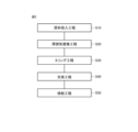
実施の形態1における熱電変換材料11は、例えば、以下の製造方法で製造することができる。図2は、実施の形態1における熱電変換材料11の製造方法の代表的な工程を示すフローチャートである。図2を参照して、実施の形態1における熱電変換材料11の製造方法では、工程(S10)として、原料投入工程が実施される。この工程(S10)では、まず、計量したSi、GeおよびPの粉末を粉砕容器にミリング用のボールと共に投入される。そして、工程(S20)として、雰囲気置換工程が実施される。この工程(S20)では、粉砕容器内の空気をArガスに置換する。この時、Arガスの圧力を大気圧より大きくする。具体的には、例えば、Arガスの圧力を1.5atm以上10.0atm以下とする。このようにArガスの圧力を調整して後のミリング工程を実施することにより、粉末原料中にArを入り込ませることができると考えられる。その後、工程(S30)として、ミリング工程が実施される。この工程(S30)では、粉砕容器に対してミリングを行い、各原料を微粉末にする。この時、微粉末の表面にもArの一部が付着していると考えられる。
The
次に、工程(S40)として、充填工程が実施される。この工程(S40)では、得られた微粉末を準備したダイに充填する。その後、工程(S50)として、焼結工程が実施される。この工程では、ダイに充填した微粉末を加熱して微粉末を焼結させる。本実施形態においては、スパークプラズマ焼結(Spark Plasma Sintering)法により焼結体を形成する。この時の温度は、例えば600℃とすることができる。このようにして、添加元素としてのArが焼結体内に含まれ、アモルファス相中にナノ結晶相が存在する焼結体から構成される熱電変換材料を製造する。 Next, a filling step is carried out as step (S40). In this step (S40), the obtained fine powder is filled into a prepared die. After that, a sintering step is carried out as step (S50). In this step, the fine powder filled into the die is heated to sinter the fine powder. In this embodiment, a sintered body is formed by a spark plasma sintering method. The temperature at this time can be, for example, 600°C. In this way, a thermoelectric conversion material is produced that is composed of a sintered body in which Ar as an additive element is contained in the sintered body and a nanocrystalline phase exists in an amorphous phase.
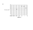
図3は、実施の形態1の熱電変換材料11におけるAr濃度とゼーベック係数との関係を示すグラフである。図3において、横軸は、Ar濃度(at%)を示し、縦軸は、ゼーベック係数(μV/K)を示す。ここで、ゼーベック係数および後述する導電率の測定については、以下のようにして行った。導電率およびゼーベック係数については、熱電特性測定装置(オザワ科学株式会社製RZ2001i)で測定した。測定方法は、以下の通りである。まず、一対の石英治具に熱電変換材料を橋架するよう固定し、雰囲気を抵抗加熱炉で加熱する。石英治具の一方を中空にしておき、その中に窒素ガスを流すことで冷却し、熱電変換材料の一方の端部を冷却する。これにより、熱電変換材料に温度差を付与する。熱電変換材料については、白金-白金ロジウム系熱電対(R熱電対)を用いて、熱電変換材料の表面の2点間の温度差を測定する。熱電対に電圧計を繋げることで、2点間の温度差で発生した電圧を測定する。これにより、温度差に対する発生電圧を測定することが可能となり、これから材料のゼーベック係数を見積もることが可能となる。また、抵抗値は、4端子法で測定する。すなわち、電圧計がつながっている2つの白金線の外側に、2つの電線を接続する。その電線に電流を流し、内側の電圧計で、電圧降下量を測定する。このようにして、4端子法により、熱電変換材料の抵抗値を測定する。測定された抵抗値から導電率を導出する。
3 is a graph showing the relationship between the Ar concentration and the Seebeck coefficient in the
図3を参照して、Arの含有割合が大きくなるほど、すなわちAr濃度が高くなるほどゼーベック係数が高くなっているのが把握できる。なお、Ar濃度が高い領域におけるゼーベック係数の増加の割合は、Ar濃度が低い領域におけるゼーベック係数の増加の割合よりも低いことも把握できる。そして、Ar濃度が0.01at%以上であると、ゼーベック係数が約250μV/Kよりも大きく増加していることが把握できる。また、Ar濃度が1.0at%以上となると、ゼーベック係数がほぼ一定となっていることが把握できる。 Referring to FIG. 3, it can be seen that the Seebeck coefficient increases as the Ar content increases, i.e., as the Ar concentration increases. It can also be seen that the rate of increase in the Seebeck coefficient in regions with high Ar concentration is lower than the rate of increase in the Seebeck coefficient in regions with low Ar concentration. It can also be seen that when the Ar concentration is 0.01 at% or more, the Seebeck coefficient increases by more than about 250 μV/K. It can also be seen that when the Ar concentration is 1.0 at% or more, the Seebeck coefficient becomes almost constant.
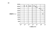
図4は、実施の形態1の熱電変換材料11におけるAr濃度と導電率との関係を示すグラフである。図4において、横軸は、Ar濃度(at%)を示し、縦軸は、導電率(S/m)を示す。導電率の測定については、上述した通りである。
Figure 4 is a graph showing the relationship between the Ar concentration and electrical conductivity in the
図4を参照して、Arの含有割合が比較的低い領域においては、導電率はほぼ一定であるものの、Arの含有割合がある含有割合、具体的には、Ar濃度が0.02at%よりも大きくなるほど、すなわちAr濃度が高くなるほど導電率が低くなっていることが把握できる。そして、Ar濃度が2.0at%よりも大きくなると、導電率が著しく低下し、25000S/mよりも小さくなっていることが把握できる。 Referring to FIG. 4, it can be seen that in regions where the Ar content is relatively low, the electrical conductivity is almost constant, but as the Ar content increases, specifically, the Ar concentration increases above 0.02 at%, the electrical conductivity decreases. It can also be seen that when the Ar concentration increases above 2.0 at%, the electrical conductivity decreases significantly, becoming smaller than 25,000 S/m.
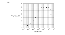
図5は、実施の形態1の熱電変換材料11におけるAr濃度とPFとの関係を示すグラフである。図5において、横軸は、Ar濃度(at%)を示し、縦軸は、PF(μW/cmK2)を示す。PFは、上記した図3および図4に示すグラフの数値を基に算出した数値である。
Fig. 5 is a graph showing the relationship between the Ar concentration and PF in the
図5を参照して、PFについて、Arの含有割合が0.01at%以上2.0at%以下であると、20μW/cmK2以上の高い値を実現することができる。よって、熱電変換の効率の向上を図ることができる。 5, when the content of Ar in PF is 0.01 at% or more and 2.0 at% or less, a high value of 20 μW/cmK2 or more can be realized. Therefore, the efficiency of thermoelectric conversion can be improved.
以上より、このような熱電変換材料11によると、導電率の低下を抑制しながら、ゼーベック係数を大きくして、PFを増大させることができる。したがって、このような熱電変換材料11は、熱電変換の効率を向上させることができる。
As described above, such a
なお、上記熱電変換材料11において、添加元素の含有割合は、0.03at%以上1.0at%以下であってもよい。添加元素の含有割合としてこの数値範囲を採用すると、エネルギーフィルタリング効果により、ゼーベック係数が特に高い値を示す。したがって、熱電変換の効率を向上させることができる。
In addition, in the
本実施の形態においては、ベース材料12は、半導体を構成する元素からなるナノ結晶相14を含む。よって、より熱電変換の効率を向上させることができる。ベース材料12がナノ結晶相14を含むことによる熱電変換の効率の向上については、例えば、以下のように考えられる。すなわち、半導体を構成する元素からなるナノ結晶相14を含むことにより、上記添加元素がナノ結晶相14の結晶粒界において高濃度となる。そうすると、上記添加元素においてナノスケールの分布を生じさせやすくなり、より大きなエネルギーフィルタリング効果を得ることができると考えられる。
In this embodiment, the
また、本実施の形態においては、ベース材料12は、アモルファス相13を含む。よって、より熱電変換の効率を向上させることができる。ベース材料12がアモルファス相13を含むことによる熱電変換の効率の向上については、以下のように考えられる。すなわち、ベース材料12がアモルファス相13を含むことにより、上記添加元素の点欠陥によるポテンシャルの局所的な乱れが大きくなり、より大きなエネルギーフィルタリング効果を得ることができると考えられる。
In addition, in this embodiment, the
本実施の形態において、ベース材料12は、SiGe系材料を含む。このようなベース材料12は、熱電変換材料に用いる場合に好適である。
In this embodiment, the
本実施の形態において、ベース材料12は、ドーパントとしてのPを含む。よって、フェルミ準位を制御して、結果的に熱電変換の効率を向上させることができる。なお、ドーパントとして用いる元素として他にAs(ヒ素)、Sb(アンチモン)、N(窒素)、B(ホウ素)、Al(アルミニウム)およびGa(ガリウム)が挙げられる。ドーパントは、P、As、Sb、N、B、AlおよびGaのうちの少なくともいずれか一つを含んでもよい。ドーパントは、求められる熱電変換材料の特性やベース材料を構成する元素に応じて適当なものが選択される。なお、本開示の熱電変換材料11において、ドーパントを含まない構成としてもよい。
In this embodiment, the
なお、上記の実施の形態において、熱電変換材料11の製造方法におけるS50の焼結行程では、スパークプラズマ焼結に限らず、例えば、ホットプレスにより焼結行程を実施することにしてもよい。また、上記の実施の形態において、S20における雰囲気置換工程では、ArガスとN2ガスとを混合した混合ガスを用いて雰囲気を置換することにしてもよい。この場合、混合ガスにおける分圧を制御して、Arガスの圧力を調整することにしてもよい。また、上記の実施の形態において、添加元素としてArを用いることとしたが、これに限らず、添加元素は、He、Ne、Ar、KrおよびXeのうちの少なくともいずれか一つを含むよう構成してもよい。
In the above embodiment, the sintering step S50 in the manufacturing method of the
(実施の形態2)
次に、他の実施の形態である実施の形態2について説明する。実施の形態2の熱電変換材料において、ベース材料は、SiGeであり、ドーパントは、Pである。すなわち、ベース材料およびドーパントは、実施の形態1の熱電変換材料と同じである。そして、実施の形態1の熱電変換材料と異なり、実施の形態2の熱電変換材料においては、添加元素としてKrを採用している。
(Embodiment 2)
Next, another embodiment, embodiment 2, will be described. In the thermoelectric conversion material of embodiment 2, the base material is SiGe and the dopant is P. That is, the base material and the dopant are the same as those of the thermoelectric conversion material of
図6は、実施の形態2の熱電変換材料におけるKr濃度とPFとの関係を示すグラフである。図6において、横軸は、Kr濃度(at%)を示し、縦軸は、PF(μW/cmK2)を示す。 Fig. 6 is a graph showing the relationship between the Kr concentration and PF in the thermoelectric conversion material of embodiment 2. In Fig. 6, the horizontal axis shows the Kr concentration (at %), and the vertical axis shows the PF (µW/cmK 2 ).
図6を参照して、PFについて、Krの含有割合が0.023at%のとき、PFの値は、27μW/cmK2であり、大きな値を示している。また、PFについて、Krの含有割合が1.0at%のとき、PFの値は、30μW/cmK2であり、大きな値を示している。実施の形態2の熱電変換材料において、PFについて、Krの含有割合が0.01at%以上2.0at%以下であると、高い値を実現していることが把握できる。よって、熱電変換の効率の向上を図ることができる。 6, when the content of Kr in PF is 0.023 at%, the value of PF is 27 μW/ cmK2 , which is a large value. When the content of Kr in PF is 1.0 at%, the value of PF is 30 μW/ cmK2 , which is a large value. In the thermoelectric conversion material of the second embodiment, it can be seen that when the content of Kr in PF is 0.01 at% or more and 2.0 at% or less, a high value is realized. Therefore, it is possible to improve the efficiency of thermoelectric conversion.
(実施の形態3)
次に、さらに他の実施の形態である実施の形態3について説明する。実施の形態3の熱電変換材料において、ベース材料は、Cu2Seであり、ドーパントは、含まれていない。すなわち、ベース材料は、実施の形態1の熱電変換材料と異なっている。そして、実施の形態1の熱電変換材料と異なり、実施の形態3の熱電変換材料においては、ドーパントを含まない構成である。実施の形態3の熱電変換材料は、添加元素として実施の形態1の熱電変換材料の場合と同様、Arを採用している。なお、本実施形態において、ベース材料については、Cu2Se系材料であってもよい。Cu2Se系材料とは、Cu2Se、およびCu2SeにおいてCu(銅)およびSe(セレン)の少なくとも一方の一部が他の元素に置き換えられた材料を意味する。
(Embodiment 3)
Next, a third embodiment, which is yet another embodiment, will be described. In the thermoelectric conversion material of the third embodiment, the base material is Cu 2 Se and does not contain a dopant. That is, the base material is different from the thermoelectric conversion material of the first embodiment. And, unlike the thermoelectric conversion material of the first embodiment, the thermoelectric conversion material of the third embodiment does not contain a dopant. The thermoelectric conversion material of the third embodiment employs Ar as an additive element, as in the case of the thermoelectric conversion material of the first embodiment. In this embodiment, the base material may be a Cu 2 Se-based material. The Cu 2 Se-based material means Cu 2 Se and a material in which at least one of Cu (copper) and Se (selenium) in Cu 2 Se is partially replaced with another element.
図7は、実施の形態3の熱電変換材料におけるAr濃度とPFとの関係を示すグラフである。図7において、横軸は、Ar濃度(at%)を示し、縦軸は、PF(μW/cmK2)を示す。 Fig. 7 is a graph showing the relationship between the Ar concentration and PF in the thermoelectric conversion material of embodiment 3. In Fig. 7, the horizontal axis shows the Ar concentration (at %), and the vertical axis shows the PF (μW/cmK 2 ).
図7を参照して、PFについて、Arの含有割合が0.08at%のとき、PFの値は、140μW/cmK2であり、大きな値を示している。また、PFについて、Arの含有割合が0.6at%のとき、PFの値は、136μW/cmK2であり、大きな値を示している。実施の形態3の熱電変換材料において、PFについて、Arの含有割合が0.01at%以上2.0at%以下であると、高い値を実現していることが把握できる。よって、熱電変換の効率の向上を図ることができる。 7, when the content of Ar in PF is 0.08 at%, the value of PF is 140 μW/ cmK2 , which is a large value. When the content of Ar in PF is 0.6 at%, the value of PF is 136 μW/ cmK2 , which is a large value. In the thermoelectric conversion material of the third embodiment, it can be seen that when the content of Ar in PF is 0.01 at% or more and 2.0 at% or less, a high value is realized. Therefore, it is possible to improve the efficiency of thermoelectric conversion.
(実施の形態4)
次に、実施の形態1における熱電変換材料11を用いた熱電変換素子の一実施形態として、発電素子について説明する。
(Embodiment 4)
Next, a power generating element will be described as one embodiment of a thermoelectric conversion element using the
図8は、実施の形態1に係る熱電材料素子の構造を示す概略断面図である。なお、理解を容易にする観点から、図8において断面を示すハッチングを一部省略している。
Figure 8 is a schematic cross-sectional view showing the structure of a thermoelectric material element according to
図8を参照して、π型の熱電変換素子21は、p型の熱電変換材料部22と、n型の熱電変換材料部23と、高温側電極24と、第1の低温側電極25と、第2の低温側電極26と、配線27とを備えている。高温側電極24は、熱電変換材料部22,23に接触して配置される第1電極である。第1の低温側電極25は、熱電変換材料部22に接触し、高温側電極24と離れて配置される第2電極である。第2の低温側電極26は、熱電変換材料部23に接触し、高温側電極24と離れて配置される第2電極である。
Referring to FIG. 8, the π-type
p型の熱電変換材料部22を構成する材料は、例えば導電型がp型となるように成分組成が調整された実施の形態1の熱電変換材料である。n型の熱電変換材料部23を構成する材料は、例えば導電型がn型となるように成分組成が調整された実施の形態1の熱電変換材料である。
The material constituting the p-type thermoelectric
p型の熱電変換材料部22とn型の熱電変換材料部23とは、間隔をおいて並べて配置される。高温側電極24は、p型の熱電変換材料部22の一方の端部31からn型の熱電変換材料部23の一方の端部32にまで延在するように配置される。高温側電極24は、p型の熱電変換材料部22の一方の端部31およびn型の熱電変換材料部23の一方の端部32の両方に接触するように配置される。高温側電極24は、p型の熱電変換材料部22の一方の端部31とn型の熱電変換材料部23の一方の端部32とを接続するように配置される。高温側電極24は、導電材料、例えば金属からなっている。高温側電極24は、p型の熱電変換材料部22およびn型の熱電変換材料部23にオーミック接触している。
The p-type thermoelectric
熱電変換材料部22もしくは熱電変換材料部23はp型あるいはn型であることが望ましいが、どちらかが金属導線としても良い。
It is preferable that the thermoelectric
第1の低温側電極25は、p型の熱電変換材料部22の他方の端部33に接触して配置される。第1の低温側電極25は、高温側電極24と離れて配置される。第1の低温側電極25は、導電材料、例えば金属からなっている。第1の低温側電極25は、p型の熱電変換材料部22にオーミック接触している。
The first low-
第2の低温側電極26は、n型の熱電変換材料部23の他方の端部34に接触して配置される。第2の低温側電極26は、高温側電極24および第1の低温側電極25と離れて配置される。第2の低温側電極26は、導電材料、例えば金属からなっている。第2の低温側電極26は、n型の熱電変換材料部23にオーミック接触している。
The second low-
配線27は、金属などの導電体からなる。配線27は、第1の低温側電極25と第2の低温側電極26とを電気的に接続する。
The
π型の熱電変換素子21において、例えばp型の熱電変換材料部22の一方の端部31およびn型の熱電変換材料部23の一方の端部32の側が高温、p型の熱電変換材料部22の他方の端部33およびn型の熱電変換材料部23の他方の端部34の側が低温、となるように温度差が形成されると、p型の熱電変換材料部22においては、一方の端部31側から他方の端部33側に向けてp型キャリア(正孔)が移動する。このとき、n型の熱電変換材料部23においては、一方の端部32側から他方の端部34側に向けてn型キャリア(電子)が移動する。その結果、配線27には、矢印Iの向きに電流が流れる。このようにして、π型の熱電変換素子21において、温度差を利用した熱電変換による発電が達成される。すなわち、π型の熱電変換素子21は発電素子である。
In the π-type
そして、p型の熱電変換材料部22およびn型の熱電変換材料部23を構成する材料として、実施の形態1の熱電変換材料11が採用される。その結果、π型の熱電変換素子21は高効率な発電素子となっている。
The
上記実施の形態においては、本開示の熱電変換素子の一例としてπ型熱電変換素子について説明したが、本開示の熱電変換素子はこれに限られない。本開示の熱電変換素子は、例えばI型(ユニレグ型)熱電変換素子など、他の構造を有する熱電変換素子であってもよい。 In the above embodiment, a π-type thermoelectric conversion element has been described as an example of a thermoelectric conversion element of the present disclosure, but the thermoelectric conversion element of the present disclosure is not limited to this. The thermoelectric conversion element of the present disclosure may be a thermoelectric conversion element having another structure, such as an I-type (uni-leg type) thermoelectric conversion element.
また、上記の実施の形態においては、p型の熱電変換材料部22およびn型の熱電変換材料部23を構成する材料として、実施の形態1の熱電変換材料11が採用されることとしたが、これに限らない。すなわち、p型の熱電変換材料部22およびn型の熱電変換材料部23を構成する材料として、実施の形態2の熱電変換材料を採用してもよいし、実施の形態3の熱電変換材料を採用してもよい。なお、p型の熱電変換材料部22を構成する材料とn型の熱電変換材料部23を構成する材料を異なる材料としてもよい。
In addition, in the above embodiment, the
(実施の形態5)
π型の上記熱電変換素子21を複数個電気的に接続することにより、熱電変換モジュールとしての発電モジュールを得ることができる。本実施の形態の熱電変換モジュールである発電モジュール41は、π型の熱電変換素子21が直列に複数個接続された構造を有する。
(Embodiment 5)
A power generation module serving as a thermoelectric conversion module can be obtained by electrically connecting a plurality of the π-type
図9は、発電モジュールの構造の一例を示す図である。図9を参照して、本実施の形態の発電モジュール41は、複数のp型の熱電変換材料部22と、複数のn型の熱電変換材料部23と、第1の低温側電極25および第2の低温側電極26に対応する低温側電極25、26と、高温側電極24と、低温側絶縁体基板28と、高温側絶縁体基板29とを備える。低温側絶縁体基板28および高温側絶縁体基板29は、アルミナなどのセラミックからなる。p型の熱電変換材料部22とn型の熱電変換材料部23とは、交互に並べて配置される。低温側電極25、26は、上述のπ型の熱電変換素子21と同様にp型の熱電変換材料部22およびn型の熱電変換材料部23に接触して配置される。高温側電極24は、上述のπ型の熱電変換素子21と同様にp型の熱電変換材料部22およびn型の熱電変換材料部23に接触して配置される。p型の熱電変換材料部22は、一方側に隣接するn型の熱電変換材料部23と共通の高温側電極24により接続される。また、p型の熱電変換材料部22は、上記一方側とは異なる側に隣接するn型の熱電変換材料部23と共通の低温側電極25、26により接続される。このようにして、全てのp型の熱電変換材料部22とn型の熱電変換材料部23とが直列に接続される。
9 is a diagram showing an example of the structure of a power generation module. Referring to FIG. 9, the
低温側絶縁体基板28は、板状の形状を有する低温側電極25、26のp型の熱電変換材料部22およびn型の熱電変換材料部23に接触する側とは反対側の主面側に配置される。低温側絶縁体基板28は、複数の(全ての)低温側電極25、26に対して1枚配置される。高温側絶縁体基板29は、板状の形状を有する高温側電極24のp型の熱電変換材料部22およびn型の熱電変換材料部23に接触する側とは反対側に配置される。高温側絶縁体基板29は、複数の(全ての)高温側電極24に対して1枚配置される。
The low-temperature
直列に接続されたp型の熱電変換材料部22およびn型の熱電変換材料部23のうち両端に位置するp型の熱電変換材料部22またはn型の熱電変換材料部23に接触する高温側電極24または低温側電極25、26に対して、配線42、43が接続される。そして、高温側絶縁体基板29側が高温、低温側絶縁体基板28側が低温となるように温度差が形成されると、直列に接続されたp型の熱電変換材料部22およびn型の熱電変換材料部23により、上記π型の熱電変換素子21の場合と同様に矢印Iの向きに電流が流れる。このようにして、発電モジュール41において、温度差を利用した熱電変換による発電が達成される。
このような発電モジュール41によると、熱電変換の効率を向上した本開示の熱電変換素子21を複数含むことにより、高い熱電変換効率を実現することができる。
Such a
今回開示された実施の形態はすべての点で例示であって、どのような面からも制限的なものではないと理解されるべきである。本発明の範囲は上記した説明ではなく、特許請求の範囲によって規定され、特許請求の範囲と均等の意味および範囲内でのすべての変更が含まれることが意図される。 It should be understood that the embodiments disclosed herein are illustrative in all respects and are not limiting in any respect. The scope of the present invention is defined by the claims, not the above description, and is intended to include all modifications within the meaning and scope of the claims.
本開示の熱電変換材料、熱電変換素子および熱電変換モジュールは、熱電変換の効率の向上が求められる場合に特に有利に適用され得る。 The thermoelectric conversion materials, thermoelectric conversion elements, and thermoelectric conversion modules disclosed herein can be particularly advantageously applied in cases where improved thermoelectric conversion efficiency is required.
11 熱電変換材料
12 ベース材料
13 アモルファス相
14 ナノ結晶相
21 熱電変換素子
22,23 熱電変換材料部
24 高温側電極
25,26 低温側電極
27,42,43 配線
28 低温側絶縁体基板
29 高温側絶縁体基板
31,32,33,34 端部
41 発電モジュール
I 矢印
11
Claims (6)
含有割合が0.01at%以上2.0at%以下である添加元素と、を含み、
前記添加元素は、He、Ne、Ar、KrおよびXeのうちの少なくともいずれか一つを含み、
前記ベース材料は、
アモルファス相と、
前記アモルファス相中に分散した状態で配置され、前記半導体を構成する元素からなるナノ結晶相と、を含み、
前記ベース材料は、SiGeである、熱電変換材料。 a base material that is a semiconductor;
An additive element having a content of 0.01 at% or more and 2.0 at% or less,
The additive element includes at least one of He, Ne, Ar, Kr, and Xe,
The base material is
An amorphous phase;
A nanocrystalline phase that is arranged in a dispersed state in the amorphous phase and is made of elements that constitute the semiconductor,
The thermoelectric conversion material , wherein the base material is SiGe .
含有割合が0.01at%以上2.0at%以下である添加元素と、を含み、
前記添加元素は、He、Ne、Ar、KrおよびXeのうちの少なくともいずれか一つを含み、
前記ベース材料は、
アモルファス相と、
前記アモルファス相中に分散した状態で配置され、前記半導体を構成する元素からなるナノ結晶相と、を含み、
前記ベース材料は、Cu 2 Seである、熱電変換材料。 a base material that is a semiconductor;
An additive element having a content of 0.01 at% or more and 2.0 at% or less,
The additive element includes at least one of He, Ne, Ar, Kr, and Xe,
The base material is
An amorphous phase;
A nanocrystalline phase that is arranged in a dispersed state in the amorphous phase and is made of elements that constitute the semiconductor,
The thermoelectric conversion material , wherein the base material is Cu 2 Se.
前記熱電変換材料部に接触して配置される第1電極と、
前記熱電変換材料部に接触し、前記第1電極と離れて配置される第2電極と、を備え、
前記熱電変換材料部を構成する材料は、導電型がp型またはn型となるように成分組成が調整された請求項1から請求項4のいずれか1項に記載の熱電変換材料である、熱電変換素子。 Thermoelectric Materials Department;
A first electrode arranged in contact with the thermoelectric conversion material portion;
a second electrode in contact with the thermoelectric conversion material portion and disposed apart from the first electrode;
A thermoelectric conversion element, comprising the thermoelectric conversion material according to claim 1 , the thermoelectric conversion material portion having a component composition adjusted to have a conductivity type of p-type or n-type.
Priority Applications (1)
| Application Number | Priority Date | Filing Date | Title |
|---|---|---|---|
| JP2021167520A JP7649727B2 (en) | 2021-10-12 | 2021-10-12 | Thermoelectric conversion material, thermoelectric conversion element, and thermoelectric conversion module |
Applications Claiming Priority (1)
| Application Number | Priority Date | Filing Date | Title |
|---|---|---|---|
| JP2021167520A JP7649727B2 (en) | 2021-10-12 | 2021-10-12 | Thermoelectric conversion material, thermoelectric conversion element, and thermoelectric conversion module |
Publications (2)
| Publication Number | Publication Date |
|---|---|
| JP2023057829A JP2023057829A (en) | 2023-04-24 |
| JP7649727B2 true JP7649727B2 (en) | 2025-03-21 |
Family
ID=86054653
Family Applications (1)
| Application Number | Title | Priority Date | Filing Date |
|---|---|---|---|
| JP2021167520A Active JP7649727B2 (en) | 2021-10-12 | 2021-10-12 | Thermoelectric conversion material, thermoelectric conversion element, and thermoelectric conversion module |
Country Status (1)
| Country | Link |
|---|---|
| JP (1) | JP7649727B2 (en) |
Citations (3)
| Publication number | Priority date | Publication date | Assignee | Title |
|---|---|---|---|---|
| US20160225972A1 (en) | 2013-09-12 | 2016-08-04 | Council Of Scientific & Industrial Research | Nanostructured copper-selenide with high thermoelectric figure-of-merit and process for the preparation thereof |
| JP2016181571A (en) | 2015-03-24 | 2016-10-13 | 国立研究開発法人物質・材料研究機構 | Titanium nitride thin-film thermoelectric semiconductor, method for manufacturing the same, and thermoelectric power generation element |
| WO2019244428A1 (en) | 2018-06-18 | 2019-12-26 | 住友電気工業株式会社 | Thermoelectric conversion material, thermoelectric conversion element, thermoelectric conversion module, optical sensor, and method of manufacturing thermoelectric conversion material |
Family Cites Families (2)
| Publication number | Priority date | Publication date | Assignee | Title |
|---|---|---|---|---|
| JPH06205999A (en) * | 1993-01-11 | 1994-07-26 | Mitsubishi Heavy Ind Ltd | Apparatus for production of thermoelectric conversion semiconductor material |
| JPH11274583A (en) * | 1998-03-25 | 1999-10-08 | Mitsubishi Heavy Ind Ltd | Manufacturing method of thermoelectric semiconductor |
-
2021
- 2021-10-12 JP JP2021167520A patent/JP7649727B2/en active Active
Patent Citations (3)
| Publication number | Priority date | Publication date | Assignee | Title |
|---|---|---|---|---|
| US20160225972A1 (en) | 2013-09-12 | 2016-08-04 | Council Of Scientific & Industrial Research | Nanostructured copper-selenide with high thermoelectric figure-of-merit and process for the preparation thereof |
| JP2016181571A (en) | 2015-03-24 | 2016-10-13 | 国立研究開発法人物質・材料研究機構 | Titanium nitride thin-film thermoelectric semiconductor, method for manufacturing the same, and thermoelectric power generation element |
| WO2019244428A1 (en) | 2018-06-18 | 2019-12-26 | 住友電気工業株式会社 | Thermoelectric conversion material, thermoelectric conversion element, thermoelectric conversion module, optical sensor, and method of manufacturing thermoelectric conversion material |
Non-Patent Citations (1)
| Title |
|---|
| Sinduja M et.al,Tuning of the Thermoelectric Properties of Bi2Te3 Nanorods Using Helium Ion Irradiation,ACS Omega,2018年,Vol.3,page.18411-18419 |
Also Published As
| Publication number | Publication date |
|---|---|
| JP2023057829A (en) | 2023-04-24 |
Similar Documents
| Publication | Publication Date | Title |
|---|---|---|
| Oestreich et al. | Thermoelectrical properties of the compounds scmviiisb and YMVIIISb (MVIII= Ni, Pd, Pt) | |
| Sauerschnig et al. | Improved High‐Temperature Material Stability and Mechanical Properties While Maintaining a High Figure of Merit in Nanostructured p‐Type PbTe‐Based Thermoelectric Elements | |
| JP7476191B2 (en) | Thermoelectric conversion material, thermoelectric conversion element, thermoelectric conversion module and optical sensor | |
| US10446732B2 (en) | NbFeSb-based half-heusler thermoelectric materials and methods of making | |
| CN108886080A (en) | Compound, thermoelectric conversion material and method for producing the compound | |
| JP7649727B2 (en) | Thermoelectric conversion material, thermoelectric conversion element, and thermoelectric conversion module | |
| JP5877275B2 (en) | Method for producing thermoelectric conversion material | |
| CN103262272B (en) | There is the metal material of N-shaped thermoelectricity conversion performance | |
| JP5199114B2 (en) | High density nanowire arrays in a glassy matrix | |
| CN107195768B (en) | Thermoelectric conversion material and method for producing same | |
| Singsoog et al. | Effecting the thermoelectric properties of p-MnSi1. 75 and n-Mg1. 98Ag0. 02Si module on power generation | |
| Cook et al. | The preparation of SiGe thermoelectric materials by mechanical alloying | |
| JP6617840B2 (en) | P-type thermoelectric conversion material, thermoelectric conversion module, and method for producing p-type thermoelectric conversion material | |
| JP5877274B2 (en) | Thermoelectric conversion material | |
| US8865997B2 (en) | Thermoelectric material, method for fabricating the same, and thermoelectric module employing the same | |
| JP2001135865A (en) | Thermoelectric conversion material and method for producing the same | |
| JP2013545278A (en) | Stable thermoelectric device | |
| JP7144506B2 (en) | thermoelectric conversion materials, thermoelectric conversion elements, thermoelectric conversion modules, and optical sensors | |
| Wu et al. | Thermoelectric Properties of Sn-Substituted AgPb m SbTe m+ 2 via the Route of Mechanical Alloying and Plasma-Activated Sintering | |
| US12433163B2 (en) | Thermoelectric conversion material, thermoelectric conversion element, and thermoelectric conversion module | |
| WO2019181142A1 (en) | Thermoelectric conversion material, thermoelectric conversion element, thermoelectric conversion module, and light sensor | |
| JP2025129696A (en) | Thermoelectric conversion material, thermoelectric conversion element, thermoelectric conversion module, optical sensor, and method for producing thermoelectric conversion material | |
| Vikhor et al. | Electrical resistance of thermoelectric material-metal contact | |
| 정수호 | Enhancement in Thermoelectric performance by tailoring electronic and thermal transports | |
| JP2023130192A (en) | Thermoelectric conversion materials, thermoelectric generation modules and Peltier cooling modules using thermoelectric conversion materials |
Legal Events
| Date | Code | Title | Description |
|---|---|---|---|
| A621 | Written request for application examination |
Free format text: JAPANESE INTERMEDIATE CODE: A621 Effective date: 20240422 |
|
| A977 | Report on retrieval |
Free format text: JAPANESE INTERMEDIATE CODE: A971007 Effective date: 20241226 |
|
| A131 | Notification of reasons for refusal |
Free format text: JAPANESE INTERMEDIATE CODE: A131 Effective date: 20250114 |
|
| A521 | Request for written amendment filed |
Free format text: JAPANESE INTERMEDIATE CODE: A523 Effective date: 20250214 |
|
| TRDD | Decision of grant or rejection written | ||
| A01 | Written decision to grant a patent or to grant a registration (utility model) |
Free format text: JAPANESE INTERMEDIATE CODE: A01 Effective date: 20250225 |
|
| A61 | First payment of annual fees (during grant procedure) |
Free format text: JAPANESE INTERMEDIATE CODE: A61 Effective date: 20250310 |
|
| R150 | Certificate of patent or registration of utility model |
Ref document number: 7649727 Country of ref document: JP Free format text: JAPANESE INTERMEDIATE CODE: R150 |