JP7635882B2 - Coil component and method for manufacturing the coil component - Google Patents
Coil component and method for manufacturing the coil component Download PDFInfo
- Publication number
- JP7635882B2 JP7635882B2 JP2024508131A JP2024508131A JP7635882B2 JP 7635882 B2 JP7635882 B2 JP 7635882B2 JP 2024508131 A JP2024508131 A JP 2024508131A JP 2024508131 A JP2024508131 A JP 2024508131A JP 7635882 B2 JP7635882 B2 JP 7635882B2
- Authority
- JP
- Japan
- Prior art keywords
- coil
- main surface
- electrode terminal
- pin member
- straight pin
- Prior art date
- Legal status (The legal status is an assumption and is not a legal conclusion. Google has not performed a legal analysis and makes no representation as to the accuracy of the status listed.)
- Active
Links
Images


Classifications
-
- H—ELECTRICITY
- H01—ELECTRIC ELEMENTS
- H01F—MAGNETS; INDUCTANCES; TRANSFORMERS; SELECTION OF MATERIALS FOR THEIR MAGNETIC PROPERTIES
- H01F27/00—Details of transformers or inductances, in general
- H01F27/28—Coils; Windings; Conductive connections
- H01F27/29—Terminals; Tapping arrangements for signal inductances
-
- H—ELECTRICITY
- H01—ELECTRIC ELEMENTS
- H01F—MAGNETS; INDUCTANCES; TRANSFORMERS; SELECTION OF MATERIALS FOR THEIR MAGNETIC PROPERTIES
- H01F41/00—Apparatus or processes specially adapted for manufacturing or assembling magnets, inductances or transformers; Apparatus or processes specially adapted for manufacturing materials characterised by their magnetic properties
- H01F41/02—Apparatus or processes specially adapted for manufacturing or assembling magnets, inductances or transformers; Apparatus or processes specially adapted for manufacturing materials characterised by their magnetic properties for manufacturing cores, coils, or magnets
- H01F41/04—Apparatus or processes specially adapted for manufacturing or assembling magnets, inductances or transformers; Apparatus or processes specially adapted for manufacturing materials characterised by their magnetic properties for manufacturing cores, coils, or magnets for manufacturing coils
Landscapes
- Engineering & Computer Science (AREA)
- Power Engineering (AREA)
- Manufacturing & Machinery (AREA)
- Coils Or Transformers For Communication (AREA)
Description
本開示は、コイル部品およびコイル部品の製造方法に関する。 The present disclosure relates to coil components and methods for manufacturing coil components.
従来、コイル部品としては、特開2000-182838号公報(特許文献1)に記載されたものがある。このコイル部品は、棒状コアと、棒状コアに巻回されたワイヤと、棒状コアの両端側にそれぞれ設けられた電極端子と、を有する。ワイヤは、電極端子に巻き付けて(絡げて)半田付け接続される。A conventional coil component is described in JP 2000-182838 A (Patent Document 1). This coil component has a rod-shaped core, a wire wound around the rod-shaped core, and electrode terminals provided on both ends of the rod-shaped core. The wire is wound (entangled) around the electrode terminal and soldered to connect it.
ところで、前記従来のコイル部品では、ワイヤは、電極端子に絡げて接続されるので、ワイヤを電極端子に絡げる際や絡げられたワイヤに残る残留応力によって、電極端子が変形してしまう虞がある。特に、薄い電極端子に太いワイヤを絡げて接続するときに、電極端子が変形するので、絡げること自体が困難である。また、ワイヤを電極端子に絡げると、ワイヤに曲げ膨らみが発生し、これにより、ワイヤと電極端子の間に隙間が発生し、接続安定性と小型化を実現できない虞がある。In the conventional coil components, the wire is wound around the electrode terminal for connection, and there is a risk that the electrode terminal may be deformed when the wire is wound around the electrode terminal or due to residual stress remaining in the wound wire. In particular, when a thick wire is wound around a thin electrode terminal for connection, the electrode terminal deforms, making the winding itself difficult. In addition, when the wire is wound around the electrode terminal, the wire is bent and bulged, which may cause a gap between the wire and the electrode terminal, making it difficult to achieve stable connection and compact size.
そこで、本開示は、コイルを絡げる必要なく電極端子に接続が可能なコイル部品およびコイル部品の製造方法を提供することにある。Therefore, the present disclosure aims to provide a coil component that can be connected to an electrode terminal without the need to entangle the coil, and a method for manufacturing the coil component.
前記課題を解決するため、本開示の一態様であるコイル部品は、
コイルと、
板状の電極端子と、
前記コイルの第1端部と前記電極端子とを接続する第1接続部材と、を備え、
前記電極端子は、前記コイルの前記第1端部と接続されるコイル接続部を含み、
前記コイル接続部は、第1主面と、前記第1主面に対向する第2主面と、前記第1主面と前記第2主面とを接続する側面と、を含み、
前記コイル接続部は、前記第1主面と前記第2主面と前記側面とに開口する第1凹部を有し、
前記コイルの前記第1端部は、前記コイル接続部の前記第1主面側にのみ配置されて前記第1主面に対向し、かつ、前記第1主面に直交する方向からみて、前記第1凹部と重なるように配置され、
前記第1接続部材の少なくとも一部は、前記第1凹部内に位置し、かつ、前記第1凹部の内面に接触している。
In order to solve the above problems, a coil component according to one aspect of the present disclosure comprises:
A coil and
A plate-shaped electrode terminal;
a first connection member that connects a first end of the coil and the electrode terminal,
the electrode terminal includes a coil connection portion connected to the first end of the coil,
the coil connection portion includes a first main surface, a second main surface opposite to the first main surface, and a side surface connecting the first main surface and the second main surface,
the coil connection portion has a first recess that opens to the first main surface, the second main surface, and the side surface,
the first end of the coil is disposed only on the first main surface side of the coil connection portion, facing the first main surface, and overlapping with the first recess when viewed from a direction perpendicular to the first main surface;
At least a portion of the first connection member is located within the first recess and is in contact with an inner surface of the first recess.
前記態様によれば、コイルの第1端部と電極端子とは、第1端部が、電極端子のコイル接続部の第1主面側にのみ配置されて第1主面に対向するように接続されているので、コイルは、電極端子に絡げて接続されない。ここで、「絡げ」とは、コイルを電極端子に巻き付けることを意味する。According to the above aspect, the first end of the coil and the electrode terminal are connected such that the first end is disposed only on the first main surface side of the coil connection portion of the electrode terminal and faces the first main surface, so that the coil is not entangled and connected to the electrode terminal. Here, "entangled" means that the coil is wound around the electrode terminal.
したがって、コイルの絡げ作業や絡げられたコイルの残留応力に起因する電極端子の変形を防止することができる。これにより、薄い電極端子に太いコイルを接続することができ、曲げ加工の容易な電極端子と大電流に対応したコイルを用いることができる。また、コイルを電極端子に絡げないため、コイルに曲げ膨らみが発生せず、これにより、コイルと電極端子の間に隙間が発生し難くなり、接続安定性と小型化を実現できる。 Therefore, it is possible to prevent deformation of the electrode terminal caused by the coil winding work or residual stress of the wound coil. This allows a thick coil to be connected to a thin electrode terminal, and allows the use of electrode terminals that are easy to bend and coils that can handle large currents. In addition, because the coil is not wound around the electrode terminal, bending and bulging do not occur in the coil, making it less likely for gaps to occur between the coil and the electrode terminal, achieving connection stability and miniaturization.
また、前記態様によれば、第1接続部材の少なくとも一部が、電極端子の第1凹部内に位置しているため、コイル接続部の第2主面側から第1接続部材を観察できる。これにより、コイルと電極端子との接続状態を容易に外観検査することができる。In addition, according to the above aspect, since at least a portion of the first connection member is located within the first recess of the electrode terminal, the first connection member can be observed from the second main surface side of the coil connection portion. This allows for easy visual inspection of the connection state between the coil and the electrode terminal.
好ましくは、コイル部品の一実施形態では、
前記第1接続部材は、前記コイルの前記第1端部と前記電極端子の前記コイル接続部とが溶接された溶接部である。
Preferably, in one embodiment of the coil component,
The first connection member is a welded portion at which the first end of the coil and the coil connection portion of the electrode terminal are welded together.
前記実施形態によれば、コイルの第1端部と電極端子とが溶接されているため、コイルと電極端子との接続強度を高めることができる。また、コイルと電極端子間の電気抵抗を下げることができる。これにより、コイル部品の電気抵抗を下げることができる。According to the above embodiment, since the first end of the coil and the electrode terminal are welded, the connection strength between the coil and the electrode terminal can be increased. In addition, the electrical resistance between the coil and the electrode terminal can be reduced. This reduces the electrical resistance of the coil component.
好ましくは、コイル部品の一実施形態では、
前記コイルの前記第1端部の周面は、平坦面を有し、
前記平坦面が、前記第1主面に対向している。
Preferably, in one embodiment of the coil component,
The circumferential surface of the first end of the coil has a flat surface;
The flat surface faces the first main surface.
前記実施形態によれば、コイルの第1端部の平坦面が、第1接続部材を介して、電極端子に接続されている。そのため、コイルの第1端部と電極端子との接触面積を増大させることができるため、コイルと電極端子との間の機械的強度を向上させることができる。また、コイルと電極端子との間の電気的経路の断面積が大きくなるため、コイル部品の電気抵抗を低減できる。According to the embodiment, the flat surface of the first end of the coil is connected to the electrode terminal via the first connection member. This increases the contact area between the first end of the coil and the electrode terminal, improving the mechanical strength between the coil and the electrode terminal. In addition, the cross-sectional area of the electrical path between the coil and the electrode terminal is increased, reducing the electrical resistance of the coil component.
好ましくは、コイル部品の一実施形態では、
前記コイルは、複数の直線ピン部材と、複数の折曲ピン部材と、を含み、
前記直線ピン部材と前記折曲ピン部材とは、交互に接続されて前記コイルの螺旋を構成し、
前記複数の直線ピン部材は、前記コイルの軸方向の少なくとも一方側の最端に位置する最端直線ピン部材を含み、
前記コイルの前記第1端部は、前記最端直線ピン部材を含み、
前記最端直線ピン部材の周面は、前記第1主面に対向し、かつ、前記第1主面に直交する方向からみて、前記第1凹部と重なり、
前記第1接続部材は、前記電極端子と前記最端直線ピン部材の前記周面とを接続している。
Preferably, in one embodiment of the coil component,
The coil includes a plurality of straight pin members and a plurality of bent pin members,
the straight pin members and the bent pin members are alternately connected to form the spiral of the coil;
the plurality of straight pin members includes an end straight pin member located at an end on at least one side of the coil in an axial direction,
the first end of the coil includes the endmost straight pin member;
a peripheral surface of the outermost straight pin member faces the first main surface and overlaps with the first recess when viewed in a direction perpendicular to the first main surface;
The first connection member connects the electrode terminal and the peripheral surface of the endmost straight pin member.
前記実施形態によれば、複数の直線ピン部材と、複数の折曲ピン部材とが交互に接続されて前記コイルの螺旋を構成しているため、コアにコイルを巻回する際に、コアに近接してコイルを卷回することができる。According to the above embodiment, a plurality of straight pin members and a plurality of bent pin members are alternately connected to form the spiral of the coil, so that when the coil is wound around the core, the coil can be wound close to the core.
好ましくは、コイル部品の一実施形態では、
前記コイルの前記第1端部と前記電極端子とを接続する第2接続部材をさらに備え、
前記コイル接続部は、前記第1主面と前記第2主面と前記側面とに開口する第2凹部を有し、
前記複数の折曲ピン部材は、前記最端直線ピン部材に隣り合って接続された隣接折曲ピン部材を含み、
前記最端直線ピン部材と前記隣接折曲ピン部材とは、前記最端直線ピン部材の端部の端面と前記隣接折曲ピン部材の端部の周面とが互いに接続され、
前記コイルの前記第1端部は、前記隣接折曲ピン部材をさらに含み、
前記隣接折曲ピン部材における前記最端直線ピン部材が接続されている側の端面は、前記第1主面に対向し、かつ、前記第1主面に直交する方向からみて、前記第2凹部の内面と重なり、
前記第2接続部材の少なくとも一部は、前記第2凹部内に位置し、かつ、前記第2凹部の内面に接触し、
前記第2接続部材は、前記電極端子と前記隣接折曲ピン部材の前記端面とを接続している。
Preferably, in one embodiment of the coil component,
a second connection member that connects the first end of the coil and the electrode terminal;
the coil connection portion has a second recess that opens to the first main surface, the second main surface, and the side surface,
the plurality of bent pin members include adjacent bent pin members connected adjacent to the endmost straight pin member,
The end straight pin member and the adjacent bent pin member are connected to each other at an end surface of the end of the end straight pin member and a peripheral surface of an end of the adjacent bent pin member,
the first end of the coil further includes the adjacent folded pin member;
an end surface of the adjacent bent pin member on a side to which the outermost straight pin member is connected faces the first main surface and overlaps an inner surface of the second recess when viewed from a direction perpendicular to the first main surface;
At least a portion of the second connection member is located within the second recess and contacts an inner surface of the second recess;
The second connection member connects the electrode terminal and the end surface of the adjacent bent pin member.
前記実施形態によれば、第2接続部材をさらに備えるため、コイルと電極端子との間の機械的強度をさらに向上させることができる。また、コイルと電極端子との間の電気的経路の断面積が大きくなるため、コイル部品の電気抵抗をさらに低減できる。According to the above embodiment, since the second connection member is further provided, the mechanical strength between the coil and the electrode terminal can be further improved. In addition, since the cross-sectional area of the electrical path between the coil and the electrode terminal is increased, the electrical resistance of the coil component can be further reduced.
好ましくは、コイル部品の一実施形態では、
前記コイルは、複数の直線ピン部材と、複数の折曲ピン部材と、を含み、
前記直線ピン部材と前記折曲ピン部材とは、交互に接続されて前記コイルの螺旋を構成し、
前記複数の折曲ピン部材は、前記コイルの軸方向の少なくとも一方側の最端に位置する最端折曲ピン部材を含み、
前記コイルの前記第1端部は、前記最端折曲ピン部材を含み、
前記最端折曲ピン部材において、前記直線ピン部材が接続されている側とは反対側の端面は、前記第1主面に対向し、かつ、前記第1主面に直交する方向からみて、前記第1凹部と重なるように配置され、
前記第1接続部材は、前記電極端子と前記最端折曲ピン部材の前記端面とを接続している。
Preferably, in one embodiment of the coil component,
The coil includes a plurality of straight pin members and a plurality of bent pin members,
the straight pin members and the bent pin members are alternately connected to form the spiral of the coil;
the plurality of bending pin members include an end bending pin member located at an end on at least one side of the coil in the axial direction,
the first end of the coil includes the endmost bent pin member,
an end surface of the outermost bent pin member opposite to the end surface to which the straight pin member is connected faces the first main surface and is disposed so as to overlap with the first recess when viewed from a direction perpendicular to the first main surface;
The first connection member connects the electrode terminal and the end face of the outermost bent pin member.
前記実施形態によれば、複数の直線ピン部材と、複数の折曲ピン部材とが交互に接続されて前記コイルの螺旋を構成しているため、コアにコイルを巻回する際に、コアに近接してコイルを卷回することができる。According to the above embodiment, a plurality of straight pin members and a plurality of bent pin members are alternately connected to form the spiral of the coil, so that when the coil is wound around the core, the coil can be wound close to the core.
好ましくは、コイル部品の一実施形態では、
前記電極端子は、実装基板に実装される実装部と、前記コイル接続部と前記実装部とを接続する中継部と、をさらに含み、
前記コイル接続部と前記実装部とは、同一平面上に存在せず、かつ、前記第1主面に直交する方向からみて重ならない。
Preferably, in one embodiment of the coil component,
the electrode terminal further includes a mounting portion to be mounted on a mounting board, and a relay portion connecting the coil connection portion and the mounting portion,
The coil connection portion and the mounting portion are not on the same plane and do not overlap when viewed in a direction perpendicular to the first main surface.
前記実施形態によれば、実装部を支点にして、中継部およびコイル接続部が撓み易くなるため、コイル接続部の第1主面に直交する方向のばね性を電極端子に付与することができる。これにより、コイル接続部とコイルの第1端部とを接続する際に、コイル接続部とコイルの第1端部とをより確実に接触させることできるため、コイルと電極端子との接続安定性を向上させることができる。また、コイル部品に外部衝撃が加えられた場合でも、電極端子のばね性により第1接続部材あるいは第2接続部材に加わる応力を低減でき、コイル部品の信頼性を高めることができる。According to the embodiment, the relay section and the coil connection section are easily bent with the mounting section as a fulcrum, so that the electrode terminal can be given springiness in a direction perpendicular to the first main surface of the coil connection section. This allows the coil connection section and the first end of the coil to be in more reliable contact when connecting the coil connection section and the first end of the coil, improving the connection stability between the coil and the electrode terminal. Furthermore, even if an external impact is applied to the coil component, the springiness of the electrode terminal can reduce the stress applied to the first connection member or the second connection member, thereby improving the reliability of the coil component.
好ましくは、コイル部品の一実施形態では、
前記電極端子は、前記コイル接続部が前記第1主面に直交する方向に揺動可能なように、弾性変形可能である。
Preferably, in one embodiment of the coil component,
The electrode terminal is elastically deformable so that the coil connection portion can swing in a direction perpendicular to the first main surface.
前記実施形態によれば、コイルと電極端子との接続安定性をさらに向上させることができる。また、コイル部品に外部衝撃が加えられた場合でも、第1接続部材あるいは第2接続部材に加わる応力をさらに低減でき、コイル部品の信頼性をさらに高めることができる。According to the above embodiment, the connection stability between the coil and the electrode terminal can be further improved. In addition, even if an external impact is applied to the coil component, the stress applied to the first connection member or the second connection member can be further reduced, and the reliability of the coil component can be further improved.
好ましくは、コイル部品の製造方法の一実施形態では、
コイルの第1端部を、電極端子のコイル接続部の第1主面側にのみ配置して、前記第1主面に対向させるとともに、前記第1主面に直交する方向からみて、電極端子に設けられた第1凹部と重なるように配置する工程と、
前記コイル接続部の第2主面側から、前記第1凹部の内面の少なくとも一部にレーザを照射して、第1接続部材を形成する工程と、
を備える。
Preferably, in one embodiment of the method for manufacturing a coil component,
a step of disposing a first end of the coil only on a first main surface side of a coil connection portion of the electrode terminal, facing the first main surface, and overlapping a first recess provided in the electrode terminal when viewed from a direction perpendicular to the first main surface;
forming a first connection member by irradiating at least a part of an inner surface of the first recess with a laser from a second main surface side of the coil connection portion;
Equipped with.
前記実施形態によれば、コイルを電極端子に絡げることなく接続することができる。また、コイル部品を小型化できる。According to the above embodiment, the coil can be connected to the electrode terminal without being entangled. In addition, the coil components can be made smaller.
前記課題を解決するため、本開示の一態様であるコイル部品は、
コイルと、
板状の電極端子と、
前記コイルの第1端部と前記電極端子とを接続する第1接続部材と、を備え、
前記電極端子は、前記コイルの前記第1端部と接続されるコイル接続部と、実装基板に実装される実装部と、前記コイル接続部と前記実装部とを接続する中継部と、を含み、
前記コイル接続部は、第1主面と、前記第1主面に対向する第2主面と、を含み、
前記コイルの前記第1端部は、前記コイル接続部の前記第1主面側にのみ配置されて前記第1主面に対向し、
前記コイル接続部と前記実装部とは、同一平面上に存在せず、かつ、前記第1主面に直交する方向からみて重ならない。
In order to solve the above problems, a coil component according to one aspect of the present disclosure comprises:
A coil and
A plate-shaped electrode terminal;
a first connection member that connects a first end of the coil and the electrode terminal,
the electrode terminal includes a coil connection portion connected to the first end of the coil, a mounting portion mounted on a mounting board, and a relay portion connecting the coil connection portion and the mounting portion,
The coil connection portion includes a first main surface and a second main surface opposite to the first main surface,
the first end of the coil is disposed only on the first main surface side of the coil connection portion and faces the first main surface,
The coil connection portion and the mounting portion are not on the same plane and do not overlap when viewed in a direction perpendicular to the first main surface.
前記態様によれば、コイルの第1端部と電極端子とは、第1端部が、電極端子のコイル接続部の第1主面側にのみ配置されて第1主面に対向するように接続されているので、コイルは、電極端子に絡げて接続されない。したがって、コイルの絡げ作業や絡げられたコイルの残留応力に起因する電極端子の変形を防止することができる。これにより、薄い電極端子に太いコイルを接続することができ、曲げ加工の容易な電極端子と大電流に対応したコイルを用いることができる。また、コイルを電極端子に絡げないため、コイルに曲げ膨らみが発生せず、これにより、コイルと電極端子の間に隙間が発生し難くなり、接続安定性と小型化を実現できる。According to the above aspect, the first end of the coil and the electrode terminal are connected so that the first end is disposed only on the first main surface side of the coil connection portion of the electrode terminal and faces the first main surface, so the coil is not entangled and connected to the electrode terminal. Therefore, it is possible to prevent deformation of the electrode terminal caused by the coil entanglement work or residual stress of the entangled coil. This allows a thick coil to be connected to a thin electrode terminal, and allows the use of an electrode terminal that is easy to bend and a coil that is compatible with large currents. In addition, since the coil is not entangled with the electrode terminal, bending bulges do not occur in the coil, which makes it difficult for gaps to occur between the coil and the electrode terminal, achieving connection stability and miniaturization.
また、コイル接続部と実装部とは、同一平面上に存在せず、かつ、コイル接続部の第1主面に直交する方向からみて重ならないため、実装部を支点にして、中継部およびコイル接続部が撓み易くなる。これにより、コイル接続部の第1主面に直交する方向のばね性を電極端子に付与することができる。その結果、コイル接続部とコイルの第1端部とを接続する際に、コイル接続部とコイルの第1端部とをより確実に接触させることできるため、コイルと電極端子との接続安定性を向上させることができる。また、コイル部品に外部衝撃が加えられた場合でも、電極端子のばね性により第1接続部材に加わる応力を低減でき、コイル部品の信頼性を高めることができる。 In addition, since the coil connection portion and the mounting portion are not on the same plane and do not overlap when viewed from a direction perpendicular to the first main surface of the coil connection portion, the relay portion and the coil connection portion are easily bent with the mounting portion as a fulcrum. This allows the electrode terminal to be given springiness in a direction perpendicular to the first main surface of the coil connection portion. As a result, when connecting the coil connection portion and the first end of the coil, the coil connection portion and the first end of the coil can be more reliably brought into contact with each other, thereby improving the connection stability between the coil and the electrode terminal. In addition, even if an external impact is applied to the coil component, the springiness of the electrode terminal can reduce the stress applied to the first connection member, thereby improving the reliability of the coil component.
本開示の一態様であるコイル部品およびコイル部品の製造方法によれば、コイルを絡げる必要なく電極端子に接続が可能となる。 According to one aspect of the coil component and the method for manufacturing the coil component of the present disclosure, it is possible to connect the coil to an electrode terminal without having to entangle the coil.
以下、本開示の一態様であるコイル部品を図示の実施の形態により詳細に説明する。なお、図面は一部模式的なものを含み、実際の寸法や比率を反映していない場合がある。A coil component according to one aspect of the present disclosure will now be described in detail with reference to the illustrated embodiments. Note that the drawings include some schematic illustrations and may not reflect actual dimensions or proportions.
(第1実施形態)
(コイル部品の構成)
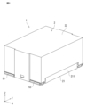
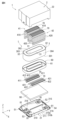
図1は、本発明の一実施形態のコイル部品を示す上方斜視図である。図2は、コイル部品の下方斜視図である。図3は、コイル部品の内部を示す上方斜視図である。図4は、コイル部品の分解斜視図である。
First Embodiment
(Configuration of coil components)
Fig. 1 is a top perspective view showing a coil component according to an embodiment of the present invention. Fig. 2 is a bottom perspective view of the coil component. Fig. 3 is a top perspective view showing the inside of the coil component. Fig. 4 is an exploded perspective view of the coil component.
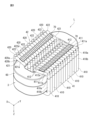
図1から図4に示すように、コイル部品1は、ケース2と、ケース2内に収納されたインダクタ素子Lと、ケース2に取り付けられた第1から第4電極端子51~54と、インダクタ素子Lと第1から第4電極端子51~54とを接続する第1接続部材81と、ケース2内に配置された樹脂部材90とを有する。コイル部品1は、例えば、コモンモードチョークコイルなどである。インダクタ素子Lは、環状のコア3と、コア3に巻回された第1コイル41および第2コイル42と、コア3に取り付けられたコアカバー60とから構成される。
As shown in Figures 1 to 4,
ケース2は、底板部21と、底板部21を覆う箱部22とを有する。ケース2は、強度と耐熱性を有する材料から構成され、好ましくは、難燃性を有する材料から構成される。ケース2は、例えば、PPS(ポリフェニレンサルファイド)、LCP(液晶ポリマー)、PPA(ポリフタルアミド)などの樹脂、または、セラミックスから構成される。The
底板部21は、互いに対向する第1主面210aおよび第2主面210bを含む底部210と、底部210の第1主面210a上で底部210の外周に沿って設けられた側壁部211とを有する。底板部21は、凹部215を有し、凹部215は、底部210および側壁部211に囲まれて構成される。側壁部211は、周方向に連続的に設けられているが、周方向に間欠的に設けられていてもよい。底部210は、第1主面210aおよび第2主面210bを貫通する複数の開口部216を有する。複数の開口部216は、第1から第4電極端子51~54に対応する位置に設けられている。この実施形態では、開口部216は、4つであるが、数量の増減は、自由である。The
底板部21には、インダクタ素子Lが配置されている。つまり、底板部21には、コア3の中心軸が底部210の第1主面210aに直交するように、コア3が配置されている。コア3の中心軸とは、コア3の内径孔部の中心軸をいう。ケース2(底板部21および箱部22)の形状は、コア3の中心軸方向からみて、矩形である。この実施形態では、ケース2の形状は、長方形である。
An inductor element L is arranged on the
ここで、コア3の中心軸方向からみたケース2の短手方向をX方向とし、コア3の中心軸方向からみたケース2の長手方向をY方向とし、上記短手方向および上記長手方向の双方に垂直な方向であるケース2の高さ方向をZ方向とする。ケース2の底板部21と箱部22とは、Z方向に向かい合って配置されており、底板部21は下側、箱部22は上側にあり、上側をZ方向の順方向、下側をZ方向の逆方向とする。つまり、第1主面210aに直交する高さ方向において、第1主面210aからコア3に向かう方向を上方向とする。なお、ケース2の底板部21の形状が正方形である場合、ケース2のX方向の長さとケース2のY方向の長さは、同一となる。Here, the short side direction of the
箱部22は、インダクタ素子Lを覆うように底板部21に取り付けられる。つまり、コア3およびコイル41,42は、箱部22に囲まれて、外側に露出しない。したがって、インダクタ素子Lを外部から保護できる。The
第1から第4電極端子51~54は、底板部21に取り付けられている。第1電極端子51と第2電極端子52は、底板部21のY方向に対向する2つの隅に位置し、第3電極端子53と第4電極端子54は、底板部21のY方向に対向する2つの隅に位置している。第1電極端子51と第3電極端子53は、X方向に対向し、第2電極端子52と第4電極端子54は、X方向に対向している。The first to
コア3は、トロイダルコアであり、コア3の形状は、中心軸方向からみて、長円形(トラック形状)である。コア3は、中心軸方向からみて、長軸に沿って延在し短軸方向に対向する一対の長手部分31と、短軸に沿って延在し長軸方向に対向する一対の短手部分32とを含む。なお、コア3の形状は、中心軸方向からみて、長方形、楕円形または円形であってもよい。The
コア3は、例えば、フェライトなどのセラミックコア、または、鉄系の粉体成型やナノ結晶箔で作られる磁性コアから構成される。コア3は、中心軸方向に対向する第1端面301および第2端面302と、内周面303および外周面304とを有する。第1端面301は、コア3の下側の端面であり、底板部21の第1主面210aと向かい合う。第2端面302は、コア3の上側の端面であり、箱部22の内面と向かい合う。コア3は、コア3の長軸方向がY方向に一致するように、ケース2に収納される。
The
コア3の中心軸方向からみた周方向に直交する断面の形状は、矩形である。第1端面301および第2端面302は、コア3の中心軸方向に垂直に配置されている。内周面303および外周面304は、コア3の中心軸方向に平行に配置されている。この明細書で、「垂直」とは、完全に垂直となる状態に限らず、実質的に垂直である状態も含む。また、「平行」とは、完全に平行となる状態に限らず、実質的に平行である状態も含む。The shape of a cross section perpendicular to the circumferential direction as viewed from the central axis direction of the
コア3の下側部分は、コアカバー60に覆われている。すなわち、コア3の底板部21側の一部はコアカバー60によって覆われている。なお、コア3の少なくとも底板部21側の一部が、コアカバー60によって覆われていればよく、コア3の全部が、コアカバー60によって覆われていてもよい。コアカバー60は、例えば、LCP、PPA、PPSなどのスーパーエンプラから構成され、これにより、コアカバー60の耐熱性、絶縁性および加工性が向上する。The lower portion of the
コアカバー60は、環状に形成され、コア3の下側部分を覆う環状凹部61を有する。コアカバー60の環状凹部61にコア3の下側部分を嵌め込むことで、コア3にコアカバー60を装着することができる。The core cover 60 is formed in an annular shape and has an
樹脂部材90は、底板部21の凹部215内に配置され、底板部21およびインダクタ素子Lに接触する。樹脂部材90の材料としては、例えば、熱硬化性のエポキシ系の樹脂を用いることができる。The
第1コイル41は、第1電極端子51と第2電極端子52との間で、コア3およびコアカバー60に巻回されている。第1コイル41の一端は、第1電極端子51に接続される。第1コイル41の他端は、第2電極端子52に接続される。The
第2コイル42は、第3電極端子53と第4電極端子54との間で、コア3およびコアカバー60に巻回されている。第2コイル42の一端は、第3電極端子53に接続される。第2コイル42の他端は、第4電極端子54に接続される。The
第1コイル41および第2コイル42は、コア3の中心軸方向からみたコア3の周方向に沿って、コア3に螺旋状に卷回される。具体的に述べると、第1コイル41は、コア3の一方の長手部分31にコア3の長軸方向に沿って巻回され、第2コイル42は、コア3の他方の長手部分31にコア3の長軸方向に沿って巻回される。第1コイル41の巻回軸と第2コイル42の巻回軸は、並走する。第1コイル41および第2コイル42は、コア3の長軸に対して、対称となる。The
第1コイル41の巻数と第2コイル42の巻数とは、同じである。第1コイル41のコア3に対する巻回方向と第2コイル42のコア3に対する巻回方向とは、逆方向となる。つまり、第1コイル41の第1電極端子51から第2電極端子52に向かう巻回方向と、第2コイル42の第3電極端子53から第4電極端子54に向かう巻回方向とは、逆方向となる。The number of turns of the
そして、コモンモードの電流が、第1コイル41において第1電極端子51から第2電極端子52に向かって流れ、第2コイル42において第3電極端子53から第4電極端子54に向かって流れ、つまり、電流の流れる向きが同じになるように、第1から第4電極端子51~54が接続される。コモンモードの電流が第1コイル41に流れると、コア3内には、第1コイル41による第1磁束が発生する。コモンモードの電流が第2コイル42に流れると、コア3内には、第1磁束とコア3内で強め合う方向に第2磁束が発生する。このため、第1コイル41とコア3、および、第2コイル42とコア3は、インダクタンス成分として働き、コモンモードの電流に対してノイズが除去される。
The first to
第1コイル41は、複数のピン部材が、例えばレーザ溶接やスポット溶接などの溶接により接続されてなる。なお、図3は、複数のピン部材が実際に溶接されている状態を表しているのでなく、複数のピン部材が組付けられている状態を表している。The
複数のピン部材は、プリント配線や導線でなく、棒状部材である。ピン部材は、剛性を有する。具体的に述べると、コア3の周方向に直交する断面において、ピン部材は、コア3の第1端面301、第2端面302、内周面303および外周面304を通過するコアの外周の一周分の長さよりも短く、また、剛性自体も高いため、折り曲げにくくなっている。The multiple pin members are rod-shaped members, not printed wiring or conductive wires. The pin members have rigidity. Specifically, in a cross section perpendicular to the circumferential direction of the
複数のピン部材は、略U字状に折り曲げられた折曲ピン部材410と、略直線状に延在された直線ピン部材412および最端直線ピン部材411とを含む。The multiple pin members include a
第1コイル41は、一端から他端に順に、一端側(一方)の最端直線ピン部材411と、複数組の折曲ピン部材410および直線ピン部材412と、他端側(他方)の最端直線ピン部材411とを含む。最端直線ピン部材411は、第1コイル41の軸方向の最端に位置する直線ピン部材である。この実施形態では、最端直線ピン部材411と直線ピン部材412とは、同一の形状にされている。しかし、これに限定されず、最端直線ピン部材411と直線ピン部材412とは、異なる形状にしてもよい。例えば、最端直線ピン部材411の延在方向の長さは、直線ピン部材412の延在方向の長さより短くしてもよい。
The
折曲ピン部材410のばね指数に関して説明すると、図5に示すように、折曲ピン部材410をコア3の第2端面302、内周面303および外周面304に沿って配置したときに、コア3の外周面304の角部に位置する折曲ピン部材410の曲率半径R1、および、コア3の内周面303の角部に位置する折曲ピン部材410の曲率半径R2において、折曲ピン部材410のばね指数Ksは、3.6よりも小さい。ばね指数Ksは、折曲ピン部材の曲率半径R1、R2/折曲ピン部材の線径rで表せる。このように、折曲ピン部材410は、剛性が高く、折り曲げにくいものである。Regarding the spring index of the
折曲ピン部材410および直線ピン部材412は、例えばレーザ溶接やスポット溶接などの溶接により交互に接続される。折曲ピン部材410の一端に直線ピン部材412の一端を接続し、直線ピン部材412の他端を他の折曲ピン部材410の一端に接続する。これを繰り返すことにより、複数の折曲ピン部材410および直線ピン部材412は、接続され、接続された複数の折曲ピン部材410および直線ピン部材412は、コア3に螺旋状に配置される。つまり、1組の折曲ピン部材410および直線ピン部材412によって、1ターンを構成する。The
折曲ピン部材410は、コア3の第2端面302、内周面303および外周面304のそれぞれの面に沿って平行に配置されている。折曲ピン部材410は、延在方向の両端部を結ぶ仮想線が、第1コイル41の軸方向に直交するように配置されている。言い換えると、折曲ピン部材410は、折曲ピン部材410の中心線を含む平面が、第1コイル41の軸方向に直交する平面(XZ平面)に平行となるように配置されている。直線ピン部材412は、コア3の第1端面301に沿って平行に配置されている。直線ピン部材412は、Y方向にやや傾いてX方向に延在している。最端直線ピン部材411は、コア3の第1端面301に沿って平行に配置されている。最端直線ピン部材411は、直線ピン部材412と平行な方向に延在している。The
隣のターンの折曲ピン部材410同士は、接着部材70により、固定されている。これにより、複数の折曲ピン部材410のコア3への取り付け状態を安定なものとできる。同様に、隣り合う最端直線ピン部材411と直線ピン部材412は、接着部材70により、固定され、隣り合う直線ピン部材412は、接着部材70により、固定されている。これにより、複数の最端直線ピン部材411および直線ピン部材412のコア3への取り付け状態を安定なものとできる。The
第1電極端子51は、一方の最端直線ピン部材411に接続され、一方の最端直線ピン部材411は、一方の最端直線ピン部材411に隣のターンの折曲ピン部材410の一端に接続される。第1電極端子51の一部(後述する中継部およびコイル接続部)は、ケース2内に入り込み、一方の最端直線ピン部材411の周面が、第1電極端子51に接続される。具体的に述べると、第1電極端子51の一部は、開口部216を貫通して、一方の最端直線ピン部材411の周面に接続される。要するに、第1コイル41と第1電極端子51は、開口部216を経由して電気的に接続される。The
第2電極端子52は、他方の最端直線ピン部材411に接続され、他方の最端直線ピン部材411は、他方の最端直線ピン部材411に隣のターンの折曲ピン部材410の一端に接続される。第2電極端子52の一部(後述する中継部およびコイル接続部)は、ケース2内に入り込み、他方の最端直線ピン部材411の周面が、第2電極端子52に接続される。具体的に述べると、第2電極端子52の一部は、開口部216を貫通して、他方の最端直線ピン部材411の周面に接続される。要するに、第1コイル41と第2電極端子52は、開口部216を経由して電気的に接続される。The
第2コイル42は、第1コイル41と同様に、複数のピン部材から構成される。つまり、第2コイル42は、一端から他端に順に、一端側(一方)の最端直線ピン部材421と、複数組の折曲ピン部材420および直線ピン部材422と、他端側(他方)の最端直線ピン部材421とを含む。コア3には、折曲ピン部材420および直線ピン部材422が交互に接続されて巻回されている。つまり、複数の折曲ピン部材420および直線ピン部材422は、接続され、接続された複数の折曲ピン部材420および直線ピン部材422は、コア3に螺旋状に巻回される。The
第3電極端子53は、一方の最端直線ピン部材421に接続され、一方の最端直線ピン部材421は、一方の最端直線ピン部材421に隣のターンの折曲ピン部材420の一端に接続される。第3電極端子53の一部(後述する中継部およびコイル接続部)は、ケース2内に入り込み、一方の最端直線ピン部材421の周面が、第3電極端子53に接続される。具体的に述べると、第3電極端子53の一部は、開口部216を貫通して、一方の最端直線ピン部材421の周面に接続される。要するに、第2コイル42と第3電極端子53は、開口部216を経由して電気的に接続される。The
第4電極端子54は、他方の最端直線ピン部材421に接続され、他方の最端直線ピン部材421は、他方の最端直線ピン部材421に隣のターンの折曲ピン部材420の一端に接続される。第4電極端子54の一部(後述する中継部およびコイル接続部)は、ケース2内に入り込み、他方の最端直線ピン部材421の周面は、第4電極端子54に接続される。具体的に述べると、第4電極端子54は、開口部216を貫通して、他方の最端直線ピン部材421の周面に接続される。要するに、第2コイル42と第4電極端子54は、開口部216を経由して電気的に接続される。The
図3に示すように、第1コイル41および第2コイル42(ピン部材410~412,420~422)は、それぞれ、導体部と導体部の一部を覆う被膜とを含む。導体部は、例えば、銅線であり、被膜は、例えば、ポリアミドイミド樹脂である。被膜の厚みは、例えば、0.02~0.04mmである。
As shown in Figure 3, the
最端直線ピン部材411,421は、被膜のない導体部411a,421aから構成される。直線ピン部材412,422は、被膜のない導体部412a,422aから構成される。折曲ピン部材410,420は、導体部410a,420aと被膜410b,420bから構成される。The
折曲ピン部材410,420の一端および他端において、導体部410a,420aは、被膜410b,420bから露出している。つまり、最端直線ピン部材411,421、直線ピン部材412,422および折曲ピン部材410,420は、互いに、露出している導体部411a,421a,412a,422a,410a,420aにおいて溶接されている。これらの被膜に覆われていない導体部、つまり、被膜から露出している(被膜のない)導体部は、外部と導通可能となる。At one end and the other end of the
図6は、コイル部品1のY方向の中心を通過するXZ断面図である。図6では、箱部22を省略して描いている。
Figure 6 is an XZ cross-sectional view passing through the center of the
図6に示すように、第1コイル41において、隣り合うピン部材の端部は互いに溶接された溶接部を有する。溶接部とは、溶接の際に一度溶解し、その後固まった部分を示す。具体的には、第1コイル41は、第1溶接部w11および第2溶接部w12を有する。より具体的には、第1コイル41における隣り合うターンにおいて、一方のターンの直線ピン部材412と折曲ピン部材410とは、直線ピン部材412の一方の導体部412aと折曲ピン部材410の導体部410aが互いに溶接された第1溶接部w11を形成し、上記直線ピン部材412と他方のターンの折曲ピン部材410とは、直線ピン部材412の他方の導体部412aと該折曲ピン部材の導体部410aとが互いに溶接された第2溶接部w12を形成する。As shown in FIG. 6, in the
なお、図6では、第1コイル41の直線ピン部材412と折曲ピン部材410とから構成されたターンについて記載しているが、最端直線ピン部材411と折曲ピン部材410とから構成されたターンにおいても同様である。具体的に説明すると、最端直線ピン部材411は、導体部411aと接続した折曲ピン部材410の導体部410aにおいて溶接され、第1溶接部w11または第2溶接部w12を形成する。6 shows a turn composed of the
第2コイル42は、第1溶接部w21および第2溶接部w22を有する。第2コイル42においても、第1コイル41と同様に、隣り合うターンにおいて、一方のターンの直線ピン部材422と折曲ピン部材420とは、直線ピン部材422の一方の導体部422aと折曲ピン部材420の導体部420aにおいて溶接され、第1溶接部w21を形成し、上記直線ピン部材422と他方のターンの折曲ピン部材420とは、直線ピン部材422の他方の導体部422aと該折曲ピン部材の導体部420aにおいて溶接され、第2溶接部w22を形成する。また、最端直線ピン部材421は、導体部421aと接続した折曲ピン部材420の導体部420aにおいて溶接され、第1溶接部w21または第2溶接部w22を形成する。第2コイル42の第1溶接部w21および第2溶接部w22については、第1コイル41の第1溶接部w11および第2溶接部w12と同様の構成を有し、その説明は省略する。The
コアカバー60は、コイル41,42における被膜から露出している導体部および溶接部とコア3との間に存在する。これにより、コイル41,42の導体部および溶接部とコア3とをより確実に絶縁することができる。The core cover 60 is disposed between the conductors and welds exposed from the coating of the
コアカバー60は、コア3の第1端面301と、コア3の内周面303の一部と、コア3の外周面304の一部とにわたって設けられる。コアカバー60は、コア3の内周面303に対向する第1部分60aと、コア3の外周面304に対向する第2部分60bと、コア3の第1端面301に対向する第3部分60cとを有する。The core cover 60 is provided over the
コアカバー60は、コア3に間接的に接続される。つまり、コアカバー60がコア3に直接接続されておらず、具体的に述べると、コアカバー60は、コア支持部材80を介してコア3に接続される。コア支持部材80がコア3の一部と接続することにより、コアカバー60から受けるコア3の応力を低減して、コア3の磁気特性の劣化を抑制できる。つまり、磁歪に起因するインダクタンス値の低下を抑制できる。なお、コアカバー60が、コア支持部材80を介してコア3に接続されておらず、コア3に単に嵌め込まれた状態であってもよい。The core cover 60 is indirectly connected to the
コア支持部材80は、コア3の第1端面301と、コアカバー60の第3部分60cとの間に設けられる。これにより、コア3への磁歪の影響を小さくしつつ、コアカバー60のコア3へ取り付け状態を安定なものとすることができる。The
コア支持部材80の材料としては、ウレタン樹脂やシリコン樹脂などの軟らかい樹脂などを挙げることができる。このような軟らかい樹脂を設けることにより、磁歪の影響を小さくすることができる。
Materials for the
なお、図6では、コア支持部材80は、コア3の第1端面301と、コアカバー60の第3部分60cとの間の全域に設けられているが、一部のみに設けられてもよい。また、図6では、コア支持部材80は、コア3の第1端面301と、コアカバー60の第3部分60cとの間に設けられているが、コア3の内周面303と、コアカバー60の第1部分60aとの間に設けられてもよく、コア3の外周面304と、コアカバー60の第2部分60bとの間に設けられてもよく、これらのうち、複数の箇所に設けられてもよい。In Fig. 6, the
図6に示すように、インダクタ素子Lは、コイル41,42における被膜から露出している導体部が第1主面210a側に位置するように、凹部215内に配置されている。樹脂部材90は、凹部215内に固定されて、インダクタ素子Lを底板部21に固定し、かつ、コイル41,42における被膜から露出している導体部の少なくとも一部を覆う。好ましくは、樹脂部材90は、導体部の全てを覆う。6, the inductor element L is disposed in the
樹脂部材90は、例えば熱硬化性樹脂からなるため、硬化によりインダクタ素子Lおよび底板部21に固定される。樹脂部材90は、凹部215の内面と、コアカバー60の第1部分60aの一部と、コアカバー60の第2部分60bの一部と、コアカバー60の第3部分60cの一部とに接触し、第1コイル41における被膜410bから露出する導体部411a,412a,410aと、第2コイル42における被膜420bから露出する導体部421a,422a,420aとを覆う。さらに、樹脂部材90は、コイル41,42の溶接部w11,w12,w21,w22をも覆う。The
樹脂部材90は、底板部21の凹部215内に固定されているので、樹脂部材90は、底板部21に安定して固定され、これにより、樹脂部材90は、インダクタ素子Lを底板部21に安定して固定することができる。また、コイル部品1の製造工程において、液状の樹脂部材90を凹部215内に充填する際、液状の樹脂部材90を凹部215内に留めることができ、樹脂部材90によりインダクタ素子Lを底板部21に確実に固定することができる。また、樹脂部材90は、コイル41,42における被膜から露出している導体部を覆うので、外部との電気的なショートなどの不具合を防止することができる。さらに、コイル部品1が振動衝撃などの外力を受けた場合に、樹脂部材90が衝撃を吸収し、コイル41,42を保護することができる。Since the
(電極端子の詳細構成)
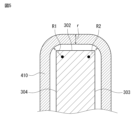
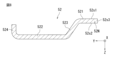
次に、電極端子の詳細構成について説明する。図7は、第1コイル41との接続前における第2電極端子52を部分的に示す模式平面図である。すなわち、図7は、第1コイル41を底板部21に組み付けた後であって、第1コイル41と第2電極端子52とを例えば溶接などにより接続する前の第2電極端子52を示している。図8は、図7のVIII-VIII断面図である。なお、以下では第2電極端子52について説明するが、第1電極端子51、第3電極端子53および第4電極端子54の構成は、第2電極端子52の構成と同様であるため、その詳細な説明を省略する。
(Detailed configuration of electrode terminal)
Next, the detailed configuration of the electrode terminal will be described. Fig. 7 is a schematic plan view partially showing the
図7および図8に示すように、第2電極端子52は、板状の端子である。第2電極端子52の厚みは、例えば0.3mmである。第2電極端子52は、第1コイル41の第1端部と接続されるコイル接続部521と、図示しない実装基板に実装される実装部522と、コイル接続部521と実装部522とを接続する中継部523と、中継部523が接続されている側とは反対側の実装部522の端部に接続されたフィレット部524と、を有する。Z方向からみて、コイル接続部521および中継部523は、実装部522から逆Y方向に延在している。コイル接続部521および実装部522の厚み方向は、Z方向に平行である。コイル接続部521および中継部523の延在方向に直交する方向である幅方向は、X方向に平行である。7 and 8, the
コイル接続部521は、XY平面に平行な平板状にされている。コイル接続部521は、第1主面52s1と、第1主面52s1に対向する第2主面52s2と、第1主面52s1と第2主面52s2とを接続する側面52s3と、を含む。コイル接続部521は、第1主面52s1と第2主面52s2と側面52s3とに開口する第1凹部C1と、幅広部52Wと、幅狭部52Nと、を有する。第1凹部C1は、幅広部52Wと幅狭部52Nとの間に、幅広部52Wおよび幅狭部52Nと隣り合って配置されている。すなわち、コイル接続部521は、第1主面52s1に直交する方向(Z方向)からみて、コイル接続部521および中継部523の延在方向(Y方向)の先端側で二股に分かれた形状にされている。要するに、第2電極端子52は、先開型の端子である。The
この実施形態では、第1主面52s1に直交する方向からみて、第1凹部C1は、コイル接続部521の延在方向の先端側の側面52s3の一部(先端面)と、第1主面52s1および第2主面52s2と、を開口している。また、第1主面52s1に直交する方向からみて、第1凹部C1は、長軸がY方向に平行な長円形(トラック形状)の一部となるような形状にされている。In this embodiment, when viewed from a direction perpendicular to the first main surface 52s1, the first recess C1 opens a part (tip surface) of the side surface 52s3 on the tip side in the extension direction of the
幅広部52Wは、X方向の幅が幅狭部52Nよりも幅広にされている。幅広部52Wは、幅狭部52Nよりも、第1コイル41の第1端部の最端に近くなるように配置されている。具体的に述べると、幅広部52Wは、X方向において、幅狭部52Nよりも底板部21の側壁部211側に配置されている。これにより、例えば第1コイル41の最端直線ピン部材411の周面と第2電極端子52とをレーザ溶接する場合、発生する熱を最端直線ピン部材411側により多く逃がすことができる。幅狭部52Nは、X方向の幅が幅広部52Wよりも幅狭にされている。幅狭部52Nは、X方向において、幅広部52Wよりも底板部21の中央部側に配置されている。The
幅狭部52NのY方向の最大長さL1は、コイル接続部521のY方向の最大長さL0の50%以上であることが好ましい。幅狭部52Nと幅広部52Wとの間の距離(言い換えると、第1凹部C1のX方向の幅)L4は、コイル接続部521のX方向の最大幅W0の20%以上であることが好ましい。上記最大長さL1および上記距離L4とすることにより、後述する第1接続部材を設ける領域を十分広く確保でき、第1コイル41と第2電極端子52との接続安定性を向上させることができる。具体的に述べると、例えば第1コイル41の最端直線ピン部材411の周面と第2電極端子52とをレーザ溶接する場合、上記寸法関係により、第1凹部C1の内面C1fの面積を十分に確保できるため、レーザ照射可能な領域を十分広く確保できる。The maximum length L1 of the
幅狭部52NのX方向の最大幅W1は、幅広部52WのX方向の最大幅W2よりも小さい。これにより、幅狭部52Nの熱容量が、幅広部52Wの熱容量よりも小さくなる。そのため、例えば第1コイル41の最端直線ピン部材411の周面と第2電極端子52とをレーザ溶接する場合、レーザを第2電極端子52に照射したときに、熱容量が小さい幅狭部52N側の部分が溶けやすくなる。その結果、最端直線ピン部材411側に多くの熱が伝わり、最端直線ピン部材411側に熱を逃がすことができるため、実装部522への熱影響を低減できる。The maximum width W1 in the X direction of the
幅広部52WのY方向の最大長さL2は、幅狭部52NのY方向の最大長さL1よりも短い。これにより、最端直線ピン部材411と隣り合う直線ピン部材412と、第2電極端子52とが、短絡することを抑制できる。具体的に述べると、後述する図9に示すように、最端直線ピン部材411および直線ピン部材412が、Y方向にやや傾いてX方向に延在している場合でも、最大長さL2を最大長さL1よりも短くすることにより、幅広部52Wと上記隣り合う直線ピン部材412との間の距離を確保できる。その結果、幅広部52Wと上記隣り合う直線ピン部材412とが短絡することを抑制できる。The maximum length L2 in the Y direction of the
第1凹部C1、幅広部52Wおよび幅狭部52Nの上記寸法の一例は、例えば以下の通りである。幅狭部52NのX方向の最大幅W1は、例えば0.65mmである。幅狭部52NのY方向の最大長さL1は、例えば0.85mmである。幅広部52WのX方向の最大幅W2は、例えば0.85mmである。幅広部52WのY方向の最大長さL2は、例えば0.65mmである。すなわち、幅狭部52NのY方向の最大長さL1と幅広部52WのY方向の最大長さL2との差L3は、例えば0.2mmである。幅狭部52Nと幅広部52Wとの間の距離L4は、例えば0.5mmである。
An example of the above dimensions of the first recess C1, the
実装部522は、XY平面に平行な平板状にされている。実装部522は、底板部21の底部210に埋め込まれて、底板部21に固定されている。実装部522は、底板部21の底面から露出し、実装基板に実装される部分となる。実装部522は、例えば、リフローはんだ付けによって、実装基板と接続される。好ましくは、実装部522には、はんだの濡れ性を確保するためにSnめっきが施される。The mounting
図8に示すように、コイル接続部521と実装部522とは、同一平面上に存在せず、かつ、第1主面52s1に直交する方向(Z方向)からみて重ならない。具体的に述べると、この実施形態では、コイル接続部521は、Z方向において実装部522よりも上方に位置する。コイル接続部521と実装部522とは、第1主面52s1に直交する方向からみて重ならない。中継部523は、平板状であり、XY平面に対して傾斜して配置されている。中継部523のY方向の一端は、コイル接続部521に接続され、中継部523のY方向の他端は、実装部522に接続されている。要するに、コイル接続部521と実装部522と中継部523とは、平板を2回折り曲げた形状にされている。なお、中継部523の形状は、特に限定されず、平板状以外の形状であってもよい。As shown in FIG. 8, the
上記構成によれば、実装部522を支点にして、中継部523およびコイル接続部521が撓み易くなるため、コイル接続部521の第1主面52s1に直交する方向のばね性を第2電極端子52に付与することができる。これにより、コイル接続部521と第1コイル41の第1端部とを接続する際に、コイル接続部521と第1コイル41の第1端部とをより確実に接触させることできるため、第1コイル41と第2電極端子52との接続安定性を向上させることができる。また、コイル部品1に外部衝撃が加えられた場合でも、第2電極端子52のばね性により第1接続部材81に加わる応力を低減でき、コイル部品1の信頼性を高めることができる。According to the above configuration, the
フィレット部524は、中継部523が接続されている側とは反対側の実装部522の端部からZ方向上側に延在する。フィレット部524は、コイル部品1の外部に露出している。フィレット部524は、はんだの濡れ上がり部分となる。したがって、実装基板にはんだを介してコイル部品1を実装するとき、はんだはフィレット部524を濡れ上がり、はんだ実装後の視認を得ることができ、また、はんだの接続強度を向上できる。好ましくは、フィレット部524には、はんだの濡れ性を確保するためにSnめっきが施される。The
(コイルと電極端子との接続部分の詳細構成)
次に、第2電極端子52と第1コイル41との接続部分の詳細構成について説明する。図9は、第2電極端子52と第1コイル41との接続部分を部分的に示す模式平面図である。図10は、図9のX-X断面図である。なお、図9は、直線ピン部材412の一端に接続される折曲ピン部材410を省略して描いている。また、図10は、見易さを考慮して、樹脂部材90の断面ハッチングを省略して描いている。
(Detailed configuration of the connection between the coil and the electrode terminal)
Next, a detailed configuration of the connection portion between the
図9および図10に示すように、第1接続部材81は、第1コイル41の第1端部41e1の周面411psと、第2電極端子52のコイル接続部521と、を接続している。第1接続部材81は、第1端部41e1とコイル接続部521とが例えばレーザ溶接されて形成される溶接部、はんだなどである。第1接続部材81は、好ましくは溶接部である。これにより、第1コイル41と第2電極端子52との接続強度を高めることができる。また、第1コイル41と第2電極端子52との間の電気抵抗を下げることができる。これにより、コイル部品1の電気抵抗を下げることができる。この実施形態では、第1接続部材81は、第1端部41e1とコイル接続部521とがレーザ溶接されて形成された溶接部である。また、この実施形態では、第1端部41e1は、最端直線ピン部材411の全体である。なお、図9では、便宜上、溶接前に存在していた第1凹部C1の内面を仮想線(2点鎖線)で示している。9 and 10, the
第1端部41e1は、コイル接続部521の第1主面52s1側にのみ配置されて第1主面52s1に対向し、かつ、第1主面52s1に直交する方向からみて、第1凹部C1と重なるように配置されている。The first end 41e1 is arranged only on the first main surface 52s1 side of the
第1端部41e1の延在方向に直交する断面において、第1端部41e1の周面411psは、Y方向に互いに対向する2つの平坦面411fsと、Z方向に互いに対向する2つの平坦面411fsと、各平坦面411fsを接続する曲面と、を有する。すなわち、第1端部41e1の断面形状は、角部にアールを有する略矩形状である。平坦面411fsは、例えば、断面が円形状のピン部材の周面を押しつぶすことで形成することができる。平坦面411fsが、第1主面52s1に対向し、かつ、第1主面52s1に直交する方向からみて、第1凹部C1と重なるように配置されている。なお、第1端部41e1の周面は、平坦面411fsを有していなくてもよい。例えば、第1端部41e1の断面形状は、円形であってもよい。In a cross section perpendicular to the extension direction of the first end 41e1, the peripheral surface 411ps of the first end 41e1 has two flat surfaces 411fs facing each other in the Y direction, two flat surfaces 411fs facing each other in the Z direction, and a curved surface connecting the flat surfaces 411fs. That is, the cross-sectional shape of the first end 41e1 is approximately rectangular with rounded corners. The flat surface 411fs can be formed, for example, by crushing the peripheral surface of a pin member having a circular cross section. The flat surface 411fs is arranged so as to face the first main surface 52s1 and overlap the first recess C1 when viewed from a direction perpendicular to the first main surface 52s1. The peripheral surface of the first end 41e1 does not have to have a flat surface 411fs. For example, the cross-sectional shape of the first end 41e1 may be circular.
第1接続部材81の少なくとも一部は、第1凹部C1内に位置し、かつ、第1凹部C1の内面C1fに接触している。具体的に述べると、第1接続部材81の一部が、第1凹部C1内に位置している。言い換えると、第1接続部材81の一部が、コイル接続部521の側面52s3の開口よりもコイル接続部521の内側の領域に位置している。第1接続部材81の一部は、第1凹部C1の内面C1fに接触している。At least a portion of the
同様に、第1コイル41の第2端部は、第1電極端子51におけるコイル接続部の第1主面側にのみ配置されて第1主面に対向し、かつ、第1主面に直交する方向からみて、第1凹部C1と重なるように配置され、第1接続部材81の一部は、第1凹部C1内に位置し、かつ、第1凹部C1の内面C1fに接触している。また、第2コイル42の第1端部は、第4電極端子54におけるコイル接続部の第1主面側にのみ配置されて第1主面に対向し、かつ、第1主面に直交する方向からみて、第1凹部C1と重なるように配置され、第1接続部材81の一部は、第1凹部C1内に位置し、かつ、第1凹部C1の内面C1fに接触している。また、第2コイル42の第2端部は、第3電極端子53におけるコイル接続部の第1主面側にのみ配置されて第1主面に対向し、かつ、第1主面に直交する方向からみて、第1凹部C1と重なるように配置され、第1接続部材81の一部は、第1凹部C1内に位置し、かつ、第1凹部C1の内面C1fに接触している。Similarly, the second end of the
コイル部品1によれば、コイル41,42の第1,第2端部と第1から第4電極端子51~54とは、第1,第2端部が、第1から第4電極端子51~54のコイル接続部の第1主面側にのみ配置されて第1主面に対向するように接続されているので、コイル41,42は、第1から第4電極端子51~54に絡げて接続されない。ここで、「絡げ」とは、コイル41,42を第1から第4電極端子51~54に巻き付けることを意味する。According to the
したがって、コイル41,42の絡げ作業や絡げられたコイル41,42の残留応力に起因する第1から第4電極端子51~54の変形を防止することができる。これにより、薄い第1から第4電極端子51~54に太いコイル41,42を接続することができ、曲げ加工の容易な第1から第4電極端子51~54と大電流に対応したコイル41,42を用いることができる。また、コイル41,42を第1から第4電極端子51~54に絡げないため、コイル41,42に曲げ膨らみが発生せず、これにより、コイル41,42と第1から第4電極端子51~54の間に隙間が発生し難くなり、接続安定性と小型化を実現できる。Therefore, it is possible to prevent deformation of the first to
また、第1接続部材81の少なくとも一部が、第1から第4電極端子51~54の第1凹部C1内に位置しているため、第1から第4電極端子51~54のコイル接続部の第2主面側(ケース2の底板部21側)から第1接続部材81を観察できる。これにより、コイル41,42と第1から第4電極端子51~54との接続状態を容易に外観検査することができる。In addition, because at least a portion of the
また、コイル部品1によれば、最端直線ピン部材411,421の周面が、第1から第4電極端子51~54のコイル接続部の第1主面に対向するため、第1から第4電極端子51~54と最端直線ピン部材411,421とを接続する際に、最端直線ピン部材411,421の位置合わせを容易にできる。Furthermore, according to the
また、コイル部品1によれば、コイル41,42の端部の平坦面が、第1接続部材81を介して、第1から第4電極端子51~54に接続されている。そのため、コイル41,42の端部と第1から第4電極端子51~54との接触面積を増大させることができるため、コイル41,42と第1から第4電極端子51~54との間の機械的強度を向上させることができる。また、コイル41,42と第1から第4電極端子51~54との間の電気的経路の断面積が大きくなるため、コイル部品1の電気抵抗を低減できる。
Furthermore, according to the
また、コイル部品1によれば、複数の直線ピン部材412と、複数の折曲ピン部材410とが交互に接続されて第1コイル41の螺旋を構成しているため、コア3に第1コイル41を巻回する際に、コア3に近接して第1コイル41を卷回することができる。同様に、複数の直線ピン部材422と、複数の折曲ピン部材420とが交互に接続されて第2コイル42の螺旋を構成しているため、コア3に第2コイル42を巻回する際に、コア3に近接して第2コイル42を卷回することができる。In addition, according to the
好ましくは、第1から第4電極端子51~54は、コイル接続部が第1主面に直交する方向に揺動可能なように、弾性変形可能である。具体的に述べると、図8において、第2電極端子52の実装部522は、底板部21に固定されているため、実装部522を支点にして、コイル接続部521を第1主面52s1に直交する方向に揺動可能なように、第2電極端子52は弾性変形可能である。他の電極端子51,53,54についても同様である。この構成によれば、コイル41,42と第1から第4電極端子51~54との接続安定性をさらに向上させることができる。また、コイル部品1に外部衝撃が加えられた場合でも、第1接続部材81に加わる応力をさらに低減でき、コイル部品1の信頼性をさらに高めることができる。
Preferably, the first to
好ましくは、コイル接続部の第1主面は、底板部21の底部210の第1主面210aよりもコイル41,42の径方向内側に位置する。具体的に述べると、図10に示すように、コイル接続部521の第1主面52s1の位置P2は、底板部21の底部210の第1主面210aの位置P1よりも第1コイル41の径方向内側に存在する。言い換えると、Z方向において、第1主面52s1の位置P2は、第1主面210aの位置P1よりも上方に位置する。この構成によれば、コイル接続部521の第2主面52s2側に配置されている樹脂部材90の厚みを、底部210の厚み(すなわち、第1主面210aと第2主面210bとの間の距離)よりも厚くすることができる。これにより、振動衝撃などの外力により第1接続部材81に生じ得る応力を低減できる。
Preferably, the first main surface of the coil connection portion is located radially inward of the
好ましくは、コイル接続部の第1主面に直交する方向からみて、第1接続部材81には、コイル接続部の側面よりも外側に突出する部分が存在しない。言い換えると、第1接続部材81には、コイル接続部の側面の開口よりも外側に突出する部分が存在しない。この構成によれば、コイル部品1を小型化できる。Preferably, when viewed from a direction perpendicular to the first main surface of the coil connection portion, the
(コイル部品の製造方法)
次に、コイル部品1の製造方法について説明する。
(Manufacturing method of coil components)
Next, a method for manufacturing the
コイル部品1の製造方法は、コイル41,42の端部を、第1から第4電極端子51~54のコイル接続部511~541の第1主面側にのみ配置して、第1主面に対向させるとともに、第1主面に直交する方向からみて、第1から第4電極端子51~54に設けられた第1凹部C1と重なるように配置する工程と、コイル接続部の第2主面側から、第1凹部C1の内面C1fの少なくとも一部にレーザを照射して、第1接続部材81を形成する工程と、を含む。この構成によれば、コイル41,42を第1から第4電極端子51~54に絡げることなく接続することができる。また、コイル部品1を小型化できる。The manufacturing method of the
具体的に述べると、図3に示すように、コアカバー60を嵌め込んだコア3に、互いの巻回軸が並走するように第1コイル41および第2コイル42を巻回して、第1コイル41の露出する導体部411a,412a,410aの少なくとも一部と第2コイル42の露出する導体部421a,422a,420aの少なくとも一部を、コア3の第1端面301側に配置する。Specifically, as shown in FIG. 3, the
その後、コア3の第1端面301を上向きのまま、第1コイル41のそれぞれのピン部材を溶接し、第2コイル42のそれぞれのピン部材を溶接する。Then, with the
その後、コア3およびコイル41,42を、コイル41,42における被膜から露出している導体部が第1主面210a側に位置するように、底板部21の凹部215内に配置する。この際、例えば第1コイル41の第1端部41e1と第2電極端子52とを接続する場合、図11Aに示すように、第1コイル41の第1端部41e1の周面を、第2電極端子52のコイル接続部521の第1主面52s1側に配置して、第1主面52s1に対向させるとともに、第1主面52s1に直交する方向からみて、第2電極端子52に設けられた第1凹部C1と重なるように配置する。そして、第1コイル41の第1端部41e1をコイル接続部521の第1主面52s1側からコイル接続部521に押し付けて、第1端部41e1をコイル接続部521に接触させる。Then, the
第2電極端子52のコイル接続部521と実装部522と中継部523とは、平板を2回折り曲げた形状を有しているため、折り曲げられた部分のばね性により、第1端部41e1をコイル接続部521により確実に接触させることができる。これにより、第1端部41e1とコイル接続部521との接続安定性を確保できる。電極端子51,53,54についても同様にして、コイル41,42の第1端部または第2端部の周面を、電極端子51,53,54のコイル接続部に接触させる。最端直線ピン部材411,421は、Z方向の高さばらつきがある場合がある。第1から第4電極端子51~54はコイル接続部の第1主面に直交する方向(Z方向)のばね性を有しているため、上記高さばらつきを吸収し、より確実に全ての電極端子51~54をコイル41,42の端部に接続させることができる。
The
その後、コイル接続部521の第2主面52s2側から、第1凹部C1の内面C1fの少なくとも一部にレーザを照射する。この際、コイル接続部521と第1端部41e1との両方にレーザ光が当たるようにする。具体的に述べると、レーザのスポット径は細いため(例えば0.05mm)、図11Aの一点鎖線で囲まれた領域LI内の第1凹部C1の内面C1fに沿ってレーザを走査する。これにより、図11Bに示すように、第1端部41e1とコイル接続部521とが溶解しその後固まった第1接続部材81が形成されて、第1端部41e1と第2電極端子52とが接続される。電極端子51,53,54についても同様にして、コイル41,42の第1端部または第2端部を、電極端子51,53,54に接続させる。Then, a laser is irradiated from the second main surface 52s2 side of the
上述のように、第1から第4電極端子51~54が第1凹部C1を有しているため、コイル接続部とコイルの第1端部との両方にレーザを照射して、コイル接続部とコイルの第1端部の両方を溶解して溶接することができる。一方、第1から第4電極端子51~54が第1凹部C1を有しておらず、例えばコイル接続部の第2主面の中央部にレーザを照射して溶接する場合、コイルの第1端部にレーザが照射されず、接続安定性が劣る。As described above, since the first to
その後、図6に示すように、液状の樹脂部材90を、例えばポッティング工法により、凹部215内に充填する。このとき、液状の樹脂部材90は、凹部215内に留まり、コイル41,42における被膜から露出している導体部やコアカバー60の一部に濡れ広がっていく。さらに、液状の樹脂部材90は、底板部21の開口部216内にも充填される。なお、液状の樹脂部材90が、開口部216から漏れないため、底部210の第2主面210bに開口部216を塞ぐようにテープを貼り付ける。6, the
その後、熱を加えて、液状の樹脂部材90を硬化させる。これにより、樹脂部材90によりコア3およびコイル41,42を底板部21に固定することができ、また、樹脂部材90によりコイル41,42における被膜から露出している導体部を覆うことができる。また、樹脂部材90により開口部216を埋めることができる。樹脂部材90の材料として、熱硬化性エポキシ樹脂を用い、このとき、弾性率は、7GPaであり、硬化条件として、30分間、120℃の加熱で硬化する。Heat is then applied to harden the
その後、箱部22を被せてケース2内に収納して、コイル部品1を製造する。このような製造方法を用いることにより、コイル部品1の製造の工程数を低減することができ、コイル部品1をより容易に製造できる。Then, the
(第2実施形態)
図12は、第2実施形態のコイル部品を部分的に示す模式断面図である。図12は、図10に対応し、側壁部211側の記載を省略している。第2実施形態では、第1実施形態と比較して、第1接続部材の構成が相違する。この相違する点について以下に説明する。その他の構成は第1実施形態と同じ構成であり、第1実施形態と同一の符号を付してその説明を省略する。
Second Embodiment
Fig. 12 is a schematic cross-sectional view partially showing a coil component of the second embodiment. Fig. 12 corresponds to Fig. 10, and the
図12に示すように、第1接続部材81Aは、第1実施形態の第1接続部材81よりも、コイル接続部521の第1主面52s1からの突出高さが大きい。これにより、Z方向において、第1端部41e1の周面のうち、第1主面52s1と対向する部分の位置P3が、第1主面52s1の位置P2よりも上方に位置する。言い換えると、Z方向において、第1端部41e1(すなわち、最端直線ピン部材411)は、他の直線ピン部材412よりも上方に位置する。12, the
上記構成によれば、コイル接続部521の第2主面52s2側に配置されている樹脂部材90の厚みを、底部210の厚みよりも厚くすることができる。これにより、振動衝撃などの外力により第1接続部材81Aに生じ得る応力を低減できる。According to the above configuration, the thickness of the
なお、Z方向において、コイル接続部521の第1主面52s1を、直線ピン部材412の周面のうちの底部210側を向く部分が配置される位置よりも予め上方に位置させておいてもよい。これにより、第1コイル41をケース2に組み付けた際に、第2電極端子52のばね性によって、第1端部41e1(すなわち、最端直線ピン部材411)のみがZ方向に押し上げられて、第1端部41e1を、他の直線ピン部材412よりも上方に位置させてもよい。In addition, in the Z direction, the first main surface 52s1 of the
(第3実施形態)
図13は、第3実施形態のコイル部品を部分的に示す模式平面図である。第3実施形態では、第1実施形態と比較して、直線ピン部材および折曲ピン部材の配置、電極端子の形状および第2接続部材が設けられている点が主に相違する。この主に相違する点について以下に説明する。その他の構成は第1実施形態と同じ構成であり、第1実施形態と同一の符号を付してその説明を省略する。
Third Embodiment
13 is a schematic plan view partially showing a coil component of the third embodiment. The third embodiment is different from the first embodiment mainly in the arrangement of the straight pin members and bent pin members, the shape of the electrode terminals, and the provision of a second connecting member. These main differences will be described below. The other configurations are the same as those of the first embodiment, and the same reference numerals as those of the first embodiment are used and the description thereof will be omitted.
図13に示すように、最端直線ピン部材411および直線ピン部材412の延在方向は、第1コイル41の軸方向(Y方向)に直交する方向に平行である。折曲ピン部材410は、延在方向の両端部を結ぶ仮想線が、Y方向にやや傾いてX方向に延在している。言い換えると、折曲ピン部材410は、折曲ピン部材410の中心線を含む平面が、第1コイル41の軸方向に直交する平面(XZ平面)に対して傾くように配置されている。13, the extension directions of the endmost
複数の折曲ピン部材410は、最端直線ピン部材411に隣り合って接続された隣接折曲ピン部材410ajを含む。最端直線ピン部材411と隣接折曲ピン部材410ajとは、最端直線ピン部材411の端部の端面411efと隣接折曲ピン部材410ajの端部の周面410psとが互いに接続されている。この実施形態では、第1コイル41の第1端部41e1は、最端直線ピン部材411および隣接折曲ピン部材410ajである。The plurality of
第1実施形態では、第1電極端子51のコイル接続および中継部は、X方向において、ケース2の側壁部211よりケース2の中央部側に配置されていたが、この実施形態では、第1電極端子51Bのコイル接続および中継部は、X方向において、ケース2の中央部よりもケース2の側壁部211側に配置されている。同様に、第1実施形態では、第3電極端子53のコイル接続および中継部は、X方向において、ケース2の側壁部211よりケース2の中央部側に配置されていたが、この実施形態では、第3電極端子53Bのコイル接続および中継部は、X方向において、ケース2の中央部よりもケース2の側壁部211側に配置されている。なお、第2電極端子52および第4電極端子54では、第1実施形態と同様に、コイル接続および中継部は、ケース2の中央部よりもケース2の側壁部211側に配置されている。全ての第1から第4電極端子におけるコイル接続および中継部が、ケース2の中央部よりもケース2の側壁部211側に配置されているため、例えば第1電極端子と第4電極端子を共通にし、第2電極端子と第3電極端子を共通にすることができる。そのため、上記構成によれば、第1実施形態の場合よりも、電極端子の種類数を削減できる。In the first embodiment, the coil connection and relay portion of the
第1電極端子51Bのコイル接続部511Bは、図示しない第1主面と第2主面51s2と側面51s3とに開口する第1凹部C1と、幅広部51Wと、幅狭部51Nと、を有する。すなわち、コイル接続部511Bは、第1主面に直交する方向からみて、Y方向の先端側で二股に分かれた形状にされている。さらに、コイル接続部511Bは、第1主面と第2主面51s2と側面51s3とに開口する第2凹部C2を有する。第2凹部C2は、コイル接続部511Bの角部に設けられ、幅広部51Wに隣り合って配置されている。The
この実施形態では、幅広部51WのY方向の最大長さと、幅狭部51NのY方向の最大長さとは、同じにされている。これにより、幅広部51WのY方向の先端位置と幅狭部51NのY方向の先端位置とを合わせられるため、第1電極端子51Bが、最端直線ピン部材411に隣り合う直線ピン部材412と短絡することを抑制できる。また、この実施形態では、幅広部51Wは、最端直線ピン部材411と隣接折曲ピン部材410ajとの接続部分に配置されている。そして、幅狭部51Nが、幅広部51Wよりも、第1コイル41の第1端部41e1の最端に近くなるように配置されている。これにより、例えば第1コイル41の最端直線ピン部材411の周面と第1電極端子51Bとをレーザ溶接する場合、発生する熱を最端直線ピン部材411側により多く逃がすことができる。In this embodiment, the maximum length of the
コイル部品1Bは、第1コイル41の第1端部41e1と第1電極端子51Bとを接続する第2接続部材82を備える。第2接続部材82は、第1接続部材81と同様に、第1端部41e1とコイル接続部511Bとが例えばレーザ溶接されて形成される溶接部、はんだなどである。この実施形態では、第2接続部材82は、第2凹部C2の内面の少なくとも一部に沿ってレーザを照射して形成された溶接部である。The
隣接折曲ピン部材410ajにおける最端直線ピン部材411が接続されている側の端面410efは、第1電極端子51Bのコイル接続部511Bの第1主面に対向し、かつ、第1主面に直交する方向からみて、第2凹部C2の内面C2fと重なっている。第2接続部材82の少なくとも一部は、第2凹部C2内に位置し、かつ、第2凹部C2の内面C2fに接触している。これにより、第2接続部材82は、第1電極端子51Bと隣接折曲ピン部材410ajの端面410efとを接続している。The end face 410ef of the adjacent bent pin member 410aj on the side to which the most distal
上記構成によれば、第2接続部材82がさらに設けられているため、第1コイル41Bと第1電極端子51Bとの間の機械的強度をさらに向上させることができる。また、第1コイル41Bと第1電極端子51Bとの間の電気的経路の断面積が大きくなるため、コイル部品1Bの電気抵抗をさらに低減できる。According to the above configuration, since the
なお、第3電極端子53Bも第1電極端子51Bと同様の構成であってもよい。すなわち、第3電極端子53Bは、第2凹部C2を有し、第2接続部材82の少なくとも一部が、第2凹部C2内に位置し、かつ、第2凹部C2の内面C2fに接触し、第2接続部材82は、第3電極端子53Bと、最端直線ピン部材に隣り合う隣接折曲ピン部材の端面と、を接続していてもよい。The third electrode terminal 53B may have a configuration similar to that of the
(第4実施形態)
図14は、第4実施形態のコイル部品を部分的に示す模式平面図である。第4実施形態では、第3実施形態と比較して、コイル接続部と中継部からなる部分が、1つの電極端子に複数存在する点が相違する。この相違する点について以下に説明する。その他の構成は第3実施形態と同じ構成であり、第3実施形態と同一の符号を付してその説明を省略する。
Fourth Embodiment
14 is a schematic plan view partially showing a coil component of the fourth embodiment. The fourth embodiment differs from the third embodiment in that a single electrode terminal has a plurality of portions each consisting of a coil connection portion and a relay portion. This difference will be described below. The other configurations are the same as those of the third embodiment, and the same reference numerals as those of the third embodiment are used, and the description thereof will be omitted.
図14に示すように、この実施形態の第1電極端子51Cでは、コイル接続部511Bと中継部513からなる部分(以下、この部分を「突片部」という。)が、X方向に隣り合って2つ存在する。一方の突片部(逆X方向側に位置する突片部)は、第3実施形態の第1電極端子51Bにおけるコイル接続部511Bおよび中継部513と同じである。他方の突片部(順X方向側に位置する突片部)は、一方の突片部と同じ形状である。他方の突片部のコイル接続部511Bは、第1接続部材81を介して、最端直線ピン部材411の周面に接続されている。
As shown in FIG. 14, in the
上記構成によれば、複数の第1接続部材81が、第1コイル41Bの第1端部41e1と第1電極端子51Cとを接続しているため、第1コイル41Bと第1電極端子51Cとの間の機械的強度をさらに向上させることができる。また、第1コイル41Bと第1電極端子51Cとの間の電気的経路の断面積がより大きくなるため、コイル部品1Bの電気抵抗をさらに低減できる。According to the above configuration, the
なお、第3電極端子53Cも第1電極端子51Cと同様の構成であってもよい。すなわち、第3電極端子53Cは、X方向に隣り合った2つの突片部を有し、一方の突片部のコイル接続部が、第1接続部材81および第2接続部材82を介して、最端直線ピン部材421の周面と隣接折曲ピン部材の端面とに接続され、他方の突片部のコイル接続部が、第1接続部材81を介して、最端直線ピン部材421の周面に接続されていてもよい。The third electrode terminal 53C may have the same configuration as the
(第5実施形態)
図15は、第5実施形態のコイル部品を部分的に示す模式平面図である。第5実施形態では、第3実施形態と比較して、コイルの軸方向の一方側の最端直線ピン部材が設けられていない点が相違する。この相違する点について以下に説明する。その他の構成は第3実施形態と同じ構成であり、第3実施形態と同一の符号を付してその説明を省略する。
Fifth Embodiment
15 is a schematic plan view partially showing a coil component of the fifth embodiment. The fifth embodiment differs from the third embodiment in that the most end straight pin member on one side in the axial direction of the coil is not provided. This difference will be described below. The other configurations are the same as those of the third embodiment, and the same reference numerals as those of the third embodiment are used and the description thereof will be omitted.
図15に示すように、第1コイル41Cの第1端部41e1は、直線ピン部材ではなく、折曲ピン部材410から構成されている。具体的に述べると、複数の折曲ピン部材410は、第1コイル41Cの軸方向の少なくとも一方側の最端に位置する最端折曲ピン部材4101を含む。最端折曲ピン部材4101において、直線ピン部材412が接続されている側とは反対側の端面4101efは、第1電極端子51Bのコイル接続部511Bの図示しない第1主面に対向し、かつ、第1主面に直交する方向からみて、第2凹部C2と重なるように配置されている。15, the first end 41e1 of the
第2接続部材82は、第1電極端子51Bのコイル接続部511Bと最端折曲ピン部材4101の端面4101efとを接続している。要するに、この実施形態のコイル部品1Dは、第3実施形態のコイル部品1Bから、第1電極端子に接続される最端直線ピン部材が除かれている。この実施形態では、第2凹部C2が、特許請求の範囲の「第1凹部」に相当し、第2接続部材82が、特許請求の範囲の「第1接続部材」に相当する。The
上記構成によれば、最端折曲ピン部材4101と第1電極端子51Bとが、最端折曲ピン部材4101の延在方向に沿って接続されるため、円滑に第1コイル41Cに電流を流すことができる。また、第1コイル41Cの軸方向の一方側の最端に位置するピン部材が折曲ピン部材410であるため、直線ピン部材の本数を削減できる。また、折曲ピン部材の直径は、直線ピン部材の直径よりも通常大きい。そのため、折曲ピン部材の端面と電極端子とを例えばレーザ溶接する場合、直線ピン部材の周面と電極端子とを例えばレーザ溶接する場合と比較して、広範囲にわたってレーザを照射できる。その結果、コイルと電極端子との間の機械的強度を向上させることができる。また、コイルと電極端子との間の電気的経路の断面積がより大きくなるため、コイル部品の電気抵抗をさらに低減できる。According to the above configuration, the most end
なお、第1電極端子側と同様に、第3電極端子側においても、第3電極端子に接続される最端直線ピン部材が除かれてもよい。 As with the first electrode terminal side, the endmost straight pin member connected to the third electrode terminal may also be removed on the third electrode terminal side.
(第6実施形態)
第6実施形態では、第1実施形態と比較して、電極端子のコイル接続部に第1凹部が設けられていない点が主に相違する。この主に相違する点について以下に説明する。その他の構成は第1実施形態と同じ構成であり、その詳細な説明を省略する。
Sixth Embodiment
The sixth embodiment is different from the first embodiment mainly in that the first recess is not provided in the coil connection portion of the electrode terminal. This main difference will be described below. The other configurations are the same as those of the first embodiment, and detailed description thereof will be omitted.
第1実施形態と同様に、電極端子は、コイルの端部と接続されるコイル接続部と、実装基板に実装される実装部と、コイル接続部と実装部とを接続する中継部と、を含む。コイル接続部は、第1主面と、第1主面に対向する第2主面と、を含む。コイルの端部は、コイル接続部の第1主面側にのみ配置されて第1主面に対向する。コイル接続部と実装部とは、同一平面上に存在せず、かつ、第1主面に直交する方向からみて重ならない。 As in the first embodiment, the electrode terminal includes a coil connection portion connected to an end of the coil, a mounting portion mounted on a mounting board, and a relay portion connecting the coil connection portion and the mounting portion. The coil connection portion includes a first main surface and a second main surface opposite the first main surface. The end of the coil is disposed only on the first main surface side of the coil connection portion and faces the first main surface. The coil connection portion and the mounting portion are not on the same plane and do not overlap when viewed from a direction perpendicular to the first main surface.
この実施形態では、コイル接続部に第1凹部が設けられていない。第1接続部材が設けられる位置は特に限定されないが、例えば、コイル接続部の第1主面に直交する方向からみて、第1接続部材は、コイル接続部の側面の一部を含む領域に設けられていてもよい。また、第1接続部材は、例えばコイル接続部の第2主面の中央部に設けられていてもよい。In this embodiment, the coil connection portion does not have a first recess. The position at which the first connection member is provided is not particularly limited, but for example, when viewed from a direction perpendicular to the first main surface of the coil connection portion, the first connection member may be provided in an area that includes a part of the side surface of the coil connection portion. Also, the first connection member may be provided, for example, in the center of the second main surface of the coil connection portion.
上記構成によれば、コイルの端部と電極端子とは、コイルの端部が、電極端子のコイル接続部の第1主面側にのみ配置されて第1主面に対向するように接続されているので、コイルは、電極端子に絡げて接続されない。したがって、コイルの絡げ作業や絡げられたコイルの残留応力に起因する電極端子の変形を防止することができる。これにより、薄い電極端子に太いコイルを接続することができ、曲げ加工の容易な電極端子と大電流に対応したコイルを用いることができる。また、コイルを電極端子に絡げないため、コイルに曲げ膨らみが発生せず、これにより、コイルと電極端子の間に隙間が発生し難くなり、接続安定性と小型化を実現できる。 According to the above configuration, the end of the coil and the electrode terminal are connected so that the end of the coil is arranged only on the first main surface side of the coil connection part of the electrode terminal and faces the first main surface, so the coil is not entangled and connected to the electrode terminal. Therefore, it is possible to prevent deformation of the electrode terminal caused by the coil entanglement work or residual stress of the entangled coil. This allows a thick coil to be connected to a thin electrode terminal, and it is possible to use an electrode terminal that is easy to bend and a coil that can handle a large current. In addition, since the coil is not entangled with the electrode terminal, bending bulges do not occur in the coil, which makes it difficult for gaps to occur between the coil and the electrode terminal, and it is possible to achieve connection stability and miniaturization.
また、コイル接続部と実装部とは、同一平面上に存在せず、かつ、コイル接続部の第1主面に直交する方向からみて重ならないため、実装部を支点にして、中継部およびコイル接続部が撓み易くなる。これにより、コイル接続部の第1主面に直交する方向のばね性を電極端子に付与することができる。その結果、コイル接続部とコイルの端部とを接続する際に、コイル接続部とコイルの端部とをより確実に接触させることできるため、コイルと電極端子との接続安定性を向上させることができる。また、コイル部品に外部衝撃が加えられた場合でも、電極端子のばね性により第1接続部材に加わる応力を低減でき、コイル部品の信頼性を高めることができる。 In addition, since the coil connection portion and the mounting portion are not on the same plane and do not overlap when viewed from a direction perpendicular to the first main surface of the coil connection portion, the relay portion and the coil connection portion are easily bent with the mounting portion as a fulcrum. This allows the electrode terminal to be given springiness in a direction perpendicular to the first main surface of the coil connection portion. As a result, when connecting the coil connection portion and the end of the coil, the coil connection portion and the end of the coil can be more reliably brought into contact with each other, thereby improving the connection stability between the coil and the electrode terminal. Furthermore, even if an external impact is applied to the coil component, the springiness of the electrode terminal can reduce the stress applied to the first connection member, thereby improving the reliability of the coil component.
なお、本開示は上述の実施形態に限定されず、本開示の要旨を逸脱しない範囲で設計変更可能である。例えば、第1から第6実施形態のそれぞれの特徴点を様々に組み合わせてもよい。ケースの形状やコアの形状は、本実施形態に限定されず、設計変更可能である。また、コイルの数量は、本実施形態に限定されず、設計変更可能である。また、ケースの箱部を設けなくてもよく、また、コアカバーを設けなくてもよい。 Note that the present disclosure is not limited to the above-described embodiments, and design modifications are possible without departing from the gist of the present disclosure. For example, various combinations of the respective characteristic points of the first to sixth embodiments may be used. The shape of the case and the shape of the core are not limited to the present embodiment, and design modifications are possible. Furthermore, the number of coils is not limited to the present embodiment, and design modifications are possible. Furthermore, the case box portion need not be provided, and the core cover need not be provided.
第1から第5実施形態では、電極端子は、幅広部と幅狭部を有していたが、電極端子の形状は、第1凹部を有していれば、特に限定されない。例えば、幅広部と幅狭部は、最大幅が同じであってもよい。また、第1から第5実施形態では、第1凹部は、長円形の一部のような形状にされていたが、第1凹部の形状は、特に限定されない。In the first to fifth embodiments, the electrode terminal has a wide portion and a narrow portion, but the shape of the electrode terminal is not particularly limited as long as it has a first recess. For example, the wide portion and the narrow portion may have the same maximum width. Also, in the first to fifth embodiments, the first recess is shaped like part of an oval, but the shape of the first recess is not particularly limited.
第1から第5実施形態では、第1接続部材の一部が、第1凹部内に位置し、かつ、第1凹部の内面に接触していたが、第1接続部材の全体が、第1凹部内に位置し、かつ、第1凹部の内面に接触していてもよい。第3から第5実施形態では、第2接続部材の一部が、第2凹部内に位置し、かつ、第2凹部の内面に接触していたが、第2接続部材の全体が、第2凹部内に位置し、かつ、第2凹部の内面に接触していてもよい。In the first to fifth embodiments, a portion of the first connection member is located within the first recess and in contact with the inner surface of the first recess, but the entire first connection member may be located within the first recess and in contact with the inner surface of the first recess. In the third to fifth embodiments, a portion of the second connection member is located within the second recess and in contact with the inner surface of the second recess, but the entire second connection member may be located within the second recess and in contact with the inner surface of the second recess.
本願は、2022年3月18日付けで日本国にて出願された特願2022-044129に基づく優先権を主張し、その記載内容の全てが、参照することにより本明細書に援用される。This application claims priority to Patent Application No. 2022-044129, filed in Japan on March 18, 2022, the entire contents of which are incorporated herein by reference.
1、1A~1D コイル部品
2 ケース
21 底板部
210 底部
210a 第1主面
210b 第2主面
211 側壁部
215 凹部
216 開口部
22 箱部
3 コア
301 第1端面(下面)
302 第2端面(上面)
303 内周面
304 外周面
41,41B,41C 第1コイル
41e1 第1端部
410 折曲ピン部材
410aj 隣接折曲ピン部材
410ef 端面
410ps 周面
410a 導体部
410b 被膜
4101 最端折曲ピン部材
4101ef 端面
411 最端直線ピン部材
411ef 端面
411fs 平坦面
411ps 周面
412 直線ピン部材
411a、412a 導体部
42 第2コイル
420 折曲ピン部材
420a 導体部
420b 被膜
421 最端直線ピン部材
422 直線ピン部材
421a、422a 導体部
51~54 第1~第4電極端子
511B,521 コイル接続部
512,522 実装部
513,523 中継部
524 フィレット部
52s1 第1主面
51s2,52s2 第2主面
51s3,52s3 側面
51N,52N 幅狭部
51W,52W 幅広部
60 コアカバー
81,81A 第1接続部材
82 第2接続部材
90 樹脂部材
C1,C2 第1,第2凹部
C1f,C2f 内面
L インダクタ素子
302 Second end surface (top surface)
303 Inner
Claims (9)
板状の電極端子と、
前記コイルの第1端部と前記電極端子とを接続する第1接続部材と、を備え、
前記電極端子は、前記コイルの前記第1端部と接続されるコイル接続部を含み、
前記コイル接続部は、第1主面と、前記第1主面に対向する第2主面と、前記第1主面と前記第2主面とを接続する側面と、を含み、
前記コイル接続部は、前記第1主面と前記第2主面と前記側面とに開口する第1凹部を有し、
前記コイルの前記第1端部は、前記コイル接続部の前記第1主面側にのみ配置されて前記第1主面に対向し、かつ、前記第1主面に直交する方向からみて、前記第1凹部と重なるように配置され、
前記第1接続部材の少なくとも一部は、前記第1凹部内に位置し、かつ、前記第1凹部の内面に接触している、コイル部品。 A coil and
A plate-shaped electrode terminal;
a first connection member that connects a first end of the coil and the electrode terminal,
the electrode terminal includes a coil connection portion connected to the first end of the coil,
the coil connection portion includes a first main surface, a second main surface opposite to the first main surface, and a side surface connecting the first main surface and the second main surface,
the coil connection portion has a first recess that opens to the first main surface, the second main surface, and the side surface,
the first end of the coil is disposed only on the first main surface side of the coil connection portion, facing the first main surface, and overlapping with the first recess when viewed from a direction perpendicular to the first main surface;
At least a portion of the first connection member is located within the first recess and in contact with an inner surface of the first recess.
前記平坦面が、前記第1主面に対向している、請求項1または2に記載のコイル部品。 The circumferential surface of the first end of the coil has a flat surface;
The coil component according to claim 1 , wherein the flat surface faces the first main surface.
前記直線ピン部材と前記折曲ピン部材とは、交互に接続されて前記コイルの螺旋を構成し、
前記複数の直線ピン部材は、前記コイルの軸方向の少なくとも一方側の最端に位置する最端直線ピン部材を含み、
前記コイルの前記第1端部は、前記最端直線ピン部材を含み、
前記最端直線ピン部材の周面は、前記第1主面に対向し、かつ、前記第1主面に直交する方向からみて、前記第1凹部と重なり、
前記第1接続部材は、前記電極端子と前記最端直線ピン部材の前記周面とを接続している、請求項1または2に記載のコイル部品。 The coil includes a plurality of straight pin members and a plurality of bent pin members,
the straight pin members and the bent pin members are alternately connected to form the spiral of the coil;
the plurality of straight pin members includes an end straight pin member located at an end on at least one side of the coil in an axial direction,
the first end of the coil includes the endmost straight pin member;
a peripheral surface of the outermost straight pin member faces the first main surface and overlaps with the first recess when viewed in a direction perpendicular to the first main surface;
The coil component according to claim 1 , wherein the first connection member connects the electrode terminal and the peripheral surface of the endmost straight pin member.
前記コイル接続部は、前記第1主面と前記第2主面と前記側面とに開口する第2凹部を有し、
前記複数の折曲ピン部材は、前記最端直線ピン部材に隣り合って接続された隣接折曲ピン部材を含み、
前記最端直線ピン部材と前記隣接折曲ピン部材とは、前記最端直線ピン部材の端部の端面と前記隣接折曲ピン部材の端部の周面とが互いに接続され、
前記コイルの前記第1端部は、前記隣接折曲ピン部材をさらに含み、
前記隣接折曲ピン部材における前記最端直線ピン部材が接続されている側の端面は、前記第1主面に対向し、かつ、前記第1主面に直交する方向からみて、前記第2凹部の内面と重なり、
前記第2接続部材の少なくとも一部は、前記第2凹部内に位置し、かつ、前記第2凹部の内面に接触し、
前記第2接続部材は、前記電極端子と前記隣接折曲ピン部材の前記端面とを接続している、請求項4に記載のコイル部品。 a second connection member that connects the first end of the coil and the electrode terminal;
the coil connection portion has a second recess that opens to the first main surface, the second main surface, and the side surface,
the plurality of bent pin members include adjacent bent pin members connected adjacent to the endmost straight pin member,
The end straight pin member and the adjacent bent pin member are connected to each other at an end surface of the end of the end straight pin member and a peripheral surface of an end of the adjacent bent pin member,
the first end of the coil further includes the adjacent folded pin member;
an end surface of the adjacent bent pin member on a side to which the outermost straight pin member is connected faces the first main surface and overlaps an inner surface of the second recess when viewed from a direction perpendicular to the first main surface;
At least a portion of the second connection member is located within the second recess and contacts an inner surface of the second recess;
The coil component according to claim 4 , wherein the second connection member connects the electrode terminal and the end surface of the adjacent bent pin member.
前記直線ピン部材と前記折曲ピン部材とは、交互に接続されて前記コイルの螺旋を構成し、
前記複数の折曲ピン部材は、前記コイルの軸方向の少なくとも一方側の最端に位置する最端折曲ピン部材を含み、
前記コイルの前記第1端部は、前記最端折曲ピン部材を含み、
前記最端折曲ピン部材において、前記直線ピン部材が接続されている側とは反対側の端面は、前記第1主面に対向し、かつ、前記第1主面に直交する方向からみて、前記第1凹部と重なるように配置され、
前記第1接続部材は、前記電極端子と前記最端折曲ピン部材の前記端面とを接続している、請求項1または2に記載のコイル部品。 The coil includes a plurality of straight pin members and a plurality of bent pin members,
the straight pin members and the bent pin members are alternately connected to form the spiral of the coil;
the plurality of bending pin members include an end bending pin member located at an end on at least one side of the coil in the axial direction,
the first end of the coil includes the endmost bent pin member,
an end surface of the outermost bent pin member opposite to the end surface to which the straight pin member is connected faces the first main surface and is disposed so as to overlap with the first recess when viewed from a direction perpendicular to the first main surface;
The coil component according to claim 1 , wherein the first connection member connects the electrode terminal and the end face of the outermost bent pin member.
前記コイル接続部と前記実装部とは、同一平面上に存在せず、かつ、前記第1主面に直交する方向からみて重ならない、請求項1または2に記載のコイル部品。 the electrode terminal further includes a mounting portion to be mounted on a mounting board, and a relay portion connecting the coil connection portion and the mounting portion,
The coil component according to claim 1 , wherein the coil connection portion and the mounting portion are not on the same plane and do not overlap when viewed in a direction perpendicular to the first main surface.
前記コイル接続部の第2主面側から、前記第1凹部の内面の少なくとも一部にレーザを照射して、第1接続部材を形成する工程と、
を備える、コイル部品の製造方法。 a step of disposing a first end of the coil only on a first main surface side of a coil connection portion of the electrode terminal, facing the first main surface, and overlapping a first recess provided in the electrode terminal when viewed from a direction perpendicular to the first main surface;
forming a first connection member by irradiating at least a part of an inner surface of the first recess with a laser from a second main surface side of the coil connection portion;
A method for manufacturing a coil component comprising:
Applications Claiming Priority (3)
| Application Number | Priority Date | Filing Date | Title |
|---|---|---|---|
| JP2022044129 | 2022-03-18 | ||
| JP2022044129 | 2022-03-18 | ||
| PCT/JP2023/009392 WO2023176738A1 (en) | 2022-03-18 | 2023-03-10 | Coil component and method for manufacturing coil component |
Publications (3)
| Publication Number | Publication Date |
|---|---|
| JPWO2023176738A1 JPWO2023176738A1 (en) | 2023-09-21 |
| JPWO2023176738A5 JPWO2023176738A5 (en) | 2024-07-23 |
| JP7635882B2 true JP7635882B2 (en) | 2025-02-26 |
Family
ID=88023673
Family Applications (1)
| Application Number | Title | Priority Date | Filing Date |
|---|---|---|---|
| JP2024508131A Active JP7635882B2 (en) | 2022-03-18 | 2023-03-10 | Coil component and method for manufacturing the coil component |
Country Status (2)
| Country | Link |
|---|---|
| JP (1) | JP7635882B2 (en) |
| WO (1) | WO2023176738A1 (en) |
Citations (5)
| Publication number | Priority date | Publication date | Assignee | Title |
|---|---|---|---|---|
| WO2017141838A1 (en) | 2016-02-15 | 2017-08-24 | 株式会社村田製作所 | Coil part and method for producing coil part |
| WO2017169737A1 (en) | 2016-04-01 | 2017-10-05 | 株式会社村田製作所 | Coil component and method for manufacturing same |
| JP2018107306A (en) | 2016-12-27 | 2018-07-05 | 太陽誘電株式会社 | Common mode filter |
| KR102123630B1 (en) | 2018-12-24 | 2020-06-17 | 아비코전자 주식회사 | Common mode filter and method for manufacturing the same |
| JP2020519031A (en) | 2017-05-12 | 2020-06-25 | モダ−イノチップス シーオー エルティディー | choke coil |
Family Cites Families (1)
| Publication number | Priority date | Publication date | Assignee | Title |
|---|---|---|---|---|
| JP5305223B2 (en) * | 2008-06-26 | 2013-10-02 | Tdk株式会社 | Method for stripping insulated conductors |
-
2023
- 2023-03-10 JP JP2024508131A patent/JP7635882B2/en active Active
- 2023-03-10 WO PCT/JP2023/009392 patent/WO2023176738A1/en not_active Ceased
Patent Citations (5)
| Publication number | Priority date | Publication date | Assignee | Title |
|---|---|---|---|---|
| WO2017141838A1 (en) | 2016-02-15 | 2017-08-24 | 株式会社村田製作所 | Coil part and method for producing coil part |
| WO2017169737A1 (en) | 2016-04-01 | 2017-10-05 | 株式会社村田製作所 | Coil component and method for manufacturing same |
| JP2018107306A (en) | 2016-12-27 | 2018-07-05 | 太陽誘電株式会社 | Common mode filter |
| JP2020519031A (en) | 2017-05-12 | 2020-06-25 | モダ−イノチップス シーオー エルティディー | choke coil |
| KR102123630B1 (en) | 2018-12-24 | 2020-06-17 | 아비코전자 주식회사 | Common mode filter and method for manufacturing the same |
Also Published As
| Publication number | Publication date |
|---|---|
| WO2023176738A1 (en) | 2023-09-21 |
| JPWO2023176738A1 (en) | 2023-09-21 |
Similar Documents
| Publication | Publication Date | Title |
|---|---|---|
| CN111627678B (en) | Coil component | |
| CN111128513B (en) | Coil component and electronic device | |
| CN109119234B (en) | Coil parts | |
| JP7352154B2 (en) | Inductor parts and methods of manufacturing inductor parts | |
| JP7635882B2 (en) | Coil component and method for manufacturing the coil component | |
| CN113284717B (en) | Inductor component and method for manufacturing the same | |
| US11749449B2 (en) | Inductor component | |
| CN113410023B (en) | Inductance component | |
| CN113284698B (en) | Inductor component and method for manufacturing same | |
| CN113284697B (en) | Inductor component and method for manufacturing same | |
| JP7715296B2 (en) | Inductor component and manufacturing method thereof | |
| JP2021048319A (en) | Inductor component and manufacturing method of the inductor component | |
| US20250210250A1 (en) | Coil component | |
| JP7816631B2 (en) | Coil component and manufacturing method thereof | |
| JP7140589B2 (en) | Coil parts and electronic equipment | |
| JP7720560B2 (en) | inductor | |
| WO2024180924A1 (en) | Coil component and method for manufacturing same | |
| CN113496811B (en) | Inductor component and method for manufacturing same | |
| US20250006420A1 (en) | Inductor | |
| WO2023176682A1 (en) | Inductor component | |
| JP2023002288A (en) | Coil device | |
| WO2025182484A1 (en) | Inductor and method for manufacturing inductor | |
| JP2020123708A (en) | Coil component, electronic equipment, and method of manufacturing coil component | |
| JP2020161552A (en) | Coil, inductor element, coil manufacturing method, and inductor element manufacturing method |
Legal Events
| Date | Code | Title | Description |
|---|---|---|---|
| A521 | Request for written amendment filed |
Free format text: JAPANESE INTERMEDIATE CODE: A523 Effective date: 20240501 |
|
| A621 | Written request for application examination |
Free format text: JAPANESE INTERMEDIATE CODE: A621 Effective date: 20240501 |
|
| TRDD | Decision of grant or rejection written | ||
| A01 | Written decision to grant a patent or to grant a registration (utility model) |
Free format text: JAPANESE INTERMEDIATE CODE: A01 Effective date: 20250114 |
|
| A61 | First payment of annual fees (during grant procedure) |
Free format text: JAPANESE INTERMEDIATE CODE: A61 Effective date: 20250127 |
|
| R150 | Certificate of patent or registration of utility model |
Ref document number: 7635882 Country of ref document: JP Free format text: JAPANESE INTERMEDIATE CODE: R150 |