JP7635784B2 - High frequency circuits and wireless devices - Google Patents
High frequency circuits and wireless devices Download PDFInfo
- Publication number
- JP7635784B2 JP7635784B2 JP2022541424A JP2022541424A JP7635784B2 JP 7635784 B2 JP7635784 B2 JP 7635784B2 JP 2022541424 A JP2022541424 A JP 2022541424A JP 2022541424 A JP2022541424 A JP 2022541424A JP 7635784 B2 JP7635784 B2 JP 7635784B2
- Authority
- JP
- Japan
- Prior art keywords
- conductive pattern
- layer
- conductor
- ground layer
- region
- Prior art date
- Legal status (The legal status is an assumption and is not a legal conclusion. Google has not performed a legal analysis and makes no representation as to the accuracy of the status listed.)
- Active
Links
Images


Classifications
-
- H—ELECTRICITY
- H01—ELECTRIC ELEMENTS
- H01Q—ANTENNAS, i.e. RADIO AERIALS
- H01Q15/00—Devices for reflection, refraction, diffraction or polarisation of waves radiated from an antenna, e.g. quasi-optical devices
- H01Q15/0006—Devices acting selectively as reflecting surface, as diffracting or as refracting device, e.g. frequency filtering or angular spatial filtering devices
-
- H—ELECTRICITY
- H01—ELECTRIC ELEMENTS
- H01P—WAVEGUIDES; RESONATORS, LINES, OR OTHER DEVICES OF THE WAVEGUIDE TYPE
- H01P1/00—Auxiliary devices
- H01P1/20—Frequency-selective devices, e.g. filters
- H01P1/201—Filters for transverse electromagnetic waves
- H01P1/203—Strip line filters
- H01P1/20327—Electromagnetic interstage coupling
-
- H—ELECTRICITY
- H01—ELECTRIC ELEMENTS
- H01Q—ANTENNAS, i.e. RADIO AERIALS
- H01Q1/00—Details of, or arrangements associated with, antennas
- H01Q1/12—Supports; Mounting means
- H01Q1/22—Supports; Mounting means by structural association with other equipment or articles
- H01Q1/2283—Supports; Mounting means by structural association with other equipment or articles mounted in or on the surface of a semiconductor substrate as a chip-type antenna or integrated with other components into an IC package
-
- H—ELECTRICITY
- H04—ELECTRIC COMMUNICATION TECHNIQUE
- H04B—TRANSMISSION
- H04B1/00—Details of transmission systems, not covered by a single one of groups H04B3/00 - H04B13/00; Details of transmission systems not characterised by the medium used for transmission
- H04B1/06—Receivers
- H04B1/16—Circuits
- H04B1/18—Input circuits, e.g. for coupling to an antenna or a transmission line
-
- H—ELECTRICITY
- H05—ELECTRIC TECHNIQUES NOT OTHERWISE PROVIDED FOR
- H05K—PRINTED CIRCUITS; CASINGS OR CONSTRUCTIONAL DETAILS OF ELECTRIC APPARATUS; MANUFACTURE OF ASSEMBLAGES OF ELECTRICAL COMPONENTS
- H05K3/00—Apparatus or processes for manufacturing printed circuits
- H05K3/46—Manufacturing multilayer circuits
Landscapes
- Engineering & Computer Science (AREA)
- Computer Networks & Wireless Communication (AREA)
- Signal Processing (AREA)
- Microelectronics & Electronic Packaging (AREA)
- Physics & Mathematics (AREA)
- Electromagnetism (AREA)
- Manufacturing & Machinery (AREA)
- Control Of Motors That Do Not Use Commutators (AREA)
- Structure Of Printed Boards (AREA)
- Production Of Multi-Layered Print Wiring Board (AREA)
Description
本開示は、高周波回路および無線装置に関する。
この出願は、2020年8月7日に出願された日本出願特願2020-134329号を基礎とする優先権を主張し、その開示のすべてをここに取り込む。
The present disclosure relates to high-frequency circuits and wireless devices.
This application claims priority based on Japanese Patent Application No. 2020-134329, filed on August 7, 2020, the disclosure of which is incorporated herein in its entirety.
特開2010-87830号公報(特許文献1)は、SIRを多層基板に実装した無線装置を開示する。この無線装置では、2つのSIRがそれぞれ、多層基板の異なる層に形成される。多層基板の積層方向から見たとき、2つのSIRは重なるように形成される。 JP 2010-87830 A (Patent Document 1) discloses a wireless device in which an SIR is mounted on a multi-layer board. In this wireless device, two SIRs are formed on different layers of the multi-layer board. When viewed from the stacking direction of the multi-layer board, the two SIRs are formed to overlap.
本開示の高周波回路は、導電体が形成された第1グランド層と、導電体が形成された第2グランド層と、第1の導電パターンが形成された導電パターン層とを備え、前記第1グランド層、前記第2グランド層および前記導電パターン層は、積層されており、前記導電パターン層は、前記第1グランド層、前記第2グランド層および前記導電パターン層の積層方向において、前記第2グランド層に形成された前記導電体までの距離が、前記第1グランド層に形成された前記導電体までの距離よりも長い領域である第1の領域を含み、前記第1の導電パターンの少なくとも一部分は、前記第1の領域に設けられる。The high-frequency circuit of the present disclosure comprises a first ground layer on which a conductor is formed, a second ground layer on which a conductor is formed, and a conductive pattern layer on which a first conductive pattern is formed, the first ground layer, the second ground layer, and the conductive pattern layer are stacked, the conductive pattern layer includes a first region in which the distance to the conductor formed on the second ground layer is longer in the stacking direction of the first ground layer, the second ground layer, and the conductive pattern layer than the distance to the conductor formed on the first ground layer, and at least a portion of the first conductive pattern is provided in the first region.
本開示の一態様は、高周波回路の一部または全部を実現する半導体集積回路として実現され得たり、高周波回路を含む通信システムとして実現され得る。One aspect of the present disclosure may be realized as a semiconductor integrated circuit that realizes part or all of a high-frequency circuit, or as a communication system that includes a high-frequency circuit.
無線装置は、たとえば受信した電波から特定の周波数帯の成分を抽出し、各種信号処理を行う。特定の周波数帯の信号波を抽出する手段として、フィルタがある。 For example, a wireless device extracts components in a specific frequency band from the radio waves it receives and performs various signal processing. Filters are one way of extracting signal waves in a specific frequency band.
フィルタには様々な種類がある一方で、無線装置の小型化の観点から、ステップインピーダンス共振器(SIR:Stepped Impedance Resonator)がフィルタとして用いられることがある。SIRは、基板に形成された導電パターンにより構成されるパターンフィルタの一種であり、パターン幅の広い低インピーダンス部とパターン幅の狭い高インピーダンス部とを組み合わせた構成となっている。 While there are many different types of filters, stepped impedance resonators (SIRs) are sometimes used as filters to reduce the size of wireless devices. SIRs are a type of pattern filter made up of a conductive pattern formed on a substrate, and are configured by combining a low impedance section with a wide pattern width and a high impedance section with a narrow pattern width.
[本開示が解決しようとする課題]
多層基板において、2つのSIRを同一の層に形成する場合、双方のSIRの配置スペースを確保するために、多層基板のサイズを大きくする必要がある。これに対し、特許文献1に記載の無線装置では、2つのSIRが異なる層に形成される。したがって、多層基板のサイズを大きくする必要がなく、無線装置を小型にすることができる。
[Problem to be solved by this disclosure]
When two SIRs are formed on the same layer of a multi-layer board, the size of the multi-layer board needs to be increased in order to secure space for arranging both SIRs. In contrast, in the wireless device described in
しかしながら、SIRを構成する導電パターンの幅は、SIRの周波数特性に深く関係する。そのため、特許文献1に記載の無線装置においても、設定すべきカットオフ周波数によっては導電パターンの幅が広くなり過ぎ、導電パターンの配置が困難になったり、無線装置が大きくなったりする。However, the width of the conductive pattern that constitutes the SIR is closely related to the frequency characteristics of the SIR. Therefore, even in the wireless device described in
これを解消するために導電パターンの幅を狭くすることが考えられるが、この場合SIRにおいて任意の特性インピーダンスに設定することが困難になったり、導電パターンの形成が困難になったりする。したがって、パターンフィルタにおいて、任意の特性インピーダンスを維持しつつ、カットオフ周波数または通過帯域幅等を自由に設計することは困難であった。One way to solve this problem is to narrow the width of the conductive pattern, but this makes it difficult to set an arbitrary characteristic impedance in the SIR and makes it difficult to form the conductive pattern. Therefore, in a pattern filter, it is difficult to freely design the cutoff frequency or passband width while maintaining an arbitrary characteristic impedance.
本開示は、上述の課題を解決するためになされたもので、その目的は、パターンフィルタにおいて所望の特性インピーダンスを実現しつつ、装置設計の自由度を向上させることが可能な高周波回路および無線装置を提供することである。 The present disclosure has been made to solve the above-mentioned problems, and its purpose is to provide a high-frequency circuit and a wireless device that can improve the freedom of device design while achieving a desired characteristic impedance in a pattern filter.
[本開示の効果]
本開示によれば、パターンフィルタにおいて所望の特性インピーダンスを実現しつつ、装置設計の自由度を向上させることができる。
[Effects of the present disclosure]
According to the present disclosure, it is possible to improve the degree of freedom in device design while realizing a desired characteristic impedance in a pattern filter.
[本開示の実施形態の説明]
最初に、本開示の実施の形態の内容を列記して説明する。
[Description of the embodiments of the present disclosure]
First, the contents of the embodiments of the present disclosure will be listed and described.
(1)本開示の実施の形態に係る高周波回路は、導電体が形成された第1グランド層と、導電体が形成された第2グランド層と、第1の導電パターンが形成された導電パターン層とを備え、前記第1グランド層、前記第2グランド層および前記導電パターン層は、積層されており、前記導電パターン層は、前記第1グランド層、前記第2グランド層および前記導電パターン層の積層方向において、前記第2グランド層に形成された前記導電体までの距離が、前記第1グランド層に形成された前記導電体までの距離よりも長い領域である第1の領域を含み、前記第1の導電パターンの少なくとも一部分は、前記第1の領域に設けられる。 (1) A high-frequency circuit according to an embodiment of the present disclosure includes a first ground layer on which a conductor is formed, a second ground layer on which a conductor is formed, and a conductive pattern layer on which a first conductive pattern is formed, the first ground layer, the second ground layer, and the conductive pattern layer being stacked, the conductive pattern layer including a first region in which the distance to the conductor formed on the second ground layer is longer than the distance to the conductor formed on the first ground layer in the stacking direction of the first ground layer, the second ground layer, and the conductive pattern layer, and at least a portion of the first conductive pattern is provided in the first region.
導電パターンによってフィルタを形成する場合、導電パターンの幅の大小に応じて、フィルタの特性インピーダンスおよび周波数特性が変化し、所望の特性が得られない場合がある。When a filter is formed using a conductive pattern, the characteristic impedance and frequency characteristics of the filter change depending on the width of the conductive pattern, and the desired characteristics may not be obtained.
これに対し、第1の導電パターンの少なくとも一部分が、第1の領域に設けられる構成により、第1の導電パターンからグランド層までの距離を長くすることができる。第1の導電パターンからグランド層までの距離を長くすれば、第1の導電パターンの特性インピーダンスは上昇する。そのため、第1の導電パターンの幅を広くすることによる第1の導電パターンの特性インピーダンスの低下分を、第1の導電パターンからグランド層までの距離を長くすることで相殺することができる。これにより、所望の特性インピーダンスを維持したまま第1の導電パターンの幅を広くすることができる。したがって、パターンフィルタにおいて所望のインピーダンスを実現しつつ、装置設計の自由度を向上させることができる。In contrast, by configuring at least a portion of the first conductive pattern to be provided in the first region, the distance from the first conductive pattern to the ground layer can be increased. Increasing the distance from the first conductive pattern to the ground layer increases the characteristic impedance of the first conductive pattern. Therefore, the decrease in the characteristic impedance of the first conductive pattern caused by widening the width of the first conductive pattern can be offset by increasing the distance from the first conductive pattern to the ground layer. This allows the width of the first conductive pattern to be widened while maintaining the desired characteristic impedance. Therefore, the degree of freedom in device design can be improved while realizing the desired impedance in the pattern filter.
また、結合線路を有するSIRを導電パターンによって形成する場合、広い通過帯域幅を実現しようとすれば、長い結合線路が必要になり、基板のサイズが大きくなる。通過帯域幅を維持しつつ結合線路の長さを短くしようとすれば、結合線路の結合度を強くする必要がある。結合度を強めるには、導電パターンの幅を広くすればよい。これにより、結合線路の長さを短くしつつ、所望の通過帯域幅に設定することができる。その一方で、導電パターンの幅を広くした分、SIRの特性インピーダンスは低下する。 Furthermore, when an SIR having coupled lines is formed using conductive patterns, a long coupled line is required to achieve a wide passband width, which increases the size of the board. To shorten the length of the coupled line while maintaining the passband width, the degree of coupling of the coupled line must be strengthened. To strengthen the degree of coupling, the width of the conductive pattern can be widened. This makes it possible to set the desired passband width while shortening the length of the coupled line. On the other hand, the characteristic impedance of the SIR decreases by the amount that the width of the conductive pattern is widened.
これに対し、第1の導電パターンの少なくとも一部分が、第1の領域に設けられる構成により、第1の導電パターンの幅を広くすることによる第1の導電パターンの特性インピーダンスの低下分を、第1の導電パターンからグランド層までの距離を長くすることで相殺することができる。これにより、所望の特性インピーダンスを維持したまま結合線路の長さを短くすることができる。したがって、パターンフィルタにおいて所望のインピーダンスを実現しつつ、装置設計の自由度を向上させることができる。In contrast, by configuring at least a portion of the first conductive pattern to be provided in the first region, the reduction in the characteristic impedance of the first conductive pattern caused by widening the width of the first conductive pattern can be offset by increasing the distance from the first conductive pattern to the ground layer. This allows the length of the coupling line to be shortened while maintaining the desired characteristic impedance. Therefore, the desired impedance can be achieved in the pattern filter while improving the freedom of device design.
(2)前記導電パターン層には、前記第1の導電パターンとは別の第2の導電パターンがさらに形成されており、前記導電パターン層は、前記積層方向において、前記第1グランド層に形成された前記導電体までの距離が、前記第2グランド層に形成された前記導電体までの距離よりも長い領域である第2の領域を含み、前記第2の導電パターンは、前記第2の領域に設けられる構成であってもよい。(2) A second conductive pattern separate from the first conductive pattern may be further formed on the conductive pattern layer, and the conductive pattern layer may include a second region in which the distance to the conductor formed on the first ground layer in the stacking direction is longer than the distance to the conductor formed on the second ground layer, and the second conductive pattern may be provided in the second region.
このような構成により、第1の領域に設けられた第1の導電パターンと、第2の領域に設けられた第2の導電パターンとでは、グランド層までの距離が異なる。そのため、同一の基板に形成された第1の導電パターンおよび第2の導電パターンにより、カットオフ周波数または通過帯域幅が大きく異なる2つのフィルタを構成することができる。したがって、装置設計の自由度をさらに向上させることができる。 With this configuration, the first conductive pattern provided in the first region and the second conductive pattern provided in the second region have different distances to the ground layer. Therefore, the first conductive pattern and the second conductive pattern formed on the same substrate can be used to configure two filters with significantly different cutoff frequencies or passband widths. This further improves the freedom of device design.
(3)前記第1の導電パターンは、前記第1の領域および前記第2の領域にまたがって設けられる構成であってもよい。(3) The first conductive pattern may be configured to span the first region and the second region.
このような構成により、導電パターン層において、第1の導電パターンが第1の領域および第2の領域にまたがって設けられた設計自由度の高いフィルタを設けることができる。With this configuration, a filter with high design freedom can be provided in the conductive pattern layer, in which the first conductive pattern is arranged across the first region and the second region.
(4)前記第1の導電パターンは、第1のフィルタの一部を構成し、前記第2の導電パターンは、第2のフィルタの一部を構成し、前記第2のフィルタの比帯域は、前記第1のフィルタの比帯域よりも狭い構成であってもよい。(4) The first conductive pattern may form part of a first filter, and the second conductive pattern may form part of a second filter, and the fractional bandwidth of the second filter may be narrower than the fractional bandwidth of the first filter.
バンドパスフィルタにおいて、比帯域は、通過帯域幅を中心周波数で除した値で表される。比帯域の広いバンドパスフィルタでは長い結合線路が必要になり、比帯域の狭いバンドパスフィルタでは短い結合線路が必要になる。第2のフィルタの比帯域が、第1のフィルタの比帯域よりも狭い構成により、比帯域の広い第1のフィルタを構成する第1の導電パターンを、結合線路の長さを長くすることができる第1の領域に配置し、比帯域の狭い第2のフィルタを構成する第2の導電パターンを、結合線路の長さを短くすることができる第2の領域に配置することができるので、各フィルタにおいて所望の比帯域を実現しつつ、装置設計の自由度を向上させることができる。In a bandpass filter, the bandwidth ratio is expressed as the value obtained by dividing the passband width by the center frequency. A bandpass filter with a wide bandwidth ratio requires a long coupling line, while a bandpass filter with a narrow bandwidth ratio requires a short coupling line. By configuring the bandwidth ratio of the second filter to be narrower than the bandwidth ratio of the first filter, the first conductive pattern constituting the first filter with a wide bandwidth ratio can be arranged in a first region where the length of the coupling line can be made longer, and the second conductive pattern constituting the second filter with a narrow bandwidth ratio can be arranged in a second region where the length of the coupling line can be made shorter, thereby improving the freedom of device design while realizing the desired bandwidth ratio in each filter.
(5)前記第1の領域は、前記第1の導電パターンの特性インピーダンスが対象信号の周波数に対して一定値となるように設けられる構成であってもよい。(5) The first region may be configured so that the characteristic impedance of the first conductive pattern is a constant value relative to the frequency of the target signal.
このような構成により、フィルタを含む対象信号の伝送路において、所望のインピーダンスを実現しつつ、装置設計の自由度を向上させることができる。 This configuration makes it possible to achieve the desired impedance in the transmission path of the target signal, including the filter, while improving the freedom of device design.
本開示の実施の形態に係る無線装置は、上記高周波回路を備える。 A wireless device according to an embodiment of the present disclosure is provided with the above-mentioned high-frequency circuit.
このような構成により、無線装置において、パターンフィルタにおける所望の特性インピーダンスを実現しつつ、装置設計の自由度を向上させることができる。 With this configuration, it is possible to improve the freedom of device design while achieving the desired characteristic impedance in the pattern filter in a wireless device.
以下、本開示の実施の形態について図面を用いて説明する。なお、図中同一または相当部分には同一符号を付してその説明は繰り返さない。また、以下に記載する実施形態の少なくとも一部を任意に組み合わせてもよい。Hereinafter, the embodiments of the present disclosure will be described with reference to the drawings. Note that the same or corresponding parts in the drawings will be given the same reference numerals and their description will not be repeated. In addition, at least some of the embodiments described below may be combined in any manner.
まず、本開示の高周波回路および無線装置の着想に至った経緯について説明する。First, we will explain how we came up with the idea for the high-frequency circuit and wireless device disclosed herein.
図1は、導電パターンで形成されたフィルタを概略的に示す断面図である。図1を参照して、フィルタ100は、板状の誘電体層1001の表面に形成された線状の導電パターン1002と、誘電体層1001の裏面に形成されたグランド層1003とを備える。フィルタ100は、マイクロストリップ線路構造のパターンフィルタである。フィルタ100では、フィルタを構成するLC回路の定数を導電パターンで置き換えている。具体的には、L(コイル)は高インピーダンスの導電パターンで置き換えられ、C(コンデンサ)は低インピーダンスの導電パターンで置き換えられる。
Figure 1 is a cross-sectional view that shows a schematic diagram of a filter formed of a conductive pattern. Referring to Figure 1,
ここで、導電パターン1002の特性インピーダンスには、主として、導電パターン1002の幅Wと、導電パターン1002からグランド層1003までの距離Hとが影響する。距離Hが一定であるとすれば、幅Wが広いほど特性インピーダンスは低くなり、幅Wが狭いほど特性インピーダンスは高くなる。Here, the characteristic impedance of the
一方、幅Wが一定であるとすれば、距離Hが長いほど特性インピーダンスは高くなり、距離Hが短いほど特性インピーダンスは低くなる。したがって、フィルタ100の設計においては、導電パターン1002の幅Wおよび距離Hを調整し、任意の特性インピーダンスを設定する。On the other hand, if the width W is constant, the longer the distance H, the higher the characteristic impedance, and the shorter the distance H, the lower the characteristic impedance. Therefore, in designing the
しかしながら、導電パターン1002の幅Wが広くなり過ぎると、基板上において導電パターン1002を配置することがスペース上困難になり、フィルタ100のサイズも大きくなる。他方、導電パターン1002の幅Wが狭くなり過ぎると、導電パターン1002を製造することが困難になる。したがって、フィルタ100において設定しようとする導電パターン1002の特性インピーダンスによっては、導電パターン1002の所望の幅Wを実現することが困難となる場合がある。However, if the width W of the
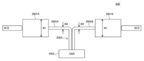
図2は、導電パターンで形成されたバンドパスフィルタの一例を概略的に示す平面図である。図2を参照して、バンドパスフィルタ200は、たとえば、幅W1の導電パターンで構成される低インピーダンス部2001A,2001Bと、幅W1よりも狭い幅W2の導電パターンで構成される高インピーダンス部2002A,2002Bとを組み合わせて形成されるステップインピーダンス共振器(SIR)である。高インピーダンス部2002Aと、高インピーダンス部2002Bとは、わずかな隙間を空けて配置されることにより結合線路2003を形成する。また、低インピーダンス部2001A,2001Bおよび高インピーダンス部2002A,2002Bは、すべて図1に示すような導電パターン1002で形成されている。2 is a plan view showing an example of a bandpass filter formed of a conductive pattern. Referring to FIG. 2, the
低インピーダンス部2001A,2001Bと高インピーダンス部2002A,2002Bとでは、特性インピーダンスが異なる。SIRでは、低インピーダンス部2001A,2001Bの幅および長さと、高インピーダンス部2002A,2002Bの幅および長さとを調整することで、共振条件、すなわちカットオフ周波数を設定する。The characteristic impedances of the
一般に、バンドパスフィルタの結合線路は電磁界を通して結合されるが、図2に示すバンドパスフィルタ200の結合線路2003では電流を流して磁界による結合を強化するため、図1に示すようなグランド層1003に接続している。Generally, the coupling lines of a bandpass filter are coupled through an electromagnetic field, but the
ここで、結合線路2003の長さは、バンドパスフィルタにおける通過帯域幅に影響する。結合線路2003が短いほど通過帯域幅は狭くなり、結合線路2003が長いほど通過帯域幅は広くなる。したがって、結合線路2003を有するSIRを用いたバンドパスフィルタ200の設計においては、結合線路2003の長さを調整し、任意の通過帯域幅を設定する。Here, the length of the coupled
一方で、結合線路2003が短くなり過ぎると、基板上において結合線路2003を形成することが製造上困難になる。この場合、結合線路2003を長くし、その分結合線路2003の結合度を弱くすることが考えられる。結合線路2003の結合度を弱めるには、導電パターンの幅を狭くする必要がある。しかしながら、導電パターンの幅を狭くすれば、特性インピーダンスが変わり、バンドパスフィルタのカットオフ周波数が設定値から外れることになる。On the other hand, if the coupled
結合線路2003が長くなり過ぎると、結合線路2003を配置するスペースを確保するために基板のサイズが大きくなる。この場合、結合線路2003を短くし、その分結合線路2003の結合度を強くすることが考えられる。結合線路2003の結合度を強めるには、導電パターンの幅を広くする必要がある。しかしながら、導電パターンの幅を広くすれば、特性インピーダンスが変わり、バンドパスフィルタのカットオフ周波数が設定値から外れることになる。If the coupled
したがって、設定しようとする通過帯域幅によっては、結合線路2003を所望の長さにすることが困難となる場合がある。
Therefore, depending on the passband width to be set, it may be difficult to make the
このように、従来技術では、導電パターンによってフィルタを形成しようとすれば、導電パターンの幅または結合線路の長さに制約があるため、所望のカットオフ周波数または通過帯域幅の実現が困難であった。このような経緯から本開示の無線装置は着想された。As described above, in conventional technology, when trying to form a filter using a conductive pattern, there are restrictions on the width of the conductive pattern or the length of the coupled line, making it difficult to achieve the desired cutoff frequency or passband width. This is the background to the concept of the wireless device disclosed herein.
以下、本開示の実施形態に係る高周波回路および無線装置について説明する。 Below, we will describe high-frequency circuits and wireless devices related to embodiments of the present disclosure.
図3は、本開示の実施の形態に係る無線装置の構成を示す平面図である。図3では、一例として、自動車に搭載される無線装置1を示している。
Figure 3 is a plan view showing the configuration of a wireless device according to an embodiment of the present disclosure. Figure 3 shows, as an example, a
図3を参照して、無線装置1は、高周波回路2と、入出力端子1Aと、テレビ用入出力端子1Bと、GPS(Global Positioning System)用入出力端子1Cと、ラジオ用入出力端子1Dとを備える。
Referring to Figure 3, the
入出力端子1Aは、高周波ケーブル1Eを介して図示しないアンテナに接続される。アンテナは、たとえば自動車のフロントガラス、リアガラスまたはルーフパネル等に設置され、RF信号(Radio Frequency Signal)を受信する。The input/
テレビ用入出力端子1B、GPS用入出力端子1Cおよびラジオ用入出力端子1Dはそれぞれ、対応の周波数帯域の無線信号を用いるサービスを提供可能な図示しない車載機と接続されている。たとえば、テレビ用入出力端子1Bは、テレビチューナー等のテレビに対応する車載機に接続され、GPS用入出力端子1Cは、カーナビゲーション等のGPSに対応する車載機に接続され、ラジオ用入出力端子1Dは、ラジオチューナー等のAM/FMラジオに対応する車載機に接続される。The television input/
高周波回路2は、入出力端子1Aにおいて受けた電波をテレビ車載機用、GPS車載機用およびラジオ車載機用に分波する。なお、高周波回路2は、テレビに対応する車載機およびGPSに対応する車載機から送信されたRF信号を合波して、入出力端子1Aから出力する構成であってもよい。The high-
図4は、図3中のIV-IV線での断面図である。理解を容易にするため図4では、図3に示す平面図を、フィルタを除き破線で示している。 Figure 4 is a cross-sectional view taken along line IV-IV in Figure 3. To facilitate understanding, Figure 4 shows the plan view shown in Figure 3 with dashed lines, excluding the filter.
図4を参照して、高周波回路2は、多層基板10により構成される。
Referring to Figure 4, the high-
[多層基板]
多層基板10は、たとえばプリント配線板である。多層基板10は、積層方向において主表面側から順に、導電パターン201が形成された層L1、誘電体層101A、第1グランド層102、誘電体層101B、中間グランド層103、誘電体層101Cおよび第2グランド層104を含む。
[Multilayer board]
The
導電パターン201が形成された層L1は、多層基板10の主表面を構成し、導電パターン等を含む。以下、導電パターン201が形成された層を、導電パターン層と称する。導電パターン201は、第1の導電パターンの一例である。The layer L1 on which the
誘電体層101Aは、導電パターン層L1と第1グランド層102との間に配置され、導電パターン層L1と第1グランド層102とを絶縁する。誘電体層101Aの材質は、たとえばガラスエポキシ樹脂である。後述する誘電体層101B,101Cも同様である。The
第1グランド層102は、導電パターン層L1とは異なる層であり、導電パターン層L1よりも下層に位置する。多層基板10では、第1グランド層102は、誘電体層101Aと誘電体層101Bとの間に配置される。第1グランド層102は、たとえば銅箔等の薄い導電体が形成された層である。後述する中間グランド層103および第2グランド層104も同様である。第1グランド層102は、一部において導電体が削除された形状を有する。削除された部分は空洞となっている。
The
誘電体層101Bは、第1グランド層102と中間グランド層103との間に配置され、第1グランド層102と中間グランド層103とを絶縁する。
The
中間グランド層103は、誘電体層101Bと誘電体層101Cとの間に配置される。中間グランド層103は、一部において導電体が削除された形状を有する。削除された部分は空洞となっている。The
誘電体層101Cは、中間グランド層103と第2グランド層104との間に配置され、中間グランド層103と第2グランド層104とを絶縁する。
The
第2グランド層104は、導電パターン層L1および第1グランド層102とは異なる層であり、第1グランド層102よりも下層に位置する。多層基板10では、第2グランド層104は、誘電体層101Cの下方に配置され、多層基板10の裏面を構成する。したがって、積層方向において、導電パターン層L1から第2グランド層104までの距離は、導電パターン層L1から第1グランド層102までの距離よりも長い。第2グランド層104は、平面視で概ね多層基板10の全域にわたって設けられる。第2グランド層104は、第1グランド層102および中間グランド層103とビアで電気的に接続されている。The
図3および図4を参照して、導電パターン層L1は、第1グランド層102、第2グランド層104および導電パターン層L1の積層方向において、第2グランド層104に形成された導電体までの距離が、第1グランド層102に形成された導電体までの距離よりも短い領域である第1の領域105を含む。たとえば、第1の領域105は、多層基板10における各層の積層方向において、第2グランド層104と対向する領域である。具体的には、第1の領域105は、平面視で長方形であり、導電パターン層L1に設けられた任意の大きさの領域である。図4に示すように、第1グランド層102および中間グランド層103において、第1の領域105に対応する領域には導電体は設けられず、空洞となっている。積層方向において第1の領域105の下方には、誘電体層101A,101B,101Cと、第2グランド層104とが配置されている。
3 and 4, the conductive pattern layer L1 includes a
導電パターン層L1は、第1グランド層102、第2グランド層104および導電パターン層L1の積層方向において、第1グランド層102に形成された導電体までの距離が、第2グランド層104に形成された導電体までの距離よりも短い領域である第2の領域107を含む。たとえば、第2の領域107は、多層基板10における各層の積層方向において、第1グランド層102と対向する領域である。具体的には、第2の領域107は、導電パターン層L1において、第1の領域105以外の領域である。第2の領域107は、導電パターン層L1において第1の領域105とは重複せず、別個の領域である。図4に示すように、第1グランド層102において、第2の領域107に対応する領域には導電体が設けられている。積層方向において第2の領域107の下方には、誘電体層101Aと、第1グランド層102とが配置されている。
The conductive pattern layer L1 includes a
[フィルタ]
再び図3を参照して、多層基板10の導電パターン層L1に形成された導電パターンは、フィルタの一部を構成する。多層基板10では、導電パターン201は、テレビ用フィルタの一部を構成する。具体的には、テレビ用フィルタは、導電パターン201および第2グランド層104により構成される。テレビ用フィルタは、第1のフィルタの一例である。テレビ用フィルタは、たとえば通過帯域が470MHz~710MHzとなるように設定される。この場合、テレビ用フィルタにおいて、通過帯域幅は240MHz、中心周波数は590MHzおよび比帯域は0.41となる。
[filter]
3, the conductive pattern formed on the conductive pattern layer L1 of the
導電パターン201は、低インピーダンス部2011,2012と、高インピーダンス部2013,2014とを含む。
The
低インピーダンス部2011,2012は、平面視で概ね長方形であり、間隔を空けて並んで配置される。
The
無線装置1はさらに、コンデンサ1F1,1F2を備える。低インピーダンス部2011は、コンデンサ1F1を介して、入出力端子1Aに接続される。低インピーダンス部2012は、コンデンサ1F2を介して、テレビ用入出力端子1Bに接続される。The
高インピーダンス部2013,2014は、低インピーダンス部2011,2012よりも導電パターンの幅が狭い。高インピーダンス部2013,2014における導電パターンの幅および長さと、低インピーダンス部2011,2012における導電パターンの幅および長さとは、所望のカットオフ周波数に合わせて適宜設定される。The
高インピーダンス部2013,2014は、平面視で概ねL字型であり、低インピーダンス部2011,2012の間に並んで配置される。高インピーダンス部2013,2014の一部は、わずかな隙間を開けて平行に配置され、結合線路2016を形成する。結合線路2016において、高インピーダンス部2013,2014は、電磁気的に結合される。The
低インピーダンス部2011,2012、高インピーダンス部2013,2014からなる共振器の長さは、通過帯域の中心周波数における波長の1/4の長さに設定される。ただし、共振器の長さは、通過帯域の中心周波数における波長の1/2の長さでもよい。The length of the resonator consisting of the
導電パターン201の少なくとも一部分は、第1の領域105に設けられ、第2グランド層104と電気的に接続される。たとえば、導電パターン201は、第1の領域105の領域内に配置されており、第1の領域105外には配置されていない。導電パターン201における結合線路2016は、導電パターン層L1に形成されたグランドパターン106に接続される。グランドパターン106には、1または複数のビア2017が設けられている。ビア2017は、グランドパターン106と第2グランド層104とを電気的に接続する。なお、図3中の「L4 GND」は、導電パターン201が、配線層としては第4層目に相当する第2グランド層104をリファレンスのグランドとしていることを意味している。At least a portion of the
図3および図4に示すように、導電パターン層L1には、導電パターン201とは別の導電パターン202がさらに形成されている。導電パターン202は、第2の導電パターンの一例である。多層基板10では、導電パターン202は、GPS用フィルタの一部を構成する。具体的には、GPS用フィルタは、導電パターン202および第1グランド層102により構成される。GPS用フィルタは、第2のフィルタの一例である。
As shown in Figures 3 and 4, a
導電パターン202は、第2の領域107に設けられ、第1グランド層102と電気的に接続される。たとえば、導電パターン202は、第2の領域107の領域内に配置されており、第2の領域107外には配置されていない。GPS用フィルタは、たとえば通過帯域が1525MHz~1625MHzとなるように設定される。この場合、GPS用フィルタにおいて、通過帯域幅は100MHz、中心周波数は1575MHzおよび比帯域は0.06となる。すなわち、GPS用フィルタの比帯域は、テレビ用フィルタの比帯域よりも狭い。The
具体的には、導電パターン202は、低インピーダンス部2021,2022と、高インピーダンス部2023,2024とを含む。Specifically, the
低インピーダンス部2021,2022は、平面視で概ね長方形であり、直線状に間隔を空けて配置される。The
無線装置1はさらに、コンデンサ1F3,1F4を備える。低インピーダンス部2021は、コンデンサ1F3を介して、入出力端子1Aに接続される。低インピーダンス部2022は、コンデンサ1F4を介して、GPS用入出力端子1Cに接続される。The
高インピーダンス部2023,2024は、低インピーダンス部2021,2022よりも導電パターンの幅が狭い。高インピーダンス部2023,2024における導電パターンの幅および長さと、低インピーダンス部2021,2022における導電パターンの幅および長さとは、所望のカットオフ周波数に合わせて適宜設定される。The
高インピーダンス部2023,2024は、平面視で概ねL字型であり、低インピーダンス部2021,2022の間に並んで配置される。高インピーダンス部2023,2024の一部は、わずかな隙間を開けて平行に配置され、結合線路2026を形成する。結合線路2026において、高インピーダンス部2023,2024は、電磁気的に結合される。The
低インピーダンス部2021,2022、および高インピーダンス部2023,2024からなる共振器の長さは、通過帯域の中心周波数における波長の1/4の長さに設定される。ただし、共振器の長さは、通過帯域の中心周波数における波長の1/2の長さでもよい。The length of the resonator consisting of the
結合線路2026は、導電パターン層L1に形成されたグランドパターン108に接続される。グランドパターン108には、1または複数のビア2027が設けられている。ビア2027は、グランドパターン108と第1グランド層102とを電気的に接続する。なお、図3中の「L2 GND」は、導電パターン202が、配線層としては第2層目に相当する第1グランド層102をリファレンスのグランドとしていることを意味している。The
高周波回路2は、さらに、第2の領域107において導電パターン202とは別の領域に設けられたラジオ用フィルタを備えている。一般に、ラジオ用フィルタはインダクタおよびコンデンサで構成されるローパスフィルタ(LPF)であるが、図3に示すラジオ用フィルタ203では、インダクタをコイルおよびパターンで構成し、ラジオ用入出力端子1Dに接続される。ラジオ用フィルタ203の電気回路は、周知の構成であるので詳細な説明は行わない。The
このように、本実施の形態に係る高周波回路2および無線装置1では、導電パターン201が、第1の領域105に設けられる構成により、導電パターン201から第2グランド層104に形成された導電体までの距離を長くすることができる。導電パターン201から第2グランド層104に形成された導電体までの距離を長くすれば、導電パターン201の特性インピーダンスは上昇する。そのため、導電パターン201の幅を広くすることによる導電パターン201の特性インピーダンスの低下分を、導電パターン201から第2グランド層104に形成された導電体までの距離を長くすることで相殺することができる。これにより、所望の特性インピーダンスを維持したまま導電パターン201の幅を広くすることができる。したがって、パターンフィルタにおいて所望のインピーダンスを実現しつつ、装置設計の自由度を向上させることができる。
In this way, in the high-
また、結合線路を有するSIRを導電パターンによって形成する場合、導電パターン201が、第1の領域105に設けられる構成により、導電パターン201の幅を広くすることによる導電パターン201の特性インピーダンスの低下分を、導電パターン201から第2グランド層104に形成された導電体までの距離を長くすることで相殺することができる。これにより、所望の特性インピーダンスを維持したまま結合線路2016を短くすることができる。したがって、パターンフィルタにおいて所望のインピーダンスを実現しつつ、装置設計の自由度を向上させることができる。Furthermore, when an SIR having a coupled line is formed by a conductive pattern, the
(変形例)
図5は、本開示の実施の形態の変形例に係る無線装置の構成を示す平面図である。図5に示す無線装置は、図3に示す無線装置と比べて、導電パターン201における低インピーダンス部2011,2012および第1の領域105が小さい。
(Modification)
Fig. 5 is a plan view showing a configuration of a wireless device according to a modified embodiment of the present disclosure. The wireless device shown in Fig. 5 has smaller
図6は、図5中のVI-VI線での断面図である。理解を容易にするため図6では、図5に示す平面図を、導電パターンを除き破線で示している。 Figure 6 is a cross-sectional view taken along line VI-VI in Figure 5. To facilitate understanding, in Figure 6, the plan view shown in Figure 5 is shown with dashed lines, except for the conductive patterns.
図5および図6を参照して、変形例に係る無線装置1では、導電パターン201が、第1の領域105および第2の領域107にまたがって設けられる。具体的には、導電パターン201において、高インピーダンス部2013,2014が第1の領域105に設けられ、低インピーダンス部2011,2012が第2の領域107に設けられる。5 and 6, in the
この場合であっても、導電パターン201の一部分は、積層方向において第2グランド層104と対向する。そのため、導電パターン201とリファレンスグランドまでの距離を長くすることができ、所望の特性インピーダンスを実現しつつ、装置設計の自由度をさらに向上させることができる。Even in this case, a portion of the
上記実施の形態は、すべての点で例示であって制限的なものではないと考えられるべきである。本開示の範囲は、上記説明ではなく請求の範囲によって示され、請求の範囲と均等の意味および範囲内でのすべての変更が含まれることが意図される。The above-described embodiments should be considered to be illustrative and not restrictive in all respects. The scope of the present disclosure is indicated by the claims, not by the above description, and is intended to include all modifications within the meaning and scope of the claims.
導電パターン層L1において、第1の領域105の位置は特に限定されるものではない。第1の領域105は、導電パターン201の特性インピーダンスが対象信号、すなわち入出力端子1Aに接続されたアンテナにおいて受信されるRF信号の周波数に対して一定値となるように設けられていればよい。たとえば、第1の領域105は、入出力端子1Aに接続されたアンテナにおいて受信されるRF信号の周波数変動に対する導電パターン201の特性インピーダンスの変動幅が5パーセント未満となるように設けられることが好ましく、当該変動幅が3パーセント未満となるように設けられることがより好ましく、当該変動幅が1パーセント未満となるように設けられることがさらに好ましい。In the conductive pattern layer L1, the position of the
上述の説明では、高周波回路2がラジオ用フィルタ203を備えている場合について説明した。しかしながら、高周波回路2はラジオ用フィルタ203を備えていなくてもよい。In the above description, the
上述の説明では、導電パターン201を含むテレビ用フィルタおよび導電パターン202を含むGPS用フィルタが、結合線路を有するSIRである場合について説明した。しかしながら、高周波回路2において、フィルタは、結合線路を有するSIRに限定されない。フィルタは、単一線路で構成されるSIRでもよいし、幅が一定の導体パターンで構成されるパターンフィルタであってもよい。当該フィルタは、多層基板10の導電パターン層L1において幅が一定の導体パターンにより形成され、第2グランド層104と積層方向において対向する第1の領域105に設けられる。In the above description, the TV filter including the
上述の説明では、図3に示すように、導電パターン201,202が多層基板10の主表面(フィルタが形成された層L1)に形成される場合について説明した。しかしながら、導電パターン201,202が形成される層はこれに限定されない。導電パターン201,202は、主表面よりも下層、すなわち多層基板10の内層に形成されていてもよい。たとえば、図3に示す多層基板10において、導電パターン層L1は主表面の1つ下層(図4では第1グランド層102が配置されている層)に配置されてもよい。この場合、第1グランド層は主表面の2つ下層(図4では中間グランド層103が配置されている層)に配置されてもよいし、主表面に配置されてもよい。また、第1グランド層が主表面に配置される場合、第2グランド層は主表面の2つ下層(図4では中間グランド層103が配置されている層)に配置されてもよい。第1グランド層102および第2グランド層104は共に導電パターン層L1よりも上層に配置されてもよいし、下層に配置されてもよい。また、第1グランド層102および第2グランド層104のうちの一方が導電パターン層L1よりも上層に配置され、他方が導電パターン層L1よりも下層に配置されてもよい。要するに、導電パターン層L1から第1グランド層102までの距離が、導電パターン層L1から第2グランド層104までの距離と異なっていればよく、導電パターン層L1、第1グランド層102および第2グランド層104の配置は、図3に示す例に限定されるものではない。In the above description, as shown in FIG. 3, the
また、上述の説明では、図3に示すように、第1グランド層102が、一部において導電体が削除された形状を有する場合について説明した。しかしながら、第1グランド層102および中間グランド層103はこれに限定されない。たとえば、第1グランド層102および第2グランド層104のうちの一方が導電パターン層L1よりも上層に配置され、他方が導電パターン層L1よりも下層に配置され、かつ導電パターン層L1から第2グランド層104までの距離が導電パターン層L1から第1グランド層102までの距離よりも長い場合、第1グランド層102は、全面において導電体が形成された形状を有してもよい。この場合、導電パターン層L1は、全体が第1の領域105であり、第2の領域107を含まない。要するに、導電パターン層L1が、第2グランド層104に形成された導電体までの距離が、第1グランド層102に形成された導電体までの距離よりも長い領域である第1の領域105を含み、かつ導電パターン201の少なくとも一部分が当該第1の領域105に形成されていればよい。
In the above description, the
上述の説明では、多層基板10が中間グランド層103を含む場合について説明した。しかしながら、多層基板10は第1グランド層102および第2グランド層104を含んでいればよく、中間グランド層103を含んでいなくてもよい。なお、多層基板10が中間グランド層103を含む場合、多層基板10は複数の中間グランド層103を含んでいてもよい。In the above description, the
上述の説明では、第1グランド層102が誘電体層101A,101Bの間に配置され、第2グランド層104が多層基板10の裏面に配置される場合について説明した。しかしながら、第1グランド層102および第2グランド層104の配置はこれに限定されない。第2グランド層104は、第1グランド層102よりも下層に配置されていればよい。In the above description, the
上述の説明では、無線装置1が自動車に搭載される場合について説明した。しかしながら、無線装置1はこれに限定されない。無線装置1は、自動車以外の輸送機器に搭載されていてもよいし、建物に設置されていてもよいし、携帯無線機であってもよい。要するに、無線装置1は、無線通信を行う機器であればよい。In the above explanation, the
以上の説明は、以下に付記する特徴を含む。
[付記1]
多層基板と、
前記多層基板において導電パターンにより形成されたフィルタと、
前記多層基板の前記フィルタが形成された層において導電パターンにより形成された結合線路を有するステップインピーダンス共振器とを備え、
前記多層基板は、
前記フィルタとは異なる層に配置された第1グランド層と、
前記フィルタおよび前記第1グランド層とは異なる層に配置された第2グランド層とを含み、
前記フィルタが形成された層から前記第2グランド層までの距離は、前記フィルタが形成された層から前記第1グランド層までの距離よりも長く、
前記フィルタが形成された層は、前記第2グランド層と積層方向において対向する第1の領域を含み、
前記ステップインピーダンス共振器は、前記第1の領域に設けられる、無線装置。
The above description includes the following additional features.
[Appendix 1]
A multilayer board;
a filter formed by a conductive pattern on the multilayer substrate;
a stepped impedance resonator having a coupled line formed by a conductive pattern in a layer of the multilayer substrate on which the filter is formed,
The multilayer substrate comprises:
a first ground layer disposed on a layer different from the filter;
a second ground layer disposed on a layer different from the filter and the first ground layer,
a distance from the layer on which the filter is formed to the second ground layer is longer than a distance from the layer on which the filter is formed to the first ground layer;
the layer in which the filter is formed includes a first region facing the second ground layer in a lamination direction,
The stepped impedance resonator is provided in the first region.
[付記2]
第1グランド層と前記第1グランド層とは異なる層に配置された第2グランド層とを含む多層基板と、
前記多層基板において前記第1グランド層および前記第2グランド層とは異なる層に配置され、導電パターンにより形成されたフィルタとを備え、
前記フィルタが形成された層から前記第2グランド層までの距離は、前記フィルタが形成された層から前記第1グランド層までの距離よりも長く、
前記フィルタが形成された層は、前記第2グランド層と積層方向において対向する第1の領域を含み、
前記フィルタは、前記第1の領域に設けられる、無線装置。
[Appendix 2]
a multilayer substrate including a first ground layer and a second ground layer disposed on a layer different from the first ground layer;
a filter formed of a conductive pattern and disposed on a layer of the multilayer board different from the first ground layer and the second ground layer;
a distance from the layer on which the filter is formed to the second ground layer is longer than a distance from the layer on which the filter is formed to the first ground layer;
the layer in which the filter is formed includes a first region facing the second ground layer in a lamination direction,
The filter is provided in the first area.
1 無線装置
2 高周波回路
1A 入出力端子
1B テレビ用入出力端子
1C GPS用入出力端子
1D ラジオ用入出力端子
1E 高周波ケーブル
1F1~1F4 コンデンサ
10 多層基板
L1 導電パターンが形成された層(導電パターン層)
100 フィルタ
101,101A,101B,101C 誘電体層
102 第1グランド層
103 中間グランド層
104 第2グランド層
105 第1の領域
106,108 グランドパターン
107 第2の領域
1001 誘電体層
1002 導電パターン
1003 グランド層
200 バンドパスフィルタ
201 導電パターン
2001A,2001B 低インピーダンス部
2002A,2002B 高インピーダンス部
2003 結合線路
2011,2012 低インピーダンス部
2013,2014 高インピーダンス部
2016 結合線路
2017 ビア
202 導電パターン
2021,2022 低インピーダンス部
2023,2024 高インピーダンス部
2026 結合線路
2027 ビア
203 ラジオ用フィルタ
REFERENCE SIGNS
100
Claims (8)
導電体である第2導電体が形成された第2グランド層と、
第1の導電パターンが形成された導電パターン層とを備え、
前記第1グランド層、前記第2グランド層および前記導電パターン層は、積層されており、
前記導電パターン層から前記第2グランド層までの距離は、前記導電パターン層から前記第1グランド層までの距離よりも長く、
前記導電パターン層は、前記第2導電体と対向する第1の領域と、前記第1導電体と対向する第2の領域とを含み、
前記第1グランド層、前記第2グランド層および前記導電パターン層の積層方向において、前記第1導電体および前記第2導電体のうちの前記第1の領域との間の距離が最も短い前記導電体は、前記第2導電体であり、
前記積層方向において、前記第1導電体および前記第2導電体のうちの前記第2の領域との間の距離が最も短い前記導電体は、前記第1導電体であり、
前記第1の導電パターンの少なくとも一部分は、前記第1の領域に設けられ、
前記導電パターン層には、前記第1の導電パターンとは別の第2の導電パターンがさらに形成されており、
前記第2の導電パターンは、前記第2の領域に設けられ、
前記第1の導電パターンは、第1のフィルタの一部を構成し、
前記第2の導電パターンは、第2のフィルタの一部を構成し、
前記第2のフィルタの比帯域は、前記第1のフィルタの比帯域よりも狭い、高周波回路。 a first ground layer on which a first conductor is formed;
a second ground layer on which a second conductor is formed;
a conductive pattern layer on which a first conductive pattern is formed;
the first ground layer, the second ground layer, and the conductive pattern layer are laminated,
a distance from the conductive pattern layer to the second ground layer is longer than a distance from the conductive pattern layer to the first ground layer;
the conductive pattern layer includes a first region facing the second conductor and a second region facing the first conductor ;
In a lamination direction of the first ground layer, the second ground layer, and the conductive pattern layer, the first conductor and the second conductor are separated by a shortest distance from the first region to the second conductor, and the second conductor is separated by a shortest distance from the first region to the first ground layer, the second ground layer, and the conductive pattern layer.
In the stacking direction, of the first conductor and the second conductor, the conductor having the shortest distance between the first conductor and the second region is the first conductor,
At least a portion of the first conductive pattern is provided in the first region ;
a second conductive pattern separate from the first conductive pattern is further formed on the conductive pattern layer;
the second conductive pattern is provided in the second region,
the first conductive pattern constitutes a part of a first filter;
the second conductive pattern constitutes a part of a second filter;
A high-frequency circuit , wherein the fractional bandwidth of the second filter is narrower than the fractional bandwidth of the first filter .
前記第2の導電パターンの特性インピーダンスは、前記第2の領域から前記第1導電体までの距離によって決定される、請求項1から請求項3のいずれか1項に記載の高周波回路。4. The high-frequency circuit according to claim 1, wherein a characteristic impedance of the second conductive pattern is determined by a distance from the second region to the first conductor.
前記積層方向において前記第2の領域に対向する前記第1グランド層の部分には、前記第1導電体が形成される、請求項4に記載の高周波回路。5. The high-frequency circuit according to claim 4, wherein the first conductor is formed in a portion of the first ground layer facing the second region in the stacking direction.
導電体である第2導電体が形成された第2グランド層と、
第1の導電パターンが形成された導電パターン層とを備え、
前記第1グランド層、前記第2グランド層および前記導電パターン層は、積層されており、
前記導電パターン層から前記第2グランド層までの距離は、前記導電パターン層から前記第1グランド層までの距離よりも長く、
前記導電パターン層は、前記第2導電体と対向する第1の領域と、前記第1導電体と対向する第2の領域とを含み、
前記第1グランド層、前記第2グランド層および前記導電パターン層の積層方向において、前記第1導電体および前記第2導電体のうちの前記第1の領域との間の距離が最も短い前記導電体は、前記第2導電体であり、
前記積層方向において、前記第1導電体および前記第2導電体のうちの前記第2の領域との間の距離が最も短い前記導電体は、前記第1導電体であり、
前記第1の導電パターンの少なくとも一部分は、前記第1の領域に設けられ、
前記導電パターン層には、前記第1の導電パターンとは別の第2の導電パターンがさらに形成されており、
前記第2の導電パターンは、前記第2の領域に設けられ、
前記第1の導電パターンは、第1のフィルタの一部を構成し、
前記第2の導電パターンは、第2のフィルタの一部を構成し、
前記第2のフィルタの比帯域は、前記第1のフィルタの比帯域よりも狭く、
前記第1のフィルタは、前記第1の導電パターンの一部により構成される低インピーダンス部と、前記第1の導電パターンの他の一部により構成される高インピーダンス部とを含むステップインピーダンス共振器である、高周波回路。 a first ground layer on which a first conductor is formed;
a second ground layer on which a second conductor is formed;
a conductive pattern layer on which a first conductive pattern is formed;
the first ground layer, the second ground layer, and the conductive pattern layer are laminated,
a distance from the conductive pattern layer to the second ground layer is longer than a distance from the conductive pattern layer to the first ground layer;
the conductive pattern layer includes a first region facing the second conductor and a second region facing the first conductor ;
In a lamination direction of the first ground layer, the second ground layer, and the conductive pattern layer, the first conductor and the second conductor are separated by a shortest distance from the first region to the second conductor, and the second conductor is separated by a shortest distance from the first region to the first ground layer, the second ground layer, and the conductive pattern layer.
In the stacking direction, of the first conductor and the second conductor, the conductor having the shortest distance between the first conductor and the second region is the first conductor,
At least a portion of the first conductive pattern is provided in the first region;
a second conductive pattern separate from the first conductive pattern is further formed on the conductive pattern layer;
the second conductive pattern is provided in the second region,
the first conductive pattern constitutes a part of a first filter;
the second conductive pattern constitutes a part of a second filter;
a fractional bandwidth of the second filter is narrower than a fractional bandwidth of the first filter;
a high-frequency circuit, wherein the first filter is a stepped impedance resonator including a low-impedance section formed by a part of the first conductive pattern and a high-impedance section formed by another part of the first conductive pattern.
導電体である第2導電体が形成された第2グランド層と、
第1の導電パターンが形成された導電パターン層とを備え、
前記第1グランド層、前記第2グランド層および前記導電パターン層は、積層されており、
前記導電パターン層から前記第2グランド層までの距離は、前記導電パターン層から前記第1グランド層までの距離よりも長く、
前記導電パターン層は、前記第2導電体と対向する第1の領域と、前記第1導電体と対向する第2の領域とを含み、
前記第1グランド層、前記第2グランド層および前記導電パターン層の積層方向において、前記第1導電体および前記第2導電体のうちの前記第1の領域との間の距離が最も短い前記導電体は、前記第2導電体であり、
前記積層方向において、前記第1導電体および前記第2導電体のうちの前記第2の領域との間の距離が最も短い前記導電体は、前記第1導電体であり、
前記第1の導電パターンの少なくとも一部分は、前記第1の領域に設けられ、
前記導電パターン層には、前記第1の導電パターンとは別の第2の導電パターンがさらに形成されており、
前記第2の導電パターンは、前記第2の領域に設けられ、
前記第1の導電パターンは、第1のフィルタの一部を構成し、
前記第2の導電パターンは、第2のフィルタの一部を構成し、
前記第2のフィルタの比帯域は、前記第1のフィルタの比帯域よりも狭く、
前記第1のフィルタは、前記第1の導電パターンの一部により構成される低インピーダンス部と、前記第1の導電パターンの他の一部により構成される高インピーダンス部とを含むステップインピーダンス共振器であり、
前記高インピーダンス部は、前記第1の領域に設けられ、
前記低インピーダンス部は、前記第2の領域に設けられる、高周波回路。
a first ground layer on which a first conductor is formed;
a second ground layer on which a second conductor is formed;
a conductive pattern layer on which a first conductive pattern is formed;
the first ground layer, the second ground layer, and the conductive pattern layer are laminated,
a distance from the conductive pattern layer to the second ground layer is longer than a distance from the conductive pattern layer to the first ground layer;
the conductive pattern layer includes a first region facing the second conductor and a second region facing the first conductor ;
In a lamination direction of the first ground layer, the second ground layer, and the conductive pattern layer, the first conductor and the second conductor are separated by a shortest distance from the first region to the second conductor, and the second conductor is separated by a shortest distance from the first region to the first ground layer, the second ground layer, and the conductive pattern layer.
In the stacking direction, of the first conductor and the second conductor, the conductor having the shortest distance between the first conductor and the second region is the first conductor,
At least a portion of the first conductive pattern is provided in the first region;
a second conductive pattern separate from the first conductive pattern is further formed on the conductive pattern layer;
the second conductive pattern is provided in the second region,
the first conductive pattern constitutes a part of a first filter;
the second conductive pattern constitutes a part of a second filter;
a fractional bandwidth of the second filter is narrower than a fractional bandwidth of the first filter;
the first filter is a stepped impedance resonator including a low impedance section formed by a part of the first conductive pattern and a high impedance section formed by another part of the first conductive pattern,
the high impedance portion is provided in the first region,
The low impedance section is provided in the second region.
Applications Claiming Priority (3)
| Application Number | Priority Date | Filing Date | Title |
|---|---|---|---|
| JP2020134329 | 2020-08-07 | ||
| JP2020134329 | 2020-08-07 | ||
| PCT/JP2021/026966 WO2022030238A1 (en) | 2020-08-07 | 2021-07-19 | High-frequency circuit and radio device |
Publications (3)
| Publication Number | Publication Date |
|---|---|
| JPWO2022030238A1 JPWO2022030238A1 (en) | 2022-02-10 |
| JPWO2022030238A5 JPWO2022030238A5 (en) | 2023-06-08 |
| JP7635784B2 true JP7635784B2 (en) | 2025-02-26 |
Family
ID=80117299
Family Applications (1)
| Application Number | Title | Priority Date | Filing Date |
|---|---|---|---|
| JP2022541424A Active JP7635784B2 (en) | 2020-08-07 | 2021-07-19 | High frequency circuits and wireless devices |
Country Status (4)
| Country | Link |
|---|---|
| US (1) | US12136764B2 (en) |
| JP (1) | JP7635784B2 (en) |
| CN (1) | CN116134975B (en) |
| WO (1) | WO2022030238A1 (en) |
Citations (3)
| Publication number | Priority date | Publication date | Assignee | Title |
|---|---|---|---|---|
| JP2001044712A (en) | 1999-07-28 | 2001-02-16 | Ricoh Co Ltd | Strip line |
| JP2002368502A (en) | 2001-06-07 | 2002-12-20 | Ngk Insulators Ltd | Multilayer dielectric filter |
| JP2013251863A (en) | 2012-06-04 | 2013-12-12 | Nippon Telegr & Teleph Corp <Ntt> | Impedance converter |
Family Cites Families (7)
| Publication number | Priority date | Publication date | Assignee | Title |
|---|---|---|---|---|
| JPH04288702A (en) | 1991-03-18 | 1992-10-13 | Fujitsu Ltd | Filter |
| JP2002271109A (en) * | 2001-03-08 | 2002-09-20 | Taiyo Yuden Co Ltd | Laminated duplexer element |
| JP2003110311A (en) * | 2001-09-28 | 2003-04-11 | Toshiba Corp | High frequency circuit board |
| JP4113196B2 (en) * | 2005-03-18 | 2008-07-09 | 株式会社東芝 | Microwave filter |
| JP2010087830A (en) | 2008-09-30 | 2010-04-15 | Tdk Corp | Multi-layered band pass filter and high frequency module |
| WO2014068811A1 (en) * | 2012-11-02 | 2014-05-08 | 日本電気株式会社 | Semiconductor package and mounting structure thereof |
| WO2020014874A1 (en) * | 2018-07-17 | 2020-01-23 | 华为技术有限公司 | Integrated circuit and terminal device |
-
2021
- 2021-07-19 JP JP2022541424A patent/JP7635784B2/en active Active
- 2021-07-19 CN CN202180057266.8A patent/CN116134975B/en active Active
- 2021-07-19 WO PCT/JP2021/026966 patent/WO2022030238A1/en not_active Ceased
-
2023
- 2023-02-06 US US18/105,893 patent/US12136764B2/en active Active
Patent Citations (3)
| Publication number | Priority date | Publication date | Assignee | Title |
|---|---|---|---|---|
| JP2001044712A (en) | 1999-07-28 | 2001-02-16 | Ricoh Co Ltd | Strip line |
| JP2002368502A (en) | 2001-06-07 | 2002-12-20 | Ngk Insulators Ltd | Multilayer dielectric filter |
| JP2013251863A (en) | 2012-06-04 | 2013-12-12 | Nippon Telegr & Teleph Corp <Ntt> | Impedance converter |
Also Published As
| Publication number | Publication date |
|---|---|
| JPWO2022030238A1 (en) | 2022-02-10 |
| US20230187840A1 (en) | 2023-06-15 |
| WO2022030238A1 (en) | 2022-02-10 |
| CN116134975A (en) | 2023-05-16 |
| CN116134975B (en) | 2025-10-28 |
| US12136764B2 (en) | 2024-11-05 |
Similar Documents
| Publication | Publication Date | Title |
|---|---|---|
| JP2905094B2 (en) | Demultiplexer package | |
| JP4579198B2 (en) | Multilayer bandpass filter | |
| JP5178899B2 (en) | Multilayer board | |
| US8952767B2 (en) | Layered bandpass filter | |
| US8031035B2 (en) | Circuit configuration | |
| US7432786B2 (en) | High frequency filter | |
| JP3778075B2 (en) | Filter circuit | |
| CN107681275B (en) | Antenna and electronic device | |
| US6798320B2 (en) | Microstrip line having a line electrode with integral edge electrodes | |
| JPH10270976A (en) | Demultiplexer package | |
| US7012481B2 (en) | Duplexer, and laminate-type high-frequency device and communication equipment using the same | |
| US20230208377A1 (en) | Filter, multiplexer, and communication module | |
| US7579929B2 (en) | Transmission circuit, antenna duplexer, and radio-frequency switch circuit | |
| JP7635784B2 (en) | High frequency circuits and wireless devices | |
| US8400236B2 (en) | Electronic component | |
| JP7589800B2 (en) | Dielectric resonator, and dielectric filter and multiplexer using the same | |
| JPH1197962A (en) | High-frequency component | |
| US12586879B2 (en) | Dielectric resonator, and dielectric filter and multiplexer using same | |
| US20200389144A1 (en) | Filter module | |
| JP2010074255A (en) | High-frequency filter device | |
| US12334896B2 (en) | Multiplexer and antenna module | |
| JP4195568B2 (en) | Multilayer electronic components | |
| US20230327632A1 (en) | Filter and multiplexer | |
| JP2005203824A (en) | High frequency coupler | |
| WO2022209122A1 (en) | Dielectric filter |
Legal Events
| Date | Code | Title | Description |
|---|---|---|---|
| A529 | Written submission of copy of amendment under article 34 pct |
Free format text: JAPANESE INTERMEDIATE CODE: A5211 Effective date: 20221129 |
|
| A621 | Written request for application examination |
Free format text: JAPANESE INTERMEDIATE CODE: A621 Effective date: 20240122 |
|
| A131 | Notification of reasons for refusal |
Free format text: JAPANESE INTERMEDIATE CODE: A131 Effective date: 20241015 |
|
| A521 | Request for written amendment filed |
Free format text: JAPANESE INTERMEDIATE CODE: A523 Effective date: 20241121 |
|
| TRDD | Decision of grant or rejection written | ||
| A01 | Written decision to grant a patent or to grant a registration (utility model) |
Free format text: JAPANESE INTERMEDIATE CODE: A01 Effective date: 20250114 |
|
| A61 | First payment of annual fees (during grant procedure) |
Free format text: JAPANESE INTERMEDIATE CODE: A61 Effective date: 20250127 |
|
| R150 | Certificate of patent or registration of utility model |
Ref document number: 7635784 Country of ref document: JP Free format text: JAPANESE INTERMEDIATE CODE: R150 |