JP7635301B2 - Semiconductor Device - Google Patents
Semiconductor Device Download PDFInfo
- Publication number
- JP7635301B2 JP7635301B2 JP2023101689A JP2023101689A JP7635301B2 JP 7635301 B2 JP7635301 B2 JP 7635301B2 JP 2023101689 A JP2023101689 A JP 2023101689A JP 2023101689 A JP2023101689 A JP 2023101689A JP 7635301 B2 JP7635301 B2 JP 7635301B2
- Authority
- JP
- Japan
- Prior art keywords
- insulator
- oxide
- conductor
- transistor
- film
- Prior art date
- Legal status (The legal status is an assumption and is not a legal conclusion. Google has not performed a legal analysis and makes no representation as to the accuracy of the status listed.)
- Active
Links
Images


Classifications
-
- H—ELECTRICITY
- H10—SEMICONDUCTOR DEVICES; ELECTRIC SOLID-STATE DEVICES NOT OTHERWISE PROVIDED FOR
- H10D—INORGANIC ELECTRIC SEMICONDUCTOR DEVICES
- H10D1/00—Resistors, capacitors or inductors
- H10D1/60—Capacitors
- H10D1/68—Capacitors having no potential barriers
- H10D1/692—Electrodes
- H10D1/711—Electrodes having non-planar surfaces, e.g. formed by texturisation
- H10D1/716—Electrodes having non-planar surfaces, e.g. formed by texturisation having vertical extensions
-
- H—ELECTRICITY
- H10—SEMICONDUCTOR DEVICES; ELECTRIC SOLID-STATE DEVICES NOT OTHERWISE PROVIDED FOR
- H10B—ELECTRONIC MEMORY DEVICES
- H10B12/00—Dynamic random access memory [DRAM] devices
- H10B12/01—Manufacture or treatment
- H10B12/02—Manufacture or treatment for one transistor one-capacitor [1T-1C] memory cells
-
- H—ELECTRICITY
- H10—SEMICONDUCTOR DEVICES; ELECTRIC SOLID-STATE DEVICES NOT OTHERWISE PROVIDED FOR
- H10B—ELECTRONIC MEMORY DEVICES
- H10B12/00—Dynamic random access memory [DRAM] devices
- H10B12/30—DRAM devices comprising one-transistor - one-capacitor [1T-1C] memory cells
-
- H—ELECTRICITY
- H10—SEMICONDUCTOR DEVICES; ELECTRIC SOLID-STATE DEVICES NOT OTHERWISE PROVIDED FOR
- H10B—ELECTRONIC MEMORY DEVICES
- H10B41/00—Electrically erasable-and-programmable ROM [EEPROM] devices comprising floating gates
- H10B41/20—Electrically erasable-and-programmable ROM [EEPROM] devices comprising floating gates characterised by three-dimensional [3D] arrangements, e.g. with cells on different height levels
-
- H—ELECTRICITY
- H10—SEMICONDUCTOR DEVICES; ELECTRIC SOLID-STATE DEVICES NOT OTHERWISE PROVIDED FOR
- H10B—ELECTRONIC MEMORY DEVICES
- H10B41/00—Electrically erasable-and-programmable ROM [EEPROM] devices comprising floating gates
- H10B41/70—Electrically erasable-and-programmable ROM [EEPROM] devices comprising floating gates the floating gate being an electrode shared by two or more components
-
- H—ELECTRICITY
- H10—SEMICONDUCTOR DEVICES; ELECTRIC SOLID-STATE DEVICES NOT OTHERWISE PROVIDED FOR
- H10D—INORGANIC ELECTRIC SEMICONDUCTOR DEVICES
- H10D30/00—Field-effect transistors [FET]
- H10D30/01—Manufacture or treatment
- H10D30/021—Manufacture or treatment of FETs having insulated gates [IGFET]
-
- H—ELECTRICITY
- H10—SEMICONDUCTOR DEVICES; ELECTRIC SOLID-STATE DEVICES NOT OTHERWISE PROVIDED FOR
- H10D—INORGANIC ELECTRIC SEMICONDUCTOR DEVICES
- H10D30/00—Field-effect transistors [FET]
- H10D30/60—Insulated-gate field-effect transistors [IGFET]
- H10D30/67—Thin-film transistors [TFT]
-
- H—ELECTRICITY
- H10—SEMICONDUCTOR DEVICES; ELECTRIC SOLID-STATE DEVICES NOT OTHERWISE PROVIDED FOR
- H10D—INORGANIC ELECTRIC SEMICONDUCTOR DEVICES
- H10D30/00—Field-effect transistors [FET]
- H10D30/60—Insulated-gate field-effect transistors [IGFET]
- H10D30/67—Thin-film transistors [TFT]
- H10D30/6729—Thin-film transistors [TFT] characterised by the electrodes
- H10D30/673—Thin-film transistors [TFT] characterised by the electrodes characterised by the shapes, relative sizes or dispositions of the gate electrodes
- H10D30/6733—Multi-gate TFTs
- H10D30/6734—Multi-gate TFTs having gate electrodes arranged on both top and bottom sides of the channel, e.g. dual-gate TFTs
-
- H—ELECTRICITY
- H10—SEMICONDUCTOR DEVICES; ELECTRIC SOLID-STATE DEVICES NOT OTHERWISE PROVIDED FOR
- H10D—INORGANIC ELECTRIC SEMICONDUCTOR DEVICES
- H10D30/00—Field-effect transistors [FET]
- H10D30/60—Insulated-gate field-effect transistors [IGFET]
- H10D30/67—Thin-film transistors [TFT]
- H10D30/674—Thin-film transistors [TFT] characterised by the active materials
- H10D30/6755—Oxide semiconductors, e.g. zinc oxide, copper aluminium oxide or cadmium stannate
-
- H—ELECTRICITY
- H10—SEMICONDUCTOR DEVICES; ELECTRIC SOLID-STATE DEVICES NOT OTHERWISE PROVIDED FOR
- H10D—INORGANIC ELECTRIC SEMICONDUCTOR DEVICES
- H10D30/00—Field-effect transistors [FET]
- H10D30/60—Insulated-gate field-effect transistors [IGFET]
- H10D30/67—Thin-film transistors [TFT]
- H10D30/6757—Thin-film transistors [TFT] characterised by the structure of the channel, e.g. transverse or longitudinal shape or doping profile
-
- H—ELECTRICITY
- H10—SEMICONDUCTOR DEVICES; ELECTRIC SOLID-STATE DEVICES NOT OTHERWISE PROVIDED FOR
- H10D—INORGANIC ELECTRIC SEMICONDUCTOR DEVICES
- H10D30/00—Field-effect transistors [FET]
- H10D30/60—Insulated-gate field-effect transistors [IGFET]
- H10D30/68—Floating-gate IGFETs
-
- H—ELECTRICITY
- H10—SEMICONDUCTOR DEVICES; ELECTRIC SOLID-STATE DEVICES NOT OTHERWISE PROVIDED FOR
- H10D—INORGANIC ELECTRIC SEMICONDUCTOR DEVICES
- H10D30/00—Field-effect transistors [FET]
- H10D30/60—Insulated-gate field-effect transistors [IGFET]
- H10D30/69—IGFETs having charge trapping gate insulators, e.g. MNOS transistors
-
- H—ELECTRICITY
- H10—SEMICONDUCTOR DEVICES; ELECTRIC SOLID-STATE DEVICES NOT OTHERWISE PROVIDED FOR
- H10D—INORGANIC ELECTRIC SEMICONDUCTOR DEVICES
- H10D64/00—Electrodes of devices having potential barriers
- H10D64/01—Manufacture or treatment
- H10D64/011—Manufacture or treatment of electrodes ohmically coupled to a semiconductor
-
- H—ELECTRICITY
- H10—SEMICONDUCTOR DEVICES; ELECTRIC SOLID-STATE DEVICES NOT OTHERWISE PROVIDED FOR
- H10D—INORGANIC ELECTRIC SEMICONDUCTOR DEVICES
- H10D64/00—Electrodes of devices having potential barriers
- H10D64/20—Electrodes characterised by their shapes, relative sizes or dispositions
- H10D64/23—Electrodes carrying the current to be rectified, amplified, oscillated or switched, e.g. sources, drains, anodes or cathodes
-
- H—ELECTRICITY
- H10—SEMICONDUCTOR DEVICES; ELECTRIC SOLID-STATE DEVICES NOT OTHERWISE PROVIDED FOR
- H10D—INORGANIC ELECTRIC SEMICONDUCTOR DEVICES
- H10D64/00—Electrodes of devices having potential barriers
- H10D64/20—Electrodes characterised by their shapes, relative sizes or dispositions
- H10D64/27—Electrodes not carrying the current to be rectified, amplified, oscillated or switched, e.g. gates
-
- H—ELECTRICITY
- H10—SEMICONDUCTOR DEVICES; ELECTRIC SOLID-STATE DEVICES NOT OTHERWISE PROVIDED FOR
- H10D—INORGANIC ELECTRIC SEMICONDUCTOR DEVICES
- H10D64/00—Electrodes of devices having potential barriers
- H10D64/60—Electrodes characterised by their materials
- H10D64/66—Electrodes having a conductor capacitively coupled to a semiconductor by an insulator, e.g. MIS electrodes
-
- H—ELECTRICITY
- H10—SEMICONDUCTOR DEVICES; ELECTRIC SOLID-STATE DEVICES NOT OTHERWISE PROVIDED FOR
- H10D—INORGANIC ELECTRIC SEMICONDUCTOR DEVICES
- H10D86/00—Integrated devices formed in or on insulating or conducting substrates, e.g. formed in silicon-on-insulator [SOI] substrates or on stainless steel or glass substrates
- H10D86/40—Integrated devices formed in or on insulating or conducting substrates, e.g. formed in silicon-on-insulator [SOI] substrates or on stainless steel or glass substrates characterised by multiple TFTs
- H10D86/421—Integrated devices formed in or on insulating or conducting substrates, e.g. formed in silicon-on-insulator [SOI] substrates or on stainless steel or glass substrates characterised by multiple TFTs having a particular composition, shape or crystalline structure of the active layer
- H10D86/423—Integrated devices formed in or on insulating or conducting substrates, e.g. formed in silicon-on-insulator [SOI] substrates or on stainless steel or glass substrates characterised by multiple TFTs having a particular composition, shape or crystalline structure of the active layer comprising semiconductor materials not belonging to the Group IV, e.g. InGaZnO
-
- H—ELECTRICITY
- H10—SEMICONDUCTOR DEVICES; ELECTRIC SOLID-STATE DEVICES NOT OTHERWISE PROVIDED FOR
- H10D—INORGANIC ELECTRIC SEMICONDUCTOR DEVICES
- H10D86/00—Integrated devices formed in or on insulating or conducting substrates, e.g. formed in silicon-on-insulator [SOI] substrates or on stainless steel or glass substrates
- H10D86/40—Integrated devices formed in or on insulating or conducting substrates, e.g. formed in silicon-on-insulator [SOI] substrates or on stainless steel or glass substrates characterised by multiple TFTs
- H10D86/60—Integrated devices formed in or on insulating or conducting substrates, e.g. formed in silicon-on-insulator [SOI] substrates or on stainless steel or glass substrates characterised by multiple TFTs wherein the TFTs are in active matrices
-
- H—ELECTRICITY
- H10—SEMICONDUCTOR DEVICES; ELECTRIC SOLID-STATE DEVICES NOT OTHERWISE PROVIDED FOR
- H10D—INORGANIC ELECTRIC SEMICONDUCTOR DEVICES
- H10D99/00—Subject matter not provided for in other groups of this subclass
-
- H—ELECTRICITY
- H10—SEMICONDUCTOR DEVICES; ELECTRIC SOLID-STATE DEVICES NOT OTHERWISE PROVIDED FOR
- H10P—GENERIC PROCESSES OR APPARATUS FOR THE MANUFACTURE OR TREATMENT OF DEVICES COVERED BY CLASS H10
- H10P14/00—Formation of materials, e.g. in the shape of layers or pillars
- H10P14/60—Formation of materials, e.g. in the shape of layers or pillars of insulating materials
- H10P14/63—Formation of materials, e.g. in the shape of layers or pillars of insulating materials characterised by the formation processes
- H10P14/6326—Deposition processes
- H10P14/6328—Deposition from the gas or vapour phase
- H10P14/6329—Deposition from the gas or vapour phase using physical ablation of a target, e.g. physical vapour deposition or pulsed laser deposition
-
- H—ELECTRICITY
- H10—SEMICONDUCTOR DEVICES; ELECTRIC SOLID-STATE DEVICES NOT OTHERWISE PROVIDED FOR
- H10P—GENERIC PROCESSES OR APPARATUS FOR THE MANUFACTURE OR TREATMENT OF DEVICES COVERED BY CLASS H10
- H10P14/00—Formation of materials, e.g. in the shape of layers or pillars
- H10P14/60—Formation of materials, e.g. in the shape of layers or pillars of insulating materials
- H10P14/63—Formation of materials, e.g. in the shape of layers or pillars of insulating materials characterised by the formation processes
- H10P14/6326—Deposition processes
- H10P14/6328—Deposition from the gas or vapour phase
- H10P14/6334—Deposition from the gas or vapour phase using decomposition or reaction of gaseous or vapour phase compounds, i.e. chemical vapour deposition
- H10P14/6336—Deposition from the gas or vapour phase using decomposition or reaction of gaseous or vapour phase compounds, i.e. chemical vapour deposition in the presence of a plasma [PECVD]
-
- H—ELECTRICITY
- H10—SEMICONDUCTOR DEVICES; ELECTRIC SOLID-STATE DEVICES NOT OTHERWISE PROVIDED FOR
- H10P—GENERIC PROCESSES OR APPARATUS FOR THE MANUFACTURE OR TREATMENT OF DEVICES COVERED BY CLASS H10
- H10P50/00—Etching of wafers, substrates or parts of devices
- H10P50/20—Dry etching; Plasma etching; Reactive-ion etching
- H10P50/28—Dry etching; Plasma etching; Reactive-ion etching of insulating materials
- H10P50/282—Dry etching; Plasma etching; Reactive-ion etching of insulating materials of inorganic materials
- H10P50/283—Dry etching; Plasma etching; Reactive-ion etching of insulating materials of inorganic materials by chemical means
-
- H—ELECTRICITY
- H10—SEMICONDUCTOR DEVICES; ELECTRIC SOLID-STATE DEVICES NOT OTHERWISE PROVIDED FOR
- H10P—GENERIC PROCESSES OR APPARATUS FOR THE MANUFACTURE OR TREATMENT OF DEVICES COVERED BY CLASS H10
- H10P52/00—Grinding, lapping or polishing of wafers, substrates or parts of devices
- H10P52/40—Chemomechanical polishing [CMP]
- H10P52/403—Chemomechanical polishing [CMP] of conductive or resistive materials
-
- H—ELECTRICITY
- H10—SEMICONDUCTOR DEVICES; ELECTRIC SOLID-STATE DEVICES NOT OTHERWISE PROVIDED FOR
- H10W—GENERIC PACKAGES, INTERCONNECTIONS, CONNECTORS OR OTHER CONSTRUCTIONAL DETAILS OF DEVICES COVERED BY CLASS H10
- H10W20/00—Interconnections in chips, wafers or substrates
- H10W20/40—Interconnections external to wafers or substrates, e.g. back-end-of-line [BEOL] metallisations or vias connecting to gate electrodes
- H10W20/45—Interconnections external to wafers or substrates, e.g. back-end-of-line [BEOL] metallisations or vias connecting to gate electrodes characterised by their insulating parts
- H10W20/48—Insulating materials thereof
-
- H—ELECTRICITY
- H10—SEMICONDUCTOR DEVICES; ELECTRIC SOLID-STATE DEVICES NOT OTHERWISE PROVIDED FOR
- H10D—INORGANIC ELECTRIC SEMICONDUCTOR DEVICES
- H10D84/00—Integrated devices formed in or on semiconductor substrates that comprise only semiconducting layers, e.g. on Si wafers or on GaAs-on-Si wafers
- H10D84/01—Manufacture or treatment
- H10D84/02—Manufacture or treatment characterised by using material-based technologies
- H10D84/08—Manufacture or treatment characterised by using material-based technologies using combinations of technologies, e.g. using both Si and SiC technologies or using both Si and Group III-V technologies
-
- H—ELECTRICITY
- H10—SEMICONDUCTOR DEVICES; ELECTRIC SOLID-STATE DEVICES NOT OTHERWISE PROVIDED FOR
- H10D—INORGANIC ELECTRIC SEMICONDUCTOR DEVICES
- H10D84/00—Integrated devices formed in or on semiconductor substrates that comprise only semiconducting layers, e.g. on Si wafers or on GaAs-on-Si wafers
- H10D84/80—Integrated devices formed in or on semiconductor substrates that comprise only semiconducting layers, e.g. on Si wafers or on GaAs-on-Si wafers characterised by the integration of at least one component covered by groups H10D12/00 or H10D30/00, e.g. integration of IGFETs
- H10D84/811—Combinations of field-effect devices and one or more diodes, capacitors or resistors
Landscapes
- Engineering & Computer Science (AREA)
- Manufacturing & Machinery (AREA)
- Semiconductor Memories (AREA)
- Physics & Mathematics (AREA)
- Semiconductor Integrated Circuits (AREA)
- Thin Film Transistor (AREA)
- Plasma & Fusion (AREA)
- Optics & Photonics (AREA)
- Metal-Oxide And Bipolar Metal-Oxide Semiconductor Integrated Circuits (AREA)
- Devices For Indicating Variable Information By Combining Individual Elements (AREA)
- Non-Volatile Memory (AREA)
- Electrodes Of Semiconductors (AREA)
- Design And Manufacture Of Integrated Circuits (AREA)
- Internal Circuitry In Semiconductor Integrated Circuit Devices (AREA)
Description
本発明の一態様は、容量素子、半導体装置、記憶装置ならびにこれらの作製方法に関す
る。または、本発明の一態様は、半導体ウエハ、モジュールおよび電子機器に関する。
TECHNICAL FIELD One embodiment of the present invention relates to a capacitor, a semiconductor device, a memory device, and a manufacturing method thereof. Another embodiment of the present invention relates to a semiconductor wafer, a module, and an electronic device.
なお、本明細書等において半導体装置とは、半導体特性を利用することで機能しうる装
置全般を指す。トランジスタなどの半導体素子をはじめ、半導体回路、演算装置、記憶装
置は、半導体装置の一態様である。表示装置(液晶表示装置、発光表示装置など)、投影
装置、照明装置、電気光学装置、蓄電装置、記憶装置、半導体回路、撮像装置および電子
機器などは、半導体装置を有すると言える場合がある。
In this specification and the like, a semiconductor device refers to any device that can function by utilizing semiconductor characteristics. Semiconductor elements such as transistors, semiconductor circuits, arithmetic devices, and memory devices are one embodiment of semiconductor devices. Display devices (such as liquid crystal display devices and light-emitting display devices), projection devices, lighting devices, electro-optical devices, power storage devices, memory devices, semiconductor circuits, imaging devices, electronic devices, and the like may be said to include semiconductor devices.
なお、本発明の一態様は、上記の技術分野に限定されない。本明細書等で開示する発明
の一態様は、物、方法、または、製造方法に関するものである。または、本発明の一態様
は、プロセス、マシン、マニュファクチャ、または、組成物(コンポジション・オブ・マ
ター)に関するものである。
Note that one embodiment of the present invention is not limited to the above technical field. One embodiment of the present invention disclosed in the present specification and the like relates to an object, a method, or a manufacturing method. Alternatively, one embodiment of the present invention relates to a process, a machine, a manufacture, or a composition of matter.
近年、半導体装置の開発が進められ、LSIやCPUやメモリが主に用いられている。
CPUは、半導体ウエハから切り離された半導体集積回路(少なくともトランジスタ及び
メモリ)を有し、接続端子である電極が形成された半導体素子の集合体である。
In recent years, the development of semiconductor devices has progressed, and LSIs, CPUs, and memories are mainly used.
A CPU has a semiconductor integrated circuit (at least a transistor and a memory) separated from a semiconductor wafer, and is an assembly of semiconductor elements on which electrodes serving as connection terminals are formed.
LSIやCPUやメモリなどの半導体回路(ICチップ)は、回路基板、例えばプリン
ト配線板に実装され、様々な電子機器の部品の一つとして用いられる。
2. Description of the Related Art Semiconductor circuits (IC chips) such as LSIs, CPUs, and memories are mounted on circuit boards, for example, printed wiring boards, and are used as components of various electronic devices.
また、絶縁表面を有する基板上に形成された半導体薄膜を用いてトランジスタを構成す
る技術が注目されている。該トランジスタは集積回路(IC)や画像表示装置(単に表示
装置とも表記する)のような電子デバイスに広く応用されている。トランジスタに適用可
能な半導体薄膜としてシリコン系半導体材料が広く知られているが、その他の材料として
酸化物半導体が注目されている。
In addition, a technique for constructing a transistor using a semiconductor thin film formed on a substrate having an insulating surface has been attracting attention. The transistor is widely applied to electronic devices such as integrated circuits (ICs) and image display devices (also simply referred to as display devices). Silicon-based semiconductor materials are widely known as semiconductor thin films applicable to transistors, but oxide semiconductors have also been attracting attention as other materials.
また、酸化物半導体を用いたトランジスタは、非導通状態において極めてリーク電流が
小さいことが知られている。例えば、酸化物半導体を用いたトランジスタのリーク電流が
低いという特性を応用した低消費電力のCPUなどが開示されている(特許文献1参照。
)。また、例えば、酸化物半導体を用いたトランジスタのリーク電流が低いという特性を
応用して、長期にわたり記憶内容を保持することができる記憶装置などが、開示されてい
る(特許文献2参照。)。
In addition, it is known that a transistor including an oxide semiconductor has an extremely small leakage current in a non-conducting state. For example, a low-power CPU utilizing the low leakage current property of a transistor including an oxide semiconductor has been disclosed (see Patent Document 1).
In addition, for example, a memory device capable of retaining stored data for a long period of time by utilizing the low leakage current property of a transistor including an oxide semiconductor has been disclosed (see Patent Document 2).
本発明の一態様は、微細化または高集積化が可能な容量素子または半導体装置を提供す
ることを課題の一つとする。本発明の一態様は、生産性の高い容量素子または半導体装置
を提供することを課題の一つとする。本発明の一態様は、静電容量の大きい容量素子を提
供することを課題の一つとする。本発明の一態様は、良好な電気特性を有する半導体装置
を提供することを課題の一つとする。本発明の一態様は、良好な信頼性を有する半導体装
置を提供することを課題の一つとする。
An object of one embodiment of the present invention is to provide a capacitor or semiconductor device that can be miniaturized or highly integrated.An object of one embodiment of the present invention is to provide a capacitor or semiconductor device with high productivity.An object of one embodiment of the present invention is to provide a capacitor with large electrostatic capacitance.An object of one embodiment of the present invention is to provide a semiconductor device having good electrical characteristics.An object of one embodiment of the present invention is to provide a semiconductor device with good reliability.
本発明の一態様は、長期間においてデータの保持が可能な半導体装置または記憶装置を
提供することを課題の一つとする。本発明の一態様は、情報の書き込み速度が速い半導体
装置または記憶装置を提供することを課題の一つとする。本発明の一態様は、消費電力を
抑えることができる半導体装置または記憶装置を提供することを課題の一つとする。本発
明の一態様は、単位面積当たりの記憶容量が大きい半導体装置または記憶装置を提供する
ことを課題の一とする。本発明の一態様は、新規な半導体装置または記憶装置を提供する
ことを課題の一つとする。
An object of one embodiment of the present invention is to provide a semiconductor device or storage device capable of retaining data for a long period of time.An object of one embodiment of the present invention is to provide a semiconductor device or storage device with a high data writing speed.An object of one embodiment of the present invention is to provide a semiconductor device or storage device with low power consumption.An object of one embodiment of the present invention is to provide a semiconductor device or storage device with a large storage capacity per unit area.An object of one embodiment of the present invention is to provide a novel semiconductor device or storage device.
なお、これらの課題の記載は、他の課題の存在を妨げるものではない。なお、本発明の
一態様は、これらの課題の全てを解決する必要はないものとする。なお、これら以外の課
題は、明細書、図面、請求項などの記載から、自ずと明らかとなるものであり、明細書、
図面、請求項などの記載から、これら以外の課題を抽出することが可能である。
Note that the description of these problems does not preclude the existence of other problems. Note that one embodiment of the present invention does not necessarily solve all of these problems. Note that problems other than these will become apparent from the description of the specification, drawings, claims, etc., and will not be described in detail without departing from the spirit and scope of the present invention.
Other issues can be extracted from the drawings, claims, etc.
金属酸化物を有するトランジスタの上に、少なくとも一部が該トランジスタと重なるよ
うに容量素子を設けることにより、半導体装置の占有面積を低減し、微細化または高集積
化を図ることができる。さらに、トランジスタの上に絶縁体を配置し、該絶縁体に形成さ
れた開口に埋め込むように容量素子を設けることにより、半導体装置の占有面積を低減し
、且つ容量素子の静電容量を大きくすることができる。
By providing a capacitor over a transistor having a metal oxide so as to overlap at least a portion of the transistor, the area occupied by the semiconductor device can be reduced, and miniaturization or high integration can be achieved. Furthermore, by disposing an insulator over the transistor and providing a capacitor in an opening formed in the insulator so as to be embedded in the opening, the area occupied by the semiconductor device can be reduced and the capacitance of the capacitor can be increased.
さらに、トランジスタと容量素子との間に、水または水素などの不純物の透過を抑制す
る機能を有する絶縁体を設けることにより、容量素子などに起因する不純物がトランジス
タに混入することを抑制できるので、電気特性および信頼性の良好なトランジスタを提供
することができる。
Furthermore, by providing an insulator between the transistor and the capacitor that has the function of suppressing the permeation of impurities such as water or hydrogen, impurities originating from the capacitor and the like can be prevented from entering the transistor, thereby making it possible to provide a transistor with good electrical characteristics and reliability.
また、不純物の透過を抑制する機能を有する絶縁体を貫通して、トランジスタと容量素
子を電気的に接続する導電体が設けられる。該導電体の上部を、湾曲面を有する形状にす
ることで、該導電体と容量素子の下部電極の接触抵抗を低減し、半導体装置に良好な電気
特性を与えることができる。
In addition, a conductor is provided that electrically connects the transistor and the capacitor through an insulator that has a function of suppressing the permeation of impurities. By forming the upper part of the conductor into a shape having a curved surface, the contact resistance between the conductor and the lower electrode of the capacitor can be reduced, and good electrical characteristics can be provided to the semiconductor device.
本発明の一態様は、第1の絶縁体と、第1の絶縁体を貫通するように配置された、第1
の導電体と、第1の絶縁体の上に配置され、第1の絶縁体および第1の導電体に達する開
口が形成された、第2の絶縁体と、開口の内壁、第1の絶縁体、および第1の導電体に接
して配置された第2の導電体と、第2の導電体の上に配置された、第3の絶縁体と、第3
の絶縁体の上に配置された、第4の導電体と、を有し、第1の絶縁体の第2の導電体と接
する領域の膜厚は、第1の絶縁体の該領域以外の膜厚より薄く、第1の導電体は、第1の
絶縁体の、第2の導電体と接する領域の上面より上の部分において、湾曲面を有する、容
量素子である。
One aspect of the present invention is a thermal expansion module including a first insulator and a first insulating film disposed so as to penetrate the first insulator.
a second insulator disposed on the first insulator and having an opening reaching the first insulator and the first conductor; a second conductor disposed in contact with an inner wall of the opening, the first insulator, and the first conductor; a third insulator disposed on the second conductor;
and a fourth conductor arranged on the first insulator, wherein the thickness of the first insulator in a region where it contacts the second conductor is thinner than the thickness of the first insulator other than that region, and the first conductor has a curved surface in a portion above the top surface of the first insulator in the region where it contacts the second conductor.
また、本発明の他の一態様は、トランジスタと、容量素子と、を有し、トランジスタは
、金属酸化物と、金属酸化物と電気的に接続された、第1の導電体と、を有し、容量素子
は、金属酸化物の上に配置され、第1の導電体が貫通している第1の絶縁体と、第1の絶
縁体の上に配置され、第1の絶縁体および第1の導電体に達する開口が形成された、第2
の絶縁体と、開口の内壁、第1の絶縁体、および第1の導電体に接して配置された第2の
導電体と、第2の導電体の上に配置された、第3の絶縁体と、第3の絶縁体の上に配置さ
れた、第4の導電体と、を有し、第1の絶縁体は、第2の絶縁体より、水素の透過を抑制
する機能が高い、半導体装置である。
Another embodiment of the present invention is a semiconductor device including a transistor and a capacitor, the transistor including a metal oxide and a first conductor electrically connected to the metal oxide, the capacitor including a first insulator disposed on the metal oxide and penetrating the first conductor, and a second insulator disposed on the first insulator and having an opening reaching the first insulator and the first conductor.
The semiconductor device has an insulator, a second conductor arranged in contact with the inner wall of the opening, the first insulator, and the first conductor, a third insulator arranged on the second conductor, and a fourth conductor arranged on the third insulator, wherein the first insulator has a higher function of suppressing hydrogen permeation than the second insulator.
上記において、第1の導電体は、第1の絶縁体の、第2の導電体と接する領域の上面よ
り上の部分において、湾曲面を有する、ことが好ましい。また、上記において、第1の導
電体は、第1の絶縁体の、第2の導電体と接する領域の上面より下の部分において、底面
と側面のなす角が90°以上である、ことが好ましい。また、上記において、第1の絶縁
体の第2の導電体と接する領域の膜厚は、第1の絶縁体の該領域以外の膜厚より薄くなっ
てもよい。
In the above, the first conductor preferably has a curved surface in a portion above the upper surface of the region of the first insulator that contacts the second conductor. Also, in the above, the first conductor preferably has an angle of 90° or more between the bottom surface and the side surface in a portion below the upper surface of the region of the first insulator that contacts the second conductor. Also, in the above, the film thickness of the region of the first insulator that contacts the second conductor may be thinner than the film thickness of the first insulator other than the region.
また、上記において、第1の絶縁体は、アルミニウムおよび酸素を含む、ことが好まし
い。また、上記において、第2の絶縁体は、第5の絶縁体と、該第5の絶縁体の上に配置
された第6の絶縁体と、を有し、第5の絶縁体および第6の絶縁体の一方は、圧縮応力を
有し、第5の絶縁体および第6の絶縁体の他方は、引っ張り応力を有する、ことが好まし
い。また、上記において、第4の導電体は、開口を埋め込むように形成され、第4の導電
体は、第2の絶縁体と重なる領域を有し、第4の導電体の当該領域の上面の平均面粗さが
2nm以下である、ことが好ましい。また、上記において、金属酸化物は、Inと、元素
M(MはAl、Ga、Y、またはSn)と、Znと、を含む、ことが好ましい。
In the above, it is preferable that the first insulator contains aluminum and oxygen. In the above, it is preferable that the second insulator has a fifth insulator and a sixth insulator arranged on the fifth insulator, one of the fifth insulator and the sixth insulator has a compressive stress, and the other of the fifth insulator and the sixth insulator has a tensile stress. In the above, it is preferable that the fourth conductor is formed to fill the opening, the fourth conductor has a region overlapping with the second insulator, and the average surface roughness of the upper surface of the region of the fourth conductor is 2 nm or less. In the above, it is preferable that the metal oxide contains In, an element M (M is Al, Ga, Y, or Sn), and Zn.
また、本発明の他の一態様は、金属酸化物を有するトランジスタの上に第1の絶縁体を
形成する工程と、第1の絶縁体の上に第2の絶縁体を形成する工程と、第1の絶縁体およ
び第2の絶縁体に、トランジスタのソースおよびドレインの一方に達する第1の開口と、
トランジスタのソースおよびドレインの他方に達する第2の開口を形成する工程と、第1
の開口に第1の導電体を埋め込み、第2の開口に第2の導電体を埋め込む工程と、第2の
絶縁体、第1の導電体、および第2の導電体の上に第3の絶縁体を形成する工程と、ドラ
イエッチング処理を行い、第1の絶縁体および第1の導電体に達する第3の開口を形成す
る工程と、第3の開口の内壁、第1の絶縁体、および第1の導電体に接して、第3の導電
体を形成する工程と、第3の導電体の上に第4の絶縁体を形成する工程と、第4の絶縁体
の上に第4の導電体を形成する工程と、を有し、第1の絶縁体として、第2の絶縁体より
、水素の透過を抑制する機能が高い絶縁体を用い、ドライエッチング処理において、少な
くとも第1の導電体の上面が露出した段階で、エッチングガスに、炭素とフッ素を含み、
かつ該炭素の原子数比が該フッ素の原子数比の50%以上であるガスを含む、半導体装置
の作製方法である。
Another embodiment of the present invention provides a method for manufacturing a semiconductor device, comprising the steps of: forming a first insulator over a transistor having a metal oxide; forming a second insulator over the first insulator; forming a first opening in the first insulator and the second insulator, the first opening reaching one of a source and a drain of the transistor;
forming a second opening reaching the other of the source and drain of the transistor;
a step of embedding a first conductor in the opening and a second conductor in the second opening; a step of forming a third insulator on the second insulator, the first conductor, and the second conductor; a step of performing a dry etching process to form a third opening reaching the first insulator and the first conductor; a step of forming a third conductor in contact with an inner wall of the third opening, the first insulator, and the first conductor; a step of forming a fourth insulator on the third conductor; and a step of forming a fourth conductor on the fourth insulator, wherein an insulator having a higher function of suppressing hydrogen permeation than the second insulator is used as the first insulator, and in the dry etching process, when at least an upper surface of the first conductor is exposed, an etching gas containing carbon and fluorine is used;
The method for manufacturing a semiconductor device further includes a gas in which the atomic ratio of carbon is 50% or more of the atomic ratio of fluorine.
また、上記において、第3の絶縁体を形成する工程において、PECVD法を用いて第
1の酸化シリコンを成膜し、第1の酸化シリコンの上に、APCVD法を用いて第2の酸
化シリコンを成膜する、ことが好ましい。また、上記において、第4の導電体を形成する
工程において、第4の導電体を成膜し、第4の導電体の上に第5の絶縁体を成膜し、第4
の導電体が露出するようにCMP処理を行うことが好ましい。また、上記のドライエッチ
ング処理において、エッチングガスにアルゴンを含み、アルゴンの流量が、エッチングガ
ス全体の流量の90%以上である、ことが好ましい。
In the above, it is preferable that in the step of forming the third insulator, the first silicon oxide is deposited by PECVD, and the second silicon oxide is deposited on the first silicon oxide by APCVD.
It is preferable to perform a CMP process so as to expose the conductor of the etching gas. In the dry etching process, it is preferable that the etching gas contains argon and the flow rate of argon is 90% or more of the flow rate of the entire etching gas.
また、上記において、第1の絶縁体は、アルミニウムを含むターゲットを用いて、酸素
を含む雰囲気でスパッタリング法で成膜する、ことが好ましい。また、上記において、金
属酸化物は、Inと、元素M(MはAl、Ga、Y、またはSn)と、Znと、を含むタ
ーゲットを用いてスパッタリング法で成膜する、ことが好ましい。
In the above, the first insulator is preferably formed by sputtering in an oxygen-containing atmosphere using a target containing aluminum, and the metal oxide is preferably formed by sputtering in an oxygen-containing atmosphere using a target containing In, an element M (M is Al, Ga, Y, or Sn), and Zn.
本発明の一態様により、微細化または高集積化が可能な容量素子または半導体装置を提
供することができる。本発明の一態様により、生産性の高い容量素子または半導体装置を
提供することができる。本発明の一態様により、静電容量の大きい容量素子を提供するこ
とができる。本発明の一態様により、良好な電気特性を有する半導体装置を提供すること
ができる。本発明の一態様により、良好な信頼性を有する半導体装置を提供することがで
きる。
According to one embodiment of the present invention, a capacitor or semiconductor device that can be miniaturized or highly integrated can be provided. According to one embodiment of the present invention, a capacitor or semiconductor device with high productivity can be provided. According to one embodiment of the present invention, a capacitor with large electrostatic capacitance can be provided. According to one embodiment of the present invention, a semiconductor device with good electrical characteristics can be provided. According to one embodiment of the present invention, a semiconductor device with good reliability can be provided.
本発明の一態様により、長期間においてデータの保持が可能な半導体装置または記憶装
置を提供することができる。本発明の一態様により、情報の書き込み速度が速い半導体装
置または記憶装置を提供することができる。本発明の一態様により、消費電力を抑えるこ
とができる半導体装置または記憶装置を提供することができる。本発明の一態様により、
単位面積当たりの記憶容量が大きい半導体装置または記憶装置を提供することができる。
本発明の一態様により、新規な半導体装置または記憶装置を提供することができる。
According to one embodiment of the present invention, a semiconductor device or storage device capable of retaining data for a long period of time can be provided. According to one embodiment of the present invention, a semiconductor device or storage device with a high data writing speed can be provided. According to one embodiment of the present invention, a semiconductor device or storage device with low power consumption can be provided. According to one embodiment of the present invention,
A semiconductor device or memory device having a large storage capacity per unit area can be provided.
According to one embodiment of the present invention, a novel semiconductor device or memory device can be provided.
なお、これらの効果の記載は、他の効果の存在を妨げるものではない。なお、本発明の
一態様は、これらの効果の全てを有する必要はない。なお、これら以外の効果は、明細書
、図面、請求項などの記載から、自ずと明らかとなるものであり、明細書、図面、請求項
などの記載から、これら以外の効果を抽出することが可能である。
Note that the description of these effects does not preclude the existence of other effects. Note that one embodiment of the present invention does not need to have all of these effects. Note that effects other than these will become apparent from the description in the specification, drawings, claims, etc., and it is possible to extract effects other than these from the description in the specification, drawings, claims, etc.
以下、実施の形態について図面を参照しながら説明する。但し、実施の形態は多くの異
なる態様で実施することが可能であり、趣旨およびその範囲から逸脱することなくその形
態および詳細を様々に変更し得ることは当業者であれば容易に理解される。従って、本発
明は、以下の実施の形態の記載内容に限定して解釈されるものではない。
Hereinafter, the embodiments will be described with reference to the drawings. However, it will be easily understood by those skilled in the art that the embodiments can be implemented in many different ways, and that the modes and details can be changed in various ways without departing from the spirit and scope of the present invention. Therefore, the present invention should not be interpreted as being limited to the description of the following embodiments.
また、図面において、大きさ、層の厚さ、又は領域は、明瞭化のために誇張されている
場合がある。よって、必ずしもそのスケールに限定されない。なお図面は、理想的な例を
模式的に示したものであり、図面に示す形状又は値などに限定されない。例えば、実際の
製造工程において、エッチングなどの処理により層やレジストマスクなどが意図せずに目
減りすることがあるが、理解を容易とするために省略して示すことがある。また、図面に
おいて、同一部分又は同様な機能を有する部分には同一の符号を異なる図面間で共通して
用い、その繰り返しの説明は省略する場合がある。また、同様の機能を指す場合には、ハ
ッチパターンを同じくし、特に符号を付さない場合がある。
In addition, in the drawings, the size, thickness of layers, or areas may be exaggerated for clarity. Therefore, the scale is not necessarily limited. The drawings are schematic illustrations of ideal examples, and are not limited to the shapes or values shown in the drawings. For example, in an actual manufacturing process, layers, resist masks, etc. may be unintentionally thinned by etching or other processes, but may be omitted for ease of understanding. In the drawings, the same reference numerals may be used in common between different drawings for the same parts or parts having similar functions, and repeated explanations may be omitted. In addition, when referring to similar functions, the same hatch pattern may be used and no particular reference numeral may be attached.
また、特に上面図(「平面図」ともいう。)や斜視図などにおいて、発明の理解を容易
とするため、一部の構成要素の記載を省略する場合がある。また、一部の隠れ線などの記
載を省略する場合がある。
In order to facilitate understanding of the invention, particularly in top views (also called "plan views") and perspective views, illustrations of some components may be omitted. Also, illustrations of some hidden lines may be omitted.
また、本明細書などにおいて、第1、第2等として付される序数詞は便宜上用いるもの
であり、工程順又は積層順を示すものではない。そのため、例えば、「第1の」を「第2
の」又は「第3の」などと適宜置き換えて説明することができる。また、本明細書等に記
載されている序数詞と、本発明の一態様を特定するために用いられる序数詞は一致しない
場合がある。
In this specification and the like, ordinal numbers such as first, second, etc. are used for convenience and do not indicate the order of steps or stacking.
In addition, the ordinal numbers described in this specification and the like may not coincide with the ordinal numbers used to specify one embodiment of the present invention.
また、本明細書において、「上に」、「下に」などの配置を示す語句は、構成同士の位
置関係を、図面を参照して説明するために、便宜上用いている。また、構成同士の位置関
係は、各構成を描写する方向に応じて適宜変化するものである。従って、明細書で説明し
た語句に限定されず、状況に応じて適切に言い換えることができる。
In addition, in this specification, the terms indicating the arrangement, such as "above" and "below", are used for convenience in order to explain the positional relationship between the components with reference to the drawings. In addition, the positional relationship between the components changes as appropriate depending on the direction in which each component is depicted. Therefore, the terms are not limited to those described in the specification, and can be rephrased appropriately depending on the situation.
例えば、本明細書等において、XとYとが接続されている、と明示的に記載されている
場合は、XとYとが電気的に接続されている場合と、XとYとが機能的に接続されている
場合と、XとYとが直接接続されている場合とが、本明細書等に開示されているものとす
る。したがって、所定の接続関係、例えば、図または文章に示された接続関係に限定され
ず、図または文章に示された接続関係以外のものも、図または文章に記載されているもの
とする。
For example, when it is explicitly stated in this specification that X and Y are connected, it is assumed that the following cases are disclosed in this specification: when X and Y are electrically connected, when X and Y are functionally connected, and when X and Y are directly connected. Therefore, it is not limited to a specific connection relationship, for example, a connection relationship shown in a figure or text, and it is assumed that a connection relationship other than that shown in a figure or text is also described in a figure or text.
ここで、X、Yは、対象物(例えば、装置、素子、回路、配線、電極、端子、導電膜、
層、など)であるとする。
Here, X and Y are the objects (e.g., devices, elements, circuits, wiring, electrodes, terminals, conductive films,
layer, etc.).
XとYとが直接的に接続されている場合の一例としては、XとYとの電気的な接続を可
能とする素子(例えば、スイッチ、トランジスタ、容量素子、インダクタ、抵抗素子、ダ
イオード、表示素子、発光素子、負荷など)が、XとYとの間に接続されていない場合で
あり、XとYとの電気的な接続を可能とする素子(例えば、スイッチ、トランジスタ、容
量素子、インダクタ、抵抗素子、ダイオード、表示素子、発光素子、負荷など)を介さず
に、XとYとが、接続されている場合である。
An example of a case where X and Y are directly connected is a case where an element (e.g., a switch, a transistor, a capacitance element, an inductor, a resistance element, a diode, a display element, a light-emitting element, a load, etc.) that enables an electrical connection between X and Y is not connected between X and Y, and is a case where X and Y are connected without an element (e.g., a switch, a transistor, a capacitance element, an inductor, a resistance element, a diode, a display element, a light-emitting element, a load, etc.) that enables an electrical connection between X and Y.
XとYとが電気的に接続されている場合の一例としては、XとYとの電気的な接続を可
能とする素子(例えば、スイッチ、トランジスタ、容量素子、インダクタ、抵抗素子、ダ
イオード、表示素子、発光素子、負荷など)が、XとYとの間に1個以上接続されること
が可能である。なお、スイッチは、オンオフが制御される機能を有している。つまり、ス
イッチは、導通状態(オン状態)、または、非導通状態(オフ状態)になり、電流を流す
か流さないかを制御する機能を有している。または、スイッチは、電流を流す経路を選択
して切り替える機能を有している。なお、XとYとが電気的に接続されている場合は、X
とYとが直接的に接続されている場合を含むものとする。
As an example of a case where X and Y are electrically connected, one or more elements (e.g., a switch, a transistor, a capacitance element, an inductor, a resistance element, a diode, a display element, a light-emitting element, a load, etc.) that enable the electrical connection between X and Y can be connected between X and Y. The switch has a function of controlling on/off. In other words, the switch has a function of being in a conductive state (on state) or a non-conductive state (off state) and controlling whether or not a current flows. Alternatively, the switch has a function of selecting and switching a path for the current to flow. When X and Y are electrically connected, X
and Y are directly connected.
XとYとが機能的に接続されている場合の一例としては、XとYとの機能的な接続を可
能とする回路(例えば、論理回路(インバータ、NAND回路、NOR回路など)、信号
変換回路(DA変換回路、AD変換回路、ガンマ補正回路など)、電位レベル変換回路(
電源回路(昇圧回路、降圧回路など)、信号の電位レベルを変えるレベルシフタ回路など
)、電圧源、電流源、切り替え回路、増幅回路(信号振幅または電流量などを大きく出来
る回路、オペアンプ、差動増幅回路、ソースフォロワ回路、バッファ回路など)、信号生
成回路、記憶回路、制御回路など)が、XとYとの間に1個以上接続されることが可能で
ある。なお、一例として、XとYとの間に別の回路を挟んでいても、Xから出力された信
号がYへ伝達される場合は、XとYとは機能的に接続されているものとする。なお、Xと
Yとが機能的に接続されている場合は、XとYとが直接的に接続されている場合と、Xと
Yとが電気的に接続されている場合とを含むものとする。
As an example of a case where X and Y are functionally connected, a circuit that enables the functional connection between X and Y (for example, a logic circuit (inverter, NAND circuit, NOR circuit, etc.), a signal conversion circuit (DA conversion circuit, AD conversion circuit, gamma correction circuit, etc.), a potential level conversion circuit (
One or more power supply circuits (such as a step-up circuit or step-down circuit, a level shifter circuit that changes the potential level of a signal, etc.), voltage sources, current sources, switching circuits, amplifier circuits (circuits that can increase the signal amplitude or current amount, such as an operational amplifier, a differential amplifier circuit, a source follower circuit, a buffer circuit, etc.), signal generation circuits, memory circuits, control circuits, etc.) can be connected between X and Y. As an example, even if another circuit is sandwiched between X and Y, if a signal output from X is transmitted to Y, X and Y are considered to be functionally connected. Note that when X and Y are functionally connected, this includes the case where X and Y are directly connected and the case where X and Y are electrically connected.
また、本明細書等において、トランジスタとは、ゲートと、ドレインと、ソースとを含
む少なくとも三つの端子を有する素子である。そして、ドレイン(ドレイン端子、ドレイ
ン領域またはドレイン電極)とソース(ソース端子、ソース領域またはソース電極)の間
にチャネル形成領域を有しており、チャネル形成領域を介して、ソースとドレインの間に
電流を流すことができるものである。なお、本明細書等において、チャネル形成領域とは
、電流が主として流れる領域をいう。
In this specification, a transistor is an element having at least three terminals including a gate, a drain, and a source. A channel-forming region is formed between the drain (drain terminal, drain region, or drain electrode) and the source (source terminal, source region, or source electrode), and a current can flow between the source and the drain through the channel-forming region. In this specification, a channel-forming region refers to a region through which a current mainly flows.
また、ソースやドレインの機能は、異なる極性のトランジスタを採用する場合や、回路
動作において電流の方向が変化する場合などには入れ替わることがある。このため、本明
細書等においては、ソースやドレインの用語は、入れ替えて用いることができる場合があ
る。
In addition, the functions of the source and drain may be interchanged when transistors of different polarities are used, when the direction of current changes during circuit operation, etc. For this reason, in this specification and the like, the terms source and drain may be used interchangeably.
なお、チャネル長とは、例えば、トランジスタの上面図において、半導体(またはトラ
ンジスタがオン状態のときに半導体の中で電流の流れる部分)とゲート電極とが互いに重
なる領域、またはチャネルが形成される領域における、ソース(ソース領域またはソース
電極)とドレイン(ドレイン領域またはドレイン電極)との間の距離をいう。なお、一つ
のトランジスタにおいて、チャネル長が全ての領域で同じ値をとるとは限らない。即ち、
一つのトランジスタのチャネル長は、一つの値に定まらない場合がある。そのため、本明
細書では、チャネル長は、チャネルの形成される領域における、いずれか一の値、最大値
、最小値または平均値とする。
Note that the channel length refers to, for example, the distance between the source (source region or source electrode) and the drain (drain region or drain electrode) in a region where the semiconductor (or the portion in the semiconductor through which current flows when the transistor is on) and the gate electrode overlap in a top view of the transistor, or in a region where a channel is formed. Note that the channel length does not necessarily have the same value in all regions of one transistor. That is,
The channel length of a transistor may not be determined to a single value, and therefore, in this specification, the channel length is defined as any one value, a maximum value, a minimum value, or an average value in a region where the channel is formed.
チャネル幅とは、例えば、半導体(またはトランジスタがオン状態のときに半導体の中
で電流の流れる部分)とゲート電極とが互いに重なる領域、またはチャネルが形成される
領域における、ソースとドレインとが向かい合っている部分の長さをいう。なお、一つの
トランジスタにおいて、チャネル幅がすべての領域で同じ値をとるとは限らない。即ち、
一つのトランジスタのチャネル幅は、一つの値に定まらない場合がある。そのため、本明
細書では、チャネル幅は、チャネルの形成される領域における、いずれか一の値、最大値
、最小値または平均値とする。
The channel width refers to, for example, the length of the region where the semiconductor (or the portion in the semiconductor through which current flows when the transistor is on) and the gate electrode overlap, or the length of the portion where the source and drain face each other in the region where the channel is formed. Note that the channel width does not necessarily have the same value in all regions of a single transistor. That is,
The channel width of a transistor may not be determined to a single value, and therefore, in this specification, the channel width is defined as any one value, a maximum value, a minimum value, or an average value in a region where the channel is formed.
なお、トランジスタの構造によっては、実際にチャネルの形成される領域におけるチャ
ネル幅(以下、「実効的なチャネル幅」ともいう。)と、トランジスタの上面図において
示されるチャネル幅(以下、「見かけ上のチャネル幅」ともいう。)と、が異なる場合が
ある。例えば、ゲート電極が半導体の側面を覆う場合、実効的なチャネル幅が、見かけ上
のチャネル幅よりも大きくなり、その影響が無視できなくなる場合がある。例えば、微細
かつゲート電極が半導体の側面を覆うトランジスタでは、半導体の側面に形成されるチャ
ネル形成領域の割合が大きくなる場合がある。その場合は、見かけ上のチャネル幅よりも
、実効的なチャネル幅の方が大きくなる。
Depending on the structure of a transistor, the channel width in a region where a channel is actually formed (hereinafter also referred to as an "effective channel width") may differ from the channel width shown in a top view of the transistor (hereinafter also referred to as an "apparent channel width"). For example, when a gate electrode covers a side surface of a semiconductor, the effective channel width may be larger than the apparent channel width, and the influence of this may not be negligible. For example, in a fine transistor in which a gate electrode covers a side surface of a semiconductor, the proportion of a channel formation region formed on the side surface of the semiconductor may be large. In that case, the effective channel width is larger than the apparent channel width.
このような場合、実効的なチャネル幅の、実測による見積もりが困難となる場合がある
。例えば、設計値から実効的なチャネル幅を見積もるためには、半導体の形状が既知とい
う仮定が必要である。したがって、半導体の形状が正確にわからない場合には、実効的な
チャネル幅を正確に測定することは困難である。
In such a case, it may be difficult to estimate the effective channel width by actual measurement. For example, in order to estimate the effective channel width from the design value, it is necessary to assume that the shape of the semiconductor is known. Therefore, if the shape of the semiconductor is not precisely known, it is difficult to accurately measure the effective channel width.
そこで、本明細書では、見かけ上のチャネル幅を、「囲い込みチャネル幅(SCW:S
urrounded Channel Width)」と呼ぶ場合がある。また、本明細
書では、単にチャネル幅と記載した場合には、囲い込みチャネル幅または見かけ上のチャ
ネル幅を指す場合がある。または、本明細書では、単にチャネル幅と記載した場合には、
実効的なチャネル幅を指す場合がある。なお、チャネル長、チャネル幅、実効的なチャネ
ル幅、見かけ上のチャネル幅、囲い込みチャネル幅などは、断面TEM像などを解析する
ことなどによって、値を決定することができる。
Therefore, in this specification, the apparent channel width is defined as the "enclosed channel width (SCW: S
In this specification, when the term "channel width" is used, it may refer to the surrounded channel width or the apparent channel width. In this specification, when the term "channel width" is used, it may refer to the surrounded channel width or the apparent channel width.
It may refer to an effective channel width. Note that the channel length, channel width, effective channel width, apparent channel width, enclosed channel width, and the like can be determined by analyzing a cross-sectional TEM image, etc.
なお、半導体の不純物とは、例えば、半導体を構成する主成分以外をいう。例えば、濃
度が0.1原子%未満の元素は不純物と言える。不純物が含まれることにより、例えば、
半導体のDOS(Density of States)が高くなることや、結晶性が低
下することなどが起こる場合がある。半導体が酸化物半導体である場合、半導体の特性を
変化させる不純物としては、例えば、第1族元素、第2族元素、第13族元素、第14族
元素、第15族元素、および酸化物半導体の主成分以外の遷移金属などがあり、例えば、
水素、リチウム、ナトリウム、シリコン、ホウ素、リン、炭素、窒素などがある。酸化物
半導体の場合、水も不純物として機能する場合がある。また、酸化物半導体の場合、例え
ば不純物の混入によって酸素欠損を形成する場合がある。また、半導体がシリコンである
場合、半導体の特性を変化させる不純物としては、例えば、酸素、水素を除く第1族元素
、第2族元素、第13族元素、第15族元素などがある。
Note that impurities in a semiconductor refer to, for example, anything other than the main component that constitutes the semiconductor. For example, an element with a concentration of less than 0.1 atomic % can be considered an impurity.
In some cases, the density of states (DOS) of the semiconductor may increase, the crystallinity may decrease, etc. When the semiconductor is an oxide semiconductor, examples of impurities that change the characteristics of the semiconductor include
Examples of impurities include hydrogen, lithium, sodium, silicon, boron, phosphorus, carbon, and nitrogen. In the case of an oxide semiconductor, water may also function as an impurity. In the case of an oxide semiconductor, for example, oxygen vacancies may be formed by the inclusion of impurities. In the case of a silicon semiconductor, examples of impurities that change the characteristics of the semiconductor include, for example,
なお、本明細書等において、酸化窒化シリコン膜とは、その組成として、窒素よりも酸
素の含有量が多いものである。例えば、好ましくは酸素が55原子%以上65原子%以下
、窒素が1原子%以上20原子%以下、シリコンが25原子%以上35原子%以下、水素
が0.1原子%以上10原子%以下の濃度範囲で含まれるものをいう。また、窒化酸化シ
リコン膜とは、その組成として、酸素よりも窒素の含有量が多いものである。例えば、好
ましくは窒素が55原子%以上65原子%以下、酸素が1原子%以上20原子%以下、シ
リコンが25原子%以上35原子%以下、水素が0.1原子%以上10原子%以下の濃度
範囲で含まれるものをいう。
In this specification and the like, a silicon oxynitride film is a film whose composition contains more oxygen than nitrogen. For example, it is preferably a film whose composition contains oxygen in the concentration ranges of 55 atomic % to 65 atomic %; nitrogen in the concentration ranges of 1 atomic % to 20 atomic %; silicon in the concentration ranges of 25 atomic % to 35 atomic %; and hydrogen in the concentration ranges of 0.1 atomic % to 10 atomic %. Also, a silicon nitride oxide film is a film whose composition contains more nitrogen than oxygen. For example, it is preferably a film whose composition contains nitrogen in the concentration ranges of 55 atomic % to 65 atomic %; oxygen in the concentration ranges of 1 atomic % to 20 atomic %; silicon in the concentration ranges of 25 atomic % to 35 atomic %; and hydrogen in the concentration ranges of 0.1 atomic % to 10 atomic %.
また、本明細書等において、「膜」という用語と、「層」という用語とは、互いに入れ
替えることが可能である。例えば、「導電層」という用語を、「導電膜」という用語に変
更することが可能な場合がある。または、例えば、「絶縁膜」という用語を、「絶縁層」
という用語に変更することが可能な場合がある。
In addition, in this specification and the like, the terms "film" and "layer" can be interchangeable. For example, the term "conductive layer" can be changed to the term "conductive film". Or, for example, the term "insulating film" can be changed to "insulating layer".
It may be possible to change the term to:
また、本明細書等において、「絶縁体」という用語を、絶縁膜または絶縁層と言い換え
ることができる。また、「導電体」という用語を、導電膜または導電層と言い換えること
ができる。また、「半導体」という用語を、半導体膜または半導体層と言い換えることが
できる。
In this specification and the like, the term "insulator" can be replaced with an insulating film or an insulating layer, the term "conductor" can be replaced with a conductive film or a conductive layer, and the term "semiconductor" can be replaced with a semiconductor film or a semiconductor layer.
また、本明細書等に示すトランジスタは、明示されている場合を除き、電界効果トラン
ジスタとする。また、本明細書等に示すトランジスタは、明示されている場合を除き、n
チャネル型のトランジスタとする。よって、そのしきい値電圧(「Vth」ともいう。)
は、明示されている場合を除き、0Vよりも大きいものとする。
In addition, the transistors described in this specification and the like are field-effect transistors unless otherwise specified. In addition, the transistors described in this specification and the like are n
Therefore, the threshold voltage (also called "Vth")
is greater than 0 V, unless otherwise specified.
また、本明細書等において、「平行」とは、二つの直線が-10°以上10°以下の角
度で配置されている状態をいう。したがって、-5°以上5°以下の場合も含まれる。ま
た、「略平行」とは、二つの直線が-30°以上30°以下の角度で配置されている状態
をいう。また、「垂直」とは、二つの直線が80°以上100°以下の角度で配置されて
いる状態をいう。したがって、85°以上95°以下の場合も含まれる。また、「略垂直
」とは、二つの直線が60°以上120°以下の角度で配置されている状態をいう。
In addition, in this specification, "parallel" refers to a state in which two straight lines are arranged at an angle of -10° or more and 10° or less. Therefore, the case of -5° or more and 5° or less is also included. "Substantially parallel" refers to a state in which two straight lines are arranged at an angle of -30° or more and 30° or less. "Perpendicular" refers to a state in which two straight lines are arranged at an angle of 80° or more and 100° or less. Therefore, the case of 85° or more and 95° or less is also included. "Substantially perpendicular" refers to a state in which two straight lines are arranged at an angle of 60° or more and 120° or less.
また、本明細書において、結晶が三方晶または菱面体晶である場合、六方晶系として表
す。
In addition, in this specification, when the crystal is a trigonal or rhombohedral crystal, it is referred to as a hexagonal crystal system.
なお、本明細書において、バリア膜とは、水素などの不純物および酸素の透過を抑制す
る機能を有する膜のことであり、該バリア膜に導電性を有する場合は、導電性バリア膜と
呼ぶことがある。
In this specification, a barrier film refers to a film that has the function of suppressing the permeation of impurities such as hydrogen and oxygen, and when the barrier film has conductivity, it may be called a conductive barrier film.
本明細書等において、金属酸化物(metal oxide)とは、広い表現での金属
の酸化物である。金属酸化物は、酸化物絶縁体、酸化物導電体(透明酸化物導電体を含む
)、酸化物半導体(Oxide Semiconductorまたは単にOSともいう)
などに分類される。例えば、トランジスタの活性層に金属酸化物を用いた場合、当該金属
酸化物を酸化物半導体と呼称する場合がある。つまり、OS FETと記載する場合にお
いては、酸化物または酸化物半導体を有するトランジスタと換言することができる。
In this specification and the like, the term "metal oxide" refers to an oxide of a metal in a broad sense. Metal oxides include oxide insulators, oxide conductors (including transparent oxide conductors), and oxide semiconductors (also referred to as "oxide semiconductors" or simply "OS").
For example, when a metal oxide is used for an active layer of a transistor, the metal oxide may be referred to as an oxide semiconductor. In other words, an OS FET can be rephrased as a transistor including an oxide or an oxide semiconductor.
(実施の形態1)
<半導体装置の構成例>
以下では、本発明の一態様に係るトランジスタ400および容量素子100を有する半
導体装置の一例について説明する。
(Embodiment 1)
<Configuration Example of Semiconductor Device>
An example of a semiconductor device including the
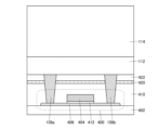
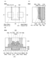
図1は、トランジスタ400および容量素子100を有する半導体装置の断面図である
。容量素子100は、水または水素などの不純物の透過を抑制する機能を有する絶縁体4
20を間に挟んで、トランジスタ400の上に配置される。容量素子100とトランジス
タ400は、絶縁体420を貫通して配置される導電体108bによって電気的に接続さ
れる。このように、絶縁体420および導電体108bは、容量素子100とトランジス
タ400の間に配置されるので、トランジスタ400が絶縁体420および導電体108
bを有しているともいえるし、容量素子100が絶縁体420および導電体108bを有
しているということもできる。
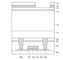
1 is a cross-sectional view of a semiconductor device including a
The
It can also be said that the
トランジスタ400は、酸化物406を有しており、酸化物406の少なくとも一部は
トランジスタ400のチャネル形成領域として機能する。酸化物406は、基板(図示せ
ず。)の上に設けられた絶縁体402の上に配置されることが好ましい。また、トランジ
スタ400は、酸化物406の上に導電体404を有し、酸化物406と導電体404の
間に絶縁体412を有する。ここで、導電体404はトランジスタ400のゲートとして
機能し、絶縁体412は導電体404に対応するゲート絶縁体として機能する。例えば、
酸化物406の導電体404と重なる領域がトランジスタ400のチャネル形成領域とし
て機能し、酸化物406の導電体404と重ならない領域の一部がトランジスタ400の
ソース領域およびドレイン領域の一方として機能し、酸化物406の導電体404と重な
らない領域の他の一部がトランジスタ400のソース領域およびドレイン領域の他方とし
て機能する。
The
A region of
酸化物406のソース領域およびドレイン領域の一方として機能する領域と電気的に接
続されるように導電体108aが配置され、酸化物406のソース領域およびドレイン領
域の他方として機能する領域と電気的に接続されるように導電体108bが配置される。
よって、導電体108aは、トランジスタ400のソース電極およびドレイン電極の一方
として機能し、導電体108bは、トランジスタ400のソース電極およびドレイン電極
の他方として機能する、ということができる。また、酸化物406、絶縁体412および
導電体404を覆って絶縁体410が配置されることが好ましい。導電体108aおよび
導電体108bは絶縁体410に形成された開口を埋め込むように形成されることが好ま
しい。
Thus, it can be said that the
トランジスタ400の酸化物406のチャネル形成領域において、酸素欠損を低減し、
水素または水などの不純物を低減することで、トランジスタ400に良好な電気特性を与
え、信頼性を向上させることができる。なお、トランジスタ400の構成の詳細な例につ
いては、後述する。
In the channel formation region of the
Reducing impurities such as hydrogen or water can provide favorable electrical characteristics and improve reliability of the
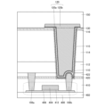
<容量素子の構成例>
容量素子100は、酸化物406、絶縁体412、導電体404、および絶縁体410
の上に配置される。絶縁体422、絶縁体112、絶縁体114、および絶縁体116に
形成された開口115の内壁、絶縁体420、および導電体108bに接して配置された
導電体110と、導電体110の上に配置された絶縁体130と、絶縁体130の上に配
置された導電体120aおよび導電体120bを有する。なお、以下において、導電体1
20aおよび導電体120bをまとめて導電体120という場合がある。
<Configuration example of capacitance element>
The
The
20a and
ここで、導電体110は容量素子100の下部電極として機能し、導電体120は容量
素子100の上部電極として機能し、絶縁体130は、容量素子100の誘電体として機
能する。容量素子100は、開口115において、底面だけでなく、側面においても上部
電極と下部電極とが誘電体を挟んで対向する構成となっており、単位面積当たりの静電容
量を大きくすることができる。そして、開口115の深さを深くするほど、容量素子10
0の静電容量を大きくすることができる。このように容量素子100の単位面積当たりの
静電容量を大きくすることにより、半導体装置の微細化または高集積化を推し進めること
ができる。
Here, the
0 can be increased. Increasing the capacitance per unit area of the
絶縁体420は、上層、例えば容量素子100などから水または水素などの不純物がト
ランジスタ400などに混入するのを防ぐバリア絶縁膜として機能できる。絶縁体420
は、水または水素などの不純物の透過を抑制する機能を有する絶縁性材料を用いることが
好ましく、例えば、酸化アルミニウムなどを用いることが好ましい。これにより、水素、
水などの不純物が絶縁体420より下層に拡散するのを抑制することができる。なお、絶
縁体420は、水素原子、水素分子、水分子、窒素原子、窒素分子、酸化窒素分子(N2
O、NO、NO2など)、銅原子などの不純物の少なくとも一の透過を抑制する機能を有
することが好ましい。また、以下において、不純物の透過を抑制する機能を有する絶縁性
材料について記載する場合も同様である。例えば、絶縁体420は、絶縁体422、絶縁
体112、および絶縁体114のいずれかより、水、または水素の透過を抑制する機能が
高いことが好ましい。
The
It is preferable to use an insulating material having a function of suppressing the permeation of impurities such as water or hydrogen, and it is preferable to use, for example, aluminum oxide.
Impurities such as water can be prevented from diffusing into layers below the
It is preferable that the
ここで、絶縁体420は、スパッタリング法を用いて成膜された酸化物絶縁体を用いる
ことが好ましく、例えば酸化アルミニウムを用いることが好ましい。このような絶縁体4
20を用いることにより、絶縁体410の絶縁体420と接する面を介して絶縁体410
に酸素を供給し、絶縁体410を酸素過剰な状態にできる。これにより、絶縁体410を
介して絶縁体412および酸化物406に酸素を供給することができる。
Here, the
20, the
By supplying oxygen to the
さらに、絶縁体420は、酸素(例えば、酸素原子または酸素分子など)の透過を抑制
する機能を有する絶縁性材料、例えば酸化アルミニウムを用いることが好ましい。これに
より、絶縁体410、酸化物406などに含まれる酸素が上方拡散するのを抑制すること
ができる。これにより、酸化物406に効果的に酸素を供給することができる。
Furthermore, the
このように絶縁体420を設け、トランジスタ400の酸化物406のチャネル形成領
域において、酸素欠損を低減し、水素または水などの不純物を低減することで、トランジ
スタ400に良好な電気特性を与え、信頼性を向上させることができる。
By providing the
また、絶縁体420は、絶縁体422、絶縁体112、および絶縁体114に開口11
5を形成する際に、エッチングストッパとして機能することが好ましい。よって、絶縁体
420は、絶縁体422、絶縁体112、および絶縁体114の少なくともいずれかと、
構成元素、組成などが異なることが好ましく、例えば、酸化アルミニウムを用いることが
好ましい。このように、絶縁体420がエッチングストッパとして機能することにより、
容量素子100が絶縁体410に接して形成され、容量素子100の絶縁体410に接し
た部分から、容量素子100に含まれる不純物が絶縁体410を介してトランジスタ40
0に拡散することを防ぐことができる。
In addition, the
It is preferable that the
It is preferable that the constituent elements and compositions are different, for example, aluminum oxide is preferably used. In this way, the
The
This can prevent the data from spreading to 0.
このとき、絶縁体420および導電体108bは、開口115の底部となる。言い換え
ると、開口115は、絶縁体420および導電体108bに達する開口ということができ
る。また、図1に示すように、絶縁体420の開口115と重なる領域、言い換えると、
絶縁体420の導電体110と接する領域の膜厚は、絶縁体420の当該領域以外の膜厚
より薄くなる場合がある。つまり、絶縁体420の当該領域は凹んだ形状になる場合があ
る。
At this time, the
The thickness of the region of the
なお、絶縁体420に積層して、絶縁体420と同様の元素を有する絶縁体を、ALD
法を用いて成膜してもよい。このように、絶縁体420にALD法で成膜された絶縁体を
積層することにより、段切れ、クラック、ピンホールなどが形成されることなく、トラン
ジスタ400を覆うことができる。これにより、水素、水などの不純物に対する絶縁体4
20のバリア性をより顕著に向上させることができる。
Note that an insulator having the same elements as the
In this manner, by stacking an insulator formed by the ALD method on the
The barrier properties of the film of No. 20 can be improved more significantly.
絶縁体420の上に絶縁体422が配置されることが好ましい。絶縁体422としては
、例えば酸化窒化シリコンなどを用いればよい。導電体108aおよび導電体108bは
、絶縁体410、絶縁体420、および絶縁体422に形成された開口に埋め込まれるよ
うに形成すればよい。このため、導電体108aまたは導電体108bの上面の一部と、
絶縁体422の上面の高さが略一致する場合がある。
The
The heights of the upper surfaces of the
ここで、絶縁体422を設けておくことで、導電体108aおよび導電体108bを形
成するための研磨処理(例えば、化学的機械研磨(Chemical Mechanic
al Polishing:CMP)処理など)を容易に行うことができる。なお、絶縁
体422は、導電体108aおよび導電体108bを形成できるならば、必ずしも設ける
必要はない。
Here, by providing the
Note that the
絶縁体410および絶縁体420に設けられる開口、および当該開口に埋め込まれる導
電体108bの断面形状は、絶縁体420の、導電体110と接する領域の上面より下の
部分において、逆テーパー形状となる場合がある。つまり、当該部分において、導電体1
08bは、側面のテーパー角度が90°以上である場合がある。また、当該部分において
、導電体108bは、底面と側面のなす角が90°以上である場合があるということもで
きる。なお、当該部分において、導電体108bの側面が絶縁体402の上面に対して略
垂直であってもよい。
The cross-sectional shape of the openings provided in the
In the portion, the taper angle of the side surface of the
また、導電体108bは、絶縁体420の、導電体110と接する領域の上面より上の
部分において、湾曲面を有することが好ましい。例えば、導電体108bの当該部分にお
いて、導電体108bの側面と、導電体108bの上面との間に、湾曲面を有することが
好ましい。つまり、導電体108bの当該部分において、側面の端部と上面の端部は、湾
曲して連続していることが好ましい。
Moreover, the
このように、導電体108bは、絶縁体420より上の部分と、下の部分で形状が異な
ることが好ましい。特に、導電体108bの上の部分の湾曲面で導電体110と接するこ
とにより、導電体108bと導電体110の接触抵抗を低減することができる。これによ
り、トランジスタ400のソースまたはドレインのいずれかと、容量素子100の下部電
極との電気的接続を良好にすることができる。よって、容量素子100とトランジスタ4
00を有する半導体装置に良好な電気特性を与えることができる。
In this way, it is preferable that the
00 can be given good electrical characteristics.
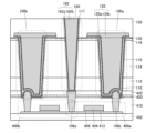
絶縁体422の上に絶縁体112が配置され、絶縁体112の上に絶縁体114が配置
される。上記の通り、開口115の深さ、すなわち絶縁体112と絶縁体114の膜厚の
合計を大きくすることにより、容量素子100の静電容量を大きくすることができる。し
かしながら、絶縁体112と絶縁体114の膜厚を大きくすることにより、これらの絶縁
体の内部応力も大きくなり、基板の反りなどが発生する場合がある。そこで、本実施の形
態に示す容量素子100においては、絶縁体112および絶縁体114の一方は圧縮応力
を有し、絶縁体112および絶縁体114の他方は引っ張り応力を有することが好ましい
。つまり、絶縁体112および絶縁体114は、積層することで互いの内部応力を相殺し
、積層された絶縁体全体の内部応力を低減することが好ましい。
The
絶縁体112および絶縁体114は、同種の元素を用いる構成としてもよく、例えば、
有機シランガス(例えば、TEOS(Tetra-Ethyl-Ortho-Silic
ate)など)を用いて成膜した酸化シリコンを用いればよい。この場合、絶縁体112
の組成と絶縁体114の組成を異なるものとし、互いの内部応力の向きを異ならせること
が好ましい。例えば、絶縁体112と絶縁体114を同じ種類の有機シランガス(例えば
、TEOSなど)を用いて、異なる種類の化学気相成長(CVD:Chemical V
apor Deposition)法を用いて成膜してもよい。
The
Organosilane gas (e.g., TEOS (Tetra-Ethyl-Ortho-Silicon)
In this case, the
It is preferable to make the composition of the
Alternatively, the film may be formed by a por deposition method.
なお、基板の反りが発生しない程度に、内部応力が低減されているなら、絶縁体112
および絶縁体114のいずれか一方のみの構成にしてもよい。
If the internal stress is reduced to such an extent that the substrate does not warp, the
Alternatively, only one of the insulating
絶縁体114の上に絶縁体116が配置されることが好ましい。絶縁体116は、開口
115内でエッチングを行うときに、導電体110とともにエッチングストッパとして機
能することが好ましい。よって、絶縁体116は、絶縁体114と構成元素、組成などが
異なることが好ましく、例えば、絶縁体116として、窒化シリコンを用いることができ
る。また、絶縁体116の上面と導電体110の最上面(導電体110の開口115の縁
に接する部分と言い換えてもよい。)が略一致することが好ましい。絶縁体116と導電
体110によって、絶縁体114、絶縁体112、絶縁体422、および絶縁体420が
覆われていることが好ましい。なお、絶縁体116は、必ずしも設ける必要はない。
It is preferable that the
絶縁体422、絶縁体112、絶縁体114、および絶縁体116に開口115が形成
されている。ここで、絶縁体422の側面、絶縁体112の側面、絶縁体114の側面、
および絶縁体116の側面は、開口115の内壁ということができる。また、導電体10
8bの上部、および絶縁体420の開口115と重なる部分は開口115の底部というこ
とができる。
The
The side surface of the
The top of 8 b and the portion of
図1に示すように、開口115の断面形状は深い位置ほど、内径が小さくなる形状にす
ることができる。また、開口115の内壁が絶縁体402の上面に対して略垂直な断面形
状にしてもよい。また、開口115を上面から見た形状は、四角形としてもよいし、四角
形以外の多角形状としてもよいし、多角形状において角部を湾曲させた形状としてもよい
し、楕円を含む円形状としてもよい。ここで、開口115とトランジスタ400の重なる
面積が多い方が好ましい。このような構成にすることにより、容量素子100とトランジ
スタ400を有する半導体装置の占有面積を増やすことなく、静電容量を大きくすること
ができる。
As shown in FIG. 1, the cross-sectional shape of the
開口115の内壁および底面に接して、導電体110が配置される。導電体110は容
量素子100の下部電極として機能し、例えば窒化チタンなどを用いることができる。例
えば、ALD法またはCVD法などを用いて導電体110となる導電膜を成膜することに
より、開口115のアスペクト比が大きくても被覆性良く導電体110を形成することが
できる。ここで、上記のように導電体108bの上部が湾曲面を有し、当該湾曲面に接し
て導電体110が形成されることにより、導電体110と導電体108bの接触抵抗を低
減することができる。
The
導電体110および絶縁体116を覆って絶縁体130が配置される。絶縁体130は
容量素子100の誘電体として機能し、例えば、酸化ハフニウム、ハフニウムシリケート
(HfSixOy(x>0、y>0))、窒素が添加されたハフニウムシリケート(Hf
SixOyNz(x>0、y>0、z>0))、窒素が添加されたハフニウムアルミネー
ト(HfAlxOyNz(x>0、y>0、z>0))、または酸化イットリウムなどの
high-k材料を用いることが好ましい。このようなhigh-k材料を用いることで
、絶縁体130を厚くしても容量素子100の静電容量を十分確保することができる。絶
縁体130を厚くすることにより、導電体110と導電体120の間に生じるリーク電流
を抑制することができる。
The
It is preferable to use a high-k material such as Si x O y N z (x>0, y>0, z>0)), nitrogen-added hafnium aluminate (HfAl x O y N z (x>0, y>0, z>0)), or yttrium oxide. By using such a high-k material, the capacitance of the
また、例えば、ALD法またはCVD法などを用いて絶縁体130となる絶縁膜を成膜
することにより、開口115のアスペクト比が大きくても被覆性良く絶縁体130を形成
することができる。また、絶縁体130は、導電体120と重なる領域の膜厚が、該領域
以外の膜厚より厚い場合がある。
Furthermore, by forming an insulating film to be the
また、導電体110の最上面が絶縁体116の上面と略一致する、言い換えると導電体
110が開口115からはみ出さないことで、絶縁体130でより確実に導電体110を
覆うことができるので、導電体110と導電体120が短絡することを抑制することがで
きる。
Furthermore, since the top surface of
開口115を覆って、絶縁体130の上に導電体120が配置される。図1に示すよう
に、導電体120は、導電体120aと、導電体120aの上に配置された導電体120
bの積層膜にすることが好ましい。導電体120は容量素子100の上部電極として機能
し、例えば導電体120aとして窒化チタンなどを、導電体120bとしてタングステン
などを用いることができる。例えば、ALD法またはCVD法などを用いて導電体120
aとなる導電膜、および導電体120bとなる導電膜を成膜することにより、開口115
のアスペクト比が大きくても被覆性良く導電体120aおよび導電体120bを形成する
ことができる。
The
The
By forming a conductive film that will become the
Even if the aspect ratio is large, the
また、導電体120は、開口115からはみ出して絶縁体116と重なる領域を有する
ことが好ましい。当該領域を有するには、フォトリソグラフィ法などを用いて導電体12
0aおよび導電体120bを形成すればよい。このとき、導電体120bの絶縁体116
と重なる領域の上面の平均面粗さ(Ra)は、4nm以下、好ましくは2nm以下、より
好ましくは1nm以下とすればよい。このように、導電体120bの上面が、開口115
の縁の近傍と重なる領域において、良好な平坦性を有していることで、フォトリソグラフ
ィの露光工程において、当該領域で乱反射が起こることを抑制できる。特に、露光に電子
ビームを用いる場合、金属膜の上面の凹凸による乱反射の影響がより顕著になるので、こ
れを防ぐため、当該領域の平坦性を向上させることが好ましい。このように、当該領域の
平坦性を向上させることで、フォトリソグラフィをより精密に行うことができる。
In addition, it is preferable that the
In this case, the
The average surface roughness (Ra) of the upper surface of the region overlapping with the
By having good flatness in the region overlapping with the vicinity of the edge of the metal film, it is possible to suppress the occurrence of diffuse reflection in the region during the exposure step of photolithography. In particular, when an electron beam is used for exposure, the effect of diffuse reflection due to the unevenness of the upper surface of the metal film becomes more pronounced, so it is preferable to improve the flatness of the region in order to prevent this. In this way, by improving the flatness of the region, photolithography can be performed more precisely.
なお、本明細書等において、平均面粗さ(Ra)とは、JISB0601:2001(
ISO4287:1997)で定義されている算術平均粗さを、曲面に対して適用できる
よう三次元に拡張したものであり、基準面から指定面までの偏差の絶対値を平均した値で
表現される。
In this specification, the average surface roughness (Ra) is defined as follows:
It is a three-dimensional extension of the arithmetic mean roughness defined in ISO 4287:1997 so that it can be applied to curved surfaces, and is expressed as the average of the absolute values of the deviation from a reference surface to a specified surface.
平均面粗さ(Ra)は、指定面をZ=F(X,Y)で表すとき、基準面から指定面まで
の偏差の絶対値を平均した値で表現され、次の式で与えられる。
The average surface roughness (Ra) is expressed as the average absolute value of the deviation from a reference surface to a specified surface when the specified surface is represented as Z = F (X, Y), and is given by the following formula.
ここで、指定面とは、粗さ計測の対象となる面であり、座標(X1,Y1,F(X1,
Y1)),(X1,Y2,F(X1,Y2)),(X2,Y1,F(X2,Y1)),(
X2,Y2,F(X2,Y2))の4点で表される四角形の領域とする。
Here, the designated surface is a surface to be subjected to roughness measurement, and is represented by coordinates ( X1 , Y1 , F( X1 ,
Y 1 )), (X 1 , Y 2 , F(X 1 , Y 2 )), (X 2 , Y 1 , F(X 2 , Y 1 )), (
The area is a rectangle represented by four points X 2 , Y 2 , and F(X 2 , Y 2 ).
また、指定面をXY平面に投影した長方形の面積をS0、基準面の高さ(指定面の平均
の高さ)をZ0とする。平均面粗さ(Ra)は原子間力顕微鏡(AFM:Atomic
Force Microscope)にて測定可能である。
The area of a rectangle obtained by projecting the designated surface onto the XY plane is S 0 , and the height of the reference surface (average height of the designated surface) is Z 0 . The average surface roughness (Ra) was measured using an atomic force microscope (AFM).
The amount of the ion exchange reaction can be measured using a Force Microscope.
なお、導電体120は、必ずしも積層膜にしなくてもよく、例えば、導電体120aお
よび導電体120bのいずれか一方を用いる構成にしてもよい。
The
導電体120および絶縁体130を覆って絶縁体150が配置されることが好ましい。
絶縁体150は、絶縁体410に用いることができる絶縁体を用いればよい。
An
The
また、上記において、導電体108b上に形成される容量素子100の構成について説
明したが、導電体108a上にも接続部160が形成されることが好ましい。接続部16
0が設けられることで、トランジスタ400の導電体108aと、各種回路素子または配
線などと、を容易に接続させることができる。
Although the configuration of the
By providing the
接続部160は、絶縁体422、絶縁体112、絶縁体114、絶縁体116、絶縁体
130、および絶縁体150に形成された開口117に埋め込まれるように形成される。
接続部160は、開口117の内壁、絶縁体420、および導電体108aに接して配置
された導電体162aと、導電体162aの内側に形成された導電体162bと、を有す
る。なお、以下において、導電体162aおよび導電体162bをまとめて導電体162
という場合がある。
The
The
This may be the case.
ここで、絶縁体420および導電体108aは、開口117の底部となる。言い換える
と、開口117は、絶縁体420および導電体108aに達する開口ということができる
。また、図1に示すように、絶縁体420の開口117と重なる領域、言い換えると、絶
縁体420の導電体162aと接する領域の膜厚は、絶縁体420の当該領域以外の膜厚
より薄くなる場合がある。つまり、絶縁体420の当該領域は凹んだ形状になる場合があ
る。
Here, the
導電体108aは導電体108bと同様の構成を有する。よって、絶縁体410および
絶縁体420に設けられる開口、および当該開口に埋め込まれる導電体108aの断面形
状は、絶縁体420の、導電体162aと接する領域の上面より下の部分において、逆テ
ーパー形状となる場合がある。つまり、当該部分において、導電体108aの側面のテー
パー角度が90°以上である場合がある。また、当該部分において、導電体108aの側
面と絶縁体402の上面とのなす角が90°以上である場合があるということもできる。
なお、当該部分において、導電体108aの側面が絶縁体402の上面に対して略垂直で
あってもよい。
The
In this portion, the side surface of the
また、導電体108aは、絶縁体420の、導電体162aと接する領域の上面より上
の部分において、湾曲面を有することが好ましい。例えば、導電体108aの当該部分に
おいて、導電体108aの側面と、導電体108aの上面との間に、湾曲面を有すること
が好ましい。つまり、導電体108aの当該部分において、側面の端部と上面の端部は、
湾曲して連続していることが好ましい。なお、図1に示すように、導電体108aの当該
部分において、導電体162aと接しない、言い換えると開口117と重ならない領域に
ついては、湾曲面が形成されない。
Furthermore, the
1, in the portion of the
このように、導電体108aは、絶縁体420より上の部分と、下の部分で形状が異な
ることが好ましい。特に、導電体108aの上の部分の湾曲面で導電体162aと接する
ことにより、導電体108aと導電体162aの接触抵抗を低減することができる。これ
により、トランジスタ400のソースまたはドレインのいずれかと、接続部160との電
気的接続を良好にすることができる。
In this manner, it is preferable that the
導電体162は、導電体120と同様の構成を用いることができる。よって、導電体1
62aは導電体120aと、導電体162bは導電体120bと同様の構成を用いること
が好ましい。なお、導電体162は、必ずしも積層膜にしなくてもよく、例えば、導電体
162aおよび導電体162bのいずれか一方を用いる構成にしてもよい。
The
It is preferable that the conductor 62a has a structure similar to that of the
次に、トランジスタ400、容量素子100および接続部160などの構成材料につい
て説明する。
Next, the constituent materials of the
[基板]
容量素子100およびトランジスタ400を有する半導体装置を形成する基板としては
、例えば、絶縁体基板、半導体基板または導電体基板を用いればよい。絶縁体基板として
は、例えば、ガラス基板、石英基板、サファイア基板、安定化ジルコニア基板(イットリ
ア安定化ジルコニア基板など)、樹脂基板などがある。また、半導体基板としては、例え
ば、シリコン、ゲルマニウムなどの半導体基板、または炭化シリコン、シリコンゲルマニ
ウム、ヒ化ガリウム、リン化インジウム、酸化亜鉛、酸化ガリウムからなる化合物半導体
基板などがある。さらには、前述の半導体基板内部に絶縁体領域を有する半導体基板、例
えばSOI(Silicon On Insulator)基板などがある。導電体基板
としては、黒鉛基板、金属基板、合金基板、導電性樹脂基板などがある。または、金属の
窒化物を有する基板、金属の酸化物を有する基板などがある。さらには、絶縁体基板に導
電体または半導体が設けられた基板、半導体基板に導電体または絶縁体が設けられた基板
、導電体基板に半導体または絶縁体が設けられた基板などがある。または、これらの基板
に素子が設けられたものを用いてもよい。基板に設けられる素子としては、容量素子、抵
抗素子、スイッチ素子、発光素子、記憶素子などがある。
[substrate]
The substrate for forming the semiconductor device having the
また、基板として、可とう性基板を用いてもよい。なお、可とう性基板上にトランジス
タを設ける方法としては、非可とう性の基板上にトランジスタを作製した後、トランジス
タを剥離し、可とう性基板である基板に転置する方法もある。その場合には、非可とう性
基板とトランジスタとの間に剥離層を設けるとよい。なお、基板として、繊維を編みこん
だシート、フィルムまたは箔などを用いてもよい。また、基板が伸縮性を有してもよい。
また、基板は、折り曲げや引っ張りをやめた際に、元の形状に戻る性質を有してもよい。
または、元の形状に戻らない性質を有してもよい。基板は、例えば、5μm以上700μ
m以下、好ましくは10μm以上500μm以下、さらに好ましくは15μm以上300
μm以下の厚さとなる領域を有する。基板を薄くすると、トランジスタを有する半導体装
置を軽量化することができる。また、基板を薄くすることで、ガラスなどを用いた場合に
も伸縮性を有する場合や、折り曲げや引っ張りをやめた際に、元の形状に戻る性質を有す
る場合がある。そのため、落下などによって基板上の半導体装置に加わる衝撃などを緩和
することができる。即ち、丈夫な半導体装置を提供することができる。
A flexible substrate may be used as the substrate. A method of providing a transistor on a flexible substrate may include a method of manufacturing a transistor on a non-flexible substrate, peeling the transistor, and transferring the transistor to a flexible substrate. In this case, a peeling layer may be provided between the non-flexible substrate and the transistor. A sheet, film, or foil having woven fibers may be used as the substrate. The substrate may be stretchable.
The substrate may also have the property of returning to its original shape when bending or pulling is stopped.
Alternatively, the substrate may have a property of not returning to its original shape.
m or less, preferably 10 μm or more and 500 μm or less, and more preferably 15 μm or more and 300 μm or less.
The substrate has a region with a thickness of 1 μm or less. By making the substrate thinner, the weight of a semiconductor device having a transistor can be reduced. Furthermore, by making the substrate thinner, even when glass or the like is used, the substrate may have elasticity, or may have the property of returning to its original shape when bending or pulling is stopped. Therefore, it is possible to reduce the impact applied to the semiconductor device on the substrate when it is dropped, etc. In other words, a robust semiconductor device can be provided.
可とう性基板である基板としては、例えば、金属、合金、樹脂もしくはガラス、または
それらの繊維などを用いることができる。可とう性基板である基板は、線膨張率が低いほ
ど環境による変形が抑制されて好ましい。可とう性基板である基板としては、例えば、線
膨張率が1×10⁻³/K以下、5×10-5/K以下、または1×10-5/K以下で
ある材質を用いればよい。樹脂としては、例えば、ポリエステル、ポリオレフィン、ポリ
アミド(ナイロン、アラミドなど)、ポリイミド、ポリカーボネート、アクリルなどがあ
る。特に、アラミドは、線膨張率が低いため、可とう性基板である基板として好適である
。
As the flexible substrate, for example, metal, alloy, resin, glass, or fibers thereof can be used. The lower the linear expansion coefficient of the flexible substrate, the more preferable it is since deformation due to the environment is suppressed. As the flexible substrate, for example, a material having a linear expansion coefficient of 1×10 −3 /K or less, 5×10 −5 /K or less, or 1×10 −5 /K or less may be used. As the resin, for example, polyester, polyolefin, polyamide (nylon, aramid, etc.), polyimide, polycarbonate, acrylic, etc. can be used. In particular, aramid has a low linear expansion coefficient and is therefore suitable as the flexible substrate.
[絶縁体]
絶縁体としては、絶縁性を有する酸化物、窒化物、酸化窒化物、窒化酸化物、金属酸化
物、金属酸化窒化物、金属窒化酸化物などがある。
[Insulator]
Examples of the insulator include oxides, nitrides, oxynitrides, nitride oxides, metal oxides, metal oxynitrides, and metal nitride oxides, each of which has insulating properties.
トランジスタを、水素などの不純物および酸素の透過を抑制する機能を有する絶縁体で
囲うことによって、トランジスタの電気特性を安定にすることができる。例えば、絶縁体
420として、水素などの不純物および酸素の透過を抑制する機能を有する絶縁体を用い
ればよい。
The electrical characteristics of the transistor can be stabilized by surrounding the transistor with an insulator that has a function of suppressing the permeation of oxygen and impurities such as hydrogen. For example, the
水素などの不純物および酸素の透過を抑制する機能を有する絶縁体としては、例えば、
ホウ素、炭素、窒素、酸素、フッ素、マグネシウム、アルミニウム、シリコン、リン、塩
素、アルゴン、ガリウム、ゲルマニウム、イットリウム、ジルコニウム、ランタン、ネオ
ジム、ハフニウムまたはタンタルを含む絶縁体を、単層で、または積層で用いればよい。
Examples of insulators that have a function of suppressing the permeation of impurities such as hydrogen and oxygen include:
An insulator containing boron, carbon, nitrogen, oxygen, fluorine, magnesium, aluminum, silicon, phosphorus, chlorine, argon, gallium, germanium, yttrium, zirconium, lanthanum, neodymium, hafnium, or tantalum may be used in a single layer or a multilayer.
例えば、絶縁体420としては、酸化アルミニウム、酸化ハフニウム、酸化マグネシウ
ム、酸化ガリウム、酸化ゲルマニウム、酸化イットリウム、酸化ジルコニウム、酸化ラン
タン、酸化ネオジムまたは酸化タンタルなどの金属酸化物、窒化酸化シリコンまたは窒化
シリコンなどを用いればよい。
For example, the
絶縁体402、絶縁体412、絶縁体410、絶縁体422、絶縁体112、絶縁体1
14、絶縁体116および絶縁体150としては、例えば、ホウ素、炭素、窒素、酸素、
フッ素、マグネシウム、アルミニウム、シリコン、リン、塩素、アルゴン、ガリウム、ゲ
ルマニウム、イットリウム、ジルコニウム、ランタン、ネオジム、ハフニウムまたはタン
タルを含む絶縁体を、単層で、または積層で用いればよい。例えば、絶縁体402、絶縁
体412、絶縁体410、絶縁体422、絶縁体112、絶縁体114、絶縁体116お
よび絶縁体150としては、酸化シリコン、酸化窒化シリコン、窒化酸化シリコンまたは
、窒化シリコンを有することが好ましい。
14. The
An insulator containing fluorine, magnesium, aluminum, silicon, phosphorus, chlorine, argon, gallium, germanium, yttrium, zirconium, lanthanum, neodymium, hafnium, or tantalum may be used as a single layer or a stack. For example, the
絶縁体412および絶縁体130は、比誘電率の高い絶縁体を有することが好ましい。
例えば、絶縁体412および絶縁体130は、酸化ガリウム、酸化ハフニウム、酸化ジル
コニウム、アルミニウムおよびハフニウムを有する酸化物、アルミニウムおよびハフニウ
ムを有する酸化窒化物、シリコンおよびハフニウムを有する酸化物、シリコンおよびハフ
ニウムを有する酸化窒化物またはシリコンおよびハフニウムを有する窒化物などを有する
ことが好ましい。または、絶縁体412および絶縁体130は、酸化シリコンまたは酸化
窒化シリコンと、比誘電率の高い絶縁体と、の積層構造を有することが好ましい。酸化シ
リコンおよび酸化窒化シリコンは、熱的に安定であるため、比誘電率の高い絶縁体と組み
合わせることで、熱的に安定かつ比誘電率の高い積層構造とすることができる。例えば、
絶縁体412および絶縁体130において、酸化アルミニウム、酸化ガリウムまたは酸化
ハフニウムを酸化物406と接する構造とすることで、酸化シリコンまたは酸化窒化シリ
コンに含まれるシリコンが、酸化物406に混入することを抑制することができる。また
、例えば、絶縁体412および絶縁体130において、酸化シリコンまたは酸化窒化シリ
コンを酸化物406と接する構造とすることで、酸化アルミニウム、酸化ガリウムまたは
酸化ハフニウムと、酸化シリコンまたは酸化窒化シリコンと、の界面にトラップセンター
が形成される場合がある。該トラップセンターは、電子を捕獲することでトランジスタの
しきい値電圧をプラス方向に変動させることができる場合がある。
It is preferable that the
For example, the
In the
絶縁体410、絶縁体422、絶縁体112、絶縁体114、および絶縁体150は、
比誘電率の低い絶縁体を有することが好ましい。例えば、絶縁体410、絶縁体422、
絶縁体112、絶縁体114、および絶縁体150は、酸化シリコン、酸化窒化シリコン
、窒化酸化シリコン、窒化シリコン、フッ素を添加した酸化シリコン、炭素を添加した酸
化シリコン、炭素および窒素を添加した酸化シリコン、空孔を有する酸化シリコンまたは
樹脂などを有することが好ましい。または、絶縁体410、絶縁体422、絶縁体112
、絶縁体114、および絶縁体150は、酸化シリコン、酸化窒化シリコン、窒化酸化シ
リコン、窒化シリコン、フッ素を添加した酸化シリコン、炭素を添加した酸化シリコン、
炭素および窒素を添加した酸化シリコンまたは空孔を有する酸化シリコンと、樹脂と、の
積層構造を有することが好ましい。酸化シリコンおよび酸化窒化シリコンは、熱的に安定
であるため、樹脂と組み合わせることで、熱的に安定かつ比誘電率の低い積層構造とする
ことができる。樹脂としては、例えば、ポリエステル、ポリオレフィン、ポリアミド(ナ
イロン、アラミドなど)、ポリイミド、ポリカーボネートまたはアクリルなどがある。
The
It is preferable to have an insulator with a low relative dielectric constant. For example, the
The
, the
It is preferable to have a laminated structure of silicon oxide to which carbon and nitrogen are added or silicon oxide having vacancies, and a resin. Silicon oxide and silicon oxynitride are thermally stable, so that a laminated structure that is thermally stable and has a low relative dielectric constant can be obtained by combining them with a resin. Examples of the resin include polyester, polyolefin, polyamide (nylon, aramid, etc.), polyimide, polycarbonate, and acrylic.
[導電体]
導電体404、導電体108a、導電体108b、導電体120b、および導電体16
2bとしては、アルミニウム、クロム、銅、銀、金、白金、タンタル、ニッケル、チタン
、モリブデン、タングステン、ハフニウム、バナジウム、ニオブ、マンガン、マグネシウ
ム、ジルコニウム、ベリリウム、インジウム、ルテニウムなどから選ばれた金属元素を1
種以上含む材料を用いることができる。また、リン等の不純物元素を含有させた多結晶シ
リコンに代表される、電気伝導度が高い半導体、ニッケルシリサイドなどのシリサイドを
用いてもよい。
[conductor]
As 2b, one or more metal elements selected from aluminum, chromium, copper, silver, gold, platinum, tantalum, nickel, titanium, molybdenum, tungsten, hafnium, vanadium, niobium, manganese, magnesium, zirconium, beryllium, indium, ruthenium, etc.
In addition, a semiconductor having high electrical conductivity, typified by polycrystalline silicon containing an impurity element such as phosphorus, or a silicide such as nickel silicide may be used.
また、上記導電体、特に導電体110、導電体120a、および導電体162aとして
、酸化物406に適用可能な金属酸化物に含まれる金属元素および酸素を含む導電性材料
を用いてもよい。また、前述した金属元素および窒素を含む導電性材料を用いてもよい。
例えば、窒化チタン、窒化タンタルなどの窒素を含む導電性材料を用いてもよい。また、
インジウム錫酸化物、酸化タングステンを含むインジウム酸化物、酸化タングステンを含
むインジウム亜鉛酸化物、酸化チタンを含むインジウム酸化物、酸化チタンを含むインジ
ウム錫酸化物、インジウム亜鉛酸化物、シリコンを添加したインジウム錫酸化物を用いて
もよい。また、窒素を含むインジウムガリウム亜鉛酸化物を用いてもよい。このような材
料を用いることで、酸化物406に含まれる水素を捕獲することができる場合がある。ま
たは、外方の絶縁体などから混入する水素を捕獲することができる場合がある。
Furthermore, the conductors, particularly the
For example, a conductive material containing nitrogen, such as titanium nitride or tantalum nitride, may be used.
Indium tin oxide, indium oxide containing tungsten oxide, indium zinc oxide containing tungsten oxide, indium oxide containing titanium oxide, indium tin oxide containing titanium oxide, indium zinc oxide, and indium tin oxide to which silicon has been added may be used. Indium gallium zinc oxide containing nitrogen may also be used. By using such a material, hydrogen contained in the
また、上記の材料で形成される導電層を複数積層して用いてもよい。例えば、前述した
金属元素を含む材料と、酸素を含む導電性材料と、を組み合わせた積層構造としてもよい
。また、前述した金属元素を含む材料と、窒素を含む導電性材料と、を組み合わせた積層
構造としてもよい。また、前述した金属元素を含む材料と、酸素を含む導電性材料と、窒
素を含む導電性材料と、を組み合わせた積層構造としてもよい。
A plurality of conductive layers formed of the above-mentioned materials may be stacked. For example, a stacked structure may be formed by combining the above-mentioned material containing a metal element and a conductive material containing oxygen. A stacked structure may be formed by combining the above-mentioned material containing a metal element and a conductive material containing nitrogen. A stacked structure may be formed by combining the above-mentioned material containing a metal element, a conductive material containing oxygen, and a conductive material containing nitrogen.
<容量素子の作製方法>
次に、本発明に係るトランジスタ400および容量素子100を有する半導体装置の作
製方法を、図2から図16を用いて説明する。
<Method for manufacturing a capacitor element>
Next, a method for manufacturing a semiconductor device including the
半導体装置の作製方法は、酸化物406を有するトランジスタ400上に絶縁体420
を形成する工程と、絶縁体420の上に絶縁体422を形成する工程と、絶縁体420お
よび絶縁体422に、トランジスタ400のソースおよびドレインの一方に達する第1の
開口と、トランジスタ400のソースおよびドレインの他方に達する第2の開口を形成す
る工程と、第1の開口に導電体108aを埋め込み、第2の開口に導電体108bを埋め
込む工程と、絶縁体422、導電体108b、および導電体108aの上に絶縁体112
、絶縁体114などを形成する工程と、ドライエッチング処理を行い、絶縁体420およ
び導電体108bに達する開口115を形成する工程と、開口115の内壁、絶縁体42
0、および導電体108bに接して、導電体110を形成する工程と、導電体110の上
に絶縁体130を形成する工程と、絶縁体130の上に導電体120を形成する工程と、
を有する。
The method for manufacturing a semiconductor device includes forming an
forming an
, an
forming a
has.
以下では、主に、トランジスタ400の上に容量素子100を作製する方法の詳細につ
いて説明する。なお、トランジスタ400の作製方法例、つまり、絶縁体422を形成し
、導電体108aおよび導電体108bを開口に埋め込むまでの工程については、後述す
る。
The following mainly describes details of a method for manufacturing the
以下、本実施の形態に係る半導体装置などに用いる、導電体(導電体膜、導電体層など
ということもできる。)、絶縁体(絶縁体膜、絶縁体層などということもできる。)、半
導体(半導体膜、半導体層などということもできる。)、酸化物(酸化膜、酸化層などと
いうこともできる。)の成膜は、スパッタリング法、CVD法、分子線エピタキシー(M
BE:Molecular Beam Epitaxy)法、パルスレーザ堆積(PLD
:Pulsed Laser Deposition)法またはALD法などを用いて行
うことができる。
Hereinafter, the formation of conductors (which can also be called conductor films or conductor layers), insulators (which can also be called insulator films or insulator layers), semiconductors (which can also be called semiconductor films or semiconductor layers), and oxides (which can also be called oxide films or oxide layers) used in the semiconductor device according to the present embodiment can be performed by sputtering, CVD, molecular beam epitaxy (MBE), etc.
BE: Molecular Beam Epitaxy, Pulsed Laser Deposition (PLD)
The deposition can be performed by using a pulsed laser deposition (PLD) method, an ALD method, or the like.
なお、CVD法は、プラズマを利用するプラズマCVD(PECVD:Plasma
Enhanced CVD)法、熱を利用する熱CVD(TCVD:Thermal C
VD)法、光を利用する光CVD(Photo CVD)法などに分類できる。さらに用
いる原料ガスによって金属CVD(MCVD:Metal CVD)法、有機金属CVD
(MOCVD:Metal Organic CVD)法に分けることができる。また、
成膜チャンバーの圧力によって、大気圧下で成膜を行なう常圧CVD(APCVD:At
mospheric Pressure CVD)法、大気圧より低い減圧状態で成膜を
行う減圧CVD(LPCVD:Low Pressure CVD)法、などに分けるこ
とができる。
The CVD method is a plasma enhanced chemical vapor deposition (PECVD) method that uses plasma.
Enhanced CVD (TCVD) method, and thermal CVD (TCVD) method.
They can be further classified into metal CVD (MCVD), metal organic CVD (MCVD), and photo CVD (Photo CVD), depending on the source gas used.
(MOCVD: Metal Organic CVD) method.
Depending on the pressure in the deposition chamber, deposition is performed under atmospheric pressure (APCVD: At
and low pressure CVD (LPCVD) in which film formation is performed under reduced pressure lower than atmospheric pressure.
プラズマCVD法は、比較的低温で高品質の膜が得られる。また、熱CVD法は、プラ
ズマを用いないため、被処理物へのプラズマダメージを小さくすることが可能な成膜方法
である。例えば、半導体装置に含まれる配線、電極、素子(トランジスタ、容量素子など
)などは、プラズマから電荷を受け取ることでチャージアップする場合がある。このとき
、蓄積した電荷によって、半導体装置に含まれる配線、電極、素子などが破壊される場合
がある。一方、プラズマを用いない熱CVD法の場合、こういったプラズマダメージが生
じないため、半導体装置の歩留まりを高くすることができる。また、熱CVD法では、成
膜中のプラズマダメージが生じないため、欠陥の少ない膜が得られる。
The plasma CVD method can obtain a high-quality film at a relatively low temperature. Moreover, the thermal CVD method is a film formation method that can reduce plasma damage to the object to be processed because it does not use plasma. For example, wiring, electrodes, elements (transistors, capacitance elements, etc.) included in a semiconductor device may be charged up by receiving electric charge from plasma. At this time, the wiring, electrodes, elements, etc. included in the semiconductor device may be destroyed by the accumulated electric charge. On the other hand, in the case of the thermal CVD method that does not use plasma, such plasma damage does not occur, so the yield of the semiconductor device can be increased. Moreover, in the thermal CVD method, plasma damage does not occur during film formation, so a film with few defects can be obtained.
また、ALD法も、被処理物へのプラズマダメージを小さくすることが可能な成膜方法
である。また、ALD法も、成膜中のプラズマダメージが生じないため、欠陥の少ない膜
が得られる。
The ALD method is also a film formation method capable of reducing plasma damage to a workpiece, and since the ALD method does not cause plasma damage during film formation, a film with few defects can be obtained.
CVD法およびALD法は、ターゲットなどから放出される粒子が堆積する成膜方法と
は異なり、被処理物の表面における反応により膜が形成される成膜方法である。したがっ
て、被処理物の形状の影響を受けにくく、良好な段差被覆性を有する成膜方法である。特
に、ALD法は、優れた段差被覆性と、優れた厚さの均一性を有するため、アスペクト比
の高い開口の表面を被覆する場合などに好適である。ただし、ALD法は、比較的成膜速
度が遅いため、成膜速度の速いCVD法などの他の成膜方法と組み合わせて用いることが
好ましい場合もある。
The CVD method and the ALD method are different from the film formation method in which particles emitted from a target or the like are deposited, and a film is formed by a reaction on the surface of the workpiece. Therefore, they are film formation methods that are not easily affected by the shape of the workpiece and have good step coverage. In particular, the ALD method has excellent step coverage and excellent thickness uniformity, so it is suitable for coating the surface of an opening with a high aspect ratio. However, since the ALD method has a relatively slow film formation speed, it may be preferable to use it in combination with other film formation methods such as the CVD method, which has a fast film formation speed.
CVD法およびALD法は、原料ガスの流量比によって、得られる膜の組成を制御する
ことができる。例えば、CVD法およびALD法では、原料ガスの流量比によって、任意
の組成の膜を成膜することができる。また、例えば、CVD法およびALD法では、成膜
しながら原料ガスの流量比を変化させることによって、組成が連続的に変化した膜を成膜
することができる。原料ガスの流量比を変化させながら成膜する場合、複数の成膜室を用
いて成膜する場合と比べて、搬送や圧力調整に掛かる時間の分、成膜に掛かる時間を短く
することができる。したがって、半導体装置の生産性を高めることができる場合がある。
The CVD method and the ALD method can control the composition of the film obtained by the flow rate ratio of the source gas. For example, the CVD method and the ALD method can form a film of any composition by changing the flow rate ratio of the source gas. Also, for example, the CVD method and the ALD method can form a film whose composition changes continuously by changing the flow rate ratio of the source gas while forming the film. When forming a film while changing the flow rate ratio of the source gas, the time required for film formation can be shortened by the time required for transportation and pressure adjustment compared to the case of forming a film using a plurality of film formation chambers. Therefore, the productivity of the semiconductor device can be increased in some cases.
また、スパッタリング法としては、スパッタ用電源に直流電源を用いるDC(Dire
ct Current)スパッタリング法、さらにパルス的にバイアスを与えるパルスD
Cスパッタ法、スパッタ用電源に高周波電源を用いるRF(Radio Frequen
cy)スパッタリング法を用いてもよい。また、チャンバー内部に磁石機構を備えたマグ
ネトロンスパッタリング法、成膜中に基板にも電圧をかけるバイアススパッタリング法、
反応性ガス雰囲気で行う反応性スパッタリング法などを用いてもよい。また、平行平板型
スパッタリング装置を用いた成膜法である、PESP(parallel electr
ode sputtering)、又は対向ターゲット式スパッタリング装置を用いた成
膜法である、VDSP(vapor deposition sputtering)を
用いてもよい。
In addition, the sputtering method uses a direct current (DC) power source as the sputtering power source.
ct Current) sputtering method, and further, pulse D which applies a bias in a pulsed manner
C sputtering method, RF (Radio Frequency) using a high frequency power source for sputtering power source
cy) Sputtering methods may also be used. In addition, magnetron sputtering methods using a magnet mechanism inside a chamber, bias sputtering methods in which a voltage is applied to a substrate during film formation,
A reactive sputtering method performed in a reactive gas atmosphere may be used. PESP (parallel electrostatic pre-sputtering), which is a film formation method using a parallel plate sputtering device, may also be used.
Alternatively, a facing target sputtering (FDSP) method or a vapor deposition sputtering (VDSP) method using a facing target sputtering apparatus may be used.
また、上記の方法で成膜された膜の加工は、リソグラフィー法などを用いて行えばよい
。リソグラフィー法では、まず、マスクを介してレジストを露光する。次に、露光された
領域を、現像液を用いて除去または残存させてレジストマスクを形成する。次に、当該レ
ジストマスクを介してエッチング処理することで導電体、半導体または絶縁体などを所望
の形状に加工することができる。例えば、KrFエキシマレーザ光、ArFエキシマレー
ザ光、EUV(Extreme Ultraviolet)光などを用いて、レジストを
露光することでレジストマスクを形成すればよい。また、基板と投影レンズとの間に液体
(例えば水)を満たして露光する、液浸技術を用いてもよい。また、前述した光に代えて
、電子ビームやイオンビームを用いてもよい。なお、電子ビームやイオンビームを用いる
場合には、マスクは不要となる。なお、レジストマスクの除去には、アッシングなどのド
ライエッチング処理を行う、ウェットエッチング処理を行う、ドライエッチング処理後に
ウェットエッチング処理を行う、またはウェットエッチング処理後にドライエッチング処
理を行うことができる。
The film formed by the above method may be processed by using a lithography method or the like. In the lithography method, first, the resist is exposed through a mask. Next, the exposed area is removed or left using a developer to form a resist mask. Next, a conductor, a semiconductor, an insulator, or the like can be processed into a desired shape by etching through the resist mask. For example, a resist mask may be formed by exposing the resist using KrF excimer laser light, ArF excimer laser light, EUV (Extreme Ultraviolet) light, or the like. In addition, a liquid immersion technique may be used in which a liquid (e.g., water) is filled between the substrate and the projection lens and exposure is performed. In addition, an electron beam or an ion beam may be used instead of the light described above. Note that when an electron beam or an ion beam is used, a mask is not required. Note that, to remove the resist mask, a dry etching process such as ashing may be performed, a wet etching process may be performed, a wet etching process may be performed after the dry etching process, or a dry etching process may be performed after the wet etching process.
また、レジストマスクの代わりに絶縁体や導電体からなるハードマスクを用いてもよい
。ハードマスクを用いる場合、加工される膜(以下、被加工膜という。)の上にハードマ
スク材料となる絶縁膜や導電膜を形成し、その上にレジストマスクを形成し、ハードマス
ク材料をエッチングすることで所望の形状のハードマスクを形成することができる。被加
工膜のエッチングは、レジストマスクを除去してから行っても良いし、レジストマスクを
残したまま行っても良い。後者の場合、エッチング中にレジストマスクが消失することが
ある。上記被加工膜のエッチング後にハードマスクをエッチングにより除去しても良い。
一方、ハードマスクの材料が後工程に影響が無い、あるいは後工程で利用できる場合、必
ずしもハードマスクを除去する必要は無い。
A hard mask made of an insulator or a conductor may be used instead of a resist mask. When using a hard mask, an insulating film or a conductive film that serves as a hard mask material is formed on a film to be processed (hereinafter, referred to as a processed film), a resist mask is formed thereon, and the hard mask material is etched to form a hard mask of a desired shape. Etching of the processed film may be performed after removing the resist mask, or may be performed while leaving the resist mask. In the latter case, the resist mask may disappear during etching. After etching of the processed film, the hard mask may be removed by etching.
On the other hand, if the material of the hard mask does not affect the subsequent process or can be used in the subsequent process, it is not necessarily necessary to remove the hard mask.
上記のマスクを形成したのち、被加工膜の加工は、ドライエッチング法やウェットエッ
チング法を用いることができる。ドライエッチング法による加工は微細加工に適している
。
After forming the above mask, the film to be processed can be processed by dry etching or wet etching. Processing by dry etching is suitable for fine processing.
ドライエッチング装置としては、平行平板型電極を有する容量結合型プラズマ(CCP
:Capacitively Coupled Plasma)エッチング装置を用いる
ことができる。以下、当該エッチング装置を平行平板型ドライエッチング装置またはCC
Pエッチング装置と呼ぶ場合がある。平行平板型電極を有する容量結合型プラズマエッチ
ング装置は、平行平板型電極の一方の電極に高周波電源を印加する構成でもよい。または
平行平板型電極の一方の電極に複数の異なった高周波電源を印加する構成でもよい。また
は平行平板型電極それぞれに同じ周波数の高周波電源を印加する構成でもよい。または平
行平板型電極それぞれに周波数の異なる高周波電源を印加する構成でもよい。または高密
度プラズマ源を有するドライエッチング装置を用いることができる。高密度プラズマ源を
有するドライエッチング装置は、例えば、誘導結合型プラズマ(ICP:Inducti
vely Coupled Plasma)エッチング装置などを用いることができる。
The dry etching equipment is a capacitively coupled plasma (CCP) device with parallel plate electrodes.
Hereinafter, the etching apparatus is referred to as a parallel plate dry etching apparatus or a capacitively coupled plasma (CC) etching apparatus.
The capacitively coupled plasma etching apparatus having parallel plate electrodes may be configured to apply a high frequency power supply to one of the parallel plate electrodes. Alternatively, it may be configured to apply a plurality of different high frequency power supplies to one of the parallel plate electrodes. Alternatively, it may be configured to apply a high frequency power supply of the same frequency to each of the parallel plate electrodes. Alternatively, it may be configured to apply a high frequency power supply of different frequencies to each of the parallel plate electrodes. Alternatively, a dry etching apparatus having a high density plasma source may be used. The dry etching apparatus having a high density plasma source may be, for example, an inductively coupled plasma (ICP) type.
A Very Coupled Plasma etching device or the like can be used.
まず、導電体108a、導電体108b、および絶縁体422の上に絶縁体112を成
膜し、絶縁体112の上に絶縁体114を成膜する(図2参照。)。絶縁体112および
絶縁体114の膜厚を調整することにより、容量素子100の静電容量を選択することが
できるので、容量素子100に求められる静電容量に合わせて絶縁体112および絶縁体
114の膜厚を適宜設定すればよい。
First, the
上述のように、絶縁体112と絶縁体114は互いの内部応力を相殺するように、一方
が圧縮応力を有し、他方が引っ張り応力を有することが好ましい。よって、絶縁体112
と絶縁体114は、異なる成膜方法を用いることなどで、互いの組成を異なるものにする
ことが好ましい。
As described above, it is preferable that one of the
It is preferable that the
本実施の形態では、例えば、絶縁体112として酸化シリコンを、成膜ガスにTEOS
を用いたPECVD法によって成膜し、絶縁体114として酸化シリコンを、成膜ガスに
TEOSを用いたAPCVD法によって成膜する。
In this embodiment, for example, silicon oxide is used as the
A silicon oxide film is formed as the
このようにして、絶縁体112と絶縁体114の積層膜の内部応力を低減し、基板の反
りを低減することにより、後述する開口115を形成する際に、当該工程に用いるマスク
の露光をより精密に行うことができる。
In this way, the internal stress of the laminated film of
また、絶縁体112は、導電体108aおよび導電体108bの上面に接するので、絶
縁体112は絶縁体114より、導電体108aおよび導電体108bを酸化させる能力
が低いことが好ましい。
Furthermore, since the
なお、本実施の形態では、絶縁体112と絶縁体114の2層構造にしているが、これ
に限られるものではない。基板の反りが発生しない程度に、内部応力が低減されているな
ら、絶縁体を3層以上の構造にしてもよいし、絶縁体112および絶縁体114のいずれ
か一方のみの単層構造としてもよい。
In this embodiment, the
次に、絶縁体114の上に絶縁体116を成膜する。絶縁体116は、開口115内で
エッチングを行うときに、導電体110とともにエッチングストッパとして機能すること
が好ましい。また、絶縁体116は、後の工程でCMP処理を行う際に、当該CMP処理
のストッパーとして機能することが好ましい。よって、絶縁体116は、絶縁体114お
よび後述する絶縁体118と構成元素、組成などが異なることが好ましい。例えば、絶縁
体114および絶縁体118として酸化窒化シリコンを用いる場合、絶縁体116として
窒化シリコンを用いればよい。本実施の形態では、例えば、絶縁体116を、PECVD
法を用いて成膜する。なお、絶縁体116は必ずしも設ける必要はない。
Next, the
Note that the
次に、絶縁体116の上に絶縁体118を成膜する(図3参照。)。絶縁体118は、
後の工程でCMP処理を行う際に、当該CMP処理のストッパーとして機能することが好
ましい。絶縁体118としては、絶縁体422に用いることができる絶縁体を用いればよ
い。例えば、導電体122Aとしてタングステンを用いる場合、絶縁体118として酸化
窒化シリコンを用いればよい。本実施の形態では、例えば、絶縁体118を、PECVD
法を用いて成膜する。なお、絶縁体118は必ずしも設ける必要はない。
Next, the
When CMP treatment is performed in a later step, the
Note that the
次に、絶縁体118の上に、ハードマスクとなる導電体122A、およびハードマスク
となる絶縁体124Aを成膜する(図4参照。)。導電体122Aおよび絶縁体124A
は、後の工程で開口115を形成するときのハードマスクとして機能する。本実施の形態
では、例えば、導電体122Aとしてタングステンを、スパッタリング法を用いて成膜し
、絶縁体124Aとして窒化シリコンを、スパッタリング法を用いて成膜する。なお、導
電体122Aと絶縁体124Aも内部応力を調整して、基板の反りを低減することが好ま
しい。
Next, a
The
次に、絶縁体124Aの上にレジストマスクを形成し、当該レジストマスクを用いて導
電体122Aおよび絶縁体124Aをエッチングして、ハードマスク122およびハード
マスク124を形成する(図5参照。)。ハードマスク122およびハードマスク124
は開口115を形成するためのハードマスクであり、導電体108bと重なる領域に、絶
縁体118に達する開口を有する。また、絶縁体124Aの上に有機塗布膜を成膜しても
よい。有機塗布膜を絶縁体124Aとレジストマスクの間に形成することで、密着性を向
上させることができる場合がある。
Next, a resist mask is formed over the
is a hard mask for forming the
なお、エッチングには、ドライエッチングを用いることが好ましい。当該ドライエッチ
ングには、例えば、C4F6ガス、C5F6ガス、C4F8ガス、CF4ガス、SF6ガ
ス、CHF3ガス、Cl2ガス、BCl3ガスまたはSiCl4ガスなどを単独または2
以上のガスを混合して用いることができる。または、上記ガスに酸素ガス、ヘリウムガス
、アルゴンガスまたは水素ガスなどを適宜添加することができる。これらのエッチングガ
スは、エッチングする対象(ハードマスク122、ハードマスク124および有機塗布膜
)に合わせて適宜切り替えて用いることができる。ドライエッチング装置としては上記の
装置を用いることができるが、対向する電極それぞれに周波数の異なる高周波電源を接続
する構成の平行平板型ドライエッチング装置の使用が好ましい。
For the etching, it is preferable to use dry etching. For the dry etching, for example, C4F6 gas, C5F6 gas, C4F8 gas, CF4 gas, SF6 gas, CHF3 gas, Cl2 gas, BCl3 gas, or SiCl4 gas, etc., may be used alone or in combination.
The above gases can be mixed and used. Alternatively, oxygen gas, helium gas, argon gas, hydrogen gas, or the like can be added to the above gas as appropriate. These etching gases can be appropriately switched according to the object to be etched (
ここで、上記のように、基板の反りを低減しておくことで、当該開口を精密に形成する
ことができる。
Here, by reducing the warpage of the substrate as described above, the opening can be formed with precision.
次に、ハードマスク122およびハードマスク124を用いてエッチングし、絶縁体4
22、絶縁体112、絶縁体114、絶縁体116、および絶縁体118に開口115を
形成する(図6参照。)。開口115は、少なくとも一部が導電体108bと重なるよう
に形成され、導電体108bおよび絶縁体420に達する開口である。上記の通り開口1
15はアスペクト比が大きいので、異方性エッチングを行うことが好ましい。なお、本工
程のエッチング処理は、図5に示すハードマスク122およびハードマスク124の形成
から外気に曝さず連続して行うことが好ましい。
Next, the
22, an
Since the aspect ratio of 15 is large, it is preferable to perform anisotropic etching. Note that the etching process of this step is preferably performed consecutively without exposure to the outside air after the formation of the
アスペクト比が大きい開口115を形成する異方性エッチングには、ドライエッチング
を用いることが好ましい。当該ドライエッチングには、例えば、C4F6ガス、C5F6
ガス、C4F8ガス、CF4ガス、SF6ガス、CHF3ガス、Cl2ガス、BCl3ガ
スまたはSiCl4ガスなどを単独または2以上のガスを混合して用いることができる。
または、上記ガスに酸素ガス、ヘリウムガス、アルゴンガスまたは水素ガスなどを適宜添
加することができる。これらのエッチングガスは、エッチングする対象(絶縁体118、
絶縁体116、絶縁体114、絶縁体112、および絶縁体422)に合わせて適宜切り
替えて用いることができる。
For the anisotropic etching to form the
Gas such as C4F8 gas, CF4 gas, SF6 gas, CHF3 gas, Cl2 gas, BCl3 gas, or SiCl4 gas can be used alone or in combination of two or more gases .
Alternatively, oxygen gas, helium gas, argon gas, hydrogen gas, or the like may be added to the above gas as appropriate. These etching gases are used depending on the target to be etched (
The insulating
ドライエッチング装置としては上記の装置を用いることができるが、対向する電極それ
ぞれに周波数の異なる高周波電源を接続する構成の平行平板型ドライエッチング装置は、
比較的容易に異方性エッチングを行うことができるので、当該ドライエッチング装置を用
いることが好ましい。
The above-mentioned dry etching apparatus can be used, but a parallel plate type dry etching apparatus having high frequency power supplies with different frequencies connected to opposing electrodes can be used.
It is preferable to use the dry etching apparatus since anisotropic etching can be performed relatively easily.
開口115を形成する際に、上記のように導電体108bの上部に湾曲面を形成するこ
とが好ましい。導電体108bの上部に湾曲面を形成するには、本ドライエッチング処理
において、少なくとも導電体108bの上面が露出した段階で、イオン化したエッチング
ガスを導電体108bの上面に衝突させることが好ましい。これにより、導電体108b
の上部の角を削り、湾曲面を形成することができる。
When forming the
The top corners can be rounded off to form a curved surface.
平行平板型ドライエッチング装置などでは、基板を設置した側の電極で陰極降下を形成
し、セルフバイアスを生じさせることができる。このとき、チャンバー中のプラズマ化し
たエッチングガスに含まれる陽イオンは、セルフバイアスに引き寄せられて、基板側に衝
突する。よって、セルフバイアスを大きくすることにより、導電体108bの上面により
強くイオンを衝突させて、導電体108bの上部に湾曲面を比較的容易に形成することが
できる。セルフバイアスを大きくするには、例えば、基板を設置した側の電極に大きい電
力(例えば、当該電極に対向する電極に印加した電力より大きい電力)を印加すればよい
。ここで、上記のように、対向する電極それぞれに周波数の異なる高周波電源を接続する
構成の平行平板型ドライエッチング装置を用いることで、プラズマ放電を行うための高周
波電源と、セルフバイアスをかけるための高周波電源と、をそれぞれ独立して制御するこ
とができる。
In a parallel plate dry etching apparatus, a cathode drop can be formed at the electrode on the side where the substrate is placed, and a self-bias can be generated. At this time, the positive ions contained in the plasmatized etching gas in the chamber are attracted to the self-bias and collide with the substrate side. Therefore, by increasing the self-bias, the ions can be collided more strongly with the upper surface of the
また、チャンバー中の陽イオンの平均自由行程を長くすることにより、当該陽イオンを
基板面に垂直に近い角度で入射させることができる。これにより、開口115の深い位置
でも当該陽イオンを開口115の底面に衝突させることができる。チャンバー中の陽イオ
ンの平均自由行程を長くするには、例えば、プラズマの密度が小さくなり過ぎない程度に
チャンバー内の圧力を低くすることが好ましい。
Furthermore, by lengthening the mean free path of the cations in the chamber, the cations can be made to enter the substrate surface at an angle close to perpendicular to the substrate surface, thereby allowing the cations to collide with the bottom surface of the
また、チャンバー中の陽イオンの量を増やすことにより、導電体108bの上部の湾曲
面を比較的容易に形成することができる。チャンバー中の陽イオンの量を増やすには、例
えば、エッチングガスとして、陽イオン化しやすく、反応性の低いアルゴンガスを含ませ
ればよい。このとき、アルゴンガスの流量は、エッチングガス全体の流量の50%以上、
好ましくは70%以上、より好ましくは90%以上とすればよい。
In addition, by increasing the amount of cations in the chamber, the curved surface of the upper part of the
It is preferably 70% or more, and more preferably 90% or more.
このように、少なくとも導電体108bの上面が露出した段階で、イオン化したエッチ
ングガスを導電体108bの上面に衝突させることにより、導電体108bの上部の角を
削り取り、湾曲面を形成することができる。このとき、導電体108bの上部だけでなく
、絶縁体420の上面もイオンの衝突に曝されるため、絶縁体420の開口115と重な
る領域は、絶縁体420の他の領域より膜厚が小さくなる場合がある。つまり、絶縁体4
20の当該領域は凹んだ形状になる場合がある。
In this way, at the stage where at least the upper surface of the
The region of interest 20 may have a concave shape.
また、上記エッチング工程において、少なくとも導電体108bの上面が露出した段階
で、エッチングガスに、炭素を多く含むガスを添加することが好ましい。具体的には、当
該炭素を多く含むガスは、炭素とフッ素を含み、かつ炭素の原子数比がフッ素の原子数比
の50%以上であることが好ましい。このような炭素を多く含むガスとしては、例えば、
C4F6ガス、C5F6ガス、またはC4F8ガスなどを、単独または2以上のガスを混
合して用いることができる。または、上記ガスに酸素ガス、ヘリウムガス、アルゴンガス
または水素ガスなどを適宜添加することができる。
In the above etching process, it is preferable to add a gas containing a large amount of carbon to the etching gas when at least the upper surface of the
C4F6 gas, C5F6 gas, or C4F8 gas can be used alone or in combination of two or more gases . Alternatively , oxygen gas, helium gas, argon gas, hydrogen gas, or the like can be appropriately added to the above gases.
このような炭素を多く含むガスを添加してエッチングを行うことにより、当該ガスがプ
ラズマで分解され、炭素化合物が開口115の底面に堆積する。つまり、開口115の底
面では陽イオンの衝突と、炭素化合物の堆積が並行して生じる。これにより、陽イオンは
堆積した炭素分子を介して絶縁体420に衝突するので、絶縁体420の開口115と重
なる領域が、過剰にエッチングされて、凹んだ部分が貫通するのを防ぐことができる。特
に、陽イオンの衝突により、開口115が絶縁体420を貫通し、絶縁体410に達する
のを防ぐことができる。
By adding such a gas containing a large amount of carbon and performing etching, the gas is decomposed by plasma, and carbon compounds are deposited on the bottom surface of the
また、エッチングガスに、上記のような炭素を多く含むガスを添加する場合、さらに酸
素ガスをエッチングガスに添加することが好ましい。炭素を多く含むガスと、酸素ガスが
存在している雰囲気でプラズマを生成することで、炭素を多く含むガスに含まれる炭素が
、酸素と結合して炭素酸化物となる。これにより、炭素を多く含むガスから生成される、
上記炭素化合物の生成量が低減する。つまり、エッチングガス中の炭素を多く含むガスの
流量を多くすると炭素化合物の量が多くなり、エッチングガス中の酸素ガスの流量を多く
すると炭素化合物の量が少なくなる。よって、エッチングガス中の炭素を多く含むガスと
、酸素ガスの流量によって、炭素化合物の堆積量を調整することができる。
In addition, when the above-mentioned carbon-rich gas is added to the etching gas, it is preferable to further add oxygen gas to the etching gas. By generating plasma in an atmosphere in which the carbon-rich gas and oxygen gas are present, the carbon contained in the carbon-rich gas combines with the oxygen to become carbon oxides. This allows the
The amount of carbon compounds produced is reduced. In other words, when the flow rate of the gas containing a large amount of carbon in the etching gas is increased, the amount of carbon compounds increases, and when the flow rate of the oxygen gas in the etching gas is increased, the amount of carbon compounds decreases. Therefore, the amount of deposition of carbon compounds can be adjusted by the flow rates of the gas containing a large amount of carbon and the oxygen gas in the etching gas.
また、上記の炭素化合物は、開口115の内壁にも付着する。開口115の内壁に付着
した炭素化合物は、開口115の内壁の保護膜として機能することができる。これにより
開口115の内壁が過剰にエッチングされ、開口115の内径が過剰に拡張されるのを防
ぐことができる。よって、上記エッチング工程において、エッチングガスに、上記の炭素
を多く含むガスを添加することで、開口115のアスペクト比を比較的容易に大きくする
ことができる。
The carbon compounds also adhere to the inner wall of the
また、開口115のエッチングが進行するにつれ、開口115のアスペクト比が増大す
る。開口115のアスペクト比が大きくなるにつれ、上記炭素化合物が開口115の深い
位置に到達しにくくなる。これは、絶縁体420の貫通、または開口115のボーイング
形状などの、形状不良を発生させる要因となりうる。このため、上記エッチング工程にお
いて、エッチングの進行に合わせて、エッチングガス(例えば、上記炭素を多く含むガス
)の流量を段階的に増やすことが好ましい。これにより、開口115の深い位置でも、開
口115の浅い位置と同程度の炭素化合物の供給を行うことが可能になる。これにより、
開口115のエッチングを、絶縁体420の上面、または絶縁体420の膜中で停止させ
ることができる。
Furthermore, as the etching of the
The etching of
なお、エッチング後に、ハードマスク124、およびハードマスク124上のレジスト
マスクを除去することが好ましい。当該レジストマスクの除去は、アッシングなどのドラ
イエッチング処理を行う、またはウェットエッチング処理を行う、またはドライエッチン
グ処理後にウェットエッチング処理を行う、またはウェットエッチング処理後にドライエ
ッチング処理を行うことによってできる。また、上記エッチング工程の途中で当該レジス
トマスクおよびハードマスク124が除去されるようにしてもよい。
After etching, it is preferable to remove the
次に、開口115およびハードマスク122を覆って導電体110Aを成膜する(図7
参照。)。導電体110Aは後の工程で容量素子100の下部電極になる。導電体110
Aは、アスペクト比の大きい開口115の内壁および底面に接して形成されることが好ま
しい。このため、導電体110Aは、ALD法またはCVD法などの被覆性の良い成膜方
法を用いて成膜することが好ましく、本実施の形態では、例えば、ALD法を用いて窒化
チタンを成膜する。
Next, a
The
A is preferably formed in contact with the inner wall and bottom surface of the
また、ALD法などの成膜方法を用いて導電体110Aを成膜することにより、導電体
108bの上部の湾曲面に対して被覆性良く導電体110Aを成膜することができる。こ
れにより、導電体110と導電体108bの接触抵抗を低減することができる。
In addition, by forming the
次に、導電体110Aの上に充填剤126を成膜する(図7参照。)。充填剤126は
、この後の工程で行うCMP処理ができる程度に、開口115を埋め込むことができれば
よい。よって、開口115内に空洞などが形成されていてもよい。充填剤126は絶縁体
を用いてもよいし、導電体を用いてもよい。本実施の形態では、例えば、充填剤126と
して、APCVD法を用いて酸化シリコンを成膜する。
Next, a
次に、CMP処理を行って、絶縁体116より上の層を除去し、導電体110を形成す
る。(図8参照。)。上記のように、絶縁体118および絶縁体116はCMP処理に対
するストッパーとして機能するので、CMP処理を段階的に行うことができる。例えば、
1段階目で絶縁体118より上に位置する、充填剤126、導電体110A、およびハー
ドマスク122を除去し、2段階目で絶縁体116より上に位置する、充填剤126、導
電体110A、および絶縁体118を除去すればよい。
Next, a CMP process is performed to remove the layers above the
In a first step, the
これにより、開口115の縁において、導電体110と絶縁体116が接するように形
成されるので、絶縁体116と導電体110によって、絶縁体114、絶縁体112、絶
縁体422、および絶縁体420を覆うことができる。
This results in the
次に、エッチング処理を行って、開口115内の充填剤126を除去する(図9参照。
)。エッチング処理としては、ウェットエッチング法およびドライエッチング法のいずれ
を用いてもよいが、開口115内の充填剤126を除去するにあたって、ウェットエッチ
ング法を用いた方が容易な場合がある。ウェットエッチングを用いる場合、エッチャント
としてフッ酸系の溶液などを用いればよい。
Next, an etching process is performed to remove the
As the etching process, either wet etching or dry etching may be used, but wet etching may be used more easily to remove the
ここで、上記のように、絶縁体114、絶縁体112、絶縁体422、および絶縁体4
20は、絶縁体116および導電体110によって覆われているので、エッチングされる
のを防ぐことができる。
Here, as described above, the
20 is covered by the
次に、導電体110および絶縁体116の上に絶縁体130を成膜する(図10参照。
)。絶縁体130は後の工程で容量素子100の誘電体になる。絶縁体130は、アスペ
クト比の大きい開口115の内側に設けられた導電体110に接して形成されることが好
ましい。このため、絶縁体130は、ALD法またはCVD法などの被覆性の良い成膜方
法を用いて成膜することが好ましく、本実施の形態では、例えば、ALD法を用いて酸化
ハフニウムを成膜する。
Next, the
). The
また、ALD法などの成膜方法を用いて絶縁体130を成膜し、被覆性良く導電体11
0を覆うことで、容量素子100の上部電極と下部電極が短絡することを防ぐことができ
る。
In addition, the
By covering the
また、絶縁体130として上記のHigh-k材料、特にハフニウムを含む酸化物を用
いる場合は、結晶構造を有せしめ、比誘電率を増加させるために、加熱処理を行うことも
できる。
Furthermore, when the
次に、絶縁体130の上に導電体120aAを成膜し、導電体120aAの上に導電体
120bAを成膜する(図10参照。)。導電体120aAおよび導電体120bAは後
の工程で容量素子100の上部電極になる。少なくとも導電体120aAは、アスペクト
比の大きい開口115の内側に設けられた絶縁体130に接して形成されることが好まし
い。このため、導電体120aAは、ALD法またはCVD法などの被覆性の良い成膜方
法を用いて成膜することが好ましく、本実施の形態では、例えば、ALD法を用いて窒化
チタンを成膜する。また、導電体120bAは、CVD法などの埋め込み性の良い成膜方
法を用いて成膜することが好ましく、本実施の形態では、例えば、金属CVD法を用いて
タングステンを成膜する。
Next, the conductor 120aA is formed on the
なお、金属CVD法を用いて導電体120bAを成膜した場合、図10に示すように、
導電体120bAの上面の平均面粗さが大きくなることがある。また、上面視における、
導電体120bAの、開口115の中央部近傍と重なる領域が、開口115に合わせて凹
む場合がある。
When the conductor 120bA is formed by using a metal CVD method, as shown in FIG.
The average surface roughness of the upper surface of the conductor 120bA may become large.
The area of the conductor 120bA that overlaps with the vicinity of the center of the
このように、導電体120aAおよび導電体120bAを成膜することで、開口115
中に埋め込み性良く、容量素子100の上部電極を設けることができるので、容量素子1
00の静電容量を大きくすることができる。
In this manner, the conductor 120aA and the conductor 120bA are formed, and thus the
Since the upper electrode of the
The capacitance of 00 can be increased.
なお、本実施の形態では、導電体120aAと導電体120bAの2層構造にしている
が、これに限られるものではない。開口115中に埋め込み性良く、容量素子100の上
部電極を設けられるなら、導電体を3層以上の構造にしてもよいし、導電体120aAと
導電体120bAのいずれか一方のみの単層構造としてもよい。
In this embodiment, the conductor 120aA and the conductor 120bA have a two-layer structure, but the present invention is not limited to this. If the upper electrode of the
次に、導電体120bAの上に膜128を成膜することが好ましい(図11参照。)。
膜128は、この後の工程で行うCMP処理ができる程度の膜厚を有することが好ましい
。膜128は絶縁体を用いてもよいし、導電体を用いてもよい。本実施の形態では、例え
ば、膜128として、PECVD法を用いて酸化窒化シリコンを成膜する。
Next, a
The
次に、CMP処理を行って、膜128を除去し、導電体120bAの上面を露出させる
。(図12参照。)。このとき、導電体120bAの上面もCMP処理が行われ、上面の
平坦性が向上した導電体120bBが形成される。このように、導電体120bAの上に
膜128を積層してCMP処理を行うことにより、少なくとも導電体120bBの絶縁体
116と重なる領域の、上面の平均面粗さ(Ra)を4nm以下、好ましくは2nm以下
、より好ましくは1nm以下にすることができる。このように、導電体120bBの上面
の平均面粗さを小さくすることにより、後の工程で行う導電体120aAおよび導電体1
20bBのフォトリソグラフィをより精密に行うことができる。なお、上記のように、上
面視における、導電体120bAの、開口115の中央部近傍と重なる領域が凹んでいる
場合、当該領域の平坦性が向上されない場合がある。
Next, a CMP process is performed to remove the
In addition, as described above, if the region of the conductor 120bA that overlaps with the vicinity of the center of the
なお、導電体120bBの上面の平坦性が十分に得られるならば、膜128を成膜せず
に、導電体120bAに直接CMP処理を行ってもよい。
If the top surface of the conductor 120bB is sufficiently flat, the CMP process may be performed directly on the conductor 120bA without forming the
次に、導電体120bBの上に、ハードマスクとなる絶縁体132Aを成膜する(図1
2参照。)。絶縁体132Aは、後の工程で導電体120aおよび導電体120bを形成
するときのハードマスクとして機能する。本実施の形態では、例えば、絶縁体132Aと
して酸化窒化シリコンを、PECVD法を用いて成膜する。
Next, an
2. The
次に、絶縁体132Aの上にレジストマスクを形成し、当該レジストマスクを用いて絶
縁体132Aをエッチングして、ハードマスク132を形成する(図13参照。)。上記
の通り、導電体120bBの上面の平均面粗さを低減しておくことで、フォトリソグラフ
ィ法を用いて比較的容易にレジストマスクを形成することができる。ハードマスク132
は、導電体120aおよび導電体120bを形成するためのハードマスクであり、開口1
15を覆うように形成される。ここで、ハードマスク132は、開口115からはみ出し
て絶縁体116と重なる領域を有することが好ましい。なお、エッチングには、ドライエ
ッチングを用いることができる。
Next, a resist mask is formed over the
denotes a hard mask for forming the
The
次に、ハードマスク132を用いて、導電体120aAおよび導電体120bBをエッ
チングして、導電体120aおよび導電体120bを形成する(図13参照。)。エッチ
ングとしては、ウェットエッチング処理またはドライエッチング処理を行うことができる
。本実施の形態では、ドライエッチング処理を行う。このようにして、導電体110、絶
縁体130、および導電体120を有する容量素子100が形成される。
Next, the conductor 120aA and the conductor 120bB are etched using the
次に、エッチング処理を行って、ハードマスク132を除去する(図14参照。)。エ
ッチングとしては、ウェットエッチング処理またはドライエッチング処理などを行うこと
ができる。本実施の形態では、ウェットエッチング処理を行う。このとき、絶縁体130
の導電体120と重ならない領域の上部が当該ウェットエッチング処理によって除去され
る場合がある。これにより、絶縁体130の導電体120と重なる領域の膜厚が、それ以
外の領域より厚くなる場合がある。
Next, etching is performed to remove the hard mask 132 (see FIG. 14). As the etching, wet etching or dry etching can be performed. In this embodiment, the wet etching is performed. At this time, the
In some cases, the upper portion of the
次に、導電体120および絶縁体130の上に絶縁体150を成膜することが好ましい
(図15参照。)。ここで絶縁体150は層間絶縁膜として機能する。本実施の形態では
、例えば、絶縁体150として酸化窒化シリコンを、PECVD法によって成膜する。
Next, it is preferable to form an
次に、絶縁体422、絶縁体112、絶縁体114、絶縁体116、絶縁体130、お
よび絶縁体150に開口117を形成する(図16参照。)。開口117は、少なくとも
一部が導電体108aと重なるように形成され、導電体108aおよび絶縁体420に達
する開口である。上記の通り開口117はアスペクト比が大きいので、異方性エッチング
を行うことが好ましい。
Next,
開口117は、開口115と同様の方法を用いてエッチングすればよい。これにより、
アスペクト比の大きい開口117を形成することができる。また、開口117と重なる領
域において、上記の導電体108bと同様に、導電体108aの上部に湾曲面を形成する
ことができる。
The
It is possible to form the
次に、開口117に埋め込むように、導電体162aおよび導電体162bを形成する
(図16参照。)。導電体162aの形成は、導電体120aについての記載を参酌する
ことができる。また、導電体162bの形成は、導電体120bについての記載を参酌す
ることができる。このようにして、導電体108aと電気的に接続される接続部160を
形成することができる。
Next, the
以上により、トランジスタ400および容量素子100を有する半導体装置を作製する
ことができる(図16参照。)。図2乃至図16に示すように、本実施の形態に示す半導
体装置の作製方法を用いることで、トランジスタ400の上に容量素子100の少なくと
も一部が重なるように形成できるので、半導体装置の占有面積を増やすことなく、静電容
量を大きくすることができる。また、上記の容量素子、および半導体装置を生産性良く作
製することができる。
In the above manner, a semiconductor device including the
<半導体装置の変形例>
本実施の形態に示す半導体装置は図1に示すものに限られるものではない。以下では、
図17から図19を用いて、本実施の形態に示す半導体装置の変形例について説明する。
<Modifications of the Semiconductor Device>
The semiconductor device shown in this embodiment is not limited to that shown in FIG.
Modifications of the semiconductor device shown in this embodiment mode will be described with reference to FIGS.
まず、図17(A)から図17(D)を用いて、導電体108b近傍の構造が、図1と
異なる半導体装置について説明する。
First, a semiconductor device in which the structure in the vicinity of the
図17(A)に示す半導体装置は、導電体108bが導電体108baと導電体108
bbの積層構造になっている点において、図1に示す半導体装置と異なる。ここで、導電
体108bbは、タングステン、銅、またはアルミニウムを主成分とする、比較的電気伝
導性の高い導電性材料を用いてもよい。また、導電体108baは、水または水素などの
不純物の透過を抑制する機能を有する導電性材料を用いることが好ましい。例えば、タン
タル、窒化タンタル、チタン、窒化チタン、ルテニウムまたは酸化ルテニウムなどを用い
ることが好ましい。また、水または水素などの不純物の透過を抑制する機能を有する導電
性材料は、単層または積層で用いてもよい。該導電性材料を用いることで、絶縁体410
などから水素、水などの不純物が、導電体108baおよび導電体108bbを通じて酸
化物406に混入するのを抑制することができる。また、導電体108baは、例えばA
LD法またはCVD法などを用いて成膜することで被覆性良く成膜することができる。
In the semiconductor device shown in FIG. 17A, the
The semiconductor device 108 differs from the semiconductor device shown in FIG. 1 in that it has a stacked structure of conductor 108bb. Here, the conductor 108bb may be made of a conductive material having relatively high electrical conductivity, mainly composed of tungsten, copper, or aluminum. The conductor 108ba is preferably made of a conductive material having a function of suppressing the permeation of impurities such as water or hydrogen. For example, tantalum, tantalum nitride, titanium, titanium nitride, ruthenium, or ruthenium oxide is preferably used. The conductive material having a function of suppressing the permeation of impurities such as water or hydrogen may be used in a single layer or a stacked layer. By using the conductive material, the
Therefore, impurities such as hydrogen and water can be prevented from being mixed into the
By forming the film using the LD method, CVD method or the like, the film can be formed with good coverage.
図17(B)に示す半導体装置は、導電体108bが埋め込まれた絶縁体410および
絶縁体420の開口の内壁を、絶縁体109bが覆っている点において、図1に示す半導
体装置と異なる。ここで、絶縁体109bは、絶縁体420に用いることができる絶縁体
を用いることが好ましい。絶縁体109bとしては、水または水素などの不純物の透過を
抑制する機能を有する絶縁性材料を用いることが好ましく、例えば、酸化アルミニウムな
どを用いることが好ましい。これにより、絶縁体410などから水素、水などの不純物が
、導電体108bを通じて酸化物406に混入するのを抑制することができる。また、絶
縁体109bは、例えばALD法またはCVD法などを用いて成膜することで被覆性良く
成膜することができる。
The semiconductor device shown in FIG. 17B differs from the semiconductor device shown in FIG. 1 in that the inner walls of the openings of the
図17(C)に示す半導体装置は、導電体108bの一部が開口115と重なっていな
い点において、図1に示す半導体装置と異なる。このように、本実施の形態に示す半導体
装置は、少なくとも開口115、言い換えると容量素子100が導電体108bの一部に
重なる構成にすればよい。図17(C)に示すように、導電体108bの上部の開口11
5と重なる領域には湾曲面が形成されるが、導電体108bの上部の開口115と重なら
ない領域には湾曲面が形成されず、導電体108bの上部の角が残っている。
1 in that a part of the
5, a curved surface is formed, but in the area of the
図17(D)に示す半導体装置は、導電体108bの上部に角が残っている点において
、図1に示す半導体装置と異なる。導電体110と導電体108bの接触抵抗を十分低減
できる場合、導電体108bの上部に角を有する形状にしてもよい。このように、導電体
108bの上部に角を残したままにするには、例えば、図6に示す開口115を形成する
工程において、セルフバイアスを小さくして、導電体108bの上面に衝突するイオンの
衝撃を弱くすればよい。
The semiconductor device shown in Fig. 17D differs from the semiconductor device shown in Fig. 1 in that a corner remains at the top of the
次に、図18(A)から図18(E)を用いて、導電体108a近傍の構造が、図1と
異なる半導体装置について説明する。
Next, a semiconductor device in which the structure in the vicinity of the
図18(A)に示す半導体装置は、導電体108aが導電体108aaと導電体108
abの積層構造になっている点において、図1に示す半導体装置と異なる。ここで、導電
体108abは、タングステン、銅、またはアルミニウムを主成分とする、比較的電気伝
導性の高い導電性材料を用いてもよい。また、導電体108aaは、水または水素などの
不純物の透過を抑制する機能を有する導電性材料を用いることが好ましい。例えば、タン
タル、窒化タンタル、チタン、窒化チタン、ルテニウムまたは酸化ルテニウムなどを用い
ることが好ましい。また、水または水素などの不純物の透過を抑制する機能を有する導電
性材料は、単層または積層で用いてもよい。該導電性材料を用いることで、絶縁体410
などから水素、水などの不純物が、導電体108aaおよび導電体108abを通じて酸
化物406に混入するのを抑制することができる。また、導電体108aaは、例えばA
LD法またはCVD法などを用いて成膜することで被覆性良く成膜することができる。
In the semiconductor device shown in FIG. 18A, the
The semiconductor device 108 differs from the semiconductor device shown in FIG. 1 in that it has a stacked structure of ab. Here, the conductor 108ab may be made of a conductive material having relatively high electrical conductivity, mainly composed of tungsten, copper, or aluminum. The conductor 108aa is preferably made of a conductive material having a function of suppressing the permeation of impurities such as water or hydrogen. For example, tantalum, tantalum nitride, titanium, titanium nitride, ruthenium, or ruthenium oxide is preferably used. The conductive material having a function of suppressing the permeation of impurities such as water or hydrogen may be used in a single layer or a stacked layer. By using such a conductive material, the
For example, impurities such as hydrogen and water can be prevented from being mixed into the
By forming the film using the LD method, CVD method or the like, the film can be formed with good coverage.
図18(B)に示す半導体装置は、導電体108aが埋め込まれた絶縁体410および
絶縁体420の開口の内壁を、絶縁体109aが覆っている点において、図1に示す半導
体装置と異なる。ここで、絶縁体109aは、絶縁体420に用いることができる絶縁体
を用いることが好ましい。絶縁体109aとしては、水または水素などの不純物の透過を
抑制する機能を有する絶縁性材料を用いることが好ましく、例えば、酸化アルミニウムな
どを用いることが好ましい。これにより、絶縁体410などから水素、水などの不純物が
、導電体108aを通じて酸化物406に混入するのを抑制することができる。また、絶
縁体109aは、例えばALD法またはCVD法などを用いて成膜することで被覆性良く
成膜することができる。
The semiconductor device shown in FIG. 18B differs from the semiconductor device shown in FIG. 1 in that the inner walls of the openings of the
図18(C)に示す半導体装置は、開口117が導電体108aの全体と重なる点にお
いて、図1に示す半導体装置と異なる。図18(C)に示すように、導電体108aの上
部全体と開口117が重なっているので、導電体108aの上部に角は残存せず、湾曲面
が形成されている。
1 in that the
図18(D)に示す半導体装置は、開口117が導電体108aの上面の端部と重なっ
ていない点において、図1に示す半導体装置と異なる。図18(D)に示すように、導電
体108aの上面の端部に開口117が重なっていないので、導電体108aの上部に角
が形成されている。また、図18(D)に示すように、導電体108aの上面の中央部が
凹んだ形状になる場合がある。
The semiconductor device shown in Fig. 18D differs from the semiconductor device shown in Fig. 1 in that the
図18(E)に示す半導体装置は、導電体108aの上部に角が残っている点において
、図1に示す半導体装置と異なる。導電体162aと導電体108aの接触抵抗を十分低
減できる場合、導電体108aの上部に角を有する形状にしてもよい。このように、導電
体108aの上部に角を残したままにするには、例えば、開口117を形成する工程にお
いて、セルフバイアスを小さくして、導電体108aの上面に衝突するイオンの衝撃を弱
くすればよい。
1 in that a corner remains at the top of the
また、図1に示す半導体装置は、トランジスタと容量素子と、を一つずつ有する構成と
したが、本実施の形態に示す半導体装置はこれに限られるものではない。例えば、図19
に示すように、トランジスタ400aおよび容量素子100aと、トランジスタ400b
および容量素子100bと、を有する構成にしてもよい。ここで、トランジスタ400a
とトランジスタ400bが導電体108aおよび接続部160を共有する構成にしてもよ
い。図19に示すトランジスタ400aおよびトランジスタ400bはトランジスタ40
0の記載を参酌することができ、容量素子100aおよび容量素子100bは容量素子1
00の記載を参酌することができる。
Although the semiconductor device illustrated in FIG. 1 includes one transistor and one capacitor, the semiconductor device described in this embodiment is not limited to this.
As shown in FIG. 1, the
and a
The
The description of the
The description in 00 can be taken into consideration.
図19に示す半導体装置は、例えば、後述する記憶装置のメモリセルなどに用いること
ができる。トランジスタ400aとトランジスタ400bが導電体108aおよび接続部
160を共有する構成にすることにより、トランジスタと容量素子一組当たりの上面視に
おける占有面積を低減することができるので、半導体装置をさらに高集積化させることが
できる。よって、当該半導体装置を用いた記憶装置の単位面積当たりの記憶容量を増加さ
せることができる。
19 can be used, for example, as a memory cell of a memory device described later. By configuring the
<トランジスタの構成例>
次に、上記のトランジスタ400の構成例について、図20から図26を用いて説明す
る。図20(A)は、本発明の一態様に係るトランジスタ400aの上面図である。また
、図20(B)は、図20(A)にA1-A2の一点鎖線で示す部位の断面図である。つ
まりトランジスタ400aのチャネル長方向の断面図を示す。図20(C)は、図20(
A)にA3-A4の一点鎖線で示す部位の断面図である。つまりトランジスタ400aの
チャネル幅方向の断面図を示す。図20(A)の上面図では、図の明瞭化のために一部の
要素を省いて図示している。なお、トランジスタのチャネル長方向とは、基板と水平な面
内において、ソース(ソース領域またはソース電極)及びドレイン(ドレイン領域または
ドレイン電極)間において、キャリアが移動する方向を意味し、チャネル幅方向は、基板
と水平な面内において、チャネル長方向に対して垂直の方向を意味する。
<Example of transistor configuration>
Next, a configuration example of the
20A) is a cross-sectional view of a portion indicated by dashed dotted line A3-A4. That is, the cross-sectional view of the channel width direction of the
図20(A)(B)(C)に示すように、トランジスタ400aは、導電体310(導
電体310a及び導電体310b)と、導電体310の上に配置された絶縁体302、絶
縁体303及び絶縁体402と、絶縁体302、絶縁体303及び絶縁体402の上に配
置された酸化物406aと、酸化物406aの上に配置された酸化物406bと、酸化物
406bの上に、離間して配置された導電体416a1及び導電体416a2と、酸化物
406b、導電体416a1及び導電体416a2の上に配置された酸化物406cと、
酸化物406cの上に配置された絶縁体412と、少なくとも一部が酸化物406bと重
なるように、絶縁体412の上に配置された導電体404(導電体404a、導電体40
4b及び導電体404c)と、を有する。
As shown in Figures 20A, 20B, and 20C, the
The
4b and
また、上記のように、絶縁体402、酸化物406a、酸化物406b、酸化物406
c、導電体416a1、導電体416a2、絶縁体412、および導電体404などの上
に絶縁体410が配置される。また、絶縁体410、バリア膜417a1、およびバリア
膜417a2に形成された開口に導電体108aおよび導電体108bが形成される。ま
た、図20には図示していないが、上記のように絶縁体410の上に絶縁体420が配置
される。
As described above, the
20, an
導電体310は、絶縁体301に形成された開口に設けられている。絶縁体301の開
口の内壁に接して導電体310aが形成され、さらに内側に導電体310bが形成されて
いる。ここで、導電体310aおよび導電体310bの上面の高さと、絶縁体301の上
面の高さは同程度にできる。導電体310は、ゲート電極の一方として機能できる。
The
ここで、導電体310aは、水または水素などの不純物が透過しにくい導電性材料を用
いることが好ましい。また、例えば、タンタル、窒化タンタル、ルテニウムまたは酸化ル
テニウムなどを用いることが好ましく、単層または積層とすればよい。これにより、絶縁
体401より下層から水素、水などの不純物が導電体310を通じて上層に拡散するのを
抑制することができる。なお、導電体310aは、水素原子、水素分子、水分子、酸素原
子、酸素分子、窒素原子、窒素分子、酸化窒素分子(N2O、NO、NO2など)、また
は銅原子などの不純物の少なくとも一が透過しにくいことが好ましい。また、以下におい
て、不純物が透過しにくい導電性材料について記載する場合も同様である。導電体310
aが酸素の透過を抑制する機能を持つことにより、導電体310bが酸化により導電率が
低下することを防ぐことができる。
Here, the
Since "a" has the function of suppressing oxygen permeation, it is possible to prevent the conductivity of the
絶縁体301は、基板(図示せず)の上に設けられた絶縁体401の上に配置されてい
る。絶縁体401は、下層から水または水素などの不純物がトランジスタに混入するのを
防ぐバリア絶縁膜として機能できる。絶縁体401は、水または水素などの不純物が透過
しにくい絶縁性材料を用いることが好ましく、例えば、酸化アルミニウムなどを用いるこ
とが好ましい。これにより、水素、水などの不純物が絶縁体401より上層に拡散するの
を抑制することができる。なお、絶縁体401は、水素原子、水素分子、水分子、窒素原
子、窒素分子、酸化窒素分子(N2O、NO、NO2など)、銅原子などの不純物の少な
くとも一が透過しにくいことが好ましい。また、以下において、不純物が透過しにくい絶
縁性材料について記載する場合も同様である。
The
また、絶縁体401は、酸素(例えば、酸素原子または酸素分子など)が透過しにくい
絶縁性材料を用いることが好ましい。これにより、絶縁体402などに含まれる酸素が下
方拡散するのを抑制することができる。これにより、酸化物406bに効果的に酸素を供
給することができる。
The
また、絶縁体303は、水または水素などの不純物、および酸素が透過しにくい絶縁性
材料を用いることが好ましく、例えば、酸化アルミニウムまたは酸化ハフニウムなどを用
いることが好ましい。これにより、絶縁体303より下層から水素、水などの不純物が絶
縁体303より上層に拡散するのを抑制することができる。さらに、絶縁体402などに
含まれる酸素が下方拡散するのを抑制することができる。
The
絶縁体402は、加熱により酸素が放出される絶縁体を用いて形成することが好ましい
。具体的には、昇温脱離ガス分析法(TDS(Thermal Desorption
Spectroscopy))にて、酸素原子に換算した酸素の脱離量が1.0×101
8atoms/cm3以上、好ましくは3.0×1020atoms/cm3以上である
絶縁体を用いることが好ましい。なお、加熱により放出される酸素を「過剰酸素」ともい
う。このような絶縁体402を酸化物406aに接して設けることにより、酸化物406
bに効果的に酸素を供給することができる。なお、上記TDS分析時における膜の表面温
度としては100℃以上700℃以下、または100℃以上500℃以下の範囲が好まし
い。
The
Spectroscopy) showed that the amount of oxygen released, calculated as oxygen atoms, was 1.0 x 10
It is preferable to use an insulator having a conductivity of 8 atoms/cm 3 or more, preferably 3.0×10 20 atoms/cm 3 or more. Note that oxygen released by heating is also called “excess oxygen.” By providing such an
It is preferable that the surface temperature of the film during the TDS analysis is in the range of 100° C. or higher and 700° C. or lower, or 100° C. or higher and 500° C. or lower.
また、絶縁体402中の水、水素または窒素酸化物などの不純物濃度が低減されている
ことが好ましい。例えば、絶縁体402の水素の脱離量は、TDSにおいて、50℃から
500℃の範囲において、水素分子に換算した脱離量が、絶縁体402の面積当たりに換
算して、2×10¹⁵molecules/cm2以下、好ましくは1×1015mol
ecules/cm2以下、より好ましくは5×1014molecules/cm2以
下であればよい。
It is preferable that the concentration of impurities such as water, hydrogen, and nitrogen oxides in the
It is preferable that the concentration is 5×10 14 molecules/cm 2 or less, and more preferably 5×10 14 molecules/cm 2 or less.
絶縁体302、絶縁体303、および絶縁体402は、ゲート絶縁膜として機能できる
。なお、トランジスタ400aでは、ゲート絶縁膜として絶縁体302、絶縁体303、
および絶縁体402が積層された絶縁膜を用いているが、本実施の形態に示す半導体装置
はこれに限られるものではない。例えば、ゲート絶縁膜として、絶縁体302、絶縁体3
03、および絶縁体402のいずれか2層または1層を用いてもよい。
The
In the embodiment, an insulating film in which an
403 and
次に、酸化物406a、酸化物406b及び酸化物406cに用いることができる、酸
化物半導体として機能する金属酸化物(以下、酸化物半導体ともいう)について説明する
。なお、本明細書等において、窒素を有する金属酸化物も金属酸化物(metal ox
ide)と総称する場合がある。また、窒素を有する金属酸化物を、金属酸窒化物(me
tal oxynitride)と呼称してもよい。
Next, a metal oxide that functions as an oxide semiconductor and can be used for the
Metal oxides containing nitrogen are sometimes collectively referred to as metal oxynitrides (MEs).
It may also be called tal oxygenide.
酸化物406a、酸化物406b及び酸化物406cとして用いる金属酸化物は、少な
くともインジウムを含むことが好ましい。特にインジウムおよび亜鉛を含むことが好まし
い。また、それらに加えて、元素M(元素Mは、ガリウム、アルミニウム、シリコン、ホ
ウ素、イットリウム、銅、バナジウム、ベリリウム、チタン、鉄、ニッケル、ゲルマニウ
ム、ジルコニウム、モリブデン、ランタン、セリウム、ネオジム、ハフニウム、タンタル
、タングステン、またはマグネシウムなどから選ばれた一種、または複数種)が含まれて
いることが好ましい。
The metal oxides used as the
また、上記金属酸化物は、エネルギーギャップが2eV以上、好ましくは2.5eV以
上である。このように、エネルギーギャップの広い金属酸化物を用いることで、トランジ
スタのオフ電流を低減することができる。
The metal oxide has an energy gap of 2 eV or more, preferably 2.5 eV or more. By using a metal oxide having such a wide energy gap, the off-state current of a transistor can be reduced.
ここで、金属酸化物が、インジウム、元素M及び亜鉛を有する場合を考える。なお、金
属酸化物が有するインジウム、元素M、及び亜鉛の原子数比のそれぞれの項を[In]、
[M]、および[Zn]とする。
Here, let us consider a case where the metal oxide contains indium, element M, and zinc. The atomic ratios of indium, element M, and zinc contained in the metal oxide are respectively represented by [In],
[M] and [Zn].
以下に、図26(A)、図26(B)、および図26(C)を用いて、酸化物406a
、酸化物406b及び酸化物406cに用いることができる金属酸化物が有するインジウ
ム、元素Mおよび亜鉛の原子数比の好ましい範囲について説明する。なお、図26(A)
、図26(B)、および図26(C)には、酸素の原子数比については記載しない。
The
A preferable range of the atomic ratio of indium, the element M, and zinc in a metal oxide that can be used for the
26(B) and 26(C), the atomic ratio of oxygen is not shown.
図26(A)、図26(B)、および図26(C)において、破線は、[In]:[M
]:[Zn]=(1+α):(1-α):1の原子数比(-1≦α≦1)となるライン、
[In]:[M]:[Zn]=(1+α):(1-α):2の原子数比となるライン、[
In]:[M]:[Zn]=(1+α):(1-α):3の原子数比となるライン、[I
n]:[M]:[Zn]=(1+α):(1-α):4の原子数比となるライン、および
[In]:[M]:[Zn]=(1+α):(1-α):5の原子数比となるラインを表
す。
In Fig. 26(A), Fig. 26(B), and Fig. 26(C), the dashed lines indicate the [In]:[M
]:[Zn]=(1+α):(1-α):1 atomic ratio (-1≦α≦1),
The line where the atomic ratio of [In]:[M]:[Zn]=(1+α):(1-α):2 is
The line where the atomic ratio of [In]:[M]:[Zn]=(1+α):(1−α):3 is
These lines represent the atomic ratio of [In]:[M]:[Zn]=(1+α):(1-α):4, and the atomic ratio of [In]:[M]:[Zn]=(1+α):(1-α):5.
また、一点鎖線は、[In]:[M]:[Zn]=5:1:βの原子数比(β≧0)と
なるライン、[In]:[M]:[Zn]=2:1:βの原子数比となるライン、[In
]:[M]:[Zn]=1:1:βの原子数比となるライン、[In]:[M]:[Zn
]=1:2:βの原子数比となるライン、[In]:[M]:[Zn]=1:3:βの原
子数比となるライン、および[In]:[M]:[Zn]=1:4:βの原子数比となる
ラインを表す。
The dashed dotted line indicates the atomic ratio of [In]:[M]:[Zn]=5:1:β (β≧0), and the line indicates the atomic ratio of [In]:[M]:[Zn]=2:1:β, [In
The line where the atomic ratio of [In]:[M]:[Zn]=1:1:β is
] = 1:2:β, a line where the atomic ratio of [In]:[M]:[Zn] = 1:3:β, and a line where the atomic ratio of [In]:[M]:[Zn] = 1:4:β.
また、図26(A)、図26(B)、および図26(C)に示す、[In]:[M]:
[Zn]=0:2:1の原子数比、およびその近傍値の金属酸化物は、スピネル型の結晶
構造をとりやすい。
In addition, the [In]:[M]:
Metal oxides with an atomic ratio of [Zn]=0:2:1 and values close to this ratio tend to have a spinel-type crystal structure.
また、金属酸化物中に複数の相が共存する場合がある(二相共存、三相共存など)。例
えば、原子数比が[In]:[M]:[Zn]=0:2:1の近傍値である場合、スピネ
ル型の結晶構造と層状の結晶構造との二相が共存しやすい。また、原子数比が[In]:
[M]:[Zn]=1:0:0の近傍値である場合、ビックスバイト型の結晶構造と層状
の結晶構造との二相が共存しやすい。金属酸化物中に複数の相が共存する場合、異なる結
晶構造の間において、結晶粒界が形成される場合がある。
In addition, multiple phases may coexist in a metal oxide (two-phase coexistence, three-phase coexistence, etc.). For example, when the atomic ratio is close to [In]:[M]:[Zn]=0:2:1, two phases, a spinel-type crystal structure and a layered crystal structure, tend to coexist.
When [M]:[Zn] is close to 1:0:0, two phases, a bixbyite-type crystal structure and a layered crystal structure, tend to coexist. When multiple phases coexist in a metal oxide, grain boundaries may be formed between different crystal structures.
図26(A)に示す領域Aは、金属酸化物が有する、インジウム、元素M、および亜鉛
の原子数比の好ましい範囲の一例について示している。
A region A shown in FIG. 26A shows an example of a preferable range of the atomic ratio of indium, the element M, and zinc contained in the metal oxide.
金属酸化物は、インジウムの含有率を高くすることで、金属酸化物のキャリア移動度(
電子移動度)を高くすることができる。従って、インジウムの含有率が高い金属酸化物は
インジウムの含有率が低い金属酸化物と比較してキャリア移動度が高くなる。
By increasing the indium content of the metal oxide, the carrier mobility of the metal oxide (
Therefore, a metal oxide having a high indium content has a higher carrier mobility than a metal oxide having a low indium content.
一方、金属酸化物中のインジウムおよび亜鉛の含有率が低くなると、キャリア移動度が
低くなる。従って、原子数比が[In]:[M]:[Zn]=0:1:0、およびその近
傍値である場合(例えば図26(C)に示す領域C)は、絶縁性が高くなる。
On the other hand, when the content of indium and zinc in the metal oxide is low, the carrier mobility is low. Therefore, when the atomic ratio [In]:[M]:[Zn] is 0:1:0 or a value close to it (e.g., region C shown in FIG. 26C), the insulating property is high.
例えば、酸化物406bに用いる金属酸化物は、キャリア移動度が高い、図26(A)
の領域Aで示される原子数比を有することが好ましい。一方、酸化物406a及び酸化物
406cに用いる金属酸化物は、絶縁性が比較的高い、図26(C)の領域Cで示される
原子数比を有することが好ましい。
For example, the metal oxide used for the
26C , the metal oxide used for the
特に、図26(B)に示す領域Bでは、領域Aの中でも、キャリア移動度が高く、信頼
性が高い優れた金属酸化物が得られる。
In particular, in region B shown in FIG. 26B, among the regions A, an excellent metal oxide having high carrier mobility and high reliability can be obtained.
なお、領域Bは、[In]:[M]:[Zn]=4:2:3から4.1、およびその近
傍値を含む。近傍値には、例えば、[In]:[M]:[Zn]=5:3:4が含まれる
。また、領域Bは、[In]:[M]:[Zn]=5:1:6、およびその近傍値、およ
び[In]:[M]:[Zn]=5:1:7、およびその近傍値を含む。
Region B includes [In]:[M]:[Zn]=4:2:3 to 4.1 and their neighboring values. Neighboring values include, for example, [In]:[M]:[Zn]=5:3:4. Region B also includes [In]:[M]:[Zn]=5:1:6 and their neighboring values, and [In]:[M]:[Zn]=5:1:7 and their neighboring values.
また、金属酸化物として、In-M-Zn酸化物を用いる場合、スパッタリングターゲ
ットとしては、多結晶のIn-M-Zn酸化物を含むターゲットを用いると好ましい。な
お、成膜される金属酸化物の原子数比は、上記のスパッタリングターゲットに含まれる金
属元素の原子数比のプラスマイナス40%の変動を含む。例えば、金属酸化物の成膜に用
いるスパッタリングターゲットの組成がIn:Ga:Zn=4:2:4.1[原子数比]
の場合、成膜される金属酸化物の組成は、In:Ga:Zn=4:2:3[原子数比]の
近傍となる場合がある。また、金属酸化物の成膜に用いるスパッタリングターゲットの組
成がIn:Ga:Zn=5:1:7[原子数比]の場合、成膜される金属酸化物の組成は
、In:Ga:Zn=5:1:6[原子数比]の近傍となる場合がある。
When In-M-Zn oxide is used as the metal oxide, it is preferable to use a target containing polycrystalline In-M-Zn oxide as the sputtering target. The atomic ratio of the metal oxide film to be formed varies by ±40% of the atomic ratio of the metal elements contained in the sputtering target. For example, when the composition of the sputtering target used to form the metal oxide film is In:Ga:Zn=4:2:4.1 [atomic ratio],
In this case, the composition of the metal oxide film may be close to In:Ga:Zn = 4:2:3 [atomic ratio]. In addition, when the composition of the sputtering target used for forming the metal oxide film is In:Ga:Zn = 5:1:7 [atomic ratio], the composition of the metal oxide film may be close to In:Ga:Zn = 5:1:6 [atomic ratio].
なお、金属酸化物が有する性質は、原子数比によって一義的に定まらない。同じ原子数
比であっても、形成条件により、金属酸化物の性質が異なる場合がある。例えば、金属酸
化物をスパッタリング装置にて成膜する場合、ターゲットの原子数比からずれた原子数比
の膜が形成される。また、成膜時の基板温度によっては、ターゲットの[Zn]よりも、
膜の[Zn]が小さくなる場合がある。従って、図示する領域は、金属酸化物が特定の特
性を有する傾向がある原子数比を示す領域であり、領域A乃至領域Cの境界は厳密ではな
い。
The properties of metal oxides are not uniquely determined by the atomic ratio. Even if the atomic ratio is the same, the properties of metal oxides may differ depending on the formation conditions. For example, when a metal oxide film is formed using a sputtering device, a film with an atomic ratio that is different from the atomic ratio of the target is formed. In addition, depending on the substrate temperature during film formation, the atomic ratio of the target [Zn] may be higher than that of the target [Zn].
[Zn] of the film may become small. Therefore, the illustrated region is a region showing an atomic ratio where the metal oxide tends to have specific properties, and the boundary between region A to region C is not strict.
また、トランジスタには、キャリア密度の低い金属酸化物を用いることが好ましい。金
属酸化物のキャリア密度を低くする場合においては、金属酸化物中の不純物濃度を低くし
、欠陥準位密度を低くすればよい。本明細書等において、不純物濃度が低く、欠陥準位密
度の低いことを高純度真性または実質的に高純度真性と言う。例えば、酸化物406bに
おけるキャリア密度が8×10¹¹/cm3未満、好ましくは1×1011/cm3未満
、さらに好ましくは1×10¹⁰/cm3未満であり、1×10-9/cm3以上とすれ
ばよい。高純度真性または実質的に高純度真性である金属酸化物は、キャリア発生源が少
ないため、キャリア密度を低くすることができる。
In addition, it is preferable to use a metal oxide with a low carrier density for the transistor. In the case of lowering the carrier density of the metal oxide, the impurity concentration in the metal oxide may be lowered to lower the density of defect states. In this specification and the like, a low impurity concentration and a low density of defect states are referred to as high-purity intrinsic or substantially high-purity intrinsic. For example, the carrier density in the
また、高純度真性または実質的に高純度真性である金属酸化物は、欠陥準位密度が低い
ため、トラップ準位密度も低くなる場合がある。
Furthermore, a highly pure intrinsic or substantially highly pure intrinsic metal oxide has a low density of defect states, and therefore may also have a low density of trap states.
また、金属酸化物のトラップ準位に捕獲された電荷は、消失するまでに要する時間が長
く、あたかも固定電荷のように振る舞うことがある。そのため、トラップ準位密度の高い
金属酸化物にチャネル形成領域が形成されるトランジスタは、電気特性が不安定となる場
合がある。
In addition, the charge trapped in the trap level of the metal oxide takes a long time to disappear and may behave as if it were a fixed charge. Therefore, a transistor in which a channel formation region is formed in a metal oxide with a high density of trap levels may have unstable electrical characteristics.
従って、トランジスタの電気特性を安定にするためには、金属酸化物中の不純物濃度を
低減することが有効である。また、金属酸化物中の不純物濃度を低減するためには、近接
する膜中の不純物濃度も低減することが好ましい。不純物としては、水素、アルカリ金属
、アルカリ土類金属、シリコン等がある。
Therefore, in order to stabilize the electrical characteristics of a transistor, it is effective to reduce the impurity concentration in the metal oxide. In order to reduce the impurity concentration in the metal oxide, it is preferable to also reduce the impurity concentration in the adjacent film. The impurities include hydrogen, alkali metals, alkaline earth metals, silicon, etc.
ここで、金属酸化物中における各不純物の影響について説明する。 Here, we explain the effects of each impurity in metal oxides.
金属酸化物において、第14族元素の一つであるシリコンや炭素が含まれると、金属酸
化物において欠陥準位が形成される。このため、金属酸化物におけるシリコンや炭素の濃
度と、金属酸化物との界面近傍のシリコンや炭素の二次イオン質量分析法(SIMS:S
econdary Ion Mass Spectrometry)により得られる濃度
を、2×10¹⁸atoms/cm3以下、好ましくは2×1017atoms/cm3
以下とする。
When a metal oxide contains silicon or carbon, which is one of the group 14 elements, defect levels are formed in the metal oxide. For this reason, the concentration of silicon or carbon in the metal oxide and the concentration of silicon or carbon near the interface with the metal oxide are measured by secondary ion mass spectrometry (SIMS).
The concentration obtained by the secondary ion mass spectrometry is set to 2×10 18 atoms/cm 3 or less, preferably 2×10 17 atoms/cm 3 or less.
The following applies.
また、金属酸化物にアルカリ金属またはアルカリ土類金属が含まれると、欠陥準位を形
成し、キャリアを生成する場合がある。従って、アルカリ金属またはアルカリ土類金属が
含まれている金属酸化物を用いたトランジスタはノーマリーオン特性となりやすい。この
ため、金属酸化物中のアルカリ金属またはアルカリ土類金属の濃度を低減することが好ま
しい。具体的には、SIMSにより得られる金属酸化物中のアルカリ金属またはアルカリ
土類金属の濃度を、1×10¹⁸atoms/cm3以下、好ましくは2×1016at
oms/cm3以下とする。
Furthermore, when an alkali metal or an alkaline earth metal is contained in a metal oxide, defect levels may be formed and carriers may be generated. Therefore, a transistor using a metal oxide containing an alkali metal or an alkaline earth metal is likely to have normally-on characteristics. For this reason, it is preferable to reduce the concentration of the alkali metal or the alkaline earth metal in the metal oxide. Specifically, the concentration of the alkali metal or the alkaline earth metal in the metal oxide obtained by SIMS is set to 1×10 18 atoms/cm 3 or less, preferably 2×10 16 atoms/
The density should be oms/ cm3 or less.
また、金属酸化物に含まれる水素は、金属原子と結合する酸素と反応して水になるため
、酸素欠損(Vo)を形成する場合がある。該酸素欠損(Vo)に水素が入ることで、キ
ャリアである電子が生成される場合がある。また、水素の一部が金属原子と結合する酸素
と結合して、キャリアである電子を生成することがある。従って、水素が含まれている金
属酸化物を用いたトランジスタはノーマリーオン特性となりやすい。このため、金属酸化
物中の水素はできる限り低減されていることが好ましい。具体的には、金属酸化物におい
て、SIMSにより得られる水素濃度を、1×10²⁰atoms/cm3未満、好まし
くは1×10¹⁹atoms/cm3未満、より好ましくは5×1018atoms/c
m3未満、さらに好ましくは1×10¹⁸atoms/cm3未満とする。
In addition, hydrogen contained in the metal oxide may react with oxygen bonded to a metal atom to form water, forming an oxygen vacancy (V o ). When hydrogen enters the oxygen vacancy (V o ), electrons serving as carriers may be generated. In addition, a portion of hydrogen may bond with oxygen bonded to a metal atom to generate electrons serving as carriers. Therefore, a transistor using a metal oxide containing hydrogen is likely to have normally-on characteristics. For this reason, it is preferable that hydrogen in the metal oxide is reduced as much as possible. Specifically, in the metal oxide, the hydrogen concentration obtained by SIMS is less than 1×10 20 atoms/cm 3 , preferably less than 1×10 19 atoms/cm 3 , and more preferably less than 5×10 18 atoms/
m3 , and more preferably less than 1×10 18 atoms/cm 3 .
なお、金属酸化物中の酸素欠損(Vo)は、酸素を金属酸化物に導入することで、低減
することができる。つまり、金属酸化物中の酸素欠損(Vo)に、酸素が補填されること
で、酸素欠損(Vo)は消失する。従って、金属酸化物中に、酸素を拡散させることで、
トランジスタの酸素欠損(Vo)を低減し、信頼性を向上させることができる。
The oxygen vacancy (V o ) in the metal oxide can be reduced by introducing oxygen into the metal oxide. In other words, the oxygen vacancy (V o ) in the metal oxide is compensated for by oxygen, and the oxygen vacancy (V o ) disappears. Therefore, by diffusing oxygen into the metal oxide,
The oxygen vacancy (V o ) of the transistor can be reduced, and the reliability can be improved.
なお、酸素を金属酸化物に導入する方法として、例えば、金属酸化物に接して、化学量
論的組成を満たす酸素よりも多くの酸素を含む酸化物を設けることができる。つまり、酸
化物には、化学量論的組成よりも酸素が過剰に存在する領域(以下、過剰酸素領域ともい
う)が形成されていることが好ましい。特に、トランジスタに金属酸化物を用いる場合、
トランジスタ近傍の下地膜や、層間膜などに、過剰酸素領域を有する酸化物を設けること
で、トランジスタの酸素欠損を低減し、信頼性を向上させることができる。
As a method for introducing oxygen into a metal oxide, for example, an oxide containing more oxygen than the oxygen that satisfies the stoichiometric composition can be provided in contact with the metal oxide. In other words, it is preferable that a region where oxygen is present in excess of the stoichiometric composition (hereinafter also referred to as an excess oxygen region) is formed in the oxide. In particular, when a metal oxide is used for a transistor,
By providing an oxide having an excess oxygen region in an undercoat film or an interlayer film near a transistor, oxygen vacancies in the transistor can be reduced and reliability can be improved.
不純物が十分に低減された金属酸化物をトランジスタのチャネル形成領域などに用いる
ことで、安定した電気特性を付与することができる。
By using a metal oxide with sufficiently reduced impurities for a channel formation region of a transistor, stable electrical characteristics can be obtained.
また、酸化物406bに用いられる金属酸化物は、CAC(Cloud-Aligne
d Composite)構成を有することが好ましい。以下では、本発明の一態様で開
示されるトランジスタに用いることができるCAC(Cloud-Aligned Co
mposite)-OSの構成について説明する。
The metal oxide used for the
A CAC (Cloud-Aligned Composite) structure that can be used for the transistor disclosed in one embodiment of the present invention will be described below.
Next, the configuration of the MPosite-OS will be described.
CAC-OSまたはCAC-metal oxideとは、材料の一部では導電性の機
能と、材料の一部では絶縁性の機能とを有し、材料の全体では半導体としての機能を有す
る。なお、CAC-OSまたはCAC-metal oxideを、トランジスタの活性
層に用いる場合、導電性の機能は、キャリアとなる電子(またはホール)を流す機能であ
り、絶縁性の機能は、キャリアとなる電子を流さない機能である。導電性の機能と、絶縁
性の機能とを、それぞれ相補的に作用させることで、スイッチングさせる機能(On/O
ffさせる機能)をCAC-OSまたはCAC-metal oxideに付与すること
ができる。CAC-OSまたはCAC-metal oxideにおいて、それぞれの機
能を分離させることで、双方の機能を最大限に高めることができる。
CAC-OS or CAC-metal oxide has a conductive function in part of the material and an insulating function in part of the material, and functions as a semiconductor as a whole. When CAC-OS or CAC-metal oxide is used in an active layer of a transistor, the conductive function is a function of allowing electrons (or holes) that serve as carriers to flow, and the insulating function is a function of preventing the flow of electrons that serve as carriers. The conductive function and the insulating function act complementarily to provide a switching function (On/O switching).
By separating the functions of the CAC-OS or CAC-metal oxide, it is possible to maximize the functions of both.
また、CAC-OSまたはCAC-metal oxideは、導電性領域、及び絶縁
性領域を有する。導電性領域は、上述の導電性の機能を有し、絶縁性領域は、上述の絶縁
性の機能を有する。また、材料中において、導電性領域と、絶縁性領域とは、ナノ粒子レ
ベルで分離している場合がある。また、導電性領域と、絶縁性領域とは、それぞれ材料中
に偏在する場合がある。また、導電性領域は、周辺がぼけてクラウド状に連結して観察さ
れる場合がある。
Moreover, CAC-OS or CAC-metal oxide has a conductive region and an insulating region. The conductive region has the above-mentioned conductive function, and the insulating region has the above-mentioned insulating function. In addition, in the material, the conductive region and the insulating region may be separated at the nanoparticle level. In addition, the conductive region and the insulating region may be unevenly distributed in the material. In addition, the conductive region may be observed to be connected in a cloud shape with a blurred periphery.
また、CAC-OSまたはCAC-metal oxideにおいて、導電性領域と、
絶縁性領域とは、それぞれ0.5nm以上10nm以下、好ましくは0.5nm以上3n
m以下のサイズで材料中に分散している場合がある。
In addition, in CAC-OS or CAC-metal oxide, a conductive region and
The insulating regions are each 0.5 nm to 10 nm, preferably 0.5 nm to 3 nm.
They may be dispersed in the material with sizes of less than one millimeter.
また、CAC-OSまたはCAC-metal oxideは、異なるバンドギャップ
を有する成分により構成される。例えば、CAC-OSまたはCAC-metal ox
ideは、絶縁性領域に起因するワイドギャップを有する成分と、導電性領域に起因する
ナローギャップを有する成分と、により構成される。当該構成の場合、キャリアを流す際
に、ナローギャップを有する成分において、主にキャリアが流れる。また、ナローギャッ
プを有する成分が、ワイドギャップを有する成分に相補的に作用し、ナローギャップを有
する成分に連動してワイドギャップを有する成分にもキャリアが流れる。このため、上記
CAC-OSまたはCAC-metal oxideをトランジスタのチャネル形成領域
に用いる場合、トランジスタのオン状態において高い電流駆動力、つまり大きなオン電流
、及び高い電界効果移動度を得ることができる。
In addition, CAC-OS or CAC-metal oxide is composed of components having different band gaps.
The CAC-OS or CAC-metal oxide is composed of a component having a wide gap due to the insulating region and a component having a narrow gap due to the conductive region. In this configuration, when carriers are caused to flow, the carriers mainly flow in the component having the narrow gap. In addition, the component having the narrow gap acts complementarily to the component having the wide gap, and carriers also flow in the component having the wide gap in conjunction with the component having the narrow gap. For this reason, when the CAC-OS or CAC-metal oxide is used in the channel formation region of a transistor, a high current driving force in the on state of the transistor, that is, a large on-current and high field-effect mobility can be obtained.
すなわち、CAC-OSまたはCAC-metal oxideは、マトリックス複合
材(matrix composite)、または金属マトリックス複合材(metal
matrix composite)と呼称することもできる。
That is, CAC-OS or CAC-metal oxide is a matrix composite or a metal matrix composite.
It can also be called a matrix composite.
また、上記金属酸化物は、単結晶酸化物半導体と、それ以外の非単結晶酸化物半導体と
、に分けられる。非単結晶酸化物半導体としては、例えば、CAAC-OS(c-axi
s aligned crystalline oxide semiconducto
r)、多結晶酸化物半導体、nc-OS(nanocrystalline oxide
semiconductor)、擬似非晶質酸化物半導体(a-like OS:am
orphous-like oxide semiconductor)および非晶質酸
化物半導体などがある。
The metal oxides are classified into single-crystal oxide semiconductors and non-single-crystal oxide semiconductors other than the single-crystal oxide semiconductors.
s aligned crystalline oxide semiconductor
r), polycrystalline oxide semiconductor, nc-OS (nanocrystalline oxide
semiconductor, pseudo-amorphous oxide semiconductor (a-like OS: am
orthogonal-like oxide semiconductor and amorphous oxide semiconductor.
CAAC-OSは、c軸配向性を有し、かつa-b面方向において複数のナノ結晶が連
結し、歪みを有した結晶構造となっている。なお、歪みとは、複数のナノ結晶が連結する
領域において、格子配列の揃った領域と、別の格子配列の揃った領域と、の間で格子配列
の向きが変化している箇所を指す。
CAAC-OS has a c-axis orientation and a crystal structure in which multiple nanocrystals are connected in the a-b plane direction and have distortion. Note that the distortion refers to a portion where the direction of the lattice arrangement changes between a region where a lattice arrangement is aligned and a region where a different lattice arrangement is aligned, in a region where multiple nanocrystals are connected.
ナノ結晶は、六角形を基本とするが、正六角形状とは限らず、非正六角形状である場合
がある。また、歪みにおいて、五角形、および七角形などの格子配列を有する場合がある
。なお、CAAC-OSにおいて、歪み近傍においても、明確な結晶粒界(グレインバウ
ンダリーともいう)を確認することはできない。即ち、格子配列の歪みによって、結晶粒
界の形成が抑制されていることがわかる。これは、CAAC-OSが、a-b面方向にお
いて酸素原子の配列が稠密でないことや、金属元素が置換することで原子間の結合距離が
変化することなどによって、歪みを許容することができるためと考えられる。
Nanocrystals are basically hexagonal, but are not limited to regular hexagonal shapes and may be non-regular hexagonal. The distortion may have a lattice arrangement such as a pentagon or a heptagon. In CAAC-OS, no clear crystal grain boundary (also called grain boundary) can be confirmed even in the vicinity of the distortion. That is, it is found that the formation of crystal grain boundaries is suppressed by the distortion of the lattice arrangement. This is considered to be because CAAC-OS can tolerate distortion due to the fact that the arrangement of oxygen atoms is not dense in the a-b plane direction and the bond distance between atoms changes due to substitution of a metal element.
また、CAAC-OSは、インジウム、および酸素を有する層(以下、In層)と、元
素M、亜鉛、および酸素を有する層(以下、(M,Zn)層)とが積層した、層状の結晶
構造(層状構造ともいう)を有する傾向がある。なお、インジウムと元素Mは、互いに置
換可能であり、(M,Zn)層の元素Mがインジウムと置換した場合、(In,M,Zn
)層と表すこともできる。また、In層のインジウムが元素Mと置換した場合、(In,
M)層と表すこともできる。
CAAC-OS also tends to have a layered crystal structure (also referred to as a layered structure) in which a layer containing indium and oxygen (hereinafter, an In layer) and a layer containing an element M, zinc, and oxygen (hereinafter, an (M, Zn) layer) are stacked. Note that indium and the element M can be substituted for each other, and when the element M in the (M, Zn) layer is substituted for indium, (In, M, Zn)
In addition, when indium in the In layer is replaced with element M, it can be expressed as (In,
M) layer.
CAAC-OSは結晶性の高い酸化物半導体である。一方、CAAC-OSは、明確な
結晶粒界を確認することはできないため、結晶粒界に起因する電子移動度の低下が起こり
にくいといえる。また、酸化物半導体の結晶性は不純物の混入や欠陥の生成などによって
低下する場合があるため、CAAC-OSは不純物や欠陥(酸素欠損など)の少ない酸化
物半導体ともいえる。従って、CAAC-OSを有する酸化物半導体は、物理的性質が安
定する。そのため、CAAC-OSを有する酸化物半導体は熱に強く、信頼性が高い。
CAAC-OS is an oxide semiconductor with high crystallinity. On the other hand, since no clear crystal grain boundaries can be identified in CAAC-OS, it can be said that a decrease in electron mobility due to crystal grain boundaries is unlikely to occur. In addition, since the crystallinity of an oxide semiconductor can be decreased due to the inclusion of impurities or the generation of defects, CAAC-OS can be said to be an oxide semiconductor with few impurities and defects (such as oxygen vacancies). Therefore, an oxide semiconductor having CAAC-OS has stable physical properties. Therefore, an oxide semiconductor having CAAC-OS has high heat resistance and reliability.
nc-OSは、微小な領域(例えば、1nm以上10nm以下の領域、特に1nm以上
3nm以下の領域)において原子配列に周期性を有する。また、nc-OSは、異なるナ
ノ結晶間で結晶方位に規則性が見られない。そのため、膜全体で配向性が見られない。し
たがって、nc-OSは、分析方法によっては、a-like OSや非晶質酸化物半導
体と区別が付かない場合がある。
The nc-OS has periodic atomic arrangement in a microscopic region (for example, a region of 1 nm to 10 nm, particularly a region of 1 nm to 3 nm). In addition, the nc-OS does not exhibit regularity in the crystal orientation between different nanocrystals. Therefore, no orientation is observed in the entire film. Therefore, the nc-OS may be indistinguishable from an a-like OS or an amorphous oxide semiconductor depending on the analysis method.
a-like OSは、nc-OSと非晶質酸化物半導体との間の構造を有する酸化物
半導体である。a-like OSは、鬆または低密度領域を有する。即ち、a-lik
e OSは、nc-OSおよびCAAC-OSと比べて、結晶性が低い。
The a-like OS is an oxide semiconductor having a structure between the nc-OS and the amorphous oxide semiconductor. The a-like OS has a void or low-density region.
e-OS has lower crystallinity than nc-OS and CAAC-OS.
酸化物半導体は、多様な構造をとり、それぞれが異なる特性を有する。本発明の一態様
の酸化物半導体は、非晶質酸化物半導体、多結晶酸化物半導体、a-like OS、n
c-OS、CAAC-OSのうち、二種以上を有していてもよい。
The oxide semiconductor has various structures and has different characteristics.
The optical fiber may include two or more of the c-OS and the CAAC-OS.
酸化物406aおよび酸化物406cに用いる金属酸化物は、元素M(元素Mは、Al
、Ga、Si、B、Y、Ti、Fe、Ni、Ge、Zr、Mo、La、Ce、Nd、Hf
、Ta、W、Mg、V、Be、またはCuのいずれか一つ、または複数)を含む酸化物で
ある。酸化物406aおよび酸化物406cは、例えば、In-Ga-Zn酸化物、酸化
ガリウム、酸化ホウ素などを用いることができる。
The metal oxide used for the
, Ga, Si, B, Y, Ti, Fe, Ni, Ge, Zr, Mo, La, Ce, Nd, Hf
, Ta, W, Mg, V, Be, or Cu), or a combination thereof. The
ここで、酸化物406aおよび酸化物406cに用いる金属酸化物において、構成元素
中の元素Mの原子数比が、酸化物406bに用いる金属酸化物における、構成元素中の元
素Mの原子数比より大きいことが好ましい。また、酸化物406aおよび酸化物406c
に用いる金属酸化物において、Inに対する元素Mの原子数比が、酸化物406bに用い
る金属酸化物における、Inに対する元素Mの原子数比より大きいことが好ましい。
Here, in the metal oxides used for the
In the metal oxide used for
また、酸化物406aおよび酸化物406cに用いる金属酸化物は、非単結晶構造であ
ると好ましい。非単結晶構造は、例えば、CAAC-OS、多結晶構造、微結晶構造、ま
たは非晶質構造を含む。酸化物406aおよび酸化物406cに用いる金属酸化物は、C
AAC構造を有していてもよい。よって、酸化物406aおよび酸化物406cに用いる
金属酸化物は、複数のIGZOのナノ結晶がc軸配向を有し、かつa-b面においては配
向せずに連結した層状の結晶構造を有していてもよい。
The metal oxide used for the
The metal oxide used for
また、酸化物406aおよび酸化物406cに用いる金属酸化物は、酸化物406bに
用いる金属酸化物より高い結晶性を有していてもよい。ここで、酸化物406aおよび酸
化物406cに用いる金属酸化物は、例えば、酸素を含む雰囲気下で成膜した酸化物とす
ればよい。これにより、酸化物406aおよび酸化物406cに高い結晶性を有せしめる
ことができる。また、酸化物406aおよび酸化物406cの形状の安定を図ることがで
きる。
The metal oxide used for the
以上のような金属酸化物を酸化物406cとして用いて、酸化物406cの伝導帯下端
のエネルギーが、酸化物406bの伝導帯下端のエネルギーより高くなることが好ましい
。また、言い換えると、酸化物406cの電子親和力が、酸化物406bの電子親和力よ
り小さいことが好ましい。ここで、電子親和力とは、真空準位と伝導帯下端のエネルギー
準位の差を指す。
It is preferable that the
また同様に、以上のような金属酸化物を酸化物406aとして用いて、酸化物406a
の伝導帯下端のエネルギーが、酸化物406bの伝導帯下端のエネルギーより高くなるこ
とが好ましい。また、言い換えると、酸化物406aの電子親和力が、酸化物406bの
電子親和力より小さいことが好ましい。
Similarly, the above-mentioned metal oxide is used as the
It is preferable that the energy of the conduction band minimum of the
ここで、酸化物406a、酸化物406b及び酸化物406cにおいて、伝導帯下端の
エネルギー準位はなだらかに変化する。換言すると、連続的に変化または連続接合すると
もいうことができる。このようにするためには、酸化物406aと酸化物406bとの界
面、または酸化物406bと酸化物406cとの界面において形成される混合層の欠陥準
位密度を低くするとよい。
Here, the energy levels of the conduction band minimums change gradually among the
具体的には、酸化物406aと酸化物406b、酸化物406bと酸化物406cが、
酸素以外に共通の元素を有する(主成分とする)ことで、欠陥準位密度が低い混合層を形
成することができる。例えば、酸化物406bがIn-Ga-Zn酸化物の場合、酸化物
406a、酸化物406cとして、In-Ga-Zn酸化物、Ga-Zn酸化物、酸化ガ
リウムなどを用いるとよい。
Specifically, the
By having a common element other than oxygen (as a main component), a mixed layer with a low density of defect states can be formed. For example, when the
このとき、キャリアの主たる経路は酸化物406bおよびその近傍となる。酸化物40
6aと酸化物406bとの界面、および酸化物406bと酸化物406cとの界面におけ
る欠陥準位密度を低くすることができるため、界面散乱によるキャリア伝導への影響が小
さく、高いオン電流が得られる。
At this time, the main path of the carriers is the
Since the defect state density at the interface between 6a and
トラップ準位に電子が捕獲されることで、捕獲された電子は固定電荷のように振る舞う
ため、トランジスタのしきい値電圧はプラス方向にシフトしてしまう。酸化物406a、
酸化物406cを設けることにより、トラップ準位を酸化物406bより遠ざけることが
できる。当該構成とすることで、トランジスタのしきい値電圧がプラス方向にシフトする
ことを防止することができる。
When electrons are trapped in the trap state, the trapped electrons behave like fixed charges, so that the threshold voltage of the transistor is shifted in the positive direction.
By providing the
なお、本実施の形態ではトランジスタに用いる金属酸化物を上述の3層構造としている
が、本発明の一態様はこれに限定されない。例えば、酸化物406aまたは酸化物406
cの一方がない2層構造としても構わない。または、酸化物406aの上もしくは下、ま
たは酸化物406cの上もしくは下に、前述した半導体のいずれか一を有する4層構造と
しても構わない。または、酸化物406aの上、酸化物406aの下、酸化物406cの
上、酸化物406cの下のいずれか二箇所以上に、酸化物406a、酸化物406bおよ
び酸化物406cとして例示した半導体のいずれか一を有するn層構造(nは5以上の整
数)としても構わない。
Note that in this embodiment, the metal oxide used in the transistor has the above-described three-layer structure; however, one embodiment of the present invention is not limited thereto. For example, the
Alternatively, a two-layer structure in which one of the
本実施の形態に示すトランジスタは、以上に示す酸化物406a、酸化物406b及び
酸化物406cを有することが好ましい。
The transistor described in this embodiment preferably includes the
酸化物406aは、絶縁体402の上面に接して配置されることが好ましい。酸化物4
06bは酸化物406aの上面に接して配置されることが好ましい。
The
06b is preferably disposed on top of
また、酸化物406bは、第1の領域、第2の領域、および第3の領域を有する。第3
の領域は、上面図において第1の領域と第2の領域に挟まれる。本実施の形態に示すトラ
ンジスタは、酸化物406bの第1の領域上に接して導電体416a1を有する。また、
酸化物406bの第2の領域上に接して導電体416a2を有する。酸化物406bの第
1の領域または第2の領域の一方は、ソース領域として機能でき、他方はドレイン領域と
して機能できる。また、酸化物406bの第3の領域はチャネル形成領域として機能でき
る。
The
The region 416a1 is sandwiched between the first region and the second region in a top view. The transistor described in this embodiment has a conductor 416a1 over and in contact with the first region of the
A conductor 416a2 is provided on and in contact with the second region of the
酸化物406cは、酸化物406bの第3の領域に接して、酸化物406a、酸化物4
06b、導電体416a1、416a2、及びバリア膜417a1、417a2の上に配
置されることが好ましい。また、酸化物406cが、酸化物406a及び酸化物406b
の側面を覆う構成にしてもよい。図20(C)に示すように、酸化物406a及び酸化物
406bのチャネル幅方向の側面が酸化物406cに接することが好ましい。さらに、第
1のゲート電極としての機能を有する導電体404は、第1のゲート絶縁体としての機能
を有する絶縁体412を介して酸化物406bの第3の領域の全体を覆うように配置され
る。
The
It is preferable that the
20C, the side surfaces of the
また、酸化物406cは、酸化物406aおよび酸化物406bの全体を覆うように配
置してもよい。例えば、酸化物406a及び酸化物406bのチャネル長方向の側面が酸
化物406cに接する構成にしてもよい。
The
導電体416a1及び導電体416a2は、離間して配置され、酸化物406bの上面
に接して配置されることが好ましい。ここで、導電体416a1は、ソース電極またはド
レイン電極の一方として機能でき、導電体416a2は、ソース電極またはドレイン電極
の他方として機能できる。
The conductor 416a1 and the conductor 416a2 are preferably spaced apart from each other and disposed in contact with a top surface of the
また、図20(A)(B)に示すように、導電体416a1の一方の側端部は、酸化物
406aの一方の側端部及び酸化物406bの一方の側端部と略一致することが好ましい
。また、同様に、導電体416a2の一方の側端部は、酸化物406aの他方の側端部及
び酸化物406bの他方の側端部と略一致することが好ましい。このような構成にするこ
とにより、酸化物406a及び酸化物406bの側面が導電体416a1及び導電体41
6a2に接しないので、酸化物406a及び酸化物406bの側面において、酸素が引き
抜かれて酸素欠損が形成されることを防ぐことができる。また、酸化物406a及び酸化
物406bの側面が導電体416a1及び導電体416a2に接しないので、酸化物40
6a及び酸化物406bの側面から導電体416a1及び導電体416a2に起因する不
純物が浸入することを防ぐことができる。
20A and 20B, one end of the conductor 416a1 preferably substantially coincides with one end of the
Since the side surfaces of the
This can prevent impurities originating from the conductors 416a1 and 416a2 from penetrating through the sides of the
ここで、互いに向かい合う導電体416a1の側端部と導電体416a2の側端部との
距離、即ちトランジスタのチャネル長は、10nm以上300nm以下、代表的には20
nm以上180nm以下とする。
Here, the distance between the side end of the conductor 416a1 and the side end of the conductor 416a2 facing each other, i.e., the channel length of the transistor, is 10 nm or more and 300 nm or less, typically 20
The thickness is set to 100 nm or more and 180 nm or less.
また、導電体416a1及び導電体416a2の互いに向かい合う側面と底面のなす角
が90°未満のテーパー角を有することが好ましい。導電体416a1及び導電体416
a2の互いに向かい合う側面と底面のなす角が45°以上75°以下であることが好まし
い。このように導電体416a1及び導電体416a2を形成することにより、酸化物4
06cを導電体416a1及び導電体416a2が形成する段差部にも被覆性良く成膜す
ることができる。これにより、酸化物406cが段切れなどを起こして、酸化物406b
と絶縁体412などが接するのを防ぐことができる。
In addition, it is preferable that the angle between the side surface and the bottom surface of the conductor 416a1 and the conductor 416a2 facing each other be less than 90°.
It is preferable that the angle between the side surface and the bottom surface of the conductor 416a2 facing each other is 45° or more and 75° or less.
The
This can prevent contact between the
また、導電体416a1の上面に接してバリア膜417a1が配置され、導電体416
a2の上面に接してバリア膜417a2が設けられることが好ましい。バリア膜417a
1及びバリア膜417a2は、水素や水などの不純物および酸素の透過を抑制する機能を
有する。バリア膜417a1及びバリア膜417a2として、例えば、酸化アルミニウム
などを用いることができる。これにより、導電体416a1及び導電体416a2の酸化
に周囲の過剰酸素が用いられることを防ぐことができる。また、導電体416a1および
導電体416a2の酸化による電気抵抗値の増加を防ぐことができる。なお、導電体の電
気抵抗値の測定は、2端子法などを用いて測定することができる。なお、バリア膜417
a1、417a2を設けない構成としてもよい。
A barrier film 417a1 is disposed in contact with the upper surface of the conductor 416a1.
It is preferable that a barrier film 417a2 is provided in contact with the upper surface of the barrier film 417a2.
The conductor 416a1 and the barrier film 417a2 have a function of suppressing the permeation of impurities such as hydrogen and water, and oxygen. For example, aluminum oxide or the like can be used as the barrier film 417a1 and the barrier film 417a2. This can prevent excess oxygen in the surrounding area from being used to oxidize the conductor 416a1 and the conductor 416a2. In addition, an increase in the electrical resistance value due to the oxidation of the conductor 416a1 and the conductor 416a2 can be prevented. The electrical resistance value of the conductor can be measured using a two-terminal method or the like. The barrier film 417
A configuration in which a1 and 417a2 are not provided is also possible.
また、導電体404と導電体416a1の間に、絶縁体412、酸化物406cに加え
て、バリア膜417a1を有しているので、導電体404と導電体416a1の間の寄生
容量を小さくすることができる。同様に、導電体404と導電体416a2の間に、絶縁
体412、酸化物406cに加えて、バリア膜417a2を有しているので、導電体40
4と導電体416a2の間の寄生容量を小さくすることができる。よって、本実施の形態
に示すトランジスタは、周波数特性に優れたトランジスタとなる。
In addition, since the barrier film 417a1 is provided between the
The parasitic capacitance between the first and second conductors 416a and 416b can be reduced. Therefore, the transistor described in this embodiment has excellent frequency characteristics.
絶縁体412はゲート絶縁膜として機能でき、酸化物406cの上面に接して配置され
ることが好ましい。絶縁体412は、絶縁体402と同様に、加熱により酸素が放出され
る絶縁体を用いて形成することが好ましい。このような絶縁体412を酸化物406cの
上面に接して設けることにより、酸化物406bに効果的に酸素を供給することができる
。また、絶縁体402と同様に、絶縁体412中の水または水素などの不純物濃度が低減
されていることが好ましい。
The
導電体404は、導電体404a、導電体404b及び導電体404cが積層された構
成とすることが好ましい。絶縁体412上に導電体404aが配置され、導電体404a
上に導電体404bが配置され、導電体404b上に導電体404cが配置される。絶縁
体412および導電体404は、酸化物406bと重なる領域を有する。また、導電体4
04a、導電体404bおよび導電体404cの側端部は概略一致する。ここで、導電体
404はゲート電極の他方として機能する。また、ゲート電極としての機能を有する導電
体404のチャネル長方向の幅は、10nm以上300nm以下、好ましくは、20nm
以上180nm以下とする。
The
The
The side end portions of the
The thickness is set to 180 nm or less.
言い換えると、導電体310及び導電体404の一方はゲート電極として機能でき、他
方はバックゲート電極として機能できる。ゲート電極とバックゲート電極で半導体のチャ
ネル形成領域を挟むように配置される。バックゲート電極の電位は、ゲート電極と同電位
としてもよいし、接地電位や、任意の電位としてもよい。また、バックゲート電極の電位
をゲート電極と連動させず独立して変化させることで、トランジスタのしきい値電圧を変
化させることができる。
In other words, one of the
導電体404aは、酸化物で導電性を有するものが好ましい。例えば、酸化物406a
、酸化物406bまたは酸化物406cとして用いることができる金属酸化物を用いるこ
とができる。特に、In-Ga-Zn系酸化物のうち、導電性が高い、金属の原子数比が
[In]:[Ga]:[Zn]=4:2:3から4.1、およびその近傍値のものを用い
ることが好ましい。このような導電体404aを設けることで、導電体404b及び導電
体404cへの酸素の透過を抑制し、導電体404b及び導電体404cが酸化によって
電気抵抗値が増加することを防ぐことができる。また、酸化物406bに過剰酸素を供給
することが可能となる。
The
, a metal oxide that can be used as the
導電体404bは、導電体404aに窒素などの不純物を添加して導電体404aの導
電性を向上できる導電体が好ましい。例えば導電体404bは、窒化チタンなどを用いる
ことが好ましい。
The
ここで、ゲート電極の機能を有する導電体404が、絶縁体412及び酸化物406c
を介して、酸化物406bの第3の領域近傍の上面及びチャネル幅方向の側面を覆うよう
に設けられる。従って、ゲート電極としての機能を有する導電体404の電界によって、
酸化物406bの第3の領域近傍の上面及びチャネル幅方向の側面を電気的に取り囲むこ
とができる。導電体404の電界によって、チャネル形成領域を電気的に取り囲むトラン
ジスタの構造を、surrounded channel(s-channel)構造と
よぶ。そのため、酸化物406bの第3の領域近傍の上面及びチャネル幅方向の側面にチ
ャネルを形成することができるので、ソース-ドレイン間に大電流を流すことができ、導
通時の電流(オン電流)を大きくすることができる。また、酸化物406bの第3の領域
近傍の上面及びチャネル幅方向の側面が、導電体404の電界によって取り囲まれている
ことから、非導通時の電流(オフ電流)を小さくすることができる。
Here, the
The
The upper surface and the side surface in the channel width direction of the
また、導電体404上にバリア膜418が設けられていることが好ましい。ここで、バ
リア膜418は、酸素が透過しにくい材料を用いることが好ましく、例えば酸化アルミニ
ウムなどを用いることができる。これにより、導電体404の酸化に周囲の過剰酸素が用
いられることを防ぐことができる。このように、バリア膜418はゲートを保護するゲー
トキャップとしての機能を有する。なお、バリア膜418を設けない構成としてもよい。
In addition, a
[絶縁体]
トランジスタを、水素などの不純物および酸素の透過を抑制する機能を有する絶縁体で
囲うことによって、トランジスタの電気特性を安定にすることができる。例えば絶縁体4
01、及び絶縁体420として、水素などの不純物および酸素の透過を抑制する機能を有
する絶縁体を用いればよい。また、絶縁体303に水素などの不純物および酸素の透過を
抑制する機能を有する絶縁体を用いてもよい。絶縁体401、絶縁体303、及び絶縁体
420は、絶縁体402などより、水または水素などの不純物が透過しにくい絶縁性材料
を用いて形成することが好ましい。
[Insulator]
By surrounding a transistor with an insulator that has a function of suppressing the permeation of impurities such as hydrogen and oxygen, the electrical characteristics of the transistor can be stabilized.
An insulator having a function of suppressing the transmission of impurities such as hydrogen and oxygen may be used as the
水素などの不純物および酸素の透過を抑制する機能を有する絶縁体としては、例えば、
酸化アルミニウム、酸化窒化アルミニウム、酸化マグネシウム、酸化ガリウム、酸化ゲル
マニウム、酸化イットリウム、酸化ジルコニウム、酸化ランタン、酸化ネオジム、酸化ハ
フニウムまたは酸化タンタルなどの金属酸化物、窒化酸化シリコン、窒化シリコンまたは
窒化アルミニウムなどを単層で、または積層で用いればよい。
Examples of insulators that have a function of suppressing the permeation of impurities such as hydrogen and oxygen include:
A metal oxide such as aluminum oxide, aluminum oxynitride, magnesium oxide, gallium oxide, germanium oxide, yttrium oxide, zirconium oxide, lanthanum oxide, neodymium oxide, hafnium oxide, or tantalum oxide, silicon nitride oxide, silicon nitride, or aluminum nitride may be used in a single layer or a stacked layer.
絶縁体401および絶縁体420が酸化アルミニウムを有することで、酸化物406a
、酸化物406bおよび酸化物406cに水素などの不純物が混入することを抑制するこ
とができる。また、例えば、絶縁体401および絶縁体420が酸化アルミニウムを有す
ることで、上述の酸化物406a、酸化物406bおよび酸化物406cへ添加された過
剰酸素の外方拡散を低減することができる。
When the
, impurities such as hydrogen can be prevented from being mixed into the
絶縁体301、絶縁体302、絶縁体303、絶縁体402および絶縁体412として
は、例えば、ホウ素、炭素、窒素、酸素、フッ素、マグネシウム、アルミニウム、シリコ
ン、リン、アルゴン、ガリウム、ゲルマニウム、イットリウム、ジルコニウム、ランタン
、ネオジム、ハフニウムまたはタンタルを含む絶縁体を、単層で、または積層で用いれば
よい。例えば、絶縁体301、絶縁体302、絶縁体303、絶縁体402および絶縁体
412としては、酸化シリコンまたは酸化窒化シリコンを有することが好ましい。
A single layer or a stack of insulators containing, for example, boron, carbon, nitrogen, oxygen, fluorine, magnesium, aluminum, silicon, phosphorus, argon, gallium, germanium, yttrium, zirconium, lanthanum, neodymium, hafnium, or tantalum may be used as the
また、絶縁体302、絶縁体303、絶縁体402および絶縁体412は、ゲート絶縁
膜として機能するので比誘電率の高い絶縁体を有することが好ましい。例えば、絶縁体3
02、絶縁体303、絶縁体402および絶縁体412は、酸化ガリウム、酸化ハフニウ
ム、アルミニウムおよびハフニウムを有する酸化物、アルミニウムおよびハフニウムを有
する酸化窒化物、シリコンおよびハフニウムを有する酸化物、またはシリコンおよびハフ
ニウムを有する酸化窒化物などを有することが好ましい。または、絶縁体302、絶縁体
303、絶縁体402および絶縁体412は、酸化シリコンまたは酸化窒化シリコンと、
比誘電率の高い絶縁体と、の積層構造を有することが好ましい。酸化シリコンおよび酸化
窒化シリコンは、熱的に安定であるため、比誘電率の高い絶縁体と組み合わせることで、
熱的に安定かつ比誘電率の高い積層構造とすることができる。例えば、酸化アルミニウム
、酸化ガリウムまたは酸化ハフニウムを酸化物406c側に有することで、酸化シリコン
または酸化窒化シリコンに含まれるシリコンが、酸化物406bに混入することを抑制す
ることができる。また、例えば、酸化シリコンまたは酸化窒化シリコンを酸化物406c
側に有することで、酸化アルミニウム、酸化ガリウムまたは酸化ハフニウムと、酸化シリ
コンまたは酸化窒化シリコンと、の界面にトラップセンターが形成される場合がある。該
トラップセンターは、電子を捕獲することでトランジスタのしきい値電圧をプラス方向に
変動させることができる場合がある。
In addition, since the
It is preferable that the
It is preferable that the insulating layer has a laminated structure including a high dielectric constant insulator. Since silicon oxide and silicon oxynitride are thermally stable, by combining the insulating layer with a high dielectric constant insulator,
A thermally stable stacked structure having a high dielectric constant can be obtained. For example, by including aluminum oxide, gallium oxide, or hafnium oxide on the
By having the aluminum oxide, gallium oxide, or hafnium oxide on the side, a trap center may be formed at the interface between the aluminum oxide, gallium oxide, or hafnium oxide and the silicon oxide or silicon oxynitride. The trap center may be able to shift the threshold voltage of the transistor in the positive direction by capturing electrons.
絶縁体410は、比誘電率の低い絶縁体を有することが好ましい。例えば、絶縁体41
0は、酸化シリコン、酸化窒化シリコン、窒化酸化シリコン、窒化シリコン、フッ素を添
加した酸化シリコン、炭素を添加した酸化シリコン、炭素および窒素を添加した酸化シリ
コン、空孔を有する酸化シリコンまたは樹脂などを有することが好ましい。または、絶縁
体410は、酸化シリコン、酸化窒化シリコン、窒化酸化シリコン、窒化シリコン、フッ
素を添加した酸化シリコン、炭素を添加した酸化シリコン、炭素および窒素を添加した酸
化シリコンまたは空孔を有する酸化シリコンと、樹脂と、の積層構造を有することが好ま
しい。酸化シリコンおよび酸化窒化シリコンは、熱的に安定であるため、樹脂と組み合わ
せることで、熱的に安定かつ比誘電率の低い積層構造とすることができる。樹脂としては
、例えば、ポリエステル、ポリオレフィン、ポリアミド(ナイロン、アラミドなど)、ポ
リイミド、ポリカーボネートまたはアクリルなどがある。
The
The
バリア膜417a1およびバリア膜417a2としては、水素などの不純物および酸素
の透過を抑制する機能を有する絶縁体を用いてもよい。バリア膜417a1およびバリア
膜417a2によって、酸化物406c及び絶縁体412中の過剰酸素が、導電体416
a1および導電体416a2へと拡散することを防止することができる。
The barrier film 417a1 and the barrier film 417a2 may be formed using an insulator having a function of suppressing permeation of impurities such as hydrogen and oxygen. The barrier film 417a1 and the barrier film 417a2 prevent excess oxygen in the
a1 and the conductor 416a2 can be prevented from diffusing therein.
バリア膜417a1およびバリア膜417a2としては、例えば、酸化アルミニウム、
酸化マグネシウム、酸化ガリウム、酸化ゲルマニウム、酸化イットリウム、酸化ジルコニ
ウム、酸化ランタン、酸化ネオジム、酸化ハフニウムまたは酸化タンタルなどの金属酸化
物、窒化酸化シリコンまたは窒化シリコンなどを用いればよい。
The barrier film 417a1 and the barrier film 417a2 may be made of, for example, aluminum oxide.
Metal oxides such as magnesium oxide, gallium oxide, germanium oxide, yttrium oxide, zirconium oxide, lanthanum oxide, neodymium oxide, hafnium oxide, and tantalum oxide, silicon nitride oxide, silicon nitride, and the like may be used.
[導電体]
導電体404、導電体310、導電体416a1、導電体416a2、導電体108a
、導電体108bとしては、アルミニウム、クロム、銅、銀、金、白金、タンタル、ニッ
ケル、チタン、モリブデン、タングステン、ハフニウム、バナジウム、ニオブ、マンガン
、マグネシウム、ジルコニウム、ベリリウム、インジウムなどから選ばれた金属元素を1
種以上含む材料を用いることができる。また、リン等の不純物元素を含有させた多結晶シ
リコンに代表される、電気伝導度が高い半導体、ニッケルシリサイドなどのシリサイドを
用いてもよい。
[conductor]
The
In addition, a semiconductor having high electrical conductivity, typified by polycrystalline silicon containing an impurity element such as phosphorus, or a silicide such as nickel silicide may be used.
また、前述した金属元素および酸素を含む導電性材料を用いてもよい。また、前述した
金属元素および窒素を含む導電性材料を用いてもよい。例えば、窒化チタン、窒化タンタ
ルなどの窒素を含む導電性材料を用いてもよい。また、インジウム錫酸化物(ITO:I
ndium Tin Oxide)、酸化タングステンを含むインジウム酸化物、酸化タ
ングステンを含むインジウム亜鉛酸化物、酸化チタンを含むインジウム酸化物、酸化チタ
ンを含むインジウム錫酸化物、インジウム亜鉛酸化物、シリコンを添加したインジウム錫
酸化物を用いてもよい。また、窒素を含むインジウムガリウム亜鉛酸化物を用いてもよい
。
Alternatively, a conductive material containing the above-mentioned metal element and oxygen may be used. Alternatively, a conductive material containing the above-mentioned metal element and nitrogen may be used. For example, a conductive material containing nitrogen, such as titanium nitride or tantalum nitride, may be used. Alternatively, indium tin oxide (ITO) may be used.
Indium tin oxide), indium oxide containing tungsten oxide, indium zinc oxide containing tungsten oxide, indium oxide containing titanium oxide, indium tin oxide containing titanium oxide, indium zinc oxide, and indium tin oxide to which silicon has been added may be used. Indium gallium zinc oxide containing nitrogen may also be used.
また、上記の材料で形成される導電層を複数積層して用いてもよい。例えば、前述した
金属元素を含む材料と、酸素を含む導電性材料と、を組み合わせた積層構造としてもよい
。また、前述した金属元素を含む材料と、窒素を含む導電性材料と、を組み合わせた積層
構造としてもよい。また、前述した金属元素を含む材料と、酸素を含む導電性材料と、窒
素を含む導電性材料と、を組み合わせた積層構造としてもよい。
A plurality of conductive layers formed of the above-mentioned materials may be stacked. For example, a stacked structure may be formed by combining the above-mentioned material containing a metal element and a conductive material containing oxygen. A stacked structure may be formed by combining the above-mentioned material containing a metal element and a conductive material containing nitrogen. A stacked structure may be formed by combining the above-mentioned material containing a metal element, a conductive material containing oxygen, and a conductive material containing nitrogen.
なお、トランジスタのチャネル形成領域に酸化物を用いる場合は、ゲート電極として前
述した金属元素を含む材料と、酸素を含む導電性材料と、を組み合わせた積層構造を用い
ることが好ましい。この場合は、酸素を含む導電性材料をチャネル形成領域側に設けると
よい。酸素を含む導電性材料をチャネル形成領域側に設けることで、当該導電性材料から
離脱した酸素がチャネル形成領域に供給されやすくなる。
In addition, when an oxide is used for the channel formation region of a transistor, it is preferable to use a stacked structure in which the above-mentioned material containing a metal element and a conductive material containing oxygen are combined as the gate electrode. In this case, it is preferable to provide the conductive material containing oxygen on the channel formation region side. By providing the conductive material containing oxygen on the channel formation region side, oxygen released from the conductive material is easily supplied to the channel formation region.
例えば、導電体310bとしては、タングステン、ポリシリコン等の導電性材料を用い
ればよい。また、絶縁体401と接する導電体310aとしては、例えば、チタン、窒化
チタン、または窒化タンタルなどのバリア層(拡散防止層)を積層または単層で用いるこ
とができる。
For example, the
絶縁体401に不純物が透過しにくい絶縁性材料を用い、絶縁体401と接する、導電
体310aに不純物が透過しにくい導電性材料を用いることで、トランジスタへの不純物
の拡散をさらに抑制することができる。よって、トランジスタの信頼性をさらに高めるこ
とができる。
By using an insulating material through which impurities do not easily permeate for the
また、バリア膜417a1、417a2、およびバリア膜418として上記の不純物が
透過しにくい導電性材料を用いてもよい。バリア膜417a1、417a2、およびバリ
ア膜418に導電性材料を用いる場合は、酸素が放出されにくい、および/または吸収さ
れにくい導電性材料を用いることが好ましい。
Furthermore, a conductive material through which the above-mentioned impurities are unlikely to permeate may be used for the barrier films 417a1, 417a2, and 418. When a conductive material is used for the barrier films 417a1, 417a2, and 418, it is preferable to use a conductive material that is unlikely to release and/or absorb oxygen.
<トランジスタの作製方法>
以下では、本発明の一態様に係る図20に示すトランジスタの作製方法を図21および
図22を用いて説明する。図21および図22では、図20(B)に示す一点鎖線A1-
A2の断面に対応する断面図と、図20(C)に示す一点鎖線A3-A4の断面に対応す
る断面図と、を示している。
<Method of manufacturing a transistor>
A method for manufacturing the transistor illustrated in FIG. 20 according to one embodiment of the present invention will be described below with reference to FIG. 21 and FIG. 22.
20A and 20B show a cross-sectional view corresponding to the cross-section at A2 and a cross-sectional view corresponding to the cross-section at dashed dotted line A3-A4 shown in FIG. 20C.
なお、以下において、絶縁体を形成するための絶縁性材料、導電体を形成するための導
電性材料、酸化物半導体として機能する酸化物などは、スパッタリング法、スピンコート
法、CVD法、ALD法、MBE法、または、PLD法などを適宜用いて形成することが
できる。
In the following, insulating materials for forming insulators, conductive materials for forming conductors, oxides that function as oxide semiconductors, etc. can be formed as appropriate by a sputtering method, a spin coating method, a CVD method, an ALD method, an MBE method, a PLD method, or the like.
まず、基板(図示せず)の上に絶縁体401、絶縁体301を順に成膜する。本実施の
形態では、基板として単結晶シリコン基板(p型の半導体基板、またはn型の半導体基板
を含む)を用いる。また、本実施の形態では、絶縁体401として、スパッタリング法を
用いて酸化アルミニウム膜を成膜し、絶縁体301としてCVD法を用いて酸化窒化シリ
コン膜を成膜する。
First, an
また、例えば、絶縁体401の上または下に積層して、ALD法を用いて酸化アルミニ
ウム膜を成膜してもよい。
Furthermore, for example, an aluminum oxide film may be formed by using an ALD method by stacking it on or under the
次に、絶縁体301に絶縁体401に達する開口(溝、トレンチまたは穴などを含む。
)を形成する。当該開口の形成はウェットエッチングを用いてもよいが、ドライエッチン
グを用いるほうが微細加工には好ましい。また、絶縁体401は、絶縁体301をエッチ
ングして開口を形成する際のエッチングストッパ膜として機能する絶縁体を選択すること
が好ましい。例えば、開口を形成する絶縁体301に酸化シリコンまたは酸化窒化シリコ
ンを用いた場合は、絶縁体401は窒化シリコン、酸化アルミニウム、酸化ハフニウムな
どを用いるとよい。このとき、絶縁体401の、絶縁体301の開口と重なる部分がエッ
チングによって凹状に形成される場合がある。
Next, an opening (such as a groove, trench or hole) is included in the
) is formed. The opening may be formed by wet etching, but dry etching is preferable for fine processing. For the
次に、導電体310aとなる導電膜、および導電体310bとなる導電膜を成膜する。
本実施の形態では、導電体310aとなる導電膜としてスパッタリング法で成膜した窒化
タンタルとALD法で成膜した窒化チタンの積層膜を用いる。また、導電体310bとな
る導電膜としてCVD法で成膜したタングステン膜を用いる。
Next, a conductive film that will become the
In this embodiment, a laminated film of tantalum nitride formed by a sputtering method and titanium nitride formed by an ALD method is used as the conductive film to be the
次に、CMP処理を行うことで、絶縁体301上の、導電体310aとなる導電膜、及
び導電体310bとなる導電膜を除去する(図21(A)(B)参照)。その結果、開口
のみに、導電体310a及び導電体310bが残存することで上面が平坦な導電体310
を形成することができる。
Next, the conductive film to be the
can be formed.
次に、絶縁体301上および導電体310上に絶縁体302を成膜する。本実施の形態
では、絶縁体302として、CVD法を用いて酸化窒化シリコン膜を成膜する。
Next, the
次に、絶縁体302上に絶縁体303を成膜する。本実施の形態では、絶縁体303と
して、ALD法を用いて酸化ハフニウム膜を成膜する。
Next, the
次に、絶縁体303上に絶縁体402を成膜する。本実施の形態では、絶縁体402と
して、CVD法を用いて酸化窒化シリコン膜を成膜する。
Next, the
次に、第1の加熱処理を行うと好ましい。第1の加熱処理は、250℃以上650℃以
下、好ましくは300℃以上500℃以下で行えばよい。また、本実施の形態に示すトラ
ンジスタの下層に銅を含んで形成された配線などを設ける場合、第1の加熱処理の温度を
410℃以下にすることが好ましい。第1の加熱処理は、不活性ガス雰囲気で行う。第1
の加熱処理は減圧状態で行ってもよい。第1の加熱処理によって、絶縁体402に含まれ
る水素や水などの不純物を除去することなどができる。本実施の形態では、第1の加熱処
理として窒素ガス雰囲気で温度を400℃として加熱処理を行う。
Next, a first heat treatment is preferably performed. The first heat treatment may be performed at a temperature of 250° C. to 650° C., preferably 300° C. to 500° C. In addition, in the case where a wiring containing copper is provided under the transistor described in this embodiment, the temperature of the first heat treatment is preferably 410° C. or lower. The first heat treatment is performed in an inert gas atmosphere.
The first heat treatment may be performed under reduced pressure. The first heat treatment can remove impurities such as hydrogen and water contained in the
次に、絶縁体402の上に酸化物406aとなる酸化膜406Aを成膜し、酸化膜40
6Aの上に酸化物406bとなる酸化膜406Bを成膜する(図21(C)(D)参照)
。
Next, an
An
.
酸化膜406A、及び酸化膜406Bは、スパッタリング法を用いて成膜することが好
ましい。スパッタリング法で成膜することで酸化膜406A、及び酸化膜406Bの密度
を高められるため、好適である。スパッタリングガスには、希ガス(代表的にはアルゴン
)、酸素、または、希ガスおよび酸素の混合ガスを適宜用いればよい。また、スパッタリ
ングガスに窒素を含めてもよい。また、基板を加熱しながら成膜を行ってもよい。
The
スパッタリングガスは高純度化することが好ましい。例えば、スパッタリングガスとし
て用いる酸素ガスやアルゴンガスは、露点が-40℃以下、好ましくは-80℃以下、よ
り好ましくは-100℃以下、より好ましくは-120℃以下にまで高純度化したガスを
用いることで酸化膜406A、及び酸化膜406Bに水分等が取り込まれることを可能な
限り防ぐことができる。
It is preferable to highly purify the sputtering gas. For example, oxygen gas or argon gas used as the sputtering gas is highly purified to a dew point of −40° C. or less, preferably −80° C. or less, more preferably −100° C. or less, and more preferably −120° C. or less, so that moisture and the like can be prevented from being taken into the
また、スパッタリング装置におけるチャンバーは、酸化膜406A、及び酸化膜406
Bにとって不純物となる水等を可能な限り除去すべくクライオポンプのような吸着式の真
空排気ポンプを用いて高真空(5×10⁻⁷Paから1×10⁻⁴Pa程度まで)排気す
ることが好ましい。または、ターボ分子ポンプとコールドトラップを組み合わせて排気系
からチャンバー内に気体、特に炭素または水素を含む気体が逆流しないようにしておくこ
とが好ましい。
The chamber in the sputtering device is formed with the
It is preferable to use an adsorption type vacuum exhaust pump such as a cryopump to evacuate to a high vacuum (5×10 −7 Pa to 1×10 −4 Pa) in order to remove as much water and other impurities as possible for B. Alternatively, it is preferable to combine a turbo molecular pump and a cold trap to prevent gas, particularly gas containing carbon or hydrogen, from flowing back into the chamber from the exhaust system.
また、スパッタリング装置の電源には、DC電源、AC電源、またはRF電源を用いれ
ばよい。
The power source for the sputtering device may be a DC power source, an AC power source, or an RF power source.
また、スパッタリング装置において、ターゲットまたはマグネットを回転または移動さ
せても構わない。例えば、成膜中にマグネットユニットを上下または/及び左右に揺動さ
せながら酸化膜を形成することができる。例えば、ターゲットを、0.1Hz以上1kH
z以下のビート(リズム、拍子、パルス、周波、周期またはサイクルなどと言い換えても
よい。)で回転または揺動させればよい。または、マグネットユニットを、0.1Hz以
上1kHz以下のビートで揺動させればよい。
In addition, in the sputtering device, the target or magnet may be rotated or moved. For example, an oxide film may be formed while the magnet unit is oscillated vertically and/or horizontally during film formation. For example, the target may be rotated at a frequency of 0.1 Hz to 1 kHz.
It is sufficient to rotate or oscillate the magnet unit at a beat (which may also be called a rhythm, a beat, a pulse, a frequency, a period, or a cycle) of 0.1 Hz to 1 kHz.
酸化膜406Aの成膜においては、成膜時の基板温度を、室温以上400℃以下とする
ことが好ましい。例えば、水の気化温度(例えば、100℃)以上、かつ装置のメンテナ
ビリティー、スループットの良い温度を可能な範囲で適宜選択すればよい。
In forming the
また、酸化膜406Aの成膜において、スパッタリングガスは、希ガス(代表的にはア
ルゴン)、酸素、希ガス及び酸素の混合ガスを適宜用いる。混合ガスの場合、成膜ガス全
体に占める酸素ガスの割合が、70%以上が好ましく、80%以上がさらに好ましく、1
00%がより好ましい。酸化膜406Aに過剰酸素を含む酸化物を用いることで、後の加
熱処理によって酸化膜406Bに酸素を供給することができる。
In addition, in forming the
By using an oxide containing excess oxygen for the
また、酸化膜406Aの成膜のターゲットとして、上記のIn-M-Zn酸化物ターゲ
ットを用いることができる。ここで、酸化膜406AのIn-M-Zn酸化物ターゲット
は、元素Mに対するInの原子数比が、酸化膜406BのIn-M-Zn酸化物ターゲッ
トにおける、元素Mに対するInの原子数比より小さいことが好ましい。例えば、[In
]:[M]:[Zn]=1:3:4[原子数比]、またはその近傍値の原子数比である金
属酸化物ターゲットを用いることが好ましい。
The above-mentioned In-M-Zn oxide target can be used as a target for forming the
It is preferable to use a metal oxide target having an atomic ratio of Zn:M:Zn=1:3:4, or a value close to this ratio.
本実施の形態では、酸化膜406Aの成膜において、酸素ガス100%程の雰囲気とし
、基板温度を200℃とし、[In]:[Ga]:[Zn]=1:3:4[原子数比]の
In-Ga-Zn酸化物ターゲットを用いて成膜を行う。
In this embodiment, the
酸化膜406Bの成膜においては、成膜時の基板温度を、100℃以上140℃未満と
することが好ましい。例えば、水の気化温度(例えば、100℃)以上、かつ装置のメン
テナビリティー、スループットの良い温度を可能な範囲で適宜選択すればよい。
In forming the
また、酸化膜406Bの成膜において、スパッタリングガスは、希ガス(代表的にはア
ルゴン)、酸素、希ガス及び酸素の混合ガスを適宜用いる。混合ガスの場合、成膜ガス全
体に占める酸素ガスの割合が、0%以上30%以下、好ましくは5%以上20%以下とす
る。
In addition, in forming the
また、酸化膜406Bの成膜のターゲットとして、上記のIn-M-Zn酸化物ターゲ
ットを用いることができる。ここで、酸化膜406BのIn-M-Zn酸化物ターゲット
は、元素Mに対するInの原子数比が、酸化膜406AのIn-M-Zn酸化物ターゲッ
トにおける、元素Mに対するInの原子数比より大きいことが好ましい。例えば、[In
]:[M]:[Zn]=4:2:4.1[原子数比]、または[In]:[M]:[Zn
]=5:1:7[原子数比]、またはその近傍値の原子数比である金属酸化物ターゲット
を用いることが好ましい。
The above-mentioned In-M-Zn oxide target can be used as a target for forming the
]:[M]:[Zn]=4:2:4.1 [atomic ratio], or [In]:[M]:[Zn
It is preferable to use a metal oxide target having an atomic ratio of 5:1:7 or a value close to this ratio.
本実施の形態では、酸化膜406Bの成膜において、酸素のガス比が10%程度の希ガ
ス、および酸素の混合ガスを用い、基板温度を130℃とし、[In]:[Ga]:[Z
n]=4:2:4.1[原子数比]のIn-Ga-Zn酸化物ターゲットを用いて成膜を
行う。
In this embodiment, in the formation of the
The film is formed using an In--Ga--Zn oxide target having an atomic ratio of In:Ga:Zn=4:2:4.1.
次に、第2の加熱処理を行ってもよい。第2の加熱処理は、250℃以上650℃以下
、好ましくは300℃以上500℃以下で行えばよい。第2の加熱処理は、不活性ガス雰
囲気、または酸化性ガスを10ppm以上、1%以上もしくは10%以上含む雰囲気で行
う。第2の加熱処理は減圧状態で行ってもよい。または、第2の加熱処理は、不活性ガス
雰囲気で加熱処理した後に、脱離した酸素を補うために酸化性ガスを10ppm以上、1
%以上または10%以上含む雰囲気で加熱処理を行ってもよい。第2の加熱処理によって
、酸化膜406Bの結晶性を高めることや、水素や水などの不純物を除去することなどが
できる。本実施の形態では、窒素雰囲気にて400℃の温度で1時間の処理を行なった後
に、連続して酸素雰囲気にて400℃の温度で1時間の処理を行う。
Next, a second heat treatment may be performed. The second heat treatment may be performed at 250° C. to 650° C., preferably 300° C. to 500° C. The second heat treatment is performed in an inert gas atmosphere or an atmosphere containing 10 ppm or more, 1% or more, or 10% or more of an oxidizing gas. The second heat treatment may be performed under reduced pressure. Alternatively, the second heat treatment may be performed after the heat treatment in an inert gas atmosphere, by adding 10 ppm or more, 1% or more of an oxidizing gas to compensate for the desorbed oxygen.
% or more or 10% or more. The second heat treatment can increase the crystallinity of the
次に、酸化膜406Bの上に導電体416a1、416a2となる導電膜を成膜する。
本実施の形態では、導電体416a1、416a2となる導電膜として、窒化タンタル膜
をスパッタリング法で形成する。窒化タンタルは、耐酸化性が高いため、後の工程におい
て加熱処理を行う場合に好ましい。
Next, a conductive film that will become the conductors 416a1 and 416a2 is formed on the
In this embodiment mode, a tantalum nitride film is formed by sputtering as the conductive film to be the conductors 416a1 and 416a2. Tantalum nitride has high oxidation resistance and is therefore preferable when a heat treatment is performed in a later step.
次に、導電体416a1、416a2となる導電膜の上にバリア膜417a1、417
a2となる膜を成膜する。本実施の形態では、バリア膜417a1、417a2となる膜
として、ALD法を用いて酸化アルミニウム膜を成膜する。ALD法を用いて形成するこ
とで、緻密な、クラックやピンホールなどの欠陥が低減された、薄く均一な厚さを備える
膜を形成することができる。
Next, barrier films 417a1 and 417a2 are formed on the conductive film that will become the conductors 416a1 and 416a2.
In this embodiment, an aluminum oxide film is formed by ALD as the film that becomes the barrier films 417a1 and 417a2. By forming the film by ALD, it is possible to form a film that is dense, has reduced defects such as cracks and pinholes, and has a thin and uniform thickness.
次に、フォトリソグラフィ法を用いて、バリア膜417a1、417a2となる膜に、
導電体416a1、416a2となる導電膜に達する開口を形成する。
Next, using a photolithography method, the film that will become the barrier films 417a1 and 417a2 is
Openings are formed that reach the conductive film that will become the conductors 416a1 and 416a2.
次に、フォトリソグラフィ法を用いて、導電体416a1、416a2となる導電膜、
バリア膜417a1、417a2となる膜の一部を選択的に除去し、島状に加工する。こ
のようにして、導電体416a1、416a2となる導電膜から島状の導電膜が、バリア
膜417a1、417a2となる膜から、バリア膜417a1、417a2が形成される
。
Next, a conductive film that becomes the conductors 416a1 and 416a2 is formed by photolithography.
Parts of the film that will become the barrier films 417a1 and 417a2 are selectively removed and processed into island shapes. In this manner, island-shaped conductive films are formed from the conductive films that will become the conductors 416a1 and 416a2, and barrier films 417a1 and 417a2 are formed from the films that will become the barrier films 417a1 and 417a2.
続いて、島状の導電膜をマスクとして酸化膜406A、および酸化膜406Bの一部を
選択的に除去する。このとき、同時に絶縁体402の一部も除去される場合がある。この
ようにして、島状の酸化物406a、および島状の酸化物406bを形成することができ
る。
Next, parts of the
なお、酸化膜406Aおよび酸化膜406Bの一部の除去は、ドライエッチング法や、
ウェットエッチング法などを用いて行なうことができる。ドライエッチング法とウェット
エッチング法の両方を用いてもよい。
The
This can be performed by using a wet etching method, etc. Both the dry etching method and the wet etching method may be used.
続いて、バリア膜417a1、417a2をマスクとして、ドライエッチング法を用い
ることで、島状の導電膜の一部を選択的に除去する。該エッチング工程により、島状の導
電膜を導電体416a1と導電体416a2に分離する(図21(E)(F)参照)。
Next, parts of the island-shaped conductive film are selectively removed by dry etching using the barrier films 417a1 and 417a2 as masks. Through this etching process, the island-shaped conductive film is separated into conductors 416a1 and 416a2 (see FIGS. 21E and 21F).
ドライエッチングに使用するガスは、例えば、C4F6ガス、C2F6ガス、C4F8
ガス、CF4ガス、SF6ガスまたはCHF3ガスなどを単独または2以上のガスを混合
して用いることができる。または、上記ガスに酸素ガス、ヘリウムガス、アルゴンガスま
たは水素ガスなどを適宜添加することができる。特に、プラズマによって有機物を生成す
ることができるガスを用いることが好ましい。例えば、C4F6ガス、C4F8ガス、ま
たはCHF3ガスのいずれか一に、ヘリウムガス、アルゴンガスまたは水素ガスなどを適
宜添加したものを使用することが好ましい。
Gases used for dry etching include, for example, C 4 F 6 gas, C 2 F 6 gas, C 4 F 8
Gas, CF4 gas, SF6 gas, or CHF3 gas, etc., can be used alone or in a mixture of two or more gases. Or, oxygen gas, helium gas, argon gas, hydrogen gas, etc. can be appropriately added to the above gas. In particular, it is preferable to use a gas that can generate an organic substance by plasma. For example, it is preferable to use one of C4F6 gas, C4F8 gas, or CHF3 gas to which helium gas, argon gas, hydrogen gas, etc. are appropriately added.
また、ドライエッチング法により導電体416a1と導電体416a2を形成した場合
は、露出した酸化物406bにエッチングガスの残留成分などの不純物元素が付着する場
合がある。例えば、エッチングガスとして塩素系ガスを用いると、塩素などが付着する場
合がある。また、エッチングガスとして炭化水素系ガスを用いると、炭素や水素などが付
着する場合がある。このため、酸化物406bの露出した表面に付着した不純物元素を低
減することが好ましい。当該不純物元素の低減は、例えば、フッ化水素酸を純水で希釈し
た水溶液(希釈フッ酸液)を用いた洗浄処理、オゾンなどを用いた洗浄処理、または紫外
線などを用いた洗浄処理で行なえばよい。なお、複数の洗浄処理を組み合わせてもよい。
Furthermore, when the conductor 416a1 and the conductor 416a2 are formed by a dry etching method, impurity elements such as residual components of an etching gas may adhere to the exposed
また、酸化性ガスを用いたプラズマ処理を行ってもよい。例えば、亜酸化窒素ガスを用
いたプラズマ処理を行う。当該プラズマ処理を行うことで、酸化物406b中のフッ素濃
度を低減することができる。また、試料表面の有機物を除去する効果も得られる。
Alternatively, plasma treatment using an oxidizing gas may be performed. For example, plasma treatment using nitrous oxide gas may be performed. By performing the plasma treatment, the fluorine concentration in the
また、露出した酸化物406bに対して、酸素ドープ処理を行ってもよい。また、後述
する加熱処理を行ってもよい。
In addition, the exposed
次に、第3の加熱処理を行ってもよい。第3の加熱処理は、第2の加熱処理と同様の条
件で行うことができる。第3の加熱処理によって、酸化物406bの結晶性を高めること
や、水素や水などの不純物を除去することなどができる。本実施の形態では、窒素雰囲気
にて400℃の温度で30分間の処理を行なった後に、連続して酸素雰囲気にて400℃
の温度で30分間の処理を行う。
Next, a third heat treatment may be performed. The third heat treatment may be performed under the same conditions as the second heat treatment. The third heat treatment may increase the crystallinity of the
The treatment is carried out at a temperature of 100° C. for 30 minutes.
次に、絶縁体402、酸化物406a、酸化物406b、導電体416a1、416a
2、バリア膜417a1、417a2の上に、酸化物406cとなる酸化膜406Cを成
膜する。
Next, the
2. An
酸化膜406Cの成膜は、酸化膜406Aと同様にスパッタリング法を用いて成膜する
ことが好ましい。
The
酸化膜406Cの成膜においては、成膜時の基板温度を、室温以上200℃未満とする
ことが好ましい。例えば、成膜時の基板温度は室温にすればよく、成膜時に基板温度が室
温より上昇しないように基板ホルダを冷却しながら成膜することが好ましい。
In forming the
また、酸化膜406Cの成膜において、スパッタリングガスは、希ガス(代表的にはア
ルゴン)、酸素、希ガス及び酸素の混合ガスを適宜用いる。混合ガスの場合、成膜ガス全
体に占める酸素ガスの割合が、70%以上が好ましく、80%以上がさらに好ましく、1
00%がより好ましい。酸化膜406Cに過剰酸素を含む酸化物を用いることで、後の加
熱処理によって酸化物406bに酸素を供給することができる。
In addition, in forming the
By using an oxide containing excess oxygen for the
また、酸化膜406Cの成膜のターゲットとして、上記のIn-M-Zn酸化物ターゲ
ットを用いることができる。ここで、酸化膜406CのIn-M-Zn酸化物ターゲット
は、酸化膜406BのIn-M-Zn酸化物ターゲットと同じターゲットを用いてもよい
。例えば、[In]:[M]:[Zn]=4:2:4.1[原子数比]、または[In]
:[M]:[Zn]=5:1:7[原子数比]、またはその近傍値の原子数比である金属
酸化物ターゲットを用いてもよい。また、酸化膜406CのIn-M-Zn酸化物ターゲ
ットは、元素Mに対するInの原子数比が、酸化膜406BのIn-M-Zn酸化物ター
ゲットにおける、元素Mに対するInの原子数比より小さいターゲットを用いてもよい。
例えば、[In]:[M]:[Zn]=1:1:1[原子数比]、またはその近傍値の原
子数比である金属酸化物ターゲットを用いてもよい。
The above-mentioned In-M-Zn oxide target can be used as a target for forming the
Alternatively, a metal oxide target having an atomic ratio of In:[M]:[Zn]=5:1:7 or a value close thereto may be used. The In-M-Zn oxide target for the
For example, a metal oxide target having an atomic ratio of [In]:[M]:[Zn]=1:1:1 (atomic ratio) or a value close to this may be used.
本実施の形態では、酸化膜406Cの成膜において、酸素ガス100%程の雰囲気とし
、基板温度を室温とし、[In]:[Ga]:[Zn]=4:2:4.1[原子数比]の
In-Ga-Zn酸化物ターゲットを用いて成膜を行う。
In this embodiment, the
次に、酸化膜406Cの上に絶縁膜412Aを成膜する。本実施の形態では、絶縁膜4
12AとしてCVD法により酸化窒化シリコン膜を形成する。
Next, an insulating
A silicon oxynitride film is formed as 12A by the CVD method.
次に、第4の加熱処理を行ってもよい。第4の加熱処理は、第1の加熱処理と同様の条
件で行うことができる。第4の加熱処理によって、絶縁膜412Aに含まれる水素や水な
どの不純物を除去することなどができる。本実施の形態では、第4の加熱処理として窒素
ガス雰囲気で温度を400℃として加熱処理を行う。
Next, a fourth heat treatment may be performed. The fourth heat treatment can be performed under conditions similar to those of the first heat treatment. The fourth heat treatment can remove impurities such as hydrogen and water contained in the insulating
次に、導電体404aとなる導電膜、導電体404bとなる導電膜、導電体404cと
なる導電膜、を順に成膜する。本実施の形態では、導電体404aとなる導電膜としてス
パッタリング法で成膜した金属酸化物を用い、導電体404bとなる導電膜として窒化チ
タンを用い、導電体404cとなる導電膜としてタングステンを用いる。導電体404a
となる導電膜を、スパッタリング法を用いて成膜することにより、絶縁膜412Aに酸素
を添加して、酸素過剰な状態にできる。特に、導電体404aとなる導電膜は酸化物40
6bのチャネル形成領域となる第3の領域の上に設けられるので、絶縁膜412Aの第3
の領域に近い部分に酸素を添加できる。これにより、絶縁体412から酸化物406bに
効果的に酸素を供給することができる。
Next, a conductive film to be the
By forming the conductive film to be the
Since the insulating
In this way, oxygen can be effectively supplied from the
次に、第5の加熱処理を行ってもよい。第5の加熱処理は、第1の加熱処理と同様の条
件で行うことができる。第5の加熱処理によって、導電体404aとなる導電膜のスパッ
タリング成膜で絶縁膜412Aに添加された酸素を拡散させることができる。これにより
、酸化物406a、酸化物406bおよび酸化物406cの酸素欠損を低減することがで
きる。
Next, a fifth heat treatment may be performed. The fifth heat treatment can be performed under conditions similar to those of the first heat treatment. By the fifth heat treatment, oxygen added to the insulating
次に、フォトリソグラフィ法を用いて、導電体404aとなる導電膜、導電体404b
となる導電膜、および導電体404cとなる導電膜の一部を選択的に除去して、導電体4
04a、導電体404b及び導電体404cを有し、ゲートとして機能する導電体404
を形成する(図21(G)(H)参照)。
Next, a conductive film that will become the
A part of the conductive film that will become the
404a,
(See FIGS. 21(G) and 21(H)).
次に、絶縁膜412A及び導電体404の上に、後の工程でバリア膜418となる膜を
成膜する。バリア膜418となる膜は、ゲートキャップとして機能し、本実施の形態では
ALD法で成膜した酸化アルミニウムを用いる。
Next, a film to be a
次に、フォトリソグラフィ法を用いて、バリア膜418となる膜、絶縁膜412A、お
よび酸化膜406Cの一部を選択的に除去して、バリア膜418、絶縁体412、および
酸化物406cを形成する(図22(A)(B)参照)。ここで、導電体404を覆って
バリア膜418を形成することにより、導電体404の酸化に周囲の過剰酸素が用いられ
ることを防ぐことができる。なお、図22(A)(B)に示すトランジスタでは、バリア
膜418、絶縁体412、および酸化物406cが上面視において重なるように形成した
が、これに限られるものではない。例えば、酸化物406cが、酸化物406a及び酸化
物406bの側面と絶縁体402の上面に接するように、酸化物406cを形成してもよ
い。
Next, a part of the film to be the
次に、バリア膜418などの上に絶縁体410を成膜する。絶縁体410の成膜は、ス
パッタリング法、CVD法、MBE法、PLD法またはALD法などを用いて行うことが
できる。または、スピンコート法、ディップ法、液滴吐出法(インクジェット法など)、
印刷法(スクリーン印刷、オフセット印刷など)、ドクターナイフ法、ロールコーター法
またはカーテンコーター法などを用いて行うことができる。
Next, the
This can be done by using a printing method (screen printing, offset printing, etc.), a doctor knife method, a roll coater method, a curtain coater method, or the like.
絶縁体410の成膜は、好ましくはCVD法を用いる。より好ましくはプラズマCVD
法を用いて成膜する。
The
The film is formed using a method.
絶縁体410は、上面が平坦性を有するように形成してもよい。例えば、絶縁体410
は、成膜直後に上面が平坦性を有していてもよい。または、例えば、絶縁体410は、成
膜後に基板裏面などの基準面と平行になるよう絶縁体などを上面から除去していくことで
平坦性を有してもよい。このような処理を、平坦化処理と呼ぶ。平坦化処理としては、C
MP処理、ドライエッチング処理などがある。ただし、絶縁体410の上面が平坦性を有
さなくても構わない。
The
The
The methods include MP processing, dry etching, etc. However, the top surface of the
次に、絶縁体410の上に、スパッタリング法を用いて絶縁体420を成膜する。
Next, a film of
絶縁体420は、酸素を含む雰囲気でスパッタリング法を用いて成膜することが好まし
い。本実施の形態では、絶縁体420として、酸素を含む雰囲気でスパッタリング法を用
いて酸化アルミニウム膜を成膜する。これにより、絶縁体420と接する絶縁体410に
酸素を添加することができる。ここで、酸素は、例えば、酸素ラジカルとして添加される
が、酸素が添加されるときの状態はこれに限定されない。酸素は、酸素原子、又は酸素イ
オンなどの状態で添加されてもよい。後の工程の熱処理などによって、酸素を拡散させて
酸化物406bに効果的に酸素を供給することができる。
The
なお、絶縁体420を成膜する際に、基板加熱を行うことが好ましい。基板加熱は、1
00℃よりも高く、300℃以下であることが好ましい。基板温度を、100℃よりも高
くすることで、酸化物406b中の水を除去することができる。また、形成した膜上に、
表面吸着水が付着することを防止することができる。また、このように基板加熱を行いな
がら絶縁体420を成膜することにより、成膜しながら酸素を酸化物406bに拡散させ
ることができる。
Note that the substrate is preferably heated when the
The substrate temperature is preferably higher than 100° C. and lower than 300° C. By raising the substrate temperature to higher than 100° C., water in the
It is possible to prevent water adsorbed on the surface from adhering to the
また、絶縁体420は積層膜にしてもよく、例えば、さらにALD法を用いて酸化アル
ミニウムを成膜してもよい。
Furthermore, the
次に、第6の加熱処理を行ってもよい。第6の加熱処理は、第2の加熱処理と同様の条
件で行うことができる。第6の加熱処理によって、絶縁体420のスパッタリング成膜で
添加された酸素を拡散させることができる。これにより、酸化物406a、酸化物406
bおよび酸化物406cの酸素欠損を低減することができる。ここで、絶縁体420およ
び絶縁体401によって、酸素がトランジスタの上方及び下方に拡散することを防ぐこと
ができ、酸化物406bに効果的に酸素を供給することができる。また、第6の加熱処理
によって、絶縁体410に含まれる水素や水などの不純物を除去することなどができる。
本実施の形態では、窒素雰囲気にて400℃の温度で1時間の処理を行なった後に、連続
して酸素雰囲気にて400℃の温度で1時間の処理を行う。
Next, a sixth heat treatment may be performed. The sixth heat treatment can be performed under conditions similar to those of the second heat treatment. By the sixth heat treatment, oxygen added during the sputtering deposition of the
The oxygen vacancies in the
In this embodiment, a process is carried out in a nitrogen atmosphere at 400° C. for one hour, and then a process is carried out continuously in an oxygen atmosphere at 400° C. for one hour.
次に、絶縁体420の上に絶縁体422を成膜する(図22(C)(D)参照)。絶縁
体422は、絶縁体410と同様の絶縁体を設けることができる。
Next, the
次に、絶縁体422、絶縁体420、絶縁体410、バリア膜417a1、およびバリ
ア膜417a2に、導電体416a1および導電体416a2に達する開口を形成する。
当該開口の形成はドライエッチングを用いることが好ましい。
Next, openings reaching the conductors 416a1 and 416a2 are formed in the
The opening is preferably formed by dry etching.
次に、上記開口を埋め込むように、導電体108aおよび導電体108bとなる導電膜
を成膜する。本実施の形態では、導電体108aおよび導電体108bとなる導電膜とし
て、ALD法で成膜した窒化チタンと、CVD法で成膜したタングステンの積層膜を用い
る。
Next, a conductive film to become the
次に、CMP処理を行うことで、絶縁体422上の、導電体108aおよび導電体10
8bとなる導電膜を除去する(図22(E)(F)参照)。その結果、開口のみに、導電
体108aおよび導電体108bが残存することで、上面が平坦な導電体108aおよび
導電体108bを形成することができる。
Next, the
The conductive film to become 8b is removed (see FIGS. 22E and 22F). As a result, the
以上により、図20に示すトランジスタ400aを作製することができる(図22(E
)(F)参照。)。
Through the above steps, the
) (See (F).)
以下、上記の図2以降に示す工程に従って、容量素子100を形成することで図1に示
す半導体装置を作製することができる。
Thereafter, the
<トランジスタの変形例>
本実施の形態に示すトランジスタは図20に示すものに限られるものではない。以下で
は、図23から図25を用いて、本実施の形態に示すトランジスタの変形例について説明
する。図23から図25は、図20と同様に、(A)が本発明の一態様に係るトランジス
タの上面図である。また、(B)は、(A)にA1-A2の一点鎖線で示す部位の断面図
である。また、(C)は、(A)にA3-A4の一点鎖線で示す部位の断面図である。(
A)の上面図では、図の明瞭化のために一部の要素を省いて図示している。また、以下に
おいて、トランジスタ400aと同一の符号を付した構成については、トランジスタ40
0aの対応する記載を参酌することができる。
<Modifications of Transistor>
The transistor described in this embodiment is not limited to that shown in FIG. 20. Modifications of the transistor described in this embodiment will be described below with reference to FIG. 23 to FIG. 25. As in FIG. 20, in each of FIG. 23 to FIG. 25, A is a top view of a transistor according to one embodiment of the present invention. B is a cross-sectional view of a portion indicated by a dashed dotted line along A1-A2 in A. C is a cross-sectional view of a portion indicated by a dashed dotted line along A3-A4 in A. (
In the top view of A), some elements are omitted for clarity. In the following description, the same reference numerals as those of the
The corresponding description of 0a can be taken into consideration.
図23(A)(B)(C)に示すトランジスタ400bは、絶縁体402、バリア膜4
17a1、バリア膜417a2、及び導電体404などの上に絶縁体408aおよび絶縁
体408bが配置されている点において、トランジスタ400aと異なる。
The
The
絶縁体408aは、酸化物406a、酸化物406b、酸化物406c、導電体416
a1、416a2、バリア膜417a1、417a2、絶縁体412、導電体404、お
よびバリア膜418を覆って設けられている。また、絶縁体408aの一部が、絶縁体4
02の上面に接していることが好ましい。例えば、絶縁体408aの一部が、絶縁体40
2の酸化物406aと重なる領域の外側において、絶縁体402の上面に接することが好
ましい。さらに、絶縁体408aの上に絶縁体408bが設けられている。絶縁体408
a及び絶縁体408bは、絶縁体420などと同様に、上層から水または水素などの不純
物がトランジスタなどに混入するのを防ぐバリア絶縁膜として機能できる。
The
The
For example, a part of the
It is preferable that the insulator 408 be in contact with the top surface of the
Similar to the
ここで、絶縁体408aは、スパッタリング法を用いて成膜された酸化物絶縁体を用い
ることが好ましく、例えば酸化アルミニウムを用いることが好ましい。このような絶縁体
408aを用いることにより、絶縁体402の絶縁体408aと接する面を介して絶縁体
402に酸素を供給し、絶縁体402を酸素過剰な状態にできる。これにより、酸化物4
06a、酸化物406b及び酸化物406cに効果的に酸素を供給することができる。
Here, the
Oxygen can be effectively supplied to
さらに、絶縁体408aとして酸化アルミニウムなどの酸素が透過しにくい絶縁性材料
を用いることにより、絶縁体402に添加した酸素が、成膜中に上方拡散するのを抑制す
ることができる。これにより、さらに効率よく絶縁体402に酸素を添加することができ
る。
Furthermore, by using an insulating material that is less permeable to oxygen, such as aluminum oxide, as the
さらに、絶縁体408bはALD法を用いて成膜された酸化物絶縁体を用いることが好
ましく、例えば酸化アルミニウムを用いることが好ましい。ALD法を用いて成膜された
絶縁体408bは、良好な被覆性を有し、クラックやピンホールなどの形成が抑制された
膜となる。絶縁体408a及び絶縁体408bは凹凸を有する形状の上に設けられるが、
ALD法で成膜された絶縁体408bを用いることにより、段切れ、クラック、ピンホー
ルなどが形成されることなく、トランジスタを絶縁体408bで覆うことができる。これ
により、絶縁体408aに段切れなどが発生しても、絶縁体408bで覆うことができる
ので、絶縁体408aと絶縁体408bの積層膜の、水素、水などの不純物に対するバリ
ア性をより顕著に向上させることができる。
Furthermore, the
By using the
このように、トランジスタが、絶縁体408a及び絶縁体408bと、絶縁体401と
、に挟まれる構造とすることによって、酸素を外方拡散させず、絶縁体402、酸化物4
06a、酸化物406b、および酸化物406c中に多くの酸素を含有させることができ
る。さらに、絶縁体408bの上方および絶縁体401の下方から水素、または水などの
不純物が混入するのを防ぎ、絶縁体402、酸化物406a、酸化物406b、および酸
化物406c中の不純物濃度を低減させることができる。
In this manner, by using a structure in which the transistor is sandwiched between the
Furthermore, impurities such as hydrogen or water can be prevented from entering from above the
次に、図24(A)(B)(C)に示すトランジスタ400cについて説明する。トラ
ンジスタ400cは、基板(図示せず)の上に配置された絶縁体401および絶縁体30
1と、絶縁体401および絶縁体301に形成された開口に埋め込まれるように配置され
た導電体310と、絶縁体301と導電体310の上に配置された絶縁体302と、絶縁
体302の上に配置された絶縁体303と、絶縁体303の上に配置された絶縁体402
と、絶縁体402の上に配置された酸化物406aと、酸化物406aの上面の少なくと
も一部に接して配置された酸化物406bと、酸化物406bの上に配置された酸化物4
06cと、酸化物406cの上に配置された絶縁体412と、絶縁体412の上に配置さ
れた導電体404と、導電体404の上に配置された絶縁体419aと、絶縁体412、
導電体404、および絶縁体419aの側面に接して配置された絶縁体419bと、酸化
物406cの上面に接し、かつ絶縁体419bの側面に接して配置された絶縁体409と
、を有する。ここで、図24(B)に示すように、絶縁体419bの上面は、絶縁体41
9aの上面と略一致することが好ましい。また、絶縁体409は、絶縁体419a、導電
体404、絶縁体419b、酸化物406a、酸化物406b、および酸化物406cを
覆って設けられることが好ましい。
Next, a
1, an
An
06c, an
The semiconductor device includes a
It is preferable that the upper surface of the
トランジスタ400cは、導電体416a1および導電体416a2を有しない点、バ
リア膜418を有せず絶縁体419aおよび絶縁体419bを有する点、絶縁体409を
有する点、および酸化物406a、406b、406cに領域426a、426b、42
6cが形成されている点において、トランジスタ400aと異なる。
The
The
図24(B)に示すように、領域426aは、領域426bと領域426cに挟まれる
。領域426bおよび領域426cは、絶縁体409の成膜により低抵抗化された領域で
あり、領域426aより導電性が高い領域となる。領域426bおよび領域426cは、
絶縁体409の成膜雰囲気に含まれる、水素または窒素などの不純物元素が添加される。
これにより、酸化物406の絶縁体409と接する領域を中心に、添加された不純物元素
により酸素欠損が形成され、さらに当該不純物元素が酸素欠損に入り込むことで、キャリ
ア密度が高くなり、低抵抗化される。
24B , the
An impurity element such as hydrogen or nitrogen is added to the atmosphere in which the
As a result, oxygen vacancies are formed by the added impurity element, mainly in the region of the
よって、領域426bおよび領域426cは、領域426aより、水素および窒素の少
なくとも一方の濃度が大きくなることが好ましい。水素または窒素の濃度は、SIMSな
どを用いて測定すればよい。
Therefore, it is preferable that the concentration of at least one of hydrogen and nitrogen be higher in the
なお、領域426bおよび領域426cは、酸素欠損を形成する元素、または酸素欠損
に捕獲される元素を添加されることで低抵抗化される。このような元素としては、代表的
には水素、ホウ素、炭素、窒素、フッ素、リン、硫黄、塩素、チタン、希ガス等が挙げら
れる。また、希ガス元素の代表例としては、ヘリウム、ネオン、アルゴン、クリプトン、
及びキセノン等がある。よって、領域426bおよび領域426cは、上記元素の一つま
たは複数を含む構成にすればよい。
The resistance of the
and xenon. Therefore, the
図24(B)に示すように、領域426bおよび領域426cは、酸化物406a、4
06b、406cの少なくとも絶縁体409と重なる領域に形成される。ここで、酸化物
406bの領域426bはソース領域およびドレイン領域の一方として機能でき、酸化物
406bの領域426cは、ソース領域およびドレイン領域の他方として機能できる。ま
た、酸化物406bの領域426aはチャネル形成領域として機能できる。
As shown in FIG. 24B, the
The
トランジスタ400cでは、図24(B)に示すように、領域426bおよび領域42
6cが、酸化物406の絶縁体409と接する領域と、絶縁体419b、および絶縁体4
12の両端部近傍と重なる領域に形成されることが好ましい。このとき、領域426bお
よび領域426cの導電体404と重なる部分は、所謂オーバーラップ領域(Lov領域
ともいう)として機能する。Lov領域を有する構造とすることで、酸化物406のチャ
ネル形成領域と、ソース領域およびドレイン領域との間に高抵抗領域が形成されないため
、トランジスタのオン電流および移動度を大きくすることができる。
In the
6c is a region of the
The
また、上面から、基板に対して垂直に見た際の絶縁体412の側面の位置は、絶縁体4
19a、導電体404の側面の位置と、略一致することが好ましい。絶縁体419aは、
ALD法を用いて成膜することが好ましい。これにより、絶縁体419aの膜厚を1nm
以上20nm以下程度、好ましくは5nm以上10nm以下程度で成膜することができる
。ここで、絶縁体419aは、水または水素などの不純物、および酸素の透過を抑制する
機能を有する絶縁性材料を用いることが好ましく、例えば、酸化アルミニウムまたは酸化
ハフニウムなどを用いることが好ましい。
In addition, the position of the side surface of the
It is preferable that the position of the
It is preferable that the
The
絶縁体419bは、絶縁体412、導電体404、および絶縁体419aの側面に接し
て設けられる。また、絶縁体419bの上面は、絶縁体419aの上面に略一致すること
が好ましい。絶縁体419bは、ALD法を用いて成膜することが好ましい。これにより
、絶縁体419bの膜厚を1nm以上20nm以下程度、好ましくは1nm以上3nm以
下程度、例えば1nmで成膜することができる。
The
ここで、絶縁体419bは、絶縁体419aと同様に、水または水素などの不純物、お
よび酸素の透過を抑制する機能を有する絶縁性材料を用いることが好ましく、例えば、酸
化アルミニウムまたは酸化ハフニウムなどを用いることが好ましい。これにより、絶縁体
412中の酸素が外部に拡散することを防ぐことができる。また、絶縁体412の端部な
どから酸化物406に水素、水などの不純物が浸入するのを抑制することができる。
Here, like the
このように、絶縁体419bおよび絶縁体419aを設けることにより、水または水素
などの不純物、および酸素の透過を抑制する機能を有する絶縁体で導電体404の上面と
側面および絶縁体412の側面を覆うことができる。これにより、導電体404および絶
縁体412を介して、水または水素などの不純物が酸化物406に混入することを防ぐこ
とができる。このように、絶縁体419bは、ゲート電極およびゲート絶縁膜の側面を保
護するサイドバリアとして、絶縁体419aは、ゲート電極の上面を保護するトップバリ
アとして、機能する。
By providing
絶縁体419bは、ALD法を用いて絶縁膜を成膜してから、異方性エッチングを行っ
て、当該絶縁膜のうち、絶縁体412、導電体404、および絶縁体419aの側面に接
する部分を残存させて形成することが好ましい。これにより、上記のように膜厚の薄い絶
縁体419bを容易に形成することができる。また、このとき、導電体404の上に、絶
縁体419aを設けておくことで、当該異方性エッチングで絶縁体419aが一部除去さ
れても、絶縁体419bの絶縁体412および導電体404に接する部分を十分残存させ
ることができる。
The
絶縁体409は、絶縁体419a、絶縁体419b、酸化物406a、酸化物406b
、酸化物406c、および絶縁体402を覆って設けられる。ここで、絶縁体409は、
絶縁体419aおよび絶縁体419bの上面に接し、かつ絶縁体419bの側面に接して
設けられる。また、絶縁体409は、水または水素などの不純物、および酸素の透過を抑
制する機能を有する絶縁性材料を用いることが好ましい。例えば、絶縁体409として、
窒化シリコン、窒化酸化シリコン、酸化窒化シリコン、窒化アルミニウム、窒化酸化アル
ミニウムなどを用いることが好ましい。このような絶縁体409を形成することで、絶縁
体409を透過して酸素が浸入し、領域426bおよび領域426cの酸素欠損に酸素を
供給して、キャリア密度が低下するのを防ぐことができる。また、絶縁体409を透過し
て水または水素などの不純物が浸入し、領域426bおよび領域426cが過剰に領域4
26a側に拡張するのを防ぐことができる。
The
, the
The
It is preferable to use silicon nitride, silicon nitride oxide, silicon oxynitride, aluminum nitride, aluminum nitride oxide, or the like. By forming such an
This can prevent the expansion toward the 26a side.
なお、図24(A)(B)(C)に示すように、トランジスタ400cでは、上面から
、基板に対して垂直に見た際の、酸化物406a、酸化物406b、および酸化物406
cの側面が略一致しているが、本実施の形態はこれに限られるものではない。例えば、酸
化物406cが酸化物406aおよび酸化物406bの側面を覆うようにしてもよい。こ
のとき、酸化物406a及び酸化物406bのチャネル幅方向の側面が酸化物406cに
接することが好ましい。さらに、酸化物406a及び酸化物406bのチャネル長方向の
側面が酸化物406cに接する構成にしてもよい。
As shown in FIGS. 24A, 24B, and 24C, in the
In the embodiment, the side surfaces of the
次に、図25(A)(B)(C)に示すトランジスタ400dについて説明する。トラ
ンジスタ400dは、上記のトランジスタ400aなどと並行して作製することができる
トランジスタである。トランジスタ400aと並行してトランジスタ400dを作製する
場合、余計な工程を増やすことなく、トランジスタ400dを作製することができる。
25A, 25B, and 25C will be described. The
トランジスタ400dは、絶縁体402の上に互いに離間して配置された酸化物406
a1および酸化物406a2と、酸化物406a1の上面に接して配置された酸化物40
6b1と、酸化物406a2の上面に接して配置された酸化物406b2と、を有し、酸
化物406cが、絶縁体402の上面、酸化物406a1および酸化物406a2の側面
、並びに酸化物406b1および酸化物406b2の側面と上面に接して配置されている
点において、トランジスタ400aと異なる。
The
a1 and oxide 406a2, and oxide 406a1 arranged in contact with the upper surface of oxide 406a1.
The
酸化物406a1および酸化物406a2、ならびに酸化物406b1および酸化物4
06b2は、それぞれ、トランジスタ400aの酸化物406a、および酸化物406b
と同様の材料を用いて形成することができる。酸化物406a1および酸化物406b1
と、酸化物406a2および酸化物406b2は、導電体310、酸化物406c、絶縁
体412、および導電体404を挟んで対向して形成される。
The oxide 406a1 and the oxide 406a2, and the oxide 406b1 and the oxide 4
06b2 are the
The oxide 406a1 and the oxide 406b1 can be formed using a material similar to that of the oxide 406a1 and the oxide 406b1.
The oxide 406a2 and the oxide 406b2 are formed facing each other with the
また、導電体416a1は、酸化物406a1および酸化物406b1と重なるように
形成することができ、導電体416a2は、酸化物406a2および酸化物406b2と
重なるように形成することができる。酸化物406a1および酸化物406b1、または
酸化物406a2および酸化物406b2は、トランジスタ400dのソース領域または
ドレイン領域のいずれかとして機能できる。
In addition, the conductor 416a1 can be formed to overlap the oxide 406a1 and the oxide 406b1, and the conductor 416a2 can be formed to overlap the oxide 406a2 and the oxide 406b2. The oxide 406a1 and the oxide 406b1, or the oxide 406a2 and the oxide 406b2 can function as either a source region or a drain region of the
トランジスタ400dの酸化物406cは、トランジスタ400aの酸化物406cと
同様の材料を用いて形成することができる。酸化物406cの、酸化物406a1および
酸化物406a2と、酸化物406b1および酸化物406b2に挟まれる領域は、チャ
ネル形成領域として機能する。
The
トランジスタ400dの活性層として機能する酸化物406cは、トランジスタ400
aの酸化物406cなどと同様に、酸素欠損が低減され、水素または水などの不純物が低
減されている。これにより、トランジスタ400dのしきい値電圧を0Vより大きくし、
オフ電流を低減し、Icutを非常に小さくすることができる。ここで、Icutとは、
トランジスタのスイッチング動作を制御するゲートの電圧が0Vのときのドレイン電流の
ことを指す。また、トランジスタ400dの導電体416a1と導電体416a2の距離
を、トランジスタ400aの導電体416a1と導電体416a2の距離より大きくする
ことにより、トランジスタ400aよりトランジスタ400dのしきい値電圧を大きくし
、オフ電流を低減し、Icutを小さくすることができる。
The
As in the
The off-current can be reduced, and Icut can be made very small. Here, Icut is defined as:
It refers to the drain current when the voltage of the gate that controls the switching operation of a transistor is 0 V. By making the distance between the conductor 416a1 and the conductor 416a2 of the
トランジスタ400dは、トランジスタ400aなどのバックゲート電圧を制御するこ
とができる。例えば、トランジスタ400dのトップゲート及びバックゲートをソースと
ダイオード接続し、トランジスタ400dのソースとトランジスタ400aのバックゲー
トを接続する構成とする。この構成でトランジスタ400aのバックゲートの負電位を保
持するとき、トランジスタ400dのトップゲート-ソース間の電圧、およびバックゲー
ト-ソース間の電圧は、0Vになる。トランジスタ400dのIcutは非常に小さいの
で、この構成とすることにより、トランジスタ400aおよびトランジスタ400dに電
源供給をしなくてもトランジスタ400aのバックゲートの負電位を長時間維持すること
ができる。
The
以上のようにして、本発明の一態様により、微細化または高集積化が可能な容量素子ま
たは半導体装置を提供することができる。または、本発明の一態様により、生産性の高い
容量素子または半導体装置を提供することができる。または、本発明の一態様により、静
電容量の大きい容量素子を提供することができる。または、本発明の一態様により、良好
な電気特性を有する半導体装置を提供することができる。または、本発明の一態様により
、良好な信頼性を有する半導体装置を提供することができる。
As described above, according to one embodiment of the present invention, a capacitor or semiconductor device that can be miniaturized or highly integrated can be provided. Alternatively, according to one embodiment of the present invention, a capacitor or semiconductor device with high productivity can be provided. Alternatively, according to one embodiment of the present invention, a capacitor with large capacitance can be provided. Alternatively, according to one embodiment of the present invention, a semiconductor device with good electrical characteristics can be provided. Alternatively, according to one embodiment of the present invention, a semiconductor device with good reliability can be provided.
以上、本実施の形態に示す構成、方法などは、他の実施の形態に示す構成、方法などと
適宜組み合わせて用いることができる。
The structures, methods, and the like described in this embodiment can be used in appropriate combination with the structures, methods, and the like described in other embodiments.
(実施の形態2)
本実施の形態では、半導体装置の一形態として、記憶装置として機能する半導体装置に
ついて、図27乃至図29を用いて説明する。
(Embodiment 2)
In this embodiment, a semiconductor device that functions as a memory device, as one mode of a semiconductor device, will be described with reference to FIGS.
[記憶装置]
図27に示す半導体装置は、トランジスタ300と、トランジスタ200、トランジス
タ345および容量素子360を有している。ここで、トランジスタ200および容量素
子360として、上記実施の形態に示すトランジスタ400(トランジスタ400a、ト
ランジスタ400b、およびトランジスタ400cなども含む)と、容量素子100を用
いることができる。また、トランジスタ345としてトランジスタ400dなどを用いる
ことができる。
[Storage device]
27 includes a
トランジスタ200は、酸化物半導体を有する半導体層にチャネルが形成されるトラン
ジスタであり、上記実施の形態に示すトランジスタを用いることができる。上記実施の形
態に示すトランジスタは、微細化しても歩留まり良く形成できるので、トランジスタ20
0の微細化を図ることができる。このようなトランジスタを記憶装置に用いることで、記
憶装置の微細化または高集積化を図ることができる。上記実施の形態に示すトランジスタ
は、オフ電流が小さいため、これを記憶装置に用いることにより長期にわたり記憶内容を
保持することが可能である。つまり、リフレッシュ動作を必要としない、あるいは、リフ
レッシュ動作の頻度が極めて少ないため、記憶装置の消費電力を十分に低減することがで
きる。
The
0 can be miniaturized. By using such a transistor in a memory device, the memory device can be miniaturized or highly integrated. Since the off-state current of the transistor described in the above embodiment is small, stored data can be retained for a long time by using the transistor in a memory device. That is, a refresh operation is not required or the frequency of the refresh operation is extremely low, so that the power consumption of the memory device can be sufficiently reduced.
容量素子360は、開口の底面だけでなく、側面においても上部電極と下部電極とが誘
電体を挟んで対向する構成となっており、単位面積当たりの静電容量を大きくすることが
できる。そして、容量素子360の高さを高くするほど、容量素子360の静電容量を大
きくすることができる。このように容量素子360の単位面積当たりの静電容量を大きく
することにより、これを記憶装置に用いる場合、容量素子の占有面積を抑えつつ、長期に
わたり記憶内容を保持することが可能である。よって、リフレッシュ動作を必要としない
、あるいは、リフレッシュ動作の頻度が極めて少ない記憶装置において、単位面積当たり
の記憶容量を増大させることができる。これにより、記憶装置の微細化または高集積化を
はかることができる。
The
図27において、配線3001はトランジスタ300のソースと電気的に接続され、配
線3002はトランジスタ300のドレインと電気的に接続されている。また、配線30
03はトランジスタ200のソースおよびドレインの一方と電気的に接続され、配線30
04はトランジスタ200のゲートと電気的に接続され、配線3006はトランジスタ2
00のバックゲートと電気的に接続されている。そして、トランジスタ300のゲート、
およびトランジスタ200のソースおよびドレインの他方は、容量素子360の電極の一
方と電気的に接続され、配線3005は容量素子360の電極の他方と電気的に接続され
ている。配線3007はトランジスタ345のソースと電気的に接続され、配線3008
はトランジスタ345のゲートと電気的に接続され、配線3009はトランジスタ345
のバックゲートと電気的に接続され、配線3010はトランジスタ345のドレインと電
気的に接続されている。ここで、配線3006、配線3007、配線3008、及び配線
3009が電気的に接続されている。
In FIG. 27, a
03 is electrically connected to one of the source and drain of the
3004 is electrically connected to the gate of the
00 and the back gate of the
The other of the source and drain of the
is electrically connected to the gate of the
The
このように、トランジスタ200とトランジスタ345を接続することにより、上記実
施の形態に示すように、トランジスタ345はトランジスタ200のバックゲート電圧を
制御することができる。さらに、トランジスタ200およびトランジスタ345に電源供
給をしなくてもトランジスタ200のバックゲートの負電位を長時間維持することができ
る。
By connecting the
図27に示す半導体装置は、トランジスタ300のゲートの電位が保持可能という特性
を有することで、以下に示すように、情報の書き込み、保持、読み出しが可能である。
The semiconductor device illustrated in FIG. 27 has a characteristic that the potential of the gate of the
また、図27に示す記憶装置は、マトリクス状に配置することで、メモリセルアレイを
構成することができる。なお、1個のトランジスタ345は、複数のトランジスタ200
のバックゲート電圧を制御することができる。そのため、トランジスタ345は、トラン
ジスタ200よりも、少ない個数とすることが出来る。
27 can be arranged in a matrix to form a memory cell array.
Therefore, the number of the
情報の書き込みおよび保持について説明する。まず、配線3004の電位を、トランジ
スタ200が導通状態となる電位にして、トランジスタ200を導通状態とする。これに
より、配線3003の電位が、トランジスタ300のゲート、および容量素子360の電
極の一方と電気的に接続するノードFGに与えられる。即ち、トランジスタ300のゲー
トには、所定の電荷が与えられる(書き込み)。ここでは、異なる二つの電位レベルを与
える電荷(以下Lowレベル電荷、Highレベル電荷という。)のどちらかが与えられ
るものとする。その後、配線3004の電位を、トランジスタ200が非導通状態となる
電位にして、トランジスタ200を非導通状態とすることにより、ノードFGに電荷が保
持される(保持)。
Writing and holding of data will be described. First, the potential of the
トランジスタ200のオフ電流が小さい場合、ノードFGの電荷は長期間にわたって保
持される。
When the off-state current of the
次に情報の読み出しについて説明する。配線3001に所定の電位(定電位)を与えた
状態で、配線3005に適切な電位(読み出し電位)を与えると、配線3002は、ノー
ドFGに保持された電荷量に応じた電位をとる。これは、トランジスタ300をnチャネ
ル型とすると、トランジスタ300のゲートにHighレベル電荷が与えられている場合
の見かけ上のしきい値電圧Vth_Hは、トランジスタ300のゲートにLowレベル電
荷が与えられている場合の見かけ上のしきい値電圧Vth_Lより低くなるためである。
ここで、見かけ上のしきい値電圧とは、トランジスタ300を「導通状態」とするために
必要な配線3005の電位をいうものとする。したがって、配線3005の電位をVth
_HとVth_Lの間の電位V0とすることにより、ノードFGに与えられた電荷を判別
できる。例えば、書き込みにおいて、ノードFGにHighレベル電荷が与えられていた
場合には、配線3005の電位がV0(>Vth_H)となれば、トランジスタ300は
「導通状態」となる。一方、ノードFGにLowレベル電荷が与えられていた場合には、
配線3005の電位がV0(<Vth_L)となっても、トランジスタ300は「非導通
状態」のままである。このため、配線3002の電位を判別することで、ノードFGに保
持されている情報を読み出すことができる。
Next, reading of data will be described. When an appropriate potential (read potential) is applied to the
Here, the apparent threshold voltage refers to the potential of the
By setting the potential V0 between Vth_H and Vth_L , the charge applied to the node FG can be determined. For example, when a high-level charge is applied to the node FG during writing, if the potential of the
Even when the potential of the
<記憶装置の構造>
本発明の一態様の半導体装置は、図27に示すようにトランジスタ300、トランジス
タ200、トランジスタ345および容量素子360を有する。トランジスタ200およ
びトランジスタ345はトランジスタ300の上方に設けられ、容量素子360はトラン
ジスタ300、トランジスタ200およびトランジスタ345の上方に設けられている。
<Structure of memory device>
27 , a semiconductor device of one embodiment of the present invention includes a
トランジスタ300は、基板311上に設けられ、導電体316、絶縁体315、基板
311の一部からなる半導体領域313、およびソース領域またはドレイン領域として機
能する低抵抗領域314a、および低抵抗領域314bを有する。
The
トランジスタ300は、pチャネル型、あるいはnチャネル型のいずれでもよい。
半導体領域313のチャネルが形成される領域、その近傍の領域、ソース領域、または
ドレイン領域となる低抵抗領域314a、および低抵抗領域314bなどにおいて、シリ
コン系半導体などの半導体を含むことが好ましく、単結晶シリコンを含むことが好ましい
。または、Ge(ゲルマニウム)、SiGe(シリコンゲルマニウム)、GaAs(ガリ
ウムヒ素)、GaAlAs(ガリウムアルミニウムヒ素)などを有する材料で形成しても
よい。結晶格子に応力を与え、格子間隔を変化させることで有効質量を制御したシリコン
を用いた構成としてもよい。またはGaAsとGaAlAs等を用いることで、トランジ
スタ300をHEMT(High Electron Mobility Transi
stor)としてもよい。
The region in which the channel of the
stor).
低抵抗領域314a、および低抵抗領域314bは、半導体領域313に適用される半
導体材料に加え、ヒ素、リンなどのn型の導電性を付与する元素、またはホウ素などのp
型の導電性を付与する元素を含む。
The
The material contains an element that imparts electrical conductivity to the mold.
ゲート電極として機能する導電体316は、ヒ素、リンなどのn型の導電性を付与する
元素、もしくはホウ素などのp型の導電性を付与する元素を含むシリコンなどの半導体材
料、金属材料、合金材料、または金属酸化物材料などの導電性材料を用いることができる
。
The
なお、導電体の材料により、仕事関数を定めることで、しきい値電圧を調整することが
できる。具体的には、導電体に窒化チタンや窒化タンタルなどの材料を用いることが好ま
しい。さらに導電性と埋め込み性を両立するために導電体にタングステンやアルミニウム
などの金属材料を積層として用いることが好ましく、特にタングステンを用いることが耐
熱性の点で好ましい。
The threshold voltage can be adjusted by determining the work function depending on the material of the conductor. Specifically, it is preferable to use materials such as titanium nitride and tantalum nitride for the conductor. Furthermore, in order to achieve both electrical conductivity and embeddability, it is preferable to use metal materials such as tungsten and aluminum as a laminate for the conductor, and in particular, it is preferable to use tungsten in terms of heat resistance.
なお、図27に示すトランジスタ300は一例であり、その構造に限定されず、回路構
成や駆動方法に応じて適切なトランジスタを用いればよい。
Note that the
トランジスタ300を覆って、絶縁体320、絶縁体322、絶縁体324、および絶
縁体326が順に積層して設けられている。
An
絶縁体320、絶縁体322、絶縁体324、および絶縁体326として、例えば、酸
化シリコン、酸化窒化シリコン、窒化酸化シリコン、窒化シリコン、酸化アルミニウム、
酸化窒化アルミニウム、窒化酸化アルミニウム、窒化アルミニウムなどを用いればよい。
Examples of the
Aluminum oxynitride, aluminum nitride oxide, aluminum nitride, or the like may be used.
絶縁体322は、その下方に設けられるトランジスタ300などによって生じる段差を
平坦化する平坦化膜としての機能を有していてもよい。例えば、絶縁体322の上面は、
平坦性を高めるために化学機械研磨(CMP)法等を用いた平坦化処理により平坦化され
ていてもよい。
The
In order to improve the flatness, the surface may be planarized by a planarization process using a chemical mechanical polishing (CMP) method or the like.
また、絶縁体324には、基板311、またはトランジスタ300などから、トランジ
スタ200が設けられる領域に、水素や不純物が拡散しないようなバリア性を有する膜を
用いることが好ましい。
The
水素に対するバリア性を有する膜の一例として、例えば、CVD法で形成した窒化シリ
コンを用いることができる。ここで、トランジスタ200等の酸化物半導体を有する半導
体素子に、水素が拡散することで、該半導体素子の特性が低下する場合がある。従って、
トランジスタ300と、トランジスタ200およびトランジスタ345との間に、水素の
拡散を抑制する膜を用いることが好ましい。水素の拡散を抑制する膜とは、具体的には、
水素の脱離量が少ない膜とする。
As an example of a film having a barrier property against hydrogen, for example, silicon nitride formed by a CVD method can be used. Here, when hydrogen diffuses into a semiconductor element having an oxide semiconductor such as the
A film that suppresses hydrogen diffusion is preferably used between the
The film has a small amount of hydrogen desorption.
水素の脱離量は、例えば、昇温脱離ガス分析法(TDS)などを用いて分析することが
できる。例えば、絶縁体324の水素の脱離量は、TDS分析において、50℃から50
0℃の範囲において、水素原子に換算した脱離量が、絶縁体324の面積当たりに換算し
て、10×1015atoms/cm2以下、好ましくは5×1015atoms/cm
2以下であればよい。
The amount of desorption of hydrogen can be analyzed by, for example, thermal desorption spectroscopy (TDS). For example, the amount of desorption of hydrogen from the
In the range of 0° C., the amount of desorption converted into hydrogen atoms is 10×10 15 atoms/cm 2 or less, preferably 5×10 15 atoms/
It is sufficient if it is 2 or less.
なお、絶縁体326は、絶縁体324よりも比誘電率が低いことが好ましい。例えば、
絶縁体326の比誘電率は4未満が好ましく、3未満がより好ましい。また例えば、絶縁
体326の比誘電率は、絶縁体324の比誘電率の0.7倍以下が好ましく、0.6倍以
下がより好ましい。比誘電率が低い材料を層間膜とすることで、配線間に生じる寄生容量
を低減することができる。
It is preferable that the
The relative dielectric constant of the
また、絶縁体320、絶縁体322、絶縁体324、および絶縁体326にはトランジ
スタ200等と電気的に接続する導電体328、および導電体330等が埋め込まれてい
る。なお、導電体328、および導電体330はプラグ、または配線としての機能を有す
る。また、プラグまたは配線としての機能を有する導電体は、複数の構造をまとめて同一
の符号を付与する場合がある。また、本明細書等において、配線と、配線と電気的に接続
するプラグとが一体物であってもよい。すなわち、導電体の一部が配線として機能する場
合、および導電体の一部がプラグとして機能する場合もある。
各プラグ、および配線(導電体328、および導電体330等)の材料としては、金属
材料、合金材料、金属窒化物材料、または金属酸化物材料などの導電性材料を、単層また
は積層して用いることができる。耐熱性と導電性を両立するタングステンやモリブデンな
どの高融点材料を用いることが好ましく、タングステンを用いることが好ましい。または
、アルミニウムや銅などの低抵抗導電性材料で形成することが好ましい。低抵抗導電性材
料を用いることで配線抵抗を低くすることができる。
As the material for each plug and wiring (
絶縁体326、および導電体330上に、配線層を設けてもよい。例えば、図27にお
いて、絶縁体350、絶縁体352、及び絶縁体354が順に積層して設けられている。
また、絶縁体350、絶縁体352、及び絶縁体354には、導電体356が形成されて
いる。導電体356は、プラグ、または配線としての機能を有する。なお導電体356は
、導電体328、および導電体330と同様の材料を用いて設けることができる。
A wiring layer may be provided over the
A
なお、例えば、絶縁体350は、絶縁体324と同様に、水素に対するバリア性を有す
る絶縁体を用いることが好ましい。また、導電体356は、水素に対するバリア性を有す
る導電体を含むことが好ましい。特に、水素に対するバリア性を有する絶縁体350が有
する開口に、水素に対するバリア性を有する導電体が形成される。当該構成により、トラ
ンジスタ300と、トランジスタ200およびトランジスタ345と、は、バリア層によ
り分離することができ、トランジスタ300からトランジスタ200およびトランジスタ
345への水素の拡散を抑制することができる。
Note that, for example, the
なお、水素に対するバリア性を有する導電体としては、例えば、窒化タンタル等を用い
るとよい。また、窒化タンタルと導電性が高いタングステンを積層することで、配線とし
ての導電性を保持したまま、トランジスタ300からの水素の拡散を抑制することができ
る。この場合、水素に対するバリア性を有する窒化タンタル層が、水素に対するバリア性
を有する絶縁体350と接する構造であることが好ましい。
Note that, for example, tantalum nitride or the like may be used as the conductor having a barrier property against hydrogen. By stacking tantalum nitride and tungsten having high conductivity, diffusion of hydrogen from the
絶縁体354、および導電体356上に、配線層を設けてもよい。例えば、図27にお
いて、絶縁体354上には、絶縁体210、絶縁体212、絶縁体214、および絶縁体
216が、順に積層して設けられている。絶縁体210、絶縁体212、絶縁体214、
および絶縁体216のいずれかは、酸素や水素に対してバリア性のある物質を用いること
が好ましい。
A wiring layer may be provided on the
It is preferable that either the insulating
例えば、絶縁体210、および絶縁体214には、例えば、基板311、またはトラン
ジスタ300を設ける領域などから、トランジスタ200またはトランジスタ345を設
ける領域に、水素や不純物が拡散しないようなバリア性を有する膜を用いることが好まし
い。従って、絶縁体324と同様の材料を用いることができる。
For example, the
水素に対するバリア性を有する膜の一例として、CVD法で形成した窒化シリコンを用
いることができる。ここで、トランジスタ200等の酸化物半導体を有する半導体素子に
、水素が拡散することで、該半導体素子の特性が低下する場合がある。従って、トランジ
スタ300と、トランジスタ200およびトランジスタ345との間に、水素の拡散を抑
制する膜を用いることが好ましい。水素の拡散を抑制する膜とは、具体的には、水素の脱
離量が少ない膜とする。
As an example of a film having a barrier property against hydrogen, silicon nitride formed by a CVD method can be used. Here, when hydrogen diffuses into a semiconductor element having an oxide semiconductor such as the
また、水素に対するバリア性を有する膜として、例えば、絶縁体210、および絶縁体
214には、酸化アルミニウム、酸化ハフニウム、酸化タンタルなどの金属酸化物を用い
ることが好ましい。
As a film having a barrier property against hydrogen, for example, the
特に、酸化アルミニウムは、酸素、およびトランジスタの電気特性の変動要因となる水
素、水分などの不純物、の両方に対して膜を透過させない遮断効果が高い。したがって、
酸化アルミニウムは、トランジスタの作製工程中および作製後において、水素、水分など
の不純物のトランジスタ200およびトランジスタ345への混入を防止することができ
る。また、トランジスタ200およびトランジスタ345を構成する酸化物からの酸素の
放出を抑制することができる。そのため、トランジスタ200およびトランジスタ345
に対する保護膜として用いることに適している。
In particular, aluminum oxide has a high blocking effect in that it does not allow the film to permeate both oxygen and impurities such as hydrogen and moisture, which are factors that cause fluctuations in the electrical characteristics of transistors.
Aluminum oxide can prevent impurities such as hydrogen and moisture from entering the
It is suitable for use as a protective film against
また、例えば、絶縁体212、および絶縁体216には、絶縁体320と同様の材料を
用いることができる。また、比較的比誘電率が低い材料を層間膜とすることで、配線間に
生じる寄生容量を低減することができる。例えば、絶縁体212、および絶縁体216と
して、酸化シリコン膜や酸化窒化シリコン膜などを用いることができる。
For example, the
また、絶縁体210、絶縁体212、絶縁体214、および絶縁体216に形成された
開口には、導電体218、及びトランジスタ200を構成する導電体およびトランジスタ
345を構成する導電体等が埋め込まれている。なお、導電体218は、トランジスタ3
00と、容量素子360またはトランジスタ200と、を電気的に接続するプラグ、また
は配線としての機能を有する。また、トランジスタ200およびトランジスタ345のバ
ックゲートに接続される配線としての機能を有する。導電体218は、導電体328、お
よび導電体330と同様の材料を用いて設けることができる。
In addition, a
The
特に、導電体218の、絶縁体214と接する層は、酸素、水素、および水に対するバ
リア性を有する導電体であることが好ましい。当該構成により、トランジスタ300と、
トランジスタ200およびトランジスタ345と、は、酸素、水素、および水に対するバ
リア性を有する層で、完全により分離することができ、トランジスタ300からトランジ
スタ200およびトランジスタ345への水素の拡散を抑制することができる。
In particular, the layer of the
The
絶縁体216の上方には、トランジスタ200およびトランジスタ345が設けられて
いる。なお、トランジスタ200およびトランジスタ345としては、先の実施の形態で
説明した半導体装置が有するトランジスタを用いればよい。例えば、トランジスタ200
としては、トランジスタ400a、トランジスタ400b、トランジスタ400cなどを
用いることができ、トランジスタ345としては、トランジスタ400dなどを用いるこ
とができる。図27では、トランジスタ200としてトランジスタ400aを用い、トラ
ンジスタ345としてトランジスタ400dを用いる例を示している。また、図27に示
すトランジスタ200およびトランジスタ345は一例であり、その構造に限定されず、
回路構成や駆動方法に応じて適切なトランジスタを用いればよい。
The
27 shows an example in which the
Appropriate transistors may be used depending on the circuit configuration and driving method.
また、絶縁体216上および導電体218上には、絶縁体230および絶縁体232が
順に積層して設けられている。絶縁体230、および絶縁体232の少なくとも一方は、
酸素や水素に対してバリア性のある物質を用いることが好ましい。
Moreover, an
It is preferable to use a material that has a barrier property against oxygen and hydrogen.
例えば、絶縁体230、および絶縁体232には、例えば、基板311、またはトラン
ジスタ300を設ける領域などから、トランジスタ200またはトランジスタ345を設
ける領域に、水素や不純物が拡散しないようなバリア性を有する膜を用いることが好まし
い。従って、絶縁体324と同様の材料を用いることができる。
For example, the
水素に対するバリア性を有する膜の一例として、CVD法で形成した窒化シリコンを用
いることができる。ここで、トランジスタ200等の酸化物半導体を有する半導体素子に
、水素が拡散することで、該半導体素子の特性が低下する場合がある。従って、トランジ
スタ300と、トランジスタ200およびトランジスタ345との間に、水素の拡散を抑
制する膜を用いることが好ましい。水素の拡散を抑制する膜とは、具体的には、水素の脱
離量が少ない膜とする。
As an example of a film having a barrier property against hydrogen, silicon nitride formed by a CVD method can be used. Here, when hydrogen diffuses into a semiconductor element having an oxide semiconductor such as the
また、絶縁体230、および絶縁体232に形成された開口には、導電体219が埋め
込まれている。なお、導電体219は、トランジスタ200のバックゲート電極およびト
ランジスタ345のバックゲート電極としての機能を有する。また、導電体219は、ト
ランジスタ300と、容量素子360またはトランジスタ200と、を電気的に接続する
プラグ、または配線としての機能を有する。導電体219は、導電体328、および導電
体330と同様の材料を用いて設けることができる。
A
トランジスタ200のバックゲート電極およびトランジスタ345のバックゲート電極
と、トランジスタ200のトップゲート電極およびトランジスタ345のトップゲート電
極と、の間に絶縁体230および絶縁体232を設けることで、トランジスタ200のバ
ックゲート電極とトランジスタ200のトップゲート電極の間の寄生容量、およびトラン
ジスタ345のバックゲート電極とトランジスタ345のトップゲート電極の間の寄生容
量を低減することができる。
By providing
トランジスタ200およびトランジスタ345の上方には、絶縁体280を設ける。絶
縁体280には、過剰酸素領域が形成されていることが好ましい。特に、トランジスタ2
00およびトランジスタ345に酸化物半導体を用いる場合、トランジスタ200および
トランジスタ345近傍の層間膜などに、過剰酸素領域を有する絶縁体を設けることで、
トランジスタ200およびトランジスタ345が有する酸化物の酸素欠損を低減すること
で、信頼性を向上させることができる。また、トランジスタ200およびトランジスタ3
45を覆う絶縁体280は、その下方の凹凸形状を被覆する平坦化膜として機能してもよ
い。
An
When an oxide semiconductor is used for the
By reducing oxygen vacancies in the oxides of the
The
過剰酸素領域を有する絶縁体として、具体的には、加熱により一部の酸素が脱離する酸
化物を用いることが好ましい。加熱により酸素を脱離する酸化物とは、TDS分析にて、
酸素原子に換算しての酸素の脱離量が1.0×10¹⁸atoms/cm3以上、好まし
くは3.0×10²⁰atoms/cm3以上である酸化物膜である。なお、上記TDS
分析時における膜の表面温度としては100℃以上700℃以下、または100℃以上5
00℃以下の範囲が好ましい。
Specifically, it is preferable to use an oxide from which part of oxygen is released by heating as an insulator having an excess oxygen region. The oxide from which oxygen is released by heating is an oxide that, in TDS analysis,
The oxide film has an oxygen desorption amount, calculated as oxygen atoms, of 1.0×10 18 atoms/cm 3 or more, preferably 3.0×10 20 atoms/cm 3 or more.
The surface temperature of the film during the analysis is 100°C or higher and 700°C or lower, or 100°C or higher and 500°C or lower.
A range of 00° C. or less is preferred.
例えばこのような材料として、酸化シリコンまたは酸化窒化シリコンを含む材料を用い
ることが好ましい。または、金属酸化物を用いることもできる。なお、本明細書中におい
て、酸化窒化シリコンとは、その組成として窒素よりも酸素の含有量が多い材料を指し、
窒化酸化シリコンとは、その組成として、酸素よりも窒素の含有量が多い材料を示す。
For example, it is preferable to use a material containing silicon oxide or silicon oxynitride as such a material. Alternatively, a metal oxide can be used. In this specification, silicon oxynitride refers to a material having a higher oxygen content than nitrogen in its composition.
Silicon nitride oxide refers to a material whose composition contains more nitrogen than oxygen.
絶縁体280上には、絶縁体282が設けられている。絶縁体282は、酸素や水素に
対してバリア性のある物質を用いることが好ましい。従って、絶縁体282には、絶縁体
214と同様の材料を用いることができる。例えば、絶縁体282には、酸化アルミニウ
ム、酸化ハフニウム、酸化タンタルなどの金属酸化物を用いることが好ましい。
An
特に、酸化アルミニウムは、酸素、およびトランジスタの電気特性の変動要因となる水
素、水分などの不純物、の両方に対して膜を透過させない遮断効果が高い。したがって、
酸化アルミニウムは、トランジスタの作製工程中および作製後において、水素、水分など
の不純物のトランジスタ200およびトランジスタ345への混入を防止することができ
る。また、トランジスタ200およびトランジスタ345を構成する酸化物からの酸素の
放出を抑制することができる。そのため、トランジスタ200およびトランジスタ345
に対する保護膜として用いることに適している。
In particular, aluminum oxide has a high blocking effect in that it does not allow the film to permeate both oxygen and impurities such as hydrogen and moisture, which are factors that cause fluctuations in the electrical characteristics of transistors.
Aluminum oxide can prevent impurities such as hydrogen and moisture from entering the
It is suitable for use as a protective film against
なお、トランジスタ200としてトランジスタ400aを設ける場合およびトランジス
タ345としてトランジスタ400dを設ける場合、絶縁体230は絶縁体401に、絶
縁体232は絶縁体301に、絶縁体220は絶縁体302に、絶縁体222は絶縁体3
03に、絶縁体224は絶縁体402に、絶縁体280は絶縁体410に、絶縁体282
は絶縁体420に対応する。よって、先の実施の形態に示す対応する構成の記載を参酌す
ることができる。
Note that when the
03, the
corresponds to the
また、絶縁体282上には、絶縁体286が設けられている。絶縁体286は、先の実
施の形態に示す絶縁体422に対応する。よって、先の実施の形態に示す対応する構成の
記載を参酌することができる。
Further, an
また、絶縁体220、絶縁体222、絶縁体224、絶縁体280、絶縁体282、お
よび絶縁体286に形成された開口には、導電体246および導電体248等が埋め込ま
れている。導電体246および導電体248は、先の実施の形態に示す導電体108aま
たは導電体108bなどに対応する。よって、先の実施の形態に示す対応する構成の記載
を参酌することができる。
導電体246および導電体248は、容量素子360、トランジスタ200、トランジ
スタ345、またはトランジスタ300と電気的に接続するプラグ、または配線としての
機能を有する。導電体246、および導電体248は、導電体328、および導電体33
0と同様の材料を用いて設けることができる。
The
It can be provided using the same materials as those of .
続いて、トランジスタ200の上に容量素子360が設けられている。容量素子360
は、絶縁体286、絶縁体288、絶縁体290、および絶縁体292に形成された開口
に埋め込まれるように設けられる。ここで、絶縁体286は絶縁体422に、絶縁体28
8は絶縁体112に、絶縁体290は絶縁体114に、絶縁体292は絶縁体116に、
それぞれ対応する。よって、これらは、先の実施の形態に示す対応する構成の記載を参酌
することができる。また、そのほかの容量素子360の構成についても、先に実施の形態
に記載の容量素子100の構成を参酌することができる。
Next, a
The insulating
8 to
The
容量素子360の上に、絶縁体294が設けられている。絶縁体294は、その下方の
凹凸形状を被覆する平坦化膜として機能してもよい。絶縁体294は、先の実施の形態に
示す絶縁体150に対応する。よって、先の実施の形態に示す対応する構成の記載を参酌
することができる。
An
絶縁体288、絶縁体290、絶縁体292、および絶縁体294に形成された開口に
埋め込まれるように導電体296および導電体298が設けられる。導電体296および
導電体298は、トランジスタ200またはトランジスタ345と電気的に接続するプラ
グ、または配線としての機能を有する。導電体296および導電体298は、先の実施の
形態に示す導電体162aおよび導電体162bなどに対応する。よって、先の実施の形
態に示す対応する構成の記載を参酌することができる。
The
また、大面積基板を半導体素子ごとに分断することによって、複数の半導体装置をチッ
プ状で取り出す場合に設けられるダイシングライン(スクライブライン、分断ライン、又
は切断ラインと呼ぶ場合がある)について説明する。分断方法としては、例えば、まず、
基板に半導体素子を分断するための溝(ダイシングライン)を形成した後、ダイシングラ
インにおいて切断し、複数の半導体装置に分断(分割)する場合がある。例えば、図27
に示す構造500は、ダイシングライン近傍の断面図を示している。
Also, a description will be given of dicing lines (also called scribe lines, dividing lines, or cutting lines) that are provided when a large-area substrate is divided into individual semiconductor elements to extract a plurality of semiconductor devices in chip form.
In some cases, after grooves (dicing lines) for dividing the semiconductor elements are formed in the substrate, the substrate is cut along the dicing lines to divide (segment) the semiconductor elements into a plurality of semiconductor devices.
The
例えば、構造500に示すように、トランジスタ200、またはトランジスタ345を
有するメモリセルの外縁に設けられるダイシングラインと重なる領域近傍において、絶縁
体280、絶縁体224、絶縁体222、絶縁体220、絶縁体232、絶縁体230及
び絶縁体216に開口を設ける。また、絶縁体280、絶縁体224、絶縁体222、絶
縁体220、絶縁体232、絶縁体230及び絶縁体216の側面を覆うように、絶縁体
282を設ける。
For example, as shown in
つまり、該開口において絶縁体214と、絶縁体282とが接する。このとき、絶縁体
214と、絶縁体282と、を同材料及び同方法を用いて形成することで、密着性を高め
ることができる。例えば、酸化アルミニウムを用いることができる。
That is, the
当該構造により、絶縁体214と、絶縁体282で、絶縁体280、トランジスタ20
0、およびトランジスタ345を包み込むことができる。絶縁体210、絶縁体222、
絶縁体282は、酸素、水素、及び水の拡散を抑制する機能を有しているため、本実施の
形態に示す半導体素子が形成された回路領域ごとに、基板を分断することにより、複数の
チップに加工しても、分断した基板の側面方向から、水素又は水などの不純物が混入し、
トランジスタ200、またはトランジスタ345に拡散することを防ぐことができる。
With this structure, the
0, and
Since the
Diffusion to
また、当該構造により、絶縁体280の過剰酸素が絶縁体282、および絶縁体222
の外部に拡散することを防ぐことができる。従って、絶縁体280の過剰酸素は、効率的
にトランジスタ200、またはトランジスタ345におけるチャネルが形成される酸化物
に供給される。当該酸素により、トランジスタ200、またはトランジスタ345におけ
るチャネルが形成される酸化物の酸素欠損を低減することができる。これにより、トラン
ジスタ200、またはトランジスタ345におけるチャネルが形成される酸化物を欠陥準
位密度が低い、安定な特性を有する酸化物半導体とすることができる。つまり、トランジ
スタ200、またはトランジスタ345の電気特性の変動を抑制すると共に、信頼性を向
上させることができる。
In addition, this structure allows excess oxygen in the
It is possible to prevent the oxygen in the
なお、図27に示す半導体装置においては、トランジスタ300のゲートが、導電体2
46および導電体248を介して、トランジスタ200のソースおよびドレインの他方と
電気的に接続される構成にしたが、本実施の形態に示す半導体装置はこれに限られるもの
ではない。例えば、図28に示すように、トランジスタ300のゲートが、トランジスタ
200のソースおよびドレインの他方と電気的に接続されず、導電体246、導電体24
8、導電体296、および導電体298を介して、配線3011に電気的に接続される構
成にしてもよい。
In the semiconductor device shown in FIG. 27, the gate of the
28, the gate of the
8, the
以上が構成例についての説明である。本構成を用いることで、酸化物半導体を有するト
ランジスタを用いた半導体装置において、電気特性の変動を抑制すると共に、信頼性を向
上させることができる。または、酸化物半導体を有するトランジスタを用いた半導体装置
において、消費電力を低減することができる。または、酸化物半導体を有するトランジス
タを用いた半導体装置において、微細化または高集積化を図ることができる。または、微
細化または高集積化された半導体装置を生産性良く提供することができる。
The above is a description of the configuration example. By using this configuration, in a semiconductor device including a transistor having an oxide semiconductor, a change in electrical characteristics can be suppressed and reliability can be improved. Alternatively, in a semiconductor device including a transistor having an oxide semiconductor, power consumption can be reduced. Alternatively, in a semiconductor device including a transistor having an oxide semiconductor, miniaturization or high integration can be achieved. Alternatively, a miniaturized or highly integrated semiconductor device can be provided with good productivity.
<メモリセルアレイの構造>
次に、本実施の形態のメモリセルアレイの一例を、図29に示す。図27に示す記憶装
置をメモリセルとして、マトリクス状に配置することで、メモリセルアレイを構成するこ
とができる。なお、図29には、図27に示すトランジスタ345は省略する。図29は
、図27に示す記憶装置を、マトリクス状に配置した場合における、行の一部を抜き出し
た断面図である。
<Memory Cell Array Structure>
Next, an example of a memory cell array of this embodiment is shown in Figure 29. A memory cell array can be configured by arranging the memory devices shown in Figure 27 as memory cells in a matrix. Note that the
また、図29は図27と、トランジスタ300の構成が異なる。図29に示すトランジ
スタ300はチャネルが形成される半導体領域313(基板311の一部)が凸形状を有
する。また、半導体領域313の側面および上面を、絶縁体315を介して、導電体31
6が覆うように設けられている。なお、導電体316は仕事関数を調整する材料を用いて
もよい。このようなトランジスタ300は半導体基板の凸部を利用していることからFI
N型トランジスタとも呼ばれる。なお、凸部の上部に接して、凸部を形成するためのマス
クとして機能する絶縁体を有していてもよい。また、ここでは半導体基板の一部を加工し
て凸部を形成する場合を示したが、SOI基板を加工して凸形状を有する半導体膜を形成
してもよい。
29 is different from FIG. 27 in the configuration of the
The
It is also called an N-type transistor. Note that an insulator that functions as a mask for forming the convex portion may be provided in contact with the upper portion of the convex portion. In addition, although the case where the convex portion is formed by processing a part of the semiconductor substrate has been shown here, a semiconductor film having a convex shape may be formed by processing an SOI substrate.
図29に示す記憶装置では、メモリセル600aとメモリセル600bが隣接して配置
されている。メモリセル600aおよびメモリセル600bは、トランジスタ300、ト
ランジスタ200、および容量素子360を有し、配線3001、配線3002、配線3
003、配線3004、配線3005、および配線3006と電気的に接続される。また
、メモリセル600aおよびメモリセル600bにおいても、同様にトランジスタ300
のゲートと、容量素子360の電極の一方と、が電気的に接続するノードを、ノードFG
とする。なお、配線3002は隣接するメモリセル600aとメモリセル600bで共通
の配線である。
29, a
3003, a
A node where the gate of the
The
メモリセルをアレイ状に配置する場合、読み出し時には、所望のメモリセルの情報を読
み出さなくてはならない。例えば、メモリセルアレイがNOR型の構成の場合、情報を読
み出さないメモリセルのトランジスタ300を非導通状態にすることで、所望のメモリセ
ルの情報のみを読み出すことができる。この場合、ノードFGに与えられた電荷によらず
トランジスタ300が「非導通状態」となるような電位、つまり、Vth_Hより低い電
位を、情報を読み出さないメモリセルと接続される配線3005に与えればよい。または
、例えば、メモリセルアレイがNAND型の構成の場合、情報を読み出さないメモリセル
のトランジスタ300を導通状態にすることで、所望のメモリセルの情報のみを読み出す
ことができる。この場合、ノードFGに与えられた電荷によらずトランジスタ300が「
導通状態」となるような電位、つまり、Vth_Lより高い電位を、情報を読み出さない
メモリセルと接続される配線3005に与えればよい。
When memory cells are arranged in an array, information from a desired memory cell must be read out at the time of reading. For example, when the memory cell array has a NOR type configuration, the
A potential that brings the memory cell into a "conductive state," that is, a potential higher than V th_L , may be applied to the
本構成を用いることで、酸化物半導体を有するトランジスタを用いた半導体装置におい
て、電気特性の変動を抑制すると共に、信頼性を向上させることができる。または、酸化
物半導体を有するトランジスタを用いた半導体装置において、消費電力を低減することが
できる。または、酸化物半導体を有するトランジスタを用いた半導体装置において、微細
化または高集積化を図ることができる。または、微細化または高集積化された半導体装置
を生産性良く提供することができる。
By using this structure, in a semiconductor device including a transistor having an oxide semiconductor, a change in electrical characteristics can be suppressed and reliability can be improved. Alternatively, in a semiconductor device including a transistor having an oxide semiconductor, power consumption can be reduced. Alternatively, in a semiconductor device including a transistor having an oxide semiconductor, miniaturization or high integration can be achieved. Alternatively, a miniaturized or highly integrated semiconductor device can be provided with high productivity.
以上、本実施の形態に示す構成、方法などは、他の実施の形態に示す構成、方法などと
適宜組み合わせて用いることができる。
The structures, methods, and the like described in this embodiment can be used in appropriate combination with the structures, methods, and the like described in other embodiments.
(実施の形態3)
本実施の形態では、表示コントローラIC、およびソースドライバICなどに用いるこ
とができる、本発明の一態様に係る半導体装置を含むフレームメモリについて説明する。
(Embodiment 3)
In this embodiment, a frame memory including a semiconductor device according to one embodiment of the present invention, which can be used for a display controller IC, a source driver IC, or the like, will be described.
フレームメモリには、例えば、1T(トランジスタ)1C(容量)型のメモリセルを備
えたDRAM(ダイナミックランダムアクセスメモリ)を適用することができる。また、
メモリセルにOSトランジスタが用いられるメモリ装置(以下、「OSメモリ」と呼ぶ。
)を用いることができる。ここでは、OSメモリの一例として、1T1C型のメモリセル
を有するRAMについて説明する。ここでは、このようなRAMを、「DOSRAM(D
ynamic Oxide Semiconductor RAM、ドスラム)」と呼ぶ
こととする。図30に、DOSRAMの構成例を示す。
For example, a DRAM (dynamic random access memory) having 1T (transistor) 1C (capacitor) type memory cells can be used as the frame memory.
A memory device in which an OS transistor is used as a memory cell (hereinafter referred to as an “OS memory”)
Here, a RAM having 1T1C type memory cells will be described as an example of the OS memory. Here, such a RAM is called a DOSRAM (D
The DOSRAM is called a Dynamic Oxide Semiconductor RAM (DOSRAM). An example of the configuration of a DOSRAM is shown in FIG.
<<DOSRAM1400>>
DOSRAM1400は、コントローラ1405、行回路1410、列回路1415、
メモリセルおよびセンスアンプアレイ1420(以下、「MC-SAアレイ1420」と
呼ぶ。)を有する。
<<DOSRAM1400>>
The
It has a memory cell and sense amplifier array 1420 (hereinafter referred to as "MC-
行回路1410はデコーダ1411、ワード線ドライバ回路1412、列セレクタ14
13、センスアンプドライバ回路1414を有する。列回路1415はグローバルセンス
アンプアレイ1416、入出力回路1417を有する。グローバルセンスアンプアレイ1
416は複数のグローバルセンスアンプ1447を有する。MC-SAアレイ1420は
メモリセルアレイ1422、センスアンプアレイ1423、グローバルビット線GBLL
、GBLRを有する。
The
13, a sense
416 has a plurality of
, GBLR.
(MC-SAアレイ1420)
MC-SAアレイ1420は、メモリセルアレイ1422をセンスアンプアレイ142
3上に積層した積層構造をもつ。グローバルビット線GBLL、GBLRはメモリセルア
レイ1422上に積層されている。DOSRAM1400では、ビット線の構造に、ロー
カルビット線とグローバルビット線とで階層化された階層ビット線構造が採用されている
。例えば、図28に示す半導体装置をDOSRAM1400に用いる場合、メモリセルア
レイ1422をトランジスタ200および容量素子360を含む層で構成し、センスアン
プアレイ1423をトランジスタ300を含む層で構成することができる。
(MC-SA array 1420)
The MC-
28 is used in the
メモリセルアレイ1422は、N個(Nは2以上の整数)のローカルメモリセルアレイ
1425<0>―1425<N-1>を有する。図31(A)にローカルメモリセルアレ
イ1425の構成例を示す。ローカルメモリセルアレイ1425は、複数のメモリセル1
445、複数のワード線WL、複数のビット線BLL、BLRを有する。図31(A)の
例では、ローカルメモリセルアレイ1425の構造はオープンビット線型であるが、フォ
ールデッドビット線型であってもよい。
The
31A, the local
図31(B)にメモリセル1445の回路構成例を示す。メモリセル1445はトラン
ジスタMW1、容量素子CS1、端子B1、B2を有する。トランジスタMW1は容量素
子CS1の充放電を制御する機能をもつ。トランジスタMW1のゲートはワード線に電気
的に接続され、第1端子はビット線に電気的に接続され、第2端子は容量素子CS1の第
1端子に電気的に接続されている。容量素子CS1の第2端子は端子B2に電気的に接続
されている。端子B2には、定電圧(例えば、低電源電圧)が入力される。例えば、図2
8に示す半導体装置をDOSRAM1400に用いる場合、トランジスタMW1としてト
ランジスタ200を用い、容量素子CS1として容量素子360を用いることができる。
31B shows an example of a circuit configuration of the
8 is used for a
トランジスタMW1はバックゲートを備えており、バックゲートは端子B1に電気的に
接続されている。そのため、端子B1の電圧によって、トランジスタMW1の閾値電圧を
変更することができる。例えば、端子B1の電圧は固定電圧(例えば、負の定電圧)であ
ってもよいし、DOSRAM1400の動作に応じて、端子B1の電圧を変化させてもよ
い。
The transistor MW1 has a back gate, which is electrically connected to the terminal B1. Therefore, the threshold voltage of the transistor MW1 can be changed by the voltage of the terminal B1. For example, the voltage of the terminal B1 may be a fixed voltage (e.g., a negative constant voltage), or the voltage of the terminal B1 may be changed according to the operation of the
トランジスタMW1のバックゲートをトランジスタMW1のゲート、ソース、またはド
レインに電気的に接続してもよい。あるいは、トランジスタMW1にバックゲートを設け
なくてもよい。
The backgate of the transistor MW1 may be electrically connected to the gate, the source, or the drain of the transistor MW1. Alternatively, the transistor MW1 does not necessarily have to have a backgate.
センスアンプアレイ1423は、N個のローカルセンスアンプアレイ1426<0>―
1426<N-1>を有する。ローカルセンスアンプアレイ1426は、1のスイッチア
レイ1444、複数のセンスアンプ1446を有する。センスアンプ1446には、ビッ
ト線対が電気的に接続されている。センスアンプ1446は、ビット線対をプリチャージ
する機能、ビット線対の電圧差を増幅する機能、この電圧差を保持する機能を有する。ス
イッチアレイ1444は、ビット線対を選択し、選択したビット線対とグローバルビット
線対との間を導通状態にする機能を有する。
The
1426<N-1>. The local
ここで、ビット線対とは、センスアンプによって、同時に比較される2本のビット線の
ことをいう。グローバルビット線対とは、グローバルセンスアンプによって、同時に比較
される2本のグローバルビット線のことをいう。ビット線対を一対のビット線と呼ぶこと
ができ、グローバルビット線対を一対のグローバルビット線と呼ぶことができる。ここで
は、ビット線BLLとビット線BLRが1組のビット線対を成す。グローバルビット線G
BLLとグローバルビット線GBLRとが1組のグローバルビット線対をなす。以下、ビ
ット線対(BLL,BLR)、グローバルビット線対(GBLL,GBLR)とも表す。
Here, a bit line pair refers to two bit lines that are compared simultaneously by a sense amplifier. A global bit line pair refers to two global bit lines that are compared simultaneously by a global sense amplifier. A bit line pair can be called a pair of bit lines, and a global bit line pair can be called a pair of global bit lines. Here, a bit line BLL and a bit line BLR form one bit line pair. A global bit line G
The global bit line GBLR and the global bit line BLL form a global bit line pair, which will hereinafter be referred to as a bit line pair (BLL, BLR) or a global bit line pair (GBLL, GBLR).
(コントローラ1405)
コントローラ1405は、DOSRAM1400の動作全般を制御する機能を有する。
コントローラ1405は、外部からの入力されるコマンド信号を論理演算して、動作モー
ドを決定する機能、決定した動作モードが実行されるように、行回路1410、列回路1
415の制御信号を生成する機能、外部から入力されるアドレス信号を保持する機能、内
部アドレス信号を生成する機能を有する。
(Controller 1405)
The
The
The internal address signal generating circuit 415 has a function of generating a control signal, a function of holding an address signal input from the outside, and a function of generating an internal address signal.
(行回路1410)
行回路1410は、MC-SAアレイ1420を駆動する機能を有する。デコーダ14
11はアドレス信号をデコードする機能を有する。ワード線ドライバ回路1412は、ア
クセス対象行のワード線WLを選択する選択信号を生成する。
(Row circuit 1410)
The
The address signal is decoded by a word
列セレクタ1413、センスアンプドライバ回路1414はセンスアンプアレイ142
3を駆動するための回路である。列セレクタ1413は、アクセス対象列のビット線を選
択するための選択信号を生成する機能をもつ。列セレクタ1413の選択信号によって、
各ローカルセンスアンプアレイ1426のスイッチアレイ1444が制御される。センス
アンプドライバ回路1414の制御信号によって、複数のローカルセンスアンプアレイ1
426は独立して駆動される。
The
The
The
426 are independently driven.
(列回路1415)
列回路1415は、データ信号WDA[31:0]の入力を制御する機能、データ信号
RDA[31:0]の出力を制御する機能を有する。データ信号WDA[31:0]は書
き込みデータ信号であり、データ信号RDA[31:0]は読み出しデータ信号である。
(Column circuit 1415)
The
グローバルセンスアンプ1447はグローバルビット線対(GBLL,GBLR)に電
気的に接続されている。グローバルセンスアンプ1447はグローバルビット線対(GB
LL,GBLR)間の電圧差を増幅する機能、この電圧差を保持する機能を有する。グロ
ーバルビット線対(GBLL,GBLR)へのデータの書き込み、および読み出しは、入
出力回路1417によって行われる。
The
The input/
DOSRAM1400の書き込み動作の概要を説明する。入出力回路1417によって
、データがグローバルビット線対に書き込まれる。グローバルビット線対のデータは、グ
ローバルセンスアンプアレイ1416によって保持される。アドレス信号が指定するロー
カルセンスアンプアレイ1426のスイッチアレイ1444によって、グローバルビット
線対のデータが、対象列のビット線対に書き込まれる。ローカルセンスアンプアレイ14
26は、書き込まれたデータを増幅し、保持する。指定されたローカルメモリセルアレイ
1425において、行回路1410によって、対象行のワード線WLが選択され、選択行
のメモリセル1445にローカルセンスアンプアレイ1426の保持データが書き込まれ
る。
The write operation of the
In the designated local
DOSRAM1400の読み出し動作の概要を説明する。アドレス信号によって、ロー
カルメモリセルアレイ1425の1行が指定される。指定されたローカルメモリセルアレ
イ1425において、対象行のワード線WLが選択状態となり、メモリセル1445のデ
ータがビット線に書き込まれる。ローカルセンスアンプアレイ1426によって、各列の
ビット線対の電圧差がデータとして検出され、かつ保持される。スイッチアレイ1444
によって、ローカルセンスアンプアレイ1426の保持データの内、アドレス信号が指定
する列のデータが、グローバルビット線対に書き込まれる。グローバルセンスアンプアレ
イ1416は、グローバルビット線対のデータを検出し、保持する。グローバルセンスア
ンプアレイ1416の保持データは入出力回路1417に出力される。以上で、読み出し
動作が完了する。
The following is an overview of the read operation of the
Thus, data of a column designated by the address signal is written to the global bit line pair from among the data held in the local
容量素子CS1の充放電によってデータを書き換えるため、DOSRAM1400には
原理的には書き換え回数に制約はなく、かつ、低エネルギーで、データの書き込みおよび
読み出しが可能である。また、メモリセル1445の回路構成が単純であるため、大容量
化が容易である。
Since data is rewritten by charging and discharging the capacitance element CS1, in principle, there is no limit to the number of times that data can be rewritten in the
トランジスタMW1はOSトランジスタである。OSトランジスタはオフ電流が極めて
小さいため、容量素子CS1から電荷がリークすることを抑えることができる。したがっ
て、DOSRAM1400の保持時間はDRAMに比べて非常に長い。したがってリフレ
ッシュの頻度を低減できるため、リフレッシュ動作に要する電力を削減できる。そのため
、DOSRAM1400をフレームメモリとして用いることで、表示コントローラIC、
およびソースドライバICの消費電力を削減することができる。
The transistor MW1 is an OS transistor. Since an OS transistor has an extremely small off-state current, leakage of electric charge from the capacitor CS1 can be suppressed. Therefore, the retention time of the
In addition, the power consumption of the source driver IC can be reduced.
MC-SAアレイ1420が積層構造であることよって、ローカルセンスアンプアレイ
1426の長さと同程度の長さにビット線を短くすることができる。ビット線を短くする
ことで、ビット線容量が小さくなり、メモリセル1445の保持容量を低減することがで
きる。また、ローカルセンスアンプアレイ1426にスイッチアレイ1444を設けるこ
とで、長いビット線の本数を減らすことができる。以上の理由から、DOSRAM140
0のアクセス時に駆動する負荷が低減されるので、表示コントローラIC、およびソース
ドライバICの消費エネルギーを低減できる。
Since the MC-
Since the load to be driven when accessing
本実施の形態に示す構成は、他の実施の形態に示す構成と適宜組み合わせて用いること
ができる。
The structure described in this embodiment mode can be used in appropriate combination with structures described in other embodiments.
(実施の形態4)
本実施の形態では、本発明の一態様に係る酸化物を半導体に用いたトランジスタ(OS
トランジスタ)が適用されている半導体装置の一例として、FPGA(フィールドプログ
ラマブルゲートアレイ)について説明する。本実施の形態のFPGAは、コンフィギュレ
ーションメモリ、およびレジスタにOSメモリが適用されている。ここでは、このような
FPGAを「OS-FPGA」と呼ぶ。
(Embodiment 4)
In this embodiment, a transistor including an oxide according to one embodiment of the present invention as a semiconductor (OS
As an example of a semiconductor device to which an OS memory is applied, an FPGA (field programmable gate array) will be described. In the FPGA of this embodiment, an OS memory is applied to the configuration memory and the registers. Here, such an FPGA is called an "OS-FPGA."
OSメモリは、少なくとも容量素子と、容量素子の充放電を制御するOSトランジスタ
を有するメモリである。OSトランジスタが極小オフ電流のトランジスタであるので、O
Sメモリは優れた保持特性をもち、不揮発性メモリとして機能させることができる。
The OS memory is a memory including at least a capacitor and an OS transistor that controls charging and discharging of the capacitor.
S memory has excellent retention characteristics and can function as a non-volatile memory.
図32(A)にOS-FPGAの構成例を示す。図32(A)に示すOS-FPGA3
110は、マルチコンテキスト構造によるコンテキスト切り替えとPLE毎の細粒度パワ
ーゲーティングを実行するNOFF(ノーマリオフ)コンピューティングが可能である。
OS-FPGA3110は、コントローラ3111、ワードドライバ3112、データド
ライバ3113、プログラマブルエリア3115を有する。
FIG. 32A shows an example of the configuration of an OS-FPGA.
The
The OS-FPGA 3110 includes a
プログラマブルエリア3115は、2個の入出力ブロック(IOB)3117、コア3
119を有する。IOB3117は複数のプログラマブル入出力回路を有する。コア31
19は、複数のロジックアレイブロック(LAB)3120、複数のスイッチアレイブロ
ック(SAB)3130を有する。LAB3120は複数のPLE3121を有する。図
32(B)には、LAB3120を5個のPLE3121で構成する例を示す。図32(
C)に示すようにSAB3130はアレイ状に配列された複数のスイッチブロック(SB
)3131を有する。LAB3120は自身の入力端子と、SAB3130を介して4(
上下左右)方向のLAB3120に接続される。
The
The
FIG. 32B shows an example in which the
As shown in FIG. 3C, the SAB3130 is a multi-switch block (SB
) 3131. The
The
図33(A)乃至図33(C)を参照して、SB3131について説明する。図33(
A)に示すSB3131には、data、datab、信号context[1:0]、
信号word[1:0]が入力される。data、databはコンフィギュレーション
データであり、dataとdatabは論理が相補的な関係にある。OS-FPGA31
10のコンテキスト数は2であり、信号context[1:0]はコンテキスト選択信
号である。信号word[1:0]はワード線選択信号であり、信号word[1:0]
が入力される配線がそれぞれワード線である。
SB3131 will be described with reference to FIG. 33(A) to FIG. 33(C).
The SB3131 shown in A) includes data, datab, and signals context[1:0],
The signal word[1:0] is input. data and datab are configuration data, and data and datab have complementary logic.
The number of contexts in the 10 memory is 2, and the signal context[1:0] is a context selection signal. The signal word[1:0] is a word line selection signal.
The wiring to which these signals are input is the word line.
SB3131は、PRS(プログラマブルルーティングスイッチ)3133[0]、3
133[1]を有する。PRS3133[0]、3133[1]は、相補データを格納で
きるコンフィギュレーションメモリ(CM)を有する。なお、PRS3133[0]とP
RS3133[1]とを区別しない場合、PRS3133と呼ぶ。他の要素についても同
様である。
SB3131 is a PRS (programmable routing switch) 3133[0], 3
PRS3133[0] and PRS3133[1] have a configuration memory (CM) that can store complementary data.
When there is no need to distinguish between RS3133[1] and PRS3133, it is referred to as PRS3133. The same applies to other elements.
図33(B)にPRS3133[0]の回路構成例を示す。PRS3133[0]とP
RS3133[1]とは同じ回路構成を有する。PRS3133[0]とPRS3133
[1]とは入力されるコンテキスト選択信号、ワード線選択信号が異なる。信号cont
ext[0]、word[0]はPRS3133[0]に入力され、信号context
[1]、word[1]はPRS3133[1]に入力される。例えば、SB3131に
おいて、信号context[0]が“H”になることで、PRS3133[0]がアク
ティブになる。
FIG. 33B shows an example of the circuit configuration of PRS3133[0].
RS3133[1] has the same circuit configuration. PRS3133[0] and PRS3133
The input context selection signal and word line selection signal are different from [1].
ext[0], word[0] are input to PRS3133[0], and the signal context
[1] and word[1] are input to PRS 3133[1]. For example, in
PRS3133[0]は、CM3135、SiトランジスタM31を有する。Siトラ
ンジスタM31は、CM3135により制御されるパストランジスタである。CM313
5は、メモリ回路3137、3137Bを有する。メモリ回路3137、3137Bは同
じ回路構成である。メモリ回路3137は、容量素子C31、OSトランジスタMO31
、MO32を有する。メモリ回路3137Bは、容量素子CB31、OSトランジスタM
OB31、MOB32を有する。
PRS3133[0] includes CM3135 and Si transistor M31. Si transistor M31 is a pass transistor controlled by CM3135.
The
, and MO32. The
Has OB31 and MOB32.
OSトランジスタMO31、MO32、MOB31、MOB32はバックゲートを有し
、これらバックゲートはそれぞれ固定電圧を供給する電源線に電気的に接続されている。
The OS transistors MO31, MO32, MOB31, and MOB32 each have a backgate, and these backgates are electrically connected to a power supply line that supplies a fixed voltage.
SiトランジスタM31のゲートがノードN31であり、OSトランジスタMO32の
ゲートがノードN32であり、OSトランジスタMOB32のゲートがノードNB32で
ある。ノードN32、NB32はCM3135の電荷保持ノードである。OSトランジス
タMO32はノードN31と信号context[0]用の信号線との間の導通状態を制
御する。OSトランジスタMOB32はノードN31と低電位電源線VSSとの間の導通
状態を制御する。
The gate of the Si transistor M31 is the node N31, the gate of the OS transistor MO32 is the node N32, and the gate of the OS transistor MOB32 is the node NB32. The nodes N32 and NB32 are charge storage nodes of the CM3135. The OS transistor MO32 controls the conduction state between the node N31 and the signal line for the signal context[0]. The OS transistor MOB32 controls the conduction state between the node N31 and the low-potential power line VSS.
メモリ回路3137、3137Bが保持するデータの論理は相補的な関係にある。した
がって、OSトランジスタMO32またはMOB32の何れか一方が導通する。
The logic of the data held in the
図33(C)を参照して、PRS3133[0]の動作例を説明する。PRS3133
[0]にコンフィギュレーションデータが既に書き込まれており、PRS3133[0]
のノードN32は“H”であり、ノードNB32は“L”である。
An example of the operation of PRS3133[0] will be described with reference to FIG.
Configuration data has already been written to PRS3133[0]
The node N32 is at "H" level and the node NB32 is at "L" level.
信号context[0]が“L”である間はPRS3133[0]は非アクティブで
ある。この期間に、PRS3133[0]の入力端子が“H”に遷移しても、Siトラン
ジスタM31のゲートは“L”が維持され、PRS3133[0]の出力端子も“L”が
維持される。
PRS3133[0] is inactive while the signal context[0] is "L." During this period, even if the input terminal of PRS3133[0] transitions to "H," the gate of the Si transistor M31 is maintained at "L," and the output terminal of PRS3133[0] is also maintained at "L."
信号context[0]が“H”である間はPRS3133[0]はアクティブであ
る。信号context[0]が“H”に遷移すると、CM3135が記憶するコンフィ
ギュレーションデータによって、SiトランジスタM31のゲートは“H”に遷移する。
PRS3133[0] is active while the signal context[0] is “H.” When the signal context[0] transitions to “H,” the gate of the Si transistor M31 transitions to “H” according to the configuration data stored in the CM3135.
PRS3133[0]がアクティブである期間に、入力端子が“H”に遷移すると、メ
モリ回路3137のOSトランジスタMO32がソースフォロアであるために、ブーステ
ィングによってSiトランジスタM31のゲート電圧は上昇する。その結果、メモリ回路
3137のOSトランジスタMO32は駆動能力を失い、SiトランジスタM31のゲー
トは浮遊状態となる。
When the input terminal transitions to "H" while PRS3133[0] is active, the gate voltage of the Si transistor M31 rises due to boosting because the OS transistor MO32 in the
マルチコンテキスト機能を備えるPRS3133において、CM3135はマルチプレ
クサの機能を併せ持つ。
In the PRS3133 having a multi-context function, the CM3135 also has a multiplexer function.
図34にPLE3121の構成例を示す。PLE3121はLUT(ルックアップテー
ブル)ブロック3123、レジスタブロック3124、セレクタ3125、CM3126
を有する。LUTブロック3123は、入力inA-inDに従って内部のデータを選択
し、出力する構成である。セレクタ3125は、CM3126が格納するコンフィギュレ
ーションデータに従って、LUTブロック3123の出力またはレジスタブロック312
4の出力を選択する。
34 shows an example of the configuration of the
The
Select output 4.
PLE3121は、パワースイッチ3127を介して電圧VDD用の電源線に電気的に
接続されている。パワースイッチ3127のオンオフは、CM3128が格納するコンフ
ィギュレーションデータによって設定される。各PLE3121にパワースイッチ312
7を設けることで、細粒度パワーゲーティングが可能である。細粒度パワーゲーティング
機能により、コンテキストの切り替え後に使用されないPLE3121をパワーゲーティ
ングすることができるので、待機電力を効果的に低減できる。
The
Fine-grained power gating is possible by providing the
NOFFコンピューティングを実現するため、レジスタブロック3124は、不揮発性
レジスタで構成される。PLE3121内の不揮発性レジスタはOSメモリを備えるフリ
ップフロップ(以下[OS-FF]と呼ぶ)である。
To realize NOFF computing, the
レジスタブロック3124は、OS-FF3140[1]、3140[2]を有する。
信号user_res、load、storeがOS-FF3140[1]、3140[
2]に入力される。クロック信号CLK1はOS-FF3140[1]に入力され、クロ
ック信号CLK2はOS-FF3140[2]に入力される。図35(A)にOS-FF
3140の構成例を示す。
The
The signals user_res, load, and store are input to the OS-FF 3140[1], 3140[
The clock signal CLK1 is input to the OS-FF 3140[1], and the clock signal CLK2 is input to the OS-FF 3140[2].
An example of the configuration of 3140 is shown below.
OS-FF3140は、FF3141、シャドウレジスタ3142を有する。FF31
41は、ノードCK、R、D、Q、QBを有する。ノードCKにはクロック信号が入力さ
れる。ノードRには信号user_resが入力される。信号user_resはリセッ
ト信号である。ノードDはデータ入力ノードであり、ノードQはデータ出力ノードである
。ノードQとノードQBとは論理が相補関係にある。
The OS-
41 has nodes CK, R, D, Q, and QB. A clock signal is input to node CK. A signal user_res is input to node R. The signal user_res is a reset signal. Node D is a data input node, and node Q is a data output node. Node Q and node QB have complementary logic.
シャドウレジスタ3142は、FF3141のバックアップ回路として機能する。シャ
ドウレジスタ3142は、信号storeに従いノードQ、QBのデータをそれぞれバッ
クアップし、また、信号loadに従い、バックアップしたデータをノードQ、QBに書
き戻す。
The
シャドウレジスタ3142は、インバータ回路3188、3189、Siトランジスタ
M37、MB37、メモリ回路3143、3143Bを有する。メモリ回路3143、3
143Bは、PRS3133のメモリ回路3137と同じ回路構成である。メモリ回路3
143は容量素子C36、OSトランジスタMO35、OSトランジスタMO36を有す
る。メモリ回路3143Bは容量素子CB36、OSトランジスタMOB35、OSトラ
ンジスタMOB36を有する。ノードN36、NB36はOSトランジスタMO36、O
SトランジスタMOB36のゲートであり、それぞれ電荷保持ノードである。ノードN3
7、NB37は、SiトランジスタM37、MB37のゲートである。
The
The
The
Node N3 is the gate of S-transistor MOB36, and is a charge storage node.
7, NB37 are the gates of Si transistors M37, MB37.
OSトランジスタMO35、MO36、MOB35、MOB36はバックゲートを有し
、これらバックゲートはそれぞれ固定電圧を供給する電源線に電気的に接続されている。
The OS transistors MO35, MO36, MOB35, and MOB36 each have a backgate, and these backgates are electrically connected to a power supply line that supplies a fixed voltage.
図35(B)を参照して、OS-FF3140の動作方法例を説明する。 An example of how OS-FF3140 operates is described below with reference to Figure 35 (B).
(バックアップ)
“H”の信号storeがOS-FF3140に入力されると、シャドウレジスタ31
42はFF3141のデータをバックアップする。ノードN36は、ノードQのデータが
書き込まれることで、“L”となり、ノードNB36は、ノードQBのデータが書き込ま
れることで、“H”となる。しかる後、パワーゲーティングが実行され、パワースイッチ
3127をオフにする。FF3141のノードQ、QBのデータは消失するが、電源オフ
であっても、シャドウレジスタ3142はバックアップしたデータを保持する。
(backup)
When the “H” signal store is input to the OS-
FF3141's data is backed up by the
(リカバリ)
パワースイッチ3127をオンにし、PLE3121に電源を供給する。しかる後、“
H”の信号loadがOS-FF3140に入力されると、シャドウレジスタ3142は
バックアップしているデータをFF3141に書き戻す。ノードN36は“L”であるの
で、ノードN37は“L”が維持され、ノードNB36は“H”であるので、ノードNB
37は“H”となる。よって、ノードQは“H”になり、ノードQBは“L”になる。つ
まり、OS-FF3140はバックアップ動作時の状態に復帰する。
(Recovery)
The
When the signal load of "H" is input to the OS-
37 becomes "H". Therefore, the node Q becomes "H" and the node QB becomes "L". In other words, the OS-
細粒度パワーゲーティングと、OS-FF3140のバックアップ/リカバリ動作とを
組み合わせることで、OS-FPGA3110の消費電力を効果的に低減できる。
By combining fine-grained power gating with the backup/recovery operation of the OS-FF3140, the power consumption of the OS-FPGA3110 can be effectively reduced.
メモリ回路において発生しうるエラーとして放射線の入射によるソフトエラーが挙げら
れる。ソフトエラーは、メモリやパッケージを構成する材料などから放出されるα線や、
宇宙から大気に入射した一次宇宙線が大気中に存在する原子の原子核と核反応を起こすこ
とにより発生する二次宇宙線中性子などがトランジスタに照射され、電子正孔対が生成さ
れることにより、メモリに保持されたデータが反転するなどの誤作動が生じる現象である
。OSトランジスタを用いたOSメモリはソフトエラー耐性が高い。そのため、OSメモ
リを搭載することで、信頼性の高いOS-FPGA3110を提供することができる。
One type of error that can occur in memory circuits is a soft error caused by radiation. Soft errors are caused by alpha rays emitted from the materials that make up the memory and packages, etc.
This is a phenomenon in which a transistor is irradiated with secondary cosmic ray neutrons, which are generated when primary cosmic rays entering the atmosphere from space react with the nuclei of atoms present in the atmosphere, and electron-hole pairs are generated, causing malfunctions such as inversion of data stored in the memory. OS memory using OS transistors has high soft error resistance. Therefore, by incorporating an OS memory, it is possible to provide a highly reliable OS-FPGA3110.
本実施の形態に示す構成は、他の実施の形態に示す構成と適宜組み合わせて用いること
ができる。
The structure described in this embodiment mode can be used in appropriate combination with structures described in other embodiments.
(実施の形態5)
本実施の形態においては、上述した記憶装置など、本発明の一態様に係る半導体装置を
含むCPUの一例について説明する。
(Embodiment 5)
In this embodiment, an example of a CPU including a semiconductor device according to one embodiment of the present invention, such as the above-described memory device, will be described.
<CPUの構成>
図36に示す半導体装置5400は、CPUコア5401、パワーマネージメントユニ
ット5421および周辺回路5422を有する。パワーマネージメントユニット5421
は、パワーコントローラ5402、およびパワースイッチ5403を有する。周辺回路5
422は、キャッシュメモリを有するキャッシュ5404、バスインターフェース(BU
S I/F)5405、及びデバッグインターフェース(Debug I/F)5406
を有する。CPUコア5401は、データバス5423、制御装置5407、PC(プロ
グラムカウンタ)5408、パイプラインレジスタ5409、パイプラインレジスタ54
10、ALU(Arithmetic logic unit)5411、及びレジスタ
ファイル5412を有する。CPUコア5401と、キャッシュ5404等の周辺回路5
422とのデータのやり取りは、データバス5423を介して行われる。
<CPU Configuration>
A
The
422 is a
S I/F) 5405, and debug interface (Debug I/F) 5406
The
10, an ALU (arithmetic logic unit) 5411, and a
Data is exchanged with 422 via a
半導体装置(セル)は、パワーコントローラ5402、制御装置5407をはじめ、多
くの論理回路に適用することができる。特に、スタンダードセルを用いて構成することが
できる全ての論理回路に適用することができる。その結果、小型の半導体装置5400を
提供できる。また、消費電力低減することが可能な半導体装置5400を提供できる。ま
た、動作速度を向上することが可能な半導体装置5400を提供できる。また、電源電圧
の変動を低減することが可能な半導体装置5400を提供できる。
The semiconductor device (cell) can be applied to many logic circuits including the
半導体装置(セル)に、pチャネル型Siトランジスタと、先の実施の形態に記載の酸
化物半導体(好ましくはIn、Ga、及びZnを含む酸化物)をチャネル形成領域に含む
トランジスタとを用い、該半導体装置(セル)を半導体装置5400に適用することで、
小型の半導体装置5400を提供できる。また、消費電力低減することが可能な半導体装
置5400を提供できる。また、動作速度を向上することが可能な半導体装置5400を
提供できる。特に、Siトランジスタはpチャネル型のみとすることで、製造コストを低
く抑えることができる。
A p-channel Si transistor and a transistor including an oxide semiconductor (preferably an oxide containing In, Ga, and Zn) described in the above embodiment in a channel formation region are used for a semiconductor device (cell), and the semiconductor device (cell) is applied to the
It is possible to provide a small-
制御装置5407は、PC5408、パイプラインレジスタ5409、パイプラインレ
ジスタ5410、ALU5411、レジスタファイル5412、キャッシュ5404、バ
スインターフェース5405、デバッグインターフェース5406、及びパワーコントロ
ーラ5402の動作を統括的に制御することで、入力されたアプリケーションなどのプロ
グラムに含まれる命令をデコードし、実行する機能を有する。
The
ALU5411は、四則演算、論理演算などの各種演算処理を行う機能を有する。
The
キャッシュ5404は、使用頻度の高いデータを一時的に記憶しておく機能を有する。
PC5408は、次に実行する命令のアドレスを記憶する機能を有するレジスタである。
なお、図36では図示していないが、キャッシュ5404には、キャッシュメモリの動作
を制御するキャッシュコントローラが設けられている。
The
The
Although not shown in FIG. 36, the
パイプラインレジスタ5409は、命令データを一時的に記憶する機能を有するレジス
タである。
The
レジスタファイル5412は、汎用レジスタを含む複数のレジスタを有しており、メイ
ンメモリから読み出されたデータ、またはALU5411の演算処理の結果得られたデー
タ、などを記憶することができる。
The
パイプラインレジスタ5410は、ALU5411の演算処理に利用するデータ、また
はALU5411の演算処理の結果得られたデータなどを一時的に記憶する機能を有する
レジスタである。
The
バスインターフェース5405は、半導体装置5400と半導体装置5400の外部に
ある各種装置との間におけるデータの経路としての機能を有する。デバッグインターフェ
ース5406は、デバッグの制御を行うための命令を半導体装置5400に入力するため
の信号の経路としての機能を有する。
The bus interface 5405 functions as a data path between the
パワースイッチ5403は、半導体装置5400が有する、パワーコントローラ540
2以外の各種回路への、電源電圧の供給を制御する機能を有する。上記各種回路は、幾つ
かのパワードメインにそれぞれ属しており、同一のパワードメインに属する各種回路は、
パワースイッチ5403によって電源電圧の供給の有無が制御される。また、パワーコン
トローラ5402はパワースイッチ5403の動作を制御する機能を有する。
The
The power supply control circuit has a function of controlling the supply of power supply voltage to various circuits other than the power supply voltage Vcc. 2. The various circuits described above belong to several power domains, and the various circuits belonging to the same power domain are
The supply of the power supply voltage is controlled by the
上記構成を有する半導体装置5400は、パワーゲーティングを行うことが可能である
。パワーゲーティングの動作の流れについて、一例を挙げて説明する。
The
まず、CPUコア5401が、電源電圧の供給を停止するタイミングを、パワーコント
ローラ5402のレジスタに設定する。次いで、CPUコア5401からパワーコントロ
ーラ5402へ、パワーゲーティングを開始する旨の命令を送る。次いで、半導体装置5
400内に含まれる各種レジスタとキャッシュ5404が、データの退避を開始する。次
いで、半導体装置5400が有するパワーコントローラ5402以外の各種回路への電源
電圧の供給が、パワースイッチ5403により停止される。次いで、割込み信号がパワー
コントローラ5402に入力されることで、半導体装置5400が有する各種回路への電
源電圧の供給が開始される。なお、パワーコントローラ5402にカウンタを設けておき
、電源電圧の供給が開始されるタイミングを、割込み信号の入力に依らずに、当該カウン
タを用いて決めるようにしてもよい。次いで、各種レジスタとキャッシュ5404が、デ
ータの復帰を開始する。次いで、制御装置5407における命令の実行が再開される。
First, the
400, various registers and a
このようなパワーゲーティングは、プロセッサ全体、もしくはプロセッサを構成する一
つ、または複数の論理回路において行うことができる。また、短い時間でも電源の供給を
停止することができる。このため、空間的に、あるいは時間的に細かい粒度で消費電力の
削減を行うことができる。
This type of power gating can be performed on the entire processor, or on one or more logic circuits that make up the processor. Also, the supply of power can be stopped even for a short period of time. This allows power consumption to be reduced at a fine spatial or temporal granularity.
パワーゲーティングを行う場合、CPUコア5401や周辺回路5422が保持する情
報を短期間に退避できることが好ましい。そうすることで、短期間に電源のオンオフが可
能となり、省電力の効果が大きくなる。
When power gating is performed, it is preferable to be able to quickly evacuate information held by the
CPUコア5401や周辺回路5422が保持する情報を短期間に退避するためには、
フリップフロップ回路がその回路内でデータ退避できることが好ましい(バックアップ可
能なフリップフロップ回路と呼ぶ)。また、SRAMセルがセル内でデータ退避できるこ
とが好ましい(バックアップ可能なSRAMセルと呼ぶ)。バックアップ可能なフリップ
フロップ回路やSRAMセルは、酸化物半導体(好ましくはIn、Ga、及びZnを含む
酸化物)をチャネル形成領域に含むトランジスタを有することが好ましい。その結果、ト
ランジスタが低いオフ電流を有することで、バックアップ可能なフリップフロップ回路や
SRAMセルは長期間電源供給なしに情報を保持することができる。また、トランジスタ
が高速なスイッチング速度を有することで、バックアップ可能なフリップフロップ回路や
SRAMセルは短期間のデータ退避および復帰が可能となる場合がある。
In order to save information held by the
It is preferable that the flip-flop circuit can save data within the circuit (referred to as a backup-capable flip-flop circuit). It is also preferable that the SRAM cell can save data within the cell (referred to as a backup-capable SRAM cell). It is preferable that the backup-capable flip-flop circuit or SRAM cell has a transistor including an oxide semiconductor (preferably an oxide containing In, Ga, and Zn) in a channel formation region. As a result, since the transistor has a low off-current, the backup-capable flip-flop circuit or SRAM cell can hold information for a long period of time without power supply. Furthermore, since the transistor has a high switching speed, the backup-capable flip-flop circuit or SRAM cell may be able to save and restore data in a short period of time.
バックアップ可能なフリップフロップ回路の例について、図37を用いて説明する。 An example of a backup-capable flip-flop circuit is explained using Figure 37.
図37に示す半導体装置5500は、バックアップ可能なフリップフロップ回路の一例
である。半導体装置5500は、第1の記憶回路5501と、第2の記憶回路5502と
、第3の記憶回路5503と、読み出し回路5504と、を有する。半導体装置5500
には、電位V1と電位V2の電位差が、電源電圧として供給される。電位V1と電位V2
は一方がハイレベルであり、他方がローレベルである。以下、電位V1がローレベル、電
位V2がハイレベルの場合を例に挙げて、半導体装置5500の構成例について説明する
ものとする。
37 is an example of a flip-flop circuit capable of backing up. The
The potential difference between potential V1 and potential V2 is supplied to the
One of the potentials V1 and V2 is at a high level and the other is at a low level. Hereinafter, a configuration example of the
第1の記憶回路5501は、半導体装置5500に電源電圧が供給されている期間にお
いて、データを含む信号Dが入力されると、当該データを保持する機能を有する。そして
、半導体装置5500に電源電圧が供給されている期間において、第1の記憶回路550
1からは、保持されているデータを含む信号Qが出力される。一方、第1の記憶回路55
01は、半導体装置5500に電源電圧が供給されていない期間においては、データを保
持することができない。すなわち、第1の記憶回路5501は、揮発性の記憶回路と呼ぶ
ことができる。
The
A signal Q including the stored data is output from the first memory circuit 55.
The
第2の記憶回路5502は、第1の記憶回路5501に保持されているデータを読み込
んで記憶する(あるいは退避する)機能を有する。第3の記憶回路5503は、第2の記
憶回路5502に保持されているデータを読み込んで記憶する(あるいは退避する)機能
を有する。読み出し回路5504は、第2の記憶回路5502または第3の記憶回路55
03に保持されたデータを読み出して第1の記憶回路5501に記憶する(あるいは復帰
する)機能を有する。
The
The data held in the
特に、第3の記憶回路5503は、半導体装置5500に電源電圧が供給されてない期
間においても、第2の記憶回路5502に保持されているデータを読み込んで記憶する(
あるいは退避する)機能を有する。
In particular, the
or evacuate).
図37に示すように、第2の記憶回路5502はトランジスタ5512と容量素子55
19とを有する。第3の記憶回路5503はトランジスタ5513と、トランジスタ55
15と、容量素子5520とを有する。読み出し回路5504はトランジスタ5510と
、トランジスタ5518と、トランジスタ5509と、トランジスタ5517と、を有す
る。
As shown in FIG. 37, the
The
15 and a
トランジスタ5512は、第1の記憶回路5501に保持されているデータに応じた電
荷を、容量素子5519に充放電する機能を有する。トランジスタ5512は、第1の記
憶回路5501に保持されているデータに応じた電荷を容量素子5519に対して高速に
充放電できることが望ましい。具体的には、トランジスタ5512が、結晶性を有するシ
リコン(好ましくは多結晶シリコン、更に好ましくは単結晶シリコン)をチャネル形成領
域に含むことが望ましい。
The
トランジスタ5513は、容量素子5519に保持されている電荷に従って導通状態ま
たは非導通状態が選択される。トランジスタ5515は、トランジスタ5513が導通状
態であるときに、配線5544の電位に応じた電荷を容量素子5520に充放電する機能
を有する。トランジスタ5515は、オフ電流が著しく小さいことが望ましい。具体的に
は、トランジスタ5515が、酸化物半導体(好ましくはIn、Ga、及びZnを含む酸
化物)をチャネル形成領域に含むことが望ましい。
The
各素子の接続関係を具体的に説明すると、トランジスタ5512のソース及びドレイン
の一方は、第1の記憶回路5501に接続されている。トランジスタ5512のソース及
びドレインの他方は、容量素子5519の一方の電極、トランジスタ5513のゲート、
及びトランジスタ5518のゲートに接続されている。容量素子5519の他方の電極は
、配線5542に接続されている。トランジスタ5513のソース及びドレインの一方は
、配線5544に接続されている。トランジスタ5513のソース及びドレインの他方は
、トランジスタ5515のソース及びドレインの一方に接続されている。トランジスタ5
515のソース及びドレインの他方は、容量素子5520の一方の電極、及びトランジス
タ5510のゲートに接続されている。容量素子5520の他方の電極は、配線5543
に接続されている。トランジスタ5510のソース及びドレインの一方は、配線5541
に接続されている。トランジスタ5510のソース及びドレインの他方は、トランジスタ
5518のソース及びドレインの一方に接続されている。トランジスタ5518のソース
及びドレインの他方は、トランジスタ5509のソース及びドレインの一方に接続されて
いる。トランジスタ5509のソース及びドレインの他方は、トランジスタ5517のソ
ース及びドレインの一方、及び第1の記憶回路5501に接続されている。トランジスタ
5517のソース及びドレインの他方は、配線5540に接続されている。また、図37
においては、トランジスタ5509のゲートは、トランジスタ5517のゲートと接続さ
れているが、トランジスタ5509のゲートは、必ずしもトランジスタ5517のゲート
と接続されていなくてもよい。
To specifically describe the connection relationship of each element, one of the source and the drain of the
and the gate of the transistor 5518. The other electrode of the
The other of the source and drain of the
One of the source and drain of the
The other of the source and drain of the
5, the gate of the
トランジスタ5515に先の実施の形態で例示したトランジスタを適用することができ
る。トランジスタ5515のオフ電流が小さいために、半導体装置5500は、長期間電
源供給なしに情報を保持することができる。トランジスタ5515のスイッチング特性が
良好であるために、半導体装置5500は、高速のバックアップとリカバリを行うことが
できる。
Any of the transistors described in the above embodiments can be used as the
本実施の形態に示す構成は、他の実施の形態に示す構成と適宜組み合わせて用いること
ができる。
The structure described in this embodiment mode can be used in appropriate combination with structures described in other embodiments.
(実施の形態6)
本実施の形態では、本発明の一態様に係る半導体装置の一形態を、図38、および図3
9を用いて説明する。
(Embodiment 6)
In this embodiment, one embodiment of a semiconductor device according to one aspect of the present invention will be described with reference to FIGS.
9 will be used for explanation.
<半導体ウエハ、チップ>
図38(A)は、ダイシング処理が行なわれる前の基板711の上面図を示している。
基板711としては、例えば、半導体基板(「半導体ウエハ」ともいう。)を用いること
ができる。基板711上には、複数の回路領域712が設けられている。回路領域712
には、本発明の一態様に係る半導体装置などを設けることができる。
<Semiconductor wafers and chips>
FIG. 38A shows a top view of a
The
A semiconductor device or the like according to one embodiment of the present invention can be provided in the semiconductor device.
複数の回路領域712は、それぞれが分離領域713に囲まれている。分離領域713
と重なる位置に分離線(「ダイシングライン」ともいう。)714が設定される。分離線
714に沿って基板711を切断することで、回路領域712を含むチップ715を基板
711から切り出すことができる。図38(B)にチップ715の拡大図を示す。
Each of the
A separation line (also called a "dicing line") 714 is set at a position where the
また、分離領域713に導電層、半導体層などを設けてもよい。分離領域713に導電
層、半導体層などを設けることで、ダイシング工程時に生じうるESDを緩和し、ダイシ
ング工程に起因する歩留まりの低下を防ぐことができる。また、一般にダイシング工程は
、基板の冷却、削りくずの除去、帯電防止などを目的として、炭酸ガスなどを溶解させて
比抵抗を下げた純水を切削部に供給しながら行なう。分離領域713に導電層、半導体層
などを設けることで、当該純水の使用量を削減することができる。よって、半導体装置の
生産コストを低減することができる。また、半導体装置の生産性を高めることができる。
Also, a conductive layer, a semiconductor layer, or the like may be provided in the
<電子部品>
チップ715を用いた電子部品の一例について、図39(A)および図39(B)を用
いて説明する。なお、電子部品は、半導体パッケージ、またはIC用パッケージともいう
。電子部品は、端子取り出し方向、端子の形状などに応じて、複数の規格、名称などが存
在する。
<Electronic Components>
An example of an electronic component using a
電子部品は、組み立て工程(後工程)において、上記実施の形態に示した半導体装置と
該半導体装置以外の部品が組み合わされて完成する。
The electronic component is completed by combining the semiconductor device shown in the above-described embodiment with components other than the semiconductor device in an assembly process (post-process).
図39(A)に示すフローチャートを用いて、後工程について説明する。前工程におい
て基板711に本発明の一態様に係る半導体装置などを形成した後、基板711の裏面(
半導体装置などが形成されていない面)を研削する「裏面研削工程」を行なう(ステップ
S721)。研削により基板711を薄くすることで、電子部品の小型化を図ることがで
きる。
A post-process will be described with reference to the flowchart in FIG. 39A. After a semiconductor device according to one embodiment of the present invention is formed on a
A "backside grinding step" is performed to grind the back side (the surface on which semiconductor devices and the like are not formed) of the substrate 711 (step S721). By thinning the
次に、基板711を複数のチップ715に分離する「ダイシング工程」を行う(ステッ
プS722)。そして、分離したチップ715を個々のリードフレーム上に接合する「ダ
イボンディング工程」を行う(ステップS723)。ダイボンディング工程におけるチッ
プ715とリードフレームとの接合は、樹脂による接合、またはテープによる接合など、
適宜製品に応じて適した方法を選択する。なお、リードフレームに代えてインターポーザ
基板上にチップ715を接合してもよい。
Next, a "dicing process" is performed to separate the
An appropriate method is selected depending on the product. The
次いで、リードフレームのリードとチップ715上の電極とを、金属の細線(ワイヤー
)で電気的に接続する「ワイヤーボンディング工程」を行う(ステップS724)。金属
の細線には、銀線、金線などを用いることができる。また、ワイヤーボンディングは、例
えば、ボールボンディング、またはウェッジボンディングを用いることができる。
Next, a "wire bonding process" is performed (step S724) in which the leads of the lead frame and the electrodes on the
ワイヤーボンディングされたチップ715は、エポキシ樹脂などで封止される「封止工
程(モールド工程)」が施される(ステップS725)。封止工程を行うことで電子部品
の内部が樹脂で充填され、チップ715とリードを接続するワイヤーを機械的な外力から
保護することができ、また水分、埃などによる特性の劣化(信頼性の低下)を低減するこ
とができる。
The wire-bonded
次いで、リードフレームのリードをめっき処理する「リードめっき工程」を行なう(ス
テップS726)。めっき処理によりリードの錆を防止し、後にプリント基板に実装する
際のはんだ付けをより確実に行うことができる。次いで、リードを切断および成形加工す
る「成形工程」を行なう(ステップS727)。
Next, a "lead plating process" is performed to plate the leads of the lead frame (step S726). The plating process prevents the leads from rusting, and allows for more reliable soldering when mounting the lead frame on a printed circuit board later. Next, a "forming process" is performed to cut and form the leads (step S727).
次いで、パッケージの表面に印字処理(マーキング)を施す「マーキング工程」を行な
う(ステップS728)。そして外観形状の良否、動作不良の有無などを調べる「検査工
程」(ステップS729)を経て、電子部品が完成する。
Next, a "marking process" is performed in which a printing process (marking) is performed on the surface of the package (step S728), and then an "inspection process" is performed in which the external shape is inspected for defects and the presence or absence of operational defects (step S729), and the electronic component is completed.
また、完成した電子部品の斜視模式図を図39(B)に示す。図39(B)では、電子
部品の一例として、QFP(Quad Flat Package)の斜視模式図を示し
ている。図39(B)に示す電子部品750は、リード755およびチップ715を有す
る。電子部品750は、チップ715を複数有していてもよい。
Moreover, a perspective schematic diagram of a completed electronic component is shown in Fig. 39(B). Fig. 39(B) shows a perspective schematic diagram of a QFP (Quad Flat Package) as an example of an electronic component.
図39(B)に示す電子部品750は、例えばプリント基板752に実装される。この
ような電子部品750が複数組み合わされて、それぞれがプリント基板752上で電気的
に接続されることで電子部品が実装された基板(実装基板754)が完成する。完成した
実装基板754は、電子機器などに用いられる。
39B is mounted on, for example, a printed
本実施の形態に示す構成は、他の実施の形態に示す構成と適宜組み合わせて用いること
ができる。
The structure described in this embodiment mode can be used in appropriate combination with structures described in other embodiments.
(実施の形態7)
<電子機器>
本発明の一態様に係る半導体装置は、様々な電子機器に用いることができる。図40に
、本発明の一態様に係る半導体装置を用いた電子機器の具体例を示す。
(Seventh embodiment)
<Electronic devices>
The semiconductor device according to one embodiment of the present invention can be used in a variety of electronic devices. Specific examples of electronic devices using the semiconductor device according to one embodiment of the present invention are illustrated in FIG.
図40(A)は、自動車の一例を示す外観図である。自動車2980は、車体2981
、車輪2982、ダッシュボード2983、およびライト2984等を有する。また、自
動車2980は、アンテナ、バッテリなどを備える。
FIG. 40A is an external view showing an example of an automobile. The
,
図40(B)に示す情報端末2910は、筐体2911、表示部2912、マイク29
17、スピーカ部2914、カメラ2913、外部接続部2916、および操作スイッチ
2915等を有する。表示部2912には、可撓性基板が用いられた表示パネルおよびタ
ッチスクリーンを備える。また、情報端末2910は、筐体2911の内側にアンテナ、
バッテリなどを備える。情報端末2910は、例えば、スマートフォン、携帯電話、タブ
レット型情報端末、タブレット型パーソナルコンピュータ、電子書籍端末等として用いる
ことができる。
The
17, a
The
図40(C)に示すノート型パーソナルコンピュータ2920は、筐体2921、表示
部2922、キーボード2923、およびポインティングデバイス2924等を有する。
また、ノート型パーソナルコンピュータ2920は、筐体2921の内側にアンテナ、バ
ッテリなどを備える。
A notebook
Furthermore, the notebook
図40(D)に示すビデオカメラ2940は、筐体2941、筐体2942、表示部2
943、操作スイッチ2944、レンズ2945、および接続部2946等を有する。操
作スイッチ2944およびレンズ2945は筐体2941に設けられており、表示部29
43は筐体2942に設けられている。また、ビデオカメラ2940は、筐体2941の
内側にアンテナ、バッテリなどを備える。そして、筐体2941と筐体2942は、接続
部2946により接続されており、筐体2941と筐体2942の間の角度は、接続部2
946により変えることが可能な構造となっている。筐体2941に対する筐体2942
の角度によって、表示部2943に表示される画像の向きの変更や、画像の表示/非表示
の切り換えを行うことができる。
A
The
43 is provided in a
The
Depending on the angle, the orientation of an image displayed on the
図40(E)にバングル型の情報端末の一例を示す。情報端末2950は、筐体295
1、および表示部2952等を有する。また、情報端末2950は、筐体2951の内側
にアンテナ、バッテリなどを備える。表示部2952は、曲面を有する筐体2951に支
持されている。表示部2952には、可撓性基板を用いた表示パネルを備えているため、
フレキシブルかつ軽くて使い勝手の良い情報端末2950を提供することができる。
FIG. 40E shows an example of a bangle-type information terminal.
The
It is possible to provide an
図40(F)に腕時計型の情報端末の一例を示す。情報端末2960は、筐体2961
、表示部2962、バンド2963、バックル2964、操作スイッチ2965、入出力
端子2966などを備える。また、情報端末2960は、筐体2961の内側にアンテナ
、バッテリなどを備える。情報端末2960は、移動電話、電子メール、文章閲覧及び作
成、音楽再生、インターネット通信、コンピュータゲームなどの種々のアプリケーション
を実行することができる。
FIG. 40F shows an example of a wristwatch-type information terminal.
, a
表示部2962の表示面は湾曲しており、湾曲した表示面に沿って表示を行うことがで
きる。また、表示部2962はタッチセンサを備え、指やスタイラスなどで画面に触れる
ことで操作することができる。例えば、表示部2962に表示されたアイコン2967に
触れることで、アプリケーションを起動することができる。操作スイッチ2965は、時
刻設定のほか、電源のオン、オフ動作、無線通信のオン、オフ動作、マナーモードの実行
及び解除、省電力モードの実行及び解除など、様々な機能を持たせることができる。例え
ば、情報端末2960に組み込まれたオペレーティングシステムにより、操作スイッチ2
965の機能を設定することもできる。
The display surface of the
It is also possible to set the functions of 965.
また、情報端末2960は、通信規格された近距離無線通信を実行することが可能であ
る。例えば無線通信可能なヘッドセットと相互通信することによって、ハンズフリーで通
話することもできる。また、情報端末2960は入出力端子2966を備え、他の情報端
末とコネクターを介して直接データのやりとりを行うことができる。また入出力端子29
66を介して充電を行うこともできる。なお、充電動作は入出力端子2966を介さずに
無線給電により行ってもよい。
The
Charging can also be performed via the input/
例えば、本発明の一態様の半導体装置を用いた記憶装置は、上述した電子機器の制御情
報や、制御プログラムなどを長期間保持することができる。本発明の一態様に係る半導体
装置を用いることで、信頼性の高い電子機器を実現することができる。
For example, a storage device using the semiconductor device of one embodiment of the present invention can hold control information, a control program, and the like of the above-described electronic device for a long period of time. By using the semiconductor device of one embodiment of the present invention, an electronic device with high reliability can be realized.
本実施の形態に示す構成は、他の実施の形態や実施例などに記載した構成と適宜組み合
わせて実施することが可能である。
The structure described in this embodiment mode can be implemented in appropriate combination with structures described in other embodiment modes or examples.
本実施例では、本発明の一態様に係る半導体装置として、図1に示す、トランジスタ4
00、容量素子100、および接続部160を有するセルをマトリクス状に複数配置した
、半導体装置を作製した。当該半導体装置を、走査透過型電子顕微鏡(STEM:Sca
nning Transmission Electron Microscope)を
用いて観察を行った結果について説明する。なお、本実施例で作製した半導体装置のトラ
ンジスタは、図20に示すトランジスタ400aと同様の構成とした。
In this example, a semiconductor device according to one embodiment of the present invention is a transistor 4
A semiconductor device was fabricated in which a plurality of cells each having a
The results of observation using a scanning transmission electron microscope (STEM) will be described. Note that the transistor of the semiconductor device manufactured in this example had a structure similar to that of the
なお、容量素子100および接続部160の作製方法については、図2から図16に係
る記載を参酌することができる。また、トランジスタ400aの作製方法については、図
21および図22に係る記載を参酌することができる。
2 to 16 can be referred to for a method for manufacturing the
最初にトランジスタ400aを作製した。まず、基板として、膜厚400nmの熱酸化
膜が形成された、シリコン基板を準備した。
First, the
次に、絶縁体401として、RFスパッタリング法を用いて膜厚が40nmの酸化アル
ミニウムを成膜した。
Next, an aluminum oxide film was formed as an
次に、絶縁体301として、PECVD法を用いて膜厚が150nmの酸化窒化シリコ
ンを成膜した。次に、絶縁体301にダマシン法を用いて、導電体310を埋め込むため
の開口を形成した。
Next, a silicon oxynitride film having a thickness of 150 nm was formed by PECVD as the
次に、導電体310aとなる導電膜として、スパッタリング法を用いて膜厚が40nm
の窒化タンタルを成膜した。次に、導電体310bとなる導電膜として、膜厚5nmの窒
化チタンと、その上に膜厚250nmのタングステンを積層した膜を成膜した。窒化チタ
ンはALD法を用いて成膜し、タングステンはメタルCVD法を用いて成膜した。それか
ら、上記導電膜にCMP処理を行って、絶縁体301の開口の内部に、導電体310aお
よび導電体310bを形成した。
Next, a conductive film having a thickness of 40 nm was formed by sputtering to become the
A tantalum nitride film of 250 nm thick was then formed on the conductive film that would become the
次に、絶縁体302として、PECVD法を用いて膜厚が10nmの酸化窒化シリコン
を成膜した。次に、絶縁体303として、ALD法を用いて膜厚が20nmの酸化ハフニ
ウムを成膜した。次に、絶縁体402として、PECVD法を用いて膜厚が30nmの酸
化窒化シリコンを成膜した。
Next, a silicon oxynitride film was formed to a thickness of 10 nm by a PECVD method as the
次に、酸素雰囲気で400℃の熱処理を1時間行った。 Next, heat treatment was performed at 400°C in an oxygen atmosphere for 1 hour.
次に、酸化膜406Aとして、DCスパッタリング法を用いて膜厚が5nmのIn-G
a-Zn酸化物を成膜した。なお、酸化膜406Aの成膜には、In:Ga:Zn=1:
3:4[原子数比]ターゲットを用い、成膜ガスとして酸素ガス45sccmを用い、成
膜圧力を0.7Pa(キャノンアネルバ製ミニチュアゲージMG-2によって計測した。
)とし、成膜電力を500Wとし、基板温度を200℃とし、ターゲット-基板間距離を
60mmとした。
Next, as the
The
A 3:4 [atomic ratio] target was used, 45 sccm of oxygen gas was used as the deposition gas, and the deposition pressure was 0.7 Pa (measured with a miniature gauge MG-2 manufactured by Canon Anelva).
), the deposition power was 500 W, the substrate temperature was 200° C., and the target-substrate distance was 60 mm.
さらに外気に曝さず連続して、酸化膜406Bとして、DCスパッタリング法を用いて
膜厚が15nmのIn-Ga-Zn酸化物を成膜した。なお、酸化膜406Bの成膜には
、In:Ga:Zn=4:2:4.1[原子数比]ターゲットを用い、成膜ガスとしてア
ルゴンガス40sccmおよび酸素ガス5sccmを用い、成膜圧力を0.7Pa(キャ
ノンアネルバ製ミニチュアゲージMG-2によって計測した。)とし、成膜電力を500
Wとし、基板温度を130℃とし、ターゲット-基板間距離を60mmとした。
Furthermore, without exposing to the outside air, a 15 nm thick In-Ga-Zn oxide film was formed as the
The substrate temperature was 130° C., and the target-substrate distance was 60 mm.
次に、窒素雰囲気で400℃1時間の熱処理を行い、さらに酸素雰囲気下で400℃1
時間の熱処理を行った。
Next, heat treatment is performed in a nitrogen atmosphere at 400° C. for 1 hour, and then in an oxygen atmosphere at 400° C. for 1 hour.
A heat treatment was performed for 1 hour.
次に、導電体416a1、416a2となる導電膜として、DCスパッタリング法を用
いて膜厚が20nmの窒化タンタルを成膜した。
Next, a tantalum nitride film was formed to a thickness of 20 nm by DC sputtering as a conductive film to become the conductors 416a1 and 416a2.
次に、バリア膜417a1、417a2となる膜として、ALD法を用いて膜厚が5n
mの酸化アルミニウムを成膜した。
Next, a film having a thickness of 5 nm is deposited by the ALD method to become the barrier films 417a1 and 417a2.
A film of aluminum oxide having a thickness of 100 nm was formed.
次に、ハードマスクとして機能する導電体として、DCスパッタリング法を用いて膜厚
が15nmの窒化タンタルを成膜した。
Next, a tantalum nitride film having a thickness of 15 nm was formed by DC sputtering as a conductor functioning as a hard mask.
次に、酸化膜406A、酸化膜406B、導電体416a1、416a2となる導電膜
、およびバリア膜417a1、417a2となる膜をドライエッチングして、酸化物40
6a、酸化物406b、導電体416a1、導電体416a2、バリア膜417a1、お
よびバリア膜417a2を形成した。
Next, the
6a, an
次に、酸化膜406Cとして、DCスパッタリング法を用いて膜厚が5nmのIn-G
a-Zn酸化物を成膜した。なお、酸化膜406Cの成膜には、In:Ga:Zn=1:
3:2[原子数比]ターゲットを用い、成膜ガスとして酸素ガス45sccmを用い、成
膜圧力を0.7Pa(キャノンアネルバ製ミニチュアゲージMG-2によって計測した。
)とし、成膜電力を500Wとし、基板温度を130℃とし、ターゲット-基板間距離を
60mmとした。
Next, as the
The
A 3:2 [atomic ratio] target was used, 45 sccm of oxygen gas was used as the deposition gas, and the deposition pressure was 0.7 Pa (measured by a miniature gauge MG-2 manufactured by Canon Anelva).
), the deposition power was 500 W, the substrate temperature was 130° C., and the target-substrate distance was 60 mm.
次に、絶縁膜412Aとして、PECVD法を用いて膜厚が10nmの酸化窒化シリコ
ンを成膜した。
Next, a silicon oxynitride film was formed to a thickness of 10 nm by PECVD as the insulating
次に、導電体404bとなる導電膜として、DCスパッタリング法を用いて膜厚が10
nmの窒化チタンを成膜した。さらに、導電体404cとなる導電膜として、DCスパッ
タリング法を用いて膜厚が30nmのタングステンを成膜した。なお、トランジスタ40
0aの導電体404aに対応する導電体は、本実施例では形成しない。
Next, a conductive film having a thickness of 100 nm was formed by DC sputtering to form the
A titanium nitride film having a thickness of 30 nm was formed on the
In this embodiment, a conductor corresponding to
次に、フォトリソグラフィ法を用いて、導電体404bとなる導電膜、および導電体4
04cとなる導電膜を加工して導電体404bおよび導電体404cを形成した。
Next, a conductive film that becomes the
The conductive film to be 404c was processed to form
次に、バリア膜418となる膜として、ALD法を用いて膜厚が7nmの酸化アルミニ
ウムを成膜した。
Next, an aluminum oxide film having a thickness of 7 nm was formed as a
次に、フォトリソグラフィ法を用いて、バリア膜418となる膜、絶縁膜412A、お
よび酸化膜406Cを加工してバリア膜418、絶縁体412、および導電体404cを
形成した。
Next, the film to be the
次に、絶縁体410として、PECVD法を用いて膜厚が310nmの酸化窒化シリコ
ンを成膜した。それから、絶縁体410にCMP処理を行って絶縁体410の上面を平坦
化した。
Next, a silicon oxynitride film with a thickness of 310 nm was formed by a PECVD method as the
次に、絶縁体420として、RFスパッタリング法を用いて膜厚が40nmの酸化アル
ミニウムを成膜した。なお、成膜ガスとしてアルゴンガス25sccmおよび酸素ガス2
5sccmを用い、成膜圧力を0.4Paとし、成膜電力を2500Wとし、基板温度を
250℃とし、ターゲット-基板間距離を60mmとした。
Next, an aluminum oxide film having a thickness of 40 nm was formed as the
The deposition pressure was 0.4 Pa, the deposition power was 2500 W, the substrate temperature was 250° C., and the target-substrate distance was 60 mm.
次に、酸素雰囲気下で350℃1時間の加熱処理を行った。 Next, heat treatment was performed at 350°C for 1 hour in an oxygen atmosphere.
次に、絶縁体410として、PECVD法を用いて膜厚が100nmの酸化窒化シリコ
ンを成膜した。
Next, a silicon oxynitride film was formed to a thickness of 100 nm as the
次に、ハードマスクを用いたフォトリソグラフィ法によって、導電体416a1に達す
る開口と、導電体416a2に達する開口と、を形成した。
Next, an opening reaching the conductor 416a1 and an opening reaching the conductor 416a2 were formed by photolithography using a hard mask.
次に、導電体108a、108bとなる導電膜として、膜厚20nmの窒化チタンと、
その上に膜厚150nmのタングステンを積層した膜を成膜した。窒化チタンはALD法
を用いて成膜し、タングステンはメタルCVD法を用いて成膜した。それから、上記導電
膜にCMP処理を行って、導電体416a1に達する開口および導電体416a2に達す
る開口の内部に、導電体108aおよび導電体108bを形成した。
Next, as a conductive film to become the
A tungsten film having a thickness of 150 nm was formed thereon. The titanium nitride film was formed by ALD, and the tungsten film was formed by metal CVD. Then, the conductive film was subjected to CMP processing to form the
以上のようにしてトランジスタ400aを形成した。次に、以下のようにして容量素子
100を作製した。
In this manner, the
まず、絶縁体112として、PECVD法を用いて膜厚が250nmの酸化シリコンを
成膜した。絶縁体112の成膜は、成膜ガスとしてTEOSガス15sccmおよび酸素
ガス750sccmを用い、成膜圧力を100Paとし、成膜電力を300W(27MH
z)とし、基板温度を300℃とし、電極間距離を14mmとした。
First, a silicon oxide film having a thickness of 250 nm was formed as the
z), the substrate temperature was 300° C., and the distance between the electrodes was 14 mm.
次に、絶縁体114として、APCVD法を用いて膜厚が500nmの酸化シリコンを
成膜した。絶縁体114の成膜は、成膜ガスとしてTEOSガス0.32g/minおよ
びO3ガス58g/minを用い、成膜圧力を大気圧からの差圧で-200Paとし、基
板温度を350℃とし、電極間距離を8.5mmとした。
Next, a silicon oxide film having a thickness of 500 nm was formed by using the APCVD method as the
次に、絶縁体116として、PECVD法を用いて膜厚が50nmの窒化シリコンを成
膜した。絶縁体116の成膜は、成膜ガスとしてSiH4ガス20sccm、NH3ガス
10sccm、およびN2ガス500sccmを用い、成膜圧力を40Paとし、成膜電
力を900W(27MHz)とし、基板温度を350℃とし、電極間距離を17mmとし
た。
Next, a silicon nitride film having a thickness of 50 nm was formed by using the PECVD method as the
次に、絶縁体118として、PECVD法を用いて膜厚が100nmの酸化シリコンを
成膜した。絶縁体118の成膜は、成膜ガスとしてSiH4ガス5sccm、およびN2
Oガス1000sccmを用い、成膜圧力を133.3Paとし、成膜電力を45W(1
3.56MHz)とし、基板温度を325℃とし、電極間距離を20mmとした。
Next, a silicon oxide film having a thickness of 100 nm was formed as the
The deposition pressure was 133.3 Pa, and the deposition power was 45 W (1
The frequency was 3.56 MHz, the substrate temperature was 325° C., and the electrode distance was 20 mm.
次に、導電体122Aとして、DCスパッタリング法を用いて膜厚が90nmのタング
ステンを成膜した。導電体122Aの成膜は、成膜ガスとしてアルゴンガス50sccm
を用い、成膜圧力を0.4Paとし、成膜電力を1000Wとし、基板温度を130℃と
し、ターゲット-基板間距離を60mmとした。
Next, a tungsten film having a thickness of 90 nm was formed as the
The deposition pressure was 0.4 Pa, the deposition power was 1000 W, the substrate temperature was 130° C., and the target-substrate distance was 60 mm.
次に、絶縁体124Aとして、DCスパッタリング法を用いて膜厚が130nmの窒化
シリコンを成膜した。絶縁体124Aの成膜は、成膜ガスとしてアルゴンガス10scc
mおよび窒素ガス10sccmを用い、成膜圧力を0.6Paとし、成膜電力を1000
Wとし、基板温度を100℃とし、ターゲット-基板間距離を60mmとした。
Next, a silicon nitride film having a thickness of 130 nm was formed as the
The deposition pressure was 0.6 Pa, and the deposition power was 1000
The substrate temperature was 100° C., and the target-substrate distance was 60 mm.
次に、絶縁体124Aの上に、有機塗布膜を塗布し、さらにその上にレジスト材料を塗
布した。当該レジスト材料に、電子ビームを用いたリソグラフィー法を行い、レジストマ
スクを形成した。当該レジストマスクを用いて、絶縁体124Aおよび導電体122Aに
ドライエッチングを行い、ハードマスク124およびハードマスク122を形成した。ド
ライエッチングは、上下の平行平板型電極それぞれに高周波電源を印加することができる
CCPエッチング装置を用いて行った。ハードマスク124およびハードマスク122の
形成は、CCPエッチング装置の第1のエッチング室で連続して行った。以下にハードマ
スク124およびハードマスク122の形成のエッチング工程の詳細について示す。
Next, an organic coating film was applied onto the
まず、有機塗布膜をエッチングした。有機塗布膜のエッチングは、エッチングガスとし
てCF4ガス80sccmを用い、圧力を3.0Paとし、上部電極の高周波電力を50
0Wとし、下部電極の高周波電力を100Wとし、電極間距離を80mmとし、処理時間
を13secとした。
First, the organic coating film was etched. The etching of the organic coating film was performed using CF4 gas at 80 sccm as an etching gas, with a pressure of 3.0 Pa and a high frequency power of 50 to the upper electrode.
The high frequency power of the lower electrode was set to 100 W, the distance between the electrodes was set to 80 mm, and the treatment time was set to 13 sec.
次に、絶縁体124Aをエッチングした。絶縁体124Aのエッチングは、エッチング
ガスとしてCHF3ガス67sccm、および酸素ガス13sccmを用い、圧力を5.
3Paとし、上部電極の高周波電力を550Wとし、下部電極の高周波電力を350Wと
し、電極間距離を80mmとし、処理時間を36secとした。
Next, the
The pressure was set to 3 Pa, the high frequency power of the upper electrode was set to 550 W, the high frequency power of the lower electrode was set to 350 W, the distance between the electrodes was set to 80 mm, and the treatment time was set to 36 sec.
次に、導電体122Aをエッチングした。導電体122Aのエッチングは、エッチング
ガスとしてCl2ガス11sccm、CF4ガス22sccm、および酸素ガス22sc
cmを用い、圧力を0.6Paとし、上部電極の高周波電力を1000Wとし、下部電極
の高周波電力を200Wとし、電極間距離を100mmとし、処理時間を37secとし
た。
Next, the
The pressure was 0.6 Pa, the RF power of the upper electrode was 1000 W, the RF power of the lower electrode was 200 W, the distance between the electrodes was 100 mm, and the treatment time was 37 sec.
以上のように形成したハードマスク124およびハードマスク122を用いて、絶縁体
118、絶縁体116、絶縁体114、および絶縁体112にドライエッチングを行って
、開口115を形成した。開口115の形成は、ハードマスク124およびハードマスク
122の形成後、上記CCPエッチング装置から基板を外に出さず、連続して行った。開
口115の形成は、CCPエッチング装置の第2のエッチング室で行った。以下に開口1
15の形成のエッチング工程の詳細について示す。
Using the
The details of the etching process for forming 15 are shown below.
まず、絶縁体118をエッチングした。絶縁体118のエッチングは、エッチングガス
としてアルゴンガス800sccm、C4F6ガス22sccm、および酸素ガス30s
ccmを用い、圧力を3.3Paとし、上部電極の高周波電力を1800Wとし、下部電
極の高周波電力を2000Wとし、電極間距離を25mmとし、処理時間を14secと
した。
First, the
ccm, the pressure was 3.3 Pa, the RF power of the upper electrode was 1800 W, the RF power of the lower electrode was 2000 W, the electrode distance was 25 mm, and the treatment time was 14 sec.
次に、絶縁体116をエッチングした。絶縁体116のエッチングは、エッチングガス
としてCHF3ガス50sccm、およびアルゴンガス275sccmを用い、圧力を2
.6Paとし、上部電極の高周波電力を300Wとし、下部電極の高周波電力を1200
Wとし、電極間距離を25mmとし、処理時間を14secとした。
Next, the
The pressure was set to 0.6 Pa, the RF power of the upper electrode was set to 300 W, and the RF power of the lower electrode was set to 1200 W.
The thickness of the electrode was set to W, the distance between the electrodes was set to 25 mm, and the treatment time was set to 14 sec.
次に、絶縁体114、絶縁体112および絶縁体422をエッチングした。絶縁体11
4、絶縁体112および絶縁体422のエッチングは、エッチングガスとしてC4F6ガ
ス、アルゴンガス800sccm、および酸素ガス30sccmを用い、圧力を3.3P
aとし、上部電極の高周波電力を1800Wとし、下部電極の高周波電力を2000Wと
し、電極間距離を25mmとした。絶縁体114、絶縁体112および絶縁体422のエ
ッチングでは、開口115を掘り進めるにつれて、C4F6ガスの流量を増やしながらエ
ッチングをおこなった。まず、C4F6ガスの流量を26sccmとして処理時間79秒
でエッチングし、次にC4F6ガスの流量を28sccmとして処理時間11秒でエッチ
ングし、最後にC4F6ガスの流量を30sccmとして処理時間15秒でエッチングし
た。
Next, the
4. The
a, the RF power of the upper electrode was 1800 W, the RF power of the lower electrode was 2000 W, and the distance between the electrodes was 25 mm. In the etching of the
なお、上記のエッチング過程でハードマスク124は消失した。
Note that the
次に、導電体110Aとして、ALD法を用いて膜厚が7nmの窒化チタンを成膜した
。導電体110Aの成膜は、成膜ガスとしてTiCl4ガス50sccm、NH3ガス2
700sccmを用い、成膜圧力を667Paとし基板温度を375℃とした。なお、当
該ALD法による成膜は、TiCl4ガス側のガス管からN2ガスを流量4500scc
mで導入し、NH3ガス側のガス管からN2ガスを流量4000sccmで導入しながら
行った。
Next, a titanium nitride film having a thickness of 7 nm was formed as the
The deposition pressure was 667 Pa and the substrate temperature was 375° C. The deposition by the ALD method was performed by supplying N 2 gas at a flow rate of 4500 sccm from the gas pipe on the TiCl 4 gas side.
The procedure was carried out while introducing N2 gas at a flow rate of 4000 sccm from the gas pipe on the NH3 gas side.
次に、充填剤126として、APCVD法を用いて膜厚が300nmの酸化シリコンを
成膜した。充填剤126の成膜は、成膜ガスとしてTEOSガス0.32g/minおよ
びO3ガス58g/minを用い、成膜圧力を大気圧からの差圧で-200Paとし、基
板温度を350℃とし、電極間距離を8.5mmとした。
Next, a silicon oxide film having a thickness of 300 nm was formed by using the APCVD method as the
次に、CMP処理を行って、絶縁体116の上面を露出させた。当該CMP処理では、
1段階目で絶縁体118の上面が露出するまで研磨を行い、2段階目で絶縁体116の上
面が露出するまで研磨を行った。
Next, a CMP process was performed to expose the top surface of the
In the first stage, polishing was performed until the top surface of the
次に、ウェットエッチング処理を行って、開口115に残存した充填剤126を除去し
た。当該ウェットエッチングは、フッ化水素アンモニウム(NH4HF2)を7.13%
と、フッ化アンモニウム(NH4F)を15.4%含む混合溶液(ステラケミファ社製、
商品名LAL500)を用いて、処理時間40秒で行った。
Next, a wet etching process was performed to remove the
and a mixed solution containing 15.4% ammonium fluoride (NH 4 F) (Stella Chemifa Corporation,
The treatment was performed using a product called LAL500 for 40 seconds.
次に、絶縁体130として、ALD法を用いて膜厚が20nmの酸化ハフニウムを成膜
した。絶縁体130の成膜は、成膜ガスとしてテトラキスジメチルアミドハフニウム(T
DMAH)を含む固体を気化させた原料ガス、H2Oガス、O3とO2の混合ガスを用い
、基板温度を200℃とした。TDMAHを含む固体を気化させた原料ガスを0.5秒導
入し、45秒N2でパージし、H2Oガスを0.03秒導入し、5秒N2でパージした。
さらにO3とO2の混合ガスを0.1秒導入し、5秒N2でパージし、このO3とO2の
混合ガスの導入とN2パージを10回繰り返した。以下、この工程を1サイクルとして、
20nmの膜厚が得られるまで当該サイクルを繰り返した。
Next, a hafnium oxide film having a thickness of 20 nm was formed as the
The source gas was a vaporized solid containing TDMAH, H 2 O gas, and a mixed gas of O 3 and O 2 , and the substrate temperature was 200° C. The source gas was a vaporized solid containing TDMAH, introduced for 0.5 seconds, purged with N 2 for 45 seconds, H 2 O gas was introduced for 0.03 seconds, and purged with N 2 for 5 seconds.
Further, a mixed gas of O3 and O2 was introduced for 0.1 seconds, and purged with N2 for 5 seconds. This introduction of a mixed gas of O3 and O2 and N2 purging were repeated 10 times. Hereinafter, this process is regarded as one cycle.
The cycle was repeated until a film thickness of 20 nm was obtained.
次に、導電体120aAとして、ALD法を用いて膜厚が5nmの窒化チタンを成膜し
た。導電体120aAの成膜は、成膜ガスとしてTiCl4ガス50sccm、NH3ガ
ス2700sccmを用い、成膜圧力を667Paとし、基板温度を375℃とした。な
お、当該ALD法による成膜は、TiCl4ガス側のガス管からN2ガスを流量4500
sccmで導入し、NH3ガス側のガス管からN2ガスを流量4000sccmで導入し
ながら行った。
Next, a titanium nitride film having a thickness of 5 nm was formed as the conductor 120aA by the ALD method. The conductor 120aA was formed by using a deposition gas of TiCl4 gas at 50 sccm and NH3 gas at 2700 sccm, a deposition pressure of 667 Pa, and a substrate temperature of 375° C. The deposition by the ALD method was performed by supplying N2 gas at a flow rate of 4500 from a gas pipe on the TiCl4 gas side.
The process was carried out while introducing N2 gas at a flow rate of 4000 sccm from the gas pipe on the NH3 gas side.
次に、導電体120bAとして、メタルCVD法を用いて膜厚が70nmのタングステ
ンを成膜した。導電体120bAの成膜は、成膜ガスとしてWF6ガス250sccm、
H2ガス2200sccm、Arガス2000sccm、N2ガス200sccmを用い
、成膜圧力10666Pa、基板温度を350℃とした。
Next, a tungsten film having a thickness of 70 nm was formed as the conductor 120bA by using a metal CVD method. The conductor 120bA was formed using WF6 gas at 250 sccm as the film forming gas.
H2 gas of 2200 sccm, Ar gas of 2000 sccm, and N2 gas of 200 sccm were used, the film formation pressure was 10666 Pa, and the substrate temperature was 350°C.
次に、膜128として、PECVD法を用いて膜厚が100nmの酸化シリコンを成膜
した。膜128の成膜は、成膜ガスとしてSiH4ガス5sccm、およびN2Oガス1
000sccmを用い、成膜圧力を133.3Paとし、成膜電力を45W(13.56
MHz)とし、基板温度を325℃とし、電極間距離を20mmとした。
Next, a silicon oxide film having a thickness of 100 nm was formed as the
000 sccm, the deposition pressure was 133.3 Pa, and the deposition power was 45 W (13.56
The frequency was set to 10 MHz, the substrate temperature was set to 325° C., and the electrode distance was set to 20 mm.
次に、膜128にCMP処理を行って、膜128を除去し、導電体120bAの上面を
露出させた。当該CMP処理により、導電体120bAは、上面の平坦性が向上された導
電体120bBになった。
Next, the
ここで、導電体120aA、導電体120bA、膜128の順番に積層した積層体と同
様の構造のサンプルを作製し、膜128の上からCMP処理を行い、導電体120bAの
上面を露出させて、AFMで平均面粗さ(Ra)を測定した結果について説明する。当該
サンプルのAFM画像の上面図および斜視図を、図41(A)および図41(B)に示す
。AFM測定の結果、導電体120bAの上面の平均面粗さ(Ra)は0.93nmであ
った。よって、上記のように膜128の上からCMP処理を行うことで、導電体120b
Aの上面の平坦性が向上することが示された。
Here, a sample having the same structure as the laminate in which conductor 120aA, conductor 120bA, and
It was shown that the flatness of the upper surface of A was improved.
次に、絶縁体132Aとして、PECVD法を用いて膜厚が20nmの酸化シリコンを
成膜した。絶縁体132Aの成膜は、成膜ガスとしてSiH4ガス5sccm、およびN
2Oガス1000sccmを用い、成膜圧力を133.3Paとし、成膜電力を45W(
13.56MHz)とし、基板温度を325℃とし、電極間距離を20mmとした。
Next, a silicon oxide film having a thickness of 20 nm was formed as the
1000 sccm of 2 O gas was used, the deposition pressure was 133.3 Pa, and the deposition power was 45 W (
The frequency was 13.56 MHz, the substrate temperature was 325° C., and the electrode distance was 20 mm.
次に、フォトリソグラフィ法を用いて、絶縁体132Aの上にレジストマスクを形成し
た。当該レジストマスクを用いて、絶縁体132Aにドライエッチングを行い、ハードマ
スク132を形成した。ドライエッチングは、上下の対向する電極それぞれに高周波電源
を印加することができるCCPエッチング装置を用いて行った。絶縁体132Aのエッチ
ングは、エッチングガスとしてCHF3ガス67sccm、および酸素ガス13sccm
を用い、圧力を5.3Paとし、上部電極の高周波電力を550Wとし、下部電極の高周
波電力を350Wとし、電極間距離を80mmとし、処理時間を12secとした。
Next, a resist mask was formed on the
The pressure was 5.3 Pa, the RF power of the upper electrode was 550 W, the RF power of the lower electrode was 350 W, the electrode distance was 80 mm, and the treatment time was 12 sec.
次に、ハードマスク132を用いて、導電体120aAおよび導電体120bBにドラ
イエッチングを行い、導電体120aおよび導電体120bを形成した。ドライエッチン
グは、ICPエッチング装置を用いて行った。導電体120aAおよび導電体120bB
のエッチングは、エッチングガスとしてCl3ガス45sccm、CF4ガス55scc
m、および酸素ガス55sccmを用い、圧力を0.67Paとし、コイル型電極の高周
波電力を3000Wとし、下部電極の高周波電力を50Wとした。
Next, the conductor 120aA and the conductor 120bB were dry-etched using the
The etching gas used for this was Cl3 gas at 45 sccm and CF4 gas at 55 sccm.
The pressure was 0.67 Pa, the high frequency power of the coil-type electrode was 3000 W, and the high frequency power of the lower electrode was 50 W.
次に、ウェットエッチング処理を行って、ハードマスク132を除去した。当該ウェッ
トエッチングは、0.5%のフッ化水素酸を用いて、処理時間180秒で行った。
Next, a wet etching process was performed to remove the
次に、絶縁体150として、PECVD法を用いて膜厚が350nmの酸化シリコンを
成膜した。絶縁体150の成膜は、成膜ガスとしてSiH4ガス5sccm、およびN2
Oガス1000sccmを用い、成膜圧力を133.3Paとし、成膜電力を45W(1
3.56MHz)とし、基板温度を325℃とし、電極間距離を20mmとした。
Next, a silicon oxide film having a thickness of 350 nm was formed as the
The deposition pressure was 133.3 Pa, and the deposition power was 45 W (1
The frequency was 3.56 MHz, the substrate temperature was 325° C., and the electrode distance was 20 mm.
以上のようにして容量素子100を形成した。次に、以下のようにして接続部160を
作製した。
In this manner, the
まず、CCPエッチング装置の第1のエッチング室で、ハードマスク124およびハー
ドマスク122と同様の積層ハードマスクを形成した。当該積層ハードマスクを用いて、
絶縁体150、絶縁体130、絶縁体116、絶縁体114、および絶縁体112にドラ
イエッチングを行って、開口117を形成した。開口117の形成は、当該積層ハードマ
スクの形成後、CCPエッチング装置から基板を外に出さず、連続して行った。開口11
7の形成は、CCPエッチング装置の第2のエッチング室で行った。以下に開口117の
形成のエッチング工程の詳細について示す。
First, a
Dry etching was performed on the
The formation of the
まず、絶縁体150をエッチングした。絶縁体150のエッチングは、処理時間を28
secとして、他の条件は、絶縁体118のエッチングと同様にした。
First, the
sec, other conditions were the same as those for etching the
次に、絶縁体130をエッチングした。絶縁体130のエッチングは、エッチングガス
としてCHF3ガス50sccm、およびアルゴンガス275sccmを用い、圧力を2
.6Paとし、上部電極の高周波電力を300Wとし、下部電極の高周波電力を1200
Wとし、電極間距離を25mmとし、処理時間を20secとした。
Next, the
The pressure was set to 0.6 Pa, the RF power of the upper electrode was set to 300 W, and the RF power of the lower electrode was set to 1200 W.
The thickness of the electrode was set to W, the distance between the electrodes was set to 25 mm, and the treatment time was set to 20 sec.
次に、絶縁体116をエッチングした。絶縁体116のエッチングは、エッチングガス
としてCF4ガス20sccm、CHF3ガス30sccm、酸素ガス10sccmおよ
びアルゴンガス200sccmを用い、圧力を7.8Paとし、上部電極の高周波電力を
1000Wとし、下部電極の高周波電力を150Wとし、電極間距離を25mmとし、処
理時間を28secとした。
Next, the
次に、絶縁体114および絶縁体112を、開口115の形成と同様の条件でエッチン
グした。
Next, the
次に、導電体162aとなる導電体を導電体120aAと同様の条件で成膜し、導電体
162bとなる導電体を導電体120bAと同様の条件で成膜した。それからCMP処理
を行って、導電体162aおよび導電体162bを形成した。
Next, a conductor that will become the
以上の工程により、トランジスタ400a、容量素子100、および接続部160を有
する半導体装置を作製した。
Through the above steps, a semiconductor device including the
作製した半導体装置について、日立製作所製「HD-2700」を用いて、加速電圧を
200kVとして、断面STEM像を撮影した。図42は倍率10万倍で撮影した断面S
TEM像であり、図43は導電体108bと容量素子100の接続部近傍を倍率20万倍
で撮影した断面STEM像である。なお、図43に示すトランジスタ400aおよび容量
素子100は、図42に示すものとは別のものである。
A cross-sectional STEM image of the fabricated semiconductor device was taken using Hitachi's HD-2700 at an accelerating voltage of 200 kV.
43 is a cross-sectional STEM image taken at a magnification of 200,000 times in the vicinity of the connection portion between the
上記の方法を用いて半導体装置を作製することで、図42および図43に示すように、
酸化物半導体を有するトランジスタ400aの上に、高アスペクト比の開口115を形成
し、開口115中に容量素子100を形成することができた。ここで、開口115は、深
さが約923nm、絶縁体420近傍の内径が約234nmであった。また、図42に示
すように、開口115の内部に、導電体110、絶縁体130、導電体120a、および
導電体120bが被覆性良く成膜されていた。このように、高アスペクト比の開口中に容
量素子100を形成することで、容量素子100の単位面積当たりの静電容量を大きくし
、半導体装置の微細化高集積化を図ることができる。さらに、容量素子100がトランジ
スタ400aと重なるように形成されているので、さらに、半導体装置の微細化高集積化
を図ることができる。
By manufacturing a semiconductor device using the above-mentioned method, as shown in FIGS.
An
また、上記のように膜128を成膜してからCMP処理を行うことで、図42に示すよ
うに、導電体120bの絶縁体116、114、112、と重なる領域の上面の平坦性を
向上させることができた。
Furthermore, by performing CMP processing after forming the
本実施例においては、絶縁体114、絶縁体112および絶縁体422のエッチングに
おいて、開口115の底面にイオン化したエッチングガスが衝突しやすくなるようにした
。まず、下部電極に印加する電力を2000Wにして、セルフバイアスを大きくした。さ
らに、エッチングガス中のアルゴンガスの流量を全体の90%以上にして、チャンバー中
の陽イオンの量を多くした。さらに、チャンバーの圧力を3.3Paと低くすることによ
って、チャンバー中の陽イオンの平均自由行程を長くした。
In this embodiment, the ionized etching gas was made to collide easily with the bottom surface of the
さらに、上記のエッチング工程において、エッチングガスとして、炭素を多く含むC4
F6ガスを用いて、エッチングと並行して炭素化合物が開口115の底部に堆積するよう
にした。また、炭素化合物を開口115の底部に供給できるように、開口115のエッチ
ングの進行に合わせて、炭素を多く含むC4F6ガスの流量を増加させながらエッチング
を行った。
Furthermore, in the above etching process, the etching gas is C4
F6 gas was used so that carbon compounds were deposited on the bottom of the
その結果、イオン化したエッチングガスの衝突により、図43に示すように、導電体1
08bの絶縁体420より上の部分に、湾曲面が形成された。これにより、導電体110
との接触抵抗を低減し、トランジスタ400aのソースまたはドレインのいずれかと、容
量素子100の下部電極との電気的接続を良好にすることができる。なお、図43に示す
ように、導電体108bの断面形状は、絶縁体420の、導電体110と接する領域の上
面より下の部分において、逆テーパー形状となっていた。また、当該部分において、導電
体108bは、底面と側面とのなす角が90°以上となっていた。
As a result, the ionized etching gas collides with the
A curved surface is formed on the portion of the
43, the cross-sectional shape of the
さらに、エッチングと並行して炭素化合物を開口115の底部に堆積させることにより
、図43に示すように、絶縁体420の開口115と重なる領域が凹んだ形状になったが
、当該領域において絶縁体420は貫通していなかった。このように、トランジスタ40
0aと容量素子100の間に、絶縁体420が形成されているので、容量素子100に含
まれる不純物がトランジスタ400に拡散することを防ぐことができる。
Furthermore, by depositing a carbon compound on the bottom of the
Since the
以上、本実施例に示す構成、方法などは、少なくともその一部を本明細書中に記載する
実施の形態と適宜組み合わせて実施することができる。
At least a part of the configurations, methods, and the like shown in the present embodiment can be appropriately combined with the embodiment modes described in this specification.
100 容量素子
100a 容量素子
100b 容量素子
108a 導電体
108aa 導電体
108ab 導電体
108b 導電体
108ba 導電体
108bb 導電体
109a 絶縁体
109b 絶縁体
110 導電体
110A 導電体
112 絶縁体
114 絶縁体
115 開口
116 絶縁体
117 開口
118 絶縁体
120 導電体
120a 導電体
120aA 導電体
120b 導電体
120bA 導電体
120bB 導電体
122 ハードマスク
122A 導電体
124 ハードマスク
124A 絶縁体
126 充填剤
128 膜
130 絶縁体
132 ハードマスク
132A 絶縁体
150 絶縁体
160 接続部
162 導電体
162a 導電体
162b 導電体
200 トランジスタ
210 絶縁体
212 絶縁体
214 絶縁体
216 絶縁体
218 導電体
219 導電体
220 絶縁体
222 絶縁体
224 絶縁体
230 絶縁体
232 絶縁体
246 導電体
248 導電体
280 絶縁体
282 絶縁体
286 絶縁体
288 絶縁体
290 絶縁体
292 絶縁体
294 絶縁体
296 導電体
298 導電体
300 トランジスタ
301 絶縁体
302 絶縁体
303 絶縁体
310 導電体
310a 導電体
310b 導電体
311 基板
313 半導体領域
314a 低抵抗領域
314b 低抵抗領域
315 絶縁体
316 導電体
320 絶縁体
322 絶縁体
324 絶縁体
326 絶縁体
328 導電体
330 導電体
345 トランジスタ
350 絶縁体
352 絶縁体
354 絶縁体
356 導電体
360 容量素子
400 トランジスタ
400a トランジスタ
400b トランジスタ
400c トランジスタ
400d トランジスタ
401 絶縁体
402 絶縁体
404 導電体
404a 導電体
404b 導電体
404c 導電体
406 酸化物
406a 酸化物
406a1 酸化物
406a2 酸化物
406A 酸化膜
406b 酸化物
406b1 酸化物
406b2 酸化物
406B 酸化膜
406c 酸化物
406C 酸化膜
408a 絶縁体
408b 絶縁体
409 絶縁体
410 絶縁体
412 絶縁体
412A 絶縁膜
416a1 導電体
416a2 導電体
417a1 バリア膜
417a2 バリア膜
418 バリア膜
419a 絶縁体
419b 絶縁体
420 絶縁体
422 絶縁体
426a 領域
426b 領域
426c 領域
500 構造
600a メモリセル
600b メモリセル
711 基板
712 回路領域
713 分離領域
714 分離線
715 チップ
750 電子部品
752 プリント基板
754 実装基板
755 リード
1400 DOSRAM
1405 コントローラ
1410 行回路
1411 デコーダ
1412 ワード線ドライバ回路
1413 列セレクタ
1414 センスアンプドライバ回路
1415 列回路
1416 グローバルセンスアンプアレイ
1417 入出力回路
1420 MC-SAアレイ
1422 メモリセルアレイ
1423 センスアンプアレイ
1425 ローカルメモリセルアレイ
1426 ローカルセンスアンプアレイ
1444 スイッチアレイ
1445 メモリセル
1446 センスアンプ
1447 グローバルセンスアンプ
2910 情報端末
2911 筐体
2912 表示部
2913 カメラ
2914 スピーカ部
2915 操作スイッチ
2916 外部接続部
2917 マイク
2920 ノート型パーソナルコンピュータ
2921 筐体
2922 表示部
2923 キーボード
2924 ポインティングデバイス
2940 ビデオカメラ
2941 筐体
2942 筐体
2943 表示部
2944 操作スイッチ
2945 レンズ
2946 接続部
2950 情報端末
2951 筐体
2952 表示部
2960 情報端末
2961 筐体
2962 表示部
2963 バンド
2964 バックル
2965 操作スイッチ
2966 入出力端子
2967 アイコン
2980 自動車
2981 車体
2982 車輪
2983 ダッシュボード
2984 ライト
3001 配線
3002 配線
3003 配線
3004 配線
3005 配線
3006 配線
3007 配線
3008 配線
3009 配線
3010 配線
3011 配線
3110 OS-FPGA
3111 コントローラ
3112 ワードドライバ
3113 データドライバ
3115 プログラマブルエリア
3117 IOB
3119 コア
3120 LAB
3121 PLE
3123 LUTブロック
3124 レジスタブロック
3125 セレクタ
3126 CM
3127 パワースイッチ
3128 CM
3130 SAB
3131 SB
3133 PRS
3135 CM
3137 メモリ回路
3137B メモリ回路
3140 OS-FF
3141 FF
3142 シャドウレジスタ
3143 メモリ回路
3143B メモリ回路
3188 インバータ回路
3189 インバータ回路
5400 半導体装置
5401 CPUコア
5402 パワーコントローラ
5403 パワースイッチ
5404 キャッシュ
5405 バスインターフェース
5406 デバッグインターフェース
5407 制御装置
5408 PC
5409 パイプラインレジスタ
5410 パイプラインレジスタ
5411 ALU
5412 レジスタファイル
5421 パワーマネージメントユニット
5422 周辺回路
5423 データバス
5500 半導体装置
5501 記憶回路
5502 記憶回路
5503 記憶回路
5504 回路
5509 トランジスタ
5510 トランジスタ
5512 トランジスタ
5513 トランジスタ
5515 トランジスタ
5517 トランジスタ
5518 トランジスタ
5519 容量素子
5520 容量素子
5540 配線
5541 配線
5542 配線
5543 配線
5544 配線
100 Capacitor 100a Capacitor 100b Capacitor 108a Conductor 108aa Conductor 108ab Conductor 108b Conductor 108ba Conductor 108bb Conductor 109a Insulator 109b Insulator 110 Conductor 110A Conductor 112 Insulator 114 Insulator 115 Opening 116 Insulator 117 Opening 118 Insulator 120 Conductor 120a Conductor 120aA Conductor 120b Conductor 120bA Conductor 120bB Conductor 122 Hard mask 122A Conductor 124 Hard mask 124A Insulator 126 Filler 128 Film 130 Insulator 132 Hard mask 132A Insulator 150 Insulator 160 Connection 162 Conductor 162a Conductor 162b Conductor 200 Transistor 210 Insulator 212 Insulator 214 Insulator 216 Insulator 218 Conductor 219 Conductor 220 Insulator 222 Insulator 224 Insulator 230 Insulator 232 Insulator 246 Conductor 248 Conductor 280 Insulator 282 Insulator 286 Insulator 288 Insulator 290 Insulator 292 Insulator 294 Insulator 296 Conductor 298 Conductor 300 Transistor 301 Insulator 302 Insulator 303 Insulator 310 Conductor 310a Conductor 310b Conductor 311 Substrate 313 Semiconductor region 314a Low resistance region 314b Low resistance region 315 Insulator 316 Conductor 320 Insulator 322 Insulator 324 Insulator 326 Insulator 328 Conductor 330 Conductor 345 Transistor 350 Insulator 352 Insulator 354 Insulator 356 Conductor 360 Capacitor 400 Transistor 400a Transistor 400b Transistor 400c Transistor 400d Transistor 401 Insulator 402 Insulator 404 Conductor 404a Conductor 404b Conductor 404c Conductor 406 Oxide 406a Oxide 406a1 Oxide 406a2 Oxide 406A Oxide film 406b Oxide 406b1 Oxide 406b2 Oxide 406B Oxide film 406c Oxide 406C Oxide film 408a Insulator 408b Insulator 409 Insulator 410 Insulator 412 Insulator 412A Insulating film 416a1 Conductor 416a2 Conductor 417a1 Barrier film 417a2 Barrier film 418 Barrier film 419a Insulator 419b Insulator 420 Insulator 422 Insulator 426a Region 426b Region 426c Region 500 Structure 600a Memory cell 600b Memory cell 711 Substrate 712 Circuit region 713 Separation region 714 Separation line 715 Chip 750 Electronic component 752 Printed circuit board 754 Mounting board 755 Lead 1400 DOSRAM
1405
3111
3119
3121 PLE
3123
3127
3130 SAB
3131 SB
3133 PRS
3135 CM
3137
3141 FF
3142
5409
5412
Claims (2)
前記半導体層上の凹部を有する第1の絶縁層と、
前記半導体層と電気的に接続され、前記第1の絶縁層を貫通する第1の導電層と、
前記第1の絶縁層上に位置し、開口を有する第2の絶縁層と、
前記開口の内壁と接する領域と、前記凹部と接する領域と、前記第1の導電層の上面と接する領域と、前記第1の導電層の上面と接しない領域と、を有する第2の導電層と、を有し、
前記開口は、前記凹部と重なる領域と、前記第1の導電層と重なる領域と、を有し、
前記第1の導電層の上面に前記第2の導電層が接する領域において、前記第1の導電層は、曲面部を有し、
前記第1の導電層の上面に前記第2の導電層が接しない領域において、前記第1の導電層は、曲面部を有さず、
前記曲面部は、前記第1の絶縁層の上面より上の部分に位置している半導体装置。 A semiconductor layer;
a first insulating layer having a recess on the semiconductor layer;
a first conductive layer electrically connected to the semiconductor layer and penetrating the first insulating layer;
a second insulating layer located on the first insulating layer and having an opening;
a second conductive layer having a region in contact with an inner wall of the opening, a region in contact with the recess, a region in contact with an upper surface of the first conductive layer, and a region not in contact with the upper surface of the first conductive layer;
the opening has a region overlapping the recess and a region overlapping the first conductive layer,
the first conductive layer has a curved surface portion in a region where the second conductive layer contacts an upper surface of the first conductive layer;
In a region where the second conductive layer is not in contact with an upper surface of the first conductive layer, the first conductive layer does not have a curved surface portion;
The curved surface portion is located above an upper surface of the first insulating layer .
前記第2の絶縁層は、第3の絶縁層と、前記第3の絶縁層の上に配置された第4の絶縁層と、を有し、
前記第3の絶縁層及び前記第4の絶縁層の一方は、圧縮応力を有し、
前記第3の絶縁層及び前記第4の絶縁層の他方は、引っ張り応力を有する半導体装置。 In claim 1,
the second insulating layer includes a third insulating layer and a fourth insulating layer disposed on the third insulating layer;
one of the third insulating layer and the fourth insulating layer has a compressive stress;
The other of the third insulating layer and the fourth insulating layer has a tensile stress.
Applications Claiming Priority (4)
| Application Number | Priority Date | Filing Date | Title |
|---|---|---|---|
| JP2017013142 | 2017-01-27 | ||
| JP2017013142 | 2017-01-27 | ||
| JP2018009272A JP7045865B2 (en) | 2017-01-27 | 2018-01-24 | Semiconductor device |
| JP2022045298A JP7302061B2 (en) | 2017-01-27 | 2022-03-22 | semiconductor equipment |
Related Parent Applications (1)
| Application Number | Title | Priority Date | Filing Date |
|---|---|---|---|
| JP2022045298A Division JP7302061B2 (en) | 2017-01-27 | 2022-03-22 | semiconductor equipment |
Publications (2)
| Publication Number | Publication Date |
|---|---|
| JP2023130375A JP2023130375A (en) | 2023-09-20 |
| JP7635301B2 true JP7635301B2 (en) | 2025-02-25 |
Family
ID=62978415
Family Applications (3)
| Application Number | Title | Priority Date | Filing Date |
|---|---|---|---|
| JP2018009272A Expired - Fee Related JP7045865B2 (en) | 2017-01-27 | 2018-01-24 | Semiconductor device |
| JP2022045298A Active JP7302061B2 (en) | 2017-01-27 | 2022-03-22 | semiconductor equipment |
| JP2023101689A Active JP7635301B2 (en) | 2017-01-27 | 2023-06-21 | Semiconductor Device |
Family Applications Before (2)
| Application Number | Title | Priority Date | Filing Date |
|---|---|---|---|
| JP2018009272A Expired - Fee Related JP7045865B2 (en) | 2017-01-27 | 2018-01-24 | Semiconductor device |
| JP2022045298A Active JP7302061B2 (en) | 2017-01-27 | 2022-03-22 | semiconductor equipment |
Country Status (6)
| Country | Link |
|---|---|
| US (3) | US11380688B2 (en) |
| JP (3) | JP7045865B2 (en) |
| KR (4) | KR102659796B1 (en) |
| CN (2) | CN110199386B (en) |
| TW (3) | TWI839677B (en) |
| WO (1) | WO2018138604A1 (en) |
Families Citing this family (22)
| Publication number | Priority date | Publication date | Assignee | Title |
|---|---|---|---|---|
| US11355082B2 (en) | 2018-02-01 | 2022-06-07 | Semiconductor Energy Laboratory Co., Ltd. | Display device and electronic device |
| TWI697091B (en) * | 2018-09-19 | 2020-06-21 | 力成科技股份有限公司 | Semiconductor package having outer metal element and fabricating method thereof |
| US12453187B2 (en) | 2018-10-26 | 2025-10-21 | Semiconductor Energy Laboratory Co., Ltd. | Semiconductor device and method for manufacturing semiconductor device |
| DE102019115915A1 (en) | 2018-11-30 | 2020-06-04 | Taiwan Semiconductor Manufacturing Co. Ltd. | SEMICONDUCTOR DEVICE THAT HAS STORAGE CELLS, AND METHOD FOR THE PRODUCTION THEREOF |
| US11380369B2 (en) | 2018-11-30 | 2022-07-05 | Taiwan Semiconductor Manufacturing Co., Ltd. | Semiconductor device including memory cells and method for manufacturing thereof |
| KR102602527B1 (en) * | 2019-01-15 | 2023-11-15 | 삼성디스플레이 주식회사 | Display device |
| US11164938B2 (en) * | 2019-03-26 | 2021-11-02 | Micromaterials Llc | DRAM capacitor module |
| TWI842855B (en) | 2019-03-29 | 2024-05-21 | 日商半導體能源研究所股份有限公司 | Semiconductor Devices |
| EP3891784B1 (en) * | 2019-04-15 | 2024-12-04 | Yangtze Memory Technologies Co., Ltd. | Integration of three-dimensional nand memory devices with multiple functional chips |
| JP7417596B2 (en) | 2019-04-29 | 2024-01-18 | 株式会社半導体エネルギー研究所 | semiconductor equipment |
| US12324143B2 (en) * | 2020-04-17 | 2025-06-03 | Micron Technology, Inc. | Methods of utilizing etch-stop material during fabrication of capacitors, integrated assemblies comprising capacitors |
| CN111968981B (en) * | 2020-08-26 | 2021-12-24 | 无锡拍字节科技有限公司 | A kind of manufacturing method of FCOB memory device and capacitor thereof |
| US11605703B2 (en) * | 2020-12-11 | 2023-03-14 | Nanya Technology Corporation | Semiconductor device with capacitors having shared electrode and method for fabricating the same |
| CN116416887B (en) * | 2021-12-31 | 2026-01-23 | 合肥鑫晟光电科技有限公司 | Shifting register unit, grid driving circuit and display device |
| US12525934B2 (en) * | 2022-03-17 | 2026-01-13 | Skyworks Solutions, Inc. | Power amplifiers with broadband matching networks |
| TWI803371B (en) * | 2022-05-11 | 2023-05-21 | 南亞科技股份有限公司 | Memory device having protruding channel structure |
| US12477714B2 (en) | 2022-05-11 | 2025-11-18 | Nanya Technology Corporation | Method for manufacturing memory device having a protruding channel structure |
| US12400951B2 (en) * | 2022-08-07 | 2025-08-26 | Nanya Technology Corporation | Semiconductor device and method of manufacturing the same |
| CN116209258B (en) * | 2022-11-01 | 2024-03-29 | 北京超弦存储器研究院 | Storage structure and preparation method of storage unit |
| CN116209259B (en) * | 2022-11-01 | 2024-03-15 | 北京超弦存储器研究院 | Memory cell array structure and preparation method |
| US20250140476A1 (en) * | 2023-11-01 | 2025-05-01 | Samsung Electro-Mechanics Co., Ltd. | Capacitor and manufacturing method thereof |
| KR20250123418A (en) * | 2024-02-08 | 2025-08-18 | 엘지디스플레이 주식회사 | Display device |
Citations (7)
| Publication number | Priority date | Publication date | Assignee | Title |
|---|---|---|---|---|
| JP2000349257A (en) | 1999-06-07 | 2000-12-15 | Nec Corp | Thin film capacitor and method of manufacturing the same |
| JP2004039699A (en) | 2002-06-28 | 2004-02-05 | Fujitsu Ltd | Semiconductor device and manufacturing method thereof |
| JP2007012788A (en) | 2005-06-29 | 2007-01-18 | Elpida Memory Inc | Manufacturing method of semiconductor device |
| JP2007081195A (en) | 2005-09-15 | 2007-03-29 | Matsushita Electric Ind Co Ltd | Semiconductor device and manufacturing method thereof |
| WO2013099697A1 (en) | 2011-12-28 | 2013-07-04 | シャープ株式会社 | Active matrix substrate |
| JP2015138874A (en) | 2014-01-22 | 2015-07-30 | ルネサスエレクトロニクス株式会社 | Manufacturing method of semiconductor device |
| JP2016174144A (en) | 2015-02-06 | 2016-09-29 | 株式会社半導体エネルギー研究所 | Apparatus, manufacturing method thereof, and electronic apparatus |
Family Cites Families (32)
| Publication number | Priority date | Publication date | Assignee | Title |
|---|---|---|---|---|
| JPH08255833A (en) * | 1995-03-15 | 1996-10-01 | Sony Corp | Method for manufacturing semiconductor device |
| US5849624A (en) * | 1996-07-30 | 1998-12-15 | Mircon Technology, Inc. | Method of fabricating a bottom electrode with rounded corners for an integrated memory cell capacitor |
| JPH11186524A (en) | 1997-12-24 | 1999-07-09 | Mitsubishi Electric Corp | Semiconductor device and manufacturing method thereof |
| KR100292938B1 (en) | 1998-07-16 | 2001-07-12 | 윤종용 | Highly integrated DRAM cell capacitors and their manufacturing method |
| JP2002319636A (en) | 2001-02-19 | 2002-10-31 | Nec Corp | Semiconductor memory device and method of manufacturing the same |
| US6563161B2 (en) | 2001-03-22 | 2003-05-13 | Winbond Electronics Corporation | Memory-storage node and the method of fabricating the same |
| JP2004095861A (en) * | 2002-08-30 | 2004-03-25 | Fujitsu Ltd | Semiconductor device and manufacturing method thereof |
| JP2004172474A (en) | 2002-11-21 | 2004-06-17 | Renesas Technology Corp | Semiconductor device and manufacturing method thereof |
| US6946735B2 (en) * | 2002-11-29 | 2005-09-20 | Infineon Ag | Side-wall barrier structure and method of fabrication |
| KR100508094B1 (en) * | 2003-06-26 | 2005-08-17 | 삼성전자주식회사 | Semiconductor device with capacitor and method of forming the same |
| JP3913203B2 (en) | 2003-08-28 | 2007-05-09 | 松下電器産業株式会社 | Semiconductor device |
| JP2006060137A (en) * | 2004-08-23 | 2006-03-02 | Sony Corp | Semiconductor memory device and manufacturing method thereof |
| JP2006339498A (en) * | 2005-06-03 | 2006-12-14 | Matsushita Electric Ind Co Ltd | Capacitive element having a three-dimensional structure |
| EP1995787A3 (en) | 2005-09-29 | 2012-01-18 | Semiconductor Energy Laboratory Co, Ltd. | Semiconductor device having oxide semiconductor layer and manufacturing method therof |
| JP2008021809A (en) | 2006-07-12 | 2008-01-31 | Elpida Memory Inc | Semiconductor device and manufacturing method thereof |
| JP2010118439A (en) | 2008-11-12 | 2010-05-27 | Toshiba Corp | Semiconductor memory device and method for manufacturing the same |
| KR101434948B1 (en) | 2009-12-25 | 2014-08-28 | 가부시키가이샤 한도오따이 에네루기 켄큐쇼 | Semiconductor device |
| DE112011102644B4 (en) | 2010-08-06 | 2019-12-05 | Semiconductor Energy Laboratory Co., Ltd. | Integrated semiconductor circuit |
| TWI520273B (en) * | 2011-02-02 | 2016-02-01 | 半導體能源研究所股份有限公司 | Semiconductor storage device |
| US9431400B2 (en) * | 2011-02-08 | 2016-08-30 | Semiconductor Energy Laboratory Co., Ltd. | Semiconductor memory device and method for manufacturing the same |
| JP5814712B2 (en) * | 2011-09-15 | 2015-11-17 | 日本放送協会 | Thin film device manufacturing method |
| CN103022012B (en) * | 2011-09-21 | 2017-03-01 | 株式会社半导体能源研究所 | Semiconductor storage |
| US8841675B2 (en) | 2011-09-23 | 2014-09-23 | Semiconductor Energy Laboratory Co., Ltd. | Minute transistor |
| JP6178065B2 (en) * | 2012-10-09 | 2017-08-09 | 株式会社東芝 | Semiconductor device |
| KR20160102295A (en) | 2013-12-26 | 2016-08-29 | 가부시키가이샤 한도오따이 에네루기 켄큐쇼 | Semiconductor device |
| JP6509596B2 (en) | 2014-03-18 | 2019-05-08 | 株式会社半導体エネルギー研究所 | Semiconductor device |
| US9450581B2 (en) | 2014-09-30 | 2016-09-20 | Semiconductor Energy Laboratory Co., Ltd. | Logic circuit, semiconductor device, electronic component, and electronic device |
| US9653613B2 (en) * | 2015-02-27 | 2017-05-16 | Semiconductor Energy Laboratory Co., Ltd. | Semiconductor device and manufacturing method thereof |
| TW202316486A (en) * | 2015-03-30 | 2023-04-16 | 日商半導體能源研究所股份有限公司 | Method for manufacturing semiconductor device |
| WO2016181256A1 (en) * | 2015-05-12 | 2016-11-17 | 株式会社半導体エネルギー研究所 | Semiconductor device, electronic component, and electronic device |
| KR20180066848A (en) * | 2016-12-09 | 2018-06-19 | 가부시키가이샤 한도오따이 에네루기 켄큐쇼 | Semiconductor device and method for manufacturing the same |
| US10651292B2 (en) * | 2018-02-19 | 2020-05-12 | Taiwan Semiconductor Manufacturing Co., Ltd. | Dual metal via for contact resistance reduction |
-
2018
- 2018-01-18 US US16/478,532 patent/US11380688B2/en active Active
- 2018-01-18 KR KR1020237035338A patent/KR102659796B1/en active Active
- 2018-01-18 CN CN201880007414.3A patent/CN110199386B/en active Active
- 2018-01-18 CN CN202311273190.XA patent/CN117355134A/en active Pending
- 2018-01-18 KR KR1020247012750A patent/KR102871209B1/en active Active
- 2018-01-18 WO PCT/IB2018/050297 patent/WO2018138604A1/en not_active Ceased
- 2018-01-18 KR KR1020237009416A patent/KR102591915B1/en active Active
- 2018-01-18 KR KR1020197023079A patent/KR102513205B1/en active Active
- 2018-01-24 JP JP2018009272A patent/JP7045865B2/en not_active Expired - Fee Related
- 2018-01-25 TW TW111103245A patent/TWI839677B/en active
- 2018-01-25 TW TW113111179A patent/TW202435424A/en unknown
- 2018-01-25 TW TW107102615A patent/TWI755475B/en active
-
2022
- 2022-03-22 JP JP2022045298A patent/JP7302061B2/en active Active
- 2022-06-27 US US17/849,854 patent/US11729965B2/en active Active
-
2023
- 2023-06-21 JP JP2023101689A patent/JP7635301B2/en active Active
- 2023-08-10 US US18/232,413 patent/US12041765B2/en active Active
Patent Citations (7)
| Publication number | Priority date | Publication date | Assignee | Title |
|---|---|---|---|---|
| JP2000349257A (en) | 1999-06-07 | 2000-12-15 | Nec Corp | Thin film capacitor and method of manufacturing the same |
| JP2004039699A (en) | 2002-06-28 | 2004-02-05 | Fujitsu Ltd | Semiconductor device and manufacturing method thereof |
| JP2007012788A (en) | 2005-06-29 | 2007-01-18 | Elpida Memory Inc | Manufacturing method of semiconductor device |
| JP2007081195A (en) | 2005-09-15 | 2007-03-29 | Matsushita Electric Ind Co Ltd | Semiconductor device and manufacturing method thereof |
| WO2013099697A1 (en) | 2011-12-28 | 2013-07-04 | シャープ株式会社 | Active matrix substrate |
| JP2015138874A (en) | 2014-01-22 | 2015-07-30 | ルネサスエレクトロニクス株式会社 | Manufacturing method of semiconductor device |
| JP2016174144A (en) | 2015-02-06 | 2016-09-29 | 株式会社半導体エネルギー研究所 | Apparatus, manufacturing method thereof, and electronic apparatus |
Also Published As
| Publication number | Publication date |
|---|---|
| JP7302061B2 (en) | 2023-07-03 |
| US20220359523A1 (en) | 2022-11-10 |
| WO2018138604A1 (en) | 2018-08-02 |
| US11729965B2 (en) | 2023-08-15 |
| KR20190109436A (en) | 2019-09-25 |
| JP2023130375A (en) | 2023-09-20 |
| JP7045865B2 (en) | 2022-04-01 |
| TWI839677B (en) | 2024-04-21 |
| TW202435424A (en) | 2024-09-01 |
| KR20240055166A (en) | 2024-04-26 |
| JP2022095691A (en) | 2022-06-28 |
| TW202230718A (en) | 2022-08-01 |
| JP2018125528A (en) | 2018-08-09 |
| CN117355134A (en) | 2024-01-05 |
| KR20230041843A (en) | 2023-03-24 |
| TWI755475B (en) | 2022-02-21 |
| CN110199386B (en) | 2023-10-03 |
| KR102591915B1 (en) | 2023-10-19 |
| CN110199386A (en) | 2019-09-03 |
| US20200043931A1 (en) | 2020-02-06 |
| US20240090194A1 (en) | 2024-03-14 |
| KR102513205B1 (en) | 2023-03-22 |
| TW201834203A (en) | 2018-09-16 |
| KR102871209B1 (en) | 2025-10-14 |
| US11380688B2 (en) | 2022-07-05 |
| US12041765B2 (en) | 2024-07-16 |
| KR102659796B1 (en) | 2024-04-22 |
| KR20230149863A (en) | 2023-10-27 |
Similar Documents
| Publication | Publication Date | Title |
|---|---|---|
| JP7635301B2 (en) | Semiconductor Device | |
| JP7441282B2 (en) | semiconductor equipment | |
| JP2023001234A (en) | Semiconductor device | |
| TWI741096B (en) | Semiconductor device and method for manufacturing the same | |
| JP2018098505A (en) | Semiconductor device and manufacturing method of semiconductor device | |
| JP2018085507A (en) | Semiconductor device and manufacturing method of semiconductor device | |
| JP2018107447A (en) | Semiconductor device and manufacturing method of semiconductor device | |
| JP6871722B2 (en) | Semiconductor device | |
| JPWO2018142239A1 (en) | Semiconductor device | |
| WO2018092007A1 (en) | Semiconductor device and semiconductor device manufacturing method | |
| JP2018098437A (en) | Semiconductor device and semiconductor device manufacturing method |
Legal Events
| Date | Code | Title | Description |
|---|---|---|---|
| A621 | Written request for application examination |
Free format text: JAPANESE INTERMEDIATE CODE: A621 Effective date: 20230704 |
|
| A977 | Report on retrieval |
Free format text: JAPANESE INTERMEDIATE CODE: A971007 Effective date: 20240828 |
|
| A131 | Notification of reasons for refusal |
Free format text: JAPANESE INTERMEDIATE CODE: A131 Effective date: 20240903 |
|
| A521 | Request for written amendment filed |
Free format text: JAPANESE INTERMEDIATE CODE: A523 Effective date: 20241008 |
|
| TRDD | Decision of grant or rejection written | ||
| A01 | Written decision to grant a patent or to grant a registration (utility model) |
Free format text: JAPANESE INTERMEDIATE CODE: A01 Effective date: 20250114 |
|
| A61 | First payment of annual fees (during grant procedure) |
Free format text: JAPANESE INTERMEDIATE CODE: A61 Effective date: 20250212 |
|
| R150 | Certificate of patent or registration of utility model |
Ref document number: 7635301 Country of ref document: JP Free format text: JAPANESE INTERMEDIATE CODE: R150 |