JP7608883B2 - Surge protection device and its manufacturing method - Google Patents
Surge protection device and its manufacturing method Download PDFInfo
- Publication number
- JP7608883B2 JP7608883B2 JP2021038863A JP2021038863A JP7608883B2 JP 7608883 B2 JP7608883 B2 JP 7608883B2 JP 2021038863 A JP2021038863 A JP 2021038863A JP 2021038863 A JP2021038863 A JP 2021038863A JP 7608883 B2 JP7608883 B2 JP 7608883B2
- Authority
- JP
- Japan
- Prior art keywords
- dielectric film
- surge protection
- protection element
- covered
- opposing surface
- Prior art date
- Legal status (The legal status is an assumption and is not a legal conclusion. Google has not performed a legal analysis and makes no representation as to the accuracy of the status listed.)
- Active
Links
Images


Landscapes
- Emergency Protection Circuit Devices (AREA)
Description
本発明は、落雷等で発生するサージから様々な機器を保護し、事故を未然に防ぐのに使用するサージ防護素子及びその製造方法に関する。 The present invention relates to a surge protection element and its manufacturing method that are used to protect various devices from surges generated by lightning strikes and other events, and to prevent accidents before they occur.
電話機、ファクシミリ、モデム等の通信機器用の電子機器が通信線との接続する部分、電源線、アンテナ或いはCRT駆動回路等、雷サージや静電気等の異常電圧(サージ電圧)による電撃を受けやすい部分には、異常電圧によって電子機器やこの機器を搭載するプリント基板の熱的損傷又は発火等による破壊を防止するために、サージ防護素子が接続されている。 In areas where electronic equipment for communication devices such as telephones, facsimiles, and modems are connected to communication lines, power lines, antennas, CRT drive circuits, and other parts that are susceptible to electrical shock from abnormal voltages (surge voltages) such as lightning surges and static electricity, surge protection elements are connected to prevent destruction by thermal damage or fire of the electronic equipment or the printed circuit board on which the equipment is mounted due to abnormal voltages.
従来、応答性の良好なサージ防護素子として、例えば特許文献1に示すように、いわゆるマイクロギャップを有するサージ吸収素子を用いたサージ防護素子などが提案されている。このサージ防護素子は、導電性被膜で被包した円柱状の絶縁性部材であるセラミックス部材の周面に、マイクロギャップが形成されていると共に、セラミックス部材の両端に一対のキャップ電極を有するサージ吸収素子が放電制御ガスと共にガラス管内に収容され、円筒状のガラス管の両端にリード線を有する封止電極(いわゆるスラグリード)が高温加熱で封着されたサージアブソーバである。 Conventionally, surge protection elements with good response have been proposed, such as those using surge absorbing elements with so-called microgaps, as shown in Patent Document 1. This surge protection element is a surge absorber in which a microgap is formed on the circumferential surface of a ceramic member, which is a cylindrical insulating member encapsulated with a conductive coating, and a surge absorbing element having a pair of cap electrodes on both ends of the ceramic member is housed in a glass tube together with a discharge control gas, and sealing electrodes (so-called slug leads) with lead wires are sealed to both ends of the cylindrical glass tube by high-temperature heating.
上記従来の技術には、以下の課題が残されている。
上記従来のサージ防護素子では、放電開始電圧の個体差が大きく、また経時的に放電開始電圧が変化してしまう不都合があった。
The above conventional techniques still have the following problems.
The above-mentioned conventional surge protection elements have the disadvantage that the discharge start voltage varies greatly from one element to another and also changes over time.
本発明は、前述の課題に鑑みてなされたもので、放電開始電圧の個体差や経時的な放電開始電圧の変化を抑制可能なサージ防護素子及びその製造方法を提供することを目的とする。 The present invention has been made in consideration of the above-mentioned problems, and aims to provide a surge protection element and a manufacturing method thereof that can suppress individual differences in discharge start voltage and changes in discharge start voltage over time.
本発明は、前記課題を解決するために以下の構成を採用した。すなわち、第1の発明のサージ防護素子は、互いに間隔を空けて対向配置された一対の放電電極と、両端に前記一対の放電電極を配して前記一対の放電電極の少なくとも互いの対向面を放電制御ガスと共に内部に封止する絶縁性管とを備え、前記放電電極が、金属で形成され前記対向面を有した電極本体を備え、前記対向面に、誘電体膜で覆われた領域と、前記誘電体膜で覆われていない領域とが設けられていることを特徴とする。 The present invention employs the following configuration to solve the above problems. That is, the surge protection element of the first invention comprises a pair of discharge electrodes arranged facing each other with a gap between them, and an insulating tube with the pair of discharge electrodes at both ends and sealing at least the opposing surfaces of the pair of discharge electrodes together with a discharge control gas inside, the discharge electrodes comprise an electrode body formed of metal and having the opposing surfaces, and the opposing surfaces are provided with an area covered with a dielectric film and an area not covered with the dielectric film.
このサージ防護素子では、電極本体の対向面に、誘電体膜で覆われた領域と、誘電体膜で覆われていない領域とが設けられているので、部分的に設けられた誘電体膜で覆われた領域では対向面の金属が酸化し難くなると共に、誘電体膜の外周縁部近傍に電気力線が集まって電界が集中することで、放電し易くなり、安定した放電開始電圧が得られる。 In this surge protection element, the opposing surfaces of the electrode body are provided with areas that are covered with a dielectric film and areas that are not covered with the dielectric film. This makes it difficult for the metal of the opposing surface to oxidize in the areas that are partially covered with the dielectric film, and also makes it easier for discharge to occur as electric field lines gather near the outer periphery of the dielectric film, concentrating the electric field and providing a stable discharge initiation voltage.
第2の発明に係るサージ防護素子は、第1の発明において、前記誘電体膜で覆われていない領域に、前記電極本体内部を構成する金属の酸化膜が前記対向面上に形成されて露出し、前記誘電体膜の外周縁部に、前記対向面の金属の酸化膜が拡散し含有され、前記誘電体膜の外周縁部の前記対向面側に、前記対向面の金属の酸化膜が除去された酸化膜除去部が形成されていることを特徴とする。
すなわち、このサージ防護素子では、誘電体膜の外周縁部の対向面側に、対向面の金属の酸化膜が除去された酸化膜除去部が形成されているので、対向面の酸化膜が除去された酸化膜除去部により、電界がさらに集中することで、より安定した放電開始電圧が得られる。
The surge protection element of the second invention is characterized in that, in the first invention, an oxide film of the metal constituting the inside of the electrode body is formed on the opposing surface and exposed in the area not covered by the dielectric film, the oxide film of the metal of the opposing surface is diffused and contained in the outer peripheral edge of the dielectric film, and an oxide film removal portion where the oxide film of the metal of the opposing surface has been removed is formed on the opposing surface side of the outer peripheral edge of the dielectric film .
That is, in this surge protection element, an oxide film removal portion is formed on the opposing surface side of the outer peripheral edge of the dielectric film, where the oxide film of the metal on the opposing surface has been removed.The electric field is further concentrated by the oxide film removal portion on the opposing surface where the oxide film has been removed, thereby obtaining a more stable discharge start voltage.
第3の発明に係るサージ防護素子は、第1又は第2の発明において、前記誘電体膜の誘電体材料が、ケイ酸ナトリウム又はケイ酸カリウムであることを特徴とする。 The surge protection element according to the third invention is the first or second invention, characterized in that the dielectric material of the dielectric film is sodium silicate or potassium silicate.
第4の発明に係るサージ防護素子の製造方法では、第1から第3の発明のいずれかのサージ防護素子の製造方法であって、互いに間隔を空けて対向配置される一対の放電電極の対向面に、誘電体材料を含有した水溶液を塗布して乾燥させ、前記対向面に誘電体膜で覆われた領域と、前記誘電体膜で覆われていない領域とを設ける誘電体膜形成工程を有していることを特徴とする。
すなわち、このサージ防護素子の製造方法では、互いに間隔を空けて対向配置される一対の放電電極の対向面に、誘電体材料を含有した水溶液を塗布して乾燥させ、対向面に誘電体膜で覆われた領域と、誘電体膜で覆われていない領域とを設ける誘電体膜形成工程を有しているので、誘電体を含有した水溶液の塗布及び乾燥によって容易に誘電体膜で覆われた領域と、誘電体膜で覆われていない領域とを設けることができる。
The manufacturing method of a surge protection element according to the fourth invention is a manufacturing method of a surge protection element according to any of the first to third inventions, and is characterized by including a dielectric film formation step of applying an aqueous solution containing a dielectric material to the opposing surfaces of a pair of discharge electrodes arranged opposite each other with a gap between them, and drying the aqueous solution, thereby providing an area on the opposing surfaces that is covered with a dielectric film and an area that is not covered with the dielectric film.
In other words, the manufacturing method of this surge protection element includes a dielectric film formation process in which an aqueous solution containing a dielectric material is applied to the opposing surfaces of a pair of discharge electrodes arranged opposite each other with a gap between them, and then dried, to provide areas on the opposing surfaces that are covered with a dielectric film and areas that are not covered with the dielectric film.Therefore, by applying and drying the aqueous solution containing the dielectric, it is possible to easily provide areas that are covered with a dielectric film and areas that are not covered with a dielectric film.
第5の発明に係るサージ防護素子の製造方法では、第4の発明において、前記誘電体膜形成工程後、両端に前記一対の放電電極を配して前記一対の放電電極の少なくとも互いの対向面を放電制御ガスと共に絶縁性管の内部に封止する封止工程と、前記封止工程後に、前記一対の放電電極間に直流電圧又は交流電圧を印加するエージング工程とを有していることを特徴とする。
すなわち、このサージ防護素子の製造方法では、一対の放電電極間に直流電圧又は交流電圧を印加するエージング工程を有しているので、エージングにより電子が対向面の金属の酸化膜に当たって酸化膜の除去効果が促進されると共に、対向面の誘電体膜の外周縁部直下(外周縁部の対向面側)の金属が活性化され、酸化膜が除去された酸化膜除去部を形成することができる。また、エージングにより絶縁性管内の余剰酸素が誘電体膜に包含されることで、より安定した放電開始電圧が得られる。
The manufacturing method of a surge protection element according to the fifth invention is characterized in that, in the fourth invention, after the dielectric film forming process, the method includes a sealing process in which the pair of discharge electrodes are arranged on both ends and at least the opposing surfaces of the pair of discharge electrodes are sealed inside an insulating tube together with a discharge control gas, and an aging process in which a DC voltage or an AC voltage is applied between the pair of discharge electrodes after the sealing process.
That is, this method of manufacturing a surge protection element includes an aging step of applying a DC or AC voltage between a pair of discharge electrodes, so that aging causes electrons to strike the metal oxide film on the opposing surface, promoting the removal of the oxide film, and activating the metal directly below the outer periphery of the dielectric film on the opposing surface (the opposing surface side of the outer periphery) , forming an oxide film-removed portion where the oxide film has been removed. Also, aging causes excess oxygen in the insulating tube to be included in the dielectric film, resulting in a more stable discharge start voltage.
第6の発明に係るサージ防護素子の製造方法では、第4又は第5の発明において、前記水溶液が、前記誘電体材料としてケイ酸ナトリウム又はケイ酸カリウムを含有した水ガラスの水溶液であることを特徴とする。
すなわち、このサージ防護素子の製造方法では、水溶液が、誘電体材料としてケイ酸ナトリウム又はケイ酸カリウムを含有した水ガラスの水溶液であるので、塗布及び乾燥が容易で、ケイ酸ナトリウム又はケイ酸カリウムの誘電体膜を得ることができる。
The sixth invention relates to a method for manufacturing a surge protection element according to the fourth or fifth invention, and is characterized in that the aqueous solution is an aqueous solution of water glass containing sodium silicate or potassium silicate as the dielectric material.
That is, in the manufacturing method of this surge protection element, since the aqueous solution is an aqueous solution of water glass containing sodium silicate or potassium silicate as a dielectric material, it is easy to apply and dry, and a dielectric film of sodium silicate or potassium silicate can be obtained.
本発明によれば、以下の効果を奏する。
すなわち、本発明に係るサージ防護素子によれば、電極本体の対向面に、誘電体膜で覆われた領域と、誘電体膜で覆われていない領域とが設けられているので、誘電体膜で覆われた領域では対向面の金属が酸化し難くなると共に、誘電体膜の外周縁部近傍に電気力線が集まって電界が集中することで、放電し易くなり、安定した放電開始電圧が得られる。
また、本発明に係るサージ防護素子の製造方法によれば、互いに間隔を空けて対向配置される一対の放電電極の対向面に、誘電体材料を含有した水溶液を塗布して乾燥させ、対向面に誘電体膜で覆われた領域と、誘電体膜で覆われていない領域とを設ける誘電体膜形成工程を有しているので、誘電体を含有した水溶液の塗布及び乾燥によって容易に誘電体膜で覆われた領域と、誘電体膜で覆われていない領域とを設けることができる。
According to the present invention, the following effects are obtained.
That is, in the surge protection element of the present invention, the opposing surfaces of the electrode body are provided with an area covered with a dielectric film and an area not covered with the dielectric film, so that the metal of the opposing surface is less likely to oxidize in the area covered with the dielectric film, and electric field lines gather near the outer periphery of the dielectric film, concentrating the electric field, making it easier to discharge and providing a stable discharge initiation voltage.
Furthermore, the manufacturing method of the surge protection element of the present invention includes a dielectric film formation process in which an aqueous solution containing a dielectric material is applied to the opposing surfaces of a pair of discharge electrodes arranged opposite each other with a gap therebetween and then dried, thereby providing an area on the opposing surfaces that is covered with a dielectric film and an area that is not covered with the dielectric film.Therefore, the application and drying of the aqueous solution containing the dielectric makes it possible to easily provide an area covered with a dielectric film and an area not covered with a dielectric film.
以下、本発明に係るサージ防護素子及びその製造方法の第1実施形態を、図1から図3を参照しながら説明する。なお、以下の説明に用いる各図面では、各部材を認識可能又は認識容易な大きさとするために縮尺を適宜変更している。 A first embodiment of a surge protection element and a manufacturing method thereof according to the present invention will be described below with reference to Figures 1 to 3. Note that the scale of each of the drawings used in the following description has been appropriately changed so that each component is recognizable or easily recognizable.
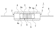
本実施形態のサージ防護素子1は、図1及び図2に示すように、互いに間隔を空けて対向配置された一対の放電電極2と、両端に一対の放電電極2を配して一対の放電電極2の少なくとも互いの対向面4aを放電制御ガスと共に内部に封止する絶縁性管3とを備えている。
上記放電電極2は、金属で形成され対向面4aを有した電極本体4を備えている。
As shown in Figures 1 and 2, the surge protection element 1 of this embodiment comprises a pair of
The
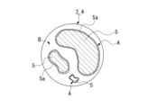
上記対向面4aには、図2に示すように、誘電体膜5で覆われた領域Aと、誘電体膜5で覆われていない領域Bとが設けられている。
すなわち、誘電体膜5で覆われていない領域Bには、電極本体4内部を構成する金属や対向面4a上に形成された金属膜及びこれらの酸化膜が露出している。
本実施形態では、電極本体4の対向面4aには銅(Cu)の膜が形成されており、誘電体膜5で覆われていない領域Bには銅の酸化膜(Cu2O、CuO)が薄く形成されている。
As shown in FIG. 2, the
That is, in the region B not covered with the
In this embodiment, a copper (Cu) film is formed on the
上記誘電体膜5の外周縁部には、対向面4aの金属の酸化膜(Cu2O、CuO)が含有され、対向面4aの誘電体膜5の外周縁部直下(外周縁部の対向面側)には、対向面4aの金属の酸化膜(Cu2O、CuO)が除去された酸化膜除去部5aが形成されている。
上記誘電体膜5の誘電体材料は、ケイ酸ナトリウムである。なお、誘電体として、ケイ酸カリウムを採用しても構わない。
The outer peripheral edge of the
The dielectric material of the
また、本実施形態のサージ防護素子1は、軸線方向中央部の放電ギャップ部Gを介して周面に導電性被膜6aが分割形成された柱状又は筒状の絶縁性部材6を備えている。
上記放電電極2は、絶縁性部材6の両端に導電部材である金属キャップ7を介して対向配置されている。
上記絶縁性部材6は、ムライト焼結体などのセラミックス材料からなり、表面に導電性被膜6aとして物理蒸着(PVD)法や化学蒸着(CVD)法などの薄膜形成技術によるSnO2等が形成されている。
The surge protection element 1 of this embodiment also includes a columnar or cylindrical insulating member 6 having a
The
The insulating member 6 is made of a ceramic material such as mullite sintered body, and a
上記放電ギャップ部Gは、導電性被膜6aの軸線方向中央に、絶縁性部材6の周面に沿ってYAGレーザからのレーザ光を照射し、導電性被膜6aを分断することによって形成される。
一対の金属キャップ7は、絶縁性部材6よりも硬度が低く塑性変形できる、例えば銅やステンレスなどの金属から形成されている。また、一対の金属キャップ7は、絶縁性部材6の両端にそれぞれ係合されており、互いに対向する面が放電電極2の内面と共に主放電面となっている。
The discharge gap G is formed by irradiating the circumferential surface of the insulating member 6 with laser light from a YAG laser at the axial center of the
The pair of
上記放電電極2の電極本体4は、Fe(鉄)-Ni(ニッケル)合金等の金属表面を銅及び酸化銅で被覆した封止電極であって、円板状又は円柱状となっている。そして、電極本体4の一方の面が金属キャップ7と接触しており、他方の面にリード線8が溶接されている。このリード線8は、銅覆鋼線等で形成されている。
すなわち、電極本体4にリード線8が取り付けられた放電電極2は、いわゆるスラグリードである。
The
That is, the
上記絶縁性管3は、鉛ガラスやソーダ石灰ガラスのような軟質ガラスで構成されており、円筒状となっている。また、絶縁性管3の両端近傍において放電電極2の外周面が絶縁性管3の内周面と溶着されている。
上記放電制御ガスは、放電開始電圧などの電気特性が所望の値となるように組成などを調整された封止ガスであって、He、Ar、Ne、Xe、SF6、CO2、C3F8、C2F6、CF4、H2及びこれらの混合ガス等の不活性ガスである。
なお、本実施形態では、放電制御ガスとしてArを採用している。
The
The discharge control gas is a sealing gas whose composition is adjusted so that electrical characteristics such as the discharge start voltage are the desired values, and is an inert gas such as He, Ar, Ne, Xe , SF6 , CO2 , C3F8 , C2F6 , CF4 , H2, and mixtures of these gases.
In this embodiment, Ar is used as the discharge control gas.
次に、本実施形態のサージ防護素子1の製造方法について説明する。
本実施形態のサージ防護素子1の製造方法では、互いに間隔を空けて対向配置される一対の放電電極2の対向面4aに、図3に示すように、誘電体材料を含有した水溶液Lを塗布して乾燥させ、対向面4aに誘電体膜5で覆われた領域Aと、誘電体膜5で覆われていない領域Bとを設ける誘電体膜形成工程を有している。
また、本実施形態のサージ防護素子の製造方法は、上記誘電体膜形成工程後、両端に一対の放電電極2を配して一対の放電電極2の少なくとも互いの対向面4aを放電制御ガスと共に絶縁性管3の内部に封止する封止工程と、封止工程後に、一対の放電電極2間に直流電圧又は交流電圧を印加するエージング工程とを有している。
Next, a method for manufacturing the surge protection device 1 of this embodiment will be described.
The manufacturing method of the surge protection element 1 of this embodiment includes a dielectric film formation step of applying an aqueous solution L containing a dielectric material to the
In addition, the manufacturing method of the surge protection element of this embodiment includes, after the dielectric film forming process, a sealing process in which a pair of
上記水溶液Lは、誘電体材料としてケイ酸ナトリウムを含有した水ガラスの水溶液である。なお、水溶液Lは、誘電体材料としてケイ酸カリウムを含有したカリ水ガラスの水溶液を採用しても構わない。
本実施形態では、水溶液Lとして例えば水ガラスの重量5~50倍の希薄溶液を使用する。なお、水ガラスを上記希薄溶液としているため、ほとんど水と同様のハンドリングで水滴を対向面4a上に塗布して付着させることができる。
水溶液Lを対向面4aに塗布する場合、スポイト等で塗布するが、ディスペンサー等で塗布しても構わない。
The aqueous solution L is an aqueous solution of water glass containing sodium silicate as a dielectric material. Alternatively, an aqueous solution of potassium water glass containing potassium silicate as a dielectric material may be used as the aqueous solution L.
In this embodiment, a dilute solution having a weight of, for example, 5 to 50 times that of water glass is used as the aqueous solution L. Since water glass is used as the dilute solution, water droplets can be applied and attached to the
When applying the aqueous solution L to the facing
上記塗布した水溶液Lの乾燥工程は、例えば150℃,10minで乾燥させる。
塗布した水溶液Lは、図2に示すように、上記乾燥時に対向面4a上で1箇所又は複数箇所に部分的に集まって点在した状態で誘電体膜5を形成する。
また、上記封止工程では、例えば絶縁性管3を700℃加熱して、Ar(800torr)の放電制御ガスを封止すると共に、電極本体4の外周面と絶縁性管3の内周面とを接合する。
さらに、上記エージング工程では、例えばAC100mA,2sec:2kV,20kΩでエージングを行う。
The applied aqueous solution L is dried, for example, at 150° C. for 10 minutes.
As shown in FIG. 2, the applied aqueous solution L partially gathers at one or more locations on the
In the sealing step, the insulating
Furthermore, in the aging process, aging is performed at AC 100 mA, 2 sec: 2 kV, 20 kΩ, for example.
このように本実施形態のサージ防護素子1では、電極本体4の対向面4aに、誘電体膜5で覆われた領域Aと、誘電体膜5で覆われていない領域Bとが設けられているので、部分的に設けられた誘電体膜5で覆われた領域Aでは対向面4aの金属が酸化し難くなると共に、誘電体膜5の外周縁部近傍に電気力線が集まって電界が集中することで、放電し易くなり、安定した放電開始電圧が得られる。
また、対向面4aの誘電体膜5の外周縁部直下(外周縁部の対向面側)に、対向面4aの金属の酸化膜が除去された酸化膜除去部5aが形成されているので、酸化膜が除去された酸化膜除去部5aにより、電界がさらに集中することで、より安定した放電開始電圧が得られる。
In this manner, in the surge protection element 1 of this embodiment, the opposing
In addition, an oxide film-removed
本実施形態のサージ防護素子1の製造方法では、互いに間隔を空けて対向配置される一対の放電電極2の対向面4aに、誘電体材料を含有した水溶液Lを塗布して乾燥させ、対向面4aに誘電体膜5で覆われた領域Aと、誘電体膜5で覆われていない領域Bとを設ける誘電体膜形成工程を有しているので、誘電体を含有した水溶液Lの塗布及び乾燥によって容易に誘電体膜5で覆われた領域Aと、誘電体膜5で覆われていない領域Bとを設けることができる。
The manufacturing method of the surge protection element 1 of this embodiment includes a dielectric film formation process in which an aqueous solution L containing a dielectric material is applied to the opposing
また、一対の放電電極2間に直流電圧又は交流電圧を印加するエージング工程を有しているので、エージングにより電子が対向面4aの金属の酸化膜に当たって酸化膜の除去効果が促進されると共に、誘電体膜5の外周縁部直下(外周縁部の対向面側)の金属が活性化され、酸化膜が除去された酸化膜除去部5aを形成することができる。また、エージングにより絶縁性管3内の余剰酸素が誘電体膜5に包含されることで、より安定した放電開始電圧が得られる。
さらに、水溶液Lが、誘電体材料としてケイ酸ナトリウム又はケイ酸カリウムを含有した水ガラスの水溶液であるので、塗布及び乾燥が容易で、ケイ酸ナトリウム又はケイ酸カリウムの誘電体膜5を得ることができる。
In addition, since the method includes an aging process in which a DC or AC voltage is applied between the pair of
Furthermore, since the aqueous solution L is an aqueous solution of water glass containing sodium silicate or potassium silicate as a dielectric material, it is easy to apply and dry, and a
次に、本発明に係るサージ防護素子及びその製造方法の第2実施形態について、図4を参照して以下に説明する。なお、以下の実施形態の説明において、上記実施形態において説明した同一の構成要素には同一の符号を付し、その説明は省略する。 Next, a second embodiment of the surge protection element and its manufacturing method according to the present invention will be described below with reference to FIG. 4. In the following description of the embodiment, the same components as those described in the above embodiment are given the same reference numerals, and the description thereof will be omitted.
第2実施形態と第1実施形態との異なる点は、第1実施形態では、放電ギャップ部Gを介して導電性被膜6aが分割形成された柱状又は筒状の絶縁性部材6を備え、一対の放電電極2が、絶縁性部材6の両端に導電部材である金属キャップ7を介して対向配置されているのに対し、第2実施形態のサージ防護素子21では、図4に示すように、一対の放電電極22の電極本体24が板状の絶縁性部材26を対向面4aで直接挟んだ状態で対向配置されている点である。
The difference between the second embodiment and the first embodiment is that the first embodiment includes a columnar or cylindrical insulating member 6 on which a
上記板状の絶縁性部材26は、例えばSiO2で形成されている。
このように第2実施形態では、第1実施形態に比べて絶縁性管23を短くでき、小型化が可能である。
また、第2実施形態のサージ防護素子21でも、第1実施形態と同様に、電極本体24の対向面4aに誘電体膜5で覆われた領域Aと、誘電体膜5で覆われていない領域Bとが設けられているので、安定した放電開始電圧が得られる。
The plate-like insulating
In this way, in the second embodiment, the insulating
In the
次に、上記第2実施形態のサージ防護素子を、上記製造方法により作製した実施例について、電極本体24の対向面4aを示すSEM組成像を、図5に示す。
なお、このSEM組成像では、明るいほど(白いほど)原子番号の大きな元素が存在することを表している。本実施形態では、白い部分が銅(酸化銅を含む)である。また、黒い部分はケイ酸ナトリウムを含んだ水ガラス塗布による誘電体膜5を表している。さらに、誘電体膜5の外周縁部に影のように滲んだ部分は、対向面4a表面の酸化銅が誘電体膜5に拡散して対向面4a表面から除去されている部分である。
Next, in an example in which the surge protection element of the second embodiment was produced by the above-mentioned manufacturing method, an SEM composition image showing the opposing
In this SEM composition image, the brighter (whiter) the image, the more elements with larger atomic numbers are present. In this embodiment, the white parts are copper (including copper oxide). The black parts represent the
この画像からわかるように、電極本体24の対向面4aに、誘電体膜5で覆われた領域Aと、誘電体膜5で覆われていない領域Bとが設けられている。
また、対向面4aの誘電体膜5の外周縁部直下(外周縁部の対向面側)に、対向面4aの金属(銅)の酸化膜が除去された酸化膜除去部5aが形成されている。
As can be seen from this image, the opposing
Further, an oxide
次に、本発明の上記実施例について、上記エージングの条件でACエージングを行った場合の放電開始電圧Vsの経時的変化を測定した結果を、図6の(b)に示す。なお、比較のため、対向面4aに上記水溶液Lを塗布せず誘電体膜5で覆われた領域Aのない比較例についても、同様にエージングを行った場合の放電開始電圧Vsの経時的変化を測定した結果を、図6の(a)に示す。
これらの結果からわかるように、対向面4aに誘電体膜5で覆われた領域Aのない比較例では、エージング後でもエージング効果が効かない個体があり、放電開始電圧のばらつきが大きいのに対し、対向面4aに誘電体膜5で覆われた領域Aを有する本発明の実施例では、いずれの個体もエージングの効果が大きく、放電開始電圧のばらつきが小さい。
Next, the above-mentioned embodiment of the present invention was subjected to AC aging under the above-mentioned aging conditions, and the result of measuring the change over time of the discharge starting voltage Vs is shown in Fig. 6(b). For comparison, a comparative example in which the aqueous solution L was not applied to the facing
As can be seen from these results, in the comparative example in which the opposing
次に、本発明の上記実施例について、絶縁抵抗(IR)の変化を測定した結果を図7の(b)に示す。なお、比較のため、対向面4aに上記水溶液Lを塗布せず誘電体膜5で覆われた領域Aのない比較例についても、同様に絶縁抵抗の変化を測定した結果を図7の(a)に示す。
これらの結果からわかる様に、比較例では、絶縁抵抗が低下する個体が多数発生したのに対し、本発明の実施例では、絶縁抵抗が安定している。
Next, the results of measuring the change in insulation resistance (IR) for the above-mentioned embodiment of the present invention are shown in Fig. 7(b) . For comparison, the results of measuring the change in insulation resistance for a comparative example in which the aqueous solution L was not applied to the opposing
As can be seen from these results, in the comparative example, many specimens exhibited a decrease in insulation resistance, whereas in the examples of the present invention, the insulation resistance was stable.
なお、本発明の技術範囲は上記各実施形態および実施例に限定されるものではなく、本発明の趣旨を逸脱しない範囲において種々の変更を加えることが可能である。 The technical scope of the present invention is not limited to the above-mentioned embodiments and examples, and various modifications can be made without departing from the spirit of the present invention.
1,21…サージ防護素子、2,22…放電電極、3,23…絶縁性管、4,24…電極本体、4a…対向面、5…誘電体膜、5a…酸化膜除去部、A…誘電体膜で覆われた領域、B…誘電体膜で覆われていない領域、L…水溶液 1, 21...surge protection element, 2, 22...discharge electrode, 3, 23...insulating tube, 4, 24...electrode body, 4a...opposing surface, 5...dielectric film, 5a...oxide film removal portion, A...area covered with dielectric film, B...area not covered with dielectric film, L...aqueous solution
Claims (5)
両端に前記一対の放電電極を配して前記一対の放電電極の少なくとも互いの対向面を放電制御ガスと共に内部に封止する絶縁性管とを備え、
前記放電電極が、金属で形成され前記対向面を有した電極本体を備え、
前記対向面に、誘電体膜で覆われた領域と、前記誘電体膜で覆われていない領域とが設けられ、
前記誘電体膜で覆われていない領域に、前記電極本体内部を構成する金属の酸化膜が前記対向面上に形成されて露出し、
前記誘電体膜の外周縁部に、前記対向面の金属の酸化膜が拡散し含有され、前記誘電体膜の外周縁部の前記対向面側に、前記対向面の金属の酸化膜が除去された酸化膜除去部が形成されていることを特徴とするサージ防護素子。 A pair of discharge electrodes arranged opposite each other with a gap therebetween;
an insulating tube having the pair of discharge electrodes disposed at both ends thereof and sealing at least the mutually facing surfaces of the pair of discharge electrodes together with a discharge control gas therein;
The discharge electrode includes an electrode body formed of a metal and having the opposing surface,
The opposing surface is provided with a region covered with a dielectric film and a region not covered with the dielectric film ,
an oxide film of a metal constituting the inside of the electrode body is formed on the opposing surface and exposed in a region not covered with the dielectric film;
A surge protection element characterized in that an oxide film of the metal of the opposing surface is diffused and contained in the outer peripheral edge portion of the dielectric film, and an oxide film removal portion in which the oxide film of the metal of the opposing surface has been removed is formed on the opposing surface side of the outer peripheral edge portion of the dielectric film .
前記誘電体膜の誘電体材料が、ケイ酸ナトリウム又はケイ酸カリウムであることを特徴とするサージ防護素子。 2. The surge protection device according to claim 1 ,
4. A surge protection element, wherein the dielectric material of the dielectric film is sodium silicate or potassium silicate.
互いに間隔を空けて対向配置される一対の放電電極の対向面に、誘電体材料を含有した水溶液を塗布して乾燥させ、前記対向面に誘電体膜で覆われた領域と、前記誘電体膜で覆われていない領域とを設ける誘電体膜形成工程を有していることを特徴とするサージ防護素子の製造方法。 A method for manufacturing the surge protection element according to claim 1 or 2 , comprising the steps of:
A method for manufacturing a surge protection element, comprising the steps of: applying an aqueous solution containing a dielectric material to the opposing surfaces of a pair of discharge electrodes arranged opposite each other with a gap therebetween; and drying the aqueous solution, the aqueous solution containing a dielectric material, to provide an area on the opposing surfaces that is covered with a dielectric film and an area that is not covered with the dielectric film.
前記誘電体膜形成工程後、両端に前記一対の放電電極を配して前記一対の放電電極の少なくとも互いの対向面を放電制御ガスと共に絶縁性管の内部に封止する封止工程と、
前記封止工程後に、前記一対の放電電極間に直流電圧又は交流電圧を印加するエージング工程とを有していることを特徴とするサージ防護素子の製造方法。 4. The method for manufacturing a surge protection element according to claim 3 ,
a sealing step of disposing the pair of discharge electrodes on both ends and sealing at least the mutually facing surfaces of the pair of discharge electrodes together with a discharge control gas inside an insulating tube after the dielectric film forming step;
The method for manufacturing a surge protection element further comprises, after the sealing step, an aging step of applying a DC voltage or an AC voltage between the pair of discharge electrodes.
前記水溶液が、前記誘電体材料としてケイ酸ナトリウム又はケイ酸カリウムを含有した水ガラスの水溶液であることを特徴とするサージ防護素子の製造方法。 The method for manufacturing a surge protection element according to claim 3 or 4 ,
2. A method for manufacturing a surge protection element, wherein the aqueous solution is an aqueous solution of water glass containing sodium silicate or potassium silicate as the dielectric material.
Priority Applications (1)
| Application Number | Priority Date | Filing Date | Title |
|---|---|---|---|
| JP2021038863A JP7608883B2 (en) | 2021-03-11 | 2021-03-11 | Surge protection device and its manufacturing method |
Applications Claiming Priority (1)
| Application Number | Priority Date | Filing Date | Title |
|---|---|---|---|
| JP2021038863A JP7608883B2 (en) | 2021-03-11 | 2021-03-11 | Surge protection device and its manufacturing method |
Publications (2)
| Publication Number | Publication Date |
|---|---|
| JP2022138781A JP2022138781A (en) | 2022-09-26 |
| JP7608883B2 true JP7608883B2 (en) | 2025-01-07 |
Family
ID=83400184
Family Applications (1)
| Application Number | Title | Priority Date | Filing Date |
|---|---|---|---|
| JP2021038863A Active JP7608883B2 (en) | 2021-03-11 | 2021-03-11 | Surge protection device and its manufacturing method |
Country Status (1)
| Country | Link |
|---|---|
| JP (1) | JP7608883B2 (en) |
Citations (9)
| Publication number | Priority date | Publication date | Assignee | Title |
|---|---|---|---|---|
| JP2001516943A (en) | 1997-09-16 | 2001-10-02 | シーメンス アクチエンゲゼルシヤフト | Gas-filled discharge path |
| JP2003077617A (en) | 2001-09-06 | 2003-03-14 | Sankosha Corp | Arrester for low voltage power system |
| JP2004079230A (en) | 2002-08-12 | 2004-03-11 | Shinko Electric Ind Co Ltd | Discharge tube and method of manufacturing the same |
| JP2006222001A (en) | 2005-02-14 | 2006-08-24 | Okaya Electric Ind Co Ltd | Discharge tube |
| US20070064372A1 (en) | 2005-09-14 | 2007-03-22 | Littelfuse, Inc. | Gas-filled surge arrester, activating compound, ignition stripes and method therefore |
| JP3161707U (en) | 2010-05-27 | 2010-08-05 | 岡谷電機産業株式会社 | Discharge tube |
| JP2016189265A (en) | 2015-03-30 | 2016-11-04 | 三菱マテリアル株式会社 | Discharge tube and manufacturing method thereof |
| JP2017195140A (en) | 2016-04-22 | 2017-10-26 | 三菱マテリアル株式会社 | Surge protective element |
| JP2017199489A (en) | 2016-04-26 | 2017-11-02 | 三菱マテリアル株式会社 | Surge protective element |
Family Cites Families (2)
| Publication number | Priority date | Publication date | Assignee | Title |
|---|---|---|---|---|
| JPS6341748Y2 (en) * | 1979-06-26 | 1988-11-01 | ||
| JP3290376B2 (en) * | 1997-05-14 | 2002-06-10 | 新光電気工業株式会社 | Discharge tube and method of manufacturing the same |
-
2021
- 2021-03-11 JP JP2021038863A patent/JP7608883B2/en active Active
Patent Citations (10)
| Publication number | Priority date | Publication date | Assignee | Title |
|---|---|---|---|---|
| JP2001516943A (en) | 1997-09-16 | 2001-10-02 | シーメンス アクチエンゲゼルシヤフト | Gas-filled discharge path |
| JP2003077617A (en) | 2001-09-06 | 2003-03-14 | Sankosha Corp | Arrester for low voltage power system |
| JP2004079230A (en) | 2002-08-12 | 2004-03-11 | Shinko Electric Ind Co Ltd | Discharge tube and method of manufacturing the same |
| JP2006222001A (en) | 2005-02-14 | 2006-08-24 | Okaya Electric Ind Co Ltd | Discharge tube |
| US20070064372A1 (en) | 2005-09-14 | 2007-03-22 | Littelfuse, Inc. | Gas-filled surge arrester, activating compound, ignition stripes and method therefore |
| JP2009508320A (en) | 2005-09-14 | 2009-02-26 | リッテルフューズ,インコーポレイティド | Surge arrester with gas, activation compound, ignition stripe and method thereof |
| JP3161707U (en) | 2010-05-27 | 2010-08-05 | 岡谷電機産業株式会社 | Discharge tube |
| JP2016189265A (en) | 2015-03-30 | 2016-11-04 | 三菱マテリアル株式会社 | Discharge tube and manufacturing method thereof |
| JP2017195140A (en) | 2016-04-22 | 2017-10-26 | 三菱マテリアル株式会社 | Surge protective element |
| JP2017199489A (en) | 2016-04-26 | 2017-11-02 | 三菱マテリアル株式会社 | Surge protective element |
Also Published As
| Publication number | Publication date |
|---|---|
| JP2022138781A (en) | 2022-09-26 |
Similar Documents
| Publication | Publication Date | Title |
|---|---|---|
| JP2648320B2 (en) | How to make a fuse | |
| JP5205555B2 (en) | Gas discharge tube | |
| JP7608883B2 (en) | Surge protection device and its manufacturing method | |
| US5506071A (en) | Sealing electrode and surge absorber using the same | |
| JP6044418B2 (en) | Surge absorber and manufacturing method thereof | |
| JPH0729667A (en) | Discharge type surge absorber and manufacturing method thereof | |
| KR100723572B1 (en) | Chip type surge absorber and method of manufacturing the same | |
| JP7459767B2 (en) | surge protection element | |
| JP2001267037A (en) | Surge absorbing element and manufacturing method therefor | |
| JP4193426B2 (en) | Surge absorber and its microgap forming method | |
| JPH01311585A (en) | Discharge type surge absorbing element | |
| TWI440271B (en) | Surge absorber | |
| JPH0668949A (en) | Lightning arrester | |
| JP2819388B2 (en) | Discharge type surge absorbing element and method of manufacturing the same | |
| JPH03194878A (en) | Discharge type surge absorption element | |
| JPH07326462A (en) | Chip type micro-gap type surge absorber | |
| JPH07245878A (en) | Chip type micro-gap type surge absorber | |
| JP2541069B2 (en) | Sealing electrode and surge absorber using the same | |
| JPH0724234B2 (en) | Micro gap type surge absorber | |
| JP2022140303A (en) | Surge protection element and manufacturing method thereof | |
| JP7161144B2 (en) | surge protective element | |
| JPH0132712Y2 (en) | ||
| JPH0536460A (en) | Discharge type surge absorbing element | |
| JPH11224761A (en) | High voltage surge absorber | |
| JP2534954B2 (en) | Discharge type surge absorber and method for manufacturing the same |
Legal Events
| Date | Code | Title | Description |
|---|---|---|---|
| A621 | Written request for application examination |
Free format text: JAPANESE INTERMEDIATE CODE: A621 Effective date: 20240129 |
|
| A977 | Report on retrieval |
Free format text: JAPANESE INTERMEDIATE CODE: A971007 Effective date: 20240809 |
|
| A131 | Notification of reasons for refusal |
Free format text: JAPANESE INTERMEDIATE CODE: A131 Effective date: 20240814 |
|
| A521 | Request for written amendment filed |
Free format text: JAPANESE INTERMEDIATE CODE: A523 Effective date: 20241009 |
|
| TRDD | Decision of grant or rejection written | ||
| A01 | Written decision to grant a patent or to grant a registration (utility model) |
Free format text: JAPANESE INTERMEDIATE CODE: A01 Effective date: 20241119 |
|
| A61 | First payment of annual fees (during grant procedure) |
Free format text: JAPANESE INTERMEDIATE CODE: A61 Effective date: 20241202 |
|
| R150 | Certificate of patent or registration of utility model |
Ref document number: 7608883 Country of ref document: JP Free format text: JAPANESE INTERMEDIATE CODE: R150 |