JP7598677B1 - Probe Card Holder for Wafer Inspection - Google Patents
Probe Card Holder for Wafer Inspection Download PDFInfo
- Publication number
- JP7598677B1 JP7598677B1 JP2024007498A JP2024007498A JP7598677B1 JP 7598677 B1 JP7598677 B1 JP 7598677B1 JP 2024007498 A JP2024007498 A JP 2024007498A JP 2024007498 A JP2024007498 A JP 2024007498A JP 7598677 B1 JP7598677 B1 JP 7598677B1
- Authority
- JP
- Japan
- Prior art keywords
- probe card
- wafer
- weight ring
- body part
- card holder
- Prior art date
- Legal status (The legal status is an assumption and is not a legal conclusion. Google has not performed a legal analysis and makes no representation as to the accuracy of the status listed.)
- Active
Links
Images


Classifications
-
- G—PHYSICS
- G01—MEASURING; TESTING
- G01R—MEASURING ELECTRIC VARIABLES; MEASURING MAGNETIC VARIABLES
- G01R31/00—Arrangements for testing electric properties; Arrangements for locating electric faults; Arrangements for electrical testing characterised by what is being tested not provided for elsewhere
- G01R31/28—Testing of electronic circuits, e.g. by signal tracer
- G01R31/2851—Testing of integrated circuits [IC]
- G01R31/2886—Features relating to contacting the IC under test, e.g. probe heads; chucks
- G01R31/2891—Features relating to contacting the IC under test, e.g. probe heads; chucks related to sensing or controlling of force, position, temperature
-
- G—PHYSICS
- G01—MEASURING; TESTING
- G01R—MEASURING ELECTRIC VARIABLES; MEASURING MAGNETIC VARIABLES
- G01R31/00—Arrangements for testing electric properties; Arrangements for locating electric faults; Arrangements for electrical testing characterised by what is being tested not provided for elsewhere
- G01R31/28—Testing of electronic circuits, e.g. by signal tracer
- G01R31/2851—Testing of integrated circuits [IC]
- G01R31/2886—Features relating to contacting the IC under test, e.g. probe heads; chucks
-
- G—PHYSICS
- G01—MEASURING; TESTING
- G01R—MEASURING ELECTRIC VARIABLES; MEASURING MAGNETIC VARIABLES
- G01R1/00—Details of instruments or arrangements of the types included in groups G01R5/00 - G01R13/00 and G01R31/00
- G01R1/02—General constructional details
- G01R1/06—Measuring leads; Measuring probes
- G01R1/067—Measuring probes
- G01R1/073—Multiple probes
-
- G—PHYSICS
- G01—MEASURING; TESTING
- G01R—MEASURING ELECTRIC VARIABLES; MEASURING MAGNETIC VARIABLES
- G01R31/00—Arrangements for testing electric properties; Arrangements for locating electric faults; Arrangements for electrical testing characterised by what is being tested not provided for elsewhere
- G01R31/28—Testing of electronic circuits, e.g. by signal tracer
- G01R31/2851—Testing of integrated circuits [IC]
- G01R31/2886—Features relating to contacting the IC under test, e.g. probe heads; chucks
- G01R31/2887—Features relating to contacting the IC under test, e.g. probe heads; chucks involving moving the probe head or the IC under test; docking stations
-
- G—PHYSICS
- G01—MEASURING; TESTING
- G01R—MEASURING ELECTRIC VARIABLES; MEASURING MAGNETIC VARIABLES
- G01R31/00—Arrangements for testing electric properties; Arrangements for locating electric faults; Arrangements for electrical testing characterised by what is being tested not provided for elsewhere
- G01R31/28—Testing of electronic circuits, e.g. by signal tracer
- G01R31/2851—Testing of integrated circuits [IC]
- G01R31/2886—Features relating to contacting the IC under test, e.g. probe heads; chucks
- G01R31/2889—Interfaces, e.g. between probe and tester
Landscapes
- Engineering & Computer Science (AREA)
- Physics & Mathematics (AREA)
- General Physics & Mathematics (AREA)
- Computer Hardware Design (AREA)
- Microelectronics & Electronic Packaging (AREA)
- General Engineering & Computer Science (AREA)
- Testing Or Measuring Of Semiconductors Or The Like (AREA)
- Testing Of Individual Semiconductor Devices (AREA)
- Measuring Leads Or Probes (AREA)
Abstract
【課題】ウェーハを1つに固定して自己位置の保持が可能なプローブカードホルダーを提供する。
【解決手段】プローブカードホルダーは、中央にプローブカード111が設けられ、プローブカード111の周辺に垂直に貫通したガイド孔112を有する第1ボディ部110と、中央にウェーハの保持されるウェーハチャック121が設けられ、ガイド孔112と対応してマグネットホルダー122が設けられる第2ボディ部120と、ガイド孔112に挿入されてマグネットホルダー122と磁力によって固定可能なマグネットチャック131が設けられ、第1ボディ部110の上部で第2ボディ部120に組み立てられるウェイトリング130と、第1ボディ部110とウェイトリング130との間に設けられ、第1ボディ部110とウェイトリング130との間隔を固定するクランプ部140と、を備える。
【選択図】図2
A probe card holder capable of fixing a wafer to itself and maintaining its own position is provided.
[Solution] The probe card holder comprises a first body part (110) having a probe card (111) at the center and guide holes (112) penetrating vertically around the periphery of the probe card (111); a second body part (120) having a wafer chuck (121) at the center for holding a wafer and a magnet holder (122) corresponding to the guide hole (112); a weight ring (130) having a magnet chuck (131) inserted into the guide hole (112) and capable of being fixed to the magnet holder (122) by magnetic force, and assembled to the second body part (120) on the upper part of the first body part (110); and a clamp part (140) provided between the first body part (110) and the weight ring (130) for fixing the distance between the first body part (110) and the weight ring (130).
[Selected figure] Figure 2
Description
本発明は、ウェーハの検査のためにプローブカードとウェーハを1つに固定して自己位置の保持が可能なプローブカードホルダーに関する。 The present invention relates to a probe card holder that can fix a probe card and a wafer together and maintain its own position for wafer inspection.
一般に、半導体装置の集積回路素子などの半導体素子は、ウェーハに一連の処理工程を繰り返し行うことにより形成できる。例えば、ウェーハに膜を形成する蒸着工程、蒸着が行われたウェーハに電気的特性を有するパターンを形成するためのエッチング工程、パターンに不純物を注入または拡散させるためのイオン注入工程または拡散工程、パターンが形成されたウェーハから不純物を除去するための洗浄及びリンス工程などを繰り返し行うことにより、半導体素子がウェーハ上に形成される。 In general, semiconductor elements such as integrated circuit elements of semiconductor devices can be formed by repeatedly performing a series of processing steps on a wafer. For example, semiconductor elements are formed on a wafer by repeatedly performing a deposition process to form a film on the wafer, an etching process to form a pattern with electrical properties on the wafer after deposition, an ion implantation process or diffusion process to inject or diffuse impurities into the pattern, and a cleaning and rinsing process to remove impurities from the wafer on which the pattern has been formed.
このような一連の工程を経た半導体素子が形成された後、半導体素子の電気的特性を検査するための電気的な検査工程が行われることがある。検査工程は、多数のプローブを有するプローブカードを含むプローブステーションと電気的な信号を提供するためにプローブカードに連結されたテスターによって行われる。 After a semiconductor device is formed through this series of processes, an electrical testing process may be performed to test the electrical characteristics of the semiconductor device. The testing process is performed by a probe station that includes a probe card with multiple probes and a tester connected to the probe card to provide an electrical signal.
一般に、プローブステーションは、検査チャンバーと、検査チャンバー内に配置されてウェーハを支持するチャックと、チャックを駆動するチャック移送装置と、ウェーハ上に形成された半導体素子と接触するように構成された多数のプローブを有するプローブカードと、プローブカードに連結されてテストを行うテスターと、を含む。 Generally, a probe station includes an inspection chamber, a chuck that is disposed within the inspection chamber and supports the wafer, a chuck transport device that drives the chuck, a probe card having a number of probes configured to contact semiconductor elements formed on the wafer, and a tester that is connected to the probe card and performs the tests.
このような従来技術では、チャック移送装置が、ウェーハの保持されたチャックを検査チャンバーに運び、CCDカメラなどのビジョンセンサーなどを用いてウェーハ上の接触電極とプローブカードのプローブの位置を把握し、把握された位置情報に基づいてチャック移送装置を制御してウェーハの接触電極をプローブに接触させることにより電気的に接続する。理想的な場合、プローブステーションは、オーバードライブ制御によって、チャックに搭載されたウェーハとプローブカードとが適切な圧力によって均一に接触した状態を維持する。 In such conventional technology, a chuck transport device carries a chuck holding a wafer to an inspection chamber, grasps the positions of the contact electrodes on the wafer and the probes of the probe card using a vision sensor such as a CCD camera, and controls the chuck transport device based on the grasped position information to bring the contact electrodes of the wafer into contact with the probes, thereby electrically connecting them. In an ideal case, the probe station uses overdrive control to keep the wafer mounted on the chuck and the probe card in uniform contact with the appropriate pressure.
しかし、プローブステーションは、機械的な精度の誤差および外乱により、チャックに搭載されたウェーハとプローブカードとが実際に完璧な接触状態を維持することは非常に難しく、この状態で、予め定められたオーバードライブ量に対応する高さまでチャックを上昇させても、ウェーハの特定部位があまり深く突き刺されてウェーハが損傷したり、特定部位が正しく突き刺されなくてプローブと接触電極とが接触していない「オープンフェイル(open fail)」が発生したりして、正常な検査が不可能になるという問題が生じる。 However, due to mechanical precision errors and disturbances, it is extremely difficult for the wafer mounted on the chuck to actually maintain perfect contact with the probe card in the probe station. Even if the chuck is raised to a height corresponding to a predetermined overdrive amount in this state, a particular part of the wafer may be pierced too deeply, damaging the wafer, or a particular part may not be pierced properly, resulting in an "open fail" in which the probe does not make contact with the contact electrode, making normal testing impossible.
本発明は、このような従来技術のウェーハ検査工程を脱皮して大量のウェーハを効率よく検査するための代案として、プローブカードとウェーハを一つにモジュール化してウェーハ検査を行おうとするものであり、このために、移送過程でプローブカードとウェーハが精密な自己位置を保持することができるプローブカードホルダーを開発し、これを出願するのである。 The present invention aims to move away from the conventional wafer inspection process and perform wafer inspection by modularizing the probe card and wafer into one module as an alternative to efficiently inspect large quantities of wafers. To this end, we have developed and filed a patent application for a probe card holder that can precisely maintain the position of the probe card and wafer during transportation.
本発明は、ウェーハの検査のためにプローブカードとウェーハを一つにモジュール化し、プローブカードとウェーハの自己位置の保持が可能なウェーハ検査用プローブカードホルダーを提供することを目的とする。 The present invention aims to provide a probe card holder for wafer inspection that modularizes a probe card and a wafer for wafer inspection and can maintain the self-positions of the probe card and the wafer.
上記目的を達成するための本発明のウェーハ検査用プローブカードホルダーは、中央にプローブカードが設けられ、前記プローブカードの周辺に垂直に貫通したガイド孔を有する第1ボディ部と、中央にウェーハの保持されるウェーハチャックが設けられ、前記ガイド孔と対応してマグネットホルダーが設けられる第2ボディ部と、前記ガイド孔に挿入されて前記マグネットホルダーと磁力によって固定可能なマグネットチャックが設けられ、前記第1ボディ部の上部で前記第2ボディ部に組み立てられるウェイトリングと、前記第1ボディ部と前記ウェイトリングとの間に設けられ、前記第1ボディ部と前記ウェイトリングとの間隔を固定するクランプ部と、を備える。 The probe card holder for wafer inspection of the present invention, which is intended to achieve the above object, comprises a first body part having a probe card at its center and a guide hole that penetrates vertically around the periphery of the probe card, a second body part having a wafer chuck at its center for holding a wafer and a magnet holder corresponding to the guide hole, a weight ring having a magnet chuck inserted into the guide hole and capable of being fixed to the magnet holder by magnetic force, assembled to the second body part on the top of the first body part, and a clamp part provided between the first body part and the weight ring and fixing the distance between the first body part and the weight ring.
好ましくは、前記マグネットチャックは、前記ウェイトリングの下部に少なくとも2つ設けられ、より好ましくは、前記クランプ部は、第1ボディ部と前記ウェイトリングとの間に少なくとも2つ設けられ、さらに好ましくは、前記クランプ部は、前記マグネットチャック同士の間に少なくとも1つ設けられる。 Preferably, at least two of the magnetic chucks are provided below the weight ring, more preferably, at least two of the clamping parts are provided between the first body part and the weight ring, and even more preferably, at least one of the clamping parts is provided between the magnetic chucks.
好ましくは、前記クランプ部は、前記ウェイトリングまたは前記第1ボディ部に一端が固定されるシャフトと、前記ウェイトリングまたは前記第1ボディ部に固定され、空圧信号によって前記シャフトに固定される空圧駆動部と、を備える。 Preferably, the clamping section includes a shaft having one end fixed to the weight ring or the first body section, and a pneumatic drive section fixed to the weight ring or the first body section and fixed to the shaft by a pneumatic signal.
好ましくは、前記第1ボディ部と前記ウェイトリングとの間に介在し、組み立て位置を案内するためのガイド部材をさらに備える。 Preferably, the device further includes a guide member interposed between the first body portion and the weight ring to guide the assembly position.
本発明のウェーハ検査用プローブカードホルダーは、中央にプローブカードが設けられ、プローブカードの周辺に垂直に貫通したガイド孔を有する第1ボディ部と、中央にウェーハの保持されるウェーハチャックが設けられ、ガイド孔と対応してマグネットホルダーが設けられる第2ボディ部と、ガイド孔に挿入されてマグネットホルダーと磁力によって固定可能なマグネットチャックが設けられ、第1ボディ部の上部で第2ボディ部に組み立てられるウェイトリングと、第1ボディ部とウェイトリングとの間に設けられ、第1ボディ部とウェイトリングとの間隔を固定するクランプ部と、を備えて、ウェーハとプローブカードをモジュール化して一体に構成することにより、モジュールの移送過程で精密な自己位置を保持することができるという効果がある。 The probe card holder for wafer inspection of the present invention comprises a first body part having a probe card at the center and a guide hole that penetrates vertically around the periphery of the probe card, a second body part having a wafer chuck at the center for holding a wafer and a magnet holder corresponding to the guide hole, a weight ring that is assembled to the second body part on the top of the first body part and has a magnet chuck that can be inserted into the guide hole and fixed to the magnet holder by magnetic force, and a clamp part that is provided between the first body part and the weight ring and fixes the distance between the first body part and the weight ring. The wafer and the probe card are modularized and integrated to provide an effect of being able to precisely maintain the self-position during the module transfer process.
本発明の実施形態において提示される特定の構造または機能的説明は、本発明の概念による実施形態を説明する目的で例示されたものに過ぎず、本発明の概念による実施形態は、様々な形態で実施できる。また、本明細書に説明された実施形態に限定されると解釈されてはならず、本発明の思想および技術範囲に含まれる全ての変更、均等物ないし代替物を包含すると理解されるべきである。 The specific structure or functional description presented in the embodiments of the present invention is merely illustrative for the purpose of describing the embodiments according to the concept of the present invention, and the embodiments according to the concept of the present invention can be implemented in various forms. Furthermore, it should not be construed as being limited to the embodiments described in this specification, but should be understood to include all modifications, equivalents, or alternatives within the spirit and technical scope of the present invention.
以下、添付図面を参照して本発明を詳細に説明する。 The present invention will now be described in detail with reference to the accompanying drawings.
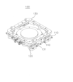
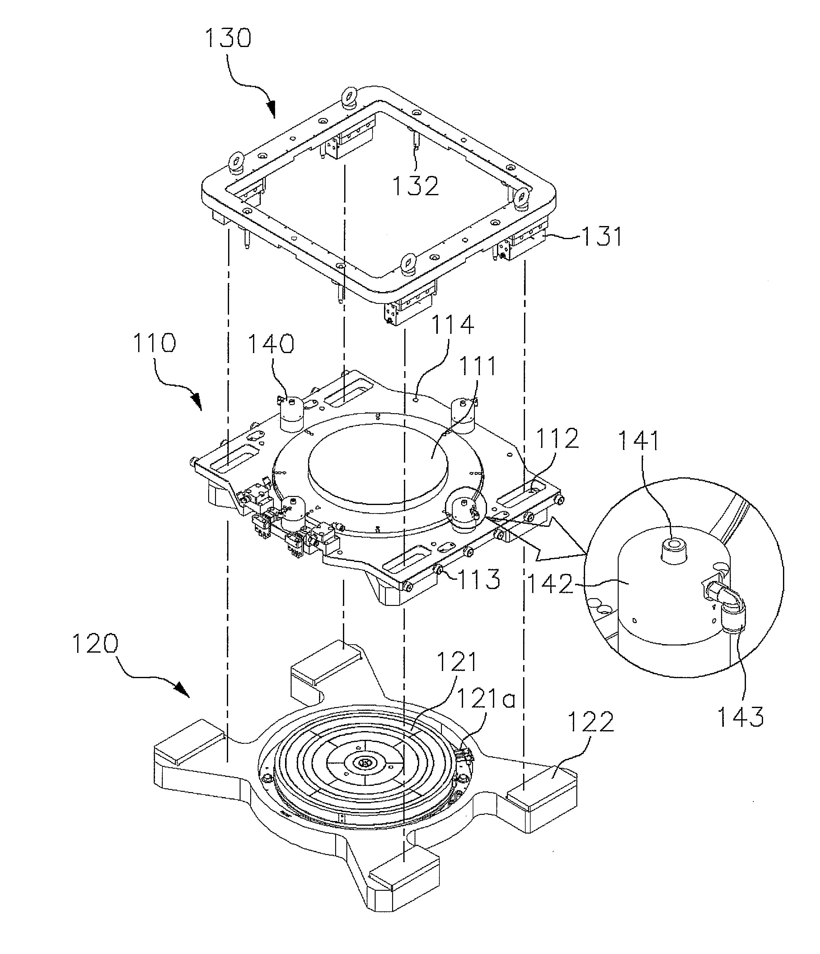
図1は、本発明の実施形態によるウェーハ検査用プローブカードホルダーの斜視構成図であり、図2は、本発明の実施形態によるウェーハ検査用プローブカードホルダーの分解斜視構成図であり、図3は、本発明の実施形態によるウェーハ検査用プローブカードホルダーの平面構成図であり、図4の(a)(b)は、それぞれ本発明の実施形態によるウェーハ検査用プローブカードホルダーの正面構成図と側面構成図である。 Figure 1 is a perspective view of a probe card holder for wafer inspection according to an embodiment of the present invention, Figure 2 is an exploded perspective view of a probe card holder for wafer inspection according to an embodiment of the present invention, Figure 3 is a plan view of a probe card holder for wafer inspection according to an embodiment of the present invention, and Figures 4(a) and 4(b) are respectively a front view and a side view of a probe card holder for wafer inspection according to an embodiment of the present invention.
図1~図4を参照すると、本発明の実施形態によるウェーハ検査用プローブカードホルダー(以下、「プローブカードホルダー」とも略記する)100は、第1ボディ部110、第2ボディ部120、ウェイトリング130、およびクランプ部140を備える。
Referring to Figures 1 to 4, a probe card holder for wafer inspection (hereinafter also abbreviated as "probe card holder") 100 according to an embodiment of the present invention includes a
第1ボディ部110は、中央にプローブカード111が設けられ、プローブカード111の周辺に垂直に貫通したガイド孔112を有する。本実施形態において、第1ボディ部110は略4つの辺を有する四角の部材であって、ガイド孔112は第1ボディ部110の4つの各隅に配置されることを示しているが、第1ボディ部の形状とガイド孔の数及び位置は様々に変形することができる。好ましくは、第1ボディ部110は少なくとも2つのガイド孔112を有する。
The
第1ボディ部110は、両端部に移送のために自由回動可能な複数のローラ113が設けられ、このようなローラは、摩擦係数が少なく且つ回転性能に優れたカム従動子(cam follower)によって提供できるが、これに限定されるものではない。
The
第2ボディ部120は、中央にウェーハの保持されるウェーハチャック121が設けられ、第1ボディ部110のガイド孔112と対応してマグネットホルダー122が設けられる。マグネットホルダー122は、マグネットチャック131と磁力によって引力が作用しうる周知の素材(例えば、強磁性体)によって提供できる。本実施形態では、マグネットホルダー122は、ガイド孔112と対応する位置に4つが設けられることを示している。ウェーハチャック121は、保持されたウェーハを真空吸着して固定するためのエアフィッティング(air fitting)121aが設けられる。
The
ウェイトリング130は、四角の環状であり、下部にマグネットチャック131が設けられ、このようなマグネットチャック131は、第2ボディ部120のマグネットホルダー122と対応して同数だけ設けられる。マグネットチャック131は、永久磁石または電磁石によって提供されることができ、好ましくは、永久磁石によって提供される。
The
好ましくは、ウェイトリング130の下部に複数のガイドピン132が設けられることができ、各ガイドピン132と対応して第1ボディ部110の上面にホール114が設けられ、ウェイトリング130と第1ボディ部110との組み立て過程で各ガイドピン132がホール114に挿入されることにより、ウェイトリング130と第1ボディ部110との組み立て位置の整列がなされることができる。一方、本実施形態において、ガイドピン132はウェイトリング130に設けられると図示しているが、第1ボディ部に複数のガイドピンが備えられ、ウェイトリングに各ガイドピンと対応して複数のホールが設けられることにより、第1ボディ部110とウェイトリング130との組み立て位置を案内するためのガイド部材が提供されることができる。
Preferably, a plurality of
クランプ部140は、第1ボディ部110とウェイトリング130との間に設けられ、第1ボディ部110とウェイトリング130との間隔を固定するためのものであり、好ましくは、第1ボディ部110とウェイトリング130との間に複数のクランプ部140が設けられる。
The
このようなクランプ部140は、ウェイトリング130の下部に上端が固定されるシャフト141と、第1ボディ部110に固定され、空圧信号に応じてシャフト141を固定する空圧駆動部142と、を備える。図面符号143は、空圧を供給するためのエアフィッティングである。
The
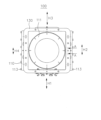
図5は、図3のA-A線に沿った断面構成図であり、理解を容易にするために、第1ボディ部、ウェイトリングおよびクランプ部のみが示されており、構成要素の大きさと比率は誇張されて表現されている。 Figure 5 is a cross-sectional view taken along line A-A in Figure 3. To facilitate understanding, only the first body portion, weight ring, and clamp portion are shown, and the sizes and proportions of the components are exaggerated.
図5を参照すると、クランプ部140は、上端がウェイトリング130と第1ボルト144とによって固定されるシャフト141と、下端が第1ボディ部110と第2ボルト145によって固定され、シャフト141を固定することができる空圧駆動部142と、を含み、空圧駆動部142に印加される空圧信号に応じて、シャフト141は、空圧駆動部142内で上下移動するか、或いは位置(高さ)が固定される。
Referring to FIG. 5, the
好ましくは、空圧駆動部142は、NC(Normal close)状態のクランプ機構であり、空圧駆動部142に空圧信号が印加される間に、シャフト141は、空圧駆動部142で上下移動が可能である。これに対し、空圧駆動部142に空圧信号が印加されなければ、シャフト141は空圧駆動部142によって固定され、第1ボディ部110とウェイトリング130との間隔は固定される。
Preferably, the
このようなクランプ部140は、Zimmer社製の「clamping and braking element」として販売されているRBPSシリーズのクランプ機構によって提供できるが、これに限定されるものではない。
Such a
このように構成された本発明のプローブカードホルダー100は、ウェーハ(図示せず)がウェーハチャック121に保持され、第2ボディ部120の上部に第1ボディ部110とウェイトリング130が積層されて組み立てられ、マグネットチャック131とマグネットホルダー122が磁力によって固定されることにより、第1ボディ部110、第2ボディ部120およびウェイトリング130は互いに固定される。一方、第1ボディ部110、第2ボディ部120及びウェイトリング130の組み立て過程でクランプ部140に空圧信号が印加されることにより、シャフト141は、空圧駆動部142で上下移動が可能である。以後、最終的に、クランプ部140に供給された空圧が遮断されると、クランプ部140によって第1ボディ部110とウェイトリング130との間隔が固定され、これにより、ウェーハとプローブカードの自己位置が固定されることができる。
In the
このように、プローブカードとウェーハは、プローブカードホルダー100によって精密に自己位置が保持されてモジュール化されることにより運搬が可能であり、検査チャンバーに移送されて検査が行われることができる。
In this way, the probe card and wafer are precisely positioned and modularized by the
図3では、4つのクランプ部によって固定された第1ボディ部110とウェイトリング130との間の各位置における間隔H1~H4を例示して矢印で示している。理解を容易にするために、各位置での間隔(H1~H4)が誇張されて表現されており、本発明は、マグネットチャックと、空圧信号を用いたクランピング部とを採用することにより、水平状態(H1=H2=H3=H4)だけでなく、勾配を有する場合(チルト状態)(H1≠H2≠H3≠H4)にも、10μm未満の精密な範囲内でその間隔を精密に維持してクランプが可能であることを確認した。
In FIG. 3, the distances H1 to H4 at each position between the
一方、本発明の実施形態では、4つのマグネットチャックと4つのクランプ部が適用されたプローブカードホルダーを例示して説明したが、ウェーハのサイズに応じてマグネットチャックとクランプ部の配置及び数は変わり得る。 Meanwhile, in the embodiment of the present invention, a probe card holder having four magnetic chucks and four clamping parts has been described as an example, but the arrangement and number of magnetic chucks and clamping parts may vary depending on the size of the wafer.
以上で説明した本発明は、上述した実施形態及び添付図面によって限定されるものではなく、本発明の技術的思想を逸脱することなく様々な置換、変形及び変更が可能であるのは、本発明の属する技術分野における通常の知識を有する者にとって自明であろう。 The present invention described above is not limited to the above-mentioned embodiment and the accompanying drawings, and it will be obvious to those with ordinary skill in the art to which the present invention pertains that various substitutions, modifications and alterations are possible without departing from the technical concept of the present invention.
100 プローブカードホルダー
110 第1ボディ部
111 プローブカード
112 ガイド孔
120 第2ボディ部
121 ウェーハチャック
122 マグネットホルダー
130 ウェイトリング
140 クランプ部
131 マグネットチャック
Claims (6)
中央にウェーハの保持されるウェーハチャックが設けられ、前記ガイド孔と対応してマグネットホルダーが設けられる第2ボディ部と、
前記ガイド孔に挿入されて前記マグネットホルダーと磁力によって固定可能なマグネットチャックが設けられ、前記第1ボディ部の上部で前記第2ボディ部に組み立てられるウェイトリングと、
前記第1ボディ部と前記ウェイトリングとの間に設けられ、前記第1ボディ部と前記ウェイトリングとの間隔を固定するクランプ部と、を備える、ウェーハ検査用プローブカードホルダー。 a first body portion having a probe card at its center and a guide hole extending vertically through the periphery of the probe card;
a second body portion having a wafer chuck at its center for holding a wafer and a magnet holder provided in correspondence with the guide hole;
a weight ring provided with a magnetic chuck that is inserted into the guide hole and can be fixed to the magnetic holder by magnetic force, the weight ring being assembled to the second body part on an upper portion of the first body part;
a clamp portion provided between the first body portion and the weight ring, the clamp portion fixing the distance between the first body portion and the weight ring.
前記ウェイトリングまたは前記第1ボディ部に一端が固定されるシャフトと、
前記ウェイトリングまたは前記第1ボディ部に固定され、空圧信号に応じて前記シャフトに固定される空圧駆動部と、を備える、請求項1に記載のウェーハ検査用プローブカードホルダー。 The clamp portion is
a shaft having one end fixed to the weight ring or the first body portion;
2. The probe card holder for wafer inspection according to claim 1, further comprising: a pneumatic drive unit fixed to the weight ring or the first body portion and fixed to the shaft in response to a pneumatic signal.
Applications Claiming Priority (2)
| Application Number | Priority Date | Filing Date | Title |
|---|---|---|---|
| KR10-2023-0157806 | 2023-11-15 | ||
| KR1020230157806A KR102648394B1 (en) | 2023-11-15 | 2023-11-15 | Probe card holder for testing a wafer |
Publications (2)
| Publication Number | Publication Date |
|---|---|
| JP7598677B1 true JP7598677B1 (en) | 2024-12-12 |
| JP2025081193A JP2025081193A (en) | 2025-05-27 |
Family
ID=90474040
Family Applications (1)
| Application Number | Title | Priority Date | Filing Date |
|---|---|---|---|
| JP2024007498A Active JP7598677B1 (en) | 2023-11-15 | 2024-01-22 | Probe Card Holder for Wafer Inspection |
Country Status (6)
| Country | Link |
|---|---|
| US (1) | US20250155496A1 (en) |
| JP (1) | JP7598677B1 (en) |
| KR (1) | KR102648394B1 (en) |
| CN (1) | CN120009697A (en) |
| TW (1) | TWI889174B (en) |
| WO (1) | WO2025105626A1 (en) |
Families Citing this family (3)
| Publication number | Priority date | Publication date | Assignee | Title |
|---|---|---|---|---|
| KR102648394B1 (en) * | 2023-11-15 | 2024-03-18 | 주식회사 유니테스트 | Probe card holder for testing a wafer |
| CN120102944B (en) * | 2025-05-08 | 2025-09-12 | 成都云绎智创科技有限公司 | Wafer bearing mechanism and wafer testing equipment |
| CN120507548B (en) * | 2025-07-21 | 2025-11-28 | 矽电半导体设备(深圳)股份有限公司 | Probe station and testing system |
Citations (4)
| Publication number | Priority date | Publication date | Assignee | Title |
|---|---|---|---|---|
| JP2005049254A (en) | 2003-07-30 | 2005-02-24 | Tokyo Electron Ltd | Inspection device |
| JP2008128798A (en) | 2006-11-21 | 2008-06-05 | Yokogawa Electric Corp | Semiconductor test equipment |
| JP2017514134A (en) | 2014-04-21 | 2017-06-01 | インテル コーポレイション | Alignment fixture for multiple integrated circuit packages |
| JP2022028607A (en) | 2020-08-03 | 2022-02-16 | 致茂電子股▲分▼有限公司 | Wafer inspection system and wafer inspection equipment thereof |
Family Cites Families (14)
| Publication number | Priority date | Publication date | Assignee | Title |
|---|---|---|---|---|
| JPH1031035A (en) * | 1996-07-13 | 1998-02-03 | Tokyo Electron Ltd | Probe card fixing mechanis and probe device |
| DE60025618T2 (en) * | 1999-07-14 | 2006-08-03 | Aehr Test Systems, Fremont | CASSETTE FOR BURNING AND TESTING A WAFERS |
| TWI306053B (en) * | 2003-12-24 | 2009-02-11 | Cascade Microtech Inc | Chuck with integrated wafer support |
| KR100967339B1 (en) * | 2007-10-22 | 2010-07-05 | (주)티에스이 | Probe Cards for Wafer Testing |
| KR101090333B1 (en) | 2009-06-03 | 2011-12-07 | 주식회사 쎄믹스 | Wafer probe station capable of active tilt control of chuck and its control method |
| US20130241587A1 (en) * | 2009-06-12 | 2013-09-19 | Semicaps Pte Ltd | Wafer stage |
| JP2011064659A (en) * | 2009-09-21 | 2011-03-31 | Tokyo Electron Ltd | Clamp mechanism of probe card and inspection apparatus |
| US8872532B2 (en) * | 2009-12-31 | 2014-10-28 | Formfactor, Inc. | Wafer test cassette system |
| WO2012054201A1 (en) * | 2010-09-28 | 2012-04-26 | Advanced Inquiry Systems, Inc. | Wafer testing systems and associated methods of use and manufacture |
| US11262381B2 (en) * | 2020-01-10 | 2022-03-01 | International Business Machines Corporation | Device for positioning a semiconductor die in a wafer prober |
| KR102801445B1 (en) * | 2020-02-19 | 2025-04-30 | 에스케이하이닉스 주식회사 | Semiconductor Fabricating Apparatus Including Probe Station |
| DE102021211263A1 (en) * | 2021-10-06 | 2023-04-06 | Ers Electronic Gmbh | Shielding device for a chuck, corresponding chuck and corresponding wafer prober arrangement |
| KR20230060900A (en) * | 2021-10-28 | 2023-05-08 | 한국생산기술연구원 | Cartridge locking apparatus for multi prober |
| KR102648394B1 (en) * | 2023-11-15 | 2024-03-18 | 주식회사 유니테스트 | Probe card holder for testing a wafer |
-
2023
- 2023-11-15 KR KR1020230157806A patent/KR102648394B1/en active Active
-
2024
- 2024-01-08 US US18/406,329 patent/US20250155496A1/en active Pending
- 2024-01-22 JP JP2024007498A patent/JP7598677B1/en active Active
- 2024-01-29 TW TW113103296A patent/TWI889174B/en active
- 2024-02-26 CN CN202410207342.4A patent/CN120009697A/en active Pending
- 2024-06-07 WO PCT/KR2024/007802 patent/WO2025105626A1/en active Pending
Patent Citations (4)
| Publication number | Priority date | Publication date | Assignee | Title |
|---|---|---|---|---|
| JP2005049254A (en) | 2003-07-30 | 2005-02-24 | Tokyo Electron Ltd | Inspection device |
| JP2008128798A (en) | 2006-11-21 | 2008-06-05 | Yokogawa Electric Corp | Semiconductor test equipment |
| JP2017514134A (en) | 2014-04-21 | 2017-06-01 | インテル コーポレイション | Alignment fixture for multiple integrated circuit packages |
| JP2022028607A (en) | 2020-08-03 | 2022-02-16 | 致茂電子股▲分▼有限公司 | Wafer inspection system and wafer inspection equipment thereof |
Also Published As
| Publication number | Publication date |
|---|---|
| JP2025081193A (en) | 2025-05-27 |
| KR102648394B1 (en) | 2024-03-18 |
| TW202521989A (en) | 2025-06-01 |
| WO2025105626A1 (en) | 2025-05-22 |
| CN120009697A (en) | 2025-05-16 |
| TWI889174B (en) | 2025-07-01 |
| US20250155496A1 (en) | 2025-05-15 |
Similar Documents
| Publication | Publication Date | Title |
|---|---|---|
| JP7598677B1 (en) | Probe Card Holder for Wafer Inspection | |
| CN101740349B (en) | Die Separator | |
| JP5341039B2 (en) | Two abutments on the alignment fixture that float together to engage the electronic component | |
| US8485511B2 (en) | Method and apparatus for holding microelectronic devices | |
| US20130241588A1 (en) | Wafer inspection apparatus | |
| CN101874209B (en) | Holding member for inspection and method for manufacturing holding member for inspection | |
| JP2010186998A (en) | Semiconductor wafer testing apparatus | |
| KR20110018856A (en) | Support for aligning electronic components comprising slidably arranged plates | |
| JP2011040758A (en) | Elastic unit mounted at elastic unit receiving part of alignment fixture as separate elastic member | |
| KR102014334B1 (en) | Cartridge for inspecting substrates and manufacturing method thereof | |
| US20150226767A1 (en) | Prober | |
| US20180348296A1 (en) | Method and device for loading and unloading devices under test into a tester by flipping | |
| US5065495A (en) | Method for holding a plate-like member | |
| TWI802289B (en) | test vehicle | |
| KR101358564B1 (en) | Probe card positioning mechanism and inspection apparatus | |
| KR102023154B1 (en) | Chuck assembly and cartridge for inspecting a substrates including the chuck assembly | |
| JPH04330753A (en) | Semiconductor inspection device | |
| KR20210017442A (en) | Probe station | |
| KR102049413B1 (en) | Multi-probe system | |
| CN108028205A (en) | Nude film with turntable places head | |
| JPS61252642A (en) | Chip supporting table for testing semiconductor ic chip | |
| JP7267058B2 (en) | inspection equipment | |
| TWI734002B (en) | Carrier for electronic component testing device | |
| JPH0373551A (en) | Chip tray | |
| KR102503282B1 (en) | Probe station |
Legal Events
| Date | Code | Title | Description |
|---|---|---|---|
| A621 | Written request for application examination |
Free format text: JAPANESE INTERMEDIATE CODE: A621 Effective date: 20240122 |
|
| TRDD | Decision of grant or rejection written | ||
| A01 | Written decision to grant a patent or to grant a registration (utility model) |
Free format text: JAPANESE INTERMEDIATE CODE: A01 Effective date: 20241105 |
|
| A61 | First payment of annual fees (during grant procedure) |
Free format text: JAPANESE INTERMEDIATE CODE: A61 Effective date: 20241125 |
|
| R150 | Certificate of patent or registration of utility model |
Ref document number: 7598677 Country of ref document: JP Free format text: JAPANESE INTERMEDIATE CODE: R150 |