JP7595331B2 - Gaming Machines - Google Patents

Gaming Machines Download PDF

Info

Publication number
JP7595331B2
JP7595331B2 JP2020084944A JP2020084944A JP7595331B2 JP 7595331 B2 JP7595331 B2 JP 7595331B2 JP 2020084944 A JP2020084944 A JP 2020084944A JP 2020084944 A JP2020084944 A JP 2020084944A JP 7595331 B2 JP7595331 B2 JP 7595331B2
Authority
JP
Japan
Prior art keywords
pad
small chip
board
decorative
game
Prior art date
Legal status (The legal status is an assumption and is not a legal conclusion. Google has not performed a legal analysis and makes no representation as to the accuracy of the status listed.)
Active
Application number
JP2020084944A
Other languages
Japanese (ja)
Other versions
JP2021178022A (en
JP2021178022A5 (en
Inventor
憲靖 平工
鉉 岡村
Current Assignee (The listed assignees may be inaccurate. Google has not performed a legal analysis and makes no representation or warranty as to the accuracy of the list.)
Sanyo Bussan Co Ltd
Original Assignee
Sanyo Bussan Co Ltd
Priority date (The priority date is an assumption and is not a legal conclusion. Google has not performed a legal analysis and makes no representation as to the accuracy of the date listed.)
Filing date
Publication date
Application filed by Sanyo Bussan Co Ltd filed Critical Sanyo Bussan Co Ltd
Priority to JP2020084944A priority Critical patent/JP7595331B2/en
Publication of JP2021178022A publication Critical patent/JP2021178022A/en
Publication of JP2021178022A5 publication Critical patent/JP2021178022A5/ja
Priority to JP2023208192A priority patent/JP2024019470A/en
Application granted granted Critical
Publication of JP7595331B2 publication Critical patent/JP7595331B2/en
Priority to JP2025069224A priority patent/JP2025105714A/en
Active legal-status Critical Current
Anticipated expiration legal-status Critical

Links

Images

Classifications

    • YGENERAL TAGGING OF NEW TECHNOLOGICAL DEVELOPMENTS; GENERAL TAGGING OF CROSS-SECTIONAL TECHNOLOGIES SPANNING OVER SEVERAL SECTIONS OF THE IPC; TECHNICAL SUBJECTS COVERED BY FORMER USPC CROSS-REFERENCE ART COLLECTIONS [XRACs] AND DIGESTS
    • Y02TECHNOLOGIES OR APPLICATIONS FOR MITIGATION OR ADAPTATION AGAINST CLIMATE CHANGE
    • Y02EREDUCTION OF GREENHOUSE GAS [GHG] EMISSIONS, RELATED TO ENERGY GENERATION, TRANSMISSION OR DISTRIBUTION
    • Y02E60/00Enabling technologies; Technologies with a potential or indirect contribution to GHG emissions mitigation
    • Y02E60/10Energy storage using batteries

Landscapes

  • Pinball Game Machines (AREA)

Description

本発明は、遊技機に関するものである。 The present invention relates to gaming machines.

遊技機の一種として、パチンコ機やスロットマシン等が知られている。これらの遊技機では、所定の抽選条件が成立したことに基づいて抽選が行われ、当該抽選の結果に応じて遊技者に特典が付与される構成が知られている。また、当該抽選の結果を遊技者に予測させたり、認識させたりするための演出が行われる構成が一般的である。これらの遊技機は、遊技を進行させるための電子部品や演出を実行するための電子部品が実装されている基板を備えている。 Pachinko machines and slot machines are known as types of gaming machines. In these gaming machines, a lottery is held when a certain lottery condition is met, and a bonus is awarded to the player depending on the result of the lottery. It is also common for the machines to be configured to provide effects that allow the player to predict or recognize the result of the lottery. These gaming machines are equipped with a circuit board on which electronic components for progressing the game and electronic components for executing effects are mounted.

パチンコ機について具体的には、例えば遊技領域に設けられた入球部に遊技球が入球したことに基づいて抽選が行われ、表示装置の表示面にて絵柄の変動表示が行われ、抽選にて当選結果となった場合には表示面にて特定絵柄の組み合わせ等が最終停止表示され、遊技者にとって有利な特別遊技状態に移行する構成等が知られている。そして、特別遊技状態に移行した場合には、例えば遊技領域に設けられた入球装置等の開閉が開始され、当該入球装置への入球に基づき遊技球の払出等が行われるようになっている(例えば特許文献1参照)。 Specific examples of pachinko machines include a lottery held when a gaming ball enters a ball entry section in the game area, a changing display of pictures on the display screen of the display device, and if the lottery results in a winning result, a combination of specific pictures is displayed in a final stopped state on the display screen, and the machine transitions to a special game state that is advantageous to the player. When the machine transitions to the special game state, for example, a ball entry device or the like in the game area starts opening and closing, and game balls are paid out based on the entry of the ball into the ball entry device (see, for example, Patent Document 1).

特開2012-170465号公報JP 2012-170465 A

ここで、上記例示等のような遊技機においては、電子部品を基板に好適に実装する必要があり、この点について未だ改良の余地がある。 Here, in gaming machines such as those exemplified above, electronic components need to be suitably mounted on the circuit board, and there is still room for improvement in this regard.

本発明は、上記例示した事情等に鑑みてなされたものであり、電子部品を基板に好適に実装することが可能な遊技機を提供することを目的とするものである。 The present invention was made in consideration of the above-mentioned circumstances, and aims to provide an amusement machine that allows electronic components to be suitably mounted on a board.

上記課題を解決すべく請求項1記載の発明は、リフロー工程を利用して所定電子部品が表面実装されている所定基板を備えた遊技機において、
前記所定電子部品は、一対の電極として、第1所定電極及び第2所定電極を備えており、
前記所定基板は、
前記第1所定電極が電気的に接続される第1所定接続部と、
前記第1所定接続部から引き出されている第1所定配線パターンと、
前記第2所定電極が電気的に接続される第2所定接続部と、
前記第2所定接続部から引き出されている第2所定配線パターンと、
を備えており、
前記第1所定接続部の中心から見て前記第1所定配線パターンが引き出されている当該第1所定接続部の辺が存在する方向は、前記第2所定接続部の中心から見て前記第2所定配線パターンが引き出されている当該第2所定接続部の辺が存在する方向と同一の方向であり、
前記第1所定接続部は、前記第1所定配線パターンを介して当該第1所定接続部よりも面積の広い第1金属領域に電気的に接続されており、
前記第2所定接続部は、前記第2所定配線パターンを介して当該第2所定接続部よりも面積の広い第2金属領域に電気的に接続されていることを特徴とする。
In order to solve the above problem, the present invention provides a gaming machine having a predetermined substrate on which a predetermined electronic component is surface -mounted using a reflow process ,
the predetermined electronic component includes a pair of electrodes, that is, a first predetermined electrode and a second predetermined electrode,
The predetermined substrate is
a first predetermined connection portion to which the first predetermined electrode is electrically connected;
a first predetermined wiring pattern extending from the first predetermined connection portion;
a second predetermined connection portion to which the second predetermined electrode is electrically connected;
a second predetermined wiring pattern extending from the second predetermined connection portion;
Equipped with
a direction in which a side of the first predetermined connection portion, from which the first predetermined wiring pattern is drawn, exists when viewed from a center of the first predetermined connection portion is the same as a direction in which a side of the second predetermined connection portion, from which the second predetermined wiring pattern is drawn, exists when viewed from a center of the second predetermined connection portion ;
the first predetermined connection portion is electrically connected to a first metal region having an area larger than that of the first predetermined connection portion via the first predetermined wiring pattern;
The second predetermined connection portion is electrically connected to a second metal region having an area larger than that of the second predetermined connection portion via the second predetermined wiring pattern .

本発明によれば、電子部品を基板に好適に実装することが可能となる。 The present invention makes it possible to mount electronic components on a substrate in an optimal manner.

第1の実施形態におけるパチンコ機の正面図である。1 is a front view of a pachinko machine according to a first embodiment. パチンコ機の主要な構成を展開して示す斜視図である。1 is an exploded perspective view showing the main components of a pachinko machine. FIG. パチンコ機の主要な構成を展開して示す斜視図である。1 is an exploded perspective view showing the main components of a pachinko machine. FIG. 遊技盤の構成を示す正面図である。FIG. 2 is a front view showing the configuration of the game board. 遊技領域を流下した遊技球の排出に関する構成を説明するための説明図である。An explanatory diagram to explain the configuration regarding the discharge of game balls that have flowed down the game area. 主制御装置の正面図である。FIG. 装飾カバー及び装飾基板を取り除いた状態におけるパチンコ機の正面図である。This is a front view of the pachinko machine with the decorative cover and decorative board removed. (a)第1装飾基板の一方側の板面である第1実装面を示す平面図であり、(b)第1装飾基板に実装されているバイパスコンデンサの周辺領域を拡大して示す第1装飾基板の第1実装面の平面図であり、(c)第1装飾基板に実装されている小型チップ抵抗器の周辺領域を拡大して示す第1装飾基板の第1実装面の平面図である。(a) is a plan view showing the first mounting surface, which is the plate surface on one side of the first decorative substrate; (b) is a plan view of the first mounting surface of the first decorative substrate showing an enlarged view of the peripheral area of a bypass capacitor mounted on the first decorative substrate; and (c) is a plan view of the first mounting surface of the first decorative substrate showing an enlarged view of the peripheral area of a small chip resistor mounted on the first decorative substrate. 図8(a)のA-A線断面図である。8(a) is a cross-sectional view taken along line AA in FIG. (a)第2装飾基板の一方側の板面である第1実装面を示す平面図であり、(b)第2装飾基板に実装されているバイパスコンデンサの周辺領域を拡大して示す第2装飾基板の第1実装面の平面図であり、(c)第2装飾基板に実装されている小型チップ抵抗器の周辺領域を拡大して示す第2装飾基板の第1実装面の平面図である。(a) is a plan view showing the first mounting surface, which is the plate surface on one side of the second decorative substrate; (b) is a plan view of the first mounting surface of the second decorative substrate showing an enlarged view of the peripheral area of a bypass capacitor mounted on the second decorative substrate; and (c) is a plan view of the first mounting surface of the second decorative substrate showing an enlarged view of the peripheral area of a small chip resistor mounted on the second decorative substrate. 第1装飾基板における第1発光回路部の配線図である。A wiring diagram of the first light-emitting circuit section on the first decorative substrate. (a)バイパスコンデンサの周辺を拡大して示す第1装飾基板の第1実装面側の斜視図であり、(b)小型チップ抵抗器の周辺を拡大して示す第1装飾基板の第1実装面側の斜視図である。(a) is an oblique view of the first mounting surface side of the first decorative substrate showing an enlarged view of the bypass capacitor and its surroundings, and (b) is an oblique view of the first mounting surface side of the first decorative substrate showing an enlarged view of the small chip resistor and its surroundings. (a)バイパスコンデンサの周辺領域を拡大して示す第1装飾基板の第1実装面の平面図であり、(b)当該周辺領域のパッドとソルダーレジストとの関係を説明するための説明図であり、(c)発生し得るバイパスコンデンサの移動態様を説明するための説明図であり、(d)比較例において発生し得るバイパスコンデンサの移動態様を説明するための説明図である。(a) is a plan view of the first mounting surface of the first decorative board showing an enlarged view of the peripheral area of the bypass capacitor; (b) is an explanatory diagram for explaining the relationship between the pads in the peripheral area and the solder resist; (c) is an explanatory diagram for explaining possible movement patterns of the bypass capacitor; and (d) is an explanatory diagram for explaining possible movement patterns of the bypass capacitor in the comparative example. (a)小型チップ抵抗器の周辺領域を拡大して示す第1装飾基板の第1実装面の平面図であり、(b)当該周辺領域のパッドとソルダーレジストとの関係を説明するための説明図であり、(c)発生し得る小型チップ抵抗器の移動態様を説明するための説明図であり、(d)比較例において発生し得る小型チップ抵抗器の移動態様を説明するための説明図である。(a) is a plan view of the first mounting surface of the first decorative substrate showing an enlarged view of the peripheral area of the small chip resistor; (b) is an explanatory diagram for explaining the relationship between the pads in the peripheral area and the solder resist; (c) is an explanatory diagram for explaining possible movement patterns of the small chip resistor; and (d) is an explanatory diagram for explaining possible movement patterns of the small chip resistor in the comparative example. (a)第1装飾基板の第2実装面を示す平面図であり、(b)第1発光回路部の裏側領域を拡大して示す第1装飾基板の第2実装面の平面図である。(a) is a plan view showing the second mounting surface of the first decorative substrate, and (b) is a plan view showing an enlarged rear area of the first light-emitting circuit section of the second mounting surface of the first decorative substrate. (a)第1装飾基板の断面図であり、(b)比較例における第1装飾基板の断面図である。FIG. 1A is a cross-sectional view of a first decorative substrate, and FIG. 1B is a cross-sectional view of a first decorative substrate in a comparative example. (a)集合基板の第1板面を示す平面図であり、(b)集合基板の谷割りを説明するための説明図であり、(c)集合基板の山割りを説明するための説明図である。FIG. 2A is a plan view showing a first plate surface of the collective substrate; FIG. 2B is an explanatory diagram for explaining valley division of the collective substrate; and FIG. 2C is an explanatory diagram for explaining mountain division of the collective substrate. (a)集合基板の分割に使用する分割治具の斜視図であり、(b)分割治具の正面図であり、(c)分割治具を用いて集合基板を分割する様子を説明するための説明図である。FIG. 2A is a perspective view of a dividing jig used to divide the aggregate substrate, FIG. 2B is a front view of the dividing jig, and FIG. 2C is an explanatory diagram for explaining how the aggregate substrate is divided using the dividing jig. パチンコ機の電気的構成を示すブロック図である。FIG. 2 is a block diagram showing the electrical configuration of the pachinko machine. 当否抽選などに用いられる各種カウンタの内容を説明するための説明図である。FIG. 13 is an explanatory diagram for explaining the contents of various counters used in lotteries, etc. 主側CPUにて実行されるメイン処理を示すフローチャートである。4 is a flowchart showing a main process executed by a main CPU. 主側CPUにて実行されるタイマ割込み処理を示すフローチャートである。11 is a flowchart showing a timer interrupt process executed by a main CPU. 主側CPUにて実行される特図特電制御処理を示すフローチャートである。13 is a flowchart showing a special chart special power control process executed by the main CPU. 主側CPUにて実行される特図変動開始処理を示すフローチャートである。This is a flowchart showing the special chart change start processing executed by the main CPU. (a)第2の実施形態における第1装飾基板の第1実装面を示す平面図であり、(b)第1装飾基板に実装されているバイパスコンデンサの周辺領域を拡大して示す第1装飾基板の第1実装面の平面図である。(a) A plan view showing the first mounting surface of the first decorative substrate in the second embodiment, and (b) a plan view of the first mounting surface of the first decorative substrate showing an enlarged view of the surrounding area of a bypass capacitor mounted on the first decorative substrate. 第3の実施形態における発光基板の第1発光面の平面図である。FIG. 13 is a plan view of a first light-emitting surface of a light-emitting substrate in a third embodiment. 発光基板の第2発光面の平面図である。4 is a plan view of a second light-emitting surface of the light-emitting substrate. FIG. (a)第4の実施形態における発光基板の第1発光面の平面図であり、(b)バイパスコンデンサの周辺領域を拡大して示す発光基板の第1発光面の平面図である。13A is a plan view of a first light-emitting surface of a light-emitting substrate in a fourth embodiment, and FIG. 13B is a plan view of the first light-emitting surface of the light-emitting substrate showing an enlarged view of a peripheral area of a bypass capacitor. (a)発光基板の第2発光面の平面図であり、(b)電源端子及びGND端子の周辺領域を拡大して示す発光基板の第2発光面の平面図である。1A is a plan view of a second light-emitting surface of the light-emitting substrate, and FIG. 1B is a plan view of the second light-emitting surface of the light-emitting substrate showing an enlarged view of the surrounding area of the power supply terminal and the GND terminal.

<第1の実施形態>
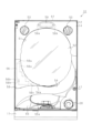
以下、遊技機の一種であるパチンコ機10の第1の実施形態を、図面に基づいて詳細に説明する。図1はパチンコ機10の正面図であり、図2及び図3はパチンコ機10の主要な構成を展開して示す斜視図である。なお、図2では便宜上パチンコ機10の遊技領域内の構成を省略しているとともに図3では後述する主制御装置60のパチンコ機10後方側の構成を省略している。
First Embodiment
A first embodiment of a pachinko machine 10, which is a type of gaming machine, will be described in detail below with reference to the drawings. Fig. 1 is a front view of the pachinko machine 10, and Figs. 2 and 3 are perspective views showing the main components of the pachinko machine 10 in an expanded form. For convenience, Fig. 2 omits the components within the game area of the pachinko machine 10, and Fig. 3 omits the components of the main control device 60, which will be described later, on the rear side of the pachinko machine 10.

パチンコ機10は、図1に示すように、当該パチンコ機10の外殻を形成する外枠11と、この外枠11に対して前方に回動可能に取り付けられた遊技機本体12と、を有する。外枠11は木製の板材を四辺に連結し構成されるものであって矩形枠状をなしている。パチンコ機10は、外枠11を島設備に取り付け固定することにより、遊技ホールに設置される。なお、パチンコ機10において外枠11は必須の構成ではなく、遊技ホールの島設備に外枠11が備え付けられた構成としてもよい。 As shown in FIG. 1, a pachinko machine 10 has an outer frame 11 that forms the outer shell of the pachinko machine 10, and a gaming machine main body 12 that is attached to the outer frame 11 so that it can rotate forward. The outer frame 11 is made of wooden boards connected at all four sides and has a rectangular frame shape. The pachinko machine 10 is installed in an amusement hall by attaching and fixing the outer frame 11 to an island facility. Note that the outer frame 11 is not a required component of the pachinko machine 10, and the outer frame 11 may be attached to the island facility of the amusement hall.

遊技機本体12は、図2及び図3に示すように、内枠13と、その内枠13の前方に配置される前扉枠14と、内枠13の後方に配置される裏パックユニット15と、を備えている。遊技機本体12のうち内枠13が外枠11に回動可能に支持されている。詳細には、正面視で左側を回動基端側とし右側を回動先端側として内枠13が前方へ回動可能とされている。 As shown in Figures 2 and 3, the gaming machine main body 12 includes an inner frame 13, a front door frame 14 disposed in front of the inner frame 13, and a back pack unit 15 disposed behind the inner frame 13. The inner frame 13 of the gaming machine main body 12 is rotatably supported by the outer frame 11. In detail, the inner frame 13 can be rotated forward with the left side as the base end of rotation and the right side as the tip end of rotation when viewed from the front.

内枠13には、前扉枠14が回動可能に支持されており、正面視で左側を回動基端側とし右側を回動先端側として前方へ回動可能とされている。また、内枠13には、裏パックユニット15が回動可能に支持されており、正面視で左側を回動基端側とし右側を回動先端側として後方へ回動可能とされている。 The front door frame 14 is rotatably supported by the inner frame 13, and can be rotated forward with the left side as the base end and the right side as the tip end when viewed from the front. The back pack unit 15 is rotatably supported by the inner frame 13, and can be rotated backward with the left side as the base end and the right side as the tip end when viewed from the front.

なお、遊技機本体12には、その回動先端部に施錠装置が設けられており、遊技機本体12を外枠11に対して開放不能に施錠状態とする機能を有しているとともに、前扉枠14を内枠13に対して開放不能に施錠状態とする機能を有している。これらの各施錠状態は、パチンコ機10前面にて露出させて設けられたシリンダ錠17に解錠キーを用いて解錠操作を行うことにより、それぞれ解除される。 The gaming machine main body 12 is provided with a locking device at its rotating tip, which has the function of locking the gaming machine main body 12 so that it cannot be opened relative to the outer frame 11, and also has the function of locking the front door frame 14 so that it cannot be opened relative to the inner frame 13. Each of these locked states is released by using an unlocking key to perform an unlocking operation on the cylinder lock 17 exposed on the front of the pachinko machine 10.

<前面側の構成>
次に、遊技機本体12の前面側の構成について説明する。
<Front side configuration>
Next, the configuration of the front side of the gaming machine main body 12 will be described.

内枠13は、外形が外枠11とほぼ同一形状をなす樹脂ベース21を主体に構成されている。樹脂ベース21の中央部には略楕円形状の窓孔23が形成されている。樹脂ベース21には遊技盤24が着脱可能に取り付けられている。遊技盤24は合板よりなり、遊技盤24の前面に形成された遊技領域PAが樹脂ベース21の窓孔23を通じて内枠13の前面側に露出した状態となっている。 The inner frame 13 is mainly composed of a resin base 21 whose outer shape is almost the same as that of the outer frame 11. A roughly elliptical window hole 23 is formed in the center of the resin base 21. A game board 24 is removably attached to the resin base 21. The game board 24 is made of plywood, and a game area PA formed on the front side of the game board 24 is exposed to the front side of the inner frame 13 through the window hole 23 of the resin base 21.

<遊技盤の構成>
ここで、遊技盤24の構成を図4に基づいて説明する。図4は遊技盤24の正面図である。
<Game board configuration>
The structure of the game board 24 will now be described with reference to Fig. 4. Fig. 4 is a front view of the game board 24.

遊技盤24には、遊技領域PAの外縁の一部を区画するようにして内レール部25と外レール部26とが取り付けられており、これら内レール部25と外レール部26とにより誘導手段としての誘導レールが構成されている。樹脂ベース21において窓孔23の下方に取り付けられた遊技球発射機構27(図2参照)から発射された遊技球は誘導レールにより遊技領域PAの上部に案内されるようになっている。 An inner rail section 25 and an outer rail section 26 are attached to the game board 24 so as to define a part of the outer edge of the game area PA, and the inner rail section 25 and the outer rail section 26 form a guide rail as a guide means. Game balls launched from a game ball launching mechanism 27 (see Figure 2) attached below the window hole 23 in the resin base 21 are guided to the upper part of the game area PA by the guide rail.

ちなみに、遊技球発射機構27は、誘導レールに向けて延びる発射レール27aと、後述する上皿54aに貯留されている遊技球を発射レール27a上に供給する球送り装置27bと、発射レール27a上に供給された遊技球を誘導レールに向けて発射させる電動アクチュエータであるソレノイド27cと、を備えている。前扉枠14に設けられた発射操作装置(又は操作ハンドル)28が回動操作されることによりソレノイド27cが駆動制御され、遊技球が発射される。 The game ball launching mechanism 27 includes a launching rail 27a extending toward the guide rail, a ball feeder 27b that supplies game balls stored in the upper tray 54a (described later) onto the launching rail 27a, and a solenoid 27c, which is an electric actuator that launches the game balls supplied onto the launching rail 27a toward the guide rail. The solenoid 27c is driven and controlled by rotating a launching operation device (or operation handle) 28 provided on the front door frame 14, and the game balls are launched.

遊技盤24には、前後方向に貫通する大小複数の開口部が形成されている。各開口部には一般入賞口31、特電入賞装置32、第1作動口33、第2作動口34、スルーゲート35、可変表示ユニット36、特図ユニット37及び普図ユニット38等がそれぞれ設けられている。一般入賞口31は合計で4個設けられており、それ以外はそれぞれ1個ずつ設けられている。 The game board 24 has multiple openings of various sizes that penetrate in the front-to-rear direction. Each opening is provided with a general winning port 31, a special electric winning device 32, a first operating port 33, a second operating port 34, a through gate 35, a variable display unit 36, a special chart unit 37, and a general chart unit 38. There are a total of four general winning ports 31, and one of each of the others.

スルーゲート35への入球が発生したとしても遊技球の払い出しは実行されない。一方、一般入賞口31、特電入賞装置32、第1作動口33及び第2作動口34への入球が発生すると、所定数の遊技球の払い出しが実行される。当該賞球個数について具体的には、第1作動口33への1個の遊技球の入球が発生した場合又は第2作動口34への1個の遊技球の入球が発生した場合には、1個の賞球の払い出しが実行され、一般入賞口31への1個の遊技球の入球が発生した場合には、10個の賞球の払い出しが実行され、特電入賞装置32への1個の遊技球の入球が発生した場合には、15個の賞球の払い出しが実行される。 Even if a ball enters the through gate 35, no game balls are paid out. On the other hand, when balls enter the general winning opening 31, the special electric winning device 32, the first operating opening 33, and the second operating opening 34, a predetermined number of game balls are paid out. Specifically, when one game ball enters the first operating opening 33 or when one game ball enters the second operating opening 34, one prize ball is paid out, when one game ball enters the general winning opening 31, ten prize balls are paid out, and when one game ball enters the special electric winning device 32, fifteen prize balls are paid out.

なお、上記賞球個数は任意であり、例えば、第2作動口34の方が第1作動口33よりも賞球個数が少ない構成としてもよく、第2作動口34の方が第1作動口33よりも賞球個数が多い構成としてもよい。 The number of prize balls is arbitrary. For example, the second actuation port 34 may be configured to have a smaller number of prize balls than the first actuation port 33, or the second actuation port 34 may be configured to have a larger number of prize balls than the first actuation port 33.

その他に、遊技盤24の最下部にはアウト口24aが設けられており、各種入賞口等に入らなかった遊技球はアウト口24aを通って遊技領域PAから排出される。また、遊技盤24には、遊技球の落下方向を適宜分散、調整等するために多数の釘24bが植設されているとともに、風車等の各種部材が配設されている。 In addition, an outlet 24a is provided at the bottom of the game board 24, and game balls that do not enter the various winning holes are discharged from the game area PA through the outlet 24a. In addition, numerous nails 24b are planted on the game board 24 to appropriately disperse and adjust the falling direction of the game balls, and various components such as windmills are also arranged.

ここで、入球とは所定の開口部を遊技球が通過することを意味し、開口部を通過した後に遊技領域PAから排出される態様だけではなく、開口部を通過した後に遊技領域PAから排出されることなく遊技領域PAの流下を継続する態様も含まれる。但し、以下の説明では、アウト口24aへの遊技球の入球と明確に区別するために、一般入賞口31、特電入賞装置32、第1作動口33、第2作動口34及びスルーゲート35への遊技球の入球を、入賞とも表現する。 Here, "ball entry" means that the game ball passes through a specified opening, and includes not only the case where the game ball passes through an opening and is discharged from the game area PA, but also the case where the game ball continues to flow down the game area PA without being discharged from the game area PA after passing through an opening. However, in the following explanation, in order to clearly distinguish from the game ball entering the outlet 24a, the game ball entering the general winning opening 31, the special electric winning device 32, the first operating opening 33, the second operating opening 34, and the through gate 35 will also be referred to as "winning."

第1作動口33及び第2作動口34は、作動口装置としてユニット化されて遊技盤24に設置されている。第1作動口33及び第2作動口34は共に上向きに開放されている。また、第1作動口33が上方となるようにして両作動口33,34は鉛直方向に並んでいる。第2作動口34には、左右一対の可動片よりなるガイド片としての普電役物34aが設けられている。普電役物34aの閉鎖状態では遊技球が第2作動口34に入賞できず、普電役物34aが開放状態となることで第2作動口34への入賞が可能となる。 The first actuation port 33 and the second actuation port 34 are united as an actuation port device and installed on the game board 24. Both the first actuation port 33 and the second actuation port 34 are open upward. In addition, both actuation ports 33, 34 are lined up vertically with the first actuation port 33 facing upward. The second actuation port 34 is provided with a normal power device 34a as a guide piece consisting of a pair of movable pieces on the left and right. When the normal power device 34a is in a closed state, the game ball cannot enter the second actuation port 34, but when the normal power device 34a is in an open state, the game ball can enter the second actuation port 34.

第2作動口34よりも遊技球の流下方向の上流側に、スルーゲート35が設けられている。スルーゲート35は縦方向に貫通した図示しない貫通孔を有しており、スルーゲート35に入賞した遊技球は入賞後に遊技領域PAを流下する。これにより、スルーゲート35に入賞した遊技球が第2作動口34へ入賞することが可能となっている。 A through gate 35 is provided upstream of the second operating port 34 in the direction in which the game ball flows down. The through gate 35 has a through hole (not shown) that runs vertically through it, and the game ball that enters the through gate 35 flows down the game area PA after entering the game. This makes it possible for the game ball that enters the through gate 35 to enter the second operating port 34.

スルーゲート35への入賞に基づき第2作動口34の普電役物34aが閉鎖状態から開放状態に切り換えられる。具体的には、スルーゲート35への入賞をトリガとして内部抽選が行われるとともに、遊技領域PAにおいて遊技球が通過しない領域である右下の隅部に設けられた普図ユニット38の普図表示部38aにて絵柄の変動表示が行われる。そして、内部抽選の結果が電役開放当選であり当該結果に対応した停止結果が表示されて普図表示部38aの変動表示が終了された場合に普電開放状態へ移行する。普電開放状態では、普電役物34aが所定の態様で開放状態となる。 When a ball wins the through gate 35, the normal power role 34a of the second operating port 34 is switched from a closed state to an open state. Specifically, an internal lottery is held when a ball wins the through gate 35, and a changing image is displayed on the normal map display section 38a of the normal map unit 38, which is located in the lower right corner of the play area PA, an area where the game ball does not pass through. If the result of the internal lottery is a winning electric role release, the stop result corresponding to that result is displayed, and the changing display on the normal map display section 38a ends, the normal power open state is entered. In the normal power open state, the normal power role 34a is opened in a predetermined manner.

なお、普図表示部38aは、LEDによる複数の表示用セグメントが所定の態様で配列されてなるセグメント表示器により構成されているが、これに限定されることはなく、液晶表示装置、有機EL表示装置、CRT又はドットマトリックス表示器等その他のタイプの表示装置によって構成されていてもよい。また、普図表示部38aにて変動表示される絵柄としては、複数種の文字が変動表示される構成、複数種の記号が変動表示される構成、複数種のキャラクタが変動表示される構成又は複数種の色が切り換え表示される構成などが考えられる。 The map display unit 38a is configured with a segment display in which a number of LED display segments are arranged in a predetermined manner, but is not limited to this and may be configured with other types of display devices such as a liquid crystal display device, an organic EL display device, a CRT or a dot matrix display. The pattern displayed on the map display unit 38a may be a number of different characters, a number of symbols, a number of characters, or a number of colors that are switched between.

普図ユニット38において、普図表示部38aに隣接した位置には、普図保留表示部38bが設けられている。遊技球がスルーゲート35に入賞した個数は最大4個まで保留され、普図保留表示部38bの点灯によってその保留個数が表示されるようになっている。 In the normal map unit 38, a normal map reserve display section 38b is provided adjacent to the normal map display section 38a. A maximum of four game balls that enter the through gate 35 are reserved, and the number of reserved balls is displayed by lighting up the normal map reserve display section 38b.

第1作動口33又は第2作動口34への入賞をトリガとして当たり抽選が行われる。そして、当該抽選結果は特図ユニット37及び可変表示ユニット36の図柄表示装置41における表示演出を通じて明示される。 A winning lottery is triggered by the entry into the first actuation port 33 or the second actuation port 34. The lottery result is then displayed clearly through the display effects on the special symbol unit 37 and the symbol display device 41 of the variable display unit 36.

特図ユニット37について詳細には、特図ユニット37には特図表示部37aが設けられている。特図表示部37aの表示領域は図柄表示装置41の表示面41aよりも狭い。特図表示部37aでは、第1作動口33への入賞又は第2作動口34への入賞をトリガとして当たり抽選が行われることで絵柄の変動表示又は所定の表示が行われる。そして、抽選結果に対応した結果が表示される。なお、特図表示部37aは、LEDによる複数の表示用セグメントが所定の態様で配列されてなるセグメント表示器により構成されているが、これに限定されることはなく、液晶表示装置、有機EL表示装置、CRT又はドットマトリックス表示器等その他のタイプの表示装置によって構成されていてもよい。また、特図表示部37aにて表示される絵柄としては、複数種の文字が表示される構成、複数種の記号が表示される構成、複数種のキャラクタが表示される構成又は複数種の色が表示される構成などが考えられる。 Regarding the special pattern unit 37 in detail, the special pattern unit 37 is provided with a special pattern display section 37a. The display area of the special pattern display section 37a is narrower than the display surface 41a of the pattern display device 41. In the special pattern display section 37a, a winning lottery is held by triggering the winning of the first operating port 33 or the winning of the second operating port 34, and a variable display of the pattern or a predetermined display is performed. Then, the result corresponding to the lottery result is displayed. The special pattern display section 37a is composed of a segment display in which a plurality of display segments using LEDs are arranged in a predetermined manner, but is not limited to this, and may be composed of other types of display devices such as a liquid crystal display device, an organic EL display device, a CRT or a dot matrix display device. In addition, the pattern displayed on the special pattern display section 37a may be a configuration in which multiple types of letters are displayed, a configuration in which multiple types of symbols are displayed, a configuration in which multiple types of characters are displayed, or a configuration in which multiple types of colors are displayed.

特図ユニット37において、特図表示部37aに隣接した位置には、特図保留表示部37bが設けられている。遊技球が第1作動口33又は第2作動口34に入賞した個数は最大4個まで保留され、特図保留表示部37bの点灯によってその保留個数が表示されるようになっている。 In the special chart unit 37, a special chart reserve display section 37b is provided adjacent to the special chart display section 37a. The number of game balls that enter the first operating port 33 or the second operating port 34 is reserved up to a maximum of four, and the number of reserved balls is displayed by lighting up the special chart reserve display section 37b.

図柄表示装置41について詳細には、図柄表示装置41は、液晶ディスプレイを備えた液晶表示装置として構成されており、後述する表示制御装置により表示内容が制御される。なお、図柄表示装置41は、液晶表示装置に限定されることはなく、プラズマディスプレイ装置、有機EL表示装置又はCRTといった表示画面を有する他の表示装置であってもよく、ドットマトリクス表示器であってもよい。 Regarding the pattern display device 41 in detail, the pattern display device 41 is configured as a liquid crystal display device equipped with a liquid crystal display, and the display content is controlled by a display control device described later. Note that the pattern display device 41 is not limited to a liquid crystal display device, and may be other display devices having a display screen such as a plasma display device, an organic EL display device, or a CRT, or may be a dot matrix display device.

図柄表示装置41では、第1作動口33への入賞又は第2作動口34への入賞に基づき特図表示部37aにて絵柄の変動表示又は所定の表示が行われる場合にそれに合わせて図柄の変動表示又は所定の表示が行われる。例えば、図柄表示装置41の表示面41aには、複数の表示領域として上段・中段・下段の3つの図柄列が設定され、各図柄列において「1」~「9」の数字が付された主図柄が昇順又は降順で配列された状態でスクロール表示される。このスクロール表示においては、最初に全図柄列におけるスクロール表示が開始され、上図柄列→下図柄列→中図柄列の順にスクロール表示から待機表示に切り換えられ、最終的に各図柄列にて所定の図柄を静止表示した状態で終了される。そして、遊技結果が大当たり結果となる遊技回では、図柄表示装置41の表示面41aにおいて予め設定されている有効ライン上に所定の図柄の組み合わせが停止表示される。具体的には、後述する最有利大当たり結果となる場合には同一の奇数図柄の組み合わせが停止表示され、後述する低確大当たり結果となる場合には同一の偶数図柄の組み合わせが停止表示され、後述する低入賞高確大当たり結果となる場合には同一の図柄の組み合わせではないものの低入賞高確大当たり結果ではない場合には停止表示されない図柄の組み合わせが停止表示される。 In the pattern display device 41, when the special pattern display unit 37a displays a variable or predetermined pattern based on the winning of the first operation port 33 or the winning of the second operation port 34, the pattern display device 41 displays a variable or predetermined pattern accordingly. For example, the display surface 41a of the pattern display device 41 has three pattern rows, an upper row, a middle row, and a lower row, set as a plurality of display areas, and in each pattern row, main patterns numbered "1" to "9" are scrolled and displayed in ascending or descending order. In this scroll display, the scroll display of all pattern rows is started first, and the scroll display is switched to standby display in the order of the upper pattern row → the lower pattern row → the middle pattern row, and finally, the scroll display is ended in a state where a predetermined pattern is statically displayed in each pattern row. Then, in a game round in which the game result is a jackpot result, a combination of predetermined patterns is displayed stationary on a valid line set in advance on the display surface 41a of the pattern display device 41. Specifically, in the case of the most favorable jackpot result described below, the same odd number symbol combination is displayed, in the case of a low probability jackpot result described below, the same even number symbol combination is displayed, and in the case of a low prize high probability jackpot result described below, a symbol combination that is not the same but would not be displayed in the case of a low prize high probability jackpot result is displayed.

なお、図柄表示装置41では、第1作動口33又は第2作動口34への入賞をトリガとした表示演出だけではなく、当たり当選となった後に移行する開閉実行モード中の表示演出などが行われる。また、いずれかの作動口33,34への入賞に基づいて、特図表示部37a及び図柄表示装置41にて表示が開始され、所定の結果を表示して終了されるまでが遊技回の1回に相当する。また、図柄表示装置41における図柄の変動表示の態様は上記のものに限定されることはなく任意であり、図柄列の数、図柄列における図柄の変動表示の方向、各図柄列の図柄数などは適宜変更可能である。また、図柄表示装置41にて変動表示される絵柄は上記のような図柄に限定されることはなく、例えば絵柄として数字のみが変動表示される構成としてもよい。 The pattern display device 41 not only performs display effects triggered by winning the first or second operating port 33 or 34, but also performs display effects during the opening and closing execution mode to which the game is switched after a winning combination is achieved. Also, based on winning the game in either operating port 33, 34, display is started on the special pattern display section 37a and the pattern display device 41, and one game round is played until a predetermined result is displayed and the game ends. Also, the manner of the variable display of the patterns on the pattern display device 41 is not limited to the above and is arbitrary, and the number of pattern rows, the direction of the variable display of the patterns in the pattern rows, the number of patterns in each pattern row, etc. can be changed as appropriate. Also, the patterns displayed by the pattern display device 41 are not limited to the above patterns, and for example, a configuration in which only numbers are displayed as patterns may be used.

第1作動口33への入賞又は第2作動口34への入賞に基づく当たり抽選にて大当たり当選となった場合には、特電入賞装置32への入賞が可能となる開閉実行モードへ移行する。特電入賞装置32は、遊技盤24の背面側へと通じる図示しない大入賞口を備えているとともに、当該大入賞口を開閉する開閉扉32aを備えている。開閉扉32aは、閉鎖状態及び開放状態のいずれかに配置される。具体的には、開閉扉32aは、通常は遊技球が入賞できない閉鎖状態になっており、内部抽選において開閉実行モードへの移行に当選した場合に遊技球が入賞可能な開放状態に切り換えられるようになっている。ちなみに、開閉実行モードとは、当たり結果となった場合に移行することとなるモードである。なお、閉鎖状態では入賞が不可ではないが開放状態よりも入賞が発生しづらい状態となる構成としてもよい。 When a big jackpot is won in a lottery based on winning the first operating port 33 or the second operating port 34, the mode transitions to an open/close execution mode in which winning is possible in the special electric winning device 32. The special electric winning device 32 has a large winning port (not shown) that leads to the back side of the game board 24, and an open/close door 32a that opens and closes the large winning port. The open/close door 32a is arranged in either a closed state or an open state. Specifically, the open/close door 32a is normally in a closed state in which game balls cannot win, and is switched to an open state in which game balls can win if an internal lottery is selected to transition to the open/close execution mode. Incidentally, the open/close execution mode is a mode to which the mode transitions when a winning result is obtained. Note that while winning is not impossible in the closed state, it may be configured to be less likely to occur than in the open state.

<遊技球の排出に関する構成>
図5は、遊技領域PAを流下した遊技球の排出に関する構成を説明するための説明図である。
<Configuration regarding the discharge of game balls>
FIG. 5 is an explanatory diagram for explaining the configuration regarding the discharge of game balls that have flowed down the game area PA.

既に説明したとおり、一般入賞口31、特電入賞装置32、第1作動口33、第2作動口34及びアウト口24aのいずれかに入球した遊技球は遊技領域PAから排出される。換言すれば、遊技球発射機構27から発射されて遊技領域PAに流入した遊技球は一般入賞口31、特電入賞装置32、第1作動口33、第2作動口34及びアウト口24aのいずれかに入球することにより遊技領域PAから排出されることとなる。一般入賞口31、特電入賞装置32、第1作動口33、第2作動口34及びアウト口24aのいずれかに入球した遊技球は遊技盤24の背面側に導かれる。 As already explained, a game ball that enters any of the general winning opening 31, the special electric winning device 32, the first operating opening 33, the second operating opening 34, and the outlet 24a is discharged from the game area PA. In other words, a game ball that is launched from the game ball launching mechanism 27 and flows into the game area PA is discharged from the game area PA by entering any of the general winning opening 31, the special electric winning device 32, the first operating opening 33, the second operating opening 34, and the outlet 24a. A game ball that enters any of the general winning opening 31, the special electric winning device 32, the first operating opening 33, the second operating opening 34, and the outlet 24a is guided to the back side of the game board 24.

遊技盤24の背面には、一般入賞口31、特電入賞装置32、第1作動口33、第2作動口34及びアウト口24aのそれぞれに対応させて排出通路部42~48が形成されている。排出通路部42~48に流入した遊技球はその流入した排出通路部42~48を流下することにより、遊技盤24の背面側において遊技盤24の下端部に導かれ図示しない排出球回収部にて回収される。そして、排出球回収部にて回収された遊技球は、遊技ホールにおいてパチンコ機10が設置された島設備の球循環装置に排出される。 On the back of the game board 24, discharge passages 42-48 are formed corresponding to the general winning port 31, the special winning device 32, the first operating port 33, the second operating port 34, and the outlet 24a, respectively. Game balls that flow into the discharge passages 42-48 flow down the discharge passages 42-48 and are guided to the lower end of the game board 24 on the back side of the game board 24, where they are collected in a discharge ball collection section (not shown). The game balls collected in the discharge ball collection section are then discharged to a ball circulation device in the island equipment where the pachinko machine 10 is installed in the game hall.

各排出通路部42~48には遊技球を検知するための各種検知センサ42a~48aが設けられている。これら排出通路部42~48及び検知センサ42a~48aについて以下に説明する。一般入賞口31は既に説明したとおり4個設けられているため、それら4個のそれぞれに対応させて排出通路部42~44が存在している。この場合、最も左の一般入賞口31に対応する第1排出通路部42及びその右隣りの一般入賞口31に対応する第2排出通路部43のそれぞれに対しては1個ずつ検知センサ42a,43aが設けられている。具体的には、第1排出通路部42の途中位置に検知範囲が存在するようにして第1入賞口検知センサ42aが設けられているとともに、第2排出通路部43の途中位置に検知範囲が存在するように第2入賞口検知センサ43aが設けられている。最も左の一般入賞口31に入球した遊技球は第1排出通路部42を通過する途中で第1入賞口検知センサ42aにて検知され、その右隣りの一般入賞口31に入球した遊技球は第2排出通路部43を通過する途中で第2入賞口検知センサ43aにて検知される。また、右側2個の一般入賞口31に対しては途中位置で合流するように形成された第3排出通路部44が設けられている。当該第3排出通路部44は、2個の一般入賞口31のそれぞれに対応する入口側領域を有しているとともに、それら入口側領域が途中で合流することで1個の出口側領域を有している。第3排出通路部44における出口側領域の途中位置に検知範囲が存在するように第3入賞口検知センサ44aが設けられている。右側2個のいずれかの一般入賞口31に入球した遊技球は第3排出通路部44を通過する途中で第3入賞口検知センサ44aにて検知される。 Each discharge passage section 42-48 is provided with various detection sensors 42a-48a for detecting game balls. These discharge passage sections 42-48 and detection sensors 42a-48a will be described below. As already explained, four general winning openings 31 are provided, and therefore discharge passage sections 42-44 exist corresponding to each of the four. In this case, one detection sensor 42a, 43a is provided for each of the first discharge passage section 42 corresponding to the leftmost general winning opening 31 and the second discharge passage section 43 corresponding to the general winning opening 31 adjacent to it on the right. Specifically, the first winning opening detection sensor 42a is provided so that its detection range is located midway through the first discharge passage section 42, and the second winning opening detection sensor 43a is provided so that its detection range is located midway through the second discharge passage section 43. A game ball that enters the leftmost general winning opening 31 is detected by the first winning opening detection sensor 42a while passing through the first discharge passage section 42, and a game ball that enters the general winning opening 31 adjacent to the left is detected by the second winning opening detection sensor 43a while passing through the second discharge passage section 43. In addition, a third discharge passage section 44 is provided for the two general winning openings 31 on the right side, which are formed so as to merge at an intermediate position. The third discharge passage section 44 has an entrance side area corresponding to each of the two general winning openings 31, and the entrance side areas merge at an intermediate position to form one exit side area. A third winning opening detection sensor 44a is provided so that a detection range exists at an intermediate position of the exit side area in the third discharge passage section 44. A game ball that enters either of the two general winning openings 31 on the right side is detected by the third winning opening detection sensor 44a while passing through the third discharge passage section 44.

特電入賞装置32に対応させて第4排出通路部45が存在している。第4排出通路部45の途中位置に検知範囲が存在するようにして特電検知センサ45aが設けられており、特電入賞装置32に入球した遊技球は第4排出通路部45を通過する途中で特電検知センサ45aにて検知される。第1作動口33に対応させて第5排出通路部46が存在している。第5排出通路部46の途中位置に検知範囲が存在するようにして第1作動口検知センサ46aが設けられており、第1作動口33に入球した遊技球は第5排出通路部46を通過する途中で第1作動口検知センサ46aにて検知される。第2作動口34に対応させて第6排出通路部47が存在している。第6排出通路部47の途中位置に検知範囲が存在するようにして第2作動口検知センサ47aが設けられており、第2作動口34に入球した遊技球は第6排出通路部47を通過する途中で第2作動口検知センサ47aにて検知される。アウト口24aに対応させて第7排出通路部48が存在している。第7排出通路部48の途中位置に検知範囲が存在するようにしてアウト口検知センサ48aが設けられており、アウト口24aに入球した遊技球は第7排出通路部48を通過する途中でアウト口検知センサ48aにて検知される。 A fourth discharge passage section 45 exists corresponding to the special electric winning device 32. A special electric detection sensor 45a is provided so that a detection range exists at a midpoint of the fourth discharge passage section 45, and a game ball that enters the special electric winning device 32 is detected by the special electric detection sensor 45a while passing through the fourth discharge passage section 45. A fifth discharge passage section 46 exists corresponding to the first operating port 33. A first operating port detection sensor 46a is provided so that a detection range exists at a midpoint of the fifth discharge passage section 46, and a game ball that enters the first operating port 33 is detected by the first operating port detection sensor 46a while passing through the fifth discharge passage section 46. A sixth discharge passage section 47 exists corresponding to the second operating port 34. A second actuation port detection sensor 47a is provided so that a detection range exists at a midpoint of the sixth discharge passage section 47, and a game ball that enters the second actuation port 34 is detected by the second actuation port detection sensor 47a as it passes through the sixth discharge passage section 47. A seventh discharge passage section 48 exists corresponding to the outlet 24a. An outlet detection sensor 48a is provided so that a detection range exists at a midpoint of the seventh discharge passage section 48, and a game ball that enters the outlet 24a is detected by the outlet detection sensor 48a as it passes through the seventh discharge passage section 48.

なお、各種検知センサ42a~48aのうちいずれか1個の検知センサ42a~48aにて検知対象となった遊技球は他の検知センサ42a~48aの検知対象となることはない。また、スルーゲート35に対してもゲート検知センサ49aが設けられており、遊技領域PAを流下する途中でスルーゲート35を通過する遊技球はゲート検知センサ49aにて検知される。 A gaming ball that is detected by any one of the various detection sensors 42a-48a will not be detected by the other detection sensors 42a-48a. A gate detection sensor 49a is also provided for the through gate 35, and a gaming ball that passes through the through gate 35 on its way down the play area PA is detected by the gate detection sensor 49a.

各種検知センサ42a~49aとしては、いずれも電磁誘導型の近接センサが用いられているが、遊技球を個別に検知できるのであれば使用するセンサは任意である。また、各種検知センサ42a~49aは後述する主制御装置60に電気的に接続されており、各種検知センサ42a~49aの検知結果は主制御装置60に出力される。具体的には、各種検知センサ42a~49aは、遊技球を検知していない状況ではLOWレベル信号を出力し、遊技球を検知している状況ではHIレベル信号を出力する。なお、これに限定されることはなくHI及びLOWの関係が逆であってもよい。 The various detection sensors 42a to 49a are all electromagnetic induction type proximity sensors, but any sensor can be used as long as it can detect game balls individually. The various detection sensors 42a to 49a are electrically connected to the main control device 60, which will be described later, and the detection results of the various detection sensors 42a to 49a are output to the main control device 60. Specifically, the various detection sensors 42a to 49a output a LOW level signal when they are not detecting a game ball, and output a HI level signal when they are detecting a game ball. However, this is not limited to the above, and the relationship between HI and LOW may be reversed.

図2に示すように、上記構成の遊技盤24が樹脂ベース21に取り付けられてなる内枠13の前面側全体を覆うようにして前扉枠14が設けられている。前扉枠14には、図1に示すように、遊技領域PAのほぼ全域を前方から視認することができるようにした窓部51が形成されている。窓部51は、略楕円形状をなし、窓パネル52が嵌め込まれている。窓パネル52は、ガラスによって無色透明に形成されているが、これに限定されることはなく合成樹脂によって無色透明に形成されていてもよく、パチンコ機10前方から窓パネル52を通じて遊技領域PAを視認可能であれば有色透明に形成されていてもよい。 As shown in FIG. 2, a front door frame 14 is provided to cover the entire front side of the inner frame 13 in which the game board 24 of the above configuration is attached to the resin base 21. As shown in FIG. 1, the front door frame 14 is formed with a window portion 51 that allows almost the entire area of the game area PA to be viewed from the front. The window portion 51 has a substantially elliptical shape, and a window panel 52 is fitted into it. The window panel 52 is formed of glass and is colorless and transparent, but is not limited to this and may be formed of synthetic resin and is colorless and transparent, or may be formed of color and transparency as long as the game area PA can be viewed through the window panel 52 from the front of the pachinko machine 10.

窓部51の上方には、遊技状態に応じた効果音などが出力される左右一対のスピーカ部53が設けられている。また、窓部51の下方には、手前側へ膨出した上側膨出部54と下側膨出部55とが上下に並設されている。上側膨出部54内側には上方に開口した上皿54aが設けられており、下側膨出部55内側には同じく上方に開口した下皿55aが設けられている。上皿54aは、後述する払出装置より払い出された遊技球を一旦貯留し、一列に整列させながら遊技球発射機構27側へ導くための機能を有する。また、下皿55aは、上皿54a内にて余剰となった遊技球を貯留する機能を有する。 Above the window 51, a pair of left and right speaker sections 53 are provided that output sound effects according to the game status. Below the window 51, an upper bulge 54 and a lower bulge 55 are arranged side by side, one above the other, and bulge toward the front. An upper tray 54a that opens upward is provided inside the upper bulge 54, and a lower tray 55a that also opens upward is provided inside the lower bulge 55. The upper tray 54a has the function of temporarily storing game balls paid out from the payout device described below, and guiding them to the game ball launching mechanism 27 while aligning them in a row. The lower tray 55a also has the function of storing surplus game balls in the upper tray 54a.

図1に示すように、前扉枠14の前面において、窓部51の左側下部には第1装飾基板56が設けられているとともに、窓部51の上側の左右方向略中央には第2装飾基板57が設けられている。各装飾基板56,57には複数のLEDチップが実装されており、これらの装飾基板56,57では遊技状態に対応する発光演出が行われる。前扉枠14には、第1装飾基板56の前方を覆う第1装飾カバー58及び第2装飾基板57の前方を覆う第2装飾カバー59が設けられている。これらの装飾カバー58,59は、LEDチップから放出される光を透過する透明又は半透明の樹脂により形成されており、パチンコ機10前方に向けて膨出している。なお、装飾基板56,57及び装飾カバー58,59の詳細については後述する。 As shown in FIG. 1, on the front surface of the front door frame 14, a first decorative board 56 is provided at the lower left side of the window portion 51, and a second decorative board 57 is provided at the approximate center in the left-right direction on the upper side of the window portion 51. Each decorative board 56, 57 is mounted with a plurality of LED chips, and these decorative boards 56, 57 perform light emission effects corresponding to the game state. The front door frame 14 is provided with a first decorative cover 58 that covers the front of the first decorative board 56 and a second decorative cover 59 that covers the front of the second decorative board 57. These decorative covers 58, 59 are formed of a transparent or translucent resin that transmits the light emitted from the LED chips, and bulge toward the front of the pachinko machine 10. Details of the decorative boards 56, 57 and the decorative covers 58, 59 will be described later.

次に、遊技機本体12の背面側の構成について説明する。 Next, we will explain the configuration on the back side of the gaming machine main body 12.

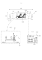
図2に示すように、内枠13(具体的には、遊技盤24)の背面には、遊技の主たる制御を司る主制御装置60が搭載されている。図6は主制御装置60の正面図である。 As shown in FIG. 2, the back of the inner frame 13 (specifically, the game board 24) is equipped with a main control device 60 that is responsible for the main control of the game. FIG. 6 is a front view of the main control device 60.

<主制御装置60の構成>
主制御装置60は、図6に示すように、主制御基板61が基板ボックス60aに収容されてなる。主制御基板61の一方の板面である素子搭載面には、MPU62が搭載されている。基板ボックス60aは当該基板ボックス60aの外部から当該基板ボックス60a内に収容されたMPU62を目視することが可能となるように透明に形成されている。なお、基板ボックス60aは無色透明に形成されているが、基板ボックス60aの外部から当該基板ボックス60a内に収容されたMPU62を目視することが可能であれば有色透明に形成されていてもよい。主制御装置60は基板ボックス60aにおいて主制御基板61の素子搭載面と対向する対向壁部60bがパチンコ機10後方を向くようにして樹脂ベース21の背面に搭載されている。したがって、遊技機本体12を外枠11に対してパチンコ機10前方に開放させて樹脂ベース21の背面を露出させることにより、基板ボックス60aの対向壁部60bを目視することが可能となるとともに当該対向壁部60bを通じてMPU62を目視することが可能となる。
<Configuration of main control device 60>
As shown in FIG. 6, the main control device 60 is configured by housing a main control board 61 in a board box 60a. An MPU 62 is mounted on one of the board surfaces of the main control board 61, which is an element mounting surface. The board box 60a is formed transparent so that the MPU 62 housed in the board box 60a can be seen from the outside of the board box 60a. Although the board box 60a is formed colorless and transparent, it may be formed colored and transparent as long as the MPU 62 housed in the board box 60a can be seen from the outside of the board box 60a. The main control device 60 is mounted on the back surface of the resin base 21 so that the opposing wall portion 60b of the board box 60a that faces the element mounting surface of the main control board 61 faces the rear of the pachinko machine 10. Therefore, by opening the gaming machine main body 12 toward the front of the pachinko machine 10 relative to the outer frame 11 and exposing the back surface of the resin base 21, it becomes possible to visually observe the opposing wall portion 60b of the base box 60a and also to visually observe the MPU 62 through the opposing wall portion 60b.

基板ボックス60aは複数のケース体60cを前後に組合せることにより形成されているが、これら複数のケース体60cには、これらケース体60cの分離を阻止するとともにこれらケース体60cの分離に際してその痕跡を残すための結合部60eが設けられている。結合部60eは、略直方体形状の基板ボックス60aにおける一辺に複数並設されている。これにより、一部の結合部60eを利用してケース体60cの分離を阻止している状態において当該一部の結合部60eを破壊してケース体60cを分離したとしても、その後に別の結合部60eを結合状態とすることでケース体60cの分離を再度阻止することが可能となる。また、ケース体60cの分離に際して結合部60eが破壊されてその痕跡が残ることにより、結合部60eを目視確認することでケース体60cの分離が不正に行われているか否かを把握することが可能となる。また、基板ボックス60aにおいて結合部60eが並設された一辺とは逆の一辺にはケース体60c間の境界を跨ぐようにして封印シール60fが貼り付けられている。封印シール60fはその引き剥がしに際して粘着層がケース体60cに残る。これにより、ケース体60cの分離に際して封印シール60fが剥がされた場合にはその痕跡を残すことが可能となる。 The board box 60a is formed by combining a plurality of case bodies 60c in front and behind, and the plurality of case bodies 60c are provided with joints 60e for preventing separation of the case bodies 60c and for leaving a trace when the case bodies 60c are separated. The joints 60e are arranged in a row on one side of the board box 60a, which is substantially rectangular. As a result, even if some of the joints 60e are used to prevent separation of the case bodies 60c and the case bodies 60c are separated by destroying the part of the joints 60e, it is possible to prevent separation of the case bodies 60c again by connecting another joint 60e thereafter. In addition, since the joints 60e are destroyed when the case bodies 60c are separated and a trace is left, it is possible to visually check the joints 60e to see whether the separation of the case bodies 60c is being carried out illegally. In addition, a seal 60f is attached to the side of the board box 60a opposite to the side on which the joints 60e are arranged, so as to straddle the boundary between the case bodies 60c. When the seal 60f is peeled off, an adhesive layer remains on the case body 60c. This makes it possible to leave a trace when the seal 60f is peeled off when the case body 60c is separated.

上記構成の主制御装置60において主制御基板61には、パチンコ機10の設定状態を「設定1」から「設定6」の範囲で変更する契機を生じさせるために遊技ホールの管理者が所有する設定キーが挿入されてON操作される設定キー挿入部68aと、設定キー挿入部68aに対するON操作後においてパチンコ機10の設定状態を順次変更させるために操作される更新ボタン68bと、主制御装置60のMPU62に設けられた後述する主側RAM65のデータをクリアするために操作されるリセットボタン68cと、遊技履歴の管理結果を報知するための第1~第3報知用表示装置69a~69cと、が設けられている。なお、パチンコ機10の設定状態は「設定1」~「設定6」の6段階に限定されることはなく複数段階であれば任意である。 In the main control device 60 configured as above, the main control board 61 is provided with a setting key insertion section 68a into which a setting key owned by the manager of the game parlor is inserted and turned on to trigger the setting state of the pachinko machine 10 to be changed within the range of "setting 1" to "setting 6", an update button 68b which is operated to sequentially change the setting state of the pachinko machine 10 after the setting key insertion section 68a is turned on, a reset button 68c which is operated to clear the data in the main RAM 65 (described later) provided in the MPU 62 of the main control device 60, and first to third notification display devices 69a to 69c for notifying the results of the management of the game history. The setting state of the pachinko machine 10 is not limited to the six stages of "setting 1" to "setting 6", and may be any number of stages.

これら設定キー挿入部68a、更新ボタン68b、リセットボタン68c、及び第1~第3報知用表示装置69a~69cはいずれも主制御基板61の素子搭載面に設けられている。また、主制御基板61の素子搭載面は既に説明したとおり基板ボックス60aの対向壁部60bと対向しているが、設定キー挿入部68a、更新ボタン68b及びリセットボタン68cは対向壁部60bにより覆われていない。つまり、対向壁部60bには設定キー挿入部68a、更新ボタン68b及びリセットボタン68cのそれぞれと対向する領域が個別の開口部とされている。これにより、基板ボックス60aの開放を要することなく、設定キー挿入部68aに設定キーを挿入することが可能であり、更新ボタン68bを押圧操作することが可能であり、リセットボタン68cを押圧操作することが可能である。 The setting key insertion section 68a, the update button 68b, the reset button 68c, and the first to third notification display devices 69a to 69c are all provided on the element mounting surface of the main control board 61. As already explained, the element mounting surface of the main control board 61 faces the opposing wall section 60b of the board box 60a, but the setting key insertion section 68a, the update button 68b, and the reset button 68c are not covered by the opposing wall section 60b. In other words, the opposing wall section 60b has separate openings in the areas facing the setting key insertion section 68a, the update button 68b, and the reset button 68c. This makes it possible to insert a setting key into the setting key insertion section 68a, press the update button 68b, and press the reset button 68c without having to open the board box 60a.

設定キー挿入部68aに設定キーを挿入して所定方向に回転操作することにより設定キー挿入部68aがON操作された状態となる。その状態でパチンコ機10への動作電力の供給を開始させることで(すなわち主制御装置60のMPU62への動作電力の供給を開始させることで)、パチンコ機10の設定状態を変更することが可能な変更可能状態となる。そして、この状態において更新ボタン68bを1回押圧操作する度にパチンコ機10の設定状態が「設定1」~「設定6」の範囲において昇順で1段階ずつ変更される。なお、「設定6」の状態で更新ボタン68bが操作された場合には「設定1」に更新される。また、設定キー挿入部68aに挿入している設定キーをON操作の位置から所定方向とは反対方向に回転操作して初期位置に復帰させることにより設定キー挿入部68aがOFF操作された状態となる。設定キー挿入部68aがOFF操作された状態となることで上記変更可能状態が終了し、その時点における設定値の状態で遊技を行うことが可能な状態となる。つまり、変更可能状態が終了した後に更新ボタン68bを操作しても設定値を変更することはできない。 By inserting a setting key into the setting key insertion section 68a and rotating it in a predetermined direction, the setting key insertion section 68a is turned ON. In this state, the supply of operating power to the pachinko machine 10 is started (i.e., the supply of operating power to the MPU 62 of the main control device 60 is started), and the setting state of the pachinko machine 10 is changed to a changeable state in which it is possible to change the setting state of the pachinko machine 10. In this state, the setting state of the pachinko machine 10 is changed by one step in ascending order in the range of "Setting 1" to "Setting 6" each time the update button 68b is pressed once. Note that if the update button 68b is operated in the "Setting 6" state, it is updated to "Setting 1". In addition, by rotating the setting key inserted in the setting key insertion section 68a from the ON operation position in the opposite direction to the predetermined direction and returning it to the initial position, the setting key insertion section 68a is turned OFF. When the setting key insertion section 68a is turned OFF, the changeable state ends, and the game is able to be played with the setting value at that time. In other words, even if you operate the update button 68b after the changeable state has ended, the setting value cannot be changed.

設定キー挿入部68aに対するON操作はパチンコ機10への動作電力の供給開始時(すなわち主制御装置60のMPU62への動作電力の供給開始時)のみ有効とされる。したがって、主制御装置60のMPU62において動作電力の供給開始時の処理が終了した後に設定キー挿入部68aに対するON操作を行ったとしても設定値を変更することはできない。 The ON operation of the setting key insertion section 68a is only valid when the supply of operating power to the pachinko machine 10 starts (i.e., when the supply of operating power to the MPU 62 of the main control device 60 starts). Therefore, even if the ON operation of the setting key insertion section 68a is performed after the processing at the start of the supply of operating power in the MPU 62 of the main control device 60 has ended, the setting value cannot be changed.

パチンコ機10の設定状態は当該パチンコ機10における単位時間当たりの有利度を定めるものであり、「設定n」(nは「1」~「6」の整数)のnが大きい値ほど(すなわち設定値が高いほど)有利度が高くなる。詳細は後述するが大当たり結果の当選確率を決定する当否抽選モードとして相対的に当選確率が低くなる低確率モードと相対的に当選確率が高くなる高確率モードとが存在しており、設定値が高いほど低確率モードにおける大当たり結果の当選確率が高くなるように設定されている。一方、いずれの設定値であっても高確率モードにおける大当たり結果の当選確率は一定となっている。 The setting state of the pachinko machine 10 determines the degree of advantage per unit time in the pachinko machine 10, and the larger the value of "setting n" (n is an integer from "1" to "6") (i.e., the higher the setting value), the higher the degree of advantage. As will be described in more detail later, there are two winning/losing lottery modes that determine the probability of winning a jackpot result: a low probability mode with a relatively low probability of winning and a high probability mode with a relatively high probability of winning, and the higher the setting value, the higher the probability of winning a jackpot result in the low probability mode. On the other hand, regardless of the setting value, the probability of winning a jackpot result in the high probability mode is constant.

リセットボタン68cは上記のとおり主側RAM65のデータをクリアするために操作されるが、当該データのクリアを発生させるためにはリセットボタン68cを押圧操作した状態でパチンコ機10への動作電力の供給を開始させる必要がある(すなわち主制御装置60のMPU62への動作電力の供給を開始させる必要がある)。リセットボタン68cに対するON操作はパチンコ機10への動作電力の供給開始時(すなわち主制御装置60のMPU62への動作電力の供給開始時)のみ有効とされる。したがって、主制御装置60のMPU62において動作電力の供給開始時の処理が終了した後にリセットボタン68cを押圧操作したとしても主側RAM65のデータのクリアを行うことはできない。 As described above, the reset button 68c is operated to clear the data in the main RAM 65, but in order to clear the data, it is necessary to start the supply of operating power to the pachinko machine 10 while the reset button 68c is pressed (i.e., it is necessary to start the supply of operating power to the MPU 62 of the main control device 60). The ON operation of the reset button 68c is only valid when the supply of operating power to the pachinko machine 10 starts (i.e., when the supply of operating power to the MPU 62 of the main control device 60 starts). Therefore, even if the reset button 68c is pressed after the processing at the start of the supply of operating power in the MPU 62 of the main control device 60 has finished, the data in the main RAM 65 cannot be cleared.

第1~第3報知用表示装置69a~69cはいずれも、LEDによる表示用セグメントが7個配列されたセグメント表示器であるが、これに限定されることはなく多色発光タイプの単一の発光体であってもよく、液晶表示装置であってもよく、有機ELディスプレイであってもよい。第1~第3報知用表示装置69a~69cはいずれもその表示面が主制御基板61の素子搭載面が向く方向を向くようにして設置されているとともに、基板ボックス60aの対向壁部60bにより覆われている。この場合に、基板ボックス60aが透明に形成されていることにより、基板ボックス60aの外部から当該基板ボックス60a内に収容された第1~第3報知用表示装置69a~69cの表示面を目視することが可能となる。また、既に説明したとおり主制御装置60は基板ボックス60aにおいて主制御基板61の素子搭載面と対向する対向壁部60bがパチンコ機10後方を向くようにして樹脂ベース21の背面に搭載されているため、遊技機本体12を外枠11に対してパチンコ機10前方に開放させて樹脂ベース21の背面をパチンコ機10前方に露出させた場合には、対向壁部60bを通じて第1~第3報知用表示装置69a~69cの表示面を目視することが可能となる。 The first to third notification display devices 69a to 69c are all segment displays in which seven LED display segments are arranged, but are not limited to this and may be a single light-emitting body of a multi-color type, a liquid crystal display device, or an organic EL display. The first to third notification display devices 69a to 69c are all installed so that their display surfaces face the direction in which the element mounting surface of the main control board 61 faces, and are covered by the opposing wall portion 60b of the board box 60a. In this case, since the board box 60a is formed transparent, it is possible to visually observe the display surfaces of the first to third notification display devices 69a to 69c housed within the board box 60a from outside the board box 60a. As already explained, the main control device 60 is mounted on the back surface of the resin base 21 with the opposing wall portion 60b, which faces the element mounting surface of the main control board 61 in the board box 60a, facing the rear of the pachinko machine 10. Therefore, when the gaming machine main body 12 is opened toward the front of the pachinko machine 10 relative to the outer frame 11 and the rear surface of the resin base 21 is exposed toward the front of the pachinko machine 10, it becomes possible to visually observe the display surfaces of the first to third notification display devices 69a to 69c through the opposing wall portion 60b.

第1報知用表示装置69aの表示面においては「0」~「9」の数字だけではなく、アルファベット文字を含めた各種文字が表示される。一方、第2報知用表示装置69b及び第3報知用表示装置69cにおいては「0」~「9」の数字が表示される。第1~第3報知用表示装置69a~69cを利用して遊技履歴の管理結果が報知される。また、パチンコ機10の設定状態を変更することが可能な変更可能状態においては現状の設定値に対応する値が第3報知用表示装置69cにて表示される。なお、当該設定値に対応する値が第1報知用表示装置69aにて表示される構成としてもよく、第2報知用表示装置69bにて表示される構成としてもよい。また、変更可能状態となる前における設定値が第1~第3報知用表示装置69a~69cのうちの一の報知用表示装置にて表示されるとともに現状の設定値が第1~第3報知用表示装置69a~69cのうちの他の一の報知用表示装置にて表示される構成としてもよい。 The display surface of the first notification display device 69a displays not only the numbers "0" to "9" but also various characters including alphabetical characters. On the other hand, the second notification display device 69b and the third notification display device 69c display the numbers "0" to "9". The first to third notification display devices 69a to 69c are used to notify the results of the management of the game history. In addition, in a changeable state in which the setting state of the pachinko machine 10 can be changed, a value corresponding to the current setting value is displayed on the third notification display device 69c. Note that the value corresponding to the setting value may be displayed on the first notification display device 69a or on the second notification display device 69b. In addition, a configuration may be adopted in which the setting value before the changeable state is displayed on one of the first to third notification display devices 69a to 69c, and the current setting value is displayed on the other of the first to third notification display devices 69a to 69c.

内枠13の背面において主制御装置60の上方には、音声発光制御装置81が設けられている。音声発光制御装置81は、主制御装置60からの指示に従い音出力制御、発光制御及び表示制御装置82の制御を実行する。また、音声発光制御装置81は、第1装飾基板56及び第2装飾基板57に実装されているLEDチップの発光制御を実行する。 A sound and light emission control device 81 is provided above the main control device 60 on the rear surface of the inner frame 13. The sound and light emission control device 81 performs sound output control, light emission control, and control of the display control device 82 in accordance with instructions from the main control device 60. The sound and light emission control device 81 also performs light emission control of the LED chips mounted on the first decorative substrate 56 and the second decorative substrate 57.

図3に示すように、主制御装置60及び音声発光制御装置81を含めて内枠13の背面側を覆うようにして裏パックユニット15が設置されている。裏パックユニット15は、透明性を有する合成樹脂により形成された裏パック72を備えており、当該裏パック72に払出機構部73及び制御装置集合ユニット74が取り付けられている。 As shown in FIG. 3, the back pack unit 15 is installed to cover the back side of the inner frame 13, including the main control device 60 and the sound and light emission control device 81. The back pack unit 15 has a back pack 72 formed of a transparent synthetic resin, to which a dispensing mechanism 73 and a control device assembly unit 74 are attached.

払出機構部73は、遊技ホールの島設備から供給される遊技球が逐次補給されるタンク75と、当該タンク75に貯留された遊技球を払い出すための払出装置76と、を備えている。払出装置76より払い出された遊技球は、当該払出装置76の下流側に設けられた払出通路を通じて、上皿54a又は下皿55aに排出される。なお、払出機構部73には、例えば交流24ボルトの主電源が供給されるとともに、電源のON操作及びOFF操作を行うための電源スイッチを有する裏パック基板が搭載されている。 The payout mechanism 73 includes a tank 75 to which game balls are successively replenished from the island equipment of the gaming hall, and a payout device 76 for paying out the game balls stored in the tank 75. The game balls paid out from the payout device 76 are discharged into the upper tray 54a or the lower tray 55a through a payout passage provided downstream of the payout device 76. The payout mechanism 73 is supplied with a main power source of, for example, 24 volts AC, and is equipped with a back pack board having a power switch for turning the power source on and off.

制御装置集合ユニット74は、払出装置76を制御する機能を有する払出制御装置77と、各種制御装置等で要する所定の電力が生成されて出力されるとともに遊技者による発射操作装置28の操作に伴う遊技球の打ち出しの制御が行われる電源・発射制御装置78と、を備えている。これら払出制御装置77と電源・発射制御装置78とは、払出制御装置77がパチンコ機10後方となるように前後に重ねて配置されている。 The control device assembly unit 74 is equipped with a payout control device 77 that has the function of controlling the payout device 76, and a power supply and launch control device 78 that generates and outputs the predetermined power required by various control devices, etc., and controls the launch of game balls in response to the player's operation of the launch operation device 28. The payout control device 77 and the power supply and launch control device 78 are stacked one behind the other, with the payout control device 77 at the rear of the pachinko machine 10.

図7は装飾カバー58,59及び装飾基板56,57を取り除いた状態におけるパチンコ機10の正面図である。図1に示すように、第1装飾カバー58には、当該第1装飾カバー58の背面の上部、左下部及び右下部をパチンコ機10後方に起立させて、円柱状のカバー固定ボス58a~58cが一体形成されている。また、第2装飾カバー59には、当該第2装飾カバー59の背面の左部及び右部をパチンコ機10後方に起立させて、円柱状のカバー固定ボス59a,59bが一体形成されている。これらのカバー固定ボス58a~58c,59a,59bの起立先の端部にはネジ穴(図示略)が形成されている。図7に示すように、前扉枠14には、これらのカバー固定ボス58a~58c,59a,59bに対応させて、前扉枠14を前後に貫通する貫通孔14a~14eが形成されている。図1に示すように、第1装飾カバー58及び第2装飾カバー59は、カバー固定ボス58a~58c,59a,59bが前扉枠14の背面側からネジ固定されることにより前扉枠14に固定されている。 Figure 7 is a front view of the pachinko machine 10 with the decorative covers 58, 59 and the decorative boards 56, 57 removed. As shown in Figure 1, the first decorative cover 58 has cylindrical cover fixing bosses 58a-58c formed integrally with the upper, lower left, and lower right parts of the back of the first decorative cover 58, which stand up toward the rear of the pachinko machine 10. The second decorative cover 59 has cylindrical cover fixing bosses 59a, 59b formed integrally with the left and right parts of the back of the second decorative cover 59, which stand up toward the rear of the pachinko machine 10. Screw holes (not shown) are formed at the ends of the upright ends of these cover fixing bosses 58a-58c, 59a, 59b. As shown in Figure 7, the front door frame 14 has through holes 14a-14e formed corresponding to these cover fixing bosses 58a-58c, 59a, 59b, which penetrate the front door frame 14 from front to rear. As shown in FIG. 1, the first decorative cover 58 and the second decorative cover 59 are fixed to the front door frame 14 by screwing the cover fixing bosses 58a-58c, 59a, and 59b from the rear side of the front door frame 14.

<装飾基板56,57の構成>
次に、装飾基板56,57の構成について説明する。
<Configuration of decorative substrates 56, 57>
Next, the configuration of the decorative substrates 56 and 57 will be described.

図8(a)は第1装飾基板56の一方側の板面である第1実装面84を示す平面図であり、図8(b)は第1装飾基板56に実装されているバイパスコンデンサ85の周辺領域86を拡大して示す第1装飾基板56の第1実装面84の平面図であり、図8(c)は第1装飾基板56に実装されている小型チップ抵抗器87の周辺領域88を拡大して示す第1装飾基板56の第1実装面84の平面図であり、図9は図8(a)のA-A線断面図である。また、図10(a)は第2装飾基板57の一方側の板面である第1実装面89を示す平面図であり、図10(b)は第2装飾基板57に実装されているバイパスコンデンサ97の周辺領域98を拡大して示す第2装飾基板57の第1実装面89の平面図であり、図10(c)は第2装飾基板57に実装されている小型チップ抵抗器101の周辺領域102を拡大して示す第2装飾基板57の第1実装面89の平面図である。 Figure 8(a) is a plan view showing the first mounting surface 84, which is the plate surface on one side of the first decorative substrate 56, Figure 8(b) is a plan view of the first mounting surface 84 of the first decorative substrate 56 showing an enlarged peripheral area 86 of a bypass capacitor 85 mounted on the first decorative substrate 56, Figure 8(c) is a plan view of the first mounting surface 84 of the first decorative substrate 56 showing an enlarged peripheral area 88 of a small chip resistor 87 mounted on the first decorative substrate 56, and Figure 9 is a cross-sectional view along line A-A in Figure 8(a). Also, FIG. 10(a) is a plan view showing the first mounting surface 89, which is the plate surface on one side of the second decorative substrate 57, FIG. 10(b) is a plan view of the first mounting surface 89 of the second decorative substrate 57 showing an enlarged peripheral area 98 of a bypass capacitor 97 mounted on the second decorative substrate 57, and FIG. 10(c) is a plan view of the first mounting surface 89 of the second decorative substrate 57 showing an enlarged peripheral area 102 of a small chip resistor 101 mounted on the second decorative substrate 57.

装飾基板56,57は、導電層と絶縁層とが交互に積層された構造を有する4層基板である。絶縁層としては、ガラスクロスの基材に熱硬化性エポキシ樹脂を含浸させた複合材などが用いられる。導電層は、絶縁層の上又は下に配置された銅箔プレートをエッチングすることにより形成されている。 The decorative substrates 56 and 57 are four-layer substrates with a structure in which conductive layers and insulating layers are alternately laminated. The insulating layers are made of a composite material such as a glass cloth base material impregnated with a thermosetting epoxy resin. The conductive layers are formed by etching copper foil plates placed above or below the insulating layers.

図9に示すように、第1装飾基板56は、導電層として、第1装飾基板56の第1実装面84側に配置されている第1配線層91と、第1装飾基板56の他方側の板面である第2実装面95側に配置されている第2配線層92と、を備えている。また、第1装飾基板56は、第1配線層91及び第2配線層92の間に配置されている導電層として、GNDプレーン層93(グランドプレーン層又はグラウンドプレーン層)と、電源プレーン層94と、を備えている。第1配線層91及び第2配線層92には、銅箔プレートをエッチングすることによりランド及び配線パターンが形成されている。 As shown in FIG. 9, the first decorative board 56 includes, as conductive layers, a first wiring layer 91 arranged on the first mounting surface 84 side of the first decorative board 56, and a second wiring layer 92 arranged on the second mounting surface 95 side, which is the other plate surface of the first decorative board 56. The first decorative board 56 also includes, as conductive layers arranged between the first wiring layer 91 and the second wiring layer 92, a GND plane layer 93 (ground plane layer or ground plane layer) and a power plane layer 94. Lands and wiring patterns are formed on the first wiring layer 91 and the second wiring layer 92 by etching a copper foil plate.

図示は省略するが、第2装飾基板57は、第1装飾基板56と同様に、導電層として、第1実装面89側に配置されている第1配線層と、第2装飾基板57の他方側の板面である第2実装面側に配置されている第2配線層と、を備えている。また、第2装飾基板57は、第1装飾基板56と同様に、第1配線層及び第2配線層の間に配置されている導電層として、GNDプレーン層(グランドプレーン層又はグラウンドプレーン層)と、電源プレーン層と、を備えている。第1配線層及び第2配線層には、銅箔プレートをエッチングすることによりランド及び配線パターンが形成されている。 Although not shown, the second decorative board 57, like the first decorative board 56, has a first wiring layer arranged on the first mounting surface 89 side as a conductive layer, and a second wiring layer arranged on the second mounting surface side, which is the other plate surface of the second decorative board 57. Also, like the first decorative board 56, the second decorative board 57 has a GND plane layer (ground plane layer or ground plane layer) and a power plane layer as conductive layers arranged between the first wiring layer and the second wiring layer. Lands and wiring patterns are formed on the first wiring layer and the second wiring layer by etching a copper foil plate.

図1に示すように、第1装飾基板56の右側上部には、湾曲している窓部51の左下部に対応する階段状凹部56aが形成されている。また、第1装飾基板56の左側下部には、第1装飾カバー58のカバー固定ボス58bを避けるための切欠部56bが形成されている。第1装飾基板56に切欠部56bが設けられていることにより、カバー固定ボス58bを避けつつ、第1装飾カバー58後方の広い領域に第1装飾基板56を設けることが可能となっている。 As shown in FIG. 1, a stepped recess 56a is formed in the upper right side of the first decorative substrate 56, corresponding to the lower left side of the curved window portion 51. In addition, a notch 56b is formed in the lower left side of the first decorative substrate 56 to avoid the cover fixing boss 58b of the first decorative cover 58. By providing the notch 56b in the first decorative substrate 56, it is possible to install the first decorative substrate 56 in a wide area behind the first decorative cover 58 while avoiding the cover fixing boss 58b.

第1装飾基板56は、階段状凹部56a及び切欠部56bを有する異形基板である。第1装飾基板56は、矩形及び略矩形の基板ではない。図8(a)に示すように、第1装飾基板56の第1方向DR1(図8(a)における上下方向)における寸法は、第1装飾基板56の当該第1方向DR1に直交する第2方向DR2(図8(a)における左右方向)における寸法よりも大きい。 The first decorative substrate 56 is an irregularly shaped substrate having a stepped recess 56a and a notch 56b. The first decorative substrate 56 is neither a rectangular nor an approximately rectangular substrate. As shown in FIG. 8(a), the dimension of the first decorative substrate 56 in a first direction DR1 (the up-down direction in FIG. 8(a)) is greater than the dimension of the first decorative substrate 56 in a second direction DR2 (the left-right direction in FIG. 8(a)) perpendicular to the first direction DR1.

図10(a)に示すように、第2装飾基板57は横長略楕円形に成形されている。第2装飾基板57は、矩形及び略矩形の基板ではない。第2装飾基板57の長軸方向LD(図10(a)における左右方向)における寸法は、第2装飾基板57の短軸方向SD(図10(a)における上下方向)における寸法よりも大きい。 As shown in FIG. 10(a), the second decorative substrate 57 is shaped like a horizontally elongated, approximately elliptical shape. The second decorative substrate 57 is not a rectangular or approximately rectangular substrate. The dimension of the second decorative substrate 57 in the long axis direction LD (left-right direction in FIG. 10(a)) is greater than the dimension of the second decorative substrate 57 in the short axis direction SD (up-down direction in FIG. 10(a)).

図8(a)に示すように、階段状凹部56aの上下方向略中央には突出部56cが設けられている。第1装飾基板56の上端部左側、突出部56c、下端部左側及び下端部右側には、第1装飾基板56を厚さ方向に貫通させて、第1装飾基板56を前扉枠14の前面にネジ固定可能とする固定貫通孔56d~56gが形成されている。また、図10(a)に示すように、第2装飾基板57の左部及び右部には、第2装飾基板57を厚さ方向に貫通させて、第2装飾基板57を前扉枠14にネジ固定可能とする固定貫通孔57a,57bが形成されている。 As shown in FIG. 8(a), a protrusion 56c is provided at approximately the center in the vertical direction of the stepped recess 56a. Fixing through-holes 56d-56g are formed on the upper left end, protrusion 56c, lower left end, and lower right end of the first decorative board 56, penetrating the first decorative board 56 in the thickness direction to enable the first decorative board 56 to be screwed to the front surface of the front door frame 14. Also, as shown in FIG. 10(a), fixing through-holes 57a, 57b are formed on the left and right parts of the second decorative board 57, penetrating the second decorative board 57 in the thickness direction to enable the second decorative board 57 to be screwed to the front door frame 14.

図7に示すように、前扉枠14には、当該前扉枠14の前面に、装飾基板56,57(図8(a)及び図10(a))を固定可能とする円柱状の基板固定ボス103~108が一体形成されている。基板固定ボス103~108は、前扉枠14の前面からパチンコ機10前方に起立しており、当該基板固定ボス103~108の起立先の端部には装飾基板56,57をネジ固定可能とするネジ孔103a~108aが形成されている。装飾基板56,57は、パチンコ機10前方から基板固定ボス103~108にネジ固定されることにより、第1実装面84,89(図8(a)及び図10(a))がパチンコ機10前方を向くようにして、図1に示すように前扉枠14の前面に固定されている。 As shown in FIG. 7, the front door frame 14 has cylindrical board fixing bosses 103-108 integrally formed on the front surface of the front door frame 14, which can fix the decorative boards 56, 57 (FIGS. 8(a) and 10(a)). The board fixing bosses 103-108 stand upright from the front surface of the front door frame 14 toward the front of the pachinko machine 10, and screw holes 103a-108a are formed at the ends of the board fixing bosses 103-108, which can screw the decorative boards 56, 57. The decorative boards 56, 57 are fixed to the front surface of the front door frame 14 as shown in FIG. 1, with the first mounting surfaces 84, 89 (FIGS. 8(a) and 10(a)) facing the front of the pachinko machine 10 by being screwed to the board fixing bosses 103-108 from the front of the pachinko machine 10.

既に説明したとおり、装飾基板56,57に搭載されているLEDチップの発光制御、及びスピーカ部53の音出力制御は、音声発光制御装置81(図3)にて行われる。図8(a)に示すように、第1装飾基板56には、第1実装面84とは逆側の板面である第2実装面95(図9)に、第1コネクタ111及び第2コネクタ112が実装されている。また、図10(a)に示すように、第2装飾基板57には、第1実装面89とは逆側の板面である第2実装面に、第3コネクタ113、第4コネクタ114及び第5コネクタ115が実装されている。 As already explained, the light emission control of the LED chips mounted on the decorative substrates 56 and 57 and the sound output control of the speaker unit 53 are performed by the sound emission control device 81 (Fig. 3). As shown in Fig. 8(a), the first decorative substrate 56 has a first connector 111 and a second connector 112 mounted on a second mounting surface 95 (Fig. 9), which is the plate surface opposite to the first mounting surface 84. Also, as shown in Fig. 10(a), the second decorative substrate 57 has a third connector 113, a fourth connector 114, and a fifth connector 115 mounted on a second mounting surface, which is the plate surface opposite to the first mounting surface 89.

第1コネクタ111には、音声発光制御装置81(図3)と第1装飾基板56とを電気的に接続するハーネス(図示略)が装着されている。第2コネクタ112及び第3コネクタ113には、第1装飾基板56と第2装飾基板57とを電気的に接続するハーネス(図示略)が装着されている。また、第4コネクタ114及び第5コネクタ115には、第2装飾基板57と左右一対のスピーカ部53とを電気的に接続するハーネス(図示略)が装着されている。音声発光制御装置81は、第1装飾基板56に対して、第1装飾基板56に実装されているLEDチップの発光制御を行うための情報を出力する。また、音声発光制御装置81は、第1装飾基板56を介して第2装飾基板57に対して、第2装飾基板57に実装されているLEDチップの発光制御を行うための情報及びスピーカ部53の音出力制御を行うための情報を出力する。 The first connector 111 is equipped with a harness (not shown) that electrically connects the sound and light emission control device 81 (FIG. 3) and the first decorative board 56. The second connector 112 and the third connector 113 are equipped with harnesses (not shown) that electrically connect the first decorative board 56 and the second decorative board 57. The fourth connector 114 and the fifth connector 115 are equipped with harnesses (not shown) that electrically connect the second decorative board 57 and the pair of left and right speaker units 53. The sound and light emission control device 81 outputs information to the first decorative board 56 for controlling the light emission of the LED chips mounted on the first decorative board 56. The sound and light emission control device 81 also outputs information to the second decorative board 57 via the first decorative board 56 for controlling the light emission of the LED chips mounted on the second decorative board 57 and information for controlling the sound output of the speaker unit 53.

図7に示すように、前扉枠14には、第1~第5コネクタ111~115(図8(a)及び図10(a))に対応させて、前扉枠14を前後に貫通する第1~第5コネクタ挿通孔14f~14jが形成されている。装飾基板56,57(図8(a)及び図10(a))は、コネクタ111~115が対応するコネクタ挿通孔14f~14jに挿通されて前扉枠14の背面側に露出している状態で、前扉枠14に固定されている。第1~第5コネクタ111~115に対するハーネス(図示略)の着脱は、前扉枠14の背面側から行われる。 As shown in FIG. 7, the front door frame 14 is formed with first to fifth connector insertion holes 14f to 14j that penetrate the front door frame 14 from front to rear in correspondence with the first to fifth connectors 111 to 115 (FIGS. 8(a) and 10(a)). The decorative boards 56, 57 (FIGS. 8(a) and 10(a)) are fixed to the front door frame 14 with the connectors 111 to 115 inserted into the corresponding connector insertion holes 14f to 14j and exposed on the rear side of the front door frame 14. The harnesses (not shown) are attached to and detached from the first to fifth connectors 111 to 115 from the rear side of the front door frame 14.

図8(a)に示すように第1装飾基板56には、第1発光回路部121、第2発光回路部122及び第3発光回路部123が設けられている。また、図10(a)に示すように第2装飾基板57には、第4発光回路部124が設けられている。これらの発光回路部121~124は、複数のLEDチップを発光制御するための回路を備えている。 As shown in FIG. 8(a), the first decorative substrate 56 is provided with a first light-emitting circuit section 121, a second light-emitting circuit section 122, and a third light-emitting circuit section 123. As shown in FIG. 10(a), the second decorative substrate 57 is provided with a fourth light-emitting circuit section 124. These light-emitting circuit sections 121 to 124 are equipped with circuits for controlling the emission of light from multiple LED chips.

発光回路部121~124の具体的な構成について、第1発光回路部121の構成を例に挙げて説明する。 The specific configuration of the light-emitting circuit units 121 to 124 will be explained using the configuration of the first light-emitting circuit unit 121 as an example.

図11は第1装飾基板56における第1発光回路部121の配線図である。図11に示すように、第1発光回路部121には、LEDドライバ126、バイパスコンデンサ85、16個のLEDチップ127~142及び8個の小型チップ抵抗器87,143~149が含まれている。また、図示は省略するが、第2~第4発光回路部122~124にもLEDドライバ、バイパスコンデンサ、複数のLEDチップ及び複数の小型チップ抵抗器が含まれている。なお、各発光回路部121~124に含まれるLEDチップの数は任意であり、各発光回路部121~124に含まれる小型チップ抵抗器の数はLEDドライバとLEDチップとの接続態様に応じて決まる。 Figure 11 is a wiring diagram of the first light-emitting circuit section 121 in the first decorative board 56. As shown in Figure 11, the first light-emitting circuit section 121 includes an LED driver 126, a bypass capacitor 85, 16 LED chips 127-142, and eight small chip resistors 87, 143-149. Although not shown, the second to fourth light-emitting circuit sections 122-124 also include an LED driver, a bypass capacitor, multiple LED chips, and multiple small chip resistors. Note that the number of LED chips included in each of the light-emitting circuit sections 121-124 is arbitrary, and the number of small chip resistors included in each of the light-emitting circuit sections 121-124 is determined according to the connection mode between the LED driver and the LED chips.

図11に示すように、LEDドライバ126は、電源端子151と、クロック端子152と、データ端子153と、GND端子154(グランド端子又はグラウンド端子)と、第1~第8出力端子155~162と、を備えている。クロック端子152には、音声発光制御装置81から受信するクロック信号を入力する配線パターン164が電気的に接続されているとともに、データ端子153には、音声発光制御装置81から受信する点灯制御データを入力する配線パターン165が電気的に接続されている。また、GND端子154にはLEDドライバ126をGNDプレーン層93(図9)に電気的に接続するための第2配線パターン172bが接続されているとともに、電源端子151には、LEDドライバ126の駆動電源を供給する第4配線パターン172dが電気的に接続されている。 As shown in FIG. 11, the LED driver 126 includes a power terminal 151, a clock terminal 152, a data terminal 153, a GND terminal 154 (ground terminal or ground terminal), and first to eighth output terminals 155 to 162. A wiring pattern 164 for inputting a clock signal received from the audio and light emission control device 81 is electrically connected to the clock terminal 152, and a wiring pattern 165 for inputting lighting control data received from the audio and light emission control device 81 is electrically connected to the data terminal 153. In addition, a second wiring pattern 172b for electrically connecting the LED driver 126 to the GND plane layer 93 (FIG. 9) is connected to the GND terminal 154, and a fourth wiring pattern 172d for supplying driving power to the LED driver 126 is electrically connected to the power terminal 151.

なお、本明細書における「端子」とは、対応するパッド(又はパット)と電気的に接続するために電子部品(後述する小型チップ部品を含む。)に設けられた線状の金属部(例えば、LEDドライバ126における電源端子151及びGND端子154(図8(b))である。また、本明細書における「電極」とは、狭義には、対応するパッド(又はパット)と電気的に面で接続させるために電子部品(後述する小型チップ部品を含む。)に設けられた金属部(例えば、バイパスコンデンサ85における後述する第1電極85a及び第2電極85b(図8(b)))であり、上記「端子」を含まない。一方、本明細書における「電極」とは、広義には、対応するパッド(又はパット)と電気的に接続するために電子部品(後述する小型チップ部品を含む。)に設けられた金属部であり、上記「端子」を含む。 In this specification, a "terminal" refers to a linear metal part (e.g., the power terminal 151 and the GND terminal 154 (FIG. 8(b)) in the LED driver 126) provided on an electronic component (including small chip components described later) for electrical connection with a corresponding pad (or pad). In addition, an "electrode" in this specification, in a narrow sense, refers to a metal part (e.g., the first electrode 85a and the second electrode 85b (FIG. 8(b)) in the bypass capacitor 85) provided on an electronic component (including small chip components described later) for electrical surface connection with a corresponding pad (or pad), and does not include the above-mentioned "terminal". On the other hand, in a broad sense, an "electrode" in this specification refers to a metal part (e.g., the first electrode 85a and the second electrode 85b (FIG. 8(b)) provided on an electronic component (including small chip components described later) for electrical surface connection with a corresponding pad (or pad), and does not include the above-mentioned "terminal".

LEDドライバ126は、音声発光制御装置81から受信する点灯制御データに基づいて、第1~第8出力端子155~162に接続されているLEDチップ127~142の発光制御を行う。LEDドライバ126の各出力端子155~162には、上述した16個のLEDチップ127~142のうち2つのLEDチップと、上述した8つの小型チップ抵抗器87,143~149のうち1つの小型チップ抵抗器とが電気的に接続されている。小型チップ抵抗器87,143~149は、LEDチップ127~142に流れる電流を制限するために設けられている。小型チップ抵抗器87,143~149が設けられていることによりLEDチップ127~142を許容電流以下で駆動することができる。 The LED driver 126 controls the light emission of the LED chips 127-142 connected to the first to eighth output terminals 155-162 based on the lighting control data received from the audio light emission control device 81. Two of the 16 LED chips 127-142 and one of the eight small chip resistors 87, 143-149 are electrically connected to each of the output terminals 155-162 of the LED driver 126. The small chip resistors 87, 143-149 are provided to limit the current flowing through the LED chips 127-142. The provision of the small chip resistors 87, 143-149 allows the LED chips 127-142 to be driven at or below the allowable current.

図12(a)はバイパスコンデンサ85の周辺を拡大して示す第1装飾基板56の第1実装面84側の斜視図であり、図12(b)は小型チップ抵抗器87の周辺を拡大して示す第1装飾基板56の第1実装面84側の斜視図である。図12(a)に示すように、バイパスコンデンサ85は、表面実装型のチップコンデンサであり、具体的には誘電体と電極とを多数積み重ねた積層セラミックコンデンサである。バイパスコンデンサ85は、略直方体であり、長手方向の両端部に一対の金属製の第1電極85a及び第2電極85bを備えている。 Figure 12(a) is a perspective view of the first mounting surface 84 of the first decorative substrate 56, showing an enlarged view of the bypass capacitor 85 and its periphery, and Figure 12(b) is a perspective view of the first mounting surface 84 of the first decorative substrate 56, showing an enlarged view of the small chip resistor 87 and its periphery. As shown in Figure 12(a), the bypass capacitor 85 is a surface-mounted chip capacitor, specifically a multilayer ceramic capacitor in which a large number of dielectrics and electrodes are stacked. The bypass capacitor 85 is roughly a rectangular parallelepiped, and has a pair of metallic first and second electrodes 85a and 85b at both ends in the longitudinal direction.

バイパスコンデンサ85は、当該バイパスコンデンサ85の厚さ方向に直交する平面に沿う長手方向(以下、「バイパスコンデンサ85の長手方向」ともいう。)の寸法が0.1mm以上であり0.9mm以下である小型チップ部品である。本明細書において、小型チップ部品とは、当該小型チップ部品の長手方向(以下、「小型チップ部品の長手方向」ともいう。)の寸法が0.1mm以上であり0.9mm以下である電子部品である。小型チップ部品の長手方向の寸法が0.9mm以下であることにより、第1装飾基板56において当該小型チップ部品が占有する面積を抑えることができる。これにより、第1装飾基板56において当該小型チップ部品以外の電子部品を実装する領域の面積を広く確保することができる。また、第1装飾基板56と電子部品の実装密度が高い基板との間で実装される電子部品を小型チップ部品に共通化することができる。小型チップ部品の長手方向の寸法が0.1mm以上であることにより、小型チップ部品と第1装飾基板56との接続箇所における機械的強度及び当該小型チップ部品自体の機械的強度が低下し過ぎてしまうことを防止できる。ここで、小型チップ部品の接続箇所には、小型チップ部品の電極に電気的に接続されるパッド、電極とパッドとを電気的に接続する半田フィレット、及びパッドから引き出されている配線パターンを含む。小型チップ部品の長手方向の寸法が0.1mm以上であることにより、小型チップ部品の実装漏れの有無を目視で確認することが困難となってしまうことを防止できる。小型チップ部品の長手方向の寸法は、0.3mm以上であり0.8mm以下であることが好ましい。小型チップ部品の長手方向の寸法が0.8mm以下であることにより、第1装飾基板56において当該小型チップ部品が占有する面積を低減することができる。小型チップ部品の長手方向の寸法が0.3mm以上であることにより、小型チップ部品と第1装飾基板56との接続箇所における機械的強度及び小型チップ部品自体の機械的強度を高めることができる。また、小型チップ部品の実装漏れの有無を確認するための工程を容易化することができる。小型チップ部品の長手方向の寸法は、0.4mm以上であり0.7mm以下であることがさらに好ましい。小型チップ部品の長手方向の寸法が0.7mm以下であることにより、第1装飾基板56において当該小型チップ部品が占有する面積をさらに低減することができる。小型チップ部品の長手方向の寸法が0.4mm以上であることにより、小型チップ部品と第1装飾基板56との接続箇所における機械的強度及び小型チップ部品自体の機械的強度を高め、当該接続箇所が破損する可能性を低減することができるとともに、小型チップ部品自体が破損してしまう可能性を低減することができる。また、小型チップ部品の長手方向の寸法が0.4mm以上であることにより、小型チップ部品の実装漏れの有無を目視で確認する場合における確認精度を高めることができる。 The bypass capacitor 85 is a small chip component whose dimension in the longitudinal direction (hereinafter also referred to as the "longitudinal direction of the bypass capacitor 85") along a plane perpendicular to the thickness direction of the bypass capacitor 85 is 0.1 mm or more and 0.9 mm or less. In this specification, a small chip component is an electronic component whose dimension in the longitudinal direction (hereinafter also referred to as the "longitudinal direction of the small chip component") of the small chip component is 0.1 mm or more and 0.9 mm or less. By making the longitudinal dimension of the small chip component 0.9 mm or less, the area occupied by the small chip component on the first decorative substrate 56 can be reduced. This makes it possible to secure a large area on the first decorative substrate 56 for mounting electronic components other than the small chip component. In addition, electronic components mounted between the first decorative substrate 56 and a substrate with a high mounting density of electronic components can be common to the small chip components. The longitudinal dimension of the small chip component is 0.1 mm or more, which can prevent the mechanical strength at the connection point between the small chip component and the first decorative substrate 56 and the mechanical strength of the small chip component itself from being excessively reduced. Here, the connection point of the small chip component includes the pad electrically connected to the electrode of the small chip component, the solder fillet electrically connecting the electrode and the pad, and the wiring pattern drawn from the pad. The longitudinal dimension of the small chip component is 0.1 mm or more, which can prevent it from becoming difficult to visually check whether or not the small chip component is missing from mounting. The longitudinal dimension of the small chip component is preferably 0.3 mm or more and 0.8 mm or less. The longitudinal dimension of the small chip component is 0.8 mm or less, which can reduce the area occupied by the small chip component on the first decorative substrate 56. The longitudinal dimension of the small chip component is 0.3 mm or more, which can increase the mechanical strength at the connection point between the small chip component and the first decorative substrate 56 and the mechanical strength of the small chip component itself. In addition, the process for checking for the presence or absence of missing small chip components can be simplified. The longitudinal dimension of the small chip components is more preferably 0.4 mm or more and 0.7 mm or less. By making the longitudinal dimension of the small chip components 0.7 mm or less, the area occupied by the small chip components on the first decorative substrate 56 can be further reduced. By making the longitudinal dimension of the small chip components 0.4 mm or more, the mechanical strength of the connection points between the small chip components and the first decorative substrate 56 and the mechanical strength of the small chip components themselves can be increased, and the possibility of the connection points being damaged can be reduced, as well as the possibility of the small chip components themselves being damaged. In addition, by making the longitudinal dimension of the small chip components 0.4 mm or more, the accuracy of checking for the presence or absence of missing small chip components can be improved when visually checking for the presence or absence of missing small chip components.

バイパスコンデンサ85は、厚さ方向に直交する平面に沿う長手方向の寸法が略0.6mmであるとともに、厚さ方向に直交する平面に沿う短手方向(以下、「短手方向」ともいう。)の寸法及び厚さ方向の寸法が略0.3mmである小型チップ部品である。バイパスコンデンサ85の長手方向の寸法が0.7mm以下であることにより、第1装飾基板56において当該バイパスコンデンサ85が占有する面積を低減することができる。バイパスコンデンサ85の長手方向の寸法が0.4mm以上であることにより、バイパスコンデンサ85と第1装飾基板56との接続箇所における機械的強度及びバイパスコンデンサ85自体の機械的強度を高め、当該接続箇所が破損する可能性を低減することができるとともに、バイパスコンデンサ85自体が破損してしまう可能性を低減することができる。また、バイパスコンデンサ85の長手方向の寸法が0.4mm以上であることにより、バイパスコンデンサ85の実装漏れの有無を目視で確認する場合における確認精度を高めることができる。なお、バイパスコンデンサ85の長手方向の寸法が0.6mmよりも小さい構成(例えば0.4mmである構成)であってもよく、バイパスコンデンサ85の短手方向の寸法が0.3mmよりも小さい構成(例えば0.2mmである構成)であってもよく、厚さ方向の寸法が0.3mmよりも小さい構成(例えば0.2mmである構成)であってもよい。 The bypass capacitor 85 is a small chip component having a longitudinal dimension of approximately 0.6 mm along a plane perpendicular to the thickness direction, and a transverse dimension (hereinafter also referred to as the "transverse direction") along a plane perpendicular to the thickness direction and a thickness direction of approximately 0.3 mm. Since the longitudinal dimension of the bypass capacitor 85 is 0.7 mm or less, the area occupied by the bypass capacitor 85 on the first decorative board 56 can be reduced. Since the longitudinal dimension of the bypass capacitor 85 is 0.4 mm or more, the mechanical strength of the connection point between the bypass capacitor 85 and the first decorative board 56 and the mechanical strength of the bypass capacitor 85 itself can be increased, and the possibility of the connection point being damaged can be reduced, and the possibility of the bypass capacitor 85 itself being damaged can be reduced. In addition, since the longitudinal dimension of the bypass capacitor 85 is 0.4 mm or more, the accuracy of confirmation when visually checking whether or not the bypass capacitor 85 is missing from installation can be improved. The bypass capacitor 85 may have a longitudinal dimension smaller than 0.6 mm (e.g., 0.4 mm), a lateral dimension smaller than 0.3 mm (e.g., 0.2 mm), or a thickness dimension smaller than 0.3 mm (e.g., 0.2 mm).

第1装飾基板56には、第1実装面84側に、バイパスコンデンサ85の第1電極85aに対応する第1パッド171a(又は第1パット)と、第2電極85bに対応する第2パッド171b(又は第2パット)とが設けられている。第1パッド171a及び第2パッド171bは一対である。第1パッド171aからは2本の配線パターン172a,172bが引き出されているとともに、第2パッド171bからは2本の配線パターン172c,172dが引き出されている。これらのパッド171a,171b及び配線パターン172a~172dは、1枚の銅箔プレートをエッチングすることにより一体的に形成されている。 The first decorative board 56 is provided with a first pad 171a (or first pad) corresponding to the first electrode 85a of the bypass capacitor 85, and a second pad 171b (or second pad) corresponding to the second electrode 85b on the first mounting surface 84 side. The first pad 171a and the second pad 171b form a pair. Two wiring patterns 172a, 172b are led out from the first pad 171a, and two wiring patterns 172c, 172d are led out from the second pad 171b. These pads 171a, 171b and wiring patterns 172a to 172d are integrally formed by etching a single copper foil plate.

バイパスコンデンサ85は、電極85a,85bが対応するパッド171a,171bに半田付けされることにより第1装飾基板56の第1実装面84側に実装されている。第1パッド171aの上には、第1電極85aと第1パッド171aとを電気的に接続する半田フィレット173aが形成されているとともに、第2パッド171bの上には、第2電極85bと第2パッド171bとを電気的に接続する半田フィレット173bが形成されている。半田フィレット173a,173bは、パッド171a,171b上に塗布された半田ペーストが加熱されて溶融半田となり、その後に冷却されて固化することにより形成されている。バイパスコンデンサ85の長手方向において、第1電極85aは第1パッド171aの略中央に固定されているとともに、第2電極85bは第2パッド171bの略中央に固定されている。 The bypass capacitor 85 is mounted on the first mounting surface 84 of the first decorative substrate 56 by soldering the electrodes 85a and 85b to the corresponding pads 171a and 171b. A solder fillet 173a is formed on the first pad 171a to electrically connect the first electrode 85a and the first pad 171a, and a solder fillet 173b is formed on the second pad 171b to electrically connect the second electrode 85b and the second pad 171b. The solder fillets 173a and 173b are formed by heating the solder paste applied to the pads 171a and 171b to melt solder, and then cooling and solidifying. In the longitudinal direction of the bypass capacitor 85, the first electrode 85a is fixed approximately at the center of the first pad 171a, and the second electrode 85b is fixed approximately at the center of the second pad 171b.

図8(b)に示すように、バイパスコンデンサ85の第1電極85aに接続されている第1パッド171aから引き出された第1配線パターン172aは第1装飾基板56に設けられたビアホール174を介してGNDプレーン層93(図9)に電気的に接続されているとともに、当該第1パッド171aから引き出された第2配線パターン172bはLEDドライバ126のGND端子154に電気的に接続されている。また、バイパスコンデンサ85の第2電極85bに電気的に接続されている第2パッド171bから引き出された第3配線パターン172cは第1装飾基板56に設けられたビアホール175を介して電源プレーン層94(図9)に電気的に接続されているとともに、当該第2パッド171bから引き出された第4配線パターン172dはLEDドライバ126の電源端子151に電気的に接続されている。このように、第1パッド171aはLEDドライバ126のGND端子154とGNDプレーン層93との間に配置されているとともに、第2パッド171bはLEDドライバ126の電源端子151と電源プレーン層94との間に配置されている。 8(b), the first wiring pattern 172a drawn from the first pad 171a connected to the first electrode 85a of the bypass capacitor 85 is electrically connected to the GND plane layer 93 (FIG. 9) through a via hole 174 provided in the first decorative substrate 56, and the second wiring pattern 172b drawn from the first pad 171a is electrically connected to the GND terminal 154 of the LED driver 126. The third wiring pattern 172c drawn from the second pad 171b electrically connected to the second electrode 85b of the bypass capacitor 85 is electrically connected to the power plane layer 94 (FIG. 9) through a via hole 175 provided in the first decorative substrate 56, and the fourth wiring pattern 172d drawn from the second pad 171b is electrically connected to the power terminal 151 of the LED driver 126. In this way, the first pad 171a is arranged between the GND terminal 154 of the LED driver 126 and the GND plane layer 93, and the second pad 171b is arranged between the power terminal 151 of the LED driver 126 and the power plane layer 94.

バイパスコンデンサ85は、電荷を蓄積可能であり、LEDドライバ126の駆動電源に含まれているノイズ成分の山部分を充電で小さくするとともに当該ノイズ成分の谷部分を放電で小さくする。このように、バイパスコンデンサ85は、LEDドライバ126の駆動電源に含まれているノイズ成分を吸収する。 The bypass capacitor 85 is capable of storing electric charge, and reduces the peaks of the noise components contained in the driving power supply of the LED driver 126 by charging, and reduces the valleys of the noise components by discharging. In this way, the bypass capacitor 85 absorbs the noise components contained in the driving power supply of the LED driver 126.

LEDドライバ126の電源端子151と電源プレーン層94との間にバイパスコンデンサ85が配置されていることにより、音声発光制御装置81からLEDドライバ126に供給される駆動電源に含まれているノイズ成分のLEDドライバ126への影響を低減することができる。図8(b)に示すように、バイパスコンデンサ85は、当該バイパスコンデンサ85とLEDドライバ126の電源端子151との間に他のICなどの電子部品が存在しないように、電源端子151に近づけて配置されている。これにより、LEDドライバ126の電源端子151に供給される駆動電源に含まれているノイズ成分がバイパスコンデンサ85に吸収される可能性を高めることができるとともに、LEDドライバ126が当該ノイズ成分の影響を受けて誤作動してしまう可能性を低減することができる。バイパスコンデンサ85と電源端子151との間に他のICが存在していない構成であるため、LEDドライバ126から発生したノイズ成分をバイパスコンデンサ85に吸収させて、当該ノイズ成分が他のICを誤作動させてしまうことを防止できる。また、バイパスコンデンサ85と電源端子151との間に他の電子部品が存在していない構成であるため、LEDドライバ126から発生したノイズ成分をバイパスコンデンサ85に吸収させて、当該ノイズ成分が他の電子部品を誤作動させてしまうことを防止できる。 By arranging the bypass capacitor 85 between the power supply terminal 151 of the LED driver 126 and the power supply plane layer 94, the influence of the noise components contained in the driving power supplied from the sound light emission control device 81 to the LED driver 126 on the LED driver 126 can be reduced. As shown in FIG. 8B, the bypass capacitor 85 is arranged close to the power supply terminal 151 so that there are no other electronic components such as ICs between the bypass capacitor 85 and the power supply terminal 151 of the LED driver 126. This increases the possibility that the noise components contained in the driving power supplied to the power supply terminal 151 of the LED driver 126 are absorbed by the bypass capacitor 85, and reduces the possibility that the LED driver 126 will malfunction due to the influence of the noise components. Since there are no other ICs between the bypass capacitor 85 and the power supply terminal 151, the noise components generated by the LED driver 126 can be absorbed by the bypass capacitor 85, preventing the noise components from causing other ICs to malfunction. In addition, because there are no other electronic components between the bypass capacitor 85 and the power supply terminal 151, the noise components generated by the LED driver 126 are absorbed by the bypass capacitor 85, preventing the noise components from causing malfunctions in other electronic components.

図12(b)に示すように、小型チップ抵抗器87は、バイパスコンデンサ85(図12(a))と同様に、略直方体であり、長手方向の両端部に一対の金属製の第1電極87a及び第2電極87bを備えている。小型チップ抵抗器87は、バイパスコンデンサ85と同様に、当該小型チップ抵抗器87の厚さ方向に直交する平面に沿う長手方向(以下、「小型チップ抵抗器87の長手方向」ともいう。)の寸法が0.1mm以上であり0.9mm以下である小型チップ部品である。小型チップ抵抗器87は、厚さ方向に直交する平面に沿う長手方向の寸法が略0.6mmであるとともに、厚さ方向に直交する平面に沿う短手方向(以下、「短手方向」ともいう。)の寸法及び厚さ方向の寸法が略0.3mmである小型チップ部品である。小型チップ抵抗器87の長手方向の寸法が0.7mm以下であることにより、第1装飾基板56において当該小型チップ抵抗器87が占有する面積を低減することができる。小型チップ抵抗器87の長手方向の寸法が0.4mm以上であることにより、小型チップ抵抗器87と第1装飾基板56との接続箇所における機械的強度及び小型チップ抵抗器87自体の機械的強度を高め、当該接続箇所が破損する可能性を低減することができるとともに、小型チップ抵抗器87自体が破損してしまう可能性を低減することができる。また、小型チップ抵抗器87の長手方向の寸法が0.4mm以上であることにより、小型チップ抵抗器87の実装漏れの有無を目視で確認する場合における確認精度を高めることができる。なお、小型チップ抵抗器87の長手方向の寸法が0.6mmよりも小さい構成(例えば0.4mmである構成)であってもよく、小型チップ抵抗器87の短手方向の寸法が0.3mmよりも小さい構成(例えば0.2mmである構成)であってもよく、厚さ方向の寸法が0.3mmよりも小さい構成(例えば0.2mmである構成)であってもよい。 As shown in FIG. 12(b), the small chip resistor 87 is a substantially rectangular parallelepiped, similar to the bypass capacitor 85 (FIG. 12(a)), and has a pair of metallic first electrodes 87a and second electrodes 87b at both ends in the longitudinal direction. The small chip resistor 87 is a small chip component having a longitudinal dimension (hereinafter also referred to as the "longitudinal direction of the small chip resistor 87") of 0.1 mm or more and 0.9 mm or less along a plane perpendicular to the thickness direction of the small chip resistor 87, similar to the bypass capacitor 85. The small chip resistor 87 is a small chip component having a longitudinal dimension of approximately 0.6 mm along a plane perpendicular to the thickness direction, and a transverse dimension (hereinafter also referred to as the "transverse direction") along a plane perpendicular to the thickness direction and a thickness direction dimension of approximately 0.3 mm. Since the longitudinal dimension of the small chip resistor 87 is 0.7 mm or less, the area occupied by the small chip resistor 87 on the first decorative substrate 56 can be reduced. By having the longitudinal dimension of the small chip resistor 87 be 0.4 mm or more, the mechanical strength at the connection point between the small chip resistor 87 and the first decorative substrate 56 and the mechanical strength of the small chip resistor 87 itself can be increased, and the possibility of the connection point being damaged can be reduced, and the possibility of the small chip resistor 87 itself being damaged can be reduced. In addition, by having the longitudinal dimension of the small chip resistor 87 be 0.4 mm or more, the accuracy of confirmation when visually checking whether or not the small chip resistor 87 is missing from mounting can be improved. Note that the longitudinal dimension of the small chip resistor 87 may be smaller than 0.6 mm (for example, a configuration of 0.4 mm), the short-side dimension of the small chip resistor 87 may be smaller than 0.3 mm (for example, a configuration of 0.2 mm), or the thickness dimension may be smaller than 0.3 mm (for example, a configuration of 0.2 mm).

第1装飾基板56には、第1実装面84側に、小型チップ抵抗器87の第1電極87aに対応する第1パッド176a(又は第1パット)と、第2電極87bに対応する第2パッド176b(又は第2パット)とが設けられている。第1パッド176a及び第2パッド176bは一対である。第1パッド176aからは1本の配線パターン181aが引き出されているとともに、第2パッド176bからは1本の配線パターン181bが引き出されている。これらのパッド176a,176b及び配線パターン181a,181bは、1枚の銅箔プレートをエッチングすることにより一体的に形成されている。 The first decorative substrate 56 is provided with a first pad 176a (or first pad) corresponding to the first electrode 87a of the small chip resistor 87 and a second pad 176b (or second pad) corresponding to the second electrode 87b on the first mounting surface 84 side. The first pad 176a and the second pad 176b form a pair. One wiring pattern 181a is drawn out from the first pad 176a, and one wiring pattern 181b is drawn out from the second pad 176b. These pads 176a, 176b and wiring patterns 181a, 181b are integrally formed by etching a single copper foil plate.

小型チップ抵抗器87は、電極87a,87bが対応するパッド176a,176bに半田付けされることにより第1装飾基板56の第1実装面84側に実装されている。第1パッド176aの上には、第1電極87aと第1パッド176aとを電気的に接続する半田フィレット177aが形成されているとともに、第2パッド176bの上には、第2電極87bと第2パッド176bとを電気的に接続する半田フィレット177bが形成されている。半田フィレット177a,177bは、パッド176a,176b上に塗布された半田ペーストが加熱されて溶融半田となり、その後に冷却されて固化することにより形成されている。小型チップ抵抗器87の長手方向において、第1電極87aは第1パッド176aの略中央に固定されているとともに、第2電極87bは第2パッド176bの略中央に固定されている。 The small chip resistor 87 is mounted on the first mounting surface 84 of the first decorative substrate 56 by soldering the electrodes 87a and 87b to the corresponding pads 176a and 176b. A solder fillet 177a is formed on the first pad 176a to electrically connect the first electrode 87a to the first pad 176a, and a solder fillet 177b is formed on the second pad 176b to electrically connect the second electrode 87b to the second pad 176b. The solder fillets 177a and 177b are formed by heating the solder paste applied to the pads 176a and 176b to melt solder, and then cooling and solidifying. In the longitudinal direction of the small chip resistor 87, the first electrode 87a is fixed approximately at the center of the first pad 176a, and the second electrode 87b is fixed approximately at the center of the second pad 176b.

図8(c)に示すように、LEDチップ142は表面実装型のチップ部品である。LEDチップ142は、略直方体であり、長手方向の両端に一対の金属製の第1電極142a及び第2電極142bを備えている。また、第1装飾基板56には、これら第1電極142aに対応する銅製の第1パッド178a(又は第1パット)と、第2電極142bに対応する銅製の第2パッド178b(又は第2パット)とが設けられている。第1パッド178a及び第2パッド178bは一対である。 As shown in FIG. 8(c), the LED chip 142 is a surface-mounted chip component. The LED chip 142 is a roughly rectangular parallelepiped, and is provided with a pair of metallic first and second electrodes 142a and 142b at both ends in the longitudinal direction. The first decorative substrate 56 is also provided with a first copper pad 178a (or first pad) corresponding to the first electrode 142a, and a second copper pad 178b (or second pad) corresponding to the second electrode 142b. The first pad 178a and the second pad 178b form a pair.

小型チップ抵抗器87の第1パッド176aから引き出されている第1配線パターン181aはLEDチップ142の第2パッド178bに電気的に接続されている。また、小型チップ抵抗器87の第2パッド176bから引き出されている第2配線パターン181bはLEDドライバ126の第8出力端子162に電気的に接続されている。 The first wiring pattern 181a extending from the first pad 176a of the small chip resistor 87 is electrically connected to the second pad 178b of the LED chip 142. In addition, the second wiring pattern 181b extending from the second pad 176b of the small chip resistor 87 is electrically connected to the eighth output terminal 162 of the LED driver 126.

上述したとおり、装飾基板56,57には、コネクタ111~115、LEDドライバ126、LEDチップ127~142、バイパスコンデンサ85,97及び小型チップ抵抗器87,101,143~149などの電子部品が実装されている。これらの電子部品のうち小型チップ部品(バイパスコンデンサ85,97及び小型チップ抵抗器87,101,143~149)の外寸は他の電子部品の外寸よりも小さく、小型チップ部品の電極とパッド(又はパット)との接触面積は、他の電子部品における電極とパッド(又はパット)との接触面積よりも小さい。このため、装飾基板56,57に実装されている各種電子部品のうち小型チップ部品と装飾基板56,57との接続箇所は、他の電子部品と装飾基板56,57との接続箇所と比較して、機械的強度が低い。本明細書において、小型チップ部品と装飾基板56,57との接続箇所には、小型チップ部品の電極に電気的に接続されているパッドと、小型チップ部品の電極とパッドとを電気的に接続する半田フィレットと、パッドから引き出されている配線パターンと、を含む。具体的には、バイパスコンデンサ85と第1装飾基板56との接続箇所には、バイパスコンデンサ85の電極85a,85bに電気的に接続されているパッド171a,171bと、バイパスコンデンサ85の電極85a,85bとパッド171a,171bとを電気的に接続する半田フィレット173a,173bと、パッド171a,171bから引き出されている配線パターン172a~172dと、を含む。また、小型チップ抵抗器87と第1装飾基板56との接続箇所には、小型チップ抵抗器87の電極87a,87bに電気的に接続されているパッド176a,176bと、小型チップ抵抗器87の電極87a,87bとパッド176a,176bとを電気的に接続する半田フィレット177a,177bと、パッド176a,176bから引き出されている配線パターン181a,181bと、を含む。 As described above, electronic components such as connectors 111-115, LED driver 126, LED chips 127-142, bypass capacitors 85, 97, and small chip resistors 87, 101, 143-149 are mounted on the decorative substrates 56, 57. The outer dimensions of the small chip components (bypass capacitors 85, 97 and small chip resistors 87, 101, 143-149) among these electronic components are smaller than the outer dimensions of the other electronic components, and the contact area between the electrodes and pads (or pads) of the small chip components is smaller than the contact area between the electrodes and pads (or pads) of the other electronic components. For this reason, the connection points between the small chip components among the various electronic components mounted on the decorative substrates 56, 57 and the decorative substrates 56, 57 have lower mechanical strength than the connection points between the other electronic components and the decorative substrates 56, 57. In this specification, the connection points between the small chip components and the decorative substrates 56 and 57 include pads electrically connected to the electrodes of the small chip components, solder fillets electrically connecting the electrodes of the small chip components and the pads, and wiring patterns drawn from the pads. Specifically, the connection points between the bypass capacitor 85 and the first decorative substrate 56 include pads 171a and 171b electrically connected to the electrodes 85a and 85b of the bypass capacitor 85, solder fillets 173a and 173b electrically connecting the electrodes 85a and 85b of the bypass capacitor 85 and the pads 171a and 171b, and wiring patterns 172a to 172d drawn from the pads 171a and 171b. In addition, the connection points between the small chip resistor 87 and the first decorative substrate 56 include pads 176a, 176b that are electrically connected to the electrodes 87a, 87b of the small chip resistor 87, solder fillets 177a, 177b that electrically connect the electrodes 87a, 87b of the small chip resistor 87 to the pads 176a, 176b, and wiring patterns 181a, 181b that are drawn out from the pads 176a, 176b.

LEDドライバ126及びLEDチップ127~142などの電子部品よりも小さい小型チップ部品(バイパスコンデンサ85,97及び小型チップ抵抗器87,101,143~149)を使用することにより装飾基板56,57においてコンデンサ及び抵抗器が占有する面積を低減することができる一方、装飾基板56,57に歪みが生じた場合に小型チップ部品と装飾基板56,57との接続箇所の破損が発生し易くなってしまうこと、及び小型チップ部品自体の破損が発生し易くなってしまうことが問題となる。本明細書において、小型チップ部品と装飾基板56,57との接続箇所の破損には、小型チップ部品の電極とパッド(又はパット)とを電気的に接続する半田フィレットにクラックが入る破損、当該半田フィレットが剥がれる破損、装飾基板56,57からパッドが剥がれる破損、及び装飾基板56,57からパッド周辺の配線パターンが剥がれる破損が含まれる。また、本明細書において、小型チップ部品自体の破損には、小型チップ部品にクラックが入る破損、及び小型チップ部品の内部構造(例えばバイパスコンデンサ85,97の積層構造)が破壊される破損が含まれる。 By using small chip components (bypass capacitors 85, 97 and small chip resistors 87, 101, 143-149) smaller than electronic components such as the LED driver 126 and the LED chips 127-142, the area occupied by the capacitors and resistors on the decorative substrate 56, 57 can be reduced, but there is a problem in that when the decorative substrate 56, 57 is distorted, the connection between the small chip components and the decorative substrate 56, 57 is easily damaged, and the small chip components themselves are easily damaged. In this specification, damage to the connection between the small chip components and the decorative substrate 56, 57 includes damage caused by cracks in the solder fillet that electrically connects the electrode of the small chip component to the pad (or pad), damage caused by peeling off the solder fillet, damage caused by peeling off the pad from the decorative substrate 56, 57, and damage caused by peeling off the wiring pattern around the pad from the decorative substrate 56, 57. In addition, in this specification, damage to the small chip component itself includes damage that causes cracks to form in the small chip component, and damage that destroys the internal structure of the small chip component (for example, the laminated structure of the bypass capacitors 85, 97).

小型チップ部品が実装された状態の装飾基板56,57に歪みが生じ得る場合として、装飾基板56,57が前扉枠14にネジ固定される場合、装飾基板56,57の第2実装面95に実装されているコネクタ111~115に対してハーネス(図示略)が着脱される場合、及び使用中に第1装飾基板56に実装されているLEDドライバ126やLEDチップ127~142などの電子部品が発熱し、当該熱によって装飾基板56,57に熱的応力が作用する場合が挙げられる。また、複数の装飾基板56,57を含む集合基板に小型チップ部品を含む電子部品を実装した後に当該集合基板を分割して複数の装飾基板56,57を取り出す製造法において、集合基板を分割する場合にも小型チップ部品が実装された状態の装飾基板56,57に歪みが生じ得る。これらの場合には、装飾基板56,57に対して曲げ応力が作用するおそれがあるとともに、装飾基板56,57に対してねじり応力が作用するおそれがある。 Circumstances in which the decorative boards 56, 57 with the small chip components mounted on them may be distorted when the decorative boards 56, 57 are screwed to the front door frame 14, when a harness (not shown) is attached to and detached from the connectors 111-115 mounted on the second mounting surface 95 of the decorative boards 56, 57, and when electronic components such as the LED driver 126 and LED chips 127-142 mounted on the first decorative board 56 generate heat during use, causing thermal stress to act on the decorative boards 56, 57 due to the heat. In addition, in a manufacturing method in which electronic components including small chip components are mounted on an aggregate board including multiple decorative boards 56, 57 and then the aggregate board is divided to extract the multiple decorative boards 56, 57, distortion may also occur in the decorative boards 56, 57 with the small chip components mounted on them when the aggregate board is divided. In these cases, bending stress may act on the decorative boards 56, 57, and torsional stress may act on the decorative boards 56, 57.

図13(a)はバイパスコンデンサ85の周辺領域182(図8(b))を拡大して示す第1装飾基板56の第1実装面84の平面図であり、図13(b)は当該周辺領域182のパッド171a,171bとソルダーレジスト222との関係を説明するための説明図である。また、図13(c)は本実施形態において発生し得るバイパスコンデンサ85の移動態様を説明するための説明図であり、図13(d)は比較例において発生し得るバイパスコンデンサ85の移動態様を説明するための説明図である。なお、図13(b)ではソルダーレジスト222にハッチを付して表示している。 Figure 13(a) is a plan view of the first mounting surface 84 of the first decorative board 56, showing an enlarged view of the peripheral area 182 (Figure 8(b)) of the bypass capacitor 85, and Figure 13(b) is an explanatory diagram for explaining the relationship between the pads 171a, 171b in the peripheral area 182 and the solder resist 222. Figure 13(c) is an explanatory diagram for explaining the movement of the bypass capacitor 85 that may occur in this embodiment, and Figure 13(d) is an explanatory diagram for explaining the movement of the bypass capacitor 85 that may occur in the comparative example. Note that in Figure 13(b), the solder resist 222 is shown hatched.

図13(a)に示すように、バイパスコンデンサ85の第1電極85a及び第2電極85bに対応する第1パッド171a及び第2パッド171bは略矩形に成形されている。図13(b)に示すように、第1パッド171a及び第2パッド171bは、互いに同一形状及び同一サイズである。パッド171a,171bの縦寸法LA1は、略0.35mmであり、バイパスコンデンサ85の短手方向の寸法(略0.3mm)よりも大きい。一対のパッド171a,171bが互いに同一形状及び同一サイズであることにより、当該一対のパッド171a,171b上に塗布される半田ペーストの量を略同一とすることができる。なお、パッド171a,171bの縦寸法LA1がバイパスコンデンサ85の短手方向の寸法と同一である構成としてもよく、パッド171a,171bの縦寸法LA1がバイパスコンデンサ85の短手方向の寸法よりも小さい構成としてもよい。 As shown in FIG. 13(a), the first pad 171a and the second pad 171b corresponding to the first electrode 85a and the second electrode 85b of the bypass capacitor 85 are formed into a substantially rectangular shape. As shown in FIG. 13(b), the first pad 171a and the second pad 171b have the same shape and size. The vertical dimension LA1 of the pads 171a and 171b is approximately 0.35 mm, which is larger than the short-side dimension (approximately 0.3 mm) of the bypass capacitor 85. Since the pair of pads 171a and 171b have the same shape and size, the amount of solder paste applied to the pair of pads 171a and 171b can be approximately the same. Note that the vertical dimension LA1 of the pads 171a and 171b may be configured to be the same as the short-side dimension of the bypass capacitor 85, or the vertical dimension LA1 of the pads 171a and 171b may be configured to be smaller than the short-side dimension of the bypass capacitor 85.

パッド171a,171bの横寸法LA2は略0.32mmである。第1パッド171a及び第2パッド171bは、バイパスコンデンサ85(図13(a))の長手方向(第1方向DR1)に所定の間隔LA3(具体的には略0.28mm)で離間させて設けられている。第1パッド171aの第2パッド171b側の外縁と、第2パッド171bの第1パッド171a側の外縁との距離(所定の間隔LA3)は、バイパスコンデンサ85の長手方向における寸法(略0.6mm)の略1/3(0.2mm)~略1/2(略0.3mm)の範囲に設定されている。これにより、バイパスコンデンサ85の長手方向において、当該バイパスコンデンサ85の第1電極85aが第1パッド171aの略中央に位置するとともに第2電極85bが第2パッド171bの略中央に位置する態様で、当該バイパスコンデンサ85を第1装飾基板56に実装することができる。 The horizontal dimension LA2 of the pads 171a and 171b is approximately 0.32 mm. The first pad 171a and the second pad 171b are spaced apart at a predetermined distance LA3 (specifically, approximately 0.28 mm) in the longitudinal direction (first direction DR1) of the bypass capacitor 85 (FIG. 13(a)). The distance (predetermined distance LA3) between the outer edge of the first pad 171a on the second pad 171b side and the outer edge of the second pad 171b on the first pad 171a side is set in the range of approximately 1/3 (0.2 mm) to approximately 1/2 (approximately 0.3 mm) of the longitudinal dimension of the bypass capacitor 85 (approximately 0.6 mm). This allows the bypass capacitor 85 to be mounted on the first decorative substrate 56 in such a way that the first electrode 85a of the bypass capacitor 85 is located approximately in the center of the first pad 171a and the second electrode 85b is located approximately in the center of the second pad 171b in the longitudinal direction of the bypass capacitor 85.

第1パッド171aと第2パッド171bとの間にソルダーレジスト222は塗布されていない。第1パッド171a及び第2パッド171bの間の狭い領域にソルダーレジスト222を塗布する構成とすると、ソルダーレジスト222の塗布領域にずれが生じた場合等にパッド171a,171bの一部又は全部がソルダーレジスト222に覆われる不良品の発生確率が高まってしまう。これに対して、第1パッド171aと第2パッド171bとの間にソルダーレジスト222を塗布しない構成であることにより、これらのパッド171a,171bの一部又は全部がソルダーレジスト222に覆われることを防止して、これらのパッド171a,171bの全域に半田ペーストを付着させることができる。これにより、第1パッド171aと第1電極85aとの接続面積を確保して第1パッド171aと第1電極85aとの接続箇所の機械的強度を確保することができるとともに、第2パッド171bと第2電極85bとの接続面積を確保して第2パッド171bと第2電極85bとの接続箇所の機械的強度を確保することができる。 The solder resist 222 is not applied between the first pad 171a and the second pad 171b. If the solder resist 222 is applied to the narrow area between the first pad 171a and the second pad 171b, the probability of defective products occurring in which part or all of the pads 171a and 171b are covered with the solder resist 222 increases if there is a misalignment in the application area of the solder resist 222. In contrast, by not applying the solder resist 222 between the first pad 171a and the second pad 171b, it is possible to prevent part or all of these pads 171a and 171b from being covered with the solder resist 222 and to apply solder paste to the entire area of these pads 171a and 171b. This ensures the connection area between the first pad 171a and the first electrode 85a, ensuring the mechanical strength of the connection between the first pad 171a and the first electrode 85a, and also ensures the connection area between the second pad 171b and the second electrode 85b, ensuring the mechanical strength of the connection between the second pad 171b and the second electrode 85b.

図13(a)に示すように、一対のパッド171a,171bはバイパスコンデンサ85の長手方向である第1方向DR1に離間させて設けられているため、リフロー工程において第1装飾基板56をリフロー炉に搬送する場合には、第1装飾基板56を当該第1方向DR1に直交する第2方向DR2に搬送することにより、当該一対のパッド171a,171b上に塗布されている半田ペーストの加熱を略同時に開始させることができる。 As shown in FIG. 13(a), the pair of pads 171a, 171b are spaced apart in the first direction DR1, which is the longitudinal direction of the bypass capacitor 85. Therefore, when the first decorative substrate 56 is transported to a reflow furnace in the reflow process, the first decorative substrate 56 is transported in a second direction DR2 perpendicular to the first direction DR1, so that heating of the solder paste applied to the pair of pads 171a, 171b can be started at approximately the same time.

パッド171a,171bに塗布された半田ペーストは、リフロー炉において加熱されて液状の溶融半田となる。溶融半田はバイパスコンデンサ85の電極85a,85bを浮かせて引き寄せる。半田ペーストにはフラックス成分が含まれており、溶融半田はパッド171a,171bの上で流動する。また、溶融半田からはガスが放出される。一対のパッド171a,171bのうち一方のパッド171aにおいて他方のパッド171bよりも先に半田ペーストが溶融した場合、バイパスコンデンサ85の一対の電極85a,85bのうち一方の電極85aのみが溶融半田と接触している状態となり、溶融半田の表面張力によりバイパスコンデンサ85の電極85a,85bに作用する力の均衡が崩れる。そして、バイパスコンデンサ85が第1装飾基板56の法線方向を軸として回転するバイパスコンデンサ85の回転が発生し易くなってしまうとともに、バイパスコンデンサ85が一方のパッド171aの上に一方の電極85aで略垂直に立ち上がる所謂チップ立ちが発生し易くなってしまう。このように、一対のパッド171a,171b間で半田ペーストが溶融するタイミングに差が生じた場合には、バイパスコンデンサ85の回転及びチップ立ちが発生し易くなってしまう。これに対して、リフロー工程において第1装飾基板56を第2方向DR2に搬送して一対のパッド171a,171b上に塗布されている半田ペーストの加熱を略同時に開始させることにより、当該一対のパッド171a,171b間において半田ペーストが溶融するタイミングを揃えることができるとともに、バイパスコンデンサ85の回転及びチップ立ちの発生を防止することができる。 The solder paste applied to the pads 171a and 171b is heated in a reflow furnace to become liquid molten solder. The molten solder floats and attracts the electrodes 85a and 85b of the bypass capacitor 85. The solder paste contains flux components, and the molten solder flows on the pads 171a and 171b. In addition, gas is released from the molten solder. If the solder paste melts in one pad 171a of the pair of pads 171a and 171b before the other pad 171b, only one electrode 85a of the pair of electrodes 85a and 85b of the bypass capacitor 85 is in contact with the molten solder, and the balance of the forces acting on the electrodes 85a and 85b of the bypass capacitor 85 due to the surface tension of the molten solder is lost. This makes it easier for the bypass capacitor 85 to rotate around an axis normal to the first decorative substrate 56, and makes it easier for the bypass capacitor 85 to stand up approximately vertically on one of the pads 171a with one electrode 85a, which is called a chip standing. In this way, if there is a difference in the timing at which the solder paste melts between the pair of pads 171a and 171b, the bypass capacitor 85 is more likely to rotate and the chip standing to occur. In contrast, by transporting the first decorative substrate 56 in the second direction DR2 in the reflow process and starting to heat the solder paste applied to the pair of pads 171a and 171b approximately at the same time, it is possible to align the timing at which the solder paste melts between the pair of pads 171a and 171b, and to prevent the bypass capacitor 85 from rotating and the chip standing from occurring.

図8(b)に示すように、バイパスコンデンサ85は、当該バイパスコンデンサ85の長手方向が第1方向DR1に平行となる態様で、第1装飾基板56に実装されている。図8(c)に示すように、小型チップ抵抗器87は、当該小型チップ抵抗器87の長手方向が第1方向DR1に平行となる態様で、第1装飾基板56に実装されている。図示は省略するが、小型チップ抵抗器143~149も、当該小型チップ抵抗器143~149の長手方向が第1方向DR1に平行となる態様で、第1装飾基板56に実装されている。このように、小型チップ部品(バイパスコンデンサ85及び小型チップ抵抗器87,143~149)は、当該小型チップ部品の長手方向が第1方向DR1に平行となる態様で、第1装飾基板56に実装されている。 As shown in FIG. 8(b), the bypass capacitor 85 is mounted on the first decorative substrate 56 with the longitudinal direction of the bypass capacitor 85 parallel to the first direction DR1. As shown in FIG. 8(c), the small chip resistor 87 is mounted on the first decorative substrate 56 with the longitudinal direction of the small chip resistor 87 parallel to the first direction DR1. Although not shown, the small chip resistors 143-149 are also mounted on the first decorative substrate 56 with the longitudinal direction of the small chip resistors 143-149 parallel to the first direction DR1. In this way, the small chip components (the bypass capacitor 85 and the small chip resistors 87, 143-149) are mounted on the first decorative substrate 56 with the longitudinal direction of the small chip components parallel to the first direction DR1.

図8(b),(c)に示すように、バイパスコンデンサ85の電極85a,85bに対応するパッド171a,171bの離間方向、及び小型チップ抵抗器87の電極87a,87bに対応するパッド176a,176bの離間方向は、第1方向DR1である。複数の小型チップ部品においてパッド171a,171b,176a,176bの離間方向が共通している。このため、リフロー工程において第1装飾基板56を当該共通の離間方向(第1方向DR1)に直交する方向(第2方向DR2)又は略直交する方向に搬送することにより、バイパスコンデンサ85の一対の電極85a,85bに対応する一対のパッド171a,171bの上に塗布されている半田ペーストの加熱が開始されるタイミングを揃えることができるとともに、小型チップ抵抗器87の一対の電極87a,87bに対応する一対のパッド176a,176bの上に塗布されている半田ペーストの加熱が開始されるタイミングを揃えることができる。これにより、複数の小型チップ部品の回転及びチップ立ちの発生を防止することができる。 8(b) and (c), the spacing direction of the pads 171a, 171b corresponding to the electrodes 85a, 85b of the bypass capacitor 85 and the spacing direction of the pads 176a, 176b corresponding to the electrodes 87a, 87b of the small chip resistor 87 are the first direction DR1. The spacing direction of the pads 171a, 171b, 176a, 176b is the same in multiple small chip components. Therefore, by transporting the first decorative substrate 56 in a direction perpendicular (second direction DR2) or substantially perpendicular to the common separation direction (first direction DR1) during the reflow process, the timing at which heating of the solder paste applied to the pair of pads 171a, 171b corresponding to the pair of electrodes 85a, 85b of the bypass capacitor 85 can be synchronized, and the timing at which heating of the solder paste applied to the pair of pads 176a, 176b corresponding to the pair of electrodes 87a, 87b of the small chip resistor 87 can be synchronized. This makes it possible to prevent rotation of multiple small chip components and the occurrence of chip standing.

バイパスコンデンサ85の電極85a,85bに対応するパッド171a,171bにおいて、配線パターン172a~172dが引き出されている箇所(配線パターン172a~172dの引き出し位置)は、熱が配線パターン172a~172dに逃げ易いため、配線パターン172a~172dが引き出されていない箇所と比較して、リフロー工程の加熱初期段階における温度上昇が遅れ易い。また、パッド171a,171bと比較して大面積であるGNDプレーン層93又は電源プレーン層94に接続されている第1配線パターン172a及び第3配線パターン172cは、当該GNDプレーン層93又は電源プレーン層94に接続されていない第2配線パターン172b及び第4配線パターン172dと比較して、加熱初期段階における温度上昇が遅れる。このため、第1パッド171aにおいてGNDプレーン層93に接続されている第1配線パターン172aが引き出されている箇所は、第2配線パターン172bが引き出されている箇所と比較して、加熱初期段階における温度上昇が遅れ易い。また、第2パッド171bにおいて電源プレーン層94に接続されている第3配線パターン172cが引き出されている箇所は、第4配線パターン172dが引き出されている箇所と比較して、加熱初期段階における温度上昇が遅れ易い。リフロー工程では、一対のパッド171a,171bから引き出されている配線パターン172a~172dの数、引き出し位置及び接続先の影響を受けて加熱初期段階におけるパッド171a,171b内の温度分布が変化する。また、一対のパッド171a,171bから引き出されている配線パターン172a~172dの引き出し方向も加熱初期段階におけるパッド171a,171b内の温度分布に影響を及ぼす可能性がある。詳細は後述するが、本実施形態における第1装飾基板56では、一対のパッド171a,171b間で加熱初期段階にパッド171a,171b内の温度分布に差が生じないように、一対のパッド171a,171bから引き出されている配線パターン172a~172dの数、引き出し位置、接続先及び引き出し方向が設定されている。 In the pads 171a and 171b corresponding to the electrodes 85a and 85b of the bypass capacitor 85, the portions where the wiring patterns 172a to 172d are pulled out (the positions where the wiring patterns 172a to 172d are pulled out) tend to lose heat to the wiring patterns 172a to 172d, so the temperature rise is likely to be delayed in the initial heating stage of the reflow process compared to the portions where the wiring patterns 172a to 172d are not pulled out. In addition, the first wiring pattern 172a and the third wiring pattern 172c connected to the GND plane layer 93 or the power plane layer 94, which are larger in area than the pads 171a and 171b, tend to experience a delayed temperature rise in the initial heating stage compared to the second wiring pattern 172b and the fourth wiring pattern 172d not connected to the GND plane layer 93 or the power plane layer 94. Therefore, the temperature rise in the first pad 171a where the first wiring pattern 172a connected to the GND plane layer 93 is drawn out is more likely to be delayed compared to the location where the second wiring pattern 172b is drawn out. Also, the temperature rise in the second pad 171b where the third wiring pattern 172c connected to the power plane layer 94 is drawn out is more likely to be delayed compared to the location where the fourth wiring pattern 172d is drawn out. In the reflow process, the temperature distribution in the pads 171a and 171b in the early heating stage changes depending on the number of wiring patterns 172a to 172d drawn out from the pair of pads 171a and 171b, the drawing positions, and the connection destinations. Also, the drawing direction of the wiring patterns 172a to 172d drawn out from the pair of pads 171a and 171b may affect the temperature distribution in the pads 171a and 171b in the early heating stage. Details will be described later, but in this embodiment, the first decorative substrate 56 has the number, drawing positions, connection destinations, and drawing directions of the wiring patterns 172a-172d drawn out from the pair of pads 171a, 171b set so that there is no difference in temperature distribution within the pair of pads 171a, 171b during the initial heating stage.

図13(d)に示すように、比較例におけるバイパスコンデンサ183では、第1パッド184a(又は第1パット)の右端から右方に向けて第1配線パターン185aが引き出されているとともに、当該第1パッド184aの左端から左方に向けて第2配線パターン185bが引き出されている。比較例における第1配線パターン185aは、既に説明した本実施形態の第1配線パターン172aと同様に、ビアホール174を介してGNDプレーン層93(図9)に電気的に接続される配線パターンであるとともに、比較例における第2配線パターン185bは、既に説明した本実施形態における第2配線パターン172bと同様に、LEDドライバ126のGND端子154に電気的に接続される配線パターンである。また、第2パッド184b(又は第2パット)の下端から下方に向けて第3配線パターン185cが引き出されているとともに、当該第2パッド184bの左端から左方に向けて第4配線パターン185dが引き出されている。比較例における第3配線パターン185cは、既に説明した本実施形態の第3配線パターン172cと同様に、ビアホール175を介して電源プレーン層94(図9)に電気的に接続される配線パターンであるとともに、比較例における第4配線パターン172dは、既に説明した本実施形態の第4配線パターン172dと同様に、LEDドライバ126の電源端子151に電気的に接続される配線パターンである。第1パッド184aにおいて、第1配線パターン185a及び第2配線パターン185bが引き出されている箇所(第1パッド184aの右端部及び左端部)は、加熱初期段階における温度上昇が遅れ易い。特に、GNDプレーン層93に接続されている第1配線パターン185aが引き出されている箇所(第1パッド184aの左端部)の温度上昇が遅れ易い。また、第2パッド184bにおいて、第3配線パターン185c及び第4配線パターン185dが引き出されている箇所(第2パッド184bの下端部及び左端部)は、加熱初期段階における温度上昇が遅れ易い。特に、電源プレーン層94に接続されている第3配線パターン185cが引き出されている箇所(第2パッド184bの下端部)の温度上昇が遅れ易い。このため、リフロー工程の加熱初期段階では、第2パッド184bの右側上部の温度が上昇し易い。第2パッド184bの右側上部のみで半田ペーストが溶融している状態が発生すると、図13(d)に示すように、第2パッド184bの右側上部が回転の中心となるとともに第1装飾基板56の法線方向が回転軸となってバイパスコンデンサ183が回転し、当該バイパスコンデンサ183が傾いた状態で第1装飾基板56に実装されてしまうおそれがある。この場合には、第1パッド184aと第1電極183aとの半田フィレット186による接続面積が小さくなってしまうため、接続不良を引き起こすおそれがある。また、バイパスコンデンサ183の回転により第1パッド184aと第1電極183aとが電気的に接触していない状態でバイパスコンデンサ183が実装されてしまう可能性もある。さらにまた、第1パッド184aの上にバイパスコンデンサ183が1つの電極183aで立ち上がるチップ立ちが発生し易くなってしまう。このように、第1パッド184a及び第2パッド184bから引き出されている配線パターン185a~185dの引き出し位置が相違している比較例では、バイパスコンデンサ183の実装不良が発生し易くなってしまう。 13(d), in the bypass capacitor 183 in the comparative example, the first wiring pattern 185a is drawn out from the right end of the first pad 184a (or the first pad) toward the right, and the second wiring pattern 185b is drawn out from the left end of the first pad 184a toward the left. The first wiring pattern 185a in the comparative example is a wiring pattern electrically connected to the GND plane layer 93 (FIG. 9) through the via hole 174, similar to the first wiring pattern 172a in the embodiment already described, and the second wiring pattern 185b in the comparative example is a wiring pattern electrically connected to the GND terminal 154 of the LED driver 126, similar to the second wiring pattern 172b in the embodiment already described. In addition, the third wiring pattern 185c is drawn out downward from the lower end of the second pad 184b (or the second pad), and the fourth wiring pattern 185d is drawn out from the left end of the second pad 184b toward the left. The third wiring pattern 185c in the comparative example is a wiring pattern electrically connected to the power supply plane layer 94 (FIG. 9) through the via hole 175, similar to the third wiring pattern 172c in the embodiment already described, and the fourth wiring pattern 172d in the comparative example is a wiring pattern electrically connected to the power supply terminal 151 of the LED driver 126, similar to the fourth wiring pattern 172d in the embodiment already described. In the first pad 184a, the temperature rise is likely to be delayed in the initial heating stage at the locations where the first wiring pattern 185a and the second wiring pattern 185b are drawn out (the right end and the left end of the first pad 184a). In particular, the temperature rise is likely to be delayed at the location where the first wiring pattern 185a connected to the GND plane layer 93 is drawn out (the left end of the first pad 184a). In addition, in the second pad 184b, the temperature rise is likely to be delayed in the initial heating stage at the locations (lower end and left end of the second pad 184b) where the third wiring pattern 185c and the fourth wiring pattern 185d are drawn out. In particular, the temperature rise is likely to be delayed at the location (lower end of the second pad 184b) where the third wiring pattern 185c connected to the power supply plane layer 94 is drawn out. For this reason, in the initial heating stage of the reflow process, the temperature of the upper right part of the second pad 184b is likely to rise. If a state occurs in which the solder paste is melted only in the upper right part of the second pad 184b, as shown in FIG. 13(d), the upper right part of the second pad 184b becomes the center of rotation, and the normal direction of the first decorative substrate 56 becomes the rotation axis, and the bypass capacitor 183 rotates, and the bypass capacitor 183 may be mounted on the first decorative substrate 56 in an inclined state. In this case, the connection area between the first pad 184a and the first electrode 183a by the solder fillet 186 becomes small, which may cause a connection failure. In addition, the bypass capacitor 183 may be mounted in a state where the first pad 184a and the first electrode 183a are not in electrical contact due to the rotation of the bypass capacitor 183. Furthermore, a chip rise where the bypass capacitor 183 stands on one electrode 183a on the first pad 184a is likely to occur. In this way, in the comparative example in which the lead-out positions of the wiring patterns 185a to 185d drawn from the first pad 184a and the second pad 184b are different, mounting failure of the bypass capacitor 183 is likely to occur.

これに対して、本実施形態における第1装飾基板56では、図13(a)に示すように、第1配線パターン172aが第1パッド171aから右方向に引き出されているとともに、第3配線パターン172cが第2パッド171bから右方向に引き出されている。また、第2配線パターン172bが第1パッド171aから左方向に引き出されているとともに、第4配線パターン172dが第2パッド171bから左方向に引き出されている。第1パッド171a及び第2パッド171bから同じ数(具体的には2本)の配線パターン172a~172dが引き出されている構成において、第1パッド171aの中心から見て第1配線パターン172aが引き出されている当該第1パッド171aの辺が存在する方向(右方向)は、第2パッド171bの中心から見て第3配線パターン172cが引き出されている当該第2パッド171bの辺が存在する方向(右方向)と同一の方向であるとともに、第1パッド171aの中心から見て第2配線パターン172bが引き出されている当該第1パッド171aの辺が存在する方向(左方向)は、第2パッド171bの中心から見て第4配線パターン172dが引き出されている当該第2パッド171bの辺が存在する方向(左方向)と同一の方向である。これにより、リフロー工程の加熱初期段階において、一対のパッド171a,171b内の温度分布に差が生じることを防止できるとともに、バイパスコンデンサ85の回転及びチップ立ちの発生を防止できる。 In contrast, in the first decorative board 56 of this embodiment, as shown in Fig. 13(a), the first wiring pattern 172a is drawn out to the right from the first pad 171a, and the third wiring pattern 172c is drawn out to the right from the second pad 171b. The second wiring pattern 172b is drawn out to the left from the first pad 171a, and the fourth wiring pattern 172d is drawn out to the left from the second pad 171b. In a configuration in which the same number of wiring patterns 172a to 172d (specifically, two) are drawn out from the first pad 171a and the second pad 171b, the direction (rightward) along which the side of the first pad 171a from which the first wiring pattern 172a is drawn out is the same direction (rightward) as the direction (rightward) along which the side of the second pad 171b from which the third wiring pattern 172c is drawn out is, when viewed from the center of the second pad 171b, and the direction (leftward) along which the side of the first pad 171a from which the second wiring pattern 172b is drawn out is the same direction (leftward) as the direction (leftward) along which the side of the second pad 171b from which the fourth wiring pattern 172d is drawn out is, when viewed from the center of the second pad 171b. This prevents differences in temperature distribution within the pair of pads 171a, 171b during the initial heating stage of the reflow process, and also prevents the bypass capacitor 85 from rotating and becoming chip-standing.

第1装飾基板56には小型チップ部品よりも厚さ方向に直交する平面に沿う長手方向の寸法が大きいコンデンサ(図示略)が複数搭載されており、これらのコンデンサの一部では、コンデンサの第1電極に電気的に接続される第1パッド(又は第1パット)の中心から見て第1配線パターンが引き出されている当該第1パッドの辺が存在する方向が、当該コンデンサの第2電極に電気的に接続される第2パッド(第2パット)の中心から見て第3配線パターンが引き出されている当該第2パッドの辺が存在する方向とは異なっている。小型チップ部品であるバイパスコンデンサ85では、第1パッド171aの中心から見て第1配線パターン172aが引き出されている当該第1パッド171aの辺が存在する方向と、第2パッド171bの中心から見て第3配線パターン172cが引き出されている当該第2パッド171bの辺が存在する方向とを同一の方向とするとともに、第1パッド171aの中心から見て第2配線パターン172bが引き出されている当該第1パッド171aの辺が存在する方向と、第2パッド171bの中心から見て第4配線パターン172dが引き出されている当該第2パッド171bの辺が存在する方向(左方向)とを同一の方向とすることにより、当該バイパスコンデンサ85の回転及びチップ立ちの発生が防止されている。 The first decorative substrate 56 is mounted with a number of capacitors (not shown) whose longitudinal dimension along a plane perpendicular to the thickness direction is larger than that of small chip components, and in some of these capacitors, the direction in which the side of the first pad (or first pad) from which the first wiring pattern is drawn out exists when viewed from the center of the first pad (or first pad) electrically connected to the first electrode of the capacitor differs from the direction in which the side of the second pad (or second pad) from which the third wiring pattern is drawn out exists when viewed from the center of the second pad (or second pad) electrically connected to the second electrode of the capacitor. In the bypass capacitor 85, which is a small chip component, the direction along which the side of the first pad 171a from which the first wiring pattern 172a is drawn is the same as the direction along which the side of the second pad 171b from which the third wiring pattern 172c is drawn is the same as the direction along which the side of the first pad 171a from which the second wiring pattern 172b is drawn is the same as the direction along which the side of the first pad 171a from which the second wiring pattern 172b is drawn is the same as the direction (leftward) along which the side of the second pad 171b from which the fourth wiring pattern 172d is drawn is the same as the direction (leftward) along which the side of the second pad 171b from which the fourth wiring pattern 172d is drawn is the same as the direction (leftward) along which the bypass capacitor 85 is rotated and the chip standing is prevented.

図8(b)に示すように、第1パッド171aにおいて、ビアホール174を介してGNDプレーン層93(図9)に電気的に接続されている第1配線パターン172aの引き出し位置は当該第1パッド171aの右端における上下方向略中央であるとともに、第2パッド171bにおいて、ビアホール175を介して電源プレーン層94(図9)に電気的に接続されている第3配線パターン172cの引き出し位置は当該第2パッド171bの右端における上下方向略中央である。GNDプレーン層93は第1パッド171aよりも広い面積を有しているとともに、電源プレーン層94は第2パッド171bよりも広い面積を有している。 As shown in FIG. 8(b), in the first pad 171a, the lead-out position of the first wiring pattern 172a electrically connected to the GND plane layer 93 (FIG. 9) through the via hole 174 is approximately the center in the vertical direction at the right end of the first pad 171a, and in the second pad 171b, the lead-out position of the third wiring pattern 172c electrically connected to the power plane layer 94 (FIG. 9) through the via hole 175 is approximately the center in the vertical direction at the right end of the second pad 171b. The GND plane layer 93 has a larger area than the first pad 171a, and the power plane layer 94 has a larger area than the second pad 171b.

第1パッド171aが第1配線パターン172aを介して当該第1パッド171aよりも面積の広いGNDプレーン層93に電気的に接続されているとともに、第2パッド171bが第3配線パターン172cを介して当該第2パッド171bよりも面積の広い電源プレーン層94に電気的に接続されている構成において、第1パッド171aの4辺のうち当該第1パッド171aの中心から見て第1配線パターン172aが引き出されている辺が存在する方向(右方向)は、第2パッド171bの4辺のうち当該第2パッド171bの中心から見て第3配線パターン172cが引き出されている辺が存在する方向(右方向)と同一の方向である。これにより、リフロー工程の加熱初期段階において、一対のパッド171a,171b内の温度分布に差が生じる可能性が低減されている。 In a configuration in which the first pad 171a is electrically connected to the GND plane layer 93 having a larger area than the first pad 171a via the first wiring pattern 172a, and the second pad 171b is electrically connected to the power plane layer 94 having a larger area than the second pad 171b via the third wiring pattern 172c, the direction (rightward) in which the side from which the first wiring pattern 172a is drawn out exists among the four sides of the first pad 171a as viewed from the center of the first pad 171a is the same direction as the direction (rightward) in which the side from which the third wiring pattern 172c is drawn out exists among the four sides of the second pad 171b as viewed from the center of the second pad 171b. This reduces the possibility of a difference in temperature distribution occurring within the pair of pads 171a and 171b during the initial heating stage of the reflow process.

図13(a)に示すように、第1パッド171aの右端から右方に引き出されている第1配線パターン172aの幅寸法は、第2パッド171bの右端から右方に引き出されている第3配線パターン172cの幅寸法と略同一である。このため、これらの配線パターン172a,172cの幅寸法が異なる構成と比較して、リフロー工程の加熱初期段階において一対のパッド171a,171b内の温度分布に差が生じる可能性が低減されている。また、第1パッド171aの左端から左方に引き出されている第2配線パターン172bの幅寸法は、第2パッド171bの左端から左方に引き出されている第4配線パターン172dの幅寸法と略同一である。このため、これらの配線パターン172b,172dの幅寸法が異なる構成と比較して、リフロー工程の加熱初期段階において一対のパッド171a,171b内の温度分布に差が生じる可能性が低減されている。 As shown in FIG. 13A, the width of the first wiring pattern 172a drawn rightward from the right end of the first pad 171a is approximately the same as the width of the third wiring pattern 172c drawn rightward from the right end of the second pad 171b. Therefore, compared to a configuration in which the widths of these wiring patterns 172a and 172c are different, the possibility of a difference in temperature distribution in the pair of pads 171a and 171b occurring in the initial heating stage of the reflow process is reduced. In addition, the width of the second wiring pattern 172b drawn leftward from the left end of the first pad 171a is approximately the same as the width of the fourth wiring pattern 172d drawn leftward from the left end of the second pad 171b. Therefore, compared to a configuration in which the widths of these wiring patterns 172b and 172d are different, the possibility of a difference in temperature distribution in the pair of pads 171a and 171b occurring in the initial heating stage of the reflow process is reduced.

既に説明したとおり、GNDプレーン層93に電気的に接続されている第1配線パターン172aは第1パッド171aの右端から引き出されているため、第1パッド171aの右辺は当該第1パッド171aの左辺よりも加熱初期段階における温度上昇が遅れ易い。また、電源プレーン層94に接続されている第3配線パターン172cは第2パッド171bの右端から引き出されているため、第2パッド171bの右辺は当該第2パッド171bの左辺よりも加熱初期段階における温度上昇が遅れ易い。第1パッド171aから引き出されている配線パターン172a,172cの数は第2パッド171bから引き出されている配線パターン172b,172dの数と同じである。また、第1パッド171aの4辺のうち当該第1パッド171aの中心から見て第1配線パターン172aが引き出されている辺が存在する方向は、第2パッド171bの4辺のうち当該第2パッド171bの中心から見て第3配線パターン172cが引き出されている辺が存在する方向と同一の方向であるとともに、第1パッド171aの4辺のうち当該第1パッド171aの中心から見て第2配線パターン172bが引き出されている辺が存在する方向は、第2パッド171bの4辺のうち当該第2パッド171bの中心から見て第4配線パターン172dが引き出されている辺が存在する方向と同一の方向である。これにより、第1パッド171a上の溶融半田の表面張力によりバイパスコンデンサ85の第1電極85aに作用する力と、第2パッド171b上の溶融半田の表面張力によりバイパスコンデンサ85の第2電極85bに作用する力とを均衡させることができる。このため、仮に、一対のパッド171a,171bにおいて、半田ペーストの左側部のみが先に溶融した場合においても、図13(c)に示すように、バイパスコンデンサ85の移動態様を平行移動とし、バイパスコンデンサ85の回転を阻止することができる。これにより、第1パッド171aと第1電極85aとの半田フィレット173aによる接続面積の減少の程度を抑えることができるとともに、第2パッド171bと第2電極85bとの半田フィレット173bによる接続面積の減少の程度を抑えることができる。 As already explained, the first wiring pattern 172a electrically connected to the GND plane layer 93 is pulled out from the right end of the first pad 171a, so the right side of the first pad 171a is more likely to experience a slower temperature rise in the initial heating stage than the left side of the first pad 171a. Also, the third wiring pattern 172c connected to the power plane layer 94 is pulled out from the right end of the second pad 171b, so the right side of the second pad 171b is more likely to experience a slower temperature rise in the initial heating stage than the left side of the second pad 171b. The number of wiring patterns 172a, 172c pulled out from the first pad 171a is the same as the number of wiring patterns 172b, 172d pulled out from the second pad 171b. Furthermore, the direction of the side from which the first wiring pattern 172a is drawn out among the four sides of the first pad 171a when viewed from the center of the first pad 171a is the same as the direction of the side from which the third wiring pattern 172c is drawn out among the four sides of the second pad 171b when viewed from the center of the second pad 171b, and the direction of the side from which the second wiring pattern 172b is drawn out among the four sides of the first pad 171a when viewed from the center of the first pad 171a is the same as the direction of the side from which the fourth wiring pattern 172d is drawn out among the four sides of the second pad 171b when viewed from the center of the second pad 171b. This makes it possible to balance the force acting on the first electrode 85a of the bypass capacitor 85 due to the surface tension of the molten solder on the first pad 171a and the force acting on the second electrode 85b of the bypass capacitor 85 due to the surface tension of the molten solder on the second pad 171b. Therefore, even if only the left side of the solder paste melts first in the pair of pads 171a, 171b, the movement of the bypass capacitor 85 is parallel, as shown in FIG. 13(c), and the rotation of the bypass capacitor 85 can be prevented. This makes it possible to suppress the degree of reduction in the connection area due to the solder fillet 173a between the first pad 171a and the first electrode 85a, and also to suppress the degree of reduction in the connection area due to the solder fillet 173b between the second pad 171b and the second electrode 85b.

図14(a)は小型チップ抵抗器87の周辺領域187(図8(c))を拡大して示す第1装飾基板56の第1実装面84の平面図であり、図14(b)は当該周辺領域187のパッド176a,176bとソルダーレジスト222との関係を説明するための説明図である。また、図14(c)は本実施形態において発生し得る小型チップ抵抗器87の移動態様を説明するための説明図であり、図14(d)は比較例において発生し得る小型チップ抵抗器191の移動態様を説明するための説明図である。なお、図14(b)ではソルダーレジスト222にハッチを付して表示している。 Figure 14(a) is a plan view of the first mounting surface 84 of the first decorative substrate 56, showing an enlarged view of the peripheral area 187 (Figure 8(c)) of the small chip resistor 87, and Figure 14(b) is an explanatory diagram for explaining the relationship between the pads 176a, 176b of the peripheral area 187 and the solder resist 222. Also, Figure 14(c) is an explanatory diagram for explaining the movement mode of the small chip resistor 87 that may occur in this embodiment, and Figure 14(d) is an explanatory diagram for explaining the movement mode of the small chip resistor 191 that may occur in the comparative example. Note that in Figure 14(b), the solder resist 222 is shown hatched.

図14(a)に示すように、小型チップ抵抗器87の第1電極87a及び第2電極87bに対応する第1パッド176a及び第2パッド176bは略矩形に成形されている。図14(b)に示すように、第1パッド176a及び第2パッド176bは、互いに同一形状及び同一サイズである。パッド176a,176bの縦寸法LB1は、略0.35mmであり、小型チップ抵抗器87の短手方向の寸法(略0.3mm)よりも大きい。一対のパッド176a,176bが互いに同一形状及び同一サイズであることにより、当該一対のパッド176a,176b上に塗布される半田ペーストの量を略同一とすることができる。なお、パッド176a,176bの縦寸法LB1が小型チップ抵抗器87の短手方向の寸法と同一である構成としてもよく、パッド176a,176bの縦寸法LB1が小型チップ抵抗器87の短手方向の寸法よりも小さい構成としてもよい。 As shown in FIG. 14(a), the first pad 176a and the second pad 176b corresponding to the first electrode 87a and the second electrode 87b of the small chip resistor 87 are formed into an approximately rectangular shape. As shown in FIG. 14(b), the first pad 176a and the second pad 176b have the same shape and size as each other. The vertical dimension LB1 of the pads 176a and 176b is approximately 0.35 mm, which is larger than the short-side dimension (approximately 0.3 mm) of the small chip resistor 87. Since the pair of pads 176a and 176b have the same shape and size as each other, the amount of solder paste applied to the pair of pads 176a and 176b can be approximately the same. The vertical dimension LB1 of the pads 176a, 176b may be the same as the short-side dimension of the small chip resistor 87, or the vertical dimension LB1 of the pads 176a, 176b may be smaller than the short-side dimension of the small chip resistor 87.

パッド176a,176bの横寸法LB2は略0.32mmである。第1パッド176a及び第2パッド176bは、小型チップ抵抗器87(図14(a))の長手方向(第1方向DR1)に所定の間隔LB3(具体的には略0.28mm)で離間させて設けられている。第1パッド176aの第2パッド176b側の外縁と、第2パッド176bの第1パッド176a側の外縁との距離(所定の間隔LB3)は、小型チップ抵抗器87の長手方向における寸法(略0.6mm)の略1/3(0.2mm)~略1/2(略0.3mm)の範囲に設定されている。これにより、小型チップ抵抗器87の長手方向において、当該小型チップ抵抗器87の第1電極87aが第1パッド176aの略中央に位置するとともに第2電極87bが第2パッド176bの略中央に位置する態様で、当該小型チップ抵抗器87を第1装飾基板56に実装することができる。 The horizontal dimension LB2 of the pads 176a and 176b is approximately 0.32 mm. The first pad 176a and the second pad 176b are spaced apart at a predetermined distance LB3 (specifically, approximately 0.28 mm) in the longitudinal direction (first direction DR1) of the small chip resistor 87 (FIG. 14(a)). The distance (predetermined distance LB3) between the outer edge of the first pad 176a on the second pad 176b side and the outer edge of the second pad 176b on the first pad 176a side is set in the range of approximately 1/3 (0.2 mm) to approximately 1/2 (approximately 0.3 mm) of the longitudinal dimension of the small chip resistor 87 (approximately 0.6 mm). This allows the small chip resistor 87 to be mounted on the first decorative substrate 56 in such a way that the first electrode 87a of the small chip resistor 87 is located approximately in the center of the first pad 176a and the second electrode 87b is located approximately in the center of the second pad 176b in the longitudinal direction of the small chip resistor 87.

第1パッド176aと第2パッド176bとの間にソルダーレジスト222は塗布されていない。第1パッド176a及び第2パッド176bの間の狭い領域にソルダーレジスト222を塗布する構成とすると、ソルダーレジスト222の塗布領域にずれが生じた場合等にパッド176a,176bの一部又は全部がソルダーレジスト222に覆われる不良品の発生確率が高まってしまう。これに対して、第1パッド176aと第2パッド176bとの間にソルダーレジスト222を塗布しない構成であることにより、これらのパッド176a,176bの一部又は全部がソルダーレジスト222に覆われることを防止して、これらのパッド176a,176bの全域に半田ペーストを付着させることができる。これにより、第1パッド176aと第1電極87aとの接続面積を確保して第1パッド176aと第1電極87aとの接続箇所の機械的強度を確保することができるとともに、第2パッド176bと第2電極87bとの接続面積を確保して第2パッド176bと第2電極87bとの接続箇所の機械的強度を確保することができる。 The solder resist 222 is not applied between the first pad 176a and the second pad 176b. If the solder resist 222 is applied to the narrow area between the first pad 176a and the second pad 176b, the probability of defective products occurring in which part or all of the pads 176a, 176b are covered with the solder resist 222 increases if there is a misalignment in the application area of the solder resist 222. In contrast, by not applying the solder resist 222 between the first pad 176a and the second pad 176b, it is possible to prevent part or all of these pads 176a, 176b from being covered with the solder resist 222 and to apply solder paste to the entire area of these pads 176a, 176b. This ensures the connection area between the first pad 176a and the first electrode 87a, ensuring the mechanical strength of the connection between the first pad 176a and the first electrode 87a, and also ensures the connection area between the second pad 176b and the second electrode 87b, ensuring the mechanical strength of the connection between the second pad 176b and the second electrode 87b.

図14(d)に示すように、比較例における小型チップ抵抗器191では、第1パッド192a(又は第1パット)の右端から右方に向けて第1配線パターン193aが引き出されているとともに、第2パッド192b(又は第2パット)の左端から左方に向けて第2配線パターン193bが引き出されている。比較例における第1配線パターン193aは、既に説明した本実施形態の第1配線パターン181aと同様に、LEDチップ142の第2電極142b(図8(c))に電気的に接続される配線パターンであるとともに、比較例における第2配線パターン193bは、既に説明した本実施形態における第2配線パターン181bと同様に、LEDドライバ126の第8出力端子162に電気的に接続される配線パターンである。第1配線パターン193aが引き出されている第1パッド192aの右辺は、配線パターンが引き出されていない左辺と比較して、リフロー工程の加熱初期段階における温度上昇が遅れ易い。また、第2配線パターン193bが引き出されている第2パッド192bの左辺は、配線パターンが引き出されていない右辺と比較して、加熱初期段階における温度上昇が遅れ易い。このため、加熱初期段階では、第1パッド192aにおける半田ペーストの左側部のみ及び第2パッド192bにおける半田ペーストの右側部のみが溶融している状態が発生し易く、図14(d)に示すように、第1装飾基板56の法線方向が回転軸となって小型チップ抵抗器191が回転し、当該小型チップ抵抗器191が傾いた状態で第1装飾基板56に実装されてしまうおそれがある。小型チップ抵抗器191が傾いた状態で実装されると、第1パッド184aと第1電極183aとの半田フィレット194による接続面積が小さくなってしまうとともに、第2パッド184bと第2電極183bとの半田フィレット195による接続面積が小さくなってしまう。また、小型チップ抵抗器191の回転により第1パッド192aと第1電極191aとが電気的に接触していない状態で小型チップ抵抗器191が実装されてしまう可能性もある。さらにまた、第1パッド192aの上に小型チップ抵抗器191が1つの電極191aで立ち上がるチップ立ちが発生し易くなってしまう。このように、一対のパッド192a,192bにおいて、配線パターン193a,193bの引き出し位置が相違している比較例では、小型チップ抵抗器191の実装不良が発生し易くなってしまう。 As shown in FIG. 14(d), in the small chip resistor 191 in the comparative example, the first wiring pattern 193a is drawn out from the right end of the first pad 192a (or the first pad) toward the right, and the second wiring pattern 193b is drawn out from the left end of the second pad 192b (or the second pad) toward the left. The first wiring pattern 193a in the comparative example is a wiring pattern electrically connected to the second electrode 142b (FIG. 8(c)) of the LED chip 142, similar to the first wiring pattern 181a in the embodiment already described, and the second wiring pattern 193b in the comparative example is a wiring pattern electrically connected to the eighth output terminal 162 of the LED driver 126, similar to the second wiring pattern 181b in the embodiment already described. The right side of the first pad 192a from which the first wiring pattern 193a is drawn out is more likely to be delayed in temperature rise in the initial heating stage of the reflow process compared to the left side from which the wiring pattern is not drawn out. In addition, the left side of the second pad 192b from which the second wiring pattern 193b is drawn out is more likely to have a delayed temperature rise in the initial heating stage compared to the right side from which the wiring pattern is not drawn out. Therefore, in the initial heating stage, only the left side of the solder paste in the first pad 192a and only the right side of the solder paste in the second pad 192b are likely to melt, and as shown in FIG. 14(d), the normal direction of the first decorative substrate 56 becomes the rotation axis and the small chip resistor 191 rotates, and the small chip resistor 191 may be mounted on the first decorative substrate 56 in a tilted state. If the small chip resistor 191 is mounted in a tilted state, the connection area between the first pad 184a and the first electrode 183a by the solder fillet 194 becomes smaller, and the connection area between the second pad 184b and the second electrode 183b by the solder fillet 195 becomes smaller. In addition, due to the rotation of the small chip resistor 191, the small chip resistor 191 may be mounted without electrical contact between the first pad 192a and the first electrode 191a. Furthermore, the small chip resistor 191 is likely to stand up on the first pad 192a with one electrode 191a. Thus, in the comparative example in which the lead-out positions of the wiring patterns 193a, 193b are different for the pair of pads 192a, 192b, mounting defects of the small chip resistor 191 are likely to occur.

これに対して、本実施形態における第1装飾基板56では、図14(a)に示すように、第1パッド176aの右端から右方に向けて第1配線パターン181aが引き出されているとともに、第2パッド176bの右端から右方に向けて第2配線パターン181bが引き出されている。第1配線パターン181aの引き出し位置は第1パッド176aの右端における上下方向略中央であるとともに、第2配線パターン181bの引き出し位置は第2パッド176bの右端における上下方向略中央である。第1パッド176a及び第2パッド176bから同じ数(具体的には1本)の配線パターン181a,181bが引き出されている構成において、第1パッド176aの4辺のうち当該第1パッド176aの中心から見て第1配線パターン181aが引き出されている辺が存在する方向(右方向)は、第2パッド176bの4辺のうち当該第2パッド176bの中心から見て第2配線パターン181bが引き出されている辺が存在する方向(右方向)と同一の方向である。これにより、リフロー工程の加熱初期段階において一対のパッド176a,176b内の温度分布に差が生じることを防止できるとともに、小型チップ抵抗器87の回転及びチップ立ちの発生を防止できる。 In contrast, in the first decorative board 56 of this embodiment, as shown in Fig. 14(a), the first wiring pattern 181a is drawn out to the right from the right end of the first pad 176a, and the second wiring pattern 181b is drawn out to the right from the right end of the second pad 176b. The drawing position of the first wiring pattern 181a is approximately the center in the vertical direction at the right end of the first pad 176a, and the drawing position of the second wiring pattern 181b is approximately the center in the vertical direction at the right end of the second pad 176b. In a configuration in which the same number of wiring patterns 181a, 181b (specifically, one) are drawn out from the first pad 176a and the second pad 176b, the direction (rightward) of the side from which the first wiring pattern 181a is drawn out when viewed from the center of the first pad 176a out of the four sides of the first pad 176a is the same direction as the direction (rightward) of the side from which the second wiring pattern 181b is drawn out when viewed from the center of the second pad 176b out of the four sides of the second pad 176b. This makes it possible to prevent differences in temperature distribution within the pair of pads 176a, 176b during the initial heating stage of the reflow process, and to prevent rotation and chip standing of the small chip resistor 87.

第1装飾基板56には小型チップ部品よりも厚さ方向に直交する平面に沿う長手方向の寸法が大きい抵抗器(図示略)が複数搭載されており、これらの抵抗器の一部では、抵抗器の第1電極に電気的に接続される第1パッド(又は第1パット)の4辺のうち当該第1パッドの中心から見て第1配線パターンが引き出されている辺が存在する方向が、当該抵抗器の第2電極に電気的に接続される第2パッド(又は第2パット)の4辺のうち当該第2パッドの中心から見て第2配線パターンが引き出されている辺が存在する方向とは異なっている。小型チップ部品である小型チップ抵抗器87では、第1パッド176aの4辺のうち当該第1パッド176aの中心から見て第1配線パターン181aが引き出されている辺が存在する方向と、第2パッド176bの4辺のうち当該第2パッド176bの中心から見て第2配線パターン181bが引き出されている辺が存在する方向とを同一の方向とすることにより、当該小型チップ抵抗器87の回転及びチップ立ちの発生が防止されている。 The first decorative board 56 is equipped with a plurality of resistors (not shown) whose longitudinal dimension along a plane perpendicular to the thickness direction is larger than that of the small chip components, and in some of these resistors, the direction in which the first wiring pattern is drawn out of the four sides of the first pad (or first pad) electrically connected to the first electrode of the resistor is different from the direction in which the second wiring pattern is drawn out of the four sides of the second pad (or second pad) electrically connected to the second electrode of the resistor is different from the direction in which the second wiring pattern is drawn out of the four sides of the second pad (or second pad) electrically connected to the second electrode of the resistor is different from the direction in which the second wiring pattern is drawn out of the four sides of the first pad 176a is the same as the direction in which the first wiring pattern 181a is drawn out of the four sides of the first pad 176a is the same as the direction in which the second wiring pattern 181b is drawn out of the four sides of the second pad 176b is the same as the direction in which the second wiring pattern 181b is drawn out of the four sides of the second pad 176b. This prevents the small chip resistor 87 from rotating and the chip from standing up.

第1パッド176aの右端は、第1配線パターン181aの引き出し位置であるため、第1パッド176aの左端よりも加熱初期段階における温度上昇が遅れ易い。また、第2パッド176bの右端は、第2配線パターン181bの引き出し位置であるため、第2パッド176bの左端よりも加熱初期段階における温度上昇が遅れ易い。第1パッド176aから引き出されている配線パターン181aの数は、第2パッド176bから引き出されている配線パターン181bの数と同じである。第1パッド176aの4辺のうち当該第1パッド176aの中心から見て第1配線パターン181aが引き出されている辺が存在する方向(右方向)は、第2パッド176bの4辺のうち当該第2パッド176bの中心から見て第2配線パターン181bが引き出されている辺が存在する方向と同一の方向である。これにより、第1パッド176a上の溶融半田の表面張力により小型チップ抵抗器87の第1電極87aに作用する力と、第2パッド176b上の溶融半田の表面張力により小型チップ抵抗器87の第2電極87bに作用する力とを均衡させることができる。このため、仮に、一対の第1パッド176a及び第2パッド176bの半田ペーストにおける左側部のみが先に溶融した場合においても、図14(c)に示すように、小型チップ抵抗器87の移動態様を平行移動とし、小型チップ抵抗器87の回転を阻止することができる。これにより、第1パッド176aと第1電極87aとの半田フィレット177aによる接続面積の減少の程度を抑えることができるとともに、第2パッド176bと第2電極87bとの半田フィレット177bによる接続面積の減少の程度を抑えることができる。 The right end of the first pad 176a is the lead-out position of the first wiring pattern 181a, so the temperature rise is more likely to be delayed in the initial heating stage than the left end of the first pad 176a. Also, the right end of the second pad 176b is the lead-out position of the second wiring pattern 181b, so the temperature rise is more likely to be delayed in the initial heating stage than the left end of the second pad 176b. The number of wiring patterns 181a drawn out from the first pad 176a is the same as the number of wiring patterns 181b drawn out from the second pad 176b. The direction (rightward) in which the side from which the first wiring pattern 181a is drawn out exists among the four sides of the first pad 176a as viewed from the center of the first pad 176a is the same direction as the direction in which the side from which the second wiring pattern 181b is drawn out exists among the four sides of the second pad 176b as viewed from the center of the second pad 176b. This makes it possible to balance the force acting on the first electrode 87a of the small chip resistor 87 due to the surface tension of the molten solder on the first pad 176a and the force acting on the second electrode 87b of the small chip resistor 87 due to the surface tension of the molten solder on the second pad 176b. Therefore, even if only the left side of the solder paste of the pair of first pad 176a and second pad 176b melts first, as shown in FIG. 14(c), the movement mode of the small chip resistor 87 is parallel movement, and the rotation of the small chip resistor 87 can be prevented. This makes it possible to suppress the degree of reduction in the connection area due to the solder fillet 177a between the first pad 176a and the first electrode 87a, and to suppress the degree of reduction in the connection area due to the solder fillet 177b between the second pad 176b and the second electrode 87b.

既に説明したとおり、小型チップ抵抗器87の第1電極87aと電気的に接続されている第1パッド176aは、第1配線パターン181aを介してLEDチップ142の第2電極142bと電気的に接続されている第2パッド178bに電気的に接続されている(図8(c)参照)。また、既に説明したとおり、小型チップ抵抗器87の第2電極87bと電気的に接続されている第2パッド176bは、第2配線パターン181bを介してLEDドライバ126(図8(a))の第8出力端子162(図11)と電気的に接続されているパッド(又はパット、図示略)に電気的に接続されている。図8(a)及び図8(c)に示すように、第1パッド176aから見て接続先の第2パッド178bは上方向に存在しているとともに、第2パッド176bから見て接続先の第8出力端子162に対応するパッド(又はパット、図示略)は左上方向に存在している。第8出力端子162に対応するパッド(図示略)において第2配線パターン181bが接続される箇所は、第2パッド176bからの第2配線パターン181bの引き出し方向(図8(a),(c)における右方向)を含む1軸の方向(図8(a),(c)における第2方向DR2)で見た場合に、第2パッド176bを基準として、当該第2パッド176bからの第2配線パターン181bの引き出し方向とは逆方向に存在している。第2配線パターン181bは、第1パッド176aからの第1配線パターン181aの引き出し方向と同一の方向(右方向)に第2パッド176bから引き出された後に、当該1軸の方向(第2方向DR2)で見た場合に第2パッド176bを基準として逆方向側に引き回されている。 As already explained, the first pad 176a electrically connected to the first electrode 87a of the small chip resistor 87 is electrically connected to the second pad 178b electrically connected to the second electrode 142b of the LED chip 142 via the first wiring pattern 181a (see FIG. 8(c)). Also, as already explained, the second pad 176b electrically connected to the second electrode 87b of the small chip resistor 87 is electrically connected to a pad (or pad, not shown) electrically connected to the eighth output terminal 162 (FIG. 11) of the LED driver 126 (FIG. 8(a)) via the second wiring pattern 181b. As shown in FIGS. 8(a) and 8(c), the second pad 178b connected to the first pad 176a is located in the upward direction, and the pad (or pad, not shown) corresponding to the eighth output terminal 162 connected to the second pad 176b is located in the upper left direction. The location where the second wiring pattern 181b is connected in the pad (not shown) corresponding to the eighth output terminal 162 is located in the opposite direction to the direction in which the second wiring pattern 181b is pulled out from the second pad 176b when viewed in the direction of one axis (second direction DR2 in FIGS. 8A and 8C) including the direction in which the second wiring pattern 181b is pulled out from the second pad 176b (rightward in FIGS. 8A and 8C). The second wiring pattern 181b is pulled out from the second pad 176b in the same direction (rightward) as the direction in which the first wiring pattern 181a is pulled out from the first pad 176a, and then routed in the opposite direction when viewed in the direction of the one axis (second direction DR2) with the second pad 176b as the reference.

第2配線パターン181bが1軸の方向(第2方向DR2)で見た場合に第2パッド176bを基準として第2パッド176bからの第2配線パターン181bの引き出し方向とは逆方向に存在する箇所で接続先に接続される構成においても、第2配線パターン181bは、第1パッド176aからの第1配線パターン181aの引き出し方向と同一の方向に第2パッド176bから引き出されている。これにより、リフロー工程の加熱初期段階において一対の第1パッド176a及び第2パッド176b内の温度分布に差が生じる可能性を低減することができる。 Even in a configuration in which the second wiring pattern 181b is connected to the connection destination at a location that is in the opposite direction to the direction in which the second wiring pattern 181b is pulled out from the second pad 176b when viewed in the direction of one axis (second direction DR2), the second wiring pattern 181b is pulled out from the second pad 176b in the same direction as the direction in which the first wiring pattern 181a is pulled out from the first pad 176a. This reduces the possibility of a difference in temperature distribution occurring within the pair of first pad 176a and second pad 176b during the initial heating stage of the reflow process.

図14(a)に示すように、第1パッド176aの右端から右方に引き出されている第1配線パターン181aの幅寸法は、第2パッド176bの右端から右方に引き出されている第2配線パターン181の幅寸法と略同一である。このため、パッド176a,176bから引き出されている配線パターン181a,181bの幅寸法が異なっている構成と比較して、リフロー工程の加熱初期段階において一対のパッド176a,176b内の温度分布に差が生じる可能性が低減されている。 As shown in FIG. 14(a), the width of the first wiring pattern 181a drawn rightward from the right end of the first pad 176a is approximately the same as the width of the second wiring pattern 181 drawn rightward from the right end of the second pad 176b. Therefore, compared to a configuration in which the widths of the wiring patterns 181a and 181b drawn from the pads 176a and 176b are different, the possibility of a difference in temperature distribution occurring within the pair of pads 176a and 176b during the initial heating stage of the reflow process is reduced.

図8(a)~図8(c)を参照しながら既に説明したとおり、第1装飾基板56において、小型チップ部品は、当該小型チップ部品の長手方向が第1方向DR1(第1装飾基板56の長手方向)に平行となる態様で第1装飾基板56に実装されている。このため、小型チップ部品の長手方向が第1方向DR1(第1装飾基板56の長手方向)に直交する態様で第1装飾基板56に実装されている場合と比較して、第1装飾基板56に歪みが生じた場合に小型チップ部品と第1装飾基板56との接続箇所に作用し得る応力の最大値が低減されているとともに、小型チップ部品自体に作用し得る応力の最大値が低減されている。 As already explained with reference to Figures 8(a) to 8(c), in the first decorative substrate 56, the small chip components are mounted on the first decorative substrate 56 in such a manner that the longitudinal direction of the small chip components is parallel to the first direction DR1 (the longitudinal direction of the first decorative substrate 56). Therefore, compared to a case in which the longitudinal direction of the small chip components is mounted on the first decorative substrate 56 in such a manner that it is perpendicular to the first direction DR1 (the longitudinal direction of the first decorative substrate 56), the maximum value of the stress that can act on the connection point between the small chip components and the first decorative substrate 56 when distortion occurs in the first decorative substrate 56 is reduced, and the maximum value of the stress that can act on the small chip components themselves is reduced.

上述したとおり、第1装飾基板56には小型チップ部品よりも厚さ方向に直交する平面に沿う長手方向の寸法が大きいコンデンサ(図示略)が複数搭載されている。これらのコンデンサの一部は、当該コンデンサの長手方向が第1方向DR1に平行とはならない態様で第1装飾基板56に実装されている。小型チップ部品は、当該小型チップ部品の長手方向が第1方向DR1に直交する態様で第1装飾基板56に実装されていることにより保護されている。 As described above, the first decorative substrate 56 is equipped with a number of capacitors (not shown) whose longitudinal dimensions along a plane perpendicular to the thickness direction are larger than those of the small chip components. Some of these capacitors are mounted on the first decorative substrate 56 in such a way that the longitudinal direction of the capacitors is not parallel to the first direction DR1. The small chip components are protected by being mounted on the first decorative substrate 56 in such a way that the longitudinal direction of the small chip components is perpendicular to the first direction DR1.

図10(b)に示すように、バイパスコンデンサ97は、当該バイパスコンデンサ97の長手方向が第2装飾基板57の長軸方向LDに平行となる態様で第2装飾基板57に実装されている。また、図10(c)に示すように、小型チップ抵抗器101は、当該小型チップ抵抗器101の長手方向が第2装飾基板57の長軸方向LDに平行となる態様で第2装飾基板57に実装されている。このように、小型チップ部品(バイパスコンデンサ97及び小型チップ抵抗器101)は、当該小型チップ部品の長手方向が第2装飾基板57の長軸方向LDに平行となる態様で第2装飾基板57に実装されているため、小型チップ部品の長手方向が第2装飾基板57の長軸方向LDに直交する態様で第2装飾基板57に実装されている場合と比較して、第2装飾基板57に歪みが生じた場合に小型チップ部品と第2装飾基板57との接続箇所に作用し得る応力の最大値が低減されているとともに、小型チップ部品自体に作用し得る応力の最大値が低減されている。 10(b), the bypass capacitor 97 is mounted on the second decorative substrate 57 in such a manner that the longitudinal direction of the bypass capacitor 97 is parallel to the longitudinal axis direction LD of the second decorative substrate 57. Also, as shown in FIG. 10(c), the small chip resistor 101 is mounted on the second decorative substrate 57 in such a manner that the longitudinal direction of the small chip resistor 101 is parallel to the longitudinal axis direction LD of the second decorative substrate 57. In this way, the small chip components (bypass capacitor 97 and small chip resistor 101) are mounted on the second decorative substrate 57 with their longitudinal direction parallel to the longitudinal axis direction LD of the second decorative substrate 57. Compared to a case where the small chip components are mounted on the second decorative substrate 57 with their longitudinal direction perpendicular to the longitudinal axis direction LD of the second decorative substrate 57, the maximum value of stress that can act on the connection points between the small chip components and the second decorative substrate 57 when distortion occurs in the second decorative substrate 57 is reduced, and the maximum value of stress that can act on the small chip components themselves is reduced.

図8(b)に示すように、第1装飾基板56において、第1パッド171aから引き出されている第1配線パターン172a及び第2パッド171bから引き出されている第3配線パターン172cは、バイパスコンデンサ85の長手方向に直交する方向(バイパスコンデンサ85の短手方向の一方)に延びている。また、第1パッド171aから引き出されている第2配線パターン172b及び第2パッド171bから引き出されている第4配線パターン172dは、バイパスコンデンサ85の長手方向に直交する方向(バイパスコンデンサ85の短手方向の他方)に延びている。このように、バイパスコンデンサ85のパッド171a,171bから引き出されている配線パターン172a~172dは、当該バイパスコンデンサ85の長手方向に直交する方向(短手方向)に延びている。なお、バイパスコンデンサ85のパッド171a,171bから引き出されている配線パターン172a~172dが、当該バイパスコンデンサ85の長手方向に略直交する方向に延びている構成としてもよい。 8B, in the first decorative board 56, the first wiring pattern 172a drawn from the first pad 171a and the third wiring pattern 172c drawn from the second pad 171b extend in a direction perpendicular to the longitudinal direction of the bypass capacitor 85 (one of the short sides of the bypass capacitor 85). The second wiring pattern 172b drawn from the first pad 171a and the fourth wiring pattern 172d drawn from the second pad 171b extend in a direction perpendicular to the longitudinal direction of the bypass capacitor 85 (the other of the short sides of the bypass capacitor 85). In this way, the wiring patterns 172a to 172d drawn from the pads 171a and 171b of the bypass capacitor 85 extend in a direction perpendicular to the longitudinal direction of the bypass capacitor 85 (the short side). In addition, the wiring patterns 172a to 172d extending from the pads 171a and 171b of the bypass capacitor 85 may be configured to extend in a direction substantially perpendicular to the longitudinal direction of the bypass capacitor 85.

既に説明したとおり、パッド171a,171b及び配線パターン172a~172dは一体的に形成されており、バイパスコンデンサ85の電極85a,85bは半田フィレット173a,173bによりパッド171a,171bに固定されている。パッド171a,171bから引き出されている配線パターン172a~172dがバイパスコンデンサ85の長手方向に平行となる方向に延びている構成とすると、当該長手方向に直交する方向又は略直交する方向に延びる折り線を基点として第1装飾基板56を折り曲げるような力が第1装飾基板56に作用する場合にバイパスコンデンサ85と第1装飾基板56との接続箇所の破損が発生し易くなってしまうとともに、バイパスコンデンサ85自体の破損が発生し易くなってしまう。また、当該構成では、第1装飾基板56の歪みによりバイパスコンデンサ85の周辺に作用する応力がバイパスコンデンサ85自体に伝わり易くなり、バイパスコンデンサ85の破損が発生し易くなってしまう。これに対して、パッド171a,171bから引き出されている配線パターン172a~172dがバイパスコンデンサ85の長手方向に直交する方向又は略直交する方向に延びている構成とすることにより、第1装飾基板56に歪みが生じた場合にバイパスコンデンサ85と第1装飾基板56との接続箇所に作用し得る応力の最大値が低減されているとともに、第1装飾基板56に歪みが生じた場合にバイパスコンデンサ85自体に作用し得る応力の最大値が低減されている。これにより、バイパスコンデンサ85と第1装飾基板56との接続箇所の破損を防止することができるとともに、バイパスコンデンサ85自体の破損を防止することができる。 As already explained, the pads 171a, 171b and the wiring patterns 172a to 172d are integrally formed, and the electrodes 85a, 85b of the bypass capacitor 85 are fixed to the pads 171a, 171b by the solder fillets 173a, 173b. If the wiring patterns 172a to 172d drawn out from the pads 171a, 171b are configured to extend in a direction parallel to the longitudinal direction of the bypass capacitor 85, when a force that bends the first decorative substrate 56 from a folding line extending in a direction perpendicular or substantially perpendicular to the longitudinal direction acts on the first decorative substrate 56, the connection between the bypass capacitor 85 and the first decorative substrate 56 is likely to be damaged, and the bypass capacitor 85 itself is likely to be damaged. In addition, in this configuration, the stress acting on the periphery of the bypass capacitor 85 due to the distortion of the first decorative substrate 56 is likely to be transmitted to the bypass capacitor 85 itself, and the bypass capacitor 85 is likely to be damaged. In contrast, by configuring the wiring patterns 172a-172d drawn out from the pads 171a, 171b to extend in a direction perpendicular or substantially perpendicular to the longitudinal direction of the bypass capacitor 85, the maximum value of stress that can act on the connection between the bypass capacitor 85 and the first decorative board 56 when distortion occurs in the first decorative board 56 is reduced, and the maximum value of stress that can act on the bypass capacitor 85 itself when distortion occurs in the first decorative board 56 is reduced. This makes it possible to prevent damage to the connection between the bypass capacitor 85 and the first decorative board 56, and also to prevent damage to the bypass capacitor 85 itself.

上述したとおり、第1装飾基板56には小型チップ部品よりも厚さ方向に直交する平面に沿う長手方向の寸法が大きいコンデンサ(図示略)が複数搭載されており、これらのコンデンサの一部では、コンデンサの電極に電気的に接続されるパッド(又はパット)から引き出されている配線パターンの引き出し方向が当該コンデンサの長手方向に直交する方向及び略直交する方向とは異なる方向に引き出されている。小型チップ部品であるバイパスコンデンサ85は、パッド171a,171bから引き出されている配線パターン172a~172dがバイパスコンデンサ85の長手方向に直交する方向又は略直交する方向に延びている構成とすることにより保護されている。 As described above, the first decorative substrate 56 is equipped with a number of capacitors (not shown) whose longitudinal dimensions along a plane perpendicular to the thickness direction are larger than those of the small chip components, and in some of these capacitors, the wiring patterns extending from the pads (or pads) electrically connected to the electrodes of the capacitor are extended in a direction different from the direction perpendicular or nearly perpendicular to the longitudinal direction of the capacitor. The bypass capacitor 85, which is a small chip component, is protected by configuring the wiring patterns 172a-172d extending from the pads 171a, 171b to extend in a direction perpendicular or nearly perpendicular to the longitudinal direction of the bypass capacitor 85.

既に説明したとおり、小型チップ抵抗器87のパッド176a,176bから引き出されている配線パターン181a,181bは、当該小型チップ抵抗器87の長手方向に直交する第2方向DR2(小型チップ抵抗器87の短手方向)に延びている。また、既に説明したとおり、小型チップ抵抗器87は、電極87a,87bとパッド176a,176bとを電気的に接触させる半田フィレット177a,177bによって配線パターン181a,181bに電気的に接続されている。パッド176a,176bから引き出されている配線パターン181a,181bが小型チップ抵抗器87の長手方向に平行となる方向に延びている構成とすると、第1装飾基板56の歪みによりバイパスコンデンサ85の周辺に作用する応力がバイパスコンデンサ85自体に伝わり易くなり、バイパスコンデンサ85の破損が発生し易くなってしまう。これに対して、小型チップ抵抗器87のパッド176a,176bから引き出されている配線パターン181a,181bが当該小型チップ抵抗器87の長手方向に直交する方向(小型チップ抵抗器87の短手方向)又は略直交する方向に延びている構成とすることにより、小型チップ抵抗器87に作用し得る応力の最大値を低減することができる。これにより、第1装飾基板56に歪みが生じた場合に小型チップ抵抗器87と第1装飾基板56との接続箇所の破損を防止することができる。 As already explained, the wiring patterns 181a, 181b drawn from the pads 176a, 176b of the small chip resistor 87 extend in the second direction DR2 (short direction of the small chip resistor 87) perpendicular to the longitudinal direction of the small chip resistor 87. Also, as already explained, the small chip resistor 87 is electrically connected to the wiring patterns 181a, 181b by the solder fillets 177a, 177b that electrically contact the electrodes 87a, 87b and the pads 176a, 176b. If the wiring patterns 181a, 181b drawn from the pads 176a, 176b are configured to extend in a direction parallel to the longitudinal direction of the small chip resistor 87, the stress acting around the bypass capacitor 85 due to the distortion of the first decorative substrate 56 is easily transmitted to the bypass capacitor 85 itself, and the bypass capacitor 85 is easily damaged. In response to this, the wiring patterns 181a, 181b extending from the pads 176a, 176b of the small chip resistor 87 extend in a direction perpendicular to the longitudinal direction of the small chip resistor 87 (the short direction of the small chip resistor 87) or in a direction substantially perpendicular thereto, thereby reducing the maximum stress that can act on the small chip resistor 87. This makes it possible to prevent damage to the connection between the small chip resistor 87 and the first decorative substrate 56 when distortion occurs in the first decorative substrate 56.

上述したとおり、第1装飾基板56には小型チップ部品よりも厚さ方向に直交する平面に沿う長手方向の寸法が大きい抵抗器(図示略)が複数搭載されており、これらの抵抗器の一部では、抵抗器の電極に電気的に接続されるパッド(又はパット)から引き出されている配線パターンの引き出し方向が当該抵抗器の長手方向に直交する方向及び略直交する方向とは異なる方向に引き出されている。小型チップ部品である小型チップ抵抗器87は、パッド176a,176bから引き出されている配線パターン181a,181bが小型チップ抵抗器87の長手方向に直交する方向又は略直交する方向に延びている構成とすることにより保護されている。 As described above, the first decorative substrate 56 is equipped with a number of resistors (not shown) whose longitudinal dimension along a plane perpendicular to the thickness direction is larger than that of the small chip components, and in some of these resistors, the wiring pattern extending from the pads (or pads) electrically connected to the electrodes of the resistors is extended in a direction different from the direction perpendicular or substantially perpendicular to the longitudinal direction of the resistor. The small chip resistor 87, which is a small chip component, is protected by a configuration in which the wiring patterns 181a, 181b extending from the pads 176a, 176b extend in a direction perpendicular or substantially perpendicular to the longitudinal direction of the small chip resistor 87.

図8(a)~図8(c)に示すように、第1装飾基板56において、小型チップ部品(バイパスコンデンサ85及び小型チップ抵抗器87,143~149(図11))は、第1実装面84側のみに実装されており、第2実装面95側には実装されていない。第1装飾基板56において、小型チップ部品が第1実装面84側に集約されている構成において、LEDチップ127~142(図11)及びLEDドライバ126も第1実装面84に実装されている。 As shown in Figures 8(a) to 8(c), in the first decorative board 56, the small chip components (bypass capacitor 85 and small chip resistors 87, 143 to 149 (Figure 11)) are mounted only on the first mounting surface 84, and are not mounted on the second mounting surface 95. In the first decorative board 56, in a configuration in which the small chip components are concentrated on the first mounting surface 84, the LED chips 127 to 142 (Figure 11) and the LED driver 126 are also mounted on the first mounting surface 84.

図15(a)は第1装飾基板56の第2実装面95を示す平面図であり、図15(b)は第1発光回路部121の裏側領域205を拡大して示す第1装飾基板56の第2実装面95の平面図である。図15(b)に示すように、第2実装面95のLED裏側対応領域201に小型チップ部品は実装されていない。LED裏側対応領域201は、第1実装面84(図8(a))においてLEDチップ127~142(図9)が実装されている領域の裏側に位置する第2実装面95の領域及び当該第2実装面95の領域の外縁からの距離が1mm以内の領域である。第1実装面84においてLEDチップ127~142が実装されている領域の裏側に位置する第2実装面95の領域に小型チップ部品が実装されていない構成であることにより、LEDチップ127~142の発熱により第1装飾基板56に作用し得る熱的応力の小型チップ部品への影響が低減されている。LED裏側対応領域201は、LEDチップ127~142の駆動時に発生する熱によって繰り返し加熱される領域であり、第1装飾基板56の熱による歪みが生じ易い領域である。LED裏側対応領域201に小型チップ部品が実装されている構成とすると、第1装飾基板56における発光演出が繰り返し実行されることによって小型チップ部品と第1装飾基板56との接続箇所に熱的応力の負荷が蓄積してしまうおそれがあるとともに、小型チップ部品自体に熱的応力の負荷が蓄積してしまうおそれがある。これに対して、小型チップ部品がLED裏側対応領域201を避けて実装されていることにより、第1装飾基板56における発光演出が繰り返し実行されることが原因となって小型チップ部品と第1装飾基板56との接続箇所が破損してしまうことを防止できるとともに、小型チップ部品自体が破損してしまうことを防止できる。 Figure 15(a) is a plan view showing the second mounting surface 95 of the first decorative substrate 56, and Figure 15(b) is a plan view of the second mounting surface 95 of the first decorative substrate 56 showing an enlarged view of the backside area 205 of the first light-emitting circuit section 121. As shown in Figure 15(b), no small chip components are mounted in the LED backside corresponding area 201 of the second mounting surface 95. The LED backside corresponding area 201 is the area of the second mounting surface 95 located on the back side of the area in which the LED chips 127-142 (Figure 9) are mounted on the first mounting surface 84 (Figure 8(a)), and is an area within 1 mm away from the outer edge of the area of the second mounting surface 95. Since the small chip components are not mounted in the area of the second mounting surface 95 located on the back side of the area where the LED chips 127-142 are mounted on the first mounting surface 84, the influence of thermal stress that may act on the first decorative board 56 due to heat generated by the LED chips 127-142 on the small chip components is reduced. The LED back side corresponding area 201 is an area that is repeatedly heated by the heat generated when the LED chips 127-142 are driven, and is an area where distortion due to heat of the first decorative board 56 is likely to occur. If the small chip components are mounted in the LED back side corresponding area 201, there is a risk that the load of thermal stress will accumulate at the connection point between the small chip components and the first decorative board 56 due to the repeated execution of the light emission performance on the first decorative board 56, and there is also a risk that the load of thermal stress will accumulate on the small chip components themselves. In contrast, by mounting the small chip components in a manner that avoids the LED backside corresponding area 201, it is possible to prevent damage to the connection points between the small chip components and the first decorative substrate 56 caused by the repeated execution of light-emitting effects on the first decorative substrate 56, and it is also possible to prevent damage to the small chip components themselves.

図15(b)に示すように、第2実装面95のドライバ裏側対応領域202に小型チップ部品は実装されていない。ドライバ裏側対応領域202は、第1実装面84(図8(a))においてLEDドライバ126(図8(a))が実装されている領域及びLEDドライバ126の端子に対応するパッド(又はパット)が設けられている領域の裏側に位置する第2実装面95の領域及び当該第2実装面95の領域の外縁からの距離が1mm以内の領域である。第1実装面84においてLEDドライバ126が実装されている領域の裏側に位置する第2実装面95の領域に小型チップ部品が実装されていない構成であることにより、LEDドライバ126の発熱により第1装飾基板56に作用し得る熱的応力の小型チップ部品への影響が低減されている。ドライバ裏側対応領域202は、LEDドライバ126の駆動時に発生する熱によって繰り返し加熱される領域であり、第1装飾基板56の熱による歪みが生じ易い領域である。ドライバ裏側対応領域202に小型チップ部品が実装されている構成とすると、第1装飾基板56における発光演出が繰り返し実行されることによって小型チップ部品と第1装飾基板56との接続箇所に熱的応力の負荷が蓄積してしまうおそれがあるとともに、小型チップ部品自体に熱的応力の負荷が蓄積してしまうおそれがある。これに対して、小型チップ部品がドライバ裏側対応領域202を避けて実装されていることにより、第1装飾基板56における発光演出が繰り返し実行されることが原因となって小型チップ部品と第1装飾基板56との接続箇所が破損してしまうことを防止できるとともに、小型チップ部品自体が破損してしまうことを防止できる。 As shown in FIG. 15B, no small chip components are mounted in the driver back side corresponding region 202 of the second mounting surface 95. The driver back side corresponding region 202 is the region of the second mounting surface 95 located on the back side of the region where the LED driver 126 (FIG. 8A) is mounted on the first mounting surface 84 (FIG. 8A) and the region where the pads (or pads) corresponding to the terminals of the LED driver 126 are provided, and the region within 1 mm from the outer edge of the region of the second mounting surface 95. Since no small chip components are mounted in the region of the second mounting surface 95 located on the back side of the region where the LED driver 126 is mounted on the first mounting surface 84, the influence of thermal stress that may act on the first decorative substrate 56 due to heat generated by the LED driver 126 on the small chip components is reduced. The driver back side corresponding region 202 is an area that is repeatedly heated by heat generated when the LED driver 126 is driven, and is an area where the first decorative substrate 56 is likely to be distorted by heat. If small chip components are mounted in the driver backside corresponding area 202, repeated light-emitting effects on the first decorative substrate 56 may cause thermal stress loads to accumulate at the connection points between the small chip components and the first decorative substrate 56, and thermal stress loads may accumulate in the small chip components themselves. In contrast, by mounting the small chip components avoiding the driver backside corresponding area 202, damage to the connection points between the small chip components and the first decorative substrate 56 caused by repeated light-emitting effects on the first decorative substrate 56 can be prevented, and damage to the small chip components themselves can be prevented.

図8(a)~図8(c)に示すように、第1装飾基板56において、小型チップ部品(バイパスコンデンサ85及び小型チップ抵抗器87)は、LEDチップ142の外縁から1mm以上の距離を置いて配置されている。小型チップ部品をLEDチップ142の外縁から1mm以上離して配置することにより、小型チップ部品と第1装飾基板56との接続箇所が熱的応力によって破損してしまうことを防止することができるとともに、小型チップ部品自体が熱的応力によって破損してしまうことを防止することができる。 As shown in Figures 8(a) to 8(c), in the first decorative substrate 56, the small chip components (bypass capacitor 85 and small chip resistor 87) are arranged at a distance of 1 mm or more from the outer edge of the LED chip 142. By arranging the small chip components at a distance of 1 mm or more from the outer edge of the LED chip 142, it is possible to prevent the connection points between the small chip components and the first decorative substrate 56 from being damaged by thermal stress, and it is also possible to prevent the small chip components themselves from being damaged by thermal stress.

図8(a)~図8(c)に示すように、第1装飾基板56において、小型チップ部品(バイパスコンデンサ85及び小型チップ抵抗器87)は、LEDドライバ126の外縁及びLEDドライバ126の端子に対応するパッドから1mm以上の距離を置いて配置されている。小型チップ部品をLEDドライバ126の外縁及びLEDドライバ126の端子に対応するパッドから1mm以上離して配置することにより、小型チップ部品と第1装飾基板56との接続箇所が熱的応力によって破損してしまうことを防止することができるとともに、小型チップ部品自体が熱的応力によって破損してしまうことを防止することができる。 As shown in Figures 8(a) to 8(c), in the first decorative substrate 56, the small chip components (bypass capacitors 85 and small chip resistors 87) are arranged at a distance of 1 mm or more from the outer edge of the LED driver 126 and the pads corresponding to the terminals of the LED driver 126. By arranging the small chip components at a distance of 1 mm or more from the outer edge of the LED driver 126 and the pads corresponding to the terminals of the LED driver 126, it is possible to prevent the connection points between the small chip components and the first decorative substrate 56 from being damaged by thermal stress, and it is also possible to prevent the small chip components themselves from being damaged by thermal stress.

図8(a)~図8(c)に示すように、第1装飾基板56において、小型チップ部品(バイパスコンデンサ85及び小型チップ抵抗器87,143~149(図11))は、貫通孔周辺領域211a~211dを避けて配置されている。貫通孔周辺領域211a~211dは、固定貫通孔56d~56gの外縁からの距離が5mm未満の領域である。第1装飾基板56を前扉枠14にネジ固定する際に、貫通孔周辺領域211a~211dには第1装飾基板56に歪みを生じさせる力が作用し得る。小型チップ部品を固定貫通孔56d~56gの外縁から5mm以上離して配置することにより、第1装飾基板56が前扉枠14にネジ固定される際に固定貫通孔56d~56g近傍に生じ得る第1装飾基板56の歪みが原因となって小型チップ部品と第1装飾基板56との接続箇所が破損してしまうことを防止できるとともに、小型チップ部品自体が破損してしまうことを防止できる。 As shown in Figures 8(a) to 8(c), in the first decorative substrate 56, the small chip components (bypass capacitor 85 and small chip resistors 87, 143-149 (Figure 11)) are arranged to avoid the through-hole peripheral areas 211a-211d. The through-hole peripheral areas 211a-211d are areas that are less than 5 mm away from the outer edges of the fixing through-holes 56d-56g. When the first decorative substrate 56 is screwed to the front door frame 14, a force that causes distortion in the first decorative substrate 56 may act on the through-hole peripheral areas 211a-211d. By positioning the small chip components at least 5 mm away from the outer edge of the fixing through holes 56d-56g, it is possible to prevent damage to the connection points between the small chip components and the first decorative substrate 56 caused by distortion of the first decorative substrate 56 that may occur near the fixing through holes 56d-56g when the first decorative substrate 56 is screwed to the front door frame 14, and it is also possible to prevent damage to the small chip components themselves.

図8(a)に示すように、固定貫通孔56d~56gは、第1装飾基板56の角部に設けられている。このため、固定貫通孔56d~56gが第1装飾基板56の中央付近に設けられている構成と比較して、第1装飾基板56において小型チップ部品を実装できない領域の面積が低減されている。 As shown in FIG. 8(a), the fixing through holes 56d-56g are provided at the corners of the first decorative substrate 56. Therefore, compared to a configuration in which the fixing through holes 56d-56g are provided near the center of the first decorative substrate 56, the area of the first decorative substrate 56 where small chip components cannot be mounted is reduced.

既に説明したとおり、固定貫通孔56eは、階段状凹部56aの突出部56cに設けられている。これにより、小型チップ部品を搭載可能な領域を確保しながら第1装飾基板56を前扉枠14に対して安定的に固定することが可能となっている。 As already explained, the fixing through-hole 56e is provided in the protruding portion 56c of the stepped recess 56a. This makes it possible to stably fix the first decorative substrate 56 to the front door frame 14 while ensuring an area in which small chip components can be mounted.

小型チップ部品が第1実装面84に集約されている構成において、図15(a)に示すように、コネクタ111,112は第2実装面95に集約されている。図8(a)に示すように、第1実装面84において、小型チップ部品はコネクタ裏側対応領域203,204を避けて配置されている。コネクタ裏側対応領域203,204は、第2実装面95(図15(a))においてコネクタ111,112が実装されている領域の裏側に位置する第1実装面84の領域及び当該第1実装面84の領域の外縁からの距離が5mm未満の領域である。第2実装面95においてコネクタ111,112が実装されている領域の裏側に位置する第1実装面84の領域に小型チップ部品が実装されていない構成であることにより、コネクタ111,112へのハーネスの着脱に際して第1装飾基板56に作用し得る応力の小型チップ部品への影響が低減されている。コネクタ裏側対応領域203,204は、コネクタ111,112にハーネス(図示略)を装着する際に引張り応力が作用し易い領域であるとともに、コネクタ111,112からハーネスを引き抜く際に圧縮応力が作用し易い領域である。コネクタ裏側対応領域203,204に小型チップ部品が実装されている構成とすると、コネクタ111,112へのハーネスの着脱に際して小型チップ部品と第1装飾基板56との接続箇所に応力が作用するおそれがあるとともに、小型チップ部品自体に応力が作用するおそれがある。これに対して、小型チップ部品がコネクタ裏側対応領域203,204を避けて配置されていることにより、コネクタ111,112へのハーネスの着脱に際して小型チップ部品と第1装飾基板56との接続箇所が破損してしまうことが防止されているとともに、小型チップ部品自体が破損してしまうことが防止されている。 In a configuration in which small chip components are concentrated on the first mounting surface 84, as shown in FIG. 15(a), the connectors 111 and 112 are concentrated on the second mounting surface 95. As shown in FIG. 8(a), the small chip components are arranged on the first mounting surface 84, avoiding the connector back side corresponding areas 203 and 204. The connector back side corresponding areas 203 and 204 are areas of the first mounting surface 84 located on the back side of the area in which the connectors 111 and 112 are mounted on the second mounting surface 95 (FIG. 15(a)) and areas that are less than 5 mm away from the outer edge of the area of the first mounting surface 84. Since small chip components are not mounted on the area of the first mounting surface 84 located on the back side of the area in which the connectors 111 and 112 are mounted on the second mounting surface 95, the effect of stress acting on the first decorative substrate 56 on the small chip components when the harness is attached to and detached from the connectors 111 and 112 is reduced. The connector back side corresponding areas 203, 204 are areas where tensile stress is likely to act when a harness (not shown) is attached to the connectors 111, 112, and where compressive stress is likely to act when the harness is removed from the connectors 111, 112. If small chip components are mounted in the connector back side corresponding areas 203, 204, stress may act on the connection between the small chip components and the first decorative substrate 56 when the harness is attached to or detached from the connectors 111, 112, and stress may act on the small chip components themselves. In contrast, the small chip components are arranged to avoid the connector back side corresponding areas 203, 204, so that the connection between the small chip components and the first decorative substrate 56 is prevented from being damaged when the harness is attached to or detached from the connectors 111, 112, and the small chip components themselves are prevented from being damaged.

図8(a)に示すように、LEDドライバ126は、第1装飾基板56の外縁から10mm未満の領域を含む領域に配置されている一方、小型チップ部品(バイパスコンデンサ85及び小型チップ抵抗器87,143~149(図11))は、第1装飾基板56の外縁から10mm以上離して配置されている。既に説明したとおり、第1装飾基板56に実装されている各種電子部品のうち小型チップ部品と第1装飾基板56との接続箇所は、他の電子部品と第1装飾基板56との接続箇所と比較して、機械的強度が低い。小型チップ部品が第1装飾基板56の外縁から10mm以上離して配置されていることにより、第1装飾基板56を取り扱う際に作業者の手が小型チップ部品に触れる等して小型チップ部品と第1装飾基板56との接続箇所が破損してしまう可能性が低減されているとともに、小型チップ部品自体が破損してしまう可能性が低減されている。 As shown in FIG. 8(a), the LED driver 126 is arranged in an area including an area less than 10 mm from the outer edge of the first decorative substrate 56, while the small chip components (bypass capacitor 85 and small chip resistors 87, 143-149 (FIG. 11)) are arranged 10 mm or more away from the outer edge of the first decorative substrate 56. As already explained, the connection points between the small chip components and the first decorative substrate 56 among the various electronic components mounted on the first decorative substrate 56 have lower mechanical strength than the connection points between the other electronic components and the first decorative substrate 56. By arranging the small chip components 10 mm or more away from the outer edge of the first decorative substrate 56, the possibility of the connection points between the small chip components and the first decorative substrate 56 being damaged by the hand of an operator touching the small chip components when handling the first decorative substrate 56 is reduced, and the possibility of the small chip components themselves being damaged is also reduced.

小型チップ部品(バイパスコンデンサ85及び小型チップ抵抗器87,143~149(図11))が貫通孔周辺領域211a~211d及び第1装飾基板56の外縁からの距離が10mm未満の領域を避けて配置されている構成において、固定貫通孔56d~56gは第1装飾基板56の外縁からの距離が10mm未満の領域に設けられている。このため、固定貫通孔56d~56gが第1装飾基板56の外縁から10mm以上離れた位置に設けられている構成と比較して、第1装飾基板56において小型チップ部品を搭載可能な領域の面積が広く確保されている。 In a configuration in which the small chip components (bypass capacitors 85 and small chip resistors 87, 143-149 (Figure 11)) are arranged to avoid the through-hole peripheral areas 211a-211d and areas less than 10 mm away from the outer edge of the first decorative substrate 56, the fixing through holes 56d-56g are provided in areas less than 10 mm away from the outer edge of the first decorative substrate 56. Therefore, compared to a configuration in which the fixing through holes 56d-56g are provided at positions 10 mm or more away from the outer edge of the first decorative substrate 56, a larger area is ensured in the first decorative substrate 56 in which small chip components can be mounted.

図8(b)に示すように、第1装飾基板56においてLEDドライバ126の周囲には、LEDドライバ126の搭載位置を把握可能とする外形シルク213と、搭載されている電子部品がLEDドライバ126であることを把握可能とする識別用シルク214(「IC1」という表示)と、が設けられている。また、図8(c)に示すように、LEDチップ142の周囲には、LEDチップ142の搭載位置を把握可能とする外形シルク215と、搭載されている電子部品がLEDチップ142であることを把握可能とする識別用シルク216(「LED16」という表示)と、が設けられている。図9に示すように、第1配線層91はソルダーレジスト222により被覆されている。外形シルク213及び識別用シルク214は、第1実装面84から凸となる態様で印刷されている。外形シルク213,215及び識別用シルク214,216の印刷は、第1装飾基板56に電子部品が実装される前に行われる。 8(b), the LED driver 126 on the first decorative board 56 is surrounded by an outer silk 213 that allows the mounting position of the LED driver 126 to be grasped, and an identification silk 214 (indicated as "IC1") that allows the mounted electronic component to be recognized as the LED driver 126. Also, as shown in FIG. 8(c), the LED chip 142 is surrounded by an outer silk 215 that allows the mounting position of the LED chip 142 to be grasped, and an identification silk 216 (indicated as "LED16") that allows the mounted electronic component to be recognized as the LED chip 142. As shown in FIG. 9, the first wiring layer 91 is covered with a solder resist 222. The outer silk 213 and the identification silk 214 are printed in a manner that convexly extends from the first mounting surface 84. The outer silk 213, 215 and the identification silk 214, 216 are printed before the electronic components are mounted on the first decorative board 56.

第1装飾基板56に小型チップ部品を含む電子部品を実装した後に、電子部品の実装漏れが発生していないことを目視により確認する場合、作業者は外形シルク213,215が設けられている場所と電子部品(LEDドライバ126及びLEDチップ142)が実装されている場所とを比較することにより、電子部品が正確な位置に実装されているか否かを把握することができる。また、作業者は、識別用シルク214,216の表示内容に基づいて、実装されている電子部品(LEDドライバ126及びLEDチップ142)の種類を把握することができる。 After mounting electronic components including small chip components on the first decorative board 56, when visually checking that no electronic components have been omitted, the worker can determine whether the electronic components have been mounted in the correct position by comparing the location where the outline silks 213, 215 are provided with the location where the electronic components (LED driver 126 and LED chip 142) are mounted. In addition, the worker can determine the type of electronic components (LED driver 126 and LED chip 142) that have been mounted based on the display contents of the identification silks 214, 216.

図8(b)に示すように、バイパスコンデンサ85の周囲には、実装されている電子部品がバイパスコンデンサ85であることを確認可能とする識別用シルク217(「C1」という表示)のみが設けられており、バイパスコンデンサ85の搭載位置を把握可能とする外形シルクは設けられていない。既に説明したとおり、バイパスコンデンサ85の外寸(縦寸法、横寸法及び高さ寸法)は、小型チップ部品以外の電子部品(LEDドライバ126及びLEDチップ127~142等)の外寸と比較して小さい。このため、第1装飾基板56にバイパスコンデンサ85の外形シルクを印刷すると、電子部品の実装後に実際にはバイパスコンデンサ85の実装漏れが発生しているにも関わらず外形シルクのみを見てバイパスコンデンサ85が実装されていると作業者が誤って認識してしまうおそれがある。これに対して、バイパスコンデンサ85の周囲には外形シルクを設けない構成とすることにより、電子部品の実装後にバイパスコンデンサ85の実装漏れを把握し易くすることができる。また、バイパスコンデンサ85の周囲に識別用シルク217が設けられていることにより、当該識別用シルク217の周辺に搭載されている部品がバイパスコンデンサ85であることを把握可能とすることができる。 8B, only the identification silk 217 (indicated as "C1") that allows confirmation that the mounted electronic component is the bypass capacitor 85 is provided around the bypass capacitor 85, and no outline silk that allows the mounting position of the bypass capacitor 85 to be grasped is provided. As already explained, the outside dimensions (length, width, and height) of the bypass capacitor 85 are smaller than the outside dimensions of electronic components other than small chip components (such as the LED driver 126 and the LED chips 127 to 142). For this reason, if the outline silk of the bypass capacitor 85 is printed on the first decorative board 56, there is a risk that the worker will mistakenly recognize that the bypass capacitor 85 is mounted by looking only at the outline silk, even though the bypass capacitor 85 is actually missing after the electronic components are mounted. In contrast, by configuring the bypass capacitor 85 so that no outline silk is provided around it, it is easier to grasp the missing mounting of the bypass capacitor 85 after the electronic components are mounted. In addition, by providing an identification silk 217 around the bypass capacitor 85, it is possible to identify that the component mounted around the identification silk 217 is the bypass capacitor 85.

既に説明したとおり、小型チップ抵抗器87の外寸は、バイパスコンデンサ85の外寸と同様に、小型チップ部品以外の電子部品の外寸と比較して小さい。図8(c)に示すように、小型チップ抵抗器87の周囲には、実装されている電子部品が小型チップ抵抗器87であることを確認可能とする識別用シルク218(「R8」という表示)のみが設けられており、小型チップ抵抗器87の搭載位置を確認可能とする外形シルクは設けられていない。これにより、小型チップ抵抗器87の実装漏れを把握し易くすることができる。また、小型チップ抵抗器87の周囲に識別用シルク218が設けられていることにより、当該識別用シルク218の周辺に搭載されている電子部品が小型チップ抵抗器87であることを把握可能とすることができる。なお、自動搭載装置を利用して電子部品を第1装飾基板56に搭載する場合、自動搭載装置は第1装飾基板56における基準位置からの座標制御により電子部品の搭載を行うため、小型チップ部品の周辺に外形シルクを設けない構成としても当該小型チップ部品の搭載位置がずれることはない。 As already explained, the external dimensions of the small chip resistor 87 are smaller than those of electronic components other than the small chip components, similar to the external dimensions of the bypass capacitor 85. As shown in FIG. 8C, only the identification silk 218 (indicated as "R8") that enables confirmation that the mounted electronic component is the small chip resistor 87 is provided around the small chip resistor 87, and no contour silk that enables confirmation of the mounting position of the small chip resistor 87 is provided. This makes it easier to grasp the mounting omission of the small chip resistor 87. In addition, by providing the identification silk 218 around the small chip resistor 87, it is possible to grasp that the electronic component mounted around the identification silk 218 is the small chip resistor 87. In addition, when the electronic component is mounted on the first decorative board 56 using an automatic mounting device, the automatic mounting device mounts the electronic component by coordinate control from the reference position on the first decorative board 56, so even if a configuration is configured in which contour silk is not provided around the small chip component, the mounting position of the small chip component will not shift.

小型チップ部品(バイパスコンデンサ85及び小型チップ抵抗器87)の周囲に設けられている識別用シルク217,218の文字寸法は、小型チップ部品よりも大きい電子部品(LEDドライバ126及びLEDチップ142)の周囲に設けられた識別用シルク214,216の文字寸法と同一の寸法である。これにより、小型チップ部品の周囲に設けられている識別用シルク217,218の目視による確認が容易化されている。 The character size of the identification silk 217, 218 provided around the small chip components (bypass capacitor 85 and small chip resistor 87) is the same as the character size of the identification silk 214, 216 provided around the electronic components (LED driver 126 and LED chip 142) that are larger than the small chip components. This makes it easy to visually check the identification silk 217, 218 provided around the small chip components.

図16(a)は本実施形態における第1装飾基板56の断面図であり、図16(b)は比較例における第1装飾基板224の断面図である。既に説明したとおり、バイパスコンデンサ85の一対の電極85a,85bに対応する一対のパッド171a,171bは、バイパスコンデンサ85の長手方向に略0.28mmの間隔を置いて形成されている。また、既に説明したとおり、第1パッド171aと第2パッド171bとの間にソルダーレジスト222は塗布されていない(図16(a)参照)。第1装飾基板56に半田ペーストを塗布する工程では、開口部が形成されたメタルマスク226により第1装飾基板56の第1実装面84及び第2実装面95(図9)がマスキングされる。メタルマスク226は、例えば厚さ略150μmの金属薄板である。メタルマスク226には、第1装飾基板56のパッド(又はパット)に対応する位置に、当該メタルマスク226を厚さ方向に貫通する開口部が設けられている。半田ペーストは、メタルマスク226の開口部からパッドの上に塗布される。メタルマスク226の厚さは均一であることにより各パッドに半田ペーストを均一に塗布することが可能となっている。 16(a) is a cross-sectional view of the first decorative board 56 in this embodiment, and FIG. 16(b) is a cross-sectional view of the first decorative board 224 in the comparative example. As already described, the pair of pads 171a, 171b corresponding to the pair of electrodes 85a, 85b of the bypass capacitor 85 are formed at an interval of approximately 0.28 mm in the longitudinal direction of the bypass capacitor 85. Also, as already described, the solder resist 222 is not applied between the first pad 171a and the second pad 171b (see FIG. 16(a)). In the process of applying solder paste to the first decorative board 56, the first mounting surface 84 and the second mounting surface 95 (FIG. 9) of the first decorative board 56 are masked by a metal mask 226 in which an opening is formed. The metal mask 226 is, for example, a thin metal plate having a thickness of approximately 150 μm. The metal mask 226 has openings penetrating the metal mask 226 in the thickness direction at positions corresponding to the pads (or pads) of the first decorative board 56. Solder paste is applied onto the pads through openings in metal mask 226. The uniform thickness of metal mask 226 allows the solder paste to be applied evenly to each pad.

図16(b)に示すように、外形シルク225a,225bはソルダーレジスト222の表面に対して凸となるため、小型チップ部品(バイパスコンデンサ85及び小型チップ抵抗器87(図8(b)及び図8(c)))の周囲に外形シルク225a,225bが設けられている構成とすると、第1実装面84とメタルマスク226との間に外形シルク225a,225bが存在することとなり、第1実装面84とメタルマスク226との距離が拡大してしまう。当該構成においては、第1パッド171aと第2パッド171bとの間に存在する空隙に半田ペースト227が回り込み、第1パッド171aと第2パッド171bとが電気的に接続されてしまうおそれがある。特に、多数の第1装飾基板56に対して連続的に半田ペースト221を塗布する場合には、メタルマスク226の開口部の縁に溜まった半田ペースト221が当該開口部の裏側に回り込み易くなり、第1パッド171aと第2パッド171bとが電気的に接続され易くなってしまう。これに対して、本実施形態では、図16(a)に示すように、小型チップ部品の周囲に外形シルクは設けられていない。これにより、第1実装面84とメタルマスク226との距離が離れすぎてしまうことを防止することができるとともに、半田ペースト221がパッド171a,171b間に入り込んでしまう半田不良の発生を防止することができる。また、小型チップ部品の一部が外形シルクの上に載って半田不良の原因となってしまうことが防止されている。 As shown in FIG. 16B, the outer silks 225a and 225b are convex with respect to the surface of the solder resist 222. If the outer silks 225a and 225b are provided around the small chip components (bypass capacitor 85 and small chip resistor 87 (FIGS. 8B and 8C)), the outer silks 225a and 225b will be present between the first mounting surface 84 and the metal mask 226, and the distance between the first mounting surface 84 and the metal mask 226 will increase. In this configuration, the solder paste 227 may get into the gap between the first pad 171a and the second pad 171b, and the first pad 171a and the second pad 171b may be electrically connected. In particular, when the solder paste 221 is applied continuously to a large number of first decorative substrates 56, the solder paste 221 that accumulates on the edge of the opening of the metal mask 226 tends to flow around the back side of the opening, and the first pad 171a and the second pad 171b tend to be electrically connected. In contrast, in this embodiment, as shown in FIG. 16(a), no outline silk is provided around the small chip components. This prevents the distance between the first mounting surface 84 and the metal mask 226 from becoming too large, and prevents solder defects caused by the solder paste 221 getting between the pads 171a and 171b. It also prevents parts of the small chip components from being placed on the outline silk, which can cause solder defects.

次に、装飾基板56,57を製造する方法について説明する。 Next, we will explain how to manufacture the decorative substrates 56 and 57.

第1装飾基板56を効率的に製造する方法として、複数の第1装飾基板56を含む集合基板(電子部品が実装される前のプリント配線板)に電子部品を実装した後に当該集合基板を分割して電子部品が実装された状態の第1装飾基板56を一度に複数枚取り出す方法が考えられる。また、第2装飾基板57を効率的に製造する方法として、複数の第2装飾基板57を含む集合基板(電子部品が実装される前のプリント配線板)に電子部品を実装した後に当該集合基板を分割して電子部品が実装された状態の第2装飾基板57を一度に複数枚取り出す方法が考えられる。これらの方法で装飾基板56,57を製造することにより、電子部品が実装された状態の装飾基板56,57を1枚ずつ製造する場合と比較して、電子部品を実装する工程の実行回数を低減することができるとともに、装飾基板56,57の製造効率を高めることができる。以下では、装飾基板56,57を製造する方法について、第1装飾基板56を効率的に製造する方法を例に挙げて説明する。 As a method for efficiently manufacturing the first decorative board 56, a method is considered in which electronic components are mounted on an aggregate board (printed wiring board before electronic components are mounted) including a plurality of first decorative boards 56, and then the aggregate board is divided to take out a plurality of first decorative boards 56 with electronic components mounted at once. Also, as a method for efficiently manufacturing the second decorative board 57, a method is considered in which electronic components are mounted on an aggregate board (printed wiring board before electronic components are mounted) including a plurality of second decorative boards 57, and then the aggregate board is divided to take out a plurality of second decorative boards 57 with electronic components mounted at once. By manufacturing the decorative boards 56, 57 by these methods, it is possible to reduce the number of times the process of mounting electronic components is performed and to increase the manufacturing efficiency of the decorative boards 56, 57, compared to the case of manufacturing the decorative boards 56, 57 with electronic components mounted one by one. Below, the method for manufacturing the decorative boards 56, 57 will be described using the method for efficiently manufacturing the first decorative board 56 as an example.

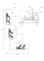
図17(a)は集合基板231の一方側の板面である第1板面268を示す平面図であり、図17(b)は第1板面268が谷形状(凹)となるように集合基板231を割る谷割りを説明するための説明図であり、図17(c)は第1板面268が山形状(凸)となるように集合基板231を割る山割りを説明するための説明図である。なお、実際には集合基板231に含まれている第1装飾基板56のそれぞれに複数の電子部品が実装されているとともに配線パターン等も形成されているが、図17(a)~図17(c)では図面の煩雑化を避けるために簡略化して図示してある。 Figure 17(a) is a plan view showing the first plate surface 268, which is the plate surface on one side of the collective substrate 231, Figure 17(b) is an explanatory diagram for explaining the valley splitting in which the collective substrate 231 is split so that the first plate surface 268 has a valley shape (concave), and Figure 17(c) is an explanatory diagram for explaining the mountain splitting in which the collective substrate 231 is split so that the first plate surface 268 has a mountain shape (convex). Note that, in reality, multiple electronic components are mounted on each of the first decorative substrates 56 included in the collective substrate 231, and wiring patterns and the like are also formed, but in Figures 17(a) to 17(c) they are illustrated in a simplified manner to avoid complicating the drawings.

集合基板231は、既に説明した装飾基板56,57と同様に、導電層と絶縁層とが交互に積層された構造を有する4層基板である。図17(a)に示すように、集合基板231は、略正方形に成形された1枚のプリント配線板の一部を、側面に刃の付いたドリル状の刃具(ルータ)を回転させながら加工するルータ加工等によって切り抜くとともに当該プリント配線板に分割溝232~247及びスリット251~258を形成することにより作成される。 The collective board 231 is a four-layer board with a structure in which conductive layers and insulating layers are alternately stacked, similar to the decorative boards 56 and 57 already described. As shown in FIG. 17(a), the collective board 231 is created by cutting out a portion of a printed wiring board formed into an approximately square shape by a router process in which a drill-shaped cutting tool (router) with a blade on the side is rotated while processing, and by forming dividing grooves 232-247 and slits 251-258 in the printed wiring board.

集合基板231は、分割溝232~247及びスリット251~258によって4つの第1装飾基板56と、7つの捨て基板261~267とに区画されている。集合基板231に分割溝232~247及びスリット251~258を形成する加工は、集合基板231に電子部品が搭載される前に行われる。集合基板231の分割は、分割溝232~247及びスリット251~258を利用して行われる。 The collective substrate 231 is divided into four first decorative substrates 56 and seven waste substrates 261-267 by the dividing grooves 232-247 and the slits 251-258. The process of forming the dividing grooves 232-247 and the slits 251-258 in the collective substrate 231 is carried out before electronic components are mounted on the collective substrate 231. The collective substrate 231 is divided using the dividing grooves 232-247 and the slits 251-258.

分割溝232~247は、例えば高速で回転する円盤状の刃を用いて集合基板231が切削加工されることにより直線状に形成されている。分割溝232~247は、その断面が集合基板231の板厚を減少させるV字形になっており、分割溝232~247の底部は最も板厚が小さい部分となっている。集合基板231において分割溝232~247が形成されている領域は、分割溝232~247が形成されていない領域と比較して、機械的強度が低くなっている。このため、分割溝232~247を基点として集合基板231を分割することにより、集合基板231を分割する際に第1装飾基板56に作用する応力を低減することができる。これにより、集合基板231を分割する際に小型チップ部品(バイパスコンデンサ85及び小型チップ抵抗器87,143~149)と第1装飾基板56との接続箇所に作用し得る応力を低減することができるとともに、小型チップ部品自体に作用し得る応力を低減することができる。また、分割の基点が分割溝232~247からずれてしまうことを防止できる。なお、分割溝232~247の断面形状はV字形に限定されることはない。分割溝232~247の断面形状は、外力で集合基板231を容易に切り離し可能とする形状であれば、矩形であってもよく、U字形であってもよい。 The dividing grooves 232-247 are formed in a straight line by cutting the collective substrate 231 using, for example, a disk-shaped blade rotating at high speed. The dividing grooves 232-247 have a V-shaped cross section that reduces the thickness of the collective substrate 231, and the bottoms of the dividing grooves 232-247 are the parts with the thinnest thickness. The area of the collective substrate 231 where the dividing grooves 232-247 are formed has a lower mechanical strength than the area where the dividing grooves 232-247 are not formed. Therefore, by dividing the collective substrate 231 using the dividing grooves 232-247 as base points, the stress acting on the first decorative substrate 56 when dividing the collective substrate 231 can be reduced. This makes it possible to reduce the stress that may act on the connection points between the small chip components (bypass capacitors 85 and small chip resistors 87, 143-149) and the first decorative substrate 56 when dividing the collective substrate 231, and also to reduce the stress that may act on the small chip components themselves. It is also possible to prevent the base point of division from shifting from the division grooves 232 to 247. The cross-sectional shape of the division grooves 232 to 247 is not limited to a V-shape. The cross-sectional shape of the division grooves 232 to 247 may be rectangular or U-shaped as long as it allows the collective substrate 231 to be easily separated by an external force.

分割溝232~247が直線状に形成されていることにより、分割溝232~247が曲線状に形成されている構成と比較して、集合基板231の分割の際に第1装飾基板56に作用し得る応力が低減されている。 By forming the dividing grooves 232-247 in a straight line, the stress that may act on the first decorative substrate 56 when the assembly substrate 231 is divided is reduced compared to a configuration in which the dividing grooves 232-247 are formed in a curved line.

本実施形態において、分割溝232~247は、第1板面268と、当該第1板面268とは逆側の板面である第2板面269(図17(b))とを見分け易くして基板分割工程の作業性を向上させるために、集合基板231の第1板面268側のみに形成されている。スリット251~258は、例えば上述したルータ加工によって形成されている。スリット251~258は、細長い長孔状であり、分割溝232~247よりも幅広に形成されている。 In this embodiment, the dividing grooves 232-247 are formed only on the first plate surface 268 side of the collective substrate 231 in order to make it easier to distinguish between the first plate surface 268 and the second plate surface 269 (FIG. 17(b)), which is the plate surface opposite the first plate surface 268, and to improve the workability of the substrate dividing process. The slits 251-258 are formed, for example, by the router processing described above. The slits 251-258 are elongated long holes, and are formed wider than the dividing grooves 232-247.

図17(a)に示すように、集合基板231の左右方向中央には縦長略矩形の中央捨て基板261が設けられている。分割溝232,233を挟んで中央捨て基板261の左側には一対の第1装飾基板56が設けられているとともに、分割溝234,235を挟んで中央捨て基板261の右側には一対の第1装飾基板56が設けられている。4つの第1装飾基板56は面一であり、これらの第1装飾基板56の第1実装面84は集合基板231の第1板面268側に存在している。 As shown in FIG. 17(a), a vertically elongated, generally rectangular central discarded substrate 261 is provided in the center of the collective substrate 231 in the left-right direction. A pair of first decorative substrates 56 are provided on the left side of the central discarded substrate 261 across the dividing grooves 232, 233, and a pair of first decorative substrates 56 are provided on the right side of the central discarded substrate 261 across the dividing grooves 234, 235. The four first decorative substrates 56 are flush, and the first mounting surfaces 84 of these first decorative substrates 56 are present on the first plate surface 268 side of the collective substrate 231.

既に説明したとおり、第1装飾基板56には階段状凹部56a及び切欠部56bが形成されている。左下の第1装飾基板56において、階段状凹部56aは中央捨て基板261側に設けられているとともに、切欠部56bは後述する左側捨て基板263側に設けられている。左上の第1装飾基板56において、階段状凹部56aは左側捨て基板263側に設けられているとともに、切欠部56bは中央捨て基板261側に設けられている。一対の第1装飾基板56の階段状凹部56aは対向している。これらの階段状凹部56aの間は切り抜かれており、階段状凹部56a同士は連結されていない。 As already explained, the first decorative substrate 56 has a stepped recess 56a and a cutout 56b. In the lower left first decorative substrate 56, the stepped recess 56a is provided on the side of the central discarded substrate 261, and the cutout 56b is provided on the side of the left discarded substrate 263, which will be described later. In the upper left first decorative substrate 56, the stepped recess 56a is provided on the side of the left discarded substrate 263, and the cutout 56b is provided on the side of the central discarded substrate 261. The stepped recesses 56a of the pair of first decorative substrates 56 face each other. The space between these stepped recesses 56a is cut out, and the stepped recesses 56a are not connected to each other.

右下の第1装飾基板56において、階段状凹部56aは後述する右側捨て基板266側に設けられているとともに、切欠部56bは中央捨て基板261側に設けられている。右上の第1装飾基板56において、階段状凹部56aは中央捨て基板261側に設けられているとともに、切欠部56bは右側捨て基板266側に設けられている。一対の第1装飾基板56の階段状凹部56aは対向している。これらの階段状凹部56aの間は切り抜かれており、階段状凹部56a同士は連結されていない。 In the first decorative substrate 56 at the bottom right, the stepped recess 56a is provided on the side of the right-side discarded substrate 266 described below, and the cutout 56b is provided on the side of the central discarded substrate 261. In the first decorative substrate 56 at the top right, the stepped recess 56a is provided on the side of the central discarded substrate 261, and the cutout 56b is provided on the side of the right-side discarded substrate 266. The stepped recesses 56a of the pair of first decorative substrates 56 face each other. The space between these stepped recesses 56a is cut out, and the stepped recesses 56a are not connected to each other.

中央捨て基板261の左側において、一対の第1装飾基板56の下側、左側及び上側には、左下捨て基板262、縦長略矩形の左側捨て基板263及び左上捨て基板264が設けられている。左下捨て基板262は、分割溝236,237を介して左側捨て基板263及び中央捨て基板261と連結されているとともに、左上捨て基板264は、分割溝238,239を介して左側捨て基板263及び中央捨て基板261と連結されている。左下捨て基板262と左上の第1装飾基板56との間にはスリット251が形成されており、左下捨て基板262及び左上の第1装飾基板56は連結されていない。また、左上捨て基板264と右上の第1装飾基板56との間にはスリット252が形成されており、左上捨て基板264及び右上の第1装飾基板56は連結されていない。左側捨て基板263は、分割溝240,241を介して左下の第1装飾基板56及び左上の第1装飾基板56と連結されている。 On the left side of the central discarded board 261, the lower left discarded board 262, the vertically elongated, approximately rectangular left discarded board 263, and the upper left discarded board 264 are provided on the lower, left, and upper sides of the pair of first decorative boards 56. The lower left discarded board 262 is connected to the left discarded board 263 and the central discarded board 261 via the dividing grooves 236 and 237, and the upper left discarded board 264 is connected to the left discarded board 263 and the central discarded board 261 via the dividing grooves 238 and 239. A slit 251 is formed between the lower left discarded board 262 and the upper left first decorative board 56, and the lower left discarded board 262 and the upper left first decorative board 56 are not connected. In addition, a slit 252 is formed between the upper left discarded board 264 and the upper right first decorative board 56, and the upper left discarded board 264 and the upper right first decorative board 56 are not connected. The left-side discarded substrate 263 is connected to the lower left first decorative substrate 56 and the upper left first decorative substrate 56 via the dividing grooves 240 and 241.

中央捨て基板261の右側において、一対の第1装飾基板56の下側、右側及び上側には、右下捨て基板265、縦長略矩形の右側捨て基板266及び右上捨て基板267が設けられている。右下捨て基板265は、分割溝242,243を介して中央捨て基板261及び右側捨て基板266と連結されているとともに、右上捨て基板267は、分割溝244、245を介して中央捨て基板261及び右側捨て基板266と連結されている。右下捨て基板265と左下の第1装飾基板56との間にはスリット253が形成されており、右下捨て基板265及び左下の第1装飾基板56は連結されていない。また、右上捨て基板267と右下の第1装飾基板56との間にはスリット254が形成されており、右上捨て基板267及び右下の第1装飾基板56は連結されていない。右側捨て基板266は、分割溝246,247を介して左下の第1装飾基板56及び右下の第1装飾基板56と連結されている。 On the right side of the central discarded board 261, a lower right discarded board 265, a vertically elongated, approximately rectangular right discarded board 266, and an upper right discarded board 267 are provided on the lower, right, and upper sides of the pair of first decorative boards 56. The lower right discarded board 265 is connected to the central discarded board 261 and the right right discarded board 266 via the dividing grooves 242 and 243, and the upper right discarded board 267 is connected to the central discarded board 261 and the right right discarded board 266 via the dividing grooves 244 and 245. A slit 253 is formed between the lower right discarded board 265 and the lower left first decorative board 56, and the lower right discarded board 265 and the lower left first decorative board 56 are not connected. In addition, a slit 254 is formed between the upper right discarded board 267 and the lower right first decorative board 56, and the upper right discarded board 267 and the lower right first decorative board 56 are not connected. The right-side discarded substrate 266 is connected to the lower-left first decorative substrate 56 and the lower-right first decorative substrate 56 via the dividing grooves 246 and 247.

このように、集合基板231の外周には全周に亘って捨て基板262~267が設けられており、4つの第1装飾基板56は捨て基板262~267によって囲われている。これにより、電子部品搭載後に第1装飾基板56に搭載されている電子部品に触れずに集合基板231を取り扱うことが可能となっている。よって、作業者の手が電子部品に接触するなどして電子部品が破損してしまうことが防止されている。なお、集合基板231に含まれる第1装飾基板56の数は「4」に限定されることはない。集合基板231に含まれている第1装飾基板56の数が「4」よりも多い構成(例えば「6」)としてもよく、集合基板231に含まれている第1装飾基板56の数が「4」よりも少ない構成(例えば「2」)としてもよい。 In this way, the discarded boards 262-267 are provided around the entire outer periphery of the collective substrate 231, and the four first decorative substrates 56 are surrounded by the discarded boards 262-267. This makes it possible to handle the collective substrate 231 after mounting the electronic components without touching the electronic components mounted on the first decorative substrate 56. This prevents the electronic components from being damaged by the worker's hands touching the electronic components. The number of first decorative substrates 56 included in the collective substrate 231 is not limited to "4". The number of first decorative substrates 56 included in the collective substrate 231 may be more than "4" (for example, "6"), or the number of first decorative substrates 56 included in the collective substrate 231 may be less than "4" (for example, "2").

中央捨て基板261の左側に階段状凹部56aを対向させて一対の第1装飾基板56が設けられているとともに、中央捨て基板261の右側に階段状凹部56aを対向させて一対の第1装飾基板56が設けられていることにより、4つの第1装飾基板56を含む集合基板231の上下方向の寸法が低減されている。 A pair of first decorative substrates 56 are provided on the left side of the central discarded substrate 261 with their stepped recesses 56a facing each other, and a pair of first decorative substrates 56 are provided on the right side of the central discarded substrate 261 with their stepped recesses 56a facing each other, thereby reducing the vertical dimension of the aggregate substrate 231 including the four first decorative substrates 56.

次に、装飾基板56,57の製造工程について、第1装飾基板56の製造工程を例に挙げて説明する。 Next, the manufacturing process for the decorative substrates 56 and 57 will be explained using the manufacturing process for the first decorative substrate 56 as an example.

第1装飾基板56の製造工程では、まず集合基板231の第2板面269(第2実装面95側、図17(b)参照)が上を向いている状態で、集合基板231の第2板面269に設けられたパッド(又はパット)に半田ペーストを塗布する半田塗布工程、コネクタ固定用の接着剤を塗布する接着剤塗布工程、自動搭載装置(図示略)を用いてコネクタ111,112(図8(a))を集合基板231の第2板面269側に搭載する部品搭載工程、集合基板231をリフロー炉に搬送して加熱するリフロー工程、及び集合基板231を常温まで冷却する冷却工程が行われる。これにより、集合基板231の第2板面269側にコネクタ111,112が実装される。接着剤が硬化することにより2回目のリフロー工程においてコネクタ111,112の落下が防止される。 In the manufacturing process of the first decorative board 56, first, with the second board surface 269 (second mounting surface 95 side, see FIG. 17(b)) of the collective board 231 facing up, a solder application process is performed to apply solder paste to the pads (or pads) provided on the second board surface 269 of the collective board 231, an adhesive application process is performed to apply an adhesive for fixing the connectors, a component mounting process is performed to mount the connectors 111, 112 (FIG. 8(a)) on the second board surface 269 side of the collective board 231 using an automatic mounting device (not shown), a reflow process is performed to transport the collective board 231 to a reflow furnace and heat it, and a cooling process is performed to cool the collective board 231 to room temperature. As a result, the connectors 111, 112 are mounted on the second board surface 269 side of the collective board 231. The adhesive hardens to prevent the connectors 111, 112 from falling off during the second reflow process.

その後、集合基板231の第1板面268が上を向いている状態として、集合基板231の第1板面268側(第1実装面84側)に設けられたランドの上に半田ペーストを塗布する半田塗布工程、自動搭載装置(図示略)を用いて小型チップ部品を含む電子部品を集合基板231の第1板面268側に搭載する部品搭載工程、集合基板231をリフロー炉に搬送して加熱するリフロー工程、集合基板231を常温まで冷却する冷却工程、電子部品実装後の集合基板231を分割する基板分割工程、及び第1装飾基板56について電子部品の実装漏れが無いかを目視で確認する実装確認工程等が行われる。これにより、集合基板231の第1板面268側に小型チップ部品を含む電子部品が実装される。 After that, with the first surface 268 of the collective substrate 231 facing upward, a solder application process is performed in which solder paste is applied onto the lands provided on the first surface 268 side (first mounting surface 84 side) of the collective substrate 231, a component mounting process is performed in which electronic components including small chip components are mounted on the first surface 268 side of the collective substrate 231 using an automatic mounting device (not shown), a reflow process is performed in which the collective substrate 231 is transported to a reflow furnace and heated, a cooling process is performed in which the collective substrate 231 is cooled to room temperature, a substrate division process is performed in which the collective substrate 231 is divided after the electronic components are mounted, and a mounting confirmation process is performed in which the first decorative substrate 56 is visually checked for any missing electronic components. As a result, electronic components including small chip components are mounted on the first surface 268 side of the collective substrate 231.

図17(a)に示すように、左側捨て基板263及び右側捨て基板266には、集合基板231を厚さ方向に貫通させて、第1搭載基準孔271及び第2搭載基準孔272が形成されている。第1搭載基準孔271は、電子部品を第1板面268側に搭載する部品搭載工程において、集合基板231の位置合わせに利用されるとともに、第2搭載基準孔272は、電子部品を第2板面269側に搭載する部品搭載工程において、集合基板231の位置合わせに利用される。自動搭載装置は、集合基板231の位置合わせを行った後、座標制御により小型チップ部品の電極が対応するパッド(又はパット)に塗布された半田ペーストの上に載るように当該小型チップ部品を第1装飾基板56上にセットする。 As shown in FIG. 17(a), the left-side discarded board 263 and the right-side discarded board 266 have a first mounting reference hole 271 and a second mounting reference hole 272 formed through the thickness of the collective board 231. The first mounting reference hole 271 is used to align the collective board 231 in the component mounting process in which electronic components are mounted on the first board surface 268 side, and the second mounting reference hole 272 is used to align the collective board 231 in the component mounting process in which electronic components are mounted on the second board surface 269 side. After aligning the collective board 231, the automatic mounting device uses coordinate control to set the small chip components on the first decorative board 56 so that the electrodes of the small chip components are placed on the solder paste applied to the corresponding pads (or pads).

集合基板231の分割方法としては、作業者が手作業により集合基板231を割る方法及びプレス機等を用いて機械的に集合基板231を切断する方法が知られている。このうち、手作業による分割方法を採用することにより、設備費用を抑えながら複数種類の集合基板に臨機応変に対応することが可能となる。 Known methods for dividing the collective substrate 231 include a method in which an operator manually divides the collective substrate 231, and a method in which the collective substrate 231 is mechanically cut using a press or the like. Of these, by adopting the manual division method, it becomes possible to flexibly handle multiple types of collective substrates while keeping equipment costs down.

集合基板231の割り方として、分割溝232~247を基点として小型チップ部品が集約されている第1板面268が谷形状(凹)となるように集合基板231を割る谷割りと、当該第1板面268が山形状(凸)となるように集合基板231を割る山割りと、が考えられる。基板分割工程では、図17(b)に示すように、分割溝232~247を基点として第1板面268を谷形状(凹)とする谷割りで集合基板231が分割されて複数枚(具体的には4枚)の第1装飾基板56が取り出される。 Possible methods of dividing the collective substrate 231 include valley division, in which the collective substrate 231 is divided so that the first plate surface 268 on which the small chip components are concentrated has a valley shape (concave) using the dividing grooves 232-247 as base points, and mountain division, in which the collective substrate 231 is divided so that the first plate surface 268 has a mountain shape (convex). In the substrate dividing process, as shown in FIG. 17(b), the collective substrate 231 is divided by valley division, using the dividing grooves 232-247 as base points to make the first plate surface 268 have a valley shape (concave), and multiple first decorative substrates 56 (specifically, four) are taken out.

既に説明したとおり、第1装飾基板56において小型チップ部品(バイパスコンデンサ85及び小型チップ抵抗器87,143~149)は、第1実装面84側に集約されている。集合基板231において小型チップ部品は、第1板面268側(第1実装面84側)に集約されており、第2板面269側(第2実装面95側)には実装されていない。また、既に説明したとおり、小型チップ部品と第1装飾基板56との接続箇所は、他の電子部品と第1装飾基板56との接続箇所よりも機械的強度が低い。図17(c)に示すように集合基板231を山割りする場合、集合基板231の第1板面268側(第1実装面84側)に作用し得る力は引張り応力となるとともに、第2板面269側(第2実装面95側)に作用し得る力は圧縮応力となる。一方、図17(b)に示すように集合基板231を谷割りする場合、集合基板231の第1板面268側(第1実装面84側)に作用し得る力は圧縮応力となるとともに、第2板面269側(第2実装面95側)に作用し得る力は引張り応力となる。 As already explained, in the first decorative board 56, the small chip components (bypass capacitor 85 and small chip resistors 87, 143 to 149) are concentrated on the first mounting surface 84 side. In the collective board 231, the small chip components are concentrated on the first board surface 268 side (first mounting surface 84 side) and are not mounted on the second board surface 269 side (second mounting surface 95 side). Also, as already explained, the connection points between the small chip components and the first decorative board 56 have lower mechanical strength than the connection points between other electronic components and the first decorative board 56. When the collective board 231 is split as shown in FIG. 17(c), the force that can act on the first board surface 268 side (first mounting surface 84 side) of the collective board 231 becomes a tensile stress, and the force that can act on the second board surface 269 side (second mounting surface 95 side) becomes a compressive stress. On the other hand, when the collective substrate 231 is split into valleys as shown in FIG. 17(b), the force that can act on the first plate surface 268 side (first mounting surface 84 side) of the collective substrate 231 is a compressive stress, and the force that can act on the second plate surface 269 side (second mounting surface 95 side) is a tensile stress.

集合基板231を分割する際の応力は、谷形状(凹)となる板面よりも山形状(凸)となる板面に対して大きく作用する。小型チップ部品が集約されている第1板面268側(第1実装面84側)が谷形状(凹)となるように集合基板231を谷割りすることにより、集合基板231の分割に際して小型チップ部品と第1装飾基板56との接続箇所に作用し得る応力を低減することができるとともに、小型チップ部品自体に作用し得る応力を低減することができる。これにより、小型チップ部品と第1装飾基板56との接続箇所が破損してしまう可能性を低減できるとともに、小型チップ部品自体が破損してしまう可能性を低減できる。このように、基板分割工程において小型チップ部品の接触不良が発生する可能性を低減することにより、第1装飾基板56の製造効率を向上させることができる。 The stress when dividing the collective substrate 231 acts more strongly on the plate surface that is mountain-shaped (convex) than on the plate surface that is valley-shaped (concave). By dividing the collective substrate 231 into valleys so that the first plate surface 268 side (first mounting surface 84 side) on which the small chip components are concentrated is valley-shaped (concave), it is possible to reduce the stress that may act on the connection points between the small chip components and the first decorative substrate 56 when dividing the collective substrate 231, and to reduce the stress that may act on the small chip components themselves. This reduces the possibility that the connection points between the small chip components and the first decorative substrate 56 will be damaged, and also reduces the possibility that the small chip components themselves will be damaged. In this way, the manufacturing efficiency of the first decorative substrate 56 can be improved by reducing the possibility of poor contact of the small chip components occurring in the substrate division process.

小型チップ部品のうちバイパスコンデンサ85として使用されている積層セラミックコンデンサは、引張り応力に弱く、バイパスコンデンサ85に引張り応力が作用した場合にはバイパスコンデンサ85自体にクラックが生じ易い。バイパスコンデンサ85を含む小型チップ部品が集約されている第1板面268側(第1実装面84側)が谷形状(凹)となるように集合基板231を谷割りすることにより、バイパスコンデンサ85に作用し得る力を圧縮応力として、バイパスコンデンサ85に引張り応力が作用することを回避できる。これにより、集合基板231の分割に際してバイパスコンデンサ85自体が破損してしまう可能性を低減できる。 Among the small chip components, the multilayer ceramic capacitors used as the bypass capacitors 85 are vulnerable to tensile stress, and when tensile stress acts on the bypass capacitors 85, the bypass capacitors 85 themselves are prone to cracking. By dividing the collective substrate 231 into valleys so that the first plate surface 268 side (first mounting surface 84 side) on which the small chip components including the bypass capacitors 85 are concentrated has a valley shape (concave), the force that may act on the bypass capacitors 85 is treated as a compressive stress, and it is possible to prevent tensile stress from acting on the bypass capacitors 85. This reduces the possibility that the bypass capacitors 85 themselves will be damaged when the collective substrate 231 is divided.

既に説明したとおり、分割溝232~247を基点として集合基板231を分割することにより、小型チップ部品と第1装飾基板56との接続箇所に作用し得る応力を最小限に抑えることができるとともに、小型チップ部品に作用し得る応力を最小限に抑えることができる。一方、分割の基点が分割溝232~247からずれてしまうと、これらの応力が増大してしまう。分割の基点が分割溝232~247からずれてしまうことを防止するとともに基板分割工程の作業性を向上させるために、分割治具が用いられる。 As already explained, by dividing the assembly substrate 231 using the dividing grooves 232-247 as base points, it is possible to minimize the stress that may act on the connection points between the small chip components and the first decorative substrate 56, and also to minimize the stress that may act on the small chip components. On the other hand, if the dividing base points deviate from the dividing grooves 232-247, these stresses will increase. A dividing jig is used to prevent the dividing base points from deviating from the dividing grooves 232-247 and to improve the workability of the substrate dividing process.

図18(a)は本実施形態における集合基板231の分割に使用される分割治具281の斜視図であり、図18(b)は分割治具281の正面図であり、図18(c)は分割治具281を用いて集合基板231を分割する様子を説明するための説明図である。図18(a)に示すように、分割治具281は、分割溝232~247に当接されて集合基板231を分割する際に支点となる金属製の薄刃282と、当該薄刃282を支持する基部283と、を備えている。基部283は、横長直方体状に成形された樹脂製の基台部283aと、基台部283aの一方側の板面から起立させて一体形成されている直方体状の起立部283bと、を備えている。 Figure 18(a) is a perspective view of a dividing jig 281 used to divide the collective substrate 231 in this embodiment, Figure 18(b) is a front view of the dividing jig 281, and Figure 18(c) is an explanatory diagram for explaining how the collective substrate 231 is divided using the dividing jig 281. As shown in Figure 18(a), the dividing jig 281 is equipped with a thin metal blade 282 that abuts against the dividing grooves 232 to 247 and serves as a fulcrum when dividing the collective substrate 231, and a base 283 that supports the thin blade 282. The base 283 is equipped with a resin base portion 283a molded in a horizontally elongated rectangular parallelepiped shape, and a rectangular parallelepiped upright portion 283b that is integrally formed by standing up from the plate surface on one side of the base portion 283a.

薄刃282は、プレート状の刃部282aと、フランジ部282bとを備えている。薄刃282は、フランジ部282bが起立部283bにネジ固定されることにより基部283に固定されている。刃部282aは、起立部283bの上側平面から上方に突出しており、起立部283bの長手方向に延在している。 The thin blade 282 has a plate-shaped blade portion 282a and a flange portion 282b. The thin blade 282 is fixed to the base portion 283 by screwing the flange portion 282b to the standing portion 283b. The blade portion 282a protrudes upward from the upper flat surface of the standing portion 283b and extends in the longitudinal direction of the standing portion 283b.

起立部283bの長手方向における略中央には、刃部282aが分割溝232~247に当接するように、刃部282aに対する集合基板231の位置合わせを補助するための突起部283cが一体形成されている。突起部283cは、起立部283bの上側平面から上方に、刃部282aよりも大きな突出寸法で突出している。図17(a)に示すように、左側捨て基板263の右部及び中央捨て基板261の左部において、一対の第1装飾基板56の間には突起部283cを挿通可能とする凹部284,285が設けられている。また、中央捨て基板261の右部及び右側捨て基板266の左部において、一対の第1装飾基板56の間には突起部283cを挿通可能とする凹部286,287が設けられている。 A protrusion 283c is integrally formed at approximately the center of the length of the standing portion 283b to assist in aligning the assembly substrate 231 with the blade portion 282a so that the blade portion 282a abuts against the dividing grooves 232 to 247. The protrusion 283c protrudes upward from the upper flat surface of the standing portion 283b with a protrusion dimension greater than that of the blade portion 282a. As shown in FIG. 17(a), recesses 284 and 285 are provided between the pair of first decorative substrates 56 on the right side of the left discarded substrate 263 and the left side of the central discarded substrate 261, allowing the protrusion 283c to be inserted. In addition, recesses 286 and 287 are provided between the pair of first decorative substrates 56 on the right side of the central discarded substrate 261 and the left side of the right discarded substrate 266, allowing the protrusion 283c to be inserted.

作業者は、図18(c)に示すように、集合基板231の第1板面268(第1実装面84)を下に向け、中央捨て基板261、左側捨て基板263及び右側捨て基板266のいずれか(図18(c)では中央捨て基板261)を起立部283bの上に固定する。このとき、突起部283cを捨て基板261,263,266に設けられた凹部284~287(図17(a))に挿通することにより分割の基点とする分割溝232~247が刃部282aに当接している状態を容易に作り出すことができる。当該状態において、第2板面269側に下向きの力を加えて起立部283bから右方にはみ出している部分を下方に押し込むことにより、第1板面268が谷形状(凹)となる態様で、分割溝232~247を基点として集合基板231を谷割りすることができる。 As shown in FIG. 18(c), the worker faces the first plate surface 268 (first mounting surface 84) of the collective board 231 downward, and fixes one of the central discarded board 261, the left discarded board 263, and the right discarded board 266 (central discarded board 261 in FIG. 18(c)) on the upright portion 283b. At this time, by inserting the protrusion 283c into the recesses 284-287 (FIG. 17(a)) provided on the discarded boards 261, 263, and 266, it is possible to easily create a state in which the dividing grooves 232-247, which are the base points of division, are in contact with the blade portion 282a. In this state, by applying a downward force to the second plate surface 269 side and pushing the part protruding to the right from the upright portion 283b downward, the collective board 231 can be divided into valleys with the dividing grooves 232-247 as the base points, with the first plate surface 268 becoming valley-shaped (concave).

作業者は、例えば、まず集合基板231(図17(a))を、左側の一対の第1装飾基板56、左下捨て基板262、左側捨て基板263及び左上捨て基板264を含む第1ユニットと、右側の一対の第1装飾基板56、中央捨て基板261、右下捨て基板265、右側捨て基板266及び右上捨て基板267を含む第2ユニットと、に分割する。その後、第1ユニットにおいて、一対の第1装飾基板56と左側捨て基板263とを分割することにより2枚の第1装飾基板56を取り出すことができる。また、第2ユニットにおいて、一対の第1装飾基板56と中央捨て基板261とを分割するとともに、当該一対の第1装飾基板56と右側捨て基板266とを分割することにより、2枚の第1装飾基板56を取り出すことができる。なお、4つの第1装飾基板56を取り出すために集合基板231を分割する順番は任意である。 For example, the worker first divides the collective board 231 (FIG. 17(a)) into a first unit including a pair of first decorative boards 56 on the left side, a lower left discard board 262, a left discard board 263, and an upper left discard board 264, and a second unit including a pair of first decorative boards 56 on the right side, a central discard board 261, a lower right discard board 265, a right discard board 266, and an upper right discard board 267. After that, in the first unit, the pair of first decorative boards 56 and the left discard board 263 can be divided to take out two first decorative boards 56. In addition, in the second unit, the pair of first decorative boards 56 and the central discard board 261 can be divided, and the pair of first decorative boards 56 and the right discard board 266 can be divided to take out two first decorative boards 56. The order in which the collective board 231 is divided to take out the four first decorative boards 56 is arbitrary.

分割の基点とする分割溝232~247に刃部282aを当接させた状態で、当該刃部282aを支点として集合基板231を谷割りすることにより、分割の基点が分割溝232~247からずれてしまうことを防止できる。これにより、集合基板231の分割に際して小型チップ部品と第1装飾基板56との接続箇所に作用し得る応力を最小限に抑えることができるとともに、小型チップ部品自体に作用し得る応力を最小限に抑えることができる。 By dividing the aggregate substrate 231 into valleys using the blade portion 282a as a fulcrum while the blade portion 282a is in contact with the dividing grooves 232 to 247 that serve as the base points for division, it is possible to prevent the base points for division from shifting from the dividing grooves 232 to 247. This makes it possible to minimize stress that may act on the connection points between the small chip components and the first decorative substrate 56 when dividing the aggregate substrate 231, and also to minimize stress that may act on the small chip components themselves.

第2実装面95を下方に押し込むことで集合基板231を谷割りする構成であることにより、第2実装面95を上方に引き上げることで集合基板231を谷割りする構成と比較して、作業者が集合基板231を分割するための力をかけ易くなっている。また、中央捨て基板261、左側捨て基板263及び右側捨て基板266において、凹部284~287(図17(a))が一対の第1装飾基板56の間に設けられていることにより、第1装飾基板56に搭載されている電子部品に作用する応力が増大してしまうことを防止しながら、分割治具281に集合基板231を固定することが可能となっている。 By pushing the second mounting surface 95 downward to split the collective substrate 231 into valleys, it is easier for the worker to apply force to split the collective substrate 231 compared to a configuration in which the collective substrate 231 is split into valleys by pulling the second mounting surface 95 upward. In addition, in the central discarded substrate 261, the left discarded substrate 263, and the right discarded substrate 266, the recesses 284-287 (FIG. 17(a)) are provided between the pair of first decorative substrates 56, making it possible to fix the collective substrate 231 to the splitting jig 281 while preventing an increase in the stress acting on the electronic components mounted on the first decorative substrate 56.

図8(a)を参照しながら既に説明したとおり、第1装飾基板56には固定貫通孔56d~56gが設けられており、小型チップ部品は貫通孔周辺領域211a~211dを避けて配置されている。このため、図18(c)に示すように、第1板面268(第1実装面84)を下に向けて中央捨て基板261、左側捨て基板263及び右側捨て基板266のいずれかを起立部283bに固定した状態で第2板面269側に下向きの力を加えて起立部283bからはみ出している部分を下方に押し込んで集合基板231を分割する際に、下方に押し込む箇所として当該固定貫通孔56d~56g付近を選択することができる。これにより、第1板面268側(第1実装面84側)に実装されている小型チップ部品に作用し得る応力を最小限に抑えることができる。 As already explained with reference to FIG. 8(a), the first decorative board 56 is provided with the fixing through holes 56d-56g, and the small chip components are arranged avoiding the through hole peripheral areas 211a-211d. Therefore, as shown in FIG. 18(c), when the first board surface 268 (first mounting surface 84) is facing downward and any of the central waste board 261, the left side waste board 263, and the right side waste board 266 is fixed to the rising portion 283b, a downward force is applied to the second board surface 269 side to push the part protruding from the rising portion 283b downward to divide the collective board 231, the vicinity of the fixing through holes 56d-56g can be selected as the part to be pushed downward. This makes it possible to minimize the stress that may act on the small chip components mounted on the first board surface 268 side (first mounting surface 84 side).

既に説明したとおり、分割溝232~247は、集合基板231の第1板面268側のみに形成されており、第2板面269側には形成されていない。このため、作業者は、分割溝232~247が形成されている側の板面(第1板面268)を下向きにして集合基板231を分割治具281にセットすればよく、誤って集合基板231が山割りされてしまう可能性が低減されている。 As already explained, the dividing grooves 232-247 are formed only on the first plate surface 268 side of the collective substrate 231, and are not formed on the second plate surface 269 side. Therefore, the worker need only set the collective substrate 231 in the dividing jig 281 with the plate surface on which the dividing grooves 232-247 are formed (first plate surface 268) facing downward, reducing the possibility of the collective substrate 231 being accidentally divided into two.

図17(a)に示すように、集合基板231内に存在する16個の分割溝232~247は第1方向DR1に延在している。これらの分割溝232~247の延在方向は互いに平行である。また、図8(a)~図8(c)を参照しながら既に説明したとおり、小型チップ部品(バイパスコンデンサ85及び小型チップ抵抗器87,143~149(図11))は、当該小型チップ部品の長手方向が集合基板231内に存在する16個の分割溝232~247に平行となる態様で、第1装飾基板56に実装されている。このため、小型チップ部品の長手方向が分割溝232~247の延在方向に直交する構成と比較して、分割溝232~247を基点として集合基板231が分割される際に小型チップ部品と第1装飾基板56との接続箇所に作用し得る応力が低減されているとともに、小型チップ部品自体に作用し得る応力が低減されている。 As shown in FIG. 17(a), the 16 dividing grooves 232-247 in the collective substrate 231 extend in the first direction DR1. The extending directions of these dividing grooves 232-247 are parallel to each other. As already explained with reference to FIG. 8(a) to FIG. 8(c), the small chip components (bypass capacitor 85 and small chip resistors 87, 143-149 (FIG. 11)) are mounted on the first decorative substrate 56 in such a manner that the longitudinal direction of the small chip components is parallel to the 16 dividing grooves 232-247 in the collective substrate 231. Therefore, compared to a configuration in which the longitudinal direction of the small chip components is perpendicular to the extending direction of the dividing grooves 232-247, the stress that may act on the connection points between the small chip components and the first decorative substrate 56 when the collective substrate 231 is divided with the dividing grooves 232-247 as the base point is reduced, and the stress that may act on the small chip components themselves is reduced.

図17(a)に示すように、集合基板231において、バイパスコンデンサ85が搭載されている領域に対応する箇所にはスリット255~258が設けられている。既に説明したとおり、スリット255~258は、細長い長孔状であり、分割溝233,234,240,247よりも幅広に形成されている。分割溝232~247を基点として集合基板231が谷割りされる際にスリット255~258の周辺に作用し得る応力は、分割溝232~247の周辺に作用し得る応力よりも小さい。バイパスコンデンサ85の搭載領域の対応箇所にスリット255~258が設けられていることにより、集合基板231が分割される際にバイパスコンデンサ85と第1装飾基板56との接続箇所に作用し得る応力が低減されているとともに、バイパスコンデンサ85自体に作用し得る応力が低減されている。 As shown in FIG. 17(a), slits 255-258 are provided in the assembly board 231 at locations corresponding to the area where the bypass capacitor 85 is mounted. As already explained, the slits 255-258 are elongated holes, and are formed wider than the dividing grooves 233, 234, 240, and 247. When the assembly board 231 is divided into valleys using the dividing grooves 232-247 as base points, the stress that may act around the slits 255-258 is smaller than the stress that may act around the dividing grooves 232-247. By providing the slits 255-258 at locations corresponding to the mounting area of the bypass capacitor 85, the stress that may act on the connection points between the bypass capacitor 85 and the first decorative board 56 when the assembly board 231 is divided is reduced, and the stress that may act on the bypass capacitor 85 itself is reduced.

図8(a),(b)に示すように、バイパスコンデンサ85は、LEDドライバ126よりも階段状凹部56a側に配置されている。図17(a)を参照しながら既に説明したとおり、集合基板231において階段状凹部56a側には分割溝233,234,240,247は設けられていない。バイパスコンデンサ85がLEDドライバ126を挟んで分割溝233,234,240,247の逆側に配置されていることにより、分割溝233,234,240,247を基点として集合基板231が分割される際にバイパスコンデンサ85と第1装飾基板56との接続箇所に作用し得る応力を低減することができるとともに、バイパスコンデンサ85自体に作用し得る応力を低減することができる。これにより、集合基板231を分割する際に、バイパスコンデンサ85と第1装飾基板56との接続箇所が破壊されてしまう可能性が低減されているとともに、バイパスコンデンサ85自体が破壊される可能性が低減されている。 8(a) and (b), the bypass capacitor 85 is disposed on the step-like recess 56a side of the LED driver 126. As already explained with reference to FIG. 17(a), the dividing grooves 233, 234, 240, and 247 are not provided on the step-like recess 56a side of the collective substrate 231. By disposing the bypass capacitor 85 on the opposite side of the dividing grooves 233, 234, 240, and 247 across the LED driver 126, it is possible to reduce stress that may act on the connection between the bypass capacitor 85 and the first decorative substrate 56 when the collective substrate 231 is divided using the dividing grooves 233, 234, 240, and 247 as base points, and to reduce stress that may act on the bypass capacitor 85 itself. As a result, when the collective substrate 231 is divided, the possibility of the connection between the bypass capacitor 85 and the first decorative substrate 56 being destroyed is reduced, and the possibility of the bypass capacitor 85 itself being destroyed is reduced.

図8(b),(c)を参照しながら既に説明したとおり、バイパスコンデンサ85の電極85a,85bに対応するパッド171a,171bの離間方向、及び小型チップ抵抗器87の電極87a,87bに対応するパッド176a,176bの離間方向は、第1方向DR1である。リフロー工程において集合基板231を当該共通の離間方向(第1方向DR1)に直交する方向(第2方向DR2)又は略直交する方向に搬送することにより、バイパスコンデンサ85の一対の電極85a,85bに対応する一対のパッド171a,171bの上に塗布されている半田ペーストの加熱が開始されるタイミングを揃えることができるとともに、小型チップ抵抗器87の一対の電極87a,87bに対応する一対のパッド176a,176bの上に塗布されている半田ペーストの加熱が開始されるタイミングを揃えることができる。これにより、複数の小型チップ部品の回転及びチップ立ちの発生を防止することができる。図17(a)に示すように、左側捨て基板263の第1板面268側には、リフロー工程における集合基板231の搬送方向を確認可能とする認識マーク288が設けられている。また、図示は省略するが、左側捨て基板263の第2板面269側にも、リフロー工程における集合基板231の搬送方向を確認可能とする認識マークが設けられている。これにより、作業者が集合基板231の搬送方向を間違えてしまう可能性が低減されている。 8(b) and (c), the separation direction of the pads 171a, 171b corresponding to the electrodes 85a, 85b of the bypass capacitor 85 and the separation direction of the pads 176a, 176b corresponding to the electrodes 87a, 87b of the small chip resistor 87 are the first direction DR1. In the reflow process, by transporting the assembly board 231 in a direction perpendicular to the common separation direction (first direction DR1) or in a direction substantially perpendicular to the common separation direction (second direction DR2), the timing at which the heating of the solder paste applied on the pair of pads 171a, 171b corresponding to the pair of electrodes 85a, 85b of the bypass capacitor 85 is started can be synchronized, and the timing at which the heating of the solder paste applied on the pair of pads 176a, 176b corresponding to the pair of electrodes 87a, 87b of the small chip resistor 87 is started can be synchronized. This makes it possible to prevent the rotation of multiple small chip components and the occurrence of chip standing. As shown in FIG. 17A, a recognition mark 288 is provided on the first plate surface 268 of the left-side throwaway board 263, allowing the transport direction of the collective board 231 in the reflow process to be confirmed. Although not shown, a recognition mark is also provided on the second plate surface 269 of the left-side throwaway board 263, allowing the transport direction of the collective board 231 in the reflow process to be confirmed. This reduces the possibility that the worker will make a mistake in the transport direction of the collective board 231.

図8(a)を参照しながら既に説明したとおり、LEDドライバ126が第1装飾基板56の外縁から10mm未満の領域を含む領域に配置されている構成において、小型チップ部品(バイパスコンデンサ85及び小型チップ抵抗器87,143~149(図11))は第1装飾基板56の外縁から10mm以上離して配置されている。既に説明したとおり、第1装飾基板56に実装されている各種電子部品のうち小型チップ部品と第1装飾基板56との接続箇所は、他の電子部品と第1装飾基板56との接続箇所と比較して、機械的強度が低い。また、第1装飾基板56の外縁から10mm以内の領域は、集合基板231(図17)において分割溝232~247(図17)の近傍に存在している可能性のある領域であるとともに、集合基板231を谷割りするために力が加えられる可能性のある領域である。第1装飾基板56の外縁から10mm以上離して小型チップ部品が配置されていることにより、集合基板231の分割に際して小型チップ部品と第1装飾基板56との接続箇所に作用し得る応力の最大値が低減されているとともに、小型チップ部品自体に作用し得る応力の最大値が低減されている。 As already explained with reference to FIG. 8(a), in a configuration in which the
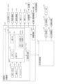
 LED driver 126 is arranged in an area including an area less than 10 mm from the outer edge of the first decorative substrate 56, the small chip components (bypass capacitor 85 and small chip resistors 87, 143-149 (FIG. 11)) are arranged 10 mm or more away from the outer edge of the first decorative substrate 56. As already explained, the connection points between the small chip components among the various electronic components mounted on the first decorative substrate 56 and the first decorative substrate 56 have lower mechanical strength than the connection points between the other electronic components and the first decorative substrate 56. In addition, the area within 10 mm from the outer edge of the first decorative substrate 56 is an area that may be present in the vicinity of the dividing grooves 232-247 (FIG. 17) in the collective substrate 231 (FIG. 17), and is also an area where force may be applied to split the collective substrate 231 into valleys. By arranging the small chip components at least 10 mm away from the outer edge of the first decorative substrate 56, the maximum value of the stress that can act on the connection points between the small chip components and the first decorative substrate 56 when the collective substrate 231 is divided is reduced, and the maximum value of the stress that can act on the small chip components themselves is also reduced.

<パチンコ機10の電気的構成>
図19は、パチンコ機10の電気的構成を示すブロック図である。
<Electrical configuration of the pachinko machine 10>
FIG. 19 is a block diagram showing the electrical configuration of the pachinko machine 10.

主制御装置60は、遊技の主たる制御を司る主制御基板61と、電源を監視する停電監視基板67と、を具備している。主制御基板61には、MPU62が搭載されている。MPU62には、制御部及び演算部を含む演算処理装置である主側CPU63の他に、主側ROM64及び主側RAM65が内蔵されている。なお、MPU62には、上記素子以外に、割込回路、タイマ回路、データ入出力回路、乱数発生器としての各種カウンタ回路などが内蔵されている。 The main control device 60 comprises a main control board 61 which is responsible for the main control of the game, and a power failure monitoring board 67 which monitors the power supply. The main control board 61 is equipped with an MPU 62. The MPU 62 contains a main CPU 63, which is an arithmetic processing device including a control unit and an arithmetic unit, as well as a main ROM 64 and a main RAM 65. In addition to the above elements, the MPU 62 also contains an interrupt circuit, a timer circuit, a data input/output circuit, various counter circuits as random number generators, and the like.

主側ROM64は、NOR型フラッシュメモリ及びNAND型フラッシュメモリなどの記憶保持に外部からの電力供給が不要なメモリ(すなわち、不揮発性記憶手段)であり、読み出し専用として利用される。主側ROM64は、主側CPU63により実行される各種の制御プログラムや固定値データを記憶している。 The main ROM 64 is a memory (i.e., a non-volatile memory means) that does not require an external power supply to retain memory, such as a NOR flash memory or a NAND flash memory, and is used for read-only purposes. The main ROM 64 stores various control programs and fixed value data executed by the main CPU 63.

主側RAM65は、SRAM及びDRAMなどの記憶保持に外部からの電力供給が必要なメモリ(すなわち、揮発性記憶手段)であり、読み書き両用として利用される。主側RAM65は、ランダムアクセスが可能であるとともに、同一のデータ容量で比較した場合に主側ROM64よりも読み出しに要する時間が早いものとなっている。主側RAM65は、主側ROM64内に記憶されている制御プログラムの実行に対して各種のデータなどを一時的に記憶する。 The main RAM 65 is a memory (i.e., a volatile memory means) that requires an external power supply to retain memory, such as SRAM and DRAM, and is used for both reading and writing. The main RAM 65 allows random access, and when compared for the same data capacity, requires less time to read data than the main ROM 64. The main RAM 65 temporarily stores various data for the execution of the control programs stored in the main ROM 64.

主側CPU63では遊技履歴を管理するための処理が実行される。主側CPU63は、一般入賞口31、特電入賞装置32、第1作動口33、第2作動口34及びアウト口24aへの遊技球の入球履歴を把握するとともに、その把握した入球履歴に応じて一般入賞口31、特電入賞装置32、第1作動口33及び第2作動口34への入球頻度を把握する。また、主側CPU63は後述する開閉実行モード及び高頻度サポートモードの発生頻度を把握する。 The main CPU 63 executes a process for managing the game history. The main CPU 63 grasps the ball entry history of the general winning opening 31, the special electric winning device 32, the first operating opening 33, the second operating opening 34, and the outlet 24a, and grasps the ball entry frequency of the general winning opening 31, the special electric winning device 32, the first operating opening 33, and the second operating opening 34 according to the grasped ball entry history. The main CPU 63 also grasps the occurrence frequency of the opening/closing execution mode and the high frequency support mode, which will be described later.

MPU62には、入力ポート及び出力ポートがそれぞれ設けられている。MPU62の入力側には主制御装置60に設けられた停電監視基板67及び払出制御装置77が接続されている。停電監視基板67には動作電力を供給する機能を有する電源・発射制御装置78が接続されており、MPU62には停電監視基板67を介して動作電力が供給される。 The MPU 62 has an input port and an output port. The input side of the MPU 62 is connected to a power outage monitoring board 67 and a payout control device 77 provided in the main control device 60. The power outage monitoring board 67 is connected to a power supply and launch control device 78 that has the function of supplying operating power, and the MPU 62 is supplied with operating power via the power outage monitoring board 67.

MPU62の入力側には、各入球検知センサ42a~49aといった各種センサが接続されている。各入球検知センサ42a~49aには、既に説明したとおり、第1入賞口検知センサ42a、第2入賞口検知センサ43a、第3入賞口検知センサ44a、特電検知センサ45a、第1作動口検知センサ46a、第2作動口検知センサ47a、アウト口検知センサ48a及びゲート検知センサ49aが含まれる。これら入球検知センサ42a~49aの検知結果に基づいて、主側CPU63にて各入球部への入球判定が行われる。また、主側CPU63では第1作動口33への入賞に基づいて各種抽選が実行されるとともに第2作動口34への入賞に基づいて各種抽選が実行される。 The input side of the MPU 62 is connected to various sensors such as the ball entry detection sensors 42a to 49a. As already explained, the ball entry detection sensors 42a to 49a include the first winning hole detection sensor 42a, the second winning hole detection sensor 43a, the third winning hole detection sensor 44a, the special electric detection sensor 45a, the first operating hole detection sensor 46a, the second operating hole detection sensor 47a, the out hole detection sensor 48a, and the gate detection sensor 49a. Based on the detection results of these ball entry detection sensors 42a to 49a, the main CPU 63 determines whether a ball has entered each entry section. In addition, the main CPU 63 executes various lotteries based on the entry into the first operating hole 33, and executes various lotteries based on the entry into the second operating hole 34.

MPU62の入力側には、主制御基板61に設けられた設定キー挿入部68a、更新ボタン68b及びリセットボタン68cが設けられている。設定キー挿入部68aには図示しないセンサが設けられており、当該センサにより当該設定キー挿入部68aがON操作の位置及びOFF操作の位置のいずれに配置されているのかが検知される。そして、主側CPU63はそのセンサからの検知結果に基づいて設定キー挿入部68aがON操作の位置及びOFF操作の位置のいずれに配置されているのかを特定する。更新ボタン68bには図示しないセンサが設けられており、当該センサにより更新ボタン68bが押圧操作されているか否かが検知される。そして、主側CPU63はそのセンサからの検知結果に基づいて更新ボタン68bが押圧操作されているか否かを特定する。リセットボタン68cには図示しないセンサが設けられており、当該センサによりリセットボタン68cが押圧操作されているか否かが検知される。そして、主側CPU63はそのセンサからの検知結果に基づいてリセットボタン68cが押圧操作されているか否かを特定する。 The input side of the MPU 62 is provided with a setting key insertion section 68a, an update button 68b, and a reset button 68c, which are provided on the main control board 61. The setting key insertion section 68a is provided with a sensor (not shown), which detects whether the setting key insertion section 68a is located at the ON operation position or the OFF operation position. The main CPU 63 then identifies whether the setting key insertion section 68a is located at the ON operation position or the OFF operation position based on the detection result from the sensor. The update button 68b is provided with a sensor (not shown), which detects whether the update button 68b is pressed. The main CPU 63 then identifies whether the update button 68b is pressed based on the detection result from the sensor. The reset button 68c is provided with a sensor (not shown), which detects whether the reset button 68c is pressed. The main CPU 63 then identifies whether the reset button 68c is pressed based on the detection result from the sensor.

MPU62の出力側には、停電監視基板67、払出制御装置77及び音声発光制御装置81が接続されている。払出制御装置77には、例えば、上記入球部のうち入球の発生が遊技球の払い出しに対応する賞球対応入球部に遊技球が入球したことに基づいて賞球コマンドが出力される。音声発光制御装置81には、変動用コマンド、種別コマンド及びオープニングコマンドなどの各種コマンドが出力される。 The output side of the MPU 62 is connected to a power outage monitoring board 67, a payout control device 77, and an audio/light emitting control device 81. A prize ball command is output to the payout control device 77, for example, based on the fact that a game ball has entered a prize ball entry section among the above-mentioned entry sections, where the occurrence of the ball entry corresponds to the payout of the game ball. Various commands such as a variation command, a type command, and an opening command are output to the audio/light emitting control device 81.

MPU62の出力側には、特電入賞装置32の開閉扉32aを開閉動作させる特電用の駆動部32b、第2作動口34の普電役物34aを開閉動作させる普電用の駆動部34b、特図ユニット37及び普図ユニット38が接続されている。ちなみに、特図ユニット37には、特図表示部37a及び特図保留表示部37bが設けられているが、これらの全てがMPU62の出力側に接続されている。同様に、普図ユニット38には、普図表示部38a及び普図保留表示部38bが設けられているが、これらの全てがMPU62の出力側に接続されている。主制御基板61には各種ドライバ回路が設けられており、当該ドライバ回路を通じてMPU62は各種駆動部及び各種表示部の駆動制御を実行する。 The output side of the MPU 62 is connected to the special electric drive unit 32b that opens and closes the opening and closing door 32a of the special electric winning device 32, the normal electric drive unit 34b that opens and closes the normal electric device 34a of the second operating port 34, the special chart unit 37, and the normal chart unit 38. Incidentally, the special chart unit 37 is provided with a special chart display unit 37a and a special chart reserved display unit 37b, all of which are connected to the output side of the MPU 62. Similarly, the normal chart unit 38 is provided with a normal chart display unit 38a and a normal chart reserved display unit 38b, all of which are connected to the output side of the MPU 62. Various driver circuits are provided on the main control board 61, and the MPU 62 controls the drive of the various drive units and various display units through the driver circuits.

つまり、開閉実行モードにおいては特電入賞装置32が開閉されるように、主側CPU63において特電用の駆動部32bの駆動制御が実行される。また、普電役物34aの開放状態当選となった場合には、普電役物34aが開閉されるように、主側CPU63において普電用の駆動部34bの駆動制御が実行される。また、各遊技回に際しては、主側CPU63において特図表示部37aの表示制御が実行される。また、普電役物34aを開放状態とするか否かの抽選結果を明示する場合に、主側CPU63において普図表示部38aの表示制御が実行される。また、第1作動口33若しくは第2作動口34への入賞が発生した場合、又は特図表示部37aにおいて変動表示が開始される場合に、主側CPU63において特図保留表示部37bの表示制御が実行され、スルーゲート35への入賞が発生した場合、又は普図表示部38aにおいて変動表示が開始される場合に、主側CPU63において普図保留表示部38bの表示制御が実行される。 That is, in the open/close execution mode, the main CPU 63 controls the drive of the special power drive unit 32b so that the special power winning device 32 is opened and closed. Also, when the open state of the regular power role device 34a is selected, the main CPU 63 controls the drive of the regular power drive unit 34b so that the regular power role device 34a is opened and closed. Also, during each game round, the main CPU 63 controls the display of the special chart display unit 37a. Also, when the lottery result of whether or not the regular power role device 34a is to be opened is to be clearly displayed, the main CPU 63 controls the display of the regular chart display unit 38a. In addition, when a winning entry occurs in the first operating port 33 or the second operating port 34, or when a variable display starts in the special chart display unit 37a, the main CPU 63 executes display control of the special chart pending display unit 37b, and when a winning entry occurs in the through gate 35, or when a variable display starts in the regular chart display unit 38a, the main CPU 63 executes display control of the regular chart pending display unit 38b.

MPU62の出力側には第1~第3報知用表示装置69a~69cが接続されている。第1~第3報知用表示装置69a~69cでは、遊技履歴の管理結果の表示が行われる。また、パチンコ機10の設定状態の変更に際しては第3報知用表示装置69cにて現状の設定値の表示が行われる。第1~第3報知用表示装置69a~69cは主側CPU63により表示制御される。 The first to third notification display devices 69a to 69c are connected to the output side of the MPU 62. The first to third notification display devices 69a to 69c display the results of game history management. When the settings of the pachinko machine 10 are changed, the third notification display device 69c displays the current settings. The display of the first to third notification display devices 69a to 69c is controlled by the main CPU 63.

停電監視基板67は、主制御基板61と電源・発射制御装置78とを中継し、電源・発射制御装置78から出力される最大電圧である直流安定24ボルトの電圧を監視する。払出制御装置77は、主制御装置60から受信した賞球コマンドに基づいて、払出装置76により賞球や貸し球の払出制御を行うものである。 The power failure monitoring board 67 relays between the main control board 61 and the power supply and launch control device 78, and monitors the stable DC voltage of 24 volts, which is the maximum voltage output from the power supply and launch control device 78. The payout control device 77 controls the payout of prize balls and loan balls by the payout device 76 based on the prize ball command received from the main control device 60.

電源・発射制御装置78は、例えば、遊技ホール等における商用電源(外部電源)に接続されている。そして、その商用電源から供給される外部電力に基づいて主制御基板61や払出制御装置77等に対して各々に必要な動作電力を生成するとともに、その生成した動作電力を供給する。ちなみに、電源・発射制御装置78にはバックアップ用コンデンサなどの電断時用電源部が設けられており、パチンコ機10の電源がOFF状態の場合であっても当該電断時用電源部から主制御装置60の主側RAM65及び払出制御装置77に記憶保持用の電力が供給される。また、電源・発射制御装置78は遊技球発射機構27の発射制御を担うものであり、遊技球発射機構27は所定の発射条件が整っている場合に駆動される。また、払出機構部73には既に説明したとおり電源スイッチが設けられており、電源スイッチがON操作されることによりパチンコ機10への動作電力の供給が開始され、電源スイッチがOFF操作されることによりパチンコ機10への動作電力の供給が停止される。 The power supply and launch control device 78 is connected to a commercial power supply (external power supply) in, for example, an amusement hall. Based on the external power supplied from the commercial power supply, the power supply and launch control device 78 generates the necessary operating power for the main control board 61, the payout control device 77, etc., and supplies the generated operating power. Incidentally, the power supply and launch control device 78 is provided with a power supply unit for power outage such as a backup capacitor, and even when the power supply to the pachinko machine 10 is in an OFF state, the power supply unit for power outage supplies memory retention power to the main RAM 65 of the main control device 60 and the payout control device 77. The power supply and launch control device 78 is also responsible for the launch control of the game ball launch mechanism 27, and the game ball launch mechanism 27 is driven when a predetermined launch condition is met. As already explained, the payout mechanism unit 73 is provided with a power switch, and when the power switch is turned ON, the supply of operating power to the pachinko machine 10 is started, and when the power switch is turned OFF, the supply of operating power to the pachinko machine 10 is stopped.

音声発光制御装置81は、主制御装置60から受信した各種コマンドに基づいて、前扉枠14に設けられたスピーカ部53を駆動制御する。また、既に説明したとおり、音声発光制御装置81は、第1装飾基板56に実装されているLEDチップ127~142及び第2装飾基板57に実装されているLEDチップの発光制御を行う。さらにまた、音声発光制御装置81は、表示制御装置82を制御する。表示制御装置82は、音声発光制御装置81から受信したコマンドに基づいて、図柄表示装置41の表示制御を実行する。 The audio and light emission control device 81 drives and controls the speaker unit 53 provided in the front door frame 14 based on various commands received from the main control device 60. As already explained, the audio and light emission control device 81 also controls the emission of the LED chips 127-142 mounted on the first decorative board 56 and the LED chips mounted on the second decorative board 57. Furthermore, the audio and light emission control device 81 controls the display control device 82. The display control device 82 executes display control of the pattern display device 41 based on commands received from the audio and light emission control device 81.

<主側CPU63にて各種抽選を行うための電気的構成>
次に、主側CPU63にて各種抽選を行うための電気的な構成について図20を用いて説明する。
<Electrical configuration for performing various lotteries by the main CPU 63>
Next, the electrical configuration for performing various lotteries by the main CPU 63 will be described with reference to FIG.

主側CPU63は遊技に際し各種カウンタ情報を用いて、大当たり発生抽選、特図表示部37aの表示の設定、図柄表示装置41の図柄表示の設定、普図表示部38aの表示の設定などを行うこととしており、具体的には、図20に示すように、当たり発生の抽選に使用する当たり乱数カウンタC1と、大当たり種別を判定する際に使用する大当たり種別カウンタC2と、図柄表示装置41が外れ変動する際のリーチ発生抽選に使用するリーチ乱数カウンタC3と、当たり乱数カウンタC1の初期値設定に使用する乱数初期値カウンタCINIと、特図表示部37a及び図柄表示装置41における表示継続時間を決定する変動種別カウンタCSと、を用いることとしている。さらに、第2作動口34の普電役物34aを普電開放状態とするか否かの抽選に使用する普電役物開放カウンタC4を用いることとしている。なお、上記各カウンタC1~C3,CINI,CS,C4は、主側RAM65の各種カウンタエリア65bに設けられている。 During play, the main CPU 63 uses various counter information to perform a lottery for determining whether a jackpot occurs, settings for the display of the special chart display section 37a, settings for the display of the pattern display device 41, settings for the display of the normal chart display section 38a, etc. Specifically, as shown in FIG. 20, a winning random number counter C1 used for the lottery for determining whether a jackpot occurs, a jackpot type counter C2 used for determining the type of jackpot, a reach random number counter C3 used for the lottery for determining whether a reach occurs when the pattern display device 41 misses and fluctuates, a random number initial value counter CINI used for setting the initial value of the winning random number counter C1, and a fluctuating type counter CS that determines the display duration time in the special chart display section 37a and the pattern display device 41. In addition, a normal power role release counter C4 used for the lottery for determining whether the normal power role 34a of the second operating port 34 is in a normal power open state is used. The counters C1 to C3, CINI, CS, and C4 are located in the various counter areas 65b of the main RAM 65.

各カウンタC1~C3,CINI,CS,C4は、その更新の都度前回値に1が加算され、最大値に達した後に「0」に戻るループカウンタとなっている。各カウンタは短時間間隔で更新される。当たり乱数カウンタC1、大当たり種別カウンタC2及びリーチ乱数カウンタC3に対応した情報は、第1作動口33又は第2作動口34への入賞が発生した場合に、主側RAM65に取得情報記憶手段として設けられた保留格納エリア65aに格納される。 Each of the counters C1 to C3, CINI, CS, and C4 is a loop counter that adds 1 to the previous value each time it is updated and returns to "0" after it reaches its maximum value. Each counter is updated at short intervals. Information corresponding to the winning random number counter C1, the big win type counter C2, and the reach random number counter C3 is stored in the reserved storage area 65a provided as acquired information storage means in the main RAM 65 when a winning occurs in the first actuation port 33 or the second actuation port 34.

保留格納エリア65aは、保留用エリアREと、実行エリアAEとを備えている。保留用エリアREは、第1保留エリアRE1、第2保留エリアRE2、第3保留エリアRE3及び第4保留エリアRE4を備えており、第1作動口33又は第2作動口34への入賞履歴に合わせて、当たり乱数カウンタC1、大当たり種別カウンタC2及びリーチ乱数カウンタC3の各数値情報の組合せが保留情報として、いずれかの保留エリアRE1~RE4に格納される。 The reserved storage area 65a comprises a reserved area RE and an execution area AE. The reserved area RE comprises a first reserved area RE1, a second reserved area RE2, a third reserved area RE3 and a fourth reserved area RE4, and a combination of the numerical information of the winning random number counter C1, the big win type counter C2 and the reach random number counter C3 is stored as reserved information in one of the reserved areas RE1 to RE4 according to the winning history of the first actuation port 33 or the second actuation port 34.

この場合、第1保留エリアRE1~第4保留エリアRE4には、第1作動口33又は第2作動口34への入賞が複数回連続して発生した場合に、第1保留エリアRE1→第2保留エリアRE2→第3保留エリアRE3→第4保留エリアRE4の順に各数値情報が時系列的に格納されていく。このように4つの保留エリアRE1~RE4が設けられていることにより、第1作動口33又は第2作動口34への遊技球の入賞履歴が最大4個まで保留記憶されるようになっている。 In this case, when multiple winning entries into the first actuation port 33 or the second actuation port 34 occur consecutively, the numerical information is stored in the first holding area RE1 to the fourth holding area RE4 in chronological order from the first holding area RE1 to the second holding area RE2 to the third holding area RE3 to the fourth holding area RE4. By providing four holding areas RE1 to RE4 in this way, up to four winning entries of game balls into the first actuation port 33 or the second actuation port 34 can be reserved and stored.

なお、保留記憶可能な数は、4個に限定されることはなく任意であり、2個、3個又は5個以上といったように他の複数であってもよく、単数であってもよい。 The number of items that can be stored on hold is not limited to four, but is arbitrary, and may be any other multiple, such as two, three, or five or more, or may be singular.

実行エリアAEは、特図表示部37aの変動表示を開始する際に、保留用エリアREの第1保留エリアRE1に格納された各数値情報を移動させるためのエリアであり、1遊技回の開始に際しては実行エリアAEに記憶されている各種数値情報に基づいて、当否判定などが行われる。 The execution area AE is an area for moving the various numerical information stored in the first reserve area RE1 of the reserve area RE when the variable display of the special chart display section 37a begins, and when one game round begins, a win/loss determination is made based on the various numerical information stored in the execution area AE.

上記各カウンタについて詳細に説明する。 Each of the above counters will be explained in detail below.

まず、普電役物開放カウンタC4について説明する。普電役物開放カウンタC4は、例えば、0~250の範囲内で順に1ずつ加算され、最大値に達した後に「0」に戻る構成となっている。普電役物開放カウンタC4は定期的に更新され、スルーゲート35に遊技球が入賞したタイミングで主側RAM65の普電保留エリア65cに格納される。そして、所定のタイミングにおいて、その格納された普電役物開放カウンタC4の値によって普電役物34aを開放状態に制御するか否かの抽選が行われる。 First, the normal power feature opening counter C4 will be described. The normal power feature opening counter C4 is configured to increment by one within the range of 0 to 250, for example, and return to "0" after reaching the maximum value. The normal power feature opening counter C4 is updated periodically, and is stored in the normal power reserve area 65c of the main RAM 65 when the game ball enters the through gate 35. Then, at a specified timing, a lottery is held to determine whether or not to control the normal power feature 34a to an open state based on the value of the stored normal power feature opening counter C4.

本パチンコ機10では、普電役物34aによるサポートの態様が相互に異なるように複数種類のサポートモードが設定されている。詳細には、サポートモードには、遊技領域PAに同様の態様で遊技球の発射が継続されている状況で比較した場合に、第2作動口34の普電役物34aが単位時間当たりに開放状態となる頻度が相対的に高低となるように、高頻度サポートモードと低頻度サポートモードとが設定されている。 In this pachinko machine 10, multiple types of support modes are set so that the manner of support provided by the normal power device 34a differs from one another. In detail, the support modes are set to a high-frequency support mode and a low-frequency support mode so that the frequency with which the normal power device 34a of the second operating port 34 opens per unit time is relatively high and low when compared with a situation in which game balls are continuously released in the same manner into the game area PA.

高頻度サポートモードと低頻度サポートモードとでは、普電役物開放カウンタC4を用いた普電開放抽選における普電開放状態当選となる確率は同一(例えば、共に4/5)となっているが、高頻度サポートモードでは低頻度サポートモードよりも、普電開放状態当選となった際に普電役物34aが開放状態となる回数が多く設定されており、さらに1回の開放時間が長く設定されている。この場合、高頻度サポートモードにおいて普電開放状態当選となり普電役物34aの開放状態が複数回発生する場合において、1回の開放状態が終了してから次の開放状態が開始されるまでの閉鎖時間は、1回の開放時間よりも短く設定されている。さらにまた、高頻度サポートモードでは低頻度サポートモードよりも、1回の普電開放抽選が行われてから次の普電開放抽選が行われる上で最低限確保される確保時間(すなわち、普図表示部38aにおける1回の表示継続時間)が短く設定されている。 In the high-frequency support mode and the low-frequency support mode, the probability of winning the normal power opening state in the normal power opening lottery using the normal power role opening counter C4 is the same (for example, both are 4/5), but in the high-frequency support mode, the number of times that the normal power role 34a will be in the open state when the normal power opening state is won is set to be more than in the low-frequency support mode, and the opening time for one time is set to be longer. In this case, when the normal power opening state is won in the high-frequency support mode and the open state of the normal power role 34a occurs multiple times, the closing time from the end of one opening state to the start of the next opening state is set to be shorter than the opening time for one time. Furthermore, in the high-frequency support mode, the minimum time to be secured between one normal power opening lottery and the next normal power opening lottery (i.e., the duration of one display on the normal power display unit 38a) is set to be shorter than in the low-frequency support mode.

上記のとおり、高頻度サポートモードでは、低頻度サポートモードよりも第2作動口34への入賞が発生する確率が高くなる。換言すれば、低頻度サポートモードでは、第2作動口34よりも第1作動口33への入賞が発生する確率が高くなるが、高頻度サポートモードでは、第1作動口33よりも第2作動口34への入賞が発生する確率が高くなる。そして、第2作動口34への入賞が発生した場合には、所定個数の遊技球の払出が実行されるため、高頻度サポートモードでは、遊技者は持ち球をあまり減らさないようにしながら遊技を行うことができる。 As described above, in the high-frequency support mode, the probability of a winning entry into the second actuation port 34 is higher than in the low-frequency support mode. In other words, in the low-frequency support mode, the probability of a winning entry into the first actuation port 33 is higher than in the second actuation port 34, but in the high-frequency support mode, the probability of a winning entry into the second actuation port 34 is higher than in the first actuation port 33. When a winning entry into the second actuation port 34 occurs, a predetermined number of game balls are paid out, so in the high-frequency support mode, the player can play without losing too many balls.

なお、高頻度サポートモードを低頻度サポートモードよりも単位時間当たりに普電開放状態となる頻度を高くする上での構成は、上記のものに限定されることはなく、例えば普電開放抽選における普電開放状態当選となる確率を高くする構成としてもよい。また、1回の普電開放抽選が行われてから次の普電開放抽選が行われる上で確保される確保時間(例えば、スルーゲート35への入賞に基づき普図表示部38aにて実行される変動表示の時間)が複数種類用意されている構成においては、高頻度サポートモードでは低頻度サポートモードよりも、短い確保時間が選択され易い又は平均の確保時間が短くなるように設定されていてもよい。さらには、開放回数を多くする、開放時間を長くする、1回の普電開放抽選が行われてから次の普電開放抽選が行われる上で確保される確保時間を短くする、係る確保時間の平均時間を短くする及び当選確率を高くするのうち、いずれか1条件又は任意の組合せの条件を適用することで、低頻度サポートモードに対する高頻度サポートモードの有利性を高めてもよい。 The configuration for increasing the frequency of the high-frequency support mode being in the normal power release state per unit time compared to the low-frequency support mode is not limited to the above, and may be, for example, a configuration for increasing the probability of winning the normal power release state in the normal power release lottery. In addition, in a configuration in which multiple types of reserved time (for example, the time of variable display executed in the normal power display unit 38a based on winning the through gate 35) are prepared for the time reserved between one normal power release lottery and the next normal power release lottery, the high-frequency support mode may be set so that a shorter reserved time is more likely to be selected or the average reserved time is shorter than in the low-frequency support mode. Furthermore, the advantage of the high-frequency support mode over the low-frequency support mode may be increased by applying any one or any combination of conditions from increasing the number of openings, lengthening the opening time, shortening the reserved time reserved between one normal power release lottery and the next normal power release lottery, shortening the average time of the reserved time, and increasing the winning probability.

ここで、既に説明したとおりパチンコ機10には「設定1」~「設定6」の設定状態が存在しているが、低頻度サポートモードにおける普電役物34aの開放頻度及び開放態様はいずれの設定値であっても同一であるとともに、高頻度サポートモードにおける普電役物34aの開放頻度及び開放態様もいずれの設定値であっても同一となっている。但し、これに限定されることはなく、低頻度サポートモード及び高頻度サポートモードの少なくとも一方について普電役物34aの開放頻度及び開放態様の少なくとも一方がパチンコ機10の設定状態に応じて変動する構成としてもよい。例えば設定値が高いほど、低頻度サポートモードにおいて普電役物34aの開放頻度が高くなる構成としてもよく、低頻度サポートモードにおいて普電役物34aが1回開放状態となる場合における第2作動口34への遊技球の入球確率が高くなる構成としてもよい。また、設定値が高いほど、高頻度サポートモードにおいて普電役物34aの開放頻度が高くなる構成としてもよく、高頻度サポートモードにおいて普電役物34aが1回開放状態となる場合における第2作動口34への遊技球の入球確率が高くなる構成としてもよい。 As already explained, the pachinko machine 10 has the setting states of "Setting 1" to "Setting 6", but the opening frequency and opening mode of the normal power device 34a in the low-frequency support mode are the same regardless of the setting value, and the opening frequency and opening mode of the normal power device 34a in the high-frequency support mode are also the same regardless of the setting value. However, this is not limited to this, and at least one of the opening frequency and opening mode of the normal power device 34a for at least one of the low-frequency support mode and the high-frequency support mode may be configured to vary depending on the setting state of the pachinko machine 10. For example, the higher the setting value, the higher the opening frequency of the normal power device 34a in the low-frequency support mode, and the higher the probability of a game ball entering the second operating port 34 when the normal power device 34a is in a one-time opening state in the low-frequency support mode. In addition, the higher the set value, the higher the frequency of opening the normal power device 34a in the high-frequency support mode, and the higher the probability of a game ball entering the second operating port 34 when the normal power device 34a is opened once in the high-frequency support mode.

次に、当たり乱数カウンタC1について説明する。当たり乱数カウンタC1は、例えば0~7999の範囲内で順に1ずつ加算され、最大値に達した後に「0」に戻る構成となっている。特に当たり乱数カウンタC1が1周した場合、その時点の乱数初期値カウンタCINIの値が当該当たり乱数カウンタC1の初期値として読み込まれる。なお、乱数初期値カウンタCINIは、当たり乱数カウンタC1と同様のループカウンタである(値=0~7999)。当たり乱数カウンタC1は定期的に更新され、遊技球が第1作動口33又は第2作動口34に入賞したタイミングで主側RAM65の保留格納エリア65aに格納される。 Next, the winning random number counter C1 will be described. The winning random number counter C1 is configured to increment by one within the range of, for example, 0 to 7999, and return to "0" after reaching a maximum value. In particular, when the winning random number counter C1 goes around once, the value of the random number initial value counter CINI at that time is read as the initial value of the winning random number counter C1. The random number initial value counter CINI is a loop counter similar to the winning random number counter C1 (value = 0 to 7999). The winning random number counter C1 is updated periodically, and is stored in the reserved storage area 65a of the main RAM 65 when a game ball enters the first actuation port 33 or the second actuation port 34.

大当たり当選となる乱数の値は、主側ROM64に当否テーブルとして記憶されている。図19に示すように、主側ROM64には当否テーブル記憶エリア64aが設けられている。当否テーブル記憶エリア64aには、当否テーブルとして、低確率モード用の低確当否テーブルと、高確率モード用の高確当否テーブルとが記憶されている。 The random number value that will result in a jackpot win is stored as a win/lose table in the main ROM 64. As shown in FIG. 19, the main ROM 64 is provided with a win/lose table storage area 64a. In the win/lose table storage area 64a, a low probability win/lose table for the low probability mode and a high probability win/lose table for the high probability mode are stored as win/lose tables.

低確当否テーブルは、「設定1」~「設定6」の設定状態に1対1で対応させて設けられている。つまり、パチンコ機10の設定状態が「設定1」である場合に参照される設定1用の低確当否テーブルと、パチンコ機10の設定状態が「設定2」である場合に参照される設定2用の低確当否テーブルと、パチンコ機10の設定状態が「設定3」である場合に参照される設定3用の低確当否テーブルと、パチンコ機10の設定状態が「設定4」である場合に参照される設定4用の低確当否テーブルと、パチンコ機10の設定状態が「設定5」である場合に参照される設定5用の低確当否テーブルと、パチンコ機10の設定状態が「設定6」である場合に参照される設定6用の低確当否テーブルと、が存在している。 The low-probability win/loss tables are provided in one-to-one correspondence with the setting states of "Setting 1" to "Setting 6." In other words, there is a low-probability win/loss table for Setting 1 that is referenced when the setting state of the pachinko machine 10 is "Setting 1," a low-probability win/loss table for Setting 2 that is referenced when the setting state of the pachinko machine 10 is "Setting 2," a low-probability win/loss table for Setting 3 that is referenced when the setting state of the pachinko machine 10 is "Setting 3," a low-probability win/loss table for Setting 4 that is referenced when the setting state of the pachinko machine 10 is "Setting 4," a low-probability win/loss table for Setting 5 that is referenced when the setting state of the pachinko machine 10 is "Setting 5," and a low-probability win/loss table for Setting 6 that is referenced when the setting state of the pachinko machine 10 is "Setting 6."

これら低確当否テーブルは高い設定値ほど大当たり結果の当選確率が高くなるように設定されている。具体的には、設定1用の低確当否テーブルが参照された場合には1/320で大当たり結果となり、設定2用の低確当否テーブルが参照された場合には約1/308で大当たり結果となり、設定3用の低確当否テーブルが参照された場合には約1/278で大当たり結果となり、設定4用の低確当否テーブルが参照された場合には約1/286で大当たり結果となり、設定5用の低確当否テーブルが参照された場合には約1/276で大当たり結果となり、設定6用の低確当否テーブルが参照された場合には約1/267で大当たり結果となる。これにより、パチンコ機10の設定状態が高い設定値である方が低確率モードにおいて大当たり結果が発生し易くなり、遊技者にとって有利となる。 These low probability tables are set so that the higher the setting value, the higher the probability of winning the jackpot. Specifically, when the low probability table for setting 1 is referenced, the jackpot result occurs at 1/320, when the low probability table for setting 2 is referenced, the jackpot result occurs at about 1/308, when the low probability table for setting 3 is referenced, the jackpot result occurs at about 1/278, when the low probability table for setting 4 is referenced, the jackpot result occurs at about 1/286, when the low probability table for setting 5 is referenced, the jackpot result occurs at about 1/276, and when the low probability table for setting 6 is referenced, the jackpot result occurs at about 1/267. As a result, when the setting state of the pachinko machine 10 is a high setting value, the jackpot result is more likely to occur in the low probability mode, which is advantageous for the player.

一方、高確当否テーブルは、「設定1」~「設定6」のいずれの設定状態であっても共通となるように1種類のみ設けられている。高確当否テーブルは「設定1」~「設定6」のいずれの設定状態であっても低確当否テーブルよりも大当たり結果の当選確率が高くなるように設定されている。具体的には、高確当否テーブルが参照された場合には約1/30で大当たり結果となる。これにより、パチンコ機10の設定状態に関係なく高確率モードを低確率モードよりも有利な状態とすることが可能となる。また、最も低い設定状態である「設定1」であっても高確率モードとなることで最も高い設定状態である「設定6」の低確率モードよりも大当たり結果となる確率を高くすることが可能となる。また、高確率モードについてはパチンコ機10の設定状態による有利又は不利が生じないようにすることが可能となるとともに、高確当否テーブルを主側ROM64にて予め記憶するための記憶容量を抑えることが可能となる。 On the other hand, only one type of high probability winning/losing table is provided so that it is common to any of the settings of "Setting 1" to "Setting 6". The high probability winning/losing table is set so that the probability of winning the jackpot result is higher than that of the low probability winning/losing table regardless of the setting of any of "Setting 1" to "Setting 6". Specifically, when the high probability winning/losing table is referenced, the jackpot result occurs at about 1/30. This makes it possible to make the high probability mode more advantageous than the low probability mode regardless of the setting of the pachinko machine 10. In addition, even in the lowest setting state "Setting 1", the high probability mode makes it possible to increase the probability of winning the jackpot result compared to the low probability mode of the highest setting state "Setting 6". In addition, it is possible to prevent the high probability mode from causing an advantage or disadvantage depending on the setting state of the pachinko machine 10, and it is also possible to reduce the storage capacity for storing the high probability winning/losing table in advance in the main ROM 64.

大当たり種別カウンタC2は、0~29の範囲内で順に1ずつ加算され、最大値に達した後に「0」に戻る構成となっている。大当たり種別カウンタC2は定期的に更新され、遊技球が第1作動口33又は第2作動口34に入賞したタイミングで保留格納エリア65aに格納される。 The jackpot type counter C2 is configured to be incremented by one within the range of 0 to 29, and to return to "0" after reaching the maximum value. The jackpot type counter C2 is updated periodically, and is stored in the reserved storage area 65a when a game ball enters the first actuation port 33 or the second actuation port 34.

本パチンコ機10では、複数の大当たり結果が設定されている。これら複数の大当たり結果は、(1)開閉実行モードにおける特電入賞装置32の開閉制御の態様、(2)開閉実行モード終了後の当否抽選手段における抽選モード、(3)開閉実行モード終了後の第2作動口34の普電役物34aにおけるサポートモード、という3つの条件に差異を設けることにより、複数の大当たり結果が設定されている。 In this pachinko machine 10, multiple jackpot results are set. These multiple jackpot results are set by providing differences in three conditions: (1) the manner of opening and closing control of the special electric prize winning device 32 in the opening and closing execution mode, (2) the lottery mode in the winning/losing lottery means after the opening and closing execution mode ends, and (3) the support mode in the regular electric device 34a of the second operating port 34 after the opening and closing execution mode ends.

開閉実行モードにおける特電入賞装置32の開閉制御の態様としては、開閉実行モードが開始されてから終了するまでの間における特電入賞装置32への入賞の発生頻度が相対的に高低となるように高頻度入賞モードと低頻度入賞モードとが設定されている。具体的には、高頻度入賞モード及び低頻度入賞モードのいずれであっても、予め定められた回数のラウンド遊技を上限として実行される。 As the manner of opening and closing control of the special electric winning device 32 in the opening and closing execution mode, a high frequency winning mode and a low frequency winning mode are set so that the frequency of winning in the special electric winning device 32 from the start to the end of the opening and closing execution mode is relatively high and low. Specifically, in either the high frequency winning mode or the low frequency winning mode, a predetermined number of rounds are played up to the upper limit.

ラウンド遊技とは、予め定められた上限継続期間が経過すること、及び予め定められた上限個数の遊技球が特電入賞装置32に入賞することのいずれか一方の条件が満たされるまで継続する遊技のことである。また、大当たり結果が契機となった開閉実行モードにおけるラウンド遊技の回数は、その移行の契機となった大当たり結果の種類がいずれであっても固定ラウンド回数で同一となっている。具体的には、いずれの大当たり結果となった場合であっても、ラウンド遊技の上限回数は15ラウンドに設定されている。 A round play is a play that continues until one of the following conditions is met: a predetermined upper limit duration has elapsed, or a predetermined upper limit number of game balls have entered the special electric winning device 32. In addition, the number of round plays in the open/close execution mode triggered by a jackpot result is the same fixed number of rounds regardless of the type of jackpot result that triggered the transition. Specifically, the upper limit number of round plays is set to 15 rounds regardless of the jackpot result.

また、本パチンコ機10では、特電入賞装置32の1回の開放態様が、特電入賞装置32が開放されてから閉鎖されるまでの開放継続時間を相違させて、複数種類設定されている。詳細には、開放継続時間が長時間である29秒に設定された長時間態様と、開放継続時間が上記長時間よりも短い短時間である0.06秒に設定された短時間態様と、が設定されている。 In addition, in this pachinko machine 10, the special electric winning device 32 is set to have multiple opening modes with different opening durations from when the special electric winning device 32 is opened to when it is closed. In detail, a long-time mode in which the opening duration is set to 29 seconds, which is a long time, and a short-time mode in which the opening duration is set to 0.06 seconds, which is a short time shorter than the long time, are set.

本パチンコ機10では、発射操作装置28が遊技者により操作されている状況では、0.6秒に1個の遊技球が遊技領域PAに向けて発射されるように遊技球発射機構27が駆動制御される。また、ラウンド遊技は終了条件の上限個数が9個に設定されている。そうすると、上記開放態様のうち長時間態様では、遊技球の発射周期と1回のラウンド遊技との積よりも長い時間の開放継続時間が設定されていることとなる。一方、短時間態様では、遊技球の発射周期と1回のラウンド遊技との積よりも短い時間、より詳細には、遊技球の発射周期よりも短い時間の開放継続時間が設定されている。したがって、長時間態様で1回の開放が行われた場合には、特電入賞装置32に対して、1回のラウンド遊技における上限個数分の入賞が発生することが期待され、短時間態様で1回の開放が行われた場合には、特電入賞装置32への入賞が発生しないこと又は入賞が発生するとしても1個程度となることが期待される。 In this pachinko machine 10, when the launch operation device 28 is operated by the player, the game ball launch mechanism 27 is driven and controlled so that one game ball is launched toward the game area PA every 0.6 seconds. In addition, the upper limit number of balls for the end condition of the round game is set to nine. In this case, in the long-time mode among the above-mentioned opening modes, the opening duration is set to a time longer than the product of the game ball launch cycle and one round game. On the other hand, in the short-time mode, the opening duration is set to a time shorter than the product of the game ball launch cycle and one round game, more specifically, shorter than the game ball launch cycle. Therefore, when one opening is performed in the long-time mode, it is expected that the special electric winning device 32 will win the maximum number of balls in one round game, and when one opening is performed in the short-time mode, it is expected that no prize will be won in the special electric winning device 32, or that if a prize is won, it will be about one ball.

高頻度入賞モードでは、各ラウンド遊技において長時間態様による特電入賞装置32の開放が1回行われる。一方、低頻度入賞モードでは、各ラウンド遊技において短時間態様による特電入賞装置32の開放が1回行われる。 In the high frequency winning mode, the special electric winning device 32 is opened once in each round of play in a long time mode. On the other hand, in the low frequency winning mode, the special electric winning device 32 is opened once in each round of play in a short time mode.

なお、高頻度入賞モード及び低頻度入賞モードにおける特電入賞装置32の開閉回数、ラウンド遊技の回数、1回の開放に対する開放継続時間及び1回のラウンド遊技における上限個数は、高頻度入賞モードの方が低頻度入賞モードよりも、開閉実行モードが開始されてから終了するまでの間における特電入賞装置32への入賞の発生頻度が高くなるのであれば、上記の値に限定されることはなく任意である。 The number of times the special electric winning device 32 is opened and closed, the number of rounds of play, the duration of opening for one opening, and the upper limit number of times per round of play in the high frequency winning mode and low frequency winning mode are not limited to the above values and are arbitrary, so long as the frequency of winning in the special electric winning device 32 from the start to the end of the opening and closing execution mode is higher in the high frequency winning mode than in the low frequency winning mode.

図19に示すように、主側ROM64には振分テーブル記憶エリア64bが設けられている。振分テーブル記憶エリア64bには、大当たり種別カウンタC2に対する大当たり結果の振分先が設定されている振分テーブルが記憶されている。振分テーブルにおいては大当たり結果となった場合における大当たり結果の振分先として、低確大当たり結果と、低入賞高確大当たり結果と、最有利大当たり結果とが設定されている。 As shown in FIG. 19, the main ROM 64 has an allocation table storage area 64b. The allocation table storage area 64b stores an allocation table in which the allocation destination of the jackpot result for the jackpot type counter C2 is set. In the allocation table, a low probability jackpot result, a low prize high probability jackpot result, and a most favorable jackpot result are set as the allocation destination of the jackpot result in the event of a jackpot result.

低確大当たり結果は、開閉実行モードが高頻度入賞モードとなり、さらに開閉実行モードの終了後には、当否抽選モードが低確率モードとなるとともに、サポートモードが高頻度サポートモードとなる大当たり結果である。但し、この高頻度サポートモードは、移行後において遊技回数が終了基準回数(具体的には、100回)に達した場合に低頻度サポートモードに移行する。 A low probability jackpot result is one in which the open/close execution mode becomes the high probability winning mode, and after the open/close execution mode ends, the win/lose selection mode becomes the low probability mode, and the support mode becomes the high frequency support mode. However, this high frequency support mode will transition to the low frequency support mode if the number of plays reaches the end reference number (specifically, 100 plays) after the transition.

低入賞高確大当たり結果は、開閉実行モードが低頻度入賞モードとなり、さらに開閉実行モードの終了後には、当否抽選モードが高確率モードとなるとともに、サポートモードが高頻度サポートモードとなる大当たり結果である。これら高確率モード及び高頻度サポートモードは、当否抽選における抽選結果が大当たり状態当選となり、それによる大当たり状態に移行するまで継続する。 A low-winning, high-probability jackpot result is one in which the open/close execution mode becomes the low-frequency winning mode, and after the open/close execution mode ends, the win/lose lottery mode becomes the high-probability mode, and the support mode becomes the high-frequency support mode. These high-probability and high-frequency support modes continue until the lottery result in a win/lose lottery win and the jackpot state is entered.

最有利大当たり結果は、開閉実行モードが高頻度入賞モードとなり、さらに開閉実行モードの終了後には、当否抽選モードが高確率モードとなるとともに、サポートモードが高頻度サポートモードとなる大当たり結果である。これら高確率モード及び高頻度サポートモードは、当否抽選における抽選結果が大当たり状態当選となり、それによる大当たり状態に移行するまで継続する。 The most favorable jackpot result is one in which the open/close execution mode becomes the high frequency winning mode, and after the open/close execution mode ends, the win/lose lottery mode becomes the high probability mode, and the support mode becomes the high frequency support mode. These high probability and high frequency support modes continue until the lottery result in a win in the jackpot state, which transitions to the jackpot state.

なお、上記各遊技状態との関係で通常遊技状態とは、開閉実行モードではなく、さらに当否抽選モードが低確率モードであり、サポートモードが低頻度サポートモードである状態をいう。また、遊技結果として、低入賞高確大当たり結果が設定されていない構成としてもよい。また、低入賞高確大当たり結果における開閉実行モードでは、ラウンド遊技の回数が低確大当たり結果及び最有利大当たり結果の場合よりも少ない回数である構成としてもよい。 In relation to the above game states, the normal game state refers to a state in which the win/lose selection mode is a low probability mode and the support mode is a low frequency support mode, rather than the open/close execution mode. Also, a configuration may be adopted in which a low prize-winning, high probability jackpot result is not set as a game result. Also, in the open/close execution mode in a low prize-winning, high probability jackpot result, the number of rounds of play may be fewer than in the case of a low probability jackpot result and a most favorable jackpot result.

振分テーブルでは、「0~29」の大当たり種別カウンタC2の値のうち、「0~9」が低確大当たり結果に対応しており、「10~14」が低入賞高確大当たり結果に対応しており、「15~29」が最有利大当たり結果に対応している。 In the distribution table, of the jackpot type counter C2 values of "0 to 29," "0 to 9" correspond to a low probability jackpot result, "10 to 14" correspond to a low probability jackpot result with a high probability of winning, and "15 to 29" correspond to the most favorable jackpot result.

振分テーブルは、「設定1」~「設定6」のいずれの設定状態であっても共通となるように1種類のみ設けられている。これにより、大当たり結果の振分態様についてパチンコ機10の設定状態による有利又は不利が生じないようにすることが可能となるとともに、振分テーブルを主側ROM64にて予め記憶するための記憶容量を抑えることが可能となる。 Only one type of distribution table is provided so that it is common to all settings from "Setting 1" to "Setting 6." This makes it possible to prevent any advantage or disadvantage in the distribution pattern of the jackpot result from being caused by the setting state of the pachinko machine 10, and also makes it possible to reduce the storage capacity required to previously store the distribution table in the main ROM 64.

なお、パチンコ機10の設定状態に応じて大当たり結果の振分態様が相違する構成としてもよい。例えば、高い設定値ほど最有利大当たり結果に振り分けられる確率を高くする構成としてもよく、高い設定値ほど最有利大当たり結果又は低入賞高確大当たり結果に振り分けられる確率を高くする構成としてもよい。この場合、高い設定値ほど大当たり結果となった後に高確率モードとなる確率を高くすることが可能となる。また、高い設定値ほど低入賞高確大当たり結果に振り分けられる確率を低くする構成としてもよく、高い設定値では低入賞高確大当たり結果に振り分けられないのに対して低い設定値では低入賞高確大当たり結果に振り分けられ得る構成としてもよい。この場合、高い設定値ほど高頻度入賞モードの開閉実行モードが発生する確率を高くすることが可能となる。 The allocation of the jackpot result may be different depending on the setting state of the pachinko machine 10. For example, the higher the setting value, the higher the probability of being allocated to the most favorable jackpot result, or the higher the setting value, the higher the probability of being allocated to the most favorable jackpot result or the low prize-winning high probability jackpot result. In this case, the higher the setting value, the higher the probability of entering the high probability mode after the jackpot result. Also, the higher the setting value, the lower the probability of being allocated to the low prize-winning high probability jackpot result, or the higher the setting value, the higher the probability of being allocated to the low prize-winning high probability jackpot result. In this case, the higher the setting value, the higher the probability of the opening and closing execution mode of the high frequency winning mode occurring.

次に、リーチ乱数カウンタC3について説明する。リーチ乱数カウンタC3は、例えば0~238の範囲内で順に1ずつ加算され、最大値に達した後に「0」に戻る構成となっている。本パチンコ機10には、図柄表示装置41における表示演出の一種として期待演出が設定されている。期待演出とは、図柄の変動表示を行うことが可能な図柄表示装置41を備え、所定の大当たり結果となる遊技回では最終的な停止結果が付与対応結果となる遊技機において、図柄表示装置41における図柄の変動表示が開始されてから停止結果が導出表示される前段階で、前記付与対応結果となり易い変動表示状態であると遊技者に思わせるための表示状態をいう。なお、付与対応結果について具体的には、いずれかの有効ライン上に同一の数字が付された図柄の組合せが停止表示される。 Next, the reach random number counter C3 will be described. The reach random number counter C3 is configured to be incremented by one within a range of, for example, 0 to 238, and to return to "0" after reaching a maximum value. In this pachinko machine 10, an expectation effect is set as a type of display effect in the pattern display device 41. The expectation effect refers to a display state that makes the player think that the change display state is likely to result in the award corresponding result from the start of the change display of the patterns in the pattern display device 41 and before the stop result is derived and displayed in a gaming machine equipped with a pattern display device 41 capable of performing a change display of the patterns, in which the final stop result in a game round that results in a predetermined jackpot result is a grant corresponding result. Specifically, the grant corresponding result is displayed as a combination of patterns with the same number on one of the pay lines.

期待演出には、リーチ表示と、リーチ表示が発生する前段階などにおいてリーチ表示の発生や付与対応結果の発生を期待させるための予告表示との2種類が設定されている。 There are two types of expected effects: a reach display and a warning display that is set to anticipate the occurrence of a reach display or a corresponding result before the reach display occurs.

リーチ表示には、図柄表示装置41の表示面41aに表示される複数の図柄列のうち一部の図柄列について図柄を停止表示させることで、リーチ図柄の組合せを表示し、その状態で残りの図柄列において図柄の変動表示を行う表示状態が含まれる。また、上記のようにリーチ図柄の組合せを表示した状態で、残りの図柄列において図柄の変動表示を行うとともに、その背景画面において所定のキャラクタなどを動画として表示することによりリーチ演出を行うものや、リーチ図柄の組合せを縮小表示させる又は非表示とした上で、表示面41aの略全体において所定のキャラクタなどを動画として表示することによりリーチ演出を行うものが含まれる。 The reach display includes a display state in which the reach pattern combination is displayed by stopping the display of the patterns for some of the multiple pattern rows displayed on the display surface 41a of the pattern display device 41, and in this state, the remaining pattern rows display a changing pattern. In addition, it includes a state in which the reach pattern combination is displayed as described above, the remaining pattern rows display a changing pattern, and a reach performance is performed by displaying a predetermined character or the like as a video on the background screen, and a reach performance is performed by displaying a reduced or hidden display of the reach pattern combination and displaying a predetermined character or the like as a video on almost the entire display surface 41a.

予告表示には、図柄表示装置41の表示面41aにおいて図柄の変動表示が開始されてから、全ての図柄列にて図柄が変動表示されている状況において、又は一部の図柄列であって複数の図柄列にて図柄が変動表示されている状況において、図柄列上の図柄とは別にキャラクタを表示させる態様が含まれる。また、背景画面をそれまでの態様とは異なる所定の態様とするものや、図柄列上の図柄をそれまでの態様とは異なる所定の態様とするものも含まれる。かかる予告表示は、リーチ表示が行われる場合及びリーチ表示が行われない場合のいずれの遊技回においても発生し得るが、リーチ表示が行われる場合の方がリーチ表示が行われない場合よりも高確率で発生するように設定されている。 Pre-notification displays include a mode in which characters are displayed separately from the patterns on the pattern rows in a situation in which patterns are displayed in a variable manner in all pattern rows after the display surface 41a of the pattern display device 41 starts displaying the variable patterns, or in a situation in which patterns are displayed in a variable manner in some pattern rows. Pre-notification displays also include a mode in which the background screen is displayed in a predetermined manner different from the previous manner, and a mode in which the patterns on the pattern rows are displayed in a predetermined manner different from the previous manner. Such pre-notification displays can occur in both game rounds when a reach display is made and when a reach display is not made, but are set to occur with a higher probability when a reach display is made than when a reach display is not made.

リーチ表示は、最終的に同一の図柄の組合せが停止表示される遊技回では、リーチ乱数カウンタC3の値に関係なく実行される。また、同一の図柄の組合せが停止表示されない大当たり結果に対応した遊技回では、リーチ乱数カウンタC3の値に関係なく実行されない。また、外れ結果に対応した遊技回では、主側ROM64に記憶されたリーチ用テーブルを参照して所定のタイミングで取得したリーチ乱数カウンタC3がリーチ表示の発生に対応している場合に実行される。 The reach display is executed regardless of the value of the reach random number counter C3 in a game round in which the same symbol combination is finally displayed. Also, in a game round corresponding to a jackpot result in which the same symbol combination is not displayed, the reach display is not executed regardless of the value of the reach random number counter C3. Also, in a game round corresponding to a miss result, the reach display is executed when the reach random number counter C3 obtained at a predetermined timing by referring to the reach table stored in the main ROM 64 corresponds to the occurrence of the reach display.

一方、予告表示を行うか否かの決定は、主制御装置60において行うのではなく、音声発光制御装置81において行われる。この場合、音声発光制御装置81は、いずれかの大当たり結果に対応した遊技回の方が、外れ結果に対応した遊技回に比べ、予告表示が発生し易いこと、及び出現率の低い予告表示が発生し易いことの少なくとも一方の条件を満たすように、予告表示用の抽選処理を実行する。ちなみに、この抽選結果は、図柄表示装置41にて遊技回用の演出が実行される場合に反映される。 On the other hand, the decision as to whether or not to display a preview is not made by the main control device 60, but by the audio and light control device 81. In this case, the audio and light control device 81 executes a lottery process for the preview display so that a game round corresponding to any jackpot result satisfies at least one of the conditions that a preview display is more likely to occur and that a preview display with a low occurrence rate is more likely to occur in a game round corresponding to a miss result. Incidentally, this lottery result is reflected when the performance for the game round is executed by the pattern display device 41.

ここで、外れ結果となる遊技回においてリーチ表示の発生となる確率は「設定1」~「設定6」のいずれの設定状態であっても同一である。これにより、外れ結果となる遊技回においてリーチ表示が発生する確率に関してパチンコ機10の設定状態による有利又は不利が生じないようにすることが可能となる。但し、これに限定されることはなく、高い設定値ほど外れ結果となる遊技回においてリーチ表示が発生する確率が高くなる構成としてもよい。 Here, the probability of a reach display occurring in a game that results in a losing result is the same regardless of the setting state of "Setting 1" to "Setting 6." This makes it possible to ensure that the setting state of the pachinko machine 10 does not result in an advantage or disadvantage in terms of the probability of a reach display occurring in a game that results in a losing result. However, this is not limited to this, and a configuration may be adopted in which the higher the setting value, the higher the probability of a reach display occurring in a game that results in a losing result.

次に、変動種別カウンタCSについて説明する。変動種別カウンタCSは、例えば0~198の範囲内で順に1ずつ加算され、最大値に達した後に「0」に戻る構成となっている。変動種別カウンタCSは、特図表示部37aにおける表示継続時間と、図柄表示装置41における図柄の表示継続時間とを主側CPU63において決定する上で用いられる。変動種別カウンタCSは、後述するタイマ割込み処理が1回実行される毎に1回更新され、次回のタイマ割込み処理が実行されるまでの残余時間内でも繰り返し更新される。そして、特図表示部37aにおける変動表示の開始時及び図柄表示装置41による図柄の変動開始時における変動パターン決定に際して変動種別カウンタCSのバッファ値が取得される。 Next, the change type counter CS will be explained. The change type counter CS is configured to increment by one within the range of, for example, 0 to 198, and return to "0" after reaching the maximum value. The change type counter CS is used by the main CPU 63 to determine the display duration in the special chart display unit 37a and the display duration of the pattern in the pattern display device 41. The change type counter CS is updated once each time the timer interrupt process described below is executed, and is repeatedly updated within the remaining time until the next timer interrupt process is executed. The buffer value of the change type counter CS is obtained when determining the change pattern at the start of the change display in the special chart display unit 37a and at the start of the pattern change by the pattern display device 41.

<主側CPU63の処理構成について>
次に、主側CPU63にて遊技を進行させるために実行される各処理を説明する。かかる主側CPU63の処理としては大別して、電源投入に伴い起動されるメイン処理と、定期的に(本実施の形態では4ミリ秒周期で)起動されるタイマ割込み処理とがある。
<Regarding the processing configuration of the main CPU 63>
Next, we will explain each process executed to progress the game by the master CPU 63. The processes of the master CPU 63 are roughly divided into main processes that are started when the power is turned on, and timer interrupt processes that are started periodically (every 4 millisecond period in this embodiment).

<メイン処理>
まず、図21のフローチャートを参照しながらメイン処理を説明する。
<Main processing>
First, the main processing will be described with reference to the flowchart of FIG.

メイン処理では、まず電源投入ウエイト処理を実行する(ステップS101)。当該電源投入ウエイト処理では、例えばメイン処理が起動されてからウエイト用の所定時間(具体的には1秒)が経過するまで次の処理に進行することなく待機する。かかる電源投入ウエイト処理の実行期間において図柄表示装置41の動作開始及び初期設定が完了することとなる。その後、主側RAM65のアクセスを許可する(ステップS102)。 In the main process, first, a power-on wait process is executed (step S101). In this power-on wait process, for example, the main process waits until a predetermined wait time (specifically, one second) has elapsed since the main process was started, without proceeding to the next process. During the execution period of this power-on wait process, the operation start and initial settings of the pattern display device 41 are completed. After that, access to the main RAM 65 is permitted (step S102).

その後、設定キー挿入部68aがON操作されているか否かを判定する(ステップS103)。設定キー挿入部68aがON操作されていない場合(ステップS103:NO)、リセットボタン68cが押圧操作されているか否かを判定する(ステップS104)。リセットボタン68cが押圧操作されている場合(ステップS104:YES)、主側RAM65においてパチンコ機10の設定状態を示す設定値の情報が設定されたエリアを除いて、主側RAM65の各エリアを「0」クリアするとともにその「0」クリアしたエリアに対して初期設定を行う(ステップS105)。つまり、設定キー挿入部68aのON操作を伴わずにリセットボタン68cを押圧操作しながらパチンコ機10への動作電力の供給が開始された場合には設定値の情報についてはパチンコ機10への動作電力の供給が停止される前の状態に維持したまま主側RAM65のクリア処理が実行されるとともにそのクリア処理が実行された記憶エリアに対して初期設定が行われる。これにより、設定値の変更を要することなく主側RAM65の他のエリアを初期化させることが可能となる。なお、ステップS105では主側CPU63の各種レジスタも「0」クリアした後に初期設定を行う。 Then, it is determined whether the setting key insertion section 68a is turned on (step S103). If the setting key insertion section 68a is not turned on (step S103: NO), it is determined whether the reset button 68c is pressed (step S104). If the reset button 68c is pressed (step S104: YES), each area of the main RAM 65 is cleared to "0" except for the area in which the setting value information indicating the setting state of the pachinko machine 10 is set in the main RAM 65, and the area cleared to "0" is initialized (step S105). In other words, when the supply of operating power to the pachinko machine 10 is started while the reset button 68c is pressed without turning on the setting key insertion section 68a, the clearing process of the main RAM 65 is executed while the setting value information is maintained in the state before the supply of operating power to the pachinko machine 10 was stopped, and the initial setting is executed for the memory area in which the clearing process was executed. This makes it possible to initialize other areas of the main RAM 65 without changing the setting value. In step S105, various registers in the main CPU 63 are also cleared to "0" and then initialized.

リセットボタン68cが押圧操作されていない場合(ステップS104:NO)、停電フラグに「1」がセットされているか否かを判定する(ステップS106)。停電フラグは主側RAM65に設けられており、主側CPU63への動作電力の供給が停止される場合において予め定められた停電時処理が正常に実行された場合には当該停電フラグに「1」がセットされることとなる。停電フラグに「1」がセットされている場合には、チェックサムの算出結果が電源遮断時に保存したチェックサムと一致するか否かすなわち記憶保持されたデータの有効性を判定する(ステップS107)。ステップS105の処理を実行した場合、又はステップS107にて肯定判定をした場合、主側RAM65を確認することでパチンコ機10の設定値が正常か否かを判定する(ステップS108)。具体的には、設定値が「設定1」~「設定6」のいずれかである場合に正常であると判定し、「0」又は7以上である場合に異常であると判定する。 If the reset button 68c is not pressed (step S104: NO), it is determined whether the power outage flag is set to "1" (step S106). The power outage flag is provided in the main RAM 65, and if the supply of operating power to the main CPU 63 is stopped and a predetermined power outage process is normally executed, the power outage flag is set to "1". If the power outage flag is set to "1", it is determined whether the checksum calculation result matches the checksum saved when the power was cut off, that is, the validity of the stored data (step S107). If the process of step S105 is executed, or if a positive determination is made in step S107, it is determined whether the setting value of the pachinko machine 10 is normal by checking the main RAM 65 (step S108). Specifically, if the setting value is any of "Setting 1" to "Setting 6", it is determined to be normal, and if it is "0" or 7 or more, it is determined to be abnormal.

ステップS106~ステップS108のいずれかで否定判定をした場合には動作禁止処理を実行する。動作禁止処理では、ホール管理者等にエラーの発生を報知するためのエラー報知処理を実行した後に(ステップS109)、無限ループとなる。当該動作禁止処理は、後述する全部クリア処理(ステップS115)が実行されることにより解除される。 If a negative judgment is made in any of steps S106 to S108, an operation prohibition process is executed. In the operation prohibition process, an error notification process is executed to notify the hall manager or the like of the occurrence of an error (step S109), and then an infinite loop is entered. The operation prohibition process is released by executing an all-clear process (step S115) described below.

ステップS106~ステップS108の全てにおいて肯定判定をした場合には電源投入設定処理を実行する(ステップS110)。電源投入設定処理では、停電フラグの初期化といった主側RAM65の所定のエリアを初期値に設定するとともに、現状の遊技状態に対応したコマンドを音声発光制御装置81に送信する。 If the determination is positive in all of steps S106 to S108, the power-on setting process is executed (step S110). In the power-on setting process, a predetermined area of the main RAM 65, such as the power outage flag, is set to an initial value, and a command corresponding to the current game state is sent to the sound and light emission control device 81.

なお、主側CPU63はタイマ割込み処理を定期的に実行する構成であるが、メイン処理が開始された段階においてはタイマ割込み処理の発生が禁止されている。このタイマ割込み処理の発生が禁止された状態はステップS110の処理が完了してステップS111の処理が実行される前のタイミングで解除され、タイマ割込み処理の実行が許可される。これにより、主側CPU63への動作電力の供給が開始された場合にはステップS110の電源投入設定処理が終了して、ステップS111の処理が開始される前の段階までタイマ割込み処理は実行されない。よって、当該状況となるまでは主側CPU63にて遊技を進行させるための処理が開始されないこととなる。 The main CPU 63 is configured to periodically execute timer interrupt processing, but timer interrupt processing is prohibited from occurring when main processing is started. This state in which timer interrupt processing is prohibited is released when step S110 processing is completed and before step S111 processing is executed, and timer interrupt processing is permitted to be executed. As a result, when the supply of operating power to the main CPU 63 is started, the power-on setting processing of step S110 is completed, and timer interrupt processing is not executed until the stage before step S111 processing is started. Therefore, processing to progress the game in the main CPU 63 is not started until this situation is reached.

その後、ステップS111~ステップS114の残余処理に進む。つまり、主側CPU63はタイマ割込み処理を定期的に実行する構成であるが、1のタイマ割込み処理と次のタイマ割込み処理との間に残余時間が生じることとなる。この残余時間は各タイマ割込み処理の処理完了時間に応じて変動することとなるが、かかる不規則な時間を利用してステップS111~ステップS114の残余処理を繰り返し実行する。この点、当該ステップS111~ステップS114の残余処理は非定期的に実行される非定期処理であると言える。 Then, proceed to the remaining processing of steps S111 to S114. In other words, the main CPU 63 is configured to periodically execute timer interrupt processing, but there will be a remaining time between one timer interrupt processing and the next timer interrupt processing. This remaining time will vary depending on the processing completion time of each timer interrupt processing, but this irregular time is used to repeatedly execute the remaining processing of steps S111 to S114. In this respect, the remaining processing of steps S111 to S114 can be said to be non-periodic processing that is executed non-periodically.

残余処理では、まずステップS111にて、タイマ割込み処理の発生を禁止するために割込み禁止の設定を行う。続くステップS112では、乱数初期値カウンタCINIの更新を行う乱数初期値更新処理を実行するとともに、ステップS113にて変動種別カウンタCSの更新を行う変動用カウンタ更新処理を実行する。これらの更新処理では、主側RAM65の対応するカウンタから現状の数値情報を読み出し、その読み出した数値情報を1加算する処理を実行した後に、読み出し元のカウンタに上書きする処理を実行する。この場合、カウンタ値が最大値を超えた際にそれぞれ「0」にクリアする。その後、ステップS114にて、タイマ割込み処理の発生を禁止している状態から許可する状態へ切り換える割込み許可の設定を行う。ステップS114の処理を実行した場合、ステップS111に戻り、ステップS111~ステップS114の処理を繰り返す。 In the remaining process, first, in step S111, interrupt prohibition is set to prohibit the occurrence of timer interrupt processing. In the following step S112, random number initial value update processing is executed to update the random number initial value counter CINI, and in step S113, fluctuation counter update processing is executed to update the fluctuation type counter CS. In these update processing, the current numerical information is read from the corresponding counter in the main RAM 65, and the read numerical information is incremented by 1, and then the counter from which it was read is overwritten. In this case, when the counter value exceeds the maximum value, each is cleared to "0". After that, in step S114, interrupt permission is set to switch from a state in which the occurrence of timer interrupt processing is prohibited to a state in which it is permitted. If the processing of step S114 is executed, the process returns to step S111, and the processing of steps S111 to S114 is repeated.

一方、設定キー挿入部68aがON操作されている場合(ステップS103:YES)には、全部クリア処理を実行する(ステップS115)。全部クリア処理では、主側RAM65においてパチンコ機10の設定状態を示す設定値の情報が設定されたエリアも含めて、主側RAM65の全てのエリアを「0」クリアするとともにその「0」クリアしたエリアに対して初期設定を行う。つまり、パチンコ機10の設定状態を変更するための操作が行われている場合にはリセットボタン68cが押圧操作されていなくても主側RAM65の全てのエリアが「0」クリアされるとともにそのクリア処理が実行された記憶エリアに対して初期設定が行われる。また、ステップS115では主側CPU63の各種レジスタも「0」クリアした後に初期設定を行う。なお、これに限定されることはなく、パチンコ機10の設定状態を変更するための操作が行われている場合であってもリセットボタン68cが押圧操作されていない場合には主側RAM65の全部クリア処理が実行されずに、パチンコ機10の設定状態を変更するための操作が行われているとともにリセットボタン68cが押圧操作されている場合に全部クリア処理が実行される構成としてもよい。 On the other hand, if the setting key insertion section 68a is turned ON (step S103: YES), an all-clear process is executed (step S115). In the all-clear process, all areas of the main RAM 65, including the areas in which setting value information indicating the setting state of the pachinko machine 10 is set in the main RAM 65, are cleared to "0", and the areas cleared to "0" are initialized. In other words, if an operation to change the setting state of the pachinko machine 10 is performed, all areas of the main RAM 65 are cleared to "0" even if the reset button 68c is not pressed, and the memory areas in which the clear process was executed are initialized. In step S115, various registers of the main CPU 63 are also cleared to "0", and then initialized. However, without being limited to this, the configuration may be such that, even if an operation to change the setting state of the pachinko machine 10 is being performed, if the reset button 68c is not pressed, the all-clear process of the main RAM 65 is not executed, and the all-clear process is executed when an operation to change the setting state of the pachinko machine 10 is being performed and the reset button 68c is pressed.

その後、ステップS116にて設定値更新処理を実行した後に、ステップS110の処理に移行する。設定値更新処理(ステップS116)では、まず主側RAM65に設けられた設定値カウンタに「1」をセットする。設定値カウンタはパチンコ機10の設定状態がいずれの設定値であるのかを主側CPU63にて特定するためのカウンタである。設定値カウンタに「1」がセットされることにより、設定値更新処理が実行される場合にはそれまでの設定値に関係なく設定値が「設定1」となる。その後、「設定1」に対応する「1」の数字が表示されるように第3報知用表示装置69cを表示制御する。遊技ホールの管理者は設定値の変更に際しては第3報知用表示装置69cを確認することでパチンコ機10の現状の設定状態を把握することが可能となる。その後、更新実行処理を実行する。 After that, in step S116, the setting value update process is executed, and then the process proceeds to step S110. In the setting value update process (step S116), first, "1" is set to the setting value counter provided in the main RAM 65. The setting value counter is a counter for the main CPU 63 to specify which setting value the setting state of the pachinko machine 10 is. By setting "1" to the setting value counter, when the setting value update process is executed, the setting value becomes "Setting 1" regardless of the previous setting value. Then, the display of the third notification display device 69c is controlled so that the number "1" corresponding to "Setting 1" is displayed. When changing the setting value, the manager of the game hall can grasp the current setting state of the pachinko machine 10 by checking the third notification display device 69c. Then, the update execution process is executed.

更新実行処理では、設定キー挿入部68aがOFF操作されていないことを条件として、更新ボタン68bが1回押圧操作されたか否かを判定し、更新ボタン68bが1回押圧操作されている場合には主側RAM65の設定値カウンタの値を1加算する。また、当該1加算後における設定値カウンタの値が「6」を超えた場合には、設定値カウンタに「1」をセットする。これにより、更新ボタン68bが1回押圧操作される度に1段階上の設定値に更新され、「設定6」の状況で更新ボタン68bが1回押圧操作された場合には「設定1」に戻ることになる。更新実行処理では、設定値カウンタの値を更新した場合、主側RAM65の設定値カウンタの値に対応する数字が表示されるように第3報知用表示装置69cを表示制御する。遊技ホールの管理者は第3報知用表示装置69cを確認することで更新ボタン68bを押圧操作した後のパチンコ機10の設定状態を把握することが可能となる。設定値更新処理(ステップS116)では、設定キー挿入部68aのOFF操作が行われるまで、更新実行処理を繰り返し実行する。そして、設定キー挿入部68aのOFF操作が行われた場合には、第3報知用表示装置69cにおける設定値の表示を終了させて、本設定値更新処理を終了する。 In the update execution process, on the condition that the setting key insertion section 68a is not turned OFF, it is determined whether the update button 68b has been pressed once, and if the update button 68b has been pressed once, the value of the setting value counter in the main RAM 65 is incremented by 1. If the value of the setting value counter after the increment exceeds "6", the setting value counter is set to "1". As a result, the setting value is updated to the next higher setting value each time the update button 68b is pressed once, and if the update button 68b is pressed once in the "setting 6" state, the setting value returns to "setting 1". In the update execution process, when the value of the setting value counter is updated, the display of the third notification display device 69c is controlled so that a number corresponding to the value of the setting value counter in the main RAM 65 is displayed. The manager of the game hall can grasp the setting state of the pachinko machine 10 after pressing the update button 68b by checking the third notification display device 69c. In the setting value update process (step S116), the update execution process is repeatedly executed until the setting key insertion section 68a is turned OFF. When the setting key insertion section 68a is turned OFF, the display of the setting value on the third notification display device 69c is terminated, and the setting value update process is terminated.

<タイマ割込み処理>
次に、図22のフローチャートを参照しながらタイマ割込み処理を説明する。タイマ割込み処理は定期的(例えば4ミリ秒周期)に実行される。
<Timer interrupt processing>
Next, the timer interrupt process will be described with reference to the flowchart of Fig. 22. The timer interrupt process is executed periodically (for example, every 4 milliseconds).

タイマ割込み処理では、まず停電情報記憶処理を実行する(ステップS201)。停電情報記憶処理では、停電監視基板67から電源遮断の発生に対応した停電信号を受信しているか否かを監視し、停電の発生を特定した場合には停電時処理を実行した後に無限ループとなる。停電時処理では、主側RAM65の停電フラグに「1」をセットするとともに、チェックサムを算出しその算出したチェックサムを保存する。 In the timer interrupt process, first, the power outage information storage process is executed (step S201). In the power outage information storage process, it is monitored whether a power outage signal corresponding to the occurrence of a power cut is received from the power outage monitoring board 67, and if the occurrence of a power outage is identified, the power outage process is executed and then an infinite loop is entered. In the power outage process, the power outage flag in the main RAM 65 is set to "1", and the checksum is calculated and the calculated checksum is saved.

その後、抽選用乱数更新処理を実行する(ステップS202)。抽選用乱数更新処理では、当たり乱数カウンタC1、大当たり種別カウンタC2、リーチ乱数カウンタC3及び普電役物開放カウンタC4の更新を実行する。具体的には、当たり乱数カウンタC1、大当たり種別カウンタC2、リーチ乱数カウンタC3及び普電役物開放カウンタC4から現状の数値情報を順次読み出し、それら読み出した数値情報をそれぞれ1加算する処理を実行した後に、読み出し元のカウンタに上書きする処理を実行する。この場合、カウンタ値が最大値を超えた際にそれぞれ「0」にクリアする。その後、ステップS203ではステップS112と同様に乱数初期値更新処理を実行するとともに、ステップS204にてステップS113と同様に変動用カウンタ更新処理を実行する。 Then, a random number update process for lottery is executed (step S202). In the random number update process for lottery, the winning random number counter C1, the big win type counter C2, the reach random number counter C3, and the normal power feature opening counter C4 are updated. Specifically, the current numerical information is read out sequentially from the winning random number counter C1, the big win type counter C2, the reach random number counter C3, and the normal power feature opening counter C4, and the read numerical information is incremented by 1, and then the counter from which it was read is overwritten. In this case, when the counter value exceeds the maximum value, each is cleared to "0". After that, in step S203, a random number initial value update process is executed as in step S112, and in step S204, a variable counter update process is executed as in step S113.

その後、不正用の監視対象として設定されている所定の事象が発生しているか否かを監視する不正検知処理を実行する(ステップS205)。当該不正検知処理では、複数種類の事象の発生を監視し、所定の事象が発生していることを確認することで、主側RAM65に設けられた遊技停止フラグに「1」をセットする。続くステップS206では、上記遊技停止フラグに「1」がセットされているか否かを判定することで、遊技の進行を停止している状態であるか否かを判定する。ステップS206にて否定判定をした場合に、ステップS207以降の処理を実行する。 Then, a fraud detection process is executed to monitor whether or not a specific event set as a target for fraudulent activity has occurred (step S205). In this fraud detection process, the occurrence of multiple types of events is monitored, and if a specific event has occurred, a game stop flag provided in the main RAM 65 is set to "1". In the following step S206, it is determined whether or not the game progress has been stopped by determining whether or not the game stop flag has been set to "1". If a negative determination is made in step S206, the process from step S207 onwards is executed.

ステップS207では、ポート出力処理を実行する。ポート出力処理では、前回のタイマ割込み処理において出力情報の設定が行われている場合に、その出力情報に対応した出力を各種駆動部32b,34bに行うための処理を実行する。例えば、特電入賞装置32を開放状態に切り換えるべき情報が設定されている場合には特電用の駆動部32bへの駆動信号の出力を開始させ、閉鎖状態に切り換えるべき情報が設定されている場合には当該駆動信号の出力を停止させる。また、第2作動口34の普電役物34aを開放状態に切り換えるべき情報が設定されている場合には普電用の駆動部34bへの駆動信号の出力を開始させ、閉鎖状態に切り換えるべき情報が設定されている場合には当該駆動信号の出力を停止させる。 In step S207, port output processing is executed. In the port output processing, when output information has been set in the previous timer interrupt processing, processing is executed to output corresponding to that output information to the various drive units 32b, 34b. For example, when information is set to switch the special power winning device 32 to an open state, the output of a drive signal to the special power drive unit 32b is started, and when information is set to switch to a closed state, the output of the drive signal is stopped. Also, when information is set to switch the normal power device 34a of the second operating port 34 to an open state, the output of a drive signal to the normal power drive unit 34b is started, and when information is set to switch to a closed state, the output of the drive signal is stopped.

その後、読み込み処理を実行する(ステップS208)。読み込み処理では、停電信号及び入賞信号以外の信号の読み込みを実行し、その読み込んだ情報を今後の処理にて利用するために記憶する。 Then, a read process is executed (step S208). In the read process, signals other than the power outage signal and the winning signal are read, and the read information is stored for use in future processes.

その後、入球検知処理を実行する(ステップS209)。当該入球検知処理では、各入球検知センサ42a~49aから受信している信号を読み込み、その読み込み結果に基づいて、アウト口24a、一般入賞口31、特電入賞装置32、第1作動口33、第2作動口34及びスルーゲート35への入球の有無を特定する。 Then, the ball entry detection process is executed (step S209). In the ball entry detection process, the signals received from each ball entry detection sensor 42a to 49a are read, and based on the read results, it is determined whether or not a ball has entered the out gate 24a, the general winning gate 31, the special electric winning device 32, the first operating gate 33, the second operating gate 34, and the through gate 35.

その後、主側RAM65に設けられている複数種類のタイマカウンタの数値情報をまとめて更新するためのタイマ更新処理を実行する(ステップS210)。この場合、記憶されている数値情報が減算されて更新されるタイマカウンタを集約して扱う構成であるが、減算式のタイマカウンタの更新及び加算式のタイマカウンタの更新の両方を集約して行う構成としてもよい。 Then, a timer update process is executed to collectively update the numerical information of multiple types of timer counters provided in the main RAM 65 (step S210). In this case, the timer counters whose stored numerical information is updated by subtraction are handled in a consolidated manner, but it is also possible to configure the system to collectively update both subtractive timer counters and additive timer counters.

その後、遊技球の発射制御を行うための発射制御処理を実行する(ステップS211)。発射操作装置28への発射操作が継続されている状況では、所定の発射周期である0.6秒に1個の遊技球が発射される。続くステップS212では、入力状態監視処理として、ステップS208の読み込み処理にて読み込んだ情報に基づいて、各入球検知センサ42a~49aの断線確認や、遊技機本体12や前扉枠14の開放確認を行う。 Then, a launch control process is executed to control the launch of the gaming balls (step S211). When the launch operation to the launch operation device 28 is continued, one gaming ball is launched every 0.6 seconds, which is the predetermined launch cycle. In the following step S212, as an input status monitoring process, based on the information read in the reading process of step S208, a disconnection check is performed for each ball entry detection sensor 42a to 49a, and the opening of the gaming machine main body 12 and the front door frame 14 is confirmed.

その後、遊技回の実行制御及び開閉実行モードの実行制御を行うための特図特電制御処理を実行する(ステップS213)。特図特電制御処理については後に詳細に説明する。 Then, a special chart special electricity control process is executed to control the execution of the game round and the open/close execution mode (step S213). The special chart special electricity control process will be described in detail later.

その後、普図普電制御処理を実行する(ステップS214)。普図普電制御処理では、スルーゲート35への入賞が発生している場合に普図側の保留情報を取得するための処理を実行するとともに、普図側の保留情報が記憶されている場合にその保留情報について開放判定を行い、さらにその開放判定を契機として普図用の演出を行うための処理を実行する。また、開放判定の結果に基づいて、第2作動口34の普電役物34aを開閉させる処理を実行する。この場合、サポートモードが低頻度サポートモードであればそれに対応する処理が実行され、サポートモードが高頻度サポートモードであればそれに対応する処理が実行される。また、開閉実行モードである場合にはその直前のサポートモードが高頻度サポートモードであったとしても低頻度サポートモードとなる。 Then, execute the normal map normal power control process (step S214). In the normal map normal power control process, if a winning entry has occurred in the through gate 35, execute a process to obtain the reserved information on the normal map side, and if reserved information on the normal map side is stored, execute an opening judgment for the reserved information, and execute a process to perform a normal map performance triggered by the opening judgment. Also, execute a process to open and close the normal power role 34a of the second operating port 34 based on the result of the opening judgment. In this case, if the support mode is the low frequency support mode, execute the corresponding process, and if the support mode is the high frequency support mode, execute the corresponding process. Also, if the opening and closing execution mode is selected, the support mode will be the low frequency support mode even if the previous support mode was the high frequency support mode.

続くステップS215では、直前のステップS213及びステップS214の処理結果に基づいて、特図表示部37aに係る保留情報の増減個数を特図保留表示部37bに反映させるための出力情報の設定を行うとともに、普図表示部38aに係る保留情報の増減個数を普図保留表示部38bに反映させるための出力情報の設定を行う。また、ステップS215では、直前のステップS213及びステップS214の処理結果に基づいて、特図表示部37aの表示内容を更新させるための出力情報の設定を行うとともに、普図表示部38aの表示内容を更新させるための出力情報の設定を行う。 In the next step S215, based on the processing results of the immediately preceding steps S213 and S214, output information is set to reflect the increase or decrease in the number of reserved information related to the special drawing display unit 37a in the special drawing reserved display unit 37b, and output information is set to reflect the increase or decrease in the number of reserved information related to the ordinary drawing display unit 38a in the ordinary drawing reserved display unit 38b. Also, in step S215, based on the processing results of the immediately preceding steps S213 and S214, output information is set to update the display contents of the special drawing display unit 37a, and output information is set to update the display contents of the ordinary drawing display unit 38a.

その後、払出制御装置77から受信したコマンド及び信号の内容を確認し、その確認結果に対応した処理を行うための払出状態受信処理を実行する(ステップS216)。また、賞球コマンドを出力対象として設定するための払出出力処理を実行する(ステップS217)。また、今回のタイマ割込み処理にて実行された各種処理の処理結果に応じた外部信号の出力の開始及び終了を制御するための外部情報設定処理を実行する(ステップS218)。その後、遊技領域PAにおける遊技球の入球結果に対応する情報を第1~第3報知用表示装置69a~69cにて表示するための管理用処理を実行して(ステップS219)、本タイマ割込み処理を終了する。 Then, the contents of the command and signal received from the payout control device 77 are confirmed, and a payout status receiving process is executed to perform processing corresponding to the confirmation result (step S216). A payout output process is also executed to set the prize ball command as the output target (step S217). An external information setting process is also executed to control the start and end of the output of an external signal according to the processing results of the various processes executed in this timer interrupt process (step S218). Then, a management process is executed to display information corresponding to the ball entry results in the game area PA on the first to third notification display devices 69a to 69c (step S219), and this timer interrupt process is terminated.

<特図特電制御処理>
次に、ステップS213の特図特電制御処理について、図23のフローチャートを参照しながら説明する。
<Special chart special signal control processing>
Next, the special picture special electricity control process in step S213 will be described with reference to the flowchart of FIG.

まず保留情報の取得処理を実行する(ステップS301)。保留情報の取得処理では、第1作動口33又は第2作動口34への入賞が発生しているか否かを判定し、入賞が発生している場合には保留格納エリア65aにおける保留数が上限値(本実施の形態では「4」)未満であるか否かを判定する。保留数が上限値未満である場合には、保留数を1加算するとともに、前回のステップS202にて更新した当たり乱数カウンタC1、大当たり種別カウンタC2及びリーチ乱数カウンタC3の各数値情報を、保留用エリアREの空き保留エリアRE1~RE4のうち最初の保留エリアに格納する。なお、第1作動口33及び第2作動口34への入賞が同時に発生している場合には、保留情報の取得処理を1回実行する範囲内において、上記保留情報を取得するための処理を複数回実行する。また、保留情報の新たな取得が行われた場合にはそれに対応する取得時コマンドを音声発光制御装置81に送信する。音声発光制御装置81は当該コマンドを受信した場合、図柄表示装置41における保留情報の個数を示す画像の表示を保留情報の増加に対応する表示内容に更新させる。 First, the process for acquiring reserved information is executed (step S301). In the process for acquiring reserved information, it is determined whether or not a winning has occurred in the first actuation port 33 or the second actuation port 34, and if a winning has occurred, it is determined whether or not the number of reserved balls in the reserved storage area 65a is less than the upper limit ("4" in this embodiment). If the number of reserved balls is less than the upper limit, the number of reserved balls is incremented by 1, and the numerical information of the winning random number counter C1, the big win type counter C2, and the reach random number counter C3 updated in the previous step S202 is stored in the first reserved area among the empty reserved areas RE1 to RE4 in the reserved area RE. If winning balls have been simultaneously won in the first actuation port 33 and the second actuation port 34, the process for acquiring the reserved information is executed multiple times within the range in which the process for acquiring reserved information is executed once. In addition, when new reserved information is acquired, a corresponding acquisition command is sent to the sound and light emission control device 81. When the audio and light emission control device 81 receives this command, it updates the image displayed on the pattern display device 41, which indicates the number of pending information items, to display content that corresponds to the increase in pending information items.

その後、主側RAM65に設けられた特図特電カウンタの情報を読み出すとともに(ステップS302)、主側ROM64に設けられた特図特電アドレステーブルを読み出す(ステップS303)。そして、特図特電アドレステーブルから特図特電カウンタの情報に対応した開始アドレスを取得し(ステップS304)、ステップS306~ステップS312の処理のうちその取得した開始アドレスが示す処理にジャンプする(ステップS305)。特図特電カウンタは、ステップS306~ステップS312の各種処理のうちいずれを実行すべきであるかを主側CPU63にて把握するためのカウンタであり、特図特電アドレステーブルは、特図特電カウンタの数値情報に対応させて、ステップS306~ステップS312の処理を実行するためのプログラムの開始アドレスが設定されている。 Then, the information of the special drawing special power counter provided in the main RAM 65 is read (step S302), and the special drawing special power address table provided in the main ROM 64 is read (step S303). Then, a start address corresponding to the information of the special drawing special power counter is obtained from the special drawing special power address table (step S304), and a jump is made to the process indicated by the obtained start address among the processes of steps S306 to S312 (step S305). The special drawing special power counter is a counter that allows the main CPU 63 to grasp which of the various processes of steps S306 to S312 should be executed, and the special drawing special power address table is set with the start address of the program for executing the processes of steps S306 to S312 corresponding to the numerical information of the special drawing special power counter.

ステップS306では特図変動開始処理を実行する。図24は特図変動開始処理を示すフローチャートである。 In step S306, the special chart change start process is executed. Figure 24 is a flowchart showing the special chart change start process.

特図変動開始処理では保留用エリアREに格納されている保留情報の個数が1以上であることを条件として(ステップS401:YES)、データ設定処理を実行する(ステップS402)。データ設定処理では、まず保留数を1減算するとともに、保留用エリアREの第1保留エリアRE1に格納されたデータを実行エリアAEに移動する。その後、保留用エリアREの各保留エリアRE1~RE4に格納されたデータをシフトさせる処理を実行する。このデータシフト処理は、第1保留エリアRE1~第4保留エリアRE4に格納されているデータを下位エリア側に順にシフトさせる処理であり、詳細には、第2保留エリアRE2→第1保留エリアRE1、第3保留エリアRE3→第2保留エリアRE2、第4保留エリアRE4→第3保留エリアRE3といった具合に各エリア内のデータをシフトさせた後に第4保留エリアRE4を「0」クリアする。この際、保留エリアのデータのシフトが行われたことを認識させるためのシフト時コマンドを音声発光制御装置81に送信する。音声発光制御装置81は当該コマンドを受信した場合、図柄表示装置41における保留情報の個数を示す画像の表示を保留情報の減少に対応する表示内容に更新させる。 In the special chart change start process, the number of reserved information stored in the reserved area RE is 1 or more (step S401: YES), and the data setting process is executed (step S402). In the data setting process, the reserved number is first subtracted by 1, and the data stored in the first reserved area RE1 of the reserved area RE is moved to the execution area AE. Then, a process is executed to shift the data stored in each reserved area RE1 to RE4 of the reserved area RE. This data shift process is a process to shift the data stored in the first reserved area RE1 to the fourth reserved area RE4 to the lower area side in order, and in detail, the data in each area is shifted from the second reserved area RE2 to the first reserved area RE1, the third reserved area RE3 to the second reserved area RE2, the fourth reserved area RE4 to the third reserved area RE3, and so on, and then the fourth reserved area RE4 is cleared to "0". At this time, a shift command to recognize that the data in the reserved area has been shifted is sent to the voice light emission control device 81. When the audio and light emission control device 81 receives this command, it updates the image displayed on the pattern display device 41, which indicates the number of pending information items, to a display content that corresponds to a decrease in the number of pending information items.

データ設定処理を実行した後は当否テーブルを主側ROM64の当否テーブル記憶エリア64aから読み出す(ステップS403)。既に説明したとおり、当否テーブル記憶エリア64aには、当否テーブルとして、設定1用低確当否テーブル~設定6用低確当否テーブル及び高確当否テーブルが記憶されている。ステップS403では、まず主側RAM65の当否抽選モードを示す情報を読み出すことにより現状の当否抽選モードを把握する。高確率モードである場合には当否テーブル記憶エリア64aから高確当否テーブルを読み出す。一方、低確率モードである場合には主側RAM65の設定値カウンタの値を読み出すことによりパチンコ機10の設定状態を把握する。そして、その把握した設定値に対応する低確当否テーブルを当否テーブル記憶エリア64aから読み出す。 After the data setting process is executed, the win/loss table is read from the win/loss table storage area 64a of the main ROM 64 (step S403). As already explained, the win/loss table storage area 64a stores the low-probability win/loss table for setting 1 through the low-probability win/loss table for setting 6 and the high-probability win/loss table as win/loss tables. In step S403, first, the current win/loss lottery mode is identified by reading information indicating the win/loss lottery mode from the main RAM 65. If it is the high probability mode, the high probability win/loss table is read from the win/loss table storage area 64a. On the other hand, if it is the low probability mode, the setting state of the pachinko machine 10 is identified by reading the value of the setting value counter in the main RAM 65. Then, the low probability win/loss table corresponding to the identified setting value is read from the win/loss table storage area 64a.

その後、ステップS403にて読み出した当否テーブルを参照して当否判定処理を実行する(ステップS404)。当否判定処理では、実行エリアAEに格納された情報のうち当否判定用の情報、すなわち当たり乱数カウンタC1に係る数値情報が、ステップS403にて読み出した当否テーブルに設定された大当たり数値情報と一致しているか否かを判定する。 Then, the hit/miss table read in step S403 is referenced to execute a hit/miss determination process (step S404). In the hit/miss determination process, it is determined whether the hit/miss determination information stored in the execution area AE, i.e., the numerical information related to the hit random number counter C1, matches the jackpot numerical information set in the hit/miss table read in step S403.

当否判定処理の結果が大当たり当選結果である場合には(ステップS405:YES)、振分判定処理を実行する(ステップS406)。振分判定処理では、実行エリアAEに格納された情報のうち振分判定用の情報、すなわち大当たり種別カウンタC2に係る数値情報を読み出す。そして、主側ROM64の振分テーブル記憶エリア64bに設けられた振分テーブルを参照して、上記読み出した大当たり種別カウンタC2に係る数値情報がいずれの大当たり結果に対応しているのかを特定する。具体的には、低確大当たり結果、低入賞高確大当たり結果及び最有利大当たり結果のうちいずれの大当たり結果に対応しているのかを特定する。 If the result of the win/loss determination process is a jackpot winning result (step S405: YES), an allocation determination process is executed (step S406). In the allocation determination process, the information for allocation determination from the information stored in the execution area AE, i.e., the numerical information related to the jackpot type counter C2, is read out. Then, by referring to the allocation table provided in the allocation table storage area 64b of the main ROM 64, it is determined which jackpot result the numerical information related to the jackpot type counter C2 read out above corresponds to. Specifically, it is determined which jackpot result it corresponds to among a low probability jackpot result, a low prize high probability jackpot result, and a most favorable jackpot result.

その後、大当たり結果用の停止結果設定処理を実行する(ステップS407)。具体的には、今回の変動開始に係る遊技回において特図表示部37aに最終的に停止表示させる絵柄の態様の情報を、主側ROM64に予め記憶されている大当たり結果用の停止結果テーブルから特定し、その特定した情報を主側RAM65に書き込む。この大当たり結果用の停止結果テーブルには、特図表示部37aに停止表示される絵柄の態様の情報が、大当たり結果の種類毎に相違させて設定されている。 Then, a stop result setting process for the jackpot result is executed (step S407). Specifically, information on the form of the pattern to be finally stopped and displayed on the special chart display unit 37a in the game round related to the start of the current fluctuation is identified from a stop result table for the jackpot result stored in advance in the main ROM 64, and the identified information is written to the main RAM 65. In this stop result table for the jackpot result, information on the form of the pattern to be stopped and displayed on the special chart display unit 37a is set differently for each type of jackpot result.

その後、振分判定結果に対応したフラグセット処理を実行する(ステップS408)。具体的には、主側RAM65には各大当たり結果の種類に対応したフラグが設けられており、ステップS408では、それら各大当たり結果の種類に対応したフラグのうち、ステップS406の振分判定処理の結果に対応したフラグに「1」をセットする。 Then, a flag set process corresponding to the distribution determination result is executed (step S408). Specifically, flags corresponding to the types of each jackpot result are provided in the main RAM 65, and in step S408, the flag corresponding to the result of the distribution determination process in step S406 is set to "1".

一方、ステップS405にて大当たり当選結果ではないと判定した場合には、外れ結果用の停止結果設定処理を実行する(ステップS409)。具体的には、今回の変動開始に係る遊技回において特図表示部37aに最終的に停止表示させる絵柄の態様の情報を、主側ROM64に予め記憶されている外れ結果用の停止結果テーブルから特定し、その特定した情報を主側RAM65に書き込む。この場合に選択される絵柄の態様の情報は、大当たり結果の場合に選択される絵柄の態様の情報とは異なっている。 On the other hand, if it is determined in step S405 that the result is not a jackpot win, a stop result setting process for a miss result is executed (step S409). Specifically, information on the pattern form to be finally stopped and displayed on the special chart display unit 37a in the game round related to the start of the current fluctuation is identified from a stop result table for miss results pre-stored in the main ROM 64, and the identified information is written to the main RAM 65. The information on the pattern form selected in this case is different from the information on the pattern form selected in the case of a jackpot win result.

ステップS408及びステップS409のいずれかの処理を実行した後は、遊技回の継続期間の把握処理を実行する(ステップS410)。かかる処理では、変動種別カウンタCSの数値情報を取得する。また、今回の遊技回において図柄表示装置41にてリーチ表示が発生するか否かを判定する。具体的には、今回の変動開始に係る遊技回が低確大当たり結果又は最有利大当たり結果である場合には、リーチ表示が発生すると判定する。また、いずれの大当たり結果でもなく、さらに実行エリアAEに格納されているリーチ乱数カウンタC3に係る数値情報がリーチ発生に対応した数値情報である場合には、リーチ表示が発生すると判定する。 After executing either step S408 or step S409, a process for grasping the duration of the game round is executed (step S410). In this process, the numerical information of the fluctuation type counter CS is acquired. Also, it is determined whether or not a reach display will occur on the pattern display device 41 in the current game round. Specifically, if the game round related to the start of the current fluctuation has a low probability jackpot result or a most favorable jackpot result, it is determined that a reach display will occur. Also, if there is no jackpot result and furthermore the numerical information related to the reach random number counter C3 stored in the execution area AE is numerical information corresponding to the occurrence of a reach, it is determined that a reach display will occur.

リーチ表示が発生すると判定した場合には、主側ROM64に記憶されているリーチ発生用継続期間テーブルを参照して、今回の変動種別カウンタCSの数値情報に対応した遊技回の継続期間を取得する。一方、リーチ表示が発生しないと判定した場合には、主側ROM64に記憶されているリーチ非発生用継続期間テーブルを参照して、今回の変動種別カウンタCSの数値情報に対応した遊技回の継続期間を取得する。ちなみに、リーチ非発生用継続期間テーブルを参照して取得され得る遊技回の継続期間は、リーチ発生用継続期間テーブルを参照して取得され得る遊技回の継続期間と異なっている。 If it is determined that a reach display will occur, the reach occurrence duration table stored in the main ROM 64 is referenced to obtain the duration of the game corresponding to the current numerical information of the variable type counter CS. On the other hand, if it is determined that a reach display will not occur, the reach non-occurrence duration table stored in the main ROM 64 is referenced to obtain the duration of the game corresponding to the current numerical information of the variable type counter CS. Incidentally, the duration of the game that can be obtained by reference to the reach non-occurrence duration table is different from the duration of the game that can be obtained by reference to the reach occurrence duration table.

なお、リーチ非発生時における遊技回の継続期間は、保留用エリアREに格納されている保留情報の数が多いほど遊技回の継続期間が短くなるように設定されている。また、サポートモードが高頻度サポートモードである状況においては低頻度サポートモードである状況よりも、保留情報の数が同一である場合で比較して、短い遊技回の継続期間が選択されるようにリーチ非発生用継続期間テーブルが設定されている。但し、これに限定されることはなく、保留情報の数やサポートモードに応じて遊技回の継続期間が変動しない構成としてもよく、上記の関係とは逆であってもよい。さらには、リーチ発生時における遊技回の継続期間に対して、上記構成を適用してもよい。また、各種大当たり結果の場合、外れリーチ時の場合及びリーチ非発生の外れ結果の場合のそれぞれに対して個別に継続期間テーブルが設定されていてもよい。この場合、各遊技結果に応じた遊技回の継続期間の振分が行われることとなる。 The duration of the game when a reach does not occur is set so that the more reserved information stored in the reserved area RE, the shorter the duration of the game. In addition, the non-reach duration table is set so that a shorter duration of the game is selected when the support mode is a high-frequency support mode than when the support mode is a low-frequency support mode, when the number of reserved information is the same. However, this is not limited to this, and the duration of the game may not change depending on the number of reserved information or the support mode, and the above relationship may be reversed. Furthermore, the above configuration may be applied to the duration of the game when a reach occurs. In addition, a duration table may be set separately for each of various jackpot results, a miss reach, and a miss result without a reach. In this case, the duration of the game is allocated according to each game result.

その後、ステップS410にて取得した遊技回の継続期間の情報を、主側RAM65に設けられた特図特電タイマカウンタにセットする(ステップS411)。特図特電タイマカウンタにセットされた数値情報の更新は、タイマ更新処理(ステップS210)にて実行される。ちなみに、遊技回用の演出として、特図表示部37aにおける絵柄の変動表示と図柄表示装置41における図柄の変動表示とが行われるが、これらの各変動表示が終了される場合にはその遊技回の停止結果が表示された状態(図柄表示装置41では有効ライン上に所定の図柄の組合せが待機された状態)で最終停止期間(例えば0.5秒)に亘って最終停止表示される。この場合に、ステップS410にて取得される遊技回の継続期間は1遊技回分のトータル時間となっている。 Then, the information on the duration of the game acquired in step S410 is set in the special chart special electricity timer counter provided in the main RAM 65 (step S411). The update of the numerical information set in the special chart special electricity timer counter is executed in the timer update process (step S210). Incidentally, as a performance for a game round, the display of changing patterns in the special chart display section 37a and the display of changing patterns in the pattern display device 41 are performed, and when each of these display of changes is ended, the final stop display is performed for the final stop period (e.g., 0.5 seconds) in a state in which the stop result of that game round is displayed (in the pattern display device 41, a predetermined combination of patterns is waiting on the active line). In this case, the duration of the game round acquired in step S410 is the total time for one game round.

その後、変動用コマンド及び種別コマンドを音声発光制御装置81に送信する(ステップS412)。変動用コマンドには、遊技回の継続期間の情報が含まれる。ここで、上記のとおりリーチ非発生用継続期間テーブルを参照して取得される遊技回の継続期間は、リーチ発生用継続期間テーブルを参照して取得される遊技回の継続期間と異なっているため、変動用コマンドにリーチ発生の有無の情報が含まれていなかったとしても、音声発光制御装置81では遊技回の継続期間の情報からリーチ発生の有無を特定することは可能である。この点、変動用コマンドには、リーチ発生の有無を示す情報が含まれているとも言える。なお、変動用コマンドにリーチ発生の有無を直接示す情報が含まれていてもよい。また、種別コマンドには、遊技結果の情報が含まれる。 Then, the variation command and the type command are sent to the sound and light emission control device 81 (step S412). The variation command includes information on the duration of the game round. Here, as described above, the duration of the game round obtained by referring to the non-reach duration table is different from the duration of the game round obtained by referring to the reach duration table. Therefore, even if the variation command does not include information on whether or not a reach has occurred, the sound and light emission control device 81 can determine whether or not a reach has occurred from the information on the duration of the game round. In this respect, it can be said that the variation command includes information indicating whether or not a reach has occurred. Note that the variation command may also include information directly indicating whether or not a reach has occurred. Furthermore, the type command includes information on the game result.

音声発光制御装置81は変動用コマンド及び種別コマンドを主側CPU63から受信した場合、装飾基板56,57、スピーカ部53及び図柄表示装置41において遊技回用の演出が実行されるようにする。この場合、当該遊技回用の演出は変動用コマンド及び種別コマンドの内容に対応する態様で行われる。また、図柄表示装置41では遊技回用の演出として図柄の変動表示が行われ、当該遊技回用の演出が終了する場合には当否判定処理及び振分判定処理の結果に対応する図柄の組み合わせが停止表示される。 When the sound and light emission control device 81 receives a variation command and a type command from the main CPU 63, it causes the decorative boards 56, 57, the speaker unit 53, and the pattern display device 41 to execute the presentation for the game round. In this case, the presentation for that game round is executed in a manner corresponding to the contents of the variation command and the type command. In addition, the pattern display device 41 displays a variation of the patterns as the presentation for the game round, and when the presentation for that game round ends, a combination of patterns corresponding to the results of the win/lose determination process and the allocation determination process is displayed in a stopped state.

その後、特図表示部37aにおける絵柄の変動表示を開始させる(ステップS413)。そして、特図特電カウンタを1加算して(ステップS414)、本特図変動開始処理を終了する。特図変動開始処理が実行される場合における特図特電カウンタの数値情報は「0」である。ステップS414にて「1」が加算されることにより当該特図特電カウンタの数値情報は「1」となる。 Then, the display of the changing pattern on the special chart display unit 37a is started (step S413). Then, the special chart special electricity counter is incremented by 1 (step S414), and the special chart change start process is terminated. When the special chart change start process is executed, the numerical information of the special chart special electricity counter is "0". By incrementing "1" in step S414, the numerical information of the special chart special electricity counter becomes "1".

特図特電制御処理(図23)の説明に戻り、ステップS307では特図変動中処理を実行する。特図変動中処理では、遊技回の継続時間中であって最終停止表示前のタイミングであるか否かを判定し、最終停止表示前であれば特図表示部37aにおける絵柄の表示態様を規則的に変化させるための処理を実行する。最終停止表示させるタイミングとなった場合には、特図特電カウンタの数値情報を1加算することで、当該カウンタの数値情報を特図変動中処理に対応したものから特図確定中処理に対応したものに更新する。なお、本実施形態においては主側CPU63から音声発光制御装置81に最終停止コマンドは送信されない。 Returning to the explanation of the special chart special electricity control process (FIG. 23), in step S307, special chart change processing is executed. In the special chart change processing, it is determined whether or not it is during the duration of a game round and before the final stop display, and if it is before the final stop display, processing is executed to regularly change the display mode of the image in the special chart display section 37a. When it is time to display the final stop, the numerical information of the special chart special electricity counter is incremented by 1, thereby updating the numerical information of the counter from that corresponding to the special chart change processing to that corresponding to the special chart determination processing. Note that in this embodiment, a final stop command is not transmitted from the main CPU 63 to the sound and light emission control device 81.

ステップS308では特図確定中処理を実行する。特図確定中処理では、特図表示部37aにおける絵柄の表示態様を今回の遊技回の抽選結果に対応した表示態様とする。また、特図確定中処理では、最終停止期間が経過したか否かを判定し、当該期間が経過している場合には開閉実行モードへの移行が発生するか否かの判定を行う。開閉実行モードへの移行が発生しない場合には特図特電カウンタの数値情報を「0」クリアする。開閉実行モードへの移行が発生する場合には特図特電カウンタの数値情報を1加算することで、当該カウンタの数値情報を特図確定中処理に対応したものから特電開始処理に対応したものに更新する。 In step S308, a special chart determination process is executed. In the special chart determination process, the display mode of the image on the special chart display unit 37a is changed to a display mode corresponding to the lottery result of the current game round. In addition, in the special chart determination process, it is determined whether the final stop period has elapsed, and if the period has elapsed, it is determined whether a transition to the opening and closing execution mode will occur. If a transition to the opening and closing execution mode does not occur, the numerical information of the special chart special electricity counter is cleared to "0". If a transition to the opening and closing execution mode occurs, the numerical information of the special chart special electricity counter is incremented by 1, thereby updating the numerical information of the counter from that corresponding to the special chart determination process to that corresponding to the special electricity start process.

ステップS309では特電開始処理を実行する。特電開始処理では今回の開閉実行モードにおけるオープニング期間を開始させるための処理を未だ実行していない場合、オープニング期間のセット処理を実行する。また、オープニングコマンドを音声発光制御装置81に送信する。音声発光制御装置81はオープニングコマンドを受信することにより、装飾基板56,57、スピーカ部53及び図柄表示装置41にてオープニング演出が実行されるようにする。オープニング期間が経過している場合、最初のラウンド遊技を開始させるための開始用処理を実行する。当該開始用処理では、特電入賞装置32を開放状態とするとともにラウンド遊技の終了条件を設定する。この終了条件の設定に際しては、今回の最初のラウンド遊技において特電入賞装置32を開放状態に継続させる場合の上限継続期間をセットするとともに、今回の最初のラウンド遊技において特電入賞装置32に入賞可能な遊技球の上限個数を主側RAM65に設けられた入賞個数カウンタにセットする。 In step S309, the special power start process is executed. In the special power start process, if the process for starting the opening period in the current opening/closing execution mode has not yet been executed, the process for setting the opening period is executed. In addition, an opening command is sent to the sound and light emission control device 81. By receiving the opening command, the sound and light emission control device 81 causes the opening performance to be executed on the decorative boards 56, 57, the speaker unit 53, and the pattern display device 41. If the opening period has elapsed, a start process is executed to start the first round of play. In the start process, the special power winning device 32 is opened and the end condition of the round of play is set. When setting this end condition, the upper limit continuation period for which the special power winning device 32 is to be kept open in the current first round of play is set, and the upper limit number of game balls that can be won in the special power winning device 32 in the current first round of play is set in the winning number counter provided in the main RAM 65.

ステップS310では特電開放中処理を実行する。特電開放中処理ではラウンド遊技の終了条件が成立したか否かを判定する。終了条件が成立している場合には特電入賞装置32を閉鎖状態とする。そして、今回終了したラウンド遊技が最後の実行回のラウンド遊技でなければ特図特電カウンタの数値情報を1加算することで当該カウンタの数値情報を特電開放中処理に対応したものから特電閉鎖中処理に対応したものに更新し、今回終了したラウンド遊技が最後の実行回のラウンド遊技であれば特図特電カウンタの数値情報を2加算することで当該カウンタの数値情報を特電開放中処理に対応したものから特電終了処理に対応したものに更新する。 In step S310, the special line open process is executed. In the special line open process, it is determined whether the end condition of the round game is met. If the end condition is met, the special line winning device 32 is closed. If the currently ended round game is not the last round game executed, the numerical information of the special chart special line counter is incremented by 1 to update the numerical information of the counter from that corresponding to the special line open process to that corresponding to the special line closed process, and if the currently ended round game is the last round game executed, the numerical information of the special chart special line counter is incremented by 2 to update the numerical information of the counter from that corresponding to the special line open process to that corresponding to the special line end process.

ステップS311では特電閉鎖中処理を実行する。特電閉鎖中処理では、ラウンド遊技間のインターバル期間が経過したか否かを判定する。インターバル期間は前回のラウンド遊技が終了する場合に設定される。インターバル期間が経過した場合には、特電入賞装置32を開放状態とするとともにラウンド遊技の終了条件を設定する。そして、特図特電カウンタの数値情報を1減算することで、当該カウンタの数値情報を特電閉鎖中処理に対応したものから特電開放中処理に対応したものに更新する。 In step S311, special line closed processing is executed. In the special line closed processing, it is determined whether or not the interval period between rounds of play has elapsed. The interval period is set when the previous round of play ends. When the interval period has elapsed, the special line winning device 32 is opened and the end condition for the round of play is set. Then, the numerical information of the special chart special line counter is subtracted by 1, thereby updating the numerical information of the counter from that corresponding to the special line closed processing to that corresponding to the special line open processing.

ステップS312では特電終了処理を実行する。特電終了処理では、今回の開閉実行モードにおけるエンディング期間を開始させるための処理を未だ実行していない場合、エンディング期間(例えば5秒)をセットするとともに、エンディングコマンドを音声発光制御装置81に送信する。音声発光制御装置81はエンディングコマンドを受信することにより、装飾基板56,57、スピーカ部53及び図柄表示装置41にてエンディング演出が実行されるようにする。エンディング期間が経過した場合には、開閉実行モードの終了後における当否抽選モード及びサポートモードのそれぞれを、今回の開閉実行モードの開始契機となった大当たり結果に対応するモードに設定する。 In step S312, the special call termination process is executed. In the special call termination process, if the process for starting the ending period in the current opening/closing execution mode has not yet been executed, the ending period (e.g., 5 seconds) is set and an ending command is sent to the sound and light emission control device 81. By receiving the ending command, the sound and light emission control device 81 causes the decorative boards 56, 57, the speaker unit 53, and the pattern display device 41 to execute an ending performance. When the ending period has elapsed, the win/lose lottery mode and the support mode after the end of the opening/closing execution mode are each set to a mode corresponding to the jackpot result that triggered the start of the current opening/closing execution mode.

以上詳述した本実施形態によれば、以下の優れた効果を奏する。 The present embodiment described above provides the following excellent advantages:

第1装飾基板56では、バイパスコンデンサ85の一対の電極85a,85bに対応する一対のパッド171a,171bから同じ数(具体的には2本)の配線パターン172a~172dが引き出されている。第1パッド171aの4辺のうち当該第1パッド171aの中心から見て第1配線パターン172aが引き出されている辺が存在する方向(右方向)は、第2パッド171bの4辺のうち当該第2パッド171bの中心から見て第3配線パターン172cが引き出されている辺が存在する方向(右方向)と同一の方向である。また、第1パッド171aの4辺のうち当該第1パッド171aの中心から見て第2配線パターン172bが引き出されている辺が存在する方向(左方向)は、第2パッド171bの4辺のうち当該第2パッド171bの中心から見て第4配線パターン172dが引き出されている辺が存在する方向(左方向)と同一の方向である。これにより、リフロー工程の加熱初期段階において、一対のパッド171a,171b内の温度分布に差が生じることを防止できるとともに、バイパスコンデンサ85の回転及びチップ立ちの発生を防止できる。 In the first decorative board 56, the same number (specifically, two) of wiring patterns 172a to 172d are drawn out from a pair of pads 171a, 171b corresponding to a pair of electrodes 85a, 85b of the bypass capacitor 85. The direction (right direction) in which the first wiring pattern 172a is drawn out of the four sides of the first pad 171a when viewed from the center of the first pad 171a is the same direction as the direction (right direction) in which the third wiring pattern 172c is drawn out of the four sides of the second pad 171b when viewed from the center of the second pad 171b. In addition, the direction (left direction) in which the second wiring pattern 172b is drawn out of the four sides of the first pad 171a when viewed from the center of the first pad 171a is the same direction as the direction (left direction) in which the fourth wiring pattern 172d is drawn out of the four sides of the second pad 171b when viewed from the center of the second pad 171b. This prevents differences in temperature distribution within the pair of pads 171a, 171b during the initial heating stage of the reflow process, and also prevents the bypass capacitor 85 from rotating and becoming chip-standing.

バイパスコンデンサ85は、長手方向の寸法が略0.6mmであるとともに、短手方向の寸法及び厚さ方向の寸法が略0.3mmである小型チップ部品である。バイパスコンデンサ85の厚さ方向に直交する平面に沿う長手方向の寸法が0.7mm以下であることにより、第1装飾基板56において当該バイパスコンデンサ85が占有する面積を低減することができる。バイパスコンデンサ85の当該長手方向の寸法が0.4mm以上であることにより、バイパスコンデンサ85と第1装飾基板56との接続箇所における機械的強度及びバイパスコンデンサ85自体の機械的強度を高め、当該接続箇所が破損する可能性を低減することができるとともに、バイパスコンデンサ85自体が破損してしまう可能性を低減することができる。また、バイパスコンデンサ85の当該長手方向の寸法が0.4mm以上であることにより、バイパスコンデンサ85の実装漏れの有無を目視で確認する場合における確認精度を高めることができる。 The bypass capacitor 85 is a small chip component with a longitudinal dimension of approximately 0.6 mm, and a transverse dimension and a thickness dimension of approximately 0.3 mm. Since the longitudinal dimension of the bypass capacitor 85 along a plane perpendicular to the thickness direction is 0.7 mm or less, the area occupied by the bypass capacitor 85 on the first decorative board 56 can be reduced. Since the longitudinal dimension of the bypass capacitor 85 is 0.4 mm or more, the mechanical strength of the connection point between the bypass capacitor 85 and the first decorative board 56 and the mechanical strength of the bypass capacitor 85 itself can be increased, and the possibility of the connection point being damaged and the possibility of the bypass capacitor 85 itself being damaged can be reduced. In addition, since the longitudinal dimension of the bypass capacitor 85 is 0.4 mm or more, the accuracy of confirmation when visually checking whether or not the bypass capacitor 85 is missing from installation can be improved.

小型チップ抵抗器87の一対の電極87a,87bに対応する一対のパッド176a,176bから同じ数(具体的には1本)の配線パターン181a,181bが引き出されている構成において、第1パッド176aの4辺のうち当該第1パッド176aの中心から見て第1配線パターン181aが引き出されている辺が存在する方向(右方向)は、第2パッド176bの4辺のうち当該第2パッド176bの中心から見て第2配線パターン181bが引き出されている辺が存在する方向(右方向)と同一の方向である。これにより、リフロー工程の加熱初期段階において一対のパッド176a,176b内の温度分布に差が生じることを防止できるとともに、小型チップ抵抗器87の回転及びチップ立ちの発生を防止できる。 In a configuration in which the same number (specifically, one) of wiring patterns 181a, 181b are drawn out from a pair of pads 176a, 176b corresponding to a pair of electrodes 87a, 87b of a small chip resistor 87, the direction (rightward) of the side from which the first wiring pattern 181a is drawn out when viewed from the center of the first pad 176a among the four sides of the first pad 176a is the same direction as the direction (rightward) of the side from which the second wiring pattern 181b is drawn out when viewed from the center of the second pad 176b among the four sides of the second pad 176b. This makes it possible to prevent differences in temperature distribution within the pair of pads 176a, 176b during the initial heating stage of the reflow process, and to prevent rotation and chip standing of the small chip resistor 87.

小型チップ抵抗器87は、バイパスコンデンサ85と同様に、部品の厚さ方向に直交する平面に沿う長手方向の寸法(小型チップ抵抗器87の長手方向の寸法)が0.1mm以上であり0.9mm以下である小型チップ部品である。小型チップ抵抗器87は、長手方向の寸法が略0.6mmであるとともに、短手方向の寸法及び厚さ方向の寸法が略0.3mmである小型チップ部品である。小型チップ抵抗器87の当該長手方向の寸法が0.7mm以下であることにより、第1装飾基板56において当該小型チップ抵抗器87が占有する面積を低減することができる。小型チップ抵抗器87の当該長手方向の寸法が0.4mm以上であることにより、小型チップ抵抗器87と第1装飾基板56との接続箇所における機械的強度及び小型チップ抵抗器87自体の機械的強度を高め、当該接続箇所が破損する可能性を低減することができるとともに、小型チップ抵抗器87自体が破損してしまう可能性を低減することができる。また、小型チップ抵抗器87の当該長手方向の寸法が0.4mm以上であることにより、小型チップ抵抗器87の実装漏れの有無を目視で確認する場合における確認精度を高めることができる。 Like the bypass capacitor 85, the small chip resistor 87 is a small chip component whose longitudinal dimension (longitudinal dimension of the small chip resistor 87) along a plane perpendicular to the thickness direction of the component is 0.1 mm or more and 0.9 mm or less. The small chip resistor 87 is a small chip component whose longitudinal dimension is approximately 0.6 mm and whose short-side dimension and thickness dimension are approximately 0.3 mm. Since the longitudinal dimension of the small chip resistor 87 is 0.7 mm or less, the area occupied by the small chip resistor 87 on the first decorative substrate 56 can be reduced. Since the longitudinal dimension of the small chip resistor 87 is 0.4 mm or more, the mechanical strength of the connection point between the small chip resistor 87 and the first decorative substrate 56 and the mechanical strength of the small chip resistor 87 itself can be increased, and the possibility of the connection point being damaged can be reduced, and the possibility of the small chip resistor 87 itself being damaged can be reduced. In addition, by having the longitudinal dimension of the small chip resistor 87 be 0.4 mm or more, the accuracy of visually checking whether or not the small chip resistor 87 is missing from the mounting can be improved.

バイパスコンデンサ85の第1電極85aに対応する第1パッド171aは第1配線パターン172aを介して当該第1パッド171aよりも面積の広いGNDプレーン層93に電気的に接続されているとともに、バイパスコンデンサ85の第2電極85bに対応する第2パッド171bは第3配線パターン172cを介して当該第2パッド171bよりも面積の広い電源プレーン層94に電気的に接続されている。第1パッド171aの4辺のうち当該第1パッド171aの中心から見て第1配線パターン172aが引き出されている辺が存在する方向(右方向)は、第2パッド171bの4辺のうち当該第2パッド171bの中心から見て第3配線パターン172cが引き出されている辺が存在する方向(右方向)と同一の方向である。これにより、リフロー工程の加熱初期段階において、一対のパッド171a,171b内の温度分布に差が生じる可能性が低減されている。 The first pad 171a corresponding to the first electrode 85a of the bypass capacitor 85 is electrically connected to the GND plane layer 93 having a larger area than the first pad 171a through the first wiring pattern 172a, and the second pad 171b corresponding to the second electrode 85b of the bypass capacitor 85 is electrically connected to the power plane layer 94 having a larger area than the second pad 171b through the third wiring pattern 172c. The direction (rightward) in which the side from which the first wiring pattern 172a is drawn out exists among the four sides of the first pad 171a as viewed from the center of the first pad 171a is the same direction as the direction (rightward) in which the side from which the third wiring pattern 172c is drawn out exists among the four sides of the second pad 171b as viewed from the center of the second pad 171b. This reduces the possibility of a difference in temperature distribution occurring within the pair of pads 171a and 171b during the initial heating stage of the reflow process.

バイパスコンデンサ85の第1電極85aに対応する第1パッド171aから引き出されている第1配線パターン172aの幅寸法は、第2電極85bに対応する第2パッド171bから引き出されている第3配線パターン172cの幅寸法と略同一である。このため、これらの配線パターン172a,172cの幅寸法が異なる構成と比較して、リフロー工程の加熱初期段階において一対のパッド171a,171b内の温度分布に差が生じる可能性が低減されている。また、第1パッド171aから引き出されている第2配線パターン172bの幅寸法は、第2パッド171bから引き出されている第4配線パターン172dの幅寸法と略同一である。このため、これらの配線パターン172b,172dの幅寸法が異なる構成と比較して、リフロー工程の加熱初期段階において一対のパッド171a,171b内の温度分布に差が生じる可能性が低減されている。 The width dimension of the first wiring pattern 172a drawn from the first pad 171a corresponding to the first electrode 85a of the bypass capacitor 85 is approximately the same as the width dimension of the third wiring pattern 172c drawn from the second pad 171b corresponding to the second electrode 85b. Therefore, compared to a configuration in which the width dimensions of these wiring patterns 172a, 172c are different, the possibility of a difference in temperature distribution in the pair of pads 171a, 171b occurring in the initial heating stage of the reflow process is reduced. In addition, the width dimension of the second wiring pattern 172b drawn from the first pad 171a is approximately the same as the width dimension of the fourth wiring pattern 172d drawn from the second pad 171b. Therefore, compared to a configuration in which the width dimensions of these wiring patterns 172b, 172d are different, the possibility of a difference in temperature distribution in the pair of pads 171a, 171b occurring in the initial heating stage of the reflow process is reduced.

小型チップ抵抗器87の第1電極87aに対応する第1パッド176aから引き出されている第1配線パターン181aの幅寸法は、第2電極87bに対応する第2パッド176bから引き出されている第2配線パターン181の幅寸法と略同一である。このため、パッド176a,176bから引き出されている配線パターン181a,181bの幅寸法が異なっている構成と比較して、リフロー工程の加熱初期段階において一対のパッド176a,176b内の温度分布に差が生じる可能性が低減されている。 The width dimension of the first wiring pattern 181a drawn from the first pad 176a corresponding to the first electrode 87a of the small chip resistor 87 is approximately the same as the width dimension of the second wiring pattern 181 drawn from the second pad 176b corresponding to the second electrode 87b. Therefore, compared to a configuration in which the width dimensions of the wiring patterns 181a, 181b drawn from the pads 176a, 176b are different, the possibility of a difference in temperature distribution occurring within the pair of pads 176a, 176b during the initial heating stage of the reflow process is reduced.

バイパスコンデンサ85の一対の電極85a,85bに対応する一対のパッド171a,171bから引き出されている配線パターン172a~172dの数及び引き出し位置が共通化されているため、第1パッド171a上の溶融半田の表面張力によりバイパスコンデンサ85の第1電極85aに作用する力と、第2パッド171b上の溶融半田の表面張力によりバイパスコンデンサ85の第2電極85bに作用する力とを均衡させることができる。このため、仮に、一対のパッド171a,171bにおいて、半田ペーストの左側部のみが先に溶融した場合においても、バイパスコンデンサ85の移動態様を平行移動とし、バイパスコンデンサ85の回転を阻止することができる。これにより、第1パッド171aと第1電極85aとの半田フィレット173aによる接続面積の減少の程度を抑えることができるとともに、第2パッド171bと第2電極85bとの半田フィレット173bによる接続面積の減少の程度を抑えることができる。 The number and positions of the wiring patterns 172a to 172d drawn out from the pair of pads 171a and 171b corresponding to the pair of electrodes 85a and 85b of the bypass capacitor 85 are common, so that the force acting on the first electrode 85a of the bypass capacitor 85 due to the surface tension of the molten solder on the first pad 171a and the force acting on the second electrode 85b of the bypass capacitor 85 due to the surface tension of the molten solder on the second pad 171b can be balanced. Therefore, even if only the left side of the solder paste melts first in the pair of pads 171a and 171b, the movement mode of the bypass capacitor 85 can be made parallel, and the rotation of the bypass capacitor 85 can be prevented. This makes it possible to suppress the degree of reduction in the connection area due to the solder fillet 173a between the first pad 171a and the first electrode 85a, and to suppress the degree of reduction in the connection area due to the solder fillet 173b between the second pad 171b and the second electrode 85b.

小型チップ抵抗器87の一対の電極87a,87bに対応する一対のパッド176a,176bから引き出されている配線パターン181a,181bの数及び引き出し位置が共通化されているため、第1パッド176a上の溶融半田の表面張力により小型チップ抵抗器87の第1電極87aに作用する力と、第2パッド176b上の溶融半田の表面張力により小型チップ抵抗器87の第2電極87bに作用する力とを均衡させることができる。このため、仮に、一対の第1パッド176a及び第2パッド176bの半田ペーストにおける左側部のみが先に溶融した場合においても、小型チップ抵抗器87の移動態様を平行移動とし、小型チップ抵抗器87の回転を阻止することができる。これにより、第1パッド176aと第1電極87aとの半田フィレット177aによる接続面積の減少の程度を抑えることができるとともに、第2パッド176bと第2電極87bとの半田フィレット177bによる接続面積の減少の程度を抑えることができる。 Since the number and drawing positions of the wiring patterns 181a, 181b drawn from the pair of pads 176a, 176b corresponding to the pair of electrodes 87a, 87b of the small chip resistor 87 are common, the force acting on the first electrode 87a of the small chip resistor 87 due to the surface tension of the molten solder on the first pad 176a and the force acting on the second electrode 87b of the small chip resistor 87 due to the surface tension of the molten solder on the second pad 176b can be balanced. Therefore, even if only the left side of the solder paste of the pair of first pads 176a and second pads 176b melts first, the movement mode of the small chip resistor 87 is parallel movement, and the rotation of the small chip resistor 87 can be prevented. This makes it possible to suppress the degree of reduction in the connection area due to the solder fillet 177a between the first pad 176a and the first electrode 87a, and also to suppress the degree of reduction in the connection area due to the solder fillet 177b between the second pad 176b and the second electrode 87b.

小型チップ部品(バイパスコンデンサ85及び小型チップ抵抗器87)は、当該小型チップ部品の長手方向が第1方向DR1に平行となるようにして第1装飾基板56に実装されている。第1装飾基板56の第1方向DR1における寸法は、第1装飾基板56の当該第1方向DR1に直交する第2方向DR2における寸法よりも大きい。小型チップ部品の長手方向が第1方向DR1に直交するようにして当該小型チップ部品が第1装飾基板56に実装されている構成とすると、第1方向DR1に延びる境界線を基点として第1装飾基板56を折り曲げるような力が第1装飾基板56に作用する場合に、小型チップ部品と第1装飾基板56との接続箇所に対して当該接続箇所を破損させるような応力が作用してしまうおそれがあるとともに、小型チップ部品自体に対して当該小型チップ部品を破損させるような応力が作用してしまうおそれがある。これに対して、小型チップ部品の長手方向が第1方向DR1に直交するようにして当該小型チップ部品が第1装飾基板56に実装されている構成であることにより、小型チップ部品と第1装飾基板56との接続箇所に対して作用し得る応力の最大値が低減されているとともに、小型チップ部品に対して作用し得る応力の最大値が低減されている。よって、小型チップ部品と第1装飾基板56との接続箇所の破損が防止されているとともに、小型チップ部品自体の破損が防止されている。 The small chip components (bypass capacitors 85 and small chip resistors 87) are mounted on the first decorative substrate 56 so that the longitudinal direction of the small chip components is parallel to the first direction DR1. The dimension of the first decorative substrate 56 in the first direction DR1 is greater than the dimension of the first decorative substrate 56 in the second direction DR2 perpendicular to the first direction DR1. If the small chip components are mounted on the first decorative substrate 56 so that the longitudinal direction of the small chip components is perpendicular to the first direction DR1, when a force acts on the first decorative substrate 56 to bend the first decorative substrate 56 from the boundary line extending in the first direction DR1, there is a risk that stress that damages the connection between the small chip components and the first decorative substrate 56 may act on the connection, and there is a risk that stress that damages the small chip components may act on the small chip components themselves. In contrast, the small chip components are mounted on the first decorative substrate 56 so that the longitudinal direction of the small chip components is perpendicular to the first direction DR1, thereby reducing the maximum stress that can act on the connection points between the small chip components and the first decorative substrate 56, and reducing the maximum stress that can act on the small chip components. This prevents damage to the connection points between the small chip components and the first decorative substrate 56, and prevents damage to the small chip components themselves.

小型チップ部品(バイパスコンデンサ97及び小型チップ抵抗器101)は、当該小型チップ部品の長手方向が長軸方向LDに平行となるようにして第2装飾基板57に実装されている。第2装飾基板57の長軸方向LDにおける寸法は、第2装飾基板57の当該長軸方向LDに直交する短軸方向SDにおける寸法よりも大きい。小型チップ部品の長手方向が長軸方向LDに直交するようにして当該小型チップ部品が第2装飾基板57に実装されている構成とすると、長軸方向LDに延びる境界線を基点として第2装飾基板57を折り曲げるような力が第2装飾基板57に作用する場合に、小型チップ部品と第2装飾基板57との接続箇所に対して当該接続箇所を破損させるような応力が作用してしまうおそれがあるとともに、小型チップ部品自体に対して当該小型チップ部品を破損させるような応力が作用してしまうおそれがある。これに対して、小型チップ部品の長手方向が長軸方向LDに直交するようにして当該小型チップ部品が第2装飾基板57に実装されている構成であることにより、小型チップ部品と第2装飾基板57との接続箇所に対して作用し得る応力の最大値が低減されているとともに、小型チップ部品に対して作用し得る応力の最大値が低減されている。よって、小型チップ部品と第2装飾基板57との接続箇所の破損が防止されているとともに、小型チップ部品自体の破損が防止されている。 The small chip components (bypass capacitor 97 and small chip resistor 101) are mounted on the second decorative substrate 57 so that the longitudinal direction of the small chip components is parallel to the longitudinal direction LD. The dimension of the second decorative substrate 57 in the longitudinal direction LD is larger than the dimension of the second decorative substrate 57 in the short axis direction SD perpendicular to the longitudinal direction LD. If the small chip components are mounted on the second decorative substrate 57 so that the longitudinal direction of the small chip components is perpendicular to the longitudinal direction LD, when a force acts on the second decorative substrate 57 to bend the second decorative substrate 57 from the boundary line extending in the longitudinal direction LD as a base point, there is a risk that stress that will damage the connection between the small chip components and the second decorative substrate 57 will act on the small chip components themselves. In contrast, the small chip components are mounted on the second decorative substrate 57 so that their longitudinal direction is perpendicular to the long axis direction LD, reducing the maximum stress that can act on the connection points between the small chip components and the second decorative substrate 57, and reducing the maximum stress that can act on the small chip components. This prevents damage to the connection points between the small chip components and the second decorative substrate 57, and prevents damage to the small chip components themselves.

バイパスコンデンサ85の電極85a,85bは半田フィレット173a,173bによりパッド171a,171bに固定されている。パッド171a,171b及び配線パターン172a~172dは、銅箔プレートをエッチングすることにより一体的に形成されている。パッド171a,171bから引き出された配線パターン172a~172dは、当該バイパスコンデンサ85の長手方向に直交する方向(短手方向)又は略直交する方向に延びている。パッド171a,171bから引き出された配線パターン172a~172dがバイパスコンデンサ85の長手方向に平行となる方向に延びている構成とすると、バイパスコンデンサ85の長辺方向に直交する境界線又は略直交する境界線を基点として第1装飾基板56を折り曲げる方向に第1装飾基板56の歪みが生じる場合に、バイパスコンデンサ85と第1装飾基板56との接続箇所に対して当該接続箇所を破損させるような応力が作用するおそれがあるとともに、バイパスコンデンサ85自体に対して当該バイパスコンデンサ85を破損させるような応力が作用するおそれがある。これに対して、パッド171a,171bから引き出された配線パターン172a~172dがバイパスコンデンサ85の長手方向に直交する方向又は略直交する方向に延びている構成とすることにより、第1装飾基板56に歪みが生じた場合にバイパスコンデンサ85と第1装飾基板56との接続箇所に作用し得る応力の最大値を低減することができるとともに、バイパスコンデンサ85自体に作用し得る応力の最大値を低減することができる。 The electrodes 85a, 85b of the bypass capacitor 85 are fixed to the pads 171a, 171b by solder fillets 173a, 173b. The pads 171a, 171b and the wiring patterns 172a to 172d are integrally formed by etching a copper foil plate. The wiring patterns 172a to 172d drawn out from the pads 171a, 171b extend in a direction perpendicular to the longitudinal direction of the bypass capacitor 85 (short side direction) or in a direction approximately perpendicular to the longitudinal direction of the bypass capacitor 85. If the wiring patterns 172a to 172d drawn from the pads 171a and 171b are configured to extend in a direction parallel to the longitudinal direction of the bypass capacitor 85, when the first decorative substrate 56 is distorted in a direction in which the first decorative substrate 56 is bent from a boundary line perpendicular or substantially perpendicular to the longitudinal direction of the bypass capacitor 85 as a base point, there is a risk that stress that may damage the connection point between the bypass capacitor 85 and the first decorative substrate 56 may act on the bypass capacitor 85 itself, and there is a risk that stress that may damage the bypass capacitor 85 may act on the bypass capacitor 85 itself. In contrast, by configuring the wiring patterns 172a to 172d drawn from the pads 171a and 171b to extend in a direction perpendicular or substantially perpendicular to the longitudinal direction of the bypass capacitor 85, it is possible to reduce the maximum value of stress that may act on the connection point between the bypass capacitor 85 and the first decorative substrate 56 when distortion occurs in the first decorative substrate 56, and to reduce the maximum value of stress that may act on the bypass capacitor 85 itself.

小型チップ抵抗器87の電極87a,87bは半田フィレット177a,177bによりパッド176a,176bに固定されている。パッド176a,176b及び配線パターン181a,181bは、銅箔プレートをエッチングすることにより一体的に形成されている。パッド176a,176bから引き出された配線パターン181a,181bは、当該小型チップ抵抗器87の長手方向に直交する方向(短手方向)又は略直交する方向に延びている。パッド176a,176bから引き出された配線パターン181a,181bが小型チップ抵抗器87の長手方向に平行となる方向に延びている構成とすると、小型チップ抵抗器87の長辺方向に直交する線又は略直交する線を境界として第1装飾基板56を折り曲げるような曲げ応力が第1装飾基板56に作用した場合に、小型チップ抵抗器87と第1装飾基板56との接続箇所に対して当該接続箇所を破損させるような応力が作用するおそれがあるとともに、小型チップ抵抗器87自体に対して当該小型チップ抵抗器87を破損させるような応力が作用するおそれがある。これに対して、パッド176a,176bから引き出された配線パターン181a,181bが小型チップ抵抗器87の長手方向に直交する方向又は略直交する方向に延びている構成とすることにより、第1装飾基板56に歪みが生じた場合に小型チップ抵抗器87と第1装飾基板56との接続箇所に作用し得る応力の最大値を低減することができるとともに、小型チップ抵抗器87自体に作用し得る応力の最大値を低減することができる。 The electrodes 87a, 87b of the small chip resistor 87 are fixed to the pads 176a, 176b by solder fillets 177a, 177b. The pads 176a, 176b and the wiring patterns 181a, 181b are integrally formed by etching a copper foil plate. The wiring patterns 181a, 181b drawn from the pads 176a, 176b extend in a direction perpendicular to the longitudinal direction of the small chip resistor 87 (short side direction) or in a direction approximately perpendicular to the longitudinal direction of the small chip resistor 87. If the wiring patterns 181a, 181b drawn out from the pads 176a, 176b are configured to extend in a direction parallel to the longitudinal direction of the small chip resistor 87, when a bending stress acts on the first decorative substrate 56 so as to bend the first decorative substrate 56 at a line perpendicular or approximately perpendicular to the long side direction of the small chip resistor 87, there is a risk that stress will act on the connection point between the small chip resistor 87 and the first decorative substrate 56 causing the connection point to be damaged, and there is also a risk that stress will act on the small chip resistor 87 itself causing the small chip resistor 87 to be damaged. In contrast, by configuring the wiring patterns 181a, 181b drawn out from the pads 176a, 176b to extend in a direction perpendicular or nearly perpendicular to the longitudinal direction of the small chip resistor 87, it is possible to reduce the maximum stress that can act on the connection point between the small chip resistor 87 and the first decorative substrate 56 when distortion occurs in the first decorative substrate 56, and also to reduce the maximum stress that can act on the small chip resistor 87 itself.

小型チップ抵抗器87の第1電極87aと電気的に接続されている第1パッド176aは、第1配線パターン181aを介してLEDチップ142の第2電極142bと電気的に接続されている第2パッド178bに電気的に接続されている(図8(c)参照)。また、小型チップ抵抗器87の第2電極87bと電気的に接続されている第2パッド176bは、第2配線パターン181bを介してLEDドライバ126(図8(a))の第8出力端子162(図11)と電気的に接続されているパッド(図示略)に電気的に接続されている。第8出力端子162に対応するパッド(図示略)において第2配線パターン181bが接続される箇所は、第2パッド176bからの第2配線パターン181bの引き出し方向(図8(a),(c)における右方向)を含む1軸の方向(図8(a),(c)における第2方向DR2)で見た場合に、第2パッド176bを基準として、当該第2パッド176bからの第2配線パターン181bの引き出し方向とは逆方向に存在している。第2配線パターン181bは、第1パッド176aからの第1配線パターン181aの引き出し方向と同一の方向(右方向)に第2パッド176bから引き出された後に、当該1軸の方向(第2方向DR2)で見た場合に第2パッド176bを基準として逆方向側に引き回されている。第2配線パターン181bが1軸の方向(第2方向DR2)で見た場合に第2パッド176bを基準として第2パッド176bからの第2配線パターン181bの引き出し方向とは逆方向に存在する箇所で接続先に接続される構成においても、第2配線パターン181bは、第1パッド176aからの第1配線パターン181aの引き出し方向と同一の方向に第2パッド176bから引き出されている。これにより、リフロー工程の加熱初期段階において一対の第1パッド176a及び第2パッド176b内の温度分布に差が生じる可能性を低減することができる。 The first pad 176a electrically connected to the first electrode 87a of the small chip resistor 87 is electrically connected to the second pad 178b electrically connected to the second electrode 142b of the LED chip 142 via the first wiring pattern 181a (see FIG. 8(c)). The second pad 176b electrically connected to the second electrode 87b of the small chip resistor 87 is electrically connected to a pad (not shown) electrically connected to the eighth output terminal 162 (FIG. 11) of the LED driver 126 (FIG. 8(a)) via the second wiring pattern 181b. The location where the second wiring pattern 181b is connected in the pad (not shown) corresponding to the eighth output terminal 162 is located in the opposite direction to the direction in which the second wiring pattern 181b is pulled out from the second pad 176b when viewed in the direction of one axis (second direction DR2 in FIGS. 8A and 8C) including the direction in which the second wiring pattern 181b is pulled out from the second pad 176b (rightward in FIGS. 8A and 8C). The second wiring pattern 181b is pulled out from the second pad 176b in the same direction (rightward) as the direction in which the first wiring pattern 181a is pulled out from the first pad 176a, and then routed in the opposite direction when viewed in the direction of the one axis (second direction DR2). Even in a configuration in which the second wiring pattern 181b is connected to the connection destination at a location that is in the opposite direction to the direction in which the second wiring pattern 181b is pulled out from the second pad 176b when viewed in the direction of one axis (second direction DR2), the second wiring pattern 181b is pulled out from the second pad 176b in the same direction as the direction in which the first wiring pattern 181a is pulled out from the first pad 176a. This reduces the possibility of a difference in temperature distribution occurring within the pair of first pad 176a and second pad 176b during the initial heating stage of the reflow process.

小型チップ部品の一対の電極に対応する一対のパッドは、互いに同一形状及び同一サイズである。このため、半田塗布工程において一対のパッドの上に塗布される半田ペーストの量を揃えることができるとともに、当該一対のパッド上に生じる溶融半田の量を揃えることができる。これにより、第1パッド上の溶融半田の表面張力により小型チップ部品の第1電極に作用する力と、第2パッド上の溶融半田の表面張力により小型チップ部品の第2電極に作用する力との均衡を図ることができる。よって、小型チップ部品の回転及び小型チップ部品のチップ立ちを防止することができる。 The pair of pads corresponding to the pair of electrodes of the small chip component have the same shape and size. This allows the amount of solder paste applied to the pair of pads in the solder application process to be uniform, and the amount of molten solder generated on the pair of pads to be uniform. This allows for a balance between the force acting on the first electrode of the small chip component due to the surface tension of the molten solder on the first pad and the force acting on the second electrode of the small chip component due to the surface tension of the molten solder on the second pad. This prevents the small chip component from rotating and the chips from standing up.

バイパスコンデンサ85は、当該バイパスコンデンサ85の長手方向が第1方向DR1に平行となるようにして第1装飾基板56に実装されている。バイパスコンデンサ85の一対の電極85a,85bに対応する一対のパッド171a,171bはバイパスコンデンサ85の長手方向に離間させて設けられている。また、小型チップ抵抗器87は、当該小型チップ抵抗器87の長手方向が第1方向DR1に平行となるようにして第1装飾基板56に実装されている。小型チップ抵抗器87の一対の電極87a,87bに対応する一対のパッド176a,176bは、小型チップ抵抗器87の長手方向に離間させて設けられている。このように、複数の小型チップ部品(バイパスコンデンサ85及び小型チップ抵抗器87)において、一対のパッド176a,176bの離間方向が共通している。このため、リフロー工程において第1装飾基板56を当該共通の離間方向に直交する方向又は略直交する方向に搬送することにより、バイパスコンデンサ85の一対の電極85a,85bに対応する一対のパッド171a,171bの上に塗布されている半田ペーストの加熱が開始されるタイミングを揃えることができるとともに、小型チップ抵抗器87の一対の電極87a,87bに対応する一対のパッド176a,176bの上に塗布されている半田ペーストの加熱が開始されるタイミングを揃えることができる。これにより、複数の小型チップ部品の回転及びチップ立ちの発生を防止することができる。 The bypass capacitor 85 is mounted on the first decorative substrate 56 so that the longitudinal direction of the bypass capacitor 85 is parallel to the first direction DR1. A pair of pads 171a, 171b corresponding to a pair of electrodes 85a, 85b of the bypass capacitor 85 are spaced apart in the longitudinal direction of the bypass capacitor 85. The small chip resistor 87 is mounted on the first decorative substrate 56 so that the longitudinal direction of the small chip resistor 87 is parallel to the first direction DR1. A pair of pads 176a, 176b corresponding to a pair of electrodes 87a, 87b of the small chip resistor 87 are spaced apart in the longitudinal direction of the small chip resistor 87. In this way, the spacing direction of the pair of pads 176a, 176b is common in multiple small chip components (bypass capacitors 85 and small chip resistors 87). Therefore, by transporting the first decorative substrate 56 in a direction perpendicular or substantially perpendicular to the common separation direction in the reflow process, the timing at which heating of the solder paste applied to the pair of pads 171a, 171b corresponding to the pair of electrodes 85a, 85b of the bypass capacitor 85 can be synchronized, and the timing at which heating of the solder paste applied to the pair of pads 176a, 176b corresponding to the pair of electrodes 87a, 87b of the small chip resistor 87 can be synchronized. This makes it possible to prevent rotation of multiple small chip components and the occurrence of chip standing.

小型チップ部品(バイパスコンデンサ85及び小型チップ抵抗器87)が第1装飾基板56の第1実装面84に集約されている構成において、コネクタ111,112は当該第1装飾基板56の第2実装面95のみに実装されている。第1実装面84において、小型チップ部品は、コネクタ裏側対応領域203,204(第2実装面95においてコネクタ111,112が搭載されている領域及びその周辺領域に対応する第1実装面84の領域)を避けて配置されている。これにより、コネクタ111,112にハーネスを装着する際に小型チップ部品と第1装飾基板56との接続箇所に作用し得る引張り応力の最大値を低減することができるとともに、小型チップ部品自体に作用し得る引張り応力の最大値を低減することができる。また、コネクタ111,112からハーネスを引き抜く際に小型チップ部品と第1装飾基板56との接続箇所に作用し得る圧縮応力の最大値を低減することができるとともに、小型チップ部品自体に作用し得る圧縮応力の最大値を低減することができる。 In a configuration in which the small chip components (bypass capacitors 85 and small chip resistors 87) are concentrated on the first mounting surface 84 of the first decorative substrate 56, the connectors 111, 112 are mounted only on the second mounting surface 95 of the first decorative substrate 56. On the first mounting surface 84, the small chip components are arranged avoiding the connector back side corresponding areas 203, 204 (the area on the first mounting surface 84 corresponding to the area on which the connectors 111, 112 are mounted on the second mounting surface 95 and the area around it). This makes it possible to reduce the maximum value of the tensile stress that can act on the connection between the small chip components and the first decorative substrate 56 when attaching the harness to the connectors 111, 112, and to reduce the maximum value of the tensile stress that can act on the small chip components themselves. In addition, it is possible to reduce the maximum value of the compressive stress that can act on the connection between the small chip components and the first decorative substrate 56 when pulling out the harness from the connectors 111, 112, and to reduce the maximum value of the compressive stress that can act on the small chip components themselves.

第1装飾基板56において、小型チップ部品(バイパスコンデンサ85及び小型チップ抵抗器87,143~149(図11))は、固定貫通孔56d~56gの外縁から5mm以上の距離を置いて配置されている。貫通孔周辺領域211a~211dに小型チップ部品は搭載されていない。小型チップ部品を固定貫通孔56d~56gの外縁から5mm以上離して配置することにより、第1装飾基板56が前扉枠14にネジ固定される際に固定貫通孔56d~56g近傍に生じ得る第1装飾基板56の歪みが原因となって小型チップ部品と第1装飾基板56との接続箇所が破損してしまうことを防止できるとともに、小型チップ部品自体が破損してしまうことを防止できる。 In the first decorative board 56, the small chip components (bypass capacitors 85 and small chip resistors 87, 143-149 (Figure 11)) are positioned at a distance of 5 mm or more from the outer edge of the fixing through holes 56d-56g. No small chip components are mounted in the through hole peripheral areas 211a-211d. By positioning the small chip components at a distance of 5 mm or more from the outer edge of the fixing through holes 56d-56g, it is possible to prevent damage to the connection points between the small chip components and the first decorative board 56 due to distortion of the first decorative board 56 that may occur near the fixing through holes 56d-56g when the first decorative board 56 is screwed to the front door frame 14, and it is also possible to prevent damage to the small chip components themselves.

第1装飾基板56の第2実装面95におけるLED裏側対応領域201に小型チップ部品は実装されていない。LED裏側対応領域201は、第1実装面84においてLEDチップ127~142が実装されている領域の裏側に位置する第2実装面95の領域及び当該第2実装面95の領域の外縁からの距離が1mm以内の領域である。第1実装面84においてLEDチップ127~142が実装されている領域の裏側に位置する第2実装面95の領域に小型チップ部品が実装されていない構成であることにより、LEDチップ127~142の発熱により第1装飾基板56に作用し得る熱的応力の小型チップ部品への影響が低減されている。小型チップ部品がLED裏側対応領域201を避けて実装されていることにより、第1装飾基板56における発光演出が繰り返し実行されることが原因となって小型チップ部品と第1装飾基板56との接続箇所が破損してしまうことを防止できるとともに、小型チップ部品自体が破損してしまうことを防止できる。 No small chip components are mounted in the LED backside corresponding area 201 on the second mounting surface 95 of the first decorative substrate 56. The LED backside corresponding area 201 is an area of the second mounting surface 95 located on the back side of the area where the LED chips 127-142 are mounted on the first mounting surface 84, and an area within a distance of 1 mm from the outer edge of the area of the second mounting surface 95. Since no small chip components are mounted in the area of the second mounting surface 95 located on the back side of the area where the LED chips 127-142 are mounted on the first mounting surface 84, the influence of thermal stress that may act on the first decorative substrate 56 due to heat generation from the LED chips 127-142 on the small chip components is reduced. Since the small chip components are mounted avoiding the LED backside corresponding area 201, it is possible to prevent the connection between the small chip components and the first decorative substrate 56 from being damaged due to repeated light-emitting effects on the first decorative substrate 56, and it is also possible to prevent the small chip components themselves from being damaged.

第2実装面95のドライバ裏側対応領域202に小型チップ部品は実装されていない。ドライバ裏側対応領域202は、第1実装面84においてLEDドライバ126が実装されている領域及びLEDドライバ126の端子に対応するパッドが設けられている領域の裏側に位置する第2実装面95の領域及び当該第2実装面95の領域の外縁からの距離が1mm以内の領域である。第1実装面84においてLEDドライバ126が実装されている領域及びLEDドライバ126の端子に対応するパッドが設けられている領域の裏側に位置する第2実装面95の領域に小型チップ部品が実装されていない構成であることにより、LEDドライバ126の発熱により第1装飾基板56に作用し得る熱的応力の小型チップ部品への影響が低減されている。小型チップ部品がドライバ裏側対応領域202を避けて実装されていることにより、第1装飾基板56における発光演出が繰り返し実行されることが原因となって小型チップ部品と第1装飾基板56との接続箇所が破損してしまうことを防止できるとともに、小型チップ部品自体が破損してしまうことを防止できる。 No small chip components are mounted in the driver back side corresponding area 202 of the second mounting surface 95. The driver back side corresponding area 202 is an area of the second mounting surface 95 located behind the area where the LED driver 126 is mounted on the first mounting surface 84 and the area where the pads corresponding to the terminals of the LED driver 126 are provided, and an area within 1 mm from the outer edge of the area of the second mounting surface 95. Since no small chip components are mounted in the area of the second mounting surface 95 located behind the area where the LED driver 126 is mounted on the first mounting surface 84 and the area where the pads corresponding to the terminals of the LED driver 126 are provided, the influence of thermal stress that may act on the first decorative board 56 due to heat generation by the LED driver 126 on the small chip components is reduced. Since the small chip components are mounted avoiding the driver back side corresponding area 202, it is possible to prevent the connection between the small chip components and the first decorative board 56 from being damaged due to repeated execution of the light-emitting performance on the first decorative board 56, and it is also possible to prevent the small chip components themselves from being damaged.

第1装飾基板56において、小型チップ部品(バイパスコンデンサ85及び小型チップ抵抗器87)は、LEDチップ142の外縁から1mm以上の距離を置いて配置されている。小型チップ部品をLEDチップ142の外縁から1mm以上離して配置することにより、小型チップ部品と第1装飾基板56との接続箇所に対する熱的応力の影響を最小限に抑えることができるとともに、小型チップ部品自体に対する熱的応力の影響を最小限に抑えることができる。また、小型チップ部品をLEDチップ142の外縁から1mm以上離して配置することにより、小型チップ部品と第1装飾基板56との接続箇所が熱的応力によって破損してしまうことを防止することができるとともに、小型チップ部品自体が熱的応力によって破損してしまうことを防止することができる。 In the first decorative substrate 56, the small chip components (bypass capacitor 85 and small chip resistor 87) are arranged at a distance of 1 mm or more from the outer edge of the LED chip 142. By arranging the small chip components at a distance of 1 mm or more from the outer edge of the LED chip 142, the effect of thermal stress on the connection points between the small chip components and the first decorative substrate 56 can be minimized, and the effect of thermal stress on the small chip components themselves can be minimized. In addition, by arranging the small chip components at a distance of 1 mm or more from the outer edge of the LED chip 142, the connection points between the small chip components and the first decorative substrate 56 can be prevented from being damaged by thermal stress, and the small chip components themselves can be prevented from being damaged by thermal stress.

第1装飾基板56において、小型チップ部品(バイパスコンデンサ85及び小型チップ抵抗器87)は、LEDドライバ126の外縁及びLEDドライバ126の端子に対応するパッドから1mm以上の距離を置いて配置されている。小型チップ部品をLEDドライバ126の外縁及びLEDドライバ126の端子に対応するパッドから1mm以上離して配置することにより、小型チップ部品と第1装飾基板56との接続箇所が熱的応力によって破損してしまうことを防止することができるとともに、小型チップ部品自体が熱的応力によって破損してしまうことを防止することができる。 In the first decorative substrate 56, the small chip components (bypass capacitors 85 and small chip resistors 87) are arranged at a distance of 1 mm or more from the outer edge of the LED driver 126 and the pads corresponding to the terminals of the LED driver 126. By arranging the small chip components at a distance of 1 mm or more from the outer edge of the LED driver 126 and the pads corresponding to the terminals of the LED driver 126, it is possible to prevent the connection points between the small chip components and the first decorative substrate 56 from being damaged by thermal stress, and it is also possible to prevent the small chip components themselves from being damaged by thermal stress.

第1装飾基板56において、小型チップ部品(バイパスコンデンサ85及び小型チップ抵抗器87,143~149(図11))は、貫通孔周辺領域211a~211dを避けて配置されている。貫通孔周辺領域211a~211dは、固定貫通孔56d~56gの外縁からの距離が5mm未満の領域である。小型チップ部品を固定貫通孔56d~56gの外縁から5mm以上離して配置することにより、第1装飾基板56が前扉枠14にネジ固定される際に固定貫通孔56d~56g近傍に生じ得る第1装飾基板56の歪みが原因となって小型チップ部品と第1装飾基板56との接続箇所が破損してしまうことを防止できるとともに、小型チップ部品自体が破損してしまうことを防止できる。 In the first decorative board 56, the small chip components (bypass capacitors 85 and small chip resistors 87, 143-149 (Figure 11)) are arranged to avoid the through-hole peripheral areas 211a-211d. The through-hole peripheral areas 211a-211d are areas that are less than 5 mm away from the outer edges of the fixing through holes 56d-56g. By arranging the small chip components 5 mm or more away from the outer edges of the fixing through holes 56d-56g, it is possible to prevent damage to the connection points between the small chip components and the first decorative board 56 due to distortion of the first decorative board 56 that may occur near the fixing through holes 56d-56g when the first decorative board 56 is screwed to the front door frame 14, and it is also possible to prevent damage to the small chip components themselves.

第1実装面84において、小型チップ部品はコネクタ裏側対応領域203,204を避けて配置されている。コネクタ裏側対応領域203,204は、第2実装面95においてコネクタ111,112が実装されている領域の裏側に位置する第1実装面84の領域及び当該第1実装面84の領域の外縁からの距離が5mm未満の領域である。第2実装面95においてコネクタ111,112が実装されている領域の裏側に位置する第1実装面84の領域に小型チップ部品が実装されていない構成であることにより、コネクタ111,112へのハーネスの着脱に際して第1装飾基板56に作用し得る応力の小型チップ部品への影響が低減されている。小型チップ部品がコネクタ裏側対応領域203,204を避けて配置されていることにより、コネクタ111,112へのハーネスの着脱に際して小型チップ部品と第1装飾基板56との接続箇所が破損してしまうことが防止されているとともに、小型チップ部品自体が破損してしまうことが防止されている。 On the first mounting surface 84, the small chip components are arranged to avoid the connector back side corresponding regions 203, 204. The connector back side corresponding regions 203, 204 are the region of the first mounting surface 84 located on the back side of the region where the connectors 111, 112 are mounted on the second mounting surface 95, and the region that is less than 5 mm away from the outer edge of the region of the first mounting surface 84. Since the small chip components are not mounted in the region of the first mounting surface 84 located on the back side of the region where the connectors 111, 112 are mounted on the second mounting surface 95, the effect of stress that may act on the first decorative substrate 56 when the harness is attached to and detached from the connectors 111, 112 on the small chip components is reduced. Since the small chip components are arranged to avoid the connector back side corresponding regions 203, 204, the connection points between the small chip components and the first decorative substrate 56 are prevented from being damaged when the harness is attached to and detached from the connectors 111, 112, and the small chip components themselves are prevented from being damaged.

LEDドライバ126は、第1装飾基板56の外縁から10mm未満の領域を含む領域に配置されている一方、小型チップ部品(バイパスコンデンサ85及び小型チップ抵抗器87,143~149(図11))は、第1装飾基板56の外縁から10mm以上離して配置されている。第1装飾基板56に実装されている各種電子部品のうち小型チップ部品と第1装飾基板56との接続箇所は、他の電子部品と第1装飾基板56との接続箇所と比較して、機械的強度が低い。小型チップ部品が第1装飾基板56の外縁から10mm以上離して配置されていることにより、第1装飾基板56を取り扱う際に作業者の手が小型チップ部品に触れる等して小型チップ部品と第1装飾基板56との接続箇所が破損してしまう可能性が低減されているとともに、小型チップ部品自体が破損してしまう可能性が低減されている。また、集合基板231の分割に際して小型チップ部品と第1装飾基板56との接続箇所に作用し得る応力の最大値が低減されているとともに、小型チップ部品自体に作用し得る応力の最大値が低減されている。 The LED driver 126 is arranged in an area including an area less than 10 mm from the outer edge of the first decorative substrate 56, while the small chip components (bypass capacitor 85 and small chip resistors 87, 143-149 (Figure 11)) are arranged 10 mm or more away from the outer edge of the first decorative substrate 56. The connection points between the small chip components and the first decorative substrate 56, among the various electronic components mounted on the first decorative substrate 56, have lower mechanical strength than the connection points between the other electronic components and the first decorative substrate 56. By arranging the small chip components 10 mm or more away from the outer edge of the first decorative substrate 56, the possibility of the connection points between the small chip components and the first decorative substrate 56 being damaged by the hand of an operator touching the small chip components when handling the first decorative substrate 56 is reduced, and the possibility of the small chip components themselves being damaged is reduced. In addition, the maximum value of the stress that can act on the connection points between the small chip components and the first decorative substrate 56 when the collective substrate 231 is divided is reduced, and the maximum value of the stress that can act on the small chip components themselves is reduced.

小型チップ部品(バイパスコンデンサ85及び小型チップ抵抗器87,143~149(図11))が貫通孔周辺領域211a~211d及び第1装飾基板56の外縁からの距離が10mm未満の領域を避けて配置されている構成において、固定貫通孔56d~56gは第1装飾基板56の外縁からの距離が10mm未満の領域に設けられている。このため、固定貫通孔56d~56gが第1装飾基板56の外縁から10mm以上離れた位置に設けられている構成と比較して、第1装飾基板56において小型チップ部品を搭載可能な領域の面積が広く確保されている。 In a configuration in which the small chip components (bypass capacitors 85 and small chip resistors 87, 143-149 (Figure 11)) are arranged to avoid the through-hole peripheral areas 211a-211d and areas less than 10 mm away from the outer edge of the first decorative substrate 56, the fixing through holes 56d-56g are provided in areas less than 10 mm away from the outer edge of the first decorative substrate 56. Therefore, compared to a configuration in which the fixing through holes 56d-56g are provided at positions 10 mm or more away from the outer edge of the first decorative substrate 56, a larger area is ensured in the first decorative substrate 56 in which small chip components can be mounted.

LEDドライバ126の電源端子151と電源プレーン層94との間には、バイパスコンデンサ85が配置されている。これにより、音声発光制御装置81からLEDドライバ126に供給される駆動電源に含まれているノイズ成分のLEDドライバ126への影響が低減されている。バイパスコンデンサ85は、当該バイパスコンデンサ85と電源端子151との間に他のICなどの電子部品が存在しないように、電源端子151に近づけて配置されている。これにより、LEDドライバ126の電源端子151に供給される駆動電源に含まれているノイズ成分がバイパスコンデンサ85に吸収される可能性を高めることができるとともに、LEDドライバ126が当該ノイズ成分の影響を受けて誤作動してしまう可能性を低減することができる。バイパスコンデンサ85と電源端子151との間に他のICが存在していない構成であるため、LEDドライバ126から発生したノイズ成分をバイパスコンデンサ85に吸収させて、当該ノイズ成分が他のICを誤作動させてしまうことを防止できる。また、バイパスコンデンサ85と電源端子151との間に他の電子部品が存在していない構成であるため、LEDドライバ126から発生したノイズ成分をバイパスコンデンサ85に吸収させて、当該ノイズ成分が他の電子部品を誤作動させてしまうことを防止できる。 A bypass capacitor 85 is disposed between the power supply terminal 151 of the LED driver 126 and the power supply plane layer 94. This reduces the effect of noise components contained in the driving power supplied from the sound emission control device 81 to the LED driver 126 on the LED driver 126. The bypass capacitor 85 is disposed close to the power supply terminal 151 so that there are no other electronic components such as ICs between the bypass capacitor 85 and the power supply terminal 151. This increases the possibility that the noise components contained in the driving power supplied to the power supply terminal 151 of the LED driver 126 are absorbed by the bypass capacitor 85, and reduces the possibility that the LED driver 126 will malfunction due to the influence of the noise components. Since there are no other ICs between the bypass capacitor 85 and the power supply terminal 151, the noise components generated by the LED driver 126 can be absorbed by the bypass capacitor 85, preventing the noise components from causing other ICs to malfunction. In addition, since there are no other electronic components between the bypass capacitor 85 and the power supply terminal 151, the noise components generated by the LED driver 126 are absorbed by the bypass capacitor 85, preventing the noise components from causing malfunctions in other electronic components.

バイパスコンデンサ85の周囲には、実装されている電子部品がバイパスコンデンサ85であることを確認可能とする識別用シルク217(「C1」という表示)のみが設けられており、バイパスコンデンサ85の搭載位置を把握可能とする外形シルクは設けられていない。バイパスコンデンサ85の外寸(縦寸法、横寸法及び高さ寸法)は、小型チップ部品以外の電子部品(LEDドライバ126及びLEDチップ127~142等)の外寸と比較して小さい。このため、第1装飾基板56にバイパスコンデンサ85の外形シルクを印刷すると、電子部品の実装後に実際にはバイパスコンデンサ85の実装漏れが発生しているにも関わらず外形シルクのみを見てバイパスコンデンサ85が実装されていると作業者が誤って認識してしまうおそれがある。これに対して、バイパスコンデンサ85の周囲には外形シルクを設けない構成とすることにより、電子部品の実装後にバイパスコンデンサ85の実装漏れを把握し易くすることができる。また、バイパスコンデンサ85の周囲に識別用シルク217が設けられていることにより、当該識別用シルク217の周辺に搭載されている部品がバイパスコンデンサ85であることを把握可能とすることができる。 Around the bypass capacitor 85, only the identification silk 217 (indicated as "C1") is provided to confirm that the mounted electronic component is the bypass capacitor 85, and no outline silk is provided to allow the mounting position of the bypass capacitor 85 to be grasped. The outside dimensions (length, width, and height) of the bypass capacitor 85 are smaller than the outside dimensions of electronic components other than small chip components (such as the LED driver 126 and the LED chips 127 to 142). For this reason, if the outline silk of the bypass capacitor 85 is printed on the first decorative board 56, there is a risk that the worker may mistakenly recognize that the bypass capacitor 85 is mounted by looking only at the outline silk, even though the bypass capacitor 85 is actually missing after mounting the electronic components. In contrast, by configuring the bypass capacitor 85 so that no outline silk is provided around it, it is easier to grasp the missing mounting of the bypass capacitor 85 after mounting the electronic components. In addition, by providing the identification silk 217 around the bypass capacitor 85, it is possible to grasp that the component mounted around the identification silk 217 is the bypass capacitor 85.

小型チップ抵抗器87の外寸は、バイパスコンデンサ85の外寸と同様に、小型チップ部品以外の電子部品の外寸と比較して小さい。小型チップ抵抗器87の周囲には、実装されている電子部品が小型チップ抵抗器87であることを確認可能とする識別用シルク218(「R8」という表示)のみが設けられており、小型チップ抵抗器87の搭載位置を確認可能とする外形シルクは設けられていない。これにより、小型チップ抵抗器87の実装漏れを把握し易くすることができる。また、小型チップ抵抗器87の周囲に識別用シルク218が設けられていることにより、当該識別用シルク218の周辺に搭載されている電子部品が小型チップ抵抗器87であることを把握可能とすることができる。 The external dimensions of the small chip resistor 87, like those of the bypass capacitor 85, are smaller than those of electronic components other than small chip components. Around the small chip resistor 87, only an identification silk 218 (marked "R8") is provided to confirm that the mounted electronic component is a small chip resistor 87, and no contour silk is provided to confirm the mounting position of the small chip resistor 87. This makes it easier to identify any missing mounting of the small chip resistor 87. Also, by providing the identification silk 218 around the small chip resistor 87, it is possible to identify that the electronic component mounted around the identification silk 218 is a small chip resistor 87.

外形シルク225a,225bはソルダーレジスト222の表面に対して凸となるため、小型チップ部品(バイパスコンデンサ85及び小型チップ抵抗器87)の周囲に外形シルク225a,225bが設けられている構成とすると、第1実装面84とメタルマスク226との間に外形シルク225a,225bが存在することとなり、第1実装面84とメタルマスク226との距離が拡大してしまう。当該構成においては、第1パッド171aと第2パッド171bとの間に存在する空隙に半田ペースト227が回り込み、第1パッド171aと第2パッド171bとが電気的に接続されてしまうおそれがある。特に、多数の第1装飾基板56に対して連続的に半田ペースト221を塗布する場合には、メタルマスク226の開口部の縁に溜まった半田ペースト221が当該開口部の裏側に回り込み易くなり、第1パッド171aと第2パッド171bとが電気的に接続され易くなってしまう。これに対して、本実施形態では、小型チップ部品の周囲に外形シルクは設けられていない。これにより、第1実装面84とメタルマスク226との距離が離れすぎてしまうことを防止することができるとともに、半田ペースト221がパッド171a,171b間に入り込んでしまう半田不良の発生を防止することができる。また、小型チップ部品の一部が外形シルクの上に載って半田不良の原因となってしまうことが防止されている。 Since the outer silk 225a, 225b are convex with respect to the surface of the solder resist 222, if the outer silk 225a, 225b are provided around the small chip components (bypass capacitor 85 and small chip resistor 87), the outer silk 225a, 225b will be between the first mounting surface 84 and the metal mask 226, and the distance between the first mounting surface 84 and the metal mask 226 will increase. In this configuration, the solder paste 227 may get into the gap between the first pad 171a and the second pad 171b, and the first pad 171a and the second pad 171b may be electrically connected. In particular, when the solder paste 221 is applied continuously to a large number of first decorative substrates 56, the solder paste 221 that accumulates on the edge of the opening of the metal mask 226 tends to flow around to the back side of the opening, and the first pad 171a and the second pad 171b tend to be electrically connected. In contrast, in this embodiment, the outline silk is not provided around the small chip components. This prevents the distance between the first mounting surface 84 and the metal mask 226 from becoming too large, and prevents solder defects caused by the solder paste 221 getting between the pads 171a and 171b. It also prevents parts of the small chip components from being placed on the outline silk, which can cause solder defects.

なお、第1装飾基板56の第2実装面95において小型チップ部品が実装されないLED裏側対応領域201は、第1実装面84(図8(a))においてLEDチップ127~142(図9)が実装されている領域の裏側に位置する第2実装面95の領域及び当該第2実装面95の領域の外縁からの距離が1mm以内の領域に限定されることはない。LED裏側対応領域201を、第1実装面84においてLEDチップ127~142が実装されている領域の裏側に位置する第2実装面95の領域及び当該第2実装面95の領域の外縁からの距離が2mm以内の領域としてもよい。これにより、LEDチップ127~142の発熱により第1装飾基板56に作用し得る熱的応力の小型チップ部品への影響をさらに低減することができる。よって、第1装飾基板56における発光演出が繰り返し実行されることが原因となって小型チップ部品と第1装飾基板56との接続箇所が破損してしまう可能性を低減することができるとともに、小型チップ部品自体が破損してしまう可能性を低減することができる。 In addition, the LED backside corresponding area 201 on the second mounting surface 95 of the first decorative substrate 56 where small chip components are not mounted is not limited to the area of the second mounting surface 95 located on the back side of the area on the first mounting surface 84 (FIG. 8(a)) where the LED chips 127-142 (FIG. 9) are mounted, and the area within 1 mm from the outer edge of the area of the second mounting surface 95. The LED backside corresponding area 201 may be the area of the second mounting surface 95 located on the back side of the area on the first mounting surface 84 where the LED chips 127-142 are mounted, and the area within 2 mm from the outer edge of the area of the second mounting surface 95. This further reduces the effect of thermal stress on the small chip components that may act on the first decorative substrate 56 due to heat generated by the LED chips 127-142. This reduces the possibility that the connection between the small chip component and the first decorative substrate 56 will be damaged due to the repeated execution of the light-emitting effects on the first decorative substrate 56, and also reduces the possibility that the small chip component itself will be damaged.

・第1装飾基板56の第2実装面95において小型チップ部品が実装されないドライバ裏側対応領域202は、第1実装面84(図8(a))においてLEDドライバ126(図8(a))が実装されている領域及びLEDドライバ126の端子に対応するパッドが設けられている領域の裏側に位置する第2実装面95の領域及び当該第2実装面95の領域の外縁からの距離が1mm以内の領域に限定されることはない。ドライバ裏側対応領域202を、第1実装面84においてLEDドライバ126が実装されている領域及びLEDドライバ126の端子に対応するパッドが設けられている領域の裏側に位置する第2実装面95の領域及び当該第2実装面95の領域の外縁からの距離が2mm以内の領域としてもよい。これにより、LEDドライバ126の発熱により第1装飾基板56に作用し得る熱的応力の小型チップ部品への影響をさらに低減することができる。よって、第1装飾基板56における発光演出が繰り返し実行されることが原因となって小型チップ部品と第1装飾基板56との接続箇所が破損してしまう可能性を低減することができるとともに、小型チップ部品自体が破損してしまう可能性を低減することができる。 The driver back side corresponding area 202 on the second mounting surface 95 of the first decorative substrate 56 where small chip components are not mounted is not limited to the area of the second mounting surface 95 located on the back side of the area where the LED driver 126 (FIG. 8(a)) is mounted and the area where the pads corresponding to the terminals of the LED driver 126 are provided on the first mounting surface 84 (FIG. 8(a)), and the area within 1 mm from the outer edge of the area of the second mounting surface 95. The driver back side corresponding area 202 may be the area of the second mounting surface 95 located on the back side of the area where the LED driver 126 is mounted and the area where the pads corresponding to the terminals of the LED driver 126 are provided on the first mounting surface 84, and the area within 2 mm from the outer edge of the area of the second mounting surface 95. This further reduces the effect of thermal stress on the small chip components that may act on the first decorative substrate 56 due to heat generated by the LED driver 126. This reduces the possibility that the connection between the small chip component and the first decorative substrate 56 will be damaged due to the repeated execution of the light-emitting effects on the first decorative substrate 56, and also reduces the possibility that the small chip component itself will be damaged.

・第1装飾基板56において、小型チップ部品(バイパスコンデンサ85及び小型チップ抵抗器87,143~149(図11))が実装されない貫通孔周辺領域211a~211dは、固定貫通孔56d~56gの外縁からの距離が5mm未満の領域に限定されることはない。貫通孔周辺領域211a~211dを、固定貫通孔56d~56gの外縁からの距離が7mm未満の領域としてもよい。これにより、第1装飾基板56が前扉枠14にネジ固定される際に固定貫通孔56d~56g近傍に生じ得る第1装飾基板56の歪みが原因となって小型チップ部品と第1装飾基板56との接続箇所が破損してしまう可能性を低減することができるとともに、小型チップ部品自体が破損してしまう可能性を低減することができる。また、貫通孔周辺領域211a~211dを、固定貫通孔56d~56gの外縁からの距離が4mm未満の領域としてもよい。これにより、第1装飾基板56が前扉枠14にネジ固定される際に小型チップ部品と第1装飾基板56との接続箇所に作用する応力及び小型チップ部品自体に作用する応力を低減しながら、第1装飾基板56において小型チップ部品を搭載可能な領域の面積を広く確保することができる。 - In the first decorative board 56, the through hole peripheral areas 211a-211d in which the small chip components (bypass capacitors 85 and small chip resistors 87, 143-149 (FIG. 11)) are not mounted are not limited to areas less than 5 mm away from the outer edge of the fixed through holes 56d-56g. The through hole peripheral areas 211a-211d may be areas less than 7 mm away from the outer edge of the fixed through holes 56d-56g. This reduces the possibility that the connection points between the small chip components and the first decorative board 56 will be damaged due to distortion of the first decorative board 56 that may occur near the fixed through holes 56d-56g when the first decorative board 56 is screwed to the front door frame 14, and also reduces the possibility that the small chip components themselves will be damaged. The through hole peripheral areas 211a-211d may be areas less than 4 mm away from the outer edge of the fixed through holes 56d-56g. This reduces the stress acting on the connection points between the small chip components and the first decorative substrate 56 when the first decorative substrate 56 is screwed to the front door frame 14, as well as the stress acting on the small chip components themselves, while ensuring a large area on the first decorative substrate 56 where small chip components can be mounted.

・第1装飾基板56の第1実装面84において、小型チップ部品が実装されないコネクタ裏側対応領域203,204は、第2実装面95(図15(a))においてコネクタ111,112が実装されている領域の裏側に位置する第1実装面84の領域及び当該第1実装面84の領域の外縁からの距離が5mm未満の領域に限定されることはない。コネクタ裏側対応領域203,204を、第2実装面95においてコネクタ111,112が実装されている領域の裏側に位置する第1実装面84の領域及び当該第1実装面84の領域の外縁からの距離が7mm未満の領域としてもよい。これにより、コネクタ111,112へのハーネスの着脱に際して小型チップ部品と第1装飾基板56との接続箇所が破損してしまう可能性を低減することができるとともに、小型チップ部品自体が破損してしまう可能性を低減することができる。また、コネクタ裏側対応領域203,204を、第2実装面95においてコネクタ111,112が実装されている領域の裏側に位置する第1実装面84の領域及び当該第1実装面84の領域の外縁からの距離が4mm未満の領域としてもよい。これにより、コネクタ111,112へのハーネスの着脱に際して小型チップ部品と第1装飾基板56との接続箇所及び小型チップ部品自体に作用する応力を低減しながら、第1装飾基板56において小型チップ部品を搭載可能な領域の面積を広く確保することができる。 - On the first mounting surface 84 of the first decorative board 56, the connector back side corresponding areas 203, 204 where small chip components are not mounted are not limited to the area of the first mounting surface 84 located on the back side of the area where the connectors 111, 112 are mounted on the second mounting surface 95 (FIG. 15(a)) and the area that is less than 5 mm away from the outer edge of the area of the first mounting surface 84. The connector back side corresponding areas 203, 204 may be the area of the first mounting surface 84 located on the back side of the area where the connectors 111, 112 are mounted on the second mounting surface 95 and the area that is less than 7 mm away from the outer edge of the area of the first mounting surface 84. This reduces the possibility that the connection points between the small chip components and the first decorative board 56 will be damaged when the harness is attached to or detached from the connectors 111, 112, and reduces the possibility that the small chip components themselves will be damaged. The connector backside corresponding areas 203, 204 may be areas of the first mounting surface 84 located on the back side of the area where the connectors 111, 112 are mounted on the second mounting surface 95, and areas that are less than 4 mm away from the outer edge of the area of the first mounting surface 84. This makes it possible to reduce the stress acting on the connection points between the small chip components and the first decorative substrate 56 and on the small chip components themselves when attaching and detaching the harness to the connectors 111, 112, while ensuring a large area on the first decorative substrate 56 where small chip components can be mounted.

・第1装飾基板56において小型チップ部品(バイパスコンデンサ85及び小型チップ抵抗器87,143~149(図11))が実装されない基板外縁付近の領域は、第1装飾基板56の外縁からの距離が10mm未満の領域に限定されることはない。小型チップ部品が実装されない基板外縁付近の領域を、第1装飾基板56の外縁からの距離が12mm未満の領域としてもよい。これにより、第1装飾基板56を取り扱う際に作業者の手が小型チップ部品に触れること等が原因となって小型チップ部品と第1装飾基板56との接続箇所が破損する可能性を低減することができるとともに、小型チップ部品自体が破損する可能性を低減することができる。また、複数の第1装飾基板56を含む集合基板231を分割して第1装飾基板56を取り出す場合に、集合基板231の分割時に小型チップ部品と第1装飾基板56との接続箇所に作用し得る応力を低減することができるとともに、小型チップ部品自体に作用する応力を低減することができる。また、小型チップ部品が実装されない基板外縁付近の領域を、第1装飾基板56の外縁からの距離が8mm未満の領域としてもよい。これにより、小型チップ部品と第1装飾基板56との接続箇所が破損する可能性及び小型チップ部品自体が破損する可能性を低減しながら、第1装飾基板56において小型チップ部品を搭載可能な領域の面積を広く確保することができる。 - The area near the outer edge of the first decorative substrate 56 where small chip components (bypass capacitors 85 and small chip resistors 87, 143-149 (Figure 11)) are not mounted is not limited to an area less than 10 mm away from the outer edge of the first decorative substrate 56. The area near the outer edge of the substrate where small chip components are not mounted may be an area less than 12 mm away from the outer edge of the first decorative substrate 56. This reduces the possibility of the connection between the small chip components and the first decorative substrate 56 being damaged due to the worker's hands touching the small chip components when handling the first decorative substrate 56, and also reduces the possibility of the small chip components themselves being damaged. In addition, when a collective substrate 231 including a plurality of first decorative substrates 56 is divided to remove the first decorative substrates 56, the stress that may act on the connection between the small chip components and the first decorative substrate 56 when the collective substrate 231 is divided can be reduced, and the stress acting on the small chip components themselves can be reduced. In addition, the area near the outer edge of the board where small chip components are not mounted may be an area that is less than 8 mm away from the outer edge of the first decorative board 56. This reduces the possibility of damage to the connection between the small chip components and the first decorative board 56 and to the small chip components themselves, while ensuring a large area on the first decorative board 56 where small chip components can be mounted.

<第2の実施形態>
本実施形態では、第1装飾基板56に実装されている小型チップ部品のうち一部の小型チップ部品の長手方向が第1方向DR1に直交する点において上記第1の実施形態と相違している。以下、上記第1の実施形態と相違する構成について説明する。なお、上記第1の実施形態と同一の構成については基本的にその説明を省略する。
Second Embodiment
This embodiment differs from the first embodiment in that the longitudinal direction of some of the small chip components mounted on the first decorative substrate 56 is perpendicular to the first direction DR1. The following describes the configuration that differs from the first embodiment. Note that the description of the same configuration as the first embodiment is basically omitted.

図25(a)は本実施形態における第1装飾基板56の第1実装面84を示す平面図であり、図25(b)は第1装飾基板56に実装されているバイパスコンデンサ291の周辺領域292を拡大して示す第1装飾基板56の第1実装面84の平面図である。上記第1の実施形態と同様に、図25(a)に示すように第1方向DR1における第1装飾基板56の寸法は、当該第1方向DR1に直交する方向における第1装飾基板56の寸法よりも大きい。 Figure 25(a) is a plan view showing the first mounting surface 84 of the first decorative substrate 56 in this embodiment, and Figure 25(b) is a plan view of the first mounting surface 84 of the first decorative substrate 56 showing an enlarged peripheral area 292 of a bypass capacitor 291 mounted on the first decorative substrate 56. As in the first embodiment described above, the dimension of the first decorative substrate 56 in the first direction DR1 is larger than the dimension of the first decorative substrate 56 in a direction perpendicular to the first direction DR1, as shown in Figure 25(a).

図25(b)に示すようにバイパスコンデンサ291は、上記第1の実施形態におけるバイパスコンデンサ85と同様に、バイパスコンデンサ291の厚さ方向に直交する平面に沿う長手方向(以下、「バイパスコンデンサ291の長手方向」ともいう。)の寸法が0.1mm以上であり0.9mm以下である小型チップ部品である。バイパスコンデンサ291は、厚さ方向に直交する平面に沿う長手方向の寸法が略0.6mmであるとともに、厚さ方向に直交する平面に沿う短手方向(以下、「短手方向」ともいう。)の寸法及び厚さ方向の寸法が略0.3mmである小型チップ部品である。バイパスコンデンサ291の厚さ方向に直交する平面に沿う長手方向の寸法が0.7mm以下であることにより、発光基板301において当該バイパスコンデンサ291が占有する面積を低減することができる。バイパスコンデンサ291の厚さ方向に直交する平面に沿う長手方向の寸法が0.4mm以上であることにより、バイパスコンデンサ291と発光基板301との接続箇所における機械的強度及びバイパスコンデンサ291自体の機械的強度を高め、当該接続箇所が破損する可能性を低減することができるとともに、バイパスコンデンサ291自体が破損してしまう可能性を低減することができる。また、バイパスコンデンサ291の当該長手方向の寸法が0.4mm以上であることにより、バイパスコンデンサ291の実装漏れの有無を目視で確認する場合における確認精度を高めることができる。なお、バイパスコンデンサ291の長手方向の寸法が0.6mmよりも小さい構成(例えば0.4mmである構成)であってもよく、バイパスコンデンサ291の短手方向の寸法が0.3mmよりも小さい構成(例えば0.2mmである構成)であってもよく、厚さ方向の寸法が0.3mmよりも小さい構成(例えば0.2mmである構成)であってもよい。 25(b), the bypass capacitor 291 is a small chip component having a dimension of 0.1 mm or more and 0.9 mm or less in the longitudinal direction along a plane perpendicular to the thickness direction of the bypass capacitor 291 (hereinafter also referred to as the "longitudinal direction of the bypass capacitor 291"), similar to the bypass capacitor 85 in the first embodiment. The bypass capacitor 291 is a small chip component having a dimension of approximately 0.6 mm in the longitudinal direction along a plane perpendicular to the thickness direction, and a dimension of approximately 0.3 mm in the transverse direction along a plane perpendicular to the thickness direction (hereinafter also referred to as the "transverse direction") and in the thickness direction. Since the dimension of the bypass capacitor 291 in the longitudinal direction along a plane perpendicular to the thickness direction is 0.7 mm or less, the area occupied by the bypass capacitor 291 in the light emitting substrate 301 can be reduced. By having the longitudinal dimension of the bypass capacitor 291 along the plane perpendicular to the thickness direction be 0.4 mm or more, the mechanical strength of the connection between the bypass capacitor 291 and the light emitting substrate 301 and the mechanical strength of the bypass capacitor 291 itself can be increased, and the possibility of the connection being damaged can be reduced, and the possibility of the bypass capacitor 291 itself being damaged can be reduced. In addition, by having the longitudinal dimension of the bypass capacitor 291 be 0.4 mm or more, the accuracy of checking whether or not the bypass capacitor 291 is missing from mounting can be improved when checking visually. Note that the longitudinal dimension of the bypass capacitor 291 may be smaller than 0.6 mm (e.g., 0.4 mm), the lateral dimension of the bypass capacitor 291 may be smaller than 0.3 mm (e.g., 0.2 mm), or the thickness dimension may be smaller than 0.3 mm (e.g., 0.2 mm).

バイパスコンデンサ291の第1電極291aに対応する第1パッド293a(又は第1パット)から引き出された第1配線パターン294aは第1装飾基板56に設けられたビアホール295を介してGNDプレーン層93(図9)に電気的に接続されているとともに、当該第1パッド293aから引き出された第2配線パターン294bはLEDドライバ296のGND端子297(グランド端子又はグラウンド端子)に電気的に接続されている。また、バイパスコンデンサ291の第2電極291bに対応する第2パッド293b(又は第2パット)から引き出された第3配線パターン294cは第1装飾基板56に設けられたビアホール298を介して電源プレーン層94(図9)に電気的に接続されているとともに、当該第2パッド293bから引き出された第4配線パターン294dはLEDドライバ296の電源端子299に電気的に接続されている。このように、第1パッド293aはLEDドライバ296のGND端子297とGNDプレーン層93との間に配置されているとともに、第2パッド293bはLEDドライバ296の電源端子299と電源プレーン層94との間に配置されている。 The first wiring pattern 294a drawn from the first pad 293a (or first pad) corresponding to the first electrode 291a of the bypass capacitor 291 is electrically connected to the GND plane layer 93 (FIG. 9) through a via hole 295 provided in the first decorative substrate 56, and the second wiring pattern 294b drawn from the first pad 293a is electrically connected to the GND terminal 297 (ground terminal or ground terminal) of the LED driver 296. The third wiring pattern 294c drawn from the second pad 293b (or second pad) corresponding to the second electrode 291b of the bypass capacitor 291 is electrically connected to the power plane layer 94 (FIG. 9) through a via hole 298 provided in the first decorative substrate 56, and the fourth wiring pattern 294d drawn from the second pad 293b is electrically connected to the power terminal 299 of the LED driver 296. In this way, the first pad 293a is arranged between the GND terminal 297 of the LED driver 296 and the GND plane layer 93, and the second pad 293b is arranged between the power terminal 299 of the LED driver 296 and the power plane layer 94.

バイパスコンデンサ291は、当該バイパスコンデンサ291の長手方向が第1方向DR1に直交又は略直交するようにして第1装飾基板56に実装されている。第1配線パターン294aは第1パッド293aの上端から上方向に向けて引き出されているとともに、第2配線パターン294bは第1パッド293aの下端から下方向に向けて引き出されている。また、第3配線パターン294cは第2パッド293bの上端から上方向に向けて引き出されているとともに、第4配線パターン294dは第2パッド293bの下端から下方向に向けて引き出されている。 The bypass capacitor 291 is mounted on the first decorative substrate 56 so that the longitudinal direction of the bypass capacitor 291 is perpendicular or nearly perpendicular to the first direction DR1. The first wiring pattern 294a is drawn upward from the upper end of the first pad 293a, and the second wiring pattern 294b is drawn downward from the lower end of the first pad 293a. The third wiring pattern 294c is drawn upward from the upper end of the second pad 293b, and the fourth wiring pattern 294d is drawn downward from the lower end of the second pad 293b.

このように、バイパスコンデンサ291の一対の電極291a,291bに対応する一対のパッド293a,293bから引き出されている配線パターン294a~294dは、バイパスコンデンサ291の長手方向に直交する方向又は略直交する方向に延びている。このため、一対のパッド293a,293bから引き出されている配線パターン294a~294dがバイパスコンデンサ291の長手方向に平行となる方向に延びている構成と比較して、第1装飾基板56に歪みが生じた場合にバイパスコンデンサ291と第1装飾基板56との接続箇所に作用し得る応力を低減することができるとともに、バイパスコンデンサ291自体に作用し得る応力を低減することができる。例えば、集合基板231を分割する際にバイパスコンデンサ291と第1装飾基板56との接続箇所に作用し得る応力を低減することができるとともに、バイパスコンデンサ291自体に作用し得る応力を低減することができる。 In this way, the wiring patterns 294a to 294d drawn from a pair of pads 293a, 293b corresponding to a pair of electrodes 291a, 291b of the bypass capacitor 291 extend in a direction perpendicular or substantially perpendicular to the longitudinal direction of the bypass capacitor 291. Therefore, compared to a configuration in which the wiring patterns 294a to 294d drawn from a pair of pads 293a, 293b extend in a direction parallel to the longitudinal direction of the bypass capacitor 291, it is possible to reduce stress that may act on the connection between the bypass capacitor 291 and the first decorative substrate 56 when distortion occurs in the first decorative substrate 56, and to reduce stress that may act on the bypass capacitor 291 itself. For example, when the collective substrate 231 is divided, it is possible to reduce stress that may act on the connection between the bypass capacitor 291 and the first decorative substrate 56, and to reduce stress that may act on the bypass capacitor 291 itself.

以上詳述した本実施形態によれば、以下の優れた効果を奏する。 The present embodiment described above provides the following excellent advantages:

第1方向DR1における第1装飾基板56の寸法は、当該第1方向DR1に直交する方向における第1装飾基板56の寸法よりも大きい。バイパスコンデンサ291の長手方向が第1方向DR1に直交している構成において、バイパスコンデンサ291の一対の電極291a,291bに対応する一対のパッド293a,293bから引き出されている配線パターン294a~294dは、バイパスコンデンサ291の長手方向に直交する方向又は略直交する方向に延びている。このため、一対のパッド293a,293bから引き出されている配線パターン294a~294dがバイパスコンデンサ291の長手方向に平行となる方向に延びている構成と比較して、第1装飾基板56に歪みが生じた場合にバイパスコンデンサ291と第1装飾基板56との接続箇所に作用し得る応力を低減することができるとともに、バイパスコンデンサ291自体に作用し得る応力を低減することができる。 The dimension of the first decorative substrate 56 in the first direction DR1 is larger than the dimension of the first decorative substrate 56 in a direction perpendicular to the first direction DR1. In a configuration in which the longitudinal direction of the bypass capacitor 291 is perpendicular to the first direction DR1, the wiring patterns 294a to 294d drawn from a pair of pads 293a, 293b corresponding to a pair of electrodes 291a, 291b of the bypass capacitor 291 extend in a direction perpendicular or substantially perpendicular to the longitudinal direction of the bypass capacitor 291. Therefore, compared to a configuration in which the wiring patterns 294a to 294d drawn from a pair of pads 293a, 293b extend in a direction parallel to the longitudinal direction of the bypass capacitor 291, when the first decorative substrate 56 is distorted, it is possible to reduce stress that may act on the connection point between the bypass capacitor 291 and the first decorative substrate 56, and also to reduce stress that may act on the bypass capacitor 291 itself.

<第3の実施形態>
本実施形態では、両方の板面にLEDチップが搭載されている発光基板を備えている点において上記第1の実施形態と相違している。以下、上記第1の実施形態と相違する構成について説明する。なお、上記第1の実施形態と同一の構成については基本的にその説明を省略する。
Third Embodiment
This embodiment differs from the first embodiment in that it includes a light emitting substrate having LED chips mounted on both plate surfaces. The following describes the configuration different from the first embodiment. Note that the description of the same configuration as the first embodiment is basically omitted.

遊技盤24(図4)の前面側において図柄表示装置41の右方には可動物(図示略)が設けられている。可動物は、遊技球が流下しない領域に配置されている。可動物は、両方の板面にLEDチップが実装されている発光基板301(図26)と、当該発光基板301を収容する基板ケース(図示略)とを備えている。 A movable object (not shown) is provided to the right of the pattern display device 41 on the front side of the game board 24 (Figure 4). The movable object is placed in an area where game balls do not flow down. The movable object includes a light-emitting board 301 (Figure 26) with LED chips mounted on both board surfaces, and a board case (not shown) that houses the light-emitting board 301.

図26は本実施形態における発光基板301の第1発光面302の平面図であり、図27は発光基板301の第2発光面303の平面図である。図26では第1発光面302に形成されている配線パターンの図示を省略しているとともに、図27では第2発光面303に形成されている配線パターンの図示を省略している。図26に示すように、発光基板301は、縦長略楕円形に成形されている。発光基板301は、上記第1の実施形態における第1装飾基板56と同様に、導電層と絶縁層とが交互に積層された構造を有する4層基板である。図示は省略するが、発光基板301は、上記第1の実施形態における第1装飾基板56と同様に、第1発光面302側に配置されている第1配線層と、第2発光面303側に配置されている第2配線層と、を備えている。また、発光基板301は、上記第1の実施形態における第1装飾基板56と同様に、第1配線層及び第2配線層の間に配置されている導電層として、GNDプレーン層(グランドプレーン層又はグラウンドプレーン層)と、電源プレーン層と、を備えている。 26 is a plan view of the first light-emitting surface 302 of the light-emitting substrate 301 in this embodiment, and FIG. 27 is a plan view of the second light-emitting surface 303 of the light-emitting substrate 301. In FIG. 26, the wiring pattern formed on the first light-emitting surface 302 is omitted, and in FIG. 27, the wiring pattern formed on the second light-emitting surface 303 is omitted. As shown in FIG. 26, the light-emitting substrate 301 is formed in a vertically elongated, approximately elliptical shape. The light-emitting substrate 301 is a four-layer substrate having a structure in which conductive layers and insulating layers are alternately laminated, similar to the first decorative substrate 56 in the first embodiment. Although not shown, the light-emitting substrate 301 has a first wiring layer arranged on the first light-emitting surface 302 side and a second wiring layer arranged on the second light-emitting surface 303 side, similar to the first decorative substrate 56 in the first embodiment. In addition, like the first decorative substrate 56 in the first embodiment, the light-emitting substrate 301 includes a GND plane layer (ground plane layer or ground plane layer) and a power plane layer as conductive layers disposed between the first wiring layer and the second wiring layer.

図26に示すように発光基板301の第1発光面302には、LEDチップ304~313と、これらのLEDチップ304~313の発光制御を行う第1LEDドライバ314とが実装されている。また、図27に示すように発光基板301の第2発光面303には、LEDチップ315~325と、これらのLEDチップ315~325の発光制御を行う第2LEDドライバ326とが実装されている。図26に示すようにLEDチップ304~313は第1発光面302における中心付近の領域に配置されているとともに、図27に示すようにLEDチップ315~325は第2発光面303における外縁付近の領域に配置されている。 As shown in FIG. 26, LED chips 304-313 and a first LED driver 314 that controls the light emission of these LED chips 304-313 are mounted on the first light-emitting surface 302 of the light-emitting substrate 301. Also, as shown in FIG. 27, LED chips 315-325 and a second LED driver 326 that controls the light emission of these LED chips 315-325 are mounted on the second light-emitting surface 303 of the light-emitting substrate 301. As shown in FIG. 26, the LED chips 304-313 are arranged in an area near the center of the first light-emitting surface 302, and as shown in FIG. 27, the LED chips 315-325 are arranged in an area near the outer edge of the second light-emitting surface 303.

図27に示すように、発光基板301の第2発光面303には、音声発光制御装置81(図19)から点灯制御データを受信するためのコネクタ327が実装されている。コネクタ327には、発光基板301と音声発光制御装置81とを電気的に接続するハーネス(図示略)が装着される。第1LEDドライバ314は、音声発光制御装置81から受信する点灯制御データに基づいて第1発光面302に実装されているLEDチップ304~313の発光制御を行うとともに、第2LEDドライバ326は、音声発光制御装置81から受信する点灯制御データに基づいて第2発光面303に実装されているLEDチップ315~325の発光制御を行う。 As shown in FIG. 27, a connector 327 for receiving lighting control data from the audio light-emitting control device 81 (FIG. 19) is mounted on the second light-emitting surface 303 of the light-emitting substrate 301. A harness (not shown) that electrically connects the light-emitting substrate 301 and the audio light-emitting control device 81 is attached to the connector 327. The first LED driver 314 controls the lighting of the LED chips 304 to 313 mounted on the first light-emitting surface 302 based on the lighting control data received from the audio light-emitting control device 81, and the second LED driver 326 controls the lighting of the LED chips 315 to 325 mounted on the second light-emitting surface 303 based on the lighting control data received from the audio light-emitting control device 81.

基板ケース(図示略)は、LEDチップ304~313,315~325から放出される光を透過する透明又は半透明の樹脂により形成されている。基板ケースは、遊技盤24の前面側に軸支されており、鉛直方向に延びる軸を中心として回転可能である。開閉実行モード以外の遊技状態において、発光基板301の第1発光面302はパチンコ機10前方を向いている。当該遊技状態では、第1発光面302に実装されているLEDチップ304~313の発光制御が行われることにより、第1発光面302の中心付近の領域が発光する。遊技状態が開閉実行モードに移行すると、可動物(図示略)は発光基板301の第2発光面303がパチンコ機10前方を向くように、軸を中心として180度回転する。開閉実行モードでは、第2発光面303に実装されているLEDチップ315~325の発光制御が行われることにより、第2発光面303の外縁付近の領域が発光する。可動物は、開閉実行モードが終了すると、第1発光面302がパチンコ機10前方を向くように、軸を中心として開閉実行モードの開始時とは逆方向に180度回転する。開閉実行モードでは、可動物において開閉実行モード以外の遊技状態とは異なる発光演出が行われる構成であることにより、開閉実行モード中の演出の興趣向上が図られている。 The board case (not shown) is made of a transparent or translucent resin that transmits the light emitted from the LED chips 304-313, 315-325. The board case is supported on the front side of the game board 24 and can rotate around an axis extending in the vertical direction. In a game state other than the opening and closing execution mode, the first light-emitting surface 302 of the light-emitting board 301 faces the front of the pachinko machine 10. In this game state, the light emission of the LED chips 304-313 mounted on the first light-emitting surface 302 is controlled, and an area near the center of the first light-emitting surface 302 emits light. When the game state transitions to the opening and closing execution mode, the movable object (not shown) rotates 180 degrees around the axis so that the second light-emitting surface 303 of the light-emitting board 301 faces the front of the pachinko machine 10. In the opening and closing execution mode, the light emission of the LED chips 315-325 mounted on the second light-emitting surface 303 is controlled, causing the area near the outer edge of the second light-emitting surface 303 to emit light. When the opening and closing execution mode ends, the movable object rotates 180 degrees around the axis in the opposite direction to when the opening and closing execution mode began, so that the first light-emitting surface 302 faces the front of the pachinko machine 10. In the opening and closing execution mode, the movable object is configured to emit light differently from game states other than the opening and closing execution mode, which increases the interest of the presentation during the opening and closing execution mode.

図26に示すように、発光基板301の第1発光面302には、バイパスコンデンサ328と、小型チップ抵抗器331~335とが実装されている。上記第1の実施形態におけるバイパスコンデンサ85と同様に、バイパスコンデンサ328は、略直方体である。バイパスコンデンサ328は、上記第1の実施形態におけるバイパスコンデンサ85と同様に、当該バイパスコンデンサ328の厚さ方向に直交する平面に沿う長手方向(以下、「バイパスコンデンサ328の長手方向」ともいう。)の寸法が0.1mm以上であり0.9mm以下である小型チップ部品である。バイパスコンデンサ328は、厚さ方向に直交する平面に沿う長手方向の寸法が略0.6mmであるとともに、厚さ方向に直交する平面に沿う短手方向(以下、「短手方向」ともいう。)の寸法及び厚さ方向の寸法が略0.3mmである小型チップ部品である。バイパスコンデンサ328の長手方向の寸法が0.7mm以下であることにより、発光基板301において当該バイパスコンデンサ328が占有する面積をさらに低減することができる。バイパスコンデンサ328の長手方向の寸法が0.4mm以上であることにより、バイパスコンデンサ328と発光基板301との接続箇所における機械的強度及びバイパスコンデンサ328自体の機械的強度を高め、当該接続箇所が破損する可能性を低減することができるとともに、バイパスコンデンサ328自体が破損してしまう可能性を低減することができる。また、バイパスコンデンサ328の長手方向の寸法が0.4mm以上であることにより、バイパスコンデンサ328の実装漏れの有無を目視で確認する場合における確認精度を高めることができる。なお、バイパスコンデンサ328の長手方向の寸法が0.6mmよりも小さい構成(例えば0.4mmである構成)であってもよく、バイパスコンデンサ328の短手方向の寸法が0.3mmよりも小さい構成(例えば0.2mmである構成)であってもよく、厚さ方向の寸法が0.3mmよりも小さい構成(例えば0.2mmである構成)であってもよい。 26, the first light-emitting surface 302 of the light-emitting substrate 301 is mounted with a bypass capacitor 328 and small chip resistors 331 to 335. Like the bypass capacitor 85 in the first embodiment, the bypass capacitor 328 is a substantially rectangular parallelepiped. Like the bypass capacitor 85 in the first embodiment, the bypass capacitor 328 is a small chip component having a dimension of 0.1 mm or more and 0.9 mm or less in the longitudinal direction (hereinafter also referred to as the "longitudinal direction of the bypass capacitor 328") along a plane perpendicular to the thickness direction of the bypass capacitor 328. The bypass capacitor 328 is a small chip component having a dimension of approximately 0.6 mm in the longitudinal direction along a plane perpendicular to the thickness direction, and a dimension of approximately 0.3 mm in the transverse direction (hereinafter also referred to as the "transverse direction") along a plane perpendicular to the thickness direction. By making the longitudinal dimension of the bypass capacitor 328 0.7 mm or less, the area occupied by the bypass capacitor 328 on the light emitting substrate 301 can be further reduced. By making the longitudinal dimension of the bypass capacitor 328 0.4 mm or more, the mechanical strength of the connection point between the bypass capacitor 328 and the light emitting substrate 301 and the mechanical strength of the bypass capacitor 328 itself can be increased, and the possibility of the connection point being damaged can be reduced, and the possibility of the bypass capacitor 328 itself being damaged can be reduced. In addition, by making the longitudinal dimension of the bypass capacitor 328 0.4 mm or more, the accuracy of confirmation when visually checking whether or not the bypass capacitor 328 is missing from mounting can be improved. Note that the longitudinal dimension of the bypass capacitor 328 may be smaller than 0.6 mm (for example, 0.4 mm), the lateral dimension of the bypass capacitor 328 may be smaller than 0.3 mm (for example, 0.2 mm), or the thickness dimension may be smaller than 0.3 mm (for example, 0.2 mm).

上記第1の実施形態における小型チップ抵抗器87と同様に、小型チップ抵抗器331~335は、略直方体である。小型チップ抵抗器331~335は、上記第1の実施形態における小型チップ抵抗器87と同様に、当該小型チップ抵抗器331~335の厚さ方向に直交する平面に沿う長手方向(以下、「小型チップ抵抗器331~335の長手方向」ともいう。)の寸法が0.1mm以上であり0.9mm以下である小型チップ部品である。小型チップ抵抗器331~335は、厚さ方向に直交する平面に沿う長手方向の寸法が略0.6mmであるとともに、小型チップ抵抗器331~335の短手方向(以下、「短手方向」ともいう。)の寸法及び厚さ方向の寸法が略0.3mmである小型チップ部品である。小型チップ抵抗器331~335の長手方向の寸法が0.7mm以下であることにより、発光基板301において当該小型チップ抵抗器331~335が占有する面積をさらに低減することができる。小型チップ抵抗器331~335の長手方向の寸法が0.4mm以上であることにより、小型チップ抵抗器331~335と発光基板301との接続箇所における機械的強度及び小型チップ抵抗器331~335自体の機械的強度を高め、当該接続箇所が破損する可能性を低減することができるとともに、小型チップ抵抗器331~335自体が破損してしまう可能性を低減することができる。また、小型チップ抵抗器331~335の長手方向の寸法が0.4mm以上であることにより、小型チップ抵抗器331~335の実装漏れの有無を目視で確認する場合における確認精度を高めることができる。なお、小型チップ抵抗器331~335の長手方向の寸法が0.6mmよりも小さい構成(例えば0.4mmである構成)であってもよく、小型チップ抵抗器331~335の短手方向の寸法が0.3mmよりも小さい構成(例えば0.2mmである構成)であってもよく、厚さ方向の寸法が0.3mmよりも小さい構成(例えば0.2mmである構成)であってもよい。 Like the small chip resistor 87 in the first embodiment, the small chip resistors 331 to 335 are approximately rectangular parallelepipeds. Like the small chip resistor 87 in the first embodiment, the small chip resistors 331 to 335 are small chip components with a dimension of 0.1 mm or more and 0.9 mm or less in the longitudinal direction (hereinafter also referred to as the "longitudinal direction of the small chip resistors 331 to 335") along a plane perpendicular to the thickness direction of the small chip resistors 331 to 335. The small chip resistors 331 to 335 are small chip components with a dimension of approximately 0.6 mm in the longitudinal direction along a plane perpendicular to the thickness direction, and a dimension of approximately 0.3 mm in the short direction (hereinafter also referred to as the "short direction") and the thickness direction of the small chip resistors 331 to 335. By making the longitudinal dimension of the small chip resistors 331-335 0.7 mm or less, the area occupied by the small chip resistors 331-335 on the light emitting substrate 301 can be further reduced. By making the longitudinal dimension of the small chip resistors 331-335 0.4 mm or more, the mechanical strength of the connection points between the small chip resistors 331-335 and the light emitting substrate 301 and the mechanical strength of the small chip resistors 331-335 themselves can be increased, and the possibility of the connection points being damaged can be reduced, and the possibility of the small chip resistors 331-335 themselves being damaged can be reduced. In addition, by making the longitudinal dimension of the small chip resistors 331-335 0.4 mm or more, the accuracy of confirmation can be improved when visually checking whether or not the small chip resistors 331-335 are missing from mounting. The longitudinal dimension of the small chip resistors 331 to 335 may be smaller than 0.6 mm (for example, 0.4 mm), the lateral dimension of the small chip resistors 331 to 335 may be smaller than 0.3 mm (for example, 0.2 mm), or the thickness dimension may be smaller than 0.3 mm (for example, 0.2 mm).

発光基板301において、小型チップ部品(バイパスコンデンサ328及び小型チップ抵抗器331~335)は、第1発光面302側に集約されており、第2発光面303側には実装されていない。このため、発光基板301の第1発光面302側に作用する応力が第2発光面303側に作用する応力よりも小さくなるように発光基板301を取り扱うことにより、小型チップ部品と発光基板301との接続箇所が破損する可能性を低減することができるとともに、小型チップ部品自体が破損する可能性を低減することができる。例えば、複数の発光基板301を含む集合基板(図示略)を分割して発光基板301を取り出す場合に、第1発光面302側が谷形状(凹)となる態様で集合基板を分割することにより小型チップ部品と発光基板301との接続箇所に引張り応力が作用することを防止できる。これにより、小型チップ部品と発光基板301との接続箇所が破損することを防止できるとともに、小型チップ部品自体が破損することを防止できる。 In the light emitting substrate 301, the small chip components (bypass capacitor 328 and small chip resistors 331 to 335) are concentrated on the first light emitting surface 302 side and are not mounted on the second light emitting surface 303 side. Therefore, by handling the light emitting substrate 301 so that the stress acting on the first light emitting surface 302 side of the light emitting substrate 301 is smaller than the stress acting on the second light emitting surface 303 side, the possibility of damage to the connection points between the small chip components and the light emitting substrate 301 can be reduced, and the possibility of damage to the small chip components themselves can be reduced. For example, when dividing an assembly substrate (not shown) including a plurality of light emitting substrates 301 to extract the light emitting substrates 301, the assembly substrate can be divided in such a manner that the first light emitting surface 302 side has a valley shape (concave), thereby preventing tensile stress from acting on the connection points between the small chip components and the light emitting substrate 301. This prevents damage to the connection points between the small chip components and the light emitting substrate 301, and prevents damage to the small chip components themselves.

図27に示すように、発光基板301の第2発光面303には、LEDチップ315~325に流れる電流を制限するチップ抵抗器336~346が実装されている。当該チップ抵抗器336~346が設けられていることによりLEDチップ315~325を許容電流以下で駆動することができる。チップ抵抗器336~346は、略直方体であり、長手方向の両端部に一対の金属製の第1電極及び第2電極(図示略)を備えている。チップ抵抗器336~346は、長手方向の寸法が1mmであるとともに、短手方向の寸法及び厚さ方向の寸法が0.5mmである表面実装型の抵抗器である。チップ抵抗器336~346の厚さ方向に直交する平面に沿う長手方向の寸法(チップ抵抗器336~346の長手方向の寸法である1mm)は0.9mmよりも大きく、チップ抵抗器336~346は小型チップ部品ではない。なお、チップ抵抗器336~346の長手方向の寸法は1mmよりも大きい寸法(例えば1.6mm)であってもよく、短手方向の寸法は0.5mmよりも大きい寸法(例えば0.8mm)であってもよく、厚さ方向の寸法は0.5mmよりも大きい寸法(例えば0.8mm)であってもよい。 As shown in FIG. 27, chip resistors 336-346 that limit the current flowing through the LED chips 315-325 are mounted on the second light-emitting surface 303 of the light-emitting substrate 301. The provision of the chip resistors 336-346 allows the LED chips 315-325 to be driven at a current equal to or less than the allowable current. The chip resistors 336-346 are substantially rectangular parallelepipeds, and each has a pair of first and second metal electrodes (not shown) at both ends in the longitudinal direction. The chip resistors 336-346 are surface-mount resistors with a longitudinal dimension of 1 mm and a transverse dimension and thickness dimension of 0.5 mm. The longitudinal dimension of the chip resistors 336-346 along a plane perpendicular to the thickness direction (the longitudinal dimension of the chip resistors 336-346, which is 1 mm) is greater than 0.9 mm, and the chip resistors 336-346 are not small chip components. The longitudinal dimension of the chip resistors 336 to 346 may be greater than 1 mm (e.g., 1.6 mm), the transverse dimension may be greater than 0.5 mm (e.g., 0.8 mm), and the thickness dimension may be greater than 0.5 mm (e.g., 0.8 mm).

第2LEDドライバ326の駆動電源は、音声発光制御装置81からコネクタ327を介して第2LEDドライバ326の電源端子348に供給される。発光基板301の第2発光面303には、第2LEDドライバ326の駆動電源に含まれているノイズ成分を吸収するためのバイパスコンデンサ352が実装されている。バイパスコンデンサ352は、略直方体であり、長手方向の両端部に一対の金属製の第1電極352a及び第2電極352bを備えている。バイパスコンデンサ352は、長手方向の寸法が1mmであるとともに、短手方向の寸法及び厚さ方向の寸法が0.5mmである表面実装型のコンデンサである。バイパスコンデンサ352の厚さ方向に直交する平面に沿う長手方向の寸法(バイパスコンデンサ352の長手方向の寸法である1mm)は0.9mmよりも大きく、バイパスコンデンサ352は小型チップ部品ではない。なお、バイパスコンデンサ352の長手方向の寸法は1mmよりも大きい寸法(例えば1.6mm)であってもよく、短手方向の寸法は0.5mmよりも大きい寸法(例えば0.8mm)であってもよく、厚さ方向の寸法は0.5mmよりも大きい寸法(例えば0.8mm)であってもよい。 The driving power of the second LED driver 326 is supplied from the sound light emission control device 81 to the power terminal 348 of the second LED driver 326 via the connector 327. A bypass capacitor 352 for absorbing noise components contained in the driving power of the second LED driver 326 is mounted on the second light emitting surface 303 of the light emitting substrate 301. The bypass capacitor 352 is an approximately rectangular parallelepiped, and has a pair of metallic first electrodes 352a and second electrodes 352b at both ends in the longitudinal direction. The bypass capacitor 352 is a surface mount type capacitor with a longitudinal dimension of 1 mm, and a lateral dimension and a thickness dimension of 0.5 mm. The longitudinal dimension of the bypass capacitor 352 along a plane perpendicular to the thickness direction (1 mm, which is the longitudinal dimension of the bypass capacitor 352) is greater than 0.9 mm, and the bypass capacitor 352 is not a small chip component. The longitudinal dimension of the bypass capacitor 352 may be greater than 1 mm (e.g., 1.6 mm), the transverse dimension may be greater than 0.5 mm (e.g., 0.8 mm), and the thickness dimension may be greater than 0.5 mm (e.g., 0.8 mm).

バイパスコンデンサ352の第1電極352aは第2LEDドライバ326のGND端子349及びGNDプレーン層(図示略)に電気的に接続されているとともに、第2電極352bは第2LEDドライバ326の電源端子348及び電源プレーン層(図示略)に電気的に接続されている。バイパスコンデンサ352が電源端子348と電源プレーン層との間に配置されていることにより、音声発光制御装置81から第2LEDドライバ326に供給される駆動電源に含まれているノイズ成分の第2LEDドライバ326への影響が低減されている。 The first electrode 352a of the bypass capacitor 352 is electrically connected to the GND terminal 349 and the GND plane layer (not shown) of the second LED driver 326, and the second electrode 352b is electrically connected to the power terminal 348 and the power plane layer (not shown) of the second LED driver 326. By disposing the bypass capacitor 352 between the power terminal 348 and the power plane layer, the effect of noise components contained in the driving power supplied from the audio light emission control device 81 to the second LED driver 326 on the second LED driver 326 is reduced.

発光基板301の第2発光面303におけるチップ抵抗器340は、第1発光面302においてドライバ裏側対応領域353を含む領域に配置されている。ドライバ裏側対応領域353は、第1発光面302(図26)において第1LEDドライバ314(図26)が実装されている領域及び第1LEDドライバ314の端子に対応するパッド(又はパット)が設けられている領域の裏側に位置する第2発光面303の領域及び当該第2発光面303の領域からの距離が1mm以内の領域である。既に説明したとおり、当該チップ抵抗器340は小型チップ部品ではない。チップ抵抗器340と発光基板301との接続箇所は、小型チップ部品と発光基板301との接続箇所と比較して、機械的強度が高い。また、チップ抵抗器340自体は、小型チップ部品自体と比較して、機械的強度が高い。第2発光面303において、チップ抵抗器340をドライバ裏側対応領域353を含む領域に配置することにより、LEDチップ319をドライバ裏側対応領域353付近に配置することができる。一方、図26に示すように、発光基板301の第1発光面302における小型チップ部品(バイパスコンデンサ328及び小型チップ抵抗器331~335)は、ドライバ裏側対応領域354を避けて配置されている。ドライバ裏側対応領域354は、第2発光面303(図27)において第2LEDドライバ326(図27)が実装されている領域及び第2LEDドライバ326の端子に対応するパッド(又はパット)が設けられている領域の裏側に位置する第1発光面302の領域及び当該第1発光面302の領域からの距離が1mm以内の領域である。第2発光面303において第2LEDドライバ326が実装されている領域及び第2LEDドライバ326の端子に対応するパッドが設けられている領域の裏側に位置する第1発光面302の領域に小型チップ部品が実装されていない構成であることにより、第2LEDドライバ326の発熱により発光基板301に作用し得る熱的応力の小型チップ部品への影響が低減されている。小型チップ部品がドライバ裏側対応領域354を避けて配置されていることにより、第2LEDドライバ326の発熱による熱的応力の影響を受けて小型チップ部品と発光基板301との接続箇所が破損することを防止できるとともに、小型チップ部品自体が破損することを防止できる。 The chip resistor 340 on the second light-emitting surface 303 of the light-emitting substrate 301 is disposed in an area including the driver back side corresponding area 353 on the first light-emitting surface 302. The driver back side corresponding area 353 is an area of the second light-emitting surface 303 located on the back side of the area where the first LED driver 314 (FIG. 26) is mounted on the first light-emitting surface 302 (FIG. 26) and the area where the pad (or pad) corresponding to the terminal of the first LED driver 314 is provided, and an area within 1 mm from the area of the second light-emitting surface 303. As already explained, the chip resistor 340 is not a small chip component. The connection point between the chip resistor 340 and the light-emitting substrate 301 has a higher mechanical strength than the connection point between the small chip component and the light-emitting substrate 301. In addition, the chip resistor 340 itself has a higher mechanical strength than the small chip component itself. In the second light-emitting surface 303, by arranging the chip resistor 340 in an area including the driver back-side corresponding area 353, the LED chip 319 can be arranged near the driver back-side corresponding area 353. Meanwhile, as shown in FIG. 26, the small chip components (bypass capacitor 328 and small chip resistors 331 to 335) in the first light-emitting surface 302 of the light-emitting substrate 301 are arranged to avoid the driver back-side corresponding area 354. The driver back-side corresponding area 354 is an area of the first light-emitting surface 302 located on the back side of the area in which the second LED driver 326 (FIG. 27) is mounted on the second light-emitting surface 303 (FIG. 27) and an area located within 1 mm away from the area of the first light-emitting surface 302. Since no small chip components are mounted in the area of the first light-emitting surface 302 located behind the area where the second LED driver 326 is mounted on the second light-emitting surface 303 and the area where the pads corresponding to the terminals of the second LED driver 326 are provided, the effect of thermal stress on the small chip components that may act on the light-emitting substrate 301 due to heat generated by the second LED driver 326 is reduced. Since the small chip components are arranged to avoid the driver back-side corresponding area 354, it is possible to prevent damage to the connection points between the small chip components and the light-emitting substrate 301 due to the influence of thermal stress caused by heat generated by the second LED driver 326, and also to prevent damage to the small chip components themselves.

図27に示すように、発光基板301の第2発光面303におけるチップ抵抗器343は、第1発光面302においてLED裏側対応領域355を含む領域に配置されている。LED裏側対応領域355は、第1発光面302(図26)においてLEDチップ310,311(図26)が実装されている領域の裏側に位置する第2発光面303の領域及び当該第2発光面303の領域の外縁からの距離が1mm以内の領域である。第2発光面303において、チップ抵抗器343をLED裏側対応領域355を含む領域に配置することにより、LEDチップ322をLED裏側対応領域355付近に配置することができる。一方、図26に示すように、発光基板301の第1発光面302における小型チップ部品(バイパスコンデンサ328及び小型チップ抵抗器331~335)は、LED裏側対応領域361~371を避けて配置されている。LED裏側対応領域361~371は、第2発光面303(図27)においてLEDチップ315~325(図27)が実装されている領域の裏側に位置する第1発光面302の領域及び当該第1発光面302の領域の外縁からの距離が1mm以内の領域である。第2発光面303においてLEDチップ315~325が実装されている領域の裏側に位置する第1発光面302の領域に小型チップ部品が実装されていない構成であることにより、LEDチップ315~325の発熱により発光基板301に作用し得る熱的応力の小型チップ部品への影響が低減されている。小型チップ部品がLED裏側対応領域361~371を避けて配置されていることにより、LEDチップ315~325の発熱による熱的応力の影響を受けて小型チップ部品と発光基板301との接続箇所が破損することを防止できるとともに、小型チップ部品自体が破損することを防止できる。 27, the chip resistor 343 on the second light-emitting surface 303 of the light-emitting substrate 301 is disposed in an area including the LED back-side corresponding area 355 on the first light-emitting surface 302. The LED back-side corresponding area 355 is an area of the second light-emitting surface 303 located on the back side of the area where the LED chips 310, 311 (FIG. 26) are mounted on the first light-emitting surface 302 (FIG. 26) and an area within a distance of 1 mm from the outer edge of the area of the second light-emitting surface 303. By disposing the chip resistor 343 in an area including the LED back-side corresponding area 355 on the second light-emitting surface 303, the LED chip 322 can be disposed near the LED back-side corresponding area 355. On the other hand, as shown in FIG. 26, the small chip components (bypass capacitor 328 and small chip resistors 331-335) on the first light-emitting surface 302 of the light-emitting substrate 301 are disposed to avoid the LED back-side corresponding areas 361-371. The LED backside corresponding regions 361-371 are the region of the first light-emitting surface 302 located on the back side of the region where the LED chips 315-325 (FIG. 27) are mounted on the second light-emitting surface 303 (FIG. 27) and the region that is within 1 mm from the outer edge of the region of the first light-emitting surface 302. Since no small chip components are mounted in the region of the first light-emitting surface 302 located on the back side of the region where the LED chips 315-325 are mounted on the second light-emitting surface 303, the influence of thermal stress that may act on the light-emitting substrate 301 due to heat generated by the LED chips 315-325 on the small chip components is reduced. Since the small chip components are arranged to avoid the LED backside corresponding regions 361-371, it is possible to prevent the connection between the small chip components and the light-emitting substrate 301 from being damaged due to the influence of thermal stress caused by heat generated by the LED chips 315-325, and it is also possible to prevent the small chip components themselves from being damaged.

図26に示すように、発光基板301の第1発光面302における中央付近には、LEDチップ310が実装されている。LEDチップ310の厚さ方向に直交する平面に沿う長手方向の寸法が0.9mmよりも大きく、LEDチップ310は小型チップ部品ではない。図26に示すように、LEDチップ310は、第1発光面302においてLED裏側対応領域368を含む領域に実装されている。LEDチップ310は、当該LED裏側対応領域368のうち、第2発光面303(図27)においてLEDチップ322(図27)が搭載されている領域の裏側に位置する第1発光面302の領域を含む領域に実装されている。発光基板301の第1発光面302において、小型チップ部品ではない電子部品の一部(LEDチップ310)が、第2発光面303(図27)においてLEDチップ322(図27)が搭載されている領域の裏側に位置する第1発光面302の領域を含む領域に実装されていることにより、第1発光面302において小型チップ部品以外の電子部品を実装可能な領域の面積が広く確保されている。 As shown in FIG. 26, an LED chip 310 is mounted near the center of the first light-emitting surface 302 of the light-emitting substrate 301. The longitudinal dimension of the LED chip 310 along a plane perpendicular to the thickness direction is greater than 0.9 mm, and the LED chip 310 is not a small chip component. As shown in FIG. 26, the LED chip 310 is mounted in an area including the LED backside corresponding area 368 on the first light-emitting surface 302. The LED chip 310 is mounted in an area of the LED backside corresponding area 368 including an area of the first light-emitting surface 302 located on the back side of the area on the second light-emitting surface 303 (FIG. 27) where the LED chip 322 (FIG. 27) is mounted. On the first light-emitting surface 302 of the light-emitting substrate 301, some of the electronic components that are not small chip components (LED chip 310) are mounted in an area that includes the area of the first light-emitting surface 302 located on the back side of the area on the second light-emitting surface 303 (Figure 27) where the LED chip 322 (Figure 27) is mounted, thereby ensuring a large area on the first light-emitting surface 302 where electronic components other than small chip components can be mounted.

小型チップ部品ではない電子部品の一部(LEDチップ310)が、第2発光面303(図27)においてLEDチップ322(図27)が搭載されている領域の裏側に位置する第1発光面302の領域を含む領域に実装されている発光基板301において、小型チップ部品はLED裏側対応領域361~371を避けて配置されている。これにより、熱的応力の影響を受けて小型チップ部品と発光基板301との接続箇所、及び小型チップ部品自体が破損してしまう可能性が低減されている。 In a light emitting substrate 301 in which a part of an electronic component that is not a small chip component (LED chip 310) is mounted in an area including an area of the first light emitting surface 302 located on the back side of the area on the second light emitting surface 303 (Fig. 27) where the LED chip 322 (Fig. 27) is mounted, the small chip component is arranged to avoid the LED back side corresponding areas 361-371. This reduces the possibility that the connection points between the small chip component and the light emitting substrate 301 and the small chip component itself will be damaged due to the influence of thermal stress.

図27に示すように、発光基板301の第2発光面303におけるチップ抵抗器341は、コネクタ周辺領域372を含む領域に配置されている。コネクタ周辺領域372は、コネクタ327の外縁から5mm未満の領域である。第2発光面303において、チップ抵抗器341をコネクタ周辺領域372を含む領域に配置することにより、コネクタ周辺領域372を避けて配置する場合と比較して、発光基板301上にLEDチップ315~325を広く分散させることができるとともに、第2発光面303の発光面積を広げることができる。一方、図26に示すように、発光基板301の第1発光面302における小型チップ部品(バイパスコンデンサ328及び小型チップ抵抗器331~335)は、コネクタ裏側対応領域373を避けて配置されている。コネクタ裏側対応領域373は、第2発光面303(図27)においてコネクタ327が実装されている領域の裏側に位置する第1発光面302の領域及び当該第1発光面302の領域の外縁からの距離が5mm未満の領域である。第2発光面303においてコネクタ327が実装されている領域の裏側に位置する第1発光面302の領域に小型チップ部品が実装されていない構成であることにより、コネクタ327へのハーネスの着脱に際して発光基板301に作用し得る応力の小型チップ部品への影響が低減されている。小型チップ部品がコネクタ裏側対応領域373を避けて配置されていることにより、コネクタ327へのハーネス(図示略)の着脱に際して小型チップ部品と発光基板301との接続箇所に作用し得る応力を低減することができるとともに、小型チップ部品自体に作用する応力を低減することができる。よって、コネクタ327へのハーネスの着脱に際して小型チップ部品と発光基板301との接続箇所が破損することを防止できるとともに、小型チップ部品自体が破損することを防止できる。 27, the chip resistors 341 on the second light-emitting surface 303 of the light-emitting substrate 301 are arranged in an area including the connector peripheral region 372. The connector peripheral region 372 is an area less than 5 mm from the outer edge of the connector 327. By arranging the chip resistors 341 in an area including the connector peripheral region 372 on the second light-emitting surface 303, the LED chips 315 to 325 can be widely distributed on the light-emitting substrate 301 and the light-emitting area of the second light-emitting surface 303 can be expanded, compared to the case where the chip resistors 341 are arranged avoiding the connector peripheral region 372. On the other hand, as shown in FIG. 26, the small chip components (bypass capacitors 328 and small chip resistors 331 to 335) on the first light-emitting surface 302 of the light-emitting substrate 301 are arranged avoiding the connector back side corresponding region 373. The connector back side corresponding region 373 is a region of the first light emitting surface 302 located on the back side of the region where the connector 327 is mounted on the second light emitting surface 303 (FIG. 27) and a region that is less than 5 mm away from the outer edge of the region of the first light emitting surface 302. Since no small chip components are mounted in the region of the first light emitting surface 302 located on the back side of the region where the connector 327 is mounted on the second light emitting surface 303, the effect of stress that may act on the light emitting substrate 301 when attaching and detaching the harness to the connector 327 on the small chip components is reduced. Since the small chip components are arranged to avoid the connector back side corresponding region 373, it is possible to reduce stress that may act on the connection between the small chip components and the light emitting substrate 301 when attaching and detaching the harness (not shown) to the connector 327, and it is also possible to reduce stress acting on the small chip components themselves. Therefore, it is possible to prevent damage to the connection between the small chip components and the light emitting substrate 301 when attaching and detaching the harness to the connector 327, and it is also possible to prevent damage to the small chip components themselves.

図27に示すように、発光基板301の第2発光面303におけるチップ抵抗器336は、第2発光面303側の基板外縁領域374を含む領域に配置されている。第2発光面303側の基板外縁領域374は、第2発光面303において発光基板301の外縁から10mm未満の領域である。第2発光面303において、チップ抵抗器336を基板外縁領域374を含む領域に配置することにより、基板外縁領域374を避けて配置する場合と比較して、発光基板301上にLEDチップ315~325を広く分散させることができる。一方、図26に示すように、発光基板301の第1発光面302における小型チップ部品(バイパスコンデンサ328及び小型チップ抵抗器331~335)は、第1発光面302側の基板外縁領域375を避けて配置されている。第1発光面302側の基板外縁領域375は、第1発光面302において発光基板301の外縁から10mm未満の領域である。第1発光面302において、基板外縁領域375を避けて小型チップ部品を配置することにより、発光基板301を取り扱う際に作業者の手が小型チップ部品に触れること等が原因となって小型チップ部品と発光基板301との接続箇所が破損することを防止できるとともに、小型チップ部品自体が破損することを防止できる。また、複数の発光基板301を含む集合基板を分割して発光基板301を取り出す場合に、集合基板の分割時に小型チップ部品と発光基板301との接続箇所に作用し得る応力を低減することができるとともに、小型チップ部品自体に作用する応力を低減することができる。よって、集合基板の分割時に小型チップ部品と発光基板301との接続箇所が破損することを防止できるとともに、小型チップ部品自体が破損することを防止できる。 As shown in FIG. 27, the chip resistors 336 on the second light-emitting surface 303 of the light-emitting substrate 301 are arranged in an area including the substrate outer edge region 374 on the second light-emitting surface 303 side. The substrate outer edge region 374 on the second light-emitting surface 303 side is an area less than 10 mm from the outer edge of the light-emitting substrate 301 on the second light-emitting surface 303. By arranging the chip resistors 336 in an area including the substrate outer edge region 374 on the second light-emitting surface 303, the LED chips 315 to 325 can be widely distributed on the light-emitting substrate 301 compared to the case where the chip resistors 336 are arranged to avoid the substrate outer edge region 374. On the other hand, as shown in FIG. 26, the small chip components (bypass capacitors 328 and small chip resistors 331 to 335) on the first light-emitting surface 302 of the light-emitting substrate 301 are arranged to avoid the substrate outer edge region 375 on the first light-emitting surface 302 side. The substrate outer edge region 375 on the first light-emitting surface 302 side is a region less than 10 mm from the outer edge of the light-emitting substrate 301 on the first light-emitting surface 302. By arranging the small chip components on the first light-emitting surface 302 while avoiding the substrate outer edge region 375, it is possible to prevent the connection points between the small chip components and the light-emitting substrate 301 from being damaged due to the operator's hands touching the small chip components when handling the light-emitting substrate 301, and also to prevent the small chip components themselves from being damaged. In addition, when an assembly substrate including a plurality of light-emitting substrates 301 is divided to remove the light-emitting substrates 301, it is possible to reduce the stress that may act on the connection points between the small chip components and the light-emitting substrate 301 when the assembly substrate is divided, and also to reduce the stress that acts on the small chip components themselves. Therefore, it is possible to prevent the connection points between the small chip components and the light-emitting substrate 301 from being damaged when the assembly substrate is divided, and it is possible to prevent the small chip components themselves from being damaged.

図26及び図27に示すように、発光基板301には、当該発光基板301を厚さ方向に貫通させて、発光基板301を基板ケース体(図示略)にネジ固定可能とする固定貫通孔301a,301bが形成されている。図27に示すように、発光基板301の第2発光面303におけるチップ抵抗器346は、固定貫通孔周辺領域376を含む領域に配置されている。固定貫通孔周辺領域376は、固定貫通孔301bの外縁から5mm未満の領域である。第2発光面303において、チップ抵抗器346を固定貫通孔周辺領域376を含む領域に配置することにより、固定貫通孔周辺領域376を避けて配置する場合と比較して、発光基板301上にLEDチップ315~325を広く分散させることができる。一方、図26に示すように、発光基板301の第1発光面302における小型チップ部品(バイパスコンデンサ328及び小型チップ抵抗器331~335)は、固定貫通孔周辺領域377,378を避けて配置されている。固定貫通孔周辺領域377,378は、第1発光面302において固定貫通孔301a,301bの外縁から5mm未満の領域である。第1発光面302において、固定貫通孔周辺領域377,378を避けて小型チップ部品を配置することにより、発光基板301を基板ケース体(図示略)に固定する際に、小型チップ部品と発光基板301との接続箇所に作用し得る応力を低減することができるとともに、小型チップ部品自体に作用する応力を低減することができる。よって、発光基板301を基板ケース体に固定する際に、小型チップ部品と発光基板301との接続箇所が破損することを防止できるとともに、小型チップ部品自体が破損することを防止できる。 26 and 27, the light emitting substrate 301 has fixing through holes 301a and 301b that penetrate the light emitting substrate 301 in the thickness direction and allow the light emitting substrate 301 to be fixed to a substrate case body (not shown) with screws. As shown in FIG. 27, the chip resistors 346 on the second light emitting surface 303 of the light emitting substrate 301 are arranged in an area including the fixing through hole peripheral area 376. The fixing through hole peripheral area 376 is an area less than 5 mm from the outer edge of the fixing through hole 301b. By arranging the chip resistors 346 in an area including the fixing through hole peripheral area 376 on the second light emitting surface 303, the LED chips 315 to 325 can be widely distributed on the light emitting substrate 301 compared to the case where the chip resistors 346 are arranged while avoiding the fixing through hole peripheral area 376. On the other hand, as shown in FIG. 26, the small chip components (bypass capacitor 328 and small chip resistors 331 to 335) on the first light-emitting surface 302 of the light-emitting substrate 301 are arranged to avoid the fixed through-hole peripheral regions 377 and 378. The fixed through-hole peripheral regions 377 and 378 are regions on the first light-emitting surface 302 that are less than 5 mm from the outer edges of the fixed through-holes 301a and 301b. By arranging the small chip components on the first light-emitting surface 302 to avoid the fixed through-hole peripheral regions 377 and 378, when the light-emitting substrate 301 is fixed to the substrate case body (not shown), it is possible to reduce the stress that may act on the connection points between the small chip components and the light-emitting substrate 301, and to reduce the stress that acts on the small chip components themselves. Therefore, when the light-emitting substrate 301 is fixed to the substrate case body, it is possible to prevent the connection points between the small chip components and the light-emitting substrate 301 from being damaged, and it is possible to prevent the small chip components themselves from being damaged.

図27に示すように、LEDチップ317,324の厚さ方向に直交する平面に沿った長手方向の寸法は0.9mmよりも大きく、LEDチップ317,324は小型チップ部品ではない。また、チップ抵抗器338,345の厚さ方向に直交する平面に沿った長手方向の寸法は0.9mmよりも大きく、チップ抵抗器338,345は小型チップ部品ではない。発光基板301において、LEDチップ317,324は、当該LEDチップ317,324の厚さ方向に直交する平面に沿った長手方向が発光基板301の長軸方向LDAに直交する短軸方向SDAに平行となる態様で発光基板301に実装されている。また、チップ抵抗器338,345は、当該チップ抵抗器338,345の厚さ方向に直交する平面に沿った長手方向が発光基板301の長軸方向LDAに直交する短軸方向SDAに平行となる態様で発光基板301に実装されている。一方、図26に示すように、発光基板301において、小型チップ部品(バイパスコンデンサ328及び小型チップ抵抗器331~335)は、当該小型チップ部品の厚さ方向に直交する平面に沿った長手方向が発光基板301の長軸方向LDAに平行となる態様で発光基板301に実装されている。これにより、小型チップ部品の長手方向が長軸方向LDAに直交する短軸方向SDAに平行となる態様で発光基板301に実装されている場合と比較して、発光基板301に歪みが生じた場合に小型チップ部品と発光基板301との接続箇所に作用し得る応力の最大値が低減されているとともに、小型チップ部品自体に作用し得る応力の最大値が低減されている。 27, the longitudinal dimension of the LED chips 317, 324 along a plane perpendicular to the thickness direction is greater than 0.9 mm, and the LED chips 317, 324 are not small chip components. The longitudinal dimension of the chip resistors 338, 345 along a plane perpendicular to the thickness direction is greater than 0.9 mm, and the chip resistors 338, 345 are not small chip components. In the light-emitting substrate 301, the LED chips 317, 324 are mounted on the light-emitting substrate 301 in such a manner that the longitudinal direction along a plane perpendicular to the thickness direction of the LED chips 317, 324 is parallel to the short axis direction SDA perpendicular to the long axis direction LDA of the light-emitting substrate 301. The chip resistors 338, 345 are mounted on the light-emitting substrate 301 in such a manner that the longitudinal direction along a plane perpendicular to the thickness direction of the chip resistors 338, 345 is parallel to the short axis direction SDA perpendicular to the long axis direction LDA of the light-emitting substrate 301. On the other hand, as shown in FIG. 26, in the light emitting substrate 301, the small chip components (bypass capacitor 328 and small chip resistors 331-335) are mounted on the light emitting substrate 301 in such a manner that the longitudinal direction along a plane perpendicular to the thickness direction of the small chip components is parallel to the long axis direction LDA of the light emitting substrate 301. As a result, compared to when the longitudinal direction of the small chip components is parallel to the short axis direction SDA perpendicular to the long axis direction LDA, the maximum value of the stress that can act on the connection points between the small chip components and the light emitting substrate 301 when the light emitting substrate 301 is distorted is reduced, and the maximum value of the stress that can act on the small chip components themselves is reduced.

小型チップ部品と発光基板301との接続箇所の機械的強度は、小型チップ部品よりも大きい電子部品と発光基板301との接続箇所の機械的強度よりも低い。また、小型チップ部品自体の機械的強度は、小型チップ部品よりも大きい電子部品自体の機械的強度よりも低い。小型チップ部品よりも大きい電子部品の一部は当該電子部品の長手方向が発光基板301の長軸方向LDAに平行ではない態様で発光基板301に搭載されている構成において、小型チップ部品は当該小型チップ部品の長手方向が発光基板301の長軸方向LDAに平行となる態様で発光基板301に搭載されている。これにより、小型チップ部品と発光基板301との接続箇所及び小型チップ部品自体が保護されている。 The mechanical strength of the connection between the small chip component and the light emitting substrate 301 is lower than the mechanical strength of the connection between the electronic component larger than the small chip component and the light emitting substrate 301. Also, the mechanical strength of the small chip component itself is lower than the mechanical strength of the electronic component itself that is larger than the small chip component. In a configuration in which some of the electronic components larger than the small chip components are mounted on the light emitting substrate 301 in a manner in which the longitudinal direction of the electronic component is not parallel to the longitudinal axis direction LDA of the light emitting substrate 301, the small chip components are mounted on the light emitting substrate 301 in a manner in which the longitudinal direction of the small chip components is parallel to the longitudinal axis direction LDA of the light emitting substrate 301. This protects the connection between the small chip components and the light emitting substrate 301 and the small chip components themselves.

以上詳述した本実施形態によれば、以下の優れた効果を奏する。 The present embodiment described above provides the following excellent advantages:

発光基板301の第2発光面303においてチップ抵抗器340がドライバ裏側対応領域353を含む領域に配置されている構成において、第1発光面302における小型チップ部品(バイパスコンデンサ328及び小型チップ抵抗器331~335)は、ドライバ裏側対応領域354を避けて配置されている。ドライバ裏側対応領域354は、第2発光面303において第2LEDドライバ326が実装されている領域及び第2LEDドライバ326の端子に対応するパッドが設けられている領域の裏側に位置する第1発光面302の領域及び当該第1発光面302の領域からの距離が1mm以内の領域である。第2発光面303において第2LEDドライバ326が実装されている領域及び第2LEDドライバ326の端子に対応するパッドが設けられている領域の裏側に位置する第1発光面302の領域に小型チップ部品が実装されていない構成であることにより、第2LEDドライバ326の発熱により発光基板301に作用し得る熱的応力の小型チップ部品への影響が低減されている。小型チップ部品がドライバ裏側対応領域354を避けて配置されていることにより、第2LEDドライバ326の発熱による熱的応力の影響を受けて小型チップ部品と発光基板301との接続箇所が破損することを防止できるとともに、小型チップ部品自体が破損することを防止できる。 In a configuration in which the chip resistor 340 is arranged in an area including the driver back side corresponding area 353 on the second light-emitting surface 303 of the light-emitting substrate 301, the small chip components (bypass capacitor 328 and small chip resistors 331 to 335) on the first light-emitting surface 302 are arranged to avoid the driver back side corresponding area 354. The driver back side corresponding area 354 is an area of the first light-emitting surface 302 located on the back side of the area in which the second LED driver 326 is mounted on the second light-emitting surface 303 and the area in which the pads corresponding to the terminals of the second LED driver 326 are provided, and an area within 1 mm from the area of the first light-emitting surface 302. Since the small chip components are not mounted on the area of the first light-emitting surface 302 located on the back side of the area in which the second LED driver 326 is mounted on the second light-emitting surface 303 and the area in which the pads corresponding to the terminals of the second LED driver 326 are provided, the effect of thermal stress that may act on the light-emitting substrate 301 due to heat generation by the second LED driver 326 on the small chip components is reduced. By arranging the small chip components to avoid the driver backside corresponding area 354, it is possible to prevent damage to the connection points between the small chip components and the light emitting substrate 301 due to the influence of thermal stress caused by heat generated by the second LED driver 326, and also to prevent damage to the small chip components themselves.

発光基板301の第2発光面303におけるチップ抵抗器343がLED裏側対応領域355を含む領域に配置されている構成において、発光基板301の第1発光面302における小型チップ部品は、LED裏側対応領域361~371を避けて配置されている。LED裏側対応領域361~371は、第2発光面303においてLEDチップ315~325が実装されている領域の裏側に位置する第1発光面302の領域及び当該第1発光面302の領域の外縁からの距離が1mm以内の領域である。第2発光面303においてLEDチップ315~325が実装されている領域の裏側に位置する第1発光面302の領域に小型チップ部品が実装されていない構成であることにより、LEDチップ315~325の発熱により発光基板301に作用し得る熱的応力の小型チップ部品への影響が低減されている。小型チップ部品がLED裏側対応領域361~371を避けて配置されていることにより、LEDチップ315~325の発熱による熱的応力の影響を受けて小型チップ部品と発光基板301との接続箇所が破損することを防止できるとともに、小型チップ部品自体が破損することを防止できる。 In a configuration in which the chip resistor 343 on the second light-emitting surface 303 of the light-emitting substrate 301 is disposed in an area including the LED backside corresponding area 355, the small chip components on the first light-emitting surface 302 of the light-emitting substrate 301 are disposed to avoid the LED backside corresponding areas 361-371. The LED backside corresponding areas 361-371 are an area of the first light-emitting surface 302 located on the back side of the area in which the LED chips 315-325 are mounted on the second light-emitting surface 303 and an area within a distance of 1 mm from the outer edge of the area of the first light-emitting surface 302. Since the small chip components are not mounted in the area of the first light-emitting surface 302 located on the back side of the area in which the LED chips 315-325 are mounted on the second light-emitting surface 303, the effect of thermal stress on the small chip components that may act on the light-emitting substrate 301 due to heat generation from the LED chips 315-325 is reduced. By arranging the small chip components to avoid the LED backside corresponding areas 361-371, it is possible to prevent damage to the connection points between the small chip components and the light emitting substrate 301 due to the influence of thermal stress caused by heat generation from the LED chips 315-325, and also to prevent damage to the small chip components themselves.

小型チップ部品ではない電子部品の一部(LEDチップ310)が、第2発光面303(図27)においてLEDチップ322(図27)が搭載されている領域の裏側に位置する第1発光面302の領域を含む領域に実装されている発光基板301において、小型チップ部品はLED裏側対応領域361~371を避けて配置されている。これにより、熱的応力の影響を受けて小型チップ部品と発光基板301との接続箇所、及び小型チップ部品自体が破損してしまう可能性が低減されている。 In a light emitting substrate 301 in which a part of an electronic component that is not a small chip component (LED chip 310) is mounted in an area including an area of the first light emitting surface 302 located on the back side of the area on the second light emitting surface 303 (Fig. 27) where the LED chip 322 (Fig. 27) is mounted, the small chip component is arranged to avoid the LED back side corresponding areas 361-371. This reduces the possibility that the connection points between the small chip component and the light emitting substrate 301 and the small chip component itself will be damaged due to the influence of thermal stress.

発光基板301の第2発光面303におけるチップ抵抗器341がコネクタ周辺領域372を含む領域に配置されている構成において、発光基板301の第1発光面302における小型チップ部品は、コネクタ裏側対応領域373を避けて配置されている。コネクタ裏側対応領域373は、第2発光面303においてコネクタ327が実装されている領域の裏側に位置する第1発光面302の領域及び当該第1発光面302の領域の外縁からの距離が5mm未満の領域である。第2発光面303においてコネクタ327が実装されている領域の裏側に位置する第1発光面302の領域に小型チップ部品が実装されていない構成であることにより、コネクタ327へのハーネスの着脱に際して発光基板301に作用し得る応力の小型チップ部品への影響が低減されている。小型チップ部品がコネクタ裏側対応領域373を避けて配置されていることにより、コネクタ327へのハーネス(図示略)の着脱に際して小型チップ部品と発光基板301との接続箇所に作用し得る応力を低減することができるとともに、小型チップ部品自体に作用する応力を低減することができる。よって、コネクタ327へのハーネスの着脱に際して小型チップ部品と発光基板301との接続箇所が破損することを防止できるとともに、小型チップ部品自体が破損することを防止できる。 In a configuration in which the chip resistor 341 on the second light-emitting surface 303 of the light-emitting substrate 301 is arranged in a region including the connector peripheral region 372, the small chip components on the first light-emitting surface 302 of the light-emitting substrate 301 are arranged to avoid the connector back side corresponding region 373. The connector back side corresponding region 373 is a region of the first light-emitting surface 302 located on the back side of the region in which the connector 327 is mounted on the second light-emitting surface 303 and a region that is less than 5 mm away from the outer edge of the region of the first light-emitting surface 302. Since the small chip components are not mounted in the region of the first light-emitting surface 302 located on the back side of the region in which the connector 327 is mounted on the second light-emitting surface 303, the effect of stress that may act on the light-emitting substrate 301 on the small chip components when the harness is attached to or detached from the connector 327 is reduced. By arranging the small chip components to avoid the connector back side corresponding area 373, it is possible to reduce the stress that may act on the connection between the small chip components and the light emitting substrate 301 when attaching or detaching the harness (not shown) to the connector 327, and also to reduce the stress that acts on the small chip components themselves. Therefore, it is possible to prevent damage to the connection between the small chip components and the light emitting substrate 301 when attaching or detaching the harness to the connector 327, and it is also possible to prevent damage to the small chip components themselves.

発光基板301の第2発光面303におけるチップ抵抗器336が基板外縁領域374を含む領域に配置されている構成において、発光基板301の第1発光面302における小型チップ部品は、第1発光面302側の基板外縁領域375を避けて配置されている。これにより、発光基板301の取り扱いに際して作業者の手が小型チップ部品に触れること等が原因となって小型チップ部品と発光基板301との接続箇所が破損することを防止できるとともに、小型チップ部品自体が破損することを防止できる。また、複数の発光基板301を含む集合基板を分割して発光基板301を取り出す場合に、集合基板の分割時に小型チップ部品と発光基板301との接続箇所に作用し得る応力を低減することができるとともに、小型チップ部品自体に作用する応力を低減することができる。よって、集合基板の分割時に小型チップ部品と発光基板301との接続箇所が破損することを防止できるとともに、小型チップ部品自体が破損することを防止できる。 In a configuration in which the chip resistor 336 on the second light-emitting surface 303 of the light-emitting substrate 301 is disposed in an area including the substrate outer edge region 374, the small chip components on the first light-emitting surface 302 of the light-emitting substrate 301 are disposed to avoid the substrate outer edge region 375 on the first light-emitting surface 302 side. This prevents the connection points between the small chip components and the light-emitting substrate 301 from being damaged due to the operator's hand touching the small chip components when handling the light-emitting substrate 301, and prevents the small chip components themselves from being damaged. In addition, when a collective substrate including a plurality of light-emitting substrates 301 is divided to remove the light-emitting substrates 301, the stress that may act on the connection points between the small chip components and the light-emitting substrate 301 when the collective substrate is divided can be reduced, and the stress acting on the small chip components themselves can be reduced. Therefore, when the collective substrate is divided, the connection points between the small chip components and the light-emitting substrate 301 can be prevented from being damaged, and the small chip components themselves can be prevented from being damaged.

発光基板301の第2発光面303におけるチップ抵抗器346が固定貫通孔周辺領域376を含む領域に配置されている構成において、発光基板301の第1発光面302における小型チップ部品は、固定貫通孔周辺領域377,378を避けて配置されている。これにより、発光基板301を基板ケース体に固定する際に、小型チップ部品と発光基板301との接続箇所に作用し得る応力を低減することができるとともに、小型チップ部品自体に作用する応力を低減することができる。よって、発光基板301を基板ケース体に固定する際に、小型チップ部品と発光基板301との接続箇所が破損することを防止できるとともに、小型チップ部品自体が破損することを防止できる。 In a configuration in which the chip resistor 346 on the second light-emitting surface 303 of the light-emitting substrate 301 is disposed in an area including the peripheral area 376 of the fixed through hole, the small chip components on the first light-emitting surface 302 of the light-emitting substrate 301 are disposed to avoid the peripheral areas 377, 378 of the fixed through hole. This makes it possible to reduce stress that may act on the connection points between the small chip components and the light-emitting substrate 301 when the light-emitting substrate 301 is fixed to the substrate case body, and also to reduce stress acting on the small chip components themselves. Therefore, when the light-emitting substrate 301 is fixed to the substrate case body, it is possible to prevent damage to the connection points between the small chip components and the light-emitting substrate 301, and also to prevent damage to the small chip components themselves.

小型チップ部品よりも大きい電子部品の一部は当該電子部品の長手方向が発光基板301の長軸方向LDAに平行ではない態様で発光基板301に搭載されている構成において、小型チップ部品(バイパスコンデンサ328及び小型チップ抵抗器331~335)は、当該小型チップ部品の厚さ方向に直交する平面に沿った長手方向が発光基板301の長軸方向LDAに平行となる態様で発光基板301に実装されている。これにより、小型チップ部品の長手方向が長軸方向LDAに直交する短軸方向SDAに平行となる態様で発光基板301に実装されている場合と比較して、発光基板301に歪みが生じた場合に小型チップ部品と発光基板301との接続箇所に作用し得る応力の最大値が低減されているとともに、小型チップ部品自体に作用し得る応力の最大値が低減されている。 In a configuration in which some of the electronic components larger than the small chip components are mounted on the light emitting substrate 301 in a manner in which the longitudinal direction of the electronic components is not parallel to the long axis direction LDA of the light emitting substrate 301, the small chip components (bypass capacitor 328 and small chip resistors 331-335) are mounted on the light emitting substrate 301 in a manner in which the longitudinal direction along a plane perpendicular to the thickness direction of the small chip components is parallel to the long axis direction LDA of the light emitting substrate 301. As a result, compared to a case in which the longitudinal direction of the small chip components is parallel to the short axis direction SDA perpendicular to the long axis direction LDA, the maximum value of the stress that can act on the connection point between the small chip components and the light emitting substrate 301 when distortion occurs in the light emitting substrate 301 is reduced, and the maximum value of the stress that can act on the small chip components themselves is reduced.

なお、発光基板301の第1発光面302において、小型チップ部品(バイパスコンデンサ328及び小型チップ抵抗器331~335)が実装されないドライバ裏側対応領域354は、第2発光面303(図27)において第2LEDドライバ326(図27)が実装されている領域及び第2LEDドライバ326の端子に対応するパッドが設けられている領域の裏側に位置する第1発光面302の領域及び当該第1発光面302の領域からの距離が1mm以内の領域に限定されることはない。ドライバ裏側対応領域354を、第2発光面303において第2LEDドライバ326が実装されている領域及び第2LEDドライバ326の端子に対応するパッドが設けられている領域の裏側に位置する第1発光面302の領域及び当該第1発光面302の領域からの距離が2mm以内の領域としてもよい。これにより、第2LEDドライバ326の発熱により発光基板301に作用し得る熱的応力の小型チップ部品への影響をさらに低減することができる。よって、第2LEDドライバ326の発熱による熱的応力の影響を受けて小型チップ部品と発光基板301との接続箇所が破損する可能性を低減することができるとともに、小型チップ部品自体が破損する可能性を低減することができる。また、ドライバ裏側対応領域354を、第2発光面303において第2LEDドライバ326が実装されている領域及び第2LEDドライバ326の端子に対応するパッドが設けられている領域の裏側に位置する第1発光面302の領域及び当該第1発光面302の領域からの距離が0.5mm以内の領域としてもよい。これにより、第2LEDドライバ326の発熱により発光基板301に作用し得る熱的応力の小型チップ部品への影響を低減しながら、発光基板301の第1発光面302において小型チップ部品を搭載可能な領域の面積を広く確保することができる。 In addition, the driver back side corresponding region 354 in which the small chip components (bypass capacitor 328 and small chip resistors 331 to 335) are not mounted on the first light-emitting surface 302 of the light-emitting substrate 301 is not limited to the region of the first light-emitting surface 302 located on the back side of the region in which the second LED driver 326 (FIG. 27) is mounted and the region in which the pads corresponding to the terminals of the second LED driver 326 are provided on the second light-emitting surface 303 (FIG. 27) and the region within 1 mm from the region of the first light-emitting surface 302. The driver back side corresponding region 354 may be the region of the first light-emitting surface 302 located on the back side of the region in which the second LED driver 326 is mounted and the region in which the pads corresponding to the terminals of the second LED driver 326 are provided on the second light-emitting surface 303 and the region within 2 mm from the region of the first light-emitting surface 302. This further reduces the effect of thermal stress on the small chip components that may act on the light-emitting substrate 301 due to heat generated by the second LED driver 326. Therefore, it is possible to reduce the possibility that the connection between the small chip component and the light emitting substrate 301 will be damaged due to the influence of thermal stress caused by the heat generated by the second LED driver 326, and the possibility that the small chip component itself will be damaged. In addition, the driver back side corresponding area 354 may be an area of the first light emitting surface 302 located on the back side of the area where the second LED driver 326 is mounted on the second light emitting surface 303 and the area where the pads corresponding to the terminals of the second LED driver 326 are provided, and an area within 0.5 mm away from the area of the first light emitting surface 302. This makes it possible to secure a large area on the first light emitting surface 302 of the light emitting substrate 301 where small chip components can be mounted, while reducing the influence of thermal stress that may act on the light emitting substrate 301 due to the heat generated by the second LED driver 326 on the small chip components.

・発光基板301の第1発光面302において小型チップ部品(バイパスコンデンサ328及び小型チップ抵抗器331~335)が実装されないLED裏側対応領域361~371は、第2発光面303(図27)においてLEDチップ315~325(図27)が実装されている領域の裏側に位置する第1発光面302の領域及び当該第1発光面302の領域の外縁からの距離が1mm以内の領域に限定されることはない。LED裏側対応領域361~371を、第2発光面303においてLEDチップ315~325が実装されている領域の裏側に位置する第1発光面302の領域及び当該第1発光面302の領域の外縁からの距離が2mm以内の領域としてもよい。これにより、LEDチップ315~325の発熱により発光基板301に作用し得る熱的応力の小型チップ部品への影響をさらに低減することができる。よって、LEDチップ315~325の発熱による熱的応力の影響を受けて小型チップ部品と発光基板301との接続箇所が破損する可能性を低減することができるとともに、小型チップ部品自体が破損する可能性を低減することができる。また、LED裏側対応領域361~371を、第2発光面303においてLEDチップ315~325が実装されている領域の裏側に位置する第1発光面302の領域及び当該第1発光面302の領域の外縁からの距離が0.5mm以内の領域としてもよい。これにより、LEDチップ315~325の発熱により発光基板301に作用し得る熱的応力の小型チップ部品への影響を低減しながら、発光基板301の第1発光面302において小型チップ部品を搭載可能な領域の面積を広く確保することができる。 - The LED backside corresponding regions 361-371 in the first light-emitting surface 302 of the light-emitting substrate 301 where small chip components (bypass capacitor 328 and small chip resistors 331-335) are not mounted are not limited to the region of the first light-emitting surface 302 located on the back side of the region in which the LED chips 315-325 (FIG. 27) are mounted in the second light-emitting surface 303 (FIG. 27) and the region within 1 mm from the outer edge of the region of the first light-emitting surface 302. The LED backside corresponding regions 361-371 may be the region of the first light-emitting surface 302 located on the back side of the region in which the LED chips 315-325 are mounted in the second light-emitting surface 303 and the region within 2 mm from the outer edge of the region of the first light-emitting surface 302. This further reduces the effect of thermal stress on the small chip components that may act on the light-emitting substrate 301 due to heat generated by the LED chips 315-325. Therefore, it is possible to reduce the possibility that the connection between the small chip parts and the light emitting substrate 301 will be damaged due to the influence of thermal stress caused by the heat generated by the LED chips 315-325, and also to reduce the possibility that the small chip parts themselves will be damaged. In addition, the LED back side corresponding areas 361-371 may be an area of the first light emitting surface 302 located on the back side of the area in which the LED chips 315-325 are mounted on the second light emitting surface 303, and an area within a distance of 0.5 mm from the outer edge of the area of the first light emitting surface 302. This makes it possible to ensure a large area on the first light emitting surface 302 of the light emitting substrate 301 where small chip parts can be mounted, while reducing the influence of thermal stress that may act on the light emitting substrate 301 due to the heat generated by the LED chips 315-325 on the small chip parts.

・発光基板301の第1発光面302において小型チップ部品(バイパスコンデンサ328及び小型チップ抵抗器331~335)実装されないコネクタ裏側対応領域373は、第2発光面303(図27)においてコネクタ327が実装されている領域の裏側に位置する第1発光面302の領域及び当該第1発光面302の領域の外縁からの距離が5mm未満の領域に限定されることはない。コネクタ裏側対応領域373を、第2発光面303においてコネクタ327が実装されている領域の裏側に位置する第1発光面302の領域及び当該第1発光面302の領域の外縁からの距離が7mm未満の領域としてもよい。これにより、コネクタ327へのハーネスの着脱に際して小型チップ部品と発光基板301との接続箇所に作用し得る応力を低減することができるとともに、小型チップ部品自体に作用する応力を低減することができる。よって、コネクタ327へのハーネスの着脱に際して小型チップ部品と発光基板301との接続箇所が破損する可能性を低減することができるとともに、小型チップ部品自体が破損する可能性を低減することができる。また、コネクタ裏側対応領域373を、第2発光面303においてコネクタ327が実装されている領域の裏側に位置する第1発光面302の領域及び当該第1発光面302の領域の外縁からの距離が4mm未満の領域としてもよい。これにより、コネクタ327へのハーネスの着脱に際して小型チップ部品と発光基板301との接続箇所及び小型チップ部品自体に作用する応力を低減しながら、発光基板301の第1発光面302において小型チップ部品を搭載可能な領域の面積を広く確保することができる。 The connector back side corresponding region 373 on the first light-emitting surface 302 of the light-emitting substrate 301 where small chip components (bypass capacitor 328 and small chip resistors 331-335) are not mounted is not limited to the region of the first light-emitting surface 302 located on the back side of the region where the connector 327 is mounted on the second light-emitting surface 303 (FIG. 27) and the region that is less than 5 mm away from the outer edge of the region of the first light-emitting surface 302. The connector back side corresponding region 373 may be the region of the first light-emitting surface 302 located on the back side of the region where the connector 327 is mounted on the second light-emitting surface 303 and the region that is less than 7 mm away from the outer edge of the region of the first light-emitting surface 302. This can reduce stress that may act on the connection between the small chip components and the light-emitting substrate 301 when attaching and detaching the harness to the connector 327, and can also reduce stress acting on the small chip components themselves. Therefore, the possibility of damage to the connection between the small chip component and the light emitting substrate 301 when attaching or detaching the harness to the connector 327 can be reduced, and the possibility of damage to the small chip component itself can be reduced. In addition, the connector back side corresponding area 373 may be an area of the first light emitting surface 302 located on the back side of the area where the connector 327 is mounted on the second light emitting surface 303, and an area that is less than 4 mm away from the outer edge of the area of the first light emitting surface 302. This reduces the stress acting on the connection between the small chip component and the light emitting substrate 301 and the small chip component itself when attaching or detaching the harness to the connector 327, while ensuring a large area on the first light emitting surface 302 of the light emitting substrate 301 where the small chip component can be mounted.

・発光基板301の第1発光面302において小型チップ部品(バイパスコンデンサ328及び小型チップ抵抗器331~335)が実装されない固定貫通孔周辺領域377,378は、第1発光面302において固定貫通孔301a,301bの外縁から5mm未満の領域に限定されることはない。固定貫通孔周辺領域377,378を、第1発光面302において固定貫通孔301a,301bの外縁から7mm未満の領域としてもよい。これにより、発光基板301を基板ケース体(図示略)に固定する際に、小型チップ部品と発光基板301との接続箇所に作用し得る応力を低減することができるとともに、小型チップ部品自体に作用する応力を低減することができる。よって、発光基板301を基板ケース体に固定する際に、小型チップ部品と発光基板301との接続箇所が破損する可能性を低減することができるとともに、小型チップ部品自体が破損する可能性を低減することができる。また、固定貫通孔周辺領域377,378を、第1発光面302において固定貫通孔301a,301bの外縁から4mm未満の領域としてもよい。これにより、発光基板301を基板ケース体(図示略)に固定する際に、小型チップ部品と発光基板301との接続箇所及び小型チップ部品自体に作用する応力を低減しながら、発光基板301の第1発光面302において小型チップ部品を搭載可能な領域の面積を広く確保することができる。 ・The fixed through hole peripheral areas 377, 378 on the first light-emitting surface 302 of the light-emitting substrate 301 where the small chip components (bypass capacitor 328 and small chip resistors 331-335) are not mounted are not limited to areas less than 5 mm from the outer edge of the fixed through holes 301a, 301b on the first light-emitting surface 302. The fixed through hole peripheral areas 377, 378 may be areas less than 7 mm from the outer edge of the fixed through holes 301a, 301b on the first light-emitting surface 302. This reduces the stress that may act on the connection points between the small chip components and the light-emitting substrate 301 when the light-emitting substrate 301 is fixed to the substrate case body (not shown), and reduces the stress acting on the small chip components themselves. Therefore, when the light-emitting substrate 301 is fixed to the substrate case body, the possibility of damage to the connection points between the small chip components and the light-emitting substrate 301 can be reduced, and the possibility of damage to the small chip components themselves can be reduced. The peripheral areas 377, 378 of the fixing through holes may be areas less than 4 mm from the outer edges of the fixing through holes 301a, 301b on the first light-emitting surface 302. This reduces the stress acting on the connection points between the small chip components and the light-emitting substrate 301 and on the small chip components themselves when the light-emitting substrate 301 is fixed to the substrate case body (not shown), while ensuring a large area on the first light-emitting surface 302 of the light-emitting substrate 301 where small chip components can be mounted.

・発光基板301の第1発光面302において小型チップ部品(バイパスコンデンサ328及び小型チップ抵抗器331~335)が実装されない第1発光面302側の基板外縁領域375は、第1発光面302において発光基板301の外縁から10mm未満の領域に限定されることはない。第1発光面302側の基板外縁領域375を、第1発光面302において発光基板301の外縁から12mm未満の領域としてもよい。これにより、発光基板301を取り扱う際に作業者の手が小型チップ部品に触れること等が原因となって小型チップ部品と発光基板301との接続箇所が破損する可能性を低減することができるとともに、小型チップ部品自体が破損する可能性を低減することができる。また、複数の発光基板301を含む集合基板を分割して発光基板301を取り出す場合に、集合基板の分割時に小型チップ部品と発光基板301との接続箇所に作用し得る応力を低減することができるとともに、小型チップ部品自体に作用する応力を低減することができる。また、第1発光面302側の基板外縁領域375を、第1発光面302において発光基板301の外縁から8mm未満の領域としてもよい。これにより、小型チップ部品と発光基板301との接続箇所が破損する可能性及び小型チップ部品自体が破損する可能性を低減しながら、発光基板301の第1発光面302において小型チップ部品を搭載可能な領域の面積を広く確保することができる。 ・The substrate outer edge region 375 on the first light-emitting surface 302 side where the small chip components (bypass capacitor 328 and small chip resistors 331 to 335) are not mounted on the first light-emitting surface 302 of the light-emitting substrate 301 is not limited to an area less than 10 mm from the outer edge of the light-emitting substrate 301 on the first light-emitting surface 302. The substrate outer edge region 375 on the first light-emitting surface 302 side may be an area less than 12 mm from the outer edge of the light-emitting substrate 301 on the first light-emitting surface 302. This reduces the possibility that the connection between the small chip components and the light-emitting substrate 301 will be damaged due to the operator's hands touching the small chip components when handling the light-emitting substrate 301, and also reduces the possibility that the small chip components themselves will be damaged. In addition, when a collective substrate including a plurality of light-emitting substrates 301 is divided to remove the light-emitting substrates 301, the stress that may act on the connection between the small chip components and the light-emitting substrate 301 when the collective substrate is divided can be reduced, and the stress acting on the small chip components themselves can be reduced. In addition, the substrate outer edge region 375 on the first light-emitting surface 302 side may be an area less than 8 mm from the outer edge of the light-emitting substrate 301 on the first light-emitting surface 302. This reduces the possibility of damage to the connection between the small chip component and the light-emitting substrate 301 and the possibility of damage to the small chip component itself, while ensuring a large area on the first light-emitting surface 302 of the light-emitting substrate 301 where the small chip component can be mounted.

<第4の実施形態>
本実施形態では、発光基板301の第2発光面303側に実装されている第2LEDドライバ326の駆動電源に含まれているノイズ成分を吸収するためのバイパスコンデンサが第1発光面302側に実装されている点において上記第3の実施形態と相違している。以下、上記第3の実施形態と相違する構成について説明する。なお、上記第3の実施形態と同一の構成については基本的にその説明を省略する。
Fourth Embodiment
This embodiment differs from the third embodiment in that a bypass capacitor for absorbing noise components contained in the driving power supply of the second LED driver 326 mounted on the second light-emitting surface 303 side of the light-emitting substrate 301 is mounted on the first light-emitting surface 302 side. The following describes the configuration different from the third embodiment. Note that the description of the same configuration as the third embodiment will basically be omitted.

図28(a)は本実施形態における発光基板301の第1発光面302の平面図である。図28(a)に示すように、発光基板301の第1発光面302側には、第2発光面303側(図29(a))に実装されている第2LEDドライバ326(図29(a))の駆動電源に含まれているノイズ成分を吸収するためのバイパスコンデンサ381が実装されている。図28(b)はバイパスコンデンサ381の周辺領域388を拡大して示す発光基板301の第1発光面302の平面図である。 Figure 28(a) is a plan view of the first light-emitting surface 302 of the light-emitting substrate 301 in this embodiment. As shown in Figure 28(a), a bypass capacitor 381 is mounted on the first light-emitting surface 302 side of the light-emitting substrate 301 to absorb noise components contained in the driving power supply of the second LED driver 326 (Figure 29(a)) mounted on the second light-emitting surface 303 side (Figure 29(a)). Figure 28(b) is a plan view of the first light-emitting surface 302 of the light-emitting substrate 301, showing an enlarged peripheral area 388 of the bypass capacitor 381.

上記第1の実施形態におけるバイパスコンデンサ85と同様に、バイパスコンデンサ381は、図28(b)に示すように、略直方体であり、長手方向の両端部に一対の金属製の第1電極381a及び第2電極381bを備えている。バイパスコンデンサ381は、上記第1の実施形態におけるバイパスコンデンサ85と同様に、当該バイパスコンデンサ381の厚さ方向に直交する平面に沿う長手方向(以下、「バイパスコンデンサ381の長手方向」ともいう。)の寸法が0.1mm以上であり0.9mm以下である小型チップ部品である。バイパスコンデンサ381は、厚さ方向に直交する平面に沿う長手方向の寸法が略0.6mmであるとともに、厚さ方向に直交する平面に沿う短手方向(以下、「短手方向」ともいう。)の寸法及び厚さ方向の寸法が略0.3mmである小型チップ部品である。バイパスコンデンサ381の長手方向の寸法が0.7mm以下であることにより、発光基板301において当該バイパスコンデンサ381が占有する面積をさらに低減することができる。バイパスコンデンサ381の長手方向の寸法が0.4mm以上であることにより、バイパスコンデンサ381と発光基板301との接続箇所における機械的強度及びバイパスコンデンサ381自体の機械的強度を高め、当該接続箇所が破損する可能性を低減することができるとともに、バイパスコンデンサ381自体が破損してしまう可能性を低減することができる。また、バイパスコンデンサ381の実装漏れの有無を目視で確認する場合における確認精度を高めることができる。なお、バイパスコンデンサ381の長手方向の寸法が0.6mmよりも小さい構成(例えば0.4mmである構成)であってもよく、バイパスコンデンサ381の短手方向の寸法が0.3mmよりも小さい構成(例えば0.2mmである構成)であってもよく、厚さ方向の寸法が0.3mmよりも小さい構成(例えば0.2mmである構成)であってもよい。 As shown in FIG. 28B, the bypass capacitor 381 is a substantially rectangular parallelepiped, and has a pair of metallic first and second electrodes 381a and 381b at both ends in the longitudinal direction. As with the bypass capacitor 85 in the first embodiment, the bypass capacitor 381 is a small chip component having a longitudinal dimension (hereinafter also referred to as the "longitudinal direction of the bypass capacitor 381") of 0.1 mm or more and 0.9 mm or less along a plane perpendicular to the thickness direction of the bypass capacitor 381. The bypass capacitor 381 is a small chip component having a longitudinal dimension of approximately 0.6 mm along a plane perpendicular to the thickness direction, and a transverse dimension (hereinafter also referred to as the "transverse direction") along a plane perpendicular to the thickness direction and a thickness direction dimension of approximately 0.3 mm. By having the longitudinal dimension of the bypass capacitor 381 be 0.7 mm or less, the area occupied by the bypass capacitor 381 on the light emitting substrate 301 can be further reduced. By making the longitudinal dimension of the bypass capacitor 381 0.4 mm or more, the mechanical strength of the connection point between the bypass capacitor 381 and the light emitting substrate 301 and the mechanical strength of the bypass capacitor 381 itself can be increased, and the possibility of the connection point being damaged can be reduced, and the possibility of the bypass capacitor 381 itself being damaged can be reduced. In addition, the accuracy of checking whether or not the bypass capacitor 381 is missing from mounting can be improved when checking visually. Note that the longitudinal dimension of the bypass capacitor 381 may be smaller than 0.6 mm (e.g., 0.4 mm), the transverse dimension of the bypass capacitor 381 may be smaller than 0.3 mm (e.g., 0.2 mm), or the thickness dimension may be smaller than 0.3 mm (e.g., 0.2 mm).

発光基板301の第1発光面302には、バイパスコンデンサ381における第1電極381aに対応する金属製(具体的には銅製)の第1パッド382a(又は第1パット)と、第2電極381bに対応する金属製(具体的には銅製)の第2パッド382b(又は第2パット)とが設けられている。第1パッド382a及び第2パッド382bは一対である。第1電極381aは第1パッド382aに電気的に接続されているとともに、第2電極381bは第2パッド382bに電気的に接続されている。 On the first light-emitting surface 302 of the light-emitting substrate 301, a first pad 382a (or a first pad) made of metal (specifically, copper) corresponding to the first electrode 381a in the bypass capacitor 381 and a second pad 382b (or a second pad) made of metal (specifically, copper) corresponding to the second electrode 381b are provided. The first pad 382a and the second pad 382b form a pair. The first electrode 381a is electrically connected to the first pad 382a, and the second electrode 381b is electrically connected to the second pad 382b.

図29(a)は発光基板301の第2発光面303の平面図である。上記第3の実施形態において既に説明したとおり、第2LEDドライバ326は電源端子348及びGND端子349を備えている。図29(b)は電源端子348及びGND端子349の周辺領域389を拡大して示す発光基板301の第2発光面303の平面図である。図28(b)及び図29(b)に示すように、発光基板301には、バイパスコンデンサ381の第1電極381aに対応する第1パッド382a(図28(b))と第2LEDドライバ326のGND端子349(図29(b))とを電気的に接続する第1スルーホール383が設けられているとともに、バイパスコンデンサ381の第2電極381bに対応する第2パッド382b(図28(b))と第2LEDドライバ326の電源端子348(図29(b))とを電気的に接続する第2スルーホール384が設けられている。これらのスルーホール383,384は発光基板301を厚さ方向に貫通させて形成されているとともに、これらのスルーホール383,384の内周は銅等の金属によってメッキされている。 Figure 29 (a) is a plan view of the second light-emitting surface 303 of the light-emitting substrate 301. As already described in the third embodiment, the second LED driver 326 has a power terminal 348 and a GND terminal 349. Figure 29 (b) is a plan view of the second light-emitting surface 303 of the light-emitting substrate 301, showing an enlarged peripheral area 389 of the power terminal 348 and the GND terminal 349. As shown in FIG. 28(b) and FIG. 29(b), the light emitting substrate 301 is provided with a first through hole 383 that electrically connects the first pad 382a (FIG. 28(b)) corresponding to the first electrode 381a of the bypass capacitor 381 to the GND terminal 349 (FIG. 29(b)) of the second LED driver 326, and a second through hole 384 that electrically connects the second pad 382b (FIG. 28(b)) corresponding to the second electrode 381b of the bypass capacitor 381 to the power terminal 348 (FIG. 29(b)) of the second LED driver 326. These through holes 383, 384 are formed by penetrating the light emitting substrate 301 in the thickness direction, and the inner circumference of these through holes 383, 384 is plated with a metal such as copper.

図28(b)に示すように、発光基板301の第1発光面302には、第1パッド382aと発光基板301に設けられたGNDビアホール385(グランドビアホール又はグラウンドビアホール)とを電気的に接続する第1配線パターン386aが設けられているとともに、第1パッド382aと第1スルーホール383とを電気的に接続する第2配線パターン386bが設けられている。バイパスコンデンサ381の第1電極381aに対応する第1パッド382aは、第1配線パターン386a及びGNDビアホール385を介してGNDプレーン層(図示略)に電気的に接続されているとともに、第2配線パターン386b及び第1スルーホール383を介して第2LEDドライバ326のGND端子349(図29(b))に電気的に接続されている。 As shown in FIG. 28(b), the first light-emitting surface 302 of the light-emitting substrate 301 is provided with a first wiring pattern 386a that electrically connects the first pad 382a to the GND via hole 385 (ground via hole or ground via hole) provided in the light-emitting substrate 301, and a second wiring pattern 386b that electrically connects the first pad 382a to the first through hole 383. The first pad 382a corresponding to the first electrode 381a of the bypass capacitor 381 is electrically connected to the GND plane layer (not shown) via the first wiring pattern 386a and the GND via hole 385, and is electrically connected to the GND terminal 349 (FIG. 29(b)) of the second LED driver 326 via the second wiring pattern 386b and the first through hole 383.

発光基板301の第1発光面302には、第2パッド382bと発光基板301に設けられた電源ビアホール387とを電気的に接続する第3配線パターン386cが設けられているとともに、第2パッド382bと第2スルーホール384とを電気的に接続する第4配線パターン386dが設けられている。バイパスコンデンサ381の第2電極381bに対応する第2パッド382bは、第3配線パターン386c及び電源ビアホール387を介して電源プレーン層(図示略)に電気的に接続されているとともに、第4配線パターン386d及び第2スルーホール384を介して第2LEDドライバ326の電源端子348(図29(b))に電気的に接続されている。 The first light-emitting surface 302 of the light-emitting substrate 301 is provided with a third wiring pattern 386c that electrically connects the second pad 382b to the power supply via hole 387 provided in the light-emitting substrate 301, and a fourth wiring pattern 386d that electrically connects the second pad 382b to the second through hole 384. The second pad 382b corresponding to the second electrode 381b of the bypass capacitor 381 is electrically connected to the power supply plane layer (not shown) via the third wiring pattern 386c and the power supply via hole 387, and is electrically connected to the power supply terminal 348 (FIG. 29(b)) of the second LED driver 326 via the fourth wiring pattern 386d and the second through hole 384.

バイパスコンデンサ381が第2LEDドライバ326の電源端子348と電源プレーン層(図示略)との間に配置されていることにより、音声発光制御装置81から第2LEDドライバ326に供給される駆動電源に含まれているノイズ成分の第2LEDドライバ326への影響を低減することができる。バイパスコンデンサ381(図28(b))は、当該バイパスコンデンサ381と第2LEDドライバ326の電源端子348(図29(b))との間に他のICなどの電子部品が存在しないように、電源端子348に近づけて配置されている。これにより、第2LEDドライバ326の電源端子348に供給される駆動電源に含まれているノイズ成分がバイパスコンデンサ381に吸収される可能性を高めることができるとともに、第2LEDドライバ326が当該ノイズ成分の影響を受けて誤作動してしまう可能性を低減することができる。また、第2LEDドライバ326から発生したノイズ成分をバイパスコンデンサ381に吸収させることにより、当該ノイズ成分が他のICなどの電子部品を誤作動させてしまうことを防止できる。 By arranging the bypass capacitor 381 between the power supply terminal 348 of the second LED driver 326 and the power supply plane layer (not shown), the influence of the noise components contained in the driving power supplied from the audio light emission control device 81 to the second LED driver 326 on the second LED driver 326 can be reduced. The bypass capacitor 381 (FIG. 28(b)) is arranged close to the power supply terminal 348 so that there are no other electronic components such as ICs between the bypass capacitor 381 and the power supply terminal 348 of the second LED driver 326 (FIG. 29(b)). This increases the possibility that the noise components contained in the driving power supplied to the power supply terminal 348 of the second LED driver 326 are absorbed by the bypass capacitor 381, and reduces the possibility that the second LED driver 326 will malfunction due to the influence of the noise components. In addition, by having the bypass capacitor 381 absorb the noise components generated by the second LED driver 326, it is possible to prevent the noise components from causing other electronic components such as ICs to malfunction.

発光基板301において、バイパスコンデンサ381を含む小型チップ部品は、第1発光面302側(図28(a))に集約されており、第2発光面303側(図29(a))には実装されていない。このため、発光基板301の第1発光面302側に作用する応力が第2発光面303側に作用する応力よりも小さくなるように発光基板301を取り扱うことにより、小型チップ部品と発光基板301との接続箇所が破損する可能性を低減することができるとともに、小型チップ部品自体が破損する可能性を低減することができる。例えば、複数の発光基板301を含む集合基板(図示略)を分割して発光基板301を取り出す場合に、第1発光面302側が谷形状(凹)となる態様で集合基板を分割することにより小型チップ部品と発光基板301との接続箇所に引張り応力が作用することを防止できる。これにより、小型チップ部品と発光基板301との接続箇所が破損することを防止できるとともに、小型チップ部品自体が破損することを防止できる。 In the light emitting substrate 301, the small chip components including the bypass capacitor 381 are concentrated on the first light emitting surface 302 side (FIG. 28(a)) and are not mounted on the second light emitting surface 303 side (FIG. 29(a)). Therefore, by handling the light emitting substrate 301 so that the stress acting on the first light emitting surface 302 side of the light emitting substrate 301 is smaller than the stress acting on the second light emitting surface 303 side, the possibility of damage to the connection points between the small chip components and the light emitting substrate 301 can be reduced, and the possibility of damage to the small chip components themselves can be reduced. For example, when a collective substrate (not shown) including a plurality of light emitting substrates 301 is divided to extract the light emitting substrates 301, the collective substrate can be divided in such a manner that the first light emitting surface 302 side has a valley shape (concave), thereby preventing tensile stress from acting on the connection points between the small chip components and the light emitting substrate 301. This prevents damage to the connection points between the small chip components and the light emitting substrate 301, and prevents damage to the small chip components themselves.

図29(a),(b)に示すように、発光基板301の第2発光面303において、第1スルーホール383及び第2スルーホール384は、第2LEDドライバ326の外縁から略0.8mm離れた位置に設けられている。また、図28(a),(b)に示すように、バイパスコンデンサ381は、第2LEDドライバ326(図28(a),(b))から離れる方向に、第1スルーホール383及び第2スルーホール384から略0.8mm離れた位置に実装されている。 As shown in Figures 29(a) and (b), on the second light-emitting surface 303 of the light-emitting substrate 301, the first through-hole 383 and the second through-hole 384 are provided at a position approximately 0.8 mm away from the outer edge of the second LED driver 326. Also, as shown in Figures 28(a) and (b), the bypass capacitor 381 is mounted at a position approximately 0.8 mm away from the first through-hole 383 and the second through-hole 384 in a direction away from the second LED driver 326 (Figures 28(a) and (b)).

図28(a)に示すように、バイパスコンデンサ381は、ドライバ裏側対応領域391を避けて配置されている。ドライバ裏側対応領域391は、第2発光面303(図29)において第2LEDドライバ326(図29)が実装されている領域及び第2LEDドライバ326の端子に対応するパッド(又はパット)が設けられている領域の裏側に位置する第1発光面302の領域及び当該第1発光面302の領域からの距離が1mm以内の領域である。第2発光面303において第2LEDドライバ326が実装されている領域及び第2LEDドライバ326の端子に対応するパッドが設けられている領域の裏側に位置する第1発光面302の領域にバイパスコンデンサ381が実装されていない構成であることにより、第2LEDドライバ326の発熱により発光基板301に作用し得る熱的応力のバイパスコンデンサ381への影響が低減されている。バイパスコンデンサ381がドライバ裏側対応領域391を避けて配置されていることにより、第2LEDドライバ326の発熱による熱的応力の影響を受けてバイパスコンデンサ381と発光基板301との接続箇所が破損することを防止できるとともに、バイパスコンデンサ381自体が破損することを防止できる。 As shown in FIG. 28A, the bypass capacitor 381 is arranged to avoid the driver back side corresponding region 391. The driver back side corresponding region 391 is a region of the first light-emitting surface 302 located on the back side of the region where the second LED driver 326 (FIG. 29) is mounted on the second light-emitting surface 303 (FIG. 29) and the region where the pads (or pads) corresponding to the terminals of the second LED driver 326 are provided, and a region within 1 mm from the region of the first light-emitting surface 302. Since the bypass capacitor 381 is not mounted in the region of the first light-emitting surface 302 located on the back side of the region where the second LED driver 326 is mounted on the second light-emitting surface 303 and the region where the pads corresponding to the terminals of the second LED driver 326 are provided, the influence of the thermal stress that may act on the light-emitting substrate 301 due to the heat generated by the second LED driver 326 on the bypass capacitor 381 is reduced. By arranging the bypass capacitor 381 to avoid the driver back side corresponding area 391, it is possible to prevent damage to the connection between the bypass capacitor 381 and the light emitting substrate 301 due to the influence of thermal stress caused by heat generated by the second LED driver 326, and also to prevent damage to the bypass capacitor 381 itself.

図28(b)に示すように、発光基板301の第1発光面302において、バイパスコンデンサ381の第1電極381aに対応する第1パッド382aとGNDビアホール385とを電気的に接続する第1配線パターン386aは、第1パッド382aの左端から左方に引き出されている直線状の配線パターンである。また、バイパスコンデンサ381の第2電極381bに対応する第2パッド382bと電源ビアホール387とを電気的に接続する第3配線パターン386cは、第2パッド382bの左端から左方に引き出されている直線状の配線パターンである。 As shown in FIG. 28(b), on the first light-emitting surface 302 of the light-emitting substrate 301, the first wiring pattern 386a electrically connecting the first pad 382a corresponding to the first electrode 381a of the bypass capacitor 381 and the GND via hole 385 is a linear wiring pattern drawn leftward from the left end of the first pad 382a. Also, the third wiring pattern 386c electrically connecting the second pad 382b corresponding to the second electrode 381b of the bypass capacitor 381 and the power supply via hole 387 is a linear wiring pattern drawn leftward from the left end of the second pad 382b.

第1パッド382aの4辺のうち当該第1パッド382aの中心から見て第1配線パターン386aが引き出されている辺が存在する方向(左方向)は、第2パッド382bの4辺のうち当該第2パッド382bの中心から見て第3配線パターン386cが引き出されている辺が存在する方向(左方向)と同一の方向である。このため、リフロー工程の加熱初期段階において一対の第1パッド382a及び第2パッド382b内の温度分布に差が生じることを防止することができる。第1パッド382aからの第1配線パターン386aの引き出し方向は、第2パッド382bからの第3配線パターン386cの引き出し方向と同一の方向(左方向)である。このため、加熱初期段階において一対の第1パッド382a及び第2パッド382b内に生じ得る温度分布の差を低減することができる。 The direction (left direction) of the four sides of the first pad 382a in which the first wiring pattern 386a is drawn out when viewed from the center of the first pad 382a is the same as the direction (left direction) of the four sides of the second pad 382b in which the third wiring pattern 386c is drawn out when viewed from the center of the second pad 382b. Therefore, it is possible to prevent a difference in temperature distribution in the pair of the first pad 382a and the second pad 382b from occurring in the initial heating stage of the reflow process. The direction in which the first wiring pattern 386a is drawn out from the first pad 382a is the same direction (left direction) as the direction in which the third wiring pattern 386c is drawn out from the second pad 382b. Therefore, it is possible to reduce the difference in temperature distribution that may occur in the pair of the first pad 382a and the second pad 382b in the initial heating stage.

第1配線パターン386a及び第3配線パターン386cは、バイパスコンデンサ381の長手方向に直交する方向又は略直交する方向に引き出されている。このため、発光基板301に歪みが生じた場合にバイパスコンデンサ381と発光基板301との接続箇所に作用し得る応力の最大値を低減することができるとともに、バイパスコンデンサ381自体に作用し得る応力の最大値を低減することができる。また、第1配線パターン386a及び第3配線パターン386cは、バイパスコンデンサ381の長手方向に直線状に延びている。このため、発光基板301に生じ得る歪みの影響を受けてバイパスコンデンサ381と発光基板301との接続箇所が破損する可能性を低減できるとともに、バイパスコンデンサ381自体が破損する可能性を低減できる。 The first wiring pattern 386a and the third wiring pattern 386c are drawn out in a direction perpendicular or substantially perpendicular to the longitudinal direction of the bypass capacitor 381. Therefore, when the light emitting substrate 301 is distorted, the maximum value of the stress that may act on the connection between the bypass capacitor 381 and the light emitting substrate 301 can be reduced, and the maximum value of the stress that may act on the bypass capacitor 381 itself can be reduced. In addition, the first wiring pattern 386a and the third wiring pattern 386c extend linearly in the longitudinal direction of the bypass capacitor 381. Therefore, the possibility that the connection between the bypass capacitor 381 and the light emitting substrate 301 will be damaged due to the influence of distortion that may occur in the light emitting substrate 301 can be reduced, and the possibility that the bypass capacitor 381 itself will be damaged can be reduced.

発光基板301の第1発光面302において、バイパスコンデンサ381の第1電極381aに対応する第1パッド382aと第1スルーホール383とを電気的に接続する第2配線パターン386bは、第1パッド382aの右端から右方に引き出されている直線状の配線パターンである。また、バイパスコンデンサ381の第2電極381bに対応する第2パッド382bと第2スルーホール384とを電気的に接続する第4配線パターン386dは、第2パッド382bの右端から右方に引き出されている直線状の配線パターンである。 On the first light-emitting surface 302 of the light-emitting substrate 301, the second wiring pattern 386b electrically connecting the first pad 382a corresponding to the first electrode 381a of the bypass capacitor 381 and the first through-hole 383 is a linear wiring pattern drawn rightward from the right end of the first pad 382a. Also, the fourth wiring pattern 386d electrically connecting the second pad 382b corresponding to the second electrode 381b of the bypass capacitor 381 and the second through-hole 384 is a linear wiring pattern drawn rightward from the right end of the second pad 382b.

第1パッド382aの4辺のうち当該第1パッド382aの中心から見て第2配線パターン386bが引き出されている辺が存在する方向(右方向)は、第2パッド382bの4辺のうち当該第2パッド382bの中心から見て第4配線パターン386dが引き出されている辺が存在する方向(右方向)と同一の方向である。このため、リフロー工程の加熱初期段階において一対の第1パッド382a及び第2パッド382b内の温度分布に差が生じることを防止することができる。第1パッド382aからの第2配線パターン386bの引き出し方向(右方向)は、第2パッド382bからの第4配線パターン386dの引き出し方向(右方向)と同一の方向である。このため、加熱初期段階において一対の第1パッド382a及び第2パッド382b内に生じ得る温度分布の差を低減することができる。 The direction (right direction) of the side from which the second wiring pattern 386b is drawn out when viewed from the center of the first pad 382a among the four sides of the first pad 382a is the same as the direction (right direction) of the side from which the fourth wiring pattern 386d is drawn out when viewed from the center of the second pad 382b among the four sides of the second pad 382b. Therefore, it is possible to prevent a difference in temperature distribution in the pair of the first pad 382a and the second pad 382b from occurring in the initial heating stage of the reflow process. The direction (right direction) of the drawing of the second wiring pattern 386b from the first pad 382a is the same as the direction (right direction) of the drawing of the fourth wiring pattern 386d from the second pad 382b. Therefore, it is possible to reduce the difference in temperature distribution that may occur in the pair of the first pad 382a and the second pad 382b in the initial heating stage.

第2配線パターン386b及び第4配線パターン386dは、バイパスコンデンサ381の長手方向に直交する方向又は略直交する方向に引き出されている。このため、発光基板301に歪みが生じた場合にバイパスコンデンサ381と発光基板301との接続箇所に作用し得る応力の最大値を低減することができるとともに、バイパスコンデンサ381自体に作用し得る応力の最大値を低減することができる。また、第2配線パターン386b及び第4配線パターン386dは、バイパスコンデンサ381の長手方向に直線状に延びている。このため、発光基板301に生じ得る歪みの影響を受けてバイパスコンデンサ381と発光基板301との接続箇所が破損する可能性を低減できるとともに、バイパスコンデンサ381自体が破損する可能性を低減できる。 The second wiring pattern 386b and the fourth wiring pattern 386d are drawn out in a direction perpendicular or substantially perpendicular to the longitudinal direction of the bypass capacitor 381. Therefore, when the light emitting substrate 301 is distorted, the maximum value of the stress that may act on the connection between the bypass capacitor 381 and the light emitting substrate 301 can be reduced, and the maximum value of the stress that may act on the bypass capacitor 381 itself can be reduced. In addition, the second wiring pattern 386b and the fourth wiring pattern 386d extend linearly in the longitudinal direction of the bypass capacitor 381. Therefore, the possibility that the connection between the bypass capacitor 381 and the light emitting substrate 301 will be damaged due to the influence of distortion that may occur in the light emitting substrate 301 can be reduced, and the possibility that the bypass capacitor 381 itself will be damaged can be reduced.

以上詳述した本実施形態によれば、以下の優れた効果を奏する。 The present embodiment described above provides the following excellent advantages:

発光基板301の第2発光面303側に実装されている第2LEDドライバ326の駆動電源に含まれているノイズ成分を吸収するためのバイパスコンデンサ381は、第2発光面303とは逆側の板面である第1発光面302側に実装されている。バイパスコンデンサ381は小型チップ部品である。バイパスコンデンサ381の第2電極381bに対応する第2パッド382bは、第3配線パターン386c及び電源ビアホール387を介して電源プレーン層に電気的に接続されているとともに、第4配線パターン386d及び第2スルーホール384を介して第2LEDドライバ326の電源端子348に電気的に接続されている。バイパスコンデンサ381が第2LEDドライバ326の電源端子348と電源プレーン層との間に配置されていることにより、音声発光制御装置81から第2LEDドライバ326に供給される駆動電源に含まれているノイズ成分の第2LEDドライバ326への影響を低減することができる。 The bypass capacitor 381 for absorbing noise components contained in the driving power supply of the second LED driver 326 mounted on the second light-emitting surface 303 side of the light-emitting substrate 301 is mounted on the first light-emitting surface 302 side, which is the plate surface opposite to the second light-emitting surface 303. The bypass capacitor 381 is a small chip component. The second pad 382b corresponding to the second electrode 381b of the bypass capacitor 381 is electrically connected to the power supply plane layer via the third wiring pattern 386c and the power supply via hole 387, and is electrically connected to the power supply terminal 348 of the second LED driver 326 via the fourth wiring pattern 386d and the second through hole 384. By arranging the bypass capacitor 381 between the power supply terminal 348 of the second LED driver 326 and the power supply plane layer, the influence of noise components contained in the driving power supply supplied from the sound light-emitting control device 81 to the second LED driver 326 on the second LED driver 326 can be reduced.

バイパスコンデンサ381は、当該バイパスコンデンサ381と第2LEDドライバ326の電源端子348との間に他のICなどの電子部品が存在しないように、電源端子348に近づけて配置されている。これにより、第2LEDドライバ326の電源端子348に供給される駆動電源に含まれているノイズ成分がバイパスコンデンサ381に吸収される可能性を高めることができるとともに、第2LEDドライバ326が当該ノイズ成分の影響を受けて誤作動してしまう可能性を低減することができる。また、第2LEDドライバ326から発生したノイズ成分をバイパスコンデンサ381に吸収させることにより、当該ノイズ成分が他のICなどの電子部品を誤作動させてしまうことを防止できる。 The bypass capacitor 381 is placed close to the power supply terminal 348 so that there are no other electronic components such as ICs between the bypass capacitor 381 and the power supply terminal 348 of the second LED driver 326. This increases the likelihood that noise components contained in the driving power supplied to the power supply terminal 348 of the second LED driver 326 will be absorbed by the bypass capacitor 381, and reduces the likelihood that the second LED driver 326 will malfunction due to the influence of the noise components. In addition, by having the bypass capacitor 381 absorb the noise components generated by the second LED driver 326, it is possible to prevent the noise components from causing other electronic components such as ICs to malfunction.

バイパスコンデンサ381の第1電極381aに対応する第1パッド382aが第1スルーホール383を介して第2LEDドライバ326のGND端子349に電気的に接続されているとともに、バイパスコンデンサ381の第2電極381bに対応する第2パッド382bが第2スルーホール384を介して第2LEDドライバ326の電源端子348に電気的に接続されている。このため、第2発光面303側に実装されている第2LEDドライバ326の駆動電源に含まれているノイズ成分を吸収するためのバイパスコンデンサ381を第2発光面303とは逆側の板面である第1発光面302側に配置することができる。バイパスコンデンサ381が小型チップ部品である構成において、当該バイパスコンデンサ381を第1発光面302側に配置することにより、発光基板301において小型チップ部品を第1発光面302側に集約させることができる。このため、発光基板301の第1発光面302側に作用する応力が第2発光面303側に作用する応力よりも小さくなるように発光基板301を取り扱うことにより、小型チップ部品と発光基板301との接続箇所が破損する可能性を低減することができるとともに、小型チップ部品自体が破損する可能性を低減することができる。例えば、複数の発光基板301を含む集合基板(図示略)を分割して発光基板301を取り出す場合に、第1発光面302側が谷形状(凹)となる態様で集合基板を分割することにより小型チップ部品と発光基板301との接続箇所に引張り応力が作用することを防止できる。これにより、小型チップ部品と発光基板301との接続箇所が破損することを防止できるとともに、小型チップ部品自体が破損することを防止できる。 The first pad 382a corresponding to the first electrode 381a of the bypass capacitor 381 is electrically connected to the GND terminal 349 of the second LED driver 326 via the first through hole 383, and the second pad 382b corresponding to the second electrode 381b of the bypass capacitor 381 is electrically connected to the power terminal 348 of the second LED driver 326 via the second through hole 384. Therefore, the bypass capacitor 381 for absorbing noise components contained in the driving power supply of the second LED driver 326 mounted on the second light-emitting surface 303 side can be arranged on the first light-emitting surface 302 side, which is the plate surface opposite to the second light-emitting surface 303. In a configuration in which the bypass capacitor 381 is a small chip component, by arranging the bypass capacitor 381 on the first light-emitting surface 302 side, the small chip components can be concentrated on the first light-emitting surface 302 side in the light-emitting substrate 301. Therefore, by handling the light emitting substrate 301 so that the stress acting on the first light emitting surface 302 side of the light emitting substrate 301 is smaller than the stress acting on the second light emitting surface 303 side, the possibility of damage to the connection points between the small chip components and the light emitting substrate 301 can be reduced, and the possibility of damage to the small chip components themselves can be reduced. For example, when dividing an assembly substrate (not shown) including a plurality of light emitting substrates 301 to extract the light emitting substrates 301, the assembly substrate can be divided in such a manner that the first light emitting surface 302 side has a valley shape (concave), thereby preventing tensile stress from acting on the connection points between the small chip components and the light emitting substrate 301. This prevents damage to the connection points between the small chip components and the light emitting substrate 301, and prevents damage to the small chip components themselves.

バイパスコンデンサ381は、ドライバ裏側対応領域391を避けて配置されている。ドライバ裏側対応領域391は、第2発光面303において第2LEDドライバ326が実装されている領域及び第2LEDドライバ326の端子に対応するパッドが設けられている領域の裏側に位置する第1発光面302の領域及び当該第1発光面302の領域からの距離が1mm以内の領域である。第2発光面303において第2LEDドライバ326が実装されている領域及び第2LEDドライバ326の端子に対応するパッドが設けられている領域の裏側に位置する第1発光面302の領域にバイパスコンデンサ381が実装されていない構成であることにより、第2LEDドライバ326の発熱により発光基板301に作用し得る熱的応力のバイパスコンデンサ381への影響が低減されている。バイパスコンデンサ381がドライバ裏側対応領域391を避けて配置されていることにより、第2LEDドライバ326の発熱による熱的応力の影響を受けてバイパスコンデンサ381と発光基板301との接続箇所が破損することを防止できるとともに、バイパスコンデンサ381自体が破損することを防止できる。 The bypass capacitor 381 is arranged to avoid the driver back side corresponding area 391. The driver back side corresponding area 391 is an area of the first light emitting surface 302 located behind the area where the second LED driver 326 is mounted on the second light emitting surface 303 and the area where the pads corresponding to the terminals of the second LED driver 326 are provided, and an area within 1 mm from the area of the first light emitting surface 302. Since the bypass capacitor 381 is not mounted in the area of the first light emitting surface 302 located behind the area where the second LED driver 326 is mounted on the second light emitting surface 303 and the area where the pads corresponding to the terminals of the second LED driver 326 are provided, the effect of the thermal stress that may act on the light emitting substrate 301 due to heat generation by the second LED driver 326 on the bypass capacitor 381 is reduced. By arranging the bypass capacitor 381 to avoid the driver back side corresponding area 391, it is possible to prevent damage to the connection between the bypass capacitor 381 and the light emitting substrate 301 due to the influence of thermal stress caused by heat generated by the second LED driver 326, and also to prevent damage to the bypass capacitor 381 itself.

バイパスコンデンサ381の第1電極381aに対応する第1パッド382aの4辺のうち当該第1パッド382aの中心から見て第1配線パターン386aが引き出されている辺が存在する方向は、バイパスコンデンサ381の第2電極381bに対応する第2パッド382bの4辺のうち当該第2パッド382bの中心から見て第3配線パターン386cが引き出されている辺が存在する方向と同一の方向である。このため、リフロー工程の加熱初期段階において一対の第1パッド382a及び第2パッド382b内の温度分布に差が生じることを防止することができる。第1パッド382aからの第1配線パターン386aの引き出し方向は、第2パッド382bからの第3配線パターン386cの引き出し方向と同一の方向である。このため、加熱初期段階において一対の第1パッド382a及び第2パッド382b内の温度分布の差を低減することができる。 The direction in which the side in which the first wiring pattern 386a is drawn out exists among the four sides of the first pad 382a corresponding to the first electrode 381a of the bypass capacitor 381 as viewed from the center of the first pad 382a is the same as the direction in which the side in which the third wiring pattern 386c is drawn out exists among the four sides of the second pad 382b corresponding to the second electrode 381b of the bypass capacitor 381 as viewed from the center of the second pad 382b. Therefore, it is possible to prevent a difference in the temperature distribution in the pair of the first pad 382a and the second pad 382b from occurring in the initial heating stage of the reflow process. The direction in which the first wiring pattern 386a is drawn out from the first pad 382a is the same as the direction in which the third wiring pattern 386c is drawn out from the second pad 382b. Therefore, it is possible to reduce the difference in the temperature distribution in the pair of the first pad 382a and the second pad 382b in the initial heating stage.

第1配線パターン386a及び第3配線パターン386cは、バイパスコンデンサ381の長手方向に直交する方向又は略直交する方向に引き出されている。このため、発光基板301に歪みが生じた場合にバイパスコンデンサ381と発光基板301との接続箇所に作用し得る応力の最大値を低減することができるとともに、バイパスコンデンサ381自体に作用し得る応力の最大値を低減することができる。また、第1配線パターン386a及び第3配線パターン386cは、バイパスコンデンサ381の長手方向に直線状に延びている。このため、発光基板301に生じ得る歪みの影響を受けてバイパスコンデンサ381と発光基板301との接続箇所が破損する可能性を低減できるとともに、バイパスコンデンサ381自体が破損する可能性を低減できる。 The first wiring pattern 386a and the third wiring pattern 386c are drawn out in a direction perpendicular or substantially perpendicular to the longitudinal direction of the bypass capacitor 381. Therefore, when the light emitting substrate 301 is distorted, the maximum value of the stress that may act on the connection between the bypass capacitor 381 and the light emitting substrate 301 can be reduced, and the maximum value of the stress that may act on the bypass capacitor 381 itself can be reduced. In addition, the first wiring pattern 386a and the third wiring pattern 386c extend linearly in the longitudinal direction of the bypass capacitor 381. Therefore, the possibility that the connection between the bypass capacitor 381 and the light emitting substrate 301 will be damaged due to the influence of distortion that may occur in the light emitting substrate 301 can be reduced, and the possibility that the bypass capacitor 381 itself will be damaged can be reduced.

バイパスコンデンサ381の第1電極381aに対応する第1パッド382aの4辺のうち当該第1パッド382aの中心から見て第2配線パターン386bが引き出されている辺が存在する方向は、バイパスコンデンサ381の第2電極381bに対応する第2パッド382bの4辺のうち当該第2パッド382bの中心から見て第4配線パターン386dが引き出されている辺が存在する方向と同一の方向である。このため、リフロー工程の加熱初期段階において一対の第1パッド382a及び第2パッド382b内の温度分布に差が生じることを防止することができる。第1パッド382aからの第2配線パターン386bの引き出し方向は、第2パッド382bからの第4配線パターン386dの引き出し方向と同一の方向である。このため、加熱初期段階において一対の第1パッド382a及び第2パッド382b内の温度分布の差を低減することができる。 The direction in which the side in which the second wiring pattern 386b is drawn out exists among the four sides of the first pad 382a corresponding to the first electrode 381a of the bypass capacitor 381 as viewed from the center of the first pad 382a is the same as the direction in which the side in which the fourth wiring pattern 386d is drawn out exists among the four sides of the second pad 382b corresponding to the second electrode 381b of the bypass capacitor 381 as viewed from the center of the second pad 382b. Therefore, it is possible to prevent a difference in the temperature distribution in the pair of the first pad 382a and the second pad 382b from occurring in the initial heating stage of the reflow process. The direction in which the second wiring pattern 386b is drawn out from the first pad 382a is the same as the direction in which the fourth wiring pattern 386d is drawn out from the second pad 382b. Therefore, it is possible to reduce the difference in the temperature distribution in the pair of the first pad 382a and the second pad 382b in the initial heating stage.

第2配線パターン386b及び第4配線パターン386dは、バイパスコンデンサ381の長手方向に直交する方向又は略直交する方向に引き出されている。このため、発光基板301に歪みが生じた場合にバイパスコンデンサ381と発光基板301との接続箇所に作用し得る応力の最大値を低減することができるとともに、バイパスコンデンサ381自体に作用し得る応力の最大値を低減することができる。また、第2配線パターン386b及び第4配線パターン386dは、バイパスコンデンサ381の長手方向に直線状に延びている。このため、発光基板301に生じ得る歪みの影響を受けてバイパスコンデンサ381と発光基板301との接続箇所が破損する可能性を低減できるとともに、バイパスコンデンサ381自体が破損する可能性を低減できる。 The second wiring pattern 386b and the fourth wiring pattern 386d are drawn out in a direction perpendicular or substantially perpendicular to the longitudinal direction of the bypass capacitor 381. Therefore, when the light emitting substrate 301 is distorted, the maximum value of the stress that may act on the connection between the bypass capacitor 381 and the light emitting substrate 301 can be reduced, and the maximum value of the stress that may act on the bypass capacitor 381 itself can be reduced. In addition, the second wiring pattern 386b and the fourth wiring pattern 386d extend linearly in the longitudinal direction of the bypass capacitor 381. Therefore, the possibility that the connection between the bypass capacitor 381 and the light emitting substrate 301 will be damaged due to the influence of distortion that may occur in the light emitting substrate 301 can be reduced, and the possibility that the bypass capacitor 381 itself will be damaged can be reduced.

なお、発光基板301の第1発光面302において、バイパスコンデンサ381が実装されないドライバ裏側対応領域391は、第2発光面303(図29)において第2LEDドライバ326(図29)が実装されている領域及び第2LEDドライバ326の端子に対応するパッドが設けられている領域の裏側に位置する第1発光面302の領域及び当該第1発光面302の領域からの距離が1mm以内の領域に限定されることはない。ドライバ裏側対応領域391を、第2発光面303において第2LEDドライバ326が実装されている領域及び第2LEDドライバ326の端子に対応するパッドが設けられている領域の裏側に位置する第1発光面302の領域及び当該第1発光面302の領域からの距離が2mm以内の領域としてもよい。これにより、第2LEDドライバ326の発熱により発光基板301に作用し得る熱的応力の小型チップ部品への影響をさらに低減することができる。よって、第2LEDドライバ326の発熱による熱的応力の影響を受けてバイパスコンデンサ381と発光基板301との接続箇所が破損する可能性を低減することができるとともに、バイパスコンデンサ381自体が破損する可能性を低減することができる。また、ドライバ裏側対応領域391を、第2発光面303において第2LEDドライバ326が実装されている領域及び第2LEDドライバ326の端子に対応するパッドが設けられている領域の裏側に位置する第1発光面302の領域及び当該第1発光面302の領域からの距離が0.5mm以内の領域としてもよい。これにより、第2LEDドライバ326の発熱により発光基板301に作用し得る熱的応力の小型チップ部品への影響を低減しながら、発光基板301の第1発光面302において小型チップ部品を搭載可能な領域の面積を広く確保することができる。 In addition, in the first light-emitting surface 302 of the light-emitting substrate 301, the driver back side corresponding region 391 where the bypass capacitor 381 is not mounted is not limited to the region of the first light-emitting surface 302 located on the back side of the region where the second LED driver 326 (FIG. 29) is mounted on the second light-emitting surface 303 (FIG. 29) and the region where the pads corresponding to the terminals of the second LED driver 326 are provided, and the region within 1 mm from the region of the first light-emitting surface 302. The driver back side corresponding region 391 may be the region of the first light-emitting surface 302 located on the back side of the region where the second LED driver 326 is mounted on the second light-emitting surface 303 and the region where the pads corresponding to the terminals of the second LED driver 326 are provided, and the region within 2 mm from the region of the first light-emitting surface 302. This can further reduce the influence of thermal stress that may act on the light-emitting substrate 301 due to heat generation by the second LED driver 326 on the small chip components. Therefore, it is possible to reduce the possibility that the connection between the bypass capacitor 381 and the light emitting substrate 301 will be damaged due to the influence of thermal stress caused by the heat generated by the second LED driver 326, and the possibility that the bypass capacitor 381 itself will be damaged. In addition, the driver back side corresponding area 391 may be an area of the first light emitting surface 302 located on the back side of the area where the second LED driver 326 is mounted on the second light emitting surface 303 and the area where the pads corresponding to the terminals of the second LED driver 326 are provided, and an area within 0.5 mm away from the area of the first light emitting surface 302. This makes it possible to secure a large area on the first light emitting surface 302 of the light emitting substrate 301 where small chip components can be mounted, while reducing the influence of thermal stress that may act on the light emitting substrate 301 due to the heat generated by the second LED driver 326 on the small chip components.

<他の実施形態>
なお、上述した実施形態の記載内容に限定されず、本発明の趣旨を逸脱しない範囲内で種々の変形改良が可能である。例えば以下のように変更してもよい。ちなみに、以下の別形態の構成を、上記実施形態の構成に対して、個別に適用してもよく、組合せて適用してもよい。
<Other embodiments>
The present invention is not limited to the above-described embodiment, and various modifications and improvements are possible without departing from the spirit of the present invention. For example, the following modifications may be made. The following configurations of the other embodiments may be applied individually or in combination to the configurations of the above-described embodiment.

(1)上記第1の実施形態において、コネクタ111,112及び小型チップ部品を含む全ての電子部品が第1装飾基板56の一方側の板面である実装面に集約されているとともに、当該実装面において小型チップ部品がコネクタ111,112の周辺領域を避けて配置されている構成としてもよい。具体的には、第1装飾基板56の一方側の板面である実装面に第1コネクタ111、第2コネクタ112及び小型チップ部品(バイパスコンデンサ85,97及び小型チップ抵抗器87,101,143~149)を含む全ての電子部品が集約されている。第1装飾基板56において実装面の逆側の板面である裏側板面に電子部品は実装されていない。第1装飾基板56において、第1コネクタ111の外縁からの距離が所定距離未満(具体的には5mm未満)である第1コネクタ周辺領域に小型チップ部品は実装されていない。第1コネクタ周辺領域は、第1コネクタ111にハーネスを装着する際に引張り応力が作用し易い領域であるとともに、第1コネクタからハーネスを取り外す際に圧縮応力が作用し易い領域である。また、第2コネクタ112からの距離が所定距離未満(具体的には5mm未満)である第2コネクタ周辺領域に小型チップ部品は実装されていない。第2コネクタ周辺領域は、第2コネクタ112にハーネスを装着する際に引張り応力が作用し易い領域であるとともに、第2コネクタ112からハーネスを取り外す際に圧縮応力が作用し易い領域である。コネクタ周辺領域に小型チップ部品が実装されている構成とすると、コネクタ111,112へのハーネスの着脱に際して当該小型チップ部品と第1装飾基板56との接続箇所に破損が生じるおそれがあるとともに、当該小型チップ部品自体の破損が生じるおそれがある。これに対して、小型チップ部品がコネクタ周辺領域を避けて配置されていることにより、コネクタ111,112へのハーネスの着脱に際して当該小型チップ部品と第1装飾基板56との接続箇所の破損が防止されているとともに、当該小型チップ部品自体の破損が防止されている。 (1) In the first embodiment, all electronic components including the connectors 111, 112 and small chip components may be concentrated on the mounting surface, which is the plate surface on one side of the first decorative board 56, and the small chip components may be arranged on the mounting surface to avoid the peripheral area of the connectors 111, 112. Specifically, all electronic components including the first connector 111, the second connector 112 and small chip components (bypass capacitors 85, 97 and small chip resistors 87, 101, 143-149) are concentrated on the mounting surface, which is the plate surface on one side of the first decorative board 56. No electronic components are mounted on the back plate surface, which is the plate surface on the opposite side of the mounting surface, in the first decorative board 56. In the first decorative board 56, no small chip components are mounted in the first connector peripheral area, which is less than a predetermined distance (specifically, less than 5 mm) from the outer edge of the first connector 111. The first connector peripheral region is an area where tensile stress is likely to act when the harness is attached to the first connector 111, and is also an area where compressive stress is likely to act when the harness is removed from the first connector. In addition, no small chip components are mounted in the second connector peripheral region, which is less than a predetermined distance (specifically, less than 5 mm) from the second connector 112. The second connector peripheral region is an area where tensile stress is likely to act when the harness is attached to the second connector 112, and is also an area where compressive stress is likely to act when the harness is removed from the second connector 112. If small chip components are mounted in the connector peripheral region, there is a risk that the connection between the small chip components and the first decorative substrate 56 will be damaged when the harness is attached to or detached from the connectors 111 and 112, and there is also a risk that the small chip components themselves will be damaged. In contrast, the small chip components are arranged to avoid the area surrounding the connector, which prevents damage to the connection between the small chip components and the first decorative substrate 56 when attaching or detaching the harness to the connectors 111 and 112, and also prevents damage to the small chip components themselves.

このように、第1装飾基板56の実装面に全ての電子部品が集約されている構成において、小型チップ部品が当該実装面においてコネクタ111,112の周辺領域を避けて配置されている構成であることにより、コネクタ111,112へのハーネスの着脱に際して当該小型チップ部品と第1装飾基板56との接続箇所の破損を防止することができるとともに、当該小型チップ部品自体の破損を防止することができる。 In this manner, all electronic components are concentrated on the mounting surface of the first decorative substrate 56, and the small chip components are arranged on the mounting surface to avoid the areas surrounding the connectors 111, 112. This prevents damage to the connection points between the small chip components and the first decorative substrate 56 when attaching or detaching the harness to the connectors 111, 112, and also prevents damage to the small chip components themselves.

(2)上記第1の実施形態において、一対のパッド171a,171bから引き出されている配線パターン172a~172dの引き出し方向が異なっている構成としてもよい。具体的には、バイパスコンデンサ85の第1電極85aに対応する第1パッド171aの右端における上下方向略中央から右斜め上方向に第1配線パターンが引き出されているとともに、第2電極に対応する第2パッド171bの右端における上下方向略中央から右斜め下方向に第3配線パターンが引き出されている。パッド171a,171bから引き出されている第1配線パターン及び第3配線パターンの引き出し方向が相違している構成であっても、第1パッド171aの4辺のうち当該第1パッド171aの中心から見て第1配線パターンが引き出されている辺が存在する方向と、第2パッド171bの4辺のうち当該第2パッド171bの中心から見て第3配線パターンが引き出されている辺が存在する方向とが共通している構成とすることにより、リフロー工程の加熱初期段階においてパッド171a,171b内の温度分布に差が生じる可能性を低減できる。 (2) In the first embodiment, the wiring patterns 172a to 172d extending from the pair of pads 171a and 171b may be configured to extend in different directions. Specifically, the first wiring pattern extends from approximately the center in the vertical direction at the right end of the first pad 171a corresponding to the first electrode 85a of the bypass capacitor 85 in an upward and upward direction to the right, and the third wiring pattern extends from approximately the center in the vertical direction at the right end of the second pad 171b corresponding to the second electrode in a downward and upward direction to the right. Even if the directions in which the first wiring pattern and the third wiring pattern are drawn out from the pads 171a and 171b are different, by configuring the direction in which the side of the four sides of the first pad 171a in which the first wiring pattern is drawn out exists as viewed from the center of the first pad 171a to be the same as the direction in which the side of the four sides of the second pad 171b in which the third wiring pattern is drawn out exists as viewed from the center of the second pad 171b, the possibility of differences in temperature distribution within the pads 171a and 171b occurring during the initial heating stage of the reflow process can be reduced.

(3)上記第1の実施形態において、パッド171a,171bから引き出されている配線パターン172a~172dの一部がバイパスコンデンサ85の長手方向に直交しない方向に延びている構成としてもよい。具体的には、上記第1の実施形態と同様に、第1配線パターン172aがバイパスコンデンサ85の第1電極85aに対応する第1パッド171aの右端から右方に引き出されているとともに、第2配線パターン172bが第1パッド171aの左端から左方に引き出されている。また、上記第1の実施形態と同様に、第4配線パターン172dがバイパスコンデンサ85の第2電極85bに対応する第2パッド171bの左端から左方に引き出されている。本構成における第3配線パターンは、第2パッド171bの右端から右斜め下方向に引き出されている。このように、パッド171a,171bから引き出されている配線パターン172a~172dの一部がバイパスコンデンサ85の長手方向に直交しない方向に延びている構成であっても、パッド171a,171bから引き出されている配線パターンがバイパスコンデンサ85の長手方向に延びている構成と比較して、第1装飾基板56に歪みが生じた場合にバイパスコンデンサ85と第1装飾基板56との接続箇所に作用し得る応力の最大値を低減することができるとともに、バイパスコンデンサ85自体に作用し得る応力の最大値を低減することができる。 (3) In the first embodiment, a part of the wiring patterns 172a to 172d drawn out from the pads 171a and 171b may extend in a direction not perpendicular to the longitudinal direction of the bypass capacitor 85. Specifically, as in the first embodiment, the first wiring pattern 172a is drawn out to the right from the right end of the first pad 171a corresponding to the first electrode 85a of the bypass capacitor 85, and the second wiring pattern 172b is drawn out to the left from the left end of the first pad 171a. Also, as in the first embodiment, the fourth wiring pattern 172d is drawn out to the left from the left end of the second pad 171b corresponding to the second electrode 85b of the bypass capacitor 85. The third wiring pattern in this configuration is drawn out diagonally downward to the right from the right end of the second pad 171b. In this way, even if some of the wiring patterns 172a to 172d drawn from the pads 171a and 171b extend in a direction that is not perpendicular to the longitudinal direction of the bypass capacitor 85, compared to a configuration in which the wiring patterns drawn from the pads 171a and 171b extend in the longitudinal direction of the bypass capacitor 85, the maximum value of the stress that can act on the connection point between the bypass capacitor 85 and the first decorative substrate 56 when distortion occurs in the first decorative substrate 56 can be reduced, and the maximum value of the stress that can act on the bypass capacitor 85 itself can be reduced.

(4)上記第1の実施形態において、第1装飾基板56がGNDプレーン層93に代えてGNDベタパターン(グランドベタパターン又はグラウンドベタパターン)を備えているとともに、電源プレーン層94に代えて電源ベタパターンを備えている構成としてもよい。具体的には、第1装飾基板は、第1実装面及び第2実装面を有する2層基板である。第1装飾基板の第2実装面には、配線パターン172a~172dよりも大面積であるGNDベタパターン及び電源ベタパターンが形成されている。バイパスコンデンサ85の第1パッド171aから引き出された第1配線パターン172aは第1装飾基板に設けられたスルーホールを介してGNDベタパターンに電気的に接続されているとともに、当該第1パッド171aから引き出された第2配線パターン172bはLEDドライバ126のGND端子154に電気的に接続されている。また、バイパスコンデンサ85の第2パッド171bから引き出された第3配線パターン172cは第1装飾基板に設けられたスルーホールを介して電源ベタパターンに電気的に接続されているとともに、当該第2パッド171bから引き出された第4配線パターン172dはLEDドライバ126の電源端子151に電気的に接続されている。第1パッド171aよりも大面積であるGNDベタパターンに接続されている第1配線パターン172aは、当該GNDベタパターンに接続されていない第2配線パターン172bと比較して、加熱初期段階における温度上昇が遅れる。また、第2パッド171bよりも大面積である電源ベタパターンに接続されている第3配線パターン172cは、当該電源ベタパターンに接続されていない第4配線パターン172dと比較して、加熱初期段階における温度上昇が遅れる。本構成においても、第1パッド171a及び第2パッド171bから同じ数(具体的には2本)の配線パターン172a~172dが引き出されている構成において、第1パッド171aの4辺のうち当該第1パッド171aの中心から見て第1配線パターン172aが引き出されている辺が存在する方向は、第2パッド171bの4辺のうち当該第2パッド171bの中心から見て第3配線パターン172cが引き出されている辺が存在する方向と同一の方向である。また、第1パッド171aの4辺のうち当該第1パッド171aの中心から見て第2配線パターン172bが引き出されている辺が存在する方向は、第2パッド171bの4辺のうち当該第2パッド171bの中心から見て第4配線パターン172dが引き出されている辺が存在する方向と同一の方向である。これにより、リフロー工程の加熱初期段階において、一対のパッド171a,171b内の温度分布の差を低減することができるとともに、バイパスコンデンサ85の回転及びチップ立ちの発生を防止することができる。 (4) In the first embodiment, the first decorative board 56 may be configured to have a GND solid pattern (ground solid pattern or ground solid pattern) instead of the GND plane layer 93, and a power solid pattern instead of the power plane layer 94. Specifically, the first decorative board is a two-layer board having a first mounting surface and a second mounting surface. A GND solid pattern and a power solid pattern having a larger area than the wiring patterns 172a to 172d are formed on the second mounting surface of the first decorative board. The first wiring pattern 172a drawn from the first pad 171a of the bypass capacitor 85 is electrically connected to the GND solid pattern via a through hole provided in the first decorative board, and the second wiring pattern 172b drawn from the first pad 171a is electrically connected to the GND terminal 154 of the LED driver 126. The third wiring pattern 172c drawn from the second pad 171b of the bypass capacitor 85 is electrically connected to the power supply solid pattern through a through hole provided in the first decorative board, and the fourth wiring pattern 172d drawn from the second pad 171b is electrically connected to the power supply terminal 151 of the LED driver 126. The first wiring pattern 172a connected to the GND solid pattern, which is larger than the first pad 171a, is slower in temperature rise in the initial heating stage than the second wiring pattern 172b not connected to the GND solid pattern. The third wiring pattern 172c connected to the power supply solid pattern, which is larger than the second pad 171b, is slower in temperature rise in the initial heating stage than the fourth wiring pattern 172d not connected to the power supply solid pattern. In this configuration, in which the same number of wiring patterns 172a to 172d (specifically, two) are drawn out from the first pad 171a and the second pad 171b, the direction in which the side from which the first wiring pattern 172a is drawn out exists among the four sides of the first pad 171a as viewed from the center of the first pad 171a is the same direction as the direction in which the side from which the third wiring pattern 172c is drawn out exists among the four sides of the second pad 171b as viewed from the center of the second pad 171b. Also, the direction in which the side from which the second wiring pattern 172b is drawn out exists among the four sides of the first pad 171a as viewed from the center of the first pad 171a is the same direction as the direction in which the side from which the fourth wiring pattern 172d is drawn out exists among the four sides of the second pad 171b as viewed from the center of the second pad 171b. This reduces the difference in temperature distribution within the pair of pads 171a, 171b during the initial heating stage of the reflow process, and prevents the bypass capacitor 85 from rotating and becoming chip-standing.

(5)上記第3の実施形態において、第2発光面303のLEDチップ315~325の発光制御を行うための第2LEDドライバ326と、当該第2LEDドライバ326の駆動電源に含まれているノイズ成分を吸収するためのノイズ吸収コンデンサとが第1発光面302に実装されている構成としてもよい。本構成におけるノイズ吸収コンデンサは、上記第1の実施形態におけるバイパスコンデンサ85と同様に、小型チップ部品である。ノイズ吸収コンデンサを第1発光面302に実装することにより、ノイズ吸収コンデンサを小型チップ部品としながら、発光基板301に実装されている全ての小型チップ部品を第1発光面302側に集約させることができる。このため、発光基板301の第1発光面302側に作用する応力が第2発光面303側に作用する応力よりも小さくなるように発光基板301を取り扱うことにより、小型チップ部品と発光基板301との接続箇所が破損する可能性を低減することができるとともに、小型チップ部品自体が破損する可能性を低減することができる。例えば、複数の発光基板301を含む集合基板(図示略)を分割して発光基板301を取り出す場合に、第1発光面302側が谷形状(凹)となる態様で集合基板を分割することにより小型チップ部品と発光基板301との接続箇所に引張り応力が作用することを防止できる。これにより、小型チップ部品と発光基板301との接続箇所が破損することを防止できるとともに、小型チップ部品自体が破損することを防止できる。 (5) In the third embodiment, the second LED driver 326 for controlling the light emission of the LED chips 315 to 325 on the second light-emitting surface 303 and a noise absorbing capacitor for absorbing noise components contained in the driving power supply of the second LED driver 326 may be mounted on the first light-emitting surface 302. The noise absorbing capacitor in this configuration is a small chip component, similar to the bypass capacitor 85 in the first embodiment. By mounting the noise absorbing capacitor on the first light-emitting surface 302, all the small chip components mounted on the light-emitting substrate 301 can be concentrated on the first light-emitting surface 302 side while the noise absorbing capacitor is a small chip component. For this reason, by handling the light-emitting substrate 301 so that the stress acting on the first light-emitting surface 302 side of the light-emitting substrate 301 is smaller than the stress acting on the second light-emitting surface 303 side, the possibility of damage to the connection points between the small chip components and the light-emitting substrate 301 can be reduced, and the possibility of damage to the small chip components themselves can be reduced. For example, when dividing an assembly substrate (not shown) including a plurality of light emitting substrates 301 to extract the light emitting substrates 301, dividing the assembly substrate in such a manner that the first light emitting surface 302 side has a valley shape (concave) can prevent tensile stress from acting on the connection points between the small chip components and the light emitting substrate 301. This can prevent damage to the connection points between the small chip components and the light emitting substrate 301, and can also prevent damage to the small chip components themselves.

(6)上記第3の実施形態及び第4の実施形態において、発光基板301が基板ケースにネジ固定される構成に代えて、発光基板301が前面側及び背面側から基板ケースに挟持される構成としてもよい。基板ケースは、前面側ケース体及び背面側ケース体を備えている。前面側ケース体には背面側に起立させて前面側固定突起部が設けられているとともに、背面側ケース体には前面側に起立させて背面側固定突起部が設けられている。発光基板301は、前面側固定突起部及び背面側固定突起部に挟持されることにより基板ケースに固定される。発光基板301において、小型チップ部品は、前面側固定突起部及び背面側固定突起部による挟持部から5mm以上離して配置されている。これにより、挟持部付近に生じ得る発光基板301の歪みの影響を受けて小型チップ部品と発光基板301との接続箇所が破損することを防止できるとともに、小型チップ部品自体が破損することを防止できる。 (6) In the third and fourth embodiments, instead of the configuration in which the light emitting substrate 301 is fixed to the substrate case by screws, the light emitting substrate 301 may be sandwiched between the substrate case from the front side and the rear side. The substrate case includes a front side case body and a rear side case body. The front side case body has a front side fixing protrusion standing on the rear side, and the rear side case body has a rear side fixing protrusion standing on the front side. The light emitting substrate 301 is fixed to the substrate case by being sandwiched between the front side fixing protrusion and the rear side fixing protrusion. In the light emitting substrate 301, the small chip components are arranged 5 mm or more away from the clamping portion between the front side fixing protrusion and the rear side fixing protrusion. This can prevent the connection between the small chip components and the light emitting substrate 301 from being damaged due to the influence of distortion of the light emitting substrate 301 that may occur near the clamping portion, and can also prevent the small chip components themselves from being damaged.

(7)上記各実施形態において、第1パッド(又は第1パット)の4辺のうち当該第1パッドの中心から見て配線パターンが引き出されている辺が存在する方向と、第2パッド(又は第2パット)の4辺のうち当該第2パッドの中心から見て配線パターンが引き出されている辺が存在する方向とが同一の方向であれば、第1パッドにおいて配線パターンが引き出されている辺における当該配線パターンの引き出し位置と、第2パッドにおいて配線パターンが引き出されている辺における当該配線パターンの引き出し位置とが同一ではない構成であってもよい。例えば、上記第1の実施形態において、小型チップ抵抗器87の第1電極87aに電気的に接続されている矩形の第1パッド176aの右辺における上下方向の中央よりも上寄りの位置から右方に第1配線パターン181aが引き出されているとともに、第2電極87bに電気的に接続されている矩形の第2パッド176bの右辺における上下方向の中央よりも下寄りの位置から右方に第2配線パターン181bが引き出されている構成としてもよい。このような構成においても、第1パッド176aの4辺のうち当該第1パッド176aの中心から見て第1配線パターン181aが引き出されている辺が存在する方向(右方向)と、第2パッド176bの4辺のうち当該第2パッド176bの中心から見て第2配線パターン181bが引き出されている辺が存在する方向(右方向)とが同一の方向であるため、リフロー工程の加熱初期段階における第1パッド176a及び第2パッド176bの温度分布に差が生じる可能性を低減することができる。 (7) In each of the above embodiments, as long as the direction in which the side in which the wiring pattern is drawn out exists among the four sides of the first pad (or first pad) as viewed from the center of the first pad exists and the direction in which the side in which the wiring pattern is drawn out exists among the four sides of the second pad (or second pad) as viewed from the center of the second pad exists are the same direction, the drawing position of the wiring pattern on the side in which the wiring pattern is drawn out in the first pad and the drawing position of the wiring pattern on the side in which the wiring pattern is drawn out in the second pad may not be the same. For example, in the above first embodiment, the first wiring pattern 181a may be drawn out to the right from a position above the center in the vertical direction on the right side of the rectangular first pad 176a electrically connected to the first electrode 87a of the small chip resistor 87, and the second wiring pattern 181b may be drawn out to the right from a position below the center in the vertical direction on the right side of the rectangular second pad 176b electrically connected to the second electrode 87b. Even with this configuration, the direction (to the right) of the four sides of the first pad 176a from which the first wiring pattern 181a is drawn when viewed from the center of the first pad 176a is the same as the direction (to the right) of the four sides of the second pad 176b from which the second wiring pattern 181b is drawn when viewed from the center of the second pad 176b. This reduces the possibility of a difference in temperature distribution between the first pad 176a and the second pad 176b during the initial heating stage of the reflow process.

(8)上記各実施形態において、小型チップ部品の第1電極に電気的に接続される第1パッド(又は第1パット)並びに第2電極に電気的に接続される第2パッド(又は第2パット)の形状は矩形に限定されることはなく、六角形及び八角形等の多角形であってもよい。例えば、第1パッド及び第2パッドの形状が六角形である構成において、第1パッドの6辺のうち当該第1パッドの中心から見て第1配線パターンが引き出されている辺が存在する方向を、第2パッドの6辺のうち当該第2パッドの中心から見て第2配線パターンが引き出されている辺が存在する方向と同一の方向とすることにより、リフロー工程の加熱初期段階において第1パッド及び第2パッド内の温度分布に差が生じる可能性を低減することができる。 (8) In each of the above embodiments, the shape of the first pad (or first pad) electrically connected to the first electrode of the small chip component and the second pad (or second pad) electrically connected to the second electrode are not limited to a rectangle, and may be a polygon such as a hexagon or octagon. For example, in a configuration in which the shape of the first pad and the second pad is a hexagon, the direction in which the side from which the first wiring pattern is drawn out exists among the six sides of the first pad as viewed from the center of the first pad is the same as the direction in which the side from which the second wiring pattern is drawn out exists among the six sides of the second pad as viewed from the center of the second pad, thereby reducing the possibility of a difference in temperature distribution occurring in the first pad and the second pad during the initial heating stage of the reflow process.

(9)上記各実施形態において、小型チップ部品(第1の実施形態におけるバイパスコンデンサ85,97、小型チップ抵抗器87,101、第2の実施形態におけるバイパスコンデンサ291、第4の実施形態におけるバイパスコンデンサ381)に狭義の電極(第1電極85a,87a,97a,101a,291a,381a及び第2電極85b,87b,97b,101b,291b,381b)が設けられている構成に代えて、当該小型チップ部品に端子が設けられている構成としてもよい。上記第1の実施形態において既に説明したとおり、「端子」とは、対応するパッド(又はパット)と電気的に接続するために電子部品(小型チップ部品を含む。)に設けられた線状の金属部であるとともに、「電極」とは、狭義には、対応するパッド(又はパット)と電気的に面で接続させるために電子部品(小型チップ部品を含む。)に設けられた金属部であり、上記「端子」を含まない。 (9) In each of the above embodiments, instead of the configuration in which the small chip components (the bypass capacitors 85, 97 in the first embodiment, the small chip resistors 87, 101, the bypass capacitor 291 in the second embodiment, and the bypass capacitor 381 in the fourth embodiment) are provided with electrodes in the narrow sense (first electrodes 85a, 87a, 97a, 101a, 291a, 381a and second electrodes 85b, 87b, 97b, 101b, 291b, 381b), the small chip components may be provided with terminals. As already explained in the first embodiment, a "terminal" is a linear metal part provided on an electronic component (including a small chip component) to electrically connect to a corresponding pad (or pad), and an "electrode" is a metal part provided on an electronic component (including a small chip component) to electrically connect to a corresponding pad (or pad) in a surface sense, and does not include the above "terminal".

具体的には、バイパスコンデンサ85,97,291,381に、当該バイパスコンデンサ85,97,291,381の厚さ方向に直交する平面に沿う長手方向の一端から当該長手方向の一方側に延びる線状の第1端子が設けられているとともに、当該バイパスコンデンサ85の当該長手方向の上記一端とは逆側の他端から当該長手方向の上記一方側とは逆側の他方側に延びる線状の第2端子が設けられている構成としてもよい。また、小型チップ抵抗器87,101に、当該小型チップ抵抗器87,101の厚さ方向に直交する平面に沿う長手方向の一端から当該長手方向の一方側に延びる線状の第1端子が設けられているとともに、当該小型チップ抵抗器87の当該長手方向の上記一端とは逆側の他端から当該長手方向の上記一方側とは逆側の他方側に延びる線状の第2端子が設けられている構成としてもよい。 Specifically, the bypass capacitors 85, 97, 291, 381 may be provided with a linear first terminal extending from one end of the bypass capacitor 85, 97, 291, 381 along a plane perpendicular to the thickness direction of the bypass capacitor 85, 97, 291, 381 to one side in the longitudinal direction, and a linear second terminal extending from the other end of the bypass capacitor 85 opposite the one end in the longitudinal direction to the other side opposite the one side in the longitudinal direction. Also, the small chip resistors 87, 101 may be provided with a linear first terminal extending from one end of the bypass capacitor 85, 101 along a plane perpendicular to the thickness direction of the small chip resistors 87, 101 to one side in the longitudinal direction, and a linear second terminal extending from the other end of the bypass capacitor 85 opposite the one end in the longitudinal direction to the other side opposite the one side in the longitudinal direction.

(10)上記各実施形態において、LEDドライバ126,314,326に端子が設けられている構成に代えて、当該LEDドライバ126,314,326に狭義の電極が設けられている構成としてもよい。上記第1の実施形態において既に説明したとおり、「端子」とは、対応するパッド(又はパット)と電気的に接続するために電子部品(小型チップ部品を含む。)に設けられた線状の金属部であるとともに、「電極」とは、狭義には、対応するパッド(又はパット)と電気的に面で接続させるために電子部品(小型チップ部品を含む。)に設けられた金属部であり、上記「端子」を含まない。具体的には、LEDドライバ126,314,326の略直方体の筐体において、パッド(又はパット)に対向する箇所に狭義の電極が設けられており、当該パッドと当該電極とが半田により電気的に接続される構成としてもよい。 (10) In each of the above embodiments, instead of the configuration in which the LED driver 126, 314, 326 is provided with a terminal, the LED driver 126, 314, 326 may be provided with an electrode in the narrow sense. As already explained in the first embodiment, a "terminal" is a linear metal part provided on an electronic component (including a small chip component) to electrically connect with a corresponding pad (or pad), and an "electrode" is a metal part provided on an electronic component (including a small chip component) to electrically connect with a corresponding pad (or pad) in a surface sense, and does not include the above "terminal". Specifically, an electrode in the narrow sense may be provided at a position facing the pad (or pad) in the approximately rectangular parallelepiped housing of the LED driver 126, 314, 326, and the pad and the electrode may be electrically connected by solder.

(11)上記第1の実施形態では、集合基板231においてバイパスコンデンサ85が搭載されている領域に対応する箇所にスリット255~258が設けられている構成としたが、これに限定されることはなく、当該箇所に通常の第1分割溝よりも深い第2分割溝(底部が薄い分割溝)が形成されている構成としてもよい。第1分割溝及び第2分割溝は直線状に形成されている。第2分割溝の底部の板厚は第1分割溝の底部の板厚よりも小さく、第2分割溝の機械的強度は第1分割溝の機械的強度よりも低い。このため、一直線上に存在する第1分割溝及び第2分割溝を基点として集合基板231が谷割りされる際に、第2分割溝の周辺に作用する応力は第1分割溝の周辺に作用する応力よりも小さい。集合基板231においてバイパスコンデンサ85が搭載されている領域に対応する箇所に第2分割溝が設けられている構成とすることにより、集合基板231の分割に際してバイパスコンデンサ85と第1装飾基板56との接続箇所に作用し得る応力を低減することができるとともに、バイパスコンデンサ85自体に作用し得る応力を低減することができる。 (11) In the first embodiment, the slits 255-258 are provided at locations on the collective substrate 231 corresponding to the area where the bypass capacitor 85 is mounted, but the present invention is not limited to this. A second division groove (a division groove with a thin bottom) that is deeper than a normal first division groove may be formed at the location. The first division groove and the second division groove are formed in a straight line. The plate thickness of the bottom of the second division groove is smaller than the plate thickness of the bottom of the first division groove, and the mechanical strength of the second division groove is lower than the mechanical strength of the first division groove. Therefore, when the collective substrate 231 is divided into valleys with the first division groove and the second division groove existing in a straight line as base points, the stress acting on the periphery of the second division groove is smaller than the stress acting on the periphery of the first division groove. By configuring the assembly substrate 231 so that the second dividing groove is provided at a location corresponding to the area where the bypass capacitor 85 is mounted, it is possible to reduce stress that may act on the connection between the bypass capacitor 85 and the first decorative substrate 56 when the assembly substrate 231 is divided, and also to reduce stress that may act on the bypass capacitor 85 itself.

(12)上記第1の実施形態では、分割溝232~247が集合基板231の第1板面268側のみに形成されている構成としたが、これに限定されることはなく、分割溝232~247が第1板面268側及び第2板面269側の両方に設けられている構成としてもよい。分割溝232~247は、集合基板231の第1板面268側及び第2板面269側のそれぞれに1本ずつ形成されており、その形成位置は第1板面268側及び第2板面269側で略一致させてある。本構成において、捨て基板261~267には、集合基板231を谷割りする際に山形状(凸)となる板面を確認可能とする山側面表示がシルク印刷により設けられている。山側面表示は、第2板面269側に設けられている。作業者は、山側面表示が印刷されている側を上向きにして集合基板231を分割治具281にセットすることにより、第1板面268が谷形状(凹)となるようにして集合基板231を谷割りすることができる。山側面表示は捨て基板のみに印刷されており、集合基板231から取り出される第1装飾基板56には印刷されていない。このように、捨て基板261~267に山側面表示が印刷されている構成とすることにより、集合基板231が誤って山割りされてしまうことを防止することができる。 (12) In the first embodiment, the dividing grooves 232-247 are formed only on the first plate surface 268 side of the collective substrate 231, but this is not limited thereto, and the dividing grooves 232-247 may be provided on both the first plate surface 268 side and the second plate surface 269 side. The dividing grooves 232-247 are formed one by one on each of the first plate surface 268 side and the second plate surface 269 side of the collective substrate 231, and the formation positions of the dividing grooves are approximately the same on the first plate surface 268 side and the second plate surface 269 side. In this configuration, the throw-away substrates 261-267 are provided with a mountain side marking by silk printing, which allows the plate surface that becomes a mountain shape (convex) when the collective substrate 231 is divided into valleys to be confirmed. The mountain side marking is provided on the second plate surface 269 side. By setting the collective board 231 in the dividing jig 281 with the side on which the mountain side markings are printed facing up, the worker can divide the collective board 231 into valleys so that the first board surface 268 has a valley shape (concave). The mountain side markings are printed only on the throw-away boards, and are not printed on the first decorative board 56 that is removed from the collective board 231. In this way, by configuring the throw-away boards 261-267 with the mountain side markings printed on them, it is possible to prevent the collective board 231 from being divided into valleys by mistake.

(13)上記第1の実施形態では集合基板231において第1装飾基板56と捨て基板261,263,266との境界に分割溝232~235,240,241,246,247が形成されている構成としたが、これに限定されることはなく、第1装飾基板56と捨て基板261,263,266との境界に、第1装飾基板56及び捨て基板261,263,266が連結されている部分と連結されていない部分とが交互に存在するミシン目が形成されている構成としてもよい。集合基板231のミシン目における機械的強度は、当該ミシン目の周辺領域における機械的強度よりも低い。第1装飾基板56と捨て基板261,263,266との境界にミシン目を設けることにより、集合基板231の分割に際して小型チップ部品と第1装飾基板56との接続箇所に作用し得る応力を低減することができるとともに、小型チップ部品自体に作用し得る応力を低減することができる。 (13) In the first embodiment, the dividing grooves 232-235, 240, 241, 246, 247 are formed at the boundaries between the first decorative substrate 56 and the throwaway substrates 261, 263, 266 in the collective substrate 231, but this is not limited thereto. The boundaries between the first decorative substrate 56 and the throwaway substrates 261, 263, 266 may be formed with perforations in which the first decorative substrate 56 and the throwaway substrates 261, 263, 266 are alternately connected and not connected. The mechanical strength of the collective substrate 231 at the perforations is lower than the mechanical strength of the area surrounding the perforations. By providing perforations at the boundaries between the first decorative substrate 56 and the throwaway substrates 261, 263, 266, it is possible to reduce the stress that may act on the connection points between the small chip components and the first decorative substrate 56 when the collective substrate 231 is divided, and also to reduce the stress that may act on the small chip components themselves.

(14)上記第1の実施形態では、集合基板231に第1装飾基板56が複数設定されている構成としたが、これに限定されることはなく、集合基板231に複数種類の基板が設定されている構成としてもよい。これにより、1枚の集合基板231から複数種類の基板を取り出すことを可能とすることができる。 (14) In the first embodiment, the collective substrate 231 is configured to have a plurality of first decorative substrates 56, but this is not limited thereto, and the collective substrate 231 may have a plurality of types of substrates. This makes it possible to extract a plurality of types of substrates from a single collective substrate 231.

(15)上記第1の実施形態において、集合基板231を谷割りするために力を加えるべき場所を示す押し位置表示が集合基板231にシルク印刷されている構成としてもよい。作業者は、集合基板231を分割治具281に固定した後、押し位置表示が印刷されている部分を指で下方に押し込むことにより当該集合基板231を分割することができる。押し位置表示によって集合基板231を谷割りするために力を加えるべき場所を指定することにより、集合基板231の分割に際して小型チップ部品と第1装飾基板56との接続箇所に作用し得る応力を最小限に抑えることができるとともに、小型チップ部品自体に作用し得る応力を最小限に抑えることができる。 (15) In the first embodiment, the collective substrate 231 may be silk-screened with pressure position indicators indicating where force should be applied to split the collective substrate 231 into valleys. After fixing the collective substrate 231 to the splitting jig 281, the worker can split the collective substrate 231 by pressing the part where the pressure position indicator is printed downward with a finger. By specifying the place where force should be applied to split the collective substrate 231 into valleys using the pressure position indicators, it is possible to minimize stress that may act on the connection points between the small chip components and the first decorative substrate 56 when splitting the collective substrate 231, and also to minimize stress that may act on the small chip components themselves.

(16)上記第1の実施形態及び第2の実施形態では、発光演出を実行するための装飾基板56,57に小型チップ部品(バイパスコンデンサ85及び小型チップ抵抗器87)が実装されている構成としたが、これに限定されることはなく、例えばパチンコ機10を振動させる振動演出を実行するためのモータ制御基板に小型チップ部品が実装されている構成であってもよい。また、主制御装置60が備えている主制御基板61、音声発光制御装置81が備えている音声発光制御基板、払出制御装置77が備えている払出制御基板、電源・発射制御装置78が備えている電源・発射制御基板及び表示制御装置82が備えている表示制御基板のうち少なくとも1つ以上の基板に小型チップ部品が実装されている構成としてもよい。 (16) In the first and second embodiments, the small chip components (bypass capacitor 85 and small chip resistor 87) are mounted on the decorative boards 56 and 57 for performing the light-emitting effects, but this is not limited thereto. For example, the small chip components may be mounted on a motor control board for performing a vibration effect that vibrates the pachinko machine 10. In addition, the small chip components may be mounted on at least one of the main control board 61 of the main control device 60, the audio and light-emitting control board of the audio and light-emitting control device 81, the payout control board of the payout control device 77, the power supply and launch control board of the power supply and launch control device 78, and the display control board of the display control device 82.

(17)主制御装置60から送信されるコマンドに基づいて、音声発光制御装置81により表示制御装置82が制御される構成に代えて、主制御装置60から送信されるコマンドに基づいて、表示制御装置82が音声発光制御装置81を制御する構成としてもよい。また、音声発光制御装置81と表示制御装置82とが別々に設けられた構成に代えて、両制御装置が一の制御装置として設けられた構成としてもよく、それら両制御装置のうち一方の機能が主制御装置60に集約されていてもよく、それら両制御装置の両機能が主制御装置60に集約されていてもよい。また、主制御装置60から音声発光制御装置81に送信されるコマンドの内容や、音声発光制御装置81から表示制御装置82に送信されるコマンドの内容も任意である。 (17) Instead of a configuration in which the display control device 82 is controlled by the audio/light emitting control device 81 based on a command sent from the main control device 60, the display control device 82 may be configured to control the audio/light emitting control device 81 based on a command sent from the main control device 60. Also, instead of a configuration in which the audio/light emitting control device 81 and the display control device 82 are provided separately, both control devices may be provided as a single control device, the functions of one of the two control devices may be integrated into the main control device 60, or both functions of the two control devices may be integrated into the main control device 60. Also, the content of the command sent from the main control device 60 to the audio/light emitting control device 81 and the content of the command sent from the audio/light emitting control device 81 to the display control device 82 are also arbitrary.

(18)上記各実施形態とは異なる他のタイプのパチンコ機等、例えば特別装置の特定領域に遊技球が入ると電動役物が所定回数開放するパチンコ機や、特別装置の特定領域に遊技球が入ると権利が発生して大当たりとなるパチンコ機、他の役物を備えたパチンコ機、アレンジボール機、雀球等の遊技機にも、本発明を適用できる。 (18) The present invention can also be applied to other types of pachinko machines that differ from the above-described embodiments, such as pachinko machines in which an electric device opens a predetermined number of times when a gaming ball enters a specific area of a special device, pachinko machines in which a right is generated and a jackpot is awarded when a gaming ball enters a specific area of a special device, pachinko machines equipped with other devices, arrange ball machines, mahjong ball machines, and other gaming machines.

また、弾球式でない遊技機、例えば、複数種の図柄が周方向に付された複数のリールを備え、メダルの投入及びスタートレバーの操作によりリールの回転を開始し、ストップスイッチが操作されるか所定時間が経過することでリールが停止した後に、表示窓から視認できる有効ライン上に特定図柄又は特定図柄の組合せが成立していた場合にはメダルの払い出し等といった特典を遊技者に付与するスロットマシンにも本発明を適用できる。 The present invention can also be applied to non-pinball gaming machines, such as slot machines, which have multiple reels with multiple patterns circumferentially attached, and which start the rotation of the reels by inserting a medal and operating a start lever, and which, after the reels stop when a stop switch is operated or a predetermined time has passed, award the player with a special prize, such as a medal payout, if a specific pattern or combination of specific patterns is formed on a winning line visible through a display window.

また、外枠に開閉可能に支持された遊技機本体に貯留部及び取込装置を備え、貯留部に貯留されている所定数の遊技球が取込装置により取り込まれた後にスタートレバーが操作されることによりリールの回転を開始する、パチンコ機とスロットマシンとが融合された遊技機にも、本発明を適用できる。 The present invention can also be applied to a gaming machine that combines a pachinko machine and a slot machine, in which the gaming machine body is supported on an outer frame so that it can be opened and closed, has a storage section and an intake device, and the reels start to rotate when a start lever is operated after a predetermined number of gaming balls stored in the storage section have been taken in by the intake device.

<上記各実施形態から抽出される発明群について>
以下、上述した各実施形態から抽出される発明群の特徴について、必要に応じて効果等を示しつつ説明する。なお以下においては、理解の容易のため、上記各実施形態において対応する構成を括弧書き等で適宜示すが、この括弧書き等で示した具体的構成に限定されるものではない。
<Inventions extracted from the above embodiments>
The following describes the features of the inventions extracted from each of the above-mentioned embodiments, while indicating, as necessary, the effects, etc. In the following, for ease of understanding, the corresponding configurations in each of the above-mentioned embodiments are appropriately indicated in parentheses, but the present invention is not limited to the specific configurations indicated in parentheses.

<特徴A群>
特徴A1.所定電子部品(第1の実施形態におけるバイパスコンデンサ85,97、小型チップ抵抗器87,101、第2の実施形態におけるバイパスコンデンサ291、第4の実施形態におけるバイパスコンデンサ381)が実装されている所定基板(第1の実施形態における第1装飾基板56、第2装飾基板57、第4の実施形態における発光基板301)を備えた遊技機において、
前記所定電子部品は、一対の電極として、第1所定電極(第1電極85a,87a,291a,381a)及び第2所定電極(第2電極85b,87b,291b,381b)を備えており、
前記所定基板は、
前記第1所定電極が電気的に接続される第1所定接続部(第1パッド171a,176a,293a,382a)と、
前記第1所定接続部から引き出されている第1所定配線パターン(第1配線パターン172a,181a,294a,386a、第2配線パターン172b,294b,386b)と、
前記第2所定電極が電気的に接続される第2所定接続部(第2パッド171b,176b,293b,382b)と、
前記第2所定接続部から引き出されている第2所定配線パターン(第2配線パターン181b、第3配線パターン172c,294c,386c、第4配線パターン172d,294d,386d)と、
を備えており、
前記第1所定接続部の中心から見て前記第1所定配線パターンが引き出されている当該第1所定接続部の辺が存在する方向は、前記第2所定接続部の中心から見て前記第2所定配線パターンが引き出されている当該第2所定接続部の辺が存在する方向と同一の方向であることを特徴とする遊技機。
<Features Group A>
Feature A1. In a gaming machine having a predetermined board (the first decorative board 56, the second decorative board 57, and the light-emitting board 301 in the fourth embodiment) on which predetermined electronic components (the bypass capacitors 85 and 97 in the first embodiment, the small chip resistors 87 and 101, the bypass capacitor 291 in the second embodiment, and the bypass capacitor 381 in the fourth embodiment) are mounted,
The predetermined electronic component includes a pair of electrodes, that is, a first predetermined electrode (first electrodes 85a, 87a, 291a, 381a) and a second predetermined electrode (second electrodes 85b, 87b, 291b, 381b),
The predetermined substrate is
a first predetermined connection portion (first pad 171a, 176a, 293a, 382a) to which the first predetermined electrode is electrically connected;
a first predetermined wiring pattern (first wiring patterns 172a, 181a, 294a, 386a, second wiring patterns 172b, 294b, 386b) drawn out from the first predetermined connection portion;
second predetermined connection portions (second pads 171b, 176b, 293b, 382b) to which the second predetermined electrodes are electrically connected;
second predetermined wiring patterns (second wiring pattern 181b, third wiring pattern 172c, 294c, 386c, fourth wiring pattern 172d, 294d, 386d) drawn out from the second predetermined connection portion;
Equipped with
A gaming machine characterized in that the direction in which the side of the first specified connection part from which the first specified wiring pattern is pulled out exists when viewed from the center of the first specified connection part is the same as the direction in which the side of the second specified connection part from which the second specified wiring pattern is pulled out exists when viewed from the center of the second specified connection part.

特徴A1によれば、第1所定接続部の中心から見て第1所定配線パターンが引き出されている当該第1所定接続部の辺が存在する方向は、第2所定接続部の中心から見て第2所定配線パターンが引き出されている当該第2所定接続部の辺が存在する方向と同一の方向である。このため、リフロー工程の加熱初期段階における一対の第1所定接続部及び第2所定接続部内の温度分布を揃えることができるとともに、当該第1所定接続部及び第2所定接続部の上に塗布された半田ペーストが溶融する態様を揃えることができる。これにより、所定基板の法線方向を回転軸として所定電子部品が回転することを防止できるとともに、所定電子部品が1つの接続部(第1所定接続部又は第2所定接続部)の上に1つの電極(第1所定電極又は第2所定電極)のみで立ち上がる所謂チップ立ちが発生することを防止できる。よって、第1所定電極と第1所定接続部との電気的な接続面積を確保することができるとともに、第2所定電極と第2所定接続部との電気的な接続面積を確保することができる。 According to feature A1, the direction in which the side of the first predetermined connection part from which the first predetermined wiring pattern is drawn exists when viewed from the center of the first predetermined connection part is the same as the direction in which the side of the second predetermined connection part from which the second predetermined wiring pattern is drawn exists when viewed from the center of the second predetermined connection part. Therefore, it is possible to align the temperature distribution in the pair of first and second predetermined connection parts in the initial heating stage of the reflow process, and to align the manner in which the solder paste applied on the first and second predetermined connection parts melts. This makes it possible to prevent the specified electronic component from rotating around the normal direction of the specified board as the rotation axis, and to prevent the occurrence of so-called chip standing, in which the specified electronic component stands up on one connection part (first specified connection part or second specified connection part) with only one electrode (first specified electrode or second specified electrode). Therefore, it is possible to ensure the electrical connection area between the first specified electrode and the first specified connection part, and to ensure the electrical connection area between the second specified electrode and the second specified connection part.

特徴A2.前記第1所定配線パターンの前記第1所定接続部からの引き出し方向は、前記第2所定配線パターンの前記第2所定接続部からの引き出し方向と同一の方向であることを特徴とする特徴A1に記載の遊技機。 Feature A2. The gaming machine described in Feature A1, characterized in that the direction in which the first predetermined wiring pattern is drawn from the first predetermined connection portion is the same as the direction in which the second predetermined wiring pattern is drawn from the second predetermined connection portion.

特徴A2によれば、リフロー工程の加熱初期段階において第1所定接続部及び第2所定接続部内の温度分布に差が生じる可能性を低減することができる。 Feature A2 reduces the possibility of a difference in temperature distribution occurring within the first and second specified connection parts during the initial heating stage of the reflow process.

特徴A3.前記第1所定接続部は、前記第1所定配線パターンを介して当該第1所定接続部よりも面積の広い第1金属領域(GNDプレーン層93)に電気的に接続されており、
前記第2所定接続部は、前記第2所定配線パターンを介して当該第2所定接続部よりも面積の広い第2金属領域(電源プレーン層94)に電気的に接続されていることを特徴とする特徴A1又はA2に記載の遊技機。
Feature A3: The first predetermined connection portion is electrically connected to a first metal region (GND plane layer 93) having an area larger than that of the first predetermined connection portion via the first predetermined wiring pattern,
The gaming machine described in feature A1 or A2, characterized in that the second specified connection portion is electrically connected to a second metal region (power supply plane layer 94) having a larger area than the second specified connection portion via the second specified wiring pattern.

特徴A3によれば、所定接続部(第1所定接続部又は第2所定接続部)において面積の広い金属領域(第1金属領域又は第2金属領域)に電気的に接続されている所定配線パターン(第1所定配線パターン又は第2所定配線パターン)の引き出し部が存在する辺はリフロー工程の加熱初期段階において温度上昇が遅れ易いが、第1所定接続部の中心から見て加熱初期段階にて温度上昇が遅れやすい辺が存在している方向は、第2所定接続部の中心から見て加熱初期段階にて温度上昇が遅れやすい辺が存在している方向と同一の方向である。これにより、当該加熱初期段階における第1所定接続部及び第2所定接続部内の温度分布を揃えることができる。 According to feature A3, in the specified connection part (first specified connection part or second specified connection part), the side where the pull-out part of the specified wiring pattern (first specified wiring pattern or second specified wiring pattern) that is electrically connected to the large-area metal region (first metal region or second metal region) is located is prone to a delayed temperature rise in the initial heating stage of the reflow process, but the direction in which the side where the temperature rise is likely to be delayed in the initial heating stage exists as viewed from the center of the first specified connection part is the same direction as the direction in which the side where the temperature rise is likely to be delayed in the initial heating stage exists as viewed from the center of the second specified connection part. This makes it possible to align the temperature distribution in the first specified connection part and the second specified connection part in the initial heating stage.

特徴A4.前記第1所定接続部から引き出されている配線パターンは、前記第1所定配線パターンのみであり、
前記第2所定接続部から引き出されている配線パターンは、前記第2所定配線パターンのみであることを特徴とする特徴A1乃至A3のいずれか1に記載の遊技機。
Feature A4. The wiring pattern drawn out from the first predetermined connection portion is only the first predetermined wiring pattern,
A gaming machine described in any one of features A1 to A3, characterized in that the wiring pattern pulled out from the second predetermined connection portion is only the second predetermined wiring pattern.

特徴A4によれば、加熱初期段階における一対の第1所定接続部及び第2所定接続部内の温度分布に差が生じる可能性を低減することができる。 Feature A4 reduces the possibility of differences in temperature distribution occurring within a pair of first and second predetermined connection parts during the initial heating stage.

特徴A5.前記所定基板は、
前記第1所定接続部から引き出されている第3所定配線パターン(第2配線パターン172b,294b,386b)と、
前記第2所定接続部から引き出されている第4所定配線パターン(第4配線パターン172d,294d,386d)と、
を備えており、
前記第1所定接続部の中心から見て前記第3所定配線パターンが引き出されている当該第1所定接続部の辺が存在する方向は、前記第2所定接続部の中心から見て前記第4所定配線パターンが引き出されている当該第2所定接続部の辺が存在する方向と同一の方向であることを特徴とする特徴A1乃至A3のいずれか1に記載の遊技機。
Feature A5. The predetermined substrate is
a third predetermined wiring pattern (second wiring patterns 172b, 294b, 386b) drawn out from the first predetermined connection portion;
a fourth predetermined wiring pattern (fourth wiring patterns 172d, 294d, 386d) drawn out from the second predetermined connection portion;
Equipped with
A gaming machine described in any one of features A1 to A3, characterized in that the direction in which the side of the first predetermined connection part from which the third predetermined wiring pattern is pulled out exists when viewed from the center of the first predetermined connection part is the same as the direction in which the side of the second predetermined connection part from which the fourth predetermined wiring pattern is pulled out exists when viewed from the center of the second predetermined connection part.

特徴A5によれば、上記特徴A1の構成を備え、第1所定接続部の中心から見て第1所定配線パターンが引き出されている当該第1所定接続部の辺が存在する方向は、第2所定接続部の中心から見て第2所定配線パターンが引き出されている当該第2所定接続部の辺が存在する方向と同一の方向である構成において、第1所定接続部の中心から見て第3所定配線パターンが引き出されている当該第1所定接続部の辺が存在する方向は、第2所定接続部の中心から見て第4所定配線パターンが引き出されている当該第2所定接続部の辺が存在する方向と同一の方向である。このため、リフロー工程の加熱初期段階における一対の第1所定接続部及び第2所定接続部内の温度分布を揃えることができるとともに、これら第1所定接続部及び第2所定接続部の上に塗布された半田ペーストが溶融する態様を揃えることができる。これにより、所定基板の法線方向を回転軸として所定電子部品が回転することを防止できるとともに、所定電子部品が一方の接続部(第1所定接続部又は第2所定接続部)の上に一方の電極(第1所定電極又は第2所定電極)のみで立ち上がる所謂チップ立ちが発生することを防止できる。よって、第1所定電極と第1所定接続部との電気的な接続面積を確保することができるとともに、第2所定電極と第2所定接続部との電気的な接続面積を確保することができる。 According to Feature A5, in a configuration having the configuration of Feature A1, in which the direction of the side of the first predetermined connection part from which the first predetermined wiring pattern is drawn as viewed from the center of the first predetermined connection part is the same as the direction of the side of the second predetermined connection part from which the second predetermined wiring pattern is drawn as viewed from the center of the second predetermined connection part, the direction of the side of the first predetermined connection part from which the third predetermined wiring pattern is drawn as viewed from the center of the first predetermined connection part is the same as the direction of the side of the second predetermined connection part from which the fourth predetermined wiring pattern is drawn as viewed from the center of the second predetermined connection part. Therefore, it is possible to align the temperature distribution in the pair of first and second predetermined connection parts in the initial heating stage of the reflow process, and to align the manner in which the solder paste applied on these first and second predetermined connection parts melts. This prevents the specified electronic component from rotating around the normal direction of the specified substrate as the axis of rotation, and also prevents the occurrence of a so-called chip standing in which the specified electronic component stands on one connection part (the first specified connection part or the second specified connection part) with only one electrode (the first specified electrode or the second specified electrode). Therefore, it is possible to ensure the electrical connection area between the first specified electrode and the first specified connection part, and to ensure the electrical connection area between the second specified electrode and the second specified connection part.

特徴A6.前記第3所定配線パターンの前記第1所定接続部からの引き出し方向は、前記第4所定配線パターンの前記第2所定接続部からの引き出し方向と同一の方向であることを特徴とする特徴A5に記載の遊技機。 Feature A6. The gaming machine described in Feature A5, characterized in that the direction in which the third predetermined wiring pattern is drawn from the first predetermined connection portion is the same as the direction in which the fourth predetermined wiring pattern is drawn from the second predetermined connection portion.

特徴A6によれば、リフロー工程の加熱初期段階にて一対の第1所定接続部及び第2所定接続部内の温度分布に差が生じる可能性を低減することができる。 Feature A6 reduces the possibility of differences in temperature distribution occurring within a pair of first and second predetermined connection parts during the initial heating stage of the reflow process.

特徴A7.前記第1所定接続部は、前記第1所定配線パターンを介して当該第1所定接続部よりも面積の広い第1金属領域(GNDプレーン層93)に電気的に接続されており、
前記第3所定配線パターンは、前記第1所定接続部よりも面積の広い金属領域には電気的に接続されておらず、
前記第2所定接続部は、前記第2所定配線パターンを介して当該第2所定接続部よりも面積の広い第2金属領域(電源プレーン層94)に電気的に接続されており、
前記第4所定配線パターンは、前記第2所定接続部よりも面積の広い金属領域には電気的に接続されていないことを特徴とする特徴A5又はA6に記載の遊技機。
Feature A7: The first predetermined connection portion is electrically connected to a first metal region (GND plane layer 93) having an area larger than that of the first predetermined connection portion via the first predetermined wiring pattern,
the third predetermined wiring pattern is not electrically connected to a metal region having an area larger than that of the first predetermined connection portion,
the second predetermined connection portion is electrically connected to a second metal region (power supply plane layer 94) having an area larger than that of the second predetermined connection portion via the second predetermined wiring pattern;
The gaming machine described in feature A5 or A6, characterized in that the fourth predetermined wiring pattern is not electrically connected to a metal area having a larger area than the second predetermined connection portion.

特徴A7によれば、所定接続部(第1所定接続部又は第2所定接続部)において面積の広い金属領域(第1金属領域又は第2金属領域)に電気的に接続されている所定配線パターン(第1所定配線パターン又は第2所定配線パターン)の引き出し部が存在する辺はリフロー工程の加熱初期段階において温度上昇が遅れ易いが、第1所定接続部の中心から見て加熱初期段階にて温度上昇が遅れやすい辺が存在している方向は、第2所定接続部の中心から見て加熱初期段階にて温度上昇が遅れやすい辺が存在している方向と同一の方向である。また、第1所定接続部の中心から見て当該第1所定接続部から面積の広い金属領域に電気的に接続されていない第3所定配線パターンが引き出されている辺が存在している方向は、第2所定接続部の中心から見て当該第2所定接続部から面積の広い金属領域に電気的に接続されていない第4所定配線パターンが引き出されている辺が存在している方向と同一の方向である。このため、当該加熱初期段階における第1所定接続部及び第2所定接続部内の温度分布を揃えることができる。 According to feature A7, the side where the pull-out part of the specified wiring pattern (first specified wiring pattern or second specified wiring pattern) electrically connected to the large metal area (first metal area or second metal area) exists in the specified connection part (first specified connection part or second specified connection part) is likely to have a delayed temperature rise in the initial heating stage of the reflow process, but the direction in which the side where the temperature rise is likely to be delayed in the initial heating stage exists as viewed from the center of the first specified connection part is the same direction as the direction in which the side where the temperature rise is likely to be delayed in the initial heating stage exists as viewed from the center of the second specified connection part. Also, the direction in which the side where the third specified wiring pattern that is not electrically connected to the large metal area from the first specified connection part exists as viewed from the center of the second specified connection part is the same direction as the direction in which the side where the fourth specified wiring pattern that is not electrically connected to the large metal area from the second specified connection part exists as viewed from the center of the second specified connection part. Therefore, the temperature distribution in the first specified connection part and the second specified connection part in the initial heating stage can be aligned.

特徴A8.前記第2所定配線パターンを利用して前記第2所定接続部と電気的に接続される接続対象(LEDドライバ126の第8出力端子162に電気的に接続されているパッド)において前記第2所定配線パターンが接続される箇所は、前記第2所定接続部からの前記第2所定配線パターンの引き出し方向を含む所定の1軸の方向(図8(a)及び図8(c)における第2方向DR2)で見た場合に、前記第2所定接続部を基準として、当該第2所定接続部からの前記第2所定配線パターンの引き出し方向とは逆方向に存在しており、
前記第2所定配線パターンは、前記第1所定接続部からの前記第1所定配線パターンの引き出し方向と同一の方向に前記第2所定接続部から引き出された後に、前記所定の1軸の方向で見た場合に前記第2所定接続部を基準として前記逆方向側に引き回されていることを特徴とする特徴A1乃至A7のいずれか1に記載の遊技機。
Feature A8: The location where the second predetermined wiring pattern is connected in the connection target (the pad electrically connected to the eighth output terminal 162 of the LED driver 126) electrically connected to the second predetermined connection portion using the second predetermined wiring pattern exists in the opposite direction to the drawing direction of the second predetermined wiring pattern from the second predetermined connection portion when viewed in a direction of a predetermined axis (the second direction DR2 in FIG. 8(a) and FIG. 8(c)) including the drawing direction of the second predetermined wiring pattern from the second predetermined connection portion, based on the second predetermined connection portion;
A gaming machine described in any one of features A1 to A7, characterized in that the second predetermined wiring pattern is pulled out from the second predetermined connection part in the same direction as the pull-out direction of the first predetermined wiring pattern from the first predetermined connection part, and then routed in the opposite direction based on the second predetermined connection part when viewed in the direction of the specified single axis.

特徴A8によれば、第2所定配線パターンが所定の1軸の方向で見た場合に第2所定接続部を基準として第2所定接続部からの第2所定配線パターンの引き出し方向とは逆方向に存在する箇所で接続対象に接続される構成においても、第2所定配線パターンは、第1所定接続部からの第1所定配線パターンの引き出し方向と同一の方向に第2所定接続部から引き出されている。これにより、リフロー工程の加熱初期段階において一対の第1所定接続部及び第2所定接続部内の温度分布に差が生じる可能性を低減することができる。 According to feature A8, even in a configuration in which the second predetermined wiring pattern is connected to the connection target at a location that is in the opposite direction to the direction in which the second predetermined wiring pattern is pulled out from the second predetermined connection part when viewed in the direction of a predetermined axis, the second predetermined wiring pattern is pulled out from the second predetermined connection part in the same direction as the direction in which the first predetermined wiring pattern is pulled out from the first predetermined connection part. This reduces the possibility of a difference in temperature distribution occurring within the pair of first and second predetermined connection parts during the initial heating stage of the reflow process.

特徴A9.前記所定電子部品は、当該所定電子部品の厚みの方向に直交する第1方向の寸法が、当該所定電子部品の厚みの方向に直交する第2方向の寸法よりも大きい構成であり、
前記第1所定配線パターンの前記第1所定接続部からの引き出し方向及び前記第2所定配線パターンの前記第2所定接続部からの引き出し方向の少なくとも一方は、前記第1方向に直交する方向又は略直交する方向であることを特徴とする特徴A1乃至A8のいずれか1に記載の遊技機。
Feature A9: The predetermined electronic component has a dimension in a first direction perpendicular to a thickness direction of the predetermined electronic component that is larger than a dimension in a second direction perpendicular to the thickness direction of the predetermined electronic component,
A gaming machine described in any one of features A1 to A8, characterized in that at least one of the direction of extension of the first predetermined wiring pattern from the first predetermined connection portion and the direction of extension of the second predetermined wiring pattern from the second predetermined connection portion is a direction perpendicular to the first direction or a direction approximately perpendicular to the first direction.

特徴A9によれば、所定基板に歪みが生じる場合において、所定電子部品と所定基板との接続箇所に作用し得る応力の最大値を低減することができるとともに、所定電子部品自体に作用し得る応力の最大値を低減することができる。これにより、所定電子部品と所定基板との接続箇所が破損することを防止できるとともに、所定電子部品自体が破損することを防止できる。 According to feature A9, when distortion occurs in the specified board, it is possible to reduce the maximum value of stress that can act on the connection point between the specified electronic component and the specified board, and to reduce the maximum value of stress that can act on the specified electronic component itself. This makes it possible to prevent damage to the connection point between the specified electronic component and the specified board, and to prevent damage to the specified electronic component itself.

特徴A10.前記第1所定接続部、前記第2所定接続部、前記第1所定配線パターン及び前記第2所定配線パターンは、前記所定基板における一方側の板面である所定実装面(第1装飾基板56の第1実装面84)に設けられており、
前記第1所定配線パターン及び前記第2所定配線パターンの少なくとも一方は、前記所定実装面において直線状に延びる配線パターンであることを特徴とする特徴A9に記載の遊技機。
Feature A10. The first predetermined connection portion, the second predetermined connection portion, the first predetermined wiring pattern, and the second predetermined wiring pattern are provided on a predetermined mounting surface (first mounting surface 84 of the first decorative substrate 56), which is a plate surface on one side of the predetermined substrate;
The gaming machine described in feature A9, wherein at least one of the first predetermined wiring pattern and the second predetermined wiring pattern is a wiring pattern that extends in a straight line on the predetermined mounting surface.

特徴A10によれば、第1所定配線パターン及び第2所定配線パターンの少なくとも一方は、所定実装面において直線状に延びている。このため、所定基板に歪みが生じる場合において、所定電子部品と所定基板との接続箇所に作用し得る応力の最大値を低減することができるとともに、所定電子部品自体に作用し得る応力の最大値を低減することができる。これにより、所定電子部品と所定基板との接続箇所が破損することを防止できるとともに、所定電子部品自体が破損することを防止できる。 According to feature A10, at least one of the first and second predetermined wiring patterns extends linearly on the predetermined mounting surface. Therefore, in the event that distortion occurs in the predetermined board, it is possible to reduce the maximum value of stress that can act on the connection point between the predetermined electronic component and the predetermined board, and to reduce the maximum value of stress that can act on the predetermined electronic component itself. This makes it possible to prevent damage to the connection point between the predetermined electronic component and the predetermined board, and to prevent damage to the predetermined electronic component itself.

特徴A11.前記所定基板は、前記所定実装面から当該所定基板の厚みの方向に延びる非貫通の所定ビアホール(ビアホール174,175)又は当該所定基板を厚みの方向に貫通する所定スルーホール(第1スルーホール383、第2スルーホール384)を備えており、
前記第1所定配線パターン及び前記第2所定配線パターンの少なくとも一方は、前記所定実装面において前記第1所定接続部又は前記第2所定接続部と、前記所定ビアホール又は前記所定スルーホールとを電気的に接続する直線状の配線パターンであることを特徴とする特徴A10に記載の遊技機。
Feature A11. The specified substrate is provided with a non-penetrating specified via hole (via hole 174, 175) extending from the specified mounting surface in a thickness direction of the specified substrate, or a specified through hole (first through hole 383, second through hole 384) penetrating the specified substrate in a thickness direction,
The gaming machine described in feature A10, characterized in that at least one of the first specified wiring pattern and the second specified wiring pattern is a linear wiring pattern that electrically connects the first specified connection portion or the second specified connection portion to the specified via hole or the specified through hole on the specified mounting surface.

特徴A11によれば、所定基板に所定ビアホール又は所定スルーホールを設け、第1所定配線パターン及び第2所定配線パターンの少なくとも一方を直線状の配線パターンとすることにより、所定基板に歪みが生じる場合において、所定電子部品と所定基板との接続箇所に作用し得る応力の最大値を低減することができるとともに、所定電子部品自体に作用し得る応力の最大値を低減することができる。 According to feature A11, by providing a specified via hole or a specified through hole in the specified substrate and making at least one of the first specified wiring pattern and the second specified wiring pattern a linear wiring pattern, when distortion occurs in the specified substrate, the maximum value of the stress that can act on the connection point between the specified electronic component and the specified substrate can be reduced, and the maximum value of the stress that can act on the specified electronic component itself can be reduced.

特徴A12.前記所定基板は、
前記第1所定接続部から引き出されている第3所定配線パターン(第2配線パターン172b,294b,386b)と、
前記第2所定接続部から引き出されている第4所定配線パターン(第4配線パターン172d,294d,386d)と、
を備えており、
前記所定電子部品は、当該所定電子部品の厚みの方向に直交する第1方向の寸法が、当該所定電子部品の厚みの方向に直交する第2方向の寸法よりも大きい構成であり、
前記第1所定配線パターンの前記第1所定接続部からの引き出し方向、前記第2所定配線パターンの前記第2所定接続部からの引き出し方向、前記第3所定配線パターンの前記第1所定接続部からの引き出し方向及び前記第4所定配線パターンの前記第2所定接続部からの引き出し方向は、前記第1方向に直交する方向又は略直交する方向であることを特徴とする特徴A1乃至A11のいずれか1に記載の遊技機。
Feature A12. The predetermined substrate is
a third predetermined wiring pattern (second wiring patterns 172b, 294b, 386b) drawn out from the first predetermined connection portion;
a fourth predetermined wiring pattern (fourth wiring patterns 172d, 294d, 386d) drawn out from the second predetermined connection portion;
Equipped with
The predetermined electronic component has a dimension in a first direction perpendicular to a thickness direction of the predetermined electronic component that is larger than a dimension in a second direction perpendicular to the thickness direction of the predetermined electronic component,
A gaming machine described in any one of features A1 to A11, characterized in that the direction of pull-out of the first predetermined wiring pattern from the first predetermined connection portion, the direction of pull-out of the second predetermined wiring pattern from the second predetermined connection portion, the direction of pull-out of the third predetermined wiring pattern from the first predetermined connection portion, and the direction of pull-out of the fourth predetermined wiring pattern from the second predetermined connection portion are perpendicular or substantially perpendicular to the first direction.

特徴A12によれば、所定電子部品の第1方向の寸法が第2方向の寸法よりも大きい構成において、第1所定配線パターンの第1所定接続部からの引き出し方向、第2所定配線パターンの第2所定接続部からの引き出し方向、第3所定配線パターンの第1所定接続部からの引き出し方向及び第4所定配線パターンの第2所定接続部からの引き出し方向は、第1方向に直交する方向又は略直交する方向である。このため、所定基板に歪みが生じる場合において、所定電子部品と所定基板との接続箇所に作用し得る応力の最大値を低減することができるとともに、所定電子部品自体に作用し得る応力の最大値を低減することができる。 According to feature A12, in a configuration in which the dimension in the first direction of the specified electronic component is greater than the dimension in the second direction, the direction of extension of the first specified wiring pattern from the first specified connection portion, the direction of extension of the second specified wiring pattern from the second specified connection portion, the direction of extension of the third specified wiring pattern from the first specified connection portion, and the direction of extension of the fourth specified wiring pattern from the second specified connection portion are perpendicular or substantially perpendicular to the first direction. Therefore, when distortion occurs in the specified board, the maximum value of the stress that can act on the connection point between the specified electronic component and the specified board can be reduced, and the maximum value of the stress that can act on the specified electronic component itself can be reduced.

特徴A13.前記所定電子部品は、コンデンサ(第1の実施形態におけるバイパスコンデンサ85,97、第2の実施形態におけるバイパスコンデンサ291、第4の実施形態におけるバイパスコンデンサ381)又は抵抗器(第1の実施形態における小型チップ抵抗器87,101)であることを特徴とする特徴A1乃至A12のいずれか1に記載の遊技機。 Feature A13. The gaming machine according to any one of Features A1 to A12, characterized in that the specified electronic component is a capacitor (bypass capacitors 85 and 97 in the first embodiment, bypass capacitor 291 in the second embodiment, and bypass capacitor 381 in the fourth embodiment) or a resistor (small chip resistors 87 and 101 in the first embodiment).

特徴A13によれば、上記特徴A1の構成を備え、第1所定接続部の中心から見て第1所定配線パターンが引き出されている当該第1所定接続部の辺が存在する方向は、第2所定接続部の中心から見て第2所定配線パターンが引き出されている当該第2所定接続部の辺が存在する方向と同一の方向である。このため、リフロー工程の加熱初期段階における一対の第1所定接続部及び第2所定接続部内の温度分布を揃えることができるとともに、当該第1所定接続部及び第2所定接続部の上に塗布された半田ペーストが溶融する態様を揃えることができる。これにより、所定基板の法線方向を回転軸としてコンデンサ又は抵抗器が回転することを防止できるとともに、コンデンサ又は抵抗器が1つの接続部(第1所定接続部又は第2所定接続部)の上に1つの電極(第1所定電極又は第2所定電極)のみで立ち上がる所謂チップ立ちが発生することを防止できる。よって、第1所定電極と第1所定接続部との電気的な接続面積を確保することができるとともに、第2所定電極と第2所定接続部との電気的な接続面積を確保することができる。 According to feature A13, the configuration of feature A1 is provided, and the direction in which the side of the first predetermined connection part from which the first predetermined wiring pattern is drawn exists as viewed from the center of the first predetermined connection part is the same as the direction in which the side of the second predetermined connection part from which the second predetermined wiring pattern is drawn exists as viewed from the center of the second predetermined connection part. Therefore, the temperature distribution in the pair of first and second predetermined connection parts in the initial heating stage of the reflow process can be made uniform, and the manner in which the solder paste applied on the first and second predetermined connection parts melts can be made uniform. This makes it possible to prevent the capacitor or resistor from rotating around the normal direction of the specified substrate as the rotation axis, and to prevent the so-called chip standing, in which the capacitor or resistor stands up on one connection part (first or second predetermined connection part) with only one electrode (first or second predetermined electrode), can be prevented. Therefore, the electrical connection area between the first predetermined electrode and the first predetermined connection part can be secured, and the electrical connection area between the second predetermined electrode and the second predetermined connection part can be secured.

特徴A14.所定電子部品(第1の実施形態におけるバイパスコンデンサ85,97、小型チップ抵抗器87,101、第2の実施形態におけるバイパスコンデンサ291、第4の実施形態におけるバイパスコンデンサ381)が実装されている所定基板(第1の実施形態における第1装飾基板56、第2装飾基板57、第4の実施形態における発光基板301)を備えた遊技機において、
前記所定電子部品は、一対の電極として、第1所定電極(第1電極85a,87a,291a,381a)及び第2所定電極(第2電極85b,87b,291b,381b)を備えており、
前記所定基板は、
前記第1所定電極が電気的に接続される第1所定接続部(第1パッド171a,176a,293a,382a)と、
前記第1所定接続部から引き出されている第1所定配線パターン(第1配線パターン172a,181a,294a,386a、第2配線パターン172b,294b,386b)と、
前記第2所定電極が電気的に接続される第2所定接続部(第2パッド171b,176b,293b,382b)と、
前記第2所定接続部から引き出されている第2所定配線パターン(第2配線パターン181b、第3配線パターン172c,294c,386c、第4配線パターン172d,294d,386d)と、
を備えており、
前記第1所定配線パターンの前記第1所定接続部からの引き出し方向は、前記第2所定配線パターンの前記第2所定接続部からの引き出し方向と同一の方向であることを特徴とする遊技機。
Feature A14. In a gaming machine having a predetermined board (the first decorative board 56, the second decorative board 57, and the light-emitting board 301 in the fourth embodiment) on which predetermined electronic components (the bypass capacitors 85 and 97 in the first embodiment, the small chip resistors 87 and 101, the bypass capacitor 291 in the second embodiment, and the bypass capacitor 381 in the fourth embodiment) are mounted,
The predetermined electronic component includes a pair of electrodes, that is, a first predetermined electrode (first electrodes 85a, 87a, 291a, 381a) and a second predetermined electrode (second electrodes 85b, 87b, 291b, 381b),
The predetermined substrate is
a first predetermined connection portion (first pad 171a, 176a, 293a, 382a) to which the first predetermined electrode is electrically connected;
a first predetermined wiring pattern (first wiring patterns 172a, 181a, 294a, 386a, second wiring patterns 172b, 294b, 386b) drawn out from the first predetermined connection portion;
second predetermined connection portions (second pads 171b, 176b, 293b, 382b) to which the second predetermined electrodes are electrically connected;
second predetermined wiring patterns (second wiring pattern 181b, third wiring pattern 172c, 294c, 386c, fourth wiring pattern 172d, 294d, 386d) drawn out from the second predetermined connection portion;
Equipped with
A gaming machine characterized in that the direction in which the first predetermined wiring pattern is drawn out from the first predetermined connection portion is the same as the direction in which the second predetermined wiring pattern is drawn out from the second predetermined connection portion.

特徴A14によれば、第1所定配線パターンの第1所定接続部からの引き出し方向が、第2所定配線パターンの第2所定接続部からの引き出し方向と同一の方向であるため、リフロー工程の加熱初期段階において一対の第1所定接続部及び第2所定接続部内の温度分布に差が生じる可能性を低減することができるとともに、当該第1所定接続部及び第2所定接続部の上に塗布された半田ペーストが溶融する態様を揃えることができる。これにより、所定基板の法線方向を回転軸として所定電子部品が回転することを防止できるとともに、所定電子部品が1つの接続部(第1所定接続部又は第2所定接続部)の上に1つの電極(第1所定電極又は第2所定電極)のみで立ち上がる所謂チップ立ちが発生することを防止できる。よって、第1所定電極と第1所定接続部との電気的な接続面積を確保することができるとともに、第2所定電極と第2所定接続部との電気的な接続面積を確保することができる。 According to feature A14, since the direction of drawing from the first predetermined connection part of the first predetermined wiring pattern is the same as the direction of drawing from the second predetermined connection part of the second predetermined wiring pattern, the possibility of a difference in temperature distribution in the pair of first and second predetermined connection parts in the initial heating stage of the reflow process can be reduced, and the manner in which the solder paste applied on the first and second predetermined connection parts melts can be made uniform. This prevents the specified electronic component from rotating around the normal direction of the specified board as the axis of rotation, and prevents the specified electronic component from standing up on one connection part (first specified connection part or second specified connection part) with only one electrode (first specified electrode or second specified electrode), which is called a chip standing. Therefore, the electrical connection area between the first specified electrode and the first specified connection part can be secured, and the electrical connection area between the second specified electrode and the second specified connection part can be secured.

なお、特徴A1~A14の構成に対して、特徴A1~A14、特徴B1~B12、特徴C1~C12、特徴D1~D12、特徴E1~E6、特徴F1~F15、特徴G1、特徴H1のうちいずれか1又は複数の構成を適用してもよい。これにより、その組み合わせた構成による相乗的な効果を奏することが可能となる。 Note that any one or more of the features A1 to A14, features B1 to B12, features C1 to C12, features D1 to D12, features E1 to E6, features F1 to F15, feature G1, and feature H1 may be applied to the features A1 to A14. This makes it possible to achieve a synergistic effect by combining the features.

<特徴B群>
特徴B1.所定電子部品(第1の実施形態におけるバイパスコンデンサ85,97、小型チップ抵抗器87,101、第2の実施形態におけるバイパスコンデンサ291、第4の実施形態におけるバイパスコンデンサ381)が実装されている所定基板(第1の実施形態における第1装飾基板56、第2装飾基板57、第4の実施形態における発光基板301)を備えた遊技機において、
前記所定電子部品は、当該所定電子部品の厚みの方向に直交する第1方向の寸法が、当該所定電子部品の厚みの方向に直交する第2方向の寸法よりも大きい構成であり、
前記所定基板は、
前記所定電子部品の電極(第1電極85a,87a,291a,381a、第2電極85b,87b,291b,381b)が電気的に接続される所定接続部(第1パッド171a,176a,293a,382a、第2パッド171b,176b,293b,382b)と、
当該所定接続部から引き出されている所定配線パターン(第1配線パターン172a,181a,294a,386a、第2配線パターン172b,294b,386b、第2配線パターン181b、第3配線パターン172c,294c,386c、第4配線パターン172d,294d,386d)と、
を備え、
前記所定配線パターンの前記所定接続部からの引き出し方向は、前記第1方向に対して直交する方向又は略直交する方向であることを特徴とする遊技機。
<Characteristics Group B>
Feature B1. In a gaming machine equipped with a predetermined board (the first decorative board 56, the second decorative board 57, and the light-emitting board 301 in the fourth embodiment) on which a predetermined electronic component (the bypass capacitors 85 and 97 in the first embodiment, the small chip resistors 87 and 101, the bypass capacitor 291 in the second embodiment, and the bypass capacitor 381 in the fourth embodiment) is mounted,
The predetermined electronic component has a dimension in a first direction perpendicular to a thickness direction of the predetermined electronic component that is larger than a dimension in a second direction perpendicular to the thickness direction of the predetermined electronic component,
The predetermined substrate is
predetermined connection portions (first pads 171a, 176a, 293a, 382a; second pads 171b, 176b, 293b, 382b) to which the electrodes (first electrodes 85a, 87a, 291a, 381a; second electrodes 85b, 87b, 291b, 381b) of the predetermined electronic components are electrically connected;
Predetermined wiring patterns (first wiring patterns 172a, 181a, 294a, 386a, second wiring patterns 172b, 294b, 386b, second wiring pattern 181b, third wiring pattern 172c, 294c, 386c, fourth wiring pattern 172d, 294d, 386d) drawn out from the predetermined connection portions,
Equipped with
A gaming machine characterized in that the direction in which the specified wiring pattern is drawn out from the specified connection portion is a direction perpendicular or substantially perpendicular to the first direction.

特徴B1によれば、所定配線パターンの所定接続部からの引き出し方向は、第1方向に対して直交する方向又は略直交する方向である。このため、所定基板に歪みが生じる場合において、所定電子部品と所定基板との接続箇所に作用し得る応力の最大値を低減することができるとともに、所定電子部品自体に作用し得る応力の最大値を低減することができる。これにより、所定電子部品と所定基板との接続箇所が破損することを防止できる。また、所定電子部品自体に作用し得る応力の最大値を低減することにより、所定電子部品自体が破損することを防止できる。 According to feature B1, the direction in which the specified wiring pattern is drawn out from the specified connection portion is perpendicular or substantially perpendicular to the first direction. Therefore, in the event that distortion occurs in the specified board, the maximum value of stress that can act on the connection point between the specified electronic component and the specified board can be reduced, and the maximum value of stress that can act on the specified electronic component itself can be reduced. This makes it possible to prevent damage to the connection point between the specified electronic component and the specified board. Furthermore, by reducing the maximum value of stress that can act on the specified electronic component itself, it is possible to prevent damage to the specified electronic component itself.

特徴B2.前記所定接続部及び前記所定配線パターンは、前記所定基板における一方側の板面である所定実装面(第1装飾基板56の第1実装面84)に設けられており、
前記所定配線パターンは、前記所定実装面において直線状に延びる配線パターンであることを特徴とする特徴B1に記載の遊技機。
Feature B2. The predetermined connection portion and the predetermined wiring pattern are provided on a predetermined mounting surface (the first mounting surface 84 of the first decorative substrate 56), which is a plate surface on one side of the predetermined substrate;
The gaming machine described in feature B1, wherein the specified wiring pattern is a wiring pattern that extends in a straight line on the specified mounting surface.

特徴B2によれば、所定配線パターンは所定実装面において直線状に延びている。このため、所定基板に歪みが生じる場合において、所定電子部品と所定基板との接続箇所に作用し得る応力の最大値を低減することができるとともに、所定電子部品自体に作用し得る応力の最大値を低減することができる。これにより、所定電子部品と所定基板との接続箇所が破損することを防止できるとともに、所定電子部品自体が破損することを防止できる。 According to feature B2, the specified wiring pattern extends linearly on the specified mounting surface. Therefore, in the event that distortion occurs in the specified board, it is possible to reduce the maximum value of stress that can act on the connection point between the specified electronic component and the specified board, and also to reduce the maximum value of stress that can act on the specified electronic component itself. This makes it possible to prevent damage to the connection point between the specified electronic component and the specified board, and also to prevent damage to the specified electronic component itself.

特徴B3.前記所定基板は、前記所定実装面から当該所定基板の厚みの方向に延びる非貫通の所定ビアホール(ビアホール174,175)又は前記所定基板を厚みの方向に貫通する所定スルーホール(第1スルーホール383、第2スルーホール384)を備えており、
前記所定配線パターンは、前記所定実装面において前記所定接続部と前記所定ビアホール又は前記所定スルーホールとを電気的に接続する直線状の配線パターンであることを特徴とする特徴B2に記載の遊技機。
Feature B3: The predetermined substrate is provided with a non-penetrating predetermined via hole (via hole 174, 175) extending from the predetermined mounting surface in a thickness direction of the predetermined substrate, or a predetermined through hole (first through hole 383, second through hole 384) penetrating the predetermined substrate in a thickness direction,
The gaming machine described in feature B2, wherein the specified wiring pattern is a linear wiring pattern that electrically connects the specified connection portion and the specified via hole or the specified through hole on the specified mounting surface.

特徴B3によれば、所定基板に所定ビアホール又は所定スルーホールを設け、所定配線パターンを直線状の配線パターンとすることにより、所定基板に歪みが生じる場合において、所定電子部品と所定基板との接続箇所に作用し得る応力の最大値を低減することができるとともに、所定電子部品自体に作用し得る応力の最大値を低減することができる。 According to feature B3, by providing a specified via hole or a specified through hole in the specified substrate and making the specified wiring pattern a linear wiring pattern, when distortion occurs in the specified substrate, it is possible to reduce the maximum value of the stress that can act on the connection point between the specified electronic component and the specified substrate, and also to reduce the maximum value of the stress that can act on the specified electronic component itself.

特徴B4.前記所定電子部品は、第1所定電極(第1電極85a,87a,291a,381a)及び第2所定電極(第2電極85b,87b,291b,381b)を備えており、
前記所定基板は、
前記第1所定電極が電気的に接続される前記所定接続部である第1所定接続部(第1パッド171a,176a,293a,382a)と、
前記第1所定接続部に電気的に接続されている前記所定配線パターンである第1所定配線パターン(第1配線パターン172a,181a,294a,386a、第2配線パターン172b,294b,386b)と、
前記第2所定電極が電気的に接続される前記所定接続部である第2所定接続部(第2パッド171b,176b,293b,382b)と、
前記第2所定接続部に電気的に接続されている前記所定配線パターンである第2所定配線パターン(第2配線パターン181b、第3配線パターン172c,294c,386c、第4配線パターン172d,294d,386d)と、
を備えており、
前記第1所定配線パターンの前記第1所定接続部からの引き出し方向及び前記第2所定配線パターンの前記第2所定接続部からの引き出し方向は、前記第1方向に直交する方向又は略直交する方向であることを特徴とする特徴B1乃至B3のいずれか1に記載の遊技機。
Feature B4: The predetermined electronic component includes a first predetermined electrode (first electrode 85a, 87a, 291a, 381a) and a second predetermined electrode (second electrode 85b, 87b, 291b, 381b),
The predetermined substrate is
a first predetermined connection portion (first pad 171a, 176a, 293a, 382a) which is the predetermined connection portion to which the first predetermined electrode is electrically connected;
a first predetermined wiring pattern (first wiring patterns 172a, 181a, 294a, 386a, second wiring patterns 172b, 294b, 386b) which is the predetermined wiring pattern electrically connected to the first predetermined connection portion;
a second predetermined connection portion (second pad 171b, 176b, 293b, 382b) which is the predetermined connection portion to which the second predetermined electrode is electrically connected;
second predetermined wiring patterns (second wiring pattern 181b, third wiring pattern 172c, 294c, 386c, fourth wiring pattern 172d, 294d, 386d) which are the predetermined wiring patterns electrically connected to the second predetermined connection portion;
Equipped with
A gaming machine described in any one of features B1 to B3, characterized in that the direction in which the first predetermined wiring pattern is drawn out from the first predetermined connection portion and the direction in which the second predetermined wiring pattern is drawn out from the second predetermined connection portion are perpendicular or substantially perpendicular to the first direction.

特徴B4によれば、第1所定配線パターンの第1所定接続部からの引き出し方向及び第2所定配線パターンの第2所定接続部からの引き出し方向は、第1方向に直交する方向又は略直交する方向である。このため、所定基板に歪みが生じる場合において、所定電子部品と所定基板との接続箇所に作用し得る応力の最大値を低減することができるとともに、所定電子部品自体に作用し得る応力の最大値を低減することができる。これにより、所定電子部品と所定基板との接続箇所が破損することを防止できる。また、所定電子部品自体に作用し得る応力の最大値を低減することにより、所定電子部品自体が破損することを防止できる。 According to feature B4, the direction of drawing from the first predetermined connection portion of the first predetermined wiring pattern and the direction of drawing from the second predetermined connection portion of the second predetermined wiring pattern are perpendicular or substantially perpendicular to the first direction. Therefore, when distortion occurs in the specified board, the maximum value of stress that can act on the connection point between the specified electronic component and the specified board can be reduced, and the maximum value of stress that can act on the specified electronic component itself can be reduced. This makes it possible to prevent damage to the connection point between the specified electronic component and the specified board. Furthermore, by reducing the maximum value of stress that can act on the specified electronic component itself, it is possible to prevent damage to the specified electronic component itself.

特徴B5.前記第1所定接続部の中心から見て前記第1所定配線パターンが引き出されている当該第1所定接続部の辺が存在する方向は、前記第2所定接続部の中心から見て前記第2所定配線パターンが引き出されている当該第2所定接続部の辺が存在する方向と同一の方向であることを特徴とする特徴B4に記載の遊技機。 Feature B5. The gaming machine described in Feature B4, characterized in that the direction in which the side of the first predetermined connection part from which the first predetermined wiring pattern is drawn exists when viewed from the center of the first predetermined connection part is the same direction as the direction in which the side of the second predetermined connection part from which the second predetermined wiring pattern is drawn exists when viewed from the center of the second predetermined connection part.

特徴B5によれば、リフロー工程の加熱初期段階における第1所定接続部及び第2所定接続部内の温度分布を揃えることができるとともに、第1所定接続部及び第2所定接続部の上に塗布された半田ペーストが溶融する態様を揃えることができる。これにより、所定基板の法線方向を回転軸として所定電子部品が回転することを防止できるとともに、所定電子部品が1つの接続部(第1所定接続部又は第2所定接続部)の上に1つの電極(第1所定電極又は第2所定電極)のみで立ち上がる所謂チップ立ちが発生することを防止できる。よって、第1所定電極と第1所定接続部との電気的な接続面積を確保することができるとともに、第2所定電極と第2所定接続部との電気的な接続面積を確保することができる。 According to feature B5, the temperature distribution in the first and second predetermined connection parts during the initial heating stage of the reflow process can be made uniform, and the manner in which the solder paste applied to the first and second predetermined connection parts melts can be made uniform. This prevents the specified electronic component from rotating around the normal direction of the specified substrate as the axis of rotation, and prevents the specified electronic component from standing up on one connection part (the first or second specified connection part) with only one electrode (the first or second specified electrode), a phenomenon known as chip standing. This ensures the electrical connection area between the first and first predetermined connection parts, and the electrical connection area between the second and second predetermined connection parts.

特徴B6.前記所定電子部品は、一対の電極として、前記第1所定電極及び前記第2所定電極を備えていることを特徴とする特徴B4又はB5に記載の遊技機。 Feature B6. The gaming machine described in Feature B4 or B5, characterized in that the specified electronic component has the first specified electrode and the second specified electrode as a pair of electrodes.

特徴B6によれば、上記特徴B4の構成を備え、第1所定接続部の中心から見て第1所定配線パターンの第1所定接続部からの引き出し位置が存在する方向は、第2所定接続部の中心から見て第2所定配線パターンの第2所定接続部からの引き出し位置が存在する方向と同一の方向であるため、リフロー工程の加熱初期段階における一対の第1所定接続部及び第2所定接続部内の温度分布を揃えることができるとともに、当該一対の第1所定接続部及び第2所定接続部の上に塗布された半田ペーストが溶融する態様を揃えることができる。これにより、所定基板の法線方向を回転軸として所定電子部品が回転することを防止できるとともに、所定電子部品が1つの接続部(第1所定接続部又は第2所定接続部)の上に1つの電極(第1所定電極又は第2所定電極)のみで立ち上がる所謂チップ立ちが発生することを防止できる。よって、第1所定電極と第1所定接続部との電気的な接続面積を確保することができるとともに、第2所定電極と第2所定接続部との電気的な接続面積を確保することができる。 According to feature B6, the configuration of feature B4 is provided, and the direction in which the lead-out position from the first predetermined connection part of the first predetermined wiring pattern exists as viewed from the center of the first predetermined connection part is the same as the direction in which the lead-out position from the second predetermined connection part of the second predetermined wiring pattern exists as viewed from the center of the second predetermined connection part, so that the temperature distribution in the pair of first predetermined connection parts and second predetermined connection parts in the initial heating stage of the reflow process can be made uniform, and the manner in which the solder paste applied on the pair of first predetermined connection parts and second predetermined connection parts melts can be made uniform. This makes it possible to prevent the specified electronic component from rotating around the normal direction of the specified board as the rotation axis, and to prevent the occurrence of so-called chip standing, in which the specified electronic component stands up on one connection part (first specified connection part or second specified connection part) with only one electrode (first specified electrode or second specified electrode). Therefore, it is possible to ensure the electrical connection area between the first specified electrode and the first specified connection part, and to ensure the electrical connection area between the second specified electrode and the second specified connection part.

特徴B7.前記第1所定接続部は、前記第1所定配線パターンを介して当該第1所定接続部よりも面積の広い第1金属領域(GNDプレーン層93)に電気的に接続されており、
前記第2所定接続部は、前記第2所定配線パターンを介して当該第2所定接続部よりも面積の広い第2金属領域(電源プレーン層94)に電気的に接続されていることを特徴とする特徴B4乃至B6のいずれか1に記載の遊技機。
Feature B7: The first predetermined connection portion is electrically connected to a first metal region (GND plane layer 93) having an area larger than that of the first predetermined connection portion via the first predetermined wiring pattern,
A gaming machine described in any one of features B4 to B6, characterized in that the second specified connection portion is electrically connected to a second metal region (power supply plane layer 94) having a larger area than the second specified connection portion via the second specified wiring pattern.

特徴B7によれば、所定接続部(第1所定接続部又は第2所定接続部)において面積の広い金属領域(第1金属領域又は第2金属領域)に電気的に接続されている所定配線パターン(第1所定配線パターン又は第2所定配線パターン)の引き出し部が存在する辺はリフロー工程の加熱初期段階において温度上昇が遅れ易いが、第1所定接続部の中心から見て加熱初期段階にて温度上昇が遅れやすい辺が存在している方向は、第2所定接続部の中心から見て加熱初期段階にて温度上昇が遅れやすい辺が存在している方向と同一の方向である。これにより、当該加熱初期段階における第1所定接続部及び第2所定接続部内の温度分布を揃えることができる。 According to feature B7, in the specified connection part (first specified connection part or second specified connection part), the side where the pull-out part of the specified wiring pattern (first specified wiring pattern or second specified wiring pattern) that is electrically connected to the large-area metal region (first metal region or second metal region) is located is prone to a delayed temperature rise in the initial heating stage of the reflow process, but the direction in which the side where the temperature rise is likely to be delayed in the initial heating stage exists as viewed from the center of the first specified connection part is the same direction as the direction in which the side where the temperature rise is likely to be delayed in the initial heating stage exists as viewed from the center of the second specified connection part. This makes it possible to align the temperature distribution in the first specified connection part and the second specified connection part in the initial heating stage.

特徴B8.前記第1所定接続部から引き出されている配線パターンは、前記第1所定配線パターンのみであり、
前記第2所定接続部から引き出されている配線パターンは、前記第2所定配線パターンのみであることを特徴とする特徴B4乃至B7のいずれか1に記載の遊技機。
Feature B8. The wiring pattern drawn out from the first predetermined connection portion is only the first predetermined wiring pattern,
A gaming machine according to any one of features B4 to B7, characterized in that the wiring pattern drawn out from the second predetermined connection portion is only the second predetermined wiring pattern.

特徴B8によれば、上記特徴B4の構成を備え、第1所定配線パターンの第1所定接続部からの引き出し方向及び第2所定配線パターンの第2所定接続部からの引き出し方向が第1方向に直交する方向又は略直交する方向である構成において、第1所定接続部から引き出されている配線パターンは第1所定配線パターンのみであるとともに、第2所定接続部から引き出されている配線パターンは第2所定配線パターンのみである。このため、所定基板に歪みが生じる場合において、所定電子部品と所定基板との接続箇所に作用し得る応力の最大値を低減することができるとともに、所定電子部品自体に作用し得る応力の最大値を低減することができる。 According to Feature B8, in a configuration having the configuration of Feature B4, in which the direction of drawing of the first predetermined wiring pattern from the first predetermined connection portion and the direction of drawing of the second predetermined wiring pattern from the second predetermined connection portion are perpendicular or substantially perpendicular to the first direction, the wiring pattern drawn from the first predetermined connection portion is only the first predetermined wiring pattern, and the wiring pattern drawn from the second predetermined connection portion is only the second predetermined wiring pattern. Therefore, when distortion occurs in the specified board, the maximum value of the stress that can act on the connection point between the specified electronic component and the specified board can be reduced, and the maximum value of the stress that can act on the specified electronic component itself can be reduced.

特徴B9.前記所定基板は、
前記第1所定接続部から引き出されている第3所定配線パターン(第2配線パターン172b,294b,386b)と、
前記第2所定接続部から引き出されている第4所定配線パターン(第4配線パターン172d,294d,386d)と、
を備えており、
前記第3所定配線パターンの前記第1所定接続部からの引き出し方向及び前記第4所定配線パターンの前記第2所定接続部からの引き出し方向は、前記第1方向に直交する方向又は略直交する方向であることを特徴とする特徴B4乃至B7のいずれか1に記載の遊技機。
Feature B9. The predetermined substrate is
a third predetermined wiring pattern (second wiring patterns 172b, 294b, 386b) drawn out from the first predetermined connection portion;
a fourth predetermined wiring pattern (fourth wiring patterns 172d, 294d, 386d) drawn out from the second predetermined connection portion;
Equipped with
A gaming machine described in any one of features B4 to B7, characterized in that the direction in which the third predetermined wiring pattern is pulled out from the first predetermined connection portion and the direction in which the fourth predetermined wiring pattern is pulled out from the second predetermined connection portion are perpendicular or substantially perpendicular to the first direction.

特徴B9によれば、第1所定配線パターン、第2所定配線パターン、第3所定配線パターン及び第4所定配線パターンは、第1方向に直交する方向又は略直交する方向に延びている。このため、所定基板に歪みが生じる場合において、所定電子部品と所定基板との接続箇所に作用し得る応力の最大値を低減することができるとともに、所定電子部品自体に作用し得る応力の最大値を低減することができる。これにより、所定電子部品と所定基板との接続箇所が破損することを防止できるとともに、所定電子部品自体が破損することを防止できる。 According to feature B9, the first, second, third, and fourth predetermined wiring patterns extend in a direction perpendicular or substantially perpendicular to the first direction. Therefore, when distortion occurs in the specified board, the maximum value of stress that can act on the connection points between the specified electronic component and the specified board can be reduced, and the maximum value of stress that can act on the specified electronic component itself can be reduced. This prevents damage to the connection points between the specified electronic component and the specified board, and prevents damage to the specified electronic component itself.

特徴B10.前記第1所定接続部の中心から見て前記第1所定配線パターンが引き出されている当該第1所定接続部の辺が存在する方向は、前記第2所定接続部の中心から見て前記第2所定配線パターンが引き出されている当該第2所定接続部の辺が存在する方向と同一の方向であり、
前記第1所定接続部の中心から見て前記第3所定配線パターンが引き出されている当該第1所定接続部の辺が存在する方向は、前記第2所定接続部の中心から見て前記第4所定配線パターンが引き出されている当該第2所定接続部の辺が存在する方向と同一の方向であることを特徴とする特徴B9に記載の遊技機。
Feature B10: A direction in which a side of the first predetermined connection part, from which the first predetermined wiring pattern is drawn, exists when viewed from a center of the first predetermined connection part is the same as a direction in which a side of the second predetermined connection part, from which the second predetermined wiring pattern is drawn, exists when viewed from a center of the second predetermined connection part;
The gaming machine described in feature B9 is characterized in that the direction in which the side of the first specified connection part from which the third specified wiring pattern is pulled out exists when viewed from the center of the first specified connection part is the same as the direction in which the side of the second specified connection part from which the fourth specified wiring pattern is pulled out exists when viewed from the center of the second specified connection part.

特徴B10によれば、上記特徴B4の構成を備え、第1所定接続部の中心から見て第1所定配線パターンの第1所定接続部からの引き出し位置が存在する方向は、第2所定接続部の中心から見て第2所定配線パターンの第2所定接続部からの引き出し位置が存在する方向と同一の方向である構成において、第1所定接続部の中心から見て第3所定配線パターンの第1所定接続部からの引き出し位置が存在する方向は、第2所定接続部の中心から見て第4所定配線パターンの第2所定接続部からの引き出し位置が存在する方向と同一の方向である。このため、リフロー工程の加熱初期段階における第1所定接続部及び第2所定接続部内の温度分布を揃えることができるとともに、これら第1所定接続部及び第2所定接続部の上に塗布された半田ペーストが溶融する態様を揃えることができる。これにより、所定基板の法線方向を回転軸として所定電子部品が回転することを防止できるとともに、所定電子部品が一方の所定接続部の上に一方の所定電極のみで立ち上がる所謂チップ立ちが発生することを防止できる。よって、所定電極と所定接続部との電気的な接続面積を確保することができる。 According to feature B10, in the configuration of feature B4, the direction in which the lead-out position from the first predetermined connection part of the first predetermined wiring pattern exists as viewed from the center of the first predetermined connection part is the same as the direction in which the lead-out position from the second predetermined connection part of the second predetermined wiring pattern exists as viewed from the center of the second predetermined connection part, and the direction in which the lead-out position from the first predetermined connection part of the third predetermined wiring pattern exists as viewed from the center of the first predetermined connection part is the same as the direction in which the lead-out position from the second predetermined connection part of the fourth predetermined wiring pattern exists as viewed from the center of the second predetermined connection part. Therefore, it is possible to make the temperature distribution in the first predetermined connection part and the second predetermined connection part uniform in the initial heating stage of the reflow process, and to make the manner in which the solder paste applied on these first predetermined connection part and the second predetermined connection part melt uniform. This makes it possible to prevent the predetermined electronic component from rotating around the normal direction of the predetermined substrate as the rotation axis, and to prevent the occurrence of so-called chip standing, in which the predetermined electronic component stands up on one predetermined connection part only with one predetermined electrode. Therefore, it is possible to ensure the electrical connection area between the predetermined electrode and the predetermined connection part.

特徴B11.前記第1所定接続部は、前記第1所定配線パターンを介して当該第1所定接続部よりも面積の広い第1金属領域(GNDプレーン層93)に電気的に接続されており、
前記第3所定配線パターンは、前記第1所定接続部よりも面積の広い金属領域には接続されておらず、
前記第2所定接続部は、前記第2所定配線パターンを介して当該第2所定接続部よりも面積の広い第2金属領域(電源プレーン層94)に電気的に接続されており、
前記第4所定配線パターンは、前記第2所定接続部よりも面積の広い金属領域には接続されていないことを特徴とする特徴B9又はB10に記載の遊技機。
Feature B11: The first predetermined connection portion is electrically connected to a first metal region (GND plane layer 93) having an area larger than that of the first predetermined connection portion via the first predetermined wiring pattern,
the third predetermined wiring pattern is not connected to a metal region having an area larger than that of the first predetermined connection portion,
the second predetermined connection portion is electrically connected to a second metal region (power supply plane layer 94) having an area larger than that of the second predetermined connection portion via the second predetermined wiring pattern;
The gaming machine according to feature B9 or B10, wherein the fourth predetermined wiring pattern is not connected to a metal region having a larger area than the second predetermined connection portion.

特徴B11によれば、第1所定接続部から引き出されている第1所定配線パターン及び第3所定配線パターンのうち第1所定配線パターンのみが第1所定接続部よりも面積の広い金属領域に接続されているとともに、第2所定接続部から引き出されている第2所定配線パターン及び第4所定配線パターンのうち第2所定配線パターンのみが第2所定接続部よりも面積の広い金属領域に接続されている。このため、リフロー工程の加熱初期段階において、第1所定配線パターンの温度が上昇する態様と、第2所定配線パターンの温度が上昇する態様とに差が生じる可能性を低減することができる。また、第1所定接続部から引き出されている第3配線パターン及び第2所定接続部から引き出されている第4所定配線パターンは、面積の広い金属領域には電気的に接続されていない。このため、リフロー工程の加熱初期段階において、第3所定配線パターンの温度が上昇する態様と、第4所定配線パターンの温度が上昇する態様とに差が生じる可能性を低減することができる。これにより、第1所定接続部内の温度分布と第2所定接続部内の温度分布とに差が生じてしまうことを防止することができる。 According to feature B11, among the first and third predetermined wiring patterns drawn from the first predetermined connection part, only the first predetermined wiring pattern is connected to a metal area having a larger area than the first predetermined connection part, and among the second and fourth predetermined wiring patterns drawn from the second predetermined connection part, only the second predetermined wiring pattern is connected to a metal area having a larger area than the second predetermined connection part. Therefore, in the initial heating stage of the reflow process, the possibility of a difference occurring between the manner in which the temperature of the first predetermined wiring pattern rises and the manner in which the temperature of the second predetermined wiring pattern rises can be reduced. In addition, the third wiring pattern drawn from the first predetermined connection part and the fourth predetermined wiring pattern drawn from the second predetermined connection part are not electrically connected to the large metal area. Therefore, in the initial heating stage of the reflow process, the possibility of a difference occurring between the manner in which the temperature of the third predetermined wiring pattern rises and the manner in which the temperature of the fourth predetermined wiring pattern rises can be reduced. This makes it possible to prevent a difference from occurring between the temperature distribution in the first predetermined connection part and the temperature distribution in the second predetermined connection part.

特徴B12.前記所定電子部品は、コンデンサ(第1の実施形態におけるバイパスコンデンサ85,97、第2の実施形態におけるバイパスコンデンサ291、第4の実施形態におけるバイパスコンデンサ381)又は抵抗器(第1の実施形態における小型チップ抵抗器87,101)であることを特徴とする特徴B1乃至B11のいずれか1に記載の遊技機。 Feature B12. A gaming machine according to any one of Features B1 to B11, characterized in that the specified electronic component is a capacitor (bypass capacitors 85 and 97 in the first embodiment, bypass capacitor 291 in the second embodiment, and bypass capacitor 381 in the fourth embodiment) or a resistor (small chip resistors 87 and 101 in the first embodiment).

特徴B12によれば、上記特徴B1の構成を備え、所定配線パターンの所定接続部からの引き出し方向は、第1方向に対して直交する方向又は略直交する方向である。このため、所定基板に歪みが生じる場合において、コンデンサ又は抵抗器と所定基板との接続箇所に作用し得る応力の最大値を低減することができるとともに、コンデンサ又は抵抗器自体に作用し得る応力の最大値を低減することができる。コンデンサ又は抵抗器と所定基板との接続箇所に作用し得る応力の最大値を低減することにより、コンデンサ又は抵抗器と所定基板との接続箇所が破損することを防止できる。また、コンデンサ又は抵抗器自体に作用し得る応力の最大値を低減することにより、コンデンサ又は抵抗器自体が破損することを防止できる。 According to feature B12, the configuration of feature B1 is provided, and the direction of drawing from the specified connection part of the specified wiring pattern is perpendicular or substantially perpendicular to the first direction. Therefore, in the case where distortion occurs in the specified board, the maximum value of stress that can act on the connection point between the capacitor or resistor and the specified board can be reduced, and the maximum value of stress that can act on the capacitor or resistor itself can be reduced. By reducing the maximum value of stress that can act on the connection point between the capacitor or resistor and the specified board, damage to the connection point between the capacitor or resistor and the specified board can be prevented. In addition, by reducing the maximum value of stress that can act on the capacitor or resistor itself, damage to the capacitor or resistor itself can be prevented.

なお、特徴B1~B12の構成に対して、特徴A1~A14、特徴B1~B12、特徴C1~C12、特徴D1~D12、特徴E1~E6、特徴F1~F15、特徴G1、特徴H1のうちいずれか1又は複数の構成を適用してもよい。これにより、その組み合わせた構成による相乗的な効果を奏することが可能となる。 Note that any one or more of the features A1 to A14, features B1 to B12, features C1 to C12, features D1 to D12, features E1 to E6, features F1 to F15, feature G1, and feature H1 may be applied to the features B1 to B12. This makes it possible to achieve a synergistic effect by combining the features.

<特徴C群>
特徴C1.第1所定電子部品(第1の実施形態におけるコネクタ111,112、第3の実施形態における第2LEDドライバ326、コネクタ327、LEDチップ315~325)及び当該第1所定電子部品よりも小さい第2所定電子部品(第1の実施形態におけるバイパスコンデンサ85、小型チップ抵抗器87、第3の実施形態におけるバイパスコンデンサ328、小型チップ抵抗器331~335)が実装されている所定基板(第1装飾基板56、発光基板301)を備えた遊技機において、
前記第1所定電子部品は、前記所定基板の一方側の板面である第1所定板面(第2実装面95、第2発光面303)側に実装されており、
前記第2所定電子部品は、前記所定基板の前記第1所定板面とは逆側の第2所定板面(第1実装面84、第1発光面302)側に実装されており、
前記第2所定板面において前記第1所定板面における前記第1所定電子部品が搭載された領域の裏側の領域には、前記第2所定電子部品が搭載されていないことを特徴とする遊技機。
<Characteristics Group C>
Feature C1. In a gaming machine having a predetermined board (first decorative board 56, light-emitting board 301) on which a first predetermined electronic component (connectors 111, 112 in the first embodiment, second LED driver 326, connector 327, LED chips 315 to 325 in the third embodiment) and a second predetermined electronic component smaller than the first predetermined electronic component (bypass capacitor 85, small chip resistor 87 in the first embodiment, bypass capacitor 328, small chip resistors 331 to 335 in the third embodiment) are mounted,
The first predetermined electronic component is mounted on a first predetermined plate surface (a second mounting surface 95, a second light emitting surface 303) which is a plate surface on one side of the predetermined board,
the second predetermined electronic component is mounted on a second predetermined plate surface (first mounting surface 84, first light emitting surface 302) side opposite to the first predetermined plate surface of the predetermined board,
A gaming machine characterized in that the second specified electronic component is not mounted in an area on the back side of the area on the first specified board surface where the first specified electronic component is mounted.

特徴C1によれば、第2所定板面において第1所定板面における第1所定電子部品が搭載された領域の裏側の領域には、第2所定電子部品が搭載されていないため、当該裏側の領域に所定基板を歪ませる応力が作用した場合に、当該応力の影響を受けて第2所定電子部品と所定基板との接続箇所が破損することを防止できるとともに、第2所定電子部品自体が破損することを防止できる。 According to feature C1, the second specified electronic component is not mounted in the area on the rear side of the area on the first specified board surface where the first specified electronic component is mounted. Therefore, when stress that distorts the specified board acts on the rear side area, it is possible to prevent the connection between the second specified electronic component and the specified board from being damaged by the influence of the stress, and it is also possible to prevent the second specified electronic component itself from being damaged.

特徴C2.前記第2所定板面において前記第1所定板面における前記第1所定電子部品が搭載された領域の裏側の領域からの距離が所定距離未満の領域(コネクタ裏側対応領域203,204、ドライバ裏側対応領域354、LED裏側対応領域361~371)にも前記第2所定電子部品が搭載されていないことを特徴とする特徴C1に記載の遊技機。 Feature C2. The gaming machine described in Feature C1, characterized in that the second specified electronic components are not mounted in any area of the second specified board surface that is less than a specified distance from the area behind the area on the first specified board surface where the first specified electronic components are mounted (connector back-side corresponding areas 203, 204, driver back-side corresponding area 354, LED back-side corresponding areas 361-371).

特徴C2によれば、第2所定板面において、第1所定板面における第1所定電子部品が搭載された領域の裏側の領域からの距離が所定距離未満の領域にも第2所定電子部品が搭載されていない構成であるため、当該裏側の領域からの距離が所定距離未満の領域に所定基板を歪ませる応力が作用した場合に、当該応力の影響を受けて第2所定電子部品と所定基板との接続箇所が破損することを防止できるとともに、第2所定電子部品自体が破損することを防止できる。 According to feature C2, the second specified electronic components are not mounted in an area on the second specified board surface that is less than a specified distance from the area on the back side of the area on the first specified board surface where the first specified electronic components are mounted. Therefore, when stress that distorts the specified board acts on the area that is less than a specified distance from the area on the back side, it is possible to prevent the connection points between the second specified electronic components and the specified board from being damaged by the influence of the stress, and also to prevent the second specified electronic components themselves from being damaged.

特徴C3.前記所定基板の前記第2所定板面側には、前記第2所定電子部品よりも大きい特定電子部品(LEDチップ310)が実装されており、
前記第2所定板面において前記第1所定板面における前記第1所定電子部品が搭載された領域の裏側の領域からの距離が所定距離未満の領域(LED裏側対応領域368)に、前記特定電子部品が搭載されていることを特徴とする特徴C2に記載の遊技機。
Feature C3. A specific electronic component (LED chip 310) larger than the second specific electronic component is mounted on the second specific plate surface side of the specific substrate,
The gaming machine described in feature C2 is characterized in that the specific electronic component is mounted in an area (LED back corresponding area 368) on the second specified board surface that is less than a specified distance from an area on the back side of the area on the first specified board surface where the first specified electronic component is mounted.

特徴C3によれば、上記特徴C2の構成を備え、第2所定板面において第1所定板面における第1所定電子部品が搭載された領域の裏側の領域からの距離が所定距離未満の領域に第2所定電子部品が搭載されていない構成において、当該裏側の領域からの距離が所定距離未満の領域に特定電子部品が搭載されている。これにより、第2所定板面において第2所定電子部品よりも大きい特定電子部品を配置可能な領域の面積を広く確保することができる。 According to feature C3, in a configuration having the configuration of feature C2, in which the second specified electronic component is not mounted in an area on the second specified board surface that is less than a specified distance from the area on the back side of the area on the first specified board surface where the first specified electronic component is mounted, the specific electronic component is mounted in an area that is less than a specified distance from the area on the back side. This makes it possible to secure a large area on the second specified board surface in which a specific electronic component larger than the second specified electronic component can be placed.

特徴C4.前記所定基板の前記第2所定板面側には、前記第2所定電子部品よりも大きい特定電子部品(LEDチップ310)が実装されており、
前記第2所定板面において前記第1所定板面における前記第1所定電子部品が搭載された領域の裏側の領域に、前記特定電子部品が搭載されていることを特徴とする特徴C1乃至C3のいずれか1に記載の遊技機。
Feature C4: A specific electronic component (LED chip 310) larger than the second specific electronic component is mounted on the second specific plate surface side of the specific substrate,
A gaming machine described in any one of features C1 to C3, characterized in that the specific electronic component is mounted in an area on the second specified board surface behind the area in which the first specified electronic component is mounted on the first specified board surface.

特徴C4によれば、上記特徴C1の構成を備え、第2所定板面において第1所定板面における第1所定電子部品が搭載された領域の裏側の領域に第2所定電子部品が搭載されていない構成において、当該裏側の領域に特定電子部品が搭載されている。これにより、第2所定板面において第2所定電子部品よりも大きい特定電子部品を配置可能な領域の面積を広く確保することができる。 According to feature C4, in a configuration having the configuration of feature C1, in which a second specified electronic component is not mounted in an area on the back side of an area on the first specified board surface where a first specified electronic component is mounted, a specific electronic component is mounted in the area on the back side. This makes it possible to secure a large area on the second specified board surface in which a specific electronic component larger than the second specified electronic component can be arranged.

特徴C5.前記所定基板は、
前記第1所定電子部品の電極に接続される特定接続部(第2LEDドライバ326の電源端子348に接続されるパッド、GND端子349に接続されるパッド)と、
前記第2所定電子部品の電極(バイパスコンデンサ381の電極381a,381b)に接続される所定接続部(第1パッド382a、第2パッド382b)と、
前記所定接続部及び前記特定接続部を電気的に接続する所定配線パターン(第2配線パターン386b、第4配線パターン386d)と、
を備えており、
前記所定配線パターンは、前記第2所定板面において前記第1所定板面における前記第1所定電子部品が搭載された領域の裏側の領域の外で前記所定接続部と電気的に接続されており、
前記第2所定板面において前記第1所定板面における前記第1所定電子部品が搭載された領域(第2LEDドライバ326の搭載領域)の裏側の領域には、前記第2所定電子部品が搭載されていないことを特徴とする特徴C1乃至C4のいずれか1に記載の遊技機。
Feature C5. The predetermined substrate is
A specific connection portion (a pad connected to a power supply terminal 348 of the second LED driver 326 and a pad connected to a GND terminal 349) connected to an electrode of the first predetermined electronic component;
a predetermined connection portion (a first pad 382a, a second pad 382b) connected to electrodes of the second predetermined electronic component (electrodes 381a, 381b of the bypass capacitor 381);
A predetermined wiring pattern (a second wiring pattern 386b, a fourth wiring pattern 386d) that electrically connects the predetermined connection portion and the specific connection portion;
Equipped with
the predetermined wiring pattern is electrically connected to the predetermined connection portion on the second predetermined plate surface outside a region on a rear side of a region on the first predetermined plate surface on which the first predetermined electronic component is mounted,
A gaming machine described in any one of features C1 to C4, characterized in that the second specified electronic component is not mounted in the area on the back side of the area on the first specified board surface where the first specified electronic component is mounted (the area where the second LED driver 326 is mounted) on the second specified board surface.

特徴C5によれば、所定配線パターンを、第2所定板面において第1所定板面における第1所定電子部品が搭載された領域の裏側の領域の外まで引き延ばして所定接続部と電気的に接続させることにより、当該裏側の領域に第2所定電子部品が配置されないようにすることができる。 According to feature C5, the specified wiring pattern is extended on the second specified plate surface to outside the area behind the area on the first specified plate surface where the first specified electronic component is mounted, and electrically connected to the specified connection portion, thereby preventing the second specified electronic component from being placed in the area behind the area.

特徴C6.前記所定基板の外縁からの距離が所定の距離未満である所定外縁領域(第1装飾基板56の外縁から10mm未満の領域)には、前記第2所定電子部品が実装されていないことを特徴とする特徴C1乃至C5のいずれか1に記載の遊技機。 Feature C6. A gaming machine according to any one of Features C1 to C5, characterized in that the second specified electronic component is not mounted in a specified outer edge area (an area less than 10 mm from the outer edge of the first decorative substrate 56) that is less than a specified distance from the outer edge of the specified substrate.

特徴C6によれば、所定基板において、第2所定電子部品は所定外縁領域を避けて配置されている。このため、所定基板を取り扱う際に作業者の手が誤って第2所定電子部品に触れる等して第2所定電子部品と所定基板との接続箇所又は第2所定電子部品自体が破損してしまう可能性を低減することができる。また、複数枚の所定基板が含まれている集合基板を分割して複数枚の所定基板を取り出す所定基板の製造方法において、集合基板を分割する際に第2所定電子部品と所定基板との接続箇所に作用し得る応力を低減することができるとともに、第2所定電子部品自体に作用し得る応力を低減することができる。これにより、集合基板を分割する際に第2所定電子部品と所定基板との接続箇所が破損することを防止できるとともに、第2所定電子部品自体が破損することを防止できる。 According to feature C6, the second specified electronic component is arranged on the specified board, avoiding the specified outer edge region. This reduces the possibility that the connection between the second specified electronic component and the specified board or the second specified electronic component itself will be damaged when the worker's hand accidentally touches the second specified electronic component when handling the specified board. In addition, in a method for manufacturing a specified board in which a collective board containing multiple specified boards is divided to extract multiple specified boards, it is possible to reduce stress that may act on the connection between the second specified electronic component and the specified board when dividing the collective board, and to reduce stress that may act on the second specified electronic component itself. This prevents damage to the connection between the second specified electronic component and the specified board when dividing the collective board, and prevents damage to the second specified electronic component itself.

特徴C7.前記所定外縁領域に前記第1所定電子部品が実装されていることを特徴とする特徴C6に記載の遊技機。 Feature C7. The gaming machine described in Feature C6, characterized in that the first specified electronic component is mounted in the specified outer edge region.

特徴C7によれば、上記特徴C6の構成を備え、所定外縁領域には第2所定電子部品が実装されていない構成において、当該所定外縁領域に第1所定電子部品を実装することにより、所定外縁領域に第2所定電子部品及び第1所定電子部品の両方が実装されていない構成と比較して、所定基板において第1所定電子部品を実装可能な領域の面積を広く確保することができる。 According to feature C7, in a configuration having the configuration of feature C6 above, in which the second specified electronic component is not mounted in the specified outer edge region, by mounting the first specified electronic component in the specified outer edge region, it is possible to ensure a larger area of the region on the specified board in which the first specified electronic component can be mounted, compared to a configuration in which neither the second specified electronic component nor the first specified electronic component is mounted in the specified outer edge region.

特徴C8.前記所定基板には、当該所定基板を固定するための基板固定部(固定貫通孔56d~56g)が設けられており、
前記基板固定部からの距離が特定距離未満の固定部周辺領域(貫通孔周辺領域211a~211d)には前記第2所定電子部品が実装されていないことを特徴とする特徴C1乃至C7のいずれか1に記載の遊技機。
Feature C8. The predetermined substrate is provided with a substrate fixing portion (fixing through holes 56d to 56g) for fixing the predetermined substrate,
A gaming machine described in any one of features C1 to C7, characterized in that the second specified electronic component is not mounted in the fixing portion peripheral area (through hole peripheral area 211a to 211d) that is less than a specific distance away from the substrate fixing portion.

特徴C8によれば、第2所定電子部品が固定部周辺領域を避けて配置されていることにより、所定基板が固定される際に第2所定電子部品と所定基板との接続箇所に作用し得る応力を低減することができるとともに、第2所定電子部品自体に作用し得る応力を低減することができる。 According to feature C8, the second specified electronic component is positioned to avoid the peripheral area of the fixed portion, which reduces stress that may act on the connection point between the second specified electronic component and the specified board when the specified board is fixed, and also reduces stress that may act on the second specified electronic component itself.

特徴C9.前記固定部周辺領域に前記第1所定電子部品が実装されていることを特徴とする特徴C8に記載の遊技機。 Feature C9. The gaming machine described in Feature C8, characterized in that the first predetermined electronic component is mounted in the peripheral area of the fixed portion.

特徴C9によれば、上記特徴C8の構成を備え、固定部周辺領域には第2所定電子部品が実装されていない構成において、当該固定部周辺領域に第1所定電子部品を実装することにより、固定部周辺領域に第2所定電子部品及び第1所定電子部品の両方が実装されていない構成と比較して、所定基板において第1所定電子部品を実装可能な領域の面積を広く確保することができる。 According to feature C9, in a configuration having the configuration of feature C8 above, in which the second specified electronic component is not mounted in the peripheral region of the fixed portion, by mounting the first specified electronic component in the peripheral region of the fixed portion, it is possible to ensure a larger area of the region on the specified board in which the first specified electronic component can be mounted, compared to a configuration in which neither the second specified electronic component nor the first specified electronic component is mounted in the peripheral region of the fixed portion.

特徴C10.前記所定基板の前記第1所定板面において、前記所定基板の外縁からの距離が所定の距離未満である所定外縁領域(第1装飾基板56の外縁から10mm未満の領域)には、前記第2所定電子部品が実装されておらず、
前記基板固定部は、前記所定外縁領域に設けられていることを特徴とする特徴C8又はC9に記載の遊技機。
Feature C10. In the first predetermined board surface of the predetermined board, the second predetermined electronic component is not mounted in a predetermined outer edge region (a region less than 10 mm from the outer edge of the first decorative board 56) that is less than a predetermined distance from the outer edge of the predetermined board;
The gaming machine described in feature C8 or C9, wherein the substrate fixing portion is provided in the specified outer edge region.

特徴C10によれば、第2所定電子部品を配置できない所定外縁領域に固定部を配置することにより、所定基板において第2所定電子部品を実装可能な領域の面積を広く確保することができる。また、複数枚の所定基板が含まれている集合基板を分割して複数枚の所定基板を取り出す所定基板の製造方法において、集合基板を分割する際に第2所定電子部品と所定基板との接続箇所に作用し得る応力を低減することができるとともに、第2所定電子部品自体に作用し得る応力を低減することができる。これにより、集合基板を分割する際に第2所定電子部品と所定基板との接続箇所が破損することを防止できるとともに、第2所定電子部品自体が破損することを防止できる。固定部が外縁部に設けられていることにより、所定基板において第2所定電子部品が実装できない領域の面積を低減することができる。 According to feature C10, by arranging the fixing portion in the predetermined outer edge region where the second predetermined electronic component cannot be arranged, it is possible to ensure a large area of the area on the predetermined board where the second predetermined electronic component can be mounted. Also, in a method for manufacturing a predetermined board in which a collective board containing multiple predetermined boards is divided to extract multiple predetermined boards, it is possible to reduce stress that may act on the connection points between the second predetermined electronic component and the predetermined board when dividing the collective board, and to reduce stress that may act on the second predetermined electronic component itself. This makes it possible to prevent damage to the connection points between the second predetermined electronic component and the predetermined board when dividing the collective board, and to prevent damage to the second predetermined electronic component itself. By providing the fixing portion on the outer edge, it is possible to reduce the area of the area on the predetermined board where the second predetermined electronic component cannot be mounted.

特徴C11.前記第1所定電子部品は、コネクタ(コネクタ111,112,327)、IC(第2LEDドライバ326)又はLEDチップ(LEDチップ315~325)であることを特徴とする特徴C1乃至C10のいずれか1に記載の遊技機。 Feature C11. The gaming machine described in any one of Features C1 to C10, characterized in that the first specified electronic component is a connector (connector 111, 112, 327), an IC (second LED driver 326), or an LED chip (LED chips 315 to 325).

特徴C11によれば、第1所定電子部品がコネクタである場合、コネクタにハーネスを装着する際に第2所定電子部品と所定基板との接続箇所に作用し得る引張り応力を低減することができるとともに、コネクタからハーネスを取り外す際に第2所定電子部品と所定基板との接続箇所に作用し得る圧縮応力を低減することができる。これにより、コネクタへのハーネスの着脱に際して、第2所定電子部品と所定基板との接続箇所が破損することを防止できるとともに、第2所定電子部品自体が破損することを防止できる。また、第1所定電子部品がICである場合、ICが所定裏側領域を避けて配置されている構成であるため、ICが発熱して所定基板に熱的応力が作用した場合に、当該応力の影響を受けて第2所定電子部品と所定基板との接続箇所が破損することを防止できるとともに、第2所定電子部品自体が破損することを防止できる。さらにまた、第1所定電子部品がLEDチップを備えている場合、LEDチップが所定裏側領域を避けて配置されている構成であるため、LEDチップが発熱して所定基板に熱的応力が作用した場合に、当該応力の影響を受けて第2所定電子部品と所定基板との接続箇所が破損することを防止できるとともに、第2所定電子部品自体が破損することを防止できる。 According to feature C11, when the first specified electronic component is a connector, it is possible to reduce the tensile stress that may act on the connection point between the second specified electronic component and the specified board when the harness is attached to the connector, and to reduce the compressive stress that may act on the connection point between the second specified electronic component and the specified board when the harness is removed from the connector. This makes it possible to prevent the connection point between the second specified electronic component and the specified board from being damaged when the harness is attached to or detached from the connector, and to prevent the second specified electronic component itself from being damaged. In addition, when the first specified electronic component is an IC, since the IC is configured to be arranged avoiding the specified back side area, when the IC generates heat and thermal stress acts on the specified board, it is possible to prevent the connection point between the second specified electronic component and the specified board from being damaged due to the influence of the stress, and to prevent the second specified electronic component itself from being damaged. Furthermore, when the first specified electronic component includes an LED chip, the LED chip is arranged to avoid the specified backside area, so that when the LED chip generates heat and thermal stress acts on the specified substrate, the connection between the second specified electronic component and the specified substrate can be prevented from being damaged by the stress, and the second specified electronic component itself can be prevented from being damaged.

特徴C12.前記第2所定電子部品は、コンデンサ(第1の実施形態におけるバイパスコンデンサ85,97、第2の実施形態におけるバイパスコンデンサ291、第4の実施形態におけるバイパスコンデンサ381)又は抵抗器(第1の実施形態における小型チップ抵抗器87,101)であることを特徴とする特徴C1乃至C11のいずれか1に記載の遊技機。 Feature C12. The gaming machine according to any one of Features C1 to C11, characterized in that the second specified electronic component is a capacitor (bypass capacitors 85 and 97 in the first embodiment, bypass capacitor 291 in the second embodiment, and bypass capacitor 381 in the fourth embodiment) or a resistor (small chip resistors 87 and 101 in the first embodiment).

特徴C12によれば、上記特徴C1の構成を備え、第2所定板面において第1所定板面における第1所定電子部品が搭載された領域の裏側の領域には、コンデンサ又は抵抗器が搭載されていない構成であるため、当該裏側の領域に所定基板を歪ませる応力が作用した場合に、当該応力の影響を受けてコンデンサ又は抵抗器と所定基板との接続箇所が破損することを防止できるとともに、コンデンサ又は抵抗器自体が破損することを防止できる。 According to feature C12, the configuration of feature C1 is provided, and no capacitors or resistors are mounted in the area on the back side of the area on the first specified board surface where the first specified electronic component is mounted on the first specified board surface. Therefore, when stress that distorts the specified board acts on the back side area, it is possible to prevent the connection between the capacitor or resistor and the specified board from being damaged by the influence of the stress, and also to prevent the capacitor or resistor itself from being damaged.

なお、特徴C1~C12の構成に対して、特徴A1~A14、特徴B1~B12、特徴C1~C12、特徴D1~D12、特徴E1~E6、特徴F1~F15、特徴G1、特徴H1のうちいずれか1又は複数の構成を適用してもよい。これにより、その組み合わせた構成による相乗的な効果を奏することが可能となる。 Note that any one or more of the features A1 to A14, features B1 to B12, features C1 to C12, features D1 to D12, features E1 to E6, features F1 to F15, feature G1, and feature H1 may be applied to the features C1 to C12. This makes it possible to achieve a synergistic effect by combining the features.

<特徴D群>
特徴D1.所定基板(第1装飾基板56、第2装飾基板57、発光基板301)を備えた遊技機において、
前記所定基板には、第1所定電子部品(第1の実施形態におけるコネクタ111,112、第3の実施形態における第2LEDドライバ326、コネクタ327、LEDチップ315~325)と、当該第1所定電子部品よりも小さい複数の第2所定電子部品(第1の実施形態におけるバイパスコンデンサ85、小型チップ抵抗器87、第3の実施形態におけるバイパスコンデンサ328、小型チップ抵抗器331~335)と、が実装されており、
前記複数の第2所定電子部品は、前記所定基板の一方の板面である第1板面(第1実装面84、第1発光面302)側に実装されており、前記所定基板における前記第1板面とは逆側の板面である第2板面(第2実装面95、第2発光面303)側には実装されていないことを特徴とする遊技機。
<Feature D group>
Feature D1. In a gaming machine equipped with a predetermined board (first decorative board 56, second decorative board 57, light-emitting board 301),
The predetermined substrate is mounted with a first predetermined electronic component (connectors 111, 112 in the first embodiment, second LED driver 326, connector 327, and LED chips 315 to 325 in the third embodiment) and a plurality of second predetermined electronic components smaller than the first predetermined electronic component (bypass capacitor 85 and small chip resistor 87 in the first embodiment, bypass capacitor 328 and small chip resistors 331 to 335 in the third embodiment),
The gaming machine is characterized in that the plurality of second specified electronic components are mounted on a first plate surface (first mounting surface 84, first light-emitting surface 302), which is one plate surface of the specified board, and are not mounted on a second plate surface (second mounting surface 95, second light-emitting surface 303), which is the plate surface on the opposite side of the specified board to the first plate surface.

特徴D1によれば、第2所定電子部品は、所定基板の第1板面側に集約されており、第2板面側には実装されていない。このため、所定基板の第1板面側に作用する応力が最小限の応力となるように所定基板を取り扱うことにより、第2所定電子部品と所定基板との接続箇所が破損することを防止できるとともに、第2所定電子部品自体が破損することを防止できる。例えば、複数の所定基板が連結されている集合基板を分割して複数の所定基板を取り出す所定基板の製造方法において、第2所定電子部品が実装されている第1板面が谷形状(凹)となるように集合基板を割ることにより、第2所定電子部品と所定基板との接続箇所に引張り応力が作用することを防止することができるとともに、第2所定電子部品自体に引張り応力が作用することを防止することができる。また、第2所定電子部品と所定基板との接続箇所に作用し得る応力を低減することができるとともに、第2所定電子部品自体に作用し得る応力を低減することができる。これにより、集合基板の分割に際して、第2所定電子部品と所定基板との接続箇所が破損することを防止できるとともに、第2所定電子部品自体が破損することを防止できる。 According to feature D1, the second predetermined electronic components are concentrated on the first plate surface side of the predetermined board, and are not mounted on the second plate surface side. Therefore, by handling the predetermined board so that the stress acting on the first plate surface side of the predetermined board is minimized, it is possible to prevent the connection points between the second predetermined electronic components and the predetermined board from being damaged, and also to prevent the second predetermined electronic components themselves from being damaged. For example, in a method for manufacturing a predetermined board in which a collective board in which a plurality of predetermined boards are connected is divided to extract the plurality of predetermined boards, by dividing the collective board so that the first plate surface on which the second predetermined electronic components are mounted has a valley shape (concave), it is possible to prevent tensile stress from acting on the connection points between the second predetermined electronic components and the predetermined board, and also to prevent tensile stress from acting on the second predetermined electronic components themselves. In addition, it is possible to reduce stress that may act on the connection points between the second predetermined electronic components and the predetermined board, and also to reduce stress that may act on the second predetermined electronic components themselves. This prevents damage to the connection points between the second specified electronic components and the specified board when the collective board is divided, and also prevents damage to the second specified electronic components themselves.

特徴D2.前記所定基板には、複数の前記第1所定電子部品が実装されており、
前記複数の第1所定電子部品のうち一部の前記第1所定電子部品は前記第2板面側に実装されており、
前記複数の第1所定電子部品のうち他の一部の前記第1所定電子部品は前記第1板面側に実装されていることを特徴とする特徴D1に記載の遊技機。
Feature D2: A plurality of the first predetermined electronic components are mounted on the predetermined substrate,
some of the plurality of first predetermined electronic components are mounted on the second plate surface side,
A gaming machine described in feature D1, characterized in that other parts of the plurality of first specified electronic components are mounted on the first panel surface side.

特徴D2によれば、第1所定電子部品が所定基板の第1板面側及び第2板面側の両方に実装されている構成において、上記特徴D1の構成を備え、複数の第2所定電子部品は、所定基板の第1板面側に集約されており、第2板面側には実装されていない構成である。所定基板における第1板面側及び第2板面側の両方に第1所定電子部品が実装されている構成であっても、所定基板の第1板面側に第2所定電子部品が集約されている構成であるため、所定基板の第1板面側に作用する応力が最小限の応力となるように所定基板を取り扱うことにより、第2所定電子部品と所定基板との接続箇所が破損することを防止できるとともに、第2所定電子部品自体が破損することを防止できる。また、所定基板における第1板面側及び第2板面側の両方に第1所定電子部品が実装されている構成とすることにより、所定基板における第1所定電子部品の配置の自由度を高めることができる。 According to feature D2, in a configuration in which the first predetermined electronic component is mounted on both the first plate surface side and the second plate surface side of the predetermined board, the configuration includes the above feature D1, and the multiple second predetermined electronic components are concentrated on the first plate surface side of the predetermined board and are not mounted on the second plate surface side. Even in a configuration in which the first predetermined electronic component is mounted on both the first plate surface side and the second plate surface side of the predetermined board, the second predetermined electronic components are concentrated on the first plate surface side of the predetermined board, so that by handling the predetermined board so that the stress acting on the first plate surface side of the predetermined board is minimized, it is possible to prevent damage to the connection between the second predetermined electronic component and the predetermined board, and to prevent damage to the second predetermined electronic component itself. In addition, by configuring the first predetermined electronic component to be mounted on both the first plate surface side and the second plate surface side of the predetermined board, it is possible to increase the degree of freedom in arranging the first predetermined electronic component on the predetermined board.

特徴D3.前記第1板面において前記第2板面における前記第1所定電子部品が搭載された領域の裏側の領域には、前記第2所定電子部品が搭載されていないことを特徴とする特徴D1又はD2に記載の遊技機。 Feature D3. The gaming machine described in Feature D1 or D2, characterized in that the second specified electronic component is not mounted in the area on the first plate surface behind the area on the second plate surface where the first specified electronic component is mounted.

特徴D3によれば、第1板面において第2板面における第1所定電子部品が搭載された領域の裏側の領域に所定基板を歪ませる応力が作用した場合に、当該応力の影響を受けて第2所定電子部品と所定基板との接続箇所が破損することを防止できるとともに、第2所定電子部品自体が破損することを防止できる。 According to feature D3, when stress that distorts the specified board acts on the area on the first board surface behind the area on the second board surface where the first specified electronic component is mounted, the connection point between the second specified electronic component and the specified board can be prevented from being damaged by the influence of the stress, and the second specified electronic component itself can be prevented from being damaged.

特徴D4.前記所定基板は、
前記第1所定電子部品の電極に電気的に接続されている特定接続部(第2LEDドライバ326の電源端子348に接続されるパッド、GND端子349に接続されるパッド)と、
前記第2所定電子部品の電極(バイパスコンデンサ381の電極381a,381b)に電気的に接続されている所定接続部(第1パッド382a、第2パッド382b)と、
を備えており、
前記所定接続部及び前記特定接続部は電気的に接続されていることを特徴とする特徴D1乃至D3のいずれか1に記載の遊技機。
Feature D4. The predetermined substrate is
A specific connection portion (a pad connected to a power supply terminal 348 of the second LED driver 326 and a pad connected to a GND terminal 349) electrically connected to an electrode of the first predetermined electronic component;
a predetermined connection portion (a first pad 382a, a second pad 382b) electrically connected to electrodes of the second predetermined electronic component (electrodes 381a, 381b of the bypass capacitor 381);
Equipped with
A gaming machine described in any one of features D1 to D3, characterized in that the specified connection portion and the specific connection portion are electrically connected.

特徴D4によれば、第2板面側に実装されている第1所定電子部品と電気的に接続される第2所定電子部品を、当該第2板面とは逆側の第1板面側に配置することにより、第1板面側に第2所定電子部品を集約することができるとともに、第2板面側に第2所定電子部品が実装されていない構成とすることができる。 According to feature D4, by arranging a second specified electronic component, which is electrically connected to a first specified electronic component mounted on the second plate surface side, on the first plate surface side opposite the second plate surface, it is possible to aggregate the second specified electronic components on the first plate surface side and to configure the second specified electronic components not to be mounted on the second plate surface side.

特徴D5.前記所定基板は、
前記第1所定電子部品の電極に接続される特定接続部(第2LEDドライバ326の電源端子348に接続されるパッド、GND端子349に接続されるパッド)と、
前記第2所定電子部品の電極(バイパスコンデンサ381の電極381a,381b)に接続される所定接続部(第1パッド382a、第2パッド382b)と、
前記所定接続部及び前記特定接続部を電気的に接続する所定配線パターン(第2配線パターン386b、第4配線パターン386d)と、
を備えており、
前記所定配線パターンは、前記第1板面において前記第2板面における前記第1所定電子部品が搭載された領域の裏側の領域の外で前記所定接続部と電気的に接続されており、
前記第1板面において前記第2板面における前記第1所定電子部品が搭載された領域(第2LEDドライバ326の搭載領域)の裏側の領域には、前記第2所定電子部品が搭載されていないことを特徴とする特徴D1乃至D4のいずれか1に記載の遊技機。
Feature D5. The predetermined substrate is
A specific connection portion (a pad connected to a power supply terminal 348 of the second LED driver 326 and a pad connected to a GND terminal 349) connected to an electrode of the first predetermined electronic component;
a predetermined connection portion (a first pad 382a, a second pad 382b) connected to electrodes of the second predetermined electronic component (electrodes 381a, 381b of the bypass capacitor 381);
A predetermined wiring pattern (a second wiring pattern 386b, a fourth wiring pattern 386d) that electrically connects the predetermined connection portion and the specific connection portion;
Equipped with
the predetermined wiring pattern is electrically connected to the predetermined connection portion on the first plate surface outside a region on the rear side of a region on the second plate surface on which the first predetermined electronic component is mounted,
A gaming machine described in any one of features D1 to D4, characterized in that the second specified electronic component is not mounted in the area on the back side of the area on the first panel surface where the first specified electronic component is mounted (the area where the second LED driver 326 is mounted) on the second panel surface.

特徴D5によれば、所定配線パターンを、第1板面において第2板面における第1所定電子部品が搭載された領域の裏側の領域の外まで引き延ばして所定接続部と電気的に接続させることにより、当該裏側の領域に第2所定電子部品が配置されないようにすることができる。 According to feature D5, the specified wiring pattern is extended on the first plate surface to outside the area behind the area on the second plate surface where the first specified electronic component is mounted, and electrically connected to the specified connection portion, thereby preventing the second specified electronic component from being placed in the area behind the area.

特徴D6.前記第2所定電子部品は、コンデンサ(第1の実施形態におけるバイパスコンデンサ85,97、第2の実施形態におけるバイパスコンデンサ291、第4の実施形態におけるバイパスコンデンサ381)又は抵抗器(第1の実施形態における小型チップ抵抗器87,101)であることを特徴とする特徴D1乃至D5のいずれか1に記載の遊技機。 Feature D6. A gaming machine according to any one of Features D1 to D5, characterized in that the second specified electronic component is a capacitor (bypass capacitors 85 and 97 in the first embodiment, bypass capacitor 291 in the second embodiment, and bypass capacitor 381 in the fourth embodiment) or a resistor (small chip resistors 87 and 101 in the first embodiment).

特徴D6によれば、上記特徴D1の構成を備え、コンデンサ又は抵抗器は、所定基板の第1板面側に集約されており、第2板面側には実装されていない。このため、所定基板の第1板面側に作用する応力が最小限の応力となるように所定基板を取り扱うことにより、コンデンサ又は抵抗器と所定基板との接続箇所が破損することを防止できるとともに、コンデンサ又は抵抗器自体が破損することを防止できる。例えば、複数の所定基板が連結されている集合基板を分割して複数の所定基板を取り出す所定基板の製造方法において、コンデンサ又は抵抗器が実装されている第1板面が谷形状(凹)となるように集合基板を割ることにより、コンデンサ又は抵抗器と所定基板との接続箇所に引張り応力が作用することを防止することができるとともに、コンデンサ又は抵抗器自体に引張り応力が作用することを防止することができる。また、コンデンサ又は抵抗器と所定基板との接続箇所に作用し得る応力を低減することができるとともに、コンデンサ又は抵抗器自体に作用し得る応力を低減することができる。これにより、集合基板の分割に際して、コンデンサ又は抵抗器と所定基板との接続箇所が破損することを防止できるとともに、コンデンサ又は抵抗器自体が破損することを防止できる。 According to feature D6, the configuration of feature D1 is provided, and the capacitors or resistors are concentrated on the first plate surface side of the specified board, and are not mounted on the second plate surface side. Therefore, by handling the specified board so that the stress acting on the first plate surface side of the specified board is minimized, it is possible to prevent the connection points between the capacitors or resistors and the specified board from being damaged, and also to prevent the capacitors or resistors themselves from being damaged. For example, in a method of manufacturing a specified board in which a collective board in which multiple specified boards are connected is divided to extract multiple specified boards, by dividing the collective board so that the first plate surface on which the capacitors or resistors are mounted has a valley shape (concave), it is possible to prevent tensile stress from acting on the connection points between the capacitors or resistors and the specified board, and also to prevent tensile stress from acting on the capacitors or resistors themselves. In addition, it is possible to reduce stress that may act on the connection points between the capacitors or resistors and the specified board, and also to reduce stress that may act on the capacitors or resistors themselves. This prevents damage to the connections between the capacitors or resistors and the specified substrates when the assembly substrate is divided, and also prevents damage to the capacitors or resistors themselves.

特徴D7.前記所定基板の外縁からの距離が所定の距離未満である所定外縁領域(第1装飾基板56の外縁から10mm未満の領域)には、前記第2所定電子部品が実装されていないことを特徴とする特徴D1乃至D6のいずれか1に記載の遊技機。 Feature D7. A gaming machine according to any one of Features D1 to D6, characterized in that the second specified electronic component is not mounted in a specified outer edge region (a region less than 10 mm from the outer edge of the first decorative substrate 56) that is less than a specified distance from the outer edge of the specified substrate.

特徴D7によれば、所定基板において、第2所定電子部品は所定外縁領域を避けて配置されている。このため、所定基板を取り扱う際に作業者の手が誤って第2所定電子部品に触れる等して第2所定電子部品と所定基板との接続箇所又は第2所定電子部品自体が破損してしまう可能性を低減することができる。また、複数枚の所定基板が含まれている集合基板を分割して複数枚の所定基板を取り出す所定基板の製造方法において、集合基板を分割する際に第2所定電子部品と所定基板との接続箇所に作用し得る応力を低減することができるとともに、第2所定電子部品自体に作用し得る応力を低減することができる。これにより、集合基板を分割する際に第2所定電子部品と所定基板との接続箇所が破損することを防止できるとともに、第2所定電子部品自体が破損することを防止できる。 According to feature D7, the second specified electronic component is arranged on the specified board, avoiding the specified outer edge region. This reduces the possibility that the operator's hand will accidentally touch the second specified electronic component when handling the specified board, causing damage to the connection points between the second specified electronic component and the specified board or the second specified electronic component itself. In addition, in a method for manufacturing a specified board in which a collective board containing multiple specified boards is divided to extract multiple specified boards, it is possible to reduce stress that may act on the connection points between the second specified electronic component and the specified board when dividing the collective board, and to reduce stress that may act on the second specified electronic component itself. This prevents damage to the connection points between the second specified electronic component and the specified board when dividing the collective board, and prevents damage to the second specified electronic component itself.

特徴D8.前記所定外縁領域に前記第1所定電子部品が実装されていることを特徴とする特徴D7に記載の遊技機。 Feature D8. The gaming machine described in Feature D7, characterized in that the first specified electronic component is mounted in the specified outer edge region.

特徴D8によれば、上記特徴D7の構成を備え、所定外縁領域には第2所定電子部品が実装されていない構成において、当該所定外縁領域に第1所定電子部品を実装することにより、所定外縁領域に第2所定電子部品及び第1所定電子部品の両方が実装されていない構成と比較して、所定基板において第1所定電子部品を実装可能な領域の面積を広く確保することができる。 According to feature D8, in a configuration having the configuration of feature D7 above, in which a second specified electronic component is not mounted in the specified outer edge region, by mounting a first specified electronic component in the specified outer edge region, it is possible to ensure a larger area of the region on the specified board in which the first specified electronic component can be mounted, compared to a configuration in which neither the second specified electronic component nor the first specified electronic component is mounted in the specified outer edge region.

特徴D9.前記所定基板には、当該所定基板を固定するための基板固定部(固定貫通孔56d~56g)が設けられており、
前記第2所定電子部品は、前記基板固定部からの距離が特定距離未満の固定部周辺領域(貫通孔周辺領域211a~211d)を避けて配置されていることを特徴とする特徴D1乃至D8のいずれか1に記載の遊技機。
Feature D9. The predetermined substrate is provided with a substrate fixing portion (fixing through holes 56d to 56g) for fixing the predetermined substrate,
A gaming machine described in any one of features D1 to D8, characterized in that the second specified electronic component is arranged to avoid the peripheral area (through hole peripheral area 211a to 211d) of the fixed portion that is less than a specific distance away from the substrate fixed portion.

特徴D9によれば、第2所定電子部品が固定部周辺領域を避けて配置されていることにより、所定基板が固定される際に第2所定電子部品と所定基板との接続箇所に作用し得る応力を低減することができるとともに、第2所定電子部品自体に作用し得る応力を低減することができる。 According to feature D9, the second specified electronic component is positioned to avoid the peripheral area of the fixed portion, which reduces stress that may act on the connection point between the second specified electronic component and the specified board when the specified board is fixed, and also reduces stress that may act on the second specified electronic component itself.

特徴D10.前記固定部周辺領域に前記第1所定電子部品が実装されていることを特徴とする特徴D9に記載の遊技機。 Feature D10. The gaming machine described in Feature D9, characterized in that the first predetermined electronic component is mounted in the peripheral area of the fixed portion.

特徴D10によれば、上記特徴D9の構成を備え、固定部周辺領域には第2所定電子部品が実装されていない構成において、当該固定部周辺領域に第1所定電子部品を実装することにより、固定部周辺領域に第2所定電子部品及び第1所定電子部品の両方が実装されていない構成と比較して、所定基板において第1所定電子部品を実装可能な領域の面積を広く確保することができる。 According to feature D10, in a configuration having the configuration of feature D9 above, in which the second specified electronic component is not mounted in the peripheral region of the fixed portion, by mounting the first specified electronic component in the peripheral region of the fixed portion, it is possible to ensure a larger area of the region on the specified board in which the first specified electronic component can be mounted, compared to a configuration in which neither the second specified electronic component nor the first specified electronic component is mounted in the peripheral region of the fixed portion.

特徴D11.前記所定基板の前記第1板面において、前記所定基板の外縁からの距離が所定の距離未満である所定外縁領域(第1装飾基板56の外縁から10mm未満の領域)には、前記第2所定電子部品が実装されておらず、
前記基板固定部は、前記所定外縁領域に設けられていることを特徴とする特徴D9又はD10に記載の遊技機。
Feature D11. The second electronic component is not mounted in a predetermined peripheral region (a region less than 10 mm from the peripheral edge of the first decorative substrate 56) on the first plate surface of the predetermined substrate, the second electronic component being mounted in the predetermined peripheral region (a region less than 10 mm from the peripheral edge of the first decorative substrate 56) that is less than a predetermined distance from the peripheral edge of the predetermined substrate,
An amusement machine described in feature D9 or D10, characterized in that the substrate fixing portion is provided in the specified outer edge region.

特徴D11によれば、第2所定電子部品を配置できない所定外縁領域に固定部を配置することにより、所定基板において第2所定電子部品を実装可能な領域の面積を広く確保することができる。また、複数枚の所定基板が含まれている集合基板を分割して複数枚の所定基板を取り出す所定基板の製造方法において、集合基板を分割する際に第2所定電子部品と所定基板との接続箇所に作用し得る応力を低減することができるとともに、第2所定電子部品自体に作用し得る応力を低減することができる。これにより、集合基板を分割する際に第2所定電子部品と所定基板との接続箇所が破損することを防止できるとともに、第2所定電子部品自体が破損することを防止できる。固定部が外縁部に設けられていることにより、所定基板において第2所定電子部品が実装できない領域の面積を低減することができる。 According to feature D11, by arranging the fixing portion in the predetermined outer edge region where the second predetermined electronic component cannot be arranged, it is possible to ensure a large area of the area on the predetermined board where the second predetermined electronic component can be mounted. Also, in a method for manufacturing a predetermined board in which a collective board containing multiple predetermined boards is divided to extract multiple predetermined boards, it is possible to reduce stress that may act on the connection points between the second predetermined electronic component and the predetermined board when dividing the collective board, and to reduce stress that may act on the second predetermined electronic component itself. This makes it possible to prevent damage to the connection points between the second predetermined electronic component and the predetermined board when dividing the collective board, and to prevent damage to the second predetermined electronic component itself. By providing the fixing portion on the outer edge, it is possible to reduce the area of the area on the predetermined board where the second predetermined electronic component cannot be mounted.

特徴D12.前記所定基板の前記第2板面側に前記第1所定電子部品として特定コンデンサ(第3の実施形態におけるバイパスコンデンサ352)が実装されており、前記所定基板の前記第1板面側に前記第2所定電子部品として所定コンデンサ(第3の実施形態におけるバイパスコンデンサ328)が実装されている構成、及び前記所定基板の前記第2板面側に前記第1所定電子部品として特定抵抗器(第3の実施形態におけるチップ抵抗器336~346)が実装されており、前記所定基板の前記第1板面側に前記第2所定電子部品として所定抵抗器(第3の実施形態における小型チップ抵抗器331~335)が実装されている構成のうち、少なくとも一方の構成を備えていることを特徴とする特徴D1乃至D11のいずれか1に記載の遊技機。 Feature D12. A gaming machine according to any one of Features D1 to D11, characterized in that it has at least one of the following configurations: a specific capacitor (bypass capacitor 352 in the third embodiment) is mounted as the first specific electronic component on the second plate surface side of the specific board, and a specific capacitor (bypass capacitor 328 in the third embodiment) is mounted as the second specific electronic component on the first plate surface side of the specific board; and a specific resistor (chip resistors 336 to 346 in the third embodiment) is mounted as the first specific electronic component on the second plate surface side of the specific board, and a specific resistor (small chip resistors 331 to 335 in the third embodiment) is mounted as the second specific electronic component on the first plate surface side of the specific board.

特徴D12によれば、所定基板に第1所定電子部品である特定コンデンサと第2所定電子部品である所定コンデンサとが実装されている構成において、所定コンデンサを第1板面側に配置することにより、第2所定電子部品を第1板面側に集約させることができるとともに、第2板面側には第2所定電子部品が実装されていない状態とすることができる。また、所定基板に第1所定電子部品である特定抵抗器と第2所定電子部品である所定抵抗器とが実装されている構成において、所定抵抗器を第1板面側に配置することにより、第2所定電子部品を第1板面側に集約させることができるとともに、第2板面側には第2所定電子部品が実装されていない状態とすることができる。 According to feature D12, in a configuration in which a specific capacitor, which is a first specific electronic component, and a specific capacitor, which is a second specific electronic component, are mounted on a specific board, by arranging the specific capacitor on the first board surface side, it is possible to consolidate the second specific electronic component on the first board surface side, and to achieve a state in which the second specific electronic component is not mounted on the second board surface side. Also, in a configuration in which a specific resistor, which is a first specific electronic component, and a specific resistor, which is a second specific electronic component, are mounted on a specific board, by arranging the specific resistor on the first board surface side, it is possible to consolidate the second specific electronic component on the first board surface side, and to achieve a state in which the second specific electronic component is not mounted on the second board surface side.

なお、特徴D1~D12の構成に対して、特徴A1~A14、特徴B1~B12、特徴C1~C12、特徴D1~D12、特徴E1~E6、特徴F1~F15、特徴G1、特徴H1のうちいずれか1又は複数の構成を適用してもよい。これにより、その組み合わせた構成による相乗的な効果を奏することが可能となる。 Note that any one or more of the features A1 to A14, features B1 to B12, features C1 to C12, features D1 to D12, features E1 to E6, features F1 to F15, feature G1, and feature H1 may be applied to the features D1 to D12. This makes it possible to achieve a synergistic effect by combining the features.

<特徴E群>
特徴E1.所定基板(第1装飾基板56)を備えた遊技機において、
前記所定基板には、第1所定電子部品(LEDドライバ126、LEDチップ142)と、当該第1所定電子部品よりも小さい第2所定電子部品(バイパスコンデンサ85、小型チップ抵抗器87)と、が実装されており、
前記所定基板において前記第1所定電子部品の複数の電極(端子151~162、第1電極142a、第2電極142b)が電気的に接続される複数の接続部(第1パッド178a、第2パッド178b)間にはレジストが設けられており、
前記所定基板において前記第2所定電子部品の複数の電極(第1電極85a,87a、第2電極85b,87b)が電気的に接続される複数の接続部(第1パッド171a、第1パッド176a、第2パッド171b、第2パッド176b)間には前記レジストが設けられておらず、
前記所定基板において前記第1所定電子部品が搭載された領域の周囲には、当該領域を区画する外形表示(外形シルク213,215)が設けられており、
前記所定基板において前記第2所定電子部品が搭載された領域の周囲には、当該領域を区画する外形表示が設けられていないことを特徴とする遊技機。
<Features Group E>
Feature E1. In a gaming machine equipped with a predetermined board (first decorative board 56),
The predetermined substrate is mounted with a first predetermined electronic component (LED driver 126, LED chip 142) and a second predetermined electronic component (bypass capacitor 85, small chip resistor 87) smaller than the first predetermined electronic component,
a resist is provided between a plurality of connection portions (first pads 178 a, second pads 178 b) to which a plurality of electrodes (terminals 151 to 162, first electrode 142 a, second electrode 142 b) of the first predetermined electronic component are electrically connected on the predetermined substrate;
the resist is not provided between a plurality of connection portions (first pad 171 a, first pad 176 a, second pad 171 b, second pad 176 b) to which a plurality of electrodes (first electrodes 85 a, 87 a, second electrodes 85 b, 87 b) of the second predetermined electronic component are electrically connected on the predetermined substrate,
a contour mark (contour silk 213, 215) for dividing an area on the predetermined board on which the first predetermined electronic component is mounted is provided around the area;
A gaming machine, characterized in that there is no outline marking to define the area around the area on the specified board on which the second specified electronic component is mounted.

特徴E1によれば、第1所定電子部品及び第2所定電子部品を実装した後の目視確認において、第1所定電子部品の周囲に設けられた外形表示を利用して、第1所定電子部品の実装漏れが発生しているか否かを確認することができるとともに、第1所定電子部品の位置ずれが発生しているか否かを確認することができる。第2所定電子部品の周囲に外形表示を設けない構成とすることにより、当該第2所定電子部品が搭載される領域において所定基板とメタルマスクとの間に隙間が生じることを防止することができる。これにより、レジストが塗布されていない接続部の間に半田ペーストが回り込んで2つの接続部が電気的に接触してしまうことを防止できる。 According to feature E1, in visual inspection after mounting the first and second specified electronic components, the contour markings provided around the first specified electronic components can be used to check whether the first specified electronic components have been omitted from mounting, and whether the first specified electronic components have been misaligned. By not providing a contour marking around the second specified electronic components, it is possible to prevent gaps from occurring between the specified board and the metal mask in the area where the second specified electronic components are mounted. This prevents solder paste from getting between the connections where no resist is applied, resulting in electrical contact between the two connections.

特徴E2.前記所定基板において、前記第2所定電子部品が搭載されている領域の外には、当該領域に搭載されている電子部品が前記第2所定電子部品であることを示す部品識別表示(識別用シルク217,218)が設けられていることを特徴とする特徴E1に記載の遊技機。 Feature E2. The gaming machine described in Feature E1, characterized in that on the specified board, outside the area in which the second specified electronic component is mounted, a component identification mark (identification silk 217, 218) is provided to indicate that the electronic component mounted in that area is the second specified electronic component.

特徴E2によれば、部品識別表示に基づいて所定基板に実装されている電子部品が第2所定電子部品であることを目視により確認可能とすることができる。また、上記特徴E1の構成を備え、所定基板において第2所定電子部品が搭載された領域の周囲には当該領域を区画する外形表示が設けられていない構成において、部品識別表示に基づいて第2所定電子部品の実装の有無を確認可能とすることができる。 According to feature E2, it is possible to visually confirm that the electronic component mounted on the specified board is the second specified electronic component based on the component identification marking. In addition, in a configuration having the configuration of feature E1 described above, in which the area on the specified board on which the second specified electronic component is mounted is not surrounded by an outline marking that defines the area, it is possible to confirm whether the second specified electronic component is mounted or not based on the component identification marking.

特徴E3.前記所定基板において前記第1所定電子部品が搭載されている領域の外には、当該領域に搭載されている電子部品が前記第1所定電子部品であることを示す第1部品識別表示(識別用シルク214,216)が設けられており、
前記所定基板において前記第2所定電子部品が搭載されている領域の外には、当該領域に搭載されている電子部品が前記第2所定電子部品であることを示す第2部品識別表示(識別用シルク217,218)が設けられており、
前記第2部品識別表示の文字サイズは、前記第1部品識別表示の文字サイズと同一であることを特徴とする特徴E1又はE2に記載の遊技機。
Feature E3: A first component identification mark (identification silk 214, 216) is provided outside the area where the first specified electronic component is mounted on the specified board, indicating that the electronic component mounted in that area is the first specified electronic component;
a second component identification mark (identification silk 217, 218) is provided outside an area on the specified board where the second specified electronic component is mounted, the second component identification mark indicating that the electronic component mounted in the area is the second specified electronic component;
A gaming machine described in feature E1 or E2, characterized in that the character size of the second part identification mark is the same as the character size of the first part identification mark.

特徴E3によれば、第1部品識別表示に基づいて所定基板に実装されている電子部品が第1所定電子部品であることを目視により確認可能とすることができるとともに、第2部品識別表示に基づいて所定基板に実装されている電子部品が第2所定電子部品であることを目視により確認可能とすることができる。また、上記特徴E1の構成を備え、所定基板において第2所定電子部品が搭載された領域の周囲には当該領域を区画する外形表示が設けられていない構成において、部品識別表示に基づいて第2所定電子部品の実装の有無を確認可能とすることができる。 According to feature E3, it is possible to visually confirm that the electronic component mounted on the specified board is the first specified electronic component based on the first component identification mark, and it is possible to visually confirm that the electronic component mounted on the specified board is the second specified electronic component based on the second component identification mark. Furthermore, in a configuration having the configuration of feature E1 above and in which no contour mark is provided around the area on the specified board in which the second specified electronic component is mounted to define the area, it is possible to confirm whether or not the second specified electronic component is mounted based on the component identification mark.

上記特徴E1の構成を備え、第2所定電子部品は第1所定電子部品よりも小さい構成であるが、第2部品識別表示の文字サイズは、第1部品識別表示の文字サイズと同一である。このため、所定基板に実装されている電子部品が第2所定電子部品であることを目視により容易に確認可能とすることができる。 The configuration of feature E1 described above is provided, and the second specified electronic component is smaller than the first specified electronic component, but the character size of the second component identification mark is the same as the character size of the first component identification mark. This makes it easy to visually confirm that the electronic component mounted on the specified board is the second specified electronic component.

特徴E4.前記所定基板には、所定制御部品(第1の実施形態におけるLEDドライバ126、第4の実施形態における第2LEDドライバ326)が実装されており、
前記所定基板は、
前記第2所定電子部品の電極(バイパスコンデンサ85の第2電極85b、バイパスコンデンサ381の第2電極381b)に電気的に接続される所定接続部(第2パッド171b,382b)と、
前記所定制御部品の所定の端子(電源端子151,348)に電気的に接続される特定の接続部(電源端子151に電気的に接続されるパッド、電源端子348に電気的に接続されるパッド)と、
を備えており、
前記所定接続部及び前記特定の接続部は電気的に接続されており、
前記所定の端子と当該第2所定電子部品との間に、前記所定制御部品以外の制御部品(IC)は配置されていないことを特徴とする特徴E1乃至E3のいずれか1に記載の遊技機。
Feature E4: A predetermined control component (the LED driver 126 in the first embodiment, the second LED driver 326 in the fourth embodiment) is mounted on the predetermined board,
The predetermined substrate is
predetermined connection portions (second pads 171b, 382b) electrically connected to electrodes of the second predetermined electronic components (second electrode 85b of the bypass capacitor 85, second electrode 381b of the bypass capacitor 381);
A specific connection portion (a pad electrically connected to the power supply terminal 151, a pad electrically connected to the power supply terminal 348) electrically connected to a specific terminal (power supply terminals 151, 348) of the specific control component;
Equipped with
the predetermined connection portion and the specific connection portion are electrically connected to each other,
A gaming machine described in any one of features E1 to E3, characterized in that no control components (ICs) other than the specified control component are arranged between the specified terminal and the second specified electronic component.

特徴E4によれば、所定制御部品の所定の端子におけるノイズ成分の影響を受けて他の制御部品が誤作動してしまうことを防止できる。 Feature E4 can prevent other control components from malfunctioning due to the influence of noise components at a specific terminal of a specific control component.

特徴E5.前記所定の端子と前記第2所定電子部品との間には、前記所定制御部品以外の電子部品は配置されていないことを特徴とする特徴E4に記載の遊技機。 Feature E5. The gaming machine described in Feature E4, characterized in that no electronic components other than the specified control component are disposed between the specified terminal and the second specified electronic component.

特徴E5によれば、所定制御部品の所定の端子におけるノイズ成分の影響を受けて他の電子部品が誤作動してしまうことを防止できる。 Feature E5 makes it possible to prevent other electronic components from malfunctioning due to the influence of noise components at a specific terminal of a specific control component.

特徴E6.前記第2所定電子部品は、コンデンサ(第1の実施形態におけるバイパスコンデンサ85,97、第2の実施形態におけるバイパスコンデンサ291、第4の実施形態におけるバイパスコンデンサ381)又は抵抗器(第1の実施形態における小型チップ抵抗器87,101)であることを特徴とする特徴E1乃至E5のいずれか1に記載の遊技機。 Feature E6. A gaming machine according to any one of Features E1 to E5, characterized in that the second specified electronic component is a capacitor (bypass capacitors 85 and 97 in the first embodiment, bypass capacitor 291 in the second embodiment, and bypass capacitor 381 in the fourth embodiment) or a resistor (small chip resistors 87 and 101 in the first embodiment).

特徴E6によれば、上記特徴E1の構成を備え、コンデンサ又は抵抗器が搭載される領域において所定基板とメタルマスクとの間に隙間が生じることを防止することができる。これにより、レジストが塗布されていない接続部の間に半田ペーストが回り込んで2つの接続部が電気的に接触してしまうことを防止できる。 Feature E6 has the configuration of feature E1, and can prevent gaps from occurring between the specified substrate and the metal mask in the area where the capacitor or resistor is mounted. This can prevent solder paste from getting between the connection parts where the resist is not applied, causing electrical contact between the two connection parts.

なお、特徴E1~E6の構成に対して、特徴A1~A14、特徴B1~B12、特徴C1~C12、特徴D1~D12、特徴E1~E6、特徴F1~F15、特徴G1、特徴H1のうちいずれか1又は複数の構成を適用してもよい。これにより、その組み合わせた構成による相乗的な効果を奏することが可能となる。 Note that any one or more of the features A1 to A14, features B1 to B12, features C1 to C12, features D1 to D12, features E1 to E6, features F1 to F15, feature G1, and feature H1 may be applied to the features E1 to E6. This makes it possible to achieve a synergistic effect by combining the features.

<特徴F群>
特徴F1.所定電子部品(第1の実施形態におけるバイパスコンデンサ85,97、小型チップ抵抗器87,101、第4の実施形態におけるバイパスコンデンサ381)が実装されている所定基板(第1装飾基板56、第2装飾基板57、発光基板301)を備えた遊技機において、
前記所定電子部品は、当該所定電子部品の厚みの方向に直交する第1方向(バイパスコンデンサ85,97,381の長手方向、小型チップ抵抗器87,101の長手方向)の寸法が、当該所定電子部品の厚みの方向に直交する第2方向(バイパスコンデンサ85,97,381の短手方向、小型チップ抵抗器87,101の短手方向)の寸法よりも大きい構成であり、
前記所定基板は、当該所定基板の板面に沿った所定方向(第1方向DR1、長軸方向LD,LDA)の寸法が、当該所定基板の板面に沿った方向であって前記所定方向に直交する方向である特定方向(第2方向DR2、短軸方向SD,SDA)の寸法よりも大きい構成であり、
前記所定電子部品は、当該所定電子部品の前記第1方向が前記所定基板の前記所定方向と平行になるようにして前記所定基板に実装されていることを特徴とする遊技機。
<Feature Group F>
Feature F1. In a gaming machine having a predetermined board (first decorative board 56, second decorative board 57, light-emitting board 301) on which predetermined electronic components (bypass capacitors 85, 97 in the first embodiment, small chip resistors 87, 101, bypass capacitor 381 in the fourth embodiment) are mounted,
The specified electronic component has a dimension in a first direction (the longitudinal direction of the bypass capacitors 85, 97, 381, and the longitudinal direction of the small chip resistors 87, 101) perpendicular to the thickness direction of the specified electronic component that is larger than a dimension in a second direction (the lateral direction of the bypass capacitors 85, 97, 381, and the lateral direction of the small chip resistors 87, 101) perpendicular to the thickness direction of the specified electronic component,
The specified substrate has a dimension in a specified direction (first direction DR1, long axis directions LD, LDA) along a plate surface of the specified substrate that is larger than a dimension in a specific direction (second direction DR2, short axis directions SD, SDA) that is a direction along the plate surface of the specified substrate and perpendicular to the specified direction,
A gaming machine characterized in that the specified electronic component is mounted on the specified board such that the first direction of the specified electronic component is parallel to the specified direction of the specified board.

特徴F1によれば、所定電子部品の第1方向が所定基板の所定方向と平行になるようにして所定電子部品が所定基板に実装されている構成であるため、所定電子部品の第1方向が所定基板の所定方向と平行にならない態様で所定電子部品が所定基板に実装されている構成と比較して、所定基板に歪みが生じる場合に所定電子部品と所定基板との接続箇所に作用し得る応力を低減することができるとともに、所定電子部品自体に作用し得る応力を低減することができる。これにより、所定電子部品と所定基板との接続箇所が破損することを防止できる。また、所定基板に歪みが生じる場合に所定電子部品自体に作用し得る応力を低減することにより、所定電子部品自体が破損することを防止できる。 According to feature F1, since the specified electronic component is mounted on the specified board such that the first direction of the specified electronic component is parallel to the specified direction of the specified board, compared to a configuration in which the specified electronic component is mounted on the specified board such that the first direction of the specified electronic component is not parallel to the specified direction of the specified board, it is possible to reduce stress that may act on the connection point between the specified electronic component and the specified board when distortion occurs on the specified board, and to reduce stress that may act on the specified electronic component itself. This makes it possible to prevent damage to the connection point between the specified electronic component and the specified board. In addition, by reducing stress that may act on the specified electronic component itself when distortion occurs on the specified board, it is possible to prevent damage to the specified electronic component itself.

特徴F2.前記所定基板は、前記所定電子部品よりも大きい特定電子部品(LEDチップ317,324、チップ抵抗器338,345)を備えており、
前記特定電子部品は、当該特定電子部品の厚みの方向に直交する特定第1方向(LEDチップ317,324の長手方向、チップ抵抗器338,345の長手方向)の寸法が、当該特定電子部品の厚みの方向に直交する特定第2方向(LEDチップ317,324の短手方向、チップ抵抗器338,345の短手方向)の寸法よりも大きい構成であり、
前記特定電子部品は、当該特定電子部品の前記特定第1方向が前記所定基板の前記所定方向と平行ではない態様で前記所定基板に実装されていることを特徴とする特徴F1に記載の遊技機。
Feature F2. The specified substrate includes specific electronic components (LED chips 317, 324, chip resistors 338, 345) that are larger than the specified electronic components;
The specific electronic component is configured such that a dimension in a specific first direction (the longitudinal direction of the LED chips 317, 324 and the longitudinal direction of the chip resistors 338, 345) perpendicular to the thickness direction of the specific electronic component is larger than a dimension in a specific second direction (the transverse direction of the LED chips 317, 324 and the transverse direction of the chip resistors 338, 345) perpendicular to the thickness direction of the specific electronic component,
The gaming machine described in feature F1, wherein the specific electronic component is mounted on the specified substrate in a manner in which the specific first direction of the specific electronic component is not parallel to the specific direction of the specified substrate.

特徴F2によれば、特定電子部品の特定第1方向が所定基板の所定方向に平行ではない態様で当該特定電子部品が所定基板に実装されている構成において、上記特徴F1の構成を備え、所定電子部品は、当該所定電子部品の第1方向が所定基板の所定方向に平行となるようにして所定基板に実装されている。このため、所定基板に歪みが生じる場合に所定電子部品と所定基板との接続箇所に作用し得る応力及び所定電子部品自体に作用し得る応力が低減されている構成において、所定基板における特定電子部品の実装の自由度を高めることができる。 According to Feature F2, in a configuration in which a specific electronic component is mounted on a specific board in such a manner that the specific first direction of the specific electronic component is not parallel to the specific direction of the specific board, the configuration of Feature F1 is provided, and the specific electronic component is mounted on the specific board such that the first direction of the specific electronic component is parallel to the specific direction of the specific board. Therefore, in a configuration in which stress that may act on the connection point between the specific electronic component and the specific board and stress that may act on the specific electronic component itself when distortion occurs in the specific board are reduced, the degree of freedom in mounting the specific electronic component on the specific board can be increased.

特徴F3.前記所定基板の外形は、矩形及び略矩形ではないことを特徴とする特徴F1又はF2に記載の遊技機。 Feature F3. The gaming machine described in Feature F1 or F2, characterized in that the outer shape of the specified board is neither rectangular nor approximately rectangular.

特徴F3によれば、所定基板の外形が矩形及び略矩形ではない構成において、上記特徴F1の構成を備え、所定電子部品は、当該所定電子部品の第1方向が所定基板の所定方向に平行となるようにして所定基板に実装されている。このため、所定電子部品の第1方向が所定基板の所定方向に直交している構成と比較して、所定基板に歪みが生じる場合に所定電子部品と所定基板との接続箇所に作用し得る応力を低減することができるとともに、所定電子部品自体に作用し得る応力を低減することができる。 According to Feature F3, in a configuration in which the outer shape of the specified board is neither rectangular nor approximately rectangular, the configuration of Feature F1 is provided, and the specified electronic component is mounted on the specified board such that the first direction of the specified electronic component is parallel to the specified direction of the specified board. Therefore, compared to a configuration in which the first direction of the specified electronic component is perpendicular to the specified direction of the specified board, it is possible to reduce stress that may act on the connection point between the specified electronic component and the specified board when distortion occurs in the specified board, and also to reduce stress that may act on the specified electronic component itself.

特徴F4.前記所定電子部品は、コンデンサ(第1の実施形態におけるバイパスコンデンサ85,97、第2の実施形態におけるバイパスコンデンサ291、第4の実施形態におけるバイパスコンデンサ381)又は抵抗器(第1の実施形態における小型チップ抵抗器87,101)であることを特徴とする特徴F1乃至F3のいずれか1に記載の遊技機。 Feature F4. The gaming machine according to any one of Features F1 to F3, characterized in that the specified electronic component is a capacitor (bypass capacitors 85 and 97 in the first embodiment, bypass capacitor 291 in the second embodiment, and bypass capacitor 381 in the fourth embodiment) or a resistor (small chip resistors 87 and 101 in the first embodiment).

特徴F4によれば、上記特徴F1の構成を備え、コンデンサ又は抵抗器の第1方向が所定基板の所定方向と平行にならない態様でコンデンサ又は抵抗器が所定基板に実装されている構成と比較して、所定基板に歪みが生じる場合にコンデンサ又は抵抗器と所定基板との接続箇所に作用し得る応力を低減することができるとともに、コンデンサ又は抵抗器自体に作用し得る応力を低減することができる。所定基板に歪みが生じる場合にコンデンサ又は抵抗器と所定基板との接続箇所に作用し得る応力を低減することにより、コンデンサ又は抵抗器と所定基板との接続箇所が破損することを防止できる。また、所定基板に歪みが生じる場合にコンデンサ又は抵抗器自体に作用し得る応力を低減することにより、コンデンサ又は抵抗器自体が破損することを防止できる。 Feature F4, compared to a configuration having the configuration of feature F1 above and in which the capacitor or resistor is mounted on the specified substrate in such a manner that the first direction of the capacitor or resistor is not parallel to the specified direction of the specified substrate, can reduce stress that may act on the connection point between the capacitor or resistor and the specified substrate when distortion occurs on the specified substrate, and can also reduce stress that may act on the capacitor or resistor itself. By reducing stress that may act on the connection point between the capacitor or resistor and the specified substrate when distortion occurs on the specified substrate, it is possible to prevent damage to the connection point between the capacitor or resistor and the specified substrate. In addition, by reducing stress that may act on the capacitor or resistor itself when distortion occurs on the specified substrate, it is possible to prevent damage to the capacitor or resistor itself.

特徴F5.前記所定基板は、
前記所定電子部品の電極(第1電極85a,87a,291a,381a、第2電極85b,87b,291b,381b)が電気的に接続される所定接続部(第1パッド171a,176a,293a,382a、第2パッド171b,176b,293b,382b)と、
前記所定接続部から引き出されている所定配線パターン(第1配線パターン172a,181a,294a,386a、第2配線パターン172b,294b,386b、第2配線パターン181b、第3配線パターン172c,294c,386c、第4配線パターン172d,294d,386d)と、
を備えており、
前記所定配線パターンの前記所定接続部からの引き出し方向は、前記第1方向に直交する方向又は略直交する方向であることを特徴とする特徴F1乃至F4のいずれか1に記載の遊技機。
Feature F5. The predetermined substrate is
predetermined connection portions (first pads 171a, 176a, 293a, 382a; second pads 171b, 176b, 293b, 382b) to which the electrodes (first electrodes 85a, 87a, 291a, 381a; second electrodes 85b, 87b, 291b, 381b) of the predetermined electronic components are electrically connected;
Predetermined wiring patterns (first wiring patterns 172a, 181a, 294a, 386a, second wiring patterns 172b, 294b, 386b, second wiring pattern 181b, third wiring pattern 172c, 294c, 386c, fourth wiring pattern 172d, 294d, 386d) drawn out from the predetermined connection portions,
Equipped with
A gaming machine described in any one of features F1 to F4, characterized in that the direction in which the specified wiring pattern is drawn out from the specified connection portion is perpendicular or substantially perpendicular to the first direction.

特徴F5によれば、所定配線パターンは第1方向に直交する方向又は略直交する方向に延びている。このため、所定基板に歪みが生じる場合において、所定電子部品と所定基板との接続箇所に作用し得る応力の最大値を低減することができるとともに、所定電子部品自体に作用し得る応力の最大値を低減することができる。これにより、所定電子部品と所定基板との接続箇所が破損することを防止できるとともに、所定電子部品自体が破損することを防止できる。 According to feature F5, the specified wiring pattern extends in a direction perpendicular or substantially perpendicular to the first direction. Therefore, in the event that distortion occurs in the specified board, it is possible to reduce the maximum value of stress that can act on the connection point between the specified electronic component and the specified board, and to reduce the maximum value of stress that can act on the specified electronic component itself. This makes it possible to prevent damage to the connection point between the specified electronic component and the specified board, and to prevent damage to the specified electronic component itself.

特徴F6.前記所定接続部及び前記所定配線パターンは、前記所定基板における一方側の板面である所定実装面(第1装飾基板56の第1実装面84)に設けられており、
前記所定配線パターンは、前記所定実装面において直線状に延びる配線パターンであることを特徴とする特徴F5に記載の遊技機。
Feature F6. The predetermined connection portion and the predetermined wiring pattern are provided on a predetermined mounting surface (the first mounting surface 84 of the first decorative substrate 56), which is a plate surface on one side of the predetermined substrate;
The gaming machine described in feature F5, wherein the specified wiring pattern is a wiring pattern that extends in a straight line on the specified mounting surface.

特徴F6によれば、所定配線パターンは所定実装面において直線状に延びている。このため、所定基板に歪みが生じる場合において、所定電子部品と所定基板との接続箇所に作用し得る応力の最大値を低減することができるとともに、所定電子部品自体に作用し得る応力の最大値を低減することができる。これにより、所定電子部品と所定基板との接続箇所が破損することを防止できるとともに、所定電子部品自体が破損することを防止できる。 According to feature F6, the specified wiring pattern extends linearly on the specified mounting surface. Therefore, in the event that distortion occurs in the specified board, it is possible to reduce the maximum value of stress that can act on the connection point between the specified electronic component and the specified board, and to reduce the maximum value of stress that can act on the specified electronic component itself. This makes it possible to prevent damage to the connection point between the specified electronic component and the specified board, and to prevent damage to the specified electronic component itself.

特徴F7.前記所定基板は、前記所定実装面から前記所定基板の厚みの方向に延びる非貫通の所定ビアホール(ビアホール174,175)又は前記所定基板を厚みの方向に貫通する所定スルーホール(第1スルーホール383、第2スルーホール384)を備えており、
前記所定配線パターンは、前記所定実装面において前記所定接続部と前記所定ビアホール又は前記所定スルーホールとを電気的に接続する直線状の配線パターンであることを特徴とする特徴F6に記載の遊技機。
Feature F7: The predetermined substrate includes a non-penetrating predetermined via hole (via hole 174, 175) extending from the predetermined mounting surface in a thickness direction of the predetermined substrate, or a predetermined through hole (first through hole 383, second through hole 384) penetrating the predetermined substrate in a thickness direction,
The gaming machine described in feature F6, wherein the specified wiring pattern is a linear wiring pattern that electrically connects the specified connection portion and the specified via hole or the specified through hole on the specified mounting surface.

特徴F7によれば、所定基板に所定ビアホール又は所定スルーホールを設け、所定配線パターンを直線状の配線パターンとすることにより、所定基板に歪みが生じる場合において、所定電子部品と所定基板との接続箇所に作用し得る応力の最大値を低減することができるとともに、所定電子部品自体に作用し得る応力の最大値を低減することができる。 According to feature F7, by providing a specified via hole or a specified through hole in the specified substrate and making the specified wiring pattern a linear wiring pattern, when distortion occurs in the specified substrate, it is possible to reduce the maximum value of the stress that can act on the connection point between the specified electronic component and the specified substrate, and also to reduce the maximum value of the stress that can act on the specified electronic component itself.

特徴F8.前記所定電子部品は、第1所定電極(第1電極85a,87a,291a,381a)及び第2所定電極(第2電極85b,87b,291b,381b)を備えており、
前記所定基板は、
前記第1所定電極が電気的に接続される第1所定接続部(第1パッド171a,176a,293a,382a)と、
前記第1所定接続部に電気的に接続されている第1所定配線パターン(第1配線パターン172a,181a,294a,386a、第2配線パターン172b,294b,386b)と、
前記第2所定電極が電気的に接続される第2所定接続部(第2パッド171b,176b,293b,382b)と、
前記第2所定接続部に電気的に接続されている第2所定配線パターン(第2配線パターン181b、第3配線パターン172c,294c,386c、第4配線パターン172d,294d,386d)と、
を備えており、
前記第1所定配線パターンの前記第1所定接続部からの引き出し方向及び前記第2所定配線パターンの前記第2所定接続部からの引き出し方向は、前記所定電子部品の前記第1方向に直交する方向又は略直交する方向であることを特徴とする特徴F1乃至F7のいずれか1に記載の遊技機。
Feature F8. The predetermined electronic component includes a first predetermined electrode (first electrode 85a, 87a, 291a, 381a) and a second predetermined electrode (second electrode 85b, 87b, 291b, 381b),
The predetermined substrate is
a first predetermined connection portion (first pad 171a, 176a, 293a, 382a) to which the first predetermined electrode is electrically connected;
a first predetermined wiring pattern (first wiring patterns 172a, 181a, 294a, 386a, second wiring patterns 172b, 294b, 386b) electrically connected to the first predetermined connection portion;
second predetermined connection portions (second pads 171b, 176b, 293b, 382b) to which the second predetermined electrodes are electrically connected;
second predetermined wiring patterns (second wiring pattern 181b, third wiring patterns 172c, 294c, 386c, fourth wiring patterns 172d, 294d, 386d) electrically connected to the second predetermined connection portions;
Equipped with
A gaming machine described in any one of features F1 to F7, characterized in that the direction in which the first predetermined wiring pattern is drawn out from the first predetermined connection portion and the direction in which the second predetermined wiring pattern is drawn out from the second predetermined connection portion are perpendicular or approximately perpendicular to the first direction of the predetermined electronic component.

特徴F8によれば、第1所定配線パターンの第1所定接続部からの引き出し方向及び第2所定配線パターンの第2所定接続部からの引き出し方向は、第1方向に直交する方向又は略直交する方向である。このため、所定基板に歪みが生じる場合において、所定電子部品と所定基板との接続箇所に作用し得る応力の最大値を低減することができるとともに、所定電子部品自体に作用し得る応力の最大値を低減することができる。これにより、所定電子部品と所定基板との接続箇所が破損することを防止できるとともに、所定電子部品自体が破損することを防止できる。 According to feature F8, the direction of drawing from the first predetermined connection portion of the first predetermined wiring pattern and the direction of drawing from the second predetermined connection portion of the second predetermined wiring pattern are perpendicular or substantially perpendicular to the first direction. Therefore, when distortion occurs in the specified board, the maximum value of stress that can act on the connection point between the specified electronic component and the specified board can be reduced, and the maximum value of stress that can act on the specified electronic component itself can be reduced. This makes it possible to prevent damage to the connection point between the specified electronic component and the specified board, and to prevent damage to the specified electronic component itself.

特徴F9.前記第1所定接続部の中心から見て前記第1所定配線パターンが引き出されている当該第1所定接続部の辺が存在する方向は、前記第2所定接続部の中心から見て前記第2所定配線パターンが引き出されている当該第2所定接続部の辺が存在する方向と同一の方向であることを特徴とする特徴F8に記載の遊技機。 Feature F9. The gaming machine described in Feature F8, characterized in that the direction in which the side of the first predetermined connection part from which the first predetermined wiring pattern is drawn exists when viewed from the center of the first predetermined connection part is the same direction as the direction in which the side of the second predetermined connection part from which the second predetermined wiring pattern is drawn exists when viewed from the center of the second predetermined connection part.

特徴F9によれば、リフロー工程の加熱初期段階における第1所定接続部及び第2所定接続部内の温度分布を揃えることができるとともに、第1所定接続部及び第2所定接続部の上に塗布された半田ペーストが溶融する態様を揃えることができる。これにより、所定基板の法線方向を回転軸として所定電子部品が回転することを防止できるとともに、所定電子部品が1つの接続部(第1所定接続部又は第2所定接続部)の上に1つの電極(第1所定電極又は第2所定電極)のみで立ち上がる所謂チップ立ちが発生することを防止できる。よって、第1所定電極と第1所定接続部との電気的な接続面積を確保することができるとともに、第2所定電極と第2所定接続部との電気的な接続面積を確保することができる。 According to feature F9, it is possible to align the temperature distribution in the first and second predetermined connection parts during the initial heating stage of the reflow process, and to align the manner in which the solder paste applied to the first and second predetermined connection parts melts. This prevents the specified electronic component from rotating around the normal direction of the specified substrate as the axis of rotation, and prevents the specified electronic component from standing up on one connection part (the first specified connection part or the second specified connection part) with only one electrode (the first specified electrode or the second specified electrode), which is called a chip standing. Therefore, it is possible to ensure the electrical connection area between the first specified electrode and the first specified connection part, and to ensure the electrical connection area between the second specified electrode and the second specified connection part.

特徴F10.前記所定電子部品は、一対の電極として、前記第1所定電極及び前記第2所定電極を備えていることを特徴とする特徴F8又はF9に記載の遊技機。 Feature F10. The gaming machine described in Feature F8 or F9, wherein the predetermined electronic component has a pair of electrodes, the first predetermined electrode and the second predetermined electrode.

特徴F10によれば、上記特徴F8の構成を備え、第1所定接続部の中心から見て第1所定配線パターンの第1所定接続部からの引き出し位置が存在する方向は、第2所定接続部の中心から見て第2所定配線パターンの第2所定接続部からの引き出し位置が存在する方向と同一の方向であるため、リフロー工程の加熱初期段階における一対の第1所定接続部及び第2所定接続部内の温度分布を揃えることができるとともに、当該一対の第1所定接続部及び第2所定接続部の上に塗布された半田ペーストが溶融する態様を揃えることができる。これにより、所定基板の法線方向を回転軸として所定電子部品が回転することを防止できるとともに、所定電子部品が1つの接続部(第1所定接続部又は第2所定接続部)の上に1つの電極(第1所定電極又は第2所定電極)のみで立ち上がる所謂チップ立ちが発生することを防止できる。よって、第1所定電極と第1所定接続部との電気的な接続面積を確保することができるとともに、第2所定電極と第2所定接続部との電気的な接続面積を確保することができる。 According to feature F10, the configuration of feature F8 is provided, and the direction in which the lead-out position from the first predetermined connection part of the first predetermined wiring pattern exists as viewed from the center of the first predetermined connection part is the same as the direction in which the lead-out position from the second predetermined connection part of the second predetermined wiring pattern exists as viewed from the center of the second predetermined connection part, so that the temperature distribution in the pair of first predetermined connection parts and second predetermined connection parts in the initial heating stage of the reflow process can be made uniform, and the manner in which the solder paste applied on the pair of first predetermined connection parts and second predetermined connection parts melts can be made uniform. This makes it possible to prevent the specified electronic component from rotating around the normal direction of the specified board as the rotation axis, and to prevent the occurrence of so-called chip standing, in which the specified electronic component stands up on one connection part (first specified connection part or second specified connection part) with only one electrode (first specified electrode or second specified electrode). Therefore, it is possible to ensure the electrical connection area between the first specified electrode and the first specified connection part, and to ensure the electrical connection area between the second specified electrode and the second specified connection part.

特徴F11.前記第1所定接続部は、前記第1所定配線パターンを介して当該第1所定接続部よりも面積の広い第1金属領域(GNDプレーン層93)に電気的に接続されており、
前記第2所定接続部は、前記第2所定配線パターンを介して当該第2所定接続部よりも面積の広い第2金属領域(電源プレーン層94)に電気的に接続されていることを特徴とする特徴F8乃至F10のいずれか1に記載の遊技機。
Feature F11: The first predetermined connection portion is electrically connected to a first metal region (GND plane layer 93) having an area larger than that of the first predetermined connection portion via the first predetermined wiring pattern,
A gaming machine described in any one of features F8 to F10, characterized in that the second specified connection portion is electrically connected to a second metal region (power supply plane layer 94) having a larger area than the second specified connection portion via the second specified wiring pattern.

特徴F11によれば、所定接続部(第1所定接続部又は第2所定接続部)において面積の広い金属領域(第1金属領域又は第2金属領域)に電気的に接続されている所定配線パターン(第1所定配線パターン又は第2所定配線パターン)の引き出し部が存在する辺はリフロー工程の加熱初期段階において温度上昇が遅れ易いが、第1所定接続部の中心から見て加熱初期段階にて温度上昇が遅れやすい辺が存在している方向は、第2所定接続部の中心から見て加熱初期段階にて温度上昇が遅れやすい辺が存在している方向と同一の方向である。これにより、当該加熱初期段階における第1所定接続部及び第2所定接続部内の温度分布を揃えることができる。 According to feature F11, in a specified connection part (first specified connection part or second specified connection part), the side where the pull-out part of the specified wiring pattern (first specified wiring pattern or second specified wiring pattern) that is electrically connected to a large-area metal region (first metal region or second metal region) is located is prone to a delayed temperature rise in the initial heating stage of the reflow process, but the direction in which the side where the temperature rise is likely to be delayed in the initial heating stage exists as viewed from the center of the first specified connection part is the same direction as the direction in which the side where the temperature rise is likely to be delayed in the initial heating stage exists as viewed from the center of the second specified connection part. This makes it possible to align the temperature distribution in the first specified connection part and the second specified connection part in the initial heating stage.

特徴F12.前記第1所定接続部から引き出されている配線パターンは、前記第1所定配線パターンのみであり、
前記第2所定接続部から引き出されている配線パターンは、前記第2所定配線パターンのみであることを特徴とする特徴F8乃至F11のいずれか1に記載の遊技機。
Feature F12: The wiring pattern drawn out from the first predetermined connection portion is only the first predetermined wiring pattern,
A gaming machine described in any one of features F8 to F11, characterized in that the wiring pattern pulled out from the second predetermined connection portion is only the second predetermined wiring pattern.

特徴F12によれば、上記特徴F8の構成を備え、第1所定配線パターンの第1所定接続部からの引き出し方向及び第2所定配線パターンの第2所定接続部からの引き出し方向が第1方向に直交する方向又は略直交する方向である構成において、第1所定接続部から引き出されている配線パターンは、第1所定配線パターンのみであり、第2所定接続部から引き出されている配線パターンは、第2所定配線パターンのみである。このため、所定基板に歪みが生じる場合において、所定電子部品と所定基板との接続箇所に作用し得る応力の最大値を低減することができるとともに、所定電子部品自体に作用し得る応力の最大値を低減することができる。 According to feature F12, in a configuration having the configuration of feature F8, in which the direction of drawing of the first predetermined wiring pattern from the first predetermined connection portion and the direction of drawing of the second predetermined wiring pattern from the second predetermined connection portion are perpendicular or substantially perpendicular to the first direction, the wiring pattern drawn from the first predetermined connection portion is only the first predetermined wiring pattern, and the wiring pattern drawn from the second predetermined connection portion is only the second predetermined wiring pattern. Therefore, when distortion occurs in the specified board, the maximum value of the stress that can act on the connection point between the specified electronic component and the specified board can be reduced, and the maximum value of the stress that can act on the specified electronic component itself can be reduced.

特徴F13.前記所定基板は、
前記第1所定接続部から引き出されている第3所定配線パターン(第2配線パターン172b,294b,386b)と、
前記第2所定接続部から引き出されている第4所定配線パターン(第4配線パターン172d,294d,386d)と、
を備えており、
前記第3所定配線パターンの前記第1所定接続部からの引き出し方向及び前記第4所定配線パターンの前記第2所定接続部からの引き出し方向は、前記所定電子部品の前記第1方向に直交する方向又は略直交する方向であることを特徴とする特徴F8乃至F11のいずれか1に記載の遊技機。
Feature F13. The predetermined substrate is
a third predetermined wiring pattern (second wiring patterns 172b, 294b, 386b) drawn out from the first predetermined connection portion;
a fourth predetermined wiring pattern (fourth wiring patterns 172d, 294d, 386d) drawn out from the second predetermined connection portion;
Equipped with
A gaming machine described in any one of features F8 to F11, characterized in that the direction in which the third predetermined wiring pattern is drawn out from the first predetermined connection portion and the direction in which the fourth predetermined wiring pattern is drawn out from the second predetermined connection portion are perpendicular or substantially perpendicular to the first direction of the predetermined electronic component.

特徴F13によれば、第1所定配線パターン、第2所定配線パターン、第3所定配線パターン及び第4所定配線パターンは、第1方向に直交する方向又は略直交する方向に延びている。このため、所定基板に歪みが生じる場合において、所定電子部品と所定基板との接続箇所に作用し得る応力の最大値を低減することができるとともに、所定電子部品自体に作用し得る応力の最大値を低減することができる。これにより、所定電子部品と所定基板との接続箇所が破損することを防止できるとともに、所定電子部品自体が破損することを防止できる。 According to feature F13, the first, second, third, and fourth predetermined wiring patterns extend in a direction perpendicular or substantially perpendicular to the first direction. Therefore, when distortion occurs in the specified board, the maximum value of stress that can act on the connection points between the specified electronic component and the specified board can be reduced, and the maximum value of stress that can act on the specified electronic component itself can be reduced. This prevents damage to the connection points between the specified electronic component and the specified board, and prevents damage to the specified electronic component itself.

特徴F14.前記第1所定接続部の中心から見て前記第1所定配線パターンが引き出されている当該第1所定接続部の辺が存在する方向は、前記第2所定接続部の中心から見て前記第2所定配線パターンが引き出されている当該第2所定接続部の辺が存在する方向と同一の方向であり、
前記第1所定接続部の中心から見て前記第3所定配線パターンが引き出されている当該第1所定接続部の辺が存在する方向は、前記第2所定接続部の中心から見て前記第4所定配線パターンが引き出されている当該第2所定接続部の辺が存在する方向と同一の方向であることを特徴とする特徴F13に記載の遊技機。
Feature F14: A direction in which a side of the first predetermined connection part, from which the first predetermined wiring pattern is drawn, exists when viewed from a center of the first predetermined connection part is the same as a direction in which a side of the second predetermined connection part, from which the second predetermined wiring pattern is drawn, exists when viewed from a center of the second predetermined connection part;
The gaming machine described in feature F13, characterized in that the direction in which the side of the first specified connection part from which the third specified wiring pattern is pulled out exists when viewed from the center of the first specified connection part is the same direction as the direction in which the side of the second specified connection part from which the fourth specified wiring pattern is pulled out exists when viewed from the center of the second specified connection part.

特徴F14によれば、リフロー工程の加熱初期段階における一対の第1所定接続部及び第2所定接続部内の温度分布を揃えることができるとともに、これら第1所定接続部及び第2所定接続部の上に塗布された半田ペーストが溶融する態様を揃えることができる。これにより、所定基板の法線方向を回転軸として所定電子部品が回転することを防止できるとともに、所定電子部品が一方の所定接続部の上に一方の所定電極のみで立ち上がる所謂チップ立ちが発生することを防止できる。よって、所定電極と所定接続部との電気的な接続面積を確保することができる。 Feature F14 makes it possible to align the temperature distribution within the pair of first and second predetermined connection parts during the initial heating stage of the reflow process, and to align the manner in which the solder paste applied to these first and second predetermined connection parts melts. This makes it possible to prevent the specified electronic component from rotating around the axis of rotation that is the normal direction of the specified substrate, and to prevent the specified electronic component from standing up on one of the specified connection parts with only one specified electrode, a phenomenon known as chip standing. This makes it possible to ensure the electrical connection area between the specified electrode and the specified connection part.

特徴F15.前記第1所定接続部は、前記所定配線パターンを介して当該第1所定接続部よりも面積の広い第1金属領域(GNDプレーン層93)に電気的に接続されており、
前記第3所定配線パターンは、前記第1所定接続部よりも面積の広い金属領域には電気的に接続されておらず、
前記第2所定接続部は、前記所定配線パターンを介して当該第2所定接続部よりも面積の広い第2金属領域(電源プレーン層94)に電気的に接続されており、
前記第4所定配線パターンは、前記第2所定接続部よりも面積の広い金属領域には電気的に接続されていないことを特徴とする特徴F13又はF14に記載の遊技機。
Feature F15: The first predetermined connection portion is electrically connected to a first metal region (GND plane layer 93) having an area larger than that of the first predetermined connection portion via the predetermined wiring pattern,
the third predetermined wiring pattern is not electrically connected to a metal region having an area larger than that of the first predetermined connection portion,
the second predetermined connection portion is electrically connected to a second metal region (power supply plane layer 94) having an area larger than that of the second predetermined connection portion via the predetermined wiring pattern;
The gaming machine described in feature F13 or F14, characterized in that the fourth predetermined wiring pattern is not electrically connected to a metal area having a larger area than the second predetermined connection portion.

特徴F15によれば、所定接続部(第1所定接続部又は第2所定接続部)において面積の広い金属領域(第1金属領域又は第2金属領域)に電気的に接続されている所定配線パターン(第1所定配線パターン又は第2所定配線パターン)の引き出し部が存在する辺はリフロー工程の加熱初期段階において温度上昇が遅れ易いが、第1所定接続部の中心から見て加熱初期段階にて温度上昇が遅れやすい辺が存在している方向は、第2所定接続部の中心から見て加熱初期段階にて温度上昇が遅れやすい辺が存在している方向と同一の方向である。また、第1所定接続部の中心から見て当該第1所定接続部から面積の広い金属領域に電気的に接続されていない第3所定配線パターンが引き出されている辺が存在している方向は、第2所定接続部の中心から見て当該第2所定接続部から面積の広い金属領域に電気的に接続されていない第4所定配線パターンが引き出されている辺が存在している方向と同一の方向である。このため、当該加熱初期段階における第1所定接続部及び第2所定接続部内の温度分布を揃えることができる。 According to feature F15, the side where the pull-out part of the specified wiring pattern (first specified wiring pattern or second specified wiring pattern) electrically connected to the large metal area (first metal area or second metal area) exists in the specified connection part (first specified connection part or second specified connection part) is likely to have a delayed temperature rise in the initial heating stage of the reflow process, but the direction in which the side where the temperature rise is likely to be delayed in the initial heating stage exists as viewed from the center of the first specified connection part is the same direction as the direction in which the side where the temperature rise is likely to be delayed in the initial heating stage exists as viewed from the center of the second specified connection part. Also, the direction in which the side where the third specified wiring pattern that is not electrically connected to the large metal area from the first specified connection part exists as viewed from the center of the second specified connection part is the same direction as the direction in which the side where the fourth specified wiring pattern that is not electrically connected to the large metal area from the second specified connection part exists as viewed from the center of the second specified connection part. Therefore, the temperature distribution in the first specified connection part and the second specified connection part in the initial heating stage can be aligned.

なお、特徴F1~F15の構成に対して、特徴A1~A14、特徴B1~B12、特徴C1~C12、特徴D1~D12、特徴E1~E6、特徴F1~F15、特徴G1、特徴H1のうちいずれか1又は複数の構成を適用してもよい。これにより、その組み合わせた構成による相乗的な効果を奏することが可能となる。 Note that any one or more of the features A1 to A14, features B1 to B12, features C1 to C12, features D1 to D12, features E1 to E6, features F1 to F15, feature G1, and feature H1 may be applied to the features F1 to F15. This makes it possible to achieve a synergistic effect by combining the features.

<特徴G群>
特徴G1.所定制御部品(第1の実施形態におけるLEDドライバ126、第4の実施形態における第2LEDドライバ326)及び所定コンデンサ(第1の実施形態におけるバイパスコンデンサ85、第4の実施形態におけるバイパスコンデンサ381)が実装されている所定基板(第1装飾基板56、発光基板301)を備えた遊技機において、
前記所定基板は、前記所定制御部品の所定の端子(電源端子151,348)に当該所定制御部品の駆動電源を供給する電源供給配線パターン(第3配線パターン172c,386c、第4配線パターン172d,386d)を備えており、
前記所定コンデンサは、前記電源供給配線パターン及びグランド(GNDプレーン層93)に電気的に接続されており、
前記所定の端子と当該所定コンデンサとの間には、前記所定制御部品以外の制御部品(IC)は配置されていないことを特徴とする遊技機。
<Feature Group G>
Feature G1. In a gaming machine having a predetermined board (first decorative board 56, light-emitting board 301) on which a predetermined control part (LED driver 126 in the first embodiment, second LED driver 326 in the fourth embodiment) and a predetermined capacitor (bypass capacitor 85 in the first embodiment, bypass capacitor 381 in the fourth embodiment) are mounted,
The predetermined substrate includes a power supply wiring pattern (third wiring pattern 172c, 386c, fourth wiring pattern 172d, 386d) that supplies drive power for the predetermined control component to a predetermined terminal (power terminal 151, 348) of the predetermined control component,
The predetermined capacitor is electrically connected to the power supply wiring pattern and the ground (GND plane layer 93),
A gaming machine characterized in that no control components (ICs) other than the specified control component are disposed between the specified terminal and the specified capacitor.

特徴G1.所定制御部品の所定の端子に供給される駆動電源のノイズ成分を所定コンデンサに吸収させることにより、所定制御部品が当該ノイズ成分の影響を受けて誤作動してしまうことを防止できる。また、所定制御部品から発生したノイズ成分を所定コンデンサに吸収させることにより、当該ノイズ成分の影響を受けて他の電子部品が誤作動してしまうことを防止できる。 Feature G1. By having a specified capacitor absorb the noise components of the drive power supply supplied to a specified terminal of a specified control component, the specified control component can be prevented from malfunctioning due to the influence of the noise components. In addition, by having a specified capacitor absorb the noise components generated by the specified control component, it is possible to prevent other electronic components from malfunctioning due to the influence of the noise components.

なお、特徴G1の構成に対して、特徴A1~A14、特徴B1~B12、特徴C1~C12、特徴D1~D12、特徴E1~E6、特徴F1~F15、特徴G1、特徴H1のうちいずれか1又は複数の構成を適用してもよい。これにより、その組み合わせた構成による相乗的な効果を奏することが可能となる。 Note that one or more of the features A1 to A14, features B1 to B12, features C1 to C12, features D1 to D12, features E1 to E6, features F1 to F15, feature G1, and feature H1 may be applied to the feature G1. This makes it possible to achieve a synergistic effect by combining the features.

<特徴H群>
特徴H1.所定基板(第1装飾基板56)を備えた遊技機において、
前記所定基板には、第1所定電子部品(第1の実施形態におけるLEDドライバ126、LEDチップ142)と、当該第1所定電子部品よりも小さい第2所定電子部品(第1の実施形態におけるバイパスコンデンサ85、小型チップ抵抗器87)と、が実装されており、
前記所定基板において前記第1所定電子部品が搭載された領域の周囲には、当該領域を区画する外形表示(外形シルク213,215)が設けられており、
前記所定基板において前記第2所定電子部品が搭載された領域の周囲には、当該領域を区画する外形表示が設けられていないことを特徴とする遊技機。
<Feature H Group>
Feature H1. In a gaming machine equipped with a predetermined board (first decorative board 56),
A first predetermined electronic component (the LED driver 126 and the LED chip 142 in the first embodiment) and a second predetermined electronic component (the bypass capacitor 85 and the small chip resistor 87 in the first embodiment) smaller than the first predetermined electronic component are mounted on the predetermined substrate,
a contour mark (contour silk 213, 215) for dividing an area on the predetermined board on which the first predetermined electronic component is mounted is provided around the area;
A gaming machine characterized in that there is no outline marking to define the area around the area on the specified board on which the second specified electronic component is mounted.

特徴H1によれば、第1所定電子部品及び第2所定電子部品を実装した後の目視確認において、第1所定電子部品の周囲に設けられている外形表示を利用して、第1所定電子部品の実装漏れが発生しているか否かを確認することができるとともに、第1所定電子部品の位置ずれが発生しているか否かを確認することができる。第2所定電子部品は第1所定電子部品よりも小さい構成において、第2所定電子部品の周囲に外形表示を設けないことにより、当該目視確認において、実際には所定電子部品の実装漏れが発生しているにも関わらず外形表示のみを見て所定電子部品が実装されていると作業者が誤って認識してしまうことを防止できる。 According to feature H1, in visual inspection after mounting the first and second specified electronic components, the contour markings provided around the first specified electronic components can be used to check whether the first specified electronic components have been omitted from mounting, and whether the first specified electronic components have been misaligned. In a configuration in which the second specified electronic components are smaller than the first specified electronic components, no contour markings are provided around the second specified electronic components, thereby preventing a worker from erroneously determining that the specified electronic components have been inserted based on the contour markings alone, when in fact the specified electronic components have been omitted from mounting.

なお、特徴H1の構成に対して、特徴A1~A14、特徴B1~B12、特徴C1~C12、特徴D1~D12、特徴E1~E6、特徴F1~F15、特徴G1、特徴H1のうちいずれか1又は複数の構成を適用してもよい。これにより、その組み合わせた構成による相乗的な効果を奏することが可能となる。 Note that one or more of the features A1 to A14, features B1 to B12, features C1 to C12, features D1 to D12, features E1 to E6, features F1 to F15, features G1, and features H1 may be applied to the feature H1. This makes it possible to achieve a synergistic effect by combining the features.

上記特徴A群、上記特徴B群、上記特徴C群、上記特徴D群、上記特徴E群、上記特徴F群、上記特徴G群及び上記特徴H群に係る発明によれば、以下の課題を解決することが可能である。 The invention relating to the above-mentioned feature group A, feature group B, feature group C, feature group D, feature group E, feature group F, feature group G, and feature group H can solve the following problems.

遊技機の一種として、パチンコ機やスロットマシン等が知られている。これらの遊技機では、所定の抽選条件が成立したことに基づいて抽選が行われ、当該抽選の結果に応じて遊技者に特典が付与される構成が知られている。また、当該抽選の結果を遊技者に予測させたり、認識させたりするための演出が行われる構成が一般的である。これらの遊技機は、遊技を進行させるための電子部品や演出を実行するための電子部品が搭載されている基板を備えている。 Pachinko machines and slot machines are known as types of gaming machines. In these gaming machines, a lottery is held when a certain lottery condition is met, and a bonus is awarded to the player depending on the result of the lottery. It is also common for the machines to be configured to provide effects that allow the player to predict or recognize the result of the lottery. These gaming machines are equipped with a board on which electronic components for progressing the game and for executing effects are mounted.

パチンコ機について具体的には、例えば遊技領域に設けられた入球部に遊技球が入球したことに基づいて抽選が行われ、表示装置の表示面にて絵柄の変動表示が行われ、抽選にて当選結果となった場合には表示面にて特定絵柄の組み合わせ等が最終停止表示され、遊技者にとって有利な特別遊技状態に移行する構成等が知られている。そして、特別遊技状態に移行した場合には、例えば遊技領域に設けられた入球装置等の開閉が開始され、当該入球装置への入球に基づき遊技球の払出等が行われるようになっている。 Specific examples of pachinko machines include a lottery held when a gaming ball enters a ball entry section in the play area, a changing display of pictures on the display screen of the display device, and if the lottery results in a winning result, a combination of specific pictures is displayed in a final stopped state on the display screen, and the machine transitions to a special game state that is advantageous to the player. When the machine transitions to the special game state, for example, a ball entry device or the like in the play area begins to open and close, and game balls are paid out based on the ball entering the ball entry device.

ここで、上記例示等のような遊技機においては、電子部品を基板に好適に実装する必要があり、この点について未だ改良の余地がある。 Here, in gaming machines such as those exemplified above, electronic components need to be suitably mounted on the circuit board, and there is still room for improvement in this regard.

以下に、以上の各特徴を適用し得る又は各特徴に適用される遊技機の基本構成を示す。 The following shows the basic configuration of a gaming machine to which each of the above features can be applied or to which each feature can be applied.

パチンコ遊技機:遊技者が操作する操作手段と、その操作手段の操作に基づいて遊技球を発射する遊技球発射手段と、その発射された遊技球を所定の遊技領域に導く球通路と、遊技領域内に配置された各遊技部品とを備え、それら各遊技部品のうち所定の通過部を遊技球が通過した場合に遊技者に特典を付与する遊技機。 Pachinko game machine: A game machine that has an operating means operated by the player, a game ball launching means that launches game balls based on the operation of the operating means, a ball passage that guides the launched game balls to a specified game area, and various game components arranged within the game area, and that awards a special prize to the player when the game ball passes through a specified passage section of each of the game components.

スロットマシン等の回胴式遊技機:複数の絵柄を可変表示させる絵柄表示装置を備え、始動操作手段の操作に起因して前記複数の絵柄の可変表示が開始され、停止操作手段の操作に起因して又は所定時間経過することにより前記複数の絵柄の可変表示が停止され、その停止後の絵柄に応じて遊技者に特典を付与する遊技機。 Slot machines and other reel-type gaming machines: A gaming machine equipped with a picture display device that variably displays multiple pictures, in which the variable display of the multiple pictures is started by operating a start operation means, the variable display of the multiple pictures is stopped by operating a stop operation means or after a predetermined time has passed, and a bonus is given to the player according to the picture after the stop.

10…パチンコ機、56…第1装飾基板、56d~56g…固定貫通孔、57…第2装飾基板、84…第1実装面、85…バイパスコンデンサ、85a…第1電極、85b…第2電極、87…小型チップ抵抗器、87a…第1電極、87b…第2電極、93…GNDプレーン層、94…電源プレーン層、95…第2実装面、97…バイパスコンデンサ、101…小型チップ抵抗器、111,112…コネクタ、126…LEDドライバ、142…LEDチップ、142a…第1電極、142b…第2電極、151…電源端子、152,153…端子、154…GND端子、155~162…端子、171a…第1パッド、171b…第2パッド、172a…第1配線パターン、172b…第2配線パターン、172c…第3配線パターン、172d…第4配線パターン、174,175…ビアホール、176a…第1パッド、176b…第2パッド、178a…第1パッド、178b…第2パッド、181a…第1配線パターン、181b…第2配線パターン、203,204…コネクタ裏側対応領域、211a~211d…貫通孔周辺領域、213…外形シルク、214…識別用シルク、215…外形シルク、216~218…識別用シルク、291…バイパスコンデンサ、291a…第1電極、291b…第2電極、293a…第1パッド、293b…第2パッド、294a…第1配線パターン、294b…第2配線パターン、294c…第3配線パターン、294d…第4配線パターン、301…発光基板、302…第1発光面、303…第2発光面、310…LEDチップ、315~325…LEDチップ、326…第2LEDドライバ、327…コネクタ、328…バイパスコンデンサ、331~335…小型チップ抵抗器、336~346…チップ抵抗器、348…電源端子、349…GND端子、352…バイパスコンデンサ、353,354…ドライバ裏側対応領域、355,361~371…LED裏側対応領域、381…バイパスコンデンサ、381a…第1電極、381b…第2電極、382a…第1パッド、382b…第2パッド、383…第1スルーホール、384…第2スルーホール、386a…第1配線パターン、386b…第2配線パターン、386c…第3配線パターン、386d…第4配線パターン、DR1…第1方向、DR2…第2方向、LD,LDA…長軸方向、SD,SDA…短軸方向。 10... Pachinko machine, 56... First decorative board, 56d to 56g... Fixing through holes, 57... Second decorative board, 84... First mounting surface, 85... Bypass capacitor, 85a... First electrode, 85b... Second electrode, 87... Small chip resistor, 87a... First electrode, 87b... Second electrode, 93... GND plane layer, 94... Power plane layer, 95... Second mounting surface, 97... Bypass capacitor, 101... Small chip resistor, 111, 112... Connector, 126... LED driver, 142... LED chip, 142a... First electrode, 142b... Second electrode, 151... Power terminal, 152, 153... Terminal, 154 ...GND terminal, 155 to 162...terminal, 171a...first pad, 171b...second pad, 172a...first wiring pattern, 172b...second wiring pattern, 172c...third wiring pattern, 172d...fourth wiring pattern, 174, 175...via hole, 176a...first pad, 176b...second pad, 178a...first pad, 178b...second pad, 181a...first wiring pattern, 181b...second wiring pattern, 203, 204...connector back side corresponding area, 211a to 211d...through hole surrounding area, 213...outline silk, 214...identification silk, 215...outline silk, 21 6 to 218...Identification silk, 291...Bypass capacitor, 291a...First electrode, 291b...Second electrode, 293a...First pad, 293b...Second pad, 294a...First wiring pattern, 294b...Second wiring pattern, 294c...Third wiring pattern, 294d...Fourth wiring pattern, 301...Light emitting substrate, 302...First light emitting surface, 303...Second light emitting surface, 310...LED chip, 315 to 325...LED chip, 326...Second LED driver, 327...Connector, 328...Bypass capacitor, 331 to 335...Small chip resistor, 336 to 346...Chip resistor, 348 ...power supply terminal, 349...GND terminal, 352...bypass capacitor, 353, 354...area corresponding to the back side of the driver, 355, 361-371...area corresponding to the back side of the LED, 381...bypass capacitor, 381a...first electrode, 381b...second electrode, 382a...first pad, 382b...second pad, 383...first through hole, 384...second through hole, 386a...first wiring pattern, 386b...second wiring pattern, 386c...third wiring pattern, 386d...fourth wiring pattern, DR1...first direction, DR2...second direction, LD, LDA...long axis direction, SD, SDA...short axis direction.

Claims (1)

リフロー工程を利用して所定電子部品が表面実装されている所定基板を備えた遊技機において、
前記所定電子部品は、一対の電極として、第1所定電極及び第2所定電極を備えており、
前記所定基板は、
前記第1所定電極が電気的に接続される第1所定接続部と、
前記第1所定接続部から引き出されている第1所定配線パターンと、
前記第2所定電極が電気的に接続される第2所定接続部と、
前記第2所定接続部から引き出されている第2所定配線パターンと、
を備えており、
前記第1所定接続部の中心から見て前記第1所定配線パターンが引き出されている当該第1所定接続部の辺が存在する方向は、前記第2所定接続部の中心から見て前記第2所定配線パターンが引き出されている当該第2所定接続部の辺が存在する方向と同一の方向であり、
前記第1所定接続部は、前記第1所定配線パターンを介して当該第1所定接続部よりも面積の広い第1金属領域に電気的に接続されており、
前記第2所定接続部は、前記第2所定配線パターンを介して当該第2所定接続部よりも面積の広い第2金属領域に電気的に接続されていることを特徴とする遊技機。
In a gaming machine having a predetermined substrate on which a predetermined electronic component is surface- mounted using a reflow process ,
the predetermined electronic component includes a pair of electrodes, that is, a first predetermined electrode and a second predetermined electrode,
The predetermined substrate is
a first predetermined connection portion to which the first predetermined electrode is electrically connected;
a first predetermined wiring pattern extending from the first predetermined connection portion;
a second predetermined connection portion to which the second predetermined electrode is electrically connected;
a second predetermined wiring pattern extending from the second predetermined connection portion;
Equipped with
a direction in which a side of the first predetermined connection portion, from which the first predetermined wiring pattern is drawn, exists when viewed from a center of the first predetermined connection portion is the same as a direction in which a side of the second predetermined connection portion, from which the second predetermined wiring pattern is drawn, exists when viewed from a center of the second predetermined connection portion ;
the first predetermined connection portion is electrically connected to a first metal region having an area larger than that of the first predetermined connection portion via the first predetermined wiring pattern;
A gaming machine characterized in that the second predetermined connection portion is electrically connected to a second metal region having a larger area than the second predetermined connection portion via the second predetermined wiring pattern .
JP2020084944A 2020-05-14 2020-05-14 Gaming Machines Active JP7595331B2 (en)

Priority Applications (3)

Application Number Priority Date Filing Date Title
JP2020084944A JP7595331B2 (en) 2020-05-14 2020-05-14 Gaming Machines
JP2023208192A JP2024019470A (en) 2020-05-14 2023-12-11 gaming machine
JP2025069224A JP2025105714A (en) 2020-05-14 2025-04-21 Gaming Machines

Applications Claiming Priority (1)

Application Number Priority Date Filing Date Title
JP2020084944A JP7595331B2 (en) 2020-05-14 2020-05-14 Gaming Machines

Related Child Applications (1)

Application Number Title Priority Date Filing Date
JP2023208192A Division JP2024019470A (en) 2020-05-14 2023-12-11 gaming machine

Publications (3)

Publication Number Publication Date
JP2021178022A JP2021178022A (en) 2021-11-18
JP2021178022A5 JP2021178022A5 (en) 2023-04-14
JP7595331B2 true JP7595331B2 (en) 2024-12-06

Family

ID=78510075

Family Applications (3)

Application Number Title Priority Date Filing Date
JP2020084944A Active JP7595331B2 (en) 2020-05-14 2020-05-14 Gaming Machines
JP2023208192A Withdrawn JP2024019470A (en) 2020-05-14 2023-12-11 gaming machine
JP2025069224A Pending JP2025105714A (en) 2020-05-14 2025-04-21 Gaming Machines

Family Applications After (2)

Application Number Title Priority Date Filing Date
JP2023208192A Withdrawn JP2024019470A (en) 2020-05-14 2023-12-11 gaming machine
JP2025069224A Pending JP2025105714A (en) 2020-05-14 2025-04-21 Gaming Machines

Country Status (1)

Country Link
JP (3) JP7595331B2 (en)

Citations (2)

* Cited by examiner, † Cited by third party
Publication number Priority date Publication date Assignee Title
JP2018157166A (en) 2017-03-21 2018-10-04 サミー株式会社 Circuit board assembly and manufacturing method
JP2018198844A (en) 2017-05-29 2018-12-20 株式会社三共 Game machine

Family Cites Families (9)

* Cited by examiner, † Cited by third party
Publication number Priority date Publication date Assignee Title
JP5937920B2 (en) * 2012-08-09 2016-06-22 ダイコク電機株式会社 Game machine
JP2015073613A (en) * 2013-10-07 2015-04-20 株式会社ソフイア Game machine
JP2015195806A (en) * 2014-03-31 2015-11-09 株式会社大都技研 game machine
JP6687372B2 (en) * 2015-11-26 2020-04-22 株式会社藤商事 Amusement machine
JP6783737B2 (en) * 2017-10-25 2020-11-11 株式会社三共 Game machine
JP6694043B1 (en) * 2018-12-03 2020-05-13 株式会社大一商会 Amusement machine
JP2021178017A (en) * 2020-05-14 2021-11-18 株式会社三洋物産 Pachinko machine
JP7435234B2 (en) * 2020-05-14 2024-02-21 株式会社三洋物産 gaming machine
JP2021178020A (en) * 2020-05-14 2021-11-18 株式会社三洋物産 Pachinko machine

Patent Citations (2)

* Cited by examiner, † Cited by third party
Publication number Priority date Publication date Assignee Title
JP2018157166A (en) 2017-03-21 2018-10-04 サミー株式会社 Circuit board assembly and manufacturing method
JP2018198844A (en) 2017-05-29 2018-12-20 株式会社三共 Game machine

Also Published As

Publication number Publication date
JP2024019470A (en) 2024-02-09
JP2021178022A (en) 2021-11-18
JP2025105714A (en) 2025-07-10

Similar Documents

Publication Publication Date Title
JP7626266B2 (en) Gaming Machines
JP7626267B2 (en) Gaming Machines
JP7626265B2 (en) Gaming Machines
JP7563558B2 (en) Gaming Machines
JP7782626B2 (en) gaming machines
JP7736132B2 (en) gaming machines
JP7736131B2 (en) gaming machines
JP2025019096A (en) Gaming Machines
JP7405294B2 (en) gaming machine
JP7736133B2 (en) gaming machines
JP7736130B2 (en) gaming machines
JP7595331B2 (en) Gaming Machines
JP2025181941A (en) gaming machines

Legal Events

Date Code Title Description
A621 Written request for application examination

Free format text: JAPANESE INTERMEDIATE CODE: A621

Effective date: 20230113

A521 Request for written amendment filed

Free format text: JAPANESE INTERMEDIATE CODE: A523

Effective date: 20230406

A977 Report on retrieval

Free format text: JAPANESE INTERMEDIATE CODE: A971007

Effective date: 20231020

A131 Notification of reasons for refusal

Free format text: JAPANESE INTERMEDIATE CODE: A131

Effective date: 20231031

A02 Decision of refusal

Free format text: JAPANESE INTERMEDIATE CODE: A02

Effective date: 20240213

A61 First payment of annual fees (during grant procedure)

Free format text: JAPANESE INTERMEDIATE CODE: A61

Effective date: 20241119

R150 Certificate of patent or registration of utility model

Ref document number: 7595331

Country of ref document: JP

Free format text: JAPANESE INTERMEDIATE CODE: R150