JP7582829B2 - Busbar assembly and manufacturing method thereof - Google Patents
Busbar assembly and manufacturing method thereof Download PDFInfo
- Publication number
- JP7582829B2 JP7582829B2 JP2020169140A JP2020169140A JP7582829B2 JP 7582829 B2 JP7582829 B2 JP 7582829B2 JP 2020169140 A JP2020169140 A JP 2020169140A JP 2020169140 A JP2020169140 A JP 2020169140A JP 7582829 B2 JP7582829 B2 JP 7582829B2
- Authority
- JP
- Japan
- Prior art keywords
- busbar
- insulating resin
- frame body
- forming
- resin layer
- Prior art date
- Legal status (The legal status is an assumption and is not a legal conclusion. Google has not performed a legal analysis and makes no representation as to the accuracy of the status listed.)
- Active
Links
- 238000004519 manufacturing process Methods 0.000 title claims description 28
- 239000011347 resin Substances 0.000 claims description 177
- 229920005989 resin Polymers 0.000 claims description 177
- 238000000034 method Methods 0.000 claims description 71
- 230000008569 process Effects 0.000 claims description 67
- 238000005520 cutting process Methods 0.000 claims description 25
- 239000011248 coating agent Substances 0.000 claims description 19
- 238000000576 coating method Methods 0.000 claims description 19
- 238000004080 punching Methods 0.000 claims description 17
- 239000002184 metal Substances 0.000 claims description 14
- 239000003973 paint Substances 0.000 claims description 9
- 230000004308 accommodation Effects 0.000 claims description 8
- 230000015572 biosynthetic process Effects 0.000 claims description 6
- 230000000873 masking effect Effects 0.000 claims description 4
- 238000010030 laminating Methods 0.000 claims description 2
- 230000000379 polymerizing effect Effects 0.000 claims description 2
- 239000004065 semiconductor Substances 0.000 description 39
- 238000007789 sealing Methods 0.000 description 14
- 230000002093 peripheral effect Effects 0.000 description 9
- 239000004020 conductor Substances 0.000 description 8
- 238000003860 storage Methods 0.000 description 7
- 230000009471 action Effects 0.000 description 5
- 230000000712 assembly Effects 0.000 description 5
- 238000000429 assembly Methods 0.000 description 5
- 238000009413 insulation Methods 0.000 description 5
- 230000000694 effects Effects 0.000 description 3
- 238000005530 etching Methods 0.000 description 3
- 239000000463 material Substances 0.000 description 3
- 239000004962 Polyamide-imide Substances 0.000 description 2
- 239000000853 adhesive Substances 0.000 description 2
- 238000004026 adhesive bonding Methods 0.000 description 2
- 230000001070 adhesive effect Effects 0.000 description 2
- 230000001678 irradiating effect Effects 0.000 description 2
- 229920002312 polyamide-imide Polymers 0.000 description 2
- 239000004593 Epoxy Substances 0.000 description 1
- 239000004952 Polyamide Substances 0.000 description 1
- 239000004642 Polyimide Substances 0.000 description 1
- 238000005516 engineering process Methods 0.000 description 1
- 238000003475 lamination Methods 0.000 description 1
- 238000007747 plating Methods 0.000 description 1
- 229920002647 polyamide Polymers 0.000 description 1
- 229920001721 polyimide Polymers 0.000 description 1
- 230000001681 protective effect Effects 0.000 description 1
- 230000004044 response Effects 0.000 description 1
- 230000008719 thickening Effects 0.000 description 1
Images


Landscapes
- Connection Or Junction Boxes (AREA)
- Structures Or Materials For Encapsulating Or Coating Semiconductor Devices Or Solid State Devices (AREA)
Description
本発明は、半導体素子等の電気素子が装着可能なバスバーアッセンブリ及びその製造方法に関する。 The present invention relates to a busbar assembly to which electrical elements such as semiconductor elements can be attached, and a method for manufacturing the same.
互いに対して電気的には絶縁状態で且つ機械的には連結されている複数のバスバーを備えたバスバーアッセンブリが提案され、種々の分野において利用されている。 Busbar assemblies that have multiple busbars that are electrically insulated from one another but mechanically connected have been proposed and are used in a variety of fields.
例えば、一の平板状バスバーと他の平板状バスバーとが互いに対して平行状態で上下に積層されてなる積層型のバスバーアッセンブリが提案されている(下記特許文献1及び2参照)。
For example, a stacked busbar assembly has been proposed in which one flat busbar is stacked above another flat busbar in a parallel state (see
前記積層型バスバーアッセンブリは、一の平板状バスバーの対向平面と他の平板状バスバーの対向平面とが絶縁性樹脂層を挟んで全面的に対向配置されている為、絶縁性に関する信頼性を十分には確保し難いという問題がある。
特に、上下方向に関し小型化を図る為に前記一の平板状バスバーと前記他の平板状バスバーとの間の絶縁性樹脂層の厚みを薄くすると、両バスバー間にリーク電流が流れる恐れがある。
The laminated busbar assembly has a problem in that the opposing flat surfaces of one flat busbar and the opposing flat surfaces of another flat busbar are arranged to face each other across an insulating resin layer, making it difficult to ensure sufficient reliability in terms of insulation.
In particular, if the thickness of the insulating resin layer between the one flat bus bar and the other flat bus bar is reduced in order to reduce the size in the vertical direction, there is a risk of leakage current flowing between the two bus bars.
前記積層型バスバーアッセンブリの問題点を解決する為に、本願出願人は、導電性金属平板の第1及び第2バスバーが同一平面内で並列配置されている平面型バスバーアッセンブリに関する出願を行い、特許を受けている(下記特許文献3及び4参照)。 To solve the problems with the laminated busbar assembly, the applicant has filed an application for and received a patent for a planar busbar assembly in which first and second busbars made of conductive metal flat plates are arranged in parallel on the same plane (see Patent Documents 3 and 4 below).
図17に、前記平面型バスバーアッセンブリ500に半導体素子(LED)が装着されてなる半導体モジュールの縦断面図を示す。
図17に示すように、前記平面型バスバーアッセンブリ500は、導電性金属平板の第1バスバー510(1)と、前記第1バスバー510(1)との間に間隙515を存しつつ前記第1バスバー510(1)と同一平面内に配置された導電性金属平板の第2バスバー510(2)と、前記第1及び第2バスバー510(1)、510(2)を電気的には絶縁状態で且つ機械的には連結する絶縁性樹脂層520とを備えている。
FIG. 17 shows a vertical cross-sectional view of a semiconductor module in which a semiconductor element (LED) is mounted on the planar
As shown in FIG. 17 , the planar
前記絶縁性樹脂層520は、前記間隙515内に充填された間隙充填部525と、前記第1及び第2バスバー510(1)、510(2)が前記間隙充填部525によって連結されてなるバスバー連結体の表面上に積層された表面積層部527とを有している。
The
前記表面積層部527は、前記バスバー連結体の厚み方向一方側の第1面及び厚み方向他方側の第2面をそれぞれ覆う第1面側積層部530及び第2面側積層部540と、前記前記バスバー連結体の外側面を覆い、前記第1及び第2面側積層部530、540を連結する側面側積層部550とを有している。
The surface laminated
前記第1面側積層部530には、前記第1及び第2バスバー510(1)、510(2)のそれぞれの上面の所定部分を露出させて第1及び第2素子接続領域511(1)、511(2)を形成する第1及び第2開口531(1)、531(2)が設けられている。
The first
前記半導体素子110は、素子本体115と、前記素子本体115の厚み方向一方側及び他方側にそれぞれ配設された上側電極層111及び下側電極層112とを有しており、下側電極層112が前記第1及び第2素子接続領域511(1)、511(2)の一方(図17においては前記第1素子接続領域511(1))に、例えば、メッキ層(図示せず)を介して機械的且つ電気的に接続され、且つ、上側電極層111が前記第1及び第2素子接続領域511(1)、511(2)の他方(図17においては前記第2素子接続領域511(2))にワイヤ120を介して電気的に接続される。
The
前記バスバーアッセンブリ500においては、前記第1及び第2バスバー510(1)、510(2)の一方(例えば前記第1バスバー510(1))が陽極として作用し、前記第1及び第2バスバー510(1)、510(2)の他方(例えば前記第2バスバー510(2))が陰極として作用し、前記第1及び第2バスバー510(1)、510(2)の下面の露出領域が外部との電気接続部を形成している。
In the
図17に示すように、前記バスバーアッセンブリ500は、さらに、少なくとも前記第1及び第2素子接続領域511(1)、511(2)を含む部分を平面視において囲むように、前記第1及び第2バスバー510(1)、510(2)が前記絶縁性樹脂層520によって連結されてなるバスバー連結体の上面に固着される枠体550を備えている。
As shown in FIG. 17, the
前記枠体550は、前記半導体素子110及び前記ワイヤ120を囲繞することで保護する封止樹脂体130の為の部品である。
The
前記封止樹脂体130は、前記半導体素子110及び前記ワイヤ120等の部品を囲繞するように当該封止樹脂体130を形成する絶縁性樹脂を前記バスバーアッセンブリ1の上面に塗布して、硬化させることによって設けられるが、塗布した後に硬化されるまでの間に前記樹脂が流れ出ることを防止する必要がある。
The sealing
前記枠体550は、前記樹脂の流出を堰き止めると共に、硬化後の前記封止樹脂体の脱離を防止する。
The
図17に示された前記バスバーアッセンブリ500においては、前記枠体550は、平面視において前記バスバー連結体の外形状に対応した外形状を有し且つ平面視中央に少なくとも前記第1及び第2素子接続領域を囲む中央孔が設けられた所定厚みを有しており、前記枠体550の外周面は絶縁性樹脂層によって覆われている。
In the
前記特許文献3及び4に記載の平面型バスバーアッセンブリ500は、前記積層型バスバーアッセンブリの前記問題点を解決し得る点において有用であるが、前記第1及び第2バスバー510(1)、510(2)の平面方向に関し小型化を図り難いという問題がある。
The
本発明は、斯かる従来技術に鑑みなされたものであり、装着される半導体素子等の電気素子に対する陽極及び陰極を有するバスバーアッセンブリであって、前記電気素子を保護する為の封止樹脂体用の枠体を有しつつ、平面方向及び厚み方向に関し小型化を図り得るバスバーアッセンブリの提供を目的とする。 The present invention has been made in consideration of such conventional technology, and aims to provide a busbar assembly having an anode and a cathode for an electrical element, such as a semiconductor element, that has a frame for a sealing resin body to protect the electrical element, while being compact in both the planar and thickness directions.
前記目的を達成するために、本発明は、導電性部材によって形成された平面状のバスバーと、前記バスバーの上面に設けられたバスバー側絶縁性樹脂層と、導電性部材によって形成された枠体であって、前記バスバーの上面の中央に上方へ開く収容空間を画するように前記バスバーの上面に前記バスバー側絶縁性樹脂層を介して電気的に絶縁状態で機械的に固着された枠体とを備え、前記バスバーは、上面のうち前記収容空間内の少なくとも一部に電気素子が電気的に接続状態で機械的に装着可能な素子搭載領域を有し、且つ、下面の少なくとも一部に外部と電気的に接続可能なバスバー側外部接続部を有しており、前記枠体は、前記バスバーの上面と対向する下面以外の部分において枠体側絶縁性樹脂層によって覆われており、前記枠体は、前記素子搭載領域に搭載される電気素子に対して電気的に接続可能な素子接続部及び外部と電気的に接続可能な枠体側外部接続部を有し、前記バスバー側絶縁性樹脂層には、前記素子搭載領域を露出させる開口が設けられ、前記枠体側絶縁性樹脂層には、前記素子接続部を形成する開口及び前記枠体側外部接続部を形成する開口が設けられているバスバーアッセンブリを提供する。 In order to achieve the above object, the present invention provides a planar busbar formed of a conductive member, a busbar-side insulating resin layer provided on an upper surface of the busbar, and a frame body formed of a conductive member, the frame body being mechanically fixed in an electrically insulated state to the upper surface of the busbar via the busbar-side insulating resin layer so as to define an accommodation space that opens upward in the center of the upper surface of the busbar, the busbar having an element mounting area on at least a part of the accommodation space on its upper surface to which an electric element can be mechanically attached in an electrically connected state, and at least a part of its lower surface having an electrical connection with the outside. the frame body has a busbar side external connection portion electrically connectable to an electrical element mounted in the element mounting area and a frame body side external connection portion electrically connectable to the outside, the frame body is covered with a frame body side insulating resin layer in a portion other than its underside opposite the upper surface of the busbar, the frame body has an element connection portion electrically connectable to an electrical element mounted in the element mounting area and a frame body side external connection portion electrically connectable to the outside, the busbar side insulating resin layer is provided with an opening exposing the element mounting area, and the frame body side insulating resin layer is provided with an opening which forms the element connection portion and an opening which forms the frame body side external connection portion .
一形態においては、前記バスバー側絶縁性樹脂層は絶縁性樹脂フィルムによって形成される。
他形態においては、前記バスバー側絶縁性樹脂層は、絶縁性樹脂塗膜によって形成される。
In one embodiment, the bus bar side insulating resin layer is formed of an insulating resin film.
In another embodiment, the bus bar side insulating resin layer is formed by an insulating resin coating film.
また、本発明は、導電性部材によって形成された平面状のバスバーと、前記バスバーの厚み方向一方側の第1面に設けられたバスバー側絶縁性樹脂層と、導電性部材によって形成された枠体であって、前記バスバーの第1面の中央に上方へ開く収容空間を画するように前記バスバー側絶縁性樹脂層を介して前記バスバーの第1面に固着された枠体とを備え、前記バスバーは、第1面のうち前記収容空間内の少なくとも一部に電気素子が電気的に接続状態で装着可能な素子搭載領域を有し、且つ、厚み方向他方側の第2面の少なくとも一部に外部と電気的に接続可能なバスバー側外部接続部を有しており、前記枠体は、前記素子搭載領域に搭載される電気素子に対して電気的に接続可能な素子接続部及び外部と電気的に接続可能な枠体側外部接続部を有しているバスバーアッセンブリの第1製造方法を提供する。 The present invention also provides a first manufacturing method for a busbar assembly, comprising: a planar busbar formed of a conductive material; a busbar-side insulating resin layer provided on a first surface of the busbar on one side in the thickness direction; and a frame body formed of a conductive material and fixed to the first surface of the busbar via the busbar-side insulating resin layer so as to define a storage space that opens upward in the center of the first surface of the busbar, the busbar having an element mounting area on at least a part of the storage space on the first surface, where an electrical element can be mounted in an electrically connected state, and at least a part of a second surface on the other side in the thickness direction has a busbar-side external connection part that can be electrically connected to the outside, and the frame body has an element connection part that can be electrically connected to the electrical element mounted in the element mounting area and a frame-side external connection part that can be electrically connected to the outside.
前記第1製造方法は、前記バスバーを形成するバスバー形成領域を有する導電性金属製のバスバー用平板を用意する工程と、前記バスバー形成領域の第1面に前記バスバー側絶縁性樹脂層を形成する絶縁性樹脂フィルムを接着するバスバー側絶縁性樹脂層形成工程と、前記バスバー用平板を用意する工程から前記バスバー側絶縁性樹脂層形成工程までの処理の前又は後、若しくは、並行して行う枠体形成処理であって、平面視において前記バスバー形成領域に対応した外形状を有する枠体形成領域を含む導電性金属製の枠体用平板を用意する工程と前記枠体形成領域のうちの中央部分を打ち抜いて枠体を形成する打ち抜き工程と、前記枠体形成領域のうち前記バスバー形成領域の第1面と対向する下面以外の外表面に、前記素子接続部及び前記枠体側外部接続部を形成する領域をマスキングした状態で絶縁性樹脂塗料を塗布して枠体側絶縁性樹脂層を形成する工程とを含む枠体形成処理と、前記バスバー側絶縁性樹脂層形成工程後の前記バスバー用平板及び前記枠体形成処理後の前記枠体用平板を重合させて、前記枠体形成領域の下面を前記バスバー側絶縁性樹脂層を介して前記バスバー形成領域の第1面に固着させる平板固着工程と、固着状態の前記バスバー形成領域及び前記枠体形成領域を前記バスバー用平板及び前記枠体用平板から切断する切断工程と、前記バスバー側絶縁性樹脂層形成工程の前、前記バスバー側絶縁性樹脂層形成工程の後で且つ前記切断工程の前、若しくは、前記切断工程の後に、前記絶縁性樹脂フィルムに前記素子搭載領域を露出させる為の開口を形成する開口形成工程とを含む。 The first manufacturing method includes a step of preparing a busbar plate made of a conductive metal having a busbar forming region for forming the busbar, a busbar-side insulating resin layer forming step of adhering an insulating resin film for forming the busbar-side insulating resin layer to a first surface of the busbar forming region, and a frame forming process which is performed before, after, or in parallel with processes from the step of preparing the busbar plate to the step of forming the busbar-side insulating resin layer, the frame forming process including a step of preparing a frame plate made of a conductive metal including a frame forming region having an outer shape corresponding to the busbar forming region in a plan view, a punching step of punching out a central portion of the frame forming region to form a frame , and a step of forming the element connection portion and the frame-side outer periphery of the frame forming region on an outer surface of the frame forming region other than a lower surface facing the first surface of the busbar forming region. the busbar forming plate after the busbar side insulating resin layer forming step and the frame body forming plate after the frame body forming process are polymerized to bond a lower surface of the frame body forming region to a first surface of the busbar forming region via the busbar side insulating resin layer; a cutting step of cutting the busbar forming region and the frame body forming region in a bonded state from the busbar forming plate and the frame body forming plate; and an opening forming step of forming an opening in the insulating resin film to expose the element mounting region before the busbar side insulating resin layer forming step, after the busbar side insulating resin layer forming step and before the cutting step, or after the cutting step.
また、本発明は、導電性部材によって形成された平面状のバスバーと、前記バスバーの厚み方向一方側の第1面に設けられたバスバー側絶縁性樹脂層と、導電性部材によって形成された枠体であって、前記バスバーの第1面の中央に上方へ開く収容空間を画するように前記バスバー側絶縁性樹脂層を介して前記バスバーの第1面に固着された枠体とを備え、前記バスバーは、第1面のうち前記収容空間内の少なくとも一部に電気素子が電気的に接続状態で装着可能な素子搭載領域を有し、且つ、厚み方向他方側の第2面の少なくとも一部に外部と電気的に接続可能なバスバー側外部接続部を有しており、前記枠体は、前記素子搭載領域に搭載される電気素子に対して電気的に接続可能な素子接続部及び外部と電気的に接続可能な枠体側外部接続部を有しているバスバーアッセンブリの第2製造方法を提供する。 The present invention also provides a second manufacturing method for a busbar assembly, comprising: a planar busbar formed of a conductive member; a busbar-side insulating resin layer provided on a first surface of the busbar on one side in the thickness direction; and a frame body formed of a conductive member and fixed to the first surface of the busbar via the busbar-side insulating resin layer so as to define a storage space that opens upward in the center of the first surface of the busbar, the busbar having an element mounting area on at least a part of the storage space on the first surface, where an electric element can be mounted in an electrically connected state, and at least a part of a second surface on the other side in the thickness direction has a busbar-side external connection part that can be electrically connected to the outside, and the frame body has an element connection part that can be electrically connected to the electric element mounted in the element mounting area and a frame-side external connection part that can be electrically connected to the outside.
前記第2製造方法は、前記バスバーを形成するバスバー形成領域を有する導電性金属製のバスバー用平板を用意する工程と、前記バスバー形成領域の少なくとも第1面に前記バスバー側絶縁性樹脂層を形成する絶縁性樹脂塗膜を設けるバスバー側絶縁性樹脂層形成工程と、前記バスバー用平板を用意する工程から前記バスバー側絶縁性樹脂層形成工程までの処理の前又は後、若しくは、並行して行う枠体形成処理であって、平面視において前記バスバー形成領域に対応した外形状を有する枠体形成領域を含む導電性金属製の枠体用平板を用意する工程と前記枠体形成領域のうちの中央部分を打ち抜いて枠体を形成する打ち抜き工程と、前記枠体形成領域のうち前記バスバー形成領域の第1面と対向する下面以外の外表面に、前記素子接続部及び前記枠体側外部接続部を形成する領域をマスキングした状態で絶縁性樹脂塗料を塗布して枠体側絶縁性樹脂層を形成する工程とを含む枠体形成処理と、前記バスバー側絶縁性樹脂層形成工程後の前記バスバー用平板及び前記枠体形成処理後の前記枠体用平板を重合させて、前記枠体形成領域の下面を対応する前記バスバー形成領域の第1面に固着させる平板固着工程と、固着状態の前記バスバー形成領域及び前記枠体形成領域を前記バスバー用平板及び前記枠体用平板から切断する切断工程と、前記バスバー側絶縁性樹脂層形成工程の後で且つ前記切断工程の前、若しくは、前記切断工程の後に、前記絶縁性樹脂塗膜に前記素子搭載領域を露出させる為の開口を形成する開口形成工程とを含む。 The second manufacturing method includes a step of preparing a busbar plate made of a conductive metal having a busbar forming region for forming the busbar, a busbar-side insulating resin layer forming step of providing an insulating resin coating film to form the busbar-side insulating resin layer on at least a first surface of the busbar forming region, and a frame forming process which is performed before, after, or in parallel with processes from the step of preparing the busbar plate to the step of forming the busbar-side insulating resin layer, the frame forming process including a step of preparing a frame plate made of a conductive metal including a frame forming region having an outer shape corresponding to the busbar forming region in a plan view, a punching step of punching out a central portion of the frame forming region to form a frame , and a punching step of punching out an outer surface of the frame forming region other than a lower surface facing the first surface of the busbar forming region. the frame body forming process including a process of applying an insulating resin paint to form a frame body side insulating resin layer while masking an area in which the element connection portion and the frame body side external connection portion are to be formed ; a plate fixing process of laminating the busbar plate after the busbar side insulating resin layer forming process and the frame body plate after the frame body forming process to fix the lower surface of the frame body forming area to a first surface of the corresponding busbar forming area; a cutting process of cutting the busbar forming area and the frame body forming area in a fixed state from the busbar plate and the frame body flat plate; and an opening forming process of forming an opening in the insulating resin coating film to expose the element mounting area after the busbar side insulating resin layer forming process and before the cutting process, or after the cutting process.
前記第2製造方法において、好ましくは、前記平板固着工程は、前記バスバー側絶縁性樹脂層形成工程によって前記バスバー形成領域の第1面に設けられた前記絶縁性樹脂塗膜が半硬化状態で行われる。 In the second manufacturing method, the flat plate fixing step is preferably performed while the insulating resin coating film provided on the first surface of the busbar forming region in the busbar side insulating resin layer forming step is in a semi-cured state.
本発明に係るバスバーアッセンブリによれば、装着される半導体素子等の電気素子を保護する為の封止樹脂体用の枠体を有しつつ、平面方向及び厚み方向に関し小型化を図ることができる。
また、本発明に係るバスバーアッセンブリの製造方法によれば、前記バスバーアッセンブリを効率良く製造することができる。
The bus bar assembly according to the present invention can be made smaller in both the planar and thickness directions while having a frame for a sealing resin body for protecting an electrical element such as a semiconductor element mounted thereon.
Furthermore, according to the method for manufacturing a busbar assembly according to the present invention, the busbar assembly can be manufactured efficiently.
実施の形態1
以下、本発明に係るバスバーアッセンブリの一実施の形態について、添付図面を参照しつつ説明する。
図1(a)に、本実施の形態に係るバスバーアッセンブリ1の平面図を示す。
また、図1(b)に、図1(a)におけるI(b)-I(b)線に沿った断面図を示す。
First embodiment
Hereinafter, an embodiment of a busbar assembly according to the present invention will be described with reference to the accompanying drawings.
FIG. 1(a) shows a plan view of a
FIG. 1(b) is a cross-sectional view taken along line I(b)-I(b) in FIG. 1(a).
前記バスバーアッセンブリ1は、導電性部材によって形成されたバスバー10と、導電性部材によって形成された枠体30とを備えている。
The
図1(a)及び図1(b)に示すように、前記バスバー10は、上面11と、前記上面11とは反対側の下面12と、前記上面11及び前記下面12の周縁を連結する側面13とを有している。
前記バスバー10は、例えば、Cu等の導電性金属プレートによって形成される。
As shown in Figures 1(a) and 1(b), the
The
前記バスバー10は、上面11の少なくとも一部に半導体素子等の電気素子が電気的かつ機械的に装着可能な素子搭載領域15を有し、且つ、下面12の少なくとも一部に外部と電気的に接続可能なバスバー側外部接続部16を有している。
The
図1(a)及び図1(b)に示すように、本実施の形態に係る前記バスバーアッセンブリ1は、前記バスバー10の上面11に設けられたバスバー側絶縁性樹脂層20を有している。
As shown in Figures 1(a) and 1(b), the
前記枠体30は、前記バスバー側絶縁性樹脂層20を介して前記バスバー10の上面11に固着されることで、前記バスバー10の上面11に電気的に絶縁状態で機械的に固着されている。
The
本実施の形態においては、前記バスバー側絶縁性樹脂層20は絶縁性樹脂フィルム25によって形成されている。
前記絶縁性樹脂フィルム25は、絶縁性を有する種々の材質によって形成され、好適には、ポリアミドイミドが用いられる。
In this embodiment, the bus bar side insulating
The insulating
前記バスバー側絶縁性樹脂層20には、前記素子搭載領域15を露出させる開口21が設けられる。
The busbar side insulating
図1(a)及び図1(b)に示すように、前記枠体30は、少なくとも前記素子搭載領域15を含む前記バスバー10の上面11の中央部分に上方へ開く収容空間Sを画するように前記バスバー10の上面11に、前記バスバー側絶縁性樹脂層20を介して電気的に絶縁状態で機械的に固着されている。
As shown in Figures 1(a) and 1(b), the
前記枠体30は、前記素子搭載領域15に搭載される電気素子及び前記電子素子に接続されるワイヤ120等の電気接続部材(下記図2参照)を保護する封止樹脂体130(下記図2参照)の為の保護部材である。
好ましくは、前記枠体30は、前記バスバー10と同一の導電性部材によって形成される。
The
Preferably, the
図2に、前記バスバーアッセンブリ1に、前記電気素子としてLED等の半導体素子110が装着されてなる半導体モジュール101の縦断面図を示す。
Figure 2 shows a vertical cross-sectional view of a
前記半導体素子110は、厚み方向一方側の上面及び厚み方向他方側の下面にそれぞれ上側電極層及び下側電極層111、112を有し、前記上側電極層及び下側電極層111、112の間に素子本体115を有している。
The
前記半導体素子110は、前記下面電極層112が前記素子搭載領域15に電気的に接続状態で接着等により固着される。
The
図2に示すように、前記半導体モジュール101には、前記バスバーアッセンブリ1に装着される前記半導体素子110及び前記ワイヤ120等の部品を覆う前記封止樹脂体130が設けられる。
As shown in FIG. 2, the
前記封止樹脂体130は、前記半導体素子110及び前記ワイヤ120等の部品を囲繞するように当該封止樹脂体130を形成する樹脂を前記バスバーアッセンブリ1の前記収容空間S上面に塗布して、硬化させることによって設けられるが、塗布した後に硬化されるまでの間に前記樹脂が流れ出ることを防止する必要がある。
前記枠体30は、未硬化状態の前記樹脂の流出を堰き止めると共に、硬化後の前記封止樹脂体130の脱離を防止する。
The sealing
The
本実施の形態においては、前記枠体130は、平面視において前記バスバー10の周縁領域に沿うように構成されている。
In this embodiment, the
ここで、前述の通り、本実施の形態においては、前記枠体30は、導電性部材によって形成されており、前記枠体30は、前記素子搭載領域15に搭載される前記半導体素子110に対して電気的に接続可能な素子接続部36及び外部と電気的に接続可能な枠体側外部接続部38を有するように構成されている。
As described above, in this embodiment, the
図2に示すように、前記素子接続部36は、前記ワイヤ120を介して前記半導体素子110の上側電極層111に電気的に接続される。
As shown in FIG. 2, the
即ち、本実施の形態においては、前記バスバー10が前記半導体素子110の前記下側電極層112に電気的に接続されて、当該半導体素子110に対する陽極及び陰極の一方(例えば陽極)として作用し、且つ、前記封止樹脂体130の為に設けられる前記枠体30が前記半導体素子110の前記上側電極層111に電気的に接続されて、当該半導体素子110に対する前記陽極及び陰極の他方(例えば陰極)としても作用する。
In other words, in this embodiment, the
斯かる構成の前記バスバーアッセンブリ1は、第1平板状バスバーと第2平板状バスバーとが絶縁性樹脂層を挟んで互いに対して平行状態で上下に積層されてなる積層型のバスバーアッセンブリ(以下、従来構成1という)、並びに、間隙515を存しつつ同一平面内に並列配置された第1及び第2バスバー510(1)、510(2)と前記間隙515内並びに前記第1及び第2バスバー510(1)、510(2)の上面に設けられた絶縁性樹脂層520と前記絶縁性樹脂層520によって連結されてなる前記第1及び第2バスバー510(1)、510(2)のバスバー連結体の上面に前記絶縁性樹脂層520を介して固着された枠体550とを備えた平面型バスバーアッセンブリ500(図17参照、従来構成2という)に比して、下記効果を奏する。
The
即ち、前記従来構成1においては、前記第1及び第2バスバーが全面に亘って対向配置される為、前記第1及び第2バスバー間の絶縁性に関する信頼性を十分には確保し難いという問題がある。
In other words, in the
また、前記従来構成1において枠体を備える場合には、前記第1バスバー、前記第2バスバー及び前記枠体が厚み方向に積層されることになり、厚み方向に関し小型化を図り難いという問題がある。
In addition, if a frame body is provided in the
これに対し、本実施の形態に係る前記バスバーアッセンブリ1においては、陽極及び陰極の一方として作用する前記バスバー10の平面の一部(図示の形態においては周縁領域)においてのみ、陽極及び陰極の他方として作用する前記枠体30が対向しており、従って、前記バスバー10及び前記枠体30の間の前記絶縁性樹脂層20を厚くすることなく、前記バスバー10及び前記枠体30間の絶縁性を十分に確保することができる。
In contrast, in the
また、封止樹脂体130用の前記枠体30が陽極又は陰極として兼用されている為、前記バスバーアッセンブリ1の厚み方向の小型化を図ることができる。
In addition, since the
前記従来構成2は、前記従来構成1に比して、厚み方向の小型化を図りつつ、前記第1及び第2バスバー510(1)、510(2)間の絶縁性に関する信頼性を十分に確保できるものの、陽極及び陰極の一方及び他方として作用する前記第1及び第2バスバー510(1)、510(2)が同一平面内に配置されている為、平面方向に関する小型化を図り難いという問題がある。
Compared to
これに対し、本実施の形態に係る前記バスバーアッセンブリ1においては、封止樹脂体130用の前記枠体30が陽極又は陰極として兼用されている為、前記従来構成2と同様の効果、即ち、厚み方向の小型化を図りつつ、陽極及び陰極として作用する一対のバスバー間の絶縁性に関する信頼性を十分に確保できるという効果を得つつ、さらに、平面方向に関しても小型化を図ることができる。
In contrast, in the
図1(b)及び図2に示すように、本実施の形態においては、前記枠体30は、外周面の全体が外部に露出されており、外周面の任意位置を前記素子接続部36及び前記枠体側外部接続部38として利用可能となっている。
As shown in Figures 1(b) and 2, in this embodiment, the entire outer peripheral surface of the
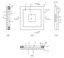
図3(a)~(d)に、それぞれ、本実施の形態の第1変形例に係るバスバーアッセンブリ1Aの平面図、図3(a)におけるIII(b)-III(b)線に沿った断面図、前記バスバーアッセンブリ1Aの側面図、及び、図3(a)におけるIII(d)-III(d)線に沿った断面図を示す。
また、図4に、前記第1変形例に係るバスバーアッセンブリ1Aに前記半導体素子110が装着されてなる半導体モジュール101Aの縦断面図を示す。
3(a) to 3(d) respectively show a plan view of a busbar assembly 1A according to a first modified example of the present embodiment, a cross-sectional view taken along line III(b)-III(b) in FIG. 3(a), a side view of the busbar assembly 1A, and a cross-sectional view taken along line III(d)-III(d) in FIG. 3(a).
FIG. 4 is a vertical cross-sectional view of a
前記第1変形例に係るバスバーアッセンブリ1Aにおいては、前記枠体30の上面、内側面(前記収容空間Sを向く側面)及び外側面(前記収容空間Sとは反対側を向く側面)を覆う枠体側絶縁性樹脂層31Aが設けられている。
In the busbar assembly 1A according to the first modified example, a frame-side insulating
前記枠体側絶縁性樹脂層31Aには、前記内側面の一部を露出させて前記素子接続部36を形成する開口、及び、前記外側面の一部を露出させて前記枠体側外部接続部38を形成する開口が形成されている。
The frame-side insulating
図5(a)~(d)に、それぞれ、本実施の形態の第2変形例に係るバスバーアッセンブリ1Bの平面図、図5(a)におけるV(a)-V(a)線に沿った断面図、前記バスバーアッセンブリ1Bの側面図、及び、図5(a)におけるV(d)-V(d)線に沿った断面図を示す。
また、図6に、前記第2変形例に係るバスバーアッセンブリ1Bに前記半導体素子110が装着されてなる半導体モジュール101Bの縦断面図を示す。
5(a) to 5(d) respectively show a plan view of a
FIG. 6 is a vertical cross-sectional view of a
前記第2変形例に係るバスバーアッセンブリ1Bにおいては、前記枠体30の上面、内側面、外側面及び下面を覆う枠体側絶縁性樹脂層31Bが設けられている。
In the
前記枠体側絶縁性樹脂層31Bには、前記内側面の一部を露出させて前記素子接続部36を形成する開口、及び、前記外側面の一部を露出させて前記枠体側外部接続部38を形成する開口が形成されている。
The frame-side insulating
なお、前記開口を有する前記枠体側絶縁性樹脂層31A、31Bは、例えば、前記開口を形成すべき部位をマスクで覆った状態で前記枠体30に絶縁性樹脂塗料を塗布して、硬化させることにより、形成することができる。
The frame-side insulating
以下、前記バスバーアッセンブリ1の製造方法の一例について説明する。
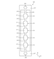
図7に、前記製造方法において用いられる導電性金属製のバスバー用平板200の平面図を示す。
An example of a method for manufacturing the
FIG. 7 shows a plan view of a bus bar
前記製造方法は、前記バスバー10と同一厚みのバスバー形成領域210を有するバスバー用平板200を用意する工程を有している。
The manufacturing method includes a step of preparing a busbar
本実施の形態においては、図7に示すように、前記バスバー用平板200は、当該バスバー用平板200が位置するX-Y平面内のY方向に沿って直列配列された複数の前記バスバー形成領域210と、Y方向に隣接するバスバー形成領域210の間を連結する連結領域230とを含むバスバー列205を有している。
In this embodiment, as shown in FIG. 7, the busbar
本実施においては、前記バスバー用平板200は、前記バスバー列205の長手方向(Y方向)一方側及び他方側にそれぞれ連結された一対の把持片207を有しており、前記一対の把持片207には位置合わせ孔208が設けられている。
In this embodiment, the busbar
なお、複数の前記バスバー列205をX方向に並列配置させ、X方向に並列配置された複数のバスバー列205を前記一対の把持片207、207によって一体的に保持することも可能である。
It is also possible to arrange
前記製造方法は、前記バスバー形成領域210の厚み方向一方側の第1面211(前記半導体素子110が装着される上面)に、前記バスバー側絶縁性樹脂層20を形成するバスバー側絶縁性樹脂層形成工程を有している。
The manufacturing method includes a busbar side insulating resin layer forming process for forming the busbar side insulating
本実施の形態においては、前記バスバー側絶縁性樹脂層形成工程は、前記バスバー形成領域210の第1面に絶縁性樹脂フィルム25を接着するように構成されている。
図8に、前記バスバー側絶縁性樹脂層形成工程後の前記バスバー用平板200の平面図を示す。
In the present embodiment, the bus bar side insulating resin layer forming step is configured to adhere an insulating
FIG. 8 shows a plan view of the
前記絶縁性樹脂フィルム25は、前記バスバー形成領域210と平面視同一外形状を有している。
The insulating
前記絶縁性樹脂フィルム20は、ポリアミドイミド、ポリイミド、ポリアミド、エポキシ等の耐熱性及び絶縁性を有する絶縁性樹脂材料によって形成される。
The insulating
前記製造方法は、前記バスバー用平板200を用意する工程から前記バスバー側絶縁性樹脂層形成工程までの処理に並行して、若しくは、前記処理の前又は後に、前記枠体30を形成する枠体形成処理を行うように構成されている。
The manufacturing method is configured to perform a frame formation process for forming the
図9に、前記枠体形成処理において用いられる導電性金属製の枠体用平板300の平面図を示す。
前記枠体形成処理は、前記枠体30の厚みと同一厚みを有し且つ平面視において前記バスバー形成領域210に対応した外形状を有する枠体形成領域310を含む枠体用平板300を用意する工程と、前記枠体30に相当する枠体形成部位が残るように前記枠体形成領域310の中央を打ち抜く打ち抜き工程とを備えている。
図9は、前記打ち抜き工程後の状態を示している。
FIG. 9 shows a plan view of a
The frame body forming process includes a step of preparing a frame body
FIG. 9 shows the state after the punching step.
前記枠体用平板300は、導電性を有する種々の材料によって形成される。
好ましくは、前記枠体用平板300は、前記バスバー用平板200と同一材料によって形成される。
The
Preferably, the frame body
前記枠体用平板300は、前記バスバー用平板200に重合させた際に、前記枠体形成領域310が前記バスバー形成領域210に位置合わせされるように構成されている。
The
詳しくは、前述の通り、前記バスバー用平板200は、Y方向に沿って直列配列された複数の前記バスバー形成領域210と、Y方向に隣接するバスバー形成領域210の間を連結する連結領域230とを含むバスバー列205を有している。
In more detail, as described above, the
従って、前記枠体用平板300は、図9に示すように、前記複数のバスバー形成領域210と同一ピッチでY方向に直列配置された複数の前記枠体形成領域310と、Y方向に隣接する枠体形成領域310の間を連結する連結領域330とを含む枠体列305を有している。
As shown in FIG. 9, the
なお、前述の通り、前記バスバー用平板200は、前記バスバー列205の長手方向(Y方向)一方側及び他方側にそれぞれ連結された一対の把持片207を有しており、前記一対の把持片207には位置合わせ孔208が設けられている。
As described above, the busbar
これに応じて、図9に示すように、前記枠体用平板300にも、前記枠体列305の長手方向(Y方向)一方側及び他方側にそれぞれ連結された一対の把持片307が設けられ、前記一対の把持片307には前記位置合わせ孔208に対応した位置合わせ孔308が設けられている。
In response to this, as shown in FIG. 9, the frame body
前記製造方法は、前記バスバー用平板200及び前記枠体用平板300を重合させて、前記枠体形成領域310を対応する前記バスバー形成領域210の第1面211に前記絶縁性樹脂層20(本実施の形態においては前記絶縁性樹脂フィルム25)を介して固着させる平板固着工程を有している、
図10に、前記平板固着工程後の状態の前記バスバー用平板200及び前記枠体用平板300の平面図を示す。
The manufacturing method includes a flat plate fixing process of polymerizing the busbar forming
FIG. 10 shows a plan view of the bus
前記平板固着工程は、例えば、前記枠体形成領域310を対応する前記バスバー形成領域210の第1面211上の前記絶縁性樹脂層20(本実施の形態においては前記絶縁性樹脂フィルム25)に接着剤によって接着させることによって行われる。
The flat plate fixing process is performed, for example, by adhering the frame
前記製造方法は、さらに、前記バスバー側絶縁性樹脂層20に、前記素子装着領域15を露出させる為の前記開口21を形成する開口形成工程を有している。
The manufacturing method further includes an opening forming step of forming the
本実施の形態においては、前記開口形成工程は、前記平板固着工程後の前記絶縁性樹脂フィルム25にレーザー光を照射することで前記開口21を形成するように構成されている。
図11に、前記開口形成工程後の状態の前記バスバー用平板200及び前記枠体用平板300の平面図を示す。
In the present embodiment, the opening forming step is configured to form the
FIG. 11 shows a plan view of the bus
前記製造方法は、さらに、固着状態の前記バスバー形成領域210及び前記枠体形成領域310を前記バスバー用平板200及び前記枠体用平板300から切断する切断工程を有している。
The manufacturing method further includes a cutting step of cutting the
前記切断工程は、図11に示すように、前記バスバー形成領域210及び前記枠体形成領域のY方向一方側及び他方側のエッジにそれぞれ沿った切断線C1、C2で切断するように構成される。
The cutting process is configured to cut along cutting lines C1 and C2 that respectively extend along the edges of the
なお、本実施の形態においては、前記開口形成工程は、前記平板固着工程の後で且つ前記切断工程の前に行われているが、これに代えて、前記バスバー形成領域210に接着される前の前記絶縁性樹脂フィルム25に対して予め前記開口21を形成することも可能である。
この場合、前記バスバー側絶縁性樹脂層形成工程は、前記開口21が形成された状態の前記絶縁性樹脂フィルム25を前記バスバー形成領域210に接着させるように構成される。
In this embodiment, the opening formation process is carried out after the flat plate fixing process and before the cutting process, but instead, it is also possible to form the
In this case, the bus bar side insulating resin layer forming step is configured to adhere the insulating
若しくは、前記絶縁性樹脂フィルム25へのレーザー光の照射を、前記バスバー側絶縁性樹脂層形成工程の後で且つ前記平板固着工程の前(図8に示す状態)、又は、前記切断工程の後に、行うことも可能である。
Alternatively, the insulating
また、本実施の形態においては、レーザー光照射によって前記開口21を形成しているが、これに代えて、エッチングによって前記開口21を形成することも可能である。
この場合、前記バスバー側絶縁性樹脂層20のうち前記開口21を形成すべき領域以外の領域にマスキングを行った状態でエッチングを行うことにより、前記開口21が形成される。
In the present embodiment, the
In this case, the
さらには、前記絶縁性樹脂フィルム25を前記バスバー形成領域210に接着させる前に前記開口21が形成される場合においては、前記絶縁性樹脂フィルム25に対してパンチング加工を行うことによって、前記開口21を形成することも可能である。
Furthermore, when the
本実施の形態においては、前述の通り、前記バスバー側絶縁性樹脂層20は、前記絶縁性樹脂フィルム25によって形成されているが、これに代えて、前記バスバー側絶縁性樹脂層20を絶縁性樹脂塗膜27によって形成することも可能である。
In this embodiment, as described above, the busbar side insulating
図12(a)~(c)に、それぞれ、本実施の形態、前記第1変形例及び前記第2変形例に係る前記バスバーアッセンブリ1、1A、1Bにおいて、前記バスバー側絶縁性樹脂層20が絶縁性樹脂フィルム25に代えて絶縁性樹脂塗膜27によって形成された第3~第5変形例に係るバスバーアッセンブリ1C~1Eの縦断面図を示す。
Figures 12(a) to (c) show longitudinal cross-sectional views of
前記第3~第5変形例に係るバスバーアッセンブリ1C~1Eの製造方法においては、前記バスバー側絶縁性樹脂層形成工程は、前記バスバー用平板200の外周面に絶縁性樹脂塗料を塗布し、硬化させるように構成される。
In the manufacturing methods for
図13(a)に、外周面に絶縁性樹脂塗膜27が設けられた状態の前記バスバー用平板200の平面図を示す。
Figure 13(a) shows a plan view of the busbar
この場合、前記開口形成工程は、レーザー光照射又はエッチングによって、前記素子搭載領域15を露出させる前記開口21に加えて、前記バスバー側外部接続部16を露出させる開口22を形成するように構成される。
In this case, the opening formation process is configured to form, by laser light irradiation or etching,
図13(b)に、図13(a)におけるXIII(b)-XIII(b)線に沿った断面図であって、前記開口21、22を形成した状態の断面図を示す。
Figure 13(b) is a cross-sectional view taken along line XIII(b)-XIII(b) in Figure 13(a), showing the state after the
なお、前記開口形成工程は、図13(b)に示すように、バスバー側絶縁性樹脂層形成工程の後で且つ平板固着工程の前に行うことも可能であるし、これに代えて、平板固着工程の後で且つ切断工程の前、又は、切断工程の後に行うことも可能である。 The opening formation process can be performed after the busbar-side insulating resin layer formation process and before the flat plate bonding process, as shown in FIG. 13(b), or alternatively, it can be performed after the flat plate bonding process and before the cutting process, or after the cutting process.
また、前記枠体側絶縁性樹脂層31A、31Bを設ける構成(前記第1、第2、第4及び第5変形例)の製造方法ににおいては、前記枠体形成処理は、前記打ち抜き工程の後に、前記枠体形成部位の外表面のうち前記素子接続部36及び枠体側外部接続部38を形成する領域をマスキングした状態で絶縁性樹脂塗料を塗布し、硬化させる枠体側絶縁性樹脂層形成工程を有するものとされる。
In the manufacturing method for the configuration in which the frame-side insulating resin layers 31A, 31B are provided (the first, second, fourth and fifth modified examples), the frame-forming process includes a frame-side insulating resin layer forming process in which, after the punching process, an insulating resin paint is applied and cured while masking the area of the outer surface of the frame-forming portion in which the
図14(a)に、前記枠体側絶縁性樹脂層形成工程後の前記枠体用平板300の平面図を示す。
また、図14(b)及び(c)に、図14(a)におけるXIV-XIV線に沿った断面図を示す。
図14(b)及び(c)は、それぞれ、前記枠体側絶縁性樹脂層31Aを設けた構成(前記第1及び第4変形例)及び前記枠体側絶縁性樹脂層31Bを設けた構成(前記第2及び第5変形例)を示している。
FIG. 14A shows a plan view of the frame body
14(b) and (c) are cross-sectional views taken along line XIV-XIV in FIG. 14(a).
Figures 14(b) and (c) respectively show a configuration in which the frame body side insulating
なお、前記枠体30及び前記バスバー10の当接領域の少なくとも一方(即ち、少なくとも前記枠体30の下面及び前記バスバー10の上面のうち前記枠体30に当接する領域の一方)に、絶縁性樹脂塗膜が設けられている構成(前記第2~第5変形例)においては、絶縁性樹脂塗膜が半硬化状態の際に前記平板固着工程を行うことができる。
In addition, in a configuration (the second to fifth modified examples) in which an insulating resin coating is provided on at least one of the contact areas of the
斯かる構成によれば、前記バスバー用平板200及び前記枠体用平板300の固着を、接着剤の作用に代えて、又は、加えて、絶縁性樹脂塗膜の硬化作用を利用して行うことができる。
With this configuration, the busbar
実施の形態2
以下、本発明に係るバスバーアッセンブリの他の実施の形態について、添付図面を参照しつつ説明する。
図15(a)~(d)に、それぞれ、本実施の形態に係るバスバーアッセンブリ2の平面図、図15(a)におけるXV(a)-XV(a)線に沿った断面図、前記バスバーアッセンブリ2の側面図、及び、図15(a)におけるXV(d)-XV(d)線に沿った断面図を示す。
また、図16に、前記バスバーアッセンブリ2に前記半導体素子110が装着されてなる半導体モジュール102の縦断面図を示す。
なお、図中、前記実施の形態1におけると同一部材には同一符号を付して、その説明を適宜省略する。
Hereinafter, another embodiment of the bus bar assembly according to the present invention will be described with reference to the accompanying drawings.
Figures 15(a) to (d) show, respectively, a plan view of a
FIG. 16 is a vertical cross-sectional view of a
In the drawings, the same members as those in the first embodiment are given the same reference numerals, and the description thereof will be omitted as appropriate.
本実施の形態に係るバスバーアッセンブリ2は、前記バスバー側絶縁性樹脂層20が削除されており、枠体側絶縁性樹脂層30Bのみによって前記枠体30及び前記バスバー10が絶縁されている点において、前記実施の形態1に係るバスバーアッセンブリ1と異なっている。
The
即ち、本実施の形態においては、前記枠体30の少なくとも下面(前記バスバー10の上面11と対向する面)を覆う枠体側絶縁性樹脂層30Bが設けられており、導電性部材によって形成された前記枠体30は、前記枠体側絶縁性樹脂層30Bを介して前記バスバー10の上面11に電気的に絶縁状態で機械的に固着されている。
That is, in this embodiment, a frame-side insulating
斯かる構成の前記バスバーアッセンブリ2も、前記従来構成1及び2に比して、前記実施の形態1に係るバスバーアッセンブリ1と同様の効果を得ることができる。
The
なお、本実施の形態においては、前記枠体側絶縁性樹脂層30Bは前記枠体30の外周面全体を覆うように構成されており、前記枠体側絶縁性樹脂層30Bには前記素子接続部36を形成する開口及び前記枠体側外部接続部38を形成する開口が設けられている。
In this embodiment, the frame-side insulating
本実施の形態に係る前記バスバーアッセンブリ2は下記製造方法によって効率よく製造される。
The
即ち、前記製造方法は、前記バスバー用平板200を用意する工程と、前記バスバー用平板200を用意する工程の前又は後に、若しくは、前記バスバー用平板200を用意する工程と並行して行う枠体形成処理枠体形成処理とを有している。
That is, the manufacturing method includes a step of preparing the
前記枠体形成処理は、前記枠体用平板300を用意する工程と、前記枠体形成領域310のうちの中央部分を打ち抜いて、枠体形成部位を形成する打ち抜き工程と、前記枠体形成部位の外表面のうち少なくとも前記バスバー10の第1面11と対向する面に絶縁性樹脂塗料を塗布して硬化させることにより前記枠体側絶縁性樹脂層30Bを形成する枠体側絶縁性樹脂層形成工程とを含むものとされる。
The frame body forming process includes a step of preparing the frame body
前記製造方法は、さらに、前記バスバー用平板200及び前記枠体用平板300を重合させて、前記枠体形成領域310を対応する前記バスバー形成領域210の第1面211に固着させる平板固着工程と、固着状態の前記バスバー形成領域210及び前記枠体形成領域310を前記バスバー用平板200及び前記枠体用平板300から切断する切断工程とを含む。
The manufacturing method further includes a flat plate fixing process in which the busbar
前記平板固着工程における前記枠体形成領域310と前記バスバー形成領域210との固着は、接着剤による接着作用によって行うことも可能であるし、接着剤による接着作用に代えて又は加えて、前記枠体30の対向面に設けられた前記絶縁性樹脂塗膜が半硬化状態の際に前記枠体形成領域310及び前記バスバー形成領域210を重合させて前記塗膜の硬化作用を利用して行うことも可能である。
The fixing of the frame
1、1A~1E、2 バスバーアッセンブリ
10 バスバー
15 素子搭載領域
16 バスバー側外部接続部
20 バスバー側絶縁性樹脂層
25 絶縁性樹脂フィルム
27 絶縁性樹脂塗膜
30 枠体
31A、31B 枠体側絶縁性樹脂層
36 素子接続部
38 素子側外部接続部
200 バスバー用平板
210 バスバー形成領域
230 連結領域
300 枠体用平板
310 枠体形成領域
330 連結領域
S 収容空間
Claims (6)
前記バスバーは、上面のうち前記収容空間内の少なくとも一部に電気素子が電気的に接続状態で機械的に装着可能な素子搭載領域を有し、且つ、下面の少なくとも一部に外部と電気的に接続可能なバスバー側外部接続部を有しており、
前記枠体は、前記バスバーの上面と対向する下面以外の部分において枠体側絶縁性樹脂層によって覆われており、
前記枠体は、前記素子搭載領域に搭載される電気素子に対して電気的に接続可能な素子接続部及び外部と電気的に接続可能な枠体側外部接続部を有し、
前記バスバー側絶縁性樹脂層には、前記素子搭載領域を露出させる開口が設けられ、
前記枠体側絶縁性樹脂層には、前記素子接続部を形成する開口及び前記枠体側外部接続部を形成する開口が設けられていることを特徴とするバスバーアッセンブリ。 a busbar-side insulating resin layer provided on an upper surface of the busbar; and a frame body formed of a conductive member, the frame body being mechanically fixed in an electrically insulated state to the upper surface of the busbar via the busbar-side insulating resin layer so as to define an accommodation space that opens upward at the center of the upper surface of the busbar,
the bus bar has an element mounting area on at least a portion of an upper surface within the accommodating space, to which an electric element can be mechanically attached in an electrically connected state, and a bus bar side external connection portion on at least a portion of a lower surface which can be electrically connected to an external device,
the frame is covered with a frame-side insulating resin layer except for a lower surface facing an upper surface of the bus bar,
the frame has an element connection portion electrically connectable to an electric element mounted in the element mounting region and a frame-side external connection portion electrically connectable to an external device ,
an opening for exposing the element mounting region is provided in the bus bar side insulating resin layer,
The busbar assembly is characterized in that the frame-side insulating resin layer is provided with an opening for forming the element connection portion and an opening for forming the frame-side external connection portion .
前記バスバーを形成するバスバー形成領域を有する導電性金属製のバスバー用平板を用意する工程と、
前記バスバー形成領域の第1面に前記バスバー側絶縁性樹脂層を形成する絶縁性樹脂フィルムを接着するバスバー側絶縁性樹脂層形成工程と、
前記バスバー用平板を用意する工程から前記バスバー側絶縁性樹脂層形成工程までの処理の前又は後、若しくは、並行して行う枠体形成処理であって、平面視において前記バスバー形成領域に対応した外形状を有する枠体形成領域を含む導電性金属製の枠体用平板を用意する工程と、前記枠体形成領域のうちの中央部分を打ち抜いて、枠体を形成する打ち抜き工程と、前記枠体形成領域のうち前記バスバー形成領域の第1面と対向する下面以外の外表面に、前記素子接続部及び前記枠体側外部接続部を形成する領域をマスキングした状態で絶縁性樹脂塗料を塗布して枠体側絶縁性樹脂層を形成する工程とを含む枠体形成処理と、
前記バスバー側絶縁性樹脂層形成工程後の前記バスバー用平板及び前記枠体形成処理後の前記枠体用平板を重合させて、前記枠体形成領域の下面を前記バスバー側絶縁性樹脂層を介して前記バスバー形成領域の第1面に固着させる平板固着工程と、
固着状態の前記バスバー形成領域及び前記枠体形成領域を前記バスバー用平板及び前記枠体用平板から切断する切断工程と、
前記バスバー側絶縁性樹脂層形成工程の前、前記バスバー側絶縁性樹脂層形成工程の後で且つ前記切断工程の前、若しくは、前記切断工程の後に、前記絶縁性樹脂フィルムに前記素子搭載領域を露出させる為の開口を形成する開口形成工程とを含むことを特徴とするバスバーアッセンブリの製造方法。 a busbar assembly including a planar busbar formed of a conductive member, a busbar-side insulating resin layer provided on a first surface of the busbar on one side in a thickness direction, and a frame body formed of a conductive member and fixed to the first surface of the busbar via the busbar-side insulating resin layer so as to define an accommodation space that opens upward in the center of the first surface of the busbar, wherein the busbar has an element mounting area on at least a part of the accommodation space on the first surface, to which an electric element can be attached in an electrically connected state, and a busbar-side external connection part on at least a part of a second surface on the other side in the thickness direction, the frame body having an element connection part electrically connectable to an electric element mounted in the element mounting area and a frame body-side external connection part electrically connectable to the outside,
preparing a busbar plate made of a conductive metal having a busbar forming region for forming the busbar;
a busbar-side insulating resin layer forming step of adhering an insulating resin film that forms the busbar-side insulating resin layer to a first surface of the busbar forming region;
a frame body forming process which is performed before or after, or in parallel with, processes from the process of preparing a busbar plate to the process of forming the busbar side insulating resin layer, the frame body forming process including: a process of preparing a frame body flat plate made of a conductive metal including a frame body forming region having an external shape corresponding to the busbar forming region in a plan view; a punching process of forming a frame body by punching out a center portion of the frame body forming region; and a process of applying an insulating resin paint to an outer surface of the frame body forming region other than a lower surface facing a first surface of the busbar forming region while masking an area in which the element connection portion and the frame body side external connection portion are to be formed, to form a frame body side insulating resin layer ;
a flat plate fixing process of polymerizing the busbar plate after the busbar-side insulating resin layer forming process and the frame plate after the frame body forming process to fix a lower surface of the frame body forming region to a first surface of the busbar forming region via the busbar-side insulating resin layer;
a cutting step of cutting the busbar forming region and the frame body forming region in a fixed state from the busbar forming plate and the frame body forming plate;
an opening forming step of forming an opening in the insulating resin film to expose the element mounting area before the bus bar side insulating resin layer forming step, after the bus bar side insulating resin layer forming step and before the cutting step, or after the cutting step.
前記バスバーを形成するバスバー形成領域を有する導電性金属製のバスバー用平板を用意する工程と、
前記バスバー形成領域の少なくとも第1面に前記バスバー側絶縁性樹脂層を形成する絶縁性樹脂塗膜を設けるバスバー側絶縁性樹脂層形成工程と、
前記バスバー用平板を用意する工程から前記バスバー側絶縁性樹脂層形成工程までの処理の前又は後、若しくは、並行して行う枠体形成処理であって、平面視において前記バスバー形成領域に対応した外形状を有する枠体形成領域を含む導電性金属製の枠体用平板を用意する工程と、前記枠体形成領域のうちの中央部分を打ち抜いて、枠体を形成する打ち抜き工程と、前記枠体形成領域のうち前記バスバー形成領域の第1面と対向する下面以外の外表面に、前記素子接続部及び前記枠体側外部接続部を形成する領域をマスキングした状態で絶縁性樹脂塗料を塗布して枠体側絶縁性樹脂層を形成する工程とを含む枠体形成処理と、
前記バスバー側絶縁性樹脂層形成工程後の前記バスバー用平板及び前記枠体形成処理後の前記枠体用平板を重合させて、前記枠体形成領域の下面を対応する前記バスバー形成領域の第1面に固着させる平板固着工程と、
固着状態の前記バスバー形成領域及び前記枠体形成領域を前記バスバー用平板及び前記枠体用平板から切断する切断工程と、
前記バスバー側絶縁性樹脂層形成工程の後で且つ前記切断工程の前、若しくは、前記切断工程の後に、前記絶縁性樹脂塗膜に前記素子搭載領域を露出させる為の開口を形成する開口形成工程とを含むことを特徴とするバスバーアッセンブリの製造方法。 a busbar assembly including a planar busbar formed of a conductive member, a busbar-side insulating resin layer provided on a first surface of the busbar on one side in a thickness direction, and a frame body formed of a conductive member and fixed to the first surface of the busbar via the busbar-side insulating resin layer so as to define an accommodation space that opens upward in the center of the first surface of the busbar, wherein the busbar has an element mounting area on at least a part of the accommodation space on the first surface, to which an electric element can be attached in an electrically connected state, and a busbar-side external connection part on at least a part of a second surface on the other side in the thickness direction, the frame body having an element connection part electrically connectable to an electric element mounted in the element mounting area and a frame body-side external connection part electrically connectable to the outside,
preparing a busbar plate made of a conductive metal having a busbar forming region for forming the busbar;
a busbar-side insulating resin layer forming step of providing an insulating resin coating film that forms the busbar-side insulating resin layer on at least a first surface of the busbar forming region;
a frame body forming process which is performed before or after, or in parallel with, processes from the process of preparing a busbar plate to the process of forming the busbar side insulating resin layer, the frame body forming process including: a process of preparing a frame body flat plate made of a conductive metal including a frame body forming region having an external shape corresponding to the busbar forming region in a plan view; a punching process of forming a frame body by punching out a center portion of the frame body forming region; and a process of applying an insulating resin paint to an outer surface of the frame body forming region other than a lower surface facing a first surface of the busbar forming region while masking an area in which the element connection portion and the frame body side external connection portion are to be formed, to form a frame body side insulating resin layer ;
a flat plate fixing process of laminating the busbar flat plate after the busbar-side insulating resin layer forming process and the frame flat plate after the frame forming process, and fixing a lower surface of the frame forming region to a first surface of the corresponding busbar forming region;
a cutting step of cutting the busbar forming region and the frame body forming region in a fixed state from the busbar forming plate and the frame body forming plate;
and an opening forming step of forming an opening in the insulating resin coating film to expose the element mounting area after the bus bar side insulating resin layer forming step and before the cutting step, or after the cutting step.
Priority Applications (2)
| Application Number | Priority Date | Filing Date | Title |
|---|---|---|---|
| JP2020169140A JP7582829B2 (en) | 2020-10-06 | 2020-10-06 | Busbar assembly and manufacturing method thereof |
| JP2024177020A JP7809181B2 (en) | 2020-10-06 | 2024-10-09 | Semiconductor Module |
Applications Claiming Priority (1)
| Application Number | Priority Date | Filing Date | Title |
|---|---|---|---|
| JP2020169140A JP7582829B2 (en) | 2020-10-06 | 2020-10-06 | Busbar assembly and manufacturing method thereof |
Related Child Applications (1)
| Application Number | Title | Priority Date | Filing Date |
|---|---|---|---|
| JP2024177020A Division JP7809181B2 (en) | 2020-10-06 | 2024-10-09 | Semiconductor Module |
Publications (2)
| Publication Number | Publication Date |
|---|---|
| JP2022061249A JP2022061249A (en) | 2022-04-18 |
| JP7582829B2 true JP7582829B2 (en) | 2024-11-13 |
Family
ID=81206591
Family Applications (2)
| Application Number | Title | Priority Date | Filing Date |
|---|---|---|---|
| JP2020169140A Active JP7582829B2 (en) | 2020-10-06 | 2020-10-06 | Busbar assembly and manufacturing method thereof |
| JP2024177020A Active JP7809181B2 (en) | 2020-10-06 | 2024-10-09 | Semiconductor Module |
Family Applications After (1)
| Application Number | Title | Priority Date | Filing Date |
|---|---|---|---|
| JP2024177020A Active JP7809181B2 (en) | 2020-10-06 | 2024-10-09 | Semiconductor Module |
Country Status (1)
| Country | Link |
|---|---|
| JP (2) | JP7582829B2 (en) |
Citations (2)
| Publication number | Priority date | Publication date | Assignee | Title |
|---|---|---|---|---|
| JP2011082259A (en) | 2009-10-05 | 2011-04-21 | Dainippon Printing Co Ltd | Led element mounting member and method for manufacturing the same, and led element package and method for manufacturing the same |
| JP2016219522A (en) | 2015-05-18 | 2016-12-22 | スタンレー電気株式会社 | Manufacturing method of semiconductor light-emitting device and semiconductor light-emitting device |
Family Cites Families (6)
| Publication number | Priority date | Publication date | Assignee | Title |
|---|---|---|---|---|
| US7777235B2 (en) * | 2003-05-05 | 2010-08-17 | Lighting Science Group Corporation | Light emitting diodes with improved light collimation |
| US6911731B2 (en) * | 2003-05-14 | 2005-06-28 | Jiahn-Chang Wu | Solderless connection in LED module |
| US20050225222A1 (en) * | 2004-04-09 | 2005-10-13 | Joseph Mazzochette | Light emitting diode arrays with improved light extraction |
| JP2006012868A (en) * | 2004-06-22 | 2006-01-12 | Toshiba Corp | Package for semiconductor light emitting device and semiconductor light emitting device using the same |
| TWI287310B (en) * | 2006-02-17 | 2007-09-21 | Jiahn-Chang Wu | Matrix light display |
| JP6637002B2 (en) * | 2017-09-04 | 2020-01-29 | サンコール株式会社 | Busbar assembly manufacturing method |
-
2020
- 2020-10-06 JP JP2020169140A patent/JP7582829B2/en active Active
-
2024
- 2024-10-09 JP JP2024177020A patent/JP7809181B2/en active Active
Patent Citations (2)
| Publication number | Priority date | Publication date | Assignee | Title |
|---|---|---|---|---|
| JP2011082259A (en) | 2009-10-05 | 2011-04-21 | Dainippon Printing Co Ltd | Led element mounting member and method for manufacturing the same, and led element package and method for manufacturing the same |
| JP2016219522A (en) | 2015-05-18 | 2016-12-22 | スタンレー電気株式会社 | Manufacturing method of semiconductor light-emitting device and semiconductor light-emitting device |
Also Published As
| Publication number | Publication date |
|---|---|
| JP2022061249A (en) | 2022-04-18 |
| JP7809181B2 (en) | 2026-01-30 |
| JP2024177533A (en) | 2024-12-19 |
Similar Documents
| Publication | Publication Date | Title |
|---|---|---|
| JP3238004B2 (en) | Method for manufacturing semiconductor device | |
| KR101544844B1 (en) | Wired rubber contact and method of manufacturing the same | |
| CN112640095B (en) | Bus bar assembly and method of manufacturing the same | |
| KR102742559B1 (en) | Wiring board, semiconductor package including wiring board and manufacturing method thereof | |
| US8193643B2 (en) | Semiconductor device and method for fabricating the same | |
| JP6840269B2 (en) | How to mechanically connect electronic components and electronic component assembly | |
| JP7582829B2 (en) | Busbar assembly and manufacturing method thereof | |
| US20250007266A1 (en) | Busbar assembly and method for manufacturing the same | |
| CN109983548B (en) | Bus bar assembly | |
| WO2020085154A1 (en) | Bus bar assembly and manufacturing method therefor | |
| CN116367931B (en) | Bus bar assembly and method for manufacturing bus bar assembly | |
| WO2025224934A1 (en) | Method for manufacturing multilayer substrate | |
| CN114467234A (en) | Bus bar assembly and method of manufacturing the same | |
| JP7606318B2 (en) | Manufacturing method for busbar assembly and flat plate laminate structure for busbar assembly | |
| US5829127A (en) | Latticework with plurality of overlying lines | |
| JP2024165043A (en) | Busbar assembly and manufacturing method thereof | |
| JP6788767B1 (en) | Busbar assembly and its manufacturing method | |
| JP4657840B2 (en) | Semiconductor device and manufacturing method thereof | |
| JP7734251B2 (en) | Busbar assembly and manufacturing method thereof | |
| KR20150000174A (en) | Electric component module and manufacturing method threrof | |
| JP2024165042A (en) | Busbar assembly and manufacturing method thereof | |
| US20250287761A1 (en) | Light-emitting device and manufacutring method of light-emitting device | |
| JP2024172922A (en) | Busbar assembly and manufacturing method thereof | |
| JP6763754B2 (en) | Manufacturing method of substrate terminal board for mounting semiconductor elements | |
| JP2025011394A (en) | Busbar assembly and manufacturing method thereof |
Legal Events
| Date | Code | Title | Description |
|---|---|---|---|
| A621 | Written request for application examination |
Free format text: JAPANESE INTERMEDIATE CODE: A621 Effective date: 20230926 |
|
| A977 | Report on retrieval |
Free format text: JAPANESE INTERMEDIATE CODE: A971007 Effective date: 20240716 |
|
| A131 | Notification of reasons for refusal |
Free format text: JAPANESE INTERMEDIATE CODE: A131 Effective date: 20240823 |
|
| A521 | Request for written amendment filed |
Free format text: JAPANESE INTERMEDIATE CODE: A523 Effective date: 20241009 |
|
| TRDD | Decision of grant or rejection written | ||
| A01 | Written decision to grant a patent or to grant a registration (utility model) |
Free format text: JAPANESE INTERMEDIATE CODE: A01 Effective date: 20241025 |
|
| A61 | First payment of annual fees (during grant procedure) |
Free format text: JAPANESE INTERMEDIATE CODE: A61 Effective date: 20241031 |
|
| R150 | Certificate of patent or registration of utility model |
Ref document number: 7582829 Country of ref document: JP Free format text: JAPANESE INTERMEDIATE CODE: R150 |