JP7579112B2 - レーザ照射装置、及び半導体装置の製造方法 - Google Patents
レーザ照射装置、及び半導体装置の製造方法 Download PDFInfo
- Publication number
- JP7579112B2 JP7579112B2 JP2020187793A JP2020187793A JP7579112B2 JP 7579112 B2 JP7579112 B2 JP 7579112B2 JP 2020187793 A JP2020187793 A JP 2020187793A JP 2020187793 A JP2020187793 A JP 2020187793A JP 7579112 B2 JP7579112 B2 JP 7579112B2
- Authority
- JP
- Japan
- Prior art keywords
- reflecting surface
- light
- reflected
- laser
- substrate
- Prior art date
- Legal status (The legal status is an assumption and is not a legal conclusion. Google has not performed a legal analysis and makes no representation as to the accuracy of the status listed.)
- Active
Links
- 239000004065 semiconductor Substances 0.000 title claims description 36
- 238000000034 method Methods 0.000 title claims description 27
- 238000004519 manufacturing process Methods 0.000 title claims description 24
- 230000000903 blocking effect Effects 0.000 claims description 102
- 239000000758 substrate Substances 0.000 claims description 90
- 230000003287 optical effect Effects 0.000 claims description 88
- 238000001816 cooling Methods 0.000 claims description 25
- 230000001678 irradiating effect Effects 0.000 claims description 6
- 239000010408 film Substances 0.000 description 67
- 239000007789 gas Substances 0.000 description 43
- 238000007789 sealing Methods 0.000 description 21
- 239000010410 layer Substances 0.000 description 17
- 238000005224 laser annealing Methods 0.000 description 13
- 229910021420 polycrystalline silicon Inorganic materials 0.000 description 12
- 229920005591 polysilicon Polymers 0.000 description 12
- 229910021417 amorphous silicon Inorganic materials 0.000 description 9
- 230000000052 comparative effect Effects 0.000 description 8
- 239000012044 organic layer Substances 0.000 description 8
- 239000000498 cooling water Substances 0.000 description 6
- 230000008569 process Effects 0.000 description 6
- IJGRMHOSHXDMSA-UHFFFAOYSA-N Atomic nitrogen Chemical compound N#N IJGRMHOSHXDMSA-UHFFFAOYSA-N 0.000 description 5
- 238000010521 absorption reaction Methods 0.000 description 5
- 230000006866 deterioration Effects 0.000 description 5
- 239000011521 glass Substances 0.000 description 5
- 239000007769 metal material Substances 0.000 description 5
- 230000004048 modification Effects 0.000 description 5
- 238000012986 modification Methods 0.000 description 5
- XUIMIQQOPSSXEZ-UHFFFAOYSA-N Silicon Chemical compound [Si] XUIMIQQOPSSXEZ-UHFFFAOYSA-N 0.000 description 4
- 230000000694 effects Effects 0.000 description 4
- 238000009413 insulation Methods 0.000 description 4
- 229910052710 silicon Inorganic materials 0.000 description 4
- 239000010703 silicon Substances 0.000 description 4
- VYPSYNLAJGMNEJ-UHFFFAOYSA-N silicon dioxide Inorganic materials O=[Si]=O VYPSYNLAJGMNEJ-UHFFFAOYSA-N 0.000 description 4
- 230000032258 transport Effects 0.000 description 4
- 229910052782 aluminium Inorganic materials 0.000 description 3
- XAGFODPZIPBFFR-UHFFFAOYSA-N aluminium Chemical compound [Al] XAGFODPZIPBFFR-UHFFFAOYSA-N 0.000 description 3
- 238000010586 diagram Methods 0.000 description 3
- 239000011261 inert gas Substances 0.000 description 3
- 239000011810 insulating material Substances 0.000 description 3
- 235000012239 silicon dioxide Nutrition 0.000 description 3
- 230000008859 change Effects 0.000 description 2
- 238000005229 chemical vapour deposition Methods 0.000 description 2
- 230000007423 decrease Effects 0.000 description 2
- 238000002845 discoloration Methods 0.000 description 2
- 239000011159 matrix material Substances 0.000 description 2
- 229910052757 nitrogen Inorganic materials 0.000 description 2
- 238000005192 partition Methods 0.000 description 2
- 239000010453 quartz Substances 0.000 description 2
- 239000010409 thin film Substances 0.000 description 2
- 229910000838 Al alloy Inorganic materials 0.000 description 1
- OKTJSMMVPCPJKN-UHFFFAOYSA-N Carbon Chemical compound [C] OKTJSMMVPCPJKN-UHFFFAOYSA-N 0.000 description 1
- 230000002411 adverse Effects 0.000 description 1
- 229910045601 alloy Inorganic materials 0.000 description 1
- 239000000956 alloy Substances 0.000 description 1
- 238000000137 annealing Methods 0.000 description 1
- 229910052681 coesite Inorganic materials 0.000 description 1
- 229910052906 cristobalite Inorganic materials 0.000 description 1
- 229910001873 dinitrogen Inorganic materials 0.000 description 1
- 238000006073 displacement reaction Methods 0.000 description 1
- 238000009826 distribution Methods 0.000 description 1
- 238000005401 electroluminescence Methods 0.000 description 1
- 239000012530 fluid Substances 0.000 description 1
- 229910002804 graphite Inorganic materials 0.000 description 1
- 239000010439 graphite Substances 0.000 description 1
- 238000009434 installation Methods 0.000 description 1
- 239000011229 interlayer Substances 0.000 description 1
- 230000031700 light absorption Effects 0.000 description 1
- 239000000463 material Substances 0.000 description 1
- 238000005259 measurement Methods 0.000 description 1
- 229910052751 metal Inorganic materials 0.000 description 1
- 239000002184 metal Substances 0.000 description 1
- 229910021424 microcrystalline silicon Inorganic materials 0.000 description 1
- 239000011347 resin Substances 0.000 description 1
- 229920005989 resin Polymers 0.000 description 1
- 239000000377 silicon dioxide Substances 0.000 description 1
- 229910052682 stishovite Inorganic materials 0.000 description 1
- 229910052905 tridymite Inorganic materials 0.000 description 1
- XLYOFNOQVPJJNP-UHFFFAOYSA-N water Substances O XLYOFNOQVPJJNP-UHFFFAOYSA-N 0.000 description 1
Images


Classifications
-
- B—PERFORMING OPERATIONS; TRANSPORTING
- B23—MACHINE TOOLS; METAL-WORKING NOT OTHERWISE PROVIDED FOR
- B23K—SOLDERING OR UNSOLDERING; WELDING; CLADDING OR PLATING BY SOLDERING OR WELDING; CUTTING BY APPLYING HEAT LOCALLY, e.g. FLAME CUTTING; WORKING BY LASER BEAM
- B23K26/00—Working by laser beam, e.g. welding, cutting or boring
- B23K26/02—Positioning or observing the workpiece, e.g. with respect to the point of impact; Aligning, aiming or focusing the laser beam
- B23K26/06—Shaping the laser beam, e.g. by masks or multi-focusing
- B23K26/064—Shaping the laser beam, e.g. by masks or multi-focusing by means of optical elements, e.g. lenses, mirrors or prisms
-
- B—PERFORMING OPERATIONS; TRANSPORTING
- B23—MACHINE TOOLS; METAL-WORKING NOT OTHERWISE PROVIDED FOR
- B23K—SOLDERING OR UNSOLDERING; WELDING; CLADDING OR PLATING BY SOLDERING OR WELDING; CUTTING BY APPLYING HEAT LOCALLY, e.g. FLAME CUTTING; WORKING BY LASER BEAM
- B23K26/00—Working by laser beam, e.g. welding, cutting or boring
- B23K26/12—Working by laser beam, e.g. welding, cutting or boring in a special atmosphere, e.g. in an enclosure
- B23K26/123—Working by laser beam, e.g. welding, cutting or boring in a special atmosphere, e.g. in an enclosure in an atmosphere of particular gases
-
- B—PERFORMING OPERATIONS; TRANSPORTING
- B23—MACHINE TOOLS; METAL-WORKING NOT OTHERWISE PROVIDED FOR
- B23K—SOLDERING OR UNSOLDERING; WELDING; CLADDING OR PLATING BY SOLDERING OR WELDING; CUTTING BY APPLYING HEAT LOCALLY, e.g. FLAME CUTTING; WORKING BY LASER BEAM
- B23K26/00—Working by laser beam, e.g. welding, cutting or boring
- B23K26/12—Working by laser beam, e.g. welding, cutting or boring in a special atmosphere, e.g. in an enclosure
- B23K26/127—Working by laser beam, e.g. welding, cutting or boring in a special atmosphere, e.g. in an enclosure in an enclosure
-
- B—PERFORMING OPERATIONS; TRANSPORTING
- B23—MACHINE TOOLS; METAL-WORKING NOT OTHERWISE PROVIDED FOR
- B23K—SOLDERING OR UNSOLDERING; WELDING; CLADDING OR PLATING BY SOLDERING OR WELDING; CUTTING BY APPLYING HEAT LOCALLY, e.g. FLAME CUTTING; WORKING BY LASER BEAM
- B23K26/00—Working by laser beam, e.g. welding, cutting or boring
- B23K26/34—Laser welding for purposes other than joining
-
- B—PERFORMING OPERATIONS; TRANSPORTING
- B23—MACHINE TOOLS; METAL-WORKING NOT OTHERWISE PROVIDED FOR
- B23K—SOLDERING OR UNSOLDERING; WELDING; CLADDING OR PLATING BY SOLDERING OR WELDING; CUTTING BY APPLYING HEAT LOCALLY, e.g. FLAME CUTTING; WORKING BY LASER BEAM
- B23K26/00—Working by laser beam, e.g. welding, cutting or boring
- B23K26/352—Working by laser beam, e.g. welding, cutting or boring for surface treatment
-
- B—PERFORMING OPERATIONS; TRANSPORTING
- B23—MACHINE TOOLS; METAL-WORKING NOT OTHERWISE PROVIDED FOR
- B23K—SOLDERING OR UNSOLDERING; WELDING; CLADDING OR PLATING BY SOLDERING OR WELDING; CUTTING BY APPLYING HEAT LOCALLY, e.g. FLAME CUTTING; WORKING BY LASER BEAM
- B23K26/00—Working by laser beam, e.g. welding, cutting or boring
- B23K26/70—Auxiliary operations or equipment
- B23K26/702—Auxiliary equipment
- B23K26/704—Beam dispersers, e.g. beam wells
-
- G—PHYSICS
- G02—OPTICS
- G02B—OPTICAL ELEMENTS, SYSTEMS OR APPARATUS
- G02B17/00—Systems with reflecting surfaces, with or without refracting elements
- G02B17/002—Arrays of reflective systems
-
- H—ELECTRICITY
- H01—ELECTRIC ELEMENTS
- H01L—SEMICONDUCTOR DEVICES NOT COVERED BY CLASS H10
- H01L21/00—Processes or apparatus adapted for the manufacture or treatment of semiconductor or solid state devices or of parts thereof
- H01L21/02—Manufacture or treatment of semiconductor devices or of parts thereof
- H01L21/04—Manufacture or treatment of semiconductor devices or of parts thereof the devices having potential barriers, e.g. a PN junction, depletion layer or carrier concentration layer
- H01L21/18—Manufacture or treatment of semiconductor devices or of parts thereof the devices having potential barriers, e.g. a PN junction, depletion layer or carrier concentration layer the devices having semiconductor bodies comprising elements of Group IV of the Periodic Table or AIIIBV compounds with or without impurities, e.g. doping materials
- H01L21/26—Bombardment with radiation
- H01L21/263—Bombardment with radiation with high-energy radiation
- H01L21/268—Bombardment with radiation with high-energy radiation using electromagnetic radiation, e.g. laser radiation
-
- H—ELECTRICITY
- H01—ELECTRIC ELEMENTS
- H01L—SEMICONDUCTOR DEVICES NOT COVERED BY CLASS H10
- H01L21/00—Processes or apparatus adapted for the manufacture or treatment of semiconductor or solid state devices or of parts thereof
- H01L21/02—Manufacture or treatment of semiconductor devices or of parts thereof
- H01L21/04—Manufacture or treatment of semiconductor devices or of parts thereof the devices having potential barriers, e.g. a PN junction, depletion layer or carrier concentration layer
- H01L21/18—Manufacture or treatment of semiconductor devices or of parts thereof the devices having potential barriers, e.g. a PN junction, depletion layer or carrier concentration layer the devices having semiconductor bodies comprising elements of Group IV of the Periodic Table or AIIIBV compounds with or without impurities, e.g. doping materials
- H01L21/30—Treatment of semiconductor bodies using processes or apparatus not provided for in groups H01L21/20 - H01L21/26
- H01L21/324—Thermal treatment for modifying the properties of semiconductor bodies, e.g. annealing, sintering
-
- H—ELECTRICITY
- H01—ELECTRIC ELEMENTS
- H01L—SEMICONDUCTOR DEVICES NOT COVERED BY CLASS H10
- H01L21/00—Processes or apparatus adapted for the manufacture or treatment of semiconductor or solid state devices or of parts thereof
- H01L21/67—Apparatus specially adapted for handling semiconductor or electric solid state devices during manufacture or treatment thereof; Apparatus specially adapted for handling wafers during manufacture or treatment of semiconductor or electric solid state devices or components ; Apparatus not specifically provided for elsewhere
- H01L21/67005—Apparatus not specifically provided for elsewhere
- H01L21/67011—Apparatus for manufacture or treatment
- H01L21/67098—Apparatus for thermal treatment
- H01L21/67115—Apparatus for thermal treatment mainly by radiation
-
- B—PERFORMING OPERATIONS; TRANSPORTING
- B23—MACHINE TOOLS; METAL-WORKING NOT OTHERWISE PROVIDED FOR
- B23K—SOLDERING OR UNSOLDERING; WELDING; CLADDING OR PLATING BY SOLDERING OR WELDING; CUTTING BY APPLYING HEAT LOCALLY, e.g. FLAME CUTTING; WORKING BY LASER BEAM
- B23K2101/00—Articles made by soldering, welding or cutting
- B23K2101/36—Electric or electronic devices
- B23K2101/40—Semiconductor devices
-
- B—PERFORMING OPERATIONS; TRANSPORTING
- B23—MACHINE TOOLS; METAL-WORKING NOT OTHERWISE PROVIDED FOR
- B23K—SOLDERING OR UNSOLDERING; WELDING; CLADDING OR PLATING BY SOLDERING OR WELDING; CUTTING BY APPLYING HEAT LOCALLY, e.g. FLAME CUTTING; WORKING BY LASER BEAM
- B23K2103/00—Materials to be soldered, welded or cut
- B23K2103/50—Inorganic material, e.g. metals, not provided for in B23K2103/02 – B23K2103/26
- B23K2103/56—Inorganic material, e.g. metals, not provided for in B23K2103/02 – B23K2103/26 semiconducting
-
- H—ELECTRICITY
- H01—ELECTRIC ELEMENTS
- H01L—SEMICONDUCTOR DEVICES NOT COVERED BY CLASS H10
- H01L21/00—Processes or apparatus adapted for the manufacture or treatment of semiconductor or solid state devices or of parts thereof
- H01L21/02—Manufacture or treatment of semiconductor devices or of parts thereof
- H01L21/02104—Forming layers
- H01L21/02365—Forming inorganic semiconducting materials on a substrate
- H01L21/02518—Deposited layers
- H01L21/02521—Materials
- H01L21/02524—Group 14 semiconducting materials
- H01L21/02532—Silicon, silicon germanium, germanium
-
- H—ELECTRICITY
- H01—ELECTRIC ELEMENTS
- H01L—SEMICONDUCTOR DEVICES NOT COVERED BY CLASS H10
- H01L21/00—Processes or apparatus adapted for the manufacture or treatment of semiconductor or solid state devices or of parts thereof
- H01L21/02—Manufacture or treatment of semiconductor devices or of parts thereof
- H01L21/02104—Forming layers
- H01L21/02365—Forming inorganic semiconducting materials on a substrate
- H01L21/02656—Special treatments
- H01L21/02664—Aftertreatments
- H01L21/02667—Crystallisation or recrystallisation of non-monocrystalline semiconductor materials, e.g. regrowth
- H01L21/02675—Crystallisation or recrystallisation of non-monocrystalline semiconductor materials, e.g. regrowth using laser beams
Landscapes
- Engineering & Computer Science (AREA)
- Physics & Mathematics (AREA)
- Optics & Photonics (AREA)
- General Physics & Mathematics (AREA)
- Mechanical Engineering (AREA)
- Plasma & Fusion (AREA)
- Microelectronics & Electronic Packaging (AREA)
- Computer Hardware Design (AREA)
- Power Engineering (AREA)
- Manufacturing & Machinery (AREA)
- Condensed Matter Physics & Semiconductors (AREA)
- Health & Medical Sciences (AREA)
- Toxicology (AREA)
- High Energy & Nuclear Physics (AREA)
- Electromagnetism (AREA)
- Recrystallisation Techniques (AREA)
Description
実施形態1に係るレーザ照射装置を説明する。本実施形態に係るレーザ照射装置は、レーザ光を被照射体に照射する装置である。被照射体は、例えば、非晶質膜等の半導体を含む膜が形成された基板である。この場合には、レーザ照射装置は、非晶質膜にレーザ光を照射して結晶化させるレーザアニール処理を行う。例えば、レーザ光として、エキシマレーザを用いてレーザアニール処理する場合には、レーザ照射装置は、エキシマレーザアニール(ELA:Excimer Laser Anneal)装置として用いられる。
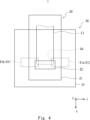
つまり、庇部630が最も+X側に配置され、終端部650が最も-X側に配置されている。閉じ込め構造体600の最も+X側の部分が庇部630となり、最も-X側の部分が終端部650となる。X方向において、対向部640が庇部630と終端部650との間に配置されている。
実施形態1では、部材610と部材620とがZ方向に並んで配置されていたのに対して、変形例1では2つの部材がX方向に並んで配置されている。変形例1にかかるビームダンパ60について、図12を用いて説明する。部材670の-X側に部材680が取り付けられている。部材670が内部空間601の上端及び下端を規定している。部材680が内部空間601の-X側の端部を規定している。
上記のポリシリコン膜を有する半導体装置は、有機EL(ElectroLuminescence)ディスプレイ用のTFT(Thin Film transistor)アレイ基板に好適である。すなわち、ポリシリコン膜は、TFTのソース領域、チャネル領域、ドレイン領域を有する半導体層として用いられる。
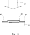
本実施の形態にかかるレーザ照射装置を用いた半導体装置の製造方法は、TFTアレイ基板の製造に好適である。TFTを有する半導体装置の製造方法について、図14、図15を用いて説明する。図14、図15は半導体装置の製造工程を示す工程断面図である。以下の説明では、逆スタガード(inverted staggered)型のTFTを有する半導体装置の製造方法について説明する。図14、図15では、半導体製造方法におけるポリシリコン膜の形成工程を示している。なお、その他の製造工程については、公知の手法を用いることができるため、説明を省略する。
10 光源
20 光学系モジュール
21 光学系筐体
22 ミラー
23 封止窓
30 密閉部
31 密閉筐体
33 封止窓
34 ガス入口
35 ガス出口
37 ガス
40 処理室
41 ガスボックス
42 導入窓
43 照射窓
44 ガス入口
45 基板ステージ
46 基台
47 走査装置
48 土台
49 搬送方向
51 遮断板
52 遮断板
54 スリット
55 スリット
57 反射ミラー
58 断熱材
60 ビームダンパ
201 ガラス基板
202 ゲート電極
203 ゲート絶縁膜
204 アモルファスシリコン膜
205 ポリシリコン膜
206 層間絶縁膜
207a ソース電極
207b ドレイン電極
300 有機ELディスプレイ
310 基板
311 TFT層
311a TFT
312 有機層
312a 有機EL発光素子
312b 隔壁
313 カラーフィルタ層
313a カラーフィルタ
314 封止基板
C1 光軸
L1 レーザ光
M1 基板
R1 反射光
R2 反射光
R3 反射光
600 閉じ込め構造体
601 内部空間
610 部材
611 冷却管
612 冷却管
620 部材
621 冷却管
622 冷却管
625 カバー
626 固定具
630 庇部
631 開口部
632 反射面
640 対向部
641 上側反射面
642 下側反射面
645 凸部
650 終端部
651 反射面
655 凹部
660 光吸収素子
661 シート
662 板バネ
Claims (18)
- レーザ光をラインビーム状にして、対象物に照射する光学系モジュールと、
前記対象物で反射した反射光を吸収するビームダンパと、備えたレーザ照射装置であって、
前記レーザ光が透過するスリットが形成された遮断板をさらに備えており、
前記ビームダンパは、前記遮断板で反射した反射光を吸収し、
前記ビームダンパは、第1部材と、前記第1部材に対向するように固定された第2部材とを備え、
前記第1部材は前記反射光が入射する庇部を備え、
前記庇部は、前記対象物で反射した反射光を前記第1部材と前記第2部材とで囲まれた内部空間に向けて反射する反射面を有しており、
前記庇部に設けられた前記反射面が凹面の曲面鏡となっており、
前記ラインビームの長手方向と直交する断面視において、円弧状又は放物線状となっており、
前記曲面鏡の曲率中心が、前記内部空間の外側、かつ、対象物側に配置されているレーザ照射装置。 - 前記ビームダンパには、前記内部空間に向けて配置され、前記反射光を吸収する光吸収素子が設けられている請求項1に記載のレーザ照射装置。
- 前記ビームダンパは、
前記光吸収素子が設けられた終端部と、
前記庇部と、前記終端部との間に配置された対向部と、をさらに備え、
前記対向部には、上側反射面と、前記上側反射面と対向する下側反射面とが設けられ、
前記庇部の前記反射面で反射した反射光の少なくとも一部が、前記上側反射面と前記下側反射面で反射して、前記光吸収素子に入射する請求項2に記載のレーザ照射装置。 - 前記上側反射面と前記下側反射面とが互いに平行な平面となっており、
前記終端部には、前記対向部からの反射光を前記光吸収素子に向けて反射する終端部反射面が設けられており、
前記庇部の前記反射面で反射した反射光の一部は前記上側反射面と前記下側反射面での反射を繰り返して、前記終端部反射面に入射し、
前記ラインビームの長手方向と直交する断面において、前記終端部反射面は、前記対象物側かつ前記対向部側を向いた凹面となっており、かつ、円弧状又は放物線状の曲面となっており、
前記ラインビームの長手方向と直交する断面において、前記終端部反射面の曲率中心が、前記内部空間内にある、
請求項3に記載のレーザ照射装置。 - 前記対象物の主面と直交する直交方向において、前記終端部が前記下側反射面よりも前記対象物側に窪んだ凹部を備え、
前記凹部に前記光吸収素子が配置されている請求項3、又は4に記載のレーザ照射装置。 - 前記庇部は、前記反射光が通過する開口部を有しており、
前記遮断板からの反射光が前記開口部を介して前記ビームダンパの前記内部空間に入射する請求項1~5のいずれか1項に記載のレーザ照射装置。 - 前記遮断板と前記ビームダンパとを収容する密閉筐体をさらに備えた請求項6に記載のレーザ照射装置。
- 前記第1部材及び前記第2部材の前記内部空間に向いた面が入射した前記反射光の一部を吸収する請求項1~7のいずれか1項に記載のレーザ照射装置。
- 前記第1部材及び前記第2部材には、冷却管が設けられている請求項1~8のいずれか1項に記載のレーザ照射装置。
- (A)光学系モジュールからレーザ光を、半導体を含む膜が形成された基板に向けて出射させる工程と、
(B)ラインビーム状の前記レーザ光を、前記基板に照射する工程と、
(C)前記基板に照射されたレーザ光のうち、前記基板で反射した反射光をビームダンパに受光させるステップと、を備え、
前記光学系モジュール
前記ビームダンパは、第1部材と、前記第1部材に対向するように固定された第2部材と、を備え、
前記第1部材は前記反射光が入射する庇部を備え、
前記庇部は、前記基板で反射した反射光を前記第1部材と前記第2部材とで囲まれた内部空間に向けて反射する反射面を有しており、
前記レーザ光を遮断板に形成されたスリットを通過させ、前記スリットを通過したレーザ光が前記基板に照射され、
前記庇部に設けられた前記反射面が凹面の曲面鏡となっており、
前記ラインビームの長手方向と直交する断面視において、円弧状又は放物線状となっており、
前記曲面鏡の曲率中心が、前記内部空間の外側、かつ、基板側に配置されている
半導体装置の製造方法。 - 前記ビームダンパには、前記内部空間に向けて配置され、前記反射光を吸収する光吸収素子が設けられている請求項10に記載の半導体装置の製造方法。
- 前記ビームダンパは、
前記光吸収素子が設けられた終端部と、
前記庇部と、前記終端部との間に配置された対向部と、をさらに備え、
前記対向部には、上側反射面と、前記上側反射面と対向する下側反射面とが設けられ、
前記庇部の前記反射面で反射した反射光の少なくとも一部が、前記上側反射面と前記下側反射面で反射して、前記光吸収素子に入射する請求項11に記載の半導体装置の製造方法。 - 前記上側反射面と前記下側反射面とが互いに平行な平面となっており、
前記終端部には、前記対向部からの反射光を前記光吸収素子に向けて反射する終端部反射面が設けられており、
前記庇部の前記反射面で反射した反射光の一部は前記上側反射面と前記下側反射面での反射を繰り返して、前記終端部反射面に入射し、
前記終端部反射面は、前記基板側かつ前記対向部側を向いた凹面となっており、
前記ラインビームの長手方向と直交する断面において、前記終端部反射面は、円弧状又は放物線状の曲面となっており、
前記ラインビームの長手方向と直交する断面において、前記終端部反射面の曲率中心が、前記内部空間内にある、
請求項12に記載の半導体装置の製造方法。 - 前記基板の主面と直交する直交方向において、前記終端部が前記下側反射面よりも前記基板側に窪んだ凹部を備え、
前記凹部に前記光吸収素子が配置されている請求項12、又は13に記載の半導体装置の製造方法。 - 前記庇部は、前記反射光が通過する開口部を有しており、
前記遮断板からの反射光が前記開口部を介して前記ビームダンパの前記内部空間に入射する請求項10~14のいずれか1項に記載の半導体装置の製造方法。 - 前記遮断板と前記ビームダンパとが密閉筐体に収容されている請求項15に記載の半導体装置の製造方法。
- 前記第1部材及び前記第2部材の前記内部空間に向いた面が入射した前記反射光の一部を吸収する請求項10~16のいずれか1項に記載の半導体装置の製造方法。
- 前記第1部材及び前記第2部材には、冷却管が設けられている請求項10~17のいずれか1項に記載の半導体装置の製造方法。
Priority Applications (5)
| Application Number | Priority Date | Filing Date | Title |
|---|---|---|---|
| JP2020187793A JP7579112B2 (ja) | 2020-11-11 | 2020-11-11 | レーザ照射装置、及び半導体装置の製造方法 |
| PCT/JP2021/040818 WO2022102538A1 (ja) | 2020-11-11 | 2021-11-05 | レーザ照射装置、及び半導体装置の製造方法 |
| CN202180075739.7A CN116420216A (zh) | 2020-11-11 | 2021-11-05 | 激光照射装置及制造半导体装置的方法 |
| KR1020237015822A KR20230104622A (ko) | 2020-11-11 | 2021-11-05 | 레이저 조사 장치, 및 반도체 장치의 제조 방법 |
| US18/035,775 US20230411159A1 (en) | 2020-11-11 | 2021-11-05 | Laser irradiation apparatus and method of manufacturing semiconductor apparatus |
Applications Claiming Priority (1)
| Application Number | Priority Date | Filing Date | Title |
|---|---|---|---|
| JP2020187793A JP7579112B2 (ja) | 2020-11-11 | 2020-11-11 | レーザ照射装置、及び半導体装置の製造方法 |
Publications (2)
| Publication Number | Publication Date |
|---|---|
| JP2022077121A JP2022077121A (ja) | 2022-05-23 |
| JP7579112B2 true JP7579112B2 (ja) | 2024-11-07 |
Family
ID=81602250
Family Applications (1)
| Application Number | Title | Priority Date | Filing Date |
|---|---|---|---|
| JP2020187793A Active JP7579112B2 (ja) | 2020-11-11 | 2020-11-11 | レーザ照射装置、及び半導体装置の製造方法 |
Country Status (5)
| Country | Link |
|---|---|
| US (1) | US20230411159A1 (ja) |
| JP (1) | JP7579112B2 (ja) |
| KR (1) | KR20230104622A (ja) |
| CN (1) | CN116420216A (ja) |
| WO (1) | WO2022102538A1 (ja) |
Families Citing this family (4)
| Publication number | Priority date | Publication date | Assignee | Title |
|---|---|---|---|---|
| JP2023174639A (ja) * | 2022-05-28 | 2023-12-08 | 大船企業日本株式会社 | プリント基板のレーザ加工方法およびプリント基板のレーザ加工機 |
| JP7237261B1 (ja) * | 2022-08-02 | 2023-03-10 | 三菱電機株式会社 | 開口数可変装置、レーザ装置およびレーザ加工機 |
| JP2025073873A (ja) * | 2023-10-27 | 2025-05-13 | 株式会社タムロン | 光アブソーバ、それを備えるビームスプリッタおよび光通信装置 |
| JP2025136290A (ja) * | 2024-03-07 | 2025-09-19 | プライムプラネットエナジー&ソリューションズ株式会社 | 組電池の製造装置および組電池の製造方法ならびにレーザ光減衰機構 |
Citations (5)
| Publication number | Priority date | Publication date | Assignee | Title |
|---|---|---|---|---|
| JP2003080390A (ja) | 2001-09-11 | 2003-03-18 | Kawasaki Heavy Ind Ltd | 高強度レーザビーム用光吸収装置 |
| JP2003151916A (ja) | 2001-08-03 | 2003-05-23 | Semiconductor Energy Lab Co Ltd | レーザ照射装置およびレーザ照射方法、並びに半導体装置の作製方法 |
| JP2005140964A (ja) | 2003-11-06 | 2005-06-02 | Nihon Koshuha Co Ltd | 光ビームアブゾーバ |
| JP2016161786A (ja) | 2015-03-02 | 2016-09-05 | ファナック株式会社 | 光ビームを吸収する光アブソーバ |
| JP2018060927A (ja) | 2016-10-06 | 2018-04-12 | 株式会社日本製鋼所 | レーザ照射装置及び半導体装置の製造方法 |
-
2020
- 2020-11-11 JP JP2020187793A patent/JP7579112B2/ja active Active
-
2021
- 2021-11-05 CN CN202180075739.7A patent/CN116420216A/zh active Pending
- 2021-11-05 US US18/035,775 patent/US20230411159A1/en active Pending
- 2021-11-05 KR KR1020237015822A patent/KR20230104622A/ko active Pending
- 2021-11-05 WO PCT/JP2021/040818 patent/WO2022102538A1/ja not_active Ceased
Patent Citations (5)
| Publication number | Priority date | Publication date | Assignee | Title |
|---|---|---|---|---|
| JP2003151916A (ja) | 2001-08-03 | 2003-05-23 | Semiconductor Energy Lab Co Ltd | レーザ照射装置およびレーザ照射方法、並びに半導体装置の作製方法 |
| JP2003080390A (ja) | 2001-09-11 | 2003-03-18 | Kawasaki Heavy Ind Ltd | 高強度レーザビーム用光吸収装置 |
| JP2005140964A (ja) | 2003-11-06 | 2005-06-02 | Nihon Koshuha Co Ltd | 光ビームアブゾーバ |
| JP2016161786A (ja) | 2015-03-02 | 2016-09-05 | ファナック株式会社 | 光ビームを吸収する光アブソーバ |
| JP2018060927A (ja) | 2016-10-06 | 2018-04-12 | 株式会社日本製鋼所 | レーザ照射装置及び半導体装置の製造方法 |
Also Published As
| Publication number | Publication date |
|---|---|
| JP2022077121A (ja) | 2022-05-23 |
| US20230411159A1 (en) | 2023-12-21 |
| CN116420216A (zh) | 2023-07-11 |
| KR20230104622A (ko) | 2023-07-10 |
| WO2022102538A1 (ja) | 2022-05-19 |
Similar Documents
| Publication | Publication Date | Title |
|---|---|---|
| JP7579112B2 (ja) | レーザ照射装置、及び半導体装置の製造方法 | |
| JP6803189B2 (ja) | レーザ照射装置及び半導体装置の製造方法 | |
| US9010155B2 (en) | Laser annealing apparatus | |
| US7135390B2 (en) | Method of fabricating a semiconductor device incorporating crystallizing by laser irradiation | |
| CN1333446C (zh) | 激光装置和激光退火方法 | |
| KR101017848B1 (ko) | 빔 호모지나이저 및 레이저 조사 장치와 반도체 장치 제조 방법 | |
| US6897166B2 (en) | Method of fabricating semiconductor device and system of fabricating semiconductor device | |
| US7474679B2 (en) | Laser apparatus and manufacturing method of thin film transistor using the same | |
| CN104741801B (zh) | 光照射设备 | |
| CN104752278B (zh) | 光照射设备 | |
| KR102490081B1 (ko) | 레이저 결정화 장치 및 방법 | |
| TWI749156B (zh) | 截止器及基板處理裝置 | |
| CN111435638B (zh) | 激光结晶装置 | |
| US12474555B2 (en) | Laser crystallization apparatus | |
| JP7781175B2 (ja) | レーザ照射装置、レーザ照射方法、及びディスプレイの製造方法 | |
| KR101333067B1 (ko) | 레이저 광을 라인 빔으로서 성형하기 위한 시스템 및 방법 | |
| JP2020145362A (ja) | レーザ処理装置 | |
| KR20220030462A (ko) | 광학계 및 이를 포함하는 레이저 조사 장치 | |
| KR20070062797A (ko) | 실리콘 결정화 장치 |
Legal Events
| Date | Code | Title | Description |
|---|---|---|---|
| A711 | Notification of change in applicant |
Free format text: JAPANESE INTERMEDIATE CODE: A712 Effective date: 20220317 |
|
| A621 | Written request for application examination |
Free format text: JAPANESE INTERMEDIATE CODE: A621 Effective date: 20230815 |
|
| A131 | Notification of reasons for refusal |
Free format text: JAPANESE INTERMEDIATE CODE: A131 Effective date: 20240625 |
|
| A521 | Request for written amendment filed |
Free format text: JAPANESE INTERMEDIATE CODE: A523 Effective date: 20240719 |
|
| TRDD | Decision of grant or rejection written | ||
| A01 | Written decision to grant a patent or to grant a registration (utility model) |
Free format text: JAPANESE INTERMEDIATE CODE: A01 Effective date: 20241008 |
|
| A61 | First payment of annual fees (during grant procedure) |
Free format text: JAPANESE INTERMEDIATE CODE: A61 Effective date: 20241025 |
|
| R150 | Certificate of patent or registration of utility model |
Ref document number: 7579112 Country of ref document: JP Free format text: JAPANESE INTERMEDIATE CODE: R150 |