JP7579112B2 - Laser irradiation device and method for manufacturing semiconductor device - Google Patents
Laser irradiation device and method for manufacturing semiconductor device Download PDFInfo
- Publication number
- JP7579112B2 JP7579112B2 JP2020187793A JP2020187793A JP7579112B2 JP 7579112 B2 JP7579112 B2 JP 7579112B2 JP 2020187793 A JP2020187793 A JP 2020187793A JP 2020187793 A JP2020187793 A JP 2020187793A JP 7579112 B2 JP7579112 B2 JP 7579112B2
- Authority
- JP
- Japan
- Prior art keywords
- reflecting surface
- light
- reflected
- laser
- substrate
- Prior art date
- Legal status (The legal status is an assumption and is not a legal conclusion. Google has not performed a legal analysis and makes no representation as to the accuracy of the status listed.)
- Active
Links
Images


Classifications
-
- H—ELECTRICITY
- H10—SEMICONDUCTOR DEVICES; ELECTRIC SOLID-STATE DEVICES NOT OTHERWISE PROVIDED FOR
- H10P—GENERIC PROCESSES OR APPARATUS FOR THE MANUFACTURE OR TREATMENT OF DEVICES COVERED BY CLASS H10
- H10P34/00—Irradiation with electromagnetic or particle radiation of wafers, substrates or parts of devices
- H10P34/40—Irradiation with electromagnetic or particle radiation of wafers, substrates or parts of devices with high-energy radiation
- H10P34/42—Irradiation with electromagnetic or particle radiation of wafers, substrates or parts of devices with high-energy radiation with electromagnetic radiation, e.g. laser annealing
-
- B—PERFORMING OPERATIONS; TRANSPORTING
- B23—MACHINE TOOLS; METAL-WORKING NOT OTHERWISE PROVIDED FOR
- B23K—SOLDERING OR UNSOLDERING; WELDING; CLADDING OR PLATING BY SOLDERING OR WELDING; CUTTING BY APPLYING HEAT LOCALLY, e.g. FLAME CUTTING; WORKING BY LASER BEAM
- B23K26/00—Working by laser beam, e.g. welding, cutting or boring
- B23K26/02—Positioning or observing the workpiece, e.g. with respect to the point of impact; Aligning, aiming or focusing the laser beam
- B23K26/06—Shaping the laser beam, e.g. by masks or multi-focusing
- B23K26/064—Shaping the laser beam, e.g. by masks or multi-focusing by means of optical elements, e.g. lenses, mirrors or prisms
-
- B—PERFORMING OPERATIONS; TRANSPORTING
- B23—MACHINE TOOLS; METAL-WORKING NOT OTHERWISE PROVIDED FOR
- B23K—SOLDERING OR UNSOLDERING; WELDING; CLADDING OR PLATING BY SOLDERING OR WELDING; CUTTING BY APPLYING HEAT LOCALLY, e.g. FLAME CUTTING; WORKING BY LASER BEAM
- B23K26/00—Working by laser beam, e.g. welding, cutting or boring
- B23K26/12—Working by laser beam, e.g. welding, cutting or boring in a special environment or atmosphere, e.g. in an enclosure
- B23K26/123—Working by laser beam, e.g. welding, cutting or boring in a special environment or atmosphere, e.g. in an enclosure in an atmosphere of particular gases
-
- B—PERFORMING OPERATIONS; TRANSPORTING
- B23—MACHINE TOOLS; METAL-WORKING NOT OTHERWISE PROVIDED FOR
- B23K—SOLDERING OR UNSOLDERING; WELDING; CLADDING OR PLATING BY SOLDERING OR WELDING; CUTTING BY APPLYING HEAT LOCALLY, e.g. FLAME CUTTING; WORKING BY LASER BEAM
- B23K26/00—Working by laser beam, e.g. welding, cutting or boring
- B23K26/12—Working by laser beam, e.g. welding, cutting or boring in a special environment or atmosphere, e.g. in an enclosure
- B23K26/127—Working by laser beam, e.g. welding, cutting or boring in a special environment or atmosphere, e.g. in an enclosure in an enclosure
-
- B—PERFORMING OPERATIONS; TRANSPORTING
- B23—MACHINE TOOLS; METAL-WORKING NOT OTHERWISE PROVIDED FOR
- B23K—SOLDERING OR UNSOLDERING; WELDING; CLADDING OR PLATING BY SOLDERING OR WELDING; CUTTING BY APPLYING HEAT LOCALLY, e.g. FLAME CUTTING; WORKING BY LASER BEAM
- B23K26/00—Working by laser beam, e.g. welding, cutting or boring
- B23K26/34—Laser welding for purposes other than joining
-
- B—PERFORMING OPERATIONS; TRANSPORTING
- B23—MACHINE TOOLS; METAL-WORKING NOT OTHERWISE PROVIDED FOR
- B23K—SOLDERING OR UNSOLDERING; WELDING; CLADDING OR PLATING BY SOLDERING OR WELDING; CUTTING BY APPLYING HEAT LOCALLY, e.g. FLAME CUTTING; WORKING BY LASER BEAM
- B23K26/00—Working by laser beam, e.g. welding, cutting or boring
- B23K26/352—Working by laser beam, e.g. welding, cutting or boring for surface treatment
-
- B—PERFORMING OPERATIONS; TRANSPORTING
- B23—MACHINE TOOLS; METAL-WORKING NOT OTHERWISE PROVIDED FOR
- B23K—SOLDERING OR UNSOLDERING; WELDING; CLADDING OR PLATING BY SOLDERING OR WELDING; CUTTING BY APPLYING HEAT LOCALLY, e.g. FLAME CUTTING; WORKING BY LASER BEAM
- B23K26/00—Working by laser beam, e.g. welding, cutting or boring
- B23K26/70—Auxiliary operations or equipment
- B23K26/702—Auxiliary equipment
- B23K26/704—Beam dispersers, e.g. beam wells
-
- G—PHYSICS
- G02—OPTICS
- G02B—OPTICAL ELEMENTS, SYSTEMS OR APPARATUS
- G02B17/00—Systems with reflecting surfaces, with or without refracting elements
- G02B17/002—Arrays of reflective systems
-
- H—ELECTRICITY
- H10—SEMICONDUCTOR DEVICES; ELECTRIC SOLID-STATE DEVICES NOT OTHERWISE PROVIDED FOR
- H10P—GENERIC PROCESSES OR APPARATUS FOR THE MANUFACTURE OR TREATMENT OF DEVICES COVERED BY CLASS H10
- H10P72/00—Handling or holding of wafers, substrates or devices during manufacture or treatment thereof
- H10P72/04—Apparatus for manufacture or treatment
- H10P72/0431—Apparatus for thermal treatment
- H10P72/0436—Apparatus for thermal treatment mainly by radiation
-
- H—ELECTRICITY
- H10—SEMICONDUCTOR DEVICES; ELECTRIC SOLID-STATE DEVICES NOT OTHERWISE PROVIDED FOR
- H10P—GENERIC PROCESSES OR APPARATUS FOR THE MANUFACTURE OR TREATMENT OF DEVICES COVERED BY CLASS H10
- H10P95/00—Generic processes or apparatus for manufacture or treatments not covered by the other groups of this subclass
- H10P95/90—Thermal treatments, e.g. annealing or sintering
-
- B—PERFORMING OPERATIONS; TRANSPORTING
- B23—MACHINE TOOLS; METAL-WORKING NOT OTHERWISE PROVIDED FOR
- B23K—SOLDERING OR UNSOLDERING; WELDING; CLADDING OR PLATING BY SOLDERING OR WELDING; CUTTING BY APPLYING HEAT LOCALLY, e.g. FLAME CUTTING; WORKING BY LASER BEAM
- B23K2101/00—Articles made by soldering, welding or cutting
- B23K2101/36—Electric or electronic devices
- B23K2101/40—Semiconductor devices
-
- B—PERFORMING OPERATIONS; TRANSPORTING
- B23—MACHINE TOOLS; METAL-WORKING NOT OTHERWISE PROVIDED FOR
- B23K—SOLDERING OR UNSOLDERING; WELDING; CLADDING OR PLATING BY SOLDERING OR WELDING; CUTTING BY APPLYING HEAT LOCALLY, e.g. FLAME CUTTING; WORKING BY LASER BEAM
- B23K2103/00—Materials to be soldered, welded or cut
- B23K2103/50—Inorganic materials other than metals or composite materials
- B23K2103/56—Inorganic materials other than metals or composite materials being semiconducting
-
- H—ELECTRICITY
- H10—SEMICONDUCTOR DEVICES; ELECTRIC SOLID-STATE DEVICES NOT OTHERWISE PROVIDED FOR
- H10P—GENERIC PROCESSES OR APPARATUS FOR THE MANUFACTURE OR TREATMENT OF DEVICES COVERED BY CLASS H10
- H10P14/00—Formation of materials, e.g. in the shape of layers or pillars
- H10P14/20—Formation of materials, e.g. in the shape of layers or pillars of semiconductor materials
- H10P14/34—Deposited materials, e.g. layers
- H10P14/3402—Deposited materials, e.g. layers characterised by the chemical composition
- H10P14/3404—Deposited materials, e.g. layers characterised by the chemical composition being Group IVA materials
- H10P14/3411—Silicon, silicon germanium or germanium
-
- H—ELECTRICITY
- H10—SEMICONDUCTOR DEVICES; ELECTRIC SOLID-STATE DEVICES NOT OTHERWISE PROVIDED FOR
- H10P—GENERIC PROCESSES OR APPARATUS FOR THE MANUFACTURE OR TREATMENT OF DEVICES COVERED BY CLASS H10
- H10P14/00—Formation of materials, e.g. in the shape of layers or pillars
- H10P14/20—Formation of materials, e.g. in the shape of layers or pillars of semiconductor materials
- H10P14/38—Formation of materials, e.g. in the shape of layers or pillars of semiconductor materials characterised by treatments done after the formation of the materials
- H10P14/3802—Crystallisation or recrystallisation of non-monocrystalline semiconductor materials, e.g. regrowth
- H10P14/3808—Crystallisation or recrystallisation of non-monocrystalline semiconductor materials, e.g. regrowth using laser beams
Landscapes
- Physics & Mathematics (AREA)
- Engineering & Computer Science (AREA)
- Optics & Photonics (AREA)
- Plasma & Fusion (AREA)
- Mechanical Engineering (AREA)
- General Physics & Mathematics (AREA)
- Recrystallisation Techniques (AREA)
- Electromagnetism (AREA)
- Health & Medical Sciences (AREA)
- Toxicology (AREA)
Description
本発明はレーザ照射装置、及び半導体装置の製造方法に関する。 The present invention relates to a laser irradiation device and a method for manufacturing a semiconductor device.
シリコン基板やガラス基板などに形成された非晶質膜にレーザ光を照射し、非晶質膜を結晶化させるレーザアニール装置が知られている。特許文献1には、スリットを通過させることによって、レーザ光の光軸に直交する断面において、強度が減少する端部を遮断し、一様な強度のレーザ光を照射光として用いるレーザアニール装置が開示されている。
There is a known laser annealing device that irradiates an amorphous film formed on a silicon substrate, a glass substrate, or the like with laser light to crystallize the amorphous film.
特許文献1に開示されたレーザアニール装置は、スリットが形成された遮断板と、遮断板で反射した反射光を吸収する反射光受光部材とを備えている。反射光受光部材としては、多層熱吸収膜が用いられている。
The laser annealing device disclosed in
このようなレーザアニール装置では、スリットや基板などで反射した反射光により、光学系モジュールの温度が上昇してしまう。光学系モジュールの温度上昇により、各光学素子の位置ずれが発生して、照射ムラが発生してしまう。したがって、温度上昇を抑制することが望まれる。 In such a laser annealing device, the temperature of the optical system module rises due to the light reflected by the slit, the substrate, etc. The temperature rise of the optical system module causes the positional deviation of each optical element, resulting in uneven irradiation. Therefore, it is desirable to suppress the temperature rise.
また、特許文献1では、多層吸収膜を用いて反射光を吸収している。高出力レーザ光を用いた場合、多層吸収膜が損傷、又は変色してしまうおそれがある。多層吸収膜が損傷又は変色すると吸収率が低下して、温度上昇を招くおそれがある。
In addition, in
その他の課題と新規な特徴は、本明細書の記述および添付図面から明らかになるであろう。 Other objects and novel features will become apparent from the description of this specification and the accompanying drawings.
一実施の形態にかかるレーザ照射装置は、レーザ光を対象物に照射する光学系モジュールと、前記対象物で反射した反射光を吸収するビームダンパと、備えたレーザ照射装置であって、前記ビームダンパは、第1部材と、前記第1部材に対向するように固定された第2部材とを備え、前記第1部材は前記反射光が入射する庇部を備え、前記庇部は、前記対象物で反射した反射光を前記第1部材と前記第2部材とで囲まれた内部空間に向けて反射する反射面を有している。 The laser irradiation device according to one embodiment includes an optical system module that irradiates a laser beam onto an object, and a beam damper that absorbs the light reflected by the object. The beam damper includes a first member and a second member fixed to face the first member. The first member includes a visor portion on which the reflected light is incident, and the visor portion has a reflective surface that reflects the light reflected by the object toward an internal space surrounded by the first member and the second member.
一実施の形態にかかる半導体装置の製造方法は、(A)光学系モジュールからレーザ光を、半導体を含む膜が形成された基板に向けて出射させる工程と、(B)前記レーザ光を、前記基板に照射する工程と、(C)前記基板に照射されたレーザ光のうち、前記基板で反射した反射光をビームダンパに受光させるステップと、を備え、前記ビームダンパは、第1部材と、前記第1部材に対向するように固定された第2部材とを備え、前記第1部材は前記反射光が入射する庇部を備え、前記庇部は、前記基板で反射した反射光を前記第1部材と前記第2部材とで囲まれた内部空間に向けて反射する反射面を有している。 A method for manufacturing a semiconductor device according to one embodiment includes the steps of: (A) emitting laser light from an optical module toward a substrate on which a film containing a semiconductor is formed; (B) irradiating the substrate with the laser light; and (C) receiving, in a beam damper, light reflected by the substrate from the laser light irradiated to the substrate. The beam damper includes a first member and a second member fixed to face the first member, the first member includes an overhanging portion on which the reflected light is incident, and the overhanging portion has a reflective surface that reflects the light reflected by the substrate toward an internal space surrounded by the first member and the second member.
前記一実施の形態によれば、安定してレーザ光を照射することができるレーザ照射装置及び半導体装置の製造方法を提供することができる。 According to the embodiment, it is possible to provide a laser irradiation device capable of stably irradiating laser light and a method for manufacturing a semiconductor device.
(実施形態1)
実施形態1に係るレーザ照射装置を説明する。本実施形態に係るレーザ照射装置は、レーザ光を被照射体に照射する装置である。被照射体は、例えば、非晶質膜等の半導体を含む膜が形成された基板である。この場合には、レーザ照射装置は、非晶質膜にレーザ光を照射して結晶化させるレーザアニール処理を行う。例えば、レーザ光として、エキシマレーザを用いてレーザアニール処理する場合には、レーザ照射装置は、エキシマレーザアニール(ELA:Excimer Laser Anneal)装置として用いられる。
(Embodiment 1)
A laser irradiation device according to the first embodiment will be described. The laser irradiation device according to the present embodiment is a device that irradiates a laser beam onto an irradiated object. The irradiated object is, for example, a substrate on which a film including a semiconductor such as an amorphous film is formed. In this case, the laser irradiation device performs a laser annealing process in which the amorphous film is irradiated with a laser beam to crystallize the film. For example, when an excimer laser is used as the laser beam for the laser annealing process, the laser irradiation device is used as an excimer laser annealing (ELA) device.
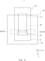
まず、レーザ照射装置の構成を説明する。図1は、実施形態1に係るレーザ照射装置を例示した断面図である。図2は、実施形態1に係るレーザ照射装置の要部を例示した断面図である。図3は、図2に示すレーザ照射装置の要部の切断線III-IIIにおける断面図である。図4は、図2に示すレーザ照射装置の要部の切断線IV-IVにおける断面図である。図5は、実施形態1に係るレーザ照射装置のレーザ光とスリットとの関係を例示した斜視図である。 First, the configuration of the laser irradiation device will be described. Fig. 1 is a cross-sectional view illustrating the laser irradiation device according to the first embodiment. Fig. 2 is a cross-sectional view illustrating the main part of the laser irradiation device according to the first embodiment. Fig. 3 is a cross-sectional view taken along line III-III of the main part of the laser irradiation device shown in Fig. 2. Fig. 4 is a cross-sectional view taken along line IV-IV of the main part of the laser irradiation device shown in Fig. 2. Fig. 5 is a perspective view illustrating the relationship between the laser light and the slit of the laser irradiation device according to the first embodiment.
図1に示すように、レーザ照射装置1は、光源10、光学系モジュール20、密閉部30、処理室40を有している。処理室40は、例えば、水平な土台48上に設けられている。処理室40の上方に密閉部30が設けられ、密閉部30の上方に光学系モジュール20が設けられている。光学系モジュール20は、光源10から放出されるレーザ光L1を受光することが可能な位置に設けられている。
As shown in FIG. 1, the
ここで、レーザ照射装置1を説明するために、XYZ直交座標軸を導入する。土台48の上面に直交する方向をZ軸方向とし、上方を+Z軸方向、下方を-Z軸方向とする。光源10と光学系モジュール20とを結ぶ方向をX軸方向とし、光源10から光学系モジュール20に向かう方向を+X軸方向、逆方向を-X軸方向とする。X軸方向及びZ軸方向に直交する方向をY軸方向とし、一方を+Y軸方向、逆方向を-Y軸方向とする。
Here, to explain the
図1に示すように、光源10は、レーザ光L1を放出する。光源10は、例えば、エキシマレーザ光源であり、中心波長308nmのエキシマレーザのレーザ光L1を放出する。また、光源10は、パルス状のレーザ光L1を放出する。光源10は、レーザ光L1を光学系モジュール20に向けて出射する。レーザ光L1は、例えば、+X軸方向に進み、光学系モジュール20に入射する。なお、必要に応じて、光源10と、光学系モジュール20との間のレーザ光L1の光路上に、エネルギー密度を調整するアテニュエータ等の光学素子を配置してもよい。
As shown in FIG. 1, the
図1~4に示すように、光学系モジュール20は、外形を構成する光学系筐体21、ミラー22、レンズ等の光学素子、及び、封止窓23を含んでいる。光学系筐体21は、例えば、アルミニウム等の材料で構成された箱状の部材である。光学系モジュール20の各光学素子は、光学系筐体21の内部にホルダ等で保持されている。このような各光学素子により、光学系モジュール20は、光源10から放出されたレーザ光L1の照射方向、光量等を調整する。封止窓23は、光学系筐体21の一部、例えば、光学系筐体21の下面に設けられている。レーザ光L1は、光学系モジュール20で調整された後に、封止窓23から密閉部30に向けて出射される。このようにして、光学系モジュール20は、レーザ光L1を被照射体(対象物ともいう)に照射する。
As shown in Figures 1 to 4, the
図5に示すように、レーザ光L1は、光学系モジュール20において、ラインビーム状となっている。すなわち、レーザ光L1の光軸C1に直交する断面は、一方向に延びた細長い線状となっている。例えば、ミラー22で反射されたレーザ光L1の光軸に直交する断面は、Y軸方向に延びた線状となっている。
As shown in FIG. 5, the laser light L1 is in the form of a line beam in the
図2~4に示すように、密閉部30は、密閉筐体31、遮断板51、ビームダンパ60、封止窓33、ガス入口34、ガス出口35を有している。図が煩雑にならないように、図3では、ガス入口34、ガス出口35を省略し、図4では、ビームダンパ60、封止窓33、ガス入口34、ガス出口35を省略している。なお、説明を明確にするため、各図面は、適宜、簡略化されている。
As shown in Figures 2 to 4, the sealed
密閉筐体31は、内部が空洞の箱状の部材である。密閉筐体31の内部に、遮断板51、ビームダンパ60が配置されている。密閉筐体31の所定の側面には、ガス入口34及びガス出口35が設けられている。ガス入口34及びガス出口35は、例えば、密閉筐体31における対向する側面に設けられている。例えば、ガス出口35は、ガス入口34よりも上方に設けられている。ガス入口34からは、ガス37、例えば、窒素等の不活性ガスが導入される。ガス入口34から密閉筐体31の内部に導入されたガス37は、ガス出口35から排出される。ガス37は、密閉筐体31の内部に連続的に供給されることが望ましい。また、ガス37は、密閉筐体31の外部に連続的に排出されるのが望ましい。ガス37の流量は、密閉筐体31の内部を常時換気された状態になるように、所定の流量に制御される。
The sealed
図2~5に示すように、遮断板51は、光学系モジュール20の封止窓23から出射したレーザ光L1が、処理室40に到達する光路上に配置されている。遮断板51は、例えば、複数の部材を含んでいる。遮断板51は、例えば、遮断板51a及び遮断板51bを含んでいる。遮断板51a及び遮断板51bは、一方向、例えばY軸方向に延びた板状の部材となっている。遮断板51a及び遮断板51bは、板面をZ軸方向に向けて配置されている。遮断板51a及び遮断板51bは、Y軸方向に間隔を空けて並んで配置されている。したがって、遮断板51a及び遮断板51bの間には、スリット54が形成されている。各遮断板51a及び51bは、+Y軸方向及び-Y軸方向に図示しないモータで可動であり、スリット54の幅(遮断板51aと遮断板51bとの間の長さ)は、適宜設定可能である。レーザ光L1は、スリット54を通過する。このように、遮断板51には、レーザ光L1が通過するスリット54が形成されている。
As shown in Figures 2 to 5, the blocking
レーザ光L1のY軸方向における両端部は、遮断板51a及び遮断板51bに遮断される。遮断板51a及び遮断板51bに遮断されたレーザ光L1の端部は、遮断板51a及び遮断板51bで反射し、反射光R1となる。このように、スリット54及び遮断板51に対して照射されたレーザ光L1のうち、遮断板51で遮断されたレーザ光L1が、遮断板51で反射する。なお、図1~図5では遮断板51は、XY平面に平行な平板となっているが、XY平面から傾斜するように配置されていてもよい(図9参照)。
Both ends of the laser light L1 in the Y-axis direction are blocked by the blocking
遮断板51の光学系モジュール20側の面に、反射ミラー57が設けられてもよい。これにより、遮断板51に遮断されたレーザ光L1が、遮断板51に吸収されることを抑制することができる。よって、遮断板51の温度が上昇することにより、遮断板51の近傍の雰囲気が乱れることを抑制することができる。反射ミラー57に施される反射膜は、レーザ光L1の入射角度に対して所定の耐性を有する仕様に処理されていることが望ましい。一般的に、反射膜には、レーザ光L1の入射角度によって反射率が極端に変化するものから、レーザ光L1の入射角によっても反射率があまり変化しないものまである。本実施形態では、被照射体に対してレーザ照射を実施する際に想定しうるレーザ光L1の入射角の変化に対して、反射率が所定の範囲内に収まる反射膜を用いる。
A reflecting
ビームダンパ60は、遮断板51と、光学系モジュール20との間に配置されている。例えば、ビームダンパ60は、光学系モジュール20の外側に、光学系モジュール20との間に間隔を有するように配置されている。ビームダンパ60の詳細な構成については後述する。ビームダンパ60は、遮断板51で遮断されたレーザ光L1が遮断板51で反射された反射光R1を受光することが可能なように配置されている。例えば、レーザ光L1の入射角と、反射光R1の反射角とを考慮して、ビームダンパ60を、反射光R1の光路上に配置する。
The
封止窓33は、密閉筐体31の一部、例えば、密閉筐体31の下面に設けられている。光学系モジュール20の封止窓23から出射したレーザ光L1は、遮断板51の間のスリット54を通る。そして、スリット54を通ったレーザ光L1は、封止窓33から処理室40に向けて出射する。
The sealing
図1に示すように、処理室40は、ガスボックス41、遮断板52、基板ステージ45、基台46、走査装置47を有している。例えば、処理室40において、基板ステージ45上に載置された基板M1にレーザ光L1が照射され、基板M1上の非晶質膜を結晶化するレーザアニール処理が行われる。基板ステージ45は、フロートタイプステージ、すなわち、被照射体である基板M1を浮上させながら搬送するステージでもよい。
As shown in FIG. 1, the
図2及び図3に示すように、ガスボックス41は、箱状の部材であって、内部は空洞となっている。ガスボックス41は、基板ステージ45の上方であって、密閉部30における封止窓33の下方に配置されている。ガスボックス41の上面には、導入窓42が設けられている。導入窓42は、封止窓33に対向するように配置されている。また、ガスボックス41の下面には、照射窓43が設けられている。照射窓43は、基板M1上の非晶質膜に対向するように配置されている。
As shown in Figures 2 and 3, the
ガスボックス41の所定の側面には、ガス入口44が設けられている。ガスボックス41には、ガス入口44から、所定のガス37、例えば、窒素等の不活性ガスが供給される。ガスボックス41に供給されたガス37は、ガスボックス41の内部を充填した後、照射窓43から排出される。
A
遮断板52は、密閉部30の封止窓33から出射したレーザ光L1が、基板M1上の非晶質膜に到達する光路上に配置されている。遮断板52は、例えば、ガスボックス41の内部において、照射窓43を覆うように配置されている。
The blocking
図3及び図5に示すように、遮断板52は、例えば、複数の部材を含んでいる。遮断板52は、例えば、遮断板52a及び遮断板52bを含んでいる。遮断板52a及び遮断板52bは、一方向に延びた板状の部材である。遮断板52a及び遮断板52bは、板面をZ軸方向に向け、延びた方向をY方向にして配置されている。遮断板52a及び遮断板52bは、Y軸方向に間隔を空けて並んで配置されている。したがって、遮断板52a及び遮断板52bの間には、スリット55が形成されている。各遮断板52a及び52bは、+Y軸方向及び-Y軸方向に図示しないモータで可動であり、スリット55の幅(遮断板52aと遮断板52bとの間の長さ)は、適宜設定可能である。レーザ光L1は、スリット55を通過する。このように、遮断板52には、スリット54を通過したレーザ光L1が通過するスリット55が形成されている。
3 and 5, the blocking
レーザ光L1のY軸方向における両端部は、遮断板52a及び遮断板52bに遮断される。遮断板52a及び遮断板52bに遮断されたレーザ光L1の端部は、遮断板52a及び遮断板52bで反射し、反射光R2となる。このように、スリット55及び遮断板52に対して照射されたレーザ光L1のうち、遮断板52で遮断されたレーザ光L1が、遮断板52で反射する。
Both ends of the laser light L1 in the Y-axis direction are blocked by the blocking
ビームダンパ60は、スリット55及び遮断板52に対して照射されたレーザ光L1のうち、遮断板52で遮断されたレーザ光L1が遮断板52で反射された反射光R2を受光することが可能なように配置されている。
The
遮断板52の光学系モジュール20側の面に、反射ミラー57が設けられてもよい。これにより、遮断板52に遮断されたレーザ光L1が、遮断板52に吸収されることを抑制することができる。よって、遮断板52の温度が上昇することにより、遮断板52の近傍の雰囲気が乱れることを抑制することができる。反射ミラー57に含まれる反射膜は、レーザ光L1の入射角度に対し、所定の耐性を有する仕様に処理されることが望ましい。
A reflecting
遮断板52の間のスリット55を通ったレーザ光L1は、照射窓43から出射し、基板M1上の非晶質膜を照射する。レーザ光L1は-X方向かつ-Z方向に進んで、基板M1に照射される。つまり、レーザ光L1は、基板M1の主面(XY平面)の法線から傾いた方向から、基板M1に入射する。
The laser light L1 that passes through the
基板M1は、基板ステージ45上に載置されている。基板M1は、例えば、シリコン基板等の半導体基板、または、石英基板等である。なお、基板M1は、半導体基板及び石英基板に限らない。基板M1上には、非晶質膜等の半導体を含む膜が形成されている。非晶質膜は、例えば、アモルファスシリコン(aSi)を含んでいる。基板M1上の非晶質膜をレーザ光L1によって照射することにより、結晶化させる。結晶化させることにより、基板M1上には、例えば、ポリシリコン(polySi)を含む結晶質膜が形成される。
The substrate M1 is placed on the
基板M1上の非晶質膜を照射したレーザ光L1は、非晶質膜または基板M1で反射し、反射光R3となる。ビームダンパ60は、非晶質膜または基板M1を照射したレーザ光L1が非晶質膜または基板M1で反射した反射光R3を受光することが可能なように配置されている。
The laser light L1 irradiated to the amorphous film on the substrate M1 is reflected by the amorphous film or the substrate M1 to become reflected light R3. The
図1に示すように、基板ステージ45は、走査装置47上に、例えば、基台46を介して載置されている。基板ステージ45は、走査装置47により、X軸方向、Y軸方向及びZ軸方向に移動可能となっている。レーザアニール処理を行う際には、基板ステージ45を、走査装置47の走査により、例えば、-X軸方向の搬送方向49に搬送させる。
As shown in FIG. 1, the
次に、実施形態1に係るレーザ照射装置1を用いたレーザ照射方法を説明する。図6は、実施形態1に係るレーザ照射装置を用いたレーザ照射方法を例示したフローチャート図である。
Next, a laser irradiation method using the
図6のステップS11に示すように、まず、光学系モジュール20からレーザ光L1を出射させる。光源10から放出されたレーザ光L1の照射方向、光量等を光学系モジュール20において調整し、密閉部30に対してレーザ光L1を出射させる。例えば、被照射体が、非晶質膜等の半導体を含む膜が形成された基板M1の場合には、光学系モジュールからレーザ光を、基板M1に向けて出射させる。
As shown in step S11 of FIG. 6, first, laser light L1 is emitted from the
次に、図6のステップS12に示すように、レーザ光L1を、遮断板51に形成されたスリットを通過させる。すなわち、レーザ光L1が通過するスリット54が形成された遮断板51を設け、スリット54及び遮断板51に対して照射されたレーザ光L1のうち、スリット54に対して照射されたレーザ光L1について、スリット54を通過させる。また、スリット55が形成された遮断板52を設け、スリット54を通過し、スリット55及び遮断板52に対して照射されたレーザ光L1のうち、スリット55に対して照射されたレーザ光L1について、スリット55を通過させる。なお、レーザ照射装置1が、遮断板51及び遮断板52を有していない構成である場合、ステップS12は、省略可能である。つまり、本実施の形態では、遮断板51及び遮断板52を有していない構成にも適用可能である。
Next, as shown in step S12 of FIG. 6, the laser light L1 is passed through a slit formed in the blocking
ここでは、スリット54及び遮断板51に対して照射されたレーザ光L1のうち、遮断板51に対して照射されたレーザ光L1を遮断板51で遮断する。また、スリット55及び遮断板52に対して照射されたレーザ光L1のうち、遮断板52に対して照射されたレーザ光L1を、遮断板52で遮断する。これにより、レーザ光L1の光軸に直交する断面において、端部を遮断し、端部以外の部分を被照射体の照射に用いる。
Here, of the laser light L1 irradiated to the
次に、図6のステップS13に示すように、レーザ光L1を被照射体に照射する。すなわち、スリット54及び遮断板51に対して照射されたレーザ光L1のうち、スリット54を通過させたレーザ光L1を、被照射体に照射する。被照射体が、非晶質膜等の半導体を含む膜が形成された基板の場合には、非晶質膜に対してレーザ光L1を照射する。具体的には、基板M1の搬送方向49、例えば、-X軸方向に基板M1を搬送しながら、基板M1に形成された非晶質膜に対してレーザ光L1を照射する。
Next, as shown in step S13 of FIG. 6, the laser light L1 is irradiated to the irradiated object. That is, of the laser light L1 irradiated to the
次に、図6のステップS14に示すように、反射光Rをビームダンパ60に受光させる。例えば、基板M1を照射したレーザ光L1が、基板M1で反射した反射光R3をビームダンパ60に受光させる。遮断板51に対して照射されたレーザ光L1が遮断板51で反射した反射光R1を、ビームダンパ60に受光させる。また、遮断板52に対して照射されたレーザ光L1が遮断板52で反射した反射光R2を、ビームダンパ60に受光させる。なお、ビームダンパ60は、光学系モジュール20と遮断板51との間に配置されている。
Next, as shown in step S14 of FIG. 6, the reflected light R is received by the
このようにして、実施形態1に係るレーザ照射装置1を用いて、レーザ照射をすることができる。
In this way, laser irradiation can be performed using the
次に、ビームダンパ60の構成について、図7を用いて説明する。図7は、ビームダンパ60を含む密閉筐体31の断面構成を示す模式図である。上記のように、ビームダンパ60は、上記の反射光R1~R3を受光するように配置されている。密閉筐体31には、不活性ガスとして、窒素ガスN2が供給されている。レーザ光L1が-X方向に進んでいるため、反射光R1~R3も-X方向に進んでいる。よって、ビームダンパ60は、基板におけるレーザ光L1の照射位置よりも-X側に配置されている。
Next, the configuration of the
ビームダンパ60を、光学系モジュール20との間に断熱材58を介して取り付けてられている。これにより、ビームダンパ60と光学系モジュール20との間の断熱性を保つことができる。あるいは、ビームダンパ60を、光学系モジュール20との間に断熱空気層となる隙間58bを設けて、隙間58bを局所排気してもよい。これにより、ビームダンパ60と光学系モジュール20との間の断熱性を保つことができる。
The
ビームダンパ60は閉じ込め構造体600と、閉じ込め構造体600の内部に収容された光吸収素子660とを備えている。閉じ込め構造体600は、例えば、アルミニウムやその合金などの金属材料により形成されている。閉じ込め構造体600は入射した反射光R1~R3を閉じ込め可能な構造を有している。閉じ込め構造体600には、水冷用の冷却管(図7では不図示)が設けられている。
The
閉じ込め構造体600の内部には、光吸収素子660が取り付けられている.光吸収素子660は、例えば、SiO2とCrとが交互に積層された多層吸収膜を有している。光吸収素子660は、レーザ波長に対して高い吸収率を有している。例えば、光吸収素子660は、レーザ波長に対して95%以上、より好ましくは98%以上の吸収率を有している。なお、レーザ波長は、308nmとしたが、これに限られるものではない。例えば、レーザ波長は、248nm、351nm、355nm等の紫外領域である。もちろん、光吸収素子660は、多層膜構造に限られるものはない。
A
閉じ込め構造体600に入射した反射光R1~R3は、閉じ込め構造体600内で反射を繰り返しながら、光吸収素子660に入射する。閉じ込め構造体600は、入射した反射光R1~R3を閉じ込めることができる。閉じ込め構造体600は、その内部空間601に入射した反射光R1~R3が外側に漏れないような形状となっている。
The reflected light R1 to R3 incident on the
具体的には、閉じ込め構造体600は+X側の端部に、反射光R1~R3が入射する開口部631を有している。内部空間601の-X側の端部には、光吸収素子660が設けられている。開口部631から内部空間601に入射した反射光R1~R3は、内部空間601内を-X方向に伝播していく。内部空間601において、閉じ込め構造体600の内壁で1回又は複数回反射した反射光R1~R3は、光吸収素子660に入射する。光吸収素子660は、反射光R1~R3の一部を吸収する。
Specifically, the
さらに、閉じ込め構造体600の内壁はレーザ波長に対する光反射率が90%程度となっている反射面となっている。閉じ込め構造体600の内部空間601を構成する内壁は、反射光の一部を吸収する。換言すると、反射光R1~R3は、閉じ込め構造体600で反射する毎に、その一部が吸収される。これにより、光吸収素子660に入射するエネルギーを抑制することができるため、光吸収素子660の劣化を防ぐことができる。
Furthermore, the inner wall of the
このように、閉じ込め構造体600は、内部空間601に入射した反射光の一部を吸収する。閉じ込め構造体600は、熱伝導率の高い金属材料により構成されており、かつ水冷されている。よって効率良くレーザエネルギーを吸収することができ、温度上昇を抑制することができる。
In this way, the
ビームダンパ60の構成の一例について、図8を用い説明する。図8はビームダンパ60の詳細な構成を示す斜視図である。図8は、ビームダンパ60を斜め下方から見た断面図である。
An example of the configuration of the
閉じ込め構造体600は、部材610と、部材620とを備えている。部材620は、部材610の下側に配置されている。部材620は、部材610に対向するように固定されている。例えば、ボルト(不図示)を下側から部材620に挿通することで、部材620を部材610に取り付けることができる。あるいは、上側から部材610にボルトを挿通することで、部材610と部材620とを固定してもよい。もちろん、部材610と部材620と固定する方法は特に限定されるものではなく、ブラケットなどによって、部材610と部材620とが固定されていてもよい。
The
部材610と部材620との間には、内部空間601が形成される。部材610が内部空間601の上端(+Z側の端部)を規定し、部材620が内部空間601の下端(-Z側の端部)を規定している。部材610と部材620と間の内部空間601を反射光R1~R3が伝播していく。
An
部材610及び部材620は、アルミニウムなどの金属材料により形成されている。部材610には、冷却管611、及び冷却管612が設けられている。部材610にY方向に沿った貫通穴を設けることで、部材610の内部に冷却管611、及び冷却管612を通すことができる。冷却管611、及び冷却管612は、Y方向に沿って配置されている。もちろん、水冷ジャケットなどにより、冷却管611、及び冷却管612を部材610に固定してもよい。
同様に、部材620には、冷却管621、及び冷却管622が設けられている。部材620にY方向に沿った貫通穴を設けることで、部材620の内部に冷却管621、及び冷却管622を通すことができる。冷却管621、622は、光吸収素子660の直下に配置されている。冷却管621、及び冷却管622は、Y方向に沿って配置されている。水冷ジャケットなどにより、冷却管621、及び冷却管622を部材620に固定してもよい。
Similarly, cooling
このように、冷却管611、冷却管612、冷却管621、冷却管622に冷却水を流すことで、閉じ込め構造体600を効果的に冷却することができる。もちろん、冷却管611、冷却管612、冷却管621、冷却管622の配置や数は、図7に示す構成に限定されるものではない。冷却管621、冷却管622を光吸収素子660の近傍に配置することで効率よく冷却することができる。
In this way, by flowing cooling water through cooling
閉じ込め構造体600は、庇部630、対向部640、及び終端部650を有している。+X側から、庇部630、対向部640、及び終端部650の順番で配置されている。
つまり、庇部630が最も+X側に配置され、終端部650が最も-X側に配置されている。閉じ込め構造体600の最も+X側の部分が庇部630となり、最も-X側の部分が終端部650となる。X方向において、対向部640が庇部630と終端部650との間に配置されている。
The
That is, the overhanging
部材610は、部材620よりも+X側にはみ出して配置されており、このはみ出した部分が、庇部630となる。反射光R1~R3は、庇部630に入射する。庇部630には、部材620が配置されていないため、庇部630の下側に開口部631が形成される。また、庇部630において、部材610の下面が反射面632となっている。開口部631を介して、反射光R1~R3が反射面632に入射する。反射面632は、-X側かつ-Z側を向いて配置された凹面となっている。例えば、反射面632は、Y方向を軸方向とするシリンドリカルミラーとして機能する。反射面632で反射した反射光は-X方向かつ-Z方向に進み、内部空間601を伝播する。つまり、反射面632は、対向部640又は終端部650に向けて反射光を反射する。
The
対向部640は、上側反射面641と下側反射面642とを備えている。上側反射面641は、部材610の下面である。下側反射面642は、部材620の上面である。対向部640において、部材620は+Z側に突出した凸部645を有している。凸部645の頂面が、下側反射面642となる。上側反射面641と下側反射面642とは、対向配置されている。上側反射面641と下側反射面642とは、Z方向に離れて配置されている。上側反射面641と下側反射面642との間の空間が内部空間601の一部となる。
The facing
上側反射面641と下側反射面642とは、平面となっている。例えば、上側反射面641と下側反射面642とは、XY平面に平行になっている。上側反射面641と下側反射面642とは、平面鏡として機能する。上側反射面641は、反射光を-X方向かつ-Z方向に反射する。下側反射面642は、反射光を-X方向かつ+Z方向に反射する。したがって、上側反射面641又は下側反射面642で反射した反射光は、終端部650に向けて進んでいく。上側反射面641と下側反射面642とは、互いに平行な平面となっているが、上側反射面641と下側反射面642とは非平行な平面であってもよい。例えば、上側反射面641下側反射面642とは、-X方向に進むにつれて、上側反射面641と下側反射面642との間隔が広くなっていくようなテーパ面となっていても良い。
The
終端部650には、光吸収素子660が設けられている。光吸収素子660は、部材620に固定されている。終端部650において、光吸収素子660は、部材620の上面に、上側を向いて配置されている。凸部645の-X側には、凹部655が設けられおり、この凹部655に光吸収素子660が配置されている。光吸収素子660は、例えば、XY平面を主面とする板状の部材である。XY平面視において、光吸収素子660は、Y方向を長手方向、X方向を短手方向とする長方形となっている。
The
光吸収素子660の上方には、反射面651が配置されている。反射面651と光吸収素子660との間の空間が内部空間601の一部となる。反射面651は、+X側かつ-Z側を向いて配置された凹面となっている。反射面651は、内部空間601の例えば、反射面651は、Y方向を軸方向とするシリンドリカルミラーとして機能する。反射面651で反射された反射光は+X方向かつ-Z方向に進み、光吸収素子660に入射する。光吸収素子660は、入射した反射光を吸収する。反射面651は、終端部650において、内部空間601の上端(+Z側の端部)を規定する。反射面651は、内部空間601の-X側の端部を規定する。
A reflecting
このように、閉じ込め構造体600の内部空間601は、開口部631を除いて、反射面632、上側反射面641、下側反射面642、及び反射面651で囲まれている。閉じ込め構造体600の内部空間601には、開口部631を介して、基板Mからの反射光R3が入射する。開口部631を介して入射した反射光は、反射面632、上側反射面641、下側反射面642、反射面651等で入射する。また、反射面632、上側反射面641、下側反射面642、及び反射面651の反射率は90%程度になっている。よって、反射光は、反射面632、上側反射面641、下側反射面642、及び反射面651で反射される毎に、反射光の一部が部材610又は部材620で吸収される。
In this way, the
光吸収素子660は、終端部650の凹部655に配置されている。光吸収素子660の両端には、固定具626が設けられている。固定具626は、例えば、ボルトなどであり、光吸収素子660を部材620に固定する。また、固定具626の頂部は、カバー625で覆われている。カバー625は、部材610、部材620と同様に金属材料により形成されている。
The light
図9は、遮断板51で反射した反射光R1の光路を示す模式図である。図10は、基板Mで反射した反射光R3の光路を示す模式図である。図9、及び図10は、XZ断面における反射光R1、及び反射光R3の光路をそれぞれ示している。
Figure 9 is a schematic diagram showing the optical path of reflected light R1 reflected by the blocking
図9に示すように、反射光R1は、開口部631を介して、反射面632に入射する。反射面632で反射された反射光R11が、閉じ込め構造体600の内部空間601に導かれる。反射面632からの反射光R11の一部は、下側反射面642、反射面651の順で反射される。反射面632からの反射光R11の一部は、直接、反射面651に入射する。反射面632からの反射光R11の一部は、上側反射面641、及び反射面651の順で反射される。反射面651は、反射光R11を光吸収素子660に向けて反射する。光吸収素子660は、入射した反射光R1を吸収する。また、図9では、反射光R1をビームダンパ60に受光させるために、遮断板51がXY平面から傾斜して配置されている。あるいは、遮断板51を部分的に屈曲することで、反射光R1をビームダンパ60にっ受光させてもよい。
9, the reflected light R1 is incident on the reflecting
同様に、図10に示すように、基板Mからの反射光R3は、開口部631を介して、反射面632に入射する。反射面632で反射された反射光R31が、閉じ込め構造体600の内部空間601に導かれる。反射面632で反射された反射光R31は、下側反射面642に入射する。下側反射面642で反射された反射光R31の一部は下側反射面642で反射して、反射面651に入射する。下側反射面642で反射された反射光R31の一部は下側反射面642と上側反射面641で反射の反射を繰り返して、反射面651に入射する。反射面651で反射された反射光R31は、直接又はカバー625で反射して光吸収素子660に入射する。光吸収素子660は、入射した反射光R31を吸収する。反射光R3は、反射光R1に比べて、Z方向に近い方向で進むため、内部空間601内における反射回数がより多くなる。
Similarly, as shown in FIG. 10, the reflected light R3 from the substrate M is incident on the reflecting
このように、閉じ込め構造体600は、様々な角度で反射面632に入射した反射光を閉じ込めることができる。つまり、反射面632に入射した反射光のほぼ全てが、開口部631から閉じ込め構造体600の外部に漏れ出すことなく、光吸収素子660に導かれる。よって、反射光を効率よく吸収することができ、温度上昇による光学素子のずれを抑制することができる。また、図示は省略するが、遮断板52により反射した反射光R2も閉じ込め構造体600に閉じ込められて、光吸収素子660に吸収される。
In this way, the
例えば、XZ平面視において、反射面632は曲率中心O1を有する曲面鏡とすることができる。つまり、XZ平面視において、反射面632は曲率中心O1を中心とする円弧状に形成されている。曲率中心O1は、内部空間601の外側に配置されている。具体的には、曲率中心O1は、対向部640の下側(-Z側)に配置される。もちろん、XZ平面視における反射面632の形状は真円の円弧状に限らず、楕円の円弧状や、放物線状など曲面であってもよい。また、反射面632は-Z方向かつ-X方向を向いた傾斜平面であってもよい。
For example, in the XZ plane view, the reflecting
XZ平面視において、反射面651を曲面とすることが好ましい。XZ平面視において、反射面651は90°の円弧となっている。反射面651の曲率中心O2は、内部空間601内にある。なお、反射面651の形状は、真円の円弧に限らず、楕円の円弧や、放物線状など曲面であってもよい。また、反射面651の-Z方向かつ+X方向を向いた傾斜平面であってもよい。
It is preferable that the reflecting
対向部640において、部材620には、+Z側に突出した凸部645が設けられている。終端部650において、部材620には、-Z側に窪んだ凹部655が設けられている。下側反射面642は、光吸収素子660よりも+Z側に配置されている。このようにすることで、反射光を効率的に内部空間601に閉じ込めることができる。つまり、光吸収素子660や反射面651で反射されて-Z方向かつ+X方向に進む反射光が閉じ込め構造体600から漏れ出すのを防ぐことができる。これにより、効率的に反射光を吸収することができるため、温度上昇による光学系のずれを抑制することができる。
At the facing
本実施の形態の構成により、光学系モジュールの温度上昇を抑制することができる。例えば、光吸収素子660の表面での反射及び散乱が少なからず存在している。高出力レーザではこの反射光、散乱光の影響が大きくなり、密閉筐体内部の部材(例えば、遮断板51)がその光を吸収し温度上昇を引き起こすおそれがある。本実施の形態の構成により、温度上昇による密閉筐体31の内部の光学素子に対する影響を抑制することができる。密閉筐体31が遮断板51とビームダンパ60とを収容している。このため遮断板51に対する影響を抑制することができる。
The configuration of this embodiment can suppress the temperature rise of the optical system module. For example, there is a considerable amount of reflection and scattering on the surface of the
本実施の形態により、反射光R1~R3の照射による光学系モジュールの温度の上昇を抑制することができ、光学系モジュールの筐体の変形を抑制する。これにより、光学系モジュールに設けられた各光学素子の位置ずれを抑制し、レーザ光の照射ムラを抑制することができる。安定してレーザ光を基板Mに照射することができる。 This embodiment can suppress the temperature rise of the optical system module caused by irradiation with reflected light R1 to R3, and suppress deformation of the housing of the optical system module. This suppresses misalignment of the optical elements provided in the optical system module, and suppresses uneven irradiation of the laser light. The laser light can be irradiated stably onto the substrate M.
また、閉じ込め構造体600や光吸収素子660の温度上昇により、密閉筐体31内部の気体の密度分布を不均一になると、レーザ光の光路長に影響を及ぼし照射結果に悪影響を与えるおそれがある。本実施の形態では、密閉筐体31に対する影響を抑制するこことできるため、レーザ照射プロセスを安定して行うことができる。
In addition, if the density distribution of the gas inside the sealed
高出力のレーザ光を用いた場合でも、光吸収素子660の劣化を抑制することができる。本実施の形態で、光吸収素子660に反射光が直接入射しないようにしているため、光吸収素子660の温度上昇を抑制することができる。つまり、反射光の一部は、水冷されている閉じ込め構造体600で吸収される。よって、光吸収素子660の劣化を抑制することができため、光吸収素子660を長寿命化することができる。これにより、生産性を向上することができる。
Even when high-power laser light is used, deterioration of the
さらに、ビームダンパ60の大型化を防ぐことができるため、設置スペースが限定されるレーザ照射装置1にも適用可能である。
Furthermore, since it is possible to prevent the
以下、本実施形態の構成と比較例の構成での温度上昇の測定結果について説明する。本実施の形態の閉じ込め構造体600を採用していない構成を比較例とする。つまり、比較例は、特許文献1のように、基板Mや遮断板51からの反射光が直接、光吸収素子660に入射する構成となっている。
The following describes the results of measuring the temperature rise in the configuration of this embodiment and the configuration of the comparative example. The comparative example is a configuration that does not employ the
ここでは、Y方向におけるビーム長を500mm、ビーム出力を360Wとした時の測定結果について説明する。なお、冷却水流量を1.2l/minとしている。光吸収素子の温度上昇は、比較例で50.8℃、本実施の形態で7.9℃である。本実施形態の構成により、光吸収素子660の温度上昇を抑制することができる。
Here, we will explain the measurement results when the beam length in the Y direction is 500 mm and the beam output is 360 W. The cooling water flow rate is 1.2 l/min. The temperature rise of the light absorbing element is 50.8°C in the comparative example and 7.9°C in this embodiment. The configuration of this embodiment makes it possible to suppress the temperature rise of the
冷却水の温度上昇は比較例では、2.6℃であり、本実施形態では3.8℃である。なお、レーザ光の光エネルギーが全て冷却水の温度上昇に使われた場合の冷却水の温度上昇は4.3℃である。本実施形態の構成により、冷却水による冷却効率を上昇することができる。したがって、温度上昇による光吸収素子660の劣化を抑制することができる。
The temperature rise of the cooling water is 2.6° C. in the comparative example and 3.8° C. in this embodiment. If all the light energy of the laser light is used to raise the temperature of the cooling water, the temperature rise of the cooling water is 4.3° C. With the configuration of this embodiment, it is possible to increase the cooling efficiency of the cooling water. Therefore, it is possible to suppress deterioration of the
ビームダンパ60に入射光に対する散乱光・漏れ光の割合は、比較例では40%、本実施の形態では、12%である。散乱光から推定される光学系モジュール20の部品の温度は、比較例では40℃、本実施の形態では28℃となる。このように、光学部品の温度上昇を抑制することができる。さらに、レーザ光出力を0.64kWとした場合、比較例の構成では、10分の連続使用で光吸収素子660に変色がみられたが、本実施の形態では4時間の連続使用でも変色がみられない。
The ratio of scattered light and leaked light to the light incident on the
閉じ込め構造体600のサイズの一例について説明する。まず、Z方向の寸法について説明する。Z方向における閉じ込め構造体600のサイズ(大きさ)は78mmとなっている。つまり、部材610の上面(上端)から部材620の下面(下端)までの距離は、78mmとなっている。Z方向における部材610のサイズ(大きさ)は、50mmとなっている。つまり、Z方向において、下側反射面642から部材610の上端までの距離は50mmとなっている。
An example of the size of the
Z方向における部材620のサイズ(大きさ)は、28mmとなっている。つまり、Z方向において、下側反射面642から部材620の下面までの距離は28mmとなる。Z方向において、上側反射面641から部材610の上面までの距離は17mmとなる。Z方向における上側反射面641と下側反射面642との間隔は、例えば33mmとなっている。Z方向において、凸部645の高さ、つまり凹部655の深さは8mmとなる。
The size (dimension) of
次に、X方向の寸法について説明する。X方向における閉じ込め構造体600のサイズは180mmとなる。X方向において、庇部630のサイズは、60mmとなる。X方向において、対向部640と終端部650との合計サイズは、120mmとなる。
Next, the dimensions in the X direction will be described. The size of the
次に、曲面となる反射面651及び反射面632にについて説明する。XZ平面視において、反射面651は、曲率半径33mmの円弧となっている。反射面651は、90°の扇型の円弧となっている。XZ平面視において、反射面632は、曲率半径100mmの円弧とすることができる。もちろん、閉じ込め構造体600は、上記のサイズに限られるものではない。レーザ光L1の拡がり角、基板Mや遮断板51までの距離に応じて、適宜、閉じ込め構造体600を設計すればよい。
Next, the curved reflecting
次に、図11を参照して、光吸収素子660を閉じ込め構造体600に取り付ける取付構造の一例について説明する。図11は、光吸収素子660の取付構造を模式的に示す斜視図である。図11は凹部655の底部周辺における閉じ込め構造体600の断面構成を示している。
Next, referring to FIG. 11, an example of an attachment structure for attaching the
上記のように、部材620に設けられた凹部655に、光吸収素子660が配置されている。部材620と光吸収素子660とに間には、シート661が配置されている。シート661は、例えば、厚さ0.5mmのグラファイトシートなどである。部材620と光吸収素子660との間にシート661を介在させることで、光吸収素子660の熱を効率良く部材620に伝導させることができる。これにより、光吸収素子660の温度上昇を抑制することができる。
As described above, the
さらに、X方向における光吸収素子660の両側には、板バネ662が設けられている。板バネ662は、ボルトなど固定具626(図8参照)で部材620に固定されている。板バネ662がX方向における光吸収素子660の端部の上まで延在している。つまり、部材620に取り付けられた板バネ662が光吸収素子660の上まではみ出している。板バネ662を介して、光吸収素子660が部材620に固定されている。
Furthermore,
板バネ662は、光吸収素子660を-Z方向に付勢する付勢力を発生する。板バネ662がシート661に光吸収素子660を押しつけている。これにより、光吸収素子660の熱を効率良く放熱することができる。もちろん、板バネ662以外の弾性体により、光吸収素子660を-Z方向に付勢しても良い。
The
さらに、X方向における光吸収素子660の両端には、カバー625が設けられている。カバー625は、板バネ662を覆うように配置されている。カバー625は、例えば部材620に固定されている。カバー625を設けることで、光吸収素子660の表面での反射光及び散乱光が、閉じ込め構造体600から漏れ出すことを防ぐことができる。カバー625は、部材610及び部材620と同様に、アルミニウム合金などの金属材料により形成されている。カバー625は、レーザ波長に対する吸収率が高くなるように表面処理を行ってもよい。このような構成により、反射光の漏れを抑制することができるとともに、効率よく放熱することができる。
Furthermore, covers 625 are provided on both ends of the
本実施形態のレーザ照射装置1は、ビームダンパ60を有している。ビームダンパ60は、遮断板51により反射した反射光R1、遮断板52により反射した反射光R2及び基板Mにより反射した反射光R3を受光するように配置されている。反射光R1~R3が、光学系モジュール20に到達することを抑制することができる。反射光R1~R3の照射による光学系モジュールの温度の上昇を抑制することができ、光学系モジュールの筐体の変形を抑制する。これにより、光学系モジュールに設けられた各光学素子の位置ずれを抑制し、レーザ光の照射ムラを抑制することができる。
The
また、反射光R1~R3が、ビームダンパ60に到達するようにしている。よって、光学系モジュール20との間に温度勾配を発生させる要因を、例えば、ビームダンパ60だけに限定し、光学系モジュール20の温度上昇を抑制する対策を容易にすることができる。
In addition, the reflected light R1 to R3 reaches the
ビームダンパ60は、光学系モジュール20に直接取り付けず、光学系モジュール20との間に間隔を有するように配置されている。これにより、ビームダンパ60と光学系モジュール20との間の断熱性を向上させることができる。また、ビームダンパ60を、光学系モジュール20に断熱材を介して間隔を有するように取り付ける。これによっても、ビームダンパ60と光学系モジュール20との間の断熱性を向上させることができる。
The
ビームダンパ60をガスボックス41の上方に設けられた封止窓33よりも上方へ配置している。よって、反射光R1~R3を受光して仮にビームダンパ60の近傍の温度が上昇しても、ビームダンパ60と、基板M1との間には、ガスボックス41が配置されているので、基板M1の近傍の雰囲気が乱れることを抑制することができる。よって、雰囲気の乱れによる照射ムラを抑制することができる。
The
遮断板51及び52の光学系モジュール20側の面に、反射ミラー57を設けることにより、遮断板51及び52によるレーザ光L1の吸収を抑制することができる。これにより、遮断板51及び52の温度が上昇することにより、遮断板51及び52の近傍の雰囲気が乱れることを抑制することができる。よって、雰囲気の乱れによる照射ムラを抑制することができる。少なくとも、光学系モジュール20に近い遮断板51に反射ミラー57を設けることにより、雰囲気の乱れによる照射ムラを抑制することができる。
By providing a reflecting
密閉筐体31の内部を常時換気された状態になるように、ガス37の流量を制御している。これにより、密閉筐体31の内部の雰囲気における温度上昇を抑制することができる。よって、レーザ光L1が通過する雰囲気の温度勾配により、流体密度が変化し、屈折率が変動することを抑制し、照射ムラを抑制することができる。
The flow rate of
(変形例1)
実施形態1では、部材610と部材620とがZ方向に並んで配置されていたのに対して、変形例1では2つの部材がX方向に並んで配置されている。変形例1にかかるビームダンパ60について、図12を用いて説明する。部材670の-X側に部材680が取り付けられている。部材670が内部空間601の上端及び下端を規定している。部材680が内部空間601の-X側の端部を規定している。
(Variation 1)
In the first embodiment, the
閉じ込め構造体600は、庇部630と対向部640とを備えている。すなわち、変形例1では、閉じ込め構造体600に、終端部650が設けられていない。庇部630と対向部640とは、部材670に設けられている。実施の形態1と同様に、庇部630は、開口部631及び反射面632を有している。実施の形態1と同様に、対向部640は、上側反射面641と下側反射面642とを備えている。
The
変形例1では、終端部650が設けられていない。対向部640の-X側に光吸収素子660が配置されている。従って、変形例1では凹部655及び凸部645が設けられていない。光吸収素子660が+X側を向いて配置されている。従って、-X側に進む反射光が光吸収素子660で吸収される。
In the first modification, the
部材680には、冷却管681、682が設けられている。冷却管681及び冷却管682は、光吸収素子660の-X側に配置されている。部材670には、冷却管671、672が設けられている。このような構成でも、反射光R1~R3を閉じ込め構造体600内に閉じ込めることができるため、温度上昇を抑制することができる。
The
(有機ELディスプレイ)
上記のポリシリコン膜を有する半導体装置は、有機EL(ElectroLuminescence)ディスプレイ用のTFT(Thin Film transistor)アレイ基板に好適である。すなわち、ポリシリコン膜は、TFTのソース領域、チャネル領域、ドレイン領域を有する半導体層として用いられる。
(Organic EL display)
The semiconductor device having the polysilicon film is suitable for a TFT (Thin Film Transistor) array substrate for an organic EL (ElectroLuminescence) display. That is, the polysilicon film is used as a semiconductor layer having a source region, a channel region, and a drain region of the TFT.
以下、本実施の形態にかかる半導体装置を有機ELディスプレイに適用した構成について説明する。図13は、有機ELディスプレイの画素回路を簡略化して示す断面図である。図13に示す有機ELディスプレイ300は、各画素PXにTFTが配置されたアクティブマトリクス型の表示装置である。
Hereinafter, a configuration in which the semiconductor device according to the present embodiment is applied to an organic EL display will be described. Fig. 13 is a cross-sectional view showing a simplified pixel circuit of the organic EL display. The
有機ELディスプレイ300は、基板310、TFT層311、有機層312、カラーフィルタ層313、及び封止基板314を備えている。図13では、封止基板314側が視認側となるトップエミッション方式の有機ELディスプレイを示している。なお、以下の説明は、有機ELディスプレイの一構成例を示すものであり、本実施の形態は、以下に説明される構成に限られるものではない。例えば、本実施の形態にかかる半導体装置は、ボトムエミッション方式の有機ELディスプレイに用いられていてもよい。
The
基板310は、ガラス基板又は金属基板である。基板310の上には、TFT層311が設けられている。TFT層311は、各画素PXに配置されたTFT311aを有している。さらに、TFT層311は、TFT311aに接続される配線(図示を省略)等を有している。TFT311a、及び配線等が画素回路を構成する。
The
TFT層311の上には、有機層312が設けられている。有機層312は、画素PXごとに配置された有機EL発光素子312aを有している。さらに、有機層312には、画素PX間において、有機EL発光素子312aを分離するための隔壁312bが設けられている。
An organic layer 312 is provided on the TFT layer 311. The organic layer 312 has an
有機層312の上には、カラーフィルタ層313が設けられている。カラーフィルタ層313は、カラー表示を行うためのカラーフィルタ313aが設けられている。すなわち、各画素PXには、R(赤色)、G(緑色)、又はB(青色)に着色された樹脂層がカラーフィルタ313aとして設けられている。
A
カラーフィルタ層313の上には、封止基板314が設けられている。封止基板314は、ガラス基板などの透明基板であり、有機層312の有機EL発光素子の劣化を防ぐために設けられている。
A sealing
有機層312の有機EL発光素子312aに流れる電流は、画素回路に供給される表示信号によって変化する。よって、表示画像に応じた表示信号を各画素PXに供給することで、各画素PXでの発光量を制御することができる。これにより、所望の画像を表示することができる。
The current flowing through the
有機ELディスプレイ等のアクティブマトリクス型表示装置では、1つの画素PXに、1つ以上のTFT(例えば、スイッチング用TFT、又は駆動用TFT)が設けられている。そして、各画素PXのTFTには、ソース領域、チャネル領域、及びドレイン領域を有する半導体層が設けられている。本実施の形態にかかるポリシリコン膜は、TFTの半導体層に好適である。すなわち、上記の製造方法により製造したポリシリコン膜をTFTアレイ基板の半導体層に用いることで、TFT特性の面内ばらつきを抑制することができる。よって、表示特性の優れた表示装置を高い生産性で製造することができる。 In an active matrix display device such as an organic EL display, one pixel PX is provided with one or more TFTs (e.g., switching TFTs or driving TFTs). The TFT of each pixel PX is provided with a semiconductor layer having a source region, a channel region, and a drain region. The polysilicon film according to this embodiment is suitable for the semiconductor layer of a TFT. In other words, by using the polysilicon film manufactured by the above manufacturing method as the semiconductor layer of a TFT array substrate, it is possible to suppress in-plane variations in TFT characteristics. Therefore, a display device with excellent display characteristics can be manufactured with high productivity.
(半導体装置の製造方法)
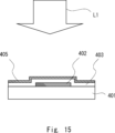
本実施の形態にかかるレーザ照射装置を用いた半導体装置の製造方法は、TFTアレイ基板の製造に好適である。TFTを有する半導体装置の製造方法について、図14、図15を用いて説明する。図14、図15は半導体装置の製造工程を示す工程断面図である。以下の説明では、逆スタガード(inverted staggered)型のTFTを有する半導体装置の製造方法について説明する。図14、図15では、半導体製造方法におけるポリシリコン膜の形成工程を示している。なお、その他の製造工程については、公知の手法を用いることができるため、説明を省略する。
(Method of manufacturing a semiconductor device)
The manufacturing method of a semiconductor device using the laser irradiation device according to the present embodiment is suitable for manufacturing a TFT array substrate. The manufacturing method of a semiconductor device having TFTs will be described with reference to Figs. 14 and 15. Figs. 14 and 15 are cross-sectional views showing the manufacturing process of a semiconductor device. In the following description, a manufacturing method of a semiconductor device having an inverted staggered type TFT will be described. Figs. 14 and 15 show the process of forming a polysilicon film in the semiconductor manufacturing method. It should be noted that the other manufacturing processes can be performed by known methods, and therefore the description will be omitted.
図14に示すように、ガラス基板401上に、ゲート電極402が形成されている。ゲート電極402の上に、ゲート絶縁膜403が形成されている。ゲート絶縁膜403の上に、アモルファスシリコン膜404を形成する。アモルファスシリコン膜404は、ゲート絶縁膜403を介して、ゲート電極402と重複するように配置されている。例えば、CVD(Chemical Vapor Deposition)法により、ゲート絶縁膜403とアモルファスシリコン膜404とを連続成膜する。
As shown in FIG. 14, a
そして、アモルファスシリコン膜404にレーザ光L1を照射することで、図15に示すように、ポリシリコン膜405が形成される。すなわち、図1等で示したレーザ照射装置1によって、アモルファスシリコン膜404を結晶化する。これにより、シリコンが結晶化したポリシリコン膜405がゲート絶縁膜403上に形成される。ポリシリコン膜405は、上記したポリシリコン膜101bに相当する。
Then, the
さらに、上記の説明では、本実施の形態にかかるレーザアニール装置が、アモルファスシリコン膜にレーザ光を照射してポリシリコン膜を形成するものとして説明したが、アモルファスシリコン膜にレーザ光を照射してマイクロクリスタルシリコン膜を形成するものであってもよい。さらには、アニールを行うレーザ光はNd:YAGレーザに限定されるものではない。また、本実施の形態にかかる方法は、シリコン膜以外の薄膜を結晶化するレーザアニール装置に適用することも可能である。すなわち、非晶質膜にレーザ光を照射して、結晶化膜を形成するレーザアニール装置であれば、本実施の形態にかかる方法は適用可能である。本実施の形態にかかるレーザアニール装置によれば、結晶化膜付き基板を適切に改質することができる。 In the above description, the laser annealing device according to the present embodiment has been described as irradiating an amorphous silicon film with laser light to form a polysilicon film, but it may also be irradiating an amorphous silicon film with laser light to form a microcrystalline silicon film. Furthermore, the laser light used for annealing is not limited to an Nd:YAG laser. The method according to the present embodiment can also be applied to a laser annealing device that crystallizes a thin film other than a silicon film. In other words, the method according to the present embodiment can be applied to any laser annealing device that irradiates an amorphous film with laser light to form a crystallized film. The laser annealing device according to the present embodiment can appropriately modify a substrate with a crystallized film.
以上、本発明者によってなされた発明を実施の形態に基づき具体的に説明したが、本発明は前記実施の形態に限定されるものではなく、その要旨を逸脱しない範囲で種々変更可能であることはいうまでもない。 The invention made by the inventor has been specifically described above based on the embodiment, but it goes without saying that the invention is not limited to the above embodiment and can be modified in various ways without departing from the gist of the invention.
1 レーザ照射装置
10 光源
20 光学系モジュール
21 光学系筐体
22 ミラー
23 封止窓
30 密閉部
31 密閉筐体
33 封止窓
34 ガス入口
35 ガス出口
37 ガス
40 処理室
41 ガスボックス
42 導入窓
43 照射窓
44 ガス入口
45 基板ステージ
46 基台
47 走査装置
48 土台
49 搬送方向
51 遮断板
52 遮断板
54 スリット
55 スリット
57 反射ミラー
58 断熱材
60 ビームダンパ
201 ガラス基板
202 ゲート電極
203 ゲート絶縁膜
204 アモルファスシリコン膜
205 ポリシリコン膜
206 層間絶縁膜
207a ソース電極
207b ドレイン電極
300 有機ELディスプレイ
310 基板
311 TFT層
311a TFT
312 有機層
312a 有機EL発光素子
312b 隔壁
313 カラーフィルタ層
313a カラーフィルタ
314 封止基板
C1 光軸
L1 レーザ光
M1 基板
R1 反射光
R2 反射光
R3 反射光
600 閉じ込め構造体
601 内部空間
610 部材
611 冷却管
612 冷却管
620 部材
621 冷却管
622 冷却管
625 カバー
626 固定具
630 庇部
631 開口部
632 反射面
640 対向部
641 上側反射面
642 下側反射面
645 凸部
650 終端部
651 反射面
655 凹部
660 光吸収素子
661 シート
662 板バネ
REFERENCE SIGNS
312
Claims (18)
前記対象物で反射した反射光を吸収するビームダンパと、備えたレーザ照射装置であって、
前記レーザ光が透過するスリットが形成された遮断板をさらに備えており、
前記ビームダンパは、前記遮断板で反射した反射光を吸収し、
前記ビームダンパは、第1部材と、前記第1部材に対向するように固定された第2部材とを備え、
前記第1部材は前記反射光が入射する庇部を備え、
前記庇部は、前記対象物で反射した反射光を前記第1部材と前記第2部材とで囲まれた内部空間に向けて反射する反射面を有しており、
前記庇部に設けられた前記反射面が凹面の曲面鏡となっており、
前記ラインビームの長手方向と直交する断面視において、円弧状又は放物線状となっており、
前記曲面鏡の曲率中心が、前記内部空間の外側、かつ、対象物側に配置されているレーザ照射装置。 an optical system module that converts the laser light into a line beam and irradiates the target object with the line beam;
a beam damper that absorbs light reflected by the object,
The laser beam is further provided with a blocking plate having a slit formed therein through which the laser beam passes,
The beam damper absorbs the light reflected by the blocking plate,
the beam damper includes a first member and a second member fixed to face the first member,
the first member includes an eave portion onto which the reflected light is incident,
the eaves portion has a reflecting surface that reflects light reflected by the object toward an internal space surrounded by the first member and the second member,
The reflecting surface provided on the eaves portion is a concave curved mirror,
The line beam has an arc shape or a parabolic shape in a cross section perpendicular to the longitudinal direction of the line beam,
A laser irradiation device in which the center of curvature of the curved mirror is located outside the internal space and on the target object side .
前記光吸収素子が設けられた終端部と、
前記庇部と、前記終端部との間に配置された対向部と、をさらに備え、
前記対向部には、上側反射面と、前記上側反射面と対向する下側反射面とが設けられ、
前記庇部の前記反射面で反射した反射光の少なくとも一部が、前記上側反射面と前記下側反射面で反射して、前記光吸収素子に入射する請求項2に記載のレーザ照射装置。 The beam dumper includes:
a terminal portion provided with the light absorbing element;
Further comprising an opposing portion disposed between the overhanging portion and the terminal end portion,
The facing portion is provided with an upper reflecting surface and a lower reflecting surface facing the upper reflecting surface,
3. The laser irradiation device according to claim 2 , wherein at least a part of the light reflected by the reflecting surface of the overhanging portion is reflected by the upper reflecting surface and the lower reflecting surface, and is incident on the light absorbing element.
前記終端部には、前記対向部からの反射光を前記光吸収素子に向けて反射する終端部反射面が設けられており、the terminal end is provided with a terminal end reflecting surface that reflects the reflected light from the facing portion toward the light absorbing element,
前記庇部の前記反射面で反射した反射光の一部は前記上側反射面と前記下側反射面での反射を繰り返して、前記終端部反射面に入射し、A part of the reflected light reflected by the reflecting surface of the canopy portion is repeatedly reflected by the upper reflecting surface and the lower reflecting surface, and is incident on the end reflecting surface,
前記ラインビームの長手方向と直交する断面において、前記終端部反射面は、前記対象物側かつ前記対向部側を向いた凹面となっており、かつ、円弧状又は放物線状の曲面となっており、In a cross section perpendicular to the longitudinal direction of the line beam, the end reflection surface is a concave surface facing the object side and the opposing portion side, and is a curved surface having an arc shape or a parabola shape,
前記ラインビームの長手方向と直交する断面において、前記終端部反射面の曲率中心が、前記内部空間内にある、In a cross section perpendicular to the longitudinal direction of the line beam, the center of curvature of the end reflecting surface is within the internal space.
請求項3に記載のレーザ照射装置。4. The laser irradiation device according to claim 3.
前記凹部に前記光吸収素子が配置されている請求項3、又は4に記載のレーザ照射装置。 In a direction perpendicular to the main surface of the object, the end portion has a recess that is recessed toward the object side relative to the lower reflecting surface,
5. The laser irradiation device according to claim 3, wherein the light absorbing element is disposed in the recess.
前記遮断板からの反射光が前記開口部を介して前記ビームダンパの前記内部空間に入射する請求項1~5のいずれか1項に記載のレーザ照射装置。 the overhanging portion has an opening through which the reflected light passes,
6. The laser irradiation device according to claim 1, wherein the light reflected from the blocking plate is incident on the internal space of the beam damper through the opening.
(B)ラインビーム状の前記レーザ光を、前記基板に照射する工程と、
(C)前記基板に照射されたレーザ光のうち、前記基板で反射した反射光をビームダンパに受光させるステップと、を備え、
前記光学系モジュール
前記ビームダンパは、第1部材と、前記第1部材に対向するように固定された第2部材と、を備え、
前記第1部材は前記反射光が入射する庇部を備え、
前記庇部は、前記基板で反射した反射光を前記第1部材と前記第2部材とで囲まれた内部空間に向けて反射する反射面を有しており、
前記レーザ光を遮断板に形成されたスリットを通過させ、前記スリットを通過したレーザ光が前記基板に照射され、
前記庇部に設けられた前記反射面が凹面の曲面鏡となっており、
前記ラインビームの長手方向と直交する断面視において、円弧状又は放物線状となっており、
前記曲面鏡の曲率中心が、前記内部空間の外側、かつ、基板側に配置されている
半導体装置の製造方法。 (A) emitting laser light from an optical system module toward a substrate on which a film including a semiconductor is formed;
(B) irradiating the substrate with the laser light in a line beam shape ;
(C) receiving, by a beam dumper, light reflected by the substrate out of the laser light irradiated onto the substrate;
the optical system module, the beam dumper includes a first member and a second member fixed to face the first member,
the first member includes an eave portion onto which the reflected light is incident,
the overhanging portion has a reflecting surface that reflects light reflected by the substrate toward an internal space surrounded by the first member and the second member,
The laser light is passed through a slit formed in a shielding plate, and the laser light that has passed through the slit is irradiated onto the substrate;
The reflecting surface provided on the eaves portion is a concave curved mirror,
The line beam has an arc shape or a parabolic shape in a cross section perpendicular to the longitudinal direction of the line beam,
The center of curvature of the curved mirror is disposed outside the internal space and on the substrate side.
A method for manufacturing a semiconductor device.
前記光吸収素子が設けられた終端部と、
前記庇部と、前記終端部との間に配置された対向部と、をさらに備え、
前記対向部には、上側反射面と、前記上側反射面と対向する下側反射面とが設けられ、
前記庇部の前記反射面で反射した反射光の少なくとも一部が、前記上側反射面と前記下側反射面で反射して、前記光吸収素子に入射する請求項11に記載の半導体装置の製造方法。 The beam dumper includes:
a terminal portion provided with the light absorbing element;
Further comprising an opposing portion disposed between the overhanging portion and the terminal end portion,
The facing portion is provided with an upper reflecting surface and a lower reflecting surface facing the upper reflecting surface,
The method for manufacturing a semiconductor device according to claim 11 , wherein at least a part of the light reflected by the reflecting surface of the overhanging portion is reflected by the upper reflecting surface and the lower reflecting surface and is incident on the light absorbing element.
前記終端部には、前記対向部からの反射光を前記光吸収素子に向けて反射する終端部反射面が設けられており、the terminal end is provided with a terminal end reflecting surface that reflects the reflected light from the facing portion toward the light absorbing element,
前記庇部の前記反射面で反射した反射光の一部は前記上側反射面と前記下側反射面での反射を繰り返して、前記終端部反射面に入射し、A part of the reflected light reflected by the reflecting surface of the canopy portion is repeatedly reflected by the upper reflecting surface and the lower reflecting surface, and is incident on the end reflecting surface,
前記終端部反射面は、前記基板側かつ前記対向部側を向いた凹面となっており、the end reflection surface is a concave surface facing the substrate and the opposing portion,
前記ラインビームの長手方向と直交する断面において、前記終端部反射面は、円弧状又は放物線状の曲面となっており、In a cross section perpendicular to the longitudinal direction of the line beam, the end reflection surface is a curved surface having an arc shape or a parabola shape,
前記ラインビームの長手方向と直交する断面において、前記終端部反射面の曲率中心が、前記内部空間内にある、In a cross section perpendicular to the longitudinal direction of the line beam, the center of curvature of the end reflecting surface is within the internal space.
請求項12に記載の半導体装置の製造方法。The method for manufacturing a semiconductor device according to claim 12 .
前記凹部に前記光吸収素子が配置されている請求項12、又は13に記載の半導体装置の製造方法。 the end portion has a recess recessed toward the substrate side relative to the lower reflecting surface in an orthogonal direction perpendicular to the main surface of the substrate,
The method for manufacturing a semiconductor device according to claim 12 or 13, wherein the light absorbing element is disposed in the recess.
前記遮断板からの反射光が前記開口部を介して前記ビームダンパの前記内部空間に入射する請求項10~14のいずれか1項に記載の半導体装置の製造方法。 the overhanging portion has an opening through which the reflected light passes,
15. The method for manufacturing a semiconductor device according to claim 10, wherein the light reflected from the blocking plate is incident on the internal space of the beam damper through the opening.
Priority Applications (5)
| Application Number | Priority Date | Filing Date | Title |
|---|---|---|---|
| JP2020187793A JP7579112B2 (en) | 2020-11-11 | 2020-11-11 | Laser irradiation device and method for manufacturing semiconductor device |
| KR1020237015822A KR102919904B1 (en) | 2020-11-11 | 2021-11-05 | Laser irradiation device and method for manufacturing semiconductor device |
| PCT/JP2021/040818 WO2022102538A1 (en) | 2020-11-11 | 2021-11-05 | Laser radiation device, and method for manufacturing semiconductor device |
| CN202180075739.7A CN116420216A (en) | 2020-11-11 | 2021-11-05 | Laser irradiation device and method for manufacturing semiconductor device |
| US18/035,775 US20230411159A1 (en) | 2020-11-11 | 2021-11-05 | Laser irradiation apparatus and method of manufacturing semiconductor apparatus |
Applications Claiming Priority (1)
| Application Number | Priority Date | Filing Date | Title |
|---|---|---|---|
| JP2020187793A JP7579112B2 (en) | 2020-11-11 | 2020-11-11 | Laser irradiation device and method for manufacturing semiconductor device |
Publications (2)
| Publication Number | Publication Date |
|---|---|
| JP2022077121A JP2022077121A (en) | 2022-05-23 |
| JP7579112B2 true JP7579112B2 (en) | 2024-11-07 |
Family
ID=81602250
Family Applications (1)
| Application Number | Title | Priority Date | Filing Date |
|---|---|---|---|
| JP2020187793A Active JP7579112B2 (en) | 2020-11-11 | 2020-11-11 | Laser irradiation device and method for manufacturing semiconductor device |
Country Status (5)
| Country | Link |
|---|---|
| US (1) | US20230411159A1 (en) |
| JP (1) | JP7579112B2 (en) |
| KR (1) | KR102919904B1 (en) |
| CN (1) | CN116420216A (en) |
| WO (1) | WO2022102538A1 (en) |
Families Citing this family (4)
| Publication number | Priority date | Publication date | Assignee | Title |
|---|---|---|---|---|
| JP2023174639A (en) * | 2022-05-28 | 2023-12-08 | 大船企業日本株式会社 | Laser processing method for printed board and laser processing machine for printed board |
| US20250170672A1 (en) * | 2022-08-02 | 2025-05-29 | Mitsubishi Electric Corporation | Numerical aperture changing apparatus, laser apparatus, and laser beam machine |
| JP2025073873A (en) * | 2023-10-27 | 2025-05-13 | 株式会社タムロン | Optical absorber, beam splitter including same, and optical communication device |
| JP2025136290A (en) * | 2024-03-07 | 2025-09-19 | プライムプラネットエナジー&ソリューションズ株式会社 | Battery assembly manufacturing device, battery assembly manufacturing method, and laser light attenuation mechanism |
Citations (5)
| Publication number | Priority date | Publication date | Assignee | Title |
|---|---|---|---|---|
| JP2003080390A (en) | 2001-09-11 | 2003-03-18 | Kawasaki Heavy Ind Ltd | Light absorber for high intensity laser beam |
| JP2003151916A (en) | 2001-08-03 | 2003-05-23 | Semiconductor Energy Lab Co Ltd | Laser irradiation apparatus and method and manufacturing method of semiconductor device |
| JP2005140964A (en) | 2003-11-06 | 2005-06-02 | Nihon Koshuha Co Ltd | Optical beam absorber |
| JP2016161786A (en) | 2015-03-02 | 2016-09-05 | ファナック株式会社 | Optical absorber that absorbs light beam |
| JP2018060927A (en) | 2016-10-06 | 2018-04-12 | 株式会社日本製鋼所 | Laser irradiation device and method of manufacturing semiconductor device |
-
2020
- 2020-11-11 JP JP2020187793A patent/JP7579112B2/en active Active
-
2021
- 2021-11-05 US US18/035,775 patent/US20230411159A1/en active Pending
- 2021-11-05 CN CN202180075739.7A patent/CN116420216A/en active Pending
- 2021-11-05 KR KR1020237015822A patent/KR102919904B1/en active Active
- 2021-11-05 WO PCT/JP2021/040818 patent/WO2022102538A1/en not_active Ceased
Patent Citations (5)
| Publication number | Priority date | Publication date | Assignee | Title |
|---|---|---|---|---|
| JP2003151916A (en) | 2001-08-03 | 2003-05-23 | Semiconductor Energy Lab Co Ltd | Laser irradiation apparatus and method and manufacturing method of semiconductor device |
| JP2003080390A (en) | 2001-09-11 | 2003-03-18 | Kawasaki Heavy Ind Ltd | Light absorber for high intensity laser beam |
| JP2005140964A (en) | 2003-11-06 | 2005-06-02 | Nihon Koshuha Co Ltd | Optical beam absorber |
| JP2016161786A (en) | 2015-03-02 | 2016-09-05 | ファナック株式会社 | Optical absorber that absorbs light beam |
| JP2018060927A (en) | 2016-10-06 | 2018-04-12 | 株式会社日本製鋼所 | Laser irradiation device and method of manufacturing semiconductor device |
Also Published As
| Publication number | Publication date |
|---|---|
| CN116420216A (en) | 2023-07-11 |
| WO2022102538A1 (en) | 2022-05-19 |
| US20230411159A1 (en) | 2023-12-21 |
| JP2022077121A (en) | 2022-05-23 |
| KR20230104622A (en) | 2023-07-10 |
| KR102919904B1 (en) | 2026-01-30 |
Similar Documents
| Publication | Publication Date | Title |
|---|---|---|
| JP7579112B2 (en) | Laser irradiation device and method for manufacturing semiconductor device | |
| JP6803189B2 (en) | Manufacturing method of laser irradiation device and semiconductor device | |
| US9010155B2 (en) | Laser annealing apparatus | |
| US7135390B2 (en) | Method of fabricating a semiconductor device incorporating crystallizing by laser irradiation | |
| US6744008B1 (en) | Laser apparatus and laser annealing method | |
| CN1492255A (en) | Beam homogenizer and laser irradiation device, and semiconductor device manufacturing method | |
| US6897166B2 (en) | Method of fabricating semiconductor device and system of fabricating semiconductor device | |
| CN104741801B (en) | Apparatus for irradiating light | |
| CN104752278B (en) | Light irradiating device | |
| KR102490081B1 (en) | Laser crystallization device and method | |
| TWI749156B (en) | Dump and substrate processing apparatus | |
| CN111435638B (en) | Laser crystallization device | |
| US12474555B2 (en) | Laser crystallization apparatus | |
| CN114101902B (en) | Optical system and laser irradiation apparatus including the same | |
| KR101333067B1 (en) | Systems and methods to shape laserlight as a line beam | |
| JP2020145362A (en) | Laser processing equipment | |
| CN118160069A (en) | Laser irradiation device, laser irradiation method, and method for manufacturing display | |
| KR20070062797A (en) | Silicon crystallization device |
Legal Events
| Date | Code | Title | Description |
|---|---|---|---|
| A711 | Notification of change in applicant |
Free format text: JAPANESE INTERMEDIATE CODE: A712 Effective date: 20220317 |
|
| A621 | Written request for application examination |
Free format text: JAPANESE INTERMEDIATE CODE: A621 Effective date: 20230815 |
|
| A131 | Notification of reasons for refusal |
Free format text: JAPANESE INTERMEDIATE CODE: A131 Effective date: 20240625 |
|
| A521 | Request for written amendment filed |
Free format text: JAPANESE INTERMEDIATE CODE: A523 Effective date: 20240719 |
|
| TRDD | Decision of grant or rejection written | ||
| A01 | Written decision to grant a patent or to grant a registration (utility model) |
Free format text: JAPANESE INTERMEDIATE CODE: A01 Effective date: 20241008 |
|
| A61 | First payment of annual fees (during grant procedure) |
Free format text: JAPANESE INTERMEDIATE CODE: A61 Effective date: 20241025 |
|
| R150 | Certificate of patent or registration of utility model |
Ref document number: 7579112 Country of ref document: JP Free format text: JAPANESE INTERMEDIATE CODE: R150 |