JP7571663B2 - Gate Driver - Google Patents
Gate Driver Download PDFInfo
- Publication number
- JP7571663B2 JP7571663B2 JP2021091316A JP2021091316A JP7571663B2 JP 7571663 B2 JP7571663 B2 JP 7571663B2 JP 2021091316 A JP2021091316 A JP 2021091316A JP 2021091316 A JP2021091316 A JP 2021091316A JP 7571663 B2 JP7571663 B2 JP 7571663B2
- Authority
- JP
- Japan
- Prior art keywords
- circuit
- voltage
- current
- sense
- gate
- Prior art date
- Legal status (The legal status is an assumption and is not a legal conclusion. Google has not performed a legal analysis and makes no representation as to the accuracy of the status listed.)
- Active
Links
Images


Classifications
-
- H—ELECTRICITY
- H02—GENERATION; CONVERSION OR DISTRIBUTION OF ELECTRIC POWER
- H02M—APPARATUS FOR CONVERSION BETWEEN AC AND AC, BETWEEN AC AND DC, OR BETWEEN DC AND DC, AND FOR USE WITH MAINS OR SIMILAR POWER SUPPLY SYSTEMS; CONVERSION OF DC OR AC INPUT POWER INTO SURGE OUTPUT POWER; CONTROL OR REGULATION THEREOF
- H02M1/00—Details of apparatus for conversion
- H02M1/08—Circuits specially adapted for the generation of control voltages for semiconductor devices incorporated in static converters
-
- H—ELECTRICITY
- H03—ELECTRONIC CIRCUITRY
- H03K—PULSE TECHNIQUE
- H03K17/00—Electronic switching or gating, i.e. not by contact-making and –breaking
- H03K17/08—Modifications for protecting switching circuit against overcurrent or overvoltage
Landscapes
- Engineering & Computer Science (AREA)
- Power Engineering (AREA)
- Power Conversion In General (AREA)
- Electronic Switches (AREA)
Description
本発明は、ゲート駆動装置に関する。 The present invention relates to a gate drive device.
IGBTやMOSトランジスタなどのゲート駆動型の半導体スイッチング素子は、上下アームに配置してオンオフ駆動制御を行う構成では、一方が短絡故障をしている状態で、他方がオン駆動されると、短絡電流が流れてスイッチング素子が破損してしまう。このため、オン時に対向アームの半導体スイッチング素子が短絡しているか否かを判定して、短絡状態である場合にはオン駆動を停止することが必要である。 In a configuration where gate-driven semiconductor switching elements such as IGBTs and MOS transistors are arranged in upper and lower arms and controlled to be turned on and off, if one of them has a short circuit and the other is turned on, a short circuit current will flow and the switching element will be damaged. For this reason, when the semiconductor switching element is on, it is necessary to determine whether or not the semiconductor switching element of the opposing arm is short-circuited, and if it is short-circuited, to stop the on-drive.
この場合、半導体スイッチング素子のオン時には、原理的に、過渡的に電流センスの電圧がオン状態よりも持ち上がり、ゲート電圧が十分に上がってオン状態に移行すると、電流センスの電圧は定常値まで低下する特性を有している。このため、過渡期に判定をすると短絡状態と誤判定をしてしまう可能性があるため、ゲート電圧が上がった定常時に電流センスの電圧を判定することで誤判定を回避するようにしている。 In this case, in principle, when the semiconductor switching element is on, the current sense voltage rises transiently above the on state, and when the gate voltage rises sufficiently to transition to the on state, the current sense voltage drops to a steady value. Because of this, there is a possibility that a short circuit state will be erroneously determined if a determination is made during the transitional period, so erroneous determinations are avoided by determining the current sense voltage during the steady state when the gate voltage has risen.
しかしながら、半導体スイッチング素子は、小型化が進むことで短絡時の飽和電流が低下する傾向にあるため、ゲート電圧が上がった定常時の電流センスの電圧を判定する場合でも、短絡時の飽和電流の値と正常時の電流センスの値との差が小さくなり、これらの値のばらつきを考慮すると両者がオーバーラップする場合が発生し、しきい値の設定が不能となり正しい判定ができなくなる不具合があった。 However, as semiconductor switching elements become smaller, there is a tendency for the saturation current during a short circuit to decrease. This means that even when determining the steady-state current sense voltage when the gate voltage has increased, the difference between the saturation current value during a short circuit and the current sense value during normal operation becomes smaller. Taking into account the variance in these values, the two may overlap, making it impossible to set a threshold value and resulting in a malfunction in which a correct determination cannot be made.
本発明は、上記事情を考慮してなされたもので、その目的は、半導体スイッチング素子の小型化が進み短絡飽和電流が低下した場合でも、対向アームの短絡状態を確実に判定することができるようにしたゲート駆動装置を提供することにある。 The present invention was made in consideration of the above circumstances, and its purpose is to provide a gate drive device that can reliably determine the short-circuit state of the opposing arm even when the miniaturization of semiconductor switching elements progresses and the short-circuit saturation current decreases.
請求項1に記載のゲート駆動装置は、電流センス端子を備えたゲート駆動形の半導体スイッチング素子の駆動制御を行うゲート駆動装置であって、前記電流センス端子からのセンス電流の検出信号を取り込み、前記検出信号に基づいて、前記センス電流が、前記半導体スイッチング素子が線形領域で動作する定常期の電流よりも上昇した後に前記定常期の電流まで低下する現象である過渡センス電流の有無を検出する波形検出回路(40)と、前記波形検出回路による検出結果を所定タイミングで判定して短絡の有無を判定する判定回路(30)と、前記半導体スイッチング素子のオンオフ駆動を制御し、前記半導体スイッチング素子をオン駆動した後、前記判定回路により短絡有りが判定されることに基づいて遮断する制御回路(20)とを備える。
The gate drive device according to
上記構成を採用することにより、波形検出回路により、半導体スイッチング素子の電流センス端子からセンス電流の検出信号を取り込み、センス電流の波形の変化から過渡センス電流の有無を検出して短絡の有無を検出し、判定回路により所定タイミングで短絡状態を判定することができる。これにより、センス電流の値そのものから短絡を判定するのではなく、過渡期のセンス電流を基準として定常期のセンス電流への変化から検出することで、飽和電流が下がるなどしてセンス電流のレベルにばらつきがある場合でも、短絡の有無を正しく判定することができる。この結果、パワー素子として用いる半導体スイッチング素子の小型化に貢献できる。また、IC/素子仕様で短絡設計が完結するため、基板での短絡保護設計が不要になる。 By adopting the above configuration, the waveform detection circuit takes in a sense current detection signal from the current sense terminal of the semiconductor switching element, detects the presence or absence of a transient sense current from changes in the sense current waveform to detect the presence or absence of a short circuit, and the judgment circuit judges the short circuit state at a predetermined timing. As a result, a short circuit is not judged from the value of the sense current itself, but is detected from the change to the steady-state sense current using the transient sense current as a reference, so that the presence or absence of a short circuit can be correctly judged even if there is variation in the level of the sense current due to a drop in saturation current, etc. As a result, it can contribute to the miniaturization of semiconductor switching elements used as power elements. In addition, since the short circuit design is completed in the IC/element specifications, there is no need for short circuit protection design on the board.
(第1実施形態)
以下、本発明の第1実施形態について、図1~図7を参照して説明する。
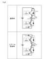
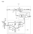
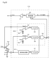
電気的構成を示す図1において、ゲート駆動形の半導体スイッチング素子としてのIGBT(Insulated Gate Bipolar Transistor)1を上下アームにそれぞれ配置して負荷への通電経路を形成する回路に対して、ゲート駆動装置10は、一方のIGBT1をオン駆動制御する際に、他方のIGBTが短絡状態にあるかどうかを判定することができるようにした機能を備える。
First Embodiment
A first embodiment of the present invention will be described below with reference to FIGS.
In FIG. 1 showing the electrical configuration, IGBTs (Insulated Gate Bipolar Transistors) 1 as gate-driven semiconductor switching elements are arranged on upper and lower arms of a circuit to form a current path to a load. A
IGBT1は、内部にコレクタ・エミッタ間の電流を検知するためのセンス素子が設けられセンス電流の出力端子であるセンス端子SEを備えている。センス端子SEは、電流検出用の抵抗2を介してエミッタと共通に接続されており、ゲート駆動装置10は、電流検出抵抗2に流れるセンス電流Iseを、センス電圧Vseとして取り込むように設けられている。
The IGBT1 has a sense element for detecting the current between the collector and emitter and a sense terminal SE that is an output terminal for the sense current. The sense terminal SE is commonly connected to the emitter via a current detection resistor 2, and the
ゲート駆動装置10は、制御回路20、判定回路30および波形検出回路40を備えている。制御回路20は、外部から与えられるオン/オフ指令信号に基づいてゲート駆動信号Sonを生成し、駆動回路21を介してIGBT1のゲートにゲート駆動電圧Vonを与える。制御回路20は、後述するように、IGBT1のオフ駆動機能も備えており、オン駆動中に短絡が検出された場合にはIGBT1を遮断する。
The
判定回路30は、コンパレータ31、しきい値電源32、遅延回路33およびアンド回路34を備える。判定回路30は、IGBT1のゲート電圧Vgeがしきい値電圧Vth1に達してオンした時点から、所定の遅延時間Td1が経過した時点でIGBT1の状態を判定する。
The
コンパレータ31は、非反転入力端子にIGBT1のゲート電圧Vgeが入力され、反転入力端子にしきい値電源32により設定されるしきい値電圧Vth1が入力される。遅延回路33は、コンパレータ31から出力されるオンタイミングの信号によりトリガがかかり、所定の遅延時間Td1後にアンド回路34にハイレベルの信号を出力する。アンド回路34は、遅延回路33からのハイレベルの信号の入力タイミングで、波形検出回路40からの出力信号を判定して短絡状態の場合には判定信号Sxを出力する。
The gate voltage Vge of IGBT1 is input to the non-inverting input terminal of the
波形検出回路40は、ピークホールド回路50およびヒステリシス付きのコンパレータからなる比較回路60を備えている。波形検出回路40は、センス電圧Vseを取り込み、この波形の変化状態から通常状態でない状態を検出して出力する。
The
ピークホールド回路50は、オペアンプ51、トランジスタ52およびコンデンサ53を備える。オペアンプ51は、非反転入力端子にセンス電圧Vseが入力され、反転入力端子にはコンデンサ53の端子電圧Vphが入力される。オペアンプ51の出力端子はトランジスタ52のベースに接続される。
The
トランジスタ52のコレクタは直流電源VDに接続され、エミッタはコンデンサ53を介してグランドに接続される。コンデンサ53の端子電圧であるピークホールド電圧Vphは、トランジスタ52のエミッタとコンデンサ53の共通接続点の電圧である。オペアンプ51は、センス電圧Vseがコンデンサ53の端子電圧であるピークホールド電圧Vphよりも大きい期間中はトランジスタ52を駆動してコンデンサ53に直流電源VDから充電を行う。
The collector of
これにより、センス電圧Vseがピーク値VPに達した後低下すると、オペアンプ51の出力信号によりトランジスタ52がオフしてコンデンサ53への充電が停止する。この結果、ピークホールド電圧Vphはセンス電圧Vseのピーク値VPとなり、この電圧が保持される。
As a result, when the sense voltage Vse drops after reaching the peak value VP, the output signal of the
比較回路60は、コンパレータ61およびヒステリシス電圧Vhを与えるヒステリシス電源62を備える。コンパレータ61は非反転入力端子にセンス電圧Vseが入力され、反転入力端子にピークホールド回路50から出力されるピークホールド電圧Vphを、ヒステリシス電源62を通じてヒステリシス電圧Vhだけ低下させた参照電圧Vhysとして入力される。
The
コンパレータ61は、センス電圧Vseが参照電圧Vhysよりも大きいときにはハイレベル、小さくなるとローレベルとなる検出信号Sdを出力する。この検出信号Sdは、判定回路30のアンド回路34に入力される。
The
次に、上記構成の作用について、図2から図7も参照して説明する。
まず、通常時および短絡時におけるセンス電圧Vseの変化について説明する。図6は2つのIGBT_A、IGBT_Bを上下アームに配置した構成で、上アームのIGBT_Aをオフ駆動してから下アームのIGBT_Bをオン駆動するまでに流れる電流について矢印をつけた破線で示している。上側に上アームのIGBT_Aが正常である通常時の電流を示し、下側にIGBT_Aが短絡状態である場合の電流を示している。
Next, the operation of the above configuration will be described with reference to FIGS.
First, the change in the sense voltage Vse during normal operation and during a short circuit will be described. Fig. 6 shows a configuration in which two IGBTs A and B are arranged in upper and lower arms, and the current that flows from when the IGBT A of the upper arm is turned off until the IGBT B of the lower arm is turned on is shown by a dashed line with an arrow. The upper side shows the current during normal operation when the IGBT A of the upper arm is normal, and the lower side shows the current when the IGBT A is short-circuited.
通常時においては、上アームのIGBT_Aをオン状態として負荷に給電している状態でオフに切り替えると、負荷側からIGBT_Aのボディダイオードを介して電源側に戻る電流I1fが流れる。ボディダイオードに流れる電流を側路させるために、同期整流動作として下アームのIGBT_Bをオン駆動する。 Under normal circumstances, when the IGBT_A of the upper arm is switched off while it is on and supplying power to the load, a current I1f flows from the load side back to the power supply side via the body diode of IGBT_A. In order to bypass the current flowing through the body diode, the IGBT_B of the lower arm is turned on as a synchronous rectification operation.
このとき、IGBT_Bに流れる電流I2は、負荷側からボディダイオードに流れていた電流I1fにボディダイオードのリカバリ電流I1rが加算された電流として流れる。このため、IGBT_Bがオン駆動されるときには、過渡期においてリカバリ電流によるピークが加算された電流が発生し、定常期になると負荷電流のレベルになる。 At this time, the current I2 flowing through IGBT_B is the sum of the current I1f flowing from the load side to the body diode and the recovery current I1r of the body diode. Therefore, when IGBT_B is turned on, a current is generated that includes a peak due to the recovery current during the transient period, and reaches the load current level during the steady state.
一方、下側に示すIGBT_Aの短絡時には、上アームのIGBT_Aをオン状態として負荷に給電している状態でオフに切り替えても、短絡状態であるから、負荷側からIGBT_Aの本体を介して電源側に戻る電流I1sが流れる。ボディダイオードには順方向電圧がかかるため電流I1fはほとんど流れない。 On the other hand, when the IGBT_A shown on the bottom is short-circuited, even if the IGBT_A in the upper arm is switched off while it is on and supplying power to the load, the current I1s flows from the load side back to the power supply side through the body of the IGBT_A because it is in a short-circuited state. Because a forward voltage is applied to the body diode, almost no current I1f flows.
このため、IGBT_Bをオン駆動して同期整流を実施しようとすると、IGBT_Aに流れていた短絡電流I1sがIGBT_Bに電流I2として流れるようになる。また、IGBT_Aのボディダイオードに電流がほとんど流れないため、リカバリ電流の発生もなく、電流I2にはリカバリ電流に起因したピーク値が発生しない。 For this reason, when IGBT_B is turned on to perform synchronous rectification, the short-circuit current I1s that was flowing through IGBT_A flows through IGBT_B as current I2. Also, since almost no current flows through the body diode of IGBT_A, no recovery current is generated, and no peak value due to the recovery current occurs in current I2.
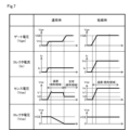
図7は、上記の動作を各部の信号変化として示したタイミングチャートである。通常時と短絡時との状態におけるゲート電圧Vge、コレクタ電流Ic、センス電圧Vseおよびコレクタ電圧Vceを示している。 Figure 7 is a timing chart showing the above operation as signal changes at each part. It shows the gate voltage Vge, collector current Ic, sense voltage Vse, and collector voltage Vce in normal and short-circuit states.
通常時においては、IGBTのゲート電圧は過渡期にミラー電圧Vmで保持された後にゲート電圧VGEまで引き上げられる。このとき、コレクタ電流Icは、ゲート電圧Vgeが時刻t0でしきい値電圧Vthに達すると、負荷に応じた電流が流れるようになる。 Under normal circumstances, the gate voltage of the IGBT is held at the mirror voltage Vm during the transitional period and then raised to the gate voltage VGE. At this time, when the gate voltage Vge reaches the threshold voltage Vth at time t0, the collector current Ic begins to flow according to the load.
センス電流Iseの変化を示すセンス電圧Vseは、オン駆動に伴って0Vから増加し、リカバリ電流によるピーク値を過ぎると過渡期では飽和領域で動作するため、定常期よりも高い電圧V2を保持する。この後、定常期に移行するとセンス電圧Vseは、線形領域となるので負荷電流に比例した電圧V1に下がり、オン期間中はこの状態が保持される。また、コレクタ電圧Vceは、過渡期では電源電圧VCEから徐々に低下し始め、定常期になるとほぼ0Vになる。 The sense voltage Vse, which indicates the change in the sense current Ise, increases from 0V as the device is turned on, and after passing the peak value due to the recovery current, it operates in the saturation region in the transitional period, so it maintains a voltage V2 higher than in the steady state. After this, when it transitions to the steady state, the sense voltage Vse enters the linear region and drops to a voltage V1 proportional to the load current, and this state is maintained during the on-period. Also, the collector voltage Vce starts to gradually decrease from the power supply voltage VCE in the transitional period, and becomes nearly 0V in the steady state.
これに対して、短絡時においては、IGBTのゲート電圧はミラー期間に関係なく上昇してゲート電圧VGEまで引き上げられる。このとき、コレクタ電流Icは、ゲート電圧Vgeが時刻t0でしきい値電圧Vthに達すると、電源短絡状態となるため短絡電流レベルまで上昇する。 In contrast, during a short circuit, the gate voltage of the IGBT rises regardless of the mirror period and is pulled up to the gate voltage VGE. At this time, when the gate voltage Vge reaches the threshold voltage Vth at time t0, the power supply is short-circuited, and the collector current Ic rises to the short-circuit current level.
センス電圧Vseは、オン駆動に伴って0Vから増加し、リカバリ電流もなく飽和領域のままで動作し短絡電流に対応する高い電圧V3のレベルとなる。また、コレクタ電圧Vceは、電源電圧VCEが印加された状態のままとなる。 The sense voltage Vse increases from 0V when the device is turned on, and operates in the saturated region without any recovery current, reaching the high voltage V3 level corresponding to the short circuit current. The collector voltage Vce remains in the state where the power supply voltage VCE is applied.
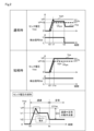
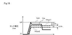
以上の基本的な動作の性質を前提として、本実施形態の動作について説明する。図2は、通常時および短絡時におけるセンス電圧Vseと検出信号Sdの状態を示している。 Assuming the above basic operational characteristics, the operation of this embodiment will be described. Figure 2 shows the state of the sense voltage Vse and the detection signal Sd during normal operation and during a short circuit.
通常時では、センス電圧Vseは、前述のように、IGBT1がオンすると過渡期においてはリカバリ電流に起因した電圧上昇でピーク値VPに達した後に過渡期の飽和状態の電圧V1のレベルとなる。この後、定常期に移行するとセンス電圧Vseは電圧V1よりも下がって負荷電流に対応する電圧V2となる。この結果、センス電圧Vseは、ピーク値VPから電圧V2まで下がり、動作点差ΔVse(=VP-V2)だけ下がったこととなる。 Under normal circumstances, as described above, when IGBT1 is turned on, the sense voltage Vse rises due to the recovery current in the transitional period, reaches a peak value VP, and then reaches the level of the saturated voltage V1 during the transitional period. After this, when the system transitions to the steady state, the sense voltage Vse drops below voltage V1 to voltage V2, which corresponds to the load current. As a result, the sense voltage Vse drops from peak value VP to voltage V2, and has dropped by the operating point difference ΔVse (=VP-V2).
一方、短絡時には、センス電圧Vseは、IGBT1は飽和状態のままとなり、IGBT1に流れる短絡電流に相当するレベルまで上昇し、このレベルが保持される。このため、センス電圧Vseがピーク値VPそのもので保持され、これよりも低下することがない。 On the other hand, during a short circuit, IGBT1 remains in a saturated state, and the sense voltage Vse rises to a level equivalent to the short circuit current flowing through IGBT1 and is maintained at this level. Therefore, the sense voltage Vse is maintained at the peak value VP itself and does not fall below this value.
この結果、通常時にはセンス電圧Vseが過渡期から定常期に移行するタイミングで、上記したΔVseの変化により電圧V2に低下するので、波形検出回路40は、この変化をピークホールド電圧Vphからヒステリシス電圧Vhだけ小さく設定する電圧Vpysと比較することにより検出することができる。
As a result, during normal operation, when the sense voltage Vse transitions from the transient to the steady state, it drops to voltage V2 due to the change in ΔVse described above, and the
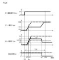
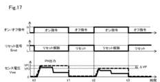
図3は、ゲート駆動装置10が外部からオン/オフ指令の信号を受けてIGBT1のゲートにゲート駆動電圧Vonを与えたときのタイミングチャートを示している。制御回路20は、駆動回路21を介してIGBT1にゲート駆動電圧Vonを与えると、対向アームのIGBTが通常時である場合には、IGBT1は、ゲート電圧Vgeが上昇してゆき、時刻t0でしきい値電圧Vth1に達すると電流が流れ始め、過渡期に移行する。
Figure 3 shows a timing chart when the
このとき、判定回路30においては、コンパレータ31に入力されるゲート電圧Vgeがしきい値電圧Vth1に達したことでハイレベルの信号を遅延回路33に出力する。遅延回路33は、ハイレベルの信号が入力された時刻t0から所定の遅延時間td1が経過する時刻t3でアンド回路34にハイレベルのタイミング信号を出力する。
At this time, in the
波形検出回路40においては、IGBT1がオン駆動し始める時刻t0からIGBT1に流れる電流に比例するセンス電流Iseが電流検出抵抗2に流れ始め、この電流に相当するセンス電圧Vseがオペアンプ51に入力される。
In the
IGBT1がオン駆動される過渡期においては、飽和状態となりゲート電圧Vgeは時刻tmからミラー電圧Vmで保持され、センス電圧Vseはリカバリ電流を含んだ電流が流れることで、時刻t1でピーク電圧VPに達し、以後通常期よりも高い電圧V1の状態が保持される。 During the transitional period when IGBT1 is turned on, a saturated state is reached and the gate voltage Vge is held at the mirror voltage Vm from time tm, and the sense voltage Vse reaches a peak voltage VP at time t1 due to the flow of a current including a recovery current, and is then held at a voltage V1 higher than the normal voltage.
波形検出回路40においては、ピークホールド回路50から出力されるピーク電圧VPに対応したピークホールド電圧Vphが比較回路60に入力される。比較回路60では、ピークホールド電圧Vphからヒステリシス電圧Vhだけ低く設定される参照電圧Vhysがコンパレータ61に入力される。参照電圧Vhysは、過渡期のセンス電圧Vseが電圧V2となるのに対してこれよりも低くなるようにヒステリシス電圧Vhが設定されている。
In the
コンパレータ61は、センス電圧Vseが定常期に入って電圧V1からさらに低下した電圧V2になるタイミングで参照電圧Vhysよりも低くなるので、この時点t2で検出信号Sdはローレベルに変化する。
The
判定回路30においては、遅延回路33により設定される遅延時間Td1が、IGBT1が定常期に入った時刻t2よりも後となるように設定されているので、アンド回路34にハイレベルのタイミング信号Stが入力された時点t3で、検出信号Sdがハイレベルかローレベルかに応じた判定信号Sxが出力される。したがって、通常時においては、判定信号Sxはローレベルとなり、この時点で通常時であることが判定される。
In the
一方、対向アームのIGBTが短絡状態となっている場合には、ゲート電圧Vgeはミラー電圧Vmで保持されることなくVGEまで上昇し、センス電圧Vseもリカバリ電流のピーク値を発生することなく短絡電流Isに相当する電圧Vxに達するまで上昇して保持された状態となる。 On the other hand, when the IGBT of the opposing arm is in a short-circuit state, the gate voltage Vge rises to VGE without being held at the mirror voltage Vm, and the sense voltage Vse also rises to and is held at a voltage Vx equivalent to the short-circuit current Is without generating a peak value of the recovery current.
このため、センス電圧Vseが、以後低下することがなくなり、波形検出回路40では短絡状態を示すハイレベルの検出信号Sdが出力された状態が保持される。判定回路30では、タイミング信号Stが出力される時刻t3で、アンド回路34は、波形検出回路40からハイレベルの検出信号Sdが入力されているので、ハイレベルの判定信号Sxを出力する。したがって、短絡時では、判定信号Sxはハイレベルとなり、短絡時であることが判定される。
As a result, the sense voltage Vse will no longer decrease, and the
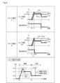
次に、図4および図5によりセンス電圧Vseの波形が図3で示したような変化とは異なる変化をする場合の検出動作について説明する。
図4の場合では、下段に示すセンス電圧Vseの形状を特徴づけるリカバリ電流が大きいときに発生する例を示している。図4の上段に示すように、リカバリ電流が通常レベルもしくは小さい場合には、前述したように、過渡期から定常期に変わる時点t2でセンス電圧Vseが参照電圧Vhysよりも低下することで通常時を検出していた。
Next, a detection operation in the case where the waveform of the sense voltage Vse changes differently from the change shown in FIG. 3 will be described with reference to FIGS.
In the case of Fig. 4, an example is shown in which this occurs when the recovery current that characterizes the shape of the sense voltage Vse shown in the lower part is large. As shown in the upper part of Fig. 4, when the recovery current is at a normal level or small, as described above, the normal state is detected by the sense voltage Vse dropping below the reference voltage Vhys at time t2 when the transition period changes to the steady state.
これに対して、図4の中段に示すように、リカバリ電流が大きいレベルの場合には、過渡期のセンス電圧Vseのレベルが前述した電圧V1よりも低くなり、リカバリ電流によるピーク値VPから過渡期の電圧に変化する時点t2xで参照電圧Vhysよりも低下してしまうことがある。 In contrast, as shown in the middle of Figure 4, when the recovery current is at a large level, the level of the transient sense voltage Vse becomes lower than the aforementioned voltage V1, and may fall below the reference voltage Vhys at the time t2x when the recovery current changes from the peak value VP to the transient voltage.
しかし、この場合には、通常時を判定する検出信号Sdが時刻t2xの早い時点で検出されることとなり、遅延時間td1が経過した時刻t3での判定に支障をきたすことはない。また、短絡時の波形は前述と同様にセンス電圧Vseが参照電圧Vhysよりも低下することはないから、短絡の判定においても支障をきたすことはない。 However, in this case, the detection signal Sd used to determine the normal state is detected at an early point in time t2x, and there is no problem with the determination at time t3 when the delay time td1 has elapsed. Also, as described above, the waveform during a short circuit does not cause the sense voltage Vse to fall below the reference voltage Vhys, so there is no problem with determining whether or not there is a short circuit.
次に、図5の場合では、下段に示すセンス電圧Vseの形状を特徴づける過渡期の電圧V1と定常期の電圧V2との差がほとんど無いときに発生する例を示している。図5の上段に示すように、過渡期の電圧V1と定常期の電圧V2との差がある程度有る場合には、前述したように、過渡期から定常期に変わる時点t2でセンス電圧Vseが参照電圧Vhysよりも低下することで通常時を検出していた。 Next, in the case of Figure 5, an example is shown that occurs when there is almost no difference between the transient voltage V1 and the steady-state voltage V2, which characterize the shape of the sense voltage Vse shown in the lower part. As shown in the upper part of Figure 5, when there is a certain degree of difference between the transient voltage V1 and the steady-state voltage V2, as described above, the normal state is detected when the sense voltage Vse falls below the reference voltage Vhys at the time t2 when the transition from the transient period to the steady-state period occurs.
これに対して、図5の中段に示すように、過渡期の電圧V1と定常期の電圧V2との差がほぼゼロの場合には、リカバリ電流の大きさによる差分だけがセンス電圧Vseのピーク電圧VPからの低下分となる。このため、センス電圧Vseによって通常時の状態を検出可能とするための条件は、リカバリ電流によるピークを過ぎた後のセンス電圧Vseが参照電圧Vhysよりも低くなるように参照電圧Vhysを設定することである。 In contrast, as shown in the middle of Figure 5, when the difference between the voltage V1 during the transient period and the voltage V2 during the steady state is almost zero, the only difference due to the magnitude of the recovery current is the drop in the sense voltage Vse from the peak voltage VP. Therefore, the condition for making it possible to detect the normal state using the sense voltage Vse is to set the reference voltage Vhys so that the sense voltage Vse after the peak due to the recovery current is lower than the reference voltage Vhys.
したがって、この場合には、ヒステリシス電圧Vhの大きさを調整して、リカバリ電流によるピーク値VPから過渡期および定常期におけるセンス電圧Vseに変化するときに参照電圧Vhysを通過するように設定することで検出可能となる。なお、このようにセンス電圧Vseの過渡期の電圧V1と定常期の電圧V2との差が無くなる場合とは、例えば、IGBTの製造上において、センス素子とメイン素子のVtを調整することで形成されることがある。 In this case, therefore, the magnitude of the hysteresis voltage Vh can be adjusted to detect it by setting it to pass through the reference voltage Vhys when it changes from the peak value VP due to the recovery current to the sense voltage Vse in the transient and steady states. Note that such a case where there is no difference between the voltage V1 in the transient state of the sense voltage Vse and the voltage V2 in the steady state can be achieved, for example, by adjusting the Vt of the sense element and the main element during the manufacture of the IGBT.
このような第1実施形態によれば、IGBT1の通常時におけるオン駆動時のセンス電圧Vseの変化を検出する波形検出回路40を設け、適切なタイミングで判定する判定回路30により判定するように構成したので、半導体スイッチング素子であるIGBT1の小型化が進み短絡飽和電流が低下した場合でも、対向アームの短絡時を確実に判定することができるようになる。
According to the first embodiment, a
(第2実施形態)
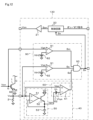
図8および図9は第2実施形態を示すもので、以下、第1実施形態と異なる部分について説明する。この実施形態では、ゲート駆動装置110は、判定回路30に代えて判定回路70を備えている。
Second Embodiment
8 and 9 show the second embodiment, and the following describes the differences from the first embodiment. In this embodiment, a
判定回路70は、遅延回路71およびアンド回路34を備えている。遅延回路71は、制御回路20から出力されるオン駆動信号Sonが入力され、ハイレベルのオン駆動信号が入力された時点から所定の遅延時間Td2が経過するとハイレベルのタイミング信号を出力する。この遅延時間Td2は、第1実施形態における遅延時間Td1に相当する時間として設定されるもので、判定タイミングを設定するものである。
The
図9は、ゲート駆動装置110が外部からオン/オフ指令の信号を受けてIGBT1のゲートにゲート駆動信号Sonを与えたときのタイミングチャートを示している。この実施形態では、ゲート駆動信号Sonをトリガとして遅延回路71により遅延時間Td2が経過すると、判定タイミングを与える信号をアンド回路34に入力する。
Figure 9 shows a timing chart when the
判定回路70においては、遅延回路71により設定される遅延時間Td2が、IGBT1が定常期に入った時刻t2よりも後となるように設定されているので、アンド回路34にハイレベルのタイミング信号Stが入力された時点t3aで、検出信号Sdがハイレベルかローレベルかに応じた判定信号Sxが出力される。したがって、通常時においては、判定信号Sxはローレベルとなり、この時点で通常時であることが判定され、短絡時では、判定信号Sxはハイレベルとなり、この時点で短絡時であることが判定される。
したがって、このような第2実施形態によっても第1実施形態と同様の作用効果を得ることができる。
In the
Therefore, the second embodiment can also provide the same effects as the first embodiment.
なお、上記実施形態に示した制御回路20から出力されるオン駆動信号Sonを用いることに代えて、外部から与えられるオンオフ指令がオン駆動を示すハイレベルの信号を遅延回路71に入力する構成とすることもできる。
In addition, instead of using the on drive signal Son output from the
(第3実施形態)
図10および図11は第3実施形態を示すもので、以下、第1実施形態と異なる部分について説明する。この実施形態では、ゲート駆動装置120は、判定回路30に代えて判定回路80を備えている。
Third Embodiment
10 and 11 show the third embodiment, and the following describes the differences from the first embodiment. In this embodiment, a
判定回路80は、コンパレータ81、モニタしきい値電源82およびアンド回路34を備えている。コンパレータ81は、ゲートモニタ回路として機能するもので、IGBT1のゲート電圧Vgeが非反転入力端子に入力され、モニタしきい値電源82により設定されるモニタしきい値電圧Vth2が反転入力端子に入力される。モニタしきい値電圧Vth2は、IGBT1が過渡期から定常期に入ってゲート電圧が電圧VGEに達したことを検出するように設定される。
The
コンパレータ81は、IGBT1のゲート電圧Vgeがモニタしきい値電圧Vth2を超えると、ハイレベルのモニタ検出信号Smを出力する。モニタ検出信号Smはアンド回路34に判定タイミング信号として入力される。
When the gate voltage Vge of IGBT1 exceeds the monitor threshold voltage Vth2, the
これにより、判定回路80においては、コンパレータ81からハイレベルのモニタ検出信号Smが入力された時点t3bで、検出信号Sdがハイレベルかローレベルかに応じた判定信号Sxが出力される。したがって、通常時においては、判定信号Sxはローレベルとなり、この時点で通常時であることが判定され、短絡時においては、判定信号Sxはハイレベルとなり、この時点で短絡時であることが判定される。
したがって、このような第3実施形態によっても第1実施形態と同様の作用効果を得ることができる。
As a result, in the
Therefore, the third embodiment can also provide the same effects as the first embodiment.
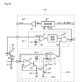
(第4実施形態)
図12から図15は第4実施形態を示すもので、以下、第3実施形態と異なる部分について説明する。この実施形態では、第3実施形態において、負荷電流が小さい領域で用いるケースにおいてセンス電圧Vseの過渡期の電圧V1と定常期の電圧V2との差が小さく、センス電圧Vseが参照電圧Vhysよりも高くなることがあり、これによって短絡状態と誤判定するのを解消できるようにしたものである。
Fourth Embodiment
12 to 15 show the fourth embodiment, and the following describes the differences from the third embodiment. In this embodiment, when the load current in the third embodiment is used in a region where the load current is small, the difference between the voltage V1 in the transient period of the sense voltage Vse and the voltage V2 in the steady period is small, and the sense voltage Vse may become higher than the reference voltage Vhys, thereby preventing the sense voltage Vse from being erroneously determined to be in a short-circuit state.
すなわち、第4実施形態では、ゲート駆動装置130は、図12に示すように、判定回路80の構成に新たにコンパレータ91およびセンスしきい値電源92を加えた構成とし、アンド回路34に代えて3入力のアンド回路93とした判定回路90を設けている。
In other words, in the fourth embodiment, as shown in FIG. 12, the
コンパレータ91は、IGBT1のセンス電圧Vseが非反転入力端子に入力され、センスしきい値電源92により設定されるセンスしきい値電圧Vth3が反転入力端子に入力される。センスしきい値電圧Vth3は、IGBT1の電流が過電流レベルに達していることを検出するように設定される。
アンド回路93は、波形検出回路40の検出信号Sdおよびコンパレータ81の出力信号であるモニタ検出信号Smに加えて、コンパレータ91の出力信号であるセンスモニタ信号Ssが入力される。アンド回路93は、3入力がすべてハイレベルになると短絡時を示すハイレベルの判定信号Sxを出力する。
AND
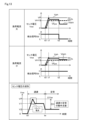
次に、上記構成の作用について説明する。図13は負荷電流大の場合および負荷電流小の場合でのセンス電圧Vseの波形と検出信号Sdの関係を示している。下段に示すセンス電圧Vseの一般的な波形に対して、上段に示す負荷電流大の場合には、通常時の検出動作では、過渡期から定常期に移行する時点で参照電圧Vhysよりも低下するので通常時であることが検出される。 Next, the operation of the above configuration will be described. Figure 13 shows the relationship between the waveform of the sense voltage Vse and the detection signal Sd when the load current is large and when the load current is small. In contrast to the typical waveform of the sense voltage Vse shown in the lower part, when the load current is large as shown in the upper part, in normal detection operation, the voltage drops below the reference voltage Vhys at the point of transition from the transient period to the steady state, so that normal operation is detected.
一方、中段に示す負荷電流小の場合には、センス電圧Vseは、過渡期のV1から定常期のV2に変化する際に、電圧V1V2の差が小さくなるため、センス電圧Vseが参照電圧Vhysよりも小さくならないことがある。このため、検出信号Sdはローレベルに変化することなく、これによって短絡時であるとして誤検出されてしまうことがある。 On the other hand, in the case of a small load current as shown in the middle, when the sense voltage Vse changes from V1 in the transient period to V2 in the steady state, the difference between the voltages V1 and V2 becomes small, so the sense voltage Vse may not become smaller than the reference voltage Vhys. As a result, the detection signal Sd does not change to a low level, which may result in an erroneous detection of a short circuit.
本実施形態では、このような誤検出が発生することがないように、コンパレータ91により、センス電圧Vseが短絡時の電流レベルに達しているか否かを判定するセンスしきい値Vth3により判定している。センスしきい値Vth3は、図14に示すように、短絡電流によるセンス電圧Vseのばらつきを考慮して短絡電流が最も小さいレベルでも短絡電流レベルとして判定することができるように設定されている。
In this embodiment, to prevent such erroneous detection from occurring, the
このため、通常時であるが負荷電流大の場合にはこの電圧を超えてしまう場合がある。しかし、この場合には、センス波形の検出結果が通常状態を示すローレベルの検出信号Sdを出力するので、アンド回路93は、短絡時の判定を示すハイレベルの判定信号Sxを出力することはない。
For this reason, under normal circumstances, when the load current is large, this voltage may be exceeded. However, in this case, the detection result of the sense waveform outputs a low-level detection signal Sd indicating a normal state, so the AND
図15は、通常時における負荷電流のレベルを小、中、大とし、短絡時との検出結果の比較を示している。通常時、負荷電流小の場合には波形検出回路40の検出信号Sdは前述のケースとなって短絡時を示すハイレベルのままとなる。
Figure 15 shows a comparison of the detection results when the load current level is small, medium, and large under normal conditions and when there is a short circuit. When the load current is small under normal conditions, the detection signal Sd of the
この場合、センス電圧Vseは、過渡期においてセンスしきい値電圧Vth3を超える場合でも、定常期に入ると負荷電流が短絡電流レベルよりも小さいので、ローレベルの検出信号Ssが出力される。この結果、ゲートモニタ出力Smがハイレベルになる判定タイミングでは、判定回路90から通常時であるローレベルの判定信号Sxが出力される。
In this case, even if the sense voltage Vse exceeds the sense threshold voltage Vth3 during the transient period, when the load current enters the steady state, it is smaller than the short circuit current level, and a low-level detection signal Ss is output. As a result, at the determination timing when the gate monitor output Sm becomes high level, the
次に、負荷電流中の場合には、波形検出回路40の検出信号Sdは過渡期から定常期に移行するタイミングでローレベルとなる。また、センス電圧Vseは、過渡期においてセンスしきい値電圧Vth3を超える場合でも、定常期に入ると負荷電流が短絡電流レベルよりも小さいので、ローレベルの検出信号Ssが出力される。この結果、ゲートモニタ出力Smがハイレベルになる判定タイミングでは、判定回路90から通常時であるローレベルの判定信号Sxが出力される。
Next, when there is a load current, the detection signal Sd of the
また、負荷電流大の場合には、波形検出回路40の検出信号Sdは過渡期から定常期に移行するタイミングでローレベルとなる。しかし、センス電圧Vseは、定常期に入っても負荷電流が大のため短絡電流レベルよりも大きくなる場合があり、これによってハイレベルの検出信号Ssが出力される。したがって、ゲートモニタ出力Smがハイレベルになる判定タイミングでは、やはり判定回路90から通常時であるローレベルの判定信号Sxが出力される。
In addition, when the load current is large, the detection signal Sd of the
一方、短絡時の場合には、波形検出回路40の検出信号Sdは定常期に入っても低下しないためハイレベルとなる。また、センス電圧Vseは、短絡電流が流れている状態では定常期に入ってもセンスしきい値電圧Vth3よりも大のためハイレベルの検出信号Ssが出力される。したがって、この場合には、ゲートモニタ出力Smがハイレベルになる判定タイミングで、判定回路90から短絡時であるハイレベルの判定信号Sxが出力される。
On the other hand, in the case of a short circuit, the detection signal Sd of the
このような第4実施形態によれば、第3実施形態の構成にセンスしきい値電圧Vth3によってセンス電圧Vseを判定するコンパレータ91を設けたので、負荷電流小のケースでも誤判定を発生させることを回避できるようになる。
According to the fourth embodiment, the configuration of the third embodiment is provided with a
(第5実施形態)
図16および図17は第5実施形態を示すもので、以下、第1実施形態と異なる部分について説明する。この実施形態では、第1実施形態におけるような波形検出の処理をスイッチング毎に実施する場合に、センス電圧Vseの波形が異なる場合に対応してピークホールド電圧Vphをスイッチング毎にリセットできるようにしたものである。
Fifth Embodiment
16 and 17 show the fifth embodiment, and the following describes the differences from the first embodiment. In this embodiment, when the waveform detection process in the first embodiment is performed for each switching, the peak hold voltage Vph can be reset for each switching in response to the case where the waveform of the sense voltage Vse differs.
図16において、ゲート駆動装置140は、波形検出回路40に代えて波形検出回路40aを備えている。波形検出回路40aは、比較回路60および、ピークホールド回路50に代わるピークホールド回路50aを備える。ピークホールド回路50aは、リセットスイッチ54が追加された構成である。リセットスイッチ54は、コンデンサ53の両端子間を短絡可能に接続されている。また、リセットスイッチ54は、制御回路20からリセット信号Swが与えられるとオンしてコンデンサ53の端子間を短絡状態として電荷の放電を実施する。
In FIG. 16, the
次に、上記構成の作用について説明する。図17は各部の信号の変化状態を示している。この実施形態では、制御回路20は、リセット信号Swにより、オンオフ指令によりオン指令の信号が与えられている期間中はリセットスイッチ54をリセット解除すなわちオフ状態に保持し、オフ指令が与えられている期間中はリセットスイッチ54をリセット状態すなわちオン状態に保持する。
Next, the operation of the above configuration will be described. FIG. 17 shows the change state of the signals in each part. In this embodiment, the
これにより、時刻t0のタイミングでオン指令が与えられると、リセットスイッチ54は、リセット解除となり、ピークホールド回路50aでは、センス電圧Vseのピークホールドを行い、コンデンサ53にピークホールド電圧VPが出力される。これにより、前述した波形検出の動作が行われる。
As a result, when an ON command is given at time t0, the
この後、時刻t1でオン指令からオフ指令に切り替わると、制御回路20は、リセットスイッチ54にハイレベルのリセット信号Swを出力してリセット動作させ、コンデンサ53の電荷を放電させ、ピークホールド電圧Vphを0Vにする。オフ指令が与えられている期間中は、ピークホールド電圧Vphが0Vに保持される。
After that, when the ON command is switched to the OFF command at time t1, the
時刻t2で再びオン指令が当たられると、時刻t3のオフ指令が与えられるまでの間、制御回路20はローレベルのリセット信号Swによりリセット状態を解除する。以下、上述と同様にして、制御回路20は、リセット信号Swにより、スイッチング毎にリセット解除を実施してセンス電圧Vseが変動し、例えばピークホールド電圧がVP1からΔVPだけ小さくなってVP2に低下する場合でも、これに対応して波形検出回路40aによる検出動作が確実に実施できるようにしている。
When an ON command is issued again at time t2, the
このような第5実施形態によれば、ピークホールド回路50aにリセットスイッチ54を設けて、スイッチング毎にピークホールド電圧Vphをリセットさせるようにしたので、センス電圧Vseのレベルがスイッチング毎に変動した場合でも、波形検出の動作を確実に実施できるようになる。
According to the fifth embodiment, a
なお、上記実施形態では、リセットスイッチ54のリセット動作は、制御回路20にオフ指令が与えられている期間中行うようにしたが、上記実施形態の場合に加えて、ノイズなどによる悪影響が無い場合には、オフ指令が与えられた直後に短時間だけリセット動作させるようにしても良い。
In the above embodiment, the reset operation of the
(第6実施形態)
図18および図19は第6実施形態を示すもので、以下、第1実施形態と異なる部分について説明する。この実施形態では、図18に示すように、ゲート駆動装置150は、波形検出回路40bにおいて、比較回路60aとして、ヒステリシス電源62に代えてヒステリシス電圧Vhを変更設定することができる可変ヒステリシス電源63を設ける構成としている。
Sixth Embodiment
18 and 19 show the sixth embodiment, and the following describes the differences from the first embodiment. In this embodiment, as shown in Fig. 18, a
これにより、図19に示しているように、可変ヒステリシス電源63によりヒステリシス電圧Vhを変更設定することで、ピーク電圧VPから減じるヒステリシス電圧Vhに応じて例えば電圧Vpys1あるいは電圧Vpys2のように異なるレベルに設定することができる。
As a result, as shown in FIG. 19, the hysteresis voltage Vh can be changed and set by the variable
このようにヒステリシス幅を変更設定することで、システムで発生するノイズなどによる誤動作を回避でき、波形検出の動作において誤検出を無くすことができる。ヒステリシス電圧Vhの調整は、人為的あるいは制御により行う構成とすることができる。 By changing and setting the hysteresis width in this way, malfunctions caused by noise generated in the system can be avoided, and false detections can be eliminated in waveform detection operations. The hysteresis voltage Vh can be adjusted manually or by control.
このような第6実施形態によれば、可変ヒステリシス電源63を設けて、ヒステリシス電圧Vhを調整可能な構成としたことで、システムで発生するノイズなどによる誤動作を回避して波形検出回路40aによる波形検出を確実に実施できるようになる。
According to the sixth embodiment, a variable
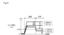
(第7実施形態)
図20および図21は第7実施形態を示すもので、以下、第4実施形態と異なる部分について説明する。この実施形態では、図20に示すゲート駆動装置160のように、第4実施形態で示した構成の2つの参照電源82、92を、参照電圧を変更設定できる可変参照電源83、93を設ける構成としている。
Seventh Embodiment
20 and 21 show the seventh embodiment, and the following describes the differences from the fourth embodiment. In this embodiment, as in a
この実施形態では、使用するIGBT1のようなパワー素子によって短絡時の飽和電流が異なることを想定し、システムによって負荷電流が異なることから通常のセンス電圧Vseも異なることに対応するものである。すなわち、このように条件や状況によって異なる場合にも対応できるようにしきい値電圧Vth2やVth3を可変参照電源83、93によって変更設定可能な構成としている。 In this embodiment, it is assumed that the saturation current during a short circuit differs depending on the power element, such as the IGBT1, used, and the normal sense voltage Vse differs because the load current differs depending on the system. In other words, the threshold voltages Vth2 and Vth3 are configured to be changeable and set by the variable reference power supplies 83 and 93 so that they can be adapted to such cases where they differ depending on the conditions and circumstances.
これにより、図21に示すように、モニタしきい値電圧Vth3を設定変更できるので、IGBT1の特性や使用形態に応じて適切なレベルに設定することができ、短絡検出を確実に実施することができるようになる。 As a result, as shown in FIG. 21, the monitor threshold voltage Vth3 can be changed, so that it can be set to an appropriate level depending on the characteristics and usage of the IGBT1, and short circuit detection can be performed reliably.
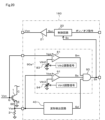
(第8実施形態)
図22および図23は第8実施形態を示すもので、以下、第4実施形態と異なる部分について説明する。この実施形態では、ゲート駆動装置170として、図22に示すように、波形検出回路40の出力段にフィルタ41を設け、判定回路90bのコンパレータ81および91のそれぞれの出力段にもフィルタ84および95を設けている。
Eighth embodiment
22 and 23 show the eighth embodiment, and the following describes the differences from the fourth embodiment. In this embodiment, as shown in Fig. 22, a
各フィルタ41、84、95は、ノイズを除去するためのローパスフィルタの機能を持つもので、センス電圧Vseやゲート電圧Vgeに重畳されるノイズを除去するものである。
Each
これにより、例えば図23に示すように、波形検出回路40において、センス電圧Vseが時刻t2で定常期に移行し通常時であることを示すローレベルの検出信号Sdが出力された後に、センス電圧Vseにノイズが重畳した場合には、短絡時であると誤検出してしまう恐れがあった。
As a result, for example, as shown in FIG. 23, in the
これに対して、この実施形態においては、時刻t3でフィルタ前の検出信号Sdにノイズに起因したハイレベルの信号が出力されていた場合でも、フィルタ41を介して出力される検出信号Sdではノイズによるハイレベルの信号部分が除去されるので、誤検出することなく検出動作が行われる。
In contrast, in this embodiment, even if a high-level signal caused by noise is output in the detection signal Sd before the filter at time t3, the high-level signal portion caused by noise is removed in the detection signal Sd output through the
(第9実施形態)
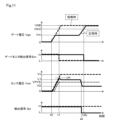
図24は第9実施形態を示すもので、以下、第1実施形態と異なる部分について説明する。この実施形態では、第1実施形態においては、通常時か短絡時かの判定をするものとして示しているが、この他に、IGBT1の動作としてオン駆動後に過電流が流れる状態があり、判定回路30により過電流時を判定するようにしたものである。
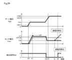
Ninth embodiment
24 shows the ninth embodiment, and the following describes the differences from the first embodiment. In this embodiment, in addition to the first embodiment, which is shown as determining whether the state is normal or short-circuited, there is a state in which an overcurrent flows after the
図24では、時刻t3以後の通常時を判定した後の、時刻txにIGBT1に過電流が流れ、センス電圧Vseが上昇していく状態を示している。この場合においても、判定回路30により、センス電圧Vseが参照電圧Vhysを超える時刻t4でハイレベルの判定信号Sxを出力させる。これにより、IGBT1の過電流時であることを判定することができるようになる。
Figure 24 shows a state in which an overcurrent flows through IGBT1 at time tx after determining that normal operation has occurred after time t3, and the sense voltage Vse rises. Even in this case, the
(他の実施形態)
なお、本発明は、上述した実施形態のみに限定されるものではなく、その要旨を逸脱しない範囲で種々の実施形態に適用可能であり、例えば、以下のように変形または拡張することができる。
Other Embodiments
The present invention is not limited to the above-described embodiment, but can be applied to various embodiments without departing from the spirit of the present invention, and can be modified or expanded as follows, for example.
上記各実施形態では、パワー素子としてIGBTを用いた場合で説明したが、このようにセンス電圧Vseが持ち上がる現象は、線形領域と飽和領域との動作の違いにより発生するものであるので、IGBT以外に一般的なMOSトランジスタやSiCMOSトランジスタなどのパワー系のゲート駆動型の半導体スイッチング素子のいずれにおいても適用することができる。
上記各実施形態は、第1実施形態および第4実施形態を基本とし、その応用として示しているが、その他の実施形態において組み合わせた構成とした複合的な構成を採用することもできる。
In each of the above embodiments, an IGBT is used as the power element. However, the phenomenon in which the sense voltage Vse rises in this manner occurs due to the difference in operation between the linear region and the saturation region. Therefore, the present invention can be applied to any gate-driven semiconductor switching element of a power system, such as a general MOS transistor or a SiCMOS transistor, other than an IGBT.
The above-described embodiments are based on the first and fourth embodiments and are shown as applications thereof, but it is also possible to adopt a composite configuration in which the other embodiments are combined.
本開示は、実施例に準拠して記述されたが、本開示は当該実施例や構造に限定されるものではないと理解される。本開示は、様々な変形例や均等範囲内の変形をも包含する。加えて、様々な組み合わせや形態、さらには、それらに一要素のみ、それ以上、あるいはそれ以下、を含む他の組み合わせや形態をも、本開示の範疇や思想範囲に入るものである。 Although the present disclosure has been described with reference to the embodiment, it is understood that the present disclosure is not limited to the embodiment or structure. The present disclosure also encompasses various modifications and modifications within the scope of equivalents. In addition, various combinations and forms, as well as other combinations and forms including only one element, more than one element, or less than one element, are also within the scope and concept of the present disclosure.
図面中、1はIGBT(ゲート駆動型の半導体スイッチング素子)、10、110、120、130、140、150、160、170はゲート駆動装置、20は制御回路、30は判定回路、31はコンパレータ、33は遅延回路、34はアンド回路、40、40a、40bは波形検出回路、41はフィルタ、50、50aはピークホールド回路、51はオペアンプ、53はコンデンサ、60、60aは比較回路、61はコンパレータ、62はヒステリシス電源、63は可変ヒステリシス電源、70は判定回路、71は遅延回路、80は判定回路、81はコンパレータ(ゲートモニタ回路)、90は判定回路、91はコンパレータ、93はアンド回路である。 In the drawings, 1 is an IGBT (gate-driven semiconductor switching element), 10, 110, 120, 130, 140, 150, 160, and 170 are gate drive devices, 20 is a control circuit, 30 is a judgment circuit, 31 is a comparator, 33 is a delay circuit, 34 is an AND circuit, 40, 40a, and 40b are waveform detection circuits, 41 is a filter, 50 and 50a are peak hold circuits, 51 is an operational amplifier, 53 is a capacitor, 60 and 60a are comparison circuits, 61 is a comparator, 62 is a hysteresis power supply, 63 is a variable hysteresis power supply, 70 is a judgment circuit, 71 is a delay circuit, 80 is a judgment circuit, 81 is a comparator (gate monitor circuit), 90 is a judgment circuit, 91 is a comparator, and 93 is an AND circuit.
Claims (9)
前記電流センス端子からのセンス電流の検出信号を取り込み、前記検出信号に基づいて、前記センス電流が、前記半導体スイッチング素子が線形領域で動作する定常期の電流よりも上昇した後に前記定常期の電流まで低下する現象である過渡センス電流の有無を検出する波形検出回路(40)と、
前記波形検出回路による検出結果を所定タイミングで判定して短絡の有無を判定する判定回路(30)と、
前記半導体スイッチング素子のオンオフ駆動を制御し、前記半導体スイッチング素子をオン駆動した後、前記判定回路により短絡有りが判定されたことに基づいて遮断する制御回路(20)とを備えたゲート駆動装置。 A gate drive device for controlling the drive of a gate drive type semiconductor switching element having a current sense terminal,
a waveform detection circuit (40) for receiving a detection signal of the sense current from the current sense terminal, and detecting, based on the detection signal, the presence or absence of a transient sense current, which is a phenomenon in which the sense current rises above a current in a steady state in which the semiconductor switching element operates in a linear region and then falls to the current in the steady state;
a determination circuit (30) that determines the presence or absence of a short circuit by determining the detection result by the waveform detection circuit at a predetermined timing;
a control circuit (20) that controls the on/off driving of the semiconductor switching element, and turns on the semiconductor switching element, and then cuts it off based on the determination by the determination circuit that a short circuit exists.
前記センス電流の検出信号のピーク値を保持するピークホールド回路(50)と、
前記センス電流の検出信号のレベルと前記ピークホールド回路の出力を所定量だけ低下させたレベルとを比較して前記短絡の有無を判定する比較回路(60)と
を有する請求項1に記載のゲート駆動装置。 The waveform detection circuit includes:
a peak hold circuit (50) for holding a peak value of the detection signal of the sense current;
2. The gate drive device according to claim 1, further comprising a comparison circuit (60) for determining the presence or absence of the short circuit by comparing a level of the detection signal of the sense current with a level obtained by lowering the output of the peak hold circuit by a predetermined amount.
前記短絡の有無の判定を、前記ゲートモニタ回路の検出タイミングで実施する請求項1から4のいずれか一項に記載のゲート駆動装置。 The determination circuit includes a gate monitor circuit (81) that monitors the gate voltage of the semiconductor switching element and detects when the gate voltage reaches a predetermined voltage,
5. The gate driving device according to claim 1, wherein the presence or absence of the short circuit is determined at a detection timing of the gate monitor circuit.
前記判定回路は、前記判定を、前記波形検出回路および前記センスしきい値検出回路の双方から短絡が検出されたときに前記短絡の有無を判定する請求項1から6のいずれか一項に記載のゲート駆動装置。 the determination circuit further has a function of detecting that the detection signal of the sense current has reached a sense threshold value corresponding to a short circuit level;
7. The gate driver according to claim 1, wherein the determination circuit determines the presence or absence of a short circuit when a short circuit is detected by both the waveform detection circuit and the sense threshold detection circuit.
Priority Applications (2)
| Application Number | Priority Date | Filing Date | Title |
|---|---|---|---|
| JP2021091316A JP7571663B2 (en) | 2021-05-31 | 2021-05-31 | Gate Driver |
| PCT/JP2022/018895 WO2022255008A1 (en) | 2021-05-31 | 2022-04-26 | Gate drive device |
Applications Claiming Priority (1)
| Application Number | Priority Date | Filing Date | Title |
|---|---|---|---|
| JP2021091316A JP7571663B2 (en) | 2021-05-31 | 2021-05-31 | Gate Driver |
Publications (3)
| Publication Number | Publication Date |
|---|---|
| JP2022183823A JP2022183823A (en) | 2022-12-13 |
| JP2022183823A5 JP2022183823A5 (en) | 2023-06-27 |
| JP7571663B2 true JP7571663B2 (en) | 2024-10-23 |
Family
ID=84324287
Family Applications (1)
| Application Number | Title | Priority Date | Filing Date |
|---|---|---|---|
| JP2021091316A Active JP7571663B2 (en) | 2021-05-31 | 2021-05-31 | Gate Driver |
Country Status (2)
| Country | Link |
|---|---|
| JP (1) | JP7571663B2 (en) |
| WO (1) | WO2022255008A1 (en) |
Citations (3)
| Publication number | Priority date | Publication date | Assignee | Title |
|---|---|---|---|---|
| JP2013077976A (en) | 2011-09-30 | 2013-04-25 | Mitsubishi Electric Corp | Semiconductor device |
| JP2017212870A (en) | 2016-05-20 | 2017-11-30 | 株式会社デンソー | Driving control device for switching element |
| JP2019213430A (en) | 2018-06-08 | 2019-12-12 | 株式会社デンソー | Drive circuit |
-
2021
- 2021-05-31 JP JP2021091316A patent/JP7571663B2/en active Active
-
2022
- 2022-04-26 WO PCT/JP2022/018895 patent/WO2022255008A1/en not_active Ceased
Patent Citations (3)
| Publication number | Priority date | Publication date | Assignee | Title |
|---|---|---|---|---|
| JP2013077976A (en) | 2011-09-30 | 2013-04-25 | Mitsubishi Electric Corp | Semiconductor device |
| JP2017212870A (en) | 2016-05-20 | 2017-11-30 | 株式会社デンソー | Driving control device for switching element |
| JP2019213430A (en) | 2018-06-08 | 2019-12-12 | 株式会社デンソー | Drive circuit |
Also Published As
| Publication number | Publication date |
|---|---|
| WO2022255008A1 (en) | 2022-12-08 |
| JP2022183823A (en) | 2022-12-13 |
Similar Documents
| Publication | Publication Date | Title |
|---|---|---|
| US10222422B2 (en) | Short-circuit detection circuits, system, and method | |
| JP7087373B2 (en) | Current detection circuit and current detection method for semiconductor devices | |
| JP6197685B2 (en) | Gate drive circuit | |
| CN108809059B (en) | Driving device for semiconductor element | |
| US9685945B2 (en) | Electric circuit | |
| US10110217B2 (en) | Load driving device | |
| JP5430608B2 (en) | Semiconductor switching element drive circuit | |
| KR101106813B1 (en) | Overcurrent protection circuit | |
| US11545970B2 (en) | Current detection circuit, current detection method, and semiconductor module | |
| JP7326762B2 (en) | Semiconductor modules and drive circuits | |
| CN114667681B (en) | Gate drive circuit | |
| CN106416071A (en) | Drive circuit for semiconductor switching element | |
| CN109983679B (en) | Control device and semiconductor device | |
| US11581886B2 (en) | Current detection circuit, current detection method, and semiconductor module | |
| JP6405998B2 (en) | Load drive circuit | |
| JP7571663B2 (en) | Gate Driver | |
| JP6711059B2 (en) | Protection circuit | |
| JP6622405B2 (en) | Inverter drive | |
| JP5144292B2 (en) | Switching power supply circuit and vehicle equipped with the same | |
| JP7552506B2 (en) | Gate Driver | |
| JP2020005229A (en) | Load drive device | |
| JP2020129867A (en) | Overcurrent detection circuit and current output circuit | |
| JP3425004B2 (en) | Ground fault current detector | |
| JP2025068482A (en) | Semiconductor switching element driving circuit | |
| JP2017118790A (en) | Switching circuit |
Legal Events
| Date | Code | Title | Description |
|---|---|---|---|
| A521 | Request for written amendment filed |
Free format text: JAPANESE INTERMEDIATE CODE: A523 Effective date: 20230616 |
|
| A621 | Written request for application examination |
Free format text: JAPANESE INTERMEDIATE CODE: A621 Effective date: 20230616 |
|
| A131 | Notification of reasons for refusal |
Free format text: JAPANESE INTERMEDIATE CODE: A131 Effective date: 20240514 |
|
| A131 | Notification of reasons for refusal |
Free format text: JAPANESE INTERMEDIATE CODE: A131 Effective date: 20240709 |
|
| A521 | Request for written amendment filed |
Free format text: JAPANESE INTERMEDIATE CODE: A523 Effective date: 20240827 |
|
| TRDD | Decision of grant or rejection written | ||
| A01 | Written decision to grant a patent or to grant a registration (utility model) |
Free format text: JAPANESE INTERMEDIATE CODE: A01 Effective date: 20240910 |
|
| A61 | First payment of annual fees (during grant procedure) |
Free format text: JAPANESE INTERMEDIATE CODE: A61 Effective date: 20240923 |
|
| R150 | Certificate of patent or registration of utility model |
Ref document number: 7571663 Country of ref document: JP Free format text: JAPANESE INTERMEDIATE CODE: R150 |