JP7541454B2 - Semiconductor device and its manufacturing method - Google Patents
Semiconductor device and its manufacturing method Download PDFInfo
- Publication number
- JP7541454B2 JP7541454B2 JP2020148586A JP2020148586A JP7541454B2 JP 7541454 B2 JP7541454 B2 JP 7541454B2 JP 2020148586 A JP2020148586 A JP 2020148586A JP 2020148586 A JP2020148586 A JP 2020148586A JP 7541454 B2 JP7541454 B2 JP 7541454B2
- Authority
- JP
- Japan
- Prior art keywords
- layer
- type
- main surface
- dislocation suppression
- silicon substrate
- Prior art date
- Legal status (The legal status is an assumption and is not a legal conclusion. Google has not performed a legal analysis and makes no representation as to the accuracy of the status listed.)
- Active
Links
Images


Classifications
-
- H—ELECTRICITY
- H10—SEMICONDUCTOR DEVICES; ELECTRIC SOLID-STATE DEVICES NOT OTHERWISE PROVIDED FOR
- H10D—INORGANIC ELECTRIC SEMICONDUCTOR DEVICES
- H10D12/00—Bipolar devices controlled by the field effect, e.g. insulated-gate bipolar transistors [IGBT]
- H10D12/01—Manufacture or treatment
- H10D12/031—Manufacture or treatment of IGBTs
- H10D12/032—Manufacture or treatment of IGBTs of vertical IGBTs
- H10D12/038—Manufacture or treatment of IGBTs of vertical IGBTs having a recessed gate, e.g. trench-gate IGBTs
-
- H—ELECTRICITY
- H10—SEMICONDUCTOR DEVICES; ELECTRIC SOLID-STATE DEVICES NOT OTHERWISE PROVIDED FOR
- H10D—INORGANIC ELECTRIC SEMICONDUCTOR DEVICES
- H10D12/00—Bipolar devices controlled by the field effect, e.g. insulated-gate bipolar transistors [IGBT]
- H10D12/411—Insulated-gate bipolar transistors [IGBT]
- H10D12/441—Vertical IGBTs
- H10D12/461—Vertical IGBTs having non-planar surfaces, e.g. having trenches, recesses or pillars in the surfaces of the emitter, base or collector regions
- H10D12/481—Vertical IGBTs having non-planar surfaces, e.g. having trenches, recesses or pillars in the surfaces of the emitter, base or collector regions having gate structures on slanted surfaces, on vertical surfaces, or in grooves, e.g. trench gate IGBTs
-
- H—ELECTRICITY
- H10—SEMICONDUCTOR DEVICES; ELECTRIC SOLID-STATE DEVICES NOT OTHERWISE PROVIDED FOR
- H10D—INORGANIC ELECTRIC SEMICONDUCTOR DEVICES
- H10D62/00—Semiconductor bodies, or regions thereof, of devices having potential barriers
- H10D62/10—Shapes, relative sizes or dispositions of the regions of the semiconductor bodies; Shapes of the semiconductor bodies
- H10D62/102—Constructional design considerations for preventing surface leakage or controlling electric field concentration
- H10D62/103—Constructional design considerations for preventing surface leakage or controlling electric field concentration for increasing or controlling the breakdown voltage of reverse-biased devices
- H10D62/105—Constructional design considerations for preventing surface leakage or controlling electric field concentration for increasing or controlling the breakdown voltage of reverse-biased devices by having particular doping profiles, shapes or arrangements of PN junctions; by having supplementary regions, e.g. junction termination extension [JTE]
- H10D62/106—Constructional design considerations for preventing surface leakage or controlling electric field concentration for increasing or controlling the breakdown voltage of reverse-biased devices by having particular doping profiles, shapes or arrangements of PN junctions; by having supplementary regions, e.g. junction termination extension [JTE] having supplementary regions doped oppositely to or in rectifying contact with regions of the semiconductor bodies, e.g. guard rings with PN or Schottky junctions
-
- H—ELECTRICITY
- H10—SEMICONDUCTOR DEVICES; ELECTRIC SOLID-STATE DEVICES NOT OTHERWISE PROVIDED FOR
- H10D—INORGANIC ELECTRIC SEMICONDUCTOR DEVICES
- H10D62/00—Semiconductor bodies, or regions thereof, of devices having potential barriers
- H10D62/10—Shapes, relative sizes or dispositions of the regions of the semiconductor bodies; Shapes of the semiconductor bodies
- H10D62/124—Shapes, relative sizes or dispositions of the regions of semiconductor bodies or of junctions between the regions
- H10D62/126—Top-view geometrical layouts of the regions or the junctions
- H10D62/127—Top-view geometrical layouts of the regions or the junctions of cellular field-effect devices, e.g. multicellular DMOS transistors or IGBTs
-
- H—ELECTRICITY
- H10—SEMICONDUCTOR DEVICES; ELECTRIC SOLID-STATE DEVICES NOT OTHERWISE PROVIDED FOR
- H10D—INORGANIC ELECTRIC SEMICONDUCTOR DEVICES
- H10D62/00—Semiconductor bodies, or regions thereof, of devices having potential barriers
- H10D62/10—Shapes, relative sizes or dispositions of the regions of the semiconductor bodies; Shapes of the semiconductor bodies
- H10D62/13—Semiconductor regions connected to electrodes carrying current to be rectified, amplified or switched, e.g. source or drain regions
- H10D62/141—Anode or cathode regions of thyristors; Collector or emitter regions of gated bipolar-mode devices, e.g. of IGBTs
- H10D62/142—Anode regions of thyristors or collector regions of gated bipolar-mode devices
-
- H—ELECTRICITY
- H10—SEMICONDUCTOR DEVICES; ELECTRIC SOLID-STATE DEVICES NOT OTHERWISE PROVIDED FOR
- H10D—INORGANIC ELECTRIC SEMICONDUCTOR DEVICES
- H10D64/00—Electrodes of devices having potential barriers
- H10D64/111—Field plates
- H10D64/117—Recessed field plates, e.g. trench field plates or buried field plates
-
- H—ELECTRICITY
- H10—SEMICONDUCTOR DEVICES; ELECTRIC SOLID-STATE DEVICES NOT OTHERWISE PROVIDED FOR
- H10D—INORGANIC ELECTRIC SEMICONDUCTOR DEVICES
- H10D62/00—Semiconductor bodies, or regions thereof, of devices having potential barriers
- H10D62/60—Impurity distributions or concentrations
Landscapes
- Electrodes Of Semiconductors (AREA)
Description
本発明は、半導体装置およびその製造方法に関し、特にIE(Injection Enhanced)型IGBT(Insulated Gate Bipolar Transistor)を有する半導体装置およびその製造方法に適用して有効な技術である。 The present invention relates to a semiconductor device and a manufacturing method thereof, and is particularly an effective technique when applied to a semiconductor device having an IE ( Injection Enhanced ) type IGBT ( Insulated Gate Bipolar Transistor) and a manufacturing method thereof.
IE型IGBTの構造の一例として、n型エミッタ層及びp型ベース層を平面視で囲むように形成されたストライプ状のトレンチゲートと、トレンチゲートの外側に配置され、かつ、その一端がトレンチゲートの側面に接するように形成されたp型フローティング層と、p型ベース層の下部に形成されたn型ホールバリア層とを有する構造が知られている(例えば、特許文献1参照)。 One example of the structure of an IE-type IGBT is a structure having a striped trench gate formed to surround an n-type emitter layer and a p-type base layer in a plan view, a p-type floating layer disposed outside the trench gate and formed so that one end of the layer contacts the side of the trench gate, and an n-type hole barrier layer formed below the p-type base layer (see, for example, Patent Document 1).
また、特許文献1には、IGBTのスイッチング損失を抑制するため、p型フローティング層に蓄積された正孔を排出する経路を供給する目的で、p型フローティング層の他端に接するように形成されたストライプ形状のトレンチエミッタを有する構造が開示されている。更に、特許文献1には、p型ベース層の下部に配置されたn型ドリフト層の下面にn型フィールドストップ層と、p型コレクタ層とを有する構造が開示されている。
本発明者は、IGBTの高速スイッチング時のリーク電流の低減、又は、逆バイアス時のリーク電流の低減の観点から、IGBTの裏面側に形成されたn型フィールドストップ層とp型コレクタ層に関して、以下の懸念があることを見出した。 The inventors have found that there are the following concerns regarding the n-type field stop layer and p-type collector layer formed on the back side of the IGBT from the perspective of reducing leakage current during high-speed switching of the IGBT or reducing leakage current during reverse bias.
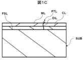
図1Aに示すように、n型単結晶シリコンからなる基板SUBの裏面BSにIGBTのn型フィールドストップ層とp型コレクタ層を形成するために、例えば、n型不純物であるリン(P)とp型不純物であるホウ素(B)を順次シリコン基板の裏面BSにイオン注入し、n型不純物注入層NIと、p型不純物注入層PIを形成する。その後、基板SUBの裏面にレーザアニールLAを施すことにより、不純物注入層NI及びPIを活性化させることによって、図1Bに示すように、n型フィールドストップ層FSLとp型コレクタ層CLを形成する。 As shown in FIG. 1A, in order to form an n-type field stop layer and a p-type collector layer of an IGBT on the back surface BS of a substrate SUB made of n-type single crystal silicon, for example, an n-type impurity, phosphorus (P), and a p-type impurity, boron (B), are ion-implanted sequentially into the back surface BS of the silicon substrate to form an n-type impurity implanted layer NI and a p-type impurity implanted layer PI. Then, by performing laser annealing LA on the back surface of the substrate SUB to activate the impurity implanted layers NI and PI, an n-type field stop layer FSL and a p-type collector layer CL are formed as shown in FIG. 1B.
このレーザアニールLAにおけるレーザ照射時に、基板SUBの裏面BSの最表面の厚さ0.2μm程度のシリコンが一旦溶融し、溶融層MLが形成される。レーザ照射後、基板SUBの温度が低下し、溶融層MLが再結晶化する。この時、溶融層MLの表面にパーティクルPTLが存在すると、図1Cに示すように、再結晶化時に、パーティクルPTLが起点となり基板SBの裏面BSに転位欠陥DILが形成されることを本発明者は見出した。 During the laser irradiation in this laser annealing LA, silicon with a thickness of about 0.2 μm on the outermost surface of the back surface BS of the substrate SUB melts once, forming a molten layer ML. After the laser irradiation, the temperature of the substrate SUB drops, and the molten layer ML recrystallizes. The inventors have found that if a particle PTL is present on the surface of the molten layer ML at this time, as shown in Figure 1C, dislocation defects DIL are formed on the back surface BS of the substrate SB, starting from the particle PTL.
この転位欠陥DILがn型フィールドストップ層FSLまで伸びると、IGBTのコレクタ・エミッタ間のリーク不良や逆バイアスリーク不良の懸念になる。IGBTの裏面構造形成プロセスおいて、パーティクルPTLを完全に無くすことができれば、転位欠陥は解決できる。しかしながら、特に高電圧、大電流を扱うIGBTは、通常のLSIチップと比較してチップ面積が大きいので(例えば10mm2以上)、パーティクルPTLを完全に無くすことは、現実的に非常に困難である。 If this dislocation defect DIL extends to the n-type field stop layer FSL, it can cause leakage defects between the collector and emitter of the IGBT and reverse bias leakage defects. If the particle PTL could be completely eliminated in the IGBT back surface structure formation process, the dislocation defect problem could be solved. However, IGBTs, which handle particularly high voltages and large currents, have a large chip area (e.g., 10 mm2 or more) compared to normal LSI chips, so in reality it is very difficult to completely eliminate the particle PTL.
また、IGBTはオン抵抗を低減するために、ドリフト層となるn型シリコン基板の裏面を、研削、研磨することによって薄型化している。このため、基板の裏面に形成されるn型フィールドストップ層及びp型コレクタ層は、基板の主面側にn型エミッタ層、p型ベース層、p型フローティング層、n型ホールバリア層等を順次形成した後に、薄型化された基板の裏面に形成することになる。n型エミッタ層、p型ベース層等の不純物プロファイルを維持するために、n型フィールドストップ層及びp型コレクタ層を形成するための高温の熱処理は、基板全体に施すことが制限される。従って、基板に対して部分的に熱処理を施すことが可能なレーザアニールは、IBGTの製造において、近年、有効な技術となっている。 In order to reduce the on-resistance of an IGBT, the back surface of the n-type silicon substrate, which serves as the drift layer, is ground and polished to make it thinner. For this reason, the n-type field stop layer and p-type collector layer formed on the back surface of the substrate are formed on the back surface of the thinned substrate after the n-type emitter layer, p-type base layer, p-type floating layer, n-type hole barrier layer, etc. are formed in sequence on the main surface side of the substrate. In order to maintain the impurity profile of the n-type emitter layer, p-type base layer, etc., high-temperature heat treatment for forming the n-type field stop layer and p-type collector layer is limited to being performed on the entire substrate. Therefore, laser annealing, which allows partial heat treatment of the substrate, has become an effective technique in the manufacture of IGBTs in recent years.
その他の課題および新規な特徴は、本明細書および図面の記載から明らかになるであろう。 Other objects and novel features will become apparent from the description of this specification and drawings.
一実施の形態に係る半導体装置は、シリコン基板の裏面にp型コレクタ層を有するIGBTを有し、p型コレクタ層中に、シリコンとヘテロ接合を形成する転位抑制層を有する。転位抑制層は、シリコンゲルマニウム(SiGe)層を有する。 The semiconductor device according to one embodiment has an IGBT having a p-type collector layer on the back surface of a silicon substrate, and the p-type collector layer has a dislocation suppression layer that forms a heterojunction with silicon. The dislocation suppression layer has a silicon germanium (SiGe) layer.
一実施の形態に係る半導体装置によれば、IGBTを有する半導体装置のリーク電流を低減し、高速スイッチングに対応可能なIGBTを提供することができる。 The semiconductor device according to one embodiment can reduce the leakage current of a semiconductor device having an IGBT and provide an IGBT that can handle high-speed switching.
以下、一実施の形態に係る半導体装置について、図面を参照して詳細に説明する。なお、明細書および図面において、同一の構成要件または対応する構成要件には、同一の符号を付し、重複する説明は省略する。また、実施の形態と各変形例との少なくとも一部は、互いに任意に組み合わされてもよい。 A semiconductor device according to one embodiment will be described in detail below with reference to the drawings. Note that in the specification and drawings, the same or corresponding components are denoted by the same reference numerals, and duplicated descriptions will be omitted. In addition, at least a portion of the embodiment and each of the modified examples may be combined with each other in any desired manner.
図2を用いて、IGBTの裏面側構造を説明する。図2は、一実施の形態に係るIGBTを有する半導体装置の裏面側構造を示す要部断面図である。ここでは、基板SUBの表面US側に形成されるn型エミッタ層、p型ベース層、トレンチゲート、トレンチエミッタ、p型フローティング層及びn型ホールバリア層等は省略して説明する。基板SUBの表面USは第1主面と見做すことができ、基板SUBの裏面BSは第1主面と対向する第2主面と見做すことができる。 The back side structure of the IGBT will be described using Figure 2. Figure 2 is a cross-sectional view of a main part showing the back side structure of a semiconductor device having an IGBT according to one embodiment. Here, the n-type emitter layer, p-type base layer, trench gate, trench emitter, p-type floating layer, n-type hole barrier layer, etc. formed on the front surface US side of the substrate SUB will be omitted. The front surface US of the substrate SUB can be regarded as the first main surface, and the back surface BS of the substrate SUB can be regarded as the second main surface opposite the first main surface.
図2に示すように、n型シリコンからなる基板SUBの裏面BSにn型半導体層からなるフィールドストップ層FSLと、p型半導体層からなるコレクタ層CLが形成されている。コレクタ層CL中には、シリコンゲルマニウム(SiGe)層からなる転位抑制層DSL1が形成されている。転位抑制層DSL1は、コレクタ層CL中にシリコン層とシリコンゲルマニウム(SiGe)層とで形成されたヘテロ接合HJを供給するように形成される。このヘテロ接合HJにより、基板SUBの裏面BSに図1Bに示したパーティクルPTLが存在したとしても、転位欠陥DILがフィールドストップ層FSL側に延びることを抑制することができるので、エミッタ・コレクタ間の電流リーク、逆バイアス時の電流リークを抑制することができる。 As shown in FIG. 2, a field stop layer FSL made of an n-type semiconductor layer and a collector layer CL made of a p-type semiconductor layer are formed on the back surface BS of a substrate SUB made of n-type silicon. A dislocation suppression layer DSL1 made of a silicon germanium (SiGe) layer is formed in the collector layer CL. The dislocation suppression layer DSL1 is formed so as to provide a heterojunction HJ made of a silicon layer and a silicon germanium (SiGe) layer in the collector layer CL. This heterojunction HJ can suppress the dislocation defect DIL from extending to the field stop layer FSL side even if a particle PTL shown in FIG. 1B is present on the back surface BS of the substrate SUB, so that current leakage between the emitter and collector and current leakage during reverse bias can be suppressed.
転位抑制層DSL1は、基板SUBの裏面BSの最表面からの深さが、0.2μmより深い位置に配置される。これは、レーザアニールLAにおけるレーザ照射時に、基板SUBの裏面BSの最表面の厚さ0.2μm程度のシリコンが一旦溶融し、溶融層MLが形成されるため、この溶融層MLの影響を避けるためである。このように転位抑制層DSL1をコレクタ層CLの比較的深い位置に配置することによって、転位抑制層DSL1の上下面の両方にヘテロ接合HJを形成することができるので、転位欠陥DILの抑制効果が高い。 The dislocation suppression layer DSL1 is positioned at a depth of more than 0.2 μm from the top surface of the back surface BS of the substrate SUB. This is to avoid the influence of the molten layer ML that is formed when the silicon on the top surface of the back surface BS of the substrate SUB, which is about 0.2 μm thick, melts during laser irradiation in the laser annealing LA, forming a molten layer ML. By positioning the dislocation suppression layer DSL1 at a relatively deep position in the collector layer CL in this way, heterojunctions HJ can be formed on both the top and bottom surfaces of the dislocation suppression layer DSL1, which provides a high suppression effect on dislocation defects DIL.
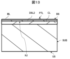
また、図3に示すように、転位抑制層の位置を基板SUBの裏面BSの表面の近傍に配置してもよい。この場合、転位抑制層DSL2の裏面BSに近い側は、溶融層MLと重なってヘテロ接合を形成できないが、転位抑制層DSL2の不純物プロファイルは、図2に示した転位抑制層DSL1と比較して、シャープに設定することが可能であるので、IGBTの出力特性を向上することができる。 Also, as shown in FIG. 3, the dislocation suppression layer may be positioned near the surface of the back surface BS of the substrate SUB. In this case, the side of the dislocation suppression layer DSL2 close to the back surface BS does not overlap with the molten layer ML to form a heterojunction, but the impurity profile of the dislocation suppression layer DSL2 can be set sharper than that of the dislocation suppression layer DSL1 shown in FIG. 2, thereby improving the output characteristics of the IGBT.
転位抑制層は、ゲルマニウム(Ge)を基板SUBの裏面BSからイオン注入することで形成するが、図3に示した転位抑制層DSL2は、裏面BSから浅い位置に形成するので、低加速エネルギーのイオン注入(たとえば、150~500keVの範囲)で形成することが可能である。そのため、転位抑制層DSL2の厚さを薄く形成できるので、IGBTの出力特性を向上することができる。 The dislocation suppression layer is formed by ion implantation of germanium (Ge) from the back surface BS of the substrate SUB. The dislocation suppression layer DSL2 shown in FIG. 3 is formed at a shallow position from the back surface BS, so it can be formed by ion implantation with low acceleration energy (for example, in the range of 150 to 500 keV). Therefore, the dislocation suppression layer DSL2 can be formed thin, which improves the output characteristics of the IGBT.
一方、図2に示した転位抑制層DSL1は、転位抑制層DSL2と比較的して、高加速のイオン注入(たとえば、600~900keV)で形成するのでイオン散乱が大きくなり不純物プロファイルがブロードになり、IGBTの出力特性が低下するが、コレクタ層CL中にヘテロ接合HJを2面形成できるので、リーク電流を抑制する効果が高い。すなわち、シリコンゲルマニウム(SiGe)とシリコン(Si)のバンドギャップには差があり、このバンドギャップの差が裏面からのホール注入を阻害する。イオン注入されたゲルマニウム(Ge)の不純物プロファイルがブロードになるということは、バンドギャップが不均一な領域が広がることと同義であり、ホール注入を阻害する効果が強まる。よって、IGBTの出力特性が低下することになる。 On the other hand, the dislocation suppression layer DSL1 shown in FIG. 2 is formed by high-acceleration ion implantation (for example, 600 to 900 keV) compared to the dislocation suppression layer DSL2, so ion scattering becomes large and the impurity profile becomes broad, and the output characteristics of the IGBT deteriorate. However, since two heterojunctions HJ can be formed in the collector layer CL, the effect of suppressing leakage current is high. In other words, there is a difference in the band gap between silicon germanium (SiGe) and silicon (Si), and this difference in band gap inhibits hole injection from the back surface. The fact that the impurity profile of ion-implanted germanium (Ge) becomes broad is synonymous with the expansion of the region with an uneven band gap, and the effect of inhibiting hole injection becomes stronger. Therefore, the output characteristics of the IGBT deteriorate.
図4に、図2で説明した転位抑制層DSL1を有するIE型IGBTの一例を示す。図4に示すように、IE型IGBT100は、n型シリコンで形成された基板SUBの主面側に、トレンチゲートTG、トレンチエミッタTE、p型ベース層BL、n型エミッタ層EL、p型フローティング層FL及びn型ホールバリア層HBLを有する。IE型IGBT100は、更に、n型ホールバリア層HBLの下部に配置されたn型ドリフト層DLと、n型ドリフト層DLの下部に配置されたn型フィールドストップ層FSLと、n型フィールドストップ層FSLの下部に配置されたp型コレクタ層CLと、p型コレクタ層CLの下部に配置されたコレクタ電極CEを有する。コレクタ層CL中には、シリコンゲルマニウム(SiGe)層からなる転位抑制層DSL1が形成されている。p型ベース層BLとn型エミッタ層ELには、層間絶縁膜ILに形成された接続孔CH1を介して、エミッタ電極EEが電気的に接続されている。尚、符号BCは、p型ベース層BLの表面に形成された高濃度のp型ベースコンタクト層である。また、エミッタ電極EEは、層間絶縁膜ILに形成された接続孔CH2を介して、トレンチエミッタTE間に形成されたp型ベース層BLと、トレンチエミッタTEとに電気的に接続されている。絶縁膜FPFがエミッタ電極EEの上側に形成されている。絶縁膜FPFは、例えばポリイミドを主要な成分とする有機絶縁膜などからなるファイナルパッシべーション膜である。
Figure 4 shows an example of an IE type IGBT having the dislocation suppression layer DSL1 described in Figure 2. As shown in Figure 4, the
IE型IGBT100は、p型フローティング層FLをソース領域、p型ベース層BLをドレイン領域、トレンチエミッタTEをゲート電極とする寄生Pチャネル型MOSFETを内蔵している。n型ホールバリア層HBLは、寄生Pチャネル型MOSFETのチャネル形成領域を構成する。この寄生Pチャネル型MOSFETによって、IGBTのターンオフ時にp型フローティング層FLに蓄積されたホールが、エミッタ電極EEに短い経路で排出されることにより、スイッチング時間を短縮することができる。また、p型フローティング層FLの電位変動が抑制されるので、トレンチゲートTGの電位が安定化し、スイッチング損失を抑制することができる。これらの効果に加えて、IE型IGBT100は、転位抑制層DSL1を有しているので、エミッタ・コレクタ間の電流リーク、逆バイアス時の電流リークを抑制することができる。
The IE-
以下、IE型IGBT100を構成する半導体層、絶縁膜、電極の材料及び形状を簡単に説明する。
Below, we will briefly explain the materials and shapes of the semiconductor layers, insulating films, and electrodes that make up the IE-
まず、基板SUBは、リン(P)等のn型不純物が導入された単結晶シリコンで形成され、不純物濃度は、例えば2×1014cm-3程度であり、この濃度がドリフト層DLの不純物濃度となっている。また、基板SUBの厚さは、例えば450μm~1,000μm程度である。 First, the substrate SUB is made of single crystal silicon doped with n-type impurities such as phosphorus (P), and the impurity concentration is, for example, about 2× 10 cm −3 , which is the impurity concentration of the drift layer DL. The thickness of the substrate SUB is, for example, about 450 μm to 1,000 μm.
n型ホールバリア層HBLは、基板SUBの表面US側からn型不純物を導入することによって形成される。このn型不純物の導入は、例えばイオン種をリンとし、ドーズ量を6×1012cm-2程度とし、注入エネルギーを200keV程度としたイオン注入を好適なものとして例示することができる。また、n型ホールバリア層HBLは、IE型IGBTの動作時に、正孔がp型ベース層BLに達して排出されることを抑制し、正孔に対しバリアとして機能する。n型ホールバリア層HBLの不純物濃度は、n型ドリフト層DLにおけるn型の不純物濃度よりも高く、かつ、後述するn型エミッタ層ELのn型の不純物濃度よりも低く設定される。 The n-type hole barrier layer HBL is formed by introducing an n-type impurity from the surface US side of the substrate SUB. The introduction of the n-type impurity can be exemplified by ion implantation in which the ion species is phosphorus, the dose amount is about 6×10 12 cm −2 , and the implantation energy is about 200 keV. The n-type hole barrier layer HBL suppresses holes from reaching the p-type base layer BL and being discharged during operation of the IE-type IGBT, and functions as a barrier against holes. The impurity concentration of the n-type hole barrier layer HBL is set to be higher than the n-type impurity concentration in the n-type drift layer DL and lower than the n-type impurity concentration in the n-type emitter layer EL described later.
p型フローティング層FLは、基板SUBの表面US側からp型不純物を導入することによって形成される。このp型不純物の導入は、例えばイオン種をボロン(B)とし、ドーズ量を3.5×1013cm-2程度とし、注入エネルギーを75keV程度としたイオン注入を好適なものとして例示することができる。 The p-type floating layer FL is formed by introducing a p-type impurity from the surface US side of the substrate SUB. The introduction of the p-type impurity can be preferably performed, for example, by ion implantation using boron (B) as the ion species, a dose amount of about 3.5×10 13 cm −2 , and an implantation energy of about 75 keV.
トレンチゲートTG及びトレンチエミッタTEは、基板SUBの主面にエッチングによって形成されたトレンチ内に埋め込むように形成されたn型不純物ドープの多結晶シリコン層で構成されている。トレンチゲートTG及びトレンチエミッタTEは、ゲート絶縁膜GIによって、基板SUBに形成された半導体層と電気的に分離されている。ゲート絶縁膜GIの厚さは、例えば0.12μm程度である。 The trench gate TG and trench emitter TE are composed of an n-type impurity doped polycrystalline silicon layer formed to be embedded in a trench formed by etching on the main surface of the substrate SUB. The trench gate TG and trench emitter TE are electrically isolated from the semiconductor layer formed on the substrate SUB by a gate insulating film GI. The thickness of the gate insulating film GI is, for example, about 0.12 μm.
トレンチの深さ及び幅は、例えば、3.0μm及び0.5~1.0μmを好適な値として例示することができる。また、トレンチは、平面視において、ストライプ状に形成され、トレンチゲートTG及びトレンチエミッタTEの各々は、ホールバリア層HBLを挟むように互い対向するように配置され、トレンチゲートTGとトレンチエミッタTEの間にp型フローティング層FLが配置される。p型フローティング層FLの厚さ(または、深さ)は、例えば、4~5μmを好適な値として例示することができ、p型フローティング層FLの底面部はトレンチの底面部を覆うように形成され、トレンチゲートTGの底面における電界集中を緩和する。 Preferable values for the depth and width of the trench are, for example, 3.0 μm and 0.5 to 1.0 μm. The trench is formed in a stripe shape in a plan view, and the trench gate TG and trench emitter TE are arranged to face each other with a hole barrier layer HBL in between, and a p-type floating layer FL is arranged between the trench gate TG and the trench emitter TE. A preferred value for the thickness (or depth) of the p-type floating layer FL is, for example, 4 to 5 μm, and the bottom surface of the p-type floating layer FL is formed to cover the bottom surface of the trench, thereby reducing electric field concentration at the bottom surface of the trench gate TG.
p型ベース層BLは、基板SUBの表面US側からp型不純物を導入することによって形成される。このp型不純物の導入は、例えばイオン種をボロンとし、ドーズ量を3×1013cm-2程度とし、注入エネルギー75keV程度とするイオン注入を好適なものとして例示することができる。 The p-type base layer BL is formed by introducing a p-type impurity into the surface US of the substrate SUB. A suitable example of the introduction of the p-type impurity is ion implantation using boron as the ion species, a dose amount of about 3×10 13 cm −2 , and an implantation energy of about 75 keV.
p型ベース層BLは、トレンチゲートTGの一側面にゲート絶縁膜GIを介して接するように、nホールバリア層HBL上に形成される。また、p型ベース層BLは、トレンチエミッタTEの一側面にゲート絶縁膜GIを介して接するように、nホールバリア層HBL上に形成される。 The p-type base layer BL is formed on the n-hole barrier layer HBL so as to contact one side of the trench gate TG via the gate insulating film GI. The p-type base layer BL is also formed on the n-hole barrier layer HBL so as to contact one side of the trench emitter TE via the gate insulating film GI.
n型エミッタ層ELは、p型ベース層BLの表面にn型不純物を導入することによって形成される。このn型不純物の導入は、例えばイオン種を砒素とし、ドーズ量を5×1015cm-2程度とし、注入エネルギー80keV程度のイオン注入を好適なものとして例示することができる。 The n-type emitter layer EL is formed by introducing an n-type impurity into the surface of the p-type base layer BL. The introduction of the n-type impurity can be preferably performed, for example, by ion implantation using arsenic as the ion species, with a dose amount of about 5×10 15 cm −2 and an implantation energy of about 80 keV.
層間絶縁膜ILは、n型エミッタ層EL、p型ベース層BL、p型フローティング層FLを覆うように基板SUBの主面上に形成される。層間絶縁膜ILは、例えばCVD法等により形成されたPSG(Phosphorus Silicate Glass)膜である。層間絶縁膜ILの厚さは、例えば0.6μm程度である。この層間絶縁膜ILの材料としては、PSG膜のほか、BPSG(Boron Phosphorus Silicate Glass)膜、NSG(Non-doped Silicate Glass)膜、SOG(Spin On Glass)膜、またはこれらの複合膜等を好適なものとして例示することができる。 The interlayer insulating film IL is formed on the main surface of the substrate SUB so as to cover the n-type emitter layer EL, the p-type base layer BL, and the p-type floating layer FL. The interlayer insulating film IL is, for example, a PSG (Phosphorus Silicate Glass) film formed by a CVD method or the like. The thickness of the interlayer insulating film IL is, for example, about 0.6 μm. In addition to the PSG film, examples of suitable materials for this interlayer insulating film IL include a BPSG (Boron Phosphorus Silicate Glass) film, a NSG (Non-doped Silicate Glass) film, a SOG (Spin On Glass) film, or a composite film of these.
層間絶縁膜ILには、接続孔CH1及びCH2が形成されている。接続孔CH1及びCH2は、例えば、例えばArガス、CHF3ガス等を使用する異方性ドライエッチングで形成することができる。異方性ドライエッチングにより、接続孔CH1及びCH2から露出する基板SUBの主面の一部がエッチングされ、p型ベース層BLおよびトレンチエミッタTEの途中まで達する接続孔CH1及びCH2が形成される。 The interlayer insulating film IL has contact holes CH1 and CH2 formed therein. The contact holes CH1 and CH2 can be formed by anisotropic dry etching using, for example, Ar gas, CHF3 gas, etc. By the anisotropic dry etching, a part of the main surface of the substrate SUB exposed from the contact holes CH1 and CH2 is etched, and the contact holes CH1 and CH2 reaching halfway through the p-type base layer BL and the trench emitter TE are formed.
p型ベースコンタクト層BCは、接続孔CH1及びCH2を通して、基板SUBの表面にp型不純物を導入することにより形成することができる。このp型不純物の導入は、例えばイオン種をボロンとし、ドーズ量を1×1015cm-2程度とし、注入エネルギー100keV程度とするイオン注入を好適なものとして例示することができる。 The p-type base contact layer BC can be formed by introducing p-type impurities into the surface of the substrate SUB through the contact holes CH1 and CH2. A suitable example of the introduction of the p-type impurities is ion implantation using boron as the ion species, a dose amount of about 1×10 15 cm −2 , and an implantation energy of about 100 keV.
エミッタ電極EEは、接続孔CH1及びCH2の内部を含む層間絶縁膜IL上に形成される。エミッタ電極EEは、例えば以下のような手順で、積層膜として形成される。まず、例えばスパッタリング法により、基板SUBの主面上に、バリアメタル膜としてチタンタングステン膜を形成する。チタンタングステン膜の厚さは、例えば0.2μm程度である。 The emitter electrode EE is formed on the interlayer insulating film IL including the insides of the contact holes CH1 and CH2. The emitter electrode EE is formed as a laminated film, for example, by the following procedure. First, a titanium tungsten film is formed as a barrier metal film on the main surface of the substrate SUB, for example, by sputtering. The thickness of the titanium tungsten film is, for example, about 0.2 μm.
次に、例えば600℃程度、10分程度のシリサイドアニールを窒素雰囲気において実行した後、チタンタングステン膜上の全面に、接続孔CH1及びCH2の内部を埋め込むように、例えばスパッタリング法により、アルミニウム系金属膜を形成する。アルミニウム系金属膜は、例えば数%シリコンが添加されたアルミニウム膜で構成され、厚さは、5μm程度である。 Next, silicide annealing is performed in a nitrogen atmosphere at about 600°C for about 10 minutes, and then an aluminum-based metal film is formed on the entire surface of the titanium tungsten film, for example by sputtering, so as to fill the insides of the contact holes CH1 and CH2. The aluminum-based metal film is made of an aluminum film with a few percent silicon added, for example, and has a thickness of about 5 μm.
次に、レジストパターンをマスクとしたドライエッチング法により所定のパターンに加工することによって、チタンタングステン膜とアルミニウム系金属膜の積層膜からなるエミッタ電極EEを形成することができる。このドライエッチングのガスとしては、例えばCl2/BCl3ガス等を、好適なものとして例示することができる。 Next, the emitter electrode EE is formed of a laminated film of a titanium tungsten film and an aluminum-based metal film by processing the film into a predetermined pattern by dry etching using a resist pattern as a mask. As a gas for this dry etching, for example, Cl2 / BCl3 gas or the like can be exemplified as a suitable gas.
エミッタ電極EEは、層間絶縁膜ILを介して、n型エミッタ層EL、p型ベースコンタクト層BC及びトレンチエミッタTEの夫々に電気的に接続される。 The emitter electrode EE is electrically connected to the n-type emitter layer EL, the p-type base contact layer BC, and the trench emitter TE via the interlayer insulating film IL.
次に、ファイナルパッシベーション膜FPFがエミッタ電極EEの上側および層間絶縁膜ILの上側に形成される。ファイナルパッシベーション膜FPFは、たとえば、ポリイミドを主要な成分とする有機膜であり、たとえば、厚さ10μm程度である。ファイナルパッシベーション膜FPFは、この有機膜をエミッタ電極EEの上側および層間絶縁膜ILの上側へ全面的に塗布し、通常のリソグラフィによって、後述される図5に示す様に、エミッタパッドEPの部分とゲートパッドGPの部分とを開口することによって形成される。 Next, a final passivation film FPF is formed on the upper side of the emitter electrode EE and on the upper side of the interlayer insulating film IL. The final passivation film FPF is, for example, an organic film whose main component is polyimide, and has a thickness of, for example, about 10 μm. The final passivation film FPF is formed by applying this organic film to the entire upper side of the emitter electrode EE and the upper side of the interlayer insulating film IL, and then opening the emitter pad EP portion and the gate pad GP portion by normal lithography, as shown in FIG. 5 described later.
ファイナルパッシベーション膜FPFの形成の後、基板SUBの裏面BS側は、例えば以下のような処理が施される。 After the formation of the final passivation film FPF, the back surface BS side of the substrate SUB is subjected to, for example, the following processing.
基板SUBの裏面BSに対して、バックグラインディング処理を施すことによって、基板SUBの最初の厚さである800μm程度の厚さを、必要に応じて、例えば30μm~200μm程度に薄型化する。IE型IGBT100の耐圧を例えば600V程度に設計する場合、基板SUBの最終的な厚さを70μm程度に設定することが好ましい。また、必要に応じて、バックグラインディング処理のダメージ除去のために、ケミカルエッチングを裏面BSに施すことができる。
By performing a backgrinding process on the back surface BS of the substrate SUB, the initial thickness of the substrate SUB, which is about 800 μm, is thinned to, for example, about 30 μm to 200 μm, as necessary. When the withstand voltage of the
次に、薄型化された基板SUBの裏面BSに、例えばイオン注入法により、P型不純物およびゲルマニウムGeを導入することによって、P型コレクタ層CLおよび転位抑制層DSL1を形成する。P型コレクタ層CLを形成するためのイオン注入条件としては、例えばイオン種をボロンとし、ドーズ量を1×10¹²~3×1013cm-2程度とし、注入エネルギー100~500keV程度を、好適なものとして例示することができる。転位抑制層DSL1を形成するためのイオン注入条件としては、例えばイオン種をゲルマニウムGeとし、ドーズ量を1×10¹⁶~1×1017cm-2程度とし、注入エネルギー200~900keV程度(より好ましくは、600~900keV程度)を、好適なものとして例示することができる。その後、必要に応じて、不純物活性化のために、基板SUBの裏面BSに対して、レーザアニールを実施する。 Next, a P-type impurity and germanium Ge are introduced into the back surface BS of the thinned substrate SUB by, for example, ion implantation to form a P-type collector layer CL and a dislocation suppression layer DSL1. Preferred ion implantation conditions for forming the P-type collector layer CL include, for example, an ion species of boron, a dose amount of about 1×10 12 to 3×10 13 cm −2 , and an implantation energy of about 100 to 500 keV. Preferred ion implantation conditions for forming the dislocation suppression layer DSL1 include, for example, an ion species of germanium Ge, a dose amount of about 1×10 16 to 1×10 17 cm −2 , and an implantation energy of about 200 to 900 keV (more preferably, about 600 to 900 keV). Thereafter, laser annealing is performed on the back surface BS of the substrate SUB as necessary to activate the impurities.
次に、薄型化された基板SUBの裏面BSに、例えばイオン注入法により、N型不純物を導入することによって、フィールドストップ層FSLを形成する。このときのイオン注入条件としては、例えばイオン種を水素Hとし、ドーズ量を1×10¹⁴~1×1015cm-2程度とし、注入エネルギー300~400keV程度を、好適なものとして例示することができる。その後、基板SUBを炉体の内部に設置し、炉体で350~550°C程度の低温アニールを行い、フィールドストップ層FSLを形成する。フィールドストップ層FSLを形成する方法は、他にも、イオン種として酸素を用い、同じく低温アニールでサーマルドナー化によりフィールドストップ層FSLを形成する方法もある。 Next, a field stop layer FSL is formed by introducing an N-type impurity into the back surface BS of the thinned substrate SUB, for example, by ion implantation. Suitable ion implantation conditions at this time include, for example, hydrogen H as the ion species, a dose of about 1×10 14 to 1×10 15 cm −2 , and an implantation energy of about 300 to 400 keV. The substrate SUB is then placed inside a furnace body, and low-temperature annealing is performed in the furnace body at about 350 to 550° C. to form the field stop layer FSL. Another method for forming the field stop layer FSL is to use oxygen as the ion species and form the field stop layer FSL by thermal donorization through low-temperature annealing.
次に、例えばスパッタリング法により、P型コレクタ層CLの表面に、コレクタ電極CEを形成する。コレクタ電極CEは、例えば、基板SUBの裏面BSから順にアルミニウム(Al)層、チタン(Ti)層、ニッケル(Ni)層および金(Au)層等の積層膜により、形成することができる。 Next, a collector electrode CE is formed on the surface of the P-type collector layer CL, for example, by sputtering. The collector electrode CE can be formed, for example, from a laminated film of an aluminum (Al) layer, a titanium (Ti) layer, a nickel (Ni) layer, and a gold (Au) layer, in that order from the back surface BS of the substrate SUB.
上記プロセスにより、図4に示したIE型IGBTを製造することができる。ここで、デバイス構造をより具体的に例示するために、デバイス各部の主要寸法の一例を示す。 The above process makes it possible to manufacture the IE-type IGBT shown in Figure 4. Here, an example of the main dimensions of each part of the device is shown to more specifically illustrate the device structure.
トレンチエミッタTEとトレンチゲートTGとの間隔TPPは約2μm~3μm程度、p型フローティング層FLの幅FLPは約6~9μm程度であり、夫々は、所謂セルピッチ及びセル間ピッチである。また、n型エミッタ層ELの深さは、200nm程度、p型ベース層BLの深さは、0.6~1.0μm程度、p型フローティング層FLの深さは、4~5μm程度である。また、n型フィールドストップ層FSLの厚さは、2~5μm程度、p型コレクタ層CLの厚さは、1.0μm程度である。なお、基板SUBの厚さは求められる耐圧に応じて変えることが可能である。基板SUBの厚さは、例えば、耐圧1200ボルトでは、120μm程度、耐圧600ボルトでは、70μm程度を好適な値として例示できる。 The distance TPP between the trench emitter TE and the trench gate TG is about 2 μm to 3 μm, and the width FLP of the p-type floating layer FL is about 6 to 9 μm, which are the so-called cell pitch and inter-cell pitch, respectively. The depth of the n-type emitter layer EL is about 200 nm, the depth of the p-type base layer BL is about 0.6 to 1.0 μm, and the depth of the p-type floating layer FL is about 4 to 5 μm. The thickness of the n-type field stop layer FSL is about 2 to 5 μm, and the thickness of the p-type collector layer CL is about 1.0 μm. The thickness of the substrate SUB can be changed depending on the required breakdown voltage. For example, the thickness of the substrate SUB can be about 120 μm for a breakdown voltage of 1200 volts, and about 70 μm for a breakdown voltage of 600 volts.
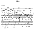
図5は、一実施の形態に係るIGBTを有する半導体装置の平面図である。図6は、セル形成領域を説明する図である、図5の領域RRの模式的な拡大平面図である。図7は、図5のA-A線に沿う模式的な断面図である。 Figure 5 is a plan view of a semiconductor device having an IGBT according to one embodiment. Figure 6 is a schematic enlarged plan view of region RR in Figure 5, which illustrates the cell formation region. Figure 7 is a schematic cross-sectional view taken along line A-A in Figure 5.
IE型IGBT100は、図5に示すように、矩形形状の半導体チップCHIPの外周部(チップ外周領域部とも言う)PERの上面には、環状のチャネルストッパー(PG)と接続された環状のガードリングGRが設けられている。ガードリングGRの内側には、環状のフローティングフィールドリング(P1、P2、P3、P4、P5)などと接続された数本(単数または複数)の環状のフィールドプレートFP(FP1、FP2、FP3、FP4、FP5)が設けられている。ガードリングGRおよびフィールドプレートFPは、例えばアルミニウムを主要な構成要素とする金属膜により構成される。図5では、図面の簡素化の為、環状のフィールドプレートFPの内、FP4、FP5の図示は省略されている。
As shown in FIG. 5, the IE-
環状のフィールドプレートFPの内側であって、半導体チップCHIPの活性部の主要部には、セル形成領域RCLが設けられており、半導体チップCHIPの活性部の上面には、半導体チップCHIPの外周部PERの近傍までエミッタ電極EEが設けられている。エミッタ電極EEは、例えばアルミニウムを主要な構成要素とする金属膜により構成される。エミッタ電極EEの中央部は、ボンディングワイヤなどを接続するためのエミッタパッドEPとなっている。エミッタパッドEPは、ファイナルパッシベーション膜FPFに開口部を設けることにより、形成されている。 A cell formation region RCL is provided inside the annular field plate FP in the main part of the active part of the semiconductor chip CHIP, and an emitter electrode EE is provided on the upper surface of the active part of the semiconductor chip CHIP up to the vicinity of the outer periphery PER of the semiconductor chip CHIP. The emitter electrode EE is made of a metal film whose main component is, for example, aluminum. The center of the emitter electrode EE serves as an emitter pad EP for connecting a bonding wire or the like. The emitter pad EP is formed by providing an opening in the final passivation film FPF.
ゲート配線GLがエミッタ電極EEとエミッタ電極EEとの間等に配置されており、ゲート配線GLは、ゲート抵抗Rgを介してゲート電極GEに接続されている。ゲート配線GLおよびゲート電極GEは、例えばアルミニウムを主要な構成要素とする金属膜により構成される。ゲート電極GEの中央部は、ボンディングワイヤなどを接続するためのゲートパッドGPとなっている。ゲートパッドGPは、ファイナルパッシベーション膜FPFに開口部を設けることにより、形成されている。ゲート抵抗Rgは、例えば所望の濃度の不純物が導入された多結晶シリコンを主要な構成要素とする抵抗膜により構成される。 The gate wiring GL is disposed between the emitter electrodes EE and EE, and is connected to the gate electrode GE via the gate resistor Rg. The gate wiring GL and the gate electrode GE are made of a metal film whose main component is aluminum, for example. The center of the gate electrode GE is a gate pad GP for connecting a bonding wire or the like. The gate pad GP is formed by providing an opening in the final passivation film FPF. The gate resistor Rg is made of a resistive film whose main component is polycrystalline silicon into which a desired concentration of impurities has been introduced, for example.
図5に示す構成例では、3本のゲート配線GLが第1方向Xに沿う様に延在して配置され、この第1方向Xに延在する3本のゲート配線GLが第1方向Xと交差する第2方向Yに沿って延在して配置され2本のゲート配線GLに接続されるようになっている。第1方向Xに延在する3本のゲート配線GLは、図示されていないが、この3本のゲート配線GLの形成領域の下側において、トレンチゲートTGのトレンチ内に埋め込まれたn型不純物ドープの多結晶シリコン層に電気的に接続されている。 In the configuration example shown in FIG. 5, three gate wirings GL are arranged to extend along the first direction X, and the three gate wirings GL extending in the first direction X are arranged to extend along a second direction Y intersecting the first direction X and connected to two gate wirings GL. Although not shown, the three gate wirings GL extending in the first direction X are electrically connected to an n-type impurity-doped polycrystalline silicon layer buried in the trench of the trench gate TG below the formation region of the three gate wirings GL.
次に、図6を用いて、セル形成領域RCLの構成例を説明する。図6のB-B線に沿う断面図は、図4に示すIE型IGBTの断面図に対応する。セル形成領域RCLは、活性セル領域RCaと、非活性領域Riaと、ホールコレクタセル領域RCcと、を含む。活性セル領域RCa、非活性領域Ria、ホールコレクタセル領域RCcのおのおのは、第2方向Yに沿う様に、ストライプ状に設けられている。また、活性セル領域RCa、非活性領域Ria、ホールコレクタセル領域RCc、非活性領域Riaの4つがこの順で1つのレイアウト単位とされて、第1方向Xに繰り返し配置されている。 Next, a configuration example of the cell formation region RCL will be described with reference to FIG. 6. The cross-sectional view along line B-B in FIG. 6 corresponds to the cross-sectional view of the IE-type IGBT shown in FIG. 4. The cell formation region RCL includes an active cell region RCa, an inactive region Ria, and a hole collector cell region RCc. Each of the active cell region RCa, the inactive region Ria, and the hole collector cell region RCc is provided in a stripe shape along the second direction Y. In addition, the active cell region RCa, the inactive region Ria, the hole collector cell region RCc, and the inactive region Ria are arranged in this order as one layout unit, and are repeatedly arranged in the first direction X.
活性セル領域RCaには、活性セルCaが形成される。図6では、活性セルCaとして、第2方向Yに、ストライプ状に形成され一対のトレンチゲートTGと、一対のトレンチゲートTGの間に設けられたn型エミッタ層ELとが模式的に描かれている。ホールコレクタセル領域RCcには、ホールコレクタセルCcが形成される。ホールコレクタセルCcは、図4で説明したように、p型フローティング層FLをソース領域、p型ベース層BLをドレイン領域、n型ホールバリア層HBLをチャネル形成領域、トレンチエミッタTEをゲート電極とする寄生Pチャネル型MOSFETである。図6では、ホールコレクタセルCcとして、第2方向Yに、ストライプ状に形成され一対のトレンチエミッタTEと、一対のトレンチエミッタTEの間を接続する接続用トレンチエミッタTEaとが模式的に描かれている。非活性領域Riaは、図6では、p型フローティング層FLが模式的に描かれている。図4に示す接続孔CH2のようにコンタクト取る場合、接続用トレンチエミッタTEaは不要である。図4に示す接続孔CH2を接続孔CH1のようにコンタクトを取る場合、エミッタトレンチTEとエミッタ電極EEを接続する接続用トレンチエミッタTEaのようなコンタクトを設けるのが良い。 In the active cell region RCa, an active cell Ca is formed. In FIG. 6, a pair of trench gates TG formed in a stripe shape in the second direction Y and an n-type emitter layer EL provided between the pair of trench gates TG are illustrated as the active cell Ca. In the hole collector cell region RCc, a hole collector cell Cc is formed. As described in FIG. 4, the hole collector cell Cc is a parasitic P-channel MOSFET having a p-type floating layer FL as a source region, a p-type base layer BL as a drain region, an n-type hole barrier layer HBL as a channel formation region, and a trench emitter TE as a gate electrode. In FIG. 6, a pair of trench emitters TE formed in a stripe shape in the second direction Y and a connecting trench emitter TEa connecting between the pair of trench emitters TE are illustrated as the hole collector cell Cc. In FIG. 6, the inactive region Ria is illustrated as a p-type floating layer FL. When making contact like the connection hole CH2 shown in FIG. 4, the connection trench emitter TEa is not necessary. When making contact like the connection hole CH1 shown in FIG. 4, it is better to provide a contact like the connection trench emitter TEa that connects the emitter trench TE and the emitter electrode EE.
次に、図7を用いてには、IE型IGBT100の断面図を説明する。なお、図7では、ファイナルパッシベーション膜FPF、コレクタ電極CEの図示を省略している。また、セル形成領域RCLについては、図面の複雑さを避けるため、トレンチエミッタTE、トレンチゲートTG、および、p型フローティング層FLの3つの層のみ描いている。
Next, a cross-sectional view of the IE-
セル形成領域RCLの周辺外部領域には、たとえば、これを取り巻くように、環状のP型ウエル領域P0が設けられている部分RP0(たとえばセル周辺接合領域とも言う)があり、このP型ウエル領域P0は、エミッタ電極EEに電気的に接続されている。環状のP型ウエル領域P0の外側には、環状の複数のp型フローティングフィールドリングP1、P2、P3、P4、P5が設けられている。フローティングフィールドリングP1、P2、P3、P4、P5のそれぞれは、フィールドプレートFP1、FP2、FP3、FP4、FP5に接続されている。p型フローティングフィールドリングP1、P2、P3、P4、P5の外側には、環状のn型チャネルストッパーPGが設けられている。チャネルストッパーPGは、ガードリングGRに接続されている。チャネルストッパーPGは、コレクタ電位とされている。半導体チップCHIPの外周部PERとセル周辺接合領域RP0とは、セル形成領域RCLを囲む様に設けられた周辺領域と言うこともできる。 In the peripheral external region of the cell formation region RCL, for example, there is a portion RP0 (also called, for example, a cell peripheral junction region) in which a ring-shaped P-type well region P0 is provided so as to surround it, and this P-type well region P0 is electrically connected to the emitter electrode EE. Outside the ring-shaped P-type well region P0, a plurality of ring-shaped p-type floating field rings P1, P2, P3, P4, and P5 are provided. The floating field rings P1, P2, P3, P4, and P5 are connected to field plates FP1, FP2, FP3, FP4, and FP5, respectively. Outside the p-type floating field rings P1, P2, P3, P4, and P5, a ring-shaped n-type channel stopper PG is provided. The channel stopper PG is connected to the guard ring GR. The channel stopper PG is set to the collector potential. The outer peripheral portion PER of the semiconductor chip CHIP and the cell peripheral bonding region RP0 can also be said to be peripheral regions that are arranged to surround the cell formation region RCL.
図7に示す様に、P型コレクタ層CLの内部には、転位抑制層DSL1が形成されている。転位抑制層DSL1は、平面視において、図5の半導体チップCHIPの全体に設けられている。言い換えるならば、転位抑制層DSL1は、平面視において、半導体チップCHIPの外周部PER、セル周辺接合領域RP0、セル形成領域RCLに設けられている。図7に示す転位抑制層DSL1は、図3に示す転位抑制層DSL2に置き換えることが可能である。 As shown in FIG. 7, a dislocation suppression layer DSL1 is formed inside the P-type collector layer CL. The dislocation suppression layer DSL1 is provided over the entire semiconductor chip CHIP of FIG. 5 in plan view. In other words, the dislocation suppression layer DSL1 is provided in the outer peripheral portion PER, the cell peripheral junction region RP0, and the cell formation region RCL of the semiconductor chip CHIP in plan view. The dislocation suppression layer DSL1 shown in FIG. 7 can be replaced with the dislocation suppression layer DSL2 shown in FIG. 3.
(半導体装置の製造方法)
次に、半導体装置の製造方法を説明する。半導体装置の製造方法は、以下の工程を含む。
(Method of manufacturing a semiconductor device)
Next, a method for manufacturing a semiconductor device will be described. The method for manufacturing a semiconductor device includes the following steps.
(基板準備工程)n型エミッタ層EL、p型ベース層BL、トレンチゲートTG、トレンチエミッタTE、p型フローティング層FL、n型ホールバリア層HBL、ゲート電極GEおよびエミッタ電極EEが第1主面US側に形成されたシリコン基板SUBを準備する工程。 (Substrate preparation process) A process for preparing a silicon substrate SUB on which an n-type emitter layer EL, a p-type base layer BL, a trench gate TG, a trench emitter TE, a p-type floating layer FL, an n-type hole barrier layer HBL, a gate electrode GE, and an emitter electrode EE are formed on the first main surface US.
(p型コレクタ層形成工程:第1工程)シリコン基板SUBの第1主面USと対向する第2主面BSに、p型コレクタ層CLを形成する工程。 (P-type collector layer formation process: First process) A process of forming a p-type collector layer CL on the second main surface BS that faces the first main surface US of the silicon substrate SUB.
(転位抑制層形成工程:第2工程)p型コレクタ層CL中に、シリコン基板SUBとヘテロ接合HJを形成する転位抑制層(DSL1、DSL2)を形成する工程。 (Dislocation suppression layer formation process: second process) A process for forming dislocation suppression layers (DSL1, DSL2) in the p-type collector layer CL that form a heterojunction HJ with the silicon substrate SUB.
(n型フィールドストップ層形成工程:第3工程)p型コレクタ層CLの第1主面US側にn型フィールドストップ層FSLを形成する工程。 (n-type field stop layer formation process: third process) A process for forming an n-type field stop layer FSL on the first main surface US side of the p-type collector layer CL.
(コレクタ電極形成工程:第4工程)p型コレクタ層CLに接続されたコレクタ電極CEを形成する工程。 (Collector electrode formation process: fourth process) A process for forming a collector electrode CE connected to the p-type collector layer CL.
上記工程において、p型コレクタ層形成工程と転位抑制層形成工程とは一体的な工程と見做すことも可能である。以下、p型コレクタ層CLおよび転位抑制層を形成する製造工程について説明する。 In the above process, the p-type collector layer formation process and the dislocation suppression layer formation process can be considered as an integrated process. The manufacturing process for forming the p-type collector layer CL and the dislocation suppression layer is described below.
(転位抑制層DSL1を有するIGBTの製造方法)
次に、図8~図11を用いて、転位抑制層DSL1を有するIE型IGBTの製造方法を説明する。図8は、IGBTを有する半導体装置の裏面側の製造方法を説明する断面図である。図9は、図8に続く製造方法を説明する断面図である。図10は、図9に続く製造方法を説明する断面図である。図11は、図10に続く製造方法を説明する断面図である。ここでは、基板SUBの表面US側に形成されるn型エミッタ層EL、p型ベース層BL、p型ベースコンタクト層BC、トレンチゲートTG、トレンチエミッタTE、p型フローティング層FL及びn型ホールバリア層HBL、層間絶縁膜IL、エミッタ電極EE、ファイナルパッシベーション膜FPF等は省略して説明する。
(Method of manufacturing an IGBT having a dislocation suppression layer DSL1)
Next, a method for manufacturing an IE-type IGBT having a dislocation suppression layer DSL1 will be described with reference to Figs. 8 to 11. Fig. 8 is a cross-sectional view for explaining a method for manufacturing the back side of a semiconductor device having an IGBT. Fig. 9 is a cross-sectional view for explaining a manufacturing method subsequent to Fig. 8. Fig. 10 is a cross-sectional view for explaining a manufacturing method subsequent to Fig. 9. Fig. 11 is a cross-sectional view for explaining a manufacturing method subsequent to Fig. 10. Here, the n-type emitter layer EL, p-type base layer BL, p-type base contact layer BC, trench gate TG, trench emitter TE, p-type floating layer FL and n-type hole barrier layer HBL, interlayer insulating film IL, emitter electrode EE, final passivation film FPF, etc. formed on the front surface US side of the substrate SUB will be omitted.
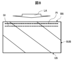
図8に示す様に、バックグラインディング処理の後、P型コレクタ層CLおよび転位抑制層DSL1を形成するため、基板SUBの裏面BSに、例えばイオン注入法により、P型不純物およびゲルマニウムGeを導入し、P型不純物注入層PIとゲルマニウム注入層GEIとを形成する。その後、基板SUBの裏面BSに対して、レーザアニールを実施し、P型不純物注入層PIとゲルマニウム注入層GEIとを活性化させる。P型コレクタ層CLを形成するためのイオン注入条件としては、例えばイオン種をボロンとし、ドーズ量を1×10¹²~3×1013cm-2程度とし、注入エネルギー100~500keV程度である。転位抑制層DSL1を形成するためのイオン注入条件としては、例えばイオン種をゲルマニウムGeとし、ドーズ量を1×10¹⁶~1×1017cm-2程度とし、注入エネルギー600~900keV程度である。 8, after the backgrinding process, in order to form the P-type collector layer CL and the dislocation suppression layer DSL1, P-type impurities and germanium Ge are introduced into the back surface BS of the substrate SUB by, for example, ion implantation to form the P-type impurity implanted layer PI and the germanium implanted layer GEI. Thereafter, laser annealing is performed on the back surface BS of the substrate SUB to activate the P-type impurity implanted layer PI and the germanium implanted layer GEI. The ion implantation conditions for forming the P-type collector layer CL are, for example, boron as the ion species, a dose amount of about 1×10 12 to 3×10 13 cm -2 , and an implantation energy of about 100 to 500 keV. The ion implantation conditions for forming the dislocation suppression layer DSL1 are, for example, germanium Ge as the ion species, approximately 1×10 16 to 1×10 17 cm −2 as the dose amount, and approximately 600 to 900 keV as the implantation energy.
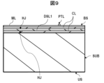
図9に示す様に、基板SUBの裏面にレーザアニールLAを施すことにより、不純物注入層PI及びGEIを活性化させて、P型コレクタ層CLおよび転位抑制層DSL1を形成する。このレーザアニールLAにおけるレーザ照射時に、基板SUBの裏面BSの最表面の厚さ0.2μm程度のシリコンが一旦溶融し、溶融層MLが形成される。レーザ照射後、基板SUBの温度が低下し、溶融層MLが再結晶化する。転位抑制層DSL1の上下面の両方には、シリコン層とシリコンゲルマニウム(SiGe)層とで形成されたヘテロ接合HJが形成されている。 As shown in FIG. 9, the back surface of the substrate SUB is subjected to laser annealing LA to activate the impurity implantation layers PI and GEI, forming a P-type collector layer CL and a dislocation suppression layer DSL1. During laser irradiation in this laser annealing LA, silicon on the top surface of the back surface BS of the substrate SUB, which is about 0.2 μm thick, melts once, forming a molten layer ML. After the laser irradiation, the temperature of the substrate SUB decreases, and the molten layer ML recrystallizes. A heterojunction HJ made of a silicon layer and a silicon germanium (SiGe) layer is formed on both the top and bottom surfaces of the dislocation suppression layer DSL1.
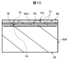
図10に示すように、この時、溶融層MLの表面にパーティクルPTLが存在すると、再結晶化時に、パーティクルPTLが起点となり基板SBの裏面BSに転位欠陥DILが形成される場合がある。転位抑制層DSL1の上下面に形成されたヘテロ接合HJは、転位欠陥DILが転位抑制層DSL1の下側に延びることを抑制する。 As shown in FIG. 10, if a particle PTL is present on the surface of the molten layer ML at this time, dislocation defects DIL may be formed on the back surface BS of the substrate SB during recrystallization, starting from the particle PTL. The heterojunction HJ formed on the top and bottom surfaces of the dislocation suppression layer DSL1 suppresses the dislocation defects DIL from extending below the dislocation suppression layer DSL1.
次に、基板SUBの裏面BSに、例えばイオン注入法により、N型不純物を導入することによって、フィールドストップ層FSLを形成する。このときのイオン注入条件としては、例えばイオン種を水素Hとし、ドーズ量を1×10¹⁴~1×1015cm-2程度とし、注入エネルギー300~400keV程度である。なお、先にフィールドストップ層FSLを形成し、その後、転位抑制層DSL1しても良い。つまり、転位抑制層DSL1を形成するためのレーザアニールLAは、製造方法の最後の方で行うのが好ましい。 Next, a field stop layer FSL is formed by introducing an N-type impurity into the back surface BS of the substrate SUB, for example, by ion implantation. The ion implantation conditions at this time are, for example, hydrogen H as the ion species, a dose amount of about 1×10 14 to 1×10 15 cm -2 , and an implantation energy of about 300 to 400 keV. Note that the field stop layer FSL may be formed first, and then the dislocation suppression layer DSL1 may be formed. In other words, it is preferable to perform the laser annealing LA for forming the dislocation suppression layer DSL1 toward the end of the manufacturing method.
その後、基板SUBを炉体の内部に設置し、炉体内で基板SUBに350~550°C程度の低温アニールを行い、図11に示す様に、フィールドストップ層FSLを形成する。その後、図示しないが、コレクタ電極CEが、スパッタリング法により、P型コレクタ層CLの表面に形成される。これにより、IGBTを有する半導体装置が形成される。 Then, the substrate SUB is placed inside the furnace, and low-temperature annealing is performed on the substrate SUB in the furnace at about 350 to 550°C to form a field stop layer FSL as shown in FIG. 11. After that, although not shown, a collector electrode CE is formed on the surface of the P-type collector layer CL by sputtering. This forms a semiconductor device having an IGBT.
(転位抑制層DSL2を有するIGBTの製造方法)
次に、図12~図13を用いて、転位抑制層DSL2を有するIE型IGBTの製造方法を説明する。図12は、IGBTを有する半導体装置の裏面側の製造方法を説明する断面図である。図13は、図12に続く製造方法を説明する断面図である。ここでは、基板SUBの表面US側に形成されるn型エミッタ層EL、p型ベース層BL、p型ベースコンタクト層BC、トレンチゲートTG、トレンチエミッタTE、p型フローティング層FL及びn型ホールバリア層HBL、層間絶縁膜IL、エミッタ電極EE、ファイナルパッシベーション膜FPF等は省略して説明する。
(Method of manufacturing an IGBT having a dislocation suppression layer DSL2)
Next, a method for manufacturing an IE-type IGBT having a dislocation suppression layer DSL2 will be described with reference to Fig. 12 and Fig. 13. Fig. 12 is a cross-sectional view for explaining a method for manufacturing the back side of a semiconductor device having an IGBT. Fig. 13 is a cross-sectional view for explaining a manufacturing method subsequent to Fig. 12. Here, the n-type emitter layer EL, p-type base layer BL, p-type base contact layer BC, trench gate TG, trench emitter TE, p-type floating layer FL and n-type hole barrier layer HBL, interlayer insulating film IL, emitter electrode EE, final passivation film FPF, etc., which are formed on the front surface US side of the substrate SUB will be omitted.
図12に示す様に、バックグラインディング処理の後、P型コレクタ層CLおよび転位抑制層DSL2を形成するため、基板SUBの裏面BSに、例えばイオン注入法により、P型不純物およびゲルマニウムGeを導入し、P型不純物注入層PIとゲルマニウム注入層GEI2とを形成する。その後、基板SUBの裏面BSに対して、レーザアニールを実施し、P型不純物注入層PIとゲルマニウム注入層GEI2とを活性化させる。P型コレクタ層CLを形成するためのイオン注入条件としては、例えばイオン種をボロンとし、ドーズ量を1×10¹²~3×1013cm-2程度とし、注入エネルギー100~500keV程度である。転位抑制層DSL2を形成するためのイオン注入条件としては、例えばイオン種をゲルマニウムGeとし、ドーズ量を1×10¹⁶~1×1017cm-2程度とし、注入エネルギーは、たとえば150~500keV程度であり、転位抑制層DSL1を形成するための注入エネルギー(たとえば600~900keV程度)と比較して低くてよい。つまり、転位抑制層DSL2は、裏面BSから浅い位置に形成するので、低加速エネルギーのイオン注入で形成することが可能である。 12, after the backgrinding process, in order to form the P-type collector layer CL and the dislocation suppression layer DSL2, P-type impurities and germanium Ge are introduced into the back surface BS of the substrate SUB by, for example, ion implantation to form the P-type impurity implanted layer PI and the germanium implanted layer GEI2. Thereafter, laser annealing is performed on the back surface BS of the substrate SUB to activate the P-type impurity implanted layer PI and the germanium implanted layer GEI2. The ion implantation conditions for forming the P-type collector layer CL are, for example, boron as the ion species, a dose amount of about 1×10 12 to 3×10 13 cm -2 , and an implantation energy of about 100 to 500 keV. The ion implantation conditions for forming the dislocation suppression layer DSL2 may be, for example, germanium Ge as the ion species, about 1×10 16 to 1×10 17 cm -2 as the dose amount, and about 150 to 500 keV as the implantation energy, which may be lower than the implantation energy for forming the dislocation suppression layer DSL1 (for example, about 600 to 900 keV). In other words, the dislocation suppression layer DSL2 is formed at a shallow position from the back surface BS, and therefore can be formed by ion implantation with low acceleration energy.
図13に示す様に、基板SUBの裏面にレーザアニールLAを施すことにより、不純物注入層GEI2及びPIを活性化させて、転位抑制層DSL2およびP型コレクタ層CLを形成する。このレーザアニールLAにおけるレーザ照射時に、基板SUBの裏面BSの最表面の厚さ0.2μm程度のシリコンが一旦溶融し、溶融層MLが形成される。レーザ照射後、基板SUBの温度が低下し、溶融層MLが再結晶化する。転位抑制層DSL2の裏面BSに近い側(図13では、転位抑制層DSL2の上面)は、溶融層MLと重なってヘテロ接合を形成できないが、転位抑制層DSL2の裏面BSに遠い側(図13では、転位抑制層DSL2の下面)には、シリコン層とシリコンゲルマニウム(SiGe)層とで形成されたヘテロ接合HJが形成されている。 As shown in FIG. 13, the rear surface of the substrate SUB is subjected to laser annealing LA to activate the impurity-implanted layers GEI2 and PI, forming the dislocation suppression layer DSL2 and the P-type collector layer CL. During the laser irradiation in this laser annealing LA, silicon of about 0.2 μm thickness on the outermost surface of the rear surface BS of the substrate SUB melts once, forming a molten layer ML. After the laser irradiation, the temperature of the substrate SUB drops, and the molten layer ML recrystallizes. The side of the dislocation suppression layer DSL2 close to the rear surface BS (the upper surface of the dislocation suppression layer DSL2 in FIG. 13) overlaps with the molten layer ML and cannot form a heterojunction, but the side of the dislocation suppression layer DSL2 far from the rear surface BS (the lower surface of the dislocation suppression layer DSL2 in FIG. 13) forms a heterojunction HJ formed of a silicon layer and a silicon germanium (SiGe) layer.
この時、溶融層MLの表面にパーティクルPTLが存在すると、再結晶化時に、パーティクルPTLが起点となり基板SBの裏面BSに転位欠陥が形成される場合がある。転位抑制層DSL2の下面に形成されたヘテロ接合HJは、転位欠陥が転位抑制層DSL2の下側に延びることを抑制する。 At this time, if a particle PTL is present on the surface of the molten layer ML, dislocation defects may be formed on the back surface BS of the substrate SB during recrystallization, starting from the particle PTL. The heterojunction HJ formed on the lower surface of the dislocation suppression layer DSL2 suppresses the dislocation defects from extending below the dislocation suppression layer DSL2.
図13の後は、図10および図11で説明した製造工程と同様な製造工程が実施され、その後、コレクタ電極CEがP型コレクタ層CLの表面に形成される。これにより、IGBTを有する半導体装置が形成される。 After FIG. 13, manufacturing processes similar to those described in FIG. 10 and FIG. 11 are carried out, and then a collector electrode CE is formed on the surface of the P-type collector layer CL. This forms a semiconductor device having an IGBT.
(変形例)
次に、いくつかの変形例を説明する。
(Modification)
Next, some modified examples will be described.
(変形例1)
図14は、変形例1に係るIGBTを有する半導体装置の裏面側構造を説明する断面図である。図15は、変形例1に係るIGBTを有する半導体装置の平面図である。図16は、変形例1に係るIGBTを有する半導体装置の裏面側の製造方法を説明する断面図である。図17は、図16に続く製造方法を説明する断面図である。
(Variation 1)
Fig. 14 is a cross-sectional view illustrating the back surface structure of a semiconductor device having an IGBT according to
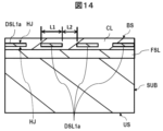
図14が図11と異なる点は、図14および図15に示す様に、転位抑制層DSL1aが複数に分割されている点である。転位抑制層DSL1aのおのおのは、第1方向Xにおいて、幅L1とされ、複数の転位抑制層DSL1aが幅L2の間隔(スペース)で配置されている。図15に示す様に、複数の転位抑制層DSL1aのおのおのは、平面視において、シリコン基板SUB中に選択的に形成されている。図15の例では、複数の転位抑制層DSL1aのおのおのは、第2方向Yに沿って、ストライプ形状に延在して設けられ、第1方向Xに並んで配列されている。図15に示す例では、複数の転位抑制層DSL1aの平面視における形状はストライプ形状(細長形状)に形成されているがそれに限定されない。複数の転位抑制層DSL1aの平面視における形状は、矩形形状、円形形状、楕円形形状、多角形形状等であってもよい。 14 differs from FIG. 11 in that the dislocation suppression layer DSL1a is divided into a plurality of layers as shown in FIG. 14 and FIG. 15. Each of the dislocation suppression layers DSL1a has a width L1 in the first direction X, and the plurality of dislocation suppression layers DSL1a are arranged at intervals (spaces) of width L2. As shown in FIG. 15, each of the plurality of dislocation suppression layers DSL1a is selectively formed in the silicon substrate SUB in plan view. In the example of FIG. 15, each of the plurality of dislocation suppression layers DSL1a is provided extending in a stripe shape along the second direction Y, and is arranged side by side in the first direction X. In the example shown in FIG. 15, the shape of the plurality of dislocation suppression layers DSL1a in plan view is formed in a stripe shape (elongated shape), but is not limited thereto. The shape of the plurality of dislocation suppression layers DSL1a in plan view may be a rectangular shape, a circular shape, an elliptical shape, a polygonal shape, or the like.
図16に示す様に、複数に分割された転位抑制層DSL1aを形成する為、ゲルマニウム注入層GEI1aは複数に分割されて形成される(ゲルマニウム注入層GEI1aの形成は、図8のゲルマニウム注入層GEIの説明を参照できる)。この場合、フォトリソグラフィ工程によって、不純物導入阻止用マスクを形成し、そして、不純物導入阻止用マスクをイオン注入のマスクに利用して、ゲルマニウムGeをイオン注入してゲルマニウム注入層GEI1aを形成し、その後、不純物導入阻止用マスクを除去するマスク除去工程等が行われる。 As shown in FIG. 16, in order to form a dislocation suppression layer DSL1a divided into a plurality of parts, the germanium injection layer GEI1a is divided into a plurality of parts (for the formation of the germanium injection layer GEI1a, refer to the explanation of the germanium injection layer GEI in FIG. 8). In this case, a mask for preventing impurity introduction is formed by a photolithography process, and then, using the mask for preventing impurity introduction as a mask for ion implantation, germanium Ge is ion-implanted to form the germanium injection layer GEI1a, and then a mask removal process for removing the mask for preventing impurity introduction is performed.
P型不純物注入層PI(図8の説明参照)とゲルマニウム注入層GEI1aを形成した後、基板SUBの裏面BSに対して、レーザアニールを実施し、P型不純物注入層PIとゲルマニウム注入層GEI1aとを活性化させる。そして、図17に示す様に、基板SUBの裏面にレーザアニールLAを施すことにより、不純物注入層GEI1a及びPIを活性化させて、シリコンゲルマニウム層により構成される転位抑制層DSL1aおよびP型コレクタ層CLをそれぞれ形成する。図17の後は、図10および図11で説明した製造工程と同様な製造工程が実施され、その後、コレクタ電極CEがP型コレクタ層CLの表面に形成される。これにより、IGBTを有する半導体装置が形成される。 After forming the P-type impurity injection layer PI (see the description of FIG. 8) and the germanium injection layer GEI1a, laser annealing is performed on the back surface BS of the substrate SUB to activate the P-type impurity injection layer PI and the germanium injection layer GEI1a. Then, as shown in FIG. 17, laser annealing LA is performed on the back surface of the substrate SUB to activate the impurity injection layers GEI1a and PI, thereby forming the dislocation suppression layer DSL1a and the P-type collector layer CL, each of which is made of a silicon germanium layer. After FIG. 17, the same manufacturing process as that described in FIG. 10 and FIG. 11 is performed, and then the collector electrode CE is formed on the surface of the P-type collector layer CL. This forms a semiconductor device having an IGBT.
図17に示す様に、パーティクルPTLが転位抑制層DSL1aの上側にある場合、パーティクルPTLを起点とする転位欠陥は、転位抑制層DSL1aの上下面に形成されたヘテロ接合HJにより、転位抑制層DSL1aの下側に延びることを抑制することができる。 As shown in FIG. 17, when the particle PTL is located above the dislocation suppression layer DSL1a, the dislocation defect originating from the particle PTL can be prevented from extending below the dislocation suppression layer DSL1a by the heterojunction HJ formed on the upper and lower surfaces of the dislocation suppression layer DSL1a.
しかし、パーティクルPTLが転位抑制層DSL1aと転位抑制層DSL1aの間にある場合、パーティクルPTLを起点とする転位欠陥が転位抑制層DSL1aと転位抑制層DSL1aの間(幅L2の間)を通って、P型コレクタ層CLの下方まで伸びてしまい、リーク不良となる場合も考えられる。次に説明する変形例2は、この問題の解決するものである。
However, if the particle PTL is between the dislocation suppression layers DSL1a and DSL1a, a dislocation defect originating from the particle PTL may pass between the dislocation suppression layers DSL1a and DSL1a (within the width L2) and extend below the P-type collector layer CL, resulting in a leak defect.
(変形例2)
図18は、変形例2に係るIGBTを有する半導体装置の裏面側構造を説明する断面図である。図19は、変形例2に係るIGBTを有する半導体装置の平面図である。図20は、変形例2に係るIGBTを有する半導体装置の裏面側の製造方法を説明する断面図である。図21は、図20に続く製造方法を説明する断面図である。
(Variation 2)
Fig. 18 is a cross-sectional view illustrating the back surface side structure of a semiconductor device having an IGBT according to
図18が図14と異なる点は、図18および図19に示す様に、転位抑制層DSL1aの間の幅L2の領域において、基板SUBの裏面BSの近傍に、転位抑制層DSL2aが設けられている点である。転位抑制層DSL1aのおのおのは、第1方向Xにおいて、幅L1とされ、複数の転位抑制層DSL1aが幅L2の間隔で配置されている。シリコンゲルマニウム層から構成される転位抑制層DSL2aのおのおのは、第1方向Xにおいて、幅L2とされ、複数の転位抑制層DSL2aが幅L1の間隔で配置されている。図19に示す様に、複数の転位抑制層DSL1aと複数の転位抑制層DSL2aとは、平面視において、第2方向Yに沿ってストライプ形状に延在して設けられ、第1方向Xに並んで交互に配列されている。 18 differs from FIG. 14 in that, as shown in FIG. 18 and FIG. 19, in the region of width L2 between the dislocation suppression layers DSL1a, dislocation suppression layers DSL2a are provided near the back surface BS of the substrate SUB. Each of the dislocation suppression layers DSL1a has a width L1 in the first direction X, and the multiple dislocation suppression layers DSL1a are arranged at intervals of width L2. Each of the dislocation suppression layers DSL2a made of a silicon germanium layer has a width L2 in the first direction X, and the multiple dislocation suppression layers DSL2a are arranged at intervals of width L1. As shown in FIG. 19, the multiple dislocation suppression layers DSL1a and the multiple dislocation suppression layers DSL2a are provided extending in a stripe shape along the second direction Y in a plan view, and are arranged alternately in the first direction X.
これにより、パーティクルPTLを起点とする転位欠陥が転位抑制層DSL1aと転位抑制層DSL1aの間(幅L2の間)を通って、P型コレクタ層CLの下方まで伸びてしまう様な問題を解決する。つまり、転位抑制層DSL1aと転位抑制層DSL1aの間に設けた転位抑制層DSL2aにおいて、図13で説明したと同様に、転位抑制層DSL2aの裏面BSに遠い側(図18では、転位抑制層DSL2の下面)には、シリコン層とシリコンゲルマニウム(SiGe)層とで形成されたヘテロ接合HJが形成されている。転位抑制層DSL2aの下面に形成されたヘテロ接合HJは、転位欠陥が転位抑制層DSL2aの下側に延びることを抑制する。 This solves the problem that dislocation defects originating from the particle PTL extend below the P-type collector layer CL through the gap between the dislocation suppression layers DSL1a and DSL1a (width L2). In other words, in the dislocation suppression layer DSL2a provided between the dislocation suppression layers DSL1a and DSL1a, a heterojunction HJ formed of a silicon layer and a silicon germanium (SiGe) layer is formed on the side of the dislocation suppression layer DSL2a far from the back surface BS (the lower surface of the dislocation suppression layer DSL2 in FIG. 18) as described in FIG. 13. The heterojunction HJ formed on the lower surface of the dislocation suppression layer DSL2a prevents dislocation defects from extending below the dislocation suppression layer DSL2a.
したがって、パーティクルPTLを起点とする転位欠陥は、転位抑制層DSL1aの上下面に形成されたヘテロ接合HJ、および、転位抑制層DSL2aの下面に形成されたヘテロ接合HJは、転位欠陥が転位抑制層DSL1aおよび転位抑制層DSL2aの下側に延びることを抑制する。 Therefore, the heterojunction HJ formed on the upper and lower surfaces of the dislocation suppression layer DSL1a and the heterojunction HJ formed on the lower surface of the dislocation suppression layer DSL2a suppress the dislocation defects originating from the particle PTL from extending below the dislocation suppression layer DSL1a and the dislocation suppression layer DSL2a.
複数の転位抑制層DSL1aの平面視における形状は、三角形形状、矩形形状、円形形状、楕円形形状、多角形形状等であってもよい。この場合、転位抑制層DSL2aの平面視における形状は、複数の転位抑制層DSL1aの形成されていない領域を覆う様な形状されている。また、複数の転位抑制層DSL2aの平面視における形状は、三角形形状、矩形形状、円形形状、楕円形形状、多角形形状等であってもよい。この場合、転位抑制層DSL1aの平面視における形状は、複数の転位抑制層DSL2aの形成されていない領域を覆う様な形状されている。 The shape of the multiple dislocation suppression layers DSL1a in a planar view may be a triangular shape, a rectangular shape, a circular shape, an elliptical shape, a polygonal shape, etc. In this case, the shape of the dislocation suppression layer DSL2a in a planar view is shaped to cover the area where the multiple dislocation suppression layers DSL1a are not formed. The shape of the multiple dislocation suppression layers DSL2a in a planar view may be a triangular shape, a rectangular shape, a circular shape, an elliptical shape, a polygonal shape, etc. In this case, the shape of the dislocation suppression layer DSL1a in a planar view is shaped to cover the area where the multiple dislocation suppression layers DSL2a are not formed.
図20に示す様に、複数に分割された転位抑制層DSL1aおよび転位抑制層DSL2aを形成する為、ゲルマニウム注入層GEI1aは複数に分割されて形成され、ゲルマニウム注入層GEI2aは複数に分割されて形成される(ゲルマニウム注入層GEI2aは、図12のゲルマニウム注入層GEI2の説明を参照できる)。ゲルマニウム注入層GEI1aおよびゲルマニウム注入層GEI2aは、図16で説明した様に、フォトリソグラフィ工程による不純物導入阻止用マスクを用いて形成することができる。 As shown in FIG. 20, in order to form the dislocation suppression layer DSL1a and the dislocation suppression layer DSL2a which are divided into a plurality of parts, the germanium injection layer GEI1a is formed divided into a plurality of parts, and the germanium injection layer GEI2a is formed divided into a plurality of parts (for the germanium injection layer GEI2a, refer to the explanation of the germanium injection layer GEI2 in FIG. 12). The germanium injection layer GEI1a and the germanium injection layer GEI2a can be formed using a mask for preventing the introduction of impurities by a photolithography process, as explained in FIG. 16.
P型不純物注入層PI(図8の説明参照)、ゲルマニウム注入層GEI1aおよびゲルマニウム注入層GEI2aを形成した後、基板SUBの裏面BSに対して、レーザアニールを実施し、P型不純物注入層PI、ゲルマニウム注入層GEI1aおよびゲルマニウム注入層GEI2aを活性化させる。そして、図21に示す様に、基板SUBの裏面にレーザアニールLAを施すことにより、不純物注入層GEI1a、GEI2a及びPIを活性化させて、転位抑制層DSL1a、転位抑制層DSL2aおよびP型コレクタ層CLを形成する。図21の後は、図10および図11で説明した製造工程と同様な製造工程が実施され、その後、コレクタ電極CEがP型コレクタ層CLの表面に形成される。これにより、IGBTを有する半導体装置が形成される。 After forming the P-type impurity injection layer PI (see the description of FIG. 8), the germanium injection layer GEI1a, and the germanium injection layer GEI2a, laser annealing is performed on the back surface BS of the substrate SUB to activate the P-type impurity injection layer PI, the germanium injection layer GEI1a, and the germanium injection layer GEI2a. Then, as shown in FIG. 21, by performing laser annealing LA on the back surface of the substrate SUB, the impurity injection layers GEI1a, GEI2a, and PI are activated to form the dislocation suppression layer DSL1a, the dislocation suppression layer DSL2a, and the P-type collector layer CL. After FIG. 21, the same manufacturing process as the manufacturing process described in FIG. 10 and FIG. 11 is performed, and then the collector electrode CE is formed on the surface of the P-type collector layer CL. This forms a semiconductor device having an IGBT.
(変形例3)
図22は、変形例3に係るIGBTを有する半導体装置の裏面側構造を説明する断面図である。図23は、変形例3に係るIGBTを有する半導体装置の平面図である。
(Variation 3)
Fig. 22 is a cross-sectional view illustrating a back surface side structure of a semiconductor device having an IGBT according to
変形例1では、平面視において、半導体チップCHIPに、複数の転位抑制層DSL1aをストライプ状に設けた構成例を説明した。変形例3では、図22に示す様に、転位抑制層DSL1bは、セル形成領域RCLの下側部分を除く領域部分に、つまり、半導体チップCHIPのチップ外周領域部PERおよびセル周辺接合領域RP0の下側の領域部分に、選択的に形成したものである。図23に示す様に、転位抑制層DSL1bは、平面視において、セル形成領域RCLの周りを取り囲むように設けられたセル周辺接合領域RP0およびセル周辺接合領域RP0の周りを取り囲むように設けられたチップ外周領域部PERの下側に位置するP型コレクタ層CLの内部に設けられている。転位抑制層DSL1bの製造方法は、変形例1の説明を参照できる。 In the first modification, a configuration example in which a plurality of dislocation suppression layers DSL1a are provided in a stripe pattern on the semiconductor chip CHIP in a plan view has been described. In the third modification, as shown in FIG. 22, the dislocation suppression layer DSL1b is selectively formed in the region excluding the lower portion of the cell formation region RCL, that is, in the region below the chip peripheral region PER and the cell peripheral junction region RP0 of the semiconductor chip CHIP. As shown in FIG. 23, the dislocation suppression layer DSL1b is provided inside the P-type collector layer CL located below the cell peripheral junction region RP0 provided to surround the cell formation region RCL and the chip peripheral region PER provided to surround the cell peripheral junction region RP0 in a plan view. The description of the first modification can be referred to for the manufacturing method of the dislocation suppression layer DSL1b.
図23に示す様に転位抑制層DSL1bを導入すれば、逆バイアス時の電流リークを抑制することができる。さらに、セル形成領域RCLには転位抑制層DSL1bが無いので、IGBTの特性に影響しない。 As shown in FIG. 23, by introducing the dislocation suppression layer DSL1b, it is possible to suppress current leakage during reverse bias. Furthermore, since there is no dislocation suppression layer DSL1b in the cell formation region RCL, it does not affect the characteristics of the IGBT.
(変形例4)
図24は、変形例4に係るIGBTを有する半導体装置の裏面側構造を説明する断面図である。図25は、変形例4に係るIGBTを有する半導体装置の平面図である。
(Variation 4)
Fig. 24 is a cross-sectional view illustrating a back surface side structure of a semiconductor device having an IGBT according to Modification 4. Fig. 25 is a plan view of the semiconductor device having an IGBT according to Modification 4.
図24が図22と異なる点は、セル形成領域RCLの下側部分に位置するP型コレクタ層CLの内部に、転位抑制層DSL2bが設けられている点である。図25に示す様に、転位抑制層DSL2bは、平面視において、セル形成領域RCLの下側部分に位置する領域に配置されている。転位抑制層DSL2bの製造方法は、変形例2の説明を参照できる。
Figure 24 differs from Figure 22 in that a dislocation suppression layer DSL2b is provided inside the P-type collector layer CL located in the lower part of the cell formation region RCL. As shown in Figure 25, the dislocation suppression layer DSL2b is disposed in a region located in the lower part of the cell formation region RCL in a plan view. For the manufacturing method of the dislocation suppression layer DSL2b, refer to the explanation of
変形例4によれば、IE型IGBT100は、転位抑制層DSL1b、DSL2bを有しているので、エミッタ・コレクタ間の電流リーク、逆バイアス時の電流リークを抑制することができる。
According to the fourth modification, the IE-
(変形例5)
図18において、ゲルマニウムGeを導入して形成した転位抑制層DSL1aの代わりに、カーボンC、シリコンSi、アルゴンAr、フッ素F、窒素N等のいずれか1つのイオン種をイオン注入して基板SUB内のシリコンSiとの格子間距離歪層(拡張欠陥)による転位抑制層を設けることもできる。図18においては、転位抑制層DSL2aを通ってホールが注入されるので、これらのイオン種で、転位抑制層DSL2aの形成領域以外の位置の転位抑制層を形成しても、IGBTの出力特性は悪化することはない。
(Variation 5)
In Fig. 18, instead of the dislocation suppression layer DSL1a formed by introducing germanium Ge, a dislocation suppression layer based on a lattice distance distortion layer (extended defects) with silicon Si in the substrate SUB can be provided by ion implantation of any one of ion species such as carbon C, silicon Si, argon Ar, fluorine F, and nitrogen N. In Fig. 18, holes are injected through the dislocation suppression layer DSL2a, so even if a dislocation suppression layer is formed in a position other than the formation region of the dislocation suppression layer DSL2a with these ion species, the output characteristics of the IGBT will not deteriorate.
(変形例6)
図22において、ゲルマニウムGeを導入して形成した転位抑制層DSL1bの代わりに、カーボンC、シリコンSi、アルゴンAr、フッ素F、窒素N等のいずれか1つのイオン種をイオン注入して基板SUB内のシリコンSiとの格子間距離歪層(拡張欠陥)による転位抑制層を設けることもできる。図22において、セル形成領域RCLの下側には転位抑制層が形成されていないので、これらのイオン種(カーボンC、シリコンSi、アルゴンAr、フッ素F、窒素N)で、転位抑制層DSL1bの形成領域の位置に転位抑制層を形成しても、IGBTの出力特性は悪化することはない。なお、図24において、転位抑制層DSL1bも、これらのイオン種を用いた転位抑制層で構成することができる。
(Variation 6)
In Fig. 22, instead of the dislocation suppression layer DSL1b formed by introducing germanium Ge, any one of ion species such as carbon C, silicon Si, argon Ar, fluorine F, and nitrogen N can be ion-implanted to provide a dislocation suppression layer due to a lattice distance distortion layer (extended defect) with silicon Si in the substrate SUB. In Fig. 22, since no dislocation suppression layer is formed below the cell formation region RCL, even if a dislocation suppression layer is formed at the position of the formation region of the dislocation suppression layer DSL1b using these ion species (carbon C, silicon Si, argon Ar, fluorine F, and nitrogen N), the output characteristics of the IGBT will not deteriorate. In Fig. 24, the dislocation suppression layer DSL1b can also be formed of a dislocation suppression layer using these ion species.
(発明者による検討の説明)
次に発明者による検討結果を説明する。
(Explanation of the inventor's considerations)
Next, the results of the study by the inventors will be described.
図26は、裏面構造が異なる3つのIGBTの出力特性を示すグラフである。図26には、図1Cに示すIGBT(Siと記す)、図3に示すIGBT(パターン1と記す)、および、図2に示すIGBT(パターン2と記す)のおのおのの出力特性が示されている。図26において、横軸はコレクタ電位(Vc)のボルトVであり、縦軸はコレクタ電流Icの電流Aである。なお、各IGBTの表面側の構成は、図4に示すIGBTの表面側の構造と同じである。 Figure 26 is a graph showing the output characteristics of three IGBTs with different back surface structures. Figure 26 shows the output characteristics of the IGBT shown in Figure 1C (labeled Si), the IGBT shown in Figure 3 (labeled Pattern 1), and the IGBT shown in Figure 2 (labeled Pattern 2). In Figure 26, the horizontal axis represents the collector potential (Vc) in volts, and the vertical axis represents the collector current Ic in A. The structure of the front surface side of each IGBT is the same as the structure of the front surface side of the IGBT shown in Figure 4.
図26が示すように、パターン1(図3のIGBT)はSi(図1CのIGBT)と特性はほぼ同じであるが、パターン2(図2のIGBT)は出力低下が見られる。例えば、コレクタ電圧Vc:1.5Vにおいて、パターン2(図2のIGBT)は、Si(図1CのIGBT)と比較して、20%程度の電流低下が確認できる。 As shown in Figure 26, pattern 1 (IGBT in Figure 3) has almost the same characteristics as Si (IGBT in Figure 1C), but pattern 2 (IGBT in Figure 2) shows a decrease in output. For example, at a collector voltage Vc of 1.5V, pattern 2 (IGBT in Figure 2) shows a current decrease of about 20% compared to Si (IGBT in Figure 1C).
前提として、裏面側に、Geをイオン注入することで、SiGe層からなる転位抑制層DSL1、DSL2を形成すると裏面からのホール注入が阻害される結果になる。これは、シリコンSiとSiGeではバンド構造が異なるためである。 The premise is that forming dislocation suppression layers DSL1 and DSL2 made of SiGe layers by ion implanting Ge on the back side will result in the inhibition of hole injection from the back side. This is because silicon Si and SiGe have different band structures.
パターン1(図3の転位抑制層DSL2)は浅く、つまり裏面BSの表面側にSiGe層を形成するので、比較的、低加速エネルギー(150~500keV)でイオン注入を行う。そのため、SiGe層(転位抑制層DSL2)の深さ方向の幅を狭く形成できる(つまり、Geのインプラプロファイルがシャープになる)。 Pattern 1 (dislocation suppression layer DSL2 in FIG. 3) is shallow, that is, the SiGe layer is formed on the surface side of the back surface BS, so ion implantation is performed with a relatively low acceleration energy (150 to 500 keV). Therefore, the width of the SiGe layer (dislocation suppression layer DSL2) in the depth direction can be narrowed (that is, the Ge implantation profile becomes sharp).
パターン2(図2の転位抑制層DSL1)は、比較的高加速エネルギー(600~900keV)でGeをイオン注入するので、SiGe層の深さ方向の幅が広くなる。これはイオン注入の特性上、高加速であるほど、イオン散乱が大きくなりプロファイルがブロードになってしまうためである。この結果、SiGe層(転位抑制層DSL1)が広くなるパターン2(図2のIGBT)では、出力特性が悪化したものと考えられる。 In pattern 2 (dislocation suppression layer DSL1 in Figure 2), Ge ions are implanted at a relatively high acceleration energy (600-900 keV), so the width of the SiGe layer in the depth direction is wide. This is because, due to the characteristics of ion implantation, the higher the acceleration, the greater the ion scattering becomes, resulting in a broader profile. As a result, it is believed that the output characteristics of pattern 2 (IGBT in Figure 2), in which the SiGe layer (dislocation suppression layer DSL1) is wide, have deteriorated.
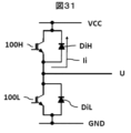
次に、IGBTのスイッチング特性をシミュレーションで評価した。シミュレーションに用いたトレンチ絶縁ゲート型バイポーラトランジスタを含むスイッチング回路の主要部分の一例について簡単に説明する。図27は、シミュレーションに用いたスイッチング回路を示す回路図である。図28は、シミュレーションにより求めたスイッチング損失の値を説明する図である。 Next, the switching characteristics of the IGBT were evaluated by simulation. An example of the main parts of a switching circuit including a trench insulated gate bipolar transistor used in the simulation will be briefly described. Figure 27 is a circuit diagram showing the switching circuit used in the simulation. Figure 28 is a diagram explaining the values of switching loss obtained by the simulation.
図27に示すように、スイッチング回路SWCでは、IGBT100が、たとえば、主負荷MOLとしてのモータに電気的に直列に接続されている。その主負荷MOLに、還流用ダイオードDiが電気的に並列に接続されている。主負荷MOLには、電源電圧VCCが電気的に接続されている。IGBT100が評価対象である。スイッチング回路SWCに電流200Aの電流が流れている状態で、IGBT100のゲート電位Vgを制御してIGBT100をON/OFFさせた。その時のスイッチング損失を図28に示す。図28において、Eonはターンオン時のスイッチング損失を示し、Eoffはターンオフ時のスイッチング損失を示している。
As shown in FIG. 27, in the switching circuit SWC, the
パターン1(図3のIGBT)はスイッチング特性も、参考として示されるSi(Ref.(Si):図1CのIGBT)とほぼ同じであることが確認できた。一方、パターン2(図2のIGBT)はEoffが15%程度良い。これは図26が示すように、パターン2のON電圧が高いため、バルク内キャリア密度が低いためである。単純に出力特性とスイッチング特性のトレードオフになっている。
It was confirmed that the switching characteristics of pattern 1 (IGBT in Figure 3) are almost the same as those of the Si (Ref. (Si): IGBT in Figure 1C) shown for reference. On the other hand, pattern 2 (IGBT in Figure 2) has an Eoff that is about 15% better. This is because, as shown in Figure 26, the ON voltage of
以上の結果から、裏面にSiGe層を導入しても、パターン1(図3のIGBT)のように形成すれば、IGBT特性を維持できることが分かった。 These results show that even if a SiGe layer is introduced to the backside, if it is formed as in pattern 1 (IGBT in Figure 3), the IGBT characteristics can be maintained.
但し、パターン1とパターン2では、パターン2の方がパターン1よりロバスト性が高い。これは、パターン2ではSiGe層の上下面がヘテロ界面(ヘテロ接合HJ)になるので、転位ストッパーとされるヘテロ接合HJが2層存在することを意味する。一方、パターン1はSiGe層の下面しかヘテロ界面(ヘテロ接合HJ)にならないからである。
However, between
変形例1(図14)の転位抑制層DSL1aは、パターン2(図2)の転位抑制層DSL1を複数に分割して、転位抑制層DSL1aの間に、幅L2のスペースを設けた構造である。基板SUBの裏面BS側に設けたコレクタ電極CEからのホールが転位抑制層DSL1aの間の幅L2のスペースを通り抜けるので、出力特性の改善が見込まれる。図29は転位抑制層DSL1aの幅L1と転位抑制層DSL1aの間の幅L2との比(L1/L2)を変えて計算した各IGBTの出力特性の結果である。図29には、Si(図1CのIGBT)の場合と、パターン2(図2のIGBT)の場合と、L1/L2=1/1(SiGe L/S=1/1として示される)の場合と、L1/L2=1/3(SiGe L/S=1/3として示される)の場合との4つのIGBTについて示されている。 The dislocation suppression layer DSL1a of the modified example 1 (Fig. 14) is a structure in which the dislocation suppression layer DSL1 of the pattern 2 (Fig. 2) is divided into multiple parts, and a space of width L2 is provided between the dislocation suppression layers DSL1a. Since holes from the collector electrode CE provided on the back surface BS side of the substrate SUB pass through the space of width L2 between the dislocation suppression layers DSL1a, improvement in output characteristics is expected. Fig. 29 shows the results of the output characteristics of each IGBT calculated by changing the ratio (L1/L2) of the width L1 of the dislocation suppression layer DSL1a to the width L2 between the dislocation suppression layers DSL1a. FIG. 29 shows four IGBTs: Si (IGBT in FIG. 1C), pattern 2 (IGBT in FIG. 2), L1/L2=1/1 (shown as SiGe L/S=1/1), and L1/L2=1/3 (shown as SiGe L/S=1/3).
転位抑制層DSL1aの間にスペース(L2)を設けた構造では出力特性が改善できていることが分かる。また、当然だが、スペース幅(L2)が広い方が出力特性が改善することを確認した。 It can be seen that the output characteristics are improved in a structure in which a space (L2) is provided between the dislocation suppression layers DSL1a. It was also confirmed that, naturally, the output characteristics are improved when the space width (L2) is wider.
一方、このままの構造では、スペース(L2)の領域に転位欠陥DILが発生した場合、スペース(L2)の領域に転位ストッパーとしてのヘテロ接合HJが無いのでリーク不良になってしまう場合も考えられる。図26により、パターン1の場合はIGBTの出力特性が悪化しないことが分かっているので、図14のスペース(L2)の領域にパターン1の転位抑制層DSL2を形成すれば、IGBTの出力特性とロバスト性向上の両立ができることが今までの結果から推定できる。そこで、変形例2(図18)に示すパターン3を新たに提案できる。変形例2(図18)に示すパターン3は、ロバスト性を高めつつ、図1CのIGBTとほぼ同じ性能(出力特性、スイッチング損出)を維持することが可能である。
On the other hand, in this structure, if a dislocation defect DIL occurs in the space (L2) region, there is a possibility that a leak defect will occur because there is no heterojunction HJ as a dislocation stopper in the space (L2) region. As can be seen from FIG. 26, in the case of
(逆バイアスリークについて)
図30はモータ駆動回路の一例を示す回路ブロック図である。図31は図30のU相に対応するIGBTとダイオードの動作を説明する回路図である。図32は、IGBT内に構成された寄生ダイオードを説明する断面図である。図33は図31のハイサイド側のIGBTに構成された寄生ダイオードを説明する等価回路図である。
(Regarding reverse bias leakage)
Fig. 30 is a circuit block diagram showing an example of a motor drive circuit. Fig. 31 is a circuit diagram explaining the operation of an IGBT and a diode corresponding to the U-phase in Fig. 30. Fig. 32 is a cross-sectional view explaining a parasitic diode formed in an IGBT. Fig. 33 is an equivalent circuit diagram explaining a parasitic diode formed in an IGBT on the high side in Fig. 31.
図30に示すように、モータ駆動回路は、モータMOT等の負荷と、インバータINVとを有する。モータMOTは、U相U、V相VおよびW相Wからなる3相モータである。そのため、インバータINVも、U相U、V相VおよびW相Wからなる3相に対応したものである。このような3相に対応したインバータINVは、IGBT100と還流ダイオードDiとの組を合計6組有する。U相U、V相VおよびW相Wからなる3相の各相において、インバータINVに電源電位(VCC)を供給する電源配線VCLとモータMOTの入力電位(インバータINVの出力端子に相当する)との間、すなわち、ハイサイドに、IGBT100と還流ダイオードDiとが逆並列に接続されている。また、U相U、V相VおよびW相Wからなる3相の各相において、モータMOTの入力電位(インバータINVの出力端子に相当する)とインバータINVに接地電位(GND)を供給する接地配線GNLとの間、すなわち、ロウサイドに、IGBT100と還流ダイオードDiとが逆並列に接続されている。ここで、逆並列とは、IGBT100のコレクタが還流ダイオードDiのカソードに接続され、IGBT100のエミッタが還流ダイオードDiのアノードに接続される様な接続構成である。
As shown in FIG. 30, the motor drive circuit has a load such as a motor MOT and an inverter INV. The motor MOT is a three-phase motor consisting of U-phase U, V-phase V, and W-phase W. Therefore, the inverter INV also corresponds to the three phases consisting of U-phase U, V-phase V, and W-phase W. The inverter INV corresponding to such three phases has a total of six pairs of
還流ダイオードDiのそれぞれは、SiC-SBD(Silicon carbide-Schottky Barrier Diode)を利用することができる。近年はSiC-SBDとSi-IGBTからなるハイブリッドモジュールが一般的になりつつある。SiC-SBDはユニポーラなので逆回復時間trrが短くなる。そのため、IGBTのVceサージがより急峻になりやすく、逆バイアスリークによるIGBTの破壊が起きやすくなる。これは、以下で詳細は記載しているが、dV/dtが急峻になり、ハイサイド側のIGBT100Hでインパクトイオン化が起きやすくなるからである。IGBTのIces不良はもちろん、逆バイアスリークを増大させる裏面転位欠陥は見過ごすことが出来ない状況になりつつある。
Each of the freewheeling diodes Di can be a SiC-SBD (Silicon carbide-Schottky Barrier Diode). In recent years, hybrid modules consisting of SiC-SBD and Si-IGBT are becoming more common. SiC-SBD is unipolar, so the reverse recovery time trr is shorter. This makes the IGBT's Vce surge more likely to become steeper, making the IGBT more likely to be destroyed by reverse bias leakage. As described in detail below, this is because dV/dt becomes steeper and impact ionization is more likely to occur in the
インバータINVは、各相の上下のIGBT100の負荷短絡を防止するためデットタイム(Dead time)が設けられており、このDead timeの期間の間、上下のIGBTはオフ状態とされている。
The inverter INV has a dead time to prevent the load of the upper and
図31に示す様に、このDead timeの期間の時、電流Iiは上側(ハイサイド側)のIGBT100Hではなく、ハイサイド側の還流ダイオードDiHを流れる。上側(ハイサイド側)のIGBT100Hに注目すると、還流ダイオードDiHが動作するため、IGBT100Hのエミッタ側の電圧がコレクタより高い逆バイアス状態になる。この逆バイアス電圧(-VCE)は通常-2~-3V程度である。
As shown in Figure 31, during this dead time period, the current Ii flows through the freewheel diode DiH on the high side, not through the upper (high side)
Dead time状態から、下側(ロウサイド側)のIGBT100Lをオンさせると、IGBT100Lのコレクタ電圧(=IGBT100Hのエミッタ電圧)が動作電圧まで落ちる。つまり、IGBT100Hは逆バイアス状態から順バイアス状態に切り替わる。このとき、IGBT100HがdV/dt:10~40kV/μsでコレクタ・エミッタ間電位VCEが上昇すると、破壊することがあることが判明した。通常、IGBTはコレクタ・エミッタ間電位VCEをdV/dt:2~7kV/μs程度で動作させる場合が多い。
When the lower (low side)
IGBT100は、基板SUBの裏面BS側に、p型コレクタ層CLがあるため、MOSFETのようにボディダイオードは存在しない。しかし、図32に示す様に、基板SUBの裏面BS側のn型フィールドストップ層FSLとp型コレクタ層CLから構成されるPN接合がパーティクルPTLを起点とする転位欠陥DILによってリークしていると、逆バイアス時に寄生ダイオードDsが動作してしまうことが分かった。この寄生ダイオードDsは、内蔵抵抗Rgの形成部分の下側に位置する環状のP型領域P0とn型ドリフト層DLとのPN接合によって構成されている。寄生ダイオードDsのアノードは、P型領域P0の左右の側に接続するエミッタ電極EEに接続される。n型フィールドストップ層FSLはn型ドリフト層DLより濃度が高いので、寄生ダイオードDsのカソードは、P型領域P0の下側のn型ドリフト層DLからn型フィールドストップ層FSLを経由して、コレクタ電極CEに接続される。これにより、エミッタ電極EEとコレクタ電極CEとに間に、寄生ダイオードDsを含む電流経路PTHが形成されることになる。
Since the
図33に示す様に、寄生ダイオードDsはIGBT100Hのエミッタとコレクタとの間に接続されるように構成されている。IGBT100Hに注目すると、Dead timeの期間の時、還流ダイオードDiに電流Iiが流れているので、IGBT100Hのエミッタ電圧はそのコレクタ電圧よりも高くなっている(逆バイアス状態)。IGBT100Hの裏面のPN接合部分にリークパスがあると、寄生ダイオードDsが動作してしまい、IGBT100Hの寄生ダイオードDsにも電流Isが流れることになる。
As shown in FIG. 33, the parasitic diode Ds is configured to be connected between the emitter and collector of the
この状態で、ロウサイド側のIGBT100Lをオンさせると、ロウサイド側のIGBT100Lのコレクタ電圧、つまりハイサイド側のIGBT100Hのエミッタ電圧がIGBT100Lの動作電圧まで低下する。たとえば、IGBT100Hのエミッタ電圧が、インバータ駆動電圧(VCC)、例えば800V、から2V程度に落ちる。この時、高dV/dtでロウサイド側のIGBT100Lをオンさせると、ハイサイド側のIGBT100Hが破壊する。ハイサイド側のIGBT100Hの破壊のメカニズムは次の通りである。
In this state, when the low-
1.裏面側にリークパスがあることで、dead time時にハイサイド側のIGBT100Hの寄生ダイオードDsが動作する。
2.ロウサイド側のIGBT100LをONさせると、ハイサイド側のIGBT100Hにコレクタ・エミッタ電位Vceが印加される。つまり、ハイサイド側のIGBT100Hのコレクタ・エミッタ電位Vceが逆バイアスから順バイアス状態に切り替わる(ハイサイド側のIGBT100Hのゲート電圧はOFFのまま)。
3.逆バイアス時、寄生ダイオードDsの動作によって、バルク内に多数のキャリアが存在している。
4.この状態で、高dV/dtでハイサイド側のIGBT100Hのコレクタ・エミッタ電位Vceが上昇すると、寄生ダイオードDsのPN接合部分でインパクトイオン化が容易に起きる。
5.このインパクトイオン化により発生する多数のホールキャリアが、内蔵抵抗Rgの下側に位置するP型領域P0を通って、エミッタコンタクトを介してエミッタ電極EEへと流れる。
6.この時、P型領域P0で電圧降下が起こるため、P型領域P0と内蔵抵抗Rg間の酸化膜OXLに高電界が生じ、酸化膜OXLが絶縁破壊に至る。
1. Due to the presence of a leakage path on the back side, the parasitic diode Ds of the
2. When the low-
3. When reverse biased, a large number of carriers exist in the bulk due to the action of the parasitic diode Ds.
4. In this state, when the collector-emitter potential Vce of the high-
5. A large number of hole carriers generated by this impact ionization pass through the P-type region P0 located below the built-in resistor Rg and flow to the emitter electrode EE via the emitter contact.
6. At this time, a voltage drop occurs in the P-type region P0, generating a high electric field in the oxide film OXL between the P-type region P0 and the built-in resistor Rg, leading to a dielectric breakdown of the oxide film OXL.
酸化膜OXLが絶縁破壊する部分は、P型領域P0の左右の側に接続されたエミッタ電極EEのコンタクト部分の間の中間部分MIDのあたりである。なお、図32において、セル周辺接合領域RP0の第1方向Xの幅、つまり、P型領域P0の第1方向Xの幅は、例えば1~3mm程度であり、外周部PERの第1方向Xの幅は、例えば400~600μm程度である。つまり、P型領域P0の第1方向Xの幅は比較的長く、エミッタ電極EEのコンタクト部分の間隔が広くなるので、P型領域P0による電圧降下は比較的大きくなる。これにより、高電界が生じてしまう。 The portion where the oxide film OXL breaks down is around the intermediate portion MID between the contact portions of the emitter electrode EE connected to the left and right sides of the P-type region P0. In FIG. 32, the width in the first direction X of the cell peripheral junction region RP0, i.e., the width in the first direction X of the P-type region P0, is, for example, about 1 to 3 mm, and the width in the first direction X of the outer periphery PER is, for example, about 400 to 600 μm. In other words, the width in the first direction X of the P-type region P0 is relatively long and the spacing of the contact portions of the emitter electrode EE is wide, so the voltage drop due to the P-type region P0 is relatively large. This creates a high electric field.
したがって、変形例3(図22)や変形例4(図24)で説明した様に、転位抑制層DSL1b、または、転位抑制層DSL1b、DSL2bを形成することにより、逆バイアス時の電流リークを抑制することができる。また、変形例4で説明した様に、転位抑制層DSL1b、DSL2bを形成することにより、エミッタ・コレクタ間の電流リーク、逆バイアス時の電流リークを抑制することができる。また、変形例3や変形例4によれば、逆バイアス時の電流リークを抑制しつつ、高速スイッチングに対応可能なIGBTを提供できる。
Therefore, as explained in Modification 3 (FIG. 22) and Modification 4 (FIG. 24), by forming the dislocation suppression layer DSL1b or the dislocation suppression layers DSL1b and DSL2b, it is possible to suppress current leakage during reverse bias. Also, as explained in Modification 4, by forming the dislocation suppression layers DSL1b and DSL2b, it is possible to suppress current leakage between the emitter and collector and current leakage during reverse bias. Also, according to
また、図30に示すモータ駆動回路において、各IGBTを本開示の転位抑制層を有するIGBT100とし、各還流ダイオードDiをSiC-SBDとしたインバータを含むハイブリッドモジュールを構成するのが良い。この構成によれば、IGBTの逆バイアス時の電流リークによる破壊を防止しつつ、高速スイッチングに対応可能なモータ駆動回路を提供することができる。
In addition, in the motor drive circuit shown in FIG. 30, it is preferable to configure a hybrid module including an inverter in which each IGBT is an
以上、本発明者によってなされた発明を実施の形態に基づき具体的に説明した。しかしながら、本発明は、上記実施の形態に限定されるものではなく、その要旨を逸脱しない範囲で種々変更され得る。 The invention made by the inventor has been specifically described above based on the embodiment. However, the present invention is not limited to the above embodiment, and various modifications can be made without departing from the gist of the invention.
例えば、半導体基板SUBは、高不純物濃度のN型半導体基板上に低不純物濃度のN型エピタキシャル層を形成した基板でもよい。 For example, the semiconductor substrate SUB may be a substrate in which a low impurity concentration N-type epitaxial layer is formed on a high impurity concentration N-type semiconductor substrate.
100:IGBT
SUB:シリコン基板
FSL:n型フィールドストップ層
CL:p型コレクタ層
DSL1、DSL2、DSL1a、DSL2a、DSL1b、DSL2b:転位抑制層(シリコンゲルマニウム層)
HJ:ヘテロ接合
100: IGBT
SUB: silicon substrate FSL: n-type field stop layer CL: p-type collector layer DSL1, DSL2, DSL1a, DSL2a, DSL1b, DSL2b: dislocation suppression layer (silicon germanium layer)
HJ: Heterozygous
Claims (16)
前記第1主面に形成されたp型ベース層と、
前記p型ベース層中に形成されたn型エミッタ層と、
前記第2主面に形成されたp型コレクタ層と、
前記p型コレクタ層中に形成され、前記シリコン基板とヘテロ接合を形成する転位抑制層と、を有し、
前記転位抑制層は、シリコンゲルマニウム層を有し、
前記シリコンゲルマニウム層は、平面視において、前記シリコン基板に選択的に形成されている、
半導体装置。 a silicon substrate having a first main surface and a second main surface opposite to the first main surface;
a p-type base layer formed on the first major surface;
an n-type emitter layer formed in the p-type base layer;
a p-type collector layer formed on the second major surface;
a dislocation suppression layer formed in the p-type collector layer and forming a heterojunction with the silicon substrate;
the dislocation suppression layer includes a silicon germanium layer;
The silicon germanium layer is selectively formed on the silicon substrate in a plan view.
Semiconductor device.
前記第1主面に形成され、互いに対向するように形成されたストライプ状のトレンチゲートと、
前記第1主面に形成され、前記p型ベース層の下部に形成されたn型ホールバリア層と、
前記第1主面に形成され、前記ストライプ状のトレンチゲートと所定の間隔で配置され、かつ、互いに対向するように形成されたストライプ状のトレンチエミッタと、
前記トレンチゲートと前記トレンチエミッタの間に配置され、かつ、その一端が前記トレンチゲートの側面に接するように形成され、かつ、その他端が前記トレンチエミッタの側面に接するように形成されたp型フローティング層と、
前記第2主面に形成され、前記p型コレクタ層よりも内側に形成されたn型フィールドストップ層と、
前記n型フィールドストップ層と前記n型ホールバリア層との間に配置されたn型ドリフト層と、
を含み、
前記p型ベース層は、前記ストライプ状のトレンチゲートで囲まれた領域に形成される、半導体装置。 In claim 1,
stripe-shaped trench gates formed on the first main surface and opposed to each other;
an n-type hole barrier layer formed on the first main surface and below the p-type base layer;
a stripe-shaped trench emitter formed on the first main surface, disposed at a predetermined interval from the stripe-shaped trench gate, and formed so as to face each other;
a p-type floating layer disposed between the trench gate and the trench emitter, one end of which is formed so as to contact a side surface of the trench gate and the other end of which is formed so as to contact a side surface of the trench emitter;
an n-type field stop layer formed on the second main surface and on an inner side than the p-type collector layer;
an n-type drift layer disposed between the n-type field stop layer and the n-type hole barrier layer;
Including,
the p-type base layer is formed in a region surrounded by the striped trench gate.
前記シリコンゲルマニウム層は、平面視において、ストライプ形状を有する、半導体装置。 In claim 1,
The silicon germanium layer has a stripe shape in a plan view.
前記シリコンゲルマニウム層は、前記第1主面側に形成された上面と、前記第2主面側に形成された下面と、を有し、
前記上面は、前記ヘテロ接合を有し、前記下面は前記ヘテロ接合を有さない、半導体装置。 In claim 1,
the silicon germanium layer has an upper surface formed on the first main surface side and a lower surface formed on the second main surface side,
The upper surface has the heterojunction, and the lower surface does not have the heterojunction.
前記第1主面に形成されたp型ベース層と、
前記p型ベース層中に形成されたn型エミッタ層と、
前記第2主面に形成されたp型コレクタ層と、
前記p型コレクタ層中に形成され、前記シリコン基板とヘテロ接合を形成する転位抑制層と、を有し、
前記転位抑制層は、シリコンゲルマニウム層を有し、
前記シリコンゲルマニウム層は、前記第1主面側に形成された上面と、前記第2主面側に形成された下面と、を有し、
前記上面および前記下面のおのおのは、前記ヘテロ接合を有する、半導体装置。 a silicon substrate having a first main surface and a second main surface opposite to the first main surface;
a p-type base layer formed on the first major surface;
an n-type emitter layer formed in the p-type base layer;
a p-type collector layer formed on the second major surface;
a dislocation suppression layer formed in the p-type collector layer and forming a heterojunction with the silicon substrate;
the dislocation suppression layer includes a silicon germanium layer;
the silicon germanium layer has an upper surface formed on the first main surface side and a lower surface formed on the second main surface side,
Each of the upper surface and the lower surface has the heterojunction.
前記シリコンゲルマニウム層は、平面視において、前記シリコン基板の全体に形成されている、半導体装置。 In claim 5,
The semiconductor device, wherein the silicon germanium layer is formed over the entire silicon substrate in a plan view.
前記第1主面に形成されたp型ベース層と、
前記p型ベース層中に形成されたn型エミッタ層と、
前記第2主面に形成されたp型コレクタ層と、
前記p型コレクタ層中に形成され、前記シリコン基板とヘテロ接合を形成する転位抑制層と、を有し、
前記転位抑制層は、第1転位抑制層と第2転位抑制層とを含み、
前記第1転位抑制層は、断面視において、前記第2転位抑制層より前記第1主面側に形成され、
前記第2転位抑制層は、平面視において、前記第1転位抑制層の形成されていない領域に形成される、半導体装置。 a silicon substrate having a first main surface and a second main surface opposite to the first main surface;
a p-type base layer formed on the first major surface;
an n-type emitter layer formed in the p-type base layer;
a p-type collector layer formed on the second major surface;
a dislocation suppression layer formed in the p-type collector layer and forming a heterojunction with the silicon substrate;
the dislocation suppression layer includes a first dislocation suppression layer and a second dislocation suppression layer,
the first dislocation suppression layer is formed closer to the first principal surface than the second dislocation suppression layer in a cross-sectional view,
the second dislocation suppression layer is formed in a region where the first dislocation suppression layer is not formed in a plan view.
前記第1主面に形成されたp型ベース層と、
前記p型ベース層中に形成されたn型エミッタ層と、
前記第2主面に形成されたp型コレクタ層と、
前記p型コレクタ層中に形成された転位抑制層と、を有し、
前記シリコン基板は、平面視において、セル形成領域と、前記セル形成領域を囲む様に設けられた周辺領域とを含み、
前記転位抑制層は、平面視において、前記周辺領域の下側に設けられ、
前記転位抑制層は、カーボン、シリコン、アルゴン、フッ素、窒素のいずれか1つを含む格子間距離歪層を有する、半導体装置。 a silicon substrate having a first main surface and a second main surface opposite to the first main surface;
a p-type base layer formed on the first major surface;
an n-type emitter layer formed in the p-type base layer;
a p-type collector layer formed on the second major surface;
a dislocation suppression layer formed in the p-type collector layer,
the silicon substrate includes, in a plan view, a cell formation region and a peripheral region provided to surround the cell formation region;
the dislocation suppression layer is provided below the peripheral region in a plan view,
The dislocation suppression layer comprises a lattice distance distortion layer containing one of carbon, silicon, argon, fluorine, and nitrogen.
前記第1主面に形成されたp型ベース層と、
前記p型ベース層中に形成されたn型エミッタ層と、
前記第2主面に形成されたp型コレクタ層と、
前記p型コレクタ層中に形成され、前記シリコン基板とヘテロ接合を形成する転位抑制層と、を有し、
前記シリコン基板は、平面視において、セル形成領域と、前記セル形成領域を囲む様に設けられた周辺領域とを含み、
前記転位抑制層は、平面視において、前記周辺領域の下側に設けられ、
前記転位抑制層は、第1転位抑制層と第2転位抑制層とを含み、
前記第1転位抑制層は、断面視において、前記第2転位抑制層より前記第1主面側に形成され、
前記第1転位抑制層は、平面視において、前記周辺領域の下側に設けられ、
前記第2転位抑制層は、平面視において、前記セル形成領域の下側に設けられる、半導体装置。 a silicon substrate having a first main surface and a second main surface opposite to the first main surface;
a p-type base layer formed on the first major surface;
an n-type emitter layer formed in the p-type base layer;
a p-type collector layer formed on the second major surface;
a dislocation suppression layer formed in the p-type collector layer and forming a heterojunction with the silicon substrate;
the silicon substrate includes, in a plan view, a cell formation region and a peripheral region provided to surround the cell formation region;
the dislocation suppression layer is provided below the peripheral region in a plan view,
the dislocation suppression layer includes a first dislocation suppression layer and a second dislocation suppression layer,
the first dislocation suppression layer is formed closer to the first principal surface than the second dislocation suppression layer in a cross-sectional view,
the first dislocation suppression layer is provided below the peripheral region in a plan view,
the second dislocation suppression layer is provided below the cell formation region in a plan view.
前記第1転位抑制層および前記第2転位抑制層は、シリコンゲルマニウム層を有する、半導体装置。 In claim 7 or 9 ,
the first dislocation suppression layer and the second dislocation suppression layer each include a silicon germanium layer.
前記第1転位抑制層は、カーボン、シリコン、アルゴン、フッ素、窒素のいずれか1つを含む格子間距離歪層を有し、
前記第2転位抑制層は、シリコンゲルマニウム層を有する、半導体装置。 In claim 7 or 9 ,
the first dislocation suppression layer has an interstitial distance distortion layer containing any one of carbon, silicon, argon, fluorine, and nitrogen;
The second dislocation suppression layer comprises a silicon germanium layer.
前記シリコン基板の前記第1主面と対向する第2主面に、p型コレクタ層を形成する第1工程と、
前記p型コレクタ層中に、前記シリコン基板とヘテロ接合を形成する第1転位抑制層を形成する第2工程と、
前記p型コレクタ層の前記第1主面側にn型フィールドストップ層を形成する第3工程と、
前記p型コレクタ層に接続されたコレクタ電極を形成する第4工程と、を含み、
前記第1工程と前記第2工程とは、
前記シリコン基板の前記第2主面に、イオン注入法により、P型不純物を導入して、P型不純物注入層を形成する第1注入層形成工程と、
前記シリコン基板の前記第2主面に、イオン注入法により、ゲルマニウムを導入して、第1ゲルマニウム注入層を形成する第2注入層形成工程と、
その後、前記シリコン基板の前記第2主面に対して、アニールを実施し、前記P型不純物注入層と前記第1ゲルマニウム注入層とを活性化させて、前記p型コレクタ層と前記第1転位抑制層とを形成するアニール工程と、を含み、
前記第1転位抑制層は、前記第1主面側に形成された上面と、前記第2主面側に形成された下面と、を有し、
前記上面および前記下面のおのおのが前記ヘテロ接合を有する、
半導体装置の製造方法。 preparing a silicon substrate having an n-type emitter layer, a p-type base layer, a trench gate, a trench emitter, a p-type floating layer, an n-type hole barrier layer, a gate electrode, and an emitter electrode formed on a first main surface side;
a first step of forming a p-type collector layer on a second main surface of the silicon substrate opposite to the first main surface;
a second step of forming a first dislocation suppression layer in the p-type collector layer, the first dislocation suppression layer forming a heterojunction with the silicon substrate;
a third step of forming an n-type field stop layer on the first main surface side of the p-type collector layer;
a fourth step of forming a collector electrode connected to the p-type collector layer;
The first step and the second step are:
a first implantation layer formation step of introducing a P-type impurity into the second main surface of the silicon substrate by an ion implantation method to form a P-type impurity implanted layer;
a second implantation layer formation step of introducing germanium into the second main surface of the silicon substrate by an ion implantation method to form a first germanium implantation layer;
thereafter, an annealing step of annealing the second main surface of the silicon substrate to activate the P-type impurity implanted layer and the first germanium implanted layer to form the p-type collector layer and the first dislocation suppression layer;
the first dislocation suppression layer has an upper surface formed on the first main surface side and a lower surface formed on the second main surface side,
each of the upper surface and the lower surface has the heterojunction;
A method for manufacturing a semiconductor device.
前記シリコン基板は、平面視において、前記n型エミッタ層、前記p型ベース層、前記トレンチゲート、前記トレンチエミッタ、前記p型フローティング層および前記n型ホールバリア層を含むセル形成領域と、前記セル形成領域を囲む様に設けられた周辺領域と、を含み、
前記第1転位抑制層は、平面視において、前記周辺領域の下側に設けられている、半導体装置の製造方法。 In claim 12 ,
the silicon substrate includes, in a plan view, a cell formation region including the n-type emitter layer, the p-type base layer, the trench gate, the trench emitter, the p-type floating layer, and the n-type hole barrier layer, and a peripheral region provided to surround the cell formation region;
the first dislocation suppression layer is provided below the peripheral region in a plan view.
前記シリコン基板の前記第1主面と対向する第2主面に、p型コレクタ層を形成する第1工程と、
前記p型コレクタ層中に、前記シリコン基板とヘテロ接合を形成する第1転位抑制層を形成する第2工程と、
前記p型コレクタ層の前記第1主面側にn型フィールドストップ層を形成する第3工程と、
前記p型コレクタ層に接続されたコレクタ電極を形成する第4工程と、を含み、
前記第1工程と前記第2工程とは、
前記シリコン基板の前記第2主面に、イオン注入法により、P型不純物を導入して、P型不純物注入層を形成する第1注入層形成工程と、
前記シリコン基板の前記第2主面に、イオン注入法により、ゲルマニウムを導入して、第1ゲルマニウム注入層を形成する第2注入層形成工程と、
その後、前記シリコン基板の前記第2主面に対して、アニールを実施し、前記P型不純物注入層と前記第1ゲルマニウム注入層とを活性化させて、前記p型コレクタ層と前記第1転位抑制層とを形成するアニール工程と、を含み、
前記シリコン基板の前記第2主面に、イオン注入法により、ゲルマニウムを導入して、前記第1ゲルマニウム注入層と比較して、前記第2主面に近い部分に、第2ゲルマニウム注入層を形成する第3注入層形成工程を含み、
前記第2注入層形成工程では、前記第1ゲルマニウム注入層の1または複数が形成され、
前記第3注入層形成工程では、平面視において、前記第1ゲルマニウム注入層の1または複数が形成されていない領域に、前記第2ゲルマニウム注入層の1または複数が形成され、
前記アニール工程により、前記1または前記複数の第2ゲルマニウム注入層を活性化させて、1または複数の第2転位抑制層を形成する、半導体装置の製造方法。 preparing a silicon substrate having an n-type emitter layer, a p-type base layer, a trench gate, a trench emitter, a p-type floating layer, an n-type hole barrier layer, a gate electrode, and an emitter electrode formed on a first main surface side;
a first step of forming a p-type collector layer on a second main surface of the silicon substrate opposite to the first main surface;
a second step of forming a first dislocation suppression layer in the p-type collector layer, the first dislocation suppression layer forming a heterojunction with the silicon substrate;
a third step of forming an n-type field stop layer on the first main surface side of the p-type collector layer;
a fourth step of forming a collector electrode connected to the p-type collector layer;
The first step and the second step are:
a first implantation layer formation step of introducing a P-type impurity into the second main surface of the silicon substrate by an ion implantation method to form a P-type impurity implanted layer;
a second implantation layer formation step of introducing germanium into the second main surface of the silicon substrate by an ion implantation method to form a first germanium implantation layer;
thereafter, an annealing step of annealing the second main surface of the silicon substrate to activate the P-type impurity implanted layer and the first germanium implanted layer to form the p-type collector layer and the first dislocation suppression layer;
a third implantation layer formation step of introducing germanium into the second main surface of the silicon substrate by an ion implantation method to form a second germanium implantation layer in a portion closer to the second main surface than the first germanium implantation layer;
In the second implantation layer formation step, one or more of the first germanium implantation layers are formed,
In the third implantation layer forming step, the second germanium implantation layer or layers are formed in a region where the first germanium implantation layer or layers are not formed in a plan view,
the annealing step activates the one or more second germanium implantation layers to form one or more second dislocation suppression layers.
前記第1転位抑制層の複数のおのおのは、平面視において、ストライプ形状とされ、
前記第2転位抑制層の複数のおのおのは、平面視において、ストライプ形状とされる、半導体装置の製造方法。 In claim 14 ,
Each of the first dislocation suppression layers is formed in a stripe shape in a plan view,
each of the second dislocation suppression layers has a stripe shape in a plan view.
前記シリコン基板は、平面視において、前記n型エミッタ層、前記p型ベース層、前記トレンチゲート、前記トレンチエミッタ、前記p型フローティング層および前記n型ホールバリア層を含むセル形成領域と、前記セル形成領域を囲む様に設けられた周辺領域と、を含み、
前記第1転位抑制層は、平面視において、前記周辺領域の下側に設けられ、
前記第2転位抑制層は、平面視において、前記セル形成領域の下側に設けられる、半導体装置の製造方法。 In claim 14 ,
the silicon substrate includes, in a plan view, a cell formation region including the n-type emitter layer, the p-type base layer, the trench gate, the trench emitter, the p-type floating layer, and the n-type hole barrier layer, and a peripheral region provided to surround the cell formation region;
the first dislocation suppression layer is provided below the peripheral region in a plan view,
The second dislocation suppression layer is provided below the cell formation region in a plan view.
Priority Applications (3)
| Application Number | Priority Date | Filing Date | Title |
|---|---|---|---|
| JP2020148586A JP7541454B2 (en) | 2020-09-03 | 2020-09-03 | Semiconductor device and its manufacturing method |
| US17/405,648 US11876127B2 (en) | 2020-09-03 | 2021-08-18 | Semiconductor device and method of manufacturing the same |
| CN202111019390.3A CN114141854A (en) | 2020-09-03 | 2021-09-01 | Semiconductor device and method for manufacturing the same |
Applications Claiming Priority (1)
| Application Number | Priority Date | Filing Date | Title |
|---|---|---|---|
| JP2020148586A JP7541454B2 (en) | 2020-09-03 | 2020-09-03 | Semiconductor device and its manufacturing method |
Publications (2)
| Publication Number | Publication Date |
|---|---|
| JP2022042904A JP2022042904A (en) | 2022-03-15 |
| JP7541454B2 true JP7541454B2 (en) | 2024-08-28 |
Family
ID=80357091
Family Applications (1)
| Application Number | Title | Priority Date | Filing Date |
|---|---|---|---|
| JP2020148586A Active JP7541454B2 (en) | 2020-09-03 | 2020-09-03 | Semiconductor device and its manufacturing method |
Country Status (3)
| Country | Link |
|---|---|
| US (1) | US11876127B2 (en) |
| JP (1) | JP7541454B2 (en) |
| CN (1) | CN114141854A (en) |
Families Citing this family (5)
| Publication number | Priority date | Publication date | Assignee | Title |
|---|---|---|---|---|
| JP7731320B2 (en) * | 2022-05-17 | 2025-08-29 | ルネサスエレクトロニクス株式会社 | Semiconductor device manufacturing method |
| CN116404039B (en) * | 2023-06-08 | 2023-10-31 | 安建科技(深圳)有限公司 | Power semiconductor device and manufacturing method thereof |
| CN119230600B (en) * | 2023-06-29 | 2025-10-17 | 上海鼎阳通半导体科技有限公司 | FS-IGBT device and manufacturing method thereof |
| CN119230599B (en) * | 2023-06-29 | 2025-10-10 | 上海鼎阳通半导体科技有限公司 | FS-IGBT device and manufacturing method thereof |
| CN119230601B (en) * | 2023-06-29 | 2025-10-10 | 上海鼎阳通半导体科技有限公司 | FS-IGBT device and manufacturing method thereof |
Citations (8)
| Publication number | Priority date | Publication date | Assignee | Title |
|---|---|---|---|---|
| JP2000058819A (en) | 1998-08-06 | 2000-02-25 | Mitsubishi Electric Corp | Power semiconductor device |
| JP2004039893A (en) | 2002-07-04 | 2004-02-05 | Toyota Central Res & Dev Lab Inc | Semiconductor devices using different materials |
| JP2011066341A (en) | 2009-09-18 | 2011-03-31 | Toyota Motor Corp | Method for manufacturing semiconductor device |
| CN105552121A (en) | 2016-02-14 | 2016-05-04 | 西安工程大学 | IGBT structure based on germanium-silicon collector region |
| JP2017022311A (en) | 2015-07-14 | 2017-01-26 | ルネサスエレクトロニクス株式会社 | Semiconductor device |
| JP2017034040A (en) | 2015-07-30 | 2017-02-09 | ルネサスエレクトロニクス株式会社 | Semiconductor device |
| JP2019140186A (en) | 2018-02-07 | 2019-08-22 | 株式会社東芝 | Semiconductor device, substrate, method for manufacturing semiconductor device, and method for manufacturing substrate |
| JP2020115550A (en) | 2016-03-28 | 2020-07-30 | ローム株式会社 | Semiconductor device and method of manufacturing semiconductor device |
Family Cites Families (9)
| Publication number | Priority date | Publication date | Assignee | Title |
|---|---|---|---|---|
| JP2576574B2 (en) * | 1988-03-10 | 1997-01-29 | 富士通株式会社 | Bipolar transistor |
| US6043112A (en) * | 1996-07-25 | 2000-03-28 | International Rectifier Corp. | IGBT with reduced forward voltage drop and reduced switching loss |
| JP4075218B2 (en) * | 1999-06-16 | 2008-04-16 | トヨタ自動車株式会社 | Heterojunction type semiconductor device |
| JP2007005723A (en) * | 2005-06-27 | 2007-01-11 | Toshiba Corp | Semiconductor device |
| JP6311723B2 (en) * | 2013-12-16 | 2018-04-18 | 富士電機株式会社 | Semiconductor device and manufacturing method of semiconductor device |
| JP6109098B2 (en) * | 2014-02-18 | 2017-04-05 | 三菱電機株式会社 | Insulated gate semiconductor device |
| CN105521210A (en) | 2014-10-27 | 2016-04-27 | 王涛 | Traditional Chinese medicine formula for nourishing yin and tonifying qi |
| JP6624973B2 (en) * | 2016-03-03 | 2019-12-25 | ルネサスエレクトロニクス株式会社 | Semiconductor device |
| JP6673502B2 (en) * | 2016-12-08 | 2020-03-25 | 富士電機株式会社 | Semiconductor device |
-
2020
- 2020-09-03 JP JP2020148586A patent/JP7541454B2/en active Active
-
2021
- 2021-08-18 US US17/405,648 patent/US11876127B2/en active Active
- 2021-09-01 CN CN202111019390.3A patent/CN114141854A/en active Pending
Patent Citations (8)
| Publication number | Priority date | Publication date | Assignee | Title |
|---|---|---|---|---|
| JP2000058819A (en) | 1998-08-06 | 2000-02-25 | Mitsubishi Electric Corp | Power semiconductor device |
| JP2004039893A (en) | 2002-07-04 | 2004-02-05 | Toyota Central Res & Dev Lab Inc | Semiconductor devices using different materials |
| JP2011066341A (en) | 2009-09-18 | 2011-03-31 | Toyota Motor Corp | Method for manufacturing semiconductor device |
| JP2017022311A (en) | 2015-07-14 | 2017-01-26 | ルネサスエレクトロニクス株式会社 | Semiconductor device |
| JP2017034040A (en) | 2015-07-30 | 2017-02-09 | ルネサスエレクトロニクス株式会社 | Semiconductor device |
| CN105552121A (en) | 2016-02-14 | 2016-05-04 | 西安工程大学 | IGBT structure based on germanium-silicon collector region |
| JP2020115550A (en) | 2016-03-28 | 2020-07-30 | ローム株式会社 | Semiconductor device and method of manufacturing semiconductor device |
| JP2019140186A (en) | 2018-02-07 | 2019-08-22 | 株式会社東芝 | Semiconductor device, substrate, method for manufacturing semiconductor device, and method for manufacturing substrate |
Also Published As
| Publication number | Publication date |
|---|---|
| US11876127B2 (en) | 2024-01-16 |
| CN114141854A (en) | 2022-03-04 |
| JP2022042904A (en) | 2022-03-15 |
| US20220069111A1 (en) | 2022-03-03 |
Similar Documents
| Publication | Publication Date | Title |
|---|---|---|
| JP7541454B2 (en) | Semiconductor device and its manufacturing method | |
| US10998432B2 (en) | Semiconductor device and method of manufacturing the same | |
| JP6119577B2 (en) | Semiconductor device | |
| JP4403366B2 (en) | Semiconductor device and manufacturing method thereof | |
| US9614106B2 (en) | Semiconductor device | |
| US9054154B2 (en) | Semiconductor device | |
| US10115793B2 (en) | Semiconductor device | |
| US7759711B2 (en) | Semiconductor device with substrate having increased resistance due to lattice defect and method for fabricating the same | |
| US12166111B2 (en) | Reverse conducting IGBT with controlled anode injection | |
| JP4840551B2 (en) | MOS transistor | |
| KR100880231B1 (en) | Semiconductor element and manufacturing method thereof | |
| JP4910894B2 (en) | Semiconductor device manufacturing method and semiconductor device | |
| US10134887B2 (en) | Semiconductor device and manufacturing method thereof | |
| CN114391184B (en) | Semiconductor device and power conversion device | |
| JP3935343B2 (en) | Insulated gate bipolar transistor and manufacturing method thereof | |
| JP7488153B2 (en) | Semiconductor device and its manufacturing method | |
| JP2020004864A (en) | Semiconductor device | |
| WO2025192748A1 (en) | Semiconductor device | |
| JP2009158643A (en) | Semiconductor device |
Legal Events
| Date | Code | Title | Description |
|---|---|---|---|
| A621 | Written request for application examination |
Free format text: JAPANESE INTERMEDIATE CODE: A621 Effective date: 20230105 |
|
| A977 | Report on retrieval |
Free format text: JAPANESE INTERMEDIATE CODE: A971007 Effective date: 20231031 |
|
| A131 | Notification of reasons for refusal |
Free format text: JAPANESE INTERMEDIATE CODE: A131 Effective date: 20231114 |
|
| A521 | Request for written amendment filed |
Free format text: JAPANESE INTERMEDIATE CODE: A523 Effective date: 20240110 |
|
| A131 | Notification of reasons for refusal |
Free format text: JAPANESE INTERMEDIATE CODE: A131 Effective date: 20240409 |
|
| A521 | Request for written amendment filed |
Free format text: JAPANESE INTERMEDIATE CODE: A523 Effective date: 20240522 |
|
| TRDD | Decision of grant or rejection written | ||
| A01 | Written decision to grant a patent or to grant a registration (utility model) |
Free format text: JAPANESE INTERMEDIATE CODE: A01 Effective date: 20240806 |
|
| A61 | First payment of annual fees (during grant procedure) |
Free format text: JAPANESE INTERMEDIATE CODE: A61 Effective date: 20240816 |
|
| R150 | Certificate of patent or registration of utility model |
Ref document number: 7541454 Country of ref document: JP Free format text: JAPANESE INTERMEDIATE CODE: R150 |