JP7534412B2 - Display substrate, manufacturing method thereof, and display device - Google Patents
Display substrate, manufacturing method thereof, and display device Download PDFInfo
- Publication number
- JP7534412B2 JP7534412B2 JP2022539718A JP2022539718A JP7534412B2 JP 7534412 B2 JP7534412 B2 JP 7534412B2 JP 2022539718 A JP2022539718 A JP 2022539718A JP 2022539718 A JP2022539718 A JP 2022539718A JP 7534412 B2 JP7534412 B2 JP 7534412B2
- Authority
- JP
- Japan
- Prior art keywords
- transistor
- output
- signal line
- electrode
- coupled
- Prior art date
- Legal status (The legal status is an assumption and is not a legal conclusion. Google has not performed a legal analysis and makes no representation as to the accuracy of the status listed.)
- Active
Links
Images

Classifications
-
- G—PHYSICS
- G11—INFORMATION STORAGE
- G11C—STATIC STORES
- G11C19/00—Digital stores in which the information is moved stepwise, e.g. shift registers
- G11C19/28—Digital stores in which the information is moved stepwise, e.g. shift registers using semiconductor elements
-
- H—ELECTRICITY
- H10—SEMICONDUCTOR DEVICES; ELECTRIC SOLID-STATE DEVICES NOT OTHERWISE PROVIDED FOR
- H10D—INORGANIC ELECTRIC SEMICONDUCTOR DEVICES
- H10D86/00—Integrated devices formed in or on insulating or conducting substrates, e.g. formed in silicon-on-insulator [SOI] substrates or on stainless steel or glass substrates
- H10D86/40—Integrated devices formed in or on insulating or conducting substrates, e.g. formed in silicon-on-insulator [SOI] substrates or on stainless steel or glass substrates characterised by multiple TFTs
- H10D86/441—Interconnections, e.g. scanning lines
-
- H—ELECTRICITY
- H10—SEMICONDUCTOR DEVICES; ELECTRIC SOLID-STATE DEVICES NOT OTHERWISE PROVIDED FOR
- H10D—INORGANIC ELECTRIC SEMICONDUCTOR DEVICES
- H10D86/00—Integrated devices formed in or on insulating or conducting substrates, e.g. formed in silicon-on-insulator [SOI] substrates or on stainless steel or glass substrates
- H10D86/40—Integrated devices formed in or on insulating or conducting substrates, e.g. formed in silicon-on-insulator [SOI] substrates or on stainless steel or glass substrates characterised by multiple TFTs
- H10D86/60—Integrated devices formed in or on insulating or conducting substrates, e.g. formed in silicon-on-insulator [SOI] substrates or on stainless steel or glass substrates characterised by multiple TFTs wherein the TFTs are in active matrices
-
- G—PHYSICS
- G09—EDUCATION; CRYPTOGRAPHY; DISPLAY; ADVERTISING; SEALS
- G09G—ARRANGEMENTS OR CIRCUITS FOR CONTROL OF INDICATING DEVICES USING STATIC MEANS TO PRESENT VARIABLE INFORMATION
- G09G2300/00—Aspects of the constitution of display devices
- G09G2300/04—Structural and physical details of display devices
- G09G2300/0421—Structural details of the set of electrodes
- G09G2300/0426—Layout of electrodes and connections
-
- G—PHYSICS
- G09—EDUCATION; CRYPTOGRAPHY; DISPLAY; ADVERTISING; SEALS
- G09G—ARRANGEMENTS OR CIRCUITS FOR CONTROL OF INDICATING DEVICES USING STATIC MEANS TO PRESENT VARIABLE INFORMATION
- G09G2300/00—Aspects of the constitution of display devices
- G09G2300/08—Active matrix structure, i.e. with use of active elements, inclusive of non-linear two terminal elements, in the pixels together with light emitting or modulating elements
- G09G2300/0809—Several active elements per pixel in active matrix panels
- G09G2300/0842—Several active elements per pixel in active matrix panels forming a memory circuit, e.g. a dynamic memory with one capacitor
- G09G2300/0852—Several active elements per pixel in active matrix panels forming a memory circuit, e.g. a dynamic memory with one capacitor being a dynamic memory with more than one capacitor
-
- G—PHYSICS
- G09—EDUCATION; CRYPTOGRAPHY; DISPLAY; ADVERTISING; SEALS
- G09G—ARRANGEMENTS OR CIRCUITS FOR CONTROL OF INDICATING DEVICES USING STATIC MEANS TO PRESENT VARIABLE INFORMATION
- G09G2310/00—Command of the display device
- G09G2310/02—Addressing, scanning or driving the display screen or processing steps related thereto
- G09G2310/0264—Details of driving circuits
- G09G2310/0286—Details of a shift registers arranged for use in a driving circuit
-
- G—PHYSICS
- G09—EDUCATION; CRYPTOGRAPHY; DISPLAY; ADVERTISING; SEALS
- G09G—ARRANGEMENTS OR CIRCUITS FOR CONTROL OF INDICATING DEVICES USING STATIC MEANS TO PRESENT VARIABLE INFORMATION
- G09G2310/00—Command of the display device
- G09G2310/06—Details of flat display driving waveforms
- G09G2310/061—Details of flat display driving waveforms for resetting or blanking
-
- G—PHYSICS
- G09—EDUCATION; CRYPTOGRAPHY; DISPLAY; ADVERTISING; SEALS
- G09G—ARRANGEMENTS OR CIRCUITS FOR CONTROL OF INDICATING DEVICES USING STATIC MEANS TO PRESENT VARIABLE INFORMATION
- G09G3/00—Control arrangements or circuits, of interest only in connection with visual indicators other than cathode-ray tubes
- G09G3/20—Control arrangements or circuits, of interest only in connection with visual indicators other than cathode-ray tubes for presentation of an assembly of a number of characters, e.g. a page, by composing the assembly by combination of individual elements arranged in a matrix no fixed position being assigned to or needed to be assigned to the individual characters or partial characters
- G09G3/22—Control arrangements or circuits, of interest only in connection with visual indicators other than cathode-ray tubes for presentation of an assembly of a number of characters, e.g. a page, by composing the assembly by combination of individual elements arranged in a matrix no fixed position being assigned to or needed to be assigned to the individual characters or partial characters using controlled light sources
- G09G3/30—Control arrangements or circuits, of interest only in connection with visual indicators other than cathode-ray tubes for presentation of an assembly of a number of characters, e.g. a page, by composing the assembly by combination of individual elements arranged in a matrix no fixed position being assigned to or needed to be assigned to the individual characters or partial characters using controlled light sources using electroluminescent panels
- G09G3/32—Control arrangements or circuits, of interest only in connection with visual indicators other than cathode-ray tubes for presentation of an assembly of a number of characters, e.g. a page, by composing the assembly by combination of individual elements arranged in a matrix no fixed position being assigned to or needed to be assigned to the individual characters or partial characters using controlled light sources using electroluminescent panels semiconductive, e.g. using light-emitting diodes [LED]
- G09G3/3208—Control arrangements or circuits, of interest only in connection with visual indicators other than cathode-ray tubes for presentation of an assembly of a number of characters, e.g. a page, by composing the assembly by combination of individual elements arranged in a matrix no fixed position being assigned to or needed to be assigned to the individual characters or partial characters using controlled light sources using electroluminescent panels semiconductive, e.g. using light-emitting diodes [LED] organic, e.g. using organic light-emitting diodes [OLED]
- G09G3/3266—Details of drivers for scan electrodes
-
- H—ELECTRICITY
- H10—SEMICONDUCTOR DEVICES; ELECTRIC SOLID-STATE DEVICES NOT OTHERWISE PROVIDED FOR
- H10K—ORGANIC ELECTRIC SOLID-STATE DEVICES
- H10K59/00—Integrated devices, or assemblies of multiple devices, comprising at least one organic light-emitting element covered by group H10K50/00
- H10K59/10—OLED displays
- H10K59/12—Active-matrix OLED [AMOLED] displays
- H10K59/121—Active-matrix OLED [AMOLED] displays characterised by the geometry or disposition of pixel elements
- H10K59/1213—Active-matrix OLED [AMOLED] displays characterised by the geometry or disposition of pixel elements the pixel elements being TFTs
-
- H—ELECTRICITY
- H10—SEMICONDUCTOR DEVICES; ELECTRIC SOLID-STATE DEVICES NOT OTHERWISE PROVIDED FOR
- H10K—ORGANIC ELECTRIC SOLID-STATE DEVICES
- H10K59/00—Integrated devices, or assemblies of multiple devices, comprising at least one organic light-emitting element covered by group H10K50/00
- H10K59/10—OLED displays
- H10K59/12—Active-matrix OLED [AMOLED] displays
- H10K59/131—Interconnections, e.g. wiring lines or terminals
Landscapes
- Engineering & Computer Science (AREA)
- Physics & Mathematics (AREA)
- Computer Hardware Design (AREA)
- General Physics & Mathematics (AREA)
- Theoretical Computer Science (AREA)
- Control Of Indicators Other Than Cathode Ray Tubes (AREA)
- Devices For Indicating Variable Information By Combining Individual Elements (AREA)
- Control Of El Displays (AREA)
- Metal-Oxide And Bipolar Metal-Oxide Semiconductor Integrated Circuits (AREA)
- Electroluminescent Light Sources (AREA)
- Shift Register Type Memory (AREA)
Description
本開示は、表示技術分野に関し、特に、表示基板、その製作方法及び表示装置に関する。 The present disclosure relates to the field of display technology, and in particular to a display substrate, a manufacturing method thereof, and a display device.
アクティブマトリックス有機発光ダイオード(Active-Matrix Organic Light-Emitting Diode、AMOLED)表示パネルは、低い消費電力、低い製造コスト、広い色域などのメリットを持ち、様々な分野で幅広く適用されている。
AMOLED表示パネルは、表示領域に位置する画素回路及び周辺領域に位置する走査駆動回路を含み、前記画素回路は、アレイで分布されている複数のサブ画素回路を含み、前記走査駆動回路は複数のシフトレジスタユニットを含み、各シフトレジスタユニットは、対応するサブ画素回路に発光制御信号を提供することに用いられる。前記走査駆動回路がAMOLED表示パネルの周辺領域に設置されているので、走査駆動回路の配列方式がAMOLED表示パネルの額縁の幅を決めるようになっている。
Active-matrix organic light-emitting diode (AMOLED) display panels have advantages such as low power consumption, low manufacturing costs, and a wide color gamut, and are therefore widely used in various fields.
The AMOLED display panel includes a pixel circuit located in a display area and a scan driving circuit located in a peripheral area, the pixel circuit includes a plurality of sub-pixel circuits distributed in an array, the scan driving circuit includes a plurality of shift register units, each shift register unit is used for providing a light emission control signal to a corresponding sub-pixel circuit. The scan driving circuit is disposed in the peripheral area of the AMOLED display panel, so that the arrangement manner of the scan driving circuit determines the width of the frame of the AMOLED display panel.
第1態様において、本開示の実施例には、表示基板であって、ベースに設けられている走査駆動回路及び表示領域を含み、前記走査駆動回路は、複数のシフトレジスタユニットを含み、前記複数のシフトレジスタユニットのうち、少なくとも一つのシフトレジスタユニットは、信号出力線及び出力回路を含み、前記出力回路は、出力トランジスタ及び出力リセットトランジスタを含み、
前記信号出力線は、第1方向に沿って延在される第1出力線部分を含み、
前記第1出力線部分は、信号線の重なり領域に設けられた複数の第1信号線ビアホールを介して前記出力トランジスタの第2電極に結合され、前記第1出力線部分は、前記信号線の重なり領域に設けられた複数の第2信号線ビアホールを介して前記出力リセットトランジスタの第2電極に結合され、前記複数の第1信号線ビアホールが第1方向に沿って順次に配列され、前記複数の第2信号線ビアホールが第1方向に沿って順次に配列され、
前記信号線の重なり領域は、第1信号線の重なり領域及び第2信号線の重なり領域を含み、前記第1信号線の重なり領域は、前記第1出力線部分の前記ベースでの正投影と、前記出力トランジスタの第2電極が含まれる第1ソース・ドレイン金属パターンの前記ベースでの正投影との重なり領域であり、前記第2信号線の重なり領域は、前記第1出力線部分の前記ベースでの正投影と、前記出力リセットトランジスタの第2電極が含まれる第2ソース・ドレイン金属パターンの前記ベースでの正投影との重なり領域であり、
第1方向に沿って順次に配列されるいずれか二つの第1信号線ビアホールの第1方向での最大距離と第3長さとの割合が第1所定割合であり、二つの隣接する第1信号線ビアホールの間の第1方向での最小距離が第1所定距離であり、前記第3長さが、前記第1信号線の重なり領域の第1方向での長さであり、
第1方向に沿って順次に配列されるいずれか二つの第2信号線ビアホールの第1方向での最大距離と第4長さとの割合が第2所定割合であり、二つの隣接する第2信号線ビアホールの間の第1方向での最小距離が第2所定距離であり、前記第4長さが、前記第2信号線の重なり領域の第1方向での長さであり、
前記第1所定割合が0.05以上かつ0.9以下であり、
前記第1所定距離が1.5μm以上かつ45μm以下であり、
前記第2所定割合が0.05以上かつ0.9以下であり、
前記第2所定距離が1.5μm以上かつ65μm以下である、表示基板を提供する。
In a first aspect, an embodiment of the present disclosure includes a display substrate, the display substrate including a scanning driving circuit and a display area provided on a base, the scanning driving circuit including a plurality of shift register units, at least one of the plurality of shift register units including a signal output line and an output circuit, the output circuit including an output transistor and an output reset transistor;
the signal output line includes a first output line portion extending along a first direction,
the first output line portion is coupled to a second electrode of the output transistor through a plurality of first signal line via holes provided in an overlapping region of the signal lines, the first output line portion is coupled to a second electrode of the output reset transistor through a plurality of second signal line via holes provided in the overlapping region of the signal lines, the plurality of first signal line via holes are sequentially arranged along a first direction, and the plurality of second signal line via holes are sequentially arranged along the first direction;
the overlapping region of the signal lines includes an overlapping region of a first signal line and an overlapping region of a second signal line, the overlapping region of the first signal line being an overlapping region of an orthogonal projection of the first output line portion on the base and an orthogonal projection of a first source-drain metal pattern including a second electrode of the output transistor on the base, and the overlapping region of the second signal line being an overlapping region of an orthogonal projection of the first output line portion on the base and an orthogonal projection of a second source-drain metal pattern including a second electrode of the output reset transistor on the base;
a ratio of a maximum distance in the first direction between any two first signal line via holes sequentially arranged along the first direction to a third length is a first predetermined ratio, a minimum distance in the first direction between two adjacent first signal line via holes is a first predetermined distance, and the third length is a length in the first direction of an overlapping region of the first signal lines,
a ratio of a maximum distance in the first direction between any two second signal line via holes sequentially arranged along the first direction to a fourth length is a second predetermined ratio, a minimum distance in the first direction between two adjacent second signal line via holes is a second predetermined distance, and the fourth length is a length in the first direction of an overlapping region of the second signal lines,
the first predetermined ratio is equal to or greater than 0.05 and equal to or less than 0.9,
the first predetermined distance is equal to or greater than 1.5 μm and equal to or less than 45 μm;
the second predetermined ratio is equal to or greater than 0.05 and equal to or less than 0.9,
The second predetermined distance is not less than 1.5 μm and not more than 65 μm.
選択的に、前記出力トランジスタのアクティブ層及び前記出力リセットトランジスタのアクティブ層は、第1方向に沿って配列され、前記出力トランジスタのアクティブ層の前記第1方向での長さを第1長さとして、前記出力リセットトランジスタのアクティブ層の前記第1方向での長さを第2長さとして、前記第1長さと前記第2長さとの和が出力アクティブ長さであり、
前記出力トランジスタのアクティブ層の第2方向に沿う最小の幅と、前記出力リセットトランジスタのアクティブ層の第2方向に沿う最小の幅とのうち、小さいものを出力アクティブ幅とし、前記第1方向と前記第2方向は互いに交差する。
Optionally, the active layer of the output transistor and the active layer of the output reset transistor are arranged along a first direction, a length of the active layer of the output transistor in the first direction is a first length, a length of the active layer of the output reset transistor in the first direction is a second length, and a sum of the first length and the second length is an output active length;
The smaller of the minimum width along the second direction of the active layer of the output transistor and the minimum width along the second direction of the active layer of the output reset transistor is defined as an output active width, and the first direction and the second direction intersect with each other.
選択的に、前記出力アクティブ長さと前記出力アクティブ幅との割合が所定割合の範囲内にあり、
前記所定割合の範囲が3以上かつ11以下である。
Optionally, a ratio of the output active length to the output active width is within a predetermined ratio range;
The range of the predetermined ratio is 3 or more and 11 or less.
選択的に、前記出力アクティブ幅が所定の幅の範囲内にあり、
前記所定の幅の範囲が12μm以上かつ45μmである。
Optionally, the output active width is within a predetermined range;
The range of the predetermined width is 12 μm or more and 45 μm or less.
選択的に、前記出力トランジスタのアクティブ層及び前記出力リセットトランジスタのアクティブ層が一つの連続した第1半導体層により形成され、前記第1半導体層が第1方向に沿って延在され、
前記第1半導体層の第1方向での長さが出力アクティブ長さであり、
前記第1半導体層の第2方向での最小の長さが前記出力アクティブ長さである。
Optionally, the active layer of the output transistor and the active layer of the output reset transistor are formed by a single continuous first semiconductor layer, and the first semiconductor layer extends along a first direction;
a length of the first semiconductor layer in a first direction is an output active length;
The minimum length of the first semiconductor layer in the second direction is the output active length.
選択的に、前記少なくとも一つのシフトレジスタユニットは、第1トランジスタをさらに含み、
前記第1トランジスタは、第1アクティブパターンを含み、前記第1アクティブパターンが第2方向に沿って延在され、
前記第1トランジスタは、前記出力回路の表示領域から離れた側に位置している。
Optionally, the at least one shift register unit further comprises a first transistor;
the first transistor includes a first active pattern, the first active pattern extending along a second direction;
The first transistor is located on a side of the output circuit away from a display area.
選択的に、前記少なくとも一つのシフトレジスタユニットは、第2トランジスタ及び第3トランジスタをさらに含み、前記第2トランジスタの第2電極が前記第3トランジスタの第2電極に結合され、
前記第2トランジスタのゲート電極の前記ベースでの正投影と、前記第3トランジスタのゲート電極の前記ベースでの正投影との間の第2方向での最大距離が第3所定距離であり、
前記第2トランジスタ及び前記第3トランジスタは、前記出力回路の表示領域から離れた側に位置している。
Optionally, the at least one shift register unit further includes a second transistor and a third transistor, a second electrode of the second transistor being coupled to a second electrode of the third transistor;
a maximum distance in a second direction between an orthogonal projection of a gate electrode of the second transistor on the base and an orthogonal projection of a gate electrode of the third transistor on the base is a third predetermined distance;
The second transistor and the third transistor are located on a side of the output circuit away from a display area.
選択的に、前記第3所定距離が14μm以上かつ50μm以下である。 Optionally, the third predetermined distance is greater than or equal to 14 μm and less than or equal to 50 μm.
選択的に、前記少なくとも一つのシフトレジスタユニットは、第1トランジスタ、第2トランジスタ及び第1コンデンサをさらに含み、
前記第1トランジスタの第2電極及び前記第2トランジスタの第1電極がそれぞれ前記第1コンデンサの第2極板に結合され、前記第1トランジスタのゲート電極が前記第1コンデンサの第1極板に結合され、
前記第1トランジスタ、前記第1コンデンサ及び前記第2トランジスタが第1方向に沿って順次に配列され、
前記第1トランジスタ、前記第1コンデンサ及び前記第2トランジスタが、前記出力回路の表示領域から離れた側に位置している。
Optionally, the at least one shift register unit further includes a first transistor, a second transistor and a first capacitor;
a second electrode of the first transistor and a first electrode of the second transistor are respectively coupled to a second plate of the first capacitor, and a gate electrode of the first transistor is coupled to a first plate of the first capacitor;
the first transistor, the first capacitor, and the second transistor are sequentially arranged along a first direction;
The first transistor, the first capacitor and the second transistor are located on a side of the output circuit away from a display area.
選択的に、前記走査駆動回路は、第1電圧信号線をさらに含み、前記少なくとも一つのシフトレジスタユニットは、出力リセットコンデンサをさらに含み、前記出力リセットコンデンサの第1極板が前記出力リセットトランジスタのゲート電極に結合され、前記出力リセットコンデンサの第2極板が前記第1電圧信号線に結合され、
前記出力リセットコンデンサの第2極板の第2方向での最大の幅が第1所定の幅であり、前記出力リセットコンデンサの第2極板の第1方向での最大の長さが第2所定の長さであり、
前記出力リセットコンデンサは前記出力回路の表示領域から離れた側に位置しており、
前記出力リセットコンデンサの第2極板の前記ベースでの正投影が前記出力リセットコンデンサの第1極板の前記ベースでの正投影内にある。
Optionally, the scan driving circuit further includes a first voltage signal line, and the at least one shift register unit further includes an output reset capacitor, a first electrode of the output reset capacitor being coupled to the gate electrode of the output reset transistor, and a second electrode of the output reset capacitor being coupled to the first voltage signal line;
a maximum width in a second direction of the second plate of the output reset capacitor is a first predetermined width, and a maximum length in a first direction of the second plate of the output reset capacitor is a second predetermined length;
the output reset capacitor is located on a side of the output circuit away from a display area;
The orthogonal projection of the second plate of the output reset capacitor on the base lies within the orthogonal projection of the first plate of the output reset capacitor on the base.
選択的に、前記第1所定の幅が3μm以上かつ60μm以下であり、前記第2所定の長さが3μm以上かつ20μm以下である。 Optionally, the first predetermined width is greater than or equal to 3 μm and less than or equal to 60 μm, and the second predetermined length is greater than or equal to 3 μm and less than or equal to 20 μm.
選択的に、前記第1電圧信号線が第1方向に沿って延在され、前記第1電圧信号線は前記出力リセットコンデンサの表示領域から離れた側に位置している。 Optionally, the first voltage signal line extends along a first direction, and the first voltage signal line is located on a side of the output reset capacitor away from the display area.
選択的に、前記出力トランジスタ及び前記出力リセットトランジスタが第1方向に沿って配列され、前記走査駆動回路は、第2電圧信号線をさらに含み、前記少なくとも一つのシフトレジスタユニットは、出力リセットコンデンサをさらに含み、
前記出力リセットコンデンサの第2極板が前記第1電圧信号線に結合され、
前記出力トランジスタの第1電極が第2電圧信号線に結合され、前記出力リセットトランジスタの第1電極が前記出力リセットコンデンサの第2極板に結合され、
前記出力トランジスタ及び前記出力リセットトランジスタが前記第2電圧信号線の表示領域から離れた側に位置している。
Optionally, the output transistor and the output reset transistor are arranged along a first direction, the scan driving circuit further includes a second voltage signal line, and the at least one shift register unit further includes an output reset capacitor;
a second plate of the output reset capacitor coupled to the first voltage signal line;
a first electrode of the output transistor coupled to a second voltage signal line, and a first electrode of the output reset transistor coupled to a second plate of the output reset capacitor;
The output transistor and the output reset transistor are located on a side of the second voltage signal line away from a display area.
選択的に、前記出力トランジスタのゲート電極は、少なくとも一つの出力ゲート電極パターンを含み、前記出力トランジスタの第1電極は、少なくとも一つの第1電極パターンを含み、前記出力トランジスタの第2電極は、少なくとも一つの第2電極パターンを含み、
前記出力ゲート電極パターンは、隣接する前記第1電極パターンと前記第2電極パターンとの間に位置しており、
前記第1電極パターン、前記出力ゲート電極パターン及び前記第2電極パターンはいずれも第2方向に沿って延在されている。
Optionally, the gate electrode of the output transistor includes at least one output gate electrode pattern, the first electrode of the output transistor includes at least one first electrode pattern, and the second electrode of the output transistor includes at least one second electrode pattern;
the output gate electrode pattern is located between the first electrode pattern and the second electrode pattern adjacent to each other,
The first electrode pattern, the output gate electrode pattern, and the second electrode pattern all extend along a second direction.
選択的に、前記出力リセットトランジスタのゲート電極は、少なくとも一つの出力リセットゲート電極パターンを含み、前記出力リセットトランジスタの第1電極は、少なくとも一つの第3電極パターンを含み、前記出力リセットトランジスタの第2電極は、少なくとも一つの第4電極パターンを含み、
前記出力リセットゲート電極パターンは、隣接する前記第3電極パターンと前記第4電極パターンとの間に位置しており、
前記第3電極パターン、前記出力リセットゲート電極パターン及び前記第4電極パターンはいずれも第2方向に沿って延在され、
前記出力リセットトランジスタのうち、前記出力トランジスタのゲート電極に最も近接する前記第4電極パターンが前記出力トランジスタの第2電極パターンとして兼用される。
Optionally, the gate electrode of the output reset transistor includes at least one output reset gate electrode pattern, the first electrode of the output reset transistor includes at least one third electrode pattern, and the second electrode of the output reset transistor includes at least one fourth electrode pattern;
the output reset gate electrode pattern is located between the third electrode pattern and the fourth electrode pattern adjacent to each other,
the third electrode pattern, the output reset gate electrode pattern, and the fourth electrode pattern are all extended along a second direction;
Of the output reset transistors, the fourth electrode pattern closest to the gate electrode of the output transistor is also used as the second electrode pattern of the output transistor.
選択的に、前記出力トランジスタのアクティブ層は、第1方向に沿って対向して設けられる少なくとも二つの第1導電部分及び少なくとも一つの第1チャネル部分を含み、それぞれの前記第1チャネル部分は二つの隣接する前記第1導電部分の間に設けられており、
前記第1チャネル部分が前記出力ゲート電極パターンに一対一対応され、各前記第1チャネル部分の前記ベースでの正投影が、いずれも対応する前記出力ゲート電極パターンの前記ベースでの正投影の内部に位置しており、
前記出力トランジスタのうちの一部の前記第1導電部分が前記第1電極パターンに一対一対応され、前記第1電極パターンの前記ベースでの正投影と、対応する前記第1導電部分の前記ベースでの正投影とが第1重なり領域を有し、前記第1電極パターンは前記第1重なり領域に設けられている少なくとも一つの第1ビアホールを介して対応する前記第1導電部分に結合され、
前記出力トランジスタのうちの他の一部の前記第1導電部分が前記第2電極パターンに一対一対応され、前記第2電極パターンの前記ベースでの正投影と、対応する前記第1導電部分の前記ベースでの正投影とが第2重なり領域を有し、前記第2電極パターンは前記第2重なり領域に設けられている少なくとも一つの第2ビアホールを介して対応する前記第1導電部分に結合される。
Optionally, the active layer of the output transistor includes at least two first conductive portions and at least one first channel portion disposed opposite to each other along a first direction, and each of the first channel portions is disposed between two adjacent first conductive portions;
the first channel portions correspond one-to-one to the output gate electrode patterns, and the orthogonal projections of the first channel portions on the base are all located within the orthogonal projections of the corresponding output gate electrode patterns on the base;
the first conductive portions of some of the output transistors correspond one-to-one to the first electrode patterns, an orthogonal projection of the first electrode pattern on the base and an orthogonal projection of the corresponding first conductive portion on the base have a first overlapping region, and the first electrode pattern is coupled to the corresponding first conductive portion through at least one first via hole provided in the first overlapping region;
The first conductive portions of another portion of the output transistors correspond one-to-one to the second electrode pattern, a orthogonal projection of the second electrode pattern on the base and a orthogonal projection of the corresponding first conductive portion on the base have a second overlap region, and the second electrode pattern is coupled to the corresponding first conductive portion through at least one second via hole provided in the second overlap region.
選択的に、前記出力リセットトランジスタのアクティブ層は、第1方向に沿って対向して設けられる少なくとも二つの第2導電部分及び少なくとも一つの第2チャネル部分を含み、それぞれの前記第2チャネル部分は二つの隣接する前記第2導電部分の間に設けられており、
前記第2チャネル部分は、前記出力リセットゲート電極パターンに一対一対応され、各前記第2チャネル部分の前記ベースでの正投影は、いずれも対応する前記出力リセットゲート電極パターンの前記ベースでの正投影の内部に位置しており、
前記出力リセットトランジスタのうちの一部の前記第2導電部分が前記第3電極パターンに一対一対応され、前記第3電極パターンの前記ベースでの正投影と、対応する前記第2導電部分の前記ベースでの正投影とが第3重なり領域を有し、前記第3電極パターンは、前記第3重なり領域に設けられている少なくとも一つの第3ビアホールを介して対応する前記第2導電部分に結合され、
前記出力リセットトランジスタのうちの他の一部の前記第2導電部分が前記第4電極パターンに一対一対応され、前記第4電極パターンの前記ベースでの正投影と、対応する前記第2導電部分の前記ベースでの正投影とが第4重なり領域を有し、前記第4電極パターンは、前記第4重なり領域に設けられている少なくとも一つの第4ビアホールを介して対応する前記第2導電部分に結合される。
Optionally, the active layer of the output reset transistor includes at least two second conductive portions and at least one second channel portion disposed opposite to each other along a first direction, and each of the second channel portions is disposed between two adjacent second conductive portions;
The second channel portions correspond one-to-one to the output reset gate electrode patterns, and the orthogonal projections of the second channel portions on the base are all located within the orthogonal projections of the corresponding output reset gate electrode patterns on the base;
the second conductive portion of a part of the output reset transistors is in one-to-one correspondence with the third electrode pattern, an orthogonal projection of the third electrode pattern on the base and an orthogonal projection of the corresponding second conductive portion on the base have a third overlapping region, and the third electrode pattern is coupled to the corresponding second conductive portion through at least one third via hole provided in the third overlapping region;
The second conductive portions of another portion of the output reset transistors correspond one-to-one to the fourth electrode pattern, a orthogonal projection of the fourth electrode pattern on the base and a orthogonal projection of the corresponding second conductive portion on the base have a fourth overlap region, and the fourth electrode pattern is coupled to the corresponding second conductive portion through at least one fourth via hole provided in the fourth overlap region.
選択的に、前記走査駆動回路は第2電圧信号線をさらに含み、前記少なくとも一つのシフトレジスタユニットは、第4トランジスタをさらに含み、
前記第2電圧信号線が電極導電接続部に結合され、前記電極導電接続部が第2方向に沿って延在され、前記少なくとも一つの第1電極パターンは第1方向に沿って順次に配列され、
前記電極導電接続部が前記出力トランジスタの第1電極に含まれる1番目の第1電極パターンに結合され、
前記第4トランジスタの第1電極が前記電極導電接続部に結合され、
前記第4トランジスタのゲート電極の前記ベースでの正投影と、前記電極導電接続部の前記ベースでの正投影との間の第1方向での最小距離が第4所定距離である。
Optionally, the scan driving circuit further includes a second voltage signal line, and the at least one shift register unit further includes a fourth transistor;
the second voltage signal line is coupled to an electrode conductive connection portion, the electrode conductive connection portion extends along a second direction, and the at least one first electrode pattern is sequentially arranged along a first direction;
the electrode conductive connection is coupled to a first first electrode pattern included in a first electrode of the output transistor;
a first electrode of the fourth transistor is coupled to the electrode conductive connection;
The minimum distance in the first direction between the orthogonal projection of the gate electrode of the fourth transistor on the base and the orthogonal projection of the electrode conductive connection on the base is a fourth predetermined distance.
選択的に、前記第4所定距離が1μm以上かつ5μm以下である。 Optionally, the fourth predetermined distance is greater than or equal to 1 μm and less than or equal to 5 μm.
選択的に、前記少なくとも一つのシフトレジスタユニットは、第4トランジスタ及び第5トランジスタをさらに含み、
前記第4トランジスタのゲート電極が前記第5トランジスタのゲート電極に結合され、
前記第4トランジスタのゲート電極及び前記第5トランジスタのゲート電極が第1ゲート金属パターンに含まれ、前記第1ゲート金属パターンが第2方向に沿って延在される。
Optionally, the at least one shift register unit further includes a fourth transistor and a fifth transistor;
a gate electrode of the fourth transistor is coupled to a gate electrode of the fifth transistor;
A gate electrode of the fourth transistor and a gate electrode of the fifth transistor are included in a first gate metal pattern, and the first gate metal pattern extends along a second direction.
選択的に、前記走査駆動回路は第1クロック信号線をさらに含み、前記第5トランジスタのゲート電極が前記第1クロック信号線に結合され、
前記第1クロック信号線は第1方向に沿って延在され、前記第1クロック信号線は前記第5トランジスタの表示領域から離れた側に位置している。
Optionally, the scan driving circuit further includes a first clock signal line, and a gate electrode of the fifth transistor is coupled to the first clock signal line;
The first clock signal line extends along a first direction, and the first clock signal line is located on a side of the fifth transistor away from a display area.
選択的に、前記少なくとも一つのシフトレジスタユニットは、第1トランジスタ、第4トランジスタ、第5トランジスタ、第6トランジスタ及び出力コンデンサをさらに含み、
前記第5トランジスタの第1電極が入力信号端に結合され、前記第5トランジスタの第2電極が前記第6トランジスタのゲート電極に結合され、
前記第6トランジスタのゲート電極は、互いに結合される第1ゲート電極パターン及び第2ゲート電極パターンを含み、
前記第1ゲート電極パターン及び前記第2ゲート電極パターンがそれぞれ前記出力コンデンサの第1極板に結合され、前記出力コンデンサの第1極板が前記出力トランジスタのゲート電極に結合され、
前記第6トランジスタの第1電極が第4トランジスタのゲート電極に結合され、前記第6トランジスタの第2電極が前記第4トランジスタの第2電極に結合され、前記出力コンデンサの第2極板が前記第1トランジスタの第1電極に結合され、
前記第4トランジスタ、前記第6トランジスタ及び前記第1トランジスタが前記第1方向に沿って順次に配列され、
前記第5トランジスタ、前記第6トランジスタ及び前記第1トランジスタが前記第1方向に沿って順次に配列され、
前記出力コンデンサは、前記第6トランジスタと前記出力回路との間に位置している。
Optionally, the at least one shift register unit further includes a first transistor, a fourth transistor, a fifth transistor, a sixth transistor, and an output capacitor;
a first electrode of the fifth transistor is coupled to an input signal terminal, and a second electrode of the fifth transistor is coupled to a gate electrode of the sixth transistor;
a gate electrode of the sixth transistor includes a first gate electrode pattern and a second gate electrode pattern coupled to each other;
the first gate electrode pattern and the second gate electrode pattern are respectively coupled to a first plate of the output capacitor, the first plate of the output capacitor being coupled to a gate electrode of the output transistor;
a first electrode of the sixth transistor is coupled to a gate electrode of the fourth transistor, a second electrode of the sixth transistor is coupled to a second electrode of the fourth transistor, and a second plate of the output capacitor is coupled to a first electrode of the first transistor;
the fourth transistor, the sixth transistor, and the first transistor are sequentially arranged along the first direction,
the fifth transistor, the sixth transistor, and the first transistor are sequentially arranged along the first direction,
The output capacitor is located between the sixth transistor and the output circuit.
選択的に、前記少なくとも一つのシフトレジスタユニットは、第2トランジスタ、第1トランジスタ、第6トランジスタ、第7トランジスタ及び第8トランジスタをさらに含み、
前記第7トランジスタのアクティブ層及び前記第8トランジスタのアクティブ層が一つの連続した第2半導体層により形成され、前記第2半導体層が第1方向に沿って延在され、
前記第7トランジスタのアクティブ層は、第1方向に沿って順次に設置される1番目の第9導電部分、第9チャネル部分及び2番目の第9導電部分を含み、
前記2番目の第9導電部分が1番目の第10導電部分として兼用され、
前記第8トランジスタのアクティブ層は、第1方向に沿って順次に設置される1番目の第10導電部分、第10チャネル部分及び2番目の第10導電部分を含み、
前記1番目の第9導電部分が前記第7トランジスタの第2電極として用いられ、前記2番目の第9導電部分が前記第7トランジスタの第1電極として用いられ、前記2番目の第10導電部分が前記第8トランジスタの第1電極として用いられ、前記第7トランジスタの第1電極が前記第8トランジスタの第2電極として兼用され、
前記第7トランジスタのゲート電極が出力コンデンサの第2極板に結合され、前記第7トランジスタの第2電極が前記第6トランジスタのゲート電極に結合され、
前記第8トランジスタのゲート電極が前記第1トランジスタのゲート電極に結合され、前記第8トランジスタの第1電極が第1電圧信号線に結合され、
前記第1電圧信号線が第1方向に沿って延在され、
前記第6トランジスタ、前記第7トランジスタ、前記第8トランジスタ及び前記第2トランジスタは、第1方向に沿って順次に配列される。
Optionally, the at least one shift register unit further includes a second transistor, a first transistor, a sixth transistor, a seventh transistor and an eighth transistor;
an active layer of the seventh transistor and an active layer of the eighth transistor are formed by a single continuous second semiconductor layer, the second semiconductor layer extending along a first direction;
the active layer of the seventh transistor includes a first ninth conductive portion, a ninth channel portion, and a second ninth conductive portion, which are sequentially disposed along a first direction;
The second ninth conductive portion is also used as the first tenth conductive portion;
the active layer of the eighth transistor includes a first tenth conductive portion, a tenth channel portion, and a second tenth conductive portion, which are sequentially disposed along a first direction;
the first ninth conductive portion is used as a second electrode of the seventh transistor, the second ninth conductive portion is used as a first electrode of the seventh transistor, the second tenth conductive portion is used as a first electrode of the eighth transistor, and the first electrode of the seventh transistor is also used as the second electrode of the eighth transistor;
a gate electrode of the seventh transistor coupled to a second plate of an output capacitor, and a second electrode of the seventh transistor coupled to a gate electrode of the sixth transistor;
a gate electrode of the eighth transistor is coupled to a gate electrode of the first transistor, and a first electrode of the eighth transistor is coupled to a first voltage signal line;
The first voltage signal line extends along a first direction,
The sixth transistor, the seventh transistor, the eighth transistor, and the second transistor are sequentially arranged along a first direction.
選択的に、前記走査駆動回路は第2クロック信号線をさらに含み、前記第2トランジスタのゲート電極及び第7トランジスタのゲート電極がそれぞれ前記第2クロック信号線に結合され、
前記第2クロック信号線が第1方向に沿って延在され、前記第2クロック信号線が前記第2トランジスタの表示領域から離れた側に位置している。
Optionally, the scan driving circuit further includes a second clock signal line, and a gate electrode of the second transistor and a gate electrode of the seventh transistor are respectively coupled to the second clock signal line;
The second clock signal line extends along a first direction, and is located on a side of the second transistor away from a display area.
選択的に、前記走査駆動回路は、第2電圧信号線及び信号出力線をさらに含み、
前記信号出力線は、第1出力線部分及び少なくとも一つの第2出力線部分を含み、
前記第2電圧信号線及び前記第1出力線部分がいずれも第1方向に沿って延在され、前記第1出力線部分が前記第2電圧信号線と前記出力回路との間に位置しており、
前記第2出力線部分が第2方向に沿って延在され、
前記第2出力線部分が表示領域のうち、画素回路に発光制御信号を提供することに用いられ、
前記第1出力線部分及び前記出力回路が前記第2電圧信号線の前記表示領域から離れた側に位置している。
Optionally, the scanning driving circuit further includes a second voltage signal line and a signal output line;
the signal output line includes a first output line portion and at least one second output line portion;
the second voltage signal line and the first output line portion both extend along a first direction, and the first output line portion is located between the second voltage signal line and the output circuit;
The second output line portion extends along a second direction,
The second output line portion is used to provide a light emitting control signal to a pixel circuit in a display area;
The first output line portion and the output circuit are located on a side of the second voltage signal line away from the display area.
選択的に、前記走査駆動回路は、第1電圧信号線、第2電圧信号線、第1クロック信号線及び第2クロック信号線をさらに含み、
前記第1電圧信号線、前記第2電圧信号線、前記第1クロック信号線及び前記第2クロック信号線がいずれも第1方向に沿って延在され、
前記第1電圧信号線の前記ベースでの正投影、前記第1クロック信号線の前記ベースでの正投影及び前記第2クロック信号線の前記ベースでの正投影がいずれも前記シフトレジスタユニットの前記ベースでの正投影の前記表示領域から離れた側に位置しており、
前記第2電圧信号線の前記ベースでの正投影は、前記シフトレジスタユニットの前記表示領域に近い側に位置している。
Optionally, the scan driving circuit further includes a first voltage signal line, a second voltage signal line, a first clock signal line and a second clock signal line;
the first voltage signal line, the second voltage signal line, the first clock signal line, and the second clock signal line all extend along a first direction;
an orthogonal projection of the first voltage signal line on the base, an orthogonal projection of the first clock signal line on the base, and an orthogonal projection of the second clock signal line on the base are all located on a side of the orthogonal projection of the shift register unit on the base away from the display area;
The orthogonal projection of the second voltage signal line at the base is located on a side of the shift register unit closer to the display area.
選択的に、前記信号出力線は、少なくとも一つの第2出力線部分をさらに含み、前記第2出力線部分が前記第1出力線部分に結合され、前記第2出力線部分が前記表示領域まで延在されて、前記表示領域に位置している画素回路に発光制御信号を提供することに用いられる。 Optionally, the signal output line further includes at least one second output line portion, the second output line portion being coupled to the first output line portion and extending to the display area and used to provide a light emission control signal to a pixel circuit located in the display area.
選択的に、前記走査駆動回路は、第1電圧信号線、第2電圧信号線、第1クロック信号線、第2クロック信号線及び信号出力線をさらに含み、前記少なくとも一つのシフトレジスタユニットは、第1コンデンサ、出力コンデンサ、出力リセットコンデンサ、第1トランジスタ、第2トランジスタ、第3トランジスタ、第4トランジスタ、第5トランジスタ、第6トランジスタ、第7トランジスタ及び第8トランジスタをさらに含み、前記信号出力線は、少なくとも一つの第2出力線部分をさらに含み、
前記出力トランジスタのゲート電極が前記出力コンデンサの第1極板に結合され、前記出力トランジスタの第1電極が第2電圧信号線に結合され、前記出力トランジスタの第2電極が前記信号出力線に結合され、
前記出力リセットトランジスタのゲート電極が前記出力リセットコンデンサの第1極板に結合され、前記出力リセットトランジスタの第1電極が前記出力リセットコンデンサの第2極板に結合され、前記出力リセットトランジスタの第2電極が前記信号出力線に結合され、
前記出力リセットコンデンサの第2極板が前記第1電圧信号線に結合され、前記出力コンデンサの第2極板が前記第7トランジスタのゲート電極に結合され、
前記第1トランジスタの第1電極が前記出力コンデンサの第2極板に結合され、前記第1トランジスタの第2電極及び前記第2トランジスタの第1電極がそれぞれ前記第1コンデンサの第2極板に結合され、前記第1トランジスタのゲート電極が前記第1コンデンサの第1極板に結合され、
前記第2トランジスタのゲート電極及び第7トランジスタのゲート電極がそれぞれ前記第2クロック信号線に結合され、前記第2トランジスタの第2電極が前記第3トランジスタの第2電極に結合され、
前記第3トランジスタのゲート電極が前記出力トランジスタのゲート電極に結合され、前記第3トランジスタの第1電極が前記出力リセットコンデンサの第1極板に結合され、
前記第4トランジスタのゲート電極が前記第5トランジスタのゲート電極に結合され、前記第4トランジスタの第1電極が前記出力トランジスタの第1電極に結合され、前記第4トランジスタの第2電極が前記第6トランジスタの第2電極に結合され、
前記第5トランジスタのゲート電極が前記第1クロック信号線に結合され、前記第5トランジスタの第1電極が入力信号端に結合され、第5トランジスタの第2電極が前記第6トランジスタのゲート電極に結合され、
前記第6トランジスタの第1電極が第4トランジスタのゲート電極に結合され、前記第6トランジスタの第2電極が前記第4トランジスタの第2電極に結合され、
前記第7トランジスタのゲート電極が出力コンデンサの第2極板に結合され、前記第7トランジスタの第1電極が前記第8トランジスタの第2電極として兼用され、前記第7トランジスタの第2電極が前記第6トランジスタのゲート電極に結合され、
前記第8トランジスタのゲート電極が前記第1トランジスタのゲート電極に結合され、前記第8トランジスタの第1電極が第1電圧信号線に結合され、
前記第2出力線部分は、前記第1出力線部分に結合され、前記第2出力線部分は前記表示領域まで延在されて、前記表示領域に位置している画素回路に発光制御信号を提供することに用いられる。
Optionally, the scan driving circuit further includes a first voltage signal line, a second voltage signal line, a first clock signal line, a second clock signal line and a signal output line, the at least one shift register unit further includes a first capacitor, an output capacitor, an output reset capacitor, a first transistor, a second transistor, a third transistor, a fourth transistor, a fifth transistor, a sixth transistor, a seventh transistor and an eighth transistor, and the signal output line further includes at least one second output line portion;
a gate electrode of the output transistor is coupled to a first plate of the output capacitor, a first electrode of the output transistor is coupled to a second voltage signal line, and a second electrode of the output transistor is coupled to the signal output line;
a gate electrode of the output reset transistor is coupled to a first plate of the output reset capacitor, a first electrode of the output reset transistor is coupled to a second plate of the output reset capacitor, and a second electrode of the output reset transistor is coupled to the signal output line;
a second plate of the output reset capacitor coupled to the first voltage signal line, and a second plate of the output capacitor coupled to a gate electrode of the seventh transistor;
a first electrode of the first transistor is coupled to a second plate of the output capacitor, a second electrode of the first transistor and a first electrode of the second transistor are each coupled to a second plate of the first capacitor, and a gate electrode of the first transistor is coupled to the first plate of the first capacitor;
a gate electrode of the second transistor and a gate electrode of the seventh transistor are respectively coupled to the second clock signal line, and a second electrode of the second transistor is coupled to a second electrode of the third transistor;
a gate electrode of the third transistor is coupled to a gate electrode of the output transistor, and a first electrode of the third transistor is coupled to a first plate of the output reset capacitor;
a gate electrode of the fourth transistor is coupled to a gate electrode of the fifth transistor, a first electrode of the fourth transistor is coupled to a first electrode of the output transistor, and a second electrode of the fourth transistor is coupled to a second electrode of the sixth transistor;
a gate electrode of the fifth transistor is coupled to the first clock signal line, a first electrode of the fifth transistor is coupled to an input signal end, and a second electrode of the fifth transistor is coupled to a gate electrode of the sixth transistor;
a first electrode of the sixth transistor is coupled to a gate electrode of a fourth transistor, and a second electrode of the sixth transistor is coupled to a second electrode of the fourth transistor;
a gate electrode of the seventh transistor is coupled to a second plate of an output capacitor, a first electrode of the seventh transistor is also used as a second electrode of the eighth transistor, and a second electrode of the seventh transistor is coupled to a gate electrode of the sixth transistor;
a gate electrode of the eighth transistor is coupled to a gate electrode of the first transistor, and a first electrode of the eighth transistor is coupled to a first voltage signal line;
The second output line portion is coupled to the first output line portion, and the second output line portion is extended to the display area and is used to provide a light emission control signal to a pixel circuit located in the display area.
選択的に、第2電圧信号線が前記シフトレジスタユニットの表示領域に近い側に設けられており、
前記第1電圧信号線、前記第1クロック信号線及び前記第2クロック信号線が、前記シフトレジスタユニットの表示領域から離れた側に設けられており、
前記表示領域に近づいてくる方向に沿って、前記第1クロック信号線、前記第2クロック信号線及び前記第1電圧信号線が順次に配列され、もしくは、前記表示領域に近づいてくる方向に沿って、前記第2クロック信号線、前記第1クロック信号線及び前記第1電圧信号線が順次に配列される。
Optionally, a second voltage signal line is provided on a side of the shift register unit close to a display area;
the first voltage signal line, the first clock signal line, and the second clock signal line are provided on a side of the shift register unit away from a display area,
The first clock signal line, the second clock signal line, and the first voltage signal line are sequentially arranged along the direction approaching the display area, or the second clock signal line, the first clock signal line, and the first voltage signal line are sequentially arranged along the direction approaching the display area.
選択的に、前記走査駆動回路は、第1初期信号線及び第2初期信号線をさらに含み、
前記表示領域に近づいてくる方向に沿って、前記第2初期信号線、前記第1初期信号線、前記第1クロック信号線、前記第2クロック信号線及び前記第1電圧信号線が順次に配列され、
前記表示領域に近づいてくる方向に沿って、前記第1初期信号線、前記第2初期信号線、前記第1クロック信号線、前記第2クロック信号線及び前記第1電圧信号線が順次に配列され、
前記表示領域に近づいてくる方向に沿って、前記第2初期信号線、前記第1初期信号線、前記第2クロック信号線、前記第1クロック信号線及び前記第1電圧信号線が順次に配列され、
前記表示領域に近づいてくる方向に沿って、前記第1初期信号線、前記第2初期信号線、前記第2クロック信号線、前記第1クロック信号線及び前記第1電圧信号線が順次に配列される。
Optionally, the scan driving circuit further includes a first initial signal line and a second initial signal line;
the second initial signal line, the first initial signal line, the first clock signal line, the second clock signal line, and the first voltage signal line are sequentially arranged along a direction approaching the display area;
the first initial signal line, the second initial signal line, the first clock signal line, the second clock signal line, and the first voltage signal line are sequentially arranged along a direction approaching the display area;
the second initial signal line, the first initial signal line, the second clock signal line, the first clock signal line, and the first voltage signal line are sequentially arranged along a direction approaching the display area;
The first initial signal line, the second initial signal line, the second clock signal line, the first clock signal line, and the first voltage signal line are sequentially arranged along a direction approaching the display area.
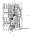
選択的に、前記出力トランジスタ及び前記出力リセットトランジスタは前記出力コンデンサと前記第1出力線部分との間に位置しており、前記出力トランジスタ及び前記出力リセットトランジスタが前記第1方向に沿って順次に配列され、
第1方向を沿って、前記第5トランジスタ、前記第6トランジスタ、前記第7トランジスタ、前記第8トランジスタ、前記第1トランジスタ、前記第1コンデンサ、前記第2トランジスタ及び前記出力リセットトランジスタが順次に配列され、
前記第5トランジスタ、前記第4トランジスタ、前記第6トランジスタ、前記第7トランジスタ及び前記第8トランジスタが前記出力コンデンサと前記第1電圧信号線との間に位置しており、
前記第5トランジスタのゲート電極及び前記第4トランジスタのゲート電極が第1ゲート金属パターンに含まれ、前記第1ゲート金属パターンが前記第2方向に沿って延在される。
Alternatively, the output transistor and the output reset transistor are located between the output capacitor and the first output line portion, and the output transistor and the output reset transistor are sequentially arranged along the first direction;
the fifth transistor, the sixth transistor, the seventh transistor, the eighth transistor, the first transistor, the first capacitor, the second transistor, and the output reset transistor are sequentially arranged along a first direction;
the fifth transistor, the fourth transistor, the sixth transistor, the seventh transistor, and the eighth transistor are located between the output capacitor and the first voltage signal line;
A gate electrode of the fifth transistor and a gate electrode of the fourth transistor are included in a first gate metal pattern, and the first gate metal pattern extends along the second direction.
選択的に、前記表示基板は、前記ベースに設けられる複数行の画素回路をさらに含み、前記画素回路は発光制御端を含み、
前記シフトレジスタユニットが少なくとも一行の前記画素回路に対応され、
前記シフトレジスタユニットの信号出力線が前記少なくとも一行の画素回路の発光制御端に結合されて、前記少なくとも一行の画素回路の発光制御端に発光制御信号を提供することに用いられる。
Optionally, the display substrate further includes a plurality of rows of pixel circuits disposed on the base, the pixel circuits including a light emitting control terminal;
The shift register unit corresponds to at least one row of the pixel circuits;
The signal output line of the shift register unit is coupled to the light emission control terminal of the pixel circuits of the at least one row, and is used for providing a light emission control signal to the light emission control terminal of the pixel circuits of the at least one row.
第2態様において、本開示の実施例では、表示基板の製作方法であって、前記表示基板の製作方法は、ベース上に走査駆動回路を製作することを含み、前記走査駆動回路は、複数のシフトレジスタユニットを含み、前記複数のシフトレジスタユニットのうち、少なくとも一つのシフトレジスタユニットは、出力回路を含み、前記出力回路は、出力トランジスタ及び出力リセットトランジスタを含み、
前記表示基板の製作方法は、
前記ベース上に半導体層を製作し、前記半導体層にパターニング工程を行って、出力トランジスタのアクティブ層及び出力リセットトランジスタのアクティブ層を形成することと、
前記半導体層の前記ベースに背く一面に第1ゲート金属層を製作し、前記第1ゲート金属層にパターニング工程を行って、前記出力トランジスタのゲート電極及び前記出力リセットトランジスタのゲート電極を形成することと、
前記出力トランジスタのゲート電極及び前記出力リセットトランジスタのゲート電極をマスクとして、半導体層のうち、前記ゲート電極により被覆されていない部分に対してドーピングを行って、前記半導体層のうち、前記ゲート電極により被覆されていない部分を導電部分として形成し、前記半導体層のうち、前記ゲート電極により被覆されている部分をチャネル部分として形成することと、
前記第1ゲート金属層の前記半導体層に背く一面に第2ゲート金属層を設け、前記第2ゲート金属層にパターニング工程を行って、第1方向に沿って延在される第1出力線部分を含む信号出力線を形成することと、
前記第2ゲート金属層の前記第1ゲート金属層に背く一面に第1絶縁層を設けることと、
前記第1絶縁層と前記第1出力線とが部分的に重なる領域に、前記第1絶縁層を貫通する複数の第1信号線ビアホール及び複数の第2信号線ビアホールを製作することと、
前記第1絶縁層の前記第2ゲート金属層に背く一面にソース・ドレイン金属層を製作し、前記ソース・ドレイン金属層にパターニング工程を行って、第1ソース・ドレイン金属パターン及び第2ソース・ドレイン金属パターンを形成することと、を含み、
前記第1ソース・ドレイン金属パターンが前記出力トランジスタの第2電極を含み、前記第2ソース・ドレイン金属パターンが前記出力リセットトランジスタの第2電極を含んでいることで、前記第1出力線部分が前記複数の第1信号線ビアホールを介して前記出力トランジスタの第2電極に結合され、かつ前記第1出力線部分が前記複数の第2信号線ビアホールを介して前記出力リセットトランジスタの第2電極に結合され、
前記信号出力線は、第1方向に沿って延在される第1出力線部分を含み、
前記複数の第1信号線ビアホールが第1方向に沿って順次に配列され、前記複数の第2信号線ビアホールが第1方向に沿って順次に配列され、
第1方向に沿って順次に配列されるいずれか二つの第1信号線ビアホールの第1方向での最大距離と第3長さとの割合が第1所定割合であり、二つの隣接する第1信号線ビアホールの間の第1方向での最小距離が第1所定距離であり、
第1方向に沿って順次に配列されるいずれか二つの第2信号線ビアホールの第1方向での最大距離と第4長さとの割合が第2所定割合であり、二つの隣接する第2信号線ビアホールの間の第1方向での最小距離が第2所定距離であり、
前記第3長さは、前記第1信号線の重なり領域の第1方向での長さであり、前記第4長さは、前記第2信号線の重なり領域の第1方向での長さであり、
前記第1所定割合は、0.05以上かつ0.9以下であり、
前記第1所定距離は、1.5μm以上かつ45μm以下であり、
前記第2所定割合は、0.05以上かつ0.9以下であり、
前記第2所定距離は、1.5μm以上かつ65μm以下である、表示基板の製作方法を提供する。
In a second aspect, an embodiment of the present disclosure provides a method for manufacturing a display substrate, the method for manufacturing the display substrate includes: manufacturing a scan driving circuit on a base, the scan driving circuit includes a plurality of shift register units, at least one of the plurality of shift register units includes an output circuit, the output circuit includes an output transistor and an output reset transistor;
The method for manufacturing the display substrate includes:
forming a semiconductor layer on the base and performing a patterning process on the semiconductor layer to form an active layer of an output transistor and an active layer of an output reset transistor;
forming a first gate metal layer on a surface of the semiconductor layer opposite the base, and performing a patterning process on the first gate metal layer to form a gate electrode of the output transistor and a gate electrode of the output reset transistor;
doping a portion of a semiconductor layer that is not covered by the gate electrode using a gate electrode of the output transistor and a gate electrode of the output reset transistor as a mask, thereby forming the portion of the semiconductor layer that is not covered by the gate electrode as a conductive portion and forming the portion of the semiconductor layer that is covered by the gate electrode as a channel portion;
providing a second gate metal layer on a surface of the first gate metal layer facing the semiconductor layer, and performing a patterning process on the second gate metal layer to form a signal output line including a first output line portion extending along a first direction;
providing a first insulating layer on a surface of the second gate metal layer facing away from the first gate metal layer;
fabricating a plurality of first signal line via holes and a plurality of second signal line via holes penetrating the first insulating layer in an area where the first insulating layer and the first output line partially overlap;
forming a source/drain metal layer on a surface of the first insulating layer opposite to the second gate metal layer, and performing a patterning process on the source/drain metal layer to form a first source/drain metal pattern and a second source/drain metal pattern;
the first source-drain metal pattern includes a second electrode of the output transistor, and the second source-drain metal pattern includes a second electrode of the output reset transistor, such that the first output line portion is coupled to the second electrode of the output transistor through the plurality of first signal line via holes, and the first output line portion is coupled to the second electrode of the output reset transistor through the plurality of second signal line via holes;
the signal output line includes a first output line portion extending along a first direction,
the first signal line via holes are arranged sequentially along a first direction, and the second signal line via holes are arranged sequentially along the first direction;
a ratio of a maximum distance in the first direction between any two first signal line via holes sequentially arranged along the first direction to a third length is a first predetermined ratio, and a minimum distance in the first direction between two adjacent first signal line via holes is a first predetermined distance;
a ratio of a maximum distance in the first direction to a fourth length of any two second signal line via holes sequentially arranged along the first direction is a second predetermined ratio, and a minimum distance in the first direction between two adjacent second signal line via holes is a second predetermined distance;
the third length is a length of an overlapping region of the first signal line in a first direction, and the fourth length is a length of an overlapping region of the second signal line in the first direction;
The first predetermined ratio is equal to or greater than 0.05 and equal to or less than 0.9,
the first predetermined distance is equal to or greater than 1.5 μm and equal to or less than 45 μm;
The second predetermined ratio is equal to or greater than 0.05 and equal to or less than 0.9,
The second predetermined distance is 1.5 μm or more and 65 μm or less.
選択的に、前記出力トランジスタのアクティブ層の前記第1方向での長さを第1長さとして、前記出力リセットトランジスタのアクティブ層の前記第1方向での長さを第2長さとして、前記第1長さと前記第2長さとの和が出力アクティブ長さであり、
前記出力トランジスタのアクティブ層の第2方向に沿う最小の幅と、前記出力リセットトランジスタのアクティブ層の第2方向に沿う最小の幅とのうち、小さいものを出力アクティブ幅とし、前記第1方向と前記第2方向は互いに交差する。
Optionally, a length of an active layer of the output transistor in the first direction is defined as a first length, a length of an active layer of the output reset transistor in the first direction is defined as a second length, and the sum of the first length and the second length is defined as an output active length;
The smaller of the minimum width along the second direction of the active layer of the output transistor and the minimum width along the second direction of the active layer of the output reset transistor is defined as an output active width, and the first direction and the second direction intersect with each other.
選択的に、前記出力アクティブ長さと前記出力アクティブ幅との割合が所定割合の範囲内にあり、
前記所定割合の範囲が3以上かつ11以下である。
Optionally, a ratio of the output active length to the output active width is within a predetermined ratio range;
The range of the predetermined ratio is 3 or more and 11 or less.
選択的に、前記出力アクティブ幅が所定の幅の範囲内にあり、
前記所定の幅の範囲が12μm以上かつ45μm以下である。
Optionally, the output active width is within a predetermined range;
The predetermined width ranges from 12 μm to 45 μm.
第3態様において、本開示の実施例では、上記の表示基板を含む表示装置をさらに提供する。 In a third aspect, an embodiment of the present disclosure further provides a display device including the display substrate described above.
以下、本開示の実施例の図面を参照しながら、本開示の実施例の技術案を明確かつ完全に説明する。明らかなように、説明される実施例は本開示の一部の実施例に過ぎず、全ての実施例ではない。説明される本開示の実施例に基づいて、当業者が創造のな努力をせずに想到し得るほかの実施例は、すべて本開示の特許範囲に属する。 The technical solutions of the embodiments of the present disclosure will be described below clearly and completely with reference to the drawings of the embodiments of the present disclosure. It is apparent that the described embodiments are only some of the embodiments of the present disclosure, and are not all of the embodiments. Based on the described embodiments of the present disclosure, other embodiments that a person skilled in the art can conceive without making creative efforts are all within the patent scope of the present disclosure.
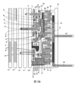
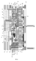
図1に示すように、本開示の少なくとも一実施例は、表示基板を提供し、前記表示基板は表示基板の周辺領域に位置する走査駆動回路を含み、前記走査駆動回路は、第1電圧信号線VGH、第2電圧信号線VGL、第1クロック信号線CK、第2クロック信号線CB及び信号出力線E0を含み、前記走査駆動回路は、複数のシフトレジスタユニットをさらに含み、
図1に示すように、前記複数のシフトレジスタユニットのうち、少なくとも一つのシフトレジスタユニットの少なくとも一実施例は、第1コンデンサC1、出力コンデンサC2、出力リセットコンデンサC3、出力トランジスタT10、出力リセットトランジスタT9、第1トランジスタT1、第2トランジスタT2、第3トランジスタT3、第4トランジスタT4、第5トランジスタT5、第6トランジスタT6、第7トランジスタT7及び第8トランジスタT8を含み、
前記出力トランジスタT10のゲート電極G10は、前記出力コンデンサC2の第1極板C2aに結合され、前記出力トランジスタT10の第1電極S10は、第2電圧信号線VGLに結合され、前記出力トランジスタT10の第2電極D10は、前記信号出力線E0に結合され、
前記出力リセットトランジスタT9のゲート電極G9は、前記出力リセットコンデンサC3の第1極板C3aに結合され、前記出力リセットトランジスタT9の第1電極S9は、前記出力リセットコンデンサC3の第2極板C3bに結合され、前記出力リセットトランジスタT9の第2電極D9は、前記信号出力線E0に結合され、
前記出力リセットコンデンサC3の第2極板C3bが前記第1電圧信号線VGHに結合され、前記出力コンデンサC2の第2極板C2bが第2クロック信号線CBに結合され、
前記第1トランジスタT1の第1電極S1が前記第2クロック信号線CBに結合され、前記第1トランジスタT1の第2電極D1及び前記第2トランジスタT2の第1電極S2がそれぞれ前記第1コンデンサC1の第2極板C1bに結合され、前記第1トランジスタT1のゲート電極G1が前記第1コンデンサC1の第1極板C1aに結合され、
前記第2トランジスタT2のゲート電極G2及び第7トランジスタT7のゲート電極G7は、それぞれ前記第1クロック信号線CBに結合され、前記第2トランジスタT2の第2電極D2は、前記第3トランジスタT3の第2電極D3に結合され、前記第2トランジスタT2の第1電極S2は、前記第1コンデンサの第2極板C1bに結合され、
前記第3トランジスタT3のゲート電極G3は、前記出力トランジスタT10のゲート電極G10に結合され、前記第3トランジスタT3の第1電極S3は、前記第1電圧信号線VGHに結合され、
前記第4トランジスタT4のゲート電極G4及び前記第5トランジスタT5のゲート電極G5は、いずれも第1クロック信号線CKに結合され、前記第4トランジスタT4の第1電極S4及び前記出力トランジスタT10の第1電極S10は、いずれも第2電圧信号線VGLに結合され、前記第4トランジスタT4の第2電極D4は、前記第6トランジスタT6の第2電極D6に結合され、
前記第5トランジスタT5のゲート電極G5は、前記第1クロック信号線CKに結合され、第5トランジスタT5の第2電極D5は、前記第6トランジスタT6のゲート電極G6に結合され、前記第5トランジスタT5の第1電極S5は、入力信号端E1に結合され、
前記第6トランジスタT6の第1電極S1及び第4トランジスタT4のゲート電極G4は、いずれも第1クロック信号線CKに結合され、前記第6トランジスタT6の第2電極D6は、前記第4トランジスタT4の第2電極D4に結合され、前記第6トランジスタT6のゲート電極G6は、第5トランジスタの第2電極D1に結合され、
前記第7トランジスタT7のゲート電極G7及び出力コンデンサC2の第2極板C2bは、いずれも第2クロック信号線CBに結合され、前記第7トランジスタT7の第1電極S7は、前記第8トランジスタT8の第2電極D8に結合され、前記第7トランジスタT7の第2電極D7は、前記第6トランジスタT6のゲート電極G6に結合され、
前記第8トランジスタT8のゲート電極G8は、前記第1トランジスタT1のゲート電極G1に結合され、前記第8トランジスタT8の第1電極S8は、第1電圧信号線VGHに結合される。
As shown in FIG. 1, at least one embodiment of the present disclosure provides a display substrate, the display substrate including a scan driving circuit located in a peripheral region of the display substrate, the scan driving circuit including a first voltage signal line VGH, a second voltage signal line VGL, a first clock signal line CK, a second clock signal line CB and a signal output line E0, the scan driving circuit further including a plurality of shift register units;
As shown in FIG. 1 , at least one embodiment of at least one of the plurality of shift register units includes a first capacitor C1, an output capacitor C2, an output reset capacitor C3, an output transistor T10, an output reset transistor T9, a first transistor T1, a second transistor T2, a third transistor T3, a fourth transistor T4, a fifth transistor T5, a sixth transistor T6, a seventh transistor T7, and an eighth transistor T8,
A gate electrode G10 of the output transistor T10 is coupled to a first plate C2a of the output capacitor C2, a first electrode S10 of the output transistor T10 is coupled to a second voltage signal line VGL, and a second electrode D10 of the output transistor T10 is coupled to the signal output line E0;
A gate electrode G9 of the output reset transistor T9 is coupled to a first plate C3a of the output reset capacitor C3, a first electrode S9 of the output reset transistor T9 is coupled to a second plate C3b of the output reset capacitor C3, and a second electrode D9 of the output reset transistor T9 is coupled to the signal output line E0;
a second plate C3b of the output reset capacitor C3 is coupled to the first voltage signal line VGH, and a second plate C2b of the output capacitor C2 is coupled to a second clock signal line CB;
a first electrode S1 of the first transistor T1 is coupled to the second clock signal line CB, a second electrode D1 of the first transistor T1 and a first electrode S2 of the second transistor T2 are respectively coupled to a second plate C1b of the first capacitor C1, and a gate electrode G1 of the first transistor T1 is coupled to a first plate C1a of the first capacitor C1;
a gate electrode G2 of the second transistor T2 and a gate electrode G7 of the seventh transistor T7 are respectively coupled to the first clock signal line CB, a second electrode D2 of the second transistor T2 is coupled to a second electrode D3 of the third transistor T3, and a first electrode S2 of the second transistor T2 is coupled to a second plate C1b of the first capacitor;
A gate electrode G3 of the third transistor T3 is coupled to a gate electrode G10 of the output transistor T10, and a first electrode S3 of the third transistor T3 is coupled to the first voltage signal line VGH;
a gate electrode G4 of the fourth transistor T4 and a gate electrode G5 of the fifth transistor T5 are both coupled to a first clock signal line CK, a first electrode S4 of the fourth transistor T4 and a first electrode S10 of the output transistor T10 are both coupled to a second voltage signal line VGL, a second electrode D4 of the fourth transistor T4 is coupled to a second electrode D6 of the sixth transistor T6,
A gate electrode G5 of the fifth transistor T5 is coupled to the first clock signal line CK, a second electrode D5 of the fifth transistor T5 is coupled to a gate electrode G6 of the sixth transistor T6, and a first electrode S5 of the fifth transistor T5 is coupled to an input signal terminal E1;
The first electrode S1 of the sixth transistor T6 and the gate electrode G4 of the fourth transistor T4 are both coupled to a first clock signal line CK, the second electrode D6 of the sixth transistor T6 is coupled to the second electrode D4 of the fourth transistor T4, and the gate electrode G6 of the sixth transistor T6 is coupled to the second electrode D1 of the fifth transistor T4.
a gate electrode G7 of the seventh transistor T7 and a second plate C2b of the output capacitor C2 are both coupled to a second clock signal line CB, a first electrode S7 of the seventh transistor T7 is coupled to a second electrode D8 of the eighth transistor T8, and a second electrode D7 of the seventh transistor T7 is coupled to a gate electrode G6 of the sixth transistor T6;
A gate electrode G8 of the eighth transistor T8 is coupled to a gate electrode G1 of the first transistor T1, and a first electrode S8 of the eighth transistor T8 is coupled to a first voltage signal line VGH.
図1に示されるシフトレジスタユニットの少なくとも一実施例では、全てのトランジスタはいずれもp型トランジスタであるが、これに限らない。 In at least one embodiment of the shift register unit shown in FIG. 1, all of the transistors are p-type transistors, but this is not limited to this.
本開示の少なくとも一実施例では、図1に示されるシフトレジスタユニットの少なくとも一実施例は、発光制御走査駆動回路であってもよいが、これに限らない。 In at least one embodiment of the present disclosure, at least one embodiment of the shift register unit shown in FIG. 1 may be, but is not limited to, a light emission control scan drive circuit.
本開示の少なくとも一実施例では、トランジスタの第1電極はソース電極であってもよく、トランジスタの第2電極はドレイン電極であってもよく、もしくは、トランジスタの第1電極はドレイン電極であってもよく、トランジスタの第2電極はソース電極であってもよく。 In at least one embodiment of the present disclosure, the first electrode of the transistor may be a source electrode and the second electrode of the transistor may be a drain electrode, or the first electrode of the transistor may be a drain electrode and the second electrode of the transistor may be a source electrode.
図1において、符号N1は第1ノードであり、符号N2は第2ノードであり、符号N3は第3ノードであり、符号N4は第4ノードである。 In FIG. 1, N1 is the first node, N2 is the second node, N3 is the third node, and N4 is the fourth node.
図1に示した少なくとも一実施例では、第1電圧信号線VGHは高電圧Vghを提供することができ、第2電圧信号線VGLは低電圧Vglを提供することができるが、これに限らない。 In at least one embodiment shown in FIG. 1, the first voltage signal line VGH can provide a high voltage Vgh and the second voltage signal line VGL can provide a low voltage Vgl, but is not limited to this.
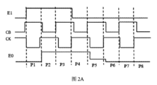
図2Aに示すように、本開示の図1に示されるシフトレジスタユニットの少なくとも一実施例において、動作する時に、
第1段階P1で、E1がハイレベルを提供し、CKがローレベルを提供し、CBがハイレベルを提供し、T5及びT4がオンとなり、N1の電位がハイレベルで、T6はオフとなり、N2の電位はローレベルであるので、T7、T3及びT10がオフとなり、T8及びT1がオンとなり、この時、N3の電位がハイレベルであり、CBがハイレベルを提供するので、T2がオフとなり、コンデンサの両端の電圧が突然に変化しないので、N4の電位が、前フレームのハイレベルに保持されて、T9がオフとなり、E0から出力される発光制御信号の電位が、前フレームのローレベルに保持され、
第2段階P2で、E1及びCKがいずれもハイレベルを提供し、CBがローレベルを提供し、T5、T6及びT4がいずれもオフとなり、N1の電位がハイレベルに保持され、N2の電位がローレベルに保持され、T7、T8及びT1がいずれもオンとなり、N3の電位がハイレベルからローレベルに変化し、T2がオンとなり、N4の電位がローレベルであり、T9がオンとなり、E0がハイレベルを出力し、T3及びT10がいずれもオフとなり、
第3段階P3で、E1及びCBがいずれもハイレベルを提供し、CKがローレベルを提供し、T5及びT4がいずれもオンとなり、N1の電位がハイレベルであり、N2の電位がローレベルであり、T6及びT7がいずれもオフとなり、T8及びT1がいずれもオンとなり、N3の電位が前の段階のローレベルからハイレベルに変化し、T2がオフとなり、N4の電位がローレベルに保持され、T9がオンとなり、E0がハイレベルを出力し、T3及びT10がいずれもオフとなり、
第4段階P4で、E1及びCBがいずれもローレベルを提供し、CKがハイレベルを提供し、T5及びT4がいずれもオフとなり、N1の電位がハイレベルであり、T6がオフとなり、N2の電位がローレベルに保持され、T7、T8及びT1がいずれもオンとなり、N3の電圧がローレベルにジャンプし、T2がオンとなり、N4の電位がローレベルであり、T9がオンとなり、E0がハイレベルを出力し、T3及びT10がいずれもオフとなり、
第5段階P5で、E1及びCKがいずれもローレベルを提供し、CBがハイレベルを提供し、T5、T6及びT4がいずれもオンとなり、N1の電位及びN2の電位はいずれもローレベルであり、T7がオフとなり、T7及びT1がいずれもオンとなり、N3の電圧がハイレベルに変化し、T2がオフとなり、T3がオンとなり、N4の電圧がハイレベルに変化し、T9がオフとなり、T10がオンとなり、E0がローレベルを出力し、
第6段階P6で、E1及びCB信号はローレベルであり、CKはハイレベルであり、T1、T3がオフとなり、ノードN1がローレベルを保持され、T2がオンとなり、N2ノードの電圧はハイレベルであり、T4、T5がオンとなり、T6がオフとなり、N3ノードはハイレベルであり、T7、T8がオンとなり、N4ノードはハイレベルであり、T9がオフとなり、T10はオンとなり、E0がローレベルを出力する。
As shown in FIG. 2A, in at least one embodiment of the shift register unit shown in FIG. 1 of the present disclosure, when in operation:
In the first stage P1, E1 provides a high level, CK provides a low level, CB provides a high level, T5 and T4 are turned on, the potential of N1 is at a high level, T6 is turned off, and the potential of N2 is at a low level, so T7, T3 and T10 are turned off, and T8 and T1 are turned on. At this time, the potential of N3 is at a high level, and CB provides a high level, so T2 is turned off. Since the voltage across the capacitor does not change suddenly, the potential of N4 is held at the high level of the previous frame, T9 is turned off, and the potential of the light emission control signal output from E0 is held at the low level of the previous frame.
In the second stage P2, E1 and CK all provide a high level, CB provides a low level, T5, T6 and T4 are all turned off, the potential of N1 is held at a high level, the potential of N2 is held at a low level, T7, T8 and T1 are all turned on, the potential of N3 changes from a high level to a low level, T2 is turned on, the potential of N4 is at a low level, T9 is turned on, E0 outputs a high level, T3 and T10 are all turned off,
In the third stage P3, E1 and CB both provide a high level, CK provides a low level, T5 and T4 are both turned on, the potential of N1 is at a high level, the potential of N2 is at a low level, T6 and T7 are both turned off, T8 and T1 are both turned on, the potential of N3 changes from the low level of the previous stage to a high level, T2 is turned off, the potential of N4 is held at a low level, T9 is turned on, E0 outputs a high level, and T3 and T10 are both turned off.
In the fourth stage P4, E1 and CB all provide a low level, CK provides a high level, T5 and T4 are all turned off, the potential of N1 is a high level, T6 is turned off, the potential of N2 is held at a low level, T7, T8 and T1 are all turned on, the voltage of N3 jumps to a low level, T2 is turned on, the potential of N4 is a low level, T9 is turned on, E0 outputs a high level, T3 and T10 are all turned off;
In the fifth stage P5, E1 and CK all provide a low level, CB provides a high level, T5, T6 and T4 are all turned on, the potential of N1 and the potential of N2 are all low level, T7 is turned off, T7 and T1 are all turned on, the voltage of N3 changes to a high level, T2 is turned off, T3 is turned on, the voltage of N4 changes to a high level, T9 is turned off, T10 is turned on, and E0 outputs a low level;
In the sixth stage P6, the E1 and CB signals are at a low level, CK is at a high level, T1 and T3 are off, node N1 is held at a low level, T2 is on, the voltage of the N2 node is at a high level, T4 and T5 are on, T6 is off, the N3 node is at a high level, T7 and T8 are on, the N4 node is at a high level, T9 is off, T10 is on, and E0 outputs a low level.
第7段階P7で、E1及びCKがいずれもローレベルを提供し、CBがハイレベルを提供し、T5、T6及びT4がいずれもオンとなり、N1の電位及びN2の電位はいずれもローレベルであり、T7がオフとなり、T8及びT1がいずれもオンとなり、N3の電位はハイレベルであり、T2がオフとなり、T3がオンとなり、N4の電位はハイレベルであり、T9がオフとなり、T10がオンとなり、E0がローレベルを出力し、 In the seventh stage P7, E1 and CK all provide low levels, CB provides a high level, T5, T6 and T4 are all on, the potential of N1 and the potential of N2 are all low levels, T7 is off, T8 and T1 are all on, the potential of N3 is high level, T2 is off, T3 is on, the potential of N4 is high level, T9 is off, T10 is on, and E0 outputs a low level,
第8段階P8で、E1及びCBがいずれもローレベルを提供し、CKがハイレベルを提供し、T5及びT4がいずれもオフとなり、N1の電位がローレベルに保持され、T6がオンとなり、N2の電位はハイレベルであり、T7がオンとなり、T8及びT1がいずれもオフとなり、N3の電位はハイレベルであり、T2及びT3がいずれもオンとなり、N4の電圧はハイレベルであり、T9がオフとなり、T10がオンとなり、E0がローレベルを出力し、
前記第6段階の後、次のフレームでE1が入力信号を受信するまで、T3が持続的にオンとなり、T9が持続的にオフとなり、T5が周期的にC2に充電し、N1の電位がローレベルに保持され、T10が持続的にオンとなり、E0がローレベルを出力する。
In the eighth stage P8, E1 and CB both provide a low level, CK provides a high level, T5 and T4 are both turned off, the potential of N1 is held at a low level, T6 is turned on, the potential of N2 is at a high level, T7 is turned on, T8 and T1 are both turned off, the potential of N3 is at a high level, T2 and T3 are both turned on, the voltage of N4 is at a high level, T9 is turned off, T10 is turned on, and E0 outputs a low level;
After the sixth step, until E1 receives an input signal in the next frame, T3 is continuously on, T9 is continuously off, T5 periodically charges C2, the potential of N1 is held at a low level, T10 is continuously on, and E0 outputs a low level.
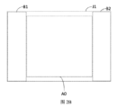
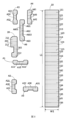
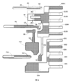
図2Bに示すように、符号J1は表示基板であり、符号A0は表示領域であり、符号B1は第1周辺領域であり、符号B2は第2周辺領域である。 As shown in FIG. 2B, J1 is the display substrate, A0 is the display area, B1 is the first peripheral area, and B2 is the second peripheral area.
前記表示基板J1の表示領域A0に複数本の発光制御線、複数本のゲート線と複数本のデータ線、及び、前記複数本のゲート線と前記複数本のデータ線が交差して限定した複数のサブ画素は設けられていてもよく、
第1周辺領域B1及び/または第2周辺領域B2に走査駆動回路が設けられていてもよく、前記走査駆動回路は、複数のシフトレジスタユニットを含み、
前記走査駆動回路に含まれる複数のシフトレジスタユニットのうち、各前記シフトレジスタユニットの信号出力線は、それぞれA本の発光制御線に結合されて、対応する発光制御線に発光制御信号を提供することに用いられてもよい。
A plurality of light emitting control lines, a plurality of gate lines, a plurality of data lines, and a plurality of sub-pixels defined by the intersection of the plurality of gate lines and the plurality of data lines may be provided in the display area A0 of the display substrate J1,
A scan driving circuit may be provided in the first peripheral region B1 and/or the second peripheral region B2, the scan driving circuit including a plurality of shift register units;
Among the plurality of shift register units included in the scanning driving circuit, the signal output lines of each of the shift register units may be respectively coupled to A emission control lines and used to provide emission control signals to the corresponding emission control lines.
ここで、Aは、正の整数であっでもよい。実際の操作において、Aは1、2、3、4であってもよく、または他の正の整数であってもよく、Aの値は実際の状態によって選択してもよい。 Here, A can be any positive integer. In actual operation, A can be 1, 2, 3, 4, or other positive integers, and the value of A can be selected according to the actual situation.
具体的に実施する時に、前記発光制御線は、相応する行の画素回路の発光制御端に結合される。
選択的に、前記表示基板は、前記ベースに設けられる複数行の画素回路をさらに含み、前記画素回路は発光制御端を含み、
前記走査駆動回路に含まれる前記シフトレジスタユニットは少なくとも一行の前記画素回路に対応され、
前記シフトレジスタユニットの信号出力線は、前記少なくとも一行の画素回路の発光制御端に結合されて、前記少なくとも一行の画素回路の発光制御端に発光制御信号を提供することに用いられる。
In particular, the light emission control line is coupled to the light emission control end of the pixel circuit of a corresponding row.
Optionally, the display substrate further includes a plurality of rows of pixel circuits disposed on the base, the pixel circuits including a light emitting control terminal;
The shift register unit included in the scan driving circuit corresponds to at least one row of the pixel circuits;
The signal output line of the shift register unit is coupled to the light emission control terminal of the pixel circuit of the at least one row, and is used for providing a light emission control signal to the light emission control terminal of the pixel circuit of the at least one row.
本開示の少なくとも一実施例では、前記画素回路が表示基板の有効表示領域に設けられてもよく、前記走査駆動回路が表示基板の周辺領域に設けられてもよい。 In at least one embodiment of the present disclosure, the pixel circuit may be provided in an effective display area of a display substrate, and the scanning drive circuit may be provided in a peripheral area of the display substrate.
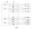
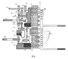
図2Cに示すように、符号Y1は走査駆動回路であり、符号S11は前記走査駆動回路S1に含まれる第1段シフトレジスタユニットであり、符号S12は前記走査駆動回路S1に含まれる第2段シフトレジスタユニットであり、符号S1N-1は前記走査駆動回路S1に含まれる第N-1段シフトレジスタユニットであり、符号S1Nは前記走査駆動回路S1に含まれる第N段シフトレジスタユニットであり、Nは3より大きい整数であり、
図2Cにおいて、符号R1は第1行画素回路であり、符号R2は第2行画素回路であり、符号R3は第3行画素回路であり、符号R4は第4行画素回路であり、符号R2N-3は第2N-3行画素回路であり、符号R2N-2は第2N-2行画素回路であり、符号R2N-1は第2N-1行画素回路であり、符号R2Nは第2N行画素回路であり、
S11がR1及びR2に発光制御信号を提供し、S12がR3及びR4に発光制御信号を提供し、S1N-1がR2N-3及びR2N-2に発光制御信号を提供し、S1NがR2N-1及びR2Nに発光制御信号を提供し、
図2Cに示すように、周辺領域において、前記表示基板は、ゲート電極駆動回路をさらに含んでもよく、前記ゲート電極駆動回路は、複数段のゲート電極駆動ユニットを含み、前記ゲート電極駆動ユニットは画素行に一対一対応されて、相応する行の画素に、相応のゲート電極駆動信号を提供することに用いられてもよく、
図2Cにおいて、符号Y2はゲート電極駆動回路であり、符号S21はゲート電極駆動回路に含まれる第1行ゲート電極駆動ユニットであり、符号S22はゲート電極駆動回路に含まれる第2行ゲート電極駆動ユニットであり、符号S23はゲート電極駆動回路に含まれる第3行ゲート電極駆動ユニットであり、符号S24はゲート電極駆動回路に含まれる第4行ゲート電極駆動ユニットであり、符号S2N-3はゲート電極駆動回路に含まれる第2N-3行ゲート電極駆動ユニットであり、符号S2N-2はゲート電極駆動回路に含まれる第2N-2行ゲート電極駆動ユニットであり、符号S2N-1はゲート電極駆動回路に含まれる第2N-1行ゲート電極駆動ユニットであり、符号S2Nはゲート電極駆動回路に含まれる第2N行ゲート電極駆動ユニットである。
As shown in FIG. 2C, Y1 is a scan driving circuit, S11 is a first-stage shift register unit included in the scan driving circuit S1, S12 is a second-stage shift register unit included in the scan driving circuit S1, S1N-1 is an (N-1)th stage shift register unit included in the scan driving circuit S1, and S1N is an Nth stage shift register unit included in the scan driving circuit S1, where N is an integer greater than 3;
In FIG. 2C , R1 is a first row pixel circuit, R2 is a second row pixel circuit, R3 is a third row pixel circuit, R4 is a fourth row pixel circuit, R2N-3 is a 2N-3 row pixel circuit, R2N-2 is a 2N-2 row pixel circuit, R2N-1 is a 2N-1 row pixel circuit, and R2N is a 2N row pixel circuit.
S11 provides a light-emitting control signal to R1 and R2, S12 provides a light-emitting control signal to R3 and R4, S1N-1 provides a light-emitting control signal to R2N-3 and R2N-2, S1N provides a light-emitting control signal to R2N-1 and R2N,
As shown in FIG. 2C , in the peripheral region, the display substrate may further include a gate electrode driving circuit, the gate electrode driving circuit may include a plurality of gate electrode driving units, the gate electrode driving units may correspond to pixel rows one-to-one, and may be used to provide corresponding gate electrode driving signals to the pixels of the corresponding rows;
In FIG. 2C , symbol Y2 is a gate electrode driving circuit, symbol S21 is a first row gate electrode driving unit included in the gate electrode driving circuit, symbol S22 is a second row gate electrode driving unit included in the gate electrode driving circuit, symbol S23 is a third row gate electrode driving unit included in the gate electrode driving circuit, symbol S24 is a fourth row gate electrode driving unit included in the gate electrode driving circuit, symbol S2N-3 is a 2N-3 row gate electrode driving unit included in the gate electrode driving circuit, symbol S2N-2 is a 2N-2 row gate electrode driving unit included in the gate electrode driving circuit, symbol S2N-1 is a 2N-1 row gate electrode driving unit included in the gate electrode driving circuit, and symbol S2N is a 2N row gate electrode driving unit included in the gate electrode driving circuit.
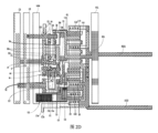
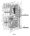
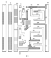
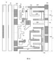
図2Dに示した少なくとも一実施例では、第1電圧信号線VGHが高電圧信号Vghを提供し、第2電圧信号線VGLが低電圧信号Vglを提供し、
図2Dに示すように、VGL、VGH、CK及びCBは表示領域から離れていく方向に沿って配列され、VGH、VGL、CK及びCBが第1方向に延在され、
図1及び図2Dに示すように、シフトレジスタユニットの少なくとも一実施例は、第1コンデンサC1、出力コンデンサC2、出力リセットコンデンサC3、出力トランジスタT10、出力リセットトランジスタT9、第1トランジスタT1、第2トランジスタT2、第3トランジスタT3、第4トランジスタT4、第5トランジスタT5、第6トランジスタT6、第7トランジスタT7及び第8トランジスタT8を含み、前記シフトレジスタユニットの該実施例は、VGHとVGLとの間に設置され、
T10及びT9は第1方向に沿って配列され、
C2は、T10のVGLから離れた側に設けられ、T5、T6及びT4は、C2及びVGHとの間に設けられ、
T1及びT3は、T9のVGLから離れた側に設けられ、C1は、T3のT9から離れた側に設けられ、T8及びT2は、C1のT8から離れた側に設けられ、
T5、T7、T8、T2及びC3が第1方向に沿って順次に配列され、T6、C1及びC3が第1方向に沿って順次に配列され、C2、T1、T3及びC3が第1方向に沿って順次に配列され、
T1は、第1アクティブパターンを含み、T1の第1アクティブパターンが縦方向に配列されて、T2及びT3との間に緊密に配列されることに不利であり、
C3の第2極板C3bの横方向での幅が長くて、シフトレジスタユニットの第2方向での幅を狭めることに不利である。
In at least one embodiment shown in FIG. 2D, a first voltage signal line VGH provides a high voltage signal Vgh, and a second voltage signal line VGL provides a low voltage signal Vgl;
As shown in FIG. 2D , VGL, VGH, CK, and CB are arranged along a direction away from the display area, and VGH, VGL, CK, and CB extend in a first direction;
As shown in FIG. 1 and FIG. 2D, at least one embodiment of a shift register unit includes a first capacitor C1, an output capacitor C2, an output reset capacitor C3, an output transistor T10, an output reset transistor T9, a first transistor T1, a second transistor T2, a third transistor T3, a fourth transistor T4, a fifth transistor T5, a sixth transistor T6, a seventh transistor T7, and an eighth transistor T8, and the embodiment of the shift register unit is disposed between VGH and VGL;
T10 and T9 are arranged along the first direction,
C2 is provided on the side of T10 away from VGL, and T5, T6, and T4 are provided between C2 and VGH.
T1 and T3 are provided on the side of T9 away from VGL, C1 is provided on the side of T3 away from T9, T8 and T2 are provided on the side of C1 away from T8,
T5, T7, T8, T2, and C3 are sequentially arranged along the first direction, T6, C1, and C3 are sequentially arranged along the first direction, and C2, T1, T3, and C3 are sequentially arranged along the first direction;
T1 includes a first active pattern, and the first active pattern of T1 is vertically aligned and closely aligned with T2 and T3;
The width of the second plate C3b of C3 in the lateral direction is long, which is disadvantageous in narrowing the width of the shift register unit in the second direction.
図2Dにおいて、符号E01は信号出力線の第1出力線部分であり、符号E021は信号出力線の1番目の第2出力線部分であり、符号E022は信号出力線の2番目の第2出力線部分であり、E01が第1方向に沿って配列され、E021が第2方向に沿って配列され、E01、E021及びE022は、互いに結合され、第1方向及び第2方向は互いに交差され、E01は、VGLと出力回路(前記出力回路は前記出力トランジスタT10及び前記出力リセットトランジスタT9を含む)との間に設けられ、E021及びE022が第2方向に沿って表示領域へと延在されて、表示領域に位置している画素回路に発光制御信号を提供することを便利にする。 In FIG. 2D, E01 is a first output line portion of the signal output line, E021 is a first second output line portion of the signal output line, and E022 is a second second output line portion of the signal output line, where E01 is arranged along a first direction, E021 is arranged along a second direction, E01, E021 and E022 are coupled to each other, and the first direction and the second direction cross each other, E01 is provided between VGL and an output circuit (the output circuit includes the output transistor T10 and the output reset transistor T9), and E021 and E022 are extended along the second direction to the display area to facilitate providing a light emission control signal to the pixel circuit located in the display area.
図2Dに示すように、S7がD8として兼用される。 As shown in Figure 2D, S7 is also used as D8.
図2D及び図3Aにおいて、符号G1はT1のゲート電極であり、符号S1はT1の第1電極であり、符号D1はT1の第2電極であり、符号G2はT2のゲート電極であり、符号S2はT2の第1電極であり、符号D2はT2の第2電極であり、符号G3はT3のゲート電極であり、符号S3はT3の第1電極であり、符号D3はT3の第2電極であり、符号G4はT4のゲート電極であり、符号S4はT4の第1電極であり、符号D4はT4の第2電極であり、符号G5はT5のゲート電極であり、符号S5はT5の第1電極であり、符号D5はT5の第2電極であり、符号G6はT6のゲート電極であり、符号S6はT6の第1電極であり、符号D6はT6の第2電極であり、符号G7はT7のゲート電極であり、符号S7はT7の第1電極であり、符号D7はT7の第2電極であり、符号G8はT8のゲート電極であり、符号S8はT8の第1電極であり、符号G9はT9のゲート電極であり、符号S9はT9の第1電極であり、符号D9はT9の第2電極であり、符号G10はT10のゲート電極であり、符号S10はT10の第1電極であり、符号D10はT10の第2電極である。 2D and 3A, G1 is the gate electrode of T1, S1 is the first electrode of T1, D1 is the second electrode of T1, G2 is the gate electrode of T2, S2 is the first electrode of T2, D2 is the second electrode of T2, G3 is the gate electrode of T3, S3 is the first electrode of T3, D3 is the second electrode of T3, G4 is the gate electrode of T4, S4 is the first electrode of T4, D4 is the second electrode of T4, G5 is the gate electrode of T5, S5 is the first electrode of T5, and D5 is It is the second electrode of T5, G6 is the gate electrode of T6, S6 is the first electrode of T6, D6 is the second electrode of T6, G7 is the gate electrode of T7, S7 is the first electrode of T7, D7 is the second electrode of T7, G8 is the gate electrode of T8, S8 is the first electrode of T8, G9 is the gate electrode of T9, S9 is the first electrode of T9, D9 is the second electrode of T9, G10 is the gate electrode of T10, S10 is the first electrode of T10, and D10 is the second electrode of T10.
図2Dに示した少なくとも一実施例では、第1方向は上から下に向かう垂直方向であっでもよく、第2方向は右から左に向かう水平方向であってもよいが、これに限らない。実際の操作において、第1方向は、下から上に向かう垂直方向であっでもよく、第2方向は、左から右に向かう水平方向であってもよく、もしくは、前記第1方向は他の方向であってもよく、前記第2方向は他の方向であってもよい。 In at least one embodiment shown in FIG. 2D, the first direction may be a vertical direction from top to bottom and the second direction may be a horizontal direction from right to left, but is not limited to this. In actual operation, the first direction may be a vertical direction from bottom to top and the second direction may be a horizontal direction from left to right, or the first direction may be another direction and the second direction may be another direction.
図2Dに示されるゲート電極駆動回路のレイアウト方式において、T9のアクティブ層及びT9のアクティブ層は一つの連続した第1半導体層により形成され、前記第1半導体層の第1方向での長さが短くて、シフトレジスタユニット全体の縦方向での空間が小さく、そのため、横方向でのシフトレジスタユニットの幅が大きくて、シフトレジスタユニットのうちの素子が水平方向で緊密に配列されることに不利で、表示基板の狭額縁化の発展に不利である。 In the layout method of the gate electrode driving circuit shown in FIG. 2D, the active layer of T9 and the active layer of T9 are formed by one continuous first semiconductor layer, and the length of the first semiconductor layer in the first direction is short, and the vertical space of the entire shift register unit is small. Therefore, the width of the shift register unit in the horizontal direction is large, which is disadvantageous in arranging the elements of the shift register unit closely in the horizontal direction and is disadvantageous in the development of narrower picture frames of display substrates.
図2Dに示されるシフトレジスタユニットは走査駆動回路に含まれる第n段シフトレジスタユニットであってもよく、nは正の整数である。 The shift register unit shown in FIG. 2D may be an nth stage shift register unit included in a scan drive circuit, where n is a positive integer.
上記の問題点に基づいて、本開示の発明者は、研究を通じて、シフトレジスタユニットのうちの各トランジスタのレイアウト方式を調整することにより、シフトレジスタユニットの占有面積を減らすことで、表示基板の額縁の幅を縮めることができることを発見した。 Based on the above problems, the inventors of the present disclosure have discovered through research that by adjusting the layout method of each transistor in the shift register unit, the area occupied by the shift register unit can be reduced, thereby narrowing the width of the frame of the display substrate.
図3Aに示されるレイアウト方式において、第1電圧信号線VGHが高電圧信号Vghを提供し、第2電圧信号線VGLが低電圧信号Vglを提供し、本開示の少なくとも一実施例では、シフトレジスタユニットは、VGHとVGLとの間に設置される。 In the layout scheme shown in FIG. 3A, a first voltage signal line VGH provides a high voltage signal Vgh, a second voltage signal line VGL provides a low voltage signal Vgl, and in at least one embodiment of the present disclosure, the shift register unit is disposed between VGH and VGL.
図3Aにおいて、符号E01は信号出力線の第1出力線部分であり、符号E021は信号出力線の1番目の第2出力線部分であり、符号E022は信号出力線の2番目の第2出力線部分であり、E01が第1方向に沿って配列され、E021が第2方向に沿って配列され、E01、E021及びE022は、互いに結合され、第1方向及び第2方向は互いに交差する。図3Aに示すように、E01がVGLと前記出力回路との間に設けられており、E021及びE022が第2方向に沿って表示領域へと延在されて、表示領域に位置している画素回路に発光制御信号を提供することを便利にする。 In FIG. 3A, E01 is the first output line portion of the signal output line, E021 is the first second output line portion of the signal output line, and E022 is the second second output line portion of the signal output line, where E01 is arranged along a first direction, E021 is arranged along a second direction, and E01, E021 and E022 are coupled to each other, and the first direction and the second direction cross each other. As shown in FIG. 3A, E01 is provided between VGL and the output circuit, and E021 and E022 are extended to the display area along the second direction to facilitate providing a light emission control signal to the pixel circuit located in the display area.
例えば、図3Aに示されるレイアウト方式において、第1方向は上から下に向かう垂直方向であっでもよく、第2方向は右から左に向かう水平方向であってもよいが、これに限らない。 For example, in the layout scheme shown in FIG. 3A, the first direction may be a vertical direction from top to bottom, and the second direction may be a horizontal direction from right to left, but is not limited to this.
図3Aに示されるシフトレジスタユニットは、走査駆動回路に含まれる第n段シフトレジスタユニットであってもよく、nは正の整数である。 The shift register unit shown in FIG. 3A may be an nth stage shift register unit included in a scan drive circuit, where n is a positive integer.
図1及び図3Aに示すように、シフトレジスタユニットの少なくとも一実施例は、第1コンデンサC1、出力コンデンサC2、出力リセットコンデンサC3、出力トランジスタT10、出力リセットトランジスタT9、第1トランジスタT1、第2トランジスタT2、第3トランジスタT3、第4トランジスタT4、第5トランジスタT5、第6トランジスタT6、第7トランジスタT7及び第8トランジスタT8を含み、図3Aに示すように、出力回路O1は、前記出力トランジスタT10及び前記出力リセットトランジスタT9を含み、
前記出力トランジスタT10のゲート電極G10は、前記出力コンデンサC2の第1極板C2aに結合され、前記出力トランジスタT10の第1電極S10は、第2電圧信号線VGLに結合され、前記出力トランジスタT10の第2電極D10は、信号出力線に含まれる第1出力線部分E01に結合され、
前記出力リセットトランジスタT9のゲート電極G9は、前記出力リセットコンデンサC3の第1極板C3aに結合され、前記出力リセットトランジスタT9の第1電極S9は、前記出力リセットコンデンサC3の第2極板C3bに結合され、前記出力リセットトランジスタT9の第2電極D9は、前記信号出力線に含まれる第1出力線部分E01に結合される。
As shown in FIG. 1 and FIG. 3A, at least one embodiment of the shift register unit includes a first capacitor C1, an output capacitor C2, an output reset capacitor C3, an output transistor T10, an output reset transistor T9, a first transistor T1, a second transistor T2, a third transistor T3, a fourth transistor T4, a fifth transistor T5, a sixth transistor T6, a seventh transistor T7, and an eighth transistor T8; as shown in FIG. 3A, the output circuit O1 includes the output transistor T10 and the output reset transistor T9;
A gate electrode G10 of the output transistor T10 is coupled to a first plate C2a of the output capacitor C2, a first electrode S10 of the output transistor T10 is coupled to a second voltage signal line VGL, and a second electrode D10 of the output transistor T10 is coupled to a first output line portion E01 included in a signal output line;
A gate electrode G9 of the output reset transistor T9 is coupled to a first plate C3a of the output reset capacitor C3, a first electrode S9 of the output reset transistor T9 is coupled to a second plate C3b of the output reset capacitor C3, and a second electrode D9 of the output reset transistor T9 is coupled to a first output line portion E01 included in the signal output line.
図3Aに示されるゲート電極駆動回路のレイアウト方式において、T9のアクティブ層及びT10のアクティブ層は、一つの連続した第1半導体層により形成されてもよく、前記第1半導体層の第1方向での長さを引き上げて、シフトレジスタユニットに含まれる他の素子が縦方向で余裕になる空間を利用して、横方向でのシフトレジスタユニットの幅を狭めて、シフトレジスタユニットのうちの素子が水平方向で緊密に配列されることに有利で、表示基板の狭額縁化の発展に有利であるようにする。 In the layout method of the gate electrode driving circuit shown in FIG. 3A, the active layer of T9 and the active layer of T10 may be formed by one continuous first semiconductor layer, and the length of the first semiconductor layer in the first direction is increased to utilize the space that other elements included in the shift register unit have in the vertical direction to narrow the width of the shift register unit in the horizontal direction, which is advantageous for the elements of the shift register unit to be closely arranged in the horizontal direction and is advantageous for the development of narrower picture frames for display substrates.
図3Aに示すように、上記構成のシフトレジスタユニットを表示基板の周辺領域にレイアウトを行う場合、表示基板の表示領域から離れていく方向に沿って、第2電圧信号線VGL、第1電圧信号線VGH、第1クロック信号線CK及び第2クロック信号線CBを順次に配列し、第2電圧信号線VGL、第1電圧信号線VGH、第1クロック信号線CK及び第2クロック信号線CBはいずれも第1方向に沿って延在され、
図3Aに示すように、第1コンデンサC1、出力コンデンサC2、出力リセットコンデンサC3、出力トランジスタT10、出力リセットトランジスタT9、第1トランジスタT1、第2トランジスタT2、第3トランジスタT3、第4トランジスタT4、第5トランジスタT5、第6トランジスタT6、第7トランジスタT7及び第8トランジスタT8がいずれもVGHとVGLとの間に設置され、第1半導体層の第1方向で引き上げた長さを利用するために、T5、T6、T4、T7及びT8をいずれも上の方に移動して、
T1は、第1アクティブパターンを含み、かつT1の第1アクティブパターンが第2方向に沿って延在されるように設け、T1をT8とC1との間に設け、T8、T1及びC1は第1方向に沿って順次に配列されることで、T8とC1との間の空間を利用してT1を設けて、T2及びT3との間の配列がより緊密にすることができ(前記第2トランジスタT2の第2電極D2が前記第3トランジスタT3の第2電極D2に結合されるので、配線の便宜上、T2及びT3を近く設けることが必要である)、シフトレジスタユニットの占める第2方向での幅をさらに狭めることができ、
そのうえ、図3Aに示されるレイアウト方式において、C1の形状と、T1、T2及びT3の配列される位置とがさらに契合し、T1、T2及びT3の間の空間を利用してC1の極板を設け、
図3Aに示されるレイアウト方式において、C3の第2極板C3bの第2方向での幅を小さく設置し、C3の第2極板C3bの第1方向での長さを大きく設置して、C3の極板の面積を確保することを前提に、C3の極板の占める第2方向での幅を狭め、
図3Aに示すように、C3の第2極板C3bのベースでの正投影がC3の第1極板C3aのベースでの正投影内にある。
As shown in FIG. 3A , when the shift register unit having the above configuration is laid out in the peripheral region of the display substrate, the second voltage signal line VGL, the first voltage signal line VGH, the first clock signal line CK, and the second clock signal line CB are sequentially arranged along a direction away from the display region of the display substrate, and the second voltage signal line VGL, the first voltage signal line VGH, the first clock signal line CK, and the second clock signal line CB are all extended along a first direction,
As shown in FIG. 3A , the first capacitor C1, the output capacitor C2, the output reset capacitor C3, the output transistor T10, the output reset transistor T9, the first transistor T1, the second transistor T2, the third transistor T3, the fourth transistor T4, the fifth transistor T5, the sixth transistor T6, the seventh transistor T7, and the eighth transistor T8 are all disposed between VGH and VGL, and in order to utilize the length of the first semiconductor layer pulled up in the first direction, T5, T6, T4, T7, and T8 are all moved upwards,
T1 includes a first active pattern, and is arranged such that the first active pattern of T1 extends along the second direction, and T1 is arranged between T8 and C1, and T8, T1, and C1 are sequentially arranged along the first direction, so that T1 is arranged using the space between T8 and C1, and thus the arrangement between T2 and T3 can be made closer (because the second electrode D2 of the second transistor T2 is coupled to the second electrode D2 of the third transistor T3, it is necessary to arrange T2 and T3 closely for convenience of wiring), and the width of the shift register unit in the second direction can be further narrowed;
In addition, in the layout scheme shown in FIG. 3A, the shape of C1 and the arrangement positions of T1, T2, and T3 are further matched, and the space between T1, T2, and T3 is used to provide the plate of C1;
In the layout method shown in FIG. 3A, the width of the second plate C3b of C3 in the second direction is set small, and the length of the second plate C3b of C3 in the first direction is set large. On the premise of securing the area of the plate of C3, the width of the plate of C3 in the second direction is narrowed;
As shown in FIG. 3A, the orthogonal projection at the base of the second plate C3b of C3 lies within the orthogonal projection at the base of the first plate C3a of C3.
また、図3A及び図6(図6は図3Aの第1ゲート金属層の概略図である)に示すように、T6のゲート電極G6は、互いに結合される第1ゲート電極パターンG61及び第2ゲート電極パターンG62を含んで、T6をダブルゲート構造として形成する。 Also, as shown in Figures 3A and 6 (Figure 6 is a schematic diagram of the first gate metal layer of Figure 3A), the gate electrode G6 of T6 includes a first gate electrode pattern G61 and a second gate electrode pattern G62 coupled to each other, forming T6 as a double gate structure.
ダブルゲート構造の設計の目的としては、第2段階P2で、走査駆動回路に含まれるシフトレジスタユニットが高電圧信号Vghを出力する時に、T10が完全にオフとなるべき、T10のゲート電極に印加されるハイレベルがT8のソース電極から入力され、したがって、第2段階P2で、必ずT8がオンとなるように確保し、即ち、第2ノードN2の電位が低電圧にされる必要である一方、第2段階P2で、T6のゲート電極の電位が高電圧になっているので、第2ノードN2の電位上昇をもたらすT6の漏電がないように、設置T6をオフにし易くさせるダブルゲート設計を採用してT6を設定することにある。 The purpose of the double gate structure design is to ensure that T10 is completely off when the shift register unit included in the scan drive circuit outputs the high voltage signal Vgh in the second stage P2, and the high level applied to the gate electrode of T10 is input from the source electrode of T8, and therefore T8 is always on in the second stage P2; that is, the potential of the second node N2 needs to be low, while the potential of the gate electrode of T6 is high in the second stage P2. Therefore, the double gate design is adopted to set T6 so that there is no leakage of T6, which would cause the potential of the second node N2 to rise.
本開示の少なくとも一実施例では、前記第1方向と前記第2方向は互いに交差され、例えば、前記第1方向が前記第2方向に垂直してもよいが、これに限らない。 In at least one embodiment of the present disclosure, the first direction and the second direction may intersect with each other, for example, the first direction may be perpendicular to the second direction, but is not limited to this.
具体的に、前記第2方向と前記第1方向とが互いに交差する夾角は、実際の必要に応じて設けてもよく、例示として、前記第2方向は前記第1方向に垂直である。 Specifically, the included angle at which the second direction and the first direction intersect with each other may be set according to actual needs, and as an example, the second direction is perpendicular to the first direction.
本開示の少なくとも一実施例では、第1クロック信号線CBの位置及び前記第2クロック信号線CKの位置は互いに交換してもよいが、これに限らない。 In at least one embodiment of the present disclosure, the position of the first clock signal line CB and the position of the second clock signal line CK may be interchanged, but is not limited to this.
図3Aに示されるレイアウト方式において、図5に示すように(図5は図3Aのアクティブ層の概略図である)、第1半導体層10の第1方向での長さは出力アクティブ長さL1であり、前記第1半導体層10の第2方向での最小の幅は出力アクティブ幅W1であり、
前記出力アクティブ長さL1は、第1所定の長さであり、
前記出力アクティブ長さL1及び前記出力アクティブ幅W1の割合が所定割合の範囲内にあり、
前記出力アクティブ幅W1は所定の幅の範囲にあり、
本開示の少なくとも一実施例前記出力アクティブ長さL1を上げることで、シフトレジスタユニットのうち、出力回路以外の素子はL1が大きくなって縦方向で余裕になる空間を利用してレイアウトを行うことができ、その上シフトレジスタユニットの占める横方向の空間を縮めることができ、かつ本開示の少なくとも一実施例では、前記出力アクティブ幅W1を減らすことができ、水平方向での空間を省き、残すべきところを、シフトレジスタユニットのうち、出力回路以外の素子が利用してレイアウトを行うことができるようにし、シフトレジスタユニットの占める横方向の空間も縮めることができる。
In the layout scheme shown in FIG. 3A, as shown in FIG. 5 (FIG. 5 is a schematic diagram of the active layer of FIG. 3A), the length of the
the output active length L1 is a first predetermined length;
a ratio of the output active length L1 to the output active width W1 is within a predetermined ratio range,
The output active width W1 is within a predetermined range,
In at least one embodiment of the present disclosure, by increasing the output active length L1, elements of the shift register unit other than the output circuit can be laid out by utilizing the extra vertical space created by the increased L1, and furthermore, the horizontal space occupied by the shift register unit can be reduced; and in at least one embodiment of the present disclosure, the output active width W1 can be reduced, eliminating horizontal space and allowing the remaining space to be used by elements of the shift register unit other than the output circuit for layout, and also reducing the horizontal space occupied by the shift register unit.
本開示の少なくとも一実施例では、前記所定割合の範囲は、3以上かつ11以下であってもよいが、これに限らない。 In at least one embodiment of the present disclosure, the range of the predetermined ratio may be, but is not limited to, 3 or more and 11 or less.
本開示の少なくとも一実施例では、前記所定の幅の範囲は、12μm以上かつ45μm以下でもよいが、これに限らない。 In at least one embodiment of the present disclosure, the range of the predetermined width may be, but is not limited to, 12 μm or more and 45 μm or less.
本開示の少なくとも一実施例では、前記第1所定の長さは、50μm以上かつ130μm以下でもよいが、これに限らない。 In at least one embodiment of the present disclosure, the first predetermined length may be, but is not limited to, 50 μm or more and 130 μm or less.
図3A及び図8に示すように、前記第1出力線部分E01は、信号線の重なり領域に設けられた複数の第1信号線ビアホールH01を介して前記出力トランジスタT10の第2電極D10に結合され、前記第1出力線部分E01は、前記信号線の重なり領域に設けられた複数の第2信号線ビアホールH02を介して前記出力リセットトランジスタT9の第2電極D9に結合され、前記複数の第1信号線ビアホールH01は第1方向に沿って順次に配列され、前記複数の第2信号線ビアホールH02が第1方向に沿って順次に配列され、
図4及び図10(図10は図3Aのソース・ドレイン金属層の概略図であり、図10に第1ソース・ドレイン金属パターンDs1及び第2ソース・ドレイン金属パターンDs2を示す)に示すように、前記信号線の重なり領域は、第1信号線の重なり領域A01及び第2信号線の重なり領域A02を含み、前記第1信号線の重なり領域A01は、前記第1出力線部分E01の前記ベースでの正投影と、前記出力トランジスタT10の第2電極D10が含まれる第1ソース・ドレイン金属パターンDs1の前記ベースでの正投影との重なり領域であり、前記第2信号線の重なり領域A02は、前記第1出力線部分E01の前記ベースでの正投影と、前記出力リセットトランジスタT9の第2電極D9が含まれる第2ソース・ドレイン金属パターンDs2の前記ベースでの正投影との重なり領域であり、
図4及び図10に示すように、第1方向に沿って順次に配列される1番目の第1信号線ビアホールと最後の一つの第1信号線ビアホールとの第1方向での最大距離K1と、第3長さL3との割合は、第3所定割合であり、二つの隣接する第1信号線ビアホールの間の第1方向での最小距離は、第1所定距離であり、前記第3長さL3は、前記第1信号線の重なり領域A01の第1方向での長さであり、
第1方向に沿って順次に配列される1番目の第2信号線ビアホールと最後の一つの第2信号線ビアホールとの第1方向での最大距離K2と、第4長さL4との割合は、第4所定割合であり、二つの隣接する第2信号線ビアホールの間の第1方向での最小距離は、第2所定距離であり、前記第4長さL4は、前記第2信号線の重なり領域A02の第1方向での長さである。
As shown in FIG. 3A and FIG. 8, the first output line portion E01 is coupled to the second electrode D10 of the output transistor T10 through a plurality of first signal line via holes H01 provided in the overlapping region of the signal lines, the first output line portion E01 is coupled to the second electrode D9 of the output reset transistor T9 through a plurality of second signal line via holes H02 provided in the overlapping region of the signal lines, the plurality of first signal line via holes H01 are sequentially arranged along a first direction, and the plurality of second signal line via holes H02 are sequentially arranged along the first direction,
As shown in FIGS. 4 and 10 (FIG. 10 is a schematic diagram of the source-drain metal layer in FIG. 3A, and FIG. 10 shows a first source-drain metal pattern Ds1 and a second source-drain metal pattern Ds2), the overlapping region of the signal lines includes a first signal line overlapping region A01 and a second signal line overlapping region A02, the first signal line overlapping region A01 being an overlapping region of an orthogonal projection of the first output line portion E01 at the base and an orthogonal projection of a first source-drain metal pattern Ds1 including a second electrode D10 of the output transistor T10 at the base, and the second signal line overlapping region A02 being an overlapping region of an orthogonal projection of the first output line portion E01 at the base and an orthogonal projection of a second source-drain metal pattern Ds2 including a second electrode D9 of the output reset transistor T9 at the base,
As shown in FIG. 4 and FIG. 10, a ratio of a maximum distance K1 in the first direction between a first first signal line via hole and a last first signal line via hole arranged sequentially along the first direction to a third length L3 is a third predetermined ratio, a minimum distance in the first direction between two adjacent first signal line via holes is a first predetermined distance, and the third length L3 is a length in the first direction of an overlapping region A01 of the first signal lines,
The ratio of the maximum distance K2 in the first direction between the first second signal line via hole and the last second signal line via hole arranged sequentially along the first direction to the fourth length L4 is a fourth predetermined ratio, the minimum distance in the first direction between two adjacent second signal line via holes is a second predetermined distance, and the fourth length L4 is the length in the first direction of the second signal line overlap region A02.
本開示の少なくとも一実施例では、前記第1信号線ビアホールの数及び前記第2信号線ビアホールの数は実際の状態によって選択してもよい。 In at least one embodiment of the present disclosure, the number of the first signal line via holes and the number of the second signal line via holes may be selected according to the actual conditions.
本開示の少なくとも一実施例では、第1方向に沿って順次に配列されるいずれか二つの第1信号線ビアホールの第1方向での最大距離というのは、いずれか二つの第1信号線ビアホールのベースでの正投影の周辺との間の第1方向での最大距離であり、
第1方向に沿って順次に配列される1番目の第1信号線ビアホールと最後の一つの第1信号線ビアホールとの第1方向での最大距離K1というのは、前記1番目の第1信号線ビアホールのベースでの正投影の周辺と、前記最後の一つの第1信号線ビアホールのベースでの正投影の周辺との間の第1方向での最大距離であり、
二つの隣接する第1信号線ビアホールの間の第1方向での最小距離K01とは、二つの隣接する第1信号線ビアホールのベースでの正投影の周辺の第1方向での最小距離であり、
第1方向に沿って順次に配列される1番目の第2信号線ビアホールと最後の一つの第2信号線ビアホールとの第1方向での最大距離K2というのは、前記1番目の第2信号線ビアホールのベースでの正投影の周辺と、前記最後の一つの第2信号線ビアホールのベースでの正投影の周辺との間の第1方向での最大距離であり、
第1方向に沿って順次に配列されるいずれか二つの第2信号線ビアホールの第1方向での最大距離というのは、いずれか二つの第2信号線ビアホールのベースでの正投影の周辺の間の第1方向での最大距離であり、
二つの隣接する第2信号線ビアホールの間の第1方向での最小距離K02というのは、二つの隣接する第2信号線ビアホールのベースでの正投影の周辺の第1方向での最小距離である。
In at least one embodiment of the present disclosure, the maximum distance in the first direction between any two first signal line via holes sequentially arranged along the first direction is the maximum distance in the first direction between peripheries of orthogonal projections at bases of any two first signal line via holes;
A maximum distance K1 in the first direction between a first first signal line via hole and a last first signal line via hole sequentially arranged along the first direction is a maximum distance in the first direction between an edge of an orthogonal projection at a base of the first first signal line via hole and an edge of an orthogonal projection at a base of the last first signal line via hole,
The minimum distance K01 in the first direction between two adjacent first signal line via holes is the minimum distance in the first direction between the peripheries of the orthogonal projections of the bases of the two adjacent first signal line via holes,
a maximum distance K2 in the first direction between a first second signal line via hole and a last second signal line via hole, which are sequentially arranged along the first direction, is a maximum distance in the first direction between an edge of an orthogonal projection at a base of the first second signal line via hole and an edge of an orthogonal projection at a base of the last second signal line via hole;
The maximum distance in the first direction between any two second signal line via holes sequentially arranged along the first direction is the maximum distance in the first direction between peripheries of orthogonal projections at bases of any two second signal line via holes;
The minimum distance K02 in the first direction between two adjacent second signal line via holes is the minimum distance in the first direction of the periphery of the orthogonal projection at the base of two adjacent second signal line via holes.
本開示の少なくとも一実施例では、前記第1所定割合は0.05以上かつ0.9以下であってもよいが、これに限らず、
前記第1所定距離は、1.5μm以上かつ45μm以下であってもよいが、これに限らず、
前記第2所定割合は、0.05以上かつ0.9以下であってもよいが、これに限らず、
前記第2所定距離は、1.5μm以上かつ65μm以下であってもよいが、これに限らない。
In at least one embodiment of the present disclosure, the first predetermined ratio may be, but is not limited to, 0.05 or more and 0.9 or less.
The first predetermined distance may be, but is not limited to, 1.5 μm or more and 45 μm or less.
The second predetermined ratio may be, but is not limited to, 0.05 or more and 0.9 or less.
The second predetermined distance may be, but is not limited to, 1.5 μm or more and 65 μm or less.
図3A、図4及び図10に示すように、T10のアクティブ層及びT9のアクティブ層が縦方向で長められるので、それに伴い、第3長さL3及び第4長さL4が長くなり、これにより複数の第1信号線ビアホールH01が第1信号線の重なり領域A01に均一に配列され得、かつ上から下の1番目の第1信号線ビアホールと上から下の最後の一つの第1信号線ビアホールとの第1方向での最大距離K1と、第3長さL3との割合は、第3所定割合であり、前記複数の第1信号線ビアホールH01が前記第1信号線の重なり領域A01にできるだけ張り詰め得、出力トランジスタT10の第2電極D10をより良好にE01に結合させることができ、
図3A、図4及び図10に示すように、T10のアクティブ層及びT9のアクティブ層が縦方向で長められるので、それに伴い、第3長さL3及び第4長さL4が長くなり、これにより複数の第2信号線ビアホールH02が第2信号線の重なり領域A02に均一に配列され得、かつ上から下の1番目の第2信号線ビアホールと上から下の最後の一つの第2信号線ビアホールとの第1方向での最大距離K2と、第4長さL4との割合が第4所定割合であり、前記複数の第2信号線ビアホールH02が前記第2信号線の重なり領域A02にできるだけ張り詰め得、出力リセットトランジスタT9の第2電極D9をより良好にE01に結合させることができる。
As shown in FIG. 3A, FIG. 4 and FIG. 10, the active layer of T10 and the active layer of T9 are lengthened in the vertical direction, and therefore the third length L3 and the fourth length L4 are lengthened accordingly, so that the plurality of first signal line via holes H01 can be uniformly arranged in the first signal line overlapping region A01, and the ratio of the maximum distance K1 in the first direction between the first first signal line via hole from the top to the bottom and the last first signal line via hole from the top to the bottom to the third length L3 is a third predetermined ratio, so that the plurality of first signal line via holes H01 can be packed as closely as possible in the first signal line overlapping region A01, and the second electrode D10 of the output transistor T10 can be better coupled to E01;
As shown in FIGS. 3A, 4 and 10, the active layer of T10 and the active layer of T9 are lengthened in the vertical direction, and therefore the third length L3 and the fourth length L4 are lengthened accordingly, so that the plurality of second signal line via holes H02 can be uniformly arranged in the second signal line overlapping region A02, and the ratio of the maximum distance K2 in the first direction between the first second signal line via hole from the top to the bottom and the last second signal line via hole from the top to the bottom to the fourth length L4 is a fourth predetermined ratio, so that the plurality of second signal line via holes H02 can be packed as closely as possible in the second signal line overlapping region A02, and the second electrode D9 of the output reset transistor T9 can be better coupled to E01.
本開示の少なくとも一実施例では、前記第3所定割合は、0.05以上かつ0.9以下であってもよく、前記第4所定割合は、0.05以上かつ0.9以下であってもよいが、これに限らない。 In at least one embodiment of the present disclosure, the third predetermined ratio may be greater than or equal to 0.05 and less than or equal to 0.9, and the fourth predetermined ratio may be greater than or equal to 0.05 and less than or equal to 0.9, but is not limited thereto.
本開示の少なくとも一実施例に記載の表示基板は、ベースに設けられている走査駆動回路及び表示領域を含み、前記走査駆動回路は、複数のシフトレジスタユニットを含み、前記複数のシフトレジスタユニットのうち、少なくとも一つのシフトレジスタユニットは、信号出力線及び出力回路を含み、前記出力回路は、出力トランジスタ及び出力リセットトランジスタを含み、
前記信号出力線は、第1方向に沿って延在される第1出力線部分を含み、
前記第1出力線部分は、信号線の重なり領域に設けられた複数の第1信号線ビアホールを介して前記出力トランジスタの第2電極に結合され、前記第1出力線部分は、前記信号線の重なり領域に設けられた複数の第2信号線ビアホールを介して前記出力リセットトランジスタの第2電極に結合され、前記複数の第1信号線ビアホールが第1方向に沿って順次に配列され、前記複数の第2信号線ビアホールが第1方向に沿って順次に配列され、
前記信号線の重なり領域は、第1信号線の重なり領域及び第2信号線の重なり領域を含み、前記第1信号線の重なり領域は、前記第1出力線部分の前記ベースでの正投影と、前記出力トランジスタの第2電極が含まれる第1ソース・ドレイン金属パターンの前記ベースでの正投影との重なり領域であり、前記第2信号線の重なり領域は、前記第1出力線部分の前記ベースでの正投影と、前記出力リセットトランジスタの第2電極が含まれる第2ソース・ドレイン金属パターンの前記ベースでの正投影との重なり領域であり、
第1方向に沿って順次に配列されるいずれか二つの第1信号線ビアホールの第1方向での最大距離と第3長さとの割合が第1所定割合であり、二つの隣接する第1信号線ビアホールの間の第1方向での最小距離が第1所定距離であり、前記第3長さが、前記第1信号線の重なり領域の第1方向での長さであり、
第1方向に沿って順次に配列されるいずれか二つの第2信号線ビアホールの第1方向での最大距離と第4長さとの割合が第2所定割合であり、二つの隣接する第2信号線ビアホールの間の第1方向での最小距離が第2所定距離であり、前記第4長さが、前記第2信号線の重なり領域の第1方向での長さであり、
前記第1所定割合が0.05以上かつ0.9以下であり、
前記第1所定距離が1.5μm以上かつ45μm以下であり、
前記第2所定割合が0.05以上かつ0.9以下であり、
前記第2所定距離が1.5μm以上かつ65μm以下である。
A display substrate according to at least one embodiment of the present disclosure includes a scanning driving circuit and a display area provided on a base, the scanning driving circuit includes a plurality of shift register units, at least one of the plurality of shift register units includes a signal output line and an output circuit, the output circuit includes an output transistor and an output reset transistor;
the signal output line includes a first output line portion extending along a first direction,
the first output line portion is coupled to a second electrode of the output transistor through a plurality of first signal line via holes provided in an overlapping region of the signal lines, the first output line portion is coupled to a second electrode of the output reset transistor through a plurality of second signal line via holes provided in the overlapping region of the signal lines, the plurality of first signal line via holes are sequentially arranged along a first direction, and the plurality of second signal line via holes are sequentially arranged along the first direction;
the overlapping region of the signal lines includes an overlapping region of a first signal line and an overlapping region of a second signal line, the overlapping region of the first signal line being an overlapping region of an orthogonal projection of the first output line portion on the base and an orthogonal projection of a first source-drain metal pattern including a second electrode of the output transistor on the base, and the overlapping region of the second signal line being an overlapping region of an orthogonal projection of the first output line portion on the base and an orthogonal projection of a second source-drain metal pattern including a second electrode of the output reset transistor on the base;
a ratio of a maximum distance in the first direction between any two first signal line via holes sequentially arranged along the first direction to a third length is a first predetermined ratio, a minimum distance in the first direction between two adjacent first signal line via holes is a first predetermined distance, and the third length is a length in the first direction of an overlapping region of the first signal lines,
a ratio of a maximum distance in the first direction between any two second signal line via holes sequentially arranged along the first direction to a fourth length is a second predetermined ratio, a minimum distance in the first direction between two adjacent second signal line via holes is a second predetermined distance, and the fourth length is a length in the first direction of an overlapping region of the second signal lines,
the first predetermined ratio is equal to or greater than 0.05 and equal to or less than 0.9,
the first predetermined distance is equal to or greater than 1.5 μm and equal to or less than 45 μm;
the second predetermined ratio is equal to or greater than 0.05 and equal to or less than 0.9,
The second predetermined distance is not less than 1.5 μm and not more than 65 μm.
選択的に、前記出力トランジスタのアクティブ層及び前記出力リセットトランジスタのアクティブ層は、第1方向に沿って配列され、前記出力トランジスタのアクティブ層の前記第1方向での長さを第1長さとして、前記出力リセットトランジスタのアクティブ層の前記第1方向での長さを第2長さとして、前記第1長さと前記第2長さとの和が出力アクティブ長さであり、
前記出力トランジスタのアクティブ層の第2方向に沿う最小の幅と、前記出力リセットトランジスタのアクティブ層の第2方向に沿う最小の幅とのうち、小さいものを出力アクティブ幅とし、前記第1方向と前記第2方向は互いに交差する。
Optionally, the active layer of the output transistor and the active layer of the output reset transistor are arranged along a first direction, a length of the active layer of the output transistor in the first direction is a first length, a length of the active layer of the output reset transistor in the first direction is a second length, and a sum of the first length and the second length is an output active length;
The smaller of the minimum width along the second direction of the active layer of the output transistor and the minimum width along the second direction of the active layer of the output reset transistor is defined as an output active width, and the first direction and the second direction intersect with each other.
本開示の少なくとも一実施例では、前記出力アクティブ長さと前記出力アクティブ幅との割合が所定割合の範囲内にあり、前記所定割合の範囲は、3以上かつ11以下であってもよいが、これに限らない。 In at least one embodiment of the present disclosure, the ratio of the output active length to the output active width is within a predetermined ratio range, which may be, but is not limited to, 3 or more and 11 or less.
本開示の少なくとも一実施例において、前記出力アクティブ長さを上げることで、シフトレジスタユニットのうち、出力回路以外の素子が出力アクティブ長さが大きくなって縦方向で余裕になる空間を利用してレイアウトを行うことができ、その上、シフトレジスタユニットの占める横方向の空間を縮めることができる。しかも、本開示の少なくとも一実施例では、出力トランジスタのアクティブ層及び出力リセットトランジスタのアクティブ層が縦方向で長められるので、それに伴い、第3長さ及び第4長さが長くなり、これにより複数の第1信号線ビアホールが第1信号線の重なり領域に均一に配列され得、かついずれか二つの第1信号線ビアホールの第1方向での最大距離と、第3長さとの割合が第1所定割合であり、前記複数の第1信号線ビアホールが前記第1信号線の重なり領域にできるだけ張り詰め得、出力トランジスタの第2電極をより良好に第1出力線部分に結合させることができ、
図3A、図4及び図10に示すように、出力トランジスタのアクティブ層及び出力リセットトランジスタのアクティブ層が縦方向で長められるので、それに伴い、第3長さ及び第4長さが長くなり、これにより複数の第2信号線ビアホールが第2信号線の重なり領域に均一に配列され得、かつ上から下のいずれか二つの第2信号線ビアホールの第1方向での最大距離と、第4長さとの割合が第2所定割合であり、前記複数の第2信号線ビアホールが前記第2信号線の重なり領域にできるだけ張り詰め得、出力リセットトランジスタの第2電極をより良好に第1出力線部分に結合させることができる。
In at least one embodiment of the present disclosure, by increasing the output active length, the elements of the shift register unit other than the output circuit can be laid out using the extra space in the vertical direction due to the increased output active length, and the horizontal space occupied by the shift register unit can be reduced. Moreover, in at least one embodiment of the present disclosure, the active layer of the output transistor and the active layer of the output reset transistor are lengthened in the vertical direction, so that the third length and the fourth length are lengthened accordingly, so that the multiple first signal line via holes can be uniformly arranged in the overlapping region of the first signal lines, and the ratio of the maximum distance in the first direction between any two first signal line via holes and the third length is a first predetermined ratio, so that the multiple first signal line via holes can be packed as tightly as possible in the overlapping region of the first signal lines, and the second electrode of the output transistor can be better coupled to the first output line portion.
As shown in FIG. 3A, FIG. 4 and FIG. 10, the active layer of the output transistor and the active layer of the output reset transistor are lengthened in the vertical direction, and the third length and the fourth length are lengthened accordingly, so that the plurality of second signal line via holes can be uniformly arranged in the overlapping region of the second signal line, and the ratio of the maximum distance in the first direction between any two second signal line via holes from the top to the bottom and the fourth length is a second predetermined ratio, so that the plurality of second signal line via holes can be packed as closely as possible in the overlapping region of the second signal line, and the second electrode of the output reset transistor can be better coupled to the first output line portion.
本開示の少なくとも一実施例では、前記出力アクティブ幅は、所定の幅の範囲にあってもよい。 In at least one embodiment of the present disclosure, the output active width may be within a predetermined range.
本開示の少なくとも一実施例では、前記出力アクティブ幅を減らすことができ、水平方向での空間を省き、残すべきところを、シフトレジスタユニットのうち、出力回路以外の素子が利用してレイアウトを行うことができるようにし、シフトレジスタユニットの占める横方向の空間を縮めることもできる。 In at least one embodiment of the present disclosure, the output active width can be reduced, eliminating horizontal space and allowing the remaining space to be utilized by elements of the shift register unit other than the output circuit for layout purposes, thereby reducing the horizontal space occupied by the shift register unit.
選択的に、図3A及び図5に示すように、前記出力トランジスタT10のアクティブ層及び前記出力リセットトランジスタT9のアクティブ層は一つの連続した第1半導体層により形成されてもよく、前記第1半導体層は第1方向10に沿って延在され、
図5に示すように、前記第1半導体層10の第1方向での長さは出力アクティブ長さL1であり、
前記第1半導体層10の第2方向での最小長さは、前記出力アクティブ長さW1であり。
Alternatively, as shown in FIGS. 3A and 5, the active layer of the output transistor T10 and the active layer of the output reset transistor T9 may be formed by a single continuous first semiconductor layer, the first semiconductor layer extending along a
As shown in FIG. 5, the length of the
The minimum length of the
図3Aに示すように、前記出力トランジスタT10及び前記出力リセットトランジスタT9は第1方向に沿って順次に配列されているが、これに限らず、実際の操作において、出力リセットトランジスタT9及び出力トランジスタT10は第1方向に沿って順次に配列するように設置されてもよい。 As shown in FIG. 3A, the output transistor T10 and the output reset transistor T9 are arranged sequentially along the first direction, but this is not limited thereto. In actual operation, the output reset transistor T9 and the output transistor T10 may be installed so as to be arranged sequentially along the first direction.
本開示の少なくとも一実施例では、出力リセットトランジスタT9は無効の発光制御信号を提供することに用いられ、出力トランジスタT10は有效の発光制御信号を提供することに用いられる。 In at least one embodiment of the present disclosure, the output reset transistor T9 is used to provide an invalid light emission control signal, and the output transistor T10 is used to provide a valid light emission control signal.
本開示の少なくとも一実施例では、前記有效の発光制御信号は画素回路のうち、発光制御トランジスタをオンとすることができる電圧信号であってもよく(前記発光制御トランジスタのゲート電極は、前記発光制御線に結合され)、前記無効の発光制御信号は、前記発光制御トランジスタをオフとすることができる電圧信号であってもよい。 In at least one embodiment of the present disclosure, the effective light-emitting control signal may be a voltage signal capable of turning on a light-emitting control transistor in a pixel circuit (the gate electrode of the light-emitting control transistor is coupled to the light-emitting control line), and the ineffective light-emitting control signal may be a voltage signal capable of turning off the light-emitting control transistor.
具体的に、前記表示基板の表示領域は、複数のサブ画素を含み、前記複数のサブ画素のうち、少なくとも一つのサブ画素は、画素駆動回路を含み、前記画素駆動回路は、トランジスタ、ゲート線、発光制御線及びデータ線を含み、前記走査駆動回路に含まれるシフトレジスタユニットは、少なくとも一本の発光制御線に対応してもよく、各前記シフトレジスタユニットの信号出力線は、対応する少なくとも一本の発光制御線に結合されて、対応する発光制御線に発光制御信号を提供することに用いられる。 Specifically, the display region of the display substrate includes a plurality of sub-pixels, at least one of the sub-pixels includes a pixel driving circuit, the pixel driving circuit includes a transistor, a gate line, a light emission control line and a data line, and the shift register unit included in the scanning driving circuit may correspond to at least one light emission control line, and the signal output line of each of the shift register units is coupled to the corresponding at least one light emission control line and is used to provide a light emission control signal to the corresponding light emission control line.
本開示の少なくとも一実施例では、前記出力トランジスタのアクティブ層及び前記リセットトランジスタのアクティブ層は一つの連続した第1半導体層により形成されてもよく、
前記出力トランジスタのアクティブ層は、第1方向に沿って対向して設けられる少なくとも二つの第1導電部分及び少なくとも一つの第1チャネル部分を含んでもよく、それぞれの前記第1チャネル部分は二つの隣接する前記第1導電部分の間に設けられており、
前記出力リセットトランジスタのアクティブ層は、第1方向に沿って対向して設けられる少なくとも二つの第2導電部分及び少なくとも一つの第2チャネル部分を含んでもよく、それぞれの前記第2チャネル部分は二つの隣接する前記第2導電部分の間に設けられており、
前記出力トランジスタのアクティブ層で前記出力リセットトランジスタのアクティブ層との距離が最も近い第1導電部分は、前記出力リセットトランジスタのうちの第2導電部分として兼用されてもよく、これにより前記出力トランジスタ及び出力リセットトランジスタのレイアウト空間をさらに縮めることができ、前記表示基板の狭額縁化を実現することに有利であるようにする。
In at least one embodiment of the present disclosure, the active layer of the output transistor and the active layer of the reset transistor may be formed by a single continuous first semiconductor layer;
The active layer of the output transistor may include at least two first conductive portions and at least one first channel portion disposed opposite to each other along a first direction, and each of the first channel portions is disposed between two adjacent first conductive portions;
The active layer of the output reset transistor may include at least two second conductive portions and at least one second channel portion disposed opposite each other along a first direction, and each of the second channel portions is disposed between two adjacent second conductive portions;
A first conductive portion of the active layer of the output transistor that is closest to the active layer of the output reset transistor may also be used as a second conductive portion of the output reset transistor, thereby further reducing the layout space of the output transistor and the output reset transistor and being advantageous in realizing a narrower frame of the display substrate.
図5に示すように、前記出力トランジスタT10のアクティブ層及び前記出力リセットトランジスタT9のアクティブ層は一つの連続した第1半導体層により形成されてもよく、
前記出力トランジスタT10のアクティブ層は、第1方向に沿って対向して設けられる1番目の第1導電部分111、2番目の第1導電部分112、3番目の第1導電部分113、4番目の第1導電部分114、5番目の第1導電部分115及び6番目の第1導電部分116を含み、前記出力トランジスタT10のアクティブ層は、1番目の第1チャネル部分121、2番目の第1チャネル部分122、3番目の第1チャネル部分123、4番目の第1チャネル部分124及び5番目の第1チャネル部分125をさらに含み、
前記1番目の第1チャネル部分121は、前記1番目の第1導電部分111と前記2番目の第1導電部分112との間に設けられており、前記2番目の第1チャネル部分122は、前記2番目の第1導電部分112と前記3番目の第1導電部分113との間に設けられており、
前記3番目の第1チャネル部分123は、前記3番目の第1導電部分113及び前記2番目の第4導電部分114との間に設けられており、前記4番目の第1チャネル部分124は、前記4番目の第1導電部分114と前記5番目の第1導電部分115との間に設けられており、前記5番目の第1チャネル部分125は、前記5番目の第1導電部分115と前記6番目の第1導電部分116との間に設けられており、
前記6番目の第1導電部分116は、前記出力リセットトランジスタT9のアクティブ層に含まれる1番目の第2導電部分として兼用され、
前記出力リセットトランジスタT9のアクティブ層は、第1方向に沿って対向して設けられる2番目の第2導電部分132、3番目の第2導電部分133、4番目の第2導電部分134、5番目の第2導電部分135及び6番目の第2導電部分136をさらに含み、前記出力リセットトランジスタT9のアクティブ層は、1番目の第2チャネル部分141、2番目の第2チャネル部分142、3番目の第2チャネル部分143、4番目の第2チャネル部分144及び5番目の第2チャネル部分145をさらに含み、
前記1番目の第2チャネル部分141は、1番目の第2導電部分と2番目の第2導電部分132との間に設けられており、前記2番目の第2チャネル部分142は、前記2番目の第2導電部分132と3番目の第2導電部分133との間に設けられており、前記3番目の第2チャネル部分143は、3番目の第2導電部分133と4番目の第2導電部分134との間に設けられており、前記4番目の第2チャネル部分144は、前記4番目の第2導電部分134と5番目の第2導電部分135との間に設けられている、前記5番目の第2チャネル部分145は、前記5番目の第2導電部分135と6番目の第2導電部分136との間に設けられている。
As shown in FIG. 5, the active layer of the output transistor T10 and the active layer of the output reset transistor T9 may be formed by a single continuous first semiconductor layer,
The active layer of the output transistor T10 includes a first first
the first
the third
The sixth first
The active layer of the output reset transistor T9 further includes a second second
The first
前記出力トランジスタT10及び前記出力リセットトランジスタT9において、各トランジスタのチャネル部分の両側の導電部分は、それぞれ対応して、該トランジスタの第1電極、第2電極としてもよく、もしくはそれぞれ該トランジスタの第1電極、該トランジスタの第2電極に結合されてもよく、これによりT10及びT9が6番目の第1導電部分116を介して電気的接続を実現可能にする。
In the output transistor T10 and the output reset transistor T9, the conductive portions on both sides of the channel portion of each transistor may be the first electrode and the second electrode of the transistor, respectively, or may be coupled to the first electrode and the second electrode of the transistor, respectively, thereby enabling T10 and T9 to realize electrical connection via the sixth first
前記第1半導体層10を製作する時に、例示として、まず、第1半導体材料層を形成した後に、出力トランジスタT10のゲート電極G10及び出力リセットトランジスタT9のゲート電極G9を形成してから、前記第1半導体材料層のうち、各トランジスタのゲート電極により被覆されていない部分が前記導電部分として形成されるよう、前記第1半導体材料層のうち、各トランジスタにより被覆されている部分が前記チャネル部分として形成されるように、出力トランジスタT10のゲート電極G10及び出力リセットトランジスタT9のゲート電極G9をマスクとして、第1半導体材料層のうち、各トランジスタのゲート電極により被覆されていない部分に対してドーピングを行ってもよい。
When manufacturing the
上記の表示基板の具体的な構成によって、本開示の少なくとも一実施例に記載の表示基板において、シフトレジスタユニットのうち、前記出力トランジスタT10及び出力リセットトランジスタT9が前記第1方向に沿って配列され得、シフトレジスタユニットの占める第2方向での面積を縮め、前記表示基板を狭額縁化の発展要求にさらに符合させることができる。 Due to the specific configuration of the display substrate described above, in the display substrate described in at least one embodiment of the present disclosure, the output transistor T10 and the output reset transistor T9 of the shift register unit can be arranged along the first direction, reducing the area occupied by the shift register unit in the second direction, and enabling the display substrate to further meet the development demand for narrower picture frames.
具体的に、前記出力トランジスタのゲート電極は、少なくとも一つの出力ゲート電極パターンを含んでもよく、前記出力トランジスタの第1電極は、少なくとも一つの第1電極パターンを含み、前記出力トランジスタの第2電極は、少なくとも一つの第2電極パターンを含み、
前記出力ゲート電極パターンは、隣接する前記第1電極パターンと前記第2電極パターンとの間に位置しており、
前記第1電極パターン、前記出力ゲート電極パターン及び前記第2電極パターンはいずれも第2方向に沿って延在されている。
Specifically, the gate electrode of the output transistor may include at least one output gate electrode pattern, the first electrode of the output transistor may include at least one first electrode pattern, and the second electrode of the output transistor may include at least one second electrode pattern;
the output gate electrode pattern is located between the first electrode pattern and the second electrode pattern adjacent to each other,
The first electrode pattern, the output gate electrode pattern, and the second electrode pattern all extend along a second direction.
具体的に、前記出力リセットトランジスタのゲート電極は、少なくとも一つの出力リセットゲート電極パターンを含んでもよく、前記出力リセットトランジスタの第1電極は、少なくとも一つの第3電極パターンを含み、前記出力リセットトランジスタの第2電極は、少なくとも一つの第4電極パターンを含み、
前記出力リセットゲート電極パターンは、隣接する前記第3電極パターンと前記第4電極パターンとの間に位置しており、
前記第3電極パターン、前記出力リセットゲート電極パターン及び前記第4電極パターンはいずれも第2方向に沿って延在され、
前記出力リセットトランジスタのうち、前記出力トランジスタのゲート電極に最も近接する前記第4電極パターンが前記出力トランジスタの第2電極パターンとして兼用される。
Specifically, the gate electrode of the output reset transistor may include at least one output reset gate electrode pattern, the first electrode of the output reset transistor may include at least one third electrode pattern, and the second electrode of the output reset transistor may include at least one fourth electrode pattern;
the output reset gate electrode pattern is located between the third electrode pattern and the fourth electrode pattern adjacent to each other,
the third electrode pattern, the output reset gate electrode pattern, and the fourth electrode pattern are all extended along a second direction;
Of the output reset transistors, the fourth electrode pattern closest to the gate electrode of the output transistor is also used as the second electrode pattern of the output transistor.
具体的に実施する時に、前記出力リセットゲート電極パターンの数量、前記第1電極パターンの数量、前記第2電極パターンの数量、前記出力ゲート電極パターンの数量、前記第3電極パターンの数量及び前記第4電極パターンの数量は、実際の必要に応じて設けられてもよい。例示として、図6及び図9に示すように、前記出力ゲート電極パターンの数量及び前記出力リセットゲート電極パターンの数量は、五つであってもよく、第1電極パターンの数量は、三つであってもよく、第2電極パターンの数量は、三つであってもよく、第3電極パターンの数量は、三つであってもよく、前記第4電極パターンの数量は、三つであってもよいが、これに限らない。 In a specific implementation, the number of the output reset gate electrode patterns, the number of the first electrode patterns, the number of the second electrode patterns, the number of the output gate electrode patterns, the number of the third electrode patterns, and the number of the fourth electrode patterns may be set according to actual needs. For example, as shown in FIG. 6 and FIG. 9, the number of the output gate electrode patterns and the number of the output reset gate electrode patterns may be five, the number of the first electrode patterns may be three, the number of the second electrode patterns may be three, the number of the third electrode patterns may be three, and the number of the fourth electrode patterns may be three, but is not limited thereto.
また、前記出力トランジスタの第2電極及び出力リセットトランジスタの第2電極はいずれも信号出力線に結合されるので、出力トランジスタ及び出力リセットトランジスタをレイアウトを行う時に、前記出力リセットトランジスタのうち、前記出力トランジスタのゲート電極に最も近接する前記第4電極パターンが前記出力トランジスタの第2電極パターンとして兼用されてもよく、これにより、出力トランジスタ及び出力リセットトランジスタのレイアウト空間をさらに縮めることができ、表示基板の狭額縁化を実現することに有利であるようにする。 In addition, since the second electrode of the output transistor and the second electrode of the output reset transistor are both coupled to the signal output line, when laying out the output transistor and the output reset transistor, the fourth electrode pattern of the output reset transistor that is closest to the gate electrode of the output transistor may also be used as the second electrode pattern of the output transistor, thereby further reducing the layout space of the output transistor and the output reset transistor, which is advantageous in realizing a narrower frame of the display substrate.
図3A及び図6に示すように、いくつの実施例では、前記出力トランジスタT10のゲート電極は、第1出力ゲート電極パターンG101、第2出力ゲート電極パターンG102、第3出力ゲート電極パターンG103、第4出力ゲート電極パターンG104及び第5出力ゲート電極パターンG105を含んでもよく、
前記出力リセットトランジスタT9のゲート電極は、第1出力リセットゲート電極パターンG91、第2出力リセットゲート電極パターンG92、第3出力リセットゲート電極パターンG93、第4出力リセットゲート電極パターンG94及び第5出力リセットゲート電極パターンG95を含んでもよく、
第1出力ゲート電極パターンG101、第2出力ゲート電極パターンG102、第3出力ゲート電極パターンG103、第4出力ゲート電極パターンG104及び第5出力ゲート電極パターンG105が第1方向に沿って順次に配列され、
第1出力リセットゲート電極パターンG91、第2出力リセットゲート電極パターンG92、第3出力リセットゲート電極パターンG93、第4出力リセットゲート電極パターンG94及び第5出力リセットゲート電極パターンG95が第1方向に沿って順次に配列され、
第1出力ゲート電極パターンG101、第2出力ゲート電極パターンG102、第3出力ゲート電極パターンG103、第4出力ゲート電極パターンG104及び第5出力ゲート電極パターンG105がいずれも第2方向に沿って延在され、第1方向と第2方向は互いに交差され、
第1出力ゲート電極パターンG101、第2出力ゲート電極パターンG102、第3出力ゲート電極パターンG103、第4出力ゲート電極パターンG104及び第5出力ゲート電極パターンG105が互いに結合され、
第1出力リセットゲート電極パターンG91、第2出力リセットゲート電極パターンG92、第3出力リセットゲート電極パターンG93、第4出力リセットゲート電極パターンG94及び第5出力リセットゲート電極パターンG95がいずれも第2方向に沿って延在され、
第1出力リセットゲート電極パターンG91、第2出力リセットゲート電極パターンG92、第3出力リセットゲート電極パターンG93、第4出力リセットゲート電極パターンG94及び第5出力リセットゲート電極パターンG95が互いに結合され、
図9に示すように、前記出力トランジスタT10の第1電極S10は、1番目の第1電極パターンS101、2番目の第1電極パターンS102及び3番目の第1電極パターンS103を含み、
前記出力トランジスタT10の第2電極D10は、1番目の第2電極パターンD101及び2番目の第2電極パターンD102を含み、
前記出力リセットトランジスタT9の第1電極S9は、1番目の第3電極パターンS91、2番目の第3電極パターンS92及び3番目の第3電極パターンS93、
前記出力リセットトランジスタT9の第2電極D9は、1番目の第4電極パターンD91、2番目の第4電極パターンD92及び3番目の第4電極パターンD93を含み、
1番目の第4電極パターンD91が前記出力トランジスタT10に含まれる3番目の第2電極パターンとして兼用され、
図3A~図10に示すように、S101がVGLに結合され、S101がS102に結合され、S103がVGLに結合され、S91、S92及びS93がそれぞれ第1導電接続部F1に結合され、前記第1導電接続部F1が前記第1電圧信号線VGHに結合され、
図3A~図10に示すように、前記第1出力線部分E01が信号線の重なり領域に設けられた複数の第1信号線ビアホールH01を介してそれぞれD101及びD102に結合され、前記第1出力線部分E01は、信号線の重なり領域に設けられた複数の第2信号線ビアホールH02を介してそれぞれD91、D92及びD93に結合され、
前記複数の第1信号線ビアホールH01が第1方向に沿って順次に配列され、前記複数の第2信号線ビアホールH02が第1方向に沿って順次に配列される。
As shown in FIGS. 3A and 6, in some embodiments, the gate electrode of the output transistor T10 may include a first output gate electrode pattern G101, a second output gate electrode pattern G102, a third output gate electrode pattern G103, a fourth output gate electrode pattern G104, and a fifth output gate electrode pattern G105;
The gate electrode of the output reset transistor T9 may include a first output reset gate electrode pattern G91, a second output reset gate electrode pattern G92, a third output reset gate electrode pattern G93, a fourth output reset gate electrode pattern G94, and a fifth output reset gate electrode pattern G95.
A first output gate electrode pattern G101, a second output gate electrode pattern G102, a third output gate electrode pattern G103, a fourth output gate electrode pattern G104, and a fifth output gate electrode pattern G105 are sequentially arranged along a first direction,
A first output reset gate electrode pattern G91, a second output reset gate electrode pattern G92, a third output reset gate electrode pattern G93, a fourth output reset gate electrode pattern G94, and a fifth output reset gate electrode pattern G95 are sequentially arranged along a first direction,
A first output gate electrode pattern G101, a second output gate electrode pattern G102, a third output gate electrode pattern G103, a fourth output gate electrode pattern G104, and a fifth output gate electrode pattern G105 are all extended along a second direction, and the first direction and the second direction intersect with each other.
a first output gate electrode pattern G101, a second output gate electrode pattern G102, a third output gate electrode pattern G103, a fourth output gate electrode pattern G104 and a fifth output gate electrode pattern G105 are coupled to each other;
A first output reset gate electrode pattern G91, a second output reset gate electrode pattern G92, a third output reset gate electrode pattern G93, a fourth output reset gate electrode pattern G94, and a fifth output reset gate electrode pattern G95 are all extended along a second direction,
a first output reset gate electrode pattern G91, a second output reset gate electrode pattern G92, a third output reset gate electrode pattern G93, a fourth output reset gate electrode pattern G94 and a fifth output reset gate electrode pattern G95 are coupled to each other;
As shown in FIG. 9, the first electrode S10 of the output transistor T10 includes a first first electrode pattern S101, a second first electrode pattern S102, and a third first electrode pattern S103.
The second electrode D10 of the output transistor T10 includes a first second electrode pattern D101 and a second second electrode pattern D102,
The first electrode S9 of the output reset transistor T9 includes a first third electrode pattern S91, a second third electrode pattern S92, and a third third electrode pattern S93.
The second electrode D9 of the output reset transistor T9 includes a first fourth electrode pattern D91, a second fourth electrode pattern D92, and a third fourth electrode pattern D93.
The first fourth electrode pattern D91 is also used as the third second electrode pattern included in the output transistor T10,
As shown in FIG. 3A to FIG. 10, S101 is coupled to VGL, S101 is coupled to S102, S103 is coupled to VGL, S91, S92 and S93 are each coupled to a first conductive connection F1, and the first conductive connection F1 is coupled to the first voltage signal line VGH;
As shown in FIGS. 3A to 10, the first output line portion E01 is coupled to D101 and D102 through a plurality of first signal line via holes H01 provided in the overlapping region of the signal lines, and the first output line portion E01 is coupled to D91, D92, and D93 through a plurality of second signal line via holes H02 provided in the overlapping region of the signal lines,
The first signal line via holes H01 are sequentially arranged along a first direction, and the second signal line via holes H02 are sequentially arranged along the first direction.
具体的に実施する時に、前記出力トランジスタのアクティブ層は、第1方向に沿って対向して設けられる少なくとも二つの第1導電部分及び少なくとも一つの第1チャネル部分を含んでもよく、それぞれの前記第1チャネル部分は、二つの隣接する前記第1導電部分の間に設けられており、
前記第1チャネル部分は、前記出力ゲート電極パターンに一対一対応され、各前記第1チャネル部分の前記ベースでの正投影は、いずれも対応する前記出力ゲート電極パターンの前記ベースでの正投影の内部に位置しており、
前記出力トランジスタのうちの一部の前記第1導電部分が前記第1電極パターンに一対一対応され、前記第1電極パターンの前記ベースでの正投影と、対応する前記第1導電部分の前記ベースでの正投影とが第1重なり領域を有し、前記第1電極パターンは前記第1重なり領域に設けられている少なくとも一つの第1ビアホールを介して対応する前記第1導電部分に結合され、
前記出力トランジスタのうちの他の一部の前記第1導電部分が前記第2電極パターンに一対一対応され、前記第2電極パターンの前記ベースでの正投影と、対応する前記第1導電部分の前記ベースでの正投影とが第2重なり領域を有し、前記第2電極パターンは前記第2重なり領域に設けられている少なくとも一つの第2ビアホールを介して対応する前記第1導電部分に結合される。
In particular, the active layer of the output transistor may include at least two first conductive portions and at least one first channel portion disposed opposite to each other along a first direction, and each of the first channel portions is disposed between two adjacent first conductive portions;
the first channel portions are in one-to-one correspondence with the output gate electrode patterns, and the orthogonal projections of the first channel portions on the base are all located within the orthogonal projections of the corresponding output gate electrode patterns on the base;
the first conductive portions of some of the output transistors correspond one-to-one to the first electrode patterns, an orthogonal projection of the first electrode pattern on the base and an orthogonal projection of the corresponding first conductive portion on the base have a first overlapping region, and the first electrode pattern is coupled to the corresponding first conductive portion through at least one first via hole provided in the first overlapping region;
The first conductive portions of another portion of the output transistors correspond one-to-one to the second electrode pattern, a orthogonal projection of the second electrode pattern on the base and a orthogonal projection of the corresponding first conductive portion on the base have a second overlap region, and the second electrode pattern is coupled to the corresponding first conductive portion through at least one second via hole provided in the second overlap region.
具体的に実施する時に、前記出力リセットトランジスタのアクティブ層は、第1方向に沿って対向して設けられる少なくとも二つの第2導電部分及び少なくとも一つの第2チャネル部分を含み、それぞれの前記第2チャネル部分は二つの隣接する前記第2導電部分の間に設けられており、
前記第2チャネル部分は、前記出力リセットゲート電極パターンに一対一対応され、各前記第2チャネル部分の前記ベースでの正投影は、いずれも対応する前記出力リセットゲート電極パターンの前記ベースでの正投影の内部に位置しており、
前記出力リセットトランジスタのうちの一部の前記第2導電部分が前記第3電極パターンに一対一対応され、前記第3電極パターンの前記ベースでの正投影と、対応する前記第2導電部分の前記ベースでの正投影とが第3重なり領域を有し、前記第3電極パターンは、前記第3重なり領域に設けられている少なくとも一つの第3ビアホールを介して対応する前記第2導電部分に結合され、
前記出力リセットトランジスタのうちの他の一部の前記第2導電部分が前記第4電極パターンに一対一対応され、前記第4電極パターンの前記ベースでの正投影と、対応する前記第2導電部分の前記ベースでの正投影とが第4重なり領域を有し、前記第4電極パターンは、前記第4重なり領域に設けられている少なくとも一つの第4ビアホールを介して対応する前記第2導電部分に結合される。
In a specific implementation, the active layer of the output reset transistor includes at least two second conductive portions and at least one second channel portion disposed opposite to each other along a first direction, and each of the second channel portions is disposed between two adjacent second conductive portions;
The second channel portions correspond one-to-one to the output reset gate electrode patterns, and the orthogonal projections of the second channel portions on the base are all located within the orthogonal projections of the corresponding output reset gate electrode patterns on the base;
the second conductive portion of a part of the output reset transistors is in one-to-one correspondence with the third electrode pattern, an orthogonal projection of the third electrode pattern on the base and an orthogonal projection of the corresponding second conductive portion on the base have a third overlapping region, and the third electrode pattern is coupled to the corresponding second conductive portion through at least one third via hole provided in the third overlapping region;
The second conductive portions of another portion of the output reset transistors correspond one-to-one to the fourth electrode pattern, a orthogonal projection of the fourth electrode pattern on the base and a orthogonal projection of the corresponding second conductive portion on the base have a fourth overlap region, and the fourth electrode pattern is coupled to the corresponding second conductive portion through at least one fourth via hole provided in the fourth overlap region.
図5、図6、図8及び図9に示すように、1番目の第1チャネル部分121が第1出力ゲート電極パターンG101に対応され、2番目の第1チャネル部分122が第2出力ゲート電極パターンG102に対応され、3番目の第1チャネル部分123が第3出力ゲート電極パターンG103に対応され、4番目の第1チャネル部分124が第4出力ゲート電極パターンG104に対応され、5番目の第1チャネル部分125が第5出力ゲート電極パターンG105に対応され、
1番目の第1チャネル部分121のベースでの正投影は、第1出力ゲート電極パターンG101のベースでの正投影の内部に位置しており、
2番目の第1チャネル部分122のベースでの正投影は、第2出力ゲート電極パターンG102のベースでの正投影の内部に位置しており、
3番目の第1チャネル部分123のベースでの正投影は、第3出力ゲート電極パターンG103のベースでの正投影の内部に位置しており、
4番目の第1チャネル部分124のベースでの正投影は、第4出力ゲート電極パターンG104のベースでの正投影の内部に位置しており、
5番目の第1チャネル部分125のベースでの正投影は、第5出力ゲート電極パターンG105のベースでの正投影の内部に位置しており、
1番目の第1導電部分111が1番目の第1電極パターンS101に対応され、2番目の第1導電部分112が1番目の第2電極パターンD101に対応され、3番目の第1導電部分113が2番目の第1電極パターンS102に対応され、4番目の第1導電部分114が2番目の第2電極パターンD102に対応され、5番目の第1導電部分115が3番目の第1電極パターンS103に対応され、6番目の第1導電部分116が1番目の第4電極パターンD91に対応され、
前記6番目の第1導電部分116は、前記出力リセットトランジスタT9のアクティブ層に含まれる1番目の第2導電部分として兼用され、
1番目の第2チャネル部分141が第1出力リセットゲート電極パターンG91に対応され、2番目の第2チャネル部分142が第2出力リセットゲート電極パターンG92に対応され、3番目の第2チャネル部分143が第3出力リセットゲート電極パターンG93に対応され、4番目の第2チャネル部分144が第4出力リセットゲート電極パターンG94に対応され、5番目の第2チャネル部分145が第5出力リセットゲート電極パターンG95に対応され、
1番目の第2チャネル部分141のベースでの正投影は、第1出力リセットゲート電極パターンG91のベースでの正投影の内部に位置しており、
2番目の第2チャネル部分142のベースでの正投影は、第2出力リセットゲート電極パターンG92のベースでの正投影の内部に位置しており、
3番目の第2チャネル部分143のベースでの正投影は、第3出力リセットゲート電極パターンG93のベースでの正投影の内部に位置しており、
4番目の第2チャネル部分144のベースでの正投影は、第4出力リセットゲート電極パターンG94のベースでの正投影の内部に位置しており、
5番目の第2チャネル部分145のベースでの正投影は、第5出力リセットゲート電極パターンG95のベースでの正投影の内部に位置しており、
2番目の第2導電部分132が1番目の第3電極パターンS91に対応され、3番目の第2導電部分133が2番目の第4電極パターンD92に対応され、4番目の第2導電部分134が2番目の第3電極パターンS92に対応され、5番目の第2導電部分135が3番目の第4電極パターンD93に対応され、6番目の第2導電部分136が3番目の第3電極パターンS93に対応され、
S101のベースでの正投影と、1番目の第1導電部分111のベースでの正投影との間に1番目の第1重なり領域を有し、S102のベースでの正投影と、3番目の第1導電部分113のベースでの正投影との間に2番目の第1重なり領域を有し、S103のベースでの正投影と、5番目の第1導電部分115のベースでの正投影との間に3番目の第1重なり領域を有し、S101は、1番目の第1重なり領域に設けられている第1ビアホールH1を介して1番目の第1導電部分111に結合され、S102は、2番目の第1重なり領域に設けられている第1ビアホールH1を介して3番目の第1導電部分113に結合され、S103は、3番目の第1重なり領域に設けられている第1ビアホールH1を介して5番目の第1導電部分115に結合され、
D101のベースでの正投影と、2番目の第1導電部分112のベースでの正投影との間に存在1番目の第2重なり領域を有し、D102のベースでの正投影と、4番目の第1導電部分114との間に2番目の第2重なり領域を有し、D101は、1番目の第2重なり領域に設けられている第2ビアホールH2を介して2番目の第1導電部分112に結合され、D102は、2番目の第2重なり領域に設けられている第2ビアホールH2を介して4番目の第1導電部分114に結合され、
D91のベースでの正投影と、1番目の第2導電部分131のベースでの正投影との間に1番目の第4重なり領域を有し、D92のベースでの正投影と、3番目の第2導電部分133のベースでの正投影との間に2番目の第4重なり領域を有し、D93のベースでの正投影と、5番目の第2導電部分135との間に3番目の第4重なり領域を有し、D91は、1番目の第4重なり領域に設けられている第4ビアホールH4を介して1番目の第2導電部分131に結合され、D92は、2番目の第4重なり領域に設けられている第4ビアホールH4を介して3番目の第2導電部分133に結合され、D93は、3番目の第4重なり領域に設けられている第4ビアホールH4を介して5番目の第2導電部分133に結合され、
S91のベースでの正投影と、2番目の第2導電部分132のベースでの正投影との間に1番目の第3重なり領域を有し、S92のベースでの正投影と、4番目の第2導電部分134のベースでの正投影との間に2番目の第3重なり領域を有し、S93のベースでの正投影と、6番目の第2導電部分136のベースでの正投影との間に3番目の第3重なり領域を有し、S91は、1番目の第3重なり領域に設けられている第3ビアホールH3を介して2番目の第2導電部分132に結合され、S92は、2番目の第3重なり領域に設けられている第3ビアホールH3を介して4番目の第2導電部分134に結合され、S93は、3番目の第3重なり領域に設けられている第3ビアホールH3を介して6番目の第2導電部分136に結合される。
As shown in Figures 5, 6, 8 and 9, the first
The orthogonal projection of the first
The orthogonal projection of the second
The orthogonal projection of the third
The orthogonal projection of the fourth
The orthogonal projection of the fifth
The first first
The sixth first
The first
The orthogonal projection of the first
The orthogonal projection of the second
The orthogonal projection of the third
The orthogonal projection of the fourth
The orthogonal projection of the fifth
The second second
a first first overlapping region between the orthogonal projection at the base of S101 and the orthogonal projection at the base of the first first
A first second overlap region exists between the orthogonal projection at the base of D101 and the orthogonal projection at the base of the second first
a first fourth overlap region between the orthogonal projection at the base of D91 and the orthogonal projection at the base of the first second conductive portion 131, a second fourth overlap region between the orthogonal projection at the base of D92 and the orthogonal projection at the base of the third second
A first third overlap region is provided between the orthogonal projection of S91 at the base and the orthogonal projection of the second second
本開示の少なくとも一実施例では、第1ビアホールの数量、第2ビアホールの数量、第3ビアホールの数量及び第4ビアホールの数量は、実際の必要に応じて設けてもよい。 In at least one embodiment of the present disclosure, the number of first via holes, the number of second via holes, the number of third via holes, and the number of fourth via holes may be set according to actual needs.
図3Aに示されるレイアウト方式において、第1ビアホールの数量、第2ビアホールの数量、第3ビアホールの数量はいずれも三つであるが、実際の操作において、以上の各ビアホールの数量は実際の状態によって選択してもよく、例えば、図11に示すように、他のレイアウト方式において、第1ビアホールの数量、第2ビアホールの数量、第3ビアホールの数量はいずれも二つであってもよく、図11に示されるレイアウト方式において、第1半導体層の第1方向での長さがより長く(図3Aに示されるレイアウト方式に比べ)、第1半導体層の第2方向での幅がより狭く(図3Aに示されるレイアウト方式に比べ)、シフトレジスタユニットの占める第2方向での幅を狭めることに寄与し、狭額縁の実現に有利である。 In the layout method shown in FIG. 3A, the number of the first via holes, the number of the second via holes, and the number of the third via holes are all three, but in actual operation, the number of each of the above via holes may be selected according to the actual situation. For example, as shown in FIG. 11, in other layout methods, the number of the first via holes, the number of the second via holes, and the number of the third via holes may all be two. In the layout method shown in FIG. 11, the length of the first semiconductor layer in the first direction is longer (compared to the layout method shown in FIG. 3A) and the width of the first semiconductor layer in the second direction is narrower (compared to the layout method shown in FIG. 3A), which contributes to narrowing the width of the shift register unit in the second direction and is advantageous for realizing a narrow frame.
上記の実施例に係る表示基板において、第1半導体層10を利用して出力リセットトランジスタT9のアクティブ層及び出力トランジスタT10のアクティブ層を形成して、T9及びT10の占める第2方向での空間を小さくするのみならず、出力リセットトランジスタT9のアクティブ層及び出力トランジスタT10のアクティブ層の第1方向でのサイズを大きくすることで、T9のチャネルの幅及びT10のチャネルの幅を確保し、これによりT9の動作性能及びT10の動作性能を確保する上に、表示基板の額縁の幅を縮めることができる。
In the display substrate according to the above embodiment, the
本開示の少なくとも一実施例では、図5は、図3Aのアクティブ層の概略図であり、図6は、図3Aの第1ゲート金属層の概略図であり、図7は、図3Aの第2ゲート金属層の概略図であり、図8は、順次にアクティブ層、第1ゲート金属層及び第2ゲート金属層を設置した後に製作したビアホールの概略図であり、図9は図3Aのソース・ドレイン金属層の概略図である。 In at least one embodiment of the present disclosure, FIG. 5 is a schematic diagram of the active layer of FIG. 3A, FIG. 6 is a schematic diagram of the first gate metal layer of FIG. 3A, FIG. 7 is a schematic diagram of the second gate metal layer of FIG. 3A, FIG. 8 is a schematic diagram of a via hole fabricated after sequentially depositing the active layer, the first gate metal layer, and the second gate metal layer, and FIG. 9 is a schematic diagram of the source-drain metal layer of FIG. 3A.
具体的に実施する時に、ベース上に順次にアクティブ層、第1ゲート金属層、第2ゲート金属層、ビアホール及びソース・ドレイン金属層を設置して表示基板を形成する。 In a specific implementation, an active layer, a first gate metal layer, a second gate metal layer, a via hole and a source/drain metal layer are sequentially disposed on a base to form a display substrate.
本開示の少なくとも一実施例では、前記少なくとも一つのシフトレジスタユニットは、出力トランジスタ及び出力リセットトランジスタに加えて、複数のトランジスタも含んでもよく、各トランジスタのチャネル部分の両側の導電部分は、対応に該トランジスタの第1電極及び第2電極それぞれにしてもよいか、もしくは該トランジスタの第1電極及び該トランジスタの第2電極それぞれに結合されてもよい。 In at least one embodiment of the present disclosure, the at least one shift register unit may also include a plurality of transistors in addition to the output transistor and the output reset transistor, and the conductive portions on either side of the channel portion of each transistor may be respectively coupled to the first electrode and the second electrode of the transistor, or may be respectively coupled to the first electrode and the second electrode of the transistor.
図3A~図9に示すように、S91、S92及びS93がそれぞれ第1導電接続部F1に結合され、前記第1導電接続部F1が前記第1電圧信号線VGHに結合され、
前記第1導電接続部F1のベースでの正投影と、前記出力リセットコンデンサC3の第2極板C3bのベースでの正投影との間に第5重なり領域を有し、前記第1導電接続部F1が前記第5重なり領域に設けられている第5ビアホールH5を介して前記出力リセットコンデンサC3の第2極板C3bに結合される。
As shown in FIGS. 3A to 9, S91, S92 and S93 are respectively coupled to a first conductive connection F1, and the first conductive connection F1 is coupled to the first voltage signal line VGH;
A fifth overlapping region is provided between the orthogonal projection of the base of the first conductive connection portion F1 and the orthogonal projection of the base of the second plate C3b of the output reset capacitor C3, and the first conductive connection portion F1 is coupled to the second plate C3b of the output reset capacitor C3 through a fifth via hole H5 provided in the fifth overlapping region.
具体的に実施する時に、前記少なくとも一つのシフトレジスタユニットは、第1トランジスタをさらに含んでもよく、
前記第1トランジスタは、第1アクティブパターンを含み、前記第1アクティブパターンが第2方向に沿って延在され、
前記第1トランジスタは、前記出力回路の表示領域から離れた側に位置している。
図1、図3A~図9に示すように、前記少なくとも一つのシフトレジスタユニットは、第1トランジスタT1をさらに含んでもよく、
前記第1トランジスタT1は、第1アクティブパターンA1を含み、前記第1アクティブパターンA1が第2方向に沿って延在され、
前記第1トランジスタT1は、前記出力回路O1の表示領域から離れた側に位置している。
In a specific embodiment, the at least one shift register unit may further include a first transistor;
the first transistor includes a first active pattern, the first active pattern extending along a second direction;
The first transistor is located on a side of the output circuit away from a display area.
As shown in FIGS. 1 and 3A to 9, the at least one shift register unit may further include a first transistor T1,
The first transistor T1 includes a first active pattern A1, the first active pattern A1 extending along a second direction,
The first transistor T1 is located on the side of the output circuit O1 that is farther away from the display area.
本開示の少なくとも一実施例では、T1のうち、第1アクティブパターンA1を第2方向に沿って延在されるように設置して、T2及びT8がより緊密に設置されて、横方向の空間を節約することができる。 In at least one embodiment of the present disclosure, the first active pattern A1 of T1 is arranged to extend along the second direction, so that T2 and T8 are arranged closer together, thereby saving lateral space.
図3A~図9に示すように、前記第1トランジスタT1は、第1アクティブパターンA1を含み、前記第1アクティブパターンA1は、第2方向に沿って順次に配列される1番目の第3導電部分A11、第3チャネル部分A10及び2番目の第3導電部分A12を含み、
1番目の第3導電部分A11が第1トランジスタT1の第1電極S1として兼用され、2番目の第3導電部分A12が第1トランジスタT1の第2電極D1として兼用され、
前記第1トランジスタT1の第1電極S1は、第1接続ビアホールH11を介して第2導電接続部F2に結合され、前記第2導電接続部F2のベースでの正投影と、前記出力コンデンサC2の第2極板C2bのベースでの正投影との間に第6重なり領域を有し、前記第2導電接続部F2は、前記第6重なり領域に設けられている第6ビアホールH6を介して前記出力コンデンサC2の第2極板C2bに結合され、
T1の第2電極D1は、第2接続ビアホールH21を介して第3導電接続部F3に結合され、前記第3導電接続部F3のベースでの正投影と、C1の第2極板C1bのベースでの正投影との間に第7重なり領域を有し、F3は、第7重なり領域に設けられている第7ビアホールH7を介してC1の第2極板C1bに結合され、
T1のゲート電極G1は、C1の第1極板C1aに結合され、T1のゲート電極G1は、T8のゲート電極G8にも結合される。
3A to 9, the first transistor T1 includes a first active pattern A1, and the first active pattern A1 includes a first third conductive portion A11, a third channel portion A10, and a second third conductive portion A12, which are sequentially arranged along a second direction.
The first third conductive portion A11 is also used as the first electrode S1 of the first transistor T1, and the second third conductive portion A12 is also used as the second electrode D1 of the first transistor T1,
the first electrode S1 of the first transistor T1 is coupled to the second conductive connection F2 through a first connection via hole H11, and has a sixth overlapping region between an orthogonal projection of the second conductive connection F2 at a base and an orthogonal projection of the second plate C2b of the output capacitor C2 at a base, the second conductive connection F2 is coupled to the second plate C2b of the output capacitor C2 through a sixth via hole H6 provided in the sixth overlapping region;
The second electrode D1 of T1 is coupled to the third conductive connection part F3 through the second connection via hole H21, and has a seventh overlapping region between the orthogonal projection of the third conductive connection part F3 at the base and the orthogonal projection of the second electrode plate C1b of C1 at the base, and F3 is coupled to the second electrode plate C1b of C1 through a seventh via hole H7 provided in the seventh overlapping region;
Gate electrode G1 of T1 is coupled to a first plate C1a of C1, and gate electrode G1 of T1 is also coupled to a gate electrode G8 of T8.
図3Aに示すように、前記出力コンデンサC2の極板のT4とT10との間の部分の第2方向での幅が狭くなり、C2の極板のT7とT10との間の部分の第2方向での幅も狭くなって、第2方向での空間を省き、残すべきところが他の素子のレイアウトに用いられるようにする。しかも、図3Aに示すように、第1方向におけるC2の極板の長さも長くなって、C2の極板の面積を確保する。 As shown in FIG. 3A, the width of the portion of the plate of the output capacitor C2 between T4 and T10 in the second direction is narrowed, and the width of the portion of the plate of C2 between T7 and T10 in the second direction is also narrowed, eliminating space in the second direction and allowing the remaining space to be used for the layout of other elements. Moreover, as shown in FIG. 3A, the length of the plate of C2 in the first direction is also increased, ensuring the area of the plate of C2.
本開示の少なくとも一実施例では、図1、図3A~図9に示すように、前記少なくとも一つのシフトレジスタユニットは、第2トランジスタT2及び第3トランジスタT3をさらに含んでもよく、
前記第2トランジスタT2のゲート電極G2の前記ベースでの正投影と、前記第3トランジスタT3のゲート電極G3の前記ベースでの正投影との間の第2方向での最大距離が第3所定距離であり、
前記第2トランジスタT2及び前記第3トランジスタT3が前記出力回路の表示領域から離れた側に位置しており、
前記第2トランジスタT2の第2電極D2は、前記第3トランジスタT3の第2電極D3に結合される。
In at least one embodiment of the present disclosure, as shown in FIGS. 1 and 3A to 9, the at least one shift register unit may further include a second transistor T2 and a third transistor T3;
a maximum distance in a second direction between an orthogonal projection of the gate electrode G2 of the second transistor T2 on the base and an orthogonal projection of the gate electrode G3 of the third transistor T3 on the base is a third predetermined distance;
the second transistor T2 and the third transistor T3 are located on a side of the output circuit away from a display area,
A second electrode D2 of the second transistor T2 is coupled to a second electrode D3 of the third transistor T3.
本開示の少なくとも一実施例では、前記第3所定距離は、14μm以上かつ50μm以下であってもよいが、これに限らない。 In at least one embodiment of the present disclosure, the third predetermined distance may be, but is not limited to, 14 μm or more and 50 μm or less.
具体的に実施する時に、前記第2トランジスタT2の第2電極D2が前記第3トランジスタT3の第2電極D2に結合されるので、配線の便宜上、T2及びT3を近く設置することが必要であり、かつT2及びT3を近く設置することは、シフトレジスタユニットの占める第2方向での幅を狭めることに寄与することができる。 In a specific implementation, the second electrode D2 of the second transistor T2 is coupled to the second electrode D2 of the third transistor T3, so for wiring convenience, it is necessary to place T2 and T3 close to each other, and placing T2 and T3 close to each other can contribute to narrowing the width of the shift register unit in the second direction.
本開示の少なくとも一実施例では、前記第2トランジスタT2のゲート電極G2の前記ベースでの正投影と、前記第3トランジスタT3のゲート電極G3の前記ベースでの正投影との間の第2方向での最大距離が第3所定距離より短いということは、G2のベースでの正投影の周辺と、G3のベースでの正投影の周辺との間の第2方向での最大距離が第3所定距離より短いことである。 In at least one embodiment of the present disclosure, the maximum distance in the second direction between the orthogonal projection of the gate electrode G2 of the second transistor T2 on the base and the orthogonal projection of the gate electrode G3 of the third transistor T3 on the base is shorter than the third predetermined distance, which means that the maximum distance in the second direction between the periphery of the orthogonal projection of G2 on the base and the periphery of the orthogonal projection of G3 on the base is shorter than the third predetermined distance.
図3A-図9に示すように、第2トランジスタT2は、第2アクティブパターンを含み、
前記第2アクティブパターンA2は、第1方向に沿って順次に配列される1番目の第4導電部分A21、第4チャネル部分A20及び2番目の第4導電部分A22を含み、
1番目の第4導電部分A21が第2トランジスタT2の第1電極S2として兼用され、2番目の第4導電部分A22が第2トランジスタT2の第2電極D2として兼用され、
第2トランジスタT2の第1電極S2は、第3接続ビアホールH31を介して前記第3導電接続部F3に結合され、前記第3導電接続部F3のベースでの正投影と、C1の第2極板C1bのベースでの正投影との間に第7重なり領域を有し、F3は、第7重なり領域に設けられている第7ビアホールH7を介してC1の第2極板C1bに結合されて、第2トランジスタT2の第1電極S2が 1の第2極板C1bに結合され、
第2トランジスタT2の第2電極D2は、第4接続ビアホールH41を介して第4導電接続部F4に結合され、
第3トランジスタT3は、第3アクティブパターンA3を含み、
前記第3アクティブパターンA3は、第2方向に沿って順次に配列される1番目の第5導電部分A31、第5チャネル部分A30及び2番目の第5導電部分A32を含み、
1番目の第5導電部分A31が第3トランジスタT3の第1電極S3として兼用され、2番目の第5導電部分A32が第3トランジスタT3の第2電極D3として兼用され、
第3トランジスタT3の第1電極S3は、第5接続ビアホールH51を介してそれぞれS91、S92及びS93に結合され、
第3トランジスタT3の第2電極D3は、第6接続ビアホールH61を介して第4導電接続部F4に結合される。
As shown in FIGS. 3A-9, the second transistor T2 includes a second active pattern,
The second active pattern A2 includes a first fourth conductive portion A21, a fourth channel portion A20, and a second fourth conductive portion A22, which are sequentially arranged along a first direction.
The first fourth conductive portion A21 is also used as the first electrode S2 of the second transistor T2, and the second fourth conductive portion A22 is also used as the second electrode D2 of the second transistor T2,
The first electrode S2 of the second transistor T2 is coupled to the third conductive connection F3 through a third connection via hole H31, and has a seventh overlapping region between the orthogonal projection of the third conductive connection F3 at the base and the orthogonal projection of the second electrode plate C1b of C1 at the base, and F3 is coupled to the second electrode plate C1b of C1 through a seventh via hole H7 provided in the seventh overlapping region, so that the first electrode S2 of the second transistor T2 is coupled to the second electrode plate C1b of C1;
The second electrode D2 of the second transistor T2 is coupled to the fourth conductive connection F4 through a fourth connection via hole H41,
The third transistor T3 includes a third active pattern A3,
The third active pattern A3 includes a first fifth conductive portion A31, a fifth channel portion A30, and a second fifth conductive portion A32, which are sequentially arranged along a second direction.
The first fifth conductive portion A31 is also used as a first electrode S3 of the third transistor T3, and the second fifth conductive portion A32 is also used as a second electrode D3 of the third transistor T3,
The first electrode S3 of the third transistor T3 is coupled to S91, S92, and S93 through a fifth connecting via hole H51, respectively;
The second electrode D3 of the third transistor T3 is coupled to the fourth conductive connection F4 through a sixth connection via hole H61.
選択的に、前記少なくとも一つのシフトレジスタユニットは、第1トランジスタ、第2トランジスタ及び第1コンデンサを含んでもよく、ここで、
前記第1トランジスタの第2電極及び前記第2トランジスタの第1電極は、それぞれ前記第1コンデンサの第2極板に結合され、前記第1トランジスタのゲート電極は、前記第1コンデンサの第1極板に結合され、
前記第1トランジスタ、前記第1コンデンサ及び前記第2トランジスタが第1方向に沿って順次に配列され、
前記第1トランジスタ、前記第1コンデンサ及び前記第2トランジスタは、前記出力回路の表示領域から離れた側に位置している。
Optionally, the at least one shift register unit may include a first transistor, a second transistor and a first capacitor, where:
a second electrode of the first transistor and a first electrode of the second transistor are respectively coupled to a second plate of the first capacitor, and a gate electrode of the first transistor is coupled to a first plate of the first capacitor;
the first transistor, the first capacitor, and the second transistor are sequentially arranged along a first direction;
The first transistor, the first capacitor, and the second transistor are located on a side of the output circuit away from a display area.
図1、図3A~図9に示すように、前記少なくとも一つのシフトレジスタユニットは、第1トランジスタT1、第2トランジスタT2及び第1コンデンサC1をさらに含んでもよく、ここで、
前記第1トランジスタT1の第2電極D1及び前記第2トランジスタT2の第1電極D2は、それぞれ前記第1コンデンサC1の第2極板C1bに結合され、前記第1トランジスタT1のゲート電極G1は、前記第1コンデンサC1の第1極板C1aに結合され、
前記第1トランジスタT1、前記第1コンデンサC1及び前記第2トランジスタT2が第1方向に沿って順次に配列され、
前記第1トランジスタT1、前記第1コンデンサC1及び前記第2トランジスタT2は、前記出力回路O1の表示領域から離れた側に位置している。
As shown in FIGS. 1 and 3A to 9, the at least one shift register unit may further include a first transistor T1, a second transistor T2, and a first capacitor C1, where:
The second electrode D1 of the first transistor T1 and the first electrode D2 of the second transistor T2 are respectively coupled to the second plate C1b of the first capacitor C1, and the gate electrode G1 of the first transistor T1 is coupled to the first plate C1a of the first capacitor C1.
The first transistor T1, the first capacitor C1, and the second transistor T2 are sequentially arranged along a first direction,
The first transistor T1, the first capacitor C1 and the second transistor T2 are located on the side of the output circuit O1 away from the display area.
本開示の少なくとも一実施例では、C1は、T1とT2との間に位置しており、かつT1、T2及びT3の配列される位置がC1の極板の形状に互いに契合して、T1、T2、T3及びC1がさらに緊密に配列される。具体的に実施する時に、図1、図3A-図9に示すように、前記走査駆動回路は、第1電圧信号線VGHをさらに含んでもよく、前記少なくとも一つのシフトレジスタユニットは、出力リセットコンデンサC3をさらに含んでもよく、前記出力リセットコンデンサC3の第1極板C3aは、前記出力リセットトランジスタT9のゲート電極G9に結合され、前記出力リセットコンデンサC3の第2極板C3bは、前記第1電圧信号線VGHに結合され、
前記出力リセットコンデンサC3の第2極板C3bの第2方向での最大の幅が第1所定の幅であり、前記出力リセットコンデンサC3の第2極板C3bの第1方向での最大長さが第2所定の長さであり、
前記出力リセットコンデンサC3は、前記出力回路O1の表示領域から離れた側に位置しており、
前記出力リセットコンデンサC3の第2極板C3bの前記ベースでの正投影は、前記出力リセットコンデンサC3の第1極板C3aの前記ベースでの正投影内にある。
In at least one embodiment of the present disclosure, C1 is located between T1 and T2, and the arranged positions of T1, T2, and T3 are matched with the shape of the plates of C1, so that T1, T2, T3, and C1 are arranged more closely. In a specific implementation, as shown in Figures 1 and 3A-9, the scan driving circuit may further include a first voltage signal line VGH, and the at least one shift register unit may further include an output reset capacitor C3, a first plate C3a of the output reset capacitor C3 is coupled to a gate electrode G9 of the output reset transistor T9, and a second plate C3b of the output reset capacitor C3 is coupled to the first voltage signal line VGH,
a maximum width of the second plate C3b of the output reset capacitor C3 in a second direction is a first predetermined width, and a maximum length of the second plate C3b of the output reset capacitor C3 in a first direction is a second predetermined length;
The output reset capacitor C3 is located on the side of the output circuit O1 away from the display area,
The orthogonal projection of the second plate C3b of the output reset capacitor C3 on the base lies within the orthogonal projection of the first plate C3a of the output reset capacitor C3 on the base.
本開示の少なくとも一実施例では、前記第1所定の幅は、3μm以上かつ60μm以下であってもよく、前記第2所定の長さは、3μm以上かつ20μm以下であってもよいが、これに限らない。 In at least one embodiment of the present disclosure, the first predetermined width may be 3 μm or more and 60 μm or less, and the second predetermined length may be 3 μm or more and 20 μm or less, but is not limited thereto.
選択的に、図3Aに示すように、前記第1電圧信号線VGHが第1方向に沿って延在され、前記第1電圧信号線VGHは、前記出力リセットコンデンサC3の表示領域から離れた側に位置している。 Optionally, as shown in FIG. 3A, the first voltage signal line VGH extends along a first direction, and the first voltage signal line VGH is located on the side of the output reset capacitor C3 that is away from the display area.
本開示の少なくとも一実施例では、C3の第2極板C3bの第2方向での幅を小さく設定して、第2方向でのシフトレジスタユニットの幅を狭め、かつC3の極板の面積を確保するために、C3の第2極板C3bの第1方向での長さを大きく設定する。 In at least one embodiment of the present disclosure, the width of the second electrode plate C3b of C3 in the second direction is set small to narrow the width of the shift register unit in the second direction, and the length of the second electrode plate C3b of C3 in the first direction is set large to ensure the area of the electrode plate of C3.
図3A~図9に示すように、C3の第1極板C3aがT9のゲート電極G9に結合され、
C3の第1極板C3aのベースでの正投影と、前記第4導電接続部F4のベースでの正投影との間に第8重なり領域を有し、C3aは、前記第8重なり領域に設けられている第8ビアホールH8を介して前記第4導電接続部F4に結合されて、C3aが第2トランジスタT2の第2電極D2に結合され、
S91、S92及びS93がそれぞれ第1導電接続部F1に結合され、前記第1導電接続部F1が前記第1電圧信号線VGHに結合され、
前記第1導電接続部F1のベースでの正投影と、前記出力リセットコンデンサC3の第2極板C3bのベースでの正投影との間に第5重なり領域を有し、前記第1導電接続部F1は、前記第5重なり領域に設けられている第5ビアホールH5を介して前記出力リセットコンデンサC3の第2極板C3bに結合されて、C3bがS91、S92及びS93それぞれに結合される。
As shown in FIGS. 3A-9, a first plate C3a of C3 is coupled to a gate electrode G9 of T9;
an eighth overlapping region between the orthogonal projection of the first electrode C3a of C3 on the base and the orthogonal projection of the fourth conductive connection F4 on the base, C3a being coupled to the fourth conductive connection F4 through an eighth via hole H8 provided in the eighth overlapping region, and C3a being coupled to the second electrode D2 of the second transistor T2;
S91, S92 and S93 are each coupled to a first conductive connection F1, and the first conductive connection F1 is coupled to the first voltage signal line VGH;
A fifth overlapping region is provided between the orthogonal projection of the base of the first conductive connection portion F1 and the orthogonal projection of the base of the second plate C3b of the output reset capacitor C3, and the first conductive connection portion F1 is coupled to the second plate C3b of the output reset capacitor C3 through a fifth via hole H5 provided in the fifth overlapping region, and C3b is coupled to S91, S92 and S93, respectively.
本開示の少なくとも一実施例では、図3A~図9に示すように、前記出力トランジスタT10及び前記出力リセットトランジスタT9は、第1方向に沿って配列され、前記走査駆動回路は、第2電圧信号線VGLをさらに含み、前記少なくとも一つのシフトレジスタユニットは、出力リセットコンデンサC3をさらに含み、
前記出力リセットコンデンサC3の第2極板C3bは、前記第1電圧信号線VGHに結合され、
前記出力トランジスタT10の第1電極S10は、第2電圧信号線VGLに結合され、前記出力リセットトランジスタT9の第1電極S9は、前記出力リセットコンデンサC3の第2極板C3bに結合され、
前記出力トランジスタT10及び前記出力リセットトランジスタT9は、前記第2電圧信号線VGLの表示領域から離れた側に位置している。
In at least one embodiment of the present disclosure, as shown in FIGS. 3A to 9, the output transistor T10 and the output reset transistor T9 are arranged along a first direction, the scan driving circuit further includes a second voltage signal line VGL, and the at least one shift register unit further includes an output reset capacitor C3;
a second plate C3b of the output reset capacitor C3 is coupled to the first voltage signal line VGH;
a first electrode S10 of the output transistor T10 is coupled to a second voltage signal line VGL; a first electrode S9 of the output reset transistor T9 is coupled to a second plate C3b of the output reset capacitor C3;
The output transistor T10 and the output reset transistor T9 are located on the side of the second voltage signal line VGL away from the display area.
選択的に、前記走査駆動回路は、第2電圧信号線をさらに含んでもよく、前記少なくとも一つのシフトレジスタユニットは、第4トランジスタをさらに含んでもよく、
前記第2電圧信号線は、電極導電接続部に結合され、前記電極導電接続部は、第2方向に沿って延在され、前記少なくとも一つの第1電極パターンは、第1方向に沿って順次に配列され、
前記電極導電接続部は、前記出力トランジスタの第1電極に含まれる1番目の第1電極パターンに結合され、
前記第4トランジスタの第1電極は、前記電極導電接続部に結合され、
前記第4トランジスタのゲート電極の前記ベースでの正投影と、前記電極導電接続部の前記ベースでの正投影との間の第1方向での最小距離は、第4所定距離である。
Optionally, the scan driving circuit may further include a second voltage signal line, and the at least one shift register unit may further include a fourth transistor;
the second voltage signal line is coupled to an electrode conductive connection portion, the electrode conductive connection portion extends along a second direction, and the at least one first electrode pattern is sequentially arranged along a first direction;
The electrode conductive connection is coupled to a first first electrode pattern included in a first electrode of the output transistor;
a first electrode of the fourth transistor is coupled to the electrode conductive connection;
The minimum distance in the first direction between the orthogonal projection of the gate electrode of the fourth transistor on the base and the orthogonal projection of the electrode conductive connection on the base is a fourth predetermined distance.
本開示の少なくとも一実施例では、前記第4トランジスタのゲート電極の前記ベースでの正投影と、前記電極導電接続部の前記ベースでの正投影との間の第1方向での最小距離というのは、第4トランジスタのゲート電極のベースでの正投影の周辺と、電極導電接続部のベースでの正投影の周辺との間の第1方向での最小距離である。 In at least one embodiment of the present disclosure, the minimum distance in the first direction between the orthogonal projection of the gate electrode of the fourth transistor on the base and the orthogonal projection of the electrode conductive connection on the base is the minimum distance in the first direction between the periphery of the orthogonal projection of the gate electrode of the fourth transistor on the base and the periphery of the orthogonal projection of the electrode conductive connection on the base.
本開示の少なくとも一実施例では、前記第4所定距離は、1μm以上かつ5μm以下であってもよいが、これに限らない。
本開示の少なくとも一実施例では、出力アクティブ長さを上げるとともに、第4トランジスタを上の方に移動し、第4トランジスタのゲート電極と電極導電接続部との第1方向での距離を短く保持することで、出力アクティブ長さを上げることにより第1方向で余裕になる空間を利用してシフトレジスタユニットに含まれる出力回路以外の他の素子をレイアウトし、その上シフトレジスタユニットの第2方向での幅を狭めることができる。
In at least one embodiment of the present disclosure, the fourth predetermined distance may be, but is not limited to, greater than or equal to 1 μm and less than or equal to 5 μm.
In at least one embodiment of the present disclosure, by increasing the output active length, moving the fourth transistor upward, and keeping the distance in the first direction between the gate electrode of the fourth transistor and the electrode conductive connection portion short, the space created in the first direction by increasing the output active length can be utilized to layout other elements other than the output circuit included in the shift register unit, and further the width of the shift register unit in the second direction can be narrowed.
図3A~図9に示すように、前記走査駆動回路は、第2電圧信号線VGLをさらに含んでもよく、前記少なくとも一つのシフトレジスタユニットは、第4トランジスタT4をさらに含んでもよく、
前記第2電圧信号線VGLは、電極導電接続部F01に結合され、前記電極導電接続部F01は、第2方向に沿って延在され、前記出力トランジスタT10の第1電極S10に含まれる1番目の第1電極パターンS101、2番目の第1電極パターンS102及び3番目の第1電極パターンS103は第1方向に沿って順次に配列され、
前記電極導電接続部F01は、前記1番目の第1電極パターンS101に結合され、
前記第4トランジスタT4の第1電極S4は、電極接続ビアホールH0を介して前記電極導電接続部F01に結合され、
前記第4トランジスタT4のゲート電極G4の前記ベースでの正投影と、前記電極導電接続部F01の前記ベースでの正投影との間の第1方向での最小距離が第4所定距離とされ、S101を上の方に移動するとともに、T4も上の方に移動するようにする。
As shown in FIGS. 3A to 9, the scan driving circuit may further include a second voltage signal line VGL, and the at least one shift register unit may further include a fourth transistor T4;
The second voltage signal line VGL is coupled to an electrode conductive connection part F01, and the electrode conductive connection part F01 extends along a second direction. A first first electrode pattern S101, a second first electrode pattern S102, and a third first electrode pattern S103 included in the first electrode S10 of the output transistor T10 are sequentially arranged along a first direction,
The electrode conductive connection part F01 is coupled to the first electrode pattern S101,
The first electrode S4 of the fourth transistor T4 is coupled to the electrode conductive connection part F01 through an electrode connection via hole H0,
The minimum distance in the first direction between the orthogonal projection of the gate electrode G4 of the fourth transistor T4 on the base and the orthogonal projection of the electrode conductive connection portion F01 on the base is set as a fourth predetermined distance, and S101 is moved upward and T4 is also moved upward.
図5に示すように、第4トランジスタT4は、第4アクティブパターンA4を含み、
前記第4アクティブパターンA4は、第1方向に沿って順次に配列される1番目の第6導電部分A41、第6チャネル部分A40及び2番目の第6導電部分A42を含み、
1番目の第6導電部分A41が第4トランジスタT4の第1電極S4として兼用され、2番目の第6導電部分A42が第4トランジスタT4の第2電極D4として兼用される。
As shown in FIG. 5, the fourth transistor T4 includes a fourth active pattern A4,
The fourth active pattern A4 includes a first sixth conductive portion A41, a sixth channel portion A40, and a second sixth conductive portion A42, which are sequentially arranged along a first direction.
The first sixth conductive portion A41 is also used as the first electrode S4 of the fourth transistor T4, and the second sixth conductive portion A42 is also used as the second electrode D4 of the fourth transistor T4.
本開示の少なくとも一実施例では、前記少なくとも一つのシフトレジスタユニットは、第4トランジスタ及び第5トランジスタをさらに含んでもよく、
前記第4トランジスタのゲート電極は、前記第5トランジスタのゲート電極に結合され、
前記第4トランジスタのゲート電極及び前記第5トランジスタのゲート電極は、第1ゲート金属パターンに含まれ、前記第1ゲート金属パターンは、第2方向に沿って延在される。
In at least one embodiment of the present disclosure, the at least one shift register unit may further include a fourth transistor and a fifth transistor;
a gate electrode of the fourth transistor is coupled to a gate electrode of the fifth transistor;
A gate electrode of the fourth transistor and a gate electrode of the fifth transistor are included in a first gate metal pattern, and the first gate metal pattern extends along a second direction.
具体的に実施する時に、前記第4トランジスタ及び前記第5トランジスタは並べて設置されてもよく、第4トランジスタを上の方に移動するとともに、第5トランジスタも上の方に移動する。
選択的に、前記走査駆動回路は、第1クロック信号線をさらに含んでもよく、前記第5トランジスタのゲート電極は、前記第1クロック信号線に結合され、
前記第1クロック信号線は第1方向に沿って延在され、前記第1クロック信号線は前記第5トランジスタの表示領域から離れた側に位置している。
In particular, the fourth transistor and the fifth transistor may be disposed side by side, and the fourth transistor is moved upward, and the fifth transistor is also moved upward.
Optionally, the scan driving circuit may further include a first clock signal line, and a gate electrode of the fifth transistor is coupled to the first clock signal line;
The first clock signal line extends along a first direction, and the first clock signal line is located on a side of the fifth transistor away from a display area.
図1、図3A~図9に示すように、前記少なくとも一つのシフトレジスタユニットは第4トランジスタT4及び第5トランジスタT5をさらに含んでもよく、前記走査駆動回路は、第1クロック信号線CKをさらに含んでもよく、
前記第4トランジスタT4のゲート電極G4は、前記第5トランジスタT5のゲート電極G5に結合され、
前記第4トランジスタT4のゲート電極G4及び前記第5トランジスタT5のゲート電極G5は第1ゲート金属パターン45に含まれ、前記第1ゲート金属パターン45は、第2方向に沿って延在され、
前記第5トランジスタT5のゲート電極G5は、前記第1クロック信号線CKに結合され、
前記第1クロック信号線CKは、第1方向に沿って延在され、前記第1クロック信号線CKは、前記第5トランジスタT5の表示領域から離れた側に位置している。
As shown in FIGS. 1 and 3A to 9, the at least one shift register unit may further include a fourth transistor T4 and a fifth transistor T5, and the scan driving circuit may further include a first clock signal line CK,
a gate electrode G4 of the fourth transistor T4 is coupled to a gate electrode G5 of the fifth transistor T5;
The gate electrode G4 of the fourth transistor T4 and the gate electrode G5 of the fifth transistor T5 are included in a first
A gate electrode G5 of the fifth transistor T5 is coupled to the first clock signal line CK.
The first clock signal line CK extends along a first direction, and is located on a side of the fifth transistor T5 away from a display area.
図3A~図9に示すように、前記第1ゲート金属パターン45のベースでの正投影と、前記第1クロック信号線CKのベースでの正投影との間に第9重なり領域を有し、前記第1ゲート金属パターン45は、前記第9重なり領域に設けられている第9ビアホールH9を介して前記第1クロック信号線CKに結合され、
T5の第1電極S5は、第7接続ビアホールH71を介して入力信号端E1に結合される。
As shown in FIGS. 3A to 9, a ninth overlapping region is formed between the orthogonal projection of the first
The first electrode S5 of T5 is coupled to the input signal end E1 through a seventh connecting via hole H71.
図5に示すように、第5トランジスタT5は、第5アクティブパターンA5を含み、
前記第5アクティブパターンA5は、第1方向に沿って順次に配列される1番目の第7導電部分A51、第7チャネル部分A50及び2番目の第7導電部分A52を含み、
1番目の第7導電部分A51が第5トランジスタT5の第1電極S5として兼用され、2番目の第7導電部分A52が第5トランジスタT5の第2電極D5として兼用される。
As shown in FIG. 5, the fifth transistor T5 includes a fifth active pattern A5,
The fifth active pattern A5 includes a first seventh conductive portion A51, a seventh channel portion A50, and a second seventh conductive portion A52, which are sequentially arranged along a first direction.
The first seventh conductive portion A51 is also used as the first electrode S5 of the fifth transistor T5, and the second seventh conductive portion A52 is also used as the second electrode D5 of the fifth transistor T5.
具体的に実施する時に、図1、図3A~図9に示すように、前記少なくとも一つのシフトレジスタユニットは、第1トランジスタT1、第4トランジスタT4、第5トランジスタT5、第6トランジスタT6及び出力コンデンサC2をさらに含んでもよく、
前記第5トランジスタT5の第2電極D5は、前記第6トランジスタT6のゲート電極G6に結合され、前記第5トランジスタT5の第1電極S1は、入力信号端E1に結合され、
前記第6トランジスタT6のゲート電極G6は、互いに結合される第1ゲート電極パターンg61及び第2ゲート電極パターンg62を含み、
前記第1ゲート電極パターンg61及び前記第2ゲート電極パターンg62は、それぞれ前記出力コンデンサC2の第1極板C2aに結合され、前記出力コンデンサC2の第1極板C2aは、前記出力トランジスタT10のゲート電極S10に結合され、
前記第6トランジスタT6の第1電極S6は、第4トランジスタT4のゲート電極G4に結合され、前記第6トランジスタT6の第2電極D6は、前記第4トランジスタT4の第2電極D4に結合され、前記出力コンデンサC2の第2極板C2bは、前記第1トランジスタT1の第1電極S1に結合され、
前記第4トランジスタT4、前記第6トランジスタT6及び前記第1トランジスタT1が前記第1方向に沿って順次に配列され、
前記第5トランジスタT5、前記第6トランジスタT6及び前記第1トランジスタT1が前記第1方向に沿って順次に配列され、
前記出力コンデンサC2は、前記第6トランジスタT6と前記出力回路O1との間に位置している。
In a specific implementation, as shown in FIG. 1 and FIG. 3A to FIG. 9, the at least one shift register unit may further include a first transistor T1, a fourth transistor T4, a fifth transistor T5, a sixth transistor T6, and an output capacitor C2;
A second electrode D5 of the fifth transistor T5 is coupled to a gate electrode G6 of the sixth transistor T6, and a first electrode S1 of the fifth transistor T5 is coupled to an input signal terminal E1;
The gate electrode G6 of the sixth transistor T6 includes a first gate electrode pattern g61 and a second gate electrode pattern g62 coupled to each other.
The first gate electrode pattern g61 and the second gate electrode pattern g62 are respectively coupled to a first plate C2a of the output capacitor C2, the first plate C2a of the output capacitor C2 is coupled to a gate electrode S10 of the output transistor T10,
a first electrode S6 of the sixth transistor T6 is coupled to a gate electrode G4 of the fourth transistor T4, a second electrode D6 of the sixth transistor T6 is coupled to a second electrode D4 of the fourth transistor T4, a second plate C2b of the output capacitor C2 is coupled to a first electrode S1 of the first transistor T1,
the fourth transistor T4, the sixth transistor T6, and the first transistor T1 are sequentially arranged in the first direction,
the fifth transistor T5, the sixth transistor T6, and the first transistor T1 are sequentially arranged in the first direction,
The output capacitor C2 is located between the sixth transistor T6 and the output circuit O1.
図5に示すように、第6トランジスタT6は、第6アクティブパターンA6を含み、
前記第6アクティブパターンA6は、第1方向に沿って順次に配列される1番目の第8導電部分A61、1番目の第8チャネル部分A601、2番目の第8導電部分A62、2番目の第8チャネル部分A602及び3番目の第8導電部分A63を含み、
1番目の第8導電部分A61が第6トランジスタT6の第1電極S6として兼用され、3番目の第8導電部分A63が第6トランジスタT6の第2電極D6として兼用される。
As shown in FIG. 5, the sixth transistor T6 includes a sixth active pattern A6,
The sixth active pattern A6 includes a first eighth conductive portion A61, a first eighth channel portion A601, a second eighth conductive portion A62, a second eighth channel portion A602, and a third eighth conductive portion A63, which are sequentially arranged along a first direction,
The first eighth conductive portion A61 is also used as the first electrode S6 of the sixth transistor T6, and the third eighth conductive portion A63 is also used as the second electrode D6 of the sixth transistor T6.
図3A~図9に示すように、T6のゲート電極は、第2ゲート金属パターン60に含まれ、前記第2ゲート金属パターン60はU形であって、T6のゲート電極が互いに結合される第1ゲート電極パターンg61及び第2ゲート電極パターンg62を含むようにし、
前記第2ゲート金属パターン60は、第8接続ビアホールH81を介して第5導電接続部F5に結合され、
T5の第2電極D5は、第9接続ビアホールH91を介して前記第5導電接続部F5に結合されて、T5の第2電極D5がT6のゲート電極に含まれる互いに結合される第1ゲート電極パターンg61及び第2ゲート電極パターンg62それぞれに結合されるようにし、
T6の第1電極S6は、第10接続ビアホールH101を介して第6導電接続部F6に結合され、第1ゲート金属パターン45は、第11接続ビアホールH111を介して前記第6導電接続部F6に結合され、
T6の第2電極D6は、第12接続ビアホールH121を介して第7導電接続部F7に結合され、T4の第2電極D4は、第13接続ビアホールH131を介して前記第7導電接続部F7に結合されて、T6の第2電極D6がT4の第2電極D4に結合されるようにする。
As shown in FIGS. 3A to 9, the gate electrode of T6 is included in a second
The second
The second electrode D5 of T5 is coupled to the fifth conductive connection part F5 through a ninth connection via hole H91, so that the second electrode D5 of T5 is coupled to the first gate electrode pattern g61 and the second gate electrode pattern g62 coupled to each other included in the gate electrode of T6,
The first electrode S6 of T6 is coupled to the sixth conductive connection part F6 through a tenth connection via hole H101, and the first
The second electrode D6 of T6 is coupled to the seventh conductive connection part F7 through the 12th connecting via hole H121, and the second electrode D4 of T4 is coupled to the seventh conductive connection part F7 through the 13th connecting via hole H131, such that the second electrode D6 of T6 is coupled to the second electrode D4 of T4.
本開示の少なくとも一実施例では、図1、図3A~図9に示すように、前記少なくとも一つのシフトレジスタユニットは、第2トランジスタT2、第1トランジスタT1、第6トランジスタT6、第7トランジスタT7及び第8トランジスタT8をさらに含んでもよく、ここで、
図5に示すように、前記第7トランジスタT7のアクティブ層及び前記第8トランジスタT8のアクティブ層は、一つの連続した第2半導体層20により形成されてもよく、前記第2半導体層20が第1方向に沿って延在され、
前記第7トランジスタT7のアクティブ層は、第1方向に沿って順次に設置される1番目の第9導電部分211、第9チャネル部分201及び2番目の第9導電部分212を含み、
前記2番目の第9導電部分212が1番目の第10導電部分として兼用され、
前記第8トランジスタT8のアクティブ層は、第1方向に沿って順次に設置される1番目の第10導電部分、第10チャネル部分202及び2番目の第10導電部分222を含み、
前記1番目の第9導電部分211は、前記第7トランジスタT7の第2電極D7として用いられ、前記2番目の第9導電部分212は、前記第7トランジスタT7の第1電極S7として用いられ、前記2番目の第10導電部分222は、前記第8トランジスタT8の第1電極S8として用いられ、前記第7トランジスタT7の第1電極S7が前記第8トランジスタT8の第2電極D8として兼用され、
前記第7トランジスタT7のゲート電極G7は、出力コンデンサC2の第2極板C2bに結合され、前記第7トランジスタT7の第2電極D7は、前記第6トランジスタT6のゲート電極G6に結合され、
前記第8トランジスタT8のゲート電極G8は、前記第1トランジスタT1のゲート電極G1に結合され、前記第8トランジスタT8の第1電極S8は、第1電圧信号線VGHに結合され、
前記第1電圧信号線VGHが第1方向に沿って延在され、
前記第6トランジスタT6、前記第7トランジスタT7、前記第8トランジスタT8及び前記第2トランジスタT2は、第1方向に沿って順次に配列される。
本開示の少なくとも一実施例では、出力アクティブ長さを上げるのに伴い、T5、T4、T6、T7及びT8がいずれも上の方に移動され、第1方向で余裕になる空隙を利用して、シフトレジスタユニットの占める第2方向での幅を狭める。
In at least one embodiment of the present disclosure, as shown in FIGS. 1 and 3A to 9, the at least one shift register unit may further include a second transistor T2, a first transistor T1, a sixth transistor T6, a seventh transistor T7 and an eighth transistor T8, where:
As shown in FIG. 5, the active layer of the seventh transistor T7 and the active layer of the eighth transistor T8 may be formed of one continuous
The active layer of the seventh transistor T7 includes a first ninth
The second ninth
The active layer of the eighth transistor T8 includes a first tenth conductive portion, a
The first ninth
A gate electrode G7 of the seventh transistor T7 is coupled to a second plate C2b of the output capacitor C2, a second electrode D7 of the seventh transistor T7 is coupled to a gate electrode G6 of the sixth transistor T6,
A gate electrode G8 of the eighth transistor T8 is coupled to a gate electrode G1 of the first transistor T1, and a first electrode S8 of the eighth transistor T8 is coupled to a first voltage signal line VGH;
The first voltage signal line VGH extends along a first direction,
The sixth transistor T6, the seventh transistor T7, the eighth transistor T8 and the second transistor T2 are sequentially arranged in a first direction.
In at least one embodiment of the present disclosure, as the output active length is increased, T5, T4, T6, T7 and T8 are all moved upward to utilize the extra space in the first direction and reduce the width of the shift register unit in the second direction.
また、前記第7トランジスタT7の第1電極S7が前記第8トランジスタT8の第2電極D8として兼用され、即ち、本開示の少なくとも一実施例に記載の表示基板において、第7トランジスタT7及び第8トランジスタT8において、第2半導体層20に含まれる2番目の第9導電部分212を介して直接的に結合されることができ、T7及びT8の第1方向で占める面積を縮める。
In addition, the first electrode S7 of the seventh transistor T7 is also used as the second electrode D8 of the eighth transistor T8, i.e., in the display substrate described in at least one embodiment of the present disclosure, the seventh transistor T7 and the eighth transistor T8 can be directly coupled via the second ninth
選択的に、図1、図3A-図9に示すように、前記走査駆動回路は、第2クロック信号線CBをさらに含んでもよく、前記第2トランジスタT2のゲート電極G2及び第7トランジスタT7のゲート電極G7は、それぞれ前記第2クロック信号線CBに結合され、
前記第2クロック信号線CBが第1方向に沿って延在され、前記第2クロック信号線CBは、前記第2トランジスタT2の表示領域から離れた側に位置している。
Optionally, as shown in FIGS. 1 and 3A-9, the scan driving circuit may further include a second clock signal line CB, and the gate electrode G2 of the second transistor T2 and the gate electrode G7 of the seventh transistor T7 are respectively coupled to the second clock signal line CB;
The second clock signal line CB extends along a first direction, and is located on a side of the second transistor T2 that is away from a display area.
図3A~図9に示すように、T7の第2電極D7は、第14接続ビアホールH141を介して前記第5導電接続部F5に結合されて、T7の第2電極D7がT6のゲート電極G6に結合され、
T7のゲート電極G7は、それぞれ第8導電接続部F8及び第9導電接続部F9に結合され、
F8は、第15接続ビアホールH151を介して第2クロック信号線CBに結合され、
F9は、第16接続ビアホールH161を介して第2導電接続部F2に結合されて、T7のゲート電極G7がC2の第2極板C2bに結合され、
T8の第1電極S8は、第17接続ビアホールH171を介して前記第1電圧信号線VGHに結合され、
T8のゲート電極G8は、T1のゲート電極G1及びC1の第1極板C1aそれぞれに結合される。
図3A-図9に示すように、T2のゲート電極G2は、第10導電接続部F10に結合され、前記第10導電接続部F10は、第18接続ビアホール181を介して前記第2クロック信号線CBに結合される。
As shown in FIGS. 3A to 9, the second electrode D7 of T7 is coupled to the fifth conductive connection part F5 through a fourteenth connection via hole H141, and the second electrode D7 of T7 is coupled to the gate electrode G6 of T6;
The gate electrode G7 of T7 is coupled to the eighth conductive connection F8 and the ninth conductive connection F9, respectively.
F8 is coupled to the second clock signal line CB through a fifteenth connecting via hole H151,
F9 is coupled to the second conductive connection F2 through a sixteenth connecting via hole H161, and the gate electrode G7 of T7 is coupled to the second electrode C2b of C2;
The first electrode S8 of T8 is coupled to the first voltage signal line VGH through a seventeenth connecting via hole H171;
The gate electrode G8 of T8 is coupled to the gate electrode G1 of T1 and to the first plate C1a of C1, respectively.
As shown in FIGS. 3A-9, the gate electrode G2 of T2 is coupled to a tenth conductive connecting portion F10, and the tenth conductive connecting portion F10 is coupled to the second clock signal line CB through an eighteenth connecting via hole 181.
図6に示すように、T3のゲート電極G3は、第11導電接続部F11を介して出力コンデンサC2の第1極板C2Aに結合され得る。 As shown in FIG. 6, the gate electrode G3 of T3 can be coupled to the first plate C2A of the output capacitor C2 via the eleventh conductive connection F11.
図9に示すように、G8は、第19接続ビアホールH191を介して第12導電接続部F12に結合され、前記第12導電接続部F12は、第12接続ビアホールH121を介してT6の第2電極D6に結合される。
選択的に、前記走査駆動回路は、第2電圧信号線及び信号出力線をさらに含んでもよく、
前記信号出力線は、第1出力線部分及び少なくとも一つの第2出力線部分を含み、
前記第2電圧信号線及び前記第1出力線部分は、いずれも第1方向に沿って延在され、前記第1出力線部分は、前記第2電圧信号線と前記出力回路との間に位置しており、
前記第2出力線部分は、第2方向に沿って延在され、
前記第2出力線部分は、表示領域のうち、画素回路に発光制御信号を提供することに用いられ、
前記第1出力線部分及び前記出力回路は、前記第2電圧信号線の前記表示領域から離れた側に位置している。
As shown in FIG. 9, G8 is coupled to a twelfth conductive connection part F12 through a twelfth connecting via hole H191, and the twelfth conductive connection part F12 is coupled to a second electrode D6 of T6 through a twelfth connecting via hole H121.
Optionally, the scanning driving circuit may further include a second voltage signal line and a signal output line;
the signal output line includes a first output line portion and at least one second output line portion;
the second voltage signal line and the first output line portion both extend along a first direction, and the first output line portion is located between the second voltage signal line and the output circuit;
The second output line portion extends along a second direction;
The second output line portion is used to provide a light emission control signal to a pixel circuit in a display area;
The first output line portion and the output circuit are located on a side of the second voltage signal line away from the display area.
図3Aに示されるレイアウト方式において、前記信号出力線は二つの第2出力線部分を含み、具体的に実施する時に、前記信号出力線に含まれる第2出力線部分の数は実際の状態に応じて選択されてもよい。 In the layout scheme shown in FIG. 3A, the signal output line includes two second output line portions, and in a specific implementation, the number of second output line portions included in the signal output line may be selected according to the actual situation.
具体的に実施する時に、前記走査駆動回路は、第1電圧信号線、第2電圧信号線、第1クロック信号線及び第2クロック信号線をさらに含んでもよく、
前記第1電圧信号線、前記第2電圧信号線、前記第1クロック信号線及び前記第2クロック信号線は、いずれも第1方向に沿って延在され、
前記第1電圧信号線の前記ベースでの正投影、前記第1クロック信号線の前記ベースでの正投影及び前記第2クロック信号線の前記ベースでの正投影がいずれも前記シフトレジスタユニットの前記ベースでの正投影の前記表示領域から離れた側に位置しており、
前記第2電圧信号線の前記ベースでの正投影は、前記シフトレジスタユニットの前記表示領域に近い側に位置している。
In particular, the scanning driving circuit may further include a first voltage signal line, a second voltage signal line, a first clock signal line and a second clock signal line;
the first voltage signal line, the second voltage signal line, the first clock signal line, and the second clock signal line all extend along a first direction;
an orthogonal projection of the first voltage signal line on the base, an orthogonal projection of the first clock signal line on the base, and an orthogonal projection of the second clock signal line on the base are all located on a side of the orthogonal projection of the shift register unit on the base away from the display area;
The orthogonal projection of the second voltage signal line at the base is located on a side of the shift register unit closer to the display area.
本開示の少なくとも一実施例では、前記信号出力線は、少なくとも一つの第2出力線部分を含んでもよく、前記第2出力線部分が前記第1出力線部分に結合され、前記第2出力線部分が前記表示領域まで延在されて、前記表示領域に位置している画素回路に発光制御信号を提供することに用いられる。 In at least one embodiment of the present disclosure, the signal output line may include at least one second output line portion, the second output line portion being coupled to the first output line portion and extending to the display area and used to provide a light emission control signal to a pixel circuit located in the display area.
具体的に、前記第1クロック信号線、前記第2クロック信号線及び前記第1電圧信号線の具体的な位置は、実際の必要に応じて設置されてもよく、例示として、前記第1クロック信号線、前記第2クロック信号線及び前記第1電圧信号線をいずれも前記表示基板の周辺の箇所に設置して、すなわち、前記第1電圧信号線の前記ベースでの正投影、前記第1クロック信号線の前記ベースでの正投影及び前記第2クロック信号線の前記ベースでの正投影がいずれも前記シフトレジスタユニットの前記ベースでの正投影の前記表示基板の表示領域から離れた側に位置され、このようにして、前記シフトレジスタユニットをレイアウトする時に、前記シフトレジスタユニットのうち、各トランジスタと前記第1クロック信号線、前記第2クロック信号線及び前記第1電圧信号線との間に過多のオーバーラップが発生することを避けることで、前記シフトレジスタユニットの動作性能を高めることにさらに寄与する。 Specifically, the specific positions of the first clock signal line, the second clock signal line, and the first voltage signal line may be set according to actual needs. For example, the first clock signal line, the second clock signal line, and the first voltage signal line are all set at the periphery of the display substrate, that is, the orthogonal projection of the first voltage signal line at the base, the orthogonal projection of the first clock signal line at the base, and the orthogonal projection of the second clock signal line at the base are all positioned away from the display area of the display substrate of the orthogonal projection of the shift register unit at the base. In this way, when laying out the shift register unit, excessive overlap between each transistor of the shift register unit and the first clock signal line, the second clock signal line, and the first voltage signal line is avoided, which further contributes to improving the operating performance of the shift register unit.
また、前記第1クロック信号線、前記第2クロック信号線及び前記第1電圧信号線をいずれも前記第1方向に沿って延在されるように設置することで、前記表示基板の狭額縁化の実現にさらに寄与する。 In addition, by arranging the first clock signal line, the second clock signal line, and the first voltage signal line so that they all extend along the first direction, this further contributes to realizing a narrower frame of the display substrate.
本開示の少なくとも一実施例では、前記第1クロック信号線から出力の第1クロック信号及び前記第2クロック信号線から出力の第2クロック信号の位相が互いに反してもよいが、これに限らない。
具体的に実施する時に、図1及び図3Aに示すように、前記走査駆動回路は、第1電圧信号線VGH、第2電圧信号線VGL、第1クロック信号線CK、第2クロック信号線CB及び信号出力線を含んでもよく、前記少なくとも一つのシフトレジスタユニットは、第1コンデンサC1、出力コンデンサC2、出力リセットコンデンサC3、第1トランジスタT1、第2トランジスタT2、第3トランジスタT3、第4トランジスタT4、第5トランジスタT5、第6トランジスタT6、第7トランジスタT7、第8トランジスタT8、出力リセットトランジスタT9及び出力トランジスタT10をさらに含んでもよく、
前記信号出力線は、第1出力線部分E01、1番目の第2出力線部分E021及び2番目の第2出力線部分E022を含み、
第1出力線部分E01、1番目の第2出力線部分E021及び2番目の第2出力線部分E022は、互いに結合され、
前記第1出力線部分E01は、第1方向に沿って延在され、前記1番目の第2出力線部分E021及び前記2番目の第2出力線部分E022は、互いに結合されかつ第2方向に沿って延在され、
前記出力トランジスタT10及び前記出力リセットトランジスタT9が第1方向に沿って配列され、
前記出力トランジスタT10のゲート電極G10は、前記出力コンデンサC2の第1極板C2aに結合され、前記出力トランジスタT10の第1電極S10は、第2電圧信号線VGLに結合され、前記出力トランジスタT10の第2電極D10は、前記第1出力線部分E01に結合され、
前記出力リセットトランジスタT9のゲート電極G9は、前記出力リセットコンデンサC3の第1極板C3aに結合され、前記出力リセットトランジスタT9の第1電極S9は、前記出力リセットコンデンサC3の第2極板C3bに結合され、前記出力リセットトランジスタT9の第2電極D9は、前記第1出力線部分E01に結合され、
前記出力リセットコンデンサC3の第2極板C3bは、前記第1電圧信号線VGHに結合され、前記出力コンデンサC2の第2極板C2bは、前記第7トランジスタT7のゲート電極G7に結合され、
前記第1トランジスタT1の第1電極S1は、前記出力コンデンサC2の第2極板C2bに結合され、前記第1トランジスタT1の第2電極D1及び前記第2トランジスタT2の第1電極D2は、それぞれ前記第1コンデンサC1の第2極板C1bに結合され、前記第1トランジスタT1のゲート電極G1は、前記第1コンデンサC1の第1極板C1aに結合され、
前記第2トランジスタT2のゲート電極G2及び第7トランジスタT7のゲート電極G7は、それぞれ前記第2クロック信号線CBに結合され、前記第2トランジスタT2の第2電極D2は、前記第3トランジスタT3の第2電極D3に結合され、
前記第3トランジスタT3のゲート電極G3は、前記出力トランジスタT10のゲート電極G10に結合され、前記第3トランジスタT3の第1電極S3は、前記出力リセットコンデンサC3の第1極板C3aに結合され、
前記第4トランジスタT4のゲート電極G4は、前記第5トランジスタT5のゲート電極G5に結合され、前記第4トランジスタT4の第1電極S4は、前記出力トランジスタT10の第1電極S10に結合され、前記第4トランジスタT4の第2電極D4は、前記第6トランジスタT6の第2電極D6に結合され、
前記第5トランジスタT5のゲート電極G5は、前記第1クロック信号線CKに結合され、第5トランジスタT5の第2電極D5は、前記第6トランジスタT6のゲート電極G6に結合され、前記第5トランジスタT5の第1電極S5は、入力信号端E1に結合され、
前記第6トランジスタT6の第1電極S6は、第4トランジスタT4のゲート電極G4に結合され、前記第6トランジスタT6の第2電極D6は、前記第4トランジスタT4の第2電極D4に結合され、
前記第7トランジスタT7のゲート電極G7は、出力コンデンサC2の第2極板C2bに結合され、前記第7トランジスタT7の第1電極S7が前記第8トランジスタG8の第2電極D8として兼用され、前記第7トランジスタT7の第2電極D7は、前記第6トランジスタG6のゲート電極G6に結合され、
前記第8トランジスタT8のゲート電極G8は、前記第1トランジスタT1のゲート電極G1に結合され、前記第8トランジスタT8の第1電極S8は、第1電圧信号線VGHに結合され、
前記1番目の第2出力線部分E021は、前記第1出力線部分E01に結合され、前記1番目の第2出力線部分E021は前記表示領域まで延在されて、前記表示領域に位置している画素回路に発光制御信号を提供することに用いられ、
前記2番目の第2出力線部分E022は、前記第1出力線部分E01に結合され、前記2番目の第2出力線部分E022は前記表示領域まで延在されて、前記表示領域に位置している画素回路に発光制御信号を提供することに用いられる。
In at least one embodiment of the present disclosure, the first clock signal output from the first clock signal line and the second clock signal output from the second clock signal line may be in opposite phase to each other, but this is not limited thereto.
In a specific implementation, as shown in FIG. 1 and FIG. 3A, the scan driving circuit may include a first voltage signal line VGH, a second voltage signal line VGL, a first clock signal line CK, a second clock signal line CB, and a signal output line, and the at least one shift register unit may further include a first capacitor C1, an output capacitor C2, an output reset capacitor C3, a first transistor T1, a second transistor T2, a third transistor T3, a fourth transistor T4, a fifth transistor T5, a sixth transistor T6, a seventh transistor T7, an eighth transistor T8, an output reset transistor T9, and an output transistor T10,
The signal output line includes a first output line portion E01, a first second output line portion E021, and a second second output line portion E022,
the first output line portion E01, the first second output line portion E021, and the second second output line portion E022 are coupled to each other;
the first output line portion E01 extends along a first direction, the first second output line portion E021 and the second second output line portion E022 are coupled to each other and extend along a second direction,
The output transistor T10 and the output reset transistor T9 are arranged along a first direction,
A gate electrode G10 of the output transistor T10 is coupled to a first plate C2a of the output capacitor C2, a first electrode S10 of the output transistor T10 is coupled to a second voltage signal line VGL, and a second electrode D10 of the output transistor T10 is coupled to the first output line portion E01;
A gate electrode G9 of the output reset transistor T9 is coupled to a first plate C3a of the output reset capacitor C3, a first electrode S9 of the output reset transistor T9 is coupled to a second plate C3b of the output reset capacitor C3, and a second electrode D9 of the output reset transistor T9 is coupled to the first output line portion E01;
a second plate C3b of the output reset capacitor C3 is coupled to the first voltage signal line VGH; a second plate C2b of the output capacitor C2 is coupled to a gate electrode G7 of the seventh transistor T7;
a first electrode S1 of the first transistor T1 is coupled to a second plate C2b of the output capacitor C2, a second electrode D1 of the first transistor T1 and a first electrode D2 of the second transistor T2 are respectively coupled to a second plate C1b of the first capacitor C1, and a gate electrode G1 of the first transistor T1 is coupled to a first plate C1a of the first capacitor C1;
a gate electrode G2 of the second transistor T2 and a gate electrode G7 of the seventh transistor T7 are respectively coupled to the second clock signal line CB, a second electrode D2 of the second transistor T2 is coupled to a second electrode D3 of the third transistor T3,
a gate electrode G3 of the third transistor T3 is coupled to a gate electrode G10 of the output transistor T10, a first electrode S3 of the third transistor T3 is coupled to a first plate C3a of the output reset capacitor C3;
a gate electrode G4 of the fourth transistor T4 is coupled to a gate electrode G5 of the fifth transistor T5, a first electrode S4 of the fourth transistor T4 is coupled to a first electrode S10 of the output transistor T10, and a second electrode D4 of the fourth transistor T4 is coupled to a second electrode D6 of the sixth transistor T6;
A gate electrode G5 of the fifth transistor T5 is coupled to the first clock signal line CK, a second electrode D5 of the fifth transistor T5 is coupled to a gate electrode G6 of the sixth transistor T6, and a first electrode S5 of the fifth transistor T5 is coupled to an input signal terminal E1;
A first electrode S6 of the sixth transistor T6 is coupled to a gate electrode G4 of the fourth transistor T4, and a second electrode D6 of the sixth transistor T6 is coupled to a second electrode D4 of the fourth transistor T4.
A gate electrode G7 of the seventh transistor T7 is coupled to a second plate C2b of the output capacitor C2, a first electrode S7 of the seventh transistor T7 is also used as a second electrode D8 of the eighth transistor G8, and a second electrode D7 of the seventh transistor T7 is coupled to a gate electrode G6 of the sixth transistor G6.
A gate electrode G8 of the eighth transistor T8 is coupled to a gate electrode G1 of the first transistor T1, and a first electrode S8 of the eighth transistor T8 is coupled to a first voltage signal line VGH;
the first second output line portion E021 is coupled to the first output line portion E01, and the first second output line portion E021 is extended to the display area and is used to provide a light emission control signal to a pixel circuit located in the display area;
The second second output line portion E022 is coupled to the first output line portion E01, and the second second output line portion E022 is extended to the display area and used to provide a light emission control signal to a pixel circuit located in the display area.
具体的に実施する時に、第2電圧信号線は、前記シフトレジスタユニットの表示領域に近い側に設けられてもよく、
前記第1電圧信号線、前記第1クロック信号線及び前記第2クロック信号線は、前記シフトレジスタユニットの表示領域から離れた側に設けられており、
前記表示領域に近づいてくる方向に沿って、前記第1クロック信号線、前記第2クロック信号線及び前記第1電圧信号線が順次に配列され、もしくは、前記表示領域に近づいてくる方向に沿って、前記第2クロック信号線、前記第1クロック信号線及び前記第1電圧信号線が順次に配列される。
In a specific embodiment, the second voltage signal line may be disposed on a side of the shift register unit close to a display area;
the first voltage signal line, the first clock signal line, and the second clock signal line are provided on a side of the shift register unit away from a display area,
The first clock signal line, the second clock signal line, and the first voltage signal line are sequentially arranged along the direction approaching the display area, or the second clock signal line, the first clock signal line, and the first voltage signal line are sequentially arranged along the direction approaching the display area.
本開示の少なくとも一実施例では、前記走査駆動回路は、第1初期信号線及び第2初期信号線をさらに含んでもよく、
前記表示領域に近づいてくる方向に沿って、前記第2初期信号線、前記第1初期信号線、前記第1クロック信号線、前記第2クロック信号線及び前記第1電圧信号線が順次に配列され、
前記表示領域に近づいてくる方向に沿って、前記第1初期信号線、前記第2初期信号線、前記第1クロック信号線、前記第2クロック信号線及び前記第1電圧信号線が順次に配列され、
前記表示領域に近づいてくる方向に沿って、前記第2初期信号線、前記第1初期信号線、前記第2クロック信号線、前記第1クロック信号線及び前記第1電圧信号線が順次に配列され、
前記表示領域に近づいてくる方向に沿って、前記第1初期信号線、前記第2初期信号線、前記第2クロック信号線、前記第1クロック信号線及び前記第1電圧信号線が順次に配列される。
In at least one embodiment of the present disclosure, the scan driving circuit may further include a first initial signal line and a second initial signal line;
the second initial signal line, the first initial signal line, the first clock signal line, the second clock signal line, and the first voltage signal line are sequentially arranged along a direction approaching the display area;
the first initial signal line, the second initial signal line, the first clock signal line, the second clock signal line, and the first voltage signal line are sequentially arranged along a direction approaching the display area;
the second initial signal line, the first initial signal line, the second clock signal line, the first clock signal line, and the first voltage signal line are sequentially arranged along a direction approaching the display area;
The first initial signal line, the second initial signal line, the second clock signal line, the first clock signal line, and the first voltage signal line are sequentially arranged along a direction approaching the display area.
図3Bに示すように、図3Aに示されるシフトレジスタユニットの少なくとも一実施例を基にして、前記シフトレジスタユニットの少なくとも一実施例は、第1初期信号線E11及び第2初期信号線E12をさらに含み、
前記第1初期信号線E11及び前記第2初期信号線E12はいずれも第1方向に沿って延在されてもよく、
図3Bに示すように、E12、E11、CB、CK、VGHは、表示領域に近づいてくる方向に沿って、順次に配列される。
実際の操作において、E11の位置及びE12の位置は互に取り換えてもよく、即ち、E11、E12、CB、CK、VGHは、表示領域に近づいてくる方向に沿って、順次に配列される。
As shown in FIG. 3B, based on at least one embodiment of the shift register unit shown in FIG. 3A, at least one embodiment of the shift register unit further includes a first initial signal line E11 and a second initial signal line E12;
The first initial signal line E11 and the second initial signal line E12 may both extend along a first direction,
As shown in FIG. 3B, E12, E11, CB, CK, and VGH are arranged in sequence along the direction approaching the display area.
In actual operation, the positions of E11 and E12 may be interchanged, that is, E11, E12, CB, CK, and VGH are arranged in sequence along the direction approaching the display area.
選択的に、図3Aに示すように、前記出力トランジスタT10及び前記出力リセットトランジスタT9は、前記出力コンデンサC2と前記第1出力線部分E01との間に位置してもよく、前記第1方向に沿って、前記出力トランジスタT10及び前記出力リセットトランジスタT9が順次に配列され、
第1方向を沿って、前記第5トランジスタT5、前記第6トランジスタT6、前記第7トランジスタT7、前記第8トランジスタT8、前記第1トランジスタT1、前記第1コンデンサC1、前記第2トランジスタT2及び前記出力リセットトランジスタT9が順次に配列され、
前記第5トランジスタT5、前記第4トランジスタT4、前記第6トランジスタT6、前記第7トランジスタT7及び前記第8トランジスタT8は、前記出力コンデンサC2と前記第1電圧信号線VGHとの間に位置しており、
前記第5トランジスタT5のゲート電極G5及び前記第4トランジスタT4のゲート電極G4は、第1ゲート金属パターンに含まれ、前記第1ゲート金属パターンは前記第2方向に沿って延在される。
Alternatively, as shown in FIG. 3A, the output transistor T10 and the output reset transistor T9 may be located between the output capacitor C2 and the first output line portion E01, and the output transistor T10 and the output reset transistor T9 may be sequentially arranged along the first direction,
The fifth transistor T5, the sixth transistor T6, the seventh transistor T7, the eighth transistor T8, the first transistor T1, the first capacitor C1, the second transistor T2, and the output reset transistor T9 are sequentially arranged along a first direction,
The fifth transistor T5, the fourth transistor T4, the sixth transistor T6, the seventh transistor T7, and the eighth transistor T8 are located between the output capacitor C2 and the first voltage signal line VGH,
The gate electrode G5 of the fifth transistor T5 and the gate electrode G4 of the fourth transistor T4 are included in a first gate metal pattern, and the first gate metal pattern extends along the second direction.
本開示の少なくとも一実施例では、前記表示基板は、前記ベースに設けられる複数行の画素回路をさらに含んでもよく、前記画素回路は、発光制御端を含んでもよく、
前記シフトレジスタユニットが少なくとも一行の前記画素回路に対応され、
前記シフトレジスタユニットの信号出力線は、前記少なくとも一行の画素回路の発光制御端に結合されて、前記少なくとも一行の画素回路の発光制御端に発光制御信号を提供することに用いられる。
In at least one embodiment of the present disclosure, the display substrate may further include a plurality of rows of pixel circuits disposed on the base, and the pixel circuits may include a light emitting control terminal;
The shift register unit corresponds to at least one row of the pixel circuits;
The signal output line of the shift register unit is coupled to the light emission control terminal of the pixel circuit of the at least one row, and is used for providing a light emission control signal to the light emission control terminal of the pixel circuit of the at least one row.
図3Aに示されるレイアウト方式において、図5に示すように(図5是図3Aのアクティブ層の概略図)、第1半導体層10の第1方向での長さは出力アクティブ長さL1であり、前記第1半導体層10の第2方向での最小の幅は出力アクティブ幅W1であり、
前記出力アクティブ長さL1は、第1所定の長さであり、
前記出力アクティブ長さL1及び前記出力アクティブ幅W1の割合は、所定割合の範囲内にあり、
前記出力アクティブ幅W1は、所定の幅の範囲にあり、
本開示の図3Aに示されるレイアウト方式において、前記出力アクティブ長さL1を上げることで、シフトレジスタユニットのうち、出力回路以外の素子はL1が大きくなって縦方向で余裕になる空間を利用してレイアウトを行うことができ、その上シフトレジスタユニットの占める横方向の空間を縮めることができ、かつ本開示の少なくとも一実施例では、前記出力アクティブ幅W1を減らすことができ、水平方向での空間を省き、残すべきところを、シフトレジスタユニットのうち、出力回路以外の素子が利用してレイアウトを行うことができるようにし、シフトレジスタユニットの占める横方向の空間も縮めることができる。
In the layout scheme shown in FIG. 3A, as shown in FIG. 5 (FIG. 5 is a schematic diagram of the active layer of FIG. 3A), the length of the
the output active length L1 is a first predetermined length;
The ratio of the output active length L1 and the output active width W1 is within a predetermined ratio range,
The output active width W1 is within a predetermined range,
In the layout method shown in FIG. 3A of the present disclosure, by increasing the output active length L1, elements of the shift register unit other than the output circuit can be laid out using the extra vertical space created by the increased L1, and further the horizontal space occupied by the shift register unit can be reduced; and in at least one embodiment of the present disclosure, the output active width W1 can be reduced, eliminating the horizontal space, allowing the remaining space to be used by elements of the shift register unit other than the output circuit for layout, and also reducing the horizontal space occupied by the shift register unit.
本開示の図3Aに示されるレイアウト方式において、T5、T4、T6、T7及びT8を上の方に移動し、縦方向で余裕になる空間を利用してレイアウトを行って、シフトレジスタユニットの水平方向で占める空間を縮めることができ、
本開示の図3Aに示されるレイアウト方式において、T1のアクティブパターンを横方向の設置に変更して、T2及びT3との間をより緊密にすることができ、かつT1、T2、T3の配列される位置がC1の極板の形状にさらに契合し、
本開示の図3Aに示されるレイアウト方式において、C3の第1極板の形状及びC3の第2極板の形状を変えて、C3の極板の第2方向での幅を狭めて、シフトレジスタユニットの水平方向での緊密な配列に寄与する。
In the layout method shown in FIG. 3A of the present disclosure, T5, T4, T6, T7, and T8 can be moved upward to utilize the extra vertical space, thereby reducing the horizontal space occupied by the shift register unit;
In the layout scheme shown in FIG. 3A of the present disclosure, the active pattern of T1 can be changed to a lateral arrangement so that it is closer to T2 and T3, and the arrangement positions of T1, T2, and T3 are more in line with the shape of the plates of C1;
In the layout scheme shown in FIG. 3A of the present disclosure, the shape of the first plate of C3 and the shape of the second plate of C3 are changed to narrow the width of the plate of C3 in the second direction, which contributes to the tighter arrangement of the shift register units in the horizontal direction.
本開示の図3Aに示されるレイアウト方式において、図3A及び図8に示すように、前記第1出力線部分E01は、信号線の重なり領域に設けられた複数の第1信号線ビアホールH01を介して前記出力トランジスタT10の第2電極D10に結合され、前記第1出力線部分E01は、前記信号線の重なり領域に設けられた複数の第2信号線ビアホールH02を介して前記出力リセットトランジスタT9の第2電極D9に結合され、前記複数の第1信号線ビアホールH01が第1方向に沿って順次に配列され、前記複数の第2信号線ビアホールH02が第1方向に沿って順次に配列され、
図4及び図10(図10は図3Aのソース・ドレイン金属層の概略図であり、図10に第1ソース・ドレイン金属パターンDs1及び第2ソース・ドレイン金属パターンDs2を示す)に示すように、前記信号線の重なり領域は、第1信号線の重なり領域A01及び第2信号線の重なり領域A02を含み、前記第1信号線の重なり領域A01は、前記第1出力線部分E01の前記ベースでの正投影と、前記出力トランジスタT10の第2電極D10が含まれる第1ソース・ドレイン金属パターンDs1の前記ベースでの正投影との重なり領域であり、前記第2信号線の重なり領域A02は、前記第1出力線部分E01の前記ベースでの正投影と、前記出力リセットトランジスタT9の第2電極D9が含まれる第2ソース・ドレイン金属パターンDs2の前記ベースでの正投影との重なり領域であり、
図4に示すように、第1方向に沿って順次に配列される1番目の第1信号線ビアホールと最後の一つの第1信号線ビアホールとの第1方向での最大距離K1と、第3長さL3との割合は、第3所定割合であり、二つの隣接する第1信号線ビアホールの間の第1方向での最小距離は、第1所定距離であり、前記第3長さL3は、前記第1信号線の重なり領域A01の第1方向での長さであり、
第1方向に沿って順次に配列される1番目の第2信号線ビアホールと最後の一つの第2信号線ビアホールの第1方向での最大距離K2と、第4長さL4との割合は、第4所定割合であり、二つの隣接する第2信号線ビアホールの間の第1方向での最小距離は、第2所定距離であり、前記第4長さL4は、前記第2信号線の重なり領域A02の第1方向での長さである。
In the layout method shown in FIG. 3A of the present disclosure, as shown in FIG. 3A and FIG. 8, the first output line portion E01 is coupled to the second electrode D10 of the output transistor T10 through a plurality of first signal line via holes H01 provided in the overlapping region of the signal lines, the first output line portion E01 is coupled to the second electrode D9 of the output reset transistor T9 through a plurality of second signal line via holes H02 provided in the overlapping region of the signal lines, the plurality of first signal line via holes H01 are sequentially arranged along a first direction, and the plurality of second signal line via holes H02 are sequentially arranged along the first direction,
As shown in FIGS. 4 and 10 (FIG. 10 is a schematic diagram of the source-drain metal layer in FIG. 3A, and FIG. 10 shows a first source-drain metal pattern Ds1 and a second source-drain metal pattern Ds2), the overlapping region of the signal lines includes a first signal line overlapping region A01 and a second signal line overlapping region A02, the first signal line overlapping region A01 being an overlapping region of an orthogonal projection of the first output line portion E01 at the base and an orthogonal projection of a first source-drain metal pattern Ds1 including a second electrode D10 of the output transistor T10 at the base, and the second signal line overlapping region A02 being an overlapping region of an orthogonal projection of the first output line portion E01 at the base and an orthogonal projection of a second source-drain metal pattern Ds2 including a second electrode D9 of the output reset transistor T9 at the base,
As shown in FIG. 4 , a ratio of a maximum distance K1 in the first direction between a first first signal line via hole and a last first signal line via hole arranged sequentially along the first direction to a third length L3 is a third predetermined ratio, a minimum distance in the first direction between two adjacent first signal line via holes is a first predetermined distance, and the third length L3 is a length in the first direction of an overlapping region A01 of the first signal lines,
The ratio of the maximum distance K2 in the first direction between the first second signal line via hole and the last second signal line via hole arranged sequentially along the first direction to the fourth length L4 is a fourth predetermined ratio, the minimum distance in the first direction between two adjacent second signal line via holes is a second predetermined distance, and the fourth length L4 is the length in the first direction of the second signal line overlap region A02.
本開示の少なくとも一実施例では、前記第1信号線ビアホールの数及び前記第2信号線ビアホールの数は実際の状態に応じて選択されてもよい。 In at least one embodiment of the present disclosure, the number of the first signal line via holes and the number of the second signal line via holes may be selected according to the actual conditions.
図3A、図4及び図10に示すように、T10のアクティブ層及びT9のアクティブ層が縦方向に長められるので、それに伴い、第3長さL3及び第4長さL4が長くなり、これにより複数の第1信号線ビアホールH01が第1信号線の重なり領域A01に均一に配列され得、かつ上から下の1番目の第1信号線ビアホールと上から下の最後の一つの第1信号線ビアホールとの第1方向での最大距離K1と、第3長さL3との割合は、第3所定割合であり、前記複数の第1信号線ビアホールH01が前記第1信号線の重なり領域A01にできるだけ張り詰め得、出力トランジスタT10の第2電極D10をより良好にE01に結合させ、
図3A、図4及び図10に示すように、T10のアクティブ層及びT9のアクティブ層が縦方向に長められるので、それに伴い、第3長さL3及び第4長さL4が長くなり、これにより複数の第2信号線ビアホールH02が第2信号線の重なり領域A02に均一に配列され得、かつ上から下の1番目の第2信号線ビアホールと上から下の最後の一つの第2信号線ビアホールとの第1方向での最大距離K2と、第4長さL4との割合は、第4所定割合であり、前記複数の第2信号線ビアホールH02が前記第2信号線の重なり領域A02にできるだけ張り詰め得、出力リセットトランジスタT9の第2電極D9をより良好にE01に結合させることができる。
As shown in FIG. 3A, FIG. 4 and FIG. 10, the active layer of T10 and the active layer of T9 are elongated in the vertical direction, and therefore the third length L3 and the fourth length L4 are elongated accordingly, so that the plurality of first signal line via holes H01 can be uniformly arranged in the first signal line overlapping region A01, and the ratio of the maximum distance K1 in the first direction between the first first signal line via hole from the top to the bottom and the last first signal line via hole from the top to the bottom to the third length L3 is a third predetermined ratio, so that the plurality of first signal line via holes H01 can be packed as closely as possible in the first signal line overlapping region A01, and the second electrode D10 of the output transistor T10 can be better coupled to E01;
As shown in FIGS. 3A, 4 and 10, the active layer of T10 and the active layer of T9 are elongated in the vertical direction, and therefore the third length L3 and the fourth length L4 are lengthened accordingly, so that the plurality of second signal line via holes H02 can be uniformly arranged in the second signal line overlapping region A02, and the ratio of the maximum distance K2 in the first direction between the first second signal line via hole from the top to the bottom and the last second signal line via hole from the top to the bottom to the fourth length L4 is a fourth predetermined ratio, so that the plurality of second signal line via holes H02 can be packed as closely as possible in the second signal line overlapping region A02, and the second electrode D9 of the output reset transistor T9 can be better coupled to E01.
本開示の少なくとも一実施例では、図5に示される半導体層及び図6に示される第1ゲート金属層との間に、第1ゲート絶縁層がさらに設けられていてもよく、図6に示される第1ゲート金属層及び図7に示される第2ゲート金属層との間に、第2ゲート絶縁層がさらに設けられていてもよく、図7に示される第2ゲート金属層及び図9に示されるソース・ドレイン金属層との間に一層の絶縁層がさらに設けられていてもよい。 In at least one embodiment of the present disclosure, a first gate insulating layer may be further provided between the semiconductor layer shown in FIG. 5 and the first gate metal layer shown in FIG. 6, a second gate insulating layer may be further provided between the first gate metal layer shown in FIG. 6 and the second gate metal layer shown in FIG. 7, and a single insulating layer may be further provided between the second gate metal layer shown in FIG. 7 and the source/drain metal layer shown in FIG. 9.
また、本開示の少なくとも一実施例に記載の表示基板を製作する時に、まず、ベースに半導体材料層を設け、前記半導体材料層にパターニング工程を行って、各トランジスタのアクティブ層を形成し、図5に示すように、第1半導体層10、第2半導体層20、第1アクティブパターンA1、第2アクティブパターンA2、第3アクティブパターンA3、第4アクティブパターンA4、第5アクティブパターンA5及び第6アクティブパターンA6を形成し、
前記アクティブ層の前記ベースに背く一面に第1ゲート絶縁層を製作し、
前記第1ゲート絶縁層の前記アクティブ層に背く一面に、第1ゲート金属層を製作し、第1ゲート金属層にパターニング工程を行い、図6に示すように、シフトレジスタユニットに含まれる各トランジスタのゲート電極、出力リセットコンデンサC3の第1極板C3a、第1コンデンサC1の第1極板C1a及び出力コンデンサC2の第1極板C2Aを形成し、
前記各トランジスタのゲート電極をマスクとし、アクティブ層のうち、前記ゲート電極により被覆されていない部分に対してドーピングを行って、前記アクティブ層のうち、前記ゲート電極により被覆されていない部分を導電部分として形成し、前記アクティブ層のうち、前記ゲート電極により被覆されている部分をチャネル部分として形成し、前記導電部分を第1電極または第2電極として用いられ、もしくは、前記導電部分が第1電極または第2電極に結合され、
前記第2ゲート絶縁層の前記第1ゲート金属層に背く一面に第2ゲート金属層を設け、前記第2ゲート金属層にパターニング工程を行って、図7に示すように、信号出力線、入力信号端E1、出力リセットコンデンサC3の第2極板C3b、第1コンデンサC1の第2極板C1b及び出力コンデンサC2の第1極板C2bを形成し、
前記第2ゲート金属層の前記第2ゲート絶縁層に背く一面に絶縁層を設け、
図8に示すように、アクティブ層、第1ゲート絶縁層、第1ゲート金属層、第2ゲート絶縁層、第2ゲート金属層及び絶縁層を設けたベースに、複数のビアホールを設け、
前記絶縁層の前記第2ゲート金属層に背く一面にソース・ドレイン金属層を設け、前記ソース・ドレイン金属層にパターニング工程を行って、図9に示すように、第1電圧信号線VGH、第2電圧信号線VGL、第1クロック信号線CK、第2クロック信号線CB、前記出力リセットトランジスタT9の第2電極、前記出力リセットトランジスタT9の第1電極、前記出力トランジスタT10の第2電極、前記出力トランジスタT10の第1電極を形成する。
In addition, when manufacturing the display substrate according to at least one embodiment of the present disclosure, a semiconductor material layer is first provided on a base, and a patterning process is performed on the semiconductor material layer to form an active layer of each transistor, and as shown in FIG. 5, a
forming a first gate insulating layer on a surface of the active layer opposite the base;
A first gate metal layer is fabricated on a surface of the first gate insulating layer facing the active layer, and a patterning process is performed on the first gate metal layer to form gate electrodes of each transistor included in the shift register unit, a first plate C3a of the output reset capacitor C3, a first plate C1a of the first capacitor C1, and a first plate C2A of the output capacitor C2, as shown in FIG.
using a gate electrode of each of the transistors as a mask, doping is performed on a portion of the active layer that is not covered by the gate electrode, forming the portion of the active layer that is not covered by the gate electrode as a conductive portion, and forming the portion of the active layer that is covered by the gate electrode as a channel portion, and the conductive portion is used as a first electrode or a second electrode, or the conductive portion is coupled to a first electrode or a second electrode;
A second gate metal layer is provided on a surface of the second gate insulating layer opposite to the first gate metal layer, and a patterning process is performed on the second gate metal layer to form a signal output line, an input signal terminal E1, a second plate C3b of the output reset capacitor C3, a second plate C1b of the first capacitor C1, and a first plate C2b of the output capacitor C2, as shown in FIG.
providing an insulating layer on one side of the second gate metal layer facing the second gate insulating layer;
As shown in FIG. 8, a plurality of via holes are provided in a base provided with an active layer, a first gate insulating layer, a first gate metal layer, a second gate insulating layer, a second gate metal layer and an insulating layer;
A source/drain metal layer is provided on one side of the insulating layer facing the second gate metal layer, and a patterning process is performed on the source/drain metal layer to form a first voltage signal line VGH, a second voltage signal line VGL, a first clock signal line CK, a second clock signal line CB, a second electrode of the output reset transistor T9, a first electrode of the output reset transistor T9, a second electrode of the output transistor T10, and a first electrode of the output transistor T10, as shown in FIG.
本開示の少なくとも一実施例に記載の表示基板の製作方法は、ベースに走査駆動回路を製作することを含み、前記走査駆動回路は、複数のシフトレジスタユニットを含み、前記複数のシフトレジスタユニットのうち、少なくとも一つのシフトレジスタユニットは、出力回路を含み、前記出力回路は、出力トランジスタ及び出力リセットトランジスタを含み、
前記ベース上に半導体層を製作し、前記半導体層にパターニング工程を行って、出力トランジスタのアクティブ層及び出力リセットトランジスタのアクティブ層を形成することと、
前記半導体層の前記ベースに背く一面に第1ゲート金属層を製作し、前記第1ゲート金属層にパターニング工程を行って、前記出力トランジスタのゲート電極及び前記出力リセットトランジスタのゲート電極を形成することと、
前記出力トランジスタのゲート電極及び前記出力リセットトランジスタのゲート電極をマスクとして、半導体層のうち、前記ゲート電極により被覆されていない部分に対してドーピングを行って、前記半導体層のうち、前記ゲート電極により被覆されていない部分を導電部分として形成し、前記導体層のうち、前記ゲート電極により被覆されている部分をチャネル部分として形成することと、
前記第1ゲート金属層の前記半導体層に背く一面に第2ゲート金属層を設け、前記第2ゲート金属層にパターニング工程を行って、第1方向に沿って延在される第1出力線部分を含む信号出力線を形成することと、
前記第2ゲート金属層の前記第1ゲート金属層に背く一面に第1絶縁層を設けることと、
前記第1絶縁層と前記第1出力線とが部分的に重なる領域に、前記第1絶縁層を貫通する複数の第1信号線ビアホール及び複数の第2信号線ビアホールを製作することと、
前記第1絶縁層の前記第2ゲート金属層に背く一面にソース・ドレイン金属層を製作し、前記ソース・ドレイン金属層にパターニング工程を行って、第1ソース・ドレイン金属パターン及び第2ソース・ドレイン金属パターンを形成することと、を含み、
前記第1ソース・ドレイン金属パターンが前記出力トランジスタの第2電極を含み、前記第2ソース・ドレイン金属パターンが前記出力リセットトランジスタの第2電極を含んでいることで、前記第1出力線部分が前記複数の第1信号線ビアホールを介して前記出力トランジスタの第2電極に結合され、かつ前記第1出力線部分が前記複数の第2信号線ビアホールを介して前記出力リセットトランジスタの第2電極に結合され、
前記信号出力線は、第1方向に沿って延在される第1出力線部分を含み、
前記複数の第1信号線ビアホールが第1方向に沿って順次に配列され、前記複数の第2信号線ビアホールが第1方向に沿って順次に配列され、
第1方向に沿って順次に配列されるいずれか二つの第1信号線ビアホールの第1方向での最大距離と第3長さとの割合が第1所定割合であり、二つの隣接する第1信号線ビアホールの間の第1方向での最小距離が第1所定距離であり、
第1方向に沿って順次に配列されるいずれか二つの第2信号線ビアホールの第1方向での最大距離と第4長さとの割合が第2所定割合であり、二つの隣接する第2信号線ビアホールの間の第1方向での最小距離が第2所定距離であり、
前記第3長さは、前記第1信号線の重なり領域の第1方向での長さであり、前記第4長さは、前記第2信号線の重なり領域の第1方向での長さであり、
前記第1所定割合は、0.05以上かつ0.9以下であり、
前記第1所定距離は、1.5μm以上かつ45μm以下であり、
前記第2所定割合は、0.05以上かつ0.9以下であり、
前記第2所定距離は、1.5μm以上かつ65μm以下である。
According to at least one embodiment of the present disclosure, a method for manufacturing a display substrate includes: manufacturing a scan driving circuit on a base; the scan driving circuit includes a plurality of shift register units; at least one of the plurality of shift register units includes an output circuit; the output circuit includes an output transistor and an output reset transistor;
forming a semiconductor layer on the base and performing a patterning process on the semiconductor layer to form an active layer of an output transistor and an active layer of an output reset transistor;
forming a first gate metal layer on a surface of the semiconductor layer opposite the base, and performing a patterning process on the first gate metal layer to form a gate electrode of the output transistor and a gate electrode of the output reset transistor;
doping a portion of a semiconductor layer that is not covered by the gate electrode using a gate electrode of the output transistor and a gate electrode of the output reset transistor as a mask, thereby forming the portion of the semiconductor layer that is not covered by the gate electrode as a conductive portion, and forming the portion of the conductor layer that is covered by the gate electrode as a channel portion;
providing a second gate metal layer on a surface of the first gate metal layer facing the semiconductor layer, and performing a patterning process on the second gate metal layer to form a signal output line including a first output line portion extending along a first direction;
providing a first insulating layer on a surface of the second gate metal layer facing away from the first gate metal layer;
fabricating a plurality of first signal line via holes and a plurality of second signal line via holes penetrating the first insulating layer in an area where the first insulating layer and the first output line partially overlap;
forming a source/drain metal layer on a surface of the first insulating layer opposite to the second gate metal layer, and performing a patterning process on the source/drain metal layer to form a first source/drain metal pattern and a second source/drain metal pattern;
the first source-drain metal pattern includes a second electrode of the output transistor, and the second source-drain metal pattern includes a second electrode of the output reset transistor, such that the first output line portion is coupled to the second electrode of the output transistor through the plurality of first signal line via holes, and the first output line portion is coupled to the second electrode of the output reset transistor through the plurality of second signal line via holes;
the signal output line includes a first output line portion extending along a first direction,
the first signal line via holes are arranged sequentially along a first direction, and the second signal line via holes are arranged sequentially along the first direction;
a ratio of a maximum distance in the first direction between any two first signal line via holes sequentially arranged along the first direction to a third length is a first predetermined ratio, and a minimum distance in the first direction between two adjacent first signal line via holes is a first predetermined distance;
a ratio of a maximum distance in the first direction to a fourth length of any two second signal line via holes sequentially arranged along the first direction is a second predetermined ratio, and a minimum distance in the first direction between two adjacent second signal line via holes is a second predetermined distance;
the third length is a length of an overlapping region of the first signal line in a first direction, and the fourth length is a length of an overlapping region of the second signal line in the first direction;
The first predetermined ratio is equal to or greater than 0.05 and equal to or less than 0.9,
the first predetermined distance is equal to or greater than 1.5 μm and equal to or less than 45 μm;
The second predetermined ratio is equal to or greater than 0.05 and equal to or less than 0.9,
The second predetermined distance is equal to or greater than 1.5 μm and equal to or less than 65 μm.
本開示の少なくとも一実施例において、前記出力アクティブ長さを上げることで、シフトレジスタユニットのうち、出力回路以外の素子が出力アクティブ長さが大きくなって縦方向で余裕になる空間を利用してレイアウトを行うことができ、その上シフトレジスタユニットの占める横方向の空間を縮めることができ、かつ本開示の少なくとも一実施例では、前記出力アクティブ幅を減らすことができ、水平方向での空間を省き、残すべきところを、シフトレジスタユニットのうち、出力回路以外の素子が、利用してレイアウトを行うことができるようにし、シフトレジスタユニットの占める横方向の空間も縮めることができる。
選択的に、前記出力トランジスタのアクティブ層の前記第1方向での長さを第1長さとして、前記出力リセットトランジスタのアクティブ層の前記第1方向での長さを第2長さとして、前記第1長さと前記第2長さとの和が出力アクティブ長さであり、
前記出力トランジスタのアクティブ層の第2方向に沿う最小の幅と、前記出力リセットトランジスタのアクティブ層の第2方向に沿う最小の幅とのうち、小さいものを出力アクティブ幅とし、前記第1方向と前記第2方向は互いに交差する。
In at least one embodiment of the present disclosure, by increasing the output active length, elements of the shift register unit other than the output circuit can utilize the extra vertical space created by the increased output active length for layout, and furthermore the horizontal space occupied by the shift register unit can be reduced; and in at least one embodiment of the present disclosure, the output active width can be reduced, eliminating horizontal space and allowing the elements of the shift register unit other than the output circuit to utilize the remaining space for layout, and also reducing the horizontal space occupied by the shift register unit.
Optionally, a length of an active layer of the output transistor in the first direction is defined as a first length, a length of an active layer of the output reset transistor in the first direction is defined as a second length, and the sum of the first length and the second length is defined as an output active length;
The smaller of the minimum width along the second direction of the active layer of the output transistor and the minimum width along the second direction of the active layer of the output reset transistor is defined as an output active width, and the first direction and the second direction intersect with each other.
選択的に、前記第1所定の長さは50μm以上かつ130μm以下であり、
選択的に、前記出力アクティブ長さと前記出力アクティブ幅との割合が所定割合の範囲内にあり、前記所定割合の範囲は、3以上かつ11以下であってもよい。
Optionally, the first predetermined length is greater than or equal to 50 μm and less than or equal to 130 μm;
Optionally, the ratio of the output active length to the output active width is within a predetermined ratio range, the predetermined ratio range being greater than or equal to 3 and less than or equal to 11.
本開示の少なくとも一実施例では、前記出力アクティブ幅は、所定の幅の範囲にあってもよい。 In at least one embodiment of the present disclosure, the output active width may be within a predetermined range.
選択的に、前記所定の幅の範囲は、12μm以上かつ45μm以下である。
前記第1出力線部分は、信号線の重なり領域に設けられた複数の第1信号線ビアホールを介して前記出力トランジスタの第2電極に結合され、前記第1出力線部分は、前記信号線の重なり領域に設けられた複数の第2信号線ビアホールを介して前記出力リセットトランジスタの第2電極に結合され、前記複数の第1信号線ビアホールが第1方向に沿って順次に配列され、前記複数の第2信号線ビアホールが第1方向に沿って順次に配列され、
前記信号線の重なり領域は、第1信号線の重なり領域及び第2信号線の重なり領域を含み、前記第1信号線の重なり領域は、前記第1出力線部分の前記ベースでの正投影と、前記出力トランジスタの第2電極が含まれる第1ソース・ドレイン金属パターンの前記ベースでの正投影との重なり領域であり、前記第2信号線の重なり領域は、前記第1出力線部分の前記ベースでの正投影と、前記出力リセットトランジスタの第2電極が含まれる第2ソース・ドレイン金属パターンの前記ベースでの正投影との重なり領域であり、
第1方向に沿って順次に配列されるいずれか二つの第1信号線ビアホールの第1方向での最大距離と第3長さとの割合が第1所定割合であり、二つの隣接する第1信号線ビアホールの間の第1方向での最小距離が第1所定距離であり、前記第3長さが、前記第1信号線の重なり領域の第1方向での長さであり、
第1方向に沿って順次に配列されるいずれか二つの第2信号線ビアホールの第1方向での最大距離と第4長さとの割合が第2所定割合であり、二つの隣接する第2信号線ビアホールの間の第1方向での最小距離が第2所定距離であり、前記第4長さが、前記第2信号線の重なり領域の第1方向での長さである。
Optionally, the predetermined width range is greater than or equal to 12 μm and less than or equal to 45 μm.
the first output line portion is coupled to a second electrode of the output transistor through a plurality of first signal line via holes provided in an overlapping region of the signal lines, the first output line portion is coupled to a second electrode of the output reset transistor through a plurality of second signal line via holes provided in the overlapping region of the signal lines, the plurality of first signal line via holes are sequentially arranged along a first direction, and the plurality of second signal line via holes are sequentially arranged along the first direction;
the overlapping region of the signal lines includes an overlapping region of a first signal line and an overlapping region of a second signal line, the overlapping region of the first signal line being an overlapping region of an orthogonal projection of the first output line portion on the base and an orthogonal projection of a first source-drain metal pattern including a second electrode of the output transistor on the base, and the overlapping region of the second signal line being an overlapping region of an orthogonal projection of the first output line portion on the base and an orthogonal projection of a second source-drain metal pattern including a second electrode of the output reset transistor on the base;
a ratio of a maximum distance in the first direction between any two first signal line via holes sequentially arranged along the first direction to a third length is a first predetermined ratio, a minimum distance in the first direction between two adjacent first signal line via holes is a first predetermined distance, and the third length is a length in the first direction of an overlapping region of the first signal lines,
The ratio of the maximum distance in the first direction between any two second signal line via holes arranged sequentially along the first direction to the fourth length is a second predetermined ratio, the minimum distance in the first direction between two adjacent second signal line via holes is a second predetermined distance, and the fourth length is the length in the first direction of the overlapping region of the second signal lines.
出力トランジスタのアクティブパターン及び出力リセットトランジスタのアクティブパターンが縦方向に長められるので、それに伴い、第3長さ及び第4長さが長くなり、これにより複数の第1信号線ビアホールが第1信号線の重なり領域に均一に配列され得、かついずれか二つの第1信号線ビアホールの第1方向での最大距離と第3長さとの割合が第1所定割合であり、前記複数の第1信号線ビアホールが前記第1信号線の重なり領域にできるだけ張り詰め得、出力トランジスタの第2電極をより良好に第1出力線部分に結合させ、
出力トランジスタのアクティブ層及び出力リセットトランジスタのアクティブ層が縦方向に長められるので、それに伴い、第3長さ及び第4長さが長くなり、これにより複数の第2信号線ビアホールが第2信号線の重なり領域に均一に配列され得、かついずれか二つの第2信号線ビアホールの第1方向での最大距離と第4長さとの割合が第2所定割合であり、前記複数の第2信号線ビアホールが前記第2信号線の重なり領域にできるだけ張り詰め得、出力リセットトランジスタの第2電極をより良好に第1出力線部分に結合させることができる。
Since the active pattern of the output transistor and the active pattern of the output reset transistor are elongated in the vertical direction, the third length and the fourth length are accordingly elongated, so that the plurality of first signal line via holes can be uniformly arranged in the overlapping region of the first signal lines, and the ratio of the maximum distance in the first direction of any two first signal line via holes to the third length is a first predetermined ratio, so that the plurality of first signal line via holes can be packed as closely as possible in the overlapping region of the first signal lines, and the second electrode of the output transistor can be better coupled to the first output line portion;
Since the active layer of the output transistor and the active layer of the output reset transistor are lengthened in the vertical direction, the third length and the fourth length are lengthened accordingly, so that the plurality of second signal line via holes can be uniformly arranged in the overlapping region of the second signal lines, and the ratio of the maximum distance in the first direction of any two second signal line via holes to the fourth length is a second predetermined ratio, so that the plurality of second signal line via holes can be packed as closely as possible in the overlapping region of the second signal lines, and the second electrode of the output reset transistor can be better coupled to the first output line portion.
選択的に、本開示の少なくとも一実施例に記載の表示基板の製作方法は、前記出力トランジスタの表示領域から離れた側に第1トランジスタを設置することをさらに含んでもよく、前記第1トランジスタを製作するステップは、
出力トランジスタのアクティブ層及び出力リセットトランジスタのアクティブ層を形成するとともに、第2方向に沿って延在される前記第1トランジスタの第1アクティブパターンを形成することを含む。
Optionally, the method for manufacturing a display substrate according to at least one embodiment of the present disclosure may further include providing a first transistor on a side of the output transistor away from a display area, and the step of fabricating the first transistor includes:
The method includes forming an active layer of an output transistor and an active layer of an output reset transistor, and forming a first active pattern of the first transistor extending along a second direction.
本開示の少なくとも一実施例では、第1アクティブパターンを第2方向に沿って延在されるように設置し、第1トランジスタを第8トランジスタ及び第1コンデンサの間に設置し、第8トランジスタ、第1トランジスタ及び第1コンデンサが第1方向に沿って順次に配列されることで、第8トランジスタと第1コンデンサとの間の空間に第1トランジスタを設置して、第2トランジスタ及び第3トランジスタとの間がより緊密に配列され(前記第2トランジスタの第2電極が前記第3トランジスタの第2電極に結合されるので、配線の便宜上、第2トランジスタ及び第3トランジスタを近く設けることも必要である)、シフトレジスタユニットの占める第2方向での幅をさらに狭めることができる。 In at least one embodiment of the present disclosure, the first active pattern is arranged to extend along the second direction, the first transistor is arranged between the eighth transistor and the first capacitor, and the eighth transistor, the first transistor, and the first capacitor are arranged sequentially along the first direction, so that the first transistor is arranged in the space between the eighth transistor and the first capacitor, and the second and third transistors are arranged more closely (since the second electrode of the second transistor is coupled to the second electrode of the third transistor, it is also necessary to arrange the second and third transistors close to each other for wiring convenience), and the width of the shift register unit in the second direction can be further narrowed.
選択的に、本開示の少なくとも一実施例に記載の表示基板の製作方法は、前記出力リセットトランジスタの表示領域から離れた側に、第2トランジスタ及び第3トランジスタを製作することをさらに含んでもよく、
前記第2トランジスタ及び前記第3トランジスタを製作するステップは、
前記出力トランジスタのゲート電極及び前記出力リセットトランジスタのゲート電極を形成するとともに、前記第2トランジスタのゲート電極及び前記第3トランジスタのゲート電極を形成することを含み、
前記第2トランジスタのゲート電極の前記ベースでの正投影と、前記第3トランジスタのゲート電極の前記ベースでの正投影との間の第2方向での最大距離が第3所定距離である。
Optionally, the method for manufacturing a display substrate according to at least one embodiment of the present disclosure may further include manufacturing a second transistor and a third transistor on a side of the output reset transistor away from a display area;
The step of fabricating the second transistor and the third transistor includes:
forming a gate electrode of the output transistor and a gate electrode of the output reset transistor, and forming a gate electrode of the second transistor and a gate electrode of the third transistor;
The maximum distance in the second direction between an orthogonal projection of a gate electrode of the second transistor on the base and an orthogonal projection of a gate electrode of the third transistor on the base is a third predetermined distance.
選択的に、前記第3所定距離は、14μm以上かつ50μmである。 Optionally, the third predetermined distance is greater than or equal to 14 μm and greater than or equal to 50 μm.
具体的に実施する時に、前記第2トランジスタの第2電極は、前記第3トランジスタの第2電極に結合されるので、配線の便宜上、第2トランジスタ及び第3トランジスタを近く設けることが必要であり、かつ第2トランジスタ及び第3トランジスタを近く設けることは、シフトレジスタユニットの占める第2方向での幅を狭めることに寄与することができる。 When specifically implemented, the second electrode of the second transistor is coupled to the second electrode of the third transistor, so for wiring convenience, it is necessary to arrange the second transistor and the third transistor close to each other, and arranging the second transistor and the third transistor close to each other can contribute to narrowing the width of the shift register unit in the second direction.
具体的に実施する時に、本開示の少なくとも一実施例に記載の表示基板の製作方法は、前記出力トランジスタの表示領域から離れた側に出力リセットコンデンサを製作することをさらに含んでもよく、前記出力リセットコンデンサを製作するステップは、
前記出力トランジスタのゲート電極及び前記出力リセットトランジスタのゲート電極を形成するとともに、前記出力リセットトランジスタのゲート電極に結合される前記出力リセットコンデンサの第1極板を形成することと、
前記信号出力線を形成するとともに、前記出力リセットトランジスタの第2極板を形成することと、を含み、
前記出力リセットコンデンサの第2極板の第2方向での最大の幅が第1所定の幅であり、前記出力リセットコンデンサの第2極板の第1方向での最大長さが第2所定の長さであり、
前記出力リセットコンデンサの第2極板の前記ベースでの正投影が前記出力リセットコンデンサの第1極板の前記ベースでの正投影内にある。
In particular, the method for manufacturing a display substrate according to at least one embodiment of the present disclosure may further include manufacturing an output reset capacitor on a side of the output transistor away from a display area, and the step of manufacturing the output reset capacitor may include:
forming a gate electrode of the output transistor and a gate electrode of the output reset transistor, and forming a first plate of the output reset capacitor coupled to a gate electrode of the output reset transistor;
forming the signal output line and forming a second plate of the output reset transistor;
a maximum width of the second plate of the output reset capacitor in the second direction is a first predetermined width, and a maximum length of the second plate of the output reset capacitor in the first direction is a second predetermined length;
The orthogonal projection of the second plate of the output reset capacitor on the base lies within the orthogonal projection of the first plate of the output reset capacitor on the base.
選択的に、前記第1所定の幅は、3μm以上かつ60μm以下であり、前記第2所定の長さは、3μm以上かつ20μm以下である。本開示の少なくとも一実施例では、出力リセットコンデンサの第1極板の第2方向での幅及び出力リセットコンデンサの第2極板の第2方向での幅を小さく設置し、出力リセットコンデンサの第1極板の第1方向での長さ及び出力リセットコンデンサの第2極板の第1方向での長さを大きく設置して、出力リセットコンデンサの極板の面積を確保することを前提に、出力リセットコンデンサの極板の占める第2方向での幅を狭める。 Optionally, the first predetermined width is 3 μm or more and 60 μm or less, and the second predetermined length is 3 μm or more and 20 μm or less. In at least one embodiment of the present disclosure, the width of the first plate of the output reset capacitor in the second direction and the width of the second plate of the output reset capacitor in the second direction are set small, and the length of the first plate of the output reset capacitor in the first direction and the length of the second plate of the output reset capacitor in the first direction are set large, thereby narrowing the width in the second direction occupied by the plates of the output reset capacitor, on the premise that the area of the plates of the output reset capacitor is secured.
本開示の少なくとも一実施例では、前記信号出力線は、少なくとも一つの第2出力線部分を含んでもよく、前記第2出力線部分は、前記第1出力線部分に結合され、前記第2出力線部分は前記表示領域まで延在されて、前記表示領域に位置している画素回路に発光制御信号を提供することに用いられる。 In at least one embodiment of the present disclosure, the signal output line may include at least one second output line portion, the second output line portion coupled to the first output line portion, and the second output line portion extended to the display area and used to provide a light emission control signal to a pixel circuit located in the display area.
本開示の少なくとも一実施例に記載される表示装置は上記の表示基板を含む。 The display device described in at least one embodiment of the present disclosure includes the above-mentioned display substrate.
上記の実施例に係る表示基板は、狭額縁を実現することができるので、本開示の実施例に係る表示装置が上記の表示基板を含む場合に、同様に、狭額縁の有益な効果を実現でき、ここでは重複して説明しない。 The display substrate according to the above embodiment can realize a narrow frame, so when a display device according to an embodiment of the present disclosure includes the above display substrate, the beneficial effects of a narrow frame can be realized in a similar manner, and will not be described again here.
本開示の少なくとも一実施例で提供した表示装置は、携帯電話、タブレット、テレビ、表示パネル、ノートパソコン、デジタルフォトフレーム、ナビゲーター等の表示機能を有する任意の製品または部品であってよい。 The display device provided in at least one embodiment of the present disclosure may be any product or component with a display function, such as a mobile phone, tablet, television, display panel, laptop, digital photo frame, or navigator.
別に定義がない限り、本開示で使用される専門用語または科学用語は、本開示が属する分野の当業者によって理解される通常の意味を有するものとする。本開示で使用される「第1」、「第2」および類似の単語は、何らの順序、数量、または重要性を示すものではなく、異なる構成要素を区別するためにのみ使用される。「含む」または「含有する」などの類似の単語は、当該単語の前に表示される要素または項目が、当該単語の後に挙げられる要素または項目およびそれらに相当するものをカバーすることを意味する。「接続」、「結合」もしくは「連結」など類似の単語は、物理的または機械的な接続に限らず、直接的または間接的な電気接続を含んでもよくい。「上」、「下」、「左」、「右」などは、相対位置関係を示すためのものにすぎず、説明対象の絶対位置が変わると、当該相対位置関係もそれに応じて変わる可能性がある。 Unless otherwise defined, technical or scientific terms used in this disclosure shall have the ordinary meaning as understood by a person skilled in the art to which this disclosure belongs. The words "first", "second" and similar words used in this disclosure do not denote any order, quantity, or importance, but are used only to distinguish different components. Similar words such as "comprise" or "contain" mean that the element or item appearing before the word covers the element or item listed after the word and their equivalents. Similar words such as "connect", "couple" or "connect" are not limited to physical or mechanical connections, but may include direct or indirect electrical connections. "Top", "bottom", "left", "right", etc. are only intended to indicate relative positional relationships, and if the absolute position of the object being described is changed, the relative positional relationships may change accordingly.
なお、層、膜、領域、または基板といった要素が、別の要素の「上」または「下」に位置すると言われる場合、該要素は、「直接に」別の要素の「上」または「下」に位置してもよいか、またはこれらの要素の間に中間要素が介在してもよい。上記の実施形態の説明において、具体的な特徴、構造、材料又は特徴は、任意の1つ又は複数の実施例又は例示において、適切な方法で組み合せることができる。 Note that when an element, such as a layer, film, region, or substrate, is said to be "on" or "under" another element, the element may be "directly on" or "under" the other element, or there may be intermediate elements between the elements. In the description of the above embodiments, specific features, structures, materials, or characteristics may be combined in any suitable manner in any one or more examples or illustrations.
以上の記載は、本開示の好ましい実施形態であり、なお、本技術分野の当業者にとって、本開示の要旨を逸脱しない限り、種々の変更や改良を行ってもよく、これらの変更及び改良も、本開示の範囲内に含まれるとする。
The above description is a preferred embodiment of the present disclosure. Furthermore, various modifications and improvements may be made by those skilled in the art without departing from the gist of the present disclosure, and these modifications and improvements are also included within the scope of the present disclosure.
Claims (14)
前記信号出力線は、第1方向に沿って延在される第1出力線部分を含み、
前記第1出力線部分は、信号線の重なり領域に設けられた複数の第1信号線ビアホールを介して前記出力トランジスタの第2電極に結合され、前記第1出力線部分は、前記信号線の重なり領域に設けられた複数の第2信号線ビアホールを介して前記出力リセットトランジスタの第2電極に結合され、前記複数の第1信号線ビアホールが第1方向に沿って順次に配列され、前記複数の第2信号線ビアホールが第1方向に沿って順次に配列され、
前記信号線の重なり領域は、第1信号線の重なり領域及び第2信号線の重なり領域を含み、前記第1信号線の重なり領域は、前記第1出力線部分の前記ベースでの正投影と、前記出力トランジスタの第2電極が含まれる第1ソース・ドレイン金属パターンの前記ベースでの正投影との重なり領域であり、前記第2信号線の重なり領域は、前記第1出力線部分の前記ベースでの正投影と、前記出力リセットトランジスタの第2電極が含まれる第2ソース・ドレイン金属パターンの前記ベースでの正投影との重なり領域であり、
第1方向に沿って順次に配列された複数つの第1信号線ビアホールのうちの1番目の第1信号線ビアホールと最後の一つの第1信号線ビアホールとの第1方向での距離と第3長さとの割合が第1所定割合であり、前記第3長さが、前記第1信号線の重なり領域の第1方向での長さであり、
第1方向に沿って順次に配列された複数の第2信号線ビアホールのうちの1番目の第2信号線ビアホールと最後の一つの第2信号線ビアホールとの第1方向での距離と第4長さとの割合が第2所定割合であり、前記第4長さが、前記第2信号線の重なり領域の第1方向での長さであり、
前記第1所定割合が0.05以上かつ0.9以下であり、
前記第2所定割合が0.05以上かつ0.9以下であり、
前記出力トランジスタのアクティブ層及び前記出力リセットトランジスタのアクティブ層は、第1方向に沿って配列され、前記出力トランジスタのアクティブ層の前記第1方向での長さを第1長さとして、前記出力リセットトランジスタのアクティブ層の前記第1方向での長さを第2長さとして、前記第1長さと前記第2長さとの和が出力アクティブ長さであり、
前記出力トランジスタのアクティブ層の第2方向に沿う最小の幅と、前記出力リセットトランジスタのアクティブ層の第2方向に沿う最小の幅とのうち、小さいものを出力アクティブ幅とし、前記第1方向と前記第2方向は互いに交差し、
前記出力アクティブ長さと前記出力アクティブ幅との割合が所定割合の範囲内にあり、
前記所定割合の範囲が3以上かつ11以下であり、
または、
前記出力アクティブ幅が所定の幅の範囲内にあり、
前記所定の幅の範囲が12μm以上かつ45μm以下である、表示基板。 A display substrate, comprising: a scanning driving circuit provided on a base; and a display region, the scanning driving circuit comprising a plurality of shift register units, at least one of the plurality of shift register units comprising a signal output line and an output circuit, the output circuit comprising an output transistor and an output reset transistor;
the signal output line includes a first output line portion extending along a first direction,
the first output line portion is coupled to a second electrode of the output transistor through a plurality of first signal line via holes provided in an overlapping region of the signal lines, the first output line portion is coupled to a second electrode of the output reset transistor through a plurality of second signal line via holes provided in the overlapping region of the signal lines, the plurality of first signal line via holes are sequentially arranged along a first direction, and the plurality of second signal line via holes are sequentially arranged along the first direction;
the overlapping region of the signal lines includes an overlapping region of a first signal line and an overlapping region of a second signal line, the overlapping region of the first signal line being an overlapping region of an orthogonal projection of the first output line portion on the base and an orthogonal projection of a first source-drain metal pattern including a second electrode of the output transistor on the base, and the overlapping region of the second signal line being an overlapping region of an orthogonal projection of the first output line portion on the base and an orthogonal projection of a second source-drain metal pattern including a second electrode of the output reset transistor on the base;
a ratio of a distance in the first direction between a first first signal line via hole and a last first signal line via hole among a plurality of first signal line via holes sequentially arranged along the first direction to a third length is a first predetermined ratio, and the third length is a length in the first direction of an overlapping region of the first signal lines,
a ratio of a distance in the first direction between a first second signal line via hole and a last second signal line via hole among a plurality of second signal line via holes sequentially arranged along the first direction to a fourth length is a second predetermined ratio, and the fourth length is a length in the first direction of an overlapping region of the second signal lines;
the first predetermined ratio is equal to or greater than 0.05 and equal to or less than 0.9,
the second predetermined ratio is equal to or greater than 0.05 and equal to or less than 0.9,
the active layer of the output transistor and the active layer of the output reset transistor are arranged along a first direction, a length of the active layer of the output transistor in the first direction is a first length, a length of the active layer of the output reset transistor in the first direction is a second length, and a sum of the first length and the second length is an output active length;
a minimum width of the active layer of the output transistor along the second direction and a minimum width of the active layer of the output reset transistor along the second direction, the smaller of which is an output active width, the first direction and the second direction intersect with each other,
a ratio of the output active length to the output active width is within a predetermined ratio range,
The range of the predetermined ratio is 3 or more and 11 or less,
or
the output active width is within a predetermined range;
A display substrate, wherein the predetermined width ranges from 12 μm to 45 μm .
前記第1半導体層の第1方向での長さが出力アクティブ長さであり、
前記第1半導体層の第2方向での最小の長さが前記出力アクティブ長さである、請求項1に記載の表示基板。 the active layer of the output transistor and the active layer of the output reset transistor are formed by a single continuous first semiconductor layer, the first semiconductor layer extending along a first direction;
a length of the first semiconductor layer in a first direction is an output active length;
The display substrate of claim 1 , wherein a minimum length of the first semiconductor layer in the second direction is the output active length.
前記第1トランジスタは、第1アクティブパターンを含み、前記第1アクティブパターンが第2方向に沿って延在され、
前記第1トランジスタは、前記出力回路の表示領域から離れた側に位置しており、
または、
前記少なくとも一つのシフトレジスタユニットは、第2トランジスタ及び第3トランジスタをさらに含み、前記第2トランジスタの第2電極が前記第3トランジスタの第2電極に結合され、
前記第2トランジスタのゲート電極の前記ベースでの正投影と、前記第3トランジスタのゲート電極の前記ベースでの正投影との間の第2方向での最大距離が第3所定距離であり、
前記第2トランジスタ及び前記第3トランジスタは、前記出力回路の表示領域から離れた側に位置しており、
前記第3所定距離が14μm以上かつ50μm以下であり、
または、
前記少なくとも一つのシフトレジスタユニットは、第1トランジスタ、第2トランジスタ及び第1コンデンサをさらに含み、
前記第1トランジスタの第2電極及び前記第2トランジスタの第1電極がそれぞれ前記第1コンデンサの第2極板に結合され、前記第1トランジスタのゲート電極が前記第1コンデンサの第1極板に結合され、
前記第1トランジスタ、前記第1コンデンサ及び前記第2トランジスタが第1方向に沿って順次に配列され、
前記第1トランジスタ、前記第1コンデンサ及び前記第2トランジスタが、前記出力回路の表示領域から離れた側に位置しており、
または、
前記走査駆動回路は、第1電圧信号線をさらに含み、前記少なくとも一つのシフトレジスタユニットは、出力リセットコンデンサをさらに含み、前記出力リセットコンデンサの第1極板が前記出力リセットトランジスタのゲート電極に結合され、前記出力リセットコンデンサの第2極板が前記第1電圧信号線に結合され、
前記出力リセットコンデンサの第2極板の第2方向での最大の幅が第1所定の幅であり、
前記出力リセットコンデンサの第2極板の第1方向での最大の長さが第2所定の長さであり、
前記出力リセットコンデンサは前記出力回路の表示領域から離れた側に位置しており、
前記出力リセットコンデンサの第2極板の前記ベースでの正投影が前記出力リセットコンデンサの第1極板の前記ベースでの正投影内にあり、
前記第1所定の幅が3μm以上かつ60μm以下であり、前記第2所定の長さが3μm以上かつ20μm以下であり、
または、
前記第1電圧信号線が第1方向に沿って延在され、前記第1電圧信号線は前記出力リセットコンデンサの表示領域から離れた側に位置している、請求項1に記載の表示基板。 The at least one shift register unit further includes a first transistor;
the first transistor includes a first active pattern, the first active pattern extending along a second direction;
the first transistor is located on a side of the output circuit away from a display area,
or
The at least one shift register unit further includes a second transistor and a third transistor, a second electrode of the second transistor being coupled to a second electrode of the third transistor;
a maximum distance in a second direction between an orthogonal projection of a gate electrode of the second transistor on the base and an orthogonal projection of a gate electrode of the third transistor on the base is a third predetermined distance;
the second transistor and the third transistor are located on a side of the output circuit away from a display area,
the third predetermined distance is equal to or greater than 14 μm and equal to or less than 50 μm;
or
The at least one shift register unit further includes a first transistor, a second transistor, and a first capacitor;
a second electrode of the first transistor and a first electrode of the second transistor are respectively coupled to a second plate of the first capacitor, and a gate electrode of the first transistor is coupled to a first plate of the first capacitor;
the first transistor, the first capacitor, and the second transistor are sequentially arranged along a first direction;
the first transistor, the first capacitor, and the second transistor are located on a side of the output circuit away from a display area,
or
The scan driving circuit further includes a first voltage signal line, and the at least one shift register unit further includes an output reset capacitor, a first electrode of the output reset capacitor being coupled to a gate electrode of the output reset transistor, and a second electrode of the output reset capacitor being coupled to the first voltage signal line;
a maximum width in a second direction of the second plate of the output reset capacitor is a first predetermined width;
a maximum length in a first direction of the second plate of the output reset capacitor is a second predetermined length;
the output reset capacitor is located on a side of the output circuit away from a display area;
an orthogonal projection of a second plate of the output reset capacitor on the base is within an orthogonal projection of a first plate of the output reset capacitor on the base;
the first predetermined width is 3 μm or more and 60 μm or less, and the second predetermined length is 3 μm or more and 20 μm or less;
or
2. The display substrate of claim 1, wherein the first voltage signal line extends along a first direction, and the first voltage signal line is located on a side of the output reset capacitor away from a display area.
前記出力リセットコンデンサの第2極板が前記第1電圧信号線に結合され、
前記出力トランジスタの第1電極が第2電圧信号線に結合され、前記出力リセットトランジスタの第1電極が前記出力リセットコンデンサの第2極板に結合され、
前記出力トランジスタ及び前記出力リセットトランジスタが前記第2電圧信号線の表示領域から離れた側に位置している、請求項3に記載の表示基板。 the output transistor and the output reset transistor are arranged along a first direction, the scan driving circuit further includes a second voltage signal line, and the at least one shift register unit further includes an output reset capacitor;
a second plate of the output reset capacitor coupled to the first voltage signal line;
a first electrode of the output transistor coupled to a second voltage signal line, and a first electrode of the output reset transistor coupled to a second plate of the output reset capacitor;
The display substrate according to claim 3 , wherein the output transistor and the output reset transistor are located on a side of the second voltage signal line away from a display area.
前記出力ゲート電極パターンは、隣接する前記第1電極パターンと前記第2電極パターンとの間に位置しており、
前記第1電極パターン、前記出力ゲート電極パターン及び前記第2電極パターンはいずれも第2方向に沿って延在されており、
または、
前記出力リセットトランジスタのゲート電極は、少なくとも一つの出力リセットゲート電極パターンを含み、前記出力リセットトランジスタの第1電極は、少なくとも一つの第3電極パターンを含み、前記出力リセットトランジスタの第2電極は、少なくとも一つの第4電極パターンを含み、
前記出力リセットゲート電極パターンは、隣接する前記第3電極パターンと前記第4電極パターンとの間に位置しており、
前記第3電極パターン、前記出力リセットゲート電極パターン及び前記第4電極パターンはいずれも第2方向に沿って延在され、
前記出力リセットトランジスタのうち、前記出力トランジスタのゲート電極に最も近接する前記第4電極パターンが前記出力トランジスタの第2電極パターンとして兼用される、請求項4に記載の表示基板。 A gate electrode of the output transistor includes at least one output gate electrode pattern, a first electrode of the output transistor includes at least one first electrode pattern, and a second electrode of the output transistor includes at least one second electrode pattern;
the output gate electrode pattern is located between the first electrode pattern and the second electrode pattern adjacent to each other,
the first electrode pattern, the output gate electrode pattern, and the second electrode pattern all extend along a second direction;
or
a gate electrode of the output reset transistor includes at least one output reset gate electrode pattern, a first electrode of the output reset transistor includes at least one third electrode pattern, and a second electrode of the output reset transistor includes at least one fourth electrode pattern;
the output reset gate electrode pattern is located between the third electrode pattern and the fourth electrode pattern adjacent to each other,
the third electrode pattern, the output reset gate electrode pattern, and the fourth electrode pattern are all extended along a second direction;
The display substrate according to claim 4 , wherein the fourth electrode pattern that is closest to a gate electrode of the output transistor of the output reset transistor is also used as a second electrode pattern of the output transistor.
前記第1チャネル部分が前記出力ゲート電極パターンに一対一対応され、各前記第1チャネル部分の前記ベースでの正投影が、いずれも対応する前記出力ゲート電極パターンの前記ベースでの正投影の内部に位置しており、
前記出力トランジスタのうちの一部の前記第1導電部分が前記第1電極パターンに一対一対応され、前記第1電極パターンの前記ベースでの正投影と、対応する前記第1導電部分の前記ベースでの正投影とが第1重なり領域を有し、前記第1電極パターンは前記第1重なり領域に設けられている少なくとも一つの第1ビアホールを介して対応する前記第1導電部分に結合され、
前記出力トランジスタのうちの他の一部の前記第1導電部分が前記第2電極パターンに一対一対応され、前記第2電極パターンの前記ベースでの正投影と、対応する前記第1導電部分の前記ベースでの正投影とが第2重なり領域を有し、前記第2電極パターンは前記第2重なり領域に設けられている少なくとも一つの第2ビアホールを介して対応する前記第1導電部分に結合される、請求項5に記載の表示基板。 an active layer of the output transistor includes at least two first conductive portions and at least one first channel portion disposed opposite to each other along a first direction, and each of the first channel portions is disposed between two adjacent first conductive portions;
the first channel portions correspond one-to-one to the output gate electrode patterns, and the orthogonal projections of the first channel portions on the base are all located within the orthogonal projections of the corresponding output gate electrode patterns on the base;
the first conductive portions of some of the output transistors correspond one-to-one to the first electrode patterns, an orthogonal projection of the first electrode pattern on the base and an orthogonal projection of the corresponding first conductive portion on the base have a first overlapping region, and the first electrode pattern is coupled to the corresponding first conductive portion through at least one first via hole provided in the first overlapping region;
6. The display substrate of claim 5, wherein the first conductive portions of another part of the output transistors correspond one-to-one to the second electrode pattern, a positive projection of the second electrode pattern on the base and a positive projection of the corresponding first conductive portion on the base have a second overlapping region, and the second electrode pattern is coupled to the corresponding first conductive portion through at least one second via hole provided in the second overlapping region.
前記第2チャネル部分は、前記出力リセットゲート電極パターンに一対一対応され、各前記第2チャネル部分の前記ベースでの正投影は、いずれも対応する前記出力リセットゲート電極パターンの前記ベースでの正投影の内部に位置しており、
前記出力リセットトランジスタのうちの一部の前記第2導電部分が前記第3電極パターンに一対一対応され、前記第3電極パターンの前記ベースでの正投影と、対応する前記第2導電部分の前記ベースでの正投影とが第3重なり領域を有し、前記第3電極パターンは、前記第3重なり領域に設けられている少なくとも一つの第3ビアホールを介して対応する前記第2導電部分に結合され、
前記出力リセットトランジスタのうちの他の一部の前記第2導電部分が前記第4電極パターンに一対一対応され、前記第4電極パターンの前記ベースでの正投影と、対応する前記第2導電部分の前記ベースでの正投影とが第4重なり領域を有し、前記第4電極パターンは、前記第4重なり領域に設けられている少なくとも一つの第4ビアホールを介して対応する前記第2導電部分に結合される、請求項5に記載の表示基板。 an active layer of the output reset transistor includes at least two second conductive portions and at least one second channel portion disposed opposite to each other along a first direction, and each of the second channel portions is disposed between two adjacent second conductive portions;
The second channel portions correspond one-to-one to the output reset gate electrode patterns, and the orthogonal projections of the second channel portions on the base are all located within the orthogonal projections of the corresponding output reset gate electrode patterns on the base;
the second conductive portion of a part of the output reset transistors is in one-to-one correspondence with the third electrode pattern, an orthogonal projection of the third electrode pattern on the base and an orthogonal projection of the corresponding second conductive portion on the base have a third overlapping region, and the third electrode pattern is coupled to the corresponding second conductive portion through at least one third via hole provided in the third overlapping region;
6. The display substrate of claim 5, wherein the second conductive portions of another part of the output reset transistors correspond one-to-one to the fourth electrode pattern, a fourth overlap region is formed between the orthogonal projection of the fourth electrode pattern on the base and the orthogonal projection of the corresponding second conductive portion on the base, and the fourth electrode pattern is coupled to the corresponding second conductive portion through at least one fourth via hole provided in the fourth overlap region.
前記第2電圧信号線が電極導電接続部に結合され、前記電極導電接続部が第2方向に沿って延在され、前記少なくとも一つの第1電極パターンは第1方向に沿って順次に配列され、
前記電極導電接続部が前記出力トランジスタの第1電極に含まれる1番目の第1電極パターンに結合され、
前記第4トランジスタの第1電極が前記電極導電接続部に結合され、
前記第4トランジスタのゲート電極の前記ベースでの正投影と、前記電極導電接続部の前記ベースでの正投影との間の第1方向での最小距離が第4所定距離であり、
前記第4所定距離が1μm以上かつ5μm以下である、請求項5に記載の表示基板。 the scan driving circuit further includes a second voltage signal line, and the at least one shift register unit further includes a fourth transistor;
the second voltage signal line is coupled to an electrode conductive connection portion, the electrode conductive connection portion extends along a second direction, and the at least one first electrode pattern is sequentially arranged along a first direction;
the electrode conductive connection is coupled to a first first electrode pattern included in a first electrode of the output transistor;
a first electrode of the fourth transistor is coupled to the electrode conductive connection;
a minimum distance in a first direction between an orthogonal projection of the gate electrode of the fourth transistor on the base and an orthogonal projection of the electrode conductive connection on the base is a fourth predetermined distance;
The display substrate of claim 5 , wherein the fourth predetermined distance is equal to or greater than 1 μm and equal to or less than 5 μm.
前記第4トランジスタのゲート電極が前記第5トランジスタのゲート電極に結合され、
前記第4トランジスタのゲート電極及び前記第5トランジスタのゲート電極が第1ゲート金属パターンに含まれ、前記第1ゲート金属パターンが第2方向に沿って延在され、
前記走査駆動回路は第1クロック信号線をさらに含み、前記第5トランジスタのゲート電極が前記第1クロック信号線に結合され、
前記第1クロック信号線は第1方向に沿って延在され、前記第1クロック信号線は前記第5トランジスタの表示領域から離れた側に位置している、請求項1に記載の表示基板。 The at least one shift register unit further includes a fourth transistor and a fifth transistor,
a gate electrode of the fourth transistor is coupled to a gate electrode of the fifth transistor;
a gate electrode of the fourth transistor and a gate electrode of the fifth transistor are included in a first gate metal pattern, the first gate metal pattern extending along a second direction;
the scan driving circuit further includes a first clock signal line, a gate electrode of the fifth transistor is coupled to the first clock signal line;
The display substrate of claim 1 , wherein the first clock signal line extends along a first direction, and the first clock signal line is located on a side of the fifth transistor away from a display area.
前記第5トランジスタの第1電極が入力信号端に結合され、前記第5トランジスタの第2電極が前記第6トランジスタのゲート電極に結合され、
前記第6トランジスタのゲート電極は、互いに結合される第1ゲート電極パターン及び第2ゲート電極パターンを含み、
前記第1ゲート電極パターン及び前記第2ゲート電極パターンがそれぞれ前記出力コンデンサの第1極板に結合され、前記出力コンデンサの第1極板が前記出力トランジスタのゲート電極に結合され、
前記第6トランジスタの第1電極が第4トランジスタのゲート電極に結合され、前記第6トランジスタの第2電極が前記第4トランジスタの第2電極に結合され、前記出力コンデンサの第2極板が前記第1トランジスタの第1電極に結合され、
前記第4トランジスタ、前記第6トランジスタ及び前記第1トランジスタが前記第1方向に沿って順次に配列され、
前記第5トランジスタ、前記第6トランジスタ及び前記第1トランジスタが前記第1方向に沿って順次に配列され、
前記出力コンデンサは、前記第6トランジスタと前記出力回路との間に位置している、請求項1に記載の表示基板。 the at least one shift register unit further includes a first transistor, a fourth transistor, a fifth transistor, a sixth transistor, and an output capacitor;
a first electrode of the fifth transistor is coupled to an input signal terminal, and a second electrode of the fifth transistor is coupled to a gate electrode of the sixth transistor;
a gate electrode of the sixth transistor includes a first gate electrode pattern and a second gate electrode pattern coupled to each other;
the first gate electrode pattern and the second gate electrode pattern are respectively coupled to a first plate of the output capacitor, the first plate of the output capacitor being coupled to a gate electrode of the output transistor;
a first electrode of the sixth transistor is coupled to a gate electrode of the fourth transistor, a second electrode of the sixth transistor is coupled to a second electrode of the fourth transistor, and a second plate of the output capacitor is coupled to a first electrode of the first transistor;
the fourth transistor, the sixth transistor, and the first transistor are sequentially arranged along the first direction,
the fifth transistor, the sixth transistor, and the first transistor are sequentially arranged along the first direction,
The display substrate of claim 1 , wherein the output capacitor is located between the sixth transistor and the output circuit.
前記第7トランジスタのアクティブ層及び前記第8トランジスタのアクティブ層が一つの連続した第2半導体層により形成され、前記第2半導体層が第1方向に沿って延在され、
前記第7トランジスタのアクティブ層は、第1方向に沿って順次に設置される1番目の第9導電部分、第9チャネル部分及び2番目の第9導電部分を含み、
前記2番目の第9導電部分が1番目の第10導電部分として兼用され、
前記第8トランジスタのアクティブ層は、第1方向に沿って順次に設置される1番目の第10導電部分、第10チャネル部分及び2番目の第10導電部分を含み、
前記1番目の第9導電部分が前記第7トランジスタの第2電極として用いられ、前記2番目の第9導電部分が前記第7トランジスタの第1電極として用いられ、前記2番目の第10導電部分が前記第8トランジスタの第1電極として用いられ、前記第7トランジスタの第1電極が前記第8トランジスタの第2電極として兼用され、
前記第7トランジスタのゲート電極が出力コンデンサの第2極板に結合され、前記第7トランジスタの第2電極が前記第6トランジスタのゲート電極に結合され、
前記第8トランジスタのゲート電極が前記第1トランジスタのゲート電極に結合され、
前記第8トランジスタの第1電極が第1電圧信号線に結合され、
前記第1電圧信号線が第1方向に沿って延在され、
前記第6トランジスタ、前記第7トランジスタ、前記第8トランジスタ及び前記第2トランジスタは、第1方向に沿って順次に配列され、
前記走査駆動回路は第2クロック信号線をさらに含み、前記第2トランジスタのゲート電極及び第7トランジスタのゲート電極がそれぞれ前記第2クロック信号線に結合され、
前記第2クロック信号線が第1方向に沿って延在され、前記第2クロック信号線が前記第2トランジスタの表示領域から離れた側に位置している、請求項1に記載の表示基板。 the at least one shift register unit further includes a second transistor, a first transistor, a sixth transistor, a seventh transistor, and an eighth transistor;
an active layer of the seventh transistor and an active layer of the eighth transistor are formed by a single continuous second semiconductor layer, the second semiconductor layer extending along a first direction;
the active layer of the seventh transistor includes a first ninth conductive portion, a ninth channel portion, and a second ninth conductive portion, which are sequentially disposed along a first direction;
The second ninth conductive portion is also used as the first tenth conductive portion;
the active layer of the eighth transistor includes a first tenth conductive portion, a tenth channel portion, and a second tenth conductive portion, which are sequentially disposed along a first direction;
the first ninth conductive portion is used as a second electrode of the seventh transistor, the second ninth conductive portion is used as a first electrode of the seventh transistor, the second tenth conductive portion is used as a first electrode of the eighth transistor, and the first electrode of the seventh transistor is also used as the second electrode of the eighth transistor;
a gate electrode of the seventh transistor coupled to a second plate of an output capacitor, and a second electrode of the seventh transistor coupled to a gate electrode of the sixth transistor;
a gate electrode of the eighth transistor is coupled to a gate electrode of the first transistor;
a first electrode of the eighth transistor is coupled to a first voltage signal line;
The first voltage signal line extends along a first direction,
the sixth transistor, the seventh transistor, the eighth transistor, and the second transistor are sequentially arranged along a first direction,
the scan driving circuit further includes a second clock signal line, a gate electrode of the second transistor and a gate electrode of the seventh transistor are respectively coupled to the second clock signal line;
The display substrate according to claim 1 , wherein the second clock signal line extends along a first direction, and the second clock signal line is located on a side of the second transistor away from a display region.
前記信号出力線は、第1出力線部分及び少なくとも一つの第2出力線部分を含み、
前記第2電圧信号線及び前記第1出力線部分がいずれも第1方向に沿って延在され、前記第1出力線部分が前記第2電圧信号線と前記出力回路との間に位置しており、
前記第2出力線部分が第2方向に沿って延在され、
前記第2出力線部分が表示領域のうち、画素回路に発光制御信号を提供することに用いられ、
前記第1出力線部分及び前記出力回路が前記第2電圧信号線の前記表示領域から離れた側に位置しており、
または、
前記走査駆動回路は、第1電圧信号線、第2電圧信号線、第1クロック信号線及び第2クロック信号線をさらに含み、
前記第1電圧信号線、前記第2電圧信号線、前記第1クロック信号線及び前記第2クロック信号線がいずれも第1方向に沿って延在され、
前記第1電圧信号線の前記ベースでの正投影、前記第1クロック信号線の前記ベースでの正投影及び前記第2クロック信号線の前記ベースでの正投影がいずれも前記シフトレジスタユニットの前記ベースでの正投影の前記表示領域から離れた側に位置しており、
前記第2電圧信号線の前記ベースでの正投影は、前記シフトレジスタユニットの前記表示領域に近い側に位置している、
または、
前記信号出力線は、少なくとも一つの第2出力線部分をさらに含み、前記第2出力線部分が前記第1出力線部分に結合され、前記第2出力線部分が前記表示領域まで延在されて、前記表示領域に位置している画素回路に発光制御信号を提供することに用いられる、請求項1に記載の表示基板。 The scanning driving circuit further includes a second voltage signal line and a signal output line;
the signal output line includes a first output line portion and at least one second output line portion;
the second voltage signal line and the first output line portion both extend along a first direction, and the first output line portion is located between the second voltage signal line and the output circuit;
The second output line portion extends along a second direction,
The second output line portion is used to provide a light emitting control signal to a pixel circuit in a display area;
the first output line portion and the output circuit are located on a side of the second voltage signal line away from the display area,
or
the scanning driving circuit further includes a first voltage signal line, a second voltage signal line, a first clock signal line and a second clock signal line;
the first voltage signal line, the second voltage signal line, the first clock signal line, and the second clock signal line all extend along a first direction;
an orthogonal projection of the first voltage signal line on the base, an orthogonal projection of the first clock signal line on the base, and an orthogonal projection of the second clock signal line on the base are all located on a side of the orthogonal projection of the shift register unit on the base away from the display area;
an orthogonal projection of the second voltage signal line on the base is located on a side of the shift register unit closer to the display area;
or
2. The display substrate of claim 1, wherein the signal output line further includes at least one second output line portion coupled to the first output line portion and extending to the display area for providing a light emission control signal to a pixel circuit located in the display area.
前記出力トランジスタのゲート電極が前記出力コンデンサの第1極板に結合され、前記出力トランジスタの第1電極が第2電圧信号線に結合され、前記出力トランジスタの第2電極が前記信号出力線に結合され、
前記出力リセットトランジスタのゲート電極が前記出力リセットコンデンサの第1極板に結合され、前記出力リセットトランジスタの第1電極が前記出力リセットコンデンサの第2極板に結合され、前記出力リセットトランジスタの第2電極が前記信号出力線に結合され、
前記出力リセットコンデンサの第2極板が前記第1電圧信号線に結合され、前記出力コンデンサの第2極板が前記第7トランジスタのゲート電極に結合され、
前記第1トランジスタの第1電極が前記出力コンデンサの第2極板に結合され、前記第1トランジスタの第2電極及び前記第2トランジスタの第1電極がそれぞれ前記第1コンデンサの第2極板に結合され、前記第1トランジスタのゲート電極が前記第1コンデンサの第1極板に結合され、
前記第2トランジスタのゲート電極が前記第2クロック信号線に結合され、前記第2トランジスタの第2電極が前記第3トランジスタの第2電極に結合され、
前記第3トランジスタのゲート電極が前記出力トランジスタのゲート電極に結合され、
前記第3トランジスタの第1電極が前記出力リセットコンデンサの第1極板に結合され、
前記第4トランジスタのゲート電極が前記第5トランジスタのゲート電極に結合され、
前記第4トランジスタの第1電極が前記出力トランジスタの第1電極に結合され、前記第4トランジスタの第2電極が前記第6トランジスタの第2電極に結合され、
前記第5トランジスタのゲート電極が前記第1クロック信号線に結合され、前記第5トランジスタの第1電極が入力信号端に結合され、第5トランジスタの第2電極が前記第6トランジスタのゲート電極に結合され、
前記第6トランジスタの第1電極が第4トランジスタのゲート電極に結合され、前記第6トランジスタの第2電極が前記第4トランジスタの第2電極に結合され、
前記第8トランジスタのゲート電極が前記第1トランジスタのゲート電極に結合され、前記第8トランジスタの第1電極が第1電圧信号線に結合され、
前記第2出力線部分は、前記第1出力線部分に結合され、前記第2出力線部分は前記表示領域まで延在されて、前記表示領域に位置している画素回路に発光制御信号を提供することに用いられ、
第2電圧信号線が前記シフトレジスタユニットの表示領域に近い側に設けられており、
前記第1電圧信号線、前記第1クロック信号線及び前記第2クロック信号線が、前記シフトレジスタユニットの表示領域から離れた側に設けられており、
前記表示領域に近づいてくる方向に沿って、前記第1クロック信号線、前記第2クロック信号線及び前記第1電圧信号線が順次に配列され、もしくは、前記表示領域に近づいてくる方向に沿って、前記第2クロック信号線、前記第1クロック信号線及び前記第1電圧信号線が順次に配列され、
前記走査駆動回路は、第1初期信号線及び第2初期信号線をさらに含み、
前記表示領域に近づいてくる方向に沿って、前記第1クロック信号線、前記第2クロック信号線及び前記第1電圧信号線が順次に配列される場合、
前記表示領域に近づいてくる方向に沿って、前記第2初期信号線、前記第1初期信号線、前記第1クロック信号線、前記第2クロック信号線及び前記第1電圧信号線が順次に配列され、または
前記表示領域に近づいてくる方向に沿って、前記第1初期信号線、前記第2初期信号線、前記第1クロック信号線、前記第2クロック信号線及び前記第1電圧信号線が順次に配列され、
前記表示領域に近づいてくる方向に沿って、前記第2クロック信号線、前記第1クロック信号線及び前記第1電圧信号線が順次に配列される場合、
前記表示領域に近づいてくる方向に沿って、前記第2初期信号線、前記第1初期信号線、前記第2クロック信号線、前記第1クロック信号線及び前記第1電圧信号線が順次に配列され、または
前記表示領域に近づいてくる方向に沿って、前記第1初期信号線、前記第2初期信号線、前記第2クロック信号線、前記第1クロック信号線及び前記第1電圧信号線が順次に配列され、
前記出力トランジスタ及び前記出力リセットトランジスタは前記出力コンデンサと前記第1出力線部分との間に位置しており、前記出力トランジスタ及び前記出力リセットトランジスタが前記第1方向に沿って順次に配列され、
第1方向に沿って、前記第5トランジスタ、前記第6トランジスタ、前記第7トランジスタ、前記第8トランジスタ、前記第1トランジスタ、前記第1コンデンサ、前記第2トランジスタ及び前記出力リセットトランジスタが順次に配列され、
前記第5トランジスタ、前記第4トランジスタ、前記第6トランジスタ、前記第7トランジスタ及び前記第8トランジスタが前記出力コンデンサと前記第1電圧信号線との間に位置しており、
前記第5トランジスタのゲート電極及び前記第4トランジスタのゲート電極が第1ゲート金属パターンに含まれ、前記第1ゲート金属パターンが前記第2方向に沿って延在される、請求項1に記載の表示基板。 the scan driving circuit further includes a first voltage signal line, a second voltage signal line, a first clock signal line, a second clock signal line and a signal output line; the at least one shift register unit further includes a first capacitor, an output capacitor, an output reset capacitor, a first transistor, a second transistor, a third transistor, a fourth transistor, a fifth transistor, a sixth transistor, a seventh transistor and an eighth transistor; and the signal output line further includes at least one second output line portion;
a gate electrode of the output transistor is coupled to a first plate of the output capacitor, a first electrode of the output transistor is coupled to a second voltage signal line, and a second electrode of the output transistor is coupled to the signal output line;
a gate electrode of the output reset transistor is coupled to a first plate of the output reset capacitor, a first electrode of the output reset transistor is coupled to a second plate of the output reset capacitor, and a second electrode of the output reset transistor is coupled to the signal output line;
a second plate of the output reset capacitor coupled to the first voltage signal line, and a second plate of the output capacitor coupled to a gate electrode of the seventh transistor;
a first electrode of the first transistor is coupled to a second plate of the output capacitor, a second electrode of the first transistor and a first electrode of the second transistor are each coupled to a second plate of the first capacitor, and a gate electrode of the first transistor is coupled to the first plate of the first capacitor;
a gate electrode of the second transistor is coupled to the second clock signal line, and a second electrode of the second transistor is coupled to a second electrode of the third transistor;
a gate electrode of the third transistor is coupled to a gate electrode of the output transistor;
a first electrode of the third transistor coupled to a first plate of the output reset capacitor;
a gate electrode of the fourth transistor is coupled to a gate electrode of the fifth transistor;
a first electrode of the fourth transistor is coupled to a first electrode of the output transistor, and a second electrode of the fourth transistor is coupled to a second electrode of the sixth transistor;
a gate electrode of the fifth transistor is coupled to the first clock signal line, a first electrode of the fifth transistor is coupled to an input signal end, and a second electrode of the fifth transistor is coupled to a gate electrode of the sixth transistor;
a first electrode of the sixth transistor is coupled to a gate electrode of a fourth transistor, and a second electrode of the sixth transistor is coupled to a second electrode of the fourth transistor;
a gate electrode of the eighth transistor is coupled to a gate electrode of the first transistor, and a first electrode of the eighth transistor is coupled to a first voltage signal line;
the second output line portion is coupled to the first output line portion, and the second output line portion is extended to the display area and used for providing a light emission control signal to a pixel circuit located in the display area;
A second voltage signal line is provided on a side of the shift register unit close to a display area,
the first voltage signal line, the first clock signal line, and the second clock signal line are provided on a side of the shift register unit away from a display area,
the first clock signal line, the second clock signal line, and the first voltage signal line are sequentially arranged along a direction approaching the display area, or the second clock signal line, the first clock signal line, and the first voltage signal line are sequentially arranged along a direction approaching the display area,
The scanning driving circuit further includes a first initial signal line and a second initial signal line;
When the first clock signal line, the second clock signal line, and the first voltage signal line are sequentially arranged along a direction approaching the display area,
The second initial signal line, the first initial signal line, the first clock signal line, the second clock signal line, and the first voltage signal line are sequentially arranged along a direction approaching the display area; or
the first initial signal line, the second initial signal line, the first clock signal line, the second clock signal line, and the first voltage signal line are sequentially arranged along a direction approaching the display area;
When the second clock signal line, the first clock signal line, and the first voltage signal line are sequentially arranged along a direction approaching the display area,
The second initial signal line, the first initial signal line, the second clock signal line, the first clock signal line, and the first voltage signal line are sequentially arranged along a direction approaching the display area; or
the first initial signal line, the second initial signal line, the second clock signal line, the first clock signal line, and the first voltage signal line are sequentially arranged along a direction approaching the display area;
the output transistor and the output reset transistor are located between the output capacitor and the first output line portion, the output transistor and the output reset transistor are sequentially arranged along the first direction,
the fifth transistor, the sixth transistor, the seventh transistor, the eighth transistor, the first transistor, the first capacitor, the second transistor, and the output reset transistor are sequentially arranged along a first direction;
the fifth transistor, the fourth transistor, the sixth transistor, the seventh transistor, and the eighth transistor are located between the output capacitor and the first voltage signal line;
2. The display substrate of claim 1, wherein the gate electrode of the fifth transistor and the gate electrode of the fourth transistor are included in a first gate metal pattern, and the first gate metal pattern extends along the second direction.
前記シフトレジスタユニットが少なくとも一行の前記画素回路に対応され、
前記シフトレジスタユニットの信号出力線が前記少なくとも一行の画素回路の発光制御端に結合されて、前記少なくとも一行の画素回路の発光制御端に発光制御信号を提供することに用いられる、請求項1に記載の表示基板。 The display substrate further includes a plurality of rows of pixel circuits disposed on the base, the pixel circuits including a light emitting control terminal;
The shift register unit corresponds to at least one row of the pixel circuits;
2. The display substrate as claimed in claim 1, wherein the signal output line of the shift register unit is coupled to the light emission control terminal of the pixel circuit of the at least one row, and is used for providing a light emission control signal to the light emission control terminal of the pixel circuit of the at least one row.
Priority Applications (1)
| Application Number | Priority Date | Filing Date | Title |
|---|---|---|---|
| JP2024125827A JP7722623B2 (en) | 2020-06-04 | 2024-08-01 | Display substrate, manufacturing method thereof, and display device |
Applications Claiming Priority (1)
| Application Number | Priority Date | Filing Date | Title |
|---|---|---|---|
| PCT/CN2020/094316 WO2021243638A1 (en) | 2020-06-04 | 2020-06-04 | Display substrate, manufacturing method, and display device |
Related Child Applications (1)
| Application Number | Title | Priority Date | Filing Date |
|---|---|---|---|
| JP2024125827A Division JP7722623B2 (en) | 2020-06-04 | 2024-08-01 | Display substrate, manufacturing method thereof, and display device |
Publications (2)
| Publication Number | Publication Date |
|---|---|
| JP2023535853A JP2023535853A (en) | 2023-08-22 |
| JP7534412B2 true JP7534412B2 (en) | 2024-08-14 |
Family
ID=78831596
Family Applications (2)
| Application Number | Title | Priority Date | Filing Date |
|---|---|---|---|
| JP2022539718A Active JP7534412B2 (en) | 2020-06-04 | 2020-06-04 | Display substrate, manufacturing method thereof, and display device |
| JP2024125827A Active JP7722623B2 (en) | 2020-06-04 | 2024-08-01 | Display substrate, manufacturing method thereof, and display device |
Family Applications After (1)
| Application Number | Title | Priority Date | Filing Date |
|---|---|---|---|
| JP2024125827A Active JP7722623B2 (en) | 2020-06-04 | 2024-08-01 | Display substrate, manufacturing method thereof, and display device |
Country Status (5)
| Country | Link |
|---|---|
| US (2) | US11436981B2 (en) |
| EP (1) | EP4050661A4 (en) |
| JP (2) | JP7534412B2 (en) |
| CN (1) | CN114072921B (en) |
| WO (1) | WO2021243638A1 (en) |
Families Citing this family (8)
| Publication number | Priority date | Publication date | Assignee | Title |
|---|---|---|---|---|
| US12154510B2 (en) * | 2021-01-26 | 2024-11-26 | CHONGQING BOE DISPLAY TECHNOLOGY Co.,Ltd. | Display substrate including multiple cascaded shift register units, preparation method thereof, and display device |
| JP7777133B2 (en) * | 2021-05-27 | 2025-11-27 | 京東方科技集團股▲ふん▼有限公司 | Display substrate and manufacturing method thereof, display device |
| CN113485046B (en) * | 2021-07-23 | 2022-08-02 | 武汉华星光电技术有限公司 | Display panel and display device |
| WO2023206210A1 (en) | 2022-04-28 | 2023-11-02 | Boe Technology Group Co., Ltd. | Scan circuit and display apparatus |
| WO2024000311A1 (en) * | 2022-06-29 | 2024-01-04 | 京东方科技集团股份有限公司 | Array substrate, display panel, and display apparatus |
| WO2024020921A1 (en) * | 2022-07-28 | 2024-02-01 | 京东方科技集团股份有限公司 | Display substrate, maintenance method, and display device |
| CN115273726B (en) * | 2022-09-01 | 2025-08-29 | 合肥鑫晟光电科技有限公司 | Display substrate, display panel, and display device |
| CN118156244A (en) * | 2022-12-06 | 2024-06-07 | 群创光电股份有限公司 | Electronic device and method of manufacturing the same |
Citations (4)
| Publication number | Priority date | Publication date | Assignee | Title |
|---|---|---|---|---|
| JP2015002347A (en) | 2013-06-12 | 2015-01-05 | 三星ディスプレイ株式會社Samsung Display Co.,Ltd. | Driving circuit including a capacitor |
| CN110047414A (en) | 2018-01-16 | 2019-07-23 | 株式会社日本有机雷特显示器 | Transmission circuit, shift register, gate drivers, display panel and flexible base board |
| CN110061035A (en) | 2019-04-24 | 2019-07-26 | 合肥京东方卓印科技有限公司 | Array substrate and display device |
| US20190304374A1 (en) | 2018-04-02 | 2019-10-03 | Samsung Display Co., Ltd. | Display device |
Family Cites Families (13)
| Publication number | Priority date | Publication date | Assignee | Title |
|---|---|---|---|---|
| EP1917656B1 (en) * | 2005-07-29 | 2016-08-24 | Semiconductor Energy Laboratory Co., Ltd. | Display device and driving method thereof |
| JP4932415B2 (en) * | 2006-09-29 | 2012-05-16 | 株式会社半導体エネルギー研究所 | Semiconductor device |
| KR102035302B1 (en) * | 2013-04-25 | 2019-10-23 | 삼성디스플레이 주식회사 | Apparatus for pixel circuit of organic light emitting display |
| JP5752216B2 (en) * | 2013-11-29 | 2015-07-22 | 株式会社ジャパンディスプレイ | Display device |
| KR102472867B1 (en) * | 2015-09-22 | 2022-12-02 | 삼성디스플레이 주식회사 | Display device |
| TWI594223B (en) * | 2016-09-07 | 2017-08-01 | 友達光電股份有限公司 | Array substrate and display device using same |
| KR102575564B1 (en) * | 2018-03-26 | 2023-09-08 | 삼성디스플레이 주식회사 | Scan driver |
| KR102586039B1 (en) * | 2018-07-26 | 2023-10-10 | 삼성디스플레이 주식회사 | Display apparatus |
| KR102649177B1 (en) * | 2018-10-11 | 2024-03-19 | 엘지디스플레이 주식회사 | Gate drivign circuit, display panel and display device |
| AU2019275624B2 (en) * | 2019-08-21 | 2021-12-02 | Boe Technology Group Co., Ltd. | Display substrate and manufacturing method thereof, and display device |
| CN110534053B (en) * | 2019-09-29 | 2023-04-21 | 京东方科技集团股份有限公司 | Shift register unit, gate driving method, circuit and display device |
| CN110767665B (en) | 2019-11-29 | 2022-05-31 | 京东方科技集团股份有限公司 | Display panel, preparation method thereof and display device |
| CN110689848B (en) * | 2019-12-10 | 2020-04-14 | 京东方科技集团股份有限公司 | Display device and driving method |
-
2020
- 2020-06-04 CN CN202080000890.XA patent/CN114072921B/en active Active
- 2020-06-04 US US17/282,373 patent/US11436981B2/en active Active
- 2020-06-04 EP EP20938683.8A patent/EP4050661A4/en active Pending
- 2020-06-04 JP JP2022539718A patent/JP7534412B2/en active Active
- 2020-06-04 WO PCT/CN2020/094316 patent/WO2021243638A1/en not_active Ceased
-
2022
- 2022-07-07 US US17/811,279 patent/US11763752B2/en active Active
-
2024
- 2024-08-01 JP JP2024125827A patent/JP7722623B2/en active Active
Patent Citations (4)
| Publication number | Priority date | Publication date | Assignee | Title |
|---|---|---|---|---|
| JP2015002347A (en) | 2013-06-12 | 2015-01-05 | 三星ディスプレイ株式會社Samsung Display Co.,Ltd. | Driving circuit including a capacitor |
| CN110047414A (en) | 2018-01-16 | 2019-07-23 | 株式会社日本有机雷特显示器 | Transmission circuit, shift register, gate drivers, display panel and flexible base board |
| US20190304374A1 (en) | 2018-04-02 | 2019-10-03 | Samsung Display Co., Ltd. | Display device |
| CN110061035A (en) | 2019-04-24 | 2019-07-26 | 合肥京东方卓印科技有限公司 | Array substrate and display device |
Also Published As
| Publication number | Publication date |
|---|---|
| US20220343859A1 (en) | 2022-10-27 |
| EP4050661A1 (en) | 2022-08-31 |
| WO2021243638A1 (en) | 2021-12-09 |
| JP2024156843A (en) | 2024-11-06 |
| EP4050661A4 (en) | 2023-02-08 |
| US11763752B2 (en) | 2023-09-19 |
| CN114072921A (en) | 2022-02-18 |
| JP2023535853A (en) | 2023-08-22 |
| JP7722623B2 (en) | 2025-08-13 |
| US11436981B2 (en) | 2022-09-06 |
| US20220189405A1 (en) | 2022-06-16 |
| CN114072921B (en) | 2025-08-22 |
Similar Documents
| Publication | Publication Date | Title |
|---|---|---|
| JP7534412B2 (en) | Display substrate, manufacturing method thereof, and display device | |
| JP7560007B2 (en) | Display substrate, manufacturing method and display device | |
| CN114270429B (en) | Display substrate, manufacturing method and display device | |
| KR102712400B1 (en) | Display substrate and manufacturing method thereof, display device | |
| JP7516726B2 (en) | Display substrate, its manufacturing method and display device | |
| CN113939866B (en) | Display substrate, manufacturing method and display device | |
| CN114144828B (en) | Display substrate, manufacturing method and display device | |
| US20240119905A1 (en) | Display substrate, manufacturing method thereof, and display device |
Legal Events
| Date | Code | Title | Description |
|---|---|---|---|
| A521 | Request for written amendment filed |
Free format text: JAPANESE INTERMEDIATE CODE: A523 Effective date: 20230530 |
|
| A621 | Written request for application examination |
Free format text: JAPANESE INTERMEDIATE CODE: A621 Effective date: 20230530 |
|
| A977 | Report on retrieval |
Free format text: JAPANESE INTERMEDIATE CODE: A971007 Effective date: 20240319 |
|
| A131 | Notification of reasons for refusal |
Free format text: JAPANESE INTERMEDIATE CODE: A131 Effective date: 20240326 |
|
| A521 | Request for written amendment filed |
Free format text: JAPANESE INTERMEDIATE CODE: A523 Effective date: 20240626 |
|
| TRDD | Decision of grant or rejection written | ||
| A01 | Written decision to grant a patent or to grant a registration (utility model) |
Free format text: JAPANESE INTERMEDIATE CODE: A01 Effective date: 20240702 |
|
| A61 | First payment of annual fees (during grant procedure) |
Free format text: JAPANESE INTERMEDIATE CODE: A61 Effective date: 20240801 |
|
| R150 | Certificate of patent or registration of utility model |
Ref document number: 7534412 Country of ref document: JP Free format text: JAPANESE INTERMEDIATE CODE: R150 |