JP7520501B2 - System and method for analyzing semiconductor devices - Google Patents
System and method for analyzing semiconductor devices Download PDFInfo
- Publication number
- JP7520501B2 JP7520501B2 JP2019224666A JP2019224666A JP7520501B2 JP 7520501 B2 JP7520501 B2 JP 7520501B2 JP 2019224666 A JP2019224666 A JP 2019224666A JP 2019224666 A JP2019224666 A JP 2019224666A JP 7520501 B2 JP7520501 B2 JP 7520501B2
- Authority
- JP
- Japan
- Prior art keywords
- wafer
- etching
- dimensional
- analysis
- semiconductor device
- Prior art date
- Legal status (The legal status is an assumption and is not a legal conclusion. Google has not performed a legal analysis and makes no representation as to the accuracy of the status listed.)
- Active
Links
- 239000004065 semiconductor Substances 0.000 title claims description 45
- 238000000034 method Methods 0.000 title claims description 32
- 238000004458 analytical method Methods 0.000 claims description 86
- 238000005530 etching Methods 0.000 claims description 85
- 238000010884 ion-beam technique Methods 0.000 claims description 39
- 238000003801 milling Methods 0.000 claims description 21
- 238000007689 inspection Methods 0.000 claims description 14
- 238000003860 storage Methods 0.000 claims description 11
- 238000004140 cleaning Methods 0.000 claims description 10
- 238000002149 energy-dispersive X-ray emission spectroscopy Methods 0.000 claims description 9
- 238000001636 atomic emission spectroscopy Methods 0.000 claims description 8
- 239000006227 byproduct Substances 0.000 claims description 8
- 229910052727 yttrium Inorganic materials 0.000 claims description 8
- 238000005259 measurement Methods 0.000 claims description 7
- 239000000523 sample Substances 0.000 claims description 7
- 238000005516 engineering process Methods 0.000 claims description 6
- 238000005498 polishing Methods 0.000 claims description 4
- 238000012545 processing Methods 0.000 claims description 4
- 238000001069 Raman spectroscopy Methods 0.000 claims description 3
- 238000011960 computer-aided design Methods 0.000 claims description 3
- 238000001312 dry etching Methods 0.000 claims description 3
- 230000003287 optical effect Effects 0.000 claims description 3
- 238000001420 photoelectron spectroscopy Methods 0.000 claims description 3
- 238000004088 simulation Methods 0.000 claims description 3
- 239000000126 substance Substances 0.000 claims description 3
- 230000005641 tunneling Effects 0.000 claims description 3
- 238000001039 wet etching Methods 0.000 claims description 3
- 235000012431 wafers Nutrition 0.000 claims 22
- 239000012491 analyte Substances 0.000 claims 1
- 230000001172 regenerating effect Effects 0.000 claims 1
- 238000010586 diagram Methods 0.000 description 16
- 230000007547 defect Effects 0.000 description 14
- 150000002500 ions Chemical class 0.000 description 10
- 230000008569 process Effects 0.000 description 9
- 239000000758 substrate Substances 0.000 description 9
- 238000009826 distribution Methods 0.000 description 7
- 239000010410 layer Substances 0.000 description 7
- 239000012535 impurity Substances 0.000 description 6
- 239000000463 material Substances 0.000 description 6
- 239000011229 interlayer Substances 0.000 description 5
- 230000000704 physical effect Effects 0.000 description 5
- 230000001678 irradiating effect Effects 0.000 description 4
- 230000007423 decrease Effects 0.000 description 3
- 230000001133 acceleration Effects 0.000 description 2
- 230000004931 aggregating effect Effects 0.000 description 2
- 230000006399 behavior Effects 0.000 description 2
- 238000011161 development Methods 0.000 description 2
- 238000010894 electron beam technology Methods 0.000 description 2
- 238000012544 monitoring process Methods 0.000 description 2
- 125000006850 spacer group Chemical group 0.000 description 2
- 239000011800 void material Substances 0.000 description 2
- 229910052782 aluminium Inorganic materials 0.000 description 1
- 229910052785 arsenic Inorganic materials 0.000 description 1
- 229910052790 beryllium Inorganic materials 0.000 description 1
- 238000004422 calculation algorithm Methods 0.000 description 1
- 238000004364 calculation method Methods 0.000 description 1
- 230000008859 change Effects 0.000 description 1
- 229910052802 copper Inorganic materials 0.000 description 1
- 238000005108 dry cleaning Methods 0.000 description 1
- 229910052733 gallium Inorganic materials 0.000 description 1
- 229910052737 gold Inorganic materials 0.000 description 1
- 229910052738 indium Inorganic materials 0.000 description 1
- 229910052745 lead Inorganic materials 0.000 description 1
- 229910052744 lithium Inorganic materials 0.000 description 1
- 238000004519 manufacturing process Methods 0.000 description 1
- 238000002844 melting Methods 0.000 description 1
- 230000008018 melting Effects 0.000 description 1
- 239000002184 metal Substances 0.000 description 1
- 229910052751 metal Inorganic materials 0.000 description 1
- 238000012986 modification Methods 0.000 description 1
- 230000004048 modification Effects 0.000 description 1
- 229910052759 nickel Inorganic materials 0.000 description 1
- 229910052763 palladium Inorganic materials 0.000 description 1
- 230000009257 reactivity Effects 0.000 description 1
- 239000007787 solid Substances 0.000 description 1
- 238000004544 sputter deposition Methods 0.000 description 1
- 230000007847 structural defect Effects 0.000 description 1
- 230000001131 transforming effect Effects 0.000 description 1
Images


Classifications
-
- H—ELECTRICITY
- H01—ELECTRIC ELEMENTS
- H01L—SEMICONDUCTOR DEVICES NOT COVERED BY CLASS H10
- H01L21/00—Processes or apparatus adapted for the manufacture or treatment of semiconductor or solid state devices or of parts thereof
- H01L21/67—Apparatus specially adapted for handling semiconductor or electric solid state devices during manufacture or treatment thereof; Apparatus specially adapted for handling wafers during manufacture or treatment of semiconductor or electric solid state devices or components ; Apparatus not specifically provided for elsewhere
- H01L21/67005—Apparatus not specifically provided for elsewhere
- H01L21/67242—Apparatus for monitoring, sorting or marking
- H01L21/67288—Monitoring of warpage, curvature, damage, defects or the like
-
- G—PHYSICS
- G01—MEASURING; TESTING
- G01B—MEASURING LENGTH, THICKNESS OR SIMILAR LINEAR DIMENSIONS; MEASURING ANGLES; MEASURING AREAS; MEASURING IRREGULARITIES OF SURFACES OR CONTOURS
- G01B11/00—Measuring arrangements characterised by the use of optical techniques
- G01B11/002—Measuring arrangements characterised by the use of optical techniques for measuring two or more coordinates
-
- G—PHYSICS
- G01—MEASURING; TESTING
- G01B—MEASURING LENGTH, THICKNESS OR SIMILAR LINEAR DIMENSIONS; MEASURING ANGLES; MEASURING AREAS; MEASURING IRREGULARITIES OF SURFACES OR CONTOURS
- G01B11/00—Measuring arrangements characterised by the use of optical techniques
- G01B11/24—Measuring arrangements characterised by the use of optical techniques for measuring contours or curvatures
-
- G—PHYSICS
- G01—MEASURING; TESTING
- G01B—MEASURING LENGTH, THICKNESS OR SIMILAR LINEAR DIMENSIONS; MEASURING ANGLES; MEASURING AREAS; MEASURING IRREGULARITIES OF SURFACES OR CONTOURS
- G01B15/00—Measuring arrangements characterised by the use of electromagnetic waves or particle radiation, e.g. by the use of microwaves, X-rays, gamma rays or electrons
- G01B15/04—Measuring arrangements characterised by the use of electromagnetic waves or particle radiation, e.g. by the use of microwaves, X-rays, gamma rays or electrons for measuring contours or curvatures
-
- H—ELECTRICITY
- H01—ELECTRIC ELEMENTS
- H01L—SEMICONDUCTOR DEVICES NOT COVERED BY CLASS H10
- H01L21/00—Processes or apparatus adapted for the manufacture or treatment of semiconductor or solid state devices or of parts thereof
- H01L21/02—Manufacture or treatment of semiconductor devices or of parts thereof
- H01L21/02041—Cleaning
- H01L21/02057—Cleaning during device manufacture
-
- H—ELECTRICITY
- H01—ELECTRIC ELEMENTS
- H01L—SEMICONDUCTOR DEVICES NOT COVERED BY CLASS H10
- H01L21/00—Processes or apparatus adapted for the manufacture or treatment of semiconductor or solid state devices or of parts thereof
- H01L21/02—Manufacture or treatment of semiconductor devices or of parts thereof
- H01L21/04—Manufacture or treatment of semiconductor devices or of parts thereof the devices having potential barriers, e.g. a PN junction, depletion layer or carrier concentration layer
- H01L21/18—Manufacture or treatment of semiconductor devices or of parts thereof the devices having potential barriers, e.g. a PN junction, depletion layer or carrier concentration layer the devices having semiconductor bodies comprising elements of Group IV of the Periodic Table or AIIIBV compounds with or without impurities, e.g. doping materials
- H01L21/30—Treatment of semiconductor bodies using processes or apparatus not provided for in groups H01L21/20 - H01L21/26
- H01L21/302—Treatment of semiconductor bodies using processes or apparatus not provided for in groups H01L21/20 - H01L21/26 to change their surface-physical characteristics or shape, e.g. etching, polishing, cutting
- H01L21/304—Mechanical treatment, e.g. grinding, polishing, cutting
-
- H—ELECTRICITY
- H01—ELECTRIC ELEMENTS
- H01L—SEMICONDUCTOR DEVICES NOT COVERED BY CLASS H10
- H01L21/00—Processes or apparatus adapted for the manufacture or treatment of semiconductor or solid state devices or of parts thereof
- H01L21/02—Manufacture or treatment of semiconductor devices or of parts thereof
- H01L21/04—Manufacture or treatment of semiconductor devices or of parts thereof the devices having potential barriers, e.g. a PN junction, depletion layer or carrier concentration layer
- H01L21/18—Manufacture or treatment of semiconductor devices or of parts thereof the devices having potential barriers, e.g. a PN junction, depletion layer or carrier concentration layer the devices having semiconductor bodies comprising elements of Group IV of the Periodic Table or AIIIBV compounds with or without impurities, e.g. doping materials
- H01L21/30—Treatment of semiconductor bodies using processes or apparatus not provided for in groups H01L21/20 - H01L21/26
- H01L21/302—Treatment of semiconductor bodies using processes or apparatus not provided for in groups H01L21/20 - H01L21/26 to change their surface-physical characteristics or shape, e.g. etching, polishing, cutting
- H01L21/306—Chemical or electrical treatment, e.g. electrolytic etching
-
- H—ELECTRICITY
- H01—ELECTRIC ELEMENTS
- H01L—SEMICONDUCTOR DEVICES NOT COVERED BY CLASS H10
- H01L21/00—Processes or apparatus adapted for the manufacture or treatment of semiconductor or solid state devices or of parts thereof
- H01L21/67—Apparatus specially adapted for handling semiconductor or electric solid state devices during manufacture or treatment thereof; Apparatus specially adapted for handling wafers during manufacture or treatment of semiconductor or electric solid state devices or components ; Apparatus not specifically provided for elsewhere
- H01L21/67005—Apparatus not specifically provided for elsewhere
- H01L21/67011—Apparatus for manufacture or treatment
- H01L21/67017—Apparatus for fluid treatment
- H01L21/67028—Apparatus for fluid treatment for cleaning followed by drying, rinsing, stripping, blasting or the like
-
- H—ELECTRICITY
- H01—ELECTRIC ELEMENTS
- H01L—SEMICONDUCTOR DEVICES NOT COVERED BY CLASS H10
- H01L21/00—Processes or apparatus adapted for the manufacture or treatment of semiconductor or solid state devices or of parts thereof
- H01L21/67—Apparatus specially adapted for handling semiconductor or electric solid state devices during manufacture or treatment thereof; Apparatus specially adapted for handling wafers during manufacture or treatment of semiconductor or electric solid state devices or components ; Apparatus not specifically provided for elsewhere
- H01L21/67005—Apparatus not specifically provided for elsewhere
- H01L21/67011—Apparatus for manufacture or treatment
- H01L21/67017—Apparatus for fluid treatment
- H01L21/67063—Apparatus for fluid treatment for etching
- H01L21/67069—Apparatus for fluid treatment for etching for drying etching
-
- H—ELECTRICITY
- H01—ELECTRIC ELEMENTS
- H01L—SEMICONDUCTOR DEVICES NOT COVERED BY CLASS H10
- H01L21/00—Processes or apparatus adapted for the manufacture or treatment of semiconductor or solid state devices or of parts thereof
- H01L21/67—Apparatus specially adapted for handling semiconductor or electric solid state devices during manufacture or treatment thereof; Apparatus specially adapted for handling wafers during manufacture or treatment of semiconductor or electric solid state devices or components ; Apparatus not specifically provided for elsewhere
- H01L21/67005—Apparatus not specifically provided for elsewhere
- H01L21/67011—Apparatus for manufacture or treatment
- H01L21/67017—Apparatus for fluid treatment
- H01L21/67063—Apparatus for fluid treatment for etching
- H01L21/67075—Apparatus for fluid treatment for etching for wet etching
-
- H—ELECTRICITY
- H01—ELECTRIC ELEMENTS
- H01L—SEMICONDUCTOR DEVICES NOT COVERED BY CLASS H10
- H01L21/00—Processes or apparatus adapted for the manufacture or treatment of semiconductor or solid state devices or of parts thereof
- H01L21/67—Apparatus specially adapted for handling semiconductor or electric solid state devices during manufacture or treatment thereof; Apparatus specially adapted for handling wafers during manufacture or treatment of semiconductor or electric solid state devices or components ; Apparatus not specifically provided for elsewhere
- H01L21/67005—Apparatus not specifically provided for elsewhere
- H01L21/67011—Apparatus for manufacture or treatment
- H01L21/67092—Apparatus for mechanical treatment
-
- H—ELECTRICITY
- H01—ELECTRIC ELEMENTS
- H01L—SEMICONDUCTOR DEVICES NOT COVERED BY CLASS H10
- H01L21/00—Processes or apparatus adapted for the manufacture or treatment of semiconductor or solid state devices or of parts thereof
- H01L21/67—Apparatus specially adapted for handling semiconductor or electric solid state devices during manufacture or treatment thereof; Apparatus specially adapted for handling wafers during manufacture or treatment of semiconductor or electric solid state devices or components ; Apparatus not specifically provided for elsewhere
- H01L21/67005—Apparatus not specifically provided for elsewhere
- H01L21/67011—Apparatus for manufacture or treatment
- H01L21/67155—Apparatus for manufacturing or treating in a plurality of work-stations
- H01L21/67161—Apparatus for manufacturing or treating in a plurality of work-stations characterized by the layout of the process chambers
- H01L21/67167—Apparatus for manufacturing or treating in a plurality of work-stations characterized by the layout of the process chambers surrounding a central transfer chamber
-
- H—ELECTRICITY
- H01—ELECTRIC ELEMENTS
- H01L—SEMICONDUCTOR DEVICES NOT COVERED BY CLASS H10
- H01L21/00—Processes or apparatus adapted for the manufacture or treatment of semiconductor or solid state devices or of parts thereof
- H01L21/67—Apparatus specially adapted for handling semiconductor or electric solid state devices during manufacture or treatment thereof; Apparatus specially adapted for handling wafers during manufacture or treatment of semiconductor or electric solid state devices or components ; Apparatus not specifically provided for elsewhere
- H01L21/67005—Apparatus not specifically provided for elsewhere
- H01L21/67011—Apparatus for manufacture or treatment
- H01L21/67155—Apparatus for manufacturing or treating in a plurality of work-stations
- H01L21/67207—Apparatus for manufacturing or treating in a plurality of work-stations comprising a chamber adapted to a particular process
- H01L21/67213—Apparatus for manufacturing or treating in a plurality of work-stations comprising a chamber adapted to a particular process comprising at least one ion or electron beam chamber
-
- H—ELECTRICITY
- H01—ELECTRIC ELEMENTS
- H01L—SEMICONDUCTOR DEVICES NOT COVERED BY CLASS H10
- H01L22/00—Testing or measuring during manufacture or treatment; Reliability measurements, i.e. testing of parts without further processing to modify the parts as such; Structural arrangements therefor
- H01L22/10—Measuring as part of the manufacturing process
- H01L22/12—Measuring as part of the manufacturing process for structural parameters, e.g. thickness, line width, refractive index, temperature, warp, bond strength, defects, optical inspection, electrical measurement of structural dimensions, metallurgic measurement of diffusions
-
- H—ELECTRICITY
- H01—ELECTRIC ELEMENTS
- H01L—SEMICONDUCTOR DEVICES NOT COVERED BY CLASS H10
- H01L22/00—Testing or measuring during manufacture or treatment; Reliability measurements, i.e. testing of parts without further processing to modify the parts as such; Structural arrangements therefor
- H01L22/20—Sequence of activities consisting of a plurality of measurements, corrections, marking or sorting steps
-
- H—ELECTRICITY
- H01—ELECTRIC ELEMENTS
- H01L—SEMICONDUCTOR DEVICES NOT COVERED BY CLASS H10
- H01L22/00—Testing or measuring during manufacture or treatment; Reliability measurements, i.e. testing of parts without further processing to modify the parts as such; Structural arrangements therefor
- H01L22/30—Structural arrangements specially adapted for testing or measuring during manufacture or treatment, or specially adapted for reliability measurements
-
- H—ELECTRICITY
- H01—ELECTRIC ELEMENTS
- H01L—SEMICONDUCTOR DEVICES NOT COVERED BY CLASS H10
- H01L21/00—Processes or apparatus adapted for the manufacture or treatment of semiconductor or solid state devices or of parts thereof
- H01L21/67—Apparatus specially adapted for handling semiconductor or electric solid state devices during manufacture or treatment thereof; Apparatus specially adapted for handling wafers during manufacture or treatment of semiconductor or electric solid state devices or components ; Apparatus not specifically provided for elsewhere
- H01L21/67005—Apparatus not specifically provided for elsewhere
- H01L21/67242—Apparatus for monitoring, sorting or marking
Landscapes
- Engineering & Computer Science (AREA)
- Physics & Mathematics (AREA)
- Manufacturing & Machinery (AREA)
- General Physics & Mathematics (AREA)
- Computer Hardware Design (AREA)
- Microelectronics & Electronic Packaging (AREA)
- Power Engineering (AREA)
- Condensed Matter Physics & Semiconductors (AREA)
- Electromagnetism (AREA)
- Testing Or Measuring Of Semiconductors Or The Like (AREA)
- Analysing Materials By The Use Of Radiation (AREA)
Description
本発明は、半導体素子の分析システム及び方法に関し、特に半導体素子の構造分析システム及び方法に関する。 The present invention relates to a system and method for analyzing semiconductor devices, and in particular to a system and method for analyzing the structure of semiconductor devices.
IT技術の急速な発展に伴い、現代人は持続的に多くの情報を取り扱っており、今後の情報量においても飛躍的な増加が予想される。情報使用者はより多くの情報がより速く処理されるような技術の開発を要求しており、現在の半導体製造技術は制限された領域により多くの情報を格納して処理するために、数十nm以下のサイズを持つ3次元の幾何学的構造が形成されるように転換及び発展しつつある。このような3次元の幾何学的構造を持つパターンは、その深層部に多様な欠陥要素を内在する恐れがあり、このような深層部の不良は2次元の情報が取得可能な一般の半導体計測/検査装備としては不良発見の信頼性が低い。 With the rapid development of IT technology, modern people are constantly dealing with large amounts of information, and the amount of information is expected to increase dramatically in the future. Information users are demanding the development of technology that can process more information faster, and current semiconductor manufacturing technology is transforming and evolving to form three-dimensional geometric structures with sizes of tens of nanometers or less in order to store and process more information in a limited area. Patterns with such three-dimensional geometric structures may contain various defect elements in their deep layers, and defects in such deep layers are not reliable to detect using general semiconductor measurement/inspection equipment that can obtain two-dimensional information.
本発明は、多様な不良が正確に検出できる半導体素子の分析システム及び方法を提供する。 The present invention provides a system and method for analyzing semiconductor devices that can accurately detect a variety of defects.
本発明の一実施例に係る半導体素子の分析システムは、分析対象が存在する深さまで、ウェーハの表面の全面を同一のエッチング速度でエッチングする全面エッチングモジュール;エッチングされた前記ウェーハの表面で2次元構造の分析情報を取得する分析モジュール;及び、前記分析モジュールで獲得した前記2次元情報を時系列的に積層及び処理して3次元イメージを再構成するコンピュータ装置を含む。 The semiconductor device analysis system according to one embodiment of the present invention includes a full surface etching module that etches the entire surface of the wafer at a uniform etching rate to a depth where an analysis target exists; an analysis module that acquires analysis information of a two-dimensional structure on the etched surface of the wafer; and a computer device that chronologically stacks and processes the two-dimensional information acquired by the analysis module to reconstruct a three-dimensional image.
前記全面エッチングモジュールは、前記ウェーハの表面の全面にイオンビームを照射するミリング装置、CMP(Chemical mechanical polishing)装置、乾式エッチング装置及び湿式エッチング装置から選択される一つが用いられる。 The full surface etching module is one selected from a milling device that irradiates an ion beam onto the entire surface of the wafer, a CMP (Chemical Mechanical Polishing) device, a dry etching device, and a wet etching device.
前記分析モジュールは、2次元情報取得が可能な光、電子ビーム、X線を使用する全ての計測、検査、分析装備を含むことができる。一例として、分析モジュールは、SEM(Scanning Electron Microscope)装置、PEEM(Photo Electron Emission Microscopy)装置、EDX(Energy Dispersive X-ray analysis)装置、XPS(X-rays Photoelectron Spectroscopy)、SPM(Scanning Probe Microscopy)、AFM(Atomic Force Microscopy)及びSTM(Scanning Tunneling Microscopy)のようにプローブ(probe)を用いた計測/分析装置、ラマン分光器(Raman spectroscopy)、TCAD(Technology Computer Aided Design)又は素子内のオプティック(optic)又は電子(electron)の挙動(behavior)を計算及び演算するシミュレーション技法及び光学計測/検査装備(Optical Metrology/Inspection tool)の少なくとも一つが用いられる。 The analysis module may include any measurement, inspection, or analysis equipment that uses light, electron beam, or X-ray capable of acquiring two-dimensional information. As an example, the analysis module may use at least one of a measurement/analysis equipment using a probe such as a scanning electron microscope (SEM) device, a photo electron emission microscope (PEEM) device, an energy dispersive X-ray analysis (EDX) device, X-rays photoelectron spectroscopy (XPS), scanning probe microscope (SPM), atomic force microscope (AFM), and scanning tunneling microscope (STM), a Raman spectroscopy, a technology computer aided design (TCAD) or a simulation technique that calculates and computes the behavior of optics or electrons in a device, and an optical metrology/inspection tool.
前記コンピュータ装置は、前記分析モジュールから提供される前記2次元イメージをエッチング深さ及び(X、Y)座標形態で位置を区分し、前記エッチング深さ及び前記(X、Y)座標に基づいて、前記2次元イメージを時系列的に積層して前記3次元イメージを生成する制御器を含む。また、コンピュータ装置は、前記制御器により区分された2次元イメージを格納する格納ユニットを含むことができる。 The computer device includes a controller that divides the two-dimensional image provided from the analysis module into positions in the form of etching depth and (X, Y) coordinates, and stacks the two-dimensional images in a time series based on the etching depth and the (X, Y) coordinates to generate the three-dimensional image. The computer device may also include a storage unit that stores the two-dimensional images divided by the controller.
また、本発明の一実施例に係る半導体素子の分析方法は、ウェーハの表面の全体を同一のエッチング速度で設定のエッチングターゲット深さだけ繰り返しエッチングして、前記ウェーハの次の表面を露出させるステップ;前記エッチングターゲット深さだけ繰り返しエッチングされた前記ウェーハの表面の2次元構造情報を各々獲得するステップ;及び、繰り返し獲得した前記2次元構造情報を時系列的に積層及び処理して3次元イメージを生成するステップを含む。 In addition, a method for analyzing a semiconductor device according to one embodiment of the present invention includes the steps of repeatedly etching the entire surface of the wafer to a set etching target depth at the same etching rate to expose a next surface of the wafer; acquiring two-dimensional structural information of the surface of the wafer that has been repeatedly etched to the etching target depth; and stacking and processing the repeatedly acquired two-dimensional structural information in a chronological order to generate a three-dimensional image.
前記2次元構造情報を繰り返し獲得するステップは、前記ウェーハの表面の2次元物理構造情報を獲得するステップ、及び、前記ウェーハの表面の2次元電気構造情報を獲得するステップを含む。 The step of repeatedly acquiring the two-dimensional structural information includes a step of acquiring two-dimensional physical structural information of the surface of the wafer, and a step of acquiring two-dimensional electrical structural information of the surface of the wafer.
本発明の実施例に係る半導体素子の分析システムは、ウェーハ全面に対して一定深さだけ同一のエッチング速度でエッチングした後、エッチングされたウェーハの表面の2次元イメージを測定する。また、半導体素子の分析システムは、前記測定された2次元イメージを時系列的に積層して3次元イメージを生成する。これにより、本発明の実施例に係る分析システムは、2次元イメージを集合して得られた3次元イメージにより、高集積3D素子で発生し得る3次元物理/電気的な構造不良及び内部不良の分析に対する高い信頼性が提供できる。 The semiconductor device analysis system according to the embodiment of the present invention etches the entire surface of the wafer to a constant depth at a uniform etching rate, and then measures a two-dimensional image of the etched wafer surface. The semiconductor device analysis system also stacks the measured two-dimensional images in a time series manner to generate a three-dimensional image. As a result, the analysis system according to the embodiment of the present invention can provide high reliability in analyzing three-dimensional physical/electrical structural defects and internal defects that may occur in highly integrated 3D devices by using a three-dimensional image obtained by aggregating two-dimensional images.
本発明の利点や特徴、並びにそれらを達成する方法は、添付図面に基づいて詳細に後述する実施例により明確になる。しかしながら、本発明は、以下で開示している実施例に限定されず、互いに異なる多様な形態で具現可能である。但し、本実施例は、本発明の開示が完全になるようにし、本発明の属する技術分野における通常の知識を有した者に発明の範囲を完全に認知させるために提供されるものであり、本発明は請求の範囲によって定義されるだけである。図において、層及び領域のサイズ及び相対的なサイズは、説明の明確性を期するために誇張されたものである。明細書の全般にわたって同一の参照符号は同一の構成要素を示す。 The advantages and features of the present invention, as well as the methods for achieving them, will become clearer from the following detailed examples based on the accompanying drawings. However, the present invention is not limited to the examples disclosed below, and can be embodied in various different forms. However, the examples are provided to complete the disclosure of the present invention and to allow those skilled in the art to fully appreciate the scope of the invention, and the present invention is defined only by the claims. In the figures, the sizes and relative sizes of layers and regions are exaggerated for clarity of explanation. The same reference numerals refer to the same elements throughout the specification.
図1は、本発明の一実施例に係る半導体素子の分析システムを示すブロック図である。 Figure 1 is a block diagram showing a semiconductor device analysis system according to one embodiment of the present invention.
図1に示すように、本実施例の半導体素子の分析システム100は、2次元情報検査装置110、コンピュータ装置150及びクリーニングモジュール180を含むことができる。前記2次元情報検査装置110は、全面エッチングモジュール120及び分析モジュール130を含むことができる。
As shown in FIG. 1, the semiconductor
全面エッチングモジュール120は、同一のエッチング速度でウェーハの全面を一定厚さ(深さ)だけエッチングできる装置であり得る。前記全面エッチングモジュール120としては、例えば、300mmの大尺寸ウェーハの全面がエッチングできるイオンビームエッチングによるミリング(ion beam milling)装置、CMP(Chemical Mechanical Polishing)装置、乾式エッチング装置又は湿式エッチング装置が用いられる。その中で、イオンビームミリング方式は、イオンビームの照射によって半導体ウェーハの全面の物質層をスパッタリング(sputtering)技法で除去する方式である。また、本実施例のイオンビームミリング方式は、ウェーハの全面に対してイオンビームを均一に照射してウェーハの表面を一定厚さだけ除去できる。一方、前記CMPは、研磨パッド(図示せず)を用いてウェーハの表面を一定厚さだけ除去する方式である。
The full
前記エッチングターゲット厚さ(エッチングターゲット深さ)は、検査位置等を考慮して任意に設定されることができる。このとき、エッチングターゲット厚さは、エッチング深さ分解能(etching depth resolution)を考慮して10nm以下に設定されることができる。 The etching target thickness (etching target depth) can be set arbitrarily taking into consideration the inspection position, etc. In this case, the etching target thickness can be set to 10 nm or less taking into consideration the etching depth resolution.
本実施例において、全面エッチングモジュール120は、多様な物質からなるウェーハ上の結果物を一定ターゲット深さ(厚さ)だけ同一のエッチング速度(例えば、物質別ウェーハの全面のエッチング率が全部“1”)でエッチングすることが重要である。全面エッチングモジュール120としてイオンビームエッチングによるミリング装置が採用される場合、前記ミリング装置は、少なくとも一つのイオンビームソースを含み、ウェーハの表面の結果物を同一のエッチング速度で除去できる。
In this embodiment, it is important that the full
分析モジュール130は、前記全面エッチングモジュール120を用いてエッチングされたウェーハの表面の2次元構造情報を獲得するための装置であり得る。例えば、分析モジュール130は、ウェーハ(w)の表面から放出されるイオン及び電子により、エッチングされたウェーハの全面の2次元イメージが獲得できる。本発明の一実施例に係る分析モジュール130は、2次元情報取得が可能な光、電子ビーム又はX-レイを使用する全ての計測、検査及び分析装備がここに含まれることができる。一例として、SEM(Scanning Electron Microscope)装置、PEEM(Photo Electron Emission Microscopy)装置、EDX(Energy Dispersive X-ray analysis)装置、XPS(X-rays Photoelectron Spectroscopy)、SPM(Scanning Probe Microscopy)、AFM(Atomic Force Microscopy)及びSTM(Scanning Tunneling Microscopy)のようにプローブ(probe)を用いた計測/分析装置、ラマン分光器(Raman spectroscopy)、光学計測/検査装備(Optical Metrology/Inspection tool)、TCAD(Technology Computer Aided Design)又は素子内のオプティック(optic)又は電子(electron)の挙動(behavior)を計算及び演算するシミュレーション技法又は各種検査(inspection)装置がここに用いられる。さらに、分析モジュール130は、質量分析器及び/又はOES(Optical Emission Spectroscopy)を備えることができる。前記質量分析器及び/又はOESは、前記ウェーハ(w)のエッチング時に発生するエッチング副産物の量が測定できる。前記質量分析器及び/又はOESは、測定された前記エッチング副産物の量を前記コンピュータ装置150に提供できる。前記コンピュータ装置150は、前記全面エッチングモジュール120のターゲット深さが制御でき、さらにエッチング副産物の物性が分析できる。
The
図2は、本発明の一実施例に係る全面エッチングモジュールの断面図である。 Figure 2 is a cross-sectional view of a full surface etching module according to one embodiment of the present invention.
図2に示すように、本実施例の全面エッチングモジュール120は、例えば、イオンビームエッチングを用いたミリング装置であり得る。以下、全面エッチングモジュール及びイオンビームエッチングを用いたミリング装置は、同一の符号120として説明する。
As shown in FIG. 2, the full
ミリング装置120は、分析するウェーハ(w)が支持されるステージ111を含むことができる。ウェーハ(w)は、半導体基板101及び前記半導体基板101上に形成される複数の物質からなる回路層102を含むことができる。
The
また、前記ミリング装置120は、ウェーハ(w)の全体面積に対してイオンビーム(BEAM)を照射するイオンビーム照射部115を含むことができる。前記イオンビーム照射部115は、ステージ111上に配置されることができ、前記ウェーハ(w)の口径よりも大きい口径を有するように構成されることができる。また、イオンビーム照射部115は、ウェーハの表面、例えば、前記回路層102の表面を前記半導体基板101の表面に対して垂直する方向に一定厚さだけ均一にエッチングできるようにイオンビーム(BEAM)が照射できる。このとき、イオンビーム(BEAM)は、前記ウェーハ(w)の表面に対して多様な方向に入射できる。
The
また、本実施例におけるミリング装置120は、集束イオンビーム(Focused ion beam:FIB)素子によってFIBを集束したり、クラスターイオンビーム(cluster ion beam:CIB)素子によってCIBを前記ウェーハ(w)上に照射したりできる。前記FIB方式及びCIB方式も、ウェーハ(w)の全面に対してイオンビームが照射されなければならず、これにより、ウェーハ(w)の回路層102の全体が一定厚さでエッチングされなければならない。
In addition, the
一例として、前記ミリング装置120は、Arイオンをエッチングイオンとして用いられる。
As an example, the
また、前述したように、ミリング装置120としてFIB又はCIBを用いる場合、低融点及び低い反応性を持つ金属をエッチングイオンとして用いられる。前記ソースとしてはAl、As、Au、Be、Bi、Cs、Cu、Ga、Ge、Fe、In、Li、Ni、Pb、Pd、Pr、Pt又はZnが用いられる。一例として、前記ミリング装置120は、固体状態のGaソースを加熱してGa+イオン形態に変化させ、Ga+イオンを所定の加速電圧で加速させて照射できる。例えば、ミリング装置120内に具備されたイオンビーム照射部は、約30keV以上の加速電圧を持つイオンビームを発生させることができる。前記ミリング装置120によりイオンビームが照射されると、ウェーハ(w)の表面からイオン及び電子などが放出されることができる。イオンビームミリング速度及びイオンビーム深さ分解能は、イオンビーム電流及びイオンビームの入射角度により制御できる。
Also, as described above, when the
一方、全面エッチングモジュール120がFIB又はCIB装置からなる場合、分析モジュール130が前記全面エッチングモジュール120内に備えられる。分析モジュール130は、ウェーハ(w)から放出されたイオン及び電子が検出できるようにウェーハ(w)上に位置できる。前記SEM装置130は、ウェーハ(w)の表面から放出されるイオン及び電子により、前記ウェーハ(w)の表面の2次元イメージが獲得できる。
On the other hand, when the full
さらに、図1を参照すれば、コンピュータ装置150は、前記分析モジュール130から得られた2次元情報(イメージ)を積層及び処理して3次元イメージが獲得できる。
Further, referring to FIG. 1, the
図3は、本発明の一実施例に係るコンピュータ装置の細部構造を示すブロック図である。 Figure 3 is a block diagram showing the detailed structure of a computer device according to one embodiment of the present invention.
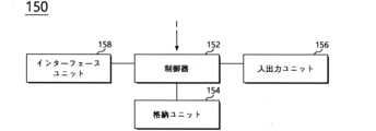
図3に示すように、本実施例のコンピュータ装置150は、制御器152、格納ユニット154、入出力ユニット156及びインターフェースユニット158を含むことができる。
As shown in FIG. 3, the
前記制御器152は、前記分析モジュール130から獲得された2次元イメージ(I)に基づいて多様な工程モニターリングデータが算出できる。このような算出作業は、所望の工程モニターリングデータの算出のために設計されたアルゴリズムによって駆動できる。本実施例の制御器152は、分析モジュール130から獲得された2次元イメージを時間順に積層/合成して、3次元イメージデータが生成できる。
The
格納ユニット154は、例えば、非揮発性記憶媒体を含むことができる。一例として、格納ユニット154は、ハードディスク及び/又は非揮発性半導体記憶素子(例えば、フラッシュメモリ素子、相変化記憶素子及び/又は磁気記憶素子等)を含むことができる。格納ユニット154は、前記分析モジュール130から獲得された2次元イメージ及び前記コンピュータ装置150で処理されたイメージデータ(例えば、各種パラメータ及び3次元イメージ)が格納できる。
The
入出力ユニット156は、キーボード(keyboard)、キーパッド(keypad)及び/又はディスプレイ装置(display device)を含むことができる。
The input/
2次元情報検査装置110から獲得されたイメージデータは、インターフェースユニット158によってコンピュータ装置150に伝達されることができる。また、コンピュータ装置150で処理されたデータは、インターフェースユニット158によって2次元情報検査装置110又は他の外部装置(一例として、データサーバやAPCサーバ)に伝達されることもできる。インターフェースユニット158は、有線要素、無線要素及び/又はUSB(universal serial bus)ポート等を含むことができる。制御器152、格納ユニット154、入出力ユニット156及びインターフェースユニット158は、データバス(data bus)を介して互いに結合されることができる。
Image data acquired from the 2D
さらに、図1を参照すれば、前記クリーニングモジュール180は、一定深さだけ一括エッチングされたウェーハ(w)の表面がクリーニングできる。クリーニングモジュール180は、湿式クリーニング装置又は乾式クリーニング装置が用いられる。
Further, referring to FIG. 1, the
図4は、本発明の一実施例に係る半導体素子の分析システムの動作を説明するためのフローチャートである。図5は、本発明の一実施例に係るウェーハのエッチング面を示す断面図である。図6は、図5のウェーハエッチング面の2次元情報を示す図である。図7は、本発明の一実施例に係る図6の2次元情報から生成された3次元イメージを示す図である。本実施例では、全面エッチングモジュール120がミリング装置である場合を一例として説明する。また、本実施例のウェーハ(w)は、複数のコンタクトプラグCT1~CT3が具備された状態を例として説明する。
Figure 4 is a flow chart for explaining the operation of a semiconductor device analysis system according to an embodiment of the present invention. Figure 5 is a cross-sectional view showing an etching surface of a wafer according to an embodiment of the present invention. Figure 6 is a diagram showing two-dimensional information of the etching surface of the wafer in Figure 5. Figure 7 is a diagram showing a three-dimensional image generated from the two-dimensional information in Figure 6 according to an embodiment of the present invention. In this embodiment, a case where the entire
図4及び図5に示すように、検査するウェーハ(w)が2次元情報検査装置110内に提供される。全面エッチングモジュール120は、前記ウェーハ(w)の全体の表面に向けて、イオンビームを一定エッチングターゲット深さで均一に照射する(S1)。例えば、先に、図5のA-A'の表面を1次ターゲット深さとしてイオンビームが照射される。イオンビームの照射によりウェーハ(w)の表面が一定深さだけスパッタリングエッチングできる。このとき、前記イオンビームによりウェーハ(w)がエッチングされる間、前記分析モジュール130内に含まれた質量分析器又はOES(Optical Emission Spectroscopy)によりエッチング副産物の量及び種類が測定され、前記エッチング副産物の量によって深さが制御できる。
As shown in Figures 4 and 5, a wafer (w) to be inspected is provided in a 2D
分析モジュール130を用いて、ウェーハ(w)の表面から放出されるイオン及び電子等の成分を測定して、エッチングされたウェーハ(w)の表面の2次元イメージを獲得する(S2)。イオンビームのミリング後、SEM装置、PEEM装置、プローブを用いた装置等のように多様な分析モジュール130を用いて、図6に示すように、エッチングされたウェーハ(w)の表面の2次元イメージを測定する。
The
次に、前記ウェーハ(w)の表面を図5のB-B'の表面をターゲット深さとしてイオンビームを照射するステップ、エッチングされたウェーハ(w)のB-B'の表面の2次元イメージを検出するステップ、前記ウェーハ(w)の表面を図5のC-C'の表面をターゲット深さとしてイオンビームを照射するステップ、及びエッチングされたウェーハ(w)のC-C'の表面の2次元イメージを検出するステップを繰り返し遂行できる。本実施例では、説明の便宜のために、A-A'、B-B'及びC-C'の表面をエッチングターゲット深さとして設定しただけで、より狭かったりより大きい間隔でターゲット深さが調整できる。2次元イメージを検出するステップ(S2)と、ウェーハの表面をエッチングするステップ(S1)との間にウェーハの表面をクリーニングするステップをさらに含むことができる。 Then, the steps of irradiating the surface of the wafer (w) with an ion beam using the surface B-B' in FIG. 5 as a target depth, detecting a two-dimensional image of the surface B-B' of the etched wafer (w), irradiating the surface of the wafer (w) with an ion beam using the surface C-C' in FIG. 5 as a target depth, and detecting a two-dimensional image of the surface C-C' of the etched wafer (w) can be repeatedly performed. In this embodiment, for the sake of convenience of explanation, the surfaces A-A', B-B', and C-C' are set as the etching target depths, but the target depth can be adjusted to a narrower or larger interval. A step of cleaning the surface of the wafer can be further included between the step of detecting the two-dimensional image (S2) and the step of etching the surface of the wafer (S1).
理論的には、A-A'の表面の2次元イメージと、B-B'の表面の2次元イメージと、C-C'の表面の2次元イメージとが同一であるべきである。しかしながら、工程進行上、特に高集積3D素子の場合、コンタクトプラグCT1~CT3のサイズ及び形状が不均一になり、コンタクトプラグCT1~CT3内にボイド(void)不良(v)が発生し得る。前記測定された2次元イメージは、測定の位置によって、内部不良及び形状不良が検出されることができるが、そうでないこともできる。さらに、前記2次元イメージ情報だけでは、高集積の半導体装置の3次元パターンの形状を予測し難い。 Theoretically, the 2D image of the A-A' surface, the 2D image of the B-B' surface, and the 2D image of the C-C' surface should be the same. However, during the process, especially in the case of highly integrated 3D devices, the size and shape of the contact plugs CT1 to CT3 may become non-uniform, which may result in void defects (v) occurring within the contact plugs CT1 to CT3. The measured 2D image may or may not detect internal defects and shape defects depending on the measurement position. Furthermore, it is difficult to predict the shape of the 3D pattern of a highly integrated semiconductor device using only the 2D image information.
本実施例によれば、前記コンピュータ装置150の制御器152を用いて、分析モジュール130で測定された2次元情報、例えば、2次元イメージを積層及び処理して3次元イメージデータが獲得できる(S3、図6参照)。前記制御器152は、前記分析モジュール130で測定された2次元情報をエッチング深さによってX-Y方向に区分して格納ユニット154に提供できる。より詳しくは、制御器152は、ウェーハの全面の2次元イメージを(X、Y)座標形態に区分して格納ユニット154に提供できる。また、制御器152は、エッチング深さ順に2次元情報データを区分して格納ユニット154に提供できる。図3には示さないが、制御器152内に別途のノイズ処理装置を備え、前記2次元イメージのノイズ成分をフィルターリングできる。
According to this embodiment, the
また、本実施例の制御器152は、エッチングターゲット深さによる2次元イメージのX-Y成分(又はX-Y座標)をアライン(align)して、前記2次元イメージを積層させることで、3次元輪郭イメージが抽出できる。これにより、ウェーハ(w)の断層イメージを通して、ウェーハ上に形成された3次元構造物の細部形態が予測できる。
In addition, the
一例として、図6のB-B'の表面における第3のコンタクトプラグCT3の断面イメージは、A-A'の表面及び/又はC-C'の表面における第3のコンタクトプラグCT3の断面積よりも相対的に小さく、一方側に偏っている。このような形態が検出された場合、図7に示すように、第3のコンタクトプラグCT3Iの3次元イメージは、中心深さ(例えばB-B'線に位置する部分)の直径が不均一な構造で復元される。これにより、コンピュータ装置150は、第3のコンタクトプラグCT3Iに形状不良、即ち物理的欠陥が発生したことが検出でき、さらに、第3のコンタクトプラグCT3Iのサイズ、コンタクトプラグCT1I~CT3I間の距離、コンタクトプラグCT1I~CT3Iの抵抗及びその外に予測される工程パラメータが異なるように算出できる。
As an example, the cross-sectional image of the third contact plug CT3 at the surface B-B' in FIG. 6 is relatively smaller than the cross-sectional area of the third contact plug CT3 at the surface A-A' and/or the surface C-C', and is biased to one side. If such a shape is detected, the three-dimensional image of the third contact plug CT3I is restored to a structure with a non-uniform diameter at the center depth (e.g., the portion located at the line B-B') as shown in FIG. 7. As a result, the
一例として、図6に示すように、C-C'の表面における第2のコンタクトプラグCT2の断面イメージがリング(ring)形態で検出されると、第2のコンタクトプラグCT2のC-C'の表面周囲にボイドが発生したことを確認でき、3次元的イメージも該当部分が異なる色相又は透明度で表示されることができる。本実施例のコンピュータ装置150の制御器152は、抽出された3次元輪郭イメージを回転及び変形(拡大又は縮小)させることができる。これにより、使用者が3次元輪郭イメージの形状及び内部欠陥が容易に判断できる。
As an example, as shown in FIG. 6, when the cross-sectional image of the second contact plug CT2 on the surface C-C' is detected in the form of a ring, it can be confirmed that a void has occurred around the surface C-C' of the second contact plug CT2, and the corresponding portion of the 3D image can also be displayed with a different color or transparency. In this embodiment, the
本実施例のコンピュータ装置150の制御器152は、エッチング厚さ及びX-Y方向(座標)によってウェーハ(w)結果物の全体の2次元イメージを全部格納している。これにより、前記入出力ユニット156からROI(Region Of Interest)のエッチング深さ及び(X、Y)座標が入力される場合、該ROIの該イメージを出力、回転及び変形させて使用者に提供できる。
The
図8は、本発明の他の実施例に係る分析モジュールを示すブロック図である。図9及び図10は、図8の分析モジュールを用いて半導体素子の分析方法を説明するための図である。 Figure 8 is a block diagram showing an analysis module according to another embodiment of the present invention. Figures 9 and 10 are diagrams for explaining a method of analyzing a semiconductor device using the analysis module of Figure 8.
図8に示すように、本実施例の分析モジュール130は、第1の分析ユニット135a及び第2の分析ユニット135bを含むことができる。第1の分析ユニット135aは、例えば、エッチングされた表面の物理的イメージを検出する装置、例えば、SEM装置を含むことができる。第2の分析ユニット135bは、例えば、エッチングされた表面の電気的特性を示す装置、例えば、PEEM装置又はEDX(Energy Dispersive X-ray analysis)装置を含むことができる。PEEM装置のような第2の分析ユニット135bは、不純物の濃度分布のような電気的特性が図式化できる。
As shown in FIG. 8, the
図8の分析モジュールを用いて半導体素子の分析方法については、図9及び図10を参照して詳細に説明する。 A method for analyzing semiconductor devices using the analysis module of Figure 8 will be described in detail with reference to Figures 9 and 10.
まず、前記ウェーハ結果物(<w0>)を用意する。前記ウェーハ結果物(<w0>)は、MOSトランジスタが形成されたウェーハ基板10構造物であり得る。前記MOSトランジスタは、公知のように、ウェーハ基板10上に形成されるゲート構造物、ソース20s及びドレイン20dを含むことができる。前記ゲート構造物は積層されたゲート絶縁膜12、ゲート15及びハードマスク膜17を含むことができる。前記ゲート構造物は、前記ゲート絶縁膜12、ゲート15及びハードマスク膜17の側壁に位置するスペーサー19をさらに含むことができる。前記ソース20s及びドレイン20dは、前記ゲート構造物の両側のウェーハ基板10内に形成されることができる。前記ウェーハ結果物(<w0>)は、前記MOSトランジスタをカバーする層間絶縁膜22及びコンタクト部25a、25b、25cをさらに含むことができる。前記コンタクト部25a、25b、25cは、前記層間絶縁膜22内に位置し、ゲート15、ソース20s及びドレイン20dと各々コンタクトされることができる。
First, the wafer result (<w0>) is prepared. The wafer result (<w0>) may be a
第1の分析ユニット135aにより、前記ウェーハ結果物(<w0>)の上部表面のイメージI0が測定される。前述したように、第1の分析ユニット135aは物理的イメージを検出する装置であるので、前記イメージI0は層間絶縁膜22及びコンタクト部25a、25b、25cが表示できる。前記イメージI0によってコンタクト部25a、25b、25cの形状及び位置のような物理的情報が確認できる。
The
次に、全面エッチングモジュール120を用いて、ウェーハ(w)を第1のターゲット深さ(da)だけエッチングして、ウェーハ(w)の第1の表面a-a'を露出させる。前記第1のターゲット深さ(da)は、例えば、前記ウェーハ結果物(<w0>)の表面からハードマスク膜17の表面までの深さであり得る。その後、第1の分析ユニット135aにより露出されたウェーハ(w)の第1の表面a-a'の物理的イメージIaが測定される。前記ウェーハ(w)の第1の表面a-a'の物理的イメージIaは、互いに異なる物性を持つ層間絶縁膜22、コンタクト部25a、25b、25c及びハードマスク膜17の形状及び位置が表示できる。
Next, the wafer (w) is etched to a first target depth (da) using the
前記全面エッチングモジュール120を用いて、ウェーハ(w)を第2のターゲット深さ(db)だけエッチングして、ウェーハ(w)の第2の表面b-b'を露出させる。前記第2のターゲット深さ(db)は、前記ゲート15の所定部分を露出させることができる深さであり得る。その後、第1の分析ユニット135aにより露出されたウェーハ(w)の第2の表面b-b'の物理的イメージIbが測定される。前記ウェーハ(w)の第2の表面b-b'の物理的イメージIbは、互いに異なる物性を持つ層間絶縁膜22、コンタクト部25b、25c、ゲート15及び側壁スペーサー19の形状及び位置が表示できる。
The wafer (w) is etched to a second target depth (db) using the
前記全面エッチングモジュール120を用いて、ウェーハ(w)を第3のターゲット深さ(dc)だけエッチングして、ウェーハ(w)の第3の表面c-c'を露出させる。前記第3のターゲット深さ(dc)は、前記ウェーハ基板10の表面を露出させることができる深さであり得る。第1及び第2の分析ユニット135a、135bにより、ウェーハ(w)の第3の表面c-c'の物理的イメージIc及び電気的イメージIEcを測定する。前記第1の分析ユニット135aによって測定された2次元物理的イメージIcは、物性が異なるウェーハ基板10、ソース20s及びドレイン20dの形状及び位置が表示できる。一方、第2の分析ユニット135bによって測定された2次元電気的イメージIEcは、ソース20s及びドレイン20dの位置は勿論、不純物の濃度分布まで表示できる。前記2次元電気的イメージIEcによれば、前記ソース20s及びドレイン20dは、ガウス分布によって端部に行くほど不純物濃度が低くなることが観察できる。
The wafer (w) is etched by the third target depth (dc) using the
前記全面エッチングモジュール120を用いて、ウェーハ(w)を第4のターゲット深さ(dd)だけエッチングして、ウェーハ(w)の第4の表面d-d'を露出させる。前記第4のターゲット深さ(dd)は、例えば、ソース20s及びドレイン20dの底面を露出させることができる深さであり得る。第1及び第2の分析ユニット135a、135bにより、ウェーハ(w)の第4の表面d-d'の物理的イメージId及び電気的イメージIEdを測定する。前記第1の分析ユニット135aによって測定された2次元物理的イメージIdは、ソース20s及びドレイン20dとウェーハ基板10との物性差による形状及び位置が表示できる。前記ソース20s及びドレイン20dは不純物領域であるため、ガウス分布によって下部に行くほどドーピング濃度が減少し、その線幅も減少する。これにより、ウェーハ(w)の第4の表面d-d'で露出されるソース20s及びドレイン20dの線幅は、ウェーハ(w)の第3の表面c-c'で露出されるソース20s及びドレイン20dの線幅よりも小さい。一方、第2の分析ユニット135bによって測定された2次元電気的イメージIEdは、ソース20s及びドレイン20dの濃度分布が表示できる。前記イメージIEdにより、ウェーハ(w)の第4の表面d-d'で露出されるソース20s及びドレイン20dの不純物濃度が、ウェーハ(w)の第3の表面c-c'で露出されるソース20s及びドレイン20dの不純物濃度よりも低いことが観察できる。
The wafer (w) is etched to a fourth target depth (dd) using the
コンピュータ装置150、特に、コンピュータ装置150の制御器152は、分析モジュール130から得られた前記2次元イメージI0、Ia、Ib、Ic、Id、IEc、IEdを集合する。次に、前記制御器152は、前記2次元イメージを時系列的に積層して、図10に示すように、実際素子(a)に対応する3次元構造物イメージ(b)が生成できる。また、本実施例では、第1の分析ユニット135aによって得られた2次元物理的イメージI0、Ia、Ib、Ic、Id及び第2の分析ユニット135bによって得られた2次元電気的イメージIEc、IEdの合成により、素子を構成する各成分等の形状及び位置分布は勿論、電気的特性分布まで3次元イメージとして表示できる。したがって、3次元イメージにより、半導体素子等の3次元的な形状欠陥及び内部欠陥の判断が容易になる。
The
図11は、本発明の他の実施例に係る半導体素子の分析システムを示す概略ブロック図である。 Figure 11 is a schematic block diagram showing a semiconductor device analysis system according to another embodiment of the present invention.
図11に示すように、半導体素子の分析システム100aを構成する各モジュール、例えば、全面エッチングモジュール120、分析モジュール130、コンピュータ装置150及びクリーニングモジュール180は、ロードロック(load lock)190を基準としてクラスター(Cluster)形態で構成されることができる。
As shown in FIG. 11, each module constituting the semiconductor
全面エッチングモジュール120、分析モジュール130、コンピュータ装置150及びクリーニングモジュール180をクラスター方式によりシステム化することで、検査効率の改善を図ることができる。
By systemizing the full
本実施例に係る半導体素子の分析システムは、ウェーハ全面に対して一定深さだけ同一のエッチング速度でエッチングした後、エッチングされたウェーハの表面の2次元イメージを測定する。また、半導体素子の分析システムは、前記測定された2次元イメージを時系列的に積層して3次元イメージを生成する。本発明の分析システムは、2次元イメージを集合して得られた3次元イメージにより、高集積3D素子で発生できる3次元不良及び内部不良が容易に検出できる。 The semiconductor device analysis system according to this embodiment etches the entire surface of the wafer to a constant depth at a uniform etching rate, and then measures a two-dimensional image of the etched wafer surface. The semiconductor device analysis system also stacks the measured two-dimensional images in a time series manner to generate a three-dimensional image. The analysis system of the present invention can easily detect three-dimensional defects and internal defects that can occur in highly integrated 3D devices using a three-dimensional image obtained by aggregating two-dimensional images.
以上、本発明の好適な実施例により詳細に説明したが、本発明は、前記実施例に限定されず、本発明の技術的思想から逸脱しない範囲内において、当分野における通常の知識を有した者によって多様な変形が可能である。 The present invention has been described in detail above with reference to preferred embodiments, but the present invention is not limited to the above embodiments, and various modifications can be made by those with ordinary skill in the art without departing from the technical concept of the present invention.
Claims (17)
繰り返しエッチングされた前記ウェーハの表面から2次元構造情報を取得する分析モジュール;及び、
前記分析モジュールから繰り返し獲得した前記2次元構造情報を時系列的に積層処理して、3次元イメージを再構成するコンピュータ装置を含み、
前記分析モジュールは、
前記エッチングされたウェーハの表面の物理的イメージを獲得する第1の分析ユニット;及び、
前記エッチングされたウェーハの表面の電気的イメージを獲得する第2の分析ユニットを含む、半導体素子の分析システム。 a full surface etching module for etching the entire surface of the wafer at the same etching rate to a depth where the analyte is present;
an analysis module for acquiring two-dimensional structural information from a surface of the repeatedly etched wafer; and
a computer device for reconstructing a three-dimensional image by stacking the two-dimensional structural information repeatedly acquired from the analysis module in a time series manner ;
The analysis module includes:
a first analysis unit for acquiring a physical image of the surface of the etched wafer; and
a second analysis unit for acquiring an electrical image of the surface of the etched wafer ;
前記ウェーハを支持するステージ;及び、
前記ウェーハの表面の回路層が同一のエッチング速度でエッチングされるように、前記ウェーハの全面に対してイオンビームを照射するイオンビーム照射部を含む、請求項1に記載の半導体素子の分析システム。 The full surface etching module includes:
a stage for supporting the wafer; and
2. The system for analyzing a semiconductor device according to claim 1, further comprising an ion beam irradiation unit that irradiates an ion beam onto an entire surface of the wafer so that a circuit layer on the front surface of the wafer is etched at a uniform etching rate.
前記コンピュータ装置は、
前記分析モジュールから提供される前記2次元イメージをエッチング深さ及び(X、Y)座標の形態で区分し、前記エッチング深さ及び前記(X、Y)座標値に基づいて、前記2次元イメージを時系列的に積層して前記3次元イメージを再生成する制御器;及び、
前記制御器により区分された2次元イメージを格納する格納ユニットを含む、請求項1に記載の半導体素子の分析システム。 the repeatedly obtained two-dimensional structural information includes a two-dimensional image;
The computer device comprises:
a controller for dividing the two-dimensional image provided from the analysis module into the form of an etching depth and an (X, Y) coordinate, and regenerating the three-dimensional image by stacking the two-dimensional images in a time series based on the etching depth and the (X, Y) coordinate; and
2. The system for analyzing a semiconductor device according to claim 1, further comprising a storage unit for storing the two-dimensional image divided by the controller.
前記全面エッチングモジュール、前記分析モジュール及び前記クリーニングモジュールは、前記ロードロックを基準としてクラスター形態で連結する、請求項10に記載の半導体素子の分析システム。 a load lock in which the wafers to be processed wait;
The system for analyzing a semiconductor device according to claim 10 , wherein the blanket etching module, the analysis module, and the cleaning module are connected in a cluster form with respect to the load lock.
前記エッチングターゲット深さだけ繰り返しエッチングされた前記ウェーハの表面の2次元構造情報を各々獲得するステップ;及び、
繰り返し獲得した前記2次元構造情報を時系列的に積層及び処理して3次元イメージを生成するステップを含み、
前記2次元構造情報を繰り返し獲得するステップは、
前記ウェーハの表面の2次元物理構造情報を獲得するステップ;及び、
前記ウェーハの表面の2次元電気構造情報を獲得するステップを含む、半導体素子の分析方法。 repeatedly etching the entire surface of the wafer at the same etch rate to a set etch target depth to expose a next surface of the wafer;
acquiring two-dimensional structure information of the surface of the wafer repeatedly etched to the etching target depth; and
generating a three-dimensional image by sequentially stacking and processing the two-dimensional structural information repeatedly obtained;
The step of repeatedly acquiring two-dimensional structural information includes:
acquiring two-dimensional physical structure information of a surface of the wafer; and
A method for analyzing a semiconductor device comprising the step of acquiring two-dimensional electrical structure information of a surface of said wafer .
前記2次元構造情報を繰り返し獲得するステップは、
前記ウェーハのエッチングターゲット深さ別に前記2次元イメージを(X、Y)座標形態で区分するステップ;及び、
前記エッチングターゲット深さ及び前記(X、Y)座標に基づいて、前記繰り返し獲得された2次元イメージを連続積層及び処理するステップを含む、請求項13に記載の半導体素子の分析方法。 the repeatedly obtained two-dimensional structural information includes a two-dimensional image;
The step of repeatedly acquiring two-dimensional structural information includes:
dividing the two-dimensional image in the form of (X, Y) coordinates according to etching target depths of the wafer; and
The method of claim 13 , further comprising the step of sequentially stacking and processing the repeatedly acquired two-dimensional images based on the etching target depth and the (X, Y) coordinates.
Applications Claiming Priority (2)
| Application Number | Priority Date | Filing Date | Title |
|---|---|---|---|
| KR10-2019-0088824 | 2019-07-23 | ||
| KR1020190088824A KR102705854B1 (en) | 2019-07-23 | Analyzing System for Semiconductor Device and Method of Analyzing the Semiconductor Device |
Publications (2)
| Publication Number | Publication Date |
|---|---|
| JP2021019179A JP2021019179A (en) | 2021-02-15 |
| JP7520501B2 true JP7520501B2 (en) | 2024-07-23 |
Family
ID=74189553
Family Applications (1)
| Application Number | Title | Priority Date | Filing Date |
|---|---|---|---|
| JP2019224666A Active JP7520501B2 (en) | 2019-07-23 | 2019-12-12 | System and method for analyzing semiconductor devices |
Country Status (3)
| Country | Link |
|---|---|
| US (2) | US11295970B2 (en) |
| JP (1) | JP7520501B2 (en) |
| CN (1) | CN112309890A (en) |
Families Citing this family (3)
| Publication number | Priority date | Publication date | Assignee | Title |
|---|---|---|---|---|
| CN111857111B (en) * | 2019-04-09 | 2024-07-19 | 商汤集团有限公司 | Object three-dimensional detection and intelligent driving control method, device, medium and equipment |
| WO2021083551A1 (en) * | 2019-10-30 | 2021-05-06 | Carl Zeiss Smt Gmbh | Contact area size determination between 3d structures in an integrated semiconductor sample |
| CN114646638A (en) * | 2022-04-12 | 2022-06-21 | 中国电子产品可靠性与环境试验研究所((工业和信息化部电子第五研究所)(中国赛宝实验室)) | Chip failure analysis positioning method, device, equipment and storage medium |
Citations (3)
| Publication number | Priority date | Publication date | Assignee | Title |
|---|---|---|---|---|
| JP2004045172A (en) | 2002-07-11 | 2004-02-12 | Fujitsu Ltd | Method for evaluating three-dimensional structure |
| JP2018152330A (en) | 2017-02-16 | 2018-09-27 | カール ツァイス マイクロスコーピー ゲーエムベーハーCarl Zeiss Microscopy GmbH | Method of analyzing object and charged particle beam device foe executing this method |
| JP2019078684A (en) | 2017-10-26 | 2019-05-23 | 信越半導体株式会社 | Silicon wafer metal impurity analysis method |
Family Cites Families (10)
| Publication number | Priority date | Publication date | Assignee | Title |
|---|---|---|---|---|
| US6317514B1 (en) | 1998-09-09 | 2001-11-13 | Applied Materials, Inc. | Method and apparatus for inspection of patterned semiconductor wafers |
| US6979819B2 (en) | 2001-11-30 | 2005-12-27 | Kla-Tencor Technologies Corporation | Photoelectron emission microscope for wafer and reticle inspection |
| US9698062B2 (en) * | 2013-02-28 | 2017-07-04 | Veeco Precision Surface Processing Llc | System and method for performing a wet etching process |
| KR101913020B1 (en) | 2014-03-25 | 2018-10-29 | 칼 짜이스 에스엠에스 엘티디 | Method and apparatus for generating a predetermined three-dimensional contour of an optical component and/or a wafer |
| KR102257901B1 (en) | 2014-09-19 | 2021-05-31 | 삼성전자주식회사 | Semiconductor inspection system and a method of inspecing a semiconductor device using the same |
| KR102410666B1 (en) | 2015-01-09 | 2022-06-20 | 삼성전자주식회사 | A method of inspecing a semiconductor device, and a method of a semiconductor device using the same |
| WO2018017677A1 (en) * | 2016-07-19 | 2018-01-25 | Tokyo Electron Limited | Three-dimensional semiconductor device and method of fabrication |
| KR102369851B1 (en) * | 2016-08-08 | 2022-03-02 | 도쿄엘렉트론가부시키가이샤 | 3D semiconductor device and manufacturing method |
| US10847376B2 (en) * | 2018-06-28 | 2020-11-24 | Sandisk Technologies Llc | In-situ deposition and etch process and apparatus for precision patterning of semiconductor devices |
| US11018063B2 (en) * | 2018-11-26 | 2021-05-25 | Sandisk Technologies Llc | Method and apparatus for nanoscale-dimension measurement using a diffraction pattern filter |
-
2019
- 2019-10-29 US US16/667,499 patent/US11295970B2/en active Active
- 2019-11-11 CN CN201911094467.6A patent/CN112309890A/en active Pending
- 2019-12-12 JP JP2019224666A patent/JP7520501B2/en active Active
-
2022
- 2022-02-25 US US17/681,201 patent/US11626306B2/en active Active
Patent Citations (3)
| Publication number | Priority date | Publication date | Assignee | Title |
|---|---|---|---|---|
| JP2004045172A (en) | 2002-07-11 | 2004-02-12 | Fujitsu Ltd | Method for evaluating three-dimensional structure |
| JP2018152330A (en) | 2017-02-16 | 2018-09-27 | カール ツァイス マイクロスコーピー ゲーエムベーハーCarl Zeiss Microscopy GmbH | Method of analyzing object and charged particle beam device foe executing this method |
| JP2019078684A (en) | 2017-10-26 | 2019-05-23 | 信越半導体株式会社 | Silicon wafer metal impurity analysis method |
Also Published As
| Publication number | Publication date |
|---|---|
| US20210028033A1 (en) | 2021-01-28 |
| JP2021019179A (en) | 2021-02-15 |
| KR20210011657A (en) | 2021-02-02 |
| US20220277975A1 (en) | 2022-09-01 |
| US11295970B2 (en) | 2022-04-05 |
| US11626306B2 (en) | 2023-04-11 |
| CN112309890A (en) | 2021-02-02 |
Similar Documents
| Publication | Publication Date | Title |
|---|---|---|
| JP7520501B2 (en) | System and method for analyzing semiconductor devices | |
| Ma et al. | Metrology and Diagnostic Techniques for Nanoelectronics | |
| CN115280463A (en) | Method for imaging a cross-section of an examination volume in a wafer | |
| JP6356397B2 (en) | Substrate outside position analysis system and method | |
| JP6188792B2 (en) | Preparation of slices for TEM observation | |
| JP4440647B2 (en) | Method and system for repairing defects | |
| JP5647603B2 (en) | Method for creating a tomogram of processed features and method for generating an image of one or more processed features | |
| US10101246B2 (en) | Method of preparing a plan-view transmission electron microscope sample used in an integrated circuit analysis | |
| TW202104841A (en) | Methods and systems for combining x-ray metrology data sets to improve parameter estimation | |
| CN110865518B (en) | Method and apparatus for detecting overlay of upper and lower layers of a wafer | |
| KR102301793B1 (en) | Image creating metohd and imaging system for performing the same | |
| Nakamae | Electron microscopy in semiconductor inspection | |
| WO2021224435A1 (en) | Image enhancement for multi-layered structure in charged-particle beam inspection | |
| KR102705854B1 (en) | Analyzing System for Semiconductor Device and Method of Analyzing the Semiconductor Device | |
| Zudhistira et al. | Integration of probing capability into plasma FIB for in-situ Delayering, defect inspection, and EBAC on BEOL defects of sub-20nm FinFET devices | |
| Bunday et al. | Metrology | |
| TW202044313A (en) | Imaging method and imaging system | |
| Nowakowski et al. | An innovative technique for large-scale delayering of semiconductor devices with nanometric-scale surface flatness | |
| US8648299B2 (en) | Isotope ion microscope methods and systems | |
| Maitra et al. | Microstructural Investigation and Serial Section Tomography on ASIC Chips for Assurance Through Reverse Engineering Applications | |
| TW202405861A (en) | E-beam optimization for overlay measurement of buried features | |
| Narang et al. | Die-Level Roadmap: Post-Isolation Domain | |
| TW202407336A (en) | Parameterizing x-ray scattering measurement using slice-and-image tomographic imaging of semiconductor structures | |
| Hashimoto et al. | Tolerance-based wafer verification methodologies with a die-to-database inspection system | |
| US20140342477A1 (en) | Method of monitoring semiconductor fabrication process using xps |
Legal Events
| Date | Code | Title | Description |
|---|---|---|---|
| A621 | Written request for application examination |
Free format text: JAPANESE INTERMEDIATE CODE: A621 Effective date: 20221108 |
|
| A977 | Report on retrieval |
Free format text: JAPANESE INTERMEDIATE CODE: A971007 Effective date: 20231218 |
|
| A131 | Notification of reasons for refusal |
Free format text: JAPANESE INTERMEDIATE CODE: A131 Effective date: 20240130 |
|
| A521 | Request for written amendment filed |
Free format text: JAPANESE INTERMEDIATE CODE: A523 Effective date: 20240423 |
|
| TRDD | Decision of grant or rejection written | ||
| A01 | Written decision to grant a patent or to grant a registration (utility model) |
Free format text: JAPANESE INTERMEDIATE CODE: A01 Effective date: 20240625 |
|
| A61 | First payment of annual fees (during grant procedure) |
Free format text: JAPANESE INTERMEDIATE CODE: A61 Effective date: 20240710 |
|
| R150 | Certificate of patent or registration of utility model |
Ref document number: 7520501 Country of ref document: JP Free format text: JAPANESE INTERMEDIATE CODE: R150 |