KR101913020B1 - Method and apparatus for generating a predetermined three-dimensional contour of an optical component and/or a wafer - Google Patents
Method and apparatus for generating a predetermined three-dimensional contour of an optical component and/or a wafer Download PDFInfo
- Publication number
- KR101913020B1 KR101913020B1 KR1020167028830A KR20167028830A KR101913020B1 KR 101913020 B1 KR101913020 B1 KR 101913020B1 KR 1020167028830 A KR1020167028830 A KR 1020167028830A KR 20167028830 A KR20167028830 A KR 20167028830A KR 101913020 B1 KR101913020 B1 KR 101913020B1
- Authority
- KR
- South Korea
- Prior art keywords
- wafer
- optical component
- dimensional
- laser
- predetermined
- Prior art date
Links
Images


Classifications
-
- G—PHYSICS
- G03—PHOTOGRAPHY; CINEMATOGRAPHY; ANALOGOUS TECHNIQUES USING WAVES OTHER THAN OPTICAL WAVES; ELECTROGRAPHY; HOLOGRAPHY
- G03F—PHOTOMECHANICAL PRODUCTION OF TEXTURED OR PATTERNED SURFACES, e.g. FOR PRINTING, FOR PROCESSING OF SEMICONDUCTOR DEVICES; MATERIALS THEREFOR; ORIGINALS THEREFOR; APPARATUS SPECIALLY ADAPTED THEREFOR
- G03F7/00—Photomechanical, e.g. photolithographic, production of textured or patterned surfaces, e.g. printing surfaces; Materials therefor, e.g. comprising photoresists; Apparatus specially adapted therefor
- G03F7/70—Microphotolithographic exposure; Apparatus therefor
- G03F7/70216—Mask projection systems
- G03F7/70283—Mask effects on the imaging process
-
- G—PHYSICS
- G03—PHOTOGRAPHY; CINEMATOGRAPHY; ANALOGOUS TECHNIQUES USING WAVES OTHER THAN OPTICAL WAVES; ELECTROGRAPHY; HOLOGRAPHY
- G03F—PHOTOMECHANICAL PRODUCTION OF TEXTURED OR PATTERNED SURFACES, e.g. FOR PRINTING, FOR PROCESSING OF SEMICONDUCTOR DEVICES; MATERIALS THEREFOR; ORIGINALS THEREFOR; APPARATUS SPECIALLY ADAPTED THEREFOR
- G03F7/00—Photomechanical, e.g. photolithographic, production of textured or patterned surfaces, e.g. printing surfaces; Materials therefor, e.g. comprising photoresists; Apparatus specially adapted therefor
- G03F7/70—Microphotolithographic exposure; Apparatus therefor
- G03F7/70483—Information management; Active and passive control; Testing; Wafer monitoring, e.g. pattern monitoring
- G03F7/70591—Testing optical components
-
- G—PHYSICS
- G03—PHOTOGRAPHY; CINEMATOGRAPHY; ANALOGOUS TECHNIQUES USING WAVES OTHER THAN OPTICAL WAVES; ELECTROGRAPHY; HOLOGRAPHY
- G03F—PHOTOMECHANICAL PRODUCTION OF TEXTURED OR PATTERNED SURFACES, e.g. FOR PRINTING, FOR PROCESSING OF SEMICONDUCTOR DEVICES; MATERIALS THEREFOR; ORIGINALS THEREFOR; APPARATUS SPECIALLY ADAPTED THEREFOR
- G03F1/00—Originals for photomechanical production of textured or patterned surfaces, e.g., masks, photo-masks, reticles; Mask blanks or pellicles therefor; Containers specially adapted therefor; Preparation thereof
- G03F1/60—Substrates
-
- G—PHYSICS
- G03—PHOTOGRAPHY; CINEMATOGRAPHY; ANALOGOUS TECHNIQUES USING WAVES OTHER THAN OPTICAL WAVES; ELECTROGRAPHY; HOLOGRAPHY
- G03F—PHOTOMECHANICAL PRODUCTION OF TEXTURED OR PATTERNED SURFACES, e.g. FOR PRINTING, FOR PROCESSING OF SEMICONDUCTOR DEVICES; MATERIALS THEREFOR; ORIGINALS THEREFOR; APPARATUS SPECIALLY ADAPTED THEREFOR
- G03F1/00—Originals for photomechanical production of textured or patterned surfaces, e.g., masks, photo-masks, reticles; Mask blanks or pellicles therefor; Containers specially adapted therefor; Preparation thereof
- G03F1/68—Preparation processes not covered by groups G03F1/20 - G03F1/50
- G03F1/72—Repair or correction of mask defects
-
- G—PHYSICS
- G03—PHOTOGRAPHY; CINEMATOGRAPHY; ANALOGOUS TECHNIQUES USING WAVES OTHER THAN OPTICAL WAVES; ELECTROGRAPHY; HOLOGRAPHY
- G03F—PHOTOMECHANICAL PRODUCTION OF TEXTURED OR PATTERNED SURFACES, e.g. FOR PRINTING, FOR PROCESSING OF SEMICONDUCTOR DEVICES; MATERIALS THEREFOR; ORIGINALS THEREFOR; APPARATUS SPECIALLY ADAPTED THEREFOR
- G03F7/00—Photomechanical, e.g. photolithographic, production of textured or patterned surfaces, e.g. printing surfaces; Materials therefor, e.g. comprising photoresists; Apparatus specially adapted therefor
- G03F7/0002—Lithographic processes using patterning methods other than those involving the exposure to radiation, e.g. by stamping
-
- G—PHYSICS
- G03—PHOTOGRAPHY; CINEMATOGRAPHY; ANALOGOUS TECHNIQUES USING WAVES OTHER THAN OPTICAL WAVES; ELECTROGRAPHY; HOLOGRAPHY
- G03F—PHOTOMECHANICAL PRODUCTION OF TEXTURED OR PATTERNED SURFACES, e.g. FOR PRINTING, FOR PROCESSING OF SEMICONDUCTOR DEVICES; MATERIALS THEREFOR; ORIGINALS THEREFOR; APPARATUS SPECIALLY ADAPTED THEREFOR
- G03F7/00—Photomechanical, e.g. photolithographic, production of textured or patterned surfaces, e.g. printing surfaces; Materials therefor, e.g. comprising photoresists; Apparatus specially adapted therefor
- G03F7/70—Microphotolithographic exposure; Apparatus therefor
- G03F7/70216—Mask projection systems
- G03F7/70316—Details of optical elements, e.g. of Bragg reflectors, extreme ultraviolet [EUV] multilayer or bilayer mirrors or diffractive optical elements
-
- G—PHYSICS
- G21—NUCLEAR PHYSICS; NUCLEAR ENGINEERING
- G21K—TECHNIQUES FOR HANDLING PARTICLES OR IONISING RADIATION NOT OTHERWISE PROVIDED FOR; IRRADIATION DEVICES; GAMMA RAY OR X-RAY MICROSCOPES
- G21K1/00—Arrangements for handling particles or ionising radiation, e.g. focusing or moderating
- G21K1/06—Arrangements for handling particles or ionising radiation, e.g. focusing or moderating using diffraction, refraction or reflection, e.g. monochromators
- G21K1/062—Devices having a multilayer structure
-
- H—ELECTRICITY
- H01—ELECTRIC ELEMENTS
- H01L—SEMICONDUCTOR DEVICES NOT COVERED BY CLASS H10
- H01L22/00—Testing or measuring during manufacture or treatment; Reliability measurements, i.e. testing of parts without further processing to modify the parts as such; Structural arrangements therefor
- H01L22/10—Measuring as part of the manufacturing process
- H01L22/12—Measuring as part of the manufacturing process for structural parameters, e.g. thickness, line width, refractive index, temperature, warp, bond strength, defects, optical inspection, electrical measurement of structural dimensions, metallurgic measurement of diffusions
-
- H—ELECTRICITY
- H01—ELECTRIC ELEMENTS
- H01L—SEMICONDUCTOR DEVICES NOT COVERED BY CLASS H10
- H01L22/00—Testing or measuring during manufacture or treatment; Reliability measurements, i.e. testing of parts without further processing to modify the parts as such; Structural arrangements therefor
- H01L22/20—Sequence of activities consisting of a plurality of measurements, corrections, marking or sorting steps
-
- B—PERFORMING OPERATIONS; TRANSPORTING
- B82—NANOTECHNOLOGY
- B82Y—SPECIFIC USES OR APPLICATIONS OF NANOSTRUCTURES; MEASUREMENT OR ANALYSIS OF NANOSTRUCTURES; MANUFACTURE OR TREATMENT OF NANOSTRUCTURES
- B82Y40/00—Manufacture or treatment of nanostructures
Abstract
본 발명은 구성 부품 및/또는 웨이퍼의 미리 정해진 3차원 윤곽을 생성하는 방법에 관한 것이며, 이 방법은, (a) 상기 미리 정해진 3차원 윤곽으로부터 상기 구성 부품 및/또는 상기 웨이퍼의 기존 3차원 윤곽의 편차를 결정하는 단계; (b) 상기 미리 정해진 3차원 윤곽으로부터 상기 3차원 윤곽의 상기 결정된 기존 편차를 정정하기 위한 레이저 펄스를 정의하는 하나 이상의 파라미터 세트를 갖는 적어도 하나의 3차원 배열의 레이저 펄스를 계산하는 단계; 및 (c) 상기 미리 정해진 3차원 윤곽을 생성하기 위해, 계산된 적어도 하나의 3차원 배열의 레이저 펄스를 상기 광학 부품 및/또는 상기 웨이퍼에 가하는 단계를 포함한다.The present invention relates to a method of generating a predetermined three-dimensional contour of a component and / or a wafer, the method comprising the steps of: (a) extracting from the predetermined three-dimensional contour the component and / Determining a deviation of the first signal; (b) calculating a laser pulse of at least one three-dimensional array having at least one parameter set defining a laser pulse for correcting said determined existing deviation of said three-dimensional contour from said predetermined three-dimensional contour; And (c) applying a computed laser pulse of at least one three-dimensional array to the optical component and / or the wafer to produce the predetermined three-dimensional contour.
Description
본 발명은 광학 부품 및/또는 웨이퍼의 미리 정해진 3차원 윤곽을 생성하는 분야에 관한 것이다.The present invention relates to the field of generating a predetermined three-dimensional contour of an optical component and / or a wafer.
광학 시스템은 그 성능에 대해서 증가하는 요구를 충족해야 한다. 예를 들어, 먼 거리에 위치하는 물체로부터 발생된 제한된 수의 광자를 수집하기 위해, 망원경의 광학 부품의 크기가 꾸준히 증가하고 있다. 광학 부품이 그 사전 정의된 표면 형태에서 약간 벗어나면 망원경 또는 일반적으로 광학 시스템의 광학 성능이 감소하게 된다.Optical systems must meet increasing demands for their performance. For example, in order to collect a limited number of photons from a distant object, the size of the optics of the telescope is steadily increasing. A slight deviation of the optical component from its predefined surface morphology results in a reduction in the optical performance of the telescope or generally the optical system.
한편, 망원경은 예를 들어 그 주위에 비해 매우 낮은 콘트라스트를 갖는 개체를 해상해야 한다. 또한, 리소그래피 장치의 투영 시스템은 더 작은 구조물을 해상하는 것이 요구된다.On the other hand, the telescope has to resolve an object with a very low contrast, for example around its periphery. In addition, the projection system of a lithographic apparatus is required to resolve smaller structures.
집적 회로(IC)도, 꾸준히 증가하는 요구를 충족해야 하는 또 다른 종류의 장치이다. 무어의 법칙(Moore's law)에 따르면, IC를 제조하기 위해 웨이퍼 상에 형성되는 구성 요소의 최소 치수가 계속 감소된다.Integrated circuits (ICs) are another type of device that must meet ever-increasing demands. According to Moore's law, the minimum dimensions of the components formed on the wafer to manufacture the IC are continuously reduced.
이하에서, 광학 시스템의 수요 증가는 투영 시스템, 특히 포토리소그래피 투영 노광 시스템에 대해서 예시된다.Hereinafter, an increase in demand of the optical system is exemplified for a projection system, particularly a photolithographic projection exposure system.
반도체 산업에서 집적도가 지속적으로 증가하는 결과로서, 포토리소그래피 투영 노광 시스템 및 포토리소그래픽 마스크는 웨이퍼 상에 배치된 포토 레지스트 상에 더 작은 구조물을 투영한다. 이러한 요구를 충족하기 위해서, 투영 노광 시스템의 노광 파장은, 전자기 스펙트럼의 근 자외선으로부터 평균 자외선을 거쳐 깊은 자외선 영역으로 시프트된다. 현재, 193 nm의 파장은 일반적으로 웨이퍼상의 포토 레지스트의 노광에 사용된다.As a result of the continued increase in the degree of integration in the semiconductor industry, photolithographic projection exposure systems and photolithographic masks project smaller structures onto the photoresist disposed on the wafer. To meet this need, the exposure wavelength of the projection exposure system is shifted from near-ultraviolet to near-ultraviolet in the electromagnetic spectrum into deep ultraviolet regions. Currently, a wavelength of 193 nm is generally used for exposure of photoresist on a wafer.
그 결과, 투영 노광 시스템의 광학 부품의 제조는 점점 더 복잡해지므로 점점 더 비싸지고 있다. 미래에, 투영 노광 시스템은 전자기 스펙트럼의 극 자외선(EUV)의 파장 범위에서 매우 짧은 파형 길이를 사용한다(예를 들면, 10nm ~ 15 nm의 범위).As a result, the manufacture of optical components in projection exposure systems becomes increasingly more complex and increasingly expensive. In the future, projection exposure systems use very short wave lengths in the extreme ultraviolet (EUV) wavelength range of the electromagnetic spectrum (e.g., in the range of 10 nm to 15 nm).
이러한 파장 범위에서, 예를 들어 미러 또는 포토리소그래픽 마스크로서의, EUV 광학 소자는, 평면성, 순도 및 온도 안정성에 대해 가장 높은 요구를 만족해야 한다. 평면성에 관한 이들 광학 소자의 기판의 허용 가능한 편차는, 기판의 표면 상에 배치된 다층 구조물에서 반사된 전자기파의 파면을 크게 방해하지 않도록 하는 노광 파장의 일부일 뿐이다. EUV 미러와 마스크의 기판의 평면성의 더 큰 편차는, 웨이퍼의 포토레지스트에서 파면의(부분) 보강 또는 상쇄 추가로 인해 포토 레지스트의 광 강도 분포의 변화를 가져 올 수 있다. 웨이퍼의 추가 처리시에, 광 강도의 변화로 인해서 예를 들면, 결함이 있는 IC와 같은 반도체 장치가 제조 될 수 있다.In this wavelength range, the EUV optical element, for example as a mirror or photolithographic mask, must meet the highest demands for planarity, purity and temperature stability. The allowable deviation of the substrate of these optical elements with respect to planarity is only a fraction of the exposure wavelength that does not significantly interfere with the wavefront of the electromagnetic waves reflected in the multilayer structure disposed on the surface of the substrate. A larger deviation of the planarity of the substrate of the EUV mirror and the mask may result in a change in the light intensity distribution of the photoresist due to (partial) reinforcement or offset addition of the wavefront in the photoresist of the wafer. Upon further processing of the wafer, a semiconductor device such as a defective IC can be manufactured due to a change in light intensity, for example.
제조사에서 공급되는 EUV 기판도 EUV 미러와 마스크의 평면성 조건을 충족하지 않을 수 있다. 또한, 다층 구조물을 형성하고 이 다층 구조물의 일 면상에 미세 패턴을 형성하는 미러 및 마스크의 제조 공정은, 각각 기판의 평탄성을 저하시킬 수 있다.The EUV substrate supplied by the manufacturer may not satisfy the planarity condition of the EUV mirror and the mask. Further, the manufacturing process of the mirror and the mask for forming the multilayered structure and forming the fine pattern on one side of the multilayered structure may reduce the flatness of the substrate, respectively.
본 출원인의 미국 출원 US 13/179,799 및 US 13/252,480은, 레지스트레이션 에러, 투과 마스크의 투과 에러, 및 다른 마스크들의 오버레이 에러를 정정하는 2차원 모델을 기술하고 있다. 그 전체가 본원에 참고로 인용되어있다.Applicant's US applications US 13 / 179,799 and US 13 / 252,480 describe a two-dimensional model for correcting registration errors, transmission errors of transmissive masks, and overlay errors of other masks. The entirety of which is incorporated herein by reference.
본 출원인의 미국 출원 13/084,991은, 기판 표면 내부에 칼라 센터를 생성하여 EUV 마스크의 기판 두께 결함을 국소적으로 보정하는 방법을 개시한다. 이 문헌도 그 전체가 참고로 본원에 인용되어 있다.The applicant's US
또한, 포토리소그래픽 마스크의 기판의 곡률은 또한 EUV 마스크의 촬상 에러를 발생시킬 수 있다. US 2008/0,322,206 A1은 제조된 포토리소그래픽 마스크의 평면성을 개선하는 방법을 기술한다. 상기 기판의 곡률을 조정하거나, 기판의 요철을 매끄럽게 하기 위해, 이 문헌은, 만곡 영역을 갖는 기판의 미리 정해진 영역에 팽창 응력 및/또는 압축 응력 발생부를 형성하는 것을 제안한다. 팽창 응력 및 압축 응력 발생부는 이 영역에 펨토초(femtosecond) 레이저 펄스를 집광함으로서 생성되며, 기판의 접합 상태를 국부적으로 변경시킨다.In addition, the curvature of the substrate of the photolithographic mask may also cause imaging errors of the EUV mask. US 2008 / 0,322,206 A1 describes a method for improving the planarity of a manufactured photolithographic mask. In order to adjust the curvature of the substrate or smooth the unevenness of the substrate, this document proposes forming an expansion stress and / or a compressive stress generating portion in a predetermined region of the substrate having the curved region. The expanding stress and compressive stress generating part are generated by focusing a femtosecond laser pulse on this area, and locally change the bonding state of the substrate.
위에 개략적으로 설명된 문헌은 기존의 광학 부품의 결함의 보정을 위한 근사 방법을 제공한다. 그러나, 미래의 더 높은 성능의 광학 부품의 항상 증가하는 결함 보정 요구는 여전히 충족되지 않는다.The literature outlined above provides an approximation method for correction of defects in existing optical components. However, the ever increasing defect correction needs of future higher performance optical components are still not met.
또한, 제조 공정 동안 웨이퍼가 가끔 구부러지는 것이 관찰되므로, 웨이퍼를 진공 척에 고정하는 것은 어렵다. 이 벤딩은 IC의 제조 공정시 웨이퍼에 도입되는 응력에 기인한 것으로 보여진다. 현재, 웨이퍼의 공정시 발생하는 웨이퍼의 벤딩은, 제조 공정의 여러 처리 단계들에서 생긴 응력을 감소시킴으로써만 저하될 수 있다. 이를 위해, 처리 단계들이 수정되어야 한다. 이것은 현대의 IC의 제조에 필요한 처리 단계들의 매우 복잡한 시퀀스에 관련된 작업이다. 또한, 제조 IC의 전기 기능의 성능 손실을 허용하는 것도 필요하다.It is also difficult to fix the wafer to the vacuum chuck since it is observed that the wafer bends occasionally during the manufacturing process. This bending is believed to be due to the stress introduced into the wafer during the fabrication of the IC. Presently, the bending of wafers during wafer processing can be reduced only by reducing the stresses occurring in the various processing steps of the manufacturing process. To this end, the processing steps must be modified. This is a task involving a very complex sequence of processing steps required for the fabrication of modern ICs. It is also necessary to allow performance loss of the electrical function of the manufacturing IC.
또 다른 접근 방법으로서, 현재 웨이퍼의 후면에 인가될 수 있어서 여러 처리 단계에서의 벤딩 효과를 감소시키는 층들이 개발되었다. 후방 웨이퍼 측에 추가 층을 더하므로, 현대의 IC 기존 관련 제조 공정에 추가 처리 단계가 도입된다.As another approach, layers have been developed that can be applied to the backside of the current wafer, thereby reducing the bending effect at various processing steps. Additional layers are added to the rear wafer side, introducing additional processing steps into modern IC existing related manufacturing processes.
그러므로, 본 발명의 목적은 고성능의 광학 부품 및/또는 웨이퍼를 생성하는 개선된 방법 및 장치를 제공하는 것이다.It is therefore an object of the present invention to provide an improved method and apparatus for producing high performance optical components and / or wafers.
본 발명의 제1 양태에 따르면, 청구항 1의 방법이 제공된다. 일 실시 예에서, 광학 부품 및/또는 웨이퍼의 미리 정해진 3차원 윤곽을 생성하는 방법은, (a) 상기 미리 정해진 3차원 윤곽으로부터 상기 광학 부품의 기존 3차원 윤곽의 편차를 결정하는 단계; (b) 상기 미리 정해진 3차원 윤곽으로부터 상기 3차원 윤곽의 상기 결정된 기존 편차를 정정하기 위한 레이저 펄스를 정의하는 하나 이상의 파라미터 세트를 갖는 적어도 하나의 3차원 배열의 레이저 펄스를 계산하는 단계; 및 (c) 상기 미리 정해진 3차원 윤곽을 생성하기 위해, 상기 계산된 적어도 하나의 3차원 배열의 레이저 펄스를 상기 광학 부품 및/또는 상기 웨이퍼에 가하는 단계를 포함한다.According to a first aspect of the present invention, a method of
본 발명의 3차원(3D) 접근 방식은 한편 레이저 빔 파라미터들과 3차원 배열의 레이저 펄스의 파라미터들 및 다른 한편 광학 부품 및/또는 웨이퍼의 3차원 배열의 레이저 펄스에 의해 생긴 체적 변형 사이의 관계를 설정한다. 이러한 관계의 설정을 이용하여, 상기 광학 부품 및/또는 상기 웨이퍼의 미리 정해진 3차원 윤곽의 생성에 필요한 레이저 빔 파라미터들과 3차원 배열의 레이저 펄스의 파라미터들을 결정할 수 있다.The three-dimensional (3D) approach of the present invention is based on the fact that the relationship between the laser beam parameters and the parameters of the laser pulse in a three-dimensional array and the volume distortion caused by the laser pulse of the three-dimensional array of the optical part and / . With the setting of this relationship, it is possible to determine parameters of the laser beam parameters and the three-dimensional array of laser pulses necessary for the generation of the optical component and / or the predetermined three-dimensional contour of the wafer.
따라서, 레이저 펄스의 3차원 배열의 계산을 위한 본 발명의 방법의 접근 방법은 광학 부품 및/또는 웨이퍼의 3차원 특성을 고려한다. 따라서, 일반적으로 지금까지 사용되는 현상학적 접근 방법뿐만 아니라 2차원 근사 방법의 단점의 대부분이 극복된다. 따라서, 본 발명의 방법에 따르면, 그 미리 정해진 3차원 윤곽으로부터 광학 부품 및/또는 웨이퍼의 결정된 편차를 정정하는 레이저 펄스를 정의하는 하나 또는 여러 개의 파라미터 세트를 갖는 레이저 펄스의 하나 이상의 3차원 배열을 산출할 수 있다. 일 실시 예에서, 본 발명의 방법에 따르면, 3차원 윤곽의 편차를 광학 부품 및/또는 웨이퍼의 표면에 평행하게 및 직교하여 동시에 정정할 수 있다. 또한, 본 발명의 방법에 따르면, 광학 부품이나 웨이퍼의 결함을 보정할 수 있을 뿐 아니라, 블랭크 또는 표준 광학 부품으로부터 특정 광학 부품을 제조할 수 있다.Thus, the approach of the inventive method for the calculation of a three-dimensional array of laser pulses considers the three-dimensional characteristics of the optical components and / or the wafer. Therefore, most of the disadvantages of the two-dimensional approximation method as well as the phenomenological approach used so far in general are overcome. Thus, according to the method of the present invention, one or more three-dimensional arrays of laser pulses having one or more parameter sets defining laser pulses correcting the determined deviation of optical components and / or wafers from the predetermined three- Can be calculated. In one embodiment, according to the method of the present invention, the deviation of the three-dimensional contour can be corrected simultaneously and in parallel to the surface of the optical component and / or the wafer. Further, according to the method of the present invention, it is possible not only to correct defects of an optical component or a wafer, but also to manufacture a specific optical component from a blank or a standard optical component.
본 발명의 또 다른 양태에 따르면, 이 방법에서, 상기 단계b는, 미리 정의된 파라미터 세트를 갖고 및/또는 레이저 펄스의 상기 배열에서 세 방향의 레이저 펄스의 미리 정의된 거리를 갖는, 레이저 펄스의 미리 정의된 3차원 배열에 의해, 상기 광학 부품 및/또는 상기 웨이퍼에 유발된 기본 체적 변형을 결정하는 단계를 더 포함하고, 상기 세 방향은 평면 내에 있지 않다.According to a further aspect of the invention, in this method, step b) includes the step of determining the number of laser pulses having a predefined set of parameters and / or having a predefined distance of the laser pulses in three directions in the array of laser pulses Further comprising the step of determining, by a predefined three-dimensional arrangement, a fundamental volume deformation induced in the optical component and / or the wafer, wherein the three directions are not in a plane.
본 발명의 또 다른 양태에 따르면, 이 방법에서, 상기 단계b는, 레이저 펄스의 미리 정의된 3차원 배열을 순차적으로 가함으로써, 상기 광학 부품 및/또는 상기 웨이퍼에 유발된 기본 체적 변형을 결정하는 단계를 더 포함하고, 상기 레이저 펄스의 미리 정의된 3차원 배열은, 미리 정의된 파라미터 세트를 갖고 및/또는 레이저 펄스의 상기 3차원 배열에서 3방향의 레이저 펄스의 미리 정의된 거리를 갖는 레이저 펄스를 포함하고, 상기 세 방향은 평면 내에 있지 않다.According to a further aspect of the present invention, in this method, step b) comprises the steps of determining the fundamental volume deformation induced in the optical component and / or the wafer by sequentially applying a predefined three-dimensional array of laser pulses Wherein the predefined three-dimensional array of laser pulses includes a set of predefined parameters and / or a laser pulse having a predefined distance of laser pulses in three directions in the three-dimensional array of laser pulses And the three directions are not in a plane.
특정 재료 및/또는 특정 편차에 대해서, 상기 광학 부품 및/또는 상기 웨이퍼의 재료에 특정의 미리 정의된 3차원 배열을 기입하여 레이저 펄스의 특정의 미리 정의된 배열의 효과를 결정하는 것이 유익할 수 있다. 다수의 레이저 펄스의 미리 정의된 3차원 배열들에 의해 생긴 측정된 체적 변형으로부터, 그 미리 정해진 형상으로부터 광학 부품 및/또는 웨이퍼의 3차원 윤곽의 결정된 편차를 정정하기 위해 레이저 펄스의 파라미터들 및 3차원 배열의 레이저 펄스이 계산된다. 이 접근 방법으로 인해 재료 파라미터의 변형 체적의 결정 및 복잡한 계산을 피할 수 있다.For certain materials and / or certain deviations, it may be beneficial to determine the effect of a specific predefined arrangement of laser pulses by writing a predefined three-dimensional array of the optical component and / or the material of the wafer have. From the measured volume deformations caused by the predefined three-dimensional arrays of the plurality of laser pulses, parameters of the laser pulse to correct the determined deviation of the three-dimensional contour of the optical component and / or wafer from its predefined shape, The laser pulse of the dimension array is calculated. This approach avoids the determination of the volume of deformations of the material parameters and complicated calculations.
이러한 상황이 간단한 예에 도시되어 있다. 예를 들면, 레이저 펄스의 제1 3차원 배열이, 레이저 펄스(선형) 밀도가 y-방향보다 x-방향에서 더 높은 상기 광학 부품 및/또는 상기 웨이퍼에 적용된다. 그 후, 다음 단계에서 레이저 펄스의 제2 3차원 배열이, 레이저 펄스(선형) 밀도가 x-방향보다 y-방향에서 더 높은 상기 광학 부품 및/또는 상기 웨이퍼에 적용된다. 또는, 농도는 3차원 배열의 레이저 펄스 내에서 고정으로 유지될 수 있고, 레이저 펄스의 파라미터는 변경될 수 있다.This situation is illustrated in a simple example. For example, a first three-dimensional array of laser pulses is applied to the optical component and / or the wafer, wherein the laser pulse (linear) density is higher in the x-direction than in the y-direction. The second three-dimensional array of laser pulses is then applied to the optical component and / or the wafer, wherein the laser pulse (linear) density is higher in the y-direction than in the x-direction in the next step. Alternatively, the concentration can be held fixed within the three-dimensional array of laser pulses, and the parameters of the laser pulses can be changed.
또 다른 양태에서, 상기 적어도 하나의 3차원 배열의 레이저 펄스를 계산하는 단계는, (d) 상기 적어도 하나의 3차원 배열의 레이저 펄스에 의해 도입된 상기 미리 정해진 3차원 윤곽 및 체적 변형으로부터 상기 광학 부품 및/또는 상기 웨이퍼의 상기 기존 3차원 윤곽의 편차를 포함하는 목표 함수를 설정하는 단계; 및 (e) 상기 적어도 하나의 3차원 배열의 레이저 펄스를 변경하여 상기 목표 함수를 최소화시키는 단계를 포함한다. 상기 레이저 펄스의 적어도 하나의 3차원 배열을 변화시키는 것은 레이저 펄스의 적어도 하나의 파라미터를 변화시키는 것을 포함한다.In yet another aspect, computing the laser pulses of the at least one three-dimensional array comprises: (d) calculating the laser pulses of the at least one three-dimensional array from the predetermined three-dimensional contour and volume variations introduced by the laser pulses of the at least one three- Setting a target function comprising a deviation of the part and / or the existing three-dimensional contour of the wafer; And (e) modifying the laser pulse of the at least one three-dimensional array to minimize the target function. Changing at least one three-dimensional arrangement of the laser pulses includes varying at least one parameter of the laser pulses.
또 다른 양태는 상기 목표 함수를 최소화하기 위해 라그랑주 변분 원리(Lagrange variational principle)를 사용하는 단계를 포함한다.Another aspect includes using a Lagrangian variational principle to minimize the objective function.
또 다른 양태에 의하면, 상기 레이저 펄스를 정의하는 상기 파라미터 세트는, 상기 레이저 빔의 에너지, 펄스 길이, 반복률, 상기 광학 부품 및/또는 상기 웨이퍼의 한 지점에 지향된 펄스의 수, 빔의 편광, 개구 수, 초점 크기, 빔의 형상, 및/또는 비점수차를 포함한다.According to yet another aspect, the parameter set defining the laser pulse includes at least one of the energy of the laser beam, the pulse length, the repetition rate, the number of pulses directed to the optical component and / or a point on the wafer, The numerical aperture, the focal spot size, the shape of the beam, and / or the astigmatism.
또 다른 양태에서, 상기 적어도 하나의 3차원 배열의 레이저 펄스의 파라미터는 세 방향의 배열의 크기, 및 3차원에서 2개 이상의 입사 레이저 펄스의 위치 사이의 간격을 포함한다. 일 양태에서, 상이한 레이저 펄스들은 3차원 배열의 레이저 펄스에서 빔 방향에 수직한 영역에 중첩하지 않은 픽셀들을 생성한다. 다른 양태에서, 레이저 펄스들은 3차원 배열의 레이저 펄스에서 빔 방향에 수직한 영역에 부분적으로 또는 본질적으로 완전히 중첩하는 2개 이상의 픽셀들을 생성한다. 또 다른 양태에서, 빔 방향에 수직한 영역에서 중첩하는 2개 이상의 픽셀들은 빔 방향으로 완전히 또는 부분적으로 중첩한다.In another aspect, the parameters of the at least one three-dimensional array of laser pulses include the size of the array in three directions and the spacing between the positions of two or more incident laser pulses in three dimensions. In one aspect, different laser pulses generate pixels that do not overlap in an area perpendicular to the beam direction in the three dimensional array of laser pulses. In another aspect, the laser pulses create two or more pixels that partially or essentially completely overlap the region perpendicular to the beam direction in the three dimensional array of laser pulses. In another aspect, two or more overlapping pixels in an area perpendicular to the beam direction overlap completely or partially in the beam direction.
비중첩 픽셀의 경우에, 광학 부품 및/또는 웨이퍼에 레이저 펄스를 배열하는 효과가 개별 픽셀의 영향을 합산하여 계산될 수 있다. 부분적으로 또는 완전히 중첩하는 픽셀의 경우에, 픽셀을 형성하는 각각의 레이저 펄스의 효과를 가산함으로써만 레이저 펄스의 3차원 배열의 영향을 결정하는 것은 불가능하다.In the case of non-overlapping pixels, the effect of arranging the laser pulse on the optical component and / or the wafer can be calculated by summing the effects of the individual pixels. In the case of a pixel that is partially or completely superimposed, it is impossible to determine the influence of the three-dimensional array of laser pulses only by adding the effect of each laser pulse forming the pixel.
또 다른 양태는 레이저 펄스에 의해 생긴 스트레인 분포에 의해 도입된 응력 분포에 의해, 상기 광학 부품 및/또는 상기 웨이퍼의 질량 밀도 및/또는 광 투과를 변경하는 단계를 더 포함하고, 상기 응력 분포 및 상기 스트레인 분포는 후크의 법칙(Hooke's law)에 의해 관련되어 있다.Another aspect further comprises modifying the mass density and / or light transmission of the optical component and / or the wafer by a stress distribution introduced by a strain distribution caused by a laser pulse, The strain distribution is related by Hooke's law.
또 다른 바람직한 양태는 상기 광학 부품 및/또는 상기 웨이퍼를 통과하는, 노드 ![]()
![]()
![]()
![]()
![]()
![]()
또 다른 양태에 따르면, 상기 3차원 그리드 노드 ![]()
![]()
![]()
![]()
![]()
![]()
![]()
![]()
![]()
![]()
![]()
![]()
![]()
![]()
![]()
![]()
바람직한 양태에서, 기본 체적 ![]()
![]()
![]()

![]()
![]()
![]()
![]()
![]()
![]()
![]()
![]()
![]()
![]()
![]()
![]()
![]()
이 식은 레이저 펄스의 파라미터 및/또는 3차원 배열의 레이저 펄스를 상기 광학 부품 및/또는 상기 웨이퍼 상에 미치는 그들의 영향과 연결시킨다. 이것은, 본 발명의 방법이 광 펄스의 빔이 상기 광학 부품 및/또는 상기 웨이퍼의 기판 재료에 발생시키는 효과를 결정하기 위해서 상기 광학 부품 및/또는 상기 웨이퍼의 재료 파라미터와 기본적인 물리 법칙을 사용하는 것을 의미한다. This equation couples the parameters of the laser pulses and / or the laser pulses in a three-dimensional array with their effects on the optical component and / or the wafer. This is because the method of the present invention uses the material parameters and the fundamental physical laws of the optical component and / or the wafer to determine the effect that a beam of optical pulses causes on the optical component and / or the substrate material of the wafer it means.
또 다른 양태에서, 상기 광학 부품 및/또는 상기 웨이퍼에 걸친 레이저 펄스의 배열의 3차원 기입 밀도 ![]()
![]()
![]()
![]()
![]()

![]()
![]()
![]()
![]()
![]()
![]()
![]()
![]()
![]()
![]()
![]()
![]()
![]()
또 다른 양태에 따르면, 기본 체적 ![]()
![]()

![]()
![]()
![]()
![]()
또 다른 양태에서, 상기 레이저 빔의 상기 적어도 하나의 기입 밀도는 상기 광학 부품 및/또는 상기 웨이퍼의 손상 스레스홀드 미만이다. 또 다른 양태에서, 상기 레이저 빔의 상기 적어도 하나의 기입 밀도는 상기 광학 부품 및/또는 상기 웨이퍼의 손상 스레스홀드를 초과한다.In another aspect, the at least one write density of the laser beam is less than the damage threshold of the optical component and / or the wafer. In another aspect, the at least one write density of the laser beam exceeds a damage threshold of the optical component and / or the wafer.
또 다른 양태는 상기 광학 부품 및/또는 상기 웨이퍼의 다른 기본 체적과 상기 기본 체적 ![]()
![]()
![]()
![]()
![]()
![]()
![]()
![]()
마지막 양태의 접근 방법은, 레이저 펄스의 파라미터와 3차원 배열의 레이저 펄스의 복잡한 계산을 용이하게 한다. 또한, 레이저 펄스의 효과는 광학 부품 및/또는 웨이퍼의 재료에서 작고 실험적인 해상도가 현재 제한되므로 이 접근 방법이 유일하게 가능한 것 일 수 있다.The approach of the last aspect facilitates the complex computation of the parameters of the laser pulses and of the laser pulses in a three-dimensional array. Also, the effect of laser pulses may be the only possible approach since the small and experimental resolution of optics and / or wafer materials is currently limited.
또 다른 양태에 따르면, 단계 (a)는 상기 광학 부품 및/또는 상기 웨이퍼의 상기 기존 3차원 윤곽을 측정하는 단계를 더 포함한다. 또 다른 양태에서, 상기 기존 3차원 윤곽을 측정하는 단계는, 접촉 조면계(profilometer), 의사 접촉 조면계, 비접촉 조면계, 간섭계, 백색광 간섭계, 공초점 현미경, 포토 마스크 계측 툴, 주사형 전자 현미경, 및/또는 이들 장치의 조합을 사용한다.According to yet another aspect, step (a) further comprises measuring said optical component and / or said existing three-dimensional contour of said wafer. In yet another aspect, the step of measuring the existing three-dimensional contour may comprise the steps of: measuring the profile of the three-dimensional contour using at least one of a profilometer, a physician contact gauge, a non-contact gauge, an interferometer, a white light interferometer, a confocal microscope, a photomask measuring tool, , And / or a combination of these devices.
또 다른 양태에 따르면, 단계 (a)는 상기 결정된 기존 위치 ![]()
![]()
![]()
![]()
![]()
![]()
![]()
![]()
또 다른 양태에서, 단계 (b)는 상기 목표 함수 
![]()
![]()
![]()
![]()
![]()
![]()
![]()
![]()
![]()
![]()
유익한 측면은 상기 광학 부품 및/또는 상기 웨이퍼를 본질적으로 투과할 수 있는 상기 광학 부품 및/또는 상기 웨이퍼에 레이저 펄스를 인가하는 단계를 더 포함한다.Advantageously, the method further comprises the step of applying a laser pulse to the optical component and / or to the optical component and / or to the wafer that is essentially transmissive to the wafer.
이러한 맥락에서뿐만 아니라, 본 명세서의 또 다른 부분에서, 용어 "본질적으로"는 측정 한계 내에서 양의 수치를 의미한다.In this context, as well as elsewhere in this specification, the term " essentially " means a positive number within the limits of measurement.
또 다른 양태는, 상기 레이저 펄스의 광자 에너지가 상기 광학 부품 및/또는 상기 웨이퍼의 밴드 갭 에너지보다 작도록, 상기 레이저 펄스의 파장을 선택하는 단계를 더 포함한다.Another aspect further comprises selecting the wavelength of the laser pulse such that the photon energy of the laser pulse is less than the band gap energy of the optical component and / or the wafer.
또 다른 양태에서, 상기 레이저 펄스의 광자 에너지는 0.95의 상기 광학 부품 및/또는 상기 웨이퍼의 밴드 갭 에너지보다 작고, 바람직하게는, 0.9의 상기 광학 부품 및/또는 상기 웨이퍼의 밴드 갭 에너지보다 작고, 보다 바람직하게는, 0.8의 상기 광학 부품 및/또는 상기 웨이퍼의 밴드 갭 에너지보다 작고, 가장 바람직하게는, 0.7의 상기 광학 부품 및/또는 상기 웨이퍼의 밴드 갭 에너지보다 작다.In another embodiment, the photon energy of the laser pulse is less than the band gap energy of the optical component and / or the wafer of 0.95, preferably less than the band gap energy of the optical component and / or the wafer of 0.9, More preferably, it is smaller than the band gap energy of the optical component of 0.8 and / or the wafer, and most preferably 0.7 or less than the band gap energy of the optical component and / or the wafer.
바람직한 양태에 따르면, 상기 레이저 펄스의 상기 광자 에너지는 0.95의 가장 작은 밴드 갭 에너지를 갖는 처리된 웨이퍼의 재료의 밴드 갭 에너지보다 작고, 바람직하게는, 0.9의 가장 작은 밴드 갭 에너지를 갖는 처리된 웨이퍼의 재료의 밴드 갭 에너지보다 작고, 보다 바람직하게는, 0.8의 가장 작은 밴드 갭 에너지를 갖는 처리된 웨이퍼의 재료의 밴드 갭 에너지보다 작고, 가장 바람직하게는, 0.7의 가장 작은 밴드 갭 에너지를 갖는 처리된 웨이퍼의 재료의 밴드 갭 에너지보다 작고, 상기 처리된 웨이퍼는 하나 이상의 집적 회로 또는 상기 하나 이상의 집적 회로의 적어도 일부를 포함한다.According to a preferred embodiment, the photon energy of the laser pulse is less than the band gap energy of the material of the processed wafer having the lowest band gap energy of 0.95, preferably less than the band gap energy of the processed wafer And most preferably less than the band gap energy of the material of the processed wafer having the lowest band gap energy of 0.8, and most preferably, the lowest band gap energy of 0.7 Wherein the processed wafer comprises at least one integrated circuit or at least a portion of the at least one integrated circuit.
또 다른 양태에서, 상기 광학 부품은 극자외선 방사용 광학 부품을 포함하고, 특히, 극자외선 방사용 미러 또는 포토리소그래픽 마스크를 포함한다. In another aspect, the optical component comprises an extreme ultraviolet radiation optical component, and in particular includes an extreme ultraviolet radiation mirror or a photolithographic mask.
또 다른 양태에 따르면, 상기 극자외선 파장 방사용 광학 부품에는 다층 구조를 갖는 전면에 대향하는 후면에 투과 전도성 코팅을 포함하고, 상기 투과 전도층은 근적외선, 가시광 및/또는 근자외선 파장 범위의 광을 광학적으로 투과시킨다.According to another aspect, the extreme ultraviolet wavelength dispersive optical component includes a transmissive conductive coating on the rear surface opposite to the front surface having a multi-layer structure, and the transmissive conductive layer may include light in the near infrared, visible, and / or near ultraviolet wavelength ranges And optically transmitted.
또 다른 양태에서, 상기 투과 전도성 코팅은, 산화 주석, 인듐 주석 산화물, 안티몬 주석 산화물, 알루미늄 아연 산화물, 또는 이들의 조합을 포함한다.In another embodiment, the transmissive conductive coating comprises tin oxide, indium tin oxide, antimony tin oxide, aluminum zinc oxide, or combinations thereof.
또 다른 양태에서, 상기 단계(a)는 상기 극자외선 파장 방사용 광학 부품의 상기 후면의 편평도 편차를 결정하는 단계를 포함하고, 상기 단계(c)는 상기 극자외선 파장 방사용 광학 부품의 상기 후면을 평평하게 하기 위한 상기 계산된 적어도 하나의 3차원 배열의 레이저 펄스를 가하는 단계를 포함한다.In yet another aspect, the step (a) includes determining a flatness deviation of the back surface of the extreme ultra violet wavelength dispersive optical component, wherein the step (c) And applying the computed laser pulses of at least one three-dimensional array for flattening the three-dimensional array.
또 다른 양태에서, 상기 단계 (a)는, 상기 전면에 상기 다층 구조물 및 흡수층을 배치한 후, 그러나 상기 흡수층을 패터닝하기 전에, 상기 극자외선 방사용 포토리소그래픽 마스크의 상기 후면의 편평도 편차를 결정하는 단계를 포함하고, 상기 단계 (c)는 상기 극자외선 방사용 포토리소그래픽 마스크의 상기 후면을 평평하게 하기 위한 상기 계산된 적어도 하나의 3차원 배열의 레이저 펄스를 가하는 단계를 포함한다.In yet another aspect, the step (a) comprises determining the flatness deviation of the back surface of the extreme ultraviolet irradiation photolithographic mask after disposing the multilayer structure and the absorbent layer on the front surface, but before patterning the absorbent layer Wherein step (c) comprises applying the calculated at least one three-dimensional array of laser pulses to flatten the back surface of the extreme ultraviolet radiation photolithographic mask.
또 다른 양태에서, 상기 단계 (a)는, 상기 전면의 주변 영역으로부터 상기 다층 구조물을 제거한 후, 상기 극자외선 파장 방사용 광학 부품의 상기 후면의 상기 편평도 편차를 결정하는 단계를 포함하고, 상기 단계 (c)는 상기 극자외선 파장 방사용 광학 부품의 상기 후면을 평평하게 하기 위한 상기 계산된 적어도 하나의 3차원 배열의 레이저 펄스를 가하는 단계를 포함한다. 또 다른 바람직한 양태에 따르면, 상기 단계 (a)는, 상기 다층 구조물의 미리 정해진 편평도로부터 상기 극자외선 파장 방사용 광학 부품의 상기 다층 구조물의 상기 편평도 편차를 결정하는 단계를 포함하고, 상기 단계 (c)는 상기 극자외선 파장 방사용 광학 부품의 상기 다층 구조물의 미리 정해진 편평도를 생성하기 위한 상기 계산된 적어도 하나의 3차원 배열의 레이저 펄스를 가하는 단계를 포함한다.In another aspect, the step (a) includes the step of removing the multilayer structure from the peripheral region of the front surface, and then determining the flatness deviation of the rear surface of the extreme ultraviolet wavelength emitting optical component, (c) comprises applying the calculated at least one three-dimensional array of laser pulses to flatten the back surface of the extreme ultraviolet wavelength emitting optical component. According to another preferred embodiment, the step (a) comprises the step of determining the flatness deviation of the multi-layer structure of the extreme ultraviolet wavelength emitting optical component from a predetermined flatness of the multi-layer structure, wherein step ) Comprises applying the calculated at least one three-dimensional array of laser pulses to produce a predetermined flatness of the multi-layered structure of the extreme ultraviolet wavelength emitting optical component.
본 발명의 방법은 마스크 제조 공정에서 결함의 발생을 방지하기 위해 EUV 마스크의 제조 공정의 다양한 단계들 사이에 적용될 수 있다.The method of the present invention can be applied between various steps of the manufacturing process of the EUV mask to prevent the occurrence of defects in the mask manufacturing process.
다른 구성에 따르면, 상기 단계 (a)는, 미리 정해진 패턴으로부터 투과형 포토리소그래픽 마스크의 패턴 요소의 편차를 결정하는 단계를 포함하고, 상기 단계 (c)는 상기 미리 정해진 패턴을 생성하기 위한 상기 계산된 적어도 하나의 3차원 배열의 레이저 펄스를 가하는 단계를 포함한다. 바람직한 양태에 따르면, 상기 단계 (a)는, 미리 정해진 광 투과로부터 투과형 포토리소그래픽 마스크의 광 투과의 상기 편차를 결정하는 단계를 포함하고, 상기 단계 (c)는 상기 미리 정해진 광 투과를 만들기 위한 상기 계산된 적어도 하나의 3차원 배열의 레이저 펄스를 가하는 단계를 포함한다.According to another configuration, said step (a) comprises the step of determining a deviation of a pattern element of a transmissive photolithographic mask from a predetermined pattern, said step (c) And applying a laser pulse of at least one three-dimensional array. According to a preferred embodiment, said step (a) comprises the step of determining said deviation of light transmission of a transmissive photolithographic mask from a predetermined light transmission, said step (c) comprising the step of: And applying the computed laser pulses of at least one three-dimensional array.
다른 양태에서, 상기 단계 (a)는, 상기 미리 정해진 패턴 및 상기 미리 정해진 광 투과로부터 투과형 포토리소그래픽 마스크에 걸친 패턴 요소 및 광 투과의 상기 편차를 결정하는 단계를 포함하고, 상기 단계 (c)는 상기 투과형 포토리소그래픽 마스크에 걸친 상기 미리 정해진 패턴 및 상기 미리 정해진 광 투과를 동시에 생성하기 위해 상기 계산된 적어도 하나의 3차원 배열의 레이저 펄스를 가하는 단계를 포함한다.In another aspect, the step (a) includes the step of determining the pattern element and the deviation of light transmission from the predetermined pattern and the predetermined light transmission through a transmissive photolithographic mask, wherein the step (c) Comprises applying the calculated at least one three dimensional array of laser pulses to simultaneously generate the predetermined pattern and the predetermined light transmission across the transmissive photolithographic mask.
이것은, 레이저 펄스의 단일 3차원 배열의 적용에 의해 또는 단일 기입 단계에 의해 광학 부품의 여러 결함의 보정을 가능하게 하는 본 발명의 방법의 3차원 접근 방법의 장점 중 하나이다.This is one of the advantages of the three-dimensional approach of the method of the present invention, which allows correction of several defects of optical components by application of a single three-dimensional array of laser pulses or by a single write step.
또 다른 양태에서, 상기 단계 (a)는, 미리 정해진 3차원 광학 형상으로부터 평평한 광학 부품의 편차를 결정하는 단계를 포함하고, 상기 단계 (c)는 상기 원래 평평한 광학 부품의 상기 미리 정해진 3차원 광학 형상을 생성하기 위한 상기 계산된 적어도 하나의 3차원 배열의 레이저 펄스를 가하는 단계를 포함한다.In another aspect, the step (a) includes determining a deviation of the flat optical component from a predetermined three-dimensional optical shape, wherein the step (c) includes determining the deviation of the flat optical component from the predetermined three- And applying the calculated at least one three-dimensional array of laser pulses to generate the shape.
3차원 접근 방법을 사용함으로써 본 발명의 방법은 주어진 블랭크로부터 특정 광학 부품을 제조할 수 있는 포텐셜을 갖는다.By using a three-dimensional approach, the method of the present invention has the potential to fabricate a particular optical component from a given blank.
또 다른 양태에서, 상기 단계 (a)는, 미리 정해진 비구면 형상으로부터 광학 부품의 구형 형상의 편차를 결정하는 단계를 포함하고, 상기 단계 (c)는 상기 광학 부품의 상기 미리 정해진 비구면 형상을 생성하기 위한 상기 계산된 적어도 하나의 3차원 배열의 레이저 펄스를 가하는 단계를 포함한다.In another aspect, the step (a) includes the step of determining a deviation of the spherical shape of the optical component from the predetermined aspherical shape, and the step (c) includes the step of generating the predetermined aspherical shape of the optical component And applying the calculated at least one three-dimensional array of laser pulses.
또한, 본 발명의 방법에 따르면, 표준 비용-효율적인 광학 부품들에서 특정 광학 부품들을 제조할 수 있다. 표준 광학 부품의 3차원 윤곽이 표준 부품의 제조자에 의해 제공되면, 본 발명의 방법의 단계 (a)는 실행되지 않는다.Further, according to the method of the present invention, it is possible to manufacture specific optical components in standard cost-efficient optical components. If the three-dimensional contour of the standard optical part is provided by the manufacturer of the standard part, step (a) of the method of the present invention is not carried out.
또 다른 바람직한 양태에 따르면, 상기 단계 (a)는 좌절된(frustrated) 총 내부 반사 셔터의 미리 정해진 접촉면으로부터 상기 좌절된 총 내부 반사 셔터의 접촉면의 편차를 결정하는 단계를 포함하고, 상기 단계 (c)는 상기 좌절된 총 내부 반사 셔터의 상기 미리 정해진 접촉면을 생성하기 위한 상기 계산된 적어도 하나의 3차원 배열의 레이저 펄스를 가하는 단계를 포함한다.According to another preferred embodiment, step (a) comprises determining a deviation of a contact surface of the frustrated total internal reflection shutter from a predetermined contact surface of a frustrated total internal reflection shutter, wherein step (c ) Comprises applying the calculated at least one three dimensional array of laser pulses to produce the predetermined contact surface of the frustrated total internal reflection shutter.
다른 양태에서, 상기 단계 (a)는 나노임프린트 리소그래피 템플릿의 미리 정해진 3차원 윤곽으로부터 상기 나노임프린트 리소그래피 템플릿의 상기 3차원 윤곽의 편차를 결정하는 단계를 포함하고, 상기 단계 (c)는 상기 나노임프린트 리소그래피 템플릿의 상기 미리 정해진 3차원 윤곽을 생성하기 위한 상기 계산된 적어도 하나의 3차원 배열의 레이저 펄스를 가하는 단계를 포함한다.In another aspect, the step (a) comprises determining a deviation of the three-dimensional contour of the nanoimprint lithography template from a predetermined three-dimensional contour of the nanoimprint lithography template, wherein the step (c) And applying the calculated at least one three-dimensional array of laser pulses to generate the predetermined three-dimensional contour of the lithography template.
다른 바람직한 형태에서, 상기 웨이퍼는 반도체 재료를 포함하고, 상기 웨이퍼가 화합물 반도체 재료를 포함한다. 바람직한 형태에서, 상기 반도체 재료는 실리콘을 포함한다. 바람직한 양태에서, 상기 웨이퍼는 하나 이상의 집적 회로의 적어도 일부를 포함한다.In another preferred form, the wafer comprises a semiconductor material, and the wafer comprises a compound semiconductor material. In a preferred form, the semiconductor material comprises silicon. In a preferred embodiment, the wafer comprises at least a portion of one or more integrated circuits.
광학 부품들 이외에, 웨이퍼가 상기 정의된 방법이 적용될 수 있는 제2 종류의 부품 또는 장치이다. 본 명세서의 제2 부분에서 이미 언급한 것 같이, 반도체 공장의 제조 공정 중에 웨이퍼가 구부러질 수 있다. 축소 구조 요소와 더 복잡한 IC에서 이 벤딩은 더 악화된다. 상기 방법은 반도체 공장의 제조 공정 중에 축적된 처리된 또는 부분적으로 처리된 웨이퍼의 벤딩을 보정하는 IC의 제조 공정 내에서 사용될 수 있다. 따라서, 상기 정의된 방법은 미래의 IC의 성능 손실을 적어도 부분적으로 방지할 수 있다.In addition to the optical components, the wafer is a second type of component or device to which the above-defined method may be applied. As already mentioned in the second part of this specification, the wafer can be bent during the manufacturing process of a semiconductor factory. In bending structural elements and more complex ICs, this bending becomes worse. The method may be used in a manufacturing process of an IC that corrects the bending of the processed or partially processed wafer accumulated during the manufacturing process of a semiconductor factory. Thus, the above-described method can at least partially prevent the performance loss of the future IC.
또 다른 양태에서, 상기 웨이퍼는 실리콘을 포함하고, 상기 레이저 펄스의 파장은 1.0 μm - 8.0 μm, 바람직하게는 1.3 μm - 7.0 μm, 및 가장 바람직하게는 1.5 μm - 6.0 μm의 범위에 있다.In yet another embodiment, the wafer comprises silicon and the wavelength of the laser pulse is in the range of 1.0 μm to 8.0 μm, preferably 1.3 μm to 7.0 μm, and most preferably 1.5 μm to 6.0 μm.
또 다른 양태는 레이저 펄스의 에너지가 웨이퍼의 밴드 갭 에너지에 가깝도록 레이저 펄스에 대한 파장을 선택하는 단계를 포함한다. 또 다른 양태에서, 웨이퍼는 실리콘을 포함하고, 레이저 펄스의 파장은 1300 nm 보다 작고, 더 바람직하게 1200 nm 보다 작고, 가장 바람직하게 1100 nm 보다 작다.Another aspect includes selecting the wavelength for the laser pulse such that the energy of the laser pulse is close to the band gap energy of the wafer. In another aspect, the wafer comprises silicon and the wavelength of the laser pulse is less than 1300 nm, more preferably less than 1200 nm, and most preferably less than 1100 nm.
바람직한 양태에 따르면, 상기 계산된 적어도 하나의 3차원 배열의 레이저 펄스를 상기 웨이퍼에 도입하면, 상기 웨이퍼가 구부러진다. 바람직한 양태에서, 상기 계산된 적어도 하나의 3차원 배열의 레이저 펄스를 상기 웨이퍼에 도입하면, 웨이퍼 처리 시에 발생하는 상기 웨이퍼의 벤딩이 보상된다.According to a preferred embodiment, when the calculated laser pulse of at least one three-dimensional array is introduced into the wafer, the wafer is bent. In a preferred embodiment, introducing the calculated at least one three-dimensional array of laser pulses into the wafer compensates for wafer bending that occurs during wafer processing.
또 다른 양태에서, 상기 레이저 펄스의 적어도 하나의 3차원 배열은, 상기 웨이퍼의 깊이에 대하여 상기 웨이퍼에 비대칭으로 도입된다.In another aspect, at least one three-dimensional array of laser pulses is introduced asymmetrically into the wafer relative to the depth of the wafer.
또 다른 양태에서, 상기 웨이퍼는 마이크로 전자 기계 시스템(MEMS) 및/또는 광자 집적 회로를 포함한다.In another aspect, the wafer includes a microelectromechanical system (MEMS) and / or a photonic integrated circuit.
또 다른 양태는 웨이퍼의 전면 측을 통해 상기 웨이퍼에 상기 계산된 적어도 하나의 3차원 배열의 레이저 펄스를 도입하는 것을 포함하며, 하나 이상의 집적 회로들을 생성하기 위해 상기 웨이퍼는 전면이 처리된다. 또 다른 양태에 따르면, 레이저 펄스의 에너지는 가장 낮은 밴드 갭 에너지를 갖는 집적 회로의 재료보다 낮다.Another aspect includes introducing the calculated at least one three-dimensional array of laser pulses through the front side of the wafer to the wafer, wherein the wafer is subjected to a front side process to produce one or more integrated circuits. According to another aspect, the energy of the laser pulse is lower than the material of the integrated circuit having the lowest band gap energy.
또 다른 양태는 하나 이상의 집적 회로들을 생성하기 위해 상기 웨이퍼가 처리되는 전면에 대향하는 웨이퍼의 후방 측을 통해 상기 웨이퍼에 상기 계산된 적어도 하나의 레이저 펄스의 3차원 배열을 도입하는 것을 포함한다.Another aspect includes introducing a three-dimensional array of the calculated at least one laser pulse into the wafer through the back side of the wafer opposite the front side where the wafer is processed to produce one or more integrated circuits.
다른 바람직한 양태는, (f) 상기 미리 정해진 3차원 윤곽으로부터 상기 광학 부품 및/또는 상기 웨이퍼의 생성된 3차원 윤곽의 잔여 편차를 결정하는 단계; (g) 상기 잔여 편차가 미리 정해진 스레스홀드보다 작으면, 상기 방법을 종료하는 단계; 및 (h) 상기 잔여 편차가 상기 미리 정해진 스레스홀드 이상이면, 단계 (b)및 (c)를 반복하는 단계를 포함한다.Another preferred aspect includes the steps of: (f) determining a residual deviation of a generated three-dimensional contour of the optical component and / or the wafer from the predetermined three-dimensional contour; (g) terminating the method if the residual deviation is less than a predetermined threshold; And (h) repeating steps (b) and (c) if the residual deviation is greater than or equal to the predetermined threshold.
다른 바람직한 양태에서, 상기 광학 부품은 근적외선, 가시광 및/또는 근자외선 파장 범위의 광을 광학적으로 투과시킨다.In another preferred embodiment, the optical component optically transmits light in the near-infrared, visible, and / or near-ultraviolet wavelength ranges.
본 형태는 본 발명의 방법의 단계 (c)가 상기 광학 부품 및/또는 상기 웨이퍼 상에서 실제로 실행될 수 있는 것을 확실하게 한다.This embodiment ensures that step (c) of the method of the present invention can actually be performed on the optical component and / or the wafer.
또 다른 양태에 따르면, 광학 부품 및/또는 웨이퍼의 미리 정해진 3차원 윤곽을 생성하는 장치는, (a) 상기 미리 정해진 3차원 윤곽으로부터 상기 광학 부품 및/또는 상기 웨이퍼의 기존 3차원 윤곽의 편차를 결정하도록 동작 가능한 계측 툴; (b) 상기 미리 정해진 3차원 윤곽으로부터 상기 3차원 윤곽의 상기 결정된 기존 편차를 정정하기 위한 레이저 펄스를 정의하는 하나 이상의 파라미터 세트를 갖는 적어도 하나의 3차원 배열의 레이저 펄스를 계산하도록 동작 가능한 연산부; 및 (c) 상기 광학 부품 및/또는 상기 웨이퍼의 상기 미리 정해진 3차원 윤곽을 생성하기 위해 상기 계산된 적어도 하나의 3차원 배열의 레이저 펄스를 가하도록 동작 가능한 광원을 포함한다.According to another aspect, an apparatus for generating a predetermined three-dimensional contour of an optical component and / or a wafer comprises: (a) means for determining a deviation of an existing three- dimensional contour of the optical component and / or the wafer from the predetermined three- A metrology tool operable to determine a metric; (b) an arithmetic unit operable to calculate a laser pulse of at least one three-dimensional array having at least one parameter set defining a laser pulse for correcting said determined existing deviation of said three-dimensional contour from said predetermined three-dimensional contour; And (c) a light source operable to apply the calculated at least one three-dimensional array of laser pulses to produce the optical component and / or the predetermined three-dimensional contour of the wafer.
다른 양태에서, 상기 계측 툴은 접촉 조면계, 의사 접촉 조면계, 비접촉 조면계, 간섭계, 백색광 간섭계, 공초점 현미경, 포토 마스크 계측 툴, 및/또는 주사형 전자 현미경을 포함한다.In another aspect, the metrology tool includes a contact roughness meter, a pseudo contact roughness meter, a non-contact roughness meter, an interferometer, a white light interferometer, a confocal microscope, a photomask measurement tool, and / or a scanning electron microscope.
다른 바람직한 양태에서, 상기 연산부는 마이크로 프로세서, 범용 프로세서, 특수 목적 프로세서, 중앙 처리 장치 및/또는 이들의 조합을 포함한다.In another preferred embodiment, the computing unit includes a microprocessor, a general purpose processor, a special purpose processor, a central processing unit, and / or a combination thereof.
또 다른 양태에서, 상기 광원은 초단 레이저 펄스의 빔을 생성할 수 있는 레이저 소스, 및 레이저 펄스의 상기 적어도 하나의 배열을 생성할 수 있는 주사 수단을 포함한다. 또 다른 양태에서, 상기 레이저 소스는, Ti:사파이어 레이저 시스템 및/또는 네오디뮴(Nd), 툴륨(Tm), 홀뮴(Ho) 및 에르븀(Er)으로 이루어진 그룹의 적어도 하나의 요소가 도핑된 YAG 레이저 시스템을 포함한다. 마지막으로, 상기 장치는, 반도체 공장에서의 반도체 제조 장치에 통합된다.In another aspect, the light source comprises a laser source capable of generating a beam of ultrarapid laser pulses, and scanning means capable of generating the at least one arrangement of laser pulses. In another aspect, the laser source is a YAG laser doped with at least one element of a Ti: sapphire laser system and / or a group of neodymium (Nd), thulium (Tm), holmium (Ho) and erbium System. Finally, the device is integrated into a semiconductor manufacturing device in a semiconductor factory.
본 발명을 더 잘 이해하고 그 실용적인 적용을 이해하기 위해, 다음의 도면들이 제공되어 다음에 참조된다. 이 도면들은 단지 일 예이며, 어떠한 방식으로든 본 발명의 범위를 제한하는 것은 아닌 것에 주목되어야 한다.
도 1은 투과형 포토 리소그래픽 마스크의 단면을 개략적으로 나타내는 도면이다.
도 2는 반사형 포토 리소그래픽 마스크의 단면을 개략적으로 나타내는 도면이다.
도 3은 불균일한 후면을 갖는 극자외선(EUV) 마스크 블랭크의 단면을 개략적으로 나타내는 도면이다.
도 4는 광학 부품의 기존의 3차원 형상(3D)의 결정을 위한 공초점 현미경의 단면도를 개략적으로 나타내는 도면이다.
도 5는 레이저 펄스의 3차원(3D) 배열을 산출하고, 미리 정해진 형상을 생성하기 위한 광학 부품에 레이저 펄스의 계산된 3차원 배열을 적용하는 장치의 블록도를 개략적으로 나타내는 도면이다.
도 6은 EUV 마스크에 레이저 펄스의 계산된 3차원(3D) 배열을 적용하는 구성을 개략적으로 나타내는 도면이다.
도 7은 마스크 블랭크를 주로 수직 방향으로 국부적으로 확장시키는, 픽셀을 생성하는 레이저 펄스의 두 개의 2차원(2D) 배열을 적용하여 마스크 블랭크 표면에 수직으로 초기에 평평한 마스크 블랭크를 확장시키는 것을 개략적으로 나타내는 도면이다.
도 8은 빔 방향에 수직한 평면에서 본질적으로 등방성 확장을 가져오는 레이저 펄스의 인가에 의해 기본 영역에 유도된 변형을 개략적으로 표시하는 도면이다.
도 9는 x-방향으로 본질적으로 1차원 확장을 가져오는 레이저 펄스의 인가에 의해 기본 영역에 유도된 변형을 개략적으로 표시하는 도면이다.
도 10은 3차원 배열의 레이저 펄스이 적용되는 마스크 블랭크의 일부를 나타내는 도면이다.
도 11은 도 8에 표시한 것 같이 기본 영역의 변형을 가져오는 레이저 펄스를 사용하는 레이저 펄스의 2D 배열에 의해 유도된 빔 방향(z-방향)의 마스크 블랭크의 변형을 도시하는 도면이다.
도 12는 도 9에 표시한 것 같이 기본 영역의 변형을 가져오는 레이저 펄스를 사용하는 레이저 펄스의 2D 배열에 의해 유도된 빔 방향의 마스크 블랭크의 변형을 도시하는 도면이다.
도 13은 생성되는 회전 대칭 3차원 목표 형상의 단면을 나타내는 도면이다.
도 14는 마스크 블랭크 상의 2D 표현으로서 도 13의 3차원 목표 형상을 나타내는 도면이다.
도 15는 x-방향으로 도 14의 마스크 블랭크의 확장을 행하기 위해 사용되는 레이저 펄스의 계산된 2D 배열 또는 기입 맵을 도시하는 도면이다.
도 16은 y-방향으로 도 14의 마스크 블랭크의 확장을 행하기 위해 사용되는 레이저 펄스의 계산된 2D 배열을 도시하는 도면이다.
도 17은 도 15 및 16의 기입 맵을 포함하는 3차원 배열의 레이저 펄스를 인가함으로서 마스크 블랭크에 유도된 측정된 3차원 윤곽을 나타내는 도면이다.
도 18은 평활화 박판 스플라인(TPS: smoothing thin plate spline) 피트를 적용한 뒤의 도 17의 측정된 3차원 윤곽을 나타내는 도면이다.
도 19는 도 13의 3차원 목표 형상(y-축에 의해 표시된 y-방향의 스케일)과 도 18에 표시된 단면에서 얻어진 2개의 플롯(도 19의 우측에 표시된 y-방향의 스케일)을 비교하는 도면이다.
도 20은 3차원 배열의 레이저 펄스를 적용함으로써 최초 평평한 마스크 블랭크로부터 큰 초점 길이를 갖는 렌즈의 제조를 개략적으로 도시하는 도면이다.
도 21은 새들의 프로필을 갖는 3차원 목표 형상의 2D 표현을 나타내는 도면이다.
도 22는 최초 평평한 마스크 블랭크를 마스크 블랭크의 전면에 가깝게 수평 방향(x-방향)으로 확장하기 위해 사용되는 레이저 펄스의 계산된 2D 배열을 나타내는 도면이다.
도 23은 최초 평평한 마스크 블랭크를 마스크 블랭크의 전면에 가깝게 수직 방향(y-방향)으로 확장하기 위해 사용되는 레이저 펄스의 계산된 2D 배열을 나타내는 도면이다.
도 24는 최초 평평한 마스크 블랭크를 후방 마스크 블랭크 표면에 가깝게 수평 방향으로 확장하기 위해 사용되는 계산된 2D 기입 모드를 표시하는 도면이다.
도 25는 최초 평평한 마스크 블랭크를 후방 마스크 블랭크 표면에 가깝게 수직 방향으로 확장하기 위해 사용되는 계산된 2D 기입 모드를 표시하는 도면이다.
도 26은 도 23 내지 26의 기입 맵을 포함하는 3차원 배열의 적용에 의해 유도된 마스크 블랭크의 측정된 3차원 윤곽을 나타내는 도면이다.
도 27은 마스크 블랭크의 측정된 3차원 윤곽을 나타내는 도면이다.
도 28은 TPS 피트를 적용한 뒤의 도 27의 측정된 3차원 윤곽을 나타내는 도면이다.
도 29는 3차원 윤곽을 제거하기 위해, 즉, 마스크 블랭크 표면을 평탄하게 하기 위해, 도 27의 3차원 윤곽을 수평 방향으로 확장하기 위한 레이저 펄스의 계산된 2D 배열 또는 기입 맵을 나타내는 도면이다.
도 30은 3차원 윤곽을 제거하기 위해, 즉, 마스크 블랭크 표면을 평탄하게 하기 위해, 도 27의 3차원 윤곽을 수직 방향으로 확장하기 위한 레이저 펄스의 계산된 2D 배열을 나타내는 도면이다.
도 31은 도 29 및 30의 기입 맵을 포함하는 3차원 배열의 레이저 펄스를 적용한 뒤 도 27의 3차원 윤곽을 나타내는 도면이다.
도 32는 높이 스케일을 8 μm (-4000 nm 내지 +4000nm)로부터 1 μm (-500 nm 내지 +500 nm)로 줄인 후 도 31의 3차원 윤곽을 나타내는 도면이다.
도 33은 평활화 TPS 피트를 적용한 뒤의 도 32의 3차원 윤곽을 나타내는 도면이다.
도 34는 0.1 μm 내지 100 μm의 파장 범위에서 실리콘(Si)의 투과 스펙트럼의 개요를 나타내는 도면이다.
도 35는 1 μm 내지 9 μm의 파장 범위에서 Si의 투과 스펙트럼을 나타내고, 이 파장 범위에서 투과의 온도 동작을 추가적으로 나타내는 도면이다.
도 36은 250 nm 내지 1400 nm의 파장 범위에 걸친 흡수 계수의 변동을 나타내는 도면이다.
도 37은 가우스 빔의 초점 범위를 나타내고, 이 범위에서 실린더를 나타내는 도면이다.
도 38은 가우스 빔 초점에서 도 37의 실린더에서 레이저 펄스에 의해 증착된 에너지를 나타낸다.
도 39는 개별 펄스가 펄스 폭 ![]()
![]()
도 40은 밴드 에지 범위, 즉, 950 nm 내지 1200 nm의 파장 범위에서 Si의 투과율을 나타내는 도면이다.
도 41은 도 37의 가우스 빔 초점을 Si의 융점을 넘는 온도까지 가열하기 위해 추정된 펄스 에너지를 나타내는 도면이다.
도 42는 웨이퍼의 전면 상에 집적 회로를 제조하기 위한 공정의 시작 전에 웨이퍼를 통한 개략 단면을 나타내는 도면이다.
도 43은 일부 또는 모든 처리 단계들이 실행된 후의 도 34의 웨이퍼를 개략적으로 표현하며, 처리된 웨이퍼에 도입되는 레이저 펄스의 2개의 3차원(3D) 배열의 위치를 나타내는 도면이다.
도 44는 레이저 펄스의 2개의 3차원 배열이 처리된 웨이퍼에 유발된 후의 도 35의 처리된 웨이퍼를 개략적으로 도시하는 도면이다.
도 45는 본 발명의 방법의 플로우차트를 나타내는 도면이다.
도 46a 및 46b는 EUV 마스크의 미리 정해진 3차원 윤곽을 생성하기 위한 EUV 마스크의 제조 공정 동안 본 발명의 방법을 사용하는 플로우차트를 나타내는 도면이다.
도 47은 광학 부품의 기본 체적 또는 기본 셀을 개략적으로 나타내는 도면이다.BRIEF DESCRIPTION OF THE DRAWINGS In order to better understand the invention and to understand its practical application, the following drawings are provided which are incorporated below. It should be noted that these figures are merely examples and do not limit the scope of the invention in any way.
BRIEF DESCRIPTION OF DRAWINGS FIG. 1 schematically shows a cross-section of a transmissive photolithographic mask. FIG.
Figure 2 is a schematic representation of a cross-section of a reflective photolithographic mask.
3 schematically shows a cross-section of an extreme ultraviolet (EUV) mask blank having a non-uniform rear surface.
4 is a diagram schematically showing a cross-sectional view of a confocal microscope for determination of an existing three-dimensional shape (3D) of an optical component.
5 is a schematic representation of a block diagram of an apparatus for calculating a three-dimensional (3D) array of laser pulses and applying a computed three-dimensional array of laser pulses to an optical component for generating a predetermined shape.
Figure 6 is a schematic representation of a configuration for applying a computed three-dimensional (3D) arrangement of laser pulses to an EUV mask.
FIG. 7 schematically illustrates extending the initially flat mask blank perpendicular to the mask blank surface by applying two two-dimensional (2D) arrays of laser pulses that produce pixels, which extend the mask blank primarily in a vertical direction, Fig.
Figure 8 is a schematic representation of a strain induced in a base region by application of a laser pulse which essentially results in isotropic expansion in a plane perpendicular to the beam direction.
9 is a schematic representation of a strain induced in the base region by application of a laser pulse which essentially results in a one-dimensional extension in the x-direction.
10 is a diagram showing a part of a mask blank to which a laser pulse of a three-dimensional array is applied.
11 is a diagram showing a modification of the mask blank in the beam direction (z-direction) induced by the 2D arrangement of the laser pulse using the laser pulse which causes the deformation of the basic region as shown in Fig.
12 is a diagram showing a modification of the mask blank in the beam direction induced by a 2D arrangement of laser pulses using a laser pulse which causes a deformation of the basic region as shown in Fig.
13 is a view showing a section of a rotationally symmetric three-dimensional target shape to be produced.
14 is a view showing the three-dimensional target shape of FIG. 13 as a 2D representation on the mask blank.
15 is a diagram showing a computed 2D array or write-in map of laser pulses used to effect the extension of the mask blank of FIG. 14 in the x-direction.
16 is a diagram showing a computed 2D array of laser pulses used to effect the extension of the mask blank of Fig. 14 in the y-direction.
17 is a view showing a measured three-dimensional contour induced in a mask blank by applying a laser pulse in a three-dimensional array including the writing maps of Figs. 15 and 16. Fig.
FIG. 18 is a diagram showing the measured three-dimensional outline of FIG. 17 after applying smoothed thin plate spline (TPS) pits.
Fig. 19 is a view for comparing the three-dimensional target shape (scale in the y-direction indicated by the y-axis) in Fig. 13 and two plots obtained in the section shown in Fig. 18 (scale in the y- FIG.
20 is a view schematically showing the manufacture of a lens having a large focal length from the original flat mask blank by applying a laser pulse in a three-dimensional array.
21 is a diagram showing a 2D representation of a three-dimensional target shape having a saddle profile;
22 is a diagram showing a calculated 2D array of laser pulses used to extend the initial flat mask blank in the horizontal direction (x-direction) close to the front face of the mask blank.
23 is a diagram showing a computed 2D array of laser pulses used to extend the initial flat mask blank in the vertical direction (y-direction) close to the front face of the mask blank.
Figure 24 is a diagram showing a calculated 2D write mode used to horizontally extend the initial flat mask blank close to the back mask blank surface.
25 is a diagram showing a computed 2D write mode used to extend the initial flat mask blank in a vertical direction close to the back mask blank surface.
Fig. 26 is a diagram showing a measured three-dimensional contour of a mask blank induced by the application of a three-dimensional array comprising the write-in map of Figs. 23-26.
27 is a view showing a measured three-dimensional contour of the mask blank.
28 is a view showing the measured three-dimensional outline of FIG. 27 after applying TPS pits.
29 is a diagram showing a computed 2D array or write-in map of laser pulses for horizontally extending the three-dimensional contour of Fig. 27 to eliminate the three-dimensional contour, i.e., to flatten the mask blank surface.
Fig. 30 is a diagram showing a computed 2D arrangement of laser pulses for extending the three-dimensional contour of Fig. 27 in the vertical direction to remove the three-dimensional contour, i.e., to flatten the mask blank surface.
FIG. 31 is a diagram showing a three-dimensional outline of FIG. 27 after application of a laser pulse of a three-dimensional array including the write-in map of FIG. 29 and FIG.
32 is a view showing the three-dimensional outline of FIG. 31 after reducing the height scale from 8 μm (-4000 nm to +4000 nm) to 1 μm (-500 nm to +500 nm).
FIG. 33 is a diagram showing the three-dimensional outline of FIG. 32 after applying smoothed TPS pits. FIG.
FIG. 34 is a diagram showing an outline of a transmission spectrum of silicon (Si) in a wavelength range of 0.1 μm to 100 μm.
Fig. 35 shows a transmission spectrum of Si in a wavelength range of 1 m to 9 m, and additionally shows a temperature operation of transmission in this wavelength range. Fig.
36 is a diagram showing the variation of the absorption coefficient over the wavelength range of 250 nm to 1400 nm.
Fig. 37 shows the focus range of the Gaussian beam, and shows the cylinder in this range.
Figure 38 shows the energy deposited by the laser pulse in the cylinder of Figure 37 at the Gaussian beam focus.
Figure 39 is a graph of the pulse width ![]()
![]()
40 is a diagram showing the transmittance of Si in a band edge range, that is, a wavelength range from 950 nm to 1200 nm.
41 is a diagram showing the estimated pulse energy for heating the Gaussian beam focus of FIG. 37 to a temperature exceeding the melting point of Si.
Figure 42 is a schematic cross-sectional view through the wafer prior to the start of the process for fabricating the integrated circuit on the front side of the wafer.
Figure 43 schematically depicts the wafer of Figure 34 after some or all of the processing steps have been performed and is a diagram showing the location of two three-dimensional (3D) arrays of laser pulses introduced into the processed wafer.
Figure 44 is a schematic diagram of the processed wafer of Figure 35 after two three-dimensional arrays of laser pulses have been induced on the processed wafer.
45 is a diagram showing a flowchart of a method of the present invention.
Figures 46a and 46b show a flow chart using the method of the invention during the manufacturing process of an EUV mask to produce a predetermined three dimensional contour of the EUV mask.
47 is a view schematically showing a basic volume or basic cell of an optical component.
5. 바람직한 실시 예들에 대한 상세한 설명5. DETAILED DESCRIPTION OF THE PREFERRED EMBODIMENTS
본 명세서의 이 부분은 다음과 같이 구성된다: 이 부분은 우선, 미리 정해진 3차원 윤곽에 따른 기존 3차원 윤곽을 가져오기 위해, 3차원 배열의 레이저 펄스를 계산하고, 광학 소자에 상기 계산된 3차원 배열의 레이저 펄스를 적용하기 위해, 광학 부품의 기존 3차원 윤곽을 결정하기 위해 사용되는 몇몇 광학 부품과 몇몇 예시된 장치를 설명한다. "적용예"라는 제목의 제2 부분에서, 본 발명의 방법은, 파트 a. 포토 리소그래픽 마스크의 미리 정해진 3차원 윤곽의 생성 및 파트 b. 웨이퍼에 적용된다. 마지막으로,이 섹션의 다양한 예들에 대한 논의에 필요한 본 발명의 방법의 이론적 및/또는 수학적 배경은 "이론적 배경" 제목의 자신의 섹션에 표시된다.This part of the present specification is structured as follows: First, the laser pulse of the three-dimensional array is calculated to bring the existing three-dimensional contour according to a predetermined three-dimensional contour, and the calculated three To apply laser pulses of a dimensional array, some optical components and some illustrated devices used to determine existing three-dimensional contours of optical components are described. In a second part entitled " Application Example ", the method of the present invention comprises the steps of: a. Generation and part of a predetermined three dimensional contour of photolithographic mask b. Lt; / RTI > Finally, the theoretical and / or mathematical background of the method of the present invention required for discussion of the various examples of this section is indicated in its section titled " Theoretical Background ".
5.1 광학 부품, 계측 툴 및 레이저 시스템의 실시 예5.1 Examples of optical components, measurement tools and laser systems
이하, 본 발명의 실시 예가 도시된 첨부 도면을 참조하여, 본 발명을 보다 완전하게 설명한다. 그러나, 본 발명은 상이한 형태로 구현될 수 있으며, 본 명세서에 기재된 실시 예들에 한정되는 것으로 해석되어서는 안 된다. 오히려, 본 개시가 명백해지고 당업자에게 본 발명의 사상이 충분히 전달되도록 이 실시 예들이 제공된다.BRIEF DESCRIPTION OF THE DRAWINGS The invention will be described more fully hereinafter with reference to the accompanying drawings, in which embodiments of the invention are shown. However, the invention may be embodied in different forms and should not be construed as limited to the embodiments set forth herein. Rather, these embodiments are provided so that this disclosure will be thorough and complete and will fully convey the concept of the invention to those skilled in the art.
이하에서, 포토 리소그래픽 마스크와 웨이퍼를 일 예로 사용해서 본 발명을 기재한다. 그러나, 본 발명은 망원경, 현미경, 및/또는 레이저 시스템에 사용되는 광학 소자에 적용될 수 있으며, 몇 가지 예만을 기재한다. 또한, 광학 부품의 동작 파장 범위는 리소그래피 분야에서 사용되는 파장에 제한되지 않는다. 오히려, 본 발명의 방법에서 처리되는 광학 부품은 전체 광범위에 걸쳐 있다. 또한, 본 발명은 후술하는 실리콘 웨이퍼에 제한되지 않는다. 오히려, 본 발명은, 임의의 유형의 집적 회로의 제조 공정 중 웨이퍼의 모든 종류에 적용될 수 있다.In the following, the present invention will be described using photolithographic masks and wafers as one example. However, the present invention can be applied to an optical element used in a telescope, a microscope, and / or a laser system, and only a few examples are described. Further, the operating wavelength range of the optical component is not limited to the wavelength used in the lithography field. Rather, the optical components that are processed in the method of the present invention span a whole wide range. Further, the present invention is not limited to the silicon wafer described later. Rather, the present invention can be applied to all kinds of wafers during the manufacturing process of any type of integrated circuit.
마지막으로, 본 명세서의 세 번째 섹션에 정의된 방법은, 그 재료가 전자기 스펙트럼의 특정 파장 범위의 광을 투과하는 모든 구성 요소에 적용될 수 있다. 구성 요소의 재료(들)가(이) 이 필요 조건을 만족하면, 구성 요소의 재료 내에 픽셀들이 도입될 수 있다. 레이저 시스템은 구성 요소의 재료에 픽셀을 기입하기 위한 레이저 펄스를 생성하기 위해 일반적으로 사용되므로, 투과 파장 영역이 작은 (<100 ㎚) 것만이 필요하다. 다수의 레이저 소스가 이들 스펙트럼 범위에 대해서 이용 가능하므로, 현재, 구성 요소의 재료의 투과 파장 범위가 전자기 스펙트럼의 자외선, 가시 광선 및/또는 적외선 부분에 있는 것이 바람직하다.Finally, the method defined in the third section of this specification can be applied to all components whose material transmits light in a particular wavelength range of the electromagnetic spectrum. If the material (s) of the element (s) satisfy this requirement, pixels may be introduced into the material of the component. Since the laser system is commonly used to generate laser pulses to write pixels to the material of the component, it is only necessary that the transmission wavelength range is small (< 100 nm). As multiple laser sources are available for these spectral ranges, it is presently preferred that the transmission wavelength range of the material of the components be in the ultraviolet, visible and / or infrared portions of the electromagnetic spectrum.
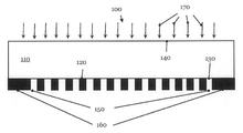
도 1은 투과형 포토리소그래픽 마스크(100)의 개략 단면을 나타낸다. 마스크(100)는 제1 또는 전면(130) 및 제2 또는 후면(140)을 갖는 기판(110)을 구비한다. 기판(110)은 웨이퍼 상의 포토레지스트의 조명에 대해서 사용되는 파장을 투과해야 한다. 노광 파장은, 전자기 스펙트럼의 원자외선(DUV) 스펙트럼 범위에 있을 수 있고, 특히, 대략 193 nm이다. 기판 재료는 일반적으로 석영을 포함한다. 기판은 152 mm x 152 mm의 전형적인 폭 치수와 본질적으로 6.35 mm의 두께 또는 높이를 가지고 있다. 포토리소그래픽 마스크(100)의 기판(110)은, 그 전면(130)에 일반적으로 크롬으로 제조된 패턴 요소(120)가 형성되고, 포토레지스트 상에 반도체 장치가 제조되는 미리 정해진 구조의 소자를 형성한다. 패턴 요소(120)를 갖는 포토리소그래픽 마스크(100)의 기판(110)의 일부는 마스크의 활성 영역(150)으로 칭하고, 패턴 요소(120)를 갖지 않는 경계부 또는 주변부는 비활성 영역(160)으로 칭한다. 노광 파장에서의 레이저 빔(170)은 기판(110)의 제2 또는 후면(140)을 통해 마스크(100)의 기판(110)을 조명한다.Figure 1 shows a schematic cross-section of a transmissive photolithographic mask (100). The
도 2는 전자기 스펙트럼의 극 자외선(EUV) 스펙트럼 범위, 특히, 10 nm 내지 15 nm의 범위의 노광 파장에 대해서 나중에 사용하기 위한 반사 포토리소그래픽 마스크(200)의 개략 단면도를 나타낸다. 도 1의 포토리소그래픽 마스크(100)와 달리, 마스크(200)는 다층 미러 구조물(255)에 기초한 반사 광학 부품이다. 포토리소그래픽 마스크(200)의 다층 미러 시스템(255)은 용융 실리카 기판과 같은 적절한 기판(210)의 전방 기판 표면(230) 상에 증착된다. 기타 투명 유전체, 유리 재료 또는 반도체 재료는 예를 들면, ZERODUR®, ULE®, 또는 CLEARCERAM®와 같은 EUV 포토리소그래픽 마스크용 기판으로서 적용될 수 있다.Figure 2 shows a schematic cross-sectional view of a reflective
다층 미러 시스템(255)은, 예를 들면, 40개의 몰리브덴(Mo) 층(250)과 실리콘(Si) 층(260)의 교호쌍을 포함한다. 각각의 Mo 층(250)의 두께는 4.15 nm이고, Si 층(260)의 두께는 2.80 nm이다. 다층 구조물(255)을 보호하기 위해, 7 nm 깊이의 자연 산화물을 갖는 실리콘 캡 층(270)이 구조물(255)의 상부에 배치된다. 다층 미러 시스템(255)에서, Mo 층(250)은 산란층으로 기능하는 반면, Si 층(260)은 분리층으로 기능한다. Mo 대신에, 코발트(Co), 니켈(Ni), 텅스텐(W), 레늄(Re) 및 이리듐(IR)과 같은 높은 Z 번호를 갖는 다른 요소가 산란층으로 사용될 수 있다.The
기판(210) 상의 다층 구조물(255)은 EUV 전자기 방사를 위한 미러의 역할을 한다. 포토리소그래픽 마스크(200)를 형성하기 위해, 버퍼 구조물(280) 및 흡수 구조물(290)이 캡층(270)에 추가로 증착된다. 처리시, 예를 들면, 흡수 구조물(290)의 에칭시, 버퍼층(280)이 다층 미러 구조물(255)을 보호하기 위해 증착될 수 있다. 가능한 버퍼 구조물의 재료는, 예를 들면, 용융 실리카(SiO2), 실리콘 산화 질화물(SiON), 루테늄(Ru), 크롬(Cr), 및/또는 질화 크롬(CrN)이다. 흡수 구조물(290)은 EUV 파장 범위 내의 광자에 대해서 큰 흡수 상수를 갖는 재료를 포함한다. 이러한 재료의 예는 크롬(Cr) 및/또는 탄탈 질화물(CrN)이다. 일반적으로, 약 50 nm의 두께는 흡수 구조물(290)에 입사된 모든 EUV 광자(295)를 본질적으로 흡수하기에 충분하다. 대조적으로, 상기 캡층(270)에 입사된 광자(295)의 대부분은 광자(297)로서 반사된다.The
일반적으로, EUV 마스크(200)의 기판(210)은 또한 152 mm x 152 mm의 폭 치수와 본질적 6.35 mm의 두께 또는 높이를 갖는다. 기판(210)의 후면(225) 또는 후방 기판 표면(225)은 얇은 금속 코팅(220)을 갖는다. 일반적으로, 이 코팅(220)은 크롬을 포함하고 있다. 금속 코팅(220)는 정전기력의 인가에 의해 EUV 스캐너에서 포토리소그래픽 마스크(200)를 고정하는데 사용된다.In general, the
광학 부품의 미리 정해진 3차원 윤곽을 생성하는 방법에서, 예를 들면, 다음에 설명하는 EUV 마스크(200)로서, 광 빔의 광 펄스로부터의 에너지가 EUV 마스크(200)의 기판(210)에 국부적으로 증착된다. 그러나, 광 빔의 광 펄스는 다층 미러 구조물(255)에 의해 흡수되면서, 전방 기판 표면(230)을 관통할 수 없고, 후방 기판 표면(225)위의 금속 코팅(220)에 의해 흡수되면서 후방 기판 표면(225)을 관통할 수 없다.In a method of generating a predetermined three-dimensional contour of an optical component, for example, as the
그러므로, EUV 마스크(200)의 후방 기판 표면(225) 상의 금속 코팅(220)은, 도 2에 도시된 것 같이, 투과 전도성 코팅(222)으로 교체된다. 이러한 투과 전도성 코팅(222)은 예를 들면, 인듐 주석 산화물(ITO)을 포함한다. 용어 투과 전도성 코팅은, 코팅(222)이 근적외선, 가시광, 및/또는 근자외선 파장 범위의 광을 광학적으로 투과시키는 것을 의미한다.Therefore, the
투과 전도성 코팅의 대체 물질은 예를 들어, 플루오르 주석 산화물(FTO) 및/또는 알루미늄 아연 산화물(AZO) 및/또는 안티몬 주석 산화물(ATO)이다. 이들 재료는 용융 실리카 기판(210)의 후방 기판 표면(225)에 쉽게 도포될 수 있고, EUV 스캐너로 마스크(200)를 고정하기에 충분히 높은 전도성을 가질 수 있다. 투과 전도성 코팅(222)으로 인해 후방 기판 표면(225)을 통해 레이저 빔의 광 펄스(200)를 완전하게 제작된 EUV 마스크(200)에 조사할 수 있다. 투과 전도성 코팅(222)으로 인해서, 제조 공정시, 마스크 제조 공정의 제 1단계에서, 코팅(222)이 마스크 블랭크 또는 후방 기판 표면(225) 상에 배치되면, 초단 레이저 펄스를 EUV 마스크(200)에 조사할 수 있다.Substituents for the transmissive conductive coatings are, for example, fluoro-tin oxide (FTO) and / or aluminum zinc oxide (AZO) and / or antimony tin oxide (ATO). These materials can be easily applied to the
EUV 미러가 버퍼층(280)과 흡수 구조물(290)을 갖지 않으면, 포토리소그래픽 마스크(200)의 구조를 가질 수 있다. 그러므로, EUV 미러에 대해서, 금속 코팅(220)이 투과 전도성 코팅(222)에 의해 교체될 수 있으므로, 광 펄스가 후방 기판 표면(도 2에 비도시)으로부터 기판으로 들어갈 수 있다.If the EUV mirror does not have a
도 3의 도해 300은 후방 기판 표면(340)은 평평하지 않고 미리 정해진 표면 형상(350)으로부터 2개의 편차(360, 370)를 갖는 EUV 마스크(300)의 마스크 블랭크 또는 기판(310)을 개략적으로 나타낸다. 다층 구조물(255)을 증착하는 척에 마스크 블랭크(310)를 고정할 때, 척은 블랭크(300)의 후면(340)을 평평하게 하여, 전면(330)에 왜곡을 가져온다. 그래서, 다층 구조물(255)이 기판(310)의 불균일한 전면(330)에 증착된다. 이로써 다층 구조물(255)이 결국 불균일한 표면을 갖게 된다.3 illustrates that the
기판(310)로부터 EUV 마스크의 제조 시, 후면(340)이 평평하지 않으므로 블랭크(310)를 척으로 고정할 때, EUV 마스크의 평평한 또는 미리 정해진 전면 형상이 제조될 수 있다. 그러나, EUV스캐너에 기판(310)으로부터 제조된 마스크를 고정할 때, 그 단계의 정전기력은 후방 기판 표면(340)의 편차(360, 370)를 본질적으로 평평한 표면(350)으로 평평하게 한다. 차례로, 도 2의 본질적으로 이상적인 EUV 마스크(200)와 비교하여 기판(310)에 배치된 다층 구조물(255)의 수차로 이어진다. 편차(360, 370)에 의해 생기는 수차는 웨이퍼의 위치를 변화시키거나 재생 배율을 변화시킴으로써 제거될 수 없다. 이미 논의된 바와 같이, 1 나노 미터의 범위의 전방 기판 표면(330)의 편평도의 편차는 수차를 유도하기에 이미 충분하다.A flat or predetermined frontal shape of the EUV mask can be produced when the blank 310 is chucked since the
현재, EUV 마스크(200)의 흡수 구조물(290)은 전자 빔 라이터로 흡수 재료의 층을 패터닝함으로써 일반적으로 생성된다. 이 과정에서, EUV 마스크(200)는 정전 척에 의해 고정되지 않는다. 이것은, 마스크 블랭크(310)의 비평탄 후면(340)은 본질적으로 패터닝 처리 동안 변경되지 않는다는 것을 의미한다. 따라서, 도 3에 나타낸 바와 같은 후방 기판 표면 형상(340)을 갖는 EUV 마스크는, 조명 공정 동안 정전 척에 고정될 때 다른 모양을 가진다. 이는 웨이퍼의 이미지 배치의 왜곡을 초래한다. 표준 마스크 벤딩에 대해서, 보정된 좌표로 전기 빔 라이터를 제어함으로써 이 문제가 부분적으로 수학적으로 해결된다. 그러나, EUV 마스크의 후방 기판 표면의 벤딩이 복잡한 형상을 가질 수 있으면서 여전히 문제가 존재한다. 더욱이, 패터닝 처리 자체는 비평판 표면에는 이상적이지 않다.At present, the absorbing
도 4는 광학 부품 또는 웨이퍼의 2차원(2D) 또는 3차원 이미지를 결정하기 위해 사용될 수 있는 계측 툴(400)의 예를 개략적으로 도시한다. 도 4의 공초점 현미경(400)은 광학 부품 또는 웨이퍼의 3차원 윤곽을 측정하기 위해 적용될 수 있는 계측 툴의 클래스의 예일 뿐이다. 예를 들어, 조면계는 웨이퍼뿐만 아니라 광학 부품의 표면 프로필 또는 2D 또는 3차원 미세 또는 서브미세한 형상을 분석하는데 사용될 수 있다. 접촉 또는 의사 접촉 방법을 활용하는 조면계가 사용될 수 있다. 스타일러스 조면계 또는 기계적 조면계, 원자력 현미경, 주사 터널링 현미경은 이 유형의 조면계의 예이다. 또한, 예를 들면, 광학적 방법을 적용하는 다수의 비접촉 조면계도 또한 이용가능하다. 이러한 유형의 조면계는, 예를 들면, 수직 주사 간섭계, 백색광 간섭계, 위상 편이 간섭계, 및/또는 미분 간섭 대조 현미경이다.Figure 4 schematically illustrates an example of a
다음에, 공초점 센서(400) 또는 공초점 현미경(400)의 동작 원리의 개요를 설명한다. 공초점 현미경(400)은 초점을 벗어난 신호 성분을 제거하기 위해 검출기의 전면에 광학적으로 공액 평면에서 핀홀의 점 조명을 사용한다. 도 4의 예에서, 점 조명은 광원(420)에 의해 생성되고, 광섬유(425)는 광원(420)의 광을 핀홀(430)을 통해 대물 렌즈(440)를 거쳐 포토 마스크(410)의 초점면(450)에 연결된다. 초점면(450)으로부터 반사된 광은, 검출기(475)의 전방에 배치된 핀홀(465)로 다이크로익 미러(435)에 의해 지시된다. 초점면(450)의 외부로부터 반사되는 광의 일부는 초점면(450)으로부터 반사된 광보다 현저하게 작다. 또한, 초점면의 외부로부터 반사되는 광은 핀홀(465)에 포커싱되지 않는다.Next, an outline of the operation principle of the
예를 들어, 광원(420)은 레이저 광원일 수 있다. 광섬유(425)가 핀홀(430)에 광원으로부터의 전자기 방사선을 안내하기 위해 사용되는 경우, 광섬유(425)가 핀홀(430) 과 유사한 효과를 가지므로, 핀홀(430)이 생략가능하다. 예를 들어 검출기(475)는 포토 다이오드, 애벌랜치 포토 다이오드 또는 광전자 배증관(photomultiplier)일 수 있다.For example, the
포토 마스크 또는 일반적으로 광학 부품(410)은 샘플 스테이지(405) 상에 배치될 수 있다. 샘플 스테이지(405)는 가동이고, 입사광 빔(x- 및/또는 y-방향)에 직교한 면에서 주사부(480)에 의해 이동된다. 예를 들어, 미세 조작기 또는 서보 모터(도 4에 도시되지 않음)는 샘플 스테이지(405)를 이동시키기 위해 사용될 수 있다. 샘플 스테이지(405)를 빔 방향에 평행하게 움직이거나 및/또는 대물 렌즈(440)를 시프팅함으로써, 초점면은 광학 부품(410)을 통해 주사될 수 있다. 다른 구현 예에서 샘플 스테이지는 고정이고, 광빔(455)은 포토 마스크(410)에 걸쳐 주사된다. 이 구현은 공초점 레이저 주사 현미경(CLSM: confocal laser scanning microscope)이라고 한다(도 4에 도시되지 않음).A photomask or generally an
제어부(470)는 광원(420), 검출기(675)뿐만 아니라, 스캔 부(480)도 제어한다. 제어부(470)는 대물 렌즈(440)의 이동(도 4에 도시되지 않음)을 또한 제어한다. 또한, 제어부(470)는 적어도 프로세서, 저장부, I/O(입력/출력) 부, 및 디스플레이를 갖는 컴퓨터 시스템에 내장될 수 있다(도 4에 도시되지 않음). 제어부 또는 컴퓨터 시스템은 상기 검출기(475)로부터 수신된 데이터를 저장한다. 또한, 상기 제어부의 처리부 또는 컴퓨터 시스템의 프로세서(또한, 도 4에 도시되지 않음)는 검출기(475)의 측정 데이터를 처리할 수 있다. 마지막으로, 상기 장치(500)로 측정 및/또는 처리된 데이터를 전송하기 위해, 제어부(470) 또는 컴퓨터 시스템은 도 5의 장치(500)로의 연결을 가질 수 있다.The
횡 방향의 공초점 현미경(400)의 해상도는 회절에 의해 제한된다. 이것은, 가로 해상도가 핀홀(430, 465)의 직경 또는 개구, 대물렌즈(440)의 개구 수(NA), 및 광원(420)의 파장에 의존하는 것을 의미한다. 횡방향에서, 해상도는 광원(420)의 파장의 범위에 있다. 빔 방향의 해상도는 회절에 제한되지 않지만, 최대 강도의 위치의 결정에 의해 제한된다. 이 빔 방향의 해상도는 한 자리 나노미터 범위에 도달한다.The resolution of the
도 5는 레이저 펄스의 배열을 계산하고 광학 부품 및/또는 웨이퍼에 적용하기 위해 사용될 수 있는 장치(500)의 개략 블록도를 도시한다. 원리에 대해서, 도 1 및 도 2의 마스크를 일 예로 설명한다. 광학 부품의 다른 예는 나노임프린트 기술에서 사용된 템플릿 및/또는 광학 시스템의 렌즈일 수 있다. 또 다른 예는, 그 위에 집적 회로(IC)가 생성되어 있는 웨이퍼이다. 이 장치(500)는 3차원으로 이동될 수 있는 척(520)을 구비한다. 광학 부품(510), 예를 들면, 마스크(510)는, 예를 들어 클램핑과 같은 다양한 기술을 사용하여, 척(520)에 고정될 수 있다. 포토리소그래픽 마스크(510)는 거꾸로 탑재된 도 1의 투과형 마스크(100)일 수 있으므로, 후방 기판 표면(140)은 대물렌즈(540)를 향한다.Figure 5 shows a schematic block diagram of an
장치(500)는 펄스 또는 광 펄스의 빔 또는 광 빔(535)을 생성하는 펄스 레이저 소스(530)를 구비한다. 레이저 소스(530)는 가변 기간의 광 펄스를 생성한다. 펄스 기간은 10 fs 만큼 낮을 수 있지만, 100 ps까지 연속적으로 증가될 수 있다. 펄스 레이저 소스(530)에 의해 생성된 광 펄스의 펄스 에너지는 펄스당 0.001 μJ 내지 펄스당 10 mJ에 달하는 넓은 범위에 걸쳐서 조정가능하다. 또한, 광 펄스의 반복률은 1 Hz 내지 100 MHz의 범위를 포함한다. 바람직한 실시 예에서, 광 펄스는 대략 800 nm의 파장에서 동작하는 Ti:사파이어 레이저에 의해 생성될 수 있다. 그러나, 다음에 서술된 방법은 이 레이저 유형에 제한되지 않고, 원칙적으로 광학 부품(510)의 밴드 갭보다 작은 광자 에너지를 갖고 펨토초 범위의 기간을 갖는 극단 펄스를 생성할 수 있는 모든 레이저 유형이 사용될 수 있다. 이 기준은 웨이퍼에 대해서도 유지된다. 일반적으로, 장치(500)의 발광 파장은 광학 부품(510) 또는 웨이퍼의 밴드 갭에 대해서 채택되어야 한다.
그러므로, 예를 들면, 네오디뮴(Nd), 툴륨(Tm), 홀뮴(Ho) 및 에르븀(Er) 요소중 적어도 하나가 도핑된 YAG 레이저 시스템이 또한 사용될 수 있다. 또 다른 예로서, 다이 레이저 시스템이 또한 적용될 수 있다. 장치(500)는 이 유형 또는 다른 유형의 하나 이상의 펄스 레이저 소스(530)를 포함할 수 있다(도 5에 도시되지 않음).Thus, for example, a YAG laser system doped with at least one of neodymium (Nd), thulium (Tm), holmium (Ho) and erbium (Er) elements may also be used. As yet another example, a die laser system may also be applied.
광학 부품(510)의 밴드 갭이 초단 레이저 펄스를 적용하는 데 사용되는 레이저 광원의 발광 파장보다 커야 한다는 필요 조건은 광학 부품(510)이 근적외선, 가시광 및/또는 근 자외선 파장 범위의 광을 광학적으로 투과시킨다는 필요 조건과 일반적으로 같다. 이러한 파장 영역에서, 레이저 소스는 큰 에너지 밀도를 갖는 극단 펄스를 생성 할 수 있는데 유용하다.The requirement that the bandgap of the
다음 표는 본 발명의 방법의 실시 예에서 사용되는 주파수 2배의 Nd-YAG 레이저 시스템의 레이저 빔 파라미터의 개요를 나타낸다.The following table gives an overview of the laser beam parameters of the Nd-YAG laser system at twice the frequency used in the embodiment of the method of the present invention.
펄스 밀도는 빔 방향(측면)과 직교하는 평면에서 2 차원 밀도를 지칭한다.Pulse density refers to the two-dimensional density in a plane orthogonal to the beam direction (side).
표 1에 나타낸 것 같이, 픽셀의 생성을 위해 사용된 레이저 펄스의 파라미터 범위는 크다. 그러므로, 픽셀의 특성은 또한 매우 다르다. 일반적으로, 레이저 펄스는 구형의 픽셀을 생성하지 않고, 타원체 또는 회전 타원체와 유사한 형태를 갖는 픽셀을 생성한다. 회전 타원체의 길이는 1 μm 내지 50μm의 범위에 있고, 그 폭 또는 두께는 예를 들면 0.5μm 내지 10μm까지 연장된다. 두께에 대한 길이의 특성 비는 2 내지 10의 범위에 있다. 표 1에 나타낸 것 같이, 횡 평면에서 픽셀 밀도는 사각형 mm당 103 내지 107 픽셀이다. 빔 방향의 일차원 픽셀 밀도는 mm 당 1 내지 100의 픽셀의 범위를 커버한다.As shown in Table 1, the parameter range of the laser pulse used for pixel generation is large. Therefore, the characteristics of the pixels are also very different. Generally, a laser pulse does not produce a spherical pixel, but produces a pixel having a shape similar to an ellipsoid or spheroid. The length of the spheroid is in the range of 1 μm to 50 μm, and the width or thickness thereof is extended, for example, to 0.5 μm to 10 μm. The characteristic ratio of length to thickness is in the range of 2 to 10. As shown in Table 1, the pixel density in the transverse plane is 10 3 to 10 7 pixels per square mm. The one-dimensional pixel density of the beam direction covers a range of 1 to 100 pixels per mm.
다음 표는 포토마스크(100)의 기판(110)의 밀도 및/또는 광 투과 분포에 다르게 영향을 주는 파라미터를 나타낸다. 표 2는 표준 프로세스 윈도우(std PW: standard process window)로 불리는 픽셀을 도입 또는 기입하는 모드용 주파수 2배의 Nd-YAG 레이저 시스템을 사용하는 실시 예의 파라미터를 나타낸다.The following table shows parameters that otherwise affect the density and / or light transmission distribution of the
표 3은 주파수 2배의 Nd-YAG 레이저 시스템을 사용하는 실시 예의 낮은 등록 프로세스 윈도우(LowReg PW: low registration process window)로 불리는 모드의 파라미터를 요약한 것이다. 레이저 시스템(530)의 동작 모드는 std PW보다 낮은 에너지를 갖는 광 펄스를 사용하지만, 더 높은 픽셀 밀도를 도입한다.Table 3 summarizes the parameters of the mode referred to as the low registration process window (LowReg PW) of the embodiment using the Nd-YAG laser system of frequency doubling. The operating mode of the
다음 표는, 레이저 시스템(530)의 광 펄스의 에너지를 더 줄인 것이 특징인, NoReg PW(no registration process window)로 불리는 모드에 대한 파라미터의 리스트이다.The following table is a list of parameters for a mode called NoReg PW (no registration process window), which is characterized by further reducing the energy of the optical pulses of the
표 5는 pixelless PW(pixelless process window)로 불리는 모드의 파라미터를 나타낸다. 이 경우, 광학 부품의 밀도 및/또는 광 투과 분포의 수정을 위해 Ti:사파이어 레이저 시스템이 사용된다. 이 레이저 시스템은 대략 800 nm의 방사 파장에서 초단 레이저 펄스를 생성한다. 픽셀리스 PW의 펄스 밀도는 매우 높다.Table 5 shows the parameters of the mode called pixelless process window (PW). In this case, a Ti: sapphire laser system is used to modify the density and / or the light transmission distribution of the optical components. This laser system produces a very short laser pulse at a radiation wavelength of approximately 800 nm. The pulse density of the pixel-less PW is very high.
스티어링 미러(590)는 펄스 레이저 빔(535)을 집속 대물렌즈(540)로 지향시킨다. 대물렌즈(540)는 펄스 레이저 빔(535)을 후방 기판 표면을 통하여 포토리소그래픽 마스크(510)의 기판으로 집광시킨다. 적용된 대물렌즈의 개구수(NA)는 초점의 미리 정해진 스폿 사이즈 및 후방 기판 표면에 대한 투과형 마스크(510)의 기판 내의 초점의 위치에 의존한다. 표 1에 나타낸 바와 같이, 대물렌즈(540)의 NA는, 본질적으로 1 μm의 초점 스팟 직경 및 본질적으로 1020 W/cm2의 최대 강도를 초래하는 0.9까지 일 수 있다.The
장치(500)는 또한 레이저 빔(x 및 y 방향)에 수직인 평면에서 샘플 스테이지(520)의 2 축의 위치 설정 단계의 변환을 관리하는 제어기(580) 및 컴퓨터(560)를 포함한다. 제어기(580) 및 컴퓨터(560)는 대물 렌즈(540)가 고정되어 있는 1 축의 위치 설정 단계 550을 통하여 척(520)(Z 방향)의 평면에 직교하게 대물렌즈(540)의 변환을 제어한다. 또한, 장치(500)의 다른 구현 예에서, 척(520)은 광학 부품(510) 또는 마스크(510)를 목표 위치까지 이동시키기 위해 3축 위치 설정 시스템을 구비할 수 있고, 대물렌즈(540)는 고정될 수 있거나, 척(520)이 고정될 수 있고 대물렌즈(540)는 3차원으로 움직일 수 있다. 현재 바람직하지 않지만, 대물 렌즈(540) 및 척(520)이 모두 3축 위치 설정 시스템을 구비하는 것도 생각할 수 있다. 또한, 수동 위치 설정 단계가 예를 들면, 투과형 마스크인 광학 부품(510)을 x-, y- 및 z-방향으로 펄스 레이저 빔(535)의 목표 위치로 이동시키기 위해 사용될 수 있고, 및/또는 대물렌즈(540)가 3차원 이동을 위한 수동 위치 설정 단계를 가질 수 있다.The
또한, 장치(500)는 다이크로익 미러(545)를 통하여 척(520)(도 5에 도시되지 않음)에 배열된 조명 원으로부터 광을 수용하는, 예를 들면, CCD(전하 결합 소자) 카메라로서 검출기(565)를 포함하는 뷰잉 시스템을 제공할 수 있다. 뷰잉 시스템은 목표 위치에 광학 부품(510)의 탐색을 용이하게 한다. 또한, 상기 뷰잉 시스템은 광학 부품(510)에 광원(530)의 레이저 빔(535)으로 레이저 펄스의 배열을 기입하여 광학 부품(510)에서 변경된 영역의 형성을 관찰하는데 사용될 수 있다.The
컴퓨터(560)는 마이크로 프로세서, 범용 프로세서, 특수 목적 프로세서, 중앙 처리 장치(CPU), 그래픽 처리 장치(GPU) 등일 수 있다. 컴퓨터는 또한 제어부(580)에 배치될 수 있고, 또는 PC(퍼스널 컴퓨터), 워크 스테이션, 메인 프레임 같은 별도의 유닛일 수 있다. 컴퓨터(560)는 키보드, 터치 패드, 마우스, 비디오/그래픽 디스플레이, 프린터 등과 같은 I/O(입력/출력)부를 더 구비할 수 있다. 또한, 컴퓨터(560)는 하나 또는 여러 개의 연결 포트를 포함 할 수 있고, 이를 통하여 도 4의 공초점 현미경(400)의 제어부(470)로 실험 데이터에 대한 요구를 전송할 수 있다. 또한, 컴퓨터(560)는 또한 휘발성 및/또는 비휘발성 메모리를 포함할 수 있다. 컴퓨터(560)는 하드웨어, 소프트웨어, 펌웨어, 또는 이들의 임의의 조합으로 구현될 수 있다. 또한, 컴퓨터(560)는 레이저 소스(530)(도 5에 비도시)를 제어할 수 있다.The
컴퓨터(560)의 비 휘발성 저장매체는 광학 부품의 3차원 형상을 저장할 수 있다. 컴퓨터(560)는 공초점 현미경(400)의 제어부(470)로부터 실험 로 데이터를 수신할 수 있다. 또는, 제어부(470)로부터 처리된 데이터를 수신할 수 있다. 컴퓨터(560)의 연산부는 광학 부품(510)의 미리 정해진 3차원 윤곽 및 제어부(470)로부터 수신된 데이터에 기초하여, 그 미리 정해진 3차원 윤곽으로부터의 광학 부품의 측정된 또는 기존의 3차원 윤곽의 하나 또는 다수의 편차를 결정한다. 광학 부품의 공급 업체가 미리 정해진 형상으로부터 기존의 3차원 윤곽의 편차를 제공하는 것도 또한 가능하다.The non-volatile storage medium of
컴퓨터(560)는 이러한 데이터 및 5.3절에 설명된 알고리즘("이론적 배경")으로부터 미리 정해진 3차원 윤곽에 따라서 광학 부품(510)의 기존의 3차원 윤곽을 가져오기에 적절한 레이저 펄스의 적어도 하나의 배열을 계산한다.The
도 6의 도해 600은 EUV 마스크(610)에 레이저 펄스의 하나 이상의 배열을 인가하는 것을 개략적으로 나타낸다. EUV 마스크(610)는 그 전면에 EUV 패턴(615)을 가지며, 그 후면에 광학적 투과 전도성 코팅(665)을 갖는다. 마스크(610)는 특정의 하우징(620) 내에 배치되어 있고, 마스크 패턴(615)이 브라켓(625) 상의 하면에 설치되어 있다. 하우징(620)은 보호 유리 윈도우(630)로 밀봉되어 있다. 특정 하우징(620)에서 마스크(610)의 환경을 제어가능하다. 특히, 하우징(620)을 대피가능하다(도 6에 비도시). 레이저 빔(650)은 EUV 마스크(610)의 기판(660)에 대물 렌즈(640)에 의해 집광된다. 교환 가능한 보상 유리판(670)은 마스크(610)의 기판(660)의 깊이에 레이저 빔(650)의 초점을 조절한다. 하우징(620)은 어떠한 이동 부품도 갖지 않는다.FIG. 6, diagram 600, schematically illustrates applying one or more arrays of laser pulses to the
5.2 응용 예5.2 Application example
5.2a 포토리소그래픽 마스크5.2a Photolithographic Mask
도 7의 부호 700은 마스크 블랭크(710)의 높이의 국소 변화를 개략적으로 나타낸다. 마스크 블랭크(710)는 초기 상태에서 평탄하다. 레이저 펄스(720)의 2D 배열을 적용하여 표면의 높이를 국소적으로 변경시킬 수 있다. 물리적 용어로 표현된, 높이 변형, 수직 변형 또는 z-방향의 변형은 z-방향의 팽창과 축소 및 벤딩의 조합이다. 국소 변형은 국부의 효과를 유발하는 반면, 벤딩은 전체적인 효과를 가져 온다. z-방향의 국소 변형(730)은 레이저 펄스(720)의 2D 또는 3D 배열을 적용함으로써, 및 포아송 비(5.3 섹션 "이론적 배경" 참조)로 표현된, 레이저 펄스의 2D 또는 3D 배열이 기입된 영역과 국소 변형을 갖는 국소 영역의 상호 간섭으로부터 생길 수 있다. 5.3 섹션에서 이론적 고려 사항들은 대부분의 경우에 z-방향의 벤딩 및 z-방향의(국소) 변형이 서로 상당히 다른 크기를 가지므로 분리될 수 있는 것을 또한 나타낸다.
도 7은, 광학 부품의 편평도 제어가 레이저 펄스의 배열에 의해 생긴 벤딩과 표면 형상의 모두를 제어하는 것을 요구하는 것을 분명하게 나타낸다. 따라서, 광학 부품의 미리 정해진 벤딩의 생성 또는 결정된 벤딩의 정정이, 3차원 배열의 레이저 펄스의 계산에 이르게 하는 3차원 변형 모델의 기능을 보여주는 좋은 예이다.Fig. 7 clearly shows that the flatness control of the optical component requires controlling both the bending and the surface shape caused by the arrangement of the laser pulses. Therefore, it is a good example to show the function of the three-dimensional deformation model which leads to the calculation of the laser pulse of the three-dimensional arrangement, the generation of the predetermined bending of the optical component or the correction of the determined bending.
광학 부품의 벤딩의 개념을 수정하기 위해 이하에 서술된 실험의 목표이다. 또한, 3차원 변형 모델을 확인하고, 3차원 배열의 레이저 펄스를 생성하기 위한 다중 모드 접근 방법의 이점을 설명하는 목적도 있다.It is the goal of the experiment described below to modify the concept of bending of optical components. There is also an object to illustrate the advantages of a multimode approach for identifying three dimensional deformation models and generating laser pulses in a three dimensional array.
아래에 설명되는 실험에서 사용되는 일 예의 광학 부품은 6 인치(152 mm) 마스크 블랭크이다. 대부분의 결과는, 광학 부품, 즉, 근적외선, 가시광 및/또는 근자외선 파장 범위의 광을 광학적으로 투과시키는 광학 부품의 체적에 3차원 배열의 레이저 펄스를 적용할 수 있는 다른 형상을 갖는 많은 다른 광학 부품에 또한 적용가능하다.An example optical component used in the experiments described below is a 6 inch (152 mm) mask blank. Most of the results show that many different optics having different shapes that can apply laser pulses in a three-dimensional array to the volume of optical components, that is, optical components that optically transmit light in the near-infrared, visible, and / It is also applicable to parts.
레이저 펄스의 서로 다른 2D 배열의 적용은, 마스크 블랭크 전면과 후면에 평행한 면에서, 각각의 표면으로부터 상이한 깊이에서, 상이한 기입 모드를 사용하여, 즉, 레이저 펄스 및/또는 다른 펄스 밀도에 대한 상이한 파라미터를 갖는 레이저 펄스의 2D 배열을 사용하여 행해진다. 2D 배열의 크기는 마스크 블랭크의 전체 활성 영역을 포함한다. 배열에 기인하는 변형은 146 mm x 146 mm의 영역에서 측정되고, 이 측정 그리드는 대략 30 x 30개의 노드들이다.The application of different 2D arrays of laser pulses may be performed at different depths from each surface, in a plane parallel to the front and back sides of the mask blank, using different writing modes, i.e. different for laser pulses and / or different pulse densities Is performed using a 2D array of laser pulses with parameters. The size of the 2D array includes the entire active area of the mask blank. The strain due to the arrangement is measured in the area of 146 mm x 146 mm, which is approximately 30 x 30 nodes.
이 섹션에서 설명된 응용 예에서 사용된 공초점 현미경(400)은, 10 mm의 작동 거리 및 400 nm의 빔 방향 또는 z-방향의 해상도를 갖는 Micro Epsilon IFS 3401-10 공초점 센서이다. 측정 센서의 노이즈는 대략 1000 nm이다. 모든 샘플링 포인트에서, 대략 100 nm의(z-방향)의 거리 샘플링 반복성을 달성하기 위해 100개의 거리 샘플링이 추가되었다. 도 4의 대물 렌즈(440)의 위치 설정 스테이지(Schneeberger)는 대략 200 nm의 z-방향의 반복성을 갖는다. z-방향의 편차에 위치 설정 스테이지가 기여하는 것을 감소시키기 위하여 5개의 순차 스캔이 행해진다. 따라서, 광학 부품의 기존의 3차원 윤곽의 판정 반복성은 약 200nm로 감소될 수 있다. 마스크 블랭크의 기울기는 항상 수학적으로 보정된다.The
다음 적용 예는 마스크 블랭크의 국소 확장을 가져오는 3차원 배열의 레이저 펄스의 적용의 결과를 보여준다. 그러나, 이것은 본 발명의 방법을 제한시키지 않는다. 이 섹션에 설명된 모든 결과는 마스크 블랭크의 국소 수축을 가져오는 3차원 배열의 레이저 펄스이 적용될 수 있다. 또한, 마스크 블랭크의 제 1 영역에 국소 수축을 가져오고 상기 마스크 블랭크의 제 2 영역에 팽창을 가져오는 3차원 배열의 레이저 펄스를 정의하는 것도 가능하다.The following example shows the result of applying a laser pulse in a three-dimensional array resulting in local expansion of the mask blank. However, this does not limit the method of the present invention. All of the results described in this section can be applied to laser pulses in a three-dimensional array resulting in local shrinkage of the mask blank. It is also possible to define a laser pulse in a three-dimensional array that causes local shrinkage in the first region of the mask blank and causes expansion in the second region of the mask blank.
제1 적용 예로서, 마스크 블랭크의 1차원(1D) 벤딩이 서술된다. 레이저 펄스의 2D 배열이 적용되어 마스크 블랭크의 면(x-/y-면)에서 등방성 확장을 가져 오면, 마스크 블랭크의 면(x-/y-면)의 모든 방향에서 동일한 곡률로 상기 설명된 마스크 블랭크에 벤딩을 가져오는 것이 명백하다. 따라서, 로컬 등방성 확장을 가져오는 레이저 펄스의 2D 배열은, 1D 벤딩, 즉, 예를 들어 x-방향의 정의된 벤딩과 y-방향의 마스크 블랭크의 벤딩 없음을 생성하는 것을 허가하지 않는다. 이것은 마스크 블랭크 면 내 등방성 확장을 가져오는 레이저 펄스의 2D 배열을 사용하는 접근 방법의 주요 또는 근본적인 한계이다.As a first application example, one-dimensional (1D) bending of a mask blank is described. When a 2D array of laser pulses is applied to bring about an isotropic expansion in the plane (x- / y-plane) of the mask blank, the above described mask with the same curvature in all directions of the plane (x- / y- Obviously it brings bending to the blank. Thus, a 2D array of laser pulses resulting in a local isotropic extension does not allow to generate 1D bending, i. E., Without defined bending of the x-direction and without bending of the y-direction mask blank. This is a major or fundamental limitation of the approach using a 2D array of laser pulses that results in isotropic expansion in the mask blank plane.
그러나, 펄스 밀도와 달리, 레이저 펄스의 형상은 마스크 블랭크 또는 일반적으로 광학 부품의 등방성 확장을 가져오는 효율적인 파라미터이다.However, unlike pulse density, the shape of the laser pulse is an efficient parameter that leads to mask blanking or, in general, isotropic expansion of the optical component.
이 가정은 현재 실험적으로 증명된다. 레이저 펄스의 2 차원 배열은 그 상면에 근접한 마스크 블랭크에 기입된다. 도 8에 나타낸 바와 같이, 횡 평면에서 등방성 확장을 가져오는 레이저 펄스의 2D 배열이 마스크 블랭크에 기입된다. 빔 방향에 수직한 평면에서 등방성 확장은 예를 들어 원형을 갖는 레이저 펄스에 의해 생성될 수 있다. 도 8의 타원(820)은 마스크 블랭크의 결과의 확장을 나타낸다. 2개의 라인(860, 870)은 공간에서 방향에 대한 확장의 크기를 나타낸다. 2 축(860, 870)은 확장의 주축을 나타낸다. 타원(820)의 편심은 매우 낮으며, 이것은 횡 평면에서 마스크 블랭크의 확장이 거의 균일한 것을 나타낸다.This assumption is now experimentally proven. A two-dimensional array of laser pulses is written to the mask blank close to its top surface. As shown in Fig. 8, a 2D array of laser pulses which results in isotropic expansion in the transverse plane is written to the mask blank. Isotropic expansion in a plane perpendicular to the beam direction can be generated by a laser pulse having a circular shape, for example. The
타원(820)이 마스크 블랭크의 모든 가능한 확장을 가시화할 수 없으므로, 사각형은 기본 영역(810)에 레이저 펄스의 배열을 기입하기 전의 마스크 블랭크의 기본 영역(810)을 나타낸다. 기본 영역(810)은 섹션 5.3에 도입된 기본 체적 ![]()
![]()
도 9는 레이저 펄스의 균질한 2D 배열이 마스크 블랭크에 기입된 경우의 상황을 도시하며, 레이저 펄스는 기본 영역(910)의 본질적인 1D 확장을 가져 온다. 도 9에 도시된 바와 같이 강한 이방성 확장이 예를 들어 실린더 렌즈에 의해 생성된 것 같이, 슬릿 형상의 빔 형상을 갖는 레이저 빔에 의해 생성될 수 있다. 또는, 기본 영역(910)의 이방성 확장은, 픽셀들이 일 방향으로 겹치게 하며 이방성 픽셀을 생성하는, 마스크 블랭크에 중첩 펄스를 기입하여 생성 될 수 있다. 도 9에서, 마스크 블랭크의 이방성 확장은 타원(920)을 상징한다. 도 8의 타원(820)과 대조적으로, 타원(920)은 큰 편심을 갖고, 거의 라인으로 퇴화된다. 화살표(930)는 기본 영역(910)의 코너 점에 생긴 변형을 또한 상징한다. 도 9에 도시된 것 같이, 평행 육면체(940)에 의해, 레이저 펄스의 이방성 빔은, 기본 영역(910)의 매우 높은 이방성 또는 거의 1 차원 변형을 가져 온다. 또한, 사각형(950)은 상기 기본 영역(910)의 정규화된 변형을 나타낸다.Figure 9 shows the situation when a homogeneous 2D array of laser pulses is written to the mask blank, which results in an intrinsic 1D extension of the
도 10은 152 mm x 152 mm의 치수를 갖는 마스크 블랭크를 나타낸다. 마스크 블랭크의 중앙에 약 39mm의 폭을 갖는 스트라이프가 레이저 펄스의 2 차원 배열에 의해 덮여있다. 레이저 펄스의 2 차원 배열의 단일 층이 마스크 블랭크의 상면 가까이에 기입되어 얻어진 결과의 해석을 용이하게 한다. 도 10의 왼쪽 치수에 표시된 것 같이, 마스크 블랭크의 광투과율은 수직 스트라이프에서 본질적으로 4.5%만큼 변화(감소)된다. 광학 부품에 픽셀을 기입함으로서 광학 부품에 생긴 광 투과의 변화 또는 광 감쇠의 증가는, 광학 부품에 픽셀을 기입하는 양을 정량화하는 역사적 척도이다. 4.5 %의 감쇠는 레이저 펄스의 2 차원 배열에 의해 커버되는 스트라이프의 픽셀의 공격적인 기입을 의미한다.Figure 10 shows a mask blank having dimensions of 152 mm x 152 mm. A stripe having a width of about 39 mm at the center of the mask blank is covered by a two-dimensional array of laser pulses. A single layer of a two-dimensional array of laser pulses is written near the top surface of the mask blank to facilitate the interpretation of the results obtained. As shown in the left dimension of FIG. 10, the light transmittance of the mask blank is changed (decreased) by essentially 4.5% in the vertical stripe. The change in light transmission or increase in light attenuation that occurs in an optical component by writing a pixel in an optical component is a historical measure for quantifying the amount of pixel writing to an optical component. An attenuation of 4.5% means an aggressive write of the pixels of the stripe covered by the two-dimensional array of laser pulses.
도 11은 도 8의 균일한 2차원 배열에 의해 생긴 높이의 변화를 나타내며, 레이저 펄스는 본질적으로 등방성 확장을 가져오는 파라미터를 갖는다. 도 12는 도 9의 레이저 펄스의 균일한 2차원 배열에 의해 생긴 빔 방향 또는 z-방향의 변화를 나타내며, 레이저 펄스는 강한 이방성 확장을 가져오는 파라미터를 갖는다. 양 도면의 경우, 높이 변화는 -3000 내지 +3000 nm의 크기이며, 152mm의 길이에 걸쳐 약 6 μm의 마스크 블랭크의 전체 높이의 변화를 가져 온다. 동시에, 제시된 방법으로 마일당 범위에 부정확성을 가져오는 나노 미터 레벨에서의 표면 형상을 제어할 수 있다. 미리 정해진 형상으로부터 그 3차원 윤곽의 편차가 이미 이 광학 부품의 기능을 상당히 저하시키는 변형을 가져 오면서 나노 미터 범위의 정밀도는 EUV 마스크의 치료에 필수적이다.Fig. 11 shows the change in height caused by the uniform two-dimensional arrangement of Fig. 8, with the laser pulse having parameters that inherently result in isotropic expansion. Figure 12 shows changes in beam direction or z-direction caused by a uniform two-dimensional array of laser pulses of Figure 9, with the laser pulses having parameters that lead to strong anisotropic expansion. For both drawings, the height variation is in the range -3000 to +3000 nm, resulting in a change in the overall height of the mask blank of about 6 μm over a length of 152 mm. At the same time, it is possible to control the surface morphology at the nanometer level, which leads to inaccuracies in the range per mile in the proposed method. Precision in the nanometer range is essential for the treatment of EUV masks, while deviation of the three-dimensional contour from a predetermined shape leads to deformation that already significantly degrades the function of this optical component.
마지막으로, 도 11과 12의 비교함으로써, 상이한 방향에서 상이한 곡률을 갖는 벤딩을 생성하기 위해 기본 영역(810)에서 등방성 확장(820)을 사용할 수 없다는 가정을 확인한다. 도 11과 12의 예에서, 필셀은 마스크 블랭크의 표면으로부터 멀리 떨어져 도입되고, 필셀 기입으로부터의 표면 프로필 또는 형상의 변화에 대한 기여는 낮다. 논의된 예에서, 표면 프로필은 1㎚ 미만만큼 변경된다. 따라서, 벤딩에 대한 표면 변화의 비율이 이 예에서는 1% 미만이다. 따라서, 기본 영역의 등방성 또는 강한 등방성 확장이 광학 소자의 표면 형상의 최소한 효과를 갖는 광학 부품의 등방성 또는 거의 1 차원의 벤딩을 생성하기 위해 적합하다.Finally, by comparing FIGS. 11 and 12, it is confirmed that the
다음의 응용 예에서, 정의된 방법은, 초기 광학 부품이 회전 대칭성을 가지고 있지 않는 경우라도 회전 대칭성을 갖는 미리 정해진 3차원 형상 또는 미리 정해진 굽힘 프로필을 생성할 수 있음을 보여준다. 마스크 블랭크는 다시 초기 광학 부품으로 사용된다. 마스크 블랭크는 다시 152mm x 152mm의 치수를 가지고 있다. 도 13은 대상 프로필의 단면을 나타낸다. x 방향의 단위는 μm이고, y 방향의 단위는 nm이다. 마스크 블랭크의 중앙부는 거의 평탄하다. 마스크 블랭크의 중앙부의 에지로부터 외측 에지로의 총 벤딩은 약 500 nm 만큼 대칭적으로 상승한다.In the following application, the defined method shows that a predefined three-dimensional shape or a predetermined bending profile with rotational symmetry can be generated even if the initial optical component does not have rotational symmetry. The mask blank is again used as the initial optical component. The mask blank again has dimensions of 152 mm x 152 mm. 13 shows a cross section of the subject profile. The unit in the x direction is μm, and the unit in the y direction is nm. The central portion of the mask blank is substantially flat. The total bend from the edge to the outer edge of the center of the mask blank rises symmetrically by about 500 nm.
도 10에서, 벤딩이 마스크 블랭크에 대칭적으로 적용된다. 이 제한은 다음 예에서 제거된다. 이것은 회전 대칭 벤딩이 사각형 마스크 블랭크에 적용된 것을 의미한다. 이 대상은 도 13의 평평한 정상 3차원 윤곽이 x- 및 y-방향에서 상이한 벤딩 곡률의 벤딩 프로필의 상이한 부분에 갖는 것으로서 선택된다. 이것은 도 13의 3차원 윤곽을 하나의 팽창 특성을 갖는 레이저 펄스의 배열로 얻을 수 없는 것을 의미한다.In Fig. 10, bending is applied symmetrically to the mask blank. This restriction is removed in the following example. This means that rotational symmetric bending is applied to the square mask blank. This object is chosen as having the flat normal three-dimensional contour of Figure 13 in different parts of the bending profile of different bending curvatures in the x- and y-directions. This means that the three-dimensional contour in Fig. 13 can not be obtained by arranging laser pulses having one expansion characteristic.
도 14는 도 13의 3차원 목표 형상을 나타내는 2차원 지도를 나타낸다. 마스크 블랭크의 우측의 눈금으로 나타낸 바와 같이, 전체 높이의 변화는 900 나노 미터에 달한다. 10 x 10 등거리 단계 그리드는 계산에 사용된다. 마스크 블랭크 평면의 프로필은 29 x 29 위치에서 샘플링된다.Fig. 14 shows a two-dimensional map showing the three-dimensional target shape of Fig. As shown by the right scale of the mask blank, the overall height change reaches 900 nanometers. A 10 x 10 equidistant phase grid is used for the calculation. The profile of the mask blank plane is sampled at the 29 x 29 position.
레이저 펄스의 2개의 서로 다른 2 차원 배열에서 2개의 확장 기입 모드를 사용함으로써 선택된 3차원 목표 형상에 따른 마스크 블랭크의 후면의 중앙부 또는 하부 면을 구부리는 계획이다. 원하는 방향으로 마스크 블랭크를 변형시키기 위해, 마스크 블랭크의 기하학적 중심 아래에 레이저 펄스의 3차원 배열을 기입 또는 적용하는 것이 필요하다. 논의된 예에서, 레이저 펄스의 3차원 배열은 마스크 블랭크의 하부 면 위에 250 μm에 기입된다. 하부 면으로부터의 거리는 하부 면의 손상을 방지하기 위해 충분히 크다.It is a plan to bend the central or lower surface of the back surface of the mask blank according to the selected three-dimensional target shape by using two extended writing modes in two different two-dimensional arrays of laser pulses. In order to deform the mask blank in the desired direction, it is necessary to write or apply a three-dimensional array of laser pulses beneath the geometric center of the mask blank. In the example discussed, a three-dimensional array of laser pulses is written at 250 μm on the lower surface of the mask blank. The distance from the bottom surface is large enough to prevent damage to the bottom surface.
2 개의 선택된 기입 모드에 대한 레이저 펄스의 2D 배열은 주지의 2D 모드 시그니쳐에 관한 정보를 이용하여 계산된다. 중첩하지 않는 레이저 펄스의 2D 배열을 사용하는 경우에, 빔 방향 또는 z-방향의 확장에 레이저 펄스의 2 차원 배열의 기여가 레이저 펄스의 2 차원 배열의 층 당 또는 기입 층 당 약 0.01 nm이기 때문에 이것은 합리적인 가정이다. 이 기여는 무시할 수 있다.The 2D arrangement of the laser pulses for the two selected writing modes is calculated using information about the known 2D mode signature. In the case of using a 2D array of non-overlapping laser pulses, since the contribution of the two-dimensional array of laser pulses to the extension in the beam direction or in the z-direction is about 0.01 nm per layer of the two-dimensional array of laser pulses or per write layer This is a reasonable assumption. This contribution can be ignored.
도 15는 x-방향의 마스크 블랭크의 확장을 위해 사용되는 레이저 펄스의 계산된 기입 맵 또는 2 차원 배열을 나타내고, 도 16은 y-방향의 마스크 블랭크의 확장을 위한 대응하는 기입 맵을 나타낸다.Fig. 15 shows the calculated write or two-dimensional array of laser pulses used for the extension of the mask blank in the x-direction, and Fig. 16 shows the corresponding write-in map for extension of the mask blank in the y-direction.
도 15는 x-방향의 확장을 위해 책임이 있는 레이저 펄스의 2 차원 배열 또는 2D 기입 맵이, 결과의 3차원 윤곽이 x-방향에서 최대 벤딩 곡률을 가져야 하는 마스크 블랭크의 영역에서 높은 밀도를 갖는 것을 나타낸다. 이러한 대칭은, y-방향의 확장을 위한 2D 기입 맵을 제시하는 도 16에 또한 반영된다. 또한, 마스크 블랭크 및 2개의 2D 기입 모드의 모드 시그니쳐가 이 대칭성을 가지고 있기 때문에, 레이저 펄스의 2 차원 배열 또는 2D 기입 맵은 180도 회전 대칭을 나타낸다. 또한, 이러한 대칭 관계로 인해서, 도 15 및 도 16의 2D 기입 모드는 90° 회전 대칭의 종류를 나타낸다. 도 15 및 도 16의 기입 모드 시그니쳐 사이의 90 ° 대칭의 부재로 인해서 이 대칭은 완벽하지 않다. 레이저 펄스의 3차원 배열을 형성하는 도 15 및 도 16의 2개의 2D 기입 모드는 약 15 μm 만큼 수직 방향으로 분리된다.Figure 15 shows a two dimensional array or a 2D write map of laser pulses responsible for the extension of the x-direction having a high density in the region of the mask blank where the resulting three dimensional contour should have the maximum bending curvature in the x- . This symmetry is also reflected in FIG. 16, which presents a 2D write-in map for y-directional expansion. Also, since the mask blank and the mode signature of the two 2D write modes have this symmetry, the two-dimensional array of laser pulses or the 2D write map exhibits a 180 degree rotational symmetry. Further, due to this symmetry relationship, the 2D write mode of Figs. 15 and 16 represents a kind of 90 ° rotational symmetry. This symmetry is not perfect due to the absence of a 90 ° symmetry between the write mode signatures of Figures 15 and 16. The two 2D writing modes of Figures 15 and 16, which form a three-dimensional array of laser pulses, are separated by about 15 占 퐉 in the vertical direction.
이 마스크 블랭크의 하부면의 3차원 형상에 생긴 결과의 변화가 도 17에 도시되어 있다. 도 15 및 도 16의 2개의 기입 모드의 기입 층을 포함하는 레이저 펄스의 3차원 배열을 기입한 후 마스크 블랭크의 3차원 형상의 변화 범위는, 도 17의 우측에 스케일로 표시된 것과 같이, -800 nm로부터 +1500 nm 또는 2.3 μm까지 연장된다. 이것은 도 13에 나타난 3차원 목표 형상에 대하여 약 2.5의 팩터만큼 상이하다. 이것은 2D로부터 3D표현으로의 모드 시그니쳐(MS)의 변환에 대한 정상화의 실수에서 생긴다.The change in the result of the three-dimensional shape of the lower surface of the mask blank is shown in Fig. The change range of the three-dimensional shape of the mask blank after writing the three-dimensional array of laser pulses including the writing layers of the two writing modes of Figs. 15 and 16 is -800 lt; RTI ID = 0.0 > nm. < / RTI > This is different by about a factor of about 2.5 for the three-dimensional target shape shown in FIG. This results from the mistake of normalizing the conversion of the mode signature (MS) from 2D to 3D representation.
측정 데이터는 약 200 nm의 소음 크기를 포함한다. 도 15 및 도 16에 표시된 기입 맵을 포함하는 레이저 펄스의 3차원 배열의 적용 전에 최초의 마스크 블랭크가 측정된다. 3차원 형상의 결과의 변화는 본질적으로 300 nm의 크기의 잡음 성분을 포함한다. 도 13의 3차원 목표 형상과 실험 결과를 비교하면, 300 nm보다 작은 크기를 갖는 데이터의 변화를 제거하는 평활화 박판 스플라인(TPS: smoothing thin plate spline) 피트가 적용된다.The measurement data includes a noise magnitude of about 200 nm. The first mask blank is measured before application of the three-dimensional array of laser pulses including the write-in map shown in Figs. The change in the result of the three-dimensional shape essentially involves a noise component of 300 nm in size. When comparing the experimental result with the three-dimensional target shape shown in FIG. 13, a smoothing thin plate spline (TPS) pit that removes a change of data having a size smaller than 300 nm is applied.
도 18은, 레이저 펄스의 3차원 배열에 의해 생긴 마스크 블랭크의 측정된 벤딩의 TPS 피트를 나타낸다. 도 13의 3차원 목표 형상과 측정된 결과를 비교하면, 수정된 마스크 블랭크에 걸친 2개의 단면 플롯이 라인(1810, 1820)에 의해 표시된 위치에서 제조된다.18 shows the TPS pits of the measured bending of the mask blank caused by the three-dimensional array of laser pulses. By comparing the measured results with the three-dimensional target shape of FIG. 13, two section plots over the modified mask blank are produced at the locations indicated by
도 19는 도 18의 위치에서 2 개의 단면 플롯(1810, 1820)을 가진 3차원 목표 형상(1910) 사이의 비교를 나타낸다. 3차원 목표 형상(1910)은 y-방향에 표시되는 스케일을 사용한다. 2 개의 단면 플롯(1810, 1820)은 y-축의 스케일과 다른 스케일을 갖는 도 19의 우측에 표시된 스케일을 사용한다. 이것은 전술한 정규화 문제에 기인한다.FIG. 19 shows a comparison between a three-
이 문제 외에, 3차원 목표 형상(1910)과 2개의 측정된 3차원 윤곽(1810, 1820)이 잘 일치한다. 대상 프로필(1910)은 회전 대칭의 중심에 있는 작은 고도를 포함한다. 마스크 몸체의 일 측에 배치되는 확장 기입 모드만이 사용되므로, 픽셀 기입으로부터 생긴 벤딩은 이 고도를 가질 수 없다. 제시된 예로부터, 광학 부품의 체적에서 레이저 펄스의 하나 이상의 3차원 배열을 기입함으로써, 약 1 nm 내지 50 μm의 범위의 높이 변화를 가져오는 곡률이 광학 부품에 도입될 수 있는 것으로 추정된다. 제 1 실시 예로서, 표면 형상의 변화는 다시 1nm 미만이다.In addition to this problem, the three-
도 20에 개략적으로 도시된 바와 같이, 광학 부품을 벤딩하는 과정은, 초기 평평한 광학 부품(2000)으로부터 매우 큰 초점 길이를 갖는 렌즈(2010)를 제조하는 것을 가능하게 한다. 도 14 내지 18의 문맥에서 논의된 것과 유사하게, 3차원 배열의 레이저 펄스(2020)이 광학 부품(2000)의 후면(2070)에 가깝게 기입되어 회전 대칭으로 굴곡하고, 따라서 평평한 구성 부품(2000)을 큰 초점 길이를 갖는 렌즈(2010)로 변환시킨다. 렌즈(2010)의 전면(2060)에 입사한 평행 광(2040)은 약간 발산 광(2050)으로서 렌즈(2010)의 후면(2070)에 남는다. 역으로, 후면(2070)에 입사한 평행 광은 약간 수렴하여 전면에 남는다(도 20에 도시되지 않음).As shown schematically in FIG. 20, the process of bending an optical component makes it possible to fabricate a
다음의 응용 예는 미리 정해진 임의의 형상을 갖는 광학 부품의 생성을 나타낸다. 이것은 다음의 실시 예의 목적이 이 광학 부품에 레이저 펄스의 하나 이상의 3차원 배열을 기입함으로써, 임의의 벤딩 형상을 갖는 3차원 목표 형상을 제조하는 기능을 나타내는 것을 의미한다. 목표는 다른 방향으로 2 개의 서로 다른 사인의 곡률을 갖는 형상으로 선택된다. 이러한 특정 3차원 윤곽은 주로 레이저 펄스의 2 차원 배열의 평면에 확장을 가져오는 레이저 펄스의 단일 평면 2 차원 배열을 사용하여 수행될 수 없다.The following application example shows the generation of an optical component having a predetermined arbitrary shape. This means that the purpose of the following embodiments is to represent the ability to produce a three-dimensional target shape with any bending shape by writing one or more three-dimensional arrays of laser pulses to the optical component. The target is selected in a shape having curvatures of two different sines in different directions. This particular three-dimensional contour can not be performed using a single, planar two-dimensional array of laser pulses that predominantly expands the plane of the two-dimensional array of laser pulses.
상이한 기호의 곡률을 갖는 단일 3차원 윤곽은 2차 다항식으로부터 계산될 수 있다. 다음의 다항식이 선택된다.A single three-dimensional contour with a different symbolic curvature can be computed from a quadratic polynomial. The following polynomial is selected.
![]()
![]()
여기서, 상수는 다음의 수치로 주어진다:Here, the constants are given by the following numbers:
![]()
![]()
도 21에 도시된 바와 같이, 식 61은 x- 및 y-방향에서 상이한 크기의 곡률을 갖는 새들 형상을 갖는 3차원 윤곽을 기술한다. 3차원 형상의 복합성을 증가시키기 위하여, 이 용어![]()
![]()
광학 부품 또는 웨이퍼의 기본 체적 또는 기본 영역의 이방성 확장의 중요한 점을 다시 강조하기 위해 다음 두 문단은 일부 기술적인 용어를 상세하게 정의한다. 픽셀 중첩의 경우에만 또는 임의의 종류의 픽셀 더빙 또는 픽셀리스 기입에 의해, 기본 영역의 이방성 확장을 얻을 수 있다. 더빙 쌍의 경우, 또는 2개 이상의 중첩 픽셀의 그룹에서, 하나 이상의 레이저 펄스가 이미 존재하는 픽셀의 측으로 인가되어 이방성 픽셀을 생성한다. 중첩 픽셀의 전체 복합 그룹이 그 자체로 다시 전체 기입 처리의 요소로 칭해질 수 있다. 중첩 또는 부분 중첩 픽셀의 그룹이 본원에서 기입 모드로 표시된다. 그 다음, 기입 모드(중첩 또는 이방성 픽셀)의 2 차원 배열이 광학 부품 또는 웨이퍼에 대한 원하는 확장 프로필을 생성하기 위해 선택된다.The following two paragraphs define some technical terms in detail to reiterate the importance of anisotropic expansion of the basic volume or base area of optical components or wafers. Anisotropic extension of the base region can be obtained only in the case of pixel superposition or by any kind of pixel dubbing or pixel-less writing. In the case of a dubbing pair, or in a group of two or more overlapping pixels, one or more laser pulses are applied to the side of an already existing pixel to produce an anisotropic pixel. The entire composite group of overlapping pixels can again be referred to as an element of the entire write process. A group of overlapping or partially overlapping pixels is displayed here in the write mode. A two-dimensional array of write modes (overlapping or anisotropic pixels) is then selected to create the desired expanded profile for the optical component or wafer.
그러나, 단일 레이저 펄스에 의해 생성되고 특정 기본 확장을 가지는 픽셀이 필요한 변형을 만드는 툴로서 사용므로, 계산 및 주어진 예들은 보다 구체적인 변형에 여전히 기초한다. 이것은 단일 레이저 펄스에 의해 생성된 개별 픽셀들이 그 자신에 의해 기본 체적의 비대칭 또는 이방성 확장을 가져오는 새로운 특징임을 의미한다. 단일 픽셀의 양적 표현은 기입 모드 시그니쳐이며, 모드 시그니쳐를 MS로 축약하여, 단일 유형의 픽셀을 사용하는 경우 생기는 확장량을 기술한다(섹션 5.3 참조). 하나의 기입 모드는 1mm x 1 mm의 영역을 균일하게 처리한다.However, calculations and given examples are still based on more specific transformations, since pixels produced by a single laser pulse and having a certain underlying extension are used as tools to make the necessary transformations. This means that individual pixels produced by a single laser pulse are new features that cause asymmetric or anisotropic expansion of the fundamental volume by itself. The quantitative representation of a single pixel is a write mode signature, which summarizes the mode signature to the MS and describes the amount of expansion that would occur if a single type of pixel was used (see section 5.3). One write mode treats the area of 1 mm x 1 mm uniformly.
도 22 및 24는 본질적으로 x-방향의 확장을 가져오는 기입 모드에 대한 레이저 펄스의 계산된 기입 맵 또는 2D 배열을 나타낸다. 유사하게, 도 23 및 25는 주로 y-방향의 확장을 가져오는 기입 모드에 대한 계산된 2D 기입 맵을 나타낸다. 도 22 및 23의 레이저 펄스의 2D 배열은 마스크 블랭크의 후면 또는 하부 면에 가깝게 기입된다. 한편, 도 24 및 25의 2D 기입 모드는 마스크 블랭크의 전면 또는 상부 면에 가깝게 도입된다. 이 예에서, 용어 "가깝게"는 각각의 표면으로부터 100 μm 내지 800 μm의 범위를 나타낸다. 마스크 블랭크의 각각의 표면에 가까운 2개의 2D 기입 모드는 15 μm 내지 50 μm의 범위에 의해 빔 방향으로 분리된다. 도 22 내지 25의 4개의 기입 맵은 3차원 목표 형상을 생성하는데 사용되는 레이저 펄스의 3차원 배열을 형성한다.Figures 22 and 24 illustrate a computed write-in map or 2D array of laser pulses for a write mode resulting in an essentially x-directional expansion. Similarly, FIGS. 23 and 25 show a computed 2D write-in map for the write mode leading primarily to the y-direction expansion. The 2D arrangement of the laser pulses of Figures 22 and 23 is written close to the back or bottom surface of the mask blank. On the other hand, the 2D writing mode of FIGS. 24 and 25 is introduced close to the front or upper surface of the mask blank. In this example, the term " close to " indicates a range of 100 [mu] m to 800 [mu] m from each surface. Two 2D write modes close to each surface of the mask blank are separated in the beam direction by a range of 15 [mu] m to 50 [mu] m. The four write maps of Figures 22 to 25 form a three-dimensional array of laser pulses used to create the three-dimensional target shape.
한편 도 21로부터 취해질 수 있는 것 같이, 다른 한편 도 22 내지 25로부터, 식 61에 대해서 2D 기입 맵과 3차원 윤곽의 상세한 내용 또는 목표 벤딩 프로필을 관련짓는 것은 쉽지 않다. 이것은 3차원 윤곽, 마스크 블랭크의 형상(또는 최초 상태의 광학 부품) 및 3차원 배열의 레이저 펄스를 형성하는 2D 기입 모드 사이의 공변동(covariation)을 없애는 식 61의 3차원 윤곽에 의해 생긴 미소한 회전의 결과이다. 특정 3차원 윤곽, 즉, 수평 및 수직 방향으로 서로 다른 곡률을 가지는 새들(saddle)을, 상이한 기입 모드를 결합한 레이저 펄스의 3차원 배열에 의해 얻을 수 있으며, 각각의 경우에 2개의 상이한 기입 모드가 마스크 블랭크의 각 표면에 가깝게 적용된다.On the other hand, as can be taken from FIG. 21, on the other hand, it is not easy to associate the 2D fill-in map with the detailed content of the 3D contour or the target bending profile with respect to Eq. This is due to the three-dimensional contour of equation 61, which eliminates the covariation between the 2D contour, the shape of the mask blank (or the optical component in its initial state) and the 2D writing mode, which forms a three- It is the result of the rotation. Saddles having different curvatures in the horizontal and vertical directions can be obtained by a three-dimensional array of laser pulses combining different writing modes, and in each case two different writing modes Is applied close to each surface of the mask blank.
한편, 마스크 블랭크의 180° 회전 대칭 및 식 61의 새들(도 21)이, 도 22 내지 25에 표시된 레이저 펄스의 2D 배열의 180° 회전 대칭에 여전히 반영된다.On the other hand, the 180 占 rotational symmetry of the mask blank and the saddle of Equation 61 (Fig. 21) are still reflected in the 180 占 rotational symmetry of the 2D arrangement of laser pulses shown in Figs.
도 22 내지 25로부터, 마스크 블랭크가 분리되는 9 x 9 셀 또는 사각형의 대부분은 레이저 펄스의 2D 배열을 차지하므로 기입 밀도는 마스크 블랭크 영역의 많은 부분에 걸쳐서 수정되는 것을 알 수 있다. 이것은, 마스크 블랭크의 특정 위치 또는 장소마다, 결과의 벤딩은 상이한 가중이 추가된 모든 가능한 기본 변형들의 조합인 것을 의미한다. 기입 모드의 확장 방향의 임의의 배향을 유연하게 용이하게 선택할 수 있으면(도 9 참조), 새들 메인 축을 따른 또는 수직의 확장을 갖는 3차원 배열의 레이저 펄스에 기입 모드를 적용하는 것이 최적화된다. 이로 인해 기입 모드의 양이 현저하게 감소된다. 따라서, 이상적인 경우에, 확장 방향으로의 배향은 지역 단위로 제어될 수 있는 기입 모드를 갖는 것이 가능하다. 이것을 달성하기 어려우면, 레이저 펄스의 3차원 배열을 미리 정의된 기입 모드를 추가함으로써 도 21의 미리 결정된 3차원 윤곽에 가까운 3차원 윤곽이 생성된다.It can be seen from Figures 22 to 25 that the majority of the 9 x 9 cells or squares from which the mask blank is separated occupy a 2D array of laser pulses, so that the write density is modified over a large portion of the mask blank area. This means that for each specific location or location of the mask blank, the resulting bending is a combination of all possible basic deformations with different weights added. If it is possible to flexibly and arbitrarily select any orientation of the extension direction of the write mode (see Fig. 9), applying the write mode to the laser pulse of the three-dimensional array along the saddle main axis or with a vertical extension is optimized. This significantly reduces the amount of write mode. Therefore, in an ideal case, it is possible to have a writing mode in which the orientation in the extending direction can be controlled on a region-by-region basis. If this is difficult to achieve, a three-dimensional contour close to the predetermined three-dimensional contour of FIG. 21 is created by adding a predefined writing mode to the three-dimensional array of laser pulses.
도 26은 도 22 내지 25의 기입 모드의 배열을 포함하는 레이저 펄스의 3차원 배열에 의해 마스크 블랭크에 도입된 측정된 3차원 형상을 나타낸다. 식 61의 기능에 대한 유도된 3차원 목표 형상을 확인하기 위해, 이 함수의 계수들이 측정 데이터로부터 도출된다. 계수에 대해서 계산된 수치는 다음과 같다:Figure 26 shows the measured three-dimensional shape introduced into the mask blank by a three-dimensional array of laser pulses including an array of write modes of Figures 22-25. To identify the derived three-dimensional target shape for the function of Equation 61, the coefficients of this function are derived from the measurement data. The calculated values for the coefficients are:
![]()
![]()
식 62 및 63의 일치는 생성된 3차원 윤곽의 정확한 측정을 위해 위에서 논의된 실험의 어려움을 고려하여 예상된 것보다 더 낫다. 일반적으로, 기입 밀도가 3% 내지 5% 범위에서 광투과율을 변경시킨다. 실험에서, 집속 대물 렌즈(540)는 그 보상 깊이로부터 멀리 사용된다. 이것은 3차원 배열의 레이저 펄스 내에 포함된 기입 모드의 기입 깊이의 결정에 에러를 발생시킬 수 있다. 또한, 여기에 설명된 응용 예는, z 방향으로의 마스크 블랭크의 배치의 반복성에 의존한다. z-방향에서 마스크 블랭크 배치의 변화는 약 50 μm로 추정된다. 또한, 이 마스크 블랭크의 두께의 편차가 약 50 μm인 것으로 가정한다. 이러한 요인은 레이저 펄스의 3차원 배열을 형성하는 데 사용되는 기입 모드의 각각에 대해 10% 내지 15%의 기입 재현성 오차를 추가할 수 있다. 따라서, 마스크 블랭크의 생성된 3차원 형상 또는 유도된 벤딩은 상이한 모드의 픽셀들의 모든 2 차원 배열에 의해 유도된 변형들의 조합의 결과이며, 대략 20% 내지 30%의 가능한 벤딩 에러를 가져 온다.The correspondence of equations 62 and 63 is better than expected in view of the difficulty of the experiment discussed above for an accurate measurement of the generated three-dimensional contour. Generally, the light transmittance is changed in the range of the write density in the range of 3% to 5%. In the experiment, the focusing
다음의 예에서, 본 발명의 방법은 광학 부품에 레이저 펄스의 3차원 배열을 적용함으로써 광학 부품의 표면의 편평도를 개선할 수 있는 능력을 입증하기 위해 적용된다. 현저한 벤딩을 갖는 저하 석영판 또는 마스크 블랭크는 잡음비에 대해 합리적인 신호를 갖기 위해, 이 응용 예에서 사용된다. 예를 들면, 마스크 블랭크의 편평도에 대한 ASAHI의 사양은, 개선된 마스크 블랭크에 대해서 편평도 편차 ≤ 2 μm 이고 ≤ 0.5 μm인 것을 정의한다.In the following example, the method of the present invention is applied to demonstrate the ability to improve the flatness of the surface of an optical component by applying a three-dimensional array of laser pulses to the optical component. A degraded quartz plate or mask blank with significant bending is used in this application to have a reasonable signal to noise ratio. For example, the ASAHI specification for the flatness of the mask blank defines that the flatness deviation is? 2 μm and? 0.5 μm for the improved mask blank.
도 27은 마스크 블랭크의 측정된 3차원 윤곽 또는 3차원 프로필을 나타낸다. 측정된 마스크 블랭크는 ASAHI의 사양을 충족하지 않도록 높이의 총 변화는 8 μm의 범위(-4000 nm 내지 +4000 nm)를 커버한다. 측정된 3차원 윤곽 또는 표면 곡률은 마스크 블랭크에서의 기호를 변경하지 않는다. 따라서, 마스크 블랭크의 표면은 전면 또는 상부 면에 가깝게 레이저 펄스의 3차원 배열을 적용함으로써 보정될 수 있다. 이것은 2가지 이유로 약 300 ㎚로 편평도 편차를 저감하도록 구성된다: (a) 약 300 nm의 편평도 편차는 개선된 마스크 블랭크의 ASAHI 사양을 만족하고, (b) 상기 논의된 것 같이, 마스크 블랭크의 3차원 윤곽을 결정하기 위해 사용된 계측 툴의 잡음은 300 nm의 범위에 있다.Figure 27 shows the measured three-dimensional contour or three-dimensional profile of the mask blank. The total change in height covers a range of 8 μm (-4000 nm to +4000 nm) so that the measured mask blank does not meet ASAHI specifications. The measured three-dimensional contour or surface curvature does not change the symbol in the mask blank. Thus, the surface of the mask blank can be corrected by applying a three-dimensional array of laser pulses close to the front or top surface. This is configured to reduce the flatness deviation to about 300 nm for two reasons: (a) the flatness deviation of about 300 nm satisfies the ASAHI specification of the improved mask blank, and (b) the
도 18과 유사하게, 평활 박판 스플라인(TPS: smoothing thin plate spline) 피트는 도 27의 3차원 윤곽에 적용되어 300 nm 미만의 크기를 갖는 3차원 윤곽의 변화를 제거한다. 도 28은 측정된 3차원 윤곽의 TPS 피트를 실행한 후의 도 27의 마스크 블랭크를 나타낸다.Similar to FIG. 18, a smoothing thin plate spline (TPS) pit is applied to the three dimensional contour of FIG. 27 to remove the change in the three dimensional contour having a size of less than 300 nm. Figure 28 shows the mask blank of Figure 27 after performing the TPS pits of the measured three dimensional contours.
도 29 및 30은 3차원 배열의 레이저 펄스에 포함되고 도 28의 3차원 윤곽을 평탄화하기 위해 사용되는 2개의 기입 모드를 도시한다. 3차원 배열의 계산을 위해 9 x 9 x 3 격자는 마스크 블랭크에서 걸쳐서 사용된다. 2개의 기입 모드는 0% 내지 5%의 범위에서 광투과율의 변형을 유도할 수 있다. 레이저 펄스의 양 2 차원 배열은 주로 레이저 빔에 수직인 평면에서의 마스크 블랭크를 확장시킨다. 시뮬레이션은 평활 TPS 피트의 3차원 형상의 94%까지 평탄화하는 것이 가능하다는 것을 보여준다.FIGS. 29 and 30 illustrate two write modes that are included in the laser pulse of the three-dimensional array and are used to planarize the three-dimensional contour of FIG. For the calculation of a three-dimensional array, a 9 x 9 x 3 grating is used across the mask blank. The two write modes can induce a variation in light transmittance in the range of 0% to 5%. The two-dimensional array of quantities of laser pulses extends the mask blank mainly in a plane perpendicular to the laser beam. The simulation shows that it is possible to planarize up to 94% of the 3D shape of the smooth TPS pits.
도 31은 2개의 기입 모드를 포함하는 3차원 배열을 적용한 뒤의 도 27 및 28의 3차원 윤곽을 나타낸다. 편평도 변화는 도 27의 1000 nm의 표준 편차(1σ)를 갖는 6500 nm의 범위로부터 약 250 nm의 표준 편차를 갖는 약 1300 nm의 편평도 편차까지 감소한다. 이것은 도 27의 3차원 형상이 4의 인자에 의해 평탄화 될 수 있음을 의미한다.Figure 31 shows the three dimensional contours of Figures 27 and 28 after applying a three dimensional array comprising two write modes. The flatness variation decreases from a range of 6500 nm with a standard deviation (1 sigma) of 1000 nm in Fig. 27 to a flatness deviation of about 1300 nm with a standard deviation of about 250 nm. This means that the three-dimensional shape of FIG. 27 can be planarized by a factor of four.
도 32는 도 31의 측정된 3차원 형상을 나타내며, 높이 스케일이 8 μm (-4000 nm 내지 +4000 nm)로부터 1 μm (-500 nm 내지 +500 nm)로 감소된다. 도 32는 y-방향의 마스크 블랭크의 확장을 책임지는 기입 모드를 일부 볼 수 있으며 개선의 여지가 있는 것을 나타낸다. 한편, x-방향의 마스크 블랭크의 확장이 이 방향의 타겟 확장에 가깝다.Fig. 32 shows the measured three-dimensional shape of Fig. 31 and the height scale is reduced from 8 占 퐉 (-4000 nm to +4000 nm) to 1 占 퐉 (-500 nm to +500 nm). Figure 32 shows some write modes responsible for extending the mask blank in the y-direction and indicates that there is room for improvement. On the other hand, the extension of the mask blank in the x-direction is close to the target extension in this direction.
또한, 도 32에서 명확하게 알 수 있는 바와 같이, 측정된 3차원 형상은 도 27의 측정 잡음의 큰 기여를 포함한다. 마스크 블랭크의 최초의 3차원 형상은 평활한 곡률을 갖는 것으로 다시 가정한다. 또한, 전면으로부터 (또는 마스크 블랭크의 후면으로부터 350 nm) 6 mm (또는 106 nm)까지 멀리 3차원 배열의 레이저 펄스를 적용함으로써 높은 주파수를 갖는 전면 변조를 유도할 수 없다. 이러한 가정에 기초하여, 평활화 TPS 피트가 도 32의 계측 툴의 측정 잡음을 제거하기 위해 도 32의 측정된 3차원 윤곽에 적용된다.Further, as can be clearly seen in Fig. 32, the measured three-dimensional shape includes a large contribution of the measurement noise of Fig. Assume again that the first three-dimensional shape of the mask blank has a smooth curvature. In addition, it is impossible to induce a front modulation having a high frequency by applying a laser pulse of three-dimensional array far from the front (or 350 nm from the rear surface of the mask blank) to 6 mm (or 10 6 nm). Based on this assumption, the smoothed TPS pits are applied to the measured three-dimensional contour of FIG. 32 to eliminate the measurement noise of the metrology tool of FIG.
도 33은 평활화 TPS 피트 후의 도 32의 잔여 3차원 윤곽을 제공한다. 이 3차원 윤곽은 180 nm의 표준 편차를 갖는 약 700 nm의 높이 변화를 나타낸다. 레이저 펄스의 3차원 배열의 적용의 결과를 비교하는 정확한 방법은 레이저 펄스의 3차원 배열의 적용의 종결 후 초기 3차원 윤곽의 TPS 데이터와 나머지 3차원 윤곽의 TPS 데이터를 비교하는 것이다. 이 접근 방식은 계측 툴(400)의 노이즈를 제거하고 초기 및 잔여 3차원 윤곽의 특성을 추출하는 것을 어느 정도 허용한다.Figure 33 provides the remaining three dimensional contours of Figure 32 after smoothed TPS pits. This three-dimensional contour represents a height variation of about 700 nm with a standard deviation of 180 nm. An accurate way to compare the results of applying a three-dimensional array of laser pulses is to compare the TPS data of the initial three-dimensional contours with the TPS data of the remaining three-dimensional contours after the application of the three-dimensional array of laser pulses is terminated. This approach allows to some extent to remove the noise of the
3D 형상의 표준 편차는 1000 nm 내지 180 nm로부터 감소되어 82 %의 개선을 가져 온다. 이것은 초기에 거부된 마스크 블랭크(일반 마스크 블랭크에 대한 ASAHI 사양을 만족하지 않으므로)가 개선된 마스크 블랭크에 대한 ASAHI 사양의 범위에 있게 되는 것을 의미한다.The standard deviation of the 3D shape is reduced from 1000 nm to 180 nm resulting in 82% improvement. This means that initially rejected mask blanks (because they do not satisfy the ASAHI specification for normal mask blanks) are in the range of the ASAHI specification for the improved mask blanks.
3D 형상의 측정 데이터가 저잡음 기여(예를 들면 그 표준 편차로 표현)를 가지므로 유용하면, 이 서술된 방법은 3차원 윤곽을 1차 이상의 크기만큼 개선시킬 수 있으므로, 미리 정해진 3차원 윤곽에 긴밀하게 따르는 기존 3차원 윤곽을 가져 온다.If the measurement data of the 3D shape is useful because it has a low noise contribution (expressed, for example, as its standard deviation), this method can improve the 3D contour by more than first order magnitude, Resulting in an existing three-dimensional contour.
5.2b 웨이퍼5.2b wafer
제2 응용 예에서, 레이저 펄스의 하나 이상의 3차원(3D) 배열을 웨이퍼에 기입하기 위해 정의된 방법이 적용된다. 이 섹션의 제1 부분에서, 레이저 펄스의 파라미터는 실리콘 웨이퍼에 픽셀을 작성하는데 사용될 수 있는 것으로 추정된다. 다음의 예에서 실리콘은 인기있는 반도체 재료로서 사용된다. 그러나, 본 출원에서 정의된 방법의 사용은 실리콘(Si) 웨이퍼에 한정되지 않는다. 오히려, 본 방법은 또한 예를 들어 게르마늄(Ge)과 같은 상이한 반도체 재료를 포함하는 웨이퍼들에 또한 사용될 수 있다. 또한, 두 개 이상의 반도체 소자를 갖는 화합물 반도체를 포함하는 웨이퍼에 적용될 수 있다. 이진 화합물 반도체의 예는 단지 몇 가지 명명하면, 갈륨 비소(GaAs), 인화 인듐(InP), 및 질화 갈륨(GaN)이다.In a second application example, a defined method is applied to write one or more three-dimensional (3D) arrays of laser pulses to a wafer. In the first part of this section, it is assumed that the parameters of the laser pulse can be used to create a pixel on a silicon wafer. In the following examples, silicon is used as a popular semiconductor material. However, the use of the method defined in this application is not limited to silicon (Si) wafers. Rather, the method may also be used on wafers that include different semiconductor materials, such as, for example, germanium (Ge). Further, the present invention can be applied to a wafer including a compound semiconductor having two or more semiconductor elements. Examples of binary compound semiconductors are gallium arsenide (GaAs), indium phosphide (InP), and gallium nitride (GaN) to name just a few.
다음 설명에서, 용어 "웨이퍼"는 반도체 제조 공정에 입력되는 것, 즉, 일반적으로 반도체 디스크, 및 반도체 제조 공정에서 출력되는 것, 즉, 웨이퍼에서 분리되기 직전의 제조된 구성 부품을 포함하는 의미로 사용된다. 또한, 용어 "웨이퍼"는 반도체 제조 공정에서 웨이퍼의 모든 중간 단계들을 포함한다.In the following description, the term " wafer " refers to what is input into a semiconductor manufacturing process, that is to say a semiconductor disk, and that which is output in the semiconductor manufacturing process, i. E. Is used. In addition, the term " wafer " includes all intermediate steps of a wafer in a semiconductor manufacturing process.
도 34는 즉, 파장에 대한 4개의 차수 또는 크기를 커버하는 세미-대수 표현에서, 0.1 μm 내지 100 μm의 범위의 파장에 대한 실리콘의 투과 스펙트럼의 개요를 나타낸다. 이 스펙트럼은 인터넷: http://micro.com/technical-notes/bk7-quartz-ge-si에서 얻어 왔다. 순수 Si의 간접 천이의 밴드 갭 에너지는 300 K에서 약 1.14 eV이며, 이것은 1.09 μm의 파장에 해당한다. 이 밴드 갭 에너지는 1 μm 주위의 파장 영역에서의 투과율의 형상 증가에 의해 표시된다. 밴드 갭 에너지보다 큰 에너지를 갖는 전자기 방사에 대해서, 실리콘의 흡수 계수는 0.1 μm 내지 1.0 μm의 파장 범위에서 높다. 실리콘은 자외선 및 가시 광선 방사용 검출기 재료로서 사용된다.Figure 34 shows a summary of the transmission spectrum of silicon for wavelengths in the range of 0.1 [mu] m to 100 [mu] m, in a semi-logarithmic representation covering four orders or magnitude for wavelength. This spectrum was obtained from the Internet: http://micro.com/technical-notes/bk7-quartz-ge-si. The band gap energy of the indirect transition of pure Si is about 1.14 eV at 300 K, which corresponds to a wavelength of 1.09 μm. This bandgap energy is indicated by the increase in the shape of the transmittance in the wavelength region around 1 m. For electromagnetic radiation having an energy greater than the band gap energy, the absorption coefficient of silicon is high in the wavelength range of 0.1 m to 1.0 m. Silicon is used as a detector material for ultraviolet and visible radiation.
실리콘은 약 1.1 μm 내지 6.0 μm 및 또한 약 40 μm 내지 100 μm의 파장 범위의 전자기 방사를 투과한다. 도 34에서 화살표는 순수 실리콘에 픽셀을 기입하는데 사용할 수 있는 1.2 μm 내지 7.0 μm의 흥미로운 파장 범위를 나타낸다.Silicon transmits electromagnetic radiation in the wavelength range of about 1.1 [mu] m to 6.0 [mu] m and also about 40 [mu] m to 100 [mu] m. In Fig. 34, the arrows indicate an interesting wavelength range of from 1.2 μm to 7.0 μm, which can be used to write pixels to pure silicon.
도 35는 높은 스펙트럼 해상도를 갖는 1 μm 내지 9 μm의 파장 범위를 나타낸다. 이 곡선은 인터넷: http://micro.com/technical-notes/bk7-quartz-ge-si에서 얻어 왔다. 도 35는 온도의 함수로서 투과의 변화를 추가적으로 나타낸다. 이것은 실리콘을 가열할 때 광 투과이 상당히 감소되는 것을 명백하게 보여준다. 이 효과는 더 큰 파장에 대해서 더욱 명백해진다. 약 5 μm의 파장을 사용하는 것이 유익할 수 있다.Figure 35 shows a wavelength range of 1 [mu] m to 9 [mu] m with a high spectral resolution. This curve was obtained from the Internet: http://micro.com/technical-notes/bk7-quartz-ge-si. Figure 35 additionally shows a change in permeation as a function of temperature. This clearly shows that the light transmission is significantly reduced when the silicon is heated. This effect becomes more apparent for larger wavelengths. It may be beneficial to use a wavelength of about 5 μm.
도 36은 세미-대수 표현에서 200 nm 내지 1400의 범위의 파장의 함수로서 실리콘의 흡수 계수를 나타낸다. 이 도면은 실리콘이 200 nm 내지 약 1000 nm의 파장 범위의 전자기 방사에 대한 검출기 재료로서 사용될 수 있는 것을 또한 나타낸다. 1000 nm (대략, 300 K에서 순수 Si의 밴드 에지) 내지 1400 μm의 파장 범위에서, 흡수는 8차의 크기보다 더 많이 떨어진다. 도 36으로부터 알 수 있듯이, 흡수 계수는 1,000 nm에서 대략 ![]()
![]()
![]()
![]()
![]()
![]()
도 35는 Si가 전자기 방사 또는 실리콘에 픽셀을 도입하는 데 사용되는 레이저 펄스를 투과하는 것이 필요하다는 요건에 대하여 Si 웨이퍼로의 픽셀의 기입에 대해서 5 μm의 범위의 파장이 바람직하다는 것을 제안한다. 그러나, 도 36에 나타낸 Si의 흡수 계수를 검토하면, 레이저 펄스의 파장을 1300 μm 아래로 유지하는게 필요한 것으로 보인다.Figure 35 suggests that a wavelength in the range of 5 [mu] m is preferred for the writing of a pixel to a Si wafer with respect to the requirement that Si is required to transmit laser pulses used to introduce a pixel into electromagnetic radiation or silicon. However, examining the absorption coefficient of Si shown in Fig. 36, it seems necessary to keep the wavelength of the laser pulse below 1300 m.
a: http://de.wikipedia.org/wiki/Siliziuma: http://de.wikipedia.org/wiki/Silizium
b: P. D'Antonio and J.H. Konnert, Appl. Phys. Lett., Vol. 64, issue 4, p. 437-439, Jan. 1994, ISSN: 0003-6951, Digital Object Identifier: 10.1063/11.111121b: P. D'Antonio and J.H. Konnert, Appl. Phys. Lett., Vol. 64,
c: M.A. Green, Solar cell research and development in Australia, Solar Cells, Vol. 26, pp. 1-166 (1989)c: M.A. Green, Solar cell research and development in Australia, Solar Cells, Vol. 26, pp. 1-166 (1989)
Si를 국부적으로 녹이기 위해, 실리콘 웨이퍼 내에 온도 > 1683 K 또는 1410 ℃를 국부적으로 생성하는 것이 필요하다. Si 결정이 국부적으로 용융되면, 용융된 체적은 결정질 Si 보다 1.8 % 낮은 밀도를 갖는 비정질 Si로서 고형화되기 쉽다(표 6 참조). 따라서, 로컬 비정질 체적이나 픽셀은 주위의 결정질 Si 보다 1.8 % 높은 체적을 필요로 하므로, Si 결정에 응력을 유발시킨다.In order to locally melt the Si, it is necessary to locally produce a temperature > 1683 K or 1410 C in the silicon wafer. When the Si crystal is locally melted, the melted volume is liable to solidify as amorphous Si with a density 1.8% lower than that of crystalline Si (see Table 6). Thus, the local amorphous volume or pixel requires a volume 1.8% higher than the surrounding crystalline Si, thus causing stress in the Si crystal.
융점을 초과하는 로컬 체적의 생성은 매우 짧거나 초단 레이저 펄스를 필요로 한다. 하나 이상의 초단 레이저 펄스 만을 인가함으로써, 생성된 열이 레이저 펄스의 초점 스폿을 둘러싸는 체적으로 대량 방출되지 않도록 충분히 빠르게 되는 생성될 수 있는 소형의 Si 체적의 열이 생성된다. 작가 P.L. Liu, R. Ren 및 N, Bloembergen는, 기사 "피코초 레이저 도입된 Si의 용융 및 형태" Appl. Phys. Lett., vol. 34, pp. 864-66, 1979에서, 1014 K/s까지의 가열 및 냉각 속도가 피코초 펄스에 대해서 얻어질 수 있다고 보고하였다. 이것은, 1 ps에 Si 결정이 100 K까지 가열 및 냉각될 수 있는 것을 의미한다. 따라서, 1 ps 미만의 펄스 지속 시간을 갖는 적어도 레이저 펄스를 생성할 수 있는 레이저 시스템이 요구된다.The creation of a local volume exceeding the melting point requires very short or very short laser pulses. Applying only one or more first-stage laser pulses produces a small Si volume of heat that can be generated that is fast enough so that the generated heat is not released in large volumes surrounding the focal spot of the laser pulse. Writers PL Liu, R. Ren and N. Bloembergen, "Pico-Second Laser-Induced Si Melting and Forms", Appl. Phys. Lett., Vol. 34, pp. 864-66, 1979 reports that heating and cooling rates up to 10 14 K / s can be obtained for picosecond pulses. This means that Si crystals can be heated and cooled to 100 K at 1 ps. Thus, there is a need for a laser system capable of generating at least laser pulses with a pulse duration of less than 1 ps.
다음 설명에서, 레이저 파라미터는 Si 결정 또는 Si 웨이퍼 내의 작은 체적의 국부 용융을 유도하는 것으로 추정된다. 작은 체적은 가우스 빔을 갖는 레이저 펄스에 집중해서 국부적으로 가열되는 것으로 한다. 도 37은 이 상황을 도시한다. 반경 ![]()
![]()
![]()
![]()

여기서, Si 결정 내의 파장 λ은 진공 파장 또는 공기 중의 파장 λ0, 실리콘의 굴절률 n에 의해 대체된다. NA는 도 37의 실린더에 레이저 펄스를 집광시키기 위해 사용되는 광학 시스템의 개구 수를 나타낸다. 또한, 작은 각도 ![]()
![]()
![]()
![]()
도 37로부터 알 수 있듯이, 초점 깊이는 롤리(Raleigh)의 범위 ![]()
![]()
![]()
![]()
따라서, 실린더의 길이 b는 다음과 같다:Thus, the length b of the cylinder is:

여기서, 식 (64)가 최종 변환을 위해 사용된다. Here, equation (64) is used for the final transformation.
길이 b와 반경 ![]()
![]()

비열 용량은 다음과 같이 주어진다: The specific heat capacity is given by:
![]()
![]()
여기서, 가열 공정이 실온에서 시작할 때, ![]()

![]()

가우스 초점, 즉, 실린더의 길이 b 내에 흡수된 에너지는 대략 Lambert-Beer 법칙이다. 도 38은 가우스 초점 내의 강도 손실 ![]()
![]()
![]()
![]()
여기서, ![]()
![]()
![]()
![]()
여기서, ![]()
![]()
![]()
![]()
![]()
![]()
![]()
![]()
도 39는 펄스 길이 또는 펄스 폭 ![]()
![]()
![]()
![]()
![]()
![]()
도 39의 펄스 열의 레이저 시스템에 의해 방사된 평균 파워는 다음과 같이 주어진다:The average power emitted by the laser system of the pulse train of Figure 39 is given by:

여기서, ![]()
![]()
![]()
![]()
입사 레이저 펄스의 펄스 에너지 ![]()
![]()
![]()
![]()
가우스 초점에서 식 (72)에 주어진 것 같이 레이저 빔의 에너지 손실이 포커스 내에서 Si 결정에 의해 흡수되는 것으로 가정한다:It is assumed that the energy loss of the laser beam is absorbed by the Si crystal in focus as given in equation (72) at the Gauss focus:

여기에서, 식 (75)가 사용되었다.Here, equation (75) is used.
식 (69)는 가우스 초점 내의 온도를 적어도 온도 차이 ![]()
![]()

식 (77)로부터, 온도 차이 ![]()
![]()
![]()
![]()

또한, 가우스 초점의 Si 결정을 국부적으로 녹이기 위해 필요한 레이저의 요구되는 평균 파워는 요구되는 온도의 차이 ![]()
![]()

식 (78) 및 (79)에서, 도 36으로부터 알 수 있는 바와 같이, 이것은, Si의 흡수 계수가 Si 결정에 픽셀을 도입하기 위해 적용된 레이저 시스템의 파장에 매우 의존하는 것을 나타낸다. Si 결정의 재료 파라미터 ![]()
![]()
![]()
![]()
![]()
![]()
![]()
![]()
도 40은 밴드 에지의 범위에서 775 μm의 두께를 갖는 순수 Si 웨이퍼의 내부 광 투과의 변화를 나타낸다. 한편, Si 웨이퍼에 픽셀을 기입하는데 사용되는 레이저 펄스의 파장은 레이저 펄스의 광자가 Si 웨이퍼에 특히 가우스 빔 포커스에 흡수되도록 충분히 낮게 선택되어야 한다. 다른 한편, 픽셀이 미리 정해진 위치에 배치될 수 있도록 전체 웨이퍼 두께를 통해 적당한 투과율을 갖기 위해 레이저 펄스의 파장은 충분히 길어야 한다.Figure 40 shows the variation of the internal light transmission of pure Si wafers having a thickness of 775 μm in the band edge range. On the other hand, the wavelength of the laser pulse used to write the pixel to the Si wafer should be selected to be low enough so that the photons of the laser pulse are absorbed in the Si wafer, especially in the Gaussian beam focus. On the other hand, the wavelength of the laser pulse must be sufficiently long to have a proper transmittance through the entire wafer thickness so that the pixel can be placed at a predetermined position.
도 41은 순수 Si 결정의 밴드 에지 주위의 파장의 함수로서 펄스 에너지를 나타낸다. 도 41에서 알 수 있는 것 같이, 펄스 에너지는 1050 nm의 파장에 대해서 0.4 μJ에 달한다. 펄스 에너지는 약 1100 nm의 파장을 갖는 레이저 펄스에 대해 약 1 μJ까지 상승한다. 따라서, 표 1에 나타낸 바와 같이, Si 결정에 픽셀을 기입하기 위한 추정된 에너지 범위는 포토 리소그래픽 마스크의 기판에 픽셀을 도입하기 위한 것과 유사하다. 도 41에서 2개의 점은 Si 결정을 국부적으로 녹이기 위해 충분한 펄스 에너지를 공급할 수 있는 레이저 시스템이 이용가능한 것을 나타낸다.41 shows the pulse energy as a function of the wavelength around the band edge of the pure Si crystal. As can be seen from Fig. 41, the pulse energy reaches 0.4 μJ for a wavelength of 1050 nm. The pulse energy rises to about 1 μJ for a laser pulse having a wavelength of about 1100 nm. Thus, as shown in Table 1, the estimated energy range for writing a pixel to a Si crystal is similar to that for introducing a pixel into the substrate of a photolithographic mask. The two points in FIG. 41 indicate that a laser system capable of supplying sufficient pulse energy to locally melt the Si crystal is available.
도 41의 HE1060은 1064 μm에서 레이저 펄스를 방사하는 Nd-YAG 레이저 시스템이다. 가우스 빔의 초점 내에서 웨이퍼 내의 Si 결정을 국부적으로 녹이기에 충분한 에너지를 공급할 수 있다. 웨이퍼 내의 용융된 Si 체적은 결정질 실리콘보다 1.8% 작은 질량 밀도를 갖는 비정질 실리콘으로서 응고된다(표 6 참조). 따라서, 픽셀은, Si 웨이퍼의 표면 형상을 변경하는데 사용될 수 있는 주위의 Si 결정에 응력을 유도한다.The HE1060 of FIG. 41 is an Nd-YAG laser system that emits laser pulses at 1064 μm. It is possible to supply sufficient energy to locally melt the Si crystal in the wafer within the focus of the Gaussian beam. The molten Si volume in the wafer coagulates as amorphous silicon with a mass density 1.8% smaller than that of crystalline silicon (see Table 6). Thus, the pixel induces stress in the surrounding Si crystal that can be used to alter the surface shape of the Si wafer.
위에 주어진 레이저 파라미터에 대한 평가는 대략적인 추정일 뿐이다. Si 웨이퍼에 픽셀을 기입하기 위한 레이저 파라미터에 대한 보다 정확한 평가는, 들어온 레이저 펄스가 Si 웨이퍼를 통해 전파하는 방법, 특히, 가우스 초점 내의 온도가 Si 결정의 광학 특성을 동적으로 변경하는 방법의 유한 요소 계산을 행함으로서 얻어질 수 있다. 예를 들면, 도 35에서 알 수 있는 바와 같이, 실리콘의 흡수율은 Si 결정의 온도의 함수로서 증가한다. 또한, 보다 정확한 추정을 위해서, 가우스 빔의 초점에 증착된 에너지가 주위의 결정 재료로 방산하는 방법을 또한 고려한다. 따라서, 상기 제시된 추정은, 픽셀들의 배열이 Si 결정에 또는 더 일반적으로 반도체 결정에 정의된 방식으로 기입될 수도 있는 것을 나타내는 1차 근사이다.The evaluation of the laser parameters given above is only a rough estimate. A more accurate assessment of the laser parameters for writing pixels on Si wafers is based on a method in which incoming laser pulses propagate through Si wafers and in particular to a finite element of a method in which the temperature within the Gaussian focal point dynamically changes the optical properties of Si crystals Can be obtained by performing calculations. For example, as can be seen in Fig. 35, the absorption rate of silicon increases as a function of the temperature of the Si crystal. Also for the sake of more accurate estimation, consider how the energy deposited at the focal point of the Gaussian beam is dissipated into the surrounding crystalline material. Thus, the presented estimate is a first order approximation indicating that the array of pixels may be written to the Si crystal or, more generally, in a manner defined by the semiconductor crystal.
이하에, 웨이퍼의 벤딩 및 그 수정이 논의된다. 도 42의 도해 4200는 웨이퍼의 전면(4420) 상에 집적 회로를 제조하는 프로세스를 시작할 때 웨이퍼(4210)를 통한 단면도를 개략적으로 도시한다. 점선(4250)은 웨이퍼(4210)의 깊이의 절반을 나타내며, 또한 중립면이라고도 칭한다. 웨이퍼(4210)는 척으로, 예를 들면, 진공 척으로, 그 후면(4230)에 고정된다. 도 42에 도시된 예에서, 웨이퍼(4210)는 실리콘 웨이퍼이다.Below, the bending of the wafer and its modification are discussed. 42 shows schematically a cross-sectional view through wafer 4210 when starting the process of manufacturing an integrated circuit on the
도 42는 웨이퍼(4210)는 그 전면(4220)에 더 많은 집적 회로(IC)를 제조하는 처리 단계의 시작 이전에 본질적으로 평형한 것을 나타낸다.Figure 42 shows that wafer 4210 is essentially balanced prior to the start of the process step of manufacturing more integrated circuits (ICs) on its front side 4220.
도 43은 IC(4360, 4370 및 4380)를 생성하기 위해 일부 처리 단계들이 행해진 후의 상황을 개략적으로 나타낸다. 전면(4320)을 처리하면 웨이퍼(4310)에 응력을 발생시켜서 그 결과 웨이퍼(4310)가 구부러지게 된다.FIG. 43 schematically illustrates a situation after some processing steps have been performed to generate
도 43에 도시된 예에서, IC는 웨이퍼(4310)의 전면(4320) 상에 제조된다. 당업자는 웨이퍼(4310) 상에 임의의 종류의 IC가 제조될 수 있는 것을 알 수 있다. 또한, 본 출원에 정의된 방법은 웨이퍼(4310)에 응력을 발생시키는 임의의 제조 공정에 적용될 수 있다.In the example shown in FIG. 43, an IC is manufactured on the
벤딩의 크기는 웨이퍼, 그 크기 및 그 웨이퍼에 제조되는 IC에 따라 달라진다. 벤딩은 최대 100 μm의 범위에 있을 수 있고, 불리한 조건에서는 더 클 수 있다. 예를 들면 3DNand와 같은 진보된 저장 기술에 따라서 벤딩 효과가 증가하는 경향이 있다.The size of the bend depends on the wafer, its size, and the IC being fabricated on the wafer. Bending can be in the range of up to 100 μm and can be larger under adverse conditions. For example, the bending effect tends to increase with advanced storage technologies such as 3DNand.
도 4의 장치(400)는 웨이퍼(4310)의 벤딩량을 측정하기 위해 사용될 수 있다. 웨이퍼의 벤딩량을 결정하기 위해 웨이퍼(4310)의 전면(4320)을 사용하는 것이 바람직하다. 웨이퍼가 척에 고정되면 웨이퍼(4310)을 측정할 수 있다. 또 다른 접근 방법에서, 다양한 처리 단계들로 인해서 프로필 또는 윤곽을 갖지 않는, 웨이퍼(4310)의 후면(4330)이 웨이퍼(4310)의 벤딩 효과를 결정하기 위해 또한 사용될 수 있다.The
다음 단계에서, 레이저 펄스의 3차원(3D) 배열은 입력 데이터로서 측정된 벤딩 데이터를 이용하여 계산된다. 이 단계는 도 5의 장치(500)의 설명과 관련하여 더욱 상세하게 설명한다.In the next step, the three-dimensional (3D) arrangement of the laser pulses is calculated using the measured bending data as input data. This step is described in more detail in connection with the description of the
마지막으로, 레이저 펄스의 계산된 3차원 배열이 웨이퍼(4310)의 상부에 기입되어, 도트(4390)로 표시된 웨이퍼(4310)의 픽셀들의 3차원 배열을 생성한다. 도 43으로부터 알 수 있는 것 같이, 레이저 펄스의 계산된 3차원 배열은 대칭의 문제, 즉, 웨이퍼(4310)의 벤딩을 고려한다.Finally, a computed three-dimensional array of laser pulses is written on top of the
도 44는 픽셀 기입 처리의 종결 후의 웨이퍼(4410)를 개략적으로 나타낸다. 도 43의 웨이퍼(4310)의 벤딩은 웨이퍼(4410)에 대해서 본질적으로 제거된다. 도 43 및 44에 도시된 예에서, 레이저 시스템이 약 2 μm의 파장에서 방사되는 초단 레이저 펄스를 생성하기 위해 사용될 수 있다. 이 파장 범위에서 방출하는 레이저는 예를 들면, Ho-YAG 및 Tm-YAG 레이저 시스템이다. 상기 추정된 것 같이, 웨이퍼에서 다이를 절단하기 위해 현재 사용되는 1064 nm의 파장에서 방출하는 Nd-YAG 레이저 시스템을 사용하는 것이 또한 가능하다. 이것은, 웨이퍼(4310)에 3차원 배열의 레이저 펄스를 도입하기 위해 이미 이용가능한 레이저 시스템이 적용될 수 있으므로 유리하다.44 schematically shows the
픽셀이 Si 결정에 응력을 국부적으로 생기게 하도록 레이저 펄스의 파라미터와 3차원 배열의 레이저 펄스이 선택되어 각종 처리 단계에 의해 생긴 응력을 상쇄하도록 웨이퍼(4410)의 질량 밀도를 감소시키고 벤딩 효과를 가져 온다.The parameters of the laser pulse and the laser pulse of the three-dimensional array are selected to cause the pixel to locally generate stress in the Si crystal, thereby reducing the mass density of the
웨이퍼(4310)의 최소 처리 노력으로 형성될 수 있으므로, 웨이퍼(4310)의 전면(4320)을 통해 레이저 펄스를 도입하는 것이 바람직하다. 이와 같이 하여, 이 처리 공정은 순수 실리콘 웨이퍼(4310)에 대하여 IC(4360, 4370 및 4380)의 재료의 밴드 갭을 변화, 즉, 감소시킬 수 있는 것을 고려해야 한다. 이것은 방사선이 흡수되지 않고 IC(4360, 4370 및 4380)를 본질적으로 투과할 수 있도록 레이저 펄스의 파장을 선택하는 것이 필요하다는 것을 의미한다. 또 다른 접근 방법에 있어서, 후방 기판 표면(4330)을 통해 레이저 펄스의 3차원 배열을 도입할 수 있다.It may be desirable to introduce a laser pulse through the
도 42 및 43으로부터 알 수 있듯이, 픽셀의 3차원 배열이 IC(4360, 4370 및 4380)의 기능 층에 배열되지 않고, 그들의 기판에 배열된다. 따라서, 픽셀 작성 프로세스는 IC(4360, 4370 및 4380)에 어떠한 손상도 유발하지 않는다.As can be seen from Figs. 42 and 43, the three-dimensional array of pixels are arranged on their substrates, not in the functional layers of
도 45는 본 발명의 방법의 실시 예의 플로우차트(4500)를 도시한다. 이 방법은 블록 4510에서 시작한다. 제1 단계 4520에서, 광학 부품 또는 웨이퍼의 기존 3차원 윤곽이 측정된다. 예를 들면, 도 4에 도시된 계측 툴(400)은 이 단계를 행한다. 제2 단계 4530에서, 미리 정해진 3차원 윤곽으로부터 기존 3차원 윤곽의 편차가 결정된다. 이 방법 단계는 예를 들어 도 5의 컴퓨터(560) 또는 컴퓨터 시스템(560)에 의해 실행될 수 있다. 그 다음, 단계 4540에서, 레이저 펄스의 3차원 배열은 단계 4530에서 결정된 편차로부터 계산된다. 예를 들면, 컴퓨터(560)는 이 계산을 다시 수행할 수 있다. 단계 4550에서, 레이저 펄스의 계산된 3차원 배열이 광학 부품에 적용된다. 예를 들면, 도 5의 레이저 시스템(500)은 이 방법 단계를 실행할 수 있다.Figure 45 shows a
도 45의 플로우차트의 또 다른 단계들은 선택적이다. 단계 4560에서, 레이저 펄스의 3차원 배열의 적용에 의해 생성된 3차원 형상이 측정된다. 이어서, 단계 4570에서, 미리 정해진 3차원 형상으로부터 생성된 3차원 형상의 잔여 편차가 결정된다. 결정 블록 4580에서, 생성된 3차원 형상과 미리 정해진 3차원 형상 간의 잔여 편차가 미리 정해진 스레스홀드 이하인지 아닌지 결정된다. 이하인 경우에는, 방법은 블록 4590에서 종료한다. 잔여 편차가 미리 정해진 스레스홀드보다 여전히 큰 경우, 방법은 블록 3740으로 진행하고, 레이저 펄스의 새로운 3차원 배열이 계산되고 미리 정해진 3차원 형상에 밀접하게 관련하여 생성된 3차원 형상을 제공한다.The other steps of the flowchart of Fig. 45 are optional. At
마지막으로, 도 46a 및 46b의 플로우차트(4600)는, 예를 들면, EUV 마스크의 제조 과정에서 정의된 방법의 적용을 제시한다. 유사한 방식으로, 이 정의된 방법은, 웨이퍼에 IC를 제조하는 공정시, 웨이퍼뿐 아니라 다른 광학 부품에 적용될 수 있다. EUV 마스크 블랭크와 EUV 마스크는 이상적으로 평평해야 한다. EUV 마스크 블랭크의 후면이 1 μm의 범위 내에서 평평하지 않으면, EUV 마스크의 제조 공정시 기계적 척에 의해 및/또는 조명 공정에서 EUV 마스크의 적용 시 스캐너의 정전 척에 의해 상이하게 파지된다. EUV 마스크의 상이한 그립으로 인한 상이한 표면 프로필은, 그 형상이 2개의 장착 원칙에 대해서 다르면, 완전히 보상 될 수 없는 형상 에러를 발생시킨다. 또한, EUV 마스크가 완전하게 평평하지 않으면, 척에 장착될 때마다 구부러져서 입자 생성을 추가적으로 초래할 수 있다. 그러므로, EUV 마스크 제조 공정의 초기에 EUV 마스크 블랭크가 완전하게 평평하며, 제조 공정의 다양한 단계 동안 평탄하게 유지되는 것이 필수적이다. 도 46a 및 46b의 플로우차트(4600)는, 제조 공정에서 들어온 마스크 블랭크가 이상적으로 평평하다고 가정한다.Finally, the
제조 공정은 도 46a의 블록 4605에서 시작한다. 제1 단계 4610에서, 도 2의 다층 구조물(255)이 마스크 블랭크 또는 기판(210)에 배치된다. 그 다음, 흡수층(290)이 다층 구조물(255) 상에 배치된다. 단계 4615에서, 블록 4610의 제조 공정 단계에 의해 생긴 후방 기판 표면(225)의 편평도의 편차가 결정된다. 결정 블록 4620에서, 후방 기판 표면(225)의 편평도의 편차가 미리 정의된 스레스홀드 이하인지 아닌지 결정된다. 이하인 경우에, 방법은 단계 4640으로 진행한다. 이 조건이 만족되지 않으면, 이 방법은 블록 4625로 진행하고, 후방 기판 표면(225)을 평탄하게 하는 3차원 배열의 레이저 펄스이 계산된다. 단계 4630에서, 레이저 펄스의 계산된 3차원 배열이 EUV 마스크의 기판(210)에 적용된다. 결정 블록 4635에서, 후방 기판 표면(225)이 편평도 요구 사항을 만족하는지 체크된다. 여전히 그렇지 않은 경우, 단계 4625 및 4830가 반복된다. EUV 마스크 편평도의 결정된 편차가 미리 정해진 스레스홀드 미만이 될 때까지 방법 단계 4625 및 4630가 반복된다. 그 다음, 이 방법은 블록 4640으로 진행한다.The manufacturing process begins at
블록 4640에서, 상기 흡수층이 패터닝되고, 다층 구조물(255)의 주변 부분이 제거된다. 다음, 단계 4645에서, 블록 4640의 처리에 의해 생긴 편평도의 편차가 결정된다. 블록 4640의 각각의 처리에 의해 개별적으로 생긴 편평도 변화를 결정할 수 있는 것은 물론이다. 결정 블록 4645에서, 편평도의 편차의 편평도 변화가 미리 정해진 스레스홀드 이하인지 아닌지 결정된다. 이 조건이 충족되면, 이 방법은 블록 4655에서 종료한다. 그렇지 않은 경우, 도 46b의 단계 4660에서, 블록 4640의 제조 단계에 의해 생긴 편평도 변화를 제거하거나 또는 적어도 감소시키기 위한 레이저 펄스의 제2 3차원 배열이 계산된다. 그 다음, 단계 4665에서, 레이저 펄스의 계산된 3차원 배열이 EUV 마스크(200)의 기판(210)에 적용된다. 또한, 결정 블록 4670에서, 후방 기판 표면(225)의 편평도의 편차가 미리 정해진 스레스홀드 미만인지 아닌지 체크된다. 이것이 사실이면, 방법은 블록 4675에서 종료한다. 이 조건이 충족되지 않으면, 방법은 블록 4660으로 진행하여 단계 4660 및 4665를 반복한다. EUV 마스크의 후방 기판 표면의 결정된 편평도가 미리 정해진 스레스홀드 아래가 될 때까지 단계 4660, 4665가 반복된다.At
6. 이론적 배경6. Theoretical background
이하에, 이론적 배경의 일부의 개요를 앞 절에 제시된 본 발명의 방법의 다른 양태를 논의하면서 설명한다.Hereinafter, an overview of a part of the theoretical background will be described while discussing another aspect of the method of the present invention presented in the previous section.
광학 소자 또는 웨이퍼의 미리 정해진 3차원(3D) 형상을 생성하기 위해, 픽셀의 다른 배열들에 배치되는 상이한 종류의 픽셀들이 사용된다. 상이한 종류의 픽셀과 상이한 배열들을 적용함으로써 측정된 또는 결정된 3차원 윤곽을 상기 광학 부품 및/또는 상기 웨이퍼의 미리 정해진 형상에 조정할 수 있다. 용어 3D는 광학 부품 또는 웨이퍼의 z-방향인 레이저 빔의 방향뿐 아니라 폭 치수, 즉 x- 및 y-방향으로 정의된, 입사 레이저 펄스에 직교하는 면에서의, 치수의 변화를 의미한다. 예를 들면, 광학 소자 및/또는 웨이퍼의 횡 방향에 주로 변화를 주거나, 또는 높이를 주로 변화시키기 위해 상기 광학 부품 및/또는 상기 웨이퍼에 상이한 종류의 픽셀을 도입할 수 있다. 모두, 횡 및 z-방향의 변동은 로컬 및/또는 글로벌 변형에 의해 이루어질 수 있다. 용어 광학 부품 및 광학 소자는 본 출원에서 동의어로 사용된다.To produce a predetermined three-dimensional (3D) shape of the optical element or wafer, different types of pixels are used that are arranged in different arrangements of pixels. By applying different arrangements to different types of pixels, it is possible to adjust the measured or determined three dimensional contour to a predetermined shape of the optical component and / or the wafer. The term 3D refers to a change in dimension, in terms of the dimension of the laser beam which is the z-direction of the optical component or wafer, as well as the dimension orthogonal to the incident laser pulse, defined in the x- and y-directions. For example, different types of pixels can be introduced into the optical component and / or the wafer to make a major change in the optical element and / or the lateral direction of the wafer, or to vary primarily the height. All, transverse and z-directional variations can be made by local and / or global variations. The term optical components and optical elements are used synonymously in the present application.
일반적으로, 이미 앞 절에서 설명된 대로, 광학 소자 재료 또는 웨이퍼 재료의 밀도를 국부적으로 변경함으로써, 픽셀은 광학 소자 또는 웨이퍼에 응력을 준다. 펄스 지속 시간, 펄스 에너지, 빔 형상, 및/또는 반복률 등의, 초단파 레이저 소스의 레이저 빔의 일부 파라미터를 변화시켜서, 확장 픽셀 및 축소 픽셀이 광학 소자에 도입될 수 있거나 광학 소자에 기입될 수 있다. 확장 픽셀을 기입함으로써, 광학 소자 재료 또는 웨이퍼 재료의 밀도가 국부적으로 감소되는 반면, 축소 픽셀을 기입함으로써, 광학 소자 재료 또는 웨이퍼 재료의 밀도가 국부적으로 증가된다.Generally, as described in the previous section, by locally changing the density of the optical element material or the wafer material, the pixel imparts stress to the optical element or wafer. By varying some parameters of the laser beam of the microwave laser source, such as pulse duration, pulse energy, beam shape, and / or repetition rate, the extended and reduced pixels can be introduced into the optical element or written to the optical element . Writing the extension pixel locally reduces the density of the optical element material or wafer material, while writing the shrink pixel locally increases the density of the optical element material or wafer material.
광학 소자 또는 웨이퍼에 픽셀을 기입하는 것은 2 세트의 파라미터에 의한 특징을 갖는다. (a) 제1 세트는 각각의 픽셀의 3차원 치수를 정의한다. (b) 제2 세트는 3차원 배열의 각각의 픽셀의 어셈블리를 정의한다.Writing pixels to optical elements or wafers is characterized by two sets of parameters. (a) The first set defines the three-dimensional dimensions of each pixel. (b) the second set defines the assembly of each pixel of the three-dimensional array.
(a) 레이저 빔 파라미터, 기입 모드 또는 기입 모드 시그니쳐: 상이한 물리적 조건을 갖는 광학 소자 또는 웨이퍼에 각각의 픽셀을 기입한 결과 상이한 특성 및/또는 상이한 형상을 갖는 상이한 종류의 픽셀들이 얻어진다. 각각의 픽셀의 3차원 치수 및 효과를 특징짓는 파라미터는 다음과 같다: (I) 픽셀의 크기를 변경하는 레이저 광원의 광 빔의 펄스 파워. 레이저 펄스 에너지를 감소시켜서 더 작은 픽셀이 얻어진다. 실제로, 픽셀 생성에 있어서, 광학 소자 또는 웨이퍼의 재료의 항복 한계에 의해 최소 펄스 에너지가 제한된다. 픽셀리스 기입을 위한 잘 정의된 스레스홀드이 존재하지 않는다. 이는 고효율 픽셀리스 기입 처리를 얻기 위해 항복 스레스홀드 바로 이하의 펄스 에너지를 사용하는 것이 유리하다. (II) 레이저 빔 펄스의 펄스 지속 시간은 각각의 픽셀의 크기에 영향을 미친다. (III) 광학 소자의 단일 위치에 적용된 레이저 펄스의 개수도 픽셀 크기에 또한 영향을 미치고, 따라서 각각의 픽셀의 효과에 영향을 미친다. (IV) 초단 광 펄스 빔의 편광은 각각의 픽셀의 횡 방향의 효과에 영향을 미친다. (V) 광빔의 개구수(NA) 및/또는 빔 발산은 광학 소자 또는 웨이퍼의 재료의 항복 스레스홀드에 영향을 미친다. 따라서, NA는 펄스 에너지와 함께 제어되어야 한다. 또한, NA는 빔 방향(z-방향)의 개별 픽셀의 크기에 매우 중요한 영향을 미친다. (VI) 레이저 광 펄스의 파장은 또한 광학 소자 또는 웨이퍼의 특정 재료에 대한 개별 픽셀의 효과에 영향을 미친다. (VII) 픽셀이 단일 레이저 펄스에 의해 생성되는 경우, 광 펄스의 횡방향 형상은 상기 생성된 픽셀의 횡방향 형상을 가져 오고, 따라서 광학 소자 또는 웨이퍼의 픽셀에 의해 유발되는 변형에 영향을 미친다.(a) Laser Beam Parameter, Write Mode or Write Mode Signature: Different types of pixels with different characteristics and / or different shapes are obtained as a result of writing each pixel on an optical element or wafer having different physical conditions. The parameters that characterize the three-dimensional dimensions and effects of each pixel are: (I) The pulse power of the light beam of the laser light source changing the size of the pixel. A smaller pixel is obtained by reducing the laser pulse energy. Indeed, in pixel generation, the minimum pulse energy is limited by the yield limit of the optical element or the material of the wafer. There is no well-defined threshold for pixel-less writing. It is advantageous to use pulse energy just below the breakout threshold to achieve a high efficiency pixel-less write process. (II) The pulse duration of the laser beam pulse affects the size of each pixel. (III) The number of laser pulses applied to a single position of the optical element also affects the pixel size, thus affecting the effect of each pixel. (IV) The polarization of the ultra-short pulse beam affects the lateral effect of each pixel. (V) The numerical aperture (NA) of the light beam and / or the beam divergence affect the yield threshold of the optical element or material of the wafer. Thus, the NA must be controlled with the pulse energy. Also, NA has a very significant effect on the size of individual pixels in the beam direction (z-direction). (VI) The wavelength of the laser light pulse also affects the effect of individual pixels on the optical element or on the specific material of the wafer. (VII) When a pixel is generated by a single laser pulse, the lateral shape of the light pulse will bring about the lateral shape of the generated pixel, thus affecting the deformation caused by the optical element or the pixels of the wafer.
(b) 픽셀의 3차원 배열: (레이저 빔 파라미터에 의해 결정된) 개별 픽셀 외에도, 광학 소자 또는 웨이퍼의 픽셀의 어셈블리는 픽셀의 3차원 배열에 의해 생성된 3차원 윤곽의 변화를 정의한다. 일반적으로, 픽셀의 3차원 배열은 6개의 파라미터에 의해 특징이 주어진다. 3개의 파라미터는 x-, y-, 및 z-방향의 픽셀 배열의 치수를 결정한다. 또한, 3개의 파라미터는 x-, y-, 및 z-방향의 선형 어셈블리를 특정하므로, 선형 픽셀 밀도를 특정한다. 광학 소자 또는 웨이퍼의 표면에 평행한 다른 방향으로 다른 선형 픽셀 밀도를 기입하는 것은 특히 중첩 또는 부분적 중첩 픽셀의 경우에 광학 소자 또는 웨이퍼의 비대칭 확장을 가져 온다.(b) Three-dimensional arrangement of pixels: In addition to the individual pixels (determined by the laser beam parameters), the optical element or assembly of the pixels of the wafer defines a change in the three-dimensional contour produced by the three-dimensional array of pixels. In general, the three-dimensional array of pixels is characterized by six parameters. The three parameters determine the dimensions of the pixel array in the x-, y-, and z-directions. In addition, the three parameters specify a linear pixel density, since they specify a linear assembly in the x-, y-, and z-directions. Writing different linear pixel densities in different directions parallel to the surface of the optical element or wafer results in an asymmetrical expansion of the optical element or wafer, especially in the case of overlapping or partially overlapping pixels.
많은 애플리케이션의 경우, 픽셀의 크기는 인접한 픽셀과의 거리의 절반보다 작다. 한편, 픽셀은 레이저 광으로 또한 기입될 수 있고, 인접한 픽셀 간의 거리가 개별 픽셀 크기보다 훨씬 작다. 따라서, 준-연속(quasi-continuous) 구조물이 광학 소자에 기입된다. 이런 종류의 픽셀에 대해서, 바람직하게는 매우 낮은 레이저 펄스 파워를 사용한다. 이러한 종류의 픽셀을 사용하는 장점은 광 산란을 유발하지 않는 동시에, 광학 소자의 광투과율만을 변경시킨다는 것이다. 가시 스펙트럼 영역에서 가시 픽셀을 갖지 않는 이 구조는, 서로 다른 물리적 특성을 갖는 광학 소자의 재료의 대부분의 층에 더 유사하다. 이 층이 충분히 균일하면, UV 또는 DUV 빔 특성에 거의 영향을 미치지 않으며, 산란이 발생하지 않고, 이 층은 인공 주기성을 도입하지 않고, 그러므로 어떠한 회절 효과를 생성하지 않는다. 이러한 레이저 빔 파라미터를 갖는 광학 소자에 레이저 빔을 지향하는 것을 픽셀리스 기입이라고 칭한다.For many applications, the size of a pixel is less than half the distance from adjacent pixels. On the other hand, the pixels can also be written with laser light, and the distance between adjacent pixels is much smaller than the individual pixel size. Thus, a quasi-continuous structure is written to the optical element. For this kind of pixel, preferably a very low laser pulse power is used. The advantage of using this kind of pixel is that it does not cause light scattering but it only changes the light transmittance of the optical element. This structure, which does not have visible pixels in the visible spectrum region, is more like most layers of material of optical elements with different physical properties. If this layer is sufficiently homogeneous, it has little effect on the UV or DUV beam properties, no scattering occurs, this layer does not introduce artificial periodicity and therefore does not produce any diffraction effects. Directing a laser beam to an optical element having such a laser beam parameter is called pixel-less writing.
기입 모드 및 기입 모드 밀도의 2개의 파라미터 세트 또는 간단히 기입 밀도는 서로 독립적이지 않다. 예를 들면, 더 작은 픽셀의 영향은 픽셀 밀도를 증가시킴으로써 보상될 수 있다. 또한, 픽셀 배열은, 레이저 빔 파라미터들의 단일 세트 또는 하나의 기입 모드로 기입된 픽셀을 포함하는 것이 가능하다. 또한, 기입 모드는 2 개 이상의 레이저 빔 파라미터를 갖고 생성된 2개 이상의 픽셀을 포함할 수 있다. 마지막으로, 가능한 한 미리 정해진 3차원 윤곽에 가까운 광학 소자의 결정된 3차원 윤곽을 얻기 위해, 2개 이상의 픽셀 배열이 광학 소자에 도입될 수 있다. 다양한 픽셀 배열은 광학 소자 내의 다른 위치를 가질 수 있고, 부분적으로 중첩되거나 완전히 중첩될 수 있다.The two parameter sets of the write mode and the write mode density or simply the write density are not independent from each other. For example, the effect of smaller pixels can be compensated for by increasing the pixel density. It is also possible that the pixel arrangement comprises a single set of laser beam parameters or a pixel written in one write mode. Further, the writing mode may include two or more pixels generated with two or more laser beam parameters. Finally, in order to obtain a determined three-dimensional contour of the optical element as close to a predetermined three-dimensional contour as possible, two or more pixel arrays may be introduced into the optical element. The various pixel arrangements can have different positions in the optical element, and can be partially overlapped or fully overlapped.
광학 소자의 미리 정해진 3차원 윤곽을 확실하게 생성하기 위해, 광학 소자에 미치는 상이한 파라미터를 갖는 극단 광 펄스들의 효과가 주지되어야 한다. 이를 위해, 상이한 파라미터 및/또는 기입 모드를 갖는 극단 광 펄스를 전체 광학 소자에 대해 결정해야 한다. 계산을 더 행하기 위해서, 광학 소자의 체적이 기본 체적 요소들 또는 기본 셀들로 분할된다. 기본 체적은 임의로 선택될 수 있지만, 에지가 직선이고 면 또는 횡면이 평면인 기본 체적을 사용하는 것이 바람직하다. 기본 체적의 코너 점들은 광학 소자의 체적에 걸친 3차원 그리드 점을 형성한다. 바람직한 기본 체적은 평행육면체, 직육면체 또는 사면체이다. 하나의 기본 체적 내에, 단일 기입 모드와 기입 모드 밀도를 갖는 픽셀이 기입된다.In order to reliably generate a predetermined three-dimensional contour of the optical element, the effect of extreme light pulses with different parameters on the optical element must be noted. To this end, extreme light pulses with different parameters and / or write modes must be determined for the entire optical element. To perform further calculations, the volume of the optical element is divided into basic volume elements or basic cells. The base volume can be chosen arbitrarily, but it is preferred to use a base volume whose edge is straight and the face or transverse face is plane. The corner points of the basic volume form a three-dimensional grid point over the volume of the optical element. The preferred base volume is a parallelepiped, rectangular parallelepiped or tetrahedron. Within one basic volume, a pixel with a single write mode and a write mode density is written.
직접 문제의 해결책은 레이저 빔의 작용으로부터 기본 체적의 변형을 계산하는 것, 즉, 기입 모드 또는 레이저 빔 파라미터 및 기입 모드 밀도 또는 기입 밀도의 함수로서 기본 체적의 체적 변형을 계산하는 것이다. 인가되는 레이저 펄스들의 배열(들)을 결정하기 위해, 역 문제가 해결되어야 한다. 이것은, 광학 소자의 결정된 3차원 윤곽을 그 미리 정해진 3차원 윤곽으로 변환하는, 기입 모드 또는 레이저 빔 파라미터 및 기입 모드 밀도 또는 기입 밀도의 3차원 맵을 계산하는 문제임을 의미한다.The solution to the direct problem is to calculate the deformation of the base volume from the action of the laser beam, i.e. to calculate the volume deformation of the base volume as a function of the write mode or laser beam parameters and the write mode density or write density. To determine the array (s) of laser pulses to be applied, the inverse problem must be solved. This means a problem of calculating a three-dimensional map of the writing mode or the laser beam parameter and the writing mode density or the writing density, which converts the determined three-dimensional contour of the optical element into the predetermined three-dimensional contour.
일반적으로 광학 소자는 매우 단단한 재료로 만들어진다. 예를 들면, 광학 시스템의 렌즈와 포토 리소그래피 조명 시스템용 포토 마스크는 바람직하게는 석영으로 만들어진다. 미리 정해진 3차원 윤곽으로부터 편차를 정정하기 위해 필요한 변형은 진폭이 매우 작고, 일반적으로 광학 소자의 재료의 탄성 한계를 초과하지 않는다.In general, the optical element is made of a very hard material. For example, lenses in optical systems and photomasks for photolithographic lighting systems are preferably made of quartz. Modifications required to correct deviations from a predetermined three-dimensional contour are very small in amplitude and generally do not exceed the elastic limit of the material of the optical element.
3가지 다른 그룹의 식들이 다음의 접근 방법에 대해 중요하다: 정적 식, 기하학 식 및 물리 식, 정적 식에서, 표면 힘의 상태 평형, 대부분의 힘과 응력은, 예를 들면, 정적 뉴턴의 법칙으로서, 광학 소자의 임의의 기본 체적에 작용한다. 기하학 식인 코시(Cauchy) 수식을 사용하여 변위 필드로부터 스트레인 텐서를 도출할 수 있다. 모든 스트레인 필드가 변위 필드에서 생길 수 있는 것은 아니기 때문에, 호환성의 조건을 고려할 필요가 있다. 열 평형 및 단열 근사에서, 일반화된 후크의 법칙(물리 식)은, 탄성체에 대해서 스트레인과 응력 텐서 사이에 선형 관련성이 있음을 나타낸다.Three different groups of equations are important for the following approaches: Static equations, geometric and physical equations, static equations, state equilibrium of surface forces, most forces and stresses, for example, as static Newton's law , And acts on any basic volume of the optical element. The geometric equation, Cauchy equation, can be used to derive the strain tensor from the displacement field. Since not all strain fields can occur in the displacement field, it is necessary to consider the compatibility condition. In thermal equilibrium and adiabatic approximation, the generalized law of hooks (physical equation) indicates that there is a linear relationship between strain and stress tensor for elastomers.
위에 이미 설명한 것 같이, 일반성의 손실없이, 완전한 광학 소자가 직육면체의 시스템으로 설명될 수 있으며, 모든 직육면체는 일정한 기입 모드 및 기입 모드 밀도를 갖는다. 직육면체는 영률(Young's modulus), 포아송비(Poisson's ratio) 등의 광학 소자의 새로운 혹은 수정된 물리적 파라미터를 갖는 새로운 또는 수정된 평형 형상에 의해 특징이 주어진다. 직육면체에 유도된 변화는 양호한 근사에서, 기입 로드, 즉, 광학 소자의 물리적 파라미터에 비례한다.As already described above, without loss of generality, a complete optical element can be described as a system of rectangular parallelepipeds, all of which have a constant write mode and write mode density. The rectangular parallelepiped is characterized by a new or modified equilibrium shape with new or modified physical parameters of optical elements such as Young's modulus, Poisson's ratio, and the like. The change induced in the rectilinear body is proportional to the write load, that is, the physical parameter of the optical element, in a good approximation.
레이저 빔 파라미터 및/또는 기입 모드(즉, 직접 문제)의 함수로서 결과의 변위 필드를 계산하기 위해, 다음의 두 가지 방법 중 하나가 사용될 수 있다:To calculate the displacement field of the result as a function of the laser beam parameters and / or write mode (i.e., direct problem), one of two methods can be used:
1. 기본 체적의 경계에 작용하는 모든 내부 힘/응력을 균일화하는 스트레인 필드의 계산, 또는1. Calculation of the strain field to equalize all internal forces / stresses acting on the boundary of the base volume, or
2. 전체 광학 소자에 대한 최소 포텐셜 에너지를 구함으로서 스트레인 필드의 계산을 행하는 것2. Calculate the strain field by obtaining the minimum potential energy for the entire optical element
두 접근법은 기입 모드의 주어진 분포의 기입 모드 밀도의 변위의 선형 의존성을 제공한다. 두 접근법은 기입 모드와 기입 모드 밀도의 지식에 기초하여 상기 레이저 빔에 의해 유도된 기본 체적의 수정의 계산을 허용한다.Both approaches provide a linear dependence of the displacement of the write mode density of a given distribution of write modes. Both approaches allow the calculation of the correction of the fundamental volume induced by the laser beam based on the knowledge of the write mode and the write mode density.
역 문제는 일반적인 경우에 공식화될 수 있다. 기입 모드용 3차원 맵이, 그 미리 정해진 3차원 윤곽과 일치하여 광학 소자 또는 웨이퍼의 결정된 3차원 윤곽을 제공하는 기본 체적의 대상 변형을 가져오는 것으로 이해되어야 한다. 일반적으로, 상기 정의된 것같이, 기입 모드에서, 한 개 또는 수 개의 중첩 또는 부분 중첩 레이저 펄스에 의해 특정 픽셀이 생성되고, 이 픽셀 들은 레이저 빔의 개별 파라미터 세트를 갖고 생성되며, 이 문제는 최적화 문제로서 공식화되어야 한다. 소망의 변위 필드에서 최소(또는 상한) 값을 갖는 목표 함수가 구성되어야 하며, 이것은 광학 소자 또는 웨이퍼의 결정된 3차원 윤곽을 미리 정해진 3차원 윤곽으로 변환한다. 최적화된 기입 모드 또는 최적화된 레이저 빔 파라미터 및 기입 모드 밀도는 목표 함수를 최소화하는 변위 필드를 생성하므로, 광학 소자 또는 웨이퍼의 미리 정해진 3차원 윤곽을 생성한다.The inverse problem can be formulated in the general case. It should be understood that the three-dimensional map for the write mode results in a target deformation of the basic volume that provides a determined three-dimensional contour of the optical element or wafer in agreement with the predetermined three-dimensional contour. Generally, in the write mode, as defined above, a specific pixel is generated by one or several overlapping or partially superimposing laser pulses, these pixels are generated with a separate set of parameters of the laser beam, It should be formulated as a problem. A target function with a minimum (or upper) value in the desired displacement field should be constructed, which converts the determined three-dimensional contour of the optical element or wafer into a predetermined three-dimensional contour. The optimized write mode or optimized laser beam parameter and write mode density produces a displacement field that minimizes the objective function, thus creating a predetermined three dimensional contour of the optical element or wafer.
역 문제를 해결하는, 즉, 광학 소자 또는 웨이퍼의 소망의 미리 정해진 3차원 윤곽을 제공하는 기입 모드의 3차원 맵을 계산하는 가능한 방법은 다음과 같다:A possible method of solving the inverse problem, i. E. Calculating a three-dimensional map of the write mode, which provides the desired predefined three-dimensional contour of the optical element or wafer, is as follows:
1. 기입 모드의 최적화는 MLS(Moving Least Squares) 접근 방법을 사용하여 실행될 수 있다; 그러나 작은 기본 직육면체의 경우에 개별 기입 모드 맵의 완전한 계산은 매우 어려울 수 있다.1. Optimization of the write mode can be performed using the Moving Least Squares (MLS) approach; However, complete computation of the individual write mode map can be very difficult in the case of small basic cubes.
2. 하나의 기본 직육면체는 상이한 기입 모드 밀도를 갖는 상이한 기입 모드의 중첩을 가질 수 있다는 가정과 함께, 3차원 모드 맵의 이산 파라미터는 연속 아날로그로 변환될 수있다. 기본 직육면체의 모든 물리적 및 형태 특성 변화가 해당 기입 모드의 기여도에 비례하는 경우, 이 목표 함수는 미리 정해진 3차원 윤곽으로부터 결정된 3차원 윤곽의 잔여 편차의 제곱이다. 그 다음, 변경된 형식으로 인해서 선형 문제가 발생한다.2. Discrete parameters of the three-dimensional mode map can be converted to continuous analogs, with the assumption that one basic cube may have a superposition of different write modes with different write mode densities. This target function is the square of the residual deviation of the three-dimensional contour determined from the predetermined three-dimensional contour, if all physical and morphological property changes of the basic rectangular parallelepiped are proportional to the contribution of the corresponding writing mode. Then, linear problems arise due to the changed format.
이하에서, 제2 접근 방법이 사용된다. 다음의 접근 방법에서, 기본 직육면체가 예시된다. 그러나, 직육면체에 제한되는 것은 아니며, 예를 들면, 정사면체 또는 평행육면체가 또한 사용될 수 있다.Hereinafter, a second approach is used. In the following approach, a basic rectangular parallelepiped is illustrated. However, it is not limited to a rectangular parallelepiped, for example, a regular tetrahedron or a parallelepiped can also be used.
광학 소자 또는 선형 탄성을 갖는 웨이퍼에 대해서 일반화된 후크의 법칙은 다음과 같이 3차원 형태로 제공될 수 있다:The generalized hook law for optical elements or wafers with linear elasticity can be provided in three-dimensional form as follows:

여기서, 3차원 미소 변형 텐서(미소 스트레인 텐서) ![]()
![]()
![]()
![]()
![]()
![]()
![]()
![]()
![]()
![]()
다음 식을 단순화하기 위해, To simplify the following equation,
![]()
![]()
로 정의하여, 응력 텐서 ![]()
![]()
응력 텐서 ![]()
![]()
![]()
![]()
변환의 관점에서, ![]()
![]()
![]()
![]()
![]()
![]()
![]()
![]()
4차 탄성 텐서 ![]()
![]()
![]()
![]()
예를 들면, 석영 렌즈 또는 포토마스크의 기판과 같은 등방성 재료에 대해서, 탄성 텐서는 2 개의 독립적인 구성 요소 E(x, y, z) 및 ![]()
![]()

여기서, E(x, y, z)는 영률을 나타내고, ![]()
![]()
광학 소자 또는 웨이퍼에 픽셀을 기입함으로써 유도된 광학 소자 또는 웨이퍼의 변위 벡터 필드는 벡터 필드이고, 다음과 같이 표현된다:The displacement vector field of an optical element or wafer derived by writing a pixel on an optical element or wafer is a vector field and is expressed as:

식 4에서, ![]()
![]()
미소 스트레인 텐서 필드 ![]()
![]()
![]()
![]()
![]()
![]()
여기서, 행렬 연산자 ![]()
![]()

미소 스트레인은 2차 텐서이고, 사용된 공학 표기로 인한 벡터처럼 보인다.The microstrain is a second tensor and looks like a vector due to the engineering notation used.
이미 상술한 바와 같이, 라그랑주 변분 원리(Lagrange variational principle)가 광학 소자 또는 웨이퍼의 포텐셜 에너지로부터 기입 모드 및 기입 모드 밀도의 결정을 위해 사용된다. 광학 소자 또는 웨이퍼에 픽셀을 도입함으로써 생긴 변형의 전체적인 포텐셜 에너지 P는 포텐셜 에너지 밀도 ![]()
![]()
![]()
![]()
스트레인 텐서 필드 ![]()
![]()
![]()
![]()
![]()
![]()
![]()
![]()
![]()
![]()
![]()
![]()
스트레인 텐서 필드 ![]()
![]()
![]()
![]()
![]()
![]()
포텐셜의 최소 기준을 만족하는 변위 벡터 필드 ![]()
![]()
![]()
![]()
![]()
![]()
![]()
![]()
![]()
![]()
다음의 포텐셜 에너지 P의 예시된 계산에 대해서, 광학 소자는 동일한 크기의 기본 직육면체 ![]()
![]()
![]()
![]()

기본 체적 또는 기본 직육면체 α의 포텐셜 에너지 ![]()
![]()
![]()
![]()
![]()
![]()
포텐셜 에너지 밀도 는 식 9로부터 획득된다:Potential energy density Is obtained from equation (9): < EMI ID =
![]()
![]()
지표 ![]()
![]()
![]()
![]()
![]()
![]()
도 47의 도해 4700는 기본 직육면체 α를 도시한다.47 shows the basic rectangular parallelopipedal [alpha].
이 직육면체는 0부터 7까지 번호가 매겨진 8개의 코너 점을 갖는다. 도 47의 직육면체의 측면 길이는 각각 ![]()
![]()
![]()
![]()
![]()
![]()
기본 직육면체 α가 광학 소자 또는 웨이퍼의 치수에 비해 작은 것을 다시 전제로 하여, 벡터 필드 ![]()
![]()
![]()
![]()
![]()
![]()

이를 위해, 코너 점 ![]()
![]()
![]()
![]()
![]()
![]()
![]()
![]()
![]()
![]()

여기서,![]()
![]()
![]()
![]()
광학 소자에 픽셀을 기입하여 생긴 코너 점의 좌표의 변위는 다음과 같이 정의된다:The displacement of the coordinates of the corner point caused by writing the pixel to the optical element is defined as follows:


이 접근 방법은 실제 변위 벡터 필드 ![]()
![]()
기본 체적 ![]()
![]()
![]()
![]()
![]()
![]()
![]()
![]()
![]()
![]()
![]()
![]()
![]()
![]()

직교 좌표 x, y, z에 대한 형태 함수 ![]()
![]()


여기서, ![]()
![]()
![]()
![]()
![]()
![]()
![]()
![]()
현재 직교 좌표가 모든 기본 체적 ![]()
![]()
![]()
![]()
즉: In other words:

그 다음, 식 (18)의 부분 도함수는 다음과 같이 변환된다:Then, the partial derivatives of Eq. (18) are transformed as follows:


![]()
![]()

변위 벡터 필드 ![]()
![]()
![]()
![]()

식 21과 식 3의 탄성 텐서 ![]()
![]()

이제 다음의 약어가 도입된다:Now the following abbreviations are introduced:


그 다음, 식 21 및 22는, 각각 다음과 같다:Then, equations 21 and 22 are as follows:

및And

이다.to be.
식 24 및 25에서, 식 16의 기본 체적 ![]()
![]()
![]()
![]()

기본 체적 ![]()
![]()
![]()
![]()
![]()
![]()
![]()
![]()

여기서, 지표 ![]()
![]()
![]()
![]()
![]()
![]()

여기서, ![]()
![]()
![]()
![]()
식 28의 행렬에서 모든 피가수(summand)는 형태의 곱 ![]()
![]()
![]()
![]()

![]()
![]()
여기서,here,
![]()
![]()
및And
![]()
![]()
식 29 내지 32의 결과, ![]()
![]()
![]()
![]()

및 ![]()
![]()

기본 체적 ![]()
![]()
![]()
![]()
![]()
![]()
![]()
![]()
![]()
![]()
![]()
![]()

상술한 가정에 따르면, 포텐셜 행렬 ![]()
![]()
![]()
![]()
광학 소자 또는 웨이퍼에 픽셀이 기입된 후에 모든 기본 체적 ![]()
![]()
![]()
![]()
![]()
![]()
![]()
![]()
![]()
![]()
![]()
![]()
![]()
![]()
![]()
![]()
모든 기본 체적 ![]()
![]()

![]()
![]()
전체 광학 소자의 포텐셜 에너지는 모든 기본 체적![]()
![]()

상기 라그랑주 변분 원리(Lagrange variational principle)는 몸체의 평형 위치에서의 포텐셜 에너지가 최소인 것을 서술한다. 또한, 모든 변위를 통한 임의의 부분 변화가 제로와 같다. 이 결과, 식 36에 대해서 선형 식의 시스템에서:The Lagrangian variational principle describes that the potential energy at the equilibrium position of the body is minimal. Also, any partial change through all displacements is equal to zero. As a result, in the system of linear equations for equation 36:
![]()
![]()
노드들 ![]()
![]()
![]()
![]()
![]()
![]()
![]()
![]()
식 39:Equation 39:

, ![]()
![]()
![]()
![]()
![]()
![]()
내부 노드 ![]()
![]()
![]()
![]()
![]()
![]()

식 40의 계산을 사용하여, 식 36의 선형 시스템의 모든 구성 요소가 표현될 수 있다: Using the calculation of

여기서, ![]()
![]()

그리고, 새로운 셀 평형 위치 ![]()
![]()

식 41은 이전 섹션에서 설명된 본 발명의 원리의 모든 다른 양태의 설명에 대한 시작점이다. 회전 및 병진 운동 대 전체 광학 소자 또는 웨이퍼의 포텐셜 에너지의 불변성으로 인해서 행렬 ![]()
![]()
![]()
![]()
![]()
![]()
![]()
![]()
![]()
![]()
생성된 변형을 원인이 되는 레이저 빔, 또는 보다 상세하게는, 레이저 빔의 레이저 빔 파라미터 및 기입 모드를 연결시키기 위해서, 생성된 체적 변형이 기입 모드 시그니쳐(또는 레이저 빔 파라미터) 및 기입 모드 밀도에 대해서 정확한 용어로 표현된다. 균일 기입은, 기본 체적 ![]()
![]()
기본 체적 ![]()
![]()
![]()
![]()
![]()
![]()
![]()
![]()
![]()
![]()
![]()
![]()
![]()
![]()

여기서, ![]()
![]()
![]()
![]()
![]()
![]()

![]()
![]()

이 식은 내부 노드 ![]()
![]()
![]()
![]()
![]()
![]()
식 46은 레이저 빔의 기입이 고정 기입 모드 또는 고정 세트의 레이저 빔 파라미터 및 고정 기입 모드 밀도 ![]()
![]()
![]()
![]()
![]()
![]()
![]()
![]()
![]()
![]()
![]()
![]()
![]()
![]()
![]()
![]()

여기서,here,
![]()
![]()
![]()
![]()
![]()
![]()
![]()
![]()
![]()
![]()
![]()
![]()

이 세트의 통합 벡터에 대한 투영이 기입 모드 시그니쳐로 표시되고, MS로 약칭되는 기입 모드의 표시로서 사용된다. 기입 모드 시그니쳐는, 선택된 유형의 기입에 대해서 또한 미리 정해진 세트의 물리적 및 기하학적 특성을 갖는 레이저 빔 세트에 대해서 레이저 시스템의 기입 도구의 특성을 나타낸다.Projection of this set of integrated vectors is indicated by the write mode signature and is used as an indication of the write mode abbreviated as MS. The write mode signature indicates the nature of the write tool of the laser system for a selected type of write and for a laser beam set having a predetermined set of physical and geometric characteristics.
식 37 내지 50 및 식 51의 표기를 사용하여,Using the notation of Equations 37 to 50 and Equation 51,

식 45가 재작성될 수 있다:Equation 45 can be rewritten:

여기서, ![]()
![]()

식 52는 실험 데이터에서 모드 시그니쳐 ![]()
![]()
![]()
![]()
![]()
![]()

이 섹션에서 이론적 개념에 대한 설명이 제공된다. 또한, 실험 데이터로부터 기입 모드 시그니쳐 및 기입 밀도를 결정하는 이론 또는 개념을 설명한다.This section provides a description of the theoretical concepts. The theory or concept for determining the write mode signature and write density from the experimental data will also be described.
그러나, 현재 변위 ![]()
![]()
![]()
![]()
![]()
![]()
개념의 도출 시, 상이한 기입 모드로 인해서 광학 소자의 기본 체적 ![]()
![]()
![]()
![]()
![]()
![]()
![]()
![]()

여기서, R은 식 55에서 고려되는 상이한 기입 모드의 수이다.Where R is the number of different write modes considered in Eq. (55).
그래서, 모드 시그니쳐 ![]()
![]()
![]()
![]()
![]()
![]()
광학 소자 ![]()
![]()
![]()
![]()
![]()
![]()
![]()
![]()

광학 소자에 레이저 빔을 국부적으로 지향하여 편차 ![]()
![]()
![]()
![]()
![]()
![]()
![]()
![]()
![]()
![]()
![]()
![]()
![]()
![]()
![]()
![]()

여기서, ![]()
![]()
![]()
![]()
![]()
![]()
![]()
![]()
![]()
![]()
![]()
![]()
따라서, 매우 짧은 레이저 펄스를 인가한 후 광학 소자 또는 웨이퍼의 선택된 위치 ![]()
![]()
![]()
![]()
미리 정해진 위치 ![]()
![]()
![]()
![]()
![]()
![]()
![]()
![]()
![]()
![]()
목표 함수 ![]()
![]()
![]()
![]()
![]()
![]()
![]()
![]()
계산 관점으로부터, 잔류 변위의 평균 제곱으로 목표 함수를 선택하는 것이 편리하며, 식 59가 다음과 같이 변환된다:From a computational point of view, it is convenient to select the target function as the mean square of the residual displacements, and Equation 59 is transformed as follows:

티호 노프(Tikhonov) 정규화는, 결과가 물리적으로 합리적인 솔루션을 정의하는 것을 확인하기 위해 목표 함수(식 60의 마지막 항)에 추가된다. 정규화 계수 ![]()
![]()
Claims (57)
a. 상기 미리 정해진 3차원 윤곽으로부터 상기 광학 부품 또는 상기 웨이퍼의 기존 3차원 윤곽의 편차를 결정하는 단계;
b. 상기 미리 정해진 3차원 윤곽으로부터 상기 3차원 윤곽의 상기 결정된 기존 편차를 정정하기 위한 레이저 펄스를 정의하는 하나 이상의 파라미터 세트를 갖는 적어도 하나의 3차원 배열의 레이저 펄스를 계산하는 단계;
c. 상기 b단계는, (i) 미리 정의된 3차원 배열의 레이저 펄스를 순차적으로 가함으로써, 제2 광학 부품 또는 제2 웨이퍼에 기본 체적 변형을 유발하는 단계 - 상기 미리 정의된 3차원 배열의 레이저 펄스는, 미리 정의된 파라미터 세트를 갖거나 레이저 펄스의 상기 3차원 배열에서 세 방향의 레이저 펄스의 미리 정의된 거리를 가지며, 상기 세 방향은 평면 내에 있지 않음 -, 및 (ii) 상기 제2 광학 부품 또는 제2 웨이퍼에 유발된 상기 기본 체적 변형으로부터 상기 레이저 펄스를 정의하는 상기 하나 이상의 파라미터 세트를 계산하는 단계를 더 포함하고,
d. 상기 미리 정해진 3차원 윤곽을 생성하기 위해 상기 광학 부품 또는 상기 웨이퍼 상에 상기 계산된 적어도 하나의 3차원 배열의 레이저 펄스를 가하는(apply) 단계를 포함하는, 방법.A method of generating a predetermined three dimensional contour of an optical component or wafer,
a. Determining a deviation of an existing three-dimensional contour of the optical component or the wafer from the predetermined three-dimensional contour;
b. Calculating a laser pulse of at least one three-dimensional array having at least one parameter set defining a laser pulse for correcting said determined existing deviation of said three dimensional contour from said predetermined three dimensional contour;
c. Wherein step (b) comprises the steps of: (i) inducing fundamental volume deformation on a second optical component or a second wafer by sequentially applying laser pulses of a predefined three-dimensional array, Having a predefined set of parameters or having a predefined distance of laser pulses in three directions in said three-dimensional array of laser pulses, said three directions being not in a plane, and (ii) Or the one or more parameter sets defining the laser pulse from the fundamental volume transformation induced on a second wafer,
d. Applying the calculated at least one three-dimensional array of laser pulses on the optical component or the wafer to produce the predetermined three-dimensional contour.
적어도 하나의 미리 정의된 파라미터 세트를 갖고, 상기 배열의 레이저 펄스에 있어서 세 방향의 레이저 펄스의 미리 정의된 거리를 갖는, 미리 정의된 3차원 배열의 레이저 펄스에 의해, 상기 광학 부품 또는 상기 웨이퍼에 유발된 기본 체적 변형을 결정하는 단계를 더 포함하고, 상기 세 방향은 평면 내에 있지 않은, 방법.The method of claim 1, wherein step b.
A laser pulse of a predefined three dimensional array having at least one predefined set of parameters and having a predefined distance of laser pulses in three directions in the laser pulses of the array, Further comprising the step of determining an induced fundamental volume deformation, wherein the three directions are not in a plane.
상기 적어도 하나의 3차원 배열의 레이저 펄스를 계산하는 단계는,
e. 상기 적어도 하나의 3차원 배열의 레이저 펄스에 의해 유발된 상기 미리 정해진 3차원 윤곽 및 체적 변형으로부터 상기 광학 부품 또는 상기 웨이퍼의 상기 기존 3차원 윤곽의 편차를 포함하는 목표 함수를 설정하는 단계; 및
f. 상기 적어도 하나의 3차원 배열의 레이저 펄스를 변화시켜 상기 목표 함수를 최소화시키는 단계를 포함하는, 방법.The method according to claim 1,
The step of calculating laser pulses of the at least one three-
e. Setting a target function including a deviation of the optical component or the existing three-dimensional contour of the wafer from the predetermined three-dimensional contour and volume distortion caused by the laser pulse of the at least one three-dimensional array; And
f. Varying the laser pulses of the at least one three-dimensional array to minimize the target function.
상기 레이저 펄스를 정의하는 상기 파라미터 세트는, 레이저 펄스의 에너지, 펄스 길이, 반복률, 상기 광학 부품 또는 상기 웨이퍼의 한 위치에 지향된 레이저 펄스의 수, 빔의 편광, 개구 수, 초점 크기, 빔의 형상, 및 비점수차 중 적어도 하나를 포함하는, 방법.The method according to any one of claims 1 to 4,
Wherein the parameter set defining the laser pulse comprises at least one of the following parameters: energy of the laser pulse, pulse length, repetition rate, number of laser pulses directed at one position of the optical component or the wafer, polarization of the beam, Shape, and astigmatism.
상기 적어도 하나의 3차원 배열의 레이저 펄스의 파라미터는, 세 방향의 배열의 크기, 및 3차원에서 2개 이상의 입사 레이저 펄스들 사이의 간격을 포함하는, 방법.The method according to any one of claims 1 to 4,
Wherein the parameters of the laser pulses of the at least one three-dimensional array comprise a size of the array in three directions and an interval between two or more incident laser pulses in three dimensions.
레이저 펄스에 의해 생긴 스트레인 분포에 의해 도입된 응력 분포에 의해, 상기 광학 부품 또는 상기 웨이퍼의 질량 밀도 및 광 투과 중 적어도 하나를 변경하는 단계를 더 포함하고,
상기 응력 분포 및 상기 스트레인 분포는 후크의 법칙(Hooke's law)에 의해 관련되어 있는, 방법.The method according to any one of claims 1 to 4,
Further comprising changing at least one of mass density and light transmission of the optical component or the wafer by a stress distribution introduced by a strain distribution caused by a laser pulse,
Wherein the stress distribution and the strain distribution are related by Hooke's law.
상기 광학 부품 또는 상기 웨이퍼를 통과하는 노드
The optical component or node passing through the wafer
상기 3차원 그리드 노드
The three-dimensional grid node
적어도 하나의 3차원 기입 밀도
At least one three-dimensional write density
기본 체적


Basic volume
상기 광학 부품 또는 상기 웨이퍼에 걸친 한 배열의 레이저 펄스의 3차원 기입 밀도
상기 텐서

The three-dimensional write density of laser pulses in one array across the optical component or wafer
The tensor
기본 체적

Basic volume
레이저 빔의 적어도 하나의 기입 밀도가 상기 광학 부품 또는 상기 웨이퍼의 손상 스레스홀드 미만인, 방법. The method of claim 11,
Wherein at least one write density of the laser beam is less than a damage threshold of the optical component or the wafer.
상기 광학 부품 또는 상기 웨이퍼의 다른 기본 체적과 상기 기본 체적
The optical component or another basic volume of the wafer and the basic volume
상기 광학 부품 또는 상기 웨이퍼의 기본 체적을 결합하고 상기 결합된 기본 체적의 축적된 포텐셜 에너지를 최소화하여 상기 광학 부품 또는 상기 웨이퍼의 전체 변형을 결정하는 단계를 더 포함하는, 방법.16. The method of claim 15,
Further comprising the step of coupling the basic volume of the optical component or wafer and minimizing the accumulated potential energy of the combined basic volume to determine the total deformation of the optical component or wafer.
상기 광학 부품 또는 상기 웨이퍼의 기존 3차원 윤곽을 측정하는 단계를 더 포함하는, 방법.The method according to any one of claims 1 to 4, wherein step a.
Further comprising measuring an existing three-dimensional contour of the optical component or the wafer.
상기 기존 3차원 윤곽을 측정하는 단계는, 접촉 조면계, 의사 접촉 조면계, 비접촉 조면계, 간섭계, 백색광 간섭계, 공초점 현미경, 포토 마스크 계측 툴, 주사형 전자 현미경, 및 이들 장치의 조합 중 적어도 하나를 사용하는, 방법.18. The method of claim 17,
The step of measuring the existing three-dimensional contour may include at least one of a contact roughness meter, a physician contact roughness meter, a non-contact roughness meter, an interferometer, a white light interferometer, a confocal microscope, a photomask measuring tool, a scanning electron microscope, How to use one.
결정된 기존 위치
Existing location determined

상기 광학 부품 또는 상기 웨이퍼를 본질적으로 투과할 수 있는 레이저 펄스를 상기 광학 부품 또는 상기 웨이퍼에 가하는 단계를 더 포함하는, 방법.The method according to any one of claims 1 to 4,
Further comprising applying to the optical component or wafer a laser pulse that is essentially transmissive to the optical component or the wafer.
레이저 펄스의 광자 에너지가 상기 광학 부품 또는 상기 웨이퍼의 밴드 갭 에너지보다 작도록, 상기 레이저 펄스의 파장을 선택하는 단계를 더 포함하는, 방법.The method according to any one of claims 1 to 4,
Further comprising selecting a wavelength of the laser pulse such that the photon energy of the laser pulse is less than the band gap energy of the optical component or the wafer.
레이저 펄스의 광자 에너지는 0.95의 상기 광학 부품 또는 상기 웨이퍼의 밴드 갭 에너지보다 작은, 방법.The method according to any one of claims 1 to 4,
Wherein the photon energy of the laser pulse is less than the band gap energy of the optical component or the wafer of 0.95.
레이저 펄스의 광자 에너지는 0.95의 가장 작은 밴드 갭 에너지를 갖는 처리된 웨이퍼의 재료의 밴드 갭 에너지보다 작고, 상기 처리된 웨이퍼는 하나 이상의 집적 회로 또는 하나 이상의 집적 회로의 적어도 일부를 포함하는, 방법.The method according to any one of claims 1 to 4,
Wherein the photon energy of the laser pulse is less than the bandgap energy of the material of the processed wafer having the smallest bandgap energy of 0.95 and wherein the processed wafer comprises at least a portion of one or more integrated circuits or one or more integrated circuits.
상기 광학 부품은 극자외선 파장 방사용 광학 부품을 포함하는, 방법.The method according to any one of claims 1 to 4,
Wherein the optical component comprises an extreme ultraviolet wavelength dispersive optical component.
상기 극자외선 파장 방사용 광학 부품은 다층 구조물을 갖는 전면의 반대쪽 후면에 투명 전도성 코팅을 포함하고,
투명 전도층이 근적외선, 가시광 및 근자외선 파장 범위 중 적어도 하나에 있어서 광학적으로 투명한, 방법.26. The method of claim 25,
Wherein the extreme ultraviolet wavelength dispersive optical component comprises a transparent conductive coating on the opposite rear surface of the front side having a multi-
Wherein the transparent conductive layer is optically transparent in at least one of the near infrared, visible and near ultraviolet wavelength ranges.
상기 투명 전도성 코팅은, 산화 주석, 인듐 주석 산화물, 안티몬 주석 산화물, 알루미늄 아연 산화물, 또는 이들 재료의 조합을 포함하는, 방법.27. The method of claim 26,
Wherein the transparent conductive coating comprises tin oxide, indium tin oxide, antimony tin oxide, aluminum zinc oxide, or a combination of these materials.
상기 단계 a.는 상기 극자외선 파장 방사용 광학 부품의 상기 후면의 편평도 편차를 결정하는 단계를 포함하고,
상기 단계 c.는 상기 극자외선 파장 방사용 광학 부품의 상기 후면을 평평하게 하기 위한 계산된 적어도 하나의 3차원 배열의 레이저 펄스를 가하는 단계를 포함하는, 방법.27. The method of claim 26,
Wherein said step a. Comprises determining a flatness deviation of said back surface of said extreme ultraviolet wavelength dispersive optical component,
Wherein said step c. Comprises applying a calculated at least one three-dimensional array of laser pulses to flatten said back surface of said extreme ultraviolet wavelength emitting optical component.
상기 단계 a.는, 상기 전면에 다층 구조물 및 흡수층을 배치한 후, 그러나 상기 흡수층을 패터닝하기 전에, 극자외선 방사용 포토리소그래픽 마스크의 후면의 편평도 편차를 결정하는 단계를 포함하고,
상기 단계 c.는, 상기 극자외선 방사용 포토리소그래픽 마스크의 상기 후면을 평평하게 하기 위한 계산된 적어도 하나의 3차원 배열의 레이저 펄스를 가하는 단계를 포함하는, 방법.27. The method of claim 26,
Wherein step a. Comprises determining the flatness deviation of the back side of the extreme ultraviolet radiation-use photolithographic mask after disposing the multi-layer structure and the absorbing layer on the front side, but before patterning the absorbing layer,
Wherein said step c. Comprises applying a calculated at least one three-dimensional array of laser pulses to flatten said backside of said extreme ultraviolet radiation photolithographic mask.
상기 단계 a.는, 상기 전면의 주변 영역으로부터 상기 다층 구조물을 제거한 후, 상기 극자외선 파장 방사용 광학 부품의 후면의 편평도 편차를 결정하는 단계를 포함하고,
상기 단계 c.는 상기 극자외선 파장 방사용 광학 부품의 상기 후면을 평평하게 하기 위한 계산된 적어도 하나의 3차원 배열의 레이저 펄스를 가하는 단계를 포함하는, 방법.27. The method of claim 26,
Wherein said step a. Includes the step of determining the flatness deviation of the back surface of said extreme ultra violet wavelength dispersive optical component after removing said multilayer structure from the peripheral region of said front surface,
Wherein said step c. Comprises applying a calculated at least one three-dimensional array of laser pulses to flatten said back surface of said extreme ultraviolet wavelength emitting optical component.
상기 단계 a.는, 상기 다층 구조물의 미리 정해진 편평도로부터 상기 극자외선 파장 방사용 광학 부품의 상기 다층 구조물의 편평도 편차를 결정하는 단계를 포함하고,
상기 단계 c.는 상기 극자외선 파장 방사용 광학 부품의 상기 다층 구조물의 미리 정해진 편평도를 만들기 위한 계산된 적어도 하나의 3차원 배열의 레이저 펄스를 가하는 단계를 포함하는, 방법.27. The method of claim 26,
Wherein said step a. Comprises determining a flatness deviation of said multi-layered structure of said extreme ultraviolet wavelength emitting optical component from a predetermined flatness of said multi-layered structure,
Wherein step c. Comprises applying a calculated at least one three-dimensional array of laser pulses to produce a predetermined flatness of the multi-layered structure of the extreme ultraviolet wavelength emitting optical component.
상기 단계 a.는, 미리 정해진 패턴으로부터 투과형 포토리소그래픽 마스크의 패턴 요소의 편차를 결정하는 단계를 포함하고,
상기 단계 c.는 상기 미리 정해진 패턴을 생성하기 위한 계산된 적어도 하나의 3차원 배열의 레이저 펄스를 가하는 단계를 포함하는, 방법.The method according to any one of claims 1 to 4,
Wherein said step a. Comprises determining a deviation of a pattern element of a transmissive photolithographic mask from a predetermined pattern,
Wherein said step c. Comprises applying a computed laser pulse of at least one three-dimensional array to produce said predetermined pattern.
상기 단계 a.는, 미리 정해진 광 투과로부터 투과형 포토리소그래픽 마스크에 걸친 광 투과의 편차를 결정하는 단계를 포함하고,
상기 단계 c.는 상기 미리 정해진 광 투과를 만들기 위한 계산된 적어도 하나의 3차원 배열의 레이저 펄스를 가하는 단계를 포함하는, 방법.The method according to any one of claims 1 to 4,
Wherein said step a. Comprises determining a deviation of light transmission from a predetermined light transmission to a transmissive photolithographic mask,
Wherein said step c. Comprises applying a computed laser pulse of at least one three-dimensional array for making said predetermined light transmission.
상기 단계 a.는, 미리 정해진 패턴 및 미리 정해진 광 투과로부터 투과형 포토리소그래픽 마스크에 걸친 패턴 요소 및 광 투과의 편차를 결정하는 단계를 포함하고,
상기 단계 c.는 상기 투과형 포토리소그래픽 마스크에 걸친 상기 미리 정해진 패턴 및 상기 미리 정해진 광 투과를 동시에 만들기 위해 계산된 적어도 하나의 3차원 배열의 레이저 펄스를 가하는 단계를 포함하는, 방법.The method according to any one of claims 1 to 4,
Wherein said step a. Comprises determining a deviation of a pattern element and a light transmission across a transmissive photolithographic mask from a predetermined pattern and a predetermined light transmission,
Wherein said step c. Comprises applying a laser pulse of at least one three-dimensional array calculated to simultaneously make said predetermined pattern and said predetermined light transmission across said transmissive photolithographic mask.
상기 단계 a.는, 미리 정해진 3차원 광학 형상으로부터 평평한 광학 부품의 편차를 결정하는 단계를 포함하고,
상기 단계 c.는 상기 원래 평평한 광학 부품의 미리 정해진 3차원 광학 형상을 생성하기 위한 계산된 적어도 하나의 3차원 배열의 레이저 펄스를 가하는 단계를 포함하는, 방법.The method according to any one of claims 1 to 4,
Wherein said step a. Comprises determining a deviation of a flat optical component from a predetermined three-dimensional optical shape,
Wherein said step c. Comprises applying a calculated at least one three-dimensional array of laser pulses to produce a predetermined three-dimensional optical shape of said original flat optical component.
상기 단계 a.는, 미리 정해진 비구면 형상으로부터 광학 부품의 구형 형상의 편차를 결정하는 단계를 포함하고,
상기 단계 c.는 상기 광학 부품의 상기 미리 정해진 비구면 형상을 생성하기 위한 계산된 적어도 하나의 3차원 배열의 레이저 펄스를 가하는 단계를 포함하는, 방법.The method according to any one of claims 1 to 4,
Wherein said step a. Comprises the step of determining a deviation of the spherical shape of the optical component from a predetermined aspherical shape,
Wherein said step c. Comprises applying a calculated at least one three-dimensional array of laser pulses to produce said predetermined aspherical shape of said optical component.
상기 단계 a.는 좌절된(frustrated) 총 내부 반사 셔터의 미리 정해진 접촉면으로부터 상기 좌절된 총 내부 반사 셔터의 접촉면의 편차를 결정하는 단계를 포함하고,
상기 단계 c.는 상기 좌절된 총 내부 반사 셔터의 상기 미리 정해진 접촉면을 생성하기 위한 계산된 적어도 하나의 3차원 배열의 레이저 펄스를 가하는 단계를 포함하는, 방법.The method according to any one of claims 1 to 4,
Wherein said step a. Comprises determining a deviation of a contact surface of said frustrated total internal reflection shutter from a predetermined contact surface of a frustrated total internal reflection shutter,
Wherein step c. Comprises applying a calculated at least one three-dimensional array of laser pulses to produce the predetermined contact surface of the frustrated total internal reflection shutter.
상기 단계 a.는 나노임프린트 리소그래피 템플릿의 미리 정해진 3차원 윤곽으로부터 상기 나노임프린트 리소그래피 템플릿의 상기 3차원 윤곽의 편차를 결정하는 단계를 포함하고,
상기 단계 c.는 상기 나노임프린트 리소그래피 템플릿의 상기 미리 정해진 3차원 윤곽을 생성하기 위한 계산된 적어도 하나의 3차원 배열의 레이저 펄스를 가하는 단계를 포함하는, 방법.The method according to any one of claims 1 to 4,
Wherein said step a. Comprises determining a deviation of said three dimensional contour of said nanoimprint lithography template from a predefined three dimensional contour of a nanoimprint lithography template,
Wherein said step c. Comprises applying a calculated at least one three-dimensional array of laser pulses to produce said predetermined three-dimensional contour of said nanoimprint lithography template.
상기 웨이퍼는 반도체 재료를 포함하거나 또는 상기 웨이퍼가 화합물 반도체 재료를 포함하는, 방법.The method according to any one of claims 1 to 4,
Wherein the wafer comprises a semiconductor material or the wafer comprises a compound semiconductor material.
상기 반도체 재료는 실리콘을 포함하는, 방법.42. The method of claim 39,
Wherein the semiconductor material comprises silicon.
상기 웨이퍼는 하나 이상의 집적 회로의 적어도 일부를 포함하는, 방법.42. The method of claim 39,
Wherein the wafer comprises at least a portion of one or more integrated circuits.
상기 웨이퍼는 실리콘을 포함하고, 상기 레이저 펄스의 파장은 1.0 μm - 8.0 μm의 범위에 있는, 방법.42. The method of claim 39,
Wherein the wafer comprises silicon and the wavelength of the laser pulse is in the range of 1.0 [mu] m to 8.0 [mu] m.
계산된 적어도 하나의 3차원 배열의 레이저 펄스를 웨이퍼에 가하는 것은 웨이퍼를 구부러지게 하는, 방법.42. The method of claim 39,
Applying the computed laser pulse of at least one three-dimensional array to the wafer causes the wafer to bend.
계산된 적어도 하나의 3차원 배열의 레이저 펄스를 웨이퍼에 가하는 것은 웨이퍼 처리 시에 발생하는 상기 웨이퍼의 벤딩이 보상되는, 방법.42. The method of claim 39,
Applying the calculated at least one three-dimensional array of laser pulses to the wafer compensates for bending of the wafer occurring during wafer processing.
상기 레이저 펄스의 적어도 하나의 3차원 배열은, 상기 웨이퍼의 깊이에 대하여 상기 웨이퍼에 비대칭으로 가해지는, 방법.42. The method of claim 39,
Wherein at least one three-dimensional array of laser pulses is applied asymmetrically to the wafer relative to the depth of the wafer.
상기 웨이퍼는 마이크로 전자 기계 시스템(MEMS) 및 광자 집적 회로 중 적어도 하나를 포함하는, 방법.42. The method of claim 39,
Wherein the wafer comprises at least one of a microelectromechanical system (MEMS) and a photonic integrated circuit.
g. 상기 미리 정해진 3차원 윤곽으로부터 상기 광학 부품 또는 상기 웨이퍼의 생성된 3차원 윤곽의 잔여 편차를 결정하는 단계;
h. 상기 잔여 편차가 미리 정해진 스레스홀드보다 작으면, 상기 방법을 종료하는 단계; 및
i. 상기 잔여 편차가 상기 미리 정해진 스레스홀드 이상이면, 단계 b및 c를 반복하는 단계를 더 포함하는, 방법.The method according to any one of claims 1 to 4,
g. Determining a residual deviation of a generated three-dimensional contour of the optical component or the wafer from the predetermined three-dimensional contour;
h. Terminating the method if the residual deviation is less than a predetermined threshold; And
i. If the residual deviation is equal to or greater than the predetermined threshold, repeating steps b and c.
상기 광학 부품 또는 상기 웨이퍼는 근적외선, 가시광 및 근자외선 파장 범위 중 적어도 하나에 있어서 광학적으로 투명한, 방법.The method according to any one of claims 1 to 4,
Wherein the optical component or the wafer is optically transparent in at least one of near infrared, visible and near ultraviolet wavelength ranges.
a. 상기 미리 정해진 3차원 윤곽으로부터 상기 광학 부품 또는 상기 웨이퍼의 기존 3차원 윤곽의 편차를 결정하도록 동작 가능한 계측 툴;
b. 상기 미리 정해진 3차원 윤곽으로부터 상기 3차원 윤곽의 결정된 기존 편차를 정정하기 위한 레이저 펄스를 정의하는 하나 이상의 파라미터 세트를 갖는 적어도 하나의 3차원 배열의 레이저 펄스를 계산하도록 동작 가능한 연산부; 및
c. 상기 광학 부품 또는 상기 웨이퍼의 미리 정해진 3차원 윤곽을 생성하기 위해 계산된 적어도 하나의 3차원 배열의 레이저 펄스를 가하도록 동작 가능한 광원을 포함하고,
d. 상기 광원은 미리 정의된 3차원 배열의 레이저 펄스를 순차적으로 가함으로써, 제2 광학 부품 또는 제2 웨이퍼에 기본 체적 변형을 유발하도록 더 동작 가능하고 - 상기 미리 정의된 3차원 배열의 레이저 펄스는, 미리 정의된 파라미터 세트를 갖거나 레이저 펄스의 상기 3차원 배열에서 세 방향의 레이저 펄스의 미리 정의된 거리를 가지고, 상기 세 방향은 평면 내에 있지 않음 -, 상기 연산부는 상기 제2 광학 부품 또는 제2 웨이퍼에 유발된 상기 기본 체적 변형으로부터 상기 레이저 펄스를 정의하는 상기 하나 이상의 파라미터 세트를 계산하도록 더 동작 가능한, 장치.An apparatus for generating a predetermined three-dimensional contour of an optical component or wafer,
a. A metrology tool operable to determine a deviation of an existing three-dimensional contour of the optical component or the wafer from the predetermined three-dimensional contour;
b. An arithmetic unit operable to calculate a laser pulse of at least one three-dimensional array having at least one parameter set defining a laser pulse for correcting a determined existing deviation of the three-dimensional contour from the predetermined three-dimensional contour; And
c. A light source operable to apply a laser pulse of at least one three-dimensional array calculated to produce a predetermined three-dimensional contour of the optical component or the wafer,
d. Wherein the light source is further operable to cause fundamental volume deformation on a second optical component or a second wafer by sequentially applying a laser pulse of a predefined three dimensional array, Said laser beam having a predefined set of parameters or having a predefined distance of laser pulses in three directions in said three-dimensional array of laser pulses, said three directions being not in a plane, And to calculate the one or more parameter sets defining the laser pulse from the fundamental volume deformation induced on the wafer.
상기 계측 툴은 접촉 조면계, 의사 접촉 조면계, 비접촉 조면계, 간섭계, 백색광 간섭계, 공초점 현미경, 포토 마스크 계측 툴, 및 주사형 전자 현미경 중 적어도 하나를 포함하는, 장치.55. The method of claim 49,
Wherein the metrology tool comprises at least one of a contact roughness meter, a pseudo contact roughness meter, a non-contact roughness meter, an interferometer, a white light interferometer, a confocal microscope, a photomask measurement tool, and a scanning electron microscope.
상기 연산부는 마이크로 프로세서, 범용 프로세서, 특수 목적 프로세서, 중앙 처리 장치 및 이들의 조합 중 적어도 하나를 포함하는, 장치.55. The method of claim 49,
Wherein the computing unit comprises at least one of a microprocessor, a general purpose processor, a special purpose processor, a central processing unit, and combinations thereof.
상기 광원은 초단 레이저 펄스의 빔을 생성하도록 동작 가능한 레이저 소스, 및 적어도 하나의 배열의 레이저 펄스를 생성하도록 동작 가능한 주사 수단을 포함하는, 장치.55. The method of claim 49,
Wherein the light source comprises a laser source operable to generate a beam of first stage laser pulses, and scanning means operable to generate at least one array of laser pulses.
상기 레이저 소스는, Ti:사파이어 레이저 시스템 및 네오디뮴(Nd), 툴륨(Tm), 홀뮴(Ho) 및 에르븀(Er)으로 이루어진 그룹의 적어도 하나의 요소가 도핑된 YAG 레이저 시스템 중 적어도 하나인, 장치.53. The method of claim 52,
Wherein the laser source is at least one of a Ti: sapphire laser system and a YAG laser system doped with at least one element of the group consisting of neodymium (Nd), thulium (Tm), holmium (Ho) and erbium (Er) .
상기 장치는 반도체 공장에서의 반도체 제조 장치에 통합되도록 되어 있는, 장치.52. The method of any one of claims 49 through 53,
Wherein the apparatus is adapted to be integrated into a semiconductor manufacturing apparatus in a semiconductor factory.
레이저 빔의 적어도 하나의 기입 밀도가 상기 광학 부품 또는 상기 웨이퍼의 손상 스레스홀드 미만인, 방법. The method of claim 12,
Wherein at least one write density of the laser beam is less than a damage threshold of the optical component or the wafer.
레이저 빔의 적어도 하나의 기입 밀도가 상기 광학 부품 또는 상기 웨이퍼의 손상 스레스홀드 미만인, 방법. 14. The method of claim 13,
Wherein at least one write density of the laser beam is less than a damage threshold of the optical component or the wafer.
상기 극자외선 파장 방사용 광학 부품은 극자외선 방사용 미러 또는 포토리소그래픽 마스크를 포함하는, 방법. 26. The method of claim 25,
Wherein the extreme ultraviolet wavelength dispersive optical component comprises an extreme ultraviolet scattering mirror or a photolithographic mask.
Applications Claiming Priority (3)
| Application Number | Priority Date | Filing Date | Title |
|---|---|---|---|
| US201461970289P | 2014-03-25 | 2014-03-25 | |
| US61/970,289 | 2014-03-25 | ||
| PCT/EP2015/056250 WO2015144700A2 (en) | 2014-03-25 | 2015-03-24 | Method and apparatus for generating a predetermined three-dimensional contour of an optical component and/or a wafer |
Publications (2)
| Publication Number | Publication Date |
|---|---|
| KR20160134783A KR20160134783A (en) | 2016-11-23 |
| KR101913020B1 true KR101913020B1 (en) | 2018-10-29 |
Family
ID=53724226
Family Applications (1)
| Application Number | Title | Priority Date | Filing Date |
|---|---|---|---|
| KR1020167028830A KR101913020B1 (en) | 2014-03-25 | 2015-03-24 | Method and apparatus for generating a predetermined three-dimensional contour of an optical component and/or a wafer |
Country Status (4)
| Country | Link |
|---|---|
| US (1) | US10353295B2 (en) |
| JP (1) | JP6554483B2 (en) |
| KR (1) | KR101913020B1 (en) |
| WO (1) | WO2015144700A2 (en) |
Cited By (1)
| Publication number | Priority date | Publication date | Assignee | Title |
|---|---|---|---|---|
| US11295970B2 (en) | 2019-07-23 | 2022-04-05 | SK Hynix Inc. | System and method for analyzing a semiconductor device |
Families Citing this family (16)
| Publication number | Priority date | Publication date | Assignee | Title |
|---|---|---|---|---|
| TWI688755B (en) * | 2014-05-29 | 2020-03-21 | 布朗大學 | Optical system and methods for the determination of stress in a substrate, and computer storage medium having computer-executable instructions |
| US11126093B2 (en) | 2016-05-25 | 2021-09-21 | Asml Netherlands B.V. | Focus and overlay improvement by modifying a patterning device |
| DE102016224690B4 (en) | 2016-12-12 | 2020-07-23 | Carl Zeiss Smt Gmbh | Method and device for examining an element of a photolithographic mask for the EUV region |
| DE102017205629A1 (en) | 2017-04-03 | 2018-10-04 | Carl Zeiss Smt Gmbh | Method and apparatus for repairing defects of a photolithographic mask for the EUV range |
| DE102017215995B4 (en) * | 2017-09-11 | 2021-05-12 | Carl Zeiss Smt Gmbh | Method for examining photolithographic masks |
| EP3486721A1 (en) * | 2017-11-17 | 2019-05-22 | IMEC vzw | Mask for extreme-uv lithography and method for manufacturing the same |
| KR102637162B1 (en) * | 2018-06-12 | 2024-02-16 | 도쿄엘렉트론가부시키가이샤 | Substrate processing method, reforming device and substrate processing system |
| DE102019201497B3 (en) * | 2019-02-06 | 2020-06-18 | Carl Zeiss Smt Gmbh | Device and method for determining the placement of pattern elements of a reflective photolithographic mask in its operating environment |
| CN109859137B (en) * | 2019-02-14 | 2023-02-17 | 重庆邮电大学 | Wide-angle camera irregular distortion global correction method |
| US11393118B2 (en) * | 2019-06-18 | 2022-07-19 | Kla Corporation | Metrics for asymmetric wafer shape characterization |
| KR20210094835A (en) | 2020-01-22 | 2021-07-30 | 삼성전자주식회사 | Method of Annealing a Reflective Photomask Using LASER |
| DE102020201482A1 (en) | 2020-02-06 | 2021-08-12 | Carl Zeiss Smt Gmbh | Apparatus and method for repairing a defect of an optical component for the extreme ultraviolet wavelength range |
| WO2022185298A1 (en) | 2021-03-01 | 2022-09-09 | Carl Zeiss Sms Ltd. | Method and apparatus for optimizing a defect correction for an optical element used in a lithographic process |
| US20220336226A1 (en) * | 2021-04-15 | 2022-10-20 | Tokyo Electron Limited | Method of correcting wafer bow using a direct write stress film |
| KR102649175B1 (en) * | 2021-08-27 | 2024-03-20 | 에이지씨 가부시키가이샤 | Reflective mask blank, reflective mask, manufacturing method of reflective mask blank, and manufacturing method of reflective mask |
| JP2024002066A (en) * | 2022-06-23 | 2024-01-11 | 信越化学工業株式会社 | Mask blank substrate, and manufacturing method of the same |
Citations (3)
| Publication number | Priority date | Publication date | Assignee | Title |
|---|---|---|---|---|
| US20070224522A1 (en) * | 2006-03-21 | 2007-09-27 | Myoung-Soo Lee | Substrate including deformed portions and method of adjusting a curvature of a substrate |
| US20120009511A1 (en) | 2010-07-12 | 2012-01-12 | Carl Zeiss Sms Ltd. | Method and apparatus for correcting errors of a photolithographic mask |
| JP2012088712A (en) * | 2010-10-04 | 2012-05-10 | Carl Zeiss Sms Ltd | Method and device for determining laser correction tool parameter |
Family Cites Families (7)
| Publication number | Priority date | Publication date | Assignee | Title |
|---|---|---|---|---|
| KR100791338B1 (en) | 2006-08-07 | 2008-01-03 | 삼성전자주식회사 | Registration corrected photomask and method for correcting photomask registration |
| JP2008096741A (en) * | 2006-10-12 | 2008-04-24 | Toshiba Corp | Mask, method for manufacturing mask and method for manufacturing semiconductor device |
| JP4909913B2 (en) | 2008-01-10 | 2012-04-04 | 株式会社東芝 | Imprint mask manufacturing method and semiconductor device manufacturing method |
| JP2010044287A (en) * | 2008-08-15 | 2010-02-25 | Renesas Technology Corp | Method of manufacturing photomask |
| US8735030B2 (en) * | 2010-04-15 | 2014-05-27 | Carl Zeiss Smt Gmbh | Method and apparatus for modifying a substrate surface of a photolithographic mask |
| WO2012103933A1 (en) * | 2011-02-01 | 2012-08-09 | Carl Zeiss Smt Gmbh | Method and apparatus for correcting errors in an euv lithography system |
| US9606444B2 (en) * | 2011-08-26 | 2017-03-28 | Carl Zeiss Sms Ltd. | Method and apparatus for locally deforming an optical element for photolithography |
-
2015
- 2015-03-24 WO PCT/EP2015/056250 patent/WO2015144700A2/en active Application Filing
- 2015-03-24 KR KR1020167028830A patent/KR101913020B1/en active IP Right Grant
- 2015-03-24 JP JP2016559363A patent/JP6554483B2/en active Active
-
2016
- 2016-09-22 US US15/272,936 patent/US10353295B2/en active Active
Patent Citations (3)
| Publication number | Priority date | Publication date | Assignee | Title |
|---|---|---|---|---|
| US20070224522A1 (en) * | 2006-03-21 | 2007-09-27 | Myoung-Soo Lee | Substrate including deformed portions and method of adjusting a curvature of a substrate |
| US20120009511A1 (en) | 2010-07-12 | 2012-01-12 | Carl Zeiss Sms Ltd. | Method and apparatus for correcting errors of a photolithographic mask |
| JP2012088712A (en) * | 2010-10-04 | 2012-05-10 | Carl Zeiss Sms Ltd | Method and device for determining laser correction tool parameter |
Cited By (2)
| Publication number | Priority date | Publication date | Assignee | Title |
|---|---|---|---|---|
| US11295970B2 (en) | 2019-07-23 | 2022-04-05 | SK Hynix Inc. | System and method for analyzing a semiconductor device |
| US11626306B2 (en) | 2019-07-23 | 2023-04-11 | SK Hynix Inc. | Method for analyzing a semiconductor device |
Also Published As
| Publication number | Publication date |
|---|---|
| US10353295B2 (en) | 2019-07-16 |
| US20170010540A1 (en) | 2017-01-12 |
| WO2015144700A3 (en) | 2015-11-12 |
| WO2015144700A2 (en) | 2015-10-01 |
| JP6554483B2 (en) | 2019-07-31 |
| JP2017517759A (en) | 2017-06-29 |
| KR20160134783A (en) | 2016-11-23 |
Similar Documents
| Publication | Publication Date | Title |
|---|---|---|
| KR101913020B1 (en) | Method and apparatus for generating a predetermined three-dimensional contour of an optical component and/or a wafer | |
| JP6261056B2 (en) | Method and apparatus for correcting photolithography mask error | |
| US20180106831A1 (en) | Method and apparatus for analyzing and for removing a defect of an euv photomask | |
| TWI688821B (en) | Method and apparatus for compensating defects of a mask blank | |
| US7884935B2 (en) | Pattern transfer apparatus, imprint apparatus, and pattern transfer method | |
| KR101912465B1 (en) | Method and apparatus for the determination of laser correcting tool parameters | |
| KR102271283B1 (en) | Method and system for increasing pattern positioning accuracy | |
| CN113678037A (en) | Optical fiber | |
| CN113631983B (en) | Apparatus and method for determining placement of pattern elements of a reflective lithographic mask | |
| KR20190117723A (en) | Method and apparatus for converting measurement data of a photolithography mask for the EUV band from a first peripheral to a second peripheral | |
| Zuo et al. | Demonstration of femtosecond laser micromachining for figure correction of thin silicon optics for x-ray telescopes | |
| US20230408911A1 (en) | Method and apparatus for optimizing a defect correction for an optical element used in a lithographic process | |
| Peverini et al. | Reflective optics for EUV/x-ray sources at Thales SESO: possibilities and perspectives | |
| WO2024014272A1 (en) | Metalens, method for manufacturing metalens, electronic instrument, and method for designing metalens | |
| JP7431319B2 (en) | Subfield control of lithography process and related equipment | |
| Chiu et al. | A study of photomask correction method in area‐forming rapid prototyping system | |
| Avizemer et al. | Improving mask registration and wafer overlay control using an ultrashort pulsed laser | |
| EP3792693A1 (en) | Sub-field control of a lithographic process and associated apparatus | |
| JP2016066715A (en) | Phase defect correction method of reflective mask and mask with pellicle | |
| Diez | Fabrication of x-ray gratings by direct write mask-less lithography |
Legal Events
| Date | Code | Title | Description |
|---|---|---|---|
| A201 | Request for examination | ||
| E902 | Notification of reason for refusal | ||
| E701 | Decision to grant or registration of patent right | ||
| GRNT | Written decision to grant |