JP7474040B2 - Self-luminous display panel - Google Patents
Self-luminous display panel Download PDFInfo
- Publication number
- JP7474040B2 JP7474040B2 JP2019184788A JP2019184788A JP7474040B2 JP 7474040 B2 JP7474040 B2 JP 7474040B2 JP 2019184788 A JP2019184788 A JP 2019184788A JP 2019184788 A JP2019184788 A JP 2019184788A JP 7474040 B2 JP7474040 B2 JP 7474040B2
- Authority
- JP
- Japan
- Prior art keywords
- light
- emitting element
- emitting
- row direction
- width
- Prior art date
- Legal status (The legal status is an assumption and is not a legal conclusion. Google has not performed a legal analysis and makes no representation as to the accuracy of the status listed.)
- Active
Links
- 239000000758 substrate Substances 0.000 claims description 81
- 239000011159 matrix material Substances 0.000 claims description 20
- 238000000576 coating method Methods 0.000 claims description 9
- 239000003086 colorant Substances 0.000 claims description 8
- 239000011248 coating agent Substances 0.000 claims description 6
- 230000004044 response Effects 0.000 claims description 4
- 239000010410 layer Substances 0.000 description 328
- 239000010408 film Substances 0.000 description 120
- 239000000463 material Substances 0.000 description 54
- 230000003287 optical effect Effects 0.000 description 47
- 238000002347 injection Methods 0.000 description 42
- 239000007924 injection Substances 0.000 description 42
- 238000000034 method Methods 0.000 description 42
- 229920005989 resin Polymers 0.000 description 30
- 239000011347 resin Substances 0.000 description 30
- 230000000903 blocking effect Effects 0.000 description 28
- 230000008859 change Effects 0.000 description 27
- 230000032258 transport Effects 0.000 description 27
- 230000005525 hole transport Effects 0.000 description 26
- 239000000976 ink Substances 0.000 description 24
- 238000004519 manufacturing process Methods 0.000 description 20
- 238000007789 sealing Methods 0.000 description 17
- 238000009826 distribution Methods 0.000 description 16
- 229910052751 metal Inorganic materials 0.000 description 16
- 239000002184 metal Substances 0.000 description 16
- 230000008569 process Effects 0.000 description 16
- -1 diphenylquinone compound Chemical class 0.000 description 14
- 230000004048 modification Effects 0.000 description 11
- 238000012986 modification Methods 0.000 description 11
- 230000015572 biosynthetic process Effects 0.000 description 10
- 238000010586 diagram Methods 0.000 description 10
- 230000001965 increasing effect Effects 0.000 description 10
- 229920002120 photoresistant polymer Polymers 0.000 description 10
- 239000004925 Acrylic resin Substances 0.000 description 9
- 229920000178 Acrylic resin Polymers 0.000 description 9
- 230000007423 decrease Effects 0.000 description 9
- 239000011368 organic material Substances 0.000 description 9
- 150000001875 compounds Chemical class 0.000 description 8
- 238000001771 vacuum deposition Methods 0.000 description 8
- 229910052782 aluminium Inorganic materials 0.000 description 7
- XAGFODPZIPBFFR-UHFFFAOYSA-N aluminium Chemical compound [Al] XAGFODPZIPBFFR-UHFFFAOYSA-N 0.000 description 7
- 239000000470 constituent Substances 0.000 description 7
- 238000000151 deposition Methods 0.000 description 7
- 239000002346 layers by function Substances 0.000 description 7
- 239000000049 pigment Substances 0.000 description 7
- 238000004544 sputter deposition Methods 0.000 description 7
- 229910052581 Si3N4 Inorganic materials 0.000 description 6
- BQCADISMDOOEFD-UHFFFAOYSA-N Silver Chemical compound [Ag] BQCADISMDOOEFD-UHFFFAOYSA-N 0.000 description 6
- 150000002894 organic compounds Chemical class 0.000 description 6
- HQVNEWCFYHHQES-UHFFFAOYSA-N silicon nitride Chemical compound N12[Si]34N5[Si]62N3[Si]51N64 HQVNEWCFYHHQES-UHFFFAOYSA-N 0.000 description 6
- 229910052709 silver Inorganic materials 0.000 description 6
- 239000004332 silver Substances 0.000 description 6
- PXHVJJICTQNCMI-UHFFFAOYSA-N Nickel Chemical compound [Ni] PXHVJJICTQNCMI-UHFFFAOYSA-N 0.000 description 5
- 229910045601 alloy Inorganic materials 0.000 description 5
- 239000000956 alloy Substances 0.000 description 5
- 239000005022 packaging material Substances 0.000 description 5
- 239000002096 quantum dot Substances 0.000 description 5
- XUIMIQQOPSSXEZ-UHFFFAOYSA-N Silicon Chemical compound [Si] XUIMIQQOPSSXEZ-UHFFFAOYSA-N 0.000 description 4
- 238000011161 development Methods 0.000 description 4
- 238000001312 dry etching Methods 0.000 description 4
- 238000005401 electroluminescence Methods 0.000 description 4
- 238000000605 extraction Methods 0.000 description 4
- 229910010272 inorganic material Inorganic materials 0.000 description 4
- 239000011147 inorganic material Substances 0.000 description 4
- 239000007769 metal material Substances 0.000 description 4
- 238000000059 patterning Methods 0.000 description 4
- 239000004065 semiconductor Substances 0.000 description 4
- 239000010703 silicon Substances 0.000 description 4
- 229910052710 silicon Inorganic materials 0.000 description 4
- 239000002904 solvent Substances 0.000 description 4
- 239000010409 thin film Substances 0.000 description 4
- 239000003990 capacitor Substances 0.000 description 3
- 239000000969 carrier Substances 0.000 description 3
- 238000005229 chemical vapour deposition Methods 0.000 description 3
- 230000000052 comparative effect Effects 0.000 description 3
- 230000008021 deposition Effects 0.000 description 3
- 239000011521 glass Substances 0.000 description 3
- 229910044991 metal oxide Inorganic materials 0.000 description 3
- 150000004706 metal oxides Chemical class 0.000 description 3
- 229920001721 polyimide Polymers 0.000 description 3
- 239000009719 polyimide resin Substances 0.000 description 3
- 230000009467 reduction Effects 0.000 description 3
- 238000002310 reflectometry Methods 0.000 description 3
- 229920002050 silicone resin Polymers 0.000 description 3
- 239000000243 solution Substances 0.000 description 3
- 238000004528 spin coating Methods 0.000 description 3
- 239000000126 substance Substances 0.000 description 3
- WFKWXMTUELFFGS-UHFFFAOYSA-N tungsten Chemical compound [W] WFKWXMTUELFFGS-UHFFFAOYSA-N 0.000 description 3
- 229910052721 tungsten Inorganic materials 0.000 description 3
- 239000010937 tungsten Substances 0.000 description 3
- YCKRFDGAMUMZLT-UHFFFAOYSA-N Fluorine atom Chemical compound [F] YCKRFDGAMUMZLT-UHFFFAOYSA-N 0.000 description 2
- XEEYBQQBJWHFJM-UHFFFAOYSA-N Iron Chemical compound [Fe] XEEYBQQBJWHFJM-UHFFFAOYSA-N 0.000 description 2
- 229920001609 Poly(3,4-ethylenedioxythiophene) Polymers 0.000 description 2
- 239000002585 base Substances 0.000 description 2
- 239000011651 chromium Substances 0.000 description 2
- 238000004140 cleaning Methods 0.000 description 2
- 229920001940 conductive polymer Polymers 0.000 description 2
- 150000004696 coordination complex Chemical class 0.000 description 2
- 239000006059 cover glass Substances 0.000 description 2
- 230000000694 effects Effects 0.000 description 2
- 239000003822 epoxy resin Substances 0.000 description 2
- 238000005530 etching Methods 0.000 description 2
- 239000011737 fluorine Substances 0.000 description 2
- 229910052731 fluorine Inorganic materials 0.000 description 2
- 238000007646 gravure printing Methods 0.000 description 2
- 239000012212 insulator Substances 0.000 description 2
- 238000010030 laminating Methods 0.000 description 2
- 239000000203 mixture Substances 0.000 description 2
- 229910052759 nickel Inorganic materials 0.000 description 2
- QGLKJKCYBOYXKC-UHFFFAOYSA-N nonaoxidotritungsten Chemical compound O=[W]1(=O)O[W](=O)(=O)O[W](=O)(=O)O1 QGLKJKCYBOYXKC-UHFFFAOYSA-N 0.000 description 2
- 239000010680 novolac-type phenolic resin Substances 0.000 description 2
- 239000012788 optical film Substances 0.000 description 2
- 238000001579 optical reflectometry Methods 0.000 description 2
- 229920000620 organic polymer Polymers 0.000 description 2
- 150000004866 oxadiazoles Chemical class 0.000 description 2
- 238000000206 photolithography Methods 0.000 description 2
- 239000004033 plastic Substances 0.000 description 2
- 229920003023 plastic Polymers 0.000 description 2
- 229920000172 poly(styrenesulfonic acid) Polymers 0.000 description 2
- 229920000647 polyepoxide Polymers 0.000 description 2
- 239000002861 polymer material Substances 0.000 description 2
- 229940005642 polystyrene sulfonic acid Drugs 0.000 description 2
- 229920000123 polythiophene Polymers 0.000 description 2
- 238000007639 printing Methods 0.000 description 2
- 239000010453 quartz Substances 0.000 description 2
- 239000005871 repellent Substances 0.000 description 2
- 238000011160 research Methods 0.000 description 2
- VYPSYNLAJGMNEJ-UHFFFAOYSA-N silicon dioxide Inorganic materials O=[Si]=O VYPSYNLAJGMNEJ-UHFFFAOYSA-N 0.000 description 2
- PUZPDOWCWNUUKD-UHFFFAOYSA-M sodium fluoride Chemical compound [F-].[Na+] PUZPDOWCWNUUKD-UHFFFAOYSA-M 0.000 description 2
- 229940042055 systemic antimycotics triazole derivative Drugs 0.000 description 2
- 229910001930 tungsten oxide Inorganic materials 0.000 description 2
- 238000001947 vapour-phase growth Methods 0.000 description 2
- BIXMBBKKPTYJEK-UHFFFAOYSA-N 1,3-benzoxazin-2-one Chemical class C1=CC=C2OC(=O)N=CC2=C1 BIXMBBKKPTYJEK-UHFFFAOYSA-N 0.000 description 1
- KXGFMDJXCMQABM-UHFFFAOYSA-N 2-methoxy-6-methylphenol Chemical compound [CH]OC1=CC=CC([CH])=C1O KXGFMDJXCMQABM-UHFFFAOYSA-N 0.000 description 1
- 239000005725 8-Hydroxyquinoline Substances 0.000 description 1
- 229910000838 Al alloy Inorganic materials 0.000 description 1
- JBRZTFJDHDCESZ-UHFFFAOYSA-N AsGa Chemical compound [As]#[Ga] JBRZTFJDHDCESZ-UHFFFAOYSA-N 0.000 description 1
- VYZAMTAEIAYCRO-UHFFFAOYSA-N Chromium Chemical compound [Cr] VYZAMTAEIAYCRO-UHFFFAOYSA-N 0.000 description 1
- RYGMFSIKBFXOCR-UHFFFAOYSA-N Copper Chemical compound [Cu] RYGMFSIKBFXOCR-UHFFFAOYSA-N 0.000 description 1
- KRHYYFGTRYWZRS-UHFFFAOYSA-M Fluoride anion Chemical compound [F-] KRHYYFGTRYWZRS-UHFFFAOYSA-M 0.000 description 1
- 229910001218 Gallium arsenide Inorganic materials 0.000 description 1
- FYYHWMGAXLPEAU-UHFFFAOYSA-N Magnesium Chemical compound [Mg] FYYHWMGAXLPEAU-UHFFFAOYSA-N 0.000 description 1
- ZOKXTWBITQBERF-UHFFFAOYSA-N Molybdenum Chemical compound [Mo] ZOKXTWBITQBERF-UHFFFAOYSA-N 0.000 description 1
- RTAQQCXQSZGOHL-UHFFFAOYSA-N Titanium Chemical compound [Ti] RTAQQCXQSZGOHL-UHFFFAOYSA-N 0.000 description 1
- HCHKCACWOHOZIP-UHFFFAOYSA-N Zinc Chemical compound [Zn] HCHKCACWOHOZIP-UHFFFAOYSA-N 0.000 description 1
- 239000000853 adhesive Substances 0.000 description 1
- 230000001070 adhesive effect Effects 0.000 description 1
- 229910052783 alkali metal Inorganic materials 0.000 description 1
- 150000001340 alkali metals Chemical class 0.000 description 1
- 229910052784 alkaline earth metal Inorganic materials 0.000 description 1
- 150000001342 alkaline earth metals Chemical class 0.000 description 1
- 150000001412 amines Chemical class 0.000 description 1
- MWPLVEDNUUSJAV-UHFFFAOYSA-N anthracene Natural products C1=CC=CC2=CC3=CC=CC=C3C=C21 MWPLVEDNUUSJAV-UHFFFAOYSA-N 0.000 description 1
- 150000001454 anthracenes Chemical class 0.000 description 1
- 239000012298 atmosphere Substances 0.000 description 1
- DZBUGLKDJFMEHC-UHFFFAOYSA-N benzoquinolinylidene Natural products C1=CC=CC2=CC3=CC=CC=C3N=C21 DZBUGLKDJFMEHC-UHFFFAOYSA-N 0.000 description 1
- 229960005057 canrenone Drugs 0.000 description 1
- 239000006229 carbon black Substances 0.000 description 1
- 229910052804 chromium Inorganic materials 0.000 description 1
- 150000001846 chrysenes Chemical class 0.000 description 1
- 239000004020 conductor Substances 0.000 description 1
- 229910052802 copper Inorganic materials 0.000 description 1
- 239000010949 copper Substances 0.000 description 1
- 150000001882 coronenes Chemical class 0.000 description 1
- 125000000332 coumarinyl group Chemical class O1C(=O)C(=CC2=CC=CC=C12)* 0.000 description 1
- ZSWFCLXCOIISFI-UHFFFAOYSA-N cyclopentadiene Chemical class C1C=CC=C1 ZSWFCLXCOIISFI-UHFFFAOYSA-N 0.000 description 1
- 230000002542 deteriorative effect Effects 0.000 description 1
- 238000007607 die coating method Methods 0.000 description 1
- KPUWHANPEXNPJT-UHFFFAOYSA-N disiloxane Chemical class [SiH3]O[SiH3] KPUWHANPEXNPJT-UHFFFAOYSA-N 0.000 description 1
- 239000012777 electrically insulating material Substances 0.000 description 1
- 238000005516 engineering process Methods 0.000 description 1
- 230000002708 enhancing effect Effects 0.000 description 1
- 230000005281 excited state Effects 0.000 description 1
- 238000010304 firing Methods 0.000 description 1
- 150000002219 fluoranthenes Chemical class 0.000 description 1
- 150000002220 fluorenes Chemical class 0.000 description 1
- PCHJSUWPFVWCPO-UHFFFAOYSA-N gold Chemical compound [Au] PCHJSUWPFVWCPO-UHFFFAOYSA-N 0.000 description 1
- 229910052737 gold Inorganic materials 0.000 description 1
- 239000010931 gold Substances 0.000 description 1
- 229940083761 high-ceiling diuretics pyrazolone derivative Drugs 0.000 description 1
- 239000012535 impurity Substances 0.000 description 1
- AMGQUBHHOARCQH-UHFFFAOYSA-N indium;oxotin Chemical compound [In].[Sn]=O AMGQUBHHOARCQH-UHFFFAOYSA-N 0.000 description 1
- 238000011835 investigation Methods 0.000 description 1
- 229910052741 iridium Inorganic materials 0.000 description 1
- GKOZUEZYRPOHIO-UHFFFAOYSA-N iridium atom Chemical compound [Ir] GKOZUEZYRPOHIO-UHFFFAOYSA-N 0.000 description 1
- 229910052742 iron Inorganic materials 0.000 description 1
- 238000007644 letterpress printing Methods 0.000 description 1
- 230000031700 light absorption Effects 0.000 description 1
- 229910052749 magnesium Inorganic materials 0.000 description 1
- 239000011777 magnesium Substances 0.000 description 1
- 238000005259 measurement Methods 0.000 description 1
- 229910001512 metal fluoride Inorganic materials 0.000 description 1
- 238000002156 mixing Methods 0.000 description 1
- 229910052750 molybdenum Inorganic materials 0.000 description 1
- 239000011733 molybdenum Substances 0.000 description 1
- CWQXQMHSOZUFJS-UHFFFAOYSA-N molybdenum disulfide Chemical compound S=[Mo]=S CWQXQMHSOZUFJS-UHFFFAOYSA-N 0.000 description 1
- 150000002790 naphthalenes Chemical class 0.000 description 1
- 229920003986 novolac Polymers 0.000 description 1
- 239000012044 organic layer Substances 0.000 description 1
- 239000012860 organic pigment Substances 0.000 description 1
- 239000003960 organic solvent Substances 0.000 description 1
- 150000002916 oxazoles Chemical class 0.000 description 1
- 230000003647 oxidation Effects 0.000 description 1
- 238000007254 oxidation reaction Methods 0.000 description 1
- 229960003540 oxyquinoline Drugs 0.000 description 1
- 238000005192 partition Methods 0.000 description 1
- DGBWPZSGHAXYGK-UHFFFAOYSA-N perinone Chemical class C12=NC3=CC=CC=C3N2C(=O)C2=CC=C3C4=C2C1=CC=C4C(=O)N1C2=CC=CC=C2N=C13 DGBWPZSGHAXYGK-UHFFFAOYSA-N 0.000 description 1
- 125000002080 perylenyl group Chemical group C1(=CC=C2C=CC=C3C4=CC=CC5=CC=CC(C1=C23)=C45)* 0.000 description 1
- 150000002987 phenanthrenes Chemical class 0.000 description 1
- 150000005041 phenanthrolines Chemical class 0.000 description 1
- 229920001568 phenolic resin Polymers 0.000 description 1
- 239000005011 phenolic resin Substances 0.000 description 1
- 229920002098 polyfluorene Polymers 0.000 description 1
- 229920000642 polymer Polymers 0.000 description 1
- 238000002360 preparation method Methods 0.000 description 1
- JEXVQSWXXUJEMA-UHFFFAOYSA-N pyrazol-3-one Chemical class O=C1C=CN=N1 JEXVQSWXXUJEMA-UHFFFAOYSA-N 0.000 description 1
- 150000003219 pyrazolines Chemical class 0.000 description 1
- 150000003220 pyrenes Chemical class 0.000 description 1
- RQGPLDBZHMVWCH-UHFFFAOYSA-N pyrrolo[3,2-b]pyrrole Chemical class C1=NC2=CC=NC2=C1 RQGPLDBZHMVWCH-UHFFFAOYSA-N 0.000 description 1
- 150000007660 quinolones Chemical class 0.000 description 1
- 229910052761 rare earth metal Inorganic materials 0.000 description 1
- 150000002910 rare earth metals Chemical class 0.000 description 1
- PYWVYCXTNDRMGF-UHFFFAOYSA-N rhodamine B Chemical class [Cl-].C=12C=CC(=[N+](CC)CC)C=C2OC2=CC(N(CC)CC)=CC=C2C=1C1=CC=CC=C1C(O)=O PYWVYCXTNDRMGF-UHFFFAOYSA-N 0.000 description 1
- 150000003839 salts Chemical class 0.000 description 1
- LIVNPJMFVYWSIS-UHFFFAOYSA-N silicon monoxide Chemical compound [Si-]#[O+] LIVNPJMFVYWSIS-UHFFFAOYSA-N 0.000 description 1
- 238000009751 slip forming Methods 0.000 description 1
- 239000011775 sodium fluoride Substances 0.000 description 1
- 235000013024 sodium fluoride Nutrition 0.000 description 1
- 238000000638 solvent extraction Methods 0.000 description 1
- 239000010935 stainless steel Substances 0.000 description 1
- 229910001220 stainless steel Inorganic materials 0.000 description 1
- PJANXHGTPQOBST-UHFFFAOYSA-N stilbene Chemical class C=1C=CC=CC=1C=CC1=CC=CC=C1 PJANXHGTPQOBST-UHFFFAOYSA-N 0.000 description 1
- 150000003518 tetracenes Chemical class 0.000 description 1
- 239000010936 titanium Substances 0.000 description 1
- 229910052719 titanium Inorganic materials 0.000 description 1
- 229910052723 transition metal Inorganic materials 0.000 description 1
- 150000003624 transition metals Chemical class 0.000 description 1
- 238000002834 transmittance Methods 0.000 description 1
- LEONUFNNVUYDNQ-UHFFFAOYSA-N vanadium atom Chemical compound [V] LEONUFNNVUYDNQ-UHFFFAOYSA-N 0.000 description 1
- 238000007740 vapor deposition Methods 0.000 description 1
- KAKZBPTYRLMSJV-UHFFFAOYSA-N vinyl-ethylene Natural products C=CC=C KAKZBPTYRLMSJV-UHFFFAOYSA-N 0.000 description 1
- 238000001039 wet etching Methods 0.000 description 1
- 229910052725 zinc Inorganic materials 0.000 description 1
- 239000011701 zinc Substances 0.000 description 1
- YVTHLONGBIQYBO-UHFFFAOYSA-N zinc indium(3+) oxygen(2-) Chemical compound [O--].[Zn++].[In+3] YVTHLONGBIQYBO-UHFFFAOYSA-N 0.000 description 1
Images


Classifications
-
- H—ELECTRICITY
- H10—SEMICONDUCTOR DEVICES; ELECTRIC SOLID-STATE DEVICES NOT OTHERWISE PROVIDED FOR
- H10K—ORGANIC ELECTRIC SOLID-STATE DEVICES
- H10K50/00—Organic light-emitting devices
- H10K50/80—Constructional details
- H10K50/86—Arrangements for improving contrast, e.g. preventing reflection of ambient light
- H10K50/865—Arrangements for improving contrast, e.g. preventing reflection of ambient light comprising light absorbing layers, e.g. light-blocking layers
-
- H—ELECTRICITY
- H10—SEMICONDUCTOR DEVICES; ELECTRIC SOLID-STATE DEVICES NOT OTHERWISE PROVIDED FOR
- H10K—ORGANIC ELECTRIC SOLID-STATE DEVICES
- H10K59/00—Integrated devices, or assemblies of multiple devices, comprising at least one organic light-emitting element covered by group H10K50/00
- H10K59/30—Devices specially adapted for multicolour light emission
- H10K59/35—Devices specially adapted for multicolour light emission comprising red-green-blue [RGB] subpixels
- H10K59/352—Devices specially adapted for multicolour light emission comprising red-green-blue [RGB] subpixels the areas of the RGB subpixels being different
-
- H—ELECTRICITY
- H10—SEMICONDUCTOR DEVICES; ELECTRIC SOLID-STATE DEVICES NOT OTHERWISE PROVIDED FOR
- H10K—ORGANIC ELECTRIC SOLID-STATE DEVICES
- H10K59/00—Integrated devices, or assemblies of multiple devices, comprising at least one organic light-emitting element covered by group H10K50/00
- H10K59/30—Devices specially adapted for multicolour light emission
- H10K59/35—Devices specially adapted for multicolour light emission comprising red-green-blue [RGB] subpixels
-
- H—ELECTRICITY
- H10—SEMICONDUCTOR DEVICES; ELECTRIC SOLID-STATE DEVICES NOT OTHERWISE PROVIDED FOR
- H10K—ORGANIC ELECTRIC SOLID-STATE DEVICES
- H10K50/00—Organic light-emitting devices
- H10K50/80—Constructional details
- H10K50/85—Arrangements for extracting light from the devices
-
- H—ELECTRICITY
- H10—SEMICONDUCTOR DEVICES; ELECTRIC SOLID-STATE DEVICES NOT OTHERWISE PROVIDED FOR
- H10K—ORGANIC ELECTRIC SOLID-STATE DEVICES
- H10K59/00—Integrated devices, or assemblies of multiple devices, comprising at least one organic light-emitting element covered by group H10K50/00
- H10K59/10—OLED displays
- H10K59/12—Active-matrix OLED [AMOLED] displays
- H10K59/122—Pixel-defining structures or layers, e.g. banks
-
- H—ELECTRICITY
- H10—SEMICONDUCTOR DEVICES; ELECTRIC SOLID-STATE DEVICES NOT OTHERWISE PROVIDED FOR
- H10K—ORGANIC ELECTRIC SOLID-STATE DEVICES
- H10K59/00—Integrated devices, or assemblies of multiple devices, comprising at least one organic light-emitting element covered by group H10K50/00
- H10K59/10—OLED displays
- H10K59/12—Active-matrix OLED [AMOLED] displays
- H10K59/126—Shielding, e.g. light-blocking means over the TFTs
-
- H—ELECTRICITY
- H10—SEMICONDUCTOR DEVICES; ELECTRIC SOLID-STATE DEVICES NOT OTHERWISE PROVIDED FOR
- H10K—ORGANIC ELECTRIC SOLID-STATE DEVICES
- H10K71/00—Manufacture or treatment specially adapted for the organic devices covered by this subclass
-
- H—ELECTRICITY
- H10—SEMICONDUCTOR DEVICES; ELECTRIC SOLID-STATE DEVICES NOT OTHERWISE PROVIDED FOR
- H10K—ORGANIC ELECTRIC SOLID-STATE DEVICES
- H10K2102/00—Constructional details relating to the organic devices covered by this subclass
- H10K2102/301—Details of OLEDs
- H10K2102/302—Details of OLEDs of OLED structures
- H10K2102/3023—Direction of light emission
- H10K2102/3026—Top emission
-
- H—ELECTRICITY
- H10—SEMICONDUCTOR DEVICES; ELECTRIC SOLID-STATE DEVICES NOT OTHERWISE PROVIDED FOR
- H10K—ORGANIC ELECTRIC SOLID-STATE DEVICES
- H10K50/00—Organic light-emitting devices
- H10K50/80—Constructional details
- H10K50/85—Arrangements for extracting light from the devices
- H10K50/852—Arrangements for extracting light from the devices comprising a resonant cavity structure, e.g. Bragg reflector pair
-
- H—ELECTRICITY
- H10—SEMICONDUCTOR DEVICES; ELECTRIC SOLID-STATE DEVICES NOT OTHERWISE PROVIDED FOR
- H10K—ORGANIC ELECTRIC SOLID-STATE DEVICES
- H10K59/00—Integrated devices, or assemblies of multiple devices, comprising at least one organic light-emitting element covered by group H10K50/00
- H10K59/30—Devices specially adapted for multicolour light emission
- H10K59/38—Devices specially adapted for multicolour light emission comprising colour filters or colour changing media [CCM]
Description
本開示は、有機電界発光素子(以下「有機EL素子」という)などの発光素子を含む画素を、基板の主面に沿って二次元配置してなる表示パネルおよび当該表示パネルの製造方法に関する。 This disclosure relates to a display panel in which pixels including light-emitting elements such as organic electroluminescent elements (hereinafter referred to as "organic EL elements") are arranged two-dimensionally along the main surface of a substrate, and a method for manufacturing the display panel.
近年、デジタルテレビ等の表示装置に用いられる表示パネルとして、基板上に有機EL素子をマトリックス状に複数配列した有機EL表示パネルが実用化されている。有機EL素子は、一対の電極の間に有機発光材料を含む発光層が配設された基本構造を有し、駆動時には、一対の電極対間に電圧を印加し、発光層に注入されるホールと電子との再結合に伴って発光する。 In recent years, organic EL display panels, in which multiple organic EL elements are arranged in a matrix on a substrate, have been put to practical use as display panels for use in display devices such as digital televisions. An organic EL element has a basic structure in which a light-emitting layer containing an organic light-emitting material is disposed between a pair of electrodes. When driven, a voltage is applied between the pair of electrodes, and light is emitted as holes and electrons injected into the light-emitting layer recombine.
トップエミッション型の有機EL素子では、基板上に光反射性材料からなる画素電極(反射電極)、有機層(発光層を含む)、及び光透光性材料からなる対向電極が順に設けられた素子構造を有する。発光層からの光は、反射電極にて反射されて対向電極から出射される反射光と、発光層から直接出射される直接光とが干渉して強められて外部に出射される光共振器構造を採ることにより高い光取り出し効率を実現することができる。 A top-emission organic EL element has an element structure in which a pixel electrode (reflective electrode) made of a light-reflective material, an organic layer (including a light-emitting layer), and a counter electrode made of a light-transmitting material are arranged in this order on a substrate. Light from the light-emitting layer is reflected by the reflective electrode and emitted from the counter electrode, and the direct light emitted directly from the light-emitting layer interfere with each other, enhancing the intensity of the reflected light and emitting it to the outside, thereby achieving high light extraction efficiency.
カラー表示用の有機EL表示パネルにおいては、このような有機EL素子が、RGB各色の副画素を形成し、隣り合うRGBの副画素が合わさってカラー表示における単位画素が形成されている。そして、一般に、有機EL表示パネルでは、各画素に設けられた反射電極の外縁による外光の照り返しによる表示のコントラストが低下や隣接福画素間の混色を防止して、出射される光の色純度を向上するために、隣接する副画素間の境界に格子状の遮光膜と、遮光膜に囲まれた副画素の上方にRGBの発光色に対応したカラーフィルタ層が設けられていた(例えば、特許文献1)。 In an organic EL display panel for color display, such organic EL elements form sub-pixels of each color, RGB, and adjacent RGB sub-pixels are combined to form a unit pixel for color display. In general, in organic EL display panels, in order to prevent a decrease in display contrast caused by reflection of external light from the outer edges of the reflective electrodes provided in each pixel and color mixing between adjacent pixels, and to improve the color purity of the emitted light, a lattice-shaped light-shielding film is provided at the boundary between adjacent sub-pixels, and a color filter layer corresponding to the RGB emission colors is provided above the sub-pixels surrounded by the light-shielding film (for example, Patent Document 1).
しかしながら、斜め方向から有機EL表示パネルを見たときに、格子状の遮光膜が各色副画素の発光領域の一部を遮光するために表示画像の色度が変化するという課題があった。これに対し、例えば、特許文献2には、RGB各色の副画素を区画する隔壁と格子状の遮光膜との大きさをRGB各色の副画素ごとに異ならせることにより斜め方向からの視認時における色度変化を低減する技術が開示されている。
However, when the organic EL display panel is viewed from an oblique direction, the chromaticity of the displayed image changes because the lattice-shaped light-shielding film blocks part of the light-emitting region of each color subpixel. In response to this, for example,
ところが、特許文献1に記載される構造では、高精細化された有機EL表示パネルにおいて、斜め方向からの視認時における色度変化を十分に低減することが難しいという課題があった。
However, the structure described in
本開示は、上記課題に鑑みてなされたものであり、高精細化が可能であり、かつ、斜め方向から表示画像を見たときの出射光の色度変化を低減する自発光表示パネルを提供することを目的とする。 This disclosure has been made in consideration of the above problems, and aims to provide a self-luminous display panel that allows for high definition and reduces changes in chromaticity of the emitted light when the displayed image is viewed from an oblique direction.
上記目的を達成するため、本開示の一態様に係る自発光型表示パネルは、複数の副画素からなる画素が行列状に配された自発光型表示パネルであって、前記画素を構成する前記副画素ごとに発光色が異なる複数の発光素子と、行方向における前記発光素子と前記発光素子との間に配され、列方向に延伸されてなる複数の列バンクと、前記発光素子の出射方向の下流側に、平面視において各前記発光素子と対向する位置に開口が設けられた遮光膜とを備え、平面視において、行方向における前記遮光膜の開口縁と前記発光素子との距離は、前記発光素子と行方向に隣り合う前記列バンクの行方向の幅のうち、前記発光素子の側に位置する部分の幅を異ならせることにより、前記発光素子の発光色に応じて異なることを特徴とする。 In order to achieve the above object, a self-luminous display panel according to one aspect of the present disclosure is a self-luminous display panel in which pixels each consisting of a plurality of sub-pixels are arranged in a matrix, and the self-luminous display panel comprises a plurality of light-emitting elements each having a different light-emitting color for each of the sub-pixels constituting the pixel, a plurality of column banks arranged between the light-emitting elements in the row direction and extending in the column direction, and a light-shielding film having an opening at a position facing each of the light-emitting elements in a planar view downstream in the emission direction of the light-emitting elements, and the distance between the edge of the opening of the light-shielding film in the row direction and the light-emitting elements in the planar view differs according to the light-emitting color of the light-emitting elements by varying the width of a portion of the row-direction width of the column bank adjacent to the light-emitting element in the row direction that is located on the side of the light-emitting element.
本開示の一態様に係る自発光表示パネルは、高精細化が可能であり、かつ、斜め方向から表示画像を見たときの出射光の色度変化を低減することができる。 A self-luminous display panel according to one embodiment of the present disclosure can achieve high definition and reduce the change in chromaticity of the emitted light when the displayed image is viewed from an oblique direction.
≪本開示の一態様に至った経緯≫
図19は、有機EL表示パネル10Xの画素を行方向(図19のX方向)に切断した模式断面図である。有機EL表示パネル10Xでは、基板1xの上面に各条が列方向(図19のY方向)に延伸するバンク22に区切られた、R、G、Bの色の光を発する発光素子23R、23G、23Bが行方向に並んで配され1画素を構成している。発光素子23R、23G、23Bとバンク22は無機材料からなる封止層26に被覆され、樹脂材料からなる接合層27を介して、基板1xが距離Lyだけ離間した上部基板30と接合されている。上部基板30には、発光素子23R、23G、23Bと対向する部分に開口を有する黒色顔料を含む遮光膜33が配され、開口内に発光素子23R、23G、23Bと対向するように、それぞれカラーフィルタ層32R、32G、32Bが配されている。
<<How one aspect of the present disclosure was arrived at>>
19 is a schematic cross-sectional view of a pixel of an organic
表示パネル10Xでは、発光素子幅をWel、遮光膜33の開口の幅をWbm、発光基準点と遮光膜133との距離をLyとしたとき、遮光膜33の開口の幅WbmR、WbmG、WbmBは、対向する発光素子23R、23G、23Bの幅WelR、WelG、WelBよりも大きく、発光素子23から出た光は上方(図19のZ方向)に出射される。
In the
表示パネル10Xを視野角αとして視線Cの方向から視したとき、遮光幅はLx、発光素子幅Welに対する遮光率はLx/Welとなる。そのため、発光素子23から看者が視認する輝度の減少率は遮光率が大きい程、増加する。このとき、発光素子23R、23G、23B間で輝度の減少率が異なる場合には、発光素子100R、G、Bからの輝度バランスが変化して看者が視認する色度が変化し、斜め方向からの視認時におけるグレーや中間調における色度ズレとして認識される。
When the
この課題に対し、例えば、特許文献2では、RGB各色の発光素子100を区画するバンク22間の間隙と格子状の遮光膜33の開口の大きさをRGB各色の副画素ごとに異ならせることにより、発光素子23R、23G、23Bの遮光率を意図的に異ならせて、斜め方向からの視認時における色度変化を補償して低減する技術が提案されている。しかしながら、発明者の検討では、高精細化された有機EL表示パネルにおいては、画素密度が増加して発光素子23の面積が減少するために、特許文献2に記載の方法では、斜め方向からの視認時における色度変化を十分に低減することが難しいという問題があった。
To address this issue, for example,
例えば、バンク22に対し格子状の遮光膜33の開口面積を減少したときには、上部基板30と背面基板1xとの貼り合わせの際に、上部基板30に形成された遮光膜33の発光素子100に対するアライメントが難化する場合がある。また、バンク22に対し格子状の遮光膜33の開口面積を増加したときには、遮光膜33の最小線幅を確保するために開口Wbmの増加が制限されて、遮光率を十分に低減できない場合がある。
For example, when the opening area of the lattice-shaped light-
また、視野角αにおける発光素子23R、23G、23Bの遮光率が構造上異なることにより、看者が視認する色度が変化する場合もある。
In addition, due to structural differences in the light blocking rates of the
この問題を解決するため、発明者は、高精細化が可能であり、かつ、正面から45°以上傾斜した斜め方向から表示画像を見たときの出射光の色度変化を低減する自発光表示パネルの構造について鋭意検討を行い、本開示の一態様に係る自発光表示パネルに想到したものである。 To solve this problem, the inventors conducted extensive research into the structure of a self-luminous display panel that allows for high definition and reduces the change in chromaticity of the emitted light when the displayed image is viewed from an oblique direction tilted at 45° or more from the front, and came up with the self-luminous display panel according to one embodiment of the present disclosure.
なお、発光素子として有機EL素子を用いた有機EL表示パネルに限らず、発光層が無機材料からなる無機EL表示パネルや、発光層が、量子ドット発光素子(QLED:quantum dot-LED)からなる量子ドット表示パネルなど、およそ自発光素子を備え、ウエットプロセスにより有機機能層を形成して光共振器構造を構築した表示パネルについても同様の課題が生じる。 The same problem occurs not only in organic EL display panels that use organic EL elements as light-emitting elements, but also in inorganic EL display panels in which the light-emitting layer is made of inorganic materials, and quantum dot display panels in which the light-emitting layer is made of quantum dot light-emitting elements (QLEDs: quantum dot-LEDs), or in other display panels that have self-emitting elements and an optical resonator structure constructed by forming an organic functional layer using a wet process.
≪本発明を実施するための形態の概要≫
本開示の実施の形態に係る自発光型表示パネルは、複数の副画素からなる画素が行列状に配された自発光型表示パネルであって、前記画素を構成する前記副画素ごとに発光色が異なる複数の発光素子と、行方向における前記発光素子と前記発光素子との間に配され、列方向に延伸されてなる複数の列バンクと、前記発光素子の出射方向の下流側に、平面視において各前記発光素子と対向する位置に開口が設けられた遮光膜とを備え、平面視において、行方向における前記遮光膜の開口縁と前記発光素子との距離は、前記発光素子と行方向に隣り合う前記列バンクの行方向の幅のうち、前記発光素子の側に位置する部分の幅を異ならせることにより、前記発光素子の発光色に応じて異なることを特徴とする。
<Overview of the embodiment of the present invention>
A self-luminous display panel according to an embodiment of the present disclosure is a self-luminous display panel in which pixels each consisting of a plurality of sub-pixels are arranged in a matrix, and the self-luminous display panel comprises a plurality of light-emitting elements each having a different light-emitting color for each of the sub-pixels constituting the pixel, a plurality of column banks arranged between the light-emitting elements in the row direction and extending in the column direction, and a light-shielding film having an opening provided in a position facing each of the light-emitting elements in a planar view downstream in the emission direction of the light-emitting elements, and is characterized in that, in a planar view, the distance between the edge of the opening of the light-shielding film in the row direction and the light-emitting elements differs depending on the light-emitting color of the light-emitting elements by varying the width of a portion of the row-direction width of the column bank adjacent to the light-emitting element in the row direction that is located on the side of the light-emitting element.
係る構成により、高精細化が可能であり、かつ、斜め方向から表示画像を見たときの出射光の色度変化を低減する自発光表示パネルを実現できる。 This configuration makes it possible to realize a self-luminous display panel that allows for high definition and reduces changes in chromaticity of the emitted light when the displayed image is viewed from an oblique direction.
また、別の態様では、上記の何れかの態様において、前記複数の発光素子は、前記発光素子の発光色に応じて行方向の発光素子幅が異なり、前記発光素子幅が大きい前記発光素子は、前記発光素子幅が小さい前記発光素子よりも、前記開口縁と前記発光素子との距離が小さい構成としてもよい。 In another aspect, in any of the above aspects, the plurality of light-emitting elements may have different light-emitting element widths in the row direction depending on the light-emitting color of the light-emitting element, and the light-emitting element having a larger light-emitting element width may have a smaller distance between the opening edge and the light-emitting element than the light-emitting element having a smaller light-emitting element width.
係る構成により、画素を構成する複数の発光素子において発光素子幅が異なる場合において、発光素子幅が相対的に小さい発光素子において、その発光素子と行方向に隣り合う列バンクの行方向の幅のうち、発光素子の側に位置する部分の幅を他の発光素子よりも拡大することにより、発光素子幅及び遮光率の同時に縮小することができる。これにより、高精細化された有機EL表示パネルにおいて、画素密度が増加して発光素子の単位面積が減少した場合でも、斜め方向から表示画像を見たときの出射光の色度変化を低減する自発光表示パネルの構造を実現できる。 With this configuration, when the light-emitting element widths differ among the multiple light-emitting elements constituting a pixel, the width of the light-emitting element width and the light-shielding rate can be simultaneously reduced by increasing the width of the portion of the column bank adjacent to the light-emitting element in the row direction that is located on the side of the light-emitting element in a light-emitting element with a relatively small light-emitting element width, more than that of the other light-emitting elements. This makes it possible to realize a self-luminous display panel structure that reduces the change in chromaticity of the emitted light when the display image is viewed from an oblique direction in a high-definition organic EL display panel, even when the pixel density increases and the unit area of the light-emitting element decreases.
また、別の態様では、上記の何れかの態様において、前記遮光膜における前記開口と前記開口との間の桟部分のうち、行方向の幅が相対的に小さい前記桟部分と対向する前記バンクの行方向の幅は、行方向の幅が相対的に大きい前記桟部分と対向する前記バンクの行方向の幅よりも大きい構成としてもよい。 In another aspect, in any of the above aspects, the row width of the bank facing the crossbar portion between the openings in the light-shielding film that has a relatively small row width may be greater than the row width of the bank facing the crossbar portion that has a relatively large row width.
係る構成により、画素を構成する複数の発光素子において発光素子幅が異なる場合において、発光素子幅が相対的に小さい発光素子において、その発光素子と行方向に隣り合う列バンクの行方向の幅のうち、発光素子の側に位置する部分の幅を他の発光素子よりも拡大すると同時に、遮光膜における桟の部分の行方向の幅を縮小する。これにより、発光素子幅を遮光率を同時に縮小するとともに、遮光率をより一層効果的に縮小することができる。 With this configuration, when the light-emitting element widths differ among the multiple light-emitting elements that make up a pixel, for a light-emitting element with a relatively small light-emitting element width, the width of the portion of the column bank adjacent to the light-emitting element in the row direction that is located on the light-emitting element side is increased more than that of the other light-emitting elements, and at the same time, the row width of the crosspiece portion of the light-shielding film is reduced. This allows the light-emitting element width and light-shielding rate to be reduced simultaneously, and the light-shielding rate to be reduced even more effectively.
また、別の態様では、上記の何れかの態様において、前記複数の発光素子は、前記発光素子の発光色に応じて行方向における発光分布が異なり、前記発光分布における1/2輝度発生領域幅が大きい前記発光素子は、前記1/2輝度発生領域幅が小さい前記発光素子よりも、前記開口縁と前記発光素子との距離が大きい構成としてもよい。 In another aspect, in any of the above aspects, the light-emitting elements may have different light-emitting distributions in the row direction depending on the light-emitting color of the light-emitting elements, and the light-emitting elements having a larger 1/2 luminance generation region width in the light-emitting distribution may have a larger distance between the opening edge and the light-emitting elements than the light-emitting elements having a smaller 1/2 luminance generation region width.
係る構成により、発光素子の輝度分布の急峻度の違いにより、各色発光素子を斜め方向から視したときの見かけの遮光率が同じでも各色発光素子から視認される輝度が異なる場合において、斜め方向からの視認時における色度変化を低減できる。 This configuration can reduce the change in chromaticity when viewed from an oblique direction in cases where the apparent light blocking rate of each color light-emitting element is the same when viewed from an oblique direction, due to differences in the steepness of the luminance distribution of the light-emitting elements.
また、別の態様では、上記の何れかの態様において、前記複数の発光素子は、前記遮光膜における前記開口と前記開口との間の桟部分の行方向の幅は、前記発光素子の発光色によらず一定である構成としてもよい。 In another aspect, in any of the above aspects, the plurality of light-emitting elements may be configured such that the width in the row direction of the crosspiece portion between the openings in the light-shielding film is constant regardless of the emission color of the light-emitting elements.
係る構成により、桟の部分の幅を製造プロセス上許容される遮光膜の最小線幅を確保しつつ、遮光率の減少により視野角αの方向から視したときの輝度を増加することができる。 This configuration ensures that the width of the crosspiece is the minimum line width of the light-shielding film permitted in the manufacturing process, while increasing the brightness when viewed from the viewing angle α by reducing the light-shielding rate.
また、別の態様では、上記の何れかの態様において、複数の前記画素は行列状に配されており、前記画素ごとに発光色が異なる前記発光素子が行方向に列設されており、さらに、行方向における前記発光素子と前記発光素子との間に配され、列方向に延伸されてなる複数のバンクを備え、前記発光素子は、行方向に隣接する2つの前記バンク間の間隙に配された塗布膜からなる発光層を有し、前記発光層は、それぞれ、前記バンク間の間隙の行方向の中心を含む範囲に存在し行方向に層厚が均一な平坦部と、前記平坦部の行方向の両側に存在し前記平坦部よりも層厚が厚いピンニング部とを含む構成としてもよい。 In another aspect, in any of the above aspects, the pixels are arranged in a matrix, the light-emitting elements having different light-emitting colors are arranged in a row direction for each pixel, and a plurality of banks are arranged between the light-emitting elements in the row direction and extend in the column direction, and the light-emitting elements have a light-emitting layer made of a coating film arranged in the gap between two adjacent banks in the row direction, and each of the light-emitting layers may include a flat portion that is present in an area including the center of the gap between the banks in the row direction and has a uniform layer thickness in the row direction, and pinning portions that are present on both sides of the flat portion in the row direction and have a layer thickness thicker than that of the flat portion.
係る構成により、斜め方向から視認したときの遮光率は、行方向の遮光率が列方向の遮光率よりも大きい関係となり、視野角から視認される色度変化も行方向の色度変化が列方向の色度変化よりも大きい関係とすることができる。そのため、遮光膜の開口における行方向の縁に、例えば、行方向における遮光膜の開口縁と発光素子との距離は、その発光素子と行方向に隣り合う列バンクの行方向の幅のうち、発光素子の側に位置する部分の幅を異ならせることにより、斜め方向からの視認時における色度変化を効果的に低減できる発光パネルの構造を実現できる。 With this configuration, the light blocking rate when viewed from an oblique direction is greater in the row direction than in the column direction, and the chromaticity change viewed from the viewing angle is also greater in the row direction than in the column direction. Therefore, by making the width of the portion of the row direction width of the column bank adjacent to the light emitting element in the row direction of the row direction edge of the light blocking film opening different, for example, the distance between the light emitting element and the opening edge of the light blocking film in the row direction, which is located on the side of the light emitting element, different, a light emitting panel structure can be realized that can effectively reduce chromaticity change when viewed from an oblique direction.
また、別の態様では、上記の何れかの態様において、各前記発光素子から発せられた光の一部が前記遮光膜における前記開口の縁によって遮られることに起因して生じる、行方向における視野角45°から観測される色度と、列方向における視野角45°から観測される色度との間の色差は、0より大きく0.02以下である構成としてもよい。 In another aspect, in any of the above aspects, the color difference between the chromaticity observed at a viewing angle of 45° in the row direction and the chromaticity observed at a viewing angle of 45° in the column direction, which is caused by a portion of the light emitted from each of the light-emitting elements being blocked by the edge of the opening in the light-shielding film, may be configured to be greater than 0 and less than or equal to 0.02.
係る構成により、遮光膜の各開口の、行方向および列方向における開口幅を縮小して遮光率を増加させたときの、斜め方向から視認される色度変化を低減することができる。 This configuration can reduce the chromaticity change that is visible from an oblique direction when the opening width of each opening in the light-shielding film in the row and column directions is reduced to increase the light-shielding rate.
また、別の態様では、上記の何れかの態様において、各前記発光素子から発せられた光の一部が前記遮光膜における前記開口の縁によって遮られることに起因して生じる、列方向における視野角45°から観測される輝度は、行方向における視野角45°から観測される輝度よりも3%以上大きい構成としてもよい。 In another aspect, in any of the above aspects, the luminance observed at a viewing angle of 45° in the column direction due to a portion of the light emitted from each of the light-emitting elements being blocked by the edge of the opening in the light-shielding film may be configured to be 3% or more greater than the luminance observed at a viewing angle of 45° in the row direction.
係る構成により、発光素子の発光層が列バンク間の間隙内に連続して形成された長尺状の塗布膜からなる場合において、発光素子の遮光率の違い補い斜め方向からの視認時における色度変化をより一層精度よく補償することができる発光パネルの構造を実現できる。 With this configuration, when the light-emitting layer of the light-emitting element is made of a long coating film formed continuously in the gap between the column banks, it is possible to realize a light-emitting panel structure that can compensate for differences in the light-shielding rate of the light-emitting element and more accurately compensate for chromaticity changes when viewed from an oblique direction.
≪実施の形態≫
<有機EL表示パネル10の全体構成>
本実施の形態に係る有機EL表示パネル10(以後、「表示パネル10」と称する)について、図面を用いて説明する。なお、図面は模式図であって、その縮尺は実際とは異なる場合がある。図1は、表示パネル10の一部を拡大した模式平面図である。
<Embodiment>
<Overall Configuration of Organic
An organic EL display panel 10 (hereinafter referred to as "
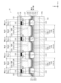
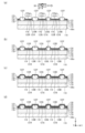
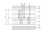
表示パネル10は、有機化合物の電界発光現象を利用した有機EL表示パネルであり、複数の薄膜トランジスタ(TFT:Thin Film Transistor)が配された基板100x(TFT基板)に、各々が画素を構成する複数の発光素子100がマトリックス状に配され、上面より光を発するトップエミッション型の構成を有する。ここで、本明細書では、図1におけるX方向、Y方向、Z方向を、それぞれ表示パネル10における、行方向、列方向、厚み方向とする。
The
図1に示すように、表示パネル10は、基板100x上をマトリックス状に区画してRGB各色の発光素子100R、100G、100B(区別しない場合は、「発光素子100」とする)を規制する列バンク122Yと行バンク122X(総称して「バンク122」とする)とが配された区画領域10e(以後、「領域10e」とする)から構成されている。発光素子100R、100G、100Bには、赤色に発光する自己発光領域100aR、緑色に発光する自己発光領域100aG、青色に発光する自己発光領域100aB(区別しない場合は「自己発光領域100a」とする)の何れかが形成されている。各発光素子100は、発光単位である副画素100seに対応する。表示パネル10の領域10eには、行方向に並んだ3つの副画素100seから構成された単位画素100eが行列状に配されている。
As shown in FIG. 1, the
また、図1に示すように、表示パネル10には、複数の画素電極119が基板100x上に行及び列方向にそれぞれ所定の距離だけ離れた状態でマトリックス状に配されている。画素電極119は、平面視において矩形形状であり、光反射材料からなる。行列状に配された画素電極119は、行方向に順に並んだ3つの自己発光領域100aR、100aG、100aBに対応する。画素電極119の行方向の長さ119xは、発光素子100B、100G、100Rの順に大きく構成されており、自己発光領域100aB、100aG、100aRの面積もこの順に大きい。したがって、発光素子100B、100G、100Rの行方向の幅WelB、WelG、WelRは、発光素子100B、100G、100Rの順に大きく構成されている。
As shown in FIG. 1, the
表示パネル10では、バンク122の形状は、いわゆるライン状のバンク形式を採用し、行方向に隣接する2つの画素電極119の間には、各条が列方向(図1のY方向)に延伸する列バンク122Yが複数行方向に並設されている。
In the
一方、列方向に隣接する2つの画素電極119の間には、各条が行方向(図1のX方向)に延伸する行バンク122Xが複数列方向に並設されている。行バンク122Xが形成される領域は、発光層123において有機電界発光が生じないために非自己発光領域100bとなる。
On the other hand, between two
122zと定義し、自己発光領域100aRに対応する間隙を赤色間隙122zR、自己発光領域100aGに対応する間隙を緑色間隙122zG、自己発光領域100aBに対応する間隙を青色間隙122zB(以後、区別しない場合は「間隙122z」)とする。
122z, the gap corresponding to self-luminous region 100aR is defined as red gap 122zR, the gap corresponding to self-luminous region 100aG is defined as green gap 122zG, and the gap corresponding to self-luminous region 100aB is defined as blue gap 122zB (hereinafter, when no distinction is made, they are referred to as "
また、図1に示すように、表示パネル10では、複数の自己発光領域100aと非自己発光領域100bとが、間隙122zに沿って列方向に交互に並んで配され、非自己発光領域100bには、画素電極119とTFTのソースS1とを接続する接続凹部(コンタクトホール、不図示)119c(118a)が設けられている。
Also, as shown in FIG. 1, in the
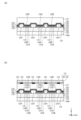
<表示パネル10の各部構成>
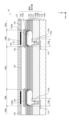
表示パネル10における発光素子100の構成について、図2、図3を用いて説明する。図2、図3は、図1におけるA1-A1、A2-A2で切断した模式断面図である。
<Configuration of Each Part of
The configuration of the
本実施の形態に係る表示パネル10においては、Z軸方向下方に薄膜トランジスタが形成された基板(TFT基板)が構成され、その上に有機EL素子部が構成されている。
In the
(発光素子部)
[基板100x]
基板100xは表示パネル10の支持部材であり、基材(不図示)と、基材上に形成された薄膜トランジスタ層(不図示)とを有する。
(Light Emitting Element Section)
[
The
基材は、表示パネル10の支持部材であり、平板状である。基材の材料としては、電気絶縁性を有する材料、例えば、ガラス材料、樹脂材料、半導体材料、絶縁層をコーティングした金属材料などを用いることができる。
The substrate is a support member for the
TFT回路は、発光素子100の外部回路からの駆動信号に応じ、自身に対応する画素電極119と外部電源とを電気的に接続するものであり、TFT層は、基材上面に形成された電極、半導体層、絶縁層などの多層構造からなる。本実施の形態では、TFT層は、基材上面に形成された複数のTFT及び配線からなる。配線は、TFTのソースS1 と対応する画素電極119、外部電源、外部回路などを電気的に接続している。
The TFT circuit electrically connects the
[平坦化層118]
基材上及びTFT層の上面には平坦化層118が設けられている。基板100xの上面に位置する平坦化層118は、TFT層によって凹凸が存在する基板100xの上面を平坦化するとともに、配線及びTFTの間を埋め、配線及びTFTの間を電気的に絶縁している。
[Planarization layer 118]
A
平坦化層118には、画素電極119と対応する画素のソースS1 に接続される配線とを接続するために、画素電極119に対応して、当該配線の上方の一部にコンタクト孔118aが開設されている。
In the
[画素電極119]
基板100xにおける領域10eの上面に位置する平坦化層118上には、図2、3に示すように、副画素100se単位で画素電極119が設けられている。
[Pixel electrode 119]
As shown in FIGS. 2 and 3, a
画素電極119は、発光層123へキャリアを供給するためのものであり、例えば陽極として機能した場合は、発光層123へホールを供給する。表示パネル10はトップエミッション型であるため、画素電極119は光反射性を有する。画素電極119の形状は、例えば、概矩形形状をした平板状である。本実施の形態では、上述のとおり、発光素子100B、100G、100Rにおける画素電極119の行方向の長さ119x(B)、(G)、(R)は、発光素子100B、100G、100Rの順に大きく構成されている。これにより、発光層123の電流密度を、発光素子100B、100G、100Rの順に小さくして各色の発光素子100の素子寿命の違いを補うように構成されている。
The
平坦化層118のコンタクト孔(不図示)上には、画素電極119の一部を基板100x方向に凹入された画素電極119の接続凹部119cが形成されており、接続凹部の底で画素電極119と対応する画素のソースS1に接続される配線とが接続される。
A
[ホール注入層120]
画素電極119及上には、図2、3に示すように、ホール注入層120が積層されている。ホール注入層120は、画素電極119から注入されたホールをホール輸送層121へ輸送する機能を有する。
[Hole injection layer 120]
2 and 3, a
ホール注入層120は、基板100x側から順に、画素電極119上に形成された金属酸化物からなる下層と、後述する間隙122zR、間隙122zG、間隙122zB内の下層の上それぞれに積層された有機物からなる上層とを含む。RGBの各副画素に形成される上層は、RGBの各副画素によって膜厚が異なって形成されている。
The
本実施の形態では、図3に示すように、間隙122zR、間隙122zG、間隙122zB内では、ホール注入層120は列方向に延伸するように線状に設けられている。
In this embodiment, as shown in FIG. 3, in gaps 122zR, 122zG, and 122zB, the
[バンク122]
図2に示すように、画素電極119、ホール注入層120の端縁を被覆するように絶縁物からなるバンクが形成されている。バンクには、列方向に延伸して行方向に複数並設されている列バンク122Yと、行方向に延伸して列方向に複数並設されている行バンク122Xとがある(以後、区別しない場合は「バンク122」と称する)。
[Bank 122]
2, banks made of an insulator are formed so as to cover the edges of the
列バンク122Yの形状は、列方向に延伸する線状であり、行方向に平行に切った断面は、上方を先細りとする順テーパー台形状である。列バンク122Yは、発光層123の材料となる有機化合物を含んだインクの行方向への流動を堰き止めて形成される発光層123の行方向外縁を規定するものである。また、列バンク122Yは、行方向の基部により行方向における各副画素100seの発光領域100aの外縁を規定する。
The
ここで、図13に示すように、平面視において、行方向における後述する遮光膜133の開口133aの縁と発光素子100との距離は、列バンク122Yの行方向の幅を異ならせることにより、発光素子100の発光色に応じて異なる構成を採る。
As shown in FIG. 13, in a plan view, the distance in the row direction between the edge of the
言い換えれば、発光素子100の発光色に応じて、列バンク122Yの行方向における幅のうち隣り合う発光素子100の側に位置する部分の幅が異なることにより、行方向における遮光膜133の開口133aの縁と発光素子100の外縁との距離が異なる態様を採る。
In other words, the width of the portion of the
具体的には、発光素子100Rを区画する2本の列バンク122Yのうち、発光素子100Bと発光素子100Rとの間に配された列バンク122Yの幅Wbk(B-R)は、発光素子100Bの側に位置する部分の幅WbkBと発光素子100Rの側に位置する部分の幅WbkRとから構成され、発光素子100Rと発光素子100Gとの間に配された列バンク122Yの幅Wbk(R-G)は、発光素子100Rの側に位置する部分の幅WbkRと発光素子100Gの側に位置する部分の幅WbkGとから構成される。そして、発光素子100Rの発光色に応じて発光素子100Rの側に位置する部分の幅WbkRが規定される。
Specifically, of the two
ここで、列バンク122Yの幅Wbk(B-R)において、発光素子100Bの側に位置する部分の幅WbkBと、発光素子100Rの側に位置する部分の幅WbkRは、列バンク122Yの幅Wbk(B-R)を発光素子幅WelRと発光素子幅WelBとで内分した点によって分割される構成としてもよい。あるいは、列バンク122Yの幅Wbk(B-R)を等分した点によって分割されてもよい。
Here, in the width Wbk(B-R) of the
同様に、列バンク122Yの幅Wbk(R-G)において、発光素子100Rの側に位置する部分の幅WbkRと、発光素子100Gの側に位置する部分の幅WbkGは、列バンク122Yの幅Wbk(R-G)を発光素子幅WelRと発光素子幅WelGとで内分した点によって分割される構成としてもよい。あるいは、列バンク122Yの幅Wbk(R-G)を等分した点によって分割されてもよい。
Similarly, in the width Wbk(R-G) of the
同様に、発光素子100Gを区画する2本の列バンク122Yのうち、発光素子100Rと発光素子100Gとの間に配された列バンク122Yの幅Wbk(R-G)は、発光素子100Rの側に位置する部分の幅WbkRと発光素子100Gの側に位置する部分の幅WbkGとから構成され、発光素子100Gと発光素子100Bとの間に配された列バンク122Yの幅Wbk(G-B)は、発光素子100Gの側に位置する部分の幅WbkGと発光素子100Bの側に位置する部分の幅WbkBとから構成される。そして、発光素子100Gの発光色に応じて発光素子100Gの側に位置する部分の幅WbkGが規定される。
Similarly, of the two
ここでも、列バンク122Yの幅Wbk(G-B)において、発光素子100Gの側に位置する部分の幅WbkGと、発光素子100Bの側に位置する部分の幅WbkBは、列バンク122Yの幅Wbk(G-B)を発光素子幅WelGと発光素子幅WelBとで内分した点によって分割される構成としてもよい。あるいは、列バンク122Yの幅Wbk(G-B)を等分した点によって分割されてもよい。
Here too, in the width Wbk(G-B) of the
さらに、発光素子100Bを区画する2本の列バンク122Yのうち、発光素子100Gと発光素子100Bとの間に配された列バンク122Yの幅Wbk(G-B)は、発光素子100Gの側に位置する部分の幅WbkGと発光素子100Bの側に位置する部分の幅WbkBとから構成され、発光素子100Bと発光素子100Rとの間に配された列バンク122Yの幅Wbk(B-R)は、発光素子100Bの側に位置する部分の幅WbkBと発光素子100Rの側に位置する部分の幅WbkRとから構成される。そして、発光素子100Bの発光色に応じて発光素子100Bの側に位置する部分の幅WbkBが規定される。
Furthermore, of the two
したがって、列バンク122Yの幅Wbk(R-G)は、発光素子100Rの発光色と発光素子100Gの発光色に基づいて規定される。同様に、列バンク122Yの幅Wbk(G-B)は、発光素子100Gの発光色と発光素子100Bの発光色に基づいて規定される。さらに、列バンク122Yの幅Wbk(B-R)は、発光素子100Bの発光色と発光素子100Rの発光色に基づいて規定される。
Therefore, the width Wbk (R-G) of the
表示パネル10では、列バンク122Yの隣接する発光素子100の側に位置する部分の幅は、その発光素子100の発光色に応じて異なる。具体的には、行方向の発光素子幅Welが大きい発光素子100は、発光素子幅Welが小さい発光素子100よりも、列バンク122Yの行方向におけるその発光素子100の側に位置する部分の幅Wbkが小さく構成される。具体的には、発光素子100の行方向の発光素子幅WelB、WelG、WelRは、発光素子100B、G、Rの順に大きく構成されているので、列バンク122Yの行方向における発光素子100の側に位置する部分の幅Wbkは、WbkB、WbkG、WbkRの順に小さく構成されている。
In the
行バンク122Xの形状は、行方向に延伸する線状であり、列方向に平行に切った断面は上方を先細りとする順テーパー台形状である。行バンク122Xは、各列バンク122Yを貫通するようにして行方向に設けられており、各々が列バンク122Yの上面122Ybよりも低い位置に上面を有する。そのため、行バンク122Xと列バンク122Yとにより、自己発光領域100aに対応する開口が形成されている。
The
[ホール輸送層121]
図2、3に示すように、間隙122zR、122zG、122zB内におけるホール注入層120上には、ホール輸送層121が積層される。また、行バンク122Xにおけるホール注入層120上にも、ホール輸送層121が積層される。ホール輸送層121は、ホール注入層120に接触している。ホール輸送層121は、ホール注入層120から注入されたホールを発光層123へ輸送する機能を有する。RGBの各副画素に形成されるホール輸送層121R、121G、121Bは、RGBの各副画素によって膜厚が異なって形成されていてもよい(以後、区別しない場合は「ホール輸送層121」とする)。
[Hole transport layer 121]
2 and 3, a
本実施の形態では、後述する間隙122z内では、ホール輸送層121は、列方向に延伸するように線状に設けられている構成を採る。
In this embodiment, in the
[発光層123]
図2、3に示すように、ホール輸送層121上には、発光層123が積層されている。発光層123は、有機化合物からなる層であり、内部でホールと電子が再結合することで光を発する機能を有する。列バンク122Yにより規定された間隙122zR、間隙122zG、間隙122zB内では、発光層123R、123G、123Bは、それぞれ列方向に延伸するように線状に設けられている。
[Light-emitting layer 123]
2 and 3, the light-emitting
各色の副画素100seにおいて、画素電極119と対向電極125との間に各色の発光層123が存在し、発光層123からの光を共振させて対向電極125側から出射させる光共振器構造が形成され、発光層123R、123G、123Bそれぞれから出射させる光の波長に応じて、発光層123上面と画素電極119上面との間の光学距離が設定され、各色に対応する光成分が強め合うように光共振器構造が形成されている。
In the subpixel 100se of each color, a light-emitting
発光層123は、画素電極119からキャリアが供給される部分のみが発光するので、層間に絶縁物である行バンク122Xが存在する範囲100bでは、有機化合物の電界発光現象が生じない。そのため、発光層123は、行バンク122Xがない部分が自己発光領域100aとなり、行バンク122Xの側面及び上面122Xbの上方にある部分は非自己発光領域となる。
Since only the portions of the light-emitting
各色の副画素100seにおいて、画素電極119と対向電極125との間に各色の発光層123が存在し、発光層123からの光を共振させて対向電極125側から出射させる光共振器構造が形成されている。すなわち、それぞれの発光層123R、123G、123Bから発された光が画素電極119にて反射されて対向電極125を通して上方に出射される反射光と、発光層R、123G、123Bから発された光が対向電極125を通して上方に出射される直接光とが干渉して強め合う構造を有する。そのため、発光層123R、123G、123Bそれぞれから出射させる光の波長に応じて、発光層123上面と画素電極119上面との間の光学距離が設定され、各色に対応する光成分が強め合うように、発光層123R、123G、123B、ホール輸送層121R、121G、121Bの膜圧が、RGBの各副画素によって異なって形成されている。
In the subpixel 100se of each color, the light-emitting
なお、発光層123は、自己発光領域100aだけでなく、隣接する非自己発光領域100bまで連続して延伸されている。このようにすると、発光層123の形成時に、自己発光領域100aに塗布されたインクが、非自己発光領域100bに塗布されたインクを通じて列方向に流動でき、列方向の画素間でその膜厚を平準化することができる。但し、非自己発光領域100bでは、行バンク122Xによって、インクの流動が程良く抑制される。よって、列方向に大きな膜厚むらが発生しにくく画素毎の輝度むらが改善される。
The light-emitting
[電子輸送層124]
図2、3に示すように、列バンク122Y及び列バンク122Yにより規定された間隙122z内の発光層123上を被覆するように電子輸送層124が積層して形成されている。電子輸送層124は、表示パネル10の少なくとも表示領域全体に連続した状態で形成されている。電子輸送層124は、対向電極125からの電子を発光層123へ輸送するとともに、発光層123への電子の注入を制限する機能を有する。
[Electron transport layer 124]
2 and 3 , an
[対向電極125]
図2、3に示すように、電子輸送層124上に、対向電極125が形成されている。対向電極125は、各発光層123に共通の電極となっている。対向電極125は、画素電極119と対になって発光層123を挟むことで通電経路を作る。対向電極125は、発光層123へキャリアを供給し、例えば陰極として機能した場合は、発光層123へ電子を供給する。
[Counter electrode 125]
2 and 3, a
[封止層126]
対向電極125を被覆するように、封止層126が積層形成されている。封止層126は、発光層123が水分や空気などに触れて劣化することを抑制するためのものである。封止層126は、対向電極125の上面を覆うように設けられている。また、ディスプレイとして良好な光取り出し性を確保するために高い透光性を有することが必要である。
[Sealing layer 126]
A
(発光素子部の構成材料)
発光素子部の各部の構成材料について、一例を示す。
(Materials Constituting the Light Emitting Element)
An example of the constituent materials of each part of the light emitting element part will be shown below.
[基板100x(TFT基板)]
基材としては、例えば、ガラス基板、石英基板、シリコン基板、硫化モリブデン、銅、亜鉛、アルミニウム、ステンレス、マグネシウム、鉄、ニッケル、金、銀などの金属基板、ガリウム砒素基などの半導体基板、プラスチック基板等を採用することができる。
[
Examples of the substrate that can be used include glass substrates, quartz substrates, silicon substrates, metal substrates such as molybdenum sulfide, copper, zinc, aluminum, stainless steel, magnesium, iron, nickel, gold, and silver, semiconductor substrates such as gallium arsenide-based substrates, and plastic substrates.
TFT層は、基材に形成されたTFT回路と、TFT回路上に形成された無機絶縁層(不図示)、平坦化層118とを有する。TFT回路は、基材上面に形成された電極、半導体層、絶縁層などの多層構造からなる。
The TFT layer has a TFT circuit formed on the substrate, an inorganic insulating layer (not shown) formed on the TFT circuit, and a
TFTを構成するゲート電極、ゲート絶縁層、チャネル層、チャネル保護層、ソース電極、ドレイン電極などには公知の材料を用いることができる。 Known materials can be used for the gate electrode, gate insulating layer, channel layer, channel protection layer, source electrode, drain electrode, and other components that make up a TFT.
基板100xの上面に位置する平坦化層118の材料としては、例えば、ポリイミド系樹脂、アクリル系樹脂、シロキサン系樹脂、ノボラック型フェノール系樹脂などの有機化合物を用いることができる。
The
[画素電極119]
画素電極119は、金属材料から構成されている。トップエミッション型の本実施の形態に係る表示パネル10の場合には、厚みを最適に設定して光共振器構造を採用することにより出射される光の色度を調整し輝度を高めているため、画素電極119の表面部が高い反射性を有する。本実施の形態に係る表示パネル10では、画素電極119は、金属層、合金層、透明導電膜の中から選択される複数の膜を積層させた構造であってもよい。金属層としては、シート抵抗が小さく、高い光反射性を有する材料として、例えば、アルミニウム(Al)を含む金属材料から構成することができる。アルミニウム(Al)合金では、反射率が80~95%と高く、電気抵抗率が、2.82×10⁻⁸(10 nΩm)と小さく、画素電極119の材料として好適である。さらに、コスト面からアルミニウムを主成分として含む金属層、合金層を用いることが好ましい。
[Pixel electrode 119]
The
金属層としては、アルミニウム合金などの金属層の他、高反射率の観点から、例えば、銀や銀を含む合金等を用いることができる。 As the metal layer, in addition to metal layers such as aluminum alloys, from the viewpoint of high reflectivity, for example, silver or alloys containing silver can be used.
[ホール注入層120]
ホール注入層120は、例えば、銀(Ag)、モリブデン(Mo)、クロム(Cr)、バナジウム(V)、タングステン(W)、ニッケル(Ni)、イリジウム(Ir)などの酸化物からなる層である。ホール注入層120を遷移金属の酸化物から構成する場合には、複数の酸化数をとるためこれにより複数の準位をとることができ、その結果、ホール注入が容易になり駆動電圧を低減することができる。
[Hole injection layer 120]
The
本実施の形態では、ホール注入層120は、膜厚が2nm以上(ここでは一例として10nm)30nm以下の酸化タングステン層として構成される。ホール注入層120は、酸化タングステンから構成されることが望ましいが、通常混入し得る程度の極微量の不純物が含まれていてもよい。
In this embodiment, the
ホール注入層120は、例えば、PEDOT(ポリチオフェンとポリスチレンスルホン酸との混合物)などの導電性ポリマー材料の有機高分子溶液からなる塗布膜を用いることができる。
The
[バンク122]
バンク122は、樹脂等の有機材料を用い形成されており絶縁性を有する。バンク122の形成に用いる有機材料の例としては、アクリル系樹脂、ポリイミド系樹脂、ノボラック型フェノール樹脂等があげられる。バンク122は、有機溶剤耐性を有することが好ましい。より好ましくは、アクリル系樹脂を用いることが望ましい。屈折率が低くリフレクターとして好適であるからである。
[Bank 122]
The bank 122 is formed using an organic material such as a resin and has insulating properties. Examples of organic materials used to form the bank 122 include acrylic resin, polyimide resin, novolac type phenolic resin, and the like. It is preferable that the bank 122 has resistance to organic solvents. More preferably, it is desirable to use an acrylic resin, as this has a low refractive index and is suitable as a reflector.
又は、バンク122は、無機材料を用いる場合には、屈折率の観点から、例えば、酸化シリコン(SiO)を用いることが好ましい。あるいは、例えば、窒化シリコン(SiN)、酸窒化シリコン(SiON)などの無機材料を用い形成される。 Alternatively, when an inorganic material is used for the bank 122, it is preferable to use, for example, silicon oxide (SiO) from the viewpoint of refractive index. Alternatively, the bank 122 may be formed using an inorganic material such as, for example, silicon nitride (SiN) or silicon oxynitride (SiON).
また、表面に撥水性をもたせるために、表面をフッ素処理することもできる。また、バンク122の形成にフッ素を含有した材料を用いてもよい。また、バンク122の表面に撥水性を低くするために、バンク122に紫外線照射を行う、低温でベーク処理を行ってもよい。 The surface can also be fluorine-treated to make it water-repellent. A material containing fluorine can also be used to form the banks 122. To make the surface of the banks 122 less water-repellent, the banks 122 can be irradiated with ultraviolet light or baked at a low temperature.
[ホール輸送層121]
ホール輸送層121は、例えば、ポリフルオレンやその誘導体、あるいはアミン系有機高分子であるポリアリールアミンやその誘導体などの高分子化合物、あるいは、TFB(poly(9、9-di-n-octylfluorene-alt-(1、4-phenylene-((4-sec-butylphenyl)imino)-1、4-phenylene))などを用いることができる。
[Hole transport layer 121]
The
[発光層123]
発光層123は、上述のように、ホールと電子とが注入され再結合されることにより励起状態が生成され発光する機能を有する。発光層123の形成に用いる材料は、湿式印刷法を用い製膜できる発光性の有機材料を用いることが必要である。
[Light-emitting layer 123]
As described above, the light-emitting
具体的には、例えば、特許公開公報(日本国・特開平5-163488号公報)に記載のオキシノイド化合物、ペリレン化合物、クマリン化合物、アザクマリン化合物、オキサゾール化合物、オキサジアゾール化合物、ペリノン化合物、ピロロピロール化合物、ナフタレン化合物、アントラセン化合物、フルオレン化合物、フルオランテン化合物、テトラセン化合物、ピレン化合物、コロネン化合物、キノロン化合物及びアザキノロン化合物、ピラゾリン誘導体及びピラゾロン誘導体、ローダミン化合物、クリセン化合物、フェナントレン化合物、シクロペンタジエン化合物、スチルベン化合物、ジフェニルキノン化合物、スチリル化合物、ブタジエン化合物、ジシアノメチレンピラン化合物、ジシアノメチレンチオピラン化合物、フルオレセイン化合物、ピリリウム化合物、チアピリリウム化合物、セレナピリリウム化合物、テルロピリリウム化合物、芳香族アルダジエン化合物、オリゴフェニレン化合物、チオキサンテン化合物、アンスラセン化合物、シアニン化合物、アクリジン化合物、8-ヒドロキシキノリン化合物の金属錯体、2-ビピリジン化合物の金属錯体、シッフ塩とIII族金属との錯体、オキシン金属錯体、希土類錯体などの蛍光物質で形成されることが好ましい。 Specific examples of the compounds include oxinoid compounds, perylene compounds, coumarin compounds, azacoumarin compounds, oxazole compounds, oxadiazole compounds, perinone compounds, pyrrolopyrrole compounds, naphthalene compounds, anthracene compounds, fluorene compounds, fluoranthene compounds, tetracene compounds, pyrene compounds, coronene compounds, quinolone compounds and azaquinolone compounds, pyrazoline derivatives and pyrazolone derivatives, rhodamine compounds, chrysene compounds, phenanthrene compounds, cyclopentadiene compounds, and stilbene compounds, which are described in the Japanese Patent Publication (JP Patent Publication No. 5-163488). It is preferable that the fluorescent substance be formed from a fluorescent substance such as a diphenylquinone compound, a styryl compound, a butadiene compound, a dicyanomethylenepyran compound, a dicyanomethylenethiopyran compound, a fluorescein compound, a pyrylium compound, a thiapyrylium compound, a selenapyrylium compound, a telluropyrylium compound, an aromatic aldadiene compound, an oligophenylene compound, a thioxanthene compound, an anthracene compound, a cyanine compound, an acridine compound, a metal complex of an 8-hydroxyquinoline compound, a metal complex of a 2-bipyridine compound, a complex of a Schiff salt and a Group III metal, an oxine metal complex, or a rare earth complex.
[電子輸送層124]
電子輸送層124には、電子輸送性が高い有機材料が用いられる。電子輸送層124は、フッ化ナトリウムで形成された層を含んでいてもよい。電子輸送層124に用いられる有機材料としては、例えば、オキサジアゾール誘導体(OXD)、トリアゾール誘導体(TAZ)、フェナンスロリン誘導体(BCP、Bphen)などのπ電子系低分子有機材料が挙げられる。
[Electron transport layer 124]
An organic material having high electron transport properties is used for the
また、電子輸送層124は、電子輸送性が高い有機材料に、アルカリ金属、又は、アルカリ土類金属から選択されるドープ金属がドープされて形成された層を含んでいてもよい。
The
[対向電極125]
対向電極125は、銀(Ag)又はアルミニウム(Al)などを薄膜化した電極を用い形成される。
[Counter electrode 125]
The
対向電極125は、光透過性を有する導電材料が用いられる。例えば、酸化インジウムスズ(ITO)若しくは酸化インジウム亜鉛(IZO)などを用い形成される。
The
[封止層126]
封止層126は、トップエミッション型の場合においては、光透過性の材料で形成される。例えば、窒化シリコン(SiN)、酸窒化シリコン(SiON)などの透光性材料を用い形成される。また、窒化シリコン(SiN)、酸窒化シリコン(SiON)などの材料を用い形成された層の上に、アクリル樹脂、シリコン樹脂などの樹脂材料からなる封止樹脂層を設けてもよい。
[Sealing layer 126]
In the case of a top emission type, the
(前面板131の各部構成)
[上部基板130]
接合層127の上に、上部基板130にカラーフィルタ層132が形成された前面板131が設置・接合されている。上部基板130には、表示パネル10がトップエミッション型であるため、例えば、カバーガラス、透明樹脂フィルムなどの光透過性材料が用いられる。また、上部基板130により、表示パネル10、剛性向上、水分や空気などの侵入防止などを図ることができる。上部基板130としては、例えば、ガラス基板、石英基板、プラスチック基板等に透光性材料を採用することができる。
(Configuration of each part of the front panel 131)
[Upper substrate 130]
A
[カラーフィルタ層132]
上部基板130には画素の各色自己発光領域100aに対応する位置にカラーフィルタ層132が形成されている。カラーフィルタ層132は、R、G、Bに対応する波長の可視光を透過させるために設けられる透明層であり、各色画素から出射された光を透過させて、その色度を矯正する機能を有する。例えば、本例では、赤色間隙122zR内の自己発光領域100aR、緑色間隙122zG内の自己発光領域100aG、青色間隙122zB内の自己発光領域100aBの上方に、赤色、緑色、青色のカラーフィルタ層132R、132G、132Bが各々形成されている。カラーフィルタ層132としては、公知の樹脂材料(例えば市販製品として、JSR株式会社製カラーレジスト)等を採用することができる。カラーフィルタ層132は膜厚が、1μm以上4μm以下の範囲で形成されていることが好ましい。カラーフィルタ層132は、具体的には、例えば、複数の開口部を画素単位に行列状に形成されたカラーフィルタ層形成用のカバーガラスからなる上部基板130に対し、カラーフィルタ層材料および溶媒を含有したインクを塗布する工程により形成される。
[Color filter layer 132]
The
[遮光膜133]
上部基板130には、図2、3に示すように、各副画素の発光領域100aに対向する位置に開口133aが開設されており、列バンク122Yの上方であって各副画素の発光領域100a間の行方向における境界に対応する位置、及び行バンク122Xの上方であって各副画素の発光領域100a間の列方向における境界に対応する位置を覆う遮光膜133が形成されている。
[Light-shielding film 133]
As shown in Figures 2 and 3,
遮光膜133は、R、G、Bに対応する波長の可視光を透過させないために設けられる黒色樹脂層であって、例えば光吸収性及び遮光性に優れる黒色顔料を含む樹脂材料からなる。いわゆるブラックマトリクスである。例えば、紫外線硬化樹脂(例えば紫外線硬化アクリル樹脂)材料を主成分とし、これに、例えば、カーボンブラック顔料、チタンブラック顔料、金属酸化顔料、有機顔料など遮光性材料の黒色顔料を添加してなる樹脂材料からなる。
The light-shielding
遮光膜133における開口133aの行方向の幅Wbma(R-G)、Wbma(G-B)、Wbma(B-R)は、発光素子100の発光色によらず等価に構成されている。また、開口133a間の桟の部分の行方向の幅Wbm(R-G)、Wbm(G-B)、Wbm(B-R)も、発光素子100の発光色によらず等価に構成されている。遮光膜133は、いわゆるブラックマトリクスである。また、「桟」とは、遮光膜133の開口133a以外の格子状の枠を構成するX方向に延伸した横のパターン、又はY方向に延伸した縦のパターンを指す。
The row widths Wbma(R-G), Wbma(G-B), and Wbma(B-R) of the
表示パネル10では、上述のとおり、行方向の発光素子幅Welが大きい発光素子100は、発光素子幅Welが小さい発光素子100よりも、列バンク122Yの行方向におけるその発光素子100の側に位置する部分の幅Wbkが小さく構成されている。その結果、行方向の発光素子幅Welが大きい発光素子100は、発光素子幅Welが小さい発光素子100よりも、遮光膜133の開口133aの行方向の縁と発光素子100の外縁との距離が小さい構成となる。
As described above, in the
具体的には、発光素子100の行方向の発光素子幅WelB、WelG、WelRは、発光素子100B、G、Rの順に大きく構成されているので、列バンク122Yの発光素子100側の幅Wbkは、WbkB、WbkG、WbkRの順に小さく構成されている。そして、遮光膜133の開口133aの行方向の縁と発光素子100の外縁との行方向の距離は、発光素子100B、100G、100Rの順に小さく構成されている。
Specifically, the row direction light emitting element widths WelB, WelG, WelR of the
また、遮光膜133は列バンク122Yと行方向に重なり、遮光膜133の行方向おける中心は、列バンク122Yの行方向において、両側の発光素子100に対応する部分の間の境界と一致する構成としてもよい。
The light-shielding
また、遮光膜133における開口133aは少なくとも行方向において対応する発光素子100を内含してもよい。
In addition, the
なお、遮光膜133は、それぞれ膜厚が、例えば、1μm以上2μm以下の範囲で形成されていてもよい。
The light-shielding
[接合層127]
封止層126のZ軸方向上方には、上部基板130のZ軸方向下側の主面にカラーフィルタ層132が形成された前面板131が配されており、接合層127により接合されている。接合層127は、基板100xから封止層126までの各層からなる背面パネルと前面板131とを貼り合わせるとともに、各層が水分や空気に晒されることを防止する機能を有する。接合層127の材料は、例えば、樹脂接着剤等からなる。接合層127は、アクリル樹脂、シリコン樹脂、エポキシ樹脂などの透光性材料樹脂材料を採用することができる。
[Bonding layer 127]
A
<表示パネル10の製造方法>
表示パネル10の製造方法について、図4~10を用いて説明する。図4は、有機EL表示パネル10の製造工程の工程図である。図5~10における各図は、表示パネル10の製造における各工程での状態を示す図1におけるA1-A1と同じ位置で切断した模式断面図である。
<Manufacturing Method of
The manufacturing method of the
[基板100xの準備]
複数のTFTや配線が形成された基板100xを準備する。基板100xは、公知のTFTの製造方法により製造することができる(図4におけるステップS1、図5(a))。
[Preparation of
A
[平坦化層118の形成]
基板100xを被覆するように、上述の平坦化層118の構成材料(感光性の樹脂材料)をフォトレジストとして塗布し、表面を平坦化することにより平坦化層118を形成する(図4:ステップS2、図5(b))。具体的には、一定の流動性を有する樹脂材料を、例えば、ダイコート法により、基板100x1の上面に沿って、TFT層による基板100x1上の凹凸を埋めるように塗布する。これにより、平坦化層118の上面は平坦化した形状となる。
[Formation of Planarizing Layer 118]
The
平坦化層118における、TFT素子の例えばソース電極上の個所にドライエッチング法を行い、コンタクトホール(不図示)を形成する。コンタクトホールは、その底部にソース電極の表面が露出するようにパターニングなどを用いて形成される。
A contact hole (not shown) is formed in the
次に、コンタクトホールの内壁に沿って接続電極層を形成する。接続電極層の上部は、その一部が平坦化層118上に配される。
Next, a connection electrode layer is formed along the inner wall of the contact hole. A portion of the upper part of the connection electrode layer is disposed on the
[画素電極119、ホール注入層120の形成]
次に、画素電極119、ホール注入層120の形成を行う(図4:ステップS3)。
[Formation of
Next, the
先ず、平坦化層118を形成した後、平坦化層118の表面にドライエッチング処理を行い成膜前洗浄を行う。
First, the
次に、平坦化層118の表面に成膜前洗浄を行った後、画素電極119を形成するための画素電極用の金属膜119xをスパッタリング法、真空蒸着法などの気相成長法により平坦化層118の表面に成膜する。本例では、アルミニウム又はアルミニウムを主成分とする合金からなる膜をスパッタリング法により成膜する。
Next, after performing pre-deposition cleaning on the surface of the
さらに、金属膜119xの表面に成膜前洗浄を行った後、引き続き真空雰囲気下でホール注入層120を形成するためのホール注入層120用の金属膜120’を気相成長法により金属膜119xの表面に成膜する(図5(d))。本例では、タングステンをスパッタリング法により成膜する。
After the surface of the
その後、感光性樹脂等からなるフォトレジスト層FRを塗布したのち、所定の開口部が施されたフォトマスクPMを載置し、その上から紫外線照射を行いフォトレジストを露光し、そのフォトレジストにフォトマスクが有するパターンを転写する(図6(a))。次に、フォトレジスト層FRを現像によってパターニングする。 After that, a photoresist layer FR made of a photosensitive resin or the like is applied, and then a photomask PM with predetermined openings is placed on top. The photoresist is exposed to ultraviolet light from above, and the pattern of the photomask is transferred to the photoresist (Figure 6(a)). Next, the photoresist layer FR is patterned by development.
その後、パターニングされたフォトレジスト層FRを介して、金属膜120’にドライエッチング処理を施してパターニングを行い、ホール注入層120を形成する。
Then, the metal film 120' is patterned by dry etching through the patterned photoresist layer FR to form the
続けて、パターニングされたフォトレジスト層FR及びホール注入層120を介して、金属膜119xにウエットエッチング処理を施してパターニングを行い、画素電極119を形成する。
Then, the
ホール注入層120の形成において、例えば、ホール注入層120と画素電極119とをドライエッチングで一括に処理してもよい。
When forming the
最後に、フォトレジスト層FRを剥離して、同一形状にパターニングされた画素電極119及びホール注入層120の積層体を形成する(図6(b))。
Finally, the photoresist layer FR is peeled off to form a laminate of
[バンク122の形成]
ホール注入層120のホール注入層120を形成した後、ホール注入層120を覆うようにバンク122を形成する。バンク122の形成では、先ず行バンク122Xを形成し、その後、間隙122zを形成するように列バンク122Yを形成する(図4:ステップS4、図6(c))。
[Formation of bank 122]
After forming the
先ず、行バンク122の形成は、先ず、ホール注入層120上に、スピンコート法などを用い、行バンク122Xの構成材料(例えば、感光性樹脂材料)からなる膜を積層形成する。そして、樹脂膜をパターニングして行バンク122Xを形成する。
First, the row bank 122 is formed by laminating a film made of the constituent material of the
行バンク122Xのパターニングは、樹脂膜の上方にフォトマスクを利用し露光を行い、現像工程、焼成工程(約230℃、約60分)をすることによりなされる。
The
次に、列バンク122Yの形成工程では、ホール注入層120上及び行バンク122X上に、スピンコート法などを用い、列バンク122Yの構成材料(例えば、感光性樹脂材料)からなる膜を積層形成する。そして、間隙122zの形成は、樹脂膜の上方にマスクを配して露光し、その後で現像することにより、樹脂膜をパターニングして間隙122zを開設して列バンク122Yを形成する。
Next, in the process of forming the
具体的には、列バンク122Yの形成工程では、先ず、有機系の感光性樹脂材料、例えば、アクリル系樹脂、ポリイミド系樹脂、ノボラック型フェノール樹脂等からなる感光性樹脂膜を形成した後、乾燥し、溶媒をある程度揮発させてから、所定の開口部が施されたフォトマスクを重ね、その上から紫外線照射を行い感光性樹脂等からなるフォトレジストを露光し、そのフォトレジストにフォトマスクが有するパターンを転写する。
Specifically, in the process of forming the
次に、感光性樹脂を現像、によって列バンク122Yをパターニングした絶縁層を、焼成(約230℃、約60分)することにより形成する。
Next, the photosensitive resin is developed to form an insulating layer patterned into the
ここで、ホール注入層120は、上述のとおり、スパッタリング法あるいは真空蒸着法などの気相成長法を用い金属(例えば、タングステン)からなる膜を形成した後、フォトリソグラフィー法及びエッチング法を用い各画素単位にパターニングされるが、行バンク122X、列バンク122Yに対する焼成工程において、金属が酸化されホール注入層120として完成する。
Here, as described above, the
[有機機能層の形成]
行バンク122X上を含む列バンク122Yにより規定される間隙122z内に形成されたホール注入層120上に対して、ホール輸送層121、発光層123を順に積層形成する(図4:ステップS6、7、図6(d)、図7(a))。
[Formation of organic functional layer]
A
ホール注入層120の上面に、インクジェット法を用い、PEDOT(ポリチオフェンとポリスチレンスルホン酸との混合物)などの導電性ポリマー材料を含むインクを列バンク122Yにより規定される間隙122z内に塗布した後、溶媒を揮発除去させる。あるいは、焼成することによりなされる。その後、フォトリソグラフィー法およびエッチング法を用い各画素単位にパターニングしてホール注入層の上層を形成してもよい。
An ink containing a conductive polymer material such as PEDOT (a mixture of polythiophene and polystyrene sulfonic acid) is applied to the upper surface of the
ホール輸送層121は、インクジェット法やグラビア印刷法によるウェットプロセスを用い、構成材料を含むインクを列バンク122Yにより規定される間隙122z内に塗布した後、溶媒を揮発除去させる、あるいは、焼成することによりなされる。
The
発光層123の形成は、インクジェット法を用い、構成材料を含むインクを列バンク122Yにより規定される間隙122z内に塗布した後、焼成することによりなされる(図4:ステップS6、図7(a))。具体的には、基板100xは、列バンク122YがY方向に沿った状態で液滴吐出装置の動作テーブル上に載置され、Y方向(図7(a)では紙面奥行き方向)に沿って複数のノズル孔がライン状に配置されたインクジェットヘッド301をX方向に基板100xに対し相対的に移動しながら、各ノズル孔から列バンク122Y同士の間隙122z内に設定された着弾目標を狙ってインクの液滴18を着弾させることによって行う。
The light-emitting
また、この工程では、副画素形成領域となる間隙122zに、インクジェット法によりR、G、Bいずれかの有機発光層の材料を含むインク123RI、123GI、123BIをそれぞれ充填し、充填したインクを減圧下で乾燥させ、ベーク処理することによって、発光層123R、123G、123Bを形成する。このとき、発光層123のインクの塗布では、先ず、液滴吐出装置を用いて発光層123の形成するための溶液の塗布を行う。
In this process, inks 123RI, 123GI, and 123BI containing the material of an organic light-emitting layer of R, G, or B are filled into
基板100xに対して赤色発光層、緑色発光層、青色発光層の何れかを形成するためのインクの塗布が終わると、次に、その基板に別の色のインクを塗布し、次にその基板に3色目のインクを塗布する工程が繰り返し行われ、3色のインクを順次塗布する。これにより、基板100x上には、赤色発光層、緑色発光層、青色発光層が、図の紙面横方向に繰り返して並んで形成される。
After the application of ink to form one of the red, green, and blue light-emitting layers to the
なお、ホール輸送層121、発光層123の形成方法は上記の方法には限定されず、インクジェット法やグラビア印刷法以外の方法、例えばディスペンサー法、ノズルコート法、スピンコート法、凹版印刷、凸版印刷等の公知の方法によりインクを滴下・塗布してもよい。
The method for forming the
[電子輸送層124の形成]
発光層123を形成した後、表示パネル10の発光エリア(表示領域)全面にわたって、真空蒸着法などにより電子輸送層124を形成する(図4:ステップS8、図7(b))。真空蒸着法を用いる理由は有機膜である発光層123に損傷を与えないためと、高真空化で行う真空蒸着法は成膜対象の分子が基板に向かって垂直方向に直進的に成膜される。電子輸送層124は、発光層123の上に、金属酸化物又はフッ化物を真空蒸着法などにより成膜し、さらに、有機材料と金属材料とを共蒸着法により成膜する。なお、電子輸送層124の膜厚は、光学的な光取り出しとして最も有利となる適切な膜厚とする。
[Formation of Electron Transport Layer 124]
After forming the light-emitting
[対向電極125の形成]
電子輸送層124を形成した後、電子輸送層124を被覆するように、対向電極125を形成する(図4:ステップS9、図7(c))。
[Formation of Counter Electrode 125]
After the
先ず、対向電極125は、電子輸送層124を被覆するように、CVD(Chemical Vapor Deposition)法、スパッタリング法、又は真空蒸着法により形成する。本例では、対向電極125Aを真空蒸着法により銀を堆積することにより形成する構成としている。
First, the
次に、スパッタリング法を用いてITO又はIZOなどの透明導電層を形成する構成としている。 Next, a transparent conductive layer such as ITO or IZO is formed using a sputtering method.
[封止層126の形成]
対向電極125Bを被覆するように、封止層126を形成する(図4:ステップS10、図7(d))。封止層126は、CVD法、スパッタリング法などを用い形成できる。
[Formation of sealing layer 126]
The
[前面板131の形成]
次に、図4のステップS10における前面板131の製造方法について説明する。図8(a)~(g)は、有機EL表示パネル10の製造におけるにおける前面板の製造の状態を示す図1におけるA1-A1と同じ位置で切断した模式断面図である。
[Formation of front panel 131]
Next, a method for manufacturing
先ず、透明な上部基板130を準備し、紫外線硬化樹脂(例えば紫外線硬化アクリル樹脂)材料を主成分とし、これに黒色顔料を添加してなる遮光膜の材料(133´)を透明な上部基板130の一方の面に塗布する(図8(a))。
First, a transparent
塗布した遮光膜の材料の膜133´の上面に所定の開口部が施されたパターンマスクPMを重ね、その上から紫外線照射を行う(図8(b))。 A pattern mask PM with a set of openings is placed on top of the applied light-shielding film material 133', and ultraviolet light is irradiated from above (Figure 8 (b)).
その後、パターンマスクPM及び未硬化の遮光膜133を除去して現像し、キュアすると、例えば、概矩形状の断面形状の遮光膜133が完成する(図8(c))。このとき、遮光膜133は、基板100xと対向させたときに、基板100xに形成されたバンク122の上方であって各副画素の発光領域100a間の行及び列方向における境界に対応する部分に位置するようにパターニングされている。
Then, the pattern mask PM and the uncured light-shielding
次に、遮光膜133を形成した上部基板130表面に、紫外線硬化樹脂成分を主成分とするカラーフィルタ層132(例えば、G)の材料132Gを塗布し(図8(d))、所定のパターンマスクPMを載置し、紫外線照射を行う(図8(e))。
Next, a material 132G for the color filter layer 132 (e.g., G) containing a UV-curable resin component as the main component is applied to the surface of the
その後はキュアを行い、パターンマスクPM及び未硬化のペースト132Gを除去して現像すると、カラーフィルタ層132Gが形成される(図8(f))。
After that, curing is performed, the pattern mask PM and
この工程を各色のカラーフィルタ層材料について同様に繰り返すことで、カラーフィルタ層132R、132Bを形成する(図8(g))。このとき、遮光膜133の内方にカラーフィルタ層132Bが形成される。以上で前面板131が形成される。
This process is repeated for each color of color filter layer material to form color filter layers 132R and 132B (Figure 8(g)). At this time,
[前面板131と背面パネルとの貼り合わせ]
次に、基板100xから封止層126までの各層からなる背面パネルに、アクリル樹脂、シリコン樹脂、エポキシ樹脂などの紫外線硬化型樹脂を主成分とする接合層127の材料を塗布する(図9(a))。
[Bonding the
Next, a material for a
続いて、塗布した材料に紫外線照射を行い、背面パネルと前面板131との相対的位置関係を合せた状態で両基板を貼り合わせる。このとき、両者の間にガスが入らないように注意する。その後、両基板を焼成して封止工程を完了すると、表示パネル10が完成する(図9(b))。
Next, the applied material is irradiated with ultraviolet light, and the rear panel and
このとき、前面板131に形成された遮光膜133は、基板100xに形成されたバンク122の上方であって各副画素の発光領域100a間の行及び列方向における境界に対応する部分に位置するようアライメントされている。
At this time, the light-shielding
<効 果>
以下、実施の形態に係る表示パネル10の効果について説明する。
<Effects>
The effects of the
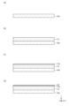
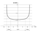
図10(a)~(b)、図11(a)~(b)は、表示パネル10において、遮光膜133の開口133aの開口幅を異ならせた比較例における発光素子の拡大断面図である。
Figures 10(a)-(b) and 11(a)-(b) are enlarged cross-sectional views of light-emitting elements in a comparative example in which the opening width of the
先ず、図10(a)に示すように、表示パネル10では、発光素子幅をWel0、遮光膜133の開口133aの幅をWbma0、発光基準点と遮光膜133との間の光学距離をLy0としたとき、視野角をαとして視線Cの方向から視したときの遮光幅はLx0、発光素子幅をWel0に対する遮光率はLx0/Wel0となる。
First, as shown in FIG. 10(a), in the
次に、図10(b)に示すように、発光素子幅をWel0より短い発光素子幅Wel1に縮小し、同時に遮光膜133の開口幅Wbma0も同等の長さだけ縮小した場合を想定する。このとき、視野角αの方向から視したときの遮光幅はLx0と変化しないが、遮光率はLx0/Wel0より大きいLx0/Wel1となる。これより、視野角αの方向から視したときの輝度は遮光率に応じて減少する。
Next, as shown in FIG. 10(b), assume that the light-emitting element width is reduced to light-emitting element width Wel1, which is shorter than Wel0, and at the same time, the opening width Wbma0 of the light-shielding
図10(b)の表示パネルに対し、遮光率はLx0/Wel1を変化させるために、遮光膜133の開口133aの開口幅Wbma1を増加させる場合を想定する。例えば、図11(a)に示すように、遮光膜133の開口133aの開口幅をWbma1より長い開口幅をWbm0に拡大したとき、視野角αの方向から視したときの遮光幅はLx0より短いLx1となり、遮光率はLx0/Wel1より大きいLx1/Wel1とすることができる。これより、視野角αの方向から視したときの輝度は遮光率の減少により改善(増加)する。
For the display panel of FIG. 10(b), assume that the opening width Wbma1 of the
しかしながら、遮光膜133の開口133a間の桟の部分の幅Wbm1が、製造プロセス上許容される遮光膜133の最小線幅を確保するために開口幅Wbm0の増加が制限される場合には、遮光幅及び遮光率を十分に減少できない場合がある。 これに対し、本実施の形態に係る表示パネル10では、図11(b)に示すように、図11(a)の表示パネルに対し、列バンク122Yの行方向に幅をWbk0より大きいWbl1まで拡大することにより、遮光膜133の開口133a間の桟の部分の幅をWbm1より大きいWbm0に戻すことができる。これより、桟の部分の幅を製造プロセス上許容される遮光膜133の最小線幅を確保しつつ、遮光率をLx0/Wel1より小さいLx1/Wel1とすることができる。これより、遮光率の減少により視野角αの方向から視したときの輝度を改善(増加)することができる。
However, when the width Wbm1 of the batten portion between the
本実施の形態では、上述のとおり、発光素子100B、100G、100Rにおける画素電極119の行方向の長さ119x(B)、(G)、(R)は、発光素子100B、100G、100Rの順に大きく構成されている。
In this embodiment, as described above, the
表示パネル10Xを視野角をαとして視線Cの方向から視したときの、発光素子幅Welに対する遮光率Lx/Welは、発光素子100R、100G、100Bの順に大きい。そのため、発光素子から看者が視認する輝度の減少率は遮光率が大きい発光素子100R、100G、100Bの順に増加するため、発光素子100R、100G、100Bからの輝度バランスが変化して看者が視認する色度が変化し、斜め方向からの視認時におけるグレーや中間調における色度ズレとして認識される。
When the
これに対し、表示パネル10では、上述のとおり、表示パネル10では、行方向の発光素子幅Welが大きい発光素子100は、発光素子幅Welが小さい発光素子100よりも、列バンク122Yの行方向におけるその発光素子100の側に位置する部分の幅Wbkが小さく構成されており、行方向の発光素子幅Welが大きい発光素子100は、発光素子幅Welが小さい発光素子100よりも、遮光膜133の開口133aの行方向の縁と発光素子100の外縁との距離が小さく構成されている。具体的には、本実施の形態では、行方向の発光素子幅がB、G、Rの順に大きく構成された発光素子100に対し、列バンク122Yの発光素子100側の幅Wbkは、WbkB、WbkG、WbkRの順に小さく構成され、遮光膜133の開口133aの行方向の縁と発光素子100の外縁との行方向の距離は、発光素子100B、100G、100Rの順に小さく構成されている。そのため、列バンク122Yの行方向における発光素子100の側に位置する部分の幅Wbkに伴う遮光率の増加は、発光素子100B、100G、100Rに大きい態様となる。
In contrast, in the
これより、発光素子100B、100G、100Rの遮光率の違いを相殺する方向に変化させて遮光率の違いを補うことで、斜め方向からの視認時における色度変化を低減することができる。
As a result, by compensating for the difference in the light blocking rate of the light-emitting
このとき、表示パネル10では、画素を構成する複数の発光素子100において発光素子幅Welが異なる場合において、発光素子幅Welが相対的に小さい発光素子100において、列バンク122Yの行方向におけるその発光素子100の側に位置する部分の幅Wbkを他の発光素子よりも拡大することにより、発光素子幅Wel及び遮光率の同時に縮小することができる。
In this case, in the
これにより、高精細化された有機EL表示パネルにおいて、画素密度が増加して発光素子100の単位面積が減少した場合でも、正面から45°以上傾斜した斜め方向から表示画像を見たときの出射光の色度変化を低減する自発光表示パネルの構造を実現できる。
This makes it possible to realize a self-luminous display panel structure that reduces the change in chromaticity of the emitted light when the displayed image is viewed from an oblique direction inclined by 45° or more from the front, even when the pixel density is increased and the unit area of the light-emitting
<まとめ>
以上のとおり、本開示の実施の形態に表示パネル10は、複数の副画素100seからなる画素が行列状に配された自発光型表示パネルであって、画素を構成する副画素100seごとに発光色が異なる複数の発光素子100と、行方向における発光素子100と発光素子100との間に配され、列方向に延伸されてなる複数の列バンク122Yと、発光素子100の出射方向の下流側に、平面視において各発光素子100と対向する位置に開口133aが設けられた遮光膜133とを備え、平面視において、遮光膜133の開口133aは少なくとも行方向において発光素子100と重なり、行方向における遮光膜133の開口133aの縁と発光素子100との距離は、発光素子100と行方向に隣り合う列バンク122Yの行方向の幅のうち、発光素子100の側に位置する部分の幅を異ならせることにより、発光素子100の発光色に応じて異なる構成されていてもよい。
<Summary>
As described above, the display panel 10 in the embodiment of the present disclosure is a self-luminous display panel in which pixels consisting of a plurality of sub-pixels 100se are arranged in a matrix, and includes a plurality of light-emitting elements 100, each of which emits a different light color for each sub-pixel 100se that constitutes a pixel, a plurality of column banks 122Y arranged between the light-emitting elements 100 in the row direction and extending in the column direction, and a light-shielding film 133 having an opening 133a provided at a position facing each light-emitting element 100 in a planar view downstream in the emission direction of the light-emitting elements 100, in which, in a planar view, the opening 133a of the light-shielding film 133 overlaps with the light-emitting element 100 at least in the row direction, and the distance in the row direction between the edge of the opening 133a of the light-shielding film 133 and the light-emitting element 100 may be configured to differ depending on the light-emitting color of the light-emitting element 100 by making different the width of the portion of the row-direction width of the column bank 122Y adjacent to the light-emitting element 100 in the row direction that is located on the side of the light-emitting element 100.
係る構成により、高精細化され画素密度が増加して発光素子100の面積が減少した場合でも、斜め方向から表示画像を見たときの出射光の色度変化を低減する自発光表示パネルの構造を実現できる。
This configuration makes it possible to realize a self-luminous display panel structure that reduces the change in chromaticity of the emitted light when the displayed image is viewed from an oblique direction, even when the pixel density is increased and the area of the light-emitting
≪有機EL表示装置1の回路構成≫
以下では、実施の形態に係る表示パネル10を用いた有機EL表示装置1(以後、「表示装置1」と称する)の回路構成について、図12を用い説明する。
<Circuit configuration of organic
Hereinafter, a circuit configuration of an organic EL display device 1 (hereinafter, referred to as a "
図12に示すように、表示装置1は、表示パネル10と、これに接続された駆動制御回路部20とを有して構成されている。
As shown in FIG. 12, the
表示パネル10は、複数の有機EL素子が、例えば、マトリクス状に配列され構成されている。駆動制御回路部20は、4つの駆動回路21~24と制御回路25とにより構成されている。
The
表示パネル10においては、複数の単位画素100eが行列状に配されて表示領域を構成している。各単位画素100eは、3個の有機EL素子、つまり、R(赤)、G(緑)、B(青)の3色に発光する3個の副画素100seから構成される。各副画素100seの回路構成について、図13を用い説明する。
In the
図13は、表示装置1に用いる表示パネル10の各副画素100seに対応する発光素子100における回路構成を示す回路図である。
Figure 13 is a circuit diagram showing the circuit configuration of a light-emitting
図13に示すように、本実施の形態に係る表示パネル10では、各副画素100seが2つのトランジスタTr1、Tr2と一つのキャパシタC、及び発光部としての有機EL素子部ELとを有し構成されている。トランジスタTr1は、駆動トランジスタであり、トランジスタTr2は、スイッチングトランジスタである。
13, in the
スイッチングトランジスタTr2のゲートG2は、走査ラインVscnに接続され、ソースS2 は、データラインVdatに接続されている。スイッチングトランジスタTr2 のドレインD2は、駆動トランジスタTr1のゲートG1に接続されている。 The gate G2 of the switching transistor Tr2 is connected to the scan line Vscn, the source S2 is connected to the data line Vdat, and the drain D2 of the switching transistor Tr2 is connected to the gate G1 of the driving transistor Tr1 .
駆動トランジスタTr1のドレインD1は、電源ラインVaに接続されており、ソースS1 は、有機EL素子部ELの画素電極(アノード)に接続されている。有機EL素子部ELにおける対向電極(カソード)は、接地ラインVcatに接続されている。 The drain D1 of the driving transistor Tr1 is connected to a power supply line Va, and the source S1 is connected to a pixel electrode (anode) of the organic EL element portion EL. The counter electrode (cathode) of the organic EL element portion EL is connected to a ground line Vcat.
なお、キャパシタCの第1端は、スイッチングトランジスタTr2のドレインD2及び駆動トランジスタTr1のゲートG1と接続され、キャパシタCの第2端は、電源ラインVaと接続されている。 The first terminal of the capacitor C is connected to the drain D2 of the switching transistor Tr2 and the gate G1 of the driving transistor Tr1 , and the second terminal of the capacitor C is connected to the power supply line Va.
表示パネル10においては、隣接する複数の副画素100se(例えば、赤色(R)と緑色(G)と青色(B)の発光色の3つの副画素100se)を組み合せて1つの単位画素100eを構成し、各単位画素100eが分布するように配されて画素領域を構成している。そして、各副画素100seのゲートG2からゲートラインが各々引き出され、表示パネル10の外部から接続される走査ラインVscnに接続されている。同様に、各副画素100seのソースS2からソースラインが各々引き出され表示パネル10の外部から接続されるデータラインVdatに接続されている。
In the
また、各副画素100seの電源ラインVa及び各副画素100seの接地ラインVcatは集約されて、表示装置1の電源ライン及び接地ラインに接続されている。
In addition, the power supply line Va of each subpixel 100se and the ground line Vcat of each subpixel 100se are aggregated and connected to the power supply line and ground line of the
≪変形例≫
実施の形態に係る表示パネル10を説明したが、本開示は、その本質的な特徴的構成要素を除き、以上の実施の形態に何ら限定を受けるものではない。例えば、実施の形態に対して当業者が思いつく各種変形を施して得られる形態や、本発明の趣旨を逸脱しない範囲で各実施の形態における構成要素及び機能を任意に組み合わせることで実現される形態も本開示に含まれる。以下では、そのような形態の一例として、有機EL表示パネルの変形例を説明する。
<<Variations>>
Although the
<変形例1>
実施の形態に係る表示パネル10では、遮光膜133における開口133aの行方向の幅Wbma(R-G)、Wbma(G-B)、Wbma(B-R)は、発光素子100の発光色によらず等価に構成され、開口133a間の桟の部分の行方向の幅Wbm(R-G)、Wbm(G-B)、Wbm(B-R)も、発光素子100の発光色によらず等価に構成されている構成とした。変形例1に係る表示パネル10Aでは、開口133a間の桟の部分の行方向の幅Wbm(R-G)、Wbm(G-B)、Wbm(B-R)も、発光素子100の発光色により異なり、その結果、遮光膜133における開口133aの行方向の幅Wbma(R-G)、Wbma(G-B)、Wbma(B-R)は、発光素子100の発光色より異なるように構成されている点で実施の形態と相違する。
<
In the
図14は、変形例1に係る表示パネル10Aの、図2におけるA1-A1と同じ断面で切断した模式断面図である。図14に示すように、変形例1に係る表示パネル10Aでは、遮光膜133における開口133aと開口133aとの間の桟の部分のうち、行方向の幅Wbmが相対的に小さい桟部分と対向する列バンク122Yの行方向の幅Wbkは、行方向の幅Wbmが相対的に大きい桟部分と対向する列バンクの行方向の幅Wbkよりも大きいことを特徴とする。具体的には、図14に示すように、表示パネル10Aでは、行方向における幅Wbkが大きい列バンク122Yの部分の上方に位置する遮光膜133の桟は、行方向における幅Wbkが小さい列バンク122Yの部分の上方に位置する遮光膜133の桟よりも、行方向における幅が小さい構成を採る。
Figure 14 is a schematic cross-sectional view of the
係る構成により、表示パネル10では、画素を構成する複数の発光素子100において発光素子幅Welが異なる場合において、発光素子幅Welが相対的に小さい発光素子100において、列バンク122Yの行方向におけるその発光素子100の側に位置する部分の幅Wbkを他の発光素子よりも拡大すると同時に、遮光膜133における桟の部分の行方向の幅を縮小することにより、実施の形態と同様に、発光素子幅Welを遮光率を同時に縮小するとともに、遮光率をより一層効果的に縮小することができる。
In the
<変形例2>
実施の形態に係る表示パネル10では、一例として、発光素子100Bの発光基準点と遮光膜133の開口133aの縁との間の出射方向における最大距離LBが、発光素子100R、Gよりも長い態様を用いて実施の形態を説明した。本実施の形態では、上述のとおり、発光素子100B、100G、100Rにおける画素電極119の行方向の長さ119x(B)、(G)、(R)が、発光素子100B、100G、100Rの順に大きく構成されており、発光素子100Bの遮光率が最小となる。これに対し、表示パネル10における上記構成を採ることにより、画素電極119の行方向の長さが最も大きい発光素子100の遮光率を増大させて、発光色による遮光率の変化を効果的に補償することができる。
<
In the
しかしながら、発光素子100の遮光率を異ならせる要因は画素電極119の行方向の長さ119x以外にも存在する。
However, there are other factors that cause the light blocking rate of the
図15は、表示パネル10の発光素子100Bを行方向に切断した断面における発光層123までの機能層の膜厚の測定結果である。図15に示すように、塗布法により形成される機能層の膜厚は、バンク間の間隙122zの行方向の中心(x=0)を含む幅±7.5μmの範囲において約0.26から0.33の範囲であり、膜厚の変動幅が0.07以下である平坦部123flが存在している。一方、平坦部123flのx方向の両側では、平坦部123flから離間するにつれて層厚が0.33から0.73に向けて徐々に増加しており、平坦部123flのx方向の両側5μmに平坦部123flよりも層厚が厚いピンニング部123pnが存在している。
Figure 15 shows the results of measuring the thickness of the functional layer up to the light-emitting
すなわち、発光層123は、それぞれ、バンク間の間隙122zの行方向の中心を含む幅の範囲に存在し行方向に層厚が所定の範囲内にあって均一な平坦部123flを有する。また、発光層123は、平坦部123flの行方向の両側に存在し平坦部123flよりも層厚が厚いピンニング部123pnとを含む。ピンニング部123pnでは、平坦部123flから離間するにつれて層厚が最大膜厚に向けて徐々に増加している。
That is, each of the light-emitting
図16は、表示パネル10の各色副画素における図2におけるA1-A1と同じ位置で測定した単色光の輝度(相対輝度)分布の測定結果を示す模式図である。
Figure 16 is a schematic diagram showing the results of measuring the luminance (relative luminance) distribution of monochromatic light measured at the same position as A1-A1 in Figure 2 for each color subpixel of the
図16に示すように、表示パネル10の各色発光素子100R、100G、100Bにおいて、発光層123の平坦部123flに相当する範囲において相対輝度0.1以上の発光輝度の分布が観測された。発光輝度の分布形状は、各色発光素子100R、100G、100Bによって異なり、発光素子100Gにおいて発光素子100R、100Bよりもより急峻な分布形状を示した。
As shown in FIG. 16, in each of the color light-emitting
また、各色発光素子100R、100G、100Bを、視野角αの方向から視したときに、発光素子100R、100Bの方が発光素子100Gよりも視認される輝度の低下率は大きいことが発明者の検討により確認されている。
In addition, the inventors have confirmed through their studies that when the light-emitting
発光層123において相対的にピンニング部123pnに比べて膜厚が小さい平坦部123flはピンニング部123pnに比べて電気抵抗が小さいために、電流密度が高くなり平坦部123flにおける発光が支配的になる。そのため、発光層123の平坦部123flに相当する範囲において相対輝度0.1以上の発光輝度の分布が観測されたと考えられる。
In the light-emitting
また、発光層123の製造工程では、上述のとおり、副画素形成領域となる間隙122zに、インクジェット法によりR、G、Bいずれかの有機発光層の材料を含むインク123RI、123GI、123BIをそれぞれ充填し、充填したインクを減圧下で乾燥させ、ベーク処理することによって、発光層123R、123G、123Bが形成される。このとき、発光層123のインクの塗布では、液滴吐出装置を用いて発光層123の形成するための溶液の塗布を行うが、インク123RI、123GI、123BIは、含まれる有機発光層の材料の種類、溶質の密度、インクの粘度、塗布される液滴の数等が互いに異なるために、形成される発光層123の膜形状が異なる傾向がある。本例では、発光素子100Gの発光層123Gにおける平坦部123flのx方向の幅が、発光素子100R、Bの発光層123R、123Bにおける平坦部123flの幅よりも小さく、そのため、発光素子100Gの方が発光素子100R、100Bよりもより急峻な分布形状を示したと考えられる。
In the manufacturing process of the light-emitting
そして、発光素子100R、100G、100Bよりもより輝度分布の形状の違いにより、各色発光素子100R、100G、100Bを、視野角αの方向から視したときに、遮光幅、遮光率が同じであったとしても、発光素子100R、100Bの方が発光素子100Gよりも視認される輝度の低下率は大きく、視野角αの方向から視したときに発光素子100R、100G、100Bの輝度バランスが変化して視認される色度が変化する。
And because of the difference in the shape of the luminance distribution compared to the light-emitting
変形例2に係る表示パネル10Bでは、最も急峻な発行分布を有する発光素子100Gに対して、列バンク122Yの行方向における発光素子100Gの側に位置する部分の幅WbkGが他の発光素子100B、Rの側に位置する部分の幅WbkB、幅WbkRよりも小さく構成した点で実施の形態と相違する。 図17は、変形例2に係る表示パネル10Bの、図2におけるA1-A1と同じ断面で切断した模式断面図である。図17に示すように、表示パネル10Bでは、発光素子100B、100G、100Rにおける画素電極119の行方向の長さ119x(B)、(G)、(R)は等しく構成され、発光素子100の行方向の発光素子幅WelR、WelG、WelBも発光素子100B、G、R間で等価に構成されている。また、開口133a間の桟の部分の行方向の幅Wbm(R-G)、Wbm(G-B)、Wbm(B-R)は、発光素子100の発光色によらず等価に構成されている。そして、列バンク122Yの行方向における発光素子100Gの側に位置する部分の幅WbkGが、発光素子100Bの側に位置する部分の幅WbkB及び発光素子100Rの側に位置する部分の幅WbkRよりも小さく構成されている。
The
ここで、列バンク122Yの幅Wbkにおいて、列バンク122Yを行方向に挟む左右の各色発光素子100における1/2輝度発生領域の幅と反比例するように内分した点によって分割される構成としてもよい。あるいは、列バンク122Yの幅Wbkを、列バンク122Yの幅Wbkを等分した点によって分割される構成としてもよい。
Here, the width Wbk of the
そのため、発光素子100Gにおける遮光幅を、発光素子100R、100Bにおける遮光幅よりも大きくして、発光素子100Gにおける遮光率を、発光素子100R、100Bにおける遮光率よりも大きくすることができる。
Therefore, the light blocking width of the light-emitting
これにより、表示パネル10Bによれば、発光素子100R、100G、100Bの輝度分布の急峻度の違いにより、各色発光素子100を斜め方向から視したときの見かけの遮光率が同じでも各色発光素子100から視認される輝度が異なる場合において、斜め方向からの視認時における色度変化を低減できる。すなわち、発光素子100B、100G、100Rの輝度減少率の違いを補償するように、発光素子100B、100G、100Rの遮光率を変化させることで、斜め方向からの視認時における色度変化を低減することができる。
As a result, with the
<光共振器構造への影響>
表示パネル10では、光取り出し効率を調整するため、共振器構造が採用されている。図18は、本実施形態にかかる表示パネル10の光共振器構造における光の干渉を説明する図である。当図では1つの副画素100seに相当する素子部分について説明する。
<Impact on optical resonator structure>
In the
この発光素子100の副画素100seの光共振器構造において、発光層123からはホール輸送層121との界面近傍から光が出射されて各層を透過していく。この各層界面において光の一部が反射されることによって光の干渉が生じる。
In the optical resonator structure of the subpixel 100se of the light-emitting
発光層123から出射され対向電極125側に進行した光の一部が、対向電極125を透過して発光素子の外部に出射される第1光路C1と、発光層123から、画素電極119側に進行した光の一部が、画素電極119で反射された後、発光層123および対向電極125を透過して発光素子の外部に出射される第2光路C2とが形成される。そして、この直接光と反射光との干渉が生じる。
A first optical path C1 is formed along which a part of the light emitted from the light-emitting
図18に示す光学膜厚L1は、第1光路C1と第2光路C2との光学距離の差に対応している。この光学膜厚L1は、発光層123と画素電極119との間に挟まれたホール注入層120、ホール輸送層121の合計の光学距離である。
18 corresponds to the difference in optical distance between the first optical path C1 and the second optical path C2 . This optical distance L1 is the total optical distance of the
発光層123から対向電極125側に進行した光の一部が、対向電極125で反射されて、さらに画素電極119で反射された後、発光素子の外部に出射される第3光路C3も形成される。そして、この第3光路C3を経由する光と、上記第1光路C1を経由する光との干渉が生じる。第2光路C2と第3光路C3との光学距離の差は図27に示す光学膜厚L2に対応する。この光学膜厚L2は、発光層123、電子輸送層124の合計の光学距離である。
A third optical path C3 is also formed, in which a part of the light traveling from the light-emitting layer 123 toward the
第3光路C3を経由する光と、上記第1光路C1を経由する光との干渉も生じる。第1光路C1と第3光路C3との光学距離の差は、図13に示す光学膜厚L3に対応する。光学膜厚L3は、上記光学膜厚L1と光学膜厚L2の和である(L3=L1+L2)。光学膜厚L3は、画素電極119と対向電極125との間に挟まれたホール注入層120、ホール輸送層121、発光層123、電子輸送層124の合計の光学距離である。
Interference also occurs between the light passing through the third optical path C3 and the light passing through the first optical path C1 . The difference in optical distance between the first optical path C1 and the third optical path C3 corresponds to the optical thickness L3 shown in FIG. 13. The optical thickness L3 is the sum of the optical thickness L1 and the optical thickness L2 ( L3 = L1 + L2 ). The optical thickness L3 is the total optical distance of the
光共振器構造を用いた発光素子における光学距離の設計では、上記のうち、光学膜厚L1の調整のために決定されたホール注入層120、ホール輸送層121の膜厚を踏まえて、光学膜厚L2と光学膜厚L3の両方の調整のために発光層123膜厚が決定される。このとき、発光層123膜厚が影響する光学膜厚L2、L3の調整では、各色の発光波長の違いにより、光学的な最適電極間距離は赤色副画素が最も長く、青色副画素が最も短い構成となる。
In designing the optical distance in a light-emitting element using an optical resonator structure, the thickness of the light-emitting
発明者の検討によると、斜め方向から見たときには実効的な光路長は、視認する方向の正面に対する角度が増加するにつれて徐々に減少する。そのため、発光に伴い干渉して強め合う光の波長が短波長側にシフトし、視認する方向の正面かに対する角度が増加したときには発光に伴い出射される光の波長が短波長側にシフトする。 According to the inventor's research, when viewed from an oblique direction, the effective optical path length gradually decreases as the angle of the viewing direction from the front increases. Therefore, the wavelength of the light that interferes and constructively interacts with each other due to light emission shifts to the shorter wavelength side, and the wavelength of the light emitted due to light emission shifts to the shorter wavelength side when the angle of the viewing direction from the front increases.
これに対し、表示パネル10Bでは、複数の発光素子100は、発光素子100の発光色に応じて行方向における発光分布が異なり、発光分布における、例えば、1/2輝度発生領域幅が大きい発光素子100は、1/2輝度発生領域幅が小さい発光素子100よりも、開口縁と発光素子との距離が大きい構成としてもよい。具体的には、本例では、最も急峻な発行分布を有する発光素子100Gに対して、列バンク122Yの行方向における発光素子100Gの側に位置する部分の幅WbkGが、他の発光素子100B、Rの側に位置する部分の幅WbkB、幅WbkRよりも小さく構成したことを特徴とする。そのため、発光素子100Gにおける遮光幅を、発光素子100R、100Bにおける遮光幅よりも大きくして、発光素子100Gにおける遮光率を、発光素子100R、100Bにおける遮光率よりも大きくすることができる。これより、発光素子100によって異なる、斜め方向から見たときのピンニング部123pnに起因する出射光の短波長側へのシフト量を補うように、各色発光素子100の遮光率を変更することができる。
In contrast, in the
したがって、表示パネル10によれば、斜め方向から見たときの平坦部123flとピンニング部123pnからの発される光の出射を発光素子の発光色に応じて遮光率を調整して出射することができ、表示パネルの斜め方向から見たときの各副画素からの出射光の色度の変化を抑制することができる。
Therefore, according to the
<行及び列方向における色度ズレの違い>
本実施の形態に係る表示パネルでは、発光層123の形成は、例えば、インクジェット法を用い、構成材料を含むインクを長尺状の列バンク122Yにより規定される間隙122z内に塗布した後、焼成することによりなされる。このとき、発光層123は、自己発光領域100aだけでなく、隣接する非自己発光領域100bまで連続して延伸されている連続して形成された長尺状の塗布膜となる。そのため、各発光素子100において、発光層123の膜形状は、行列方向において、平坦部123flの両側に離間するにつれて膜厚が徐々に増加するピンニング部123pnが存在する膜形状となる。このとき、列方向における平坦部123flの長さが行方向における平坦部123flの長さよりも大きい態様となる。また、表示パネル10では行方向に並んだ3つの発光素子100から構成された単位画素100eが行列状に配されているために、各発光素子100に相当する副画素100seの行及び列方向の長さも、列方向の長さが行方向の長さよりも長い態様となる。そのため、斜め方向から視認したときの遮光率は、行方向の遮光率が列方向の遮光率よりも大きい関係となり、視野角から視認される色度変化も行方向の色度変化が列方向の色度変化よりも大きい関係となる。したがって、遮光膜133の開口133aにおける行方向の縁において、本開示に係る構成、すなわち、行方向における発光素子100Gの側に位置する部分の列バンク122Yの幅Wbkが発光素子100の発光色によって異なる構成を採ることにより、斜め方向からの視認時における色度変化を効果的に低減できる発光パネルの構造を実現できる。さらに、遮光膜133の開口133aにおける列方向の縁では、バンク112Xの間隔は等間隔としても斜め方向からの視認における色度変化が問題となることは少ない。
<Difference in chromaticity deviation in row and column directions>
In the display panel according to the present embodiment, the light-emitting
すなわち、本実施の形態では、発光素子100R、100G、100Bに対応する遮光膜133の各開口133aの、行方向および列方向における開口幅Wbmは、各発光素子100から発せられた光の一部が遮光膜133によって遮られることに起因して視野角α(αは例えば45°)から視認される輝度が行方向および列方向において互いに異なる態様となる。
In other words, in this embodiment, the opening widths Wbm in the row and column directions of each
そして、本実施の形態では、発光素子100R、100G、100Bに対応する開口133aの、行方向および列方向における開口幅Wbmは、さらに、行方向および列方向における視野角α(αは例えば45°)から観測される色度(u’v’)間の色差(Δu’v’)が0.020以下となるように構成されている。
In this embodiment, the opening width Wbm in the row and column directions of the
具体的には、各発光素子100から発せられた光の一部が遮光膜133における開口133aの縁によって遮られることに起因して生じる、行方向における視野角45°から観測される色度と、列方向における視野角45°から観測される色度との間の色差は、0より大きく0.020以下である構成を採る。
Specifically, the color difference between the chromaticity observed at a viewing angle of 45° in the row direction and the chromaticity observed at a viewing angle of 45° in the column direction, which occurs due to a portion of the light emitted from each light-emitting
係る構成により、遮光膜133の各開口133aの、行方向および列方向における開口幅Wbmを縮小して遮光率を増加させたときの、斜め方向から視認される色度変化を低減することができる。
This configuration makes it possible to reduce the chromaticity change visible from an oblique direction when the opening width Wbm in the row and column directions of each
また、色差(Δu’v’)は0.004以下となるよう構成してもよい。これにより、色差(Δu’v’)が人間の認識限界以下とすることができる。 The color difference (Δu'v') may be set to 0.004 or less. This allows the color difference (Δu'v') to be below the human recognition limit.
また、本実施の形態では、各発光素子100から発せられた光の一部が遮光膜133における開口133aの縁によって遮られることに起因して生じる、列方向における視野角45°から観測される輝度は、行方向における視野角45°から観測される輝度よりも3%以上大きい場合に、本開示に係る、例えば、行方向における遮光膜の開口縁と発光素子との距離を、その発光素子と行方向に隣り合う列バンクの行方向の幅のうち、発光素子の側に位置する部分の幅を異ならせることは有効である。すなわち、発光素子100の発光基準点と、発光素子100Bに対応する遮光膜133との間の光学距離を、各発光素子100における遮光率の大きさに応じて異ならせることにより、各発光素子100からの輝度バランスを制御して、行方向および列方向における視野角α(αは例えば45°)から観測される色度(u’v’)の最適点を一致させることができる。これより、発光素子100の発光層123が列バンク122Y間の間隙122z内に連続して形成された長尺状の塗布膜からなる場合において、発光素子100B、100G、100Rの遮光率の違いを補い斜め方向からの視認時における色度変化をより一層精度よく補償することができる発光パネルの構造を実現できる。
In addition, in this embodiment, when the luminance observed at a viewing angle of 45° in the column direction, which occurs due to a part of the light emitted from each light-emitting
<その他の変形例>
実施の形態及び変形例に係る表示パネル10、10Aでは、行列状に配された画素電極119は、行方向に順に並んだ3つの自己発光領域100aR、100aG、100aBに対応する。画素電極119の行方向の長さ119xは、発光素子100B、100G、100Rの順に大きく構成されており、自己発光領域100aB、100aG、100aRの行方向の長さ及び面積もこの順に大きい構成としている。しかしながら、上記は一例であって、画素電極119の行方向の長さ119x、発光素子100B、100G、100R(自己発光領域100aB、100aG、100aR)の行方向の長さ及び面積は、上記に限定されない。例えば、変形例Bに示すように、画素電極119の行方向の長さ119x、発光素子100B、100G、100Rは、発光素子100B、100G、100Rで等価としてもよい。あるいは、発光素子100R、100G、100Bの順に大きいなど、他の構成としてもよい。
<Other Modifications>
In the
実施の形態に係る発光素子100では、画素電極119と対向電極125の間に、ホール注入層120、ホール輸送層121、発光層123及び電子輸送層124が存在する構成であったが、本発明はこれに限られない。例えば、ホール注入層120、ホール輸送層121又は電子輸送層124を用いずに、画素電極119と対向電極125との間にホール輸送層121、発光層123が存在する構成や、発光層123と電子輸送層124が存在する構成、ホール輸送層121、発光層123と電子輸送層124が存在する構成としてもよい。また、発光層123の他に、例えば、ホール注入層、ホール輸送層、電子輸送層、電子注入層の何れかを備える構成や、これらの複数又は全部を同時に備える構成であってもよい。また、これらの層はすべて有機化合物からなる必要はなく、無機物などで構成されていてもよい。
In the light-emitting
実施の形態に係る表示パネル10では、バンク122の形状は、いわゆるライン状のバンク形式を採用し、行方向に隣接する2つの画素電極119の間には、各条が列方向(図1のY方向)に延伸する列バンク122Yが複数行方向に並設されており、列方向に隣接する2つの画素電極119の間には、各条が行方向(図1のX方向)に延伸する行バンク122Xが複数列方向に並設され、行バンク122Xが形成される領域は、発光層123が列状に連続して形成されているが、有機電界発光が生じないために非自己発光領域100bとなる構成としている。しかしながら、行バンク122Xが形成される領域には、発光層123が形成されておらず、発光層123は行バンク122Xと列バンク122Yが形成する格子内に島状に形成され、副画素毎に分離している態様としてもよい。係るピクセルバンクにより区画される発光層123においても、発光層123のピンニング部123pnにおける色度が変化する。このような場合でも、表示パネル10によれば、斜め方向から見たときの平坦部123flとピンニング部123pnからの発される光の出射を発光素子の発光色に応じて遮光率を調整して出射することができ、表示パネルの斜め方向から見たときの各副画素からの出射光の色度の変化を抑制することができる。
In the
また、上記実施の形態では、行方向に隣接する列バンク122Y間の間隙122zに配された副画素100seの発光層123が発する光の色は互いに異なる構成とし、列方向に隣接する行バンク122X間の間隙に配された副画素100seの発光層123が発する光の色は同じである構成とした。しかしながら、上記構成において、行方向に隣接する副画素100seの発光層123が発する光の色は同じであり、列方向に隣接する副画素100seの発光層123が発する光の色が互いに異なる構成としてもよい。
In the above embodiment, the
表示パネル10では、画素100eには、赤色画素、緑色画素、青色画素の3種類があったが、本発明はこれに限られない。例えば、発光層が1種類であってもよいし、発光層が赤、緑、青、白色などに発光する4種類であってもよい。
In the
また、上記実施の形態では、単位画素100eが、マトリクス状に並んだ構成であったが、本発明はこれに限られない。例えば、画素領域の間隔を1ピッチとするとき、隣り合う間隙同士で画素領域が列方向に半ピッチずれている構成に対しても効果を有する。高精細化が進む表示パネルにおいて、多少の列方向のずれは視認上判別が難しく、ある程度の幅を持った直線上(あるいは千鳥状)に膜厚むらが並んでも、視認上は帯状となる。したがって、このような場合も輝度むらが上記千鳥状に並ぶことを抑制することで、表示パネルの表示品質を向上できる。
In addition, in the above embodiment, the
また、上記の形態では、EL素子部の下部にアノードである画素電極119が配され、TFTのソース電極に接続された配線110に画素電極119を接続する構成を採用したが、EL素子部の下部に対向電極、上部にアノードが配された構成を採用することもできる。この場合には、TFTにおけるドレインに対して、下部に配されたカソードを接続することになる。
In the above embodiment, the
また、上記実施の形態では、一つの副画素100seに対して2つのトランジスタTr1、Tr2が設けられてなる構成を採用したが、本発明はこれに限定を受けるものではない。例えば、一つの副画素に対して一つのトランジスタを備える構成でもよいし、三つ以上のトランジスタを備える構成でもよい。 さらに、上記実施の形態では、トップエミッション型のEL表示パネルを一例としたが、本発明はこれに限定を受けるものではない。例えば、ボトムエミッション型の表示パネルに適用することもできる。その場合には、各構成について、適宜の変更が可能である。 In addition, in the above embodiment, a configuration in which two transistors Tr1 and Tr2 are provided for one subpixel 100se is adopted, but the present invention is not limited to this. For example, a configuration in which one transistor is provided for one subpixel, or a configuration in which three or more transistors are provided, may be adopted. Furthermore, in the above embodiment, a top emission type EL display panel is taken as an example, but the present invention is not limited to this. For example, it may be applied to a bottom emission type display panel. In that case, each configuration can be appropriately modified.
また、上記実施の形態では、発光層として有機ELを使用した有機EL表示パネルの製造方法について説明したが、その他、発光層として無機ELを使用した無機EL表示パネルや、発光層として量子ドット発光素子(QLED:Quantum dot Light Emitting Diode)を使用した量子ドット表示パネル(例えば、特開2010-199067号公報参照)などの表示パネルについても、発光層の構造や種類が異なるだけで、画素電極と対向電極との間に発光層やその他の機能層を介在させるという構成において有機EL表示パネルと同じであり、当該発光層やその他の機能層の形成に塗布方式を採用する場合には、本発明を適用することが可能である。 In addition, in the above embodiment, a method for manufacturing an organic EL display panel using an organic EL as the light-emitting layer has been described, but other display panels such as an inorganic EL display panel using an inorganic EL as the light-emitting layer and a quantum dot display panel using quantum dot light-emitting elements (QLEDs: Quantum dot Light Emitting Diodes) as the light-emitting layer (see, for example, JP 2010-199067 A) can also be applied to such display panels, which differ only in the structure and type of the light-emitting layer, but have the same configuration as an organic EL display panel in that a light-emitting layer and other functional layers are interposed between a pixel electrode and a counter electrode, and the present invention can be applied when a coating method is used to form the light-emitting layer and other functional layers.
≪補足≫
以上で説明した実施の形態は、いずれも本発明の好ましい一具体例を示すものである。実施の形態で示される数値、形状、材料、構成要素、構成要素の配置位置及び接続形態、工程、工程の順序などは一例であり、本発明を限定する主旨ではない。また、実施の形態における構成要素のうち、本発明の最上位概念を示す独立請求項に記載されていない工程については、より好ましい形態を構成する任意の構成要素として説明される。
<Additional Information>
The above-described embodiments each show a preferred specific example of the present invention. The numerical values, shapes, materials, components, the arrangement and connection of the components, steps, and the order of steps shown in the embodiments are merely examples and are not intended to limit the present invention. Furthermore, among the components in the embodiments, steps that are not described in the independent claims showing the highest concept of the present invention are described as optional components constituting a more preferred embodiment.
また、上記の工程が実行される順序は、本発明を具体的に説明するために例示するためのものであり、上記以外の順序であってもよい。また、上記工程の一部が、他の工程と同時(並列)に実行されてもよい。 The order in which the above steps are performed is merely an example to specifically explain the present invention, and other orders may be used. Also, some of the above steps may be performed simultaneously (in parallel) with other steps.
また、発明の理解の容易のため、上記各実施の形態で挙げた各図の構成要素の縮尺は実際のものと異なる場合がある。また本発明は上記各実施の形態の記載によって限定されるものではなく、本発明の要旨を逸脱しない範囲において適宜変更可能である。 In order to facilitate understanding of the invention, the scale of the components in the figures shown in the above embodiments may differ from the actual scale. Furthermore, the present invention is not limited to the description of the above embodiments, and may be modified as appropriate without departing from the gist of the present invention.
また、各実施の形態及びその変形例の機能のうち少なくとも一部を組み合わせてもよい。 Furthermore, at least some of the functions of each embodiment and its modified examples may be combined.
さらに、本実施の形態に対して当業者が思いつく範囲内の変更を施した各種変形例も本発明に含まれる。 Furthermore, various modifications to this embodiment that are within the scope of what a person skilled in the art would conceive are also included in the present invention.
本開示の一態様に係る有機EL表示パネル、及び有機EL表示装置は、テレビジョンセット、パーソナルコンピュータ、携帯電話などの装置、又はその他表示パネルを有する様々な電子機器に広く利用することができる。 The organic EL display panel and organic EL display device according to one embodiment of the present disclosure can be widely used in devices such as television sets, personal computers, and mobile phones, as well as various other electronic devices having a display panel.
1 有機EL表示装置
10、10A、10B 有機EL表示パネル
10e 区画領域(表示用領域)
100 有機EL素子
100e 単位画素
100se 副画素
100a 自己発光領域
100b 非自己発光領域
100x 基板(TFT基板)
118 平坦化層
119 画素電極(反射電極)
120 ホール注入層
121 ホール輸送層
122 バンク
122X 行バンク(行絶縁層)
122Y 列バンク(列絶縁層)
122z(122zR、122zG、122zB) 間隙
123(123R、123G、123B) 発光層
124 電子輸送層
125 対向電極
126 封止層
127 接合層
130 上部基板
131 前面板
132 カラーフィルタ層
133 遮光膜
1 Organic
100
118
120
122Y Column bank (column insulating layer)
122z (122zR, 122zG, 122zB) Gap 123 (123R, 123G, 123B) Light-emitting
Claims (7)
基板と、
前記画素を構成する前記副画素ごとに発光色が異なる複数の発光素子と、
前記基板と前記複数の発光素子のそれぞれの間に配され、当該発光素子に対応して設けられた複数の画素電極と、
前記複数の発光素子を挟んで、前記複数の画素電極とは反対側に配された対向電極と、
行方向における前記発光素子と前記発光素子との間に配され、列方向に延伸されてなる複数の列バンクと、
前記発光素子の出射方向の下流側に、平面視において各前記発光素子と対向する位置に開口が設けられた遮光膜とを備え、
前記複数の発光素子のそれぞれは、前記画素電極と前記対向電極間の通電により発光する発光層を含み、行方向に隣り合う一方の列バンクの側壁下端部の位置から他方の列バンクの側壁下端部の位置までの間に亘って設けられており、
前記列バンクの側壁下端部の行方向における位置を、前記発光素子の行方向端縁の位置としたとき、
平面視において、行方向における前記遮光膜の開口縁と前記発光素子の行方向端縁との距離は、前記発光素子と行方向に隣り合う前記列バンクの行方向の幅のうち、前記発光素子の側に位置する部分の幅を異ならせることにより、前記発光素子の発光色に応じて異なり、
前記複数の発光素子は、前記複数の列バンクのうちの一の列バンクを介して行方向に隣り合う第1の発光素子とこれとは発光色が異なる第2の発光素子とを含み、
前記遮光膜において、前記第1の発光素子と対向する位置に設けられた開口を第1の開口、前記第2の発光素子と対向する位置に設けられた開口を第2の開口とし、
平面視において行方向に、前記第1の開口における前記一の列バンクの側に位置する開口縁を第1の開口縁、前記第2の開口における前記一の列バンクの側に位置する開口縁を第2の開口縁としたとき、
前記第1の開口の行方向の幅の方が前記第1の発光素子の行方向の幅よりも広く、前記第2の開口の行方向の幅の方が前記第2の発光素子の行方向の幅よりも広く、
前記一の列バンクの、前記第1の発光素子が位置する側の側壁下端部の位置を、前記第1の発光素子の行方向端縁の位置とし、前記第2の発光素子が位置する側の側壁下端部の位置を、前記第2の発光素子の行方向端縁の位置としたとき、
平面視において、前記第1の開口縁と前記第1の発光素子の行方向端縁との距離と、前記第2の開口縁と前記第2の発光素子の行方向端縁との距離とが異なる
自発光型表示パネル。 A self-luminous display panel in which pixels each consisting of a plurality of sub-pixels are arranged in a matrix,
A substrate;
A plurality of light-emitting elements each having a different emission color for each of the sub-pixels constituting the pixel;
a plurality of pixel electrodes disposed between the substrate and each of the plurality of light-emitting elements, the pixel electrodes corresponding to the light-emitting elements;
a counter electrode disposed on the opposite side of the pixel electrodes with the light emitting elements interposed therebetween;
a plurality of column banks arranged between the light emitting elements in the row direction and extending in the column direction;
a light-shielding film having openings at positions facing each of the light-emitting elements in a plan view on a downstream side of the light-emitting element in an emission direction;
each of the plurality of light-emitting elements includes a light-emitting layer that emits light in response to passage of current between the pixel electrode and the counter electrode, and is provided across a region extending from a lower end of a sidewall of one column bank to a lower end of a sidewall of the other column bank that are adjacent to each other in a row direction;
When the position in the row direction of the lower end of the side wall of the column bank is the position of the row direction edge of the light emitting element,
a distance in a row direction between an opening edge of the light-shielding film and a row-direction edge of the light-emitting element in a plan view varies depending on a light emission color of the light-emitting element by varying a width of a portion of the row direction width of the column bank adjacent to the light-emitting element in the row direction that is located on the side of the light-emitting element;
the plurality of light-emitting elements include a first light-emitting element and a second light-emitting element having a different emission color from the first light-emitting element, the first light-emitting element and the second light-emitting element being adjacent to each other in a row direction via one of the plurality of column banks;
an opening provided in the light-shielding film at a position facing the first light-emitting element is defined as a first opening, and an opening provided in a position facing the second light-emitting element is defined as a second opening;
When an opening edge of the first opening located on the side of the one column bank in a row direction in a plan view is defined as a first opening edge, and an opening edge of the second opening located on the side of the one column bank is defined as a second opening edge,
the first opening has a width in a row direction greater than a width of the first light-emitting element, and the second opening has a width in a row direction greater than a width of the second light-emitting element,
When the position of the bottom end of a sidewall of the one column bank on the side where the first light emitting element is located is defined as the row direction edge of the first light emitting element, and the position of the bottom end of a sidewall of the one column bank on the side where the second light emitting element is located is defined as the row direction edge of the second light emitting element,
A self-luminous display panel, wherein in a plan view, a distance between the first opening edge and a row-direction edge of the first light-emitting element is different from a distance between the second opening edge and a row-direction edge of the second light-emitting element.
前記複数の発光素子は、前記発光素子の発光色に応じて行方向の発光素子幅が異なり、
前記発光素子幅が大きい前記発光素子は、前記発光素子幅が小さい前記発光素子よりも、前記開口縁と前記発光素子との距離が小さい
請求項1に記載の自発光型表示パネル。 For each of the plurality of light-emitting elements, when the distance between the position of the bottom end of a sidewall of one column bank adjacent to the other column bank in the row direction is defined as the light-emitting element width in the row direction of the light-emitting element,
The plurality of light-emitting elements have different light-emitting element widths in a row direction depending on the light-emitting color of the light-emitting element,
The self-luminous display panel according to claim 1 , wherein the light-emitting element having a larger light-emitting element width has a smaller distance between the opening edge and the light-emitting element than the light-emitting element having a smaller light-emitting element width.
基板と、
前記画素を構成する前記副画素ごとに発光色が異なる複数の発光素子と、
前記基板と前記複数の発光素子のそれぞれの間に配され、当該発光素子に対応して設けられた複数の画素電極と、
前記複数の発光素子を挟んで、前記複数の画素電極とは反対側に配された対向電極と、
行方向における前記発光素子と前記発光素子との間に配され、列方向に延伸されてなる複数の列バンクと、
前記発光素子の出射方向の下流側に、平面視において各前記発光素子と対向する位置に開口が設けられた遮光膜とを備え、
前記複数の発光素子のそれぞれは、前記画素電極と前記対向電極間の通電により発光する発光層を含み、行方向に隣り合う一方の列バンクの側壁下端部の位置から他方の列バンクの側壁下端部の位置までの間に亘って設けられており、
前記列バンクの側壁下端部の行方向における位置を、前記発光素子の行方向端縁の位置としたとき、
平面視において、行方向における前記遮光膜の開口縁と前記発光素子の行方向端縁との距離は、前記発光素子と行方向に隣り合う前記列バンクの行方向の幅のうち、前記発光素子の側に位置する部分の幅を異ならせることにより、前記発光素子の発光色に応じて異なり、
前記遮光膜における前記開口と前記開口との間の桟部分のうち、
行方向の幅が相対的に小さい前記桟部分と対向する前記列バンクの行方向の幅は、行方向の幅が相対的に大きい前記桟部分と対向する前記列バンクの行方向の幅よりも大きい
自発光型表示パネル。 A self-luminous display panel in which pixels each consisting of a plurality of sub-pixels are arranged in a matrix,
A substrate;
A plurality of light-emitting elements each having a different emission color for each of the sub-pixels constituting the pixel;
a plurality of pixel electrodes disposed between the substrate and each of the plurality of light-emitting elements, the pixel electrodes corresponding to the light-emitting elements;
a counter electrode disposed on the opposite side of the pixel electrodes with the light emitting elements interposed therebetween;
a plurality of column banks arranged between the light emitting elements in the row direction and extending in the column direction;
a light-shielding film having openings at positions facing each of the light-emitting elements in a plan view on a downstream side of the light-emitting element in an emission direction;
each of the plurality of light-emitting elements includes a light-emitting layer that emits light in response to passage of current between the pixel electrode and the counter electrode, and is provided across a region from a lower end of a sidewall of one column bank to a lower end of a sidewall of the other column bank that are adjacent to each other in a row direction;
When the position in the row direction of the lower end of the side wall of the column bank is the position of the row direction edge of the light emitting element,
a distance in a row direction between an opening edge of the light-shielding film and a row-direction edge of the light-emitting element in a plan view varies depending on a light emission color of the light-emitting element by varying a width of a portion of the row direction width of the column bank adjacent to the light-emitting element in the row direction that is located on the side of the light-emitting element;
Among the rail portions between the openings in the light-shielding film,
a width in the row direction of the column bank facing the crosspiece portion having a relatively small width in the row direction is greater than a width in the row direction of the column bank facing the crosspiece portion having a relatively large width in the row direction.
請求項1~3の何れか1項に記載の自発光型表示パネル。 The self-luminous display panel according to any one of claims 1 to 3, wherein the row-direction width of the crosspiece portion between the openings in the light-shielding film is constant regardless of the emission color of the light-emitting element.
前記発光層は、行方向に隣接する2つの前記列バンク間の間隙に配された塗布膜からなり、それぞれ、前記列バンク間の間隙の行方向の中心を含む範囲に存在し行方向に層厚が均一な平坦部と、前記平坦部の行方向の両側に存在し前記平坦部よりも層厚が厚いピンニング部とを含む
請求項1~4の何れか1項に記載の自発光型表示パネル。 The light-emitting elements having different luminescent colors for each pixel are arranged in a row direction,
The self-luminous display panel according to any one of claims 1 to 4, wherein the light -emitting layer is made of a coating film disposed in a gap between two of the column banks adjacent in the row direction, and each of the light-emitting layers includes a flat portion that is present in an area including the center of the gap between the column banks in the row direction and has a uniform layer thickness in the row direction, and pinning portions that are present on both sides of the flat portion in the row direction and have a layer thickness greater than that of the flat portion.
請求項5に記載の自発光型表示パネル。 6. The self-luminous display panel of claim 5, wherein a color difference between the chromaticity observed at a viewing angle of 45° in the row direction and the chromaticity observed at a viewing angle of 45° in the column direction, which is caused by a portion of the light emitted from each of the light-emitting elements being blocked by the edge of the opening in the light-shielding film, is greater than 0 and less than or equal to 0.020.
請求項5に記載の自発光型表示パネル。 6. The self-luminous display panel of claim 5, wherein the luminance observed at a 45° viewing angle in the column direction due to a portion of the light emitted from each of the light-emitting elements being blocked by the edge of the opening in the light-shielding film is 3% or more higher than the luminance observed at a 45° viewing angle in the row direction.
Priority Applications (3)
| Application Number | Priority Date | Filing Date | Title |
|---|---|---|---|
| JP2019184788A JP7474040B2 (en) | 2019-10-07 | 2019-10-07 | Self-luminous display panel |
| CN202011065222.3A CN112635524A (en) | 2019-10-07 | 2020-09-30 | Self-luminous display panel |
| US17/062,643 US11594707B2 (en) | 2019-10-07 | 2020-10-05 | Self-luminous display panel having different distances between openings of light-shielding film and light-emitting elements depending on light emission color of the light-emitting elements |
Applications Claiming Priority (1)
| Application Number | Priority Date | Filing Date | Title |
|---|---|---|---|
| JP2019184788A JP7474040B2 (en) | 2019-10-07 | 2019-10-07 | Self-luminous display panel |
Publications (3)
| Publication Number | Publication Date |
|---|---|
| JP2021061175A JP2021061175A (en) | 2021-04-15 |
| JP2021061175A5 JP2021061175A5 (en) | 2022-10-18 |
| JP7474040B2 true JP7474040B2 (en) | 2024-04-24 |
Family
ID=75275247
Family Applications (1)
| Application Number | Title | Priority Date | Filing Date |
|---|---|---|---|
| JP2019184788A Active JP7474040B2 (en) | 2019-10-07 | 2019-10-07 | Self-luminous display panel |
Country Status (3)
| Country | Link |
|---|---|
| US (1) | US11594707B2 (en) |
| JP (1) | JP7474040B2 (en) |
| CN (1) | CN112635524A (en) |
Families Citing this family (4)
| Publication number | Priority date | Publication date | Assignee | Title |
|---|---|---|---|---|
| KR102613734B1 (en) * | 2018-12-24 | 2023-12-13 | 엘지디스플레이 주식회사 | Organic light emitting display device |
| US11864443B2 (en) * | 2019-10-04 | 2024-01-02 | Jdi Design And Development G. K. | Self-luminous display panel having different optical distances between light-shielding film and light emission reference points depending on light emission color |
| KR20220060626A (en) * | 2020-11-04 | 2022-05-12 | 삼성디스플레이 주식회사 | Display Device |
| CN113241014B (en) * | 2021-05-21 | 2022-09-20 | 厦门天马微电子有限公司 | Display panel and display device |
Citations (6)
| Publication number | Priority date | Publication date | Assignee | Title |
|---|---|---|---|---|
| JP2015037065A (en) | 2013-08-15 | 2015-02-23 | 株式会社ジャパンディスプレイ | Organic el display device |
| JP2016206634A (en) | 2014-09-12 | 2016-12-08 | 株式会社半導体エネルギー研究所 | Display device |
| JP2017054601A (en) | 2015-09-07 | 2017-03-16 | 株式会社Joled | Organic el element, organic el display panel using the same, and manufacturing method for organic el display panel |
| US20180197922A1 (en) | 2017-01-11 | 2018-07-12 | Samsung Display Co, Ltd | Display device color filter patterns and a black matrix |
| JP2018206710A (en) | 2017-06-09 | 2018-12-27 | 株式会社Joled | Organic el display panel and manufacturing method for organic el display panel |
| JP2019050114A (en) | 2017-09-08 | 2019-03-28 | 株式会社Joled | Organic el display panel and manufacturing method of organic el display panel |
Family Cites Families (11)
| Publication number | Priority date | Publication date | Assignee | Title |
|---|---|---|---|---|
| JPH05163488A (en) | 1991-12-17 | 1993-06-29 | Konica Corp | Electroluminescent element of organic thin film |
| US5443922A (en) | 1991-11-07 | 1995-08-22 | Konica Corporation | Organic thin film electroluminescence element |
| JP2000098126A (en) | 1998-09-25 | 2000-04-07 | Toppan Printing Co Ltd | Production of color filter |
| JP4893392B2 (en) | 2007-03-15 | 2012-03-07 | ソニー株式会社 | Display device and electronic device |
| KR101652789B1 (en) | 2009-02-23 | 2016-09-01 | 삼성전자주식회사 | Quantum dot light emitting device having quantum dot multilayer |
| JP5293497B2 (en) | 2009-08-18 | 2013-09-18 | ソニー株式会社 | Display device |
| WO2013118196A1 (en) * | 2012-02-10 | 2013-08-15 | パナソニック株式会社 | Organic el panel and method for manufacturing same |
| JP6695785B2 (en) | 2016-11-29 | 2020-05-20 | 株式会社Joled | Light emitting device, display device, and lighting device |
| JP6470476B1 (en) * | 2017-11-28 | 2019-02-13 | 堺ディスプレイプロダクト株式会社 | Organic EL light emitting device and method for manufacturing the same |
| KR20200083813A (en) * | 2018-12-28 | 2020-07-09 | 삼성디스플레이 주식회사 | Display device |
| KR20200089379A (en) * | 2019-01-16 | 2020-07-27 | 삼성디스플레이 주식회사 | Organic light emitting display apparatus |
-
2019
- 2019-10-07 JP JP2019184788A patent/JP7474040B2/en active Active
-
2020
- 2020-09-30 CN CN202011065222.3A patent/CN112635524A/en active Pending
- 2020-10-05 US US17/062,643 patent/US11594707B2/en active Active
Patent Citations (6)
| Publication number | Priority date | Publication date | Assignee | Title |
|---|---|---|---|---|
| JP2015037065A (en) | 2013-08-15 | 2015-02-23 | 株式会社ジャパンディスプレイ | Organic el display device |
| JP2016206634A (en) | 2014-09-12 | 2016-12-08 | 株式会社半導体エネルギー研究所 | Display device |
| JP2017054601A (en) | 2015-09-07 | 2017-03-16 | 株式会社Joled | Organic el element, organic el display panel using the same, and manufacturing method for organic el display panel |
| US20180197922A1 (en) | 2017-01-11 | 2018-07-12 | Samsung Display Co, Ltd | Display device color filter patterns and a black matrix |
| JP2018206710A (en) | 2017-06-09 | 2018-12-27 | 株式会社Joled | Organic el display panel and manufacturing method for organic el display panel |
| JP2019050114A (en) | 2017-09-08 | 2019-03-28 | 株式会社Joled | Organic el display panel and manufacturing method of organic el display panel |
Also Published As
| Publication number | Publication date |
|---|---|
| US20210104708A1 (en) | 2021-04-08 |
| US11594707B2 (en) | 2023-02-28 |
| CN112635524A (en) | 2021-04-09 |
| JP2021061175A (en) | 2021-04-15 |
Similar Documents
| Publication | Publication Date | Title |
|---|---|---|
| US20180374909A1 (en) | Organic el display panel and organic el display panel manufacturing method | |
| JP4121514B2 (en) | ORGANIC LIGHT EMITTING ELEMENT AND DISPLAY DEVICE INCLUDING THE SAME | |
| JP7474040B2 (en) | Self-luminous display panel | |
| US11228005B2 (en) | Organic el display panel having dummy light emitting layers and method for manufacturing organic el display panel having dummy light emitting layers | |
| US10714549B2 (en) | Organic EL display panel manufacturing method and organic EL display panel | |
| JP2018206710A (en) | Organic el display panel and manufacturing method for organic el display panel | |
| US10833138B2 (en) | Organic EL display panel and production method therefor | |
| US10680047B2 (en) | Organic EL display panel, organic EL display device, and method of manufacturing organic EL display panel | |
| CN108417600B (en) | Organic EL display panel and method for manufacturing organic EL display panel | |
| JP6789196B2 (en) | Manufacturing method of organic EL display panel and organic EL display panel | |
| JP2019192337A (en) | Organic EL display panel, organic EL display device, and method of manufacturing organic EL display panel | |
| WO2017204150A1 (en) | Organic el display panel, organic el display device, and method for manufacturing same | |
| JP2021061234A (en) | Self-luminous display panel | |
| JP2018133242A (en) | Organic el display panel, and method for manufacturing the same | |
| JP2020030933A (en) | Organic el display panel and manufacturing method of organic el display panel | |
| JP2020035713A (en) | Organic EL display panel | |
| JP6019372B2 (en) | Light emitting device and light emitting panel | |
| JP2018156882A (en) | Organic el display panel and manufacturing method thereof | |
| JP7014421B2 (en) | Manufacturing method of organic EL display panel and organic EL display panel | |
| JP2019133835A (en) | Organic el display panel and method for manufacturing the same | |
| JP7412999B2 (en) | Organic EL display panel and method for manufacturing organic EL display panel | |
| US11864443B2 (en) | Self-luminous display panel having different optical distances between light-shielding film and light emission reference points depending on light emission color | |
| JP2019192838A (en) | Organic el display panel, and method of manufacturing organic el display panel | |
| CN111640880B (en) | Organic EL display panel and method for manufacturing organic EL display panel | |
| US20200243613A1 (en) | Organic el display panel and method of manufacturing organic el display panel |
Legal Events
| Date | Code | Title | Description |
|---|---|---|---|
| A521 | Request for written amendment filed |
Free format text: JAPANESE INTERMEDIATE CODE: A523 Effective date: 20221007 |
|
| A621 | Written request for application examination |
Free format text: JAPANESE INTERMEDIATE CODE: A621 Effective date: 20221007 |
|
| A977 | Report on retrieval |
Free format text: JAPANESE INTERMEDIATE CODE: A971007 Effective date: 20230823 |
|
| A131 | Notification of reasons for refusal |
Free format text: JAPANESE INTERMEDIATE CODE: A131 Effective date: 20230905 |
|
| A711 | Notification of change in applicant |
Free format text: JAPANESE INTERMEDIATE CODE: A711 Effective date: 20231031 |
|
| A521 | Request for written amendment filed |
Free format text: JAPANESE INTERMEDIATE CODE: A523 Effective date: 20231101 |
|
| A521 | Request for written amendment filed |
Free format text: JAPANESE INTERMEDIATE CODE: A523 Effective date: 20231218 |
|
| A131 | Notification of reasons for refusal |
Free format text: JAPANESE INTERMEDIATE CODE: A131 Effective date: 20240109 |
|
| A521 | Request for written amendment filed |
Free format text: JAPANESE INTERMEDIATE CODE: A523 Effective date: 20240307 |
|
| TRDD | Decision of grant or rejection written | ||
| A01 | Written decision to grant a patent or to grant a registration (utility model) |
Free format text: JAPANESE INTERMEDIATE CODE: A01 Effective date: 20240326 |
|
| A61 | First payment of annual fees (during grant procedure) |
Free format text: JAPANESE INTERMEDIATE CODE: A61 Effective date: 20240412 |
|
| R150 | Certificate of patent or registration of utility model |
Ref document number: 7474040 Country of ref document: JP Free format text: JAPANESE INTERMEDIATE CODE: R150 |