JP7465612B2 - Semiconductor light emitting element chip integrated device and its manufacturing method - Google Patents
Semiconductor light emitting element chip integrated device and its manufacturing method Download PDFInfo
- Publication number
- JP7465612B2 JP7465612B2 JP2024509569A JP2024509569A JP7465612B2 JP 7465612 B2 JP7465612 B2 JP 7465612B2 JP 2024509569 A JP2024509569 A JP 2024509569A JP 2024509569 A JP2024509569 A JP 2024509569A JP 7465612 B2 JP7465612 B2 JP 7465612B2
- Authority
- JP
- Japan
- Prior art keywords
- electrode
- emitting element
- semiconductor light
- chip
- light
- Prior art date
- Legal status (The legal status is an assumption and is not a legal conclusion. Google has not performed a legal analysis and makes no representation as to the accuracy of the status listed.)
- Active
Links
- 239000004065 semiconductor Substances 0.000 title claims description 134
- 238000004519 manufacturing process Methods 0.000 title description 46
- 239000000758 substrate Substances 0.000 claims description 65
- 230000005291 magnetic effect Effects 0.000 claims description 56
- 230000008878 coupling Effects 0.000 claims description 27
- 238000010168 coupling process Methods 0.000 claims description 27
- 238000005859 coupling reaction Methods 0.000 claims description 27
- 239000000696 magnetic material Substances 0.000 claims description 26
- 238000005304 joining Methods 0.000 claims description 12
- 239000007788 liquid Substances 0.000 claims description 11
- 230000010354 integration Effects 0.000 claims description 10
- 229910052751 metal Inorganic materials 0.000 claims description 10
- 239000002184 metal Substances 0.000 claims description 10
- 230000004907 flux Effects 0.000 claims description 7
- 238000002844 melting Methods 0.000 claims description 7
- 230000005294 ferromagnetic effect Effects 0.000 claims description 6
- 230000008018 melting Effects 0.000 claims description 4
- 239000010408 film Substances 0.000 description 33
- 238000000034 method Methods 0.000 description 21
- PXHVJJICTQNCMI-UHFFFAOYSA-N Nickel Chemical compound [Ni] PXHVJJICTQNCMI-UHFFFAOYSA-N 0.000 description 9
- 230000002950 deficient Effects 0.000 description 9
- 230000008439 repair process Effects 0.000 description 9
- 239000002904 solvent Substances 0.000 description 7
- 238000005520 cutting process Methods 0.000 description 6
- 230000007547 defect Effects 0.000 description 5
- 239000000463 material Substances 0.000 description 5
- 239000011521 glass Substances 0.000 description 4
- 239000011159 matrix material Substances 0.000 description 4
- XLYOFNOQVPJJNP-UHFFFAOYSA-N water Substances O XLYOFNOQVPJJNP-UHFFFAOYSA-N 0.000 description 4
- OAICVXFJPJFONN-UHFFFAOYSA-N Phosphorus Chemical compound [P] OAICVXFJPJFONN-UHFFFAOYSA-N 0.000 description 3
- 229910045601 alloy Inorganic materials 0.000 description 3
- 239000000956 alloy Substances 0.000 description 3
- 239000003990 capacitor Substances 0.000 description 3
- 239000000969 carrier Substances 0.000 description 3
- GUBSQCSIIDQXLB-UHFFFAOYSA-N cobalt platinum Chemical compound [Co].[Pt].[Pt].[Pt] GUBSQCSIIDQXLB-UHFFFAOYSA-N 0.000 description 3
- 238000010586 diagram Methods 0.000 description 3
- 230000000694 effects Effects 0.000 description 3
- 238000010438 heat treatment Methods 0.000 description 3
- 238000007689 inspection Methods 0.000 description 3
- 239000000203 mixture Substances 0.000 description 3
- 239000010409 thin film Substances 0.000 description 3
- 229910017750 AgSn Inorganic materials 0.000 description 2
- 239000004593 Epoxy Substances 0.000 description 2
- XEEYBQQBJWHFJM-UHFFFAOYSA-N Iron Chemical compound [Fe] XEEYBQQBJWHFJM-UHFFFAOYSA-N 0.000 description 2
- 235000005811 Viola adunca Nutrition 0.000 description 2
- 240000009038 Viola odorata Species 0.000 description 2
- 235000013487 Viola odorata Nutrition 0.000 description 2
- 235000002254 Viola papilionacea Nutrition 0.000 description 2
- 230000008901 benefit Effects 0.000 description 2
- KPLQYGBQNPPQGA-UHFFFAOYSA-N cobalt samarium Chemical compound [Co].[Sm] KPLQYGBQNPPQGA-UHFFFAOYSA-N 0.000 description 2
- 238000007796 conventional method Methods 0.000 description 2
- 239000013078 crystal Substances 0.000 description 2
- 238000007599 discharging Methods 0.000 description 2
- 239000007772 electrode material Substances 0.000 description 2
- 238000010894 electron beam technology Methods 0.000 description 2
- 238000005530 etching Methods 0.000 description 2
- 239000003302 ferromagnetic material Substances 0.000 description 2
- 230000006870 function Effects 0.000 description 2
- 238000007641 inkjet printing Methods 0.000 description 2
- 230000001678 irradiating effect Effects 0.000 description 2
- 150000002739 metals Chemical class 0.000 description 2
- 229910001172 neodymium magnet Inorganic materials 0.000 description 2
- 238000001020 plasma etching Methods 0.000 description 2
- 239000002798 polar solvent Substances 0.000 description 2
- 239000011347 resin Substances 0.000 description 2
- 229920005989 resin Polymers 0.000 description 2
- 229910000938 samarium–cobalt magnet Inorganic materials 0.000 description 2
- 229910000881 Cu alloy Inorganic materials 0.000 description 1
- QJVKUMXDEUEQLH-UHFFFAOYSA-N [B].[Fe].[Nd] Chemical compound [B].[Fe].[Nd] QJVKUMXDEUEQLH-UHFFFAOYSA-N 0.000 description 1
- PRQMIVBGRIUJHV-UHFFFAOYSA-N [N].[Fe].[Sm] Chemical compound [N].[Fe].[Sm] PRQMIVBGRIUJHV-UHFFFAOYSA-N 0.000 description 1
- 229910000828 alnico Inorganic materials 0.000 description 1
- 230000004888 barrier function Effects 0.000 description 1
- 230000015572 biosynthetic process Effects 0.000 description 1
- 230000000903 blocking effect Effects 0.000 description 1
- 230000015556 catabolic process Effects 0.000 description 1
- 239000011248 coating agent Substances 0.000 description 1
- 238000000576 coating method Methods 0.000 description 1
- 229910017052 cobalt Inorganic materials 0.000 description 1
- 239000010941 cobalt Substances 0.000 description 1
- GUTLYIVDDKVIGB-UHFFFAOYSA-N cobalt atom Chemical compound [Co] GUTLYIVDDKVIGB-UHFFFAOYSA-N 0.000 description 1
- 239000003086 colorant Substances 0.000 description 1
- 230000007423 decrease Effects 0.000 description 1
- 238000013461 design Methods 0.000 description 1
- 239000006023 eutectic alloy Substances 0.000 description 1
- 239000000945 filler Substances 0.000 description 1
- 230000020169 heat generation Effects 0.000 description 1
- 238000010191 image analysis Methods 0.000 description 1
- 230000006872 improvement Effects 0.000 description 1
- 229910052738 indium Inorganic materials 0.000 description 1
- 239000012442 inert solvent Substances 0.000 description 1
- 239000004973 liquid crystal related substance Substances 0.000 description 1
- 238000001459 lithography Methods 0.000 description 1
- 230000007246 mechanism Effects 0.000 description 1
- 239000000155 melt Substances 0.000 description 1
- 230000004048 modification Effects 0.000 description 1
- 238000012986 modification Methods 0.000 description 1
- 229910052759 nickel Inorganic materials 0.000 description 1
- 239000012454 non-polar solvent Substances 0.000 description 1
- 238000000059 patterning Methods 0.000 description 1
- 229910000889 permalloy Inorganic materials 0.000 description 1
- 230000035699 permeability Effects 0.000 description 1
- BASFCYQUMIYNBI-UHFFFAOYSA-N platinum Substances [Pt] BASFCYQUMIYNBI-UHFFFAOYSA-N 0.000 description 1
- 239000003880 polar aprotic solvent Substances 0.000 description 1
- 229910021420 polycrystalline silicon Inorganic materials 0.000 description 1
- 230000008569 process Effects 0.000 description 1
- 239000003586 protic polar solvent Substances 0.000 description 1
- 230000006798 recombination Effects 0.000 description 1
- 238000005215 recombination Methods 0.000 description 1
- 230000009467 reduction Effects 0.000 description 1
- 238000004544 sputter deposition Methods 0.000 description 1
- 238000003756 stirring Methods 0.000 description 1
- 229910000815 supermalloy Inorganic materials 0.000 description 1
- 239000004094 surface-active agent Substances 0.000 description 1
- 238000012360 testing method Methods 0.000 description 1
- 229910052718 tin Inorganic materials 0.000 description 1
- 238000012546 transfer Methods 0.000 description 1
- 229910052723 transition metal Inorganic materials 0.000 description 1
- 150000003624 transition metals Chemical class 0.000 description 1
- 230000007723 transport mechanism Effects 0.000 description 1
- 238000001771 vacuum deposition Methods 0.000 description 1
- 229910000859 α-Fe Inorganic materials 0.000 description 1
Images


Classifications
-
- G—PHYSICS
- G09—EDUCATION; CRYPTOGRAPHY; DISPLAY; ADVERTISING; SEALS
- G09F—DISPLAYING; ADVERTISING; SIGNS; LABELS OR NAME-PLATES; SEALS
- G09F9/00—Indicating arrangements for variable information in which the information is built-up on a support by selection or combination of individual elements
- G09F9/30—Indicating arrangements for variable information in which the information is built-up on a support by selection or combination of individual elements in which the desired character or characters are formed by combining individual elements
- G09F9/33—Indicating arrangements for variable information in which the information is built-up on a support by selection or combination of individual elements in which the desired character or characters are formed by combining individual elements being semiconductor devices, e.g. diodes
-
- H—ELECTRICITY
- H01—ELECTRIC ELEMENTS
- H01L—SEMICONDUCTOR DEVICES NOT COVERED BY CLASS H10
- H01L33/00—Semiconductor devices with at least one potential-jump barrier or surface barrier specially adapted for light emission; Processes or apparatus specially adapted for the manufacture or treatment thereof or of parts thereof; Details thereof
- H01L33/36—Semiconductor devices with at least one potential-jump barrier or surface barrier specially adapted for light emission; Processes or apparatus specially adapted for the manufacture or treatment thereof or of parts thereof; Details thereof characterised by the electrodes
- H01L33/38—Semiconductor devices with at least one potential-jump barrier or surface barrier specially adapted for light emission; Processes or apparatus specially adapted for the manufacture or treatment thereof or of parts thereof; Details thereof characterised by the electrodes with a particular shape
-
- H—ELECTRICITY
- H01—ELECTRIC ELEMENTS
- H01L—SEMICONDUCTOR DEVICES NOT COVERED BY CLASS H10
- H01L33/00—Semiconductor devices with at least one potential-jump barrier or surface barrier specially adapted for light emission; Processes or apparatus specially adapted for the manufacture or treatment thereof or of parts thereof; Details thereof
- H01L33/36—Semiconductor devices with at least one potential-jump barrier or surface barrier specially adapted for light emission; Processes or apparatus specially adapted for the manufacture or treatment thereof or of parts thereof; Details thereof characterised by the electrodes
- H01L33/40—Materials therefor
Description
この発明は半導体発光素子チップ集積装置およびその製造方法に関し、例えば、微小化した縦型(あるいは垂直型)マイクロ発光ダイオード(LED)チップを基板上に多数集積したマイクロLEDディスプレイに適用して好適なものである。This invention relates to a semiconductor light-emitting element chip integration device and its manufacturing method, and is suitable for use, for example, in a micro LED display in which a large number of miniaturized vertical (or vertical) micro light-emitting diode (LED) chips are integrated on a substrate.
現在、薄型テレビやスマートフォンなどの表示装置(ディスプレイ)の主流は、液晶ディスプレイ(LCD)および有機ELディスプレイ(OLED)である。このうちLCDの場合、画素の微細化に伴い、出力される光量はバックライトの光量の10分の1程度である。OLEDも、理論上の電力効率は高いが、実際の製品はLCDと同等の水準に留まっている。 Currently, the mainstream display devices (monitors) used in flat-screen TVs, smartphones, and other devices are liquid crystal displays (LCDs) and organic light-emitting diode displays (OLEDs). With the miniaturization of pixels, the amount of light output by LCDs is around one-tenth of that of backlights. OLEDs also have a high theoretical power efficiency, but actual products only achieve the same level as LCDs.
LCDおよびOLEDを遥かに凌ぐ高輝度、高効率(低消費電力)のディスプレイとしてマイクロLEDディスプレイが注目されている。直接発光のマイクロLEDディスプレイは高効率であるが、マイクロLEDディスプレイの実現のためには、数μmから数十μmオーダーのサイズのマイクロLEDチップを実装基板上に数千万個配列させる必要がある。Micro-LED displays are attracting attention as displays with high brightness and high efficiency (low power consumption) that far surpass LCD and OLED. Direct emission micro-LED displays are highly efficient, but to realize a micro-LED display, it is necessary to arrange tens of millions of micro-LED chips, each measuring on the order of a few μm to a few tens of μm, on a mounting substrate.
このように大量のマイクロLEDチップを実装基板上に配列させる方法として従来、チップソーターを用いる方法、マルチチップ転写装置を用いる方法(特許文献1、2参照)、レーザ照射によるチップ吐出と液体を利用したチップ配列方法(特許文献3参照)、磁性体膜を利用した素子(チップ)の配列方法(特許文献4、5参照)などが提案されている。
Conventional methods proposed for arranging such large numbers of micro LED chips on a mounting substrate include a method using a chip sorter, a method using a multi-chip transfer device (see
しかしながら、特許文献1~5で提案された方法では、マイクロLEDディスプレイを低コストで実現することは困難であった。However, the methods proposed in
上述のような背景の下、本発明者は、マイクロLEDディスプレイを低コストで実現することが可能なマイクロLEDディスプレイの製造方法を提案した(特許文献6~8参照)。特許文献6~8では、例えばp側電極側がn側電極側に比べてより強く磁場に引き寄せられるように構成されたマイクロLEDチップを液体に分散させたインクを基板の主面のチップ結合部に吐出し、基板の下方から外部磁場を印加することによりマイクロLEDチップのp側電極側をチップ結合部に結合させることによりマイクロLEDディスプレイを製造する。 In light of the above-mentioned background, the present inventor has proposed a method for manufacturing a micro LED display that can realize a micro LED display at low cost (see Patent Documents 6 to 8). In Patent Documents 6 to 8, for example, a micro LED display is manufactured by discharging ink in which a micro LED chip configured so that the p-side electrode side is more strongly attracted to a magnetic field than the n-side electrode side is dispersed in a liquid onto a chip bonding section on the main surface of a substrate, and then applying an external magnetic field from below the substrate to bond the p-side electrode side of the micro LED chip to the chip bonding section.
特許文献6~8に記載のマイクロLEDディスプレイの製造方法によれば、マイクロLEDディスプレイを低コストで実現することが可能であるが、検査によりマイクロLEDチップの不良が発見された場合、その修理を行うことができたとしても、無駄になるマイクロLEDチップの個数が多いことから、改善の余地があった。According to the manufacturing methods of micro LED displays described in Patent Documents 6 to 8, it is possible to realize micro LED displays at low cost. However, when a defect in a micro LED chip is discovered during inspection, even if it can be repaired, a large number of micro LED chips will be wasted, leaving room for improvement.
そこで、この発明が解決しようとする課題は、マイクロLEDディスプレイをはじめとする各種の半導体発光素子チップ集積装置を低コストで製造することができるだけでなく、マイクロLEDチップなどの半導体発光素子チップを基板上に実装した後、検査により半導体発光素子チップの不良が発見された場合、修理を容易に行うことができるとともに、無駄になる半導体発光素子チップの個数の大幅な低減を図ることができる半導体発光素子チップ集積装置およびその製造方法を提供することである。 Therefore, the problem that this invention aims to solve is to provide a semiconductor light-emitting element chip integrated device and a manufacturing method thereof that not only enables various semiconductor light-emitting element chip integrated devices, including micro LED displays, to be manufactured at low cost, but also enables easy repair if a defect in a semiconductor light-emitting element chip, such as a micro LED chip, is discovered through inspection after the semiconductor light-emitting element chip is mounted on a substrate, and enables a significant reduction in the number of semiconductor light-emitting element chips that are wasted.
上記課題を解決するために、この発明は、
一方の主面に下部幹線部電極と当該下部幹線部電極から分岐した複数の下部支線部電極とを有する下部電極を有する基板と、
上記下部電極の上記下部支線部電極の上面により構成されたチップ結合部と、
上記チップ結合部に結合した、上下にp側電極およびn側電極を有し、上記p側電極および上記n側電極のうちの一方が他方に比べてより強く磁場に引き寄せられるように構成された縦型の半導体発光素子チップと、
上記半導体発光素子チップの上層の、上部幹線部電極と当該上部幹線部電極から分岐し、上記複数の下部支線部電極と交差するように上記チップ結合部に跨がる複数の上部支線部電極とを有する上部電極とを有し、
上記半導体発光素子チップは、上記p側電極および上記n側電極のうちの上記一方を上記チップ結合部に向けて上記チップ結合部に結合し、上記p側電極および上記n側電極のうちの上記一方と上記下部支線部電極とが互いに電気的に接続され、上記p側電極および上記n側電極のうちの他方と上記上部電極の上記上部支線部電極とが互いに電気的に接続されている半導体発光素子チップ集積装置である。
In order to solve the above problems, the present invention provides:
a substrate having a lower electrode on one main surface thereof, the lower electrode having a lower trunk electrode and a plurality of lower branch electrodes branched from the lower trunk electrode;
a chip coupling portion formed by an upper surface of the lower branch electrode of the lower electrode;
a vertical semiconductor light-emitting element chip connected to the chip connecting portion, the vertical semiconductor light-emitting element chip having a p-side electrode and an n-side electrode on the top and bottom, the p-side electrode and the n-side electrode being configured so that one of the p-side electrode and the n-side electrode is more strongly attracted to a magnetic field than the other;
an upper electrode on the upper layer of the semiconductor light-emitting element chip, the upper electrode having an upper trunk electrode and a plurality of upper branch electrodes branching from the upper trunk electrode and straddling the chip coupling portion so as to intersect with the plurality of lower branch electrodes;
The semiconductor light-emitting element chip is a semiconductor light-emitting element chip integrated device in which one of the p-side electrode and the n-side electrode is connected to the chip connecting portion toward the chip connecting portion, one of the p-side electrode and the n-side electrode is electrically connected to the lower branch electrode, and the other of the p-side electrode and the n-side electrode is electrically connected to the upper branch electrode of the upper electrode.
基板は、典型的には、互いに独立駆動可能な複数の回路ユニットを有し、これらの複数の回路ユニットのそれぞれに対して下部電極および上部電極が設けられる。The substrate typically has a number of circuit units that can be driven independently of one another, and a lower electrode and an upper electrode are provided for each of the multiple circuit units.
特に、半導体発光素子チップ集積装置がカラーディスプレイである場合には、典型的には、互いに隣接する3つ以上の回路ユニットを含む領域により1画素が構成される。この1画素の面積は必要に応じて選ばれる。1画素の面積は、典型的には、500μm×500μm程度に選ばれるが、500μm×500μmより大きくても小さくてもよい。この場合、3つ以上の回路ユニットにより、赤色、緑色、青色の3色の発光が行われるようにすることができる。In particular, when the semiconductor light-emitting element chip integrated device is a color display, one pixel is typically formed by an area including three or more adjacent circuit units. The area of this one pixel is selected as needed. The area of one pixel is typically selected to be about 500 μm x 500 μm, but may be larger or smaller than 500 μm x 500 μm. In this case, the three or more circuit units can be used to emit light in three colors: red, green, and blue.
半導体発光素子チップのp側電極およびn側電極のうちの一方は、典型的には、軟磁性体を含む。軟磁性体は、保磁力が小さく透磁率が大きい材料であり、磁場の影響下では強く磁化されるが、磁場が存在しない場合は磁力を持たない性質を有する。軟磁性体は、例えば、ニッケル(Ni)、鉄(Fe)、コバルト(Co)、パーマロイ(Fe-78.5Ni合金)、スーパーマロイ(Fe-79Ni-5Mo合金)などであるが、これに限定されるものではない。 One of the p-side electrode and the n-side electrode of the semiconductor light-emitting element chip typically includes a soft magnetic material. A soft magnetic material is a material with a small coercive force and a large magnetic permeability, and has the property of being strongly magnetized under the influence of a magnetic field, but having no magnetic force when a magnetic field is not present. Examples of soft magnetic materials include, but are not limited to, nickel (Ni), iron (Fe), cobalt (Co), permalloy (Fe-78.5Ni alloy), and supermalloy (Fe-79Ni-5Mo alloy).
半導体発光素子は、発光ダイオード(LED)のほか、レーザダイオード(LD)(特に垂直共振器面発光レーザー(VCSEL))や有機EL素子などであってもよい。半導体発光素子は、AlGaInN系半導体発光素子やAlGaInP系半導体発光素子などであるが、これに限定されるものではない。AlGaInN系半導体発光素子は、青紫、青色から緑色の波長帯(波長390nm~550nm)の発光を得る場合に使用され、AlGaInP系半導体発光素子は、赤色の波長帯(波長600nm~650nm)の発光を得る場合に使用される。青色、緑色、赤色の波長帯を得るためにはAlGaInN系半導体発光素子と蛍光体を組み合わせて実現してもよい。The semiconductor light-emitting element may be a light-emitting diode (LED), a laser diode (LD) (especially a vertical-cavity surface-emitting laser (VCSEL)), an organic EL element, or the like. The semiconductor light-emitting element may be, but is not limited to, an AlGaInN-based semiconductor light-emitting element or an AlGaInP-based semiconductor light-emitting element. An AlGaInN-based semiconductor light-emitting element is used to obtain light emission in the blue-violet, blue to green wavelength band (wavelength 390 nm to 550 nm), and an AlGaInP-based semiconductor light-emitting element is used to obtain light emission in the red wavelength band (wavelength 600 nm to 650 nm). In order to obtain the blue, green, and red wavelength bands, an AlGaInN-based semiconductor light-emitting element may be combined with a phosphor.
半導体発光素子チップのチップサイズは必要に応じて選ばれるが、一般的には20μm×20μm以下、典型的には10μm×10μm以下、最も典型的には5μm×5μm以下に選ばれ、一般的には0.1μm(100nm)×0.1μm(100nm)以上、あるいは0.5μm(500nm)×0.5μm(500nm)以上である。また、半導体発光素子チップの厚さも必要に応じて選ばれるが、一般的には10μm以下、好適には5μm以下である。半導体発光素子チップは、基板上に半導体発光素子を構成する半導体層の結晶成長を行った後、基板を半導体層から分離したものであることが望ましく、厚さは例えば10μm以下であることが望ましい。半導体発光素子チップは、好適には、チップ面に垂直な軸に関し回転対称性を有し、例えば、円形、正方形、正六角形、正八角形などであり、この場合、半導体発光素子チップは全体としてそれぞれ円柱、正四角柱、正六角柱、正八角柱などであるが、これに限定されるものではない。特に、半導体発光素子チップが円柱状である場合、半導体発光素子チップは、好適には直径10μm以下、厚さ10μm以下である。また、半導体発光素子チップのp側電極およびn側電極の数は典型的にはそれぞれ1つであり、電極サイズはチップサイズと同等かそれ以下であるが、p側電極およびn側電極のどちらか一方または両方がチップサイズよりも小さいサイズの複数の電極により形成されていてもよい。また、特に半導体発光素子チップがAlGaInN系またはAlGaInP系の半導体発光素子チップである場合、好適には、半導体発光素子チップの発光層の最大幅は5μm以下であり、AlGaInN系の半導体発光素子チップにおいてはこの発光層の周囲がこの発光層よりバンドギャップが大きく、かつ比抵抗の高いAlGaInN系の半導体層によって被覆され、AlGaInP系の半導体発光素子チップにおいてはこの発光層の周囲がこの発光層よりバンドギャップが大きく、かつ比抵抗の高いAlGaInP系の半導体層によって被覆される。これらの半導体層は、p型、ノンドープ、n型のいずれであってもよい。発光層の周囲をp型半導体層で覆い、その上にn型半導体層、またはn型半導体層およびp型半導体層を積層して被覆層としてもよい。この場合は、被覆層のn型半導体層が電流ブロック層の役割を果たし、被覆層を流れるリーク電流を低減する。また、被覆層を高抵抗化させるために半導体のバンドギャップに深い準位を形成するFeなどの遷移金属をドープしてもよい。エッチングなどによって生じた側壁界面は非発光再結合の割合が高い。半導体発光素子チップが微細化するほど電子などのキャリアは発光層の側壁に到達しやすく、そこで非発光再結合し発光効率を低下させる。そのため、半導体発光素子チップは微細化されるに従って発光効率は低下する。この現象を避けるためには、発光層の側壁付近を避けて電流を流すことが有効である。そのための方法は幾つか考えられるが、発光層の側壁を発光層よりバンドギャップの大きい高抵抗のノンドープまたはp型半導体層によって被覆することが有効である。バンドギャップの大きい半導体層の被覆により水平方向での発光層内へのキャリアの閉じ込め効果が期待できる。さらに被覆時の高温での半導体結晶成長によって発光層側壁の欠陥を減少させる効果も期待できる。またp型半導体層による被覆は、発光層部分が実質的にn型であるため、側壁の界面に空乏層が形成され高抵抗化することにより、キャリアが側壁に移動する確率を著しく低減できる。AlGaInN系またはAlGaInP系の半導体発光素子チップをこのように構成することにより、発光層の最大幅が5μm以下の微細な半導体発光素子チップであっても、高い発光効率を得ることができる。The chip size of the semiconductor light-emitting element chip is selected as needed, but is generally 20 μm x 20 μm or less, typically 10 μm x 10 μm or less, most typically 5 μm x 5 μm or less, and generally 0.1 μm (100 nm) x 0.1 μm (100 nm) or more, or 0.5 μm (500 nm) x 0.5 μm (500 nm) or more. The thickness of the semiconductor light-emitting element chip is also selected as needed, but is generally 10 μm or less, preferably 5 μm or less. The semiconductor light-emitting element chip is preferably a chip obtained by performing crystal growth of a semiconductor layer constituting a semiconductor light-emitting element on a substrate, and then separating the substrate from the semiconductor layer, and the thickness is preferably, for example, 10 μm or less. The semiconductor light-emitting element chip preferably has rotational symmetry with respect to an axis perpendicular to the chip surface, and is, for example, a circle, a square, a regular hexagon, a regular octagon, etc. In this case, the semiconductor light-emitting element chip as a whole is a cylinder, a regular square prism, a regular hexagonal prism, a regular octagonal prism, etc., but is not limited thereto. In particular, when the semiconductor light-emitting element chip is cylindrical, the semiconductor light-emitting element chip is preferably 10 μm or less in diameter and 10 μm or less in thickness. The number of p-side electrodes and n-side electrodes of the semiconductor light-emitting element chip is typically one each, and the electrode size is equal to or smaller than the chip size, but either one or both of the p-side electrodes and n-side electrodes may be formed of a plurality of electrodes smaller than the chip size. In particular, when the semiconductor light-emitting element chip is an AlGaInN-based or AlGaInP-based semiconductor light-emitting element chip, the maximum width of the light-emitting layer of the semiconductor light-emitting element chip is preferably 5 μm or less, and in the AlGaInN-based semiconductor light-emitting element chip, the periphery of the light-emitting layer is covered with an AlGaInN-based semiconductor layer having a larger band gap and higher resistivity than the light-emitting layer, and in the AlGaInP-based semiconductor light-emitting element chip, the periphery of the light-emitting layer is covered with an AlGaInP-based semiconductor layer having a larger band gap and higher resistivity than the light-emitting layer. These semiconductor layers may be any of p-type, non-doped, and n-type. The light-emitting layer may be covered with a p-type semiconductor layer, and an n-type semiconductor layer, or an n-type semiconductor layer and a p-type semiconductor layer may be laminated thereon to form a covering layer. In this case, the n-type semiconductor layer of the covering layer plays the role of a current blocking layer, reducing the leakage current flowing through the covering layer. In addition, in order to increase the resistance of the covering layer, a transition metal such as Fe that forms a deep level in the band gap of the semiconductor may be doped. The sidewall interface created by etching or the like has a high rate of non-radiative recombination. The smaller the semiconductor light-emitting element chip, the more likely carriers such as electrons are to reach the sidewall of the light-emitting layer, where they recombine non-radiatively and reduce the light-emitting efficiency. Therefore, the light-emitting efficiency of the semiconductor light-emitting element chip decreases as it is miniaturized. In order to avoid this phenomenon, it is effective to pass a current while avoiding the vicinity of the sidewall of the light-emitting layer. There are several methods for this, but it is effective to cover the sidewall of the light-emitting layer with a non-doped or p-type semiconductor layer with a high resistance and a band gap larger than that of the light-emitting layer. By covering the semiconductor layer with a large band gap, the effect of confining carriers in the light-emitting layer in the horizontal direction can be expected. Furthermore, the effect of reducing defects on the sidewall of the light-emitting layer can be expected due to the semiconductor crystal growth at high temperatures during the coating. In addition, since the light-emitting layer portion is substantially n-type when the p-type semiconductor layer is coated, a depletion layer is formed at the interface of the sidewall, which increases the resistance, significantly reducing the probability of carriers moving to the sidewall. By configuring an AlGaInN or AlGaInP semiconductor light-emitting element chip in this way, high light-emitting efficiency can be obtained even for a fine semiconductor light-emitting element chip with a maximum width of 5 μm or less.
基板(あるいは実装基板)は、特に限定されないが、例えば、Si基板、ガラス基板、ガラスエポキシ基板、樹脂フィルム、プリント基板などである。基板は剛体であってもフレキシブルであってもよく、更に透明、半透明、不透明でもよく適宜選択される。The substrate (or mounting substrate) is not particularly limited, but may be, for example, a Si substrate, a glass substrate, a glass epoxy substrate, a resin film, a printed circuit board, etc. The substrate may be rigid or flexible, and may be transparent, semi-transparent, or opaque, and may be selected as appropriate.
下部電極を構成する複数の下部支線部電極の幅、下部支線部電極の間の隙間の幅などは必要に応じて選択されるが、例えば、各下部支線部電極の幅は5~100μm、下部支線部電極の間の隙間の幅は1~5μmである。下部支線部電極の数については後述する。典型的には、これらの複数の下部支線部電極は互いに平行に設けられる。各下部支線部電極の上面によりチップ結合部が構成される。このチップ結合部は半導体発光素子チップを結合させる領域である。複数の下部支線部電極のうちの少なくとも一つの下部支線部電極のチップ結合部には少なくとも一つの半導体発光素子チップが結合しているが、一つの半導体発光素子チップも結合していないチップ結合部が含まれることもある。半導体発光素子チップはチップ結合部のどの位置に結合してもよいが、結合させる位置を予め決めておきたい場合は、チップ結合部の領域に強磁性体領域が設けられる。こうすることで、半導体発光素子チップのp側電極およびn側電極のうちの一方が磁力によりこの強磁性体領域に向かって引き寄せられて結合しやすくなる。例えば、下部支線部電極のチップ結合部の中心線上に一列にかつ等間隔に半導体発光素子チップを結合させる場合は、その結合させたい位置にそれぞれ強磁性体領域が形成される。これらの強磁性体領域は、基板と下部支線部電極との間に設けてもよいし、チップ結合部上に設けてもよい。強磁性体領域の面積は、典型的には、半導体発光素子チップのp側電極およびn側電極のうちの一方の面積以下に選ばれる。また、強磁性体領域の形状は、典型的には、半導体発光素子チップのp側電極およびn側電極のうちの一方の形状と同様に選ばれるが、これに限定されるものではない。強磁性体領域は、典型的には、軟磁性体または硬磁性体からなる。硬磁性体は、磁場を取り去っても保磁力を有する性質を有し、永久磁石として用いられる。硬磁性体は、例えば、ネオジム鉄ボロン(Nd-Fe-B)磁石、コバルト白金(Co-Pt)系磁石(Co-Pt磁石、Co-Cr-Pt磁石など)、サマリウムコバルト(Sm-Co)磁石、サマリウム鉄窒素(Sm-Fe-N)磁石、フェライト磁石、アルニコ磁石などであるが、これに限定されるものではない。The width of the lower branch electrodes constituting the lower electrode, the width of the gap between the lower branch electrodes, etc. are selected as necessary, but for example, the width of each lower branch electrode is 5 to 100 μm, and the width of the gap between the lower branch electrodes is 1 to 5 μm. The number of lower branch electrodes will be described later. Typically, these multiple lower branch electrodes are provided parallel to each other. The upper surfaces of each lower branch electrode form a chip coupling section. This chip coupling section is an area where a semiconductor light-emitting element chip is coupled. At least one semiconductor light-emitting element chip is coupled to the chip coupling section of at least one lower branch electrode among the multiple lower branch electrodes, but there may also be a chip coupling section where no semiconductor light-emitting element chip is coupled. The semiconductor light-emitting element chip may be coupled to any position of the chip coupling section, but if the coupling position is to be determined in advance, a ferromagnetic material area is provided in the chip coupling section area. In this way, one of the p-side electrode and the n-side electrode of the semiconductor light-emitting element chip is attracted toward the ferromagnetic material area by a magnetic force, making it easier to couple. For example, when semiconductor light-emitting element chips are to be bonded in a row at equal intervals on the center line of the chip bonding portion of the lower branch electrode, ferromagnetic regions are formed at the desired bonding positions. These ferromagnetic regions may be provided between the substrate and the lower branch electrode, or may be provided on the chip bonding portion. The area of the ferromagnetic region is typically selected to be equal to or smaller than the area of one of the p-side electrode and the n-side electrode of the semiconductor light-emitting element chip. The shape of the ferromagnetic region is typically selected to be the same as the shape of one of the p-side electrode and the n-side electrode of the semiconductor light-emitting element chip, but is not limited thereto. The ferromagnetic region is typically made of a soft magnetic material or a hard magnetic material. The hard magnetic material has a property of having a coercive force even when the magnetic field is removed, and is used as a permanent magnet. Examples of hard magnetic materials include, but are not limited to, neodymium iron boron (Nd-Fe-B) magnets, cobalt platinum (Co-Pt) magnets (Co-Pt magnets, Co-Cr-Pt magnets, etc.), samarium cobalt (Sm-Co) magnets, samarium iron nitrogen (Sm-Fe-N) magnets, ferrite magnets, and alnico magnets.
半導体発光素子チップの上層の上部電極を構成する複数の上部支線部電極の幅、下部支線部電極の間の隙間の幅などは下部電極を構成する複数の下部支線部電極と同様に必要に応じて選択されるが、例えば、各上部支線部電極の幅は5~100μm、上部支線部電極の間の隙間の幅は1~5μmである。上部支線部電極の数については後述する。典型的には、これらの上部支線部電極は互いに平行に設けられ、これらの上部支線部電極は下部支線部電極に対して直角に設けられるが、これに限定されるものではない。半導体発光素子チップからの光を下部支線部電極を通して外部に取り出す場合、これらの上部支線部電極のうちのチップ結合部に跨がる部分は透明電極材料により構成される。The width of the multiple upper branch electrodes constituting the upper electrode on the upper layer of the semiconductor light-emitting element chip, the width of the gap between the lower branch electrodes, etc. are selected as necessary, similar to the multiple lower branch electrodes constituting the lower electrode, but for example, the width of each upper branch electrode is 5 to 100 μm, and the width of the gap between the upper branch electrodes is 1 to 5 μm. The number of upper branch electrodes will be described later. Typically, these upper branch electrodes are arranged parallel to each other and these upper branch electrodes are arranged at right angles to the lower branch electrodes, but this is not limited to this. When light from the semiconductor light-emitting element chip is extracted to the outside through the lower branch electrodes, the portions of these upper branch electrodes that span the chip joint are made of a transparent electrode material.
典型的には、下部電極を構成する複数の下部支線部電極の数をL(L≧4)、上部電極を構成する複数の上部支線部電極の数をU(U≧4)としたとき、L×U≧16を満足するように選ばれる。例えば、半導体発光素子チップ集積装置に含まれる回路ユニットの数が数十万個程度である場合、半導体発光素子チップ集積装置の製造歩留まりを確保するためには、一つの回路ユニットに使用するチップ数を5個前後として、不良チップ数が3つの場合でも修理によって回路ユニットを生かせる設計が必要である。L、Uのどちらの数も3以下の場合、一つの回路ユニット内の全ての下部支線部電極に不良の半導体発光素子チップが1つ以上含まれる可能性がある。その場合、下部支線部電極の切断による修理が困難となる。そのため、確実に歩留まりを確保するためには、下部支線部電極および上部支線部電極のいずれかの数は4つ以上が望ましい。また、下部支線部電極および上部支線部電極のうち数が多い方を切断する方が良品チップを生かせる可能性が高い。そのため、良品チップを生かせる確率を上げるには、下部支線部電極および上部支線部電極とも数は4以上である方がよい。一つの回路ユニットに使用されるチップ数が必要以上に多い場合は、却って不良チップが含まれる割合を増大させる。L=4、U=4の場合、下部支線部電極と上部支線部電極とが交差する領域の数は4×4=16であるが、チップ数は4~5個前後が望ましく、交差領域一つ当たりのチップ数は1個が理想的である。Typically, when the number of the lower branch electrodes constituting the lower electrode is L (L≧4) and the number of the upper branch electrodes constituting the upper electrode is U (U≧4), it is selected so as to satisfy L×U≧16. For example, when the number of circuit units included in a semiconductor light-emitting element chip integrated device is about hundreds of thousands, in order to ensure the manufacturing yield of the semiconductor light-emitting element chip integrated device, it is necessary to design the circuit unit so that the number of chips used in one circuit unit is about 5 and the circuit unit can be used by repair even if the number of defective chips is three. When both the numbers of L and U are 3 or less, there is a possibility that all the lower branch electrodes in one circuit unit contain one or more defective semiconductor light-emitting element chips. In that case, repair by cutting the lower branch electrodes becomes difficult. Therefore, in order to reliably ensure the yield, it is desirable that the number of either the lower branch electrodes or the upper branch electrodes is 4 or more. In addition, there is a high possibility that good chips can be used by cutting the lower branch electrodes or the upper branch electrodes, whichever has a larger number. Therefore, to increase the probability of using good chips, it is better for the number of lower branch electrodes and upper branch electrodes to be four or more. If more chips than necessary are used in one circuit unit, the proportion of defective chips increases. When L=4 and U=4, the number of regions where the lower branch electrodes and upper branch electrodes intersect is 4 x 4 = 16, but the number of chips is preferably around 4 to 5, and ideally one chip per intersection region.
必要に応じて、下部支線部電極の少なくとも一部および/または上部支線部電極の少なくとも一部を融点が350℃以下、典型的には150℃以上の低融点金属から構成することができ、この一部をヒューズとして用いることができる。すなわち、この下部支線部電極あるいは上部支線部電極に通電を行った場合、発熱によりこの低融点金属からなる部分が選択的に溶けることにより下部支線部電極あるいは上部支線部電極が切断される。このような金属は、単体金属としてはIn、Snなどが挙げられ、合金(共晶合金)としてはInSn、InSnAg、AgSn、AgSnなどが挙げられるが、これに限定されるものではない。下部支線部電極または上部支線部電極の全体が融点の高い材料からなる場合は、その材料からなる下部支線部電極または上部支線部電極の一部にレーザービームまたは電子線の照射を行うことにより切断することができる。切断箇所は他に支障の生じない限り、下部支線部電極または上部支線部電極のどの位置であってもよく、どの位置でもヒューズとなり得る。If necessary, at least a part of the lower branch electrode and/or at least a part of the upper branch electrode can be made of a low-melting metal with a melting point of 350°C or less, typically 150°C or more, and this part can be used as a fuse. That is, when a current is passed through this lower branch electrode or upper branch electrode, the part made of this low-melting metal is selectively melted by heat generation, and the lower branch electrode or upper branch electrode is cut off. Examples of such metals include In and Sn as simple metals, and examples of alloys (eutectic alloys) include InSn, InSnAg, AgSn, AgSn, etc., but are not limited to these. If the entire lower branch electrode or upper branch electrode is made of a material with a high melting point, it can be cut by irradiating a part of the lower branch electrode or upper branch electrode made of that material with a laser beam or electron beam. The cut location may be any position on the lower branch electrode or upper branch electrode as long as no other problems occur, and any position can become a fuse.
半導体発光素子チップ集積装置は、必要に応じて、半導体発光素子チップに加えて、上下にp側電極およびn側電極を有し、これらのp側電極およびn側電極のうちの一方が他方に比べてより強く磁場に引き寄せられるように構成された縦型のツェナーダイオードをさらに有し、当該ツェナーダイオードは当該半導体発光素子チップに対して逆バイアスになるように接続される。このツェナーダイオードを下部電極と上部電極との間に逆バイアスが印加されるように接続することにより、何らかの理由により下部電極と上部電極との間にサージ電圧などが印加されても、このツェナーダイオードを通して電流を逃がすことができるため、半導体発光素子チップの静電破壊(ESD)を効果的に防止することができる。典型的には、ツェナーダイオードの混合割合は半導体発光素子チップに対して10分の1以下の割合とされる。 In addition to the semiconductor light-emitting element chip, the semiconductor light-emitting element chip integrated device may further include a vertical Zener diode having p-side and n-side electrodes on the top and bottom, one of which is more strongly attracted to the magnetic field than the other, and the Zener diode is connected to the semiconductor light-emitting element chip so as to be reverse biased. By connecting the Zener diode so that a reverse bias is applied between the lower electrode and the upper electrode, even if a surge voltage or the like is applied between the lower electrode and the upper electrode for some reason, the current can be released through the Zener diode, so that electrostatic breakdown (ESD) of the semiconductor light-emitting element chip can be effectively prevented. Typically, the Zener diode is mixed in a ratio of 1/10 or less to the semiconductor light-emitting element chip.
半導体発光素子チップ集積装置は、基本的にはどのようなものであってもよく、半導体発光素子チップの種類に応じて適宜設計される。半導体発光素子チップ集積装置は、一種類の半導体発光素子チップを集積したものだけでなく、二種類以上の半導体発光素子チップを集積したものや蛍光体と組み合わせたものであってもよい。半導体発光素子チップ集積装置は、例えば、発光ダイオード照明装置、発光ダイオードバックライト、発光ダイオードディスプレイなどであるが、これに限定されるものではない。半導体発光素子チップ集積装置の大きさ、平面形状などは、半導体発光素子チップ集積装置の用途、半導体発光素子チップ集積装置に要求される機能などに応じて適宜選択される。 Basically, the semiconductor light-emitting element chip integrated device may be of any type, and is designed appropriately according to the type of semiconductor light-emitting element chip. The semiconductor light-emitting element chip integrated device may be not only an integrated device of one type of semiconductor light-emitting element chip, but also an integrated device of two or more types of semiconductor light-emitting element chips, or a combined device with a phosphor. Examples of the semiconductor light-emitting element chip integrated device include, but are not limited to, a light-emitting diode lighting device, a light-emitting diode backlight, and a light-emitting diode display. The size, planar shape, etc. of the semiconductor light-emitting element chip integrated device are appropriately selected according to the application of the semiconductor light-emitting element chip integrated device, the functions required of the semiconductor light-emitting element chip integrated device, etc.
また、この発明は、
チップ結合部に軟磁性体領域が設けられた基板の当該軟磁性体領域に磁場を印加して磁化させる工程と、
上記磁場を取り去った後、上記軟磁性体領域の残留磁束が消える前に、上下にp側電極およびn側電極を有し、上記p側電極および上記n側電極のうちの一方が他方に比べてより強く磁場に引き寄せられるように構成された縦型の複数の半導体発光素子チップと液体とを含有する液滴状のインクを上記チップ結合部に供給し、上記インク中の上記半導体発光素子チップを、上記p側電極および上記n側電極のうちの上記一方を上記軟磁性体領域に向けて上記軟磁性体領域上に結合させる工程とを有する半導体発光素子チップ集積装置の製造方法である。
The present invention also provides
a step of magnetizing the soft magnetic material region of the substrate provided with the chip coupling portion by applying a magnetic field to the soft magnetic material region;
a method for manufacturing a semiconductor light-emitting element chip integration device, comprising the steps of: after removing the magnetic field and before the residual magnetic flux in the soft magnetic material region disappears, supplying droplet-shaped ink containing a liquid and a plurality of vertical semiconductor light-emitting element chips having p-side electrodes and n-side electrodes on the top and bottom, one of the p-side electrode and the n-side electrode being attracted to the magnetic field more strongly than the other, to the chip joining section, and joining the semiconductor light-emitting element chips in the ink onto the soft magnetic material region, with one of the p-side electrode and the n-side electrode facing the soft magnetic material region.
半導体発光素子チップを含むインクが含有する液体は、使用する半導体発光素子チップを分散させることができる限り特に限定されず、極性溶媒であっても無極性溶媒であってもよく、必要に応じて選ばれる。極性溶媒は、極性非プロトン性溶媒であってもプロトン性溶媒であってもよい。あるいは、この液体は、水であっても非水溶媒(水を除く二種類以上の溶媒の混合物、水と水を除く二種類以上の溶媒との混合物を含む)であってもよく、非水溶媒は不活性溶媒であっても活性溶媒であってもよい。The liquid contained in the ink containing the semiconductor light-emitting element chip is not particularly limited as long as it can disperse the semiconductor light-emitting element chip to be used, and may be a polar solvent or a nonpolar solvent, selected as necessary. The polar solvent may be a polar aprotic solvent or a protic solvent. Alternatively, the liquid may be water or a nonaqueous solvent (including a mixture of two or more solvents excluding water, and a mixture of water and two or more solvents excluding water), and the nonaqueous solvent may be an inert solvent or an active solvent.
インク中の半導体発光素子チップの濃度は必要に応じて選ばれるが、典型的には、半導体発光素子チップが液体中に100ピコリットルの体積中に10~10000個存在するように分散されている。インク中の半導体発光素子チップの体積分率は必要に応じて選ばれるが、典型的には30%以下である。インクの粘度は必要に応じて選ばれるが、例えば0.001~100Pa・sの範囲である。 The concentration of the semiconductor light-emitting element chips in the ink is selected as needed, but typically the semiconductor light-emitting element chips are dispersed in the liquid so that there are 10 to 10,000 chips in a volume of 100 picoliters. The volume fraction of the semiconductor light-emitting element chips in the ink is selected as needed, but is typically 30% or less. The viscosity of the ink is selected as needed, but is in the range of 0.001 to 100 Pa·s, for example.
基板のチップ結合部にインクを供給する方法は特に限定されず、必要に応じて選ばれる。チップ結合部に供給される液滴状のインクの形態はインクのチップ結合部に対する濡れ性などにより変化し、曲率が大きく球状の液滴から曲率が小さく平坦な液滴まで様々な形態を取りうる。典型的には、ノズルの先端からインクをチップ結合部に吐出する。好適には、インクジェットプリンティング方式によりノズルの先端からインクをチップ結合部に吐出する。この場合、吐出するインクの量は、一つのチップ結合部当たり複数(例えば2~100個、場合によってはそれ以上)の半導体発光素子チップを含む量であればよく、典型的には10ピコリットル以上であるが、必要に応じて選ばれる。基板のチップ結合部に供給されたインクは、加熱などによる強制乾燥または自然乾燥により液体成分が除去される。供給されたインク中に含まれていた半導体発光素子チップは、後述する方法により、p側電極およびn側電極のうちの一方をチップ結合部に向けてチップ結合部と接触する。本方式では液滴中に複数個の半導体発光素子チップを含み、その個数に柔軟性を持たせることによりインクジェットプリンティング方式などの適用性を向上させ、更にチップ結合部の面積を半導体発光素子チップの面積よりも大きく設定し、複数の半導体発光素子チップとチップ結合部との結合位置にかなりの自由度を与えてチップ結合位置の制御の煩雑さを解消することにより製造工程を飛躍的に簡単化させることができる。また、チップ結合部は基板内に占める割合の少ない限定された領域であるが、複数の半導体発光素子チップは、吐出された液滴の広がりの範囲内に留まり基板全体に散乱されることは無く、効率的にチップ結合部との結合を行うことができる。The method of supplying ink to the chip bonding portion of the substrate is not particularly limited and is selected as necessary. The form of the ink droplets supplied to the chip bonding portion varies depending on the wettability of the ink to the chip bonding portion, and can take various forms from spherical droplets with large curvature to flat droplets with small curvature. Typically, ink is discharged from the tip of a nozzle to the chip bonding portion. Preferably, ink is discharged from the tip of a nozzle to the chip bonding portion by an inkjet printing method. In this case, the amount of ink discharged may be an amount that contains multiple semiconductor light-emitting element chips (for example, 2 to 100, and in some cases more) per chip bonding portion, and is typically 10 picoliters or more, but is selected as necessary. The ink supplied to the chip bonding portion of the substrate is forced to dry by heating or naturally dried to remove liquid components. The semiconductor light-emitting element chip contained in the supplied ink comes into contact with the chip bonding portion by a method described below, with one of the p-side electrode and the n-side electrode facing the chip bonding portion. In this method, the droplet contains multiple semiconductor light-emitting element chips, and the number of chips can be made flexible, thereby improving the applicability of inkjet printing methods, and furthermore, the area of the chip bonding portion is set to be larger than the area of the semiconductor light-emitting element chip, and a considerable degree of freedom is given to the bonding position between the multiple semiconductor light-emitting element chips and the chip bonding portion, thereby eliminating the complexity of controlling the chip bonding position, thereby dramatically simplifying the manufacturing process. Furthermore, although the chip bonding portion is a limited area that occupies a small proportion of the substrate, the multiple semiconductor light-emitting element chips remain within the range of the spread of the discharged droplet and are not scattered over the entire substrate, and can be efficiently bonded to the chip bonding portion.
この半導体発光素子チップ集積装置の製造方法は、上記の半導体発光素子チップ集積装置の製造に適用して好適なものである。This manufacturing method for a semiconductor light-emitting element chip integrated device is suitable for use in manufacturing the above-mentioned semiconductor light-emitting element chip integrated device.
この半導体発光素子チップ集積装置の製造方法の発明においては、上記以外のことは、特にその性質に反しない限り、上記の半導体発光素子チップ集積装置の発明に関連して説明したことが成立する。In the invention of the manufacturing method for this semiconductor light-emitting element chip integrated device, everything other than the above applies, unless it is particularly contrary to its nature, as described in relation to the invention of the semiconductor light-emitting element chip integrated device above.
この発明によれば、下部電極が下部幹線部電極と当該下部幹線部電極から分岐した複数の下部支線部電極とを有するとともに、上部電極が上部幹線部電極と当該上部幹線部電極から分岐し、複数の下部支線部電極と交差するようにチップ結合部に跨がる複数の上部支線部電極とを有することにより、いずれかの上部支線部電極が接続された半導体発光素子チップに不良があった場合、その上部支線部電極あるいはこの半導体発光素子チップがチップ結合部に結合した下部支線部電極だけを切断すれば修理を行うことができるため、その半導体発光素子チップが無駄になるだけで済み、無駄になる半導体発光素子チップの数の大幅な低減を図ることができる。また、チップ結合部に複数の軟磁性体領域が設けられた基板のこの軟磁性体領域に磁場を印加して磁化させ磁場を取り去った後、軟磁性体領域の残留磁束が消える前に、縦型の複数の半導体発光素子チップと液体とを含有する液滴状のインクをチップ結合部に供給することにより、残留磁束の効果により、インク中の半導体発光素子チップを、p側電極およびn側電極のうちの一方を確実に軟磁性体領域に結合させることができるため、半導体発光素子チップ集積装置を容易に製造することができる。そして、例えば、チップ結合部を二次元アレイ状に設けることにより、大面積あるいは高集積密度の半導体発光素子チップ集積装置、例えば、発光ダイオード照明装置、大面積の発光ダイオードバックライト、大画面の発光ダイオードディスプレイなどを容易に実現することができる。 According to this invention, the lower electrode has a lower main electrode and a plurality of lower branch electrodes branching off from the lower main electrode, and the upper electrode has an upper main electrode and a plurality of upper branch electrodes branching off from the upper main electrode and spanning the chip connection portion so as to intersect with the plurality of lower branch electrodes. Therefore, if a semiconductor light-emitting element chip to which any of the upper branch electrodes is connected is defective, repair can be performed by cutting only the upper branch electrode or the lower branch electrode to which this semiconductor light-emitting element chip is connected to the chip connection portion. Therefore, only that semiconductor light-emitting element chip is wasted, and the number of semiconductor light-emitting element chips that are wasted can be significantly reduced. In addition, by applying a magnetic field to the soft magnetic material regions of a substrate having a chip coupling section to magnetize the soft magnetic material regions and then removing the magnetic field, before the residual magnetic flux in the soft magnetic material regions disappears, ink droplets containing multiple vertical semiconductor light-emitting element chips and a liquid are supplied to the chip coupling section, whereby the semiconductor light-emitting element chips in the ink can be reliably coupled to one of the p-side electrode and the n-side electrode by the effect of the residual magnetic flux, and thus a semiconductor light-emitting element chip integrated device can be easily manufactured. And, for example, by providing the chip coupling section in a two-dimensional array, a large-area or high-density semiconductor light-emitting element chip integrated device, such as a light-emitting diode lighting device, a large-area light-emitting diode backlight, or a large-screen light-emitting diode display, can be easily realized.
以下、発明を実施するための形態(以下「実施の形態」と言う)について説明する。 Below, we will explain the form for implementing the invention (hereinafter referred to as "embodiment").
〈第1の実施の形態〉
第1の実施の形態によるマイクロLEDチップ集積装置は実装基板上に縦型マイクロLEDチップを多数実装することにより製造するが、最初にまず、上下にp側電極およびn側電極を有し、n側電極がp側電極に比べてより強く磁場に引き寄せられるように構成された縦型マイクロLEDチップ、この縦型マイクロLEDチップを含有するインク、このインクの吐出に用いるインク吐出装置および実装基板について説明する。
First Embodiment
The micro LED chip integration device according to the first embodiment is manufactured by mounting a large number of vertical micro LED chips on a mounting substrate. First, a description will be given of the vertical micro LED chip having a p-side electrode and an n-side electrode on the top and bottom, with the n-side electrode being more strongly attracted to a magnetic field than the p-side electrode, the ink containing this vertical micro LED chip, the ink ejection device used to eject this ink, and the mounting substrate.
[マイクロLEDチップ集積装置の製造方法]
(1)縦型マイクロLEDチップ
この縦型マイクロLEDチップの一例を図1Aおよび図1Bに示す。図1Aは平面図、図1Bは縦断面図である。この縦型マイクロLEDチップ40は全体として円柱状の形状を有する。図1Aおよび図1Bに示すように、この縦型マイクロLEDチップ40においては、n型GaN層41、障壁層としてのInx Ga1-x N層と井戸層としてのIny Ga1-y N層とが交互に積層されたInx Ga1-x N/Iny Ga1-y N多重量子井戸(MQW)構造(x<y、0≦x<1、0≦y<1)を有する発光層42およびp型GaN層43が順次積層されている。これらのn型GaN層41、発光層42およびp型GaN層43はそれぞれ円形である。n型GaN層41の上部の直径は下部の直径に比べて小さくなっている。発光層42およびp型GaN層43の直径はn型GaN層41の上部の直径と同一である。これらのn型GaN層41の上部、発光層42およびp型GaN層43の直径は5μm以下である。これらのn型GaN層41の上部、発光層42およびp型GaN層43の外周を被覆するように比抵抗の高いp型またはノンドープのGaN層44が設けられている。GaN層44の外周面の直径はn型GaN層41の下部の直径と同一である。p型GaN層43上にITOからなるp側電極45が形成され、n型GaN層41上にn側電極46が形成されている。p側電極45は円形であり、ここでは一例としてp型GaN層43の全面に形成されている。n側電極46はn型GaN層41の全面に設けられている。n側電極46は軟磁性体としてNiを含み、例えば、Ti/Al/Ti/Ni/Ti/Au膜などの多重積層膜からなる。n側電極46上には低融点金属としてのSn膜47が設けられている。Sn膜47の厚さは、例えば0.5μmである。n型GaN層41、発光層42およびp型GaN層43の合計の厚さは例えば1~3μmである。発光層42を構成するInx Ga1-x N/Iny Ga1-y N MQW構造のIn組成比x、yは、縦型マイクロLEDチップ40の発光波長に応じて選ばれる。
[Method of manufacturing a micro LED chip integrated device]
(1) Vertical Micro LED Chip An example of the vertical micro LED chip is shown in FIG. 1A and FIG. 1B. FIG. 1A is a plan view, and FIG. 1B is a vertical cross-sectional view. The vertical
この縦型マイクロLEDチップ40は従来公知の方法によって容易に製造することができる。
This vertical
(2)インク
図2に示すように、容器100中において縦型マイクロLEDチップ40を液体50に分散させてインク200を作製する。インク200には、必要に応じて縦型マイクロLEDチップ40に加えてフィラーや界面活性剤などを含有させる。縦型マイクロLEDチップ40のサイズが上述のように微小であるとインク200中の分散性が十分に高く、インク吐出装置の吐出ノズルからの吐出も容易に行うことができる。
(2) Ink As shown in Fig. 2, the vertical
(3)インク吐出装置
図3はインク吐出装置300を示す。
(3) Ink Discharge Device FIG.
図3に示すように、インク吐出装置300は、インクジェットプリントヘッド301を有する。インクジェットプリントヘッド301は内部にインク室302を有し、上部にインク供給部303を有する。インクジェットプリントヘッド301の内部にはさらに、インク室302の上部側面とインク供給部303の底面に設けられた管部303aとを連結する流路305と、インク室302の下部側面に連結された流路306とを有する。インク供給部303の管部303aの途中には制御バルブ307が設けられている。インク室302の下方には吐出ノズル308が設けられている。吐出ノズル308の直径は必要に応じて選ばれるが、例えば10~50μmである。インク室302の上には、一対の電極間に圧電体を挟んだ構造のピエゾアクチュエーター309が設けられている。流路306は、インク室302内のインク200を外部に排出したり、インク供給部303にインクを戻して循環させることにより吐出ノズル308の詰まりを防止したり、インク200の攪拌機能を持たせたりするためのものである。As shown in FIG. 3, the
このインク吐出装置300においては、制御バルブ307を開いた状態でインク供給部303にインク200が供給される。こうしてインク供給部303に供給されたインク200は、管部303aおよび流路305を通ってインク室302に供給される。インク200は、流路305、インク室302および流路306が満タンになるまで供給され、その後、制御バルブ307が閉められる。In this
このインク吐出装置300はさらに、このインク吐出装置300の吐出ノズル308から水平方向に少しずれた位置に磁場印加装置311を有する。インク200の吐出を行う後述の実装基板400は、インクジェットプリントヘッド301と磁場印加装置311との間の高さの位置を水平方向に移動するようになっている。The
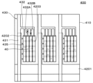
(4)実装基板
図4Aおよび図4BはこのマイクロLEDチップ集積装置の製造に用いられる実装基板400を示す。ここで、図4Aは平面図、図4Bは下部支線部電極とその近傍の下部幹線部電極とを横断する断面図である。図4Aおよび図4Bに示すように、基板410の一方の主面に下部電極420が設けられている。図4Aおよび図4Bには、電気的にオン/オフ制御が可能な1回路ユニットに相当する領域を一点鎖線で示す。この場合、下部電極420は、一方向に延在する幅広の下部幹線部電極4201と、この下部幹線部電極4201からこの下部幹線部電極4201と直交する方向に分岐した、この下部幹線部電極4201より幅狭の複数の下部幹線部電極4202と、この下部幹線部電極4202と接続され、この下部幹線部電極4202と直交する方向、従って下部幹線部電極4201と平行な方向に延在する複数の下部支線部電極4203とからなる。下部支線部電極4203の数LはL≧4に選ばれる。図4Aにおいては一例としてL=5の場合が示されている。基板410は剛性を有するものであってもフレキシブルなものであってもよく、また透明であっても不透明であってもよく、必要に応じて選ばれる。基板410は、例えば、Si基板、ガラス基板、ガラスエポキシ基板などのほか、樹脂フィルムなどであってもよい。下部電極420は、例えば、基板410の全面にスパッタリング法や真空蒸着法などにより非磁性の金属膜を形成した後、この金属膜をリソグラフィーおよびエッチングにより所定形状にパターニングすることにより形成することができる。金属膜としては、非磁性の金属からなるもの、例えば、Ti/Al/Ti/Au/Ti積層膜が用いられるが、Cu(あるいはCu合金)/Au/Ti積層膜を用いてもよい。Ti/Al/Ti/Au/Ti積層膜を構成する膜の厚さは、例えば、下から順に5~10nm、300~1000nm、50nm、5~100nm、50nmである。下部支線部電極4203の上面によりチップ結合部421が構成されている。下部支線部電極4203の幅、間隔などは必要に応じて選択される。
(4) Mounting Substrate Figures 4A and 4B show a mounting
(5)マイクロLEDチップ集積装置の製造方法
以上のことを前提としてこのマイクロLEDチップ集積装置の製造方法について説明する。
(5) Manufacturing Method of the Micro LED Chip Integrated Device Based on the above, a manufacturing method of the micro LED chip integrated device will be described.
図3に示すように、インク吐出装置300の吐出ノズル308の下方に実装基板400を水平に配置する。この場合、インク吐出装置300を固定し、実装基板400を図示省略した搬送機構により水平面内で図3中矢印で示す方向に移動させるようにする。ピエゾアクチュエーター309を作動させることにより吐出ノズル308からインク200を実装基板400のチップ結合部421に吐出させる。こうして吐出される一滴のインク200は、一つの回路ユニット内の全ての下部支線部電極4203を含む領域を覆い、かつ十分な個数の縦型マイクロLEDチップ40が含まれるようにする。一滴のインク200に含まれる縦型マイクロLEDチップ40の数は、インク200中の縦型マイクロLEDチップ40の濃度やインク200の吐出回数などによって調整することができる。この状態のインク200の一例を図5Aおよび図5Bに示す。ここで、図5Aは平面図、図5Bは断面図である。この場合、一滴のインク200の体積は例えば1~10ピコリットルである。縦型マイクロLEDチップ40の体積は一般に0.001~0.5ピコリットルである。例えば、縦型マイクロLEDチップ40が直径1μmの円形の形状を有し、厚さが3μmであるとすると、体積は約0.0024ピコリットルである。As shown in FIG. 3, the mounting
次に、図3中矢印で示すように、実装基板400を図示省略した搬送機構により所定距離移動させ、インク200が吐出されたチップ結合部421を磁場印加装置311の上方に位置させた後、磁場印加装置311により磁場を印加することにより、インク200に含まれる複数の縦型マイクロLEDチップ40のn側電極46に含まれるNi膜を磁化させる。このため、各縦型マイクロLEDチップ40はインク200中を磁力により下方に引き寄せられ、最終的に各縦型マイクロLEDチップ40はn側電極46側が下になるようにしてチップ結合部421に接触する。振動や擾乱などの外的要因などにより縦型マイクロLEDチップ40が倒れたり位置がずれたりするのを防止するため、磁場印加装置310による磁場の印加は、好適には、インク200を吐出させる前あるいは吐出させた時点あるいはその時点からインク200の液体が蒸発する前に行う。3, the mounting
次に、磁力により各縦型マイクロLEDチップ40をチップ結合部421に接触させたまま、ランプなどにより加熱を行うことによりインク200の溶媒を蒸発させ、続いてランプやレーザーなどにより加熱を行うことにより各縦型マイクロLEDチップ40のSn膜47を溶融させる。その後、溶融Snが冷却することにより各縦型マイクロLEDチップ40のn側電極46が下部支線部電極4203のチップ結合部421に電気的および機械的に結合する。Next, while each vertical
同様にして、各回路ユニット内の下部支線部電極4203のチップ結合部421に縦型マイクロLEDチップ40のn側電極46を電気的および機械的に結合させる。この状態の一例を図6Aおよび図6Bに示す。ここで、図6Aは平面図、図6Bは断面図である。図6Aに示すように、チップ結合部421において、縦型マイクロLEDチップ40はランダムに配置している。チップ結合部421の中には、一つの縦型マイクロLEDチップ40も結合していないものが含まれることもあり、図6Aにはそのような例が示されている。In the same manner, the n-
次に、図7に示すように、縦型マイクロLEDチップ40がチップ結合部421に結合した実装基板400の全面に絶縁膜422を表面がほぼ平坦となるように形成した後、この絶縁膜422をは反応性イオンエッチング(RIE)法などによりエッチングすることによりp側電極45(図示せず)を露出させる。Next, as shown in FIG. 7, an insulating
次に、図8Aおよび図8Bに示すように、絶縁膜422上に、各回路ユニット内の全ての下部支線部電極4203と直交する方向に延在するように、かつ全ての下部支線部電極4203に跨がるように複数の短冊状の細長い透明電極435を形成する。これらの透明電極435の間の隙間は縦型マイクロLEDチップ40のp側電極45の直径より小さくする。こうすることで、チップ結合部421に結合した縦型マイクロLEDチップ40のp側電極45は、いずれかの透明電極435と接触することができる。透明電極435はITOなどの透明電極材料からなる。次に、絶縁膜422上に上部電極430を形成する。上部電極430は、下部幹線部電極4201と直交する方向に互いに平行に延在する複数の上部幹線部電極431とそれぞれの上部幹線部電極431からこの上部幹線部電極431と直交する方向に各回路ユニット当たり当たり1本延びた上部支線部電極432とからなる。各上部支線部電極432は各上部幹線部電極431に平行な方向に、従って下部支線部電極4203に直角な方向に延びるように複数に分岐しており、それらの先端は透明電極435と接続されている。分岐した複数の上部支線部電極432の数UはU≧4に選ばれる。図8AにおいてはU=4の場合が示されている。透明電極435は上部支線部電極432の一部を構成している。8A and 8B, a plurality of elongated
この後、上述のようにして製造されたマイクロLEDチップ集積装置の検査を行う。具体的には、上部電極430と下部電極420との間の通電試験を行う。すなわち、上部電極430が下部電極420より高電位となるように電圧を印加することにより各縦型マイクロLEDチップ40に例えば1μA程度の電流を流して各縦型マイクロLEDチップ40の発光を画像解析し、リーク不良に起因して光量不良のある縦型マイクロLEDチップ40が接続されている透明電極435および上部支線部電極432を特定する。図9において、こうして特定された上部支線部電極432を符号432A、432Bで示す。After this, the micro LED chip integrated device manufactured as described above is inspected. Specifically, a current test is performed between the
次に、上述のようにして特定された上部支線部電極432A、432Bの一部(図9中、×で示した箇所)にレーザービームまたは電子線を照射することにより切断する。切断後の上部支線部電極432A、432Bの状態を図10に示す。この場合、切断された上部支線部電極432A、432Bが接続された透明電極435と接続された縦型マイクロLEDチップ40は全て使用することができなくなるが、それ以外の上部支線部電極432が接続された透明電極435と接続された縦型マイクロLEDチップ40は全て使用することができる。一つの上部支線部電極432に複数の縦型マイクロLEDチップ40が接続され、不良チップが特定できる場合は、不良チップの近くで上部支線部電極432を切断することで上部幹線部電極431に近い側の良品チップは犠牲にならず使用することができる。Next, a part of the
この後、次のようにして再検査を行う。すなわち、上部電極430と下部電極420との間に例えば1μA程度の電流を流して各縦型マイクロLEDチップ40の発光を画像解析する。その結果、光量不良のある縦型マイクロLEDチップ40が見つからなかった場合に修理を終了する。こうしてマイクロLEDチップ集積装置の修理を行うことができる。After this, re-inspection is performed as follows. That is, a current of, for example, about 1 μA is passed between the
(6)マイクロLEDチップ集積装置の構造
図8Aおよび図8Bに示すように、このマイクロLEDチップ集積装置は、一方の主面に下部幹線部電極4201、4202と下部幹線部電極4202から分岐した複数の下部支線部電極4203とを有する下部電極420を有する基板410と、下部電極420の下部支線部電極4203の上面により構成されたチップ結合部421と、チップ結合部421に結合した、上下にp側電極45およびn側電極46を有し、n側電極46がp側電極45に比べてより強く磁場に引き寄せられるように構成された縦型マイクロLEDチップ40と、縦型マイクロLEDチップ40の上層の、上部幹線部電極431とこの上部幹線部電極431から分岐し、複数の下部支線部電極4203と直交する方向に延在し、透明電極435が下部支線部電極4203のチップ結合部421に跨がる複数の上部支線部電極432とを有する上部電極430とを有する。そして、縦型マイクロLEDチップ40は、n側電極46をチップ結合部421に向けてこのチップ結合部421に結合し、n側電極46と下部支線部電極4203とが互いに電気的に接続され、p側電極45と上部電極430の上部支線部電極432とが互いに電気的に接続されている。
(6) Structure of Micro LED Chip Integration Device As shown in Figures 8A and 8B, this micro LED chip integration device has a
以上のように、この第1の実施の形態によれば、縦型マイクロLEDチップ40のn側電極46に軟磁性体であるNi膜を含ませることにより、縦型マイクロLEDチップ40のn側電極46側がp側電極45側に比べてより強く磁場に引き寄せられるように構成し、一つの回路ユニット内の下部支線部電極4203のチップ結合部421にインク200を吐出し、縦型マイクロLEDチップ40のn側電極46側を磁力により引き付けてチップ結合部421に接触させ、その後Sn膜47を溶融固化させることにより縦型マイクロLEDチップ40とチップ結合部421とを電気的および機械的に結合させることで、縦型マイクロLEDチップ40の集積度によらず、マイクロLEDチップ集積装置、例えばマイクロLEDディスプレイ、マイクロLEDバックライト、マイクロLED照明装置などを低コストで容易に実現することができる。また、縦型マイクロLEDチップ40はチップ結合部421上にランダム配置で結合させれば足りるため、縦型マイクロLEDチップ40の高精度の位置制御が不要であり、マイクロLEDチップ集積装置の製造が容易となる。また、一つの回路ユニット内には、複数の下部支線部電極4203および複数の上部支線部電極432が設けられているので、いずれかの上部支線部電極432が接続された縦型マイクロLEDチップ40に不良があった場合、その上部支線部電極432を切断するだけで、あるいは、この縦型マイクロLEDチップ40がチップ結合部421に結合した下部支線部電極4203だけを切断するだけで修理を容易に行うことができる。このため、修理に伴って無駄になる縦型マイクロLEDチップ40を最小限に留めることができ、無駄になる縦型マイクロLEDチップ40の数の大幅な低減を図ることができる。このマイクロLEDチップ集積装置は、図8Aおよび図8Bに示す3つの回路ユニットのそれぞれを青(B)、赤(R)、緑(G)の発光領域としてRGB-1画素を構成すると考えると、パッシブマトリクス駆動方式のカラーマイクロLEDディスプレイを実現することができる。この場合、上部電極幹線部431がカラム電極配線を構成する。縦型マイクロLEDチップ40を青色発光とすると、赤の発光領域および緑の発光領域の上方にそれぞれ赤および緑の蛍光体を形成する。縦型マイクロLEDチップ40を紫外領域または青紫色発光とすると、青の発光領域、赤の発光領域および緑の発光領域の上方にそれぞれ青、赤および緑の蛍光体を形成する。具体的には、例えば、図8Aおよび図8Bに示す実装基板400の表面にそれぞれの蛍光体を形成した後、その上にフレキシブルフィルムなどからなる透明基板を設け、さらにその上に光拡散用の拡散シートを設ける。As described above, according to the first embodiment, the n-
〈第2の実施の形態〉
[マイクロLEDチップ集積装置の製造方法]
第2の実施の形態においては、実装基板400として図4Aおよび図4Bに示すものの代わりに図11Aおよび図11Bに示すものを用いることが第1の実施の形態と異なる。すなわち、図11Aおよび図11Bに示すように、この実装基板400においては、下部支線部電極4203のチップ結合部421の下方の部分における基板410上にNiなどの円形の軟磁性体500が下部支線部電極4203の中心線に沿って一列にかつ等間隔に複数(この場合は4個)設けられており、これらの軟磁性体500を覆うように下部支線部電極4203が設けられている。軟磁性体500の直径は、縦型マイクロLEDチップ40のn側電極46の直径と同等またはそれ以下に選ばれる。下部支線部電極4203のチップ結合部421のうちの軟磁性体500に対応する部分が縦型マイクロLEDチップ40の結合位置となる。この結合位置のチップ結合部421には円形のSn膜47が設けられている。この場合、縦型マイクロLEDチップ40のSn膜47は形成する必要がない。この実装基板400のその他のことは第1の実施の形態と同様である。
Second Embodiment
[Method of manufacturing a micro LED chip integrated device]
The second embodiment differs from the first embodiment in that the mounting
図12は図11Bに示す実装基板400の一部を模式的に示したものである。図12に示すように、磁場印加装置(図示せず)により矢印で示すように磁場を印加することにより、軟磁性体500を磁化させる。この後、磁場の印加を停止する。この場合、磁場の印加を停止した後も、暫くは、図13に示すように、軟磁性体500から残留磁束501が生じている。
Figure 12 is a schematic diagram of a portion of the mounting
そこで、こうして残留磁束501が存在している状態で、インク200を実装基板400の一つの回路ユニット内のチップ結合部421に吐出させる。吐出直後の状態を図14に示す。図15に示すように、こうして吐出されたインク200はチップ結合部421の全体に広がると同時に、このインク200においては、軟磁性体500から生じている残留磁束501により、その中に含まれている複数の縦型マイクロLEDチップ40のn側電極46に含まれるNi膜が磁化される。このため、各縦型マイクロLEDチップ40はインク200中を磁力により下方に引き寄せられ、最終的に各縦型マイクロLEDチップ40はn側電極46側が下になるようにしてチップ結合部421のSn膜47に接触する。この状態を図16に示す。
In this state, the
この後、第1の実施の形態と同様にしてインク200の溶媒の蒸発およびSn膜47の溶融固化により各縦型マイクロLEDチップ40をn側電極46側を下にして機械的および電気的に結合する。符号48は溶融固化したSnを示す。After this, in the same manner as in the first embodiment, the solvent of the
こうして、図17に示すように、各回路ユニット内のチップ結合部421に縦型マイクロLEDチップ40を結合する。
In this way, as shown in Figure 17, the vertical
この後、第1の実施の形態と同様に絶縁膜422の形成以降の工程を進めて、図18に示すように、目的とするマイクロLEDチップ集積装置を製造する。
After this, similarly to the first embodiment, the processes from the formation of the insulating
[マイクロLEDチップ集積装置の構造]
図18に示すように、このマイクロLEDチップ集積装置は、実装基板400の下部支線部電極4203のチップ結合部421の下方の部分の基板410上に軟磁性体500が下部支線部電極4203の中心線に沿って複数設けられ、これらの軟磁性体500を覆うように下部支線部電極4203が設けられ、チップ結合部421に縦型マイクロLEDチップ40がn側電極46側を下にして結合していることを除いて、第1の実施の形態によるマイクロLEDチップ集積装置と同様な構成を有する。
[Structure of Micro LED Chip Integrated Device]
As shown in Figure 18, this micro LED chip integration device has a similar configuration to the micro LED chip integration device of the first embodiment, except that a plurality of soft
第2の実施の形態によれば、下部支線部電極4203のチップ結合部201の下方の基板410上に軟磁性体500を予め設けておくことにより、その上方の部分における下部支線部電極4203のチップ結合部421上に縦型マイクロLEDチップ40を結合させることができるため、各縦型マイクロLEDチップ40の結合位置を下部支線部電極4203と上部電極支線部432との交差部に限定することができる。このため、接続不良となる縦型マイクロLEDチップ40の大幅な低減を図ることができ、ひいてはマイクロLEDチップ集積装置の製造コストの低減を図ることができる。そのほか、第1の実施の形態と同様な利点を得ることができる。According to the second embodiment, by providing a soft
このマイクロLEDチップ集積装置によっても、パッシブマトリクス駆動方式のカラーマイクロLEDディスプレイを実現することができる。This micro LED chip integration device also makes it possible to realize a passive matrix driven color micro LED display.
〈第3の実施の形態〉
第3の実施の形態においては、アクティブマトリクス駆動方式のカラーマイクロLEDディスプレイとして用いることができるマイクロLEDチップ集積装置について説明する。
Third embodiment
In a third embodiment, a micro LED chip integrated device is described which can be used as an active matrix driven color micro LED display.
[マイクロLEDチップ集積装置の製造方法]
図19は第3の実施の形態における上部電極形成前の実装基板400を示す。図19に示すように、実装基板400上に下部幹線部電極4202が行方向に互いに平行に複数設けられている。下部幹線部電極4202にはこの下部幹線部電極4202と直交する方向、すなわち列方向に延在して複数の下部支線部電極4203が接続されている。下部支線部電極4203の下方には第2の実施の形態と同様に軟磁性体500が設けられている。そして、軟磁性体500の上方の下部支線部電極4203のチップ結合部421に縦型マイクロLEDチップ40が結合している。図19に示す三つの回路ユニットは左からそれぞれB、R、Gの発光領域を構成しており、これらの発光領域により構成されるRGB-1画素単位が配列しており、実装基板400全体として画素が二次元マトリクス状に配列している。実装基板400上には、列方向に延在した電源線610およびデータ線620に加え、行方向に延在した走査線630も設けられている。各データ線620と各画素の各発光領域との間にはアクティブ駆動回路が設けられ、このアクティブ駆動回路により各画素の各発光領域を選択することができるようになっている。アクティブ駆動回路はトランジスタT1、T2およびコンデンサCからなる。トランジスタT1、T2は一般的には多結晶Si薄膜などの半導体薄膜を用いた薄膜トランジスタにより構成され、コンデンサCは下部電極、絶縁膜および上部電極を積層することにより構成される。トランジスタT1のソースはデータ線620に接続され、ドレインはトランジスタT2のゲートに接続され、ゲートは走査線630に接続されている。トランジスタT2のソースは電源線610に接続され、ドレインは下部電極420に接続されている。コンデンサCはトランジスタT1のドレインと電源線610との間に接続されている。走査線630とデータ線620との選択により各画素の各発光領域を選択する。
後述のアクティブ駆動回路を介してこの下部幹線部電極4201と接続されて幅狭の下部幹線部電極4202がこの下部幹線部電極4201に平行に設けられている。
[Method of manufacturing a micro LED chip integrated device]
FIG. 19 shows the mounting
A narrow
図20は、図19に示す実装基板400上に上部電極430を形成した状態を示す。第1の実施の形態と同様に、各回路ユニット内の全ての下部支線部電極4203のチップ結合部421に跨がるように複数の透明電極435が設けられている。これらの透明電極435に上部電極430の上部支線部電極432がそれぞれ接続されている。
Figure 20 shows the state in which the
縦型マイクロLEDチップ40を青色発光とし、赤の発光領域および緑の発光領域の上方にそれぞれ赤および緑の蛍光体を形成することなどは第1の実施例と同様である。The vertical
この第3の実施の形態によれば、実装基板400上にRGBの各発光用の縦型マイクロLEDチップ40を容易にしかも極めて短時間に能率的に実装することができ、不良の縦型マイクロLEDチップ40の影響も容易に除去することができることにより、高性能のアクティブ駆動方式のカラーマイクロLEDディスプレイを低コストで実現することができる。加えて、第2の実施の形態と同様な利点を得ることもできる。According to the third embodiment, the vertical
以上、この発明の実施の形態について具体的に説明したが、この発明は上述の実施の形態に限定されるものではなく、この発明の技術的思想に基づく各種の変形が可能である。 Although the above describes in detail an embodiment of the present invention, the present invention is not limited to the above-described embodiment, and various modifications based on the technical concept of the present invention are possible.
例えば、上述の実施の形態において挙げた数値、構成、形状、材料、方法などはあくまでも例に過ぎず、必要に応じてこれらと異なる数値、構成、形状、材料、方法などを用いてもよい。For example, the numerical values, configurations, shapes, materials, methods, etc. listed in the above-mentioned embodiments are merely examples, and different numerical values, configurations, shapes, materials, methods, etc. may be used as necessary.
40 縦型マイクロLEDチップ
41 n型GaN層
42 発光層
43 p型GaN層
44 GaN層
45 p側電極
46 n側電極
47 Sn膜
400 実装基板
410 基板
420 下部電極
4201、4202 下部幹線部電極
4203 下部支線部電極
421 チップ結合部
422 絶縁膜
430 上部電極
431 上部幹線部電極
432 上部支線部電極
435 透明電極
40 Vertical micro LED chip 41 n-
Claims (11)
上記下部電極の上記複数の下部支線部電極の上面により構成されたチップ結合部と、
上記チップ結合部に結合した、上下にp側電極およびn側電極を有し、上記p側電極および上記n側電極のうちの一方が他方に比べてより強く磁場に引き寄せられるように構成された縦型の半導体発光素子チップと、
上記半導体発光素子チップの上層の、上部幹線部電極と当該上部幹線部電極から分岐し、上記複数の下部支線部電極と交差するように上記チップ結合部に跨がる複数の上部支線部電極とを有する上部電極とを有し、
上記半導体発光素子チップは、上記p側電極および上記n側電極のうちの上記一方を上記チップ結合部に向けて上記チップ結合部に結合し、上記p側電極および上記n側電極のうちの上記一方と上記下部支線部電極とが互いに電気的に接続され、上記p側電極および上記n側電極のうちの他方と上記上部電極の上記上部支線部電極とが互いに電気的に接続されている半導体発光素子チップ集積装置。 a substrate having a lower electrode on one main surface thereof, the lower electrode having a lower trunk electrode and a plurality of lower branch electrodes branched from the lower trunk electrode;
a chip coupling portion formed by upper surfaces of the plurality of lower branch electrodes of the lower electrode;
a vertical semiconductor light-emitting element chip connected to the chip connecting portion, the vertical semiconductor light-emitting element chip having a p-side electrode and an n-side electrode on the top and bottom, the p-side electrode and the n-side electrode being configured so that one of the p-side electrode and the n-side electrode is more strongly attracted to a magnetic field than the other;
an upper electrode on the upper layer of the semiconductor light-emitting element chip, the upper electrode having an upper trunk electrode and a plurality of upper branch electrodes branching from the upper trunk electrode and straddling the chip coupling portion so as to intersect with the plurality of lower branch electrodes;
The semiconductor light-emitting element chip is joined to the chip joining portion with one of the p-side electrode and the n-side electrode facing the chip joining portion, and one of the p-side electrode and the n-side electrode is electrically connected to the lower branch electrode, and the other of the p-side electrode and the n-side electrode is electrically connected to the upper branch electrode of the upper electrode.
上記磁場を取り去った後、上記軟磁性体領域の残留磁束が消える前に、上下にp側電極およびn側電極を有し、上記p側電極および上記n側電極のうちの一方が他方に比べてより強く磁場に引き寄せられるように構成された縦型の複数の半導体発光素子チップと液体とを含有する液滴状のインクを上記チップ結合部に供給し、上記インク中の上記半導体発光素子チップを、上記p側電極および上記n側電極のうちの上記一方を上記軟磁性体領域に向けて上記軟磁性体領域上に結合させる工程とを有する半導体発光素子チップ集積装置の製造方法。 a step of magnetizing the soft magnetic material region of the substrate provided with the chip coupling portion by applying a magnetic field to the soft magnetic material region;
and after removing the magnetic field and before the residual magnetic flux in the soft magnetic material region disappears, supplying droplet-shaped ink containing a liquid and a plurality of vertical semiconductor light-emitting element chips having p-side electrodes and n-side electrodes above and below, one of the p-side electrode and the n-side electrode being attracted to the magnetic field more strongly than the other, to the chip joining section, and joining the semiconductor light-emitting element chips in the ink onto the soft magnetic material region with one of the p-side electrode and the n-side electrode facing the soft magnetic material region.
Applications Claiming Priority (1)
| Application Number | Priority Date | Filing Date | Title |
|---|---|---|---|
| PCT/JP2022/013902 WO2023181246A1 (en) | 2022-03-24 | 2022-03-24 | Semiconductor light-emitting element chip integration device and production method for same |
Publications (2)
| Publication Number | Publication Date |
|---|---|
| JPWO2023181246A1 JPWO2023181246A1 (en) | 2023-09-28 |
| JP7465612B2 true JP7465612B2 (en) | 2024-04-11 |
Family
ID=88100630
Family Applications (1)
| Application Number | Title | Priority Date | Filing Date |
|---|---|---|---|
| JP2024509569A Active JP7465612B2 (en) | 2022-03-24 | 2022-03-24 | Semiconductor light emitting element chip integrated device and its manufacturing method |
Country Status (2)
| Country | Link |
|---|---|
| JP (1) | JP7465612B2 (en) |
| WO (1) | WO2023181246A1 (en) |
Citations (5)
| Publication number | Priority date | Publication date | Assignee | Title |
|---|---|---|---|---|
| JP2016512347A (en) | 2013-03-15 | 2016-04-25 | ルクスビュー テクノロジー コーポレイション | Light emitting diode display with redundancy scheme and method for manufacturing light emitting diode display with integrated defect detection inspection |
| WO2020029657A1 (en) | 2018-08-10 | 2020-02-13 | 林宏诚 | Diode device, display panel, and flexible display |
| US20210033240A1 (en) | 2019-07-31 | 2021-02-04 | Lg Display Co., Ltd. | Display apparatus |
| JP6886213B1 (en) | 2020-06-20 | 2021-06-16 | アルディーテック株式会社 | Semiconductor light emitting device chip integration device and its manufacturing method |
| JP2023520120A (en) | 2020-03-30 | 2023-05-16 | ジェイド バード ディスプレイ(シャンハイ) リミテッド | System and method for multi-color LED with stacked junction structure |
-
2022
- 2022-03-24 WO PCT/JP2022/013902 patent/WO2023181246A1/en active Application Filing
- 2022-03-24 JP JP2024509569A patent/JP7465612B2/en active Active
Patent Citations (5)
| Publication number | Priority date | Publication date | Assignee | Title |
|---|---|---|---|---|
| JP2016512347A (en) | 2013-03-15 | 2016-04-25 | ルクスビュー テクノロジー コーポレイション | Light emitting diode display with redundancy scheme and method for manufacturing light emitting diode display with integrated defect detection inspection |
| WO2020029657A1 (en) | 2018-08-10 | 2020-02-13 | 林宏诚 | Diode device, display panel, and flexible display |
| US20210033240A1 (en) | 2019-07-31 | 2021-02-04 | Lg Display Co., Ltd. | Display apparatus |
| JP2023520120A (en) | 2020-03-30 | 2023-05-16 | ジェイド バード ディスプレイ(シャンハイ) リミテッド | System and method for multi-color LED with stacked junction structure |
| JP6886213B1 (en) | 2020-06-20 | 2021-06-16 | アルディーテック株式会社 | Semiconductor light emitting device chip integration device and its manufacturing method |
Also Published As
| Publication number | Publication date |
|---|---|
| JPWO2023181246A1 (en) | 2023-09-28 |
| WO2023181246A1 (en) | 2023-09-28 |
Similar Documents
| Publication | Publication Date | Title |
|---|---|---|
| JP6694222B1 (en) | Method for manufacturing semiconductor chip integrated device, semiconductor chip integrated device, semiconductor chip ink, and semiconductor chip ink ejection device | |
| JP6842783B1 (en) | Manufacturing method of micro LED display and micro LED display | |
| WO2021084783A1 (en) | Semiconductor chip integrated device manufacturing method, semiconductor chip integrated device, semiconductor chip integrated device assembly, semiconductor chip ink, and semiconductor chip ink ejection device | |
| US10170664B2 (en) | Surface mount emissive elements | |
| JP6886213B1 (en) | Semiconductor light emitting device chip integration device and its manufacturing method | |
| US11605757B2 (en) | Display device using semiconductor light emitting diode | |
| JP6803595B1 (en) | Semiconductor light emitting device chip integration device and its manufacturing method | |
| US11824049B2 (en) | Display device | |
| JP2021125544A (en) | Manufacturing method of semiconductor chip integrated device, semiconductor chip integrated device, and semiconductor chip integrated device assembly | |
| JP2020025064A (en) | Manufacturing method of light emitting element integrated device and light emitting element array device | |
| CN114144309B (en) | Inkjet printing device, method for aligning bipolar elements and method for manufacturing a display device | |
| JP7465612B2 (en) | Semiconductor light emitting element chip integrated device and its manufacturing method | |
| CN115996849A (en) | Inkjet printing apparatus and method for manufacturing display device | |
| JP2021072290A (en) | Micro led backlight and manufacturing method thereof, as well as micro led lighting device and manufacturing method thereof | |
| JP7422449B1 (en) | Light emitting diode chip integrated device | |
| US20220115565A1 (en) | Ink including light-emitting elements, display device and method of fabricating the same | |
| JP2022122320A (en) | Manufacturing method of semiconductor light emitting element chip integrated device and semiconductor light emitting element chip integrated device | |
| EP4094946A1 (en) | Inkjet printing device, method for printing bipolar elements, and method for manufacturing display device | |
| JP2021093430A (en) | Manufacturing method of semiconductor chip integrated device and semiconductor chip integrated device | |
| CN115461869A (en) | Light-emitting element ink and method for manufacturing display device | |
| KR20230123028A (en) | Inkjet printing apparatus | |
| EP3352210A1 (en) | Light emitting diodes adapted for the fluidic assembly of emissive displays |
Legal Events
| Date | Code | Title | Description |
|---|---|---|---|
| A621 | Written request for application examination |
Free format text: JAPANESE INTERMEDIATE CODE: A621 Effective date: 20240220 |
|
| A871 | Explanation of circumstances concerning accelerated examination |
Free format text: JAPANESE INTERMEDIATE CODE: A871 Effective date: 20240220 |
|
| TRDD | Decision of grant or rejection written | ||
| A01 | Written decision to grant a patent or to grant a registration (utility model) |
Free format text: JAPANESE INTERMEDIATE CODE: A01 Effective date: 20240322 |
|
| A61 | First payment of annual fees (during grant procedure) |
Free format text: JAPANESE INTERMEDIATE CODE: A61 Effective date: 20240325 |
|
| R150 | Certificate of patent or registration of utility model |
Ref document number: 7465612 Country of ref document: JP Free format text: JAPANESE INTERMEDIATE CODE: R150 |