JP7428323B2 - light emitting device - Google Patents
light emitting device Download PDFInfo
- Publication number
- JP7428323B2 JP7428323B2 JP2020525601A JP2020525601A JP7428323B2 JP 7428323 B2 JP7428323 B2 JP 7428323B2 JP 2020525601 A JP2020525601 A JP 2020525601A JP 2020525601 A JP2020525601 A JP 2020525601A JP 7428323 B2 JP7428323 B2 JP 7428323B2
- Authority
- JP
- Japan
- Prior art keywords
- phosphor
- light
- emitting device
- peak wavelength
- range
- Prior art date
- Legal status (The legal status is an assumption and is not a legal conclusion. Google has not performed a legal analysis and makes no representation as to the accuracy of the status listed.)
- Active
Links
- OAICVXFJPJFONN-UHFFFAOYSA-N Phosphorus Chemical compound [P] OAICVXFJPJFONN-UHFFFAOYSA-N 0.000 claims description 200
- 238000000295 emission spectrum Methods 0.000 claims description 66
- 239000000203 mixture Substances 0.000 claims description 25
- 239000007787 solid Substances 0.000 claims description 11
- 238000005401 electroluminescence Methods 0.000 claims description 3
- 239000010408 film Substances 0.000 description 105
- 239000010410 layer Substances 0.000 description 65
- 229910052693 Europium Inorganic materials 0.000 description 18
- -1 europium ions Chemical class 0.000 description 17
- 230000004048 modification Effects 0.000 description 16
- 238000012986 modification Methods 0.000 description 16
- 238000001228 spectrum Methods 0.000 description 14
- 239000000463 material Substances 0.000 description 13
- OGPBJKLSAFTDLK-UHFFFAOYSA-N europium atom Chemical compound [Eu] OGPBJKLSAFTDLK-UHFFFAOYSA-N 0.000 description 11
- 239000013078 crystal Substances 0.000 description 9
- 229910052736 halogen Inorganic materials 0.000 description 9
- 150000002367 halogens Chemical class 0.000 description 9
- 238000004519 manufacturing process Methods 0.000 description 9
- 238000002156 mixing Methods 0.000 description 9
- 229920002050 silicone resin Polymers 0.000 description 8
- 238000000034 method Methods 0.000 description 6
- 239000000843 powder Substances 0.000 description 6
- 229910052709 silver Inorganic materials 0.000 description 6
- 239000004332 silver Substances 0.000 description 6
- 239000000126 substance Substances 0.000 description 6
- 239000000758 substrate Substances 0.000 description 6
- 239000012190 activator Substances 0.000 description 5
- 230000000052 comparative effect Effects 0.000 description 5
- 238000009826 distribution Methods 0.000 description 5
- 238000010304 firing Methods 0.000 description 5
- 229920005989 resin Polymers 0.000 description 5
- 239000011347 resin Substances 0.000 description 5
- 239000011575 calcium Substances 0.000 description 4
- 230000005284 excitation Effects 0.000 description 4
- 239000011521 glass Substances 0.000 description 4
- 150000004767 nitrides Chemical class 0.000 description 4
- 239000011342 resin composition Substances 0.000 description 4
- 239000002356 single layer Substances 0.000 description 4
- 229910052712 strontium Inorganic materials 0.000 description 4
- 125000001424 substituent group Chemical group 0.000 description 4
- 150000004645 aluminates Chemical class 0.000 description 3
- 229910052791 calcium Inorganic materials 0.000 description 3
- 239000003822 epoxy resin Substances 0.000 description 3
- 230000004907 flux Effects 0.000 description 3
- RAXXELZNTBOGNW-UHFFFAOYSA-N imidazole Natural products C1=CNC=N1 RAXXELZNTBOGNW-UHFFFAOYSA-N 0.000 description 3
- 150000002500 ions Chemical class 0.000 description 3
- 229920000647 polyepoxide Polymers 0.000 description 3
- QSQXISIULMTHLV-UHFFFAOYSA-N strontium;dioxido(oxo)silane Chemical class [Sr+2].[O-][Si]([O-])=O QSQXISIULMTHLV-UHFFFAOYSA-N 0.000 description 3
- 230000007704 transition Effects 0.000 description 3
- 229910052724 xenon Inorganic materials 0.000 description 3
- FHNFHKCVQCLJFQ-UHFFFAOYSA-N xenon atom Chemical compound [Xe] FHNFHKCVQCLJFQ-UHFFFAOYSA-N 0.000 description 3
- 125000001781 1,3,4-oxadiazolyl group Chemical group 0.000 description 2
- UJOBWOGCFQCDNV-UHFFFAOYSA-N 9H-carbazole Chemical compound C1=CC=C2C3=CC=CC=C3NC2=C1 UJOBWOGCFQCDNV-UHFFFAOYSA-N 0.000 description 2
- IJGRMHOSHXDMSA-UHFFFAOYSA-N Atomic nitrogen Chemical compound N#N IJGRMHOSHXDMSA-UHFFFAOYSA-N 0.000 description 2
- 229910052582 BN Inorganic materials 0.000 description 2
- ROFVEXUMMXZLPA-UHFFFAOYSA-N Bipyridyl Chemical compound N1=CC=CC=C1C1=CC=CC=N1 ROFVEXUMMXZLPA-UHFFFAOYSA-N 0.000 description 2
- PZNSFCLAULLKQX-UHFFFAOYSA-N Boron nitride Chemical compound N#B PZNSFCLAULLKQX-UHFFFAOYSA-N 0.000 description 2
- 229910052684 Cerium Inorganic materials 0.000 description 2
- YLQBMQCUIZJEEH-UHFFFAOYSA-N Furan Chemical compound C=1C=COC=1 YLQBMQCUIZJEEH-UHFFFAOYSA-N 0.000 description 2
- UFWIBTONFRDIAS-UHFFFAOYSA-N Naphthalene Chemical compound C1=CC=CC2=CC=CC=C21 UFWIBTONFRDIAS-UHFFFAOYSA-N 0.000 description 2
- PCNDJXKNXGMECE-UHFFFAOYSA-N Phenazine Natural products C1=CC=CC2=NC3=CC=CC=C3N=C21 PCNDJXKNXGMECE-UHFFFAOYSA-N 0.000 description 2
- KYQCOXFCLRTKLS-UHFFFAOYSA-N Pyrazine Chemical compound C1=CN=CC=N1 KYQCOXFCLRTKLS-UHFFFAOYSA-N 0.000 description 2
- JUJWROOIHBZHMG-UHFFFAOYSA-N Pyridine Chemical compound C1=CC=NC=C1 JUJWROOIHBZHMG-UHFFFAOYSA-N 0.000 description 2
- KAESVJOAVNADME-UHFFFAOYSA-N Pyrrole Chemical compound C=1C=CNC=1 KAESVJOAVNADME-UHFFFAOYSA-N 0.000 description 2
- BQCADISMDOOEFD-UHFFFAOYSA-N Silver Chemical compound [Ag] BQCADISMDOOEFD-UHFFFAOYSA-N 0.000 description 2
- 125000000217 alkyl group Chemical group 0.000 description 2
- 229910052788 barium Inorganic materials 0.000 description 2
- 238000005422 blasting Methods 0.000 description 2
- 125000004432 carbon atom Chemical group C* 0.000 description 2
- 239000000919 ceramic Substances 0.000 description 2
- GWXLDORMOJMVQZ-UHFFFAOYSA-N cerium Chemical compound [Ce] GWXLDORMOJMVQZ-UHFFFAOYSA-N 0.000 description 2
- 239000000470 constituent Substances 0.000 description 2
- 238000010586 diagram Methods 0.000 description 2
- TXCDCPKCNAJMEE-UHFFFAOYSA-N dibenzofuran Chemical compound C1=CC=C2C3=CC=CC=C3OC2=C1 TXCDCPKCNAJMEE-UHFFFAOYSA-N 0.000 description 2
- 239000002270 dispersing agent Substances 0.000 description 2
- 230000001747 exhibiting effect Effects 0.000 description 2
- NIHNNTQXNPWCJQ-UHFFFAOYSA-N fluorene Chemical compound C1=CC=C2CC3=CC=CC=C3C2=C1 NIHNNTQXNPWCJQ-UHFFFAOYSA-N 0.000 description 2
- PCHJSUWPFVWCPO-UHFFFAOYSA-N gold Chemical compound [Au] PCHJSUWPFVWCPO-UHFFFAOYSA-N 0.000 description 2
- 229910052737 gold Inorganic materials 0.000 description 2
- 239000010931 gold Substances 0.000 description 2
- 238000010438 heat treatment Methods 0.000 description 2
- 229910052746 lanthanum Inorganic materials 0.000 description 2
- 229910052749 magnesium Inorganic materials 0.000 description 2
- 239000011777 magnesium Substances 0.000 description 2
- 238000005259 measurement Methods 0.000 description 2
- 239000004570 mortar (masonry) Substances 0.000 description 2
- 239000011858 nanopowder Substances 0.000 description 2
- 229910052757 nitrogen Inorganic materials 0.000 description 2
- 229920001296 polysiloxane Polymers 0.000 description 2
- 238000003825 pressing Methods 0.000 description 2
- 238000007639 printing Methods 0.000 description 2
- XSCHRSMBECNVNS-UHFFFAOYSA-N quinoxaline Chemical compound N1=CC=NC2=CC=CC=C21 XSCHRSMBECNVNS-UHFFFAOYSA-N 0.000 description 2
- 238000004611 spectroscopical analysis Methods 0.000 description 2
- 238000003756 stirring Methods 0.000 description 2
- XTQHKBHJIVJGKJ-UHFFFAOYSA-N sulfur monoxide Chemical compound S=O XTQHKBHJIVJGKJ-UHFFFAOYSA-N 0.000 description 2
- 239000010409 thin film Substances 0.000 description 2
- TZMSYXZUNZXBOL-UHFFFAOYSA-N 10H-phenoxazine Chemical compound C1=CC=C2NC3=CC=CC=C3OC2=C1 TZMSYXZUNZXBOL-UHFFFAOYSA-N 0.000 description 1
- VEPOHXYIFQMVHW-XOZOLZJESA-N 2,3-dihydroxybutanedioic acid (2S,3S)-3,4-dimethyl-2-phenylmorpholine Chemical compound OC(C(O)C(O)=O)C(O)=O.C[C@H]1[C@@H](OCCN1C)c1ccccc1 VEPOHXYIFQMVHW-XOZOLZJESA-N 0.000 description 1
- UXGVMFHEKMGWMA-UHFFFAOYSA-N 2-benzofuran Chemical compound C1=CC=CC2=COC=C21 UXGVMFHEKMGWMA-UHFFFAOYSA-N 0.000 description 1
- MGADZUXDNSDTHW-UHFFFAOYSA-N 2H-pyran Chemical compound C1OC=CC=C1 MGADZUXDNSDTHW-UHFFFAOYSA-N 0.000 description 1
- GJCOSYZMQJWQCA-UHFFFAOYSA-N 9H-xanthene Chemical compound C1=CC=C2CC3=CC=CC=C3OC2=C1 GJCOSYZMQJWQCA-UHFFFAOYSA-N 0.000 description 1
- 229910002704 AlGaN Inorganic materials 0.000 description 1
- KYNSBQPICQTCGU-UHFFFAOYSA-N Benzopyrane Chemical compound C1=CC=C2C=CCOC2=C1 KYNSBQPICQTCGU-UHFFFAOYSA-N 0.000 description 1
- OYPRJOBELJOOCE-UHFFFAOYSA-N Calcium Chemical compound [Ca] OYPRJOBELJOOCE-UHFFFAOYSA-N 0.000 description 1
- OKTJSMMVPCPJKN-UHFFFAOYSA-N Carbon Chemical compound [C] OKTJSMMVPCPJKN-UHFFFAOYSA-N 0.000 description 1
- 239000001856 Ethyl cellulose Substances 0.000 description 1
- ZZSNKZQZMQGXPY-UHFFFAOYSA-N Ethyl cellulose Chemical compound CCOCC1OC(OC)C(OCC)C(OCC)C1OC1C(O)C(O)C(OC)C(CO)O1 ZZSNKZQZMQGXPY-UHFFFAOYSA-N 0.000 description 1
- 229910052688 Gadolinium Inorganic materials 0.000 description 1
- UFHFLCQGNIYNRP-UHFFFAOYSA-N Hydrogen Chemical compound [H][H] UFHFLCQGNIYNRP-UHFFFAOYSA-N 0.000 description 1
- FYYHWMGAXLPEAU-UHFFFAOYSA-N Magnesium Chemical compound [Mg] FYYHWMGAXLPEAU-UHFFFAOYSA-N 0.000 description 1
- ZCQWOFVYLHDMMC-UHFFFAOYSA-N Oxazole Chemical compound C1=COC=N1 ZCQWOFVYLHDMMC-UHFFFAOYSA-N 0.000 description 1
- WTKZEGDFNFYCGP-UHFFFAOYSA-N Pyrazole Chemical compound C=1C=NNC=1 WTKZEGDFNFYCGP-UHFFFAOYSA-N 0.000 description 1
- CZPWVGJYEJSRLH-UHFFFAOYSA-N Pyrimidine Chemical compound C1=CN=CN=C1 CZPWVGJYEJSRLH-UHFFFAOYSA-N 0.000 description 1
- 229910004283 SiO 4 Inorganic materials 0.000 description 1
- VYPSYNLAJGMNEJ-UHFFFAOYSA-N Silicium dioxide Chemical compound O=[Si]=O VYPSYNLAJGMNEJ-UHFFFAOYSA-N 0.000 description 1
- 229910052784 alkaline earth metal Inorganic materials 0.000 description 1
- 125000003118 aryl group Chemical group 0.000 description 1
- 239000012298 atmosphere Substances 0.000 description 1
- QVGXLLKOCUKJST-UHFFFAOYSA-N atomic oxygen Chemical compound [O] QVGXLLKOCUKJST-UHFFFAOYSA-N 0.000 description 1
- DSAJWYNOEDNPEQ-UHFFFAOYSA-N barium atom Chemical compound [Ba] DSAJWYNOEDNPEQ-UHFFFAOYSA-N 0.000 description 1
- RFRXIWQYSOIBDI-UHFFFAOYSA-N benzarone Chemical compound CCC=1OC2=CC=CC=C2C=1C(=O)C1=CC=C(O)C=C1 RFRXIWQYSOIBDI-UHFFFAOYSA-N 0.000 description 1
- 239000011230 binding agent Substances 0.000 description 1
- 230000033228 biological regulation Effects 0.000 description 1
- 230000015572 biosynthetic process Effects 0.000 description 1
- 125000006267 biphenyl group Chemical group 0.000 description 1
- 125000000609 carbazolyl group Chemical group C1(=CC=CC=2C3=CC=CC=C3NC12)* 0.000 description 1
- 230000008859 change Effects 0.000 description 1
- 239000003795 chemical substances by application Substances 0.000 description 1
- 150000001875 compounds Chemical class 0.000 description 1
- 230000009849 deactivation Effects 0.000 description 1
- 230000003247 decreasing effect Effects 0.000 description 1
- 238000009792 diffusion process Methods 0.000 description 1
- 230000008034 disappearance Effects 0.000 description 1
- 230000000694 effects Effects 0.000 description 1
- 229920001249 ethyl cellulose Polymers 0.000 description 1
- 235000019325 ethyl cellulose Nutrition 0.000 description 1
- 125000001495 ethyl group Chemical group [H]C([H])([H])C([H])([H])* 0.000 description 1
- 150000002244 furazanes Chemical class 0.000 description 1
- UIWYJDYFSGRHKR-UHFFFAOYSA-N gadolinium atom Chemical compound [Gd] UIWYJDYFSGRHKR-UHFFFAOYSA-N 0.000 description 1
- 229910002804 graphite Inorganic materials 0.000 description 1
- 239000010439 graphite Substances 0.000 description 1
- 230000005484 gravity Effects 0.000 description 1
- 238000007646 gravure printing Methods 0.000 description 1
- 125000005843 halogen group Chemical group 0.000 description 1
- 230000020169 heat generation Effects 0.000 description 1
- 239000001257 hydrogen Substances 0.000 description 1
- 229910052739 hydrogen Inorganic materials 0.000 description 1
- 239000011261 inert gas Substances 0.000 description 1
- 230000002452 interceptive effect Effects 0.000 description 1
- 125000000959 isobutyl group Chemical group [H]C([H])([H])C([H])(C([H])([H])[H])C([H])([H])* 0.000 description 1
- 125000001449 isopropyl group Chemical group [H]C([H])([H])C([H])(*)C([H])([H])[H] 0.000 description 1
- CTAPFRYPJLPFDF-UHFFFAOYSA-N isoxazole Chemical compound C=1C=NOC=1 CTAPFRYPJLPFDF-UHFFFAOYSA-N 0.000 description 1
- 238000004898 kneading Methods 0.000 description 1
- FZLIPJUXYLNCLC-UHFFFAOYSA-N lanthanum atom Chemical compound [La] FZLIPJUXYLNCLC-UHFFFAOYSA-N 0.000 description 1
- QDLAGTHXVHQKRE-UHFFFAOYSA-N lichenxanthone Natural products COC1=CC(O)=C2C(=O)C3=C(C)C=C(OC)C=C3OC2=C1 QDLAGTHXVHQKRE-UHFFFAOYSA-N 0.000 description 1
- 230000005499 meniscus Effects 0.000 description 1
- 229910052751 metal Inorganic materials 0.000 description 1
- 239000002184 metal Substances 0.000 description 1
- 150000002739 metals Chemical class 0.000 description 1
- 125000002496 methyl group Chemical group [H]C([H])([H])* 0.000 description 1
- 239000011812 mixed powder Substances 0.000 description 1
- 125000004108 n-butyl group Chemical group [H]C([H])([H])C([H])([H])C([H])([H])C([H])([H])* 0.000 description 1
- 125000001624 naphthyl group Chemical group 0.000 description 1
- 239000012299 nitrogen atmosphere Substances 0.000 description 1
- 239000013307 optical fiber Substances 0.000 description 1
- WCPAKWJPBJAGKN-UHFFFAOYSA-N oxadiazole Chemical compound C1=CON=N1 WCPAKWJPBJAGKN-UHFFFAOYSA-N 0.000 description 1
- NFBOHOGPQUYFRF-UHFFFAOYSA-N oxanthrene Chemical compound C1=CC=C2OC3=CC=CC=C3OC2=C1 NFBOHOGPQUYFRF-UHFFFAOYSA-N 0.000 description 1
- 239000001301 oxygen Substances 0.000 description 1
- 229910052760 oxygen Inorganic materials 0.000 description 1
- 238000010422 painting Methods 0.000 description 1
- 239000002245 particle Substances 0.000 description 1
- 125000001147 pentyl group Chemical group C(CCCC)* 0.000 description 1
- 125000001997 phenyl group Chemical group [H]C1=C([H])C([H])=C(*)C([H])=C1[H] 0.000 description 1
- 238000004382 potting Methods 0.000 description 1
- 125000001436 propyl group Chemical group [H]C([*])([H])C([H])([H])C([H])([H])[H] 0.000 description 1
- PBMFSQRYOILNGV-UHFFFAOYSA-N pyridazine Chemical compound C1=CC=NN=C1 PBMFSQRYOILNGV-UHFFFAOYSA-N 0.000 description 1
- UMJSCPRVCHMLSP-UHFFFAOYSA-N pyridine Natural products COC1=CC=CN=C1 UMJSCPRVCHMLSP-UHFFFAOYSA-N 0.000 description 1
- 125000004076 pyridyl group Chemical group 0.000 description 1
- 230000005855 radiation Effects 0.000 description 1
- 229910052761 rare earth metal Inorganic materials 0.000 description 1
- 150000002910 rare earth metals Chemical class 0.000 description 1
- 230000009103 reabsorption Effects 0.000 description 1
- 238000005488 sandblasting Methods 0.000 description 1
- 238000007650 screen-printing Methods 0.000 description 1
- 229910052710 silicon Inorganic materials 0.000 description 1
- 238000004528 spin coating Methods 0.000 description 1
- 238000005507 spraying Methods 0.000 description 1
- CIOAGBVUUVVLOB-UHFFFAOYSA-N strontium atom Chemical compound [Sr] CIOAGBVUUVVLOB-UHFFFAOYSA-N 0.000 description 1
- 229910052917 strontium silicate Inorganic materials 0.000 description 1
- 125000000999 tert-butyl group Chemical group [H]C([H])([H])C(*)(C([H])([H])[H])C([H])([H])[H] 0.000 description 1
- 239000002918 waste heat Substances 0.000 description 1
- 238000005303 weighing Methods 0.000 description 1
- 229910052727 yttrium Inorganic materials 0.000 description 1
- VWQVUPCCIRVNHF-UHFFFAOYSA-N yttrium atom Chemical compound [Y] VWQVUPCCIRVNHF-UHFFFAOYSA-N 0.000 description 1
- 239000011701 zinc Substances 0.000 description 1
- 229910052984 zinc sulfide Inorganic materials 0.000 description 1
Images


Classifications
-
- H—ELECTRICITY
- H01—ELECTRIC ELEMENTS
- H01L—SEMICONDUCTOR DEVICES NOT COVERED BY CLASS H10
- H01L33/00—Semiconductor devices with at least one potential-jump barrier or surface barrier specially adapted for light emission; Processes or apparatus specially adapted for the manufacture or treatment thereof or of parts thereof; Details thereof
- H01L33/48—Semiconductor devices with at least one potential-jump barrier or surface barrier specially adapted for light emission; Processes or apparatus specially adapted for the manufacture or treatment thereof or of parts thereof; Details thereof characterised by the semiconductor body packages
- H01L33/50—Wavelength conversion elements
- H01L33/501—Wavelength conversion elements characterised by the materials, e.g. binder
- H01L33/502—Wavelength conversion materials
- H01L33/504—Elements with two or more wavelength conversion materials
-
- C—CHEMISTRY; METALLURGY
- C09—DYES; PAINTS; POLISHES; NATURAL RESINS; ADHESIVES; COMPOSITIONS NOT OTHERWISE PROVIDED FOR; APPLICATIONS OF MATERIALS NOT OTHERWISE PROVIDED FOR
- C09K—MATERIALS FOR MISCELLANEOUS APPLICATIONS, NOT PROVIDED FOR ELSEWHERE
- C09K11/00—Luminescent, e.g. electroluminescent, chemiluminescent materials
- C09K11/08—Luminescent, e.g. electroluminescent, chemiluminescent materials containing inorganic luminescent materials
- C09K11/58—Luminescent, e.g. electroluminescent, chemiluminescent materials containing inorganic luminescent materials containing copper, silver or gold
- C09K11/582—Chalcogenides
- C09K11/584—Chalcogenides with zinc or cadmium
-
- C—CHEMISTRY; METALLURGY
- C09—DYES; PAINTS; POLISHES; NATURAL RESINS; ADHESIVES; COMPOSITIONS NOT OTHERWISE PROVIDED FOR; APPLICATIONS OF MATERIALS NOT OTHERWISE PROVIDED FOR
- C09K—MATERIALS FOR MISCELLANEOUS APPLICATIONS, NOT PROVIDED FOR ELSEWHERE
- C09K11/00—Luminescent, e.g. electroluminescent, chemiluminescent materials
- C09K11/08—Luminescent, e.g. electroluminescent, chemiluminescent materials containing inorganic luminescent materials
- C09K11/77—Luminescent, e.g. electroluminescent, chemiluminescent materials containing inorganic luminescent materials containing rare earth metals
- C09K11/7728—Luminescent, e.g. electroluminescent, chemiluminescent materials containing inorganic luminescent materials containing rare earth metals containing europium
- C09K11/7734—Aluminates
-
- C—CHEMISTRY; METALLURGY
- C09—DYES; PAINTS; POLISHES; NATURAL RESINS; ADHESIVES; COMPOSITIONS NOT OTHERWISE PROVIDED FOR; APPLICATIONS OF MATERIALS NOT OTHERWISE PROVIDED FOR
- C09K—MATERIALS FOR MISCELLANEOUS APPLICATIONS, NOT PROVIDED FOR ELSEWHERE
- C09K11/00—Luminescent, e.g. electroluminescent, chemiluminescent materials
- C09K11/08—Luminescent, e.g. electroluminescent, chemiluminescent materials containing inorganic luminescent materials
- C09K11/77—Luminescent, e.g. electroluminescent, chemiluminescent materials containing inorganic luminescent materials containing rare earth metals
- C09K11/7783—Luminescent, e.g. electroluminescent, chemiluminescent materials containing inorganic luminescent materials containing rare earth metals containing two or more rare earth metals one of which being europium
- C09K11/7784—Chalcogenides
- C09K11/7787—Oxides
- C09K11/7789—Oxysulfides
-
- C—CHEMISTRY; METALLURGY
- C09—DYES; PAINTS; POLISHES; NATURAL RESINS; ADHESIVES; COMPOSITIONS NOT OTHERWISE PROVIDED FOR; APPLICATIONS OF MATERIALS NOT OTHERWISE PROVIDED FOR
- C09K—MATERIALS FOR MISCELLANEOUS APPLICATIONS, NOT PROVIDED FOR ELSEWHERE
- C09K11/00—Luminescent, e.g. electroluminescent, chemiluminescent materials
- C09K11/08—Luminescent, e.g. electroluminescent, chemiluminescent materials containing inorganic luminescent materials
- C09K11/77—Luminescent, e.g. electroluminescent, chemiluminescent materials containing inorganic luminescent materials containing rare earth metals
- C09K11/7783—Luminescent, e.g. electroluminescent, chemiluminescent materials containing inorganic luminescent materials containing rare earth metals containing two or more rare earth metals one of which being europium
- C09K11/77927—Silicon Nitrides or Silicon Oxynitrides
-
- H—ELECTRICITY
- H01—ELECTRIC ELEMENTS
- H01L—SEMICONDUCTOR DEVICES NOT COVERED BY CLASS H10
- H01L33/00—Semiconductor devices with at least one potential-jump barrier or surface barrier specially adapted for light emission; Processes or apparatus specially adapted for the manufacture or treatment thereof or of parts thereof; Details thereof
- H01L33/48—Semiconductor devices with at least one potential-jump barrier or surface barrier specially adapted for light emission; Processes or apparatus specially adapted for the manufacture or treatment thereof or of parts thereof; Details thereof characterised by the semiconductor body packages
- H01L33/50—Wavelength conversion elements
- H01L33/505—Wavelength conversion elements characterised by the shape, e.g. plate or foil
-
- H—ELECTRICITY
- H01—ELECTRIC ELEMENTS
- H01S—DEVICES USING THE PROCESS OF LIGHT AMPLIFICATION BY STIMULATED EMISSION OF RADIATION [LASER] TO AMPLIFY OR GENERATE LIGHT; DEVICES USING STIMULATED EMISSION OF ELECTROMAGNETIC RADIATION IN WAVE RANGES OTHER THAN OPTICAL
- H01S5/00—Semiconductor lasers
- H01S5/005—Optical components external to the laser cavity, specially adapted therefor, e.g. for homogenisation or merging of the beams or for manipulating laser pulses, e.g. pulse shaping
- H01S5/0087—Optical components external to the laser cavity, specially adapted therefor, e.g. for homogenisation or merging of the beams or for manipulating laser pulses, e.g. pulse shaping for illuminating phosphorescent or fluorescent materials, e.g. using optical arrangements specifically adapted for guiding or shaping laser beams illuminating these materials
-
- H—ELECTRICITY
- H05—ELECTRIC TECHNIQUES NOT OTHERWISE PROVIDED FOR
- H05B—ELECTRIC HEATING; ELECTRIC LIGHT SOURCES NOT OTHERWISE PROVIDED FOR; CIRCUIT ARRANGEMENTS FOR ELECTRIC LIGHT SOURCES, IN GENERAL
- H05B33/00—Electroluminescent light sources
- H05B33/12—Light sources with substantially two-dimensional radiating surfaces
- H05B33/14—Light sources with substantially two-dimensional radiating surfaces characterised by the chemical or physical composition or the arrangement of the electroluminescent material, or by the simultaneous addition of the electroluminescent material in or onto the light source
-
- H—ELECTRICITY
- H10—SEMICONDUCTOR DEVICES; ELECTRIC SOLID-STATE DEVICES NOT OTHERWISE PROVIDED FOR
- H10K—ORGANIC ELECTRIC SOLID-STATE DEVICES
- H10K50/00—Organic light-emitting devices
-
- H—ELECTRICITY
- H10—SEMICONDUCTOR DEVICES; ELECTRIC SOLID-STATE DEVICES NOT OTHERWISE PROVIDED FOR
- H10K—ORGANIC ELECTRIC SOLID-STATE DEVICES
- H10K59/00—Integrated devices, or assemblies of multiple devices, comprising at least one organic light-emitting element covered by group H10K50/00
- H10K59/30—Devices specially adapted for multicolour light emission
- H10K59/38—Devices specially adapted for multicolour light emission comprising colour filters or colour changing media [CCM]
-
- H—ELECTRICITY
- H10—SEMICONDUCTOR DEVICES; ELECTRIC SOLID-STATE DEVICES NOT OTHERWISE PROVIDED FOR
- H10K—ORGANIC ELECTRIC SOLID-STATE DEVICES
- H10K85/00—Organic materials used in the body or electrodes of devices covered by this subclass
- H10K85/60—Organic compounds having low molecular weight
-
- H—ELECTRICITY
- H01—ELECTRIC ELEMENTS
- H01L—SEMICONDUCTOR DEVICES NOT COVERED BY CLASS H10
- H01L33/00—Semiconductor devices with at least one potential-jump barrier or surface barrier specially adapted for light emission; Processes or apparatus specially adapted for the manufacture or treatment thereof or of parts thereof; Details thereof
- H01L33/48—Semiconductor devices with at least one potential-jump barrier or surface barrier specially adapted for light emission; Processes or apparatus specially adapted for the manufacture or treatment thereof or of parts thereof; Details thereof characterised by the semiconductor body packages
- H01L33/50—Wavelength conversion elements
- H01L33/507—Wavelength conversion elements the elements being in intimate contact with parts other than the semiconductor body or integrated with parts other than the semiconductor body
-
- H—ELECTRICITY
- H10—SEMICONDUCTOR DEVICES; ELECTRIC SOLID-STATE DEVICES NOT OTHERWISE PROVIDED FOR
- H10K—ORGANIC ELECTRIC SOLID-STATE DEVICES
- H10K50/00—Organic light-emitting devices
- H10K50/10—OLEDs or polymer light-emitting diodes [PLED]
- H10K50/11—OLEDs or polymer light-emitting diodes [PLED] characterised by the electroluminescent [EL] layers
Description
本発明は、発光装置に関する。 The present invention relates to a light emitting device.
近年、家庭用照明をはじめとする各種照明は、ハロゲンランプから発光ダイオード(LED)への置き換えが急速に進んでおり長寿命化及び小型化が実現可能となっている。しかし、分光分析装置等の産業機器用の光源は、未だハロゲンランプが支配的に用いられており、LEDへの置き換えが進んでいない。その大きな原因として、従来のLEDでは、産業機器用の光源に求められる、広帯域での安定した発光スペクトル分布を呈することや温度変化による波長シフトが生じ難いこと等の特性を充足することが困難であることが考えられる。特許文献1には、赤色蛍光体と緑色蛍光体を含む2種以上の蛍光体を含有する発光装置用の多層膜シートにおいて、各々の蛍光体層に含有される蛍光体が一種類であり、発光波長が長い蛍光体を含有する蛍光体層から発光波長が短い蛍光体を含有する蛍光体層へと順に配置することによって発光装置の全光束を高めることが記載されている。
In recent years, halogen lamps have been rapidly replaced with light emitting diodes (LEDs) in various types of lighting, including household lighting, making it possible to achieve longer lifespans and smaller sizes. However, halogen lamps are still predominantly used as light sources for industrial equipment such as spectrometers, and replacement with LEDs has not progressed. A major reason for this is that it is difficult for conventional LEDs to meet the characteristics required for light sources for industrial equipment, such as exhibiting a stable emission spectrum distribution over a wide band and being resistant to wavelength shifts due to temperature changes. I can think of something.
しかしながら、従来の発光装置は、照明用途への適用を目的としたものであったため高波長側のピーク波長が700nm以下のものであり、700nmを超える近赤外線領域にもピーク波長を有する発光が求められる産業機器用の光源としては十分ではない。
本発明は、光源からの光による励起により、少なくとも、700nmを超える領域にピーク波長を有する発光装置を提供することを課題とする。
However, since conventional light emitting devices were intended for application to lighting applications, the peak wavelength on the high wavelength side was 700 nm or less, and light emission with a peak wavelength in the near-infrared region exceeding 700 nm was also required. This is not sufficient as a light source for industrial equipment.
An object of the present invention is to provide a light emitting device that has a peak wavelength in a region exceeding at least 700 nm when excited by light from a light source.
本発明は、以下に関するものである。
[1]480nm以下の範囲にピーク波長を有する光を発光する固体光源と、該固体光源を覆い少なくとも一種の蛍光体を含有する蛍光膜とを少なくとも備え、前記蛍光膜が前記固体光源からの光に励起されて700nmを超える範囲にピーク波長を有しかつ該ピーク波長を含む範囲における発光スペクトルの半値全幅が100nm以上である光を発する少なくとも一種の近赤外蛍光体を含有する、発光装置。
[2]少なくとも、400nm以上1000nm以下の範囲に連続的な発光スペクトルを有する、[1]に記載の発光装置。
[3]前記蛍光膜が、前記固体光源からの光に励起され350nm以上700nm以下の範囲にピーク波長を有する光を発する少なくとも一種の可視蛍光体をさらに含有する、[1]又は[2]に記載の発光装置。
[4]前記蛍光膜が、前記可視蛍光体として、前記固体光源からの光に励起されて350nm以上430nm未満の範囲にピーク波長を有する光を発する可視蛍光体A、前記固体光源からの光に励起されて430nm以上500nm未満の範囲にピーク波長を有する光を発する可視蛍光体B、前記固体光源からの光に励起されて500nm以上700nm以下の範囲にピーク波長を有する光を発する可視蛍光体Cを、それぞれ一種以上含む、[3]に記載の発光装置。
[5]前記蛍光膜が2以上の層で形成されており、前記可視蛍光体A及びBが異なる層に含まれている、[4]に記載の発光装置。
[6]前記蛍光膜が、含まれる前記蛍光体の種類が異なる2以上の層で形成されており、該2以上の層が、ピーク波長がより長い蛍光体を含有する層からピーク波長がより短い蛍光体を含有する層へと順に、前記固体光源からの光の進行方向に積層されている、[4]又は[5]に記載の発光装置。
[7]前記蛍光膜の各層に含まれる前記蛍光体の種類が1以上3以下である、[5]又は[6]に記載の発光装置。
[8]前記蛍光膜が、含まれる前記蛍光体の種類が異なる2以上の領域を同一面上に有する、[4]に記載の発光装置。
[9]前記蛍光体の種類が異なる2以上の領域が、少なくとも、前記近赤外蛍光体を含有する領域及び前記可視蛍光体を含有する領域を有する、[8]に記載の発光装置。
[10]前記固体光源を2以上備える、[1]から[9]のいずれかに記載の発光装置。
[11]前記固体光源が、発光ダイオード、レーザーダイオード、及び有機エレクトロルミネッセンス発光素子から選択される少なくとも1種である、[1]~[10]のいずれかに記載の発光装置。
[12]前記近赤外蛍光体が2価のユーロピウムイオンを含有する、[1]~[11]のいずれかに記載の発光装置。
[13]前記近赤外蛍光体が、以下の式(I)で示される組成を有する、[1]~[12]のいずれかに記載の発光装置。
LiaSrbLacSidNeEuf・・・(I)
(ただし、a~fは、a+b+c+d+e+f=100、0≦a≦8.22、0.22≦b≦17.33、1.12≦c≦11.36、22.41≦d≦38.09、49.47≦e≦56.09、0.88≦f≦1.01、を満たす数である。)
[14]480nm以下の範囲にピーク波長を有する光により700nmを超える範囲にピーク波長を有しかつ該ピーク波長を含む範囲における発光スペクトルの半値全幅が100nm以上である光を発する少なくとも一種の近赤外蛍光体と、前記光により350nm以上700nm以下の範囲にピーク波長を有する光を発する少なくとも一種の可視蛍光体とを含有する、蛍光膜。
The present invention relates to the following.
[1] At least includes a solid-state light source that emits light having a peak wavelength in a range of 480 nm or less, and a fluorescent film that covers the solid-state light source and contains at least one type of phosphor, and the fluorescent film emits light from the solid-state light source. A light-emitting device containing at least one type of near-infrared phosphor that emits light having a peak wavelength in a range exceeding 700 nm and having an emission spectrum full width at half maximum in the range including the peak wavelength of 100 nm or more.
[2] The light emitting device according to [1], which has a continuous emission spectrum in a range of at least 400 nm or more and 1000 nm or less.
[3] According to [1] or [2], the fluorescent film further contains at least one visible phosphor that is excited by light from the solid-state light source and emits light having a peak wavelength in a range of 350 nm or more and 700 nm or less. The light emitting device described.
[4] The fluorescent film includes, as the visible phosphor, a visible phosphor A that emits light having a peak wavelength in a range of 350 nm or more and less than 430 nm when excited by the light from the solid-state light source; Visible phosphor B that emits light having a peak wavelength in the range of 430 nm or more and less than 500 nm when excited; Visible phosphor C that emits light that has a peak wavelength in the range of 500 nm or more and 700 nm or less when excited by the light from the solid-state light source. The light emitting device according to [3], each containing one or more types.
[5] The light emitting device according to [4], wherein the fluorescent film is formed of two or more layers, and the visible phosphors A and B are contained in different layers.
[6] The phosphor film is formed of two or more layers containing different types of the phosphor, and the two or more layers are arranged so that the layer containing the phosphor with a longer peak wavelength has a longer peak wavelength. The light-emitting device according to [4] or [5], wherein layers containing short phosphors are stacked in order in the direction in which light from the solid-state light source travels.
[7] The light emitting device according to [5] or [6], wherein the number of types of the phosphor included in each layer of the phosphor film is 1 or more and 3 or less.
[8] The light emitting device according to [4], wherein the phosphor film has two or more regions containing different types of phosphors on the same surface.
[9] The light emitting device according to [8], wherein the two or more regions having different types of phosphors have at least a region containing the near-infrared phosphor and a region containing the visible phosphor.
[10] The light emitting device according to any one of [1] to [9], comprising two or more of the solid-state light sources.
[11] The light-emitting device according to any one of [1] to [10], wherein the solid-state light source is at least one selected from a light-emitting diode, a laser diode, and an organic electroluminescence light-emitting device.
[12] The light emitting device according to any one of [1] to [11], wherein the near-infrared phosphor contains divalent europium ions.
[13] The light emitting device according to any one of [1] to [12], wherein the near-infrared phosphor has a composition represented by the following formula (I).
Li a Sr b La c Si d N e Eu f ...(I)
(However, a to f are a+b+c+d+e+f=100, 0≦a≦8.22, 0.22≦b≦17.33, 1.12≦c≦11.36, 22.41≦d≦38.09, The number satisfies 49.47≦e≦56.09, 0.88≦f≦1.01.)
[14] At least one kind of near-red light that emits light having a peak wavelength in a range exceeding 700 nm and having a full width at half maximum of the emission spectrum in a range including the peak wavelength of 100 nm or more by light having a peak wavelength in a range of 480 nm or less A phosphor film comprising an external phosphor and at least one visible phosphor that emits light having a peak wavelength in a range of 350 nm or more and 700 nm or less.
本発明によれば、光源からの光による励起により、少なくとも、700nmを超える領域にピーク波長を有する発光装置を提供することができる。 According to the present invention, it is possible to provide a light emitting device having a peak wavelength in a region exceeding at least 700 nm by excitation with light from a light source.
以下、本発明の一実施形態について詳細に説明する。本発明は、以下の実施形態に限定されるものではなく、本発明の効果を阻害しない範囲で適宜変更を加えて実施することができる。 Hereinafter, one embodiment of the present invention will be described in detail. The present invention is not limited to the following embodiments, and can be implemented with appropriate modifications within a range that does not impede the effects of the present invention.
<第1実施形態>
[発光装置]
図1に、一実施形態に係る発光装置の構成を示す概略平面図及び側面図を示す。図2に、固体光源及び蛍光膜の積層例を示す。図1,2に示す発光装置10は、パッケージ1に載置された固体光源2と、該固体光源2を覆う蛍光膜3とを備える。パッケージ1は、凹部を有するカップ状の基体で構成され、凹部の底面に固体光源2が設けられているとともに、凹部の開口部分が蛍光膜3で覆われている。なお、図1(A)では蛍光膜3は省略している。パッケージ1を構成する基体としては、樹脂板、セラミックス板等を用いた、表面実装用パッケージ(SMDパッケージ)又はチップオンボード用基板(COB基板)等を用いることができる。固体光源2は、図示しない銀ペースト等のダイアタッチ材を用いてパッケージ1に接合されているとともに、固体光源2の正極及び負極がパッケージ1の正極及び負極のそれぞれの電極パッド5に繋がるように、金等を含むワイヤ4によってパッケージ1と電気的に接続されている。なお、フリップチップ実装の場合は、ワイヤ4に替えて導電部材を用いた突起状の端子を用いて電気的に接続されていてもよい。固体光源2の上側には、固体光源2の上面から所定の空間をあけて、パッケージ1の凹部の開口部を覆いかつ固体光源2の上面と平行になるように、蛍光膜3が設けられている。これにより、蛍光膜3は、固体光源2の全体を覆うように、かつ主面が固体光源2からの光と垂直に交わるように設けられている。
図2では、蛍光膜3は三層で構成されているが、単層でもよく、二層以上の任意の層数とすることができる。層構成の詳細は後述する。蛍光膜3が複数の層(2以上の層)で形成されている場合、各層は固体光源2からの光の進行方向に積層されている。図1では、蛍光膜3は、固体光源の上面から所定の空間をあけて設けられているが、該空間は不活性ガスや樹脂やガラスなどの透明部材等により充填されていてもよい。また、蛍光膜3は、固体光源2に接するように設けられていてもよい。
必要に応じて、図1に示すように、ツェナーダイオードやESD素子等の静電保護素子6を、固体光源2と並列に、ワイヤ4で電極パット5に接続してもよい。
<First embodiment>
[Light emitting device]
FIG. 1 shows a schematic plan view and a side view showing the configuration of a light emitting device according to an embodiment. FIG. 2 shows an example of stacking a solid-state light source and a fluorescent film. A
Although the
If necessary, as shown in FIG. 1, an
(固体光源)
固体光源は、480nm以下の範囲にピーク波長を有する光を発光する固体光源である。固体光源は、450nm以下、又は410nm以下の範囲にピーク波長を有する光を発光する固体光源とすることもできる。固体光源が発する光のピーク波長の範囲の下限値は、特に限定されず、260nm以上、330nm以上、又は350nm以上とすることができる。なお、本明細書において、特に指定のない限り、「ピーク波長」との用語は、分光発光スペクトルがピークを示す波長のことであり、そのうち最大強度の波長を「最大ピーク波長」という。上記範囲にピーク波長を有する光を発光する固体光源を用いることで、後述する各種の蛍光体を励起させることができる。また、固体光源の発光スペクトルは、通常は半値全幅が10nm以上、かつ、該発光スペクトルはガウス関数に従う強度分布を取ると考えて良いため、カットオフ波長(例えば、蛍光強度が最大ピーク波長における強度の1.5%を下回る波長)の幅(短波長側カットオフ波長と長波長側カットオフ波長の間隔)は20nm以上となるので、例えば、400nm以下の範囲にピーク波長を有する光を発光する固体光源を用いることで、380nm以下の紫外線領域の発光スペクトルを有する発光装置とすることができる。
(solid light source)
A solid-state light source is a solid-state light source that emits light having a peak wavelength in a range of 480 nm or less. The solid-state light source can also be a solid-state light source that emits light having a peak wavelength in the range of 450 nm or less, or 410 nm or less. The lower limit of the peak wavelength range of light emitted by the solid-state light source is not particularly limited, and can be 260 nm or more, 330 nm or more, or 350 nm or more. In this specification, unless otherwise specified, the term "peak wavelength" refers to a wavelength at which a spectroscopic emission spectrum exhibits a peak, and the wavelength with the maximum intensity is referred to as the "maximum peak wavelength." By using a solid-state light source that emits light having a peak wavelength within the above range, various phosphors described below can be excited. In addition, the emission spectrum of a solid-state light source usually has a full width at half maximum of 10 nm or more, and can be considered to have an intensity distribution according to a Gaussian function. Since the width (the interval between the short wavelength side cutoff wavelength and the long wavelength side cutoff wavelength) is 20 nm or more, for example, light having a peak wavelength in the range of 400 nm or less is emitted. By using a solid-state light source, a light-emitting device having an emission spectrum in the ultraviolet region of 380 nm or less can be obtained.
固体光源としては、例えば、発光ダイオード(LED)、レーザーダイオード(LD)、及び有機エレクトロルミネッセンス発光素子(有機EL素子)から選択される少なくとも1種を用いることができる。LED又はLDとしては、例えば、InGan系、GaN系、AlGaN系等の紫外から紫色発光のLED又はLDを挙げることができる。有機EL素子としては、例えば、発光層に、ナフタレン、ジスチリルアリーレン、オキサゾール、イソオキサゾール、オキサジアゾール、イミダゾール、カルバゾール、ピラゾール、ピロール、フラン、フラザン、ベンゾフラン、イソベンゾフラン、フルオレン、ピリジン、ピラン、ベンゾピラン、ピラジン、ピリミジン、ピリダジン、ビピリジン、キノキサリン、キサンテン、フェナジン、フェノキサジン、ジベンゾジオキシン、ジベンゾフラン、及びそれらの誘導体等芳香族基を骨格に有する化合物から選択される1以上の青色系の発光材料を含む有機EL素子等を挙げることができる。 As the solid-state light source, for example, at least one selected from a light emitting diode (LED), a laser diode (LD), and an organic electroluminescence light emitting device (organic EL device) can be used. Examples of the LED or LD include InGan-based, GaN-based, AlGaN-based, and other LEDs or LDs that emit ultraviolet to violet light. As an organic EL element, for example, naphthalene, distyrylarylene, oxazole, isoxazole, oxadiazole, imidazole, carbazole, pyrazole, pyrrole, furan, furazane, benzofuran, isobenzofuran, fluorene, pyridine, pyran, One or more blue light-emitting materials selected from compounds having an aromatic group in their skeleton, such as benzopyran, pyrazine, pyrimidine, pyridazine, bipyridine, quinoxaline, xanthene, phenazine, phenoxazine, dibenzodioxin, dibenzofuran, and derivatives thereof. For example, an organic EL element containing the same.
(蛍光膜)
蛍光膜は、固体光源を覆うように設けられており、少なくとも一種の蛍光体を含有する。蛍光膜は、単層で構成されていてもよく2以上の層で構成されていてもよい。蛍光膜は、固体光源からの光に励起されて700nmを超える範囲、好ましくは750nm以上の範囲にピーク波長(好ましくは、最大ピーク波長)を有しかつ該発光スペクトルの半値全幅(full width at half maximum,FWHM)が100nm以上、好ましくは120nm以上、より好ましくは150nm以上、特に好ましくは200nm以上である光を発する少なくとも一種の近赤外蛍光体(以下、単に「近赤外蛍光体」ともいう。)を含有する。
(fluorescent film)
The fluorescent film is provided to cover the solid-state light source and contains at least one type of fluorescent substance. The fluorescent film may be composed of a single layer or two or more layers. The fluorescent film is excited by light from a solid-state light source and has a peak wavelength (preferably a maximum peak wavelength) in a range exceeding 700 nm, preferably in a range of 750 nm or more, and has a full width at half maximum of the emission spectrum. At least one type of near-infrared phosphor (hereinafter also simply referred to as "near-infrared phosphor" ).
なお、本明細書において、「近赤外蛍光体」との用語は、上記のとおり、「固体光源からの光に励起されて700nmを超える範囲にピーク波長(好ましくは、最大ピーク波長)を有しかつ該ピーク波長を含む範囲における発光スペクトルの半値全幅が100nm以上である光を発する蛍光体」のことを意味している。一般的には、「近赤外」との用語は、780nm~3000nm程度の波長範囲を指す用語として用いられている。本実施形態で用いる近赤外蛍光体は、700nmを超える範囲にピーク波長を有しかつ該ピーク波長を含む範囲における発光スペクトルの半値全幅が100nm以上、かつ、該発光スペクトルはガウス関数に従う強度分布を取ると考えて良いため、カットオフ波長(例えば、蛍光強度が最大ピーク波長における強度の1.5%を下回る波長)の幅(短波長側カットオフ波長と長波長側カットオフ波長の間隔)は200nm以上であるので、少なくとも780nmを超える波長範囲にスペクトルを呈することができ、一般的な意味合いからも矛盾しない。 In this specification, the term "near-infrared phosphor" is used as "near-infrared phosphor" as "a substance that is excited by light from a solid-state light source and has a peak wavelength (preferably maximum peak wavelength) in a range exceeding 700 nm." It also means a phosphor that emits light whose emission spectrum has a full width at half maximum of 100 nm or more in a range that includes the peak wavelength. Generally, the term "near infrared" is used to refer to a wavelength range of approximately 780 nm to 3000 nm. The near-infrared phosphor used in this embodiment has a peak wavelength in a range exceeding 700 nm, the full width at half maximum of the emission spectrum in the range including the peak wavelength is 100 nm or more, and the emission spectrum has an intensity distribution according to a Gaussian function. Therefore, the width of the cutoff wavelength (for example, the wavelength where the fluorescence intensity is less than 1.5% of the intensity at the maximum peak wavelength) (the interval between the short wavelength side cutoff wavelength and the long wavelength side cutoff wavelength) Since it is 200 nm or more, it can exhibit a spectrum in a wavelength range exceeding at least 780 nm, which is consistent from a general meaning.
固体光源からの光に励起されて700nmを超える範囲にピーク波長を有しかつ該発光スペクトルの半値全幅が50nm以上、特に100nm以上のブロードなピークを形成する近赤外蛍光体を含有するので、上記した光源からの光による励起により近赤外線領域に一定の強度でかつブロードなピーク波長を有する発光装置とすることができる。加えて、上記固体光源や後述する必要に応じて含有してもよい可視蛍光体と組み合わせて、紫外線領域から近赤外線領域までの広帯域の発光スペクトルを有する発光装置とすることができる。なお、近赤外蛍光体は、700nmを超える範囲、好ましくは750nm以上の範囲にピーク波長を有していればよく、それ以外の範囲にもピーク波長を有していてよい。例えば、近赤外蛍光体は、600nm以上700nm以下の範囲と、700nmを超える範囲とにピーク波長を有しているように構成することもできる。 Because it contains a near-infrared phosphor that is excited by light from a solid-state light source and has a peak wavelength in a range exceeding 700 nm and forms a broad peak with a full width at half maximum of the emission spectrum of 50 nm or more, particularly 100 nm or more, Excitation by light from the light source described above allows a light-emitting device to have a constant intensity and a broad peak wavelength in the near-infrared region. In addition, in combination with the above-mentioned solid-state light source and a visible phosphor that may be included as necessary, which will be described later, a light-emitting device having a broadband emission spectrum from the ultraviolet region to the near-infrared region can be obtained. Note that the near-infrared phosphor only needs to have a peak wavelength in a range exceeding 700 nm, preferably in a range of 750 nm or more, and may have a peak wavelength in other ranges as well. For example, the near-infrared phosphor can be configured to have a peak wavelength in a range of 600 nm or more and 700 nm or less and a range exceeding 700 nm.
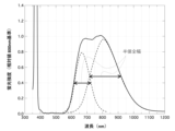
図5に基づいて、近赤外蛍光体の発光スペクトルの一例を説明する。図5は、後述する実施例で用いた近赤外蛍光体P8の発光スペクトル(光源:370nmに分光したキセノンランプ)である。図5に示すように、この近赤外蛍光体は、680±3nm、及び776±3nmにピーク波長を有している。つまり、この近赤外蛍光体は、700nmを超える範囲に一つのピーク波長を有している。各発光スペクトルの半値全幅は、それぞれ113nm、及び209nmである。これら二つのピークは重なり合っており、両者を含む発光スペクトルのカットオフ波長(例えば、蛍光強度が800nmにおける強度の1.5%を下回る波長)は、短波長側が540±3nmであり、長波長側が1200nm±3nmである。なお、近赤外蛍光体の発光スペクトルは、700nmを超える範囲にピーク波長を有していればよく、図5に示す発光スペクトルと同じ波形に限定されない。 An example of the emission spectrum of a near-infrared phosphor will be explained based on FIG. 5. FIG. 5 shows the emission spectrum of the near-infrared phosphor P8 used in the examples described below (light source: xenon lamp with a wavelength of 370 nm). As shown in FIG. 5, this near-infrared phosphor has peak wavelengths at 680±3 nm and 776±3 nm. That is, this near-infrared phosphor has one peak wavelength in a range exceeding 700 nm. The full width at half maximum of each emission spectrum is 113 nm and 209 nm, respectively. These two peaks overlap, and the cutoff wavelength of the emission spectrum that includes both (for example, the wavelength where the fluorescence intensity is less than 1.5% of the intensity at 800 nm) is 540 ± 3 nm on the short wavelength side and 540 ± 3 nm on the long wavelength side. It is 1200nm±3nm. Note that the emission spectrum of the near-infrared phosphor only needs to have a peak wavelength in a range exceeding 700 nm, and is not limited to the same waveform as the emission spectrum shown in FIG. 5.
この近赤外蛍光体を用いた蛍光膜(後述する可視蛍光体を含まない蛍光膜)と上記固体光源とで構成される発光装置は、強度バランスは任意となるものの、図5と概ね同じ波長にピーク波長を有する。 A light-emitting device composed of a fluorescent film using this near-infrared phosphor (a fluorescent film not containing a visible phosphor described later) and the above-mentioned solid-state light source has approximately the same wavelength as in Figure 5, although the intensity balance can be arbitrarily determined. It has a peak wavelength at
近赤外蛍光体としては、上記範囲にピーク波長を有する蛍光体であれば特に限定されず、例えば、ユーロピウム又はセリウム賦活化窒化物又は酸窒化物蛍光体を挙げることができる。これらは、5dと4f間の遷移による発光であり、半値幅が広いため好ましい。特に、2価のユーロピウム(2価のユーロピウムイオン)を添加した蛍光体は、半値幅が広く発光強度が高いためより好ましい。 The near-infrared phosphor is not particularly limited as long as it has a peak wavelength within the above range, and examples thereof include europium or cerium-activated nitride or oxynitride phosphors. These are light emissions due to the transition between 5d and 4f, and are preferable because they have a wide half-width. In particular, a phosphor doped with divalent europium (divalent europium ions) is more preferable because it has a wide half-width and high emission intensity.
ユーロピウム又はセリウム賦活化窒化物又は酸窒化物蛍光体としては、例えば、Li,Sr,La,及びSiからなる群から選択された1以上の金属の窒化物を母体結晶として、該母体結晶に賦活剤としてユーロピウムを含有する窒化物蛍光体を挙げることができる。 As a europium or cerium activated nitride or oxynitride phosphor, for example, a nitride of one or more metals selected from the group consisting of Li, Sr, La, and Si is used as a host crystal, and the host crystal is activated. As the agent, a nitride phosphor containing europium can be mentioned.
近赤外蛍光体は、以下の式(I)で示される組成を有する近赤外蛍光体とすることが、半値幅が広いため好ましく、以下の式(I)において、0.88≦f≦1.01の組成を有する近赤外蛍光体とすることが、発光強度が高いためより好ましい。
LiaSrbLacSidNeEuf・・・(I)
(ただし、a~fは、a+b+c+d+e+f=100、0≦a≦8.22、0.22≦b≦17.33、1.12≦c≦11.36、22.41≦d≦38.09、49.47≦e≦56.09、0.05≦f≦10、となる数である。)
The near-infrared phosphor is preferably a near-infrared phosphor having a composition represented by the following formula (I) because it has a wide half-value width, and in the following formula (I), 0.88≦f≦ It is more preferable to use a near-infrared phosphor having a composition of 1.01 because the emission intensity is high.
Li a Sr b La c Si d N e Eu f ...(I)
(However, a to f are a+b+c+d+e+f=100, 0≦a≦8.22, 0.22≦b≦17.33, 1.12≦c≦11.36, 22.41≦d≦38.09, 49.47≦e≦56.09, 0.05≦f≦10.)
近赤外蛍光体の含有量は、蛍光膜に含まれる全蛍光体中、5質量%以上50質量%以下であることが好ましく、10質量%以上30質量%以下であることがより好ましく、15質量%以上25質量%以下であることがさらに好ましい。上記範囲内とすることで、他の蛍光体層の発光を妨げることなく近赤外蛍光体の発光を得ることができる。 The content of the near-infrared phosphor is preferably 5% by mass or more and 50% by mass or less, more preferably 10% by mass or more and 30% by mass or less, based on the total phosphors contained in the fluorescent film. More preferably, it is at least 25% by mass and not more than 25% by mass. By setting it within the above range, light emission of the near-infrared phosphor can be obtained without interfering with the light emission of other phosphor layers.
蛍光膜は、上記近赤外蛍光体の他に、固体光源からの光に励起されて350nm以上700nm以下の範囲にピーク波長(好ましくは、最大ピーク波長)を有する光を発する少なくとも一種の可視蛍光体(以下、単に「可視蛍光体」ともいう。)を含有していてもよい。可視蛍光体を含有することで、紫外線領域、可視光領域及び近赤外線領域までの広帯域な発光スペクトルを有する発光装置とすることができる。
なお、本明細書において、「可視蛍光体」との用語は、上記のとおり、「固体光源からの光に励起されて350nm以上700nm以下の範囲にピーク波長(好ましくは、最大ピーク波長)を有する光を発する蛍光体」のことを意味している。一般的には、「可視」との用語は、380nm~780nm程度の波長範囲を指す用語として用いられている。本実施形態で用いる可視蛍光体は、350nm以上700nm以下の範囲にピーク波長を有しており、通常は該発光スペクトルの半値全幅は50nm以上であり、かつ、該発光スペクトルはガウス関数に従う強度分布を取ると考えて良いため、カットオフ波長(例えば、蛍光強度が最大ピーク波長における強度の1.5%を下回る波長)の幅(短波長側カットオフ波長と長波長側カットオフ波長の範囲)は100nm以上であるので、少なくとも380nm~780nm程度の波長範囲全域にわたってスペクトルを呈することになるため、一般的な意味合いからも矛盾しない。
In addition to the above-mentioned near-infrared phosphor, the fluorescent film contains at least one type of visible fluorescent material that emits light having a peak wavelength (preferably a maximum peak wavelength) in a range of 350 nm or more and 700 nm or less when excited by light from a solid-state light source. (hereinafter also simply referred to as "visible phosphor"). By containing a visible phosphor, a light-emitting device can have a wide-band emission spectrum from the ultraviolet region to the visible light region and the near-infrared region.
In addition, in this specification, the term "visible phosphor" refers to "a phosphor that is excited by light from a solid-state light source and has a peak wavelength (preferably a maximum peak wavelength) in the range of 350 nm or more and 700 nm or less". It means a phosphor that emits light. Generally, the term "visible" is used to refer to a wavelength range of about 380 nm to 780 nm. The visible phosphor used in this embodiment has a peak wavelength in the range of 350 nm or more and 700 nm or less, the full width at half maximum of the emission spectrum is usually 50 nm or more, and the emission spectrum has an intensity distribution that follows a Gaussian function. Therefore, the width of the cutoff wavelength (for example, the wavelength where the fluorescence intensity is less than 1.5% of the intensity at the maximum peak wavelength) (the range between the short wavelength side cutoff wavelength and the long wavelength side cutoff wavelength) Since it is 100 nm or more, it exhibits a spectrum over the entire wavelength range of at least about 380 nm to 780 nm, so there is no contradiction from a general meaning.
可視蛍光体としては、上記範囲にピーク波長を有する蛍光体であれば特に限定されず、例えば、固体光源からの光に励起されて350nm以上430nm未満の範囲にピーク波長を有する光を発する蛍光体A(以下、単に「可視蛍光体A」ともいう。)、固体光源からの光に励起されて430nm以上500nm未満の範囲にピーク波長を有する光を発する蛍光体B(以下、単に「可視蛍光体B」ともいう。)、固体光源からの光に励起されて500nm以上700nm未満の範囲にピーク波長を有する光を発する蛍光体C(以下、単に「可視蛍光体C」ともいう。)、を挙げることができる。蛍光体A~Cは、それぞれ、上記範囲に最大ピーク波長を有することが好ましい。広帯域の発光スペクトルをより確実に呈する点で、可視蛍光体は、蛍光体A~Cをそれぞれ一種以上含むことが好ましい。なお、可視蛍光体のピーク波長は、可視蛍光体の活化剤の含有量を調整したり、混合物の混合比を調整したりすることで各領域内の任意の波長に調整することができる。 The visible phosphor is not particularly limited as long as it has a peak wavelength in the above range; for example, a phosphor that emits light having a peak wavelength in the range of 350 nm or more and less than 430 nm when excited by light from a solid-state light source. A (hereinafter also simply referred to as "visible phosphor A"), phosphor B (hereinafter simply referred to as "visible phosphor ), and a phosphor C (hereinafter also simply referred to as "visible phosphor C") that emits light having a peak wavelength in the range of 500 nm or more and less than 700 nm when excited by light from a solid-state light source. be able to. Each of the phosphors A to C preferably has a maximum peak wavelength within the above range. In order to more reliably exhibit a broadband emission spectrum, the visible phosphor preferably contains one or more of each of phosphors A to C. Note that the peak wavelength of the visible phosphor can be adjusted to any wavelength within each region by adjusting the content of the activator of the visible phosphor or adjusting the mixing ratio of the mixture.
可視蛍光体Aとしては、例えば、π電子共役系有機蛍光体A1(以下、「可視蛍光体A1」ともいう。)、ユーロピウム賦活化酸硫化物蛍光体及び銀賦活化硫化亜鉛蛍光体の混合物蛍光体A2(以下、「可視蛍光体A2」ともいう。)を挙げることができ、これらから選択される一種以上を用いることができる。 Examples of the visible phosphor A include a π-electron conjugated organic phosphor A1 (hereinafter also referred to as "visible phosphor A1"), a fluorescent mixture of a europium-activated oxysulfide phosphor, and a silver-activated zinc sulfide phosphor. phosphor A2 (hereinafter also referred to as "visible phosphor A2"), and one or more selected from these can be used.
可視蛍光体A1としては、例えば、以下の式(A1)で表される、1,3,4-オキサジアゾリル環の2,5位にπ電子共役系置換基を有する蛍光体を挙げることができる。

可視蛍光体A1は、例えば、1,3,4-オキサジアゾリル環(-C2N2O-)、1,4-フェニル環(-C6H4-)、及び1-フェニル環(-C6H5)をそれぞれ1~3個含むπ電子共役系有機蛍光体とすることもできる。可視蛍光体A1は、その純度が90%以上であることが好ましい。可視蛍光体A1は、これらから選択される一種以上を用いることができる。 The visible phosphor A1 includes, for example, a 1,3,4-oxadiazolyl ring (-C 2 N 2 O-), a 1,4-phenyl ring (-C 6 H 4 -), and a 1-phenyl ring (-C 6 It is also possible to use a π-electron conjugated organic phosphor containing 1 to 3 H 5 ). It is preferable that the visible phosphor A1 has a purity of 90% or more. As the visible phosphor A1, one or more types selected from these can be used.
可視蛍光体A2としては、例えば、ユーロピウム賦活化酸硫化物蛍光体(A2-1)及び銀賦活化硫化亜鉛蛍光体(A2-2)の混合物等を挙げることができる。
ユーロピウム賦活化酸硫化物蛍光体(A2-1)としては、例えば、ガドリニウム、イットリウム、及びランタンからなる群から選択された1以上の希土類金属と、酸硫化物を母体結晶として、該母体結晶に賦活剤としてユーロピウムを含有する、酸硫化物蛍光体等を挙げることができる。
Examples of the visible phosphor A2 include a mixture of a europium-activated oxysulfide phosphor (A2-1) and a silver-activated zinc sulfide phosphor (A2-2).
As the europium-activated oxysulfide phosphor (A2-1), for example, one or more rare earth metals selected from the group consisting of gadolinium, yttrium, and lanthanum and oxysulfide are used as a host crystal, and the host crystal is Examples of the activator include oxysulfide phosphors containing europium.
ユーロピウム賦活化酸硫化物蛍光体は、以下の式(A2-1)で表される蛍光体とすることもできる。
(A2-x,Eux)2O2S ・・・(A2-1)
(但し、Aは、Ga,Y,Laのいずれかであり、xは、0<x<0.1を満たす数である。)
The europium-activated oxysulfide phosphor can also be a phosphor represented by the following formula (A2-1).
(A 2-x , Eu x ) 2 O 2 S...(A2-1)
(However, A is Ga, Y, or La, and x is a number satisfying 0<x<0.1.)
銀賦活化硫化亜鉛蛍光体(A2-2)は、以下の式(A2-2)で表される蛍光体とすることもできる。
(Zn1-x,Ag2x)S ・・・(A2-2)
(但し、xは、0<x<0.1を満たす数である。)
The silver-activated zinc sulfide phosphor (A2-2) can also be a phosphor represented by the following formula (A2-2).
(Zn 1-x ,Ag 2x )S...(A2-2)
(However, x is a number that satisfies 0<x<0.1.)
可視蛍光体A2において、ユーロピウム賦活化酸硫化物蛍光体(A2-1)と銀賦活化硫化亜鉛蛍光体(A2-2)との混合比は、質量比[(A2-1)/(A2-2)]として、0.1以上9以下とすることができる。 In the visible phosphor A2, the mixing ratio of the europium-activated oxysulfide phosphor (A2-1) and the silver-activated zinc sulfide phosphor (A2-2) is the mass ratio [(A2-1)/(A2- 2)] can be set to 0.1 or more and 9 or less.
可視蛍光体Bとしては、例えば、ユーロピウム賦活化アルカリ土類アルミン酸塩蛍光体を挙げることができる。ユーロピウム賦活化アルカリ土類アルミン酸塩蛍光体としては、例えば、カルシウム、ストロンチウム、マグネシウム及びバリウムからなる群から選択される1以上の第2族元素のアルミン酸塩を母体結晶とし、該母体結晶に賦活剤としてユーロピウムを含有する蛍光体を挙げることができる。可視蛍光体Bとしては、これらから選択される一種以上を用いることができる。
As the visible phosphor B, mention may be made, for example, of a europium-activated alkaline earth aluminate phosphor. As a europium-activated alkaline earth aluminate phosphor, for example, an aluminate of one or
可視蛍光体Bは、以下の式(B1)~(B4)で表される蛍光体とすることもできる。
(A1-x,Eux)Al11O17 ・・・(B1)
(但し、Aは、Ca,Sr,Mg,Ba又はその組み合わせであり、xは、0<x<0.1を満たす数である。)
The visible phosphor B can also be a phosphor expressed by the following formulas (B1) to (B4).
(A 1-x , Eu x ) Al 11 O 17 ...(B1)
(However, A is Ca, Sr, Mg, Ba, or a combination thereof, and x is a number satisfying 0<x<0.1.)
(Sr0~0.8Si6N8:Eu0.01~0.2 ・・・(B2)
(Ca0.25~2Si0.01~11.49Al0.51~11.99O0.01~11.49N4.51~15.99):Ce0.001~0.5 ・・・(B3)
Al4.6Si0.3~0.39N5:Eu0.01~0.1 ・・・(B4)
(Sr 0-0.8 Si 6 N 8 :Eu 0.01-0.2 ...(B2)
(Ca 0.25~2 Si 0.01~11.49 Al 0.51~11.99 O 0.01~11.49 N 4.51~15.99 ): Ce 0.001~0.5・...(B3)
Al 4.6 Si 0.3-0.39 N 5 :Eu 0.01-0.1 ...(B4)
可視蛍光体Cとしては、例えば、ユーロピウム賦活化ストロンチウムシリケート蛍光体を挙げることができる。ユーロピウム賦活化ストロンチウムシリケート蛍光体としては、例えば、ストロンチウムシリケートを母体結晶とし、該母体結晶に賦活剤としてユーロピウムを含有する蛍光体であって、以下の式(C1)~(C5)で表される可視蛍光体C1~C5を挙げることができる。 As the visible phosphor C, for example, a europium-activated strontium silicate phosphor can be mentioned. The europium-activated strontium silicate phosphor is, for example, a phosphor containing strontium silicate as a host crystal and containing europium as an activator in the host crystal, and is represented by the following formulas (C1) to (C5). Visible phosphors C1 to C5 can be mentioned.
(Sr1-x,Eux)3SiO5 ・・・(C1)
(但し、xは、0<x<0.1を満たす数である。)
(Sr 1-x , Eu x ) 3 SiO 5 ...(C1)
(However, x is a number that satisfies 0<x<0.1.)
(Sr1-x―y,Bax,Euy)3SiO5 ・・・(C2)
(但し、x,yは、0<x<1、0<y<0.1を満たす数である。)
(Sr 1-x-y , Bax , Eu y ) 3 SiO 5 ...(C2)
(However, x and y are numbers that satisfy 0<x<1 and 0<y<0.1.)
(Sr1-x―y,Bax,Euy)2SiO4 ・・・(C3)
(但し、x,yは、0<x<1、0<y<0.1を満たす数である。)
(Sr 1-x-y , Bax , Eu y ) 2 SiO 4 ...(C3)
(However, x and y are numbers that satisfy 0<x<1 and 0<y<0.1.)
Me2Si5N8:Eu ・・・(C4)
MeAlSiN3:Eu ・・・(C5)
但し、式(C4),(C5)において、Meは、Ca,Sr,又はBaを表す。
Me 2 Si 5 N 8 :Eu...(C4)
MeAlSiN3 :Eu...(C5)
However, in formulas (C4) and (C5), Me represents Ca, Sr, or Ba.
可視蛍光体Cとしては、上記可視蛍光体C1~C5から選択される1以上を用いることができる。 As the visible phosphor C, one or more selected from the above visible phosphors C1 to C5 can be used.
各層における蛍光体の総含有量は、3質量%以上75質量%以下であることが好ましく、5質量%以上60質量%以下であることがより好ましい。上記範囲内とすることで、分散性良く均質な層を形成でき、かつ、蛍光体からの発光を効果的に得るとともに、層内での散乱による光の散逸を押さえた条件を達成し、十分な発光強度と狭い放射角特性を具備することが可能となる。 The total content of the phosphor in each layer is preferably 3% by mass or more and 75% by mass or less, more preferably 5% by mass or more and 60% by mass or less. By keeping it within the above range, it is possible to form a homogeneous layer with good dispersibility, and to effectively obtain light emission from the phosphor, while also achieving conditions that suppress the dissipation of light due to scattering within the layer. It becomes possible to have a high emission intensity and narrow radiation angle characteristics.
可視蛍光体の含有量は、所望される各々の波長の光量バランスに応じて選択することができる。例えば、蛍光体Aの含有量は、蛍光膜に含まれる全蛍光体中、2質量%以上50質量%以下であることが好ましく、5質量%以上35質量%以下であることがより好ましい。蛍光体Bの含有量は、蛍光膜に含まれる全蛍光体中、2質量%以上50質量%以下であることが好ましく、5質量%以上35質量%以下であることがより好ましい。蛍光体Cの含有量は、蛍光膜に含まれる全蛍光体中、1質量%以上30質量%以下であることが好ましく、5質量%以上15質量%以下であることがより好ましい。 The content of the visible phosphor can be selected depending on the desired balance of light amounts of each wavelength. For example, the content of phosphor A is preferably 2% by mass or more and 50% by mass or less, more preferably 5% by mass or more and 35% by mass or less, based on all the phosphors contained in the phosphor film. The content of the phosphor B is preferably 2% by mass or more and 50% by mass or less, more preferably 5% by mass or more and 35% by mass or less, based on all the phosphors contained in the fluorescent film. The content of the phosphor C is preferably 1% by mass or more and 30% by mass or less, more preferably 5% by mass or more and 15% by mass or less, based on all the phosphors contained in the fluorescent film.
蛍光膜中に含まれる蛍光体の数は、少なくとも400nm以上1000nm以下の範囲に連続的な発光スペクトルを有する発光装置とする場合、上記近赤外蛍光体に可視蛍光体を組み合わせて、合計2種以上とすることができ、3種以上とすることが好ましく、5種以上とすることがより好ましい。上限値は特に限定されず、10種以下、又は8種以下とすることができる。
蛍光膜が複数の層で構成されている場合、各層に含まれる蛍光体の種類は、1以上4以下であることが好ましく、1以上3以下であることがより好ましい。蛍光体の種類を1以上4以下とすることで、比重や粒径の違う多種の蛍光体を含むことにより蛍光体の分散性が低下することを防ぐことができる。
In the case of a light emitting device having a continuous emission spectrum in the range of at least 400 nm or more and 1000 nm or less, the number of phosphors contained in the phosphor film is two in total, including a combination of the above near-infrared phosphor and a visible phosphor. or more, preferably three or more types, more preferably five or more types. The upper limit is not particularly limited, and may be 10 or less, or 8 or less.
When the fluorescent film is composed of a plurality of layers, the number of types of phosphor contained in each layer is preferably 1 or more and 4 or less, more preferably 1 or more and 3 or less. By setting the number of types of phosphor to 1 or more and 4 or less, it is possible to prevent the dispersibility of the phosphor from decreasing due to the inclusion of various phosphors with different specific gravity and particle size.
蛍光膜は、一層以上で構成されており、好ましくは、含まれる蛍光体の種類が異なる複数の層で構成されている。含まれる蛍光体の種類が異なる複数の層で構成することで、一層に含まれる蛍光体の種類が過度に多くならないので、蛍光体の分散性を高めて均一な蛍光膜とすることができる。蛍光膜を構成する層の数は、1以上、2以上又は3以上とすることができ、8以下、7以下又は5以下とすることができる。 The phosphor film is composed of one or more layers, preferably a plurality of layers containing different types of phosphors. By configuring the layer with a plurality of layers containing different types of phosphors, the number of types of phosphors contained in one layer does not increase excessively, so that the dispersibility of the phosphors can be improved and a uniform phosphor film can be obtained. The number of layers constituting the fluorescent film can be 1 or more, 2 or more, or 3 or more, and can be 8 or less, 7 or less, or 5 or less.
なお、「蛍光体の種類」とは、蛍光体のピーク波長によって区別される種類のことである。同じ母体結晶や混合物の構成要素が同一の場合でも、賦活化物の添加量や混合物の構成要素の混合比が異なる等によりピーク波長が異なる蛍光体は種類が異なる。「蛍光体の種類が異なる複数の層(2以上の層)」とは、ある一層に含まれる少なくとも一種の蛍光体が、他の層に含まれる蛍光体の種類と一致していないことを意味している。広帯域の発光スペクトルを呈することができる蛍光膜を効率よく作製する点で、含まれる蛍光体の種類が層間ですべて異なることが好ましい。「蛍光体の種類が異なる複数の層」とするには、例えば、近赤外蛍光体を含む層、可視蛍光体A~Cを含む層の2層で構成することができる。或いは、近赤外蛍光体を含む層、可視蛍光体Aを含む層、可視蛍光体Bを含む層、可視蛍光体Cを含む層の4層で構成することで蛍光体の種類が異なる複数の層とすることもできる。蛍光体の種類ごとに別の層として積層させることもできる。 Note that the "type of phosphor" refers to a type that is distinguished by the peak wavelength of the phosphor. Even when the same host crystal or the same constituent elements of the mixture are used, different types of phosphors have different peak wavelengths due to differences in the amount of activator added or the mixing ratio of the constituent elements of the mixture. "Multiple layers containing different types of phosphor (two or more layers)" means that at least one type of phosphor contained in one layer does not match the type of phosphor contained in other layers. are doing. In order to efficiently produce a fluorescent film capable of exhibiting a broadband emission spectrum, it is preferable that the types of phosphors contained in the layers are all different. In order to have "a plurality of layers containing different types of phosphors", for example, it can be composed of two layers: a layer containing a near-infrared phosphor and a layer containing visible phosphors A to C. Alternatively, a layer containing a near-infrared phosphor, a layer containing a visible phosphor A, a layer containing a visible phosphor B, and a layer containing a visible phosphor C can be used. It can also be a layer. It is also possible to laminate each type of phosphor as a separate layer.
但し、紫外領域および紫外領域寄りの可視領域にピーク波長を有する蛍光体の光は、特に、他の蛍光体による再吸収によって消失してしまう傾向にある。よって、蛍光膜が可視蛍光体A及び可視蛍光体Bを含む場合は、光の失活を防ぎながら、十分な強度の短波長側の発光を得る目的から、可視蛍光体Aと可視蛍光体Bとは異なる層に含むことが好ましい。一方、近赤外蛍光体、可視蛍光体Cは、他の蛍光体と混合しても発光スペクトルの強度に大きな影響は及ぼさない。 However, light from phosphors having peak wavelengths in the ultraviolet region and the visible region close to the ultraviolet region particularly tends to disappear due to reabsorption by other phosphors. Therefore, when the fluorescent film contains visible phosphor A and visible phosphor B, visible phosphor A and visible phosphor B are used in order to obtain sufficient intensity of light emission on the short wavelength side while preventing light deactivation. It is preferable to include it in a layer different from the On the other hand, near-infrared phosphor and visible phosphor C do not significantly affect the intensity of the emission spectrum even when mixed with other phosphors.
蛍光膜は、蛍光体の種類が異なる複数の層で形成されている場合、該複数の層が、ピーク波長がより長い蛍光体を含有する層からピーク波長がより短い蛍光体を含有する層へと順に、固体光源からの光の進行方向に積層されていることが好ましい。このような構成にすることで、蛍光発光した光が次の層に含まれる蛍光体の励起に利用されて短い波長の光が消失してしまうことを防ぐことができる。 When the phosphor film is formed of multiple layers containing different types of phosphors, the multiple layers change from a layer containing a phosphor with a longer peak wavelength to a layer containing a phosphor with a shorter peak wavelength. It is preferable that the layers are stacked in this order in the direction in which light from the solid-state light source travels. By adopting such a configuration, it is possible to prevent light with a short wavelength from disappearing due to the fluorescent light being used to excite the phosphor included in the next layer.
蛍光膜の各層の厚みは、含まれる蛍光体の割合により調整され、例えば、蛍光体の含有量が5質量%以上60質量%以下の場合、1μm以上500μm以下とすることができ、蛍光体の含有量が60質量%より多い場合、10μm以上100μm以下とすることができる。 The thickness of each layer of the phosphor film is adjusted depending on the proportion of the phosphor contained. For example, when the phosphor content is 5% by mass or more and 60% by mass or less, the thickness of each layer of the phosphor film can be set to 1 μm or more and 500 μm or less. When the content is more than 60% by mass, it can be 10 μm or more and 100 μm or less.
蛍光膜の作製方法は、特に限定されず、例えば、上記した蛍光体を、シリコーン樹脂、エポキシ樹脂、エチルセルロース、ガラス等の薄膜材料中に、必要に応じてシリコーンナノパウダー等の分散剤とともに、公知の攪拌・混練装置を用いて分散させてペースト状にした後、ポッティング、スプレー、スピンコート、スクリーン印刷、グラビア印刷、等により、固体光源上、又はガラス板等の透明基材上に塗布又は印刷して作製することができる。複数の蛍光体を混合して用いる場合の混合方法は、特に限定されず、従来の混合装置を用いて行えばよい。蛍光膜を複数の層で構成する場合、各層はシリコーン樹脂やエポキシ樹脂等で接着してもよいし、固定部品で押さえつけるように固定してもよい。蛍光膜をパッケージに装着する場合の接着方法についても、同様に、シリコーン樹脂やエポキシ樹脂等で接着してもよいし、固定部品で押さえつけるように固定してもよい。 The method for producing the fluorescent film is not particularly limited, and for example, the above-mentioned phosphor is added to a thin film material such as silicone resin, epoxy resin, ethyl cellulose, glass, etc., along with a dispersant such as silicone nanopowder as necessary, and known methods are used. After dispersing into a paste using a stirring and kneading device, apply or print onto a solid light source or a transparent substrate such as a glass plate by potting, spraying, spin coating, screen printing, gravure printing, etc. It can be made by The method for mixing a plurality of phosphors is not particularly limited, and may be performed using a conventional mixing device. When the fluorescent film is composed of a plurality of layers, each layer may be adhered with silicone resin, epoxy resin, or the like, or may be fixed by pressing with a fixing component. Regarding the adhesion method when attaching the fluorescent film to the package, it may be similarly adhered with silicone resin, epoxy resin, etc., or it may be fixed by pressing it with a fixing part.
(発光装置)
本実施形態に係る発光装置は、少なくとも、400nm以上1000nm以下の範囲に連続的な発光スペクトル(以下、「連続スペクトル」ともいう。)を有していることが好ましい。この範囲に連続的なスペクトルを有することで、広帯域な発光が求められる産業用機器用の光源として好ましく用いることができる。「連続的な発光スペクトル」とは、発光スペクトルの発光強度(以下、「蛍光強度」ともいう。)がこの範囲内の全域で、800nm基準の相対値として0.01以上(1%以上)であることを意味している。上記範囲の全域で800nm基準の相対値として1%以上であるので、産業機器用の光源としてより好ましく用いることができる。標準光源として用いる場合は、発光スペクトルの発光強度(蛍光強度)が、上記範囲の全域で、800nm基準の相対値として0.015以上(1.5%以上)であることが好ましく、使いやすさの観点からは、0.05以上(5%以上)であることがより好ましい。
(Light emitting device)
The light emitting device according to this embodiment preferably has a continuous emission spectrum (hereinafter also referred to as "continuous spectrum") at least in the range of 400 nm or more and 1000 nm or less. By having a continuous spectrum in this range, it can be preferably used as a light source for industrial equipment that requires broadband light emission. "Continuous emission spectrum" means that the emission intensity of the emission spectrum (hereinafter also referred to as "fluorescence intensity") is 0.01 or more (1% or more) as a relative value with respect to the 800 nm standard throughout this range. It means something. Since it is 1% or more as a relative value with respect to the 800 nm standard throughout the above range, it can be more preferably used as a light source for industrial equipment. When used as a standard light source, it is preferable that the emission intensity (fluorescence intensity) of the emission spectrum is 0.015 or more (1.5% or more) as a relative value with respect to the 800 nm standard throughout the above range, and it is easy to use. From this point of view, it is more preferably 0.05 or more (5% or more).
例えば、図6に示す実施例1のスペクトルにおいて、連続スペクトルの両端(350nm、1200nm)における蛍光強度は、800nm付近の最大強度に対してそれぞれ1.7%、1.9%であり、かつ、390nm付近の極小点における蛍光強度も8.2%であり、いずれも1.5%を上回っており、350nm以上1200nm以下の範囲に連続的な発光スペクトルを有しているといえる。よって、この発光装置は、少なくとも、400nm以上1000nm以下の範囲に連続的な発光スペクトルを有しており、産業用機器の標準光源として十分に使用可能である。 For example, in the spectrum of Example 1 shown in FIG. 6, the fluorescence intensities at both ends (350 nm, 1200 nm) of the continuous spectrum are 1.7% and 1.9%, respectively, of the maximum intensity near 800 nm, and The fluorescence intensity at the minimum point near 390 nm was also 8.2%, which exceeded 1.5% in both cases, and it could be said that it had a continuous emission spectrum in the range of 350 nm or more and 1200 nm or less. Therefore, this light emitting device has a continuous emission spectrum in the range of at least 400 nm or more and 1000 nm or less, and can be fully used as a standard light source for industrial equipment.
発光装置は、用いる固体光源及び近赤外蛍光体の発光スペクトルによって、より広帯域の連続スペクトルを有するように構成することができる。例えば、固体光源として、410nm以下の範囲にピーク波長を有する光を発光する固体光源を用いる場合、該発光スペクトルの半値全幅が50nm以上とすると、少なくとも、360nm以上の範囲に連続スペクトルを有する発光装置とすることができる。 The light emitting device can be configured to have a broader continuous spectrum depending on the emission spectrum of the solid-state light source and near-infrared phosphor used. For example, when using a solid-state light source that emits light having a peak wavelength in a range of 410 nm or less, and assuming that the full width at half maximum of the emission spectrum is 50 nm or more, a light-emitting device that has a continuous spectrum in a range of at least 360 nm or more is used. It can be done.
また、本実施形態に係る近赤外蛍光体を用いることで、1200nmを超える領域を含む広帯域の連続スペクトルを実現することができる。後述する実施例では、少なくとも、350nm以上1200nm以下の範囲に連続的な発光スペクトルを有する発光装置の例を示している。 Further, by using the near-infrared phosphor according to this embodiment, a continuous spectrum in a wide band including a region exceeding 1200 nm can be realized. In the examples described later, examples of light emitting devices are shown that have a continuous emission spectrum in a range of at least 350 nm or more and 1200 nm or less.
発光装置は、700nmを超える近赤外線領域にピーク波長を有する。近赤外線領域に強い光量が求められる場合は、700nmを超える近赤外線領域に、発光装置が呈する連続的な発光スペクトルにおいて最大の発光強度を得る波長を有する。より高波長側の発光が求められる場合は、近赤外蛍光体の組成や混合比を調整することにより、750nm以上、又は800nm以上の範囲にピーク波長を有するように構成することもできる。近赤外線領域にピーク波長を有することで、従来のLEDより広い波長範囲の光を得ることができるので、分光分析装置等の産業機器用の発光装置としてより好適に用いることができる。 The light emitting device has a peak wavelength in the near-infrared region exceeding 700 nm. When a strong amount of light in the near-infrared region is required, the wavelength that provides the maximum emission intensity in the continuous emission spectrum exhibited by the light-emitting device is in the near-infrared region exceeding 700 nm. If emission at a higher wavelength is required, the composition and mixing ratio of the near-infrared phosphor can be adjusted so that the peak wavelength is in the range of 750 nm or more or 800 nm or more. By having a peak wavelength in the near-infrared region, it is possible to obtain light in a wider wavelength range than conventional LEDs, so it can be more suitably used as a light-emitting device for industrial equipment such as a spectrometer.
産業機器としては、白色干渉膜厚計、ハンディタイプの色度計等の分光分析機器や、ハロゲンランプが用いられている産業機器等を挙げることができる。
白色干渉膜厚計は、光源の波長帯域の範囲に複数のフリンジ(干渉縞)が含まれていることが望ましいため、特に極薄膜の膜厚等を計測するためには、より広帯域の光源を用いることが求められている。従来のLED光源では十分な広帯域を達成することができないが、本実施形態に係る発光装置によれば白色干渉膜厚計の光源として十分な波長帯域を達成することができる。
ハンディタイプの色度計は、従来、光源の帯域に合せて測光範囲が400nm~700nmに設定されている。しかし、国際照明委員会(CIE)が定めるXYZ表色系は、380nm~780nmに規定されているため、従来のハンディタイプの色度計では厳密な計測が難しい。本実施形態に係る発光装置によれば、少なくとも、400nm以上1000nm以下の範囲の広帯域の発光スペクトルを有するので、CIEの規定に則った正確な計測が可能となる。その結果、照明分野、色彩分野、印刷分野、塗装分野等、広範囲の産業に貢献することができる。
ハロゲンランプは、多くの産業機器用光源として用いられている。しかし、例えばクリーンルーム等の外部と遮断された空間で用いられるものは、発熱及び排熱の問題が生じる場合がある。本実施形態に係る発光装置によれば、ハロゲンランプに類似した発光スペクトルに調整することが可能であるため、ハロゲンランプの代替品として好適に用いることができる。ハロゲンランプの代替品として用いる場合は、上記の蛍光体を複数組み合わせることにより、ハロゲンランプの発光スペクトルに類似した発光スペクトルを有する発光装置とすることができる。
Examples of industrial equipment include spectroscopic analysis equipment such as a white interference film thickness meter and a hand-held color meter, and industrial equipment that uses a halogen lamp.
Since it is desirable for a white interference film thickness meter to include multiple fringes (interference fringes) within the wavelength range of the light source, a wider band light source is recommended, especially for measuring the thickness of extremely thin films. It is required to use it. Although conventional LED light sources cannot achieve a sufficiently wide band, the light emitting device according to this embodiment can achieve a wavelength band sufficient as a light source for a white interference film thickness meter.
Conventionally, the photometric range of a handheld color meter is set to 400 nm to 700 nm, depending on the band of the light source. However, the XYZ color system defined by the Commission Internationale de l'Eclairage (CIE) is defined as 380 nm to 780 nm, making it difficult to accurately measure with conventional hand-held color meters. The light emitting device according to the present embodiment has a broadband emission spectrum in the range of at least 400 nm or more and 1000 nm or less, so accurate measurement in accordance with CIE regulations is possible. As a result, it can contribute to a wide range of industries, including the lighting, color, printing, and painting fields.
Halogen lamps are used as light sources for many industrial equipment. However, when used in a space isolated from the outside, such as a clean room, problems of heat generation and waste heat may occur. The light emitting device according to this embodiment can be adjusted to have an emission spectrum similar to that of a halogen lamp, and therefore can be suitably used as a substitute for a halogen lamp. When used as a substitute for a halogen lamp, a light-emitting device having an emission spectrum similar to that of a halogen lamp can be obtained by combining a plurality of the above-mentioned phosphors.
<変形例>
次に本実施形態に係る発光装置の変形例について述べる。以下の各変形例では、第1実施形態及び他の変形例と異なる点のみを述べる。以下に述べられていない構成については既述の構成と同様にすることができる。
<Modified example>
Next, a modification of the light emitting device according to this embodiment will be described. In each modified example below, only points different from the first embodiment and other modified examples will be described. Configurations not described below can be made similar to the configurations described above.
(第1変形例)
第1変形例は、第1実施形態において蛍光膜を複数の層で構成する例(図2参照)の変形例であり、含まれる蛍光体の種類が異なる複数の領域を同一面上に有するように構成する。
(First modification)
The first modification is a modification of the first embodiment in which the fluorescent film is composed of a plurality of layers (see FIG. 2), and has a plurality of regions containing different types of phosphors on the same surface. Configure.
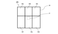
図9,10を用いて第1変形例を説明する。図9は第1変形例の発光装置の構成例を示す概略平面図であり、図10は概略側面図である。図9,10に示す発光装置100は、パッケージ11上に設けられた固体光源21と、固体光源21を覆うように設けられた蛍光膜30,31とを備える。蛍光膜30は、含まれる蛍光体の種類が異なる2以上の領域(領域30a~30f)を有している。「蛍光体の種類」とは、上記したように、蛍光体のピーク波長によって区別される種類のことである。なお、この例では、蛍光膜30,31は、基材7上に設けられているが、基材7は必須の構成ではない。基材としては、ガラス等の透明の部材を用いることができる。このような基材7を用いることで、製膜が容易であるとともに取り扱いが容易で、かつ強度を保つことができる。
The first modification will be explained using FIGS. 9 and 10. FIG. 9 is a schematic plan view showing a configuration example of a light emitting device according to a first modification, and FIG. 10 is a schematic side view. A
また、この例では、蛍光膜30を他の蛍光膜31と積層させる場合の例を示しているが、蛍光膜30のみを単層で用いることもできる。蛍光膜30を単層で用いる場合は、少なくとも一つの領域に近赤外蛍光体を含有するように構成する。この場合、蛍光膜30は、少なくとも一種の近赤外蛍光体を含有する領域(例えば領域30a)、及び少なくとも一種の可視蛍光体を含有する領域(例えば領域30b~30f)を有していることが好ましい。蛍光膜30が近赤外蛍光体を含有しない場合は、蛍光膜30を少なくとも一種の近赤外蛍光体を含有する蛍光膜31と積層させて用いればよい。他の蛍光膜31の構成は、特に限定されず、含まれる蛍光体の種類が異なる2以上の領域を同一面上に有する蛍光膜(蛍光膜30と同様の構成)であってもよく、1以上の蛍光体を含む一つの領域で構成された蛍光膜であってもよい。
Moreover, although this example shows an example in which the
蛍光膜30を他の蛍光膜31と積層させる場合は、第1実施形態で複数の層構成とする場合と同様に、ピーク波長がより長い蛍光体を含有する蛍光膜からピーク波長がより短い蛍光体を含有する蛍光膜へと順に、固体光源からの光の進行方向に積層されていることが好ましい。このような構成にすることで、蛍光発光した光が次の蛍光膜に含まれる蛍光体の励起に利用されて短い波長の光が消失してしまうことを防ぐことができる。
When the
図9では、蛍光膜30は、6つの領域30a~30fで構成されているが、領域の数はこれに限定されず、2以上の任意の数で構成することができる。中でも、蛍光発光した光の消失を防ぐ点で、含まれる蛍光体の種類が異なる4以上の領域で構成されていることが好ましい。
In FIG. 9, the
蛍光膜30の作製方法は、特に限定されず、蛍光体を含んだインクによる印刷や、あらかじめ蛍光体と樹脂を混合して作製された別々の蛍光膜を同一面上に配置することにより作製することができる。
The method for producing the
(第2変形例)
第2変形例は、固体光源を2以上用いる場合の例である。図11,12を用いて第2変形例を説明する。図11,12は、第2変形例の発光装置の構成例を示す概略平面図である。図11に示す発光装置101は、パッケージ12の同一面上に設けられた2以上の固体光源22a~22fと、該固体光源22a~22fのいずれか一つ又は複数を覆う蛍光膜32a~32eを備える。図12に示す発光装置102は、固体光源23a~23fと、該固体光源23a~23fの全てを覆う蛍光膜33gと、蛍光膜33gの上に設けられかつ固体光源23a~23fのうちの一つを覆う位置に設けられた蛍光膜33a~33fと、を備える。
固体光源22a~22f、23a~23fは、ピーク波長が同じ光を発光する固体光源であってもよく、ピーク波長が異なる光をそれぞれ発光する固体光源であってもよい。図11,12では、固体光源は6つの固体光源22a~22f又は23a~23fで構成されているが、固体光源の数は、これに限定されず2以上、3以上、5以上、10以上等、求められる明るさに対応できるよう任意の数にすることができる。
(Second modification)
The second modification is an example in which two or more solid-state light sources are used. A second modification will be explained using FIGS. 11 and 12. 11 and 12 are schematic plan views showing a configuration example of a light emitting device of a second modification. A light-emitting
The solid-
各固体光源を覆う蛍光膜の構成は、図11,12に示すものに限定されず、各固体光源がそれぞれ別個の蛍光膜(好ましくは、含まれる蛍光体の種類がそれぞれ異なる蛍光膜)で覆われていてもよく、一部又は全ての固体光源が単一の蛍光膜で覆われていてもよい。いずれの場合も、少なくとも一つの蛍光膜は、少なくとも近赤外蛍光体を含有するように構成する。各固体光源が別個の蛍光膜で覆われている場合、少なくとも近赤外蛍光体を含有する蛍光膜以外の蛍光膜のうち少なくとも一つの蛍光膜は、上記可視蛍光体から選択される少なくとも一種を含有する蛍光膜であることが好ましい。各固体光源が単一の蛍光膜で覆われている場合、蛍光膜は、近赤外蛍光体及び可視蛍光体を含有することが好ましい。また、蛍光膜は、第1変形例に記載した同一面上に2以上の領域を有する蛍光膜を用いることもでき、複数の層を有する蛍光膜を用いることもできる。その場合の構成は上記のとおりである。 The structure of the fluorescent film covering each solid-state light source is not limited to that shown in FIGS. 11 and 12, and each solid-state light source is covered with a separate fluorescent film (preferably, a fluorescent film containing different types of phosphors). Some or all of the solid-state light sources may be covered with a single fluorescent film. In either case, at least one phosphor film is configured to contain at least near-infrared phosphor. When each solid-state light source is covered with a separate fluorescent film, at least one of the fluorescent films other than the fluorescent film containing at least a near-infrared phosphor contains at least one kind selected from the above visible phosphors. It is preferable that it is a fluorescent film containing. When each solid-state light source is covered with a single fluorescent film, the fluorescent film preferably contains a near-infrared phosphor and a visible phosphor. Further, the fluorescent film may be a fluorescent film having two or more regions on the same surface as described in the first modification, or a fluorescent film having multiple layers. The configuration in that case is as described above.
蛍光膜の作製方法は、特に限定されず、前記の作製方法と同じ方法により作製することができる。
蛍光膜を同一平面状に複数個有する構成(例えば各固体光源がそれぞれ別個の蛍光膜で覆われている構成)にする場合は、樹脂硬化のための加熱時に樹脂が流れ出すことを防止する点で、例えばシリコーン樹脂等が固体光源の周囲を取り囲むように設けられている、いわゆるダムを有していてもよい。
The method for producing the fluorescent film is not particularly limited, and can be produced by the same method as described above.
When using a structure with multiple fluorescent films on the same plane (for example, a structure in which each solid-state light source is covered with a separate fluorescent film), it is important to prevent the resin from flowing out during heating to cure the resin. , for example, may have a so-called dam in which silicone resin or the like is provided so as to surround the solid-state light source.
(その他の構成)
発光装置は、発光した光の指向性をコントロールするため、固体光源及び蛍光膜を覆うようにレンズが設けられていてもよい。レンズとしては、片面凸レンズ、両面凸レンズ、凸メニスカスレンズ、ロッドレンズ、光ファイバー、等を挙げることができる。
(Other configurations)
In order to control the directivity of emitted light, the light emitting device may be provided with a lens to cover the solid state light source and the fluorescent film. Examples of the lens include a single-sided convex lens, a double-sided convex lens, a convex meniscus lens, a rod lens, and an optical fiber.
発光装置は、さらに、異なる波長の光を混合する目的のため、レンズの光入射面や出射面にブラスト加工が施されていてもよい。ブラスト加工の方法は特に限定されず、公知のサンドブラスト加工の方法等を用いて行うことができる。 In the light emitting device, the light incident surface and the light exit surface of the lens may be further subjected to blasting for the purpose of mixing light of different wavelengths. The method of blasting is not particularly limited, and any known sandblasting method can be used.
以下に実施例を示して本発明を更に具体的に説明するが、これらの実施例により本発明の解釈が限定されるものではない。 The present invention will be explained in more detail with reference to Examples below, but the interpretation of the present invention is not limited by these Examples.
[製造例1~14](近赤外蛍光体の製造)
実施例では、組成にLiaSrbLacSidNeEuf(ただし、a~fは、a+b+c+d+e+f=100となる数)で表される赤外蛍光体材料を用いた。
以下のようにして、実施例で用いることのできる近赤外蛍光体P1~P14を製造した。表1にこれらの蛍光体の設計組成示す。

In the example, an infrared phosphor material having the composition Li a Sr b La c Si d N e Eu f (where a to f are numbers such that a+b+c+d+e+f=100) was used.
Near-infrared phosphors P1 to P14 that can be used in Examples were manufactured in the following manner. Table 1 shows the designed compositions of these phosphors.
上記設計組成の蛍光体を得るために原料粉末Si3N4、Li3N、Sr3N2、LaN、EuNを、表2に示す重量比率で秤量し、メノウ乳棒と乳鉢で10分間混合した。その後、得られた混合物を窒化ホウ素製のるつぼに充填した。尚、粉末の秤量、混合の各工程は全て、水分1ppm以下、酸素1ppm以下の窒素雰囲気を保持することができるグローブボックス中で行った。 In order to obtain a phosphor having the above designed composition, raw powder powders Si 3 N 4 , Li 3 N, Sr 3 N 2 , LaN, and EuN were weighed at the weight ratios shown in Table 2 and mixed for 10 minutes using an agate pestle and mortar. . Thereafter, the resulting mixture was filled into a boron nitride crucible. All of the steps of weighing and mixing the powder were performed in a glove box capable of maintaining a nitrogen atmosphere containing 1 ppm of moisture or less and 1 ppm of oxygen or less.

その後、この混合粉末を入れた窒化ホウ素製のるつぼを、黒鉛抵抗加熱方式の電気炉にセットした。焼成の操作は、まず、拡散ポンプにより焼成雰囲気を真空とし、室温から800℃まで毎時1200℃の速度で昇温し、800℃において、純度が99.999体積%の窒素を導入して圧力を0.92MPaとし、1700℃の焼成温度まで、毎時600℃で昇温し、1700℃の焼成温度で2時間保持して行った。焼成後、乳鉢を用いて手で粉砕して赤外蛍光体粉末P1~P14を得た。
この蛍光体を370nmに分光したXe光源で励起した場合の発光特性を表3に示す。なお、表3において、「発光ピーク波長」は、「最大ピーク波長」を示しており、発光半値全幅の単位は「nm」である。
Thereafter, the boron nitride crucible containing this mixed powder was placed in a graphite resistance heating type electric furnace. In the firing operation, first, the firing atmosphere is made into a vacuum using a diffusion pump, the temperature is raised from room temperature to 800°C at a rate of 1200°C per hour, and at 800°C, nitrogen with a purity of 99.999% by volume is introduced and the pressure is increased. The temperature was set at 0.92 MPa, and the temperature was raised at a rate of 600°C per hour to a firing temperature of 1700°C, and the firing temperature was maintained at 1700°C for 2 hours. After firing, the powders were crushed by hand using a mortar to obtain infrared phosphor powders P1 to P14.
Table 3 shows the emission characteristics when this phosphor is excited with a Xe light source with a wavelength of 370 nm. In Table 3, the "emission peak wavelength" indicates the "maximum peak wavelength", and the unit of the full width at half maximum of the light emission is "nm".

図3,4に、上記蛍光体P1~P14の発光スペクトルを示す。図3,4において、横軸は波長(nm)を示し、縦軸は蛍光強度(任意単位)を示す。なお、スペクトル測定には大塚電子製MCPD9800(311C型)を用いた。ここでは、370nmに分光したキセノンランプで励起した場合を示したが、これらの蛍光体は300~500nmの広い波長範囲で励起することが可能であり、励起波長を変えても同様の発光スペクトルが得られた。これらの蛍光体は700~850nmの範囲に発光ピーク(ピーク波長)を有し、近赤外領域の広範囲に亘る発光スペクトルを有する。これらの蛍光体は、発光イオンとして2価Euを用いており、5d-4f遷移による半値全幅100nm以上の幅広い発光スペクトルを有する。さらに製造した蛍光体の発光イオンは複数の配位環境にあるため、いくつかの発光ピークが重畳したスペクトルを表している。このため、発光スペクトル線幅は通常の5d-4f遷移型蛍光体に比べても広く、本製造例に示すように100~300nmに及ぶ半値全幅を得ることができた。複数の発光ピークの強度のバランスは製造組成により異なり、組成によっては700nm以下に最大ピークを有するものもあるが、700nm以上の波長領域においてサブピークが重畳しているのが特徴である。 3 and 4 show the emission spectra of the phosphors P1 to P14. In FIGS. 3 and 4, the horizontal axis indicates wavelength (nm), and the vertical axis indicates fluorescence intensity (arbitrary unit). Note that MCPD9800 (311C type) manufactured by Otsuka Electronics was used for spectrum measurement. Here, we have shown the case of excitation using a xenon lamp with spectroscopy at 370 nm, but these phosphors can be excited over a wide wavelength range of 300 to 500 nm, and the same emission spectrum can be obtained even if the excitation wavelength is changed. Obtained. These phosphors have an emission peak (peak wavelength) in the range of 700 to 850 nm, and have an emission spectrum spanning a wide range in the near-infrared region. These phosphors use divalent Eu as a luminescent ion and have a wide emission spectrum with a full width at half maximum of 100 nm or more due to the 5d-4f transition. Furthermore, since the luminescent ions of the manufactured phosphor exist in multiple coordination environments, the spectrum represents a spectrum in which several luminescent peaks are superimposed. Therefore, the emission spectrum linewidth is wider than that of ordinary 5d-4f transition type phosphors, and as shown in this production example, it was possible to obtain a full width at half maximum of 100 to 300 nm. The balance of the intensity of multiple emission peaks varies depending on the manufacturing composition, and some compositions have a maximum peak below 700 nm, but are characterized by overlapping sub-peaks in the wavelength region above 700 nm.
以上の製造例からLiaSrbLacSidNeEufの組成(ただし、a+b+c+d+e+f=100、0≦a≦8.22、0.22≦b≦17.33、1.12≦c≦11.36、22.41≦d≦38.09、49.47≦e≦56.09、0.88≦f≦1.01)の蛍光体を本発明の実施例に用いることができる。ただし、発光イオンEuの濃度は約1atm%としたが、一般的に蛍光体で使われる範囲である0.01~10atm%とすることができる。上記の設計範囲とすることで、発光強度が低下することを抑制することができ、産業機器用の発光素子としてより好ましく使用することができる。 From the above production examples, the composition of Li a Sr b La c Si d N e Eu f (however, a+b+c+d+e+f=100, 0≦a≦8.22, 0.22≦b≦17.33, 1.12≦c≦ 11.36, 22.41≦d≦38.09, 49.47≦e≦56.09, 0.88≦f≦1.01) can be used in the embodiments of the present invention. However, although the concentration of the luminescent ion Eu was set to about 1 atm %, it can be set to 0.01 to 10 atm %, which is the range generally used in fluorescent materials. By setting it within the above design range, it is possible to suppress a decrease in the emission intensity, and it is possible to use it more preferably as a light emitting element for industrial equipment.
以下の実施例では、上述の製造例の内の蛍光体P8を用いて発光素子を作製した。この蛍光体は、発光線幅が広く、発光強度も高いため、発光素子に特に適しているといえるが、この他の組成の蛍光体を用いても本発明の目的を達成することが可能である。
この近赤外蛍光体P8の発光スペクトルを、分光器(光源:370nmに分光したキセノンランプ)を用いて測定したところ、680±3nm、776±3nmにピーク波長が測定された。この結果を図5に示した。
In the following examples, a light emitting element was manufactured using the phosphor P8 of the above-mentioned manufacturing examples. This phosphor has a wide emission linewidth and high emission intensity, so it can be said to be particularly suitable for light-emitting devices, but it is also possible to achieve the purpose of the present invention using phosphors with other compositions. be.
When the emission spectrum of this near-infrared phosphor P8 was measured using a spectrometer (light source: a xenon lamp with a wavelength of 370 nm), peak wavelengths were measured at 680±3 nm and 776±3 nm. The results are shown in FIG.
可視蛍光体として、以下の蛍光体を用いた。
[可視蛍光体A1]式(A1-1)で表される蛍光体(分子式:C24H22N2O)、ピーク波長405nm±3nm

[可視蛍光体B]BaMgAl11O17:Eu、ピーク波長452±3nm、459±3nm
[可視蛍光体C1-1]Sr3SiO5:Eu、ピーク波長520±3nm
[可視蛍光体C1-2]Sr3SiO5:Eu、ピーク波長593±3nm
[バインダー]シリコーン樹脂、信越化学工業株式会社製「KER-1930」
[分散剤]シリコーンナノパウダー、株式会社トクヤマ製、「レシオロール」
The following phosphor was used as the visible phosphor.
[Visible phosphor A1] Fluorescent substance represented by formula (A1-1) (molecular formula: C 24 H 22 N 2 O), peak wavelength 405 nm ± 3 nm
[Visible phosphor B] BaMgAl 11 O 17 :Eu, peak wavelength 452±3 nm, 459±3 nm
[Visible phosphor C1-1] Sr 3 SiO 5 :Eu, peak wavelength 520±3 nm
[Visible phosphor C1-2] Sr 3 SiO 5 :Eu, peak wavelength 593±3 nm
[Binder] Silicone resin, “KER-1930” manufactured by Shin-Etsu Chemical Co., Ltd.
[Dispersant] Silicone nanopowder, manufactured by Tokuyama Co., Ltd., "Ratio Roll"
[実施例1]
表4に示す蛍光体粉末とシリコーン樹脂とを、攪拌装置を用いて表1に記載の割合で混合し、蛍光体樹脂組成物a~eを作製した。樹脂組成物aを、SCHOTT社製の透明基材上で基材との間に隙間を設けたスキージをスライドさせて成膜し、熱硬化させた後に透明基材から剥がして、表1に記載の厚さの第1層を形成した。次いで、樹脂組成物bを、第1層と同様の方法で第2層を形成した。さらに同様の方法で樹脂組成物c、d、eを用いて第3層、第4層、第5層を形成し、それぞれの層の間にシリコーン樹脂を薄く塗布し、重ねあわせることで5種類の蛍光体がそれぞれ別の層に含まれる5層の蛍光膜を製作した。
凹部を有するセラミック製パッケージの凹部の底面に、銀ペースト製のダイアタッチ材を塗布し、その上に365nmにピーク波長を有する紫外線LEDチップ(1.1mm×1.1mm×高さ0.2mm、電流値500mA、放射束600mW以上)をマウントした。LEDチップの正極と負極がパッケージの正極と負極のそれぞれの電極パッドに繋がるように金ワイヤで接続した。LEDチップと並列に、静電保護素子を配置した。パッケージの凹部の開口部に上記の蛍光膜をシリコーン樹脂で取り付け、図1,2に示す構造を有する発光装置を作製した。

Phosphor powders and silicone resins shown in Table 4 were mixed in the proportions shown in Table 1 using a stirring device to produce phosphor resin compositions a to e. Resin composition a was formed into a film by sliding a squeegee with a gap between it and the substrate on a transparent substrate made by SCHOTT, and after being thermally cured, it was peeled off from the transparent substrate and the results are shown in Table 1. A first layer having a thickness of . Next, a second layer was formed using the resin composition b in the same manner as the first layer. Furthermore, the third, fourth, and fifth layers are formed using resin compositions c, d, and e in the same manner, and silicone resin is thinly applied between each layer and layered to form five types. A five-layer phosphor film was fabricated, each containing phosphors in separate layers.
A die attach material made of silver paste is applied to the bottom of the recess of a ceramic package having a recess, and an ultraviolet LED chip (1.1 mm x 1.1 mm x 0.2 mm height, A current value of 500 mA and a radiant flux of 600 mW or more) were mounted. The positive and negative electrodes of the LED chip were connected to the positive and negative electrode pads of the package using gold wires, respectively. An electrostatic protection element was placed in parallel with the LED chip. The above fluorescent film was attached to the opening of the recess of the package using silicone resin to produce a light emitting device having the structure shown in FIGS. 1 and 2.
[実施例2]
表5に示す組成及び割合で蛍光膜を作製した以外は、実施例1と同様にして、発光装置を作製した。この発光装置における蛍光膜は、7種類の蛍光体がそれぞれ別の層に含まれる7層構造を有している。

A light emitting device was produced in the same manner as in Example 1, except that a fluorescent film was produced with the composition and ratio shown in Table 5. The phosphor film in this light-emitting device has a seven-layer structure in which seven types of phosphors are contained in separate layers.
[実施例3]
表6に示す組成及び割合で蛍光膜を作製した以外は、実施例1と同様にして、発光装置を作製した。この発光装置における蛍光膜は、可視蛍光体A,Bがそれぞれ別の層に含まれており、近赤外蛍光体、可視蛍光体C1-1、C1-2が同じ層に含まれている3層構造を有している。

A light emitting device was produced in the same manner as in Example 1, except that a fluorescent film was produced with the composition and ratio shown in Table 6. In the fluorescent film in this light emitting device, visible phosphors A and B are contained in separate layers, and near-infrared phosphors and visible phosphors C1-1 and C1-2 are contained in the same layer. It has a layered structure.
[比較例1]
近赤外蛍光体を含まないこと以外は、実施例1と同様にして、発光装置を作製した。
[Comparative example 1]
A light-emitting device was produced in the same manner as in Example 1 except that the near-infrared phosphor was not included.
[比較例2]
近赤外蛍光体に替えて三菱ケミカル株式会社製の蛍光体「BR-101/N」(ピーク波長648nm、半値全幅88nm)を用いた以外は、実施例1と同様にして、発光装置を作製した。
[Comparative example 2]
A light-emitting device was produced in the same manner as in Example 1, except that the phosphor "BR-101/N" manufactured by Mitsubishi Chemical Corporation (peak wavelength 648 nm, full width at half maximum 88 nm) was used instead of the near-infrared phosphor. did.
[発光スペクトル]
実施例及び比較例の発光装置の発光スペクトルを、分光器を用いて、Ta=25℃、IF=500mAの条件により測定した。実施例1,3の結果を図6に示した。実施例2の結果を図7に示した。比較例1,2と実施例1との比較を図8に示した。
図6,7に示すように、実施例1~3の発光装置は、780nmを超える領域にピーク波長を有している。中でも、実施例1,3の発光装置は、780nmを超える領域に、連続的な発光スペクトルにおいて最大の発光強度を得る波長を有している。
また、図6に示す実施例1のスペクトルにおいて、連続スペクトルの両端(350nm、1200nm)における蛍光強度は、800nm付近の最大強度に対してそれぞれ1.7%、1.9%であり、かつ、390nm付近の極小点における蛍光強度も8.2%であり、いずれも1.5%を上回っている。よって、この発光装置は、少なくとも、350nm以上1200nm以下の範囲に連続的な発光スペクトルを有している。同様に、実施例2,3の発光装置についても、少なくとも、350nm以上1200nmの広帯域に連続的な発光スペクトルを有していることが確認された。
さらに、実施例に示す発光装置は、10mWを超える放射束を達成することが確認された。よって、この発光装置は、紫外線領域から近赤外線領域まで広帯域の発光スペクトル分布を有するとともに、高輝度性、高集光性に優れており、通電時の発光応答性、発光強度の時間的変動、温度による波長シフト等も小さいので、それらの特性に関して問題点を有していた従来光源(ハロゲンランプ等)の代替素子として、産業機器用の発光装置に好適に用いることができる。
[Emission spectrum]
The emission spectra of the light emitting devices of Examples and Comparative Examples were measured using a spectrometer under the conditions of Ta=25° C. and IF=500 mA. The results of Examples 1 and 3 are shown in FIG. The results of Example 2 are shown in FIG. A comparison between Comparative Examples 1 and 2 and Example 1 is shown in FIG.
As shown in FIGS. 6 and 7, the light emitting devices of Examples 1 to 3 have peak wavelengths in a region exceeding 780 nm. Among them, the light emitting devices of Examples 1 and 3 have a wavelength in a region exceeding 780 nm that provides the maximum emission intensity in a continuous emission spectrum.
In addition, in the spectrum of Example 1 shown in FIG. 6, the fluorescence intensities at both ends (350 nm, 1200 nm) of the continuous spectrum are 1.7% and 1.9%, respectively, of the maximum intensity near 800 nm, and The fluorescence intensity at the minimum point near 390 nm was also 8.2%, both exceeding 1.5%. Therefore, this light emitting device has a continuous emission spectrum in the range of at least 350 nm or more and 1200 nm or less. Similarly, the light emitting devices of Examples 2 and 3 were also confirmed to have continuous emission spectra in a wide band of at least 350 nm to 1200 nm.
Furthermore, it was confirmed that the light emitting device shown in the example achieved a radiant flux exceeding 10 mW. Therefore, this light-emitting device has a wide-band emission spectrum distribution from the ultraviolet region to the near-infrared region, and is also excellent in high brightness and high light-gathering properties. Since the wavelength shift and the like are small, it can be suitably used in light emitting devices for industrial equipment as an alternative element to conventional light sources (such as halogen lamps) that have problems with these characteristics.
10,100,101,102 発光装置
1,11,12,13 パッケージ
2,21,22a~22e,23a~23f 固体光源
3,30,31,32a~32e,33a~33g 蛍光膜
4 ワイヤ
5 電極パッド
6 静電保護素子
10, 100, 101, 102
Claims (12)
前記蛍光膜が、前記固体光源からの光に励起されて700nmを超える範囲にピーク波長を有しかつ該ピーク波長を含む範囲における発光スペクトルの半値全幅が100nm以上である光を発する少なくとも一種の近赤外蛍光体を含有し、
前記近赤外蛍光体が、以下の式(I):
LiaSrbLacSidNeEuf・・・(I)
(ただし、a~fは、a+b+c+d+e+f=100、0≦a≦8.22、0.22≦b≦17.33、1.12≦c≦11.36、22.41≦d≦38.09、49.47≦e≦56.09、0.88≦f≦1.01、を満たす数である。)
で示される組成を有する、発光装置。 At least comprising a solid-state light source that emits light having a peak wavelength in a range of 480 nm or less, and a fluorescent film covering the solid-state light source and containing at least one type of phosphor,
The fluorescent film is excited by the light from the solid-state light source and emits light having a peak wavelength in a range exceeding 700 nm, and the full width at half maximum of the emission spectrum in the range including the peak wavelength is 100 nm or more. Contains infrared phosphor,
The near-infrared phosphor has the following formula (I):
Li a Sr b La c Si d N e Eu f ...(I)
(However, a to f are a+b+c+d+e+f=100, 0≦a≦8.22, 0.22≦b≦17.33, 1.12≦c≦11.36, 22.41≦d≦38.09, The number satisfies 49.47≦e≦56.09, 0.88≦f≦1.01.)
A light emitting device having a composition represented by:
該2以上の層が、ピーク波長がより長い蛍光体を含有する層からピーク波長がより短い蛍光体を含有する層へと順に、前記固体光源からの光の進行方向に積層されている、請求項4又は5に記載の発光装置。 The phosphor film is formed of two or more layers containing different types of phosphors,
The two or more layers are stacked in order from a layer containing a phosphor with a longer peak wavelength to a layer containing a phosphor with a shorter peak wavelength in the traveling direction of light from the solid-state light source. Item 5. The light-emitting device according to item 4 or 5 .
前記近赤外蛍光体が、以下の式(I):
LiaSrbLacSidNeEuf・・・(I)
(ただし、a~fは、a+b+c+d+e+f=100、0≦a≦8.22、0.22≦b≦17.33、1.12≦c≦11.36、22.41≦d≦38.09、49.47≦e≦56.09、0.88≦f≦1.01、を満たす数である。)
で示される組成を有する、蛍光膜。 At least one type of near-infrared phosphor that emits light having a peak wavelength in a range of 480 nm or less and having a peak wavelength in a range exceeding 700 nm, and the full width at half maximum of the emission spectrum in the range including the peak wavelength is 100 nm or more. and at least one visible phosphor that emits light having a peak wavelength in the range of 350 nm or more and 700 nm or less,
The near-infrared phosphor has the following formula (I):
Li a Sr b La c Si d N e Eu f ...(I)
(However, a to f are a+b+c+d+e+f=100, 0≦a≦8.22, 0.22≦b≦17.33, 1.12≦c≦11.36, 22.41≦d≦38.09, The number satisfies 49.47≦e≦56.09, 0.88≦f≦1.01.)
A fluorescent film having the composition shown in .
Applications Claiming Priority (5)
| Application Number | Priority Date | Filing Date | Title |
|---|---|---|---|
| JP2018111551 | 2018-06-12 | ||
| JP2018111551 | 2018-06-12 | ||
| JP2018211960 | 2018-11-12 | ||
| JP2018211960 | 2018-11-12 | ||
| PCT/JP2019/023203 WO2019240150A1 (en) | 2018-06-12 | 2019-06-12 | Light-emitting device |
Publications (2)
| Publication Number | Publication Date |
|---|---|
| JPWO2019240150A1 JPWO2019240150A1 (en) | 2021-07-26 |
| JP7428323B2 true JP7428323B2 (en) | 2024-02-06 |
Family
ID=68842191
Family Applications (1)
| Application Number | Title | Priority Date | Filing Date |
|---|---|---|---|
| JP2020525601A Active JP7428323B2 (en) | 2018-06-12 | 2019-06-12 | light emitting device |
Country Status (7)
| Country | Link |
|---|---|
| US (1) | US11641009B2 (en) |
| EP (1) | EP3809475A4 (en) |
| JP (1) | JP7428323B2 (en) |
| KR (1) | KR20210019427A (en) |
| CN (1) | CN112262481A (en) |
| TW (1) | TW202005120A (en) |
| WO (1) | WO2019240150A1 (en) |
Families Citing this family (10)
| Publication number | Priority date | Publication date | Assignee | Title |
|---|---|---|---|---|
| JP6684412B1 (en) * | 2019-06-27 | 2020-04-22 | 国立研究開発法人物質・材料研究機構 | Phosphor, method of manufacturing the same, and light-emitting device |
| KR102408688B1 (en) * | 2020-09-14 | 2022-06-16 | (주)올릭스 | Tunable ultra-broad band near-infrared light-emitting device |
| CN116918084A (en) | 2021-02-24 | 2023-10-20 | 松下知识产权经营株式会社 | Light-emitting device and electronic apparatus using the same |
| KR20230145138A (en) | 2021-03-02 | 2023-10-17 | 덴카 주식회사 | Phosphor powder, wavelength converter and light emitting device |
| CN113285005B (en) * | 2021-05-28 | 2022-08-05 | 杭州电子科技大学 | Preparation method of near-infrared light-emitting device |
| JP7455396B2 (en) | 2021-07-20 | 2024-03-26 | フェニックス電機株式会社 | broadband light emitting device |
| FR3125632A1 (en) * | 2021-07-22 | 2023-01-27 | Aledia | Stack of antenna-effect materials and optoelectronic device comprising such a stack |
| CN114198649A (en) * | 2021-11-18 | 2022-03-18 | 惠州市勤仕达科技有限公司 | Full-spectrum eye-protecting LED lamp panel structure and lamp |
| WO2023038554A1 (en) * | 2022-04-04 | 2023-03-16 | Дамир Булатович АБДРАШИТОВ | Infrared conditioner |
| WO2024058087A1 (en) * | 2022-09-12 | 2024-03-21 | ローム株式会社 | Semiconductor laser device |
Citations (5)
| Publication number | Priority date | Publication date | Assignee | Title |
|---|---|---|---|---|
| JP2009224053A (en) | 2008-03-13 | 2009-10-01 | Sharp Corp | Headlamp and vehicular infrared night vision apparatus employing the headlamp as light source |
| WO2010055831A1 (en) | 2008-11-13 | 2010-05-20 | 国立大学法人名古屋大学 | Semiconductor light-emitting device |
| WO2016174236A1 (en) | 2015-04-30 | 2016-11-03 | Osram Opto Semiconductors Gmbh | Radiation-emitting optoelectronic component |
| WO2017159175A1 (en) | 2016-03-14 | 2017-09-21 | 三井金属鉱業株式会社 | Fluorescent substance |
| JP2017214442A (en) | 2016-05-30 | 2017-12-07 | 日亜化学工業株式会社 | Fluophor having composition of rare earth aluminum gallium acid salt |
Family Cites Families (10)
| Publication number | Priority date | Publication date | Assignee | Title |
|---|---|---|---|---|
| US7038370B2 (en) * | 2003-03-17 | 2006-05-02 | Lumileds Lighting, U.S., Llc | Phosphor converted light emitting device |
| JP2007049114A (en) | 2005-05-30 | 2007-02-22 | Sharp Corp | Light emitting device and method of manufacturing the same |
| US9062853B2 (en) | 2010-07-12 | 2015-06-23 | National University Corporation Nagoya University | Broadband infrared light emitting device |
| JP2013106550A (en) * | 2011-11-18 | 2013-06-06 | Sharp Corp | Lighting device for growing plant |
| CN104662680B (en) * | 2012-09-13 | 2017-07-14 | 3M创新有限公司 | High efficiency lighting system with wide color gamut |
| CN103022328B (en) | 2013-01-17 | 2016-06-01 | 中国科学院上海高等研究院 | Solar simulator light source and its implementation |
| US9184350B2 (en) * | 2013-06-21 | 2015-11-10 | Venntis Technologies LLC | Light emitting device for illuminating plants |
| JP6351265B2 (en) | 2014-01-09 | 2018-07-04 | デンカ株式会社 | Fluorescent substance-containing multilayer film sheet and light emitting device |
| US9911937B2 (en) * | 2016-05-12 | 2018-03-06 | Semiconductor Energy Laboratory Co., Ltd. | Light-emitting element, light-emitting device, electronic device, and lighting device |
| JP7107307B2 (en) | 2017-05-11 | 2022-07-27 | 三菱ケミカル株式会社 | Light-emitting device and phosphor |
-
2019
- 2019-06-12 WO PCT/JP2019/023203 patent/WO2019240150A1/en unknown
- 2019-06-12 EP EP19818988.8A patent/EP3809475A4/en active Pending
- 2019-06-12 JP JP2020525601A patent/JP7428323B2/en active Active
- 2019-06-12 KR KR1020207034812A patent/KR20210019427A/en not_active Application Discontinuation
- 2019-06-12 TW TW108120328A patent/TW202005120A/en unknown
- 2019-06-12 CN CN201980039362.2A patent/CN112262481A/en active Pending
- 2019-06-12 US US16/972,947 patent/US11641009B2/en active Active
Patent Citations (5)
| Publication number | Priority date | Publication date | Assignee | Title |
|---|---|---|---|---|
| JP2009224053A (en) | 2008-03-13 | 2009-10-01 | Sharp Corp | Headlamp and vehicular infrared night vision apparatus employing the headlamp as light source |
| WO2010055831A1 (en) | 2008-11-13 | 2010-05-20 | 国立大学法人名古屋大学 | Semiconductor light-emitting device |
| WO2016174236A1 (en) | 2015-04-30 | 2016-11-03 | Osram Opto Semiconductors Gmbh | Radiation-emitting optoelectronic component |
| WO2017159175A1 (en) | 2016-03-14 | 2017-09-21 | 三井金属鉱業株式会社 | Fluorescent substance |
| JP2017214442A (en) | 2016-05-30 | 2017-12-07 | 日亜化学工業株式会社 | Fluophor having composition of rare earth aluminum gallium acid salt |
Non-Patent Citations (1)
| Title |
|---|
| V.P.Dotsenko et al.,「Influence of Ce3+ Ions on the Near Infrared Emission of Eu2+-doped Ca3Sc2Si3O12」,JOURNAL OF NANO-AND ELECTRONIC PHYSICS,2015年01月01日 |
Also Published As
| Publication number | Publication date |
|---|---|
| JPWO2019240150A1 (en) | 2021-07-26 |
| EP3809475A1 (en) | 2021-04-21 |
| EP3809475A4 (en) | 2022-03-02 |
| KR20210019427A (en) | 2021-02-22 |
| CN112262481A (en) | 2021-01-22 |
| TW202005120A (en) | 2020-01-16 |
| US20210249569A1 (en) | 2021-08-12 |
| WO2019240150A1 (en) | 2019-12-19 |
| US11641009B2 (en) | 2023-05-02 |
Similar Documents
| Publication | Publication Date | Title |
|---|---|---|
| JP7428323B2 (en) | light emitting device | |
| EP1859657B1 (en) | Illumination system comprising a radiation source and a fluorescent material | |
| US7939996B2 (en) | Display device with solid state fluorescent material | |
| KR101178054B1 (en) | Preparing method of ß-SiAlON phosphor | |
| US7391060B2 (en) | Phosphor composition and method for producing the same, and light-emitting device using the same | |
| US7768189B2 (en) | White LEDs with tunable CRI | |
| EP1853681B1 (en) | Illumination system comprising a radiation source and a luminescent material | |
| GB2474413A (en) | Method for producing a ß-SiA1ON phosphor | |
| WO2006061778A1 (en) | Illumination system comprising a radiation source and a blue-emitting phospor | |
| JP2011066227A (en) | White led light source, backlight unit, liquid crystal panel, and liquid crystal tv | |
| KR101357515B1 (en) | Fluorescent substance and light-emitting device employing the same | |
| JP2013144794A (en) | Oxynitride-based phosphor and light-emitting device using the same | |
| JP4948015B2 (en) | Aluminate blue phosphor and light emitting device using the same | |
| JP2011066228A (en) | White led light source, backlight unit, liquid crystal panel, and liquid crystal tv | |
| JP2008266385A (en) | Fluorescent substance, method for producing the same, and light-emitting device using the same |
Legal Events
| Date | Code | Title | Description |
|---|---|---|---|
| A521 | Request for written amendment filed |
Free format text: JAPANESE INTERMEDIATE CODE: A821 Effective date: 20201009 |
|
| A621 | Written request for application examination |
Free format text: JAPANESE INTERMEDIATE CODE: A621 Effective date: 20220114 |
|
| A131 | Notification of reasons for refusal |
Free format text: JAPANESE INTERMEDIATE CODE: A131 Effective date: 20230307 |
|
| A131 | Notification of reasons for refusal |
Free format text: JAPANESE INTERMEDIATE CODE: A131 Effective date: 20230718 |
|
| A521 | Request for written amendment filed |
Free format text: JAPANESE INTERMEDIATE CODE: A523 Effective date: 20230915 |
|
| A131 | Notification of reasons for refusal |
Free format text: JAPANESE INTERMEDIATE CODE: A131 Effective date: 20231010 |
|
| A521 | Request for written amendment filed |
Free format text: JAPANESE INTERMEDIATE CODE: A523 Effective date: 20231206 |
|
| TRDD | Decision of grant or rejection written | ||
| A01 | Written decision to grant a patent or to grant a registration (utility model) |
Free format text: JAPANESE INTERMEDIATE CODE: A01 Effective date: 20231219 |
|
| A61 | First payment of annual fees (during grant procedure) |
Free format text: JAPANESE INTERMEDIATE CODE: A61 Effective date: 20240116 |
|
| R150 | Certificate of patent or registration of utility model |
Ref document number: 7428323 Country of ref document: JP Free format text: JAPANESE INTERMEDIATE CODE: R150 |