JP7413376B2 - 半導体検査方法及び半導体検査装置 - Google Patents
半導体検査方法及び半導体検査装置 Download PDFInfo
- Publication number
- JP7413376B2 JP7413376B2 JP2021524695A JP2021524695A JP7413376B2 JP 7413376 B2 JP7413376 B2 JP 7413376B2 JP 2021524695 A JP2021524695 A JP 2021524695A JP 2021524695 A JP2021524695 A JP 2021524695A JP 7413376 B2 JP7413376 B2 JP 7413376B2
- Authority
- JP
- Japan
- Prior art keywords
- image
- pattern image
- pattern
- semiconductor device
- semiconductor
- Prior art date
- Legal status (The legal status is an assumption and is not a legal conclusion. Google has not performed a legal analysis and makes no representation as to the accuracy of the status listed.)
- Active
Links
- 239000004065 semiconductor Substances 0.000 title claims description 79
- 238000012360 testing method Methods 0.000 title description 12
- 238000000034 method Methods 0.000 claims description 40
- 238000007689 inspection Methods 0.000 claims description 18
- 238000010801 machine learning Methods 0.000 claims description 10
- 238000013135 deep learning Methods 0.000 claims description 9
- 238000012549 training Methods 0.000 claims description 7
- 238000006243 chemical reaction Methods 0.000 claims description 4
- 238000012545 processing Methods 0.000 description 30
- 238000010191 image analysis Methods 0.000 description 21
- 230000003287 optical effect Effects 0.000 description 18
- 230000006870 function Effects 0.000 description 12
- 238000005286 illumination Methods 0.000 description 9
- 238000004458 analytical method Methods 0.000 description 7
- 238000005259 measurement Methods 0.000 description 7
- 238000001514 detection method Methods 0.000 description 6
- 238000010586 diagram Methods 0.000 description 6
- 230000010354 integration Effects 0.000 description 5
- 229910000530 Gallium indium arsenide Inorganic materials 0.000 description 4
- WPYVAWXEWQSOGY-UHFFFAOYSA-N indium antimonide Chemical compound [Sb]#[In] WPYVAWXEWQSOGY-UHFFFAOYSA-N 0.000 description 4
- 238000002955 isolation Methods 0.000 description 4
- 238000004590 computer program Methods 0.000 description 3
- 238000009792 diffusion process Methods 0.000 description 3
- 230000020169 heat generation Effects 0.000 description 3
- 229910052751 metal Inorganic materials 0.000 description 3
- 239000002184 metal Substances 0.000 description 3
- 230000004913 activation Effects 0.000 description 2
- 238000013527 convolutional neural network Methods 0.000 description 2
- 238000003384 imaging method Methods 0.000 description 2
- 230000015654 memory Effects 0.000 description 2
- 230000000644 propagated effect Effects 0.000 description 2
- 230000008685 targeting Effects 0.000 description 2
- KXNLCSXBJCPWGL-UHFFFAOYSA-N [Ga].[As].[In] Chemical compound [Ga].[As].[In] KXNLCSXBJCPWGL-UHFFFAOYSA-N 0.000 description 1
- 238000013459 approach Methods 0.000 description 1
- 238000013528 artificial neural network Methods 0.000 description 1
- 239000003086 colorant Substances 0.000 description 1
- 230000000295 complement effect Effects 0.000 description 1
- 238000013461 design Methods 0.000 description 1
- 230000001678 irradiating effect Effects 0.000 description 1
- 238000013507 mapping Methods 0.000 description 1
- 229910044991 metal oxide Inorganic materials 0.000 description 1
- 150000004706 metal oxides Chemical class 0.000 description 1
- 238000005457 optimization Methods 0.000 description 1
Images


Classifications
-
- G—PHYSICS
- G06—COMPUTING; CALCULATING OR COUNTING
- G06T—IMAGE DATA PROCESSING OR GENERATION, IN GENERAL
- G06T7/00—Image analysis
- G06T7/0002—Inspection of images, e.g. flaw detection
- G06T7/0004—Industrial image inspection
- G06T7/001—Industrial image inspection using an image reference approach
-
- G—PHYSICS
- G06—COMPUTING; CALCULATING OR COUNTING
- G06N—COMPUTING ARRANGEMENTS BASED ON SPECIFIC COMPUTATIONAL MODELS
- G06N3/00—Computing arrangements based on biological models
- G06N3/02—Neural networks
- G06N3/04—Architecture, e.g. interconnection topology
-
- G—PHYSICS
- G06—COMPUTING; CALCULATING OR COUNTING
- G06N—COMPUTING ARRANGEMENTS BASED ON SPECIFIC COMPUTATIONAL MODELS
- G06N3/00—Computing arrangements based on biological models
- G06N3/02—Neural networks
- G06N3/04—Architecture, e.g. interconnection topology
- G06N3/045—Combinations of networks
-
- G—PHYSICS
- G06—COMPUTING; CALCULATING OR COUNTING
- G06N—COMPUTING ARRANGEMENTS BASED ON SPECIFIC COMPUTATIONAL MODELS
- G06N3/00—Computing arrangements based on biological models
- G06N3/02—Neural networks
- G06N3/08—Learning methods
-
- G—PHYSICS
- G06—COMPUTING; CALCULATING OR COUNTING
- G06T—IMAGE DATA PROCESSING OR GENERATION, IN GENERAL
- G06T3/00—Geometric image transformations in the plane of the image
- G06T3/40—Scaling of whole images or parts thereof, e.g. expanding or contracting
- G06T3/4053—Scaling of whole images or parts thereof, e.g. expanding or contracting based on super-resolution, i.e. the output image resolution being higher than the sensor resolution
-
- G—PHYSICS
- G06—COMPUTING; CALCULATING OR COUNTING
- G06T—IMAGE DATA PROCESSING OR GENERATION, IN GENERAL
- G06T7/00—Image analysis
- G06T7/30—Determination of transform parameters for the alignment of images, i.e. image registration
-
- G—PHYSICS
- G06—COMPUTING; CALCULATING OR COUNTING
- G06F—ELECTRIC DIGITAL DATA PROCESSING
- G06F30/00—Computer-aided design [CAD]
- G06F30/30—Circuit design
- G06F30/39—Circuit design at the physical level
- G06F30/392—Floor-planning or layout, e.g. partitioning or placement
-
- G—PHYSICS
- G06—COMPUTING; CALCULATING OR COUNTING
- G06T—IMAGE DATA PROCESSING OR GENERATION, IN GENERAL
- G06T2207/00—Indexing scheme for image analysis or image enhancement
- G06T2207/20—Special algorithmic details
- G06T2207/20081—Training; Learning
-
- G—PHYSICS
- G06—COMPUTING; CALCULATING OR COUNTING
- G06T—IMAGE DATA PROCESSING OR GENERATION, IN GENERAL
- G06T2207/00—Indexing scheme for image analysis or image enhancement
- G06T2207/20—Special algorithmic details
- G06T2207/20084—Artificial neural networks [ANN]
-
- G—PHYSICS
- G06—COMPUTING; CALCULATING OR COUNTING
- G06T—IMAGE DATA PROCESSING OR GENERATION, IN GENERAL
- G06T2207/00—Indexing scheme for image analysis or image enhancement
- G06T2207/30—Subject of image; Context of image processing
- G06T2207/30108—Industrial image inspection
- G06T2207/30148—Semiconductor; IC; Wafer
Landscapes
- Engineering & Computer Science (AREA)
- Physics & Mathematics (AREA)
- Theoretical Computer Science (AREA)
- General Physics & Mathematics (AREA)
- Computer Vision & Pattern Recognition (AREA)
- General Health & Medical Sciences (AREA)
- Artificial Intelligence (AREA)
- Computational Linguistics (AREA)
- Data Mining & Analysis (AREA)
- Evolutionary Computation (AREA)
- Biomedical Technology (AREA)
- Molecular Biology (AREA)
- Computing Systems (AREA)
- General Engineering & Computer Science (AREA)
- Biophysics (AREA)
- Mathematical Physics (AREA)
- Software Systems (AREA)
- Life Sciences & Earth Sciences (AREA)
- Health & Medical Sciences (AREA)
- Quality & Reliability (AREA)
- Image Analysis (AREA)
- Image Processing (AREA)
- Length Measuring Devices By Optical Means (AREA)
Description
Claims (12)
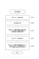
- 半導体デバイスのパターンを示す第1のパターン画像とは分解能が異なり、前記半導体デバイスのパターンを示す第2のパターン画像を取得するステップと、
互いに分解能が異なる同一の半導体デバイスのパターン画像の組み合わせを教師データとして機械学習によって得られた学習モデルを用いた再構成処理により、前記第2のパターン画像を前記第2のパターン画像とは分解能が異なる再構成画像に再構成するステップと、
前記第1のパターン画像を取得するステップと、
前記再構成画像における前記再構成処理によって前記学習モデルの出力を基に得られた確実度が高いと計算された領域と、第1のパターン画像とに基づいて、位置合わせを行うステップと、
を備える半導体検査方法。 - 前記機械学習は、ディープラーニングである、
請求項1記載の半導体検査方法。 - 前記確実度は、前記学習モデルにおける出力層のノードの出力値に基づく、
請求項2記載の半導体検査方法。 - 前記再構成画像に対して前記確実度に応じて重み付けを行った上で、前記再構成画像と前記第1のパターン画像との位置合わせを行う、
請求項1~3のいずれか1項に記載の半導体検査方法。 - 第1のパターン画像あるいは第2のパターン画像を、前記半導体デバイスを測定することにより取得する、
請求項1~4のいずれか1項に記載の半導体検査方法。 - 第1のパターン画像あるいは第2のパターン画像を、前記半導体デバイスに関するCADデータを基に取得する、
請求項1~5のいずれか1項に記載の半導体検査方法。 - 半導体デバイスのパターンを示す第1のパターン画像と、前記半導体デバイスのパターンを示す、前記第1のパターン画像とは分解能が異なる第2のパターン画像とを取得する取得部と、
互いに分解能が異なる同一の半導体デバイスのパターン画像の組み合わせを教師データとして機械学習によって得られた学習モデルを用いた再構成処理により、前記第2のパターン画像を前記第2のパターン画像とは分解能が異なる再構成画像に再構成する画像変換部と、
前記再構成画像における前記再構成処理によって前記学習モデルの出力を基に得られた確実度が高いと計算された領域と、第1のパターン画像とに基づいて、位置合わせを行う位置合わせ部と、
を備える半導体検査装置。 - 前記機械学習は、ディープラーニングである、
請求項7記載の半導体検査装置。 - 前記確実度は、前記学習モデルにおける出力層のノードの出力値に基づく、
請求項8記載の半導体検査装置。 - 前記位置合わせ部は、前記再構成画像に対して前記確実度に応じて重み付けを行った上で、前記再構成画像と前記第1のパターン画像との位置合わせを行う、
請求項7~9のいずれか1項に記載の半導体検査装置。 - 前記取得部は、第1のパターン画像あるいは第2のパターン画像を、前記半導体デバイスを測定することにより取得する、
請求項7~10のいずれか1項に記載の半導体検査装置。 - 前記取得部は、第1のパターン画像あるいは第2のパターン画像を、前記半導体デバイスに関するCADデータを基に取得する、
請求項7~11のいずれか1項に記載の半導体検査装置。
Applications Claiming Priority (3)
| Application Number | Priority Date | Filing Date | Title |
|---|---|---|---|
| JP2019103831 | 2019-06-03 | ||
| JP2019103831 | 2019-06-03 | ||
| PCT/JP2020/016753 WO2020246150A1 (ja) | 2019-06-03 | 2020-04-16 | 半導体検査方法及び半導体検査装置 |
Publications (3)
| Publication Number | Publication Date |
|---|---|
| JPWO2020246150A1 JPWO2020246150A1 (ja) | 2020-12-10 |
| JPWO2020246150A5 JPWO2020246150A5 (ja) | 2023-03-10 |
| JP7413376B2 true JP7413376B2 (ja) | 2024-01-15 |
Family
ID=73652093
Family Applications (1)
| Application Number | Title | Priority Date | Filing Date |
|---|---|---|---|
| JP2021524695A Active JP7413376B2 (ja) | 2019-06-03 | 2020-04-16 | 半導体検査方法及び半導体検査装置 |
Country Status (8)
| Country | Link |
|---|---|
| US (1) | US20220301135A1 (ja) |
| EP (1) | EP3958210A4 (ja) |
| JP (1) | JP7413376B2 (ja) |
| KR (1) | KR20220016030A (ja) |
| CN (1) | CN113966524A (ja) |
| SG (1) | SG11202111977XA (ja) |
| TW (1) | TW202101292A (ja) |
| WO (1) | WO2020246150A1 (ja) |
Families Citing this family (2)
| Publication number | Priority date | Publication date | Assignee | Title |
|---|---|---|---|---|
| US20220067525A1 (en) * | 2020-08-25 | 2022-03-03 | Nvidia Corporation | Techniques for pruning neural networks |
| JP2022135215A (ja) * | 2021-03-05 | 2022-09-15 | 株式会社日立ハイテク | 学習器の学習方法、及び画像生成システム |
Citations (6)
| Publication number | Priority date | Publication date | Assignee | Title |
|---|---|---|---|---|
| US20080298719A1 (en) | 2001-05-30 | 2008-12-04 | Dcg Systems, Inc. | Sub-resolution alignment of images |
| JP2009162718A (ja) | 2008-01-10 | 2009-07-23 | Olympus Corp | 基板検査装置および検査領域設定方法 |
| US20170148226A1 (en) | 2015-11-19 | 2017-05-25 | Kla-Tencor Corporation | Generating simulated images from design information |
| US20170193680A1 (en) | 2016-01-04 | 2017-07-06 | Kla-Tencor Corporation | Generating high resolution images from low resolution images for semiconductor applications |
| US20170345140A1 (en) | 2016-05-25 | 2017-11-30 | Kla-Tencor Corporation | Generating simulated images from input images for semiconductor applications |
| JP2019129169A (ja) | 2018-01-22 | 2019-08-01 | 株式会社日立ハイテクノロジーズ | 画像評価方法及び画像評価装置 |
Family Cites Families (6)
| Publication number | Priority date | Publication date | Assignee | Title |
|---|---|---|---|---|
| JP2015098342A (ja) | 2013-11-19 | 2015-05-28 | 株式会社エンプラス | 密閉容器および密閉容器セット |
| KR102278964B1 (ko) | 2013-12-26 | 2021-07-20 | 하마마츠 포토닉스 가부시키가이샤 | 화상 처리 방법, 화상 처리 장치, 화상 처리 프로그램 및 화상 처리 프로그램을 기억한 기억 매체 |
| TWI797699B (zh) * | 2015-12-22 | 2023-04-01 | 以色列商應用材料以色列公司 | 半導體試樣的基於深度學習之檢查的方法及其系統 |
| US10282510B2 (en) | 2017-04-07 | 2019-05-07 | Fei Company | Alignment of CAD data to images in high resolution optical fault analysis |
| US10733744B2 (en) * | 2017-05-11 | 2020-08-04 | Kla-Tencor Corp. | Learning based approach for aligning images acquired with different modalities |
| JP6957197B2 (ja) * | 2017-05-17 | 2021-11-02 | キヤノン株式会社 | 画像処理装置および画像処理方法 |
-
2020
- 2020-04-16 KR KR1020217030941A patent/KR20220016030A/ko unknown
- 2020-04-16 SG SG11202111977XA patent/SG11202111977XA/en unknown
- 2020-04-16 WO PCT/JP2020/016753 patent/WO2020246150A1/ja unknown
- 2020-04-16 CN CN202080041089.XA patent/CN113966524A/zh active Pending
- 2020-04-16 EP EP20818826.8A patent/EP3958210A4/en active Pending
- 2020-04-16 JP JP2021524695A patent/JP7413376B2/ja active Active
- 2020-04-16 US US17/608,857 patent/US20220301135A1/en active Pending
- 2020-05-15 TW TW109116147A patent/TW202101292A/zh unknown
Patent Citations (6)
| Publication number | Priority date | Publication date | Assignee | Title |
|---|---|---|---|---|
| US20080298719A1 (en) | 2001-05-30 | 2008-12-04 | Dcg Systems, Inc. | Sub-resolution alignment of images |
| JP2009162718A (ja) | 2008-01-10 | 2009-07-23 | Olympus Corp | 基板検査装置および検査領域設定方法 |
| US20170148226A1 (en) | 2015-11-19 | 2017-05-25 | Kla-Tencor Corporation | Generating simulated images from design information |
| US20170193680A1 (en) | 2016-01-04 | 2017-07-06 | Kla-Tencor Corporation | Generating high resolution images from low resolution images for semiconductor applications |
| US20170345140A1 (en) | 2016-05-25 | 2017-11-30 | Kla-Tencor Corporation | Generating simulated images from input images for semiconductor applications |
| JP2019129169A (ja) | 2018-01-22 | 2019-08-01 | 株式会社日立ハイテクノロジーズ | 画像評価方法及び画像評価装置 |
Also Published As
| Publication number | Publication date |
|---|---|
| EP3958210A4 (en) | 2023-05-03 |
| CN113966524A (zh) | 2022-01-21 |
| US20220301135A1 (en) | 2022-09-22 |
| KR20220016030A (ko) | 2022-02-08 |
| TW202101292A (zh) | 2021-01-01 |
| SG11202111977XA (en) | 2021-11-29 |
| WO2020246150A1 (ja) | 2020-12-10 |
| JPWO2020246150A1 (ja) | 2020-12-10 |
| EP3958210A1 (en) | 2022-02-23 |
Similar Documents
| Publication | Publication Date | Title |
|---|---|---|
| TWI706485B (zh) | 光學晶粒對資料庫檢查 | |
| JP6893514B2 (ja) | ハイブリッドインスペクタ | |
| JP6853273B2 (ja) | ニューラルネットワークと順物理モデルを半導体用途に組み込んだシステムおよび方法 | |
| TWI742277B (zh) | 用於對準以不同模態所獲取之影像之以學習為基礎之方法 | |
| TWI735774B (zh) | 基於輪廓之缺陷偵測 | |
| TWI665445B (zh) | 光學晶粒至資料庫檢測 | |
| JP6707616B2 (ja) | 画像処理方法、画像処理装置、画像処理プログラム、及び画像処理プログラムを記憶した記憶媒体 | |
| JP7413376B2 (ja) | 半導体検査方法及び半導体検査装置 | |
| TW201928541A (zh) | 用於大型偏移晶粒對晶粒檢測之多步驟影像對準方法 | |
| US20220206063A1 (en) | Semiconductor device examination method and semiconductor device examination device | |
| US10983162B2 (en) | Semiconductor device inspection method and semiconductor device inspection device | |
| JP2018072290A (ja) | 故障箇所特定装置および故障箇所特定方法 | |
| US9958502B2 (en) | Defect isolation methods and systems | |
| JP6232476B2 (ja) | サブ光学解像度によるcadレイアウトへのチップの自動配向システムおよび方法 | |
| US20220221411A1 (en) | Semiconductor apparatus examination method and semiconductor apparatus examination apparatus | |
| JP7413375B2 (ja) | 半導体検査装置及び半導体検査方法 | |
| JP6961846B1 (ja) | Euvマスク検査装置、euvマスク検査方法、euvマスク検査プログラム及びeuvマスク検査システム | |
| US10768225B1 (en) | Probe placement for laser probing system |
Legal Events
| Date | Code | Title | Description |
|---|---|---|---|
| A621 | Written request for application examination |
Free format text: JAPANESE INTERMEDIATE CODE: A621 Effective date: 20221028 |
|
| A521 | Request for written amendment filed |
Free format text: JAPANESE INTERMEDIATE CODE: A523 Effective date: 20230302 |
|
| A131 | Notification of reasons for refusal |
Free format text: JAPANESE INTERMEDIATE CODE: A131 Effective date: 20230822 |
|
| A521 | Request for written amendment filed |
Free format text: JAPANESE INTERMEDIATE CODE: A523 Effective date: 20231012 |
|
| TRDD | Decision of grant or rejection written | ||
| A01 | Written decision to grant a patent or to grant a registration (utility model) |
Free format text: JAPANESE INTERMEDIATE CODE: A01 Effective date: 20231221 |
|
| A61 | First payment of annual fees (during grant procedure) |
Free format text: JAPANESE INTERMEDIATE CODE: A61 Effective date: 20231227 |
|
| R150 | Certificate of patent or registration of utility model |
Ref document number: 7413376 Country of ref document: JP Free format text: JAPANESE INTERMEDIATE CODE: R150 |