JP7406943B2 - Polishing equipment, polishing method, and substrate processing equipment - Google Patents
Polishing equipment, polishing method, and substrate processing equipment Download PDFInfo
- Publication number
- JP7406943B2 JP7406943B2 JP2019160218A JP2019160218A JP7406943B2 JP 7406943 B2 JP7406943 B2 JP 7406943B2 JP 2019160218 A JP2019160218 A JP 2019160218A JP 2019160218 A JP2019160218 A JP 2019160218A JP 7406943 B2 JP7406943 B2 JP 7406943B2
- Authority
- JP
- Japan
- Prior art keywords
- substrate
- polishing
- device surface
- cleaning
- wafer
- Prior art date
- Legal status (The legal status is an assumption and is not a legal conclusion. Google has not performed a legal analysis and makes no representation as to the accuracy of the status listed.)
- Active
Links
- 238000005498 polishing Methods 0.000 title claims description 391
- 239000000758 substrate Substances 0.000 title claims description 232
- 238000012545 processing Methods 0.000 title claims description 28
- 238000000034 method Methods 0.000 title claims description 26
- 238000004140 cleaning Methods 0.000 claims description 294
- 230000007246 mechanism Effects 0.000 claims description 140
- 239000012530 fluid Substances 0.000 claims description 123
- 239000007788 liquid Substances 0.000 claims description 60
- XLYOFNOQVPJJNP-UHFFFAOYSA-N water Substances O XLYOFNOQVPJJNP-UHFFFAOYSA-N 0.000 claims description 48
- 230000001681 protective effect Effects 0.000 claims description 39
- CBENFWSGALASAD-UHFFFAOYSA-N Ozone Chemical compound [O-][O+]=O CBENFWSGALASAD-UHFFFAOYSA-N 0.000 claims description 22
- 239000007921 spray Substances 0.000 claims description 17
- 238000001035 drying Methods 0.000 claims description 11
- 239000000126 substance Substances 0.000 claims description 11
- 238000003825 pressing Methods 0.000 claims description 6
- 235000012431 wafers Nutrition 0.000 description 234
- 230000002093 peripheral effect Effects 0.000 description 19
- 238000012546 transfer Methods 0.000 description 15
- 238000010586 diagram Methods 0.000 description 10
- 239000006061 abrasive grain Substances 0.000 description 8
- 239000013256 coordination polymer Substances 0.000 description 7
- 238000007517 polishing process Methods 0.000 description 4
- 238000013519 translation Methods 0.000 description 4
- KFZMGEQAYNKOFK-UHFFFAOYSA-N Isopropanol Chemical compound CC(C)O KFZMGEQAYNKOFK-UHFFFAOYSA-N 0.000 description 3
- 238000011109 contamination Methods 0.000 description 3
- 230000008569 process Effects 0.000 description 3
- 239000000243 solution Substances 0.000 description 3
- 239000004696 Poly ether ether ketone Substances 0.000 description 2
- 239000000428 dust Substances 0.000 description 2
- 239000010419 fine particle Substances 0.000 description 2
- 239000012535 impurity Substances 0.000 description 2
- 239000000463 material Substances 0.000 description 2
- 239000002101 nanobubble Substances 0.000 description 2
- 229920002530 polyetherether ketone Polymers 0.000 description 2
- 239000011347 resin Substances 0.000 description 2
- 229920005989 resin Polymers 0.000 description 2
- 238000003860 storage Methods 0.000 description 2
- 229910021642 ultra pure water Inorganic materials 0.000 description 2
- 239000012498 ultrapure water Substances 0.000 description 2
- 239000004677 Nylon Substances 0.000 description 1
- 239000004743 Polypropylene Substances 0.000 description 1
- 230000008901 benefit Effects 0.000 description 1
- 239000011230 binding agent Substances 0.000 description 1
- 230000003247 decreasing effect Effects 0.000 description 1
- 239000013013 elastic material Substances 0.000 description 1
- 238000002347 injection Methods 0.000 description 1
- 239000007924 injection Substances 0.000 description 1
- 238000012423 maintenance Methods 0.000 description 1
- 230000007257 malfunction Effects 0.000 description 1
- 238000004519 manufacturing process Methods 0.000 description 1
- 239000002184 metal Substances 0.000 description 1
- 229910052751 metal Inorganic materials 0.000 description 1
- 150000002739 metals Chemical class 0.000 description 1
- 239000003595 mist Substances 0.000 description 1
- 239000000203 mixture Substances 0.000 description 1
- 238000012986 modification Methods 0.000 description 1
- 230000004048 modification Effects 0.000 description 1
- 239000004745 nonwoven fabric Substances 0.000 description 1
- 229920001778 nylon Polymers 0.000 description 1
- 230000001590 oxidative effect Effects 0.000 description 1
- 239000002245 particle Substances 0.000 description 1
- 238000005192 partition Methods 0.000 description 1
- 238000000059 patterning Methods 0.000 description 1
- 229920000728 polyester Polymers 0.000 description 1
- -1 polypropylene Polymers 0.000 description 1
- 229920001155 polypropylene Polymers 0.000 description 1
- 229920002635 polyurethane Polymers 0.000 description 1
- 239000004814 polyurethane Substances 0.000 description 1
- 239000012487 rinsing solution Substances 0.000 description 1
- 230000035939 shock Effects 0.000 description 1
- 229920002379 silicone rubber Polymers 0.000 description 1
- 239000004945 silicone rubber Substances 0.000 description 1
Images


Classifications
-
- B—PERFORMING OPERATIONS; TRANSPORTING
- B24—GRINDING; POLISHING
- B24B—MACHINES, DEVICES, OR PROCESSES FOR GRINDING OR POLISHING; DRESSING OR CONDITIONING OF ABRADING SURFACES; FEEDING OF GRINDING, POLISHING, OR LAPPING AGENTS
- B24B21/00—Machines or devices using grinding or polishing belts; Accessories therefor
-
- B—PERFORMING OPERATIONS; TRANSPORTING
- B24—GRINDING; POLISHING
- B24B—MACHINES, DEVICES, OR PROCESSES FOR GRINDING OR POLISHING; DRESSING OR CONDITIONING OF ABRADING SURFACES; FEEDING OF GRINDING, POLISHING, OR LAPPING AGENTS
- B24B55/00—Safety devices for grinding or polishing machines; Accessories fitted to grinding or polishing machines for keeping tools or parts of the machine in good working condition
- B24B55/06—Dust extraction equipment on grinding or polishing machines
- B24B55/08—Dust extraction equipment on grinding or polishing machines specially designed for belt grinding machines
-
- H—ELECTRICITY
- H01—ELECTRIC ELEMENTS
- H01L—SEMICONDUCTOR DEVICES NOT COVERED BY CLASS H10
- H01L21/00—Processes or apparatus adapted for the manufacture or treatment of semiconductor or solid state devices or of parts thereof
- H01L21/02—Manufacture or treatment of semiconductor devices or of parts thereof
- H01L21/04—Manufacture or treatment of semiconductor devices or of parts thereof the devices having at least one potential-jump barrier or surface barrier, e.g. PN junction, depletion layer or carrier concentration layer
- H01L21/18—Manufacture or treatment of semiconductor devices or of parts thereof the devices having at least one potential-jump barrier or surface barrier, e.g. PN junction, depletion layer or carrier concentration layer the devices having semiconductor bodies comprising elements of Group IV of the Periodic System or AIIIBV compounds with or without impurities, e.g. doping materials
- H01L21/30—Treatment of semiconductor bodies using processes or apparatus not provided for in groups H01L21/20 - H01L21/26
- H01L21/302—Treatment of semiconductor bodies using processes or apparatus not provided for in groups H01L21/20 - H01L21/26 to change their surface-physical characteristics or shape, e.g. etching, polishing, cutting
- H01L21/304—Mechanical treatment, e.g. grinding, polishing, cutting
Description
本発明は、ウェーハなどの基板の裏面を研磨する研磨装置および研磨方法に関する。さらに、本発明は、研磨装置を備えた基板処理装置に関する。 The present invention relates to a polishing apparatus and a polishing method for polishing the back surface of a substrate such as a wafer. Furthermore, the present invention relates to a substrate processing apparatus equipped with a polishing apparatus.
近年、メモリー回路、ロジック回路、イメージセンサ(例えばCMOSセンサー)などのデバイスは、より高集積化されつつある。これらのデバイスを形成する工程においては、微粒子や塵埃などの異物がデバイスに付着することがある。デバイスに付着した異物は、配線間の短絡や回路の不具合を引き起こしてしまう。したがって、デバイスの信頼性を向上させるために、デバイスが形成された基板(例えば、ウェーハ)を洗浄して、基板上の異物を除去することが必要とされる。 In recent years, devices such as memory circuits, logic circuits, and image sensors (for example, CMOS sensors) are becoming more highly integrated. In the process of forming these devices, foreign matter such as fine particles and dust may adhere to the devices. Foreign matter adhering to devices can cause short circuits between wires and circuit malfunctions. Therefore, in order to improve device reliability, it is necessary to clean the substrate (eg, wafer) on which the device is formed to remove foreign matter on the substrate.
基板の裏面(非デバイス面)にも、上述したような微粒子や粉塵などの異物が付着することがある。このような異物が基板の裏面に付着すると、基板が露光装置のステージ基準面から離間したり、基板の表面(デバイス面)がステージ基準面に対して傾き、結果として、パターニングのずれや焦点距離のずれが生じることとなる。このような問題を防止するために、基板の裏面に付着した異物を除去することが必要とされる。 Foreign matter such as the above-mentioned fine particles and dust may also adhere to the back surface (non-device surface) of the substrate. If such foreign matter adheres to the back surface of the substrate, the substrate may move away from the stage reference plane of the exposure equipment, or the surface of the substrate (device surface) may tilt with respect to the stage reference plane, resulting in patterning misalignment or focal length distortion. A deviation will occur. In order to prevent such problems, it is necessary to remove foreign matter adhering to the back surface of the substrate.
そこで、基板の裏面を研磨して、該裏面に付着した異物を除去する研磨装置が従来から用いられている(例えば、特許文献1参照)。なお、本明細書では、デバイスが形成されていない、またはデバイスが形成される予定がない基板の裏面を「非デバイス面」と定義し、デバイスが形成されている、またはデバイスが形成される予定である基板の表面を「デバイス面」と定義する。 Therefore, a polishing apparatus that polishes the back surface of a substrate to remove foreign matter attached to the back surface has been conventionally used (for example, see Patent Document 1). Note that in this specification, the back side of the substrate on which no device is formed or where no device is planned to be formed is defined as the "non-device side"; The surface of the substrate that is defined as the "device surface" is defined as the "device surface".
特許文献1に記載の研磨装置では、基板の非デバイス面が下を向いた状態で、基板の非デバイス面全体が効率的に研磨される。したがって、基板の非デバイス面を研磨するために、該基板を反転させる必要がないので、基板への空気中の不純物の付着を防止し、かつ研磨装置全体の処理時間を減らすことができる。さらに、このような研磨装置は、例えば、基板の非デバイス面を研磨し、洗浄し、乾燥させる一連の工程を行うことができる基板処理装置に設けられる。この場合、基板を反転させる反転機が不要となるため、基板処理装置の構成を単純化し、費用を削減することができる。
In the polishing apparatus described in
基板の非デバイス面が下を向いた状態で、該非デバイス面を研磨する研磨装置であっても、基板の研磨中に発生した研磨屑および/または該研磨屑を含むリンス液などの異物が基板のデバイス面に回り込んで、該基板のデバイス面を汚染してしまうおそれがある。そのため、特許文献1に記載の研磨装置は、基板の非デバイス面の研磨中に、デバイス面に保護液(例えば純水)を供給する保護液供給ノズルを有している。保護液でデバイス面を覆うことにより、非デバイス面の研磨中に発生した異物によって基板のデバイス面が汚染されることを防止している。
Even with polishing equipment that polishes the non-device surface of the substrate with the non-device surface facing downward, foreign matter such as polishing debris generated during polishing the substrate and/or a rinsing solution containing the polishing debris may be removed from the substrate. There is a risk that the particles may get around to the device surface of the substrate and contaminate the device surface of the substrate. Therefore, the polishing apparatus described in
しかしながら、基板のデバイス面に形成されたデバイスの信頼性の向上をさらに図るためには、非デバイス面の研磨中にできる限り基板のデバイス面を汚染させない、すなわち、基板のデバイス面に異物をできる限り付着させないことが重要である。さらに、基板の研磨時にデバイス面に多量の異物が付着してしまうと、該異物を除去するために基板を比較的長時間洗浄する必要が生じる。例えば、基板処理装置の洗浄ユニットで、研磨後の基板のデバイス面を比較的長時間洗浄する必要が生じ、その結果、基板処理装置のスループットが低下してしまうおそれもある。したがって、基板の研磨処理の後に行われる該基板の洗浄処理の負担を軽減し、基板処理装置のスループットの向上を図るためにも、基板の非デバイス面の研磨中に、デバイス面にできる限り異物を付着させないことが重要である。 However, in order to further improve the reliability of devices formed on the device side of the substrate, it is important to avoid contaminating the device side of the substrate as much as possible during polishing of non-device surfaces. It is important to avoid adhesion as much as possible. Furthermore, if a large amount of foreign matter adheres to the device surface during polishing of the substrate, it becomes necessary to clean the substrate for a relatively long time to remove the foreign matter. For example, the cleaning unit of the substrate processing apparatus needs to clean the device surface of the polished substrate for a relatively long time, and as a result, the throughput of the substrate processing apparatus may be reduced. Therefore, in order to reduce the burden of the substrate cleaning process that is performed after the substrate polishing process and to improve the throughput of the substrate processing equipment, during the polishing of the non-device side of the substrate, as much foreign material as possible is removed from the device side. It is important not to allow it to adhere.
そこで、本発明は、基板をそのデバイス面が上を向いた状態で保持して、該基板の非デバイス面を研磨している間に、基板のデバイス面が異物によって汚染されることを防止することが可能な研磨装置、および研磨方法を提供することを目的とする。また、本発明は、このような研磨装置を有する基板処理装置を提供することを目的とする。 Therefore, the present invention prevents the device side of the substrate from being contaminated by foreign matter while polishing the non-device side of the substrate by holding the substrate with its device side facing upward. The purpose of the present invention is to provide a polishing device and a polishing method that can perform the following steps. Another object of the present invention is to provide a substrate processing apparatus having such a polishing apparatus.
一態様では、基板をそのデバイス面が上を向いた状態で保持して、該基板を回転させる基板保持部と、前記基板の非デバイス面に接触して、該基板の非デバイス面を研磨する研磨具と、前記研磨具で前記基板の非デバイス面を研磨している間に、前記基板のデバイス面を洗浄する非接触式洗浄機構と、を備えたことを特徴とする研磨装置が提供される。 In one embodiment, a substrate holder rotates the substrate while holding the substrate with its device side facing upward; and the substrate holder contacts the non-device side of the substrate to polish the non-device side of the substrate. There is provided a polishing apparatus comprising: a polishing tool; and a non-contact cleaning mechanism that cleans a device surface of the substrate while the polishing tool polishes a non-device surface of the substrate. Ru.
一態様では、前記非接触式洗浄機構は、洗浄流体を前記基板のデバイス面に向けて噴射する洗浄流体ノズルと、前記洗浄流体ノズルを、前記基板のデバイス面の上方で移動させるノズル移動機構と、を有する。
一態様では、前記洗浄流体ノズルは、2流体ジェットを前記基板のデバイス面に向けて噴射させる2流体ジェットノズルである。
一態様では、前記非接触式洗浄機構は、オゾン発生器をさらに含み、前記洗浄流体ノズルは、オゾン水、またはオゾンマイクロバブル水を前記基板のデバイス面に向けて噴射する。
In one aspect, the non-contact cleaning mechanism includes a cleaning fluid nozzle that sprays cleaning fluid toward a device surface of the substrate, and a nozzle movement mechanism that moves the cleaning fluid nozzle above the device surface of the substrate. , has.
In one aspect, the cleaning fluid nozzle is a two-fluid jet nozzle that directs a two-fluid jet toward a device surface of the substrate.
In one aspect, the non-contact cleaning mechanism further includes an ozone generator, and the cleaning fluid nozzle sprays ozonated water or ozonated microbubble water toward a device surface of the substrate.
一態様では、前記非接触式洗浄機構は、電解水生成機をさらに含み、前記洗浄流体ノズルは、電解水を前記基板のデバイス面に向けて噴射する。
一態様では、前記洗浄流体ノズルは、メガソニック水または薬液を前記基板のデバイス面に向けて噴射する。
一態様では、前記研磨装置は、前記基板のデバイス面に保護液を供給する保護液供給ノズルをさらに備える。
一態様では、前記研磨装置は、前記非接触式洗浄機構、および前記保護液供給ノズルの動作を制御する動作制御部をさらに備え、前記動作制御部は、前記研磨具で前記基板の非デバイス面を研磨している間に、前記基板のデバイス面に前記保護液供給ノズルから前記保護液を供給しつつ、さらに、前記非接触式洗浄機構によって、前記基板のデバイス面を洗浄する。
一態様では、前記研磨装置は、前記研磨具、および前記非接触式洗浄機構の動作を制御する動作制御部をさらに備え、前記動作制御部は、前記研磨具による前記基板の非デバイス面の研磨の開始よりも前に、前記非接触式洗浄機構による前記基板のデバイス面の洗浄を開始し、前記研磨具による前記基板の非デバイス面の研磨の終了後に、前記非接触式洗浄機構による前記基板のデバイス面の洗浄を終了する。
一態様では、前記研磨装置は、前記研磨具、および前記非接触式洗浄機構の動作を制御する動作制御部をさらに備え、前記動作制御部は、前記研磨具による前記基板の非デバイス面の研磨の開始と同時に、前記非接触式洗浄機構による前記基板のデバイス面の洗浄を開始し、前記研磨具による前記基板の非デバイス面の研磨の終了と同時に、前記非接触式洗浄機構による前記基板のデバイス面の洗浄を終了する。
一態様では、前記研磨装置は、前記研磨具、および前記非接触式洗浄機構の動作を制御する動作制御部をさらに備え、前記動作制御部は、前記研磨具による前記基板の非デバイス面の研磨の開始後に、前記非接触式洗浄機構による前記基板のデバイス面の洗浄を開始し、前記研磨具による前記基板の非デバイス面の研磨の終了後に、前記非接触式洗浄機構による前記基板のデバイス面の洗浄を終了する。
In one aspect, the non-contact cleaning mechanism further includes an electrolyzed water generator, and the cleaning fluid nozzle sprays electrolyzed water toward a device surface of the substrate.
In one aspect, the cleaning fluid nozzle sprays megasonic water or a chemical toward a device surface of the substrate.
In one aspect, the polishing apparatus further includes a protective liquid supply nozzle that supplies a protective liquid to the device surface of the substrate.
In one aspect, the polishing apparatus further includes an operation control unit that controls operations of the non-contact cleaning mechanism and the protective liquid supply nozzle, and the operation control unit is configured to use the polishing tool to clean a non-device surface of the substrate. While polishing, the protective liquid is supplied from the protective liquid supply nozzle to the device surface of the substrate, and the device surface of the substrate is further cleaned by the non-contact cleaning mechanism.
In one aspect, the polishing apparatus further includes an operation control unit that controls operations of the polishing tool and the non-contact cleaning mechanism, and the operation control unit is configured to polish a non-device surface of the substrate with the polishing tool. , the non-contact cleaning mechanism starts cleaning the device surface of the substrate, and after the polishing tool finishes polishing the non-device surface of the substrate, the non-contact cleaning mechanism starts cleaning the device surface of the substrate. Finish cleaning the device surface.
In one aspect, the polishing apparatus further includes an operation control unit that controls operations of the polishing tool and the non-contact cleaning mechanism, and the operation control unit is configured to polish a non-device surface of the substrate with the polishing tool. At the same time as the non-contact cleaning mechanism starts cleaning the device side of the substrate, and at the same time as the polishing tool finishes polishing the non-device side of the substrate, the non-contact cleaning mechanism starts cleaning the substrate. Finish cleaning the device surface.
In one aspect, the polishing apparatus further includes an operation control unit that controls operations of the polishing tool and the non-contact cleaning mechanism, and the operation control unit is configured to polish a non-device surface of the substrate with the polishing tool. After the non-contact cleaning mechanism starts cleaning the device surface of the substrate, and after the polishing tool finishes polishing the non-device surface of the substrate, the non-contact cleaning mechanism starts cleaning the device surface of the substrate. Finish cleaning.
一態様では、基板を、そのデバイス面が上を向いた状態で保持して、該基板を回転させ、前記回転している基板の非デバイス面に研磨具を押し付けて、該非デバイス面を研磨し、前記基板の非デバイス面を研磨している間に、前記基板のデバイス面を非接触式洗浄機構で洗浄することを特徴とする研磨方法が提供される。 In one embodiment, the substrate is held with its device side facing upward, the substrate is rotated, and a polishing tool is pressed against the non-device side of the rotating substrate to polish the non-device side. , there is provided a polishing method characterized in that, while the non-device surface of the substrate is being polished, the device surface of the substrate is cleaned by a non-contact cleaning mechanism.
一態様では、前記基板のデバイス面の洗浄は、洗浄流体ノズルを前記基板のデバイス面の上方で移動させながら、該洗浄流体ノズルから洗浄流体を前記基板のデバイス面に噴射することにより行われる。
一態様では、前記洗浄流体ノズルは、2流体ジェットを前記基板のデバイス面に向けて噴射する。
一態様では、前記洗浄流体ノズルは、オゾン水、またはオゾンマイクロバブル水を前記基板のデバイス面に向けて噴射する。
In one aspect, cleaning the device surface of the substrate is performed by jetting cleaning fluid from a cleaning fluid nozzle onto the device surface of the substrate while moving the cleaning fluid nozzle above the device surface of the substrate.
In one aspect, the cleaning fluid nozzle fires a two-fluid jet toward a device surface of the substrate.
In one aspect, the cleaning fluid nozzle sprays ozonated water or ozonated microbubble water toward a device surface of the substrate.
一態様では、前記洗浄流体ノズルは、電解水を前記基板のデバイス面に向けて噴射する。
一態様では、前記洗浄流体ノズルは、メガソニック水または薬液を前記基板のデバイス面に向けて噴射する。
一態様では、前記基板の非デバイス面を研磨している間、前記基板のデバイス面にさらに保護液が供給される。
一態様では、前記基板の非デバイス面を研磨している間に、前記基板のデバイス面に前記保護液を供給しつつ、さらに、前記非接触式洗浄機構によって、前記基板のデバイス面を洗浄する。
一態様では、前記研磨具による前記基板の非デバイス面の研磨の開始よりも前に、前記非接触式洗浄機構による前記基板のデバイス面の洗浄を開始し、前記研磨具による前記基板の非デバイス面の研磨の終了後に、前記非接触式洗浄機構による前記基板のデバイス面の洗浄を終了する。
一態様では、前記研磨具による前記基板の非デバイス面の研磨の開始と同時に、前記非接触式洗浄機構による前記基板のデバイス面の洗浄を開始し、前記研磨具による前記基板の非デバイス面の研磨の終了と同時に、前記非接触式洗浄機構による前記基板のデバイス面の洗浄を終了する。
一態様では、前記研磨具による前記基板の非デバイス面の研磨の開始後に、前記非接触式洗浄機構による前記基板のデバイス面の洗浄を開始し、前記研磨具による前記基板の非デバイス面の研磨の終了後に、前記非接触式洗浄機構による前記基板のデバイス面の洗浄を終了する。
In one aspect, the cleaning fluid nozzle sprays electrolyzed water toward a device surface of the substrate.
In one aspect, the cleaning fluid nozzle sprays megasonic water or a chemical toward a device surface of the substrate.
In one embodiment, a protective liquid is further provided to the device side of the substrate while polishing the non-device side of the substrate.
In one aspect, while the non-device surface of the substrate is being polished, the protective liquid is supplied to the device surface of the substrate, and the device surface of the substrate is further cleaned by the non-contact cleaning mechanism. .
In one aspect, before the polishing tool starts polishing the non-device surface of the substrate, the non-contact cleaning mechanism starts cleaning the device surface of the substrate, and the polishing tool starts cleaning the non-device surface of the substrate. After the polishing of the surface is completed, cleaning of the device surface of the substrate by the non-contact cleaning mechanism is completed.
In one aspect, at the same time as the polishing tool starts polishing the non-device surface of the substrate, the non-contact cleaning mechanism starts cleaning the device surface of the substrate, and the polishing tool starts polishing the non-device surface of the substrate. Simultaneously with the completion of polishing, cleaning of the device surface of the substrate by the non-contact cleaning mechanism is completed.
In one aspect, after the polishing tool starts polishing the non-device surface of the substrate, the non-contact cleaning mechanism starts cleaning the device surface of the substrate, and the polishing tool starts polishing the non-device surface of the substrate. After the cleaning of the device surface of the substrate by the non-contact cleaning mechanism is completed.
一態様では、上記研磨装置と、前記研磨装置によって研磨された基板を洗浄する洗浄ユニットと、前記洗浄ユニットで洗浄された基板を乾燥させる乾燥ユニットと、を備えたことを特徴とする基板処理装置が提供される。
一態様では、前記洗浄ユニットは、前記基板の非デバイス面のみを洗浄する。
In one aspect, a substrate processing apparatus includes the polishing apparatus, a cleaning unit that cleans the substrate polished by the polishing apparatus, and a drying unit that dries the substrate cleaned by the cleaning unit. is provided.
In one aspect, the cleaning unit cleans only the non-device side of the substrate.
本発明によれば、研磨具が基板の非デバイス面を研磨している間に、非接触式洗浄機構によって基板のデバイス面が積極的に洗浄される。したがって、異物によって基板のデバイス面が汚染されることを効果的に防止することができ、その結果、デバイスの信頼性が向上する。さらに、基板の非デバイス面を研磨した後であっても、基板のデバイス面にはほとんど異物が付着していないので、基板の研磨処理の後に行われる該基板の洗浄処理の負担を軽減するとともに、洗浄処理にかかる時間の短縮を図ることができる。 According to the present invention, the non-contact cleaning mechanism actively cleans the device side of the substrate while the polishing tool polishes the non-device side of the substrate. Therefore, it is possible to effectively prevent the device surface of the substrate from being contaminated by foreign matter, and as a result, the reliability of the device is improved. Furthermore, even after polishing the non-device surface of the substrate, almost no foreign matter adheres to the device surface of the substrate, which reduces the burden of cleaning the substrate after polishing the substrate. , it is possible to reduce the time required for cleaning processing.
以下、本発明の実施形態について図面を参照して説明する。
図1は、研磨装置の一実施形態を示す模式図である。図1に示す研磨装置は、基板の一例であるウェーハWを保持し、その軸心を中心として回転させる基板保持部10と、研磨具の一例である研磨テープ31をこの基板保持部10に保持されたウェーハWの第1の面1に接触させてウェーハWの第1の面1を研磨する研磨ヘッド50と、研磨テープ31を研磨ヘッド50に供給する研磨テープ供給機構41と、研磨ヘッド50および研磨テープ供給機構41を並進回転運動させる並進回転運動機構60とを備えている。
Embodiments of the present invention will be described below with reference to the drawings.
FIG. 1 is a schematic diagram showing one embodiment of a polishing apparatus. The polishing apparatus shown in FIG. 1 includes a
基板保持部10は、ウェーハWの周縁部に接触可能な複数のローラー11を備えている。研磨ヘッド50は、基板保持部10に保持されているウェーハWの下側に配置されている。並進回転運動機構60は、研磨ヘッド50および研磨テープ供給機構41の下方に配置されており、研磨ヘッド50および研磨テープ供給機構41は並進回転運動機構60に連結されている。図1では、基板保持部10の一部の図示は省略されている。
The
本実施形態では、ウェーハWの第1の面1は、デバイスが形成されていない、またはデバイスが形成される予定がないウェーハWの裏面、すなわち非デバイス面である。第1の面1とは反対側のウェーハWの第2の面2は、デバイスが形成されている、またはデバイスが形成される予定である面、すなわちデバイス面である。以下では、ウェーハWの第1の面1を「非デバイス面1」と称し、ウェーハWの第2の面2を「デバイス面2」と称する。本実施形態では、ウェーハWは、その非デバイス面1が下向きの状態で、基板保持部10に水平に保持される。
In this embodiment, the
図2は、基板保持部10の詳細を示す模式図であり、図3は、図2に示すローラー回転機構12を示す平面図である。基板保持部10は、ウェーハWの周縁部に接触可能な複数のローラー11と、これらローラー11をそれぞれの軸心を中心に回転させるローラー回転機構12とを備えている。本実施形態では、4つのローラー11が設けられている。5つ以上のローラー11を設けてもよい。ウェーハWの周縁部に接触しているときの(すなわちウェーハWを保持しているときの)上記複数のローラー11は、基板保持部10の軸心CPから同じ距離にある。
FIG. 2 is a schematic diagram showing details of the
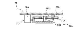
ローラー回転機構12は、4つのローラー11のうちの2つを連結する第1ベルト14Aと、第1ベルト14Aで連結された2つのローラー11のうちの一方に連結された第1モータ15Aと、第1モータ15Aを支持する第1モータ支持体25Aと、第1ベルト14Aで連結された2つのローラー11を回転可能に支持する第1ローラー台16Aと、4つのローラー11のうちの他の2つを連結する第2ベルト14Bと、第2ベルト14Bで連結された2つのローラー11のうちの一方に連結された第2モータ15Bと、第2モータ15Bを支持する第2モータ支持体25Bと、第2ベルト14Bで連結された2つのローラー11を軸受24Bを介して回転可能に支持する第2ローラー台16Bとを備える。第1ローラー台16Aは、上側第1ローラー台17Aと、下側第1ローラー台17Bとを備えている。第1モータ15Aおよび第1ベルト14Aは第1ローラー台16Aの下方に配置され、第2モータ15Bおよび第2ベルト14Bは第2ローラー台16Bの下方に配置されている。第1モータ15Aは、第1モータ支持体25Aを介して第1ローラー台16Aに固定されている。第2モータ15Bは、第2モータ支持体25Bを介して第2ローラー台16Bの下面に固定されている。
The
図4は、図3のA-A線断面図である。図4に示すように、第1ローラー台16Aは、第1ベルト14Aで連結された2つのローラー11を軸受24A(図2参照)を介して回転可能に支持する下側第1ローラー台17Bと、下側第1ローラー台17Bに固定されたピボット軸17Cと、ピボット軸17Cを軸受24Cを介して回転可能に支持する上側第1ローラー台17Aとを備えている。上側第1ローラー台17Aと下側第1ローラー台17Bは、ピボット軸17Cを介して互いに連結されている。図3に示すように、ピボット軸17Cは、第1ベルト14Aで連結された2つのローラー11の間に位置している。図2に示すように、第1モータ15Aは、第1モータ支持体25Aを介して下側第1ローラー台17Bの下面に固定されている。したがって、第1ベルト14A、第1ベルト14Aで連結された2つのローラー11、下側第1ローラー台17B、第1モータ15A、および第1モータ支持体25Aは一体に、ピボット軸17Cを中心に回転可能である。
FIG. 4 is a cross-sectional view taken along the line AA in FIG. 3. As shown in FIG. 4, the first roller stand 16A includes a lower
ローラー回転機構12は、4つのローラー11を同じ方向に同じ速度で回転させるように構成されている。ウェーハWの非デバイス面1の研磨中、ウェーハWの周縁部は、ローラー11によって把持される。ウェーハWは水平に保持され、ローラー11の回転によってウェーハWはその軸心を中心に回転される。ウェーハWの非デバイス面1の研磨中、4つのローラー11はそれぞれの軸心を中心に回転するが、ローラー11自体の位置は静止している。
The
4つのローラー11の下部にはプーリー22がそれぞれ固定されている。第1ベルト14Aは、4つのローラー11のうちの2つに固定されたプーリー22に掛けられ、第2ベルト14Bは他の2つのローラー11に固定されたプーリー22に掛けられている。第1モータ15Aおよび第2モータ15Bは同じ速度で同じ方向に回転するように構成されている。したがって、4つのローラー11は、同じ速度で同じ方向に回転することができる。
A
図3に示すように、ローラー回転機構12は、第1ローラー台16Aの上側第1ローラー台17Aに連結された第1アクチュエータ18Aと、第2ローラー台16Bに連結された第2アクチュエータ18Bをさらに備えている。第1アクチュエータ18Aは、第1ローラー台16Aに支持されている2つのローラー11を矢印で示すように水平方向に移動させる。同様に、第2アクチュエータ18Bは、第2ローラー台16Bに支持されている他の2つのローラー11を矢印で示すように水平方向に移動させる。すなわち、第1アクチュエータ18Aおよび第2アクチュエータ18Bは、2組のローラー11(本実施形態では各組は2つのローラー11からなる)を互いに近づく方向および離間する方向に移動させるように構成されている。第1アクチュエータ18Aおよび第2アクチュエータ18Bは、エアシリンダまたはモータ駆動型アクチュエータなどから構成することができる。図2および図3に示す実施形態では、第1アクチュエータ18Aおよび第2アクチュエータ18Bはエアシリンダから構成されている。第1アクチュエータ18Aおよび第2アクチュエータ18Bは、ベースプレート23の下面に固定されている。
As shown in FIG. 3, the
ローラー11は、ベースプレート23を貫通して上方に延びている。ベースプレート23の下面には第1直動ガイド26Aおよび第2直動ガイド26Bが固定されている。第1直動ガイド26Aの可動部は上側第1ローラー台17Aに連結されており、第2直動ガイド26Bの可動部は第2ローラー台16Bに連結されている。2つの直動ガイド26A,26Bは、ローラー11の動きを水平方向への直線運動に制限する。
The
2組のローラー11が互いに近づく方向に移動すると、ウェーハWは4つのローラー11によって保持される。4つのローラー11のうちの2つはピボット軸17Cの周りを回転可能であるので、4つのローラー11がウェーハWを保持しているとき、上記2つのローラー11の位置が自動的に調整される。2組のローラー11が互いに離れる方向に移動すると、ウェーハWは4つのローラー11から解放される。本実施形態では、基板保持部10の軸心CPの周りに配列された4つのローラー11が設けられているが、ローラー11の数は4つに限定されない。例えば、3つのローラー11を120度の角度で等間隔で軸心CPの周りに配列し、それぞれのローラー11に対して、アクチュエータを1つずつ設けるようにしてもよい。一実施形態では、3つのローラー11を120度の角度で等間隔で軸心CPの周りに配列し、3つのローラー11のうちの2つを第1ベルト14Aで連結し、第1ベルト14Aで連結された2つのローラー11と、第1ベルト14Aで連結されていないローラー11に対して、アクチュエータを1つずつ設けてもよい。
When the two sets of
図5は、ローラー11の上部の一例を拡大して示す模式図である。ローラー11は、ウェーハWの周縁部に接触可能な円筒状の基板保持面11aと、基板保持面11aに接続され、かつ基板保持面11aから下方に傾斜するテーパー面11bとを有している。テーパー面11bは円錐台形状を有しており、基板保持面11aよりも大きな直径を有している。ウェーハWは、まず、図示しない搬送装置によりテーパー面11b上に載置され、その後ローラー11がウェーハWに向かって移動することによりウェーハWの周縁部が基板保持面11aに保持される。ローラー11がウェーハWを解放するときは、ローラー11がウェーハWから離れる方向に移動することにより、ウェーハWの周縁部が基板保持面11aから離れ、テーパー面11bに支持される(図5の点線参照)。図示しない搬送装置は、テーパー面11b上のウェーハWを取り出すことができる。
FIG. 5 is an enlarged schematic diagram showing an example of the upper part of the
図1に示すように、基板保持部10に保持されたウェーハWの下方には、ウェーハWの非デバイス面1にリンス液(例えば純水、またはアルカリ性の薬液)を供給するリンス液供給ノズル27が配置されている。このリンス液供給ノズル27は、図示しないリンス液供給源に接続されている。リンス液供給ノズル27は、ウェーハWの非デバイス面1の中心O1を向いて配置されている。リンス液は、リンス液供給ノズル27からウェーハWの非デバイス面1に供給され、遠心力によりリンス液はウェーハWの非デバイス面1上を広がる。リンス液は、ウェーハWの非デバイス面1上を半径方向外側に流れ、これにより研磨屑をウェーハWの非デバイス面1から除去することができる。
As shown in FIG. 1, below the wafer W held by the
本実施形態では、基板保持部10に保持されたウェーハWの上方には、ウェーハWのデバイス面2に保護液(例えば純水)を供給する保護液供給ノズル28が配置されている。保護液供給ノズル28は、図示しない保護液供給源に接続されている。保護液供給ノズル28はウェーハWのデバイス面2の中心を向いて配置されている。保護液は、保護液供給ノズル28からウェーハWのデバイス面2の中心に供給され、遠心力により保護液はウェーハWのデバイス面2上を広がる。保護液は、ウェーハWの研磨で生じた研磨屑や異物を含むリンス液がウェーハWのデバイス面2に回り込んでウェーハWのデバイス面2に付着することを防止する。その結果、ウェーハWのデバイス面2を清浄に保つことができる。
In this embodiment, a protective
後述するように、ウェーハWの非デバイス面1の研磨中、ウェーハWのデバイス面2には、非接触式洗浄機構30の洗浄流体ノズル33から洗浄流体が噴射される。そのため、非デバイス面1の研磨レシピ、特に、ウェーハWの回転速度次第では、保護液供給ノズル28を省略してもよい。
As will be described later, during polishing of the
図1に示すように、並進回転運動機構60は、モータ62と、モータ62に固定されたクランクシャフト70と、テーブル69と、基台71と、複数の偏心継手65とを備えている。モータ62は、基台71の下側に配置され、基台71の下面に固定されている。クランクシャフト70は、基台71を貫通して上方に延びている。テーブル69は、複数の偏心継手65およびクランクシャフト70を介して基台71に連結されている。テーブル69は、複数の軸受67を介して複数の偏心継手65に連結されており、さらに軸受68を介してクランクシャフト70に連結されている。基台71は、複数の軸受75を介して複数の偏心継手65に接続されている。図1では2つの偏心継手65のみが描かれているが、並進回転運動機構60は、少なくとも2つの偏心継手65を備えている。
As shown in FIG. 1, the
クランクシャフト70の先端は、モータ62の軸心から距離eだけ偏心している。よって、モータ62が作動すると、テーブル69は半径eの円運動を行う。本明細書において、円運動は、対象物が円軌道上を移動する運動と定義される。テーブル69は、複数の偏心継手65によって支持されているので、テーブル69が円運動を行っているとき、テーブル69自体は回転しない。複数の偏心継手65の偏心量は、テーブル69の偏心量と同じである。このようなテーブル69の運動は、並進回転運動とも呼ばれる。本明細書において、対象物自体は回転せずに、対象物が円軌道上を移動する運動は、並進回転運動と定義される。研磨ヘッド50および研磨テープ供給機構41は、テーブル69に固定されている。よって、並進回転運動機構60が作動すると、研磨ヘッド50および研磨テープ供給機構41は、一体に(同期して)並進回転運動を行う。
The tip of the
本実施形態では、基板の非デバイス面1を研磨するための研磨具として、砥粒を表面に有する研磨テープ31が使用されている。研磨テープ31の一例としては、基材テープと、該基材テープの表面を覆う研磨層とを有する研磨テープがあげられる。研磨層は、例えば、砥粒と、砥粒を保持するバインダ(樹脂)とを有する。研磨テープ31の他の例としては、基材テープと、研磨層と、これらの間に位置する弾性層とを有する研磨テープがあげられる。弾性層は、例えば、ポリプロピレン、ポリウレタン、ポリエステル、またはナイロンからなる不織布、もしくはシリコーンゴムなどの弾性材料から構成される。
In this embodiment, a polishing
図1に示すように、研磨ヘッド50は、基板保持面11aよりも下方に配置され、かつ上向きに配置されている。研磨ヘッド50は、研磨テープ31をウェーハWの非デバイス面1に対して押し付ける研磨ブレード55と、研磨ブレード55を上方に押し上げる加圧機構52と、加圧機構52を支持する支持部材79を備えている。支持部材79は並進回転運動機構60のテーブル69に固定されており、研磨ヘッド50の全体はテーブル69と一体に並進回転運動を行うことが可能となっている。支持部材79は図示しない通孔を有しており、研磨テープ31はこの通孔を通って延びている。
As shown in FIG. 1, the polishing
研磨テープ供給機構41は、研磨テープ31を供給するテープ巻き出しリール43と、研磨テープ31を回収するテープ巻き取りリール44とを備えている。テープ巻き出しリール43およびテープ巻き取りリール44は、それぞれテンションモータ43a,44aに連結されている。これらテンションモータ43a,44aは、リールベース42に固定されており、所定のトルクをテープ巻き出しリール43およびテープ巻き取りリール44に与えることにより、研磨テープ31に所定のテンションをかけることができる。リールベース42は、並進回転運動機構60のテーブル69に固定されており、研磨テープ供給機構41の全体はテーブル69と一体に並進回転運動を行うことが可能となっている。
The polishing
テープ巻き出しリール43とテープ巻き取りリール44との間には、研磨テープ31をその長手方向に送るテープ送り装置46が設けられている。このテープ送り装置46は、研磨テープ31を送るテープ送りローラー48と、研磨テープ31をテープ送りローラー48に対して押し付けるニップローラー49と、テープ送りローラー48を回転させるテープ送りモータ47とを備えている。研磨テープ31はニップローラー49とテープ送りローラー48との間に挟まれている。テープ送りモータ47がテープ送りローラー48を図1の矢印で示す方向に回転させると、研磨テープ31はテープ巻き出しリール43から研磨ブレード55を経由してテープ巻き取りリール44に送られる。研磨テープ31を送る速度は、テープ送りモータ47の回転速度を変化させることによって変更できる。一実施形態では、研磨テープ31を送る方向は、図1の矢印で示す方向の逆方向としてもよい(テープ巻き出しリール43とテープ巻き取りリール44の配置を入れ替えてもよい)。この場合も、テープ送り装置46はテープ巻き取りリール44側に設置される。
A
研磨テープ31は、研磨テープ31の研磨面31aがウェーハWの非デバイス面1を向くように研磨ブレード55の上面に供給される。本明細書では、研磨テープ31の研磨面31aは、研磨ブレード55の上側に位置し、ウェーハWの非デバイス面1に押し付けられる面と定義される。
The polishing
研磨装置は、研磨テープ31を支持する複数のガイドローラー53a,53b,53c,53dをさらに備えている。研磨テープ31はこれらガイドローラー53a,53b,53c,53dにより、研磨ブレード55および加圧機構52を囲むように案内される。研磨ヘッド50は、研磨ブレード55によって研磨テープ31をその裏側からウェーハWの非デバイス面1に押し付けることでウェーハWの非デバイス面1を研磨する。研磨ヘッド50の上部に配置されたガイドローラー53b,53cは、ウェーハWの非デバイス面1と平行な方向に研磨テープ31が進行するように研磨テープ31をガイドする。
The polishing device further includes a plurality of
テープ送り装置46およびガイドローラー53a,53b,53c,53dは、図示しない保持部材に固定されており、この保持部材は並進回転運動機構60のテーブル69に固定されている。したがって、並進回転運動機構60が動作すると、研磨ヘッド50、研磨テープ供給機構41、テープ送り装置46、およびガイドローラー53a,53b,53c,53dは、一体に(すなわち同期して)並進回転運動を行う。
The
図6は、研磨ヘッド50の配置の一例を示す平面図であり、図7は、図6の矢印Bで示す方向から見た図である。図6に示すように、研磨ヘッド50は、研磨ブレード55の一部がウェーハWの周縁部から外側にはみ出すように配置されている。すなわち、基板保持部10の軸心CPから研磨ブレード55の最外端までの距離d1は、ローラー11がウェーハWを保持しているときの軸心CPから各ローラー11の基板保持面11aまでの距離d2よりも長い。本実施形態では、研磨ブレード55はウェーハWの半径よりも長く、研磨ブレード55の上縁は丸みを帯びた断面形状を有している。より具体的には、研磨ブレード55の一端はウェーハWの周縁部から外側にはみ出ており、他端はウェーハWの非デバイス面1の中心O1(すなわち基板保持部10の軸心CP)を越えて延びている。これにより、研磨ブレード55は、研磨テープ31をウェーハWの非デバイス面1の中心O1から最外部まで接触させることができる。研磨ブレード55は、PEEK(ポリエーテルエーテルケトン)等の樹脂材料から構成することができる。一実施形態では、研磨ブレード55はウェーハWの直径よりも長くてもよい。
FIG. 6 is a plan view showing an example of the arrangement of the polishing
ウェーハWの研磨中、ウェーハWはローラー11によって回転される。全てのローラー11は各軸心を中心に回転するが、これらローラー11の位置は固定されている。したがって、研磨ブレード55の一部がウェーハWの周縁部からはみ出ていても、ローラー11は研磨ブレード55に接触しない。ウェーハWの研磨中、研磨ブレード55を含む研磨ヘッド50は、並進回転運動機構60によって並進回転運動される。この並進回転運動によって、研磨ヘッド50は、ウェーハWに対して相対運動を行い、研磨テープ31とウェーハWの非デバイス面1との接触点(以下、研磨点という)における研磨テープ31とウェーハWとの相対速度を確保する。特に、並進回転運動機構60は、ウェーハWの中心部において、ウェーハWと研磨テープ31との相対速度を大きくすることができる。研磨ヘッド50は、並進回転運動したときに、ローラー11に接触しない位置に配置されている。結果として、研磨テープ31は、最外部を含むウェーハWの非デバイス面1の全体を研磨することが可能となる。
During polishing of the wafer W, the wafer W is rotated by the
図6に示すように、研磨ブレード55は、研磨テープ31の進行方向(矢印Cで示す)に対して斜めに延びている。本実施形態では、研磨テープ31の進行方向Cは、研磨テープ31の長手方向に一致する。さらに、研磨ブレード55は、研磨テープ31からはみ出さない限りにおいて、研磨テープ31の全幅に亘って延びている。研磨ブレード55を研磨テープ31の進行方向C(研磨テープ31の長手方向)に対して斜めに傾けることによって、研磨テープ31の進行方向の下流側(本実施形態の場合、ウェーハWの外周側)でも未使用の研磨テープ31をウェーハWに接触させることができる。結果として、研磨によって劣化した研磨テープ31が使用されることに起因する研磨レートの低下を防ぐことができる。
As shown in FIG. 6, the
図7に示すように、研磨ブレード55は、保持パッド56の表面に設けられ、上方に突起している。保持パッド56は、バックプレート57の表面に固定されている。加圧機構52は、バックプレート57の下方に配置されており、バックプレート57の下面に連結されている。加圧機構52は、研磨ブレード55、保持パッド56、およびバックプレート57を一体に上昇および下降させることが可能に構成されている。ウェーハWの研磨中は、加圧機構52は、研磨ブレード55、保持パッド56、およびバックプレート57を上方に押し上げ、研磨ブレード55の上縁で研磨テープ31をウェーハWの非デバイス面1に押し付けて研磨することが可能となる。研磨ブレード55は、その上縁が丸みを帯びた断面形状を有するため、研磨テープ31と研磨ブレード55との接触抵抗を減らすことができる。研磨待機状態(研磨をしていない状態)では、加圧機構52は、研磨ブレード55、保持パッド56、およびバックプレート57を下降させ、研磨テープ31をウェーハWの非デバイス面1から離す。
As shown in FIG. 7, the
本実施形態では、加圧機構52はエアシリンダから構成される。エアシリンダからなる加圧機構52は、バックプレート57に連結されるピストンロッド52aと、気体が供給されることによってピストンロッド52aを押し下げる第1圧力室52bと、気体が供給されることによってピストンロッド52aを押し上げる第2圧力室52cとを備えている。第1圧力室52bおよび第2圧力室52cに供給される気体の圧力は、図示しない圧力レギュレータによって制御される。圧力レギュレータの一例として、電空レギュレータが挙げられる。圧力レギュレータにより、研磨テープ31に対する一定の押圧力を得ることができる。
In this embodiment, the
一実施形態では、研磨具は、研磨テープ31に代えて、砥石などの固定砥粒であってもよい。この場合、固定砥粒はバックプレート57の表面に固定されてもよく、研磨ブレード55の表面に固定されてもよい。研磨ヘッド50は、固定砥粒をウェーハWの非デバイス面1に接触させてウェーハWの非デバイス面1を研磨することができる。
In one embodiment, the polishing tool may be a fixed abrasive such as a grindstone instead of the polishing
さらに一実施形態では、固定砥粒は、バックプレート57の表面に環状に固定されてもよい。この場合、研磨ヘッド50は図示しない回転機構を備え、回転機構は、バックプレート57に連結され、固定砥粒およびバックプレート57は、回転機構によって回転可能に構成される。研磨ヘッド50は、固定砥粒を回転させながらウェーハWの非デバイス面1に接触させてウェーハWの非デバイス面1を研磨することができる。
Furthermore, in one embodiment, the fixed abrasive grains may be fixed to the surface of the
ウェーハWの非デバイス面1を研磨可能である限り、研磨ヘッド50の構成も任意であり、上述した実施形態に限定されない。例えば、研磨ヘッド50の加圧機構52は、研磨ブレード55を上下動可能なエアバックであってもよい。この場合、エアバックに気体(例えば、空気)を供給するとエアバックが膨張して、研磨ブレード55をウェーハWの非デバイス面1に押し付けることができる。エアバックから気体を抜くと、研磨ブレード55が非デバイス面1から離れる。
As long as the
あるいは、研磨ヘッド50は、複数の研磨ブレードと、各研磨ブレードを介して研磨具(例えば、研磨テープ)をウェーハWの非デバイス面1に押し付ける複数の加圧機構と、を有していてもよい。この場合、複数の研磨ブレードは、直線状に並んで配置されていてもよいし、ウェーハWの周方向で互いに離れて配置されていてもよい。複数の研磨ブレードのうち、ウェーハWの周縁部に配置された研磨ブレードの一端は、ウェーハWの周縁部から外側にはみ出し、ウェーハWの中心部に配置された研磨ブレードの一部は、ウェーハWが1回転する間にウェーハWの第1の面1の中心O1と重なるように配置される。
Alternatively, the polishing
さらに、ウェーハWの非デバイス面1を研磨可能である限り、基板保持部10の構成も任意である。図示はしないが、基板保持部10は、基板の周縁部を保持する第1保持部と、基板の中央部を保持する第2保持部との組み合わせによって構成されてもよい。この場合、ウェーハWの研磨は、第1保持部にその周縁部が保持されたウェーハWの中央部を第1研磨具で研磨する第1研磨工程と、第2保持部にその中央部が保持されたウェーハWの周縁部を第2研磨具で研磨する第2研磨工程の2つの研磨工程を組み合わせて行われる。第2研磨具は第1研磨具と同一の研磨具であってもよいし、異なる研磨具であってもよい。さらに、第1研磨工程の後で、第2研磨工程を行ってもよいし、第2研磨工程の後で、第1研磨工程をおこなってもよい。
Further, the configuration of the
研磨具(図1に示す研磨装置では、研磨テープ31)をウェーハWの非デバイス面1に押し付けて、該非デバイス面1を研磨すると、ウェーハWの研磨屑、および該研磨屑を含んだリンス液などの異物がウェーハWのデバイス面2に回り込んで、該デバイス面2を汚染するおそれがある。そのため、図1に示す研磨装置は、ウェーハ(基板)Wの非デバイス面1の研磨中に、デバイス面2を洗浄する非接触式洗浄機構30を備えている。非接触式洗浄機構30は、ウェーハWのデバイス面2に直接接触する洗浄部材(例えば、洗浄ブラシまたは洗浄スポンジ)を有さない洗浄機構である。
When a polishing tool (in the polishing apparatus shown in FIG. 1, polishing tape 31) is pressed against the
図8は、非接触式洗浄機構の一例を示す模式図である。図8に示すように、本実施形態に係る非接触式洗浄機構30は、洗浄流体をウェーハWのデバイス面2に噴射する洗浄流体ノズル33と、洗浄流体ノズル33をウェーハWの上方で移動させるノズル移動機構32とを備える。ノズル移動機構32は、洗浄流体ノズル33を支持するノズルアーム34と、ノズルアーム34を旋回させるノズル旋回軸35と、ノズル旋回軸35を回転させるモータ(駆動源)36とを備える。モータ36は、動作制御部180に電気的に接続されており、動作制御部180からの指令に基づいてノズル旋回軸35をその軸心まわりに回転させる。
FIG. 8 is a schematic diagram showing an example of a non-contact cleaning mechanism. As shown in FIG. 8, the
洗浄流体ノズル33は、ノズルアーム34の一端に連結されており、下方に向けられた先端を有している。本実施形態では、非接触式洗浄機構30は、洗浄流体供給装置40を有しており、洗浄流体は、洗浄流体供給装置40から延びる洗浄流体ライン37を介して該洗浄流体ノズル33に供給される。洗浄流体ノズル33は、その先端から洗浄流体をウェーハWのデバイス面2に噴射して、該デバイス面2を洗浄するように構成されている。ノズルアーム34の他端には、ノズル旋回軸35が連結されており、モータ36の動作によって、ノズル旋回軸35が回転されると、洗浄流体ノズル33は、ウェーハWのデバイス面2の上方を水平方向に移動する。
Cleaning
図9は、洗浄流体ノズル33がウェーハWの上方を移動する様子を示す模式図である。図9に示すように、洗浄流体ノズル33は、ノズル移動機構32によって、ウェーハWの上方でデバイス面2の略中央部から周縁部まで水平方向に移動する。洗浄流体ノズル33がウェーハWのデバイス面2の中央部にあるとき、該洗浄流体ノズル33から噴射された洗浄流体は、デバイス面2の中心O2を少なくとも含む領域に衝突する。洗浄流体ノズル33をデバイス面2の略中央部から周縁部まで移動させることにより、デバイス面2の全体に洗浄流体が衝突し、該洗浄流体によって、デバイス面2の全体が洗浄される。洗浄流体を噴射している洗浄流体ノズル33を、デバイス面2の略中央部と周縁部との間を1回以上往復させてもよい。
FIG. 9 is a schematic diagram showing how the cleaning
図示はしないが、ノズル移動機構32を、洗浄流体ノズル33をウェーハWの半径方向に進退させるエアシリンダ機構によって構成してもよい。あるいは、ノズル移動機構32を、洗浄流体ノズル33をウェーハWの半径方向に進退させるボールねじ機構によって構成してもよい。
Although not shown, the
洗浄流体供給装置40は、所定の洗浄流体を所定のタイミングでウェーハWのデバイス2に供給するための装置である。洗浄流体供給装置40は、研磨装置の内部に配置されていてもよいし、研磨装置の外部に配置されていてもよい。洗浄流体供給装置40は、動作制御部180に電気的に接続されており、動作制御部180によって、洗浄流体供給装置40の動作が制御される。例えば、動作制御部180は、洗浄流体供給装置40に内蔵されたマスフローコントローラなどの流量調整器(図示せず)を制御して、洗浄流体供給装置40から洗浄流体ノズル33に供給される洗浄流体の流量と供給タイミングとを制御する。図8に示すように、洗浄流体ライン37に、マスフローコントローラなどの流量調整器38を配置してもよい。動作制御部180が流量調整器38の動作を制御することによって、洗浄流体供給装置40から供給される洗浄流体の流量、および供給タイミングが調整される。
The cleaning
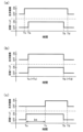
図10(a)乃至図10(c)は、それぞれ、洗浄流体の供給タイミングの例を示すグラフである。図10(a)乃至図10(c)において、縦軸は研磨ヘッドの動作状態と、非接触式洗浄機構30の動作状態とを表し、横軸は時間を表す。図10(a)乃至図10(c)において、研磨ヘッド50の動作状態がon状態になると、研磨テープ(研磨具)31がウェーハ(基板)Wの非デバイス面1に押し付けられ、該非デバイス面1の研磨が開始される。研磨ヘッド50の動作状態がoff状態になると、研磨テープ31がウェーハWの非デバイス面1から離れて、非デバイス面1の研磨が停止される。非接触式洗浄機構30の動作状態がon状態になると、洗浄流体ノズル33から洗浄流体がウェーハWのデバイス面2に噴射され、該デバイス面2の洗浄が開始される。非接触式洗浄機構30の動作状態がoff状態になると、洗浄流体ノズル33からの洗浄流体の噴射が停止され、デバイス面2の洗浄が停止する。
FIGS. 10(a) to 10(c) are graphs each showing an example of the supply timing of the cleaning fluid. In FIGS. 10(a) to 10(c), the vertical axis represents the operating state of the polishing head and the operating state of the
図10(a)に示す例では、デバイス面2の洗浄が開始される時点Tcは、研磨テープ31によるウェーハWの非デバイス面1の研磨が開始される時点Taよりも前である。すなわち、非接触式洗浄機構30によるデバイス面2の洗浄は、研磨テープ31によるウェーハWの非デバイス面1の研磨よりも前に開始される。さらに、図10(a)に示す例では、デバイス面2の洗浄が終了される時点Tdは、研磨テープ31によるウェーハWの非デバイス面1の研磨が終了される時点Tbよりも後である。すなわち、非接触式洗浄機構30によるデバイス面2の洗浄は、研磨テープ31によるウェーハWの非デバイス面1の研磨が終了した後に終了される。
In the example shown in FIG. 10A, the time Tc at which cleaning of the
図10(b)に示す例では、デバイス面2の洗浄が開始される時点Tcは、研磨テープ31によるウェーハWの非デバイス面1の研磨が開始される時点Taと同一である。すなわち、非接触式洗浄機構30によるデバイス面2の洗浄は、研磨テープ31によるウェーハWの非デバイス面1の研磨と同時に開始される。さらに、図10(b)に示す例では、デバイス面2の洗浄が終了される時点Tdは、研磨テープ31によるウェーハWの非デバイス面1の研磨が終了される時点Tbと同一である。すなわち、非接触式洗浄機構30によるデバイス面2の洗浄は、研磨テープ31によるウェーハWの非デバイス面1の研磨が終了するのと同時に終了される。
In the example shown in FIG. 10(b), the time Tc at which cleaning of the
図10(a)および図10(b)に示すように、少なくとも研磨テープ31によるウェーハWの非デバイス面1の研磨を行っている間中、デバイス面2の洗浄を行うことにより、異物によるデバイス面2の汚染を最大限に防止することができる。
As shown in FIGS. 10(a) and 10(b), by cleaning the
一方で、図10(c)に示す例では、デバイス面2の洗浄が開始される時点Tcは、研磨テープ31によるウェーハWの非デバイス面1の研磨が開始されてから所定時間Intが経過した後に開始される。すなわち、非接触式洗浄機構30によるデバイス面2の洗浄は、研磨テープ31によるウェーハWの非デバイス面1の研磨の後に開始される。この場合、洗浄流体の消費量が低減されるので、研磨装置のランニングコストを低減することができる。さらに、図10(c)に示す例では、デバイス面2の洗浄が終了される時点Tdは、研磨テープ31によるウェーハWの非デバイス面1の研磨が終了される時点Tbよりも後である。一実施形態では、デバイス面2の洗浄が終了される時点Tdを、研磨テープ31によるウェーハWの非デバイス面1の研磨が終了される時点Tbと同一に設定してもよい。このように、少なくとも研磨テープ31によるウェーハWの非デバイス面1の研磨が終了する時点Tbまでは、デバイス面2の洗浄を行うことが好ましい。
On the other hand, in the example shown in FIG. 10(c), the time Tc at which cleaning of the
本実施形態では、洗浄流体ノズル33は、2流体ジェットをデバイス面2に向けて噴射する2流体ジェットノズルである。2流体ジェットノズルは、洗浄流体供給装置40から供給された気体と液体の混合流体を高速で噴射可能に構成されたノズルである。2流体ジェットノズルである洗浄流体ノズル33は、例えば、高速の気体に乗せた微小液滴(ミスト)をウェーハWのデバイス面2に衝突させ、この衝突で発生した衝撃波を利用してデバイス面2上の異物を除去、すなわち、デバイス面2を洗浄する。
In this embodiment, the cleaning
洗浄流体ノズル33からウェーハWのデバイス面2に噴射される洗浄流体は、2流体ジェットに限定されない。例えば、洗浄流体は、純水(または、超純水)にオゾンガスを溶解させたオゾン水であってもよいし、オゾンガスの微少な気泡を純水(または、超純水)に含ませたオゾンマイクロバブル水(または、オゾンナノバブル水)であってもよい。これらの場合、非接触式洗浄機構30の洗浄流体供給装置40は、オゾンガスを製造するオゾン発生器85を備える。
The cleaning fluid injected from the cleaning
洗浄流体がオゾン水の場合は、ウェーハWのデバイス面2に付着した有機物および金属をオゾンが有する強力な酸化作用によってオゾン水に溶解させ、デバイス面2から除去する。洗浄流体がオゾンマイクロバブル水(または、オゾンナノバブル水)の場合は、オゾンマイクロバブルが消滅するときに発生する多量のOHラジカルを利用して、異物を分解・除去する。
When the cleaning fluid is ozone water, organic substances and metals attached to the
一実施形態では、洗浄流体は、電解水であってもよい。この場合、非接触式洗浄機構30の洗浄流体供給装置40は、電解水生成機86を有する。電解水生成機86によって生成された電解水が洗浄流体ノズル33に供給され、該洗浄流体ノズル33からデバイス面2に噴射される。さらに、洗浄流体ノズル33からウェーハWのデバイス面2に噴射される洗浄流体は、超音波振動により励起されたメガソニック水であってもよいし、異物を溶解可能な薬液であってもよい。さらに、一実施形態では、洗浄流体ノズル33からウェーハWのデバイス面2に噴射される洗浄流体は、デバイス面2上の異物と反応し、該異物をデバイス面から除去可能な洗浄ガスであってもよい。
In one embodiment, the cleaning fluid may be electrolyzed water. In this case, the cleaning
次に、本実施形態に係る研磨装置の動作について説明する。以下に説明する研磨装置の動作、すなわち、ウェーハWの研磨処理は、図1に示す動作制御部180によって制御される。動作制御部180は、基板保持部10、非接触式洗浄機構30、研磨ヘッド50、研磨テープ供給機構41、テープ送り装置46、および並進回転運動機構60などに電気的に接続されており、これら構成要素の動作を制御する。例えば、動作制御部180は、基板保持部10、リンス液供給ノズル27、保護液供給ノズル28、モータ36、流量調整器38、洗浄流体供給装置40、研磨ヘッド50、研磨テープ供給機構41、テープ送り装置46、並進回転運動機構60、オゾン発生器85(または、電解水生成機86)の動作を制御する。動作制御部180は、専用のコンピュータまたは汎用のコンピュータから構成される。
Next, the operation of the polishing apparatus according to this embodiment will be explained. The operation of the polishing apparatus described below, that is, the polishing process of the wafer W, is controlled by the
研磨されるウェーハWは、非デバイス面1が下向きの状態(すなわち、デバイス面2が上向きの状態)で、基板保持部10のローラー11により保持され、さらにウェーハWの軸心を中心に回転される。具体的には、基板保持部10は、ウェーハWの非デバイス面1が下向きの状態で複数のローラー11をウェーハWの周縁部に接触させながら、複数のローラー11をそれぞれの軸心を中心に回転させることで、ウェーハWを回転させる。次に、リンス液供給ノズル27からウェーハWの非デバイス面1にリンス液が供給され、保護液供給ノズル28からウェーハWのデバイス面2に保護液が供給される。リンス液は、ウェーハWの非デバイス面1上を半径方向外側に流れ、保護液は、遠心力によりウェーハWのデバイス面2の全体に広がる。
The wafer W to be polished is held by the
さらに、図10(a)を参照して説明したように、ウェーハWの非デバイス面1の研磨が開始される前から、非接触式洗浄機構30によるウェーハWのデバイス面2の洗浄が開始される。より具体的には、非接触式洗浄機構30の洗浄流体供給装置40から洗浄流体ノズル33に洗浄流体が供給され、該洗浄流体ノズル33から洗浄流体がウェーハWのデバイス面2に噴射される。同時に、非接触式洗浄機構30のノズル移動機構32によって、洗浄流体ノズル33をウェーハWの上方で水平方向に移動させる。
Furthermore, as described with reference to FIG. 10A, cleaning of the
図10(b)を参照して説明したように、非接触式洗浄機構30によるウェーハWのデバイス面2の洗浄は、ウェーハWの非デバイス面1の研磨の開始と同時でもよい。あるいは、図10(c)を参照して説明したように、非接触式洗浄機構30によるウェーハWのデバイス面2の洗浄は、ウェーハWの非デバイス面1の研磨の開始から所定時間Intが経過した後に開始してもよい。
As described with reference to FIG. 10(b), cleaning of the
洗浄流体ノズル33から噴射される洗浄流体としては、デバイス面2に付着するおそれがある異物に応じて、適切な洗浄流体が選択される。洗浄流体は、例えば、2流体ジェット、オゾン水、オゾンマイクロバブル水、電解水、メガソニック水、および薬液のいずれかでありえる。一実施形態では、洗浄流体は洗浄ガスであってもよい。
As the cleaning fluid injected from the cleaning
次に、動作制御部180は、研磨テープ供給機構41およびテープ送り装置46を駆動し、所定のテンションを掛けながら研磨テープ31をその長手方向に所定の速度で進行させる。そして、並進回転運動機構60は、研磨ヘッド50、研磨テープ供給機構41、ガイドローラー53a,53b,53c,53d、およびテープ送り装置46を並進回転運動させながら、研磨ヘッド50は研磨テープ31をウェーハWの非デバイス面1に接触させ、リンス液の存在下でウェーハWの非デバイス面1を研磨する。具体的には、加圧機構52は、研磨ブレード55を上方に押し上げ、研磨ブレード55は研磨テープ31の研磨面31aをウェーハWの非デバイス面1に押し付けることによって、ウェーハWの非デバイス面1の全体を研磨する。研磨装置は、ウェーハWの研磨中、リンス液および保護液を常にウェーハWに供給し続ける。さらに、研磨装置は、ウェーハWの研磨中、洗浄流体をウェーハWに供給し続けるのが好ましい。
Next, the
本実施形態では、ウェーハWの研磨中、保護液供給ノズル28から保護液がウェーハWのデバイス面2の中心部に供給される。したがって、洗浄液供給ノズル33がウェーハWの周縁部付近に移動されても、ウェーハWの中心部は保護液により覆われたままである。特に、ウェーハWの回転速度が高く設定されていても、ウェーハWの中心部を含むデバイス面2の全体を少なくとも保護液によって覆うことができる。その結果、ウェーハWのデバイス面2に異物が付着することが効果的に防止される。
In this embodiment, during polishing of the wafer W, the protective liquid is supplied from the protective
上述のように、研磨ブレード55の一端はウェーハWの周縁部から外側にはみ出ており、他端はウェーハWの非デバイス面1の中心O1を越えて延びているため、研磨ブレード55は、研磨テープ31をウェーハWの非デバイス面1の中心O1から最外部まで接触させることができる。ウェーハWの研磨中、ローラー11の位置は静止しているので、ローラー11は研磨ブレード55に接触しない。さらに、研磨ブレード55を含む研磨ヘッド50は並進回転運動するため、ウェーハWの中心部においても研磨テープ31とウェーハWとの相対速度を大きくすることができる。結果として、研磨テープ31は、最外部を含むウェーハWの非デバイス面1の全体を高い研磨レートで研磨することが可能となる。
As described above, one end of the
予め設定された時間が経過した後、加圧機構52は、研磨ブレード55を下降させ、研磨テープ31をウェーハWの非デバイス面1から離す。その後、動作制御部180は、基板保持部10、非接触式洗浄機構30、研磨ヘッド50、研磨テープ供給機構41、テープ送り装置46、および並進回転運動機構60などの構成要素の動作を停止させ、ウェーハWの研磨処理を終了する。図10(a)乃至図10(c)を参照して説明したように、動作制御部180は、ウェーハWの非デバイス面1の研磨が終了した後(すなわち、研磨テープ31が非デバイス面1から離れた後)で、非接触式洗浄機構30を停止してもよいし、ウェーハWの非デバイス面1の研磨の終了と同時に、非接触式洗浄機構30を停止してもよい。
After a preset time has elapsed, the
本実施形態によれば、ウェーハ(基板)Wの非デバイス面1を研磨する研磨具の一例である研磨テープ31が非デバイス面1を研磨している間に、非接触式洗浄機構30によってデバイス面2が積極的に洗浄される。さらに、保護液供給ノズル28から供給された保護液がデバイス面2を覆い、異物がデバイス面2に到達することを防止する。したがって、研磨屑などの異物によってウェーハWのデバイス面2が汚染されることを効果的に防止することができ、その結果、デバイス面2に形成されたデバイスの信頼性が向上する。
According to this embodiment, while the polishing
ここで、基板の表面(例えば、デバイス面2)を洗浄する方法として、洗浄ブラシまたは洗浄スポンジなどの洗浄部材を基板の表面に直接摺接させる接触式洗浄方法(例えば、スクラブ洗浄方法)が従来から知られている。この接触式洗浄方法は、基板の表面に付着した比較的大きな異物を効率よく除去可能であるというメリットを有している。 Here, as a method for cleaning the surface of the substrate (for example, device surface 2), a contact cleaning method (for example, a scrub cleaning method) in which a cleaning member such as a cleaning brush or a cleaning sponge is brought into direct sliding contact with the surface of the substrate has conventionally been used. known from. This contact cleaning method has the advantage that relatively large foreign matter adhering to the surface of the substrate can be efficiently removed.
しかしながら、接触式洗浄方法では、洗浄部材をデバイス面2に所定の力で押し付ける押圧機構などの付帯設備が必要となるため、非接触式洗浄方法と比較して、研磨装置の構成が複雑となる。さらに、接触式洗浄方法では、基板の表面から除去された異物が洗浄部材に蓄積し、洗浄部材に蓄積された異物がデバイス面2に再付着する所謂逆汚染の問題が生じるおそれがある。そのため、洗浄部材を定期的にメンテナンスまたは交換する必要がある。本実施形態では、デバイス面2の洗浄は、2流体ジェット、オゾン水、オゾンマイクロバブル水、メガソニック水、薬液、および洗浄ガスなどから選択された洗浄流体を用いた非接触式洗浄方法で行われるため、逆汚染の問題が生じない。そのため、非接触式洗浄方法は、接触式洗浄方法と比較して、メンテナンス頻度およびランニングコストを低減することができる。
However, the contact cleaning method requires incidental equipment such as a pressing mechanism that presses the cleaning member against the
さらに、本実施形態によれば、ウェーハWの非デバイス面1の研磨後にウェーハWのデバイス面2にはほとんど異物が付着していないので、ウェーハWの研磨処理の後に行われる該ウェーハWの洗浄処理の時間短縮を図ることができる。その結果、後述するように、研磨装置が配置される基板処理装置のスループットも向上させることができる。
Further, according to the present embodiment, since almost no foreign matter is attached to the
図11は、上述した研磨装置を備えた基板処理装置の一実施形態を模式的に示す平面図である。本実施形態では、基板処理装置は、多数のウェーハWが収容されたウェーハカセット(基板カセット)が載置される複数のロードポート122を備えたロードアンロード部121を有している。ロードポート122には、オープンカセット、SMIF(Standard Manufacturing Interface)ポッド、またはFOUP(Front Opening Unified Pod)を搭載することができるようになっている。SMIF、FOUPは、内部にウェーハカセットを収納し、隔壁で覆うことにより、外部空間とは独立した環境を保つことができる密閉容器である。
FIG. 11 is a plan view schematically showing an embodiment of a substrate processing apparatus including the above-described polishing apparatus. In this embodiment, the substrate processing apparatus has a load/unload
ロードアンロード部121には、ロードポート122の配列方向に沿って移動可能な第1の搬送ロボット(ローダー)123が設置されている。第1の搬送ロボット123はロードポート122に搭載されたウェーハカセットにアクセスして、ウェーハWをウェーハカセットから取り出すことができるようになっている。
A first transfer robot (loader) 123 that is movable along the arrangement direction of the
基板処理装置は、水平方向に移動可能な第2の搬送ロボット126と、ウェーハWが一時的に置かれる第1仮置き台140および第2仮置き台141と、研磨ユニット127と、基板処理装置全体の動作を制御するシステムコントローラ133と、研磨されたウェーハWを洗浄する洗浄ユニット172と、洗浄されたウェーハWを乾燥させる乾燥ユニット173とをさらに備えている。第2仮置き台141と洗浄ユニット172との間には、ウェーハWを搬送するための第3の搬送ロボット150が配置されており、洗浄ユニット172と乾燥ユニット173との間には、ウェーハWを搬送するための第4の搬送ロボット151が配置されている。研磨ユニット127は、上述した研磨装置である。上述の動作制御部180を、システムコントローラ133として用いてもよいし、システムコントローラ133に内蔵してもよい。
The substrate processing apparatus includes a
次に、研磨ユニット127を用いてウェーハWを研磨するときのウェーハWの搬送ルートについて説明する。複数(例えば25枚)のウェーハWは、そのデバイス面2が上を向いた状態で、ロードポート122のウェーハカセット(基板カセット)内に収容されている。第1の搬送ロボット123は、ウェーハカセットから1枚のウェーハWを取り出し、ウェーハWを第1仮置き台140に載置する。第2の搬送ロボット126は、ウェーハWを第1仮置き台140から取り出し、ウェーハWの非デバイス面1が下向きの状態でウェーハWを研磨ユニット127に搬送する。上述のように、ウェーハWの非デバイス面1は研磨ユニット127によって研磨される。第2の搬送ロボット126は、研磨されたウェーハWを研磨ユニット127から取り出し、第2仮置き台141に載置する。第3の搬送ロボット150は、ウェーハWを第2仮置き台141から取り出し、洗浄ユニット172に搬送する。
Next, a transport route for the wafer W when polishing the wafer W using the
ウェーハWは、その研磨された非デバイス面1が下向きの状態で、洗浄ユニット172によって洗浄される。一実施形態では、洗浄ユニット172は、ウェーハWを挟むように配置された上側洗浄具(例えば、上側ロールスポンジ)および下側洗浄具(例えば、下側ロールスポンジ)を備えており、洗浄液をウェーハWの両面に供給しながらこれら洗浄具でウェーハの両面を洗浄する。
The wafer W is cleaned by the
上述したように、研磨ユニット127で研磨されたウェーハWのデバイス面2は、非接触式洗浄機構30によって既に洗浄されている。そのため、洗浄ユニット172でのウェーハWの洗浄処理の負担が軽減されるとともに、比較的短時間で洗浄処理を完了することができる。例えば、上側洗浄具によるデバイス面2の洗浄時間を短くすることが可能であり、さらには、上側洗浄具および下側洗浄具によるウェーハWの両面の洗浄時間の短縮も期待できる。その結果、基板処理装置のスループットを向上させることができ、さらに、洗浄ユニット172でのランニングコストを低減することができる。一実施形態では、洗浄ユニット172で、下側洗浄具によってウェーハWの非デバイス面1のみを洗浄してもよい。この場合、上側洗浄具を省略できるので、洗浄ユニット172の構成を単純化することができ、さらに、洗浄ユニット172のランニングコストをさらに低減することができる。
As described above, the
第4の搬送ロボット151は、洗浄されたウェーハWを洗浄ユニット172から取り出し、乾燥ユニット173に搬送する。ウェーハWは、その洗浄された非デバイス面1が下向きの状態で、乾燥ユニット173によって乾燥される。本実施形態では、乾燥ユニット173は、ウェーハWをその軸心まわりに高速で回転させることによってウェーハWをスピン乾燥させるように構成されている。一実施形態では、乾燥ユニット173は、純水ノズルおよびIPAノズルをウェーハWの半径方向に移動させながら、純水ノズルおよびIPAノズルから純水とIPA蒸気(イソプロピルアルコールとN2ガスとの混合物)をウェーハWの上面に供給することでウェーハWを乾燥させるIPAタイプであってもよい。
The
乾燥されたウェーハWは、その非デバイス面1が下向きの状態で第1の搬送ロボット123によりロードポート122のウェーハカセットに戻される。このようにして、基板処理装置は、ウェーハWの非デバイス面1が下向きの状態のまま、ウェーハWの研磨、洗浄、乾燥、およびロードアンロード部への搬送の一連の工程を行うことができる。
The dried wafer W is returned to the wafer cassette of the
この基板処理装置によれば、ウェーハWの非デバイス面1が下向きの状態で、効率的にウェーハWの非デバイス面1の全体を研磨することができる。結果として、ウェーハWを反転させる必要がなくなるため、ウェーハWへの空気中の不純物の付着を防止し、かつ全体の処理時間を減らすことができる。さらに、ウェーハWを反転させる反転機が不要であり、基板処理装置の構成を単純化し、費用を削減することができる。一実施形態では、基板処理装置は、別の研磨ユニット127をさらに備えてもよい。基板処理装置が複数の研磨ユニット127を備えることによって、処理枚数が倍増し、基板処理装置のスループットを向上させることができる。
According to this substrate processing apparatus, the entire
上述した実施形態は、本発明が属する技術分野における通常の知識を有する者が本発明を実施できることを目的として記載されたものである。上記実施形態の種々の変形例は、当業者であれば当然になしうることであり、本発明の技術的思想は他の実施形態にも適用しうる。したがって、本発明は、記載された実施形態に限定されることはなく、特許請求の範囲によって定義される技術的思想に従った最も広い範囲に解釈されるものである。 The embodiments described above have been described to enable those skilled in the art to carry out the invention. Various modifications of the above embodiments can be naturally made by those skilled in the art, and the technical idea of the present invention can be applied to other embodiments. Therefore, the invention is not limited to the described embodiments, but is to be construed in the broadest scope according to the spirit defined by the claims.
10 基板保持部
11 ローラー
12 ローラー回転機構
27 リンス液供給ノズル
28 保護液供給ノズル
30 非接触式洗浄機構
31 研磨テープ
32 ノズル移動機構
33 洗浄流体ノズル
34 ノズルアーム
35 ノズル旋回軸
36 モータ(駆動機)
37 洗浄流体ライン
38 流量調整器
40 洗浄流体供給装置
41 研磨テープ供給機構
46 テープ送り装置
50 研磨ヘッド
52 加圧機構
53a,53b,53c,53d,53e,53f,53g ガイドローラー
55 研磨ブレード
56 研磨パッド
57 バックプレート
60 並進回転運動機構
85 オゾン発生器
86 電解水生成機
127 研磨ユニット(研磨装置)
133 システムコントローラ
140 第1仮置き台
141 第2仮置き台
150 第3の搬送ロボット
151 第4の搬送ロボット
172 洗浄ユニット
173 乾燥ユニット
180 動作制御部
10
37
133
Claims (20)
前記基板の非デバイス面に接触して、該基板の非デバイス面を研磨する研磨具と、
前記研磨具で前記基板の非デバイス面を研磨している間に、前記基板のデバイス面を洗浄する非接触式洗浄機構と、
前記基板のデバイス面に保護液を供給する保護液供給ノズルと、
前記非接触式洗浄機構、および前記保護液供給ノズルの動作を制御する動作制御部と、を備え、
前記動作制御部は、前記研磨具で前記基板の非デバイス面を研磨している間に、前記基板のデバイス面に前記保護液供給ノズルから前記保護液を供給しつつ、さらに、前記非接触式洗浄機構によって、前記基板のデバイス面を洗浄することを特徴とする研磨装置。 a substrate holding unit that holds the substrate with its device side facing upward and rotates the substrate;
a polishing tool that contacts the non-device surface of the substrate and polishes the non-device surface of the substrate;
a non-contact cleaning mechanism that cleans the device surface of the substrate while the non-device surface of the substrate is being polished with the polishing tool;
a protective liquid supply nozzle that supplies a protective liquid to the device surface of the substrate;
an operation control unit that controls the operation of the non-contact cleaning mechanism and the protective liquid supply nozzle ,
The operation control unit is configured to supply the protective liquid from the protective liquid supply nozzle to the device surface of the substrate while polishing the non-device surface of the substrate with the polishing tool, and further supply the protective liquid to the device surface of the substrate. A polishing apparatus characterized in that a cleaning mechanism cleans a device surface of the substrate .
洗浄流体を前記基板のデバイス面に向けて噴射する洗浄流体ノズルと、
前記洗浄流体ノズルを、前記基板のデバイス面の上方で移動させるノズル移動機構と、を有することを特徴とする請求項1に記載の研磨装置。 The non-contact cleaning mechanism includes:
a cleaning fluid nozzle that sprays cleaning fluid toward a device surface of the substrate;
The polishing apparatus according to claim 1, further comprising a nozzle movement mechanism that moves the cleaning fluid nozzle above a device surface of the substrate.
前記洗浄流体ノズルは、オゾン水、またはオゾンマイクロバブル水を前記基板のデバイス面に向けて噴射することを特徴とする請求項2に記載の研磨装置。 The non-contact cleaning mechanism further includes an ozone generator,
3. The polishing apparatus according to claim 2, wherein the cleaning fluid nozzle sprays ozone water or ozone microbubble water toward the device surface of the substrate.
前記洗浄流体ノズルは、電解水を前記基板のデバイス面に向けて噴射することを特徴とする請求項2に記載の研磨装置。 The non-contact cleaning mechanism further includes an electrolyzed water generator,
3. The polishing apparatus according to claim 2, wherein the cleaning fluid nozzle sprays electrolyzed water toward a device surface of the substrate.
前記動作制御部は、
前記研磨具による前記基板の非デバイス面の研磨の開始よりも前に、前記非接触式洗浄機構による前記基板のデバイス面の洗浄を開始し、
前記研磨具による前記基板の非デバイス面の研磨の終了後に、前記非接触式洗浄機構による前記基板のデバイス面の洗浄を終了することを特徴とする請求項1に記載の研磨装置。 The operation control unit is configured to be able to control the operation of the polishing tool ,
The operation control section includes:
Before the polishing tool starts polishing the non-device surface of the substrate, the non-contact cleaning mechanism starts cleaning the device surface of the substrate,
2. The polishing apparatus according to claim 1, wherein the cleaning of the device surface of the substrate by the non-contact cleaning mechanism is completed after the polishing of the non-device surface of the substrate by the polishing tool is completed.
前記動作制御部は、
前記研磨具による前記基板の非デバイス面の研磨の開始と同時に、前記非接触式洗浄機構による前記基板のデバイス面の洗浄を開始し、
前記研磨具による前記基板の非デバイス面の研磨の終了と同時に、前記非接触式洗浄機構による前記基板のデバイス面の洗浄を終了することを特徴とする請求項1に記載の研磨装置。 The operation control unit is configured to be able to control the operation of the polishing tool ,
The operation control section includes:
At the same time as the polishing tool starts polishing the non-device surface of the substrate, the non-contact cleaning mechanism starts cleaning the device surface of the substrate,
2. The polishing apparatus according to claim 1, wherein the cleaning of the device surface of the substrate by the non-contact cleaning mechanism is completed at the same time as the polishing of the non-device surface of the substrate by the polishing tool is completed.
前記動作制御部は、
前記研磨具による前記基板の非デバイス面の研磨の開始後に、前記非接触式洗浄機構による前記基板のデバイス面の洗浄を開始し、
前記研磨具による前記基板の非デバイス面の研磨の終了後に、前記非接触式洗浄機構による前記基板のデバイス面の洗浄を終了することを特徴とする請求項1に記載の研磨装置。 The operation control unit is configured to be able to control the operation of the polishing tool ,
The operation control section includes:
After the polishing tool starts polishing the non-device surface of the substrate, the non-contact cleaning mechanism starts cleaning the device surface of the substrate,
2. The polishing apparatus according to claim 1, wherein the cleaning of the device surface of the substrate by the non-contact cleaning mechanism is completed after the polishing of the non-device surface of the substrate by the polishing tool is completed.
前記回転している基板の非デバイス面に研磨具を押し付けて、該非デバイス面を研磨し、
前記基板の非デバイス面を研磨している間に、前記基板のデバイス面に保護液を供給しつつ、さらに、前記基板のデバイス面を非接触式洗浄機構で洗浄することを特徴とする研磨方法。 holding the substrate with its device side facing up and rotating the substrate;
pressing a polishing tool against the non-device surface of the rotating substrate to polish the non-device surface;
A polishing method characterized by supplying a protective liquid to the device surface of the substrate while polishing the non-device surface of the substrate, and further cleaning the device surface of the substrate with a non-contact cleaning mechanism. .
前記研磨具による前記基板の非デバイス面の研磨の終了後に、前記非接触式洗浄機構による前記基板のデバイス面の洗浄を終了することを特徴とする請求項10に記載の研磨方法。 Before the polishing tool starts polishing the non-device surface of the substrate, the non-contact cleaning mechanism starts cleaning the device surface of the substrate,
11. The polishing method according to claim 10 , wherein cleaning of the device surface of the substrate by the non-contact cleaning mechanism is completed after polishing of the non-device surface of the substrate by the polishing tool is completed.
前記研磨具による前記基板の非デバイス面の研磨の終了と同時に、前記非接触式洗浄機構による前記基板のデバイス面の洗浄を終了することを特徴とする請求項10に記載の研磨方法。 At the same time as the polishing tool starts polishing the non-device surface of the substrate, the non-contact cleaning mechanism starts cleaning the device surface of the substrate,
11. The polishing method according to claim 10 , wherein the cleaning of the device surface of the substrate by the non-contact cleaning mechanism is completed at the same time as the polishing of the non-device surface of the substrate by the polishing tool is completed.
前記研磨具による前記基板の非デバイス面の研磨の終了後に、前記非接触式洗浄機構による前記基板のデバイス面の洗浄を終了することを特徴とする請求項10に記載の研磨方法。 After the polishing tool starts polishing the non-device surface of the substrate, the non-contact cleaning mechanism starts cleaning the device surface of the substrate,
11. The polishing method according to claim 10 , wherein cleaning of the device surface of the substrate by the non-contact cleaning mechanism is completed after polishing of the non-device surface of the substrate by the polishing tool is completed.
前記研磨装置によって研磨された基板を洗浄する洗浄ユニットと、
前記洗浄ユニットで洗浄された基板を乾燥させる乾燥ユニットと、を備えたことを特徴とする基板処理装置。 A polishing device according to any one of claims 1 to 9 ,
a cleaning unit that cleans the substrate polished by the polishing device;
A substrate processing apparatus comprising: a drying unit that dries the substrate cleaned by the cleaning unit.
Priority Applications (3)
| Application Number | Priority Date | Filing Date | Title |
|---|---|---|---|
| JP2019160218A JP7406943B2 (en) | 2019-09-03 | 2019-09-03 | Polishing equipment, polishing method, and substrate processing equipment |
| PCT/JP2020/023328 WO2021044694A1 (en) | 2019-09-03 | 2020-06-15 | Polishing device, polishing method and substrate processing device |
| TW109123683A TW202112496A (en) | 2019-09-03 | 2020-07-14 | Polishing device, polishing method and substrate processing device |
Applications Claiming Priority (1)
| Application Number | Priority Date | Filing Date | Title |
|---|---|---|---|
| JP2019160218A JP7406943B2 (en) | 2019-09-03 | 2019-09-03 | Polishing equipment, polishing method, and substrate processing equipment |
Publications (3)
| Publication Number | Publication Date |
|---|---|
| JP2021040022A JP2021040022A (en) | 2021-03-11 |
| JP2021040022A5 JP2021040022A5 (en) | 2022-08-29 |
| JP7406943B2 true JP7406943B2 (en) | 2023-12-28 |
Family
ID=74847361
Family Applications (1)
| Application Number | Title | Priority Date | Filing Date |
|---|---|---|---|
| JP2019160218A Active JP7406943B2 (en) | 2019-09-03 | 2019-09-03 | Polishing equipment, polishing method, and substrate processing equipment |
Country Status (3)
| Country | Link |
|---|---|
| JP (1) | JP7406943B2 (en) |
| TW (1) | TW202112496A (en) |
| WO (1) | WO2021044694A1 (en) |
Families Citing this family (1)
| Publication number | Priority date | Publication date | Assignee | Title |
|---|---|---|---|---|
| CN117260515B (en) * | 2023-11-22 | 2024-02-13 | 北京特思迪半导体设备有限公司 | Dynamic linkage control method of polishing machine |
Citations (4)
| Publication number | Priority date | Publication date | Assignee | Title |
|---|---|---|---|---|
| JP2004273961A (en) | 2003-03-12 | 2004-09-30 | Ebara Corp | Cleaning device of metal wiring forming substrate |
| JP2006303143A (en) | 2005-04-20 | 2006-11-02 | Seiko Epson Corp | Apparatus and method for cleaning substrate |
| JP2015119161A (en) | 2013-11-13 | 2015-06-25 | 東京エレクトロン株式会社 | Polishing/cleaning mechanism, substrate processing apparatus, and substrate processing method |
| JP2017108113A (en) | 2015-11-27 | 2017-06-15 | 株式会社荏原製作所 | Substrate processing apparatus, substrate processing method, and control program of substrate processing apparatus |
Family Cites Families (1)
| Publication number | Priority date | Publication date | Assignee | Title |
|---|---|---|---|---|
| JP7148349B2 (en) * | 2017-11-14 | 2022-10-05 | 株式会社荏原製作所 | SUBSTRATE PROCESSING APPARATUS AND SUBSTRATE PROCESSING METHOD |
-
2019
- 2019-09-03 JP JP2019160218A patent/JP7406943B2/en active Active
-
2020
- 2020-06-15 WO PCT/JP2020/023328 patent/WO2021044694A1/en active Application Filing
- 2020-07-14 TW TW109123683A patent/TW202112496A/en unknown
Patent Citations (4)
| Publication number | Priority date | Publication date | Assignee | Title |
|---|---|---|---|---|
| JP2004273961A (en) | 2003-03-12 | 2004-09-30 | Ebara Corp | Cleaning device of metal wiring forming substrate |
| JP2006303143A (en) | 2005-04-20 | 2006-11-02 | Seiko Epson Corp | Apparatus and method for cleaning substrate |
| JP2015119161A (en) | 2013-11-13 | 2015-06-25 | 東京エレクトロン株式会社 | Polishing/cleaning mechanism, substrate processing apparatus, and substrate processing method |
| JP2017108113A (en) | 2015-11-27 | 2017-06-15 | 株式会社荏原製作所 | Substrate processing apparatus, substrate processing method, and control program of substrate processing apparatus |
Also Published As
| Publication number | Publication date |
|---|---|
| TW202112496A (en) | 2021-04-01 |
| JP2021040022A (en) | 2021-03-11 |
| WO2021044694A1 (en) | 2021-03-11 |
Similar Documents
| Publication | Publication Date | Title |
|---|---|---|
| JP3990073B2 (en) | Substrate cleaning apparatus and substrate cleaning method | |
| JP6908496B2 (en) | Polishing equipment | |
| US20020007840A1 (en) | Substrate cleaning apparatus, substrate cleaning method and substrate processing apparatus | |
| TWI774776B (en) | Method and apparatus for polishing a substrate, and method for processing a substrate | |
| JP2014167996A (en) | Polishing device and polishing method | |
| KR20190054937A (en) | Apparatus and method for processing a surface of a substrate | |
| JP7406943B2 (en) | Polishing equipment, polishing method, and substrate processing equipment | |
| JP2019091886A (en) | Substrate processing apparatus and substrate processing method | |
| JP6445298B2 (en) | Polishing apparatus and processing method | |
| JP6625461B2 (en) | Polishing equipment | |
| JP2016111265A (en) | Buff processing device and substrate processing device | |
| EP3396707B1 (en) | Apparatus and method for cleaning a back surface of a substrate | |
| JP6346541B2 (en) | Buff processing apparatus and substrate processing apparatus | |
| US20230182262A1 (en) | Substrate cleaning device and substrate polishing device | |
| US10651057B2 (en) | Apparatus and method for cleaning a back surface of a substrate | |
| JP2023097533A (en) | Polishing device and polishing method | |
| JP2016119368A (en) | Conditioning device, buff processing unit, substrate processing apparatus, dresser, and conditioning method | |
| JP2019042923A (en) | Polishing device and processing method | |
| JP2016111264A (en) | Buff processing device and substrate processing device | |
| JP2016078156A (en) | Processing module | |
| JP2021109281A (en) | Buff processing module, and substrate processing apparatus | |
| JP2022039487A (en) | Workpiece support device and workpiece support method | |
| TW201842983A (en) | Apparatus and method for cleaning back surface of substrate capable of removing particles from a back surface of a substrate with a higher removal rate |
Legal Events
| Date | Code | Title | Description |
|---|---|---|---|
| A521 | Request for written amendment filed |
Free format text: JAPANESE INTERMEDIATE CODE: A523 Effective date: 20220819 |
|
| A621 | Written request for application examination |
Free format text: JAPANESE INTERMEDIATE CODE: A621 Effective date: 20220819 |
|
| A131 | Notification of reasons for refusal |
Free format text: JAPANESE INTERMEDIATE CODE: A131 Effective date: 20230808 |
|
| A521 | Request for written amendment filed |
Free format text: JAPANESE INTERMEDIATE CODE: A523 Effective date: 20230927 |
|
| TRDD | Decision of grant or rejection written | ||
| A01 | Written decision to grant a patent or to grant a registration (utility model) |
Free format text: JAPANESE INTERMEDIATE CODE: A01 Effective date: 20231212 |
|
| A61 | First payment of annual fees (during grant procedure) |
Free format text: JAPANESE INTERMEDIATE CODE: A61 Effective date: 20231218 |
|
| R150 | Certificate of patent or registration of utility model |
Ref document number: 7406943 Country of ref document: JP Free format text: JAPANESE INTERMEDIATE CODE: R150 |