JP7378317B2 - プラズマ処理装置 - Google Patents
プラズマ処理装置 Download PDFInfo
- Publication number
- JP7378317B2 JP7378317B2 JP2020030327A JP2020030327A JP7378317B2 JP 7378317 B2 JP7378317 B2 JP 7378317B2 JP 2020030327 A JP2020030327 A JP 2020030327A JP 2020030327 A JP2020030327 A JP 2020030327A JP 7378317 B2 JP7378317 B2 JP 7378317B2
- Authority
- JP
- Japan
- Prior art keywords
- dielectric member
- wall
- processing apparatus
- plasma processing
- electromagnetic waves
- Prior art date
- Legal status (The legal status is an assumption and is not a legal conclusion. Google has not performed a legal analysis and makes no representation as to the accuracy of the status listed.)
- Active
Links
Images


Classifications
-
- H—ELECTRICITY
- H01—ELECTRIC ELEMENTS
- H01J—ELECTRIC DISCHARGE TUBES OR DISCHARGE LAMPS
- H01J37/00—Discharge tubes with provision for introducing objects or material to be exposed to the discharge, e.g. for the purpose of examination or processing thereof
- H01J37/32—Gas-filled discharge tubes
- H01J37/32431—Constructional details of the reactor
- H01J37/32623—Mechanical discharge control means
-
- H—ELECTRICITY
- H01—ELECTRIC ELEMENTS
- H01J—ELECTRIC DISCHARGE TUBES OR DISCHARGE LAMPS
- H01J37/00—Discharge tubes with provision for introducing objects or material to be exposed to the discharge, e.g. for the purpose of examination or processing thereof
- H01J37/32—Gas-filled discharge tubes
- H01J37/32431—Constructional details of the reactor
- H01J37/3244—Gas supply means
-
- C—CHEMISTRY; METALLURGY
- C23—COATING METALLIC MATERIAL; COATING MATERIAL WITH METALLIC MATERIAL; CHEMICAL SURFACE TREATMENT; DIFFUSION TREATMENT OF METALLIC MATERIAL; COATING BY VACUUM EVAPORATION, BY SPUTTERING, BY ION IMPLANTATION OR BY CHEMICAL VAPOUR DEPOSITION, IN GENERAL; INHIBITING CORROSION OF METALLIC MATERIAL OR INCRUSTATION IN GENERAL
- C23C—COATING METALLIC MATERIAL; COATING MATERIAL WITH METALLIC MATERIAL; SURFACE TREATMENT OF METALLIC MATERIAL BY DIFFUSION INTO THE SURFACE, BY CHEMICAL CONVERSION OR SUBSTITUTION; COATING BY VACUUM EVAPORATION, BY SPUTTERING, BY ION IMPLANTATION OR BY CHEMICAL VAPOUR DEPOSITION, IN GENERAL
- C23C16/00—Chemical coating by decomposition of gaseous compounds, without leaving reaction products of surface material in the coating, i.e. chemical vapour deposition [CVD] processes
- C23C16/44—Chemical coating by decomposition of gaseous compounds, without leaving reaction products of surface material in the coating, i.e. chemical vapour deposition [CVD] processes characterised by the method of coating
- C23C16/50—Chemical coating by decomposition of gaseous compounds, without leaving reaction products of surface material in the coating, i.e. chemical vapour deposition [CVD] processes characterised by the method of coating using electric discharges
-
- H—ELECTRICITY
- H01—ELECTRIC ELEMENTS
- H01J—ELECTRIC DISCHARGE TUBES OR DISCHARGE LAMPS
- H01J37/00—Discharge tubes with provision for introducing objects or material to be exposed to the discharge, e.g. for the purpose of examination or processing thereof
- H01J37/32—Gas-filled discharge tubes
- H01J37/32431—Constructional details of the reactor
- H01J37/32458—Vessel
- H01J37/32467—Material
-
- H—ELECTRICITY
- H01—ELECTRIC ELEMENTS
- H01J—ELECTRIC DISCHARGE TUBES OR DISCHARGE LAMPS
- H01J37/00—Discharge tubes with provision for introducing objects or material to be exposed to the discharge, e.g. for the purpose of examination or processing thereof
- H01J37/32—Gas-filled discharge tubes
- H01J37/32431—Constructional details of the reactor
- H01J37/32715—Workpiece holder
-
- H—ELECTRICITY
- H01—ELECTRIC ELEMENTS
- H01J—ELECTRIC DISCHARGE TUBES OR DISCHARGE LAMPS
- H01J37/00—Discharge tubes with provision for introducing objects or material to be exposed to the discharge, e.g. for the purpose of examination or processing thereof
- H01J37/32—Gas-filled discharge tubes
- H01J37/32431—Constructional details of the reactor
- H01J37/32798—Further details of plasma apparatus not provided for in groups H01J37/3244 - H01J37/32788; special provisions for cleaning or maintenance of the apparatus
- H01J37/32816—Pressure
- H01J37/32834—Exhausting
-
- H—ELECTRICITY
- H05—ELECTRIC TECHNIQUES NOT OTHERWISE PROVIDED FOR
- H05H—PLASMA TECHNIQUE; PRODUCTION OF ACCELERATED ELECTRICALLY-CHARGED PARTICLES OR OF NEUTRONS; PRODUCTION OR ACCELERATION OF NEUTRAL MOLECULAR OR ATOMIC BEAMS
- H05H1/00—Generating plasma; Handling plasma
- H05H1/24—Generating plasma
- H05H1/46—Generating plasma using applied electromagnetic fields, e.g. high frequency or microwave energy
-
- H—ELECTRICITY
- H10—SEMICONDUCTOR DEVICES; ELECTRIC SOLID-STATE DEVICES NOT OTHERWISE PROVIDED FOR
- H10P—GENERIC PROCESSES OR APPARATUS FOR THE MANUFACTURE OR TREATMENT OF DEVICES COVERED BY CLASS H10
- H10P14/00—Formation of materials, e.g. in the shape of layers or pillars
- H10P14/60—Formation of materials, e.g. in the shape of layers or pillars of insulating materials
-
- H—ELECTRICITY
- H10—SEMICONDUCTOR DEVICES; ELECTRIC SOLID-STATE DEVICES NOT OTHERWISE PROVIDED FOR
- H10P—GENERIC PROCESSES OR APPARATUS FOR THE MANUFACTURE OR TREATMENT OF DEVICES COVERED BY CLASS H10
- H10P50/00—Etching of wafers, substrates or parts of devices
- H10P50/20—Dry etching; Plasma etching; Reactive-ion etching
- H10P50/24—Dry etching; Plasma etching; Reactive-ion etching of semiconductor materials
- H10P50/242—Dry etching; Plasma etching; Reactive-ion etching of semiconductor materials of Group IV materials
-
- H—ELECTRICITY
- H01—ELECTRIC ELEMENTS
- H01J—ELECTRIC DISCHARGE TUBES OR DISCHARGE LAMPS
- H01J2237/00—Discharge tubes exposing object to beam, e.g. for analysis treatment, etching, imaging
- H01J2237/32—Processing objects by plasma generation
- H01J2237/327—Arrangements for generating the plasma
-
- H—ELECTRICITY
- H01—ELECTRIC ELEMENTS
- H01J—ELECTRIC DISCHARGE TUBES OR DISCHARGE LAMPS
- H01J2237/00—Discharge tubes exposing object to beam, e.g. for analysis treatment, etching, imaging
- H01J2237/32—Processing objects by plasma generation
- H01J2237/33—Processing objects by plasma generation characterised by the type of processing
- H01J2237/332—Coating
- H01J2237/3321—CVD [Chemical Vapor Deposition]
-
- H—ELECTRICITY
- H01—ELECTRIC ELEMENTS
- H01J—ELECTRIC DISCHARGE TUBES OR DISCHARGE LAMPS
- H01J2237/00—Discharge tubes exposing object to beam, e.g. for analysis treatment, etching, imaging
- H01J2237/32—Processing objects by plasma generation
- H01J2237/33—Processing objects by plasma generation characterised by the type of processing
- H01J2237/334—Etching
-
- H—ELECTRICITY
- H01—ELECTRIC ELEMENTS
- H01J—ELECTRIC DISCHARGE TUBES OR DISCHARGE LAMPS
- H01J37/00—Discharge tubes with provision for introducing objects or material to be exposed to the discharge, e.g. for the purpose of examination or processing thereof
- H01J37/32—Gas-filled discharge tubes
- H01J37/32009—Arrangements for generation of plasma specially adapted for examination or treatment of objects, e.g. plasma sources
- H01J37/32082—Radio frequency generated discharge
Landscapes
- Chemical & Material Sciences (AREA)
- Engineering & Computer Science (AREA)
- Physics & Mathematics (AREA)
- Plasma & Fusion (AREA)
- Analytical Chemistry (AREA)
- Chemical Kinetics & Catalysis (AREA)
- General Chemical & Material Sciences (AREA)
- Materials Engineering (AREA)
- Mechanical Engineering (AREA)
- Metallurgy (AREA)
- Organic Chemistry (AREA)
- Spectroscopy & Molecular Physics (AREA)
- Electromagnetism (AREA)
- Plasma Technology (AREA)
- Chemical Vapour Deposition (AREA)
- Drying Of Semiconductors (AREA)
Description
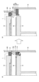
まず、実施形態に係るプラズマ処理装置1について、図1を参照しながら説明する。図1は、実施形態に係るプラズマ処理装置1を示す断面模式図である。図1に示すプラズマ処理装置1は、処理容器10、載置台12、上部電極14、及び電磁波導入部20を有する。
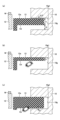
次に、実施形態に係る誘電体部材13について、図2及び図3を参照しながら詳細に説明する。図2は、一実施形態に係る誘電体部材の構成及び効果の一例を示す図である。図3は、一実施形態に係る誘電体部材の構成及び効果を説明するための図である。
次に、誘電体部材13と載置台12との間の空間や誘電体部材13の下方において異常放電が生じることを防止するために好ましい誘電体部材13の寸法について説明する。誘電体部材13に入射する電磁波の実効波長をλ0とすると、シースShを伝播する電磁波の表面波(シース波)の波長λswは以下で示される。
また、誘電体部材13における電磁波の実効波長λgは、式(1)で示される。

Claims (13)
- VHF帯以上の周波数の電磁波を処理容器内に導入し、ガスから発生したプラズマにより基板を処理するプラズマ処理装置であって、
前記処理容器の内部に設けられ、前記基板を載置する載置台と、
前記処理容器の内壁に面して形成され、前記電磁波を前記処理容器の内部に導入する電磁波導入部と、
前記電磁波が伝播する前記内壁に設けられる誘電体部材と、を有し、
前記誘電体部材の第1の部分は、前記内壁から前記載置台に向かって突出し、前記誘電体部材を厚さ方向に貫通する複数の排気孔を有し、複数の前記排気孔は、前記内壁から径方向に前記誘電体部材における電磁波の実効波長λgの1/4以上離れた位置に形成され、
前記誘電体部材の第2の部分は、前記内壁の凹部又は段差部に挿入される、プラズマ処理装置。 - VHF帯以上の周波数の電磁波を処理容器内に導入し、ガスから発生したプラズマにより基板を処理するプラズマ処理装置であって、
前記処理容器の内部に設けられ、前記基板を載置する載置台と、
前記処理容器の内壁に面して形成され、前記電磁波を前記処理容器の内部に導入する電磁波導入部と、
前記電磁波が伝播する前記内壁に設けられる誘電体部材と、を有し、
前記誘電体部材の第1の部分は、前記内壁から前記載置台に向かって突出し、前記誘電体部材を厚さ方向に貫通する複数の排気孔を有し、複数の前記排気孔は、前記内壁から径方向に5mm以上離れた位置に形成され、
前記誘電体部材の第2の部分は、前記内壁の凹部又は段差部に挿入される、プラズマ処理装置。 - 前記誘電体部材は、前記内壁に対して90°±30°の角度以内に傾斜して前記載置台に向かって突出している、
請求項1又は2に記載のプラズマ処理装置。 - 前記誘電体部材は、前記内壁から径方向に前記誘電体部材における電磁波の実効波長λgの1/2以上突出している、
請求項1~3のいずれか一項に記載のプラズマ処理装置。 - 前記誘電体部材は、前記内壁から径方向に5mm以上突出している、
請求項1~3のいずれか一項に記載のプラズマ処理装置。 - 前記誘電体部材の厚さは、前記誘電体部材における電磁波の実効波長λgの1/2以上である、
請求項1~5のいずれか一項に記載のプラズマ処理装置。 - 前記誘電体部材の厚さは、5mm以上である、
請求項1~5のいずれか一項に記載のプラズマ処理装置。 - 前記誘電体部材の下面は、前記処理容器の内部空間に露出する、
請求項1~7のいずれか一項に記載のプラズマ処理装置。 - 前記誘電体部材の下面と、前記下面に対向する前記内壁の面との間隔は、5mm以上である、
請求項8に記載のプラズマ処理装置。 - 前記誘電体部材の第2の部分の上面と、前記上面に対向する前記内壁の面との間隔は、0.5mm以下である、
請求項1~9のいずれか一項に記載のプラズマ処理装置。 - 前記電磁波は、100MHz以上の周波数である、
請求項1~10のいずれか一項に記載のプラズマ処理装置。 - 前記誘電体部材の第1の部分と前記載置台との間の空間は、排気路であり、
前記排気路に連通する前記誘電体部材の下方の排気空間からガスが排気されるように構成される、
請求項1~11のいずれか一項に記載のプラズマ処理装置。 - 前記誘電体部材の下方の排気空間は、前記処理容器の側壁の外部に形成された排気路に連通し、
前記誘電体部材の下方の排気空間を介して前記排気路からガスが側方に排気されるように構成される、
請求項12に記載のプラズマ処理装置。
Priority Applications (4)
| Application Number | Priority Date | Filing Date | Title |
|---|---|---|---|
| JP2020030327A JP7378317B2 (ja) | 2020-02-26 | 2020-02-26 | プラズマ処理装置 |
| KR1020227031937A KR102759377B1 (ko) | 2020-02-26 | 2021-02-15 | 플라스마 처리 장치 |
| PCT/JP2021/005550 WO2021172072A1 (ja) | 2020-02-26 | 2021-02-15 | プラズマ処理装置 |
| US17/904,427 US20230064817A1 (en) | 2020-02-26 | 2021-02-15 | Plasma processing apparatus |
Applications Claiming Priority (1)
| Application Number | Priority Date | Filing Date | Title |
|---|---|---|---|
| JP2020030327A JP7378317B2 (ja) | 2020-02-26 | 2020-02-26 | プラズマ処理装置 |
Publications (2)
| Publication Number | Publication Date |
|---|---|
| JP2021136114A JP2021136114A (ja) | 2021-09-13 |
| JP7378317B2 true JP7378317B2 (ja) | 2023-11-13 |
Family
ID=77491464
Family Applications (1)
| Application Number | Title | Priority Date | Filing Date |
|---|---|---|---|
| JP2020030327A Active JP7378317B2 (ja) | 2020-02-26 | 2020-02-26 | プラズマ処理装置 |
Country Status (4)
| Country | Link |
|---|---|
| US (1) | US20230064817A1 (ja) |
| JP (1) | JP7378317B2 (ja) |
| KR (1) | KR102759377B1 (ja) |
| WO (1) | WO2021172072A1 (ja) |
Families Citing this family (1)
| Publication number | Priority date | Publication date | Assignee | Title |
|---|---|---|---|---|
| JP7836736B2 (ja) * | 2022-08-25 | 2026-03-27 | 東京エレクトロン株式会社 | プラズマ処理装置 |
Citations (5)
| Publication number | Priority date | Publication date | Assignee | Title |
|---|---|---|---|---|
| JP2002194540A (ja) | 2000-12-26 | 2002-07-10 | Anelva Corp | プラズマ支援スパッタ成膜装置 |
| JP2004079829A (ja) | 2002-08-20 | 2004-03-11 | Tokyo Electron Ltd | プラズマ処理装置 |
| JP2012084848A (ja) | 2010-09-16 | 2012-04-26 | Tokyo Electron Ltd | プラズマ処理装置及びプラズマ処理方法 |
| JP2016086099A (ja) | 2014-10-27 | 2016-05-19 | 東京エレクトロン株式会社 | プラズマ処理装置 |
| JP2018533192A (ja) | 2015-09-04 | 2018-11-08 | アプライド マテリアルズ インコーポレイテッドApplied Materials,Incorporated | 周期的かつ選択的な材料の除去及びエッチングのための処理チャンバ |
Family Cites Families (6)
| Publication number | Priority date | Publication date | Assignee | Title |
|---|---|---|---|---|
| JPH11238597A (ja) * | 1998-02-23 | 1999-08-31 | Matsushita Electric Ind Co Ltd | プラズマ処理方法及び装置 |
| JP2003100722A (ja) | 2001-09-27 | 2003-04-04 | Tokyo Electron Ltd | プラズマ処理装置 |
| US20110061810A1 (en) * | 2009-09-11 | 2011-03-17 | Applied Materials, Inc. | Apparatus and Methods for Cyclical Oxidation and Etching |
| US9793126B2 (en) | 2010-08-04 | 2017-10-17 | Lam Research Corporation | Ion to neutral control for wafer processing with dual plasma source reactor |
| JP2015109249A (ja) * | 2013-10-22 | 2015-06-11 | 東京エレクトロン株式会社 | プラズマ処理装置 |
| US9963782B2 (en) * | 2015-02-12 | 2018-05-08 | Asm Ip Holding B.V. | Semiconductor manufacturing apparatus |
-
2020
- 2020-02-26 JP JP2020030327A patent/JP7378317B2/ja active Active
-
2021
- 2021-02-15 US US17/904,427 patent/US20230064817A1/en active Pending
- 2021-02-15 WO PCT/JP2021/005550 patent/WO2021172072A1/ja not_active Ceased
- 2021-02-15 KR KR1020227031937A patent/KR102759377B1/ko active Active
Patent Citations (5)
| Publication number | Priority date | Publication date | Assignee | Title |
|---|---|---|---|---|
| JP2002194540A (ja) | 2000-12-26 | 2002-07-10 | Anelva Corp | プラズマ支援スパッタ成膜装置 |
| JP2004079829A (ja) | 2002-08-20 | 2004-03-11 | Tokyo Electron Ltd | プラズマ処理装置 |
| JP2012084848A (ja) | 2010-09-16 | 2012-04-26 | Tokyo Electron Ltd | プラズマ処理装置及びプラズマ処理方法 |
| JP2016086099A (ja) | 2014-10-27 | 2016-05-19 | 東京エレクトロン株式会社 | プラズマ処理装置 |
| JP2018533192A (ja) | 2015-09-04 | 2018-11-08 | アプライド マテリアルズ インコーポレイテッドApplied Materials,Incorporated | 周期的かつ選択的な材料の除去及びエッチングのための処理チャンバ |
Also Published As
| Publication number | Publication date |
|---|---|
| US20230064817A1 (en) | 2023-03-02 |
| KR20220141857A (ko) | 2022-10-20 |
| JP2021136114A (ja) | 2021-09-13 |
| WO2021172072A1 (ja) | 2021-09-02 |
| KR102759377B1 (ko) | 2025-01-24 |
Similar Documents
| Publication | Publication Date | Title |
|---|---|---|
| JP5438205B2 (ja) | プラズマ処理装置用の天板及びプラズマ処理装置 | |
| US6818852B2 (en) | Microwave plasma processing device, plasma processing method, and microwave radiating member | |
| TWI650793B (zh) | 介電體窗、天線、以及電漿處理裝置 | |
| KR20070096855A (ko) | 기판 탑재 기구 및 기판 처리 장치 | |
| JP4093212B2 (ja) | プラズマ処理装置 | |
| JP4878782B2 (ja) | プラズマ処理装置及びプラズマ処理方法 | |
| JP7336378B2 (ja) | プラズマ処理装置及びプラズマ処理方法 | |
| CN102246604A (zh) | 等离子体处理装置 | |
| JP7194937B2 (ja) | プラズマ処理装置、及び、プラズマ処理方法 | |
| JP7001456B2 (ja) | プラズマ処理装置 | |
| JP7378317B2 (ja) | プラズマ処理装置 | |
| JP7632975B2 (ja) | プラズマ処理装置及びプラズマ処理方法 | |
| JP2003203869A (ja) | プラズマ処理装置 | |
| JP4430560B2 (ja) | プラズマ処理装置 | |
| US7828927B2 (en) | Plasma processing device | |
| KR20230039536A (ko) | 플라스마원 및 플라스마 처리 장치 | |
| KR102337936B1 (ko) | 플라즈마 처리 장치 | |
| US20060005769A1 (en) | Plasma processing device | |
| JPH09171900A (ja) | プラズマ発生装置 | |
| JP7605569B2 (ja) | プラズマ源及びプラズマ処理装置 | |
| US20230335380A1 (en) | Plasma processing apparatus and semiconductor device manufacturing method | |
| WO2021241256A1 (ja) | プラズマ処理装置 | |
| JP2001167900A (ja) | プラズマ処理装置 |
Legal Events
| Date | Code | Title | Description |
|---|---|---|---|
| A621 | Written request for application examination |
Free format text: JAPANESE INTERMEDIATE CODE: A621 Effective date: 20221026 |
|
| A131 | Notification of reasons for refusal |
Free format text: JAPANESE INTERMEDIATE CODE: A131 Effective date: 20230801 |
|
| A521 | Request for written amendment filed |
Free format text: JAPANESE INTERMEDIATE CODE: A523 Effective date: 20230831 |
|
| TRDD | Decision of grant or rejection written | ||
| A01 | Written decision to grant a patent or to grant a registration (utility model) |
Free format text: JAPANESE INTERMEDIATE CODE: A01 Effective date: 20231003 |
|
| A61 | First payment of annual fees (during grant procedure) |
Free format text: JAPANESE INTERMEDIATE CODE: A61 Effective date: 20231031 |
|
| R150 | Certificate of patent or registration of utility model |
Ref document number: 7378317 Country of ref document: JP Free format text: JAPANESE INTERMEDIATE CODE: R150 |