JP7378317B2 - plasma processing equipment - Google Patents
plasma processing equipment Download PDFInfo
- Publication number
- JP7378317B2 JP7378317B2 JP2020030327A JP2020030327A JP7378317B2 JP 7378317 B2 JP7378317 B2 JP 7378317B2 JP 2020030327 A JP2020030327 A JP 2020030327A JP 2020030327 A JP2020030327 A JP 2020030327A JP 7378317 B2 JP7378317 B2 JP 7378317B2
- Authority
- JP
- Japan
- Prior art keywords
- dielectric member
- wall
- processing apparatus
- plasma processing
- electromagnetic waves
- Prior art date
- Legal status (The legal status is an assumption and is not a legal conclusion. Google has not performed a legal analysis and makes no representation as to the accuracy of the status listed.)
- Active
Links
Images


Classifications
-
- H—ELECTRICITY
- H01—ELECTRIC ELEMENTS
- H01J—ELECTRIC DISCHARGE TUBES OR DISCHARGE LAMPS
- H01J37/00—Discharge tubes with provision for introducing objects or material to be exposed to the discharge, e.g. for the purpose of examination or processing thereof
- H01J37/32—Gas-filled discharge tubes
- H01J37/32431—Constructional details of the reactor
- H01J37/32623—Mechanical discharge control means
-
- H—ELECTRICITY
- H01—ELECTRIC ELEMENTS
- H01J—ELECTRIC DISCHARGE TUBES OR DISCHARGE LAMPS
- H01J37/00—Discharge tubes with provision for introducing objects or material to be exposed to the discharge, e.g. for the purpose of examination or processing thereof
- H01J37/32—Gas-filled discharge tubes
- H01J37/32431—Constructional details of the reactor
- H01J37/3244—Gas supply means
-
- C—CHEMISTRY; METALLURGY
- C23—COATING METALLIC MATERIAL; COATING MATERIAL WITH METALLIC MATERIAL; CHEMICAL SURFACE TREATMENT; DIFFUSION TREATMENT OF METALLIC MATERIAL; COATING BY VACUUM EVAPORATION, BY SPUTTERING, BY ION IMPLANTATION OR BY CHEMICAL VAPOUR DEPOSITION, IN GENERAL; INHIBITING CORROSION OF METALLIC MATERIAL OR INCRUSTATION IN GENERAL
- C23C—COATING METALLIC MATERIAL; COATING MATERIAL WITH METALLIC MATERIAL; SURFACE TREATMENT OF METALLIC MATERIAL BY DIFFUSION INTO THE SURFACE, BY CHEMICAL CONVERSION OR SUBSTITUTION; COATING BY VACUUM EVAPORATION, BY SPUTTERING, BY ION IMPLANTATION OR BY CHEMICAL VAPOUR DEPOSITION, IN GENERAL
- C23C16/00—Chemical coating by decomposition of gaseous compounds, without leaving reaction products of surface material in the coating, i.e. chemical vapour deposition [CVD] processes
- C23C16/44—Chemical coating by decomposition of gaseous compounds, without leaving reaction products of surface material in the coating, i.e. chemical vapour deposition [CVD] processes characterised by the method of coating
- C23C16/50—Chemical coating by decomposition of gaseous compounds, without leaving reaction products of surface material in the coating, i.e. chemical vapour deposition [CVD] processes characterised by the method of coating using electric discharges
-
- H—ELECTRICITY
- H01—ELECTRIC ELEMENTS
- H01J—ELECTRIC DISCHARGE TUBES OR DISCHARGE LAMPS
- H01J37/00—Discharge tubes with provision for introducing objects or material to be exposed to the discharge, e.g. for the purpose of examination or processing thereof
- H01J37/32—Gas-filled discharge tubes
- H01J37/32431—Constructional details of the reactor
- H01J37/32458—Vessel
- H01J37/32467—Material
-
- H—ELECTRICITY
- H01—ELECTRIC ELEMENTS
- H01J—ELECTRIC DISCHARGE TUBES OR DISCHARGE LAMPS
- H01J37/00—Discharge tubes with provision for introducing objects or material to be exposed to the discharge, e.g. for the purpose of examination or processing thereof
- H01J37/32—Gas-filled discharge tubes
- H01J37/32431—Constructional details of the reactor
- H01J37/32715—Workpiece holder
-
- H—ELECTRICITY
- H01—ELECTRIC ELEMENTS
- H01J—ELECTRIC DISCHARGE TUBES OR DISCHARGE LAMPS
- H01J37/00—Discharge tubes with provision for introducing objects or material to be exposed to the discharge, e.g. for the purpose of examination or processing thereof
- H01J37/32—Gas-filled discharge tubes
- H01J37/32431—Constructional details of the reactor
- H01J37/32798—Further details of plasma apparatus not provided for in groups H01J37/3244 - H01J37/32788; special provisions for cleaning or maintenance of the apparatus
- H01J37/32816—Pressure
- H01J37/32834—Exhausting
-
- H—ELECTRICITY
- H05—ELECTRIC TECHNIQUES NOT OTHERWISE PROVIDED FOR
- H05H—PLASMA TECHNIQUE; PRODUCTION OF ACCELERATED ELECTRICALLY-CHARGED PARTICLES OR OF NEUTRONS; PRODUCTION OR ACCELERATION OF NEUTRAL MOLECULAR OR ATOMIC BEAMS
- H05H1/00—Generating plasma; Handling plasma
- H05H1/24—Generating plasma
- H05H1/46—Generating plasma using applied electromagnetic fields, e.g. high frequency or microwave energy
-
- H—ELECTRICITY
- H10—SEMICONDUCTOR DEVICES; ELECTRIC SOLID-STATE DEVICES NOT OTHERWISE PROVIDED FOR
- H10P—GENERIC PROCESSES OR APPARATUS FOR THE MANUFACTURE OR TREATMENT OF DEVICES COVERED BY CLASS H10
- H10P14/00—Formation of materials, e.g. in the shape of layers or pillars
- H10P14/60—Formation of materials, e.g. in the shape of layers or pillars of insulating materials
-
- H—ELECTRICITY
- H10—SEMICONDUCTOR DEVICES; ELECTRIC SOLID-STATE DEVICES NOT OTHERWISE PROVIDED FOR
- H10P—GENERIC PROCESSES OR APPARATUS FOR THE MANUFACTURE OR TREATMENT OF DEVICES COVERED BY CLASS H10
- H10P50/00—Etching of wafers, substrates or parts of devices
- H10P50/20—Dry etching; Plasma etching; Reactive-ion etching
- H10P50/24—Dry etching; Plasma etching; Reactive-ion etching of semiconductor materials
- H10P50/242—Dry etching; Plasma etching; Reactive-ion etching of semiconductor materials of Group IV materials
-
- H—ELECTRICITY
- H01—ELECTRIC ELEMENTS
- H01J—ELECTRIC DISCHARGE TUBES OR DISCHARGE LAMPS
- H01J2237/00—Discharge tubes exposing object to beam, e.g. for analysis treatment, etching, imaging
- H01J2237/32—Processing objects by plasma generation
- H01J2237/327—Arrangements for generating the plasma
-
- H—ELECTRICITY
- H01—ELECTRIC ELEMENTS
- H01J—ELECTRIC DISCHARGE TUBES OR DISCHARGE LAMPS
- H01J2237/00—Discharge tubes exposing object to beam, e.g. for analysis treatment, etching, imaging
- H01J2237/32—Processing objects by plasma generation
- H01J2237/33—Processing objects by plasma generation characterised by the type of processing
- H01J2237/332—Coating
- H01J2237/3321—CVD [Chemical Vapor Deposition]
-
- H—ELECTRICITY
- H01—ELECTRIC ELEMENTS
- H01J—ELECTRIC DISCHARGE TUBES OR DISCHARGE LAMPS
- H01J2237/00—Discharge tubes exposing object to beam, e.g. for analysis treatment, etching, imaging
- H01J2237/32—Processing objects by plasma generation
- H01J2237/33—Processing objects by plasma generation characterised by the type of processing
- H01J2237/334—Etching
-
- H—ELECTRICITY
- H01—ELECTRIC ELEMENTS
- H01J—ELECTRIC DISCHARGE TUBES OR DISCHARGE LAMPS
- H01J37/00—Discharge tubes with provision for introducing objects or material to be exposed to the discharge, e.g. for the purpose of examination or processing thereof
- H01J37/32—Gas-filled discharge tubes
- H01J37/32009—Arrangements for generation of plasma specially adapted for examination or treatment of objects, e.g. plasma sources
- H01J37/32082—Radio frequency generated discharge
Landscapes
- Chemical & Material Sciences (AREA)
- Engineering & Computer Science (AREA)
- Physics & Mathematics (AREA)
- Plasma & Fusion (AREA)
- Analytical Chemistry (AREA)
- Chemical Kinetics & Catalysis (AREA)
- General Chemical & Material Sciences (AREA)
- Materials Engineering (AREA)
- Mechanical Engineering (AREA)
- Metallurgy (AREA)
- Organic Chemistry (AREA)
- Spectroscopy & Molecular Physics (AREA)
- Electromagnetism (AREA)
- Plasma Technology (AREA)
- Chemical Vapour Deposition (AREA)
- Drying Of Semiconductors (AREA)
Description
本開示は、プラズマ処理装置に関する。 The present disclosure relates to a plasma processing apparatus.
載置台とプラズマとの間で異常放電が生じることを防止することができるプラズマ処理装置が提案されている。例えば、特許文献1は、チャンバー内で載置台と対向するように設けられた上部電極と、チャンバー内に処理ガスを供給する処理ガス供給機構と、チャンバー内を排気する排気機構と、載置台に高周波電力を供給し、載置台と上部電極との間の処理空間に処理ガスのプラズマを形成する電源とを有する。特許文献1では、プラズマから載置台側面への短絡経路を遮蔽するように載置台上の基板の側面の周囲を囲む部材を具備することが提案されている。 A plasma processing apparatus has been proposed that can prevent abnormal discharge from occurring between a mounting table and plasma. For example, Patent Document 1 discloses that an upper electrode provided in a chamber to face a mounting table, a processing gas supply mechanism that supplies processing gas into the chamber, an exhaust mechanism that exhausts the inside of the chamber, and a mounting table that It has a power source that supplies high frequency power and forms plasma of processing gas in the processing space between the mounting table and the upper electrode. Patent Document 1 proposes providing a member that surrounds the side surface of the substrate on the mounting table so as to block a short circuit path from the plasma to the side surface of the mounting table.
本開示は、VHF帯以上の周波数の電磁波による異常放電を防止することができるプラズマ処理装置を提供する。 The present disclosure provides a plasma processing apparatus that can prevent abnormal discharge due to electromagnetic waves having frequencies above the VHF band.
本開示の一の態様によれば、VHF帯以上の周波数の電磁波を処理容器内に導入し、ガスから発生したプラズマにより基板を処理するプラズマ処理装置であって、前記処理容器の内部に設けられ、前記基板を載置する載置台と、前記処理容器の内壁に面して形成され、前記電磁波を前記処理容器の内部に導入する電磁波導入部と、前記電磁波が伝播する前記内壁に設けられる誘電体部材と、を有し、前記誘電体部材の第1の部分は、前記内壁から前記載置台に向かって突出し、前記誘電体部材の第2の部分は、前記電磁波が伝播する前記内壁の凹部又は段差部に挿入される、プラズマ処理装置が提供される。 According to one aspect of the present disclosure, there is provided a plasma processing apparatus that introduces electromagnetic waves having a frequency equal to or higher than the VHF band into a processing container and processes a substrate with plasma generated from a gas, the plasma processing apparatus including: , a mounting table on which the substrate is placed; an electromagnetic wave introduction section formed facing the inner wall of the processing container and introducing the electromagnetic waves into the processing container; and a dielectric provided on the inner wall through which the electromagnetic waves propagate. a body member, a first portion of the dielectric member protrudes from the inner wall toward the mounting table, and a second portion of the dielectric member is a recessed portion of the inner wall through which the electromagnetic wave propagates. Alternatively, a plasma processing device is provided that is inserted into the stepped portion.
一の側面によれば、VHF帯以上の周波数の電磁波による異常放電を防止することができる。 According to one aspect, abnormal discharge due to electromagnetic waves having a frequency equal to or higher than the VHF band can be prevented.
以下、図面を参照して本開示を実施するための形態について説明する。各図面において、同一構成部分には同一符号を付し、重複した説明を省略する場合がある。 Hereinafter, embodiments for implementing the present disclosure will be described with reference to the drawings. In each drawing, the same components are given the same reference numerals, and redundant explanations may be omitted.
[プラズマ処理装置]
まず、実施形態に係るプラズマ処理装置1について、図1を参照しながら説明する。図1は、実施形態に係るプラズマ処理装置1を示す断面模式図である。図1に示すプラズマ処理装置1は、処理容器10、載置台12、上部電極14、及び電磁波導入部20を有する。
[Plasma processing equipment]
First, a plasma processing apparatus 1 according to an embodiment will be described with reference to FIG. FIG. 1 is a schematic cross-sectional view showing a plasma processing apparatus 1 according to an embodiment. The plasma processing apparatus 1 shown in FIG. 1 includes a
処理容器10は、略円筒形状を有し、鉛直方向に沿って延在している。処理容器10の中心軸線は、鉛直方向に延びる軸線AXである。処理容器10は、アルミニウム又はアルミニウム合金といった導体から形成されている。処理容器10の表面上には、耐腐食性を有する膜が形成されている。耐腐食性を有する膜は、例えば酸化アルミニウム又は酸化イットリウムといったセラミックスである。処理容器10は、接地されている。
The
載置台12は、処理容器10内に設けられている。載置台12は、その上面に載置された基板Wを略水平に支持するように構成されている。載置台12は、略円盤形状を有している。載置台12の中心軸線は、軸線AXに略一致している。
The mounting table 12 is provided inside the
上部電極14は、処理容器10内のプラズマ処理空間(以下、処理空間SPという。)を介して載置台12の上方に設けられている。上部電極14の中心軸線は、軸線AXに略一致している。上部電極14は、略円盤形状を有している。上部電極14は、プレート18を有する。載置台12とプレート18とは対向する。
The
プレート18は、セラミックス等の誘電体から形成され、VHF帯以上の周波数の電磁波を透過する。プレート18の下面は処理空間SPに露出し、プレート18を透過した電磁波は処理空間SPに放射される。上部電極14は、さらに基台19を有し、基台19は、プレート18の上部に設けられる。基台19は、アルミニウム等の金属であってもよい。ただし、基台19は金属に限られず、その他の導体材料で形成されてもよい。
The
プレート18の厚みは外周部が薄く、中央部が厚くなっている。これにより、電磁波による電界を処理空間SP内に均一に形成することができる。処理空間SPに形成された電磁波の電界により、ガスが処理空間SP内で励起されて、当該ガスからプラズマが生成される。これにより、プラズマは、処理空間SP内で均一な密度分布で生成される。載置台12上の基板Wには、プラズマからの化学種によって成膜、エッチング等の処理が施される。
The thickness of the
なお、プレート18の少なくとも下面には、耐腐食性を有する膜が形成されていてもよい。耐腐食性を有する膜は、酸化イットリウム膜、オキシフッ化イットリウム及びフッ化イットリウムからなる群のうち少なくともいずれか一種を含むことができる。耐腐食性を有する膜は、その他のセラミックス材料を用いることもできる。
Note that a corrosion-resistant film may be formed on at least the lower surface of the
処理容器10の上方には、上部電極14を囲む円筒部材24が設けられている。円筒部材24は、略円筒形状を有し、アルミニウム又はアルミニウム合金といった導体から形成されている。円筒部材24の中心軸線は、軸線AXに略一致している。円筒部材24は、鉛直方向に延在している。円筒部材24の下端面は、処理容器10の上端面に接触する。処理容器10は接地されている。したがって、円筒部材24は、接地されている。円筒部材24の上端には、基台19の上面と共に導波通路rを構成する上壁部221が位置している。
A
円筒部材24の下面と処理容器10の本体の上端面との間には、封止部材25が介在している。封止部材25は、弾性を有し、例えば、ゴム製のOリングである。封止部材25は、軸線AXの周りで周方向に延在している。なお、導波路201の下面は、処理容器10の本体の上端面で覆われることなく、導波路201と処理空間SPと隔絶するリング状誘電体21を介して処理空間SPに面している。本明細書では、円筒部材24と処理容器10とを区別するが、円筒部材24は、処理容器10の内壁の一部である。導波路201の全部、または一部には、誘電物が埋め込まれていてもよい。
A sealing
かかる構成により、プラズマ処理装置1は、処理容器10の内壁に面して形成され、VHF帯以上の周波数の電磁波を処理容器10の内部に導入する電磁波導入部20を有する。電磁波導入部20は、上部電極14の上部から周縁部の外側に垂直に曲がる導波路201を有する。電磁波導入部20は、導波路201の内部の導波通路rにVHF帯の電磁波を伝播させ、電磁波を処理空間SPに導入する。なお、電磁波導入部20は、図1に示すように電磁波導入部20の端部から下側に電磁波を導入する構成に限られず、端部から平面視で処理空間SPの中央に向かって内側に電磁波を導入する構成であってもよい。
With this configuration, the plasma processing apparatus 1 includes an electromagnetic
電磁波は、VHF帯以上の周波数を有し、100MHz以上の周波数であることが好ましく、更に150MHz以上の周波数であることが好ましい。電磁波は、VHF帯の電磁波に限られず、マイクロ波帯の電磁波であってもよい。ただし、本明細書におけるマイクロ波帯の電磁波には、上限値が3GHzまでの周波数の電磁波が含まれる。 The electromagnetic wave has a frequency of VHF band or higher, preferably 100 MHz or higher, and more preferably 150 MHz or higher. The electromagnetic waves are not limited to VHF band electromagnetic waves, but may also be microwave band electromagnetic waves. However, the microwave band electromagnetic waves in this specification include electromagnetic waves with frequencies up to 3 GHz.
電磁波導入部20の内壁を構成する上部電極14の上面には、電源30が、整合器32を介して電気的に接続されている。電源30は、電磁波を発生する電源である。電源30は、VHF波を発生してもよいし、マイクロ波を発生してもよい。整合器32は、電源30から見た負荷側のインピーダンスを電源30の出力インピーダンスに整合させるための整合回路を含んでいる。
A
基台19の下面とプレート18との間には、ガス拡散用の空間225が画成されている。空間225には、配管40が接続されている。配管40には、ガス供給器42が接続されている。ガス供給器42は、基板Wの処理のために用いられる一つ以上のガス源を含む。また、ガス供給器42は、一つ以上のガス源からのガスの流量をそれぞれ制御するための一つ以上の流量制御器を含む。
A
配管40は、空間225に延びている。電磁波導入部20が提供する導波路201は、接地された導体によって構成され、配管40も接地されているため、配管40内でガスが励起されることが抑制される。空間225に供給されたガスは、プレート18の複数のガス吐出孔18hを介して、処理空間SPに吐出される。電磁波は、電源30から電磁波導入部20の導波路201を介してプレート18の外周側に伝播し、プレート18を透過してプレート18の下面から処理空間SPに供給される。また、電磁波は、導波路201を介して処理容器10の内壁10dに沿って伝播し、処理空間SPに供給される。処理空間SPに供給されたガスは、導波路201から処理空間SPに導入される電磁波の電界によりプラズマ化する。プラズマ処理装置1は、発生したプラズマにより基板Wを処理する。
処理容器10の内壁10d(側壁)には、載置台12と略水平な位置に誘電体部材13が設けられている。誘電体部材13は、略環状の板状部材である。誘電体部材13は、例えば、酸化アルミニウム(Al2O3)又は石英等の誘電体から形成されている。誘電体部材13は、電磁波導入部20から導入され、内壁10dに沿って伝播する電磁波の表面波(進行波)を反射させるように内壁10dから載置台に向かって突出するように構成されている。電磁波が伝播する内壁10dの載置台12と略同じ高さには段差部10fが形成されている。
A
誘電体部材13は、位置Aで外側に垂直に曲がる処理容器10の内壁10d(段差部10f)の下面に沿って挿入されるように構成されている。誘電体部材13の下面は、自由空間に開放されている。
The
誘電体部材13には、厚さ方向に貫通する複数の排気孔13cが形成されている。複数の排気孔13cは、誘電体部材13の周方向に均等な間隔で配置されている。誘電体部材13と載置台12との間の空間は、排気路qになっている。処理空間SPに供給されたガスは、複数の排気孔13c及び排気路qを通って、載置台12の下方の排気空間EXへ運ばれる。排気空間EXは、処理容器10の外部側壁に隣接して形成された排気機構15内の排気通路15aに連通する。排気空間EXに運ばれたガスは、排気空間EXの外周側方に流れ、排気通路15aを介して排気通路15aの上方の、排気機構15内に形成された排気路ESに運ばれる。排気路ESは、処理容器10の側壁と排気機構15の壁により画定され、環状に形成されている。
A plurality of
排気路ESに形成された排気口15bには、排気装置が接続されている。排気装置は、圧力制御弁並びにターボ分子ポンプ及び/又はドライポンプといった真空ポンプを含んでいる。排気装置により、処理容器10内のガスが排気される。
An exhaust device is connected to the
これによれば、処理容器10内のガスは、排気空間EXへ下方に排気され、更に排気空間EXから排気路ESへ処理空間SPの側方に排気される。これにより、排気経路中に異常放電が生じることを抑制しつつ、ガスを側方に排気することでプラズマ処理装置1を小型化できる。特に、図1に示す載置台が2つ又は4つ等複数配置され、複数枚の基板Wを同時に処理可能なプラズマ処理装置1では、ガスを側方に排気する排気機構15を有するメリットは大きい。この場合、処理容器10の下方へ排気するよりも装置を小型化でき、フットプリントを改善できる。ただし、処理容器10の底壁に排気口を設けることで、排気空間EXから下方へガスを排気してもよい。
According to this, the gas in the
載置台12には、図示しない静電チャック用の導電層と、ヒータ用の導電層とを有する。載置台12は、下部電極として機能させるためのアルミニウムなどの導電体としてもよいが、一例としては、窒化アルミニウムといった絶縁体から形成されている。載置台12は、略円盤形状を有している。載置台12の導電層は、導電性を有する材料、例えばタングステンから形成されている。この導電層は、本体内に設けられている。直流電源からの直流電圧が、静電チャック用の導電層に印加されると、載置台12と基板Wとの間で静電引力が発生する。発生した静電引力により、基板Wは、載置台12に引き付けられ、載置台12によって保持される。別の実施形態において、この導電層は、高周波電極であってもよい。この場合には、導電層には、電源が整合器を介して電気的に接続される。更に別の実施形態において、導電層は、接地される電極であってもよい。このような絶縁体に埋め込まれた導電層は、上部電極との間の電界を形成するための下部電極としても機能させることができる。 The mounting table 12 has a conductive layer for an electrostatic chuck and a conductive layer for a heater (not shown). The mounting table 12 may be made of a conductive material such as aluminum to function as a lower electrode, but as an example, it is formed of an insulating material such as aluminum nitride. The mounting table 12 has a substantially disk shape. The conductive layer of the mounting table 12 is made of a conductive material, such as tungsten. This conductive layer is provided within the main body. When a DC voltage from a DC power supply is applied to the electrostatic chuck conductive layer, electrostatic attraction is generated between the mounting table 12 and the substrate W. Due to the generated electrostatic attraction, the substrate W is attracted to the mounting table 12 and held by the mounting table 12. In another embodiment, this conductive layer may be a radio frequency electrode. In this case, a power source is electrically connected to the conductive layer via a matching box. In yet another embodiment, the conductive layer may be a grounded electrode. The conductive layer embedded in such an insulator can also function as a lower electrode for forming an electric field with the upper electrode.
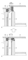
[誘電体部材]
次に、実施形態に係る誘電体部材13について、図2及び図3を参照しながら詳細に説明する。図2は、一実施形態に係る誘電体部材の構成及び効果の一例を示す図である。図3は、一実施形態に係る誘電体部材の構成及び効果を説明するための図である。
[Dielectric member]
Next, the
図2(a)及び図3(a)は、比較例に係る誘電体部材113を示し、図2(b)及び図3(b)は、実施形態に係る誘電体部材13を示す。図2(a)の比較例に係る誘電体部材113は、処理容器10の内壁10dから略垂直方向に載置台12に向かって内壁10dに沿って取り付けられている。かかる構造では、導波路201の導波通路rから内壁10dに沿って伝播する電磁波は、誘電体部材113の上面113sで反射する。誘電体部材113の上面113sは、異なる誘電率を有する処理空間SPの真空空間と誘電体部材113との境界であるため、電界が強くなる。これにより、載置台12と誘電体部材113との間で異常放電が生じる場合がある。
2(a) and 3(a) show a
例えば、VHF帯(30M~300MHz)よりも低い周波数の高周波を処理容器10内に導入した場合、高周波は、内壁10dを伝播する表面波としての性質を有さず、載置台12と上部電極14との間でカップリングし、放電が発生する。このため、載置台12と誘電体部材113との間で異常放電が発生する現象は生じ難い。
For example, when a high frequency wave with a frequency lower than the VHF band (30 MHz to 300 MHz) is introduced into the
一方、VHF波及びマイクロ波の周波数帯の電磁波は、載置台12と上部電極14との間でカップリングが生じ難く、電磁波の表面波が処理容器10の内壁10dの面を伝播する。このため、内壁10dに沿って伝播した電磁波によって載置台12と誘電体部材113との間で異常放電が発生し易くなる。
On the other hand, coupling of electromagnetic waves in the VHF and microwave frequency bands is difficult to occur between the mounting table 12 and the
そこで、本実施形態に係るプラズマ処理装置1では、図2(b)に示すように、誘電体部材13は、内壁10dの面に対して不連続面を有する。誘電体部材13を処理容器10の内壁10dの段差部10fに沿って配置する。つまり、誘電体部材13の一部分は、載置台に向かって内壁10dから突出し、他の部分は、電磁波が伝播する処理容器10の内壁の段差部10fに挿入される。図2(b)の例では、誘電体部材13の他の部分が、内壁10dの段差部10fの内面10f1に沿って挿入されている。
Therefore, in the plasma processing apparatus 1 according to the present embodiment, the
次に、かかる構成の誘電体部材13の作用について、図3(a)に示す比較例に係る誘電体部材113と比較しながら説明する。図3(a)及び(b)に示す通り、電磁波の表面波は、処理容器10の内壁10dに形成されたシースSh内を伝播する。このとき、電磁波の表面波は処理空間SPでエネルギーを放出しながら、電磁波の伝播経路に配置された誘電体部材113及び誘電体部材13まで到達する。到達した電磁波は、誘電体部材113の上面113s及び誘電体部材13の上面13sにて反射し、一部が誘電体部材113及び誘電体部材13の内部を透過する。
Next, the operation of the
処理空間SPの誘電率と誘電体部材113の誘電率及び誘電体部材13の誘電率とは異なるため、誘電体部材113の上面113s及び誘電体部材13の上面13sでは、電磁波の電界が強くなる。例えば、誘電体部材113及び誘電体部材13に替えて金属部材を配置すると、金属部材の上面で誘電体部材の場合よりも電磁波の電界がさらに強くなり処理空間SPと金属部材との境界で異常放電が発生する。これに対して、誘電体部材113及び誘電体部材13は、金属部材を配置した場合よりも処理空間SPとの境界における電界は強くならない。
Since the dielectric constant of the processing space SP is different from the dielectric constant of the
誘電体部材113及び誘電体部材13の内部を透過する電磁波の電界強度は、図3(a)及び(b)に点線で模式的に示すように、位置Aを中心として円弧状に誘電体部材113及び誘電体部材13の内部を下に向かって弱くなる。
The electric field strength of the electromagnetic waves transmitted through the
図3(a)の誘電体部材113の配置では、誘電体部材113の内部の電磁波の電界は、位置Aから左側へ広がりながら弱まっていく。一方、位置Aから右側へ広がろうとする電磁波は、内壁10dで反射する。その結果、位置Aから左側へ伝播する電磁波と、位置Aから右側へ伝播できずに反射する電磁波とにより、位置Aから左側へ広がる電磁波の電界強度はある程度の強さを持つ。これにより、図3(a)に示すように誘電体部材113の側面113m及び下面113rから自由空間へ漏れ出る電界は、矢印で示すようにある程度の強度となる。この結果、図2(a)及び図3(a)に示すように、誘電体部材113と載置台12との間又は誘電体部材113の下方で電界が強くなり、異常放電が発生する場合がある。
In the arrangement of the
このように、本明細書でいう異常放電は、電磁波の伝播経路である処理容器10の内壁10dに配置された誘電体部材と載置台との間の空間及び誘電体部材の下方の空間で発生する異常放電のことをいう。特に、VHF帯以上の周波数の電磁波では、処理容器10の内壁10dに沿って伝播する表面波の性質により、VHF帯より低い周波数の高周波と比較して誘電体部材と載置台との間の空間及び誘電体部材の下方の空間で異常放電が発生し易い。
In this way, the abnormal discharge referred to in this specification occurs in the space between the dielectric member placed on the
そこで、図3(b)に示す本実施形態に係る誘電体部材13は、VHF帯以上の周波数の電磁波をプラズマ処理装置1に導入する際、載置台12等の近傍における異常放電を防止するように構成される。具体的には、本実施形態に係る誘電体部材13は、内壁10dの位置Aから左側の第1の部分13aは、載置台12に向かって内壁10dから突出し、位置Aから右側の第2の部分13bは、内壁10dの段差部10fに沿って挿入される。誘電体部材13の第2の部分13bは、電磁波が伝播する内壁10dの凹部(図4(a)の凹部10g参照)に挿入されてもよい。
Therefore, the
誘電体部材13は、電磁波の伝播経路である処理容器10の内壁10dに対して略垂直方向、つまり略90°に載置台12に向かって突出することが好ましい。ただし、これに限られず、誘電体部材13は、内壁10dに対して90°±30°の角度以内に傾斜して突出してもよい。誘電体部材13が、内壁10dに対して90°±30°の角度よりも大きく傾斜すると、電磁波の表面波が伝播し易い角度の方へ伝播し、異常放電の発生のリスクが高まるため、これを回避するためである。
It is preferable that the
電磁波の電界は、位置Aにおいて最も強く、位置Aから下に向かうほど左右へ広がりながら弱まる。その結果、第1の部分13aを左側へ伝播する電磁波と、第2の部分13bを右側へ伝播する電磁波とが誘電体部材13の内部を透過する間に電界強度は指数関数的に弱まる。これにより、図3(b)に示すように誘電体部材13の内側面13m及び下面13rから漏れ出る電界は、矢印で示すように放電しない程に弱められる。この結果、図2(b)及び図3(b)に示すように、内壁10dに沿って伝播した電磁波は、誘電体部材13の上面13sで大部分が反射され、更に誘電体部材13を透過する電磁波は上記の通り弱められる。これにより、誘電体部材13と載置台12との間の空間や誘電体部材13の下方において異常放電が生じることを防止できる。
The electric field of the electromagnetic wave is strongest at position A, and weakens as it spreads left and right as it goes downward from position A. As a result, the electric field intensity weakens exponentially while the electromagnetic waves propagating to the left through the
[誘電体部材の寸法]
次に、誘電体部材13と載置台12との間の空間や誘電体部材13の下方において異常放電が生じることを防止するために好ましい誘電体部材13の寸法について説明する。誘電体部材13に入射する電磁波の実効波長をλ0とすると、シースShを伝播する電磁波の表面波(シース波)の波長λswは以下で示される。
[Dimensions of dielectric member]
Next, preferred dimensions of the
λsw=λ0/40~λ0/20
また、誘電体部材13における電磁波の実効波長λgは、式(1)で示される。
λ sw = λ 0 /40 to λ 0 /20
Further, the effective wavelength λg of the electromagnetic wave in the

誘電体部材13の第1の部分13aは、内壁10dから誘電体部材13における電磁波の実効波長λgの1/2以上突出していることが好ましい。つまり、図3(b)に示す内壁10dから誘電体部材13の内側面13mまでの径方向の幅B1は、誘電体部材13における電磁波の実効波長λgの1/2以上であることが好ましい。また、幅B1は、5mm以上であることが好ましい。
It is preferable that the
180MHzのVHF波の電磁波の実効波長λ0は約1600mmである。このとき、電磁波の表面波の波長λswは40mm~80mmになる。式(1)から誘電体部材13における電磁波の実効波長λgは、13mm~26mmになる。以上から、誘電体部材13の幅B1は、6.5mm以上であることが更に好ましい。
The effective wavelength λ 0 of the electromagnetic wave of the 180 MHz VHF wave is approximately 1600 mm. At this time, the wavelength λ sw of the electromagnetic surface wave is 40 mm to 80 mm. From equation (1), the effective wavelength λg of the electromagnetic waves in the
誘電体部材13の第2の部分13bは、内壁10dから段差部10fの内面10f1に沿って、誘電体部材13における電磁波の実効波長λgの1/4以上挿入されることが好ましい。つまり、図3(b)に示す内壁10dから誘電体部材13の外側面13nまでの径方向の幅B2は、誘電体部材13における電磁波の実効波長λgの1/4以上であることが好ましい。また、幅B2は、例えば、5mm以上であることが好ましい。
It is preferable that the
誘電体部材13の厚さhは、誘電体部材13における電磁波の実効波長λgの1/2以上であることが好ましい。また、誘電体部材13の厚さhは、例えば、5mm以上であることが好ましい。
The thickness h of the
内壁10dの段差部10fの内面10f1と、内面10f1に対向する誘電体部材13の上面13sとの間の隙間ΔDは、0.5mm以下であることが好ましい。同様に、図4(a)に示す内壁10dの凹部10gの上面10g1と、上面10g1に対向する誘電体部材13の上面13sとの間の隙間ΔDは、0.5mm以下であることが好ましい。これにより、隙間ΔDでプラズマが生成されることを防止することができる。これにより、誘電体部材13の上面13sで異常放電が生じることを防止できる。
The gap ΔD between the inner surface 10f1 of the stepped
誘電体部材13の第1の部分13aには、誘電体部材13を厚さ方向に貫通する複数の排気孔13cが形成されている。複数の排気孔13cは、内壁10dから径方向に誘電体部材13における電磁波の実効波長λgの1/4以上離れた位置に形成されている。つまり、図3(b)に示す内壁10dから排気孔13cまでの距離B3は、誘電体部材13における電磁波の実効波長λgの1/4以上であることが好ましい。距離B3は、例えば、5mm以上であることが好ましい。これにより、排気孔13c内にて異常放電が発生することを防止できる。なお、排気孔13cの直径φは、2~3mmであってもよい。
A plurality of
このように誘電体部材13に排気孔13cを設ける場合には、電界が最も集中する中心部の位置Aから離れたところに形成することが好ましい。なお、誘電体部材13の内側面13mから下方に延在する凸部分は、排気経路を確保するためと、排気空間EXへの反応生成物の進入と付着を防ぐためである。ただし、誘電体部材13の内側面13mから下方に延在する凸部分はなくてもよい。
When providing the
かかる構成では、電磁波の表面波が伝播する処理容器10の内壁10dに誘電体部材13を配置して自由空間を仕切る。これにより、誘電体部材13により電磁波の進行波を概ね反射させることができる。電磁波の一部は、誘電体部材13の内部を透過するが、誘電体部材13の内部の電界を指数関数的に減衰させることで異常放電を防止することができる。このように誘電体部材13の下面13rの下側の自由空間には放電が生じない程の弱い電界が放出される。
In this configuration, the
ただし、誘電体部材13の下面13rと下面13rに対向する内壁10dの面との間の空間が狭いと、誘電体部材13の下面13rにて異常放電が生じる可能性がある。よって、誘電体部材13の下面13rは、処理容器10の内部空間に露出するようにする。そして、誘電体部材13の下面13rと、下面13rに対向する処理容器10の内壁10dの面との間隔は、5mm以上であることが好ましい。例えば、図4(a)に示すように、誘電体部材13の第2の部分13bが、電磁波が伝播する内壁10dの凹部10gに挿入されている場合、誘電体部材13の下面13rと、下面13rに対向する内壁10dの面との間隔Gは、5mm以上であることが好ましい。これにより、誘電体部材13の下面13r下の自由空間にて異常放電が発生することを防止できる。凹部10gの深さは、15mm以上であることが好ましい。
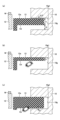
However, if the space between the
図4は、一実施形態に係る誘電体部材13の構成例として許容できる構成(図4(a))と、許容できない構成(図4(b)及び(c))とを示す図である。図4は、シミュレーションの結果の一例である。図4(a)は、誘電体部材13の厚さhが7mm、間隔Gが5mmの例を示す。誘電体部材13の厚さが十分にあるため、誘電体部材13の内部で電界の減衰が十分に起こる。かつ、誘電体部材13の下面13rと内壁10dの面との間隔Gが十分にあるため、誘電体部材13の下面13rの下の自由空間にて異常放電が発生することを防止できる。
FIG. 4 is a diagram showing an acceptable configuration (FIG. 4(a)) and an unacceptable configuration (FIGS. 4(b) and (c)) as exemplary configurations of the
図4(b)は、誘電体部材13の厚さhが2mmの場合の例を示す。誘電体部材13の厚さが不十分なため、誘電体部材13の内部において電界の減衰が不十分になり、誘電体部材13の下面13r下の自由空間にて異常放電が発生している。
FIG. 4(b) shows an example in which the thickness h of the
図4(c)は、誘電体部材13の下面13rと、下面13rに対向する内壁10dの面との間隔Gが1mmの場合の例を示す。間隔Gが不十分なため、誘電体部材13の下面13r下の自由空間に放出する電界により、凹部10gの下面13rに対向する金属面で電界強度が高くなり、異常放電が発生している。
FIG. 4C shows an example in which the distance G between the
以上に説明したように、本実施形態に係るプラズマ処理装置1によれば、誘電体部材13をVHF帯以上の周波数の電磁波の伝播経路に設けることで、異常放電を防止することができる。
As described above, according to the plasma processing apparatus 1 according to the present embodiment, abnormal discharge can be prevented by providing the
今回開示された一実施形態に係るプラズマ処理装置は、すべての点において例示であって制限的なものではないと考えられるべきである。上記の実施形態は、添付の請求の範囲及びその主旨を逸脱することなく、様々な形態で変形及び改良が可能である。上記複数の実施形態に記載された事項は、矛盾しない範囲で他の構成も取り得ることができ、また、矛盾しない範囲で組み合わせることができる。 The plasma processing apparatus according to the embodiment disclosed this time should be considered to be an example in all respects and not a limitation. The embodiments described above can be modified and improved in various ways without departing from the scope and spirit of the appended claims. The matters described in the plurality of embodiments described above may be configured in other ways without being inconsistent, and may be combined without being inconsistent.
本開示のプラズマ処理装置は、radial line slot antenna、Electron Cyclotron Resonance Plasma(ECR)、Helicon Wave Plasma(HWP)のいずれのタイプの装置でも適用可能である。 The plasma processing apparatus of the present disclosure is applicable to any type of apparatus: radial line slot antenna, Electron Cyclotron Resonance Plasma (ECR), and Helicon Wave Plasma (HWP).
1…プラズマ処理装置、10…処理容器、12…載置台、13…誘電体部材、13a…誘電体部材の第1の部分、13b…誘電体部材の第2の部分、13c…排気孔、14…上部電極、15…排気機構、18…プレート、18h…ガス吐出孔、20…電磁波導入部、21…リング状誘電体、30…電源、32…整合器、40…配管、42…ガス供給器、201…導波路、r…導波通路、SP…処理空間、EX…排気空間、ES…排気路、W…基板 DESCRIPTION OF SYMBOLS 1... Plasma processing apparatus, 10... Processing container, 12... Mounting table, 13... Dielectric member, 13a... First part of dielectric member, 13b... Second part of dielectric member, 13c... Exhaust hole, 14 ... Upper electrode, 15... Exhaust mechanism, 18... Plate, 18h... Gas discharge hole, 20... Electromagnetic wave introduction part, 21... Ring-shaped dielectric, 30... Power supply, 32... Matching box, 40... Piping, 42... Gas supply device , 201...Waveguide, r...Waveguide path, SP...Processing space, EX...Exhaust space, ES...Exhaust path, W...Substrate
Claims (13)
前記処理容器の内部に設けられ、前記基板を載置する載置台と、
前記処理容器の内壁に面して形成され、前記電磁波を前記処理容器の内部に導入する電磁波導入部と、
前記電磁波が伝播する前記内壁に設けられる誘電体部材と、を有し、
前記誘電体部材の第1の部分は、前記内壁から前記載置台に向かって突出し、前記誘電体部材を厚さ方向に貫通する複数の排気孔を有し、複数の前記排気孔は、前記内壁から径方向に前記誘電体部材における電磁波の実効波長λgの1/4以上離れた位置に形成され、
前記誘電体部材の第2の部分は、前記内壁の凹部又は段差部に挿入される、プラズマ処理装置。 A plasma processing apparatus that introduces electromagnetic waves with a frequency above the VHF band into a processing container and processes a substrate with plasma generated from a gas,
a mounting table provided inside the processing container and on which the substrate is placed;
an electromagnetic wave introduction part that is formed facing an inner wall of the processing container and introduces the electromagnetic wave into the inside of the processing container;
a dielectric member provided on the inner wall through which the electromagnetic waves propagate;
The first portion of the dielectric member has a plurality of exhaust holes that protrude from the inner wall toward the mounting table and penetrate the dielectric member in the thickness direction, and the plurality of exhaust holes are arranged in the inner wall. formed at a position radially away from 1/4 or more of the effective wavelength λg of the electromagnetic wave in the dielectric member,
In the plasma processing apparatus, the second portion of the dielectric member is inserted into a recess or a stepped portion of the inner wall.
前記処理容器の内部に設けられ、前記基板を載置する載置台と、
前記処理容器の内壁に面して形成され、前記電磁波を前記処理容器の内部に導入する電磁波導入部と、
前記電磁波が伝播する前記内壁に設けられる誘電体部材と、を有し、
前記誘電体部材の第1の部分は、前記内壁から前記載置台に向かって突出し、前記誘電体部材を厚さ方向に貫通する複数の排気孔を有し、複数の前記排気孔は、前記内壁から径方向に5mm以上離れた位置に形成され、
前記誘電体部材の第2の部分は、前記内壁の凹部又は段差部に挿入される、プラズマ処理装置。 A plasma processing apparatus that introduces electromagnetic waves with a frequency above the VHF band into a processing container and processes a substrate with plasma generated from a gas,
a mounting table provided inside the processing container and on which the substrate is placed;
an electromagnetic wave introduction part that is formed facing an inner wall of the processing container and introduces the electromagnetic wave into the inside of the processing container;
a dielectric member provided on the inner wall through which the electromagnetic waves propagate;
The first portion of the dielectric member has a plurality of exhaust holes that protrude from the inner wall toward the mounting table and penetrate the dielectric member in the thickness direction, and the plurality of exhaust holes are arranged in the inner wall. is formed at a position 5 mm or more away from the radial direction,
In the plasma processing apparatus, the second portion of the dielectric member is inserted into a recess or a stepped portion of the inner wall.
請求項1又は2に記載のプラズマ処理装置。 The dielectric member is inclined within an angle of 90°±30° with respect to the inner wall and protrudes toward the mounting table.
The plasma processing apparatus according to claim 1 or 2 .
請求項1~3のいずれか一項に記載のプラズマ処理装置。 The dielectric member protrudes from the inner wall in a radial direction by 1/2 or more of an effective wavelength λg of electromagnetic waves in the dielectric member.
The plasma processing apparatus according to any one of claims 1 to 3 .
請求項1~3のいずれか一項に記載のプラズマ処理装置。 The dielectric member protrudes from the inner wall by 5 mm or more in the radial direction.
The plasma processing apparatus according to any one of claims 1 to 3 .
請求項1~5のいずれか一項に記載のプラズマ処理装置。 The thickness of the dielectric member is 1/2 or more of the effective wavelength λg of electromagnetic waves in the dielectric member,
The plasma processing apparatus according to any one of claims 1 to 5 .
請求項1~5のいずれか一項に記載のプラズマ処理装置。 The thickness of the dielectric member is 5 mm or more,
The plasma processing apparatus according to any one of claims 1 to 5 .
請求項1~7のいずれか一項に記載のプラズマ処理装置。 The lower surface of the dielectric member is exposed to the internal space of the processing container.
The plasma processing apparatus according to any one of claims 1 to 7 .
請求項8に記載のプラズマ処理装置。 The distance between the lower surface of the dielectric member and the surface of the inner wall opposite to the lower surface is 5 mm or more.
The plasma processing apparatus according to claim 8 .
請求項1~9のいずれか一項に記載のプラズマ処理装置。 The distance between the upper surface of the second portion of the dielectric member and the surface of the inner wall opposite to the upper surface is 0.5 mm or less;
The plasma processing apparatus according to any one of claims 1 to 9 .
請求項1~10のいずれか一項に記載のプラズマ処理装置。 The electromagnetic wave has a frequency of 100 MHz or more,
The plasma processing apparatus according to any one of claims 1 to 10 .
前記排気路に連通する前記誘電体部材の下方の排気空間からガスが排気されるように構成される、
請求項1~11のいずれか一項に記載のプラズマ処理装置。 A space between the first portion of the dielectric member and the mounting base is an exhaust path,
configured such that gas is exhausted from an exhaust space below the dielectric member that communicates with the exhaust path;
The plasma processing apparatus according to any one of claims 1 to 11 .
前記誘電体部材の下方の排気空間を介して前記排気路からガスが側方に排気されるように構成される、
請求項12に記載のプラズマ処理装置。 The exhaust space below the dielectric member communicates with an exhaust path formed on the outside of the side wall of the processing container,
The gas is configured to be exhausted to the side from the exhaust path via the exhaust space below the dielectric member.
The plasma processing apparatus according to claim 12 .
Priority Applications (4)
| Application Number | Priority Date | Filing Date | Title |
|---|---|---|---|
| JP2020030327A JP7378317B2 (en) | 2020-02-26 | 2020-02-26 | plasma processing equipment |
| KR1020227031937A KR102759377B1 (en) | 2020-02-26 | 2021-02-15 | Plasma treatment device |
| PCT/JP2021/005550 WO2021172072A1 (en) | 2020-02-26 | 2021-02-15 | Plasma treatment device |
| US17/904,427 US20230064817A1 (en) | 2020-02-26 | 2021-02-15 | Plasma processing apparatus |
Applications Claiming Priority (1)
| Application Number | Priority Date | Filing Date | Title |
|---|---|---|---|
| JP2020030327A JP7378317B2 (en) | 2020-02-26 | 2020-02-26 | plasma processing equipment |
Publications (2)
| Publication Number | Publication Date |
|---|---|
| JP2021136114A JP2021136114A (en) | 2021-09-13 |
| JP7378317B2 true JP7378317B2 (en) | 2023-11-13 |
Family
ID=77491464
Family Applications (1)
| Application Number | Title | Priority Date | Filing Date |
|---|---|---|---|
| JP2020030327A Active JP7378317B2 (en) | 2020-02-26 | 2020-02-26 | plasma processing equipment |
Country Status (4)
| Country | Link |
|---|---|
| US (1) | US20230064817A1 (en) |
| JP (1) | JP7378317B2 (en) |
| KR (1) | KR102759377B1 (en) |
| WO (1) | WO2021172072A1 (en) |
Families Citing this family (1)
| Publication number | Priority date | Publication date | Assignee | Title |
|---|---|---|---|---|
| JP7836736B2 (en) * | 2022-08-25 | 2026-03-27 | 東京エレクトロン株式会社 | Plasma processing equipment |
Citations (5)
| Publication number | Priority date | Publication date | Assignee | Title |
|---|---|---|---|---|
| JP2002194540A (en) | 2000-12-26 | 2002-07-10 | Anelva Corp | Plasma assisted sputter deposition system |
| JP2004079829A (en) | 2002-08-20 | 2004-03-11 | Tokyo Electron Ltd | Plasma processing equipment |
| JP2012084848A (en) | 2010-09-16 | 2012-04-26 | Tokyo Electron Ltd | Plasma processing apparatus and plasma processing method |
| JP2016086099A (en) | 2014-10-27 | 2016-05-19 | 東京エレクトロン株式会社 | Plasma processing equipment |
| JP2018533192A (en) | 2015-09-04 | 2018-11-08 | アプライド マテリアルズ インコーポレイテッドApplied Materials,Incorporated | Process chamber for periodic and selective material removal and etching |
Family Cites Families (6)
| Publication number | Priority date | Publication date | Assignee | Title |
|---|---|---|---|---|
| JPH11238597A (en) * | 1998-02-23 | 1999-08-31 | Matsushita Electric Ind Co Ltd | Plasma processing method and apparatus |
| JP2003100722A (en) | 2001-09-27 | 2003-04-04 | Tokyo Electron Ltd | Plasma processing equipment |
| US20110061810A1 (en) * | 2009-09-11 | 2011-03-17 | Applied Materials, Inc. | Apparatus and Methods for Cyclical Oxidation and Etching |
| US9793126B2 (en) * | 2010-08-04 | 2017-10-17 | Lam Research Corporation | Ion to neutral control for wafer processing with dual plasma source reactor |
| JP2015109249A (en) * | 2013-10-22 | 2015-06-11 | 東京エレクトロン株式会社 | Plasma processing equipment |
| US9963782B2 (en) * | 2015-02-12 | 2018-05-08 | Asm Ip Holding B.V. | Semiconductor manufacturing apparatus |
-
2020
- 2020-02-26 JP JP2020030327A patent/JP7378317B2/en active Active
-
2021
- 2021-02-15 KR KR1020227031937A patent/KR102759377B1/en active Active
- 2021-02-15 US US17/904,427 patent/US20230064817A1/en active Pending
- 2021-02-15 WO PCT/JP2021/005550 patent/WO2021172072A1/en not_active Ceased
Patent Citations (5)
| Publication number | Priority date | Publication date | Assignee | Title |
|---|---|---|---|---|
| JP2002194540A (en) | 2000-12-26 | 2002-07-10 | Anelva Corp | Plasma assisted sputter deposition system |
| JP2004079829A (en) | 2002-08-20 | 2004-03-11 | Tokyo Electron Ltd | Plasma processing equipment |
| JP2012084848A (en) | 2010-09-16 | 2012-04-26 | Tokyo Electron Ltd | Plasma processing apparatus and plasma processing method |
| JP2016086099A (en) | 2014-10-27 | 2016-05-19 | 東京エレクトロン株式会社 | Plasma processing equipment |
| JP2018533192A (en) | 2015-09-04 | 2018-11-08 | アプライド マテリアルズ インコーポレイテッドApplied Materials,Incorporated | Process chamber for periodic and selective material removal and etching |
Also Published As
| Publication number | Publication date |
|---|---|
| KR20220141857A (en) | 2022-10-20 |
| KR102759377B1 (en) | 2025-01-24 |
| JP2021136114A (en) | 2021-09-13 |
| US20230064817A1 (en) | 2023-03-02 |
| WO2021172072A1 (en) | 2021-09-02 |
Similar Documents
| Publication | Publication Date | Title |
|---|---|---|
| JP5438205B2 (en) | Top plate for plasma processing apparatus and plasma processing apparatus | |
| US6818852B2 (en) | Microwave plasma processing device, plasma processing method, and microwave radiating member | |
| KR20160049463A (en) | Plasma processing apparatus | |
| KR20070096855A (en) | Substrate Mounting Mechanism and Substrate Processing Equipment | |
| US20150155139A1 (en) | Dielectric window, antenna and plasma processing apparatus | |
| JP4093212B2 (en) | Plasma processing equipment | |
| JP4878782B2 (en) | Plasma processing apparatus and plasma processing method | |
| JP7194937B2 (en) | Plasma processing apparatus and plasma processing method | |
| JP7336378B2 (en) | Plasma processing apparatus and plasma processing method | |
| CN102246604A (en) | Plasma processing apparatus | |
| JP7001456B2 (en) | Plasma processing equipment | |
| JP7378317B2 (en) | plasma processing equipment | |
| JP7632975B2 (en) | Plasma processing apparatus and plasma processing method | |
| JP2003203869A (en) | Plasma processing equipment | |
| JP4430560B2 (en) | Plasma processing equipment | |
| US7828927B2 (en) | Plasma processing device | |
| KR20230039536A (en) | Plasma source and plasma processing appartus | |
| US7779783B2 (en) | Plasma processing device | |
| KR102337936B1 (en) | Plasma processing apparatus | |
| JPH09171900A (en) | Plasma generator | |
| JP7605569B2 (en) | Plasma source and plasma processing device | |
| US20230335380A1 (en) | Plasma processing apparatus and semiconductor device manufacturing method | |
| WO2021241256A1 (en) | Plasma treatment device | |
| JP2001167900A (en) | Plasma treatment apparatus |
Legal Events
| Date | Code | Title | Description |
|---|---|---|---|
| A621 | Written request for application examination |
Free format text: JAPANESE INTERMEDIATE CODE: A621 Effective date: 20221026 |
|
| A131 | Notification of reasons for refusal |
Free format text: JAPANESE INTERMEDIATE CODE: A131 Effective date: 20230801 |
|
| A521 | Request for written amendment filed |
Free format text: JAPANESE INTERMEDIATE CODE: A523 Effective date: 20230831 |
|
| TRDD | Decision of grant or rejection written | ||
| A01 | Written decision to grant a patent or to grant a registration (utility model) |
Free format text: JAPANESE INTERMEDIATE CODE: A01 Effective date: 20231003 |
|
| A61 | First payment of annual fees (during grant procedure) |
Free format text: JAPANESE INTERMEDIATE CODE: A61 Effective date: 20231031 |
|
| R150 | Certificate of patent or registration of utility model |
Ref document number: 7378317 Country of ref document: JP Free format text: JAPANESE INTERMEDIATE CODE: R150 |