JP7368233B2 - Substrates and their manufacturing methods, electronic devices - Google Patents
Substrates and their manufacturing methods, electronic devices Download PDFInfo
- Publication number
- JP7368233B2 JP7368233B2 JP2019547303A JP2019547303A JP7368233B2 JP 7368233 B2 JP7368233 B2 JP 7368233B2 JP 2019547303 A JP2019547303 A JP 2019547303A JP 2019547303 A JP2019547303 A JP 2019547303A JP 7368233 B2 JP7368233 B2 JP 7368233B2
- Authority
- JP
- Japan
- Prior art keywords
- common electrode
- lead wire
- electrode lead
- substrate
- layer
- Prior art date
- Legal status (The legal status is an assumption and is not a legal conclusion. Google has not performed a legal analysis and makes no representation as to the accuracy of the status listed.)
- Active
Links
- 239000000758 substrate Substances 0.000 title claims description 275
- 238000004519 manufacturing process Methods 0.000 title claims description 55
- 239000010410 layer Substances 0.000 claims description 208
- WABPQHHGFIMREM-UHFFFAOYSA-N lead(0) Chemical compound [Pb] WABPQHHGFIMREM-UHFFFAOYSA-N 0.000 claims description 182
- 238000000034 method Methods 0.000 claims description 86
- 230000002093 peripheral effect Effects 0.000 claims description 81
- 239000002346 layers by function Substances 0.000 claims description 17
- 238000010586 diagram Methods 0.000 description 50
- 239000000463 material Substances 0.000 description 34
- 238000004806 packaging method and process Methods 0.000 description 19
- 238000005192 partition Methods 0.000 description 15
- 238000007740 vapor deposition Methods 0.000 description 15
- 230000000694 effects Effects 0.000 description 11
- 239000004020 conductor Substances 0.000 description 10
- 230000003068 static effect Effects 0.000 description 10
- 239000004642 Polyimide Substances 0.000 description 6
- 238000000059 patterning Methods 0.000 description 6
- 229920002120 photoresistant polymer Polymers 0.000 description 6
- 229920001721 polyimide Polymers 0.000 description 6
- 230000005611 electricity Effects 0.000 description 5
- 230000002452 interceptive effect Effects 0.000 description 5
- XLYOFNOQVPJJNP-UHFFFAOYSA-N water Substances O XLYOFNOQVPJJNP-UHFFFAOYSA-N 0.000 description 5
- QVGXLLKOCUKJST-UHFFFAOYSA-N atomic oxygen Chemical compound [O] QVGXLLKOCUKJST-UHFFFAOYSA-N 0.000 description 4
- 230000015572 biosynthetic process Effects 0.000 description 4
- 238000000151 deposition Methods 0.000 description 4
- 230000008021 deposition Effects 0.000 description 4
- 229910052760 oxygen Inorganic materials 0.000 description 4
- 239000001301 oxygen Substances 0.000 description 4
- 238000000206 photolithography Methods 0.000 description 4
- 230000008054 signal transmission Effects 0.000 description 4
- VYPSYNLAJGMNEJ-UHFFFAOYSA-N Silicium dioxide Chemical compound O=[Si]=O VYPSYNLAJGMNEJ-UHFFFAOYSA-N 0.000 description 3
- 238000005229 chemical vapour deposition Methods 0.000 description 3
- 238000000576 coating method Methods 0.000 description 3
- 238000009459 flexible packaging Methods 0.000 description 3
- 238000001755 magnetron sputter deposition Methods 0.000 description 3
- 229910001507 metal halide Inorganic materials 0.000 description 3
- 150000005309 metal halides Chemical class 0.000 description 3
- 229920000728 polyester Polymers 0.000 description 3
- 239000011347 resin Substances 0.000 description 3
- 229920005989 resin Polymers 0.000 description 3
- RYGMFSIKBFXOCR-UHFFFAOYSA-N Copper Chemical compound [Cu] RYGMFSIKBFXOCR-UHFFFAOYSA-N 0.000 description 2
- 229910000881 Cu alloy Inorganic materials 0.000 description 2
- 229910052581 Si3N4 Inorganic materials 0.000 description 2
- 229910052782 aluminium Inorganic materials 0.000 description 2
- XAGFODPZIPBFFR-UHFFFAOYSA-N aluminium Chemical compound [Al] XAGFODPZIPBFFR-UHFFFAOYSA-N 0.000 description 2
- 238000005452 bending Methods 0.000 description 2
- 230000005540 biological transmission Effects 0.000 description 2
- 229910052802 copper Inorganic materials 0.000 description 2
- 239000010949 copper Substances 0.000 description 2
- 238000005516 engineering process Methods 0.000 description 2
- AMGQUBHHOARCQH-UHFFFAOYSA-N indium;oxotin Chemical compound [In].[Sn]=O AMGQUBHHOARCQH-UHFFFAOYSA-N 0.000 description 2
- 239000011810 insulating material Substances 0.000 description 2
- 239000007769 metal material Substances 0.000 description 2
- 230000003287 optical effect Effects 0.000 description 2
- 239000011368 organic material Substances 0.000 description 2
- -1 polyethylene Polymers 0.000 description 2
- HQVNEWCFYHHQES-UHFFFAOYSA-N silicon nitride Chemical compound N12[Si]34N5[Si]62N3[Si]51N64 HQVNEWCFYHHQES-UHFFFAOYSA-N 0.000 description 2
- 229910052814 silicon oxide Inorganic materials 0.000 description 2
- 238000002834 transmittance Methods 0.000 description 2
- YVTHLONGBIQYBO-UHFFFAOYSA-N zinc indium(3+) oxygen(2-) Chemical compound [O--].[Zn++].[In+3] YVTHLONGBIQYBO-UHFFFAOYSA-N 0.000 description 2
- 239000004925 Acrylic resin Substances 0.000 description 1
- 229910000838 Al alloy Inorganic materials 0.000 description 1
- VYZAMTAEIAYCRO-UHFFFAOYSA-N Chromium Chemical compound [Cr] VYZAMTAEIAYCRO-UHFFFAOYSA-N 0.000 description 1
- 239000004698 Polyethylene Substances 0.000 description 1
- 229910021607 Silver chloride Inorganic materials 0.000 description 1
- WGLPBDUCMAPZCE-UHFFFAOYSA-N Trioxochromium Chemical compound O=[Cr](=O)=O WGLPBDUCMAPZCE-UHFFFAOYSA-N 0.000 description 1
- 239000003990 capacitor Substances 0.000 description 1
- 229910052804 chromium Inorganic materials 0.000 description 1
- 239000011651 chromium Substances 0.000 description 1
- 229910000423 chromium oxide Inorganic materials 0.000 description 1
- 239000011248 coating agent Substances 0.000 description 1
- 238000007796 conventional method Methods 0.000 description 1
- 230000007423 decrease Effects 0.000 description 1
- 238000005137 deposition process Methods 0.000 description 1
- 239000011521 glass Substances 0.000 description 1
- 238000010438 heat treatment Methods 0.000 description 1
- 229910010272 inorganic material Inorganic materials 0.000 description 1
- 239000011147 inorganic material Substances 0.000 description 1
- 238000009413 insulation Methods 0.000 description 1
- 239000002923 metal particle Substances 0.000 description 1
- 239000002245 particle Substances 0.000 description 1
- 229920006122 polyamide resin Polymers 0.000 description 1
- 229920001225 polyester resin Polymers 0.000 description 1
- 239000004645 polyester resin Substances 0.000 description 1
- 229920000573 polyethylene Polymers 0.000 description 1
- 229920013716 polyethylene resin Polymers 0.000 description 1
- 238000007639 printing Methods 0.000 description 1
- 239000010453 quartz Substances 0.000 description 1
- 229910052709 silver Inorganic materials 0.000 description 1
- 239000004332 silver Substances 0.000 description 1
- ADZWSOLPGZMUMY-UHFFFAOYSA-M silver bromide Chemical compound [Ag]Br ADZWSOLPGZMUMY-UHFFFAOYSA-M 0.000 description 1
- HKZLPVFGJNLROG-UHFFFAOYSA-M silver monochloride Chemical compound [Cl-].[Ag+] HKZLPVFGJNLROG-UHFFFAOYSA-M 0.000 description 1
- 238000000638 solvent extraction Methods 0.000 description 1
- 239000010409 thin film Substances 0.000 description 1
- 239000012780 transparent material Substances 0.000 description 1
- 238000005019 vapor deposition process Methods 0.000 description 1
- 230000003245 working effect Effects 0.000 description 1
Images


Classifications
-
- H—ELECTRICITY
- H01—ELECTRIC ELEMENTS
- H01L—SEMICONDUCTOR DEVICES NOT COVERED BY CLASS H10
- H01L21/00—Processes or apparatus adapted for the manufacture or treatment of semiconductor or solid state devices or of parts thereof
- H01L21/70—Manufacture or treatment of devices consisting of a plurality of solid state components formed in or on a common substrate or of parts thereof; Manufacture of integrated circuit devices or of parts thereof
-
- H—ELECTRICITY
- H10—SEMICONDUCTOR DEVICES; ELECTRIC SOLID-STATE DEVICES NOT OTHERWISE PROVIDED FOR
- H10K—ORGANIC ELECTRIC SOLID-STATE DEVICES
- H10K59/00—Integrated devices, or assemblies of multiple devices, comprising at least one organic light-emitting element covered by group H10K50/00
- H10K59/10—OLED displays
- H10K59/12—Active-matrix OLED [AMOLED] displays
- H10K59/131—Interconnections, e.g. wiring lines or terminals
- H10K59/1315—Interconnections, e.g. wiring lines or terminals comprising structures specially adapted for lowering the resistance
-
- H—ELECTRICITY
- H01—ELECTRIC ELEMENTS
- H01L—SEMICONDUCTOR DEVICES NOT COVERED BY CLASS H10
- H01L27/00—Devices consisting of a plurality of semiconductor or other solid-state components formed in or on a common substrate
- H01L27/02—Devices consisting of a plurality of semiconductor or other solid-state components formed in or on a common substrate including semiconductor components specially adapted for rectifying, oscillating, amplifying or switching and having potential barriers; including integrated passive circuit elements having potential barriers
- H01L27/12—Devices consisting of a plurality of semiconductor or other solid-state components formed in or on a common substrate including semiconductor components specially adapted for rectifying, oscillating, amplifying or switching and having potential barriers; including integrated passive circuit elements having potential barriers the substrate being other than a semiconductor body, e.g. an insulating body
- H01L27/1214—Devices consisting of a plurality of semiconductor or other solid-state components formed in or on a common substrate including semiconductor components specially adapted for rectifying, oscillating, amplifying or switching and having potential barriers; including integrated passive circuit elements having potential barriers the substrate being other than a semiconductor body, e.g. an insulating body comprising a plurality of TFTs formed on a non-semiconducting substrate, e.g. driving circuits for AMLCDs
- H01L27/1218—Devices consisting of a plurality of semiconductor or other solid-state components formed in or on a common substrate including semiconductor components specially adapted for rectifying, oscillating, amplifying or switching and having potential barriers; including integrated passive circuit elements having potential barriers the substrate being other than a semiconductor body, e.g. an insulating body comprising a plurality of TFTs formed on a non-semiconducting substrate, e.g. driving circuits for AMLCDs with a particular composition or structure of the substrate
-
- H—ELECTRICITY
- H01—ELECTRIC ELEMENTS
- H01L—SEMICONDUCTOR DEVICES NOT COVERED BY CLASS H10
- H01L21/00—Processes or apparatus adapted for the manufacture or treatment of semiconductor or solid state devices or of parts thereof
- H01L21/70—Manufacture or treatment of devices consisting of a plurality of solid state components formed in or on a common substrate or of parts thereof; Manufacture of integrated circuit devices or of parts thereof
- H01L21/71—Manufacture of specific parts of devices defined in group H01L21/70
- H01L21/768—Applying interconnections to be used for carrying current between separate components within a device comprising conductors and dielectrics
-
- H—ELECTRICITY
- H01—ELECTRIC ELEMENTS
- H01L—SEMICONDUCTOR DEVICES NOT COVERED BY CLASS H10
- H01L23/00—Details of semiconductor or other solid state devices
- H01L23/52—Arrangements for conducting electric current within the device in operation from one component to another, i.e. interconnections, e.g. wires, lead frames
- H01L23/522—Arrangements for conducting electric current within the device in operation from one component to another, i.e. interconnections, e.g. wires, lead frames including external interconnections consisting of a multilayer structure of conductive and insulating layers inseparably formed on the semiconductor body
- H01L23/5226—Via connections in a multilevel interconnection structure
-
- H—ELECTRICITY
- H01—ELECTRIC ELEMENTS
- H01L—SEMICONDUCTOR DEVICES NOT COVERED BY CLASS H10
- H01L23/00—Details of semiconductor or other solid state devices
- H01L23/58—Structural electrical arrangements for semiconductor devices not otherwise provided for, e.g. in combination with batteries
- H01L23/60—Protection against electrostatic charges or discharges, e.g. Faraday shields
-
- H—ELECTRICITY
- H01—ELECTRIC ELEMENTS
- H01L—SEMICONDUCTOR DEVICES NOT COVERED BY CLASS H10
- H01L27/00—Devices consisting of a plurality of semiconductor or other solid-state components formed in or on a common substrate
- H01L27/02—Devices consisting of a plurality of semiconductor or other solid-state components formed in or on a common substrate including semiconductor components specially adapted for rectifying, oscillating, amplifying or switching and having potential barriers; including integrated passive circuit elements having potential barriers
- H01L27/12—Devices consisting of a plurality of semiconductor or other solid-state components formed in or on a common substrate including semiconductor components specially adapted for rectifying, oscillating, amplifying or switching and having potential barriers; including integrated passive circuit elements having potential barriers the substrate being other than a semiconductor body, e.g. an insulating body
- H01L27/1214—Devices consisting of a plurality of semiconductor or other solid-state components formed in or on a common substrate including semiconductor components specially adapted for rectifying, oscillating, amplifying or switching and having potential barriers; including integrated passive circuit elements having potential barriers the substrate being other than a semiconductor body, e.g. an insulating body comprising a plurality of TFTs formed on a non-semiconducting substrate, e.g. driving circuits for AMLCDs
- H01L27/1248—Devices consisting of a plurality of semiconductor or other solid-state components formed in or on a common substrate including semiconductor components specially adapted for rectifying, oscillating, amplifying or switching and having potential barriers; including integrated passive circuit elements having potential barriers the substrate being other than a semiconductor body, e.g. an insulating body comprising a plurality of TFTs formed on a non-semiconducting substrate, e.g. driving circuits for AMLCDs with a particular composition or shape of the interlayer dielectric specially adapted to the circuit arrangement
-
- H—ELECTRICITY
- H10—SEMICONDUCTOR DEVICES; ELECTRIC SOLID-STATE DEVICES NOT OTHERWISE PROVIDED FOR
- H10K—ORGANIC ELECTRIC SOLID-STATE DEVICES
- H10K59/00—Integrated devices, or assemblies of multiple devices, comprising at least one organic light-emitting element covered by group H10K50/00
- H10K59/80—Constructional details
- H10K59/805—Electrodes
- H10K59/8052—Cathodes
- H10K59/80522—Cathodes combined with auxiliary electrodes
-
- H—ELECTRICITY
- H10—SEMICONDUCTOR DEVICES; ELECTRIC SOLID-STATE DEVICES NOT OTHERWISE PROVIDED FOR
- H10K—ORGANIC ELECTRIC SOLID-STATE DEVICES
- H10K59/00—Integrated devices, or assemblies of multiple devices, comprising at least one organic light-emitting element covered by group H10K50/00
- H10K59/10—OLED displays
- H10K59/12—Active-matrix OLED [AMOLED] displays
- H10K59/124—Insulating layers formed between TFT elements and OLED elements
-
- H—ELECTRICITY
- H10—SEMICONDUCTOR DEVICES; ELECTRIC SOLID-STATE DEVICES NOT OTHERWISE PROVIDED FOR
- H10K—ORGANIC ELECTRIC SOLID-STATE DEVICES
- H10K59/00—Integrated devices, or assemblies of multiple devices, comprising at least one organic light-emitting element covered by group H10K50/00
- H10K59/10—OLED displays
- H10K59/12—Active-matrix OLED [AMOLED] displays
- H10K59/126—Shielding, e.g. light-blocking means over the TFTs
Landscapes
- Engineering & Computer Science (AREA)
- Power Engineering (AREA)
- Microelectronics & Electronic Packaging (AREA)
- Physics & Mathematics (AREA)
- Condensed Matter Physics & Semiconductors (AREA)
- General Physics & Mathematics (AREA)
- Computer Hardware Design (AREA)
- Manufacturing & Machinery (AREA)
- Electroluminescent Light Sources (AREA)
- Liquid Crystal (AREA)
- Devices For Indicating Variable Information By Combining Individual Elements (AREA)
Description
本願は、基板及びその製造方法、電子装置に関する。
本願は2018年3月30日付出願の中国特許出願第201810293281.2号の優先権を主張し、ここで上述の中国特許出願が開示した全ての内容を援用して本願の一部として取り込む。
The present application relates to a substrate, a method for manufacturing the same, and an electronic device.
This application claims priority to Chinese Patent Application No. 201810293281.2 filed on March 30, 2018, and all the contents disclosed in the above-mentioned Chinese patent application are hereby incorporated by reference as part of this application.
表示基板においては、回路(たとえば駆動回路)の接続線の抵抗が大きくなると、回路内の信号伝送速度が低下し、それによって表示画面の輝度が不均一になり、表示品質に影響を与える。また、表示技術の発展につれて、人々は狭いフレームをますます要求してきている。 In a display substrate, when the resistance of a connection line of a circuit (for example, a drive circuit) increases, the signal transmission speed within the circuit decreases, thereby making the brightness of the display screen non-uniform and affecting the display quality. Also, as display technology develops, people are increasingly demanding narrower frames.
本開示の少なくとも1つの実施例は、作業エリアと前記作業エリアの周辺に位置する非作業エリアと、ベース基板と、前記ベース基板に位置して前記非作業エリアに位置する周辺回路と共通電極リード線と、を含む基板を提供し、前記共通電極リード線は、前記周辺回路の前記作業エリアに近接する側に位置する。 At least one embodiment of the present disclosure includes a working area, a non-working area located around the working area, a base substrate, a peripheral circuit located on the base substrate and located in the non-working area, and a common electrode lead. a wire, the common electrode lead being located on a side of the peripheral circuit proximate to the work area.
例えば、本開示の少なくとも1つの実施例に係る基板は、共通電極をさらに含み、前記共通電極は、前記作業エリアから前記非作業エリアまで延び、前記共通電極は、少なくとも一部の前記共通電極リード線に直接に接触される。 For example, the substrate according to at least one embodiment of the present disclosure further includes a common electrode, the common electrode extending from the working area to the non-working area, and the common electrode extending from at least some of the common electrode leads. directly touched by the line.
例えば、本開示の少なくとも1つの実施例に係る基板において、前記周辺回路はゲート駆動回路であり、前記共通電極は陰極であり、前記共通電極リード線は陰極リード線である。 For example, in the substrate according to at least one embodiment of the present disclosure, the peripheral circuit is a gate drive circuit, the common electrode is a cathode, and the common electrode lead line is a cathode lead line.
例えば、本開示の少なくとも1つの実施例に係る基板は、前記周辺回路と前記共通電極リード線とを覆う平坦層をさらに含み、前記共通電極は、前記平坦層の前記ベース基板に離れる側に位置し、前記平坦層は、少なくとも一部の前記共通電極リード線を露出させるビアホールを含み、前記共通電極は前記ビアホールの位置する場所で前記共通電極リード線に直接に接触される。 For example, the substrate according to at least one embodiment of the present disclosure further includes a flat layer covering the peripheral circuit and the common electrode lead wire, and the common electrode is located on a side of the flat layer remote from the base substrate. The flat layer may include a via hole that exposes at least a portion of the common electrode lead, and the common electrode may be directly contacted with the common electrode lead at a location where the via hole is located.
例えば、本開示の少なくとも1つの実施例に係る基板は、前記平坦層の前記ベース基板に離れる側に設けられて少なくとも一部の前記周辺回路を覆い、前記ビアホールの位置する場所で前記共通電極リード線に電気的接続される、静電保護層をさらに含む。 For example, the substrate according to at least one embodiment of the present disclosure is provided on a side of the flat layer that is remote from the base substrate, covers at least a portion of the peripheral circuit, and has the common electrode lead at a location where the via hole is located. It further includes an electrostatic protection layer electrically connected to the line.
例えば、本開示の少なくとも1つの実施例に係る基板は平坦層をさらに含み、前記共通電極と前記共通電極リード線は、前記平坦層の前記ベース基板に離れる側に位置し、前記共通電極は、少なくとも一部の前記共通電極リード線に直接に接触される。 For example, the substrate according to at least one embodiment of the present disclosure further includes a planar layer, the common electrode and the common electrode lead are located on a side of the planar layer remote from the base substrate, and the common electrode is At least some of the common electrode leads are directly contacted.
例えば、本開示の少なくとも1つの実施例に係る基板において、前記共通電極は、前記共通電極リード線に直接に接触されるように、少なくとも一部の前記共通電極リード線に直接にラップされる。 For example, in a substrate according to at least one embodiment of the present disclosure, the common electrode is directly wrapped around at least some of the common electrode leads such that the common electrode is in direct contact with the common electrode leads.
例えば、本開示の少なくとも1つの実施例に係る基板において、前記共通電極リード線は、前記共通電極に直接に接触されるように、少なくとも一部の前記共通電極に直接にラップされる。 For example, in a substrate according to at least one embodiment of the present disclosure, the common electrode lead wire is directly wrapped around at least a portion of the common electrode so as to be in direct contact with the common electrode.
例えば、本開示の少なくとも1つの実施例に係る基板において、前記共通電極と前記共通電極リード線を直接に接触させるように、前記共通電極の一端は、前記共通電極リード線の一端に接合される。 For example, in the substrate according to at least one embodiment of the present disclosure, one end of the common electrode is joined to one end of the common electrode lead wire so that the common electrode and the common electrode lead wire are in direct contact with each other. .
例えば、本開示の少なくとも1つの実施例に係る基板において、前記作業アリアはアレイに分布される複数の作業ユニットを含み、各前記作業ユニットは、前記ベース基板に設けられる第1電極と、前記第1電極の前記ベース基板に離れる側に設けられる機能層と、前記機能層の前記ベース基板に離れる側に設けられる第2電極と、を含み、前記第2電極は前記共通電極である。 For example, in a substrate according to at least one embodiment of the present disclosure, the working area includes a plurality of working units distributed in an array, and each working unit includes a first electrode provided on the base substrate and a first electrode provided on the base substrate; The device includes a functional layer provided on a side of one electrode away from the base substrate, and a second electrode provided on a side of the functional layer separated from the base substrate, and the second electrode is the common electrode.
例えば、本開示の少なくとも1つの実施例に係る基板において、前記共通電極リード線は、前記第1電極と同層に設けられる。 For example, in the substrate according to at least one embodiment of the present disclosure, the common electrode lead wire is provided in the same layer as the first electrode.
例えば、本開示の少なくとも1つの実施例に係る基板は、前記平坦層の前記ベース基板に離れる側に設けられて少なくとも一部の前記周辺回路を覆い、前記共通電極リード線に電気的接続される、静電保護層をさらに含む。 For example, a substrate according to at least one embodiment of the present disclosure is provided on a side of the flat layer remote from the base substrate, covers at least a portion of the peripheral circuit, and is electrically connected to the common electrode lead wire. , further comprising an electrostatic protection layer.
例えば、本開示の少なくとも1つの実施例に係る基板において、前記静電保護層は、前記共通電極リード線に電気的接続されるように、少なくとも一部の前記共通電極リード線に直接にラップされる。 For example, in a substrate according to at least one embodiment of the present disclosure, the electrostatic protection layer is directly wrapped around at least some of the common electrode leads so as to be electrically connected to the common electrode leads. Ru.
例えば、本開示の少なくとも1つの実施例に係る基板において、前記共通電極リード線は、前記静電保護層に電気的接続されるように、少なくとも一部の前記静電保護層に直接にラップされる。 For example, in a substrate according to at least one embodiment of the present disclosure, the common electrode lead is directly wrapped in at least a portion of the electrostatic protection layer so as to be electrically connected to the electrostatic protection layer. Ru.
例えば、本開示の少なくとも1つの実施例に係る基板において、前記共通電極リード線と前記静電保護層を電気的接続させるように、前記共通電極リード線の他端は、前記静電保護層の一端に接合される。 For example, in the substrate according to at least one embodiment of the present disclosure, the other end of the common electrode lead wire is connected to the electrostatic protection layer so that the common electrode lead wire and the electrostatic protection layer are electrically connected to each other. It is joined at one end.
本開示の少なくとも1つの実施例は上記いずれかの実施例に係る基板を含む電子装置を提供する。 At least one embodiment of the present disclosure provides an electronic device including a substrate according to any of the embodiments above.
本開示の少なくとも1つの実施例は、作業エリアと、前記作業エリアの周辺に位置する非作業エリアとを含む基板の製造方法を提供し、当該製造方法は、ベース基板を提供するステップと、前記ベース基板且つ前記非作業エリアにおいて周辺回路と共通電極リード線を形成するステップと、を含み、前記共通電極リード線は、前記周辺回路の前記作業エリアに近接する側に位置する。 At least one embodiment of the present disclosure provides a method for manufacturing a substrate including a working area and a non-working area located around the working area, the manufacturing method comprising: providing a base substrate; forming a common electrode lead with a peripheral circuit on a base substrate and in the non-working area, the common electrode lead being located on a side of the peripheral circuit adjacent to the working area.
例えば、本開示の少なくとも1つの実施例に係る基板の製造方法は、共通電極を形成するステップをさらに含み、前記共通電極は、前記作業エリアから前記非作業エリアまで延び、前記共通電極は、少なくとも一部の前記共通電極リード線に直接に接触される。 For example, the method of manufacturing a substrate according to at least one embodiment of the present disclosure further includes forming a common electrode, the common electrode extending from the working area to the non-working area, and the common electrode having at least Some of the common electrode leads are directly contacted.
例えば、本開示の少なくとも1つの実施例に係る基板の製造方法は、平坦層を形成するステップをさらに含み、前記平坦層は前記周辺回路と前記共通電極リード線を覆い、前記共通電極は前記平坦層の前記ベース基板に離れる側に位置し、前記平坦層を形成するステップは、前記平坦層において、少なくとも一部の前記共通電極リード線を露出させるビアホールを形成するステップを含み、前記共通電極は前記ビアホールの位置する場所で前記共通電極リード線に直接に接触される。 For example, the method of manufacturing a substrate according to at least one embodiment of the present disclosure further includes forming a flat layer, the flat layer covering the peripheral circuit and the common electrode lead wire, and the common electrode covering the flat layer. located on a side of the layer remote from the base substrate, forming the planar layer includes forming a via hole in the planar layer exposing at least a portion of the common electrode lead; The common electrode lead wire is directly contacted at a location where the via hole is located.
例えば、本開示の少なくとも1つの実施例に係る基板の製造方法は、平坦層を形成するステップをさらに含み、前記共通電極と前記共通電極リード線は、前記平坦層の前記ベース基板に離れる側に形成され、前記共通電極は少なくとも一部の前記共通電極リード線に直接に接触される。 For example, the method of manufacturing a substrate according to at least one embodiment of the present disclosure further includes the step of forming a flat layer, and the common electrode and the common electrode lead wire are arranged on a side of the flat layer remote from the base substrate. and the common electrode is in direct contact with at least some of the common electrode leads.
例えば、本開示の少なくとも1つの実施例に係る基板の製造方法は、静電保護層を形成するステップをさらに含み、前記静電保護層は、前記平坦層の前記ベース基板に離れる側に形成され、少なくとも一部の前記周辺回路を覆って前記共通電極リード線に電気的接続される。 For example, the method of manufacturing a substrate according to at least one embodiment of the present disclosure further includes forming an electrostatic protection layer, the electrostatic protection layer being formed on a side of the flat layer that is away from the base substrate. , covering at least a portion of the peripheral circuit and electrically connected to the common electrode lead wire.
本開示の実施例の技術的手段をより明瞭に説明するために、以下では実施例の図面を簡単に説明し、明らかなように、下記図面は単に本開示の一部の実施例に過ぎず、本開示を限定するものではない。 In order to more clearly explain the technical means of the embodiments of the present disclosure, the drawings of the embodiments will be briefly described below, and it is obvious that the following drawings are only some embodiments of the present disclosure. , and is not intended to limit this disclosure.
本開示の実施例の目的、技術的手段及び利点をより明瞭にするために、以下では本開示の実施例の図面を参照しながら、本開示の実施例の技術的手段を明瞭で、完全に説明する。勿論、説明した実施例は本開示の一部の実施例に過ぎず、全ての実施例ではない。説明した本開示の実施例に基づいて、当業者が進歩性のある労働を必要とせずに得られる全ての他の実施例は、本開示の保護範囲に属する。 In order to make the objectives, technical means and advantages of the embodiments of the present disclosure more clear, the technical means of the embodiments of the present disclosure will be explained clearly and completely with reference to the drawings of the embodiments of the present disclosure. explain. Of course, the described embodiments are only some and not all embodiments of the present disclosure. Based on the described embodiments of the present disclosure, all other embodiments that a person skilled in the art can obtain without any inventive effort fall within the protection scope of the present disclosure.
特に定義しない限り、ここで使用される技術用語又は科学用語は当業者が理解可能な一般的なの意味である。本開示の明細書及び請求の範囲に使用される「第一」、「第二」及び類似する単語は、何らかの順序、数量又は重要性を示すものではなく、異なる構成部分を区別するためのものに過ぎない。「含む」又は「備える」のような用語は該用語前に現れた素子又はデバイスが該用語後に現れる素子又はデバイス及びその同等物をカバーすることを意味し、他の素子又はデバイスを排除しない。「内」、「外」、「上」、「下」等は相対位置関係を示すものに過ぎず、説明する対象の絶対位置が変わると、該相対位置関係も変わる。 Unless otherwise defined, technical or scientific terms used herein have their common meanings as understood by those of ordinary skill in the art. The use of "first," "second," and similar words in the specification and claims of this disclosure do not imply any order, quantity or importance, but are intended to distinguish between different components. It's nothing more than that. Terms such as "comprising" or "comprising" are meant to cover elements or devices appearing before the term and their equivalents, and do not exclude other elements or devices. "Inside", "outside", "above", "below", etc. only indicate relative positional relationships, and when the absolute position of the object to be explained changes, the relative positional relationship also changes.
本開示の図面の寸法は実際の縮尺で厳密に描かれておらず、基板におけるアレイユニットの数は、図面に示されている数に限定されない。本開示の図面における各構造の具体的な寸法および数は、実際のニーズに従って決定され得る。本開示で説明される図面は、構造模式図にすぎない。 The dimensions of the drawings of this disclosure are not drawn to scale, and the number of array units on a substrate is not limited to the number shown in the drawings. The specific dimensions and number of each structure in the drawings of this disclosure may be determined according to actual needs. The drawings described in this disclosure are only structural schematics.
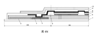
図1は基板の断面構造模式図であり、例えば、当該基板は例えば有機表示装置を形成するための表示基板である。図1に示すように、当該表示基板はベース基板201と、駆動回路202と、共通電極リード線103とを含む。当該表示基板は表示エリア1001と表示エリア1001の周辺に位置する非作業エリア1002とを含む。当該表示基板の非作業エリア1002に駆動回路202が設けられ、駆動回路202は例えばゲート駆動回路であり、例えばアレイ基板に集積されたゲート駆動回路(GOA)である。共通電極リード線103はベース基板201における非作業エリア1002に設けられ、駆動回路202の表示エリア1001に離れる側に位置してベース基板201の外側輪郭エッジに沿って延びる。
FIG. 1 is a schematic cross-sectional structure diagram of a substrate, and the substrate is, for example, a display substrate for forming an organic display device. As shown in FIG. 1, the display substrate includes a
当該表示基板は、駆動回路202と一部の共通電極リード線103とを覆う平坦層1004を含み、平坦層1004は、駆動回路202と共通電極リード線103を絶縁させるように、一部が駆動回路202と共通電極リード線103との間に位置する。当該表示基板は、ジャンパー電極109と共通電極105をさらに含み、共通電極105はジャンパー電極109を介して共通電極リード線103に電気的接続され、即ちジャンパー電極109は共通電極105と共通電極リード線103との電気的接続を実現する架け橋とされる。共通電極105は、ジャンパー電極109との電気的接続を実現するように、表示エリア1001から非作業エリア1002まで延びてジャンパー電極109の表示エリア1001に近接する端に接触され、ジャンパー電極109は、共通電極リード線103との電気的接続を実現するように、ジャンパー電極109の表示エリア1001に離れる端が共通電極リード線103に接触され、よって、共通電極105と共通電極リード線103との電気的接続が実現される。
The display substrate includes a
図1に示す表示基板において、共通電極はジャンパー電極を通じて共通電極リード線との電気的接続を実現し、共通電極リード線と共通電極との間の距離が大きく、ジャンパー電極の長さが大きく、共通電極リード線と共通電極との間の抵抗が大きい。この状況は局部および回路全体の電圧降下の低減に不利であり、よって、信号の伝送速度に影響を与え、最終的に表示スクリーンの輝度が不均一になる一方、当該抵抗が大きいとジュール熱が増加し、当該表示基板が適用される表示装置の寿命が短くなる。また、共通電極とジャンパー電極を蒸着によって形成する時に、蒸着過程におけるマスクの位置誤差により、共通電極とジャンパー電極との接触面積と、ジャンパー電極と共通電極リード線との接触面積とは大きさが固定されないため、共通電極とジャンパー電極との接触面積と、ジャンパー電極と共通電極リード線との接触面積との大きさは、蒸着マスクの位置に直接に影響され、当該接触面積の大きさは固定されず、最終的に基板の寸法誤差が過度に大きくなる問題が生じる。 In the display substrate shown in FIG. 1, the common electrode realizes electrical connection with the common electrode lead wire through the jumper electrode, the distance between the common electrode lead wire and the common electrode is large, the length of the jumper electrode is large, The resistance between the common electrode lead wire and the common electrode is large. This situation is unfavorable to reducing the voltage drop locally and across the circuit, thus affecting the signal transmission speed and ultimately resulting in non-uniform display screen brightness, while the large resistance causes Joule heating. This will shorten the life of the display device to which the display substrate is applied. Furthermore, when forming the common electrode and jumper electrode by vapor deposition, the contact area between the common electrode and jumper electrode and the contact area between the jumper electrode and the common electrode lead wire may vary due to positional errors of the mask during the vapor deposition process. Because it is not fixed, the contact area between the common electrode and the jumper electrode and the contact area between the jumper electrode and the common electrode lead wire are directly affected by the position of the vapor deposition mask, and the size of the contact area is fixed. Otherwise, the problem arises that the dimensional error of the substrate becomes excessively large.
また、蒸着過程におけるマスクの位置の誤差によって、共通電極リード線から基板の外側輪郭エッジまでの距離が固定されなくなる。通常、例えばパッケージ層またはパッケージ基板と配合してパッケージを実現するために、基板に共通電極リード線103の基板の外側輪郭エッジに近接する側に位置するダム(Dam)を設ける必要があり、当該ダムと共通電極リード線との間には一定の距離を予め設けるが必要であり、当該距離は蒸着マスクの位置誤差の影響も受け、蒸着マスクがダムの方向に対してオフセットが大きすぎると、ダムと蒸着マスクとの間に予め設けるマージンをさらに大きくする必要があり、狭いフレームの表示装置の実現には不利である。
Additionally, due to mask position errors during the deposition process, the distance from the common electrode lead to the outer contour edge of the substrate is not fixed. Usually, in order to realize a package, e.g. in combination with a package layer or a package substrate, it is necessary to provide the substrate with a dam located on the side of the
本開示の少なくとも1つの実施例は、作業エリアと作業エリアの周辺に位置する非作業エリアと、ベース基板と、ベース基板に位置して非作業エリアに位置する周辺回路と共通電極リード線と、を含む基板を提供し、共通電極リード線は、周辺回路の作業エリアに近接する側に位置する。 At least one embodiment of the present disclosure includes a working area, a non-working area located around the working area, a base substrate, a peripheral circuit and a common electrode lead wire located on the base substrate and located in the non-working area, a common electrode lead located on a side proximate a working area of peripheral circuitry;
例示的に、図2Aは本開示の1つの実施例に係る基板の平面構造模式図であり、図2Bは本開示の1つの実施例に係る別の基板の平面構造模式図であり、図2Cは本開示の1つの実施例に係るさらに別の基板の平面構造模式図であり、図3Aは図2AにおけるG-G’線または図2BにおけるI-I’線の断面構造模式図である。 Illustratively, FIG. 2A is a schematic plan view of a substrate according to an embodiment of the present disclosure, FIG. 2B is a schematic plan structure diagram of another substrate according to an embodiment of the present disclosure, and FIG. 2C is a schematic plan view of a structure of another substrate according to an embodiment of the present disclosure. 3A is a schematic planar structure diagram of yet another substrate according to one embodiment of the present disclosure, and FIG. 3A is a schematic cross-sectional structure diagram taken along line GG' in FIG. 2A or line II' in FIG. 2B.
図2Aと図3Aに示すように、基板10は、作業エリア101と、作業エリア101の周辺に位置する非作業エリア102と、ベース基板1と、ベース基板1に位置して非作業エリア102に位置する周辺回路2と共通電極リード線3と、作業エリア101から非作業エリア102まで延びる共通電極5と、を含み、共通電極リード線3は、周辺回路2の作業エリア101に近接する側に位置し、共通電極5は、少なくとも一部の共通電極リード線3に直接に接触される。
As shown in FIGS. 2A and 3A, the
例えば、ベース基板1は外側輪郭エッジ104を含む。例えば、表示装置または照明装置に対して、作業エリア101は表示エリアまたは発光エリアなどであってもよく、それに応じて、非作業エリア102は非表示エリアまたは非発光エリアなどであってもよい。非作業エリア102は例えば表示、発光などに用いられないが、その中に表示、発光などの機能を支持と実現するための回路、パッド、相互接続構造などが設けられてもよい。周辺回路2(周辺回路の構造は具体的に図示されておらず)は、ベース基板1に設けられて非作業エリア102に位置し、例えば作業エリア101内の作業ユニット14の作業状態の制御にも用いられてもよい。例えば、作業ユニット14が発光ユニットである時に、周辺回路2は、発光ユニットの発光か否か、および発光強度の制御に用いられることができる。周辺回路2は例えばゲート駆動回路またはデータ駆動回路などの駆動回路であってもよい。周辺回路2のタイプと具体的な構造について、本開示は限定しないが、例えばゲート駆動回路はアレイ基板に集積されたゲート駆動回路(GOA)であってもよい。
For example, the
共通電極リード線3はベース基板1に位置してベース基板1の一部の外側輪郭エッジに沿って設けられ、即ち共通電極リード線3は、ベース基板1の一部の外側輪郭エッジに沿って延びる。共通電極リード線3は周辺回路2の作業エリア101に近接する側に位置し、よって、共通電極リード線3が後続で形成される共通電極にさらに近接させることができ、共通電極リード線3を、後続で形成される共通電極に直接に接触させて共通電極リード線3と共通電極との電気的接続を実現させ、信号が共通電極リード線3から共通電極に伝える抵抗を低減する。例えば、当該共通電極リード線3は陰極リード線である。
The common
例えば、共通電極5は、作業エリア101から非作業エリア102まで延びる。共通電極5は、共通電極リード線3との電気的接続を実現するように、一部の共通電極リード線3に直接に接触される。例えば、当該共通電極5は陰極である。ジャンパー電極を通じて共通電極リード線3と共通電極5との電気的接続を実現する場合に比べて、共通電極リード線3が共通電極に直接に接触されて電気的接続が実現され、よって、信号が共通電極リード線から共通電極に伝える回路の抵抗が低減され、信号が共通電極リード線と共通電極との間の伝送速度の向上に有利であり、例えば、当該基板が表示基板である時に、表示画面の輝度の均一性を向上させることができ、よりよい表示効果を得るとともに、信号が共通電極リード線から共通電極に伝える回路の抵抗の低減は、作業中の電力消費とジュール熱の低減に有利であり、ジュール熱による温度上昇が低減され、それにより、当該基板装置が適用される装置例えば表示装置の寿命の延長に有利である。
For example, the
一方、本開示の実施例に係る基板10について、蒸着法で共通電極5と共通電極リード線3を形成する過程において、蒸着マスクの位置誤差が存在しても、共通電極5が共通電極リード線との一定の接触面積を確保することができるため、共通電極リード線3とベース基板1の外側輪郭エッジ104に近接するダムとの間に過大のマージンを予め設ける必要がなく、狭いフレームの実現に有利であり、複数回の生産における蒸着マスクの異なる位置誤差による、基板製品の寸法誤差の不一致や表示輝度の均一性の不一致などの問題を回避することができる。
On the other hand, regarding the
なお、本開示の実施例において、共通電極リード線が共通電極に直接に接触されることとは、共通電極リード線の少なくとも一部が、共通電極の少なくとも一部に接触され、共通電極リード線と共通電極が接触位置において両者を接続するための他の部品(例えばジャンパー電極、導線など)が存在しないことを指す。 Note that in the embodiments of the present disclosure, the common electrode lead wire is in direct contact with the common electrode, which means that at least a portion of the common electrode lead wire is in contact with at least a portion of the common electrode, and the common electrode lead wire is in direct contact with the common electrode. This means that there is no other component (for example, a jumper electrode, a conductor, etc.) to connect the two at the point where the common electrode and the common electrode are in contact.
図1に示す基板において、電気信号が共通電極リード線から共通電極に伝えることに係る抵抗は、共通電極リード線の抵抗と、共通電極リード線とジャンパー電極との接触抵抗と、ジャンパー電極の抵抗と、ジャンパー電極と共通電極との接触抵抗と、共通電極の抵抗との和である。本開示の実施例に係る基板において、信号が共通電極リード線から共通電極に伝えることに係る抵抗は、共通電極リード線の抵抗と、共通電極リード線と共通電極との接触抵抗と、共通電極の抵抗との和である。そのため、ジャンパー電極を通じて共通電極リード線と共通電極との電気的接続を実現する場合に比べて、本開示の実施例に係る基板において、信号は共通電極リード線から共通電極に伝える回路の抵抗が低減される。 In the board shown in Figure 1, the resistance involved in transmitting an electrical signal from the common electrode lead wire to the common electrode is the resistance of the common electrode lead wire, the contact resistance between the common electrode lead wire and the jumper electrode, and the resistance of the jumper electrode. , the contact resistance between the jumper electrode and the common electrode, and the resistance of the common electrode. In the substrate according to the embodiment of the present disclosure, the resistance involved in transmitting a signal from the common electrode lead wire to the common electrode is the resistance of the common electrode lead wire, the contact resistance between the common electrode lead wire and the common electrode, and the resistance of the common electrode lead wire and the common electrode. is the sum of the resistance of Therefore, compared to the case where the electrical connection between the common electrode lead wire and the common electrode is realized through a jumper electrode, in the substrate according to the embodiment of the present disclosure, the resistance of the circuit that transmits the signal from the common electrode lead wire to the common electrode is lower. reduced.
例えば、図3Aに示すように、基板10は、駆動回路2と共通電極リード線3とを覆う平坦層4を含み、平坦層4は、周辺回路2と共通電極リード線3との絶縁を実現するように、一部が周辺回路2と共通電極リード線3との間に位置する。共通電極5は、共通電極リード線3との電気的接続を実現するように、平坦層4のベース基板1に離れる側に位置し、平坦層4は、少なくとも一部の共通電極リード線3を露出させるビアホール401を含み、共通電極5は、ビアホール401の位置する場所で共通電極リード線3に直接に接触される。例えば、ベース基板1の板面に平行となる平面において、ビアホール401の平面形状はドット状であってもよく、例えば円形、楕円形、多辺形(例えば三角形、矩形など)などであってもよい。
For example, as shown in FIG. 3A, the
もちろん、その他の例示において、平坦層4は一部の共通電極リード線3を露出させるビアホールを含んでもよく、ベース基板1の板面に平行となる平面において、当該ビアホールの平面形状はストリップ状、例えば矩形、波線形などである。共通電極5は、当該ビアホールを通じて共通電極リード線3に電気的接続される。本開示の実施例は当該ビアホールの形状を限定しない。もちろん、本開示の他の実施例において、上記ビアホールは共通電極リード線の全体を露出させてもよく、本開示の実施例はそれを限定しない。
Of course, in other examples, the
共通電極リード線3と周辺回路2は作業エリア101の作業状態の制御に用いられる。例えば、図2Aに示すように、共通電極リード線3と周辺回路2は基板10の左側の、その外側輪郭エッジに近接する場所に位置し、左側から作業エリア101へ制御信号を入力してもよい。例えば、図2Bに示すように、共通電極リード線3と周辺回路2は基板10の上側の、その外側輪郭エッジに近接する場所に位置し、上側から作業エリア101へ制御信号を入力してもよい。また例えば、図2Cに示すように、共通電極リード線3と周辺回路2は基板10の上の対面となる両側、例えば左側と右側の、その外側輪郭エッジに近接する場所に位置してもよい。このようにして、両側から同時に作業エリア101へ制御信号を入力することができ、信号遅延を低減する技術的効果を達成することができ、その結果、基板10はより良い作動効果を達成することができる。基板10の平面面積が大きい状況について、この技術的効果がさらに顕著である。なお、本開示の実施例における「左」、「右」、「上」は対応する図面で示された相対位置を指す。
The common
例えば、共通電極リード線3と共通電極5の材料は透明導電材料または不透明導電材料であってもよい。透明導電材料は例えば酸化インジウムスズ(ITO)または酸化インジウム亜鉛(IZO)などであってもよく、不透明導電材料は例えば導電率が高い銅、アルミニウム、銅合金、アルミニウム合金などの金属材料であってもよい。共通電極リード線3と共通電極リード5は上記またはその他の種類の導電率が高い材料を採用し、共通信号伝送の速度の向上に有利である。例えば、作業エリア101が発光エリアであり、光を図3Aにおける共通電極5側から出射させる必要がある時に、共通電極5は透明材料である。
For example, the common
以上で列挙された材料の種類は単なる例示であり、本開示の実施形態は共通電極リード線と共通電極の材料を限定せず、当業者は具体的なニーズに従って選択することができる。 The types of materials listed above are merely examples, and embodiments of the present disclosure do not limit the materials of the common electrode lead and the common electrode, which can be selected by those skilled in the art according to specific needs.
例えば、作業エリア101はアレイに分布される複数の作業ユニット14を含む。複数の作業ユニットはアレイ素子を含み、例えば、アレイ素子は第1電極7と、機能層8と、第2電極5とを含む。第1電極7はベース基板1に設けられ、例えば、平坦層4のベース基板1に離れる側に設けられる。機能層8は第1電極7のベース基板1に離れる側に設けられる。本開示に1つの実施例において、第2電極は共通電極であり、機能層8のベース基板1に離れる側に設けられる。例えば、機能層8は有機エレクトロルミネセンス層のようなエレクトロルミネセンス層である。例えば、アレイ素子は有機発光ダイオードデバイスであってもよく、当該有機発光ダイオードデバイスはトップエミッション、ボトムエミッションなどの構造であってもよい。示範的に、有機発光ダイオードデバイスは対面に設けられる陽極と陰極、および陽極と陰極の間に位置する有機発光層を含む。
For example,
例えば、図3Aに示す例示において、第1電極7は陽極である。この時に、共通電極リード線3は共通陰極リード線であり、作業過程において共通電極5に低レベル信号を入力する。例えば、陽極は反射電極であってもよいか、または陽極は反射層(図示せず)を含み、作業過程において、光が陰極側から出射され、または、陰極は反射電極であってもよいか、または陰極は反射層を含み、作業過程において、光が陽極側から出射される。本開示の実施例の他の例示において、陽極と陰極に位置は交換してもよい。例えば、陽極は共通電極5であり、第1電極7は陰極であってもよく、この時に、共通電極リード線3は共通陽極リード線であり、作業過程において共通電極5に高レベル信号を入力する。
For example, in the illustration shown in FIG. 3A, the first electrode 7 is an anode. At this time, the common
例えば、基板10は、複数の発光ユニットまたは画素ユニットを区画し、隣接する発光ユニットまたは隣接する画素ユニットの間の光のクロストークを防止するように、画素区画層6をさらに含み、画素区画層6は作業ユニット14に対応する開口を含み、機能層8は少なくとも開口に設けられ、例えば、共通電極5は画素区画層6を覆う。
For example, the
例えば、周辺回路2は例えばゲート駆動回路またはデータ駆動回路などであってもよい。例えば、当該ゲート駆動回路またはデータ駆動回路は異なる例示に応じて、薄膜トランジスター、コンデンサ、ゲートリード線またはデータラインリード線などを含んでもよい。
For example, the
例えば、基板10はフレキシブル基板であってもよい。この時に、当該基板10は第1有機パッケージ層9と、無機パッケージ層11と、第2有機パッケージ層12とを含むフレキシブルパッケージ層をさらに含む。第1有機パッケージ層9は、作業エリア101と一部の非作業エリア102を覆う。無機パッケージ層11は、第1有機パッケージ層9に設けられ、作業エリア101と一部の非作業エリア102を覆う。第2有機パッケージ層12は無機パッケージ層11に設けられ、作業エリア101と一部の非作業エリア102を覆い、一部のベース基板1を覆う。第1有機パッケージ層9は、水と酸素をブロックする能力が弱く、無機パッケージ層11は、水と酸素をブロックする能力が良いため、無機パッケージ層11を設けることによって、フレキシブル基板をより良い耐水性と耐酸素性を有させ、フレキシブル基板に設けられた機能層8を保護する。
For example,
例えば、第1有機パッケージ層9と第2有機パッケージ層12の材料はポリイミド、ポリエステル、ポリフッ化物のうちの1つまたは複数の組み合わせであってもよい。ポリイミドは優れた光透過性、高温耐性、耐屈曲性の特徴を備えている。もちろん、第1有機パッケージ層9と第2有機パッケージ層12の材料は上記で列挙された種類に限定されるものではない。
For example, the material of the first organic packaging layer 9 and the second
例えば、無機パッケージ層11の材料は酸化ケイ素または窒化ケイ素を含んでもよい。もちろん、無機パッケージ層11の材料は上記で列挙された種類に限定されるものではない。水と酸素をブロックする能力の良い無機層である限り、適用できる。
For example, the material of the
例えば、基板10がフレキシブル基板である時に、ベース基板1の材料はポリイミド、ポリエステル、ポリフッ化物のうちの1つまたは複数の組み合わせであってもよい。もちろん、本開示の実施例はベース基板の材料を限定しない。
For example, when the
図3Bは図2AにおけるG-G’線または図2BにおけるI-I’線の別の断面構造模式図であり、図3Bは本開示の実施例に係る別の基板を示す。図3Bに示すように、共通電極5と共通電極リード線3とは平坦層4に位置し、共通電極5は、共通電極リード線3に直接に接触されるように、一部の共通電極リード線3にラップされる。もちろん、本開示の他の実施例において、共通電極5は、共通電極リード線3に直接に接触されるように、直接に共通電極リード線3の全体にラップされてもよい。このようにしても図3Aに示す基板と類似する技術的効果を達成することができ、上記説明を参照し、ここで説明しない。
FIG. 3B is another schematic diagram of a cross-sectional structure taken along line GG' in FIG. 2A or line II' in FIG. 2B, and FIG. 3B shows another substrate according to an embodiment of the present disclosure. As shown in FIG. 3B, the
なお、本開示の実施例において、共通電極が共通電極リード線にラップされることとは、共通電極の一部が、ベース基板に垂直となる方向において少なくとも一部の共通電極リード線に重なり、少なくとも一部の共通電極リード線に接触して電気的接続を実現し、共通電極と共通電極リード線との間にその他の層がなく、両者は例えばビアホールを介して接続する必要がないことを指す。 In the embodiments of the present disclosure, wrapping the common electrode with the common electrode lead wire means that a portion of the common electrode overlaps at least a portion of the common electrode lead wire in a direction perpendicular to the base substrate; At least some of the common electrode leads are contacted to achieve an electrical connection, and there is no other layer between the common electrode and the common electrode leads, and the two do not need to be connected, for example, via a via hole. Point.
図3Bにおいて、基板10の平坦層4は、周辺回路2と一部のベース基板1を覆い、一部の平坦層4は、共通電極リード線3を周辺回路2に絶縁させるように、共通電極リード線3と周辺回路2との間に位置する。
In FIG. 3B, the
例えば、図3Bに示すように、共通電極リード線3は第1電極7に同層に設けられる。このようにして、共通電極リード線3を第1電極7と同じ材料によって同じ工程で同時に形成させることができ、基板10の製造工程の簡略化に有利であり、生産効率を向上する。
For example, as shown in FIG. 3B, the common
例えば、図3Bに示すように、共通電極リード線3のベース基板1における正投影の一部は、周辺回路2のベース基板1における正投影の一部に重なり、基板のフレームの更なる減少に有利であり、よって、当該基板が適用される装置例えば表示装置のフレームの減少に有利である。
For example, as shown in FIG. 3B, a portion of the orthographic projection of the
図3Bに示す基板の他の特徴およびその効果は図3Aに示すものと同じであり、上記の説明を参照してください。 Other features of the substrate shown in FIG. 3B and its effects are the same as those shown in FIG. 3A, see description above.
例えば、図3B’は図2AにおけるG-G’線または図2BにおけるI-I’線の別の断面構造模式図であり、図3B’は本開示の実施例に係る別の基板を示す。図3B’に示すように、共通電極5と共通電極リード線3とは平坦層4に位置し、共通電極5の一端は、共通電極と共通電極リード線に直接に接触されるように、一部の共通電極リード線3の一端に接合される。このようにしても図3Aに示す基板と類似する技術的効果を達成することができ、上記説明を参照し、ここで説明しない。
For example, FIG. 3B' is another schematic cross-sectional structure diagram taken along line GG' in FIG. 2A or line II' in FIG. 2B, and FIG. 3B' shows another substrate according to an embodiment of the present disclosure. As shown in FIG. 3B', the
なお、本開示の実施例において、共通電極の一端と一部の共通電極リード線の一端に接合されることとは、共通電極が一部の共通電極リード線に端部のみにおいて直接に接触され、共通電極と共通電極リード線がベース基板における正投影は重ならないことを指す。 Note that in the embodiments of the present disclosure, being joined to one end of the common electrode and one end of some of the common electrode lead wires means that the common electrode is in direct contact with some of the common electrode lead wires only at the ends. , refers to the fact that the orthogonal projections of the common electrode and the common electrode lead wire on the base substrate do not overlap.
例えば、図3B’’は図2AにおけるG-G’線または図2BにおけるI-I’線の別の断面構造模式図であり、図3B’’は本開示の実施例に係る別の基板を示す。図3B’’に示すように、共通電極5と共通電極リード線3とは平坦層4に位置し、共通電極リード線3は、共通電極5に直接に接触されるように、一部の共通電極5に直接にラップされる。もちろん、本開示の他の実施例において、共通電極リード線3は、共通電極5に直接に接触されるように、直接に共通電極5の全体にラップされてもよい。このようにしても図3Aに示す基板と類似する技術的効果を達成することができ、上記説明を参照し、ここで説明しない。
For example, FIG. 3B'' is another cross-sectional structure schematic diagram taken along line GG' in FIG. 2A or line II' in FIG. show. As shown in FIG. 3B'', the
図3Cは図2AにおけるG-G’線または図2BにおけるI-I’線のさらに別の断面構造模式図であり、図3Cは本開示の実施例に係るさらに別の基板を示す。図3Cに示す基板と図3Aに示す基板の区別は以下である。基板10は、平坦層4のベース基板1に離れる側に設けられて周辺回路2を覆って共通電極リード線3に電気的接続される静電保護層13をさらに含み、例えば、共通電極5は静電保護層13に設けられて静電保護層13に直接にラップされて、静電保護層13の共通電極リード線3に近接する端はビアホール401を介して共通電極リード線3に直接に接触され、静電保護層13と共通電極リード線3との電気的接続を実現する。例えば、静電保護層13の共通電極リード線3に近接する端をその他のビアホールを介して共通電極リード線3に直接に接触されるように、共通電極と同じビアホールを共用せずに、平坦層にその他のビアホールを形成してもよい。静電保護層13は周辺回路2の外部の静電を共通電極リード線を通じてガイドし、静電荷が周辺回路2に侵入して周辺回路2の作業状態に干渉するのを防ぐことができる。このようにして、静電保護層13と共通電極リード線3は静電防止回路の一部とされてもよく、基板10に静電防止回路を設ける必要がある時に、基板10の部品を簡略化してもよい。
FIG. 3C is still another schematic cross-sectional structure diagram taken along the line GG' in FIG. 2A or the line II' in FIG. 2B, and FIG. 3C shows still another substrate according to the embodiment of the present disclosure. The distinction between the substrate shown in FIG. 3C and the substrate shown in FIG. 3A is as follows. The
図3C’は図2AにおけるG-G’線または図2BにおけるI-I’線のさらに別の断面構造模式図であり、図3C’は本開示の実施例に係るさらに別の基板を示す。図3C’に示す基板と図3Bに示す基板の区別は以下である。基板10は、平坦層4のベース基板1に離れる側に設けられて周辺回路2を覆って共通電極リード線3に電気的接続される静電保護層13をさらに含み、例えば、静電保護層13と共通電極リード線3との電気的接続を実現するように、静電保護層13は少なくとも一部の共通電極リード線3に直接にラップされる。静電保護層13は周辺回路2の外部の静電を共通電極リード線を通じてガイドし、静電荷が周辺回路2に侵入して周辺回路2の作業状態に干渉するのを防ぐことができる。このようにして、静電保護層13と共通電極リード線3は静電防止回路の一部とされてもよく、基板10に静電防止回路を設ける必要がある時に、基板10の部品を簡略化してもよい。
FIG. 3C' is still another cross-sectional structure schematic diagram taken along line GG' in FIG. 2A or line II' in FIG. 2B, and FIG. 3C' shows still another substrate according to the embodiment of the present disclosure. The distinction between the substrate shown in FIG. 3C' and the substrate shown in FIG. 3B is as follows. The
図3C’’は図2AにおけるG-G’線または図2BにおけるI-I’線のさらに別の断面構造模式図であり、図3C’’は本開示の実施例に係るさらに別の基板を示す。図3C’’に示す基板と図3Bに示す基板の区別は以下である。基板10は、平坦層4のベース基板1に離れる側に設けられて周辺回路2を覆って共通電極リード線3に電気的接続される静電保護層13をさらに含み、例えば、静電保護層13と共通電極リード線3との電気的接続を実現するように、共通電極リード線3は少なくとも一部の静電保護層13に直接にラップされる。静電保護層13は周辺回路2の外部の静電を共通電極リード線を通じてガイドし、静電荷が周辺回路2に侵入して周辺回路2の作業状態に干渉するのを防ぐことができる。このようにして、静電保護層13と共通電極リード線3は静電防止回路の一部とされてもよく、基板10に静電防止回路を設ける必要がある時に、基板10の部品を簡略化してもよい。
3C'' is still another cross-sectional structure schematic diagram taken along the line GG' in FIG. 2A or the line II' in FIG. 2B, and FIG. 3C'' shows still another substrate according to the embodiment of the present disclosure. show. The distinction between the substrate shown in FIG. 3C'' and the substrate shown in FIG. 3B is as follows. The
図3C’’’は図2AにおけるG-G’線または図2BにおけるI-I’線のさらに別の断面構造模式図であり、図3C’’’は本開示の実施例に係るさらに別の基板を示す。図3C’’’に示す基板と図3Bに示す基板の区別は以下である。基板10は、平坦層4のベース基板1に離れる側に設けられて周辺回路2を覆って共通電極リード線3に電気的接続される静電保護層13をさらに含み、例えば、静電保護層13と共通電極リード線3との電気的接続を実現するように、共通電極リード線3の他端は静電保護層13の一端に接合される。静電保護層13は周辺回路2の外部の静電を共通電極リード線を通じてガイドし、静電荷が周辺回路2に侵入して周辺回路2の作業状態に干渉するのを防ぐことができる。このようにして、静電保護層13と共通電極リード線3は静電防止回路の一部とされてもよく、基板10に静電防止回路を設ける必要がある時に、基板10の部品を簡略化してもよい。
FIG. 3C''' is still another cross-sectional structure schematic diagram taken along line GG' in FIG. 2A or line II' in FIG. 2B, and FIG. The board is shown. The distinction between the substrate shown in FIG. 3C''' and the substrate shown in FIG. 3B is as follows. The
なお、本開示の実施例において、共通電極リード線の他端と静電保護層の一端に接合されることとは、共通電極リード線と静電保護層は端部のみに直接に接触され、共通電極リード線と静電保護層はベース基板における正投影は重ならないことを指す。 Note that in the embodiments of the present disclosure, being joined to the other end of the common electrode lead wire and one end of the electrostatic protection layer means that the common electrode lead wire and the electrostatic protection layer are in direct contact only at their ends; This means that the common electrode lead wire and the electrostatic protection layer do not overlap in orthogonal projection on the base substrate.
本開示の実施例に係る基板は表示装置、照明装置などの電子装置に適用可能である。本開示の実施例に係る基板は、フレキシブル表示パネル、発光パネルなどに用いられるフレキシブル基板であってもよい。 The substrate according to the embodiment of the present disclosure is applicable to electronic devices such as display devices and lighting devices. The substrate according to the embodiment of the present disclosure may be a flexible substrate used for a flexible display panel, a light emitting panel, or the like.
本開示の1つの実施例は、本開示の上記実施例に係るいずれかの基板を含む電子装置をさら提供する。示範的に、図7は本開示の1つの実施例に係る電子装置のブロック図である。図7に示すように、当該電子装置は本開示の実施例に係るいずれかの基板を含む。例えば、当該電子装置は表示装置であってもよく、例えば、当該表示装置は有機発光ダイオード表示装置であってもよい。例えば、当該表示装置はフレキシブル表示装置であってもよい。例えば、当該表示装置は携帯電話、タブレットコンピュータ、テレビ、ディスプレイ、ノートパソコン、デジタルフォトフレーム、ナビゲータ、電子広告スクリーン等の表示機能を有する任意の製品又は部材として実現されてもよい。例えば、当該電子装置は照明装置であってもよく、例えば、当該照明装置は装飾用灯具であってもよい。 One embodiment of the present disclosure further provides an electronic device including any substrate according to any of the above embodiments of the present disclosure. Illustratively, FIG. 7 is a block diagram of an electronic device according to one embodiment of the present disclosure. As shown in FIG. 7, the electronic device includes any substrate according to the embodiments of the present disclosure. For example, the electronic device may be a display device, for example the display device may be an organic light emitting diode display device. For example, the display device may be a flexible display device. For example, the display device may be realized as any product or component having a display function, such as a mobile phone, a tablet computer, a television, a display, a laptop computer, a digital photo frame, a navigator, an electronic advertising screen, etc. For example, the electronic device may be a lighting device; for example, the lighting device may be a decorative lamp.
図7は本開示の実施例に係るいずれかの基板を含む表示装置のブロック図に過ぎなく、表示装置の他の構造を図示せず、当業者は従来の技術を参照することができ、本開示の実施例はこれを限定するものではない。 FIG. 7 is only a block diagram of a display device including any of the substrates according to the embodiments of the present disclosure, and does not illustrate other structures of the display device, and those skilled in the art can refer to the conventional technology, and this The disclosed embodiments are not intended to be limiting.
本開示の実施例に係る電子装置は、共通電極リード線と共通電極との電気的接続を実現するための抵抗を低減することができ、信号が共通電極リード線と共通電極との間の伝送速度の向上に有利であり、例えば当該基板が発光基板例えば表示基板である時に、表示画面の輝度の均一性を向上させることができ、よりよい表示効果を得るとともに、共通電極リード線と共通電極との電気的接続を実現するための抵抗の低減は、電子装置の作業中の電力消費とジュール熱の低減に有利であり、ジュール熱による温度上昇が低減され、それにより、電子装置の寿命の延長に有利である。また、本開示の実施例に係る電子装置は、狭いフレームを実現することができる。 The electronic device according to the embodiment of the present disclosure can reduce the resistance for realizing the electrical connection between the common electrode lead wire and the common electrode, and the transmission of signals between the common electrode lead wire and the common electrode can be reduced. For example, when the substrate is a light emitting substrate, such as a display substrate, it can improve the uniformity of the brightness of the display screen, obtain a better display effect, and connect the common electrode lead wire and the common electrode. Reducing the resistance to realize electrical connection with the electronic device is advantageous to reduce power consumption and Joule heat during the operation of electronic devices, and the temperature rise due to Joule heat is reduced, thereby extending the lifespan of electronic devices. It is advantageous for extension. Further, the electronic device according to the embodiment of the present disclosure can realize a narrow frame.
本開示の少なくとも1つの実施例は、作業エリアと、作業エリアの周辺に位置する非作業エリアとを含む基板の製造方法をさらに提供し、当該製造方法は、ベース基板を提供するステップと、ベース基板且つ非作業エリアにおいて周辺回路と共通電極リード線を形成するステップと、作業エリアと非作業エリアにおいて共通電極を形成するステップと、を含み、共通電極リード線は、周辺回路の作業エリアに近接する側に位置し、共通電極は少なくとも一部の共通電極リード線に直接に接触される。 At least one embodiment of the present disclosure further provides a method of manufacturing a substrate including a working area and a non-working area located around the working area, the manufacturing method comprising: providing a base substrate; forming a common electrode lead wire with the peripheral circuit on the substrate and in the non-working area; and forming a common electrode in the working area and the non-working area, the common electrode lead wire being close to the working area of the peripheral circuit. and the common electrode is in direct contact with at least some of the common electrode leads.
示範的に、図4A~図4Oは本開示の実施例に係る基板の製造方法のプロセス模式図である。以下で、作業エリアが有機発光ダイオードデバイスを含む基板の形成を例として示範的な紹介をする。 Illustratively, FIGS. 4A to 4O are process diagrams of a method for manufacturing a substrate according to an embodiment of the present disclosure. In the following, an illustrative introduction will be given, taking as an example the formation of a substrate whose working area includes an organic light emitting diode device.
図4Aに示すように、ベース基板1を提供する。ベース基板1は例えばガラス基板、石英基板、樹脂(例えばポリエチレン)基板などであってもよく、例えば、ポリイミドからなるフレキシブル基板であってもよい。ベース基板1は外側輪郭エッジを含み、形成される基板の含む作業エリア101と作業エリア101の周辺に位置する非作業エリア102とのベース基板1に対応するエリアは図4Aに示すものである。
As shown in FIG. 4A, a
図4Bに示すように、基板の非作業エリア102において周辺回路2を提供し、当該周辺回路2は例えばゲート駆動回路またはデータ駆動回路のような駆動回路であってもよい。当該周辺回路2の具体的な製造方法について、当業者は従来の技術を参照することができる。
As shown in FIG. 4B, a
図4Cに示すように、共通電極リード線3は、後続で形成される、作業エリア101から非作業エリア102まで延びる共通電極に直接に接触させることを便利にするように、周辺回路2の作業エリア101に近接する側に位置する。それに、共通電極リード線3と周辺回路2とを絶縁させるように、共通電極リード線3と周辺回路2との間には一定の距離が設けられる。例えば、共通電極リード線3の材料は例えば透明導電材料または不透明導電材料であってもよく、透明導電材料は例えば酸化インジウムスズ(ITO)または酸化インジウム亜鉛(IZO)などであってもよく、不透明導電材料は例えば導電率が高い銅、アルミニウム、銅合金などの金属材料であってもよい。共通電極リード線3はマスクと配合して化学気相蒸着法またはマグネトロンスパッタリング蒸着法、蒸着などにより形成してもよい。
As shown in FIG. 4C, the common
図4Dに示すように、当該方法は平坦層4を形成するステップをさらに含む。平坦層4は周辺回路2と共通電極リード線3を覆う。共通電極リード線3と周辺回路2とを絶縁させるように、一部の平坦層4は共通電極リード線3と周辺回路2との間に位置する。例えば、平坦層4の材料は、絶縁層として機能しつつ、絶縁材料であってもよい。当該絶縁材料は例えば無機材料または有機材料であってもよく、当該有機材料は例えばポリエチレン樹脂、ポリアクリル樹脂、ポリエステル樹脂、ポリアミド樹脂などの樹脂材料である。本開示の実施例は平坦層4の材料を限定しない。
As shown in FIG. 4D, the method further includes forming a
図4Eに示すように、平坦層4に対してパターニング工程が実施され、平坦化層4に一部の共通電極リード線を露出させるビアホール401が形成される。例えば、当該パターニング工程はフォトレジストであってもよい。もちろん、その他の実施例において、平坦層4に対してパターニング工程を実施することによって一部の共通電極リード線を露出させる溝を形成してもよく、溝はビアホールの特殊の形式である。
As shown in FIG. 4E, a patterning process is performed on the
図4Fに示すように、平坦層4の上方にプレ画素区画層601が形成され、例えばコーティングによってプレ画素区画層601が形成されてもよい。例えば、プレ画素区画層601の材料は、後続のフォトリソグラフィ工程を行うための感光性材料であってもよい。例えば、当該感光性材料は、フォトレジスト材料と金属ハロゲン化物を含んでもよく、金属ハロゲン化物は例えばハロゲン化銀(例えば、AgClまたはAgBr)である。プレ画素区画層601の材料は、黒色樹脂、金属クロムまたは酸化クロムなどの暗い材料であってもよく、所望のパターンは、印刷またはフォトリソグラフィなどのパターニング方法によって得ることができる。もちろん、プレ画素区画層601の材料は、他の材料であってもよく、当業者はニーズに応じて選択してもよい。
As shown in FIG. 4F, a
図4Gに示すように、プレ画素区画層601に対してパターニング工程を実施して画素区画層6を形成する。画素区画層6は開口を有する。画素区画層6は作業エリア101においてアレイに分布される複数の作業ユニットを区画し、即ち作業エリア101においてアレイに分布される複数の作業ユニットを形成する。例えば、当該パターニング工程はフォトレジスト工程であってもよい。例えば、画素区画層6は、露光-現像工程によって形成されてもよく、プレ画素区画層601の材料がフォトレジスト材料と金属ハロゲン化物を含む場合に、金属ハロゲン化物は、露光されていない時に低光学密度材料であり、露光後に金属粒子に分解され、当該金属粒子は小さな粒子のために黒く見られ、高い光学密度値を有する。一方、例えば、フォトレジスト材料はネガ型フォトレジスト材料であり、露光後に現像液に不溶となり残存するため、画素区画層6を形成することができる。
As shown in FIG. 4G, a patterning process is performed on the
図4Iに示すように、例えば第1電極7は、蒸着や堆積などの方法により、マスクと配合して平坦層4に形成されてもよく、例えば、第1電極7は陽極である。また、図4Hに示すように、まず蒸着、マグネトロンスパッタリング蒸着、化学気相蒸着などの方法によりプレ第1電極層701を形成し、次にフォトリソグラフィ工程によって図4Iに示すような第1の電極7を形成する。第1電極7は各作業ユニットにおける画素区画層6の開口に位置する。
As shown in FIG. 4I, for example, the first electrode 7 may be formed on the
図4Kに示すように、マスクと配合して堆積などの方法により第1電極7のベース基板1に離れる側に位置する機能層8が形成される。例えば、機能層8は有機発光層である。また、図4Jに示すように、コーティング法によりプレ機能層801が形成され、その後、図4Kに示すような機能層8がフォトリソグラフィーにより形成され、例えば、機能層8は、各作業ユニットにおける画素区画層6の開口に位置する。
As shown in FIG. 4K, a functional layer 8 located on the side remote from the
図4Lに示すように、共通電極5が形成される。例えば、共通電極5は陰極である。もちろん、他の実施例において、共通電極5が陽極で、第1電極7が陰極であってもよい。共通電極5は画素区画層6を覆い、作業エリア101から非作業エリア102まで延びる。非作業エリア102において、共通電極5は、共通電極リード線3との電気的接続を実現するように、ビアホール401を介して共通電極リード線3に直接に接触されることができる。共通電極5が共通電極リード線3に直接に接触される技術的効果については、前の実施例における説明を参照し、ここで説明しない。
As shown in FIG. 4L,
例えば、当該基板がフレキシブル基板である時に、当該基板の製造方法はフレキシブルパッケージ層を形成するステップをさらに含む。フレキシブルパッケージ層を形成するステップは、第1有機パッケージ層と、無機パッケージ層と、第2有機パッケージ層とを形成するステップを含む。図4Mに示すように、作業エリア101と一部の非作業エリア102を覆う第1有機パッケージ層9が形成される。例えば、第1有機パッケージ層9の材料はポリイミド、ポリエステル、ポリフッ化物のうちの1つまたは複数の組み合わせであってもよい。ポリイミドは優れた光透過性、高温耐性、耐屈曲性の特徴を備えている。もちろん、第1有機パッケージ層9の材料は上記で列挙された種類に限定されるものではない。例えば、第1有機パッケージ層9はコーディング方法によって形成されてもよい。
For example, when the substrate is a flexible substrate, the method for manufacturing the substrate further includes forming a flexible packaging layer. Forming a flexible packaging layer includes forming a first organic packaging layer, an inorganic packaging layer, and a second organic packaging layer. As shown in FIG. 4M, a first organic packaging layer 9 is formed covering the working
図4Nに示すように、第1有機パッケージ層9に設けられる無機パッケージ層11が形成される。例えば、無機パッケージ層11の材料は酸化ケイ素または窒化ケイ素を含んでもよい。もちろん、無機パッケージ層11の材料は上記で列挙された種類に限定されるものではない。水と酸素をブロックする能力の良い無機層であればよい。例えば、無機パッケージ層11は蒸着、化学気相蒸着またはマグネトロンスパッタリング蒸着などの方法により形成されてもよい。
As shown in FIG. 4N, an
図4Оに示すように、無機パッケージ層11に設けられて一部のベース基板1を覆う第2有機パッケージ層12が形成される。第2有機パッケージ層12の材料と形成方法は第1有機パッケージ層9と同じである。上記方法によって図4Oに示す基板を形成することができる。
As shown in FIG. 4O, a second
なお、本開示の実施例はフレキシブル基板の形成を例として説明する。いくつかの実施例において、基板は非フレキシブル基板であってもよい。 Note that the embodiments of the present disclosure will be described using the formation of a flexible substrate as an example. In some embodiments, the substrate may be a non-flexible substrate.
図5A~図5Fは本開示の実施例に係る別の基板の製造方法のプロセス模式図である。図4Bに示す構造が形成された後に、図5Aに示す、周辺回路2を覆う平坦層4が形成される。平坦層の材料と形成方法は上記説明を参照してください。
5A to 5F are process diagrams of another method for manufacturing a substrate according to an embodiment of the present disclosure. After the structure shown in FIG. 4B is formed, a
図5Bに示すように、図4F~4Gに示す方法と同じ方法を採用して画素区画層6を形成する。図5Cに示すように、基板の製造プロセスを簡略化するために、平坦層4のベース基板1に離れる側に共通電極リード線3と第1電極7を同時に形成してもよく、即ち共通電極リード線3と第1電極7は同じ工程によって形成してもよい。
As shown in FIG. 5B, the
図5Dに示すように、図4Kに示す方法と同じ方法を採用して機能層8を形成する。 As shown in FIG. 5D, the functional layer 8 is formed using the same method as shown in FIG. 4K.
図5Eに示すように、平坦層4のベース基板1に離れる側に共通電極5が設けられる。共通電極5は画素区画層6を覆い、作業エリア101から非作業エリア102まで延びる。非作業エリア102において、共通電極5は、共通電極リード線3との電気的接続を実現するように、一部の共通電極リード線3に直接にラップして直接に接触される。
As shown in FIG. 5E, a
例えば、図5Eの1つの変形において、図5E’に示すように、共通電極5は、共通電極リード線3との電気的接続を実現するように、ベース基板1の板面に平行となる平面において少なくとも一部の共通電極リード線3に直接に接触されてもよく、即ち、共通電極5と一部の共通電極リード線3に直接にラップされる部分が無くされた。後続の過程は図5Eに示す構造を基礎とする。
For example, in one variation of FIG. 5E, as shown in FIG. 5E', the
図4M~4Oに示す方法と同じ方法によって第1有機パッケージ層9、無機パッケージ層11、第2有機パッケージ層12を順に形成し、図5Fに示す基板を形成することができる。
The first organic package layer 9, the
図5A~5Fに示す製造方法は、図4M~4Oに示す製造方法と同じまたは類似する技術的効果を達成することができ、当該方法の他の技術的特徴はすべて図4M~4Oに示す方法と同じであり、上記説明を参照してください。 The manufacturing method shown in FIGS. 5A-5F can achieve the same or similar technical effects as the manufacturing method shown in FIGS. 4M-4O, and all other technical features of the method are the same as the manufacturing method shown in FIGS. 4M-4O. and see the explanation above.
図6A~図6Bは本開示の実施例に係るさらに別の基板の製造方法のプロセス模式図である。当該方法は静電保護層を形成するステップをさらに含む。図4Gに示す構造の後に、同じ工程を利用して静電保護層13と第1電極7を同時に形成する。静電保護層13は周辺回路2を覆って共通電極リード線3に電気的接続される。静電保護層13と共通電極リード線3との電気的接続を実現するように、静電保護層13の共通電極リード線3に近接する端をビアホール401を介して共通電極リード線3に直接にラップして直接に接触される。静電保護層13は周辺回路2の外部の静電を共通電極リード線を通じてガイドし、静電荷が周辺回路2に侵入して周辺回路2の作業状態に干渉するのを防ぐことができる。このようにして、静電保護層13と共通電極リード線3は静電防止回路の一部とされてもよく、基板10に静電防止回路を設ける必要がある時に、基板10の部品を簡略化してもよい。本開示に1つの実施例において、静電保護層13と第1電極7が同じ工程によって同時に形成されることは、基板の製造工程の簡略化に有利である。
6A to 6B are process schematic diagrams of yet another method of manufacturing a substrate according to an embodiment of the present disclosure. The method further includes forming an electrostatic protection layer. After the structure shown in FIG. 4G, the
図4M~4Oに示す方法と同じ方法によって第1有機パッケージ層9、無機パッケージ層11、第2有機パッケージ層12を順に形成し、図6Bに示す基板を形成することができる。
The first organic package layer 9, the
本開示の実施例は基板及びその製造方法、電子装置を提供し、本開示の少なくとも1つの実施例において、共通電極リード線は周辺回路の作業エリアに近接する側に位置し、よって、共通電極リード線を共通電極にさらに近接させることができ、共通電極リード線を、共通電極との電気的接続を実現するように、少なくとも共通電極に直接に接触させる。ジャンパー電極を通じて共通電極リード線と共通電極との電気的接続を実現する場合に比べて、共通電極リード線が共通電極に直接に接触されて電気的接続が実現され、よって、信号が共通電極リード線から共通電極に伝える回路の抵抗が低減され、信号が共通電極リード線と共通電極との間の伝送速度の向上に有利であり、例えば、当該基板が発光基板例えば表示基板である時に、表示画面の輝度の均一性を向上させることができ、よりよい表示効果を得るとともに、当該抵抗の低減は、作業中の電力消費とジュール熱の低減に有利であり、ジュール熱による温度上昇が低減され、それにより、当該基板装置が適用される装置例えば表示装置の寿命の向上に有利である。一方、本開示の実施例に係る基板について、共通電極を製造する過程において、例えば蒸着法で共通電極と共通電極リード線を形成する過程において、蒸着マスクの位置誤差が存在しても、共通電極が共通電極リード線との一定の接触面積を確保することができるため、共通電極リード線とベース基板に近接する外側輪郭エッジに近接するダムとの間に過大のマージンを予め設ける必要がなく、狭いフレームの実現に有利であり、複数回の生産における蒸着マスクの異なる位置誤差による、基板製品の寸法誤差の不一致や表示輝度の均一性の不一致などの問題を回避することができる。 Embodiments of the present disclosure provide a substrate, a method of manufacturing the same, and an electronic device, and in at least one embodiment of the present disclosure, the common electrode lead is located on the side proximate to the working area of the peripheral circuitry, so that the common electrode lead The lead wire can be brought closer to the common electrode, and the common electrode lead wire is in direct contact with at least the common electrode to achieve electrical connection with the common electrode. Compared to the case where the electrical connection between the common electrode lead wire and the common electrode is achieved through a jumper electrode, the common electrode lead wire is brought into direct contact with the common electrode to achieve the electrical connection, so that the signal is transmitted directly to the common electrode lead. The resistance of the circuit transmitting from the wire to the common electrode is reduced, which is advantageous for increasing the transmission speed of the signal between the common electrode lead wire and the common electrode, for example, when the substrate is a light emitting substrate, such as a display substrate, the display The uniformity of the screen brightness can be improved, obtaining a better display effect, and the reduction in resistance is advantageous to reducing power consumption and Joule heat during work, and the temperature rise due to Joule heat is reduced. This is advantageous in improving the lifespan of devices to which the substrate device is applied, such as display devices. On the other hand, regarding the substrate according to the embodiment of the present disclosure, in the process of manufacturing the common electrode, for example, in the process of forming the common electrode and the common electrode lead wire by a vapor deposition method, even if there is a positional error of the vapor deposition mask, the common electrode Since it is possible to ensure a constant contact area with the common electrode lead wire, there is no need to provide an excessive margin in advance between the common electrode lead wire and the dam adjacent to the outer contour edge adjacent to the base substrate. It is advantageous in realizing a narrow frame, and can avoid problems such as dimensional error discrepancies in substrate products and display brightness uniformity discrepancies due to different positional errors of vapor deposition masks in multiple productions.
以上の説明は、本開示の例示的な実施形態に過ぎず、本開示の範囲を限定するものではなく、本開示の保護範囲は、添付の特許請求の範囲によって規定される。 The above descriptions are only exemplary embodiments of the disclosure and do not limit the scope of the disclosure, and the protection scope of the disclosure is defined by the appended claims.
1 ベース基板
2 周辺回路
3 共通電極リード線
4 平坦層
5 共通電極
6 画素区画層
8 機能層
9 第1有機パッケージ層
10 基板
11 無機パッケージ層
12 第2有機パッケージ層
13 静電保護層
14 作業ユニット
101 作業エリア
102 非作業エリア
103 共通電極リード線
104 外側輪郭エッジ
105 共通電極
109 ジャンパー電極
201 ベース基板
202 駆動回路
401 ビアホール
601 プレ画素区画層
701 プレ第1電極層
801 プレ機能層
1001 表示エリア
1002 非作業エリア
1004 平坦層
1
Claims (19)
ベース基板と、
前記ベース基板に位置して前記非作業エリアに位置する周辺回路と共通電極リード線と、
共通電極と、を含み、
前記共通電極リード線は、前記周辺回路の前記作業エリアに近接する側に位置し、
前記共通電極は、前記作業エリアから前記非作業エリアまで延び、
前記共通電極は、少なくとも一部の前記共通電極リード線に直接に接触され、
前記ベース基板上の前記共通電極の正投影と前記ベース基板上の周辺回路の正投影とが少なくとも部分的に重なり、前記共通電極の周辺回路に対応する部分と前記共通電極リード線に対応する部分とが一体構造であり、前記ベース基板上の前記共通電極の正投影、前記ベース基板上の前記周辺回路の正投影および前記ベース基板上の前記共通電極リード線の正投影が同時に重なる部分を有せず、
前記非作業エリアにおいて、前記非作業エリアから前記作業エリアへの方向において、前記共通電極リード線と前記非作業エリア内に位置する前記共通電極の一部との間に導通層が存在せず、前記共通電極は、前記共通電極リード線の前記ベース基板から離れた一部の上面と、前記共通電極リード線の前記作業エリアに近接した側面との双方に直接接触しており、前記作業エリアから遠い側の前記共通電極リード線の端部は、前記作業エリアから遠い側の前記共通電極の端部よりも前記作業エリアからさらに離れており、前記ベース基板に垂直な方向において、前記共通電極と前記共通電極リード線との間には他の層が存在しない、基板。 a work area and a non-work area located around the work area;
a base board;
a peripheral circuit and a common electrode lead wire located on the base substrate and located in the non-working area;
a common electrode;
The common electrode lead wire is located on a side of the peripheral circuit close to the work area,
the common electrode extends from the working area to the non-working area;
the common electrode is in direct contact with at least some of the common electrode leads;
The orthographic projection of the common electrode on the base substrate and the orthographic projection of the peripheral circuit on the base substrate at least partially overlap, and a portion of the common electrode corresponding to the peripheral circuit and a portion corresponding to the common electrode lead wire. have an integral structure, and have a portion where an orthogonal projection of the common electrode on the base substrate, an orthogonal projection of the peripheral circuit on the base substrate, and an orthogonal projection of the common electrode lead wire on the base substrate overlap at the same time. Without ,
In the non-working area, there is no conductive layer between the common electrode lead wire and a part of the common electrode located in the non-working area in the direction from the non-working area to the working area, The common electrode is in direct contact with both an upper surface of a portion of the common electrode lead wire away from the base substrate and a side surface of the common electrode lead wire close to the work area, and The end of the common electrode lead wire on the far side is further away from the work area than the end of the common electrode on the side far from the work area, and is connected to the common electrode in the direction perpendicular to the base substrate. A substrate with no other layer between it and the common electrode lead .
前記共通電極は、前記平坦層の前記ベース基板に離れる側に位置し、前記平坦層は、少なくとも一部の前記共通電極リード線を露出させるビアホールを含み、前記共通電極は前記ビアホールの位置する場所で前記共通電極リード線に直接に接触される、請求項2に記載の基板。 further comprising a flat layer covering the peripheral circuit and the common electrode lead wire,
The common electrode is located on a side of the planar layer remote from the base substrate, the planar layer includes a via hole that exposes at least a portion of the common electrode lead, and the common electrode is located at a location where the via hole is located. 3. The substrate of claim 2, wherein the substrate is directly contacted by the common electrode lead.
前記ベース基板に設けられる第1電極と、
前記第1電極の前記ベース基板に離れる側に設けられる機能層と、
前記機能層の前記ベース基板に離れる側に設けられる第2電極と、を含み、
前記第2電極は前記共通電極である、請求項6または8に記載の基板。 The work area includes a plurality of work units distributed in an array, each said work unit comprising:
a first electrode provided on the base substrate;
a functional layer provided on a side of the first electrode away from the base substrate;
a second electrode provided on a side of the functional layer remote from the base substrate;
The substrate according to claim 6 or 8, wherein the second electrode is the common electrode.
ベース基板を提供するステップと、
前記ベース基板に且つ前記非作業エリアにおいて周辺回路と共通電極リード線を形成するステップと、
共通電極を形成するステップと、を含み、
前記共通電極リード線は、前記周辺回路の前記作業エリアに近接する側に位置し、
前記共通電極は、前記作業エリアから前記非作業エリアまで延び、前記共通電極は、少なくとも一部の前記共通電極リード線に直接に接触され、
前記ベース基板上の前記共通電極の正投影と前記ベース基板上の周辺回路の正投影とが少なくとも部分的に重なり、前記共通電極の周辺回路に対応する部分と前記共通電極リード線に対応する部分とが一体構造であり、前記ベース基板上の前記共通電極の正投影、前記ベース基板上の前記周辺回路の正投影および前記ベース基板上の前記共通電極リード線の正投影が同時に重なる部分を有せず、
前記非作業エリアにおいて、前記非作業エリアから前記作業エリアへの方向において、前記共通電極リード線と前記非作業エリア内に位置する前記共通電極の一部との間に導通層が存在せず、前記共通電極は、前記共通電極リード線の前記ベース基板から離れた一部の上面と、前記共通電極リード線の前記作業エリアに近接した側面との双方に直接接触しており、前記作業エリアから遠い側の前記共通電極リード線の端部は、前記作業エリアから遠い側の前記共通電極の端部よりも前記作業エリアからさらに離れており、前記ベース基板に垂直な方向において、前記共通電極と前記共通電極リード線との間には他の層が存在しない、基板の製造方法。 A method for manufacturing a board including a working area and a non-working area located around the working area, the method comprising:
providing a base substrate;
forming a peripheral circuit and a common electrode lead wire on the base substrate and in the non-working area;
forming a common electrode;
The common electrode lead wire is located on a side of the peripheral circuit close to the work area,
the common electrode extends from the working area to the non-working area, the common electrode is in direct contact with at least some of the common electrode leads;
The orthographic projection of the common electrode on the base substrate and the orthographic projection of the peripheral circuit on the base substrate at least partially overlap, and a portion of the common electrode corresponding to the peripheral circuit and a portion corresponding to the common electrode lead wire. have an integral structure, and have a portion where an orthogonal projection of the common electrode on the base substrate, an orthogonal projection of the peripheral circuit on the base substrate, and an orthogonal projection of the common electrode lead wire on the base substrate overlap at the same time. Without ,
In the non-working area, there is no conductive layer between the common electrode lead wire and a part of the common electrode located in the non-working area in the direction from the non-working area to the working area, The common electrode is in direct contact with both an upper surface of a portion of the common electrode lead wire away from the base substrate and a side surface of the common electrode lead wire close to the work area, and The end of the common electrode lead wire on the far side is further away from the work area than the end of the common electrode on the side far from the work area, and is in contact with the common electrode in the direction perpendicular to the base substrate. A method of manufacturing a substrate , wherein no other layer exists between the common electrode lead wire and the common electrode lead wire .
前記平坦層は前記周辺回路と前記共通電極リード線を覆い、
前記共通電極は前記平坦層の前記ベース基板に離れる側に位置し、
前記平坦層を形成するステップは、前記平坦層において、少なくとも一部の前記共通電極リード線を露出させるビアホールを形成するステップを含み、前記共通電極は前記ビアホールの位置する場所で前記共通電極リード線に直接に接触される、請求項16に記載の基板の製造方法。 further comprising forming a planar layer;
the flat layer covers the peripheral circuitry and the common electrode lead;
the common electrode is located on a side of the flat layer remote from the base substrate;
The step of forming the planar layer includes forming a via hole in the planar layer that exposes at least a portion of the common electrode lead wire, and the common electrode is connected to the common electrode lead wire at a location where the via hole is located. 17. The method of manufacturing a substrate according to claim 16, wherein the substrate is brought into direct contact with the substrate.
前記共通電極と前記共通電極リード線は、前記平坦層の前記ベース基板に離れる側に形成され、前記共通電極は少なくとも一部の前記共通電極リード線に直接に接触される、請求項16に記載の基板の製造方法。 further comprising forming a planar layer;
17. The common electrode and the common electrode lead are formed on a side of the planar layer remote from the base substrate, and the common electrode is directly contacted by at least some of the common electrode leads. A method for manufacturing a substrate.
前記静電保護層は、前記平坦層の前記ベース基板に離れる側に形成され、少なくとも一部の前記周辺回路を覆って前記共通電極リード線に電気的接続される、請求項17または18に記載の基板の製造方法。 further comprising forming an electrostatic protection layer;
The electrostatic protection layer is formed on a side of the flat layer remote from the base substrate, covers at least a portion of the peripheral circuit, and is electrically connected to the common electrode lead wire. A method for manufacturing a substrate.
Applications Claiming Priority (3)
| Application Number | Priority Date | Filing Date | Title |
|---|---|---|---|
| CN201810293281.2 | 2018-03-30 | ||
| CN201810293281.2A CN110323228B (en) | 2018-03-30 | 2018-03-30 | Substrate, manufacturing method thereof and electronic device |
| PCT/CN2018/112199 WO2019184327A1 (en) | 2018-03-30 | 2018-10-26 | Substrate and manufacturing method thereof, and electronic device |
Publications (2)
| Publication Number | Publication Date |
|---|---|
| JP2021517258A JP2021517258A (en) | 2021-07-15 |
| JP7368233B2 true JP7368233B2 (en) | 2023-10-24 |
Family
ID=68060837
Family Applications (1)
| Application Number | Title | Priority Date | Filing Date |
|---|---|---|---|
| JP2019547303A Active JP7368233B2 (en) | 2018-03-30 | 2018-10-26 | Substrates and their manufacturing methods, electronic devices |
Country Status (5)
| Country | Link |
|---|---|
| US (1) | US11482592B2 (en) |
| EP (1) | EP3779585A4 (en) |
| JP (1) | JP7368233B2 (en) |
| CN (1) | CN110323228B (en) |
| WO (1) | WO2019184327A1 (en) |
Families Citing this family (4)
| Publication number | Priority date | Publication date | Assignee | Title |
|---|---|---|---|---|
| CN111308820B (en) * | 2020-03-11 | 2022-07-05 | 京东方科技集团股份有限公司 | Array substrate, display device and control method thereof |
| KR20210134175A (en) * | 2020-04-29 | 2021-11-09 | 삼성디스플레이 주식회사 | Display apparatus |
| CN111785743A (en) * | 2020-08-26 | 2020-10-16 | 京东方科技集团股份有限公司 | Display substrate, manufacturing method thereof and display device |
| CN117460282A (en) * | 2023-02-28 | 2024-01-26 | 武汉华星光电半导体显示技术有限公司 | Display panel and display device |
Citations (8)
| Publication number | Priority date | Publication date | Assignee | Title |
|---|---|---|---|---|
| JP2004047411A (en) | 2001-11-09 | 2004-02-12 | Semiconductor Energy Lab Co Ltd | Light emitting device and manufacturing method thereof |
| JP2004127933A (en) | 2002-09-11 | 2004-04-22 | Semiconductor Energy Lab Co Ltd | Light-emitting apparatus and fabrication method of the same |
| JP2007073499A (en) | 2005-08-08 | 2007-03-22 | Semiconductor Energy Lab Co Ltd | Light-emitting device and its manufacturing method |
| WO2007066573A1 (en) | 2005-12-05 | 2007-06-14 | Sharp Kabushiki Kaisha | Organic electroluminescent panel and organic electroluminescent display |
| JP2008203761A (en) | 2007-02-22 | 2008-09-04 | Hitachi Displays Ltd | Display device |
| JP2006113568A5 (en) | 2005-09-15 | 2008-10-16 | ||
| US20140332769A1 (en) | 2013-05-09 | 2014-11-13 | Samsung Display Co., Ltd. | Organic light emitting diode display |
| US20160141545A1 (en) | 2014-11-14 | 2016-05-19 | Lg Display Co., Ltd. | Narrow bezel large area organic light emitting diode display |
Family Cites Families (22)
| Publication number | Priority date | Publication date | Assignee | Title |
|---|---|---|---|---|
| US7042024B2 (en) | 2001-11-09 | 2006-05-09 | Semiconductor Energy Laboratory Co., Ltd. | Light emitting apparatus and method for manufacturing the same |
| CN100466285C (en) | 2002-09-11 | 2009-03-04 | 株式会社半导体能源研究所 | Light-emitting apparatus and fabrication method of the same |
| KR100581903B1 (en) * | 2004-03-09 | 2006-05-22 | 삼성에스디아이 주식회사 | Electroluminescence display device |
| JP4776949B2 (en) * | 2004-03-16 | 2011-09-21 | 株式会社半導体エネルギー研究所 | Light emitting device |
| JP2006113568A (en) * | 2004-09-17 | 2006-04-27 | Semiconductor Energy Lab Co Ltd | Display device, and method for manufacturing the same |
| US8350466B2 (en) | 2004-09-17 | 2013-01-08 | Semiconductor Energy Laboratory Co., Ltd. | Display device and manufacturing method thereof |
| US7994711B2 (en) | 2005-08-08 | 2011-08-09 | Semiconductor Energy Laboratory Co., Ltd. | Light emitting device and manufacturing method thereof |
| US7851996B2 (en) * | 2005-11-16 | 2010-12-14 | Canon Kabushiki Kaisha | Display apparatus |
| JP4827499B2 (en) * | 2005-11-16 | 2011-11-30 | キヤノン株式会社 | Current-driven device and display device |
| CN103918098B (en) * | 2011-11-07 | 2017-02-15 | 株式会社日本有机雷特显示器 | Organic el display panel and organic el display device |
| KR101307260B1 (en) * | 2012-03-29 | 2013-09-10 | 엘지디스플레이 주식회사 | Line on glass type liquid crystal display device and method of fabricating the same |
| KR102191978B1 (en) * | 2013-09-23 | 2020-12-18 | 엘지디스플레이 주식회사 | Thin film transistor array substrate |
| KR102218573B1 (en) | 2013-09-30 | 2021-02-23 | 삼성디스플레이 주식회사 | Display devices and methods of manufacturing display devices |
| KR102279921B1 (en) * | 2014-02-12 | 2021-07-22 | 삼성디스플레이 주식회사 | Organic light emitting display device and method of manufacturing the same |
| CN104716165B (en) * | 2015-03-30 | 2017-10-17 | 京东方科技集团股份有限公司 | Organic LED array substrate and preparation method thereof and display device |
| CN104965367A (en) | 2015-07-21 | 2015-10-07 | 重庆京东方光电科技有限公司 | Array substrate, display device and manufacturing method |
| KR102591636B1 (en) | 2016-03-24 | 2023-10-20 | 삼성디스플레이 주식회사 | Organic light-emitting display apparatus |
| KR102571085B1 (en) | 2016-04-04 | 2023-08-28 | 삼성디스플레이 주식회사 | Display device |
| CN105895637A (en) * | 2016-05-05 | 2016-08-24 | 京东方科技集团股份有限公司 | Array baseplate and preparation method and display device for same |
| JP2018049209A (en) * | 2016-09-23 | 2018-03-29 | 株式会社ジャパンディスプレイ | Display |
| KR20180062284A (en) * | 2016-11-30 | 2018-06-08 | 엘지디스플레이 주식회사 | Organic light emitting diode display |
| CN106775173B (en) * | 2017-02-07 | 2019-12-20 | 上海天马微电子有限公司 | Touch display panel and touch display device |
-
2018
- 2018-03-30 CN CN201810293281.2A patent/CN110323228B/en active Active
- 2018-10-26 WO PCT/CN2018/112199 patent/WO2019184327A1/en unknown
- 2018-10-26 JP JP2019547303A patent/JP7368233B2/en active Active
- 2018-10-26 EP EP18887217.0A patent/EP3779585A4/en active Pending
- 2018-10-26 US US16/471,336 patent/US11482592B2/en active Active
Patent Citations (8)
| Publication number | Priority date | Publication date | Assignee | Title |
|---|---|---|---|---|
| JP2004047411A (en) | 2001-11-09 | 2004-02-12 | Semiconductor Energy Lab Co Ltd | Light emitting device and manufacturing method thereof |
| JP2004127933A (en) | 2002-09-11 | 2004-04-22 | Semiconductor Energy Lab Co Ltd | Light-emitting apparatus and fabrication method of the same |
| JP2007073499A (en) | 2005-08-08 | 2007-03-22 | Semiconductor Energy Lab Co Ltd | Light-emitting device and its manufacturing method |
| JP2006113568A5 (en) | 2005-09-15 | 2008-10-16 | ||
| WO2007066573A1 (en) | 2005-12-05 | 2007-06-14 | Sharp Kabushiki Kaisha | Organic electroluminescent panel and organic electroluminescent display |
| JP2008203761A (en) | 2007-02-22 | 2008-09-04 | Hitachi Displays Ltd | Display device |
| US20140332769A1 (en) | 2013-05-09 | 2014-11-13 | Samsung Display Co., Ltd. | Organic light emitting diode display |
| US20160141545A1 (en) | 2014-11-14 | 2016-05-19 | Lg Display Co., Ltd. | Narrow bezel large area organic light emitting diode display |
Also Published As
| Publication number | Publication date |
|---|---|
| EP3779585A4 (en) | 2022-01-26 |
| WO2019184327A1 (en) | 2019-10-03 |
| US11482592B2 (en) | 2022-10-25 |
| JP2021517258A (en) | 2021-07-15 |
| EP3779585A1 (en) | 2021-02-17 |
| CN110323228A (en) | 2019-10-11 |
| US20210359077A1 (en) | 2021-11-18 |
| CN110323228B (en) | 2022-04-15 |
Similar Documents
| Publication | Publication Date | Title |
|---|---|---|
| TWI726605B (en) | Display substrate, display panel and display device | |
| JP7368233B2 (en) | Substrates and their manufacturing methods, electronic devices | |
| WO2021057026A1 (en) | Display substrate and display device | |
| CN109786434B (en) | Array substrate, preparation method thereof, display panel, device and pixel driving circuit | |
| US11417713B2 (en) | Substrate and manufacturing method therefor, and electronic apparatus | |
| CN107565046B (en) | Organic light emitting display panel and its manufacturing method and display device | |
| US11340745B2 (en) | Touch structure and method for manufacturing the same, touch substrate and touch display device | |
| TWI824609B (en) | Transparent display device | |
| CN108509081B (en) | Touch display panel, manufacturing method thereof and display device | |
| CN111312742A (en) | Backlight module, preparation method thereof and display device | |
| CN112786812B (en) | Display panel and display device | |
| WO2020133938A1 (en) | Display panel, display panel manufacturing method, display screen, and display terminal | |
| CN109148485B (en) | Array substrate, manufacturing method thereof and display device | |
| KR20220088634A (en) | Display substrate, manufacturing method thereof, and display device | |
| CN114287063A (en) | Display substrate and display device | |
| US11281046B2 (en) | Backlight module, manufacturing method thereof, and display device | |
| WO2023184244A1 (en) | Display substrate and display device | |
| WO2021102811A1 (en) | Array substrate and manufacturing method therefor, and display apparatus | |
| KR20240023195A (en) | Array substrate and display panel | |
| KR20230131999A (en) | Display device | |
| KR20230102609A (en) | Display apparatus | |
| KR20240020763A (en) | Display device and method of manufacturing the same | |
| KR20230033058A (en) | Display device and method of fabricating the same | |
| CN114220823A (en) | Display panel, display device and manufacturing method of display panel | |
| CN115552619A (en) | Display device, display substrate and preparation method thereof |
Legal Events
| Date | Code | Title | Description |
|---|---|---|---|
| A621 | Written request for application examination |
Free format text: JAPANESE INTERMEDIATE CODE: A621 Effective date: 20211022 |
|
| A131 | Notification of reasons for refusal |
Free format text: JAPANESE INTERMEDIATE CODE: A131 Effective date: 20220822 |
|
| A521 | Request for written amendment filed |
Free format text: JAPANESE INTERMEDIATE CODE: A523 Effective date: 20221122 |
|
| A02 | Decision of refusal |
Free format text: JAPANESE INTERMEDIATE CODE: A02 Effective date: 20230313 |
|
| A521 | Request for written amendment filed |
Free format text: JAPANESE INTERMEDIATE CODE: A523 Effective date: 20230713 |
|
| A911 | Transfer to examiner for re-examination before appeal (zenchi) |
Free format text: JAPANESE INTERMEDIATE CODE: A911 Effective date: 20230724 |
|
| TRDD | Decision of grant or rejection written | ||
| A01 | Written decision to grant a patent or to grant a registration (utility model) |
Free format text: JAPANESE INTERMEDIATE CODE: A01 Effective date: 20230919 |
|
| A61 | First payment of annual fees (during grant procedure) |
Free format text: JAPANESE INTERMEDIATE CODE: A61 Effective date: 20231012 |
|
| R150 | Certificate of patent or registration of utility model |
Ref document number: 7368233 Country of ref document: JP Free format text: JAPANESE INTERMEDIATE CODE: R150 |