JP7367494B2 - Fixtures and vibration devices - Google Patents

Fixtures and vibration devices Download PDF

Info

Publication number
JP7367494B2
JP7367494B2 JP2019215653A JP2019215653A JP7367494B2 JP 7367494 B2 JP7367494 B2 JP 7367494B2 JP 2019215653 A JP2019215653 A JP 2019215653A JP 2019215653 A JP2019215653 A JP 2019215653A JP 7367494 B2 JP7367494 B2 JP 7367494B2
Authority
JP
Japan
Prior art keywords
head
main surface
wiring member
shaft
piezoelectric element
Prior art date
Legal status (The legal status is an assumption and is not a legal conclusion. Google has not performed a legal analysis and makes no representation as to the accuracy of the status listed.)
Active
Application number
JP2019215653A
Other languages
Japanese (ja)
Other versions
JP2021087135A (en
Inventor
瑠之輔 安部
ヨンミン 任
薫 成田
兼一郎 安藤
佳生 太田
明丈 武田
久光 齋藤
Current Assignee (The listed assignees may be inaccurate. Google has not performed a legal analysis and makes no representation or warranty as to the accuracy of the list.)
TDK Corp
Original Assignee
TDK Corp
Priority date (The priority date is an assumption and is not a legal conclusion. Google has not performed a legal analysis and makes no representation as to the accuracy of the date listed.)
Filing date
Publication date
Application filed by TDK Corp filed Critical TDK Corp
Priority to JP2019215653A priority Critical patent/JP7367494B2/en
Publication of JP2021087135A publication Critical patent/JP2021087135A/en
Application granted granted Critical
Publication of JP7367494B2 publication Critical patent/JP7367494B2/en
Active legal-status Critical Current
Anticipated expiration legal-status Critical

Links

Images

Landscapes

  • Piezo-Electric Transducers For Audible Bands (AREA)
  • Diaphragms For Electromechanical Transducers (AREA)

Description

本発明は、固定具及び振動デバイスに関する。 FIELD OF THE INVENTION The present invention relates to fixtures and vibration devices.

圧電素体及び一対の外部電極を有する圧電素子を備える振動デバイスが知られている(例えば、特許文献1参照)。このような振動デバイスにおいて、圧電素体の一方の主面上に一対の外部電極を配置し、一方の主面上で一対の外部電極と配線部とを接続する構成が考えられる。 2. Description of the Related Art A vibration device including a piezoelectric element having a piezoelectric body and a pair of external electrodes is known (for example, see Patent Document 1). In such a vibration device, a configuration can be considered in which a pair of external electrodes are arranged on one main surface of the piezoelectric element body, and the pair of external electrodes and a wiring section are connected on one main surface.

特開2006-33774号公報Japanese Patent Application Publication No. 2006-33774

上記の構成の振動デバイスでは、配線部がケースに固定される場合がある。配線部とケースとは、ケースに設けられている固定部(固定具)によって固定される。固定部は、ケースから突出している軸部と、軸部に接続されていると共に配線部に係止された頭部と、を有している。固定部は、配線部の貫通孔に軸部が挿通され、貫通孔よりも外形の大きい頭部によって配線部をケースに対して固定している。振動デバイスでは、圧電素子の振動によって、配線部が頭部を押し上げたりすることがある。これにより、軸部と頭部との接続部分(軸部と頭部とが成す隅部)を起点としてクラックが発生するおそれがある。クラックが発生によって頭部が破損すると、配線部を固定できなくなり得る。これにより、振動デバイスの信頼性が低下し得る。 In the vibrating device having the above configuration, the wiring section may be fixed to the case. The wiring part and the case are fixed by a fixing part (fixing tool) provided on the case. The fixing part has a shaft part protruding from the case, and a head part connected to the shaft part and latched to the wiring part. The fixing part has a shaft inserted through the through hole of the wiring part, and fixes the wiring part to the case with a head having a larger external shape than the through hole. In a vibrating device, the wiring section may push up the head due to the vibration of the piezoelectric element. As a result, cracks may occur starting from the connection portion between the shaft and the head (the corner formed by the shaft and the head). If the head is damaged due to cracks, it may become impossible to fix the wiring part. This may reduce the reliability of the vibration device.

本発明の一側面は、信頼性の向上が図れる固定具及び振動デバイスを提供する。 One aspect of the present invention provides a fixture and a vibration device with improved reliability.

本発明の一側面に係る固定具は、一方向に沿って延在する軸部と、軸部の一方向の一端部に設けられている頭部と、を有し、一方向から見て、頭部の外形は、軸部の外形よりも大きく、頭部は、軸部の一端部に接続されている第一頭部と、第一頭部と接続されていると共に第一頭部から一方向において軸部の他端部側に延在しており、軸部の外周面と所定の間隔をあけて対向して配置されている第二頭部と、を有する。 A fixture according to one aspect of the present invention includes a shaft extending in one direction and a head provided at one end in one direction of the shaft, and when viewed from one direction, The outer shape of the head is larger than the outer shape of the shaft, and the head includes a first head connected to one end of the shaft, and a first head connected to the first head and one part from the first head. The second head extends toward the other end of the shaft in the direction of the shaft, and is disposed to face the outer peripheral surface of the shaft at a predetermined distance.

本発明の一側面に係る固定具では、頭部は、第一頭部及び第二頭部を有している。第二頭部は、第一頭部と接続されていると共に第一頭部から軸部の一方向の他端部側に延在しており、軸部の外周面と所定の間隔をあけて対向して配置されている。すなわち、第二頭部は、軸部から離間して設けられている。これにより、固定具では、第二頭部が配線部等によって押し上げられた場合であっても、第二頭部において外部からの応力を分散させることができる。そのため、固定具では、軸部と頭部との接続部分を起点としてクラックが発生することを抑制できる。したがって、固定具では、頭部が破損することを抑制できる。その結果、固定具では、信頼性の向上が図れる。 In the fixture according to one aspect of the present invention, the head includes a first head and a second head. The second head is connected to the first head and extends from the first head toward the other end in one direction of the shaft, and is spaced apart from the outer peripheral surface of the shaft by a predetermined distance. are placed facing each other. That is, the second head is provided apart from the shaft. Thereby, in the fixture, even if the second head is pushed up by the wiring section or the like, stress from the outside can be dispersed in the second head. Therefore, in the fixture, it is possible to suppress the occurrence of cracks starting from the connecting portion between the shaft portion and the head. Therefore, with the fixture, damage to the head can be suppressed. As a result, the reliability of the fixture can be improved.

一実施形態においては、第二頭部は、軸部の外周面の全周を囲うように配置されていてもよい。この構成では、第二頭部において、外部からの応力をより効果的に分散させることができる。 In one embodiment, the second head may be arranged to surround the entire outer peripheral surface of the shaft. With this configuration, external stress can be more effectively dispersed in the second head.

一実施形態においては、第二頭部の先端部は、湾曲部分を有していてもよい。この構成では、配線部等に接触(当接)する第二頭部の先端部が角部を有していないため、第二頭部が接触し得る配線部等が損傷することを抑制できる。 In one embodiment, the tip of the second head may have a curved portion. In this configuration, since the tip of the second head that contacts (abuts) the wiring portion, etc. does not have a corner, it is possible to suppress damage to the wiring portion, etc. that the second head may come into contact with.

本発明の一側面に係る振動デバイスは、第一主面を有する圧電素体と、第一主面上に配置された一対の外部電極と、を有する圧電素子と、第一主面上で一対の外部電極に接続された帯状の第一配線部材と、互いに対向している第二主面及び第三主面を有し、第一配線部材に接続された板状の第二配線部材と、第二配線部材が配置されたケースと、を備え、第二配線部材には、第二配線部材を第二主面及び第三主面の対向方向に貫通している複数の貫通孔が設けられており、ケースは、第三主面と対向している第四主面を有し、第二配線部材が配置された配置部と、配置部と一体的に構成され、第二配線部材を配置部に固定している複数の固定部と、を有し、複数の固定部のそれぞれは、第四主面から一方向に沿って突出し、貫通孔に挿通された軸部と、軸部の一方向の一端部に設けられ、第三主面に係止された頭部と、を有し、頭部は、軸部の一端部に接続されている第一頭部と、第一頭部と接続されていると共に第一頭部から一方向において軸部の他端部側に延在しており、軸部の外周面と所定の間隔をあけて対向して配置されている第二頭部と、を有する。 A vibration device according to one aspect of the present invention includes a piezoelectric element having a piezoelectric element body having a first main surface, a pair of external electrodes disposed on the first main surface, and a piezoelectric element having a piezoelectric element body having a first main surface; a strip-shaped first wiring member connected to the external electrode of the first wiring member; a plate-shaped second wiring member having second and third main surfaces facing each other and connected to the first wiring member; a case in which a second wiring member is disposed, and the second wiring member is provided with a plurality of through holes passing through the second wiring member in opposing directions of the second main surface and the third main surface. The case has a fourth main surface facing the third main surface, and is configured integrally with the arrangement section, in which the second wiring member is arranged, and the arrangement section, in which the second wiring member is arranged. a plurality of fixing parts fixed to the part, each of the plurality of fixing parts protruding along one direction from the fourth principal surface, a shaft part inserted into the through hole, and one part of the shaft part. a head provided at one end in the direction and locked to the third main surface, the head includes a first head connected to the one end of the shaft; a second head that is connected and extends from the first head in one direction toward the other end of the shaft, and is disposed facing the outer circumferential surface of the shaft at a predetermined distance; and has.

本発明の一側面に係る振動デバイスでは、ケースが複数の固定部を有している。固定部は、軸部及び頭部を有している。頭部は、第一頭部及び第二頭部を有している。第二頭部は、第一頭部と接続されていると共に第一頭部から軸部の一方向の他端部側に延在しており、軸部の外周面と所定の間隔をあけて対向して配置されている。すなわち、第二頭部は、軸部から離間して設けられている。これにより、振動デバイスでは、第二頭部が第二配線部材によって押し上げられた場合であっても、第二頭部において外部からの応力を分散させることができる。そのため、振動デバイスでは、軸部と頭部との接続部分を起点としてクラックが発生することを抑制できる。したがって、振動デバイスでは、頭部が破損することを抑制できる。その結果、振動デバイスでは、信頼性の向上が図れる。 In the vibrating device according to one aspect of the present invention, the case has a plurality of fixing parts. The fixing part has a shaft part and a head part. The head has a first head and a second head. The second head is connected to the first head and extends from the first head toward the other end in one direction of the shaft, and is spaced apart from the outer peripheral surface of the shaft by a predetermined distance. are placed facing each other. That is, the second head is provided apart from the shaft. Thereby, in the vibrating device, even if the second head is pushed up by the second wiring member, external stress can be dispersed in the second head. Therefore, in the vibrating device, it is possible to suppress the occurrence of cracks starting from the connecting portion between the shaft portion and the head portion. Therefore, in the vibration device, damage to the head can be suppressed. As a result, the reliability of the vibration device can be improved.

一実施形態においては、複数の固定部のそれぞれは、頭部の第二頭部の形状が異なっていてもよい。この構成では、各固定部の第二頭部と第二配線部材との接触の頻度が異なり得る。これにより、振動デバイスでは、各固定部の耐久性(寿命)が異なり得る。そのため、全ての固定部が同時に破損することを回避できる。 In one embodiment, the second head portion of each of the plurality of fixing portions may have a different shape. With this configuration, the frequency of contact between the second head of each fixing part and the second wiring member may be different. As a result, in the vibrating device, the durability (life span) of each fixed part may differ. Therefore, it is possible to prevent all the fixing parts from being damaged at the same time.

本発明の一側面によれば、信頼性の向上が図れる。 According to one aspect of the present invention, reliability can be improved.

図1は、一実施形態に係る振動デバイスの断面図である。FIG. 1 is a cross-sectional view of a vibrating device according to one embodiment. 図2は、図1の一部拡大図である。FIG. 2 is a partially enlarged view of FIG. 1. 図3は、振動部の斜視図である。FIG. 3 is a perspective view of the vibrating section. 図4は、振動部の分解斜視図である。FIG. 4 is an exploded perspective view of the vibrating section. 図5は、振動部の上面図である。FIG. 5 is a top view of the vibrating section. 図6は、圧電素子の分解斜視図である。FIG. 6 is an exploded perspective view of the piezoelectric element. 図7は、配線部材の下面図である。FIG. 7 is a bottom view of the wiring member. 図8は、図5のVIII-VIII線に沿っての断面図である。FIG. 8 is a sectional view taken along line VIII-VIII in FIG. 5. 図9は、図5のIX-IX線に沿っての断面図である。9 is a sectional view taken along line IX-IX in FIG. 5. FIG. 図10は、図9の一部拡大図である。FIG. 10 is a partially enlarged view of FIG. 図11(a)、図11(b)、図11(c)及び図11(d)は、固定部の断面図である。11(a), FIG. 11(b), FIG. 11(c), and FIG. 11(d) are cross-sectional views of the fixing portion. 図12(a)及び図12(b)は、第二配線部材を底板に固定する方法について説明するための断面図である。FIGS. 12(a) and 12(b) are cross-sectional views for explaining a method of fixing the second wiring member to the bottom plate. 図13は、従来の固定部の断面図である。FIG. 13 is a sectional view of a conventional fixing part. 図14(a)及び図14(b)は、変形例に係る固定部の断面図である。FIGS. 14(a) and 14(b) are cross-sectional views of a fixing part according to a modified example. 図15は、変形例に係る固定部の断面図である。FIG. 15 is a sectional view of a fixing part according to a modification.

以下、添付図面を参照して、本発明の好適な実施形態について詳細に説明する。なお、図面の説明において同一又は相当要素には同一符号を付し、重複する説明は省略する。 Hereinafter, preferred embodiments of the present invention will be described in detail with reference to the accompanying drawings. In the description of the drawings, the same or equivalent elements are given the same reference numerals, and redundant description will be omitted.

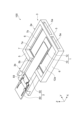
図1~図5に示される振動デバイス100は、例えば、スピーカー、又はブザーとして用いられる音響デバイスである。振動デバイス100は、振動部1と、振動部1に接続された配線部2と、振動部1が配置される音響空間を形成するケース3と、接合部材70と、接合部材71とを備えている。振動デバイス100は、図1に示されるように、被取付部材200の被取付面200aに取り付けられる。被取付部材200は、例えば、テレビ、スマートフォン等の電子機器である。 The vibration device 100 shown in FIGS. 1 to 5 is, for example, an acoustic device used as a speaker or a buzzer. The vibrating device 100 includes a vibrating part 1, a wiring part 2 connected to the vibrating part 1, a case 3 forming an acoustic space in which the vibrating part 1 is arranged, a joining member 70, and a joining member 71. There is. The vibration device 100 is attached to an attached surface 200a of an attached member 200, as shown in FIG. The attached member 200 is, for example, an electronic device such as a television or a smartphone.

振動部1は、圧電素子10と、振動部材12と、を有している。振動部材12は、例えば、Ni-Fe合金、Ni、黄銅、又はステンレス鋼等金属からなる。振動部材12は、板状部材である。振動部材12は、圧電素子10が設けられた主面12aと、主面12aと厚さ方向で対向している主面12bと、を有している。主面12a,12bは、長方形状を呈している。つまり、厚さ方向から見て、振動部材12は、長方形状を呈している。ここで、長方形状には、例えば、各角が面取りされている形状、及び、各角が丸められている形状が含まれる。長方形状には、正方形状も含まれる。本実施形態では、主面12a,12bは、例えば、一辺の長さが21mm以上29mm以下の正方形状を呈している。振動部材12の厚さは、例えば、0.06mm以上0.15mm以下である。 The vibrating section 1 includes a piezoelectric element 10 and a vibrating member 12. The vibrating member 12 is made of metal such as Ni--Fe alloy, Ni, brass, or stainless steel, for example. The vibrating member 12 is a plate-like member. The vibrating member 12 has a main surface 12a on which the piezoelectric element 10 is provided, and a main surface 12b facing the main surface 12a in the thickness direction. The main surfaces 12a and 12b have a rectangular shape. That is, the vibrating member 12 has a rectangular shape when viewed from the thickness direction. Here, the rectangular shape includes, for example, a shape in which each corner is chamfered and a shape in which each corner is rounded. The rectangular shape also includes a square shape. In this embodiment, the main surfaces 12a and 12b have, for example, a square shape with a side length of 21 mm or more and 29 mm or less. The thickness of the vibrating member 12 is, for example, 0.06 mm or more and 0.15 mm or less.

図6は、圧電素子の分解斜視図である。図6に示されるように、圧電素子10は、圧電素体11と、互いに極性が異なる一対の外部電極13,15と、を有している。圧電素体11は、直方体形状を呈している。直方体形状には、例えば、角部及び稜線部が面取りされている直方体の形状、及び、角部及び稜線部が丸められている直方体の形状が含まれる。圧電素体11は、互いに対向している主面(第一主面)11a及び主面11bを有している。主面11aには、一対の外部電極13,15が設けられている。主面11bは、主面12a(図2参照)と対向し、接合部材71によって主面12aの中央部に接合(接着)されている。 FIG. 6 is an exploded perspective view of the piezoelectric element. As shown in FIG. 6, the piezoelectric element 10 includes a piezoelectric element body 11 and a pair of external electrodes 13 and 15 having mutually different polarities. The piezoelectric element body 11 has a rectangular parallelepiped shape. The rectangular parallelepiped shape includes, for example, a rectangular parallelepiped shape with chamfered corners and edge lines, and a rectangular parallelepiped shape with rounded corners and edge lines. The piezoelectric element 11 has a main surface (first main surface) 11a and a main surface 11b facing each other. A pair of external electrodes 13 and 15 are provided on the main surface 11a. The main surface 11b faces the main surface 12a (see FIG. 2) and is joined (adhered) to the center of the main surface 12a by a joining member 71.

主面11a,11bは、長方形状を呈している。以下では、主面11a,11bの長辺方向をX方向、主面11a,11bの短辺方向をY方向、主面11a,11bの対向方向をZ方向とする。主面11a,11bの長辺方向、短辺方向及び対向方向は、それぞれ主面12a,12bの長辺方向、短辺方向及び対向方向と一致している。圧電素子10のX方向での長さは、例えば、20mmである。圧電素子10のY方向での長さは、例えば、10mmである。圧電素子10のZ方向での長さは、例えば、0.45mmである。 The main surfaces 11a and 11b have a rectangular shape. Hereinafter, the long side direction of the main surfaces 11a, 11b will be referred to as the X direction, the short side direction of the main surfaces 11a, 11b will be referred to as the Y direction, and the opposing direction of the main surfaces 11a, 11b will be referred to as the Z direction. The long side direction, short side direction, and opposing direction of the main surfaces 11a and 11b correspond to the long side direction, short side direction, and opposing direction of the main surfaces 12a and 12b, respectively. The length of the piezoelectric element 10 in the X direction is, for example, 20 mm. The length of the piezoelectric element 10 in the Y direction is, for example, 10 mm. The length of the piezoelectric element 10 in the Z direction is, for example, 0.45 mm.

圧電素体11は、複数の圧電体層17a,17b,17c,17dが積層されて構成されている。すなわち、圧電素体11は、積層されている複数の圧電体層17a,17b,17c,17dを有している。本実施形態では、圧電素体11は、四つの圧電体層17a,17b,17c,17dを有している。圧電素体11では、複数の圧電体層17a,17b,17c,17dが積層されている方向がZ方向と一致している。圧電体層17aは、主面11aを有している。圧電体層17dは、主面11bを有している。圧電体層17b,17cは、圧電体層17aと圧電体層17dとの間に位置している。 The piezoelectric element body 11 is configured by laminating a plurality of piezoelectric layers 17a, 17b, 17c, and 17d. That is, the piezoelectric element body 11 has a plurality of stacked piezoelectric layers 17a, 17b, 17c, and 17d. In this embodiment, the piezoelectric element body 11 has four piezoelectric layers 17a, 17b, 17c, and 17d. In the piezoelectric element body 11, the direction in which the plurality of piezoelectric layers 17a, 17b, 17c, and 17d are stacked coincides with the Z direction. The piezoelectric layer 17a has a main surface 11a. The piezoelectric layer 17d has a main surface 11b. The piezoelectric layers 17b and 17c are located between the piezoelectric layer 17a and the piezoelectric layer 17d.

各圧電体層17a,17b,17c,17dは、圧電材料からなる。本実施形態では、各圧電体層17a,17b,17c,17dは、圧電セラミック材料からなる。圧電セラミック材料には、例えば、PZT[Pb(Zr、Ti)O]、PT(PbTiO)、PLZT[(Pb,La)(Zr、Ti)O]、又はチタン酸バリウム(BaTiO)が用いられる。各圧電体層17a,17b,17c,17dは、例えば、上述した圧電セラミック材料を含むセラミックグリーンシートの焼結体から構成される。実際の圧電素体11では、各圧電体層17a,17b,17c,17dは、各圧電体層17a,17b,17c,17dの間の境界が認識できない程度に一体化されている。 Each piezoelectric layer 17a, 17b, 17c, 17d is made of piezoelectric material. In this embodiment, each piezoelectric layer 17a, 17b, 17c, and 17d is made of a piezoelectric ceramic material. Piezoelectric ceramic materials include, for example, PZT[Pb(Zr,Ti)O 3 ], PT(PbTiO 3 ), PLZT[(Pb,La)(Zr,Ti)O 3 ], or barium titanate (BaTiO 3 ). is used. Each piezoelectric layer 17a, 17b, 17c, and 17d is composed of, for example, a sintered body of a ceramic green sheet containing the piezoelectric ceramic material described above. In the actual piezoelectric element 11, the piezoelectric layers 17a, 17b, 17c, and 17d are integrated to such an extent that the boundaries between the piezoelectric layers 17a, 17b, 17c, and 17d are unrecognizable.

圧電素子10は、圧電素体11内に配置されている複数の内部電極19,21,23を備えている。本実施形態では、圧電素子10は、三つの内部電極19,21,23を備えている。各内部電極19,21,23は、導電性材料からなる。導電性材料には、例えば、Ag、Pd、又はAg-Pd合金が用いられる。各内部電極19,21,23は、例えば、上記導電性材料を含む導電性ペーストの焼結体として構成されている。本実施形態では、各内部電極19,21,23の外形形状は、長方形状である。 The piezoelectric element 10 includes a plurality of internal electrodes 19 , 21 , 23 arranged within the piezoelectric element body 11 . In this embodiment, the piezoelectric element 10 includes three internal electrodes 19, 21, and 23. Each internal electrode 19, 21, 23 is made of a conductive material. For example, Ag, Pd, or Ag-Pd alloy is used as the conductive material. Each of the internal electrodes 19, 21, and 23 is configured, for example, as a sintered body of conductive paste containing the above-mentioned conductive material. In this embodiment, the outer shape of each internal electrode 19, 21, 23 is rectangular.

各内部電極19,21,23は、Z方向において異なる位置(層)に配置されている。内部電極19と内部電極21とは、Z方向に間隔を有して対向している。内部電極21と内部電極23とは、Z方向に間隔を有して対向している。内部電極19は、圧電体層17aと圧電体層17bとの間に位置している。内部電極21は、圧電体層17bと圧電体層17cとの間に位置している。内部電極23は、圧電体層17cと圧電体層17dとの間に位置している。各内部電極19,21,23は、圧電素体11の表面には露出していない。すなわち、各内部電極19,21,23は、各側面には露出していない。各内部電極19,21,23は、Z方向から見て、主面11a,11bの全ての縁(四辺)から離間している。 Each internal electrode 19, 21, 23 is arranged at a different position (layer) in the Z direction. Internal electrode 19 and internal electrode 21 face each other with a gap in the Z direction. Internal electrode 21 and internal electrode 23 face each other with a gap in the Z direction. Internal electrode 19 is located between piezoelectric layer 17a and piezoelectric layer 17b. Internal electrode 21 is located between piezoelectric layer 17b and piezoelectric layer 17c. The internal electrode 23 is located between the piezoelectric layer 17c and the piezoelectric layer 17d. Each internal electrode 19 , 21 , 23 is not exposed on the surface of the piezoelectric element body 11 . That is, each internal electrode 19, 21, 23 is not exposed on each side surface. Each internal electrode 19, 21, 23 is spaced apart from all edges (four sides) of main surfaces 11a, 11b when viewed from the Z direction.

一対の外部電極13,15は、主面11a上に配置されている。外部電極13と外部電極15とは、X方向に並んでいる。外部電極13と外部電極15とは、X方向で隣り合っている。一対の外部電極13,15は、主面11aの中央部に配置されている。一対の外部電極13,15は、Z方向から見て、主面11aの全ての縁(四辺)から離間している。各外部電極13,15は、Z方向から見て、長方形状を呈している。各外部電極13,15は、導電性材料からなる。導電性材料には、例えば、Ag、Pd、又はAg-Pd合金が用いられる。各外部電極13,15は、例えば、上記導電性材料を含む導電性ペーストの焼結体として構成されている。 A pair of external electrodes 13 and 15 are arranged on the main surface 11a. The external electrodes 13 and 15 are arranged in the X direction. External electrode 13 and external electrode 15 are adjacent to each other in the X direction. A pair of external electrodes 13 and 15 are arranged at the center of the main surface 11a. The pair of external electrodes 13 and 15 are spaced apart from all edges (four sides) of the main surface 11a when viewed from the Z direction. Each external electrode 13, 15 has a rectangular shape when viewed from the Z direction. Each external electrode 13, 15 is made of a conductive material. For example, Ag, Pd, or Ag-Pd alloy is used as the conductive material. Each of the external electrodes 13 and 15 is configured, for example, as a sintered body of conductive paste containing the above-mentioned conductive material.

外部電極13は、ビア導体31を通して接続導体25と電気的に接続されている。接続導体25は、内部電極19と同じ層に位置している。接続導体25は、内部電極19の内側に位置している。内部電極19には、Z方向から見て、外部電極13に対応する位置に、開口が形成されている。接続導体25は、内部電極19に形成されている開口内に位置している。Z方向から見て、接続導体25の全縁が、内部電極19で囲まれている。 External electrode 13 is electrically connected to connection conductor 25 through via conductor 31 . The connection conductor 25 is located on the same layer as the internal electrode 19. The connection conductor 25 is located inside the internal electrode 19. An opening is formed in the internal electrode 19 at a position corresponding to the external electrode 13 when viewed from the Z direction. The connection conductor 25 is located within an opening formed in the internal electrode 19. The entire edge of the connection conductor 25 is surrounded by the internal electrode 19 when viewed from the Z direction.

接続導体25は、圧電体層17aと圧電体層17bとの間に位置している。内部電極19と接続導体25とは、離間している。接続導体25は、Z方向で、外部電極13と対向している。ビア導体31は、外部電極13と接続されていると共に、接続導体25と接続されている。接続導体25は、ビア導体33を通して内部電極21と電気的に接続されている。接続導体25は、Z方向で、内部電極21と対向している。ビア導体33は、接続導体25と接続されていると共に、内部電極21と接続されている。 The connection conductor 25 is located between the piezoelectric layer 17a and the piezoelectric layer 17b. Internal electrode 19 and connection conductor 25 are spaced apart. The connection conductor 25 faces the external electrode 13 in the Z direction. The via conductor 31 is connected to the external electrode 13 and also to the connection conductor 25 . The connection conductor 25 is electrically connected to the internal electrode 21 through the via conductor 33. The connection conductor 25 faces the internal electrode 21 in the Z direction. The via conductor 33 is connected to the connection conductor 25 and also to the internal electrode 21 .

内部電極21は、ビア導体35を通して接続導体27と電気的に接続されている。接続導体27は、内部電極23と同じ層に位置している。接続導体27は、内部電極23の内側に位置している。内部電極23には、Z方向から見て、外部電極13(接続導体25)に対応する位置に、開口が形成されている。接続導体27は、内部電極23に形成されている開口内に位置している。Z方向から見て、接続導体27の全縁が、内部電極23で囲まれている。 Internal electrode 21 is electrically connected to connection conductor 27 through via conductor 35 . The connection conductor 27 is located on the same layer as the internal electrode 23. The connecting conductor 27 is located inside the internal electrode 23. An opening is formed in the internal electrode 23 at a position corresponding to the external electrode 13 (connection conductor 25) when viewed from the Z direction. The connection conductor 27 is located within an opening formed in the internal electrode 23. The entire edge of the connection conductor 27 is surrounded by the internal electrode 23 when viewed from the Z direction.

外部電極15は、ビア導体37を通して内部電極19と電気的に接続されている。内部電極19は、Z方向で、外部電極15と対向している。ビア導体37は、外部電極15と接続されていると共に、内部電極19と接続されている。 External electrode 15 is electrically connected to internal electrode 19 through via conductor 37 . The internal electrode 19 faces the external electrode 15 in the Z direction. The via conductor 37 is connected to the external electrode 15 and also to the internal electrode 19 .

内部電極19は、ビア導体39を通して接続導体29と電気的に接続されている。接続導体29は、内部電極21と同じ層に位置している。接続導体29は、内部電極21の内側に位置している。内部電極21には、Z方向から見て、外部電極15に対応する位置に、開口が形成されている。接続導体29は、内部電極21に形成されている開口内に位置している。Z方向から見て、接続導体29の全縁が、内部電極21で囲まれている。 Internal electrode 19 is electrically connected to connection conductor 29 through via conductor 39 . The connection conductor 29 is located on the same layer as the internal electrode 21. The connecting conductor 29 is located inside the internal electrode 21 . An opening is formed in the internal electrode 21 at a position corresponding to the external electrode 15 when viewed from the Z direction. The connecting conductor 29 is located within an opening formed in the internal electrode 21. The entire edge of the connecting conductor 29 is surrounded by the internal electrode 21 when viewed from the Z direction.

接続導体29は、圧電体層17bと圧電体層17cとの間に位置している。内部電極21と接続導体29とは、離間している。接続導体29は、Z方向で、内部電極19と対向している。ビア導体39は、内部電極19と接続されていると共に、接続導体29と接続されている。接続導体29は、ビア導体41を通して内部電極23と電気的に接続されている。接続導体29は、Z方向で、内部電極23と対向している。ビア導体41は、接続導体29と接続されていると共に、内部電極23と接続されている。 The connection conductor 29 is located between the piezoelectric layer 17b and the piezoelectric layer 17c. Internal electrode 21 and connection conductor 29 are spaced apart. The connection conductor 29 faces the internal electrode 19 in the Z direction. The via conductor 39 is connected to the internal electrode 19 and also to the connection conductor 29 . The connection conductor 29 is electrically connected to the internal electrode 23 through the via conductor 41. The connection conductor 29 faces the internal electrode 23 in the Z direction. The via conductor 41 is connected to the connection conductor 29 and also to the internal electrode 23 .

外部電極13は、ビア導体31、接続導体25、及び、ビア導体33を通して、内部電極21と電気的に接続されている。外部電極15は、ビア導体37を通して、内部電極19と電気的に接続されている。外部電極15は、ビア導体37、内部電極19、ビア導体39、接続導体29、及び、ビア導体41を通して、内部電極23と電気的に接続されている。 The external electrode 13 is electrically connected to the internal electrode 21 through the via conductor 31 , the connecting conductor 25 , and the via conductor 33 . External electrode 15 is electrically connected to internal electrode 19 through via conductor 37 . The external electrode 15 is electrically connected to the internal electrode 23 through the via conductor 37 , internal electrode 19 , via conductor 39 , connection conductor 29 , and via conductor 41 .

接続導体25,27,29及びビア導体31,33,35,37,39,41は、導電性材料からなる。ビア導体31,33,35,37,39,41のそれぞれは、複数のビア導体からなるビア導体群であるが、単体のビア導体であってもよい。Z方向で互いに隣り合う圧電体層17a,17bに配置されたビア導体31,33は、Z方向から見て互いに離間し、重ならないように配置されている。圧電体層17a,17bに配置されたビア導体37,39は、Z方向から見て互いに離間し、重ならないように配置されている。Z方向で互いに隣り合う圧電体層17b,17cに配置されたビア導体33,35は、Z方向から見て互いに離間し、重ならないように配置されている。圧電体層17b,17cに配置されたビア導体39,41は、Z方向から見て互いに離間し、重ならないように配置されている。 The connection conductors 25, 27, 29 and the via conductors 31, 33, 35, 37, 39, 41 are made of conductive material. Each of the via conductors 31, 33, 35, 37, 39, and 41 is a via conductor group consisting of a plurality of via conductors, but may be a single via conductor. Via conductors 31 and 33 arranged in piezoelectric layers 17a and 17b adjacent to each other in the Z direction are spaced apart from each other when viewed from the Z direction, and are arranged so as not to overlap. The via conductors 37 and 39 arranged in the piezoelectric layers 17a and 17b are spaced apart from each other when viewed from the Z direction, and are arranged so as not to overlap. Via conductors 33 and 35 arranged in piezoelectric layers 17b and 17c adjacent to each other in the Z direction are spaced apart from each other when viewed from the Z direction, and are arranged so as not to overlap. The via conductors 39 and 41 arranged in the piezoelectric layers 17b and 17c are spaced apart from each other when viewed from the Z direction, and are arranged so as not to overlap.

導電性材料には、例えば、Ag、Pd、又はAg-Pd合金が用いられる。接続導体25,27,29及びビア導体31,33,35,37,39,41は、例えば、上記導電性材料を含む導電性ペーストの焼結体として構成されている。接続導体25,27,29は、長方形状を呈している。ビア導体31,33,35,37,39,41は、対応する圧電体層17a,17b,17cを形成するためのセラミックグリーンシートに形成された貫通孔に充填された導電性ペーストが焼結することにより形成される。 For example, Ag, Pd, or Ag-Pd alloy is used as the conductive material. The connection conductors 25, 27, 29 and the via conductors 31, 33, 35, 37, 39, 41 are configured, for example, as sintered bodies of conductive paste containing the above-mentioned conductive material. The connection conductors 25, 27, 29 have a rectangular shape. Via conductors 31, 33, 35, 37, 39, and 41 are formed by sintering conductive paste filled in through holes formed in ceramic green sheets for forming corresponding piezoelectric layers 17a, 17b, and 17c. It is formed by

圧電素体11の主面11bには、内部電極19,23と電気的に接続されている導体と、内部電極21と電気的に接続されている導体とは配置されていない。本実施形態では、主面11bをZ方向から見たとき、主面11bの全体が露出している。主面11a,11bは、自然面である。自然面とは、焼成により成長した結晶粒の表面により構成される面である。 A conductor electrically connected to the internal electrodes 19 and 23 and a conductor electrically connected to the internal electrode 21 are not arranged on the main surface 11b of the piezoelectric element 11. In this embodiment, when main surface 11b is viewed from the Z direction, the entire main surface 11b is exposed. The main surfaces 11a and 11b are natural surfaces. The natural surface is a surface formed by the surface of crystal grains grown by firing.

圧電素体11の各側面にも、内部電極19,23と電気的に接続されている導体と、内部電極21と電気的に接続されている導体とは配置されていない。本実施形態では、圧電素体11の各側面をX方向及びY方向から見たとき、各側面の全体が露出している。本実施形態では、これらの各側面も、自然面である。 Conductors electrically connected to the internal electrodes 19 and 23 and conductors electrically connected to the internal electrode 21 are not arranged on each side surface of the piezoelectric element 11 either. In this embodiment, when each side surface of the piezoelectric element body 11 is viewed from the X direction and the Y direction, each side surface is entirely exposed. In this embodiment, each of these sides is also a natural surface.

圧電体層17bにおける内部電極19と内部電極21とで挟まれた領域と、圧電体層17cにおける内部電極21と内部電極23とで挟まれた領域とは、圧電的に活性な領域を構成する。本実施形態では、圧電的に活性な領域は、Z方向から見て、一対の外部電極13,15を囲むように位置している。Z方向から見て、圧電素体11は、外部電極13と外部電極15との間に位置している領域に、圧電的に活性な領域を含んでいる。Z方向から見て、圧電素体11は、外部電極13と外部電極15とが位置している領域の外側にも、圧電的に活性な領域を含んでいる。 The region sandwiched between the internal electrodes 19 and 21 in the piezoelectric layer 17b and the region sandwiched between the internal electrodes 21 and 23 in the piezoelectric layer 17c constitute piezoelectrically active regions. . In this embodiment, the piezoelectrically active region is located so as to surround the pair of external electrodes 13 and 15 when viewed from the Z direction. When viewed from the Z direction, the piezoelectric element body 11 includes a piezoelectrically active region in a region located between the external electrodes 13 and 15. When viewed from the Z direction, the piezoelectric element body 11 also includes a piezoelectrically active region outside the region where the external electrodes 13 and 15 are located.

図1~図5に示されるように、配線部2は、主面11a上で一対の外部電極13,15に接続された帯状の第一配線部材50と、第一配線部材50に接続された板状の第二配線部材60と、接合部材72と、を有している。 As shown in FIGS. 1 to 5, the wiring section 2 includes a strip-shaped first wiring member 50 connected to the pair of external electrodes 13 and 15 on the main surface 11a, and a first wiring member 50 connected to the first wiring member 50. It has a plate-shaped second wiring member 60 and a joining member 72.

第一配線部材50は、主面11aに直交する直交方向(Z方向)から見て、主面11aの長辺に沿って延在して、主面11aの短辺と直交している。第一配線部材50は、X方向に延在し、Y方向と直交している。第一配線部材50は、第二配線部材60と電気的かつ物理的に接続される一端部50aと、圧電素子10と電気的かつ物理的に接続されている他端部50bと、を有している。第一配線部材50は、一端部50aと他端部50bとの間に幅(Y方向の長さ)が狭くされた幅狭部50cを有している。幅狭部50cは、一端部50aと隣り合って設けられている。第一配線部材50は、幅狭部50c以外の部分において一定の幅を有している。幅狭部50cの幅は、例えば、幅狭部50c以外の部分の幅の56%以上83%以下である。 The first wiring member 50 extends along the long side of the main surface 11a and is orthogonal to the short side of the main surface 11a when viewed from the orthogonal direction (Z direction) perpendicular to the main surface 11a. The first wiring member 50 extends in the X direction and is perpendicular to the Y direction. The first wiring member 50 has one end 50a that is electrically and physically connected to the second wiring member 60, and the other end 50b that is electrically and physically connected to the piezoelectric element 10. ing. The first wiring member 50 has a narrow portion 50c having a narrow width (length in the Y direction) between one end portion 50a and the other end portion 50b. The narrow portion 50c is provided adjacent to the one end portion 50a. The first wiring member 50 has a constant width in a portion other than the narrow portion 50c. The width of the narrow portion 50c is, for example, 56% or more and 83% or less of the width of the portion other than the narrow portion 50c.

第一配線部材50の他端部50bは、接合部材70によって一対の外部電極13,15に接合されている。接合部材70は、一対の外部電極13,15と他端部50bとの間に配置され、一対の外部電極13,15と他端部50bとを接合している。接合部材70は、複数の導電性粒子(不図示)を含む樹脂層である。導電性粒子は、例えば、金属粒子、金めっき粒子である。接合部材70は、例えば熱硬化性エラストマーを含んでいる。接合部材70は、例えば、異方性導電ペースト又は異方性導電性膜が硬化することにより形成される。接合部材70は、一対の外部電極13,15と他端部50bとを電気的に接続している。Z方向から見て、接合部材70は、一対の外部電極13,15を一体的に覆っている。Z方向から見て、接合部材70は、他端部50bに設けられた後述の一対の端部53b,55b(図7参照)を一体的に覆っている。 The other end 50b of the first wiring member 50 is joined to the pair of external electrodes 13 and 15 by a joining member 70. The joining member 70 is disposed between the pair of external electrodes 13, 15 and the other end 50b, and joins the pair of external electrodes 13, 15 and the other end 50b. The joining member 70 is a resin layer containing a plurality of conductive particles (not shown). The conductive particles are, for example, metal particles or gold-plated particles. The joining member 70 includes, for example, a thermosetting elastomer. The joining member 70 is formed, for example, by curing an anisotropic conductive paste or an anisotropic conductive film. The joining member 70 electrically connects the pair of external electrodes 13 and 15 to the other end portion 50b. When viewed from the Z direction, the joining member 70 integrally covers the pair of external electrodes 13 and 15. When viewed from the Z direction, the joining member 70 integrally covers a pair of end portions 53b and 55b (see FIG. 7), which will be described later, provided at the other end portion 50b.

第一配線部材50は、接合部材71によって主面11a及び主面12aに接合されている。接合部材71は、導電性粒子を含んでおらず、電気絶縁性を有する樹脂層である。接合部材71は、例えば、反応型フェノール樹脂とニトリルゴムを主成分にしたホットメルト樹脂である。接合部材71は、接合部材70に含まれる樹脂材料と同じ樹脂材料を含んでいてもよい。接合部材71は、主面11aの一方の短辺に沿って配置されている。接合部材71は、第一配線部材50の幅方向(Y方向)の全体を主面11a及び主面12aに接合している。接合部材71は、接合部材70からX方向において離間している。 The first wiring member 50 is joined to the main surface 11a and the main surface 12a by a joining member 71. The joining member 71 is a resin layer that does not contain conductive particles and has electrical insulation properties. The joining member 71 is, for example, a hot melt resin whose main components are a reactive phenol resin and nitrile rubber. Bonding member 71 may include the same resin material as that contained in bonding member 70 . The joining member 71 is arranged along one short side of the main surface 11a. The joining member 71 joins the entire first wiring member 50 in the width direction (Y direction) to the main surface 11a and the main surface 12a. The joining member 71 is spaced apart from the joining member 70 in the X direction.

第一配線部材50の一端部50aは、接合部材72によって第二配線部材60に接合されている。接合部材72は、後述の一対の導体層63,65(図4参照)と一端部50aとの間に配置され、一対の導体層63,65と一端部50aとを接合している。接合部材72は、複数の導電性粒子(不図示)を含む樹脂層である。導電性粒子は、例えば、金属粒子、金めっき粒子である。接合部材72は、例えば熱硬化性エラストマーを含んでいる。接合部材72は、例えば、異方性導電ペースト又は異方性導電性膜が硬化することにより形成される。接合部材72は、例えば、接合部材70と同じ材料で構成されている。接合部材72は、一対の導体層63,65と一端部50aとを電気的に接続している。Z方向から見て、接合部材70は、一対の導体層63,65を一体的に覆っている。Z方向から見て、接合部材70は、他端部50bに設けられた後述の一対の端部53a,55aを一体的に覆っている。 One end 50a of the first wiring member 50 is joined to the second wiring member 60 by a joining member 72. The joining member 72 is disposed between a pair of conductor layers 63, 65 (see FIG. 4) to be described later and one end portion 50a, and joins the pair of conductor layers 63, 65 and one end portion 50a. The joining member 72 is a resin layer containing a plurality of conductive particles (not shown). The conductive particles are, for example, metal particles or gold-plated particles. The joining member 72 includes, for example, a thermosetting elastomer. The joining member 72 is formed, for example, by curing an anisotropic conductive paste or an anisotropic conductive film. The joining member 72 is made of the same material as the joining member 70, for example. The joining member 72 electrically connects the pair of conductor layers 63, 65 and one end portion 50a. When viewed from the Z direction, the joining member 70 integrally covers the pair of conductor layers 63 and 65. When viewed from the Z direction, the joining member 70 integrally covers a pair of end portions 53a and 55a, which will be described later, provided at the other end portion 50b.

接合部材70,71,72は、厚さ方向(Z方向)からみて、いずれも長方形状を呈している。接合部材70の長手方向は、後述の一対の端部53b,55b(図7参照)の並ぶ方向(X方向)と一致している。接合部材71の長手方向は、主面11aの短辺方向(Y方向)と一致している。接合部材72の長手方向は、後述の一対の導体層63,65(図4参照)の並ぶ方向(Y方向)と一致している。接合部材70の長手方向と、接合部材71,72の長手方向とは互いに交差(直交)している。 The joining members 70, 71, and 72 all have a rectangular shape when viewed from the thickness direction (Z direction). The longitudinal direction of the joining member 70 coincides with the direction (X direction) in which a pair of end portions 53b and 55b (see FIG. 7), which will be described later, are lined up. The longitudinal direction of the joining member 71 coincides with the short side direction (Y direction) of the main surface 11a. The longitudinal direction of the bonding member 72 coincides with the direction (Y direction) in which a pair of conductor layers 63 and 65 (see FIG. 4), which will be described later, are lined up. The longitudinal direction of the joining member 70 and the longitudinal directions of the joining members 71 and 72 intersect with each other (orthogonal to each other).

図1及び図7に示されるように、第一配線部材50は、ベース51、一対の導体層53,55、カバー57、及び補強部59を有している。第一配線部材50は、可撓性を有し、例えば、フレキシブルプリント基板(FPC)又はフレキシブルフラットケーブル(FFC)である。 As shown in FIGS. 1 and 7, the first wiring member 50 includes a base 51, a pair of conductor layers 53 and 55, a cover 57, and a reinforcing portion 59. The first wiring member 50 has flexibility, and is, for example, a flexible printed circuit board (FPC) or a flexible flat cable (FFC).

ベース51は、帯状を呈し、互いに対向している一対の主面51a,51bを有している。ベース51は、電気絶縁性を有している。ベース51は、例えば、ポリイミド樹脂等の樹脂からなる樹脂層である。ベース51の厚さは、例えば100μmである。 The base 51 is strip-shaped and has a pair of principal surfaces 51a and 51b facing each other. The base 51 has electrical insulation properties. The base 51 is, for example, a resin layer made of resin such as polyimide resin. The thickness of the base 51 is, for example, 100 μm.

各導体層53,55は、ベース51の主面51a上に配置されている。各導体層53,55は、接着層(不図示)によって、主面51aに接合(接着)されている。各導体層53,55は、例えば、Cuからなる。各導体層53,55は、例えば、Cu層上にNiメッキ層及びAuメッキ層がこの順に設けられた構成であってもよい。導体層53と導体層55とは、互いに離間して配置されている。各導体層53,55の厚さは、例えば20μmである。 Each conductor layer 53, 55 is arranged on the main surface 51a of the base 51. Each conductor layer 53, 55 is joined (adhered) to the main surface 51a by an adhesive layer (not shown). Each conductor layer 53, 55 is made of, for example, Cu. Each conductor layer 53, 55 may have a structure in which, for example, a Ni plating layer and an Au plating layer are provided in this order on a Cu layer. The conductor layer 53 and the conductor layer 55 are spaced apart from each other. The thickness of each conductor layer 53, 55 is, for example, 20 μm.

導体層53は、第二配線部材60に接続された端部53aと、外部電極13に接続された端部53bと、端部53aと端部53bとを接続している接続部53cと、を含んでいる。接続部53cは、第一配線部材50が延在している方向(X方向)に延在している。端部53aは、接続部53cの一端部と、第一配線部材50が延在している方向において隣り合っている。端部53bは、接続部53cの他端部と、第一配線部材50の幅方向(Y方向)において隣り合っている。 The conductor layer 53 has an end 53a connected to the second wiring member 60, an end 53b connected to the external electrode 13, and a connecting part 53c connecting the end 53a and the end 53b. Contains. The connecting portion 53c extends in the direction in which the first wiring member 50 extends (X direction). The end portion 53a is adjacent to one end portion of the connecting portion 53c in the direction in which the first wiring member 50 extends. The end portion 53b is adjacent to the other end portion of the connecting portion 53c in the width direction (Y direction) of the first wiring member 50.

導体層55は、第二配線部材60に接続された端部55aと、外部電極15に接続された端部55bと、端部55aと端部55bとを接続している接続部55cと、を含んでいる。接続部55cは、第一配線部材50が延在している方向(X方向)に延在している。端部55aは、接続部55cの一端部と、第一配線部材50が延在している方向において隣り合っている。端部55bは、接続部55cの他端部と、第一配線部材50の幅方向(Y方向)において隣り合っている。 The conductor layer 55 has an end 55a connected to the second wiring member 60, an end 55b connected to the external electrode 15, and a connecting part 55c connecting the end 55a and the end 55b. Contains. The connecting portion 55c extends in the direction in which the first wiring member 50 extends (X direction). The end portion 55a is adjacent to one end portion of the connecting portion 55c in the direction in which the first wiring member 50 extends. The end portion 55b is adjacent to the other end portion of the connecting portion 55c in the width direction (Y direction) of the first wiring member 50.

端部53aと端部55aとは、第一配線部材50の幅方向において互いに離間して配置されている。端部53bと端部55bとは、第一配線部材50の延在している方向において互いに離間して配置されている。接続部53cと接続部55cとは、互いに平行、かつ、第一配線部材50の幅方向において互いに離間して配置されている。 The end portion 53a and the end portion 55a are spaced apart from each other in the width direction of the first wiring member 50. The end portion 53b and the end portion 55b are spaced apart from each other in the direction in which the first wiring member 50 extends. The connecting portion 53c and the connecting portion 55c are arranged parallel to each other and spaced apart from each other in the width direction of the first wiring member 50.

端部53bと外部電極13との間には、接合部材70が存在している。端部53bと外部電極13とは、接合部材70に含まれる導電性粒子を通じて電気的に接続されている。端部55bと外部電極15との間には、接合部材70が存在している。端部55bと外部電極15とは、接合部材70に含まれる導電性粒子を通じて電気的に接続されている。 A joining member 70 is present between the end portion 53b and the external electrode 13. The end portion 53b and the external electrode 13 are electrically connected through conductive particles included in the joining member 70. A joining member 70 is present between the end portion 55b and the external electrode 15. The end portion 55b and the external electrode 15 are electrically connected through conductive particles included in the joining member 70.

カバー57は、主面51a上に配置されている。カバー57は、各導体層53,55と、主面51aとを覆っている。カバー57は、各導体層53,55と、主面51aのうち、各導体層53,55から露出している領域とに接着層(不図示)によって接合(接着)されている。カバー57は、例えば、ポリイミド樹脂等の樹脂からなる樹脂層である。カバー57の厚さは、例えば25μmである。導体層53の端部53a,53bと、導体層55の端部55a,55bと、主面51aにおける各端部53a,53b,55a,55bの近傍領域とは、カバー57から露出している。 The cover 57 is arranged on the main surface 51a. The cover 57 covers each conductor layer 53, 55 and the main surface 51a. The cover 57 is joined (adhered) to each conductor layer 53, 55 and a region of the main surface 51a exposed from each conductor layer 53, 55 by an adhesive layer (not shown). The cover 57 is, for example, a resin layer made of resin such as polyimide resin. The thickness of the cover 57 is, for example, 25 μm. Ends 53a and 53b of the conductor layer 53, ends 55a and 55b of the conductor layer 55, and areas near the ends 53a, 53b, 55a, and 55b on the main surface 51a are exposed from the cover 57.

補強部59は、ベース51の主面51b上に配置されている。補強部59は、接着層(不図示)によって、主面51bに接合(接着)されている。補強部59は、少なくとも幅狭部50cに設けられている。補強部59は、Z方向から見て、第一配線部材50のうち、第二配線部材60と重なる部分、及び、第二配線部材60と重ならない部分の両方にまたがって設けられている。補強部59は、例えば、ポリイミドからなる樹脂層である。補強部59の厚さは、例えば200μmである。 The reinforcing portion 59 is arranged on the main surface 51b of the base 51. The reinforcing portion 59 is joined (adhered) to the main surface 51b by an adhesive layer (not shown). The reinforcing portion 59 is provided at least in the narrow portion 50c. The reinforcing portion 59 is provided across both a portion of the first wiring member 50 that overlaps with the second wiring member 60 and a portion that does not overlap with the second wiring member 60 when viewed from the Z direction. The reinforcing portion 59 is, for example, a resin layer made of polyimide. The thickness of the reinforcing portion 59 is, for example, 200 μm.

図4及び図8に示されるように、第二配線部材60は、基板61と、一対の導体層63,65と、一対のレジスト層67,69と、を有している。第二配線部材60は、矩形板状を呈し、厚さ方向(Z方向)で互いに対向している主面60a(第二主面)及び主面60b(第三主面)を有している。主面60aは、後述の主面61aと、一対の導体層63,65の表面と、レジスト層67の表面と、を含んでいる。主面60bは、レジスト層69の表面を含んでいる。 As shown in FIGS. 4 and 8, the second wiring member 60 includes a substrate 61, a pair of conductor layers 63 and 65, and a pair of resist layers 67 and 69. The second wiring member 60 has a rectangular plate shape and has a main surface 60a (second main surface) and a main surface 60b (third main surface) facing each other in the thickness direction (Z direction). . The main surface 60a includes a main surface 61a, which will be described later, the surfaces of a pair of conductor layers 63 and 65, and the surface of a resist layer 67. Main surface 60b includes the surface of resist layer 69.

第二配線部材60には、第二配線部材60を主面60a及び主面60bの対向方向(Z方向)に貫通している複数の貫通孔60cが設けられている。貫通孔60cは、断面円形状を呈している。第二配線部材60は、第一配線部材50よりも硬く、可撓性を有していない。第二配線部材60は、例えば、プリント基板(PCB:Print Circuit Board)である。第二配線部材60は、ケース3よりも硬い。 The second wiring member 60 is provided with a plurality of through holes 60c that penetrate the second wiring member 60 in the direction in which the main surfaces 60a and 60b face each other (Z direction). The through hole 60c has a circular cross section. The second wiring member 60 is harder than the first wiring member 50 and has no flexibility. The second wiring member 60 is, for example, a printed circuit board (PCB). The second wiring member 60 is harder than the case 3.

基板61は、矩形板状を呈している。基板61は、例えば、ガラスからなり、電気絶縁性を有している。基板61は、互いに対向している矩形状の一対の主面61a,61bを有している。一対の主面61a,61bの長辺方向(X方向)の長さは、例えば17mmである。一対の主面61a,61bの短辺方向(Y方向)の長さは、例えば10.9mmである。基板61の厚さ(基板61のZ方向の長さ)は、例えば0.8mmである。 The substrate 61 has a rectangular plate shape. The substrate 61 is made of glass, for example, and has electrical insulation properties. The substrate 61 has a pair of rectangular main surfaces 61a and 61b facing each other. The length of the pair of main surfaces 61a, 61b in the long side direction (X direction) is, for example, 17 mm. The length of the pair of main surfaces 61a and 61b in the short side direction (Y direction) is, for example, 10.9 mm. The thickness of the substrate 61 (the length of the substrate 61 in the Z direction) is, for example, 0.8 mm.

各導体層63,65は、主面61a上に設けられている。各導体層63,65は、例えば、Cuからなる。各導体層63,65は、例えば、Cu層上にNiメッキ層及びAuメッキ層がこの順に設けられた構成であってもよい。導体層63と導体層65とは、互いに離間して配置されている。各導体層63,65の厚さは、例えば20μmである。レジスト層67は、基板61の主面61a及び各導体層63,65を覆っている。レジスト層67の厚さは、例えば1μmである。レジスト層69は、基板61の主面61bを覆っている。レジスト層69の厚さは、例えば1μmである。 Each conductor layer 63, 65 is provided on the main surface 61a. Each conductor layer 63, 65 is made of, for example, Cu. Each conductor layer 63, 65 may have a structure in which, for example, a Ni plating layer and an Au plating layer are provided in this order on a Cu layer. The conductor layer 63 and the conductor layer 65 are spaced apart from each other. The thickness of each conductor layer 63, 65 is, for example, 20 μm. The resist layer 67 covers the main surface 61a of the substrate 61 and each conductor layer 63, 65. The thickness of the resist layer 67 is, for example, 1 μm. The resist layer 69 covers the main surface 61b of the substrate 61. The thickness of the resist layer 69 is, for example, 1 μm.

導体層63は、レジスト層67から露出した端部63aを有している。端部63aと端部53aとの間には接合部材72が存在している。端部63aは、端部53aと接合部材72により接合されている。導体層63は、接合部材72に含まれる導電性粒子を通じて端部53aと電気的に接続されている。導体層65は、レジスト層67から露出した端部65aを有している。端部65aと端部55aとの間には接合部材72が存在している。端部65aは、端部55aと接合部材72により接合されている。導体層65は、接合部材72に含まれる導電性粒子を通じて端部55aと電気的に接続されている。図示を省略するが、第二配線部材60は、基板61の下面に設けられ、各導体層63,65とスルーホール導体で接続された一対の導体層を更に有している。 The conductor layer 63 has an end portion 63a exposed from the resist layer 67. A joining member 72 exists between the end portion 63a and the end portion 53a. The end portion 63a is joined to the end portion 53a by a joining member 72. The conductor layer 63 is electrically connected to the end portion 53a through conductive particles included in the bonding member 72. The conductor layer 65 has an end portion 65a exposed from the resist layer 67. A joining member 72 exists between the end portion 65a and the end portion 55a. The end portion 65a is joined to the end portion 55a by a joining member 72. The conductor layer 65 is electrically connected to the end portion 55a through conductive particles included in the bonding member 72. Although not shown, the second wiring member 60 further includes a pair of conductor layers provided on the lower surface of the substrate 61 and connected to the conductor layers 63 and 65 through through-hole conductors.

図1~図5に示されるケース3は、例えば、アクリル系樹脂、塩化ビニル系樹脂、成型樹脂等の樹脂材料からなる。ケース3は、振動部1が収容される第一収容部3a、及び配線部2が収容される第二収容部3bを有している。ケース3には、振動部1及び配線部2が配置される。 The case 3 shown in FIGS. 1 to 5 is made of a resin material such as acrylic resin, vinyl chloride resin, molded resin, or the like. The case 3 has a first housing part 3a in which the vibrating part 1 is housed, and a second housing part 3b in which the wiring part 2 is housed. In the case 3, the vibrating section 1 and the wiring section 2 are arranged.

第一収容部3aは、例えば、上面(被取付部材200側の面)が開放された直方体形状の箱部材である。第一収容部3aは、底板4と、一対の側板5と、一対の側板6と、支持部7と、を有している。 The first accommodating portion 3a is, for example, a rectangular parallelepiped-shaped box member with an open top surface (surface on the side of the attached member 200). The first accommodating part 3a has a bottom plate 4, a pair of side plates 5, a pair of side plates 6, and a support part 7.

底板4は、振動部材12の主面12bと対向している主面4a(第三主面)を有している。主面4aは、例えば、一対の長辺と一対の短辺とを有する長方形状を呈している。ここで、長方形状には、例えば、各角が面取りされている形状、及び、各角が丸められている形状が含まれる。長方形状には、正方形状も含まれる。主面4aの長辺方向はX方向、主面4aの短辺方向はY方向、底板4の厚さ方向はZ方向とそれぞれ一致している。主面4aは、主面12a,12bよりも大きく、Z方向から見て、主面4aの外縁は、主面12a,12bから離間して主面12a,12bの外側に位置している。底板4の厚さ(Z方向での長さ)は、例えば、1.2mm以上1.4mm以下である。 The bottom plate 4 has a main surface 4a (third main surface) facing the main surface 12b of the vibrating member 12. The main surface 4a has, for example, a rectangular shape having a pair of long sides and a pair of short sides. Here, the rectangular shape includes, for example, a shape in which each corner is chamfered and a shape in which each corner is rounded. The rectangular shape also includes a square shape. The long side direction of the main surface 4a corresponds to the X direction, the short side direction of the main surface 4a corresponds to the Y direction, and the thickness direction of the bottom plate 4 corresponds to the Z direction. The main surface 4a is larger than the main surfaces 12a, 12b, and when viewed from the Z direction, the outer edge of the main surface 4a is spaced apart from the main surfaces 12a, 12b and located on the outside of the main surfaces 12a, 12b. The thickness (length in the Z direction) of the bottom plate 4 is, for example, 1.2 mm or more and 1.4 mm or less.

本実施形態では、主面4aは、例えば、主面12a,12bの形状と相似形状であり、一辺の長さが30mm以上33mm以下の正方形状を呈している。なお、主面4aは、各角が面取りされている形状、又は、各角が丸められている形状であるか否かの点で主面12a,12bと異なるが、相似形状は、このような場合も含むとする。つまり、各角が面取りされている形状、又は、各角が丸められている形状であるかを考慮せず、主面4aの概形と、主面12a,12bの概形とが相似形状であれば、主面4aは、主面12a,12bの形状と相似形状であるとする。 In this embodiment, the main surface 4a has a similar shape to the main surfaces 12a and 12b, for example, and has a square shape with a side length of 30 mm or more and 33 mm or less. Note that the main surface 4a differs from the main surfaces 12a and 12b in that each corner is chamfered or each corner is rounded. This also includes cases. In other words, the outline of the principal surface 4a and the outline of the principal surfaces 12a and 12b are similar shapes, regardless of whether each corner is chamfered or rounded. If so, it is assumed that the main surface 4a has a shape similar to that of the main surfaces 12a and 12b.

一対の側板5は、底板4のX方向の両端に配置され、X方向で互いに対向している。側板5は、厚さ方向(X方向)から見て、長方形状を呈している。一方の側板5には、一対の貫通孔5aがY方向に並んで設けられている。貫通孔5aは、長方形状を呈し、一方の側板5をX方向に貫通している。一対の貫通孔5aは、互いに同形状を呈している。振動デバイス100で発生した音は、主に貫通孔5aを通じてケース3の外部に伝わる。他方の側板5は、第二収容部3bに接続されている。他方の側板5の上端(底板4と反対側の端)には、切り欠き状の凹部5bが形成されている。 The pair of side plates 5 are arranged at both ends of the bottom plate 4 in the X direction, and face each other in the X direction. The side plate 5 has a rectangular shape when viewed from the thickness direction (X direction). One side plate 5 is provided with a pair of through holes 5a aligned in the Y direction. The through hole 5a has a rectangular shape and passes through one side plate 5 in the X direction. The pair of through holes 5a have the same shape. The sound generated by the vibration device 100 is mainly transmitted to the outside of the case 3 through the through hole 5a. The other side plate 5 is connected to the second accommodating portion 3b. A cut-out recess 5b is formed at the upper end of the other side plate 5 (the end opposite to the bottom plate 4).

一対の側板6は、底板4のY方向の両端に配置され、Y方向で互いに対向している。側板6は、一対の側板5を互いに接続している。側板6は、厚さ方向(Y方向)から見て、長方形状を呈している。一対の側板6は、互いに同形状を呈している。 The pair of side plates 6 are arranged at both ends of the bottom plate 4 in the Y direction, and face each other in the Y direction. The side plates 6 connect the pair of side plates 5 to each other. The side plate 6 has a rectangular shape when viewed from the thickness direction (Y direction). The pair of side plates 6 have the same shape.

支持部7は、底板4の主面4aから突出し、振動部材12の主面12bの周縁部12cを支持している。支持部7の上面は、主面12bの周縁部12cと接合されている。支持部7は、矩形枠状を呈する凸部(突条部)である。支持部7の幅は、例えば、3mmである。支持部7は、四つの辺部7aを有し、主面12bの四辺を支持している。四つの辺部7aのうち、Y方向で互いに対向する一対の辺部7aの上面には、それぞれ長さ方向(X方向)の中央に連通部7bが設けられている。連通部7bは、辺部7aを幅方向(Y方向)に横切る切り欠き状の凹部である。連通部7bは、辺部7aの幅全体に設けられている。辺部7aの長さ方向における連通部7bの長さは、例えば、辺部7aの長さよりも短く、2.5mm以上3.5mm以下である。 The support portion 7 protrudes from the main surface 4a of the bottom plate 4 and supports the peripheral edge 12c of the main surface 12b of the vibrating member 12. The upper surface of the support portion 7 is joined to the peripheral edge portion 12c of the main surface 12b. The support portion 7 is a convex portion (projection portion) having a rectangular frame shape. The width of the support portion 7 is, for example, 3 mm. The support portion 7 has four sides 7a and supports the four sides of the main surface 12b. Among the four side portions 7a, a communicating portion 7b is provided at the center in the length direction (X direction) on the upper surfaces of a pair of side portions 7a that face each other in the Y direction. The communication portion 7b is a notch-shaped recess that crosses the side portion 7a in the width direction (Y direction). The communication portion 7b is provided across the entire width of the side portion 7a. The length of the communication portion 7b in the longitudinal direction of the side portion 7a is, for example, shorter than the length of the side portion 7a, and is 2.5 mm or more and 3.5 mm or less.

主面12b及び主面4aの対向方向(Z方向)から見て、支持部7は、圧電素子10から離間している。Z方向から見て、圧電素子10は、支持部7の内側の領域のX方向及びY方向の中央に配置されている。つまり、X方向における圧電素子10の一端と支持部7の一端との間の距離は、X方向における圧電素子10の他端と支持部7の他端との間の距離と等しい。Y方向における圧電素子10の一端と支持部7の一端との間の距離は、Y方向における圧電素子10の他端と支持部7の他端との間の距離と等しい。このような圧電素子10の配置によれば、圧電素子10をバランスよく振動させることができる。 The support portion 7 is spaced apart from the piezoelectric element 10 when viewed from the opposing direction (Z direction) of the main surface 12b and the main surface 4a. When viewed from the Z direction, the piezoelectric element 10 is disposed at the center of the inner region of the support portion 7 in the X and Y directions. That is, the distance between one end of the piezoelectric element 10 and one end of the support section 7 in the X direction is equal to the distance between the other end of the piezoelectric element 10 and the other end of the support section 7 in the X direction. The distance between one end of the piezoelectric element 10 and one end of the support section 7 in the Y direction is equal to the distance between the other end of the piezoelectric element 10 and the other end of the support section 7 in the Y direction. According to such an arrangement of the piezoelectric element 10, the piezoelectric element 10 can be vibrated in a well-balanced manner.

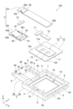
第二収容部3bは、他方の側板5に取り付けられている。第二収容部3bは、断面U字状の溝形状を有している。第二収容部3bの内部空間は、凹部5bを介して第一収容部3aの内部空間と連通している。第二収容部3bは、配線部2が配置された底板8(配置部)と、一対の側板9と、を有している。 The second accommodating portion 3b is attached to the other side plate 5. The second accommodating portion 3b has a groove shape with a U-shaped cross section. The internal space of the second accommodating part 3b communicates with the internal space of the first accommodating part 3a via the recess 5b. The second accommodating part 3b has a bottom plate 8 (arranging part) in which the wiring part 2 is arranged, and a pair of side plates 9.

図4、図5及び図9に示されるように、底板8は、第二配線部材60の主面60bとZ方向で対向している主面8a(第四主面)を有している。主面60bと主面8aとの間には、隙間Gが形成されている。主面8aには、第二配線部材60の厚さに相当する段差が設けられている。これにより、第一配線部材50のうち、第二配線部材60上に配置された部分と、それ以外の部分との間には段差がない。よって、第一配線部材50は湾曲せず直線状に配置されている。底板8は、厚さ方向(Z方向)から見て、長方形状を呈している。一対の側板9は、底板8のY方向の両端に配置され、Y方向で互いに対向している。一対の側板9は、厚さ方向(Y方向)から見て、長方形状を呈している。 As shown in FIGS. 4, 5, and 9, the bottom plate 8 has a main surface 8a (fourth main surface) facing the main surface 60b of the second wiring member 60 in the Z direction. A gap G is formed between the main surface 60b and the main surface 8a. A step corresponding to the thickness of the second wiring member 60 is provided on the main surface 8a. Thereby, there is no difference in level between the portion of the first wiring member 50 disposed on the second wiring member 60 and the other portions. Therefore, the first wiring member 50 is arranged in a straight line without being curved. The bottom plate 8 has a rectangular shape when viewed from the thickness direction (Z direction). The pair of side plates 9 are arranged at both ends of the bottom plate 8 in the Y direction, and face each other in the Y direction. The pair of side plates 9 have a rectangular shape when viewed from the thickness direction (Y direction).

第二収容部3bは、底板8と一体的に構成され、第二配線部材60を底板8に固定している複数(ここでは四つ)の固定部(固定具)8b,8c,8d,8eを有している。固定部8b,8c,8d,8eのそれぞれは、軸部80と、頭部81と、を有している。軸部80及び頭部81は、一体に形成されている。 The second accommodating part 3b is configured integrally with the bottom plate 8, and has a plurality of (four in this case) fixing parts (fixing tools) 8b, 8c, 8d, 8e that fix the second wiring member 60 to the bottom plate 8. have. Each of the fixing parts 8b, 8c, 8d, and 8e has a shaft part 80 and a head part 81. The shaft portion 80 and the head portion 81 are integrally formed.

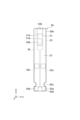
図10に示されるように、軸部80は、一方向に沿って延在している。軸部80は、主面8aから突出し(主面8aに立設され)ている。軸部80は、延在方向の他端部が主面8aに接続されている。軸部80は、円柱状であり、断面円形を呈している。軸部80は、対応する貫通孔60cに挿通されている。貫通孔60cの内径d1は、軸部80の外径d2と同等であり、例えば、1.55mm以上1.65mm以下である。軸部80の外周面80aと貫通孔10cの内周面とは、互いに面接触している。ここでは、軸部80の外周面80aの全体と貫通孔10cの内周面の全体とは、互いに面接触している。 As shown in FIG. 10, the shaft portion 80 extends in one direction. The shaft portion 80 protrudes from the main surface 8a (is erected on the main surface 8a). The other end of the shaft portion 80 in the extending direction is connected to the main surface 8a. The shaft portion 80 is columnar and has a circular cross section. The shaft portion 80 is inserted into the corresponding through hole 60c. The inner diameter d1 of the through hole 60c is equivalent to the outer diameter d2 of the shaft portion 80, and is, for example, 1.55 mm or more and 1.65 mm or less. The outer peripheral surface 80a of the shaft portion 80 and the inner peripheral surface of the through hole 10c are in surface contact with each other. Here, the entire outer peripheral surface 80a of the shaft portion 80 and the entire inner peripheral surface of the through hole 10c are in surface contact with each other.

頭部81は、軸部80と接続され、第二配線部材60の主面60aに係止されている。頭部81は、円板形状を呈している。頭部81の外径d3は、貫通孔60cの内径d1よりも大きい。頭部81は、第一頭部81aと、第二頭部81bと、を有している。第一頭部81a及び第二頭部81bは、一体に形成されている。第一頭部81aは、軸部80の一端部に接続されている。第一頭部81aは、円板形状を呈している。第一頭部81aの上面は、例えば、平坦面である。 The head 81 is connected to the shaft portion 80 and is locked to the main surface 60a of the second wiring member 60. The head 81 has a disk shape. The outer diameter d3 of the head 81 is larger than the inner diameter d1 of the through hole 60c. The head 81 includes a first head 81a and a second head 81b. The first head 81a and the second head 81b are integrally formed. The first head 81a is connected to one end of the shaft portion 80. The first head 81a has a disk shape. The upper surface of the first head 81a is, for example, a flat surface.

第二頭部81bは、第一頭部81aと接続されている。第二頭部81bは、第一頭部81aにおいて、軸部80よりも径方向に張り出した部分の下面に接続されている。第二頭部81bは、第一頭部81aから一方向において軸部80の他端部側に延在している。すなわち、第二頭部81bは、第一頭部81aから第二配線部材60(主面8a)側に向かって延在している。第二頭部81bは、軸部80の外周面80aと所定の間隔をあけて対向して配置されている。すなわち、第二頭部81bの内面81bsは、軸部80の外周面80aと対向して配置されている。第二頭部81bと軸部80との間には、空隙(間隙)が形成されている。 The second head 81b is connected to the first head 81a. The second head 81b is connected to the lower surface of a portion of the first head 81a that extends radially beyond the shaft portion 80. The second head 81b extends from the first head 81a toward the other end of the shaft portion 80 in one direction. That is, the second head 81b extends from the first head 81a toward the second wiring member 60 (main surface 8a). The second head 81b is disposed to face the outer circumferential surface 80a of the shaft portion 80 with a predetermined distance therebetween. That is, the inner surface 81bs of the second head 81b is arranged to face the outer circumferential surface 80a of the shaft portion 80. A void (gap) is formed between the second head 81b and the shaft portion 80.

第二頭部81bは、軸部80の外周面80aの全周を囲うように配置されている。すなわち、第二頭部81bは、円環状を呈している。第二頭部81bの先端部(第一頭部81aに接続されている端部とは反対側の端部)は、湾曲部分を有している。すなわち、第二頭部81bでは、第二配線部材60の主面60bと接触し得る端部に角部が形成されていない。 The second head 81b is arranged to surround the entire circumference of the outer peripheral surface 80a of the shaft portion 80. That is, the second head 81b has an annular shape. The tip of the second head 81b (the end opposite to the end connected to the first head 81a) has a curved portion. That is, in the second head 81b, no corner is formed at the end that can come into contact with the main surface 60b of the second wiring member 60.

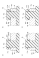
本実施形態では、複数の固定部8b,8c,8d,8eのそれぞれは、頭部81の第二頭部81bの形状が異なっている。図11(a)に示されるように、固定部8cでは、頭部81の第二頭部81bは、第二配線部材60の主面60aと当接していない。図11(b)に示されるように、固定部8bでは、頭部81の第二頭部81bは、第二配線部材60の主面60aと当接している。図11(c)に示されるように、固定部8eでは、頭部81の第二頭部81bの一部は、第二配線部材60の主面60aと当接し、第二頭部81bの一部は、第二配線部材60の主面60aと当接していない。図11(d)に示されるように、固定部8dでは、頭部81の第二頭部81bの一部は、第二配線部材60の主面60aと当接し、第二頭部81bの一部は、第二配線部材60の主面60aと当接していない。 In this embodiment, the shapes of the second heads 81b of the heads 81 of the plurality of fixing parts 8b, 8c, 8d, and 8e are different from each other. As shown in FIG. 11(a), in the fixed portion 8c, the second head 81b of the head 81 is not in contact with the main surface 60a of the second wiring member 60. As shown in FIG. 11(b), in the fixed portion 8b, the second head 81b of the head 81 is in contact with the main surface 60a of the second wiring member 60. As shown in FIG. 11(c), in the fixed part 8e, a part of the second head 81b of the head 81 is in contact with the main surface 60a of the second wiring member 60, and a part of the second head 81b is in contact with the main surface 60a of the second wiring member 60. The portion is not in contact with the main surface 60a of the second wiring member 60. As shown in FIG. 11(d), in the fixed part 8d, a part of the second head 81b of the head 81 is in contact with the main surface 60a of the second wiring member 60, and a part of the second head 81b is in contact with the main surface 60a of the second wiring member 60. The portion is not in contact with the main surface 60a of the second wiring member 60.

続いて、配線部2を底板8に固定する方法について説明する。図12(a)に示されるように、配線部2が固定される前の固定部8b0は、配線部2が固定された後の固定部8bと異なる形状を有している。配線部2が固定される前の軸部800は、例えば、貫通孔60cの内径d1よりも大きい。配線部2が固定される前の頭部810は、軸部800から遠ざかるにしたがって先窄まりとなるテーパ状に形成されている。頭部810の先端部の外径は、貫通孔60cの内径d1よりも小さい。 Next, a method for fixing the wiring section 2 to the bottom plate 8 will be explained. As shown in FIG. 12(a), the fixed part 8b0 before the wiring part 2 is fixed has a different shape from the fixed part 8b after the wiring part 2 is fixed. The shaft portion 800 before the wiring portion 2 is fixed is, for example, larger than the inner diameter d1 of the through hole 60c. The head 810 before the wiring section 2 is fixed is formed in a tapered shape that becomes narrower as it moves away from the shaft section 800. The outer diameter of the tip of the head 810 is smaller than the inner diameter d1 of the through hole 60c.

配線部2を底板8に固定する際、まず、第二配線部材60の貫通孔60cが対応する固定部8b0上に配置されるよう、配線部2を底板8に対して位置合わせして、軸部800に貫通孔60cを挿通させる。続いて、図12(b)に示されるように、固定部8b0をプレス板Pにより主面8aに向かって押圧する。プレス板Pは、加熱されている。これにより、樹脂から成る頭部810は、プレス板Pにより溶融さて潰され、頭部81となる。 When fixing the wiring part 2 to the bottom plate 8, first align the wiring part 2 with the bottom plate 8 so that the through hole 60c of the second wiring member 60 is placed on the corresponding fixing part 8b0, and then The through hole 60c is inserted into the portion 800. Subsequently, as shown in FIG. 12(b), the fixing portion 8b0 is pressed by the press plate P toward the main surface 8a. The press plate P is heated. As a result, the head 810 made of resin is melted and crushed by the press plate P to become the head 81.

ケース3は、図2に示されるように、被取付部材200の被取付面200aに取りけられ、被取付面200aのとの間に振動部1が配置される音響空間Sを形成する。音響空間Sは、連通部7bを通じて互いに連通する第一空間S1及び第二空間S2を有する。第一空間S1は、被取付面200aと主面12aとの間に形成される。第二空間S2は、ケース3と主面12bとの間に形成される。第一空間S1は、例えば、第二空間S2よりも広い。 As shown in FIG. 2, the case 3 is attached to the mounting surface 200a of the mounting member 200, and forms an acoustic space S in which the vibrating section 1 is disposed between the mounting surface 200a and the mounting surface 200a. The acoustic space S has a first space S1 and a second space S2 that communicate with each other through the communication portion 7b. The first space S1 is formed between the attached surface 200a and the main surface 12a. The second space S2 is formed between the case 3 and the main surface 12b. The first space S1 is, for example, wider than the second space S2.

圧電素子10、振動部材12、及び音響空間Sは、可聴域(例えば、2kHz以上20kHz以下の範囲)において互いに異なる共振周波数(共振点)をそれぞれ有するように構成されている。例えば、圧電素子10及び振動部材12の共振周波数は、圧電素子10及び振動部材12の外形を小さくすると高くなり、圧電素子10及び振動部材12の外形を大きくすると低くなる。圧電素子10及び振動部材12の共振周波数は、例えば、圧電素子10及び振動部材12を構成する材料、又は、圧電素子10及び振動部材12の形状等によっても調整される。音響空間Sの共振周波数は、例えば、音響空間Sの大きさや形状等を調整することにより調整される。音響空間Sの共振周波数は、音響空間Sを画定するケース3や被取付部材200等の部材を構成する材料によっても調整される。なお、共振周波数は、音圧が共振によって最大となる周波数である。 The piezoelectric element 10, the vibration member 12, and the acoustic space S are configured to have mutually different resonance frequencies (resonance points) in the audible range (for example, a range of 2 kHz or more and 20 kHz or less). For example, the resonant frequency of the piezoelectric element 10 and the vibrating member 12 becomes higher when the outer dimensions of the piezoelectric element 10 and the vibrating member 12 are made smaller, and becomes lower when the outer dimensions of the piezoelectric element 10 and the vibrating member 12 are made larger. The resonance frequencies of the piezoelectric element 10 and the vibrating member 12 are also adjusted, for example, by the materials that constitute the piezoelectric element 10 and the vibrating member 12, or the shapes of the piezoelectric element 10 and the vibrating member 12. The resonant frequency of the acoustic space S is adjusted, for example, by adjusting the size, shape, etc. of the acoustic space S. The resonant frequency of the acoustic space S is also adjusted by the materials constituting members such as the case 3 and the attached member 200 that define the acoustic space S. Note that the resonant frequency is the frequency at which the sound pressure becomes maximum due to resonance.

圧電素子10は、例えば、2000Hz以上3000Hz以下の範囲に共振周波数を有するように構成されている。音響空間Sは、例えば、3000Hz以上6000Hz以下の範囲に共振周波数を有するように構成されている。振動部材12は、例えば、13000Hz以上17000Hz以下の範囲に共振周波数を有するように構成されている。圧電素子10、振動部材12、及び音響空間Sは、可聴域において互いに異なる範囲(互いに重ならない範囲)に共振周波数を有する。圧電素子10、振動部材12、及び音響空間Sの共振周波数は、少なくとも互いに500Hz以上の差を有して分散するように調整されている。圧電素子10の共振周波数と振動部材12の共振周波数との差は、例えば、10000Hz以上である。振動部材12の共振周波数と音響空間Sの共振周波数との差は、例えば、7000Hz以上である。 The piezoelectric element 10 is configured to have a resonant frequency in a range of, for example, 2000 Hz or more and 3000 Hz or less. The acoustic space S is configured to have a resonant frequency in a range of, for example, 3000 Hz or more and 6000 Hz or less. The vibrating member 12 is configured to have a resonant frequency in a range of, for example, 13,000 Hz or more and 17,000 Hz or less. The piezoelectric element 10, the vibration member 12, and the acoustic space S have resonance frequencies in different ranges (ranges that do not overlap with each other) in the audible range. The resonant frequencies of the piezoelectric element 10, the vibrating member 12, and the acoustic space S are adjusted to be dispersed with at least a difference of 500 Hz or more from each other. The difference between the resonant frequency of the piezoelectric element 10 and the resonant frequency of the vibrating member 12 is, for example, 10,000 Hz or more. The difference between the resonant frequency of the vibrating member 12 and the resonant frequency of the acoustic space S is, for example, 7000 Hz or more.

図13に示されるように、従来の固定部8Pは、軸部80Pと、頭部81Pと、を有している。頭部81Pは、平板形状を呈している。固定部8Pでは、圧電素子の振動によって、第二配線部材60が頭部81Pを押し上げたりすることがある。これにより、軸部80Pと頭部81Pとの接続部分(軸部80の外周面80Paと頭部81Pの下面とが成す隅部)を起点としてクラックが発生するおそれがある。クラックが発生によって頭部81Pが破損すると、第二配線部材60を固定できなくなり得る。これにより、振動デバイスの信頼性が低下し得る。 As shown in FIG. 13, the conventional fixing portion 8P includes a shaft portion 80P and a head portion 81P. The head 81P has a flat plate shape. In the fixed part 8P, the second wiring member 60 may push up the head 81P due to the vibration of the piezoelectric element. As a result, there is a possibility that cracks may occur starting from the connection portion between the shaft portion 80P and the head portion 81P (the corner formed by the outer circumferential surface 80Pa of the shaft portion 80 and the lower surface of the head portion 81P). If the head 81P is damaged due to the occurrence of cracks, it may become impossible to fix the second wiring member 60. This may reduce the reliability of the vibration device.

本実施形態に係る振動デバイス100では、ケース3が複数の固定部8b,8c,8d,8eを有している。固定部8b,8c,8d,8eのそれぞれは、軸部80及び頭部81を有している。頭部81は、第一頭部81a及び第二頭部81bを有している。第二頭部81bは、第一頭部81aと接続されていると共に第一頭部81aから軸部80の一方向の他端部側に延在しており、軸部80の外周面80aと所定の間隔をあけて対向して配置されている。すなわち、第二頭部81bは、軸部80から離間して設けられている。これにより、振動デバイス100では、第二頭部81bが第二配線部材60によって押し上げられた場合であっても、第二頭部81bにおいて外部からの応力を分散させることができる。そのため、振動デバイス100では、軸部80と頭部81との接続部分を起点としてクラックが発生することを抑制できる。したがって、振動デバイス100では、頭部81が破損することを抑制できる。その結果、振動デバイス100では、信頼性の向上が図れる。 In the vibration device 100 according to this embodiment, the case 3 has a plurality of fixing parts 8b, 8c, 8d, and 8e. Each of the fixing parts 8b, 8c, 8d, and 8e has a shaft part 80 and a head part 81. The head 81 has a first head 81a and a second head 81b. The second head 81b is connected to the first head 81a and extends from the first head 81a toward the other end in one direction of the shaft 80, and is connected to the outer peripheral surface 80a of the shaft 80. They are arranged facing each other at a predetermined interval. That is, the second head 81b is provided apart from the shaft portion 80. Thereby, in the vibrating device 100, even if the second head 81b is pushed up by the second wiring member 60, external stress can be dispersed in the second head 81b. Therefore, in the vibrating device 100, it is possible to suppress the occurrence of cracks starting from the connecting portion between the shaft portion 80 and the head portion 81. Therefore, in the vibration device 100, damage to the head 81 can be suppressed. As a result, the reliability of the vibration device 100 can be improved.

本実施形態では、固定部8b,8c,8d,8eは、アクリル系樹脂、塩化ビニル系樹脂、成型樹脂等の樹脂材料からなる。そのため、第二頭部81bは、柔軟性を有しているため、外力が加えられると撓んだりする。これにより、振動デバイス100では、第二頭部81bが第二配線部材60によって押し上げられた場合、第二頭部81bにおいて外部からの応力を効果的に分散させることができる。 In this embodiment, the fixing parts 8b, 8c, 8d, and 8e are made of a resin material such as acrylic resin, vinyl chloride resin, or molded resin. Therefore, since the second head 81b has flexibility, it bends when external force is applied. Thereby, in the vibrating device 100, when the second head 81b is pushed up by the second wiring member 60, external stress can be effectively dispersed in the second head 81b.

本実施形態に係る振動デバイス100では、第二頭部81bは、軸部80の外周面80aの全周を囲うように配置されている。この構成では、第二頭部81bにおいて、外部からの応力をより効果的に分散させることができる。 In the vibration device 100 according to the present embodiment, the second head 81b is arranged to surround the entire circumference of the outer peripheral surface 80a of the shaft portion 80. With this configuration, external stress can be more effectively dispersed in the second head 81b.

本実施形態に係る振動デバイス100では、第二頭部81bの先端部は、湾曲部分を有している。この構成では、第二配線部材60に接触(当接)する第二頭部81bの先端部が角部を有していないため、第二頭部81bが接触し得る第二配線部材60(主面60a)が損傷することを抑制できる。 In the vibration device 100 according to this embodiment, the tip of the second head 81b has a curved portion. In this configuration, since the tip of the second head 81b that contacts (butts) the second wiring member 60 does not have a corner, the second wiring member 60 (the main Damage to the surface 60a) can be suppressed.

本実施形態に係る振動デバイス100では、複数の固定部8b,8c,8d,8eのそれぞれは、頭部81の第二頭部81bの形状が異なっている。この構成では、固定部8b,8c,8d,8eのそれぞれの第二頭部81bと第二配線部材60との接触の頻度が異なり得る。これにより、振動デバイス100では、固定部8b,8c,8d,8eの耐久性(寿命)が異なり得る。そのため、全ての固定部8b,8c,8d,8eが同時に破損することを回避できる。 In the vibration device 100 according to the present embodiment, the second head 81b of the head 81 of each of the plurality of fixing parts 8b, 8c, 8d, and 8e has a different shape. In this configuration, the frequency of contact between the second head 81b of each of the fixing parts 8b, 8c, 8d, and 8e and the second wiring member 60 may be different. As a result, in the vibrating device 100, the durability (life span) of the fixed parts 8b, 8c, 8d, and 8e may differ. Therefore, it is possible to avoid damaging all the fixing parts 8b, 8c, 8d, and 8e at the same time.

以上、本発明の実施形態について説明してきたが、本発明は必ずしも上述した実施形態に限定されるものではなく、その要旨を逸脱しない範囲で様々な変更が可能である。 Although the embodiments of the present invention have been described above, the present invention is not necessarily limited to the embodiments described above, and various changes can be made without departing from the gist thereof.

上記実施形態では、固定部8b,8c,8d,8eの頭部81の第二頭部81bの上面が平坦面である形態を一例に説明した。頭部81の形状はこれに限定されない。図14(a)に示されるように、固定部8Abは、軸部80と、頭部81Aと、を有している。頭部81Aは、第一頭部81Aaと、第二頭部81Abと、を有している。第一頭部81Aaの上面は、例えば、湾曲面である。第一頭部81Aaは、半球形状を呈している。第一頭部81Aaは、いわゆるシングルマウント形状を呈している。第二頭部81Abは、軸部80の外周面80aと所定の間隔をあけて対向して配置されている。すなわち、第二頭部81Abの内面81Absは、軸部80の外周面80aと対向して配置されている。 In the above embodiment, the upper surface of the second head 81b of the head 81 of the fixing parts 8b, 8c, 8d, and 8e is a flat surface. The shape of the head 81 is not limited to this. As shown in FIG. 14(a), the fixing portion 8Ab has a shaft portion 80 and a head portion 81A. The head 81A includes a first head 81Aa and a second head 81Ab. The upper surface of the first head 81Aa is, for example, a curved surface. The first head 81Aa has a hemispherical shape. The first head 81Aa has a so-called single mount shape. The second head 81Ab is arranged to face the outer circumferential surface 80a of the shaft portion 80 with a predetermined distance therebetween. That is, the inner surface 81Abs of the second head 81Ab is arranged to face the outer circumferential surface 80a of the shaft portion 80.

図14(b)に示されるように、固定部8Bbは、軸部80と、頭部81BCと、を有している。頭部81Bは、第一頭部81Baと、第二頭部81Bbと、を有している。第一頭部81Baの上面は、例えば、湾曲面である。第一頭部81Baは、中央部が窪んだ半球形状を呈している。第一頭部81Baは、いわゆるダブルマウント形状を呈している。第二頭部81Bbは、軸部80の外周面80aと所定の間隔をあけて対向して配置されている。すなわち、第二頭部81Bbの内面81Bbsは、軸部80の外周面80aと対向して配置されている。 As shown in FIG. 14(b), the fixing portion 8Bb includes a shaft portion 80 and a head portion 81BC. The head 81B includes a first head 81Ba and a second head 81Bb. The upper surface of the first head 81Ba is, for example, a curved surface. The first head 81Ba has a hemispherical shape with a depressed center. The first head 81Ba has a so-called double mount shape. The second head 81Bb is disposed to face the outer circumferential surface 80a of the shaft portion 80 with a predetermined distance therebetween. That is, the inner surface 81Bbs of the second head 81Bb is arranged to face the outer circumferential surface 80a of the shaft portion 80.

上記実施形態では、固定部8b,8c,8d,8eの軸部80と頭部81とが一体に形成されている形態を一例に説明した。しかし、図15に示されるように、固定部8Cbは、軸部80と頭部81Cとは、別体で設けられていてもよい。頭部81Cは、第一頭部81Aaと、第二頭部81Abと、を有している。頭部81Cは、ボルト82によって、軸部80に固定されている。これにより、第二頭部81Cbは、軸部80の外周面80aと所定の間隔をあけて対向して配置されている。すなわち、第二頭部81Cbの内面81Cbsは、軸部80の外周面80aと対向して配置されている。 In the embodiment described above, an example has been described in which the shaft portions 80 and heads 81 of the fixing portions 8b, 8c, 8d, and 8e are integrally formed. However, as shown in FIG. 15, in the fixing part 8Cb, the shaft part 80 and the head part 81C may be provided separately. The head 81C includes a first head 81Aa and a second head 81Ab. The head 81C is fixed to the shaft portion 80 with a bolt 82. Thereby, the second head 81Cb is disposed to face the outer circumferential surface 80a of the shaft portion 80 with a predetermined distance therebetween. That is, the inner surface 81Cbs of the second head 81Cb is arranged to face the outer circumferential surface 80a of the shaft portion 80.

上記実施形態では、頭部81の第二頭部81bが、軸部80の外周面80aの全周を囲うように配置されている形態を一例に説明した。しかし、第二頭部81bは、軸部80の外周面80aの一部を囲うように配置されていてもよい。 In the above embodiment, the second head 81b of the head 81 is arranged to surround the entire circumference of the outer peripheral surface 80a of the shaft portion 80, as an example. However, the second head 81b may be arranged so as to surround a part of the outer circumferential surface 80a of the shaft portion 80.

上記実施形態では、図10に示されるように、軸部80の外周面80aと第二頭部81bとが所定の間隔をあけて対向して配置されている形態を一例に説明した。すなわち、軸部80と第二頭部81bとの間に空間が形成されている形態を一例に説明した。しかし、所定の間隔を開けて対向して配置されているとは、軸部と頭部(第二頭部)との間に少なくとも間隙が存在していればよい。ここで言う間隙は、軸部と第二頭部との間に存在して軸部と第二頭部とを区画するものであればよい。そのため、間隙は、例えば、ウェルドラインのように線状であってもよい。固定具(固定部)では、このような間隙を設けることにより、万が一軸部と頭部との接続部分を起点としてクラックが発生したとしても、そのクラックの延伸を抑制することができる。また、固定具では、上記間隙を設けることにより、頭部が完全に破損する前に当該構造が顕著になり、完全に破損することを抑制できる。 In the above embodiment, as shown in FIG. 10, the outer circumferential surface 80a of the shaft portion 80 and the second head portion 81b are arranged to face each other with a predetermined interval. That is, the embodiment in which a space is formed between the shaft portion 80 and the second head 81b has been described as an example. However, being disposed facing each other with a predetermined interval may mean that at least a gap exists between the shaft portion and the head (second head). The gap referred to here may be any gap that exists between the shaft portion and the second head portion and partitions the shaft portion and the second head portion. Therefore, the gap may be linear like a weld line, for example. By providing such a gap in the fixture (fixing part), even if a crack should occur starting from the connecting portion between the shaft part and the head part, extension of the crack can be suppressed. Further, in the fixture, by providing the above-mentioned gap, the structure becomes noticeable before the head is completely damaged, and it is possible to prevent the head from being completely damaged.

上記実施形態では、複数の固定部8b,8c,8d,8eのそれぞれが、頭部81の第二頭部81bの形状が異なっている形態を一例に説明した。しかし、複数の固定部8b,8c,8d,8eのそれぞれの頭部81の第二頭部81bの形状が同じであってもよい。また、複数の固定部8b,8c,8d,8eのうち、2つの固定部において、頭部81の第二頭部81bの形状が異なっていてもよい。 In the embodiment described above, the second head 81b of the head 81 of each of the plurality of fixing parts 8b, 8c, 8d, and 8e has been explained as an example. However, the shapes of the second heads 81b of the respective heads 81 of the plurality of fixing parts 8b, 8c, 8d, and 8e may be the same. Moreover, the shape of the second head 81b of the head 81 may be different in two of the plurality of fixing parts 8b, 8c, 8d, and 8e.

上記実施形態では、軸部80が円柱状であり、頭部81が円板形状である形態を一例に説明した。しかし、軸部は、角柱状であってもよい。また、頭部は、矩形板状を呈していてもよい。 In the above embodiment, the shaft portion 80 has a cylindrical shape and the head portion 81 has a disk shape. However, the shaft portion may also be prismatic. Further, the head may have a rectangular plate shape.

上記実施形態では、固定具(固定部8b,8c,8d,8e)が振動デバイス100に適用されている形態を一例に説明した。しかし、固定具は、他の装置(構造)に適用されてもよい。また、固定具は、単体で用いられてもよい。 In the embodiment described above, an example in which the fixtures (fixing parts 8b, 8c, 8d, and 8e) are applied to the vibration device 100 has been described. However, the fixture may also be applied to other devices (structures). Further, the fixture may be used alone.

上記実施形態では、図10において、頭部81の第二頭部81bの厚みを均等に示している。しかし、第二頭部81bは、厚みが均等でなくてもよい。すなわち、第二頭部81bは、肉厚な部分及び肉薄な部分を有していてもよい。 In the embodiment described above, the thickness of the second head 81b of the head 81 is shown to be uniform in FIG. However, the second head 81b does not need to have an even thickness. That is, the second head 81b may have a thick portion and a thin portion.

3…ケース、8…底板(配置部)、8a…主面(第四主面)、8b…固定部(固定具)、10…圧電素子、11…圧電素体、11a…主面、13,15…外部電極、50…第一配線部材、50c…幅狭部、59…補強部、60…第二配線部材、60a…主面(第二主面)、60b…主面(第三主面)、60c…貫通孔、80…軸部、80a…外周面、81…頭部、81a…第一頭部、81b…第二頭部、100…振動デバイス。 3... Case, 8... Bottom plate (arrangement part), 8a... Main surface (fourth main surface), 8b... Fixing part (fixing tool), 10... Piezoelectric element, 11... Piezoelectric element body, 11a... Main surface, 13, DESCRIPTION OF SYMBOLS 15... External electrode, 50... First wiring member, 50c... Narrow part, 59... Reinforcement part, 60... Second wiring member, 60a... Principal surface (second principal surface), 60b... Principal surface (third principal surface) ), 60c...through hole, 80...shaft portion, 80a...outer peripheral surface, 81...head, 81a...first head, 81b...second head, 100...vibration device.

Claims (2)

第一主面を有する圧電素体と、前記第一主面上に配置された一対の外部電極と、を有する圧電素子と、
前記第一主面上で前記一対の外部電極に接続された帯状の第一配線部材と、
互いに対向している第二主面及び第三主面を有し、前記第一配線部材に接続された板状の第二配線部材と、
前記第二配線部材が配置されたケースと、を備え、
前記第二配線部材には、前記第二配線部材を前記第二主面及び前記第三主面の対向方向に貫通している複数の貫通孔が設けられており、
前記ケースは、
前記第三主面と対向している第四主面を有し、前記第二配線部材が配置された配置部と、
前記配置部と一体的に構成され、前記第二配線部材を前記配置部に固定している複数の固定部と、を有し、
複数の前記固定部のそれぞれは、
前記第四主面から一方向に沿って突出し、前記貫通孔に挿通された軸部と、
前記軸部の前記一方向の一端部に設けられ、前記第主面に係止された頭部と、を有し、
前記頭部は、
前記軸部の前記一端部に接続されている第一頭部と、
前記第一頭部と接続されていると共に前記第一頭部から前記一方向において前記軸部の他端部側に延在しており、前記軸部の外周面と所定の間隔をあけて対向して配置されている第二頭部と、を有する、振動デバイス。
a piezoelectric element having a piezoelectric element body having a first main surface, and a pair of external electrodes disposed on the first main surface;
a strip-shaped first wiring member connected to the pair of external electrodes on the first main surface;
a plate-shaped second wiring member having a second main surface and a third main surface facing each other and connected to the first wiring member;
a case in which the second wiring member is arranged,
The second wiring member is provided with a plurality of through holes penetrating the second wiring member in a direction opposite to the second main surface and the third main surface,
The said case is
an arrangement portion having a fourth main surface facing the third main surface and in which the second wiring member is arranged;
a plurality of fixing parts configured integrally with the arrangement part and fixing the second wiring member to the arrangement part,
Each of the plurality of fixing parts is
a shaft protruding from the fourth principal surface in one direction and inserted into the through hole;
a head provided at one end of the shaft in the one direction and locked to the second main surface;
The head is
a first head connected to the one end of the shaft;
connected to the first head, extending from the first head in the one direction toward the other end of the shaft, and facing the outer circumferential surface of the shaft at a predetermined distance; a second head disposed as a vibration device;
複数の前記固定部のそれぞれは、前記頭部の前記第二頭部の形状が異なっている、請求項に記載の振動デバイス。
The vibration device according to claim 1 , wherein the second head of the head of each of the plurality of fixing parts has a different shape.
JP2019215653A 2019-11-28 2019-11-28 Fixtures and vibration devices Active JP7367494B2 (en)

Priority Applications (1)

Application Number Priority Date Filing Date Title
JP2019215653A JP7367494B2 (en) 2019-11-28 2019-11-28 Fixtures and vibration devices

Applications Claiming Priority (1)

Application Number Priority Date Filing Date Title
JP2019215653A JP7367494B2 (en) 2019-11-28 2019-11-28 Fixtures and vibration devices

Publications (2)

Publication Number Publication Date
JP2021087135A JP2021087135A (en) 2021-06-03
JP7367494B2 true JP7367494B2 (en) 2023-10-24

Family

ID=76085886

Family Applications (1)

Application Number Title Priority Date Filing Date
JP2019215653A Active JP7367494B2 (en) 2019-11-28 2019-11-28 Fixtures and vibration devices

Country Status (1)

Country Link
JP (1) JP7367494B2 (en)

Citations (2)

* Cited by examiner, † Cited by third party
Publication number Priority date Publication date Assignee Title
JP2005086136A (en) 2003-09-11 2005-03-31 Calsonic Kansei Corp Substrate fixing structure and rotation sensor therewith
WO2015125370A1 (en) 2014-02-24 2015-08-27 京セラ株式会社 Acoustic generator, acoustic generation apparatus, portable terminal, and electronic apparatus

Family Cites Families (2)

* Cited by examiner, † Cited by third party
Publication number Priority date Publication date Assignee Title
US5013174A (en) * 1989-12-04 1991-05-07 Motorola, Inc. Dual function fastener
JP7123638B2 (en) * 2018-06-06 2022-08-23 キヤノン株式会社 Accessories and imagers

Patent Citations (2)

* Cited by examiner, † Cited by third party
Publication number Priority date Publication date Assignee Title
JP2005086136A (en) 2003-09-11 2005-03-31 Calsonic Kansei Corp Substrate fixing structure and rotation sensor therewith
WO2015125370A1 (en) 2014-02-24 2015-08-27 京セラ株式会社 Acoustic generator, acoustic generation apparatus, portable terminal, and electronic apparatus

Also Published As

Publication number Publication date
JP2021087135A (en) 2021-06-03

Similar Documents

Publication Publication Date Title
US20050258711A1 (en) Ultrasonic vibrator and ultrasonic motor including ultrasonic vibrator
JP6933054B2 (en) Vibration device
JP7136318B2 (en) Vibration device and its manufacturing method
JP7367494B2 (en) Fixtures and vibration devices
WO2020153289A1 (en) Piezoelectric element
WO2020100828A1 (en) Vibration device and electronic device
JP7276019B2 (en) vibration device
JP7294006B2 (en) vibration device
JP7354575B2 (en) Piezoelectric elements, vibration devices and electronic equipment
WO2020153290A1 (en) Audio device
JP7455533B2 (en) acoustic device
JP6720959B2 (en) Vibrating device
WO2019172052A1 (en) Vibration device
JP7405042B2 (en) vibration device
JP7087942B2 (en) Vibration devices, electronic devices, and how to drive vibration devices
JP7550066B2 (en) Vibration Device
JP4658530B2 (en) Ultrasonic vibrator and ultrasonic motor using the same
JP7415400B2 (en) Audio devices and speaker equipment
JP7234594B2 (en) Vibration device and electronic equipment
JP6733641B2 (en) Vibrating device
JP7200796B2 (en) Piezoelectric element
JP2022184332A (en) vibration device
JP2022115339A (en) vibration device
JP2024124930A (en) Acoustic Devices
US8829768B2 (en) Haptic feedback device

Legal Events

Date Code Title Description
A621 Written request for application examination

Free format text: JAPANESE INTERMEDIATE CODE: A621

Effective date: 20220704

A977 Report on retrieval

Free format text: JAPANESE INTERMEDIATE CODE: A971007

Effective date: 20230327

A131 Notification of reasons for refusal

Free format text: JAPANESE INTERMEDIATE CODE: A131

Effective date: 20230411

A521 Request for written amendment filed

Free format text: JAPANESE INTERMEDIATE CODE: A523

Effective date: 20230607

TRDD Decision of grant or rejection written
A01 Written decision to grant a patent or to grant a registration (utility model)

Free format text: JAPANESE INTERMEDIATE CODE: A01

Effective date: 20230912

A61 First payment of annual fees (during grant procedure)

Free format text: JAPANESE INTERMEDIATE CODE: A61

Effective date: 20230925

R150 Certificate of patent or registration of utility model

Ref document number: 7367494

Country of ref document: JP

Free format text: JAPANESE INTERMEDIATE CODE: R150