JP7355256B2 - Transmission lines and electronic equipment - Google Patents
Transmission lines and electronic equipment Download PDFInfo
- Publication number
- JP7355256B2 JP7355256B2 JP2022565249A JP2022565249A JP7355256B2 JP 7355256 B2 JP7355256 B2 JP 7355256B2 JP 2022565249 A JP2022565249 A JP 2022565249A JP 2022565249 A JP2022565249 A JP 2022565249A JP 7355256 B2 JP7355256 B2 JP 7355256B2
- Authority
- JP
- Japan
- Prior art keywords
- hollow
- transmission line
- conductor layer
- hollow parts
- viewed
- Prior art date
- Legal status (The legal status is an assumption and is not a legal conclusion. Google has not performed a legal analysis and makes no representation as to the accuracy of the status listed.)
- Active
Links
Images


Classifications
-
- H—ELECTRICITY
- H01—ELECTRIC ELEMENTS
- H01B—CABLES; CONDUCTORS; INSULATORS; SELECTION OF MATERIALS FOR THEIR CONDUCTIVE, INSULATING OR DIELECTRIC PROPERTIES
- H01B7/00—Insulated conductors or cables characterised by their form
- H01B7/02—Disposition of insulation
- H01B7/0208—Cables with several layers of insulating material
- H01B7/0225—Three or more layers
-
- H—ELECTRICITY
- H01—ELECTRIC ELEMENTS
- H01B—CABLES; CONDUCTORS; INSULATORS; SELECTION OF MATERIALS FOR THEIR CONDUCTIVE, INSULATING OR DIELECTRIC PROPERTIES
- H01B3/00—Insulators or insulating bodies characterised by the insulating materials; Selection of materials for their insulating or dielectric properties
- H01B3/18—Insulators or insulating bodies characterised by the insulating materials; Selection of materials for their insulating or dielectric properties mainly consisting of organic substances
- H01B3/30—Insulators or insulating bodies characterised by the insulating materials; Selection of materials for their insulating or dielectric properties mainly consisting of organic substances plastics; resins; waxes
-
- H—ELECTRICITY
- H01—ELECTRIC ELEMENTS
- H01P—WAVEGUIDES; RESONATORS, LINES, OR OTHER DEVICES OF THE WAVEGUIDE TYPE
- H01P3/00—Waveguides; Transmission lines of the waveguide type
- H01P3/02—Waveguides; Transmission lines of the waveguide type with two longitudinal conductors
- H01P3/08—Microstrips; Strip lines
-
- H—ELECTRICITY
- H05—ELECTRIC TECHNIQUES NOT OTHERWISE PROVIDED FOR
- H05K—PRINTED CIRCUITS; CASINGS OR CONSTRUCTIONAL DETAILS OF ELECTRIC APPARATUS; MANUFACTURE OF ASSEMBLAGES OF ELECTRICAL COMPONENTS
- H05K1/00—Printed circuits
- H05K1/02—Details
-
- H—ELECTRICITY
- H01—ELECTRIC ELEMENTS
- H01B—CABLES; CONDUCTORS; INSULATORS; SELECTION OF MATERIALS FOR THEIR CONDUCTIVE, INSULATING OR DIELECTRIC PROPERTIES
- H01B7/00—Insulated conductors or cables characterised by their form
- H01B7/04—Flexible cables, conductors, or cords, e.g. trailing cables
Landscapes
- Physics & Mathematics (AREA)
- Spectroscopy & Molecular Physics (AREA)
- Engineering & Computer Science (AREA)
- Microelectronics & Electronic Packaging (AREA)
- Structure Of Printed Boards (AREA)
- Production Of Multi-Layered Print Wiring Board (AREA)
Description
本発明は、高周波信号が伝送される伝送線路及び電子機器に関する。 The present invention relates to a transmission line and electronic equipment through which high-frequency signals are transmitted.
従来の伝送線路に関する発明としては、例えば、特許文献1に記載のサスペンデッド線路が知られている。このサスペンデッド線路は、外導体、ストリップ導体及び誘電体基板を備えている。ストリップ導体は、誘電体基板の上主面に設けられている。ストリップ導体は、前後方向に延びている。外導体は、ストリップ導体と重なるように、ストリップ導体の上に設けられている。誘電体基板には複数の左貫通孔及び右貫通孔が設けられている。複数の左貫通孔は、ストリップ導体の左において前後方向に並んでいる。複数の右貫通孔は、ストリップ導体の右において前後方向に並んでいる。
As an invention related to a conventional transmission line, for example, a suspended line described in
ところで、特許文献1に記載のサスペンデッド線路では、ストリップ導体に発生する特性インピーダンスが大きく変化しやすい。より詳細には、複数の左貫通孔は、ストリップ導体の左に位置している。複数の右貫通孔は、ストリップ導体の右に位置している。そして、複数の左貫通孔の前後方向における位置は、複数の右貫通孔の前後方向における位置と一致している。そのため、ストリップ導体の左及び右に左貫通孔及び右貫通孔が存在する存在区間と、ストリップ導体の左及び右に左貫通孔及び右貫通孔が存在しない非存在区間とが形成される。存在区間では、ストリップ導体の周囲の誘電率が低くなる。一方、非存在区間では、ストリップ導体の周囲の誘電率が高くなる。その結果、存在区間においてストリップ導体に発生する特性インピーダンスと、非存在区間においてストリップ導体に発生する特性インピーダンスとの差が大きくなりやすい。以上より、特許文献1に記載のサスペンデッド線路では、ストリップ導体に発生する特性インピーダンスが大きく変化しやすい。
By the way, in the suspended line described in
そこで、本発明の目的は、信号導体層に発生している特性インピーダンスが大きく変化することを抑制できる伝送線路及び電子機器を提供することである。 SUMMARY OF THE INVENTION Therefore, an object of the present invention is to provide a transmission line and an electronic device that can suppress large changes in characteristic impedance occurring in a signal conductor layer.
本発明の一形態に係る伝送線路は、
複数の絶縁体層が上下方向に積層された構造を有している積層体と、
前記積層体に設けられており、かつ、前記上下方向に直交する前後方向に延びている信号導体層と、
前記積層体に設けられており、かつ、前記上下方向に見て、前記信号導体層と重なるように、前記信号導体層の上に設けられている第1グランド導体層と、
を備えており、
複数の第1中空部及び複数の第2中空部が前記積層体に設けられており、
前記複数の第1中空部及び前記複数の第2中空部は、前記絶縁体層が存在しない空洞であり、
前記複数の第1中空部及び前記複数の第2中空部は、前記上下方向に見て、前記第1グランド導体層と重なっており、
前記前後方向に直交する方向を第1直交方向と定義し、及び、前記前後方向及び前記第1直交方向に直交する方向を第2直交方向と定義し、
前記第2直交方向は、第1方向及び前記第1方向の反対方向である第2方向を含んでおり、
前記第1直交方向に見て、前記複数の第1中空部は、前記信号導体層の前記第1方向において前記前後方向に並んでおり、
前記第1直交方向に見て、前記複数の第2中空部は、前記信号導体層の前記第2方向において前記前後方向に並んでおり、
前記前後方向に隣り合う2つの前記第1中空部の間に位置する領域のそれぞれを複数の第1領域と定義し、
前記前後方向に隣り合う2つの前記第2中空部の間に位置する領域のそれぞれを複数の第2領域と定義し、
前記複数の第1中空部のそれぞれは、前記第2直交方向に見て、前記複数の第2領域の対応する1つと重なっており、
前記複数の第2中空部のそれぞれは、前記第2直交方向に見て、前記複数の第1領域の対応する1つと重なっている。
The transmission line according to one embodiment of the present invention is
A laminate having a structure in which a plurality of insulating layers are stacked vertically;
a signal conductor layer provided on the laminate and extending in a front-back direction perpendicular to the up-down direction;
a first ground conductor layer provided in the laminate and provided on the signal conductor layer so as to overlap with the signal conductor layer when viewed in the vertical direction;
It is equipped with
A plurality of first hollow parts and a plurality of second hollow parts are provided in the laminate,
The plurality of first hollow parts and the plurality of second hollow parts are cavities in which the insulating layer does not exist,
The plurality of first hollow parts and the plurality of second hollow parts overlap with the first ground conductor layer when viewed in the vertical direction,
A direction perpendicular to the longitudinal direction is defined as a first orthogonal direction, and a direction orthogonal to the longitudinal direction and the first orthogonal direction is defined as a second orthogonal direction,
The second orthogonal direction includes a first direction and a second direction that is opposite to the first direction,
When viewed in the first orthogonal direction, the plurality of first hollow portions are lined up in the front-rear direction in the first direction of the signal conductor layer,
When viewed in the first orthogonal direction, the plurality of second hollow portions are lined up in the front-rear direction in the second direction of the signal conductor layer,
Each of the regions located between the two first hollow portions adjacent in the front-rear direction is defined as a plurality of first regions,
Each of the regions located between the two second hollow portions adjacent in the front-rear direction is defined as a plurality of second regions,
Each of the plurality of first hollow portions overlaps with a corresponding one of the plurality of second regions when viewed in the second orthogonal direction,
Each of the plurality of second hollow portions overlaps a corresponding one of the plurality of first regions when viewed in the second orthogonal direction.
本発明に係る伝送線路及び電子機器によれば、信号導体層に発生している特性インピーダンスが大きく変化することを抑制できる。 According to the transmission line and electronic device according to the present invention, it is possible to suppress a large change in the characteristic impedance occurring in the signal conductor layer.
(実施形態)
[伝送線路の構造]
以下に、本発明の実施形態に係る伝送線路10の構造について図面を参照しながら説明する。図1は、伝送線路10の分解斜視図である。なお、図1では、複数の層間接続導体v1及び複数の層間接続導体v2の内の代表的な層間接続導体v1,v2にのみ参照符号を付した。図1では、複数の第1中空部H1及び複数の第2中空部H2の内の代表的な第1中空部H1及び第2中空部H2にのみ参照符号を付した。図2は、図1の絶縁体層16cの上面図である。図3は、図2のA-A,B-B,C-Cにおける断面図である。(Embodiment)
[Transmission line structure]
Below, the structure of a
本明細書において、方向を以下のように定義する。伝送線路10の積層体12の積層方向を上下方向と定義する。また、伝送線路10の信号導体層22が延びている方向を前後方向と定義する。また、信号導体層22の線幅方向を左右方向と定義する。上下方向は、前後方向に直交する。左右方向は、上下方向及び前後方向に直交する。また、本実施形態において、第1直交方向は、上下方向である。第2直交方向は、左右方向である。また、左右方向は、左方向及び左方向の反対方向である右方向を含んでいる。本実施形態において、第1方向は、左方向である。第2方向は、右方向である。
In this specification, direction is defined as follows. The stacking direction of the
以下では、Xは、伝送線路10の部品又は部材である。本明細書において、特に断りのない場合には、Xの各部について以下のように定義する。Xの前部とは、Xの前半分を意味する。Xの後部とは、Xの後半分を意味する。Xの左部とは、Xの左半分を意味する。Xの右部とは、Xの右半分を意味する。Xの上部とは、Xの上半分を意味する。Xの下部とは、Xの下半分を意味する。Xの前端とは、Xの前方向の端を意味する。Xの後端とは、Xの後方向の端を意味する。Xの左端とは、Xの左方向の端を意味する。Xの右端とは、Xの右方向の端を意味する。Xの上端とは、Xの上方向の端を意味する。Xの下端とは、Xの下方向の端を意味する。Xの前端部とは、Xの前端及びその近傍を意味する。Xの後端部とは、Xの後端及びその近傍を意味する。Xの左端部とは、Xの左端及びその近傍を意味する。Xの右端部とは、Xの右端及びその近傍を意味する。Xの上端部とは、Xの上端及びその近傍を意味する。Xの下端部とは、Xの下端及びその近傍を意味する。
In the following, X is a component or member of the
まず、図1を参照しながら、伝送線路10の構造について説明する。伝送線路10は、高周波信号を伝送する。伝送線路10は、スマートフォン等の電子機器において、2つの回路を電気的に接続するために用いられる。伝送線路10は、図1に示すように、積層体12、信号導体層22、第1グランド導体層24、第2グランド導体層26、信号端子28a,28b、グランド端子29a,29b,30a,30b、複数の層間接続導体v1、複数の層間接続導体v2及び層間接続導体v3~v8を備えている。
First, the structure of the
積層体12は、板形状を有している。従って、積層体12は、上主面及び下主面を有している。積層体12の上主面及び下主面は、前後方向に延びる長辺を有する長方形状を有している。従って、積層体12の前後方向における長さは、積層体12の左右方向における長さより長い。 The laminate 12 has a plate shape. Therefore, the laminate 12 has an upper main surface and a lower main surface. The upper main surface and the lower main surface of the laminate 12 have a rectangular shape with long sides extending in the front-rear direction. Therefore, the length of the laminate 12 in the front-rear direction is longer than the length of the laminate 12 in the left-right direction.
積層体12は、図1に示すように、絶縁体層16a~16d,18a~18cを含んでいる。積層体12は、絶縁体層16a~16d,18a~18cが上下方向に積層された構造を有している。絶縁体層16a,18a,16b,18c,16c,18b,16dは、上から下へとこの順に並んでいる。絶縁体層16a~16d,18a~18cは、上下方向に見て、積層体12と同じ長方形状を有している。絶縁体層16a~16dは、可撓性を有する誘電体シートである。絶縁体層16a~16dの材料は、例えば、熱可塑性樹脂である。熱可塑性樹脂は、例えば、液晶ポリマー、PTFE(ポリテトラフロオロエチレン)等の熱可塑性樹脂である。絶縁体層16a~16dの材料は、ポリイミドであってもよい。
As shown in FIG. 1, the laminate 12 includes insulator layers 16a to 16d and 18a to 18c. The laminate 12 has a structure in which insulator layers 16a to 16d and 18a to 18c are stacked in the vertical direction. The insulator layers 16a, 18a, 16b, 18c, 16c, 18b, and 16d are arranged in this order from top to bottom. The insulator layers 16a to 16d and 18a to 18c have the same rectangular shape as the
絶縁体層18a~18cは、接着層として機能する絶縁体層である。従って、絶縁体層18a(接着層)は、絶縁体層18a(接着層)の上に位置する絶縁体層16aと絶縁体層18a(接着層)の下に位置する絶縁体層16bとを接合する。絶縁体層18b(接着層)は、絶縁体層18b(接着層)の上に位置する絶縁体層16cと絶縁体層18b(接着層)の下に位置する絶縁体層16dとを接合する。絶縁体層18cは、絶縁体層16bと絶縁体層16cとを接合する。そのため、絶縁体層18a~18cの材料は、絶縁体層16a~16dの材料と異なる。絶縁体層18a~18cの材料は、例えば、エポキシ樹脂やフッ素樹脂やアクリル樹脂等である。
The insulator layers 18a to 18c are insulator layers that function as adhesive layers. Therefore, the
信号導体層22は、図1に示すように、積層体12に設けられている。信号導体層22は、絶縁体層18c(接着層)の下に位置する絶縁体層16cに設けられている。本実施形態では、信号導体層22は、絶縁体層16cの上主面に設けられている。これにより、信号導体層22は、積層体12内に設けられている。信号導体層22は、線形状を有している。信号導体層22は、上下方向に直交する前後方向に延びている。信号導体層22は、絶縁体層16cの上主面の左右方向における中央に位置している。
The
第1グランド導体層24は、図1に示すように、積層体12に設けられている。第1グランド導体層24は、上下方向に見て、信号導体層22と重なるように、信号導体層22の上に設けられている。第1グランド導体層24は、絶縁体層18a(接着層)の上に位置する絶縁体層16aに設けられている。本実施形態では、第1グランド導体層24は、絶縁体層16aの下主面に設けられている。また、第1グランド導体層24は、絶縁体層16aの下主面の略全面を覆っている。
The first
第2グランド導体層26は、図1に示すように、積層体12に設けられている。第2グランド導体層26は、上下方向に見て、信号導体層22と重なるように、信号導体層22の下に設けられている。本実施形態では、第2グランド導体層26は、絶縁体層16dの上主面に設けられている。また、第2グランド導体層26は、絶縁体層16dの上主面の略全面を覆っている。以上のような信号導体層22、第1グランド導体層24及び第2グランド導体層26は、ストリップライン構造を有している。
The second
複数の層間接続導体v1,v2は、第1グランド導体層24と第2グランド導体層26とを電気的に接続している。より詳細には、複数の層間接続導体v1,v2は、絶縁体層16b,16c,18a~18cを上下方向に貫通している。複数の層間接続導体v1,v2の上端部は、第1グランド導体層24に接続されている。複数の層間接続導体v1,v2の下端部は、第2グランド導体層26に接続されている。複数の層間接続導体v1は、信号導体層22の左に設けられている。複数の層間接続導体v1は、前後方向において等間隔に一列に並んでいる。複数の層間接続導体v2は、信号導体層22の右に設けられている。複数の層間接続導体v2は、前後方向において等間隔に一列に並んでいる。
The plurality of interlayer connection conductors v1 and v2 electrically connect the first
信号端子28aは、積層体12の上主面に設けられている。より詳細には、信号端子28aは、絶縁体層16aの上主面の前端部に設けられている。信号端子28aは、上下方向に見て、信号導体層22の前端部と重なっている。信号端子28aは、上下方向に見て、長方形状を有している。
The
層間接続導体v3は、信号端子28aと信号導体層22とを電気的に接続している。具体的には、層間接続導体v3は、絶縁体層16a,16b,18a,18cを上下方向に貫通している。層間接続導体v3の上端は、信号端子28aに接続されている。層間接続導体v3の下端は、信号導体層22の前端部に接続されている。これにより、信号端子28aは、信号導体層22と電気的に接続されている。また、層間接続導体v3が第1グランド導体層24と絶縁されるように、層間接続導体v3の周囲には第1グランド導体層24が設けられていない。高周波信号は、信号端子28aを介して、信号導体層22に入出力する。
The interlayer connection conductor v3 electrically connects the
なお、信号端子28b及び層間接続導体v4は、信号端子28a及び層間接続導体v3と前後対称な構造を有する。従って、信号端子28b及び層間接続導体v4の説明を省略する。
Note that the
グランド端子29aは、積層体12の上主面に設けられている。より詳細には、グランド端子29aは、絶縁体層16aの上主面の前端部に設けられている。グランド端子29aは、信号端子28aの左に設けられている。グランド端子29aは、上下方向に見て、第1グランド導体層24と重なっている。グランド端子29aは、上下方向に見て、長方形状を有している。
The
層間接続導体v5は、グランド端子29aと第1グランド導体層24と第2グランド導体層26とを電気的に接続している。具体的には、層間接続導体v5は、絶縁体層16a~16c,18a~18cを上下方向に貫通している。層間接続導体v5の上端は、グランド端子29aに接続されている。層間接続導体v5の中間部は、第1グランド導体層24に接続されている。層間接続導体v5の下端は、第2グランド導体層26に接続されている。これにより、グランド端子29aは、第1グランド導体層24及び第2グランド導体層26に電気的に接続されている。第1グランド導体層24及び第2グランド導体層26は、グランド端子29aを介して、グランド電位に接続される。なお、グランド端子30a及び層間接続導体v6は、グランド端子29a及び層間接続導体v5の構造と左右対称な構造を有する。従って、グランド端子30a及び層間接続導体v6の説明を省略する。
The interlayer connection conductor v5 electrically connects the
また、グランド端子29b,30b及び層間接続導体v7,v8は、グランド端子29a,30a及び層間接続導体v5,v6の構造と前後対称な構造を有する。従って、グランド端子29b,30b及び層間接続導体v7,v8の説明を省略する。
Further, the
以上のような信号導体層22、第1グランド導体層24、第2グランド導体層26、信号端子28a,28b及びグランド端子29a,29b,30a,30bは、例えば、絶縁体層16a~16dの上主面又は下主面に設けられた金属箔にエッチングが施されることにより形成されている。金属箔は、例えば、銅箔である。また、層間接続導体v1~v8は、例えば、スルーホール導体である。スルーホール導体は、絶縁体層16a~16d,18a,18bの一部又は全部を貫通する貫通孔を形成し、貫通孔にメッキを施すことにより作製される。なお、層間接続導体v1~v8は、ビアホール導体であってもよい。ビアホール導体は、絶縁体層16a~16d,18a,18bに貫通孔を形成し、貫通孔に導電性ペーストを充填し、導電性ペーストを焼結させることにより作製される。
The
次に、図1ないし図3を参照しながら第1中空部H1及び第2中空部H2について説明する。複数の第1中空部H1が積層体12に設けられている。複数の第1中空部H1は、絶縁体層16b,16cが存在しない空洞である。本明細書において、中空部には、絶縁体層にエッチングを施すことにより発生する樹脂残差が存在していてもよい。ただし、中空部は、樹脂が存在しない空間であるので、樹脂残差は、中空部の一部ではない。より詳細には、上下方向(第1直交方向)に見て、複数の第1中空部H1は、信号導体層22の左(第1方向)において前後方向に並んでいる。複数の第1中空部H1は、一列に並んでいる。複数の第1中空部H1は、等間隔に並んでいる。また、複数の第1中空部H1のそれぞれは、同じ形状を有している。具体的には、複数の第1中空部H1は、絶縁体層16b,16cを上下方向に貫通している。すなわち、複数の第1中空部H1は、信号導体層22が設けられている絶縁体層16cを上下方向に貫通している。これにより、左右方向に見て、複数の第1中空部H1は、信号導体層22と重なっている。複数の第1中空部H1は、図2に示すように、上下方向に見て、長方形状を有している。複数の第1中空部H1の長辺は、前後方向に延びている。複数の第1中空部H1の短辺は、左右方向に延びている。以上のような複数の第1中空部H1は、上下方向に見て、第1グランド導体層24と重なっている。
Next, the first hollow part H1 and the second hollow part H2 will be explained with reference to FIGS. 1 to 3. A plurality of first hollow parts H1 are provided in the stacked
また、図2に示すように、前後方向に隣り合う2つの第1中空部H1の間に位置する領域のそれぞれを第1領域A11と定義する。複数の第1領域A11は、前後方向に等間隔に並んでいる。なお、図2では、代表的な1つの第1領域A11にのみ参照符号を付した。 Further, as shown in FIG. 2, each region located between two first hollow portions H1 adjacent in the front-rear direction is defined as a first region A11. The plurality of first regions A11 are arranged at equal intervals in the front-rear direction. Note that in FIG. 2, only one representative first area A11 is given a reference numeral.
複数の第2中空部H2が積層体12に設けられている。複数の第2中空部H2は、絶縁体層16b,16cが存在しない空洞である。複数の第2中空部H2は、複数の第1中空部H1と同じ形状を有している。より詳細には、上下方向(第1直交方向)に見て、複数の第2中空部H2は、信号導体層22の右(第2方向)において前後方向に並んでいる。複数の第2中空部H2は、一列に並んでいる。複数の第2中空部H2は、等間隔に並んでいる。また、複数の第2中空部H2のそれぞれは、同じ形状を有している。具体的には、複数の第2中空部H2は、絶縁体層16b,16cを上下方向に貫通している。すなわち、複数の第2中空部H2は、信号導体層22が設けられている絶縁体層16cを上下方向に貫通している。これにより、左右方向に見て、複数の第2中空部H2は、信号導体層22と重なっている。複数の第2中空部H2は、図2に示すように、上下方向に見て、長方形状を有している。複数の第2中空部H2の長辺は、前後方向に延びている。複数の第2中空部H2の短辺は、左右方向に延びている。以上のような複数の第2中空部H2は、上下方向に見て、第1グランド導体層24と重なっている。
A plurality of second hollow parts H2 are provided in the
また、図2に示すように、前後方向に隣り合う2つの第2中空部H2の間に位置する領域のそれぞれを第2領域A12と定義する。複数の第2領域A12は、前後方向に等間隔に並んでいる。なお、図2では、代表的な1つの第2領域A12にのみ参照符号を付した。 Further, as shown in FIG. 2, each region located between two second hollow portions H2 adjacent in the front-rear direction is defined as a second region A12. The plurality of second regions A12 are arranged at equal intervals in the front-rear direction. Note that in FIG. 2, only one representative second area A12 is given a reference numeral.
上記のように、複数の第1中空部H1及び複数の第2中空部H2のそれぞれは、周期的に並んでいる。複数の第1中空部H1の一周期の長さL11は、複数の第2中空部H2の一周期の長さL12と等しい。複数の第1中空部H1の一周期の長さL11は、第1中空部H1の前後方向における長さa1と第1領域A11の前後方向における長さa2との合計の長さである。複数の第2中空部H2の一周期の長さL12は、第2中空部H2の前後方向における長さb1と第2領域A12の前後方向における長さb2との合計の長さである。ただし、複数の第1中空部H1の前後方向における位置と複数の第2中空部H2の前後方向における位置とは、半周期の長さだけ前後にずれている。これにより、複数の第1中空部H1のそれぞれは、複数の第2領域A12の左(第1方向)に位置している。すなわち、複数の第1中空部H1のそれぞれは、左右方向(第2直交方向)に見て、複数の第2領域A12と重なっている。複数の第2中空部H2のそれぞれは、複数の第1領域A11の右(第2方向)に位置している。すなわち、複数の第2中空部H2のそれぞれは、左右方向(第2直交方向)に見て、複数の第1領域A11と重なっている。 As described above, each of the plurality of first hollow parts H1 and the plurality of second hollow parts H2 are arranged periodically. The length L11 of one period of the plurality of first hollow parts H1 is equal to the length L12 of one period of the plurality of second hollow parts H2. The length L11 of one period of the plurality of first hollow parts H1 is the total length of the length a1 of the first hollow parts H1 in the front-rear direction and the length a2 of the first region A11 in the front-rear direction. The length L12 of one period of the plurality of second hollow parts H2 is the total length of the length b1 of the second hollow parts H2 in the front-rear direction and the length b2 of the second region A12 in the front-rear direction. However, the positions of the plurality of first hollow parts H1 in the front-rear direction and the positions of the plurality of second hollow parts H2 in the front-rear direction are shifted back and forth by the length of a half cycle. Thereby, each of the plurality of first hollow portions H1 is located to the left (first direction) of the plurality of second regions A12. That is, each of the plurality of first hollow portions H1 overlaps with the plurality of second regions A12 when viewed in the left-right direction (second orthogonal direction). Each of the plurality of second hollow portions H2 is located to the right (second direction) of the plurality of first regions A11. That is, each of the plurality of second hollow portions H2 overlaps with the plurality of first regions A11 when viewed in the left-right direction (second orthogonal direction).
ただし、複数の第1中空部H1の前後方向における長さa1は、複数の第1領域A11の前後方向における長さa2より長い。複数の第2中空部H2の前後方向における長さb1は、複数の第2領域A12の前後方向における長さb2より長い。その結果、第1中空部H1の前端部は、左右方向(第2直交方向)に見て、第1中空部H1の右前に位置する第2中空部H2と重なっている。すなわち、第1中空部H1の前端部は、左右方向(第2直交方向)に見て、第1中空部H1の右(第2方向)に位置している第2領域A12の前に位置する第2中空部H2と重なっている。第1中空部H1の後端部は、左右方向(第2直交方向)に見て、第1中空部H1の右後に位置する第2中空部H2と重なっている。すなわち、第1中空部H1の後端部は、左右方向(第2直交方向)に見て、第1中空部H1の右(第2方向)に位置している第2領域A12の後に位置する第2中空部H2と重なっている。第2中空部H2の前端部は、左右方向(第2直交方向)に見て、第2中空部H2の左前に位置する第1中空部H1と重なっている。すなわち、第2中空部H2の前端部は、左右方向(第2直交方向)に見て、第2中空部H2の左(第1方向)に位置している第1領域A11の前に位置する第1中空部H1と重なっている。第2中空部H2の後端部は、左右方向(第2直交方向)に見て、第2中空部H2の左後に位置する第1中空部H1と重なっている。すなわち、第2中空部H2の後端部は、左右方向(第2直交方向)に見て、第2中空部H2の左(第1方向)に位置している第1領域A11の後に位置する第1中空部H1と重なっている。 However, the length a1 of the plurality of first hollow parts H1 in the front-rear direction is longer than the length a2 of the plurality of first regions A11 in the front-rear direction. The length b1 of the plurality of second hollow portions H2 in the front-rear direction is longer than the length b2 of the plurality of second regions A12 in the front-rear direction. As a result, the front end portion of the first hollow portion H1 overlaps with the second hollow portion H2 located to the right front of the first hollow portion H1 when viewed in the left-right direction (second orthogonal direction). That is, the front end portion of the first hollow portion H1 is located in front of the second region A12 located to the right (second direction) of the first hollow portion H1 when viewed in the left-right direction (second orthogonal direction). It overlaps with the second hollow part H2. The rear end portion of the first hollow portion H1 overlaps with the second hollow portion H2 located at the right rear of the first hollow portion H1 when viewed in the left-right direction (second orthogonal direction). That is, the rear end portion of the first hollow portion H1 is located behind the second region A12 located to the right (second direction) of the first hollow portion H1 when viewed in the left-right direction (second orthogonal direction). It overlaps with the second hollow part H2. The front end portion of the second hollow portion H2 overlaps with the first hollow portion H1 located at the front left of the second hollow portion H2 when viewed in the left-right direction (second orthogonal direction). That is, the front end portion of the second hollow portion H2 is located in front of the first region A11 located on the left (first direction) of the second hollow portion H2 when viewed in the left-right direction (second orthogonal direction). It overlaps with the first hollow part H1. The rear end portion of the second hollow portion H2 overlaps with the first hollow portion H1 located at the rear left of the second hollow portion H2 when viewed in the left-right direction (second orthogonal direction). That is, the rear end portion of the second hollow portion H2 is located behind the first region A11 located on the left (first direction) of the second hollow portion H2 when viewed in the left-right direction (second orthogonal direction). It overlaps with the first hollow part H1 .
次に、図1及び図3を参照しながら第3中空部H3及び第4中空部H4について説明する。第3中空部H3が積層体12に設けられている。第3中空部H3は、絶縁体層18aが存在しない空洞である。第3中空部H3は、絶縁体層18aを上下方向に貫通している。第3中空部H3は、上下方向に見て、長方形状を有している。第3中空部H3の長辺は、前後方向に延びている。第3中空部H3の短辺は、左右方向に延びている。第3中空部H3は、上下方向に見て、複数の第1中空部H1、複数の第2中空部H2及び信号導体層22と重なっている。ただし、第3中空部H3は、上下方向に見て、信号導体層22の両端部と重なっていない。これにより、第3中空部H3は、複数の第1中空部H1及び複数の第2中空部H2と繋がっている。
Next, the third hollow part H3 and the fourth hollow part H4 will be explained with reference to FIGS. 1 and 3. A third hollow portion H3 is provided in the stacked
次に、第4中空部H4が積層体12に設けられている。第4中空部H4は、第3中空部H3と同じ形状を有している。第4中空部H4は、絶縁体層18bが存在しない空洞である。第4中空部H4は、絶縁体層18bを上下方向に貫通している。第4中空部H4は、上下方向に見て、長方形状を有している。第4中空部H4の長辺は、前後方向に延びている。第4中空部H4の短辺は、左右方向に延びている。第4中空部H4は、上下方向に見て、複数の第1中空部H1、複数の第2中空部H2及び信号導体層22と重なっている。ただし、第4中空部H4は、上下方向に見て、信号導体層22の両端と重なっていない。これにより、第4中空部H4は、複数の第1中空部H1及び複数の第2中空部H2と繋がっている。
Next, a fourth hollow portion H4 is provided in the
[電子機器の構造]
次に、伝送線路10を備える電子機器1の構造について図面を参照しながら説明する。図4は、伝送線路10を備える電子機器1の内部構造の左面図である。電子機器1は、例えば、携帯無線通信端末である。電子機器1は、例えば、スマートフォンである。[Structure of electronic equipment]
Next, the structure of the
伝送線路10は、図4に示すように、折り曲げられる。「伝送線路10が折り曲げられる」とは、伝送線路10に外力が加えられることにより伝送線路10が変形して曲がっていることを意味する。変形は、弾性変形でもよいし、塑性変形でもよいし、弾性変形及び塑性変形でもよい。以下では、伝送線路10が折り曲げられる区間を曲げ区間A2と呼ぶ。伝送線路10が折り曲げられない区間を非曲げ区間A1,A3と呼ぶ。そして、電子機器1におけるx軸、y軸及びz軸を以下の様に定義する。x軸は、非曲げ区間A1での前後方向である。y軸は、非曲げ区間A1での左右方向である。z軸は、非曲げ区間A1での上下方向である。非曲げ区間A1、曲げ区間A2及び非曲げ区間A3は、x軸の正方向に向かってこの順に並んでいる。
The
図4に示すように、曲げ区間A2はz軸方向に折り曲げられる。従って、上下方向及び前後方向は、図4に示すように、伝送線路10の位置によって異なる。積層体12が折り曲げられていない非曲げ区間A1及び非曲げ区間A3(例えば、(1)の位置)では、上下方向及び前後方向のそれぞれは、z軸方向及びx軸方向と一致する。一方、積層体12が折り曲げられている曲げ区間A2(例えば、(2)の位置)では、上下方向及び前後方向のそれぞれは、z軸方向及びx軸方向と一致しない。
As shown in FIG. 4, the bending section A2 is bent in the z-axis direction. Therefore, the vertical direction and the front-back direction differ depending on the position of the
電子機器1は、図4に示すように、伝送線路10、コネクタ32a,32b,102a,102b、回路基板100,110を備えている。
As shown in FIG. 4, the
回路基板100,110は、板形状を有している。回路基板100は、主面S5,S6を有している。主面S5は、主面S6よりz軸の負方向側に位置する。回路基板110は、主面S11,S12を有している。主面S11は、主面S12よりz軸の負方向側に位置する。回路基板100,110は、図示しない配線導体層やグランド導体層、電極等を含んでいる。
The
コネクタ32a,32bのそれぞれは、非曲げ区間A1及び非曲げ区間A3のz軸の正方向側の主面(上主面)に実装されている。より詳細には、コネクタ32aは、信号端子28a及びグランド端子29a,30aに実装される。コネクタ32bは、信号端子28b及びグランド端子29b,30bに実装される。
Each of the
コネクタ102a,102bのそれぞれは、回路基板100の主面S5及び回路基板110の主面S11に実装されている。コネクタ102a,102bのそれぞれは、コネクタ32a,32bに接続されている。これにより、伝送線路10は、回路基板100と回路基板110とを電気的に接続している。
Each of the
[効果]
伝送線路10によれば、信号導体層22に発生している特性インピーダンスが大きく変化することを抑制できる。より詳細には、複数の第1中空部H1及び複数の第2中空部H2のそれぞれは、周期的に並んでいる。複数の第1中空部H1の一周期の長さL11は、複数の第2中空部H2の一周期の長さL12と等しい。ただし、複数の第1中空部H1の位置と複数の第2中空部H2の位置とは、半周期の長さだけ前後にずれている。これにより、複数の第1中空部H1のそれぞれは、左右方向に見て、複数の第2領域A12と重なっている。複数の第2中空部H2のそれぞれは、左右方向に見て、複数の第1領域A11と重なっている。これにより、信号導体層22の左又は右の少なくとも一方に第1中空部H1又は第2中空部H2が存在するようになる。すなわち、信号導体層22の左及び右の両方に第1中空部H1及び第2中空部H2のいずれもが存在しない区間が、信号導体層22に発生しにくくなる。よって、第1領域A11と第2領域A12とが左右方向に並びにくくなる。その結果、信号導体層22の周囲の誘電率が高くなりすぎることが抑制される。信号導体層22に発生する特性インピーダンスが低くなりすぎることが抑制される。以上より、伝送線路10によれば、信号導体層22に発生している特性インピーダンスが大きく変化することを抑制できる。これにより、伝送線路10において、高周波信号の反射が抑制される。[effect]
According to the
伝送線路10によれば、信号導体層22に発生している特性インピーダンスの変化の一周期の長さを短くできる。より詳細には、特許文献1に記載のサスペンデッド線路は、複数の存在区間と複数の非存在区間とが交互に並ぶ構造を有している。存在区間は、ストリップ導体の左及び右に左貫通孔及び右貫通孔が存在する区間である。非存在区間は、ストリップ導体の左及び右に左貫通孔及び右貫通孔が存在しない区間である。存在区間では、ストリップ導体に発生する特性インピーダンスが高くなる。非存在区間では、ストリップ導体に発生する特性インピーダンスが低くなる。これにより、ストリップ導体に発生している特性インピーダンスは、周期的に変化する。ストリップ導体に発生している特性インピーダンスの変化の一周期の長さは、1つの存在区間の長さ及び1つの非存在区間の長さの合計の長さである。
According to the
一方、伝送線路10は、前後方向に隣り合う2つの層間接続導体v1間において、図2のA-A断面の構造、図2のB-B断面の構造及び図2のC-C断面の構造を有する。従って、前後方向に隣り合う2つの層間接続導体v1間において、信号導体層22に発生している特性インピーダンスは、高い特性インピーダンスから低い特性インピーダンスへと変化し、低い特性インピーダンスから高い特性インピーダンスへと変化する。よって、信号導体層22に発生している特性インピーダンスは、周期的に変化する。信号導体層22に発生している特性インピーダンスの変化の一周期の長さは、前後方向に隣り合う2つの層間接続導体v1の距離D1(図2参照)の半分である。
On the other hand, the
ここで、前後方向に隣り合う2つの層間接続導体v1の距離D1は、第1中空部H1の前後方向における長さa1及び第1領域A11の前後方向における長さa2との合計の長さである。従って、前後方向に隣り合う2つの層間接続導体v1の距離D1は、特許文献1に記載のサスペンデッド線路の存在区間の長さ及び非存在区間の長さの合計の長さに相当する。その結果、信号導体層22に発生している特性インピーダンスの変化の一周期の長さは、ストリップ導体に発生している特性インピーダンスの変化の一周期の長さの半分である。以上より、伝送線路10によれば、信号導体層22に発生している特性インピーダンスの変化の一周期の長さを短くできる。これにより、信号導体層22に発生しうる定常波の周波数が高くなる。そのため、信号導体層22を伝送される高周波信号により定常波が発生しにくくなる。
Here, the distance D1 between two interlayer connection conductors v1 adjacent in the front-rear direction is the total length of the length a1 in the front-rear direction of the first hollow part H1 and the length a2 in the front-rear direction of the first region A11 . be. Therefore, the distance D1 between two interlayer connection conductors v1 adjacent in the front-back direction corresponds to the total length of the length of the existing section and the length of the non-existing section of the suspended line described in
伝送線路10によれば、複数の第1中空部H1及び複数の第2中空部H2が変形することが抑制される。より詳細には、複数の第1領域A11及び複数の第2領域A12が位置する区間では、伝送線路10が変形しにくい。そこで、複数の第1領域A11と複数の第2領域A12とが設けられる位置が、伝送線路10において多くなればよい。そこで、複数の第1中空部H1のそれぞれは、左右方向(第2直交方向)に見て、複数の第2領域A12と重なっている。複数の第2中空部H2のそれぞれは、左右方向(第2直交方向)に見て、複数の第1領域A11と重なっている。これにより、第2領域A12は、前後方向に隣り合う2つの第1領域A11の間に位置するようになる。また、第1領域A11は、前後方向に隣り合う2つの第2領域A12の間に位置するようになる。よって、複数の第1領域A11と複数の第2領域A12とが設けられる位置が、伝送線路10において多くなる。その結果、伝送線路10によれば、複数の第1中空部H1及び複数の第2中空部H2が変形することが抑制される。よって、複数の第1中空部H1及び複数の第2中空部H2の変形によって信号導体層22に発生している特性インピーダンスが変化することが抑制される。
According to the
(第1変形例)
以下に、第1変形例に係る伝送線路10aについて図面を参照しながら説明する。図5は、伝送線路10aの絶縁体層16cの上面図である。(First modification)
A
伝送線路10aは、伝送線路10と以下の点において相違する。曲げ区間A2における複数の第1中空部H1の一周期の長さL13及び複数の第2中空部H2の一周期の長さL14は、非曲げ区間A1,A3における複数の第1中空部H1の一周期の長さL11及び複数の第2中空部H2の一周期の長さL12より短い。それに伴い、曲げ区間A2における複数の第1中空部H1の前後方向における長さa11及び複数の第2中空部H2の前後方向における長さb11は、非曲げ区間A1,A3における複数の第1中空部H1の前後方向における長さa1及び複数の第2中空部H2の前後方向における長さb1より短い。伝送線路10aのその他の構造は、伝送線路10と同じであるので説明を省略する。
The
伝送線路10aによれば、伝送線路10と同じ作用効果を奏する。また、伝送線路10aによれば、曲げ区間A2において複数の第1中空部H1及び複数の第2中空部H2が変形することが抑制される。より詳細には、曲げ区間A2には、積層体12に応力が発生する。そのため、曲げ区間A2における複数の第1中空部H1及び複数の第2中空部H2は、非曲げ区間A1,A3における複数の第1中空部H1及び複数の第2中空部H2より変形しやすい。そこで、曲げ区間A2における複数の第1中空部H1及び複数の第2中空部H2の変形を抑制したい。
According to the
そこで、曲げ区間A2における複数の第1中空部H1の前後方向における長さa11及び複数の第2中空部H2の前後方向における長さb11は、非曲げ区間A1,A3における複数の第1中空部H1の前後方向における長さa1及び複数の第2中空部H2の前後方向における長さb1より短い。これにより、単位長さ当たりの曲げ区間A2に出現する第1領域A11及び第2領域A12の数は、単位長さ当たりの非曲げ区間A1,A3に出現する第1領域A11及び第2領域A12より多くなる。複数の第1領域A11及び複数の第2領域A12が位置する区間では、伝送線路10aが変形しにくい。そのため、伝送線路10aでは、曲げ区間A2において複数の第1中空部H1及び複数の第2中空部H2が変形することが抑制される。
Therefore, the length a11 in the front-rear direction of the plurality of first hollow parts H1 in the bending section A2 and the length b11 in the front-rear direction of the plurality of second hollow parts H2 are the same as the length b11 in the front-rear direction of the plurality of first hollow parts H1 in the non-bending section A1, A3. It is shorter than the length a1 of H1 in the front-rear direction and the length b1 of the plurality of second hollow parts H2 in the front-rear direction. As a result, the number of first areas A11 and second areas A12 that appear in the bending section A2 per unit length is equal to the number of first areas A11 and second areas A12 that appear in the non-bending sections A1 and A3 per unit length. Become more. In the section where the plurality of first regions A11 and the plurality of second regions A12 are located, the
(第2変形例)
以下に、第2変形例に係る伝送線路10bについて図面を参照しながら説明する。図6は、伝送線路10bの絶縁体層16cの上面図である。(Second modification)
A
伝送線路10bは、複数の第1中空部H1の一周期の長さL11及び複数の第2中空部H2の一周期の長さL12が短い点において、伝送線路10と相違する。前後方向に隣り合う2つの層間接続導体v1の間に、3つの第1中空部H1が設けられている。そして、複数の第1中空部H1の前後方向における長さa1は、第1領域A11の前後方向における長さa2より短い。前後方向に隣り合う2つの層間接続導体v2の間に、3つの第2中空部H2が設けられている。そして、複数の第2中空部H2の前後方向における長さb1は、第2領域A12の前後方向における長さb2より短い。伝送線路10bのその他の構造は、伝送線路10と同じであるので説明を省略する。
The
伝送線路10bによれば、伝送線路10と同じ作用効果を奏する。また、伝送線路10bによれば、複数の第1中空部H1及び複数の第2中空部H2が変形することが抑制される。より詳細には、複数の第1中空部H1の前後方向における長さa1及び複数の第2中空部H2の前後方向における長さb1が短い。これにより、単位長さ当たりの伝送線路10bに出現する第1領域A11及び第2領域A12の数が多くなる。複数の第1領域A11及び複数の第2領域A12が位置する区間では、伝送線路10bが変形しにくい。そのため、伝送線路10bでは、複数の第1中空部H1及び複数の第2中空部H2が変形することが抑制される。
According to the
(第3変形例)
以下に、第3変形例に係る伝送線路10cについて図面を参照しながら説明する。図7は、伝送線路10cの絶縁体層16cの上面図である。(Third modification)
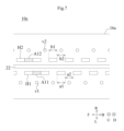
A
伝送線路10cは、複数の第1中空部H1の前後方向における長さa1及び複数の第2中空部H2の前後方向における長さb1において、伝送線路10と相違する。より詳細には、複数の第1中空部H1は、左右方向に見て、複数の第2中空部H2と重なっていない。第1中空部H1の前端の前後方向における位置は、第1中空部H1の右前に位置する第2中空部H2の後端の前後方向における位置と一致する。第1中空部H1の後端の前後方向における位置は、第1中空部H1の右後に位置する第2中空部H2の前端の前後方向における位置と一致する。伝送線路10cのその他の構造は、伝送線路10と同じであるので説明を省略する。
The
伝送線路10cによれば、伝送線路10と同じ作用効果を奏する。また、伝送線路10cによれば、信号導体層22に発生している特性インピーダンスが変化することがより抑制される。より詳細には、伝送線路10cでは、信号導体層22の左又は右には、第1中空部H1又は第2中空部H2のいずれか一方が位置している。換言すれば、信号導体層22の左及び右に、第1中空部H1及び第2中空部H2の両方が位置しない。これにより、信号導体層22の周囲の誘電率が変化しにくくなる。よって、伝送線路10cによれば、信号導体層22に発生している特性インピーダンスが変化することがより抑制される。
According to the
(第4変形例)
以下に、第4変形例に係る伝送線路10dについて図面を参照しながら説明する。図8は、伝送線路10dの絶縁体層16c,18a,18bの上面図である。(Fourth modification)
A
伝送線路10dでは、複数の第1中空部H11が絶縁体層18aに設けられ、かつ、複数の第2中空部H12が絶縁体層18bに設けられている点において、伝送線路10と相違する。伝送線路10dでは、第1直交方向は、左右方向である。
The
左右方向(第1直交方向)に見て、複数の第1中空部H11は、信号導体層22の上(第1方向)において前後方向に並んでいる。複数の第1中空部H11は、上下方向に見て、第1グランド導体層24と重なっている。また、前後方向に隣り合う2つの第1中空部H11の間に位置する領域のそれぞれを第1領域A21と定義する。複数の第1領域A21は、前後方向に等間隔に並んでいる。
When viewed in the left-right direction (first orthogonal direction), the plurality of first hollow portions H11 are arranged in the front-rear direction on the signal conductor layer 22 (first direction). The plurality of first hollow parts H11 overlap with the first
左右方向(第1直交方向)に見て、複数の第2中空部H12は、信号導体層22の下(第2方向)において前後方向に並んでいる。また、前後方向に隣り合う2つの第2中空部H12の間に位置する領域のそれぞれを第2領域A22と定義する。複数の第2領域A22は、前後方向に等間隔に並んでいる。 When viewed in the left-right direction (first orthogonal direction), the plurality of second hollow portions H12 are lined up in the front-back direction below the signal conductor layer 22 (second direction). Furthermore, each region located between two second hollow portions H12 adjacent in the front-rear direction is defined as a second region A22. The plurality of second regions A22 are arranged at equal intervals in the front-rear direction.
複数の第1中空部H11及び複数の第2中空部H12のそれぞれは、周期的に並んでいる。複数の第1中空部H11の一周期の長さL11は、複数の第2中空部H12の一周期の長さL12と等しい。複数の第1中空部H11の一周期の長さL11は、第1中空部H11の前後方向における長さと第1領域A21の前後方向における長さとの合計の長さである。複数の第2中空部H12の一周期の長さL12は、第2中空部H12の前後方向における長さと第2領域A22の前後方向における長さとの合計の長さである。複数の第1中空部H11の前後方向における長さは、複数の第2中空部H12の前後方向における長さと等しい。複数の第1領域A21の前後方向における長さは、複数の第2領域A22の前後方向における長さと等しい。ただし、複数の第1中空部H11の前後方向における位置と複数の第2中空部H12の前後方向における位置とは、半周期の長さだけ前後にずれている。これにより、複数の第1中空部H11のそれぞれは、複数の第2領域A22の上(第1方向)に位置している。すなわち、複数の第1中空部H11のそれぞれは、上下方向(第2直交方向)に見て、複数の第2領域A22と重なっている。複数の第2中空部H12のそれぞれは、複数の第1領域A21の下(第2方向)に位置している。すなわち、複数の第2中空部H12のそれぞれは、上下方向(第2直交方向)に見て、複数の第1領域A21と重なっている。 Each of the plurality of first hollow parts H11 and the plurality of second hollow parts H12 are arranged periodically. The length L11 of one cycle of the plurality of first hollow parts H11 is equal to the length L12 of one cycle of the plurality of second hollow parts H12. The length L11 of one period of the plurality of first hollow parts H11 is the total length of the length of the first hollow parts H11 in the front-back direction and the length of the first region A21 in the front-back direction. The length L12 of one period of the plurality of second hollow portions H12 is the total length of the length of the second hollow portions H12 in the front-back direction and the length of the second region A22 in the front-back direction. The length of the plurality of first hollow parts H11 in the front-rear direction is equal to the length of the plurality of second hollow parts H12 in the front-rear direction. The length of the plurality of first regions A21 in the front-rear direction is equal to the length of the plurality of second regions A22 in the front-rear direction. However, the positions of the plurality of first hollow parts H11 in the front-rear direction and the positions of the plurality of second hollow parts H12 in the front-rear direction are shifted back and forth by the length of a half cycle. Thereby, each of the plurality of first hollow parts H11 is located above the plurality of second regions A22 (in the first direction). That is, each of the plurality of first hollow portions H11 overlaps with the plurality of second regions A22 when viewed in the vertical direction (second orthogonal direction). Each of the plurality of second hollow portions H12 is located below (in the second direction) the plurality of first regions A21. That is, each of the plurality of second hollow portions H12 overlaps with the plurality of first regions A21 when viewed in the vertical direction (second orthogonal direction).
なお、絶縁体層16b,16cには、第1中空部H1及び第2中空部H2が設けられていない。伝送線路10dのその他の構造は、伝送線路10と同じであるので説明を省略する。
Note that the first hollow portion H1 and the second hollow portion H2 are not provided in the insulator layers 16 b and 16 c . The rest of the structure of the
伝送線路10dによれば、伝送線路10と同じ作用効果を奏する。また、絶縁体層16b,16cに第1中空部H1及び第2中空部H2が設けられていないので、伝送線路10dの強度が高くなる。また、第1領域A21の左端が絶縁体層18aの左部に固定されていると共に、第1領域A21の右端が絶縁体層18aの右部に固定されている。これにより、第1領域A21が変形しにくくなる。その結果、第1中空部H11が変形しにくくなる。第1領域A21と同じ理由により、第2領域A22が変形しにくくなる。その結果、第2中空部H12が変形しにくくなる。
According to the
(第5変形例)
以下に、第5変形例に係る伝送線路10eについて図面を参照しながら説明する。図9は、伝送線路10eの絶縁体層16c,18a,18bの上面図である。(Fifth modification)
A
伝送線路10eでは、第1領域A11の前後方向における位置と、第2領域A12の前後方向における位置と、第1領域A21の前後方向における位置と、第2領域A22の前後方向における位置とは、互いに異なっている。伝送線路10eのその他の構造は、伝送線路10と同じであるので説明を省略する。伝送線路10eによれば、伝送線路10dと同じ作用効果を奏する。
In the
(第6変形例)
以下に、第6変形例に係る伝送線路10fについて図面を参照しながら説明する。図10は、伝送線路10fの分解斜視図である。(Sixth variation)
A
伝送線路10fは、以下の点において伝送線路10と相違する。
・第3中空部H3及び第4中空部H4のそれぞれが絶縁体層18a,18bに設けられていない。
・第1中空部H1及び第2中空部H2のそれぞれが絶縁体層18a,18bに設けられている。
The
- The third hollow part H3 and the fourth hollow part H4 are not provided in the insulator layers 18a and 18b, respectively.
- The first hollow part H1 and the second hollow part H2 are provided in the insulator layers 18a and 18b, respectively.
伝送線路10fのその他の構造は、伝送線路10と同じであるので説明を省略する。伝送線路10fは、伝送線路10と同じ作用効果を奏する。伝送線路10fによれば、絶縁体層16b,16c,18a,18bに同時に第1中空部H1及び第2中空部H2を形成することができる。
The other structure of the
(第7変形例)
以下に、第7変形例に係る伝送線路10gについて図面を参照しながら説明する。図11は、伝送線路10gの分解斜視図である。(Seventh modification)
A
伝送線路10gは、第3中空部H3及び第4中空部H4のそれぞれが絶縁体層18a,18bに設けられていない点において伝送線路10と相違する。伝送線路10gのその他の構造は、伝送線路10と同じであるので説明を省略する。伝送線路10gによれば、伝送線路10と同じ作用効果を奏する。また、伝送線路10gによれば、第3中空部H3及び第4中空部H4の変形による信号導体層22に発生している特性インピーダンスが変化することが抑制される。
The
(第8変形例)
以下に、第8変形例に係る伝送線路10hについて図面を参照しながら説明する。図12は、伝送線路10hの絶縁体層16cの上面図である。(Eighth modification)
A
伝送線路10hは、信号導体層22の形状において伝送線路10と相違する。伝送線路10hでは、信号導体層22は、複数の太線部22a及び複数の細線部22bを含んでいる。太線部22aの左右方向における幅w1は、細線部22bの左右方向における幅w2より大きい。複数の太線部22aと複数の細線部22bとは、前後方向に交互に並んでいる。また、複数の細線部22bは、左右方向に見て、複数の層間接続導体v1,v2と重なっている。なお、伝送線路10hのその他の構造は、伝送線路10と同じであるので説明を省略する。
The
伝送線路10hは、伝送線路10と同じ作用効果を奏する。また、伝送線路10hによれば、複数の層間接続導体v1,v2と複数の細線部22bとの距離が大きくなる。そのため、複数の層間接続導体v1,v2と複数の細線部22bとの間に容量が形成されにくくなる。これにより、信号導体層22に発生する特性インピーダンスが高くなる。伝送線路10では、信号導体層22の線幅が均一であるため、信号導体層22と層間接続導体v1,v2との間に形成される容量により、信号導体層22に発生する特性インピーダンスが変化する。一方、伝送線路10hでは、太線部22a及び細線部22bにより、信号導体層22に発生する特性インピーダンスの変化が小さくなる。
The
(第9変形例)
以下に、第9変形例に係る伝送線路10iについて図面を参照しながら説明する。図13は、伝送線路10iの絶縁体層16cの上面図である。(9th modification)
A
伝送線路10iは、複数の第1中空部H1と複数の層間接続導体v1との位置関係、及び、複数の第2中空部H2と複数の層間接続導体v2との位置関係において伝送線路10と相違する。より詳細には、左右方向に見て、複数の第1中空部H1は、複数の層間接続導体v1と重なっている。左右方向に見て、複数の第2中空部H2は、複数の層間接続導体v2と重なっている。伝送線路10iのその他の構造は、伝送線路10と同じであるので説明を省略する。
The
伝送線路10iは、伝送線路10と同じ作用効果を奏する。また、伝送線路10iによれば、信号導体層22に発生する特性インピーダンスが変化することを抑制できる。より詳細には、左右方向に見て、複数の第1中空部H1は、複数の層間接続導体v1と重なっている。これにより、信号導体層22と複数の層間接続導体v1との間に容量が形成されることが抑制される。また、左右方向に見て、複数の第2中空部H2は、複数の層間接続導体v2と重なっている。これにより、信号導体層22と複数の層間接続導体v2との間に容量が形成されることが抑制される。その結果、信号導体層22に発生する特性インピーダンスが変化することが抑制される。また、信号導体層22と複数の層間接続導体v1,v2との間に容量が形成されにくいので、信号導体層22の線幅を大きくすることが可能となる。その結果、信号導体層22の直流抵抗値が低減される。
The
(第10変形例)
以下に、第10変形例に係る伝送線路10jについて図面を参照しながら説明する。図14は、伝送線路10jの絶縁体層16cの上面図である。(10th modification)
A
伝送線路10jは、曲がっている点において伝送線路10と相違する。「伝送線路10jが曲がっている」とは、伝送線路10jに外力を加えない状態で曲がった形状を有していることを意味する。なお、この場合、前後方向は、信号導体層22の位置によって異なる。
The
伝送線路10jでは、信号導体層22より外周側に位置する第2中空部H2の前後方向における長さb1は、信号導体層22より内周側に位置する第1中空部H1の前後方向における長さa1より長い。伝送線路10jのその他の構造は、伝送線路10と同じであるので説明を省略する。伝送線路10jは、伝送線路10と同じ作用効果を奏する。
In the
(その他の実施形態)
本発明に係る伝送線路は、伝送線路10,10a~10jに限らず、その要旨の範囲内において変更可能である。なお、伝送線路10,10a~10jの構成を任意に組み合わせてもよい。(Other embodiments)
The transmission line according to the present invention is not limited to the
なお、伝送線路10,10a~10jは、複数本の信号導体層を備えていてもよい。この場合、複数本の信号導体層は、例えば、差動伝送線路を形成していてもよい。また、複数本の信号導体層は、同じ絶縁体層上に設けられていなくてもよい。
Note that the
なお、伝送線路10,10a~10jにおいて、信号端子28a,28b及びグランド端子29a,29b,30a,30bは、積層体12の下主面に設けられてもよい。
Note that in the
なお、伝送線路10,10a~10jは、ストリップライン線路に加えて、他の回路を更に備えていてもよい。
Note that the
なお、伝送線路10,10a~10jには、コネクタ32a,32b以外に電子部品が実装されてもよい。電子部品は、例えば、チップインダクタやチップコンデンサ等である。
Note that electronic components other than the
なお、第2グランド導体層26は、必須の構成ではない。この場合、信号導体層22及び第1グランド導体層24は、マイクロストリップライン構造を構成する。
Note that the second
なお、絶縁体層16aの上に保護層が設けられてもよい。
Note that a protective layer may be provided on the
なお、複数の絶縁体層16a~16dの内の1以上の絶縁体層の材料は多孔質材料であってもよい。多孔質構造とは、多孔質材料により作製された絶縁体層の全体に複数の小さな気泡が分散している構造である。多孔質材料により作製された絶縁体層は、複数の独立気泡を含んでいる。独立気泡は、気泡の全体が絶縁体層の材料により囲まれることにより、気泡内の気体が絶縁体層の外部に漏れることができない構造を有している。また、独立気泡では、隣り合う気泡同士がつながっていない。多孔質材料により作製された絶縁体層の空孔率は、例えば、30%以上80%以下である。空孔率は、多孔質材料により作製された絶縁体層の全体の体積に占める気泡の体積の割合である。このように、多孔質材料は、空気を含んでいるため、低い誘電率を有している。これにより、信号導体層22の周囲の誘電率が低くなり、信号導体層22を伝送される高周波信号に誘電損が発生しにくくなる。すなわち、伝送線路10,10a~10jの高周波特性が向上する。
Note that the material of one or more of the plurality of
なお、絶縁体層18a,18bの材料は、熱可塑性樹脂であってもよい。 Note that the material of the insulator layers 18a and 18b may be thermoplastic resin.
なお、複数の第1中空部H1の前後方向における長さa1は、第1領域A11の前後方向における長さa2と等しくてもいい。複数の第2中空部H2の前後方向における長さb1は、第2領域A12の前後方向における長さb2と等しくてもいい。 Note that the length a1 of the plurality of first hollow portions H1 in the front-rear direction may be equal to the length a2 of the first region A11 in the front-rear direction. The length b1 of the plurality of second hollow portions H2 in the front-rear direction may be equal to the length b2 of the second region A12 in the front-rear direction.
なお、複数の第1中空部H1の形状は、均一でなくてもよい。複数の第2中空部H2の形状は、均一でなくてもよい。 Note that the shapes of the plurality of first hollow parts H1 may not be uniform. The shapes of the plurality of second hollow parts H2 may not be uniform.
なお、第1領域A11の前後方向における長さは、均一でなくてもよい。第2領域A12の前後方向における長さは、均一でなくてもよい。 Note that the length of the first region A11 in the front-rear direction may not be uniform. The length of the second region A12 in the front-rear direction may not be uniform.
なお、信号導体層22が絶縁体層16cの上主面に設けられ、信号導体層が絶縁体層16cの下主面に設けられていてもよい。
Note that the
なお、層間接続導体v1~v8は、図1に示すように、絶縁体層16a~16d,18a,18bの一部を上下方向に貫通していてもよいし、絶縁体層16a~16d,18a,18bを上下方向に貫通していてもよい。 Note that the interlayer connection conductors v1 to v8 may vertically penetrate a portion of the insulator layers 16a to 16d, 18a, and 18b, as shown in FIG. , 18b in the vertical direction.
なお、複数の第1中空部H1の前後方向における位置と複数の第2中空部H2の前後方向における位置とは半周期の長さだけ前後にずれている例を示した。しかしながら、ずれの量は、半周期でなくてもよい。 Note that an example has been shown in which the positions of the plurality of first hollow parts H1 in the front-rear direction and the positions of the plurality of second hollow parts H2 in the front-rear direction are shifted back and forth by the length of a half period. However, the amount of shift need not be half a cycle.
なお、図3に示す伝送線路10において、第1中空部H1は、第3中空部H3の左端と同じ位置又は第3中空部H3の左端より左に位置していてもよい。すなわち、第1中空部H1と信号導体層22との左右方向の距離は、第3中空部H3の左端と信号導体層22との左右方向の距離以上であってもよい。第2中空部H2は、第4中空部H4の右端と同じ位置又は第4中空部H4の右端より右に位置していてもよい。すなわち、第2中空部H2と信号導体層22との左右方向の距離は、第4中空部H4の右端と信号導体層22との左右方向の距離以上であってもよい。なお、第1中空部H1の体積及び第2中空部H2の体積が大きいことが好ましい。
In the
1:電子機器
10,10a~10j:伝送線路
12:積層体
16a~16d,18a,18b:絶縁体層
22:信号導体層
22a:太線部
22b:細線部
24:第1グランド導体層
26:第2グランド導体層
A1,A3:非曲げ区間
A11,A21:第1領域
A12,A22:第2領域
A2:曲げ区間
A3:非曲げ区間
H1,H11:第1中空部
H2,H12:第2中空部
H3:第3中空部
H4:第4中空部
v1~v8:層間接続導体1:
Claims (11)
前記積層体に設けられており、かつ、前記上下方向に直交する前後方向に延びている信号導体層と、
前記積層体に設けられており、かつ、前記上下方向に見て、前記信号導体層と重なるように、前記信号導体層の上に設けられている第1グランド導体層と、
を備えており、
複数の第1中空部及び複数の第2中空部が前記積層体に設けられており、
前記複数の第1中空部及び前記複数の第2中空部は、前記絶縁体層が存在しない空洞であり、
前記複数の第1中空部及び前記複数の第2中空部は、前記上下方向に見て、前記第1グランド導体層と重なっており、
前記前後方向に直交する方向を第1直交方向と定義し、及び、前記前後方向及び前記第1直交方向に直交する方向を第2直交方向と定義し、
前記第2直交方向は、第1方向及び前記第1方向の反対方向である第2方向を含んでおり、
前記第1直交方向に見て、前記複数の第1中空部は、前記信号導体層の前記第1方向において前記前後方向に並んでおり、
前記第1直交方向に見て、前記複数の第2中空部は、前記信号導体層の前記第2方向において前記前後方向に並んでおり、
前記前後方向に隣り合う2つの前記第1中空部の間に位置する領域のそれぞれを複数の第1領域と定義し、
前記前後方向に隣り合う2つの前記第2中空部の間に位置する領域のそれぞれを複数の第2領域と定義し、
前記複数の第1中空部のそれぞれは、前記第2直交方向に見て、前記複数の第2領域の対応する1つと重なっており、
前記複数の第2中空部のそれぞれは、前記第2直交方向に見て、前記複数の第1領域の対応する1つと重なっている、伝送線路。 A laminate having a structure in which a plurality of insulating layers are stacked vertically;
a signal conductor layer provided on the laminate and extending in a front-back direction perpendicular to the up-down direction;
a first ground conductor layer provided in the laminate and provided on the signal conductor layer so as to overlap with the signal conductor layer when viewed in the vertical direction;
It is equipped with
A plurality of first hollow parts and a plurality of second hollow parts are provided in the laminate,
The plurality of first hollow parts and the plurality of second hollow parts are cavities in which the insulating layer does not exist,
The plurality of first hollow parts and the plurality of second hollow parts overlap with the first ground conductor layer when viewed in the vertical direction,
A direction perpendicular to the longitudinal direction is defined as a first orthogonal direction, and a direction orthogonal to the longitudinal direction and the first orthogonal direction is defined as a second orthogonal direction,
The second orthogonal direction includes a first direction and a second direction that is opposite to the first direction,
When viewed in the first orthogonal direction, the plurality of first hollow portions are lined up in the front-rear direction in the first direction of the signal conductor layer,
When viewed in the first orthogonal direction, the plurality of second hollow portions are lined up in the front-rear direction in the second direction of the signal conductor layer,
Each of the regions located between the two first hollow portions adjacent in the front-rear direction is defined as a plurality of first regions,
Each of the regions located between the two second hollow portions adjacent in the front-rear direction is defined as a plurality of second regions,
Each of the plurality of first hollow portions overlaps with a corresponding one of the plurality of second regions when viewed in the second orthogonal direction,
The transmission line, wherein each of the plurality of second hollow portions overlaps a corresponding one of the plurality of first regions when viewed in the second orthogonal direction.
請求項1に記載の伝送線路。 the first orthogonal direction is the up-down direction;
The transmission line according to claim 1.
請求項1に記載の伝送線路。 the first orthogonal direction is a left-right direction;
The transmission line according to claim 1.
前記接着層は、前記絶縁体層のうちの、前記接着層の上に位置する1つの絶縁体層と前記絶縁体層のうちの、前記接着層の下に位置する1つの絶縁体層とを接合する、
請求項1ないし請求項3のいずれかに記載の伝送線路。 The plurality of insulator layers include the insulator layer that functions as an adhesive layer,
The adhesive layer includes one insulator layer located above the adhesive layer among the insulator layers and one insulator layer located below the adhesive layer among the insulator layers. join,
The transmission line according to any one of claims 1 to 3.
前記信号導体層は、前記接着層の下に位置する前記絶縁体層に設けられている、
請求項4に記載の伝送線路。 The first ground conductor layer is provided on one insulator layer located on the adhesive layer among the insulator layers,
The signal conductor layer is provided on the insulator layer located below the adhesive layer,
The transmission line according to claim 4.
請求項1ないし請求項3のいずれかに記載の伝送線路。 The material of the plurality of insulator layers is a thermoplastic resin,
The transmission line according to any one of claims 1 to 3.
請求項1ないし請求項5のいずれかに記載の伝送線路。 The material of one or more of the plurality of insulator layers is a porous material,
The transmission line according to any one of claims 1 to 5.
前記複数の第2中空部それぞれは、同じ形状を有している、
請求項1ないし請求項7のいずれかに記載の伝送線路。 Each of the plurality of first hollow parts has the same shape,
Each of the plurality of second hollow parts has the same shape,
The transmission line according to any one of claims 1 to 7.
前記複数の第2中空部は、等間隔に並んでいる、
請求項1ないし請求項8のいずれかに記載の伝送線路。 The plurality of first hollow parts are arranged at equal intervals,
The plurality of second hollow parts are arranged at equal intervals,
The transmission line according to any one of claims 1 to 8.
前記第1中空部のそれぞれの後端部は、前記第2直交方向に見て、前記第1中空部の前記第2方向に位置している前記第2領域のうちの1つの第2領域の後に位置する前記第2中空部のうちの1つの第2中空部と重なっており、
前記第2中空部のそれぞれの前端部は、前記第2直交方向に見て、前記第2中空部の前記第1方向に位置している前記第1領域のうちの1つの第2領域の前に位置する前記第1中空部のうちの1つの第2中空部と重なっており、
前記第2中空部のそれぞれの後端部は、前記第2直交方向に見て、前記第2中空部の前記第1方向に位置している前記第1領域のうちの1つの第2領域の後に位置する前記第1中空部のうちの1つの第2中空部と重なっている、
請求項1ないし請求項9のいずれかに記載の伝送線路。 The front end of each of the first hollow parts is located in front of one of the second regions of the first hollow part located in the second direction when viewed in the second orthogonal direction. overlaps one of the second hollow parts located in the second hollow part ,
The rear end portion of each of the first hollow portions is located in one of the second regions of the first hollow portion located in the second direction when viewed in the second orthogonal direction. overlaps with one second hollow part of the second hollow parts located behind,
The front end of each of the second hollow parts is located in front of one of the first regions of the second hollow part located in the first direction when viewed in the second orthogonal direction. overlaps with a second hollow part of one of the first hollow parts located in
A rear end portion of each of the second hollow portions is arranged in a second region of one of the first regions located in the first direction of the second hollow portion when viewed in the second orthogonal direction. overlapping with a second hollow part of one of the first hollow parts located behind;
The transmission line according to any one of claims 1 to 9.
備えている、
電子機器。 The transmission line according to any one of claims 1 to 10,
are equipped with
Electronics.
Applications Claiming Priority (5)
| Application Number | Priority Date | Filing Date | Title |
|---|---|---|---|
| JP2020198385 | 2020-11-30 | ||
| JP2020198385 | 2020-11-30 | ||
| JP2021033558 | 2021-03-03 | ||
| JP2021033558 | 2021-03-03 | ||
| PCT/JP2021/042035 WO2022113818A1 (en) | 2020-11-30 | 2021-11-16 | Transmission line and electronic device |
Publications (3)
| Publication Number | Publication Date |
|---|---|
| JPWO2022113818A1 JPWO2022113818A1 (en) | 2022-06-02 |
| JPWO2022113818A5 JPWO2022113818A5 (en) | 2023-07-13 |
| JP7355256B2 true JP7355256B2 (en) | 2023-10-03 |
Family
ID=81756010
Family Applications (1)
| Application Number | Title | Priority Date | Filing Date |
|---|---|---|---|
| JP2022565249A Active JP7355256B2 (en) | 2020-11-30 | 2021-11-16 | Transmission lines and electronic equipment |
Country Status (3)
| Country | Link |
|---|---|
| US (1) | US20230290537A1 (en) |
| JP (1) | JP7355256B2 (en) |
| WO (1) | WO2022113818A1 (en) |
Citations (3)
| Publication number | Priority date | Publication date | Assignee | Title |
|---|---|---|---|---|
| US20020084876A1 (en) | 2000-12-29 | 2002-07-04 | Wright Mitchel E. | Slotted ground plane for controlling the impedance of high speed signals on a printed circuit board |
| JP2017123740A (en) | 2016-01-07 | 2017-07-13 | シャープ株式会社 | Switching power supply |
| WO2017130731A1 (en) | 2016-01-27 | 2017-08-03 | 株式会社村田製作所 | Signal transmission line |
Family Cites Families (4)
| Publication number | Priority date | Publication date | Assignee | Title |
|---|---|---|---|---|
| JPS62269401A (en) * | 1986-05-16 | 1987-11-21 | Mitsubishi Electric Corp | Suspend line |
| US5844450A (en) * | 1996-03-05 | 1998-12-01 | Motorola, Inc. | Integrated microstrip to suspend stripline transition structure and method of fabrication |
| US5712607A (en) * | 1996-04-12 | 1998-01-27 | Dittmer; Timothy W. | Air-dielectric stripline |
| JP2007123740A (en) * | 2005-10-31 | 2007-05-17 | Sony Corp | Flexible board, optical transmission/reception module and optical transmission/reception device |
-
2021
- 2021-11-16 WO PCT/JP2021/042035 patent/WO2022113818A1/en active Application Filing
- 2021-11-16 JP JP2022565249A patent/JP7355256B2/en active Active
-
2023
- 2023-05-17 US US18/198,475 patent/US20230290537A1/en active Pending
Patent Citations (3)
| Publication number | Priority date | Publication date | Assignee | Title |
|---|---|---|---|---|
| US20020084876A1 (en) | 2000-12-29 | 2002-07-04 | Wright Mitchel E. | Slotted ground plane for controlling the impedance of high speed signals on a printed circuit board |
| JP2017123740A (en) | 2016-01-07 | 2017-07-13 | シャープ株式会社 | Switching power supply |
| WO2017130731A1 (en) | 2016-01-27 | 2017-08-03 | 株式会社村田製作所 | Signal transmission line |
Also Published As
| Publication number | Publication date |
|---|---|
| JPWO2022113818A1 (en) | 2022-06-02 |
| US20230290537A1 (en) | 2023-09-14 |
| WO2022113818A1 (en) | 2022-06-02 |
Similar Documents
| Publication | Publication Date | Title |
|---|---|---|
| US9935352B2 (en) | Composite transmission line and electronic device | |
| WO2014002757A1 (en) | Cable connection/anchoring method | |
| WO2015118791A1 (en) | High-frequency signal transmission line and electronic device | |
| JP7355256B2 (en) | Transmission lines and electronic equipment | |
| WO2022114092A1 (en) | Transmission line and electronic device | |
| WO2022113591A1 (en) | Transmission line and electronic device | |
| WO2022124038A1 (en) | Circuit board and electronic device | |
| CN220306489U (en) | Transmission line and electronic device | |
| JP7414147B2 (en) | Circuit boards and electronic equipment | |
| WO2022113739A1 (en) | Transmission line and electronic device | |
| WO2022270294A1 (en) | Multilayer substrate, multilayer substrate module, and electronic device | |
| CN219979789U (en) | Transmission line and electronic device | |
| JP5929557B2 (en) | Flat cable | |
| WO2022138355A1 (en) | Multilayer board and method for manufacturing multilayer board | |
| US20230282955A1 (en) | Transmission line and electronic device | |
| JP2017123421A (en) | Wiring board and electronic apparatus | |
| JP7409493B2 (en) | Signal transmission line and method for manufacturing the signal transmission line | |
| CN206236772U (en) | Transmission line component | |
| US20230328883A1 (en) | Multilayer substrate | |
| US9560743B2 (en) | Multilayer circuit substrate having core layer with through-hole | |
| WO2023204099A1 (en) | Multilayer substrate | |
| WO2022149450A1 (en) | Multilayer substrate, electronic apparatus, and method for manufacturing multilayer substrate | |
| JP7359308B2 (en) | transmission line | |
| WO2022118810A1 (en) | Transmission line and electronic device | |
| WO2023085177A1 (en) | Multilayer board |
Legal Events
| Date | Code | Title | Description |
|---|---|---|---|
| A521 | Request for written amendment filed |
Free format text: JAPANESE INTERMEDIATE CODE: A523 Effective date: 20230515 |
|
| A621 | Written request for application examination |
Free format text: JAPANESE INTERMEDIATE CODE: A621 Effective date: 20230515 |
|
| A871 | Explanation of circumstances concerning accelerated examination |
Free format text: JAPANESE INTERMEDIATE CODE: A871 Effective date: 20230515 |
|
| TRDD | Decision of grant or rejection written | ||
| A01 | Written decision to grant a patent or to grant a registration (utility model) |
Free format text: JAPANESE INTERMEDIATE CODE: A01 Effective date: 20230822 |
|
| A61 | First payment of annual fees (during grant procedure) |
Free format text: JAPANESE INTERMEDIATE CODE: A61 Effective date: 20230904 |
|
| R150 | Certificate of patent or registration of utility model |
Ref document number: 7355256 Country of ref document: JP Free format text: JAPANESE INTERMEDIATE CODE: R150 |