JP7329954B2 - Acoustic wave resonators, filters and multiplexers - Google Patents
Acoustic wave resonators, filters and multiplexers Download PDFInfo
- Publication number
- JP7329954B2 JP7329954B2 JP2019075871A JP2019075871A JP7329954B2 JP 7329954 B2 JP7329954 B2 JP 7329954B2 JP 2019075871 A JP2019075871 A JP 2019075871A JP 2019075871 A JP2019075871 A JP 2019075871A JP 7329954 B2 JP7329954 B2 JP 7329954B2
- Authority
- JP
- Japan
- Prior art keywords
- substrate
- piezoelectric substrate
- polycrystalline
- wave resonator
- electrode fingers
- Prior art date
- Legal status (The legal status is an assumption and is not a legal conclusion. Google has not performed a legal analysis and makes no representation as to the accuracy of the status listed.)
- Active
Links
Images


Description
本発明は、弾性波共振器、フィルタおよびマルチプレクサに関し、例えば一対の櫛型電極を有する弾性波共振器、フィルタおよびマルチプレクサに関する。 The present invention relates to acoustic wave resonators, filters and multiplexers, and for example to acoustic wave resonators, filters and multiplexers having a pair of comb electrodes.
スマートフォン等の通信機器に用いられる弾性波共振器として、弾性表面波共振器が知られている。弾性表面波共振器を形成する圧電基板を支持基板に接合することが知られている。圧電基板の厚さを弾性表面波の波長以下とすることが知られている(例えば特許文献1)。 A surface acoustic wave resonator is known as an acoustic wave resonator used in communication devices such as smartphones. It is known to bond a piezoelectric substrate forming a surface acoustic wave resonator to a support substrate. It is known to make the thickness of the piezoelectric substrate equal to or less than the wavelength of the surface acoustic wave (for example, Patent Document 1).
圧電基板を支持基板に接合することにより、弾性表面波共振器の温度特性が向上する。さらに、圧電基板の厚さを弾性表面波の波長以下とすることにより、損失およびスプリアスを抑制できる。しかしながら、スプリアスの抑制は十分でない。 By bonding the piezoelectric substrate to the support substrate, the temperature characteristics of the surface acoustic wave resonator are improved. Furthermore, loss and spurious can be suppressed by setting the thickness of the piezoelectric substrate to be equal to or less than the wavelength of the surface acoustic wave. However, spurious suppression is not sufficient.
本発明は、上記課題に鑑みなされたものであり、スプリアスを抑制することを目的とする。 The present invention has been made in view of the above problems, and an object of the present invention is to suppress spurious.
本発明は、10°以上かつ50°以下回転YカットX伝搬タンタル酸リチウム基板である圧電基板と、前記圧電基板上に設けられ、複数の電極指を有し弾性波を励振する一対の櫛型電極と、前記圧電基板の前記一対の櫛型電極が設けられた面と反対側に設けられ、平均粒径が前記複数の電極指の平均ピッチの1倍以上かつ66倍以下であり、多結晶スピネル基板である多結晶基板と、を備え、前記圧電基板の厚さは、前記複数の電極指の平均ピッチの2倍以下である弾性波共振器である。
The present invention comprises: a piezoelectric substrate that is a Y-cut X-propagation lithium tantalate substrate rotated by 10° or more and 50° or less; The electrodes are provided on the side of the piezoelectric substrate opposite to the surface on which the pair of comb-shaped electrodes are provided, and have an average particle diameter of 1 to 66 times the average pitch of the plurality of electrode fingers . and a polycrystalline substrate that is a crystal spinel substrate , wherein the thickness of the piezoelectric substrate is equal to or less than twice the average pitch of the plurality of electrode fingers .
本発明は、圧電基板と、前記圧電基板上に設けられ、複数の電極指を有し主にSH波を励振する一対の櫛型電極と、前記圧電基板の前記一対の櫛型電極が設けられた面と反対側に設けられ、平均粒径が前記複数の電極指の平均ピッチの1倍以上かつ66倍以下であり、多結晶スピネル基板である多結晶基板と、を備え、前記圧電基板の厚さは、前記複数の電極指の平均ピッチの2倍以下である弾性波共振器である。
The present invention includes a piezoelectric substrate, a pair of comb-shaped electrodes provided on the piezoelectric substrate and having a plurality of electrode fingers for mainly exciting SH waves, and the pair of comb-shaped electrodes of the piezoelectric substrate. a polycrystalline substrate which is a polycrystalline spinel substrate provided on the opposite side of the piezoelectric substrate and has an average grain size of 1 to 66 times the average pitch of the plurality of electrode fingers; The thickness of the elastic wave resonator is not more than twice the average pitch of the plurality of electrode fingers .
上記構成において、前記平均粒径は前記平均ピッチの40倍以下である構成とすることができる。
In the above configuration, the average particle size may be 40 times or less the average pitch .
上記構成において、前記多結晶基板の前記圧電基板側の面と前記圧電基板の前記一対の櫛型電極が設けられた面との距離は前記平均ピッチの2倍以下である構成とすることができる。 In the above configuration, the distance between the surface of the polycrystalline substrate on the side of the piezoelectric substrate and the surface of the piezoelectric substrate on which the pair of comb-shaped electrodes is provided may be less than or equal to twice the average pitch. .
上記構成において、前記圧電基板は、36°以上かつ42°以下回転YカットX伝搬タンタル酸リチウム基板である構成とすることができる。 In the above configuration, the piezoelectric substrate may be a Y-cut X-propagation lithium tantalate substrate rotated 36° or more and 42° or less.
上記構成において、前記多結晶基板の厚さは前記平均ピッチの2倍以上かつ前記平均粒径以上である構成とすることができる。 In the above configuration, the thickness of the polycrystalline substrate may be at least twice the average pitch and at least the average grain size.
上記構成において、前記圧電基板と前記多結晶基板とは直接接合されている構成とすることができる。 In the above configuration, the piezoelectric substrate and the polycrystalline substrate may be directly bonded.
上記構成において、前記圧電基板と前記多結晶基板との間に設けられた中間層を有する構成とすることができる。 In the above configuration, an intermediate layer may be provided between the piezoelectric substrate and the polycrystalline substrate.
本発明は、上記弾性波共振器を備えるフィルタである。 The present invention is a filter comprising the above elastic wave resonator.
本発明は、上記フィルタを含むマルチプレクサである。 The present invention is a multiplexer including the above filters.
本発明によれば、スプリアスを抑制することができる。 According to the present invention, spurious can be suppressed.
以下、図面を参照し本発明の実施例について説明する。 Hereinafter, embodiments of the present invention will be described with reference to the drawings.
図1(a)は、実施例1における弾性波共振器の平面図、図1(b)は、図1(a)のA-A断面図である。電極指の配列方向をX方向、電極指の延伸方向をY方向、支持基板および圧電基板の積層方向をZ方向とする。X方向、Y方向およびZ方向は、圧電基板の結晶方位のX軸方向およびY軸方向とは必ずしも対応しない。圧電基板が回転YカットX伝搬基板の場合、X方向は結晶方位のX軸方向となる。 FIG. 1(a) is a plan view of the elastic wave resonator in Example 1, and FIG. 1(b) is a cross-sectional view taken along the line AA of FIG. 1(a). The arrangement direction of the electrode fingers is the X direction, the extending direction of the electrode fingers is the Y direction, and the stacking direction of the supporting substrate and the piezoelectric substrate is the Z direction. The X-direction, Y-direction and Z-direction do not necessarily correspond to the X-axis direction and Y-axis direction of the crystal orientation of the piezoelectric substrate. When the piezoelectric substrate is a rotated Y-cut X-propagation substrate, the X-direction is the X-axis direction of the crystal orientation.
図1(a)および図1(b)に示すように、多結晶基板10上に圧電基板12が積層されている。多結晶基板10および圧電基板12の厚さはそれぞれT0およびT2である。圧電基板12上に弾性波共振器20が設けられている。弾性波共振器20はIDT22および反射器24を有する。反射器24はIDT(Inter Digital Transducer)22のX方向の両側に設けられている。IDT22および反射器24は、圧電基板12上の金属膜14により形成される。
As shown in FIGS. 1( a ) and 1 ( b ), a
IDT22は、対向する一対の櫛型電極18を備える。櫛型電極18は、複数の電極指15と、複数の電極指15が接続されたバスバー16と、を備える。一対の櫛型電極18の電極指15が交差する領域が交差領域25である。交差領域25の長さが開口長である。一対の櫛型電極18は、交差領域25の少なくとも一部において電極指15がほぼ互い違いとなるように、対向して設けられている。交差領域25において複数の電極指15が励振する弾性波は、主にX方向に伝搬する。一対の櫛型電極18のうち一方の櫛型電極18の電極指15のピッチがほぼ弾性波の波長λとなる。弾性波の波長λはほぼ電極指15の2本分のピッチとなる。反射器24は、IDT22の電極指15が励振した弾性波(弾性表面波)を反射する。これにより弾性波はIDT22の交差領域25内に閉じ込められる。
The IDT 22 includes a pair of
圧電基板12は、単結晶基板であり、例えばタンタル酸リチウム(LiTaO3)基板またはニオブ酸リチウム(LiNbO3)基板であり、例えば回転YカットX伝搬タンタル酸リチウム基板または回転YカットX伝搬ニオブ酸リチウム基板である。多結晶基板10は、例えば、スピネル(MgAl2O3)基板、シリコン(Si)基板またはアルミナ(Al2O3)基板である。多結晶基板10のX方向の線膨張係数は圧電基板12のX方向の線膨張係数より小さい。これにより、弾性波共振器の共振周波数等の温度係数を小さくできる。
The
金属膜14は、例えばAl(アルミニウム)またはCu(銅)を主成分とする膜であり、例えばAl膜またはCu膜である。電極指15と圧電基板12との間にTi(チタン)膜またはCr(クロム)膜等の密着膜が設けられていてもよい。密着膜は電極指15より薄い。電極指15を覆うように絶縁膜が設けられていてもよい。絶縁膜は保護膜または温度補償層として機能する。
The
厚さT0は例えば50μmから500μmである。厚さT2は例えば0.5μmから20μmであり、例えば10λ以下であり、1λ以下である。2本の電極指15を1対としたときの対数は例えば20対から300対である。IDT22のデュティ比は、電極指15の太さ/電極指15のピッチであり、例えば30%から70%である。IDT22の開口長は例えば10λから50λである。
The thickness T0 is, for example, 50 μm to 500 μm. The thickness T2 is, for example, 0.5 μm to 20 μm, and is, for example, 10λ or less and 1λ or less. The number of pairs of two
[実施例1の製造方法]
図2(a)から図2(d)は、実施例1に係る弾性波共振器の製造方法を示す断面図である。図2(a)に示すように、多結晶基板10の上面および圧電基板12の下面にイオン54等を照射する。イオン54は例えばAr(アルゴン)イオン等の不活性元素(例えば希ガス元素)のイオンである。イオン54等をイオンビーム、中性化したビームまたはプラズマとして、照射する。これにより、多結晶基板10の上面に多結晶基板10に接するアモルファス層10aが形成され、圧電基板12の下面に圧電基板12に接するアモルファス層12aが形成される。アモルファス層10aおよび12aの表面には未結合の結合手が形成される(すなわち活性化される)。
[Manufacturing method of Example 1]
2A to 2D are cross-sectional views showing the method of manufacturing the elastic wave resonator according to the first embodiment. As shown in FIG. 2A, the upper surface of the
図2(b)に示すように、真空を維持した状態で、アモルファス層10aと12aとを張り合わせると、未結合手同士が結合し、強固な結合となる。これにより、多結晶基板10と圧電基板12が接合される。このような接合は常温(例えば100℃以下かつ-20℃以上、好ましくは80℃以下かつ0℃以上)で行われるため熱応力を抑制できる。常温で接合されたか否かは、残留応力の温度依存性により確かめることができる。すなわち、接合された温度において、残留応力が最も小さくなる。アモルファス層10aと12aからなるアモルファス層30が形成される。
As shown in FIG. 2(b), when the
アモルファス層10aは、多結晶基板10の構成元素を主成分とし、表面活性化のための元素(例えばAr)を含む。多結晶基板10がスピネル基板のとき、アモルファス層10aはMg(マグネシウム)、Al(アルミニウム)およびO(酸素)を主成分とし、表面活性化のための元素を含む。アモルファス層12aは、圧電基板12の構成元素を主成分とし、表面活性化のための元素を含む。圧電基板12がタンタル酸リチウム基板のとき、アモルファス層12aは、Ta(タンタル)、Li(リチウム)およびOを主成分とし、表面活性化のための元素を含む。アモルファス層10aは、圧電基板12の構成元素のうち多結晶基板10以外の構成元素をほとんど含まない。例えばアモルファス層10aはTaおよびLiをほとんど含まない。アモルファス層12aは、多結晶基板10の構成元素のうち圧電基板12の構成元素以外の元素をほとんど含まない。例えばアモルファス層12aはMgおよびAlをほとんど含まない。
The
アモルファス層10aおよび12aの厚さは、0nmより大きいことが好ましく、1nm以上がより好ましい。これにより、多結晶基板10と圧電基板12との接合性を向上させることができる。アモルファス層10aおよび12aの厚さは、10nm以下が好ましく、5nm以下がより好ましい。これにより、弾性波共振器の特性の劣化を抑制できる。アモルファス層30の厚さは多結晶基板10および圧電基板12と比べて非常に薄いため、多結晶基板10と圧電基板12とは実質的には直接接合されている。多結晶基板10、圧電基板12、アモルファス層10aおよび12aは、TEM(Transmission Electron Microscope)法を用い観察することができる。
The thickness of the
図2(c)に示すように、圧電基板12の上面を例えばCMP(Chemical Mechanical Polishing)法を用い平坦化する。これにより、圧電基板12の厚さがT2となる。図2(d)に示すように、圧電基板12の上面に金属膜14からなるIDT22および反射器24を形成する。
As shown in FIG. 2C, the upper surface of the
図3は、多結晶であるスピネル基板の断面のSEM(Scanning Electron Microscope)画像を模写した図である。複数の結晶粒50と結晶粒50の間の粒界52が観察できる。多結晶基板10の平均粒径を以下のように測定する。結晶粒50の断面積と等しい円の直径を粒径とする。90μm×90μmのSEM画像内の結晶粒50の粒径を測定し、粒径の平均を算出する。
FIG. 3 is a view of a copy of a SEM (Scanning Electron Microscope) image of a cross section of a polycrystalline spinel substrate. A plurality of
[実験]
圧電基板12の厚さT2を弾性波の波長λ以下とすると、バルク波に起因するスプリアスが低減する。しかし、反共振周波数より高い周波数に発生するスプリアスの抑圧は十分でない。そこで、平均粒径の異なるスピネル基板を支持基板として、弾性波共振器を有するラダー型フィルタを作製した。作製したラダー型フィルタは、直列共振器が5個であり並列共振器が4個である。その他の作製条件は以下である。
多結晶基板10:焼結法を用いて製造した多結晶スピネル基板
厚さT0:150μm
圧電基板12:42°回転YカットX伝搬タンタル酸リチウム基板
厚さT2:1.3μm
ラダー型フィルタ内の複数の弾性波共振器のうち1つの弾性波共振器の条件は以下である。他の弾性波共振器では、フィルタ特性が所望となるように適宜調整している。
弾性波の波長λ:1.6μm
IDT22の対数:100対
開口長:25λ
デュティ比:50%
弾性波の波長λはIDT22の電極指15の平均ピッチのほぼ2倍である。
[experiment]
When the thickness T2 of the
Polycrystalline substrate 10: Polycrystalline spinel substrate manufactured using a sintering method Thickness T0: 150 μm
Piezoelectric substrate 12: 42° rotated Y-cut X-propagation lithium tantalate substrate Thickness T2: 1.3 μm
The conditions for one elastic wave resonator among the plurality of elastic wave resonators in the ladder-type filter are as follows. In other acoustic wave resonators, the filter characteristics are appropriately adjusted so as to be desired.
Elastic wave wavelength λ: 1.6 μm
Logarithm of IDT22: 100 pairs Aperture length: 25λ
Duty ratio: 50%
The wavelength λ of the elastic wave is approximately twice the average pitch of the
サンプルAからCの多結晶基板10の平均粒径は以下である。
サンプルA:17μm
サンプルB:30μm
サンプルC:54μm
The average grain sizes of the
Sample A: 17 μm
Sample B: 30 μm
Sample C: 54 μm
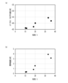
作製したラダー型フィルタのスプリアスおよび通過特性を測定した。図4(a)および図4(b)は、サンプルAからCにおける粒径に対するスプリアスピークの平均値および標準偏差を示す図である。スプリアスピークの平均値は、各サンプルにおけるウエハ面内のスプリアスのピーク値の平均値を示し、標準偏差は各サンプルにおけるウエハ面内のスプリアスのピーク値の標準偏差を示す。λは2本の電極指15のピッチである。図4(a)および図4(b)に示すように、粒径が小さくなると、スプリアスピークの平均値が小さくなり、標準偏差が小さくなる。
We measured the spurious and transmission characteristics of the ladder-type filter that we fabricated. 4(a) and 4(b) show the mean and standard deviation of spurious peaks versus particle size for samples A to C. FIG. The spurious peak average value indicates the average value of the spurious peak values within the wafer plane in each sample, and the standard deviation indicates the standard deviation of the spurious peak values within the wafer plane for each sample. λ is the pitch of the two
図5(a)から図5(c)は、サンプルAからCにおけるラダー型フィルタの通過特性を示す図である。図5(a)は広帯域の通過特性、図5(b)は、通過帯域周辺の拡大図、図5(c)は阻止帯域付近の拡大図である。図5(a)に示すように、作製したラダー型フィルタの通過帯域は2.4GHz帯(2.4025GHz~2.4815GHz)であり、LTE(Long Term Evolution)バンド41および42の通信帯域付近を阻止帯域とする。 FIGS. 5(a) to 5(c) are diagrams showing the pass characteristics of ladder-type filters in samples A to C. FIG. FIG. 5(a) is a broadband pass characteristic, FIG. 5(b) is an enlarged view around the passband, and FIG. 5(c) is an enlarged view around the stopband. As shown in FIG. 5(a), the pass band of the fabricated ladder-type filter is the 2.4 GHz band (2.4025 GHz to 2.4815 GHz). be the stopband.
図5(b)に示すように、サンプルAからCにおいて通過帯域の損失はほぼ同じである。通過帯域がサンプルにより異なるが、これは各サンプルで弾性波共振器の共振周波数および反共振周波数を最適化していないためである。図5(c)に示すように、サンプルCはバンド41および42の通信帯域周辺に大きなスプリアスが形成されている。サンプルBでは、サンプルCに比べスプリアスが小さくなっている。サンプルAではスプリアスがさらに小さくなっている。
As shown in FIG. 5(b), samples A to C have approximately the same passband loss. The passband differs depending on the sample, but this is because the resonance frequency and anti-resonance frequency of the elastic wave resonator are not optimized for each sample. As shown in FIG. 5(c), sample C has large spurious emissions around the communication bands of
圧電基板12の厚さT2を弾性波の波長λ以下とするとバルク波に起因する通過帯域周辺のスプリアスが抑制される。しかしながら、通過帯域より高周波数の帯域に生成されるスプリアスの抑制は十分ではない。図5(c)のように、多結晶基板10の粒径を小さくすると、このスプリアスを抑制できる。これは、多結晶基板10においてバルク波等の不要波が散乱されるためと考えられる。
When the thickness T2 of the
[実施例1の変形例1]
図6(a)は、実施例1の変形例1に係る弾性波共振器の断面図である。図6(a)に示すように、多結晶基板10と圧電基板12との間に中間層11が設けられている。中間層11の厚さはT1である。中間層11は、例えば酸化シリコン層、窒化シリコン層、酸化アルミニウム層または窒化アルミニウム層等の絶縁層である。中間層11の弾性率の温度係数の符号が圧電基板12の弾性率の温度係数の符号と逆のとき、中間層11は温度補償膜として機能する。温度補償膜としては、酸化シリコン膜(弗素等の添加物を含んでもよい)が用いられる。また、中間層11は多結晶基板10と圧電基板12とを接合する接合層として機能してもよい。その他の構成は実施例1と同じであり説明を省略する。
[
6A is a cross-sectional view of an elastic wave resonator according to
[実施例1の変形例2]
図6(b)は、実施例1の変形例2に係る弾性波共振器の断面図である。図6(b)に示すように、多結晶基板10の下面は支持基板13に接合されている。支持基板13は、例えばサファイア基板、アルミナ基板、石英基板または水晶基板である。その他の構成は実施例1と同じであり説明を省略する。
[
FIG. 6B is a cross-sectional view of an elastic wave resonator according to
[実施例1の変形例3]
図6(c)は、実施例1の変形例3に係る弾性波共振器の断面図である。図6(c)に示すように、多結晶基板10の下面は支持基板13に接合されている。その他の構成は実施例1の変形例1と同じであり説明を省略する。
[
FIG. 6C is a cross-sectional view of an elastic wave resonator according to
実施例1およびその変形例2のように、多結晶基板10と圧電基板12とは直接接合されていてもよいし、実施例1の変形例1および3のように、多結晶基板10と圧電基板12との間に中間層11が設けられていてもよい。実施例1の変形例2および3のように、多結晶基板10は支持基板13に接合されていてもよい。
The
実施例1およびその変形例によれば、多結晶基板10は、圧電基板12の一対の櫛型電極18が設けられた面と反対側に設けられ、平均粒径が複数の電極指15の平均ピッチの66倍(すなわち33λ)以下である。これにより、図4(a)から図5(c)のように、通過帯域の高周波側のスプリアスを抑制できる。
According to the first embodiment and its modification, the
多結晶基板10の平均粒径は電極指15の平均ピッチの40倍(すなわち20λ)以下が好ましく、20倍以下がより好ましい。これにより、スプリアスをより抑制できる。多結晶基板10で不要波を散乱させるため、平均粒径は電極指15の平均ピッチの1倍以上が好ましく、2倍以上がより好ましい。電極指15の平均ピッチは、弾性波共振器20のX方向の長さを電極指15の本数で除することにより算出できる。多結晶基板10の平均粒径の算出は図3において説明した方法により算出できる。20個以上の結晶粒50の粒径を平均するとより精度が高くなる。50個以上の結晶粒50の粒径を平均するとさらに精度が高くなる。
The average grain size of the
多結晶基板10は多結晶スピネル基板(すなわち、MgAl2O3を主成分とする多結晶基板)である。これにより、スプリアスをより抑制できる。主成分とするとは、実施例1およびその変形例の効果を奏する程度に含むことを意味し、意図的または意図せずに添加される不純物を含み、例えば構成元素の50原子%または80原子%以上含むことである。
The
多結晶基板10の上面(圧電基板12側の面)と圧電基板12の上面(一対の櫛型電極が設けられた面)との距離(例えば実施例1およびその変形例2のT2、実施例1の変形例1および3のT2+T1)は電極指15の平均ピッチの4倍以下である。このように、T2またはT2+T1を薄くすることで、バルク波に起因するスプリアスが抑制できる。しかし、図5(c)のように、通過帯域より高い周波数のスプリアスの抑制は十分でない。そこで、多結晶基板10の平均粒径を小さくする。これにより、通過帯域より高い周波数のスプリアスが抑制される。多結晶基板10の上面と圧電基板12の上面との距離は、電極指15の平均ピッチの2倍以下が好ましく、0.2倍以上がより好ましい。
The distance between the upper surface of the polycrystalline substrate 10 (the surface on the side of the piezoelectric substrate 12) and the upper surface of the piezoelectric substrate 12 (the surface on which the pair of comb-shaped electrodes is provided) (for example, T2 in Example 1 and its Modified Example 2, Example T2+T1) of
圧電基板12の厚さT2は電極指15の平均ピッチの2倍以下が好ましく、1.6倍以下がより好ましく、0.2倍以上が好ましい。これにより、バルク波に起因するスプリアスが抑制できる。また、損失を抑制できる。
The thickness T2 of the
圧電基板12が10°以上かつ50°以下回転YカットX伝搬タンタル酸リチウム基板のとき、櫛型電極18は主にSH(Shear Horizontal)波を励振する。圧電基板12は、36°以上かつ42°以下回転YカットX伝搬タンタル酸リチウム基板であることがより好ましい。SH波は圧電基板12の表面に平行でかつSH波の伝搬方向に直交方向に変位する波である。このとき、バルク波が励振されやすい。よって、多結晶基板10を用いることが好ましい。
When the
多結晶基板10の厚さT2は電極指15の平均ピッチの2倍以上が好ましく、4倍以上がより好ましい。また、T2は平均粒径以上が好ましく、平均粒径の2倍以上がより好ましい。これにより、不要波を拡散しスプリアスを抑制できる。
The thickness T2 of the
図7(a)は、実施例2に係るフィルタの回路図である。図7(a)に示すように、入力端子Tinと出力端子Toutとの間に、1または複数の直列共振器S1からS3が直列に接続されている。入力端子Tinと出力端子Toutとの間に、1または複数の並列共振器P1およびP2が並列に接続されている。1または複数の直列共振器S1からS3および1または複数の並列共振器P1およびP2の少なくとも1つに実施例1の弾性波共振器を用いることができる。ラダー型フィルタの共振器の個数等は適宜設定できる。フィルタは、多重モード型フィルタでもよい。 FIG. 7A is a circuit diagram of a filter according to Example 2. FIG. As shown in FIG. 7A, one or more series resonators S1 to S3 are connected in series between an input terminal Tin and an output terminal Tout. One or more parallel resonators P1 and P2 are connected in parallel between the input terminal Tin and the output terminal Tout. The elastic wave resonator of Example 1 can be used for at least one of the one or more series resonators S1 to S3 and the one or more parallel resonators P1 and P2. The number of resonators of the ladder-type filter and the like can be set as appropriate. The filter may be a multimode filter.
[実施例2の変形例1]
図7(b)は、実施例2の変形例1に係るデュプレクサの回路図である。図7(b)に示すように、共通端子Antと送信端子Txとの間に送信フィルタ40が接続されている。共通端子Antと受信端子Rxとの間に受信フィルタ42が接続されている。送信フィルタ40は、送信端子Txから入力された高周波信号のうち送信帯域の信号を送信信号として共通端子Antに通過させ、他の周波数の信号を抑圧する。受信フィルタ42は、共通端子Antから入力された高周波信号のうち受信帯域の信号を受信信号として受信端子Rxに通過させ、他の周波数の信号を抑圧する。送信フィルタ40および受信フィルタ42の少なくとも一方を実施例2のフィルタとすることができる。
[
FIG. 7B is a circuit diagram of a duplexer according to
マルチプレクサとしてデュプレクサを例に説明したがトリプレクサまたはクワッドプレクサでもよい。 A duplexer has been described as an example of a multiplexer, but a triplexer or a quadplexer may be used.
以上、本発明の実施例について詳述したが、本発明はかかる特定の実施例に限定されるものではなく、特許請求の範囲に記載された本発明の要旨の範囲内において、種々の変形・変更が可能である。 Although the embodiments of the present invention have been described in detail above, the present invention is not limited to such specific embodiments, and various modifications and variations can be made within the scope of the gist of the present invention described in the scope of claims. Change is possible.
10 多結晶基板
11 中間層
12 圧電基板
13 支持基板
15 電極指
18 櫛型電極
20 弾性波共振器
22 IDT
REFERENCE SIGNS
Claims (10)
前記圧電基板上に設けられ、複数の電極指を有し弾性波を励振する一対の櫛型電極と、
前記圧電基板の前記一対の櫛型電極が設けられた面と反対側に設けられ、平均粒径が前記複数の電極指の平均ピッチの1倍以上かつ66倍以下であり、多結晶スピネル基板である多結晶基板と、
を備え、
前記圧電基板の厚さは、前記複数の電極指の平均ピッチの2倍以下である弾性波共振器。 a piezoelectric substrate that is a Y-cut X-propagating lithium tantalate substrate rotated 10° or more and 50° or less ;
a pair of comb-shaped electrodes provided on the piezoelectric substrate and having a plurality of electrode fingers to excite elastic waves;
A polycrystalline spinel substrate provided on the side of the piezoelectric substrate opposite to the surface on which the pair of comb-shaped electrodes is provided, having an average grain size of 1 to 66 times the average pitch of the plurality of electrode fingers , and a polycrystalline spinel substrate A polycrystalline substrate that is
with
The elastic wave resonator , wherein the thickness of the piezoelectric substrate is not more than twice the average pitch of the plurality of electrode fingers .
前記圧電基板上に設けられ、複数の電極指を有し主にSH波を励振する一対の櫛型電極と、 a pair of comb-shaped electrodes provided on the piezoelectric substrate and having a plurality of electrode fingers for mainly exciting SH waves;
前記圧電基板の前記一対の櫛型電極が設けられた面と反対側に設けられ、平均粒径が前記複数の電極指の平均ピッチの1倍以上かつ66倍以下であり、多結晶スピネル基板である多結晶基板と、 provided on the side of the piezoelectric substrate opposite to the surface on which the pair of comb-shaped electrodes are provided, having an average grain size of 1 to 66 times the average pitch of the plurality of electrode fingers, and being a polycrystalline spinel substrate; a polycrystalline substrate;
を備え、with
前記圧電基板の厚さは、前記複数の電極指の平均ピッチの2倍以下である弾性波共振器。 The elastic wave resonator, wherein the thickness of the piezoelectric substrate is not more than twice the average pitch of the plurality of electrode fingers.
A multiplexer including the filter of claim 9.
Applications Claiming Priority (2)
| Application Number | Priority Date | Filing Date | Title |
|---|---|---|---|
| JP2019020791 | 2019-02-07 | ||
| JP2019020791 | 2019-02-07 |
Publications (2)
| Publication Number | Publication Date |
|---|---|
| JP2020129787A JP2020129787A (en) | 2020-08-27 |
| JP7329954B2 true JP7329954B2 (en) | 2023-08-21 |
Family
ID=72174920
Family Applications (1)
| Application Number | Title | Priority Date | Filing Date |
|---|---|---|---|
| JP2019075871A Active JP7329954B2 (en) | 2019-02-07 | 2019-04-11 | Acoustic wave resonators, filters and multiplexers |
Country Status (1)
| Country | Link |
|---|---|
| JP (1) | JP7329954B2 (en) |
Citations (7)
| Publication number | Priority date | Publication date | Assignee | Title |
|---|---|---|---|---|
| WO2013187410A1 (en) | 2012-06-13 | 2013-12-19 | 日本碍子株式会社 | Composite substrate |
| JP2014013991A (en) | 2012-07-04 | 2014-01-23 | Taiyo Yuden Co Ltd | Lamb wave device and manufacturing method of the same |
| WO2014192597A1 (en) | 2013-05-31 | 2014-12-04 | 日本碍子株式会社 | Support substrate for composite substrate and composite substrate |
| WO2016060072A1 (en) | 2014-10-17 | 2016-04-21 | 株式会社村田製作所 | Piezoelectric device and method for manufacturing piezoelectric device |
| JP2016100729A (en) | 2014-11-20 | 2016-05-30 | 太陽誘電株式会社 | Manufacturing method of acoustic wave device |
| JP2018041888A (en) | 2016-09-09 | 2018-03-15 | 住友電気工業株式会社 | Method of grinding ceramic substrate and method of manufacturing piezoelectric element |
| WO2018123208A1 (en) | 2016-12-27 | 2018-07-05 | 株式会社村田製作所 | Multiplexer, high-frequency front end circuit, and communication device |
-
2019
- 2019-04-11 JP JP2019075871A patent/JP7329954B2/en active Active
Patent Citations (7)
| Publication number | Priority date | Publication date | Assignee | Title |
|---|---|---|---|---|
| WO2013187410A1 (en) | 2012-06-13 | 2013-12-19 | 日本碍子株式会社 | Composite substrate |
| JP2014013991A (en) | 2012-07-04 | 2014-01-23 | Taiyo Yuden Co Ltd | Lamb wave device and manufacturing method of the same |
| WO2014192597A1 (en) | 2013-05-31 | 2014-12-04 | 日本碍子株式会社 | Support substrate for composite substrate and composite substrate |
| WO2016060072A1 (en) | 2014-10-17 | 2016-04-21 | 株式会社村田製作所 | Piezoelectric device and method for manufacturing piezoelectric device |
| JP2016100729A (en) | 2014-11-20 | 2016-05-30 | 太陽誘電株式会社 | Manufacturing method of acoustic wave device |
| JP2018041888A (en) | 2016-09-09 | 2018-03-15 | 住友電気工業株式会社 | Method of grinding ceramic substrate and method of manufacturing piezoelectric element |
| WO2018123208A1 (en) | 2016-12-27 | 2018-07-05 | 株式会社村田製作所 | Multiplexer, high-frequency front end circuit, and communication device |
Also Published As
| Publication number | Publication date |
|---|---|
| JP2020129787A (en) | 2020-08-27 |
Similar Documents
| Publication | Publication Date | Title |
|---|---|---|
| JP6954378B2 (en) | Elastic wave device, multiplexer, high frequency front end circuit and communication device | |
| KR102085184B1 (en) | Acoustic wave device and module | |
| US11595019B2 (en) | Acoustic wave resonator, filter, and multiplexer | |
| JP4497159B2 (en) | Boundary acoustic wave filter | |
| CN111602337B (en) | Elastic wave device, multiplexer, high frequency front-end circuit and communication device | |
| US10938372B2 (en) | Acoustic wave resonator, acoustic wave device, and filter | |
| WO2005060094A1 (en) | Acoustic boundary wave device | |
| CN107204750B (en) | Acoustic wave device | |
| CN110710106B (en) | Elastic wave device, demultiplexer, and communication device | |
| US11509284B2 (en) | Acoustic wave device and radio-frequency front-end circuit | |
| JP2019201345A (en) | Acoustic wave resonator, filter and multiplexer | |
| JP2023060058A (en) | Acoustic wave resonator, filter and multiplexer | |
| JP7433873B2 (en) | Acoustic wave resonators, filters, and multiplexers | |
| CN114586282A (en) | Elastic wave device | |
| JP7329954B2 (en) | Acoustic wave resonators, filters and multiplexers | |
| JP7312562B2 (en) | Acoustic wave resonator and its manufacturing method, filter and multiplexer | |
| JP7061005B2 (en) | Elastic wave resonators, filters and multiplexers | |
| JP2022176790A (en) | Elastic wave device, wafer, filter and multiplexer | |
| CN114070257A (en) | Acoustic wave device, filter and multiplexer | |
| JP7068974B2 (en) | Ladder type filter and multiplexer | |
| CN114641932A (en) | Thin film surface acoustic wave device using Rayleigh mode | |
| JP6886264B2 (en) | Elastic wave devices and composite substrates and their manufacturing methods | |
| JP2022174977A (en) | Elastic wave device, filter, multiplexer, wafer, and method of manufacturing wafer | |
| JP2020043403A (en) | Acoustic wave resonator, filter, and multiplexer | |
| US20230402991A1 (en) | Resonator |
Legal Events
| Date | Code | Title | Description |
|---|---|---|---|
| A621 | Written request for application examination |
Free format text: JAPANESE INTERMEDIATE CODE: A621 Effective date: 20220323 |
|
| A977 | Report on retrieval |
Free format text: JAPANESE INTERMEDIATE CODE: A971007 Effective date: 20230228 |
|
| A131 | Notification of reasons for refusal |
Free format text: JAPANESE INTERMEDIATE CODE: A131 Effective date: 20230307 |
|
| A521 | Request for written amendment filed |
Free format text: JAPANESE INTERMEDIATE CODE: A523 Effective date: 20230410 |
|
| TRDD | Decision of grant or rejection written | ||
| A01 | Written decision to grant a patent or to grant a registration (utility model) |
Free format text: JAPANESE INTERMEDIATE CODE: A01 Effective date: 20230725 |
|
| A61 | First payment of annual fees (during grant procedure) |
Free format text: JAPANESE INTERMEDIATE CODE: A61 Effective date: 20230808 |
|
| R150 | Certificate of patent or registration of utility model |
Ref document number: 7329954 Country of ref document: JP Free format text: JAPANESE INTERMEDIATE CODE: R150 |