JP7306571B2 - Temperature sensors and temperature sensor arrays - Google Patents
Temperature sensors and temperature sensor arrays Download PDFInfo
- Publication number
- JP7306571B2 JP7306571B2 JP2022511587A JP2022511587A JP7306571B2 JP 7306571 B2 JP7306571 B2 JP 7306571B2 JP 2022511587 A JP2022511587 A JP 2022511587A JP 2022511587 A JP2022511587 A JP 2022511587A JP 7306571 B2 JP7306571 B2 JP 7306571B2
- Authority
- JP
- Japan
- Prior art keywords
- temperature
- temperature sensor
- sensor
- thickness
- thermistor
- Prior art date
- Legal status (The legal status is an assumption and is not a legal conclusion. Google has not performed a legal analysis and makes no representation as to the accuracy of the status listed.)
- Active
Links
Images


Classifications
-
- G—PHYSICS
- G01—MEASURING; TESTING
- G01K—MEASURING TEMPERATURE; MEASURING QUANTITY OF HEAT; THERMALLY-SENSITIVE ELEMENTS NOT OTHERWISE PROVIDED FOR
- G01K1/00—Details of thermometers not specially adapted for particular types of thermometer
- G01K1/14—Supports; Fastening devices; Arrangements for mounting thermometers in particular locations
- G01K1/143—Supports; Fastening devices; Arrangements for mounting thermometers in particular locations for measuring surface temperatures
-
- G—PHYSICS
- G01—MEASURING; TESTING
- G01K—MEASURING TEMPERATURE; MEASURING QUANTITY OF HEAT; THERMALLY-SENSITIVE ELEMENTS NOT OTHERWISE PROVIDED FOR
- G01K1/00—Details of thermometers not specially adapted for particular types of thermometer
- G01K1/02—Means for indicating or recording specially adapted for thermometers
- G01K1/026—Means for indicating or recording specially adapted for thermometers arrangements for monitoring a plurality of temperatures, e.g. by multiplexing
-
- G—PHYSICS
- G01—MEASURING; TESTING
- G01K—MEASURING TEMPERATURE; MEASURING QUANTITY OF HEAT; THERMALLY-SENSITIVE ELEMENTS NOT OTHERWISE PROVIDED FOR
- G01K7/00—Measuring temperature based on the use of electric or magnetic elements directly sensitive to heat ; Power supply therefor, e.g. using thermoelectric elements
- G01K7/16—Measuring temperature based on the use of electric or magnetic elements directly sensitive to heat ; Power supply therefor, e.g. using thermoelectric elements using resistive elements
- G01K7/22—Measuring temperature based on the use of electric or magnetic elements directly sensitive to heat ; Power supply therefor, e.g. using thermoelectric elements using resistive elements the element being a non-linear resistance, e.g. thermistor
-
- H—ELECTRICITY
- H01—ELECTRIC ELEMENTS
- H01C—RESISTORS
- H01C1/00—Details
- H01C1/14—Terminals or tapping points or electrodes specially adapted for resistors; Arrangements of terminals or tapping points or electrodes on resistors
-
- H—ELECTRICITY
- H01—ELECTRIC ELEMENTS
- H01C—RESISTORS
- H01C7/00—Non-adjustable resistors formed as one or more layers or coatings; Non-adjustable resistors made from powdered conducting material or powdered semi-conducting material with or without insulating material
- H01C7/008—Thermistors
-
- H—ELECTRICITY
- H01—ELECTRIC ELEMENTS
- H01C—RESISTORS
- H01C1/00—Details
- H01C1/14—Terminals or tapping points or electrodes specially adapted for resistors; Arrangements of terminals or tapping points or electrodes on resistors
- H01C1/1406—Terminals or electrodes formed on resistive elements having positive temperature coefficient
-
- H—ELECTRICITY
- H01—ELECTRIC ELEMENTS
- H01C—RESISTORS
- H01C1/00—Details
- H01C1/14—Terminals or tapping points or electrodes specially adapted for resistors; Arrangements of terminals or tapping points or electrodes on resistors
- H01C1/1413—Terminals or electrodes formed on resistive elements having negative temperature coefficient
Landscapes
- Physics & Mathematics (AREA)
- General Physics & Mathematics (AREA)
- Engineering & Computer Science (AREA)
- Microelectronics & Electronic Packaging (AREA)
- Nonlinear Science (AREA)
- Electromagnetism (AREA)
- Measuring Temperature Or Quantity Of Heat (AREA)
- Thermistors And Varistors (AREA)
Description
本発明は、温度センサおよび温度センサを複数含む温度センサアレイに関する。 The present invention relates to temperature sensors and temperature sensor arrays containing a plurality of temperature sensors.
従来、フレキシブル基板にセンサ部が形成されている温度センサが知られている。かかる温度センサは、全体としてフレキシブルかつ薄く構成することができ、被温度検知物の温度を検知するための様々な用途に利用されている。 2. Description of the Related Art Conventionally, a temperature sensor is known in which a sensor portion is formed on a flexible substrate. Such a temperature sensor can be made flexible and thin as a whole, and is used for various purposes for detecting the temperature of an object to be temperature-detected.
例えば、特許文献1には、フレキシブル基板に開口部を設け、この開口部にセンサ部としてフレキシブルサーミスタを埋設実装し、フレキシブル基板の開口部の周囲の表面の高さと、フレキシブルサーミスタの露出面の高さとを実質的に同じにした温度センサが開示されている。より詳細には、例えば特許文献1の図5を参照して、金属基材11、サーミスタ層15および一対の分割電極21、22を有するフレキシブルサーミスタ1Aを、ベース層51、配線導体層52およびカバー層53を有するフレキシブル基板5Aの開口部に埋設して、はんだ層54により配線導体層52上に実装し、カバー層53の表面の高さと、フレキシブルサーミスタ1Aの露出面の高さとを実質的に同じにしている。
For example, in
また例えば、特許文献2には、フレキシブル基板である絶縁性フィルムの表面に、センサ部として、薄膜サーミスタ部および一対の櫛型電極を設け、絶縁性フィルムにおける薄膜サーミスタ部の直下の少なくとも一部を、絶縁性フィルムの他の部分よりも薄く形成した温度センサが開示されている。より詳細には、例えば特許文献2の図1を参照して、絶縁性フィルム2の表面に薄膜サーミスタ部3および一対の櫛型電極4を設け、これらを保護膜6で被覆し、絶縁性フィルム2における薄膜サーミスタ部3の直下に凹部2aを設けている。
Further, for example, in
フレキシブル基板にセンサ部が形成されている温度センサは、その厚さ方向に荷重が印加され得る。高い温度検知精度を実現するためには、温度センサを被温度検知物に対してある程度の力で十分に接触させることが好ましい。しかしながら、温度センサのセンサ部に荷重が印加されると、センサ部(より詳細にはサーミスタ層)に生じる応力によって、センサ部の変形による抵抗変化や、センサ部でのクラック発生による劣化が起こり得、かえって温度検知精度の低下を招き得る。かかる状況下、耐荷重性能に優れ、高い温度検知精度が得られる温度センサが求められている。 A temperature sensor in which a sensor portion is formed on a flexible substrate can be applied with a load in its thickness direction. In order to achieve high temperature detection accuracy, it is preferable to bring the temperature sensor into sufficient contact with the object to be temperature-detected with a certain amount of force. However, when a load is applied to the sensor portion of the temperature sensor, the stress generated in the sensor portion (more specifically, the thermistor layer) can cause resistance changes due to deformation of the sensor portion and deterioration due to cracks in the sensor portion. , rather, it may lead to a decrease in temperature detection accuracy. Under such circumstances, there is a demand for a temperature sensor that has excellent load-bearing performance and high temperature detection accuracy.
特許文献1に開示される温度センサでは、フレキシブル基板の開口部の周囲の表面の高さと、フレキシブルサーミスタの露出面の高さとを実質的に同じにしているので、かかる温度センサに対して厚さ方向に荷重が印加された場合には、より詳細には、特許文献1の図7に示すように温度センサを被温度検知物に接触させて押し付けた場合には、上記荷重(押圧力)は、温度センサと被温度検知物との接触領域の全体(フレキシブルサーミスタの露出面の全領域と、その周囲のフレキシブル基板の表面の接触領域との合計)に亘って均等に印加されることとなり、フレキシブルサーミスタの露出面のみに印加されることを回避できる。しかしながら、上記荷重は、接触領域の全体の面積に対するフレキシブルサーミスタの露出面の面積の比に応じて、フレキシブルサーミスタ(特にサーミスタ層)に印加されることとなるので、サーミスタ層における応力の発生をなくすことはできず、必ずしも十分な耐荷重性能が得られず、サーミスタ層の変形による抵抗変化や、サーミスタ層でのクラック発生による劣化が起こり得、高い温度検知精度を得ることは困難である。耐荷重性能の向上だけに着目すれば、フレキシブルサーミスタの露出面の面積に対して、他の部分の接触領域の面積を相当大きくすることが考えられる。しかしながら、この場合には、他の部分の接触領域の面積が大きくなり過ぎて、被温度検知物(熱源)の熱が、他の部分を経由して、配線や接触面と反対側の面などに伝導して失われ、依然として、高い温度検知精度は得られない。
In the temperature sensor disclosed in
また、特許文献2に開示される温度センサでは、絶縁性フィルムにおける薄膜サーミスタ部の直下の少なくとも一部を、絶縁性フィルムの他の部分よりも薄く形成している(凹部を設けている)ので、かかる温度センサに対して厚さ方向に荷重が印加された場合には、より詳細には、温度センサ(薄膜サーミスタ部側)を被温度検知物に接触させて押し付けた場合には、上記荷重(押圧力)が、薄膜サーミスタ部に対して厚さ方向に直接印加されることを防止できる。しかしながら、上記荷重は、薄膜サーミスタ部に対して絶縁性フィルムの面内方向に水平な方向に作用することとなる(とりわけ、薄膜サーミスタ部および一対の櫛型電極の上面および全周を保護膜が被覆している場合に、水平な方向に顕著に作用することとなる)ので、薄膜サーミスタ部における応力の発生をなくすことはできず、必ずしも十分な耐荷重性能が得られず、薄膜サーミスタ部の変形による抵抗変化や、薄膜サーミスタ部でのクラック発生による劣化が起こり得、高い温度検知精度を得ることは困難である。加えて、被温度検知物(熱源)の熱が、温度センサ全体を通じて伝導して失われ得、高い温度検知精度が得られない。
Further, in the temperature sensor disclosed in
本発明の目的は、耐荷重性能に優れ、高い温度検知精度が得られる温度センサを提供することにある。本発明の更なる目的は、かかる温度センサを複数含む温度センサアレイを提供することにある。 SUMMARY OF THE INVENTION An object of the present invention is to provide a temperature sensor that has excellent load bearing performance and high temperature detection accuracy. A further object of the present invention is to provide a temperature sensor array including a plurality of such temperature sensors.
本発明の1つの要旨によれば、フレキシブル基板にセンサ部が形成されている温度センサであって、
前記フレキシブル基板が、該フレキシブル基板の端部に位置し、かつ前記センサ部が形成されている第1部分と、該第1部分に対して前記端部から遠位方向に隣接し、かつ互いに対向する第1面および第2面の間において最大厚さを有する第2部分とを含み、
前記第1部分の前記センサ部と反対側の面と、前記第2部分の前記第1面とが、同一面上にあり、
少なくとも前記第2部分の前記第1面が、被温度検知物と接触する検知面を成し、
前記第1部分および前記センサ部の合計厚さが、前記第2部分の前記最大厚さより小さい、温度センサが提供される。According to one gist of the present invention, there is provided a temperature sensor in which a sensor portion is formed on a flexible substrate,
The flexible substrate is located at an end portion of the flexible substrate and has a first portion formed with the sensor portion, and is adjacent to the first portion in a distal direction from the end portion and faces each other. and a second portion having a maximum thickness between the first and second surfaces,
the surface of the first portion opposite to the sensor section and the first surface of the second portion are on the same plane;
at least the first surface of the second portion forms a detection surface that contacts an object to be temperature-detected;
A temperature sensor is provided, wherein the total thickness of the first portion and the sensor portion is less than the maximum thickness of the second portion.
本発明のもう1つの要旨によれば、本発明の上記温度センサを複数含み、該複数の温度センサが、前記フレキシブル基板の前記第1部分と反対側の端部またはその近傍において共通の接続部に接続されている、温度センサアレイが提供される。 According to another aspect of the present invention, a plurality of the temperature sensors of the present invention are included, the plurality of temperature sensors being a common connection at or near the end of the flexible substrate opposite the first portion. A temperature sensor array is provided, connected to the
本発明によれば、耐荷重性能に優れ、高い温度検知精度が得られる温度センサが提供される。更に、本発明によれば、かかる温度センサを複数含む温度センサアレイが提供され、上記と同様の効果を奏し得る。 ADVANTAGE OF THE INVENTION According to this invention, the temperature sensor which is excellent in load-bearing performance and can obtain high temperature detection accuracy is provided. Furthermore, according to the present invention, a temperature sensor array including a plurality of such temperature sensors is provided, and the same effects as described above can be achieved.
以下、本発明を複数の実施形態を通じて図面を参照しながら詳細に説明するが、本発明はこれら実施形態に限定されない。 Hereinafter, the present invention will be described in detail through a plurality of embodiments with reference to the drawings, but the present invention is not limited to these embodiments.
(実施形態1)
本実施形態は、フレキシブル基板にセンサ部が形成されている温度センサに関する。(Embodiment 1)
The present embodiment relates to a temperature sensor having a sensor portion formed on a flexible substrate.
図1を参照して、本実施形態の温度センサ30において、フレキシブル基板20は、フレキシブル基板20の一方の端部Xに位置し、かつセンサ部10が形成されている第1部分11と、第1部分11に対して端部Xから遠位方向に隣接し、かつ互いに対向する第1面A2および第2面B2の間において最大厚さd2を有する第2部分12とを含む。本発明において「最大厚さ」とは、温度センサ全体のうちで最大となる厚さを意味する。第2部分が、第1部分に対して端部Xから「遠位方向に隣接する」とは、第2部分が、第1部分が存在する一方の端部Xから他方の端部Yに向かう方向に、第1部分に隣接していることを意味する。換言すれば、第1部分に対して遠位方向以外の方向には、最大厚さd2を有する第2部分は存在しない。Referring to FIG. 1, in
本実施形態の温度センサ30において、センサ部10は第1部分11の上に形成されており、第1部分11のセンサ部10と反対側の面A1と、第2部分12の第1面A2とが、同一面上にある。本発明において2つの面が「同一面上」にあるとは、温度センサに荷重(または外力)が加わっていない状態において共通の平面を形成することを意味し、荷重が加わった状態においてはこの限りでなく、例えば湾曲および/または屈曲していてもよい。In the
本実施形態の温度センサ30において、第1部分11およびセンサ部10の合計厚さd1は、第2部分12の最大厚さd2より小さく、好ましくは、d2に対するd1の割合(厚さ比d1/d2)は、0.83(=約5/6)以下であり得、下限は特に限定されないが、例えば0.1(=1/10)以上とされ得る。第1部分11およびセンサ部10の合計厚さd1は、第1部分11の面A1およびこれに対向するセンサ部10の露出面B1の間の厚さ方向寸法である。In the
センサ部10は、温度を検知する機能を有する限り特に限定されないが、例えばサーミスタ層と、サーミスタ層に接触し、かつ互いに離間して配置された2つの電極とを含み得、更に、カバー層(または保護膜)を含んでいてもいなくてもよい。かかるサーミスタ層および2つの電極は、任意の適切な材料から成り得、任意の適切な構造および配置等であり得る。サーミスタ層は、例えば、特許文献3に開示される材料などを利用できる。電極は、例えば、サーミスタ層に接触して形成された一対の櫛型電極であってよく、または、サーミスタ層に接触して(かつ好ましくは非接続型内部電極と対向して)配置された一対の分割電極であってよく、またあるいは、サーミスタ層を挟持した一対の平面電極であってもよい。第1部分11および第2部分12は、適宜、センサ部10の2つの電極から引き出された2つの引出電極部およびこれらに各々電気接続された2つの配線等を含んでいてよい。電極および引出電極部は別個に形成されていてもよいが、好ましくは一体的に形成され得る。なお、サーミスタ層、電極、引出電極部および配線の数は、より多く存在してもよい。
The
本実施形態の温度センサ30は、全体としてフレキシブルかつ薄く構成することができる。フレキシブル性を担うフレキシブル基板20の材料および厚さは適宜選択され得るが、最大厚さd2は、好ましくは200μm以下とされ、より好ましくは100μm以下であり得、下限は特に限定されないが、例えば60μm以上であり得る。The
本実施形態の温度センサ30において、センサ部10は第2部分12に近接して配置される。よって、第1部分11の長さL1(フレキシブル基板20の一方の端部X(図示する態様では端面)と、第1部分11および第2部分12の境界との間の寸法)は小さいほうが好ましく、例えば30mm以下、特に20mm以下、より好ましくは10mm以下、場合により5mm以下であり得、下限は特に限定されないが、例えば1mm以上であり得る。本実施形態を限定するものではないが、d1/d2が0.83以下である場合、L1は9.5mm以下であり得る。他方、第2部分12の長さL2(本実施形態では、第1部分11および第2部分12の境界と、フレキシブル基板20の他方の端部Y(図示する態様では端面)との間の寸法)は、特に限定されず、温度センサ30の用途に応じて様々であり得る。In the
かかる本実施形態の温度センサ30は、図2に示すように、少なくとも第2部分12の第1面A2が被温度検知物41と接触するようにして使用される。換言すれば、少なくとも第2部分12の第1面A2が、被温度検知物41と接触する(より詳細には、被温度検知物41に押し付けられて密着する)検知面を成す。第1部分11のセンサ部10と反対側の面A1も、被温度検知物41と接触し得る(検知面を成し得る)が、面A1は被温度検知物41と必ずしも接触していなくてよく、例えば被温度検知物41から「浮いて」いてもよい。特に、温度センサ30は、図2に示すように、被温度検知物41とこれに対向する物体43との間で押圧された状態で使用され得る。第2部分12の第2面B2は、対向物体43と接触し得る。対向物体43は特に限定されないが、例えば金属板などであり得る。The
温度センサ30を使用するときに、温度センサ30には、その厚さ方向に荷重(押圧力)が印加される。本実施形態の温度センサ30によれば、センサ部10が形成されていない第2部分12が最大厚さd2を有するので、温度センサ30の厚さ方向に荷重が印加された場合には、この第2部分12に荷重が印加されることとなり、第1部分11に形成されたセンサ部10には直接印加されない。更に、第2部分12に荷重が印加されることにより、第2部分12に隣接した第1部分11に応力が伝播し得るが、第1部分11はフレキシブル基板20の端部Xに位置し、フリーであるので、応力を効果的に緩和することができる。これらの結果、センサ部10における応力の発生を実質的になくすことができ、優れた耐荷重性能を得ることができる。加えて、本実施形態の温度センサ30によれば、センサ部10における応力の発生に起因する温度検知精度の低下を防止することができる。更に、本実施形態の温度センサ30によれば、第2部分12の第1面A2が被温度検知物41と接触する検知面を成し、荷重(押圧力)により第1面A2が被温度検知物41に押し付けられて密着し、そして、この第2部分12に隣接した第1部分11にセンサ部10が形成されているので、被温度検知物41の温度をセンサ部10により高精度に検知することができる。すなわち、本実施形態によれば、耐荷重性能に優れ、高い温度検知精度が得られる温度センサ30が提供される。When the
(実施形態2)
本実施形態は、実施形態1の温度センサの改変例に関し、特に断りのない限り、実施形態1と同様の説明が当て嵌まり得る。(Embodiment 2)
This embodiment relates to a modified example of the temperature sensor of
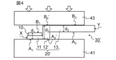
図3を参照して、本実施形態の温度センサ30’において、フレキシブル基板20’は、フレキシブル基板20’の一方の端部Xに位置し、かつセンサ部10が形成されている第1部分11と、第1部分11に対して端部Xから遠位方向に隣接し、かつ互いに対向する第1面A2’および第2面B2’の間において最大厚さd2を有する第2部分12’と、第2部分12’に対して端部Xから遠位方向に隣接し、かつ、互いに対向する第3面A3および第4面B3の間において、最大厚さd2より小さい厚さd3を有する第3部分13とを含む。第1部分11、第2部分12’および第3部分13は、適宜、センサ部10の2つの電極から引き出された2つの引出電極部およびこれらに各々電気接続された2つの配線等を含んでいてよい。Referring to FIG. 3, in the temperature sensor 30' of the present embodiment, the flexible substrate 20' is positioned at one end X of the flexible substrate 20', and the
本実施形態の温度センサ30’において、第3部分13の第4面B3と、第2部分12’の第2面B2’とが、同一面上にある。よって、第3部分13の厚さd3は第2部分12’の最大厚さd2より小さいことから、第3部分13の第3面A3は、第2部分12’の第1面A2’に対して奥まった位置にある。かかるフレキシブル基板20’は、第1部分11、第2部分12’および第3部分13から構成される全体として略S字状の断面形状を有するものとして理解され得る。In the temperature sensor 30' of this embodiment, the fourth surface B3 of the
本実施形態の温度センサ30’において、第2部分12’の長さL2’(本実施形態では、第1部分11および第2部分12’の境界と、第2部分12’および第3部分13の境界との間の寸法)は、後述する検知面に必要な最小面積を与える寸法以上、かつ、より一層高い温度検知精度を達成し得る寸法以内で適宜選択され得る。他方、第3部分13の長さL3(第2部分12’および第3部分13の境界と、フレキシブル基板20’の他方の端部Yとの間の寸法)は、特に限定されず、温度センサ30’の用途に応じて様々であり得る。In the temperature sensor 30' of this embodiment, the length L 2 ' of the second portion 12' (in this embodiment, the boundary between the
かかる本実施形態の温度センサ30’は、図4に示すように、少なくとも第2部分12’の第1面A2’が被温度検知物41と接触するようにして使用される。換言すれば、少なくとも第2部分12’の第1面A2’が、被温度検知物41と接触する(より詳細には、被温度検知物41に押し付けられて密着する)検知面を成す。第1部分11のセンサ部10と反対側の面A1も、被温度検知物41と接触し得る(検知面を成し得る)が、面A1は被温度検知物41と必ずしも接触していなくてよく、例えば被温度検知物41から「浮いて」いてもよい。第3部分13の第3面A3は、被温度検知物41から離間している(接触していない)が、例えば第3部分13が湾曲した場合には、第3面A3が被温度検知物41に部分的に接触することがあり得る。特に、温度センサ30’は、図4に示すように、被温度検知物41とこれに対向する物体43との間で押圧された状態で使用され得る。第2部分12’の第2面B2’に加えて、第3部分13の第4面B3も、対向物体43と接触し得る。The temperature sensor 30' of this embodiment is used such that at least the first surface A 2 ' of the second portion 12' is in contact with the
温度センサ30’を使用するときに、温度センサ30’には、その厚さ方向に荷重(押圧力)が印加される。本実施形態の温度センサ30’によれば、荷重(押圧力)により被温度検知物41に押し付けられて密着する第1面A2’が、実施形態1の温度センサ30における第1面A2に比べて小さくなっているので、被温度検知物41(熱源)の熱が第2面B2’および第4面B3(更に対向物体43)などに伝導し難く、より効率的にセンサ10へ伝導させることができ、被温度検知物41の温度をセンサ部10により更に高精度に検知することができる。すなわち、本実施形態によれば、実施形態1と同様の効果に加えて、より一層高い温度検知精度が得られる温度センサ30’が提供される。When using the temperature sensor 30', a load (pressing force) is applied to the temperature sensor 30' in its thickness direction. According to the
より一層高い温度検知精度を達成し得るには、被温度検知物41の被測定対象面積に対して、第1面A2’の面積が3%以下であることが好ましい。被温度検知物41(熱源)の熱が第2面B2’および第4面B3(更に対向物体43)などに伝導するのを防止することによって、被温度検知物41の実際の温度に対して±0.5℃以内の精度で温度検知できる。In order to achieve even higher temperature detection accuracy, it is preferable that the area of the first surface A 2 ′ is 3% or less of the area of the
温度検知精度を更に向上させるには、被温度検知物41(熱源)に応じて、温度センサ30’の断熱性および放熱性を調節することが好ましい。被温度検知物41の熱源が小さい場合には、熱伝導を極力抑える(断熱性を確保する)ことにより、温度センサ30’を被温度検知物41と対向物体43との間に挿入することによる被温度検知物41の温度変化を低減することができ、温度検知精度を更に向上させることができる。被温度検知物41の熱源が大きい場合には、熱伝導を高める(放熱性を確保する)ことにより、温度センサ30’を被温度検知物41と対向物体43との間に挿入することによる被温度検知物41の温度変化を低減することができ、温度検知精度を更に向上させることができる。
In order to further improve the temperature detection accuracy, it is preferable to adjust the heat insulation and heat dissipation of the temperature sensor 30' according to the object 41 (heat source) to be temperature detected. If the heat source of the
断熱性が要求される場合、図3~4に示す温度センサ30’のように、第3部分13の第3面A3を露出させてよい。これにより、被温度検知物41と第3面A3との隙間において空気(または場合により他のガス)断熱をもたらすことができる。If thermal insulation is required, the third surface A3 of the
あるいは、断熱性が要求される場合、図5に示すように、第3部分13の第3面A3を、被温度検知物41と接触する断熱性材料15で被覆してよい。これにより、被温度検知物41と第3面A3との隙間を断熱性材料15で埋めて断熱をもたらすことができる。センサ部10への影響が許容可能である場合には、センサ部10と対向物体43との隙間も断熱性材料15’で埋めて更なる断熱をもたらすようにしてもよい。なお、断熱性材料は、熱伝導率が低い材料であればよく、例えば、熱伝導率が1W/(m・K)以下の材料であり得る。Alternatively, if heat insulation is required, the third surface A3 of the
放熱性(冷却性)が要求される場合、図5に示すように、第3部分13の第3面A3を、被温度検知物41と接触する放熱性材料15で被覆してよい。これにより、被温度検知物41と第3面A3との隙間を放熱性材料15で埋めて放熱をもたらすことができる。センサ部10への影響が許容可能である場合には、センサ部10と対向物体43との隙間も放熱性材料15’で埋めて更なる放熱をもたらすようにしてもよい。なお、放熱性材料は、熱伝導率が高い材料であればよく、例えば、熱伝導率が10W/(m・K)以上の材料であり得る。If heat dissipation (cooling) is required, the third surface A3 of the
あるいは、放熱性(冷却性)が要求される場合、図6(a)~(b)に示すように、荷重(押圧力)を大きくして、対向物体43および/または被温度検知物41を変形させて、対向物体43(例えば金属板)を被温度検知物41に接触させてよい(図6(a)は、実施形態1の温度センサ30の場合を示し、図6(b)は、実施形態2の温度センサ30’の場合を示す)。対向物体43と被温度検知物41との接触面積は適宜調節してよい。これにより、被温度検知物41の熱を対向物体43に逃がして放熱(冷却)をもたらすことができる。この場合、対向物体43の厚さt、第2部分12または12’の最大厚さd2、第1部分11の長さL1を適切に選択することによって、センサ部10に負荷がかかる(例えば、対向物体43が変形して、センサ部10に荷重が直接印加される)ことを防止できる。Alternatively, when heat dissipation (cooling) is required, as shown in FIGS. The facing object 43 (for example, a metal plate) may be deformed and brought into contact with the
いずれの場合にも、温度センサ30’を被温度検知物41と対向物体43との間に挿入することによる被温度検知物41の温度変化を±0.5℃以下に抑えることができる。
In either case, by inserting the
(実施形態3)
本実施形態は、実施形態2の温度センサの具体例に関し、特に断りのない限り、実施形態1~2と同様の説明が当て嵌まり得る。(Embodiment 3)
This embodiment relates to a specific example of the temperature sensor of
図7を参照して、本実施形態の温度センサ30’’のフレキシブル基板20’’において、第2部分12’’は、第1部分11からの第1部分拡張部12aと、第3部分13からの第3部分拡張部12bと、これら拡張部12aおよび12bを接合する接合部12cとを含む。
Referring to FIG. 7, in the flexible substrate 20'' of the temperature sensor 30'' of the present embodiment, the second portion 12'' includes a first
より詳細には、図8~11を参照して、センサ部10は、サーミスタ層1と、サーミスタ層1に接触し、かつ互いに離間して配置された2つの電極3とを含み、更に、カバー層(または保護膜)7を含んでいてもいなくてもよい。図8および図9では、2つの電極3は、サーミスタ層1に接触して形成された一対の櫛型電極であり、図10および図11では、2つの電極3は、サーミスタ層1に接触し、かつ非接続型内部電極3’と対向して配置された一対の分割電極である。(図10および図11中、電極3は引出電極部5と一体的に形成されており、電極3と引出電極部5との境界を明確に定めることは困難であるが、電極3は、非接続型内部電極3’と対向する領域を含めばよく、便宜的に、図10(c)および図11(d)に上記境界を点線にて示す。図8~11では、第1部分11、第2部分12’’、第1部分拡張部12a、第3部分拡張部12b、第3部分13等の符号を省略しているが、図7と対照させることにより、これら省略した部材の符号が図8~11のどの部分を指すものであるかが把握される。なお、図9~10において、サーミスタ層1の一部が第2部分12’’の第1部分拡張部12に及んで存在しているが、第1部分拡張部12に存在するサーミスタ層1の部分には、電極3が設けられていないため、センサとして機能せず、よって、センサ部10に含まれないことに留意されたい。
More specifically, referring to FIGS. 8 to 11, the
そして、図7~11を参照して、第1部分11および第1部分拡張部12aは、第1基材21と、第1基材21上に形成され、かつセンサ部10の2つの電極3から引き出された2つの引出電極部5とを含む。第3部分13および第3部分拡張部12bは、第2基材23と、第2基材23上に形成された2つの配線25とを含む。そして2つの引出電極部5および2つの配線25が、接合部12cを介して各々電気接続される。第1部分11において、サーミスタ層1および/または電極3を被覆するカバー層7が設けられていてよい。また、第3部分13において、配線25を被覆するカバー層27が設けられていてよい。本実施形態に必須ではないが、第3部分13の端部Yおよびその近傍において、カバー層27を除去して配線25を露出させ、これと反対側の第2基材23の表面に補強板29を設けて、例えばコネクタ等の接続部(図示せず)に接続可能としてもよい。この場合、コネクタ等の接続部および接合部12cは、それぞれ二次接続部および一次接続部と理解され得る。
7 to 11,
接合部12cには、2つの引出電極部5および2つの配線25を各々電気接続できる限り(好ましくは薄く、かつ電気的および強度的に十分に接合できる限り)、任意の適切な材料および工法を利用できる。接合部12cは、例えば、異方導電性フィルム(ACF)、はんだ材料、導電性ペースト、接触部の硬化性樹脂による封止(引出電極部と配線とを接触させた状態でその周囲を硬化性樹脂で覆い、樹脂を硬化させて封止する)、超音波接合などが挙げられる。
Any appropriate material and construction method can be used for the
本実施形態によれば、第2部分12’’が、引出電極部5および配線25ならびにこれらを接合する接合部12cを集中させて含むことにより、比較的高い剛性が得られ、耐荷重性能が更に向上する。
According to the present embodiment, the second portion 12'' includes the
本実施形態の温度センサ30’’によれば、図8~11に示すように、実施形態2の温度センサ30’を容易に具体化することが可能となる。本実施形態の温度センサ30’’は、第1部分11および第1部分拡張部12aにセンサ部10を形成し、別途、第3部分および第3部分拡張部12cを準備して、これらを接合部12cで接合することより製造可能である。よって、本実施形態によれば、耐荷重性能に優れ、高い温度検知精度が得られる温度センサであって、簡便な製造方法により低コストで量産するのに適した温度センサ30’’が提供される。
According to the temperature sensor 30'' of the present embodiment, as shown in FIGS. 8 to 11, the temperature sensor 30' of the second embodiment can be easily implemented. In the temperature sensor 30'' of this embodiment, the
(実施形態4)
本実施形態は、実施形態3の温度センサを複数含む温度センサアレイに関し、特に断りのない限り、実施形態1~3と同様の説明が当て嵌まり得る。(Embodiment 4)
This embodiment relates to a temperature sensor array including a plurality of temperature sensors according to
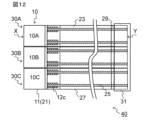
図12を参照して、本実施形態の温度センサアレイ40は、複数の温度センサ30A~30Cを含み、かかる複数の温度センサ30A~30Cが、フレキシブル基板の第1部分11(端部Xに位置する)と反対側の端部Yまたはその近傍において共通の接続部31に接続されている。この場合、共通の接続部31および接合部12cは、それぞれ二次接続部および一次接続部と理解され得る。図示する例では、温度センサ30A~30Cの端部Yが、共通の接続部(例えばコネクタ)31に挿入されているが、これに限定されない。複数の温度センサ30A~30Cは、互いに分離されており、かかる複数の温度センサ30A~30Cは、一体的に同時に作製した後に個々に切断することにより製造されていてよく、この切断は、複数の温度センサ30A~Cの共通の接続部31への接続の前および後のいずれで実施してもよい。
Referring to FIG. 12, the
図示する態様では、温度センサアレイ40が、複数の温度センサとして、例示的に3つの温度センサ30A~30Cを含むものを示しているが、複数の温度センサの数は2以上であれば特に限定されず、温度センサアレイ40の用途に応じて選択され得る。また、本実施形態では、温度センサアレイ40が、実施形態3の温度センサを複数含むものとして示しているが、実施形態1~3のいずれの温度センサを用いてもよい。
In the illustrated embodiment,
本実施形態の温度センサアレイ40によれば、複数の温度センサ30A~30Cをそれぞれ別の被温度検知物に接触させて各温度を検知することができる。本実施形態の温度センサアレイ40によれば、複数の温度センサ30A~30Cが共通の接続部31に接続されているので、共通の接続部31を測定回路等の外部装置(図示せず)に接続するだけで、複数の温度センサ30A~30Cを一度に外部装置に接続できる。
According to the
本実施形態の温度センサアレイ40は、任意の適切な用途に利用され得るが、例えば、図13に示すように、リチウムイオン電池モジュールの複数のセル(電池)51に対して、互いに隣接する2つのセル51間に温度センサ30A~30Cを1つずつ挟み込んで利用でき、これにより、各セル51の温度を検知することができる。図13では、複数のセル51のスタックに載置された電池モジュール回路基板53に温度センサアレイ用回路基板55が組み込まれており、温度センサアレイ用回路基板55に共通の接続部(例えばコネクタ)31を介して温度センサアレイ40が接続されている。より詳細には、温度センサアレイ40は、図12のように端部Yがコネクタ31に挿入されており、図13では温度センサアレイ40がコネクタ31から、図13の斜視図に向かって手前に一旦引き出された後に折り曲げられて、電池モジュール回路基板51の裏面側に沿って引き廻されているが、図13に例示する態様に限定されない。リチウムイオン電池モジュール50において、隣接する2つのセル51間に挟まれた温度センサ30A~30Cのセンサ部10A~10Cは、セル51間で荷重が印加された(押圧された)状態になり得、かかる状態で想定される荷重(押圧力)に耐えつつ、高い温度検知精度を示すことが望まれる。本実施形態の温度センサアレイ40の各温度センサ30A~30Cは、耐荷重性能に優れ、高い温度検知精度が得られるので、リチウムイオン電池モジュールにおいて各セルの温度を検知するのに好適に利用され得る。
Although the
(比較例1)
比較例1は、センサ部を含めて、全体的に均一な厚さを有する温度センサに関する。(Comparative example 1)
Comparative Example 1 relates to a temperature sensor having a uniform thickness as a whole including the sensor portion.
Mn:Niを4:1(原子比)の割合で含む、平均粒径約0.2μmの金属酸化物粒子に、マンガンアセチルアセトネートを10質量%(金属酸化物粒子の全質量に対して)の割合で添加し、エタノールを溶媒として原料混合物を調製し、16時間混合した。これにより得られたスラリーの形態の原料混合物を、厚さ10μmの銅箔上にドクターブレード法により厚さ10μmのシートの形態で供給した。このシートを100℃で10時間乾燥させた後、加熱プレス機を用いて100MPaの加圧下にて250℃で30分間加熱して、前駆構造体を得た。この前駆構造体を250℃で10時間アニールして、残存し得る不要な有機物を除去して、構造体を得た。その後、得られた構造体のうち上記シートに由来する膜(サーミスタ層として機能し得る金属酸化物含有複合体層)の上にポリアミドイミドの前駆体液を10μmの厚さで塗布して、200℃で1時間加熱して、ポリアミドイミドを熱硬化させて樹脂基材とした。その後、樹脂基材と反対側の銅箔の表面にレジストを所定のパターンで塗布して、露光および現像し、銅箔の所定部分をエッチング除去し、残っているレジストを除去して、2つの櫛型電極およびそれぞれから引き出された引出電極部をパターン形成した。銅箔のパターンは、図14(a)に模式的に示すように、櫛型電極3の櫛歯部分を上から見た外形寸法を幅1.5mmおよび長さ3.0mmとし、櫛歯部分の幅方向両外側のそれぞれに櫛型電極3の柄部分および引出電極部5を幅0.5mmおよび長さ150mmとした(センサ部の面積は幅3.0mmおよび長さ3.0mmであり、引出電極部は十分長いので配線としても理解され得る)。なお、図14(a)の櫛型電極は模式的例示であり、櫛型電極の詳細(櫛型電極の各櫛歯の寸法および数ならびにピッチ等)は図14(a)と異なり得る(以下の比較例および実施例においても同様である)。これにより得られた樹脂基材(厚さ約10μm)および金属酸化物含有複合体層(サーミスタ層:厚さ約10μm)の積層体であって、その上面にパターン形成された銅層(櫛型電極および引出電極部:厚さ約10μm)を有する積層体の上に、銅層を被覆するように、カバー層としてポリイミドテープ(粘着層を有するポリイミドフィルム:厚さ約30μm)を貼った(図14(b)中、カバー層を斜線領域にて示す)。これにより得られた構造体をダイシングソーでカットして、図14(a)~(b)に示すように、幅約3mmおよび長さ約150mmであり、全体に亘って均一な60μmの厚さを有する温度センサを作製した。
Metal oxide particles with an average particle size of about 0.2 μm containing Mn:Ni in a ratio of 4:1 (atomic ratio), and 10% by mass of manganese acetylacetonate (based on the total mass of the metal oxide particles) A raw material mixture was prepared using ethanol as a solvent and mixed for 16 hours. The raw material mixture in the form of slurry thus obtained was supplied in the form of a sheet with a thickness of 10 μm by a doctor blade method onto a copper foil with a thickness of 10 μm. After drying this sheet at 100° C. for 10 hours, it was heated at 250° C. for 30 minutes under a pressure of 100 MPa using a heating press to obtain a precursor structure. The precursor structure was annealed at 250° C. for 10 hours to remove any remaining unwanted organics to obtain a structure. After that, a polyamideimide precursor liquid was applied to a thickness of 10 μm on the film (metal oxide-containing composite layer that can function as a thermistor layer) derived from the sheet in the obtained structure, and the temperature was 200 ° C. was heated for 1 hour to thermally cure the polyamide-imide to form a resin base material. Thereafter, a resist is applied in a predetermined pattern on the surface of the copper foil on the side opposite to the resin base material, exposed and developed, a predetermined portion of the copper foil is removed by etching, and the remaining resist is removed to form two layers. The comb-shaped electrodes and lead-out electrode portions led out from each were patterned. As schematically shown in FIG. 14(a), the pattern of the copper foil is such that the external dimensions of the comb-teeth portion of the comb-shaped
作製した温度センサを荷重試験に付した。より詳細には、温度センサを直径50mmおよび厚さ25mmの2つの鉄板の間に挟み、0.5トン(約5000N)での圧力印加を5回繰り返して、同一温度での抵抗値変化(ΔR(-))を測定した。なお、圧力印加時、感圧フィルム(富士フイルム株式会社製、「プレスケール」中圧用、検出感度10MPa、以下同様)を、温度センサの櫛型電極(センサ部に対応する)と鉄板との間に挟んで圧力を測定したところ、センサ部に10MPa以上の荷重がかかっていることが確認された。結果を図15(a)に示す。図15(a)に示すように、荷重試験での抵抗変化率が5%以上で、温度検知の誤差が5℃より大きくなることがわかった。
The fabricated temperature sensor was subjected to a load test. More specifically, the temperature sensor is sandwiched between two iron plates with a diameter of 50 mm and a thickness of 25 mm. (-)) was measured. When pressure was applied, a pressure-sensitive film (manufactured by Fuji Film Co., Ltd., "Prescale" for medium pressure,
(比較例2)
比較例2は、センサ部を除く長手方向両外側部分が、全体的に均一な厚さを有する温度センサに関する。(Comparative example 2)
Comparative Example 2 relates to a temperature sensor in which both longitudinally outer portions excluding the sensor portion have an overall uniform thickness.
図16(a)~(b)に示すように、櫛型電極3に隣接して、櫛歯部分を有しない長さ3.0mmのダミー部Dを設け、櫛型電極3に対応するセンサ部をカバー層で被覆しなかったこと以外は、比較例1と同様にして(カバー層の厚さ約30μm)温度センサを作製した(図16(b)中、カバー層を斜線領域にて示す)。この温度センサにおいては、櫛型電極3に対応するセンサ部を除いて、ダミー部Dおよび引出電極部5をカバー層で被覆した。樹脂基材の裏面から櫛型電極3の最も高い露出表面までの厚さは30μmであったのに対して、樹脂基材の裏面からカバー層の外表面までの厚さは60μmであった。
As shown in FIGS. 16A and 16B, a dummy portion D having a length of 3.0 mm and having no comb teeth is provided adjacent to the comb-shaped
作製した温度センサを比較例1と同様の荷重試験に付した。なお、圧力印加時、感圧フィルムを、温度センサの櫛型電極(センサ部に対応する)と鉄板との間に挟んで圧力を測定したところ、比較例2でも、センサ部に10MPa以上の荷重がかかっていることが確認された。この結果、荷重試験での抵抗変化率が5%以上となり、満足できる温度検知精度が得られず、温度センサとして不適格であることがわかった。この温度センサでは、センサ部に荷重が直接的にかからない構造にしたものの、荷重によりカバー層が水平方向に変形し、水平方向の応力がサーミスタ層に伝播し、この結果、抵抗変化が起きたものと考えられる。上記の通りセンサ部に10MPa以上の荷重がかかっていることが確認されたのは、センサ部に水平方向に応力がかかり変形することで、結果的に、垂直方向に荷重が測定されたものと考えられる。 The produced temperature sensor was subjected to the same load test as in Comparative Example 1. When pressure was applied, the pressure was measured by sandwiching the pressure-sensitive film between the comb-shaped electrode (corresponding to the sensor portion) of the temperature sensor and the iron plate. It was confirmed that As a result, the rate of resistance change in the load test was 5% or more, and satisfactory temperature detection accuracy could not be obtained, making it unsuitable as a temperature sensor. Although this temperature sensor has a structure in which no load is applied directly to the sensor, the cover layer deforms in the horizontal direction due to the load, and horizontal stress propagates to the thermistor layer, resulting in a change in resistance. it is conceivable that. As mentioned above, it was confirmed that a load of 10 MPa or more was applied to the sensor part because stress was applied to the sensor part in the horizontal direction and it deformed, resulting in the load being measured in the vertical direction. Conceivable.
(実施例1)
実施例1は、図1~2を参照して上述した実施形態1の温度センサに関する。(Example 1)
Example 1 relates to the temperature sensor of
櫛型電極が存在する端部から長さL1でカットしたカバー層を使用して、図17(a)~(b)に示すように上記端部から長さL1の第1部分をカバー層(図17(b)中、斜線領域にて示す)で被覆しなかったこと以外は、比較例1と同様にして(カバー層の厚さ約30μm)温度センサを作製した。この温度センサにおいては、長さL1を5.0mmとした。樹脂基材の裏面から櫛型電極の最も高い露出表面までの厚さ(第1部分およびセンサ部の合計厚さd1)は30μmであったのに対して、樹脂基材の裏面からカバー層の外表面までの厚さ(第2部分の最大厚さd2)は60μmであった。A cover layer cut a length L 1 from the end where the comb electrodes are present is used to cover a first portion of length L 1 from the end as shown in FIGS. 17(a)-(b). A temperature sensor was fabricated in the same manner as in Comparative Example 1 (thickness of cover layer: about 30 μm), except that it was not covered with a layer (indicated by the hatched area in FIG. 17(b)). In this temperature sensor, the length L1 was set to 5.0 mm. The thickness from the back surface of the resin substrate to the highest exposed surface of the comb-shaped electrode (total thickness d 1 of the first portion and the sensor portion) was 30 μm, while the thickness from the back surface of the resin substrate to the cover layer was 30 μm. The thickness to the outer surface of the second portion (maximum thickness d 2 of the second portion) was 60 μm.
作製した温度センサを比較例1と同様の荷重試験に付した。なお、圧力印加時、感圧フィルムを、温度センサの櫛型電極(センサ部に対応する)と鉄板との間に挟んで圧力を測定し、センサ部に10MPa以上の荷重がかかっていないことを確認した。結果を図15(b)に示す。図15(b)に示すように、荷重試験での抵抗変化率が1%以下で、温度検知の誤差1℃以内を実現することができた。 The produced temperature sensor was subjected to the same load test as in Comparative Example 1. When pressure was applied, the pressure-sensitive film was sandwiched between the comb-shaped electrode (corresponding to the sensor section) of the temperature sensor and an iron plate to measure the pressure, and it was confirmed that the sensor section was not subjected to a load of 10 MPa or more. confirmed. The results are shown in FIG. 15(b). As shown in FIG. 15(b), the resistance change rate in the load test was 1% or less, and the temperature detection error was within 1°C.
(実施例2)
実施例2は、図1~2を参照して上述した実施形態1の温度センサに関し、より詳細には、図6(a)の使用態様に関する。(Example 2)
Example 2 relates to the temperature sensor of
樹脂基材の厚さ、カバー層を貼る位置、カバー層の厚さ(表面側に1枚または2枚以上積層し、場合により、樹脂基材の裏面全体に1枚または2枚以上を積層する等)を種々異ならせたこと以外は、実施例1と同様にして温度センサを作製した。これにより、第1部分およびセンサ部の合計厚さd1、第2部分の最大厚さd2および第1部分の長さL1を変化させた。Thickness of the resin base material, position to attach the cover layer, thickness of the cover layer (1 or 2 or more layers are laminated on the front surface side, and in some cases, 1 or 2 or more layers are laminated on the entire back surface of the resin base material. etc.) were varied in the same manner as in Example 1 to produce temperature sensors. As a result, the total thickness d 1 of the first portion and the sensor portion, the maximum thickness d 2 of the second portion, and the length L 1 of the first portion were changed.
作製した温度センサの上に、対向物体(図6(a)中、符号43にて示す)として厚さtの金属板(60mm角のSUS板)を配置し、更にその外側上に厚さ1mmのフッ素ゴムを配置し、これらをプレス機の上下平板間に挟んで0.5トンの圧力を印加して、図6(a)に示すような金属板の変形に伴うセンサ部への荷重の印加を調べた。金属板の厚さt、第1部分およびセンサ部の合計厚さd1、第2部分の最大厚さd2、ならびに厚さ比d1/d2が異なる条件を設定した。そして、圧力印加時、感圧フィルムを、温度センサと金属板との間の全面を覆うように挟んで圧力を測定し、各条件で、センサ部に10MPa以上の荷重がかからない最も大きいL1(以下、「L1MAX」と言う)を調べた。結果を表1および図18(a)~(c)に示す。A metal plate (60 mm square SUS plate) with a thickness of t is placed on the fabricated temperature sensor as an opposing object (indicated by

図18(a)は、d1=0.06mm、かつd1/d2=0.5または0.83としたときのL1MAXとtの関係を示すグラフである。図18(a)から理解されるように、d1=0.06mmでは、d1/d2=0.5および0.83の双方の場合において(即ち、d1/d2によらずに)、L1MAXは、t=2.0mmにおいて極小値を示した。これは次のように理解される。例えば図2に示すように、対向物体(図2中、符号43にて示す)として、厚さtが十分に大きい金属板を使用することを想定した場合、かかる金属板に圧力を印加しても金属板は実質的に変形せず、全ての圧力は第2部分(厚さd2の部分)に印加され、L1をいかに大きくしても、センサ部に10MPa以上の荷重がかからず、理論的には、L1MAXは無限大であると理解される。金属板の厚さtが小さくなるにつれて、金属板が変形し易くなり、図2に模式的に示す状態から、図6(a)に模式的に示す状態へと移行する。なお、金属板の変形の程度は、金属板の厚さtのほか、圧力(荷重)と金属の材料特性にも依存し得るが、実施例2の条件(および後述する、実施例2で想定している使用用途)では、これらによって大きく影響されないので、厚さtによる影響のみを考えればよい。金属板の厚さtが小さくなるにつれて、金属板の変形量が次第に大きくなり、センサ部にかかる荷重が10MPa以上となってL1MAXが現れ、センサ部にかかる荷重が増加するにつれて、L1MAXの値が次第に減少することは容易に理解される。そして、金属板の厚さtが更に小さくなり、金属板の変形量がより一層大きくなると、温度センサの上側の金属板と、温度センサの下側の物体(実施例2ではプレス機の下側平板であり、図6(a)中、符号41にて示す被温度検知物に対応する)との接触面積が増えることにより、金属板からの荷重は、第2部分およびセンサ部だけでなく、かかる下側物体にもかかるようになり、第2部分およびセンサ部への荷重が相対的に小さくなる。よって、金属板の厚さtが更に小さくなると、センサ部にかかる荷重が増加から減少に転じ、L1MAXの値が減少から増加に転じることとなる。この結果、L1MAXの値は、金属板の厚さtとの関係において極小値を示すこととなり、実施例2では、図18(a)に示すように、L1MAXは、t=2.0mmにおいて極小値を示したものと理解される。
FIG. 18A is a graph showing the relationship between L 1MAX and t when d 1 =0.06 mm and d 1 /d 2 =0.5 or 0.83. As can be seen from FIG. 18(a), at d 1 =0.06 mm, both d 1 /d 2 =0.5 and 0.83 (that is, regardless of d 1 /d 2 ), L 1MAX showed a local minimum at t=2.0 mm. This is understood as follows. For example, as shown in FIG. 2, assuming that a metal plate having a sufficiently large thickness t is used as the opposing object (indicated by
図18(b)は、t=2.0mm、かつd1=0.06mmとしたときのL1MAXとd1/d2の関係を示すグラフである。図18(b)に示すように、d1=0.06mmの場合、L1MAXが極小値を示すt=2.0mmにおいて、L1MAXは、d1/d2が増えるにつれて(d1/d2=0.50~0.83のデータにて)直線的に減少するが、d1/d2が0.83を超えると(d1/d2=0.92のデータにて)急激に減少した。d1/d2=0.83のとき、L1MAXは9.5であった(表1のNo.3)。d1/d2=0.50~0.83のデータから直線近似式を求めたところ、L1MAX(mm)=-15×d1/d2+22であった(図18(b)中、近似直線を点線にて示し、d1/d2(-)およびL1MAX(mm)をそれぞれxおよびyとした直線近似式を共に示す)。上述の通り、L1MAX(mm)は、センサ部に10MPa以上の荷重がかからない最も大きいL1とし、図18(b)は、L1MAXが極小値を示すt=2.0mmにおけるデータである。よって、図18(b)の結果から、d1/d2≦0.83、かつ、L1(mm)≦-15×d1/d2+22を満たす範囲であれば、センサ部に10MPa以上の荷重がかからないことが確保されると理解される。更に確実には、d1/d2≦0.83、かつ、L1≦9.5mmを満たす範囲で、センサ部に10MPa以上の荷重がかからないことが理解される。なお、d1/d2>0.83では、L1MAXが急激に減少するため、印加される圧力(荷重)の大きさや測定環境等の影響を受け得ると考えられる。FIG. 18(b) is a graph showing the relationship between L1MAX and d1 / d2 when t=2.0 mm and d1 =0.06 mm. As shown in FIG . 18(b), when d 1 = 0.06 mm, L 1MAX becomes (d 1 /d 2 = 0.50 to 0.83 data), but decreases sharply when d 1 /d 2 exceeds 0.83 (d 1 /d 2 = 0.92 data) Diminished. When d 1 /d 2 =0.83, L 1MAX was 9.5 (No. 3 in Table 1). When a linear approximation formula was obtained from the data of d 1 /d 2 =0.50 to 0.83, it was L 1MAX (mm) = -15 x d 1 /d 2 +22 (in FIG. 18(b), An approximation straight line is indicated by a dotted line, and a linear approximation formula with d 1 /d 2 (−) and L 1MAX (mm) as x and y, respectively). As described above, L 1MAX (mm) is the largest L 1 that does not apply a load of 10 MPa or more to the sensor portion, and FIG . Therefore, from the result of FIG. 18(b), if d 1 /d 2 ≤ 0.83 and L 1 (mm) ≤ -15 x d 1 /d 2 + 22 are satisfied, the pressure of 10 MPa or more is applied to the sensor unit. It is understood that it is ensured that no load of More reliably, it is understood that a load of 10 MPa or more is not applied to the sensor portion within a range satisfying d 1 /d 2 ≦0.83 and L 1 ≦9.5 mm. Note that when d 1 /d 2 >0.83, L 1MAX decreases abruptly, so it is considered that the magnitude of the applied pressure (load), the measurement environment, and the like may affect it.
図18(c)は、t=2.0mm、かつd1/d2=0.5または0.83としたときのL1MAXとd1の関係を示すグラフである。図18(c)では、L1MAXが極小値を示すt=2.0mmにおいて、L1MAXは、d1/d2が一定(図示する例では0.5または0.83)であれば、d1によらずほぼ一定(ほぼ横ばい)であった。よって、図18(a)および(b)から理解される事項は、d1=0.06mmである場合のみならず、d1が他の値である場合にも同様に当て嵌まると考えて差し支えないことが確認された。FIG. 18(c) is a graph showing the relationship between L1MAX and d1 when t=2.0 mm and d1 / d2 =0.5 or 0.83. In FIG . 18(c), at t=2.0 mm where L 1MAX shows a minimum value, L 1MAX is d It was almost constant (almost flat) regardless of 1 . Therefore, it is safe to assume that the matters understood from FIGS. 18(a) and (b) apply not only when d 1 =0.06 mm but also when d 1 has other values. Confirmed not.
表1の結果は、温度センサの上に対向物体として配置した金属板を変形させたものであるが、温度センサの上下に同じ金属板を配置してこれらの間に温度センサを挟んだ場合も、これと同様の結果を示した。よって、例えば、L1≦9.5mmの第1部分にセンサ部が設けられた温度センサが、電池モジュールにおいて隣接するセル間などの金属板間に挟まれて使用される場合、d1/d2は0.83以下とすることが好ましいことが理解される。The results in Table 1 are obtained by deforming a metal plate placed as an opposing object on top of the temperature sensor. , showed similar results. Therefore, for example, when a temperature sensor provided with a sensor portion in the first portion where L 1 ≤ 9.5 mm is sandwiched between metal plates such as between adjacent cells in a battery module, d 1 /d It is understood that 2 is preferably 0.83 or less.
実施例2では、温度センサを、電池モジュールにおいて隣接するセル間に挟んで使用する場合を想定して、かかる使用用途において最小と考えられる60mm角のSUS板を使用し、かつ、かかる使用用途においては最大と考えられる0.5トンの圧力(面積あたりの圧力ではなく実荷重を想定するのが好ましい)を印加するものとし、代表的にセンサ部の幅を3.0mm(図17参照)として、センサ部にかかる荷重が10MPa以下となる条件で、上記の結果を得た。しかしながら、金属板(SUS板)が60mm角より小さく、印加される圧力が0.5トンより大きく、センサ部の幅が3mmよりも小さく、および/またはセンサ部にかかる荷重の上限が10MPaより小さい場合には、d1/d2=0.83となるL1MAXの値(換言すれば、d1/d2≦0.83の場合のL1の好ましい上限値)は、9.5mmより小さくなり得、実施例2と同様の試験により求めることができる。In Example 2, assuming that the temperature sensor is sandwiched between adjacent cells in a battery module, a SUS plate of 60 mm square, which is considered to be the smallest for such usage, is used. is considered to be the maximum pressure of 0.5 tons (it is preferable to assume the actual load rather than the pressure per area), and the width of the sensor section is typically 3.0 mm (see FIG. 17). , the above results were obtained under the condition that the load applied to the sensor portion was 10 MPa or less. However, the metal plate (SUS plate) is smaller than 60 mm square, the applied pressure is larger than 0.5 tons, the width of the sensor section is smaller than 3 mm, and/or the upper limit of the load applied to the sensor section is smaller than 10 MPa. , the value of L 1MAX at which d 1 /d 2 =0.83 (in other words, the preferred upper limit of L 1 when d 1 /d 2 ≤ 0.83) is less than 9.5 mm It can be determined by the same test as in Example 2.
(実施例3)
実施例3は、図7を参照して上述した実施形態3の温度センサ、より詳細には図8に示した具体例の温度センサに関する。(Example 3)
Example 3 relates to the temperature sensor of
厚さ10μmのポリイミド基板上に厚さ10μmの銅箔が所定のパターンで形成されたフレキシブルプリント基板(FPC)を準備した。銅箔のパターンは、図19(a)に模式的に示すように、櫛型電極3の櫛歯部分を上から見た外形寸法を幅1.5mmおよび長さ3.0mmとし、櫛歯部分の幅方向両外側のそれぞれに櫛型電極3の柄部分および引出電極部5を幅0.5mmおよび長さ4.5mmで形成した(センサ部の面積は幅3.0mmおよび長さ3.0mmであった)。このFPC上に、櫛型電極3を埋設被覆するようにサーミスタ層を、比較例1にて上述した金属酸化物含有複合体層の形成方法と同様にして、櫛型電極3の上面からの高さが10μmとなる厚さで形成した。サーミスタ層を上面からみた外形寸法は幅約3.0mmおよび長さ約3.0mmとした。サーミスタ層の上面全体に、カバー層としてポリイミドテープ(粘着層を有するポリイミドフィルム:厚さ約30μm)を貼った。これにより、図19(a)~(b)に模式的に示すように、センサ部がカバー層(図19(b)中、斜線領域にて示す)で被覆され、引出電極部5が露出したサーミスタ素子を作製した。
A flexible printed circuit board (FPC) was prepared by forming a copper foil with a thickness of 10 μm in a predetermined pattern on a polyimide substrate with a thickness of 10 μm. As schematically shown in FIG. 19(a), the pattern of the copper foil has a width of 1.5 mm and a length of 3.0 mm when the comb-shaped
他方、厚さ100μmのポリイミド基材に、厚さ10μmの2つの銅配線が2mmピッチで形成され、その上を被覆するようにポリイミドフィルムのカバー層が形成された全体厚さ135μmのフレキシブルフラットケーブル(FFC)を準備した。このFFCの一方の端部において、カバー層が該端部から長さ3mmで設けられておらず、2つの配線が露出していた。 On the other hand, a flexible flat cable with a total thickness of 135 μm, in which two 10 μm-thick copper wires are formed at a pitch of 2 mm on a 100 μm-thick polyimide base material, and a polyimide film cover layer is formed so as to cover it. (FFC) was prepared. At one end of this FFC, the cover layer was not provided with a length of 3 mm from the end, and two wires were exposed.
そして、このFFCの配線露出領域と、上記で作製したサーミスタ素子のカバー層で被覆していない領域とを、これらの間に、幅3mmおよび長さ1mmの異方導電性フィルム(ACF)を(図19(b)に示される長さL2の領域に)配置して重ね合わせて、2MPaの荷重を印加しながら180℃で接合した。これにより、上記サーミスタ素子の2つの引出電極部5と、上記FFCの2つの配線とを各々電気接続して、温度センサを作製した。温度センサにおいて、ACFに由来する接合部のうち、引出電極部5と配線との間の部分の厚さは10μmであった。またこの温度センサにおいて、サーミスタ素子のポリイミド基板の裏面からサーミスタ素子のカバー層の外表面までの厚さ(第1部分およびセンサ部の合計厚さd1)は60μmであったのに対して、サーミスタ素子のポリイミド基板の裏面から接合部を含んでFFCのポリイミド基材の外表面までの厚さ(第2部分の最大厚さd2)は140μmであった。またこの温度センサにおいて、第1部分の長さL1は3.5mm、第2部分の長さL2は1.0mm、接合部の面積(第2部分の被温度検知物と接触する第1面A’の面積)は3mm2であった。Then, an anisotropic conductive film (ACF) having a width of 3 mm and a length of 1 mm is placed between the wiring exposed region of this FFC and the region not covered with the cover layer of the thermistor element produced above ( 19(b)) and overlapped, and bonded at 180° C. while applying a load of 2 MPa. Thus, the temperature sensor was manufactured by electrically connecting the two
作製した温度センサを比較例1と同様の荷重試験に付した。この実施例3の結果は、図15(b)に示す実施例1の結果と同様に、荷重試験での抵抗変化率が1%以下で、温度検知の誤差1℃以内を実現することができた。 The produced temperature sensor was subjected to the same load test as in Comparative Example 1. Similar to the results of Example 1 shown in FIG. 15(b), the results of Example 3 show that the resistance change rate in the load test is 1% or less, and the temperature detection error is within 1°C. rice field.
また、この温度センサのうちサーミスタ素子のポリイミド基板の裏面を、50℃に設定した10mm角のヒーター表面に貼り(ヒーターの実温度Th)、温度センサのうちFFCのポリイミド基材の表面を、10mm角で厚さ10mmのアルミ板に接触させて、ヒーター表面の温度として温度センサの測定値を取得した(測定温度Tm1)。1時間経過時点におけるTm1-Thの温度差は0.5℃以内であった。被温度検知物であるヒーターの被測定対象面積(この例では加熱面積)が100mm2であったのに対して、温度センサの第2部分の被温度検知物と接触する第1面A’の面積は3mm2であった。よって、被温度検知物の被測定対象面積に対して、第1面A2’の面積を3%以下にすることにより、高い温度検知精度が得られることが示された。In addition, the back surface of the polyimide substrate of the thermistor element of this temperature sensor was attached to the surface of a 10 mm square heater set at 50 ° C. (actual temperature T h of the heater), and the surface of the polyimide base material of the FFC of the temperature sensor was It was brought into contact with an aluminum plate of 10 mm square and 10 mm thick, and the measured value of the temperature sensor was obtained as the temperature of the surface of the heater (measured temperature T m1 ). The temperature difference between T m1 -T h after 1 hour was within 0.5°C. While the area to be measured (heating area in this example) of the heater, which is the object to be temperature-detected, was 100 mm 2 The area was 3 mm2 . Therefore, it was shown that high temperature detection accuracy can be obtained by setting the area of the first surface A 2 ′ to 3% or less with respect to the measurement target area of the temperature detection object.
また、この温度センサのうちサーミスタ素子のポリイミド基板の裏面を、50℃に設定した60mm角のヒーター表面に貼り、温度センサのうちFFCのポリイミド基材の表面を、60mm角で厚さ1mmのアルミ板に接触させ、更にアルミ板の外側に厚さ1mmのフッ素ゴムを配置し、これらをプレス機に挟んで0.5トンの圧力を印加して(図6(b)に示すように、アルミ板を変形させてヒーター表面に接触させた)、ヒーター表面の温度として温度センサの測定値を取得するとともに(測定温度Tm1)、このアルミ板の表面の温度を別の温度測定器で測定した(測定温度Tm2)。また、温度センサを用いなかった場合として、50℃に設定した60mm角のヒーター表面に、60mm角で厚さ1mmのアルミ板を接触させ、更にアルミ板の外側に厚さ1mmのフッ素ゴムを配置し、これらをプレス機に挟んで0.5トンの圧力を印加して、アルミ板の表面の温度を別の温度測定器で測定した(測定温度Tm0)(なお、熱抵抗のロスを考慮すると一般に、Tm0≧Tm2≧Tm1と想定されることに留意されたい)。この結果、Tm0-Tm2、Tm0-Tm1、Tm2-Tm1の温度差がいずれも0.5℃以内であった。よって、放熱性を必要とする場合にも、高い温度検知精度が得られることが示された。In addition, the back surface of the polyimide substrate of the thermistor element of this temperature sensor was attached to the surface of a 60 mm square heater set at 50° C., and the surface of the polyimide base material of the FFC of the temperature sensor was attached to a 60 mm square, 1 mm thick aluminum substrate. A fluororubber with a thickness of 1 mm is placed on the outer side of the aluminum plate, and a pressure of 0.5 tons is applied by sandwiching them in a press (as shown in FIG. 6(b), aluminum The plate was deformed and brought into contact with the heater surface), the temperature of the heater surface was measured by the temperature sensor (measured temperature T m1 ), and the surface temperature of this aluminum plate was measured with another temperature measuring instrument. (measured temperature T m2 ). In addition, assuming that the temperature sensor is not used, a 60 mm square 60 mm square heater surface is brought into contact with a 60 mm square 1 mm thick aluminum plate, and a 1 mm thick fluororubber is placed on the outside of the aluminum plate. Then, a pressure of 0.5 tons was applied by sandwiching these in a press, and the temperature of the surface of the aluminum plate was measured with another temperature measuring instrument (measured temperature T m0 ) (Note that the loss of thermal resistance was taken into consideration. Note that it is then generally assumed that T m0 ≧T m2 ≧T m1 ). As a result, the temperature differences between T m0 -T m2 , T m0 -T m1 and T m2 -T m1 were all within 0.5°C. Therefore, it was shown that high temperature detection accuracy can be obtained even when heat dissipation is required.
上述した温度センサの作製方法のうち、サーミスタ素子の作製において、サーミスタ層の上面全体にカバー層としてポリイミドテープを貼らずに、下記(a)~(d)の改変を行ったこと以外は同様にして、合計4つの温度センサを更に作製した。
(a)サーミスタ素子のポリイミド基板(厚さ10μm)の裏面をそのままとした(よって、d1=30μmおよびd2=140μm)
(b)サーミスタ素子のポリイミド基板(厚さ10μm)の裏面全体に、厚さ30μmのポリイミドテープ(粘着層を有するポリイミドフィルム)を貼った(よって、d1=60μmおよびd2=170μm)
(c)サーミスタ素子のポリイミド基板(厚さ10μm)の裏面全体に、厚さ60μmのポリイミドテープ(粘着層を有するポリイミドフィルム)を貼った(よって、d1=90μmおよびd2=200μm)
(d)サーミスタ素子のポリイミド基板(厚さ10μm)の裏面全体に、厚さ90μmのポリイミドテープ(粘着層を有するポリイミドフィルム)を貼った(よって、d1=120μmおよびd2=230μm)
これら4つの温度センサの各々を上記と同様に評価した。すなわち、温度センサを、サーミスタ素子のポリイミド基板の裏面を、50℃に設定した60mm角のヒーター表面に貼り、温度センサのうちFFCのポリイミド基材の表面を、60mm角で厚さ1mmのアルミ板に接触させ、更にアルミ板の外側に厚さ1mmのフッ素ゴムを配置し、これらをプレス機に挟んで0.5トンの圧力を印加して(図6(b)に示すように、アルミ板を変形させてヒーター表面に接触させた)、ヒーター表面の温度として温度センサの測定値を取得するとともに(測定温度Tm1)、このアルミ板の表面の温度を別の温度測定器で測定した(測定温度Tm2)。この結果、これら4つの温度センサのいずれにおいても、Tm0-Tm2、Tm0-Tm1、Tm2-Tm1の温度差がいずれも0.5℃以内であった。よって、最大厚さd2が230μm以下、特に200μm以下である場合、センサ部と被温度検知物との間に存在するポリイミド基板の厚さ(第1部分(および第1部分拡張部)の厚さ)は、温度検知精度に実質的に影響しないことがわかった。In the method of manufacturing the temperature sensor described above, the thermistor element was manufactured in the same manner, except that the following modifications (a) to (d) were made without applying a polyimide tape as a cover layer to the entire upper surface of the thermistor layer. Thus, a total of 4 temperature sensors were further fabricated.
(a) The back surface of the thermistor element polyimide substrate (
(b) A 30 μm thick polyimide tape (polyimide film having an adhesive layer) was attached to the entire back surface of the polyimide substrate (10 μm thick) of the thermistor element (thus, d 1 =60 μm and d 2 =170 μm).
(c) A 60 μm thick polyimide tape (polyimide film having an adhesive layer) was attached to the entire back surface of the polyimide substrate (10 μm thick) of the thermistor element (thus, d 1 =90 μm and d 2 =200 μm).
(d) A 90 μm thick polyimide tape (polyimide film having an adhesive layer) was attached to the entire back surface of the polyimide substrate (10 μm thick) of the thermistor element (thus, d 1 =120 μm and d 2 =230 μm).
Each of these four temperature sensors was evaluated as above. That is, the back surface of the polyimide substrate of the thermistor element is attached to the surface of a 60 mm square heater set at 50 ° C., and the surface of the polyimide base material of the FFC of the temperature sensor is attached to an aluminum plate of 60 mm square and 1 mm thick. Furthermore, a fluororubber with a thickness of 1 mm is placed on the outside of the aluminum plate, and a pressure of 0.5 tons is applied by sandwiching them in a press (as shown in FIG. 6(b), the aluminum plate was deformed and brought into contact with the heater surface), the measured value of the temperature sensor was obtained as the temperature of the heater surface (measured temperature T m1 ), and the temperature of the surface of this aluminum plate was measured with another temperature measuring instrument ( measured temperature T m2 ). As a result, the temperature differences T m0 −T m2 , T m0 −T m1 , and T m2 −T m1 were within 0.5° C. for all of these four temperature sensors. Therefore, when the maximum thickness d2 is 230 μm or less, particularly 200 μm or less, the thickness of the polyimide substrate existing between the sensor portion and the object to be temperature-detected (the thickness of the first portion (and the first portion extension portion) ) was found to have virtually no effect on temperature sensing accuracy.
実施例3で示された効果は、センサ部の構造を、実施例1のようにサーミスタ層と電極との配置を変更した場合や、櫛型電極の代わりに、分割電極や平面電極を適用した場合にも同様に得られるものと考えられる。 The effect shown in Example 3 is obtained by changing the arrangement of the thermistor layer and the electrodes as in Example 1, or by applying split electrodes or flat electrodes instead of comb-shaped electrodes. It is considered that the same can be obtained in the case of
(実施例4)
実施例4は、図12を参照して上述した実施形態4の温度センサアレイに関する。(Example 4)
Example 4 relates to the temperature sensor array of
実施例3と同様にして、サーミスタ素子を3個作製した。他方、ポリイミド基材に、厚さ10μmの6つの銅配線が2mmおよび1mmの交互ピッチで形成され、その上を被覆するようにポリイミドフィルムのカバー層が形成された全体厚さ135μmのフレキシブルフラットケーブル(FFC)を準備した。このFFCの両方の端部において、カバー層が該端部から長さ3mmで設けられておらず、6つの配線が露出していた。このFFCの他方の端部において、配線露出領域と反対側のポリイミド基材の表面に補強板が設けられていた。 Three thermistor elements were produced in the same manner as in Example 3. On the other hand, a flexible flat cable with a total thickness of 135 μm, in which 6 copper wires with a thickness of 10 μm are formed on a polyimide base material at alternating pitches of 2 mm and 1 mm, and a cover layer of a polyimide film is formed so as to cover it. (FFC) was prepared. At both ends of this FFC, the cover layer was not provided for a length of 3 mm from the ends, leaving six wires exposed. At the other end of this FFC, a reinforcing plate was provided on the surface of the polyimide base material opposite to the wiring exposed area.
そして、このFFCの配線露出領域(補強板がないほうの一方の端部)と、上記で作製した3つのサーミスタ素子のカバー層で被覆していない領域とを、これらの間に、幅9mmおよび長さ1mmの異方導電性フィルム(ACF)を配置して重ね合わせて、2MPaの荷重を印加しながら180℃で接合した。これにより、上記3つのサーミスタ素子のそれぞれ2つの引出電極部5と、上記FFCの6つの配線とを各々電気接続した。これにより得られた構造体を、FFCの6つの配線が2つずつとなるように、補強版が存在する他方の端部側部分を残して3分割した。その後、補強版が存在する他方の端部側部分を、市販の1mmピッチの9ピンのコネクタに挿入して接続した。これにより、図12に模式的に示すような温度センサアレイを作製した。
Then, the wiring exposed region of this FFC (one end without the reinforcing plate) and the region not covered with the cover layer of the three thermistor elements prepared above were placed between them with a width of 9 mm and a width of 9 mm. An anisotropically conductive film (ACF) having a length of 1 mm was placed and superimposed and bonded at 180° C. while applying a load of 2 MPa. As a result, the two
作製した温度センサアレイは、コネクタを測定用回路基板に接続することが可能であり、3つのセンサ部の全部において、実施例3と同様に高い温度検知精度が得られた。 The manufactured temperature sensor array was able to connect the connector to the measurement circuit board, and high temperature detection accuracy was obtained in all of the three sensor portions as in Example 3.
その他、実施例3で上述した説明が、実施例4の温度センサアレイにも当て嵌まり得る。 In addition, the description given above for the third embodiment can also apply to the temperature sensor array of the fourth embodiment.
本発明の温度センサおよび温度センサアレイは、全体としてフレキシブルかつ薄く構成することができ、被温度検知物の温度を検知するための様々な用途に利用され得る。例えば、被温度検知物に接触させて押し付けた状態(特に、被温度検知物とこれに対向する物体との間で押圧された状態)で、被温度検知物の温度を検知する場合に好適に利用され得る。 INDUSTRIAL APPLICABILITY The temperature sensor and temperature sensor array of the present invention can be constructed flexible and thin as a whole, and can be used in various applications for detecting the temperature of objects to be temperature-detected. For example, it is suitable for detecting the temperature of a temperature-detected object in a state of contact and pressing with the temperature-detected object (particularly, a state of being pressed between the temperature-detected object and an object facing the temperature-detected object). can be utilized.
本願は、2020年3月31日付けで日本国にて出願された特願2020-64343に基づく優先権を主張し、その記載内容の全てが、参照することにより本明細書に援用される。 This application claims priority based on Japanese Patent Application No. 2020-64343 filed in Japan on March 31, 2020, the entire contents of which are incorporated herein by reference.
1 サーミスタ層
3、3’ 電極
5 引出電極部
7 カバー層
10 センサ部
11 第1部分
12、12’ 第2部分
12a 第1部分拡張部
12b 第3部分拡張部
12c 接合部
13 第3部分
15、15’ 断熱性材料または放熱性材料
20、20’、20’’ フレキシブル基板
21 第1基材
23 第2基材
25 配線
27 カバー層
29 補強板
30、30’、30’’、30A、30B、30C 温度センサ
31 共通の接続部
40 温度センサアレイ
41 被温度検知物
43 対向物体
50 リチウムイオン電池モジュール
51 セル
53 電池モジュール回路基板
55 温度センサアレイ用回路基板
A1 センサ部と反対側の面
B1 センサ部の露出面
A2、A2’ ’第1面
B2、B2’ 第2面
A3 第3面
B3 第4面
d1、d2、d3 厚さ
X、Y 端部1
Claims (9)
前記フレキシブル基板が、該フレキシブル基板の端部に位置し、かつ前記センサ部が形成されている第1部分と、該第1部分に対して前記端部から遠位方向に隣接し、かつ互いに対向する第1面および第2面の間において最大厚さを有する第2部分とを含み、
前記第1部分の前記センサ部と反対側の面と、前記第2部分の前記第1面とが、同一面上にあり、
少なくとも前記第2部分の前記第1面が、被温度検知物と接触する検知面を成し、
前記第1部分および前記センサ部の合計厚さが、前記第2部分の前記最大厚さより小さい、温度センサ。A temperature sensor in which a sensor portion is formed on a flexible substrate,
The flexible substrate is located at an end portion of the flexible substrate and has a first portion formed with the sensor portion, and is adjacent to the first portion in a distal direction from the end portion and faces each other. and a second portion having a maximum thickness between the first and second surfaces,
the surface of the first portion opposite to the sensor section and the first surface of the second portion are on the same plane;
at least the first surface of the second portion forms a detection surface that contacts an object to be temperature-detected;
A temperature sensor, wherein the total thickness of the first portion and the sensor portion is less than the maximum thickness of the second portion.
前記第3部分の前記第4面と、前記第2部分の前記第2面とが、同一面上にある、請求項1または2に記載の温度センサ。The flexible substrate has a thickness less than the maximum thickness between third and fourth surfaces that are adjacent to the second portion in a distal direction from the end and that are opposed to each other. further comprising a portion
3. The temperature sensor according to claim 1, wherein said fourth surface of said third portion and said second surface of said second portion are coplanar.
前記第3部分および前記第3部分からの拡張部が、第2基材と、該第2基材上に形成された2つの配線とを含み、
前記2つの電極部および前記2つの配線が、前記接合部を介して各々電気接続されている、請求項6に記載の温度センサ。the first portion and an extension from the first portion comprising a first substrate and two electrode portions formed on the first substrate and extending from the sensor portion;
wherein the third portion and extensions from the third portion include a second substrate and two traces formed on the second substrate;
7. The temperature sensor according to claim 6, wherein said two electrode portions and said two wirings are electrically connected to each other via said joint portion.
Applications Claiming Priority (3)
| Application Number | Priority Date | Filing Date | Title |
|---|---|---|---|
| JP2020064343 | 2020-03-31 | ||
| JP2020064343 | 2020-03-31 | ||
| PCT/JP2021/003499 WO2021199647A1 (en) | 2020-03-31 | 2021-02-01 | Temperature sensor and temperature sensor array |
Publications (2)
| Publication Number | Publication Date |
|---|---|
| JPWO2021199647A1 JPWO2021199647A1 (en) | 2021-10-07 |
| JP7306571B2 true JP7306571B2 (en) | 2023-07-11 |
Family
ID=77928971
Family Applications (1)
| Application Number | Title | Priority Date | Filing Date |
|---|---|---|---|
| JP2022511587A Active JP7306571B2 (en) | 2020-03-31 | 2021-02-01 | Temperature sensors and temperature sensor arrays |
Country Status (4)
| Country | Link |
|---|---|
| EP (1) | EP4089381B1 (en) |
| JP (1) | JP7306571B2 (en) |
| CN (1) | CN115398192A (en) |
| WO (1) | WO2021199647A1 (en) |
Citations (2)
| Publication number | Priority date | Publication date | Assignee | Title |
|---|---|---|---|---|
| US20130182745A1 (en) | 2012-01-13 | 2013-07-18 | Therm-O-Disc, Incorporated | Low-profile temperature sensor probe |
| JP2015129731A (en) | 2014-01-09 | 2015-07-16 | 株式会社村田製作所 | temperature sensor |
Family Cites Families (5)
| Publication number | Priority date | Publication date | Assignee | Title |
|---|---|---|---|---|
| DE112011104686B4 (en) * | 2011-01-07 | 2017-09-28 | Murata Manufacturing Co., Ltd. | TEMPERATURE SENSOR AND STRUCTURE TO WHICH A TEMPERATURE SENSOR IS MOUNTED |
| JP2016090262A (en) | 2014-10-30 | 2016-05-23 | 三菱マテリアル株式会社 | Temperature sensor and manufacturing method thereof |
| WO2019008711A1 (en) | 2017-07-05 | 2019-01-10 | 株式会社村田製作所 | Method for producing sintered body |
| JP6799518B2 (en) * | 2017-10-12 | 2020-12-16 | 株式会社オートネットワーク技術研究所 | Sensor unit |
| JP2020064343A (en) | 2018-10-15 | 2020-04-23 | 株式会社ニッセイコム | Job turnover factor presentation apparatus, job turnover factor presentation method and job turnover factor presentation program |
-
2021
- 2021-02-01 CN CN202180026810.2A patent/CN115398192A/en active Pending
- 2021-02-01 EP EP21779344.7A patent/EP4089381B1/en active Active
- 2021-02-01 JP JP2022511587A patent/JP7306571B2/en active Active
- 2021-02-01 WO PCT/JP2021/003499 patent/WO2021199647A1/en unknown
Patent Citations (2)
| Publication number | Priority date | Publication date | Assignee | Title |
|---|---|---|---|---|
| US20130182745A1 (en) | 2012-01-13 | 2013-07-18 | Therm-O-Disc, Incorporated | Low-profile temperature sensor probe |
| JP2015129731A (en) | 2014-01-09 | 2015-07-16 | 株式会社村田製作所 | temperature sensor |
Also Published As
| Publication number | Publication date |
|---|---|
| EP4089381A4 (en) | 2023-07-26 |
| CN115398192A (en) | 2022-11-25 |
| EP4089381A1 (en) | 2022-11-16 |
| EP4089381B1 (en) | 2024-01-24 |
| WO2021199647A1 (en) | 2021-10-07 |
| JPWO2021199647A1 (en) | 2021-10-07 |
Similar Documents
| Publication | Publication Date | Title |
|---|---|---|
| CN108770184B (en) | Flexible circuit board, manufacturing method of flexible circuit board and flexible display panel | |
| JP5326826B2 (en) | Temperature sensor | |
| TWI466601B (en) | Improvements for electrical circuits | |
| TW201346944A (en) | Flexible cable for low profile electrical device | |
| JP6043971B2 (en) | Solar cell module and method for manufacturing solar cell module | |
| JP5978457B2 (en) | Thermal conductor | |
| WO2018003547A1 (en) | Thermal conduction sheet and secondary battery pack using same | |
| WO2018123422A1 (en) | Chip resistor and method of producing same | |
| JP2018138887A (en) | Strain body and force sensor including the strain body | |
| TW201306061A (en) | Micro-resistive device with soft material layer and manufacture method for the same | |
| JP2022163238A (en) | Resistor | |
| JP2014168037A (en) | Electronic component | |
| JP7306571B2 (en) | Temperature sensors and temperature sensor arrays | |
| JPH0868699A (en) | Thermister sensor | |
| WO2015123863A1 (en) | Wiring member and manufacturing method thereof | |
| JP5343477B2 (en) | Graphite composite sheet and method for producing the same | |
| WO2021220540A1 (en) | Temperature sensor array and mounting structure therefor | |
| JP2012054391A (en) | Wiring board, stack and bipolar secondary battery | |
| TW202018980A (en) | Piezoelectric device and electronic device | |
| JP6432295B2 (en) | Waste heat device | |
| JP6981336B2 (en) | Heat flow measuring device and its manufacturing method | |
| JP5651096B2 (en) | Flexible printed circuit board and flat display device | |
| JP6734559B2 (en) | Temperature sensor and manufacturing method thereof | |
| JP4992302B2 (en) | Power semiconductor module | |
| JP2014060463A (en) | Chip resistor and method for manufacturing the same |
Legal Events
| Date | Code | Title | Description |
|---|---|---|---|
| A621 | Written request for application examination |
Free format text: JAPANESE INTERMEDIATE CODE: A621 Effective date: 20220727 |
|
| TRDD | Decision of grant or rejection written | ||
| A01 | Written decision to grant a patent or to grant a registration (utility model) |
Free format text: JAPANESE INTERMEDIATE CODE: A01 Effective date: 20230530 |
|
| A61 | First payment of annual fees (during grant procedure) |
Free format text: JAPANESE INTERMEDIATE CODE: A61 Effective date: 20230612 |
|
| R150 | Certificate of patent or registration of utility model |
Ref document number: 7306571 Country of ref document: JP Free format text: JAPANESE INTERMEDIATE CODE: R150 |