JP7299770B2 - Arithmetic processing device and arithmetic processing method - Google Patents
Arithmetic processing device and arithmetic processing method Download PDFInfo
- Publication number
- JP7299770B2 JP7299770B2 JP2019123135A JP2019123135A JP7299770B2 JP 7299770 B2 JP7299770 B2 JP 7299770B2 JP 2019123135 A JP2019123135 A JP 2019123135A JP 2019123135 A JP2019123135 A JP 2019123135A JP 7299770 B2 JP7299770 B2 JP 7299770B2
- Authority
- JP
- Japan
- Prior art keywords
- memory
- unit
- characteristic
- layer
- feature
- Prior art date
- Legal status (The legal status is an assumption and is not a legal conclusion. Google has not performed a legal analysis and makes no representation as to the accuracy of the status listed.)
- Active
Links
Images


Classifications
-
- G—PHYSICS
- G06—COMPUTING; CALCULATING OR COUNTING
- G06N—COMPUTING ARRANGEMENTS BASED ON SPECIFIC COMPUTATIONAL MODELS
- G06N3/00—Computing arrangements based on biological models
- G06N3/02—Neural networks
- G06N3/06—Physical realisation, i.e. hardware implementation of neural networks, neurons or parts of neurons
- G06N3/063—Physical realisation, i.e. hardware implementation of neural networks, neurons or parts of neurons using electronic means
-
- G—PHYSICS
- G06—COMPUTING; CALCULATING OR COUNTING
- G06N—COMPUTING ARRANGEMENTS BASED ON SPECIFIC COMPUTATIONAL MODELS
- G06N3/00—Computing arrangements based on biological models
- G06N3/02—Neural networks
- G06N3/04—Architecture, e.g. interconnection topology
- G06N3/045—Combinations of networks
-
- G—PHYSICS
- G06—COMPUTING; CALCULATING OR COUNTING
- G06T—IMAGE DATA PROCESSING OR GENERATION, IN GENERAL
- G06T1/00—General purpose image data processing
- G06T1/20—Processor architectures; Processor configuration, e.g. pipelining
-
- G—PHYSICS
- G06—COMPUTING; CALCULATING OR COUNTING
- G06T—IMAGE DATA PROCESSING OR GENERATION, IN GENERAL
- G06T1/00—General purpose image data processing
- G06T1/60—Memory management
Landscapes
- Engineering & Computer Science (AREA)
- Physics & Mathematics (AREA)
- Theoretical Computer Science (AREA)
- Health & Medical Sciences (AREA)
- Life Sciences & Earth Sciences (AREA)
- Biomedical Technology (AREA)
- Biophysics (AREA)
- General Physics & Mathematics (AREA)
- General Health & Medical Sciences (AREA)
- Mathematical Physics (AREA)
- Data Mining & Analysis (AREA)
- Molecular Biology (AREA)
- Computing Systems (AREA)
- General Engineering & Computer Science (AREA)
- Computational Linguistics (AREA)
- Evolutionary Computation (AREA)
- Software Systems (AREA)
- Artificial Intelligence (AREA)
- Neurology (AREA)
- Image Analysis (AREA)
- Memory System (AREA)
- Image Processing (AREA)
Description
本発明は、階層型ニューラルネットワークに入力データを入力して該階層型ニューラルネットワークの各階層における演算処理を行うことで、該階層における特徴面を算出する技術に関するものである。 The present invention relates to a technique of inputting input data into a hierarchical neural network and performing arithmetic processing in each layer of the hierarchical neural network to calculate a feature plane in the layer.
Convolutional Neural Network(以下CNNと略記する)と呼ばれる階層的な演算手法が認識対象の変動に対して頑健なパターン認識を可能にする手法として注目されている。例えば、非特許文献1では様々な応用例・実装例が開示されている。
A hierarchical computation method called a Convolutional Neural Network (hereinafter abbreviated as CNN) is attracting attention as a method that enables robust pattern recognition against variations in recognition targets. For example, Non-Patent
図9は、簡単なCNNのネットワーク構成例を示す図である。901は入力層であり、画像データに対してCNNによる処理を行う場合、所定サイズの画像データに相当する。903a~903dは第1階層908の特徴面、905a~905dは第2階層909の特徴面、907は第3階層910の特徴面を示す。特徴面とは、所定の特徴抽出演算(コンボリューション演算及び非線形処理)の処理結果に相当するデータ面である。特徴面は上位階層で所定の対象を認識するための特徴抽出結果に相当し、画像データに対する処理結果であるため、処理結果も面で表す。特徴面903a~903dは、入力層901に対応するコンボリューション演算と非線形処理により生成されるものである。例えば、特徴面903aは、9021aとして模式的に示す2次元のコンボリューション演算と演算結果の非線形変換により算出する。例えば、カーネル(係数マトリクス)サイズがcolumnSize×rowSizeのコンボリューション演算は以下の式(1)に示すような積和演算により処理する。
FIG. 9 is a diagram showing an example of a simple CNN network configuration. An

input(x,y) : 座標(x、y)での参照画素値
output(x,y) : 座標(x、y)での演算結果
weight(column,row) : output(x、y)の演算に使用する重み係数
columnSize、rowSize : コンボリューションカーネルサイズ
L : 前階層の特徴マップの数
CNNによる処理では、複数のコンボリューションカーネルを画素単位で走査しながら積和演算を繰り返し、最終的な積和結果を非線形変換することで特徴面を算出する。なお、特徴面903aを算出する場合は、前階層との結合数が1であるため、コンボリューションカーネルは1つである。ここで、9021b、9021c、9021dはそれぞれ特徴面903b、903c、903dを算出する際に使用されるコンボリューションカーネルである。
input(x, y) : reference pixel value at coordinates (x, y) output(x, y) : calculation result at coordinates (x, y) weight(column, row) : calculation of output (x, y) columnSize, rowSize : Convolution kernel size L : Number of feature maps in the previous layer In processing by CNN, multiple convolution kernels are scanned pixel by pixel, and product-sum operations are repeated, and the final product-sum A feature plane is calculated by nonlinearly transforming the result. Note that when calculating the
図10は、特徴面905aを算出す場合の例を説明する図である。特徴面905aは、特徴面905aが属する第2階層909の前階層である第1階層908における特徴面903a~dと結合している。特徴面905aのデータを算出する場合、特徴面903aに対しては9041aで模式的に示すカーネルを用いたフィルタ演算を畳み込み演算処理部1001にて行い、該フィルタ演算の結果を累積加算器1002に保持する。特徴面903b、903c、904cに対してはそれぞれ9042a、9043a、9044aで示すカーネルのコンボリューション演算を畳み込み演算処理部1001にて行い、該フィルタ演算の結果を累積加算器1002に蓄積する。この4種類のコンボリューション演算の終了後、累積加算器1002により該4種類のコンボリューション演算の累積加算を行う。そして、該累積加算の結果に対して非線形変換処理部1003によりロジスティック関数や双曲正接関数(tanh関数)を利用した非線形変換処理を行う。
FIG. 10 is a diagram illustrating an example of calculating the
以上の処理を画像全体に対して1画素ずつ走査しながら行うことで、特徴面905aを算出する。同様に特徴面905bは前階層である第1階層908の特徴面に対して9041b/9042b/9043b/9044bで示す4つのカーネルのコンボリューション演算を行い、累積加算、非線形処理し、算出する。これは、特徴面905c、905dについても同様である。更に特徴面907は、前階層である第2階層909の特徴面905a~dに対して9061、9062、9063、9064で示す4つのカーネルのコンボリューション演算を用いて算出する。なお、各カーネル係数はパーセプトロン学習やバックプロパゲーション学習等の一般的な手法を用いて予め学習により決定されているものとする。
By performing the above processing while scanning the entire image pixel by pixel, the
CNNを用いた演算を行うCNN処理ハードウェアを組み込みシステムに実装してネットワーク処理する場合、CNN処理ハードウェアは、階層毎に、入力データと重み係数とを用いた演算を行う。そしてCNN処理ハードウェアは、該演算の結果を次の階層の入力データとし、次の階層の重み係数との演算を行うことを繰り返し、最終的なパターン認識結果を得る。 When CNN processing hardware that performs computation using CNN is installed in an embedded system to perform network processing, the CNN processing hardware performs computation using input data and weighting factors for each layer. Then, the CNN processing hardware uses the result of the calculation as the input data of the next layer, repeats the calculation with the weight coefficient of the next layer, and obtains the final pattern recognition result.
CNNによる処理では、多数のコンボリューションを繰り返すために膨大な回数の積和演算が必要になり、そのためCNN処理ハードウェアは高速で処理を実行することが求められる。 Processing by CNN requires an enormous number of multiply-accumulate operations in order to repeat a large number of convolutions, so CNN processing hardware is required to perform processing at high speed.
特許文献1の手法では、CNN処理ハードウェア内部にSRAMを備え、中間階層の特徴面903a~d、905a~dの一部または全てを格納する中間バッファとして使用する。中間バッファから読み出したデータをコンボリューション演算し、該コンボリューション演算により得られた処理結果を中間バッファへ格納する。中間バッファをSRAMで構成することでデータアクセス時間を削減し、処理効率を向上させている。
In the technique of
さらにデータアクセス時間を削減するために、一般的なフィルタ演算で必要になる複数ラインを別々のメモリに格納し、同時に読み出すことで高速化を図る技術が特許文献2などに開示されている。
Furthermore, in order to reduce the data access time,
このように、CNN処理ハードウェアは、積和演算を効率的に行うために、複数のデータを短いアクセス時間で同時に読み書きすることができるよう内部に複数のSRAMを備え、複数ラインを別々のメモリに格納し、処理する。 Thus, in order to efficiently perform sum-of-products operations, the CNN processing hardware is internally provided with a plurality of SRAMs so that a plurality of data can be read and written simultaneously with a short access time, and a plurality of lines are stored in separate memories. stored in and processed.
一方、CNN処理ハードウェアが出力するパターン認識結果は、後処理され、検出対象の位置座標が特定される。後処理は例えば、検出位置の精度を高めるための補正処理や、検出位置の抽出、重複した判別結果をマージする処理等が挙げられ、これらの処理により、誤検出を抑制し、出力されたパターン判別結果の精度を向上させることができる。後処理には柔軟性が求められるため、汎用CPUによる処理が適している。一般的にはCNN処理ハードウェアが出力した演算結果は、DMAC等で汎用CPUが使用する共有メモリに転送され、汎用CPUが処理する。そのため、共有メモリにデータを転送する時間が必要となり、処理性能が低下する、また、共有メモリに転送する際にバスを経由してデータを転送するので、バス帯域が逼迫するという課題がある。さらに、CNN処理ハードウェアのメモリと、共有メモリが別々に必要であるためコストがかかる課題がある。 On the other hand, the pattern recognition results output by the CNN processing hardware are post-processed to identify the position coordinates of the detection target. Post-processing includes, for example, correction processing for increasing the accuracy of detection positions, extraction of detection positions, and processing for merging duplicate discrimination results. It is possible to improve the accuracy of the determination result. Post-processing requires flexibility, so processing by a general-purpose CPU is suitable. In general, the computation result output by the CNN processing hardware is transferred to a shared memory used by the general-purpose CPU using a DMAC or the like, and processed by the general-purpose CPU. Therefore, it takes time to transfer data to the shared memory, which lowers the processing performance. In addition, since data is transferred via the bus when transferring to the shared memory, there is a problem that the bus band becomes tight. Furthermore, there is the problem that the memory of the CNN processing hardware and the shared memory are required separately, which increases the cost.
本発明では、階層型ニューラルネットワークに入力データを入力して該階層型ニューラルネットワークの各階層における演算処理を行う場合に、処理性能を低下させずに処理を高速化させるとともに、コストの削減を可能にする技術を提供する。 In the present invention, when input data is input to a hierarchical neural network and arithmetic processing is performed in each layer of the hierarchical neural network, the processing speed can be increased without lowering the processing performance, and the cost can be reduced. We provide technology to
本発明の一様態は、階層型ニューラルネットワークに入力データを入力して該階層型ニューラルネットワークの各階層における演算処理を行う演算処理装置であって、
前記各階層における特徴面を、該階層の前の階層の特徴面を参照して算出する演算部と、
前記演算部によって算出され、参照される特徴面を保持する複数のメモリを有する特徴面保持部と、
前記演算処理を行うそれぞれの階層に関する情報であるネットワーク情報に基づいて、前記複数のメモリに前記演算部によって算出された特徴面を配置して書き込み、該複数のメモリから前記演算部によって参照される特徴面を読み出すメモリアクセス管理部と、
前記特徴面保持部がメモリ空間にアドレスマップされており、前記ネットワーク情報に基づいて該メモリ空間にアドレスマップされた特徴面の画素値のアドレスを算出し、該アドレスを用いて該特徴面保持部から画素値を読み出して処理するプロセッサと
を備えることを特徴とする。
One aspect of the present invention is an arithmetic processing device that inputs input data to a hierarchical neural network and performs arithmetic processing in each layer of the hierarchical neural network,
a calculation unit that calculates the characteristic surface in each layer by referring to the characteristic surface in the layer before the layer ;
a feature plane holding unit having a plurality of memories that hold the feature planes calculated and referred to by the calculation unit;
Based on network information , which is information about each layer on which the arithmetic processing is performed, the characteristic plane calculated by the arithmetic unit is arranged and written in the plurality of memories, and is referred to by the arithmetic unit from the plurality of memories. a memory access manager that reads the feature plane ;
The characteristic surface holding unit is address-mapped in a memory space, and based on the network information, calculates an address of a pixel value of the characteristic surface that is address-mapped in the memory space, and uses the address to calculate the characteristic surface holding unit. and a processor for reading and processing pixel values from .
本発明の構成によれば、共有メモリにデータを転送する必要がなく、処理性能を低下せせずに処理を高速化させることができる。さらには共有メモリを別途設ける必要がなく、コストを削減することができる。 According to the configuration of the present invention, there is no need to transfer data to the shared memory, and processing can be speeded up without lowering processing performance. Furthermore, there is no need to separately provide a shared memory, and costs can be reduced.
以下、添付図面を参照して実施形態を詳しく説明する。尚、以下の実施形態は特許請求の範囲に係る発明を限定するものでない。実施形態には複数の特徴が記載されているが、これらの複数の特徴の全てが発明に必須のものとは限らず、また、複数の特徴は任意に組み合わせられてもよい。さらに、添付図面においては、同一若しくは同様の構成に同一の参照番号を付し、重複した説明は省略する。 Hereinafter, embodiments will be described in detail with reference to the accompanying drawings. It should be noted that the following embodiments do not limit the invention according to the scope of claims. Although multiple features are described in the embodiments, not all of these multiple features are essential to the invention, and multiple features may be combined arbitrarily. Furthermore, in the accompanying drawings, the same or similar configurations are denoted by the same reference numerals, and redundant description is omitted.
[第1の実施形態]
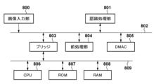
先ず、本実施形態に係る演算処理装置としての認識処理装置を利用した画像処理システムのハードウェア構成例について、図8のブロック図を用いて説明する。本実施形態に係る画像処理システムは、入力された画像データから特定の物体の領域を検出する機能を有する。
[First embodiment]
First, a hardware configuration example of an image processing system using a recognition processing device as an arithmetic processing device according to the present embodiment will be described with reference to the block diagram of FIG. The image processing system according to this embodiment has a function of detecting a specific object area from input image data.
画像入力部800は、撮像を行うことで画像データを入力データとして取得する。画像データは動画像における各フレームの画像のデータであっても良いし、静止画像のデータであっても良い。画像入力部800は、光学系、CCD(Charge-Coupled Devices)又はCMOS(Complimentary Metal Oxide Semiconductor)センサ等の光電変換デバイス及びセンサを制御するドライバー回路/ADコンバータ/各種画像補正を司る信号処理回路/フレームバッファ等により構成される。
The
認識処理部801は、本実施形態に係る演算処理装置としての認識処理装置を含み、画像入力部800による画像データから特定の物体の領域を検出する。DMAC(Direct Memory Access Controller)805は、画像バス802上の各処理部と、CPUバス809上の各処理部と、の間のデータ転送を司る。
A
ブリッジ803は、画像バス802とCPUバス809のブリッジ機能を提供する。
前処理部804は、認識処理部801による認識処理を効果的に行うための各種の前処理を行う。具体的には、前処理部804は、画像入力部800が取得した画像データに対して色変換処理/コントラスト補正処理等の画像変換処理をハードウェアで処理する。
A
CPU806は、ROM807やRAM808に格納されているコンピュータプログラムやデータを用いて各種の処理を実行する。これによりCPU806は、画像処理システム全体の動作制御を行うと共に、画像処理システムが行うものとして後述する各処理を実行若しくは制御する。
The
ROM(Read Only Memory)807には、CPU806の動作を規定する命令を含むコンピュータプログラムやデータなどが格納されている。以下の説明において画像処理システムが既知の情報として取り扱う情報はROM807に格納されている。ROM807に格納されているデータには、認識処理部801を動作させるためのデータセット(階層型ニューラルネットワークの一例であるCNNに応じた動作パラメータと重み係数)も含まれている。このデータセットは、DMAC805を介して認識処理部801に入力される。
A ROM (Read Only Memory) 807 stores computer programs, data, and the like including instructions that define the operation of the
RAM808はROM807からロードされたコンピュータプログラムやデータを格納するためのエリア、画像入力部800が取得した画像データを保持するためのエリア、処理対象とするデータを一時的に保持するためのエリア、等を有する。またRAM808は、CPU806が各種の処理を実行する際に用いるワークエリアを有する。このようにRAM808は各種のエリアを適宜提供することができる。
A
画像入力部800が取得した画像データは前処理部804で前処理されて一端RAM808に格納され、DMAC805により認識処理部801に転送(入力)される。認識処理部801は、入力された前処理後の画像データに対して画素単位で所定の判別処理を行うことで、該画像データが表す画像中の特定の物体の領域を検出する。認識処理部801によって検出された領域に係る情報(画像中の該領域を規定する情報や該領域内の画像など)は、DMAC805によってRAM808に転送されて該RAM808に格納される。
The image data acquired by the
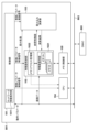
次に、認識処理部801のハードウェア構成例について、図1のブロック図を用いて説明する。制御部101は、認識処理部801の全体を制御する。制御部101は内部にネットワーク情報保持部1011を有しており、該ネットワーク情報保持部1011にはネットワーク情報が設定(格納)される。DMAC805がROM807に予め格納されているネットワーク情報をネットワーク情報保持部1011に転送して設定する。ネットワーク情報は、処理する階層の数、階層の番号、階層毎の特徴面の情報(特徴面の幅、高さ、特徴面の数)、階層間の結合の情報(コンボリューションカーネルの水平サイズ、垂直サイズ)を含む。
Next, a hardware configuration example of the
また制御部101は、動作制御用のレジスタとしてイネーブルレジスタも備え、CPU806が処理開始を指示する。CPU806は複数階層の処理開始を制御部101へ指示し、制御部101は後述する特徴面格納部102、畳み込み演算部103へ階層単位の処理の開始を複数回指示する。制御部101は、処理の開始指示を示す制御信号と共にネットワーク情報保持部1011に設定(保持)されているネットワーク情報を、制御パラメータとして送信する。
The
生成した階層の特徴面に後処理を施す場合、特徴面格納部102及び畳み込み演算部103での階層単位の処理が完了すると、制御部101はネットワーク情報保持部1011に設定されているネットワーク情報をCPU104に制御パラメータとして送信する。そして制御部101は処理の開始指示を出す。
When post-processing is applied to the feature plane of the generated hierarchy, when the feature
特徴面格納部102は、特徴面を格納するためのものであり、特徴面保持部1021と、特徴面保持部1021のデータの読み書きを制御するメモリアクセス管理部1022と、を備える。
The feature
特徴面保持部1021は、(N+1)個(Nは1以上の整数)のデュアルポートSRAM(メモリ0~メモリN)を有する。以下の説明では一例としてN=5とする。つまり、以下の説明では、特徴面保持部1021は6つのデュアルポートSRAM(メモリ0~メモリ5)を有するものとする。また、SRAMのデータ幅は4バイトとする。
The characteristic
メモリアクセス管理部1022は、デュアルポートSRAMのインターフェースのうちの片側1ポートを制御する。メモリアクセス管理部1022は、制御部101から受信する制御パラメータ(階層のネットワーク情報)に基づき、畳み込み演算部103の演算結果である各階層の生成された特徴面を6つのデュアルポートSRAMへどのように配置するか決定し、書き込む。また、メモリアクセス管理部1022は、参照特徴面を読み出して畳み込み演算部103へ送信する。そしてメモリアクセス管理部1022は、畳み込み演算部103から、生成する階層の全特徴面を受信すると、制御部101へ完了を通知する。
Memory
畳み込み演算部103は、畳み込み演算を行うものであり、フィルタカーネルサイズに応じた重み係数と参照特徴面を入力とし、演算結果として特徴面を出力する。DMAC805がROM807に予め配置された重み係数を畳み込み演算部103に転送する。畳み込み演算部103は、制御部101から制御パラメータとしてフィルタカーネルサイズを受信し、処理開始を指示されると演算処理を行い、生成する階層の全特徴面の演算処理が完了すると、制御部101へ完了を通知する。
The
CPU104は、特徴面の後処理を行う。CPU104は、画像バス802のバスマスタであり、メモリ空間に、後述するメモリ制御部105を介して特徴面保持部1021のメモリがアドレスマップされている。制御部101から処理開始指示を受信すると、処理対象の階層のネットワーク情報に基づいてデータを取得し、処理する。
The
メモリ制御部105は、特徴面保持部1021が有するデュアルポートSRAMに対するデータの読み書きを制御するものであり、特徴面保持部1021の6つのデュアルポートSRAMのインターフェースのうちの片側1ポートを制御する。またメモリ制御部105は画像バス802のバススレーブであり、バスマスタから要求を受け、メモリに対するデータの読み書きを行う。
The
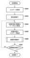
次に、画像処理システムの全体動作について、図2のフローチャートに従って説明する。ステップS202では、CPU806は、画像入力部800を介して画像データ(入力データ)を取得する。ステップS203では、前処理部804は、ステップS202で取得した画像データに対して前処理を施し、RAM808に格納する。
Next, the overall operation of the image processing system will be described according to the flowchart of FIG. In step S<b>202 , the
ステップS204では、CPU806はDMAC805に、ROM807に格納されている処理対象の階層のデータセットの開始位置アドレスを設定して起動する。処理対象の階層は1つであっても複数であってもよい。これによりDMAC805は、設定された開始アドレスから処理対象の階層のデータセットを読み出して転送する。
In step S204, the
転送完了後、ステップS205では、再びCPU806は、DMAC805にRAM808の前処理後のデータの開始位置アドレスを設定して起動する。これによりDMAC805は、設定された開始アドレスから前処理後のデータを読み出して転送する。
After the transfer is completed, in step S205, the
ステップS206では、CPU806は、認識処理部801を起動するので、認識処理部801は処理を実行する。認識処理部801の処理が完了すると、該処理の結果(検出結果や中間階層の特徴データ)が再度RAM808に格納される。
In step S206, the
ステップS207では、CPU806は、全階層の処理が完了したか否かを判断する。この判断の結果、全階層の処理が完了した場合には、図2のフローチャートに従った処理は終了する。一方、未だ処理が完了していない階層が残っている場合には、処理はステップS204に進み、未だ処理が完了していない階層についてステップS204以降の処理を行う。
In step S207, the
組み込み機器向けの小規模なニューラルネットワークでは、全階層を一度に処理することが可能であるため、この場合はステップS207では「全階層の処理は完了した」と判断して、図2のフローチャートに従った処理は終了する。一方、大規模なニューラルネットワークでは、一度にすべての階層を処理することができないため、ニューラルネットワークを時分割で処理することとなる。この場合、ステップS207では、時分割で行っている処理が未だ施されていない階層が残っている場合には、処理はステップS204に進み、残りの階層の処理を実施する。2回目以降のステップS205の処理は、RAM808に格納した認識処理部801の処理結果を処理対象のデータとして転送する。
In a small-scale neural network for embedded devices, it is possible to process all layers at once. In this case, in step S207, it is determined that "processing of all layers has been completed", and the process proceeds to the flow chart of FIG. Following processing ends. On the other hand, since a large-scale neural network cannot process all layers at once, the neural network is processed by time division. In this case, in step S207, if there remains a hierarchy that has not been subjected to time-divisional processing, the process proceeds to step S204, and the remaining hierarchy is processed. In the processing of step S205 from the second time onward, the processing result of the
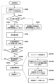
次に、上記のステップS206における処理の詳細について、図3のフローチャートに従って説明する。制御部101が全体を制御する。ステップS205の処理が完了した時点で、認識処理部801の処理対象の階層に関する情報はネットワーク情報保持部1011に設定されている。
Next, the details of the processing in step S206 will be described with reference to the flowchart of FIG. A
ステップS302では、制御部101は、ネットワーク情報保持部1011に保持された情報を、階層単位で特徴面格納部102、畳み込み演算部103に対して制御パラメータとして送信し、処理開始指示を出す。
In step S302, the
ステップS303では、特徴面格納部102は、入力層の処理であるか否かを判定する。この判定の結果、入力層の処理である場合には、処理はステップS304に進み、入力層以外の階層の処理である場合には、処理はステップS305に進む。
In step S303, the feature
ステップS304では、特徴面格納部102は、画像データを参照特徴面として出力する。一方、ステップS305では、特徴面格納部102は、前階層の特徴面を特徴面保持部1021から読み出し、参照特徴面として出力する。
In step S304, the feature
ステップS306では、畳み込み演算部103は、参照特徴面と重み係数に基づき畳み込み演算を行い、演算結果を特徴面格納部102に送信する。ステップS307では、メモリアクセス管理部1022は、生成された特徴面のメモリ配置を決定し、該決定されたメモリ配置に従って特徴面を特徴面保持部1021に格納する。メモリ配置の詳細については、図4~6を用いて後述する。
In step S<b>306 , the
次に、ステップS308では、特徴面格納部102は全特徴面の生成が完了したか否かを判定する。この判定の結果、全特徴面の生成が完了した場合には、処理はステップS309に進む。一方、未だ生成が完了していない特徴面が残っている場合には、処理はステップS303に進み、未だ生成が完了していない特徴面についてステップS303以降の処理を行う。
Next, in step S308, the feature
ステップS309では、特徴面格納部102および畳み込み演算部103は制御部101に対して完了通知を出す。そして制御部101は完了通知を受けると、最終階層の処理が完了したか否かを判定する。
In step S<b>309 , the feature
この判定の結果、最終階層の処理が完了した場合には、処理はステップS310に進む。一方、最終階層の処理がまだ完了していない場合には、処理はステップS302に進み、さらに制御部101は次の階層の処理を指示する。
As a result of this determination, if the processing of the final layer has been completed, the process proceeds to step S310. On the other hand, if the processing of the final layer has not been completed yet, the process proceeds to step S302, and the
ステップS310では、制御部101は最終階層の処理が完了すると、CPU104に最終階層の番号等のネットワーク情報を与え、処理開始指示を出す。CPU104はネットワーク情報に基づき、最終階層の特徴面を読み出し、位置座標を特定し、処理を終了する。ステップS310の処理の詳細(ステップS3101~ステップS3104)については後述する。
In step S310, when the processing of the final layer is completed, the
次に、図4~6を用いて、メモリアクセス管理部1022が制御するメモリ配置について説明する。図4は、図9の第1階層908と第2階層909の特徴面を特徴面保持部1021のメモリに割り当てる割り当て方法の一例を示す図である。
Next, memory allocation controlled by the memory
特徴面格納部102の特徴面は、階層を単位に複数のメモリにインターリーブする。また、特徴面格納部102の特徴面は、ラインを単位に複数のメモリにインターリーブする。
The feature planes in the feature
図9の左側には、第1階層908の特徴面903a~d、第2階層909の特徴面905a~dの画素値を示している。特徴面903aの左上隅の位置を(0,0)としたときの位置(x、y)における特徴面903aの画素値をa(x、y)と表している。特徴面903bの左上隅の位置を(0,0)としたときの位置(x、y)における特徴面903bの画素値をb(x、y)と表している。特徴面903cの左上隅の位置を(0,0)としたときの位置(x、y)における特徴面903cの画素値をc(x、y)と表している。特徴面903cの左上隅の位置を(0,0)としたときの位置(x、y)における特徴面903cの画素値をc(x、y)と表している。特徴面905aの左上隅の位置を(0,0)としたときの位置(x、y)における特徴面905aの画素値をa(x、y)と表している。特徴面905bの左上隅の位置を(0,0)としたときの位置(x、y)における特徴面905bの画素値をb(x、y)と表している。特徴面905cの左上隅の位置を(0,0)としたときの位置(x、y)における特徴面905cの画素値をc(x、y)と表している。特徴面905dの左上隅の位置を(0,0)としたときの位置(x、y)における特徴面905dの画素値をd(x、y)と表している。
Pixel values of
図4では、第1階層908の特徴面の水平方向のサイズは32画素、垂直方向のサイズは32画素としており、第2階層909の特徴面の水平方向のサイズは16画素、垂直方向のサイズは16画素としている。1座標の画素値のデータは1バイトとする。図4の右側には、各特徴面をメモリに割り当てる方法の一例を示している。
In FIG. 4, the horizontal size of the feature surface of the
特徴面保持部1021が有するメモリ群を2つのグループに分け、一方のグループを第1のメモリ群、他方のグループを第2のメモリ群とする。本実施形態では、特徴面保持部1021は6つのデュアルポートSRAM(メモリ0~メモリ5)を有するので、メモリ0~メモリ2を第1のメモリ群、メモリ3~メモリ5を第2のメモリ群とする。そして階層ごとに特徴面を、第1のメモリ群、第2のメモリ群の順に交互に配置する。これにより、入力特徴面と出力特徴面を別のメモリに配置し、読み出しと書き込みを同時に行うことができ、高速に処理を行うことができる。さらに、1枚の特徴面をライン(Y座標が同一の画素群をラインと呼ぶ)毎に異なるメモリに割り当てる。つまり、本実施形態の場合、特徴面の連続する3ラインが異なるメモリに配置される。これにより、コンボリューションカーネルのサイズが3×3以下のときは畳み込み演算部103に入力する参照特徴面の画素を同時に読み出すことができ、高速に処理ができる。コンボリューションカーネルサイズが3×3より大きいときは2サイクルで読み出すことができる。
The memory group of the characteristic
上述の説明に従い、図4の右側に示すように、第1階層908の特徴面903a~dには1ライン毎に、メモリ0、メモリ1、メモリ2を交互に割り当てる。特徴面903aの最終ラインに割り当てたメモリはメモリ1であるので、特徴面903bの1ライン目には次のメモリであるメモリ2を割り当てる。メモリを効率的に使用するために、特徴面を跨ぐときにも、連続するラインと同様にメモリを割り当てる。同様に特徴面903cにもラインごとにメモリ1、メモリ2、メモリ0を交互に割り当て、特徴面903dにもラインごとにメモリ0、メモリ1、メモリ2を交互に割り当てる。
According to the above description, as shown on the right side of FIG. 4,
第2階層909の特徴面905a~dには1ライン毎に、メモリ3、メモリ4、メモリ5を交互に割り当てる。特徴面905aの最終ラインに割り当てたメモリはメモリ3であるので、特徴面905bの1ライン目には次のメモリであるメモリ4を割り当てる。メモリを効率的に使用するために、特徴面を跨ぐときにも、連続するラインと同様にメモリを割り当てる。同様に特徴面905cにもラインごとにメモリ3、メモリ4、メモリ5を交互に割り当て、特徴面905dにもラインごとにメモリ3、メモリ4、メモリ5を交互に割り当てる。
Memory 3,
図5は、図4に示した割り当て方法に従って割り当てられた各メモリの特徴面のアドレスの割り当て方法の一例を示す図である。メモリはデータ幅4バイトであるから、1アドレスに4画素のデータを格納することになる。x座標が小さい画素から順に下位バイトに詰めるものとする。 FIG. 5 is a diagram showing an example of a method of allocating addresses of characteristic planes of each memory allocated according to the allocating method shown in FIG. Since the memory has a data width of 4 bytes, 4 pixels of data are stored at one address. It is assumed that pixels with smaller x-coordinates are packed into lower bytes.
メモリ0には、アドレス0~0x7に特徴面903aの1ライン目の画素の画素値、アドレス0x8~0xfに4ライン目の画素の画素値、アドレス0x10~0x17に7ライン目の画素の画素値…と3ラインオフセットの32画素の画素値を格納する。この32画素の画素値のデータサイズは32バイトである。
In the
特徴面903aの11ライン分の画素値を格納後、次のアドレス0x58から特徴面903bの2ライン目の画素の画素値を格納する。同様に、特徴面903c、特徴面903dについても画素値を格納する。メモリ1には、アドレス0~0x7に903aの2ライン目のデータから順に3ラインオフセットで32画素を格納し、続いて、特徴面903b~dについても画素値を格納する。メモリ2にも同様に特徴面903a~dの画素値を格納する。メモリ3~5にも、それぞれ同様に、第2階層908の特徴面905a~dの3ラインオフセットの16画素の画素値(16バイト)を格納する。
After storing the pixel values for 11 lines of the
次に、上記のステップS307にて、メモリアクセス管理部1022が特徴面番号nの特徴面の座標(x、y)における画素値を格納するメモリと、そのアドレスを決定する方法について、図6のフローチャートに従って説明する。
Next, in step S307 described above, the memory in which the memory
ステップS302では、制御部101は、制御パラメータとして処理対象及び生成対象の階層の階層番号、特徴面の水平サイズw、垂直サイズh、特徴面数、を階層単位で特徴面格納部102、畳み込み演算部103に対して送信する。畳み込み演算部103は、全特徴面のデータをラスタ順に出力するものとする。畳み込み演算部103が出力すると図6のフローチャートに従った処理が開始される。
In step S302, the
ステップS602では、メモリアクセス管理部1022は、特徴面番号n、座標(x、y)の全特徴面のラインの通し番号LをL=(n-1)×h+yを計算することで求める。
In step S602, the memory
ステップS603では、メモリアクセス管理部1022は、通し番号Lを特徴面保持部1021のメモリ数に応じて剰余演算することで、格納先メモリ番号memを決定する。つまりメモリアクセス管理部1022は、mem=mod(L,(メモリ数/2))を計算することで、格納先メモリ番号memを求める。
In step S<b>603 , the memory
mem=0の場合(剰余演算結果が0のとき)、処理はステップS604に進む。ステップS604では、メモリアクセス管理部1022は、生成対象の階層の階層番号が奇数か否かを判定し、奇数の場合は処理はステップS605に進み、偶数の場合はステップS606に進む。ステップS605ではメモリアクセス管理部1022は、画素値をメモリ0へ格納し、ステップS606ではメモリアクセス管理部1022は、画素値をメモリ3へ格納する。
If mem=0 (when the remainder calculation result is 0), the process proceeds to step S604. In step S604, the memory
mem=1の場合(剰余演算結果が1のとき)、処理はステップS607に進む。ステップS607では、メモリアクセス管理部1022は、生成対象の階層の階層番号が奇数か否かを判定し、奇数の場合は処理はステップS608に進み、偶数の場合はステップS609に進む。ステップS608ではメモリアクセス管理部1022は、画素値をメモリ1へ格納し、ステップS609ではメモリアクセス管理部1022は、画素値をメモリ4へ格納する。
If mem=1 (when the remainder calculation result is 1), the process proceeds to step S607. In step S607, the memory
mem=2の場合(剰余演算結果が2のとき)、処理はステップS610に進む。ステップS610では、メモリアクセス管理部1022は、生成対象の階層の階層番号が奇数か否かを判定し、奇数の場合は処理はステップS611に進み、偶数の場合はステップS612に進む。ステップS611ではメモリアクセス管理部1022は、画素値をメモリ2へ格納し、ステップS612ではメモリアクセス管理部1022は、画素値をメモリ5へ格納する。
If mem=2 (when the remainder calculation result is 2), the process proceeds to step S610. In step S610, the memory
このように画素値の格納先を決定することで、奇数番号の階層から偶数番号の階層を生成するとき、参照特徴面を読み出すメモリと生成特徴面を書き出すメモリが別々となる。同様に偶数番号の階層から奇数番号の階層を生成するとき、参照特徴面を読み出すメモリと生成特徴面を書き出すメモリが別々となる。また、生成特徴面はラインの通し番号順に1ラインずつ異なるメモリに格納することになり、参照特徴面として読み込むときに複数ラインが同時に読み込める。 By determining where to store pixel values in this way, when generating even-numbered layers from odd-numbered layers, the memory for reading the reference feature plane and the memory for writing the generated feature plane are separate. Similarly, when odd-numbered layers are generated from even-numbered layers, the memory for reading the reference feature plane and the memory for writing the generated feature plane are separate. In addition, the generated feature planes are stored in different memories line by line in the order of the serial number of the lines, so that a plurality of lines can be read at the same time when they are read as the reference feature planes.
そしてステップS613では、メモリアクセス管理部1022は、メモリのアドレスを算出する。1ラインの先頭画素を格納するアドレスA0については、A0=L/(メモリ数/2)×w/4を計算することで求め、アドレスA1については、A0+x/4を計算することで求める。
Then, in step S613, the memory
次に、上記のステップS310における処理の詳細について説明する。図7はCPU104のメモリマップの一部を示す図である。メモリ0~5はそれぞれ8KBのメモリとし、特定のベースアドレスから48KBの連続した領域に割り当てる。メモリ0の先頭アドレスは0番地、メモリ1以降の先頭アドレスは0x2000番地ずつ加算される。
Next, details of the processing in step S310 will be described. FIG. 7 is a diagram showing part of the memory map of the
メモリ制御部105は、アクセス要求のアドレスに応じてメモリのチップセレクトを選択する。例えば、0番地から0x1FFF番地へのアクセス要求はメモリ0のチップセレクトを、0x2000番地から0x3FFF番地へのアクセス要求はメモリ1のチップセレクトを選択する。また、メモリのアドレスはアクセス要求のアドレスの[13:2]とする。
The
ステップS3101では、CPU104は、ネットワーク情報を取得する。制御部101が制御パラメータとして最終階層の階層番号、特徴面の水平サイズw、垂直サイズh、特徴面数を引き渡し、CPU104はこの制御パラメータを参照する。
In step S3101,
次に、ステップS3102では、特徴面番号n、座標(x、y)の特徴面の画素値を読み出すために図6のフローチャートに従った処理が実行され、格納メモリとアドレスA1が特定される。ここでは、図6のフローチャートに従った処理はCPU104が行っても良いし、メモリアクセス管理部1022が行っても良い。
Next, in step S3102, the processing according to the flowchart of FIG. 6 is executed to read the pixel value of the feature plane with the feature plane number n and the coordinates (x, y), and the storage memory and address A1 are specified. Here, the processing according to the flowchart of FIG. 6 may be performed by the
そしてステップS3103では、CPU104は、ステップS3102で特定された格納メモリとアドレスA1から、以下のような変換処理を行うことで、メモリマップ上のアドレスを取得する。
Then, in step S3103, the
格納メモリがメモリ0のとき、アドレス=A1×4
格納メモリがメモリ1のとき、アドレス=A1×4+0x2000
格納メモリがメモリ2のとき、アドレス=A1×4+0x4000
格納メモリがメモリ3のとき、アドレス=A1×4+0x6000
格納メモリがメモリ4のとき、アドレス=A1×4+0x8000
格納メモリがメモリ5のとき、アドレス=A1×4+0xa000
そしてステップS3104ではCPU104は、変換後のアドレスでメモリ制御部105にアクセス要求を出し、該アクセス要求に応じて読み出された特徴面の画素値を取得し、位置座標を特定する。
When the storage memory is
When the storage memory is
When the storage memory is
When the storage memory is memory 3, address = A1x4+0x6000
When the storage memory is
When the storage memory is memory 5, address=A1×4+0xa000
Then, in step S3104, the
このように、本実施形態によれば、共有メモリにデータ転送する時間をなくし、かつ、バス帯域を削減することができる。また、CNNの処理を行うハードウェア(CNN処理ハードウェア)のメモリは、CPUのアドレスマップドメモリとなる。そのため、CNN処理ハードウェアが動作しないときはCPUのワークメモリとして使用することもでき、ワークメモリを別途設ける必要がなく、コストを削減できる。 Thus, according to this embodiment, it is possible to eliminate the time required to transfer data to the shared memory and reduce the bus bandwidth. Also, the memory of the hardware that performs CNN processing (CNN processing hardware) is the address-mapped memory of the CPU. Therefore, when the CNN processing hardware does not operate, it can be used as a work memory for the CPU, and there is no need to separately provide a work memory, thereby reducing costs.
[第2の実施形態]
以下では第1の実施形態との差分について説明し、以下で特に触れない限りは第1の実施形態と同様であるものとする。本実施形態に係る認識処理部801の構成例について、図11のブロック図を用いて説明する。
[Second embodiment]
Differences from the first embodiment will be described below, and the same as the first embodiment is assumed unless otherwise specified. A configuration example of the
本実施形態では、メモリマップ上の48KBの連続した領域に、先頭アドレス0番地から順に、処理対象の階層の特徴面がラスタ順に連続して格納されているものとして扱う。つまり、特徴面の水平サイズw、垂直サイズhに応じて、特徴面番号n、座標(x、y)の特徴面のデータのメモリマップ上のアドレスA2は以下の式で決定する。
In the present embodiment, it is assumed that the characteristic planes of the layer to be processed are successively stored in raster order in a continuous area of 48 KB on the memory map, starting from the leading
A2=w×h×n(特徴面オフセット)+y×w(ラインオフセット)+x
メモリ制御部1051は、SRAMインターフェースは1つ(チップセレクトは1つ)であるという構成の元、アクセス要求アドレスをそのままSRAMのアドレス信号とする。SRAMインターフェースはメモリアクセス管理部1024に接続される。ステップS310にてA2へのSRAMアクセスがそのままメモリアクセス管理部1024に通知される。
A2 = w x h x n (feature surface offset) + y x w (line offset) + x
The
特徴面保持部1023はシングルポートSRAMとする。メモリアクセス管理部1024は、メモリ制御部1051のSRAMインターフェースからアクセス要求があるとき、そのアドレスと特徴面の水平サイズw、垂直サイズh、階層番号から、特徴面番号n、座標(x、y)を特定する。そして図6のフローチャートに従って格納先メモリとアドレスを決定してメモリからデータを読み込む。リードデータは、メモリ制御部1051へ出力する。
The characteristic
このように、本実施形態では、CNN処理ハードウェアが出力した演算結果に対して後処理するCPU104が、特徴面の水平サイズ、垂直サイズに応じ、メモリマップ上の特定アドレスへのアクセス要求を出す。メモリアクセス管理部1024が中間層および最終層の特徴面を格納するメモリのインターフェースから直接読み出すことで、第1の実施形態と同様の効果を得ることができる。なお、汎用CPU、アドレスマップドメモリとしてそれぞれ、認識処理部801の外部にあるCPU806、RAM808を使用しても良い。
As described above, in this embodiment, the
なお、上記の各実施形態では、図1,11に示した全ての機能部をハードウェアで実装したケースについて説明した。しかし、図1,11に示した機能部のうち一部の機能部をソフトウェア(コンピュータプログラム)で実装しても良い。この場合、このコンピュータプログラムはROM807等のメモリに格納され、CPU806等のプロセッサがこのコンピュータプログラムを実行することで、対応する機能部の機能を実現させることができる。
In each of the above-described embodiments, the case where all the functional units shown in FIGS. 1 and 11 are implemented by hardware has been described. However, some of the functional units shown in FIGS. 1 and 11 may be implemented by software (computer programs). In this case, the computer program is stored in a memory such as the
なお、上記の説明において使用した具体的な数値は、具体的な説明を行うために使用したものであって、上記の各実施形態がこれらの数値に限定されることを意図したものではない。なお、以上説明した各実施形態の一部若しくは全部を適宜組み合わせても構わない。また、以上説明した各実施形態の一部若しくは全部を選択的に用いても構わない。 It should be noted that the specific numerical values used in the above description are used for specific description, and are not intended to limit each of the above embodiments to these numerical values. It should be noted that part or all of the embodiments described above may be appropriately combined. Moreover, you may selectively use a part or all of each embodiment demonstrated above.
(その他の実施形態)
本発明は、上述の実施形態の1以上の機能を実現するプログラムを、ネットワーク又は記憶媒体を介してシステム又は装置に供給し、そのシステム又は装置のコンピュータにおける1つ以上のプロセッサがプログラムを読出し実行する処理でも実現可能である。また、1以上の機能を実現する回路(例えば、ASIC)によっても実現可能である。
(Other embodiments)
The present invention supplies a program that implements one or more functions of the above-described embodiments to a system or apparatus via a network or a storage medium, and one or more processors in the computer of the system or apparatus reads and executes the program. It can also be realized by processing to It can also be implemented by a circuit (for example, ASIC) that implements one or more functions.
発明は上記実施形態に制限されるものではなく、発明の精神及び範囲から離脱することなく、様々な変更及び変形が可能である。従って、発明の範囲を公にするために請求項を添付する。 The invention is not limited to the embodiments described above, and various modifications and variations are possible without departing from the spirit and scope of the invention. Accordingly, the claims are appended to make public the scope of the invention.
101:制御部 102:特徴面格納部 1021:特徴面保持部 1022:メモリアクセス管理部 103:畳み込み演算部 104:CPU 105:メモリ制御部 101: Control Unit 102: Feature Plane Storage Unit 1021: Feature Plane Holding Unit 1022: Memory Access Management Unit 103: Convolution Calculator 104: CPU 105: Memory Control Unit
Claims (8)
前記各階層における特徴面を、該階層の前の階層の特徴面を参照して算出する演算部と、
前記演算部によって算出され、参照される特徴面を保持する複数のメモリを有する特徴面保持部と、
前記演算処理を行うそれぞれの階層に関する情報であるネットワーク情報に基づいて、前記複数のメモリに前記演算部によって算出された特徴面を配置して書き込み、該複数のメモリから前記演算部によって参照される特徴面を読み出すメモリアクセス管理部と、
前記特徴面保持部がメモリ空間にアドレスマップされており、前記ネットワーク情報に基づいて該メモリ空間にアドレスマップされた特徴面の画素値のアドレスを算出し、該アドレスを用いて該特徴面保持部から画素値を読み出して処理するプロセッサと
を備えることを特徴とする演算処理装置。 An arithmetic processing device that inputs input data to a hierarchical neural network and performs arithmetic processing in each layer of the hierarchical neural network,
a calculation unit that calculates the characteristic surface in each layer by referring to the characteristic surface in the layer before the layer ;
a feature plane holding unit having a plurality of memories that hold the feature planes calculated and referred to by the calculation unit;
Based on network information, which is information about each layer on which the arithmetic processing is performed , the characteristic planes calculated by the arithmetic unit are arranged and written in the plurality of memories, and are referred to by the arithmetic unit from the plurality of memories. a memory access manager that reads the feature plane ;
The characteristic surface holding unit is address-mapped in a memory space, and based on the network information, calculates an address of a pixel value of the characteristic surface that is address-mapped in the memory space, and uses the address to calculate the characteristic surface holding unit. and a processor that reads out pixel values from and processes them.
前記演算処理装置は、
前記各階層における特徴面を、該階層の前の階層の特徴面を参照して算出する演算部と、
前記演算部によって算出され、参照される特徴面を保持する複数のメモリを有する特徴面保持部と、
前記メモリに対する読み書きを管理するメモリアクセス管理部と、
前記特徴面保持部へアクセスするプロセッサと
を備え、
前記メモリアクセス管理部は、前記演算処理を行うそれぞれの階層に関する情報であるネットワーク情報に基づいて、前記複数のメモリに前記演算部によって算出された特徴面を配置して書き込み、該複数のメモリから前記演算部によって参照される特徴面を読み出し、
前記特徴面保持部がメモリ空間にアドレスマップされており、前記プロセッサは、前記ネットワーク情報に基づいて該メモリ空間にアドレスマップされた特徴面の画素値のアドレスを算出し、該アドレスを用いて該特徴面保持部から画素値を読み出して処理することを特徴とする演算処理方法。 An arithmetic processing method performed by an arithmetic processing device that inputs input data to a hierarchical neural network and performs arithmetic processing in each layer of the hierarchical neural network,
The arithmetic processing unit is
a calculation unit that calculates the characteristic surface in each layer by referring to the characteristic surface in the layer before the layer ;
a feature plane holding unit having a plurality of memories that hold the feature planes calculated and referred to by the calculation unit;
a memory access management unit that manages reading and writing with respect to the memory;
a processor that accesses the feature surface holder;
The memory access management unit arranges and writes the characteristic planes calculated by the calculation unit in the plurality of memories based on network information, which is information about each layer in which the calculation processing is performed, and writes reading a feature plane referenced by the computing unit;
The feature plane holding unit is address-mapped in a memory space, and the processor calculates an address of a pixel value of the feature plane address-mapped in the memory space based on the network information, and uses the address. An arithmetic processing method, comprising: reading pixel values from a feature plane holding unit and processing the pixel values.
Priority Applications (2)
| Application Number | Priority Date | Filing Date | Title |
|---|---|---|---|
| JP2019123135A JP7299770B2 (en) | 2019-07-01 | 2019-07-01 | Arithmetic processing device and arithmetic processing method |
| US16/916,507 US11704546B2 (en) | 2019-07-01 | 2020-06-30 | Operation processing apparatus that calculates addresses of feature planes in layers of a neutral network and operation processing method |
Applications Claiming Priority (1)
| Application Number | Priority Date | Filing Date | Title |
|---|---|---|---|
| JP2019123135A JP7299770B2 (en) | 2019-07-01 | 2019-07-01 | Arithmetic processing device and arithmetic processing method |
Publications (3)
| Publication Number | Publication Date |
|---|---|
| JP2021009566A JP2021009566A (en) | 2021-01-28 |
| JP2021009566A5 JP2021009566A5 (en) | 2022-07-11 |
| JP7299770B2 true JP7299770B2 (en) | 2023-06-28 |
Family
ID=74066056
Family Applications (1)
| Application Number | Title | Priority Date | Filing Date |
|---|---|---|---|
| JP2019123135A Active JP7299770B2 (en) | 2019-07-01 | 2019-07-01 | Arithmetic processing device and arithmetic processing method |
Country Status (2)
| Country | Link |
|---|---|
| US (1) | US11704546B2 (en) |
| JP (1) | JP7299770B2 (en) |
Families Citing this family (2)
| Publication number | Priority date | Publication date | Assignee | Title |
|---|---|---|---|---|
| JP6970827B2 (en) * | 2018-06-25 | 2021-11-24 | オリンパス株式会社 | Arithmetic processing unit |
| JP7278150B2 (en) * | 2019-05-23 | 2023-05-19 | キヤノン株式会社 | Image processing device, imaging device, image processing method |
Citations (1)
| Publication number | Priority date | Publication date | Assignee | Title |
|---|---|---|---|---|
| JP2017168174A (en) | 2016-03-18 | 2017-09-21 | 力晶科技股▲ふん▼有限公司 | Semiconductor storage device and address control method therefor |
Family Cites Families (11)
| Publication number | Priority date | Publication date | Assignee | Title |
|---|---|---|---|---|
| JPS6162187A (en) | 1984-09-03 | 1986-03-31 | Fuji Xerox Co Ltd | Image processor |
| JP5368687B2 (en) | 2007-09-26 | 2013-12-18 | キヤノン株式会社 | Arithmetic processing apparatus and method |
| JP6700712B2 (en) * | 2015-10-21 | 2020-05-27 | キヤノン株式会社 | Convolution operation device |
| US9665799B1 (en) | 2016-01-29 | 2017-05-30 | Fotonation Limited | Convolutional neural network |
| JP6964969B2 (en) * | 2016-09-30 | 2021-11-10 | キヤノン株式会社 | Arithmetic processing unit, arithmetic processing method and program |
| JP6945986B2 (en) * | 2016-10-28 | 2021-10-06 | キヤノン株式会社 | Arithmetic circuit, its control method and program |
| CN110050267B (en) * | 2016-12-09 | 2023-05-26 | 北京地平线信息技术有限公司 | System and method for data management |
| JP6936592B2 (en) * | 2017-03-03 | 2021-09-15 | キヤノン株式会社 | Arithmetic processing unit and its control method |
| EP3460724A1 (en) | 2017-09-22 | 2019-03-27 | Kabushiki Kaisha Toshiba | Operation device and operation system |
| JP2019207458A (en) | 2018-05-28 | 2019-12-05 | ルネサスエレクトロニクス株式会社 | Semiconductor device and memory access setting method |
| US11443185B2 (en) * | 2018-10-11 | 2022-09-13 | Powerchip Semiconductor Manufacturing Corporation | Memory chip capable of performing artificial intelligence operation and method thereof |
-
2019
- 2019-07-01 JP JP2019123135A patent/JP7299770B2/en active Active
-
2020
- 2020-06-30 US US16/916,507 patent/US11704546B2/en active Active
Patent Citations (1)
| Publication number | Priority date | Publication date | Assignee | Title |
|---|---|---|---|---|
| JP2017168174A (en) | 2016-03-18 | 2017-09-21 | 力晶科技股▲ふん▼有限公司 | Semiconductor storage device and address control method therefor |
Also Published As
| Publication number | Publication date |
|---|---|
| US20210004667A1 (en) | 2021-01-07 |
| JP2021009566A (en) | 2021-01-28 |
| US11704546B2 (en) | 2023-07-18 |
Similar Documents
| Publication | Publication Date | Title |
|---|---|---|
| JP6945986B2 (en) | Arithmetic circuit, its control method and program | |
| US11699067B2 (en) | Arithmetic processing apparatus and control method therefor | |
| JP6945987B2 (en) | Arithmetic circuit, its control method and program | |
| JP2010134697A (en) | Convolution operation circuit, hierarchical convolution operation circuit, and object recognition device | |
| JP7299770B2 (en) | Arithmetic processing device and arithmetic processing method | |
| CN110738308A (en) | neural network accelerators | |
| EP3093757B1 (en) | Multi-dimensional sliding window operation for a vector processor | |
| JP6800656B2 (en) | Arithmetic circuit, its control method and program | |
| JP6532334B2 (en) | Parallel computing device, image processing device and parallel computing method | |
| CN115471404A (en) | Image scaling method, processing device and storage medium | |
| JP7308674B2 (en) | Arithmetic processing device and arithmetic processing method | |
| US11775809B2 (en) | Image processing apparatus, imaging apparatus, image processing method, non-transitory computer-readable storage medium | |
| US20230377111A1 (en) | Image processing apparatus including neural network processor and method of operation | |
| JP7530187B2 (en) | Data processing device and data processing method | |
| JP7410961B2 (en) | arithmetic processing unit | |
| JP2023058636A (en) | Information processing apparatus and memory control method | |
| US6809422B2 (en) | One-chip image processing apparatus | |
| JP2021009491A (en) | Information processing device, information processing method, and program | |
| JP4970378B2 (en) | Memory controller and image processing apparatus | |
| JP7297468B2 (en) | Data processing device and method | |
| CN115242990A (en) | Image sensor module and method of operating the same | |
| US8503793B2 (en) | Correlation processing apparatus and medium readable by correlation processing apparatus | |
| US20230334820A1 (en) | Image processing apparatus, image processing method, and non-transitory computer-readable storage medium | |
| JP4865021B2 (en) | Image processing apparatus and image processing method | |
| US6489967B1 (en) | Image formation apparatus and image formation method |
Legal Events
| Date | Code | Title | Description |
|---|---|---|---|
| RD01 | Notification of change of attorney |
Free format text: JAPANESE INTERMEDIATE CODE: A7421 Effective date: 20210103 |
|
| A521 | Request for written amendment filed |
Free format text: JAPANESE INTERMEDIATE CODE: A523 Effective date: 20210113 |
|
| A521 | Request for written amendment filed |
Free format text: JAPANESE INTERMEDIATE CODE: A523 Effective date: 20220701 |
|
| A621 | Written request for application examination |
Free format text: JAPANESE INTERMEDIATE CODE: A621 Effective date: 20220701 |
|
| TRDD | Decision of grant or rejection written | ||
| A01 | Written decision to grant a patent or to grant a registration (utility model) |
Free format text: JAPANESE INTERMEDIATE CODE: A01 Effective date: 20230519 |
|
| A977 | Report on retrieval |
Free format text: JAPANESE INTERMEDIATE CODE: A971007 Effective date: 20230517 |
|
| A61 | First payment of annual fees (during grant procedure) |
Free format text: JAPANESE INTERMEDIATE CODE: A61 Effective date: 20230616 |
|
| R151 | Written notification of patent or utility model registration |
Ref document number: 7299770 Country of ref document: JP Free format text: JAPANESE INTERMEDIATE CODE: R151 |