[1.パチンコ遊技機の全体構造]
以下、図面を参照して本発明の好適な実施形態について、図面を参照して説明する。まず、図1乃至図7を参照して実施形態に係るパチンコ遊技機の全体について説明する。図1は、実施形態に係るパチンコ遊技機の外枠に対して本体枠を開放し、本体枠に対して扉枠を開放した状態を示す斜視図である。図2は、パチンコ遊技機の正面図であり、図3は、パチンコ遊技機の右側面図である。また、図4は、パチンコ遊技機の平面図であり、図5は、パチンコ遊技機の背面図である。更に、図6は、パチンコ遊技機を構成する外枠、本体枠、遊技盤、扉枠の後方から見た分解斜視図であり、図7は、パチンコ遊技機を構成する外枠、本体枠、遊技盤、扉枠の前方から見た分解斜視図である。
[1. Overall Structure of Pachinko Machine]
Preferred embodiments of the present invention will be described below with reference to the drawings. First, the entire pachinko gaming machine according to the embodiment will be described with reference to FIGS. 1 to 7. FIG. FIG. 1 is a perspective view showing a state in which the body frame is opened with respect to the outer frame of the pachinko game machine according to the embodiment, and the door frame is opened with respect to the body frame. FIG. 2 is a front view of the pachinko gaming machine, and FIG. 3 is a right side view of the pachinko gaming machine. 4 is a plan view of the pachinko game machine, and FIG. 5 is a rear view of the pachinko game machine. Further, FIG. 6 is an exploded perspective view of the outer frame, main body frame, game board, and door frame, which constitute the pachinko game machine, viewed from behind, and FIG. It is an exploded perspective view of the game board and the door frame as seen from the front.
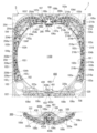
図1乃至図7において、本実施形態に係るパチンコ遊技機1は、遊技ホールの島設備(図示しない)に設置される外枠2と、外枠2に開閉自在に軸支され前側が開放された箱枠状の本体枠3と、本体枠3に前側から装着固定され遊技媒体としての遊技球が打ち込まれる遊技領域1100を有した遊技盤4と、本体枠3及び遊技盤4の前面を遊技者側から閉鎖するように本体枠3に対して開閉自在に軸支された扉枠5とを備えている。このパチンコ遊技機1の扉枠5には、遊技盤4の遊技領域1100が遊技者側から視認可能となるように形成された遊技窓101と、遊技窓101の下方に配置され遊技球を貯留する皿状の上皿301及び下皿302と、上皿301に貯留された遊技球を遊技盤4の遊技領域1100内へ打ち込むために遊技者が操作するハンドル装置500と、を備えている。
1 to 7, a pachinko game machine 1 according to the present embodiment includes an outer frame 2 installed on an island facility (not shown) of a game hall, and an outer frame 2 pivotally supported so as to be openable and closable, and the front side is open. a box-shaped body frame 3; a game board 4 having a game area 1100 attached and fixed to the body frame 3 from the front side and into which game balls as game media are driven; A door frame 5 is pivotally supported to be openable and closable with respect to the body frame 3 so as to be closed from the side of the user. The door frame 5 of the pachinko game machine 1 has a game window 101 formed so that the game area 1100 of the game board 4 can be visually recognized from the player side, and a game window 101 arranged below the game window 101 to store game balls. and a handle device 500 operated by the player to hit the game balls stored in the upper plate 301 into the game area 1100 of the game board 4.例文帳に追加
パチンコ遊技機1は、図示するように、正面視において、外枠2、本体枠3、及び扉枠5がそれぞれ上下方向へ延びた縦長の矩形状に形成されており、それぞれの左右方向の横幅が略同じ寸法とされていると共に、上下方向の縦幅の寸法が、外枠2に対して本体枠3及び扉枠5の寸法が若干短く形成されている。そして、本体枠3及び扉枠5よりも下側の位置において、外枠2の前面に装飾カバー23が取付けられており、扉枠5及び装飾カバー23によって外枠2の前面が完全に閉鎖されるようになっている。また、外枠2、本体枠3、及び扉枠5は、上端が略揃うようにそれぞれが配置されると共に、外枠2の左端前側の位置で本体枠3及び扉枠5が回転可能に軸支されており、外枠2に対して本体枠3及び扉枠5の右端が前側へ移動することで開状態となるようになっている。
As shown in the figure, the pachinko game machine 1 has an outer frame 2, a main body frame 3, and a door frame 5 each formed in a vertically long rectangular shape extending vertically when viewed from the front. are substantially the same, and the vertical width of the main body frame 3 and the door frame 5 is slightly shorter than that of the outer frame 2 . A decorative cover 23 is attached to the front surface of the outer frame 2 at a position below the main body frame 3 and the door frame 5, and the front surface of the outer frame 2 is completely closed by the door frame 5 and the decorative cover 23. It has become so. The outer frame 2, the main body frame 3, and the door frame 5 are arranged such that their upper ends are substantially aligned, and the main body frame 3 and the door frame 5 are rotatably pivoted at a position on the front side of the left end of the outer frame 2. The right ends of the main body frame 3 and the door frame 5 are moved forward with respect to the outer frame 2 to open them.
このパチンコ遊技機1は、正面視において、略円形状の遊技窓101を介して遊技球が打ち込まれる遊技領域1100が望むようになっており、その遊技窓101の下側に前方へ突出するように二つの上皿301及び下皿302が上下に配置されている。また、扉枠5の前面右下隅部には、遊技者が操作するためのハンドル装置500が配置されており、上皿301内に遊技球が貯留されている状態で遊技者がハンドル装置500を回転操作すると、その回転角度に応じた打球強さで上皿301内の遊技球が遊技盤4の遊技領域1100内へ打ち込まれて、遊技をすることができるようになっている。
When viewed from the front, the pachinko game machine 1 has a substantially circular game window 101 in which a game ball is hit through a game area 1100, which projects forward below the game window 101. An upper plate 301 and a lower plate 302 are arranged vertically. A handle device 500 for the player to operate is arranged at the lower right corner of the front surface of the door frame 5 . When a rotating operation is performed, the game ball in the upper tray 301 is hit into the game area 1100 of the game board 4 with a hitting strength corresponding to the rotation angle, so that a game can be played.
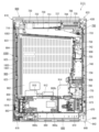
なお、詳細は後述するが、扉枠5の遊技窓101は、透明なガラスユニット590によって閉鎖されており、遊技者から遊技領域1100内を視認することができるものの、遊技者が遊技領域1100内へ手等を挿入して遊技領域1100内の遊技球や障害釘、各種入賞口や役物等に触ることができないようになっている。また、本体枠3の後側には、各種の制御基板が備えられていると共に、遊技盤4の後方を覆うように閉鎖するかバー体1250備えられている。
Although the details will be described later, the game window 101 of the door frame 5 is closed by a transparent glass unit 590, and although the player can visually recognize the inside of the game area 1100, the player cannot see inside the game area 1100. It is not possible to insert a hand or the like into the game area 1100 to touch the game balls, obstacle nails, various winning openings, accessories, and the like. Various control boards are provided on the rear side of the body frame 3, and a closed bar body 1250 is provided so as to cover the rear side of the game board 4. As shown in FIG.
[2.外枠]
外枠2について、主として図8乃至図16を参照して説明する。図8は外枠の正面斜視図であり、図9は外枠の正面から見た分解斜視図であり、図10は外枠の正面図である。また、図11は外枠の背面斜視図であり、図12は外枠の右側面図である。更に、図13は、本体枠の上軸支金具と外枠の上支持金具との脱着構造を説明するための斜視図である。また、図14(A)は外枠の上支持金具の裏面に設けられるロック部材の取付状態を示す分解斜視図であり、(B)は(A)の図を下方から見た斜視図である。図15は、軸支ピンとロック部材との関係を説明するための上支持金具部分の裏面図である。更に、図16は、ロック部材の作用を説明するための上支持金具部分の裏面図である。
[2. Outer frame]
The outer frame 2 will be described mainly with reference to FIGS. 8 to 16. FIG. 8 is a front perspective view of the outer frame, FIG. 9 is an exploded perspective view of the outer frame viewed from the front, and FIG. 10 is a front view of the outer frame. 11 is a rear perspective view of the outer frame, and FIG. 12 is a right side view of the outer frame. Furthermore, FIG. 13 is a perspective view for explaining the attachment/detachment structure between the upper shaft support metal fitting of the main body frame and the upper support metal fitting of the outer frame. FIG. 14(A) is an exploded perspective view showing a mounting state of a lock member provided on the back surface of the upper support fitting of the outer frame, and (B) is a perspective view of FIG. 14(A) viewed from below. . FIG. 15 is a back view of the upper support fitting portion for explaining the relationship between the pivot pin and the lock member. Furthermore, FIG. 16 is a back view of the upper support bracket portion for explaining the action of the locking member.
図8及び図9に示すように、本実施形態のパチンコ遊技機1における外枠2は、横方向へ延びる上下の上枠板10及び下枠板11と、縦(上下)方向へ延びる左右の側枠板12,13と、それぞれの枠板10,11,12,13の端部を連結する四つの連結部材14と、を備えており、連結部材14で各枠板10,11,12,13同士を連結することで縦長の矩形状(方形状)に組立てられている。外枠2における上枠板10及び下枠板11は、所定厚さの無垢材(例えば、木材、合板、等)により形成されており、左右両端の前後方向の略中央に、上下に貫通し左右方向中央側へ窪んだ係合切欠部15が備えられている。なお、上枠板10における左側端部の上面及び前面には、その他の一般面よりも窪んだ取付段部10aが形成されており、この取付段部10aに後述する上支持金具20が取付けられるようになっている。
As shown in FIGS. 8 and 9, the outer frame 2 in the pachinko game machine 1 of this embodiment includes an upper and lower frame plate 10 and a lower frame plate 11 extending in the horizontal direction, and left and right frames extending in the vertical (vertical) direction. It is provided with side frame plates 12, 13 and four connecting members 14 connecting the ends of the frame plates 10, 11, 12, 13, respectively. By connecting 13 together, it is assembled in a vertically long rectangular shape (square shape). The upper frame plate 10 and the lower frame plate 11 of the outer frame 2 are made of solid wood (for example, wood, plywood, etc.) with a predetermined thickness, and are vertically pierced at approximately the center in the front-rear direction of both left and right ends. An engagement notch 15 recessed toward the center in the left-right direction is provided. Mounting stepped portions 10a recessed from other general surfaces are formed on the upper surface and the front surface of the left end portion of the upper frame plate 10, and upper support metal fittings 20, which will be described later, are mounted on the mounting stepped portions 10a. It's like
一方、側枠板12,13は、一定断面形状の軽量金属型材(例えば、アルミ合金)とされており、外側側面は略平坦面とされていると共に、内側側面は後端部に内側へ突出し上下方向(押出方向)に貫通する空洞を有した突出部16を備えており、強度剛性が高められている。なお、側枠板12,13の外側側面及び内側側面には、上下方向へ延びた複数の溝が形成されており、パチンコ遊技機1を遊技ホールのパチンコ島設備に設置する際等に、作業者の指掛りとなってパチンコ遊技機1を保持し易くすることができるようになっていると共に、外観の意匠性を高められるようになっている。なお、便宜上、側枠板12,13の側面に形成された複数の溝を省略して示した図面もある。
On the other hand, the side frame plates 12 and 13 are made of a lightweight metal material (for example, an aluminum alloy) with a constant cross section, and the outer side surfaces are substantially flat surfaces, and the inner side surfaces protrude inward at the rear ends. It is provided with a protruding portion 16 having a cavity penetrating in the vertical direction (extrusion direction) to enhance strength and rigidity. In addition, a plurality of grooves extending in the vertical direction are formed on the outer side surface and the inner side surface of the side frame plates 12 and 13, and when the pachinko game machine 1 is installed on the pachinko island equipment of the game hall, work can be performed. The pachinko game machine 1 can be easily held by the pachinko game machine 1 as a finger rest, and the design of the appearance can be improved. For the sake of convenience, there are drawings in which the plurality of grooves formed on the side surfaces of the side frame plates 12 and 13 are omitted.
外枠2における連結部材14は、所定厚さの金属板をプレス成型等によって屈曲塑性変形させることで形成されたものであり、上枠板10又は下枠板11に固定され左右方向へ延びた板状の水平片17と、水平片17の外側端部から上下方向の一方側へ延び側枠板12,13に固定される板状の垂直片18と、垂直片18とは反対方向へ延び上枠板10又は下枠板11の係合切欠部15内に挿入係合可能な板状の係合片19と、を有している。なお、本実施形態では、上枠板10と左側の側枠板12とを連結する連結部材14と、上枠板10と右側の側枠板13とを連結する連結部材14とは、それぞれ左右非対称の形状に形成されていると共に、垂直片18が前後に分かれて形成されている。一方、下枠板11と左側の側枠板12とを連結する連結部材14と、下枠板11と右側の側枠板13とを連結する連結部材14とは、それぞれ左右対称の形状に形成されている。
The connecting member 14 in the outer frame 2 is formed by bending and plastically deforming a metal plate having a predetermined thickness by press molding or the like, and is fixed to the upper frame plate 10 or the lower frame plate 11 and extends in the left-right direction. A plate-like horizontal piece 17, a plate-like vertical piece 18 extending from the outer end of the horizontal piece 17 to one side in the vertical direction and fixed to the side frame plates 12 and 13, and the vertical piece 18 extending in the opposite direction. It has a plate-shaped engagement piece 19 that can be inserted into and engaged with the engagement notch 15 of the upper frame plate 10 or the lower frame plate 11 . In this embodiment, the connecting member 14 that connects the upper frame plate 10 and the left side frame plate 12 and the connecting member 14 that connects the upper frame plate 10 and the right side frame plate 13 are connected to the left and right sides, respectively. It is formed in an asymmetrical shape, and a vertical piece 18 is formed in front and rear. On the other hand, the connecting member 14 that connects the lower frame plate 11 and the left side frame plate 12 and the connecting member 14 that connects the lower frame plate 11 and the right side frame plate 13 are each formed in a symmetrical shape. It is
この連結部材14は、水平片17の上面及び下面が上枠板10及び下枠板11の下面及び上面と当接すると共に、係合片19が上枠板10及び下枠板11の係合切欠部15内に挿入係合された状態で、水平片17及び係合片19を貫通して所定のビスが上枠板10及び下枠板11にねじ込まれることで、上枠板10及び下枠板11に固定されるようになっている。また、上枠板10に固定された連結部材14は、その垂直片18が側枠板12,13の上端内側側面に当接した状態で、側枠板12,13を貫通して所定のビスが垂直片18へねじ込まれることで、上枠板10と側枠板12,13とを連結することができるようになっている。なお、上枠板10に固定された連結部材14における後側の垂直片18は、側枠板12,13の突出部16内に挿入された状態で、側枠板12,13へ固定されるようになっている。更に、下枠板11に固定された連結部材14は、その垂直片18が側枠板12,13の下端内側側面に当接した状態で、側枠板12,13を貫通して所定のビスが垂直片18へねじ込まれることで、下枠板11と側枠板12,13とを連結することができるようになっており、四つの連結部材14により、上枠板10、下枠板11、及び側枠板12,13を枠状に組立てることができるようになっている。
The upper and lower surfaces of the horizontal piece 17 abut against the lower and upper surfaces of the upper frame plate 10 and the lower frame plate 11 , and the engaging piece 19 of the connecting member 14 engages the upper and lower frame plate 10 and the lower frame plate 11 . In the state of being inserted into and engaged with the portion 15, a predetermined screw is screwed into the upper frame plate 10 and the lower frame plate 11 through the horizontal piece 17 and the engagement piece 19, whereby the upper frame plate 10 and the lower frame It is adapted to be fixed to the plate 11 . The connecting member 14 fixed to the upper frame plate 10 is screwed through the side frame plates 12 and 13 with the vertical piece 18 in contact with the inner side surface of the upper end of the side frame plates 12 and 13. is screwed into the vertical piece 18 so that the upper frame plate 10 and the side frame plates 12 and 13 can be connected. The rear vertical piece 18 of the connecting member 14 fixed to the upper frame plate 10 is fixed to the side frame plates 12 and 13 while being inserted into the projecting portion 16 of the side frame plates 12 and 13. It's like Further, the connecting member 14 fixed to the lower frame plate 11 is screwed through the side frame plates 12 and 13 with the vertical piece 18 in contact with the inner side surface of the lower end of the side frame plates 12 and 13 and screwed with a predetermined screw. is screwed into the vertical piece 18 to connect the lower frame plate 11 and the side frame plates 12 and 13. Four connecting members 14 connect the upper frame plate 10 and the lower frame plate 11 , and the side frame plates 12 and 13 can be assembled into a frame shape.
外枠2は、上枠板10の左端上面に固定される上支持金具20と、上支持金具20と対向するように配置され左側の側枠板12における下部内側の所定位置に固定される下支持金具21と、下支持金具21の下面を支持するように配置され左右の側枠板12,13を連結するように固定される補強金具22と、補強金具22の前面に固定される装飾カバー23と、を備えている。この上支持金具20及び下支持金具21は、本体枠3及び扉枠5を開閉可能に軸支するためのものである。
The outer frame 2 includes an upper support metal fitting 20 fixed to the upper surface of the left end of the upper frame plate 10, and a lower support metal fitting 20 arranged to face the upper support metal fitting 20 and fixed to a predetermined position inside the lower portion of the left side frame plate 12. A supporting metal fitting 21, a reinforcing metal fitting 22 arranged to support the lower surface of the lower supporting metal fitting 21 and fixed so as to connect the left and right side frame plates 12, 13, and a decorative cover fixed to the front surface of the reinforcing metal fitting 22. 23 and. The upper support metal fitting 20 and the lower support metal fitting 21 are for pivotally supporting the body frame 3 and the door frame 5 so that they can be opened and closed.
まず、上支持金具20は、上枠板10に固定される板状の固定片20aと、固定片20aの前端から上枠板10の前端よりも前方へ突出する支持突出片20bと、支持突出片20bにおける前端付近の右側端から先端中央部へ向かって屈曲するように切欠かれて形成された支持鉤穴20cと、固定片20a及び支持突出片20bの左端から下方へ垂下し左側の側枠板12における外側側面と当接する板状の垂下固定片20d(図14(A)を参照)と、垂下固定片20dと連続し支持突出片20bの外側縁に沿って垂下する垂下壁20e(図14を参照)と、垂下壁20eと連続し支持鉤穴20cの入口端部で内側へ向って傾斜した停止垂下部20f(図15を参照)と、を備えている。この上支持金具20における支持鉤穴20cには、後述する本体枠3における上軸支金具630の軸支ピン633(図57を参照)が着脱自在に係合されるようになっている。また、上支持金具20は、固定片20aと垂下固定片20dとによって、上枠板10と左側の側枠板12とを連結することができるようになっている。
First, the upper support metal fitting 20 includes a plate-like fixed piece 20a fixed to the upper frame plate 10, a support projecting piece 20b projecting forward from the front end of the fixed piece 20a beyond the front end of the upper frame plate 10, and a support projecting piece 20b. A supporting hook hole 20c formed by notching from the right end near the front end of the piece 20b so as to bend toward the center of the tip, and a left side frame that hangs downward from the left ends of the fixed piece 20a and the supporting protruding piece 20b. A plate-shaped hanging fixed piece 20d (see FIG. 14A) that abuts the outer side surface of the plate 12, and a hanging wall 20e that is continuous with the hanging fixed piece 20d and hangs down along the outer edge of the support projecting piece 20b (see FIG. 14A). 14) and a stop droop 20f (see FIG. 15) which is continuous with the depending wall 20e and slopes inwardly at the entrance end of the support barb 20c. A pivot pin 633 (see FIG. 57) of an upper pivot bracket 630 of the body frame 3, which will be described later, is detachably engaged with the support hook hole 20c of the upper support bracket 20. As shown in FIG. Also, the upper support fitting 20 can connect the upper frame plate 10 and the left side frame plate 12 by means of a fixing piece 20a and a hanging fixing piece 20d.
この上支持金具20は、支持突出片20bの外側縁から垂下する垂下壁20eによって、支持突出片20bの強度が高められていると共に、詳細は後述するが、正面から見た時に支持突出片20bの裏面に配置されるロック部材27が遊技者側から視認できないように隠蔽することができ、外観の見栄えを良くすることができるようになっている。また、支持突出片20bに形成された支持鉤穴20cは、垂下壁20eが形成されない反対側(右側)の側方から先端中央部に向かって傾斜状となるようにく字状に屈曲した形状とされていると共に、支持鉤穴20cの傾斜状穴部の幅寸法は、軸支ピン633の直径よりもやや大きな寸法とされている。
The strength of the support projecting piece 20b is increased by the hanging wall 20e that hangs down from the outer edge of the support projecting piece 20b. The lock member 27 arranged on the rear surface of the player can be hidden so as not to be visually recognized from the player side, and the external appearance can be improved. Further, the support hook hole 20c formed in the support protruding piece 20b is bent in a V-shape so as to be inclined from the opposite side (right side) where the hanging wall 20e is not formed toward the center of the tip. , and the width dimension of the inclined hole portion of the support hook hole 20 c is slightly larger than the diameter of the pivot pin 633 .
一方、下支持金具21は、補強金具22上に載置固定される水平固定片21aと、水平固定片21aの左端から上方へ立上がり左側の側枠板12の内側側面に固定される垂直固定片21bと、水平固定片21aの前端から上枠板10及び下枠板11よりも前方へ突出する板状の支持突出片21cと、支持突出片21cの前端付近から上向きに突設されたピン状の支持突起21dと、を備えている。この下支持金具21における支持突起21dには、後述する本体枠3の本体枠軸支金具644(図59等を参照)に形成された本体枠軸支が挿入されるようになっており、下支持金具21の支持突起21dを、本体枠3における本体枠軸支金具644の支持穴に挿入した後に、本体枠3の上軸支金具630の軸支ピン633を支持鉤穴20cに係止することにより簡単に本体枠3を開閉自在に軸支することができるようになっている。
On the other hand, the lower support metal fitting 21 comprises a horizontal fixing piece 21a placed and fixed on the reinforcing metal fitting 22, and a vertical fixing piece rising upward from the left end of the horizontal fixing piece 21a and fixed to the inner side surface of the left side frame plate 12. 21b, a plate-like support projecting piece 21c projecting forward from the front end of the horizontal fixed piece 21a beyond the upper frame plate 10 and the lower frame plate 11, and a pin-like projecting upward from near the front end of the support projecting piece 21c. and a support projection 21d. A body frame shaft support formed on a body frame shaft support metal fitting 644 (see FIG. 59, etc.) of the body frame 3, which will be described later, is inserted into the support projection 21d of the lower support metal fitting 21. After inserting the support protrusion 21d of the support metal fitting 21 into the support hole of the main body frame pivot metal fitting 644 of the main body frame 3, the pivot pin 633 of the upper shaft support metal fitting 630 of the main body frame 3 is engaged with the support hook hole 20c. As a result, the body frame 3 can be easily pivotally supported so that it can be freely opened and closed.
また、外枠2は、図示するように、右側の側枠板13の内側に、上下方向に所定距離離反して配置される二つの閉鎖板24,25が取付固定されている。これら閉鎖板24,25は、平面視で略L字状に形成されており、下側に配置される閉鎖板25には、前後方向に貫通する矩形状の開口25aを有している(図9を参照)。この閉鎖板24,25は、外枠2に対して本体枠3を閉じる際に、本体枠3の開放側辺に沿って取付けられる錠装置1000のフック部1054,1065(図82を参照)と係合するものであり、詳細は後述するが、錠装置1000のシリンダ錠1010に鍵を差し込んで一方に回動することにより、フック部1054,1065と閉鎖板24,25との係合が外れて本体枠3を外枠2に対して開放することができるものである。
As shown in the figure, the outer frame 2 has two closing plates 24 and 25 mounted and fixed to the inside of the right side frame plate 13 so as to be spaced apart from each other by a predetermined distance in the vertical direction. These closing plates 24 and 25 are formed in a substantially L-shape in plan view, and the closing plate 25 arranged on the lower side has a rectangular opening 25a penetrating in the front-back direction (Fig. 9). The closing plates 24 and 25 are attached along the open sides of the main body frame 3 when the main body frame 3 is closed to the outer frame 2. Although the details will be described later, when the key is inserted into the cylinder lock 1010 of the lock device 1000 and turned to one side, the engagement between the hook portions 1054 and 1065 and the closing plates 24 and 25 is released. The body frame 3 can be opened with respect to the outer frame 2 by pressing.
更に、外枠2は、補強金具22の右端上面に固定される案内板26を更に備えている。この案内板26は、外枠2に対して本体枠3を閉止する際に、本体枠3をスムーズに案内するためのものであり、交換可能に装着固定されている。
Furthermore, the outer frame 2 further includes a guide plate 26 fixed to the top surface of the right end of the reinforcing metal fitting 22 . This guide plate 26 is for smoothly guiding the body frame 3 when closing the body frame 3 with respect to the outer frame 2, and is attached and fixed so as to be replaceable.
また、外枠2は、図14等に示すように、上支持金具20における支持突出片20bの裏面に支持されたロック部材27を更に備えており、リベット28によって支持突出片20bに対して回動可能に軸支されている。このロック部材27は、合成樹脂により形成されており、リベット28により軸支される位置から前方へ突出するストッパ部27aと、リベット28により軸支される位置から右方向へストッパ部27aよりも短く突出する操作部27bと、操作部27bに対してリベット28により軸支される位置とは反対側から突出する弾性片27cと、ストッパ部27aの先端に前方側へ膨出するように形成された円弧状の先端面27dと、を備えている。このロック部材27は、図示するように、ストッパ部27aと操作部27bとで、略L字状に形成されている。また、ロック部材27の弾性片27cは、ストッパ部27aや操作部27bよりも狭い幅に形成されていると共に、ストッパ部27aから左方へ遠ざかるに従って前方へ延びだすように形成されている。
14 and other figures, the outer frame 2 further includes a lock member 27 supported on the back surface of the support projecting piece 20b of the upper support fitting 20, and is rotated with the support projecting piece 20b by a rivet 28. It is movably pivoted. The locking member 27 is made of synthetic resin, and has a stopper portion 27a that protrudes forward from the position where it is supported by the rivet 28, and a portion that is shorter than the stopper portion 27a to the right from the position where it is supported by the rivet 28. A projecting operation portion 27b, an elastic piece 27c projecting from the side opposite to the position where the operation portion 27b is pivotally supported by the rivet 28, and an elastic piece 27c formed at the tip of the stopper portion 27a so as to bulge forward. and an arcuate tip surface 27d. As shown, the lock member 27 is formed in a substantially L shape by a stopper portion 27a and an operating portion 27b. The elastic piece 27c of the lock member 27 is formed to have a width narrower than that of the stopper portion 27a and the operation portion 27b, and is formed to extend forward as it moves leftward from the stopper portion 27a.
このロック部材27は、図14(B)や図15に示すように、上支持金具20の支持突出片20bに支持した状態(通常の状態)では、弾性片27cの先端当接部が垂下壁20eの内側面と当接しており、ストッパ部27aが支持鉤穴20cの傾斜状穴部を閉塞するようになっていると共に、ストッパ部27aの先端部分が、支持鉤穴20cの傾斜状穴部の先頭空間部分を閉塞した状態とはならず、支持鉤穴20cの先頭空間部分に本体枠3の上軸支金具630の軸支ピン633を挿入可能な空間が形成された状態となっている。
As shown in FIGS. 14(B) and 15, when the lock member 27 is supported by the support protruding piece 20b of the upper support fitting 20 (normal state), the end abutting portion of the elastic piece 27c is the hanging wall. 20e, the stopper portion 27a closes the inclined hole portion of the support hook hole 20c, and the tip portion of the stopper portion 27a contacts the inclined hole portion of the support hook hole 20c. is not closed, and a space is formed in the leading space of the support hook hole 20c so that the pivot pin 633 of the upper pivot bracket 630 of the body frame 3 can be inserted. .
上支持金具20とロック部材27とを用いた軸支ピン633の支持機構は、軸支ピン633が支持鉤穴20cの傾斜状穴部の先端空間部分に挿入されてストッパ部27aの先端側方が入口端部の停止垂下部20fに対向している状態(この状態ではストッパ部27aの先端側方と停止垂下部20fとの間に僅かな隙間があり当接した状態となっていない)である通常の軸支状態においては、屈曲して形成される支持鉤穴20cの傾斜状穴部の先端空間部分に位置する軸支ピン633とストッパ部27aの先端面27dとのそれぞれの中心が斜め方向にずれて対向した状態となっている。そして、この通常の軸支状態においては、重量のある本体枠3を軸支している軸支ピン633が支持鉤穴20cの先端部分に当接した状態となっているので、軸支ピン633からストッパ部27aの先端面27dへの負荷がほとんどかかっていないため、ロック部材27の弾性片27cに対し負荷がかかっていない状態となっている。なお、ストッパ部27aの先端に円弧状の先端面27dを備えているので、ロック部材27を回動させるために操作部27bを回動操作した時に、ロック部材27がスムーズに回動するようになっている。また、図示では、先端面27dの円弧中心が、リベット28の中心(ロック部材27の回転中心)とされている。
The support mechanism of the shaft support pin 633 using the upper support metal fitting 20 and the lock member 27 is such that the shaft support pin 633 is inserted into the tip space portion of the inclined hole portion of the support hook hole 20c to move the tip side of the stopper portion 27a. is facing the stop drooping portion 20f at the entrance end (in this state, there is a slight gap between the tip side of the stopper portion 27a and the stop drooping portion 20f, so they are not in contact) In a normal axially supporting state, the respective centers of the axially supporting pin 633 located in the distal end space portion of the inclined hole portion of the support hook hole 20c formed by bending and the distal end surface 27d of the stopper portion 27a are inclined. It is in a state of being shifted in the direction and facing each other. In this normal pivoting state, the pivot pin 633 that pivotally supports the heavy body frame 3 is in contact with the tip of the support hook hole 20c. Since almost no load is applied to the tip surface 27d of the stopper portion 27a, the elastic piece 27c of the lock member 27 is in a state where no load is applied. In addition, since the stopper portion 27a has an arcuate tip surface 27d at the tip thereof, when the operation portion 27b is rotated to rotate the lock member 27, the lock member 27 can be rotated smoothly. It's becoming Also, in the illustration, the center of the arc of the tip surface 27d is the center of the rivet 28 (the center of rotation of the lock member 27).
したがって、軸支ピン633が支持鉤穴20cの傾斜状穴部の傾斜に沿って抜ける方向に作用力Fがかかって円弧状の先端面27dに当接したとき、その作用力Fを、軸支ピン633と円弧状の先端面27dとの当接部分に作用する分力F1(先端面27dの円弧の法線方向)と、軸支ピン633と支持鉤穴20cの傾斜状穴部の一側内面との当接部分に作用する分力F2と、に分けたときに、分力F1の方向がリベット28の中心(ロック部材27の回転中心)を向くため、ロック部材27のストッパ部27aの先端部が支持突出片20bから外れる方向(図示の時計方向)に回転させるモーメントが働かず、軸支ピン633がロック部材27のストッパ部27aの先端部と支持鉤穴20cの傾斜状穴部の一側内面との間に挟持された状態を保持する。このため、通常の軸支状態でもあるいは軸支ピン633の作用力がロック部材27にかかった状態でも、ロック部材27の弾性片27cに常時負荷がかからず、合成樹脂で一体形成される弾性片27cのクリープによる塑性変形を防止し、長期間に亘って軸支ピン633の支持鉤穴20cからの脱落を防止することができる。なお、仮に無理な力がかかってロック部材27のストッパ部27aの先端部が支持突出片20bから外れる方向(図示の時計方向)に回転させられても、ストッパ部27aの先端部の一側方が停止垂下部20fに当接してそれ以上外れる方向に回転しないので、ロック部材27が支持突出片20bの外側にはみ出ないようになっている。
Therefore, when the axial support pin 633 comes into contact with the arc-shaped distal end surface 27d with an acting force F applied along the inclination of the inclined hole portion of the support hook hole 20c, the acting force F is applied to the axially supporting pin 633. A force component F1 acting on the contact portion between the pin 633 and the arcuate tip surface 27d (in the normal direction of the arc of the tip surface 27d), and one side of the inclined hole portion of the pivot pin 633 and the support hook hole 20c When the direction of the component force F1 is directed toward the center of the rivet 28 (the center of rotation of the lock member 27), the stopper portion 27a of the lock member 27 is stopped. A moment that rotates the tip portion in a direction (clockwise direction in the drawing) to separate from the support projecting piece 20b does not act, and the pivot pin 633 is positioned between the tip portion of the stopper portion 27a of the lock member 27 and the inclined hole portion of the support hook hole 20c. It maintains the state of being sandwiched between the inner surface of one side. Therefore, even in a normal axially supported state or in a state in which the force of the axially supporting pin 633 is applied to the lock member 27, the elastic piece 27c of the lock member 27 is not always subjected to a load, and the elastic member 27c integrally formed of synthetic resin is secured. It is possible to prevent plastic deformation due to creep of the piece 27c and to prevent the pivot pin 633 from falling out of the support hook hole 20c for a long period of time. Even if the tip of the stopper portion 27a of the locking member 27 is rotated in the direction (clockwise direction in the drawing) in which the tip portion of the stopper portion 27a of the locking member 27 is disengaged from the support projecting piece 20b by applying an excessive force, the tip portion of the stopper portion 27a will not move to one side. abuts on the stop drooping portion 20f and does not rotate further in the direction of detachment, so that the locking member 27 does not protrude outside the support projecting piece 20b.
なお、ストッパ部27aの先端面27dの形状は円弧状でなくても、上記した分力F1の作用により回転モーメントが生じない位置又はロック部材27をその先端部が支持突出片20bの外側に向って回転させる回転モーメントが生ずる位置にロック部材27の回転中心(リベット28により固定される軸)を位置させることにより、常時ロック部材27の弾性片27cに対しても負荷がかかることはないし、ロック部材27が回転してもストッパ部27aの先端一側方が停止垂下部20fに当接するだけであるため、ロック部材27が支持突出片20bの外側にはみ出ることもないという点を本出願人は確認している。
Even if the shape of the tip surface 27d of the stopper portion 27a is not arcuate, the locking member 27 may be placed in a position where the force component F1 does not generate a rotational moment or the tip portion of the lock member 27 may be positioned toward the outside of the support projecting piece 20b. By locating the center of rotation of the lock member 27 (the shaft fixed by the rivet 28) at a position where a rotational moment is generated, no load is applied to the elastic piece 27c of the lock member 27 at all times. Even if the member 27 rotates, the one side of the tip of the stopper portion 27a only abuts the stop drooping portion 20f. Confirmed.
ロック部材27の作用について図16を参照して具体的に説明する。外枠2に本体枠3を開閉自在に軸支する前提として、本体枠3の本体枠軸支金具644(図57を参照)に形成される本体枠軸支穴(図示しない)に下支持金具21の支持突起21dが挿通されていることが必要である。そのような前提において、図16(A)に示すように、本体枠3の上軸支金具630の軸支ピン633をロック部材27のストッパ部27aの側面に当接させて押し込むことにより、図16(B)に示すように、ロック部材27が弾性片27cを変形させながら反時計方向に回動させるので、軸支ピン633を支持鉤穴20cに挿入することができる。そして、軸支ピン633が支持鉤穴20cの傾斜状穴部の先頭空間部分に到達すると、図16(C)に示すように、軸支ピン633とストッパ部27aの先端側面とが当接しなくなるためロック部材27が弾性片27cの弾性力に付勢されて時計方向に回動し、ロック部材27のストッパ部27aが再度通常の状態に戻って支持鉤穴20cの入口部分を閉塞すると同時に、ストッパ部27aの先端部分が軸支ピン633と対向して軸支ピン633が支持鉤穴20cから抜け落ちないようになっている。
The action of the lock member 27 will be specifically described with reference to FIG. On the premise that the main body frame 3 is pivotally supported on the outer frame 2 so as to be openable and closable, a lower support metal fitting is inserted into a main body frame shaft support hole (not shown) formed in a main body frame shaft support metal fitting 644 (see FIG. 57) of the main body frame 3 . It is necessary that the support projection 21d of 21 is inserted. On such a premise, as shown in FIG. As shown in 16(B), the locking member 27 rotates the elastic piece 27c counterclockwise while deforming it, so that the pivot pin 633 can be inserted into the supporting hook hole 20c. Then, when the pivot pin 633 reaches the top space of the inclined hole portion of the support hook hole 20c, as shown in FIG. Therefore, the lock member 27 is biased by the elastic force of the elastic piece 27c and rotates clockwise, and the stopper portion 27a of the lock member 27 returns to its normal state to close the entrance portion of the support hook hole 20c. The tip portion of the stopper portion 27a faces the pivot pin 633 so that the pivot pin 633 does not drop out of the support hook hole 20c.
そして、この状態は、図16(D)に示すように、本体枠3が完全に閉じられた状態でもあるいは本体枠3の通常の開閉動作中も保持される。次いで、軸支ピン633を支持鉤穴20cから取外すためには、図16(E)に示すように、指を支持突出片20bの裏面に差し入れてロック部材27の操作部27bを反時計方向に回動することにより、ロック部材27が弾性片27cの弾性力に抗して回動し、ストッパ部27aの先端部分が支持鉤穴20cから退避した状態となるため、軸支ピン633を支持鉤穴20cから取り出すことができる。その後、本体枠3を持ち上げて、本体枠軸支金具644に形成される本体枠軸支穴と下支持金具21の支持突起21dとの係合を解除することにより、本体枠3を外枠2から取外すことができるようになっている。
This state is maintained even when the body frame 3 is completely closed or during the normal opening/closing operation of the body frame 3, as shown in FIG. 16(D). Next, in order to remove the pivot pin 633 from the support hook hole 20c, as shown in FIG. By rotating, the lock member 27 rotates against the elastic force of the elastic piece 27c, and the tip portion of the stopper portion 27a is retracted from the support hook hole 20c. It can be taken out from the hole 20c. After that, the body frame 3 is lifted up to release the engagement between the body frame shaft support holes formed in the body frame shaft support metal fittings 644 and the support projections 21d of the lower support metal fittings 21, thereby moving the body frame 3 to the outer frame 2. can be removed from the
上述したように、外枠2は、外枠2の外郭を構成する上枠板10と下枠板11とを従来と同じく木製とすると共に、側枠板12,13を軽量金属(例えば、アルミ合金)の押出型材としているので、パチンコ遊技機1を遊技場に列設されるパチンコ島設備に設置する場合に、島の垂直面に対し所定の角度をつけて固定する作業を行う必要があるが、そのような作業は上枠板10及び下枠板11と島とに釘を打ち付けて行われるため、釘を打ち易くすることができ、既存のパチンコ島設備にパチンコ遊技機1を問題なく設置することができるようになっている。また、側枠板12,13を軽量金属(例えば、アルミ合金)の押出型材としているので、従来の木製の外枠と比較して強度を維持しつつ肉厚を薄く形成することが可能となり、側枠板12,13の内側に隣接する本体枠3の周壁部605(図57等を参照)の正面から見たときの左右幅を広くすることができ、左右方向の寸法の大きな遊技盤4を本体枠3に装着することができると同時に、遊技盤4の遊技領域1100を大きく形成することができるようになっている。
As described above, in the outer frame 2, the upper frame plate 10 and the lower frame plate 11 constituting the outer shell of the outer frame 2 are made of wood as in the conventional case, and the side frame plates 12 and 13 are made of lightweight metal (for example, aluminum). alloy), when the pachinko game machine 1 is installed on the pachinko island equipment arranged in rows in the game hall, it is necessary to fix it at a predetermined angle with respect to the vertical plane of the island. However, since such work is performed by driving nails into the upper frame plate 10 and the lower frame plate 11 and the island, the nails can be easily driven, and the pachinko game machine 1 can be easily installed in the existing pachinko island equipment. It can be installed. In addition, since the side frame plates 12 and 13 are extruded materials of lightweight metal (for example, aluminum alloy), it is possible to form a thin wall thickness while maintaining the strength compared to the conventional wooden outer frame. The lateral width of the peripheral wall 605 (see FIG. 57, etc.) of the main body frame 3 adjacent to the inside of the side frame plates 12, 13 can be widened when viewed from the front, and the game board 4 with a large lateral dimension. can be attached to the main body frame 3, and at the same time, the game area 1100 of the game board 4 can be formed large.
また、外枠2の外郭を構成する上枠板10、下枠板11、及び側枠板12,13を連結部材14で連結するようにしており、連結部材14が側枠板12,13の内面に密着して止着されると共に連結部材14と上枠板10及び下枠板11が係合した状態で止着されるので、外枠2の組付け強度を高くすることができ、頑丈な方形状の枠組みとすることができるようになっている。また、連結部材14によって上枠板10、下枠板11、及び側枠板12,13を連結した後、上支持金具20を所定の位置に取付けたときに、図10に示すように、各枠板10,11,12,13の外側面(外周面)から外側に突出する部材が存在しないので、パチンコ遊技機1を図示しない遊技ホールのパチンコ島設備に設置する際に、隣接する装置(例えば、隣接する球貸機やCRユニット)と密着して取付けることができるようになっている。
The upper frame plate 10, the lower frame plate 11, and the side frame plates 12 and 13, which constitute the outline of the outer frame 2, are connected by a connecting member 14. The connecting member 14 connects the side frame plates 12 and 13. Since the outer frame 2 is fixed in close contact with the inner surface and is fixed while the connecting member 14 and the upper frame plate 10 and the lower frame plate 11 are engaged with each other, the assembly strength of the outer frame 2 can be increased, and the outer frame 2 is sturdy. It is designed to be able to be a square-shaped framework. After the upper frame plate 10, the lower frame plate 11, and the side frame plates 12 and 13 are connected by the connecting member 14, when the upper support bracket 20 is attached at a predetermined position, each Since there is no member protruding outward from the outer surface (peripheral surface) of the frame plates 10, 11, 12, 13, when the pachinko game machine 1 is installed in a pachinko island facility of a game hall (not shown), an adjacent device ( For example, it can be installed in close contact with an adjacent ball rental machine or CR unit).
[3.扉枠の全体構成]
次に、上記した本体枠3の前面側に開閉自在に設けられる扉枠5について、図17乃至図23を参照して説明する。図17は扉枠の正面図であり、図18は扉枠の背面図であり、図19は扉枠を右前方から見た斜視図である。また、図20は扉枠を左前方から見た斜視図であり、図21は扉枠の右後方から見た斜視図である。更に、図22は扉枠を正面から見た分解斜視図であり、図23は扉枠を背面から見た分解斜視図である。
[3. Overall configuration of door frame]
Next, the door frame 5 provided openable and closable on the front side of the body frame 3 will be described with reference to FIGS. 17 to 23. FIG. 17 is a front view of the door frame, FIG. 18 is a rear view of the door frame, and FIG. 19 is a perspective view of the door frame viewed from the front right. 20 is a perspective view of the door frame viewed from the left front, and FIG. 21 is a perspective view of the door frame viewed from the right rear. Further, FIG. 22 is an exploded perspective view of the door frame viewed from the front, and FIG. 23 is an exploded perspective view of the door frame viewed from the back.
本実施形態のパチンコ遊技機1における扉枠5は、図示するように、外形が縦長の矩形状に形成され内周形状がやや縦長の円形状(楕円形状)とされた遊技窓101を有する扉枠ベースユニット100と、扉枠ベースユニット100の前面で遊技窓101の右外周に取付けられる右サイド装飾ユニット200と、右サイド装飾ユニット200と対向し扉枠ベースユニット100の前面で遊技窓101の左外周に取付けられる左サイド装飾ユニット240と、扉枠ベースユニット100の前面で遊技窓101の上部外周に取付けられる上部装飾ユニット280と、右サイド装飾ユニット200及び左サイド装飾ユニット240の下端下側に配置され扉枠ベースユニット100の前面に取付けられる一対のサイドスピーカカバー290と、を備えている。
The door frame 5 in the pachinko game machine 1 of the present embodiment is, as shown in the figure, a door having a game window 101 whose outer shape is formed in a vertically long rectangular shape and whose inner peripheral shape is a slightly vertically long circular (elliptical) shape. A frame base unit 100, a right side decoration unit 200 attached to the right outer periphery of the game window 101 in front of the door frame base unit 100, and a right side decoration unit 200 facing the game window 101 in front of the door frame base unit 100. The left side decoration unit 240 attached to the left outer periphery, the upper decoration unit 280 attached to the upper outer periphery of the game window 101 in front of the door frame base unit 100, the lower end lower side of the right side decoration unit 200 and the left side decoration unit 240 and a pair of side speaker covers 290 arranged on the front side of the door frame base unit 100.
また、扉枠5は、扉枠ベースユニット100の前面で遊技窓101の下部に取付けられる皿ユニット300と、皿ユニット300の上部中央に取付けられる操作ユニット400と、皿ユニット300を貫通して扉枠ベースユニット100の右下隅部に取付けられ遊技球の打込操作をするためのハンドル装置500と、扉枠ベースユニット100を挟んで皿ユニット300の後側に配置され扉枠ベースユニット100の後面に取付けられるファールカバーユニット540と、ファールカバーユニット540の右側で扉枠ベースユニット100の後面に取付けられる球送ユニット580と、扉枠ベースユニット100の後側に遊技窓101を閉鎖するように取付けられるガラスユニット590と、を備えている。
The door frame 5 includes a plate unit 300 attached to the lower part of the game window 101 on the front surface of the door frame base unit 100, an operation unit 400 attached to the upper center of the plate unit 300, and a door penetrating the plate unit 300. A handle device 500 attached to the lower right corner of the frame base unit 100 for driving a game ball, and a rear surface of the door frame base unit 100 disposed behind the plate unit 300 with the door frame base unit 100 interposed therebetween. a foul cover unit 540 attached to the foul cover unit 540, a ball feeding unit 580 attached to the rear surface of the door frame base unit 100 on the right side of the foul cover unit 540, and a game window 101 attached to the rear side of the door frame base unit 100 and a glass unit 590 that is
[3-1.扉枠ベースユニット]
続いて、扉枠5における扉枠ベースユニット100について、主に図24乃至図26を参照して説明する。図24(A)は扉枠における扉枠ベースユニットの正面斜視図であり、(B)は扉枠における扉枠ベースユニットの背面斜視図である。また、図25は扉枠ベースユニットを分解して前から見た分解斜視図であり、図26は扉枠ベースユニットを分解して後ろから見た分解斜視図である。
[3-1. door frame base unit]
Next, the door frame base unit 100 in the door frame 5 will be described mainly with reference to FIGS. 24 to 26. FIG. FIG. 24A is a front perspective view of the door frame base unit in the door frame, and FIG. 24B is a rear perspective view of the door frame base unit in the door frame. 25 is an exploded perspective view of the door-frame base unit as viewed from the front, and FIG. 26 is an exploded perspective view of the door-frame base unit as viewed from the rear.
扉枠ベースユニット100は、図示するように、外形が縦長の矩形状に形成されると共に、前後方向に貫通し内周が縦長の略楕円形状に形成された遊技窓101を有する扉枠ベース本体110と、扉枠ベース本体110の前面で遊技窓101の上部中央に取付けられ上部装飾ユニットを固定するための上部ブラケット120と、扉枠ベース本体110の前面で遊技窓101の下端左右両外側に取付けられる一対のサイドスピーカ130と、扉枠ベース本体110の前面で正面視右下隅部に取付けられハンドル装置500を支持するためのハンドルブラケット140と、を備えている。
As illustrated, the door frame base unit 100 has a vertically long rectangular outer shape and a door frame base body having a game window 101 penetrating in the front-rear direction and having an inner periphery formed in a substantially vertically long elliptical shape. 110, an upper bracket 120 for fixing the upper decoration unit attached to the upper center of the game window 101 on the front surface of the door frame base body 110, and on both the left and right sides of the lower end of the game window 101 on the front surface of the door frame base body 110. A pair of side speakers 130 to be attached and a handle bracket 140 for supporting the handle device 500 attached to the front surface of the door frame base body 110 at the lower right corner when viewed from the front are provided.
また、扉枠ベースユニット100は、扉枠ベース本体110の後側に固定される金属製で枠状の補強ユニット150と、扉枠ベース本体110の後面で遊技窓101の下部を被覆するように取付けられる防犯カバー180と、扉枠ベース本体110の後面で遊技窓101の外周の所定位置に回動可能に取付けられるガラスユニット係止部材190と、背面視で左右方向の中央より左側(開放側)に配置され遊技窓101の下端に沿って扉枠ベース本体110の後面に取付けられる発射カバー191と、発射カバー191の下側で扉枠ベース本体110の後面に取付けられハンドル装置500のポテンショメータ512と主制御基板4100との接続を中継するハンドル中継端子板192と、ハンドル中継端子板192の後側を被覆するハンドル中継端子板カバー193と、左右方向の中央を挟んで発射カバー191やハンドル中継端子板192等とは反対側(背面視で左右方向中央よりも右側(軸支側))に配置され扉枠ベース本体の後面に取付けられる枠装飾駆動アンプ基板194と、枠装飾駆動アンプ基板194の後側を被覆する枠装飾駆動アンプ基板カバー195と、を備えている。
In addition, the door frame base unit 100 includes a metal frame-shaped reinforcing unit 150 fixed to the rear side of the door frame base body 110, and a rear surface of the door frame base body 110 so as to cover the lower part of the game window 101. A security cover 180 to be attached, a glass unit locking member 190 rotatably attached to a predetermined position on the outer circumference of the game window 101 on the rear surface of the door frame base body 110, and a left side (open side) from the center in the left and right direction in rear view. ) and attached to the rear surface of the door frame base body 110 along the lower end of the game window 101, and the potentiometer 512 of the handle device 500 attached to the rear surface of the door frame base body 110 below the firing cover 191 and the main control board 4100, a handle relay terminal plate cover 193 covering the rear side of the handle relay terminal plate 192, and a firing cover 191 and a handle relay terminal plate 193 covering the rear side of the handle relay terminal plate 192. A frame-decoration drive amplifier board 194 arranged on the opposite side of the terminal plate 192 and the like (on the right side (rotary support side) of the center in the left-right direction when viewed from the back) and attached to the rear surface of the door frame base main body, and a frame-decoration drive amplifier board 194 and a frame-decorated driving amplifier board cover 195 covering the rear side of the.
扉枠ベースユニット100は、合成樹脂からなる矩形状の扉枠ベース本体110の後側に、金属板金をリベット等で組立てた補強ユニット150が固定されることで、全体の剛性が高められていると共に、各装飾ユニット200,240,280や皿ユニット300等を充分に支持することができる強度を有している。
The door frame base unit 100 has a rectangular door frame base body 110 made of synthetic resin, and a reinforcing unit 150 is fixed to the rear side of the door frame base body 110. The reinforcement unit 150 is made by assembling metal sheets with rivets or the like, thereby increasing the rigidity of the entire door frame base unit. At the same time, it has sufficient strength to support each of the decorative units 200, 240, 280, the plate unit 300, and the like.
この扉枠ベースユニット100における枠装飾駆動アンプ基板194は、サイドスピーカ130や左右のサイド装飾ユニット200,240の上部スピーカ222,262と接続されると共に、後述する遊技盤4に備えられた周辺制御基板4140と接続されており、周辺制御基板4140から送られた音響信号を増幅して各スピーカ130へ出力する増幅回路を備えている。なお、具体的な図示は省略するが、本実施形態では、各装飾ユニット200,240,280及び皿ユニット300や操作ユニット400に備えられた各装飾基板430,432、操作ユニット400に備えられたダイヤル駆動モータ414やスイッチ432a,432b,432c、ハンドル中継端子板192、皿ユニット300の貸球ユニット360等と、払出制御基板4110や周辺制御基板4140等とを接続する配線が、枠装飾駆動アンプ基板194の背面視で右側(軸支側)の位置に集約して束ねられた上で後方へ延出して本体枠3の主扉中継端子板880や周辺扉中継端子板882に接続されるようになっている。
The frame decoration drive amplifier board 194 in the door frame base unit 100 is connected to the side speaker 130 and the upper speakers 222, 262 of the left and right side decoration units 200, 240, and is also connected to the peripheral control circuit provided on the game board 4, which will be described later. It is connected to the board 4140 and has an amplifier circuit that amplifies the acoustic signal sent from the peripheral control board 4140 and outputs it to each speaker 130 . Although specific illustrations are omitted, in the present embodiment, each decoration unit 200, 240, 280, each decoration substrate 430, 432 provided in the plate unit 300 and the operation unit 400, and the operation unit 400 have The wiring that connects the dial drive motor 414, the switches 432a, 432b, 432c, the handle relay terminal plate 192, the ball rental unit 360 of the plate unit 300, etc., and the payout control board 4110, the peripheral control board 4140, etc. is connected to the frame decoration drive amplifier. The board 194 is concentrated and bundled at a position on the right side (rotary support side) of the substrate 194 when viewed from the rear, and extends rearward so as to be connected to the main door relay terminal plate 880 and the peripheral door relay terminal plate 882 of the main body frame 3 . It has become.
扉枠ベースユニット100における扉枠ベース本体110は、図25及び図26等に示すように、合成樹脂によって縦長の額縁状に形成されており、前後方向に貫通し内形が縦長で略楕円形状の遊技窓101が全体的に上方へオフセットするような形態で形成されている。この遊技窓101は、図示するように、左右側及び上側の内周縁が連続した滑らかな曲線状に形成されているのに対して、下側の内周縁は左右へ延びた直線状に形成されている。また、扉枠ベース本体110における遊技窓101の下側の内周縁には、軸支側(正面視で左側)にファールカバーユニット540の第一球出口544aを挿通可能な方形状の切欠部101aが形成されている。この扉枠ベース本体110は、遊技窓101によって形成される上辺、及び左右の側辺の幅が、後述する補強ユニット150の上側補強板金151、軸支側補強板金152、及び開放側補強板金153の幅と略同じ幅とされており、正面視における扉枠ベース本体の大きさに対して、遊技窓101が可及的に大きく形成されている。したがって、扉枠5の後側に配置される遊技盤4のより広い範囲を遊技者側から視認できるようになっており、従来のパチンコ遊技機よりも広い遊技領域1100を容易に形成することができるようになっている。
As shown in FIGS. 25 and 26, the door frame base body 110 in the door frame base unit 100 is formed of a synthetic resin in the shape of a vertically long picture frame. is formed in such a manner that the game window 101 is entirely offset upward. As shown in the drawing, the game window 101 is formed such that the left, right, and upper inner peripheral edges are formed in continuous smooth curved lines, while the lower inner peripheral edge is formed in a straight line extending to the left and right. ing. In addition, a rectangular notch 101a through which the first ball outlet 544a of the foul cover unit 540 can be inserted is provided on the inner peripheral edge of the lower side of the game window 101 in the door frame base body 110 on the pivot side (left side in front view). is formed. The width of the upper side formed by the game window 101 and the width of the left and right sides of the door frame base body 110 are equal to the upper side reinforcing sheet metal 151, the pivot side reinforcing sheet metal 152, and the opening side reinforcing sheet metal 153 of the reinforcing unit 150, which will be described later. , and the game window 101 is formed as large as possible with respect to the size of the door frame base main body when viewed from the front. Therefore, a wider range of the game board 4 arranged on the rear side of the door frame 5 can be visually recognized from the player side, and a game area 1100 wider than that of the conventional pachinko game machine can be easily formed. It is possible.
この扉枠ベース本体110は、遊技窓101の他に、遊技窓101の下辺の左右両外側に配置されサイドスピーカ130を取付固定するためのスピーカ取付部111と、球送ユニット580を取付固定するための球送ユニット取付凹部112(図26を参照)と、球送ユニット取付凹部112の所定位置で前後方向に貫通し皿ユニット300の上皿301に貯留された遊技球を球送ユニット580へ供給するための球送開口113と、正面視で右下隅部に配置され前方へ膨出した前面の右側(開放側)端が後退するように斜めに傾斜しハンドルブラケット140を取付けるためのハンドル取付部114と、ハンドル取付部114の所定位置で前後方向へ貫通しハンドル装置500からの配線が通過可能な配線通過口115と、ハンドル取付部114の上側で前方へ向かって短く延びた筒状に形成され後述するシリンダ錠1010が挿通可能な錠穴116と、を備えている。
In addition to the game window 101, the door frame base body 110 has a speaker mounting portion 111 for mounting and fixing the side speaker 130 which is arranged on both left and right outer sides of the lower side of the game window 101, and a ball feeding unit 580. 26) and a game ball stored in the upper plate 301 of the plate unit 300 through the ball feeding unit mounting recess 112 at a predetermined position in the ball feeding unit mounting recess 112 to the ball feeding unit 580. A ball feeding opening 113 for supplying a ball, and a handle attachment for attaching a handle bracket 140 with the right (open side) end of the front surface, which is arranged in the lower right corner in a front view and bulges forward, is inclined so as to recede. a wire passage opening 115 that penetrates in the front-rear direction at a predetermined position of the handle mounting portion 114 and through which the wiring from the handle device 500 can pass; and a lock hole 116 formed through which a cylinder lock 1010, which will be described later, can be inserted.
また、扉枠ベース本体110は、図26に示すように、球送ユニット取付凹部112に下側にハンドル中継端子板192を取付けるための中継基板取付部117と、背面視で扉枠ベース本体110の下部右側(軸支側)に配置され枠装飾駆動アンプ基板194を取付けるための基板取付部118と、遊技窓101の下端の背面視左側(開放側)でスピーカ取付部111よりも中央寄りの配置から後方へ突出し防犯カバー180の装着弾性片185を装着するための防犯カバー装着部119と、扉枠ベース本体110は、その後側に、遊技窓101の内周に略沿って前側へ凹みガラスユニット590の前面外周縁が当接可能なガラスユニット支持段部110aと、遊技窓101の外周の所定位置から後方へ突出しガラスユニット係止部材190を回動可能に支持するための四つの係止部材取付部110bと、を更に備えている。
Further, as shown in FIG. 26, the door frame base main body 110 has a relay board mounting portion 117 for mounting the handle relay terminal plate 192 on the lower side of the ball feeding unit mounting concave portion 112, and the door frame base main body 110 in a rear view. A substrate mounting portion 118 for mounting the frame decoration driving amplifier substrate 194 disposed on the lower right side (shaft support side) of the game window 101, and a speaker mounting portion 111 closer to the center than the speaker mounting portion 111 on the rear view left side (open side) of the lower end of the game window 101 The security cover mounting portion 119 for mounting the mounting elastic piece 185 of the security cover 180 and the door frame base main body 110 protrude rearward from the arrangement, and the door frame base body 110 is recessed forward along the inner circumference of the game window 101 on the rear side. A glass unit support stepped portion 110a with which the front outer peripheral edge of the unit 590 can abut, and four locks projecting rearward from a predetermined position on the outer circumference of the game window 101 for rotatably supporting the glass unit locking member 190. A member mounting portion 110b is further provided.
更に、扉枠ベース本体110の後側には、その下辺から後方へ所定量突出する扉枠突片110cを備えており、この扉枠突片110cは、後述する本体枠3の係合溝603内に挿入されるようになっている。これにより、扉枠5が本体枠3に対して位置決め係止することができると共に、扉枠5と本体枠3との下辺の隙間からピアノ線等の不正な工具をパチンコ遊技機1内に挿入しようとしても、係合溝603と係合した扉枠突片110cによって工具の侵入を阻止することができ、パチンコ遊技機1の防犯機能が高められている。また、扉枠ベース本体110の後側には、背面視で錠穴116よりもやや右下の位置から後方へ突出し本体枠3の嵌合溝612と嵌合する位置決め突起110dを、備えており、この位置決め突起110dが嵌合溝612と嵌合することで、扉枠5と本体枠3とが正しい位置に位置決めされるようになっている
Further, on the rear side of the door-frame base body 110, there is provided a door-frame projecting piece 110c projecting backward from the lower side of the door-frame base body 110 by a predetermined amount. It is designed to be inserted inside. As a result, the door frame 5 can be positioned and locked to the main body frame 3, and an illegal tool such as a piano wire can be inserted into the pachinko game machine 1 through the gap between the lower sides of the door frame 5 and the main body frame 3. Even if an attempt is made, the entry of the tool can be prevented by the door frame projecting piece 110c engaged with the engaging groove 603, and the security function of the pachinko game machine 1 is enhanced. Further, on the rear side of the door frame base body 110, there is provided a positioning projection 110d that protrudes rearward from a position slightly lower right than the lock hole 116 in a rear view and fits into the fitting groove 612 of the body frame 3. By fitting the positioning protrusion 110d into the fitting groove 612, the door frame 5 and the body frame 3 are positioned in the correct positions.
また、扉枠ベース本体110は、図25に示すように、その前面に、装飾ユニット200,240,280や皿ユニット300等を固定するための前方へ突出した複数の取付ボス110eが備えられていると共に、上部ブラケット120、サイドスピーカ130、ハンドルブラケット140等を取付けるための取付穴が適宜位置に多数形成されている。
Further, as shown in FIG. 25, the door frame base body 110 is provided with a plurality of mounting bosses 110e protruding forward for fixing the decorative units 200, 240, 280, the dish unit 300, etc. on the front surface thereof. In addition, a large number of mounting holes for mounting the upper bracket 120, the side speaker 130, the handle bracket 140, etc. are formed at appropriate positions.
また、扉枠ベース本体110には、球送ユニット取付凹部112と基板取付部118との間で、後述する皿ユニット300の皿ユニットベース310における下皿球供給口310g及びファールカバーユニット540の第二球出口544bと対応する位置に、前後方向に貫通する矩形状の球通過口110fを備えている。
Further, in the door frame base body 110, between the ball feeding unit mounting recess 112 and the board mounting portion 118, a lower plate ball supply port 310g in the plate unit base 310 of the plate unit 300 and a foul cover unit 540, which will be described later, are provided. A rectangular ball passage opening 110f penetrating in the front-rear direction is provided at a position corresponding to the two-ball outlet 544b.
次に、扉枠ベースユニット100における上部ブラケット120は、扉枠ベース本体110の前面上部中央に固定されるものであり、詳細な図示は省略するが、扉枠ベースユニット100に取付けられた左右のサイド装飾ユニット200,240の間に形成される上部の隙間を隠蔽すると共に、左右両端がそれぞれサイド装飾ユニット200,240によって支持されるようになっている。また、上部ブラケット120は、その先端の一部が上部装飾ユニット280内へ挿入されるようになっており、扉枠5が組立てられた状態では、上部装飾ユニット280を上側から支持することができるようになっている。
Next, the upper bracket 120 in the door frame base unit 100 is fixed to the front upper center of the door frame base body 110, and although detailed illustration is omitted, the left and right brackets attached to the door frame base unit 100 The upper gap formed between the side decoration units 200 and 240 is hidden, and both the left and right ends are supported by the side decoration units 200 and 240, respectively. Further, the upper bracket 120 has a part of its tip inserted into the upper decoration unit 280, and can support the upper decoration unit 280 from above when the door frame 5 is assembled. It's like
また、扉枠ベースユニット100における一対のサイドスピーカ130は、詳細な図示は省略するが、その中心軸の交点が正面視で遊技領域1100の中央から前方へ所定距離(例えば、0.2m~1.5m)の位置となるように斜めに固定されており、パチンコ遊技機1の前に着座した遊技者に対して最も効率良く音が届くようになっている。また、このサイドスピーカ130は、主に中高音域の音を出力するようになっていると共に、パチンコ遊技機1に対して、可及的に左右方向へ離反した位置に配置されており、左右のサイドスピーカ130から関連した異なる音を出力させることで、ステレオ感の高い音を出力することができるようになっている。
In addition, the pair of side speakers 130 in the door frame base unit 100 are not shown in detail, but the point of intersection of their central axes is a predetermined distance (for example, 0.2 m to 1 m) forward from the center of the game area 1100 when viewed from the front. .5 m), so that the sound reaches the player seated in front of the pachinko game machine 1 most efficiently. In addition, the side speaker 130 mainly outputs sounds in the mid-to-high range, and is arranged at a position separated from the pachinko game machine 1 in the horizontal direction as much as possible. By outputting related and different sounds from the side speakers 130, a sound with a high stereo feeling can be output.
更に、扉枠ベースユニット100におけるハンドルブラケット140は、図25及び図26等に示すように、前後方向へ延びた円筒状の筒部141と、筒部141の後端から筒部141の軸に対して直角方向外方へ延びた円環状のフランジ部142と、筒部141内に突出し筒部141の周方向に対して不等間隔に配置された複数(本実施形態では、3つ)の突条143と、筒部141の外周面とフランジ部142の前面とを繋ぎ筒部141の周方向に対して複数配置された補強リブ144と、を備えている。このハンドルブラケット140は、フランジ部142の後面を、扉枠ベース本体110におけるハンドル取付部114の前面に当接させた状態で、所定のビスによってハンドル取付部114に取付けられるようになっており、図示は省略するが、ハンドル取付部114に取付けた状態で、筒部141の軸が配線通過口115と略一致するようになっている。
25 and 26, the handle bracket 140 in the door frame base unit 100 includes a cylindrical tubular portion 141 extending in the front-rear direction and a shaft extending from the rear end of the tubular portion 141 to the axis of the tubular portion 141. A circular flange portion 142 extending outward in a right angle direction, and a plurality of (three in this embodiment) projecting into the cylindrical portion 141 and arranged at uneven intervals with respect to the circumferential direction of the cylindrical portion 141. A plurality of reinforcing ribs 144 connecting the outer peripheral surface of the tubular portion 141 and the front surface of the flange portion 142 and arranged in the circumferential direction of the tubular portion 141 are provided. The handle bracket 140 is attached to the handle mounting portion 114 with a predetermined screw while the rear surface of the flange portion 142 is in contact with the front surface of the handle mounting portion 114 of the door frame base body 110. Although not shown, the axis of the cylindrical portion 141 is substantially aligned with the wire passage opening 115 when attached to the handle attachment portion 114 .
このハンドルブラケット140は、筒部141内の上側に一つ、下側に二つの突条143が備えられており、これら突条143はハンドル装置500におけるハンドルベース502の円筒部の外周に形成された三つの溝部502aと対応する位置に配置形成されている。そして、ハンドルブラケット140の三つの突条143と、ハンドル装置500の三つの溝部502aとが一致した状態でのみ、筒部141内にハンドル装置500の円筒部を挿入させることができるようになっている。したがって、ハンドルブラケット140に挿入支持されたハンドル装置500のハンドルベース502は、ハンドルブラケット140に対して相対回転不能の状態に支持されるようになっている。
The handle bracket 140 is provided with two projections 143 on the upper side and two on the lower side in the cylindrical portion 141 . They are arranged and formed at positions corresponding to the three grooves 502a. The cylindrical portion of the handle device 500 can be inserted into the cylindrical portion 141 only when the three ridges 143 of the handle bracket 140 and the three groove portions 502a of the handle device 500 are aligned. there is Therefore, the handle base 502 of the handle device 500 inserted and supported by the handle bracket 140 is supported so as not to rotate relative to the handle bracket 140 .
なお、このハンドルブラケット140は、斜めに傾斜したハンドル取付部114に取付けることで、筒部141の軸が正面視で前方へ向かうに従って右側(開放側)へ向かうように延びるように取付けられ、この状態でハンドルブラケット140に支持されたハンドル装置500の軸も、同様に斜めに傾いた状態となるようになっている。
The handle bracket 140 is attached to the obliquely inclined handle attachment portion 114 so that the axis of the cylindrical portion 141 extends to the right (open side) as it goes forward in a front view. The shaft of the handle device 500 supported by the handle bracket 140 in this state is similarly tilted.
続いて、扉枠ベースユニット100における補強ユニット150は、主に図25及び図26に示すように、扉枠ベース本体110の上辺部裏面に沿って取付けられる上側補強板金151と、扉枠ベース本体110の軸支側辺部裏面に沿って取付けられる軸支側補強板金152と、扉枠ベース本体110の開放側辺部裏面に沿って取付けられる開放側補強板金153と、扉枠ベース本体110の遊技窓101の下辺裏面に沿って取付けられる下側補強板金154と、を備えており、それらが相互にビスやリベット等で締着されて方形状に形成されている。
25 and 26, the reinforcing unit 150 in the door-frame base unit 100 consists of an upper reinforcing sheet metal 151 attached along the rear surface of the upper side of the door-frame base body 110, and a door-frame base body. A support-side reinforcing sheet metal 152 attached along the back surface of the pivot-side side portion of the door-frame base body 110 , an opening-side reinforcing sheet metal 153 attached along the back surface of the open-side side portion of the door-frame base body 110 , and the door-frame base body 110 . A lower reinforcing sheet metal 154 attached along the back surface of the lower side of the game window 101 is provided, and they are fastened to each other with screws, rivets, or the like to form a rectangular shape.
この補強ユニット150は、図25に示すように、軸支側補強板金152の上下端部に、その上面に上下方向に摺動自在に設けられる軸ピン155を有する上軸支部156と、その下面に軸ピン157(図18を参照)を有する下軸支部158と、を一体的に備えている。そして、上下の軸ピン155,157が本体枠3の軸支側上下に形成される上軸支金具630及び下軸支金具640に軸支されることにより、扉枠5が本体枠3に対して開閉自在に軸支されるようになっている。
As shown in FIG. 25, this reinforcing unit 150 includes an upper shaft supporting portion 156 having a shaft pin 155 slidably provided on the upper surface thereof at the upper and lower ends of a supporting side reinforcing sheet metal 152, and a lower surface thereof. and a lower shaft support portion 158 having a shaft pin 157 (see FIG. 18). The upper and lower shaft pins 155 and 157 are pivotally supported by the upper and lower shaft support fittings 630 and 640 formed on the upper and lower sides of the body frame 3 on the shaft support side, so that the door frame 5 is attached to the body frame 3. It is pivotally supported so that it can be freely opened and closed.
また、補強ユニット150の下側補強板金154は、所定幅を有して扉枠ベース本体110の横幅寸法と略同じ長さに形成され、その長辺の両端縁のうち下方長辺端縁に前方へ向って折曲した下折曲突片159と(図25を参照)、上方長辺端縁の正面視右側(開放側)部に前方へ向って折曲した上折曲突片160と、上方長辺端縁の中央部分に後方へ折曲した上で垂直方向に延設された垂直折曲突片161と、を備えている。この下側補強板金154は、下折曲突片159や上折曲突片160等によって強度が高められている。また、この下側補強板金154の垂直折曲突片161は、後述するガラスユニット590のユニット枠592の下端に形成された係止片592bと係合係止するように形成されており、ガラスユニット590を扉枠5の裏面側に固定した時に、垂直折曲突片161がガラスユニット590におけるユニット枠592の係止片592bが係止されることで、ガラスユニット590の下端が左右方向及び後方へ移動するのを規制することができるようになっている。なお、下側補強板金154には、扉枠ベース本体110の切欠部101aと略対応した切欠部162が形成されている。
Further, the lower reinforcing sheet metal 154 of the reinforcing unit 150 has a predetermined width and is formed to have a length substantially equal to the width dimension of the door frame base body 110. A lower bent projecting piece 159 bent forward (see FIG. 25), and an upper bent projecting piece 160 bent forward on the right side (open side) of the upper long side edge in front view. and a vertically bent projecting piece 161 which is bent backward at the central portion of the upper long side edge and extends vertically. The strength of the lower reinforcing sheet metal 154 is increased by a lower bending projecting piece 159, an upper bending projecting piece 160, and the like. Further, the vertically bent projecting piece 161 of the lower reinforcing sheet metal 154 is formed so as to be engaged and locked with a locking piece 592b formed at the lower end of the unit frame 592 of the glass unit 590, which will be described later. When the unit 590 is fixed to the back side of the door frame 5, the vertically bent projecting piece 161 is engaged with the locking piece 592b of the unit frame 592 of the glass unit 590, so that the lower end of the glass unit 590 is horizontally and vertically bent. It is designed to be able to restrict backward movement. The lower reinforcing sheet metal 154 is formed with a notch 162 substantially corresponding to the notch 101 a of the door frame base body 110 .
また、補強ユニット150の開放側補強板金153は、上側補強板金151と下側補強板金154との間の長辺の両側に、後方へ向かって屈曲された開放側外折曲突片163と、開放側内折曲突片164とを備えており、図示するように、開放側外折曲突片163よりも開放側内折曲突片164の方が後方へ長く延び出したように形成されている。また、開放側補強板金153の後側下部には、後述する錠装置1000の扉枠用フック部1041と当接するフックカバー165が備えられている。更に、軸支側補強板金152には、その長辺の外側端に後方へ延び出すと共に軸支側の外側に開口したコ字状の軸支側コ字状突片166を備えている。また、上側補強板金151は、その長辺の両側に後方へ向かって屈曲された屈曲突片167をそれぞれ備えている。
In addition, the open-side reinforcing sheet metal 153 of the reinforcing unit 150 includes open-side outward bending projecting pieces 163 bent rearward on both sides of the long side between the upper reinforcing sheet metal 151 and the lower reinforcing sheet metal 154, As shown in the figure, the opening-side inward bending projection 164 is formed to extend longer rearward than the opening-side outward bending projection 163 . ing. A hook cover 165 is provided on the lower rear side of the open-side reinforcing sheet metal 153 so as to abut on a door frame hook portion 1041 of the lock device 1000, which will be described later. Further, the support-side reinforcing sheet metal 152 is provided with a support-side U-shaped protruding piece 166 extending rearward from the outer end of the long side and opening outward on the support side. In addition, the upper reinforcing sheet metal 151 is provided with bending projecting pieces 167 that are bent rearward on both sides of its long sides.
この補強ユニット150の軸支側補強板金152は、本体枠3に対して上軸支部156と下軸支部158の上下の二点でのみ取付支持されるようになっているので、軸支側の扉枠5と本体枠3との間にドライバーやバール等の不正な工具が差込まれると、軸支側補強板金152が変形して扉枠5と本体枠3との隙間が大きくなって不正行為を行い易くなる虞があるが、軸支側補強板金152では、軸支側コ字状突片166を備えているので、軸支側補強板金152の強度がより高められており、軸支側補強板金152が曲がり難くなっている。また、軸支側補強板金152の軸支側コ字状突片166は、そのコ字内に後述する本体枠3における側面防犯板950における前端片952bが挿入されるようになっており、工具の挿入を阻止することができると共に、軸支側補強板金152のみが曲がるのを防止することができ、パチンコ遊技機1の防犯機能を高めることができるようになっている。
The support-side reinforcing sheet metal 152 of the reinforcement unit 150 is attached to and supported by the body frame 3 only at the upper and lower points of the upper support portion 156 and the lower support portion 158. If an unauthorized tool such as a screwdriver or a crowbar is inserted between the door frame 5 and the main body frame 3, the shaft support side reinforcing sheet metal 152 is deformed and the gap between the door frame 5 and the main body frame 3 becomes larger, resulting in an illegal operation. Although there is a risk that it may become easier to perform the action, the support-side reinforcement sheet metal 152 is provided with the support-side U-shaped projecting piece 166, so that the strength of the support-side reinforcement sheet metal 152 is further increased. The side reinforcing sheet metal 152 is hard to bend. Further, the support-side U-shaped projecting piece 166 of the support-side reinforcing sheet metal 152 is designed such that a front end piece 952b of a side security plate 950 of the body frame 3 described later is inserted into the U-shape. can be prevented from being inserted, and only the support-side reinforcing sheet metal 152 can be prevented from bending, so that the security function of the pachinko game machine 1 can be enhanced.
次に、扉枠5における扉枠ベースユニット100の防犯カバー180について、主に図25及び図26を参照して説明する。この防犯カバー180は、上記したガラスユニット590の下部裏面を被覆して遊技盤4への不正具の侵入を防ぐ防犯機能が付与されたものであり、図示するように、透明な合成樹脂によって左右の補強板金152,153の間に配されるガラスユニット590の下方部を覆うような平板状に形成され、その上辺部に遊技盤4の内レール1112の下方円弧面に略沿って円弧状に形成された当接凹部181と、当接凹部181の上端に沿って後方に向って突出する防犯後突片182と、を備えている。また、防犯カバー180の左右両端には、その端部形状に沿って後方へ突出する防犯後端部突片183がそれぞれ備えられている。なお、背面視で右側(軸支側)の防犯後端部突片183は、反対側(開放側)の防犯後端部突片183よりも後方へ長く延びだした形態となっている。一方、防犯カバー180の前面には、防犯カバー180を取付けた状態でガラスユニット590におけるユニット枠592の下方形状に沿って突設する防犯前突片184と、防犯前突片184の外側で左右の下部端に前方へ突出するU字状の装着弾性片185と、を備えている。
Next, the security cover 180 of the door frame base unit 100 in the door frame 5 will be described mainly with reference to FIGS. 25 and 26. FIG. The crime prevention cover 180 covers the lower back surface of the glass unit 590 and has a crime prevention function to prevent unauthorized devices from entering the game board 4. The glass unit 590 is arranged between the reinforcing sheet metals 152 and 153 of the game board 4. The glass unit 590 is formed in a flat plate shape to cover the lower part thereof. A contact recess 181 is formed, and a security rear projecting piece 182 protrudes rearward along the upper end of the contact recess 181 . In addition, the left and right ends of the security cover 180 are provided with security rear end projecting pieces 183 that protrude rearward along the shape of the ends. In addition, the crime prevention rear end projection 183 on the right side (rotary support side) in the rear view extends longer rearward than the crime prevention rear end projection 183 on the opposite side (open side). On the other hand, on the front surface of the security cover 180, a crime prevention front projecting piece 184 projecting along the lower shape of the unit frame 592 of the glass unit 590 with the crime prevention cover 180 attached, and left and right security projection pieces 184 on the outside of the crime prevention front projection piece 184. A U-shaped mounting elastic piece 185 protruding forward is provided at the lower end of the .
この防犯カバー180は、正面視で右側(開放側)の装着弾性片185を扉枠ベースユニット100の防犯カバー装着部119に装着すると共に、反対側(軸支側)の装着弾性片185を皿ユニット300の防犯カバー装着部364に装着することで、扉枠5の裏面側に着脱自在に取付けられるようになっている。この防犯カバー180を、扉枠5に取付けた状態では、詳細な図示は省略するが、防犯前突片184がガラスユニット590のユニット枠592の下部外周と嵌合するようになっていると共に、ユニット枠592の下端部後面が垂直折曲突片161と当接するようになっている。また、後方へ突出した防犯後突片182は、扉枠5を閉じた時に、軸支側の半分が遊技盤4に固定された内レール1112の下側面に挿入され、開放側の半分が前構成部材1110における内レール1112のレール防犯溝1118に挿入された状態となるようになっている。これにより、遊技盤4の遊技領域1100に不正な工具を侵入させようとしても、内レール1112の下側に挿入された防犯後突片182によりその侵入を阻止することができるようになっている。
In this security cover 180, the attachment elastic piece 185 on the right side (open side) in a front view is attached to the security cover attachment portion 119 of the door frame base unit 100, and the attachment elastic piece 185 on the opposite side (rotary support side) is attached to the plate. By attaching it to the crime prevention cover attachment part 364 of the unit 300, it can be detachably attached to the back side of the door frame 5. - 特許庁When the crime prevention cover 180 is attached to the door frame 5, although detailed illustration is omitted, the crime prevention front projecting piece 184 is fitted to the outer periphery of the lower portion of the unit frame 592 of the glass unit 590. The rear surface of the lower end portion of the unit frame 592 abuts on the vertically bent projecting piece 161 . In addition, when the door frame 5 is closed, the anti-crime rear projecting piece 182 projecting backward is inserted into the lower surface of the inner rail 1112 fixed to the game board 4 at the half on the pivot side, and the half on the open side is forward. It is inserted into the rail security groove 1118 of the inner rail 1112 of the component 1110 . As a result, even if an unauthorized tool tries to enter the game area 1100 of the game board 4, the entry can be prevented by the security rear projecting piece 182 inserted under the inner rail 1112.例文帳に追加.
なお、防犯カバー180は、その裏面によって、扉枠5を閉じた状態で外レール1111と内レール1112とで形成される打球の誘導通路の前面下方部分を覆うことができるようになっているので、誘導通路部分を飛送若しくは逆送する打球のガラス板594への衝突を防止することができるようになっている。
The back surface of the security cover 180 can cover the front lower part of the ball-hitting guidance path formed by the outer rail 1111 and the inner rail 1112 when the door frame 5 is closed. , the collision of the hit ball that flies or reverses the guide passage portion with the glass plate 594 can be prevented.
続いて、扉枠ベースユニット100における四つのガラスユニット係止部材190は、扉枠ベース本体110から後方へ突出する係止部材取付部110bに対して回動可能に嵌合する嵌合部190aと、嵌合部190aの軸方向に対して直角方向へ延出しガラスユニット590の係止突片451fを係止する係止片190bと、を備えている。このガラスユニット係止部材190は、嵌合部190aに対して扉枠ベース本体110の係止部材取付部110bが貫通した状態で、係止部材取付部110bの先端に抜止め用のビスを固定することで、係止部材取付部110bに対して回転可能に軸支されるようになっている。
Subsequently, the four glass unit locking members 190 in the door frame base unit 100 are fitted with fitting portions 190a that are rotatably fitted to the locking member mounting portions 110b projecting rearward from the door frame base body 110. and a locking piece 190b extending in a direction perpendicular to the axial direction of the fitting portion 190a and locking the locking projecting piece 451f of the glass unit 590. As shown in FIG. The glass unit locking member 190 has a locking screw attached to the tip of the locking member mounting portion 110b in a state in which the locking member mounting portion 110b of the door frame base body 110 passes through the fitting portion 190a. By doing so, it is rotatably pivotally supported with respect to the locking member mounting portion 110b.
このガラスユニット係止部材190の係止片190bは、詳細な図示は省略するが、後側に後方へ突出した突条を有しており、この突条がガラスユニット590の着脱時において、回転操作する際の指掛りとなっている。なお、四つのガラスユニット係止部材190のうち、背面視で右下に取付けられるガラスユニット係止部材190の係止片190bには、突条が形成されておらず、後面が平坦面となっている。また、背面視で右下に取付けられるガラスユニット係止部材190には、嵌合部190aの軸方向に対して直角方向で係止片190bとは異なる方向へ延出する操作片190cを備えている。この操作片190cは、図18に示すように、防犯カバー180によって後側が被覆されるようになっているので、防犯カバー180を取付けた状態では、この操作片190cを操作することができないようになっており、ガラスユニット係止部材190を回転操作して安易にガラスユニット590が取外されるのを抑制することができるようになっている。
Although detailed illustration is omitted, the locking piece 190b of the glass unit locking member 190 has a ridge projecting rearward on the rear side. It serves as a finger grip for operation. Of the four glass unit locking members 190, the locking piece 190b of the glass unit locking member 190 attached to the lower right in the rear view has no ridge, and has a flat rear surface. ing. Further, the glass unit locking member 190 attached to the lower right side in rear view is provided with an operating piece 190c extending in a direction perpendicular to the axial direction of the fitting portion 190a and in a direction different from that of the locking piece 190b. there is As shown in FIG. 18, the operation piece 190c is covered with a security cover 180 on the rear side so that the operation piece 190c cannot be operated with the security cover 180 attached. Thus, it is possible to prevent the glass unit 590 from being easily removed by rotating the glass unit locking member 190 .
また、扉枠ベースユニット100における発射カバー191は、補強ユニット150における下側補強板金154の後側に固定されるようになっている。また、ハンドル中継端子板カバー193及び枠装飾駆動アンプ基板カバー195は、それぞれ扉枠ベース本体110の後側の所定位置に固定されるようになっている。なお、扉枠ベースユニット100に対して発射カバー191、ハンドル中継端子板カバー193、及び球送ユニット580を取付けた状態では、それらの後面が略同一面状となるようになっており、それらによって本体枠3に取付けられる打球発射装置650の前面を被覆することができるようになっている。
Also, the launch cover 191 in the door frame base unit 100 is fixed to the rear side of the lower reinforcing sheet metal 154 in the reinforcing unit 150 . Also, the handle relay terminal plate cover 193 and the frame-decorated drive amplifier board cover 195 are fixed at predetermined positions on the rear side of the door frame base body 110, respectively. In addition, when the launch cover 191, the handle relay terminal plate cover 193, and the ball feed unit 580 are attached to the door frame base unit 100, their rear surfaces are substantially flush with each other. The front surface of the ball shooting device 650 attached to the body frame 3 can be covered.
[3-2.右サイド装飾ユニット]
続いて、扉枠5における右サイド装飾ユニット200について、主に図27乃至図29を参照して説明する。図27(A)は扉枠における右サイド装飾ユニットの正面斜視図であり、(B)は扉枠における右サイド装飾ユニットの背面斜視図である。また、図28は、右サイド装飾ユニットを分解して前から見た分解斜視図である。更に、図29は、右サイド装飾ユニットを分解して後から見た分解斜視図である。
[3-2. right side decorative unit]
Next, the right side decoration unit 200 in the door frame 5 will be described mainly with reference to FIGS. 27 to 29. FIG. FIG. 27(A) is a front perspective view of the right side decoration unit in the door frame, and (B) is a rear perspective view of the right side decoration unit in the door frame. Also, FIG. 28 is an exploded perspective view of the right side decoration unit exploded and viewed from the front. Further, FIG. 29 is an exploded perspective view of the right side decoration unit exploded and viewed from behind.
本実施形態における扉枠5の右サイド装飾ユニット200は、図示するように、遊技窓101の前側外周のうち、正面視で下部を除く右側半分を装飾するものであり、内側が遊技窓101に沿って円弧状に形成されていると共に、外側が扉枠ベースユニット100の外周に沿って直線状に形成されている。この右サイド装飾ユニット200は、右サイド装飾ユニット200の骨格を形成するサイド装飾フレーム202と、サイド装飾フレーム202の上辺に沿って配置されるサイド上部装飾部材204と、サイド上部装飾部材204に対して後側から嵌合するサイド上部装飾レンズ206と、サイド装飾フレーム202及びサイド上部装飾部材204の上側を被覆すると共に、サイド上部装飾レンズ206を挟むようにサイド上部装飾部材204が前側に取付けられるサイド上部カバー208と、サイド上部カバー208の下部を支持すると共にサイド装飾フレーム202に対して後側から嵌合固定されるサイドレンズ210と、サイドレンズ210の裏側に嵌合されるサイドインナーレンズ212と、を備えている。
The right side decoration unit 200 of the door frame 5 in this embodiment, as illustrated, decorates the right half of the front outer periphery of the game window 101 excluding the lower part in front view, and the inside is the game window 101. The outer side is formed in a straight line along the outer periphery of the door frame base unit 100 . The right side decorative unit 200 includes a side decorative frame 202 forming the skeleton of the right side decorative unit 200, a side upper decorative member 204 arranged along the upper edge of the side decorative frame 202, and the side upper decorative member 204. The side upper decorative lens 206 fitted from the rear side covers the upper side of the side decorative frame 202 and the side upper decorative member 204, and the side upper decorative member 204 is attached to the front side so as to sandwich the side upper decorative lens 206. A side upper cover 208, a side lens 210 that supports the lower part of the side upper cover 208 and is fitted and fixed to the side decoration frame 202 from the rear side, and a side inner lens 212 that is fitted to the back side of the side lens 210. and have.
また、右サイド装飾ユニット200は、サイドインナーレンズ212の後側で上下方向の略中央から上側に配置され表面に複数のLED214a(フルカラーLED),214b(白色LED)が実装された右サイド上装飾基板214と、下側でサイドインナーレンズ212の上下方向の略中央から下側に配置され表面に複数のLED216a(フルカラーLED),216b(白色LED)が実装された右サイド下装飾基板216と、右サイド上装飾基板214の後側を覆い右サイド上装飾基板214を挟むようにサイドインナーレンズ212に取付けられる右サイド上装飾基板カバー218と、右サイド下装飾基板216の後側を覆い右サイド下装飾基板216を挟むようにサイドレンズ210及びサイド装飾フレーム202に取付けられる右サイド下装飾基板カバー220と、を備えている。
In addition, the right side decoration unit 200 is disposed on the rear side of the side inner lens 212 from the approximate center in the vertical direction to the upper side, and has a plurality of LEDs 214a (full color LEDs) and 214b (white LEDs) mounted on the surface of the right side upper decoration. a substrate 214, and a right side lower decoration substrate 216 arranged below from the approximate center in the vertical direction of the side inner lens 212 and having a plurality of LEDs 216a (full-color LEDs) and 216b (white LEDs) mounted on the surface thereof; A right side upper decorative board cover 218 which covers the rear side of the right side upper decorative board 214 and is attached to the side inner lens 212 so as to sandwich the right side upper decorative board 214, and a right side lower decorative board 216 which covers the rear side of the right side lower decorative board. A right side lower decorative board cover 220 attached to the side lens 210 and the side decorative frame 202 so as to sandwich the lower decorative board 216 is provided.
更に、右サイド装飾ユニット200は、サイド装飾フレーム202の正面視で左上部に配置される右上部スピーカ222と、右上部スピーカ222を支持しサイド装飾フレーム202の後側上部に嵌合される上部スピーカブラケット224と、上部スピーカブラケット224とサイド装飾フレーム202との間に挟持される上部スピーカカバー226と、サイド上部カバー208における側面の所定位置に内側から取付けられるサイドサブレンズ228と、を備えている。サイドサブレンズ228の後側には、右サイド上装飾基板214のLED214cが配置されており、LED214cによって発光装飾されるようになっている。
Further, the right side decorative unit 200 includes an upper right speaker 222 arranged in the upper left part of the side decorative frame 202 when viewed from the front, and an upper part that supports the upper right speaker 222 and is fitted to the rear upper part of the side decorative frame 202. A speaker bracket 224, an upper speaker cover 226 sandwiched between the upper speaker bracket 224 and the side decorative frame 202, and a side sub-lens 228 attached from the inside to a predetermined position on the side surface of the side upper cover 208. there is The LED 214c of the right side upper decorative substrate 214 is arranged behind the side sub-lens 228, and the LED 214c is used for decoration.
この右サイド装飾ユニット200は、サイド装飾フレーム202、サイド上部装飾部材204、右サイド上装飾基板カバー218、及び右サイド下装飾基板カバー220が不透光性の部材によって形成されており、サイド装飾フレーム202及びサイド上部装飾部材204の表面には所定色のメッキ層が形成されている。また、右サイド装飾ユニット200のサイド上部装飾レンズ206、サイド上部カバー208、サイドレンズ210、サイドインナーレンズ212、上部スピーカカバー226、上部スピーカブラケット224、及びサイドサブレンズ228は、透光性の部材によって形成されており、サイド上部カバー208が略全体が乳白色に、サイド上部装飾レンズ206、サイドレンズ210、サイドインナーレンズ212、上部スピーカブラケット224、上部スピーカカバー226、及びサイドサブレンズ228が略透明とされている。
In this right side decorative unit 200, the side decorative frame 202, the side upper decorative member 204, the right side upper decorative board cover 218, and the right side lower decorative board cover 220 are formed of opaque members. A plated layer of a predetermined color is formed on the surfaces of the frame 202 and the side upper decorative member 204 . The side upper decorative lens 206, the side upper cover 208, the side lens 210, the side inner lens 212, the upper speaker cover 226, the upper speaker bracket 224, and the side sub-lens 228 of the right side decorative unit 200 are translucent members. The side upper cover 208 is almost entirely milky white, and the side upper decorative lens 206, the side lens 210, the side inner lens 212, the upper speaker bracket 224, the upper speaker cover 226, and the side sub-lens 228 are almost transparent. It is said that
なお、詳細な図示は省略するが、略透明に形成されたサイドレンズ210及び上部スピーカカバー226の裏面側と、サイドインナーレンズ212及び上部スピーカブラケット224の表面側は、多面体状に形成されており、光を乱屈折させることができるようになっている。そのため、サイドレンズ210及びサイドインナーレンズ212の後側に配置された右サイド上装飾基板214や右サイド下装飾基板216の表面(前面)に実装されたLED214a,214b,216a,216b等が、遊技者側から明確に視認することができないようになっている。また、右サイド上装飾基板214や右サイド下装飾基板216の前面は、白色とされており、実装されたLED214a,214b,216a,216b等の光によって右サイド装飾ユニット200を効率良く発光装飾させることができるようになっていると共に、LED214a,214b,216a,216bが非点灯時に各装飾基板214,216が目立たないようになっている。なお、右サイド上装飾基板214及び右サイド下装飾基板216は、それぞれ周辺制御基板4140と接続されており、周辺制御基板4140からの駆動信号(発光駆動信号)により各LED214a,214b,214c,216a,216bを適宜発光させて、右サイド装飾ユニット200を発光装飾させることができるようになっている。
Although detailed illustration is omitted, the back side of the side lens 210 and the upper speaker cover 226, which are formed substantially transparent, and the front side of the side inner lens 212 and the upper speaker bracket 224 are formed in a polyhedral shape. , can refract light irregularly. Therefore, LEDs 214a, 214b, 216a, 216b, etc. mounted on the surface (front surface) of the right side upper decorative substrate 214 and the right side lower decorative substrate 216 arranged behind the side lens 210 and the side inner lens 212 It is designed so that it cannot be clearly seen from the person's side. In addition, the front surfaces of the upper right side decoration substrate 214 and the lower right side decoration substrate 216 are white, and the right side decoration unit 200 is efficiently illuminated and decorated by the light from the mounted LEDs 214a, 214b, 216a, 216b. In addition, when the LEDs 214a, 214b, 216a, 216b are off, the decorative substrates 214, 216 are inconspicuous. The right side upper decoration board 214 and the right side lower decoration board 216 are connected to the peripheral control board 4140 respectively, and the respective LEDs 214a, 214b, 214c and 216a are controlled by drive signals (light emission drive signals) from the peripheral control board 4140. , 216b to emit light as appropriate so that the right side decoration unit 200 can be decorated with light.
右サイド装飾ユニット200におけるサイド装飾フレーム202は、図示するように、全体が遊技窓101に略沿った円弧状に形成されており、具体的には、遊技窓101の外周に沿った円弧状の内側枠202aと、内側枠202aに対して外側へ離反した位置に配置され下端から上部にかけて扉枠5(扉枠ベースユニット100)の側面外周に沿った直線状とされると共に続く上部が内側枠202aの上端縁へ向かって湾曲するように円弧状に形成された外側枠202bと、外側枠202bと内側枠202aの上端縁同士を連結する上端枠202cと、外側枠202bと内側枠202aの下端縁同士を連結する下端枠202dと、内側枠202a及び外側枠202bの周方向に沿って複数箇所(本実施形態では、4箇所)に配置され内側枠202aと外側枠202bとを連結すると共に所定幅のスリット202eを有した隔壁枠202fと、を備えている。
The side decorative frame 202 in the right side decorative unit 200 is, as shown in the figure, formed in an arc shape generally along the game window 101 as a whole. The inner frame 202a is arranged at a position separated from the inner frame 202a to the outside, and is formed in a straight line along the outer periphery of the side surface of the door frame 5 (door frame base unit 100) from the lower end to the upper part, and the upper part is the inner frame. An outer frame 202b formed in an arc shape so as to curve toward the upper end edge of 202a, an upper end frame 202c connecting the upper end edges of the outer frame 202b and the inner frame 202a, and lower ends of the outer frame 202b and the inner frame 202a. A lower end frame 202d that connects the edges to each other is arranged at a plurality of locations (four locations in this embodiment) along the circumferential direction of the inner frame 202a and the outer frame 202b to connect the inner frame 202a and the outer frame 202b and a predetermined and a partition frame 202f having a width slit 202e.
このサイド装飾フレーム202の内側枠202aは、前後方向に対して略同じ位置で遊技窓101の周方向へ略同じ幅で延びている。一方、外側枠202bは、扉枠5の側面に沿って延びる直線状の部位における後端が内側枠202aの後端と略同じ位置で直線状に形成されているのに対して、前端は上下の両端が前方へ突出するような円弧状に形成されている。また、外側枠202bの直線状に上下に延びた部位よりも上側の湾曲した円弧状の部位は、上端縁側が前方へ突出するように前後方向にも湾曲した円弧状に形成されている。また、サイド装飾フレーム202の隔壁枠202fは、内側枠202aと外側枠202bとの間の部位が最も前方へ突出するように前後方向に湾曲した形状とされている。この隔壁枠202fは、扉枠5を組立てた状態で遊技窓101の中央下部付近から放射状に延びた放射線上に配置されている(図17等を参照)。
The inner frame 202a of the side decorative frame 202 extends with substantially the same width in the circumferential direction of the game window 101 at substantially the same position in the front-rear direction. On the other hand, in the outer frame 202b, the rear end of the linear portion extending along the side surface of the door frame 5 is formed in a linear shape at substantially the same position as the rear end of the inner frame 202a, whereas the front end is formed vertically. are formed in an arc shape such that both ends of are protruded forward. In addition, the arcuate portion of the outer frame 202b that is curved upward and downward from the linearly extending portion is formed in an arcuate shape that is also curved in the front-rear direction so that the upper edge side protrudes forward. The partition frame 202f of the side decorative frame 202 is curved in the front-rear direction so that the portion between the inner frame 202a and the outer frame 202b protrudes most forward. 202 f of this partition frame is arrange|positioned on the radial extending radially from near the center lower part of the game window 101 in the assembled state of the door frame 5 (refer FIG. 17 etc.).
このサイド装飾フレーム202は、図示するように、複数の隔壁枠202fによって内側枠202aと外側枠202bの間が周方向(長手方向)へ複数に分割された形態となっており、分割されたそれぞれの開口が発光装飾開口202gとされ、後述するサイドレンズ210の周レンズ部210aが後側から嵌め込まれるようになっている。また、隔壁枠202fのスリット202eには、後側からサイドレンズ210の放射レンズ部210bが嵌め込まれるようになっている。更に、隔壁枠202fによりスリット202eと発光装飾開口202gとを仕切ることができ、それぞれの発光態様を異ならせることができるようになっている。
As shown in the figure, the side decorative frame 202 is divided into a plurality of sections between the inner frame 202a and the outer frame 202b by a plurality of partition wall frames 202f in the circumferential direction (longitudinal direction). is used as a light-emitting decoration opening 202g, and a peripheral lens portion 210a of a side lens 210, which will be described later, is fitted from the rear side. Also, the radiation lens portion 210b of the side lens 210 is fitted from the rear side into the slit 202e of the partition frame 202f. Furthermore, the partition frame 202f can partition the slit 202e and the light-emitting decoration opening 202g, so that the respective light-emitting modes can be differentiated.
右サイド装飾ユニット200のサイド上部装飾部材204は、図示するように、サイド装飾フレーム202における外側枠202bの円弧状に延びた上部に略沿って一定高さで左右方向へ延びていると共に、後面が窪んだ状態に形成されており、前面には前後方向に貫通する複数の開口部204aが形成されている。このサイド上部装飾部材204は、列設された開口部204aに沿った上側に縄文状のレリーフが施されている。
As shown in the figure, the upper side decorative member 204 of the right side decorative unit 200 extends in the left-right direction at a constant height substantially along the arc-shaped upper portion of the outer frame 202b of the side decorative frame 202. is formed in a recessed state, and a plurality of openings 204a penetrating in the front-rear direction are formed in the front surface. The side upper decorative member 204 has a Jomon-shaped relief on the upper side along the rows of openings 204a.
一方、サイド上部装飾レンズ206は、サイド上部装飾部材204の窪んだ後面内に嵌合可能な形状とされていると共に、サイド上部装飾部材204の後側から開口部204aを通ってその前端付近まで突出することが可能な複数の導光部206aを備えている。この導光部206aは、先端が多面体状に形成されており、サイド上部装飾部材204の開口部204aに挿入嵌合させることで、開口部204aに恰も宝石が嵌め込まれているように見せることができるようになっている。また、サイド上部装飾レンズ206の導光部206aによって後側に配置された右サイド上装飾基板214からの光をサイド上部装飾部材204の開口部204aから前方(遊技者側)へ放射させることができると共に、導光部206aの先端を宝石として輝かせることができるようになっている。
On the other hand, the side upper decorative lens 206 has a shape that can be fitted into the recessed rear surface of the side upper decorative member 204, and extends from the rear side of the side upper decorative member 204 through the opening 204a to near its front end. It has a plurality of light guide portions 206a that can protrude. The light guide portion 206a has a polyhedral tip, and by inserting and fitting it into the opening 204a of the side upper decorative member 204, it is possible to make the opening 204a look like a jewel. It is possible. In addition, the light from the right side upper decorative substrate 214 arranged on the rear side can be emitted forward (to the player side) from the opening 204a of the side upper decorative member 204 by the light guide portion 206a of the side upper decorative lens 206. In addition, the tip of the light guide portion 206a can be made to shine like a jewel.
右サイド装飾ユニット200のサイド上部カバー208は、その上面及び右側面(正面視で)が扉枠5(扉枠ベースユニット100)の外周と略沿った形状とされていると共に、下面(下端)がサイド上部装飾部材204と略沿った形状とされている。このサイド上部カバー208は、前面下部に、サイド上部装飾部材204を収容可能となるように、下方が開放されると共に後方へ窪んだ取付段部208aが形成されており、取付段部208aの後端面にサイド上部装飾部材204等を取付けるための取付ボスや取付穴等が形成されている。また、サイド上部カバー208の右側面には、上下に配置された二つの切欠部208bが形成されており、この切欠部208bを介して内部に取付けられるサイドサブレンズ228が表面側へ望むようになっている。サイド上部カバー208の切欠部208bにサイドサブレンズ228が嵌め込まれることで、この部位のみ異なる態様で発光させることができるようになっている。
The upper side cover 208 of the right side decorative unit 200 has a top surface and a right side surface (in a front view) that are shaped substantially along the outer periphery of the door frame 5 (door frame base unit 100), and a bottom surface (lower end). is shaped substantially along the side upper decorative member 204 . The side upper cover 208 has a mounting stepped portion 208a that is open at the bottom and recessed rearward so that the side upper decorative member 204 can be accommodated in the lower front portion of the side upper cover 208. Mounting bosses, mounting holes, etc. for mounting the side upper decorative member 204 and the like are formed on the end face. Two cutouts 208b are formed on the right side of the side upper cover 208, and a side sub-lens 228 mounted inside is viewed from the front through the cutouts 208b. It's becoming By fitting the side sub-lens 228 into the notch 208b of the side upper cover 208, only this part can emit light in a different manner.
右サイド装飾ユニット200のサイドレンズ210は、サイド装飾フレーム202と略沿った形状とされると共に、後面が窪んだ形状とされており、サイド装飾フレーム202の発光装飾開口202gに後から挿入される周レンズ部210aと、サイド装飾フレーム202のスリット202eに後から挿入される放射レンズ部210bと、を備えている。なお、図示するように、このサイドレンズ210は、サイド装飾フレーム202の上端枠202cに接する発光装飾開口202gと対応する周レンズ部210aを備えておらず、該当する部位は、前方及び下方に開放された収容段部210cとされている。この収容段部210c内には、後述する右上部スピーカ222や上部スピーカブラケット224等が収容されるようになっている。また、サイドレンズ210は、収容段部210cの上面を形成しサイド上部カバー208における取付段部208aの後側に固定される取付部210dを備えている。
The side lens 210 of the right side decoration unit 200 has a shape substantially along the side decoration frame 202 and a recessed rear surface, and is inserted into the luminous decoration opening 202g of the side decoration frame 202 from behind. It has a peripheral lens portion 210a and a radiation lens portion 210b that is inserted into the slit 202e of the side decorative frame 202 from behind. As shown in the figure, this side lens 210 does not have a peripheral lens portion 210a corresponding to the luminous decoration opening 202g that contacts the upper end frame 202c of the side decoration frame 202, and the corresponding portion is open forward and downward. and a stepped accommodation portion 210c. An upper right speaker 222, an upper speaker bracket 224, and the like, which will be described later, are accommodated in the accommodation step portion 210c. The side lens 210 also has a mounting portion 210d that forms the upper surface of the housing stepped portion 210c and is fixed to the rear side of the mounting stepped portion 208a of the side upper cover 208. As shown in FIG.
このサイドレンズ210は、周レンズ部210a及び放射レンズ部210bの前面が、サイド装飾フレーム202の隔壁枠202fの前端と略沿うように、前側へ膨出した湾曲面形状とされている。また、詳細な図示は省略するが、周レンズ部210aの裏面(内面)側は、互いに異なる方向を向いた複数の面によって多面体状に形成されており、周レンズ部210aの板厚が不均一となることで、周レンズ部210aを透過する光が乱屈折するようになっている。また、この多面体状に形成された内面により、周レンズ部210aがキラキラした特徴的な外観を呈することができるようになっている。
The side lens 210 has a curved surface that bulges forward so that the front surfaces of the peripheral lens portion 210a and the radiation lens portion 210b are substantially aligned with the front end of the partition frame 202f of the side decorative frame 202. As shown in FIG. Although detailed illustration is omitted, the back surface (inner surface) side of the peripheral lens portion 210a is formed in a polyhedral shape by a plurality of surfaces facing different directions, and the plate thickness of the peripheral lens portion 210a is uneven. As a result, the light passing through the peripheral lens portion 210a is irregularly refracted. In addition, due to the polyhedral inner surface, the peripheral lens portion 210a can exhibit a sparkling characteristic appearance.
サイドインナーレンズ212は、サイドレンズ210の内部に後側から挿入嵌合されるものであり、図示するように、サイドレンズ210における周レンズ部210a及び放射レンズ部210bが形成された部位と対応するように形成されており、後面が窪んだ本体部212aと、本体部212aの後端から連続し本体部212aよりも前方へ突出すると共に放射レンズ部210b(サイド装飾フレーム202のスリット202e)と対応した位置に配置される板状の導光部212bと、を備えている。このサイドインナーレンズ212の本体部212aは、その前面がサイドレンズ210の内面に対して所定距離控えた状態に形成されている。また、詳細な図示は省略するが、サイドインナーレンズ212における本体部212aの一方の面には、サイドレンズ210の周レンズ部210aと同様に、互いに異なる方向を向いた複数の面によって多面体状に形成されており、本体部212aの板厚が不均一となることで、本体部212aを透過する光が乱屈折するようになっている。
The side inner lens 212 is inserted and fitted into the side lens 210 from the rear side, and as shown in the figure, corresponds to the portion of the side lens 210 where the peripheral lens portion 210a and the radiation lens portion 210b are formed. A main body portion 212a having a recessed rear surface, and a radial lens portion 210b (slit 202e of the side decorative frame 202) that is continuous from the rear end of the main body portion 212a and protrudes forward from the main body portion 212a and corresponds to the slit 202e of the side decorative frame 202). and a plate-shaped light guide portion 212b arranged at a position where the light guide portion 212b is located. The main body portion 212 a of the side inner lens 212 is formed such that the front surface thereof is set apart from the inner surface of the side lens 210 by a predetermined distance. Although not shown in detail, one surface of the body portion 212a of the side inner lens 212 has a polyhedral shape with a plurality of surfaces facing in different directions, similar to the peripheral lens portion 210a of the side lens 210. Since the plate thickness of the body portion 212a is uneven, the light passing through the body portion 212a is irregularly refracted.
このサイドインナーレンズ212は、サイドレンズ210と組合わせることで、周レンズ部210a及び本体部212aを透過する光を二重に乱屈折させることができ、反対側に配置された物の形状等をほとんど認識することができないようになっている。また、乱屈折と共に多面体状による乱反射により、サイドレンズ210(周レンズ部210a)の外観をキラキラさせると共に遠近感が不明瞭な不思議な感じに見せることができるようになっている。
By combining the side inner lens 212 with the side lens 210, the light passing through the peripheral lens portion 210a and the main body portion 212a can be double refracted irregularly. It has become almost unrecognizable. In addition, due to irregular refraction and irregular reflection due to the polyhedral shape, the appearance of the side lens 210 (peripheral lens portion 210a) can be glittered and the perspective can be made to look strange.
右サイド装飾ユニット200の右サイド上装飾基板214及び右サイド下装飾基板216は、表面に高輝度のカラーLEDが複数実装されており、サイド装飾フレーム202の発光装飾開口202g(サイドレンズ210の周レンズ部210a)と対応する位置に配置されたLED214a,216aは比較的照射角度の広いもの(例えば、60゜~180゜)が用いられており、サイド装飾フレーム202のスリット202e(サイドレンズ210の放射レンズ部210b)と対応する位置に配置されたLED214b,216bは比較的照射角度の狭いもの(例えば、15゜~60゜)が用いられている。なお、サイドサブレンズ228を発光装飾させる右サイド上装飾基板214のLED214cは、本実施形態では、赤色のLEDとされている。
A plurality of high-brightness color LEDs are mounted on the surfaces of the upper right side decoration substrate 214 and the lower right side decoration substrate 216 of the right side decoration unit 200, and the light emission decoration opening 202g of the side decoration frame 202 (around the side lens 210) is mounted. The LEDs 214a and 216a arranged at positions corresponding to the lens portion 210a) have a relatively wide irradiation angle (for example, 60° to 180°). The LEDs 214b and 216b arranged at positions corresponding to the radiation lens portion 210b) have a relatively narrow irradiation angle (for example, 15° to 60°). In this embodiment, the LED 214c of the right side upper decorative substrate 214 that decorates the side sub-lens 228 is a red LED.
右サイド装飾ユニット200の右上部スピーカ222は、サイドスピーカ130と同様に、中高音域の音を出力するものであり、上部スピーカブラケット224により所定位置に所定方向へ向けて取付けられるようになっている。この右上部スピーカ222を支持する上部スピーカブラケット224は、正面視でパチンコ遊技機1の左右中央で斜め前下方に向かって突出する円筒状のホーン部224aを備えている。そして、上部スピーカブラケット224におけるホーン部224aの上端裏側に、右上部スピーカ222が固定されるようになっており、正面視では、ホーン部224aによって右上部スピーカ222が遊技者側から見えないようになっている。
The upper right speaker 222 of the right side decorative unit 200 outputs sounds in the mid-to-high range similarly to the side speaker 130, and is attached to a predetermined position in a predetermined direction by an upper speaker bracket 224. there is An upper speaker bracket 224 that supports the upper right speaker 222 has a cylindrical horn portion 224a projecting obliquely forward and downward at the left and right center of the pachinko game machine 1 when viewed from the front. The upper right speaker 222 is fixed to the back side of the upper end of the horn portion 224a of the upper speaker bracket 224, so that the upper right speaker 222 cannot be seen from the player side by the horn portion 224a when viewed from the front. It's becoming
右上部スピーカ222は、上部スピーカブラケット224のホーン部224aによって、パチンコ遊技機1の上部から下方の遊技者へ向かって発せられるようになっており、他のパチンコ遊技機に対して騒音に為り難いようになっている。なお、詳細な図示は省略するが、この上部スピーカブラケット224もまた、その前面が、サイドレンズ210の周レンズ部210aやサイドインナーレンズ212の本体部212aと同様に、互いに異なる方向を向いた複数の面によって多面体状に形成されており、その板厚が不均一となることで、上部スピーカブラケット224を透過する光が乱屈折するようになっている。
The upper right speaker 222 emits sound from the upper part of the pachinko game machine 1 toward the player below by means of the horn part 224a of the upper speaker bracket 224, so that it makes noise compared to other pachinko game machines. It's getting harder. Although not shown in detail, the upper speaker bracket 224 also has a plurality of front surfaces facing in different directions like the peripheral lens portion 210a of the side lens 210 and the body portion 212a of the side inner lens 212. The surface of the upper speaker bracket 224 is formed in a polyhedral shape, and the thickness of the plate is uneven, so that the light passing through the upper speaker bracket 224 is irregularly refracted.
また、上部スピーカブラケット224の前面側を覆う上部スピーカカバー226は、サイド装飾フレーム202における上端枠202cに接する発光装飾開口202gを閉鎖するようにサイド装飾フレーム202の後側から嵌合されると共に、その表面が、サイドレンズ210の表面と連続するような湾曲面形状に形成されている。また、上部スピーカカバー226の表面には貫通孔226aが複数形成されており、右上部スピーカ222からの音を遊技者側へ充分に透過させることができるようになっている。
Further, the upper speaker cover 226 covering the front side of the upper speaker bracket 224 is fitted from the rear side of the side decorative frame 202 so as to close the light emitting decorative opening 202g in contact with the upper end frame 202c of the side decorative frame 202. Its surface is formed into a curved shape that is continuous with the surface of the side lens 210 . Further, a plurality of through holes 226a are formed in the surface of the upper speaker cover 226 so that the sound from the upper right speaker 222 can be sufficiently transmitted to the player side.
なお、詳細な図示は省略するが、この上部スピーカカバー226もまた、その内面側が、サイドレンズ210の周レンズ部210aやサイドインナーレンズ212の本体部212aと同様に、互いに異なる方向を向いた複数の面によって多面体状に形成されており、その板厚が不均一となることで、上部スピーカカバー226を透過する光が乱屈折するようになっている。したがって、上部スピーカカバー226及び上部スピーカブラケット224において、光が乱屈折することで、遊技者側から右上部スピーカ222や上部スピーカカバー226に形成された貫通孔226aを視認し難くすることができると共に、サイドレンズ210の周レンズ部210aと同様の見栄えの外観とすることができるようになっている。
Although not shown in detail, the upper speaker cover 226 also has a plurality of inner surfaces facing in different directions, like the peripheral lens portion 210a of the side lens 210 and the body portion 212a of the side inner lens 212. The surface of the upper speaker cover 226 is formed into a polyhedral shape, and the thickness of the plate is uneven, so that the light passing through the upper speaker cover 226 is irregularly refracted. Therefore, light is irregularly refracted in the upper speaker cover 226 and the upper speaker bracket 224, making it difficult for the player to visually recognize the through holes 226a formed in the upper right speaker 222 and the upper speaker cover 226. , the peripheral lens portion 210a of the side lens 210 can have an appearance similar to that of the peripheral lens portion 210a.
[3-3.左サイド装飾ユニット]
続いて、扉枠5における左サイド装飾ユニット240について、主に図30乃至図32を参照して説明する。図30(A)は扉枠における左サイド装飾ユニットの正面斜視図であり、(B)は扉枠における左サイド装飾ユニットの背面斜視図である。また、図31は、左サイド装飾ユニットを分解して前から見た分解斜視図である。更に、図32は、左サイド装飾ユニットを分解して後から見た分解斜視図である。
[3-3. Left side decorative unit]
Next, the left side decoration unit 240 in the door frame 5 will be described mainly with reference to FIGS. 30 to 32. FIG. FIG. 30(A) is a front perspective view of the left side decoration unit in the door frame, and (B) is a rear perspective view of the left side decoration unit in the door frame. Also, FIG. 31 is an exploded perspective view of the left-side decoration unit exploded and viewed from the front. Further, FIG. 32 is an exploded perspective view of the left side decoration unit exploded and viewed from behind.
本実施形態における扉枠5の左サイド装飾ユニット240は、図示するように、遊技窓101の前側外周のうち、正面視で下部を除く左側半分を装飾するものであり、内側が遊技窓101に沿って円弧状に形成されていると共に、外側が扉枠ベースユニット100の外周に沿って直線状に形成されており、右サイド装飾ユニット200と略対称に形成されている。この左サイド装飾ユニット240は、左サイド装飾ユニット240の骨格を形成するサイド装飾フレーム242と、サイド装飾フレーム242の上辺に沿って配置されるサイド上部装飾部材244と、サイド上部装飾部材244に対して後側から嵌合するサイド上部装飾レンズ246と、サイド装飾フレーム242及びサイド上部装飾部材244の上側を被覆すると共に、サイド上部装飾レンズ246を挟むようにサイド上部装飾部材244が前側に取付けられるサイド上部カバー248と、サイド上部カバー248の下部を支持すると共にサイドフレーム装飾242に対して後側から嵌合固定されるサイドレンズ250と、サイドレンズ250の裏側に嵌合されるサイドインナーレンズ252と、を備えている。
The left side decoration unit 240 of the door frame 5 in this embodiment, as shown in the figure, decorates the left half of the front outer periphery of the game window 101 excluding the lower part when viewed from the front. It is formed in an arc along the outer circumference of the door frame base unit 100 , and the outer side is formed in a straight line along the outer circumference of the door frame base unit 100 . The left side decorative unit 240 includes a side decorative frame 242 forming the skeleton of the left side decorative unit 240, a side upper decorative member 244 arranged along the upper edge of the side decorative frame 242, and the side upper decorative member 244. The side upper decorative lens 246 fitted from the rear side covers the upper side of the side decorative frame 242 and the side upper decorative member 244, and the side upper decorative member 244 is attached to the front side so as to sandwich the side upper decorative lens 246. A side upper cover 248, a side lens 250 that supports the lower part of the side upper cover 248 and is fitted and fixed to the side frame decoration 242 from the rear side, and a side inner lens 252 that is fitted to the back side of the side lens 250. and has.
また、左サイド装飾ユニット240は、サイドインナーレンズ252の後側で上下方向の略中央から上側に配置され表面に複数のLED254a(フルカラーLED),254b(白色LED)が実装された左サイド上装飾基板254と、下側でサイドインナーレンズ252の上下方向の略中央から下側に配置され表面に複数のLED256a(フルカラーLED),256b(白色LED)が実装された左サイド下装飾基板256と、左サイド上装飾基板254の後側を覆い左サイド上装飾基板254を挟むようにサイドインナーレンズ252に取付けられる左サイド上装飾基板カバー258と、左サイド下装飾基板256の後側を覆い左サイド下装飾基板256を挟むようにサイドレンズ250及びサイド装飾フレーム242に取付けられる左サイド下装飾基板カバー260と、を備えている。
Also, the left side decoration unit 240 is arranged on the rear side of the side inner lens 252 from the approximate center in the vertical direction to the upper side, and has a plurality of LEDs 254a (full color LEDs) and 254b (white LEDs) mounted on the surface. a substrate 254, and a left side lower decorative substrate 256 arranged below from the approximate center in the vertical direction of the side inner lens 252 and having a plurality of LEDs 256a (full color LEDs) and 256b (white LEDs) mounted on the surface thereof; A left side upper decorative board cover 258 which covers the rear side of the left side upper decorative board 254 and is attached to the side inner lens 252 so as to sandwich the left side upper decorative board 254, and a left side cover which covers the rear side of the left side lower decorative board 256. A left side lower decorative board cover 260 attached to the side lens 250 and the side decorative frame 242 so as to sandwich the lower decorative board 256 is provided.
更に、左サイド装飾ユニット240は、サイド装飾フレーム242の正面視で右上部に配置される左上部スピーカ262と、左上部スピーカ262を支持しサイド装飾フレーム242の後側上部に嵌合される上部スピーカブラケット264と、上部スピーカブラケット264とサイド装飾フレーム242との間に挟持される上部スピーカカバー266と、を備えている。
Further, the left side decoration unit 240 includes an upper left speaker 262 arranged in the upper right part of the side decoration frame 242 when viewed from the front, and an upper part supporting the upper left speaker 262 and fitted to the rear upper part of the side decoration frame 242 . A speaker bracket 264 and an upper speaker cover 266 sandwiched between the upper speaker bracket 264 and the side decorative frame 242 are provided.
この左サイド装飾ユニット240は、サイド装飾フレーム242、サイド上部装飾部材244、左サイド上装飾基板カバー258、及び左サイド下装飾基板カバー260が不透光性の部材によって形成されており、サイド装飾フレーム242及びサイド上部装飾部材244の表面には所定色のメッキ層が形成されている。また、左サイド装飾ユニット240のサイド上部装飾レンズ246、サイド上部カバー248、サイドレンズ250、サイドインナーレンズ252、上部スピーカカバー266、及び上部スピーカブラケット264は、透光性の部材によって形成されており、サイド上部カバー248が略全体が乳白色に、サイド上部装飾レンズ246、サイドレンズ250、サイドインナーレンズ252、上部スピーカブラケット264、及び上部スピーカカバー266が略透明とされている。
In this left side decoration unit 240, the side decoration frame 242, the side upper decoration member 244, the left side upper decoration board cover 258, and the left side lower decoration board cover 260 are formed of opaque members. A plated layer of a predetermined color is formed on the surfaces of the frame 242 and the side upper decorative members 244 . The side upper decorative lens 246, the side upper cover 248, the side lens 250, the side inner lens 252, the upper speaker cover 266, and the upper speaker bracket 264 of the left side decorative unit 240 are made of translucent members. , the side upper cover 248 is substantially entirely milky white, and the side upper decorative lens 246, the side lens 250, the side inner lens 252, the upper speaker bracket 264, and the upper speaker cover 266 are substantially transparent.
なお、詳細な図示は省略するが、略透明に形成されたサイドレンズ250及び上部スピーカカバー266の裏面側と、サイドインナーレンズ252及び上部スピーカブラケット264の表面側は、多面体状に形成されており、光を乱屈折させることができるようになっている。そのため、サイドレンズ250及びサイドインナーレンズ252の後側に配置された左サイド上装飾基板254や左サイド下装飾基板256の表面(前面)に実装されたLED254a,254b,256a,256b等が、遊技者側から明確に視認することができないようになっている。また、左サイド上装飾基板254や左サイド下装飾基板256の前面は、白色とされており、実装されたLED254a,254b,256a,256b等の光によって左サイド装飾ユニット240を効率良く発光装飾させることができるようになっていると共に、LED254a,254b,256a,256bが非点灯時に各装飾基板254,256が目立たないようになっている。なお、左サイド上装飾基板254及び左サイド下装飾基板256は、それぞれ周辺制御基板4140と接続されており、周辺制御基板4140からの駆動信号(発光駆動信号)により各LED254a,254b,256a,256bを適宜発光させて、左サイド装飾ユニット240を発光装飾させることができるようになっている。
Although detailed illustration is omitted, the rear side of the side lens 250 and the upper speaker cover 266, which are formed substantially transparent, and the front side of the side inner lens 252 and the upper speaker bracket 264 are formed in a polyhedral shape. , can refract light irregularly. Therefore, LEDs 254a, 254b, 256a, 256b, etc. mounted on the surface (front surface) of the left side upper decorative substrate 254 and the left side lower decorative substrate 256 arranged behind the side lens 250 and the side inner lens 252 It is designed so that it cannot be clearly seen from the person's side. In addition, the front surfaces of the left side upper decoration board 254 and the left side lower decoration board 256 are white, and the left side decoration unit 240 is efficiently illuminated and decorated by the light from the mounted LEDs 254a, 254b, 256a, 256b. In addition, when the LEDs 254a, 254b, 256a, 256b are off, the decorative substrates 254, 256 are inconspicuous. The left side upper decoration board 254 and the left side lower decoration board 256 are connected to a peripheral control board 4140, respectively, and the LEDs 254a, 254b, 256a, 256b are controlled by drive signals (light emission drive signals) from the peripheral control board 4140. can be appropriately illuminated to decorate the left side decoration unit 240 with light emission.
左サイド装飾ユニット240におけるサイド装飾フレーム242は、図示するように、全体が遊技窓101に略沿った円弧状に形成されており、具体的には、遊技窓101の外周に沿った円弧状の内側枠242aと、内側枠242aに対して外側へ離反した位置に配置され下端から上部にかけて扉枠5(扉枠ベースユニット100)の側面外周に沿った直線状とされると共に続く上部が内側枠242aの上端縁へ向かって湾曲するように円弧状に形成された外側枠242bと、外側枠242bと内側枠242aの上端縁同士を連結する上端枠242cと、外側枠242bと内側枠242aの下端縁同士を連結する下端枠242dと、内側枠242a及び外側枠242bの周方向に沿って複数箇所(本実施形態では、4箇所)に配置され内側枠242aと外側枠242bとを連結すると共に所定幅のスリット242eを有した隔壁枠242fと、を備えている。
The side decoration frame 242 in the left side decoration unit 240 is, as shown in the figure, formed in an arc shape generally along the game window 101 as a whole. The inner frame 242a and the inner frame 242a are arranged at a position separated from the inner frame 242a to the outside, and are formed in a straight line along the outer periphery of the side surface of the door frame 5 (door frame base unit 100) from the lower end to the upper part, and the upper part is the inner frame. An outer frame 242b formed in an arc shape so as to curve toward the upper end edge of 242a, an upper end frame 242c connecting the upper end edges of the outer frame 242b and the inner frame 242a, and lower ends of the outer frame 242b and the inner frame 242a. A lower end frame 242d that connects the edges to each other is arranged at a plurality of locations (four locations in this embodiment) along the circumferential direction of the inner frame 242a and the outer frame 242b. and a partition frame 242f having a width slit 242e.
このサイド装飾フレーム242の内側枠242aは、前後方向に対して略同じ位置で遊技窓101の周方向へ略同じ幅で延びている。一方、外側枠242bは、扉枠5の側面に沿って延びる直線状の部位における後端が内側枠242aの後端と略同じ位置で直線状に形成されているのに対して、前端は上下の両端が前方へ突出するような円弧状に形成されている。また、外側枠242bの直線状に上下へ延びた部位よりも上側の湾曲した円弧状の部位は、上端縁側が前方へ突出するように前後方向にも湾曲した円弧状に形成されている。また、サイド装飾フレーム242の隔壁枠242fは、内側枠242aと外側枠242bとの間の部位が最も前方へ突出するように前後方向に湾曲した形状とされている。この隔壁枠242fは、扉枠5を組立てた状態で遊技窓101の中央下部付近から放射状に延びた放射線上に配置されている(図17等を参照)。
The inner frame 242a of the side decorative frame 242 extends with substantially the same width in the circumferential direction of the game window 101 at substantially the same position in the front-rear direction. On the other hand, the outer frame 242b has a linear portion extending along the side surface of the door frame 5. The rear end of the linear portion extending along the side surface of the door frame 5 is formed linearly at substantially the same position as the rear end of the inner frame 242a. are formed in an arc shape such that both ends of are protruded forward. Further, the curved arcuate portion above the linearly vertically extending portion of the outer frame 242b is formed in an arcuate shape that is also curved in the front-rear direction so that the upper edge side protrudes forward. The partition frame 242f of the side decorative frame 242 is curved in the front-rear direction so that the portion between the inner frame 242a and the outer frame 242b protrudes most forward. The partition frame 242f is arranged on a radial line extending radially from the vicinity of the central lower portion of the game window 101 in the assembled state of the door frame 5 (see FIG. 17, etc.).
このサイド装飾フレーム242は、図示するように、複数の隔壁枠242fによって内側枠242aと外側枠242bの間が周方向(長手方向)へ複数に分割された形態となっており、分割されたそれぞれの開口が発光装飾開口242gとされ、後述するサイドレンズ250の周レンズ部250aが後側から嵌め込まれるようになっている。また、隔壁枠242fのスリット242eには、後側からサイドレンズ250の放射レンズ部250bが嵌め込まれるようになっている。更に、隔壁枠242fによりスリット242eと発光装飾開口242gとを仕切ることができ、それぞれの発光態様を異ならせることができるようになっている。
As shown in the figure, the side decorative frame 242 is divided into a plurality of parts in the circumferential direction (longitudinal direction) between the inner frame 242a and the outer frame 242b by a plurality of partition wall frames 242f. 242g is used as a light-emitting decoration opening, and a peripheral lens portion 250a of a side lens 250, which will be described later, is fitted from the rear side. Also, the radiation lens portion 250b of the side lens 250 is fitted from the rear side into the slit 242e of the partition frame 242f. Furthermore, the partition frame 242f can partition the slit 242e and the light-emitting decoration opening 242g, so that the respective light-emitting modes can be differentiated.
左サイド装飾ユニット240のサイド上部装飾部材244は、図示するように、サイド装飾フレーム242における外側枠242bの円弧状に延びた上部に略沿って一定高さで左右方向へ延びていると共に、後面が窪んだ状態に形成されており、前面には前後方向に貫通する複数の開口部244aが形成されている。このサイド上部装飾部材244は、列設された開口部244aに沿った上側に縄文状のレリーフが施されている。
As shown in the figure, the side upper decorative member 244 of the left side decorative unit 240 extends in the left-right direction at a constant height substantially along the arc-shaped upper portion of the outer frame 242b of the side decorative frame 242. is formed in a recessed state, and a plurality of openings 244a penetrating in the front-rear direction are formed in the front surface. The side upper decorative member 244 has a Jomon-shaped relief on the upper side along the rows of openings 244a.
一方、サイド上部装飾レンズ246は、サイド上部装飾部材244の窪んだ後面内に嵌合可能な形状とされていると共に、サイド上部装飾部材244の後側から開口部244aを通ってその前端付近まで突出することが可能な複数の導光部246aを備えている。この導光部246aは、先端が多面体状に形成されており、サイド上部装飾部材244の開口部244aに挿入嵌合させることで、開口部244aに恰も宝石が嵌め込まれているように見せることができるようになっている。また、サイド上部装飾レンズ244の導光部246aによって後側に配置された左サイド上装飾基板254からの光をサイド上部装飾部材244の開口部244aから前方(遊技者側)へ放射させることができると共に、導光部246aの先端を宝石として輝かせることができるようになっている。
On the other hand, the side upper decorative lens 246 has a shape that can be fitted into the recessed rear surface of the side upper decorative member 244, and extends from the rear side of the side upper decorative member 244 through the opening 244a to near its front end. It has a plurality of light guiding portions 246a that can protrude. The light guide portion 246a has a polyhedral tip, and by inserting and fitting it into the opening 244a of the side upper decorative member 244, it is possible to make the opening 244a look like a jewel. It is possible. Also, the light from the left side upper decorative substrate 254 arranged on the rear side can be emitted forward (toward the player) from the opening 244a of the side upper decorative member 244 by the light guide portion 246a of the side upper decorative lens 244. In addition, the tip of the light guide portion 246a can be made to shine like a jewel.
左サイド装飾ユニット240のサイド上部カバー248は、その上面及び左側面(正面視で)が扉枠5(扉枠ベースユニット100)の外周と略沿った形状とされていると共に、下面(下端)がサイド上部装飾部材244と略沿った形状とされている。このサイド上部カバー248は、前面下部に、サイド上部装飾部材244を収容可能となるように、下方が開放されると共に後方へ窪んだ取付段部248aが形成されており、取付段部248aの後端面にサイド上部装飾部材244等を取付けるための取付ボスや取付穴等が形成されている。また、サイド上部カバー248は、その外側側面(正面視で左側側面)に、扉枠ベースユニット100における補強ユニット150の上軸支部156を前側から被覆する被覆部248bを備えている。
The upper side cover 248 of the left side decoration unit 240 has a top surface and a left side surface (in a front view) that are shaped substantially along the outer periphery of the door frame 5 (door frame base unit 100), and a bottom surface (lower end). is shaped substantially along the side upper decorative member 244 . The side upper cover 248 has a mounting stepped portion 248a that is open at the bottom and recessed rearward so that the side upper decorative member 244 can be accommodated. Mounting bosses, mounting holes, etc. for mounting the side upper decorative member 244 and the like are formed on the end face. The side upper cover 248 has a covering portion 248b on its outer side surface (left side surface in front view) for covering the upper shaft support portion 156 of the reinforcement unit 150 of the door frame base unit 100 from the front side.
左サイド装飾ユニット240のサイドレンズ250は、サイド装飾フレーム242と略沿った形状とされると共に、後面が窪んだ形状とされており、サイド装飾フレーム242の発光装飾開口242gに後から挿入される周レンズ部250aと、サイド装飾フレーム242のスリット242eに後から挿入される放射レンズ部250bと、を備えている。なお、図示するように、このサイドレンズ250は、サイド装飾フレーム242の上端枠242cに接する発光装飾開口242gと対応する周レンズ部250aを備えておらず、該当する部位は、前方及び下方に開放された収容段部250cとされている。この収容段部250c内には、後述する左上部スピーカ262や上部スピーカブラケット264等が収容されるようになっている。また、サイドレンズ250は、収容段部250cの上面を形成しサイド上部カバー248における取付段部248aの後側に固定される取付部250dを備えている。
The side lens 250 of the left side decoration unit 240 has a shape substantially along the side decoration frame 242 and a recessed rear surface, and is inserted into the luminous decoration opening 242g of the side decoration frame 242 from behind. It has a peripheral lens portion 250a and a radial lens portion 250b that is inserted into the slit 242e of the side decorative frame 242 from behind. As shown in the figure, the side lens 250 does not have a peripheral lens portion 250a corresponding to the light-emitting decorative opening 242g that contacts the upper end frame 242c of the side decorative frame 242, and the corresponding portion is open forward and downward. and a storage step portion 250c. An upper left speaker 262, an upper speaker bracket 264, and the like, which will be described later, are accommodated in the accommodation step portion 250c. The side lens 250 also has a mounting portion 250d that forms the upper surface of the housing stepped portion 250c and is fixed to the rear side of the mounting stepped portion 248a of the side upper cover 248. As shown in FIG.
このサイドレンズ250は、周レンズ部250a及び放射レンズ部250bの前面が、サイド装飾フレーム242の隔壁枠242fの前端と略沿うように、前側へ膨出した湾曲面形状とされている。また、詳細な図示は省略するが、周レンズ部250aの裏面(内面)側は、互いに異なる方向を向いた複数の面によって多面体状に形成されており、周レンズ部250aの板厚が不均一となることで、周レンズ部250aを透過する光が乱屈折するようになっている。また、この多面体状に形成された内面により、周レンズ部250aがキラキラした特徴的な外観を呈することができるようになっている。
The side lens 250 has a curved surface that bulges forward so that the front surfaces of the peripheral lens portion 250a and the radiation lens portion 250b are substantially aligned with the front end of the partition frame 242f of the side decorative frame 242. As shown in FIG. Although detailed illustration is omitted, the back surface (inner surface) side of the peripheral lens portion 250a is formed in a polyhedral shape by a plurality of surfaces facing different directions, and the plate thickness of the peripheral lens portion 250a is uneven. As a result, the light passing through the peripheral lens portion 250a is irregularly refracted. In addition, due to the polyhedral inner surface, the peripheral lens portion 250a can exhibit a sparkling characteristic appearance.
サイドインナーレンズ252は、サイドレンズ250の内部に後側から挿入嵌合されるものであり、図示するように、サイドレンズ250における周レンズ部250a及び放射レンズ部250bが形成された部位と対応するように形成されており、後面が窪んだ本体部252aと、本体部252aの後端から連続し本体部252aよりも前方へ突出すると共に放射レンズ部250b(サイド装飾フレーム242のスリット242e)と対応した位置に配置される板状の導光部252bと、を備えている。このサイドインナーレンズ252の本体部252aは、その前面がサイドレンズ250の内面に対して所定距離控えた状態に形成されている。また、詳細な図示は省略するが、サイドインナーレンズ252における本体部252aの一方の面には、サイドレンズ250の周レンズ部250aと同様に、互いに異なる方向を向いた複数の面によって多面体状に形成されており、本体部252aの板厚が不均一となることで、本体部252aを透過する光が乱屈折するようになっている。
The side inner lens 252 is inserted and fitted into the side lens 250 from the rear side, and as shown in the figure, corresponds to the portion of the side lens 250 where the peripheral lens portion 250a and the radial lens portion 250b are formed. A main body portion 252a having a recessed rear surface, and a radiation lens portion 250b (slit 242e of the side decorative frame 242) that is continuous from the rear end of the main body portion 252a and protrudes forward from the main body portion 252a and corresponds to the slit 242e of the side decorative frame 242). and a plate-shaped light guide portion 252b arranged at a position where the light guide portion 252b is located. The main body portion 252 a of the side inner lens 252 is formed such that the front surface thereof is located a predetermined distance from the inner surface of the side lens 250 . Although not shown in detail, one surface of the body portion 252a of the side inner lens 252 has a polyhedral shape formed by a plurality of surfaces facing in different directions, similar to the peripheral lens portion 250a of the side lens 250. Since the plate thickness of the body portion 252a is uneven, the light passing through the body portion 252a is irregularly refracted.
このサイドインナーレンズ252は、サイドレンズ250と組合わせることで、周レンズ部250a及び本体部252aを透過する光を二重に乱屈折させることができ、反対側に配置された物の形状等をほとんど認識することができないようになっている。また、乱屈折と共に多面体状による乱反射により、サイドレンズ250(周レンズ部250a)の外観をキラキラさせると共に遠近感が不明瞭な不思議な感じに見せることができるようになっている。
By combining with the side lens 250, the side inner lens 252 can double irregularly refract the light passing through the peripheral lens portion 250a and the main body portion 252a, so that the shape of an object placed on the opposite side can be refracted. It has become almost unrecognizable. In addition, due to irregular refraction and irregular reflection due to the polyhedral shape, the appearance of the side lens 250 (peripheral lens portion 250a) can be made sparkling and the perspective can be made to look mysterious.
左サイド装飾ユニット240の左サイド上装飾基板254及び左サイド下装飾基板256は、表面に高輝度のカラーLEDが複数実装されており、サイド装飾フレーム242の発光装飾開口242g(サイドレンズ250の周レンズ部250a)と対応する位置に配置されたLED254a,256aは比較的照射角度の広いもの(例えば、60゜~180゜)が用いられており、サイド装飾フレーム242のスリット242e(サイドレンズ250の放射レンズ部250b)と対応する位置に配置されたLED254b,256bは比較的照射角度の狭いもの(例えば、15゜~60゜)が用いられている。
A plurality of high-brightness color LEDs are mounted on the surfaces of the left side upper decorative board 254 and the left side lower decorative board 256 of the left side decorative unit 240, and the light emitting decorative opening 242g of the side decorative frame 242 (around the side lens 250). The LEDs 254a and 256a arranged at positions corresponding to the lens portion 250a) have a relatively wide irradiation angle (for example, 60° to 180°). The LEDs 254b and 256b arranged at positions corresponding to the radiation lens portion 250b) have a relatively narrow irradiation angle (for example, 15° to 60°).
左サイド装飾ユニット240の左上部スピーカ262は、サイドスピーカ130と同様に、中高音域の音を出力するものであり、上部スピーカブラケット264により所定位置に所定方向へ向けて取付けられるようになっている。この左上部スピーカ262を支持する上部スピーカブラケット264は、正面視でパチンコ遊技機1の左右中央で斜め前下方に向かって突出する円筒状のホーン部264aを備えている。そして、上部スピーカブラケット264におけるホーン部264aの上端裏側に、左上部スピーカ262が固定されるようになっており、正面視では、ホーン部264aによって左上部スピーカ262が遊技者側から見えないようになっている。
The upper left speaker 262 of the left side decorative unit 240 outputs sounds in the mid-to-high range similarly to the side speaker 130, and is attached to a predetermined position in a predetermined direction by an upper speaker bracket 264. there is The upper speaker bracket 264 that supports the upper left speaker 262 has a cylindrical horn portion 264a projecting obliquely forward and downward at the left and right center of the pachinko game machine 1 when viewed from the front. The upper left speaker 262 is fixed to the back side of the upper end of the horn portion 264a of the upper speaker bracket 264, and the horn portion 264a prevents the player from seeing the upper left speaker 262 when viewed from the front. It's becoming
左上部スピーカ262は、上部スピーカブラケット264のホーン部264aによって、パチンコ遊技機1の上部から下方の遊技者へ向かって発せられるようになっており、他のパチンコ遊技機に対して騒音に為り難いようになっている。なお、詳細な図示は省略するが、この上部スピーカブラケット264もまた、その前面が、サイドレンズ250の周レンズ部250aやサイドインナーレンズ252の本体部252aと同様に、互いに異なる方向を向いた複数の面によって多面体状に形成されており、その板厚が不均一となることで、上部スピーカブラケット264を透過する光が乱屈折するようになっている。
The upper left speaker 262 emits sound from the upper part of the pachinko game machine 1 toward the player below by means of the horn part 264a of the upper speaker bracket 264, which makes noise in comparison with other pachinko game machines. It's getting harder. Although not shown in detail, the upper speaker bracket 264 also has a plurality of front surfaces facing in different directions like the peripheral lens portion 250a of the side lens 250 and the body portion 252a of the side inner lens 252. 264 is formed in a polyhedral shape by the surfaces of the upper speaker bracket 264, and the thickness of the plate is uneven, so that light passing through the upper speaker bracket 264 is irregularly refracted.
また、上部スピーカブラケット264の前面側を覆う上部スピーカカバー266は、サイド装飾フレーム242における上端枠242cに接する発光装飾開口242gを閉鎖するようにサイド装飾フレーム242の後側から嵌合されると共に、その表面が、サイドレンズ250の表面と連続するような湾曲面形状に形成されている。また、上部スピーカカバー266の表面には貫通孔266aが複数形成されており、左上部スピーカ262からの音を遊技者側へ充分に透過させることができるようになっている。
Also, the upper speaker cover 266 covering the front side of the upper speaker bracket 264 is fitted from the rear side of the side decorative frame 242 so as to close the light emitting decorative opening 242g in contact with the upper end frame 242c of the side decorative frame 242. Its surface is formed into a curved shape that is continuous with the surface of the side lens 250 . Further, a plurality of through holes 266a are formed in the surface of the upper speaker cover 266 so that the sound from the upper left speaker 262 can be sufficiently transmitted to the player side.
なお、詳細な図示は省略するが、この上部スピーカカバー266もまた、その内面側が、サイドレンズ250の周レンズ部250aやサイドインナーレンズ252の本体部252aと同様に、互いに異なる方向を向いた複数の面によって多面体状に形成されており、その板厚が不均一となることで、上部スピーカカバー266を透過する光が乱屈折するようになっている。したがって、上部スピーカカバー266及び上部スピーカブラケット264において、光が乱屈折することで、遊技者側から左上部スピーカ262や上部スピーカカバー266に形成された貫通孔266aを視認し難くすることができると共に、サイドレンズ250の周レンズ部250aと同様の見栄えの外観とすることができるようになっている。
Although not shown in detail, the upper speaker cover 266 also has a plurality of inner surfaces facing in different directions like the peripheral lens portion 250a of the side lens 250 and the body portion 252a of the side inner lens 252. The surface of the upper speaker cover 266 is formed into a polyhedral shape, and the thickness of the plate is uneven, so that the light passing through the upper speaker cover 266 is irregularly refracted. Therefore, light is irregularly refracted in the upper speaker cover 266 and the upper speaker bracket 264, making it difficult for the player to visually recognize the upper left speaker 262 and the through holes 266a formed in the upper speaker cover 266. , the peripheral lens portion 250a of the side lens 250 can have an appearance similar to that of the peripheral lens portion 250a.
[3-4.上部装飾ユニット]
続いて、扉枠5における上部装飾ユニット280について、主に図33乃至図36を参照して説明する。図33は、扉枠における上部装飾ユニットの正面斜視図であり、図34は、扉枠における上部装飾ユニットの背面斜視図である。また、図35は上部装飾ユニットを分解して前から見た分解斜視図であり、図36は上部装飾ユニットを分解して後から見た分解斜視図である。
[3-4. Upper decoration unit]
Next, the upper decoration unit 280 in the door frame 5 will be described mainly with reference to FIGS. 33 to 36. FIG. 33 is a front perspective view of the upper decoration unit in the door frame, and FIG. 34 is a rear perspective view of the upper decoration unit in the door frame. FIG. 35 is an exploded perspective view of the upper decoration unit as seen from the front, and FIG. 36 is an exploded perspective view of the upper decoration unit as seen from the rear.
本実施形態の扉枠5における上部装飾ユニット280は、図17等に示すように、扉枠5の前面中央上部で、右サイド装飾ユニット200及び左サイド装飾ユニット240における中央側の上端縁同士の間に取付けられ、それらの間を装飾するものである。この上部装飾ユニット280は、図示するように、正面視で全体の外形形状が略逆二等辺三角形状とされ、中央に大きく貫通する中央開口部281a、及び中央開口部281aの左右両側に貫通する一対の側開口部281bを有し中央開口部281aの上側に扉枠ベースユニット100における上部ブラケット120の先端が挿入される前面装飾部材281と、前面装飾部材281の中央開口部281a内に後側から嵌め込まれる中央レンズ282と、中央レンズ282の後端に配置されるインナーレンズ283と、前面装飾部材281の側開口部281bに後側から嵌め込まれる一対の側レンズ284と、正面視の外形が前面装飾部材281と類似した形状とされ中央レンズ282、インナーレンズ283、及び一対の側レンズ284を前面装飾部材281とで挟持するように前面装飾部材281の後側に取付けられる本体部材285と、本体部材285の後側に配置され前面に複数のカラーLED286a,286bが実装された上部装飾基板286と、正面視の外形が本体部と略同じ形状とされ上部装飾基板286を後側から覆うように本体部材285の後面に取付けられる基板カバー287と、を備えている。
The upper decorative unit 280 in the door frame 5 of this embodiment is, as shown in FIG. It is installed between and decorates between them. As shown in the figure, the upper decorative unit 280 has a generally inverted isosceles triangular outer shape when viewed from the front. A front decorative member 281 having a pair of side openings 281b and into which the tip of the upper bracket 120 of the door frame base unit 100 is inserted above the central opening 281a; A central lens 282 fitted from the rear, an inner lens 283 arranged at the rear end of the central lens 282, and a pair of side lenses 284 fitted from the rear into the side openings 281b of the front decorative member 281. a main body member 285 having a shape similar to that of the front decorative member 281 and attached to the rear side of the front decorative member 281 so as to sandwich a central lens 282, an inner lens 283, and a pair of side lenses 284 with the front decorative member 281; An upper decoration substrate 286 arranged on the rear side of the main body member 285 and having a plurality of color LEDs 286a and 286b mounted on the front surface, and an outer shape of the upper decoration substrate 286 having substantially the same shape as the main body when viewed from the front so as to cover the upper decoration substrate 286 from the rear side. and a board cover 287 attached to the rear surface of the body member 285 .
また、上部装飾ユニット280は、前面装飾部材281の下端から連続するように屈曲しながら後方へ延出し前端上部が前面装飾部材281に支持されると共に後端が扉枠ベースユニット100に取付けられ下方へ向かって貫通する一対の下開口部288aを有した下面装飾部材288と、下面装飾部材288の下開口部288aに上側から嵌め込まれ下面装飾部材288及び基板カバー287に固定される下レンズ289と、を備えている。なお、本実施形態では、前面装飾部材281及び下面装飾部材288の表面に金属的な光沢を有したメッキ層が形成されている。なお、上部装飾基板286のLED286aは、中央レンズ282と対応した位置に配置されていると共に、LED286bは、側レンズ284及び下レンズ289と対応した位置に配置されており、中央レンズ282と、側レンズ284及び下レンズ289とをそれぞれ別々に発光装飾させることができるようになっている。また、本実施形態では、LED286aがフルカラーLEDとされていると共に、LED286bが高輝度の白色LEDとされている。
The upper decorative unit 280 extends rearward while bending continuously from the lower end of the front decorative member 281. The upper front end is supported by the front decorative member 281, and the rear end is attached to the door frame base unit 100 downward. a lower decorative member 288 having a pair of lower openings 288a penetrating toward the lower lens 288; , is equipped with In this embodiment, a plated layer having metallic luster is formed on the surfaces of the front surface decorative member 281 and the lower surface decorative member 288 . The LED 286a of the upper decorative substrate 286 is arranged at a position corresponding to the central lens 282, and the LED 286b is arranged at a position corresponding to the side lens 284 and the lower lens 289. The lens 284 and the lower lens 289 can be separately decorated with light. Moreover, in this embodiment, the LED 286a is a full-color LED, and the LED 286b is a high-intensity white LED.
上部装飾ユニット280における前面装飾部材281は、その中央開口部281aの内周形状が、正面視で中央上端が左右へ延びた辺とされ中央下端が頂点とされ各辺が緩い円弧状に延びた変五角形状に形成されており、上辺両側の上側辺の略中央と下端頂点から中央開口部281a内へ延びだした三つの突出部を有している。また、前面装飾部材281は、中央開口部281aの上側辺の外側に、斜め外側上方へ向かって延びる複数の筋彫りが形成されており、この筋彫りによって前面装飾部材281は中央開口部281aから羽根が延びだしたような形状に形成されていると共に、筋彫りに沿うように側開口部281bが形成されている。
In the front decorative member 281 of the upper decorative unit 280, the inner circumference of the central opening 281a is such that, in a front view, the central upper end is a side extending left and right, and the central lower end is a vertex, and each side extends in a gentle arc shape. It is formed in a modified pentagonal shape, and has three protrusions extending into the central opening 281a from approximately the center of the upper side on both sides of the upper side and from the apex of the lower end. The front decorative member 281 has a plurality of lines extending obliquely outward and upward on the outside of the upper side of the central opening 281a. It is formed in a shape that looks like an extended blade, and a side opening 281b is formed along the line carving.
この前面装飾部材281の中央開口部281a内に嵌め込まれる中央レンズ282は、その外形が、中央開口部281aと略同じ形状とされており、前方へ膨出した形状とされていると共に、その前面が互いに異なる方向を向いた複数の面によって多面体状に形成されている。中央レンズ282は、透明(無色透明、有色透明)な樹脂によって形成されている。この中央レンズ282を前面装飾部材281の中央開口部281aに嵌め込むことで、中央レンズ282がトリリアントカットされたような宝石に見えると共に、前面装飾部材281が宝石の台座に見えるようになっている。
The central lens 282 fitted in the central opening 281a of the front decorative member 281 has an outer shape substantially the same as that of the central opening 281a. is formed in a polyhedral shape with a plurality of faces facing in different directions. The central lens 282 is made of a transparent (colorless transparent, colored transparent) resin. By fitting the central lens 282 into the central opening 281a of the front decorative member 281, the central lens 282 looks like a trilliant-cut jewel, and the front decorative member 281 looks like a jewel base. .
また、中央レンズ282の後側に配置されるインナーレンズ283は、中央レンズ282の後側の開口を閉鎖するように透明な樹脂で形成されていると共に、表面に微細なレンズ(又はプリズム)が複数形成されており、上部装飾基板286からの光を中央レンズ282側へ広く拡散させることができるようになっている。一方、前面装飾部材281の側開口部281b内に嵌め込まれる側レンズ284は、側開口部281bへ嵌め込んだ状態で、その前面が前面装飾部材281の前面と略連続するよう透明な樹脂によって形成されている。なお、側レンズ284の裏面側には、インナーレンズ283と同様に、微細なレンズ(又はプリズム)が複数形成されており、上部装飾基板286からの照射される光によって側レンズ284全体が略均一に発光することができるようになっている。
The inner lens 283 arranged behind the central lens 282 is made of transparent resin so as to close the opening behind the central lens 282, and has fine lenses (or prisms) on its surface. A plurality of them are formed so that the light from the upper decorative substrate 286 can be widely diffused toward the central lens 282 side. On the other hand, the side lens 284 fitted in the side opening 281b of the front decorative member 281 is made of transparent resin so that its front surface is substantially continuous with the front surface of the front decorative member 281 when fitted into the side opening 281b. It is A plurality of fine lenses (or prisms) are formed on the rear surface side of the side lens 284 similarly to the inner lens 283, and the light emitted from the upper decoration substrate 286 illuminates the entire side lens 284 substantially uniformly. It is designed to be able to emit light at
なお、インナーレンズ283及び側レンズ284は、表面に形成された複数の微細なレンズ等によって、白濁したような感じとなっており、インナーレンズ283及び側レンズ284を通して後側が明確に見えないようになっている。
In addition, the inner lens 283 and the side lens 284 have a cloudy feeling due to a plurality of fine lenses formed on the surface, so that the rear side cannot be clearly seen through the inner lens 283 and the side lens 284. It's becoming
上部装飾ユニット280の本体部材285は、前面装飾部材281の中央開口部281aの形状に略沿った外形で前後方向へ筒状に延び前端開口が斜め下方へ向かって傾斜すると共に閉鎖された後端が斜め上方へ向かって傾斜する中央部285aと、中央部285aの両側に配置され閉鎖された後端が中央部285aの後端と略同じ位置とされると共に前端が中央部285aよりも短く延びた凹陥状の側部285bと、中央部285a及び側部285bの後端面を貫通し上部装飾基板286に実装されたLED286a,286bと対応する位置に形成された複数の開口部285cと、を備えている。この本体部材285は、後側に上部装飾基板286を配置すると、上部装飾基板286のLED286aが開口部285c内に挿入配置されるようになっており、LED286aからの光が後側へ漏れないようになっている。また、本体部材285の中央部285a及び側部285bは前側から後側へ窪んだ形状となっており、それぞれに対応したLED285a,286bからの光が側方へ影響しないようになっている。
The main body member 285 of the upper decorative unit 280 has an outer shape that substantially conforms to the shape of the central opening 281a of the front decorative member 281 and extends cylindrically in the front-rear direction. The central portion 285a is slanted obliquely upward, and the closed rear ends arranged on both sides of the central portion 285a are positioned substantially at the same positions as the rear ends of the central portion 285a, and the front ends extend shorter than the central portion 285a. and a plurality of openings 285c formed at positions corresponding to the LEDs 286a and 286b mounted on the upper decorative substrate 286 through the central portion 285a and rear end surfaces of the side portions 285b. ing. When the upper decorative board 286 is arranged on the rear side of the main body member 285, the LED 286a of the upper decorative board 286 is inserted into the opening 285c so that the light from the LED 286a does not leak to the rear side. It has become. A central portion 285a and side portions 285b of the main body member 285 are recessed from the front side to the rear side, so that the light from the corresponding LEDs 285a and 286b does not affect the sides.
また、上部装飾ユニット280の下面装飾部材288は、後方へ向かうに従って細くなるように形成されており、その左右の側面形状が、右サイド装飾ユニット200及び左サイド装飾ユニット240における上部スピーカカバー226,266の上端枠202c,242c寄り側の端部形状と略一致した形状とされていると共に、上部スピーカカバー226,266の上端枠202c,242c寄り側の端部が載置固定されるようになっている。なお、下レンズ289は、下面装飾部材288と上部スピーカカバー226,266との間に挟持されるようになっている。また、下レンズ289へは、右サイド装飾ユニット200及び左サイド装飾ユニット240の上部スピーカブラケット224,264を介して、右サイド上装飾基板214及び左サイド上装飾基板254からの光が供給されて発光するようになっている。
In addition, the lower surface decorative member 288 of the upper decorative unit 280 is formed so as to taper toward the rear, and the left and right side surfaces of the lower surface decorative member 288 of the upper decorative unit 280 are shaped like the upper speaker covers 226 and 226 of the right side decorative unit 200 and the left side decorative unit 240. 266, and the ends of the upper speaker covers 226, 266 near the upper end frames 202c, 242c are placed and fixed. ing. Note that the lower lens 289 is sandwiched between the lower surface decorative member 288 and the upper speaker covers 226 and 266 . Light from the right side upper decoration substrate 214 and the left side upper decoration substrate 254 is supplied to the lower lens 289 through the upper speaker brackets 224 and 264 of the right side decoration unit 200 and the left side decoration unit 240. It is designed to emit light.
[3-5.サイドスピーカカバー]
次に、扉枠5における一対のサイドスピーカカバー290について、主に図22及び図23を参照して説明する。このサイドスピーカカバー290は、扉枠ベースユニット100に取付けられたサイドスピーカ130の前面を被覆して装飾するものであり、右サイド装飾ユニット200及び左サイド装飾ユニット240の下端と、皿ユニット300との間に配置されるものである。このサイドスピーカカバー290は、扉枠ベースユニット100に取付けられたサイドスピーカ130の前面を覆うように湾曲した円盤状で複数の孔を有したカバー体291と、カバー体291の外周を前側から支持する円環状の開口部を有し右サイド装飾ユニット200及び左サイド装飾ユニット240の下端と連続するように形成された本体部材292と、本体部材292の下側に配置され皿ユニット300の下皿カバー328における左右後端と連続するように形成された下部部材293と、を備えている。
[3-5. side speaker cover]
Next, the pair of side speaker covers 290 on the door frame 5 will be described mainly with reference to FIGS. 22 and 23. FIG. The side speaker cover 290 covers and decorates the front surface of the side speaker 130 attached to the door frame base unit 100, and covers the lower ends of the right side decorative unit 200 and the left side decorative unit 240, and the plate unit 300. is placed between The side speaker cover 290 includes a curved disc-shaped cover body 291 having a plurality of holes so as to cover the front surface of the side speaker 130 attached to the door frame base unit 100, and supports the outer periphery of the cover body 291 from the front side. a main body member 292 formed so as to be continuous with the lower ends of the right-side decoration unit 200 and the left-side decoration unit 240, and a lower plate of the plate unit 300 arranged below the main body member 292. and a lower member 293 formed so as to be continuous with the left and right rear ends of the cover 328 .
このサイドスピーカカバー290は、本体部材292の表面に金属的な光沢を有したメッキ層が形成されている。また、下部部材293は、後述する皿ユニット300における下皿カバー328と同様の乳白色をした透光性の部材により形成されている。このサイドスピーカカバー290は、扉枠ベースユニット100の前面に取付けられるようになっている。
The side speaker cover 290 has a body member 292 on which a plated layer with metallic luster is formed. The lower member 293 is made of a translucent milky white member similar to the lower plate cover 328 of the plate unit 300, which will be described later. This side speaker cover 290 is attached to the front surface of the door frame base unit 100 .
[3-6.皿ユニット]
続いて、扉枠5における皿ユニット300について、主に図37乃至図40を参照して説明する。図37は、扉枠における皿ユニットの正面斜視図であり、図38は、扉枠における皿ユニットの背面斜視図である。また、図39は、皿ユニットを分解して前から見た分解斜視図であり、図40は、皿ユニットを分解して後から見た分解斜視図である。
[3-6. plate unit]
Next, the plate unit 300 in the door frame 5 will be described mainly with reference to FIGS. 37 to 40. FIG. FIG. 37 is a front perspective view of the tray unit on the door frame, and FIG. 38 is a rear perspective view of the tray unit on the door frame. 39 is an exploded perspective view of the plate unit viewed from the front, and FIG. 40 is an exploded perspective view of the plate unit viewed from the rear.
本実施形態の扉枠5における皿ユニット300は、後述する賞球装置740から払出された遊技球を貯留するための上皿301及び下皿302を備えていると共に、上皿301に貯留した遊技球を球送ユニット580を介して後述する打球発射装置650へ供給することができるものである。皿ユニット300は、図39及び図40等に示すように、扉枠ベースユニット100の下部前面に固定される左右方向延びた略板状の皿ユニットベース310と、皿ユニットベース310の前面略中央に固定され上方及び後方が開放され正面視左側(軸支側)が大きく前方へ膨出した皿状の上皿本体312と、上皿本体312の上部外周を覆うと共前端が正面視で左右方向中央が前方へ突出するように湾曲状に形成された上皿上部パネル314と、上皿上部パネル314の上側前端縁に取付けられ上下方向に貫通した複数の開口部316aを有する上皿前部装飾部材316と、上皿前部装飾部材316と上皿上部パネル314との間に配置され上皿前部装飾部材316の開口部316a内に嵌め込まれる複数の導光部318aを有した左右一対の上皿上部レンズ318と、上皿上部レンズ318とは上皿上部パネル314を挟んで反対側に配置されると共に上皿上部パネル314の下面に取付けられ上面に複数のカラーLED320a,322aが実装された上皿右装飾基板320及び上皿左装飾基板322と、上皿上部レンズ318と上皿上部パネル314との間に配置され上皿右装飾基板320及び上皿左装飾基板322からの光を上皿上部レンズ318側へ拡散させる複数の微細プリズムを有した上皿上部インナーレンズ319と、を備えている。
The plate unit 300 in the door frame 5 of the present embodiment includes an upper plate 301 and a lower plate 302 for storing game balls paid out from a prize ball device 740 described later. A ball can be supplied to a hitting ball launching device 650 to be described later via a ball feeding unit 580 . As shown in FIGS. 39 and 40, the plate unit 300 includes a substantially plate-shaped plate unit base 310 fixed to the lower front surface of the door frame base unit 100 and a plate unit base 310 extending in the left-right direction. A dish-shaped upper plate body 312 that is fixed to the upper and rear sides and has a large frontwardly bulging left side (rotary support side) when viewed from the front. An upper plate upper panel 314 formed in a curved shape so that the directional center protrudes forward, and an upper plate front portion having a plurality of openings 316a attached to the upper front edge of the upper plate upper panel 314 and penetrating in the vertical direction. A left and right pair having a decorative member 316 and a plurality of light guides 318a arranged between the upper plate front decorative member 316 and the upper plate upper panel 314 and fitted into the opening 316a of the upper plate front decorative member 316. The upper lens 318 of the upper plate and the upper lens 318 are arranged on the opposite side of the upper plate 314 and are attached to the lower surface of the upper plate 314. A plurality of color LEDs 320a and 322a are mounted on the upper surface. The light from the upper plate right decorative substrate 320 and the upper plate left decorative substrate 322 arranged between the upper plate upper lens 318 and the upper plate upper panel 314. and an upper plate upper inner lens 319 having a plurality of fine prisms for diffusing the light toward the upper plate upper lens 318 side.
また、皿ユニット300には、上皿本体312の下側で皿ユニットベース310の前面に固定され上方及び後方が開放されると共に正面視で左右方向中央が前方へ膨出し前端が左右方向中央へ向かうに従って低くなるように形成された皿状の下皿本体324と、下皿本体324の上部に固定され正面視で左右方向中央が下皿本体324と略同様に前方へ膨出し前端が左右方向中央へ向かうに従って高くなるように湾曲した板状の下皿天板326と、下皿天板326及び下皿本体324の前端に沿った開口部328aを有すると共に開口部328aの外周を覆う下皿カバー328と、下皿カバー328の左右両側に配置され前後方向に貫通した開口部330aを有する皿サイド中カバー330と、皿サイド中カバー330の開口部330aに後側から嵌め込まれる皿サイド中カバーレンズ332と、皿サイド中カバー330の左右両外側に配置され扉枠ベースユニット100の左右両端と対応する位置まで左右方向へ延びた皿サイド外カバー334と、を備えている。なお、正面視で右側に配置される皿サイド中カバー330には、その右端部に後述する錠装置1000のシリンダ錠1010が臨む錠孔330bが形成されている。また、正面視で右側の皿サイド外カバー334には、前方からハンドル装置500が挿入されるハンドル挿通孔334aが形成されている。
The plate unit 300 is fixed to the front surface of the plate unit base 310 at the lower side of the upper plate main body 312 and is open at the upper and rear sides. A dish-shaped lower plate body 324 is formed so as to become lower as it goes, and is fixed to the upper portion of the lower plate body 324. When viewed from the front, the center in the left-right direction bulges forward in substantially the same way as the lower plate body 324, and the front end extends in the left-right direction. A plate-shaped lower tray top plate 326 curved so as to become higher toward the center, and an opening 328a along the front ends of the lower tray top plate 326 and the lower tray main body 324 and covering the outer circumference of the opening 328a. A cover 328, a dish-side intermediate cover 330 having openings 330a disposed on both left and right sides of the lower dish cover 328 and penetrating in the front-rear direction, and a dish-side intermediate cover fitted into the opening 330a of the dish-side intermediate cover 330 from the rear side. A lens 332 and a dish side outer cover 334 arranged on both left and right outer sides of the dish side middle cover 330 and extending in the left and right direction to positions corresponding to the left and right ends of the door frame base unit 100 are provided. A lock hole 330b is formed at the right end of the dish side middle cover 330 arranged on the right side in a front view so that a cylinder lock 1010 of the lock device 1000, which will be described later, faces. A handle insertion hole 334a into which the handle device 500 is inserted from the front is formed in the dish side outer cover 334 on the right side in front view.
更に、皿ユニット300には、皿ユニットベース310及び上皿本体312に取付けられ上皿301に貯留された遊技球を下皿302へ抜くための上皿球抜き機構340と、下皿本体324の下面に取付けられ下皿302に貯留された遊技球を下方へ抜くための下皿球抜き機構350と、皿ユニットベース310の正面視で左側上部に取付けられパチンコ遊技機1に隣接して設置された図示しないCRユニットを作動させる貸球ユニット360と、を備えている。
Further, the plate unit 300 includes an upper plate ball removal mechanism 340 attached to the plate unit base 310 and the upper plate main body 312 for removing game balls stored in the upper plate 301 to the lower plate 302, and a lower plate main body 324. A lower tray ball extracting mechanism 350 attached to the lower surface for extracting game balls stored in the lower tray 302 downward, and a lower tray ball extracting mechanism 350 attached to the upper left side of the tray unit base 310 in front view and installed adjacent to the pachinko game machine 1. and a ball rental unit 360 that operates a CR unit (not shown).
皿ユニット300は、皿ユニットベース310の一部、上皿本体312、及び上皿上部パネル314等によって遊技球を貯留可能な上皿301を構成している。また、皿ユニット300は、皿ユニットベース310の一部、下皿本体324、下皿天板326、及び下皿カバー328等によって遊技球を貯留可能な下皿302を構成している。
The plate unit 300 constitutes an upper plate 301 capable of storing game balls by a part of the plate unit base 310, an upper plate main body 312, an upper plate upper panel 314, and the like. Also, the plate unit 300 constitutes a lower plate 302 capable of storing game balls by a portion of the plate unit base 310, a lower plate main body 324, a lower plate top plate 326, a lower plate cover 328, and the like.
この皿ユニット300における皿ユニットベース310は、図39に示すように、左右方向へ延びた略板状に形成されており、左右へ延びた上端縁には所定形状の形成された装飾部310aが備えられている。この装飾部310aの左端に前後方向へ貫通し貸球ユニット360を取付けるための貸球ユニット取付部310bが形成されている。この皿ユニットベース310は、貸球ユニット取付部310bの下側(正面視で左上隅部近傍)に配置され横長の矩形状で前後方向に貫通する上皿球供給口310cと、上皿球供給口310cよりも下側(皿ユニットベース310の高さ方向の略中間)で装飾部310aの右端近傍の下側に前後方向へ貫通し上下方向へ延びた上皿球排出口310dと、上皿球排出口310d及び上皿球供給口310cの直下に配置され前方へ突出すると共に上面が同じ高さとされた一対の下皿支持部310eと、を備えている。なお、上皿球排出口310dは、直下に配置された下皿支持部310eの上面の前後方向中間位置まで連続して形成されている。
As shown in FIG. 39, the plate unit base 310 of the plate unit 300 is formed in a substantially plate-like shape extending in the left-right direction. are provided. A ball rental unit mounting portion 310b for mounting a ball rental unit 360 is formed through the left end of the decoration portion 310a in the longitudinal direction. The plate unit base 310 includes an upper plate ball supply port 310c arranged below the ball rental unit mounting portion 310b (near the upper left corner when viewed from the front) and penetrating in the longitudinal direction in a horizontally long rectangular shape, and an upper plate ball supply port 310c. An upper tray ball discharge port 310d penetrating in the front-rear direction and extending vertically below the right end of the decorative portion 310a below the opening 310c (approximately in the middle of the plate unit base 310 in the height direction), and an upper plate. A pair of lower plate support portions 310e are arranged directly below the ball discharge port 310d and the upper plate ball supply port 310c, protrude forward, and have the same top surface. In addition, the upper tray ball outlet 310d is formed continuously up to an intermediate position in the front-rear direction of the upper surface of the lower tray support portion 310e arranged directly below.
また、皿ユニット300は、一対の下皿支持部310eの間に配置され下皿本体324及び下皿天板326の後端と嵌合し正面視で横長の矩形環状に形成された下皿支持溝310fと、下皿支持溝310fによって囲まれた部位の中央右寄りの下部に配置され前後方向に貫通する矩形状の下皿球供給口310gと、を備えている。更に、皿ユニットベース310は、図40に示すように、下皿球供給口310gと連続するように後方へ筒状に延びた下皿球供給樋310hと、下皿球供給樋310hの開放側側面に形成され遊技球が通過可能な大きさの切欠部310iと、を備えている。
The tray unit 300 is disposed between a pair of lower tray support portions 310e and is fitted with the lower tray main body 324 and the rear end of the lower tray top plate 326 to form a horizontally long rectangular annular lower tray support when viewed from the front. It is provided with a groove 310f and a rectangular lower tray ball supply port 310g that is arranged in the lower part of the part surrounded by the lower tray support groove 310f and is located on the right side of the center and penetrates in the front-rear direction. Further, as shown in FIG. 40, the dish unit base 310 includes a lower dish ball supply gutter 310h that extends cylindrically rearward so as to be continuous with the lower dish ball supply port 310g, and an open side of the lower dish ball supply gutter 310h. A cutout portion 310i formed on the side surface and having a size through which a game ball can pass is provided.
この皿ユニットベース310の上皿球供給口310cは、扉枠ベースユニット100における扉枠ベース本体110及び補強ユニット150の切欠部101a,162を介して扉枠ベースユニットの後側に取付けられるファールカバーユニット540の第一球出口544aと連通するようになっている。この上皿球供給口310cの前端には、正面視右方向へ長く延び後方へ窪んだ誘導凹部310jを備えている。この誘導凹部310jは、左右方向に対しては正面視右端側が若干低くなるように傾斜していると共に、前後方向に対しては前端側が低くなるように傾斜している。これにより、誘導凹部310jの前端と上皿本体312の底面との高低差は、誘導凹部310j右端へ向かうほど高くなるようになっており、誘導凹部310jの右端では、上皿本体312の底面との高低差が遊技球の外径よりも若干高くなるようになっている。
The upper tray ball supply port 310c of the tray unit base 310 is a foul cover attached to the rear side of the door frame base unit 100 via the cutouts 101a and 162 of the door frame base body 110 and the reinforcement unit 150 of the door frame base unit 100. It communicates with the first bulb outlet 544 a of the unit 540 . The front end of the upper tray ball supply port 310c is provided with a guide recess 310j that extends long to the right in front view and is recessed rearward. The guide recess 310j is slanted so that the right end side in the front view is slightly lower in the left-right direction, and is slanted so that the front end side is lower in the front-rear direction. As a result, the height difference between the front end of the guide recess 310j and the bottom surface of the upper plate main body 312 becomes higher toward the right end of the guide recess 310j. is slightly higher than the outer diameter of the game ball.
したがって、本実施形態では、上皿301内に貯留された遊技球によって上皿球供給口310cの前側が閉鎖された場合、ファールカバーユニット540を介して賞球装置740から払出された遊技球が、上皿球供給口310cから直線的に前方の上皿301内に出ることができなくなるので、払出された遊技球は上皿球供給口310cの前側を閉鎖した遊技球に当接してその転動方向が変化し、誘導凹部310j内を正面視右方向へと転動するように誘導され、誘導凹部310jの右端付近から上皿301内に貯留された遊技球の上側へと放出されることとなる。これにより、上皿301内において遊技球を自動的に上下二段に貯留させることができるので、上皿球供給口310cの前を遊技球が塞いだ時に遊技者が手で遊技球を寄せなくても払出された遊技球を上皿301内に供給(放出)し続けることが可能となり、上皿301への遊技球の貯留に対して遊技者が煩わしく感じてしまうのを抑制することができ、遊技者を遊技球の打込操作や打ち込まれた遊技球による遊技に専念させて遊技に対する興趣が低下するのを抑制することができると共に、上皿301における遊技球の貯留量を多くすることができるようになっている。
Therefore, in this embodiment, when the front side of the upper tray ball supply port 310c is closed by the game balls stored in the upper tray 301, the game balls paid out from the prize ball device 740 through the foul cover unit 540 Since it is not possible to come out straight from the upper tray ball supply port 310c into the front upper tray 301, the paid out game ball comes into contact with the game ball that closes the front side of the upper tray ball supply port 310c and rolls. The movement direction changes, the ball is guided to roll rightward in the front view inside the guide recess 310j, and is released from near the right end of the guide recess 310j to the upper side of the game ball stored in the upper tray 301. becomes. As a result, the game balls can be automatically stored in two stages, upper and lower, in the upper tray 301, so that when the game balls block the front of the upper tray ball supply port 310c, the player does not move the game balls by hand. It is possible to continue to supply (release) the game balls that have been paid out into the upper tray 301 even if the game balls are stored in the upper tray 301, and it is possible to suppress the player from feeling annoyed by the storage of the game balls in the upper tray 301. To prevent a player from losing interest in a game by devoting himself to the operation of hitting the game ball or playing the game with the hit game ball, and to increase the amount of game balls stored in the upper tray 301.例文帳に追加can be done.
皿ユニットベース310の上皿球排出口310dは、上皿球抜き機構340における上皿球抜きベース344の開口部344a、及び扉枠ベースユニット100における扉枠ベース本体110の球送開口113、を介して扉枠ベースユニット100の後側に取付けられる球送ユニット580の進入口581aと連通するようになっている。更に、下皿球供給口310gは、その後側から後方へ延びた下皿球供給樋310hが、扉枠ベースユニット100における扉枠ベース本体110の球通過口110fを貫通して後方へ延出した上で、扉枠ベースユニット100の後側に取付けられるファールカバーユニット540の第二球出口544bに接続されていると共に、下皿球供給樋310hの切欠部310iが、上皿球抜き機構340における上皿球抜きベース344の球抜き流路344cと接続されている。
The upper tray ball discharge port 310d of the tray unit base 310 includes the opening 344a of the upper tray ball removal base 344 of the upper tray ball removal mechanism 340 and the ball feeding opening 113 of the door frame base main body 110 of the door frame base unit 100. 581a of the ball feeding unit 580 attached to the rear side of the door frame base unit 100. Further, the lower tray ball supply port 310g has a lower tray ball supply gutter 310h extending rearward from the rear side thereof, which penetrates the ball passage opening 110f of the door frame base body 110 of the door frame base unit 100 and extends rearward. Above, it is connected to the second ball outlet 544b of the foul cover unit 540 attached to the rear side of the door frame base unit 100, and the notch 310i of the lower tray ball supply gutter 310h is connected to the upper tray ball extraction mechanism 340. It is connected to the ball removal channel 344c of the upper dish ball removal base 344. As shown in FIG.
なお、本実施形態では、図示するように、下皿球供給口310gの前端には、正面視で左方向へ広がった拡口部310kを備えており、この拡口部310kによって下皿球供給口310gの前端が左右方向へ広がった状態となっている。これにより、下皿球供給口310gの前側に溜まった下皿302内の遊技球により下皿球供給口310gにおいて早期に球詰りが発生してしまうのを抑制することができ、より多くの遊技球を下皿302内へ供給することができるようになっている。
In the present embodiment, as shown in the figure, the front end of the lower tray ball supply port 310g is provided with a widening portion 310k that widens leftward in a front view, and the lower tray ball supply port 310k is used to supply the lower tray balls. The front end of the mouth 310g is in a state of spreading in the left-right direction. As a result, it is possible to suppress the early occurrence of ball clogging in the lower tray ball supply port 310g due to the game balls in the lower tray 302 accumulated in front of the lower tray ball supply port 310g, so that more games can be played. Balls can be supplied into the lower plate 302 .
皿ユニット300の上皿本体312は、正面視で中央よりも左側(軸支側)が前方へ膨出し、底面が全体的に左端側(開放側)及び後端側が低くなるように形成されている。この上皿本体312の底面は、軸支側の後端が皿ユニットベース310における上皿球供給口310cの底辺付近に、開放側の後端が皿ユニットベース310における上皿球排出口310dの上下方向中間位置付近に、それぞれ位置するように形成されており、上皿球供給口310cから上皿本体312(上皿301)に供給された遊技球が、上皿球排出口310dへ誘導されるようになっている。
The upper plate main body 312 of the plate unit 300 is formed so that the left side (rotary support side) bulges forward from the center when viewed from the front, and the bottom surface is generally lower on the left end side (open side) and the rear end side. there is The bottom surface of the upper tray main body 312 has a rear end near the bottom of the upper tray ball supply opening 310c in the tray unit base 310 on the pivot side, and a rear end on the open side near the upper tray ball discharge opening 310d in the tray unit base 310. They are formed so as to be positioned near the middle positions in the vertical direction, respectively, and game balls supplied from the upper tray ball supply port 310c to the upper tray main body 312 (upper tray 301) are guided to the upper tray ball discharge port 310d. It has become so.
なお、上皿本体312は、底面の後端で左右方向中央から開放側に遊技球と接触可能な金属製の上皿レール312aが取付けられている。この上皿レール312aは、図示は省略するが、電気的に接地(アース)されており、遊技球に帯電した静電気を除去することができるようになっている。
The upper plate main body 312 has a metal upper plate rail 312a attached to the open side from the center in the left-right direction at the rear end of the bottom surface and capable of coming into contact with the game ball. Although illustration is omitted, the upper tray rail 312a is electrically grounded (earthed) so that the static electricity charged to the game ball can be removed.
皿ユニット300の上皿上部パネル314は、上皿本体312の上端から扉枠5の左右方向中央が前方へ突出するように湾曲状に延びだしており、上皿本体312の開放側よりも外側に上下方向へ貫通し後述する上皿球抜き機構340の上皿球抜きボタン341が取付けられる取付孔314aが形成されている。この上皿上部パネル314は、前端に上皿本体312の上部前端よりも一段下がった段状に形成され上皿前部装飾部材316を取付けるための装飾取付部314bと、左右方向の中央で上皿本体312よりも前側の位置で装飾取付部314bよりも更に下がった段状に形成され後述する操作ユニット400を取付けるための操作ユニット取付部314cと、を備えている。
The upper plate upper panel 314 of the plate unit 300 extends in a curved shape from the upper end of the upper plate main body 312 so that the center of the door frame 5 in the left-right direction projects forward, and is outside the open side of the upper plate main body 312. is formed with a mounting hole 314a penetrating in the vertical direction and into which an upper tray ball extracting button 341 of an upper tray ball extracting mechanism 340, which will be described later, is attached. The upper plate upper panel 314 has a stepped portion 314b formed at the front end thereof so as to be one step lower than the upper front end of the upper plate main body 312 and for mounting the upper plate front decorative member 316 thereon. An operation unit mounting portion 314c is formed in a stepped shape lower than the decoration mounting portion 314b at a position on the front side of the plate main body 312 and for mounting an operation unit 400, which will be described later.
なお、詳細な説明省略するが、上皿上部パネル314の装飾取付段部314bには、下面に取付けられる上皿右装飾基板320及び上皿左装飾基板322のLED320a,322aと対応した位置に上下方向に貫通する開口部や切欠部が形成されていると共に、操作ユニット取付部314cには、操作ユニット400と周辺制御基板4140とを接続する配線ケーブルが通過可能な開口部等が形成されている。
Although detailed description is omitted, the decoration mounting stepped portion 314b of the upper plate upper panel 314 has upper and lower portions corresponding to the LEDs 320a and 322a of the upper plate right decorative substrate 320 and the upper plate left decorative substrate 322 attached to the lower surface. An opening and a notch are formed to penetrate in the direction, and an opening through which a wiring cable connecting the operation unit 400 and the peripheral control board 4140 can pass is formed in the operation unit mounting portion 314c. .
上皿前部装飾部材316は、上皿上部パネル314の前端に沿って左右方向へ湾曲状に延びた形状とされ、その複数の開口部316aに下側から上皿上部レンズ318の導光部318aが嵌め込まれるようになっていると共に、上皿上部パネル314の装飾取付部314bに取付けることで上皿上部レンズ318を上皿上部パネル314とで挟持することができるようになっている。また、上皿上部レンズ318の下側には、表面に微細なレンズ(プリズム)を複数有した上皿上部インナーレンズ319が配置されており、上皿右装飾基板320や上皿左装飾基板322からの光を充分に拡散させて、上皿上部レンズ318全体を略均一に発光装飾させることができるようになっている。なお、図示するように、上皿前部装飾部材316における開口部316aの内周形状が洋梨状に形成されており、開口部316aに嵌め込まれる上皿上部レンズ318の導光部318aも同様の形状とされ、この導光部318aを嵌め込むことで、上皿前部装飾部材316の開口部316aに、ペアシェイプカットされたような宝石が嵌め込まれたような外観を呈するようになっている。
The upper plate front decorative member 316 has a shape extending in a curved shape in the left-right direction along the front end of the upper plate upper panel 314, and the light guide portion of the upper plate upper lens 318 passes through the plurality of openings 316a from below. The upper lens 318 can be sandwiched between the upper plate upper panel 314 and the upper plate upper panel 314 by attaching the upper plate upper lens 318 to the decorative mounting portion 314b of the upper plate upper panel 314 . Further, an upper plate upper inner lens 319 having a plurality of fine lenses (prisms) on its surface is arranged below the upper plate upper lens 318 , and an upper plate right decorative substrate 320 and an upper plate left decorative substrate 322 are arranged. By sufficiently diffusing the light from the upper plate 318, the entire upper lens 318 can be illuminated substantially uniformly. As shown in the figure, the inner peripheral shape of the opening 316a in the upper plate front decorative member 316 is formed in a pear shape, and the light guide portion 318a of the upper plate upper lens 318 fitted in the opening 316a is similar. By fitting the light guide portion 318a, the opening 316a of the upper plate front decorative member 316 has an appearance as if a pair-shaped cut jewel was fitted therein. .
皿ユニット300の下皿本体324は、平面視で前方へ扇状に広がり後端が左右方向へ直線状に形成され上面の略中央が最も低くなるように形成された底板324aと、底板324aの中央に上下方向へ貫通するように形成された下皿球抜き孔324bと、底板324aの後端を除く前端及び側端から上方へ立上がる側板324cと、を備えている。この下皿本体324の側板324cは、底板324aの側端から上方へ立上がった上端が、前側が最も低く後側へ向かうに従って高くなるように曲線状に形成されていると共に、底板324aの側端から上方へ立上がった上端が直線状に形成されており、上端の直線状の部分に下皿天板326の左右両端が載置接続されるようになっている。
The lower plate main body 324 of the plate unit 300 includes a bottom plate 324a that spreads forward in a fan shape in a plan view, the rear end of which is formed in a straight line in the horizontal direction, and the bottom plate 324a that is formed so that the approximate center of the upper surface is the lowest, and the center of the bottom plate 324a. and side plates 324c rising upward from the front and side ends of the bottom plate 324a except for the rear end. The side plate 324c of the lower tray main body 324 is formed in a curved shape so that the upper end rising upward from the side end of the bottom plate 324a is lowest at the front side and becomes higher toward the rear side. The upper end that rises upward from the end is formed in a linear shape, and both the left and right ends of the lower tray top plate 326 are placed and connected to the linear portion of the upper end.
この下皿本体324は、底板324a及び側板324cの後端が、皿ユニットベース310の前面に形成された下皿支持溝310f内に挿入支持されるようになっている。また、下皿本体324の下皿球抜き孔324bは、底板324aの裏面側に配置される下皿球抜き機構350の開閉シャッター352によって閉鎖されるようになっている。
The bottom plate 324a and the rear ends of the side plates 324c of the lower plate main body 324 are inserted and supported in the lower plate support grooves 310f formed in the front surface of the plate unit base 310. As shown in FIG. The lower tray ball removal hole 324b of the lower tray main body 324 is closed by an open/close shutter 352 of a lower tray ball removal mechanism 350 arranged on the back side of the bottom plate 324a.
下皿カバー328は、正面視の外形が下側へ膨出し各辺が円弧の逆三角形状に形成されており、中央に前後方向へ貫通する開口部328aを備えている。この開口部328aの内形は、下皿本体324及び下皿天板326の前端により形成される形状と一致した形状とされており、下皿302の開口を形成するものである。また、下皿カバー328は、透光性を有した乳白色の樹脂によって形成されていると共に、図示は省略するが、裏側にカラーLEDが所定間隔で配置されており、下皿カバー328全体を発光装飾させることができるようになっている。
The lower tray cover 328 is formed in an inverted triangular shape in which each side bulges downward when viewed from the front, and has an opening 328a penetrating in the front-rear direction at the center. The inner shape of this opening 328a is made to match the shape formed by the lower tray main body 324 and the front end of the lower tray top plate 326, and forms the opening of the lower tray 302. As shown in FIG. In addition, the lower tray cover 328 is made of translucent milky white resin, and although not shown, color LEDs are arranged at predetermined intervals on the back side of the lower tray cover 328, and the entire lower tray cover 328 emits light. It can be decorated.
皿サイド中カバー330は、正面視で下皿カバー328の左右両外側に配置され、正面視で左右方向の略中央から扉枠5の側面まで下皿カバー328の下側側辺に沿って所定幅で延びており、扉枠5の側面まで延びた上部後端が扉枠ベースユニット100における扉枠ベース本体110の前面に取付けられるようになっている。この皿サイド中カバー330は、前後方向に貫通する開口部330aを備えており、開口部330a内に後側から皿サイド中カバーレンズ332が嵌め込まれるようになっている。更に、正面視で右側(開放側)の皿サイド中カバー330には、その外側端部(右側端部)付近で錠装置1000のシリンダ錠1010と対応した位置に前後方向に貫通する錠孔330bが形成されており、本体枠3に対して扉枠5を閉じた状態とすると、この錠孔330bからシリンダ錠1010の錠穴が臨むようになっている。
The pan side middle covers 330 are arranged on both the left and right outer sides of the lower pan cover 328 when viewed from the front, and are arranged along the lower sides of the lower pan cover 328 from approximately the center in the horizontal direction to the side surfaces of the door frame 5 when viewed from the front. The upper rear end extending to the side of the door frame 5 is attached to the front surface of the door frame base body 110 in the door frame base unit 100 . The dish-side middle cover 330 has an opening 330a penetrating in the front-rear direction, and a dish-side middle cover lens 332 is fitted into the opening 330a from the rear side. Furthermore, a lock hole 330b penetrates in the longitudinal direction at a position corresponding to the cylinder lock 1010 of the lock device 1000 in the vicinity of the outer end (right end) of the right (open side) dish side middle cover 330 in a front view. is formed, and when the door frame 5 is closed with respect to the body frame 3, the lock hole of the cylinder lock 1010 faces from this lock hole 330b.
この皿サイド中カバー330は、その前端下部から後方へ延出する底板部330cを更に備えており、この底板部330cの後端が扉枠ベースユニット100における扉枠ベース本体110の前面に取付けられるようになっている。また、皿サイド中カバー330の底板部330cによって下皿本体324の下側の一部が被覆されるようになっている。
The dish side middle cover 330 further includes a bottom plate portion 330c extending rearward from the lower front end thereof, and the rear end of the bottom plate portion 330c is attached to the front surface of the door frame base body 110 of the door frame base unit 100. It's like A bottom plate portion 330c of the plate side middle cover 330 covers a part of the lower side of the lower plate main body 324. As shown in FIG.
皿サイド外カバー334は、正面視で皿サイド中カバー330の左右両外側に配置され、正面視が扉枠5の側辺及び底辺に沿った略三角形状とされており、後方及び上方に開放された箱状に形成されている。本実施形態では、右側(開放側)の皿サイド外カバー334に、扉枠ベースユニット100におけるハンドルブラケット140と対応した位置に前後方向へ貫通するハンドル挿通孔334aが形成されている。この皿サイド外カバー334は、扉枠ベースユニット100における扉枠ベース本体110の前面に取付けられるようになっていると共に、一部が皿ユニットベース310に取付けられるようになっている。また、皿サイド外カバー334及び皿サイド中カバー330によって下皿本体324の中央部を除く下側が被覆されるようになっている。
The dish side outer covers 334 are arranged on both the left and right sides of the dish side inner cover 330 when viewed from the front, and have a substantially triangular shape along the side and bottom sides of the door frame 5 when viewed from the front, and are open rearward and upward. It is formed in a box shape. In this embodiment, a right (open side) dish side outer cover 334 is formed with a handle insertion hole 334a penetrating in the front-rear direction at a position corresponding to the handle bracket 140 in the door frame base unit 100 . The dish side outer cover 334 is attached to the front surface of the door frame base main body 110 in the door frame base unit 100 and partially attached to the dish unit base 310 . Further, the lower side of the lower plate main body 324 except for the central portion is covered by the plate side outer cover 334 and the plate side inner cover 330 .
皿ユニット300における上皿球抜き機構340は、上皿上部パネル314の取付孔314aに対して上下方向へ進退可能に取付けられる上皿球抜きボタン341と、上皿球抜きボタン341の操作に対して上皿球抜きボタン341の上下動よりも大きく上下動し皿ユニットベース310の前面側に支持される作動片342と、作動片342の上下動によって上下方向へスライドし後述する球送ユニット580における球抜き部材583の作動棹583cと当接する当接片343aを備え皿ユニットベース310の後側に配置される上皿球抜きスライダ343と、上皿球抜きスライダ343を上下方向へスライド可能に支持し皿ユニットベース310の後側に取付けられる上皿球抜きベース344と、を備えている。
The upper tray ball removal mechanism 340 in the tray unit 300 includes an upper tray ball removal button 341 that is attached to the mounting hole 314a of the upper tray upper panel 314 so as to be able to advance and retreat in the vertical direction, and the upper tray ball removal button 341. An operating piece 342 supported on the front side of the dish unit base 310 by moving up and down larger than the up and down movement of the upper tray ball ejecting button 341, and a ball feeding unit 580 which slides in the vertical direction due to the vertical movement of the operating piece 342. An upper tray ball removal slider 343 disposed on the rear side of the plate unit base 310 and an upper tray ball removal slider 343 are slidable in the vertical direction. and an upper tray ball removal base 344 attached to the rear side of the supporting tray unit base 310 .
この上皿球抜き機構340は、詳細な図示は省略するが、上皿球抜きボタン341が上側の移動端に位置するように、上皿球抜きボタン341と伴に上下動する作動片342がコイルバネによって上方側へ付勢されている。また、上皿球抜きスライダ343は、上皿球抜きベース344との間に備えられたコイルバネによって上方側へ付勢された状態となっている。
Although not shown in detail, the upper tray ball removing mechanism 340 has an operating piece 342 that moves up and down together with the upper tray ball removing button 341 so that the upper tray ball removing button 341 is positioned at the upper movement end. It is biased upward by a coil spring. Further, the upper bowl ball extraction slider 343 is biased upward by a coil spring provided between it and the upper bowl ball extraction base 344 .
上皿球抜き機構340の上皿球抜きベース344は、皿ユニットベース310の上皿球排出口310dを閉鎖すると同時に上皿球排出口310dと連絡し前方へ向かって開口する開口部344a(図39を参照)と、上皿球抜きベース344の裏面側で開口部344aと連通し開口部344aを通過した遊技球を下方へ誘導した後に後方へ誘導する球誘導流路344b(図38及び図40を参照)と、球誘導流路344bの下側から下方へ延出した後に上皿球抜きベース344の下辺に略沿って背面視で右側(軸支側)の端部へ向かって延出し遊技球が流通可能とされた球抜き流路344cと、を備えている。
The upper tray ball removal base 344 of the upper tray ball removal mechanism 340 closes the upper tray ball discharge port 310d of the tray unit base 310, and at the same time, communicates with the upper tray ball discharge port 310d to open forward. 39), and a ball guiding passage 344b (FIGS. 38 and 38) that communicates with the opening 344a on the back side of the upper tray ball extraction base 344 and guides the game ball that has passed through the opening 344a downward and then backward. 40), and after extending downward from the lower side of the ball guide channel 344b, extend substantially along the lower side of the upper tray ball extraction base 344 toward the end on the right side (rotary support side) in rear view. A ball extraction channel 344c through which game balls can flow is provided.
上皿球抜きベース344は、開口部344aが上皿球排出口310dと連通すると共に、開口部344aと連通する球誘導流路344bの下端が扉枠ベースユニット100における扉枠ベース本体110の球送開口113を介して扉枠ベース本体110の後側に取付けられる球送ユニット580の進入口581aと連通するようになっており、上皿301内に貯留された遊技球を、球送ユニット580へ供給することができるようになっている。
The upper tray ball extraction base 344 has an opening 344a that communicates with the upper tray ball discharge port 310d, and a lower end of a ball guide passage 344b that communicates with the opening 344a. It communicates with an entrance 581a of a ball feeding unit 580 attached to the rear side of the door frame base body 110 via the feeding opening 113, and the game balls stored in the upper tray 301 are transferred to the ball feeding unit 580. can be supplied to
また、上皿球抜きベース344の球抜き流路344cは、球誘導流路344bと隣接した上端が扉枠ベース本体110の球送開口113を介して球送ユニット580の球抜口581bと連通していると共に、軸支側へ延びた下端が皿ユニットベース310における下皿球供給樋310hの切欠部310iと連通しており、球送ユニット580の球抜口581bから排出された遊技球を下皿302へ誘導することができるようになっている。なお、球抜き流路344cの後端下部は上皿球抜き流路カバー345によって閉鎖されている。
The upper end of the ball extraction channel 344c of the upper tray ball extraction base 344, which is adjacent to the ball guide channel 344b, communicates with the ball extraction port 581b of the ball transfer unit 580 via the ball transfer opening 113 of the door frame base body 110. In addition, the lower end extending to the shaft support side communicates with the notch 310i of the lower tray ball supply gutter 310h in the tray unit base 310, and the game balls discharged from the ball outlet 581b of the ball feeding unit 580 are removed. It can be guided to the lower tray 302 . A lower rear end portion of the ball removal channel 344c is closed by an upper plate ball removal channel cover 345. As shown in FIG.
この上皿球抜き機構340は、コイルバネの付勢力に抗して上皿球抜きボタン341を下方へ押圧すると、上皿球抜きスライダ343が下方へスライドすると共に後方へ突出した当接片343aも下方へ移動する。そして、当接片343aの上面と当接する球送ユニット580における球抜き部材583の作動棹583cは、当接片343aが下方へ移動することで球抜き部材583の仕切部583aが所定方向へ回動し、仕切部583aによって仕切られた進入口581aと球抜口581bとの仕切りが解除されて進入口581aと球抜口581bとが連通した状態となる。これにより、上皿301に貯留された遊技球は、上皿球排出口310dから上皿球抜きベース344の開口部344a及び球誘導流路344bを介して、球送ユニット580の進入口581aへ進入した上で球抜口581bから上皿球抜きベース344の球抜き流路344cへと排出され、皿ユニットベース310の下皿球供給樋310hを介して下皿球供給口310gから下皿302へ排出することができるようになっている。
In this upper bowl ball extracting mechanism 340, when the upper bowl ball extracting button 341 is pressed downward against the urging force of the coil spring, the upper bowl ball extracting slider 343 slides downward and the contact piece 343a protruding rearward also moves. Move down. As the contact piece 343a moves downward, the partition portion 583a of the ball removing member 583 rotates in a predetermined direction. As a result, the partition between the inlet 581a and the ball outlet 581b partitioned by the partition portion 583a is released, and the inlet 581a and the ball outlet 581b communicate with each other. As a result, the game balls stored in the upper tray 301 are transferred from the upper tray ball discharge port 310d to the entrance 581a of the ball feeding unit 580 via the opening 344a of the upper tray ball extraction base 344 and the ball guide passage 344b. After entering the ball outlet 581b, the ball is discharged from the ball outlet 581b into the ball outlet channel 344c of the upper tray ball outlet base 344, and through the lower tray ball supply trough 310h of the tray unit base 310, from the lower tray ball supply opening 310g to the lower tray 302. can be discharged to
なお、球送ユニット580の球抜き部材583は、その作動棹583cがコイルバネによって上方へ付勢された上皿球抜きスライダ343における当接片343aの上面と当接しているので、球抜き部材583の仕切部583a上に遊技球が勢い良く供給されても、その衝撃を、作動棹583cを介して上皿球抜きスライダ343を付勢するコイルバネによって吸収させることができ、球抜き部材583等が破損するのを防止することができると共に、遊技球が仕切部583aで跳ね返るのを防止することができるようになっている。
The ball removing member 583 of the ball feeding unit 580 is in contact with the upper surface of the contact piece 343a of the upper tray ball removing slider 343 whose operating rod 583c is urged upward by the coil spring. Even if a game ball is vigorously supplied onto the partition portion 583a, the impact can be absorbed by the coil spring that biases the upper tray ball removal slider 343 via the operating rod 583c. It is possible to prevent damage, and it is possible to prevent the game ball from bouncing off the partition portion 583a.
皿ユニット300における下皿球抜き機構350は、下皿本体324の下側で正面視左右に配置された皿サイド中カバー330の底板部330c同士の間に配置される下皿球抜きベース351と、下皿球抜きベース351の上面に回動可能に軸支され下皿本体324の下皿球抜き孔324bを開閉可能な板状の開閉シャッター352と、開閉シャッター352を回動させると共に下皿球抜きベース351の上面に前後方向へスライド可能に支持された下皿球抜きスライダ353と、下皿球抜きスライダ353の前端に取付けられる下皿球抜きボタン354と、を備えている。
The lower tray ball removal mechanism 350 in the tray unit 300 includes a lower tray ball removal base 351 arranged between the bottom plate portions 330c of the tray side middle covers 330 arranged on the left and right sides in the front view on the lower side of the lower tray main body 324. , a plate-like open/close shutter 352 which is rotatably supported on the upper surface of a lower pan ball extractor base 351 and can open and close the lower pan ball extractor hole 324b of the lower pan main body 324; A lower dish ball extractor slider 353 supported on the upper surface of a ball extractor base 351 so as to be slidable in the front-rear direction, and a lower dish ball extractor button 354 attached to the front end of the lower dish ball extractor slider 353 are provided.
この下皿球抜きベース351は、下皿本体324の下皿球抜き孔324bと対向する位置に上下方向に貫通したベース球抜き孔351aを備えている。また、開閉シャッター352は、下皿球抜き孔324bを閉鎖可能な閉鎖部352aと、閉鎖部352aの前側に配置され下皿球抜き孔324bと略一致可能な上下方向に貫通したシャッター球抜き孔352bと、を備えており、下皿球抜きベース351との間でコイルバネによって閉鎖部352aが下皿球抜き孔324b及びベース球抜き孔351aを閉鎖する位置となるように付勢されている。
The lower tray ball removal base 351 has a base ball removal hole 351a penetrating vertically at a position facing the lower tray ball removal hole 324b of the lower tray main body 324. As shown in FIG. The open/close shutter 352 includes a closing portion 352a capable of closing the lower tray ball removal hole 324b, and a shutter ball removal hole disposed in front of the closing portion 352a and penetrating in the vertical direction and substantially coinciding with the lower tray ball removal hole 324b. 352b, and the closing portion 352a is urged by a coil spring between it and the lower tray ball extraction base 351 so as to be positioned to close the lower tray ball extraction hole 324b and the base ball extraction hole 351a.
なお、詳細な図示は省略するが、開閉シャッター352は、下皿球抜きスライダ353と当接可能な当接ピンを備えており、この当接ピンが下皿球抜きスライダ353と当接することで、下皿球抜きスライダ353によって閉鎖部352a及びシャッター球抜き孔352bが後方へ移動するように回動させられたり、コイルバネの付勢力により下皿球抜きスライダ353を前方側へスライドさせたりすることができるようになっている。
Although not shown in detail, the open/close shutter 352 has a contact pin that can come into contact with the lower plate ball removal slider 353. When this contact pin contacts the lower plate ball removal slider 353, , the closing portion 352a and the shutter ball removal hole 352b are rotated rearward by the lower disk ball removal slider 353, and the lower disk ball removal slider 353 is slid forward by the urging force of the coil spring. is now possible.
また、下皿球抜きボタン354は、図示するように、皿ユニット300における下皿カバー328の左右方向中央下側で、左右の皿サイド中カバー330に挟まれた位置に配置されるようになっており、その表面形状が下皿カバー328や皿サイド中カバー330の表面形状に対して滑らかに連続するような形状とされている。
As shown in the figure, the lower tray ball release button 354 is arranged at a position sandwiched between the left and right tray side middle covers 330 below the center of the lower tray cover 328 in the horizontal direction of the tray unit 300 . The surface shape of the lower plate cover 328 and the surface shape of the plate side middle cover 330 are smoothly continuous with each other.
また、下皿球抜き機構350は、開閉シャッター352のシャッター球抜き孔352bが、下皿本体324の下皿球抜き孔324b及び下皿球抜きベース351のベース球抜き孔351aと略一致した回動位置に保持するために、下皿球抜きスライダ353を所定位置に保持する保持機構355を、更に備えている。
In addition, the lower tray ball removal mechanism 350 is configured so that the shutter ball removal hole 352b of the open/close shutter 352 is substantially coincident with the lower tray ball removal hole 324b of the lower tray main body 324 and the base ball removal hole 351a of the lower tray ball removal base 351. A holding mechanism 355 is further provided for holding the lower dish ball removal slider 353 in place to hold it in the moving position.
この下皿球抜き機構350は、下皿球抜きボタン354の表面形状が下皿カバー328等の表面形状と連続したような状態では、下皿球抜きボタン354が前方端へ移動した閉状態であり、開閉シャッター352の閉鎖部352aによって下皿本体324の下皿球抜き孔324bが閉鎖された状態となっている。この状態で、下皿本体324(下皿302)内に遊技球を貯留することができるようになっている。閉状態の下皿球抜きボタン354を、後方へ押圧すると、下皿球抜きボタン354と下皿球抜きスライダ353とが後方へスライドすると共に、下皿球抜きスライダ353の後方へのスライドによって開閉シャッター352がコイルバネの付勢力に抗してその閉鎖部352a及びシャッター球抜き孔352bが後方へ移動するように回動することとなる。
When the surface shape of the lower tray ball removal button 354 is continuous with the surface shape of the lower tray cover 328 and the like, the lower tray ball removal mechanism 350 is closed when the lower tray ball removal button 354 is moved to the front end. The closing portion 352a of the open/close shutter 352 closes the lower tray ball extraction hole 324b of the lower tray main body 324. As shown in FIG. In this state, game balls can be stored in the lower tray main body 324 (lower tray 302). When the lower tray ball removal button 354 in the closed state is pushed backward, the lower tray ball removal button 354 and the lower tray ball removal slider 353 slide rearward, and the lower tray ball removal slider 353 slides rearward to open and close. The shutter 352 rotates against the urging force of the coil spring so that the closing portion 352a and the shutter ball extraction hole 352b move rearward.
そして、開閉シャッター352が後方へ回動することでシャッター球抜き孔352bが下皿球抜き孔324b及びベース球抜き孔351aと重なるようになり、やがて、シャッター球抜き孔352bと下皿球抜き孔324bとが一致し、下皿302に貯留された遊技球を下皿球抜き孔324bを介して皿ユニット300の下方へ排出することができる。なお、シャッター球抜き孔352bと下皿球抜き孔324bとが略一致する位置へ下皿球抜きスライダ353が後方へ移動すると、下皿球抜きスライダ353が保持機構355によってスライドが保持されるようになっており、下皿球抜きスライダ353のスライドがロック(保持)されることで下皿球抜きボタン354が後方へ後退した開状態のままとなると共に、シャッター球抜き孔352bが下皿球抜き孔3324bと一致した状態で保持され、下皿球抜きボタン354を押し続けていなくても、下皿302に貯留された遊技球を下方へ排出することができるようになっている。
As the open/close shutter 352 rotates backward, the shutter ball removal hole 352b overlaps with the lower tray ball removal hole 324b and the base ball removal hole 351a. 324b, and the game balls stored in the lower tray 302 can be discharged downward from the tray unit 300 through the lower tray ball extraction hole 324b. When the lower tray ball removal slider 353 moves rearward to a position where the shutter ball removal hole 352b and the lower tray ball removal hole 324b are substantially aligned, the lower tray ball removal slider 353 is held by the holding mechanism 355. By locking (holding) the slide of the lower pan ball extracting slider 353, the lower pan ball extracting button 354 remains in an open state in which it retreats rearward, and the shutter ball extracting hole 352b is opened. The game balls stored in the lower tray 302 can be ejected downward even if the lower tray ball extraction button 354 is not kept pressed.
一方、下皿球抜き孔324bを閉鎖する場合、後退した開状態の下皿球抜きボタン354を更に後方へ押圧すると、保持機構355による下皿球抜きスライダ353の保持が解除されて、下皿球抜きスライダ353がスライドすることができるようになり、コイルバネによって閉鎖部352aが下皿球抜き孔324bを閉鎖する方向へ付勢された開閉シャッター352が、その付勢力によって閉鎖部352aが下皿球抜き孔324bの方向(前方)へ移動する方向へ回動することとなる。そして、開閉シャッター352の前方への回動に伴って下皿球抜きスライダ353が前方へスライドし、閉鎖部352aによって下皿球抜き孔324bが閉鎖されると共に、下皿球抜きボタン354が下皿カバー328等の前面と略一致した閉状態の位置に復帰し、下皿302内に遊技球を貯留することができるようになる。
On the other hand, when closing the lower tray ball removal hole 324b, pressing the retracted open lower tray ball removal button 354 further rearward releases the lower tray ball removal slider 353 from being held by the holding mechanism 355. The ball removal slider 353 is slidable, and the open/close shutter 352 is biased by the coil spring in the direction in which the closing portion 352a closes the lower plate ball removal hole 324b. It rotates in the direction of moving in the direction (forward) of the ball extraction hole 324b. As the open/close shutter 352 rotates forward, the lower tray ball removal slider 353 slides forward, the lower tray ball removal hole 324b is closed by the closing portion 352a, and the lower tray ball removal button 354 is lowered. It returns to the closed state position substantially coinciding with the front surface of the plate cover 328 and the like, and the game balls can be stored in the lower plate 302.例文帳に追加
なお、下皿球抜き機構350の保持機構355は、上記の機能を有した公知の技術を用いており、その詳細な機構については、説明を省略する。
Note that the holding mechanism 355 of the lower tray ball removing mechanism 350 uses a known technique having the above function, and the detailed explanation of the mechanism is omitted.
皿ユニット300における貸球ユニット360は、後方へ押圧可能な貸球ボタン361及び返却ボタン362を備えていると共に、貸球ボタン361と返却ボタン362の間に貸出残表示部363を備えている。貸球ボタン361が操作されると、球貸スイッチ365aにより検出され、返却ボタン362が操作されると、返却スイッチ365bにより検出されるようになっている。残度数表示器365cの表示内容は貸出残表示部363を介して視認することができるようになっている。球貸スイッチ365a、返却スイッチ365b、及び残度数表示器365cは、度数表示板365に実装されており、この度数表示板365は、貸球ユニット360の内部に取り付けられている。この貸球ユニット360は、パチンコ遊技機1に隣接して設けられた球貸機に対して現金やプリペイドカードを投入した上で、貸球ボタン361を押すと、所定数の遊技球を皿ユニット300の上皿301内へ貸出す(払出す)ことができると共に、返却ボタン362を押すと貸出された分の残りを引いた上で投入した現金の残金やプリペイドカードが返却されるようになっている。また、貸出残表示部363には、球貸機に投入した現金やプリペイドカードの残数が表示されるようになっている。
A ball rental unit 360 in the plate unit 300 has a ball rental button 361 and a return button 362 that can be pushed backward, and a rental balance display portion 363 between the ball rental button 361 and the return button 362 . When the ball rental button 361 is operated, it is detected by a ball rental switch 365a, and when the return button 362 is operated, it is detected by a return switch 365b. The display content of the remaining credit display 365c can be visually recognized through the remaining loan display section 363. FIG. The ball rental switch 365 a , the return switch 365 b , and the remaining score display 365 c are mounted on a score display plate 365 , and this score display plate 365 is attached inside the ball rental unit 360 . This ball lending unit 360 puts cash or a prepaid card into a ball lending machine provided adjacent to the pachinko gaming machine 1, and presses a ball lending button 361 to provide a predetermined number of game balls to the plate unit. 300 can be lent (paid out) into the upper tray 301, and when the return button 362 is pressed, the balance of the lent cash and the prepaid card will be returned after subtracting the balance of the lent amount. ing. In addition, the balance of cash and prepaid cards put into the ball lending machine is displayed on the balance of lending display section 363 .
この貸球ユニット360は、皿ユニットベース310における上端の装飾部310aに形成された貸球ユニット取付部310bに対して、後側から取付けられるようになっている。また、貸球ユニット360には、後面から後方へ突出し防犯カバー180における軸支側(正面視で左側)の装着弾性片185を装着係止する防犯カバー装着部364を備えている。
The ball rental unit 360 is attached to the ball rental unit attachment portion 310b formed in the decorative portion 310a at the upper end of the plate unit base 310 from the rear side. In addition, the ball rental unit 360 is provided with a crime prevention cover mounting portion 364 that protrudes rearward from the rear surface and mounts and locks the mounting elastic piece 185 on the pivot side (left side in front view) of the crime prevention cover 180 .
[3-7.操作ユニット]
次に、扉枠5における操作ユニット400について、主に図41乃至図46を参照して説明する。図41は、扉枠における操作ユニットの正面斜視図であり、図42は、扉枠における操作ユニットの背面斜視図である。また、図43は、操作ユニットを分解して右前上方から見た分解斜視図であり、図44は、操作ユニットを分解して右前下方から見た分解斜視図である。更に、図45は、操作ユニットの断面図であり、図46は、操作ユニットにおける押圧操作部押した状態で示す断面図である。
[3-7. operation unit]
Next, the operation unit 400 in the door frame 5 will be described mainly with reference to FIGS. 41 to 46. FIG. 41 is a front perspective view of the operation unit in the door frame, and FIG. 42 is a rear perspective view of the operation unit in the door frame. 43 is an exploded perspective view of the operating unit viewed from the upper front right side, and FIG. 44 is an exploded perspective view of the operating unit viewed from the lower front right side. Further, FIG. 45 is a cross-sectional view of the operating unit, and FIG. 46 is a cross-sectional view showing the pressing operation portion of the operating unit in a pressed state.
本実施形態の扉枠5における操作ユニット400は、正面視左右方向の略中央で上皿301の前面に配置され、遊技者が回転操作可能なダイヤル操作部401と、遊技者が押圧可能な押圧操作部405と、を備えており、遊技状態に応じて遊技者の操作を受付けたり、ダイヤル操作部401が可動したりすることができ、遊技者に対して遊技球の打込操作だけでなく、遊技中の演出にも参加することができるようにするものである。
The operation unit 400 in the door frame 5 of the present embodiment is arranged on the front surface of the upper tray 301 at the approximate center in the horizontal direction when viewed from the front. It is equipped with an operation unit 405, which can accept the player's operation according to the game state, and can move the dial operation unit 401. , to be able to participate in the production during the game.
この操作ユニット400は、円環状のダイヤル操作部401と、ダイヤル操作部401の円環内に挿入される円柱状の押圧操作部405と、ダイヤル操作部401の下端と連結される円環状の従動ギア410と、従動ギア410と噛合する円盤状の駆動ギア412と、駆動ギア412が回転軸に固定されるダイヤル駆動モータ414と、従動ギア410を回転可能に支持する円環状のギアレール416a、及び押圧操作部405を上下方向へ摺動可能に支持する円筒状のボタン支持筒416bを有した操作部保持部材416と、操作部保持部材416のボタン支持筒416b内に配置され押圧操作部405を上方へ付勢するバネ418と、操作部保持部材416のギアレール416a及びボタン支持筒416bが通過可能な開口420aを有し操作部保持部材416とダイヤル駆動モータ414とが下面に固定されるベース部材420と、ベース部材420の上面を覆いダイヤル操作部401の内筒部401aが通過可能な開口422aを有した上カバー422と、上カバー422の下側にベース部材420を挟むように取付けられベース部材420及びダイヤル駆動モータ414の下面を覆う下カバー424と、を主に備えている。
This operation unit 400 includes an annular dial operation portion 401 , a cylindrical pressing operation portion 405 inserted into the ring of the dial operation portion 401 , and an annular driven portion 405 connected to the lower end of the dial operation portion 401 . A gear 410, a disk-shaped drive gear 412 that meshes with the driven gear 410, a dial drive motor 414 to which the drive gear 412 is fixed to a rotating shaft, an annular gear rail 416a that rotatably supports the driven gear 410, and An operation portion holding member 416 having a cylindrical button support cylinder 416b that supports the pressing operation portion 405 so as to be slidable in the vertical direction; A base member having an opening 420a through which a spring 418 biasing upward and a gear rail 416a and a button support cylinder 416b of the operation portion holding member 416 can pass, and to which the operation portion holding member 416 and the dial driving motor 414 are fixed to the lower surface. 420, an upper cover 422 covering the upper surface of the base member 420 and having an opening 422a through which the inner cylindrical portion 401a of the dial operating portion 401 can pass; A lower cover 424 that covers the lower surface of the member 420 and the dial drive motor 414 is mainly provided.
本実施形態では、従動ギア410の歯数が駆動ギア412の歯数の2倍、つまり減速比が値2に選定されているため、ダイヤル駆動モータ414の回転軸に固定された駆動ギア412が2回転すると、この駆動ギア412と噛合する従動ギア410が1回転するようになっている。なお、ダイヤル駆動モータ414は、ステッピングモータであり、その出力軸が1ステップで15°回転し、24ステップで360°回転するものである。このため、ダイヤル駆動モータ414の出力軸が1ステップで15°回転すると、この出力軸に固定された駆動ギア412も15°回転し、この回転が従動ギア410に伝わって、減速比が値2により、従動ギア410と連結されたダイヤル操作部401も従動ギア410とともに30°回転することとなる。
In this embodiment, the number of teeth of the driven gear 410 is twice the number of teeth of the driving gear 412, that is, the reduction ratio is set to 2. When the drive gear 412 rotates twice, the driven gear 410 meshing with the drive gear 412 rotates once. The dial drive motor 414 is a stepping motor whose output shaft rotates by 15° in one step and by 360° in 24 steps. Therefore, when the output shaft of the dial driving motor 414 rotates by 15° in one step, the drive gear 412 fixed to this output shaft also rotates by 15°, and this rotation is transmitted to the driven gear 410, and the reduction ratio is 2. As a result, the dial operating portion 401 connected to the driven gear 410 also rotates 30° together with the driven gear 410 .
また、操作ユニット400は、上カバー422の上側を覆うようにベース部材420に固定されダイヤル操作部401の内筒部401aが通過可能な開口426a、及び開口426aの左右両側から外方へ延出し皿ユニット300における操作ユニット取付部314cへ固定するための固定部426bを有したカバー本体426と、カバー本体426の上面を覆う表面カバー428と、ベース部材420の上面に取付けられ操作部保持部材416のボタン支持筒416b及びダイヤル操作部401の内筒部401aが通過可能な開口430aを有し上面におけるダイヤル操作部401の円環と対応した位置に複数のカラーLED430bが実装されたダイヤル装飾基板430と、ベース部材420の下側に固定され、ダイヤル操作部401の回転を検出する一対の回転検出スイッチ432a,432b、押圧操作部405の操作を検出する押圧検出スイッチ432c、及び押圧操作部405の直下の上面に実装されたカラーLED432dを有したボタン装飾基板432と、を備えている。
The operation unit 400 is fixed to the base member 420 so as to cover the upper side of the upper cover 422, and extends outward from an opening 426a through which the inner cylindrical portion 401a of the dial operation portion 401 can pass, and from both left and right sides of the opening 426a. A cover main body 426 having a fixing portion 426b for fixing to an operation unit attachment portion 314c of the dish unit 300, a surface cover 428 covering the upper surface of the cover main body 426, and an operation portion holding member 416 attached to the upper surface of the base member 420. A dial decoration board 430 having an opening 430a through which the button support cylinder 416b and the inner cylinder part 401a of the dial operation part 401 can pass, and on which a plurality of color LEDs 430b are mounted at positions corresponding to the ring of the dial operation part 401 on the upper surface. , a pair of rotation detection switches 432a and 432b fixed to the lower side of the base member 420 for detecting rotation of the dial operation unit 401, a press detection switch 432c for detecting operation of the press operation unit 405, and the press operation unit 405. and a button decoration substrate 432 having a color LED 432d mounted on the upper surface directly below.
操作ユニット400におけるダイヤル操作部401は、透光性を有した素材により形成されており、上下方向へ延びた筒状の内筒部401aと、内筒部401aの上端から外方へ延出し表面に所定の装飾(具体的には、滑らかな凹凸を有する意匠が施されている。)が施された円環状の天板部401bと、天板部401bの外周端から下方へ筒状に延出し内筒部401aよりも短い外筒部401cと、外筒部401cの下端から外側へ環状に延出する鍔部401dと、を主に備えている。このダイヤル操作部401における鍔部401dの外径は、上カバー422における開口422aの内径よりも大径とされている。また、ダイヤル操作部401は、内筒部401aの下端に連結係止部(図44を参照)を備えており、従動ギア410の連結係止爪410bが係止されることで、ダイヤル操作部401と従動ギア410とを連結することができるようになっている。更に、ダイヤル操作部401は、上端から所定距離下がった位置に内筒部401aの内壁から中心方向へ突出した突出部401fを更に備えている。ダイヤル操作部401の突出部401fは、内筒部401aの内周に沿って環状に形成されている。この突出部401fは、詳細は後述するが、押圧操作部405におけるボタンキャップ407の段部407aと当接することができるようになっており、ボタンキャップ407の段部407aがダイヤル操作部401の突出部401fと当接することで、ボタンキャップ407(押圧操作部405)が、これ以上、内筒部401a内へ没入するのを防止することができるようになっている(図46を参照)。
The dial operation portion 401 in the operation unit 400 is made of a translucent material, and includes a cylindrical inner cylinder portion 401a extending in the vertical direction and a surface extending outward from the upper end of the inner cylinder portion 401a. An annular top plate portion 401b with a predetermined decoration (specifically, a design having smooth unevenness is given), and a cylindrical top plate portion 401b extending downward from the outer peripheral end of the top plate portion 401b. It mainly includes an outer cylindrical portion 401c that is shorter than the inner cylindrical portion 401a, and a collar portion 401d that annularly extends outward from the lower end of the outer cylindrical portion 401c. The outer diameter of the collar portion 401 d of the dial operating portion 401 is larger than the inner diameter of the opening 422 a of the upper cover 422 . In addition, the dial operation portion 401 has a connection locking portion (see FIG. 44) at the lower end of the inner cylindrical portion 401a, and by locking the connection locking claw 410b of the driven gear 410, the dial operation portion 401 and the driven gear 410 can be connected. Further, the dial operating portion 401 further includes a protruding portion 401f that protrudes toward the center from the inner wall of the inner cylindrical portion 401a at a position lower than the upper end by a predetermined distance. A projecting portion 401f of the dial operation portion 401 is formed in an annular shape along the inner circumference of the inner cylindrical portion 401a. Although the details will be described later, this projecting portion 401f can come into contact with the stepped portion 407a of the button cap 407 in the pressing operation portion 405, and the stepped portion 407a of the button cap 407 protrudes from the dial operation portion 401. By coming into contact with the portion 401f, the button cap 407 (pressing operation portion 405) can be prevented from further retracting into the inner cylindrical portion 401a (see FIG. 46).
なお、図示するように、ダイヤル操作部401の突出部401fと、押圧操作部405におけるボタンキャップ407の段部407aは、互いの当接面が、ダイヤル操作部401の中心へ向かうに従って低くなるような傾斜面とされており、互いが当接した時の接触面積が大きくなるようになっている。これにより、押圧操作部405からの荷重をダイヤル操作部401側へより多く分散させる(逃がす)ことができると共に、ダイヤル操作部401からの振動を押圧操作部405側へ伝え易くすることができるようになっている。
As shown in the figure, the protruding portion 401f of the dial operation portion 401 and the stepped portion 407a of the button cap 407 in the pressing operation portion 405 are arranged such that their contact surfaces become lower toward the center of the dial operation portion 401. slanted surfaces, so that the contact area becomes large when they come into contact with each other. As a result, the load from the pressing operation portion 405 can be more dispersed (relieved) to the dial operation portion 401 side, and the vibration from the dial operation portion 401 can be easily transmitted to the pressing operation portion 405 side. It has become.
また、操作ユニット400における押圧操作部405は、上端が閉鎖された円筒状に形成されており、有底筒状のボタン本体406と、ボタン本体406の上端を閉鎖するボタンキャップ407と、ボタンキャップ407の内側に配置されボタン本体406の上端とボタンキャップ407の間に挟持されるキャップインナ408と、を備えている。この押圧操作部405のボタン本体406は、底部下面が下方へ向かうに従って窄まる円錐台形状とされており、この円錐台形状の下面にコイル状のバネ418の上端が挿入されるようになっていると共に、円錐台形状の下端面中央に上下方向に貫通する貫通孔406aを備えており、この貫通孔406aを通してボタン装飾基板432のLED432dからの光がボタンキャップ407及びキャップインナ408へ照射されるようになっている。
Further, the pressing operation portion 405 in the operation unit 400 is formed in a cylindrical shape with a closed upper end, and includes a cylindrical button body 406 with a bottom, a button cap 407 closing the upper end of the button body 406, and a button cap. 407 and is sandwiched between the upper end of the button body 406 and the button cap 407 . The button body 406 of the pressing operation portion 405 has a truncated cone shape that tapers downward as the lower surface of the bottom portion goes downward, and the upper end of a coiled spring 418 is inserted into the lower surface of the truncated cone shape. In addition, a through hole 406a is provided in the center of the lower end surface of the truncated cone shape and penetrates vertically through the through hole 406a. It's like
また、ボタン本体406は、外周下部から下方へ向かって延出し下端が軸直角方向外方へ突出した一対の係止爪406bを有しており、この係止爪406bが操作部保持部材416のボタン支持筒416b内に形成された係止凸部416g(図45及び図46を参照)と係止することで、ボタン本体406がボタン支持筒416bから抜けないように、上方への移動端を規制することができるようになっている。また、詳細な図示は省略するが、操作部保持部材416におけるボタン支持筒416b内には、ボタン本体406の係止爪406bが周方向へ移動するのを阻止する当接部を備えており、ボタン本体406(押圧操作部405)が、ボタン支持筒416b内で回転しないようになっている。なお、ボタン本体406の係止爪406bと、ボタン支持筒416b内の当接部との間には、周方向へ所定量の隙間が形成されており、その隙間によって、ボタン本体406が所定角度範囲内で回動することができるようになっている。
Further, the button body 406 has a pair of locking claws 406b extending downward from the lower part of the outer periphery and having lower ends protruding outward in the direction perpendicular to the axis. By engaging with a locking protrusion 416g (see FIGS. 45 and 46) formed in the button support cylinder 416b, the upward moving end is restrained so that the button main body 406 does not slip out of the button support cylinder 416b. can be regulated. Although not shown in detail, the button support cylinder 416b of the operation unit holding member 416 is provided with an abutting portion that prevents the engaging claw 406b of the button body 406 from moving in the circumferential direction. The button body 406 (pressing operation portion 405) is prevented from rotating within the button support tube 416b. A gap of a predetermined amount is formed in the circumferential direction between the locking claw 406b of the button body 406 and the abutting portion in the button support cylinder 416b. It is designed to be able to rotate within a range.
また、ボタン本体406は、係止爪406bとは外周下部の異なる位置から下方へ延出しボタン装飾基板432の押圧検出スイッチ432cによって検出可能な押圧検出片406cを備えている。この押圧検出片406cは、バネ418の付勢力に抗してボタン本体406(押圧操作部405)が下方へ移動すると、押圧検出スイッチ432cによって検出されるようになっている。
Further, the button body 406 has a press detection piece 406c that extends downward from a different position on the outer periphery lower portion of the button body 406b and that can be detected by a press detection switch 432c of the button decoration substrate 432. As shown in FIG. When the button main body 406 (the pressing operation portion 405) moves downward against the biasing force of the spring 418, the pressing detection piece 406c is detected by the pressing detection switch 432c.
更に、押圧操作部405のボタンキャップ407は、図示するように、上下方向の略中央よりも下側の外径が上側よりも小径とされており、上側と下側との間に段部407aが形成されている。このボタンキャップ407(押圧操作部405)は、段部407aよりも下側が、ダイヤル操作部401における突出部401fの内径よりも小径とされていると共に、段部407aよりも上側が、ダイヤル操作部401の内筒部401aの内径よりも小径で突出部401fの内径よりも大径とされている。これにより、ボタンキャップ407(押圧操作部405)を、ダイヤル操作部401の上側から内筒部401a内へ挿入すると、ボタンキャップ407の段部407aがダイヤル操作部401の突出部401fに当接して、ボタンキャップ407(押圧操作部405)が、これ以上、内筒部401a内へ没入することができないようになっている(図46を参照)。
Furthermore, as shown in the figure, the button cap 407 of the pressing operation portion 405 has a smaller outer diameter below the approximate center in the vertical direction than the upper side. is formed. The button cap 407 (pressing operation portion 405) has a diameter smaller than the inner diameter of the projecting portion 401f of the dial operation portion 401 below the stepped portion 407a, and has a dial operation portion above the stepped portion 407a. 401 has a smaller diameter than the inner diameter of the inner cylindrical portion 401a and a larger diameter than the inner diameter of the projecting portion 401f. As a result, when the button cap 407 (pressing operation portion 405) is inserted into the inner cylindrical portion 401a from the upper side of the dial operation portion 401, the stepped portion 407a of the button cap 407 comes into contact with the projecting portion 401f of the dial operation portion 401. , the button cap 407 (pressing operation portion 405) cannot be retracted further into the inner cylinder portion 401a (see FIG. 46).
更に、押圧操作部405のボタンキャップ407及びキャップインナ408は、透光性環有した素材によって形成されている。キャップインナ408の上面には「Push」の文字が表示されており、その文字がボタンキャップ407を通して外側から視認することができるようになっている。
Furthermore, the button cap 407 and the cap inner 408 of the pressing operation portion 405 are made of a material having a translucent ring. A character “Push” is displayed on the upper surface of the cap inner 408 , and the character can be visually recognized from the outside through the button cap 407 .
操作ユニット400における従動ギア410は、円環状の外周に駆動ギア412と噛合する複数のギア歯を備えている。この従動ギア410は、その内径が操作部保持部材416におけるボタン支持筒416bの外径よりも若干大径とされていると共に、下面に操作部保持部材416のギアレール416aと当接する円環状の摺動面410aを備えている。この従動ギア410をボタン支持筒416bへ挿入すると共に、摺動面410aをギアレール416a上に当接させることで、従動ギア410がボタン支持筒416bと略同心状に摺動回転することができるようになっている。
The driven gear 410 in the operation unit 400 has a plurality of gear teeth that mesh with the driving gear 412 on its annular outer circumference. The driven gear 410 has an inner diameter slightly larger than the outer diameter of the button support cylinder 416b of the operating portion holding member 416, and has an annular slide on the lower surface thereof that contacts the gear rail 416a of the operating portion holding member 416. It has a moving surface 410a. By inserting the driven gear 410 into the button support cylinder 416b and bringing the sliding surface 410a into contact with the gear rail 416a, the driven gear 410 can slide and rotate substantially concentrically with the button support cylinder 416b. It has become.
また、従動ギア410は、上端の対向する位置から上方へ延出した上で内側へ向かって突出する一対の連結係止爪410bを備えており、この連結係止爪410bがダイヤル操作部401における内筒部401aの連結係止部401eと係止することで、従動ギア410とダイヤル操作部401とが一体回転可能に連結されるようになっている。
In addition, the driven gear 410 has a pair of connecting locking claws 410b that extend upward from opposite positions on the upper end and protrude inward. The driven gear 410 and the dial operating portion 401 are connected to each other so as to be rotatable together by being engaged with the connection engaging portion 401e of the inner cylindrical portion 401a.
また、従動ギア410は、下端から下方へ突出し周方向に一定間隔で列設された複数の回転検出片410cを備えている。これら回転検出片410cは、ボタン装飾基板432に取付けられた一対の回転検出スイッチ432a,432bによって検出されるようになっており、詳細は後述するが、回転検出片410cと回転検出片410c同士の間に形成されたスリット410dとにより、回転検出片410cに対する各回転検出スイッチ432a,432bの検出パターンによって従動ギア410、つまりダイヤル操作部401の回転方向を検出することができるようになっている。なお、本実施形態では、回転検出片410cとスリット410dにおける周方向の長さが、略同じ長さとされている。
The driven gear 410 also has a plurality of rotation detecting pieces 410c that protrude downward from the lower end and are arranged in a row at regular intervals in the circumferential direction. These rotation detection pieces 410c are detected by a pair of rotation detection switches 432a and 432b attached to the button decoration board 432. Although the details will be described later, the rotation detection pieces 410c and the rotation detection pieces 410c are detected by a pair of rotation detection switches 432a and 432b. With the slit 410d formed therebetween, the rotation direction of the driven gear 410, that is, the dial operating portion 401 can be detected by the detection patterns of the rotation detection switches 432a and 432b with respect to the rotation detection piece 410c. In this embodiment, the circumferential lengths of the rotation detecting piece 410c and the slit 410d are substantially the same.
また、操作ユニット400における駆動ギア412は、図示するように、従動ギア410と噛合する平歯車とされており、ダイヤル駆動モータ414の回転軸と一体回転可能に固定されている。また、ダイヤル駆動モータ414は、回転方向、回転速度、及び回転角度を任意に制御可能な公知のステッピングモータとされており、ダイヤル駆動モータ414によって回転軸を介して駆動ギア412を回転駆動させることで、従動ギア410を介してダイヤル操作部401を回転させることができるようになっている。また、ダイヤル駆動モータ414によって駆動ギア412(回転軸)を正転させる回転と逆転させる回転とを交互に小刻みに繰返させることで、ダイヤル操作部401を時計方向への回転と反時計方向への回転とを交互に小刻みに繰返させるようにすることができるため、ダイヤル操作部401を振動させることができる。また、回転検出スイッチ432a,432bからの検出信号等に基づいて所定回転角度毎にダイヤル駆動モータ414の回転を短時間停止させるようにすることで、ダイヤル操作部401の回転操作に対して、クリック感を付与することができるようになっている。
Further, the drive gear 412 in the operation unit 400 is a spur gear that meshes with the driven gear 410 as shown in the figure, and is fixed so as to be rotatable integrally with the rotation shaft of the dial drive motor 414 . The dial drive motor 414 is a known stepping motor that can arbitrarily control the direction of rotation, the speed of rotation, and the angle of rotation. , the dial operation unit 401 can be rotated via the driven gear 410 . In addition, the dial driving motor 414 rotates the driving gear 412 (rotating shaft) alternately in the forward direction and the reverse direction, so that the dial operation unit 401 rotates clockwise and counterclockwise. Since the rotation can be alternately repeated in small steps, the dial operation unit 401 can be vibrated. Further, by stopping the rotation of the dial drive motor 414 for a short period of time at each predetermined rotation angle based on the detection signals from the rotation detection switches 432a and 432b, the rotation operation of the dial operation unit 401 can be suppressed by clicking. It is designed to be able to give a feeling.
更に、操作ユニット400における操作部保持部材416は、従動ギア410を回転可能に支持する円環状のギアレール416aと、ギアレール416aの内側から上方へ筒状に突出し内部に押圧操作部405のボタン本体406を上下方向へ摺動可能に支持するボタン支持筒416bと、ボタン支持筒416b内の底部近傍の内周面に形成されボタン本体406の係止爪406bと係止可能な係止凸部416g(図45及び図46を参照)と、ボタン支持筒416b内の底部中央を貫通しボタン装飾基板432に実装されたLED432dからの光をボタン支持筒416b内(押圧操作部405)へ送る貫通孔416cと、ボタン支持筒416bよりも外側の底部を上下方向に貫通しボタン装飾基板432に取付けられた回転検出スイッチ432a,432bが通過可能な開口部416dと、ボタン支持筒416b内の底部を上下方向に貫通しボタン装飾基板432に取付けられた押圧検出スイッチ432cが上側から臨む開口部416eと、下面から下方へ延出しボタン装飾基板432を係止保持するための一対の基板保持爪416fと、を備えている。
Furthermore, the operation unit holding member 416 in the operation unit 400 includes an annular gear rail 416a that rotatably supports the driven gear 410, and a cylindrical button body 406 of the pressing operation unit 405 that protrudes upward from the inside of the gear rail 416a. and a locking protrusion 416g ( 45 and 46), and a through hole 416c that passes through the center of the bottom of the button support cylinder 416b and transmits the light from the LED 432d mounted on the button decoration substrate 432 into the button support cylinder 416b (press operation unit 405). An opening 416d through which the rotation detection switches 432a and 432b attached to the button decoration substrate 432 can pass vertically through the bottom outside the button support cylinder 416b, and the bottom inside the button support cylinder 416b. an opening 416e through which a press detection switch 432c attached to the button decoration substrate 432 faces from above; I have it.
また、操作部保持部材416は、詳細な図示は省略するが、ボタン支持筒416b内に配置され、ボタン本体406の係止爪406bに対して周方向へ所定量の隙間を形成すると共に係止爪406bと当接可能とされた複数の当接部を更に備えている。この当接部によって、ボタン本体406(押圧操作部405)が、所定角度範囲内で回動することができると共に、ボタン支持筒416b内でグルグルと回転しないようになっている。更に、操作部保持部材416は、詳細な説明は省略するが、ベース部材420へ固定するためのビス孔や、ベース部材420やボタン装飾基板432との位置決めをするための位置決めボス等が適宜位置に備えられている。
Further, although detailed illustration is omitted, the operation portion holding member 416 is arranged in the button support cylinder 416b, forms a predetermined amount of gap in the circumferential direction with respect to the locking claw 406b of the button main body 406, and locks the locking claw 406b. It further includes a plurality of abutting portions that can abut against the claws 406b. This abutting portion allows the button body 406 (pressing operation portion 405) to rotate within a predetermined angular range, and prevents it from rotating in the button support cylinder 416b. Further, the operation unit holding member 416 has screw holes for fixing to the base member 420, positioning bosses for positioning with the base member 420 and the button decoration substrate 432, etc., which are appropriately positioned. provided for.
この操作部保持部材416は、ボタン支持筒416bの外周に従動ギア410を挿通させてギアレール416a上に載置することで、従動ギア410(ダイヤル操作部401)を所定の回転軸を中心として摺動回転可能に支持することができるようになっている。また、ボタン支持筒416b内に押圧操作部405のボタン本体406を挿入することで、ボタン本体406を介して押圧操作部405を上下方向へ摺動可能に支持することができるようになっている。なお、ボタン支持筒416b内の底部とボタン本体406の円錐台状の下面と間に、コイル状のバネ418が配置されるようになっており、このバネ418によって、ボタン本体406(押圧操作部405)が上方へ向かって付勢された状態となっている。
The driven gear 410 is inserted through the outer periphery of the button support cylinder 416b, and placed on the gear rail 416a. It can be supported so as to be dynamically rotatable. Further, by inserting the button main body 406 of the pressing operation portion 405 into the button support cylinder 416b, the pressing operation portion 405 can be slidably supported in the vertical direction via the button main body 406. . A coiled spring 418 is arranged between the bottom of the button support cylinder 416b and the bottom surface of the button main body 406 in the shape of a truncated cone. 405) is biased upward.
操作ユニット400におけるベース部材420は、アルミ合金等の金属により形成されており、ダイヤル操作部401や押圧操作部405を強く叩いても操作ユニット400が破損し難いようになっている。このベース部材420は、操作部保持部材416の外周が嵌合可能とされ上方へ向かって窪んだ下部凹部420bと、下部凹部420bの底部(天井部)を上下方向に貫通し操作部保持部材416のギアレール416aが通過可能な内形とされた開口420aと、開口420aを挟んで下部凹部420bとは反対側に配置され少なくとも従動ギア410を収容可能な下方へ向かって窪んだ上部凹部420cと、を備えている。また、ベース部材420は、図44に示すように、下部凹部420bの外側に下方へ向かって開放されダイヤル駆動モータ414を取付けるためのモータ取付部420dと、下部凹部420bの外側から下方へ向かって所定量突出する複数(本実施形態では四つ)の脚部420eと、各脚部420eの下端に下方へ向かって開口する位置決め孔420fと、を備えている。
The base member 420 of the operation unit 400 is made of metal such as an aluminum alloy, so that the operation unit 400 is less likely to break even if the dial operation portion 401 or the pressing operation portion 405 is strongly struck. The base member 420 includes a lower concave portion 420b recessed upward into which the outer periphery of the operating portion holding member 416 can be fitted, and a bottom portion (ceiling portion) of the lower concave portion 420b. an opening 420a having an inner shape through which the gear rail 416a can pass; an upper recess 420c recessed downward and capable of accommodating at least the driven gear 410, which is arranged on the opposite side of the opening 420a from the lower recess 420b; It has As shown in FIG. 44, the base member 420 has a motor mounting portion 420d for mounting the dial drive motor 414 which opens downward outside the lower recessed portion 420b, and a motor mounting portion 420d which opens downward from the outside of the lower recessed portion 420b. It has a plurality of (four in this embodiment) leg portions 420e that protrude by a predetermined amount, and positioning holes 420f that open downward at the lower end of each leg portion 420e.
また、ベース部材420は、上部凹部420cの外側に上方に配置されるカバー本体426を固定するための複数のカバー固定部420gと、カバー固定部420gとは上部凹部420cの外側の異なる位置から上方へ突出しダイヤル装飾基板430を取付けるための複数の基板取付ボス420hと、を備えている。更に、ベース部材420は、詳細な説明は省略するが、その上面及び下面の適宜位置に、各部材の位置決めをするための位置決めボスや、取付孔等が形成されている。
In addition, the base member 420 includes a plurality of cover fixing portions 420g for fixing the cover main body 426 arranged upwardly outside the upper recessed portion 420c, and the cover fixing portions 420g are arranged upwardly from different positions outside the upper recessed portion 420c. A plurality of board mounting bosses 420h for mounting the protruding dial decoration board 430 are provided. Further, although detailed description is omitted, the base member 420 has positioning bosses, mounting holes, etc. for positioning each member at appropriate positions on its upper and lower surfaces.
このベース部材420は、中央の開口420aに対して、下側からボタン支持筒416b及びギアレール416aが通過するように下部凹部420b内に操作部保持部材416を嵌合挿入した上で、所定のビスを上側から下部凹部420bの天井部を通して操作部保持部材416にねじ込むことで、操作部保持部材416を支持することができるようになっている。ベース部材420は、詳細な図示は省略するが、操作部保持部材416を支持した状態では、ギアレール416aの上端が下部凹部420bの天井部の上面、つまり、上部凹部420cの底面よりも僅かに上方へ突出した状態となるようになっており、ギアレール416a上に載置される従動ギア410が、上部凹部420c内で問題なく摺動回転することができるようになっている。
This base member 420 has an opening 420a in the center, and the operation portion holding member 416 is fitted and inserted into the lower recessed portion 420b so that the button support cylinder 416b and the gear rail 416a pass from below. is screwed into the operating section holding member 416 from above through the ceiling of the lower recessed portion 420b, so that the operating section holding member 416 can be supported. Although the detailed illustration of the base member 420 is omitted, when the operating portion holding member 416 is supported, the upper end of the gear rail 416a is slightly above the upper surface of the ceiling portion of the lower recessed portion 420b, that is, the bottom surface of the upper recessed portion 420c. The driven gear 410 mounted on the gear rail 416a can slide and rotate within the upper recess 420c without any problem.
また、ベース部材420の脚部420eは、その下端に形成された位置決め孔420fが、後述する下カバー424における底部の上面に形成された位置決め突起424aと嵌合するようになっており、ベース部材420と下カバー424とが互いに決められた位置に位置決めすることができるようになっている。また、ベース部材420の基板取付ボス420hは、上部凹部420c内に収容配置された従動ギア410よりも上方の位置まで突出しており、基板取付ボス420h上に取付けられたダイヤル装飾基板430が、従動ギア410と接触しないようになっている。
A positioning hole 420f formed at the lower end of the leg portion 420e of the base member 420 is fitted with a positioning projection 424a formed on the upper surface of the bottom portion of a lower cover 424, which will be described later. 420 and lower cover 424 can be positioned at predetermined positions relative to each other. Further, the board mounting boss 420h of the base member 420 protrudes to a position above the driven gear 410 housed in the upper recess 420c, and the dial decoration board 430 mounted on the board mounting boss 420h is attached to the driven gear 420h. It is kept out of contact with the gear 410 .
更に、ベース部材420は、モータ取付部420dにダイヤル駆動モータ414を取付けることで、ダイヤル駆動モータ414の上面と面で接触するようになっており、ダイヤル駆動モータ414からの熱をベース部材420側へ充分に伝達させることができ、ダイヤル駆動モータ414の熱を、ベース部材420によって放熱させることができるようになっている。これにより、ダイヤル駆動モータ414の過熱を抑制させることができ、過熱によりダイヤル駆動モータ414等に不具合が発生するのを防止することができるようになっている。
Further, the dial drive motor 414 is attached to the motor attachment portion 420d of the base member 420, so that the upper surface of the dial drive motor 414 and the surface of the base member 420 are in contact with each other. , and the heat of the dial drive motor 414 can be dissipated by the base member 420 . As a result, overheating of the dial drive motor 414 can be suppressed, thereby preventing malfunction of the dial drive motor 414 and the like due to overheating.
操作ユニット400の上カバー422は、下方が開放された箱状で、その天板にダイヤル操作部401の外筒部401cが通過可能で鍔部401dが通過不能とされた内径の開口422aを備えている。この上カバー422は、平面視で、押圧操作部405(従動ギア410)の軸心と、ダイヤル駆動モータ414(駆動ギア412)の軸心とを結ぶ方向(パチンコ遊技機1における左右方向)が長く延びたように形成されており、その長軸方向両端に下方へ突出した係合爪422bを備えており、この係合爪422bを下カバー424の係合部424bに係合させることで、上カバー422と下カバー424とを組立てることができるようになっている。
The upper cover 422 of the operation unit 400 has a box shape with an open bottom, and has an inner diameter opening 422a through which the outer cylindrical portion 401c of the dial operation portion 401 can pass but the collar portion 401d cannot pass. ing. This upper cover 422 has a direction connecting the axial center of the pressing operation portion 405 (driven gear 410) and the axial center of the dial driving motor 414 (driving gear 412) (horizontal direction in the pachinko game machine 1) in plan view. It is formed to extend long, and has engaging claws 422b protruding downward at both ends in the longitudinal direction. The upper cover 422 and the lower cover 424 can be assembled together.
また、上カバー422は、短軸方向(パチンコ遊技機1における前後方向)の一方(パチンコ遊技機1における前側)の外周から下方へ延出した上で下端が外側へ突出した爪状の係止片422cを備えている。この係止片422cは、皿ユニット300における上皿前部装飾部材316と係止することができるようになっており、係止片422cを上皿前部装飾部材316に係止させることで、操作ユニット400が操作ユニット取付部314cから上方へ抜けるのを阻止することができるようになっている。
The upper cover 422 extends downward from the outer circumference of one side (the front side in the pachinko game machine 1) of the short axis direction (the front and back direction in the pachinko game machine 1), and the lower end protrudes outward. It has a piece 422c. This locking piece 422c can be locked to the upper plate front decorative member 316 of the plate unit 300. By locking the locking piece 422c to the upper plate front decorative member 316, The operation unit 400 can be prevented from slipping upward from the operation unit mounting portion 314c.
この上カバー422は、ベース部材420に、操作部保持部材416、従動ギア410、ダイヤル装飾基板430、及びダイヤル操作部401等を取付けた状態で、開口422aに対して下側からダイヤル操作部401が通るようにベース部材420の上方を覆うことで、開口422aによってダイヤル操作部401が上方へ抜けるのを防止することができるようになっている。
The upper cover 422 is a base member 420 to which the operation unit holding member 416, the driven gear 410, the dial decoration board 430, the dial operation unit 401, etc. are attached, and the dial operation unit 401 is mounted from below the opening 422a. By covering the upper part of the base member 420 so that the dial operation part 401 can pass through, the opening 422a can prevent the dial operation part 401 from coming off upward.
一方、操作ユニット400の下カバー424は、上方が開放された箱状で、外周形状が上カバー422の外周と略一致した形状とされており、底部上面の所定位置にベース部材420における脚部420e下端の位置決め孔420fと嵌合可能な位置決め突起424aを備えている。この下カバー424は、長軸方向(パチンコ遊技機1における左右方向)両端の上部に、上カバー422の係合爪422bと係合可能な係合部424bを備えており、この係合部424bに係合爪422bを係合させることで、下カバー424に上カバー422を取付けることができるようになっている。
On the other hand, the lower cover 424 of the operation unit 400 has a box-like shape with an open top, and the outer circumference of the lower cover 424 has a shape that substantially matches the outer circumference of the upper cover 422 . A positioning projection 424a that can be fitted into the positioning hole 420f at the lower end of 420e is provided. The lower cover 424 is provided with engaging portions 424b that can be engaged with the engaging claws 422b of the upper cover 422 at the upper portions of both ends in the longitudinal direction (horizontal direction in the pachinko game machine 1). The upper cover 422 can be attached to the lower cover 424 by engaging the engaging claws 422b.
操作ユニット400におけるカバー本体426は、図示するように、中央に上下方向に貫通しダイヤル操作部401(鍔部401dを除く)が通過可能な開口426aと、開口426aの左右両側から外方へ延出し皿ユニット300の操作ユニット取付部314cに固定される固定部426bと、開口426aの外周下面から下方へ延出しベース部材420のカバー固定部420gに固定される固定ボス426cと、を備えている。
As shown, the cover body 426 of the operation unit 400 has an opening 426a vertically penetrating the center through which the dial operation portion 401 (excluding the flange portion 401d) can pass, and extending outward from both left and right sides of the opening 426a. A fixing portion 426b fixed to the operation unit mounting portion 314c of the tray unit 300, and a fixing boss 426c extending downward from the outer peripheral lower surface of the opening 426a and fixed to the cover fixing portion 420g of the base member 420 are provided. .
操作ユニット400は、カバー本体426の固定部426bを介して皿ユニット300に取付けられるようになっており、詳細な図示は省略するが、皿ユニット300の操作ユニット取付部314cに取付けた状態では、操作ユニット400(下カバー424)の下面が操作ユニット取付部314cの上面よりも若干浮いた状態(例えば、0.5mm~2.0mm)で取付けられるようになっており、操作ユニット400を押圧操作した場合や叩いた場合に、カバー本体426が弾性変形して衝撃を緩和させることができるようになっている。
The operation unit 400 is attached to the plate unit 300 via the fixing portion 426b of the cover body 426. Although detailed illustration is omitted, when the operation unit 400 is attached to the operation unit attachment portion 314c of the plate unit 300, The lower surface of the operation unit 400 (lower cover 424) is mounted in a state slightly floating (for example, 0.5 mm to 2.0 mm) from the upper surface of the operation unit mounting portion 314c. When the cover body 426 is pushed or hit, the cover main body 426 is elastically deformed to reduce the impact.
なお、この操作ユニット400は、表面カバー428を外した状態で、皿ユニット300の操作ユニット取付部314cに対して、カバー本体426の固定部426bを所定のビスで取付け、その後、カバー本体426の上面に表面カバー428を取付けるような構造となっている。
With the surface cover 428 removed, the operation unit 400 attaches the fixing portion 426b of the cover main body 426 to the operation unit attachment portion 314c of the dish unit 300 with predetermined screws. The structure is such that a surface cover 428 is attached to the upper surface.
本実施形態の操作ユニット400は、ダイヤル操作部401と共に回転する従動ギア410の回転検出片410cが、隣接する回転検出片410c同士の間のスリットにおける周方向の長さと、回転検出片410cの周方向の長さが同じ長さとされている。また、ボタン装飾基板432に取付けられた一対の回転検出スイッチ432a,432bは、ダイヤル操作部401に対応した周方向の間隔が、回転検出片410cの周方向における長さの2.5倍の間隔とされている。これにより、詳細は後述するが、遊技者がダイヤル操作部401を回転操作することで、一対の回転検出スイッチ432a,432bによる回転検出片410cの検出と非検出とにタイムラグが発生し、各回転検出スイッチ432a,432bによる回転検出片410cの検出パターンから、ダイヤル操作部401が何れの方向に回転しているのかを検出することができるようになっている。
In the operation unit 400 of this embodiment, the rotation detection piece 410c of the driven gear 410 that rotates together with the dial operation part 401 has a circumferential length in a slit between the adjacent rotation detection pieces 410c and a circumference of the rotation detection piece 410c. The length in the direction is assumed to be the same length. The pair of rotation detection switches 432a and 432b attached to the button decoration substrate 432 has a circumferential interval corresponding to the dial operating portion 401 that is 2.5 times the circumferential length of the rotation detection piece 410c. It is said that As a result, although the details will be described later, when the player rotates the dial operation unit 401, a time lag occurs between detection and non-detection of the rotation detection piece 410c by the pair of rotation detection switches 432a and 432b. From the detection pattern of the rotation detection piece 410c by the detection switches 432a and 432b, it is possible to detect in which direction the dial operation unit 401 is rotating.
また、本実施形態の操作ユニット400は、詳細は後述するが、ダイヤル駆動モータ414の駆動力によって、ダイヤル操作部401を時計回りや、反時計回りの方向へ回転させることができるようになっている。また、操作ユニット400は、ステッピングモータを用いたダイヤル駆動モータ414の駆動力によって、ダイヤル操作部401を、カクカクと段階的に回転させたり、遊技者がダイヤル操作部401を回転操作した時に、その回転を補助したり、わざと回らないようにしたり、回転にクリック感を付与したりすることができるようになっている。更に、操作ユニット400は、ダイヤル駆動モータ414を小刻みに正転させる回転と逆転させる回転とを交互に繰返させることで、ダイヤル操作部401を振動させるようにすることができるようになっている。
Further, the operation unit 400 of the present embodiment can rotate the dial operation section 401 clockwise or counterclockwise by the driving force of the dial drive motor 414, which will be described later in detail. there is In addition, the operation unit 400 rotates the dial operation section 401 step by step by the driving force of a dial driving motor 414 using a stepping motor, and rotates the dial operation section 401 when the player rotates the dial operation section 401. It is possible to assist the rotation, prevent it from rotating on purpose, and give a click feeling to the rotation. Further, the operation unit 400 can vibrate the dial operation section 401 by alternately repeating forward rotation and reverse rotation of the dial driving motor 414 in small steps.
また、本実施形態の操作ユニット400は、図46に示すように、押圧操作部405を下方へ押圧すると、ボタンキャップ407の段部407aがダイヤル操作部401の突出部401fへ当接して、ボタンキャップ407(押圧操作部405)が、これ以上、内筒部401a内へ没入することができないようになっているので、押圧操作部405へ加えられた荷重を、段部407a及び突出部401fを介してダイヤル操作部401側へ分散させることができ、押圧操作部405(操作ユニット400)が壊れ難いようになっている。
Further, in the operation unit 400 of the present embodiment, as shown in FIG. 46, when the pressing operation portion 405 is pressed downward, the stepped portion 407a of the button cap 407 abuts against the protruding portion 401f of the dial operation portion 401, thereby pressing the button. Since the cap 407 (pressing operation portion 405) cannot be further retracted into the inner cylindrical portion 401a, the load applied to the pressing operation portion 405 is transferred to the stepped portion 407a and the projecting portion 401f. It can be distributed to the dial operation section 401 side via the press operation section 405 (operation unit 400) so that it is difficult to break.
更に、本実施形態の操作ユニット400は、押圧操作部405を押圧してボタンキャップ407の段部407aとダイヤル操作部401の突出部401fとが当接した状態で、ダイヤル駆動モータ414を小刻みに正転させる回転と逆転させる回転とを交互に繰返させることで、ダイヤル操作部401と共に押圧操作部405も振動させるようにすることができ、押圧操作部405の振動によって遊技者を驚かせて遊技や演出を楽しませることができるようになっている。
Further, the operation unit 400 of the present embodiment presses the pressing operation portion 405 to bring the stepped portion 407a of the button cap 407 and the protruding portion 401f of the dial operation portion 401 into contact with each other, and the dial driving motor 414 is rotated in small increments. By alternately repeating forward rotation and reverse rotation, it is possible to vibrate not only the dial operation unit 401 but also the pressing operation unit 405, and the vibration of the pressing operation unit 405 surprises the player to play games. It is designed so that you can enjoy the performance.
次に、ダイヤル駆動モータ414を小刻みに正転させる回転と逆転させる回転とを交互に繰返させることで、ダイヤル操作部401を振動させるようにすることができるダイヤル加振制御について説明する。ダイヤル駆動モータ414は、上述したように、ステッピングモータであり、その出力軸が1ステップで15°回転し、24ステップで360°回転するものである。このため、ダイヤル駆動モータ414の出力軸が1ステップで15°回転すると、この出力軸に固定された駆動ギア412も15°回転し、この回転が従動ギア410に伝わって、減速比が値2により、従動ギア410と連結されたダイヤル操作部401も従動ギア410とともに30°回転することとなる。
Next, dial vibration control that can vibrate the dial operation unit 401 by alternately repeating forward rotation and reverse rotation of the dial driving motor 414 in small increments will be described. The dial drive motor 414 is, as described above, a stepping motor whose output shaft rotates by 15° in one step and by 360° in 24 steps. Therefore, when the output shaft of the dial driving motor 414 rotates by 15° in one step, the driving gear 412 fixed to this output shaft also rotates by 15°, and this rotation is transmitted to the driven gear 410, and the reduction ratio is 2. As a result, the dial operating portion 401 connected to the driven gear 410 also rotates 30° together with the driven gear 410 .
ダイヤル駆動モータ414の出力軸を1ステップだけ正転させたのち、1ステップだけ逆転させる、このような1ステップの正転させる回転と逆転させる回転とを交互に繰り返し行うことにより、ダイヤル操作部401を小刻みに時計回りと反時計回りとのいずれにも交互に回転させてダイヤル操作部401がまるで振動しているかの状態を作り出すことができる。ダイヤル操作部401の天板部401bの表面には、滑らかな凹凸を有する意匠が施されているため、ダイヤル操作部401が小刻みに時計回りと反時計回りとのいずれにも交互に回転させられると、ダイヤル操作部401の天板部401bに遊技者の指や手のひらが触れることにより、天板部401bの表面に施された滑らかな凹凸によって指や手のひらが動かされて振動が加わるように遊技者に感じさせることもできるようになっている。
The output shaft of the dial driving motor 414 is rotated forward by one step and then reversed by one step. can be alternately rotated clockwise and counterclockwise in small increments to create a state as if the dial operation unit 401 were vibrating. Since the surface of the top plate portion 401b of the dial operation unit 401 is designed to have smooth unevenness, the dial operation unit 401 can be alternately rotated clockwise and counterclockwise in small increments. When the player's finger or palm touches the top plate portion 401b of the dial operation unit 401, the finger or palm is moved by the smooth unevenness on the surface of the top plate portion 401b, and vibration is applied to the game. It is also possible to make people feel it.
このようなダイヤル駆動モータ414の出力軸を1ステップだけ正転させる回転と逆転させる回転とを交互に繰り返し行うダイヤル加振制御は、具体的には、周辺制御基板4140の周辺制御部4150(図100を参照)により行われる。この周辺制御部4150の周辺制御MPU4150a(図100を参照)は、主制御基板4100(図100を参照)からのコマンド(例えば、特図1同調演出関連に区分される特図1同調演出開始コマンド、特図2同調演出関連に区分される特図2同調演出開始コマンド等(図120を参照))を受信すると、この受信したコマンドに基づいて、後述する周辺制御部電源投入時処理の周辺制御部定常処理において(図145のステップS1009~ステップS1038を参照)、ダイヤル駆動モータ414の出力軸を1ステップだけ正転させる回転と逆転させる回転とを交互に繰り返し行うためのスケジュールデータに従ってダイヤル加振制御を行う。このダイヤル加振制御のスケジュールデータは、ダイヤル加振制御の開始時期、終了時期が規定されているものであり、周辺制御部4150の周辺制御ROM4150b(図100を参照)に予め複数記憶されている。周辺制御MPU4150aは、後述する周辺制御部1msタイマ割り込み処理におけるモータ及びソレノイド駆動処理において(図147のステップS1104を参照)、スケジュールデータに従ってダイヤル加振制御を行う。
Specifically, the dial excitation control in which the output shaft of the dial drive motor 414 is alternately rotated by one step forward and reversely is performed by the peripheral control unit 4150 of the peripheral control board 4140 (Fig. 100). The peripheral control MPU 4150a (see FIG. 100) of this peripheral control unit 4150 receives a command from the main control board 4100 (see FIG. 100) (for example, a special figure 1 synchronization effect start command classified as special figure 1 synchronization effect related , special figure 2 synchronization production start command (see FIG. 120) classified into special figure 2 synchronization production related, etc.), based on this received command, the peripheral control of the peripheral control unit power-on processing described later In the unit steady process (see steps S1009 to S1038 in FIG. 145), dial vibration is performed according to schedule data for alternately repeating forward rotation and reverse rotation of the output shaft of dial drive motor 414 by one step. control. The dial vibration control schedule data defines the start time and end time of the dial vibration control, and a plurality of schedule data are stored in advance in the peripheral control ROM 4150b (see FIG. 100) of the peripheral control unit 4150. . The peripheral control MPU 4150a performs dial vibration control according to the schedule data in the motor and solenoid drive processing (see step S1104 in FIG. 147) in the peripheral control unit 1 ms timer interrupt processing described later.
次に、ダイヤル操作部401を時計回りや、反時計回りの方向へ回転させることができる回転方向転換制御について説明する。ダイヤル操作部401は、上述したように、従動ギア410に連結されており、この従動ギア410に一定間隔で列設された複数の回転検出片410cが一対の回転検出スイッチ432a,432bによって検出された検出パターンに基づいて回転方向が検出されるようになっている。
Next, rotation direction change control for rotating the dial operation unit 401 clockwise or counterclockwise will be described. As described above, the dial operation unit 401 is connected to the driven gear 410. A plurality of rotation detection pieces 410c arranged in rows on the driven gear 410 at regular intervals are detected by a pair of rotation detection switches 432a and 432b. The direction of rotation is detected based on the detected pattern.
回転方向転換制御は、ダイヤル操作部401を時計方向に回転させている際に、遊技者の指や手のひらがダイヤル操作部401に触れてダイヤル操作部401の回転が停止したときには、回転方向を転換してダイヤル操作部401を反時計方向に回転開始させたり、ダイヤル操作部401を反時計方向に回転させている際に、遊技者の指や手のひらがダイヤル操作部401に触れてダイヤル操作部401の回転が停止したときには、回転方向を転換してダイヤル操作部401を時計方向に回転開始させたりする。ダイヤル操作部401の回転が停止している状態では、ダイヤル操作部401と連結された従動ギア410の回転も停止するため、この従動ギア410と噛合する駆動ギア412に固定されたダイヤル駆動モータ414の出力軸の回転も停止され、ステッピングモータであるダイヤル駆動モータ414が脱調した状態となる。このように、本実施形態では、ステッピングモータであるダイヤル駆動モータ414を遊技者の意志によって脱調させることができるようになっているため、遊技者は、指や手のひらをダイヤル操作部401に触ってダイヤル操作部401の回転を強制的に停止させたり、回転方向を転換させたりすることができる。
Rotational direction change control changes the direction of rotation when the player's finger or palm touches the dial operation unit 401 while the dial operation unit 401 is being rotated clockwise and rotation of the dial operation unit 401 stops. to start rotating the dial operation unit 401 in the counterclockwise direction, or when the player's finger or palm touches the dial operation unit 401 while rotating the dial operation unit 401 in the counterclockwise direction, the dial operation unit 401 rotates. stops rotating, the direction of rotation is reversed and the dial operation unit 401 starts rotating clockwise. When the dial operation unit 401 stops rotating, the driven gear 410 connected to the dial operation unit 401 also stops rotating. The rotation of the output shaft of is also stopped, and the dial drive motor 414, which is a stepping motor, is out of step. As described above, in this embodiment, the dial drive motor 414, which is a stepping motor, can be stepped out at will of the player. can forcibly stop the rotation of the dial operation unit 401 or change the direction of rotation.
具体的には、周辺制御基板4140の周辺制御部4150(図100を参照)により行われる。この周辺制御部4150の周辺制御MPU4150a(図100を参照)は、主制御基板4100(図100を参照)からのコマンド(例えば、特図1同調演出関連に区分される特図1同調演出開始コマンド、特図2同調演出関連に区分される特図2同調演出開始コマンド等(図120を参照))を受信すると、この受信したコマンドに基づいて、後述する周辺制御部電源投入時処理の周辺制御部定常処理において(図145のステップS1009~ステップS1038を参照)、ダイヤル駆動モータ414の出力軸を正転させる回転と逆転させる回転とを行うためのスケジュールデータに従って回転方向転換制御を行う。この回転方向転換制御のスケジュールデータは、ダイヤル駆動モータ414の出力軸を回転開始時期、回転終了時期が規定されているものであり、周辺制御部4150の周辺制御ROM4150b(図100を参照)に予め複数記憶されている。周辺制御MPU4150aは、後述する周辺制御部1msタイマ割り込み処理における操作ユニット情報取得処理において(図147のステップS1108を参照)の一処理として実行される回転検出スイッチ履歴作成処理(図150を参照)で作成された回転検出スイッチ検出履歴情報DSW0-HIST,DSW1-HISTから、ダイヤル操作部401が停止している状態であるか(換言すると、ダイヤル駆動モータ414が脱調している状態であるか)、時計方向に回転している状態であるか、反時計方向に回転している状態であるか、を把握し、周辺制御部1msタイマ割り込み処理におけるモータ及びソレノイド駆動処理において(図147のステップS1104を参照)、スケジュールデータに従って回転方向転換制御を行う。
Specifically, it is performed by the peripheral controller 4150 (see FIG. 100) of the peripheral controller board 4140 . The peripheral control MPU 4150a (see FIG. 100) of this peripheral control unit 4150 receives a command from the main control board 4100 (see FIG. 100) (for example, a special figure 1 synchronization effect start command classified as special figure 1 synchronization effect related , special figure 2 synchronization production start command (see FIG. 120) classified into special figure 2 synchronization production related, etc.), based on this received command, the peripheral control of the peripheral control unit power-on processing described later In the normal process (see steps S1009 to S1038 in FIG. 145), rotation direction change control is performed according to schedule data for rotating the output shaft of the dial driving motor 414 forward and backward. The schedule data for this rotational direction change control prescribes the rotation start timing and rotation end timing of the output shaft of the dial drive motor 414, and is stored in advance in the peripheral control ROM 4150b (see FIG. 100) of the peripheral control unit 4150. Multiple stored. The peripheral control MPU 4150a performs a rotation detection switch history creation process (see FIG. 150) executed as one process of the operation unit information acquisition process (see step S1108 in FIG. 147) in the peripheral control unit 1ms timer interrupt process to be described later. Based on the created rotation detection switch detection history information DSW0-HIST and DSW1-HIST, whether the dial operation unit 401 is stopped (in other words, whether the dial drive motor 414 is out of step) , is rotated clockwise or counterclockwise. ), and perform rotation direction change control according to the schedule data.
例えば、周辺制御MPU4150aは、現在、ダイヤル操作部401を時計方向に回転させている場合に、回転検出スイッチ検出履歴情報DSW0-HIST,DSW1-HISTから、ダイヤル操作部401が時計方向に回転している状態であることを把握すると、継続してダイヤル操作部401を時計方向に回転させるスケジュールデータに従って回転方向転換制御を行うのに対して、ダイヤル操作部401が停止している状態(換言すると、ダイヤル駆動モータ414が脱調している状態)、又は反時計方向に回転している状態であることを把握すると、ダイヤル操作部401を反時計方向に回転させるスケジュールデータに従って回転方向転換制御を行う。
For example, when the dial operation unit 401 is currently being rotated clockwise, the peripheral control MPU 4150a detects that the dial operation unit 401 is rotating clockwise based on the rotation detection switch detection history information DSW0-HIST and DSW1-HIST. When it is recognized that the dial operation unit 401 is in a state where the dial operation unit 401 is in a stopped state (in other words, a state in which the dial operation unit 401 is stopped (in other words, When it is detected that the dial driving motor 414 is out of step or is rotating counterclockwise, it performs rotation direction change control according to the schedule data for rotating the dial operation unit 401 counterclockwise. .
また、周辺制御MPU4150aは、現在、ダイヤル操作部401を反時計方向に回転させている場合に、回転検出スイッチ検出履歴情報DSW0-HIST,DSW1-HISTから、ダイヤル操作部401が反時計方向に回転している状態であることを把握すると、継続してダイヤル操作部401を反時計方向に回転させるスケジュールデータに従って回転方向転換制御を行うのに対して、ダイヤル操作部401が停止している状態(換言すると、ダイヤル駆動モータ414が脱調している状態)、又は時計方向に回転している状態であることを把握すると、ダイヤル操作部401を時計方向に回転させるスケジュールデータに従って回転方向転換制御を行う。
Further, when the dial operation unit 401 is currently rotated counterclockwise, the peripheral control MPU 4150a detects that the dial operation unit 401 is rotated counterclockwise from the rotation detection switch detection history information DSW0-HIST and DSW1-HIST. When it is grasped that the dial operation unit 401 is in a state where the dial operation unit 401 is stopped ( In other words, when the dial driving motor 414 is out of step or is rotating clockwise, the rotation direction change control is performed according to the schedule data for rotating the dial operation unit 401 clockwise. conduct.
このように、上述した、ダイヤル加振制御、及び回転方向転換制御は、どちらもダイヤル駆動モータ414の出力軸を正転又は逆転させているものの、後者の回転方向転換制御は、ダイヤル操作部401の回転方向が実際に周辺制御MPU4150aが意図する方向と逆回転している場合や停止している場合等の外的要因が発生した場合に実行されるのに対して、前者のダイヤル加振制御は、外的要因の発生に関係なく、ダイヤル駆動モータ414の出力軸を正転又は逆転させる期間が予め設定されて実行される点でまったく相違する。
As described above, both the dial vibration control and the rotation direction change control rotate the output shaft of the dial drive motor 414 forward or reverse, but the latter rotation direction change control is performed by the dial operation unit 401 is actually reversed to the direction intended by the peripheral control MPU 4150a or is stopped, whereas the former dial vibration control is executed when an external factor occurs. is completely different in that the period during which the output shaft of the dial driving motor 414 is rotated forward or reverse is preset and executed regardless of the occurrence of an external factor.
また、回転方向転換制御では、ダイヤル駆動モータ414が脱調している状態であることを把握すると、ダイヤル操作部401の回転方向を逆回転方向に急転換させるのに対して、ダイヤル加振制御では、ダイヤル操作部401を振動させる点でまったく相違するため、回転方向転換制御では、ダイヤル加振制御によって創出されるダイヤル操作部401を用いた演出の感覚とまったく異なった感覚の演出を、同一のダイヤル操作部401を用いて創出することができる。
Further, in the rotation direction change control, when the dial drive motor 414 is found to be out of step, the rotation direction of the dial operation unit 401 is suddenly changed to the reverse rotation direction. is completely different in vibrating the dial operation unit 401. Therefore, in the rotation direction change control, the production feeling completely different from the production feeling using the dial operation unit 401 created by the dial vibration control is the same. can be created using the dial operation unit 401 of .
次に、ダイヤル操作部401の回転操作に対してクリック感を付与することができるクリック発生制御について説明する。ダイヤル駆動モータ414は、上述したように、ステッピングモータであるため、ステッピングモータの特定の相への通電状態(励磁状態)を維持することでダイヤル駆動モータ414の出力軸に静止トルクを発生させることができる。そここで、本実施形態では、特定の1相に対して励磁状態を維持して静止トルクを発生させる第1の静止トルク発生状態と、特定の2相に対して励磁状態を維持して静止トルクを発生させる第2の静止トルク発生状態と、を作り出す仕組みを採用している。
Next, click generation control capable of imparting a click feeling to the rotation operation of the dial operation unit 401 will be described. Since the dial drive motor 414 is a stepping motor as described above, static torque can be generated in the output shaft of the dial drive motor 414 by maintaining an energized state (excited state) to a specific phase of the stepping motor. can be done. Therefore, in the present embodiment, a first static torque generation state in which a static torque is generated by maintaining an excited state for one specific phase, and a static torque generation state in which a static torque is generated by maintaining an excited state for one specific phase A second stationary torque generating state for generating torque is adopted.
第1の静止トルク発生状態では、この状態における静止トルクを超えてダイヤル操作部401を回転させる場合には、このダイヤル操作部401を回転が従動ギア410、そして駆動ギア412が固定されたダイヤル駆動モータ414の出力軸に伝わると、この出力軸が脱調して1ステップずつ回転、つまり15°ずつカクカクと回転し、この脱調してカクカク回転する動作がダイヤル操作部401のクリック感として伝わる。第2の静止トルク発生状態でも、この状態における静止トルクを超えてダイヤル操作部401を回転させる場合には、このダイヤル操作部401を回転が従動ギア410、そして駆動ギア412が固定されたダイヤル駆動モータ414の出力軸に伝わると、この出力軸が脱調して1ステップずつ回転、つまり15°ずつカクカクと回転し、この脱調してカクカク回転する動作がダイヤル操作部401のクリック感として伝わる。
In the first static torque generation state, when rotating the dial operation unit 401 beyond the static torque in this state, the rotation of the dial operation unit 401 is driven by the driven gear 410 and the dial driving gear 412 is fixed. When it is transmitted to the output shaft of the motor 414, the output shaft rotates one step at a time, that is, rotates by 15 degrees, and this out-of-step and jerky rotation is transmitted as a click feeling of the dial operation unit 401. . Even in the second static torque generation state, if the dial operation unit 401 is rotated beyond the static torque in this state, the rotation of the dial operation unit 401 is driven by the driven gear 410 and the dial driving gear 412 is fixed. When it is transmitted to the output shaft of the motor 414, the output shaft rotates one step at a time, that is, rotates by 15 degrees, and this out-of-step and jerky rotation is transmitted as a click feeling of the dial operation unit 401. .
第2の静止トルク発生状態では、特定の2相に対して励磁状態を維持しているため、特定の1相に対して励磁状態を維持している第1の静止トルク発生状態に対して2倍の静止トルクを得ることができる。換言すると、第2の静止トルク発生状態におけるダイヤル操作部401のクリック感は、第1の静止トルク発生状態におけるダイヤル操作部401のクリック感の2倍となって伝わることとなる。
In the second static torque generation state, since the excitation state is maintained for the specific two phases, two specific phases are maintained for the first static torque generation state in which the excitation state is maintained for the specific one phase. Double static torque can be obtained. In other words, the click feeling of the dial operating unit 401 in the second static torque generating state is twice the click feeling of the dial operating unit 401 in the first static torque generating state.
ステッピングモータは、通常、制御不能とならないように脱調を防止するように制御されるものであるが、本実施形態では、ステッピングモータを積極的に脱調させる制御を行うことにより、ダイヤル操作部401の回転操作にクリック感を得ることができるとともに、そのクリック感を2段階に発生させることにより、第1の静止トルク発生状態におけるダイヤル操作部401のクリック感を軽く感じさせることができるのに対して、第2の静止トルク発生状態におけるダイヤル操作部401のクリック感を重く感じさせることができる。
The stepping motor is normally controlled to prevent the stepping motor from going out of control. A click feeling can be obtained from the rotation operation of the dial 401, and by generating the click feeling in two stages, the click feeling of the dial operation unit 401 in the first static torque generation state can be lightly felt. On the other hand, the click feeling of the dial operation unit 401 in the second static torque generation state can be felt heavy.
このようなダイヤル操作部401の回転操作に対してクリック感を付与することができるクリック発生制御は、具体的には、周辺制御基板4140の周辺制御部4150(図100を参照)により行われる。この周辺制御部4150の周辺制御MPU4150a(図100を参照)は、主制御基板4100(図100を参照)からのコマンド(例えば、特図1同調演出関連に区分される特図1同調演出開始コマンド、特図2同調演出関連に区分される特図2同調演出開始コマンド等(図120を参照))を受信すると、この受信したコマンドに基づいて、後述する周辺制御部電源投入時処理の周辺制御部定常処理において(図145のステップS1009~ステップS1038を参照)、ダイヤル駆動モータ414の出力軸に静止トルクを発生させるためのスケジュールデータに従ってクリック発生制御を行う。このクリック発生制御のスケジュールデータは、ダイヤル駆動モータ414の出力軸に静止トルクを発生させる時期、停止する時期が規定されているものであり、周辺制御部4150の周辺制御ROM4150b(図100を参照)に予め複数記憶されている。周辺制御MPU4150aは、周辺制御部1msタイマ割り込み処理におけるモータ及びソレノイド駆動処理において(図147のステップS1104を参照)、スケジュールデータに従ってクリック発生制御を行う。
Specifically, the click generation control that can give a click feeling to the rotation operation of the dial operation unit 401 is performed by the peripheral control unit 4150 (see FIG. 100) of the peripheral control board 4140 . The peripheral control MPU 4150a (see FIG. 100) of this peripheral control unit 4150 receives a command from the main control board 4100 (see FIG. 100) (for example, a special figure 1 synchronization effect start command classified as special figure 1 synchronization effect related , special figure 2 synchronization production start command (see FIG. 120) classified into special figure 2 synchronization production related, etc.), based on this received command, the peripheral control of the peripheral control unit power-on processing described later In the steady-state process (see steps S1009 to S1038 in FIG. 145), click generation control is performed according to schedule data for generating static torque on the output shaft of the dial driving motor 414. FIG. The schedule data for this click generation control defines when to generate static torque on the output shaft of the dial drive motor 414 and when to stop it. are stored in advance. The peripheral control MPU 4150a performs click generation control according to the schedule data in motor and solenoid drive processing in the peripheral control unit 1 ms timer interrupt processing (see step S1104 in FIG. 147).
このように、クリック発生制御では、ダイヤル操作部401が停止した状態であるときに実行させるものであるのに対して、回転方向転換制御では、ダイヤル操作部401が回転しているときに実行されるものである点でまったく相違する。また、クリック発生制御では、ダイヤル操作部401を回転させるとクリック感があるのに対して、回転方向転換制御では、ダイヤル操作部401の回転を妨げたり(阻止したり)することで回転方向が逆回転方向に急転換する点でまったく相違するため、クリック発生制御では、回転方向転換制御によって創出されるダイヤル操作部401を用いた演出の感覚とまったく異なった感覚の演出を、同一のダイヤル操作部401を用いて創出することができる。
As described above, the click generation control is executed when the dial operation unit 401 is stopped, whereas the rotation direction change control is executed while the dial operation unit 401 is rotating. They are completely different in that they are things. In the click generation control, when the dial operation unit 401 is rotated, there is a click feeling. Since it is completely different in that the direction of rotation is changed suddenly in the reverse direction, the click generation control provides a completely different feeling from the effect created using the dial operation unit 401 created by the rotation direction change control using the same dial operation. It can be created using the part 401 .
ここで、ダイヤル駆動モータ414の出力軸に静止トルクをまったく付与しないトルクフリー制御について説明する。このトルクフリー制御では、ダイヤル駆動モータ414の各相がすべて無通電状態(無励磁状態)となり、ダイヤル駆動モータ414の出力軸がトルクフリーとなる。つまり、ダイヤル操作部401を時計回りや、反時計回りの方向へ回転させても、その操作を妨げる負荷やクリック感等がまったく発生しない状態となる。
Here, torque-free control in which no static torque is applied to the output shaft of dial drive motor 414 will be described. In this torque-free control, all phases of dial drive motor 414 are in a non-energized state (non-excited state), and the output shaft of dial drive motor 414 is torque-free. That is, even if the dial operation unit 401 is rotated clockwise or counterclockwise, no load, click feeling, or the like that hinders the operation is generated.
トルクフリー制御を利用する演出について簡単に説明すると、例えば、ダイヤル操作部401を操作してダイヤル操作部401の回転にともなって選択される演出画面を液晶表示装置1900(図95を参照)に表示するとともに、上述した、クリック発生制御によって、ダイヤル操作部401にクリック感を付与し、遊技者がダイヤル操作部401を操作して、時計方向、又は反時計方向へ回転させているときに、突然、クリック発生制御を止めてトルクフリーとなる状態、つまりトルクフリー制御に移行し、遊技者が意図しない演出画面を選択させる(足をすくう)演出に利用することができる。換言すると、クリック発生制御では、ダイヤル駆動モータ414の出力軸に静止トルクが発生させるのに対して、トルクフリー制御では、その発生させた静止トルクを強制的に解除することで遊技者の指や手のひらに付与されるダイヤル操作部401からの負荷である静止トルクを突然取り除くことができるため、その静止トルクの強制的な解除がダイヤル操作部401の回転操作にスリップ感として遊技者の指や手のひらに付与されることとなる。
To briefly explain the effect using the torque-free control, for example, by operating the dial operation unit 401, an effect screen selected as the dial operation unit 401 is rotated is displayed on the liquid crystal display device 1900 (see FIG. 95). At the same time, the click generation control described above provides the dial operation unit 401 with a click feeling. , the click generation control is stopped and the torque is free, that is, the transition to the torque free control can be used to select a performance screen not intended by the player (scooping the leg). In other words, in the click generation control, a static torque is generated in the output shaft of the dial drive motor 414, whereas in the torque free control, the generated static torque is forcibly released so that the player's finger or Since the static torque, which is the load applied to the palm of the hand from the dial operation unit 401, can be suddenly removed, the forceful cancellation of the static torque causes the player's fingers and palm to feel slippery when rotating the dial operation unit 401. will be granted to
このように、本実施形態では、ステッピングモータを利用して可動体を駆動するという、これまでの発想に加えて、ステッピングモータをマンマシンインターフェイスとしても用いるという、まったく新しい発想に基づくものである。
Thus, in this embodiment, in addition to the conventional idea of using a stepping motor to drive a movable body, it is based on a completely new idea of using a stepping motor as a man-machine interface.
なお、本実施形態では、図示しないが、周辺制御基板4140の周辺制御MPU4150a(図100を参照)は、後述する周辺制御部1msタイマ割り込み処理における操作ユニット情報取得処理において(図147のステップS1108を参照)の一処理として実行される回転検出スイッチ履歴作成処理(図150を参照)で作成された回転検出スイッチ検出履歴情報DSW0-HIST,DSW1-HISTから、ダイヤル操作部401が停止している状態であるか、時計方向に回転している状態であるか、反時計方向に回転している状態であるか、を把握しているため、遊技者が演出の進行と無関係に(例えば、演出とリンクしてダイヤル操作部401を操作させる(操作を促す演出等)以外の演出)ダイヤル操作部401の有無を監視することができるようになっている。これにより、周辺制御MPU4150aは、ダイヤル操作部401が遊技者の指や手のひらにより操作されている状態であると把握したときにはダイヤル駆動モータ414の出力軸を回転させてダイヤル操作部401を時計回り、又は反時計回りに回転させるという挙動を付与して遊技者によるダイヤル操作部401の回転方向に対抗して回転するようになっている。
In this embodiment, although not shown, the peripheral control MPU 4150a (see FIG. 100) of the peripheral control board 4140 performs operation unit information acquisition processing in the peripheral control unit 1ms timer interrupt processing described later (step S1108 in FIG. 147). (see FIG. 150), which is executed as one process, the rotation detection switch detection history information DSW0-HIST and DSW1-HIST created in the rotation detection switch history creation process (see FIG. 150) indicates that the dial operation unit 401 is stopped. Since it is grasped whether it is rotating clockwise or rotating counterclockwise, the player can irrespective of the progress of the production (for example, the production and It is possible to monitor the presence or absence of the dial operation unit 401 by linking and operating the dial operation unit 401 (effect other than prompting the operation, etc.). As a result, when the peripheral control MPU 4150a recognizes that the dial operation unit 401 is being operated by the player's finger or palm, the peripheral control MPU 4150a rotates the dial operation unit 401 clockwise by rotating the output shaft of the dial driving motor 414. Alternatively, the action of rotating counterclockwise is imparted so that it rotates against the direction of rotation of the dial operation unit 401 by the player.
周辺制御MPU4150aは、演出の進行とまったく無関係にダイヤル操作部401が遊技者の指や手のひらにより操作されている状態であると把握したときにはダイヤル駆動モータ414の出力軸を回転させてダイヤル操作部401を時計回り、又は反時計回りに回転させるスケジュールデータに従って回転挙動付与制御を行う。この回転挙動付与制御のスケジュールデータは、ダイヤル駆動モータ414の出力軸を回転させる回転方向や回転速度等が規定されているものであり、周辺制御部4150の周辺制御ROM4150b(図100を参照)に予め複数記憶されている。周辺制御MPU4150aは、周辺制御部1msタイマ割り込み処理におけるモータ及びソレノイド駆動処理において(図147のステップS1104を参照)、スケジュールデータに従って回転挙動付与制御を行う。
When the peripheral control MPU 4150a recognizes that the dial operation unit 401 is being operated by the player's finger or palm, the peripheral control MPU 4150a rotates the output shaft of the dial drive motor 414 to operate the dial operation unit 401. is rotated clockwise or counterclockwise according to the schedule data. The schedule data for this rotational behavior imparting control defines the rotational direction, rotational speed, etc. for rotating the output shaft of the dial drive motor 414, and is stored in the peripheral control ROM 4150b (see FIG. A plurality of them are stored in advance. The peripheral control MPU 4150a performs rotational behavior imparting control according to the schedule data in the motor and solenoid drive processing in the peripheral control unit 1 ms timer interrupt processing (see step S1104 in FIG. 147).
このように、周辺制御基板4140の周辺制御部4150は、演出の進行とまったく無関係にダイヤル操作部401が遊技者の指や手のひらにより操作されている状態であると把握したときにはダイヤル駆動モータ414の出力軸が回転することによってダイヤル操作部401に挙動が付与されるようになっているため、突発的にダイヤル操作部401が動き出すこととなる。換言すると、遊技者が演出とまったく関係ない無意味な操作をダイヤル操作部401に対して行うと、これにパチンコ遊技機1が応えてダイヤル操作部401に挙動が付与されるようになっており、遊技者がダイヤル操作部401に対して無意味な操作を行わないように注意を促すような振る舞いをする。このようなダイヤル操作部401による挙動により、まるでパチンコ遊技機1が意志を持っているかのような印象を遊技者に与えることができる。したがって、操作部材による斬新な遊技性を創出することができる。
In this way, when the peripheral control unit 4150 of the peripheral control board 4140 recognizes that the dial operation unit 401 is being operated by the player's finger or palm regardless of the progress of the performance, the dial drive motor 414 is turned on. Since a behavior is imparted to the dial operation unit 401 by rotating the output shaft, the dial operation unit 401 suddenly starts moving. In other words, when the player performs a nonsensical operation on the dial operation unit 401 that is completely unrelated to the performance, the pachinko game machine 1 responds to this by giving a behavior to the dial operation unit 401. , the player behaves so as to warn the player not to perform meaningless operations on the dial operation unit 401 . Such behavior by the dial operation unit 401 can give the player an impression as if the pachinko game machine 1 has a will. Therefore, it is possible to create a novel game with the operating member.
[3-8.ハンドル装置]
次に、扉枠5におけるハンドル装置500について、主に図47を参照して説明する。図47は、扉枠におけるハンドル装置を分解して後から見た分解斜視図である。本実施形態のハンドル装置500は、図示するように、皿ユニット300における皿サイド外カバー334のハンドル挿通孔334aを通して扉枠ベースユニット100における扉枠ベース本体110の前面に取付けられたハンドルブラケット140に固定され円筒状で前端が軸直角方向へ丸く膨出したハンドルベース502と、ハンドルベース502に対して相対回転可能にハンドルベース502の前側に配置される環状の回転ハンドル本体後504と、回転ハンドル本体後504の前面に固定され回転ハンドル本体後504と一体回転可能とされた回転ハンドル本体前506と、回転ハンドル本体前506の前面に配置されると共にハンドルベース502に固定され、ハンドルベース502と協働して回転ハンドル本体前506及び回転ハンドル本体後504を回転可能に支持する前端カバー508と、を備えている。
[3-8. handle device]
Next, the handle device 500 in the door frame 5 will be described mainly with reference to FIG. FIG. 47 is an exploded perspective view of the handle device in the door frame, seen from behind. As illustrated, the handle device 500 of this embodiment is attached to the handle bracket 140 attached to the front surface of the door frame base body 110 of the door frame base unit 100 through the handle insertion hole 334a of the dish side outer cover 334 of the dish unit 300. A handle base 502 which is fixed and has a cylindrical shape and whose front end is rounded in the direction perpendicular to the axis, an annular rotary handle body rear 504 which is arranged on the front side of the handle base 502 so as to be relatively rotatable with respect to the handle base 502, and a rotary handle. A front rotating handle body 506 fixed to the front surface of the rear body 504 and capable of rotating integrally with the rear rotating handle body 504, and a handle base 502 arranged on the front surface of the front rotating handle body 506 and fixed to the handle base 502. and a front end cover 508 that cooperates to rotatably support the front rotatable handle body 506 and the rear rotatable handle body 504 .
また、ハンドル装置500は、回転ハンドル本体前の回転中心に前側から後側へ突出するように取付固定され後端に非円形の軸受部510aを有した軸部材510と、軸部材510の軸受部510aと嵌合し回転可能とされた検出軸部512aを有しハンドルベース502の前面に回転不能に嵌合されるポテンショメータ512と、ポテンショメータ512をハンドルベース502とで挟むようにハンドルベース502の前面に固定されポテンショメータ512の検出軸部512aが通過可能な貫通孔514aを有したスイッチ支持部材514と、スイッチ支持部材514の後面に取付けられるタッチスイッチ516と、タッチスイッチ516とはスイッチ支持部材514の後面の異なる位置に取付けられる発射停止スイッチ518と、スイッチ支持部材514に対して回転可能に軸支され発射停止スイッチ518を作動させる単発ボタン520と、軸部材510の外周を覆うように配置され回転ハンドル本体前506及び回転ハンドル本体後504を原回転位置(正面視で反時計周りの方向への回転端)へ復帰するように付勢するハンドル復帰バネ522と、を備えている。なお、ポテンショメータ512は、回転ハンドル本体前506の回転位置に応じて遊技球を遊技領域1100に向かって打ち出す強度を電気的に調節するためのものである。また、回転ハンドル本体前506及び回転ハンドル本体後504は、原回転位置から正面視で時計周りの方向へ最大回転位置となる限界回転位置(正面視で時計周りの方向への回転端)まで回動する。
Further, the handle device 500 includes a shaft member 510 which is attached and fixed to the center of rotation in front of the rotating handle body so as to protrude from the front side to the rear side and has a non-circular bearing portion 510a at the rear end, and a bearing portion of the shaft member 510. A potentiometer 512 having a rotatable detection shaft 512a fitted with 510a and non-rotatably fitted to the front surface of the handle base 502, and a front surface of the handle base 502 so that the potentiometer 512 is sandwiched between the handle base 502 and the potentiometer 512. A switch support member 514 having a through hole 514a through which a detection shaft portion 512a of a potentiometer 512 can pass; a touch switch 516 attached to the rear surface of the switch support member 514; A firing stop switch 518 attached to a different position on the rear surface, a single-shot button 520 rotatably pivoted to the switch support member 514 for activating the firing stop switch 518, and a rotating button 520 arranged to cover the outer circumference of the shaft member 510. A handle return spring 522 is provided to urge the front handle body 506 and the rear handle body 504 to return to the original rotation position (the end of rotation in the counterclockwise direction when viewed from the front). Incidentally, the potentiometer 512 is for electrically adjusting the intensity of hitting the game ball toward the game area 1100 according to the rotational position of the rotary handle main body front 506 . In addition, the front 506 of the rotating handle body and the rear 504 of the rotating handle body are rotated from the original rotating position to the maximum rotating position in the clockwise direction when viewed from the front (the end of rotation in the clockwise direction when viewed from the front). move.
ハンドル装置500のハンドルベース502は、図示するように、前端側は前側へ広がった半球状に丸く膨出した形状とされていると共に、後端側は後端が開放された円筒状に形成されており、後端側の円筒状の外周に、軸方向へ延びた三つの溝部502aが形成されている。ハンドルベース502の三つの溝部502aは、ハンドルブラケット140における筒部141内の三つの突条143と対応するように、上側に一つ、下側に二つ、周方向に対して不等間隔に配置されている。このハンドルベース502は、溝部502aが突条143と嵌合するように、ハンドルブラケット140の筒部141内に挿入することで、回転不能な状態で支持されるようになっている。
As shown in the figure, the handle base 502 of the handle device 500 has a hemispherical bulging front end and a cylindrical rear end with an open rear end. Three grooves 502a extending in the axial direction are formed on the cylindrical outer periphery on the rear end side. The three grooves 502a of the handlebar base 502 correspond to the three ridges 143 in the cylindrical portion 141 of the handlebar bracket 140, one on the upper side and two on the lower side, at irregular intervals in the circumferential direction. are placed. The handle base 502 is supported in a non-rotatable state by inserting it into the tubular portion 141 of the handle bracket 140 so that the groove portion 502 a fits with the ridge 143 .
ハンドル装置500は、回転ハンドル本体前506に、その回転軸と同心円状に配置された円弧状のスリット506aが形成されていると共に、前端カバー508に、後方へ突出する三つの取付ボス508aが形成されており、これら取付ボス508aが回転ハンドル本体前506のスリット506aを通してハンドルベース502の前面に固定されるようになっている。これにより、回転ハンドル本体前506におけるスリット506aの周方向端部が、前端カバー508の取付ボス508aに当接することで、回転ハンドル本体504,506の回転範囲が規制されるようになっている。
The handle device 500 has an arc-shaped slit 506a arranged concentrically with the rotary shaft in the front 506 of the rotary handle main body, and three mounting bosses 508a projecting rearward are formed in the front end cover 508. These mounting bosses 508a are fixed to the front surface of the handle base 502 through slits 506a in the front 506 of the rotary handle main body. As a result, the circumferential ends of the slits 506a in the front 506 of the rotary handle main body come into contact with the mounting bosses 508a of the front end cover 508, thereby restricting the rotational ranges of the rotary handle main bodies 504 and 506. As shown in FIG.
また、ハンドル装置500は、回転ハンドル本体前506に、後方へ突出する係止突部506bが形成されており、この係止突部506bにコイル状のハンドル復帰バネ522の一端側(前端側)が係止されるようになっていると共に、ハンドル復帰バネ522の他端側(後端側)がスイッチ支持部材514に係止されるようになっており、ハンドル復帰バネ522によって回転ハンドル本体504,506が正面視で反時計周りの方向へ回動するように付勢されている。
In addition, the handle device 500 is formed with a locking protrusion 506b projecting rearward from the front 506 of the rotating handle main body, and one end side (front end side) of a coil-shaped handle return spring 522 is formed on the locking protrusion 506b. is locked, and the other end (rear end) of the handle return spring 522 is locked to the switch support member 514. , 506 are urged to rotate counterclockwise when viewed from the front.
ハンドル装置500は、扉枠ベース本体110のハンドル取付部114に対して、ハンドルブラケット140を介して取付けられるようになっている。この扉枠ベース本体110のハンドル取付部114は、上方から見た平面視において、その取付面が、外側(開放側)を向くように傾斜しているので、ハンドルブラケット140を介して取付けられるハンドル装置500も平面視で外側に傾斜(換言すると、パチンコ遊技機1の前面垂直面に直交する線に対してその先端部がパチンコ遊技機1の外側に向かうように傾斜している。)して扉枠5に取付固定されるようになっている。これにより、遊技者がハンドル装置500を握り易く、回動動作に違和感がなく回動操作が行い易いようになっている。
The handle device 500 is attached to the handle attachment portion 114 of the door frame base body 110 via the handle bracket 140 . The handle mounting portion 114 of the door frame base body 110 has a mounting surface slanted so as to face the outside (opening side) in plan view from above, so that the handle mounted via the handle bracket 140 can be mounted. The device 500 is also inclined outward in plan view (in other words, the tip is inclined toward the outside of the pachinko game machine 1 with respect to a line orthogonal to the front vertical plane of the pachinko game machine 1). It is attached and fixed to the door frame 5 . As a result, the player can easily grip the handle device 500, and the rotation operation can be easily performed without any sense of incompatibility.
また、ハンドル装置500は、ポテンショメータ512が可変抵抗器とされており、回転ハンドル本体504,506(ハンドル装置500)を回転させると、軸部材510を介してポテンショメータ512の検出軸部512aが回転することとなる。そして、検出軸部512aの回転位置(回転角度)に応じてポテンショメータ512の内部抵抗が変化し、ポテンショメータ512の内部抵抗に応じて後述する打球発射装置650における発射ソレノイド654の駆動力が変化して、回転ハンドル本体504,506の回転角度、つまり回転ハンドル本体504,506の回転位置に応じた発射強度で遊技球が遊技領域1100内へ打ち込まれるようになっている。
Further, the handle device 500 has a potentiometer 512 as a variable resistor, and when the rotary handle bodies 504 and 506 (handle device 500) are rotated, the detection shaft portion 512a of the potentiometer 512 is rotated via the shaft member 510. It will happen. The internal resistance of the potentiometer 512 changes according to the rotational position (rotational angle) of the detection shaft 512a, and the driving force of the firing solenoid 654 in the ball shooting device 650, which will be described later, changes according to the internal resistance of the potentiometer 512. , the rotation angles of the rotary handle bodies 504 and 506, that is, the game balls are driven into the game area 1100 with a shooting intensity corresponding to the rotational positions of the rotary handle bodies 504 and 506.
なお、回転ハンドル本体504,506や前端カバー508の外周表面は、導電性のメッキが施されており、遊技者が回転ハンドル本体504,506等に接触することでタッチスイッチ516が接触を検出するようになっている。そして、タッチスイッチ516が遊技者の接触を検出している時に、回転ハンドル本体504,506が回動すると、その回動に応じた強さで発射ソレノイド654の回転駆動が制御されて、遊技球を打ち込むことができるようになっている。つまり、遊技者がハンドル装置500を触らずに、何らかの方法でハンドル装置500を回転させて遊技球の打ち込みを行おうとしても、発射ソレノイド654は駆動されず、遊技球を打ち込むことができず、遊技者が本来とは異なる遊技をすることを防止してパチンコ遊技機1を設置する遊技ホールに係る負荷(負担)を軽減させることができるようになっている。
The outer peripheral surfaces of the rotating handle bodies 504, 506 and the front end cover 508 are plated with conductive material, and when the player touches the rotating handle bodies 504, 506, etc., the touch switch 516 detects the contact. It's like When the rotary handle main bodies 504 and 506 rotate while the touch switch 516 detects the contact of the player, the rotational drive of the firing solenoid 654 is controlled with the strength corresponding to the rotation, and the game ball is rotated. can be entered. In other words, even if the player tries to hit the game ball by rotating the handle device 500 by some method without touching the handle device 500, the shooting solenoid 654 is not driven and the game ball cannot be hit. By preventing the player from playing a game different from the original one, the load (burden) on the game hall where the pachinko game machine 1 is installed can be reduced.
また、遊技者がハンドル装置500を回転操作中に、単発ボタン520を押圧すると、発射停止スイッチ518が単発ボタン520の操作を検出し、発射制御部4120によって発射ソレノイド654の回転駆動が停止させられるようになっている。これにより、ハンドル装置500の回転操作を戻さなくても、遊技球の発射を一時的に停止させることができると共に、単発ボタン520の押圧操作を解除することで、単発ボタン520を操作する前の打込強さで遊技球を発射することができるようになっている。
Also, when the player presses the single-shot button 520 while rotating the handle device 500, the firing stop switch 518 detects the operation of the single-shot button 520, and the firing control unit 4120 stops the rotation of the firing solenoid 654. It's like As a result, it is possible to temporarily stop the shooting of the game ball without returning the rotation operation of the handle device 500, and by canceling the pressing operation of the single-shot button 520, The game ball can be shot with the driving strength.
ハンドル装置500は、回転ハンドル本体504,506の回転操作をポテンショメータ512によって電気的に検出した上で、そのポテンショメータ512からの回転位置の検出に基づいて、発射制御部4120で発射ソレノイド654の回転駆動強さを制御するようにしているので、従来のパチンコ遊技機のように、扉枠5に備えられるハンドル装置500と、本体枠3に備えられる打球発射装置650とを、扉枠5の閉鎖時には互いに連係し、扉枠5の開放時には連係が解除されるように機械的(例えば、ジョイントユニット)な機構を備える必要が無く、パチンコ遊技機1に係る構成を簡略化することができると共に、ジョイントユニットでの不具合の発生をなくすことができ、遊技球の打込不具合によって遊技者の興趣が低下するのを抑制することができるようになっている。
The handle device 500 electrically detects the rotation operation of the rotary handle bodies 504 and 506 by the potentiometer 512, and based on the detection of the rotational position from the potentiometer 512, the firing control unit 4120 rotates the firing solenoid 654. Since the strength is controlled, the handle device 500 provided on the door frame 5 and the shot ball launching device 650 provided on the body frame 3 are controlled when the door frame 5 is closed, as in a conventional pachinko game machine. It is not necessary to provide a mechanical (for example, a joint unit) mechanism for interlocking with each other and releasing the interlocking when the door frame 5 is opened. It is possible to eliminate the occurrence of troubles in the unit, and to suppress the deterioration of the player's interest due to the trouble of hitting the game ball.
[3-9.ファールカバーユニット]
次に、扉枠5におけるファールカバーユニット540について、主に図48乃至図50を参照して説明する。図48は、扉枠におけるファールカバーユニットを分解して前から見た分解斜視図であり、図49は、扉枠におけるファールカバーユニットを分解して後から見た分解斜視図である。また、図50は、ファールカバーユニットの前カバーを外した状態で示す正面図である。
[3-9. foul cover unit]
Next, the foul cover unit 540 in the door frame 5 will be described mainly with reference to FIGS. 48 to 50. FIG. 48 is an exploded front perspective view of the foul cover unit in the door frame, and FIG. 49 is an exploded rear perspective view of the foul cover unit in the door frame. FIG. 50 is a front view of the foul cover unit with the front cover removed.
扉枠5におけるファールカバーユニット540は、扉枠ベースユニット100における遊技窓101よりも下側の後面に取付けられ、後述する賞球ユニット700から払出された遊技球や、打球発射装置650により発射されにも関わらず遊技領域1100内へ到達しなかった遊技球(ファール球)を、皿ユニット300の上皿301や下皿302へ誘導するものである。ファールカバーユニット540は、前側が開放され複数の遊技球の流路を内部に有したカバーベース542と、カバーベース542の前端を閉鎖する前カバー544と、を備えている。
The foul cover unit 540 in the door frame 5 is attached to the rear surface of the door frame base unit 100 below the game window 101, and is used for game balls dispensed from a prize ball unit 700 described later and shot by a batted ball launcher 650. A game ball (foul ball) that has not reached the game area 1100 in spite of this is guided to the upper plate 301 or the lower plate 302 of the plate unit 300 . The foul cover unit 540 includes a cover base 542 having an open front side and having flow paths for a plurality of game balls inside, and a front cover 544 closing the front end of the cover base 542 .
このファールカバーユニット540のカバーベース542は、図49に示すように、背面視で右上隅に配置され前後方向に貫通する第一球入口542aと、第一球入口と連通しカバーベース542の前端に向かうに従って正面視右側へ広がる第一球通路542bと、第一球入口542aの外側(背面視でで右側)に配置され第一球入口542aよりも大口の第二球入口542cと、第二球通路542dと連通しカバーベース542の内部で、下方へ延びた上で正面視右下隅へ向かって低くなるように傾斜した第二球入口542cと、を備えている。この第一球入口542a及び第二球入口542cは、扉枠5を本体枠3に対して閉じた状態で、賞球ユニット700における満タン分岐ユニット770の通常球出口774及び満タン球出口776とそれぞれ対向する位置に形成されている。なお、カバーベース542における第二球通路542dは、図示するように、下端に沿って左右方向へ延びた部分の高さが、遊技球の外径に対して約3倍の高さとされており、所定量の遊技球を収容可能な収容空間546が形成されている。
As shown in FIG. 49, the cover base 542 of the foul cover unit 540 has a first ball inlet 542a arranged in the upper right corner in a rear view and penetrating in the front-rear direction, and a front end of the cover base 542 communicating with the first ball inlet. a first ball passage 542b that widens to the right in the front view, a second ball inlet 542c that is arranged outside the first ball inlet 542a (on the right side in the rear view) and is larger than the first ball inlet 542a, a second Inside the cover base 542, which communicates with the ball passage 542d, there is provided a second ball inlet 542c extending downward and sloping downward toward the lower right corner in a front view. The first ball inlet 542a and the second ball inlet 542c are the normal ball outlet 774 and the full tank ball outlet 776 of the full tank branch unit 770 in the prize ball unit 700 when the door frame 5 is closed with respect to the main body frame 3. are formed at positions facing each other. As shown in the figure, the second ball passage 542d in the cover base 542 has a portion extending in the left-right direction along the lower end, which is about three times as high as the outer diameter of the game ball. , an accommodation space 546 capable of accommodating a predetermined amount of game balls is formed.
また、カバーベース542は、左右方向の略中央上部に配置され上方に開口したファール球入口542eと、ファール球入口542eと連通し第二球通路542dの下流付近の上部へ遊技球を誘導可能なファール球通路542fと、を備えている。また、カバーベース542は、第二球入口542cの下側の後面に球出口開閉ユニット790の開閉シャッター792を作動させるための開閉作動片542gを、備えている。この開閉作動片542gは、扉枠5を本体枠3に対して閉じた時に、球出口開閉ユニット790における開閉クランク793の球状の当接部793dと当接することで、開閉クランク793を回転させて開閉シャッター792を開状態とすることができるものである。
In addition, the cover base 542 has a foul ball inlet 542e that is arranged in the upper part in the left-right direction and that opens upward, and communicates with the foul ball inlet 542e so that the game ball can be guided to the upper part near the downstream of the second ball passage 542d. and a foul ball passage 542f. Further, the cover base 542 has an opening/closing operation piece 542g for operating the opening/closing shutter 792 of the ball outlet opening/closing unit 790 on the rear surface of the lower side of the second ball inlet 542c. When the door frame 5 is closed with respect to the body frame 3, the opening/closing operation piece 542g comes into contact with the spherical contact portion 793d of the opening/closing crank 793 in the ball outlet opening/closing unit 790, thereby rotating the opening/closing crank 793. The opening/closing shutter 792 can be opened.
ファールカバーユニット540の前カバー544は、カバーベース542の前面を閉鎖する略板状に形成されており、正面視左上隅に配置されカバーベース542の第一球通路542bと連通し前後方向に貫通した第一球出口544aと、正面視右下隅に配置されカバーベース542の第二球通路542dの下流端と連通し前後方向に貫通した第二球出口544bと、を備えている。前カバー544の第一球出口544aは、扉枠ベースユニット100の切欠部101aを通して皿ユニット300の上皿球供給口310cと接続されるようになっている。また、第二球出口544bは、扉枠ベース本体110の球通過口110fを通して皿ユニット300における下皿球供給樋310hの後端が接続されるようになっている。
The front cover 544 of the foul cover unit 540 has a substantially plate-like shape that closes the front surface of the cover base 542. The front cover 544 is arranged in the upper left corner when viewed from the front and communicates with the first ball passage 542b of the cover base 542 and penetrates in the front-rear direction. and a second ball outlet 544b arranged at the lower right corner in front view and communicated with the downstream end of the second ball passage 542d of the cover base 542 and penetrated in the front-rear direction. The first ball outlet 544 a of the front cover 544 is connected to the upper tray ball supply port 310 c of the tray unit 300 through the notch 101 a of the door frame base unit 100 . The second ball outlet 544b is connected to the rear end of the lower tray ball supply gutter 310h in the tray unit 300 through the ball passage opening 110f of the door frame base body 110. As shown in FIG.
ファールカバーユニット540は、賞球ユニット700における満タン分岐ユニット770の通常球出口774から第一球入口542aへ供給された遊技球を、第一球通路542bを通って第一球出口544aから皿ユニット300の上皿球供給口310cを介して上皿301へ供給することができるようになっている。また、ファールカバーユニット540は、賞球ユニット700における満タン分岐ユニット770の満タン球出口776から第二球入口542cへ供給された遊技球を、第二球通路542dを通って第二球出口544bから皿ユニット300の下皿球供給樋310h及び下皿球供給口310gを介して下皿302へ供給することができるようになっている。
The foul cover unit 540 passes the game ball supplied from the normal ball outlet 774 of the full tank branch unit 770 in the prize ball unit 700 to the first ball inlet 542a through the first ball passage 542b and from the first ball outlet 544a. The upper plate 301 can be supplied through the upper plate ball supply port 310c of the unit 300. FIG. In addition, the foul cover unit 540 passes the game ball supplied from the full tank ball outlet 776 of the full tank branch unit 770 in the prize ball unit 700 to the second ball inlet 542c through the second ball passage 542d to the second ball outlet. The lower tray 302 can be supplied from 544b through the lower tray ball supply gutter 310h and the lower tray ball supply port 310g of the tray unit 300. As shown in FIG.
更に、ファールカバーユニット540は、詳細は後述するが、扉枠5を本体枠3に対して閉じた状態とすると、ファール球入口542eが本体枠3のファール空間626の下部に位置するようになっており、打球発射装置650により発射された遊技球が遊技領域1100内へ到達せずにファール球となってファール空間626を落下すると、ファール球入口542eによって受けられるようになっている。そして、ファールカバーユニット540は、ファール球入口542eに受けられた遊技球を、ファール球通路542f及び第二球通路542dを通って第二球出口544bから皿ユニット300の下皿302へ排出(供給)することができるようになっている。
Further, the foul cover unit 540 is such that when the door frame 5 is closed with respect to the body frame 3, the foul ball inlet 542e is positioned below the foul space 626 of the body frame 3, although the details will be described later. If a game ball shot by the batted ball shooting device 650 does not reach the game area 1100 and falls down the foul space 626 as a foul ball, it is received by the foul ball entrance 542e. Then, the foul cover unit 540 discharges (supplies) the game ball received by the foul ball inlet 542e from the second ball outlet 544b to the lower plate 302 of the plate unit 300 through the foul ball passage 542f and the second ball passage 542d. ).
また、ファールカバーユニット540は、第二球通路542dにおける収容空間546の上流側(正面視左側)側面を形成し収容空間546内に貯留された遊技球によって揺動可能にカバーベース542に軸支された揺動部材548と、揺動部材548の揺動を検出する満タンスイッチ550と、揺動部材548が満タンスイッチ550によって非検出状態となる方向へ付勢するバネ552と、を備えている。この揺動部材548は、図50に示すように、カバーベース542に対して下端が回動可能に軸支されていると共に、上端が正面視左側へ回動するようになっており、略垂直な状態で収容空間546の左側側壁を形成するようになっている。また、揺動部材548は、バネ552によって略垂直状態となる位置へ付勢されている。また、揺動部材548は、収容空間546側とは反対側の側面に外側へ突出する検出片548aが形成されており、この検出片548aが満タンスイッチ550よって検出されるようになっている。つまり、満タンスイッチ550からの検出信号に基づいて、収容空間546が貯留された遊技球で満タンであるか否かを判断することができるようになっている。
Further, the foul cover unit 540 forms an upstream side (left side in a front view) of the accommodation space 546 in the second ball passage 542d and is pivotally supported on the cover base 542 so as to be swingable by the game balls stored in the accommodation space 546. a full-tank switch 550 for detecting the rocking motion of the rocking member 548; ing. As shown in FIG. 50, the swinging member 548 has its lower end rotatably supported on the cover base 542 and its upper end rotating to the left when viewed from the front. In this state, the left side wall of the accommodation space 546 is formed. Also, the swing member 548 is biased by a spring 552 to a substantially vertical position. The rocking member 548 has a detection piece 548a projecting outward from the side surface opposite to the housing space 546, and the detection piece 548a is detected by the full tank switch 550. . In other words, based on the detection signal from the full tank switch 550, it can be determined whether or not the accommodation space 546 is full of game balls.
更に、ファールカバーユニット540は、第二球通路542dにおける収容空間546の底部に配置されるアースレール554と、カバーベース542の背面視で右端と、左端をそれぞれ被覆する板状のアース金具556と、を備えており、遊技球の流通による転動抵抗によって発生する静電気を除去することができるようになっている。
Further, the foul cover unit 540 includes a ground rail 554 arranged at the bottom of the accommodation space 546 in the second ball passage 542d, and plate-shaped ground metal fittings 556 covering the right and left ends of the cover base 542 when viewed from the rear. , so that static electricity generated by rolling resistance due to circulation of game balls can be removed.
本実施形態では、賞球ユニット700から払出された遊技球が満タン分岐ユニット770の通常球出口774からファールカバーユニット540を介して皿ユニット300の上皿301へ供給されるようになっており、上皿301内が満杯となっても更に遊技球が賞球ユニット700から払出されると、ファールカバーユニット540の第一球通路542b内で滞り、更に満タン分岐ユニット770における通常球出口774の上流の通常通路773内も一杯になると、満タン分岐ユニット770の分岐空間772を介して満タン通路775側へ遊技球が流通するようになり(図72を参照)、満タン分岐ユニット770の満タン球出口776からファールカバーユニット540の第二球入口542c、第二球通路542d、及び第二球出口544bを介して皿ユニット300の下皿302へ供給されるようになる。
In this embodiment, game balls paid out from the prize ball unit 700 are supplied from the normal ball outlet 774 of the full tank branch unit 770 to the upper plate 301 of the plate unit 300 via the foul cover unit 540. , Even if the inside of the upper tray 301 is full, if game balls are further paid out from the prize ball unit 700, they will stay in the first ball passage 542b of the foul cover unit 540, and furthermore, the normal ball outlet 774 in the full tank branch unit 770 When the normal passage 773 upstream of is also full, the game balls flow to the full tank passage 775 side through the branch space 772 of the full tank branch unit 770 (see FIG. 72), and the full tank branch unit 770 from the full ball outlet 776 of the foul cover unit 540 to the lower plate 302 of the plate unit 300 via the second ball inlet 542c, the second ball passage 542d, and the second ball outlet 544b.
そして、皿ユニット300の下皿302内が遊技球で一杯になると、ファールカバーユニット540の第二球出口544bから遊技球が出られなくなり、第二球通路542d内の収容空間546内に滞った遊技球が貯留されることとなる。更に、賞球ユニット700から遊技球が払出されて収容空間546内に遊技球が多く貯留されるにつれて、遊技球の貯留圧が揺動部材548に作用し、バネ552の付勢力に抗して揺動部材548の上端が左方へと移動することとなる。そして、揺動部材548の検出片548aが、満タンスイッチ550によって検出されると、つまり収容空間546が貯留された遊技球で満タンとなると、払出制御基板4110において賞球ユニット700から遊技球の払い出しが停止されると共に、遊技者に対して皿ユニット300内の遊技球を外部へ排出するのを促す通知を行うようになっている。
When the lower plate 302 of the plate unit 300 is filled with game balls, the game balls cannot exit from the second ball outlet 544b of the foul cover unit 540 and stay in the accommodation space 546 in the second ball passage 542d. Game balls are stored. Furthermore, as the game balls are dispensed from the prize ball unit 700 and more game balls are stored in the storage space 546, the storage pressure of the game balls acts on the swing member 548, resisting the biasing force of the spring 552. The upper end of the swing member 548 will move leftward. Then, when the detection piece 548a of the swinging member 548 is detected by the full tank switch 550, that is, when the storage space 546 is filled with the stored game balls, the game balls are output from the prize ball unit 700 in the payout control board 4110. is stopped, and the player is notified to urge the player to discharge the game balls in the plate unit 300 to the outside.
なお、収容空間546(下皿302)内の遊技球が排出されて、揺動部材548がバネ552の付勢力によって略垂直な状態に復帰すると、満タンスイッチ550による検出片548aの検出が非検出となり、賞球ユニット700からの遊技球の払い出しが再開されるようになっている。
In addition, when the game ball in the accommodation space 546 (lower tray 302) is discharged and the swinging member 548 returns to a substantially vertical state by the biasing force of the spring 552, the detection of the detection piece 548a by the full tank switch 550 is disabled. It is detected, and the payout of game balls from the prize ball unit 700 is resumed.
[3-10.球送ユニット]
続いて、扉枠5における球送ユニット580について、主に図51及び図52を参照して説明する。図51(A)は扉枠における球送ユニットの正面斜視図であり、(B)は扉枠における球送ユニットの背面斜視図である。また、図52(A)は球送ユニットを分解して前から見た分解斜視図であり、(B)は、球送ユニットの後ケースを外して後から見た分解斜視図である。扉枠5における球送ユニット580は、皿ユニット300における上皿301から供給される遊技球を一つずつ打球発射装置650へ供給することができると共に、上皿301内に貯留された遊技球を、上皿球抜き機構340の上皿球抜きボタン341の操作によって下皿302へ抜くことができるものである。
[3-10. Ball forwarding unit]
Next, the ball feeding unit 580 in the door frame 5 will be described mainly with reference to FIGS. 51 and 52. FIG. FIG. 51(A) is a front perspective view of the ball feeding unit in the door frame, and (B) is a rear perspective view of the ball feeding unit in the door frame. 52A is an exploded perspective view of the ball feeding unit viewed from the front, and FIG. 52B is an exploded perspective view of the ball feeding unit viewed from the rear with the rear case removed. The ball feeding unit 580 in the door frame 5 can supply the game balls supplied from the upper tray 301 in the tray unit 300 one by one to the hitting ball launching device 650, and also feed the game balls stored in the upper tray 301. , the upper tray ball removing button 341 of the upper tray ball removing mechanism 340 can be operated to remove the ball to the lower tray 302 .
この球送ユニット580は、皿ユニット300の上皿301に貯留された遊技球が、皿ユニットベース310の上皿球排出口310d、扉枠ベース本体110の球送開口113を通して供給され前後方向に貫通した進入口581a、及び進入口581aの下側に開口する球抜口581bを有し後方が開放された箱状の前カバー581と、前カバー581の後端を閉鎖すると共に前方が開放された箱状で、前後方向に貫通し前カバー581の進入口581aから進入した遊技球を打球発射装置650へ供給するための打球供給口582aを有した後カバー582と、後カバー582及び前カバー581の間で前後方向へ延びた軸周りに回動可能に軸支され前カバー581の後側で進入口581aと球抜口581bとの間を仕切る仕切部583aを有した球抜き部材583と、球抜き部材583の仕切部583a上の遊技球を一つずつ後カバーの打球供給口582aへ送り前カバー581と後カバー582との間で上下方向へ延びた軸周りに回動可能に支持された球送部材584と、球送部材584を回動させる球送ソレノイド585と、を備えている。本実施形態では、図示するように、正面視で、球送部材584が進入口581aの右側に配置されており、この球送部材584の左側に球抜き部材583が右側に球送ソレノイド585がそれぞれ配置されている。
In this ball feeding unit 580, the game balls stored in the upper plate 301 of the plate unit 300 are supplied through the upper plate ball discharge port 310d of the plate unit base 310 and the ball feeding opening 113 of the door frame base main body 110, and forward and backward. A box-shaped front cover 581 having a penetrating inlet 581a and a ball outlet 581b opening below the inlet 581a and having an open rear, and a front open while closing the rear end of the front cover 581. A rear cover 582 having a box-like shape and having a batted ball supply port 582a for supplying a game ball entering from an entrance port 581a of the front cover 581 to the batted ball launching device 650, the rear cover 582 and the front cover. A ball extracting member 583 having a partitioning portion 583a which is rotatably supported between the front cover 581 and the ball extracting port 581b on the rear side of the front cover 581 and which separates the entrance port 581a and the ball extracting port 581b. , the game balls on the partition part 583a of the ball removing member 583 are fed one by one to the hit ball supply port 582a of the rear cover, and are rotatably supported between the front cover 581 and the rear cover 582 around an axis extending in the vertical direction. and a ball-feeding solenoid 585 for rotating the ball-feeding member 584 . In this embodiment, as shown in the figure, the ball feeding member 584 is arranged on the right side of the entry port 581a when viewed from the front. placed respectively.
この球送ユニット580の前カバー581は、正面視で球抜口581bの左側に、球抜き部材583の回転中心に対して同心円状に形成された円弧状のスリット581cを備えており、このスリット581cから後述する球抜き部材583の作動棹583cが前方へ延びだすようになっている。また、前カバー581は、進入口581aの上縁から上側が上方へ延びだしており、扉枠ベースユニット100へ組立てた際に、上皿球抜きベース344における球誘導流路344bの後端開口を閉鎖するように形成されている。
The front cover 581 of the ball feeding unit 580 has an arcuate slit 581c formed concentrically with respect to the center of rotation of the ball removing member 583 on the left side of the ball removing opening 581b in front view. An operating rod 583c of a ball removing member 583, which will be described later, extends forward from 581c. The front cover 581 extends upward from the upper edge of the entry port 581a. is formed to close the
また、球抜き部材583は、進入口581aよりも下側で進入口581aと球抜口581bと間を仕切り上面が球送部材584の方向へ向かって低くなる仕切部583aと、仕切部583aの球送部材584とは反対側の端部から下方へ延出すると共に上下方向の中間付近から球抜口581bの下側中央へ向かってく字状に屈曲し下端が前後方向へ延びた軸周りに回動可能に支持される回動棹部583bと、回動棹部583bの上端から前方へ向かって突出する棒状の作動棹583cと、作動棹583cよりも下側で回動棹部583bの側面から仕切部583aとは反対側へ突出した錘部583dと、を備えている。この球抜き部材583の作動棹583cは、前カバー581に形成された円弧状のスリット581cを通して前方へ突出するように形成されており(図51を参照)、扉枠ベース本体110の球送開口113を介して皿ユニット300の上皿球抜き機構340における上皿球抜きスライダ343の当接片343aの上端と当接するようになっている。
In addition, the ball removing member 583 has a partition portion 583a which partitions between the inlet port 581a and the ball removing port 581b below the inlet port 581a and whose upper surface is lowered toward the ball feeding member 584, and a partition portion 583a. It extends downward from the end opposite to the ball feeding member 584 and bends in a dogleg shape from near the middle of the vertical direction toward the center of the lower side of the ball outlet 581b. A rotating rod portion 583b that is rotatably supported, a rod-shaped operating rod 583c projecting forward from the upper end of the rotating rod portion 583b, and a side surface of the rotating rod portion 583b below the operating rod portion 583c. and a weight portion 583d projecting in the opposite direction to the partition portion 583a. The actuating rod 583c of the ball removing member 583 is formed to protrude forward through an arc-shaped slit 581c formed in the front cover 581 (see FIG. 51). 113, the upper end of the contact piece 343a of the upper plate ball removing slider 343 in the upper plate ball removing mechanism 340 of the plate unit 300 is contacted.
更に、球送部材584は、進入口581a及び球抜き部材583の仕切部583aの方向を向き上下方向へ延びた回転軸芯を中心とした平面視が扇状の遮断部584aと、遮断部584aの後端から回転軸芯側へ円弧状に窪んだ球保持部584bと、球保持部584bの後端から下方へ延出する棒状の棹部584cと、を備えている。この球送部材54における遮断部584aと球保持部584bは、それぞれ回転軸芯を中心とした約90゜の角度範囲内にそれぞれ形成されている。また、球送部材584の球保持部584bは、一つの遊技球を保持可能な大きさとされている。この球送部材584は、球送ソレノイド585の駆動によって回転軸芯と偏芯した位置に配置された棹部584cが左右方向へ移動させられることで、回転軸芯周りに回動するようになっている。
Further, the ball feeding member 584 has a fan-shaped cut-off portion 584a centered on a rotational axis extending vertically in the direction of the entrance port 581a and the partition portion 583a of the ball extraction member 583, and a cut-off portion 584a. It has a ball holding portion 584b recessed in an arc shape from the rear end toward the center of the rotation axis, and a rod-shaped rod portion 584c extending downward from the rear end of the ball holding portion 584b. The blocking portion 584a and the ball holding portion 584b of the ball feeding member 54 are each formed within an angular range of about 90° around the rotation axis. Also, the ball holding portion 584b of the ball feeding member 584 has a size capable of holding one game ball. The ball feeding member 584 rotates about the rotational axis by driving the ball feeding solenoid 585 to move the rod portion 584c, which is arranged at a position eccentric to the rotational axis, in the left-right direction. ing.
球送部材584は、遮断部584aが仕切部583aの方向を向くと同時に球保持部584bが打球供給口582aと連通した方向を供給位置と、球保持部584bが仕切部583aの方向へ向いた保持位置との間で回動するようになっている。この球送部材584が供給位置の時には、球保持部584bに保持された遊技球が、打球供給口582aから打球発射装置650へ供給されると共に、進入口581aから仕切部583a上に進入した遊技球が、遮断部584aによって球保持部584b(打球供給口582a)側への移動が遮断されて仕切部583a上に留まった状態となる。一方、球送部材584が保持位置へ回動すると、球保持部584bが仕切部583aの方向を向くと共に、球保持部584bの棹部584c側の端部が打球供給口582aを閉鎖した状態となり、仕切部583a上の遊技球が一つだけ球保持部584b内に保持されるようになっている。
The ball feeding member 584 has a supply position in which the blocking portion 584a faces the partition portion 583a and the ball holding portion 584b communicates with the hit ball supply port 582a at the same time, and the ball holding portion 584b faces the partition portion 583a. It rotates between holding positions. When the ball feeding member 584 is at the supply position, the game ball held in the ball holding portion 584b is supplied from the batted ball supply port 582a to the batted ball launching device 650 and enters the partition portion 583a from the entrance port 581a. The ball is blocked from moving toward the ball holding portion 584b (hit ball supply port 582a) by the blocking portion 584a, and remains on the partition portion 583a. On the other hand, when the ball feeding member 584 rotates to the holding position, the ball holding portion 584b faces the partition portion 583a, and the end of the ball holding portion 584b on the rod portion 584c side closes the hit ball supply port 582a. , Only one game ball on the partition portion 583a is held in the ball holding portion 584b.
また、球送ユニット580は、球送ソレノイド585の駆動(通電)によって先端が上下方向へ揺動する球送作動桿586と、球送作動桿586における上下方向へ揺動する先端の動きによって前後方向へ延びた軸周りに回動すると共に、球送部材584を上下方向へ延びた軸周りに回動させる球送クランク587と、を備えている。この球送クランク587は、球送作動桿586の上下動する先端と係合可能とされ左右方向へ延びた係合部587aと、係合部587aの球送作動桿586と係合する側とは反対側に配置され前カバー581と後カバー582との間で前後方向へ延びた軸周りに回動可能に軸支される軸部587bと、軸部587bから上方へ延出し球送部材584における回動中心に対して偏芯した位置から下方へ突出する棒状の棹部584c(図52を参照)と係合する伝達部587cと、を備えている。なお、本実施形態では、球送ソレノイド585と球送作動桿586とが一体的に形成されたフラッパーソレノイドを用いている。
Further, the ball feeding unit 580 includes a ball feeding operating rod 586 whose tip swings vertically by driving (energizing) a ball feeding solenoid 585, and the movement of the tip of the ball feeding operating rod 586 that swings up and down moves forward and backward. and a ball feed crank 587 that rotates around an axis extending in the direction and rotates the ball feed member 584 around an axis that extends in the vertical direction. The ball feed crank 587 has an engaging portion 587a extending in the left-right direction and capable of being engaged with the tip of the ball feed operating rod 586 that moves up and down, and a side of the engaging portion 587a that engages with the ball feed operating rod 586. is arranged on the opposite side and is supported between the front cover 581 and the rear cover 582 so as to be rotatable about an axis extending in the front-rear direction; and a transmitting portion 587c that engages with a rod-shaped rod portion 584c (see FIG. 52) protruding downward from a position eccentric to the center of rotation. In this embodiment, a flapper solenoid in which the ball feed solenoid 585 and the ball feed actuation rod 586 are integrally formed is used.
球送ユニット580は、球送作動桿586及び球送クランク587によって、上下方向へ進退する球送ソレノイド585の駆動により揺動する球送作動桿586の動きを伝達させて球送部材584を回動させることができるようになっている。なお、球送ソレノイド585の非駆動時(通常時)では、球送作動桿586が球送ソレノイド585の下端から離れて揺動する先端が下方へ位置した状態となるようになっており、この状態では球送部材584が供給位置に位置した状態となる。また、球送ソレノイド585の駆動時では、球送作動桿586が球送ソレノイド585の下端に吸引され揺動する先端が上方へ位置した状態となり、球送部材584が保持位置へ回動するようになっている。つまり、球送ソレノイド585が駆動される(ONの状態)と球送部材584が遊技球を一つ受入れ、球送ソレノイド585の駆動が解除される(OFFの状態)と球送部材584が受入れた遊技球を打球発射装置650側へ送る(供給する)ようになっている。この球送ユニット580における球送ソレノイド585の駆動は、発射制御部4120により発射ソレノイド654の駆動制御と同期して制御されるようになっている。
The ball-feeding unit 580 rotates the ball-feeding member 584 by transmitting the movement of the ball-feeding operating rod 586 swinging by driving the ball-feeding solenoid 585 which advances and retreats in the vertical direction by the ball-feeding operating rod 586 and the ball-feeding crank 587 . It can be moved. When the ball-feeding solenoid 585 is not driven (normal time), the ball-feeding actuation rod 586 moves away from the lower end of the ball-feeding solenoid 585, and the tip of the ball-feeding solenoid 586 swings downward. In this state, the ball feeding member 584 is positioned at the supply position. When the ball-feeding solenoid 585 is driven, the ball-feeding operating rod 586 is attracted to the lower end of the ball-feeding solenoid 585, and the swinging tip is positioned upward, so that the ball-feeding member 584 rotates to the holding position. It has become. That is, when the ball-feeding solenoid 585 is driven (ON state), the ball-feeding member 584 receives one game ball, and when the ball-feeding solenoid 585 is deactivated (OFF state), the ball-feeding member 584 receives the game ball. The game ball is sent (supplied) to the shot ball launching device 650 side. The driving of the ball feeding solenoid 585 in the ball feeding unit 580 is controlled by the firing control section 4120 in synchronization with the driving control of the firing solenoid 654 .
また、球送ユニット580における回動可能に軸支された球抜き部材583は、錘部583dによって正面視反時計周りの方向へ回転するようなモーメントがかかるようになっているが、前方へ突出した作動棹583cが皿ユニット300の上皿球抜き機構340における上皿球抜きスライダ343の当接片343aの上端と当接することで、その回動が規制されるようになっており、通常時では、球抜き部材583の仕切部583aが進入口581aと球抜口581bとの間を仕切って、球抜口581b側へ遊技球が侵入しないようになっている。そして、遊技者が、皿ユニット300における上皿球抜き機構340の上皿球抜きボタン341を下方へ押圧操作すると、上皿球抜きスライダ343が当接片343aと共に下方へスライドして、当接片343aの下方への移動に伴って作動棹583cも相対的に下方へ移動することとなる。
Also, the ball removing member 583 rotatably supported in the ball feeding unit 580 is applied with a moment by the weight portion 583d so as to rotate counterclockwise when viewed from the front, but it protrudes forward. When the actuating rod 583c comes into contact with the upper end of the contact piece 343a of the upper plate ball removing slider 343 in the upper plate ball removing mechanism 340 of the plate unit 300, its rotation is restricted. Then, the partition portion 583a of the ball extraction member 583 partitions between the entrance port 581a and the ball extraction port 581b so that the game ball does not enter the ball extraction port 581b side. Then, when the player presses downward the upper tray ball removal button 341 of the upper tray ball removal mechanism 340 in the tray unit 300, the upper tray ball removal slider 343 slides downward together with the contact piece 343a and contacts. As the piece 343a moves downward, the operating rod 583c also moves relatively downward.
このように、上皿球抜き機構340の当接片343aと共に作動棹583cが下方へ移動することで、球抜き部材583が正面視反時計周りの方向へ回動して仕切部583aによる進入口381aと球抜口381bとの間の仕切りが解除され、進入口381aから進入した遊技球が、球抜口381bから皿ユニット300の上皿球抜きベース344の球抜き流路344cへと排出され、下皿302へ排出(供給)されるようになっている。
In this way, by moving the operating rod 583c downward together with the contact piece 343a of the upper tray ball removing mechanism 340, the ball removing member 583 rotates counterclockwise when viewed from the front, and the entry opening formed by the partition 583a is closed. The partition between 381a and the ball outlet 381b is released, and the game ball entering from the inlet 381a is discharged from the ball outlet 381b to the ball outlet channel 344c of the upper tray ball outlet base 344 of the plate unit 300. , is discharged (supplied) to the lower tray 302 .
なお、球抜き部材583の作動棹583cが当接する上皿球抜きスライダ343の当接片343aは、コイルバネによって上方へ付勢されているので、仕切部583a上に遊技球が勢い良く供給されても、その衝撃を、作動棹583cを介して上皿球抜きスライダ343を付勢するコイルバネによって吸収させることができ、球抜き部材583等が破損するのを防止することができると共に、遊技球が仕切部583aで跳ね返るのを防止することができるようになっている。
Since the contact piece 343a of the upper tray ball removal slider 343 with which the operating rod 583c of the ball removal member 583 contacts is biased upward by the coil spring, game balls are vigorously supplied onto the partition portion 583a. However, the impact can be absorbed by the coil spring that biases the upper tray ball removal slider 343 via the operating rod 583c, preventing the ball removal member 583 and the like from being damaged and preventing the game ball from being damaged. The partition portion 583a can prevent the ball from rebounding.
[3-11.ガラスユニット]
次に、扉枠5におけるガラスユニット590について、主に図22及び図23を参照して説明する。このガラスユニット590は、遊技窓101と略同じ大きさの開口を有し合成樹脂で成型した環状で縦長八角形状のユニット枠592と、ユニット枠592の開口の前後端をそれぞれ閉鎖する二枚の透明なガラス板594と、を備えている。このガラスユニット590のユニット枠592は、左右両端に上下方向へ離反して配置され外方へ板状に延出した四つの片592aと、下端に沿って左右方向へ延び下方へ延出した板状の係止片592bと、を備えている。
[3-11. glass unit]
Next, the glass unit 590 in the door frame 5 will be described mainly with reference to FIGS. 22 and 23. FIG. This glass unit 590 consists of an annular and vertically long octagonal unit frame 592 molded of synthetic resin and having an opening of approximately the same size as the game window 101, and two pieces that respectively close the front and rear ends of the opening of the unit frame 592. and a transparent glass plate 594 . The unit frame 592 of the glass unit 590 includes four pieces 592a arranged separately in the vertical direction at both left and right ends and extending outward in a plate shape, and a plate extending in the horizontal direction along the lower end and extending downward. and a locking piece 592b.
このガラスユニット590は、下端の係止片592bを、扉枠ベースユニット100の補強ユニット150における下側補強板金154の垂直折曲突片161に対して後上方から係合するように係止させた上で、ユニット枠592の外周縁を扉枠ベース本体110のガラスユニット支持段部110a内に嵌め込み、ガラスユニット係止部材190によってユニット枠592の止め片592aを係止させることで、扉枠ベースユニット100に対して脱着可能に取付けられるようになっている(図23、図26等を参照)。
This glass unit 590 has a locking piece 592b at the lower end that is locked so as to be engaged with the vertical bent projecting piece 161 of the lower reinforcing sheet metal 154 in the reinforcing unit 150 of the door frame base unit 100 from the rear upper side. After that, the outer peripheral edge of the unit frame 592 is fitted into the glass unit supporting stepped portion 110a of the door frame base body 110, and the glass unit locking member 190 locks the stop piece 592a of the unit frame 592, whereby the door frame is closed. It is detachably attached to the base unit 100 (see FIGS. 23, 26, etc.).
このように、本実施形態のパチンコ遊技機1における扉枠5は、縦長楕円形状の遊技窓101の下側に、遊技球を貯留するための上皿301と下皿302とが上下に並ぶと共に、下皿302の正面視右側に、上皿301に貯留された遊技球を、遊技窓101を閉鎖する透明なガラスユニット590の後側に配置された遊技盤4の遊技領域1100内へ打ち込むためのハンドル装置500が配置されている。また、扉枠5は、遊技窓101の左右及び上側を囲むように右サイド装飾ユニット200、左サイド装飾ユニット2200、及び上部装飾ユニット280が配置されていると共に、遊技窓101の下側を囲むように皿ユニット300がサイドスピーカカバー290を挟んで右サイド装飾ユニット200と左サイド装飾ユニット220の下端と連続するように配置されており、各ユニット200,220,280,300の外観が丸みを帯びた連続した一体化の有る外観となっている。
As described above, the door frame 5 in the pachinko game machine 1 of the present embodiment has an upper tray 301 and a lower tray 302 for storing game balls arranged vertically under the vertically long elliptical game window 101. , to hit the game balls stored in the upper tray 301 on the right side of the lower tray 302 in front view into the game area 1100 of the game board 4 arranged behind the transparent glass unit 590 closing the game window 101. of handle devices 500 are arranged. In addition, the door frame 5 has a right side decoration unit 200, a left side decoration unit 2200, and an upper decoration unit 280 arranged so as to surround the left, right, and upper sides of the game window 101, and also surrounds the lower side of the game window 101. As shown, the plate unit 300 is arranged so as to be continuous with the lower ends of the right side decorative unit 200 and the left side decorative unit 220 with the side speaker cover 290 interposed therebetween. It has an appearance with continuous integration.
また、扉枠5は、各ユニット200,220,280,300に備えられた装飾基板214,216,254,256,286,320,322等に実装されたLEDを発光させることで、遊技窓101及び下皿カバー328の開口部328aを囲むように任意の発光色で発光装飾させることができるようになっている。また、右サイド装飾ユニット200及び左サイド装飾ユニット220に備えられた装飾基板214,216,254,256に実装されたLEDのうち、サイドレンズ210,250の放射レンズ部210b,250bの後側に配置されたLED214b,216b,254b,256を点灯したり消灯したりすることで、遊技窓101を囲んだ発光装飾の態様を変化させることができるようになっている。
In addition, the door frame 5 emits light from the LEDs mounted on the decorative substrates 214, 216, 254, 256, 286, 320, 322, etc. provided in the respective units 200, 220, 280, 300. And the opening 328a of the lower tray cover 328 can be decorated with an arbitrary luminescent color. In addition, among the LEDs mounted on the decoration substrates 214, 216, 254, 256 provided in the right side decoration unit 200 and the left side decoration unit 220, the rear side of the radiation lens portions 210b, 250b of the side lenses 210, 250 By turning on and off the arranged LEDs 214b, 216b, 254b, and 256, it is possible to change the mode of the luminous decoration surrounding the game window 101.例文帳に追加
具体的には、サイドレンズ210,250における周レンズ部210a,250aと対応したLED214a,216a,254a,256aの発光態様と、放射レンズ部210b,250bと対応したLED214b,216b,254b,256bの発光態様とを、同一の発光態様(発光色と発光パターンとが同じ)とすると全体が略均一の発光装飾とすることができ、周レンズ部210a,250aを強調するようにそれらの発光態様を異ならせると周方向に途切れができたような発光装飾とすることができ、放射レンズ部210b,250bを強調するようにそれらの発光態様を異ならせると遊技窓101の中央を中心とした放射状に輝く発光装飾とすることができ、遊技者の関心を強く引付けることができるようになっている。
Specifically, the light emission modes of the LEDs 214a, 216a, 254a, and 256a corresponding to the peripheral lens portions 210a and 250a in the side lenses 210 and 250, and the light emission modes of the LEDs 214b, 216b, 254b, and 256b corresponding to the radiation lens portions 210b and 250b. If the luminescence mode is the same (same luminescence color and luminescence pattern), the overall luminous decoration can be made substantially uniform, and the luminescence modes are different so as to emphasize the peripheral lens portions 210a and 250a. When the radiating lens parts 210b and 250b are made different in their luminescence modes so as to emphasize them, they shine radially around the center of the game window 101. It can be a luminous decoration and can attract the player's attention strongly.
また、扉枠5は、操作ユニット400におけるダイヤル操作部401や押圧操作部405を支持するベース部材420を、ダイキャストによるアルミ合金製としていると共に、カバー本体426によってベース部材420を皿ユニット300の操作ユニット取付部314cに対して吊持させるようにしているので、ダイヤル操作部401や押圧操作部405を叩いた場合、カバー本体426が撓るように弾性変形した上で、ベース部材420が下カバー424を介して操作ユニット取付部314cの上面に当接することとなり、ダイヤル操作部401や押圧操作部405等にかかる衝撃を緩和させることができ、操作ユニット400が破損するのを防止することができるようになっている。
In the door frame 5, the base member 420 that supports the dial operation portion 401 and the pressing operation portion 405 of the operation unit 400 is made of die-cast aluminum alloy, and the base member 420 is attached to the plate unit 300 by the cover body 426. Since it is suspended from the operation unit mounting portion 314c, when the dial operation portion 401 or the pressing operation portion 405 is hit, the cover main body 426 is elastically deformed so that the base member 420 is lowered. It comes into contact with the upper surface of the operation unit mounting portion 314c through the cover 424, and can reduce the impact applied to the dial operation portion 401, the pressing operation portion 405, and the like, thereby preventing the operation unit 400 from being damaged. It is possible.
更に、扉枠5における操作ユニット400は、押圧操作部405を円環状のダイヤル操作部401に挿入した状態としており、遊技者等が押圧操作部405を強く叩こうとしてもダイヤル操作部401も一緒に叩いてしまうこととなるので、ダイヤル操作部401によって叩いた衝撃を分散させることができ、衝撃が集中するのを防止して破損し難くすることができるようになっている。また、ダイヤル操作部401を回転可能に支持する操作部保持部材416のギアレール416aを、金属製のベース部材420における開口420aに対して下方から上面より僅かに突出するように取付けており、ダイヤル操作部401を叩いた衝撃が従動ギア410を介して操作部保持部材416(ギアレール416a)へ伝わって、操作部保持部材416が下方へ撓むと、従動ギア410の下面が金属製の開口420aの外周上面と当接し、その衝撃をベース部材420に受けさせることができるので、操作部保持部材416に係る負荷を軽減させることができると共に、ギアレール416aが衝撃によって潰れてしまうのを防止することができ、操作ユニット400の耐久性を高めることができるようになっている。
Further, the operation unit 400 in the door frame 5 is in a state where the pressing operation part 405 is inserted into the ring-shaped dial operation part 401, and even if the player or the like tries to hit the pressing operation part 405 strongly, the dial operation part 401 is also pressed together. Therefore, the dial operation part 401 can disperse the impact of the impact, preventing the impact from concentrating and making it less likely to be damaged. In addition, the gear rail 416a of the operation unit holding member 416 that rotatably supports the dial operation unit 401 is attached to the opening 420a in the metal base member 420 so as to protrude slightly from the upper surface from below. When the impact of striking the portion 401 is transmitted to the operation portion holding member 416 (gear rail 416a) via the driven gear 410, and the operation portion holding member 416 bends downward, the lower surface of the driven gear 410 is pushed toward the outer periphery of the metal opening 420a. Since the base member 420 can receive the impact due to the contact with the upper surface, the load on the operating portion holding member 416 can be reduced, and the gear rail 416a can be prevented from being crushed by the impact. , the durability of the operation unit 400 can be enhanced.
また、扉枠5における操作ユニット400は、皿ユニット300に対して上側から取付けられるようにしているので、万が一、操作ユニット400が破損しても、操作ユニット400を簡単に取替えることができ、操作ユニット400の取替えによりパチンコ遊技機1の稼働率が低下するのを抑制することができるようになっている。
Further, since the operation unit 400 in the door frame 5 is attached to the tray unit 300 from above, even if the operation unit 400 is damaged, the operation unit 400 can be easily replaced. It is possible to suppress the decrease in the operation rate of the pachinko game machine 1 due to the replacement of the unit 400.例文帳に追加
[3-12.扉枠における発光装飾]
続いて、扉枠5における発光装飾について、主に図53及び図54を参照して説明する。図53は、扉枠における発光装飾用のLEDの配置を示す正面図である。また、図54は、扉枠における発光装飾用のLEDの系統を示す正面図である。本実施形態の扉枠5は、右サイド装飾ユニット200、左サイド装飾ユニット240、上部装飾ユニット280、及び皿ユニット300によって遊技盤4の遊技領域1100と略対応した遊技窓101の外周を略環状に囲うように形成されている。これら各ユニット200,240,280,300には、LEDが実装された装飾基板214,216,254,256,286,320,322を備えており、各LEDを適宜発光させることで、遊技窓101の外周を発光装飾させることができるようになっている。
[3-12. Light-emitting decoration on the door frame]
Next, the lighting decoration on the door frame 5 will be described mainly with reference to FIGS. 53 and 54. FIG. FIG. 53 is a front view showing the arrangement of LEDs for light emission decoration on the door frame. Also, FIG. 54 is a front view showing a system of LEDs for lighting decoration in the door frame. The door frame 5 of this embodiment has a substantially annular outer periphery of the game window 101 substantially corresponding to the game area 1100 of the game board 4 by means of the right side decoration unit 200, the left side decoration unit 240, the upper decoration unit 280, and the plate unit 300. It is formed so as to surround the Each of these units 200, 240, 280, 300 is provided with decoration boards 214, 216, 254, 256, 286, 320, 322 on which LEDs are mounted. The outer periphery of the can be decorated with light emission.
扉枠5の右サイド装飾ユニット200及び左サイド装飾ユニット240は、上述したように、遊技窓101の下辺を除く外周の殆どを囲うように形成されており、サイドレンズ210,250における複数の周レンズ部210a,250aが遊技窓101の外周に沿うように配置されていると共に、放射レンズ部210b,250bが遊技窓101の左右方向中央の下部付近を中心とした放射状の軸線に沿って延びるように隣接した周レンズ部210a,250a同士の間に配置されている。これらサイドレンズ210,250の周レンズ部210a,250aと放射レンズ部210b,250bは、不透光性(本実施形態では、表面にメッキ層を有している)のサイド装飾フレーム202,242によって外周が囲まれた状態となっている。
The right side decoration unit 200 and the left side decoration unit 240 of the door frame 5 are formed so as to surround most of the outer periphery except for the lower side of the game window 101 as described above. The lens portions 210a and 250a are arranged along the outer periphery of the game window 101, and the radiation lens portions 210b and 250b are arranged so as to extend along radial axes around the lower part of the center of the game window 101 in the left-right direction. are arranged between the peripheral lens portions 210a and 250a adjacent to each other. Peripheral lens portions 210a, 250a and radiation lens portions 210b, 250b of these side lenses 210, 250 are formed by side decorative frames 202, 242 which are opaque (in this embodiment, have a plated layer on the surface). The outer circumference is surrounded.
これらサイドレンズ210,250の後側には、サイドインナーレンズ212,252が配置されており、サイドインナーレンズ212,252は、その本体部212a,252aが周レンズ部210a,250aの後面に対して所定距離離間した位置となるように形成されていると共に、板状の導光部212b,252bが放射レンズ部210b,250bの後面に対して可及的に接近した位置まで延出するように形成されている。このサイドインナーレンズ212,252の本体部212a,252aには、詳細な図示は省略するが、その表面に微細なプリズムが複数形成されており、後側に配置された装飾基板214,216,254,256からの光を拡散させることができるようになっている。
Side inner lenses 212 and 252 are arranged behind these side lenses 210 and 250, and main body portions 212a and 252a of the side inner lenses 212 and 252 face rear surfaces of peripheral lens portions 210a and 250a. The plate-shaped light guide portions 212b and 252b are formed to extend to positions as close as possible to the rear surfaces of the radiation lens portions 210b and 250b. It is Although not shown in detail, the body portions 212a, 252a of the side inner lenses 212, 252 have a plurality of fine prisms formed on the surface thereof, and the decorative substrates 214, 216, 254 arranged on the rear side. , 256 can be diffused.
サイドインナーレンズ212,252の後側に配置される右サイド上装飾基板214、右サイド下装飾基板216、左サイド上装飾基板254、左サイド下装飾基板256には、周レンズ部210a,250aと対応する位置に配置されたLED214a,216a,254a,256aと、放射レンズ部210b,250bと対応する位置に配置されたLED214b,216b,254b,256bとを備えている。本実施形態では、周レンズ部210a,250aと対応したLED214a,216a,254a,256aがフルカラーLEDとされており、放射レンズ部210b,250bと対応したLED214b,216b,254b,256bが白色LED(上部装飾ユニット280における上部装飾基板286のLED286bよりも低い通常の輝度)とされている。また、右サイド上装飾基板214におけるサイドサブレンズ228と対応し上下に配置された二つのLED214cは、赤色LEDとされている。
The right side upper decoration substrate 214, the right side lower decoration substrate 216, the left side upper decoration substrate 254, and the left side lower decoration substrate 256 arranged behind the side inner lenses 212 and 252 are provided with the peripheral lens portions 210a and 250a. LEDs 214a, 216a, 254a, 256a are arranged at corresponding positions, and LEDs 214b, 216b, 254b, 256b are arranged at positions corresponding to radiation lens portions 210b, 250b. In this embodiment, the LEDs 214a, 216a, 254a, 256a corresponding to the peripheral lens portions 210a, 250a are full-color LEDs, and the LEDs 214b, 216b, 254b, 256b corresponding to the radiation lens portions 210b, 250b are white LEDs (upper portion LEDs). normal brightness lower than that of the LED 286b of the upper decoration board 286 in the decoration unit 280). Also, the two LEDs 214c arranged vertically corresponding to the side sub-lenses 228 on the right side upper decorative substrate 214 are red LEDs.
なお、本実施形態では、右サイド上装飾基板214、右サイド下装飾基板216、左サイド上装飾基板254、及び左サイド下装飾基板256の表面が、白色のフォトレジスト、白色印刷(例えば、シルク印刷)、白色塗装、等によって白色とされている。これにより、装飾基板214,216,254,256での反射率を高めることができるので、各LED210a,210b等が非点灯時に遊技者側からの光を装飾基板214,216,254,256によって反射させることで、サイドレンズ210,250が暗くなりすぎて見栄えが悪くなるのを防止することができると共に、発光する各LED210a,210b等からの光を基板によって遊技者側へ反射させることで、サイドレンズ210,250をより明るく発光装飾させることができるようになっている。
In this embodiment, the surfaces of the right side upper decorative substrate 214, the right side lower decorative substrate 216, the left side upper decorative substrate 254, and the left side lower decorative substrate 256 are coated with white photoresist, white printing (for example, silk printing), white painting, etc. to make it white. As a result, the reflectance of the decoration substrates 214, 216, 254, 256 can be increased, so that the decoration substrates 214, 216, 254, 256 reflect the light from the player when the LEDs 210a, 210b, etc. are not lit. By doing so, it is possible to prevent the side lenses 210 and 250 from becoming too dark and deteriorating the appearance, and by reflecting the light from the emitting LEDs 210a and 210b to the player side by the substrate, the side lenses 210 and 250 can be The lenses 210 and 250 can be decorated with brighter light emission.
次に、扉枠5の上部装飾ユニット280は、上述したように、右サイド装飾ユニット200及び左サイド装飾ユニット240の上部における扉枠5の左右方向中央側を向いた端部同士の間を接続するように形成されており、遊技窓101の上部中央を装飾するものである。この上部装飾ユニット280は、中央に宝石状に形成された大型の中央レンズ282と、中央レンズ282の斜め上左右両側に羽根状に形成された側レンズ284と、中央レンズ282の下左右両側に配置された下レンズ289とを備えている。上部装飾ユニット280の中央レンズ282は、青味を帯びた透明な部材により形成されており、側レンズ284及び下レンズ289は、透光性を有した白色(乳白色)の部材により形成されている。これにより、中央レンズ282の後側に配置されたインナーレンズ283が、遊技者側から視認することができるようになっている。
Next, as described above, the upper decorative unit 280 of the door frame 5 connects the ends of the right side decorative unit 200 and the left side decorative unit 240 facing toward the center of the door frame 5 in the left-right direction. It is formed so as to decorate the upper center of the game window 101 . The upper decoration unit 280 includes a large central lens 282 shaped like a jewel in the center, side lenses 284 shaped like blades on the left and right sides of the central lens 282, and left and right sides below the central lens 282. and a lower lens 289 positioned thereon. The central lens 282 of the upper decorative unit 280 is made of a bluish transparent member, and the side lens 284 and the lower lens 289 are made of a translucent white (milky white) member. . As a result, the inner lens 283 arranged on the rear side of the central lens 282 can be visually recognized from the player side.
この上部装飾ユニット280のインナーレンズ283は、表面に複数の微細なレンズ(プリズムを含む)が形成されており、光を乱反射させたり乱屈折させたりすることができるので、透明な中央レンズ282を通してインナーレンズ283を見ると、中央レンズ282に深味があるように見えると共に、あたかも中央レンズ282自体がキラキラ輝いているように見えるようになっている。また、遊技者側からは、インナーレンズ283の後側に配置された上部装飾基板286が見えないようになっている。
The inner lens 283 of the upper decoration unit 280 has a plurality of fine lenses (including prisms) formed on its surface, and can diffusely reflect and refract light. When looking at the inner lens 283, the center lens 282 looks deep and looks as if the center lens 282 itself is glittering. Also, the upper decoration substrate 286 arranged behind the inner lens 283 is not visible from the player side.
上部装飾ユニット280における上部装飾基板286には、中央レンズ282と対応しインナーレンズ283の後側に配置された複数(本実施形態では、六つ)のLED286aと、側レンズ284及び下レンズ289の後側に配置された複数(本実施形態では、側レンズ284用に二つ、下レンズ289用に一つずつ、左右それぞれに配置されている)のLED286bとを備えている。なお、本実施形態では、中央レンズ282と対応したLED286aは、フルカラーLEDとされており、側レンズ284及び下レンズ289と対応したLED286bは、高輝度の白色LEDとされている。また、上部装飾基板286の前面もまた、白色とされており、上記と同様の作用効果を奏することができるようになっている。
The upper decoration substrate 286 in the upper decoration unit 280 includes a plurality of (six in this embodiment) LEDs 286 a arranged behind the inner lens 283 corresponding to the central lens 282 , a side lens 284 and a lower lens 289 . A plurality of LEDs 286b arranged on the rear side (in this embodiment, two for the side lens 284 and one for the lower lens 289, arranged on each of the left and right sides) are provided. In this embodiment, the LED 286a corresponding to the center lens 282 is a full-color LED, and the LED 286b corresponding to the side lens 284 and the lower lens 289 is a high-brightness white LED. Also, the front surface of the upper decorative substrate 286 is also white, so that the same effect as described above can be achieved.
続いて、皿ユニット300では、左右のサイド装飾ユニット200,240の下端同士を結ぶように、上皿301の前端に沿って上皿上部レンズ318における宝石状の複数の導光部318aが上皿前部装飾部材316の開口部316aを通して露出した状態で列設されており、正面から見ると、図示するように、上皿前部装飾部材316及び上皿上部レンズ318によって遊技窓101の下辺外側(下側)が装飾させるようになっている。この上皿上部レンズ318の下側には、各導光部318aと対応する突出部を有した上皿上部インナーレンズ319が配置されている。皿ユニット300の上皿上部レンズ318は、青味を帯びた透明な部材で形成されており、上皿上部インナーレンズ319は、透明な部材で形成されている。
Subsequently, in the plate unit 300, a plurality of jewel-like light guide portions 318a of the upper plate upper lens 318 are formed along the front end of the upper plate 301 so as to connect the lower ends of the left and right side decorative units 200 and 240. They are arranged in rows in an exposed state through the opening 316a of the front decorative member 316, and when viewed from the front, as shown in the figure, the outer lower side of the game window 101 is formed by the upper plate front decorative member 316 and the upper plate upper lens 318. (lower side) is designed to be decorated. Under the upper lens 318, an upper inner lens 319 having protrusions corresponding to the light guides 318a is arranged. The upper plate upper lens 318 of the plate unit 300 is formed of a bluish transparent member, and the upper plate upper inner lens 319 is formed of a transparent member.
皿ユニット300の上皿上部インナーレンズ319は、上皿上部レンズ318の導光部318aと対応する表面(上面)に、複数の微細なプリズムが形成されており、光を乱反射させたり乱屈折させたりすることができるようになっているので、上部装飾ユニット280の中央レンズ282と同様に、上皿上部レンズ318の導光部318aに、深味を付与すると共にキラキラした輝きを付与して、導光部318aがあたかも宝石のように見えるようになっている。また、上皿上部インナーレンズ319によって遊技者側から導光部318aを通して、下側に配置された上皿右装飾基板320や上皿左装飾基板322が見えないようになっている。
The upper plate upper inner lens 319 of the plate unit 300 has a plurality of fine prisms formed on the surface (upper surface) corresponding to the light guide portion 318a of the upper plate upper lens 318, and diffusely reflects and refracts light. Therefore, like the central lens 282 of the upper decorative unit 280, the light guiding portion 318a of the upper lens 318 of the upper plate is given depth and glittering brilliance. The light portion 318a looks like a jewel. In addition, the upper plate upper inner lens 319 prevents the player from seeing the upper plate right decorative substrate 320 and the upper plate left decorative substrate 322 through the light guide portion 318a from the player side.
この皿ユニット300における上皿右装飾基板320及び上皿左装飾基板322の上面には、上皿上部レンズ318の導光部318aと対応するように、複数(本実施形態では、それぞれ六つ)のLED320a,322aが備えられている。本実施形態では、上皿右装飾基板320及び上皿左装飾基板322のLED320a,322aは、フルカラーLEDとされている。また、上皿右装飾基板320及び上皿左装飾基板322の表面(上面)も、白色とされており、上記と同様の作用効果を奏することができるようになっている。
A plurality (in this embodiment, six of each) are provided on the upper surfaces of the upper plate right decorative substrate 320 and the upper plate left decorative substrate 322 in the plate unit 300 so as to correspond to the light guide portions 318 a of the upper plate upper lens 318 . LEDs 320a and 322a are provided. In this embodiment, the LEDs 320a and 322a of the upper plate right decorative substrate 320 and the upper plate left decorative substrate 322 are full-color LEDs. In addition, the surfaces (upper surfaces) of the upper plate right decorative substrate 320 and the upper plate left decorative substrate 322 are also white, so that the same effect as described above can be achieved.
次に、皿ユニット300に取付けられる操作ユニット400は、透光性を有した環状のダイヤル操作部401と、ダイヤル操作部401の内側に配置された透光性を有した円柱状の押圧操作部405とを備えており、ダイヤル操作部401及び押圧操作部405の下側にはダイヤル装飾基板430及びボタン装飾基板432がそれぞれ配置されている。ダイヤル装飾基板430には、ダイヤル操作部401と対応するように周方向へ複数(本実施形態では、四つ)配置されたLED430bが備えられている。また、ボタン装飾基板432には、押圧操作部405と対応するように一つのLED432dが備えられている。本実施形態では、ダイヤル装飾基板430のLED430bが高輝度の白色LEDとされており、ボタン装飾基板432のLED432dがフルカラーLEDとされている。また、ダイヤル装飾基板430及びボタン装飾基板432の表面(上面)もまた、白色とされており、上記と同様の作用効果を奏することができるようになっている。
Next, the operation unit 400 attached to the plate unit 300 includes a translucent ring-shaped dial operation portion 401 and a translucent cylindrical pressing operation portion disposed inside the dial operation portion 401 . 405, and a dial decoration substrate 430 and a button decoration substrate 432 are arranged below the dial operation portion 401 and the pressing operation portion 405, respectively. The dial decoration board 430 is provided with a plurality (four in this embodiment) of LEDs 430b arranged in the circumferential direction so as to correspond to the dial operation portion 401 . Also, the button decoration board 432 is provided with one LED 432 d corresponding to the pressing operation portion 405 . In this embodiment, the LEDs 430b of the dial decoration board 430 are high-brightness white LEDs, and the LEDs 432d of the button decoration board 432 are full-color LEDs. The surfaces (upper surfaces) of the dial decoration substrate 430 and the button decoration substrate 432 are also white, so that the same effect as described above can be achieved.
ところで、扉枠5では、遊技窓101の下辺よりも上側の外周を覆う右サイド装飾ユニット200及び左サイド装飾ユニット240におけるサイドレンズ210,250の各周レンズ部210a,250aと対応したLED214a,216a,254a,256aが、遊技窓101に近い第一環状グループ102(図53及び図54においてハッチの範囲内)と、第一環状グループ102よりも外側に配置された第二環状グループ103(図53及び図54においてクロスハッチの範囲内)とに分けられており、第一環状グループ102と第二環状グループ103のLEDを適宜発光させることで、遊技窓101を囲むように略同心円状に複数(本実施形態では二つ)発光装飾させることができるようになっている。つまり、第一環状グループ102のLED214a,216a,254a,256aを全て発光させると、遊技窓101に近いハッチの範囲が環状に発光装飾され、第二環状グループ103のLED214a,216a,254a,256aを全て発光させると、遊技窓101から遠ざかったクロスハッチの範囲が環状に発光装飾されるようになっている。
By the way, in the door frame 5, the LEDs 214a and 216a corresponding to the peripheral lens portions 210a and 250a of the side lenses 210 and 250 in the right side decoration unit 200 and the left side decoration unit 240 covering the outer circumference above the lower side of the game window 101 , 254a and 256a are divided into a first annular group 102 (within hatched areas in FIGS. 53 and 54) near the game window 101 and a second annular group 103 (see FIG. 53) arranged outside the first annular group 102. and within the cross-hatched range in FIG. 54), and by appropriately emitting light from the LEDs of the first annular group 102 and the second annular group 103, a plurality of ( In this embodiment, two) light-emitting decorations can be made. That is, when all the LEDs 214a, 216a, 254a, and 256a of the first annular group 102 are made to emit light, the range of hatches near the game window 101 is decorated with annular light emission, and the LEDs 214a, 216a, 254a, and 256a of the second annular group 103 are illuminated. When all of them are illuminated, the range of the crosshatch away from the game window 101 is annularly decorated with illumination.
また、扉枠5では、右サイド装飾ユニット200及び左サイド装飾ユニット240におけるサイドレンズ210,250の放射レンズ部210b,250bと対応したLED214b,216b,254b,256bが、第一環状グループ102及び第二環状グループ103を周方向へ分割するように遊技窓101(遊技領域1100)の左右方向中央下部を中心として放射状に延びた放射状グループ104(図53及び図54において網掛けの範囲内)とされている。この放射状グループ104のLED214b,216b,254b,256bを適宜発光させることで、遊技窓101の外側を放射状に発光装飾させることができる他に、第一環状グループ102や第二環状グループ103による環状の発光装飾を周方向へ分割するように発光装飾させることができるようになっている。また、右サイド装飾ユニット200における上部右側面のサイドサブレンズ228と対応したLED214cは、上部右サイドグループ105とされており、このLED214cを適宜発光させることで、扉枠5の上部右側面の一部(サイドサブレンズ228)を発光装飾させることができるようになっている。
In the door frame 5, the LEDs 214b, 216b, 254b, and 256b corresponding to the radiation lens portions 210b and 250b of the side lenses 210 and 250 in the right side decorative unit 200 and the left side decorative unit 240 are arranged in the first annular group 102 and the second Radial groups 104 (within the shaded area in FIGS. 53 and 54) radially extending around the lower center in the left-right direction of the game window 101 (game area 1100) so as to divide the two annular groups 103 in the circumferential direction. ing. By appropriately emitting light from the LEDs 214b, 216b, 254b, and 256b of this radial group 104, the outer side of the game window 101 can be radially decorated with light emission. The luminous decoration can be divided in the circumferential direction. In addition, the LED 214c corresponding to the side sub-lens 228 on the upper right side of the right side decoration unit 200 is included in the upper right side group 105, and by appropriately emitting light from this LED 214c, one part of the upper right side of the door frame 5 can be displayed. The part (side sub-lens 228) can be decorated with light emission.
また、扉枠5では、遊技窓101の上側中央を装飾する上部装飾ユニット280における中央レンズ282と対応したLED286aが、第一環状グループ102及び第二環状グループ103の上部中央を発光装飾する上部中央グループ106とされている。この上部中央グループ106のLED286aを適宜発光させることで、遊技窓101の上部中央を発光装飾させることができる他に、第一環状グループ102や第二環状グループ103による環状の発光装飾の基準点となるような発光装飾をさせることができるようになっている。また、上部装飾ユニット280における側レンズ284及び下レンズ289と対応したLED286bは、上部中央グループ106の左右両側を発光装飾させる上部中央サイドグループ107とされている。この上部中央サイドグループ107のLED286bを適宜発光させることで、第一環状グループ102及び第二環状グループ103と上部中央グループ106との境界を発光装飾させたり、遊技窓101の上側(上部も含む)でV字状に発光装飾させたりすることができるようになっている。
In addition, in the door frame 5, the LED 286a corresponding to the central lens 282 in the upper decoration unit 280 decorating the upper center of the game window 101 is the upper center that decorates the upper center of the first annular group 102 and the second annular group 103 group 106. By appropriately emitting light from the LEDs 286a of the upper center group 106, the center of the upper part of the game window 101 can be decorated with light. It is now possible to make such luminous decoration. In addition, the LEDs 286b corresponding to the side lenses 284 and the lower lenses 289 in the upper decoration unit 280 form the upper central side group 107 that decorates the left and right sides of the upper central group 106 with light. By appropriately emitting light from the LEDs 286b of the upper central side group 107, the boundaries between the first annular group 102 and the second annular group 103 and the upper central group 106 are decorated with light emission, and the upper side of the game window 101 (including the upper part) It is designed to be able to make a V-shaped luminous decoration.
更に、扉枠5では、遊技窓101の下辺を装飾する皿ユニット300における上皿前部装飾部材316の複数の開口部316aに嵌め込まれた上皿上部レンズ318の導光部318aと対応したLED320a,322aが、第一環状グループ102及び第二環状グループ103の左右の下端同士を連結するように遊技窓101の下辺外周を発光装飾する下部グループ108とされている。この下部グループ108のLED320a,322aを適宜発光させることで、遊技窓101の下辺や上皿301の前縁を発光装飾させることができる他に、第一環状グループ102や第二環状グループ103のLED214a,216a,254a,256aと連動させることで、遊技窓101の外周全体を環状に発光装飾させることができるようになっている。
Furthermore, in the door frame 5, LEDs 320a corresponding to the light guide portions 318a of the upper plate upper lens 318 fitted into the plurality of openings 316a of the upper plate front decoration member 316 in the plate unit 300 decorating the lower side of the game window 101 , 322a is a lower group 108 that decorates the outer perimeter of the lower side of the game window 101 so as to connect the left and right lower ends of the first annular group 102 and the second annular group 103 with each other. By appropriately emitting light from the LEDs 320a and 322a of the lower group 108, the lower side of the game window 101 and the front edge of the upper tray 301 can be decorated with light emission. , 216a, 254a, and 256a, the entire outer periphery of the game window 101 can be annularly decorated with light.
また、扉枠5では、遊技窓101の下側中央で皿ユニット300の上部中央に配置された操作ユニット400のダイヤル操作部401及び押圧操作部405と対応したLED430b,432dが、操作ユニット400を発光装飾させる操作部グループ109とされている。この操作部グループ109のLED430b,432dを適宜発光させることで、ダイヤル操作部401や押圧操作部405を発光装飾させることができ、ダイヤル操作部401や押圧操作部405の操作タイミングや操作方向等を遊技者に知らせることができるようになっている。
In addition, in the door frame 5, LEDs 430b and 432d corresponding to the dial operation portion 401 and the pressing operation portion 405 of the operation unit 400 arranged in the center of the lower side of the game window 101 and in the center of the upper portion of the plate unit 300 activate the operation unit 400. It is an operation unit group 109 that is decorated with light emission. By appropriately lighting the LEDs 430b and 432d of the operation unit group 109, the dial operation unit 401 and the pressing operation unit 405 can be illuminated and decorated, and the operation timing and operation direction of the dial operation unit 401 and the pressing operation unit 405 can be controlled. Players can be notified.
本実施形態における扉枠5における発光装飾について、更に、詳述すると、本実施形態では、扉枠5に備えられた各LED214a,214b,214c,216a,216b,254a,254b,256a,256b,286a,286b,320a,322a,430b,432dが、それぞれが属するグループ102,103,104,106,107,108,109内で制御系統に対応して更に細分化されている。具体的には、図54に示すように、第一環状グループ102に属する20個のLED214a,216a,254a,256aは、サイドレンズ210,250の各周レンズ部210a,250a毎に102a~102jの10系統に分けられており、第二環状グループ103に属する26個のLED214a,216a,254a,256aは、サイドレンズ210,250の各周レンズ部210a,250a毎に103a~103jの10系統に分けられている。
More specifically, the luminous decoration on the door frame 5 in this embodiment will be described in more detail. , 286b, 320a, 322a, 430b, and 432d are further subdivided corresponding to control systems within groups 102, 103, 104, 106, 107, 108, and 109 to which they belong. Specifically, as shown in FIG. 54, the 20 LEDs 214a, 216a, 254a, 256a belonging to the first annular group 102 are connected to the peripheral lens portions 210a, 250a of the side lenses 210, 250, respectively. The 26 LEDs 214a, 216a, 254a, 256a belonging to the second annular group 103 are divided into 10 systems 103a to 103j for each peripheral lens portion 210a, 250a of the side lenses 210, 250. It is
また、放射状グループ104に属する20個のLED214b,216b,254b,256bは、サイドレンズ210,250の放射レンズ部210b,250b毎に104a~104hの8系統に分けられている。また、上部右サイドグループ105に属する2個のLED214cは、上側105aと下側105bの2系統に分けられている。更に、上部中央グループ106に属する6個のLED286aは、下部106a、右上部106b、左上部106cの3系統に分けられている。また、上部中央サイドグループ107に属する6個のLED286bは、右側107aと左側107bの2系統に分けられている。
The 20 LEDs 214b, 216b, 254b, 256b belonging to the radial group 104 are divided into eight systems 104a to 104h for each of the radiation lens portions 210b, 250b of the side lenses 210, 250. FIG. Also, the two LEDs 214c belonging to the upper right side group 105 are divided into two systems of an upper side 105a and a lower side 105b. Further, the six LEDs 286a belonging to the upper center group 106 are divided into three systems of lower part 106a, upper right part 106b, and upper left part 106c. Also, the six LEDs 286b belonging to the upper center side group 107 are divided into two systems of right side 107a and left side 107b.
更に、下部グループ108に属する12個のLED320a,322aは、正面視右側から三つずつに108a~108dの4系統に分けられている。また、操作部グループ109に属する5個のLED430b,432dは、ダイヤル操作部401と対応した4個のLED430bが押圧操作部405を挟んで対角線状に配置されたLED430bを一組として左右109aと前後109bの2系統、押圧操作部405と対応した1個のLED432cが1系統、の3系統に分けられている。このように、扉枠5では、各LED214a,214b,214c,216a,216b,254a,254b,256a,256b,286a,286b,320a,322a,430b,432dが、42の系統に分けられている。
Furthermore, the 12 LEDs 320a and 322a belonging to the lower group 108 are divided into 4 systems 108a to 108d, each consisting of three from the right side in front view. The five LEDs 430b and 432d belonging to the operation unit group 109 are arranged diagonally with the pressing operation unit 405 interposed between the four LEDs 430b corresponding to the dial operation unit 401. 109b, and one LED 432c corresponding to the pressing operation unit 405 is divided into three systems. Thus, in the door frame 5, the LEDs 214a, 214b, 214c, 216a, 216b, 254a, 254b, 256a, 256b, 286a, 286b, 320a, 322a, 430b, 432d are divided into 42 systems.
ところで、扉枠5では、上述したように、LED214a,216a,254a,256a,286a,320a,322a,432dがフルカラーLEDとされており、それらLED214a,216a,254a,256a,286a,320a,322a,432dの属する28の系統102a~102j,103a~103j,106a~106c,108a~108d,109cでは、フルカラーで発光させるためにRGBの独立した3つの系統を更に備えており、実際の発光制御では3倍の84系統となっている。また、LED286b,430bは高輝度の白色LEDとされており、それらLED286b,430bが属する4つの系統107a,107b,109a,109bでは、高輝度で発光させるために多くの電流を必要とするので、それぞれ2つの系統が接続されており、実際の発光制御では2倍の8系統となっている。
By the way, in the door frame 5, as described above, the LEDs 214a, 216a, 254a, 256a, 286a, 320a, 322a, 432d are full-color LEDs. The 28 systems 102a to 102j, 103a to 103j, 106a to 106c, 108a to 108d, and 109c to which 432d belongs are further provided with three independent RGB systems for full-color light emission. It has 84 lines, which is double. In addition, the LEDs 286b and 430b are white LEDs with high brightness, and the four systems 107a, 107b, 109a and 109b to which the LEDs 286b and 430b belong require a large amount of current to emit light with high brightness. Two systems are connected to each of them, and in actual light emission control, the number of systems is doubled, that is, eight systems.
なお、LED214b,216b,254b,256bは通常の輝度の白色LEDとされており、8つの系統104a~108hに属している。また、LED214cは赤色LEDとされており、2つの系統105a,105bに属している。これらLED214b,216b,254b,256b,214cによる10の系統104a~108h,105a,105bは、各系統で充分に制御することができるので、実際の発光制御でも同数の10系統となっている。
The LEDs 214b, 216b, 254b, and 256b are white LEDs with normal brightness, and belong to eight systems 104a to 108h. The LED 214c is a red LED and belongs to two systems 105a and 105b. Since the ten systems 104a to 108h, 105a, and 105b by these LEDs 214b, 216b, 254b, 256b, and 214c can be sufficiently controlled by each system, the same number of ten systems are used in actual light emission control.
したがって、扉枠5における発光制御での実際の系統数は、102系統となっており、各LED214a,214b,214c,216a,216b,254a,254b,256a,256b,286a,286b,320a,322a,430b,432dが属した系統毎に、点灯・点滅等がダイナミック点灯により制御されていると共に、階調(色や明るさ)がPWM制御(パルス幅変調制御)により制御されるようになっている。これにより、表情豊かな発光演出をすることができるようになっている。
Therefore, the actual number of systems in the light emission control in the door frame 5 is 102 systems, and each LED 214a, 214b, 214c, 216a, 216b, 254a, 254b, 256a, 256b, 286a, 286b, 320a, 322a, For each system to which 430b and 432d belong, lighting, blinking, etc. are controlled by dynamic lighting, and gradation (color and brightness) is controlled by PWM control (pulse width modulation control). . As a result, it is possible to perform an expressive lighting effect.
扉枠5における発光演出としては、例えば、第一環状グループ102から第二環状グループ103へ順に発光(同色、或いは、類似色で順次発光)させることで遊技窓101を中心として外側へ広がるような発光演出や、逆に、第二環状グループ103から第一環状グループ102へ順に発光(同色、或いは、類似色で順次発光)させることで遊技窓101へ向かって外側から収束するような発光演出、或いは、第一環状グループ102と第二環状グループ103とを同時に発光させることで遊技窓101の外周全体を広く発光させるような発光演出等をすることができるようになっている。
As the light emission effect in the door frame 5, for example, the first ring group 102 and the second ring group 103 are sequentially lighted (same color or similar color), so that the game window 101 spreads outward. Light emitting effect, or conversely, light emitting effect that converges from the outside toward the game window 101 by sequentially emitting light from the second ring group 103 to the first ring group 102 (sequentially emitting light in the same color or similar color), Alternatively, by causing the first annular group 102 and the second annular group 103 to emit light at the same time, it is possible to perform a light emitting effect or the like in which the entire outer periphery of the game window 101 is illuminated widely.
また、遊技盤4の前面や表ユニット2000等に備えられたLED(詳細な図示は省略する)と協調することで、遊技盤4のLEDと、遊技窓101に近い第一環状グループ102のLEDと、第一環状グループ102よりも外側に配置された第二環状グループ103のLEDとによって、更に表情豊かな発光演出を行うことが可能となり、遊技者の関心を強く引付けることができると共に、遊技者を楽しませて興趣が低下するのを抑制することができる。
In addition, by cooperating with the LEDs (detailed illustration is omitted) provided on the front surface of the game board 4 and the front unit 2000 etc., the LEDs of the game board 4 and the LEDs of the first annular group 102 near the game window 101 , and the LEDs of the second annular group 103 arranged outside the first annular group 102, it is possible to perform a more expressive light emission effect, and it is possible to strongly attract the player's interest. It is possible to entertain the player and suppress the decline in interest.
また、第一環状グループ102、第二環状グループ103や、下部グループ108において、各系統102a~102j,103a~103j,108a~108dを適宜発光させることで、遊技窓101の外周を光が周回するような発光演出をしたり、遊技窓101の外周に沿って上部装飾ユニット280の中央レンズ282へ向かって光が移動するような、或いは、中央レンズ282から光が遊技窓101の外周に沿って移動するような発光演出をしたりすることができる。なお、本実施形態では、第一環状グループ102や第二環状グループ103を周方向へ10系統102a~102j,103a~103jに分割(10分割)したものを示したが、これに限定するものではなく、8系統程に分割(8分割程)されていれば遊技窓101の外周を光が周回するような発光演出を良好に行うことができる。
In addition, in the first annular group 102, the second annular group 103, and the lower group 108, the light circulates around the outer periphery of the game window 101 by appropriately emitting light from the systems 102a to 102j, 103a to 103j, and 108a to 108d. , light moves along the outer periphery of the game window 101 toward the central lens 282 of the upper decorative unit 280, or light from the central lens 282 travels along the outer periphery of the game window 101. It is possible to make a light-emitting effect that moves. In this embodiment, the first annular group 102 and the second annular group 103 are divided (10 divisions) into 10 systems 102a to 102j and 103a to 103j in the circumferential direction, but it is not limited to this. However, if it is divided into about 8 systems (about 8 divisions), it is possible to satisfactorily perform a light emitting effect in which light circulates around the outer periphery of the game window 101. - 特許庁
更に、放射状グループ104のみを発光させることで遊技窓101を中心に放射状に発光する発光演出をしたり、放射状グループ104と同時に第一環状グループ102、第二環状グループ103、及び下部グループ108を発光させることで遊技窓101の外周全体を略均一に発光させる発光演出をしたり、第一環状グループ102や第二環状グループ103の発光中に放射状グループ104を発光(点灯・点滅)させることで環状の発光装飾に対してアクセントを付与する発光演出をしたりすることができる。また、放射状グループ104の各系統104a~104hをそれぞれ個々に発光させることで、放射レンズ部210b,250bが周回するような発光演出もすることができる。
Furthermore, by causing only the radial group 104 to emit light, a light emitting effect is produced in which the light is emitted radially around the game window 101, or the first annular group 102, the second annular group 103, and the lower group 108 emit light at the same time as the radial group 104. By making the entire outer periphery of the game window 101 emit light substantially uniformly, or by causing the radial group 104 to emit light (lighting/blinking) while the first annular group 102 or the second annular group 103 emits light. It is possible to perform a light-emitting production that gives an accent to the light-emitting decoration of the above. In addition, by causing each of the systems 104a to 104h of the radial group 104 to emit light individually, it is possible to produce a light emission effect in which the radial lens portions 210b and 250b rotate.
また、上部中央グループ106の各系統106a~106cを同時に発光させることで中央レンズ282全体が発光する発光演出や、各系統106a~106cを順次発光させることで中央レンズ282内において光が回転するような発光演出を行うことができる。また、上部中央サイドグループ107を発光させることで、側レンズ284や下レンズ289を高輝度に発光装飾させて遊技者に対してチャンスの到来や特定の遊技状態(例えば、大当り遊技状態、確変遊技状態、時短遊技状態、確変時短遊技状態、等)を示唆する発光演出を行うことができる。なお、下レンズ289は、遊技者の頭上から遊技者へ向かって光を照射するように配置されており、高輝度なLED286bの発光を遊技者に気付かせ易くすることができるようになっている。
In addition, by causing the systems 106a to 106c of the upper center group 106 to emit light at the same time, the entire center lens 282 emits light, and by sequentially causing the systems 106a to 106c to emit light, the light rotates within the center lens 282. It is possible to perform a light emission effect. In addition, by emitting light from the upper central side group 107, the side lens 284 and the lower lens 289 are decorated with high luminance to give the player a chance or a specific game state (for example, a big hit game state, a probability variable game). state, time-saving game state, probability variable time-saving game state, etc.) can be performed. The lower lens 289 is arranged so as to irradiate the player with light from above the player's head, so that the player can easily notice the light emission of the high-brightness LED 286b. .
更に、下部グループ108の各系統108a~108dを適宜発光させることで、上皿301の前縁を発光装飾させる発光演出をしたり、操作部グループ109と関連させて発光させることで、ダイヤル操作部401や押圧操作部405の操作を促す発光演出をしたりすることができる。また、操作部グループ109におけるダイヤル操作部401と対応した系統109a,109bを適宜発光させることで、ダイヤル操作部401の操作を促したり、ダイヤル操作部401の回転操作方向を案内したりする発光演出をすることができる。更に、操作部グループ109における押圧操作部405と対応した系統109cを発光させることで、押圧操作部405の操作を促す発光演出をすることができる。
Further, by appropriately lighting each of the systems 108a to 108d of the lower group 108, the front edge of the upper plate 301 is decorated with lighting, and by lighting in association with the operation section group 109, the dial operation section 401 or the pressing operation unit 405 can be illuminated to prompt the operation. In addition, by appropriately lighting the systems 109a and 109b corresponding to the dial operation unit 401 in the operation unit group 109, the operation of the dial operation unit 401 is prompted and the direction of rotation of the dial operation unit 401 is guided. can do Furthermore, by causing the system 109c corresponding to the pressing operation portion 405 in the operation portion group 109 to emit light, it is possible to perform a lighting effect that prompts the operation of the pressing operation portion 405. FIG.
なお、第一環状グループ102、第二環状グループ103、上部中央グループ106、下部グループ108、及び操作部グループ109の系統109cは、フルカラーLEDとされているので、各グループ102,103,106,108,109毎や、各系統102a~102j,103a~103j,106a~106c,108a~108d,109c毎に、発光色や明るさ等の階調を異ならせた発光演出を行うことができ、多彩で表情豊かな発光演出を行うことができる。
The system 109c of the first annular group 102, the second annular group 103, the upper central group 106, the lower group 108, and the operation unit group 109 is a full-color LED. , 109 and each of the systems 102a to 102j, 103a to 103j, 106a to 106c, 108a to 108d, and 109c, it is possible to perform light emission production with different gradations such as light emission color and brightness. It is possible to perform an expressive light emission effect.
このように、扉枠5では、右サイド装飾ユニット200及び左サイド装飾ユニット240では、周レンズ部210a,250aと対応したLED214a,216a,254a,256aを、遊技窓101に近い第一環状グループ102と、第一環状グループ102の外側で遊技窓101から遠い第二環状グループ103とに分けて発光させることができるようにしているので、遊技窓101(遊技領域1100)の外側を複数の略同心円状に発光装飾させることができ、遊技窓101の外周を光が囲うことでこれまでのパチンコ遊技機には無い発光演出を行うことができ、遊技者の関心を強く引付けられるパチンコ遊技機1とすることができるようになっている。
Thus, in the door frame 5, in the right side decoration unit 200 and the left side decoration unit 240, the LEDs 214a, 216a, 254a, 256a corresponding to the peripheral lens portions 210a, 250a are arranged in the first annular group 102 near the game window 101. and a second ring-shaped group 103 far from the game window 101 outside the first ring-shaped group 102. The pachinko game machine 1 can be decorated with light in a shape, and by enclosing the outer periphery of the game window 101 with light, it is possible to perform a light emission performance not found in the past pachinko game machines, thereby strongly attracting the interest of the players. It is designed to be able to
また、一つの周レンズ部210a,250aにおいて、略同心円状配置された二系統のLEDを備えるようにしており、外観状は一つに見えても、二系統の各LEDをそれぞれ発光させることで、略同心円状に発光装飾させることができるので、発光装飾の態様を外観からは想像し難くすることが可能となり、発光装飾による周レンズ部210a,250a(右サイド装飾ユニット200及び左サイド装飾ユニット240)の変化を大きくすることができ、発光装飾によるインパクトを高くして遊技者の関心を強く引付けられるパチンコ遊技機1とすることができるようになっている。
In addition, one peripheral lens portion 210a, 250a is provided with two systems of LEDs that are arranged substantially concentrically. Since the luminous decoration can be made substantially concentrically, it is possible to make it difficult to imagine the mode of the luminous decoration from the outside. 240) can be increased, and the impact of the luminous decoration can be increased to make the pachinko game machine 1 capable of strongly attracting the player's interest.
[4.本体枠の全体構成]
次に、パチンコ遊技機1における本体枠3について、図55乃至図60を参照して説明する。図55は、本体枠の正面図であり、図56は、本体枠の背面図である。また、図57は、本体枠の正面斜視図であり、図58は、本体枠の背面斜視図である。更に、図59は、本体枠を分解して前から見た分解斜視図であり、図60は、本体枠を分解して後から見た斜視図である。本実施形態の本体枠3は、外枠2に対して正面視左辺が軸支されており、扉枠5の後側で外枠2の前面を開閉するように扉状に支持されていると共に、前側が扉枠5によって開閉させられるようになっている。また、本体枠3は、扉枠5の遊技窓101と対応した位置に前側から遊技盤4を着脱自在に保持することができるようになっている。
[4. Overall configuration of main body frame]
Next, the body frame 3 in the pachinko game machine 1 will be described with reference to FIGS. 55 to 60. FIG. 55 is a front view of the body frame, and FIG. 56 is a rear view of the body frame. 57 is a front perspective view of the body frame, and FIG. 58 is a rear perspective view of the body frame. Further, FIG. 59 is an exploded perspective view of the body frame as seen from the front, and FIG. 60 is an exploded perspective view of the body frame as seen from the rear. The body frame 3 of this embodiment is pivotally supported on the left side of the outer frame 2 in a front view, and is supported in a door-like manner so as to open and close the front surface of the outer frame 2 on the rear side of the door frame 5 . , the front side of which can be opened and closed by a door frame 5. - 特許庁The main body frame 3 can detachably hold the game board 4 from the front side at a position corresponding to the game window 101 of the door frame 5 .
本体枠3は、本体枠3の骨格を形成すると共に前後方向に貫通し遊技盤4を保持するための矩形状の遊技盤保持口601を有した本体枠ベース600と、本体枠ベース600の正面視左側端部の上端及び下端にそれぞれ取付けられ外枠2に軸支されると共に扉枠5を軸支するための上軸支金具630及び下軸支金具640と、本体枠ベース600の下部前面に取付けられ遊技盤4の遊技領域1100内へ遊技球を打ち込むための打球発射装置650と、本体枠ベース600の後側に取付けられ皿ユニット300の上皿301へ遊技球を払出すための賞球ユニット700と、本体枠ベース600の前面に取付けられ本体枠3に対して扉枠5が開いた時に賞球ユニット700から扉枠5の皿ユニット300への遊技球の流れを遮断する球出口開閉ユニット790と、を備えている。
The main body frame 3 includes a main body frame base 600 that forms the skeleton of the main body frame 3 and has a rectangular game board holding opening 601 that penetrates in the front-rear direction and holds the game board 4 , and a front surface of the main body frame base 600 . Upper and lower shaft support fittings 630 and 640, which are attached to the upper and lower ends of the left side as viewed, are pivotally supported by the outer frame 2 and pivotally support the door frame 5, and the lower front surface of the main body frame base 600. A hitting ball launching device 650 for hitting a game ball into the game area 1100 of the game board 4 and a prize for putting out the game ball to the upper tray 301 of the tray unit 300 attached to the rear side of the main body frame base 600. A ball unit 700 and a ball outlet for blocking the flow of game balls from the prize ball unit 700 to the plate unit 300 of the door frame 5 when the door frame 5 is opened with respect to the main body frame 3 and is attached to the front surface of the main body frame base 600. An opening/closing unit 790 is provided.
また、本体枠3は、本体枠ベース600の下部後面に取付けられ遊技盤4を除く扉枠5や本体枠3に備えられた電気的部品を制御するための各種の制御基板や電源基板851等を一纏めにしてユニット化した基板ユニット800と、本体枠ベース600における遊技盤保持口601の後側開口を覆う裏カバー900と、本体枠ベース600の正面視左側端部を被覆する側面防犯板950と、本体枠ベースの正面視右側端部に取付けられ外枠2に対する本体枠3の開閉施錠、及び本体枠3に対する扉枠5の開閉施錠をする錠装置1000と、を主に備えている。
In addition, the main body frame 3 is attached to the lower rear surface of the main body frame base 600, and various control boards and a power supply board 851 for controlling the electrical parts provided in the door frame 5 and the main body frame 3 except for the game board 4 are provided. A board unit 800 that is integrated into a unit, a back cover 900 that covers the rear opening of the game board holding opening 601 in the main body frame base 600, and a side security plate 950 that covers the left end of the main body frame base 600 when viewed from the front. and a locking device 1000 attached to the right end of the main body frame base in front view for opening and closing and locking the main body frame 3 with respect to the outer frame 2 and opening and closing and locking the door frame 5 with respect to the main body frame 3 .
[4-1.本体枠ベース]
次に、本体枠3における本体枠ベース600について、主に図61及び図62を参照して説明する。図61は、本体枠における本体枠ベースの正面斜視図である。また、図62は、本体枠における本体枠ベースの背面斜視図である。本実施形態の本体枠3における本体枠ベース600は、合成樹脂によって一体成形されており、正面視の外形が扉枠5の外形と沿った縦長の矩形状とされていると共に、前後方向に所定量の奥行きを有するように形成されている。この本体枠ベース600は、図示するように、上部から下部へ向かって全体の約3/4の範囲内が前後方向へ矩形状に貫通し遊技盤4の外周を嵌合保持可能な遊技盤保持口601と、本体枠ベース600の正面視左辺を除く前端外周を形成するコ字状の前端枠部602と、前端枠部602の前面から後方へ向かって窪み、扉枠5における扉枠ベース本体110の下端から後方へ突出した扉枠突片110c、扉枠5の補強ユニット150における上側補強板金151の後方へ突出した上側の屈曲突片167及び開放側補強板金153の後方へ突出した開放側外折曲突片163が挿入係合される係合溝603と、を備えている。
[4-1. Body frame base]
Next, the body frame base 600 of the body frame 3 will be described mainly with reference to FIGS. 61 and 62. FIG. FIG. 61 is a front perspective view of a body frame base in the body frame. Also, FIG. 62 is a rear perspective view of the body frame base in the body frame. The main body frame base 600 of the main body frame 3 of the present embodiment is integrally formed of synthetic resin, and has a vertically long rectangular shape in front view along the outer shape of the door frame 5. It is formed to have a certain amount of depth. As shown in the figure, the body frame base 600 has a rectangular shape that penetrates in the front-rear direction within about 3/4 of the entire range from the top to the bottom, and holds the game board 4 by fitting and holding the outer periphery of the game board 4 . A mouth 601, a U-shaped front end frame portion 602 forming the outer periphery of the front end of the body frame base 600 excluding the left side of the main body frame base 600 in front view, and a door frame base body in the door frame 5 that is recessed rearward from the front surface of the front end frame portion 602. The door frame projecting piece 110c projecting backward from the lower end of the door frame 110, the upper curved projecting piece 167 projecting backward of the upper reinforcing sheet metal 151 in the reinforcing unit 150 of the door frame 5, and the opening side projecting backward of the open side reinforcing sheet metal 153 and an engaging groove 603 into which the outwardly bent projecting piece 163 is inserted and engaged.
また、本体枠ベース600は、遊技盤保持口601の下側から本体枠ベース600下端まで延出し前端枠部602の前端から所定量後側へ窪み左右方向へ板状に広がった下部後壁部604と、前端枠部602よりも内側で後方へ突出し遊技盤保持口601の内周壁を形成する周壁部605と、を備えている。この周壁部605によって、コ字状の前端枠部602の自由端部(正面視で上下の左側端部)同士が連結されるようになっており、本体枠ベース600の外形が枠状となるようになっている。
In addition, the main body frame base 600 extends from the lower side of the game board holding opening 601 to the lower end of the main body frame base 600, is recessed rearward by a predetermined amount from the front end of the front end frame portion 602, and is a lower rear wall portion that spreads in the left and right direction in a plate shape. 604 and a peripheral wall portion 605 that protrudes rearward inside the front end frame portion 602 and forms the inner peripheral wall of the game board holding opening 601 . The peripheral wall 605 connects the free ends (upper and lower left ends in a front view) of the U-shaped front end frame 602, so that the body frame base 600 has a frame shape. It's like
また、本体枠ベース600は、下部後壁部604の上端に遊技盤保持口601の下辺を形成すると共に遊技盤4が載置される遊技盤載置部606と、遊技盤載置部606の左右方向略中央から上方へ突出し遊技盤4における遊技パネル1150のアウト球排出溝1156と係合する位置決め突起607と、周壁部605における正面視右側内壁の所定位置に形成され遊技盤4の遊技盤止め具1120が止め付けられる遊技盤係止部608(図55を参照)と、周壁部605の上側内壁から下方へ垂下し下端が遊技盤4の上端と当接可能な板状で左右方向に複数配置された上端規制リブ609と、を備えている。本体枠ベース600の位置決め突起607は、遊技盤4のアウト球排出溝1156と嵌合することで、遊技盤4の下端が左右方向及び後方向へ移動するのを規制することができるようになっている。また、遊技盤係止部608は、遊技盤4の遊技盤止め具1120が係止されることで遊技盤4の正面視右辺が前後方向へ移動するのを規制することができるようになっている。なお、遊技盤4の正面視左辺は、詳細は後述するが、側面防犯板950の位置決め部材956によって前後方向への移動が規制されるようになっている。
In addition, the main body frame base 600 forms the lower side of the game board holding opening 601 at the upper end of the lower rear wall part 604, and the game board placing part 606 on which the game board 4 is placed, and the game board placing part 606. A positioning projection 607 projecting upward from the approximate center in the left-right direction and engaging with the out-ball discharge groove 1156 of the game panel 1150 of the game board 4 , and a game board of the game board 4 formed at a predetermined position on the right inner wall of the peripheral wall portion 605 when viewed from the front. A game board locking portion 608 (see FIG. 55) to which a stopper 1120 is secured, and a plate-like plate that hangs downward from the upper inner wall of the peripheral wall portion 605 and whose lower end can contact the upper end of the game board 4 in the left-right direction. A plurality of upper end regulating ribs 609 are arranged. The positioning protrusion 607 of the main body frame base 600 is engaged with the out-ball discharge groove 1156 of the game board 4, so that the lower end of the game board 4 can be restricted from moving in the left-right direction and the rearward direction. ing. In addition, the game board locking part 608 can regulate the front-view right side of the game board 4 from moving forward and backward by locking the game board stopper 1120 of the game board 4 . there is The front-view left side of the game board 4 is restricted from moving forward and backward by the positioning member 956 of the side crime prevention plate 950, although the details will be described later.
更に、本体枠ベース600は、コ字状の前端枠部602の自由端部(正面視で上下の左側端部)の後面に上軸支金具630及び下軸支金具640を取付けるための金具取付部610を備えている(図62を参照)。この金具取付部610は、図61等示すように、その前側が上下及び左右に延びた複数のリブによって補強されており、充分な強度で上軸支金具630及び下軸支金具640を取付けることができるようになっている。また、本体枠ベース600は、正面視で下部後壁部604の右端上部に前後方向に貫通した略円形のシリンダ錠貫通穴611と、シリンダ錠貫通穴611の正面視左下に形成され扉枠5における扉枠ベース本体110から後方へ突出する位置決め突起110dと嵌合するU字状の嵌合溝612と、嵌合溝612の正面視左下に形成され打球発射装置650の発射ソレノイド654を収容するソレノイド収容凹部613と、を備えている。
Further, the main body frame base 600 has metal fittings for mounting an upper shaft support metal fitting 630 and a lower shaft support metal fitting 640 on the rear surface of the free end portion of the U-shaped front end frame portion 602 (upper and lower left end portions in front view). A portion 610 is provided (see FIG. 62). As shown in FIG. 61, etc., the metal fitting mounting portion 610 is reinforced at its front side by a plurality of ribs extending vertically and horizontally so that the upper shaft support metal fitting 630 and the lower shaft support metal fitting 640 can be attached with sufficient strength. can be done. The body frame base 600 also has a substantially circular cylinder lock through hole 611 that penetrates in the front-rear direction at the upper right end of the lower rear wall portion 604 when viewed from the front, and a door frame 5 that is formed at the lower left of the cylinder lock through hole 611 when viewed from the front. A U-shaped fitting groove 612 fitted with the positioning projection 110d protruding rearward from the door frame base body 110 in , and a firing solenoid 654 of the ball shooting device 650 formed at the lower left of the fitting groove 612 in the front view. A solenoid housing recess 613 is provided.
本体枠ベース600は、上述したように、下部後壁部604が前端枠部602の前面よりも後側へ一段窪んだ位置に形成されており、下部後壁部604の正面視右側前面に、打球発射装置650の発射ソレノイド654がソレノイド収容凹部613内に収容されるように前側から打球発射装置650が取付けられるようになっている。この下部後壁部604の前面に打球発射装置650を取付けた状態では、図57や図87等に示すように、打球発射装置650における発射レール660の上端よりも正面視左側に、左方向及び下方へ広がったファール空間626が形成されるようになっている。本実施形態では、本体枠3に対して扉枠5を閉じた状態とすると、ファール空間626の下部にファールカバーユニット540におけるファール球入口542eが位置するようになっており、ファール空間626を下降した遊技球が、ファールカバーユニット540のファール球入口542eに受けられて、皿ユニット300における下皿302へ排出されるようになっている。
As described above, the main body frame base 600 is formed at a position where the lower rear wall portion 604 is recessed one step rearward from the front surface of the front end frame portion 602. The ball shooting device 650 is attached from the front side so that the shooting solenoid 654 of the ball shooting device 650 is housed in the solenoid housing recess 613 . When the ball launching device 650 is attached to the front surface of the lower rear wall portion 604, as shown in FIGS. A downward widening foul space 626 is formed. In this embodiment, when the door frame 5 is closed with respect to the body frame 3, the foul ball inlet 542e of the foul cover unit 540 is positioned below the foul space 626, and the foul space 626 is lowered. The played game ball is received by the foul ball inlet 542 e of the foul cover unit 540 and discharged to the lower tray 302 of the tray unit 300 .
また、本体枠ベース600は、正面視で下部後壁部604の左右中央よりも左側に前後方向へ矩形状に貫通する開口部614と、開口部614の上側及び正面視左右両側に複数形成され前後方向に貫通した透孔615と、を備えている。この本体枠ベース600の開口部614は、前側から中継端子板カバー692(図59等を参照)によって閉鎖されるようになっており、中継端子板カバー692の開口692aを通して、下部後壁部604の後面に取付けられた基板ユニット800の主扉中継端子板880と周辺扉中継端子板882とが前側へ臨むようになっている。また、複数の透孔615は、基板ユニット800のスピーカボックス820からの音を、本体枠ベース600の前側へ伝達させるためのものである。なお、開口部614の左右両側に配置された透孔615は、前側に衝壁を有したベンチレーション型の孔とされている。
Further, the main body frame base 600 has an opening 614 that penetrates in the front-rear direction in a rectangular shape to the left of the left-right center of the lower rear wall portion 604 when viewed from the front, and a plurality of openings 614 are formed above the opening 614 and on both the left and right sides when viewed from the front. and a through hole 615 penetrating in the front-rear direction. The opening 614 of the body frame base 600 is closed from the front side by a relay terminal board cover 692 (see FIG. 59, etc.). A main door relay terminal plate 880 and a peripheral door relay terminal plate 882 of the board unit 800 attached to the rear surface of the door face forward. Also, the plurality of through holes 615 are for transmitting sound from the speaker box 820 of the board unit 800 to the front side of the main body frame base 600 . The through-holes 615 arranged on both left and right sides of the opening 614 are ventilation-type holes having partition walls on the front side.
また、本体枠ベース600は、開口部614の上側で下部後壁部604の前面上端付近に遊技盤4を脱着可能に固定するための遊技盤固定具690を回転可能に支持する固定具支持部616と、固定具支持部616の正面視右下から前方へ突出し遊技盤固定具690の回転位置を規制するストッパ617と、を備えている。
In addition, the main body frame base 600 has a fixture support section that rotatably supports a game board fixture 690 for detachably fixing the game board 4 near the upper end of the front surface of the lower rear wall section 604 above the opening 614 . 616, and a stopper 617 that protrudes forward from the lower right side of the fixture support portion 616 in front view and regulates the rotational position of the game board fixture 690. As shown in FIG.
ここで、遊技盤固定具690は、図55等に示すように、本体枠ベース600の固定具支持部616に軸支される軸心を中心に扇状に広がる固定片690aと、固定片690aにおける周方向一端側(正面視で時計回りの方向へ回転させた時に後端となる側)から外方へ延出する操作片690bと、を備えている。この遊技盤固定具690は、本体枠ベース600の固定具支持部616に軸支させた上で、操作片690bを操作して遊技盤固定具690を正面視で時計回りの方向へ回動させると、固定片690aが遊技盤載置部606よりも上方へ突出し、遊技盤載置部606に載置された遊技盤4の固定凹部1121内に挿入されるようになっており、遊技盤4が前側へ移動するのを阻止することができるようになっている。また、遊技盤固定具690は、操作片690bがストッパ617と当接するようになっており、ストッパ617と当接することで、正面視反時計周りの方向への回動端が規制されるようになっている。
Here, as shown in FIG. 55 and the like, the game board fixture 690 includes a fixing piece 690a that spreads in a fan shape around the axis supported by the fixture support portion 616 of the main body frame base 600, and a and an operating piece 690b that extends outward from one end in the circumferential direction (the side that becomes the rear end when rotated clockwise in a front view). The game board fixing member 690 is pivotally supported by the fixing member supporting portion 616 of the main body frame base 600, and the operation piece 690b is operated to rotate the game board fixing member 690 clockwise in a front view. Then, the fixed piece 690a protrudes upward from the game board placing portion 606 and is inserted into the fixed concave portion 1121 of the game board 4 placed on the game board placing portion 606. can be prevented from moving forward. The game board fixture 690 has an operating piece 690b that abuts against the stopper 617. By abutting the stopper 617, the end of rotation in the counterclockwise direction when viewed from the front is restricted. It's becoming
更に、本体枠ベース600は、シリンダ錠貫通穴611の下側前面に、本体枠3に対する扉枠5の開放を検出するための扉枠開放スイッチ618が取付けられており、本体枠3に対して扉枠5が開かれる(開放される)と、その押圧が解除されて扉枠5の開放を検出することができるようになっている。また、本体枠ベース600は、扉枠開放スイッチ618が取付けられた位置よりも下側後面に、外枠2に対する本体枠3の開放を検出するための本体枠開放スイッチ619が取付けられており(図62を参照)、外枠2に対して本体枠3が開かれる(開放される)と、その押圧が解除されて本体枠3の開放を検出することができるようになっている。
Furthermore, the body frame base 600 has a door frame open switch 618 for detecting opening of the door frame 5 with respect to the body frame 3 attached to the lower front surface of the cylinder lock through hole 611 . When the door frame 5 is opened (released), the pressure is released and the opening of the door frame 5 can be detected. Further, the body frame base 600 has a body frame open switch 619 for detecting the opening of the body frame 3 with respect to the outer frame 2 attached to the lower rear surface than the position where the door frame open switch 618 is attached ( 62), when the body frame 3 is opened (released) with respect to the outer frame 2, the pressure is released and the opening of the body frame 3 can be detected.
また、本体枠ベース600は、コ字状の前端枠部602における正面視で右側(開放側)辺の係合溝603よりも内側(軸支側)に、前後方向へ縦長に貫通する三つの扉用フック穴620と、下端の扉用フック穴620の下側に前後方向へ貫通し左右方向に二つ並んだ錠係止穴621と、を備えている。これら三つの扉用フック穴620は、上下方向の上下両端付近と、上下方向の略中央にそれぞれ形成されている。この上側と中央の扉用フック穴620と錠係止穴621には、錠装置1000の上下両端に備えられた係止突起1004が係合係止されるようになっており、前端枠部602における正面視右辺の後側で周壁部605の外壁に沿って錠装置1000が本体枠ベース600に取付けられるようになっている。そして、本体枠ベース600に錠装置1000を取付けた状態では、錠装置1000の三つの扉枠用フック部1041が、三つの扉用フック穴620から前方へ突出すると共に、錠装置1000のシリンダ錠1010がシリンダ錠貫通穴611から前方へ突出した状態となるようになっている(図57を参照)。
In addition, the main body frame base 600 has three longitudinally penetrating portions extending in the front-rear direction inside (rotary support side) of the engaging groove 603 on the right side (open side) of the U-shaped front end frame portion 602 when viewed from the front. A door hook hole 620 and two lock engaging holes 621 lined up in the left-right direction are provided below the door hook hole 620 at the lower end and penetrating in the front-rear direction. These three door hook holes 620 are formed near the upper and lower ends in the vertical direction and approximately in the center in the vertical direction. Locking protrusions 1004 provided at both upper and lower ends of the lock device 1000 are engaged and locked in the upper and center door hook holes 620 and the lock locking holes 621 . The lock device 1000 is attached to the main body frame base 600 along the outer wall of the peripheral wall portion 605 on the rear side of the right side in the front view. When the lock device 1000 is attached to the body frame base 600, the three door frame hook portions 1041 of the lock device 1000 protrude forward from the three door hook holes 620, and the cylinder lock of the lock device 1000 is projected forward. 1010 protrudes forward from the cylinder lock through hole 611 (see FIG. 57).
更に、本体枠ベース600は、下部後壁部604の後面に、背面視で、右側上端から左右方向略中央へ向かって緩く斜めに下降した上で、左右方向の略中央で下部後壁部604における上下方向の中間からやや上寄りの位置まで垂下し遊技球が流通可能とされた本体枠ベース球抜通路622を備えている。この本体枠ベース球抜通路622は、基板ユニット800における基板ユニットベース810によって後側が閉鎖されようになっており、詳細は後述するが、賞球装置740における球抜通路741dを流通した遊技球が流通するようになっている。
Further, the body frame base 600 is located on the rear surface of the lower rear wall portion 604, and is gently and obliquely lowered from the right upper end toward the approximate center in the left-right direction in a rear view. A body frame base ball extraction passage 622 is provided which hangs from the middle in the vertical direction to a slightly upper position and allows game balls to circulate. The rear side of the main body frame base ball extraction passage 622 is closed by the board unit base 810 of the board unit 800. Although details will be described later, the game balls circulating through the ball extraction passage 741d of the prize ball device 740 are It is designed to circulate.
また、本体枠ベース600は、周壁部605における背面視左辺の後端に、上下方向へ所定間隔で複数配置され裏カバー900の軸支ピン906を回動可能に軸支する裏カバー軸支部623と、下部後壁部604の前面で開口部614の正面視斜め左上に球出口開閉ユニット790を取付けるための取付部624と、周壁部605の正面視右側(開放側)側面に錠装置1000を取付固定するための錠取付部625と、を備えている。
In addition, the body frame base 600 has a plurality of back cover shaft support portions 623 arranged at predetermined intervals in the vertical direction at the rear end of the left side of the peripheral wall portion 605 in a rear view, and rotatably supporting the shaft support pins 906 of the back cover 900 . A mounting portion 624 for mounting the ball outlet opening/closing unit 790 on the front view obliquely upper left of the opening 614 on the front surface of the lower rear wall portion 604, and the lock device 1000 is mounted on the right side (opening side) of the peripheral wall portion 605 when viewed from the front. and a lock mounting portion 625 for mounting and fixing.
なお、詳細な説明は省略するが、本体枠ベース600には、上記の他に、打球発射装置650、賞球ユニット700、及び基板ユニット800等を取付けるための取付ボスや取付孔等が適宜位置に形成されている。
Although detailed description is omitted, the body frame base 600 has, in addition to the above, mounting bosses, mounting holes, and the like for mounting the hit ball launching device 650, prize ball unit 700, board unit 800, etc., at appropriate positions. is formed in
[4-2.上軸支金具及び下軸支金具]
次に、本体枠3における上軸支金具630及び下軸支金具640について、主に図59及び図60を参照して説明する。本体枠3における上軸支金具630及び下軸支金具640は、本体枠ベース600の正面視左端上下後面の金具取付部610に、所定のビスを用いてそれぞれ取付けることで、本体枠3に対して扉枠5を開閉可能に軸支することができると共に、外枠2に対して本体枠3を開閉可能に軸支させることができるものである。
[4-2. Upper shaft support bracket and lower shaft support bracket]
Next, the upper shaft support metal fitting 630 and the lower shaft support metal fitting 640 in the body frame 3 will be described mainly with reference to FIGS. 59 and 60. FIG. The upper shaft support metal fitting 630 and the lower shaft support metal fitting 640 of the main body frame 3 are attached to the main body frame 3 by using predetermined screws, respectively, to the metal fitting mounting portions 610 on the upper and lower rear surfaces of the left end of the main body frame base 600 when viewed from the front. The door frame 5 can be pivotally supported so that it can be opened and closed, and the body frame 3 can be pivotally supported to the outer frame 2 so that it can be opened and closed.
まず、上軸支金具630は、本体枠ベース600の上側の金具取付部610に取付けられ上下左右方向へ広がる板状の取付部631と、取付部631の上端から前方へ延出する板状の前方延出部632と、前方延出部632の前端付近から上方へ延びだすように突設された軸支ピン633と、軸支ピン633の正面視左側に配置され扉枠5の軸ピン155が挿入される上下方向に貫通した扉枠軸支穴634(図57等を参照)と、前方延出部632の正面視左側端部から下方へ垂下し扉枠5の開放側への回動端を規制するストッパ(図示は省略する)と、を備えている。この上軸支金具630は、取付部631、前方延出部632、及びストッパが、一枚の金属板を屈曲成形することで一体的に形成されている。
First, the upper shaft support metal fitting 630 includes a plate-shaped mounting portion 631 attached to the metal fitting mounting portion 610 on the upper side of the main body frame base 600 and extending in the vertical and horizontal directions, and a plate-shaped mounting portion 631 extending forward from the upper end of the mounting portion 631. A forward extending portion 632, a pivot pin 633 projecting upward from near the front end of the forward extending portion 632, and a pivot pin 155 of the door frame 5 disposed on the left side of the pivot pin 633 in front view. is inserted vertically through the door frame shaft support hole 634 (see FIG. 57, etc.), and the forward extending portion 632 hangs down from the left end of the front view and rotates the door frame 5 to the open side. and a stopper (not shown) that regulates the end. In this upper shaft support metal fitting 630, a mounting portion 631, a forward extending portion 632, and a stopper are integrally formed by bending a single metal plate.
一方、下軸支金具640は、扉枠5を軸支するための扉枠軸支金具642と、扉枠軸支金具642の下側に配置され外枠2に対して本体枠3を軸支するための本体枠軸支金具644と、を備えている。下軸支金具640における扉枠軸支金具642は、本体枠ベース600の下側の金具取付部610に取付けられ上下左右方向へ広がる板状の取付部642aと、取付部642aの下端から前方へ延出する板状の前方延出部642bと、前方延出部642bの前端付近に上下方向へ貫通し扉枠5の軸ピン157が挿入される扉枠軸支穴642cと、前方延出部642bの正面視左側端部から上方へ立設され扉枠5の開放側への回動端を規制するストッパ642dと、を備えている。この扉枠軸支金具642は、取付部642a、前方延出部642b、及びストッパ642dが、一枚の金属板を屈曲成形することで一体的に形成されている。
On the other hand, the lower shaft support metal fitting 640 is arranged below the door frame support metal fitting 642 for supporting the door frame 5 and the door frame support metal fitting 642 to support the body frame 3 with respect to the outer frame 2 . and a body frame pivot bracket 644 for The door frame pivot bracket 642 of the lower pivot bracket 640 has a plate-shaped mounting portion 642a that is attached to the metal fitting mounting portion 610 on the lower side of the main body frame base 600 and spreads in the vertical and horizontal directions. A plate-shaped forward extension portion 642b, a door frame shaft support hole 642c penetrating vertically near the front end of the forward extension portion 642b and into which the shaft pin 157 of the door frame 5 is inserted, and the forward extension portion. A stopper 642d is provided to stand upward from the left end portion of the door frame 642b in a front view and to restrict the rotation end of the door frame 5 toward the open side. In the door frame pivot bracket 642, a mounting portion 642a, a forward extending portion 642b, and a stopper 642d are integrally formed by bending a single metal plate.
また、下軸支金具640における本体枠軸支金具644は、本体枠ベース600の下側の金具取付部610に取付けられ上下左右方向へ広がる板状の取付部644aと、取付部644aの下端から前方へ延出する前方延出部644bと、前方延出部644b前端付近に上下方向へ貫通した本体枠軸支穴(図示は省略する)と、を備えている。この本体枠軸支金具644もまた、取付部644a、及び前方延出部644bが、一枚の金属板を屈曲成形することで一体的に形成されている。
The body frame shaft support metal fitting 644 of the lower shaft support metal fitting 640 has a plate-like mounting portion 644a that is attached to the metal fitting mounting portion 610 on the lower side of the main body frame base 600 and spreads in the vertical and horizontal directions. It has a front extension portion 644b that extends forward, and a body frame shaft support hole (not shown) penetrating vertically near the front end of the front extension portion 644b. The body frame shaft support metal fitting 644 is also integrally formed by bending a single metal plate so that the mounting portion 644a and the forward extending portion 644b are formed.
下軸支金具640は、扉枠軸支金具642の取付部642aと本体枠軸支金具644の取付部644aとが前後方向に重なった(接した)状態とされると共に、扉枠軸支金具642の前方延出部642bと本体枠軸支金具644の前方延出部644bとが上下方向に所定距離離間した状態で、本体枠ベース600における下側の金具取付部610に取付けられるようになっている。
In the lower shaft support metal fitting 640, the attachment portion 642a of the door frame support metal fitting 642 and the attachment portion 644a of the main body frame support metal fitting 644 overlap (contact) in the front-rear direction. 642 and the front extending portion 644b of the main body frame shaft support metal fitting 644 are attached to the metal fitting mounting portion 610 on the lower side of the main body frame base 600 with a predetermined distance in the vertical direction. ing.
この上軸支金具630及び下軸支金具640は、本体枠ベース600に取付けた状態で、上軸支金具630の軸支ピン633と、下軸支金具640の図示しない本体枠軸支穴とが同軸上に位置するようになっており、下軸支金具640における本体枠軸支金具644の本体枠軸支穴が、外枠2における下支持金具21の支持突起21dに嵌合挿入されるように、本体枠軸支金具644の前方延出部644bを、下支持金具21の支持突出片21c上に載置した上で、上軸支金具630の軸支ピン633を、外枠2における上支持金具20の支持鉤穴20c内に挿入することで、本体枠3を外枠2に対して開閉可能に軸支させることができるようになっている。
The upper shaft support metal fitting 630 and the lower shaft support metal fitting 640 are attached to the main body frame base 600 and are connected to the main body frame shaft support hole (not shown) of the lower shaft support metal fitting 640 and the shaft support pin 633 of the upper shaft support metal fitting 630 . are coaxially positioned, and the body frame shaft support hole of the body frame shaft support metal fitting 644 of the lower shaft support metal fitting 640 is fitted and inserted into the support projection 21d of the lower support metal fitting 21 of the outer frame 2. , the front extending portion 644b of the main body frame pivot bracket 644 is placed on the support protruding piece 21c of the lower support bracket 21, and then the pivot pin 633 of the upper pivot bracket 630 is attached to the outer frame 2. By inserting it into the support hook hole 20c of the upper support metal fitting 20, the main body frame 3 can be pivotally supported with respect to the outer frame 2 so that it can be opened and closed.
また、この上軸支金具630及び下軸支金具640は、本体枠ベース600に取付けた状態で、上軸支金具630の扉枠軸支穴634と、下軸支金具640の扉枠軸支穴642cとが同軸上に位置するようになっており、下軸支金具640における扉枠軸支金具642の扉枠軸支穴642cに、扉枠5の軸ピン157が挿入されるように扉枠5の下軸支部158を扉枠軸支金具642の前方延出部642b上に載置した上で、扉枠5の軸ピン155を、上軸支金具630の扉枠軸支穴634に挿入することで、本体枠3に対して扉枠5を開閉可能に軸支することができるようになっている。なお、本実施形態では、扉枠5の上側の軸ピン155は、上下方向へ摺動可能とされており、上軸支金具630の扉枠軸支穴634へ挿入させる際に、軸ピン155を一旦、下方へスライドさせて、扉枠5の上軸支部156と上軸支金具630の前方延出部632とが上下に重なるようにした上で、軸ピン155を上方へスライドさせることで扉枠軸支穴634へ挿入することができるようになっている。
The upper and lower shaft support metal fittings 630 and 640 are attached to the main body frame base 600 so that the door frame support hole 634 of the upper and lower shaft support metal fittings 630 and the door frame support hole of the lower and lower shaft support metal fittings 640 are connected to each other. The door frame shaft support hole 642c of the door frame shaft support metal fitting 642 of the lower shaft support metal fitting 640 is positioned so that the shaft pin 157 of the door frame 5 is inserted into the door frame shaft support hole 642c. After placing the lower shaft support portion 158 of the frame 5 on the forward extending portion 642 b of the door frame support metal fitting 642 , the shaft pin 155 of the door frame 5 is inserted into the door frame shaft support hole 634 of the upper shaft support metal fitting 630 . By inserting it, the door frame 5 can be pivotally supported with respect to the main body frame 3 so that it can be opened and closed. In this embodiment, the shaft pin 155 on the upper side of the door frame 5 is slidable in the vertical direction. is once slid downward so that the upper shaft support portion 156 of the door frame 5 and the forward extension portion 632 of the upper shaft support metal fitting 630 overlap vertically, and then the shaft pin 155 is slid upward. It can be inserted into the door frame shaft support hole 634 .
[4-3.打球発射装置]
次に、本体枠3における打球発射装置650について、主に図63及び図64を参照して説明する。図63は、本体枠における打球発射装置の正面斜視図である。また、図64は、本体枠における打球発射装置の背面斜視図である。この打球発射装置650は、扉枠5の球送ユニット580から供給された遊技球を、ハンドル装置500の回転操作に応じた強さで遊技盤4の遊技領域1100内へ打ち込むことができるものである。
[4-3. Ball launcher]
Next, the hitting ball launching device 650 in the body frame 3 will be described mainly with reference to FIGS. 63 and 64. FIG. FIG. 63 is a front perspective view of the batted ball launcher in the body frame. Also, FIG. 64 is a rear perspective view of the ball shooting device in the body frame. The hitting ball launching device 650 can hit the game ball supplied from the ball feeding unit 580 of the door frame 5 into the game area 1100 of the game board 4 with a strength corresponding to the rotation operation of the handle device 500. be.
本実施形態の打球発射装置650は、本体枠ベース600における下部後壁部604の前面所定位置に取付けられる金属板の発射ベース652と、発射ベース652の下部後面に前側へ回転駆動軸654aが突出するように取付けられる発射ソレノイド654と、発射ソレノイド654の回転駆動軸654aに一体回転可能に固定される打球槌656と、打球槌656の先端に固定される槌先658と、槌先658の移動軌跡上における所定位置を基端として正面視斜め左上へ延出し発射ベース652の前面に取付けられる発射レール660と、発射レール660の基端上部に発射レール660との間で打球槌656先端の槌先658が通過可能とされると同時に遊技球が通過不能な隙間を形成し発射レール660の基端に遊技球を保持する球止め片662と、球止め片662によって発射レール660の基端に保持された遊技球を打球可能な打球位置よりも打球槌656(槌先658)が発射レール660側へ回動するのを規制するストッパ664と、を備えている。
The hitting ball shooting device 650 of this embodiment has a shooting base 652 made of a metal plate attached to a predetermined position on the front surface of the lower rear wall portion 604 of the main body frame base 600, and a rotation drive shaft 654a protruding forward from the lower rear surface of the shooting base 652. A shooting solenoid 654 attached so as to do so, a ball-striking mallet 656 fixed to a rotary drive shaft 654a of the shooting solenoid 654 so as to be able to rotate integrally, a tip 658 fixed to the tip of the ball-striking mallet 656, and movement of the mallet tip 658. A firing rail 660 extending obliquely to the upper left in a front view and attached to the front surface of a firing base 652 with a predetermined position on the trajectory as a base end, and a firing rail 660 above the base end of the firing rail 660. A ball stop piece 662 that forms a gap through which the game ball cannot pass while the tip 658 is allowed to pass and holds the game ball at the base end of the launch rail 660, A stopper 664 is provided to prevent the ball hitting mallet 656 (hammer tip 658) from rotating toward the shooting rail 660 from the ball hitting position where the held game ball can be hit.
この打球発射装置650における発射ソレノイド654は、詳細な図示は省略するが、回転駆動軸654aがハンドル装置500の回転操作角度に応じた強さ(速さ)で往復回動するようになっている。また、打球発射装置650の打球槌656は、発射ソレノイド654の回転駆動軸654aに固定される固定部656aと、固定部656aから緩やかな円弧状に延出し先端が回転駆動軸654aの軸心に対して法線方向を向き先端に槌先658が固定される棹部656bと、棹部656bに対して固定部656aを挟んで反対側へ延出しストッパ664と当接可能なストッパ部656cと、を備えている。打球槌656のストッパ部656cがストッパ664と当接することで、先端の槌先658が打球位置(正面視で反時計周りの方向の回動端)よりも発射レール660側へ回動するのが規制されるようになっている。
The shooting solenoid 654 in the shot ball shooting device 650 has a rotating drive shaft 654a that reciprocates at a strength (speed) corresponding to the rotation operation angle of the handle device 500, although detailed illustration is omitted. . The ball hitting mallet 656 of the ball shooting device 650 has a fixed portion 656a fixed to the rotary drive shaft 654a of the shooting solenoid 654, and a tip extending in a gentle arc shape from the fixed portion 656a at the axial center of the rotary drive shaft 654a. A rod portion 656b to which a mallet tip 658 is fixed at the tip facing the normal direction, a stopper portion 656c that extends to the opposite side of the rod portion 656b across the fixing portion 656a and is capable of coming into contact with the stopper 664, It has When the stopper portion 656c of the ball hitting mallet 656 comes into contact with the stopper 664, the tip 658 of the mallet tip 658 rotates toward the launch rail 660 from the ball hitting position (rotating end in the counterclockwise direction when viewed from the front). It is supposed to be regulated.
また、打球発射装置650の発射レール660は、遊技盤4の外レール1111の下端延長線上と略沿うように下方が窪んだ緩い円弧状とされている(図87を参照)と共に、前後方向に対して中央がV字状に窪んだ形状とされており、打球槌656によって打球された遊技球を発射レール660に沿って滑らかに遊技盤4側へ誘導させることができるようになっている。この発射レール660は、金属板を屈曲成形することで形成されている。
In addition, the shooting rail 660 of the hitting ball shooting device 650 is formed in a loose circular arc shape with a downward depression so as to substantially follow the extension line of the lower end of the outer rail 1111 of the game board 4 (see FIG. 87). On the other hand, it has a V-shaped depression in the center so that the game ball hit by the hitting mallet 656 can be smoothly guided along the launch rail 660 to the game board 4 side. The launch rail 660 is formed by bending a metal plate.
また、打球発射装置650は、打球槌656における打球位置側への回動端を規制可能なストッパ664の前面を被覆するストッパカバー666と、打球槌656における打球位置とは離れた位置の回動端(正面視で時計回りの方向の回動端)を規制するストッパ668と、を備えている。打球発射装置650は、ストッパ664,668の表面がゴムで覆われており、打球槌656が当接した時の衝撃を吸収することができると共に、当接による騒音の発生を抑制することができるようになっている。
In addition, the ball shooting device 650 includes a stopper cover 666 covering the front surface of a stopper 664 capable of regulating the rotation end of the ball hitting mallet 656 toward the ball hitting position, and a rotation position of the ball hitting mallet 656 away from the ball hitting position. and a stopper 668 that regulates the end (rotating end in the clockwise direction when viewed from the front). In the ball shooting device 650, the surfaces of the stoppers 664 and 668 are covered with rubber, which can absorb the impact when the ball-striking mallet 656 comes into contact with the ball and can suppress the noise caused by the contact. It's like
打球発射装置650は、図57や図87等に示すように、本体枠ベース600の下部後壁部604に取付けた状態とすると、発射レール660の上端が左右方向の略中央で下部後壁部604の上端、つまり、遊技盤載置部606(遊技盤保持口601の下辺)よりも下方に位置するようになっており、遊技盤保持口601に保持された遊技盤4における外レール1111の下端との間で、左右方向に所定幅で下方へ広がったファール空間626が形成されるようになっている。そして、打球発射装置650は、発射レール660よりも正面視左側のファール空間626を飛び越えるようにして遊技球を発射することで、遊技盤4の遊技領域1100内へ遊技球を打ち込むことができるようになっている。なお、上述したように、本体枠3に対して扉枠5を閉じた状態とすると、ファール空間626の下部にファールカバーユニット540のファール球入口542eが位置するようになっており、遊技領域1100内へ打ち込まれずにファール球となった遊技球が、ファール空間626を落下してファール球入口542eへ受入れられて、下皿302へ排出されるようになっている。
As shown in FIGS. 57 and 87, when the hitting ball launching device 650 is attached to the lower rear wall portion 604 of the main body frame base 600, the upper end of the shooting rail 660 is substantially in the center in the left-right direction. 604 upper end, that is, the game board mounting portion 606 (lower side of the game board holding opening 601), and the outer rail 1111 of the game board 4 held in the game board holding opening 601. A foul space 626 is formed between the lower end and the lower end and spreads downward with a predetermined width in the left-right direction. The hitting ball launching device 650 shoots the game ball so as to jump over the foul space 626 on the left side of the launch rail 660 in the front view, so that the game ball can be hit into the game area 1100 of the game board 4. It has become. As described above, when the door frame 5 is closed with respect to the main body frame 3, the foul ball inlet 542e of the foul cover unit 540 is positioned below the foul space 626, and the game area 1100 A game ball that has become a foul ball without being hit inside falls through the foul space 626, is received by the foul ball inlet 542e, and is discharged to the lower tray 302. - 特許庁
また、打球発射装置650は、発射ソレノイド654が、発射制御部4130によりハンドル装置500の回転操作に応じた駆動強さで駆動させられるようになっていると共に、球送ユニット580の球送ソレノイド585の駆動と同期するように駆動させられるようになっている。具体的には、打球発射装置650へ遊技球を供給する球送ユニット580では、球送ソレノイド585が駆動(ON)すると球送部材584が遊技球を受入れ、その状態から球送ソレノイド585の駆動が解除(OFF)されると球送部材584が受入れた遊技球を打球発射装置650側へ送るようになっているので、この球送ユニット580の球送ソレノイド585と同時に発射ソレノイド654を駆動(ON)することで、球送ユニット580から発射レール660の後端へ遊技球を円滑に供給することができ、打球槌656の回動により遊技球を確実に発射することができるようになっている。
Also, in the ball shooting device 650, the shooting solenoid 654 is driven by the shooting control unit 4130 with driving strength corresponding to the rotation operation of the handle device 500, and the ball sending solenoid 585 of the ball sending unit 580 is driven so as to synchronize with the driving of Specifically, in the ball feeding unit 580 that supplies game balls to the batted ball launching device 650, when the ball feeding solenoid 585 is driven (ON), the ball feeding member 584 receives the game ball, and from that state the ball feeding solenoid 585 is driven. is released (OFF), the game ball received by the ball sending member 584 is sent to the ball shooting device 650 side, so the shooting solenoid 654 is driven at the same time as the ball sending solenoid 585 of the ball sending unit 580 ( ON), the game ball can be smoothly supplied from the ball feeding unit 580 to the rear end of the shooting rail 660, and the game ball can be reliably shot by rotating the ball hitting mallet 656. there is
[4-4.賞球ユニット]
次に、本体枠3における賞球ユニット700について、主に図65乃至図72を参照して説明する。図65は、本体枠における賞球ユニットの正面斜視図であり、図66は、本体枠における賞球ユニットの背面斜視図である。また、図67は、賞球ユニットを分解して前から見た分解斜視図であり、図68は、賞球ユニットを分解して後から見た分解斜視図である。更に、図69は、賞球ユニットにおける賞球タンクとタンクレールユニットとの関係を分解して後方から示す分解斜視図である。図70は、賞球ユニットにおける賞球装置を分解して後から見た分解斜視図である。図71は、賞球装置における払出通路と払出モータと払出回転体との関係を示す背面図である。また、図72は、賞球ユニットにおける球の流通通路を示す断面図である。
[4-4. Prize ball unit]
Next, the prize ball unit 700 in the body frame 3 will be described mainly with reference to FIGS. 65 to 72. FIG. 65 is a front perspective view of the prize ball unit in the body frame, and FIG. 66 is a rear perspective view of the prize ball unit in the body frame. 67 is an exploded perspective view of the prize ball unit as seen from the front, and FIG. 68 is an exploded perspective view of the prize ball unit as seen from the rear. Furthermore, FIG. 69 is an exploded perspective view showing the relationship between the prize ball tank and the tank rail unit in the prize ball unit exploded from the rear. FIG. 70 is an exploded perspective view of the prize ball device in the prize ball unit disassembled and viewed from behind. FIG. 71 is a rear view showing the relationship between the payout passage, the payout motor, and the payout rotator in the prize ball device. Also, FIG. 72 is a sectional view showing a ball distribution passage in the prize ball unit.
本実施形態の本体枠3における賞球ユニット700は、パチンコ遊技機1を設置する遊技ホールにおけるパチンコ島設備において、パチンコ島設備側からパチンコ遊技機1へ供給された遊技球を貯留した上で、所定の払出指示に基づいてパチンコ遊技機1の上皿301へ払出すものである。この賞球ユニット700は、本体枠ベース600の後面に取付けられる賞球ベース710と、賞球ベース710の後面上部に取付けられパチンコ島設備側から供給される遊技球を受けると共に貯留する賞球タンク720と、賞球タンク720の下側に配置され賞球タンク720に貯留された遊技球を整列させて下流側へ送るタンクレールユニット730と、タンクレールユニット730によって整列された遊技球を所定の払出指示に基づいて払出す賞球装置740と、賞球装置740によって払出された遊技球を皿ユニットの上皿301へ誘導することができると共に上皿301が遊技球で満タンになると払出された遊技球を下皿302側へ分岐誘導することができる満タン分岐ユニット770と、を主に備えている。
The prize ball unit 700 in the main body frame 3 of the present embodiment stores game balls supplied from the pachinko island facility side to the pachinko gaming machine 1 in the pachinko island facility in the gaming hall where the pachinko gaming machine 1 is installed, It pays out to the upper tray 301 of the pachinko game machine 1 based on a predetermined payout instruction. This prize ball unit 700 includes a prize ball base 710 attached to the rear surface of the body frame base 600, and a prize ball tank attached to the upper rear surface of the prize ball base 710 to receive and store game balls supplied from the pachinko island facility side. 720, a tank rail unit 730 arranged below the prize ball tank 720 to align the game balls stored in the prize ball tank 720 and send them downstream; A prize ball device 740 that pays out based on a payout instruction, the game balls paid out by the prize ball device 740 can be guided to the upper tray 301 of the plate unit, and are paid out when the upper tray 301 is filled with game balls. It is mainly provided with a full tank branching unit 770 capable of branching and guiding the game ball to the lower tray 302 side.
また、賞球ユニット700は、賞球ベース710に形成された賞球通路715の後側開口を閉鎖する賞球通路蓋780と、タンクレールユニット730や賞球装置740を接地するためのアース金具782と、賞球ベース710の後面に取付けられる外部端子板784と、外部端子板784の後側を覆う外部端子板カバー786と、を備えている。賞球ユニット700における賞球通路蓋780は、その後面に裏カバー900を固定するための裏カバー係合溝780aが形成されている(図68を参照)。
In addition, the prize ball unit 700 includes a prize ball passage lid 780 that closes the rear opening of the prize ball passage 715 formed in the prize ball base 710, and a ground metal fitting for grounding the tank rail unit 730 and the prize ball device 740. 782, an external terminal plate 784 attached to the rear surface of the prize ball base 710, and an external terminal plate cover 786 covering the rear side of the external terminal plate 784. A prize ball passage lid 780 in the prize ball unit 700 has a back cover engaging groove 780a for fixing the back cover 900 on the rear surface thereof (see FIG. 68).
この賞球ユニット700は、賞球ベース710が、正面視で本体枠ベース600の上辺と左辺に沿うような逆L字状に形成されており、上辺に賞球タンク720及びタンクレールユニット730が配置されていると共に、左辺に縦長の賞球装置740が配置されており、賞球装置740の下側に満タン分岐ユニット770が配置されている。また、賞球装置740の直上でタンクレールユニット730よりも上側に賞球タンク720と隣接するように外部端子板784及び外部端子板カバー786が配置されている。
In this prize ball unit 700, a prize ball base 710 is formed in an inverted L shape along the upper and left sides of the body frame base 600 when viewed from the front, and a prize ball tank 720 and a tank rail unit 730 are formed on the upper side. Along with being arranged, a vertically long prize ball device 740 is arranged on the left side, and a full tank branch unit 770 is arranged below the prize ball device 740. In addition, an external terminal plate 784 and an external terminal plate cover 786 are arranged so as to be adjacent to the prize ball tank 720 above the tank rail unit 730 directly above the prize ball device 740 .
次に、賞球ユニット700における賞球ベース710は、図示するように、本体枠ベース600の上辺と正面視で遊技盤保持口601の左辺と略対応するような正面視逆L字状に形成されており、合成樹脂によって一体的に成形されている。この賞球ベース710は、逆L字状の外側外周に略沿って後方へ延出した周壁部710aと、周壁部710aの後端から内側へ所定幅で延出し略同一面状に配置された後壁部710bと、を備えている。本実施形態では、図68に示すように、周壁部710aの上辺側が、賞球ベース710の上端よりも一段下がった位置から後方へ延出するように形成されている。この賞球ベース710は、後壁部710bが前端よりも奥まった位置に位置しており、本体枠ベース600に取付けた時に、遊技盤4を収容可能な空間を形成することができるようになっている。
Next, the prize ball base 710 in the prize ball unit 700 is formed in an inverted L shape when viewed from the front so as to substantially correspond to the upper side of the main body frame base 600 and the left side of the game board holding opening 601 when viewed from the front. and are integrally molded from synthetic resin. The prize ball base 710 is arranged substantially flush with a peripheral wall portion 710a extending rearward along the outer periphery of the inverted L shape and extending inward from the rear end of the peripheral wall portion 710a with a predetermined width. and a rear wall portion 710b. In this embodiment, as shown in FIG. 68, the upper side of the peripheral wall portion 710a is formed to extend rearward from a position one step lower than the upper end of the prize ball base 710. As shown in FIG. The prize ball base 710 has a rear wall portion 710b located at a position deeper than the front end, and when attached to the body frame base 600, a space capable of accommodating the game board 4 can be formed. ing.
また、賞球ベース710は、周壁部710aの上辺上側に賞球タンク720を取付ける賞球タンク取付部711と、賞球タンク取付部711の横(背面視で右側)に配置され外部端子板784及び外部端子板カバー786を取付けるための外部端子板取付部712と、後壁部710bの上辺下端後側にタンクレールユニット730を取付けるための複数の取付係止部713と、後壁部710bの垂直辺後側に賞球装置740を取付けるための賞球装置取付部714と、賞球装置取付部714に隣接して賞球装置740から払出された遊技球を下方へ誘導する賞球通路715と、後壁部710bの下端に満タン分岐ユニット770を取付けるための取付係止部716と、を備えている。
In addition, the prize ball base 710 includes a prize ball tank mounting portion 711 for mounting the prize ball tank 720 on the upper side of the peripheral wall portion 710a, and an external terminal plate 784 disposed next to the prize ball tank mounting portion 711 (right side in rear view). and an external terminal board mounting portion 712 for mounting the external terminal board cover 786, a plurality of mounting locking portions 713 for mounting the tank rail unit 730 on the rear side of the lower end of the upper side of the rear wall portion 710b, and the rear wall portion 710b. A prize ball device mounting portion 714 for mounting the prize ball device 740 on the rear side of the vertical side, and a prize ball passage 715 that is adjacent to the prize ball device mounting portion 714 and guides the game ball dispensed from the prize ball device 740 downward. and an attachment locking portion 716 for attaching the full-tank branch unit 770 to the lower end of the rear wall portion 710b.
更に、賞球ベース710は、後壁部710bの賞球装置取付部714の位置に前後方向へ貫通し賞球装置740から前方へ突出した払出モータ744等を逃がすための逃し穴717と、裏カバー900を固定するための裏カバー係合溝718と、を備えている。また、賞球ベース710には、詳細な説明は省略するが、賞球タンク720や賞球装置740等を取付けたり、本体枠ベース600に取付けたりするための取付孔や取付ボス等が適宜位置に形成されている。
Furthermore, the prize ball base 710 penetrates in the front-rear direction at the position of the prize ball device mounting portion 714 of the rear wall portion 710b and projects forward from the prize ball device 740. and a back cover engagement groove 718 for securing the cover 900 . In addition, although detailed description is omitted, the prize ball base 710 has mounting holes, mounting bosses, etc. for mounting the prize ball tank 720, the prize ball device 740, etc., and mounting them to the main body frame base 600 at appropriate positions. is formed in
続いて、賞球ユニット700における賞球タンク720は、図69にも示すように、上方が開放された横長箱状に形成されており、平面視が横長の略矩形状とされた底壁部721と、底壁部721の外周から上方へ立上ると共に平面視で右側後部(開放側の後部)のみが矩形状に底壁部721よりも後方へ突出した外周壁部722と、外周壁部722における右側後部の底壁部721よりも後方へ突出した部位によって形成され下方へ開口した排出口723と、排出口723の平面視左側(軸支側)から賞球タンク720の左端まで板状に延びた庇部724と、庇部724の平面視左端下側から後方へ延出する棒状の軸部725と、軸部725の基端付近及び外周壁部722の前側両端に形成され賞球タンク720を賞球ベース710における賞球タンク取付部711へ取付けるための取付部726と、を備えている。
Next, as shown in FIG. 69, the prize ball tank 720 in the prize ball unit 700 is formed in a horizontally long box shape with an open top, and the bottom wall portion has a substantially horizontally long rectangular shape in plan view. 721, an outer peripheral wall portion 722 which rises upward from the outer periphery of the bottom wall portion 721 and protrudes rearward from the bottom wall portion 721 in a rectangular shape only at the right rear portion (open side rear portion) in a plan view, and an outer peripheral wall portion. A discharge port 723 formed by a portion protruding rearward from the bottom wall portion 721 of the right rear portion of 722 and opening downward, and a plate shape from the left side of the discharge port 723 in plan view (shaft support side) to the left end of the prize ball tank 720 a rod-shaped shaft portion 725 extending rearward from the lower left end of the eaves portion 724 in plan view; and a mounting portion 726 for mounting the tank 720 to the ball tank mounting portion 711 of the ball base 710 .
この賞球タンク720は、底壁部721の外周が外周壁部722で囲まれており、底壁部721上に所定量の遊技球を貯留することができるようになっている。また、賞球タンク720は、底壁部721の上面が、排出口723へ向かって低くなるように傾斜しており、底壁部721上の遊技球が排出口723へ向かって転動するようになっている。
The outer periphery of the bottom wall portion 721 of the prize ball tank 720 is surrounded by an outer peripheral wall portion 722 so that a predetermined amount of game balls can be stored on the bottom wall portion 721 . The top surface of the bottom wall portion 721 of the prize ball tank 720 is inclined so as to become lower toward the discharge port 723 so that the game balls on the bottom wall portion 721 roll toward the discharge port 723. It has become.
また、賞球タンク720は、軸部725に回動自在に軸支される二つの球ならし部材727を備えている。この球ならし部材727は、図示するように、一端側が軸部725に軸支されるようになっていると共に内部に錘を保持しており、自重によって他端側が垂下するようになっている。この球ならし部材727は、後述するタンクレールユニット730内に垂下するようになっており、タンクレールユニット730内を流通する遊技球をならして整列させることができるものである。また、賞球タンク720の庇部724は、タンクレールユニット730の上側の略半分を覆うように形成されており、タンクレールユニット730内から遊技球が溢れるのを防止することができると共に、タンクレールユニット730内に埃等が侵入するのを防止することができるようになっている。
The prize ball tank 720 also includes two ball leveling members 727 rotatably supported by the shaft portion 725 . As shown in the figure, this sphere leveling member 727 has one end supported by the shaft portion 725 and holds a weight inside so that the other end hangs down due to its own weight. . The ball leveling member 727 is suspended in a tank rail unit 730, which will be described later, and can level and align game balls circulating in the tank rail unit 730. As shown in FIG. In addition, the canopy portion 724 of the prize ball tank 720 is formed so as to cover substantially the upper half of the tank rail unit 730, and it is possible to prevent game balls from overflowing from the tank rail unit 730. Intrusion of dust or the like into the rail unit 730 can be prevented.
なお、詳細な図示は省略するが、賞球タンク720の底壁部721の上面は、平面視で左側(排出口723から遠い側)が右側へ向かって低くなるように傾斜していると共に、平面視で右側(排出口723に近い側)が後側の排出口723へ向かって傾斜するように形成されている。これにより、遊技球の流れをスムーズにすることができ、賞球タンク720内で球詰まりが発生するのを抑制することができるようになっていると共に、排出口723からタンクレールユニット730側へ遊技球をスムーズに排出することができるようになっている。
Although detailed illustration is omitted, the upper surface of the bottom wall portion 721 of the prize ball tank 720 is inclined so that the left side (the side far from the discharge port 723) is lower toward the right side in plan view, The right side (the side closer to the discharge port 723 ) in plan view is formed so as to incline toward the rear discharge port 723 . As a result, the flow of the game balls can be made smooth, and it is possible to suppress the occurrence of ball clogging in the prize ball tank 720, and from the discharge port 723 to the tank rail unit 730 side. The game ball can be discharged smoothly.
次に、賞球ユニット700におけるタンクレールユニット730は、図69にも示すように、賞球タンク720の下側に配置され左右方向へ長く延びたタンクレール731を備えている。このタンクレール731は、上方が開放された所定深さの樋状で前後方向に遊技球が二列で整列することが可能な幅(奥行)とされ、正面視左側(軸支側)端部が低くなるように底部が傾斜している。このタンクレール731は、左側(軸支側)端部に下方へ開口する排出口731a(図72を参照)と、前後方向の略中央で底部から上方へ延出した仕切壁731bと、前端下面より下方へ突出し賞球ベース710の取付係止部713に上側から係止される複数の係止突片731c(図67を参照)と、を備えている。このタンクレール731は、正面視右側(開放側)端部が賞球タンク720における排出口723の直下に位置するようになっており、賞球タンク720の排出口723から排出された遊技球を受取った後に左方向へ転動させて排出口731aから賞球装置740側へ受け渡すことができるようになっている。また、タンクレール731の係止突片731cを賞球ベース710の取付係止部713に係止させることで、タンクレール731つまりタンクレールユニット730を賞球ベース710に取付けることができるようになっている。
Next, as shown in FIG. 69, the tank rail unit 730 in the prize ball unit 700 includes a tank rail 731 arranged below the prize ball tank 720 and elongated in the left-right direction. The tank rail 731 has a gutter shape with an open top and a predetermined depth, and has a width (depth) that allows game balls to be aligned in two rows in the front-rear direction. The bottom is slanted so that the The tank rail 731 has a discharge port 731a (see FIG. 72) that opens downward at the left (rotary support side) end, a partition wall 731b that extends upward from the bottom at substantially the center in the front-rear direction, and a lower surface at the front end. It is provided with a plurality of locking projecting pieces 731c (see FIG. 67) that protrude downward and are locked to the mounting locking portion 713 of the prize ball base 710 from above. The tank rail 731 has a right (open side) end in a front view located directly under the discharge port 723 of the prize ball tank 720, and the game ball discharged from the discharge port 723 of the prize ball tank 720 is discharged. After receiving it, it can be rolled to the left and delivered to the prize ball device 740 side from the discharge port 731a. In addition, by locking the locking projecting piece 731c of the tank rail 731 to the mounting locking portion 713 of the prize ball base 710, the tank rail 731, that is, the tank rail unit 730 can be attached to the prize ball base 710. ing.
また、タンクレールユニット730は、タンクレール731の排出口731a上部に回転可能に支持される整列歯車732と、整列歯車732の上部を覆う歯車カバー733と、歯車カバー733の正面視右端と連続しタンクレール731の上部を閉鎖する球押え板734と、タンクレール731内に進退可能とされタンクレール731内の遊技球が排出口731a側へ転動するのを停止させることが可能な球止片735と、タンクレール731内に配置されタンクレール731内の遊技球と接触可能とされたアース板736と、を備えている。整列歯車732は、図示するように、タンクレール731の仕切壁731bによって二列に仕切られた遊技球の二つの流路と対応するように、前後方向に並んで二つ備えられている。また、球押え板734は、上部に球止片735が取付けられる取付部734aと、上下方向に貫通し球止片735の突片735aが挿通可能な二つのスリット734bと、を備えている。
In addition, the tank rail unit 730 is continuous with an alignment gear 732 rotatably supported on the upper part of the discharge port 731a of the tank rail 731, a gear cover 733 covering the top of the alignment gear 732, and a right end of the gear cover 733 in front view. A ball retainer plate 734 that closes the upper part of the tank rail 731, and a ball stop piece that can move forward and backward in the tank rail 731 and stop the game ball in the tank rail 731 from rolling toward the discharge port 731a side. 735, and a ground plate 736 arranged in the tank rail 731 and capable of coming into contact with the game ball in the tank rail 731. - 特許庁As shown, two aligning gears 732 are provided side by side in the front-rear direction so as to correspond to the two paths of game balls partitioned into two rows by the partition wall 731b of the tank rail 731 . Also, the ball retainer plate 734 has an attachment portion 734a to which the ball stopper 735 is attached, and two slits 734b that penetrate vertically and into which the projecting pieces 735a of the ball stopper 735 can be inserted.
このタンクレールユニット730内には、賞球タンク720に軸支された二つの球ならし部材727が上方から球押え板734の上流側(開放側)に挿入されるようになっており、この球ならし部材727によって賞球タンク720の排出口723からタンクレール731内に排出された遊技球が、一段となるようにならすと共に、仕切壁731bに沿って二列に整列させるようにすることができるようになっている。また、球押え板734は、球ならし部材727によって一段とならなかった遊技球を強制的に一段とするためのものであり、排出口731a側へ向かうに従ってタンクレール731の底部との隙間が狭くなるようにタンクレール731に取付けられている。
In this tank rail unit 730, two ball leveling members 727 pivotally supported by the prize ball tank 720 are inserted from above into the upstream side (open side) of the ball holding plate 734. The game balls discharged from the discharge port 723 of the prize ball tank 720 into the tank rail 731 are leveled by the ball leveling member 727, and aligned in two rows along the partition wall 731b. It is possible. In addition, the ball pressing plate 734 is for forcibly making the game ball that has not reached a single stage by the ball leveling member 727, and the gap between the bottom of the tank rail 731 becomes narrower toward the discharge port 731a side. It is attached to the tank rail 731 as shown in FIG.
タンクレールユニット730の整列歯車732は、図示するように、外周に複数の歯が形成されており、一対の整列歯車732における歯のピッチが半ピッチずつ、ずれるように軸支されている。これにより、タンクレール731を流下してきた遊技球の上部が整列歯車732の歯と噛み合いながら下流側の排出口731aへ流下する時に、二列に整列された遊技球が交互に一つずつ賞球装置740へ送られるようになっている。
As illustrated, the alignment gear 732 of the tank rail unit 730 has a plurality of teeth formed on the outer periphery, and is pivotally supported such that the tooth pitches of the pair of alignment gears 732 are shifted by half a pitch. As a result, when the upper portion of the game ball flowing down the tank rail 731 meshes with the teeth of the aligning gear 732 and flows down to the discharge port 731a on the downstream side, the game balls aligned in two rows are alternately awarded one by one. It is intended to be sent to device 740 .
なお、タンクレール731の底部には、上下に貫通する細溝が形成されており、タンクレール731内を遊技球と一緒に転動する埃等の異物がその細溝から下方に落下するようになっている。また、タンクレール731の内壁に配置されたアース板736は、詳細な図示は省略するが、アース金具782を介して電源基板851のアース用コネクタを経由して外部に接地されるようになっており、タンクレール731内で遊技球がアース板736と接触することで、帯電した静電気を除去することができるようになっている。
In addition, a narrow groove penetrating vertically is formed in the bottom of the tank rail 731 so that foreign matter such as dust that rolls in the tank rail 731 together with the game ball falls down from the narrow groove. It's becoming Further, the grounding plate 736 arranged on the inner wall of the tank rail 731 is grounded to the outside through the grounding connector of the power supply board 851 via the grounding metal fitting 782, although detailed illustration is omitted. When the game ball comes into contact with the ground plate 736 within the tank rail 731, the static electricity can be removed.
また、タンクレールユニット730は、球押え板734の取付部734aに回動可能に取付けられた球止片735を回動させて、球止片735の突片735aをスリット734bを通してタンクレール731内へ挿入することで、突片735aによってタンクレール731内の二列の流路を閉止することができ、賞球装置740側へ遊技球が供給されるのを停止させることができるようになっている。
In addition, the tank rail unit 730 rotates the ball stopper piece 735 rotatably attached to the mounting portion 734a of the ball retainer plate 734 so that the protruding piece 735a of the ball stopper piece 735 is inserted into the tank rail 731 through the slit 734b. By inserting the protruding piece 735a into the tank rail 731, the two rows of flow paths can be closed, and the supply of game balls to the prize ball device 740 can be stopped. there is
続いて、賞球ユニット700における賞球装置740は、タンクレールユニット730の排出口731aから排出供給された遊技球を、所定の払出指示に基づいて皿ユニット300の上皿301へ払出すためのものである。この賞球装置740は、図70乃至図72等に示すように、賞球ベース710における賞球装置取付部714に取付けられる上下方向へ延びたユニットベース741を備えている。賞球装置740におけるユニットベース741は、図示するように、後面側に、上端に開口し遊技球の外形よりも若干広い幅で上下方向の中央よりもやや下側の位置まで延出する供給通路741aと、供給通路741aの下端と連通し所定広さの空間を有した振分空間741bと、振分空間741bの背面視左側(開放側)下端と連通し略く字状に曲がって背面視左側面に開口する賞球通路741cと、振分空間741bの背面視右側(軸支側)下端と連通し下方へ延出して下端に開口する球抜通路741dと、を備えている。このユニットベース741の供給通路741a、振分空間741b、賞球通路741c、及び球抜通路741dは、後方へ開放された状態で形成されている。
Subsequently, the prize ball device 740 in the prize ball unit 700 discharges the game balls discharged and supplied from the discharge port 731a of the tank rail unit 730 to the upper plate 301 of the plate unit 300 based on a predetermined payout instruction. It is a thing. This prize ball device 740 includes a vertically extending unit base 741 attached to a prize ball device mounting portion 714 of a prize ball base 710, as shown in FIGS. As shown, the unit base 741 in the prize ball device 740 has a supply passage on the rear surface side, which opens at the upper end and extends to a position slightly lower than the center in the vertical direction with a width slightly wider than the outer shape of the game ball. 741a, a distribution space 741b having a space of a predetermined size that communicates with the lower end of the supply passage 741a, and a lower end of the distribution space 741b on the left side (open side) in rear view and bent in a substantially V shape in rear view. It has a winning ball passage 741c that opens on the left side, and a ball extraction passage 741d that communicates with the lower end of the distribution space 741b on the right side (rotary support side) in rear view and extends downward to open on the lower end. The supply passage 741a, the distribution space 741b, the prize ball passage 741c, and the ball extraction passage 741d of the unit base 741 are formed in a rearwardly open state.
賞球装置740は、ユニットベース741の後側に取付けられユニットベース741よりも上下方向の長さが短い裏蓋742と、裏蓋742の下側に配置される板状のモータ支持板743と、モータ支持板743の前側に配置され回転軸744aがモータ支持板743よりも後方へ突出するようにユニットベース741に固定される払出モータ744と、払出モータ744の回転軸744aに一体回転可能に固定されモータ支持板743の後側に配置される第1ギア745と、第1ギア745と噛合しユニットベース741に軸支される第2ギア746と、第2ギア746と噛合しユニットベース741に軸支される第3ギア747と、第3ギア747と共に一体回転しユニットベース741の振分空間741b内に配置される払出回転体748と、払出回転体748とは第3ギア747を挟んで反対側に一体回転可能に固定され周方向に等間隔で複数(本実施形態では、3つ)の検出スリット749aが形成された回転検出盤749と、を備えている。
The prize ball device 740 includes a back cover 742 attached to the rear side of the unit base 741 and having a shorter length in the vertical direction than the unit base 741, and a plate-like motor support plate 743 arranged under the back cover 742. , a payout motor 744 arranged on the front side of the motor support plate 743 and fixed to the unit base 741 so that the rotary shaft 744a projects backward beyond the motor support plate 743, and the payout motor 744 can rotate integrally with the rotary shaft 744a. A first gear 745 fixed and arranged behind the motor support plate 743 , a second gear 746 that meshes with the first gear 745 and is pivotally supported by the unit base 741 , and a unit base 741 that meshes with the second gear 746 . a third gear 747 pivotally supported by the third gear 747; and a rotation detection plate 749 on which a plurality of (three in this embodiment) detection slits 749a are formed at equal intervals in the circumferential direction and fixed so as to be integrally rotatable on the opposite side.
また、賞球装置740は、ユニットベース741に取付けられ供給通路741a内の遊技球の有無を検出するための球切れスイッチ750と、ユニットベース741に取付けられ賞球通路741c内を流下する遊技球を検出するための計数スイッチ751と、払出回転体748と一体回転する回転検出盤749に形成された検出スリット749aを検出するための回転角スイッチ752と、回転角スイッチ752を保持し裏蓋742の後面に取付けられる回転角スイッチ基板753と、払出モータ744、球切れスイッチ750、計数スイッチ751、及び回転角スイッチ752と払出制御基板4110との接続を中継し裏蓋742の後面に取付けられる賞球ケース内基板754と、を備えている。
In addition, the prize ball device 740 includes a ball break switch 750 attached to the unit base 741 for detecting the presence or absence of game balls in the supply passage 741a, and a game ball attached to the unit base 741 and flowing down the prize ball passage 741c. , a rotation angle switch 752 for detecting a detection slit 749a formed in a rotation detection plate 749 that rotates integrally with the dispensing rotator 748, and a back cover 742 that holds the rotation angle switch 752. A prize attached to the rear surface of the back cover 742 by relaying the connection between the rotation angle switch board 753 attached to the rear surface, the payout motor 744, the ball break switch 750, the counting switch 751, and the rotation angle switch 752 and the payout control board 4110. and a substrate 754 in the sphere case.
更に、賞球装置740は、賞球ケース内基板754を後側から覆い裏蓋742の後面に取付けられる基板カバー755と、第1ギア745、第2ギア746、第3ギア747(回転検出盤749)、及び回転角スイッチ基板753を後側から覆い裏蓋742を挟んでユニットベース741の後面に取付けられるギアカバー756と、ユニットベース741の供給通路741a内を流通する遊技球と接触可能な供給通路アース金具757と、モータ支持板743を挟んで払出モータ744をユニットベース741へ固定すると共に払出モータ744をアース接続するためのビス758と、裏蓋742をユニットベース741に対して着脱可能に支持する着脱ボタン759と、を備えている。
Furthermore, the prize ball device 740 includes a board cover 755 attached to the rear surface of the back cover 742 covering the board 754 in the prize ball case from the rear side, a first gear 745, a second gear 746, a third gear 747 (rotation detection board 749), and a gear cover 756 attached to the rear surface of the unit base 741 with the back cover 742 therebetween covering the rotation angle switch board 753 from the rear side, and a game ball circulating in the supply passage 741a of the unit base 741 can contact. A supply passage ground metal fitting 757, a screw 758 for fixing the payout motor 744 to the unit base 741 with the motor support plate 743 interposed therebetween and for grounding the payout motor 744, and a back cover 742 are detachable from the unit base 741. and an attachment/detachment button 759 that supports the .
賞球装置740は、ユニットベース741の後側に裏蓋742が取付けられることで、供給通路741a、振分空間741b、賞球通路741c、及び球抜通路741dの開放された後端が閉鎖されるようになっている。また、ユニットベース741は、供給通路741aにおける上端よりも下の位置が、一旦、後方へ膨出した形状とされており、タンクレールユニット730から排出落下してきた遊技球の勢いを緩和させることができるようになっている。また、ユニットベース741は、供給通路741aにおける後方へ膨出した位置よりも下側の一方(背面視左側)の側面が部分的に切欠かれていると共に供給通路741aの切欠かれた位置の外側に球切れスイッチ750を取付けるためのスイッチ取付部741eと、賞球通路741cの途中に計数スイッチ751を取付けるためのスイッチ取付部741fと、賞球通路741cよりも下側で前後方向へ貫通するように形成され払出モータ744を挿通可能なモータ挿通孔741gと、を備えている。
The prize ball device 740 has a back cover 742 attached to the rear side of the unit base 741, so that the open rear ends of the supply passage 741a, the distribution space 741b, the prize ball passage 741c, and the ball extraction passage 741d are closed. It has become so. In addition, the unit base 741 has a shape in which a position below the upper end of the supply passage 741a bulges rearward once, so that the momentum of the game ball ejected and dropped from the tank rail unit 730 can be reduced. It is possible. In addition, the unit base 741 has one side surface (left side in the rear view) that is partially cut out below the rearwardly bulging position of the supply passage 741a, and is outside the cutout position of the supply passage 741a. A switch mounting portion 741e for mounting the ball cutoff switch 750, a switch mounting portion 741f for mounting the counting switch 751 in the middle of the prize ball passage 741c, and a lower side than the prize ball passage 741c so as to penetrate in the front and back direction. and a motor insertion hole 741g formed through which the payout motor 744 can be inserted.
このユニットベース741のスイッチ取付部741eに球切れスイッチ750を取付けることで、球切れスイッチ750の作動片が供給通路741aの側壁の一部を形成するようになっており、供給通路741a内に存在する遊技球によって作動片が押圧されることで球切れスイッチ750によって供給通路741a内の遊技球の有無を検出することができるようになっている。この球切れスイッチ750により供給通路741a内の遊技球が検出されていない状態(球切れの状態)では、払出モータ744が回転しないようになっていると共に、球切れであることが遊技者やホール側に報知されるようになっている。
By attaching the ball breaker switch 750 to the switch mounting portion 741e of the unit base 741, the operating piece of the ball breaker switch 750 forms a part of the side wall of the supply passage 741a. When the actuating piece is pressed by the game ball, the presence or absence of the game ball in the supply passage 741a can be detected by the ball break switch 750. As shown in FIG. When the game balls in the supply passage 741a are not detected by the ball-out switch 750 (ball-out state), the payout motor 744 is prevented from rotating, and a player or a hall can detect that the ball is out. It is designed to be notified to the side.
また、ユニットベース741は、第2ギア746、及び第3ギア747(払出回転体748)を軸支するための軸受部741hと、供給通路741aにおけるスイッチ取付部741eと振分空間741bとの間に配置され供給通路アース金具757を取付けるためのアース金具取付部741iと、ユニットベース741の上部に配置され裏蓋742を着脱支持するための着脱ボタン759が支持されるボタン支持孔741jと、を備えている。このユニットベース741は、アース金具取付部741iに供給通路アース金具757を取付けることで、供給通路アース金具757の後面が供給通路741a内の遊技球と接触することができるようになっていると共に、供給通路アース金具757の前面がコ字状のアース金具782の下端後面と接触するようになっており、供給通路アース金具757を介して供給通路741a内を流通する遊技球の静電気を除去することができるようになっている。
In addition, the unit base 741 includes a bearing portion 741h for axially supporting the second gear 746 and the third gear 747 (dispensing rotating body 748), and between the switch mounting portion 741e and the distribution space 741b in the supply passage 741a. and a button support hole 741j for supporting a detachable button 759 disposed on the upper part of the unit base 741 and for detachably supporting the back cover 742. I have. This unit base 741 has a supply path grounding metal fitting 757 attached to the grounding metal fitting mounting portion 741i so that the rear surface of the supply path grounding metal fitting 757 can come into contact with the game balls in the supply path 741a. The front surface of the supply passage grounding metal fitting 757 is in contact with the rear surface of the lower end of the U-shaped grounding fitting 782, and the static electricity of the game balls flowing through the supply passage 741a via the supply passage grounding metal fitting 757 is removed. is now possible.
賞球装置740の裏蓋742は、全体が縦長の板状とされ上端が後方へ膨出した形態とされている。裏蓋742の上部には、着脱ボタン759を挿通させるボタン挿通穴742aと、上下方向の略中央後面に賞球ケース内基板754及び基板カバー755を取付けるための中継基板取付部742bと、中継基板取付部742bの下側に配置され回転角スイッチ基板753を取付けるための回転角スイッチ基板取付部742cと、払出回転体748が通過可能な貫通孔742dと、を備えている。裏蓋742の中継基板取付部742bは、ユニットベース741のアース金具取付部741iの後側に位置するように形成されている。
The back cover 742 of the prize ball device 740 has a vertically elongated plate shape as a whole, and the upper end of the back cover 742 protrudes rearward. In the upper part of the back cover 742, there are a button insertion hole 742a for inserting the attachment/detachment button 759, a relay board mounting part 742b for mounting the board 754 in the prize ball case and the board cover 755 on the rear surface substantially in the vertical direction, and a relay board. A rotation angle switch board mounting portion 742c for mounting the rotation angle switch board 753 disposed below the mounting portion 742b, and a through hole 742d through which the dispensing rotating body 748 can pass are provided. The relay board mounting portion 742b of the back cover 742 is formed so as to be positioned behind the ground metal fitting mounting portion 741i of the unit base 741. As shown in FIG.
また、賞球装置740のモータ支持板743は、本実施形態では、アルミ板とされており、払出モータ744の金属製のモータハウジングと接触するようになっており、払出モータ744で発生する熱を放熱し易くすることができるようになっている。
In addition, the motor support plate 743 of the prize ball device 740 is an aluminum plate in this embodiment, and is in contact with the metal motor housing of the payout motor 744, and the heat generated by the payout motor 744 can be made easy to dissipate heat.
また、賞球装置740の払出回転体748は、図71に示すように、周方向に等間隔でそれぞれ一つの遊技球を収容可能な大きさの三つの凹部748aを備えており、払出回転体748が回転することで、供給通路741aから供給された遊技球が一つずつ凹部748aに収容されて、賞球通路741c又は球抜通路741d側へ払出すことができるようになっている。また、払出回転体748と一体回転する回転検出盤749に形成された3つの検出スリット749aは、回転検出盤749の外周に等分(120度ごと)に形成されるとともに、払出回転体748の凹部748a間と対応する位置にそれぞれ設けられており、検出スリット749aを回転角スイッチ752によって検出することで、払出回転体748の回転位置を検出することができるようになっている。なお、本実施形態では、回転検出盤749(払出回転体748)の各検出スリット749a間(120度)の回転は、払出モータ744の18ステップの回転に相当するように設計されている。
In addition, as shown in FIG. 71, the payout rotator 748 of the prize ball device 740 is provided with three concave portions 748a each having a size capable of accommodating one game ball at equal intervals in the circumferential direction. By rotating the 748, the game balls supplied from the supply passage 741a are accommodated one by one in the concave portion 748a, and can be paid out to the winning ball passage 741c or the ball extraction passage 741d side. In addition, three detection slits 749a formed in a rotation detection plate 749 that rotates integrally with the payout rotor 748 are formed on the outer periphery of the rotation detection plate 749 at equal intervals (every 120 degrees). The detection slits 749a are provided at positions corresponding to the spaces between the recesses 748a. By detecting the detection slits 749a with the rotation angle switch 752, the rotational position of the payout rotating body 748 can be detected. In this embodiment, the rotation of the rotation detecting plate 749 (dispensing rotor 748) between the detection slits 749a (120 degrees) is designed to correspond to the rotation of the dispensing motor 744 in 18 steps.
賞球装置740は、払出制御基板4110に、主制御基板4100からの払出コマンドやCRユニットからの貸出コマンド等が入力されたり、球抜スイッチ860bが操作されたりすることで払出モータ744が回転して、所定数の遊技球を遊技者側(上皿301)へ払出したり、遊技ホール側(パチンコ遊技機1の後側)へ排出したりすることができるようになっている。この払出モータ744の回転軸744aを回転駆動させると、回転軸744aに固定された第1ギア745を回転すると同時に、第1ギア745と噛合する第2ギア746が回転し、更に第2ギア746と噛合する第3ギア747が回転するようになっている。この第3ギア747には、前側に払出回転体748が、後側に回転検出盤749が、それぞれ一体回転可能に固定されており、第3ギア747と共に払出回転体748及び回転検出盤749が回転するようになっている。なお、第1ギア745、第2ギア746、第3ギア747には遊び(バックラッシュ)があるため、払出回転体748が時計方向又は反時計方向に回転することとなるものの、このバックラッシュによる払出回転体748の回転は、払出モータ744の約2ステップの回転に相当する程度となるように設計されている。
In the prize ball device 740, a payout command from the main control board 4100, a lending command from the CR unit, or the like is input to the payout control board 4110, or a payout motor 744 is rotated by operating the ball extraction switch 860b. , a predetermined number of game balls can be paid out to the player side (upper tray 301) or discharged to the game hall side (rear side of the pachinko game machine 1). When the rotary shaft 744a of the dispensing motor 744 is driven to rotate, the first gear 745 fixed to the rotary shaft 744a is rotated, and at the same time the second gear 746 meshing with the first gear 745 is rotated. A third gear 747 meshing with is rotated. A payout rotator 748 is fixed to the front side of the third gear 747, and a rotation detection board 749 is fixed to the rear side of the third gear 747 so as to be able to rotate integrally therewith. It is designed to rotate. In addition, since the first gear 745, the second gear 746, and the third gear 747 have play (backlash), the payout rotating body 748 rotates clockwise or counterclockwise. The rotation of the payout rotor 748 is designed to correspond to about two steps of rotation of the payout motor 744 .
この賞球装置740は、図71に示すように、振分空間741bの略中央に払出回転体748が回転可能に軸支されている。そして、払出モータ744によって払出回転体748が背面視反時計周りの方向へ回転させられると、供給通路741a内の遊技球が、賞球通路741c側へ払出されるようになっており、払出回転体748の回転によって賞球通路741c側へ払出された遊技球は、計数スイッチ751によって一つずつ数えられた上で賞球ベース710の賞球通路715へ受け渡されるようになっている。一方、払出モータ744によって払出回転体748が背面視時計回りの方向へ回転させられると、供給通路741a内の遊技球が球抜通路741d側へ払出されるようになっており、払出回転体748によって球抜通路741d側へ払出された遊技球は、球抜通路741dの下端から後述する満タン分岐ユニット770の球抜通路778、本体枠ベース600の本体枠ベース球抜通路622、基板ユニット800における基板ユニットベース810の開口部812、及び電源基板ボックスホルダ840の排出通路842を介してパチンコ遊技機1の後側外部へと排出することができるようになっている。
As shown in FIG. 71, the prize ball device 740 has a payout rotating body 748 rotatably supported substantially in the center of the sorting space 741b. When the payout rotating body 748 is rotated counterclockwise in a rear view by the payout motor 744, the game balls in the supply passage 741a are paid out toward the winning ball passage 741c, and the payout rotation is performed. The game balls put out to the prize ball passage 741c side by the rotation of the body 748 are counted one by one by the counting switch 751, and then transferred to the prize ball passage 715 of the prize ball base 710.例文帳に追加On the other hand, when the payout rotating body 748 is rotated in the clockwise direction in the rear view by the payout motor 744, the game balls in the supply passage 741a are paid out to the ball extraction passage 741d side, and the payout rotating body 748 The game ball dispensed to the ball extraction passage 741d side from the lower end of the ball extraction passage 741d, the ball extraction passage 778 of the full tank branch unit 770 described later, the main body frame base ball extraction passage 622 of the main body frame base 600, the board unit 800 It can be discharged to the rear outside of the pachinko game machine 1 through the opening 812 of the board unit base 810 and the discharge passage 842 of the power board box holder 840 .
次に、賞球ユニット700における満タン分岐ユニット770について、主に図67、図68及び図72を参照して説明する。賞球ユニット700における満タン分岐ユニット770は、賞球ベース710の下端に取付けられるものであり、賞球装置740の賞球通路741c側へ払出された遊技球を、皿ユニット300へ誘導することができると共に、皿ユニット300の上皿301において遊技球が満タンになると、皿ユニット300の下皿302に対して遊技球を払出すように振分けることができるものである。
Next, the full tank branch unit 770 in the prize ball unit 700 will be described mainly with reference to FIGS. 67, 68 and 72. FIG. The full tank branch unit 770 in the prize ball unit 700 is attached to the lower end of the prize ball base 710, and guides the game balls paid out to the prize ball passage 741c side of the prize ball device 740 to the plate unit 300. In addition, when the upper plate 301 of the plate unit 300 is filled with game balls, the game balls can be distributed to the lower plate 302 of the plate unit 300 so as to be put out.
この満タン分岐ユニット770は、前後方向の略中央上部に賞球ベース710の取付係止部716に係止される係止部770aと、後端上部に賞球ベース710の下端裏面に固定される固定部770bと、を備えている。満タン分岐ユニット770は、係止部770aを賞球ベース710の取付係止部716に、後側から係止させることで取付係止部716に対して吊持ちされた状態となり、賞球ベース710に対して固定部770bを所定のビスで固定することで、満タン分岐ユニット770を賞球ベース710の下端に取付固定することができるようになっている。
This full tank branch unit 770 has a locking portion 770a that is locked to the mounting locking portion 716 of the prize ball base 710 at the upper part in the approximate center in the front and back direction, and is fixed to the lower end back surface of the prize ball base 710 at the upper rear end. and a fixing portion 770b. The full tank branch unit 770 is suspended from the mounting locking portion 716 by locking the locking portion 770a to the mounting locking portion 716 of the prize ball base 710 from the rear side, and the prize ball base By fixing the fixing portion 770b to the 710 with a predetermined screw, the full tank branch unit 770 can be attached and fixed to the lower end of the prize ball base 710.
また、満タン分岐ユニット770は、図示するように、全体が後端から前端へ向かうに従って低くなるような箱状に形成されており、後端上部における左右方向の略中央に上方へ向かって開口し賞球ベース710の賞球通路715を流下してきた遊技球を受ける賞球受口771と、賞球受口771の下側に配置され左右方向へ広がった分岐空間772(図72を参照)と、分岐空間772における賞球受口771の直下から前側へ向かって遊技球を誘導する通常通路773(図72を参照)と、通常通路773を流通した遊技球を前方へ放出し前端の正面視右端に開口した通常球出口774と、分岐空間772における賞球受口771の直下よりも背面視右側へ離れた位置から前側へ向かって遊技球を誘導する満タン通路775(図72を参照)と、満タン通路775を流通した遊技球を前方へ放出し通常球出口774の正面視左側に開口した満タン球出口776と、を備えている。
As shown in the figure, the full-tank branch unit 770 is formed in a box shape that is lowered from the rear end to the front end. A prize ball receiving port 771 that receives the game balls that have flowed down the prize ball passage 715 of the prize ball base 710, and a branch space 772 that is arranged below the prize ball receiving port 771 and spreads in the left and right direction (see FIG. 72) , a normal passage 773 (see FIG. 72) that guides the game ball forward from directly below the prize ball receiving port 771 in the branch space 772, and a game ball that has circulated through the normal passage 773 is released forward A normal ball outlet 774 opened at the right end of the view, and a full tank passage 775 that guides game balls forward from a position away from the right side of the prize ball receiving port 771 in the branch space 772 (see FIG. 72) ), and a full-ball outlet 776 that discharges game balls that have circulated through the full-fill passage 775 forward and that opens on the left side of the normal ball outlet 774 when viewed from the front.
更に、満タン分岐ユニット770は、後端上部の正面視左側端部に上方へ向かって開口し賞球装置740の球抜通路741dを流下してきた遊技球を受ける球抜受口777と、球抜受口777に受けられた遊技球を前側へ誘導する球抜通路778(図72を参照)と、球抜通路778を流通した遊技球を前方へ放出し正面視左端で通常球出口774及び満タン球出口776よりも後方の位置で開口した球抜出口779と、を備えている。
Furthermore, the full tank branch unit 770 has a ball extraction receiving opening 777 that opens upward at the left end in the front view of the upper rear end and receives the game ball that has flowed down the ball extraction passage 741d of the prize ball device 740, and a ball. A ball extraction passage 778 (see FIG. 72) that guides the game ball received in the extraction and reception opening 777 to the front side, and a normal ball exit 774 and a normal ball exit 774 A ball extraction port 779 opened at a position behind the full tank ball outlet 776 is provided.
満タン分岐ユニット770は、本体枠3に対して扉枠5を閉じた状態とすると、通常球出口774及び満タン球出口776が、それぞれ扉枠5におけるファールカバーユニット540の第一球入口542a及び第二球入口542cと対向して連通するようになっており、通常球出口774から放出された遊技球は、ファールカバーユニット540の第一球入口542aを通って皿ユニット300の上皿301へ供給され、満タン球出口776から放出された遊技球は、ファールカバーユニット540の第二球入口542cを通って皿ユニット300の下皿302へ供給されるようになっている。また、球抜出口779は、本体枠ベース600における本体枠ベース球抜通路622の背面視右側上端と連通するように形成されており、球抜出口779から放出された遊技球が本体枠ベース600の本体枠ベース球抜通路622へ受け渡されるようになっている。
In the full-tank branch unit 770, when the door frame 5 is closed with respect to the main body frame 3, the normal ball outlet 774 and the full-tank ball outlet 776 are connected to the first ball inlet 542a of the foul cover unit 540 in the door frame 5, respectively. and the second ball inlet 542c, and the game ball released from the normal ball outlet 774 passes through the first ball inlet 542a of the foul cover unit 540 and passes through the upper plate 301 of the plate unit 300. , and discharged from the full tank ball outlet 776 are supplied to the lower plate 302 of the plate unit 300 through the second ball inlet 542c of the foul cover unit 540. In addition, the ball extraction port 779 is formed so as to communicate with the upper right end of the main body frame base ball extraction passage 622 in the main body frame base 600 when viewed from the rear. is delivered to the body frame base ball extraction passage 622.
この満タン分岐ユニット770は、賞球装置740の賞球通路741c側へ払出された遊技球が、賞球ベース710の賞球通路715を介して賞球受口771で受取られるようになっており、賞球受口771へ進入した遊技球は、通常の状態では、分岐空間772を垂下して賞球受口771の直下に配置された通常通路773内へと流下する。そして、通常通路773内へ流下した遊技球は、通常球出口774からファールカバーユニット540の第一球入口542aに進入し、第一球通路542bを通って第一球出口544aから皿ユニット300の上皿301へ供給されることとなる。
In this full-tank branch unit 770, the game balls paid out to the prize ball passage 741c side of the prize ball device 740 are received at the prize ball receiving port 771 through the prize ball passage 715 of the prize ball base 710. In a normal state, the game ball entering the prize ball receiving port 771 hangs down the branch space 772 and flows down into the normal passage 773 arranged directly below the prize ball receiving port 771 . Then, the game ball that has flowed down into the normal passage 773 enters the first ball entrance 542a of the foul cover unit 540 from the normal ball exit 774, passes through the first ball passage 542b, and exits the first ball exit 544a of the plate unit 300. It will be supplied to the upper tray 301 .
ところで、皿ユニット300の上皿301が遊技球で満タンとなった状態で、更に賞球ユニット700(賞球装置740)から遊技球が払出されると、ファールカバーユニット540の第一球出口544aから上皿301側へ出られなくなった遊技球が、ファールカバーユニット540の第一球通路542b内で滞り、やがて、満タン分岐ユニット770における通常球出口774を通して上流の通常通路773内も一杯になる。この状態で、賞球受口771から分岐空間772内へ進入した遊技球は、通常通路773内へ進入することができず、分岐空間772内で横方向へ移動し始め、横方向へ移動した遊技球が満タン通路775内へ進入して、満タン球出口776からファールカバーユニット540の第二球入口542c、第二球通路542d、及び第二球出口544bを介して皿ユニット300の下皿302へ供給されるようになっている。
By the way, when the upper plate 301 of the plate unit 300 is filled with game balls and game balls are paid out from the prize ball unit 700 (prize ball device 740), the first ball outlet of the foul cover unit 540 The game balls that cannot exit from 544a to the upper plate 301 side stay in the first ball passage 542b of the foul cover unit 540, and eventually the normal passage 773 upstream through the normal ball outlet 774 in the full tank branch unit 770 is also full. become. In this state, the game ball entered into the branch space 772 from the prize ball receiving port 771 could not enter the normal passage 773, started to move laterally in the branch space 772, and moved laterally. A game ball enters into the full ball passage 775 and passes through the second ball inlet 542c of the foul cover unit 540, the second ball passage 542d, and the second ball outlet 544b from the full ball outlet 776 and under the plate unit 300. It is adapted to be supplied to the plate 302 .
このように、満タン分岐ユニット770は、上皿301内で遊技球が満タンとなると、その満タンが解消されるまでは、賞球装置740から払出された遊技球を、自動的に下皿302へ供給させることができるので、従来のパチンコ遊技機のように上皿が満タンとなって上皿の球抜ボタンを操作することで遊技球が打球発射装置に供給されなくなって遊技球の打込が中断してしまうのを回避させることができ、遊技中の煩わしさを解消させて遊技に対する興趣が低下するのを抑制することができるようになっている。
In this way, when the upper plate 301 is filled with game balls, the full tank branch unit 770 automatically lowers the game balls paid out from the winning ball device 740 until the full tank is cleared. Since it can be supplied to the tray 302, game balls are not supplied to the hitting ball shooting device by operating the ball ejection button of the upper tray when the upper tray is full like the conventional pachinko game machine. It is possible to avoid the interruption of the hitting, eliminate the annoyance during the game, and suppress the decline in the interest in the game.
満タン分岐ユニット770は、上述したように、上皿301が満タンとなると、賞球装置740の直下、つまり、パチンコ遊技機1の後部で払出される遊技球の通路を分岐させるようにしており、満タン分岐ユニット770の通常通路773内で滞留した遊技球は上皿301へ払出されるので、上皿301内の遊技球と通常通路773内の遊技球が打球発射装置650によって直接打ち込むことができる遊技球となり、上皿301における遊技球の貯留量は、実質的には、上皿301の容量と通常通路773の容量とを合わせた量となる。つまり、上皿301の容量を、従来のパチンコ遊技機における上皿の容量よりも小さくしても、通常通路773の容量が加えられるので、従来と同等量の遊技球を上皿301で貯留することができる。したがって、上皿301を小さくすることで相対的に扉枠5における遊技窓101を大きく(広く)することが可能となり、より広い遊技領域1100を備えたパチンコ遊技機1とすることができ、遊技する遊技者に対して訴求力の高いパチンコ遊技機1とすることができると共に、広い遊技領域1100により遊技者を楽しませることができるようになっている。
As described above, the full-tank branching unit 770 branches the path of the game balls paid out directly below the prize ball device 740, that is, at the rear of the pachinko game machine 1 when the upper tray 301 is full. Since the game balls staying in the normal passage 773 of the full tank branch unit 770 are paid out to the upper tray 301, the game balls in the upper tray 301 and the game balls in the normal passage 773 are directly struck by the ball shooting device 650. The amount of game balls stored in the upper tray 301 is substantially the sum of the capacity of the upper tray 301 and the capacity of the normal passage 773 . That is, even if the capacity of the upper tray 301 is smaller than that of the conventional pachinko game machine, the capacity of the normal passage 773 is added, so that the upper tray 301 stores the same amount of game balls as the conventional one. be able to. Therefore, by making the upper plate 301 smaller, it becomes possible to relatively enlarge (widen) the game window 101 in the door frame 5, and the pachinko game machine 1 having a wider game area 1100 can be provided. The pachinko game machine 1 can be highly appealing to players who play games, and the wide game area 1100 can entertain the players.
[4-5.球出口開閉ユニット]
次に、本体枠3における球出口開閉ユニット790について、主に図73乃至図75を参照して説明する。図73は、本体枠における球出口開閉ユニットの正面斜視図である。また、図74は、本体枠における球出口開閉ユニットの背面斜視図である。更に、図75は、本体枠における球出口開閉ユニットと扉枠におけるファールカバーユニットとの関係を示す説明図である。本実施形態の本体枠3における球出口開閉ユニット790は、本体枠ベース600の下部後壁部604における正面視左上端付近に形成された取付部624に取付けられるものであり、本体枠3に対して扉枠5が開いた時に、賞球ユニット700における満タン分岐ユニット770前端の通常球出口774と満タン球出口776とを閉鎖して、賞球ユニット700から扉枠5の皿ユニット300への遊技球の流れを遮断することができるものである。
[4-5. Ball exit opening/closing unit]
Next, the ball outlet opening/closing unit 790 in the body frame 3 will be described mainly with reference to FIGS. 73 to 75. FIG. FIG. 73 is a front perspective view of the ball outlet opening/closing unit in the body frame. Also, FIG. 74 is a rear perspective view of the ball outlet opening/closing unit in the body frame. Further, FIG. 75 is an explanatory diagram showing the relationship between the ball outlet opening/closing unit in the body frame and the foul cover unit in the door frame. The ball outlet opening/closing unit 790 in the body frame 3 of the present embodiment is attached to the mounting portion 624 formed near the upper left end in the front view of the lower rear wall portion 604 of the body frame base 600. When the door frame 5 is opened, the normal ball outlet 774 and the full tank ball outlet 776 at the front end of the full tank branch unit 770 in the prize ball unit 700 are closed, and the prize ball unit 700 goes to the plate unit 300 of the door frame 5. It is possible to block the flow of game balls.
この球出口開閉ユニット790は、本体枠ベース600の下部後壁部604における正面視左上端付近に形成された取付部624に下部後壁部604の上端よりも突出しないように取付けられるシャッターベース791と、シャッターベース791に上下方向へスライド可能に保持される板状の開閉シャッター792と、開閉シャッター792を上下方向へスライドさせる開閉クランク793と、開閉クランク793を介して開閉シャッター792が上昇するように付勢する開閉バネ794と、を備えている。
The ball outlet opening/closing unit 790 is attached to a mounting portion 624 formed in the vicinity of the upper left end of the lower rear wall portion 604 of the main body frame base 600 when viewed from the front so as not to protrude beyond the upper end of the lower rear wall portion 604. A shutter base 791 is attached. Then, a plate-like opening/closing shutter 792 held by the shutter base 791 so as to be slidable in the vertical direction, an opening/closing crank 793 for sliding the opening/closing shutter 792 in the vertical direction, and the opening/closing shutter 792 is lifted through the opening/closing crank 793. and an opening/closing spring 794 that biases the opening and closing.
球出口開閉ユニット790のシャッターベース791は、開閉シャッター792がシャッターベース791の上端よりも上方へ突出するように上下方向へスライド可能に保持するための上下方向へ延びた一対のスライド溝791aと、一対のスライド溝791aの間で前後方向に貫通した矩形状の開口部791bと、正面視で左側端部前面に配置され開閉クランク793を前後方向へ延びた軸周りに回動可能に支持するクランク支持部791cと、開閉バネ794の一端(上端)を係止するバネ係止部791dと、を備えている。シャッターベース791のクランク支持部791cは、開口部791bの正面視左側に配置されていると共に、バネ係止部791dは、正面視で左右方向中央から左寄りの上部付近に配置されている。
The shutter base 791 of the ball outlet opening/closing unit 790 includes a pair of vertically extending slide grooves 791a for holding the opening/closing shutter 792 so as to be vertically slidable so as to protrude upward from the upper end of the shutter base 791; A rectangular opening 791b penetrating in the front-rear direction between the pair of slide grooves 791a, and a crank disposed on the front surface of the left end in a front view and supporting an opening/closing crank 793 so as to be rotatable about an axis extending in the front-rear direction. A support portion 791c and a spring locking portion 791d that locks one end (upper end) of the opening/closing spring 794 are provided. The crank support portion 791c of the shutter base 791 is arranged on the left side of the opening 791b in front view, and the spring locking portion 791d is arranged in the vicinity of the upper left side of the left-right center in front view.
また、球出口開閉ユニット790の開閉シャッター792は、平板状のシャッター本体792aと、シャッター本体792aの前面から突出しシャッターベース791のスライド溝791a内を摺動する一対の摺動突部(図示は省略)と、一対の摺動突部の間でシャッターベース791の開口部791bから臨む位置に配置され前後方向へ貫通した横長矩形状の駆動孔792bと、を備えている。
The opening/closing shutter 792 of the ball outlet opening/closing unit 790 includes a flat shutter body 792a and a pair of sliding protrusions (not shown) that protrude from the front surface of the shutter body 792a and slide in the slide grooves 791a of the shutter base 791. ), and a laterally long rectangular drive hole 792b that is arranged between the pair of sliding protrusions and faces the opening 791b of the shutter base 791 and penetrates in the front-rear direction.
更に、球出口開閉ユニット790の開閉クランク793は、シャッターベース791のクランク支持部791cにより前後方向へ延びた軸周りに回動可能に支持される軸部793aと、軸部793aの正面視右側外周から右外方へ延出し先端が開口部791bの左右方向中央付近まで延出した駆動棹793bと、駆動棹793bの先端から後方へ突出し開閉シャッター792の駆動孔792b内に摺動可能に挿入される駆動ピン793cと、軸部793aの正面視下側外周から下方へ延出し先端が球形状とされた当接部793dと、駆動棹793bの途中上面に形成され開閉バネ794の他端(下端)を係止するバネ係止部793eと、を備えている。
Further, the opening/closing crank 793 of the ball outlet opening/closing unit 790 includes a shaft portion 793a supported by a crank support portion 791c of the shutter base 791 so as to be rotatable about an axis extending in the front-rear direction, and a right outer periphery of the shaft portion 793a in front view. A drive rod 793b extends right outward from the opening 791b and has a tip extending to the vicinity of the center of the opening 791b in the left-right direction. an abutment portion 793d extending downward from the lower outer periphery of the shaft portion 793a in a front view and having a spherical tip; ), and a spring locking portion 793e for locking.
球出口開閉ユニット790は、開閉クランク793が前後方向へ延びた軸回りに回動することで、開閉クランク793の駆動ピン793cが円弧状に上下方向へ回動すると同時に、駆動ピン793cが挿入された駆動孔792bを介して開閉シャッター792が上下方向へスライドするようになっている。この球出口開閉ユニット790は、本体枠3に対して扉枠5を閉じた状態では、開閉クランク793の当接部793dが扉枠5におけるファールカバーユニット540の開閉作動片542gと当接して、当接部793dが正面視で時計回りの方向へ開閉バネ794の付勢力に抗して回動させられるようになっており、当接部793dと共に駆動ピン793cが正面視時計回りの方向へ回動することで、開閉シャッター792が下降して満タン分岐ユニット770前端の通常球出口774と満タン球出口776とを開放させることができるようになっている。
In the ball outlet opening/closing unit 790, the opening/closing crank 793 rotates about an axis extending in the front-rear direction, thereby rotating the driving pin 793c of the opening/closing crank 793 in an arc shape in the vertical direction, and simultaneously inserting the driving pin 793c. The open/close shutter 792 slides vertically through the drive hole 792b. In the ball outlet opening/closing unit 790, when the door frame 5 is closed with respect to the body frame 3, the abutting portion 793d of the opening/closing crank 793 abuts the opening/closing operation piece 542g of the foul cover unit 540 on the door frame 5. The contact portion 793d is rotated clockwise in front view against the biasing force of the opening/closing spring 794, and the driving pin 793c rotates clockwise in front view together with the contact portion 793d. By moving, the open/close shutter 792 is lowered to open the normal ball outlet 774 and the full tank ball outlet 776 at the front end of the full tank branch unit 770 .
この状態から本体枠3に対して扉枠5を開くと、開閉クランク793の当接部793dと、扉枠5におけるファールカバーユニット540の開閉作動片542gとの当接が解除され、開閉クランク793が開閉バネ794の付勢力によって正面視反時計周りの方向へ回動すると同時に、開閉シャッター792が上昇して、満タン分岐ユニット770前端の通常球出口774と満タン球出口776とを閉鎖することができるようになっている。
When the door frame 5 is opened with respect to the body frame 3 from this state, the abutment between the contact portion 793d of the opening/closing crank 793 and the opening/closing operation piece 542g of the foul cover unit 540 on the door frame 5 is released, and the opening/closing crank 793 is released. is rotated counterclockwise in front view by the biasing force of the opening/closing spring 794, the opening/closing shutter 792 rises to close the normal ball outlet 774 and the full tank ball outlet 776 at the front end of the full tank branch unit 770. It is possible to do so.
このように、本体枠3に対する扉枠5の開閉に応じて、球出口開閉ユニット790により賞球ユニット700における満タン分岐ユニット770前端の通常球出口774と満タン球出口776とを自動的に開閉させることができるので、満タン分岐ユニット770内に遊技球が残っている状態で扉枠5を開いても、通常球出口774や満タン球出口776から遊技球がこぼれてしまうのを防止することができるようになっている。
In this way, according to the opening and closing of the door frame 5 with respect to the body frame 3, the ball outlet opening and closing unit 790 automatically opens the normal ball outlet 774 and the full tank ball outlet 776 at the front end of the full tank branch unit 770 in the prize ball unit 700. Since it can be opened and closed, even if the door frame 5 is opened while game balls remain in the full-tank branching unit 770, game balls are prevented from spilling out of the normal ball outlet 774 and the full-tank ball outlet 776.例文帳に追加You can do it.
[4-6.基板ユニット]
次に、本体枠3における基板ユニット800について、主に図76乃至図80を参照して説明する。図76は、本体枠における基板ユニットの正面斜視図であり、図77は、本体枠における基板ユニットの背面斜視図である。また、図78は、基板ユニットを分解して前から見た分解斜視図である。更に、図79は、基板ユニットを分解して後から見た分解斜視図である。図80(A)は発射電源基板ボックスの正面図であり、(B)は(A)に示すA-A線の断面図である。
[4-6. Substrate unit]
Next, the board unit 800 in the body frame 3 will be described mainly with reference to FIGS. 76 to 80. FIG. 76 is a front perspective view of the board unit in the body frame, and FIG. 77 is a rear perspective view of the board unit in the body frame. Also, FIG. 78 is an exploded perspective view of the substrate unit when it is exploded and viewed from the front. Further, FIG. 79 is an exploded perspective view of the substrate unit when it is exploded and viewed from behind. FIG. 80(A) is a front view of the emission power supply board box, and (B) is a cross-sectional view taken along line AA shown in (A).
本体枠3における基板ユニット800は、本体枠ベース600の下部後壁部604の後面に取付けられる基板ユニットベース810と、基板ユニットベース810の正面視左側後面に取付けられるスピーカボックス820と、基板ユニットベース810の正面視右端後面に取付けられる発射電源基板ボックス830と、発射電源基板ボックス830を後側から囲うように基板ユニットベース810の後面に取付けられる電源基板ボックスホルダ840と、電源基板ボックスホルダ840の後面に取付けられ後端がスピーカボックス820の後端と略同一面状となる大きさに形成された電源基板ボックス850と、電源基板ボックス850及びスピーカボックス820の後面に取付けられる払出制御基板ボックス860と、払出制御基板ボックス860の正面視左側端部を覆うようにスピーカボックス820の後面に取付けられる端子基板ボックス870と、基板ユニットベース810の前面に取付けられる主扉中継端子板880及び周辺扉中継端子板882と、を備えている。
The board unit 800 in the body frame 3 includes a board unit base 810 attached to the rear surface of the lower rear wall portion 604 of the body frame base 600, a speaker box 820 attached to the left rear surface of the board unit base 810 in front view, and a board unit base. A power supply board box 830 attached to the rear surface of the right end of 810 in front view, a power supply board box holder 840 attached to the rear surface of the board unit base 810 so as to surround the power supply board box 830 from the rear side, and a power supply board box holder 840. A power supply board box 850 attached to the rear surface and having a rear end formed in a size substantially flush with the rear end of the speaker box 820, and a payout control board box 860 attached to the rear surface of the power supply board box 850 and the speaker box 820. , a terminal board box 870 attached to the rear surface of the speaker box 820 so as to cover the left end of the payout control board box 860 in front view, a main door relay terminal board 880 attached to the front surface of the board unit base 810, and a peripheral door relay A terminal plate 882 is provided.
基板ユニット800における基板ユニットベース810は、図示するように、左右方向へ長く延びた形態とされ、左右方向の略中央部が下方へ一段下がり左右両端へ向かうに従って緩やかに上側へ傾斜し前面から前方へ突出した壁状の遮蔽壁部811と、遮蔽壁部811における左右方向中央の一段下がった位置の上側に配置され前後方向へ貫通した開口部812と、遮蔽壁部811の下側で正面視左端近傍の前面に形成され主扉中継端子板880及び周辺扉中継端子板882を取付けるための基板取付部813と、基板取付部813の正面視左側で前後方向へ横長の矩形状に貫通した筒状のダクト部814と、後面に固定されるスピーカボックス820の下部スピーカ821と対応する位置で前後方向に貫通する縦長スリット状の複数の透孔815と、背面視左側(正面視右側)上部の後面に後方及び上方へ開放され発射電源基板ボックス830の前側を収容可能なボックス収容部816と、を備えている。
The substrate unit base 810 of the substrate unit 800 is, as shown in the drawing, elongated in the left-right direction. A wall-shaped shielding wall portion 811 protruding to the front, an opening 812 disposed above a position one step lower in the center of the shielding wall portion 811 in the left-right direction and penetrating in the front-rear direction, and a lower side of the shielding wall portion 811 in a front view. A substrate mounting portion 813 formed on the front surface near the left end for mounting the main door relay terminal plate 880 and the peripheral door relay terminal plate 882 , and a horizontally long rectangular cylinder penetrating the board mounting portion 813 on the left side of the front view in the front-rear direction. shaped duct portion 814, a plurality of vertical slit-shaped through holes 815 penetrating in the front-rear direction at positions corresponding to the lower speakers 821 of the speaker box 820 fixed to the rear surface, and the left side of the rear view (the right side of the front view) upper part A box housing portion 816 that is open rearward and upward and that can house the front side of the firing power supply board box 830 is provided on the rear surface.
この基板ユニットベース810は、遮蔽壁部811が、本体枠ベース600における下部後壁部604の後面に形成された本体枠ベース球抜通路622の下側に沿うように形成されており、本体枠ベース球抜通路622から遊技球が下方へ脱落するのを防止することができると共に、基板ユニットベース810の強度を高めることができるようになっている。また、基板ユニットベース810は、前後方向に貫通した開口部812を通して、本体枠ベース球抜通路622を流下してきた遊技球を基板ユニットベース810の後側に配置された電源基板ボックスホルダ840へ送ることができるようになっている。
The board unit base 810 is formed such that the shielding wall portion 811 is formed along the lower side of the main body frame base ball extraction passage 622 formed on the rear surface of the lower rear wall portion 604 of the main body frame base 600. A game ball can be prevented from dropping downward from the base ball extraction passage 622, and the strength of the board unit base 810 can be increased. In addition, the board unit base 810 sends game balls that have flowed down the body frame base ball extraction passage 622 to the power board box holder 840 arranged on the rear side of the board unit base 810 through an opening 812 penetrating in the front-rear direction. It is possible to do so.
また、基板ユニットベース810は、主扉中継端子板880及び周辺扉中継端子板882を取付ける基板取付部813が、本体枠ベース600における矩形状に開口した開口部614と対応した位置に配置されており、基板取付部813に主扉中継端子板880と周辺扉中継端子板882を取付けた状態では、本体枠ベース600の開口部614から主扉中継端子板880と周辺扉中継端子板882が前側へ臨むようになっている。また、基板ユニットベース810は、ダクト部814及び複数の透孔815によってスピーカボックス820の下部スピーカ821からの音を前側へ良好に伝達させることができるようになっている。
Also, in the board unit base 810, the board mounting portion 813 for mounting the main door relay terminal board 880 and the peripheral door relay terminal board 882 is arranged at a position corresponding to the rectangular opening 614 in the main body frame base 600. When the main door relay terminal plate 880 and the peripheral door relay terminal plate 882 are attached to the board mounting portion 813, the main door relay terminal plate 880 and the peripheral door relay terminal plate 882 are forward from the opening 614 of the main body frame base 600. It is designed to come to In addition, the board unit base 810 can transmit the sound from the lower speaker 821 of the speaker box 820 satisfactorily to the front side by means of the duct portion 814 and the plurality of through holes 815 .
基板ユニット800におけるスピーカボックス820は、文字通り、前側を向いて取付けられた下部スピーカ821を備えている。このスピーカボックス820は、下部スピーカ821の後側を密閉状に覆うと同時に、正面視で下部スピーカ821の左側に横長矩形状の開放口822が形成されている。この開放口822は、詳細な図示は省略するが、所定の迷路状の通路を介して下部スピーカ821の後側の空間と連通することで、下部スピーカ821の後側の音の位相を反転させて前方へ放射するようにしており、下部スピーカ821の口径に対してより重低音を発することが可能なバスレフ型のスピーカボックスとされている。なお、基板ユニットベース810におけるダクト部814は、スピーカボックス820の開放口822と対応する位置に形成されており、開放口822から放射される音を前方へ良好に伝達させることができるようになっている。
A speaker box 820 in the board unit 800 literally has a lower speaker 821 mounted facing forward. The speaker box 820 hermetically covers the rear side of the lower speaker 821 and has a horizontally elongated rectangular opening 822 on the left side of the lower speaker 821 in front view. Although not shown in detail, the opening 822 communicates with the space behind the lower speaker 821 through a predetermined labyrinthine passage, thereby inverting the phase of the sound behind the lower speaker 821. This is a bass-reflex type speaker box capable of emitting a deeper bass sound with respect to the diameter of the lower speaker 821 . The duct portion 814 of the board unit base 810 is formed at a position corresponding to the opening 822 of the speaker box 820, so that the sound radiated from the opening 822 can be transmitted well forward. ing.
基板ユニット800における発射電源基板ボックス830は、後方が開放された箱状に形成されており、その後端開口を閉鎖するように取付けられた発射電源基板831を備えている。この発射電源基板831には、DC/DCコンバータ831aと、DC/DCコンバータ831aからの電力を充電及び放電する電解コンデンサSC0と、を備えており、DC/DCコンバータ831aからの電流と電解コンデンサSC0からの放電による電流とを併合した併合電流を打球発射装置650の発射ソレノイド654に電流を流して駆動している。この発射電源基板ボックス830は、発射電源基板831に実装されるDC/DCコンバータ831a及び電解コンデンサSC0が発する熱を外部へ放出するために、その上面及び下面に放熱孔としてのスリット830aが形成されている。電解コンデンサSC0はDC/DCコンバータ831aと比べて熱によって破損しやすい電子部品であるため、電解コンデンサSC0が配置される発射電源基板ボックス830の側面には放熱孔としてのスリット830aが形成されている。また発射電源基板ボックス830には、その内部空間を、DC/DCコンバータ831aを収容するための空間と、電解コンデンサSC0を収容するための空間と、の2つの空間に仕切る仕切壁830bが上面内壁と下面内壁とを接続するように底面から端開口縁まで一体に形成されている。これにより、発射電源基板ボックス830の端開口に発射電源基板831を取り付けて発射電源基板ボックス830の内部空間を閉鎖すると、発射電源基板ボックス830の内部空間が仕切壁830bによって、電解コンデンサSC0を収容するための収容空間830cと、DC/DCコンバータ831aを収容するための収容空間830dと、の2つ空間が形成されるため、仕切壁830bは、電解コンデンサSC0を収容するための収容空間830cと、DC/DCコンバータ831aを収容するための収容空間830dと、の熱の出入りを遮断する断熱壁として機能している。電解コンデンサSC0が収容された収容空間830c内の熱は、つまり電解コンデンサSC0が発する熱は、収容空間830cと外気とを連通する、上面、側面、及び下面にそれぞれ形成された放熱孔としてのスリット830aを介して、外部へ放出されることにより、この放出される熱をDC/DCコンバータ831aが収容される収容空間830dへ入り込ませないようにすることができる。したがって、電解コンデンサSC0が発する熱をDC/DCコンバータ831aへ伝えないようにすることができる。また、DC/DCコンバータ831aが収容された収容空間830d内の熱は、つまりDC/DCコンバータ831aが発する熱は、収容空間830dと外気とを連通する上面及び下面にそれぞれ形成された放熱孔としてのスリット830aを介して、外部へ放出されることにより、この放出される熱を電解コンデンサSC0が収容される収容空間830cへ入り込ませないようにすることができる。したがって、DC/DCコンバータ831aが発する熱を電解コンデンサSC0へ伝えないようにすることができる。
A firing power supply board box 830 in the board unit 800 is formed in a box-like shape with an open rear, and includes a firing power supply board 831 attached so as to close the rear end opening. The launch power supply board 831 includes a DC/DC converter 831a and an electrolytic capacitor SC0 that charges and discharges power from the DC/DC converter 831a. The combined current is applied to the firing solenoid 654 of the batting ball firing device 650 to drive it. The emission power supply board box 830 has slits 830a formed on its upper and lower surfaces as heat dissipation holes in order to release heat generated by the DC/DC converter 831a and the electrolytic capacitor SC0 mounted on the emission power supply board 831 to the outside. ing. Since the electrolytic capacitor SC0 is an electronic component that is more easily damaged by heat than the DC/DC converter 831a, a slit 830a is formed as a heat dissipation hole in the side surface of the emission power supply board box 830 where the electrolytic capacitor SC0 is arranged. . In addition, in the emission power supply board box 830, a partition wall 830b that divides the internal space into two spaces, a space for accommodating the DC/DC converter 831a and a space for accommodating the electrolytic capacitor SC0, is an upper inner wall. and the inner wall of the lower surface are integrally formed from the bottom surface to the edge of the end opening. Accordingly, when the launch power board 831 is attached to the end opening of the launch power board box 830 to close the internal space of the launch power board box 830, the internal space of the launch power board box 830 is accommodated by the partition wall 830b to accommodate the electrolytic capacitor SC0. and an accommodation space 830d for accommodating the DC/DC converter 831a. , and a housing space 830d for housing the DC/DC converter 831a. The heat in the housing space 830c in which the electrolytic capacitor SC0 is housed, that is, the heat generated by the electrolytic capacitor SC0 is released through the slits formed on the top surface, the side surfaces, and the bottom surface, respectively, as heat radiation holes, which communicate the housing space 830c with the outside air. By releasing the heat to the outside through 830a, it is possible to prevent the released heat from entering the accommodation space 830d in which the DC/DC converter 831a is accommodated. Therefore, the heat generated by electrolytic capacitor SC0 can be prevented from being transmitted to DC/DC converter 831a. The heat in the accommodation space 830d in which the DC/DC converter 831a is accommodated, that is, the heat generated by the DC/DC converter 831a is dissipated through heat dissipation holes formed in the upper and lower surfaces that communicate the accommodation space 830d and the outside air. By releasing the heat to the outside through the slit 830a, it is possible to prevent the released heat from entering the accommodation space 830c in which the electrolytic capacitor SC0 is accommodated. Therefore, the heat generated by DC/DC converter 831a can be prevented from being transferred to electrolytic capacitor SC0.
本実施形態では、打球発射装置650の発射ソレノイド654に流す併合電流を作成するためのDC/DCコンバータ831a及び電解コンデンサSC0が電源基板851に設けられるのではなく、電源基板851と別体の発射電源基板831に設けられることにより発射電源基板831のサイズを電源基板851のサイズと比べて小さくすることができる。発射電源基板831の小型化により取り扱え易くなって発射電源基板831の交換作業が容易となりその交換作業に費やす時間の短縮化に寄与することができる。この交換作業では、発射電源基板ボックス830の端開口に発射電源基板831が取り付けたままの状態、つまり発射電源基板ボックス830ごと、交換することもできる。またパチンコ遊技機1が稼働されて電解コンデンサSC0がその寿命を迎え、発射ソレノイド654による駆動発射が突然発射不能となって遊技を中断せざるを得なくなっても、発射電源基板831の交換作業が容易に行えることにより遊技の中断を早い段階で解消することができる。したがって、電解コンデンサSC0の寿命による発射不能を極めて簡単に解消することができるとともに、その発射不能による遊技の中断を早い段階で解消して遊技を再開することができる。
In this embodiment, the DC/DC converter 831a and the electrolytic capacitor SC0 for creating a combined current to flow through the firing solenoid 654 of the batted ball shooting device 650 are not provided on the power supply board 851, but are separate from the power supply board 851. By being provided on the power supply board 831 , the size of the emission power supply board 831 can be made smaller than the size of the power supply board 851 . The miniaturization of the emission power supply board 831 makes it easier to handle, facilitating the replacement work of the emission power supply board 831 and contributing to shortening the time spent on the replacement work. In this replacement work, it is also possible to replace the entire firing power supply board box 830 while the firing power supply board 831 is attached to the end opening of the firing power supply board box 830 . Also, even if the pachinko game machine 1 is operated and the electrolytic capacitor SC0 reaches the end of its life, and the driving discharge by the discharge solenoid 654 suddenly becomes impossible to discharge and the game has to be interrupted, the replacement work of the discharge power supply board 831 is not necessary. Since it can be easily performed, the interruption of the game can be eliminated at an early stage. Therefore, the impossibility of shooting due to the life of the electrolytic capacitor SC0 can be very easily resolved, and the interruption of the game due to the impossibility of shooting can be resolved at an early stage to restart the game.
発射電源基板831の電解コンデンサSC0は、発射ソレノイド654による駆動発射が行われるごとに、例えば、1分当たりに100回という頻度において、充放電が繰り返し行われることにより劣化して寿命を迎えるのに対して、電源基板851は、パチンコ島設備の交流電源から直流電源を作成するものの、発射電源基板831の電解コンデンサSC0と同様の頻度で充放電が繰り返し行わるものではないため、発射電源基板831と比べると、その寿命は極めて長い。換言すると、発射電源基板831は、電解コンデンサSC0の充放電にともなう劣化によって寿命を迎えるのに対して、電源基板851は、経年変化によって寿命を迎える。発射ソレノイド654に流す併合電流を作成するためのDC/DCコンバータ831a及び電解コンデンサSC0が電源基板851に設けられるのではなく、電源基板851と別体の発射電源基板831に設けられることにより、寿命の長い経年変化にともなう電子部品を電源基板851に集中させることができる。これにより、寿命の長い経年変化にともなう電子部品が寿命の短い電解コンデンサSC0と一緒に交換されることを防止することができる。
The electrolytic capacitor SC0 of the firing power supply board 831 deteriorates due to repeated charging and discharging at a frequency of, for example, 100 times per minute each time the firing is performed by the firing solenoid 654. On the other hand, although the power supply board 851 creates a DC power supply from the AC power supply of the pachinko island facility, charging and discharging are not repeated at the same frequency as the electrolytic capacitor SC0 of the launch power supply board 831. Therefore, the launch power supply board 831 Its lifespan is relatively long. In other words, the emission power supply board 831 reaches the end of its life due to deterioration due to charging and discharging of the electrolytic capacitor SC0, while the power supply board 851 reaches the end of its life due to aging. The DC/DC converter 831a and the electrolytic capacitor SCO for creating a combined current to flow through the firing solenoid 654 are not provided in the power supply board 851, but are provided in the firing power supply board 831 separate from the power supply board 851. It is possible to concentrate on the power supply board 851 the electronic components associated with long-term aging. As a result, it is possible to prevent an electronic component with a long life due to secular change from being replaced together with the electrolytic capacitor SC0 with a short life.
また、基板ユニット800における電源基板ボックスホルダ840は、正面視で左右中央よりも左側前面に、上方へ開放され遊技盤4のアウト球排出部1161から排出された下方へ排出された遊技球を受ける排出球受部841と、排出球受部841で受けられた遊技球を下方へ誘導して排出する排出通路842と、排出通路842及び排出球受部841の横(正面視で右側)の前面に前方及び上方へ開放され発射電源基板ボックス830の後側を収容可能な前ボックス収容部843と、電源基板ボックスホルダ840の後面全体が前側へ窪んだように形成され電源基板ボックス850の前端を収容可能な後ボックス収容部844と、を備えている。
In addition, the power supply board box holder 840 in the board unit 800 is opened upward to the front left side of the left-right center in front view, and receives the game ball discharged downward from the out-ball discharge part 1161 of the game board 4. A discharge ball receiving portion 841, a discharge passage 842 that guides downward and discharges the game ball received by the discharge ball receiving portion 841, and a front side (right side in front view) of the discharge passage 842 and the discharge ball receiving portion 841. A front box housing portion 843 that is open forward and upward to accommodate the rear side of the launching power board box 830, and a front end of the power board box 850 that is formed so that the entire rear surface of the power board box holder 840 is recessed forward. and a rear box accommodation portion 844 that can be accommodated.
この電源基板ボックスホルダ840は、排出通路842の開放された前端側が基板ユニットベース810の後面によって閉鎖されるようになっていると共に、基板ユニットベース810の開口部812が排出通路842へ望む位置に形成されており、本体枠ベース600における下部後壁部604の後面に形成された本体枠ベース球抜通路622を流通して基板ユニットベース810の開口部812を通って基板ユニットベース810の後側へ流下した遊技球と、詳細は後述するが遊技盤4のアウト球排出部1161から排出されて排出球受部841で受けられた遊技球とを、排出通路842を通してパチンコ遊技機1の後側下方へ排出することができるようになっている。
The power board box holder 840 is arranged such that the open front end side of the discharge passage 842 is closed by the rear surface of the board unit base 810, and the opening 812 of the board unit base 810 faces the discharge passage 842. 622 formed on the rear surface of the lower rear wall portion 604 of the main body frame base 600 , and passes through the opening 812 of the board unit base 810 to the rear side of the board unit base 810 . The game ball that has flowed down to the back side of the pachinko machine 1 through the discharge passage 842 and the game ball discharged from the out ball discharge portion 1161 of the game board 4 and received by the discharge ball receiving portion 841, which will be described in detail later. It can be discharged downward.
更に、基板ユニット800における電源基板ボックス850は、前方が開放された横長の箱状に形成されており、その前端開口を閉鎖するように取付けられた電源基板851を備えている。この電源基板ボックス850は、電源基板851に取付けられた各種電子部品が収容されるようになっており、上面及び下面に形成された複数のスリット850aを介して、電子部品等からの熱を外部へ放出することができるようになっている。なお、図79に示すように、電源基板ボックス850の後面には、電源基板851に取付けられた電源スイッチ852が臨むようになっている。
Further, the power supply board box 850 in the board unit 800 is formed in a horizontally long box shape with an open front, and includes a power supply board 851 attached so as to close the front end opening. The power supply board box 850 accommodates various electronic components attached to the power supply board 851, and allows heat from the electronic components and the like to escape to the outside through a plurality of slits 850a formed on the upper and lower surfaces. can be released to As shown in FIG. 79, a power switch 852 attached to a power board 851 faces the rear surface of the power board box 850 .
この電源基板ボックス850及び電源基板ボックスホルダ840は、互いに組付けた状態における前後方向の寸法が、スピーカボックス820の前後方向の寸法と略同じとなるように形成されており、基板ユニットベース810に取付けると、電源基板ボックス850の後面と、スピーカボックス820の後面とが略同一面状となるようになっている。
The power supply board box 850 and the power supply board box holder 840 are formed so that the front-to-rear dimensions in the assembled state are substantially the same as the front-to-rear dimensions of the speaker box 820 . When attached, the rear surface of the power supply board box 850 and the rear surface of the speaker box 820 are substantially flush with each other.
また、基板ユニット800における払出制御基板ボックス860は、横長で後方が開放された薄箱状のボックスベース861と、ボックスベース861内へ後側から嵌合し前方が開放された薄箱状のカバー862と、ボックスベース861の後面に取付けられカバー862によって後面が覆われる払出制御基板4110(図97を参照)と、を備えている。また、払出制御基板ボックス860は、背面視左端から外方へ突出しボックスベース861及びカバー862の双方に形成された複数の分離切断部863を備えており、複数の分離切断部863の一箇所でボックスベース861とカバー862とがカシメ固定されている。これによってボックスベース861とカバー862とを分離するためには、分離切断部863を切断しないと分離できないようになっており、払出制御基板ボックス860を開くと、その痕跡が残るようになっている。したがって、払出制御基板ボックス860が不正に開閉させられたか否かが判るようになっている。なお、本実施形態では、検査等のために払出制御基板ボックス860を一回だけ開閉することができるようになっている。
The payout control board box 860 in the board unit 800 includes a thin box-shaped box base 861 which is oblong and open at the rear, and a thin box-shaped cover which is fitted into the box base 861 from the rear side and opened at the front. 862 and a payout control board 4110 (see FIG. 97) attached to the rear surface of the box base 861 and covered with the cover 862 . In addition, the payout control board box 860 is provided with a plurality of separation cuts 863 formed on both the box base 861 and the cover 862 projecting outward from the left end in rear view. A box base 861 and a cover 862 are caulked and fixed. Thus, in order to separate the box base 861 and the cover 862, they cannot be separated unless the separation cutting portion 863 is cut, and when the payout control board box 860 is opened, the trace remains. . Therefore, it is possible to know whether or not the payout control board box 860 has been illegally opened or closed. In this embodiment, the payout control board box 860 can be opened and closed only once for inspection and the like.
この払出制御基板ボックス860は、払出制御基板4110に取付けられたエラー解除スイッチ860a、球抜スイッチ860b、検査用出力端子860c、等がカバー862を通して後方へ臨むようになっている(図56を参照)。また、払出制御基板ボックス860は、主制御基板4100等と接続するための各種接続用の端子が、カバー862を通して後方へ臨むようになっている。
The payout control board box 860 has an error release switch 860a, a ball removal switch 860b, an inspection output terminal 860c, etc. attached to the payout control board 4110 facing backward through a cover 862 (see FIG. 56). ). In the payout control board box 860, various connection terminals for connecting with the main control board 4100 or the like face rearward through the cover 862. As shown in FIG.
更に、基板ユニット800における端子基板ボックス870は、スピーカボックス820の後面に取付けられる基板ベース871と、基板ベース871の後面に取付けられ後方へ向かって周辺パネル中継端子872が固定された枠周辺中継端子板868と、基板ベース871の後面に取付けられ後方へ向かってCRユニット中継端子873が固定された遊技球等貸出装置接続端子板869と、周辺パネル中継端子872とCRユニット中継端子873とが後側へ臨むように基板ベース871の後側を覆う基板カバー874と、を備えている。周辺パネル中継端子872は、パチンコ遊技機1を設置するパチンコ島設備側に備えられたパチンコ遊技機1の稼動状態等を表示するための度数表示器と接続するためのものであり、CRユニット中継端子873は、パチンコ遊技機1と隣接して設置されるCRユニットと接続するためのものである。
Further, the terminal board box 870 in the board unit 800 includes a board base 871 attached to the rear surface of the speaker box 820, and frame peripheral relay terminals attached to the rear surface of the board base 871 and to which peripheral panel relay terminals 872 are fixed toward the rear. A plate 868, a game ball rental device connection terminal plate 869 attached to the rear surface of the substrate base 871 and fixed to the CR unit relay terminal 873 toward the rear, a peripheral panel relay terminal 872 and a CR unit relay terminal 873 are attached to the rear. and a substrate cover 874 that covers the rear side of the substrate base 871 so as to face the side. The peripheral panel relay terminal 872 is for connecting to a frequency indicator for displaying the operating state of the pachinko game machine 1 provided on the side of the pachinko island facility where the pachinko game machine 1 is installed. The terminal 873 is for connecting with a CR unit installed adjacent to the pachinko gaming machine 1 .
また、基板ユニット800における主扉中継端子板880及び周辺扉中継端子板882は、本体枠3に取付けられる遊技盤4に備えられた周辺制御基板4140や基板ユニット800の払出制御基板4110等と、扉枠5に備えられたハンドル装置500、各装飾基板や操作ユニット400等との接続を中継するためのものである。これら主扉中継端子板880及び周辺扉中継端子板882は、基板ユニットベース810の前面に形成された基板取付部813に取付けることで、本体枠ベース600の前面から前側へ臨むようになっており、扉枠5から延びだした配線を接続することができるようになっている。
In addition, the main door relay terminal plate 880 and the peripheral door relay terminal plate 882 in the board unit 800 include the peripheral control board 4140 provided in the game board 4 attached to the main body frame 3, the payout control board 4110 of the board unit 800, etc. It is for relaying connection with the handle device 500 provided on the door frame 5, each decorative substrate, the operation unit 400, and the like. The main door relay terminal plate 880 and the peripheral door relay terminal plate 882 are attached to the board mounting portion 813 formed on the front surface of the board unit base 810 so as to face forward from the front surface of the main body frame base 600. , wiring extending from the door frame 5 can be connected.
なお、主扉中継端子板880及び周辺扉中継端子板882は、本体枠ベース600の前面に取付けられる中継端子板カバー692によってその前側が覆われるようになっていると共に、中継端子板カバー692の開口692aを通して、接続端子のみが前側へ臨むようになっており、本体枠3の前面がすっきりした外観となるようになっている(図55等を参照)。
The front side of the main door relay terminal plate 880 and the peripheral door relay terminal plate 882 is covered with a relay terminal plate cover 692 attached to the front surface of the main body frame base 600. Only the connection terminals face forward through the opening 692a, and the front surface of the body frame 3 has a neat appearance (see FIG. 55, etc.).
また、主扉中継端子板880は、扉枠5側に配置される皿ユニット300における貸球ユニット360の貸球ボタン361、返却ボタン362、貸出残表示部363、ハンドル装置500のポテンショメータ512、タッチスイッチ516、発射停止スイッチ518、及びファールカバーユニット540の満タンスイッチ550と、本体枠3側に配置される払出制御基板4110との接続を中継するためのものである。また、周辺扉中継端子板882は、扉枠5側に配置される各装飾ユニット200,240,280及び皿ユニット300や操作ユニット400に備えられた各装飾基板430,432、及び操作ユニット400に備えられたダイヤル駆動モータ414やスイッチ432a,432b,432cと、本体枠3側に配置される遊技盤4の周辺制御基板4140との接続を中継するためのものである。
In addition, the main door relay terminal plate 880 includes the ball rental button 361, the return button 362, the remaining rental display portion 363, the potentiometer 512 of the handle device 500, the touch It is for relaying the connection between the switch 516, the firing stop switch 518, the full tank switch 550 of the foul cover unit 540, and the payout control board 4110 arranged on the body frame 3 side. In addition, the peripheral door relay terminal plate 882 is connected to each of the decoration units 200, 240, and 280 arranged on the door frame 5 side, each of the decoration substrates 430 and 432 provided in the plate unit 300 and the operation unit 400, and the operation unit 400. It is for relaying the connection between the provided dial drive motor 414 and switches 432a, 432b, 432c and the peripheral control board 4140 of the game board 4 arranged on the main body frame 3 side.
[4-7.裏カバー]
続いて、本体枠3における裏カバー900について、図81を参照して説明する。図81(A)は本体枠における裏カバーの正面斜視図であり、(B)は本体枠における裏カバーの背面斜視図である。本体枠3における裏カバー900は、本体枠3における遊技盤4を保持するための遊技盤保持口601(本体枠3に取付けられた遊技盤4)の後側を開閉可能に被覆するものである。この裏カバー900は、遊技盤保持口601の後側開口を閉鎖する板状の本体部902と、本体部902の正面視右辺から前方へ延出する側部904と、側部904の前端に上下方向へ並んで複数配置され下方へ向かって突出し本体枠ベース600の裏カバー軸支部623に軸支される軸支ピン906と、本体部902の正面視左辺上部と下部にそれぞれ形成され賞球ベース710の裏カバー係合溝718と賞球通路蓋780の裏カバー係合溝780aとにそれぞれ係合する係合片908と、を備えている。
[4-7. back cover]
Next, the rear cover 900 of the body frame 3 will be described with reference to FIG. FIG. 81(A) is a front perspective view of the back cover of the body frame, and FIG. 81(B) is a rear perspective view of the back cover of the body frame. The back cover 900 of the body frame 3 covers the rear side of the game board holding opening 601 (the game board 4 attached to the body frame 3) for holding the game board 4 of the body frame 3 so that it can be opened and closed. . The back cover 900 includes a plate-like body portion 902 that closes the rear opening of the game board holding opening 601, a side portion 904 that extends forward from the right side of the body portion 902 when viewed from the front, and a front end of the side portion 904. A plurality of shaft support pins 906 are arranged in a vertical direction and protrude downward and are supported by the rear cover shaft support portion 623 of the main body frame base 600, and prize balls are formed on the upper and lower left side of the main body portion 902 when viewed from the front. Engagement pieces 908 that engage with the back cover engagement groove 718 of the base 710 and the back cover engagement groove 780a of the prize ball passage lid 780 are provided.
また、裏カバー900は、本体部902の正面視右側下端に上方へ矩形状に切欠かれた接続用切欠部910と、接続用切欠部910の正面視左側で下辺に沿って横長矩形状に貫通した確認用開口部912と、本体部902の正面視左下隅部に矩形状に切欠かれた確認用切欠部914と、を備えている。
In addition, the rear cover 900 has a rectangular connection cutout portion 910 cut upward at the right lower end of the main body portion 902 when viewed from the front, and a horizontally elongated rectangular shape extending along the lower side of the connection cutout portion 910 at the left side of the connection cutout portion 910 when viewed from the front. and a confirmation notch 914 cut in a rectangular shape at the bottom left corner of the main body 902 when viewed from the front.
裏カバー900は、軸支ピン906を本体枠ベース600の裏カバー軸支部623に軸支させることで、本体枠3における遊技盤保持口601の後側開口を開閉することができ、係合片908を本体枠ベース600及び賞球通路蓋780の裏カバー係合溝718,780aに係合させることで、閉じた状態とすることができるようになっている。なお、詳細な図示は省略するが、裏カバー900の正面視左辺は、係合片908と裏カバー係合溝718,780aとの係合の他に、所定のビスによって賞球ユニット700の後面に固定されるようになっている。
The rear cover 900 can open and close the rear opening of the game board holding opening 601 in the main body frame 3 by pivotally supporting the rear cover supporting portion 623 of the main body frame base 600 with the supporting pin 906. By engaging 908 with the back cover engaging grooves 718 and 780a of the main body frame base 600 and the prize ball passage lid 780, it can be in a closed state. Although detailed illustration is omitted, the left side of the back cover 900 in front view is attached to the rear surface of the prize ball unit 700 by predetermined screws in addition to the engagement between the engagement piece 908 and the back cover engagement grooves 718 and 780a. is fixed to
また、裏カバー900は、本体枠3に対して閉じた状態で、接続用切欠部910を通して遊技盤4における主制御基板ボックス1170のRAMクリアスイッチ4100eや試験用端子4100f等が後側へ臨むようになっている。また、裏カバー900は、確認用開口部912を通して、主制御基板ボックス1170の密封シール(図示は省略)が後側へ臨むようになっていると共に、確認用切欠部914を通して主制御基板ボックス1170の封止部1176が臨むようになっている。これにより、裏カバー900を本体枠3に対して開かなくても、主制御基板ボックス1170及び主制御基板4100の作動確認や外観確認を行うことができるようになっている。
Also, the back cover 900 is closed with respect to the main body frame 3 so that the RAM clear switch 4100e and test terminals 4100f of the main control board box 1170 on the game board 4 face the rear side through the connection notch 910. It has become. Further, the rear cover 900 has a sealing seal (not shown) of the main control board box 1170 facing the rear side through the confirmation opening 912 , and the main control board box 1170 through the confirmation notch 914 . , the sealing portion 1176 of the . As a result, it is possible to check the operation and appearance of the main control board box 1170 and the main control board 4100 without opening the back cover 900 with respect to the main body frame 3 .
また、裏カバー900は、本体部902及び側部904に細長く貫通した複数のスリット916が形成されており、これらスリット916を通して遊技盤4等で発生した熱を本体枠3(パチンコ遊技機1)の後側外部へ排出することができるようになっている。
In addition, the back cover 900 has a plurality of elongated slits 916 penetrating through the body portion 902 and the side portions 904. Through these slits 916, the heat generated in the game board 4, etc. can be discharged to the outside on the rear side.
[4-8.側面防犯板]
次に、本体枠3における側面防犯板950について、主に図59及び図60を参照して説明する。本体枠3における側面防犯板950は、図示するように、正面視における本体枠3の左側面を形成するものであり、本体枠ベース600に取付けられるようになっている。この側面防犯板950は、平面視で浅いコ字状に押出し成形された金属製の本体952と、本体952の内側前端付近の上下に固定され本体枠ベース600の前面に取付けられる取付金具954と、本体952の内側に固定され遊技盤4の位置決め凹部1119と係合する位置決め部材956と、を備えている。
[4-8. Side security plate]
Next, the side security plate 950 of the body frame 3 will be described mainly with reference to FIGS. 59 and 60. FIG. As illustrated, the side security plate 950 of the body frame 3 forms the left side of the body frame 3 in front view, and is attached to the body frame base 600 . The side security plate 950 includes a metal body 952 extruded into a shallow U-shape in a plan view, and mounting brackets 954 fixed above and below near the inner front end of the body 952 and attached to the front face of the body frame base 600 . , and a positioning member 956 that is fixed inside the main body 952 and engages with the positioning recess 1119 of the game board 4 .
この側面防犯板950の本体952は、本体枠ベース600の高さと略同じ長さで上下方向へ延びると共に前後方向が略一定奥行きとされた側板片952aと、側板片952aの前端から正面視右方向へ延出した前端片952bと、前端片952bの後側に所定量の隙間を形成するように配置され前端片952bよりも突出量の少ない中片952cと、側板片952aの後端から正面視右方向へ前端片952bよりも長く延出した後端片952dと、を備えている。この本体952は、側板片952a、前端片952b、及び後端片952dによって浅いコ字状に形成されている。
A main body 952 of the side security plate 950 includes a side plate piece 952a that extends vertically with substantially the same length as the height of the main body frame base 600 and has a substantially constant depth in the front-rear direction, and a front end of the side plate piece 952a. a front end piece 952b extending in the direction, a middle piece 952c arranged to form a predetermined gap behind the front end piece 952b and projecting less than the front end piece 952b; and a rear end piece 952d extending longer than the front end piece 952b in the right direction when viewed. The main body 952 is formed in a shallow U-shape by a side plate piece 952a, a front end piece 952b, and a rear end piece 952d.
側面防犯板950は、取付金具954が本体枠ベース600の前面に取付けられると共に、本体952の後端片952dが本体枠ベース600の後面に取付けられるようになっている。この側面防犯板950は、本体枠3に対して扉枠5を閉じた状態とすると、本体952の前端片952bが、扉枠5の補強ユニット150における軸支側補強板金152の軸支側コ字状突片166のコ字内に挿入されるようになっており、正面視左側において本体枠3と扉枠5との間に不正行為を行うための工具が挿入されるのを防止することができるようになっている。また、側面防犯板950の本体952は、金属(例えば、アルミ合金)の押出型材とされていると共に、側板片952aの面に対して直角方向へ配置された前端片952b、中片952c、及び後端片952dを備えているので、側面防犯板950の強度・剛性が高められており、本体枠3全体の強度を高めて遊技盤4や扉枠5等を良好に支持することができるようになっている。
The side security plate 950 has a mounting bracket 954 attached to the front surface of the body frame base 600 and a rear end piece 952 d of the body 952 attached to the rear surface of the body frame base 600 . When the door frame 5 is closed with respect to the main body frame 3 , the front end piece 952 b of the main body 952 of the side crime prevention plate 950 is attached to the support side reinforcement plate 152 of the reinforcement unit 150 of the door frame 5 . It is designed to be inserted into the U-shaped protruding piece 166, and to prevent a tool for cheating from being inserted between the body frame 3 and the door frame 5 on the left side in front view. can be done. The main body 952 of the side security plate 950 is made of extruded metal (for example, aluminum alloy), and has a front end piece 952b, a middle piece 952c, and a Since the rear end piece 952d is provided, the strength and rigidity of the side crime prevention plate 950 are increased, and the strength of the entire body frame 3 is increased so that the game board 4, the door frame 5, etc. can be well supported. It has become.
[4-9.錠装置]
続いて、本体枠3における錠装置1000について、主に図82乃至図86を参照して説明する。図82(A)は本体枠における錠装置の左側面図であり、(B)は本体枠における錠装置を前から見た斜視図である。また、図83(A)は錠装置の背面斜視図であり、(B)は錠装置のコ字状基体の内部に摺動自在に設けられるガラス扉枠用摺動杆と本体枠用摺動杆を示す背面斜視図であり、(C)は(B)の正面斜視図である。更に、図84は、錠装置を分解して後から見た分解斜視図であり、図85は、錠装置におけるガラス扉枠用摺動杆と本体枠用摺動杆の動作を示す説明図であり、図86は、錠装置における不正防止部材の動作を示す説明図である。
[4-9. lock device]
Next, the lock device 1000 in the body frame 3 will be described mainly with reference to FIGS. 82 to 86. FIG. FIG. 82(A) is a left side view of the lock device in the body frame, and (B) is a front perspective view of the lock device in the body frame. Further, FIG. 83(A) is a rear perspective view of the lock device, and (B) is a glass door frame sliding rod and a body frame sliding rod provided slidably inside the U-shaped base body of the lock device. It is a rear perspective view showing a rod, and (C) is a front perspective view of (B). Further, FIG. 84 is an exploded perspective view of the lock device as viewed from behind, and FIG. 85 is an explanatory view showing the operation of the glass door frame sliding rod and the body frame sliding rod in the lock device. FIG. 86 is an explanatory diagram showing the operation of the anti-tampering member in the lock device.
本体枠3における錠装置1000は、本体枠3の本体枠ベース600における周壁部605の開放側の外側側面に沿って本体枠3の略上端から下端にかけて取付けられるものであり、図61に示すように、本体枠ベース600における前端枠部602の正面視右側(開放側)辺の上部に形成された扉用フック穴620及び下部に形成された錠係止穴621と、本体枠ベース600における周壁部605の正面視右側側面に複数形成された錠取付部625と、に取付られるようになっている。
The lock device 1000 in the main body frame 3 is attached along the outer side surface of the open side of the peripheral wall portion 605 of the main body frame base 600 of the main body frame 3 from substantially the upper end to the lower end of the main body frame 3, as shown in FIG. 2, a door hook hole 620 formed in the upper part of the right side (open side) of the front end frame part 602 in the main body frame base 600, a lock locking hole 621 formed in the lower part, and a peripheral wall of the main body frame base 600 A plurality of lock mounting portions 625 are formed on the right side surface of the portion 605 when viewed from the front.
図82乃至図84に示すように、錠装置1000は、断面コ字状に形成される錠基体としてのコ字状基体1001と、コ字状基体1001内に摺動自在に設けられる扉枠用摺動杆1040と、コ字状基体1001内に摺動自在に設けられる本体枠用摺動杆1050と、本体枠用摺動杆1050の摺動を不正に行うことができないようにコ字状基体1001の下部に取付けられる不正防止部材1023,1032と、を備えている。
As shown in FIGS. 82 to 84, the lock device 1000 includes a U-shaped base 1001 as a lock base having a U-shaped cross section, and a door frame lock slidably provided in the U-shaped base 1001 . A sliding rod 1040, a main body frame sliding rod 1050 slidably provided in the U-shaped base 1001, and a U-shaped structure to prevent illegal sliding of the main body frame sliding rod 1050 and tamper-proof members 1023 and 1032 attached to the lower part of the base 1001 .
錠装置1000におけるコ字状基体1001は、所定の金属板を断面コ字状となるように折曲成形したものであり、その内部に扉枠用摺動杆1040と本体枠用摺動杆1050とが摺動可能に配置されるようになっている。なお、コ字状基体1001は、その横幅寸法が従来の断面L字状に成形された基体に集約された錠装置に比べて極めて薄いものとなっている。これにより、錠装置1000の左右方向の寸法を可及的に薄くすることが可能となり、相対的に本体枠3における遊技盤保持口601の左右方向の寸法を大きくすることができ、より遊技領域1100の広い遊技盤4を備えることができるようになっている。
The U-shaped base body 1001 in the lock device 1000 is formed by bending a predetermined metal plate so as to have a U-shaped cross section, and a door frame sliding rod 1040 and a main body frame sliding rod 1050 are provided therein. and are slidably arranged. The U-shaped base 1001 has a width dimension that is extremely thin as compared with a conventional lock device that is integrated into a base having an L-shaped cross section. As a result, the horizontal dimension of the lock device 1000 can be made as thin as possible, and the horizontal dimension of the game board holding opening 601 in the main body frame 3 can be relatively increased, thereby increasing the game area. A wide game board 4 of 1100 can be provided.
このコ字状基体1001は、断面コ字状の開放側が本体枠ベース600の裏面と対面した状態で取付けられるようになっており、錠装置1000を本体枠3に取付けた状態では、コ字状基体1001の開放側が本体枠ベース600に閉鎖されるようになっている。これにより、コ字状基体1001の内部に配置された扉枠用摺動杆1040と本体枠用摺動杆1050とが、それぞれのフック部1041、1054,1065を除いてコ字状基体1001に完全に被覆された状態となり、外部から錠装置1000に対して不正行為を行い難い不正防止構造となっている。
The U-shaped substrate 1001 is attached with the open side of the U-shaped cross section facing the back surface of the main body frame base 600, and when the lock device 1000 is attached to the main body frame 3, The open side of the base body 1001 is closed by the body frame base 600 . As a result, the door frame sliding rod 1040 and the main body frame sliding rod 1050 arranged inside the U-shaped substrate 1001 are attached to the U-shaped substrate 1001 except for the hook portions 1041, 1054, and 1065, respectively. It is in a completely covered state, and has an anti-tampering structure that makes it difficult for the lock device 1000 to be tampered with from the outside.
また、錠装置1000におけるコ字状基体1001は、その開放側(後側)と反対の閉塞側(前側)上下に本体枠用摺動杆1050のフック部1054,1065が貫通可能な長方形状のフック貫通開口1002と、前側における本体枠ベース600の周壁部605と接する側面1001b(図84を参照)の上部と中程に外方へ向かって突設されたビス止め部1003と、ビス止め部1003が突設された側面1001bとは反対側の側面1001a(図84を参照)の開放側(前側)の上端部と中間部、及び開放側の両側面1001a,1001bの下端部から前方へ突出した係止突起1004と、を備えている。
The U-shaped base body 1001 in the lock device 1000 has a rectangular shape through which the hook portions 1054 and 1065 of the main body frame sliding rod 1050 can penetrate above and below the closed side (front side) opposite to the open side (rear side). A hook through opening 1002, a screwing portion 1003 protruding outward from the upper part of the side surface 1001b (see FIG. 84) in contact with the peripheral wall portion 605 of the main body frame base 600 on the front side and a screwing portion 1003, and a screwing portion. Protrudes forward from the upper and middle portions of the open side (front side) of the side surface 1001a (see FIG. 84) opposite to the side surface 1001b on which the 1003 protrudes, and from the lower ends of both side surfaces 1001a and 1001b on the open side. and a locking protrusion 1004 .
コ字状基体1001のビス止め部1003と係止突起1004は、錠装置1000を本体枠ベース600の裏面に取付けるためのものであり、係止突起1004を本体枠ベース600の扉用フック穴620及び錠係止穴621に後側から挿入した上で、上方へ移動させると、ビス止め部1003と本体枠ベース600の錠取付部625とが一致するようになっており、ビス止め部1003を介して図示しないビスを錠取付部625へ螺着することで、錠装置1000を本体枠ベース600(本体枠3)に強固に固定することができるようになっている。
The screwed portion 1003 and locking projection 1004 of the U-shaped base body 1001 are for attaching the lock device 1000 to the back surface of the main body frame base 600. and the lock engaging hole 621 from the rear side, and then moved upward, the screwed portion 1003 and the lock mounting portion 625 of the main body frame base 600 are aligned with each other, and the screwed portion 1003 is The lock device 1000 can be firmly fixed to the main body frame base 600 (main body frame 3) by screwing a screw (not shown) to the lock mounting portion 625 through it.
なお、錠装置1000のビスによる取付けは、上部と中程のビス止め部1003だけではなく、後述する錠取付片1008に形成されたビス止め部1003と、シリンダ錠貫通穴611の上方近傍に形成された錠取付部625と、においても図示しないビスで本体枠ベース600に止着されるようになっており、錠装置1000の下方も取付けられるようになっている。
It should be noted that the lock device 1000 is attached with screws not only at the upper and middle screw fastening portions 1003, but also at the screw fastening portions 1003 formed on the lock attachment piece 1008 described later and near the upper portion of the cylinder lock through-hole 611. The lock mounting portion 625 is also fixed to the body frame base 600 with screws (not shown), and the lock device 1000 is also mounted below.
また、錠装置1000の取付けに際し、コ字状基体1001の開放側(前側)の上中下の3箇所に形成された係止突起1004を、上中の扉用フック穴620と錠係止穴621とに挿入して位置決め係止すると共に、コ字状基体1001のビス止め部1003を錠取付部625にビスで固定する構造としているので、極めて簡単な構造で錠装置1000を本体枠ベース600(本体枠3)に強固に固定することができるようになっている。
When the lock device 1000 is attached, the locking projections 1004 formed at the top, middle, and bottom of the open side (front side) of the U-shaped base 1001 are attached to the door hook hole 620 and the lock locking hole at the top and middle. 621 and is positioned and locked, and the screw fixing portion 1003 of the U-shaped base 1001 is fixed to the lock mounting portion 625 with screws. (Main body frame 3) can be firmly fixed.
換言すると、錠装置1000を極めて横幅寸法の薄いコ字状基体1001に集約して構成した場合でも、錠装置1000の前側及び後側の係止及び固定により、錠装置1000を本体枠3に強固に固定することができるものである。特に、本実施形態の場合には、前側の係止構造(固定構造でもよい)を構成する係止突起1004がコ字状基体1001の周壁部605と接しない側面1001aに突設した上で、後側の固定構造を構成するビス止め部1003がコ字状基体1001の周壁部605と密する側面1001bから周壁部605側へ突設した構造としているので、前側の係止構造が周壁部605と密する側面1001bに形成した場合と比較して、ガタ付きが生じないように錠装置1000を本体枠3に固定することができるようになっている。
In other words, even if the lock device 1000 is integrated into the U-shaped base body 1001 having an extremely thin width, the lock device 1000 is firmly attached to the body frame 3 by engaging and fixing the front and rear sides of the lock device 1000. can be fixed to In particular, in the case of the present embodiment, the locking protrusion 1004 constituting the locking structure (fixing structure may be used) on the front side protrudes from the side surface 1001a that does not come into contact with the peripheral wall portion 605 of the U-shaped base 1001, Since the screw fixing portion 1003 constituting the fixing structure on the rear side protrudes toward the peripheral wall portion 605 from the side surface 1001b of the U-shaped base 1001 which is in close contact with the peripheral wall portion 605, the locking structure on the front side is the peripheral wall portion 605. The lock device 1000 can be fixed to the body frame 3 so as not to rattle, compared to the case where the lock device 1001 is formed on the side surface 1001b that is in close contact with the lock device 1001b.
また、コ字状基体1001は、その両側面1001a,1001bの上部、中程、下部に左右方向へ貫通した挿通穴1005を備えており、コ字状基体1001に扉枠用摺動杆1040及び本体枠用摺動杆1050を収納した状態で挿通穴1005にリベット1006を差込んでかしめることで、コ字状基体1001の内部に扉枠用摺動杆1040及び本体枠用摺動杆1050を上下方向へ摺動自在に取付けることができるようになっている。
The U-shaped substrate 1001 has insertion holes 1005 penetrating in the left-right direction in the upper, middle, and lower portions of both side surfaces 1001a and 1001b. By inserting the rivet 1006 into the insertion hole 1005 and crimping it with the main body frame sliding rod 1050 housed, the door frame sliding rod 1040 and the main body frame sliding rod 1050 are installed inside the U-shaped substrate 1001 . can be mounted so as to be vertically slidable.
つまり、図83(C)に示すように、扉枠用摺動杆1040の上中下の3箇所に形成されたリベット用長穴1042の上端部にリベット1006が貫通していると共に、図83(B)に示すように、本体枠用摺動杆1050の上フック部材1051及び下フック部材1052にそれぞれ一つずつ形成されたリベット用長穴1055,1061の下端部にリベット1006が貫通しており、扉枠用摺動杆1040を上方に、本体枠用摺動杆1050を下方に移動させることができるようになっている。
That is, as shown in FIG. 83(C), the rivets 1006 are passed through the upper ends of the rivet long holes 1042 formed in the upper, middle, and lower portions of the door frame sliding rod 1040. As shown in (B), the rivet 1006 penetrates through the lower ends of the long holes 1055 and 1061 for rivets formed in the upper hook member 1051 and the lower hook member 1052 of the main body frame sliding rod 1050, respectively. The door frame sliding lever 1040 can be moved upward, and the main body frame sliding lever 1050 can be moved downward.
更に、コ字状基体1001は、その下部の閉塞側面に形成された不正防止切欠部1007と、開放側の本体枠ベース600における周壁部605と接する側面1001bの前端から側方へ向かって突設されシリンダ錠1010を取付けるための錠取付片1008と、周壁部605と接する側面1001bに挿入縦開口1020、バネ係止片1021、及び逃げ横穴1022と、がそれぞれ形成されている。コ字状基体1001の不正防止切欠部1007は、詳細は後述するが、第一不正防止部材1023のストッパ片部1027が進退するようになっている。また、コ字状基体1001の錠取付片1008は、錠装置1000を本体枠ベース600の裏面に取付けた状態で、遊技盤保持口601の下端辺よりも下方の位置となるように側面1001bの前端部から側方に向かって突設されており、シリンダ錠1010が貫通する錠挿通穴1009と、シリンダ錠1010の錠取付基板1011に形成された取付穴1013をビス1012で取付けるため上下2箇所に穿設された取付穴1014と、錠装置1000の下部を本体枠3の裏面に取付けるために穿設されたビス止め部1003と、が形成されている。
Further, the U-shaped substrate 1001 protrudes laterally from the front end of the side surface 1001b in contact with the peripheral wall portion 605 of the body frame base 600 on the open side, and from the anti-tamper notch portion 1007 formed on the closed side surface of the lower portion of the U-shaped substrate 1001. A lock mounting piece 1008 for mounting the cylinder lock 1010, and a vertical insertion opening 1020, a spring locking piece 1021, and a relief horizontal hole 1022 are formed in the side surface 1001b in contact with the peripheral wall portion 605, respectively. Although the details will be described later, the tamper-preventing notch 1007 of the U-shaped base 1001 is such that the stopper piece 1027 of the first tamper-preventing member 1023 advances and retreats. The lock mounting piece 1008 of the U-shaped base 1001 is positioned below the lower edge of the game board holding opening 601 when the lock device 1000 is mounted on the back surface of the main body frame base 600. A lock insertion hole 1009 protrudes laterally from the front end portion, through which the cylinder lock 1010 penetrates, and a mounting hole 1013 formed in the lock mounting base plate 1011 of the cylinder lock 1010 for mounting with screws 1012 at two upper and lower positions. A mounting hole 1014 drilled in and a screw portion 1003 drilled for mounting the lower portion of the lock device 1000 to the back surface of the body frame 3 are formed.
また、コ字状基体1001は、シリンダ錠1010に固定される係合カム1016の第一係合突片1017及び第二係合突片1018がシリンダ錠1010の回動時に侵入する挿入縦開口1020と、第二不正防止部材1032を上方へ付勢するバネ1035を係止するためのバネ係止片1021と、連結ピン1034の移動の邪魔をしないように逃げ穴を形成する逃げ横穴1022と、を備えている。
The U-shaped base body 1001 also has an insertion vertical opening 1020 into which the first engaging protrusion 1017 and the second engaging protrusion 1018 of the engaging cam 1016 fixed to the cylinder lock 1010 enter when the cylinder lock 1010 rotates. , a spring locking piece 1021 for locking the spring 1035 that urges the second tamper-proof member 1032 upward, and a side clearance hole 1022 that forms a clearance hole so as not to hinder the movement of the connecting pin 1034, It has
錠装置1000におけるシリンダ錠1010は、コ字状基体1001における錠取付片1008に取付けられるものである。このシリンダ錠1010は、円筒状のシリンダ錠本体の後端に錠取付片1008へ取付けるための錠取付基板1011が固定されており、錠取付基板1011の後面からシリンダ錠本体の錠軸1015が延びだしていると共に、錠軸1015の後端にビス1019によって係合カム1016が固定されている。この係合カム1016は、ブーメラン形状に形成され、一端辺が回動時に本体枠用摺動杆1050の下降係合穴1062に係合する第一係合突片1017とされていると共に、他端辺が回動時に扉枠用摺動杆1040の上昇係合穴1045に係合する第二係合突片1018とされている。
The cylinder lock 1010 in the lock device 1000 is attached to the lock attachment piece 1008 in the U-shaped base 1001 . In this cylinder lock 1010, a lock mounting base plate 1011 for mounting to a lock mounting piece 1008 is fixed to the rear end of a cylindrical cylinder lock body, and a lock shaft 1015 of the cylinder lock body extends from the rear surface of the lock mounting base plate 1011. An engagement cam 1016 is fixed to the rear end of the lock shaft 1015 with a screw 1019 . This engaging cam 1016 is formed in a boomerang shape, and one end side is a first engaging projecting piece 1017 that engages with the downward engaging hole 1062 of the main body frame sliding rod 1050 when it rotates. A second engaging protrusion 1018 is formed on the end side to engage with the rising engaging hole 1045 of the sliding lever 1040 for the door frame during rotation.
このシリンダ錠1010は、円筒状のシリンダ錠本体部分を錠取付片1008に形成された錠挿通穴1009に後側から挿通した上で、錠取付基板1011の上下2箇所に形成された取付穴1013を通して錠取付片1008の取付穴1014へビス1012を螺着することで、シリンダ錠1010をコ字状基体1001に固定することができるようになっている。
This cylinder lock 1010 has a cylindrical cylinder lock main body portion inserted into a lock insertion hole 1009 formed in a lock mounting piece 1008 from the rear side, and mounting holes 1013 formed in two upper and lower positions of a lock mounting base plate 1011. The cylinder lock 1010 can be fixed to the U-shaped base 1001 by screwing a screw 1012 into the mounting hole 1014 of the lock mounting piece 1008 .
錠装置1000のコ字状基体1001に取付けられる不正防止部材1023,1032は、シリンダ錠1010を正式な鍵で回動させずに、例えばピアノ線や針金等で不正に本体枠用摺動杆1050を下降させることを防止するためのものである。この不正防止部材1023,1032は、図84に示すように、第一不正防止部材1023と第二不正防止部材1032とを連結ピン1034で連結した構造となっている。第一不正防止部材1023は、縦長の板状で上端の揺動軸穴1025を中心にしてコ字状基体1001に揺動自在に支持されるようになっている。具体的には、この第一不正防止部材1023は、その揺動軸穴1025を通して、コ字状基体1001の内部に配置される扉枠用摺動杆1040及び本体枠用摺動杆1050と共に最下方の挿通穴1005及びリベット1006によって取付けられるようになっている。
The anti-tampering members 1023 and 1032 attached to the U-shaped base body 1001 of the lock device 1000 are designed to prevent the cylinder lock 1010 from being rotated by an official key, and to be used, for example, by a piano wire or a wire to tamper with the body frame slide rod 1050. to prevent it from dropping. These anti-tampering members 1023 and 1032 have a structure in which a first anti-tampering member 1023 and a second anti-tampering member 1032 are connected by a connecting pin 1034, as shown in FIG. The first tamper-proof member 1023 has a vertically long plate-like shape and is supported by the U-shaped base 1001 so as to be capable of swinging around a swing shaft hole 1025 at the upper end. Specifically, the first tamper-proof member 1023, through its swing shaft hole 1025, is the most movable together with the door frame sliding lever 1040 and the main body frame sliding lever 1050 arranged inside the U-shaped base body 1001. It is attached by lower insertion holes 1005 and rivets 1006 .
また、第一不正防止部材1023は、その板状面にコ字状基体1001の挿入縦開口1020と重複する位置で縦長に開口し係合カム1016の第二係合突片1018が挿入可能とされた突片挿入穴1026を備えている。この突片挿入穴1026と挿入縦開口1020とを、係合カム1016の第二係合突片1018が貫通することで、コ字状基体1001の内部に設けられた扉枠用摺動杆1040の上昇係合穴1045と第二係合突片1018とが係合するようになっている。また、第一不正防止部材1023は、突片挿入穴1026の前斜め上方の外辺に、係合カム1016の回動時に第一係合突片1017の後面側と当接可能な斜めに傾斜した傾斜部1024を備えており、この傾斜部1024が、係合カム1016の回動時に第一係合突片1017と当接することで、第一不正防止部材1023が揺動軸穴1025を中心として揺動(図86(B)において時計回転方向)するようになっている。
In addition, the first tamper-proof member 1023 has a vertically long opening at a position overlapping the insertion vertical opening 1020 of the U-shaped base 1001 on its plate-like surface so that the second engaging protrusion 1018 of the engaging cam 1016 can be inserted. It has a projecting piece inserting hole 1026 which has been shaped. The second engaging projection 1018 of the engaging cam 1016 penetrates the projecting piece insertion hole 1026 and the vertical insertion opening 1020, so that the door frame sliding rod 1040 provided inside the U-shaped base 1001 is moved. The rising engagement hole 1045 and the second engagement projecting piece 1018 are engaged with each other. In addition, the first tamper-proof member 1023 is provided on the front obliquely upper outer edge of the projecting piece insertion hole 1026 so as to be able to come into contact with the rear side of the first engaging projecting piece 1017 when the engaging cam 1016 rotates. When the engaging cam 1016 rotates, the inclined portion 1024 comes into contact with the first engaging projection piece 1017, so that the first fraud prevention member 1023 moves around the swing shaft hole 1025. (clockwise direction in FIG. 86(B)).
更に、第一不正防止部材1023は、突片挿入穴1026の斜め後下方の外辺からコ字状基体1001側へ向かって突出したストッパ片部1027と、ストッパ片部1027が突出した位置から更に下方へ突出した規制突片1031と、規制突片1031の前側に左右方向へ貫通し上下に配置されたピン穴1029及び連結穴1030と、を備えている。この第一不正防止部材1023のストッパ片部1027は、本体枠用摺動杆1050の施錠時に、不正防止切欠部1007及び本体枠用摺動杆1050の係合切欠部1066に侵入係合させることで、本体枠用摺動杆1050が不正に摺動しないようにすることができるようになっている。また、第一不正防止部材1023の規制突片1031は、バネ1035によって上方へ付勢された第二不正防止部材1032と当接することで、第二不正防止部材1032が上方(付勢方向)へ移動するのを規制することができるようになっている。
Furthermore, the first tamper-proof member 1023 includes a stopper piece 1027 projecting toward the U-shaped base 1001 from the oblique rear lower outer edge of the projecting piece insertion hole 1026, and further from the position where the stopper piece 1027 projects. It has a regulating projection piece 1031 projecting downward, and a pin hole 1029 and a connecting hole 1030 arranged vertically through the front side of the regulating projection piece 1031 in the horizontal direction. The stopper piece 1027 of the first tamper-proof member 1023 is engaged with the tamper-proof notch 1007 and the engaging notch 1066 of the main body frame sliding lever 1050 when the main body frame sliding lever 1050 is locked. Thus, the body frame sliding rod 1050 can be prevented from illicitly sliding. In addition, the regulating protrusion 1031 of the first tamper-proof member 1023 contacts the second tamper-proof member 1032 urged upward by the spring 1035, so that the second tamper-proof member 1032 moves upward (biasing direction). Movement can be regulated.
また、第一不正防止部材1023のピン穴1029は、ガイドピン1028が第一不正防止部材1023の裏面側から挿入固定されるようになっており、ピン穴1029に固定されたガイドピン1028を、コ字状基体1001における挿入縦開口1020の最下端部に形成された横長状開口部に係合させることで、第一不正防止部材1023をコ字状基体1001の側面1001bに沿って案内することができるようになっている。更に、第一不正防止部材1023の連結穴1030は、連結ピン1034によって、第一不正防止部材1023と第二不正防止部材1032とを回動可能に連結するためのものである。
Further, the pin hole 1029 of the first fraud prevention member 1023 is such that the guide pin 1028 is inserted and fixed from the back side of the first fraud prevention member 1023, and the guide pin 1028 fixed to the pin hole 1029 is The first anti-tampering member 1023 is guided along the side surface 1001b of the U-shaped base 1001 by engaging with the oblong opening formed at the lowest end of the insertion vertical opening 1020 in the U-shaped base 1001. can be done. Furthermore, the connecting hole 1030 of the first anti-tampering member 1023 is for rotatably connecting the first anti-tampering member 1023 and the second anti-tampering member 1032 with a connecting pin 1034 .
一方、第一不正防止部材1023に連結される第二不正防止部材1032は、逆「て」字状の板材で形成され、その上部一端に連結穴1033と、上部他端にバネ係止穴1036とがそれぞれ穿設されていると共に、下方端部に当接部1037が備えられている。第二不正防止部材1032は、連結穴1033を第一不正防止部材1023の連結穴1030と合わせた上で連結ピン1034を挿入することで第一不正防止部材1023と相対回転可能に連結することができるようになっている。また、第二不正防止部材1032は、バネ係止穴1036に、上端(一端)がコ字状基体1001のバネ係止片1021に係止されたバネ1035の下端(他端)を係止させることで、バネ1035によって上方へ付勢されるようになっている。更に、第二不正防止部材1032は、当接部1037が、本体枠3の閉鎖時に外枠2の内側下部に固定された閉鎖板25と当接するようになっている。
On the other hand, the second anti-tampering member 1032 connected to the first anti-tampering member 1023 is formed of an inverted "te"-shaped plate material, and has a connecting hole 1033 at one end of its upper part and a spring locking hole 1036 at the other end of its upper part. , and a contact portion 1037 is provided at the lower end. The second anti-tampering member 1032 can be relatively rotatably connected to the first anti-tampering member 1023 by aligning the connecting hole 1033 with the connecting hole 1030 of the first anti-tampering member 1023 and inserting the connecting pin 1034. It is possible. In addition, the second tamper-proof member 1032 locks the lower end (the other end) of a spring 1035 whose upper end (one end) is locked by the spring locking piece 1021 of the U-shaped base 1001 in the spring locking hole 1036 . As a result, the spring 1035 biases upward. Further, the contact portion 1037 of the second tamper-proof member 1032 contacts the closing plate 25 fixed to the inner lower portion of the outer frame 2 when the body frame 3 is closed.
次に、錠装置1000における扉枠用摺動杆1040は、コ字状基体1001の内部に摺動自在に支持され、縦長の金属製の板状部材によって形成されている。この扉枠用摺動杆1040は、その一側縦辺の上中下の3箇所に前方へ向かって突出する扉枠用フック部1041を備えている。扉枠用摺動杆1040の扉枠用フック部1041は、コ字状基体1001内に扉枠用摺動杆1040を収納した状態で、コ字状基体1001の開放側から前方に突出するようになっており、錠装置1000を本体枠ベース600の裏面に固定した時に、本体枠ベース600に形成された扉用フック穴620(図57及び図61等を参照)から前方に突出して、扉枠5の裏面に形成されるフックカバー165(図18を参照)に係止することができるようになっている。なお、扉枠用フック部1041は、図示するように、下向きの係合爪形状となっており、これにより、扉枠用摺動杆1040を上昇させることで扉枠用フック部1041とフックカバー165との係止状態を解除することができるようになっている。
Next, the door frame sliding rod 1040 in the lock device 1000 is slidably supported inside the U-shaped base 1001 and is formed of a vertically long metal plate member. This door-frame sliding rod 1040 has door-frame hook portions 1041 projecting forward at three locations, upper, middle and lower, on one vertical side. The door-frame hook portion 1041 of the door-frame sliding rod 1040 projects forward from the open side of the U-shaped substrate 1001 when the door-frame sliding rod 1040 is housed in the U-shaped substrate 1001 . When the lock device 1000 is fixed to the back surface of the main body frame base 600, it protrudes forward from the door hook hole 620 (see FIGS. 57 and 61) formed in the main body frame base 600, A hook cover 165 (see FIG. 18) formed on the back surface of the frame 5 can be engaged. The door-frame hook portion 1041 has a downward engaging claw shape as shown in the figure, so that the door-frame hook portion 1041 and the hook cover can be engaged by lifting the door-frame sliding rod 1040 . 165 can be released.
また、扉枠用摺動杆1040は、上中下の側面中央に穿設されリベット1006が挿通される縦長のリベット用長穴1042と、最上部のリベット用長穴1042の下方及び扉枠用摺動杆1040の最下端に扉枠用摺動杆1040の面に対して直角方向へ突出したガイド突片1043と、を備えている。この扉枠用摺動杆1040のリベット用長穴1042は、コ字状基体1001の挿通穴1005に挿通されるリベット1006が挿通されるようになっていると共に、リベット1006が扉枠用摺動杆1040の上昇動作を邪魔しないように縦長に形成されている。なお、通常状態では、リベット用長穴1042の上端部に貫通したリベット1006が当接した状態となっている。また、扉枠用摺動杆1040は、ガイド突片1043が、本体枠用摺動杆1050の上フック部材1051及び下フック部材1052に形成された突片移動穴1056,1064に挿通されるようになっており、扉枠用摺動杆1040と本体枠用摺動杆1050との相互の摺動動作を案内することができるようになっている。
Further, the door frame sliding rod 1040 has a vertically elongated rivet slot 1042 drilled in the center of the upper, middle and lower side surfaces and through which the rivet 1006 is inserted, and a lower part of the uppermost slotted rivet hole 1042 and for the door frame. The lowermost end of the sliding rod 1040 is provided with a guide projecting piece 1043 projecting in a direction perpendicular to the surface of the door frame sliding rod 1040 . The rivet slot 1042 of the door frame sliding rod 1040 is adapted to receive the rivet 1006 inserted through the insertion hole 1005 of the U-shaped base 1001, and the rivet 1006 is inserted into the door frame sliding rod. It is formed vertically so as not to interfere with the upward motion of the rod 1040 . In the normal state, the rivet 1006 that penetrates the upper end of the rivet elongated hole 1042 is in contact. The door frame sliding rod 1040 is arranged such that the guide projection 1043 is inserted into projection moving holes 1056 and 1064 formed in the upper hook member 1051 and the lower hook member 1052 of the main body frame sliding rod 1050 . , so that it is possible to guide the mutual sliding motion between the door frame sliding rod 1040 and the main body frame sliding rod 1050 .
また、扉枠用摺動杆1040は、上端部にスプリング1048の一端を係止するスプリングフック部1046が形成されている。このスプリングフック部1046に係止されたスプリング1048の他端は、本体枠用摺動杆1050における上フック部材1051のスプリングフック部1057に係止されており、スプリング1048によって、扉枠用摺動杆1040が下方向に、本体枠用摺動杆1050が上方向に、それぞれ相互に付勢されるようになっている。また、扉枠用摺動杆1040は、上下方向の中程に凸状に形成された当接弾性片1047を備えており、扉枠用摺動杆1040の一側側面からプレス成形により打ち出して凸状に形成されている。この当接弾性片1047は、コ字状基体1001の内側面に当接するようになっており、コ字状基体1001の内部で扉枠用摺動杆1040がガタ付くのを抑制することができるようになっている。
A spring hook portion 1046 for locking one end of a spring 1048 is formed at the upper end portion of the door frame sliding rod 1040 . The other end of the spring 1048 engaged with the spring hook portion 1046 is engaged with the spring hook portion 1057 of the upper hook member 1051 of the main body frame sliding rod 1050, and the spring 1048 allows the door frame to slide. The rod 1040 is biased downward, and the body frame sliding rod 1050 is biased upward. Further, the door-frame sliding lever 1040 is provided with a contact elastic piece 1047 formed in a convex shape in the middle in the vertical direction, and is pressed out from one side surface of the door-frame sliding lever 1040 by press molding. It is formed in a convex shape. The contact elastic piece 1047 contacts the inner side surface of the U-shaped base 1001 and can suppress the door frame sliding rod 1040 from rattling inside the U-shaped base 1001 . It's like
更に、扉枠用摺動杆1040は、下方部分の側面に縦長な遊び穴1044と、上昇係合穴1045と、を備えている。この遊び穴1044は、係合カム1016の第一係合突片1017が差し込まれて回動する時に、係合カム1016の回動動作の邪魔にならないように第一係合突片1017の先端部が移動可能な空間を構成するものである。また、上昇係合穴1045は、係合カム1016の第二係合突片1018が差し込まれて回動する時に、係合カム1016の回動動作によって扉枠用摺動杆1040が上昇するように係合するためのものである。なお、扉枠用摺動杆1040は、縦辺下部後方に、不正防止切欠部1007よりも上下方向に大きく切欠いた逃げ切欠部1049を備えている。この逃げ切欠部1049は、第一不正防止部材1023のストッパ片部1027が、確実に不正防止切欠部1007及び係合切欠部1066に係合するように、扉枠用摺動杆1040が邪魔にならないように該当部分を切欠いたものである。
Further, the door frame sliding rod 1040 has a vertically elongated play hole 1044 and a rising engagement hole 1045 on the side surface of the lower portion. This play hole 1044 is formed at the tip of the first engaging projection 1017 so as not to interfere with the rotational movement of the engaging cam 1016 when the first engaging projection 1017 of the engaging cam 1016 is inserted and rotated. It constitutes a space in which the part can move. The rising engagement hole 1045 is designed so that when the engagement cam 1016 rotates with the second engagement protrusion 1018 inserted therein, the door frame sliding rod 1040 rises due to the rotation of the engagement cam 1016 . for engaging the The door frame sliding rod 1040 is provided with a relief notch 1049 vertically larger than the tampering prevention notch 1007 at the rear of the lower part of the vertical side. The relief notch 1049 is provided so that the stopper piece 1027 of the first anti-tampering member 1023 can be reliably engaged with the anti-tampering notch 1007 and the engagement notch 1066 so that the door frame sliding rod 1040 is in the way. The corresponding part is notched so that it will not be.
一方、本体枠用摺動杆1050は、金属板製の上フック部材1051と、金属板製の下フック部材1052と、上フック部材1051と下フック部材1052とを連結する連結線杆1053と、を備えている。つまり、本体枠用摺動杆1050は、従来のように1つの金属製の縦長板で構成されておらず、フック部1054,1065を有する上フック部材1051と下フック部材1052とを金属製の板材をプレスで形成し、その金属製の上フック部材1051と下フック部材1052とを細い金属製の連結線杆1053で連結したものである。これにより、狭いコ字状基体1001の空間に扉枠用摺動杆1040と本体枠用摺動杆1050とを効率よく収納することができるようになっている。
On the other hand, the main body frame sliding rod 1050 includes an upper hook member 1051 made of a metal plate, a lower hook member 1052 made of a metal plate, a connecting rod 1053 that connects the upper hook member 1051 and the lower hook member 1052, It has In other words, the main body frame sliding rod 1050 is not composed of a single vertically elongated metal plate as in the conventional art, but an upper hook member 1051 having hook portions 1054 and 1065 and a lower hook member 1052 are made of metal. A plate material is formed by pressing, and the metal upper hook member 1051 and the lower hook member 1052 are connected by a thin metal connecting rod 1053 . As a result, the door frame sliding rod 1040 and the body frame sliding rod 1050 can be efficiently accommodated in the narrow space of the U-shaped substrate 1001 .
この本体枠用摺動杆1050の上フック部材1051は、上端部に後方に向かって形成されたフック部1054と、フック部1054に隣接した板面部に左右方向へ貫通したリベット用長穴1055と、リベット用長穴1055の下方に左右方向へ貫通した突片移動穴1056と、突片移動穴1056の前方の縦辺下端部に形成されたスプリングフック部1057と、スプリングフック部1057の下側に穿設された連結穴1058と、上フック部材1051の上辺及び下辺に形成された当接部1059と、を備えている。この上フック部材1051のフック部1054は、コ字状基体1001の上方のフック貫通開口1002を貫通して外枠2の開放側内側の上部に備えられた閉鎖板24に係合するようになっており、上向きに係止爪部が形成されている。
The upper hook member 1051 of the body frame sliding rod 1050 has a hook portion 1054 formed toward the rear at the upper end portion, and a long rivet hole 1055 penetrating in the left-right direction through a plate surface portion adjacent to the hook portion 1054 . , a projecting piece moving hole 1056 penetrating in the horizontal direction below the long hole 1055 for rivet, a spring hook portion 1057 formed at the lower end of the front vertical side of the projecting piece moving hole 1056, and the lower side of the spring hook portion 1057 and contact portions 1059 formed on the upper and lower sides of the upper hook member 1051 . The hook portion 1054 of the upper hook member 1051 penetrates the hook through opening 1002 above the U-shaped base 1001 and engages with the closing plate 24 provided on the upper inner side of the open side of the outer frame 2. , and a locking claw portion is formed upward.
また、上フック部材1051のこのリベット用長穴1055は、扉枠用摺動杆1040の上部に形成されたリベット用長穴1042に対応する位置に配置されており、このリベット用長穴1055にリベット1006が貫通した通常の状態では、リベット1006がリベット用長穴1055の最下端部を貫通した状態となり、上フック部材1051が下方へ向かって移動することができるようになっている。上フック部材1051の突片移動穴1056は、扉枠用摺動杆1040の上方のガイド突片1043が挿入されるようになっており、扉枠用摺動杆1040と本体枠用摺動杆1050との相互の移動を案内することができるようになっている。
The rivet elongated hole 1055 of the upper hook member 1051 is arranged at a position corresponding to the rivet elongated hole 1042 formed in the upper part of the door frame sliding rod 1040. In a normal state in which the rivet 1006 penetrates, the rivet 1006 penetrates the lowermost end of the rivet elongated hole 1055 so that the upper hook member 1051 can move downward. The projecting piece moving hole 1056 of the upper hook member 1051 is adapted to receive the guide projecting piece 1043 above the sliding lever 1040 for the door frame. 1050 and mutual movement can be guided.
また、上フック部材1051のスプリングフック部1057は、スプリング1048の他端が係止されるようになっている。また、上フック部材1051の連結穴1058は、連結線杆1053の上端が折り曲げられて挿入されるようになっている。更に、上フック部材1051の当接部1059は、コ字状基体1001に収納された時に、コ字状基体1001の内部側壁に当接するようになっており、上フック部材1051の摺動動作においてガタ付きがなくスムーズに摺動することができるようになっている。
The other end of the spring 1048 is engaged with the spring hook portion 1057 of the upper hook member 1051 . Further, the upper end of the connecting rod 1053 is bent and inserted into the connecting hole 1058 of the upper hook member 1051 . Further, the contact portion 1059 of the upper hook member 1051 contacts the inner side wall of the U-shaped base 1001 when it is accommodated in the U-shaped base 1001. It can slide smoothly without rattling.
一方、本体枠用摺動杆1050の下フック部材1052は、下端部から後方に向かって突設されたフック部1065と、下フック部材1052の板面部の上端付近で左右方向へ貫通したリベット用長穴1061と、リベット用長穴1061の下側に配置された下降係合穴1062と、下降係合穴1062の下部後側から下方へ延出した遊び穴1063と、遊び穴1063の下方で下端付近に形成された突片移動穴1064と、下フック部材1052の縦辺上端部の前端側に穿設された連結穴1060と、下フック部材1052の後方の縦辺下部に形成された係合切欠部1066と、下フック部材1052の上辺及び下辺に形成された当接部1067と、を備えている。
On the other hand, the lower hook member 1052 of the main body frame sliding rod 1050 includes a hook portion 1065 projecting rearward from the lower end portion and a rivet portion penetrating in the left-right direction near the upper end of the plate surface portion of the lower hook member 1052 . a slotted hole 1061, a descending engagement hole 1062 arranged below the slotted rivet hole 1061, a play hole 1063 extending downward from the lower rear side of the descending engagement hole 1062, and below the play hole 1063 A projecting piece moving hole 1064 formed in the vicinity of the lower end, a connecting hole 1060 drilled in the front end side of the upper end of the vertical side of the lower hook member 1052, and an engagement hole formed in the lower portion of the rear vertical side of the lower hook member 1052. A notch portion 1066 and contact portions 1067 formed on the upper and lower sides of the lower hook member 1052 are provided.
この下フック部材1052のフック部1065は、コ字状基体1001の下方のフック貫通開口1002を貫通して外枠2の開放側内側の下部に形成された閉鎖板25と係合するようになっており、上向きに係止爪部が形成されている。また、下フック部材1052のリベット用長穴1061は、扉枠用摺動杆1040の下部に形成されたリベット用長穴1042と対応する位置に形成されており、このリベット用長穴1061にリベット1006を貫通させた通常の状態では、リベット1006がリベット用長穴1061の最下端部を貫通した状態となるようになっている。これにより、下フック部材1052が下方に向かって移動することができるようになっている。
The hook portion 1065 of the lower hook member 1052 passes through the hook through-opening 1002 below the U-shaped base 1001 and engages with the closing plate 25 formed at the bottom inside the open side of the outer frame 2. A locking claw portion is formed upward. The rivet slot 1061 of the lower hook member 1052 is formed at a position corresponding to the rivet slot 1042 formed in the lower part of the door frame sliding rod 1040. In a normal state in which the rivet 1006 is passed through, the rivet 1006 passes through the lowermost end of the rivet elongated hole 1061 . This allows the lower hook member 1052 to move downward.
また、下フック部材1052の下降係合穴1062は、係合カム1016の第一係合突片1017が差し込まれて回動する時に、その回動動作によって本体枠用摺動杆1050が下降するように係合するためのものである。また、下フック部材1052の遊び穴1063は、係合カム1016の第二係合突片1018が差し込まれて回動する時に、その回動動作の邪魔にならないように第二係合突片1018の先端部が移動可能な空間を形成することができるようになっている。また、下フック部材1052の突片移動穴1064は、扉枠用摺動杆1040の下方のガイド突片1043が挿入されるようになっており、扉枠用摺動杆1040と本体枠用摺動杆1050との相互の移動を案内することができるようになっている。
Further, when the first engaging protrusion 1017 of the engaging cam 1016 is inserted into the downward engaging hole 1062 of the lower hook member 1052 and is rotated, the main body frame sliding rod 1050 is lowered by the rotating operation. It is intended to engage as Further, the play hole 1063 of the lower hook member 1052 is designed so that when the second engaging protrusion 1018 of the engaging cam 1016 is inserted and rotated, the second engaging protrusion 1018 does not interfere with the rotating operation. can form a movable space. Further, the projecting piece moving hole 1064 of the lower hook member 1052 is adapted to receive the guide projecting piece 1043 below the door frame sliding rod 1040, so that the door frame sliding rod 1040 and the main body frame slide can be inserted. Mutual movement with the movable rod 1050 can be guided.
また、下フック部材1052の連結穴1060は、連結線杆1053の折り曲げられた下端が挿入されるようになっている。更に、下フック部材1052の当接部1067は、コ字状基体1001に収納された時に、コ字状基体1001の内部側壁に当接するようになっており、コ字状基体1001に対して下フック部材1052が摺動動作する際に、ガタ付きがなくスムーズに摺動させることができるようになっている。
Further, the bent lower end of the connecting rod 1053 is inserted into the connecting hole 1060 of the lower hook member 1052 . Further, the abutting portion 1067 of the lower hook member 1052 abuts on the inner side wall of the U-shaped substrate 1001 when it is housed in the U-shaped substrate 1001 . When the hook member 1052 slides, it can slide smoothly without play.
次に、本実施形態の錠装置1000の組立てについて説明する。この錠装置1000を組付けるには、本体枠用摺動杆1050の上フック部材1051と下フック部材1052とを連結線杆1053で連結し、その状態で扉枠用摺動杆1040のガイド突片1043を、上フック部材1051と下フック部材1052の突片移動穴1056,1064に挿入すると共に、相互のリベット用長穴1042とリベット用長穴1055,1061を位置合わせして重ね合わせ、その重ね合わせた状態で上フック部材1051のフック部1054と下フック部材1052のフック部1065とを、コ字状基体1001のフック貫通開口1002に貫通させながら扉枠用摺動杆1040及び本体枠用摺動杆1050をコ字状基体1001のコ字状の空間に挿入した後に、挿通穴1005からリベット1006を差し込む。
Next, assembly of the lock device 1000 of this embodiment will be described. In order to assemble this lock device 1000, the upper hook member 1051 and the lower hook member 1052 of the main body frame sliding lever 1050 are connected by the connecting rod 1053, and in this state, the guide projection of the door frame sliding lever 1040 is connected. The piece 1043 is inserted into the projecting piece moving holes 1056 and 1064 of the upper hook member 1051 and the lower hook member 1052, and the rivet elongated holes 1042 and rivet elongated holes 1055 and 1061 are aligned and overlapped. The hook portion 1054 of the upper hook member 1051 and the hook portion 1065 of the lower hook member 1052 are passed through the hook through-opening 1002 of the U-shaped substrate 1001 in a superimposed state, while sliding the door frame sliding rod 1040 and the main body frame. After inserting the sliding rod 1050 into the U-shaped space of the U-shaped substrate 1001 , the rivet 1006 is inserted through the insertion hole 1005 .
このリベット1006を挿入する際に、リベット1006がリベット用長穴1055,1061、1042を貫通するように差し込む。なお、最下端のリベット1006を差し込む時には、第一不正防止部材1023の揺動軸穴1025にもリベット1006を差し込んで第一不正防止部材1023をコ字状基体1001に同時に取付ける必要がある。また、第一不正防止部材1023をコ字状基体1001に取付ける前に、第一不正防止部材1023と第二不正防止部材1032とを連結ピン1034で連結し、且つ、ガイドピン1028を、ピン穴1029に図示しないビスで止着してから、さらにガイドピン1028を挿入縦開口1020の最下端の開口部に挿入しておく必要がある。
When inserting this rivet 1006 , the rivet 1006 is inserted so as to pass through the rivet slots 1055 , 1061 , 1042 . When inserting the lowermost rivet 1006 , it is necessary to insert the rivet 1006 also into the pivot shaft hole 1025 of the first anti-tampering member 1023 to attach the first anti-tampering member 1023 to the U-shaped base 1001 at the same time. In addition, before attaching the first tamper-proof member 1023 to the U-shaped base 1001, the first tamper-proof member 1023 and the second tamper-proof member 1032 are connected with a connecting pin 1034, and the guide pin 1028 is inserted into the pin hole. 1029 is fixed with a screw (not shown), and then the guide pin 1028 must be inserted into the lowermost opening of the vertical insertion opening 1020 .
更に、リベット1006で扉枠用摺動杆1040及び本体枠用摺動杆1050をコ字状基体1001内に収納固定した状態で、スプリング1048をスプリングフック部1046,1057相互間に掛け渡し、扉枠用摺動杆1040と本体枠用摺動杆1050とを相互に反対方向に付勢し、さらに、バネ1035をバネ係止片1021とバネ係止穴1036とに掛け渡して第二不正防止部材1032が規制突片1031に当接した状態とする。その後、錠取付片1008の錠挿通穴1009に、シリンダ錠1010の円筒状本体部分を挿入してシリンダ錠1010をビス1012で取付穴1014に固定する。なお、この時、係合カム1016の第一係合突片1017の先端部が傾斜部1024の外側で且つ挿入縦開口1020に僅かに挿入されると共に、係合カム1016の第二係合突片1018の先端部が第一不正防止部材1023の突片挿入穴1026及び挿入縦開口1020に僅かに挿入された状態となるようにシリンダ錠1010を錠取付片1008に取付ける。
Furthermore, with the door frame sliding rod 1040 and the main body frame sliding rod 1050 housed and fixed in the U-shaped base 1001 by the rivets 1006, the spring 1048 is stretched between the spring hook portions 1046 and 1057, and the door is opened. The frame sliding rod 1040 and the body frame sliding rod 1050 are biased in mutually opposite directions, and a spring 1035 is hung between the spring locking piece 1021 and the spring locking hole 1036 to perform the second fraud prevention. It is assumed that the member 1032 is in contact with the restricting projecting piece 1031 . After that, the cylindrical body portion of the cylinder lock 1010 is inserted into the lock insertion hole 1009 of the lock mounting piece 1008 and the cylinder lock 1010 is fixed to the mounting hole 1014 with the screw 1012 . At this time, the tip of the first engaging projection 1017 of the engaging cam 1016 is slightly inserted into the vertical insertion opening 1020 outside the inclined portion 1024, and the second engaging projection of the engaging cam 1016 is inserted. The cylinder lock 1010 is attached to the lock mounting piece 1008 so that the tip of the piece 1018 is slightly inserted into the projecting piece insertion hole 1026 and the insertion vertical opening 1020 of the first anti-tampering member 1023 .
このように、組立てた錠装置1000を本体枠ベース600の裏面に取付けるには、扉枠用摺動杆1040の扉枠用フック部1041を本体枠ベース600に形成された扉用フック穴620に差し込みながら、鉤型に突出する係止突起1004を本体枠ベース600の扉用フック穴620及び錠係止穴621に差し込んで上方に移動させ、その状態で水平方向に突出したビス止め部1003を錠取付部625に一致させ、その一致した穴に図示しないビスを螺着することにより、錠装置1000を本体枠ベース600の裏面に強固に固定することができる。特に、本実施形態の場合には、前方部の係止構造を構成する係止突起1004がコ字状基体1001の周壁部605と接しない側面1001aに突設形成される一方、後方部の固定構造を構成するビス止め部1003がコ字状基体1001の周壁部605と接する側面1001bから水平方向に突設形成される構造とされているので、前方部の係止構造が周壁部605と接する側面1001bに形成された場合と比較して、ガタ付きが生じないように錠装置1000を本体枠ベース600に固定することができるようになっている。
In order to attach the assembled lock device 1000 to the back surface of the main body frame base 600 in this manner, the door frame hook portion 1041 of the door frame sliding lever 1040 is inserted into the door hook hole 620 formed in the main body frame base 600. While inserting, the locking protrusion 1004 protruding in a hook shape is inserted into the door hook hole 620 and the lock locking hole 621 of the main body frame base 600 and moved upward. The lock device 1000 can be firmly fixed to the back surface of the body frame base 600 by aligning it with the lock mounting portion 625 and screwing screws (not shown) into the aligned holes. In particular, in the case of this embodiment, the locking protrusion 1004 constituting the locking structure of the front portion is formed on the side surface 1001a of the U-shaped base 1001 not in contact with the peripheral wall portion 605, while the rear portion is fixed. Since the screw fixing portion 1003 constituting the structure is formed to project horizontally from the side surface 1001b of the U-shaped base 1001 which contacts the peripheral wall portion 605, the locking structure at the front portion contacts the peripheral wall portion 605. The lock device 1000 can be fixed to the main body frame base 600 so as not to rattle as compared with the case where it is formed on the side surface 1001b.
次に、本実施形態の錠装置1000の作用について、図85及び図86を参照して説明する。図85に示すように、本体枠ベース600(本体枠3)が外枠2に対して閉じ且つ扉枠5が本体枠3に対して閉じている状態においては、図85(A)に示すように、外枠2の閉鎖板24,25と本体枠用摺動杆1050のフック部1054,1065とが係止し且つ扉枠用摺動杆1040の扉枠用フック部1041と扉枠5のフックカバー165とが係止した状態となっている。その状態でシリンダ錠1010に図示しない鍵を差し込んで係合カム1016の第一係合突片1017が挿入縦開口1020内に侵入する方向に回動すると、図85(B)に示すように、第一係合突片1017の先端が本体枠用摺動杆1050の下降係合穴1062に係合してスプリング1048の付勢力に抗して下フック部材1052を下方に押下げ、これと連結されている連結線杆1053と上フック部材1051も押下げられて下降する。これにより、外枠2の閉鎖板24,25と本体枠用摺動杆1050のフック部1054,1065との係止状態が解除され、本体枠3を前面側に引くことにより本体枠3を外枠2に対して開放することができる。
Next, the operation of the lock device 1000 of this embodiment will be described with reference to FIGS. 85 and 86. FIG. As shown in FIG. 85, when the main body frame base 600 (main body frame 3) is closed with respect to the outer frame 2 and the door frame 5 is closed with respect to the main body frame 3, as shown in FIG. In addition, the closing plates 24 and 25 of the outer frame 2 and the hook portions 1054 and 1065 of the main body frame sliding rod 1050 are locked, and the door frame hook portion 1041 of the door frame sliding rod 1040 and the door frame 5 are engaged. The hook cover 165 is locked. In this state, when a key (not shown) is inserted into the cylinder lock 1010 and the first engagement protrusion 1017 of the engagement cam 1016 rotates in the direction of entering the vertical insertion opening 1020, as shown in FIG. The tip of the first engaging projecting piece 1017 engages with the downward engaging hole 1062 of the main body frame sliding rod 1050 to push down the lower hook member 1052 against the urging force of the spring 1048 and connect with it. The connecting rod 1053 and the upper hook member 1051 are also pushed down and lowered. As a result, the locked state between the closing plates 24 and 25 of the outer frame 2 and the hook portions 1054 and 1065 of the main body frame sliding rod 1050 is released, and the main body frame 3 is pulled forward to remove the main body frame 3. It can be opened to the frame 2.
なお、本体枠3を閉じる場合には、フック部1054,1065がスプリング1048の付勢力により上昇した状態(図85(A)に示す状態と同じ上昇した位置)となっているが、フック部1054,1065の上辺が外側に向かって下り傾斜しているため、強制的に本体枠3を外枠2に対して押圧することにより、フック部1054,1065の上辺傾斜部が閉鎖板24,25の下端部と当接するので、本体枠用摺動杆1050が下方に下降し、フック部1054,1065の上向き爪部と閉鎖板24,25とが再度係止した状態となって本体枠用摺動杆1050が上昇して係止状態に戻るようになっている。
When the body frame 3 is closed, the hooks 1054 and 1065 are raised by the biasing force of the spring 1048 (same raised position as shown in FIG. 85A). , 1065 are inclined downward toward the outside, the body frame 3 is forcibly pressed against the outer frame 2 so that the upper inclined portions of the hook portions 1054 and 1065 are inclined downward from the closing plates 24 and 25. Since it abuts against the lower end, the main body frame sliding rod 1050 descends downward, and the upward claws of the hooks 1054 and 1065 and the closing plates 24 and 25 are engaged again. The rod 1050 is raised to return to the locked state.
一方、シリンダ錠1010に図示しない鍵を差し込んで係合カム1016の第二係合突片1018が挿入縦開口1020内に侵入する方向に回動すると、図85(C)に示すように、第二係合突片1018の先端が扉枠用摺動杆1040の上昇係合穴1045に係合してスプリング1048の付勢力に抗して扉枠用摺動杆1040を上方に押し上げ上昇する。このため、扉枠5のフックカバー165と扉枠用摺動杆1040の扉枠用フック部1041とが係止状態が解除されるので、扉枠5を前面側に引くことにより扉枠5を本体枠3に対して開放することができる。
On the other hand, when a key (not shown) is inserted into the cylinder lock 1010 and the second engagement protrusion 1018 of the engagement cam 1016 rotates in the direction of entering the vertical insertion opening 1020, the second The tip of the two engaging projecting piece 1018 engages with the rising engaging hole 1045 of the door frame sliding rod 1040 to push the door frame sliding rod 1040 upward against the urging force of the spring 1048 . As a result, the locked state between the hook cover 165 of the door frame 5 and the door frame hook portion 1041 of the door frame sliding rod 1040 is released. It can be opened with respect to the body frame 3 .
なお、扉枠5を閉じる場合には、扉枠用フック部1041がスプリング1048の付勢力により下降した状態(図85(A)に示す状態と同じ下降した位置)となっているが、扉枠用フック部1041の下辺が外側に向かって上り傾斜しているので、強制的に扉枠5を本体枠3に対して押圧することにより、扉枠用フック部1041の下辺傾斜部がフックカバー165の上端部と当接して扉枠用摺動杆1040が上方に上昇し、更に、扉枠用フック部1041の下向き爪部とフックカバー165とが再度係止した状態となって扉枠用摺動杆1040が下降して係止状態に戻る。なお、本実施形態における扉枠用摺動杆1040は、コ字状基体1001の全長と略同じ長さに形成されると共に、そのコ字状基体1001が本体枠3の縦方向の側面の略全長に亘って取付けられ、しかも、扉枠5との係止部である扉枠用フック部1041が扉枠用摺動杆1040の上端部、中央部、下端部の3箇所に形成されているので、扉枠5と本体枠3の縦方向の全長における施錠を確実に行うことができ、扉枠5と本体枠3との間を無理やりこじ開けてその間からピアノ線等の不正具を挿入する不正行為を行うことができないようになっている。
When closing the door frame 5, the door frame hook portion 1041 is lowered by the biasing force of the spring 1048 (same lowered position as shown in FIG. 85(A)). Since the lower side of the hook portion 1041 for the door frame is inclined upward toward the outside, by forcibly pressing the door frame 5 against the main body frame 3 , the lower side inclined portion of the hook portion 1041 for the door frame is inclined toward the hook cover 165 . The door-frame sliding rod 1040 comes into contact with the upper end and rises upward, and furthermore, the downward claw portion of the door-frame hook portion 1041 and the hook cover 165 engage again, and the door-frame slide The movable rod 1040 descends and returns to the locked state. The door frame sliding rod 1040 in this embodiment is formed to have substantially the same length as the overall length of the U-shaped substrate 1001, and the U-shaped substrate 1001 extends approximately along the vertical side of the main body frame 3. Door frame hook portions 1041 which are attached over the entire length and are engaging portions with the door frame 5 are formed at three locations of the upper end portion, the center portion and the lower end portion of the door frame sliding rod 1040 . Therefore, the door frame 5 and the body frame 3 can be securely locked over the entire length in the vertical direction. It has become incapable of performing an act.
このように、本実施形態の本体枠3の錠装置1000は、シリンダ錠1010に差し込んだ鍵を一方向に回動することにより、外枠2に対する本体枠3の施錠を解除し、他方向に回動することにより、本体枠3に対する扉枠5の施錠を解除することができる。また、錠装置1000は、シリンダ錠1010に鍵を差し込むことなく本体枠用摺動杆1050のフック部1054,1065にピアノ線等を引っ掛けてこれを下降させるような不正行為を行うことができないようになっている。このような不正行為を防止する構造の第一番目が第一不正防止部材1023と第二不正防止部材1032とから構成されるロック機構であり、第二番目の不正防止構造がコ字状基体1001の閉鎖空間に扉枠用摺動杆1040及び本体枠用摺動杆1050が収納される構造である。
As described above, the locking device 1000 for the body frame 3 of the present embodiment unlocks the body frame 3 from the outer frame 2 by turning the key inserted into the cylinder lock 1010 in one direction, and rotates it in the other direction. By rotating, the locking of the door frame 5 with respect to the body frame 3 can be released. Further, the lock device 1000 is designed so that a piano wire or the like is hooked on the hook portions 1054 and 1065 of the main body frame sliding rod 1050 without inserting the key into the cylinder lock 1010 to lower the hook. It has become. The first structure to prevent such fraud is a lock mechanism composed of the first fraud prevention member 1023 and the second fraud prevention member 1032, and the second fraud prevention structure is the U-shaped substrate 1001. The door frame sliding rod 1040 and the body frame sliding rod 1050 are housed in the closed space.
まず、第一番目の不正防止構造であるロック機構の作用について図86を参照して説明する。まず、外枠2と本体枠3とが閉じている状態では、図86(A)に示すように、外枠2の閉鎖板25と第二不正防止部材1032の当接部1037とが当接した状態となっている。この状態においては、バネ1035の付勢力により第一不正防止部材1023が反時計方向に回動してストッパ片部1027が不正防止切欠部1007内に侵入し、ストッパ片部1027が不正防止切欠部1007に対応する位置にある本体枠用摺動杆1050の下フック部材1052に形成される係合切欠部1066と係合した状態となっている。これにより、本体枠用摺動杆1050にピアノ線等を引っ掛けて引き降ろそうとしても、ストッパ片部1027と係合切欠部1066とが係合しているので、本体枠用摺動杆1050を不正に下方に引き降ろすこと(解錠すること)が不能となり、本体枠3を開放するという不正行為を行うことができないようになっている。
First, the action of the locking mechanism, which is the first fraud prevention structure, will be described with reference to FIG. First, when the outer frame 2 and the body frame 3 are closed, as shown in FIG. It is in a state of In this state, the biasing force of the spring 1035 rotates the first anti-tampering member 1023 counterclockwise so that the stopper piece 1027 enters the anti-tampering notch 1007, and the stopper piece 1027 moves into the anti-tampering notch. It is engaged with the engagement notch 1066 formed in the lower hook member 1052 of the main body frame sliding rod 1050 at the position corresponding to 1007 . As a result, even if a piano wire or the like is hooked on the main body frame sliding rod 1050 and an attempt is made to pull it down, the stopper piece portion 1027 and the engaging notch portion 1066 are engaged with each other, so that the main body frame sliding rod 1050 can be pulled down. Unauthorized pulling down (unlocking) is disabled, and the unauthorized act of opening the body frame 3 cannot be performed.
一方、シリンダ錠1010に鍵を差し込んで正規に本体枠3を開錠する場合には、図86(B)に示すように、鍵を回動させることにより係合カム1016の第一係合突片1017が挿入縦開口1020内に侵入するように回動される。この第一係合突片1017の回動時に、第一不正防止部材1023の傾斜部1024と第一係合突片1017の側面とが当接するため、第一不正防止部材1023が揺動軸穴1025を中心として図示の時計回転方向に回転を始め、ストッパ片部1027も不正防止切欠部1007から退避するように移動する。これにより、ストッパ片部1027と係合切欠部1066との係合が解除された状態となる。この時、第二不正防止部材1032は、バネ1035を伸ばして当接部1037が後退した位置となっている。この状態でさらに係合カム1016を回動させて第一係合突片1017も回動させると、第一係合突片1017の先端が下フック部材1052の下降係合穴1062に係合して本体枠用摺動杆1050の全体を下降させるので、フック部1054,1065と外枠2の閉鎖板24,25との係止状態が解除されて本体枠3を外枠2に対して開放することができるようになっている。
On the other hand, when the key is inserted into the cylinder lock 1010 to unlock the body frame 3 normally, the first engagement projection of the engagement cam 1016 is caused by rotating the key as shown in FIG. 86(B). Piece 1017 is pivoted to enter into longitudinal insertion opening 1020 . When the first engagement protrusion 1017 rotates, the inclined portion 1024 of the first fraud prevention member 1023 and the side surface of the first engagement protrusion 1017 come into contact with each other. It starts to rotate clockwise around 1025 , and the stopper piece 1027 also moves away from the tamper prevention notch 1007 . As a result, the engagement between the stopper piece portion 1027 and the engagement notch portion 1066 is released. At this time, the second tamper-proof member 1032 is at a position where the spring 1035 is extended and the contact portion 1037 is retracted. In this state, when the engaging cam 1016 is further rotated to rotate the first engaging projecting piece 1017 as well, the tip of the first engaging projecting piece 1017 is engaged with the downward engaging hole 1062 of the lower hook member 1052. As a result, the hook portions 1054 and 1065 and the closing plates 24 and 25 of the outer frame 2 are released from the locked state, and the main body frame 3 is opened from the outer frame 2. You can do it.
なお、本体枠3を外枠2に対して閉じる時には、第二不正防止部材1032は、規制突片1031に当接した状態となっているので、第一不正防止部材1023と第二不正防止部材1032との位置関係は、図86(A)に示す状態と略同じ位置関係になっている。この状態で本体枠3を閉めると、外枠2の閉鎖板25と第二不正防止部材1032の当接部1037とが正面から当接し、最終的に図86(A)に示す状態となる。これにより、第一不正防止部材1023と第二不正防止部材1032とが、本体枠3を閉じる時に邪魔にならないようになっている。また、本実施形態においては、第一不正防止部材1023と第二不正防止部材1032とが本体枠用摺動杆1050の下降動作だけが不正に行われないように防止しているのは、本体枠用摺動杆1050を不正に開放すれば、解放後に扉枠用摺動杆1040を手動で簡単に開けることができることと、ピアノ線等で摺動杆を上昇させる不正行為は事実上行い難いという理由により、本体枠用摺動杆1050に対する不正操作ができないように工夫されている。
When the body frame 3 is closed with respect to the outer frame 2, the second tamper-proof member 1032 is in contact with the regulation projecting piece 1031, so the first tamper-proof member 1023 and the second tamper-proof member 1023 are in contact with each other. 1032 is substantially the same as the state shown in FIG. 86(A). When the body frame 3 is closed in this state, the closing plate 25 of the outer frame 2 and the contact portion 1037 of the second tamper-proof member 1032 come into front contact with each other, finally resulting in the state shown in FIG. 86(A). As a result, the first tamper-proof member 1023 and the second tamper-proof member 1032 do not get in the way when the body frame 3 is closed. In this embodiment, the first tamper-proof member 1023 and the second tamper-proof member 1032 only prevent the body frame sliding lever 1050 from being illegally lowered because the main body If the frame sliding rod 1050 is illegally opened, the door frame sliding rod 1040 can be easily opened manually after the release, and it is practically difficult to illegally raise the sliding rod with a piano wire or the like. For this reason, it is devised to prevent unauthorized operation of the main body frame sliding rod 1050 .
また、上記した第一番目の不正防止構造であるロック機構であっても、第一不正防止部材1023をピアノ線等で揺動させることにより、ロック機構の機能を無力化することも不可能ではない。そこで、万一ロック機構のロック機能が不正な行為により無力化される場合を想定すると、本実施形態においては、錠装置1000が本体枠3(本体枠ベース600)に取付けられた状態では、内部に設けられる扉枠用摺動杆1040と本体枠用摺動杆1050とが、それぞれのフック部1041、1054,1065を除いてコ字状基体1001の閉鎖空間に収納されて完全に被覆された状態となっているので、ピアノ線等を差し込んでコ字状基体1001の閉鎖空間の内部に設けられる本体枠用摺動杆1050を引き下げようとしても、コ字状基体1001の両側面1001a,1001bによって不正具の閉鎖空間への侵入が阻止されるため、不正行為を簡単に行うことができない構造となっている。
Further, even with the locking mechanism, which is the first anti-tampering structure, it may be impossible to disable the function of the locking mechanism by swinging the first anti-tampering member 1023 with a piano wire or the like. do not have. Therefore, assuming that the locking function of the locking mechanism is disabled by an illegal act, in the present embodiment, when the lock device 1000 is attached to the body frame 3 (body frame base 600), the internal The sliding lever 1040 for the door frame and the sliding lever 1050 for the main body frame, except for the respective hook portions 1041, 1054 and 1065, are housed in the closed space of the U-shaped substrate 1001 and completely covered. In this state, even if a piano wire or the like is inserted to pull down the main body frame sliding rod 1050 provided inside the closed space of the U-shaped substrate 1001, both side surfaces 1001a and 1001b of the U-shaped substrate 1001 will not move. Since the entry of unauthorized tools into the closed space is prevented by the structure, unauthorized actions cannot be easily carried out.
このように、本実施形態の錠装置1000は、その横幅寸法が従来のL字状基体に集約される錠装置に比べて極めて薄いコ字状基体1001の内部に扉枠用摺動杆1040と本体枠用摺動杆1050とを摺動可能に設け且つ錠装置1000を操作するためのシリンダ錠1010のコ字状基体1001への取付位置を遊技盤4の下端辺よりも下方となる位置としているので、遊技盤4の左右方向及び上下方向の大きさを極めて大きくすると共に、本体枠3の側面壁540~543で囲まれる空間を大きくしても、錠装置1000を本体枠3の裏側に強固に取付けることができる。
Thus, in the lock device 1000 of the present embodiment, the door frame sliding rod 1040 is placed inside the U-shaped base 1001, which is extremely thin compared to the conventional lock device in which the width dimension is integrated into the L-shaped base. The main body frame sliding rod 1050 is slidably provided, and the mounting position of the cylinder lock 1010 for operating the lock device 1000 to the U-shaped substrate 1001 is set below the lower end side of the game board 4. Therefore, even if the size of the game board 4 in the horizontal direction and the vertical direction is made extremely large and the space surrounded by the side walls 540 to 543 of the main body frame 3 is enlarged, the lock device 1000 can be placed on the back side of the main body frame 3. It can be installed firmly.
また、コ字状基体1001の断面コ字状の開放側が本体枠3の裏面に対面するように取付けられるので、錠装置1000が本体枠3(本体枠ベース600)に取付けられた状態では、内部に配置された扉枠用摺動杆1040と本体枠用摺動杆1050とが、それぞれのフック部1041、1054,1065を除いてコ字状基体1001に完全に被覆された状態となっており、ピアノ線等を差し込んで内部に設けられる本体枠用摺動杆1050を引き下げる等の不正行為を簡単に行うことができないようになっている。
In addition, since the open side of the U-shaped cross section of the U-shaped substrate 1001 is attached so as to face the back surface of the main body frame 3, when the lock device 1000 is attached to the main body frame 3 (main body frame base 600), the inside The door frame sliding rod 1040 and the main body frame sliding rod 1050 are completely covered with the U-shaped substrate 1001 except for the respective hook portions 1041, 1054 and 1065. , a piano wire or the like is inserted to pull down the body frame slide rod 1050 provided inside, and other illegal acts cannot be easily performed.
また、錠装置1000の取付けに際し、コ字状基体1001の開放側(前方部)の上中下の3箇所に形成される係止突起1004を扉用フック穴620や錠係止穴621に差し込んで位置決め係止し、コ字状基体1001の閉塞側(後方部)の上中下の3箇所に形成されたビス止め部1003を錠取付部625にビスで固定する構造としているので、極めて簡単な構造で錠装置1000を本体枠3(本体枠ベース600)に強固に固定することができるようになっている。
When the lock device 1000 is attached, the locking protrusions 1004 formed at three positions, upper, middle and lower, on the open side (front portion) of the U-shaped base 1001 are inserted into the door hook hole 620 and the lock locking hole 621. is positioned and locked, and screwing portions 1003 formed at three locations, upper, middle and lower, on the closing side (rear portion) of the U-shaped base 1001 are fixed to the lock mounting portion 625 with screws, which is extremely simple. With such a structure, the lock device 1000 can be firmly fixed to the body frame 3 (body frame base 600).
なお、錠装置1000では、コ字状基体1001の下方部をビス止めする構造として錠取付片1008に形成されたビス止め部1003と本体枠3のシリンダ錠貫通穴611の上部近傍に形成した錠取付部625とを螺着する構造としたものを示しているが、これに代えて、シリンダ錠1010を錠取付片1008に取付けるビス1012を利用して、ビス1012の先端が錠取付片1008を貫通して螺着される錠取付穴をシリンダ錠貫通穴611の上下に形成する構造としても良い。また、コ字状基体1001の下方部をビス止めしなくても、錠装置1000の後方部のビス止め部1003と錠取付部625との固定だけでも、錠装置1000を本体枠3(本体枠ベース600)の裏面に、充分に強固に固定することができる。
In addition, in the lock device 1000, a screwing portion 1003 formed on the lock mounting piece 1008 as a structure for screwing the lower portion of the U-shaped base 1001 and a lock formed in the vicinity of the upper portion of the cylinder lock through hole 611 of the body frame 3 are provided. Although a structure is shown in which the mounting portion 625 is screwed together, instead of this, a screw 1012 for mounting the cylinder lock 1010 to the lock mounting piece 1008 is used so that the tip of the screw 1012 engages the lock mounting piece 1008. It is also possible to adopt a structure in which lock mounting holes to be screwed through are formed above and below the cylinder lock through hole 611 . Further, even if the lower part of the U-shaped base body 1001 is not screwed, the lock device 1000 can be attached to the main body frame 3 (main body frame) only by fixing the rear portion of the lock device 1000 with the screwed portion 1003 and the lock mounting portion 625. It can be sufficiently firmly fixed to the back surface of the base 600).
また、錠装置1000では、扉枠用摺動杆1040及び本体枠用摺動杆1050を左右の側面1001a,1001bを有するコ字状基体1001で完全に被覆するものを示したが、例えば、扉枠用摺動杆1040及び本体枠用摺動杆1050を周壁部605に接しない反対側の側面1001aに摺動自在にリベット等で装着し、周壁部605に接する側面1001bを省略したL字状基体(錠基体)とし、そのL字状基体(錠基体)の側面1001aと第一側面壁とによって形成される閉鎖空間に扉枠用摺動杆1040及び本体枠用摺動杆1050を収納する構造としても良く、上述した錠装置1000と同様の作用効果を奏することができる。
In the lock device 1000, the door frame sliding rod 1040 and the main body frame sliding rod 1050 are completely covered with the U-shaped substrate 1001 having left and right side surfaces 1001a and 1001b. The frame sliding rod 1040 and the main body frame sliding rod 1050 are slidably attached to the side surface 1001a on the opposite side not in contact with the peripheral wall portion 605 by rivets or the like, and the side surface 1001b in contact with the peripheral wall portion 605 is omitted to form an L-shape. The door frame sliding lever 1040 and the body frame sliding lever 1050 are housed in the closed space formed by the side surface 1001a of the L-shaped base (lock base) and the first side wall. It may have a structure, and the same effects as those of the lock device 1000 described above can be obtained.
[5.遊技盤の基本構成]
次に、パチンコ遊技機1における遊技盤4の基本構成について、図87乃至図94を参照して説明する。図87は、パチンコ遊技機の扉枠を外した状態で本体枠に取付けられた遊技盤を示す正面図である。また、図88は、遊技盤の正面図であり、図89は、遊技盤を分解して前から見た分解斜視図であり、図90は、遊技盤を分解して後から見た分解斜視図である。更に、図91は、パチンコ遊技機に取付けた状態で遊技盤における機能表示ユニットを拡大して示す正面図である。また、図92は、図89等の例とは異なる実施形態の遊技パネルを用いた遊技盤を分解して前から見た分解斜視図であり、図93は、図92を後から見た遊技盤の分解斜視図である。また、図94は、図92の遊技盤における遊技パネルを縦方向に切断した断面図である。
[5. Basic configuration of the game board]
Next, the basic configuration of the game board 4 in the pachinko game machine 1 will be described with reference to FIGS. 87 to 94. FIG. FIG. 87 is a front view showing a game board attached to the body frame of the pachinko game machine with the door frame removed. 88 is a front view of the game board, FIG. 89 is an exploded perspective view of the game board viewed from the front, and FIG. 90 is an exploded perspective view of the game board viewed from the rear. It is a diagram. Furthermore, FIG. 91 is a front view showing an enlarged function display unit on the game board in a state of being attached to the pachinko game machine. 92 is an exploded front perspective view of a game board using a game panel of an embodiment different from the example of FIG. 89, etc., and FIG. It is an exploded perspective view of a board. FIG. 94 is a cross-sectional view of the game panel of the game board shown in FIG. 92 cut in the vertical direction.
本実施形態の遊技盤4は、図示するように、遊技者がハンドル装置500を操作することで遊技球が打ち込まれる遊技領域1100の外周を区画し外形が正面で略矩形状とされた前構成部材1110と、前構成部材1110の後側に配置され遊技領域1100の後端を区画する板状の遊技パネル1150と、遊技パネル1150の後側下部に配置される基板ホルダ1160と、基板ホルダ1160の後面に取付けられ遊技球を遊技領域1100内へ打ち込むことで行われる遊技内容を制御する主制御基板4100を収容する主制御基板ボックス1170と、主制御基板4100からの制御信号に基づいて所定の遊技状況を表示可能とされ前構成部材1110の所定位置に遊技者側へ視認可能に取付けられる機能表示ユニット1180と、を備えている。この遊技盤4は、図87乃至図94での図示は省略し詳細は後述するが、遊技パネル1150の前面に取付けられる表ユニット2000と、遊技パネル1150の後面に取付けられる裏ユニット3000と、を更に備えている(図95及び図96を参照)。
As shown in the figure, the game board 4 of this embodiment has a front configuration in which the outer periphery of a game area 1100 into which game balls are hit by a player operating a handle device 500 is defined, and the external shape is substantially rectangular in front. A member 1110, a plate-shaped game panel 1150 arranged on the rear side of the front component member 1110 and defining the rear end of the game area 1100, a substrate holder 1160 arranged on the lower rear side of the game panel 1150, and a substrate holder 1160. A main control board box 1170 which is attached to the rear surface and houses a main control board 4100 which controls the contents of games performed by hitting game balls into the game area 1100, and a predetermined control board based on the control signal from the main control board 4100 A function display unit 1180 which can display a game situation and is attached to a predetermined position of the front structural member 1110 so as to be visible to the player side is provided. The game board 4, which is not shown in FIGS. 87 to 94 and will be described later in detail, comprises a front unit 2000 attached to the front surface of the game panel 1150 and a back unit 3000 attached to the rear surface of the game panel 1150. Further provided (see Figures 95 and 96).
本実施形態の遊技盤4は、前構成部材1110、遊技パネル1150、基板ホルダ1160、主制御基板ボックス1170、及び機能表示ユニット1180によって、基本的な構成が形成されており、遊技パネル1150に取付けられる表ユニット2000と裏ユニット3000、及び主制御基板ボックス1170内に収容される主制御基板4100によってパチンコ遊技機1(遊技盤4)を特徴付ける詳細な構成が形成されている。ここでは、遊技盤4の基本構成を説明し、詳細構成については後述する。
The game board 4 of this embodiment has a basic configuration formed by a front structural member 1110, a game panel 1150, a board holder 1160, a main control board box 1170, and a function display unit 1180, and is attached to the game panel 1150. The front unit 2000 and the rear unit 3000, and the main control board 4100 housed in the main control board box 1170 form a detailed configuration that characterizes the pachinko game machine 1 (game board 4). Here, the basic configuration of the game board 4 will be described, and the detailed configuration will be described later.
[5-1.前構成部材]
続いて、遊技盤4における前構成部材1110について説明する。遊技盤4における前構成部材1110は、外形が本体枠3の遊技盤保持口601内へ挿入可能な略矩形状とされ、内形が略円形状に前後方向へ貫通しており、内形の内周によって遊技領域1100の外周が区画されるようになっている。この前構成部材1110は、正面視で左右方向中央から左寄りの下端から時計回りの周方向へ沿って円弧状に延び正面視左右方向中央上端を通り過ぎて右斜め上部まで延びた外レール1111と、外レール1111に略沿って外レール1111の内側に配置され正面視左右方向中央下部から正面視左斜め上部まで円弧状に延びた内レール1112と、内レール1112の下端から滑らかに連続するように正面視反時計回りの周方向へ沿って外レール1111の終端(上端)よりも下側の位置まで円弧状に延びた内周レール1113と、内周レール1113の終端(上端)と外レール1111の終端(上端)とを結び外レール1111に沿って転動してきた遊技球が当接可能とされた衝止部1114と、内レール1112と内周レール1113との境界部で遊技領域1100の最下端に配置され後方へ向かって低くなったアウト口誘導面1115と、内レール1112の上端に回動可能に軸支され、外レール1111との間を閉鎖するように内レール1112の上端から上方へ延出した閉鎖位置と正面視時計回りの方向へ回動して外レール1111との間を開放した開放位置との間でのみ回動可能とされると共に閉鎖位置側へ復帰するように図示しないバネによって付勢された逆流防止部材1116と、を備えている。
[5-1. Front component]
Next, the front constituent member 1110 of the game board 4 will be described. The front structural member 1110 of the game board 4 has a substantially rectangular outer shape that can be inserted into the game board holding opening 601 of the main body frame 3, and has a substantially circular inner shape that penetrates in the front-rear direction. The outer periphery of the game area 1100 is defined by the inner periphery. The front component member 1110 includes an outer rail 1111 extending in an arc from a lower end on the left side of the center in the front view in the front view along the circumferential direction in a clockwise direction, passing through the upper end in the center in the left-right direction in the front view and extending obliquely to the upper right. An inner rail 1112 that is arranged inside the outer rail 1111 substantially along the outer rail 1111 and extends in an arc from the lower center in the horizontal direction when viewed from the front to the oblique upper left diagonally when viewed from the front, and the inner rail 1112 smoothly continues from the lower end of the inner rail 1112. An inner peripheral rail 1113 extending in an arc shape to a position below the terminal end (upper end) of the outer rail 1111 along the circumferential direction counterclockwise in front view, the terminal end (upper end) of the inner peripheral rail 1113 and the outer rail 1111 The end (upper end) of the game area 1100 is connected to the boundary part between the impact part 1114, which can be contacted by the game ball rolling along the outer rail 1111, and the inner rail 1112 and the inner peripheral rail 1113. Out port guide surface 1115 arranged at the lowest end and lowered toward the rear, and the upper end of inner rail 1112 are rotatably pivotally supported, and from the upper end of inner rail 1112 so as to close the space between outer rail 1111 and outer rail 1111 . It is rotatable only between the closed position extending upward and the open position in which it rotates clockwise in front view to open the space between the outer rail 1111 and returns to the closed position side. and a backflow prevention member 1116 biased by a spring (not shown).
この前構成部材1110は、遊技盤4を本体枠3に取付けた状態とすると、図87等に示すように、外レール1111と内レール1112との間の下端開口が、本体枠3の打球発射装置650における発射レール660の延長線上に位置するようになっている。この外レール1111の下端と、発射レール660の上端との間には、左右方向及び下方へ広がった空間が形成されており、打球発射装置650の発射レール660に沿って打ち出された遊技球が、その空間を飛び越えて、外レール1111と内レール1112との間の下端開口から外レール1111と内レール1112との間へ打ち込まれるようになっている。外レール1111と内レール1112との間に打ち込まれた遊技球は、その勢いに応じて外レール1111に沿って上方へ転動し、内レール1112の上端に軸支された逆流防止部材1116を、その付勢力に抗して開放位置側へ回動させることにより、遊技領域1100内へ進入することができるようになっている。
When the game board 4 is attached to the main body frame 3, the front component member 1110 has a lower end opening between the outer rail 1111 and the inner rail 1112, as shown in FIG. It is intended to be positioned on an extension of launch rail 660 in device 650 . Between the lower end of the outer rail 1111 and the upper end of the shooting rail 660, a space is formed that expands in the left-right direction and downward, and a game ball shot along the shooting rail 660 of the shot ball shooting device 650 is released. , jumps over the space and is driven into between the outer rail 1111 and the inner rail 1112 from the lower end opening between the outer rail 1111 and the inner rail 1112 . A game ball hit between the outer rail 1111 and the inner rail 1112 rolls upward along the outer rail 1111 according to its momentum, and the backflow prevention member 1116 pivotally supported on the upper end of the inner rail 1112 is pushed. , and by rotating to the open position side against the urging force, it is possible to enter into the game area 1100 .
また、打球発射装置650において遊技球を強く打球した場合、遊技領域1100内で外レール1111に沿って転動した遊技球が、外レール1111の終端に備えられた衝止部1114に当接するようになっており、この衝止部1114に遊技球が当接することで遊技球の転動方向を強制的に変化させることができ、外レール1111から内周レール1113へ連続して遊技球が転動するのを防止することができるようになっている。なお、遊技領域1100内へ進入した(打ち込まれた)遊技球が、外レール1111と内レール1112との間へ戻ろうとしても、その前に逆流防止部材1116が付勢力によって閉鎖位置へ復帰することで、逆流防止部材1116によって遊技球の逆流が阻止されるようになっている。
Also, when the game ball is hit hard by the hitting ball launching device 650, the game ball rolling along the outer rail 1111 within the game area 1100 is arranged so as to abut against the impact portion 1114 provided at the end of the outer rail 1111. When the game ball comes into contact with the impinging portion 1114, the rolling direction of the game ball can be forcibly changed, and the game ball rolls continuously from the outer rail 1111 to the inner peripheral rail 1113. It is designed to prevent it from moving. In addition, even if the game ball that has entered (hit) into the game area 1100 tries to return between the outer rail 1111 and the inner rail 1112, it returns to the closed position by the biasing force of the backflow prevention member 1116 before that. Thus, the backflow prevention member 1116 prevents the backflow of the game ball.
また、遊技領域1100内へ打ち込まれた遊技球は、後述する表ユニット2000の始動口2101,2102や入賞口2103,2104,2201等に受入れられなかった場合は、遊技領域1100の下端へと流下し、内レール1112と内周レール1113との境界のアウト口誘導面1115によって、遊技パネル1150のアウト口1151へ誘導され、アウト口1151から遊技盤4の後側下方へ排出されるようになっている。
In addition, the game ball driven into the game area 1100 flows down to the lower end of the game area 1100 when it is not received in the starting ports 2101, 2102, winning openings 2103, 2104, 2201, etc. of the table unit 2000 described later. Then, it is guided to the out port 1151 of the game panel 1150 by the out port guide surface 1115 at the boundary between the inner rail 1112 and the inner peripheral rail 1113, and is discharged from the out port 1151 to the lower rear side of the game board 4. ing.
一方、打球発射装置650から発射された遊技球が、内レール1112先端の逆流防止部材1116を越えて遊技領域1100内へ進入することができなかった場合は、外レール1111と内レール1112との間を逆方向の下方へ向かって転動し、外レール1111と内レール1112との間の下端開口から、発射レール660の上端と外レール1111の下端との間に形成されたファール空間626を落下することとなり、ファール空間626の下部に位置する扉枠5におけるファールカバーユニット540のファール球入口542eに受入れられて、皿ユニット300における下皿302へ排出されるようになっている。
On the other hand, if the game ball shot from the ball shooting device 650 cannot cross the backflow preventing member 1116 at the tip of the inner rail 1112 and enter the game area 1100, the outer rail 1111 and the inner rail 1112 1111 and 1112 from the lower end opening between the outer rail 1111 and the inner rail 1112 to the foul space 626 formed between the upper end of the firing rail 660 and the lower end of the outer rail 1111. The ball falls, is received by the foul ball inlet 542e of the foul cover unit 540 in the door frame 5 located in the lower part of the foul space 626, and is discharged to the lower tray 302 of the tray unit 300.
なお、前構成部材1110における外レール1111は、その表面に金属板が取付けられており、遊技球の転動による耐摩耗性が高められていると共に、遊技球が滑らかに転動するようになっている。また、衝止部1114は、表面にゴムや合成樹脂等の弾性体が配置されており、遊技球が外レール1111に沿って勢い良く転動してきて衝突しても、その衝撃を緩和させることができるようになっていると共に、遊技球を内側へ反発させることができるようになっている。
A metal plate is attached to the surface of the outer rail 1111 of the front component member 1110, which enhances wear resistance due to the rolling of the game ball and allows the game ball to roll smoothly. ing. In addition, the impact portion 1114 has an elastic body such as rubber or synthetic resin arranged on the surface thereof, so that even if the game ball rolls vigorously along the outer rail 1111 and collides with it, the impact can be alleviated. and the game ball can be rebounded inward.
また、前構成部材1110は、外レール1111の下部外側から前方へ向かって突出した壁状の防犯突起1117と、アウト口誘導面1115の下側から内周レール1113に沿って上下方向の略中央まで延出し前端から所定量窪んだ溝状のレール防犯溝1118と、を備えている。前構成部材1110における防犯突起1117は、本体枠3に対して扉枠5を閉じた状態とした時に、扉枠5における防犯カバー180の防犯後端部突片183と上下方向に重複するようになっており、これにより、軸支側(正面視左側)における本体枠3と扉枠5との間からピアノ線等の不正具を侵入させても、不正具を遊技領域1100内まで到達させることができないようになっている。
In addition, the front component 1110 includes a wall-shaped crime prevention projection 1117 protruding forward from the outside of the lower portion of the outer rail 1111, and an approximately central portion in the vertical direction along the inner peripheral rail 1113 from the lower side of the out-port guide surface 1115. and a groove-shaped rail crime prevention groove 1118 recessed by a predetermined amount from the front end extending to the front end. The crime prevention projection 1117 on the front component member 1110 is arranged so as to vertically overlap the crime prevention rear end projection 183 of the security cover 180 on the door frame 5 when the door frame 5 is closed with respect to the main body frame 3 . As a result, even if a fraudulent tool such as a piano wire enters from between the body frame 3 and the door frame 5 on the pivot side (left side in front view), the fraudulent tool can reach the game area 1100. is not possible.
また、前構成部材1110は、本体枠3に対して扉枠5を閉じた状態とすると、レール防犯溝1118内に、扉枠5における防犯カバー180の防犯後突片182が挿入されるようになっていると共に、防犯後突片182が内レール1112の外側(遊技領域1100とは反対側)面に略接するように内レール1112と外レール1111との間に挿入されるようになっており、内レール1112及びレール防犯溝1118と防犯後突片182とでも、本体枠3と扉枠5との間から侵入させたピアノ線等の不正具が遊技領域1100内へ到達するのを防止することができるようになっている。
In addition, the front component member 1110 is arranged so that when the door frame 5 is closed with respect to the main body frame 3, the security rear projecting piece 182 of the security cover 180 of the door frame 5 is inserted into the rail crime prevention groove 1118. In addition, the security rear projecting piece 182 is inserted between the inner rail 1112 and the outer rail 1111 so as to be substantially in contact with the outer surface of the inner rail 1112 (the side opposite to the play area 1100). , the inner rail 1112, the rail security groove 1118, and the crime prevention rear projecting piece 182 also prevent illegal tools such as piano wire entering from between the body frame 3 and the door frame 5 from reaching the game area 1100.例文帳に追加It is possible to do so.
また、前構成部材1110は、正面視左端に上下方向へ離間して配置され前方から後方へ向かって窪むと共に左端に開放された一対の位置決め凹部1119と、正面視右端に上下方向へ離間して配置された一対の遊技盤止め具1120と、外レール1111の下端よりも正面視左側に配置され下方へ開放されると共に上側が円弧状に形成され前側から窪んだ固定凹部1121と、正面視下端の左側端部付近に下端から上方へ左右方向へ長く延びた矩形状に切欠かれた球通路用切欠部1122と、を備えている。前構成部材1110の位置決め凹部1119は、本体枠3における側面防犯版950の内側に取付けられた位置決め部材956と嵌合させることで、遊技盤保持口601に挿入された遊技盤4の正面視左端が、前後方向へ移動するのを規制することができるようになっている。また、遊技盤止め具1120は、本体枠3における本体枠ベース600の遊技盤係止部608に対して着脱可能に係止することができるようになっており、遊技盤止め具1120を遊技盤係止部608に係止させることで、本体枠3の遊技盤保持口601に挿入された遊技盤4の正面視右端が、前後方向へ移動するのを規制することができるようになっている。
In addition, the front structural member 1110 has a pair of positioning recesses 1119 which are arranged apart in the vertical direction at the left end when viewed from the front and which are recessed from the front to the rear and which are open at the left end, and a pair of positioning recesses 1119 which are vertically spaced at the right end when viewed from the front. a pair of game board stoppers 1120 arranged in a row, a fixed recess 1121 arranged on the left side of the lower end of the outer rail 1111 in front view and opened downward and recessed from the front side with the upper side formed in an arc shape, and a front view A notch 1122 for ball passage is provided in the vicinity of the left end of the lower end and is cut out in a rectangular shape extending upward from the lower end in the left-right direction. The positioning recess 1119 of the front structural member 1110 is fitted with a positioning member 956 attached to the inner side of the side crime prevention plate 950 of the main body frame 3, so that the game board 4 inserted into the game board holding opening 601 is positioned at the left end of the front view. can be restricted from moving forward and backward. The game board stopper 1120 can be detachably locked to the game board locking portion 608 of the main body frame base 600 of the main body frame 3, and the game board stopper 1120 can be attached to the game board. By being locked by the locking portion 608, the front-view right end of the game board 4 inserted into the game board holding opening 601 of the main body frame 3 can be restricted from moving forward and backward. .
また、前構成部材1110の固定凹部1121は、遊技盤4を本体枠3の遊技盤保持口601へ挿入した状態で、本体枠3の前面に軸支された遊技盤固定具690を正面視で時計回りの方向へ回動させると、遊技盤固定具690の固定片690aが挿入されるようになっており、遊技盤固定具690によって遊技盤4の下端が前方へ移動するのが規制されるようになっている。また、前構成部材1110の球通路用切欠部1122は、遊技パネル1150の同位置にも同様の球通路用切欠部1152が形成されており、遊技盤4を本体枠3の遊技盤保持口601へ挿入した状態では、球通路用切欠部1122,1152内に満タン分岐ユニット770の前端が挿通されるようになっている。
In addition, the fixing concave portion 1121 of the front component member 1110 has a game board fixture 690 pivotally supported on the front surface of the main body frame 3 in a state where the game board 4 is inserted into the game board holding opening 601 of the main body frame 3 when viewed from the front. When it is turned clockwise, the fixing piece 690a of the game board fixture 690 is inserted, and the game board fixture 690 restricts the lower end of the game board 4 from moving forward. It's like In addition, a ball passage notch 1152 is formed at the same position on the game panel 1150 as the ball passage notch 1122 of the front structural member 1110 , and the game board 4 is held by the game board holding opening 601 of the main body frame 3 . The front end of the full-tank branch unit 770 is inserted into the cutouts 1122 and 1152 for the ball passage when it is inserted into the ball passage.
更に、前構成部材1110は、下端部における正面視右端近傍に、前後方向へ貫通した横長の貫通穴1123と、貫通穴1123の下辺における左右方向の中央から正面視左寄りの位置に前後方向の厚さを薄く形成した締結部1124と、貫通穴1123の正面視左側に配置され証明確認用の証紙を貼付るための証紙貼付部1125と、を備えている。この前構成部材1110における締結部1124は、詳細な図示は省略するが、本遊技盤を従前の本体枠に取付ける場合に、従前の本体枠に形成された締結穴に対して所定の締結バンドを互いに巻き掛けて締結することで、遊技盤4を取外し難くすることができ、遊技盤4の不正な取外しを防止することができるものである。
Further, the front component member 1110 has a horizontally long through hole 1123 that penetrates in the front-rear direction near the right end in the front view of the lower end, and a front-rear direction thickness at a position on the lower side of the through hole 1123 from the center in the left-right direction to the left in the front view. A fastening portion 1124 formed to have a small thickness, and a certificate stamp pasting portion 1125 arranged on the left side of the through hole 1123 in front view and for sticking a certificate stamp for certification confirmation are provided. The fastening portion 1124 in the front component member 1110 is not shown in detail, but when the game board is attached to the previous body frame, a predetermined fastening band is attached to the fastening hole formed in the previous body frame. The game board 4 can be made difficult to remove by winding and tightening each other, and illegal removal of the game board 4 can be prevented.
また、前構成部材1110は、内周レール1113に沿ったレール防犯溝1118の外側で正面視右下に、後述する機能表示ユニット1180の表示部1181が配置されている。また、前構成部材1110は、後面の下部の左右両端から後方へ突出した複数の取付ボス1126と、内レール1112の後面から後方へ突出した複数の位置決め突起1127と、を備えている。この取付ボス1126は、遊技パネル1150を貫通して基板ホルダ1160の固定ボス1162と係合するようになっており、基板ホルダ1160の後側から固定ボス1162を通して取付ボス1126へ所定のビスを螺着することで、前構成部材1110と基板ホルダ1160とで遊技パネル1150を挟持することができるようになっている。また、位置決め突起1127は、遊技パネル1150に形成された内レール固定孔1155へ嵌合させることで、内レール1112を遊技パネル1150の所定位置に固定することができるようになっている。
Further, the front structural member 1110 is provided with a display section 1181 of a function display unit 1180, which will be described later, outside the rail crime prevention groove 1118 along the inner peripheral rail 1113 and at the bottom right in the front view. The front structural member 1110 also includes a plurality of mounting bosses 1126 protruding rearward from both left and right ends of the lower portion of the rear surface, and a plurality of positioning projections 1127 protruding rearward from the rear surface of the inner rail 1112 . This mounting boss 1126 passes through the game panel 1150 and engages with a fixed boss 1162 of the board holder 1160. A predetermined screw is screwed from the rear side of the board holder 1160 through the fixed boss 1162 to the mounting boss 1126. By wearing the front component member 1110 and the substrate holder 1160, the game panel 1150 can be sandwiched. Also, the positioning protrusion 1127 can be fitted into an inner rail fixing hole 1155 formed in the game panel 1150 so that the inner rail 1112 can be fixed at a predetermined position of the game panel 1150 .
[5-2.遊技パネル]
続いて、遊技盤4における遊技パネル1150について説明する。遊技パネル1150は、所定厚さ(例えば、18mm~21mm)のベニア合板等の木質板材によって形成されており、外形が前構成部材1110の外形と略同形状とされている。この遊技パネル1150は、正面視左右方向略中央の下部で前構成部材1110におけるアウト口誘導面1115と対応した位置に前後方向へ貫通するアウト口1151と、下端の正面視左側に前後方向へ横長に貫通すると共に下方へ開放され前構成部材1110の球通路用切欠部1122と同形状の球通路用切欠部1152と、正面視右下隅部に前後方向へ貫通し機能表示ユニット1180の後方突出部1182が挿入される挿入穴1153と、を備えている。
[5-2. Game panel]
Next, the game panel 1150 on the game board 4 will be described. The game panel 1150 is made of a wood board material such as veneer plywood having a predetermined thickness (for example, 18 mm to 21 mm), and has substantially the same outer shape as the front structural member 1110 . This game panel 1150 has an out port 1151 penetrating in the front-rear direction at a position corresponding to the out-port guiding surface 1115 of the front structural member 1110 at the lower part in the left-right direction of the front view, and an out port 1151 extending in the front-rear direction on the left side of the lower end in the front view. A ball passage notch 1152 that penetrates through and opens downward and has the same shape as the ball passage notch 1122 of the front structural member 1110, and a rear protrusion of the function display unit 1180 that penetrates in the front-back direction at the lower right corner in front view. and an insertion hole 1153 into which 1182 is inserted.
また、遊技パネル1150は、下部の左右両端付近で前構成部材1110の取付ボス1126と対応した位置に前後方向へ貫通した複数のボス挿通孔1154と、前構成部材1110の位置決め突起1127が挿入固定される複数の内レール固定孔1155と、アウト口1151の後面側で後面から前方へ向かって所定量窪むと共に下端側が下方へ開放された溝状のアウト球排出溝1156(図90を参照)と、前構成部材1110の遊技盤止め具1120と対応した位置に形成され正面視右端から前後方向へ貫通するように切欠かれた切欠部1157と、を備えている。また、遊技パネル1150は、適宜位置に前構成部材1110の後面に対して取付固定するための複数の取付孔を備えている。
In addition, the game panel 1150 has a plurality of boss insertion holes 1154 penetrating in the front-rear direction at positions corresponding to the mounting bosses 1126 of the front component 1110 near both left and right ends of the lower part, and the positioning projections 1127 of the front component 1110 are inserted and fixed. and a plurality of inner rail fixing holes 1155, and a groove-shaped out ball discharge groove 1156 that is recessed forward by a predetermined amount from the rear surface on the rear surface side of the out port 1151 and that is open downward at the lower end side (see FIG. 90). and a notch 1157 which is formed at a position corresponding to the game board stopper 1120 of the front structural member 1110 and penetrates in the front-rear direction from the right end in front view. In addition, the game panel 1150 has a plurality of mounting holes for mounting and fixing to the rear surface of the front structural member 1110 at appropriate positions.
遊技盤4における遊技パネル1150は、前構成部材1110によって外周が区画される遊技領域1100の後端を区画することができるものであり、図示は省略するが、前面における遊技領域1100と対応した範囲内に、複数の障害釘が所定のゲージ配列で植設されるようになっていると共に、表ユニット2000が取付けられるようになっている。また、遊技パネル1150の後面には、裏ユニット3000が取付けられるようになっている。また、遊技パネル1150は、アウト口1151が、遊技領域1100の最下端に位置するように形成されており、遊技盤4に組立てた状態では、前構成部材1110における遊技領域1100の最下端に形成されたアウト口誘導面1115によって後方へ誘導された遊技球がアウト口1151へ進入して遊技盤4の後側へ排出されるようになっている。
The game panel 1150 on the game board 4 can partition the rear end of the game area 1100 whose outer periphery is partitioned by the front structural member 1110. Although illustration is omitted, the range corresponding to the game area 1100 on the front surface Inside, a plurality of obstacle nails are to be implanted in a predetermined gauge arrangement, and a front unit 2000 is to be mounted. A back unit 3000 is attached to the rear surface of the game panel 1150 . In addition, the game panel 1150 is formed so that the out port 1151 is positioned at the lowest end of the game area 1100, and is formed at the lowest end of the game area 1100 in the front constituent member 1110 when assembled on the game board 4. The game ball guided backward by the out-port guide surface 1115 thus formed enters the out-port 1151 and is discharged to the rear side of the game board 4.例文帳に追加
[5-3.基板ホルダ]
次に、遊技盤4における基板ホルダ1160について説明する。基板ホルダ1160は、上方及び前方が開放された横長の箱状に形成されている。この基板ホルダ1160は、正面視左右方向の略中央における底壁部の前端に上下方向へ貫通するように形成されたアウト球排出部1161が形成されていると共に、底壁部の上面がアウト球排出部1161へ向かって低くなるように形成されており、遊技パネル1150のアウト口1151、表ユニット2000や裏ユニット3000から排出されて、基板ホルダ1160の底部上面に供給(排出)された遊技球が、アウト球排出部1161から下方へ排出されるようになっている。なお、アウト球排出部1161は、遊技盤4を本体枠3に取付けた状態とすると、本体枠3における基板ユニット800の排出球受部841の直上に位置するようになっており、遊技盤4から排出された遊技球は、すべて基板ユニット800の排出通路842を通ってパチンコ遊技機1の後側下方へ排出されるようになっている。
[5-3. Substrate holder]
Next, the board holder 1160 on the game board 4 will be described. The substrate holder 1160 is formed in a horizontally long box shape with an open top and front. This substrate holder 1160 has an out-ball discharging portion 1161 formed so as to penetrate in the vertical direction at the front end of the bottom wall portion substantially in the center in the left-right direction when viewed from the front. It is formed so as to be lowered toward the discharge portion 1161, and the game balls discharged from the out port 1151 of the game panel 1150, the front unit 2000 or the rear unit 3000, and supplied (discharged) to the bottom upper surface of the substrate holder 1160. is discharged downward from the out-ball discharge portion 1161 . In addition, when the game board 4 is attached to the main body frame 3 , the out-ball discharging part 1161 is positioned directly above the discharged ball receiving part 841 of the board unit 800 in the main body frame 3 . All the game balls discharged from the board unit 800 are discharged to the lower rear side of the pachinko game machine 1 through the discharge passage 842 of the board unit 800.例文帳に追加
また、基板ホルダ1160は、側壁部における上下両端の前端から前方へ突出した複数の固定ボス1162を備えている。複数の固定ボス1162は、先端が遊技パネル1150の後側からボス挿通孔1154内へ挿入された上で、前構成部材1110の取付ボス1126の後端と嵌合するようになっており、取付ボス1126と嵌合させた状態で、基板ホルダ1160の後側から固定ボス1162内を貫通して取付ボス1126へ所定のビスを螺着することで、前構成部材1110に対して基板ホルダ1160を組付けることができるようになっていると共に、前構成部材1110と基板ホルダ1160とで遊技パネル1150を挟持することができるようになっている。
The substrate holder 1160 also has a plurality of fixed bosses 1162 projecting forward from the front ends of the upper and lower ends of the side wall. The plurality of fixed bosses 1162 have their tips inserted into the boss insertion holes 1154 from the rear side of the game panel 1150, and are fitted with the rear ends of the mounting bosses 1126 of the front component 1110. In a state where the bosses 1126 are engaged, predetermined screws are screwed into the mounting bosses 1126 through the fixed bosses 1162 from the rear side of the substrate holder 1160 , thereby attaching the substrate holder 1160 to the front component member 1110 . As well as being able to be assembled, the game panel 1150 can be sandwiched between the front component member 1110 and the board holder 1160 .
また、基板ホルダ1160は、図90に示すように、後壁部における後面の背面視左側端部に主制御基板ボックス1170の固定片1174が横側から嵌合可能な固定部1163と、固定部1163と対向するように配置され主制御基板ボックス1170の弾性固定片1175が後方から係止可能な係止部1164と、を備えている。この基板ホルダ1160の固定部1163及び係止部1164によって、基板ホルダ1160の後面に主制御基板ボックス1170を着脱可能に支持することができるようになっている。
As shown in FIG. 90, the substrate holder 1160 includes a fixing portion 1163 to which a fixing piece 1174 of the main control board box 1170 can be fitted from the lateral side to the left end portion of the rear surface of the rear wall portion when viewed from the rear, and a fixing portion 1163 and an engaging portion 1164 capable of engaging the elastic fixing piece 1175 of the main control board box 1170 from behind. The fixing portion 1163 and locking portion 1164 of the substrate holder 1160 allow the main control substrate box 1170 to be detachably supported on the rear surface of the substrate holder 1160 .
[5-4.主制御基板ボックス]
続いて、遊技盤4における主制御基板ボックス1170について説明する。この主制御基板ボックス1170は、後側が開放された薄い横長箱状の基板ベース1171と、基板ベース1171の後面を覆い前側が開放された薄い横長箱状で基板ベース1171の内部へ後側から嵌合する基板カバー1172と、基板カバー1172の前端に電子部品や端子等が後面側に実装された主制御基板4100と、を備えている。また、主制御基板ボックス1170は、基板ベース1171における背面視左側端部から外方へ延出し基板ホルダ1160の固定部1163と嵌合する固定片1174と、基板カバー1172における背面視右側端部から後方へ突出し基板ホルダ1160の係止部1164に弾性係止される弾性固定片と、を備えている。
[5-4. Main control board box]
Next, the main control board box 1170 on the game board 4 will be explained. The main control board box 1170 includes a board base 1171 in the shape of a thin oblong box with an open rear side, and a thin oblong box shape with an open front side that covers the rear surface of the board base 1171 and is fitted into the inside of the board base 1171 from the rear side. and a main control board 4100 having electronic components, terminals, etc. mounted on the front end of the board cover 1172 on the rear surface side. The main control board box 1170 has a fixed piece 1174 extending outward from the left end of the board base 1171 in the rear view and fitted with the fixed part 1163 of the board holder 1160, and a board cover 1172 extending from the right end of the board cover 1172 in the rear view. and an elastic fixing piece that protrudes rearward and is elastically locked to the locking portion 1164 of the substrate holder 1160 .
また、主制御基板ボックス1170は、図90等に示すように、弾性固定片1175を挟んで上下に2つずつ背面視右側端部に配置され基板ベース1171と基板カバー1172との開閉を封止可能な封止部1176と、基板ベース1171と基板カバー1172の下端で基板ベース1171と基板カバー1172とに跨って貼付けられる密封シール(図示は省略)と、密封シールの表面を被覆する透明なシール保護カバー1177と、を備えている。この主制御基板ボックス1170の封止部1176は、基板ユニット800における払出制御基板ボックス860の分離切断部863と同様の構成とされており、4つの封止部1176の何れか1つにおいてカシメ固定されている。この主制御基板ボックス1170は、基板ベース1171と基板カバー1172とを分離するには、カシメ固定された封止部1176を切断する必要があり、主制御基板ボックス1170の開閉の痕跡が残るようになっている。これにより、主制御基板ボックス1170が不正に開かれたか否かが外部から目視で明瞭に判別することができるようになっている。
Also, as shown in FIG. 90 and the like, the main control board box 1170 is arranged two by two on the right side in a rear view with an elastic fixing piece 1175 interposed therebetween, and seals the opening and closing of the board base 1171 and the board cover 1172. A possible seal 1176, a hermetic seal (not shown) affixed across the substrate base 1171 and substrate cover 1172 at the lower ends of the substrate base 1171 and substrate cover 1172, and a transparent seal covering the surfaces of the hermetic seal. and a protective cover 1177 . The sealing portion 1176 of the main control board box 1170 has the same configuration as the separation/cutting portion 863 of the dispensing control board box 860 in the board unit 800, and is fixed by caulking at any one of the four sealing portions 1176. It is In order to separate the board base 1171 and the board cover 1172 of the main control board box 1170, it is necessary to cut the sealing part 1176 fixed by caulking. It's becoming As a result, whether or not the main control board box 1170 has been illegally opened can be clearly determined visually from the outside.
なお、主制御基板ボックス1170の封止部1176は、本実施形態では4つ備えられているので、主制御基板ボックス1170を三回まで開閉することができるようになっている。また、主制御基板ボックス1170は、基板ベース1171と基板カバー1172とに跨って密封シールが貼付られており、基板ベース1171と基板カバー1172とを分離させる際に、密封シールを切断したり剥したりする必要があり、この密封シールにおいても開閉の痕跡が残るようになっている。したがって、主制御基板ボックス1170が不正に開閉されて、内部の主制御基板4100が不正に改造されたり、不正な主制御基板(或いは、遊技内容のプログラム等を記憶したROM)と交換されたりしても、外部から目視で確認することができ、それらの不正行為が行われるのを防止することができるようになっている。
In addition, since four sealing portions 1176 of the main control board box 1170 are provided in this embodiment, the main control board box 1170 can be opened and closed three times. A sealing seal is attached across the board base 1171 and the board cover 1172 of the main control board box 1170. When separating the board base 1171 and the board cover 1172, the sealing seal can be cut or peeled off. It is necessary to do so, and the traces of opening and closing are left even in this hermetic seal. Therefore, the main control board box 1170 is illegally opened and closed, and the internal main control board 4100 is illegally remodeled or replaced with an illegal main control board (or a ROM storing a game content program, etc.). However, it is possible to visually check from the outside, and it is possible to prevent such fraudulent acts.
また、主制御基板ボックス1170は、基板カバー1172の前後方向へ貫通した開口が適宜位置に形成されており、その開口を通して主制御基板4100に取付けられた、RAMクリアスイッチ4100eや試験用端子4100f、周辺制御基板4140や払出制御基板4110等と接続するための各種接続端子等が後側へ臨むようになっている。なお、主制御基板ボックス1170の後面から臨む試験用端子4100fに、所定の計測機器を接続することで、主制御基板ボックス1170を開けることなく主制御基板4100を外部からチェックすることができると共に、上述の封止部1176や密封シールに対して巧妙な細工がなされていても、主制御基板4100に対する不正な改造の有無を目視以外に確認することができ、防犯性能の高いパチンコ遊技機1とすることができるようになっている。
Further, the main control board box 1170 has an opening penetrating the board cover 1172 in the front-rear direction at an appropriate position. Various connection terminals and the like for connecting with the peripheral control board 4140, the payout control board 4110 and the like face the rear side. By connecting a predetermined measuring instrument to the test terminal 4100f facing from the rear surface of the main control board box 1170, the main control board 4100 can be checked from the outside without opening the main control board box 1170. Even if the sealing part 1176 and the sealing seal are skillfully worked, the presence or absence of unauthorized modification of the main control board 4100 can be confirmed other than visually, and the pachinko game machine 1 with high crime prevention performance. You can do it.
[5-5.機能表示ユニット]
次に、遊技盤4における機能表示ユニット1180について説明する。この機能表示ユニット1180は、前構成部材1110の所定位置に取付配置されるものであり、前構成部材1110の前面で遊技者側から視認可能に配置される表示部1181と、前構成部材1110の後面よりも後方へ突出した後方突出部1182と、を備えている。
[5-5. Function display unit]
Next, the function display unit 1180 on the game board 4 will be explained. The function display unit 1180 is attached to a predetermined position of the front structural member 1110. A display section 1181 is arranged on the front surface of the front structural member 1110 so as to be visible from the player side. and a rear protrusion 1182 that protrudes rearward from the rear surface.
機能表示ユニット1180の表示部1181には、図91に拡大して示すように、正面視左側端部に遊技領域1100内へ打ち込まれた遊技球によって変化する遊技状態を表示するための1つのLEDからなる遊技状態表示器1183と、遊技状態表示器1183の右側で上下方向へ並んだ2つのLEDからなり上始動口2101への遊技球の受入れに関する保留数を表示するための上特別図柄記憶表示器1184と、上特別図柄記憶表示器1184の右側に配置され上始動口2101への遊技球の受入れにより抽選された第一特別抽選結果を第一特別図柄として表示するための1つの7セグメントLEDからなる上特別図柄表示器1185と、上特別図柄表示器1185の右斜め上に配置され下始動口2102への遊技球の受入れにより抽選された第二特別抽選結果を第二特別図柄として表示するための1つの7セグメントLEDからなる下特別図柄表示器1186と、下特別図柄表示器1186の右側で上下方向へ並んだ2つのLEDからなり下始動口2102への遊技球の受入れに関する保留数を表示するための下特別図柄記憶表示器1187と、を備えている。
As shown in an enlarged view in FIG. 91, the display section 1181 of the function display unit 1180 has one LED at the left end in front view for displaying the game state changed by the game ball hit into the game area 1100. and a game state display 1183 consisting of two LEDs arranged in the vertical direction on the right side of the game state display 1183. A device 1184 and one 7-segment LED for displaying, as a first special symbol, the first special lottery result which is arranged on the right side of the upper special symbol memory display 1184 and is drawn by receiving the game ball into the upper starting port 2101. An upper special pattern display device 1185 consisting of an upper special pattern display device 1185 and a second special lottery result drawn by receiving a game ball into a lower starting port 2102 which is arranged diagonally above the upper special pattern display device 1185 is displayed as a second special pattern. A lower special symbol indicator 1186 consisting of one 7-segment LED for the lower special symbol indicator 1186 and two LEDs arranged vertically on the right side of the lower special symbol indicator 1186. It has a lower special symbol memory display 1187 for displaying.
また、機能表示ユニット1180の表示部1181には、下特別図柄表示器1186の直上から内周レール1113に略沿った円弧状に並んで配置され遊技球によるゲート部2350の通過に関する保留数を表示するための4つのLEDからなる普通図柄記憶表示器1188と、普通図柄記憶表示器の下側に配置され遊技球がゲート部2350を通過することで抽選された普通抽選結果を普通図柄として表示するための1つのLEDからなる普通図柄表示器1189と、普通図柄記憶表示器1188の斜め右上側へ並んで配置され第一特別抽選結果又は第二特別抽選結果が「大当り」の時に大入賞口2103の開閉パターンの繰返し回数(ラウンド数)を表示するための2つのLEDからなるラウンド表示器1190と、を備えている。
In addition, the display portion 1181 of the function display unit 1180 is arranged in an arc substantially along the inner peripheral rail 1113 from directly above the lower special pattern display device 1186, and displays the number of reservations related to the passage of the game ball through the gate portion 2350. A normal pattern memory display 1188 consisting of four LEDs for playing and a normal pattern memory display 1188 arranged below the normal pattern memory display and displayed as a normal pattern is a normal lottery result drawn by the game ball passing through a gate part 2350.例文帳に追加A normal pattern display device 1189 consisting of one LED for and a normal pattern storage display device 1188 are arranged in parallel on the oblique upper right side, and when the first special lottery result or the second special lottery result is "big hit", a big winning opening 2103 and a round indicator 1190 consisting of two LEDs for displaying the number of repetitions (number of rounds) of the opening and closing pattern.
機能表示ユニット1180における遊技状態表示器1183は、赤色・緑色・橙色と、その発光色を変化させることが可能なフルカラーLEDとされており、発光する発光色と、点灯・点滅との組合せにより、様々な遊技状態(例えば、確率変動状態、時間短縮状態、確変時短状態、大当り遊技状態、小当り遊技状態、等)を表示することができるようになっている。
The gaming state indicator 1183 in the function display unit 1180 is a full-color LED that can change its emission color between red, green, and orange. Various game states (for example, probability fluctuation state, time reduction state, probability variable time reduction state, big hit game state, small hit game state, etc.) can be displayed.
また、機能表示ユニット1180における上特別図柄記憶表示器1184は、上特別図柄表示器1185において第一特別図柄を変動表示させることができない時に、上始動口2101へ遊技球が受入れられた場合に、変動表示の開始が保留(記憶)された第一特別図柄の保留数(記憶数)を表示するものである。この上特別図柄記憶表示器1184は、所定のLEDからなる第一特別図柄記憶ランプ1184aと、第一特別図柄記憶ランプ1184bとを有しており、第一特別図柄記憶ランプ1184a,1184bの点灯・点滅パターンによって、保留数を表示することができるようになっている。具体的には、例えば、保留数が1つの時には第一特別図柄記憶ランプ1184aが点灯して第一特別図柄記憶ランプ1184bが消灯し、保留数が2つの時には第一特別図柄記憶ランプ1184a,1184bが共に点灯し、保留数が3つの時には第一特別図柄記憶ランプ1184aが点滅して第一特別図柄記憶ランプ1184bが点灯し、保留数が4つの時には第一特別図柄記憶ランプ1184a,1184bが共に点滅するようになっている。なお、本実施形態では、4つまで保留されるようになっている。
In addition, when the upper special symbol memory display 1184 in the function display unit 1180 cannot variably display the first special symbol in the upper special symbol display 1185, when the game ball is accepted into the upper starting port 2101, It displays the pending number (stored number) of the first special symbols in which the start of the variable display is suspended (stored). The special symbol memory display device 1184 has a first special symbol memory lamp 1184a and a first special symbol memory lamp 1184b made up of predetermined LEDs. A blinking pattern allows the pending number to be displayed. Specifically, for example, when the number of reservations is one, the first special symbol memory lamp 1184a is lit and the first special symbol memory lamp 1184b is extinguished, and when the number of reservations is two, the first special symbol memory lamps 1184a and 1184b. are lit together, and when the number of reservations is 3, the first special symbol memory lamp 1184a blinks and the first special symbol memory lamp 1184b is lit, and when the number of reservations is 4, both the first special symbol memory lamps 1184a and 1184b are lit. Flashing. In addition, in this embodiment, up to four are reserved.
また、機能表示ユニット1180における下特別図柄記憶表示器1187は、下特別図柄表示器1186において第二特別図柄を変動表示させることができない時に、下始動口2102へ遊技球が受入れられた場合に、変動表示の開始が保留(記憶)された第二特別図柄の保留数(記憶数)を表示するものである。この下特別図柄記憶表示器1187は、所定のLEDからなる第二特別図柄記憶ランプ1187aと、第二特別図柄記憶ランプ1187bとを有しており、第二特別図柄記憶ランプ1187a,1187bの点灯・点滅パターンによって、保留数を表示することができるようになっている。具体的には、例えば、保留数が1つの時には第二特別図柄記憶ランプ1187aが点灯して第二特別図柄記憶ランプ1187bが消灯し、保留数が2つの時には第二特別図柄記憶表示ランプ1187a,1187bが共に点灯し、保留数が3つの時には第二特別図柄記憶ランプ1187aが点滅して第二特別図柄記憶ランプ1187bが点灯し、保留数が4つの時には第二特別図柄記憶ランプ1187a,1187bが共に点滅するようになっている。なお、本実施形態では、4つまで保留されるようになっている。
In addition, when the lower special symbol memory display 1187 in the function display unit 1180 cannot variably display the second special symbol in the lower special symbol display 1186, when the game ball is accepted into the lower starting port 2102, It displays the pending number (stored number) of the second special symbol in which the start of the variable display is suspended (stored). This lower special symbol memory display device 1187 has a second special symbol memory lamp 1187a and a second special symbol memory lamp 1187b consisting of predetermined LEDs, and the second special symbol memory lamps 1187a and 1187b are lit and A blinking pattern allows the pending number to be displayed. Specifically, for example, when the number of reservations is one, the second special symbol memory lamp 1187a is lit and the second special symbol memory lamp 1187b is extinguished, and when the number of reservations is two, the second special symbol memory display lamp 1187a, 1187b are lit together, when the number of reservations is 3, the second special design memory lamp 1187a blinks and the second special design memory lamp 1187b is lit, and when the number of reservations is 4, the second special design memory lamps 1187a and 1187b are lit. They are designed to flash together. In addition, in this embodiment, up to four are reserved.
更に、機能表示ユニット1180における上特別図柄表示器1185及び下特別図柄表示器1186は、上始動口2101や下始動口2102への遊技球の受入れにより、抽選された第一特別抽選結果や第二特別抽選結果を表示するものであり、7セグメントLEDが特別抽選結果に応じた所定の時間、変動した後に停止し、停止した7セグメントLEDの発光パターン(特別図柄)によって、第一特別抽選結果や第二特別抽選結果を遊技者側に認識させることができるようになっている。
Furthermore, the upper special symbol indicator 1185 and the lower special symbol indicator 1186 in the function display unit 1180 are the first special lottery result and the second It displays the special lottery result, and the 7-segment LED stops after fluctuating for a predetermined time according to the special lottery result, and the 1st special lottery result and the light emission pattern (special design) of the stopped 7-segment LED The player side can be made to recognize the result of the second special lottery.
また、機能表示ユニット1180における普通図柄表示器1189は、赤色・緑色・橙色と、その発光色を変化させることが可能なフルカラーLEDとされており、発光する発光色と、点灯・点滅との組合せにより、ゲート部2350を遊技球が通過することで抽選される普通抽選結果を表示することができるようになっている。なお、普通図柄表示器1189による普通図柄の表示も、特別図柄と同様に、所定時間変動表示した後に、普通抽選結果に対応した発光パターンで停止表示するようになっている。
In addition, the normal symbol display device 1189 in the function display unit 1180 is red, green, orange, and a full-color LED that can change the emission color. As a result, it is possible to display the result of the ordinary lottery drawn by passing the game ball through the gate section 2350 . It should be noted that the display of the normal symbols by the normal symbol display 1189, like the special symbols, is changed and displayed for a predetermined period of time, and then stopped and displayed in a light emission pattern corresponding to the result of the normal lottery.
また、機能表示ユニット1180における普通図柄記憶表示器1188は、普通図柄表示器1189において普通図柄を変動表示させることができない時に、ゲート部2350を遊技球が通過した場合に、変動表示の開始が保留(記憶)された普通図柄の保留数(記憶数)を表示するものである。この普通図柄記憶表示器1188は、下から並んで配置された4つの普通図柄記憶ランプ1188a~1188dを備え、それぞれが所定のLEDとされており、保留数に応じて下から普通図柄記憶ランプ1188a~1188dを順次点灯させることで普通図柄の保留数を表示させることができるようになっている。なお、本実施形態では、普通図柄の変動表示が4つまで保留(記憶)されるようになっている。
In addition, the normal symbol memory display 1188 in the function display unit 1180 suspends the start of the variable display when the game ball passes through the gate portion 2350 when the normal symbol display 1189 cannot variably display the normal symbol. It displays the number of reserved (stored) normal symbols (stored). This normal design memory display device 1188 has four normal design memory lamps 1188a to 1188d arranged side by side from the bottom, each of which is a predetermined LED, and the normal design memory lamp 1188a from the bottom according to the number of reservations. By sequentially lighting up to 1188d, it is possible to display the reserved number of normal symbols. In the present embodiment, up to four variable displays of normal symbols are held (stored).
更に、機能表示ユニット1180におけるラウンド表示器1190は、所定のLEDからなる2ラウンド表示ランプ1190aと、15ラウンド表示ランプ1190bとを備えており、それぞれのランプが点灯することで「大当り」遊技におけるラウンド数を表示することができるようになっている。
Further, the round indicator 1190 in the function display unit 1180 includes a 2-round indicator lamp 1190a and a 15-round indicator lamp 1190b, which are made up of predetermined LEDs. A number can be displayed.
機能表示ユニット1180は、図91に示すように、遊技盤4をパチンコ遊技機1に取付けた状態で、扉枠5の遊技窓101を通して遊技者側から視認することができるようになっている。また、機能表示ユニット1180の遊技状態表示器1183、上特別図柄記憶表示器1184、上特別図柄表示器1185、下特別図柄表示器1186、下特別図柄記憶表示器1187、普通図柄記憶表示器1188、普通図柄表示器1189、及びラウンド表示器1190は、機能表示基板1191(図97を参照)の前面に取付けられている。また、機能表示ユニット1180の後方突出部1182の後端には、機能表示基板1191と、主制御基板4100とを接続するための接続端子が取付けられている。
The function display unit 1180 can be viewed from the player side through the game window 101 of the door frame 5 when the game board 4 is attached to the pachinko game machine 1, as shown in FIG. In addition, the game state indicator 1183 of the function display unit 1180, the upper special design storage display 1184, the upper special design display 1185, the lower special design display 1186, the lower special design storage display 1187, the normal design storage display 1188, The normal symbol display 1189 and the round display 1190 are attached to the front surface of the function display board 1191 (see FIG. 97). A connection terminal for connecting the function display board 1191 and the main control board 4100 is attached to the rear end of the rear protrusion 1182 of the function display unit 1180 .
本実施形態では、機能表示ユニット1180を遊技盤4の前構成部材1110に備えるようにしているので、遊技パネル1150に取付けられる表ユニット2000や裏ユニット3000に備えるようにした場合と比較して、機能表示ユニット1180を遊技盤4の基本構成として流用することができ、パチンコ遊技機1に係る構成を簡略化してコストが増加するのを防止することができると共に、パチンコ遊技機1の機種(表ユニット2000や裏ユニット3000により具現化されパチンコ遊技機1の機種を特徴付けることが可能な遊技盤4の詳細構成)が異なっていても、機能表示ユニット1180の表示部1181の位置が変化しないので、遊技者や遊技ホールの店員等に対して、戸惑うことなく表示部1181の位置を認識させることができるようになっている。
In this embodiment, since the function display unit 1180 is provided on the front component member 1110 of the game board 4, compared with the case where it is provided on the front unit 2000 and the back unit 3000 attached to the game panel 1150, The function display unit 1180 can be diverted as the basic configuration of the game board 4, the configuration related to the pachinko game machine 1 can be simplified, the cost can be prevented from increasing, and the model of the pachinko game machine 1 (table Even if the detailed configuration of the game board 4 that is embodied by the unit 2000 and the back unit 3000 and can characterize the model of the pachinko game machine 1 is different, the position of the display section 1181 of the function display unit 1180 does not change. The position of the display unit 1181 can be recognized by the player, the store clerk of the game hall, or the like without confusion.
[5-6.遊技パネルの第二実施形態]
続いて、上記した遊技盤4における遊技パネル1150とは異なる形態の遊技パネル1200について、図92乃至図94を参照して説明する。なお、図92乃至図94における前構成部材1110、基板ホルダ1160、及び主制御基板ボックス1170は、上述したもの同一の構成とされており、ここでの詳細な説明は省略する。本実施形態の遊技パネル1200は、上述した遊技パネル1150よりも厚さが薄く前構成部材1110によって外周が区画された遊技領域1100の後端を区画可能な板状で前構成部材1110の外形よりも外形が小さく形成されたパネル板1210と、パネル板1210を前側から脱着可能に保持すると共に前構成部材1110の後面に取付けられる枠状のパネルホルダ1220と、を備えている。
[5-6. Second embodiment of game panel]
Next, a game panel 1200 different from the game panel 1150 on the game board 4 described above will be described with reference to FIGS. 92 to 94. FIG. 92 to 94, the front component member 1110, substrate holder 1160, and main control substrate box 1170 have the same configurations as those described above, and detailed description thereof will be omitted here. The game panel 1200 of this embodiment is thinner than the game panel 1150 described above, and is plate-shaped so that the rear end of the game area 1100 whose outer periphery is defined by the front component 1110 can be defined. and a frame-like panel holder 1220 that detachably holds the panel plate 1210 from the front side and is attached to the rear surface of the front structural member 1110 .
この遊技パネル1200パネル板1210は、その外形が遊技領域1100よりも若干大きい多角形状とされており、アクリル樹脂、ポリカーボネイト樹脂、ポリアリレート樹脂、メタクリル樹脂等の合成樹脂板や、ガラスや金属等の無機質板により形成されている。このパネル板1210の板厚は、パネルホルダ1220(遊技パネル1150)よりも薄く、図示しない障害釘を前面に植設したり表ユニット2000を取付けたりしても十分に保持可能な必要最低限の厚さ(8~10mm)とされている。なお、本実施形態では、透明な合成樹脂板によってパネル板1210が形成されている。
The game panel 1200 panel plate 1210 has a polygonal outer shape slightly larger than the game area 1100, and is made of a synthetic resin plate such as acrylic resin, polycarbonate resin, polyarylate resin, or methacrylic resin, glass, metal, or the like. It is formed of an inorganic plate. The thickness of this panel plate 1210 is thinner than that of the panel holder 1220 (game panel 1150), and is the minimum required thickness that can be sufficiently held even if obstacle nails (not shown) are implanted in the front surface or the front unit 2000 is attached. It has a thickness of 8 to 10 mm. In addition, in this embodiment, the panel plate 1210 is formed of a transparent synthetic resin plate.
このパネル板1210は、外周近傍に配置され前後方向に貫通する丸孔からなる複数の嵌合孔1211と、左下部の外周近傍に配置され前後方向に貫通し上下方向に延びる長孔1212と、を備えている。これら嵌合孔1211及び長孔1212は、遊技領域1100よりも外側に配置されており、パネルホルダ1220との位置決めを行うものである。また、パネル板1210には、その上辺の両端と下辺の両端に、前側が窪んだ段状の係合段部1213がそれぞれ備えられている。この係合段部1213は、パネル板1210の板厚の略半分まで切欠いた形態とされると共に、嵌合孔1211及び長孔1212と同様に、遊技領域1100よりも外側に配置されており、パネル板1210をパネルホルダ1220へ係合固定するためのものである。
This panel plate 1210 has a plurality of fitting holes 1211 formed by round holes arranged near the outer periphery and penetrating in the front-rear direction, long holes 1212 arranged near the outer periphery at the lower left corner and extending in the front-rear direction and extending in the vertical direction. It has These fitting holes 1211 and elongated holes 1212 are arranged outside the game area 1100 and are used for positioning with the panel holder 1220 . In addition, the panel plate 1210 is provided with stepped engagement stepped portions 1213 recessed on the front side at both ends of the upper side and both ends of the lower side. The engaging stepped portion 1213 is cut out to approximately half the plate thickness of the panel plate 1210, and is arranged outside the game area 1100 like the fitting hole 1211 and the long hole 1212. It is for engaging and fixing the panel plate 1210 to the panel holder 1220 .
また、パネル板1210は、所定位置に内レール固定孔1214が複数備えられている。この内レール固定孔1214に内レール1112の後側から突出する位置決め突起1127を嵌合固定させることで、内レール1112を所定の位置に固定することができるようになっている。
In addition, the panel plate 1210 is provided with a plurality of inner rail fixing holes 1214 at predetermined positions. By fitting and fixing a positioning projection 1127 projecting from the rear side of the inner rail 1112 into the inner rail fixing hole 1214, the inner rail 1112 can be fixed at a predetermined position.
一方、遊技パネル1200におけるパネルホルダ1220は、パネル板1210を包含する大きさで外形が略四角形状とされ、上述した木質板からなる遊技パネル1150の厚さと略同じ厚さ(本実施形態では、約20mm)とされた合成樹脂(例えば、熱可塑性合成樹脂)からなるものである。このパネルホルダ1220には、パネル板1210を着脱可能に保持し前面側から後方側に向かって凹んだ保持段部1221と、保持段部1221の内側において略遊技領域1100と同等の大きさで前後方向に貫通する貫通口1222とを主に備えている。
On the other hand, the panel holder 1220 in the game panel 1200 has a size that includes the panel plate 1210 and has a substantially rectangular outer shape, and has a thickness that is substantially the same as the thickness of the game panel 1150 made of the wooden board described above (in this embodiment, 20 mm) and made of synthetic resin (for example, thermoplastic synthetic resin). The panel holder 1220 has a holding stepped portion 1221 that detachably holds the panel plate 1210 and is recessed from the front side toward the rear side, and a front and rear portion that is approximately the same size as the game area 1100 inside the holding stepped portion 1221 . It mainly has a through hole 1222 penetrating in the direction.
パネルホルダ1220の保持段部1221は、前面からの深さがパネル板1210の厚さと略同じ深さとされており、保持段部1221内に保持されたパネル板1210の前面がパネルホルダ1220の前面と略同一面となるようになっている。また、この保持段部1221は、その前側内周面が、パネル板1210の外周面に対して所定量のクリアランスが形成される大きさとされている。このクリアランスにより、温度変化や経時変化により相対的にパネル板1210が伸縮しても、その伸縮を吸収できるようになっている。なお、クリアランス内にゴム等の弾性部材を詰めても良い。
The depth from the front surface of the holding stepped portion 1221 of the panel holder 1220 is substantially the same as the thickness of the panel plate 1210 , and the front surface of the panel plate 1210 held in the holding stepped portion 1221 is the front surface of the panel holder 1220 . and substantially the same surface. The holding stepped portion 1221 has a front inner peripheral surface of a size such that a predetermined amount of clearance is formed with respect to the outer peripheral surface of the panel plate 1210 . Due to this clearance, even if the panel plate 1210 expands and contracts relatively due to changes in temperature and changes over time, the expansion and contraction can be absorbed. The clearance may be filled with an elastic member such as rubber.
また、パネルホルダ1220には、保持段部1221に保持されるパネル板1210に形成された嵌合孔1211及び長孔1212と対応する位置に配置され、保持段部1221の前面から前方に向かって延び、パネル板1210の嵌合孔1211及び長孔1212に嵌合及び挿通可能な複数の突出ピン1223を備えている。これらの突出ピン1223をパネル板1210の嵌合孔1211及び長孔1212に嵌合及び挿通することで、パネルホルダ1220とパネル板1210とを互いに位置決めすることができるようになっている。
Further, the panel holder 1220 is arranged at positions corresponding to the fitting holes 1211 and the elongated holes 1212 formed in the panel plate 1210 held by the holding stepped portion 1221, and is arranged forward from the front surface of the holding stepped portion 1221. It has a plurality of protruding pins 1223 that extend and can be fitted and inserted into the fitting holes 1211 and long holes 1212 of the panel plate 1210 . By fitting and inserting these projecting pins 1223 into the fitting holes 1211 and long holes 1212 of the panel plate 1210, the panel holder 1220 and the panel plate 1210 can be positioned relative to each other.
更に、パネルホルダ1220には、パネル板1210の係合段部1213と対応する位置に、係合段部1213と係合する係合爪1224及び係合片1225を供えている。詳述すると、係合爪1224は、パネルホルダ1220の上側の保持段部1221に配置されており、パネル板1210における上側の係合段部1213と対応し、保持段部1221の前面から前方に向かって突出し係合段部1213と弾性係合するようになっている。この係合爪1224は、その先端がパネルホルダ1220の前面から突出しない大きさとされている。一方、係合片1225は、パネルホルダ1220の下側の保持段部1221に配置され、パネル板1210における下側の係合段部1213と対応し、保持段部1221の前面との間にパネル板1210の係合段部1213が挿入可能な大きさの所定の隙間を形成した状態で、パネルホルダ1220の前面に沿って上側(中心側)に向かって所定量延びる形態とされている。これら係合爪1224及び係合片1225にパネル板1210の係合段部1213を係合させることで、パネル板1210がパネルホルダ1220に対して着脱可能に保持されるようになっている。
Further, the panel holder 1220 is provided with an engaging claw 1224 and an engaging piece 1225 that engage with the engaging stepped portion 1213 at positions corresponding to the engaging stepped portion 1213 of the panel plate 1210 . More specifically, the engaging claw 1224 is arranged on the upper holding stepped portion 1221 of the panel holder 1220, corresponds to the upper engaging stepped portion 1213 of the panel plate 1210, and extends forward from the front surface of the holding stepped portion 1221. It projects toward and elastically engages with the engagement stepped portion 1213 . The engaging claw 1224 is sized so that the tip thereof does not protrude from the front surface of the panel holder 1220 . On the other hand, the engaging piece 1225 is disposed on the lower holding stepped portion 1221 of the panel holder 1220, corresponds to the lower engaging stepped portion 1213 of the panel plate 1210, and is located between the front surface of the holding stepped portion 1221 and the panel. The engaging stepped portion 1213 of the plate 1210 extends upward (toward the center) along the front surface of the panel holder 1220 by a predetermined amount while forming a predetermined gap large enough to be inserted. By engaging the engaging stepped portion 1213 of the panel plate 1210 with the engaging claws 1224 and the engaging pieces 1225, the panel plate 1210 is detachably held with respect to the panel holder 1220. As shown in FIG.
また、パネルホルダ1220には、前構成部材1110に備えられた取付ボス1126を挿通可能な前後方向に貫通するボス挿通孔1226を備えており、このボス挿通孔1226に前構成部材1110の取付ボス1126を挿通することで、パネルホルダ1220と前構成部材1110とが互いに位置決めされるようになっている。
The panel holder 1220 is also provided with a boss insertion hole 1226 penetrating in the front-rear direction through which the mounting boss 1126 provided on the front structural member 1110 can be inserted. By inserting 1126, the panel holder 1220 and the front component 1110 are positioned relative to each other.
このパネルホルダ1220には、図93に示すように、その後面側に、上下方向の中央やや下方より下側と外周縁を残すように前側に所定量窪んだ形態の取付支持部1227が備えられている。この取付支持部1227により、パネルホルダ1220の後面は、下端より所定高さまでの所定範囲より上側で、後面側外周部が後方に突出したような状態で窪んだ形態となると共に、その窪み量(深さ)が、取付支持部1227に取付固定される裏ユニット3000における裏箱3001のフランジ状の固定部3001a(図96を参照)を収容できる深さ(本実施形態では、約2.5mmとされており、1~3mmの間とすることが望ましい)とされている。この取付支持部1227に所定の部材を取付固定することで、その固定部3001aがパネルホルダ1220よりも後側に突出するのを防止することができ、パネルホルダ1220、つまり遊技盤4を本体枠3(パチンコ遊技機1)の遊技盤保持口601内に確実に設置装着できるようになっている。
As shown in FIG. 93, this panel holder 1220 is provided with a mounting support portion 1227 which is recessed forward by a predetermined amount so as to leave the lower side slightly below the center in the vertical direction and the outer peripheral edge on the rear surface side. ing. Due to this mounting support portion 1227, the rear surface of the panel holder 1220 is recessed above a predetermined range from the lower end to a predetermined height, with the outer peripheral portion of the rear surface side protruding rearward. 96) of the back box 3001 of the back unit 3000 attached and fixed to the attachment support portion 1227 (in this embodiment, about 2.5 mm). and preferably between 1 and 3 mm). By attaching and fixing a predetermined member to the attachment support portion 1227, the fixing portion 3001a can be prevented from protruding rearward from the panel holder 1220, and the panel holder 1220, that is, the game board 4 can be attached to the body frame. 3 (pachinko game machine 1) can be securely installed and mounted in the game board holding opening 601.例文帳に追加
更に、パネルホルダ1220には、図示するように、後面側の取付支持部1227内及び収容凹部630hよりも上側に配置され所定のビスを螺合可能な複数の取付孔1228が所定配列で配置されている。また、パネルホルダ1220には、取付孔1228と対応するように配置される複数の位置決め孔1229が備えられている。この位置決め孔1229は、取付孔1228を用いて取付固定される部材に形成された位置決め突起(例えば、裏箱3001における前面のフランジ状に形成された固定部3001aから前方へ突出する位置決め突起(図示は省略する))が挿入されるものである。なお、本実施形態では、位置決め孔1229は、背面視略矩形状(角孔状)の止り孔とされている。
Furthermore, as shown in the figure, the panel holder 1220 is provided with a plurality of mounting holes 1228 arranged in a mounting support portion 1227 on the rear side and above the housing recess 630h, into which predetermined screws can be screwed, arranged in a predetermined arrangement. ing. In addition, the panel holder 1220 is provided with a plurality of positioning holes 1229 arranged to correspond to the mounting holes 1228 . This positioning hole 1229 is a positioning projection (for example, a positioning projection (illustrated is omitted)) is inserted. In this embodiment, the positioning hole 1229 is a substantially rectangular (square hole) blind hole when viewed from the rear.
なお、取付孔1228に対して、その孔の内径が大径のものと小径のものとを混在させるようにして、取付固定する所定の部材の大きさや重量等に応じて、適宜径の取付孔1228を用いるようにしても良い。
For the mounting holes 1228, holes having a large inner diameter and those having a small inner diameter are mixed, and mounting holes having an appropriate diameter are arranged according to the size and weight of a predetermined member to be mounted and fixed. 1228 may be used.
また、パネルホルダ1220には、少なくとも下端から所定高さまでの所定範囲では後面側に開口する複数の肉抜き部1230が形成されており、肉抜き部1230によりパネルホルダ1220の重量が軽減されるようになっている。図92に示すように、収容凹部630hの前側、つまり、パネルホルダ1220の前面側の下端から所定高さまでの所定範囲内には、これらの肉抜き部1230が形成されておらず、その範囲内では、パネルホルダ1220の前面が略平らな面となるようになっているので、その前面に配置される前構成部材1110の後面が略平らな面となり、打球発射装置650から発射された遊技球が、滑らかに案内されるようになっている。また、このパネルホルダ1220は、図示するように、肉抜き部1230が形成されることで、取付孔1228等がボス状に形成されると共に、それらを支持したりパネルホルダ1220の強度を維持したりするために、箱状のリブが形成された状態となっている。
In addition, the panel holder 1220 is formed with a plurality of lightening portions 1230 that are open to the rear surface side at least in a predetermined range from the lower end to a predetermined height. It has become. As shown in FIG. 92, these lightening portions 1230 are not formed within a predetermined range from the front side of the housing recess 630h, that is, the lower end of the front side of the panel holder 1220 to a predetermined height. Since the front surface of the panel holder 1220 is substantially flat, the rear surface of the front structural member 1110 disposed on the front surface is substantially flat, and the game ball shot from the ball shooting device 650 is flat. However, it is designed to be guided smoothly. In addition, as shown in the figure, this panel holder 1220 is formed with a lightening portion 1230 so that a mounting hole 1228 and the like are formed in a boss shape, support them, and maintain the strength of the panel holder 1220. It is in a state in which box-shaped ribs are formed in order to
なお、このパネルホルダ1220には、障害釘植設装置(図示しない)や、組立治具等の位置決め手段に対応した位置決め部1231が形成されており、障害釘植設装置に遊技パネル1150を保持した状態でセットできるようになっている。また、パネルホルダ1220の下部には、前構成部材1110のアウト口誘導面1115と対応した位置に前後方向へ貫通するアウト口1232と、下端の正面視左側に前後方向へ横長に貫通すると共に下方へ開放され前構成部材1110の球通路用切欠部1122と同形状の球通路用切欠部1233と、正面視右下隅部に前後方向へ貫通し機能表示ユニット1180の後方突出部1182が挿入される挿入穴1234と、を備えている。
The panel holder 1220 is formed with a positioning portion 1231 corresponding to a positioning means such as an obstacle nail implantation device (not shown) and an assembly jig, and the game panel 1150 is held by the obstacle nail implantation device. It can be set in the state of In the lower part of the panel holder 1220, an out port 1232 penetrates in the front-rear direction at a position corresponding to the out-port guide surface 1115 of the front component member 1110, and an out port 1232 penetrates in the front-rear direction on the left side of the lower end in a front view and extends downward. A ball passage cutout portion 1233 having the same shape as the ball passage cutout portion 1122 of the front structural member 1110 and a rear projection portion 1182 of the function display unit 1180 penetrating in the front-rear direction is inserted in the lower right corner of the front view. an insertion hole 1234;
また、パネルホルダ1220は、アウト口1232の後面側で後面から前方へ向かって所定量窪むと共に下端側が下方へ開放された溝状のアウト球排出溝1235(図93を参照)と、前構成部材1110の遊技盤止め具1120と対応した位置に形成され正面視右端から前後方向へ貫通するように切欠かれた切欠部1236と、を備えている。また、パネルホルダ1220は、適宜位置に前構成部材1110の後面に対して取付固定するための複数の取付孔を備えている。
In addition, the panel holder 1220 has a groove-shaped out-ball discharge groove 1235 (see FIG. 93) that is recessed forward from the rear surface by a predetermined amount on the rear surface side of the out-port 1232 and that is open downward at the lower end side, and a front structure. A notch portion 1236 is formed at a position corresponding to the game board stopper 1120 of the member 1110 and penetrates in the front-rear direction from the right end in front view. In addition, the panel holder 1220 has a plurality of mounting holes for mounting and fixing to the rear surface of the front structural member 1110 at appropriate positions.
このパネルホルダ1220におけるアウト球排出溝1235は、遊技盤4を本体枠3の遊技盤保持口601へ挿入保持させると、本体枠3(本体枠ベース600における遊技盤載置部606の上面)に備えられた位置決め突起607と嵌合するようになっており、アウト球排出溝1235が位置決め突起607と嵌合することで、本体枠3に対して遊技盤4が左右方向へ相対移動するのが規制されるようになっている。
Out-ball discharge groove 1235 in this panel holder 1220, when the game board 4 is inserted and held in the game board holding opening 601 of the main body frame 3, the main body frame 3 (upper surface of the game board placing portion 606 in the main body frame base 600). The positioning projection 607 provided is fitted, and by fitting the out-ball discharge groove 1235 with the positioning projection 607, the game board 4 moves relative to the main body frame 3 in the left-right direction. It is supposed to be regulated.
本実施形態の遊技パネル1200は、前方からパネルホルダ1220の保持段部1221内へパネル板1210を嵌合挿入して、係合爪1224及び係合片1225と、係合段部1213とを係合させることで、パネルホルダ1220にパネル板1210を保持させることができると共に、パネル板1210とパネルホルダ1220の前面側が略面一となるようになっており、従来より用いられている障害釘植設装置を改造等しなくてもパネル板1210をパネルホルダ1220に保持した状態で従前の障害釘植設装置にセットすることが可能となり、障害釘の植設にかかるコストが増加するのを抑制することができるようになっている。
In the game panel 1200 of this embodiment, the panel plate 1210 is fitted and inserted into the holding stepped portion 1221 of the panel holder 1220 from the front, and the engaging claw 1224 and the engaging piece 1225 are engaged with the engaging stepped portion 1213 . By joining together, the panel plate 1210 can be held by the panel holder 1220, and the front sides of the panel plate 1210 and the panel holder 1220 are substantially flush with each other. The panel plate 1210 held by the panel holder 1220 can be set in the conventional obstacle nail implantation device without modifying the installation device, and the increase in the cost required for implantation of the obstacle nail can be suppressed. You can do it.
また、遊技パネル1200は、図示は省略するが、パネル板1210の前面における遊技領域1100と対応した範囲内に、複数の障害釘が所定のゲージ配列で植設されるようになっていると共に、表ユニット2000が取付けられるようになっている。また、パネルホルダ1220の後面には、裏ユニット3000が取付けられるようになっている。これにより、薄いパネル板1210においては、表ユニットのみを支持するようにしているので、表ユニットの荷重によってパネル板1210が歪むのを防止することができるようになっている。
Although not shown, the game panel 1200 has a plurality of obstacle nails planted in a predetermined gauge arrangement within a range corresponding to the game area 1100 on the front surface of the panel plate 1210. A front unit 2000 is attached. Also, the back unit 3000 is attached to the rear surface of the panel holder 1220 . Thus, since the thin panel plate 1210 supports only the front unit, it is possible to prevent the panel plate 1210 from being distorted by the load of the front unit.
更に、遊技パネル1200を、パネル板1210とパネルホルダ1220とによる分割構造としているので、パネル板1210を透明板としても遊技パネル1200全体の重量が増加するのを抑制することができ、透明なパネル板1210を通して遊技領域1100の後側が遊技者から見えるパチンコ遊技機1を具現化することができ、遊技者の関心を強く引付けられるパチンコ遊技機1とすることができるようになっている。
Furthermore, since the game panel 1200 is divided into the panel plate 1210 and the panel holder 1220, even if the panel plate 1210 is a transparent plate, it is possible to suppress an increase in the weight of the entire game panel 1200. The pachinko game machine 1, in which the player can see the rear side of the game area 1100 through the plate 1210, can be realized, and the pachinko game machine 1 can strongly attract the player's interest.
また、遊技パネル1200を、パネル板1210、及びパネルホルダ1220に分割するようにしているので、パチンコ遊技機1の機種によって障害釘や入賞口等の位置が変化するパネル板1210を交換パーツとすると共に、パネルホルダ1220を共通パーツとすることができ、パネル板1210のみを交換するだけで種々の機種に対応可能な遊技盤4を備えたパチンコ遊技機1とすることができるようになっている。
In addition, since the game panel 1200 is divided into the panel plate 1210 and the panel holder 1220, the panel plate 1210, in which the position of the obstacle nail, the winning opening, etc. changes depending on the model of the pachinko game machine 1, is used as a replacement part. At the same time, the panel holder 1220 can be used as a common part, and the pachinko game machine 1 equipped with the game board 4 compatible with various models can be obtained only by replacing the panel plate 1210.例文帳に追加.
更に、パネルホルダ1220に予め複数の取付孔1228が所定配列で備えられているので、機種に応じてパネルホルダ1220の後面側に取付固定される裏ユニット3000等の種々の所定部材の取付固定位置が異なる位置となっていても、各種部材の固定部を取付孔1228の位置と対応させるように設計することで、パネルホルダ1220を機種に依存しないパチンコ遊技機1の共通パーツとすることができるようになっている。
Furthermore, since the panel holder 1220 is provided with a plurality of mounting holes 1228 in advance in a predetermined arrangement, various predetermined members such as the rear unit 3000 mounted and fixed to the rear surface side of the panel holder 1220 can be mounted and fixed in positions depending on the model. Even if the positions of the panel holders 1220 and 1220 are different, the panel holder 1220 can be used as a common part of the pachinko game machine 1 regardless of the model by designing the fixing parts of various members so as to correspond to the positions of the mounting holes 1228. It's like
[5-7.遊技盤の詳細構成]
次に、本実施形態における遊技盤4の詳細な構成について、図95及び図96を参照して説明する。図95は、遊技盤の詳細な正面図である。また、図96は、図95の遊技盤を分解して前から見た分解斜視図である。
[5-7. Detailed configuration of the game board]
Next, a detailed configuration of the game board 4 in this embodiment will be described with reference to FIGS. 95 and 96. FIG. FIG. 95 is a detailed front view of the game board. FIG. 96 is an exploded perspective view of the game board of FIG. 95 as seen from the front.
本実施形態のパチンコ遊技機1における遊技盤4は、外レール1111及び内レール1112を有し、遊技者がハンドル装置500を操作することで遊技媒体としての遊技球が打ち込まれる遊技領域1100の外周を区画形成する枠状の前構成部材1110と、前構成部材1110の正面視右下隅部でパチンコ遊技機1へ取付けた時に扉枠5の遊技窓101から遊技者側へ視認可能となる位置に配置された機能表示ユニット1180と、前構成部材1110の後側に遊技領域1100を閉鎖するように取付けられ遊技領域1100と対応する位置に所定形状で前後方向へ貫通した複数の開口部1158(図96を参照)を有した板状の遊技パネル1150と、遊技パネル1150の開口部1158に対して前側から取付けられる表ユニット2000と、遊技パネル1150の後面に取付けられる裏ユニット3000と、を備えている。
The game board 4 in the pachinko game machine 1 of this embodiment has an outer rail 1111 and an inner rail 1112, and the outer periphery of the game area 1100 where game balls as game media are driven by the player operating the handle device 500. and a front lower right corner of the front structural member 1110 when attached to the pachinko game machine 1 at a position where it can be viewed from the game window 101 of the door frame 5 to the player side. Arranged function display unit 1180 and a plurality of openings 1158 (see FIG. 96), a front unit 2000 attached to the opening 1158 of the game panel 1150 from the front side, and a back unit 3000 attached to the rear surface of the game panel 1150. there is
また、パチンコ遊技機1における遊技盤4は、遊技パネル1150と裏ユニット3000との間に配置され、遊技パネル1150を貫通するように複数穿設された発光装飾孔に対して遊技パネル1150の後側から挿入されるパネルレンズ部材2500と、裏ユニット3000の後側に脱着可能に取付けられ遊技状態に応じて遊技者側から視認可能とされた所定の演出画像を表示可能な液晶表示装置と、裏ユニット3000の下部を後側から覆うように遊技パネル1150の後面下部に取付けられる基板ホルダ1160と、基板ホルダ1160の後面に取付けられる主制御基板ボックス1170と、を備えている。
In addition, the game board 4 in the pachinko game machine 1 is arranged between the game panel 1150 and the back unit 3000, and the game panel 1150 is positioned behind the game panel 1150 with respect to a plurality of light-emitting decoration holes drilled so as to penetrate the game panel 1150. a panel lens member 2500 inserted from the side, a liquid crystal display device detachably attached to the rear side of the back unit 3000 and capable of displaying a predetermined effect image visible from the player side according to the game state; A substrate holder 1160 attached to the lower rear surface of the game panel 1150 so as to cover the lower portion of the back unit 3000 from the rear side, and a main control substrate box 1170 attached to the rear surface of the substrate holder 1160 are provided.
[5-7-1.表ユニット]
遊技盤4における表ユニット2000は、遊技領域1100内の左右方向略中央下部でアウト口1151の上側に配置され遊技パネル1150の前面に支持されるアタッカユニット2100と、アタッカユニット2100の左側で遊技領域1100の外周に沿って配置され遊技パネル1150の前面に支持されるサイド入賞口部材2200と、遊技領域1100の略中央部分に配置され遊技パネル1150に支持される枠状のセンター役物2300と、を備えている。
[5-7-1. front unit]
The front unit 2000 on the game board 4 includes an attacker unit 2100 arranged above the out port 1151 at the lower center in the horizontal direction in the game area 1100 and supported on the front surface of the game panel 1150, and an attacker unit 2100 on the left side of the attacker unit 2100 in the game area. A side prize winning opening member 2200 arranged along the outer periphery of the game area 1100 and supported on the front surface of the game panel 1150, a frame-shaped center accessory 2300 arranged substantially in the center of the game area 1100 and supported by the game panel 1150, It has
この表ユニット2000は、遊技パネル1150における遊技領域1100と対応した位置に形成された開口部1158に対して、前側から挿入された上で、遊技パネル1150の前面に取付けられるようになっており、遊技パネル1150よりも前側へ突出した部分は、遊技領域1100内に位置するようになっている。これにより、表ユニット2000は、遊技領域1100内へ打ち込まれた遊技球と適宜位置で当接するようになっており、遊技パネル1150の前面に植設された障害釘と共に、遊技球の動きに対して変化を付与することができるようになっているものである。また、表ユニット2000は、遊技領域1100内を装飾することができるようになっている。
This front unit 2000 is inserted from the front side into an opening 1158 formed at a position corresponding to the game area 1100 in the game panel 1150, and attached to the front of the game panel 1150. A portion projecting forward from the game panel 1150 is positioned within the game area 1100 . As a result, the front unit 2000 comes into contact with the game ball driven into the game area 1100 at an appropriate position, and together with the obstacle nail planted on the front surface of the game panel 1150, the movement of the game ball is prevented by the front unit 2000. It is designed so that it can be changed by Also, the front unit 2000 can decorate the inside of the game area 1100 .
[5-7-1a.アタッカユニット]
遊技盤4の表ユニット2000におけるアタッカユニット2100は、遊技領域1100内へ打ち込まれた遊技球が受入可能とされた複数の受入口(入賞口)を有しており、具体的には、左右方向の略中央に配置された上始動口2101と、上始動口2101の下側に配置された下始動口2102と、下始動口2102の下側に配置され上始動口2101や下始動口2102よりも左右方向へ大きく延びた矩形状の大入賞口2103と、大入賞口2103の左右両側やや上寄りに配置された一般入賞口2104と、を備えている。これら上始動口2101、下始動口2102、大入賞口2103、及び一般入賞口2104に受入れられた遊技球は、遊技パネル1150の前面側から後面側へ誘導されるようになっている。
[5-7-1a. Attacker unit]
The attacker unit 2100 in the front unit 2000 of the game board 4 has a plurality of receiving openings (winning openings) capable of receiving game balls hit into the game area 1100, specifically, in the horizontal direction. The upper starting port 2101 arranged substantially in the center of the upper starting port 2101, the lower starting port 2102 arranged below the upper starting port 2101, and the lower starting port 2102 arranged below the upper starting port 2101 and the lower starting port 2102 It has a rectangular big prize winning opening 2103 extending in the horizontal direction, and general winning openings 2104 arranged on both left and right sides of the big winning opening 2103 slightly upward. A game ball received in these upper starting opening 2101, lower starting opening 2102, big winning opening 2103, and general winning opening 2104 is guided from the front side of the game panel 1150 to the rear side.
このアタッカユニット2100の上始動口2101は、上側が開放されており遊技球が常時受入(入賞)可能となっている。一方、上始動口2101の下側に配置された下始動口2102は、上始動口2101との間に始動口ソレノイド2105(図97を参照)により拡開可能な一対の可動片2106が配置されており、一対の可動片2106が略垂直に立上った状態では上始動口2101と一対の可動片2106とによって下始動口2102へ遊技球が受入不能となるのに対して、一対の可動片2106が左右方向へ拡開した状態では下始動口2102へ遊技球が受入可能となるようになっている。つまり、一対の可動片2106により下始動口2102が可変入賞口となっている。なお、一対の可動片2106は、後述するセンター役物2300におけるゲート部2350のゲートスイッチ2352による遊技球の通過の検出に基づいて始動口ソレノイド2105の駆動により開閉されるようになっている。
The upper starting port 2101 of this attacker unit 2100 is open at the upper side, and game balls can always be received (winning). On the other hand, a pair of movable pieces 2106 that can be opened by a starting port solenoid 2105 (see FIG. 97) are arranged between the lower starting port 2102 arranged below the upper starting port 2101 and the upper starting port 2101 . In the state in which the pair of movable pieces 2106 are erected substantially vertically, the game ball cannot be received into the lower start opening 2102 by the upper start opening 2101 and the pair of movable pieces 2106, whereas the pair of movable pieces 2106 cannot be received. In a state in which the piece 2106 is expanded in the left-right direction, the game ball can be received into the lower start opening 2102. - 特許庁In other words, the pair of movable pieces 2106 make the lower starting opening 2102 a variable winning opening. The pair of movable pieces 2106 are opened and closed by driving the starting solenoid 2105 based on the detection of the passage of the game ball by the gate switch 2352 of the gate portion 2350 of the center accessory 2300, which will be described later.
また、アタッカユニット2100の大入賞口2103は、その開口を閉鎖可能な横長矩形状の開閉部材2107によって開閉可能とされている。この開閉部材2107は、下辺が回動可能に軸支されており、略垂直な状態では大入賞口2103を閉鎖して遊技球を受入不能とすることができると共に、上辺が前側へ移動するように回動すると大入賞口2103を開放して遊技球を受入可能とすることができるようになっている。この開閉部材2107は、通常の遊技状態では大入賞口2103を閉鎖した状態となっており、上始動口2101や下始動口2102へ遊技球が受入れられる(始動入賞する)ことで抽選される特別抽選結果に応じて(特別抽選結果が「大当り」又は「小当り」の時に)アタッカソレノイド2108(図97を参照)の駆動により開閉するようになっている。
Also, the large winning opening 2103 of the attacker unit 2100 can be opened and closed by a horizontally long rectangular opening and closing member 2107 capable of closing the opening. The opening/closing member 2107 is rotatably supported at its lower side, and when it is in a substantially vertical state, it can close the big winning opening 2103 to make it impossible to receive a game ball, and its upper side moves forward. 2103 is opened to accept game balls. This opening/closing member 2107 is in a state in which the large winning opening 2103 is closed in a normal game state, and a special lottery is drawn by receiving a game ball into the upper starting opening 2101 or the lower starting opening 2102 (starting winning). Depending on the result of the lottery (when the result of the special lottery is "big win" or "minor win"), the attacker solenoid 2108 (see FIG. 97) is driven to open and close.
更に、アタッカユニット2100の一般入賞口2104は、図示するように、上向きに開放されており、遊技球が常時受入(入賞)可能となっている。
Furthermore, as shown in the figure, the general winning opening 2104 of the attacker unit 2100 is opened upward, and game balls can always be received (winning a prize).
また、アタッカユニット2100は、詳細な図示は省略するが、下始動口2102へ受入れられた遊技球を検出する下始動口スイッチ2109と、大入賞口2103へ受入れられた遊技球を検出するカウントスイッチ2110と、を更に備えており、下始動口スイッチ2109やカウントスイッチ2110により検出された遊技球は、基板ホルダ1160の底壁部上に排出されるようになっている。なお、上始動口2101へ受入れられた遊技球を検出する上始動口スイッチ3022と、一般入賞口2104へ受入れられた遊技球を検出する一般入賞口スイッチ3020は、後述する裏ユニット3000に備えられている。
In addition, the attacker unit 2100 includes a lower starting port switch 2109 for detecting game balls received into the lower starting port 2102 and a count switch for detecting game balls received into the big winning port 2103, although detailed illustration is omitted. 2110 are further provided, and game balls detected by the lower starting port switch 2109 and the count switch 2110 are discharged onto the bottom wall portion of the substrate holder 1160 . In addition, the upper starting port switch 3022 for detecting the game ball received to the upper starting port 2101 and the general winning port switch 3020 for detecting the game ball received to the general winning port 2104 are provided in the back unit 3000 which will be described later. ing.
[5-7-1b.サイド入賞口部材]
遊技盤4における表ユニット2000のサイド入賞口部材2200は、遊技パネル1150における左右方向中央から左寄りの下部で、アタッカユニット2100が挿入固定される開口部1158よりも左側に形成された開口部1158に対して、前側から挿入された上で、遊技パネル1150の前面に固定されるものであり、アタッカユニット2100における正面視左側の一般入賞口2104と並ぶように遊技領域1100の外周に沿って互いに背向するようにされた2つの一般入賞口2201を備えている。これら2つの一般入賞口2201は、上方に開放され遊技球が常時受入(入賞)可能となっており、一般入賞口2201へ受入れられた遊技球は、遊技パネル1150の前面側から後面側へ誘導された後に、後述する裏ユニット3000に備えられた一般入賞口スイッチ3020によって検出されるようになっている。
[5-7-1b. Side prize opening member]
The side winning opening member 2200 of the front unit 2000 on the game board 4 is located in an opening 1158 formed on the left side of the opening 1158 into which the attacker unit 2100 is inserted and fixed, in the lower left part of the game panel 1150 from the center in the left-right direction. On the other hand, after being inserted from the front side, it is fixed to the front surface of the game panel 1150, and along the outer periphery of the game area 1100 so as to be aligned with the general winning opening 2104 on the left side of the attacker unit 2100 when viewed from the front. It has two general winning ports 2201 that are directed towards each other. These two general prize-winning ports 2201 are open upward and are always capable of receiving (winning) game balls, and the game balls received into the general prize-winning ports 2201 are guided from the front side to the rear side of the game panel 1150. After that, it is detected by a general prize winning port switch 3020 provided in the back unit 3000, which will be described later.
また、サイド入賞口部材2200には、その左上端部に左側の端部が遊技領域1100の外周と略接するような位置に配置され、右側の端部へ向うに従って低くなるように傾斜した第一棚部2202と、第一棚部2202とは2つの一般入賞口2201を挟んで反対側且つ下側に配置され遊技領域1100の左右方向中央側(アタッカユニット2100の下始動口2102や大入賞口2103側)へ向かって低くなる第二棚部2203と、を備えており、第一棚部2202によって遊技領域1100の外周に沿って流下してきた遊技球を遊技領域1100の中央側へ寄せることができるようになっている。
In addition, in the side winning opening member 2200, the left end is arranged at the upper left end at a position where the left end is substantially in contact with the outer periphery of the game area 1100. The shelf portion 2202 and the first shelf portion 2202 are arranged on the opposite side and the lower side of the two general winning openings 2201, and are arranged on the left-right center side of the game area 1100 (the lower starting opening 2102 of the attacker unit 2100 and the big winning opening). 2103 side), and the first shelf 2202 allows the game ball that has flowed down along the outer periphery of the game area 1100 to be brought to the center side of the game area 1100. It is possible.
なお、2つの一般入賞口2201は、第一棚部2202の右側の端部よりも右側へ配置されており、第一棚部2202により遊技球が遊技領域1100の中央側へ寄せられても、一般入賞口2201へ入賞する可能性があるようになっている。また、2つの一般入賞口2201の間の上側にも、遊技領域1100の中央側へ向って低くなるように傾斜した第三棚部2204が備えられている。
In addition, the two general winning openings 2201 are arranged on the right side of the right end of the first shelf 2202, and even if the game ball is brought to the center side of the game area 1100 by the first shelf 2202, It is designed so that there is a possibility of winning a prize in the general prize winning opening 2201 . Further, a third shelf portion 2204 is also provided on the upper side between the two general prize winning openings 2201 so as to be lowered toward the central side of the game area 1100 .
このサイド入賞口部材2200は、全体的に透光性を有するように形成されており、詳細な図示は省略するが、第二棚部2203の後側にサイド入賞口装飾基板が備えられていると共に、サイド入賞口部材2200の後側に後述する裏ユニット3000におけるサイドランプ装飾基板3014が配置されるようになっており、これらサイド入賞口装飾基板及びサイドランプ装飾基板3014によってサイド入賞口部材2200が発光装飾可能とされている。
The side winning hole member 2200 is formed to have translucency as a whole, and although detailed illustration is omitted, a side winning hole decorative substrate is provided on the rear side of the second shelf part 2203. In addition, a side lamp decoration substrate 3014 in a back unit 3000, which will be described later, is arranged on the rear side of the side winning opening member 2200. The side winning opening decoration substrate and the side lamp decoration substrate 3014 make the side winning opening member 2200. can be luminous decoration.
[5-7-1c.センター役物]
また、遊技盤4における表ユニット2000のセンター役物2300は、遊技パネル1150の略中央を貫通するように大きく形成された開口部1158に対して、前側から挿入された上で、遊技パネル1150の前面に固定されるものであり、図示するように、遊技領域1100の大半を占める大きさで枠状に形成され、正面視右側の外周面は遊技領域1100の外周との間で遊技球の外径よりも若干大きい隙間が形成されるように円弧状に形成されていると共に、左側の外周面は遊技領域1100の外周との間で所定幅の領域が形成されるように垂下した略直線上に形成されている。
[5-7-1c. Center role]
In addition, the center accessory 2300 of the front unit 2000 on the game board 4 is inserted from the front side into the opening 1158 that is formed to penetrate substantially the center of the game panel 1150, and then the game panel 1150 is opened. It is fixed to the front surface, and as shown in the figure, it is formed in a frame shape with a size that occupies most of the game area 1100, and the outer peripheral surface on the right side of the front view is outside the game ball between the outer periphery of the game area 1100 It is formed in an arc shape so that a gap slightly larger than the diameter is formed, and the outer peripheral surface on the left side is on a substantially straight line that hangs so that a region of a predetermined width is formed between the outer periphery of the game area 1100 is formed in
このセンター役物2300は、遊技パネル1150の前面に位置する前壁部の上側の外周面における左右方向中央のやや右寄りの位置から左側に、左方向へ向うに従って低くなるように傾斜した上棚部2301を備えており、遊技領域1100内の上部へ打ち込まれた遊技球が、上棚部2301へ流下するとセンター役物2300の左側を通って流下するようになっていると共に、上棚部2301よりも右側へ流下(進入)した遊技球はセンター役物2300の右側を通って一気に遊技領域1100の下部へ流下するようになっている。つまり、センター役物2300における上棚部2301よりも右側へ遊技球が進入するように遊技球を打ち込むと、遊技球の流下を楽しむ機会が少なくなるようになっているので、遊技球の打込強さを適宜調整させることができ、緊張感を維持させて漫然とした遊技となるのを抑制することができるようになっている。
This center accessory 2300 is an upper shelf 2301 that is inclined from a position slightly rightward of the center in the left-right direction on the outer peripheral surface of the upper side of the front wall portion located in front of the game panel 1150 so as to become lower as it goes leftward. , and when the game ball hit to the upper part in the game area 1100 flows down to the upper shelf part 2301, it flows down through the left side of the center accessory 2300, and to the right side of the upper shelf part 2301 The game ball that has flowed down (entered) passes through the right side of the center accessory 2300 and flows down to the bottom of the game area 1100 at once. In other words, if a game ball is hit so that it enters the right side of the upper shelf portion 2301 of the center accessory 2300, the opportunity to enjoy the downfall of the game ball is reduced. The tension can be adjusted as appropriate, and tension can be maintained to prevent the game from becoming careless.
また、センター役物2300は、遊技パネル1150の前側に位置する前壁部の左側の外周面に遊技領域1100を流下する遊技球が進入可能とされたワープ入口2302と、ワープ入口2302に進入した遊技球を枠内へ放出するワープ出口(図示は省略)と、ワープ出口から放出された遊技球を左右方向へ転動させた後にアタッカユニット2100の上側の遊技領域1100内へ放出させセンター役物2300における枠内の下辺上面に形成されたステージ2310と、を主に備えている。
In addition, the center accessory 2300 enters a warp entrance 2302 through which game balls flowing down the game area 1100 can enter on the outer peripheral surface on the left side of the front wall portion located on the front side of the game panel 1150, and the warp entrance 2302. A warp exit (not shown) that releases the game ball into the frame, and a center function that releases the game ball released from the warp exit into the game area 1100 above the attacker unit 2100 after rolling in the left and right direction. and a stage 2310 formed on the upper surface of the lower side within the frame in 2300 .
このセンター役物2300におけるステージ2310は、詳細な図示は省略するが、ワープ出口から放出された遊技球が供給される第一ステージと、第一ステージの前側に配置され第一ステージから遊技球が供給されると共に遊技領域1100内へ遊技球を放出可能とされた第二ステージと、を備えている。このステージ2310は、左右方向の略中央が低くなるような湾曲面状に形成されている。また、第一ステージの左右方向略中央の後側には、遊技球が進入可能なチャンス入口2313が形成されており、チャンス入口2313へ進入した遊技球はセンター役物2300における最下端前面のチャンス出口2314から遊技領域1100内へ放出されるようになっている。このチャンス出口2314は、図示するように、アタッカユニット2100における上始動口2101の直上に配置されており、チャンス出口2314から放出された遊技球は、高い確率で上始動口2101へ受入れられる(入賞する)ようになっている。
Although not shown in detail, the stage 2310 in the center function 2300 includes a first stage where game balls released from the warp exit are supplied, and a stage in front of the first stage where game balls are delivered from the first stage. and a second stage that is supplied and capable of releasing game balls into the game area 1100 . The stage 2310 is formed in a curved surface so that the center in the left-right direction is lowered. A chance entrance 2313 into which a game ball can enter is formed on the rear side of the center in the left-right direction of the first stage. It is designed to be released into the game area 1100 from the exit 2314 . As shown, this chance exit 2314 is arranged directly above the upper starting opening 2101 in the attacker unit 2100, and the game balls released from the chance exit 2314 are accepted into the upper starting opening 2101 with a high probability (winning do).
なお、センター役物2300におけるステージ2310は、透明な部材で形成されており、このステージ2310を通して、裏ユニット3000におけるステージ2310よりも下側に配置された装飾体が遊技者側から視認できるようになっている。
The stage 2310 in the center accessory 2300 is formed of a transparent member, and through this stage 2310, decorations placed below the stage 2310 in the back unit 3000 can be seen from the player side. It's becoming
また、センター役物2300には、遊技パネル1150の前側に位置する前壁部の左側の外周面でワープ入口2302よりも上側に、内レール1112と略接するように左方向へ延出する透明なアーチ部2315を更に備えている。このアーチ部2315は、前壁部の略前端から薄板状の延びだしており、アーチ部2315と遊技パネル1150の前面との間に遊技球が通過可能な空間を形成している。これにより、遊技領域1100の上部に打ち込まれて上棚部2301によってセンター役物2300の左側へ誘導された遊技球が、アーチ部2315の後側を通って下流側へ流下するようになっている。
In addition, the center accessory 2300 has a transparent transparent wall extending leftward so as to substantially contact the inner rail 1112 above the warp entrance 2302 on the outer peripheral surface of the left side of the front wall portion located on the front side of the game panel 1150 . An arch portion 2315 is further provided. The arch portion 2315 extends like a thin plate from the front end of the front wall portion, and forms a space between the arch portion 2315 and the front surface of the game panel 1150 through which game balls can pass. As a result, the game ball hit into the upper part of the game area 1100 and guided to the left side of the center accessory 2300 by the upper shelf part 2301 flows downstream through the rear side of the arch part 2315 .
更に、センター役物2300には、遊技パネル1150の前側に位置する前壁部の左側の外周面でアーチ部2315付近に遊技球の通過を検出するゲート部2350を備えている。このゲート部2350は、前壁部の左側の外周面でアーチ部2315の上側に配置され遊技領域1100を流下する遊技球が進入可能とされたゲート入口と、ゲート入口に進入した遊技球を検出するゲートスイッチ2352と、ゲートスイッチ2352で検出された遊技球を前壁部の外周面から遊技領域1100へ放出するゲート出口とを備えている。なお、本実施形態では、詳細な図示は省略するが、ゲート部2350のゲート出口が、アーチ部2315と同じ高さの位置に形成されており、ゲートスイッチ2352で検出された遊技球が、アーチ部2315をあたかも潜ったかのように見えるようになっている。
Further, the center accessory 2300 is provided with a gate portion 2350 for detecting the passage of a game ball near the arch portion 2315 on the outer peripheral surface on the left side of the front wall portion located on the front side of the game panel 1150 . This gate portion 2350 is arranged above the arch portion 2315 on the outer peripheral surface on the left side of the front wall portion, and detects a gate entrance through which game balls flowing down the game area 1100 can enter, and a game ball that has entered the gate entrance. A gate switch 2352 that detects the gate switch 2352 and a gate exit that discharges the game ball detected by the gate switch 2352 from the outer peripheral surface of the front wall portion to the game area 1100 . In this embodiment, although detailed illustration is omitted, the gate exit of the gate portion 2350 is formed at the same height position as the arch portion 2315, and the game ball detected by the gate switch 2352 is It is made to look as if the part 2315 has been dived.
[5-7-2.パネルレンズ部材]
パチンコ遊技機1における遊技盤4のパネルレンズ部材2500は、遊技パネル1150における遊技領域1100内でセンター役物2300が挿入される開口部1158よりも外側の位置に円形や×形状で前後方向へ貫通するように形成された複数の発光装飾孔を発光装飾させるものである。このパネルレンズ部材2500は、センター役物2300の外周で左上側に形成された複数の発光装飾孔と対応した透明な上パネルレンズ2510と、上パネルレンズ2510の後側に配置され表面に複数のLEDが実装された上パネルレンズ基板と、センター役物2300の外周で左下側に形成された複数の発光装飾孔と対応した透明な下パネルレンズ2520と、下パネルレンズ2520の後側に配置され表面に複数のLEDが実装された下パネルレンズ基板とを備えている。
[5-7-2. Panel lens member]
The panel lens member 2500 of the game board 4 in the pachinko game machine 1 penetrates in the front-rear direction in a circle or x shape at a position outside the opening 1158 into which the center accessory 2300 is inserted in the game area 1100 of the game panel 1150. A plurality of luminous decoration holes formed so as to luminesce are decorated. This panel lens member 2500 includes a transparent upper panel lens 2510 corresponding to a plurality of light emitting decorative holes formed on the upper left side of the outer circumference of the center accessory 2300, and a plurality of transparent upper panel lenses 2510 arranged behind the upper panel lens 2510 on the surface. An upper panel lens substrate on which LEDs are mounted, a transparent lower panel lens 2520 corresponding to a plurality of light emitting decorative holes formed on the lower left side of the outer periphery of the center accessory 2300, and a transparent lower panel lens 2520 arranged behind the lower panel lens 2520. and a lower panel lens substrate having a plurality of LEDs mounted on its surface.
このパネルレンズ部材2500における上パネルレンズ2510及び下パネルレンズ2520は、板状のレンズベース部から前方へ突出し、挿入される発光装飾孔の形状と略同形状とされた複数の棒状の挿入導光部を備えている。この挿入導光部2502を遊技パネル1150の発光装飾孔へ後側から挿入した状態では、その先端が遊技パネル1150の前面と略一致するように形成されており、遊技パネル1150の前面を流下する遊技球に対して可及的に影響を及ぼさないようになっている。
The upper panel lens 2510 and the lower panel lens 2520 in the panel lens member 2500 project forward from a plate-like lens base portion, and are a plurality of rod-shaped inserted light guides having substantially the same shape as the shape of the decorative light emission hole to be inserted. has a department. When the insertion light guide part 2502 is inserted into the decorative light emitting hole of the game panel 1150 from the rear side, the tip of the insertion light guide part 2502 is formed so as to substantially match the front surface of the game panel 1150, and flows down the front surface of the game panel 1150. It is designed so as not to affect the game ball as much as possible.
パネルレンズ部材2500は、上パネルレンズ基板及び下パネルレンズ基板のLEDを適宜発光させることで、ベニア合板等の不透明な遊技パネル1150を用いても遊技球が流下する領域を発光装飾させることができ、これまでにない遊技パネル1150の装飾を遊技者に見せることができると共に、パチンコ遊技機1を目立たせて他のパチンコ遊技機との差別化を計ることができるようになっている。
The panel lens member 2500 allows the LEDs of the upper panel lens substrate and the lower panel lens substrate to emit light as appropriate, so that even if an opaque game panel 1150 such as veneer plywood is used, the region where the game balls flow down can be decorated with light. In addition, the game panel 1150 can be displayed to the player, and the pachinko game machine 1 can be distinguished from other pachinko game machines by making it stand out.
[5-7-3.裏ユニット]
本実施形態の遊技盤4における裏ユニット3000は、遊技パネル1150の後面に取付固定されており、図示するように、遊技パネル1150から所定距離後側へ離れた位置に液晶表示装置1900を支持する裏箱3001と、裏箱3001内で液晶表示装置1900の上側に配置される上部ユニット3002と、裏箱3001内で液晶表示装置1900の右側に配置されるサブ液晶ユニット3400と、裏箱3001内で液晶表示装置1900の左側に配置される歯車装飾体ユニット3500と、を主に備えている。
[5-7-3. back unit]
The back unit 3000 of the game board 4 of this embodiment is attached and fixed to the rear surface of the game panel 1150, and as shown in the figure, supports the liquid crystal display device 1900 at a position a predetermined distance behind the game panel 1150. A back box 3001, an upper unit 3002 arranged inside the back box 3001 above the liquid crystal display device 1900, a sub liquid crystal unit 3400 arranged inside the back box 3001 on the right side of the liquid crystal display device 1900, and inside the back box 3001 and a gear decoration unit 3500 arranged on the left side of the liquid crystal display device 1900 .
また、裏ユニット3000は、裏箱3001の左下前端付近で遊技パネル1150の前面に取付けられた表ユニット2000におけるサイド入賞口部材2200と対応する位置に配置され、表面に複数のLEDが実装されたサイドランプ装飾基板3014と、裏箱3001の下部前端に取付けられ、サイド入賞口部材2200の一般入賞口2201へ受入れられた遊技球と、アタッカユニット2100における左側の一般入賞口2104へ受入れられた遊技球とを下方へ誘導する左誘導部材3016と、左誘導部材3016の右側に配置され、アタッカユニット2100の上始動口2101及び右側の一般入賞口2104へ受入れられた遊技球を下方へ誘導する右誘導部材3018と、を主に備えている。
In addition, the back unit 3000 is arranged at a position corresponding to the side winning opening member 2200 in the front unit 2000 attached to the front of the game panel 1150 near the lower left front end of the back box 3001, and a plurality of LEDs are mounted on the surface. A side lamp decoration board 3014, a game ball attached to the lower front end of the back box 3001 and received into the general winning opening 2201 of the side winning opening member 2200, and a game received into the left general winning opening 2104 of the attacker unit 2100. A left guide member 3016 that guides the ball downward, and a right guide member 3016 that is arranged on the right side of the left guide member 3016 and guides down the game ball received into the upper starting port 2101 of the attacker unit 2100 and the general winning port 2104 on the right side. and a guide member 3018 .
更に、裏ユニット3000は、詳細な図示は省略するが、裏箱3001の後側下部に配置されランプ駆動基板4170(図99を参照)を収容した横長矩形状のランプ駆動基板ボックスと、裏箱3001の後側に固定されランプ駆動基板ボックスの背面視で左側に配置されたパネル中継端子板4161(図97を参照)と、裏箱3001の後側上部に配置された横長矩形状の上部抵抗基板と、裏箱3001の後側に取付けられ液晶表示装置1900を脱着可能に保持するロック部材と、を更に備えている。
Further, although detailed illustration is omitted, the back unit 3000 includes a horizontally elongated rectangular lamp drive board box arranged at the rear lower part of the back box 3001 and accommodating the lamp drive board 4170 (see FIG. 99), and a back box. Panel relay terminal plate 4161 (see FIG. 97) fixed to the rear side of 3001 and arranged on the left side in rear view of the lamp drive board box, and a horizontally elongated rectangular upper resistor arranged on the upper rear side of the back box 3001 It further comprises a substrate and a locking member attached to the rear side of the back case 3001 and holding the liquid crystal display device 1900 in a detachable manner.
この裏ユニット3000は、本実施形態では、表ユニット2000におけるセンター役物2300の枠内を通して遊技者側から視認することができるようになっており、所定の形状に造形された各ユニット3100,3400,3500等によってパチンコ遊技機1のコンセプトを特徴付けることができるようになっている。また、裏ユニット3000は、遊技状態に応じて各ユニット3100,3400,3500が、それぞれ独立、或いは、連係しながら可動するようになっており、その可動により遊技者に対して、遊技状態の変化やチャンスの到来等を示唆することができ、遊技者を楽しませることができるようになっている。
In this embodiment, the back unit 3000 can be visually recognized from the player side through the frame of the center accessory 2300 in the front unit 2000, and each unit 3100, 3400 formed in a predetermined shape. , 3500, etc. can characterize the concept of the pachinko game machine 1. FIG. In the back unit 3000, each unit 3100, 3400, 3500 can move independently or in cooperation with each other according to the game state. , the arrival of a chance, etc., can be suggested, and the player can be entertained.
[5-7-3a.裏箱]
裏ユニット3000における裏箱3001は、前側が開放された箱状に形成され、前端に外方へ突出するフランジ状の固定部3001aが複数備えられており、この固定部3001aを介して遊技パネル1150の後側に固定されるようになっている。また、裏箱3001は、後壁の略中央に矩形状の開口が形成されており、この開口を通して後側に支持される液晶表示装置1900が遊技者側から視認できるようになっている。更に、裏箱3001は、各ユニット3100,3400,3500や、各基板3014等を取付固定するための取付部が適宜位置に形成されている。
[5-7-3a. back box]
The back box 3001 of the back unit 3000 is formed in a box shape with an open front side, and has a plurality of flange-like fixing portions 3001a projecting outward at the front end. It is designed to be fixed to the rear side of the In addition, the rear box 3001 has a rectangular opening formed substantially in the center of the rear wall, and the liquid crystal display device 1900 supported on the rear side can be viewed from the player side through this opening. Further, the rear box 3001 has mounting portions for mounting and fixing the units 3100, 3400, 3500 and the substrates 3014 and the like at appropriate positions.
また裏箱3001は、図示は省略するが、背面視で開口の右側に、液晶表示装置1900の左右両辺から外方へ突出する一方(背面視で右辺)の固定片1902を挿入係止する液晶支持部を備えていると共に、開口の背面視で左側にロック部材が取付けられており、ロック部材により液晶表示装置1900の他方(背面視で左辺)の固定片1902を支持することで、液晶表示装置1900が裏箱3001の後側に脱着可能に取付けられるようになっている。
Also, although illustration is omitted, the back box 3001 has a liquid crystal display device 1900 for inserting and locking fixing pieces 1902 protruding outward from both left and right sides of the liquid crystal display device 1900 (right side as viewed from the back) on the right side of the opening when viewed from the back. A support portion is provided, and a lock member is attached to the left side of the opening when viewed from the back. A device 1900 is detachably attached to the rear side of the back box 3001 .
[5-7-3b.誘導部材]
裏ユニット3000における左誘導部材3016は、サイド入賞口部材2200の一般入賞口2201と、アタッカユニット2100の左側の一般入賞口2104へ受入れられた遊技球を、それぞれ異なる流路を通って下方へ誘導排出するようになっており、それぞれの流路に遊技球の通過を検出する一般入賞口スイッチ3020が備えられている。一方、右誘導部材3018は、アタッカユニット2100の上始動口2101と右側の一般入賞口2104へ受入れられた遊技球を下端付近まではそれぞれ異なる流路を通って下方へ誘導排出されるようになっており、上始動口2101と対応した流路には上始動口スイッチ3022が、右側の一般入賞口2104と対応した流路には一般入賞口スイッチ3020が備えられている。また、右誘導部材3018には、磁気を検出可能な磁気検出スイッチ3024が備えられている。
[5-7-3b. Induction member]
The left guiding member 3016 in the rear unit 3000 guides the game balls received in the general winning opening 2201 of the side winning opening member 2200 and the general winning opening 2104 on the left side of the attacker unit 2100 downward through different channels. Each channel is provided with a general prize winning port switch 3020 for detecting the passage of game balls. On the other hand, the right guide member 3018 guides and discharges the game balls received in the upper starting port 2101 and the right general winning port 2104 of the attacker unit 2100 downward through different flow paths until near the lower end. An upper starting port switch 3022 is provided in the channel corresponding to the upper starting port 2101, and a general winning port switch 3020 is provided in the channel corresponding to the general winning port 2104 on the right side. Further, the right guide member 3018 is provided with a magnetism detection switch 3024 capable of detecting magnetism.
これら左誘導部材3016及び右誘導部材3018によって下方へ誘導された遊技球は、基板ホルダ1160の底壁部上に排出され、基板ホルダ1160のアウト球排出部1161から遊技盤4の下方へ排出されるようになっている。
The game ball guided downward by the left guide member 3016 and the right guide member 3018 is discharged onto the bottom wall portion of the board holder 1160, and is discharged below the game board 4 from the out ball discharge portion 1161 of the board holder 1160. It has become so.
[5-7-3c.上部ユニット]
裏ユニット3000における上部ユニット3100は、全体的に横長に形成され、裏箱3001内で液晶表示装置1900が臨む開口の上側に取付け固定されるものである。この上部ユニット3100は、左右方向の略中央で前面に配置され正面視で円形状の回転装飾体ユニット3200と、回転装飾体ユニット3200の後側に配置され回転装飾体ユニット3200を昇降させる昇降機構3250と、昇降機構3250の後側で左右方向の略中央に配置された揺動装飾体ユニット3300と、揺動装飾体ユニット3300の左右両側に配置された可動天井ユニット3350と、を主に備えている。
[5-7-3c. upper unit]
The upper unit 3100 of the back unit 3000 is formed horizontally as a whole, and is attached and fixed to the upper side of the opening facing the liquid crystal display device 1900 in the back box 3001 . The upper unit 3100 includes a rotary decoration unit 3200 which is arranged on the front in the approximate center in the left-right direction and has a circular shape when viewed from the front, and an elevating mechanism which is arranged on the rear side of the rotary decoration unit 3200 and moves the rotary decoration unit 3200 up and down. 3250, a swinging decoration unit 3300 arranged substantially in the center in the horizontal direction on the rear side of the lifting mechanism 3250, and movable ceiling units 3350 arranged on both left and right sides of the swinging decoration unit 3300. ing.
この上部ユニット3100の回転装飾体ユニット3200は、昇降機構3250によって、液晶表示装置1900の上部に位置する上昇位置と、液晶表示装置1900の略中央に位置する下降位置との間で上下方向へ移動することができるようになっている。この回転装飾体ユニット3200は、前面に配置された手裏剣状に形成された回転装飾体が回転するようになっていると共に、回転することでその遠心力により回転装飾体の回転半径が拡径するようになっている。
The rotating decorative body unit 3200 of the upper unit 3100 is vertically moved by a lifting mechanism 3250 between a raised position positioned above the liquid crystal display device 1900 and a lowered position positioned substantially in the center of the liquid crystal display device 1900. You can do it. In this rotary decoration unit 3200, the rotary decoration formed in the shape of a shuriken arranged on the front side rotates, and the centrifugal force of the rotation expands the radius of rotation of the rotary decoration. It's like
この回転装飾体ユニット3200は、端に回転装飾体が回転するだけでなく、半径方向外側へ突出するようになっているので、回転装飾体全体の回転半径が拡径して見た目を大きく変化させることができるようになっており、遊技者に強いインパクトを与えることができ、遊技者を楽しませて遊技に対する興趣が低下するのを抑制することができると共に、遊技者の関心を強く引付けることができ、他のパチンコ遊技機に対して大きく差別化して遊技するパチンコ遊技機としてパチンコ遊技機1を選択させ易くすることができるようになっている。
In this rotary decoration unit 3200, not only the rotary decoration rotates at the end, but also the rotary decoration protrudes outward in the radial direction. It is possible to give a strong impact to the player, to entertain the player, to suppress the decline in interest in the game, and to strongly attract the interest of the player. This makes it possible to make the pachinko game machine 1 easily selected as a pachinko game machine that plays a game in a highly differentiated manner from other pachinko game machines.
また、上部ユニット3100の揺動装飾体ユニット3300は、上昇位置に位置した回転装飾体ユニット3200に隣接するようにその後側の左右に配置された揺動装飾体を備えており、遊技状態に応じて左右の揺動装飾体を一斉に左右方向へ揺動させることができるようになっている。更に、上部ユニット3100の可動天井ユニット3350は、上部ユニット3100の左右両端に水平方向へ延びるような板状の天井装飾体を備えている。この天井装飾体は、前端側を中心として左右方向へ延びた軸周りに回動可能に形成されており、遊技状態に応じて、天井装飾体の後端側が下降する方向へ回動するようになっている。
Further, the swinging decoration unit 3300 of the upper unit 3100 has swinging decorations arranged on the left and right on the rear side so as to be adjacent to the rotating decoration unit 3200 positioned at the raised position, and the swinging decorations are arranged according to the game state. The left and right swing ornaments can be swung in the left and right direction at the same time. Further, the movable ceiling unit 3350 of the upper unit 3100 is provided with plate-like ceiling decoration bodies extending horizontally at both left and right ends of the upper unit 3100 . The ceiling decoration is formed to be rotatable about an axis extending in the left-right direction with the front end side as the center. It's becoming
[5-7-3d.サブ液晶ユニット]
裏ユニット3000におけるサブ液晶ユニット3400は、図示するように、立体的に造形したキャラクタ体を備えており、遊技状態に応じて、キャラクタ体が右端の位置から、中央側へ寄った位置へ左右方向に移動することができるようになっている。
[5-7-3d. Sub liquid crystal unit]
The sub-liquid crystal unit 3400 in the back unit 3000 has a three-dimensionally shaped character body, as shown in the figure, and the character body moves from the rightmost position to the central position in the left-right direction according to the game state. You can move to
サブ液晶ユニット3400のキャラクタ体は、その裏面側からサブ液晶表示装置3450が装着されている。このサブ液晶表示装置3450は、液晶表示装置1900とともに、あるいは単独で遊技状態に応じて所定の演出画像を表示することができるようになっている。サブ液晶ユニット3400のキャラクタ体であって、サブ液晶表示装置3450が装着される周囲には、フルカラーLEDである装飾LED3400aが複数配置されている。
A sub-liquid crystal display device 3450 is attached to the character body of the sub-liquid crystal unit 3400 from the back side thereof. This sub-liquid crystal display device 3450 can display a predetermined effect image according to the game state together with the liquid crystal display device 1900 or independently. A plurality of decorative LEDs 3400a, which are full-color LEDs, are arranged around the sub-liquid crystal display device 3450, which is a character body of the sub-liquid crystal unit 3400. FIG.
裏ユニット3000における裏箱3001の後面には、周辺制御基板4140からの描画データを受信して下位基板に送信するための液晶出力基板3420が収容される液晶出力基板ボックス3421と、液晶出力基板3420が送信した描画データをサブ液晶駆動基板3425へ中継するためのサブ液晶中継基板3422が収容されるサブ液晶中継基板ボックス3423と、液晶出力基板3420が送信した描画データをサブ液晶中継基板3422を介して受信してサブ液晶表示装置3450を駆動するためのサブ液晶駆動基板3425が収容されるサブ液晶駆動基板ボックス3430と、がサブ液晶駆動基板ボックス3430、サブ液晶中継基板ボックス3423、そして液晶出力基板ボックス3421という順番で脱着可能に取付けられている。サブ液晶駆動基板ボックス3430、サブ液晶中継基板ボックス3423及び液晶出力基板ボックス3421は、それぞれ上下両側から外方へ突出して図示しない固定片を備えており、この固定片を介して裏箱3001に取付けられるようになっている。
On the rear surface of the back box 3001 in the back unit 3000, there is a liquid crystal output board box 3421 housing a liquid crystal output board 3420 for receiving drawing data from the peripheral control board 4140 and transmitting it to the lower board. A sub-liquid crystal relay board box 3423 housing a sub-liquid crystal relay board 3422 for relaying the drawing data sent by the sub liquid crystal drive board 3425 to the sub liquid crystal relay board 3425, A sub liquid crystal drive board box 3430 in which a sub liquid crystal drive board 3425 for driving a sub liquid crystal display device 3450 is housed, a sub liquid crystal drive board box 3430, a sub liquid crystal relay board box 3423, and a liquid crystal output board. Box 3421 is detachably attached in order. The sub liquid crystal drive board box 3430, the sub liquid crystal relay board box 3423, and the liquid crystal output board box 3421 each have fixing pieces (not shown) protruding outward from both upper and lower sides, and are attached to the rear box 3001 via these fixing pieces. It is designed to be
[5-7-3e.歯車装飾体ユニット]
裏ユニット3000における歯車装飾体ユニット3500は、左右方向へ延びた軸周りに回転可能とされ上下方向に複数配置された歯車状の歯車装飾体を備えており、遊技状態に応じて、各歯車装飾体が一斉に回転するようになっている。
[5-7-3e. Gear decoration unit]
The gear decoration unit 3500 in the rear unit 3000 includes a plurality of gear-shaped gear decorations that are rotatable around an axis extending in the left-right direction and arranged in the vertical direction. The body rotates in unison.
[5-7-4.液晶表示装置]
遊技盤4における液晶表示装置1900は、裏ユニット3000における裏箱3001の後面に脱着可能に取付けられるようになっており、遊技状態に応じて所定の演出画像を表示することができるようになっている。この液晶表示装置1900は、その左右両側から外方へ突出した固定片1902を備えており、この固定片1902を介して裏箱3001に取付けられるようになっている。
[5-7-4. Liquid crystal display device]
The liquid crystal display device 1900 in the game board 4 is detachably attached to the rear surface of the back box 3001 in the back unit 3000, and can display a predetermined effect image according to the game state. there is The liquid crystal display device 1900 has fixing pieces 1902 protruding outward from both left and right sides thereof, and is attached to the back case 3001 via the fixing pieces 1902 .
また、液晶表示装置1900は、詳細な図示は省略するが、その後側に周辺制御基板4140を収容した周辺基板ボックスを備えている。
Further, the liquid crystal display device 1900 is provided with a peripheral board box housing the peripheral control board 4140 on its rear side, though detailed illustration is omitted.
[6.主制御基板、払出制御基板及び周辺制御基板]
次に、パチンコ遊技機1の各種制御を行う制御基板について、図97~図102を参照して説明する。図97は主制御基板、払出制御基板及び周辺制御基板のブロック図であり、図98は図97のつづきを示すブロック図であり、図99は主基板を構成する払出制御基板とCRユニット及び度数表示板との電気的な接続を中継する遊技球等貸出装置接続端子板に入出力される各種検出信号の概略図であり、図100は図97のつづきを示すブロック図であり、図101は周辺制御MPUの概略を示すブロック図であり、図102は液晶及び音制御部における音源内蔵VDP周辺のブロック図である。
[6. Main control board, payout control board and peripheral control board]
Next, the control board for performing various controls of the pachinko game machine 1 will be described with reference to FIGS. 97 to 102. FIG. 97 is a block diagram of the main control board, the payout control board and the peripheral control board, FIG. 98 is a block diagram showing the continuation of FIG. 97, and FIG. 100 is a block diagram showing the continuation of FIG. 97, and FIG. 101 is a block diagram showing the continuation of FIG. FIG. 102 is a block diagram showing an outline of a peripheral control MPU, and FIG. 102 is a block diagram around VDP with built-in sound source in the liquid crystal and sound control unit.
パチンコ遊技機1の制御構成は、図97に示すように、主制御基板4100、払出制御基板4110及び周辺制御基板4140から主として構成されており、各種制御が分担されている。まず、主制御基板4100について説明し、続いて払出制御基板4110、周辺制御基板4140について説明する。
As shown in FIG. 97, the control structure of the pachinko game machine 1 is mainly composed of a main control board 4100, a payout control board 4110 and a peripheral control board 4140, and various controls are shared. First, the main control board 4100 will be explained, and then the payout control board 4110 and the peripheral control board 4140 will be explained.
[6-1.主制御基板]
遊技の進行を制御する主制御基板4100は、図97に示すように、各種制御プログラムや各種コマンドを記憶するROMや一時的にデータを記憶するRAM等が内蔵されるマイクロプロセッサである主制御MPU4100aと、入出力デバイス(I/Oデバイス)としての主制御I/Oポート4100bと、各種検出スイッチからの検出信号が入力される主制御入力回路4100cと、各種ソレノイドを駆動するための主制御ソレノイド駆動回路4100dと、主制御MPU4100aに内蔵されているRAM(以下、「主制御内蔵RAM」と記載する。)に記憶された情報を完全に消去するためのRAMクリアスイッチ4100eと、を備えている。主制御MPU4100aは、その内蔵されたROM(以下、「主制御内蔵ROM」と記載する。)や主制御内蔵RAMのほかに、その動作(システム)を監視するウォッチドックタイマや不正を防止するための機能等も内蔵されている。また、主制御MPU4100aは不揮発性のRAMが内蔵されており、この不揮発性のRAMには、主制御MPU4100aを製造したメーカによって個体を識別するためのユニークな符号(世界で1つしか存在しない符号)が付された固有のIDコードが予め記憶されている。この一度付されたIDコードは、不揮発性のRAMに記憶されるため、外部装置を用いても書き換えられない。主制御MPU4100aは、不揮発性のRAMからIDコードを取り出して参照することができる。
[6-1. Main control board]
As shown in FIG. 97, the main control board 4100, which controls the progress of the game, has a main control MPU 4100a, which is a microprocessor containing a ROM for storing various control programs and various commands, a RAM for temporarily storing data, and the like. , a main control I/O port 4100b as an input/output device (I/O device), a main control input circuit 4100c to which detection signals from various detection switches are input, and a main control solenoid for driving various solenoids. A drive circuit 4100d and a RAM clear switch 4100e for completely erasing information stored in a RAM built in the main control MPU 4100a (hereinafter referred to as "main control built-in RAM"). . The main control MPU 4100a has a built-in ROM (hereinafter referred to as "main control built-in ROM") and main control built-in RAM, as well as a watchdog timer for monitoring its operation (system) and a functions are also built in. In addition, the main control MPU 4100a has a built-in non-volatile RAM, and this non-volatile RAM contains a unique code for identifying an individual by the manufacturer that manufactured the main control MPU 4100a (a code that only exists in the world). ) is stored in advance. Since the ID code assigned once is stored in a non-volatile RAM, it cannot be rewritten using an external device. The main control MPU 4100a can retrieve the ID code from the nonvolatile RAM and refer to it.
図95に示した、上始動口2101に入球した遊技球を検出する上始動口スイッチ3022、下始動口2102に入球した遊技球を検出する下始動口スイッチ2109、及び一般入賞口2104に入球した遊技球を検出する一般入賞口スイッチ3020からの検出信号は、まず主制御入力回路4100cに入力され、主制御I/Oポート4100bを介して主制御MPU4100aに入力されている。また、図95に示した、ゲート部2350を通過した遊技球を検出するゲートスイッチ2352、一般入賞口2201に入球した遊技球を検出する一般入賞口スイッチ3020、大入賞口2103に入球した遊技球を検出するカウントスイッチ2110、及び図96に示した裏ユニット3000に取付けられて磁石を用いた不正行為を検出する磁気検出スイッチ3024からの検出信号は、まず遊技盤4に取付けられたパネル中継端子板4161を介して主制御入力回路4100cに入力され、主制御I/Oポート4100bを介して主制御MPU4100aに入力されている。
Shown in FIG. 95, the upper starting port switch 3022 for detecting the game ball that entered the upper starting port 2101, the lower starting port switch 2109 for detecting the gaming ball that entered the lower starting port 2102, and the general winning port 2104 A detection signal from the general prize winning port switch 3020 for detecting an entered game ball is first input to the main control input circuit 4100c, and is input to the main control MPU 4100a via the main control I/O port 4100b. Also, shown in FIG. 95, a gate switch 2352 for detecting a game ball that has passed through the gate portion 2350, a general winning hole switch 3020 for detecting a game ball that has entered the general winning hole 2201, and a ball that has entered the big winning hole 2103 Detection signals from the count switch 2110 for detecting game balls and the magnetism detection switch 3024 for detecting cheating using a magnet attached to the back unit 3000 shown in FIG. It is input to the main control input circuit 4100c via the relay terminal board 4161, and is input to the main control MPU 4100a via the main control I/O port 4100b.
主制御MPU4100aは、これらの検出信号に基づいて、主制御I/Oポート4100bから主制御ソレノイド駆動回路4100dに制御信号を出力することにより、パネル中継端子板4161を介して始動口ソレノイド2105及びアタッカソレノイド2108に駆動信号を出力したり、主制御I/Oポート4100bからパネル中継端子板4161、そして機能表示基板1191を介して上特別図柄表示器1185、下特別図柄表示器1186、上特別図柄記憶表示器1184、下特別図柄記憶表示器1187、普通図柄表示器1189、普通図柄記憶表示器1188、遊技状態表示器1183、ラウンド表示器1190に駆動信号を出力したりする。
Based on these detection signals, the main control MPU 4100a outputs a control signal from the main control I/O port 4100b to the main control solenoid drive circuit 4100d, thereby controlling the starter solenoid 2105 and the attacker through the panel relay terminal plate 4161. Output a drive signal to the solenoid 2108, from the main control I / O port 4100b to the panel relay terminal plate 4161, and through the function display board 1191 upper special pattern display 1185, lower special pattern display 1186, upper special pattern storage A drive signal is output to the indicator 1184, the lower special symbol memory indicator 1187, the normal symbol indicator 1189, the normal symbol memory indicator 1188, the game state indicator 1183, and the round indicator 1190.
なお、本実施形態おいて、上始動口スイッチ3022、下始動口スイッチ2109、ゲートスイッチ2352、及びカウントスイッチ2110には、非接触タイプの電磁式の近接スイッチを用いているのに対して、一般入賞口スイッチ3020,3020には、接触タイプのON/OFF動作式のメカニカルスイッチを用いている。これは、遊技球が上始動口2101や下始動口2102に頻繁に入球するし、ゲート部2350を頻繁に通過するため、上始動口スイッチ3022、下始動口スイッチ2109、及びゲートスイッチ2352による遊技球の検出も頻繁に発生する。このため、上始動口スイッチ3022、下始動口スイッチ2109、及びゲートスイッチ2352には、寿命の長い近接スイッチを用いている。また、遊技者にとって有利となる大当り遊技状態が発生すると、大入賞口2103が開放されて遊技球が頻繁に入球するため、カウントスイッチ2110による遊技球の検出も頻繁に発生する。このため、カウントスイッチ2110にも、寿命の長い近接スイッチを用いている。これに対して、遊技球が頻繁に入球しない一般入賞口2104,2201には、一般入賞口スイッチ3020,3020による検出も頻繁に発生しない。このため、一般入賞口スイッチ3020,3020には、近接スイッチより寿命が短いメカニカルスイッチを用いている。
In this embodiment, the upper start switch 3022, the lower start switch 2109, the gate switch 2352, and the count switch 2110 are non-contact electromagnetic proximity switches. For the winning opening switches 3020, 3020, contact-type ON/OFF mechanical switches are used. This is because the game ball frequently enters the upper starting port 2101 and the lower starting port 2102 and frequently passes through the gate portion 2350, so the upper starting port switch 3022, the lower starting port switch 2109 and the gate switch 2352 Game ball detection also occurs frequently. For this reason, long-life proximity switches are used for the upper starter switch 3022, the lower starter switch 2109, and the gate switch 2352. FIG. Also, when a big win game state that is advantageous to the player occurs, the big winning opening 2103 is opened and game balls enter frequently, so the game balls are frequently detected by the count switch 2110 . For this reason, the count switch 2110 also uses a long-life proximity switch. On the other hand, in general winning openings 2104 and 2201 into which game balls do not enter frequently, detection by general winning opening switches 3020 and 3020 does not occur frequently. For this reason, the general prize winning port switches 3020, 3020 are mechanical switches having a shorter life than proximity switches.
また、主制御MPU4100aは、遊技に関する各種情報(遊技情報)及び払い出しに関する各種コマンド等を払出制御基板4110にシリアル方式で送信したり、この払出制御基板4110からのパチンコ遊技機1の状態に関する各種コマンド等をシリアル方式で受信したりする。また、主制御MPU4100aは、遊技演出の制御に関する各種コマンド及びパチンコ遊技機1の状態に関する各種コマンドを周辺制御基板4140に送信したりする。ここで、周辺制御基板4140へ各種コマンドをシリアル方式で送信する主周シリアル送信ポートについて説明する。主制御MPU4100aは、主制御CPUコア4100aaを中心として構成されており、主制御内蔵RAMのほかに、主制御各種シリアルI/Oポートの1つである主周シリアル送信ポート4100ae等がバス4100ahを介して回路接続されている(図106を参照)。主周シリアル送信ポート4100aeは、周辺制御基板4140へ各種コマンドを主周シリアルデータとして送信するものであり、送信シフトレジスタ4100aea、送信バッファレジスタ4100aeb、シリアル管理部4100aec等を主として構成されている(図106を参照)。主制御CPUコア4100aaは、コマンドを送信バッファレジスタ4100aebにセットすると、送信開始信号をシリアル管理部4100aecに出力すると、このシリアル管理部4100aecが送信バッファレジスタ4100aebにセットされたコマンドを送信バッファレジスタ4100aebから送信シフトレジスタ4100aeaに転送して主周シリアルデータとして周辺制御基板4140に送信開始する。本実施形態では、送信バッファレジスタ4100aebの記憶容量として32バイトを有している。主制御CPUコア4100aaは、送信バッファレジスタ4100aebに複数のコマンドをセットした後にシリアル管理部4100aecに送信開始信号を出力することによって複数のコマンドを連続的に周辺制御基板4140に送信している。
In addition, the main control MPU 4100a transmits various information (game information) related to the game and various commands related to payout to the payout control board 4110 in a serial manner, and various commands related to the state of the pachinko game machine 1 from the payout control board 4110. etc. are received serially. In addition, the main control MPU 4100a transmits various commands related to the control of game effects and various commands related to the state of the pachinko game machine 1 to the peripheral control board 4140. Here, the main peripheral serial transmission port for serially transmitting various commands to the peripheral control board 4140 will be described. The main control MPU 4100a is composed mainly of a main control CPU core 4100aa, and in addition to the main control built-in RAM, the main peripheral serial transmission port 4100ae, which is one of the main control serial I/O ports, etc., are connected to the bus 4100ah. (see FIG. 106). The main peripheral serial transmission port 4100ae transmits various commands as main peripheral serial data to the peripheral control board 4140, and mainly includes a transmission shift register 4100aea, a transmission buffer register 4100aeb, a serial management unit 4100aec, etc. (Fig. 106). When the main control CPU core 4100aa sets a command in the transmission buffer register 4100aeb, and outputs a transmission start signal to the serial management unit 4100aec, the serial management unit 4100aec transmits the command set in the transmission buffer register 4100aeb from the transmission buffer register 4100aeb. It is transferred to the transmission shift register 4100aea to start transmission to the peripheral control board 4140 as main peripheral serial data. In this embodiment, the transmission buffer register 4100aeb has a storage capacity of 32 bytes. The main control CPU core 4100aa continuously transmits multiple commands to the peripheral control board 4140 by outputting a transmission start signal to the serial management unit 4100aec after setting multiple commands in the transmission buffer register 4100aeb.
なお、主制御基板4100に各種電圧を供給する電源基板851は、電源遮断時にでも所定時間、主制御基板4100に電力を供給するためのバックアップ電源としての電気二重層キャパシタ(以下、単に「キャパシタ」と記載する。)BC0(図103参照)を備えている。このキャパシタBC0により主制御MPU4100aは、電源遮断時にでも電源断時処理において各種情報を主制御内蔵RAMに記憶することができるようになっている。この記憶した各種情報は、電源投入時に主制御基板4100のRAMクリアスイッチ4100eが操作されると、主制御内蔵RAMから完全に消去(クリア)されるようになっている。このRAMクリアスイッチ4100eの操作信号(検出信号)は、払出制御基板4110にも出力されるようになっている。
The power supply board 851 that supplies various voltages to the main control board 4100 has an electric double layer capacitor (hereinafter simply referred to as "capacitor") as a backup power supply for supplying power to the main control board 4100 for a predetermined period of time even when power is cut off. ) and BC0 (see FIG. 103). This capacitor BC0 allows the main control MPU 4100a to store various types of information in the main control built-in RAM even when the power is cut off during the power cut-off process. When the RAM clear switch 4100e of the main control board 4100 is operated when power is turned on, the stored various information is completely erased (cleared) from the main control built-in RAM. The operation signal (detection signal) of this RAM clear switch 4100 e is also output to the payout control board 4110 .
[6-2.払出制御基板]
遊技球の払い出し等を制御する払出制御基板4110は、図98に示すように、払い出しに関する各種制御を行う払出制御部4120と、発射ソレノイド654による発射制御を行うとともに、球送ソレノイド585による球送制御を行う発射制御部4130と、パチンコ遊技機1の状態を表示するエラーLED表示器860cと、エラーLED表示器860cに表示されているエラーを解除するためのエラー解除スイッチ860aと、図66に示した、賞球タンク720、タンクレール731、及び賞球装置740内の遊技球をパチンコ遊技機1の外部へ排出して球抜き動作を開始するための球抜きスイッチ860bと、を備えている。
[6-2. Payout control board]
As shown in FIG. 98, a payout control board 4110 for controlling the payout of game balls includes a payout control unit 4120 that performs various controls related to payout, a launch control by a launch solenoid 654, and a ball feed by a ball feed solenoid 585. A firing control unit 4130 that performs control, an error LED indicator 860c that displays the state of the pachinko gaming machine 1, an error release switch 860a for releasing the error displayed on the error LED indicator 860c, and FIG. A ball extraction switch 860b for discharging the game balls in the prize ball tank 720, the tank rail 731, and the prize ball device 740 to the outside of the pachinko game machine 1 and starting the ball removal operation is provided. .
[6-2-1.払出制御部]
払い出しに関する各種制御を行う払出制御部4120は、図98に示すように、各種制御プログラムや各種コマンドを記憶するROMや一時的にデータを記憶するRAM等が内蔵されるマイクロプロセッサである払出制御MPU4120aと、I/Oデバイスとしての払出制御I/Oポート4120bと、払出制御MPU4120aが正常に動作しているか否かを監視するための外部ウォッチドックタイマ4120c(以下、「外部WDT4120c」と記載する。)と、賞球装置740の払出モータ744に駆動信号を出力するための払出モータ駆動回路4120dと、払い出しに関する各種検出スイッチからの検出信号が入力される払出制御入力回路4120eと、CRユニット6との各種信号をやり取りするためのCRユニット入出力回路4120fと、を備えている。払出制御MPU4120aには、その内蔵されたROM(以下、「払出制御内蔵ROM」と記載する。)やRAM(以下、「払出制御内蔵RAM」と記載する。)のほかに、不正を防止するため機能等も内蔵されている。
[6-2-1. Payout control unit]
As shown in FIG. 98, the payout control unit 4120, which performs various controls related to payout, has a payout control MPU 4120a, which is a microprocessor in which a ROM for storing various control programs and various commands, a RAM for temporarily storing data, etc. are incorporated. And, a payout control I/O port 4120b as an I/O device and an external watchdog timer 4120c (hereinafter referred to as "external WDT 4120c") for monitoring whether or not the payout control MPU 4120a is operating normally. ), a payout motor drive circuit 4120d for outputting a drive signal to the payout motor 744 of the prize ball device 740, a payout control input circuit 4120e into which detection signals from various detection switches related to payout are input, and a CR unit 6 and a CR unit input/output circuit 4120f for exchanging various signals. In the payout control MPU 4120a, in addition to the built-in ROM (hereinafter referred to as "payout control built-in ROM") and RAM (hereinafter referred to as "payout control built-in RAM"), It also has built-in functions.
払出制御MPU4120aは、主制御基板4100からの遊技に関する各種情報(遊技情報)及び払い出しに関する各種コマンドを払出制御I/Oポート4120bを介してシリアル方式で受信したり、主制御基板4100からのRAMクリアスイッチ4100eの操作信号(検出信号)が払出制御I/Oポート4120bを介して入力されたりする。
The payout control MPU 4120a receives various information (game information) related to the game from the main control board 4100 and various commands related to payout in a serial manner via the payout control I/O port 4120b, and clears the RAM from the main control board 4100. An operation signal (detection signal) of the switch 4100e is input via the payout control I/O port 4120b.
図70に示した、賞球装置740のベースユニット741に形成された供給通路741a内に遊技球の有無を検出する球切れスイッチ750、及びベースユニット741に形成された賞球通路741c内を流下する遊技球を検出する計数スイッチ751からの検出信号は、まず賞球装置740の賞球ケース内基板754を介して払出制御入力回路4120eに入力され、払出制御I/Oポート4120bを介して払出制御MPU4120aに入力されている。賞球装置740の回転検出盤749に形成された検出スリット749aを検出するための回転角スイッチ752からの検出信号は、まず賞球装置740の回転角スイッチ基板753、そして賞球ケース内基板754を介して払出制御入力回路4120eに入力され、払出制御I/Oポート4120bを介して払出制御MPU4120aに入力されている。
Shown in FIG. 70, a ball break switch 750 that detects the presence or absence of game balls in the supply passage 741a formed in the base unit 741 of the prize ball device 740, and the prize ball passage 741c formed in the base unit 741. The detection signal from the counting switch 751 for detecting the game balls to be played is first input to the payout control input circuit 4120e through the board 754 in the prize ball case of the prize ball device 740, and payout via the payout control I/O port 4120b. It is input to the control MPU 4120a. The detection signal from the rotation angle switch 752 for detecting the detection slit 749a formed in the rotation detection plate 749 of the prize ball device 740 is first sent to the rotation angle switch board 753 of the prize ball device 740, and then to the prize ball case inner board 754. is input to the payout control input circuit 4120e via and is input to the payout control MPU 4120a via the payout control I/O port 4120b.
また、本体枠3に対する扉枠5の開放を検出する扉枠開放スイッチ618、及び外枠2に対する本体枠3の開放を検出する本体枠開放スイッチ619からの検出信号は、まず払出制御入力回路4120eに入力され、払出制御I/Oポート4120bを介して払出制御MPU4120aに入力されている。
Detection signals from the door frame open switch 618 for detecting the opening of the door frame 5 with respect to the main body frame 3 and the main body frame open switch 619 for detecting the opening of the main body frame 3 with respect to the outer frame 2 are first sent to the dispensing control input circuit 4120e. , and is input to the payout control MPU 4120a via the payout control I/O port 4120b.
また、図48に示したファールカバーユニット540の収容空間546が貯留された遊技球で満タンであるか否かを検出する満タンスイッチ550からの検出信号は、まずハンドル中継端子板192、そして主扉中継端子板880を介して払出制御入力回路4120eに入力され、払出制御I/Oポート4120bを介して払出制御MPU4120aに入力されている。
Further, the detection signal from the full tank switch 550 for detecting whether or not the storage space 546 of the foul cover unit 540 shown in FIG. It is input to the payout control input circuit 4120e via the main door relay terminal plate 880, and is input to the payout control MPU 4120a via the payout control I/O port 4120b.
払出制御MPU4120aは、払出モータ744を駆動するための駆動信号を、払出制御I/O4120b、そして賞球ケース内基板754を介して払出モータ744に出力したり、パチンコ遊技機1の状態をエラーLED表示器860cに表示するための信号を、払出制御I/Oポート4120bを介してエラーLED表示器860cに出力したり、パチンコ遊技機1の状態を示すためのコマンドを、払出制御I/Oポート4120bを介して主制御基板4100にシリアル方式で送信したり、実際に払い出した遊技球の球数を払出制御I/Oポート4120bを介して外部端子板784に出力したりする。この外部端子板784は、遊技場(ホール)に設置されたホールコンピュータと電気的に接続されている。このホールコンピュータは、パチンコ遊技機1が払い出した遊技球の球数やパチンコ遊技機1の遊技情報等を把握することにより遊技者の遊技を監視している。
The payout control MPU 4120a outputs a drive signal for driving the payout motor 744 to the payout motor 744 via the payout control I/O 4120b and the board 754 in the prize ball case, and the state of the pachinko game machine 1 is indicated by the error LED A signal for displaying on the indicator 860c is output to the error LED indicator 860c via the payout control I/O port 4120b, or a command for indicating the state of the pachinko gaming machine 1 is sent to the payout control I/O port. 4120b to the main control board 4100 in a serial manner, or output the number of game balls actually put out to the external terminal plate 784 through the payout control I/O port 4120b. This external terminal board 784 is electrically connected to a hall computer installed in a game hall (hall). This hall computer monitors the game played by the player by grasping the number of game balls put out by the pachinko game machine 1, the game information of the pachinko game machine 1, and the like.
エラーLED表示器860cは、セグメント表示器であり、英数字や図形等を表示してパチンコ遊技機1の状態を表示している。エラーLED表示器860cが表示して報知する内容としては、次のようなものがある。例えば、図形「-」が表示されているときには「正常」である旨を報知し、数字「0」が表示されているときには「接続異常」である旨(具体的には、主制御基板4100と払出制御基板4110との基板間の電気的な接続に異常が生じている旨)を報知し、数字「1」が表示されているときには「球切れ」である旨(具体的には、球切れスイッチ750からの検出信号に基づいて賞球装置740のベースユニット741に形成された供給通路741a内に遊技球がない旨)を報知し、数字「2」が表示されているときには「球がみ」である旨(具体的には、回転角スイッチ752からの検出信号に基づいて賞球装置740のベースユニット741に形成された供給通路741aと連通する振分空間741bの入り口において払出回転体748と遊技球とがその入り口近傍でかみ合って払出回転体748が回転困難となっている旨)を報知し、数字「3」が表示されているときには「計数スイッチエラー」である旨(具体的には、計数スイッチ751からの検出信号に基づいて計数スイッチ751に不具合が生じている旨)を報知し、数字「5」が表示されているときには「リトライエラー」である旨(具体的には、払い出し動作のリトライ回数が予め設定された上限値に達した旨)を報知し、数字「6」が表示されているときには「満タン」である旨(具体的には、満タンスイッチ550からの検出信号に基づいてファールカバーユニット540の収容空間546が貯留された遊技球で満タンである旨)を報知し、数字「7」が表示されているときには「CR未接続」である旨(払出制御基板4110からCRユニット6までに亘るいずれかにおいて電気的な接続が切断されている旨)を報知し、数字「9」が表示されているときには「ストック中」である旨(具体的には、まだ払い出していない遊技球の球数が予め定めた球数に達している旨)を報知している。
The error LED indicator 860c is a segment indicator, and displays the status of the pachinko gaming machine 1 by displaying alphanumeric characters, graphics, and the like. Contents displayed and notified by the error LED indicator 860c are as follows. For example, when the figure "-" is displayed, it is notified that it is "normal", and when the number "0" is displayed, it is notified that it is "abnormal connection" (specifically, the main control board 4100 and It informs that an abnormality has occurred in the electrical connection between the boards with the payout control board 4110), and when the number "1" is displayed, it means that the ball is out (specifically, the ball is out) Based on the detection signal from the switch 750, it informs that there is no game ball in the supply passage 741a formed in the base unit 741 of the prize ball device 740), and when the number "2" is displayed, "the ball is caught." (Specifically, based on the detection signal from the rotation angle switch 752, the payout rotating body 748 and the game ball are engaged near the entrance, making it difficult for the payout rotating body 748 to rotate), and when the number "3" is displayed, it is a "counting switch error" (specifically, indicates that the counter switch 751 is malfunctioning based on the detection signal from the counter switch 751), and when the number "5" is displayed, it is a "retry error" (specifically, When the number "6" is displayed, it is notified that the retry count of the dispensing operation has reached a preset upper limit value, and that the tank is "full" (specifically, the full tank switch 550 is turned on). Based on the detection signal, it informs that the storage space 546 of the foul cover unit 540 is full of stored game balls), and when the number "7" is displayed, it is "CR not connected" (discharge It informs that the electrical connection is cut off anywhere from the control board 4110 to the CR unit 6), and when the number "9" is displayed, it is "in stock" (specifically, , that the number of game balls that have not yet been paid out has reached a predetermined number).
球貸スイッチ365aからの遊技球の球貸要求信号、及び返却スイッチ365bからのプリペイドカードの返却要求信号は、まず度数表示板365、主扉中継端子板880、そして遊技球等貸出装置接続端子板869を介してCRユニット6に入力されるようになっている。CRユニット6は、球貸要求信号に従って貸し出す遊技球の球数を指定した信号を、遊技球等貸出装置接続端子板869を介して払出制御基板4110にシリアル方式で送信し、この信号がCRユニット入出力回路4120fを介して払出制御I/Oポート4120bで受信されて払出制御MPU4120aに入力されるようになっている。またCRユニット6は、貸し出した遊技球の球数に応じて挿入されたプリペイドカードの残度を更新するとともに、その残度を残度数表示器365cに表示するための信号を、遊技球等貸出装置接続端子板869、主扉中継端子板880、そして度数表示板365に出力し、この信号が残度数表示器365cに入力されるようになっている。
A game ball lending request signal from the ball lending switch 365a and a prepaid card return request signal from the return switch 365b are first sent to the frequency display plate 365, the main door relay terminal plate 880, and then the game ball lending device connection terminal plate. 869 to the CR unit 6. The CR unit 6 transmits a signal specifying the number of game balls to be rented according to the ball lending request signal to the payout control board 4110 via the game ball lending device connection terminal board 869 in a serial manner, and this signal is transmitted to the CR unit. It is received at the payout control I/O port 4120b via the input/output circuit 4120f and is input to the payout control MPU 4120a. In addition, the CR unit 6 updates the residual of the inserted prepaid card according to the number of rented game balls, and sends a signal for displaying the residual on the residual display 365c. The signal is output to the device connection terminal plate 869, the main door relay terminal plate 880, and the frequency display plate 365, and this signal is input to the remaining frequency display 365c.
[6-2-2.発射制御部]
発射ソレノイド654による発射制御と、球送ソレノイド585による球送制御と、を行う発射制御部4130は、図98に示すように、発射に関する各種検出スイッチからの検出信号が入力される発射制御入力回路4130aと、定時間毎にクロック信号を出力する発信回路4130bと、このクロック信号に基づいて遊技球を遊技領域1100に向かって打ち出すための発射基準パルスを出力する発射タイミング制御回路4130cと、この発射基準パルスに基づいて発射ソレノイド654に駆動信号を出力する発射ソレノイド駆動回路4130dと、発射基準パルスに基づいて球送ソレノイド585に駆動信号を出力する球送ソレノイド駆動回路4130eと、を備えている。発射タイミング制御回路4130cは、発信回路4130bからのクロック信号に基づいて、1分当たり100個の遊技球が遊技領域1100に向かって打ち出されるよう発射基準パルスを生成して発射ソレノイド駆動回路4130dに出力するとともに、発射基準パルスを所定数倍した球送基準パルスを生成して球送ソレノイド駆動回路4130eに出力する。
[6-2-2. Launch control unit]
A firing control unit 4130, which performs firing control by the firing solenoid 654 and ball feeding control by the ball feeding solenoid 585, has a firing control input circuit to which detection signals from various detection switches related to firing are inputted, as shown in FIG. 4130a, a transmission circuit 4130b that outputs a clock signal at regular time intervals, a launch timing control circuit 4130c that outputs a launch reference pulse for launching a game ball toward the game area 1100 based on this clock signal, and this launch. It has a firing solenoid drive circuit 4130d that outputs a drive signal to the firing solenoid 654 based on the reference pulse, and a ball-feeding solenoid drive circuit 4130e that outputs a drive signal to the ball-feeding solenoid 585 based on the firing reference pulse. The firing timing control circuit 4130c generates a firing reference pulse so that 100 game balls are shot toward the game area 1100 per minute based on the clock signal from the transmission circuit 4130b, and outputs it to the firing solenoid driving circuit 4130d. At the same time, a ball-feeding reference pulse obtained by multiplying the firing reference pulse by a predetermined number is generated and output to the ball-feeding solenoid drive circuit 4130e.
回転ハンドル本体前506に手のひらや指が触れているか否かを検出するタッチスイッチ516、及び遊技者の意志によって遊技球の打ち出しを強制的に停止するか否かを検出する発射停止スイッチ518からの検出信号は、まずハンドル中継端子板192、そして主扉中継端子板880を介して発射制御入力回路4130aに入力され、発射タイミング制御回路4130cに入力されている。またCRユニット6と遊技球等貸出装置接続端子板869とが電気的に接続されると、CR接続信号として発射制御入力回路4130aに入力され、発射タイミング制御回路4130cに入力されるようになっている。回転ハンドル本体前506の回転位置に応じて遊技球を遊技領域1100に向かって打ち出す強度を電気的に調節するポテンショメータ512からの信号は、まずハンドル中継端子板192、そして主扉中継端子板880を介して発射ソレノイド駆動回路4130dに入力されている。
A touch switch 516 detects whether or not the palm or fingers are in contact with the front 506 of the rotating handle body, and a shooting stop switch 518 detects whether or not the launch of the game ball is forcibly stopped by the player's will. The detection signal is first input to the firing control input circuit 4130a through the handle relay terminal plate 192 and the main door relay terminal plate 880, and is input to the firing timing control circuit 4130c. When the CR unit 6 and the game ball rental device connection terminal plate 869 are electrically connected, the CR connection signal is input to the launch control input circuit 4130a and is input to the launch timing control circuit 4130c. there is A signal from a potentiometer 512 that electrically adjusts the intensity of hitting a game ball toward the game area 1100 in accordance with the rotational position of the front 506 of the rotating handle main body is first applied to the handle relay terminal plate 192 and then to the main door relay terminal plate 880. input to the firing solenoid drive circuit 4130d.
この発射ソレノイド駆動回路4130dは、ポテンショメータ512からの信号に基づいて、回転ハンドル本体前506の回転位置に見合う打ち出し強度で遊技球を遊技領域1100に向かって打ち出すための駆動電流を、発射基準パルスが入力されたことを契機として、発射ソレノイド654に出力するようになっている。これに対して、球送ソレノイド駆動回路4130eは、球送基準パルスが入力されたことを契機として、主扉中継端子板880、そしてハンドル中継端子板192を介して球送ソレノイド585に一定電流を出力することにより球送ユニット580の球送部材584が皿ユニット300の上皿301に貯留された遊技球を1球受け入れ、その球送基準パルスの入力が終了したことを契機として、その一定電流の出力を停止することにより球送部材584が受け入れた遊技球を打球発射装置650側へ送るようになっている。このように、発射ソレノイド駆動回路4130dから発射ソレノイド654に出力される駆動電流は可変に制御されるのに対して、球送ソレノイド駆動回路4130eから球送ソレノイド585に出力される駆動電流は一定に制御されている。
The firing solenoid drive circuit 4130d, based on the signal from the potentiometer 512, applies a drive current for launching the game ball toward the game area 1100 with a launching strength corresponding to the rotational position of the rotary handle main body front 506. Triggered by the input, it is output to the firing solenoid 654 . On the other hand, the ball-feeding solenoid drive circuit 4130e supplies a constant current to the ball-feeding solenoid 585 via the main door relay terminal plate 880 and the handle relay terminal plate 192 when the ball-feeding reference pulse is input. By outputting, the ball-feeding member 584 of the ball-feeding unit 580 accepts one game ball stored in the upper plate 301 of the plate unit 300, and when the input of the ball-feeding reference pulse ends, the constant current By stopping the output of , the game ball received by the ball feeding member 584 is sent to the hitting ball launching device 650 side. In this way, the drive current output from the firing solenoid drive circuit 4130d to the firing solenoid 654 is variably controlled, while the drive current output from the ball forwarding solenoid drive circuit 4130e to the ball forwarding solenoid 585 is constant. controlled.
なお、払出制御基板4110に各種電圧を供給する電源基板851は、電源遮断時にでも所定時間、払出制御基板4110に電力を供給するためのバックアップ電源としてのキャパシタBC1(図103参照)を備えている。このキャパシタBC1により払出制御MPU4120aは、電源遮断時にでも電源断時処理において各種情報を払出制御内蔵RAMに記憶することができるようになっている。この記憶した各種情報は、電源投入時に主制御基板4100のRAMクリアスイッチ4100eが操作されると、払出制御内蔵RAMから完全に消去(クリア)されるようになっている。
In addition, the power supply board 851 that supplies various voltages to the payout control board 4110 has a capacitor BC1 (see FIG. 103) as a backup power supply for supplying power to the payout control board 4110 for a predetermined time even when the power is cut off. . Due to this capacitor BC1, the payout control MPU 4120a can store various kinds of information in the payout control built-in RAM even when the power is cut off in the process at the time of power cutoff. When the RAM clear switch 4100e of the main control board 4100 is operated when the power is turned on, the stored various information is completely erased (cleared) from the payout control built-in RAM.
[6-2-3.遊技球等貸出装置接続端子板との各種信号のやり取り]
ここで、払出制御部4120とCRユニット6とにおける各種信号のやり取り、及びCRユニット6と度数表示板365とにおける各種信号のやり取りについて、図99に基づいて説明する。遊技球等貸出装置接続端子板869は、図99に示すように、CRユニット6と払出制御基板4110との基板間の電気的な接続を中継するほかに、CRユニット6と度数表示板365との基板間の電気的な接続も中継している。払出制御基板4110と遊技球等貸出装置接続端子板869との基板間、CRユニット6と遊技球等貸出装置接続端子板869との基板間、及び度数表示板365と遊技球等貸出装置接続端子板869との基板間は、各配線(ハーネス)によって電気的にそれぞれ接続されている。また、電源基板851からの後述するAC24Vが遊技球等貸出装置接続端子板869を介してCRユニット6に供給されている。CRユニット6は、この供給されたAC24Vから所定電圧VL(本実施形態では、直流+12V(DC+12V、以下「+12V」記載する。))を、内蔵する図示しない電圧作成回路によって作成し、グランドLGとともに、遊技球等貸出装置接続端子板869を介して、払出制御基板4110及び度数表示板365に供給している。
[6-2-3. Exchanging various signals with the connection terminal board for rental equipment such as game balls]
Here, exchange of various signals between the payout control section 4120 and the CR unit 6 and exchange of various signals between the CR unit 6 and the frequency display plate 365 will be described with reference to FIG. As shown in FIG. 99, the game ball rental device connection terminal plate 869 relays the electrical connection between the CR unit 6 and the payout control board 4110, and also connects the CR unit 6 and the frequency display plate 365. It also relays the electrical connection between the substrates. Between the payout control board 4110 and the game ball rental device connection terminal plate 869, between the CR unit 6 and the game ball rental device connection terminal plate 869, and between the frequency display plate 365 and the game ball rental device connection terminal The substrates with the plate 869 are electrically connected by respective wirings (harnesses). AC 24 V, which will be described later, is supplied from the power supply board 851 to the CR unit 6 via a terminal board 869 for renting equipment such as game balls. The CR unit 6 generates a predetermined voltage VL (in this embodiment, DC +12V (DC+12V, hereinafter referred to as "+12V")) from the supplied AC 24V by a built-in voltage generating circuit (not shown), and generates the voltage together with the ground LG. , to the payout control board 4110 and the frequency display board 365 via the game ball lending device connection terminal board 869 .
度数表示板365は、その部品面に、図17に示した、貸球ユニット360の貸球ボタン361と対応する位置に押ボタンスイッチである球貸スイッチ365aが実装され、貸球ユニット360の返却ボタン362と対応する位置に押ボタンスイッチである返却スイッチ365bが実装され、貸球ユニット360の貸出残表示部363と対応する位置にセグメント表示器である残度数表示器365cが実装されている。
The frequency display plate 365 has a ball rental switch 365a, which is a push button switch, mounted at a position corresponding to the ball rental button 361 of the ball rental unit 360 shown in FIG. A return switch 365b, which is a push button switch, is mounted at a position corresponding to the button 362, and a remaining number indicator 365c, which is a segment display, is mounted at a position corresponding to the remaining rental display section 363 of the ball rental unit 360.
球貸スイッチ365a及び返却スイッチ365bは、CRユニット6からのグランドLGが遊技球等貸出装置接続端子板869を介して電気的に接続されている。球貸スイッチ365aは、貸球ボタン361が押圧操作されると、スイッチが入り(ONし)、この球貸操作信号TDSが遊技球等貸出装置接続端子板869を介してCRユニット6に入力されるようになっている。返却スイッチ365bは、返却ボタン362が押圧操作されると、スイッチが入り(ONし)、この返却操作信号RESが遊技球等貸出装置接続端子板869を介してCRユニット6に入力されるようになっている。
The ball lending switch 365a and the return switch 365b are electrically connected to the ground LG from the CR unit 6 via a game ball lending device connection terminal plate 869. FIG. When the ball lending button 361 is pressed, the ball lending switch 365a is switched on (ON), and the ball lending operation signal TDS is input to the CR unit 6 via the game ball lending device connection terminal plate 869. It has become so. When the return button 362 is pressed, the return switch 365b is switched on (ON) so that the return operation signal RES is input to the CR unit 6 via the game ball rental device connection terminal plate 869. It's becoming
残度数表示器365cは、セグメント表示器が3個一列に並設されたものであり、これら3桁のセグメント表示器のうち1桁のセグメント表示器ずつ順次駆動する、いわゆるダイナミック点灯方式によって3桁のセグメント表示器が点灯制御されるようになっている。このような点灯制御によって、残度数表示器365cは、CRユニット6に挿入されたプリペイドカードの残額を表示したり、CRユニット6のエラーを表示したりする。残度数表示器365cは、3桁のセグメント表示器のうち1桁のセグメント表示器を指定するためのデジット信号DG0~DG2(計3本の信号)と、この指定した1桁のセグメント表示器を点灯させて表示させる内容を指定するためのセグメント駆動信号SEG-A~SEG-G(計7本の信号)と、がCRユニット6から遊技球等貸出装置接続端子板869を介して入力されると、この入力された、デジット信号DG0~DG2及びセグメント駆動信号SEG-A~SEG-Gに従って1桁のセグメント表示器が順次発光され、これらの3桁のセグメント表示器の発光による内容が貸出残表示部363を通して視認することができるようになっている。なお、残度数表示器365cに隣接してCRユニットランプ365dが度数表示板365に実装されている。このCRユニットランプ365dは、CRユニット6からの所定電圧VLが遊技球等貸出装置接続端子板869を介して入力されている。所定電圧VLは、CRユニットランプ365dを介して遊技球等貸出装置接続端子板869に実装された電流制限抵抗を通って球貸可能信号TDLとしてCRユニット6に入力されている。CRユニット6は、内蔵する電圧作成回路で電源基板851から供給されたAC24Vから所定電圧VLを作成しており、球貸スイッチ365a及び返却スイッチ365bが有効である球貸可能な状態である場合には球貸可能信号TDLの論理を制御してCRユニットランプ365dを発光させ、この発光が貸出残表示部363を通して視認することができるようになっている。また、セグメント駆動信号SEG-A~SEG-Gは、遊技球等貸出装置接続端子板869に実装された電流制限抵抗を通って残度数表示器365cに入力されている。
The remaining number indicator 365c is composed of three segment indicators arranged in a row. Of these three-digit segment indicators, each one-digit segment indicator is sequentially driven. The lighting of the segment display is controlled. With such lighting control, the remaining credits indicator 365c displays the remaining amount of the prepaid card inserted in the CR unit 6 or an error of the CR unit 6. FIG. The remaining number indicator 365c includes digit signals DG0 to DG2 (three signals in total) for designating a one-digit segment display out of three-digit segment displays, and the specified one-digit segment display. Segment drive signals SEG-A to SEG-G (7 signals in total) for designating the contents to be lit and displayed are input from the CR unit 6 via the game ball lending device connection terminal plate 869. Then, according to the digit signals DG0 to DG2 and the segment drive signals SEG-A to SEG-G which have been input, the 1-digit segment displays are sequentially illuminated, and the contents of the 3-digit segment displays are displayed as the loan balance. It can be visually recognized through the display unit 363 . A CR unit lamp 365d is mounted on the power display plate 365 adjacent to the remaining power display 365c. A predetermined voltage VL from the CR unit 6 is input to the CR unit lamp 365d via a game ball rental device connection terminal plate 869. As shown in FIG. A predetermined voltage VL is input to the CR unit 6 as a ball lendable signal TDL through a current limiting resistor mounted on a game ball lending device connection terminal plate 869 via a CR unit lamp 365d. The CR unit 6 creates a predetermined voltage VL from the AC 24V supplied from the power supply board 851 with a built-in voltage creation circuit, and when the ball lending switch 365a and the return switch 365b are valid and the ball lending possible state controls the logic of the ball lendable signal TDL to cause the CR unit lamp 365d to emit light. Further, the segment drive signals SEG-A to SEG-G are input to the remaining number indicator 365c through the current limiting resistor mounted on the terminal board 869 for connecting the game ball lending device.
CRユニット6は、貸球ボタン361が押圧操作されて球貸操作信号TDSが度数表示板365から遊技球等貸出装置接続端子板869を介して入力されると、貸球要求信号であるBRDYを、遊技球等貸出装置接続端子板869を介して、払出制御基板4110(払出制御MPU4120a)に出力するようになっている。そしてCRユニット6は、1回の払出動作で所定の貸球数(本実施形態では、25球であり、金額として100円に相当する。)を払い出すための1回の払出動作開始要求信号であるBRQを、遊技球等貸出装置接続端子板869を介して、払出制御基板4110(払出制御MPU4120a)に出力するようになっている。BRDY及びBRQが入力される払出制御基板4110(払出制御MPU4120a)は、1回の払出動作を開始した旨又は終了した旨を伝えるための信号であるEXSを、遊技球等貸出装置接続端子板869を介して、CRユニット6に出力したり、貸球を払い出すための払出動作が可能である旨又は不可能である旨を伝えるための信号であるPRDYを、遊技球等貸出装置接続端子板869を介して、CRユニット6に出力したりする。なお、例えば、貸球ボタン361が押圧操作されると、200円分の遊技球が払い出されるように、ホールの店員等がCRユニット6に予め設定している場合には、1回の払出動作が連続して2回行われるようになっており、100円分の25球が払い出されると、続けて100円分の25球が払い出され、計200円分の50球が払い出されることとなる。
When the ball rental button 361 is pressed and the ball rental operation signal TDS is input from the frequency display plate 365 through the game ball rental device connection terminal plate 869, the CR unit 6 outputs the ball rental request signal BRDY. , game ball rental device connection terminal plate 869, output to the payout control board 4110 (payout control MPU4120a). Then, the CR unit 6 issues a single payout operation start request signal for paying out a predetermined number of rental balls (in this embodiment, 25 balls, which is equivalent to 100 yen as an amount) in one payout operation. BRQ is output to the payout control board 4110 (payout control MPU 4120a) via the game ball lending device connection terminal plate 869. The payout control board 4110 (payout control MPU 4120a) to which BRDY and BRQ are input sends EXS, which is a signal for notifying the start or end of one payout operation, to the game ball lending device connection terminal board 869. to output to the CR unit 6 via the terminal board for connecting the machine for renting game balls, etc. 869 to the CR unit 6. For example, if the hall clerk or the like has set the CR unit 6 in advance so that game balls worth 200 yen are paid out when the ball rental button 361 is pressed, one payout operation is performed. is performed twice in a row, and when 25 balls worth 100 yen are paid out, 25 balls worth 100 yen will be paid out, and a total of 50 balls worth 200 yen will be paid out. Become.
CRユニット6は、返却ボタン362が押圧操作されて返却操作信号RESが度数表示板365から遊技球等貸出装置接続端子板869を介して入力されると、プリペイドカードを図示しない挿入口から排出して返却するようになっている。この返却されたプリペイドカードは、貸球ボタン361が押圧操作された結果、払い出された遊技球の球数に相当する金額が減算された残額が記憶されている。
When the return button 362 is pressed and the return operation signal RES is input from the game ball rental device connection terminal plate 869 from the frequency display plate 365, the CR unit 6 ejects the prepaid card from an insertion slot (not shown). to be returned. The returned prepaid card stores the remaining amount after subtracting the amount corresponding to the number of game balls paid out as a result of pressing the ball rental button 361 .
[6-3.周辺制御基板]
周辺制御基板4140は、図100に示すように、主制御基板4100からの各種コマンドに基づいて演出制御を行う周辺制御部4150と、液晶表示装置1900の描画制御と本体枠3に設けたスピーカ821及び扉枠5に設けたスピーカ130,222,262から流れる音楽や効果音等の音制御とを行う液晶及び音制御部4160と、年月日を特定するカレンダー情報と時分秒を特定する時刻情報とを保持するリアルタイムクロック(以下、「RTC」と記載する。)制御部4165と、本体枠3に設けたスピーカ821及び扉枠5に設けたスピーカ130,222,262から流れる音楽や効果音等の音量をつまみ部を回動操作することにより調節する音量調整ボリューム4140aと、を備えている。
[6-3. Peripheral control board]
The peripheral control board 4140 includes, as shown in FIG. and a liquid crystal and sound control unit 4160 that controls sounds such as music and sound effects flowing from the speakers 130, 222, and 262 provided on the door frame 5; A real-time clock (hereinafter referred to as "RTC") control unit 4165 that holds information and music and sound effects that flow from the speaker 821 provided on the main body frame 3 and the speakers 130, 222, and 262 provided on the door frame 5 and a volume adjustment volume 4140a for adjusting the volume of such as by rotating the knob.
[6-3-1.周辺制御部]
演出制御を行う周辺制御部4150は、図99に示すように、マイクロプロセッサとしての周辺制御MPU4150aと、各種制御プログラム、各種データ、各種制御データ及び各種スケジュールデータを記憶する周辺制御ROM4150bと、後述する液晶及び音制御部4160の音源内蔵VDP4160aからのVブランク信号が入力されるごとに実行される周辺制御部定常処理をまたいで継続される各種情報(例えば、液晶表示装置1900に描画する画面を規定するスケジュールデータや各種LED等の発光態様を規定するスケジュールデータなどを管理するための情報など)を記憶する周辺制御RAM4150cと、日をまたいで継続される各種情報(例えば、大当り遊技状態が発生した履歴を管理するための情報や特別な演出フラグの管理するための情報など)を記憶する周辺制御SRAM4150dと、周辺制御MPU4150aが正常に動作しているか否かを監視するための周辺制御外部ウォッチドックタイマ4150e(以下、「周辺制御外部WDT4150e」と記載する。)と、を備えている。周辺制御RAM4150cは、瞬停が発生して電力がすぐ復帰する程度の時間しか記憶された内容を保持することができず、電力が長時間遮断された状態(長時間の電断が発生した場合)ではその内容を失うのに対して、周辺制御SRAM4150dは、電源基板851に設けられた図示しない大容量の電解コンデンサ(以下、「SRAM用電解コンデンサ」と記載する。)によりバックアップ電源が供給されることにより、記憶された内容を50時間程度、保持することができるようになっている。電源基板851にSRAM用電解コンデンサが設けられることにより、遊技盤4をパチンコ遊技機1から取り外した場合には、周辺制御SRAM4150dにバックアップ電源が供給されなくなるため、周辺制御SRAM4150dは、記憶された内容を保持することができなくなってその内容を失う。周辺制御外部WDT4150eは、周辺制御MPU4150aのシステムが暴走していないかを監視するためのタイマであり、このタイマがタイマアップすると、ハードウェア的にリセットをかけるようになっている。つまり、周辺制御MPU4150aは、一定期間内(タイマがタイマアップするまで)に周辺制御外部WDT4150eのタイマをクリアするクリア信号を周辺制御外部WDT4150eに出力しないときには、リセットがかかることとなる。周辺制御MPU4150aは、一定期間内にクリア信号を周辺制御外部WDT4150eに出力するときには、周辺制御外部WDT4150eのタイマカウントを再スタートさせることができるため、リセットがかからない。
[6-3-1. Peripheral control unit]
Peripheral control unit 4150, which performs performance control, includes, as shown in FIG. Various information (for example, specifying the screen to be drawn on the liquid crystal display device 1900) that continues across the peripheral control unit steady-state processing that is executed each time a V blank signal is input from the VDP 4160a with built-in sound source of the liquid crystal and sound control unit 4160 Peripheral control RAM 4150c that stores information for managing schedule data that determines the light emission mode of various LEDs, etc., and various information that continues over the day (for example, when a big hit game state occurs Peripheral control SRAM 4150d for storing information for managing history, information for managing special effect flags, etc.) and peripheral control external watchdog for monitoring whether the peripheral control MPU 4150a is operating normally and a timer 4150e (hereinafter referred to as “peripheral control external WDT 4150e”). Peripheral control RAM 4150c can retain the stored contents only for a period of time when power is restored immediately after an instantaneous power failure occurs. ), the peripheral control SRAM 4150d loses its contents, whereas the peripheral control SRAM 4150d is supplied with backup power by a large-capacity electrolytic capacitor (not shown) provided on the power supply board 851 (hereinafter referred to as "SRAM electrolytic capacitor"). As a result, the stored contents can be retained for about 50 hours. Since the electrolytic capacitor for SRAM is provided on the power supply board 851, when the game board 4 is removed from the pachinko game machine 1, backup power is not supplied to the peripheral control SRAM 4150d. can no longer hold and lose its contents. The peripheral control external WDT 4150e is a timer for monitoring whether the system of the peripheral control MPU 4150a is running out of control. When this timer expires, it is reset by hardware. In other words, the peripheral control MPU 4150a is reset when it does not output a clear signal for clearing the timer of the peripheral control external WDT 4150e to the peripheral control external WDT 4150e within a certain period (until the timer expires). When the peripheral control MPU 4150a outputs the clear signal to the peripheral control external WDT 4150e within a fixed period, the timer count of the peripheral control external WDT 4150e can be restarted, so the reset is not applied.
周辺制御MPU4150aは、パラレルI/Oポート、シリアルI/Oポート等を複数内蔵しており、主制御基板4100からの各種コマンドを受信すると、この各種コマンドに基づいて、遊技盤4の各装飾基板に設けた複数のLED及び/又はサブ液晶ユニット3400の複数の装飾LED3400a等への点灯信号、点滅信号又は階調点灯信号を出力するための遊技盤側発光データをランプ駆動基板用シリアルI/Oポートからランプ駆動基板4170に送信したり、遊技盤4に設けた各種可動体を作動させるモータやソレノイド等の電気的駆動源への駆動信号を出力するための遊技盤側モータ駆動データをモータ駆動基板用シリアルI/Oポートからモータ駆動基板4180に送信したり、扉枠5に設けたダイヤル駆動モータ414等の電気的駆動源への駆動信号を出力するための扉側モータ駆動データを枠装飾駆動アンプ基板モータ用シリアルI/Oポートから枠周辺中継端子板868、そして周辺扉中継端子板882を介して枠装飾駆動アンプ基板194に送信したり、扉枠5の各装飾基板に設けた複数のLED等への点灯信号、点滅信号又は階調点灯信号を出力するための扉側発光データを枠装飾駆動アンプ基板LED用シリアルI/Oポートから枠周辺中継端子板868、そして周辺扉中継端子板882を介して枠装飾駆動アンプ基板194に送信したりする。
The peripheral control MPU 4150a incorporates a plurality of parallel I/O ports, serial I/O ports, etc., and when various commands from the main control board 4100 are received, based on these various commands, each decoration board The game board side light emission data for outputting the lighting signal, blinking signal or gradation lighting signal to the plurality of LEDs provided in the sub liquid crystal unit 3400 and / or the plurality of decorative LEDs 3400 a of the sub liquid crystal unit 3400 is sent to the serial I / O for the lamp drive board The game board side motor drive data for transmitting to the lamp drive board 4170 from the port and for outputting drive signals to electric drive sources such as motors and solenoids that operate various movable bodies provided on the game board 4 are motor driven. Door-side motor drive data for transmitting from the board serial I/O port to the motor drive board 4180 and for outputting drive signals to the electric drive source such as the dial drive motor 414 provided on the door frame 5 is frame-decorated. It is transmitted from the drive amplifier board motor serial I/O port to the frame decoration drive amplifier board 194 via the frame peripheral relay terminal board 868 and the peripheral door relay terminal board 882. The door-side light emission data for outputting a lighting signal, a blinking signal or a gradation lighting signal to the LED etc. is sent from the serial I/O port for the frame decoration driving amplifier board LED to the frame peripheral relay terminal board 868, and then to the peripheral door relay terminal. It is transmitted to the frame decoration drive amplifier board 194 via the plate 882 .
主制御基板4100からの各種コマンドは、周辺制御MPU4150aの主制御基板用シリアルI/Oポートに入力されている。また、図43に示した、操作ユニット400に設けられた、ダイヤル操作部401の回転(回転方向)を検出するための回転検出スイッチ432a,432bからの検出信号、及び押圧操作部405の操作を検出するための押圧検出スイッチ432cからの検出信号は、枠装飾駆動アンプ基板194に設けた図示しない扉側シリアル送信回路でシリアル化され、このシリアル化された操作ユニット検出データが扉側シリアル送信回路から、周辺扉中継端子板882、そして枠周辺中継端子板868を介して周辺制御MPU4150aの操作ユニット検出用シリアルI/Oポートに入力されている。
Various commands from the main control board 4100 are input to the main control board serial I/O port of the peripheral control MPU 4150a. Also, detection signals from rotation detection switches 432a and 432b for detecting rotation (rotation direction) of dial operation portion 401 and operation of pressing operation portion 405, which are provided in operation unit 400 shown in FIG. A detection signal from the press detection switch 432c for detection is serialized by a door-side serial transmission circuit (not shown) provided on the frame decoration drive amplifier board 194, and the serialized operation unit detection data is sent to the door-side serial transmission circuit. , is input to the operation unit detection serial I/O port of the peripheral control MPU 4150a via the peripheral door relay terminal plate 882 and the frame peripheral relay terminal plate 868 .
遊技盤4に設けた各種可動体の原位置や可動位置等を検出するための各種検出スイッチ(例えば、フォトセンサなど。)からの検出信号は、モータ駆動基板4180に設けた図示しない遊技盤側シリアル送信回路でシリアル化され、このシリアル化された可動体検出データが遊技盤側シリアル送信回路から周辺制御MPU4150aのモータ駆動基板用シリアルI/Oポートに入力されている。周辺制御MPU4150aは、モータ駆動基板用シリアルI/Oポートの入出力を切り替えることにより周辺制御基板4140とモータ駆動基板4180との基板間における各種データのやり取りを行うようになっている。
Detection signals from various detection switches (for example, photo sensors) for detecting the original positions and movable positions of various movable bodies provided on the game board 4 are sent to the game board side (not shown) provided on the motor drive board 4180 . It is serialized by a serial transmission circuit, and this serialized movable object detection data is input from the game board side serial transmission circuit to the motor drive board serial I/O port of the peripheral control MPU 4150a. The peripheral control MPU 4150a exchanges various data between the peripheral control board 4140 and the motor drive board 4180 by switching the input/output of the serial I/O port for the motor drive board.
なお、周辺制御MPU4150aは、ウォッチドックタイマを内蔵(以下、「周辺制御内蔵WDT」と記載する。)しており、周辺制御内蔵WDTと周辺制御外部WDT4150eとを併用して自身のシステムが暴走しているか否かを診断している。
The peripheral control MPU 4150a has a built-in watchdog timer (hereinafter referred to as "peripheral control built-in WDT"). It is diagnosed whether or not
[6-3-1a.周辺制御MPU]
次に、マイクロコンピュータである周辺制御MPU4150aについて説明する。周辺制御MPU4150aは、図101に示すように、周辺制御CPUコア4150aaを中心として、周辺制御内蔵RAM4150ab、周辺制御DMA(Direct Memory Accessの略)コントローラ4150ac、周辺制御バスコントローラ4150ad、周辺制御各種シリアルI/Oポート4150ae、周辺制御内蔵WDT4150af、周辺制御各種パラレルI/Oポート4150ag、及び周辺制御アナログ/デジタルコンバータ(以下、周辺制御A/Dコンバータと記載する)4150ak等から構成されている。
[6-3-1a. Peripheral control MPU]
Next, the peripheral control MPU 4150a, which is a microcomputer, will be described. As shown in FIG. 101, the peripheral control MPU 4150a has a peripheral control CPU core 4150aa as the center, a peripheral control built-in RAM 4150ab, a peripheral control DMA (abbreviation of Direct Memory Access) controller 4150ac, a peripheral control bus controller 4150ad, and various peripheral control serial I/O controllers. /O port 4150ae, peripheral control built-in WDT 4150af, peripheral control various parallel I/O ports 4150ag, peripheral control analog/digital converter (hereinafter referred to as peripheral control A/D converter) 4150ak, and the like.
周辺制御CPUコア4150aaは、周辺制御内蔵RAM4150ab、周辺制御DMAコントローラ4150acに対して、内部バス4150ahを介して、各種データを読み書きする一方、周辺制御各種シリアルI/Oポート4150ae、周辺制御内蔵WDT4150af、周辺制御各種パラレルI/Oポート4150ag、及び周辺制御A/Dコンバータ4150akに対して、内部バス4150ah、周辺制御バスコントローラ4150ad、そして周辺バス4150aiを介して、各種データを読み書きする。
The peripheral control CPU core 4150aa reads/writes various data from/to the peripheral control built-in RAM 4150ab and the peripheral control DMA controller 4150ac via the internal bus 4150ah. Various data are read from and written to the peripheral control various parallel I/O ports 4150ag and the peripheral control A/D converter 4150ak via the internal bus 4150ah, the peripheral control bus controller 4150ad and the peripheral bus 4150ai.
また周辺制御CPUコア4150aaは、周辺制御ROM4150bに対して、内部バス4150ah、周辺制御バスコントローラ4150ad、そして外部バス4150hを介して、各種データを読み込む一方、周辺制御RAM4150c、及び周辺制御SRAM4150dに対して、内部バス4150ah、周辺制御バスコントローラ4150ad、そして外部バス4150hを介して、各種データを読み書きする。
The peripheral control CPU core 4150aa reads various data from the peripheral control ROM 4150b via the internal bus 4150ah, the peripheral control bus controller 4150ad, and the external bus 4150h. , an internal bus 4150ah, a peripheral control bus controller 4150ad, and an external bus 4150h.
周辺制御DMAコントローラ4150acは、周辺制御内蔵RAM4150ab、周辺制御ROM4150b、周辺制御RAM4150c、及び周辺制御SRAM4150d等の記憶装置と、周辺制御各種シリアルI/Oポート4150ae、周辺制御内蔵WDT4150af、周辺制御各種パラレルI/Oポート4150ag、及び周辺制御A/Dコンバータ4150ak等の入出力装置と、の装置間において、周辺制御CPUコア4150aaを介すことなく、独立してデータ転送を行う専用のコントローラであり、DMA0~DMA3という4つのチャンネルを有している。
The peripheral control DMA controller 4150ac includes storage devices such as a peripheral control built-in RAM 4150ab, a peripheral control ROM 4150b, a peripheral control RAM 4150c, and a peripheral control SRAM 4150d. /O port 4150ag and peripheral control A/D converter 4150ak and other input/output devices, without going through the peripheral control CPU core 4150aa. to DMA3.
具体的には、周辺制御DMAコントローラ4150acは、周辺制御MPU4150aに内蔵される周辺制御内蔵RAM4150abの記憶装置と、周辺制御MPU4150aに内蔵される、周辺制御各種シリアルI/Oポート4150ae、周辺制御内蔵WDT4150af、周辺制御各種パラレルI/Oポート4150ag、及び周辺制御A/Dコンバータ4150ak等の入出力装置と、の装置間において、周辺制御CPUコア4150aaを介すことなく、独立してデータ転送を行うために、周辺制御内蔵RAM4150abの記憶装置に対して、内部バス4150ahを介して、読み書きする一方、周辺制御各種シリアルI/Oポート4150ae、周辺制御内蔵WDT4150af、周辺制御各種パラレルI/Oポート4150ag、及び周辺制御A/Dコンバータ4150ak等の入出力装置に対して、周辺制御バスコントローラ4150ad及び周辺バス4150aiを介して、読み書きする。
Specifically, the peripheral control DMA controller 4150ac includes a storage device of a peripheral control built-in RAM 4150ab built into the peripheral control MPU 4150a, a peripheral control various serial I/O port 4150ae built into the peripheral control MPU 4150a, and a peripheral control built-in WDT 4150af. , peripheral control various parallel I/O ports 4150ag, and peripheral control A/D converters 4150ak and other input/output devices, without going through the peripheral control CPU core 4150aa, to transfer data independently. In addition, while reading and writing the storage device of the peripheral control built-in RAM 4150ab via the internal bus 4150ah, peripheral control various serial I/O ports 4150ae, peripheral control built-in WDT 4150af, peripheral control various parallel I/O ports 4150ag, and It reads and writes from/to an input/output device such as a peripheral control A/D converter 4150ak via a peripheral control bus controller 4150ad and a peripheral bus 4150ai.
また周辺制御DMAコントローラ4150acは、周辺制御MPU4150aに外付けされる、周辺制御ROM4150b、周辺制御RAM4150c、及び周辺制御SRAM4150d等の記憶装置と、周辺制御MPU4150aに内蔵される、周辺制御各種シリアルI/Oポート4150ae、周辺制御内蔵WDT4150af、周辺制御各種パラレルI/Oポート4150ag、及び周辺制御A/Dコンバータ4150ak等の入出力装置と、の装置間において、周辺制御CPUコア4150aaを介すことなく、独立してデータ転送を行うために、周辺制御ROM4150b、周辺制御RAM4150c、及び周辺制御SRAM4150d等の記憶装置に対して、周辺制御バスコントローラ4150ad及び外部バス4150hを介して、読み書きする一方、周辺制御各種シリアルI/Oポート4150ae、周辺制御内蔵WDT4150af、周辺制御各種パラレルI/Oポート4150ag、及び周辺制御A/Dコンバータ4150ak等の入出力装置に対して、周辺制御バスコントローラ4150ad及び周辺バス4150aiを介して、読み書きする。
The peripheral control DMA controller 4150ac includes storage devices such as a peripheral control ROM 4150b, a peripheral control RAM 4150c, and a peripheral control SRAM 4150d, which are externally attached to the peripheral control MPU 4150a, and various peripheral control serial I/O Port 4150ae, peripheral control built-in WDT 4150af, peripheral control various parallel I/O ports 4150ag, peripheral control A/D converter 4150ak and other input/output devices are independent without going through the peripheral control CPU core 4150aa. 4150b, peripheral control RAM 4150c, and peripheral control SRAM 4150d via the peripheral control bus controller 4150ad and the external bus 4150h. I/O port 4150ae, peripheral control built-in WDT 4150af, peripheral control various parallel I/O ports 4150ag, peripheral control A/D converter 4150ak, and other input/output devices via peripheral control bus controller 4150ad and peripheral bus 4150ai , read and write.
周辺制御バスコントローラ4150adは、内部バス4150ah、周辺バス4150ai、及び外部バス4150hをコントロールして周辺制御MPUコア4150aaの中央処理装置と、周辺制御内蔵RAM4150ab、周辺制御ROM4150b、周辺制御RAM4150c、及び周辺制御SRAM4150d等の記憶装置と、周辺制御各種シリアルI/Oポート4150ae、周辺制御内蔵WDT4150af、周辺制御各種パラレルI/Oポート4150ag、及び周辺制御A/Dコンバータ4150ak等の入出力装置と、の各種装置間において、各種データのやり取りを行う専用のコントローラである。
The peripheral control bus controller 4150ad controls the internal bus 4150ah, the peripheral bus 4150ai, and the external bus 4150h to control the central processing unit of the peripheral control MPU core 4150aa, the peripheral control built-in RAM 4150ab, the peripheral control ROM 4150b, the peripheral control RAM 4150c, and the peripheral control RAM 4150c. Storage devices such as SRAM 4150d, input/output devices such as peripheral control serial I/O ports 4150ae, peripheral control built-in WDT 4150af, peripheral control parallel I/O ports 4150ag, and peripheral control A/D converters 4150ak It is a dedicated controller that exchanges various data between them.
周辺制御各種シリアルI/Oポート4150aeは、ランプ駆動基板用シリアルI/Oポート、モータ駆動基板用シリアルI/Oポート、枠装飾駆動アンプ基板モータ用シリアルI/Oポート、枠装飾駆動アンプ基板LED用シリアルI/Oポート、枠装飾駆動アンプ基板モータ用シリアルI/Oポート、主制御基板用シリアルI/Oポート、及び操作ユニット情報取得用シリアルI/Oポートを有している。
Peripheral control various serial I/O ports 4150ae are serial I/O port for lamp drive board, serial I/O port for motor drive board, serial I/O port for frame decoration drive amplifier board motor, frame decoration drive amplifier board LED serial I/O port for frame decoration drive amplifier board motor, serial I/O port for main control board, and serial I/O port for acquisition of operation unit information.
周辺制御内蔵ウォッチドックタイマ(周辺制御内蔵WDT)4150afは、周辺制御MPU4150aのシステムが暴走していないかを監視するためのタイマであり、このタイマがタイマアップすると、ハードウェア的にリセットをかけるようになっている。つまり、周辺制御CPUコア4150aaは、ウォッチドックタイマをスタートさせた場合には、一定期間内(タイマがタイマアップするまで)にそのタイマをクリアするクリア信号を周辺制御内蔵WDT4150afに出力しないときには、リセットがかかることとなる。周辺制御CPUコア4150aaは、ウォッチドックタイマをスタートさせて一定期間内にクリア信号を周辺制御内蔵WDT4150afに出力するときには、タイマカウントを再スタートさせることができるため、リセットがかからない。
A peripheral control built-in watchdog timer (peripheral control built-in WDT) 4150af is a timer for monitoring whether the system of the peripheral control MPU 4150a is running out of control. It has become. In other words, when the peripheral control CPU core 4150aa starts the watchdog timer, and does not output a clear signal for clearing the timer within a certain period (until the timer expires) to the WDT 4150af with built-in peripheral control, it is reset. will be required. When the peripheral control CPU core 4150aa starts the watchdog timer and outputs a clear signal to the WDT 4150af with built-in peripheral control within a certain period, it can restart the timer count, so the reset is not applied.
周辺制御各種パラレルI/Oポート4150agは、遊技盤側モータ駆動ラッチ信号、扉側モータ駆動発光ラッチ信号等の各種ラッチ信号を出力するほかに、周辺制御外部WDT4150eにクリア信号を出力したり、遊技盤4に設けた各種可動体の原位置や可動位置等を検出するための各種検出スイッチからの検出信号をモータ駆動基板4180に設けた図示しない遊技盤側シリアル送信回路でシリアル化して、このシリアル化された可動体検出データを遊技盤側シリアル送信回路から周辺制御MPU4150aのモータ駆動基板用シリアルI/Oポートで受信するための可動体情報取得ラッチ信号を出力したり、扉枠5における上部装飾ユニット280の上部装飾基板286に実装されたLED286bの点灯信号を出力したりする。このLED286bは、上述したように、高輝度の白色LEDであり、大当り遊技状態の発生が確定している旨を伝えるための確定告知ランプとなっている。本実施形態では、LED286bと周辺制御各種パラレルI/Oポート4150agとが電気的に直接接続された構成を採用することにより、LED286bと周辺制御各種パラレルI/Oポート4150agとの経路を短くすることで遊技上重量な意味を持つLED286bの点灯制御についてノイズ対策を講ずることができる。なお、LED286bの点灯制御については、後述する周辺制御部1msタイマ割り込み処理において実行されるようになっており、このLED286bを除く他のLED等は、後述する周辺制御部定常処理において実行されるようになっている。
The peripheral control parallel I/O port 4150ag outputs various latch signals such as the game board side motor drive latch signal and the door side motor drive light emission latch signal, as well as outputs a clear signal to the peripheral control external WDT 4150e, Detection signals from various detection switches for detecting the original positions and movable positions of various movable bodies provided on the board 4 are serialized by a game board side serial transmission circuit (not shown) provided on the motor drive board 4180. output a movable body information acquisition latch signal for receiving the converted movable body detection data from the game board side serial transmission circuit at the serial I/O port for the motor drive board of the peripheral control MPU 4150a, and the upper decoration on the door frame 5 A lighting signal for the LED 286b mounted on the upper decoration board 286 of the unit 280 is output. As described above, the LED 286b is a high-intensity white LED and serves as a confirmation notification lamp for notifying that the occurrence of the big win game state is confirmed. In this embodiment, by adopting a configuration in which the LED 286b and the peripheral control parallel I/O port 4150ag are directly connected electrically, the path between the LED 286b and the peripheral control parallel I/O port 4150ag can be shortened. Noise countermeasures can be taken for the lighting control of the LED 286b, which has a significant meaning in the game. The lighting control of the LED 286b is executed in the peripheral control unit 1ms timer interrupt processing described later, and the other LEDs excluding this LED 286b are executed in the peripheral control unit regular processing described later. It has become.
周辺制御A/Dコンバータ4150akは、音量調整ボリューム4140aと電気的に接続されており、音量調整ボリューム4140aのつまみ部が回動操作されることにより抵抗値が可変し、つまみ部の回転位置における抵抗値により分圧された電圧を、アナログ値からデジタル値に変換して、値0~値1023までの1024段階の値に変換している。本実施形態では、1024段階の値を7つに分割して基板ボリューム0~6として管理している。基板ボリューム0では消音、基板ボリューム6では最大音量に設定されており、基板ボリューム0から基板ボリューム6に向かって音量が大きくなるようにそれぞれ設定されている。基板ボリューム0~6に設定された音量となるように液晶及び音制御部4160(後述する音源内蔵VDP4160a)を制御して本体枠3に設けたスピーカ821及び扉枠5に設けたスピーカ130,222,262から音楽や効果音が流れるようになっている。このように、つまみ部の回動操作に基づく音量調整により本体枠3に設けたスピーカ821及び扉枠5に設けたスピーカ130,222,262から音楽や効果音が流れるようになっている。なお、本実施形態では、音楽や効果音のほかに、パチンコ遊技機1の不具合の発生やパチンコ遊技機1に対する不正行為をホールの店員等に報知するための報知音や、遊技演出に関する内容等を告知する(例えば、液晶表示装置1900に繰り広げられている画面をより迫力あるものとして演出したり、遊技者にとって有利な遊技状態に移行する可能性が高いこと告知したりする等。)ための告知音も本体枠3に設けたスピーカ821及び扉枠5に設けたスピーカ130,222,262から流れるが、報知音や告知音は、つまみ部の回動操作に基づく音量調整に全く依存されずに流れる仕組みとなっており、消音から最大音量までの音量をプログラムにより液晶及び音制御部4160(後述する音源内蔵VDP4160a)を制御して調整することができるようになっている。このプログラムにより調整される音量は、上述した7段階に分けられた基板ボリュームと異なり、消音から最大音量までを滑らかに変化させることができるようになっている。これにより、例えば、ホールの店員等が音量調整ボリューム4140aのつまみ部を回動操作して音量を小さく設定した場合であっても、本体枠3に設けたスピーカ821及び扉枠5に設けたスピーカ130,222,262から流れる音楽や効果音等の演出音が小さくなるものの、パチンコ遊技機1に不具合が発生しているときや遊技者が不正行為を行っているときには大音量(本実施形態では、最大音量)に設定した報知音を流すことができる。したがって、演出音の音量を小さくしても、報知音によりホールの店員等が不具合の発生や遊技者の不正行為を気付き難くなることを防止することができる。また、つまみ部の回動操作に基づく音量調整により設定されている現在の基板ボリュームに基づいて、広告音を流す音量を小さくして音楽や効果音の妨げとならないようにしたりする一方、広告音を流す音量を大きくして音楽や効果音に加えて液晶表示装置1900で繰り広げられている画面をより迫力あるものとして演出したり、遊技者にとって有利な遊技状態に移行する可能性が高いこと告知したりすることもできる。
Peripheral control A/D converter 4150ak is electrically connected to volume control volume 4140a, and its resistance value is varied by rotating the knob of volume control volume 4140a. The voltage divided by the value is converted from an analog value to a digital value and converted to a value of 1024 steps from value 0 to value 1023. In this embodiment, the values of 1024 steps are divided into 7 and managed as substrate volumes 0-6. The board volume 0 is set to mute, and the board volume 6 is set to the maximum sound volume. A speaker 821 provided on the body frame 3 and speakers 130 and 222 provided on the door frame 5 by controlling the liquid crystal and sound control unit 4160 (a VDP 4160a with a built-in sound source to be described later) so that the volume is set to the board volume 0 to 6. , 262 to play music and sound effects. In this manner, music and sound effects are played from the speaker 821 provided on the main body frame 3 and the speakers 130, 222, and 262 provided on the door frame 5 by volume adjustment based on the turning operation of the knob. In the present embodiment, in addition to music and sound effects, notification sounds for notifying pachinko game machine 1 clerk or the like of the occurrence of malfunctions of the pachinko game machine 1 or fraudulent acts on the pachinko game machine 1, content related to game performance, etc. (For example, to make the screen displayed on the liquid crystal display device 1900 more powerful, or to notify that there is a high possibility that the game state will shift to an advantageous game state for the player, etc.) Notification sounds also flow from the speaker 821 provided on the main body frame 3 and the speakers 130, 222, and 262 provided on the door frame 5, but the notification sounds and notification sounds are not dependent on the volume adjustment based on the turning operation of the knob at all. The sound volume can be adjusted by controlling the liquid crystal and sound control unit 4160 (VDP 4160a with built-in sound source to be described later) by a program from mute to maximum sound volume. The volume adjusted by this program can be changed smoothly from mute to maximum volume, unlike the substrate volume divided into 7 steps described above. As a result, for example, even if a hall clerk or the like turns the knob portion of the volume control volume 4140a to set the volume to a low level, the speaker 821 provided on the main body frame 3 and the speaker provided on the door frame 5 can be turned on. 130, 222, and 262, the sound effects such as music and sound effects are reduced. , maximum volume) can be played. Therefore, even if the volume of the effect sound is reduced, it is possible to prevent the hall clerk from noticing the occurrence of a problem or the player's fraudulent behavior due to the notification sound. In addition, based on the current board volume set by adjusting the volume based on the turning operation of the knob, the volume of the advertising sound is reduced so as not to interfere with the music and sound effects. In addition to the music and sound effects, the screen unfolding on the liquid crystal display device 1900 is made more powerful by increasing the volume of the sound, and the player is notified that there is a high possibility of shifting to a game state that is advantageous to the player. You can also
[6-3-1b.周辺制御ROM]
周辺制御ROM4150bは、周辺制御部4150、液晶及び音制御部4160、RTC制御部4165等を制御する各種制御プログラム、各種データ、各種制御データ、及び各種スケジュールデータを予め記憶されている。各種スケジュールデータには、液晶表示装置1900に描画する画面を生成する画面生成用スケジュールデータ、各種LEDの発光態様を生成する発光態様生成用スケジュールデータ、音楽や効果音等を生成する音生成用スケジュールデータ、及びモータやソレノイド等の電気的駆動源の駆動態様を生成する電気的駆動源スケジュールデータ等がある。画面生成用スケジュールデータは、画面の構成を規定する画面データが時系列に配列されて構成されており、液晶表示装置1900に描画する画面の順序が規定されている。発光態様生成用スケジュールデータは、各種LEDの発光態様を規定する発光データが時系列に配列されて構成されている。音生成用スケジュールデータは、音指令データが時系列に配列されて構成されており、音楽や効果音が流れる順番が規定されている。この音指令データには、後述する液晶及び音制御部4160の音源内蔵VDP4160aの内蔵音源における複数の出力チャンネルのうち、どの出力チャンネルを使用するのかを指示するための出力チャンネル番号と、音源内蔵VDP4160aの内蔵音源における複数のトラックのうち、どのトラックに音楽及び効果音等の音データを組み込むのかを指示するためのトラック番号と、が規定されている。電気的駆動源スケジュールデータは、モータやソレノイド等の電気的駆動源の駆動データが時系列に配列されて構成されており、モータやソレノイド等の電気的駆動源の動作が規定されている。
[6-3-1b. Peripheral control ROM]
The peripheral control ROM 4150b stores in advance various control programs, various data, various control data, and various schedule data for controlling the peripheral control unit 4150, the liquid crystal and sound control unit 4160, the RTC control unit 4165, and the like. The various schedule data include screen generation schedule data for generating a screen to be drawn on the liquid crystal display device 1900, light emission mode generation schedule data for generating light emission modes of various LEDs, and sound generation schedule for generating music, sound effects, and the like. data, and electrical drive source schedule data for generating drive modes of electrical drive sources such as motors and solenoids. The screen generation schedule data is configured by arranging screen data defining the configuration of the screen in time series, and defines the order of the screens to be drawn on the liquid crystal display device 1900 . The schedule data for generating the light emission mode is configured by arranging light emission data defining the light emission modes of various LEDs in time series. The sound generation schedule data is configured by arranging sound command data in time series, and defines the order in which music and sound effects are played. This sound command data includes an output channel number for indicating which output channel is to be used among a plurality of output channels in the built-in sound source of the sound source built-in VDP 4160a of the liquid crystal and sound control unit 4160, which will be described later, and the sound source built-in VDP 4160a. and a track number for indicating in which track sound data such as music and sound effects are to be incorporated among a plurality of tracks in the built-in sound source. The electric drive source schedule data is configured by arranging drive data of electric drive sources such as motors and solenoids in time series, and defines operations of the electric drive sources such as motors and solenoids.
なお、周辺制御ROM4150bに記憶されている各種制御プログラムは、周辺制御ROM4150bから直接読み出されて実行されるものもあれば、後述する周辺制御RAM4150cの各種制御プログラムコピーエリア4150cdに電源投入時等においてコピーされたものが読み出されて実行されるものもある。また周辺制御ROM4150bに記憶されている、各種データ、各種制御データ及び各種スケジュールデータも、周辺制御ROM4150bから直接読み出されるものもあれば、後述する周辺制御RAM4150cの各種制御データコピーエリア4150ceに電源投入時等においてコピーされたものが読み出されるものもある。
Some of the various control programs stored in the peripheral control ROM 4150b are directly read out from the peripheral control ROM 4150b and executed. Some copies are read and executed. Various data, various control data, and various schedule data stored in the peripheral control ROM 4150b may also be read directly from the peripheral control ROM 4150b, or stored in the various control data copy area 4150ce of the peripheral control RAM 4150c, which will be described later, when the power is turned on. Some of them are read out by copying them in .
また、周辺制御ROM4150bには、RTC制御部4165を制御する各種制御プログラムの1つとして、液晶表示装置1900の使用時間に応じて液晶表示装置1900の輝度を補正するための輝度補正プログラムが含まれている。この輝度補正プログラムは、液晶表示装置1900のバックライトがLEDタイプのものが装着されている場合には、液晶表示装置1900の経年変化にともなう輝度低下を補正するものであり、後述するRTC制御部4165の内蔵RAMから液晶表示装置1900を最初に電源投入した日時、現在の日時、輝度設定情報等を取得して、この取得した輝度設定情報を補正情報に基づいて補正する。この補正情報は、周辺制御ROM4150bに予め記憶されている。輝度設定情報は、後述するように、液晶表示装置1900のバックライトであるLEDの輝度が100%~70%までに亘る範囲を5%刻みで調節するための輝度調節情報と、現在設定されている液晶表示装置1900のバックライトであるLEDの輝度と、が含まれているものであり、例えば、液晶表示装置1900を最初に電源投入した日時と現在の日時とから、液晶表示装置1900を最初に電源投入した日時からすでに6月を経過している場合には、周辺制御ROM4150bから対応する補正情報(例えば、5%)を取得するとともに、輝度設定情報に含まれるLEDの輝度が75%で液晶表示装置1900のバックライトを点灯するときには、この75%に対して取得した補正情報である5%だけさらに上乗せした80%の輝度となるように、輝度設定情報に含まれる輝度調節情報に基づいて液晶表示装置1900のバックライトの輝度を調節して点灯し、液晶表示装置1900を最初に電源投入した日時からすでに12月を経過している場合には、周辺制御ROM4150bから対応する補正情報(例えば、10%)を取得するとともに、輝度設定情報に含まれるLEDの輝度が75%で液晶表示装置1900のバックライトを点灯するときには、この75%に対して取得した補正情報である10%だけさらに上乗せした85%の輝度となるように、輝度設定情報に含まれる輝度調節情報に基づいて液晶表示装置1900のバックライトの輝度を調節して点灯する。
Further, the peripheral control ROM 4150b includes a luminance correction program for correcting the luminance of the liquid crystal display device 1900 according to the operating time of the liquid crystal display device 1900 as one of various control programs for controlling the RTC control unit 4165. ing. This luminance correction program corrects the decrease in luminance due to aging of the liquid crystal display device 1900 when the backlight of the liquid crystal display device 1900 is of the LED type. The date and time when the liquid crystal display device 1900 was first turned on, the current date and time, brightness setting information, etc. are acquired from the built-in RAM of the 4165, and the acquired brightness setting information is corrected based on the correction information. This correction information is stored in advance in the peripheral control ROM 4150b. As will be described later, the brightness setting information includes brightness adjustment information for adjusting the brightness of the LED, which is the backlight of the liquid crystal display device 1900, from 100% to 70% in increments of 5%, and brightness adjustment information that is currently set. For example, based on the date and time when the power of the liquid crystal display device 1900 was first turned on and the current date and time, the liquid crystal display device 1900 is initially turned on. If six months have already passed since the date and time when the power was turned on, the corresponding correction information (for example, 5%) is obtained from the peripheral control ROM 4150b, and the brightness of the LED included in the brightness setting information is 75%. When the backlight of the liquid crystal display device 1900 is turned on, the brightness is adjusted to 80% by adding 5%, which is the acquired correction information, to the 75%, based on the brightness adjustment information included in the brightness setting information. to adjust the brightness of the backlight of the liquid crystal display device 1900 and turn on the liquid crystal display device 1900, and if twelve months have already passed since the date and time when the liquid crystal display device 1900 was first turned on, the corresponding correction information ( For example, 10%) is acquired, and when the backlight of the liquid crystal display device 1900 is turned on when the brightness of the LEDs included in the brightness setting information is 75%, only 10%, which is the acquired correction information for this 75%, Further, the brightness of the backlight of the liquid crystal display device 1900 is adjusted based on the brightness adjustment information included in the brightness setting information so that the added brightness is 85%.
[6-3-1c.周辺制御RAM]
周辺制御MPU4150aに外付けされる周辺制御RAM4150cは、各種制御プログラムが実行されることにより更新される各種情報のうち、バックアップ対象となっているものを専用に記憶するバックアップ管理対象ワークエリア4150caと、このバックアップ管理対象ワークエリア4150caに記憶されている各種情報がコピーされたものを専用に記憶するバックアップ第1エリア4150cb及びバックアップ第2エリア4150ccと、周辺制御ROM4150bに記憶されている各種制御プログラムがコピーされたものを専用に記憶する各種制御プログラムコピーエリア4150cdと、周辺制御ROM4150bに記憶されている、各種データ、各種制御データ、及び各種スケジュールデータ等がコピーされたものを専用に記憶する各種制御データコピーエリア4150ceと、各種制御プログラムが実行されることにより更新される各種情報のうち、バックアップ対象となっていないものを専用に記憶するバックアップ非管理対象ワークエリア4150cfと、が設けられている。なお、パチンコ遊技機1の電源投入時(瞬停や停電による復電時も含む。)には、バックアップ非管理対象ワークエリア4150cfに対して値0が強制的に書き込まれてゼロクリアされる一方、バックアップ管理対象ワークエリア4150ca、バックアップ第1エリア4150cb、及びバックアップ第2エリア4150ccについては、パチンコ遊技機1の電源投入時に主制御基板4100からの電源投入コマンド(図120参照)がRAMクリア演出開始及びそれぞれの状態演出開始を指示するものである(例えば、図97に示したRAMクリアスイッチ4100eが操作された時における演出の開始を指示したりするものである)であるときにはゼロクリアされる。
[6-3-1c. Peripheral control RAM]
A peripheral control RAM 4150c externally attached to the peripheral control MPU 4150a includes a backup management target work area 4150ca for exclusively storing information to be backed up among various information updated by executing various control programs; A backup first area 4150cb and a backup second area 4150cc exclusively storing copies of various information stored in the backup management target work area 4150ca, and various control programs stored in the peripheral control ROM 4150b are copied. various control program copy area 4150cd for exclusively storing the data stored in the peripheral control ROM 4150b; A copy area 4150ce and a backup unmanaged work area 4150cf for exclusively storing information not to be backed up among various information updated by executing various control programs are provided. When the power of the pachinko machine 1 is turned on (including when the power is restored due to an instantaneous power failure or power failure), a value of 0 is forcibly written into the backup unmanaged work area 4150cf to clear it to zero. For the backup management target work area 4150ca, the first backup area 4150cb, and the second backup area 4150cc, when the power of the pachinko game machine 1 is turned on, a power-on command (see FIG. 120) from the main control board 4100 starts the RAM clear effect and When it is to instruct the start of each state production (for example, to instruct the start of production when the RAM clear switch 4100e shown in FIG. 97 is operated), it is cleared to zero.
バックアップ管理対象ワークエリア4150caは、後述する液晶及び音制御部4160の音源内蔵VDP4160aからのVブランク信号が入力されるごとに実行される周辺制御部定常処理において更新される各種情報である演出情報(1fr)をバックアップ対象として専用に記憶するBank0(1fr)と、後述する1msタイマ割り込みが発生するごとに実行される周辺制御部1msタイマ割り込み処理において更新される各種情報である演出情報(1ms)をバックアップ対象として専用に記憶するBank0(1ms)と、から構成されている。ここで、Bank0(1fr)及びBank0(1ms)の名称について簡単に説明すると、「Bank」とは、各種情報を記憶するための記憶領域の大きさを表す最小管理単位であり、「Bank」に続く「0」は、各種制御プログラムが実行されることにより更新される各種情報を記憶するための通常使用する記憶領域であることを意味している。つまり「Bank0」とは、通常使用する記憶領域の大きさを最小管理単位としているという意味である。そして、後述するバックアップ第1エリア4150cbからバックアップ第2エリア4150ccに亘るエリアに設けられる、「Bank1」、「Bank2」、「Bank3」、及び「Bank4」とは、「Bank0」と同一の記憶領域の大きさを有していることを意味している。「(1fr)」は、後述するように、音源内蔵VDP4160aが1画面分(1フレーム分)の描画データを液晶表示装置1900に出力すると、周辺制御MPU4150aからの画面データを受け入れることができる状態である旨を伝えるVブランク信号を周辺制御MPU4150aに出力するようになっているため、Vブランク信号が入力されるごとに、換言すると、1フレーム(1frame)ごとに周辺制御部定常処理が実行されるところから、「Bank0」、「Bank1」、「Bank2」、「Bank3」、及び「Bank4]にそれぞれ付記されている(演出情報(1fr)や後述する演出バックアップ情報(1fr)についても、同一の意味で用いる)。「(1ms)」は、後述するように、1msタイマ割り込みが発生するごとに周辺制御部1msタイマ割り込み処理が実行されるところから、「Bank0」、「Bank1」、「Bank2」、「Bank3」、及び「Bank4]にそれぞれ付記されている(演出情報(1ms)や後述する演出バックアップ情報(1ms)についても、同一の意味で用いる)。
The backup management target work area 4150ca is performance information (which is various information updated in the peripheral control unit regular processing executed each time a V blank signal is input from the VDP 4160a with built-in sound source of the liquid crystal and sound control unit 4160, which will be described later). 1fr) for exclusive use as a backup target, and effect information (1ms), which is various information updated in the peripheral control unit 1ms timer interrupt processing executed each time a 1ms timer interrupt described later occurs. and Bank0 (1 ms) which is exclusively stored as a backup target. The names of Bank0 (1fr) and Bank0 (1ms) will be briefly explained here. The following "0" means a normally used storage area for storing various information updated by executing various control programs. In other words, "Bank0" means that the size of the normally used storage area is the minimum management unit. "Bank 1", "Bank 2", "Bank 3", and "Bank 4" provided in an area extending from a backup first area 4150cb to a backup second area 4150 cc, which will be described later, are of the same storage area as "Bank 0". It means that it has a size. "(1fr)" is a state in which, as will be described later, when VDP 4160a with built-in sound source outputs drawing data for one screen (one frame) to liquid crystal display device 1900, screen data from peripheral control MPU 4150a can be accepted. Since a V blank signal is output to the peripheral control MPU 4150a to indicate that the Therefore, the effect information (1fr) attached to "Bank0", "Bank1", "Bank2", "Bank3", and "Bank4" (effect information (1fr) and effect backup information (1fr) described later have the same meaning). As will be described later, "(1ms)" is defined as "Bank0", "Bank1", "Bank2", "Bank0", "Bank1", "Bank2", and "Bank2" because the peripheral control unit 1ms timer interrupt processing is executed each time a 1ms timer interrupt occurs. It is added to "Bank3" and "Bank4" (effect information (1ms) and effect backup information (1ms) described later are also used with the same meaning).
Bank0(1fr)には、ランプ駆動基板側送信データ記憶領域4150caa、枠装飾駆動アンプ基板側LED用送信データ記憶領域4150cab、受信コマンド記憶領域4150cac、RTC情報取得記憶領域4150cad、及びスケジュールデータ記憶領域4150cae等が設けられている。ランプ駆動基板側送信データ記憶領域4150caaには、遊技盤4の各装飾基板に設けた複数のLED及び/又はサブ液晶ユニット3400の複数の装飾LED3400aへの点灯信号、点滅信号又は階調点灯信号を出力するための遊技盤側発光データSL-DATがセットされる記憶領域であり、枠装飾駆動アンプ基板側LED用送信データ記憶領域4150cabには、扉枠5の各装飾基板に設けた複数のLED等への点灯信号、点滅信号又は階調点灯信号を出力するための扉側発光データSTL-DATがセットされる記憶領域であり、受信コマンド記憶領域4150cacには、主制御基板4100から送信される各種コマンドを受信してその受信した各種コマンドがセットされる記憶領域であり、RTC情報取得記憶領域4150cadには、RTC制御部4165(後述するRTC41654aのRTC内蔵RAM4165aa)から取得した各種情報がセットされる記憶領域であり、スケジュールデータ記憶領域4150caeには、主制御基板4100(主制御MPU4100a)から受信したコマンドに基づいて、この受信したコマンドと対応する各種スケジュールデータがセットされる記憶領域である。スケジュールデータ記憶領域4150caeには、周辺制御ROM4150bから各種制御データコピーエリア4150ceにコピーされた各種スケジュールデータが読み出されてセットされるものもあれば、周辺制御ROM4150bから各種スケジュールデータが直接読み出されてセットされるものもある。
Bank 0 (1fr) includes a lamp drive board side transmission data storage area 4150caa, a frame decoration drive amplifier board side LED transmission data storage area 4150cab, a reception command storage area 4150cac, an RTC information acquisition storage area 4150cad, and a schedule data storage area 4150cae. etc. are provided. In the lamp drive board side transmission data storage area 4150caa, a lighting signal, a blinking signal or a gradation lighting signal for a plurality of LEDs provided on each decoration board of the game board 4 and/or a plurality of decoration LEDs 3400a of the sub-liquid crystal unit 3400 is stored. It is a storage area in which the game board side light emission data SL-DAT for output is set, and in the frame decoration driving amplifier board side LED transmission data storage area 4150cab, a plurality of LEDs provided on each decoration board of the door frame 5 are stored. is a storage area in which door-side light emission data STL-DAT for outputting a lighting signal, a blinking signal, or a gradation lighting signal is set to the reception command storage area 4150cac. It is a storage area in which various commands are received and the received various commands are set. In the RTC information acquisition storage area 4150cad, various information acquired from the RTC control unit 4165 (RTC built-in RAM 4165aa of the RTC 41654a described later) is set. The schedule data storage area 4150cae is a storage area in which various schedule data corresponding to commands received from the main control board 4100 (main control MPU 4100a) are set. In the schedule data storage area 4150cae, various schedule data copied from the peripheral control ROM 4150b to the various control data copy area 4150ce are read and set, and various schedule data are directly read from the peripheral control ROM 4150b. Some are set
Bank0(1ms)には、枠装飾駆動アンプ基板側モータ用送信データ記憶領域4150caf、モータ駆動基板側送信データ記憶領域4150cag、可動体情報取得記憶領域4150cah、及び操作ユニット情報取得記憶領域4150cai等が設けられている。枠装飾駆動アンプ基板側モータ用送信データ記憶領域4150cafには、扉枠5に設けたダイヤル駆動モータ414等の電気的駆動源への駆動信号を出力するための扉側モータ駆動データSTM-DATがセットされる記憶領域であり、モータ駆動基板側送信データ記憶領域4150cagには、遊技盤4に設けた各種可動体を作動させるモータやソレノイド等の電気的駆動源への駆動信号を出力するための遊技盤側モータ駆動データSM-DATがセットされる記憶領域であり、可動体情報取得記憶領域4150cahには、遊技盤4に設けた各種検出スイッチからの検出信号に基づいて遊技盤4に設けた各種可動体の原位置や可動位置等を取得した各種情報がセットされる記憶領域であり、操作ユニット情報取得記憶領域4150caiには、操作ユニット400に設けられた各種検出スイッチからの検出信号に基づいてダイヤル操作部401の回転(回転方向)及び押圧操作部405の操作等を取得した各種情報(例えば、操作ユニット400に設けられた各種検出スイッチからの検出信号に基づいて作成するダイヤル操作部401の回転(回転方向)履歴情報、及び押圧操作部405の操作履歴情報など。)がセットされる記憶領域である。
Bank 0 (1 ms) is provided with frame decoration drive amplifier board side motor transmission data storage area 4150caf, motor drive board side transmission data storage area 4150cag, movable body information acquisition storage area 4150cah, operation unit information acquisition storage area 4150cai, and the like. It is Door-side motor drive data STM-DAT for outputting a drive signal to an electric drive source such as the dial drive motor 414 provided on the door frame 5 is stored in the frame decoration drive amplifier board-side motor transmission data storage area 4150caf. This is a storage area to be set, and in the motor drive board side transmission data storage area 4150cag, a drive signal for outputting a drive signal to an electric drive source such as a motor or solenoid that operates various movable bodies provided on the game board 4 is stored. This is a storage area in which the game board side motor drive data SM-DAT is set. This is a storage area in which various types of information obtained by acquiring the original positions and movable positions of various movable bodies are set. Various information (for example, the dial operation unit 401 created based on detection signals from various detection switches provided in the operation unit 400) obtained by acquiring the rotation (rotation direction) of the dial operation unit 401 and the operation of the pressing operation unit 405 (rotation direction) history information, operation history information of the pressing operation unit 405, etc.) is set.
なお、Bank0(1fr)のランプ駆動基板側送信データ記憶領域4150caa及び枠装飾駆動アンプ基板側LED用送信データ記憶領域4150cabと、Bank0(1ms)の枠装飾駆動アンプ基板側モータ用送信データ記憶領域4150caf及びモータ駆動基板側送信データ記憶領域4150cagとは、第1領域及び第2領域という2つの領域にそれぞれ分割されている。
The lamp drive board side transmission data storage area 4150caa in Bank 0 (1fr), the frame decoration drive amplifier board side LED transmission data storage area 4150cab, and the frame decoration drive amplifier board side motor transmission data storage area 4150caf in Bank 0 (1ms). and the motor drive board side transmission data storage area 4150cag are each divided into two areas, a first area and a second area.
ランプ駆動基板側送信データ記憶領域4150caaは、後述する周辺制御部定常処理が実行されると、ランプ駆動基板側送信データ記憶領域4150caaの第1領域に、遊技盤側発光データSL-DATがセットされ、次の周辺制御部定常処理が実行されると、ランプ駆動基板側送信データ記憶領域4150caaの第2領域に遊技盤側発光データSL-DATがセットされるようになっており、周辺制御部定常処理が実行されるごとに、ランプ駆動基板側送信データ記憶領域4150caaの第1領域、第2領域に遊技盤側発光データSL-DATが交互にセットされる。周辺制御部定常処理が実行され、例えば、今回の周辺制御部定常処理においてランプ駆動基板側送信データ記憶領域4150caaの第2領域に遊技盤側発光データSL-DATがセットされるときには、前回の周辺制御部定常処理が実行された際に、ランプ駆動基板側送信データ記憶領域4150caaの第1領域にセットした遊技盤側発光データSL-DATに基づいて処理を進行するようになっている。
In the lamp drive board side transmission data storage area 4150caa, game board side light emission data SL-DAT is set in the first area of the lamp drive board side transmission data storage area 4150caa when the peripheral controller steady-state processing described later is executed. , when the next peripheral control unit steady-state processing is executed, the game board side light emission data SL-DAT is set in the second area of the lamp drive board side transmission data storage area 4150caa, and the peripheral control unit steady-state Each time the process is executed, the game board side emission data SL-DAT are alternately set in the first area and the second area of the lamp drive board side transmission data storage area 4150caa. Peripheral control unit steady processing is executed, for example, when game board side emission data SL-DAT is set in the second area of the lamp drive board side transmission data storage area 4150caa in the current peripheral control unit steady process, the previous peripheral When the control unit steady process is executed, the process proceeds based on the game board side emission data SL-DAT set in the first area of the lamp driving board side transmission data storage area 4150caa.
枠装飾駆動アンプ基板側LED用送信データ記憶領域4150cabは、周辺制御部定常処理が実行されると、枠装飾駆動アンプ基板側LED用送信データ記憶領域4150cabの第1領域に、扉側発光データSTL-DATがセットされ、次の周辺制御部定常処理が実行されると、枠装飾駆動アンプ基板側LED用送信データ記憶領域4150cabの第2領域に扉側発光データSTL-DATがセットされるようになっており、周辺制御部定常処理が実行されるごとに、枠装飾駆動アンプ基板側LED用送信データ記憶領域4150cabの第1領域、第2領域に扉側発光データSTL-DATが交互にセットされる。周辺制御部定常処理が実行され、例えば、今回の周辺制御部定常処理において枠装飾駆動アンプ基板側LED用送信データ記憶領域4150cabの第2領域に扉側発光データSTL-DATがセットされるときには、前回の周辺制御部定常処理が実行された際に、枠装飾駆動アンプ基板側LED用送信データ記憶領域4150cabの第1領域にセットした扉側発光データSTL-DATに基づいて処理を進行するようになっている。
In the frame decoration drive amplifier board side LED transmission data storage area 4150cab, when the peripheral controller steady-state processing is executed, the door side light emission data STL is stored in the first area of the frame decoration drive amplifier board side LED transmission data storage area 4150cab. -When DAT is set and the next peripheral control unit steady process is executed, the door side light emission data STL-DAT is set in the second area of the frame decoration driving amplifier board side LED transmission data storage area 4150cab. Each time the peripheral control unit steady process is executed, the door-side light emission data STL-DAT are alternately set in the first area and the second area of the frame-decoration drive amplifier board-side LED transmission data storage area 4150cab. be. Peripheral control unit steady processing is executed, for example, when the door side light emission data STL-DAT is set in the second area of the frame decoration drive amplifier board side LED transmission data storage area 4150cab in this peripheral control unit steady process, When the previous peripheral control unit steady process is executed, the process proceeds based on the door side light emission data STL-DAT set in the first area of the frame decoration driving amplifier board side LED transmission data storage area 4150cab. It's becoming
枠装飾駆動アンプ基板側モータ用送信データ記憶領域4150cafは、後述する周辺制御部1msタイマ割り込み処理が実行されると、枠装飾駆動アンプ基板側モータ用送信データ記憶領域4150cafの第1領域に、扉側モータ駆動データSTM-DATがセットされ、次の周辺制御部1msタイマ割り込み処理が実行されると、枠装飾駆動アンプ基板側モータ用送信データ記憶領域4150cafの第2領域に扉側モータ駆動データSTM-DATがセットされるようになっており、周辺制御部1msタイマ割り込み処理が実行されるごとに、枠装飾駆動アンプ基板側モータ用送信データ記憶領域4150cafの第1領域、第2領域に扉側モータ駆動データSTM-DATが交互にセットされる。周辺制御部1msタイマ割り込み処理が実行され、例えば、今回の周辺制御部1msタイマ割り込み処理において枠装飾駆動アンプ基板側モータ用送信データ記憶領域4150cafの第2領域に扉側モータ駆動データSTM-DATがセットされるときには、前回の周辺制御部1msタイマ割り込み処理が実行された際に、枠装飾駆動アンプ基板側モータ用送信データ記憶領域4150cafの第1領域にセットした扉側モータ駆動データSTM-DATに基づいて処理を進行するようになっている。
In the frame-decoration drive amplifier board-side motor transmission data storage area 4150caf, when the peripheral control unit 1 ms timer interrupt process described later is executed, the door is added to the first area of the frame decoration drive amplifier board-side motor transmission data storage area 4150caf When the side motor drive data STM-DAT is set and the next peripheral controller 1 ms timer interrupt process is executed, the door side motor drive data STM is stored in the second area of the frame decoration drive amplifier board side motor transmission data storage area 4150caf. -DAT is set, and every time the peripheral control unit 1 ms timer interrupt process is executed, the door side is stored in the first area and the second area of the transmission data storage area 4150caf for the frame decoration drive amplifier board side motor. Motor drive data STM-DAT are alternately set. Peripheral control unit 1 ms timer interrupt processing is executed. For example, in this peripheral control unit 1 ms timer interrupt processing, the door side motor drive data STM-DAT is stored in the second area of frame decoration drive amplifier board side motor transmission data storage area 4150caf. When set, the door side motor drive data STM-DAT set in the first area of the frame decoration drive amplifier board side motor transmission data storage area 4150caf when the previous peripheral control unit 1ms timer interrupt processing was executed. Based on this, the process proceeds.
モータ駆動基板側送信データ記憶領域4150cagは、周辺制御部1msタイマ割り込み処理が実行されると、モータ駆動基板側送信データ記憶領域4150cagの第1領域に、遊技盤側モータ駆動データSM-DATがセットされ、次の周辺制御部1msタイマ割り込み処理が実行されると、モータ駆動基板側送信データ記憶領域4150cagの第2領域に遊技盤側モータ駆動データSM-DATがセットされるようになっており、周辺制御部1msタイマ割り込み処理が実行されるごとに、モータ駆動基板側送信データ記憶領域4150cagの第1領域、第2領域に遊技盤側モータ駆動データSM-DATが交互にセットされる。周辺制御部1msタイマ割り込み処理が実行され、例えば、今回の周辺制御部1msタイマ割り込み処理においてモータ駆動基板側送信データ記憶領域4150cagの第2領域に遊技盤側モータ駆動データSM-DATがセットされるときには、前回の周辺制御部1msタイマ割り込み処理が実行された際に、モータ駆動基板側送信データ記憶領域4150cagの第1領域にセットした遊技盤側モータ駆動データSM-DATに基づいて処理を進行するようになっている。
In the motor drive board side transmission data storage area 4150cag, game board side motor drive data SM-DAT is set in the first area of the motor drive board side transmission data storage area 4150cag when the peripheral control unit 1 ms timer interrupt processing is executed. Then, when the next peripheral control unit 1 ms timer interrupt process is executed, the game board side motor drive data SM-DAT is set in the second area of the motor drive board side transmission data storage area 4150cag, Each time the peripheral control unit 1 ms timer interrupt process is executed, the game board side motor drive data SM-DAT is alternately set in the first area and the second area of the motor drive board side transmission data storage area 4150cag. Peripheral control unit 1 ms timer interrupt processing is executed, for example, game board side motor drive data SM-DAT is set in the second area of motor drive board side transmission data storage area 4150cag in this peripheral control unit 1 ms timer interrupt processing. Occasionally, when the previous peripheral control unit 1 ms timer interrupt process was executed, the process proceeds based on the game board side motor drive data SM-DAT set in the first area of the motor drive board side transmission data storage area 4150cag. It's like
次に、バックアップ管理対象ワークエリア4150caに記憶されている各種情報である演出情報がコピーされたものを専用に記憶するバックアップ第1エリア4150cb及びバックアップ第2エリア4150ccについて説明する。バックアップ第1エリア4150cb及びバックアップ第2エリア4150ccは、2つのバンクを1ペアとする2ペアが1ページとして管理されている。通常使用する記憶領域であるBank0(1fr)に記憶される内容である演出情報(1fr)は、演出バックアップ情報(1fr)として、1フレーム(1frame)ごとに周辺制御部定常処理が実行されるごとに、バックアップ第1エリア4150cb及びバックアップ第2エリア4150ccに周辺制御DMAコントローラ4150acにより高速にコピーされるとともに、通常使用する記憶領域であるBank0(1ms)に記憶される内容である演出情報(1ms)は、演出バックアップ情報(1ms)として、1msタイマ割り込みが発生するごとに周辺制御部1msタイマ割り込み処理が実行されるごとに、バックアップ第1エリア4150cb及びバックアップ第2エリア4150ccに周辺制御DMAコントローラ4150acにより高速にコピーされる。1ページの整合性は、そのページを構成する2つのバンクの内容が一致しているか否かにより行う。
Next, a backup first area 4150cb and a backup second area 4150cc dedicated to storing copies of performance information, which is various information stored in the backup management target work area 4150ca, will be described. In the first backup area 4150cb and the second backup area 4150cc, two pairs of two banks are managed as one page. Effect information (1fr), which is the content stored in Bank0 (1fr), which is a storage area that is normally used, is used as effect backup information (1fr) every time the peripheral control unit steady process is executed. Effect information (1 ms), which is copied at high speed to the first backup area 4150cb and the second backup area 4150cc by the peripheral control DMA controller 4150ac, and stored in Bank0 (1 ms), which is a storage area normally used. , as effect backup information (1 ms), is transferred to the backup first area 4150cb and the backup second area 4150cc by the peripheral control DMA controller 4150ac each time a 1ms timer interrupt occurs and the peripheral control unit 1ms timer interrupt processing is executed. Copied quickly. Consistency of one page is determined by whether or not the contents of two banks that constitute the page match.
具体的には、バックアップ第1エリア4150cbは、Bank1(1fr)及びBank2(1fr)を1ペアとし、Bank1(1ms)及びBank2(1ms)を1ペアとする、計2ペアが1ページとして管理されている。通常使用する記憶領域であるBank0(1fr)に記憶される内容は、1フレーム(1frame)ごとに周辺制御部定常処理が実行されるごとに、Bank1(1fr)及びBank2(1fr)に周辺制御DMAコントローラ4150acにより高速にコピーされるとともに、通常使用する記憶領域であるBank0(1ms)に記憶される記憶は、1msタイマ割り込みが発生するごとに周辺制御部1msタイマ割り込み処理が実行されるごとに、Bank1(1ms)及びBank2(1ms)に周辺制御DMAコントローラ4150acにより高速にコピーされ、このページの整合性は、Bank1(1fr)及びBank2(1fr)の内容が一致しているか否かにより行うとともに、Bank1(1ms)及びBank2(1ms)の内容が一致しているか否かにより行う。
Specifically, in the first backup area 4150cb, one pair of Bank1 (1fr) and Bank2 (1fr) and one pair of Bank1 (1ms) and Bank2 (1ms) are managed as one page. ing. The contents stored in Bank0 (1fr), which is a storage area that is normally used, are transferred to Bank1 (1fr) and Bank2 (1fr) each time peripheral control unit steady processing is executed for each frame (1frame). Memory that is copied at high speed by the controller 4150ac and stored in Bank0 (1 ms), which is a storage area that is normally used, is changed each time a 1 ms timer interrupt occurs and the peripheral controller 1 ms timer interrupt process is executed. It is copied to Bank1 (1 ms) and Bank2 (1 ms) at high speed by the peripheral control DMA controller 4150ac. This is done depending on whether or not the contents of Bank1 (1 ms) and Bank2 (1 ms) match.
また、バックアップ第2エリア4150ccは、Bank3(1fr)及びBank4(1fr)を1ペアとし、Bank3(1ms)及びBank4(1ms)を1ペアとする、計2ペアが1ページとして管理されている。通常使用する記憶領域であるBank0(1fr)に記憶される内容は、1フレーム(1frame)ごとに周辺制御部定常処理が実行されるごとに、Bank3(1fr)及びBank4(1fr)に周辺制御DMAコントローラ4150acにより高速にコピーされるとともに、通常使用する記憶領域であるBank0(1ms)に記憶される記憶は、1msタイマ割り込みが発生するごとに周辺制御部1msタイマ割り込み処理が実行されるごとに、Bank3(1ms)及びBank4(1ms)に周辺制御DMAコントローラ4150acにより高速にコピーされ、このページの整合性は、Bank3(1fr)及びBank4(1fr)の内容が一致しているか否かにより行うとともに、Bank3(1ms)及びBank4(1ms)の内容が一致しているか否かにより行う。
In the backup second area 4150cc, one pair of Bank3 (1fr) and Bank4 (1fr) and one pair of Bank3 (1ms) and Bank4 (1ms) are managed as one page. The contents stored in Bank0 (1fr), which is a storage area that is normally used, are transferred to Bank3 (1fr) and Bank4 (1fr) each time peripheral control unit steady processing is executed for each frame (1frame). Memory that is copied at high speed by the controller 4150ac and stored in Bank0 (1 ms), which is a storage area that is normally used, is changed each time a 1 ms timer interrupt occurs and the peripheral controller 1 ms timer interrupt process is executed. It is copied to Bank3 (1 ms) and Bank4 (1 ms) at high speed by the peripheral control DMA controller 4150ac. This is done depending on whether or not the contents of Bank3 (1ms) and Bank4 (1ms) match.
このように、本実施形態では、バックアップ第1エリア4150cbは、Bank1(1fr)及びBank2(1fr)を1ペアとし、Bank1(1ms)及びBank2(1ms)を1ペアとする、計2ペアを1ページとして管理するためのエリアであり、バックアップ第2エリア4150ccは、Bank3(1fr)及びBank4(1fr)を1ペアとし、Bank3(1ms)及びBank4(1ms)を1ペアとする、計2ペアを1ページとして管理するためのエリアである。各ページの先頭と終端とには、つまりバックアップ第1エリア4150cb及びバックアップ第2エリア4150ccの先頭と終端とには、それぞれ異なるIDコートが記憶されるようになっている。
Thus, in this embodiment, in the first backup area 4150cb, one pair is Bank1 (1 fr) and Bank2 (1 fr), and one pair is Bank1 (1 ms) and Bank2 (1 ms). The backup second area 4150cc is an area for managing as a page. This is an area for managing as one page. Different ID codes are stored at the beginning and end of each page, that is, at the beginning and end of the first backup area 4150cb and the second backup area 4150cc.
また、本実施形態では、通常使用する記憶領域であるBank0(1fr)に記憶される内容である演出情報(1fr)は、演出バックアップ情報(1fr)として、1フレーム(1frame)ごとに周辺制御部定常処理が実行されるごとに、バックアップ第1エリア4150cb及びバックアップ第2エリア4150ccに周辺制御DMAコントローラ4150acにより高速にコピーされるとともに、通常使用する記憶領域であるBank0(1ms)に記憶される内容である演出情報(1ms)は、演出バックアップ情報(1ms)として、1msタイマ割り込みが発生するごとに周辺制御部1msタイマ割り込み処理が実行されるごとに、バックアップ第1エリア4150cb及びバックアップ第2エリア4150ccに周辺制御DMAコントローラ4150acにより高速にコピーされるようになっているが、これらの周辺制御DMAコントローラ4150acによる高速コピーを実行するプログラムは共通化されている。つまり本実施形態では、演出情報(1fr)、演出情報(1ms)を、共通の管理手法(共通のプログラムの実行)で情報を管理している。
Further, in the present embodiment, the performance information (1fr), which is the content stored in Bank0 (1fr), which is a storage area that is normally used, is stored as performance backup information (1fr) by the peripheral control unit every 1 frame. Each time a routine process is executed, the peripheral control DMA controller 4150ac copies at high speed to the first backup area 4150cb and the second backup area 4150cc, and the contents stored in Bank0 (1 ms), which is the normally used storage area. is backup first area 4150cb and backup second area 4150cc each time a 1ms timer interrupt occurs and a peripheral control unit 1ms timer interrupt process is executed as backup backup information (1ms). The peripheral control DMA controller 4150ac executes high-speed copying by the peripheral control DMA controller 4150ac in common. That is, in this embodiment, the performance information (1fr) and the performance information (1ms) are managed by a common management method (common program execution).
[6-3-1d.周辺制御SRAM]
周辺制御MPU4150aに外付けされる周辺制御SRAM4150dは、各種制御プログラムが実行されることにより更新される各種情報のうち、バックアップ対象となっているものを専用に記憶するバックアップ管理対象ワークエリア4150daと、このバックアップ管理対象ワークエリア4150daに記憶されている各種情報がコピーされたものを専用に記憶するバックアップ第1エリア4150db及びバックアップ第2エリア4150dcと、が設けられている。なお、周辺制御SRAM4150dに記憶された内容は、パチンコ遊技機1の電源投入時(瞬停や停電による復電時も含む。)に主制御基板4100からの電源投入コマンド(図120参照)がRAMクリア演出開始及びそれぞれの状態演出開始を指示するものである(例えば、図97に示したRAMクリアスイッチ4100eが操作された時における演出の開始を指示したりするものである)ときにおいても、ゼロクリアされない。この点については、上述した周辺制御RAM4150cのバックアップ管理対象ワークエリア4150ca、バックアップ第1エリア4150cb、及びバックアップ第2エリア4150ccがゼロクリアされる点と、全く異なる。また、パチンコ遊技機1の電源投入後、所定時間内において、操作ユニット400のダイヤル操作部401や押圧操作部405を操作すると、設定モードを行うための画面が液晶表示装置1900に表示されるようになっている。この設定モードの画面に従って操作ユニット400のダイヤル操作部401や押圧操作部405を操作することで、周辺制御SRAM4150dに記憶されている内容(項目)ごとに(例えば、大当り遊技状態が発生した履歴など。)クリアすることができる一方、周辺制御RAM4150cに記憶されている内容(項目)については、全く表示されず、設定モードにおいてクリアすることができないようになっている。この点についても、周辺制御RAM4150cと周辺制御SRAM4150dとで全く異なる。
[6-3-1d. Peripheral control SRAM]
A peripheral control SRAM 4150d externally attached to the peripheral control MPU 4150a includes a backup management target work area 4150da for exclusively storing information to be backed up among various information updated by executing various control programs; A backup first area 4150db and a backup second area 4150dc are provided for exclusively storing copies of various information stored in the backup management target work area 4150da. The contents stored in the peripheral control SRAM 4150d are such that when the power of the pachinko machine 1 is turned on (including when the power is restored due to an instantaneous power failure or power failure), the power-on command (see FIG. 120) from the main control board 4100 is transmitted to the RAM. Even when instructing the start of the clear effect and the start of each state effect (for example, when instructing the start of the effect when the RAM clear switch 4100e shown in FIG. 97 is operated), zero clear not. This point is completely different from the point that the backup management target work area 4150ca, backup first area 4150cb, and backup second area 4150cc of the peripheral control RAM 4150c are cleared to zero. Further, when the dial operation section 401 or the pressing operation section 405 of the operation unit 400 is operated within a predetermined time after the pachinko game machine 1 is powered on, a screen for performing the setting mode is displayed on the liquid crystal display device 1900. It has become. By operating the dial operation unit 401 and the pressing operation unit 405 of the operation unit 400 according to the screen of this setting mode, each content (item) stored in the peripheral control SRAM 4150d (for example, the history of occurrence of the jackpot game state, etc.) ) can be cleared, but the contents (items) stored in the peripheral control RAM 4150c are not displayed at all and cannot be cleared in the setting mode. This point is also completely different between the peripheral control RAM 4150c and the peripheral control SRAM 4150d.
バックアップ管理対象ワークエリア4150daは、日をまたいで継続される各種情報である演出情報(SRAM)(例えば、大当り遊技状態が発生した履歴を管理するための情報や特別な演出フラグの管理するための情報など)をバックアップ対象として専用に記憶するBank0(SRAM)から構成されている。ここで、Bank0(SRAM)の名称について簡単に説明すると、「Bank」とは、上述したように、各種情報を記憶するための記憶領域の大きさを表す最小管理単位であり、「Bank」に続く「0」は、各種制御プログラムが実行されることにより更新される各種情報を記憶するための通常使用する記憶領域であることを意味している。つまり「Bank0」とは、通常使用する記憶領域の大きさを最小管理単位としているという意味である。そして、後述するバックアップ第1エリア4150dbからバックアップ第2エリア4150dcに亘るエリアに設けられる、「Bank1」、「Bank2」、「Bank3」、及び「Bank4」とは、「Bank0」と同一の記憶領域の大きさを有していることを意味している。「(SRAM)」は、周辺制御MPU4150aに外付けされる周辺制御SRAM4150dに記憶されている各種情報がバックアップ対象となっていることから、「Bank0」、「Bank1」、「Bank2」、「Bank3」、及び「Bank4]にそれぞれ付記されている(演出情報(SRAM)や後述する演出バックアップ情報(SRAM)についても、同一の意味で用いる)。
The backup management target work area 4150da includes performance information (SRAM), which is various information that continues over the course of the day (for example, information for managing the history of the occurrence of a big hit game state and for managing a special performance flag). information, etc.) to be backed up. Here, the name of Bank0 (SRAM) will be briefly explained. As described above, "Bank" is the minimum management unit representing the size of the storage area for storing various information. The following "0" means a normally used storage area for storing various information updated by executing various control programs. In other words, "Bank0" means that the size of the normally used storage area is the minimum management unit. "Bank 1", "Bank 2", "Bank 3", and "Bank 4" provided in an area extending from a first backup area 4150db to a second backup area 4150dc, which will be described later, are the same storage areas as "Bank 0". It means that it has a size. "(SRAM)" is for backing up various information stored in the peripheral control SRAM 4150d externally attached to the peripheral control MPU 4150a. , and “Bank 4” (effect information (SRAM) and effect backup information (SRAM) described later are also used with the same meaning).
次に、バックアップ管理対象ワークエリア4150daに記憶されている各種情報である演出情報(SRAM)がコピーされたものを専用に記憶するバックアップ第1エリア4150db及びバックアップ第2エリア4150dcについて説明する。バックアップ第1エリア4150db及びバックアップ第2エリア4150dcは、2つのバンクを1ペアとする、この1ペアを1ページとして管理されている。通常使用する記憶領域であるBank0(SRAM)に記憶される内容である演出情報(SRAM)は、演出バックアップ情報(SRAM)として、1フレーム(1frame)ごとに周辺制御部定常処理が実行されるごとに、バックアップ第1エリア4150db及びバックアップ第2エリア4150dcに周辺制御DMAコントローラ4150acにより高速にコピーされる。1ページの整合性は、そのページを構成する2つのバンクの内容が一致しているか否かにより行う。
Next, a backup first area 4150db and a backup second area 4150dc dedicated to storing copies of performance information (SRAM), which is various information stored in the backup management target work area 4150da, will be described. The first backup area 4150db and the second backup area 4150dc are managed as one page, with two banks forming one pair. Effect information (SRAM), which is the content stored in Bank 0 (SRAM), which is a storage area that is normally used, is stored as effect backup information (SRAM) every time the peripheral control unit steady process is executed. Then, it is copied at high speed to the first backup area 4150db and the second backup area 4150dc by the peripheral control DMA controller 4150ac. Consistency of one page is determined by whether or not the contents of two banks that constitute the page match.
具体的には、バックアップ第1エリア4150dbは、Bank1(SRAM)及びBank2(SRAM)を1ペアとする、この1ペアが1ページとして管理されている。通常使用する記憶領域であるBank0(SRAM)に記憶される内容は、1フレーム(1frame)ごとに周辺制御部定常処理が実行されるごとに、Bank1(SRAM)及びBank2(SRAM)に周辺制御DMAコントローラ4150acにより高速にコピーされ、このページの整合性は、Bank1(SRAM)及びBank2(SRAM)の内容が一致しているか否かにより行う。
Specifically, in the first backup area 4150db, Bank1 (SRAM) and Bank2 (SRAM) form a pair, and this pair is managed as one page. The contents stored in Bank0 (SRAM), which is a storage area normally used, are transferred to Bank1 (SRAM) and Bank2 (SRAM) by peripheral control DMA each time the peripheral control unit routine processing is executed for each frame. This page is copied at high speed by the controller 4150ac, and consistency of this page is determined by whether or not the contents of Bank1 (SRAM) and Bank2 (SRAM) match.
また、バックアップ第2エリア4150dcは、Bank3(SRAM)及びBank4(SRAM)を1ペアとする、この1ペアが1ページとして管理されている。通常使用する記憶領域であるBank0(SRAM)に記憶される内容は、1フレーム(1frame)ごとに周辺制御部定常処理が実行されるごとに、Bank3(SRAM)及びBank4(SRAM)に周辺制御DMAコントローラ4150acにより高速にコピーされ、このページの整合性は、Bank3(SRAM)及びBank4(SRAM)の内容が一致しているか否かにより行う。
In the backup second area 4150dc, Bank3 (SRAM) and Bank4 (SRAM) are paired, and this pair is managed as one page. The contents stored in Bank0 (SRAM), which is a storage area that is normally used, are transferred to Bank3 (SRAM) and Bank4 (SRAM) by peripheral control DMA each time the peripheral control unit routine processing is executed for each frame. This page is copied at high speed by the controller 4150ac, and consistency of this page is determined by whether or not the contents of Bank3 (SRAM) and Bank4 (SRAM) match.
このように、本実施形態では、バックアップ第1エリア4150dbは、Bank1(SRAM)及びBank2(SRAM)を1ペアとする、この1ペアを1ページとして管理するためのエリアであり、バックアップ第2エリア4150dcは、Bank3(SRAM)及びBank4(SRAM)を1ペアとする、この1ペアを1ページとして管理するためのエリアである。各ページの先頭と終端とには、つまりバックアップ第1エリア4150db及びバックアップ第2エリア4150dcの先頭と終端とには、それぞれ異なるIDコートが記憶されるようになっている。
As described above, in this embodiment, the first backup area 4150db is an area for managing a pair of Bank1 (SRAM) and Bank2 (SRAM) as one page. 4150dc is an area for managing a pair of Bank3 (SRAM) and Bank4 (SRAM) as one page. Different ID codes are stored at the beginning and end of each page, that is, at the beginning and end of the first backup area 4150db and the second backup area 4150dc.
[6-3-2.液晶及び音制御部]
液晶表示装置1900及びサブ液晶表示装置3450の描画制御と、本体枠3に設けたスピーカ821及び扉枠5に設けたスピーカ130,222,262から流れる音楽や効果音等の音制御と、を行う液晶及び音制御部4160は、図100に示すように、音楽や効果音等の音制御を行うための音源が内蔵(以下、「内蔵音源」と記載する。)されるとともに液晶表示装置1900及びサブ液晶表示装置3450の描画制御を行う音源内蔵VDP(Video Display Processorの略)4160aと、液晶表示装置1900及びサブ液晶表示装置3450に表示される画面の各種キャラクタデータに加えて音楽や効果音等の各種音データを記憶する液晶及び音制御ROM4160bと、シリアル化された音楽や効果音等をオーディオデータとして枠装飾駆動アンプ基板194に向かって送信するオーディオデータ送信IC4160cと、を備えている。
[6-3-2. Liquid crystal and sound control section]
Rendering control of the liquid crystal display device 1900 and the sub-liquid crystal display device 3450, and sound control such as music and sound effects flowing from the speaker 821 provided on the main body frame 3 and the speakers 130, 222, and 262 provided on the door frame 5 are performed. As shown in FIG. 100, the liquid crystal and sound control unit 4160 has a built-in sound source (hereinafter referred to as “internal sound source”) for controlling sounds such as music and sound effects. Sound source built-in VDP (abbreviation of Video Display Processor) 4160a for controlling drawing of the sub-liquid crystal display device 3450; and an audio data transmission IC 4160c for transmitting serialized music, sound effects, etc. to the frame decoration drive amplifier board 194 as audio data.
周辺制御部4150の周辺制御MPU4150aは、主制御基板4100からのコマンドと対応する画面生成用スケジュールデータを、周辺制御部4150の周辺制御ROM4150b又は周辺制御RAM4150cの各種制御データコピーエリア4150ceから抽出して周辺制御RAM4150cのスケジュールデータ記憶領域に4150caeにセットし、このスケジュールデータ記憶領域4150caeにセットされた画面生成用スケジュールデータの先頭の画面データを、周辺制御部4150の周辺制御ROM4150b又は周辺制御RAM4150cの各種制御データコピーエリア4150ceから抽出して音源内蔵VDP4160aに出力した後に、後述するVブランク信号が入力されたことを契機として、スケジュールデータ記憶領域4150caeにセットされた画面生成用スケジュールデータに従って先頭の画面データに続く次の画面データを、周辺制御部4150の周辺制御ROM4150b又は周辺制御RAM4150cの各種制御データコピーエリア4150ceから抽出して音源内蔵VDP4160aに出力する。このように、周辺制御MPU4150aは、スケジュールデータ記憶領域4150caeにセットされた画面生成用スケジュールデータに従って、この画面生成用スケジュールデータに時系列に配列された画面データを、Vブランク信号が入力されるごとに、先頭の画面データから1つずつ音源内蔵VDP4160aに出力する。
The peripheral control MPU 4150a of the peripheral control unit 4150 extracts screen generation schedule data corresponding to commands from the main control board 4100 from the peripheral control ROM 4150b of the peripheral control unit 4150 or the various control data copy areas 4150ce of the peripheral control RAM 4150c. 4150cae is set in the schedule data storage area of the peripheral control RAM 4150c, and the top screen data of the schedule data for screen generation set in the schedule data storage area 4150cae is stored in the peripheral control ROM 4150b of the peripheral control unit 4150 or the peripheral control RAM 4150c. After extracting from the control data copy area 4150ce and outputting to the VDP 4160a with built-in tone generator, when a V blank signal to be described later is input as a trigger, the first screen data is extracted according to the screen generation schedule data set in the schedule data storage area 4150cae. The following screen data is extracted from the peripheral control ROM 4150b of the peripheral control unit 4150 or the various control data copy areas 4150ce of the peripheral control RAM 4150c, and is output to the tone generator built-in VDP 4160a. In this way, the peripheral control MPU 4150a, in accordance with the screen generation schedule data set in the schedule data storage area 4150cae, stores the screen data arranged in time series in the screen generation schedule data each time the V blank signal is input. Then, the screen data is output one by one from the first screen data to the VDP 4160a with built-in tone generator.
また周辺制御MPU4150aは、主制御基板4100からのコマンドと対応する音生成用スケジュールデータの先頭の音指令データを、周辺制御部4150の周辺制御ROM4150b又は周辺制御RAM4150cの各種制御データコピーエリア4150ceから抽出して周辺制御RAM4150cのスケジュールデータ記憶領域に4150caeにセットし、このスケジュールデータ記憶領域4150caeにセットされた音生成用スケジュールデータの先頭の音指令データを、周辺制御部4150の周辺制御ROM4150b又は周辺制御RAM4150cの各種制御データコピーエリア4150ceから抽出して音源内蔵VDP4160aに出力した後に、Vブランク信号が入力されたことを契機として、スケジュールデータ記憶領域4150caeにセットされた音生成用スケジュールデータに従って先頭の音指令データに続く次の音指令データを、周辺制御部4150の周辺制御ROM4150b又は周辺制御RAM4150cの各種制御データコピーエリア4150ceから抽出して音源内蔵VDP4160aに出力する。このように、周辺制御MPU4150aは、スケジュールデータ記憶領域4150caeにセットされた音生成用スケジュールデータに従って、この音生成用スケジュールデータに時系列に配列された音指令データを、Vブランク信号が入力されるごとに、先頭の音指令データから1つずつ音源内蔵VDP4160aに出力する。
The peripheral control MPU 4150a extracts the head sound command data of the sound generation schedule data corresponding to the command from the main control board 4100 from the peripheral control ROM 4150b of the peripheral control unit 4150 or the various control data copy area 4150ce of the peripheral control RAM 4150c. and set it to 4150cae in the schedule data storage area of the peripheral control RAM 4150c. After extracting from the various control data copy area 4150ce of the RAM 4150c and outputting it to the tone generator built-in VDP 4160a, when the V blank signal is input, the first sound is played according to the sound generation schedule data set in the schedule data storage area 4150cae. Next sound command data following the command data is extracted from the peripheral control ROM 4150b of the peripheral control unit 4150 or the various control data copy area 4150ce of the peripheral control RAM 4150c, and is output to the tone generator built-in VDP 4160a. In this way, the peripheral control MPU 4150a receives the sound command data arranged in time series in the sound generation schedule data set in the schedule data storage area 4150cae, and receives the V blank signal. Each time, the sound command data is output to the sound source built-in VDP 4160a one by one from the top sound command data.
また周辺制御MPU4150aは、音源内蔵VDP4160aからの描画データが液晶出力基板3420、そしてサブ液晶中継基板3422を介して、サブ液晶駆動基板3425で受信されると、この受信した描画データが異常なデータでサブ液晶表示装置3450に描画することが困難であるとサブ液晶駆動基板3425が判断すると、その旨を伝える後述するLOCKN信号がサブ液晶駆動基板3425からサブ液晶中継基板3422、そして液晶出力基板3420を介して入力されるようになっている。
When drawing data from the VDP 4160a with built-in sound source is received by the sub-liquid crystal drive board 3425 via the liquid crystal output board 3420 and the sub-liquid crystal relay board 3422, the peripheral control MPU 4150a detects that the received drawing data is abnormal data. When the sub-liquid crystal drive board 3425 determines that it is difficult to draw on the sub-liquid crystal display device 3450, a LOCKN signal, which will be described later, is transmitted from the sub-liquid crystal drive board 3425 to the sub-liquid crystal relay board 3422, and then the liquid crystal output board 3420. It is designed to be entered via
[6-3-2a.音源内蔵VDP]
音源内蔵VDP4160aは、上述した内蔵音源のほかに、周辺制御MPU4150aから画面データが入力されると、この入力された画面データに基づいて、図102に示すように、液晶及び音制御ROM4160bからキャラクタデータを抽出してスプライトデータを作成して液晶表示装置1900及び/又はサブ液晶表示装置3450に表示する1画面分(1フレーム分)の描画データを生成するためのVRAMも内蔵(以下、「内蔵VRAM」と記載する。)している。音源内蔵VDP4160aは、内蔵VRAM上に生成した描画データを、チャンネルCH1,CH2から液晶出力基板3420を介して液晶表示装置1900に出力する。チャンネルCH1から出力される描画データは、液晶出力基板3420を介して液晶表示装置1900に出力されるのに対して、チャンネルCH2から出力される描画データは、液晶出力基板3420、サブ液晶中継基板3422、そしてサブ液晶駆動基板3425を介してサブ液晶表示装置3450に出力される。
[6-3-2a. Sound source built-in VDP]
When screen data is input from the peripheral control MPU 4150a in addition to the built-in tone generator described above, the VDP 4160a with built-in tone generator extracts character data from the liquid crystal and sound control ROM 4160b as shown in FIG. is extracted, sprite data is created, and drawing data for one screen (one frame) to be displayed on the liquid crystal display device 1900 and/or the sub-liquid crystal display device 3450 is generated. ”). The tone generator built-in VDP 4160a outputs the drawing data generated on the built-in VRAM to the liquid crystal display device 1900 via the liquid crystal output board 3420 from the channels CH1 and CH2. Drawing data output from the channel CH1 is output to the liquid crystal display device 1900 via the liquid crystal output substrate 3420, whereas drawing data output from the channel CH2 is output to the liquid crystal output substrate 3420 and the sub-liquid crystal relay substrate 3422. , and is output to the sub-liquid crystal display device 3450 via the sub-liquid crystal drive substrate 3425 .
チャンネルCH1は、LVDS(Low Voltage Differential Signaling)というシリアル方式による差動インターフェースを使用しているのに対して、チャンネルCH2は、パラレル方式によるインターフェースを使用している。チャンネルCH2から出力される描画データは、赤色映像信号、緑色映像信号、及び青色映像信号という3つの映像信号と、水平同期信号、垂直同期信号、及びクロック信号という3つの同期信号と、から構成されており、液晶出力基板3420に備えるサブ液晶用トランスミッタIC3420aでシリアル化されて、サブ液晶中継基板3422を介して、サブ液晶駆動基板3425に出力される。そして、このシリアル化された各種信号は、パラレル信号に復元されてサブ液晶表示装置3450に出力されるようになっている。
Channel CH1 uses a serial differential interface called LVDS (Low Voltage Differential Signaling), whereas channel CH2 uses a parallel interface. The drawing data output from channel CH2 is composed of three video signals, a red video signal, a green video signal, and a blue video signal, and three synchronization signals, a horizontal synchronization signal, a vertical synchronization signal, and a clock signal. It is serialized by the sub-liquid crystal transmitter IC 3420 a provided on the liquid crystal output board 3420 and output to the sub-liquid crystal drive board 3425 via the sub-liquid crystal relay board 3422 . The serialized various signals are restored to parallel signals and output to the sub-liquid crystal display device 3450 .
なお、図95に示したサブ液晶ユニット3400の複数の装飾LED3400aへの点灯信号、点滅信号又は階調点灯信号を出力するための遊技盤側発光データが周辺制御MPU4150aからランプ駆動基板4170に送信され、この遊技盤側発光データを受信したランプ駆動基板4170が遊技盤側発光データに基づいてサブ液晶中継基板3422を介してサブ液晶駆動基板3425に駆動信号を出力する。これにより、サブ液晶駆動基板3425は、複数の装飾LED3400aへ点灯信号、点滅信号又は階調点灯信号を出力して、複数の装飾LED3400aを、階調点灯したり、点灯したり、あるいは点滅したりすることができるようになっている。
The game board side emission data for outputting lighting signals, blinking signals or gradation lighting signals to the plurality of decoration LEDs 3400a of the sub liquid crystal unit 3400 shown in FIG. Upon receiving the game board side light emission data, the lamp drive board 4170 outputs a drive signal to the sub liquid crystal drive board 3425 via the sub liquid crystal relay board 3422 based on the game board side light emission data. As a result, the sub-liquid crystal drive board 3425 outputs a lighting signal, a blinking signal, or a gradation lighting signal to the plurality of decoration LEDs 3400a, and causes the plurality of decoration LEDs 3400a to be gradation lighting, lighting, or blinking. You can do it.
このように、周辺制御MPU4150aが液晶表示装置1900及び/又はサブ液晶表示装置3450に表示する1画面分(1フレーム分)の画面データを音源内蔵VDP4160aに出力すると、音源内蔵VDP4160aは、この入力された画面データに基づいて液晶及び音制御ROM4160bからキャラクタデータを抽出してスプライトデータを作成して液晶表示装置1900及び/又はサブ液晶表示装置3450に表示する1画面分(1フレーム分)の描画データを内蔵VRAM上で生成し、この生成した描画データを、チャンネルCH1,CH2から液晶出力基板3420出力する。つまり、「1画面分(1フレーム分)の画面データ」とは、液晶表示装置1900及び/又はサブ液晶表示装置3450に表示する1画面分(1フレーム分)の描画データを内蔵VRAM上で生成するためのデータのことである。
In this way, when peripheral control MPU 4150a outputs screen data for one screen (one frame) to be displayed on liquid crystal display device 1900 and/or sub-liquid crystal display device 3450 to VDP 4160a with built-in tone generator, VDP 4160a with built-in tone generator receives this input. Drawing data for one screen (one frame) to be displayed on the liquid crystal display device 1900 and/or the sub-liquid crystal display device 3450 by extracting character data from the liquid crystal and sound control ROM 4160b based on the obtained screen data to create sprite data. is generated on the built-in VRAM, and the generated drawing data is output to the liquid crystal output substrate 3420 from channels CH1 and CH2. In other words, "screen data for one screen (one frame)" means that drawing data for one screen (one frame) to be displayed on the liquid crystal display device 1900 and/or the sub-liquid crystal display device 3450 is generated on the built-in VRAM. It is the data for
ここで、液晶出力基板3420に備えるサブ液晶用トランスミッタIC3420aについて簡単に説明すると、サブ液晶用トランスミッタIC3420aは、図102に示すように、音源内蔵VDP4160aのチャンネルCH2から出力される描画データが入力されている。チャンネルCH2は、上述したように、パラレル方式によるインターフェースが使用されている。描画データは、赤色映像信号、緑色映像信号、及び青色映像信号という3つの映像信号と、水平同期信号、垂直同期信号、及びクロック信号という3つの同期信号と、から構成されており、赤色映像信号、緑色映像信号、及び青色映像信号がそれぞれ8ビット、計24ビットで構成されている。本実施形態では、サブ液晶用トランスミッタIC3420aに入力可能な赤色映像信号、緑色映像信号、及び青色映像信号がそれぞれ6ビット、計18ビットであるため、各映像信号における上位6ビットがサブ液晶用トランスミッタIC3420aに入力されている。下位2ビットは、人間の目にとって判別困難な極めて微弱な色情報であるため、音源内蔵VDP4160aから出力されているものの、微弱な色情報を含む下位2ビットを無効化している。
Here, the sub-liquid crystal transmitter IC 3420a provided on the liquid crystal output board 3420 will be briefly described. As shown in FIG. there is Channel CH2 uses a parallel interface as described above. The drawing data is composed of three video signals, a red video signal, a green video signal, and a blue video signal, and three synchronization signals, a horizontal synchronization signal, a vertical synchronization signal, and a clock signal. , the green video signal, and the blue video signal each consist of 8 bits, for a total of 24 bits. In this embodiment, the red video signal, the green video signal, and the blue video signal that can be input to the sub-liquid crystal transmitter IC 3420a are each 6 bits, for a total of 18 bits. It is input to IC3420a. Since the lower 2 bits are very weak color information that is difficult for the human eye to distinguish, the lower 2 bits including the weak color information are invalidated although they are output from the VDP 4160a with built-in tone generator.
音源内蔵VDP4160aのチャンネルCH2から出力される描画データである、赤色映像信号、緑色映像信号、及び青色映像信号という3つの映像信号と、水平同期信号、垂直同期信号、及びクロック信号という3つの同期信号と、がサブ液晶用トランスミッタIC3420aに入力されると、サブ液晶用トランスミッタIC3420aは、赤色映像信号、緑色映像信号、及び青色映像信号という3つの映像信号と、水平同期信号、垂直同期信号、及びクロック信号という3つの同期信号と、がザインエレクトロニクス株式会社の「V-by-One(登録商標)」というディファレンシャル方式のシリアル信号(シリアルデータ)にシリアル化して差動1ペアケーブルのみでこれらの各種信号を、サブ液晶中継基板3422を介して、サブ液晶駆動基板3425に送信する。サブ液晶駆動基板3425は、そのシリアル信号(シリアルデータ)を受信すると、液晶出力基板3420においてシリアル化された各種信号をパラレル信号に復元してサブ液晶表示装置3450に出力する。なお、サブ液晶駆動基板3425は、音源内蔵VDP4160aからの描画データを受信すると、この受信した描画データが異常なデータでサブ液晶表示装置3450に描画することが困難であると判断すると、その旨を伝える後述するLOCKN信号を、サブ液晶中継基板3422、そして液晶出力基板3420を介して、周辺制御基板4140の周辺制御部4150の周辺制御MPU4150aに出力する。
Three video signals, a red video signal, a green video signal, and a blue video signal, and three synchronization signals, a horizontal synchronization signal, a vertical synchronization signal, and a clock signal, which are drawing data output from the channel CH2 of the VDP 4160a with built-in sound source. and are input to the sub-liquid crystal transmitter IC 3420a, the sub-liquid crystal transmitter IC 3420a transmits three video signals, a red video signal, a green video signal, and a blue video signal, a horizontal synchronizing signal, a vertical synchronizing signal, and a clock. These signals are serialized into a differential serial signal (serial data) called "V-by-One (registered trademark)" of Ga-Thine Electronics Co., Ltd., and these various signals are serialized using only a differential 1-pair cable. is transmitted to the sub-liquid crystal drive substrate 3425 via the sub-liquid crystal relay substrate 3422 . Upon receiving the serial signal (serial data), the sub liquid crystal drive board 3425 restores the various signals serialized in the liquid crystal output board 3420 to parallel signals and outputs them to the sub liquid crystal display device 3450 . When the sub-liquid crystal drive board 3425 receives drawing data from the VDP 4160a with built-in sound source and determines that the received drawing data is abnormal data and it is difficult to draw on the sub-liquid crystal display device 3450, it notifies that fact. A LOCKN signal to be transmitted, which will be described later, is output to the peripheral control MPU 4150 a of the peripheral control section 4150 of the peripheral control board 4140 via the sub-liquid crystal relay board 3422 and the liquid crystal output board 3420 .
また音源内蔵VDP4160aは、1画面分(1フレーム分)の描画データをチャンネルCH1から液晶表示装置1900に出力すると、周辺制御MPU4150aからの画面データを受け入れることができる状態である旨を伝えるVブランク信号を周辺制御MPU4150aに出力し、サブ液晶表示装置3450についても、1画面分(1フレーム分)の描画データをチャンネルCH2から液晶出力基板3420に出力すると、周辺制御MPU4150aからの画面データを受け入れることができる状態である旨を伝えるVブランク信号を周辺制御MPU4150aに出力する。本実施形態では、液晶表示装置1900及びサブ液晶表示装置3450のフレーム周波数(1秒間あたりの画面更新回数)として概ね秒間30fpsに設定しているため、Vブランク信号が出力される間隔は、約33.3ms(=1000ms÷30fps)となっている。周辺制御MPU4150aは、このVブランク信号が入力されたことを契機として、後述する周辺制御部Vブランク信号割り込み処理を実行するようになっている。ここで、Vブランク信号が出力される間隔は、液晶表示装置1900及びサブ液晶表示装置3450の液晶サイズによって多少変化する。また、周辺制御MPU4150aと音源内蔵VDP4160aとが実装された周辺制御基板4140の製造ロットにおいてもVブランク信号が出力される間隔が多少変化する場合がある。
When the VDP 4160a with built-in tone generator outputs drawing data for one screen (one frame) from the channel CH1 to the liquid crystal display device 1900, it outputs a V blank signal indicating that it is ready to receive screen data from the peripheral control MPU 4150a. is output to the peripheral control MPU 4150a, and for the sub-liquid crystal display device 3450 as well, when drawing data for one screen (one frame) is output to the liquid crystal output board 3420 from the channel CH2, the screen data from the peripheral control MPU 4150a can be accepted. A V blank signal is output to the peripheral control MPU 4150a to notify that it is ready. In this embodiment, the frame frequency (the number of screen updates per second) of the liquid crystal display device 1900 and the sub-liquid crystal display device 3450 is set to approximately 30 fps per second. .3 ms (=1000 ms/30 fps). The peripheral control MPU 4150a executes peripheral control unit V blank signal interrupt processing, which will be described later, in response to the input of this V blank signal. Here, the interval at which the V blank signal is output varies somewhat depending on the liquid crystal sizes of the liquid crystal display device 1900 and the sub liquid crystal display device 3450 . Also, the interval at which the V blank signal is output may vary slightly in the manufacturing lot of the peripheral control board 4140 on which the peripheral control MPU 4150a and the tone generator built-in VDP 4160a are mounted.
なお、音源内蔵VDP4160aは、フレームバッファ方式が採用されている。この「フレームバッファ方式」とは、例えば、液晶表示装置1900の画面に描画する1画面分(1フレーム分)の描画データをフレームバッファ(内蔵VRAM)に保持し、このフレームバッファ(内蔵VRAM)に保持した1画面分(1フレーム分)の描画データを液晶表示装置1900に出力する方式である。
Note that the VDP 4160a with built-in sound source adopts a frame buffer system. The "frame buffer system" is, for example, a frame buffer (internal VRAM) that holds drawing data for one screen (one frame) to be drawn on the screen of the liquid crystal display device 1900, and stores the data in the frame buffer (internal VRAM). This is a method of outputting retained drawing data for one screen (one frame) to the liquid crystal display device 1900 .
また、音源内蔵VDP4160aは、主制御基板4100からのコマンドに基づいて周辺制御MPU4150aから上述した音指令データが入力されると、図102に示すように、液晶及び音制御ROM4160bに記憶されている音楽や効果音等の音データを抽出して内蔵音源を制御することにより、音指令データに規定された、トラック番号に従って音楽及び効果音等の音データをトラックに組み込むとともに、出力チャンネル番号に従って使用する出力チャンネルを設定して本体枠3に設けたスピーカ821及び扉枠5に設けたスピーカ130,222,262から流れる音楽や効果音等をシリアル化してオーディオデータとしてオーディオデータ送信IC4160cに出力する。
In addition, when the above-described sound command data is input from the peripheral control MPU 4150a based on the command from the main control board 4100, the VDP 4160a with built-in sound source displays the music stored in the liquid crystal and sound control ROM 4160b as shown in FIG. By extracting sound data such as sound and sound effects and controlling the built-in sound source, sound data such as music and sound effects are incorporated into the track according to the track number specified in the sound command data, and used according to the output channel number. The output channel is set, and the music, sound effects, and the like flowing from the speaker 821 provided on the main body frame 3 and the speakers 130, 222, and 262 provided on the door frame 5 are serialized and output as audio data to the audio data transmission IC 4160c.
なお、音指令データには、音データを組み込むトラックの音量を調節するためのサブボリューム値も含まれており、音源内蔵VDP4160aの内蔵音源における複数のトラックには、音楽や効果音等の演出音の音データとその音量を調節するサブボリューム値のほかに、パチンコ遊技機1の不具合の発生やパチンコ遊技機1に対する不正行為をホールの店員等に報知するための報知音の音データとその音量を調節するサブボリューム値が組み込まれる。
The sound command data also includes a sub-volume value for adjusting the volume of the track in which the sound data is incorporated. In addition to the sound data and the sub-volume value for adjusting the sound volume, the sound data and the volume of the notification sound for notifying the hall clerk of the occurrence of a malfunction of the pachinko game machine 1 or the fraudulent act on the pachinko game machine 1 A subvolume value is incorporated that adjusts the .
具体的には、演出音に対しては、上述した、音量調整ボリューム4140aのつまみ部が回動操作されて調節された基板ボリュームがサブボリューム値として設定され、報知音に対しては、音量調整ボリューム4140aのつまみ部の回動操作に基づく音量調整に全く依存されず最大音量がサブボリューム値として設定されるようになっている。演出音のサブボリューム値は、図43に示した、操作ユニット400のダイヤル操作部401や押圧操作部405を操作することで後述する設定モードへ移行して調節することができるようになっている。また、音指定データには、出力するチャンネルの音量を調節するためのマスターボリューム値も含まれており、音源内蔵VDP4160aの内蔵音源における複数の出力チャンネルには、音源内蔵VDP4160aの内蔵音源における複数のトラックうち、使用するトラックに組み込まれた演出音の音データと、使用するトラックに組み込まれた演出音の音量を調節するサブボリューム値と、を合成して、この合成した演出音の音量を、実際に、本体枠3に設けたスピーカ821及び扉枠5に設けたスピーカ130,222,262から流れる音量となるマスターボリューム値まで増幅し、この増幅した演出音をシリアル化してオーディオデータとしてオーディオデータ送信IC4160cに出力するようになっている。
Specifically, for the effect sound, the substrate volume adjusted by rotating the knob of the volume adjustment volume 4140a is set as the sub-volume value, and for the notification sound, the volume is adjusted. The maximum volume is set as the sub-volume value without depending on the volume adjustment based on the turning operation of the knob portion of the volume 4140a. The sub-volume value of the effect sound can be adjusted by operating the dial operation section 401 and the pressing operation section 405 of the operation unit 400 shown in FIG. . The sound specification data also includes a master volume value for adjusting the volume of the channel to be output. Of the tracks, the sound data of the effect sound incorporated in the track to be used and the sub-volume value for adjusting the volume of the effect sound incorporated in the track to be used are synthesized, and the volume of the synthesized effect sound is Actually, the speaker 821 provided on the main body frame 3 and the speakers 130, 222, and 262 provided on the door frame 5 are amplified to a master volume value, which is the sound volume, and the amplified production sound is serialized to be audio data. It is designed to output to the transmission IC 4160c.
本実施形態では、マスターボリューム値は一定値に設定されており、合成した演出音の音量が最大音量であるときに、マスターボリューム値まで増幅されることにより、本体枠3に設けたスピーカ821及び扉枠5に設けたスピーカ130,222,262から流れる音量が許容最大音量となるように設定されている。具体的には、演出音に対しては、複数のトラックのうち、使用するトラックに組み込まれた演出音の音データと、使用するトラックに組み込まれた演出音の音量を調節するサブボリューム値として設定された音量調整ボリューム4140aのつまみ部が回動操作されて調節された基板ボリュームと、を合成して、この合成した演出音の音量を、実際に、本体枠3に設けたスピーカ821及び扉枠5に設けたスピーカ130,222,262から流れる音量となるマスターボリューム値まで増幅し、この増幅した演出音をシリアル化してオーディオデータとしてオーディオデータ送信IC4160cに出力し、報知音に対しては、使用するトラックに組み込まれた報知音の音データと、使用するトラックに組み込まれた報知音の音量を調節するサブボリューム値として設定された音量調整ボリューム4140aのつまみ部の回動操作に基づく音量調整に全く依存されず最大音量と、を合成して、この合成した報知音の音量を、実際に、本体枠3に設けたスピーカ821及び扉枠5に設けたスピーカ130,222,262から流れる音量となるマスターボリューム値まで増幅し、この増幅した報知音をシリアル化してオーディオデータとしてオーディオデータ送信IC4160cに出力する。
In this embodiment, the master volume value is set to a constant value, and when the volume of the synthesized effect sound is the maximum volume, the volume is amplified to the master volume value, so that the speaker 821 and the The volume of sound emitted from the speakers 130, 222, 262 provided on the door frame 5 is set to be the maximum allowable volume. Specifically, for the sound effect, among the multiple tracks, the sound data of the sound effect incorporated in the track to be used and the sub volume value for adjusting the volume of the sound effect incorporated in the track to be used By synthesizing the substrate volume adjusted by rotating the knob of the set volume adjustment volume 4140a, the volume of the synthesized effect sound is actually output to the speaker 821 provided on the main body frame 3 and the door. It amplifies to the master volume value which becomes the sound volume flowing from the speakers 130, 222, and 262 provided in the frame 5, serializes the amplified dramatic sound, and outputs it as audio data to the audio data transmission IC 4160c. Sound data of the informative sound incorporated in the track to be used, and volume adjustment based on the turning operation of the knob portion of the volume adjustment volume 4140a set as a sub-volume value for adjusting the volume of the informative sound incorporated in the track to be used. , and the volume of the synthesized notification sound is the volume actually flowing from the speaker 821 provided on the main body frame 3 and the speakers 130, 222, and 262 provided on the door frame 5. is amplified to the master volume value, and the amplified notification sound is serialized and output as audio data to the audio data transmission IC 4160c.
ここで、演出音が本体枠3に設けたスピーカ821及び扉枠5に設けたスピーカ130,222,262から流れている場合に、パチンコ遊技機1の不具合の発生やパチンコ遊技機1に対する不正行為をホールの店員等に報知するため報知音を流す制御について簡単に説明すると、まず演出音が組み込まれているトラックのサブボリューム値を強制的に消音に設定し、この演出音が組み込まれたトラックの音データと、その消音に設定したサブボリューム値と、報知音が組み込まれたトラックの音データと、報知音の音量が最大音量に設定されたサブボリューム値と、を合成し、この合成した演出音の音量と報知音の音量とを、実際に、本体枠3に設けたスピーカ821及び扉枠5に設けたスピーカ130,222,262から流れる音量となるマスターボリューム値まで増幅し、この増幅した演出音及び報知音をシリアル化してオーディオデータとしてオーディオデータ送信IC4160cに出力する。つまり、実際に、本体枠3に設けたスピーカ821及び扉枠5に設けたスピーカ130,222,262から流れる音は、最大音量の報知音だけが流れることとなる。このとき、演出音は消音となっているため、本体枠3に設けたスピーカ821及び扉枠5に設けたスピーカ130,222,262から流れないものの、演出音は、上述した音生成用スケジュールデータに従って進行している。
Here, when the effect sound is played from the speaker 821 provided on the main body frame 3 and the speakers 130, 222, and 262 provided on the door frame 5, the pachinko game machine 1 malfunctions and fraudulent acts on the pachinko game machine 1 occur. To give a brief explanation of the control of playing the notification sound to notify the hall clerk, etc. The sound data, the sub-volume value set to mute, the sound data of the track in which the informational sound is incorporated, and the sub-volume value in which the volume of the informational sound is set to the maximum volume are synthesized, and this synthesized The volume of the effect sound and the volume of the notification sound are amplified to a master volume value which is the volume actually flowing from the speaker 821 provided on the body frame 3 and the speakers 130, 222 and 262 provided on the door frame 5, and this amplification is performed. The produced sound and notification sound are serialized and output as audio data to the audio data transmission IC 4160c. In other words, the sounds that are actually emitted from the speaker 821 provided on the main body frame 3 and the speakers 130, 222, and 262 provided on the door frame 5 are only the notification sounds with the maximum volume. At this time, since the effect sound is muted, the effect sound does not flow from the speaker 821 provided on the main body frame 3 and the speakers 130, 222, and 262 provided on the door frame 5, but the effect sound does not flow from the above-described sound generation schedule data. is proceeding according to
本実施形態では、報知音は所定期間(例えば、90秒)だけ本体枠3に設けたスピーカ821及び扉枠5に設けたスピーカ130,222,262から流れるようになっており、この所定期間経過すると、これまで消音に強制的に設定された音生成用スケジュールデータに従って進行している演出音の音量が、音量調整ボリューム4140aのつまみ部が回動操作されて調節された基板ボリュームがサブボリューム値として再び設定され(このとき、操作ユニット400のダイヤル操作部401や押圧操作部405を操作することで設定モードへ移行して調節されている場合には、その調節された演出音のサブボリューム値に設定され)、本体枠3に設けたスピーカ821及び扉枠5に設けたスピーカ130,222,262から流れるようになっている。
In this embodiment, the notification sound is emitted from the speaker 821 provided on the body frame 3 and the speakers 130, 222, and 262 provided on the door frame 5 for a predetermined period (for example, 90 seconds). Then, the volume of the effect sound progressing according to the sound generation schedule data that has been forcibly set to mute until now is reduced to the sub-volume value by the substrate volume adjusted by rotating the knob of the volume adjustment volume 4140a. (At this time, if the adjustment is made by shifting to the setting mode by operating the dial operation unit 401 or the pressing operation unit 405 of the operation unit 400, the sub-volume value of the adjusted effect sound ), and the sound flows from the speaker 821 provided on the body frame 3 and the speakers 130 , 222 and 262 provided on the door frame 5 .
このように、演出音が本体枠3に設けたスピーカ821及び扉枠5に設けたスピーカ130,222,262から流れている場合に、パチンコ遊技機1の不具合の発生やパチンコ遊技機1に対する不正行為をホールの店員等に報知するため報知音が流れるときには、演出音の音量が消音になって報知音が本体枠3に設けたスピーカ821及び扉枠5に設けたスピーカ130,222,262から流れるものの、この消音となった演出音は、音生成用スケジュールデータに従って進行しているため、報知音が所定期間経過して本体枠3に設けたスピーカ821及び扉枠5に設けたスピーカ130,222,262から流れなくなると、演出音は、報知音が流れ始めたところから再び流れ始めるのではなく、報知音が流れ始めて所定期間経過した時点まで音生成用スケジュールデータに従って進行したところから再び流れ始めるようになっている。
In this way, when the performance sound is being played from the speaker 821 provided on the main body frame 3 and the speakers 130, 222, and 262 provided on the door frame 5, the pachinko game machine 1 malfunctions and fraud occurs. When the notification sound is played to notify the staff of the hall of the action, the volume of the effect sound is muted and the notification sound is emitted from the speaker 821 provided on the main body frame 3 and the speakers 130, 222 and 262 provided on the door frame 5. Although it flows, this muted effect sound progresses according to the schedule data for sound generation. When the sound stops flowing from 222, 262, the effect sound does not start playing again from the point where the informational sound started to flow, but starts playing again from the point where it progressed according to the schedule data for sound generation until a predetermined period has elapsed since the informational sound started to flow. It's getting started.
[6-3-2b.液晶及び音制御ROM]
液晶及び音制御ROM4160bは、図102に示すように、液晶表示装置1900の表示領域に各種画像を描画するためのメイン液晶用キャラクタデータと、サブ液晶表示装置3450の表示領域に各種画像を描画するためのサブ液晶用キャラクタデータと、から構成される極めて多くのキャラクタデータに加えて、音楽、効果音、報知音、及び告知音等の各種の音データも予め記憶されている。
[6-3-2b. Liquid crystal and sound control ROM]
The liquid crystal and sound control ROM 4160b, as shown in FIG. 102, draws main liquid crystal character data for drawing various images in the display area of the liquid crystal display device 1900 and various images in the display region of the sub liquid crystal display device 3450. In addition to character data for sub-liquid crystal for sub-liquid crystal display, various sound data such as music, effect sound, notification sound, notification sound, etc. are stored in advance.
[6-3-2c.オーディオデータ送信IC]
オーディオデータ送信IC4160cは、図102に示すように、音源内蔵VDP4160aからのシリアル化したオーディオデータが入力されると、右側オーディオデータをプラス信号、マイナス信号とするディファレンシャル方式のシリアルデータとして、枠周辺中継端子板868、そして周辺扉中継端子板882を介して、枠装飾駆動アンプ基板194に向かって送信するとともに、左側オーディオデータをプラス信号、マイナス信号とするディファレンシャル方式のシリアルデータとして、枠周辺中継端子板868、そして周辺扉中継端子板882を介して、枠装飾駆動アンプ基板194に向かって送信する。これにより、本体枠3に設けたスピーカ821及び扉枠5に設けたスピーカ130,222,262から各種演出に合わせた音楽や効果音等がステレオ再生されるようになっている。なお、オーディオデータ送信IC4160cは、周辺制御基板4140から枠装飾駆動アンプ基板194に亘る基板間を、左右それぞれディファレンシャル方式のシリアルデータとしてオーディオデータを出力することにより、例えば、左側オーディオデータのプラス信号、マイナス信号にノイズの影響を受けても、プラス信号に乗ったノイズ成分と、マイナス信号に乗ったノイズ成分と、を枠装飾駆動アンプ基板194で合成して1つの左側オーディオデータにする際に、互いにキャンセルし合ってノイズ成分が除去されるようになっているため、ノイズ対策を講じることができる。
[6-3-2c. Audio data transmission IC]
As shown in FIG. 102, the audio data transmission IC 4160c receives serialized audio data from the built-in sound source VDP 4160a, and relays the right audio data as differential serial data with positive and negative signals. Through the terminal plate 868 and the peripheral door relay terminal plate 882, while transmitting toward the frame decoration driving amplifier board 194, the left audio data is transmitted to the frame peripheral relay terminal as differential serial data with positive signal and negative signal. It is transmitted to the frame decoration drive amplifier board 194 via the plate 868 and the peripheral door relay terminal plate 882 . As a result, the speakers 821 provided on the main body frame 3 and the speakers 130, 222, 262 provided on the door frame 5 reproduce music, sound effects, etc. in stereo according to various presentations. The audio data transmission IC 4160c outputs audio data as differential serial data between the boards extending from the peripheral control board 4140 to the frame decoration drive amplifier board 194, for example, the plus signal of the left audio data, Even if the negative signal is affected by noise, when the noise component on the positive signal and the noise component on the negative signal are synthesized by the frame-decorating drive amplifier board 194 to form one left-side audio data, Since noise components are removed by canceling each other, noise countermeasures can be taken.
[6-3-3.RTC制御部]
年月日を特定するカレンダー情報と時分秒を特定する時刻情報とを保持するRTC制御部4165は、図100に示すように、RTC4165aを中心として構成されている。このRTC4165aには、カレンダー情報と時刻情報とが保持されるRAM4165aaが内蔵(以下、「RTC内蔵RAM4165aa」と記載する。)されている。RTC4165aは、駆動用電源及びRTC内蔵RAM4165aaのバックアップ用電源として電池4165b(本実施形態では、ボタン電池を採用している。)から電力が供給されるようになっている。つまりRTC4165aは、周辺制御基板4140(パチンコ遊技機1)からの電力が全く供給されずに、周辺制御基板4140(パチンコ遊技機1)と独立して電池4165bから電力が供給されている。これにより、RTC4165aは、パチンコ遊技機1の電力が遮断されても、電池4165bからの電力供給により、カレンダー情報や時刻情報を更新保持することができるようになっている。
[6-3-3. RTC control section]
As shown in FIG. 100, the RTC control unit 4165, which holds calendar information specifying the date and time information specifying the hour, minute, and second, is mainly composed of the RTC 4165a. The RTC 4165a incorporates a RAM 4165aa (hereinafter referred to as "RTC built-in RAM 4165aa") that holds calendar information and time information. The RTC 4165a is supplied with power from a battery 4165b (a button battery is used in this embodiment) as a drive power source and a backup power source for the RTC built-in RAM 4165aa. In other words, the RTC 4165a is supplied with power from the battery 4165b independently of the peripheral control board 4140 (pachinko game machine 1) without being supplied with power at all from the peripheral control board 4140 (pachinko game machine 1). As a result, even if power to the pachinko gaming machine 1 is cut off, the RTC 4165a can update and hold calendar information and time information by power supply from the battery 4165b.
周辺制御部4150の周辺制御MPU4150aは、RTC4165aのRTC内蔵RAM4165aaからカレンダー情報や時刻情報を取得して上述した周辺制御RAM4150cのRTC情報取得記憶領域4150cadにセットし、この取得したカレンダー情報や時刻情報に基づく演出を液晶表示装置1900及びサブ液晶表示装置3450で繰り広げることができるようになっている。このような演出としては、例えば、12月25日であればクリスマスツリーやトナカイの画面が液晶表示装置1900で繰り広げられたり、大晦日であれば新年カウントダウンを実行する画面が液晶表示装置1900で繰り広げられたりする等を挙げることができる。カレンダー情報や時刻情報は、工場出荷時に設定される。
The peripheral control MPU 4150a of the peripheral control unit 4150 acquires calendar information and time information from the RTC built-in RAM 4165aa of the RTC 4165a, sets them in the RTC information acquisition storage area 4150cad of the peripheral control RAM 4150c described above, and stores the acquired calendar information and time information. The effect based on this can be displayed on the liquid crystal display device 1900 and the sub liquid crystal display device 3450 . For example, if it is December 25th, the liquid crystal display device 1900 displays a Christmas tree or reindeer screen, or if it is New Year's Eve, the liquid crystal display device 1900 displays a New Year countdown screen. and so on. Calendar information and time information are set at the time of shipment from the factory.
なお、RTC内蔵RAM4165aaには、カレンダー情報や時刻情報のほかに、液晶表示装置1900のバックライトがLEDタイプのものが装着されている場合にはLEDの輝度設定情報が記憶保持されている。周辺制御MPU4150aは、液晶表示装置1900のバックライトがLEDタイプのものが装着されている場合には、RTC内蔵RAM4165aaから輝度設定情報を取得してバックライトの輝度調整をPWM制御により行う。輝度設定情報は、液晶表示装置1900のバックライトであるLEDの輝度が100%~70%までに亘る範囲を5%刻みで調節するための輝度調節情報と、現在設定されている液晶表示装置1900のバックライトであるLEDの輝度と、が含まれている。さらに、RTC内蔵RAM4165aaには、カレンダー情報、時刻情報や輝度設定情報のほかに、カレンダー情報、時刻情報、及び輝度設定情報をRTC内蔵RAM4165aaに最初に記憶した年月日及び時分秒の情報として入力日時情報も記憶されている。また周辺制御MPU4150aは、液晶表示装置1900のバックライトが冷陰極管タイプのものが装着されている場合には、バックライトのON/OFF制御もしくはONのみとするようになっている。RTC内蔵RAM4165aaに記憶される、カレンダー情報、時刻情報、輝度設定情報、及び入力日時情報等の各種情報は、遊技機メーカの製造ラインにおいて設定される。製造ラインにおいては、例えば液晶表示装置1900の表示テスト等の各種テストを行うため、液晶表示装置1900を最初に電源投入した日時として入力日時情報が製造ラインで入力された年月日及び時分秒である製造日時に設定される。
In addition to the calendar information and time information, the RTC built-in RAM 4165aa stores and holds LED luminance setting information when the backlight of the liquid crystal display device 1900 is of an LED type. When the backlight of the liquid crystal display device 1900 is of the LED type, the peripheral control MPU 4150a acquires luminance setting information from the RTC built-in RAM 4165aa and performs backlight luminance adjustment by PWM control. The brightness setting information includes brightness adjustment information for adjusting the range of the brightness of the LED, which is the backlight of the liquid crystal display device 1900, from 100% to 70% in increments of 5%, and the currently set brightness of the liquid crystal display device 1900. and the brightness of the LEDs that are the backlights of the . In addition to the calendar information, time information, and brightness setting information, the RTC built-in RAM 4165aa stores the calendar information, time information, and brightness setting information as information on the date and hour, minute, and second first stored in the RTC built-in RAM 4165aa. Input date and time information is also stored. The peripheral control MPU 4150a is designed to ON/OFF control or ON only the backlight when the backlight of the liquid crystal display device 1900 is of cold cathode tube type. Various types of information such as calendar information, time information, luminance setting information, and input date/time information stored in the RTC built-in RAM 4165aa are set on the production line of the game machine manufacturer. In order to perform various tests such as a display test of the liquid crystal display device 1900 on the production line, the input date and time information is the date and time when the power supply of the liquid crystal display device 1900 was first turned on. is set to the date and time of manufacture.
このように、RTC内蔵RAM4165aaには、カレンダー情報や時刻情報のほかに、液晶表示装置1900のバックライトがLEDタイプのものが装着されている場合における輝度設定情報、及び入力日時情報等、パチンコ遊技機1の機種情報(例えば、低確率や高確率における大当り遊技状態が発生する確率など)とは独立して維持が必要な情報を記憶保持することができるようになっている。
In this way, in addition to calendar information and time information, the RTC built-in RAM 4165aa stores information such as brightness setting information and input date and time information when the backlight of the liquid crystal display device 1900 is an LED type. The information that needs to be maintained can be stored independently of the model information of the machine 1 (for example, the probability of occurrence of a jackpot game state with a low probability or a high probability).
また、RTC内蔵RAM4165aaに記憶保持される輝度設定情報等は、パチンコ遊技機1が設置されるホールの環境によっては製造日時に設定された液晶表示装置1900のバックライトの輝度では明るすぎたり、暗すぎたりする場合もある。そこで、図43に示した、操作ユニット400のダイヤル操作部401や押圧操作部405を操作することで設定モードへ移行してバックライトの輝度を所定の輝度に調節することができるようになっている。パチンコ遊技機1の電源投入後、所定時間内において、操作ユニット400のダイヤル操作部401や押圧操作部405を操作すると、設定モードを行うための画面が液晶表示装置1900に表示されるほかに、客待ち状態となって液晶表示装置1900によるデモンストレーションが行われている期間内において、操作ユニット400のダイヤル操作部401や押圧操作部405を操作すると、設定モードを行うための画面が液晶表示装置1900に表示されるようになっている。この設定モードの画面に従って操作ユニット400のダイヤル操作部401や押圧操作部405を操作することでカレンダー情報、時刻情報を再設定したり、バックライトの輝度を所望の輝度に調節したりすることができる。この調節された所望の輝度は、輝度設定情報に記憶されるLEDの輝度として上書き(更新記憶)されるようになっている。
In addition, the brightness setting information stored in the RTC built-in RAM 4165aa may be too bright or too dark depending on the environment of the hall where the pachinko game machine 1 is installed. Sometimes it's too much. Therefore, by operating the dial operation section 401 and the pressing operation section 405 of the operation unit 400 shown in FIG. 43, it is possible to shift to the setting mode and adjust the brightness of the backlight to a predetermined brightness. there is When the dial operation unit 401 or the pressing operation unit 405 of the operation unit 400 is operated within a predetermined time after the pachinko game machine 1 is powered on, a screen for performing the setting mode is displayed on the liquid crystal display device 1900. When the dial operation section 401 or the pressing operation section 405 of the operation unit 400 is operated during the period in which the liquid crystal display device 1900 is in a customer waiting state and the demonstration is being performed, the screen for performing the setting mode is displayed on the liquid crystal display device 1900 . to be displayed. By operating the dial operation section 401 and the pressing operation section 405 of the operation unit 400 according to the setting mode screen, it is possible to reset calendar information and time information and adjust the brightness of the backlight to a desired brightness. can. This adjusted desired luminance is overwritten (updated and stored) as the luminance of the LED stored in the luminance setting information.
なお、設定モードでは、周辺制御MPU4150aは、上述した輝度補正プログラムを実行することにより、液晶表示装置1900のバックライトがLEDタイプのものが装着されている場合には、液晶表示装置1900の経年変化にともなう輝度低下を補正する。周辺制御MPU4150aは、RTC制御部4165のRTC内蔵RAM4165aaから、入力日時情報を取得して液晶表示装置1900を最初に電源投入した日時を特定し、年月日を特定するカレンダー情報と時分秒を特定する時刻情報とを取得して現在の日時を特定し、液晶表示装置1900のバックライトであるLEDの輝度が100%~70%までに亘る範囲を5%刻みで調節するための輝度調節情報と現在設定されている液晶表示装置1900のバックライトであるLEDの輝度とを有する輝度設定情報を取得する。この取得した輝度設定情報を周辺制御ROM4150bに予め記憶されている補正情報に基づいて補正する。
In the setting mode, the peripheral control MPU 4150a executes the above-described luminance correction program so that when the backlight of the liquid crystal display device 1900 is of the LED type, the secular change of the liquid crystal display device 1900 is corrected. It corrects the decrease in brightness that accompanies it. Peripheral control MPU 4150a acquires input date and time information from RTC built-in RAM 4165aa of RTC control unit 4165, specifies the date and time when liquid crystal display device 1900 was first turned on, and converts calendar information specifying the date and hour, minute, and second. Brightness adjustment information for acquiring time information to be specified, specifying the current date and time, and adjusting the brightness of the LED, which is the backlight of the liquid crystal display device 1900, from 100% to 70% in increments of 5%. and the currently set luminance of the LED, which is the backlight of the liquid crystal display device 1900, is acquired. The acquired luminance setting information is corrected based on the correction information pre-stored in the peripheral control ROM 4150b.
例えば、液晶表示装置1900を最初に電源投入した日時と現在の日時とから、液晶表示装置1900を最初に電源投入した日時からすでに6月を経過している場合には、周辺制御ROM4150bから対応する補正情報(例えば、5%)を取得するとともに、輝度設定情報に含まれるLEDの輝度が75%で液晶表示装置1900のバックライトを点灯するときには、この75%に対して取得した補正情報である5%だけさらに上乗せした80%の輝度となるように、輝度設定情報に含まれる輝度調節情報に基づいて液晶表示装置1900のバックライトの輝度を調節して点灯し、液晶表示装置1900を最初に電源投入した日時からすでに12月を経過している場合には、周辺制御ROM4150bから対応する補正情報(例えば、10%)を取得するとともに、輝度設定情報に含まれるLEDの輝度が75%で液晶表示装置1900のバックライトを点灯するときには、この75%に対して取得した補正情報である10%だけさらに上乗せした85%の輝度となるように、輝度設定情報に含まれる輝度調節情報に基づいて液晶表示装置1900のバックライトの輝度を調節して点灯する。なお、RTC制御部4165のRTC内蔵RAM4165aaから、直接、年月日を特定するカレンダー情報と時分秒を特定する時刻情報とを取得して現在の日時を特定してもいいし、後述する周辺制御部電源投入時処理におけるステップS1002の現在時刻情報取得処理において周辺制御RAM4150cのRTC情報取得記憶領域4150cadにおける、カレンダー情報記憶部にセットされて周辺制御基板4140のシステムにより更新される現在のカレンダー情報と、時刻情報記憶部にセットされて周辺制御基板4140のシステムにより更新される現在の時刻情報と、を取得して現在の日時を特定してもいい。
For example, based on the date and time when the liquid crystal display device 1900 was first powered on and the current date and time, if six months have already passed since the date and time when the liquid crystal display device 1900 was first powered on, the peripheral control ROM 4150b responds. Correction information (for example, 5%) is acquired, and when the backlight of the liquid crystal display device 1900 is turned on when the brightness of the LEDs included in the brightness setting information is 75%, the correction information acquired for this 75%. The brightness of the backlight of the liquid crystal display device 1900 is adjusted based on the brightness adjustment information included in the brightness setting information so that the brightness becomes 80% by adding 5%, and the liquid crystal display device 1900 is turned on first. If 12 months have already passed since the date and time when the power was turned on, the corresponding correction information (for example, 10%) is acquired from the peripheral control ROM 4150b, and the brightness of the LED included in the brightness setting information is 75%. When the backlight of the display device 1900 is turned on, the brightness is adjusted to 85% by adding 10%, which is the acquired correction information, to the 75%, based on the brightness adjustment information included in the brightness setting information. The brightness of the backlight of the liquid crystal display device 1900 is adjusted and turned on. The current date and time may be specified by directly acquiring calendar information specifying the date and time information specifying the hour, minute, and second from the RTC built-in RAM 4165aa of the RTC control unit 4165. Current calendar information set in the calendar information storage unit and updated by the system of the peripheral control board 4140 in the RTC information acquisition storage area 4150cad of the peripheral control RAM 4150c in the current time information acquisition processing of step S1002 in the control unit power-on processing. and the current time information set in the time information storage unit and updated by the system of the peripheral control board 4140 to specify the current date and time.
[6-3-4.音量調整ボリューム]
音量調整ボリューム4140aは、上述したように、本体枠3に設けたスピーカ821及び扉枠5に設けたスピーカ130,222,262から流れる音楽や効果音等の音量をつまみ部を回動操作することにより調節することができるようになっている。音量調整ボリューム4140aは、上述したように、そのつまみ部が回動操作されることにより抵抗値が可変するようになっており、電気的に接続された周辺制御A/Dコンバータ4150akがつまみ部の回転位置における抵抗値により分圧された電圧を、アナログ値からデジタル値に変換して、値0~値1023までの1024段階の値に変換している。本実施形態では、上述したように、1024段階の値を7つに分割して基板ボリューム0~6として管理している。基板ボリューム0では消音、基板ボリューム6では最大音量に設定されており、基板ボリューム0から基板ボリューム6に向かって音量が大きくなるようにそれぞれ設定されている。基板ボリューム0~6に設定された音量となるように液晶及び音制御部4160(後述する音源内蔵VDP4160a)を制御して本体枠3に設けたスピーカ821及び扉枠5に設けたスピーカ130,222,262から音楽や効果音が流れるようになっている。
[6-3-4. Volume adjustment volume]
As described above, the volume control volume 4140a rotates the knob to adjust the volume of music, sound effects, and the like, which are played from the speaker 821 provided on the main body frame 3 and the speakers 130, 222, and 262 provided on the door frame 5. can be adjusted by As described above, the volume control volume 4140a is adapted to vary its resistance value by rotating the knob thereof, and the electrically connected peripheral control A/D converter 4150ak is connected to the knob. The voltage divided by the resistance value at the rotational position is converted from an analog value to a digital value, and converted into values in 1024 steps from value 0 to value 1023. In this embodiment, as described above, the values of 1024 steps are divided into 7 and managed as substrate volumes 0-6. The board volume 0 is set to mute, and the board volume 6 is set to the maximum sound volume. A speaker 821 provided on the main body frame 3 and speakers 130 and 222 provided on the door frame 5 are controlled by the liquid crystal and sound control unit 4160 (VDP 4160a with built-in sound source to be described later) so that the volume is set to the board volume 0 to 6. , 262 to play music and sound effects.
このように、つまみ部の回動操作に基づく音量調整により本体枠3に設けたスピーカ821及び扉枠5に設けたスピーカ130,222,262から音楽や効果音が流れるようになっている。
In this manner, music and sound effects are played from the speaker 821 provided on the main body frame 3 and the speakers 130, 222, and 262 provided on the door frame 5 by volume adjustment based on the turning operation of the knob.
また、本実施形態では、上述したように、音楽や効果音のほかに、パチンコ遊技機1の不具合の発生やパチンコ遊技機1に対する不正行為をホールの店員等に報知するための報知音や、遊技演出に関する内容等を告知する(例えば、液晶表示装置1900に繰り広げられている画面をより迫力あるものとして演出したり、遊技者にとって有利な遊技状態に移行する可能性が高いこと告知したり等。)ための告知音も本体枠3に設けたスピーカ821及び扉枠5に設けたスピーカ130,222,262から流れるが、報知音や告知音は、つまみ部の回動操作に基づく音量調整に全く依存されずに流れる仕組みとなっており、消音から最大音量までの音量をプログラムにより液晶及び音制御部4160(後述する音源内蔵VDP4160a)を制御して調整することができるようになっている。
Further, in the present embodiment, as described above, in addition to the music and sound effects, a notification sound for notifying the hall clerk or the like of the occurrence of a malfunction of the pachinko game machine 1 or a fraudulent act on the pachinko game machine 1, Announcing the contents of the game performance (for example, making the screen displayed on the liquid crystal display device 1900 more powerful, notifying that there is a high possibility of shifting to a game state that is advantageous to the player, etc.) ) also flows from the speaker 821 provided on the main body frame 3 and the speakers 130, 222, and 262 provided on the door frame 5, but the notification sound and the notification sound can be adjusted based on the turning operation of the knob. It is designed to flow without any dependence, and the volume from mute to maximum volume can be adjusted by controlling the liquid crystal and sound control unit 4160 (VDP 4160a with built-in sound source to be described later) by a program.
このプログラムにより調整される音量は、上述した7段階に分けられた基板ボリュームと異なり、消音から最大音量までを滑らかに変化させることができるようになっている。これにより、例えば、ホールの店員等が音量調整ボリューム4140aのつまみ部を回動操作して音量を小さく設定した場合であっても、本体枠3に設けたスピーカ821及び扉枠5に設けたスピーカ130,222,262から流れる音楽や効果音等の演出音が小さくなるものの、パチンコ遊技機1に不具合が発生しているときや遊技者が不正行為を行っているときには大音量(本実施形態では、最大音量)に設定した報知音を流すことができる。
The volume adjusted by this program can smoothly change from mute to maximum volume, unlike the substrate volume divided into 7 levels described above. As a result, for example, even if a hall clerk or the like turns the knob portion of the volume control volume 4140a to set the volume to a low level, the speaker 821 provided on the main body frame 3 and the speaker provided on the door frame 5 can be adjusted. 130, 222, and 262, the sound effects such as music and sound effects are reduced. , maximum volume) can be played.
したがって、演出音の音量を小さくしても、報知音によりホールの店員等が不具合の発生や遊技者の不正行為を気付き難くなることを防止することができる。また、つまみ部の回動操作に基づく音量調整により設定されている現在の基板ボリュームに基づいて、広告音を流す音量を小さくして音楽や効果音の妨げとならないようにしたりする一方、広告音を流す音量を大きくして音楽や効果音に加えて液晶表示装置1900で繰り広げられている画面をより迫力あるものとして演出したり、遊技者にとって有利な遊技状態に移行する可能性が高いこと告知したりすることもできる。
Therefore, even if the volume of the effect sound is reduced, it is possible to prevent the hall clerk from noticing the occurrence of a problem or the fraudulent act of the player due to the notification sound. In addition, based on the current board volume set by adjusting the volume based on the turning operation of the knob, the volume of the advertising sound is reduced so as not to interfere with the music and sound effects. In addition to the music and sound effects, the screen unfolding on the liquid crystal display device 1900 is made more powerful by increasing the volume of the sound, and the player is notified that there is a high possibility of shifting to a game state that is advantageous to the player. You can also
なお、本実施形態では、音量調整ボリューム4140aのつまみ部を回動操作することにより音楽や効果音の音量を調節するようになっていることに加えて、図43に示した、操作ユニット400のダイヤル操作部401や押圧操作部405を操作することで設定モードへ移行して音楽や効果音の音量を調節することができるようになっている。パチンコ遊技機1の電源投入後、所定時間内において、操作ユニット400のダイヤル操作部401や押圧操作部405を操作すると、設定モードを行うための画面が液晶表示装置1900に表示されるほかに、客待ち状態となって液晶表示装置1900によるデモンストレーションが行われている期間内において、操作ユニット400のダイヤル操作部401や押圧操作部405を操作すると、設定モードを行うための画面が液晶表示装置1900に表示されるようになっている。この設定モードの画面に従って操作ユニット400のダイヤル操作部401や押圧操作部405を操作することで音楽や効果音の音量を所望の音量に調節することができる。
In this embodiment, in addition to adjusting the volume of music and sound effects by rotating the knob of the volume control volume 4140a, the operation unit 400 shown in FIG. By operating the dial operation unit 401 and the pressing operation unit 405, the setting mode can be entered and the volume of music and sound effects can be adjusted. When the dial operation unit 401 or the pressing operation unit 405 of the operation unit 400 is operated within a predetermined time after the pachinko game machine 1 is powered on, a screen for performing the setting mode is displayed on the liquid crystal display device 1900. When the dial operation section 401 or the pressing operation section 405 of the operation unit 400 is operated during the period in which the liquid crystal display device 1900 is in a customer waiting state and the demonstration is being performed, the screen for performing the setting mode is displayed on the liquid crystal display device 1900 . to be displayed. By operating the dial operation section 401 and the pressing operation section 405 of the operation unit 400 according to the setting mode screen, the volume of music and sound effects can be adjusted to a desired volume.
具体的には、音量調整ボリューム4140aのつまみ部の回転位置における抵抗値により分圧された電圧を、周辺制御A/Dコンバータ4150akがアナログ値からデジタル値に変換して、この変換した値に対して、操作ユニット400のダイヤル操作部401や押圧操作部405の操作に応じて所定値を加算又は減算することによって、基板ボリュームの値を増やしたり、又は減らしたりすることができるようになっている。この調節された音量は、音源内蔵VDP4160aの内蔵音源における複数のトラックのうち、音楽や効果音等の演出音の音データが組み込まれたトラックに対して、サブボリューム値として設定更新されて演出音の音量の調節に反映されるものの、上述した報知音や告知音の音量に調節に反映されないようになっている。
Specifically, the peripheral control A/D converter 4150ak converts the voltage divided by the resistance value at the rotational position of the knob of the volume control volume 4140a from an analog value to a digital value, and the converted value is By adding or subtracting a predetermined value according to the operation of the dial operation section 401 or the pressing operation section 405 of the operation unit 400, the value of the substrate volume can be increased or decreased. . This adjusted volume is set and updated as a sub-volume value for a track in which sound data such as music, sound effects, etc. is incorporated among a plurality of tracks in the built-in sound source of the built-in sound source VDP 4160a. However, it is not reflected in the adjustment of the volume of the notification sound and notification sound described above.
このように、本実施形態では、音量調整ボリューム4140aのつまみ部を直接回動操作することにより音楽や効果音の音量を調節する場合と、操作ユニット400のダイヤル操作部401や押圧操作部405の操作に応じて所定値を加算又は減算することによって、基板ボリュームの値を増やしたり、又は減らしたりすることにより音楽や効果音の音量を調節する場合と、の2つの方法がある。音量調整ボリューム4140aは、周辺制御基板4140に実装されているため、本体枠3を外枠2から必ず開放した状態にする必要がある。そうすると、音量調整ボリューム4140aのつまみ部を回動操作することができるのは、ホールの店員となる。ところが、ホールの店員が調節した音量では、遊技者にとって小さく感じて音楽や効果音を聞き取り難い場合もあるし、遊技者にとって大きく感じて音楽や効果音をうるさく感じる場合もある。そこで、パチンコ遊技機1の電源投入後、所定時間内において、操作ユニット400のダイヤル操作部401や押圧操作部405を操作したり、客待ち状態となって液晶表示装置1900によるデモンストレーションが行われている期間内において、操作ユニット400のダイヤル操作部401や押圧操作部405を操作したりした場合には、設定モードを行うための画面が液晶表示装置1900に表示され、この設定モードの画面に従って操作ユニット400のダイヤル操作部401や押圧操作部405を操作することで音楽や効果音の音量を所望の音量に調節することができるようになっている。これにより、遊技者は所望の音量に音楽や効果音の音量を調節することができるため、ホールの店員が調節した音量を小さく感じて音楽や効果音を聞き取り難い場合には、操作ユニット400のダイヤル操作部401や押圧操作部405を操作して所望の音量まで大きくすることができるし、ホールの店員が調節した音量を大きく感じて音楽や効果音をうるさく感じる場合には、操作ユニット400のダイヤル操作部401や押圧操作部405を操作して所望の音量まで小さくすることができる。
As described above, in the present embodiment, the volume of music or sound effects is adjusted by directly rotating the knob portion of the volume adjustment volume 4140a, and the dial operation portion 401 or the pressing operation portion 405 of the operation unit 400 is adjusted. There are two methods of adjusting the volume of music or sound effects by increasing or decreasing the value of the substrate volume by adding or subtracting a predetermined value according to the operation. Since the volume control volume 4140 a is mounted on the peripheral control board 4140 , the body frame 3 must always be left open from the outer frame 2 . Then, the person who can turn the knob of the volume control volume 4140a is the store clerk in the hall. However, with the volume adjusted by the hall clerk, the player may find the music and sound effects to be too soft and difficult to hear, and the player may feel loud and the music and sound effects loud. Therefore, after the pachinko game machine 1 is turned on, within a predetermined period of time, the dial operation section 401 and the pressing operation section 405 of the operation unit 400 are operated, or the liquid crystal display device 1900 is put into a customer waiting state and a demonstration is performed. When the dial operation unit 401 or the press operation unit 405 of the operation unit 400 is operated during the period in which the operation unit 400 is in, a screen for performing the setting mode is displayed on the liquid crystal display device 1900, and the operation is performed according to the screen of the setting mode. By operating the dial operation section 401 and the pressing operation section 405 of the unit 400, the volume of music and sound effects can be adjusted to a desired volume. As a result, the player can adjust the volume of the music and sound effects to a desired volume. The dial operation unit 401 and the press operation unit 405 can be operated to increase the volume to a desired level. By operating the dial operation unit 401 or the pressing operation unit 405, the volume can be reduced to a desired volume.
また、本実施形態では、パチンコ遊技機1において遊技が行われていない状態が所定時間継続され、客待ち状態となって液晶表示装置1900によるデモンストレーションが繰り返し行われると(例えば、10回)、前回、パチンコ遊技機1の前面に着座して遊技を行っていた遊技者が調節した音量がキャンセルされて、音量が初期化されるようになっている。この音量の初期化では、ホールの店員が調節した音量、つまりホールの店員が音量調整ボリューム4140aのつまみ部を直接回動操作して調節した音量となるようになっている。これにより、前回、パチンコ遊技機1の前面に着座して遊技を行っていた遊技者が調節した音量を小さく感じて音楽や効果音を聞き取り難い場合には、今回、パチンコ遊技機1の前面に着座して遊技を行う遊技者が操作ユニット400のダイヤル操作部401や押圧操作部405を操作して所望の音量まで大きくすることができるし、前回、パチンコ遊技機1の前面に着座して遊技を行っていた遊技者が調節した音量を大きく感じて音楽や効果音をうるさく感じる場合には、今回、パチンコ遊技機1の前面に着座して遊技を行う遊技者が操作ユニット400のダイヤル操作部401や押圧操作部405を操作して所望の音量まで小さくすることができる。
Further, in the present embodiment, when the pachinko gaming machine 1 is in a non-playing state for a predetermined period of time, and the customer waiting state is reached and the demonstration by the liquid crystal display device 1900 is repeated (for example, 10 times), the previous , the volume adjusted by the player sitting in front of the pachinko game machine 1 and playing the game is canceled and the volume is initialized. In this volume initialization, the volume is set to the volume adjusted by the hall clerk, that is, the volume adjusted by the hall clerk by directly rotating the knob of the volume control volume 4140a. As a result, if the player who was sitting in front of the pachinko game machine 1 last time felt that the adjusted sound volume was too small to hear the music and sound effects, the player could sit in front of the pachinko game machine 1 this time. A player who sits down and plays a game can operate the dial operation part 401 and the pressing operation part 405 of the operation unit 400 to increase the volume to a desired level. If the player who has been playing pachinko feels the adjusted volume is loud and the music and sound effects are loud, this time, the player who sits in front of the pachinko game machine 1 and plays the game can press the dial operation section of the operation unit 400. 401 or the pressing operation unit 405 can be operated to reduce the volume to a desired volume.
[7.電源システム]
次に、パチンコ遊技機1に供給される電力について、図103、及び図104を参照して説明する。図103はパチンコ遊技機の電源システムを示すブロック図であり、図104は図103のつづきを示すブロック図である。まず、電源基板851について説明し、続いて各制御基板等に供給される電源について説明する。なお、各種基板のグランドや各種端子板のグランドは、図示しないが、電源基板851のグランドと電気的に接続されている。
[7. power supply system]
Next, power supplied to the pachinko gaming machine 1 will be described with reference to FIGS. 103 and 104. FIG. FIG. 103 is a block diagram showing the power supply system of the pachinko game machine, and FIG. 104 is a block diagram showing the continuation of FIG. First, the power supply board 851 will be described, and then the power supplied to each control board and the like will be described. The grounds of various substrates and the grounds of various terminal plates are electrically connected to the ground of the power supply substrate 851, although not shown.
[7-1.電源基板]
電源基板851は、電源コードと電気的に接続されており、この電源コードのプラグがパチンコ島設備の電源コンセントに差し込まれている。図79に示した電源スイッチ852を操作すると、パチンコ島設備から供給されている電力が電源基板851に供給され、パチンコ遊技機1の電源投入を行うことができる。
[7-1. Power board]
The power board 851 is electrically connected to a power cord, and the plug of this power cord is inserted into the power outlet of the pachinko island facility. When the power switch 852 shown in FIG. 79 is operated, power supplied from the pachinko island facility is supplied to the power board 851, and the pachinko gaming machine 1 can be powered on.
電源基板851は、図103に示すように、全波整流回路851a、力率改善回路851b、平滑化回路851c、+5.2V作成回路851d、+5.25V作成回路851e、+12V作成回路851f、+24V作成回路851gを備えている。全波整流回路851aは、パチンコ島設備から供給されている交流24ボルト(AC24V)を全波整流して力率改善回路851bに供給している。この力率改善回路851bは、全波整流された電力の力率を改善して直流+37V(DC+37V、以下、「+37V」と記載する。)を作成して平滑化回路851cに供給している。この平滑化回路851cは、入力される+37Vのリップルを除去して+37Vを平滑化させて+5.2V作成回路851d、+5.25V作成回路851e、+12V作成回路851f、+24V作成回路851g、払出制御基板4110、及び枠周辺中継端子板868にそれぞれ供給している。+5.2V作成回路851dは、平滑化回路851cから供給される+37Vから直流+5.2V(DC+5.2V、以下、「+5.2V」と記載する。)を作成している。この+5.2Vが印加されて供給される電源系統が+5.2V電源ラインとなる。+5.25V作成回路851eは、平滑化回路851cから供給される+37Vから直流+5.25V(DC+5.25V、以下、「+5.25V」と記載する。)を作成している。この+5.25Vが印加されて供給される電源系統が+5.25V電源ラインとなる。+12V作成回路851fは、平滑化回路851cから供給される+37Vから直流+12V(DC+12V、以下、「+12V」と記載する。)を作成している。この+12Vが印加されて供給される電源系統が+12V電源ラインとなる。+24V作成回路851gは、平滑化回路851cから供給される+37Vから直流+24V(DC+24V、以下、「+24V」と記載する。)を作成している。この+24Vが印加されて供給される電源系統が+24V電源ラインとなる。+5.2V作成回路851d、+12V作成回路851f、及び+24V作成回路851gで作成される電圧は、払出制御基板4110に供給され、+5.25V作成回路851e、+12V作成回路851f、及び+24V作成回路851gで作成される電圧は、枠周辺中継端子板868に供給されている。なお、パチンコ島設備から供給されているAC24Vは、全波整流回路851aのほかに、電源基板851を介して遊技球等貸出装置接続端子板869にも供給されている。
As shown in FIG. 103, the power supply board 851 includes a full-wave rectifying circuit 851a, a power factor improving circuit 851b, a smoothing circuit 851c, a +5.2V generating circuit 851d, a +5.25V generating circuit 851e, a +12V generating circuit 851f, and a +24V generating circuit. A circuit 851g is provided. The full-wave rectifier circuit 851a full-wave rectifies the AC 24 volts (AC24V) supplied from the pachinko island facility and supplies it to the power factor correction circuit 851b. The power factor correction circuit 851b improves the power factor of the full-wave rectified power to produce DC +37V (DC+37V, hereinafter referred to as "+37V") and supplies it to the smoothing circuit 851c. This smoothing circuit 851c removes the input +37V ripple, smoothes +37V, and generates +5.2V generation circuit 851d, +5.25V generation circuit 851e, +12V generation circuit 851f, +24V generation circuit 851g, payout control board. 4110, and the frame peripheral relay terminal plate 868, respectively. The +5.2V generating circuit 851d generates DC +5.2V (DC+5.2V, hereinafter referred to as "+5.2V") from the +37V supplied from the smoothing circuit 851c. A power supply system to which this +5.2V is applied and supplied becomes a +5.2V power supply line. The +5.25V generating circuit 851e generates DC +5.25V (DC +5.25V, hereinafter referred to as "+5.25V") from +37V supplied from the smoothing circuit 851c. The power system to which this +5.25V is applied and supplied becomes the +5.25V power supply line. The +12V generating circuit 851f generates DC +12V (DC+12V, hereinafter referred to as "+12V") from the +37V supplied from the smoothing circuit 851c. A power supply system to which this +12V is applied and supplied becomes a +12V power supply line. The +24V generating circuit 851g generates DC +24V (DC+24V, hereinafter referred to as "+24V") from +37V supplied from the smoothing circuit 851c. A power supply system to which this +24V is applied and supplied becomes a +24V power supply line. The voltage generated by the +5.2V generation circuit 851d, the +12V generation circuit 851f, and the +24V generation circuit 851g is supplied to the payout control board 4110, and the +5.25V generation circuit 851e, the +12V generation circuit 851f, and the +24V generation circuit 851g. The generated voltage is supplied to the frame peripheral relay terminal plate 868 . The AC 24V supplied from the pachinko island facility is supplied to the game ball rental device connection terminal plate 869 via the power supply board 851 in addition to the full-wave rectifier circuit 851a.
また、電源基板851は、キャパシタBC0,BC1を備えている。キャパシタBC0は、主制御基板4100の主制御MPU4100aに内蔵されたRAM(主制御内蔵RAM)のバックアップ電源であり、キャパシタBC1は、払出制御基板4110における払出制御部4120の払出制御MPU4120aに内蔵されたRAM(払出制御内蔵RAM)のバックアップ電源である。
The power supply board 851 also includes capacitors BC0 and BC1. Capacitor BC0 is a backup power supply for RAM (main control built-in RAM) built in main control MPU4100a of main control board 4100, capacitor BC1 is built in payout control MPU4120a of payout control unit 4120 in payout control board 4110 It is a backup power supply for RAM (RAM with built-in payout control).
+5.2V作成回路851dで作成される+5.2Vは、後述するように、払出制御基板4110に供給されるとともに、払出制御基板4110を介して主制御基板4100に供給されている。払出制御基板4110に供給される+5.2Vは、払出制御MPU4120aの電源端子に印加されるとともに、ダイオードPD0を介して払出制御内蔵RAMの電源端子に印加されるようになっている。主制御基板4100に供給される+5.2Vは、主制御MPU4100aの電源端子に印加されるとともに、ダイオードMD0を介して主制御内蔵RAMの電源端子に印加されるようになっている。
+5.2V generated by the +5.2V generation circuit 851d is supplied to the payout control board 4110 and supplied to the main control board 4100 via the payout control board 4110, as will be described later. +5.2V supplied to the payout control board 4110 is applied to the power supply terminal of the payout control MPU 4120a, and is applied to the power supply terminal of the payout control built-in RAM via the diode PD0. The +5.2 V supplied to the main control board 4100 is applied to the power supply terminal of the main control MPU 4100a and to the power supply terminal of the main control built-in RAM via the diode MD0.
電源基板851のキャパシタBC1のマイナス端子(以下、「キャパシタBC1の-端子」と記載する。)は、グランドと接地される一方、そのプラス端子(以下、「キャパシタBC1の+端子」と記載する。)は、払出制御基板4110の払出制御内蔵RAMの電源端子と電気的に接続されるとともに、払出制御基板4110のダイオードPD0のカソード端子とも電気的に接続されている。つまり、+5.2V作成回路851dからの電力は、払出制御MPU4120aの電源端子に向かって電流が流れるとともに、ダイオードPD0により順方向である払出制御内蔵RAMの電源端子と、キャパシタBC1の+端子と、に向かって電流が流れるようになっている。このように、キャパシタBC1は、+5.2V作成回路851dで作成される+5.2Vが払出制御基板4110、そして再び払出制御基板4110から電源基板851に戻ってくるという電気的な接続方法により+5.2Vが印加されて充電することができるようになっている。これにより、+5.2V作成回路851dからの電力が払出制御基板4110に供給されなくなった場合には、キャパシタBC1に充電された電荷が払VBBとして払出制御基板4110に供給されるようになっているため、払出制御MPU4120aの電源端子にはダイオードPD0により電流が妨げられて流れず払出制御MPU4120aが作動しないものの、払出制御内蔵RAMの電源端子には払VBBが印加されることにより記憶内容が保持されるようになっている。
The negative terminal of the capacitor BC1 of the power supply substrate 851 (hereinafter referred to as “the negative terminal of the capacitor BC1”) is connected to the ground, while its positive terminal (hereinafter referred to as the “positive terminal of the capacitor BC1”). ) is electrically connected to the power supply terminal of the payout control built-in RAM of the payout control board 4110, and is also electrically connected to the cathode terminal of the diode PD0 of the payout control board 4110. That is, the power from the +5.2V generation circuit 851d flows toward the power supply terminal of the payout control MPU 4120a, and the power supply terminal of the payout control built-in RAM in the forward direction due to the diode PD0, the + terminal of the capacitor BC1, A current flows in the direction of In this way, the capacitor BC1 is +5.2V by an electrical connection method in which +5.2V generated by the +5.2V generating circuit 851d is returned to the payout control board 4110 and then from the payout control board 4110 to the power supply board 851 again. 2V is applied to enable charging. As a result, when power from the +5.2V generating circuit 851d is no longer supplied to the payout control board 4110, the charge charged in the capacitor BC1 is supplied to the payout control board 4110 as payout VBB. Therefore, although the current does not flow to the power supply terminal of the payout control MPU 4120a because it is blocked by the diode PD0, the payout control MPU 4120a does not operate. It has become so.
電源基板851のキャパシタBC0のマイナス端子(以下、「キャパシタBC0の-端子」と記載する。)は、グランドと接地される一方、そのプラス端子(以下、「キャパシタBC0の+端子」と記載する。)は、払出制御基板4110を介して主制御基板4100の主制御内蔵RAMの電源端子と電気的に接続されるとともに、主制御基板4100のダイオードMD0のカソード端子とも電気的に接続されている。つまり、+5.2V作成回路851dからの電力は、主制御MPU4100aの電源端子に向かって電流が流れるとともに、ダイオードMD0により順方向である主制御内蔵RAMの電源端子と、キャパシタBC0の+端子と、に向かって電流が流れるようになっている。このように、キャパシタBC0は、+5.2V作成回路851dで作成される+5.2Vが払出制御基板4110、主制御基板4100、そして再び払出制御基板4110から電源基板851に戻ってくるという電気的な接続方法により+5.2Vが印加されて充電することができるようになっている。これにより、+5.2V作成回路851dからの電力が主制御基板4100に供給されなくなった場合には、キャパシタBC0に充電された電荷が主VBBとして主制御基板4100に供給されるようになっているため、主制御MPU4100aの電源端子にはダイオードMD0により電流が妨げられて流れず主制御MPU4100aが作動しないものの、主制御内蔵RAMの電源端子には主VBBが印加されることにより記憶内容が保持されるようになっている。
The negative terminal of the capacitor BC0 of the power supply substrate 851 (hereinafter referred to as "the - terminal of the capacitor BC0") is grounded, while its positive terminal (hereinafter referred to as the "+ terminal of the capacitor BC0"). ) is electrically connected to the power supply terminal of the main control built-in RAM of the main control board 4100 via the payout control board 4110, and is also electrically connected to the cathode terminal of the diode MD0 of the main control board 4100. In other words, the power from the +5.2V generation circuit 851d flows toward the power supply terminal of the main control MPU 4100a, and the power supply terminal of the main control built-in RAM, which is forward due to the diode MD0, and the + terminal of the capacitor BC0. A current flows in the direction of In this way, the capacitor BC0 is an electrical circuit in which +5.2V created by the +5.2V creation circuit 851d returns to the power supply board 851 from the payout control board 4110, the main control board 4100, and the payout control board 4110 again. Depending on the connection method, +5.2 V is applied to enable charging. As a result, when power from the +5.2V generating circuit 851d is no longer supplied to the main control board 4100, the charges charged in the capacitor BC0 are supplied to the main control board 4100 as the main VBB. Therefore, the main control MPU 4100a does not operate because the current is blocked by the diode MD0 and does not flow to the power supply terminal of the main control MPU 4100a. It has become so.
[7-2.各制御基板等に供給される電圧]
次に、各制御基板等に供給される電圧についての概要を説明し、続いて、主として払出制御基板4110、主制御基板4100、及び発射電源基板831に供給される電圧ついて説明する。
[7-2. Voltage supplied to each control board, etc.]
Next, the outline about the voltage supplied to each control board etc. is demonstrated, Then, the voltage mainly supplied to the payout control board 4110, the main control board 4100, and the firing power supply board 831 is demonstrated.
電源基板851で作成された+5.2V、+12V、及び+24Vという3種類の電圧は、図103に示すように、払出制御基板4110に供給されるとともに、この払出制御基板4110を介して主制御基板4100にも供給されている。また電源基板851で作成された+5.25V、+12V、+24V、及び+37Vという4種類の電圧は、枠周辺中継端子板868に供給されるとともに、この枠周辺中継端子板868を介して周辺制御基板4140に供給される一方、その4種類の電圧のうち、+5.25V、+12V、及び+24Vという3種類の電圧が周辺扉中継端子板882に供給されている。
Three kinds of voltages +5.2V, +12V, and +24V created by the power supply board 851 are supplied to the payout control board 4110 as shown in FIG. 4100 is also supplied. The four types of voltages +5.25 V, +12 V, +24 V, and +37 V generated by the power supply board 851 are supplied to the frame peripheral relay terminal board 868, and are supplied to the peripheral control board via the frame peripheral relay terminal board 868. 4140, three voltages of +5.25 V, +12 V, and +24 V among the four voltages are supplied to the peripheral door relay terminal plate 882 .
周辺制御基板4140に供給される+5.25V、+12V、+24V、及び+37Vという4種類の電圧は、図104(a)に示すように、その4種類の電圧がモータ駆動基板4180の駆動源駆動回路4180aに供給されて駆動源駆動回路4180aから遊技盤4のモータやソレノイド等の電気的駆動源に駆動信号が出力され、その4種類の電圧のうち、+24V及び+37Vという2種類の電圧が液晶表示装置1900に供給されている。液晶表示装置1900は、描画制御される液晶モジュール1900aと、この液晶モジュール1900aのバックライト用の電源を作成するバックライト電源回路1900bと、を備えており、+24Vが液晶モジュール1900aに供給され、+37Vがバックライト電源回路1900bに供給され、その4種類の電圧のうち、+12Vという1種類の電圧が液晶出力基板3420に供給されている。液晶出力基板3420は、図102に示したサブ液晶用トランスミッタIC3420aのほかに、+12Vから直流+3.3V(DC+3.3V、以下、「+3.3V」と記載する。)を作成する+3.3V作成回路3420b等を備えている。この+3.3V作成回路3420bが作成した+3.3Vは、サブ液晶用トランスミッタIC3420a等に供給されている。
The four types of voltages +5.25 V, +12 V, +24 V, and +37 V supplied to the peripheral control board 4140 are applied to the drive source drive circuit of the motor drive board 4180 as shown in FIG. 104(a). 4180a, a drive signal is output from the drive source drive circuit 4180a to an electrical drive source such as a motor or solenoid of the game board 4, and two of the four voltages, +24V and +37V, are displayed on the liquid crystal display. It is supplied to the device 1900. The liquid crystal display device 1900 includes a liquid crystal module 1900a for which drawing is controlled, and a backlight power supply circuit 1900b for generating power for the backlight of the liquid crystal module 1900a. is supplied to the backlight power supply circuit 1900 b , and one of the four voltages, +12 V, is supplied to the liquid crystal output substrate 3420 . The liquid crystal output board 3420, in addition to the sub-liquid crystal transmitter IC 3420a shown in FIG. A circuit 3420b and the like are provided. The +3.3V generated by the +3.3V generation circuit 3420b is supplied to the sub-liquid crystal transmitter IC 3420a and the like.
周辺制御基板4140に供給される+5.25V、+12V、+24V、及び+37Vという4種類の電圧のうち、+5.25V、+12V、及び+24Vという3種類の電圧がランプ駆動基板4170のランプ駆動回路4170aに供給されてランプ駆動回路4170aから遊技盤4の各種装飾基板及び/又はサブ液晶中継基板3422を介してサブ液晶駆動基板3425に点灯信号、点滅信号や階調点灯信号等の各種信号が出力される。
Of the four voltages of +5.25 V, +12 V, +24 V, and +37 V supplied to the peripheral control board 4140, three voltages of +5.25 V, +12 V, and +24 V are applied to the lamp drive circuit 4170a of the lamp drive board 4170. Various signals such as a lighting signal, a blinking signal and a gradation lighting signal are output to the sub-liquid crystal driving substrate 3425 via various decoration substrates of the game board 4 and/or the sub-liquid crystal relay substrate 3422 from the lamp driving circuit 4170a. .
サブ液晶中継基板3422は、ランプ駆動基板4170を介して、+5.25V、+12V、及び+24Vという3種類の電圧のほかに、液晶出力基板3420において+12Vを分岐したLCD+12Vという電圧も供給され、これら4種類の電圧をサブ液晶駆動基板3425へ中継している。
The sub-liquid crystal relay board 3422 is supplied with three voltages of +5.25 V, +12 V, and +24 V through the lamp drive board 4170, and also a voltage of LCD +12 V obtained by branching +12 V at the liquid crystal output board 3420. The voltage of each kind is relayed to the sub-liquid crystal drive board 3425 .
サブ液晶駆動基板3425は、サブ液晶中継基板3422を介して、+5.25V、+12V、+24V、及びLCD+12Vという4種類の電圧が供給されている。+12VとLCD+12Vは、もともと同一電圧であるものの、サブ液晶駆動基板3425においては、+12VとLCD+12Vとが電気的に接続されないように配線パターンが形成されている。これは、+12VとLCD+12Vとを電気的に接続することで+12Vという閉ループ電源回路が形成されることを防止している。サブ液晶駆動基板3425は、LCD+12Vから+3.3Vを作成する+3.3V作成回路3425aのほかに、この+3.3V作成回路3425aが作成した+3.3Vからサブ液晶表示装置3450のバックライト用の電源を作成するバックライト電源回路3425b、サブ液晶表示装置3450が装着される図95に示したサブ液晶ユニット3400のキャラクタ体の周囲に複数配置されるフルカラーLEDである装飾LED3400aを階調点灯や点灯点滅する装飾LED駆動回路3425c等、種々の回路を備えており、+3.3V作成回路3425aが作成した+3.3Vと、バックライト電源回路3425bが作成したバックライト用の電源と、がサブ液晶表示装置3450に供給されている。
The sub-liquid crystal drive substrate 3425 is supplied with four voltages of +5.25V, +12V, +24V, and LCD+12V via the sub-liquid crystal relay substrate 3422 . +12V and LCD+12V are originally the same voltage, but on the sub-liquid crystal drive substrate 3425, a wiring pattern is formed so that +12V and LCD+12V are not electrically connected. This prevents the formation of a +12V closed loop power supply circuit by electrically connecting +12V and LCD +12V. The sub-liquid crystal drive board 3425 includes a +3.3V generation circuit 3425a that generates +3.3V from the LCD +12V. and a sub-liquid crystal unit 3400 shown in FIG. 95 to which the sub-liquid crystal display device 3450 is attached. +3.3 V created by the +3.3 V creation circuit 3425a and the backlight power source created by the backlight power supply circuit 3425b are the sub-liquid crystal display device. 3450 supplied.
+5.25Vは装飾LED駆動回路3425cに供給され、+12V、及び+24VがフルカラーLEDである装飾LED3400aに供給されている。サブ液晶表示装置3450が装着されるサブ液晶ユニット3400のキャラクタ体の周囲に複数配置される装飾LED3400aは、3個のフルカラーLEDが電気的に直列接続された2つの系統と、4個のフルカラーLEDが電気的に直列接続された2つの系統と、により構成されており、計14個のフルカラーLEDを備えている。フルカラーLEDは、赤、緑、及び青の3つのLEDを1つのパッケージに収めたものであり、赤の順方向降下電圧Vfが約2V程度であるのに対して、青色及び緑の順方向降下電圧Vfが約3V程度あるため、3個のフルカラーLEDが電気的に直列接続されると、青色及び緑のVfが約9V程度となり、4個のフルカラーLEDが電気的に直列接続されると、青色及び緑のVfが約12V程度となる。このため、3個のフルカラーLEDが電気的に直列接続された2つの系統に対しては+12Vが供給される一方、4個のフルカラーLEDが電気的に直列接続された2つの系統に対しては、+24Vが供給されている。つまりフルカラーLEDである装飾LED3400aは、+12Vが供給されるものもあれば、+24Vが供給されるものもあり、装飾LED駆動回路3425cに入力されたランプ駆動基板4170からの駆動信号に基づいて、階調点灯されたり、点灯されたり、あるいは点滅されたりする。なお、装飾LED駆動回路3425cは、ランプ駆動基板4170からの駆動信号が入力されている。
+5.25V is supplied to the decoration LED drive circuit 3425c and +12V and +24V are supplied to the decoration LED 3400a which is a full color LED. A plurality of decoration LEDs 3400a arranged around the character body of the sub-liquid crystal unit 3400 to which the sub-liquid crystal display device 3450 is attached are composed of two systems in which three full-color LEDs are electrically connected in series, and four full-color LEDs. are electrically connected in series, and a total of 14 full-color LEDs are provided. A full-color LED contains three LEDs of red, green, and blue in one package. Since the voltage Vf is about 3 V, when three full-color LEDs are electrically connected in series, Vf of blue and green is about 9 V. When four full-color LEDs are electrically connected in series, Vf of blue and green becomes about 12V. For this reason, +12V is supplied to two systems in which three full-color LEDs are electrically connected in series, while +12V is supplied to two systems in which four full-color LEDs are electrically connected in series. , +24V are supplied. That is, some of the decoration LEDs 3400a, which are full-color LEDs, are supplied with +12V and others with +24V. Dimly lit, illuminated, or flashing. A drive signal from the lamp drive board 4170 is input to the decoration LED drive circuit 3425c.
これに対して、周辺扉中継端子板882に供給される+5.25V、+12V、及び+24Vという3種類の電圧は、図104(b)に示すように、枠装飾駆動アンプ基板194に供給されており、その3種類の電圧のうち、+12Vが+9V作成回路194aに供給されて直流+9V(DC+9V、以下、「+9V」と記載する。)を作成している。枠装飾駆動アンプ基板194は、その3種類の電圧に加えて、+9V作成回路194aで作成される+9Vを合わせた4種類の電圧を扉枠5の各種装飾基板等に供給している。
On the other hand, the three voltages of +5.25 V, +12 V, and +24 V supplied to the peripheral door relay terminal plate 882 are supplied to the frame decoration driving amplifier board 194 as shown in FIG. 104(b). Of the three voltages, +12V is supplied to a +9V generating circuit 194a to generate DC +9V (DC+9V, hereinafter referred to as "+9V"). The frame decoration driving amplifier board 194 supplies four types of voltages including the +9V generated by the +9V generating circuit 194a in addition to the three types of voltages to various decoration boards of the door frame 5 and the like.
[7-2-1.払出制御基板に供給される電圧]
払出制御基板4110は、図103に示すように、払出制御MPU4120a等のほかに、払出制御フィルタ回路4110a、停電監視回路4110bも備えている。この払出制御フィルタ回路4110aは、電源基板851からの+5.2Vが供給されており、この+5.2Vからノイズを除去している。この+5.2Vは、ダイオードPD0を介して電源基板851のキャパシタBC1に供給されるほかに、例えば、払出制御部4120の払出制御MPU4120a等に供給されている。停電監視回路4110bは、電源基板851からの+12V及び+24Vが供給されており、これら+12V及び+24Vの停電又は瞬停の兆候を監視している。停電監視回路4110bは、+12V及び+24Vの停電又は瞬停の兆候を検出すると、停電予告として停電予告信号を主制御基板4100の主制御MPU4100aに出力する。この停電予告信号は、主制御基板4100を介して、周辺制御基板4140に伝わることにより、この周辺制御基板4140を介して、図104(a),(b)に示すように、液晶表示装置1900のバックライト電源回路1900bに伝わる一方、枠周辺中継端子板868、周辺扉中継端子板882、そして枠装飾駆動アンプ基板194にも伝わって、枠装飾駆動アンプ基板194を介して、扉枠5の各種装飾基板等に伝わるようになっている。
[7-2-1. Voltage supplied to payout control board]
As shown in FIG. 103, the payout control board 4110 includes a payout control filter circuit 4110a and a power outage monitoring circuit 4110b in addition to the payout control MPU 4120a. This payout control filter circuit 4110a is supplied with +5.2V from the power supply board 851, and removes noise from this +5.2V. This +5.2V is supplied to the capacitor BC1 of the power supply board 851 via the diode PD0, and is also supplied to the payout control MPU 4120a of the payout control unit 4120, for example. The power failure monitoring circuit 4110b is supplied with +12V and +24V from the power supply board 851, and monitors signs of power failure or momentary power failure of these +12V and +24V. The power failure monitoring circuit 4110b outputs a power failure warning signal as a power failure warning to the main control MPU 4100a of the main control board 4100 when detecting a sign of +12V and +24V power failure or momentary power failure. This blackout warning signal is transmitted to the peripheral control board 4140 via the main control board 4100, and the liquid crystal display device 1900, as shown in FIGS. While being transmitted to the backlight power supply circuit 1900b, it is also transmitted to the frame peripheral relay terminal plate 868, the peripheral door relay terminal plate 882, and the frame decoration drive amplifier board 194, and is transmitted to the door frame 5 via the frame decoration drive amplifier board 194. It is designed to be transmitted to various decorative substrates and the like.
なお、+12V及び+24Vは、停電監視回路4110bに供給されるほかに、+12Vは、例えば、払出制御部4120の払出制御入力回路4120e等にも供給され、+24Vは、例えば、払出制御部4120の払出モータ駆動回路4120d等にも供給されている。また、電源基板851からの+37は、払出制御基板4110において何ら使用されずに、払出制御基板4110を介して、そのまま発射電源基板831に供給されている。発射電源基板831は、供給される+37Vから後述する所定電圧を作成して発射制御部4130の発射ソレノイド駆動回路4130dに供給している。
Note that +12V and +24V are supplied to the power failure monitoring circuit 4110b, +12V is also supplied to, for example, the payout control input circuit 4120e of the payout control unit 4120, and +24V is supplied to the payout control unit 4120, for example. It is also supplied to the motor driving circuit 4120d and the like. Also, +37 from the power board 851 is not used at all in the payout control board 4110 and is supplied to the firing power board 831 as it is via the payout control board 4110 . The firing power supply board 831 creates a predetermined voltage, which will be described later, from the supplied +37V, and supplies it to the firing solenoid drive circuit 4130d of the firing control section 4130 .
このように、停電監視回路4110bを本体枠3側の払出制御基板4110に備えることによって、遊技盤4を製造するごとに停電監視回路4110bを搭載する必要がまったくなくなるため、遊技盤4の製造コスト削減に寄与することができる。
In this way, by providing the power failure monitoring circuit 4110b in the payout control board 4110 on the side of the main body frame 3, there is no need to install the power failure monitoring circuit 4110b each time the game board 4 is manufactured. can contribute to reduction.
ここで、本実施形態では、払出制御基板4110に停電監視回路4110bを備えた構成としている理由について簡単に説明する。電源基板851からの+5.2V、+12V、及び+24Vは、上述したように、払出制御基板4110を介して主制御基板4100に供給されている。換言すると、本体枠3側に備える電源基板851からの+5.2V、+12V、及び+24Vは、遊技盤4側に備える主制御基板4100に対して、伝送経路として最も近い関係となっている本体枠3側に備える払出制御基板4110を介して供給されている。これにより、電源基板851に停電監視回路を備える場合と比べて、主制御基板4100に対して伝送経路としてより近い関係で+12V及び+24Vの停電又は瞬停の兆候を監視することができるため、停電予告信号を主制御基板4100に伝える伝送経路を短く構成することによって主制御基板4100が重要な遊技情報のバックアップを開始するタイミングを速くすることに寄与することができる。また、上述した、+12V電源ラインと+24V電源ラインとの2つの電源ラインに印加される電圧をそれぞれ監視することによって、+12V電源ライン又は+24V電源ラインの一方の電源ラインに印加される電圧を監視する場合と比べて、停電又は瞬停等の電源断の兆候をより正確に把握することができる。また、最近のパチンコ遊技機では、扉枠や遊技盤等に極めて多くの電飾を設けることによって、煌びやかな演出や迫力ある魅力的な演出を遊技者に提供しており、電飾の数が増加する傾向にある。これに伴って消費電力も大きくなってきており、電源基板を改良する機会も増加してきている。これに対して、払出制御基板は、専ら遊技球の払出動作等を行う基板であるため、払出に関する大きなシステム改良がなければ、作り直す機会が極めて少ない。そこで、本実施形態では、上述した理由により、停電監視回路4110bを、電源基板851に備えた構成を採用せず、払出制御基板4110に備えた構成を採用した。
Here, in this embodiment, the reason why the payout control board 4110 is provided with the power failure monitoring circuit 4110b will be briefly described. +5.2V, +12V and +24V from the power board 851 are supplied to the main control board 4100 via the payout control board 4110 as described above. In other words, +5.2V, +12V, and +24V from the power supply board 851 provided on the side of the main body frame 3 are transmitted to the main control board 4100 provided on the side of the game board 4 through the main body frame, which has the closest relationship as a transmission path. It is supplied via a payout control board 4110 provided on the 3 side. As a result, compared to the case where the power supply board 851 is provided with a power failure monitoring circuit, it is possible to monitor +12V and +24V power failures or signs of momentary power failures in a closer relationship as a transmission path to the main control board 4100. Shortening the transmission path for transmitting the notice signal to the main control board 4100 can contribute to speeding up the timing at which the main control board 4100 starts backing up important game information. Also, by monitoring the voltages applied to the two power supply lines, the +12V power supply line and the +24V power supply line, the voltage applied to either the +12V power supply line or the +24V power supply line is monitored. Signs of power interruptions such as power outages or momentary interruptions can be more accurately grasped than in the case. In recent pachinko machines, door frames, game boards, etc., are provided with an extremely large number of electric decorations to provide players with gorgeous and powerful and attractive effects. tend to increase. Along with this, the power consumption is also increasing, and the opportunity to improve the power supply board is also increasing. On the other hand, since the payout control board is a board exclusively for performing game ball payout operations and the like, there is very little opportunity to recreate it unless there is a major system improvement related to payout. Therefore, in the present embodiment, for the reason described above, the power failure monitoring circuit 4110b is not provided on the power supply board 851, but is provided on the payout control board 4110.
[7-2-2.主制御基板に供給される電圧]
主制御基板4100は、図103に示すように、主制御MPU4100a等のほかに、主制御フィルタ回路4100gも備えている。主制御フィルタ回路4100gは、払出制御基板4110からの+5.2Vが供給されており、この+5.2Vからノイズを除去している。この+5.2Vは、ダイオードMD0を介して電源基板851のキャパシタBC0に供給されるほかに、例えば、主制御MPU4100a等に供給されている。払出制御基板4110からの+12Vは、例えば、主制御入力回路4100c等に供給され、払出制御基板4110からの+24Vは、例えば、主制御ソレノイド駆動回路4100d等に供給されている。
[7-2-2. Voltage supplied to the main control board]
As shown in FIG. 103, the main control board 4100 includes a main control filter circuit 4100g in addition to the main control MPU 4100a. The main control filter circuit 4100g is supplied with +5.2V from the payout control board 4110, and removes noise from this +5.2V. This +5.2 V is supplied to the capacitor BC0 of the power supply board 851 via the diode MD0, and also supplied to the main control MPU 4100a, for example. +12V from the payout control board 4110, for example, is supplied to the main control input circuit 4100c, etc., +24V from the payout control board 4110, for example, is supplied to the main control solenoid drive circuit 4100d.
[7-2-3.発射電源基板に供給される電圧]
発射電源基板831は、図103に示すように、DC/DCコンバータ831a、電解コンデンサSC0(本実施形態では、静電容量:4700マイクロファラッド(μF))を備えている。DC/DCコンバータ831aは、払出制御基板4110からの+37Vを降圧して直流+35V(DC+35V、以下、「+35V」と記載する。)を作成して払出制御基板4110における発射制御部4130の発射ソレノイド駆動回路4130dに供給している。
[7-2-3. Voltage supplied to the launch power supply board]
The launch power supply board 831, as shown in FIG. 103, includes a DC/DC converter 831a and an electrolytic capacitor SC0 (capacitance: 4700 microfarads (μF) in this embodiment). DC / DC converter 831a steps down the +37V from the payout control board 4110 to create DC +35V (DC +35V, hereinafter referred to as "+35V") to drive the firing solenoid of the firing control unit 4130 in the payout control board 4110 It feeds into circuit 4130d.
電解コンデンサSC0のマイナス端子(以下、「電解コンデンサSC0の-端子」と記載する。)は、グランドと接地される一方、そのプラス端子(以下、「電解コンデンサSC0の+端子」と記載する。)は、DC/DCコンバータ831aの+35V出力端子と電気的に接続されている。つまり、電解コンデンサSC0は、DC/DCコンバータ831aから出力される+35Vが印加されることで充電されるようになっている。本実施形態では、DC/DCコンバータ831aからの電流と、電解コンデンサSC0に充電された電荷の放電による電流と、が併合された併合電流が払出制御基板4110の発射ソレノイド駆動回路4130dに流れるようになっている。その詳細な説明を後述する。
The negative terminal of the electrolytic capacitor SC0 (hereinafter referred to as "the negative terminal of the electrolytic capacitor SC0") is connected to the ground, while its positive terminal (hereinafter referred to as the "+ terminal of the electrolytic capacitor SC0") is grounded. is electrically connected to the +35V output terminal of the DC/DC converter 831a. That is, the electrolytic capacitor SC0 is charged by applying +35V output from the DC/DC converter 831a. In this embodiment, the current from the DC / DC converter 831a and the current due to the discharge of the electric charge charged in the electrolytic capacitor SC0 are merged so that the combined current flows through the discharge solenoid drive circuit 4130d of the payout control board 4110 It's becoming A detailed description thereof will be given later.
なお、上述したように、電源基板851からの+5.2Vは、払出制御基板4110に供給されるのに対して、電源基板851からの+5.25Vは、枠周辺中継端子板868に供給されている。+5.2V及び+5.25Vは、各制御基板の制御基準電圧となるものであるが、電源基板851と配線(ハーネス)を介して電気的に接続された場合に、配線のトータル長さ、つまり電源経路が短い、払出制御基板4110と主制御基板4100とに対しては、その配線に伴う電圧ドロップ(電圧降下)を小さく見積もることができるため、+5.2Vが電源基板851から供給されるのに対して、配線のトータル長さ、つまり電源経路が払出制御基板4110と主制御基板4100とに比べて長い、周辺制御基板4140や枠装飾駆動アンプ基板194に加えて、周辺制御基板4140に従属する、ランプ駆動基板4170、及びモータ駆動基板4180や枠装飾駆動アンプ基板194に従属する扉枠側の各種装飾基板等に対しては、その配線に伴う電圧ドロップ(電圧降下)が無視できないため、払出制御基板4110と主制御基板4100とに供給される+5.2Vより高い電圧である+5.25Vが電源基板851から供給されている。
As described above, +5.2V from the power supply board 851 is supplied to the payout control board 4110, while +5.25V from the power supply board 851 is supplied to the frame peripheral relay terminal board 868. there is +5.2V and +5.25V are control reference voltages for each control board. For the payout control board 4110 and the main control board 4100, which have short power supply paths, +5.2V is supplied from the power supply board 851 because the voltage drop (voltage drop) associated with the wiring can be estimated to be small. On the other hand, the total length of the wiring, that is, the power supply path is longer than the payout control board 4110 and the main control board 4100. However, for the lamp drive board 4170, the motor drive board 4180, and various decoration boards on the door frame side that are subordinate to the frame decoration drive amplifier board 194, the voltage drop (voltage drop) associated with the wiring cannot be ignored. +5.25V, which is a voltage higher than +5.2V supplied to the payout control board 4110 and the main control board 4100, is supplied from the power supply board 851.
[8.主制御基板の回路]
次に、図97に示した主制御基板4100の回路等について、図105、及び図106を参照して説明する。図105は主制御基板の回路を示す回路図であり、図106は主制御基板と周辺制御基板との基板間の通信用インターフェース回路を示す回路図である。まず、図103に示した主制御フィルタ回路4100gについて説明し、続いて主制御基板4100で作成された電源、主制御システムリセットIC、主制御水晶発振器、主制御入力回路、主制御I/Oポート4100b等の各種入出力信号、主制御基板4100と周辺制御基板4140との基板間の通信用インターフェース回路について説明する。
[8. Main control board circuit]
Next, the circuit etc. of the main control board 4100 shown in FIG. 97 will be described with reference to FIGS. 105 and 106. FIG. FIG. 105 is a circuit diagram showing the circuit of the main control board, and FIG. 106 is a circuit diagram showing an inter-board communication interface circuit between the main control board and the peripheral control board. First, the main control filter circuit 4100g shown in FIG. 103 will be described, followed by the power supply, main control system reset IC, main control crystal oscillator, main control input circuit, and main control I/O port created by the main control board 4100. Various input/output signals such as 4100b and inter-board communication interface circuits between the main control board 4100 and the peripheral control board 4140 will be described.
主制御基板4100は、図105に示すように、主制御MPU4100a、主制御I/Oポート4100b、主制御3端子フィルタMIC0のほかに、周辺回路として、リセット信号を出力する主制御システムリセットMIC1、クロック信号を出力する主制御水晶発振器MX0(本実施形態では、24メガヘルツ(MHz))を主として構成されている。
As shown in FIG. 105, the main control board 4100 includes a main control MPU 4100a, a main control I/O port 4100b, a main control 3-terminal filter MIC0, and peripheral circuits such as a main control system reset MIC1 that outputs a reset signal, It mainly consists of a main controlled crystal oscillator MX0 (24 megahertz (MHz) in this embodiment) that outputs a clock signal.
[8-1.主制御フィルタ回路]
主制御フィルタ回路4100gは、図105に示すように、主制御3端子フィルタMIC0を主として構成されている。この主制御3端子フィルタMIC0は、T型フィルタ回路であり、フェライトで磁気シールドした減衰特性の優れたものである。主制御3端子フィルタMIC0は、その1番端子に、図103に示した、電源基板851から払出制御基板4110を介して+5.2Vが印加され、その2番端子がグランドと接地され、その3番端子からノイズ成分を除去した+5.2Vが出力されている。1番端子に印加される+5.2Vは、グランド(GND)と接地された電解コンデンサMC0により、まずリップル(電圧に畳重された交流成分)が除去されて平滑化されている。
[8-1. Main control filter circuit]
As shown in FIG. 105, the main control filter circuit 4100g is mainly composed of a main control 3-terminal filter MIC0. This main control 3-terminal filter MIC0 is a T-type filter circuit, magnetically shielded with ferrite, and has excellent attenuation characteristics. The main control 3-terminal filter MIC0 has +5.2V applied to its first terminal from the power supply board 851 through the payout control board 4110 shown in FIG. +5.2 V from which the noise component has been removed is output from the No. terminal. The +5.2 V applied to the No. 1 terminal is first smoothed by removing ripples (AC components superimposed on the voltage) by an electrolytic capacitor MC0 connected to the ground (GND).
3番端子から出力される+5.2Vは、グランドと接地された、コンデンサMC1、及び電解コンデンサMC2(本実施形態では、静電容量:470マイクロファラッド(μF))により、さらにリップルが除去されて平滑化されている。この平滑化された+5.2Vは、主制御システムリセットMIC1の電源端子、主制御水晶発振器MX0の電源端子であるVDD端子、主制御MPU4100aの電源端子であるVDD端子、主制御I/Oポート4100bの電源端子であるVCC端子等にそれぞれ印加されている。
The +5.2V output from the 3rd terminal is further smoothed by removing ripples by a capacitor MC1 and an electrolytic capacitor MC2 (capacitance: 470 microfarads (μF) in this embodiment) which are grounded. has been made This smoothed +5.2 V is applied to the main control system reset MIC1 power supply terminal, the main control crystal oscillator MX0 power supply terminal VDD terminal, the main control MPU 4100a power supply terminal VDD terminal, and the main control I/O port 4100b. are applied to the VCC terminals, etc., which are power supply terminals of the .
主制御MPU4100aのVDD端子はグランドと接地されたコンデンサMC3と電気的に接続され、主制御I/Oポート4100bのVCC端子はグランドと接地されたコンデンサMC4と電気的に接続されており、VDD端子及びVCC端子に入力される+5.2Vはさらにリップルが除去されて平滑化されている。主制御MPU4100aの接地端子であるVSS端子はグランドと接地され、主制御I/Oポート4100bの接地端子であるGND端子はグランドと接地されている。
The VDD terminal of the main control MPU 4100a is electrically connected to the grounded capacitor MC3, and the VCC terminal of the main control I/O port 4100b is electrically connected to the grounded capacitor MC4. And the +5.2V input to the VCC terminal is further smoothed by removing ripples. The VSS terminal, which is the ground terminal of the main control MPU 4100a, is grounded, and the GND terminal, which is the ground terminal of the main control I/O port 4100b, is grounded.
また、主制御MPU4100aのVDD端子は、コンデンサMC3と電気的に接続されるほかに、ダイオードMD0のアノード端子と電気的に接続されている。ダイオードMD0のカソード端子は、主制御MPU4100aに内蔵されたRAM(主制御内蔵RAM)の電源端子であるVBB端子と電気的に接続されるとともに、グランドと接地されたコンデンサMC5と電気的に接続されている。この主制御内蔵RAMのVBB端子は、ダイオードMD0のカソード端子及びコンデンサMC5と電気的に接続されるほかに、抵抗MR0を介して、図103に示した電源基板851のキャパシタBC0の+端子と電気的に接続されている。つまり、主制御フィルタ回路4100gによりノイズ成分が除去されて平滑化された+5.2Vは、主制御MPU4100aのVDD端子に印加されるとともに、ダイオードMD0を介して、主制御内蔵RAMのVBB端子と、キャパシタBC0の+端子と、に印加されるようになっている。これにより、上述したように、図103に示した電源基板851の+5.2V作成回路851dからの電力が主制御基板4100に供給されなくなった場合には、キャパシタBC0に充電された電荷が主VBBとして主制御基板4100に供給されるようになっているため、主制御MPU4100aのVDD端子にはダイオードMD0により電流が妨げられて流れず主制御MPU4100aが作動しないものの、主制御内蔵RAMのVBB端子には主VBBが印加されることにより記憶内容が保持されるようになっている。
The VDD terminal of the main control MPU 4100a is electrically connected to the anode terminal of the diode MD0 in addition to being electrically connected to the capacitor MC3. The cathode terminal of the diode MD0 is electrically connected to the VBB terminal, which is the power supply terminal of the RAM (main control built-in RAM) built in the main control MPU 4100a, and is also electrically connected to the grounded capacitor MC5. ing. The VBB terminal of the main control built-in RAM is electrically connected to the cathode terminal of the diode MD0 and the capacitor MC5, and is electrically connected to the + terminal of the capacitor BC0 of the power supply substrate 851 shown in FIG. 103 via the resistor MR0. properly connected. That is, the +5.2V smoothed by removing noise components by the main control filter circuit 4100g is applied to the VDD terminal of the main control MPU 4100a, and is applied to the VBB terminal of the main control built-in RAM via the diode MD0. It is applied to the + terminal of the capacitor BC0. As a result, as described above, when power from the +5.2V generating circuit 851d of the power supply board 851 shown in FIG. is supplied to the main control board 4100 as a main control board 4100, the current is blocked by the diode MD0 and does not flow to the VDD terminal of the main control MPU 4100a. The memory contents are held by applying the main VBB.
[8-2.主制御システムリセットIC]
主制御フィルタ回路4100gによりノイズ成分が除去されて平滑化された+5.2Vは、図105に示すように、主制御システムリセットMIC1の電源端子に印加されている。主制御システムリセットMIC1は、主制御MPU4100a及び主制御I/Oポート4100bにリセットをかけるものであり、遅延回路が内蔵されている。主制御システムリセットMIC1の遅延容量端子には、グランドと接地されたコンデンサMC6が電気的に接続されており、このコンデンサMC6の容量によって遅延回路による遅延時間を設定することができるようになっている。具体的には、主制御システムリセットMIC1は、電源端子に入力された+5.2Vがしきい値(例えば、4.25V)に達すると、遅延時間経過後に出力端子からシステムリセット信号を出力する。
[8-2. Main control system reset IC]
The +5.2 V from which noise components have been removed and smoothed by the main control filter circuit 4100g is applied to the power terminal of the main control system reset MIC1 as shown in FIG. The main control system reset MIC1 resets the main control MPU 4100a and the main control I/O port 4100b, and has a built-in delay circuit. A grounded capacitor MC6 is electrically connected to the delay capacitor terminal of the main control system reset MIC1, and the delay time of the delay circuit can be set by the capacitance of this capacitor MC6. . Specifically, the main control system reset MIC1 outputs a system reset signal from the output terminal after the elapse of the delay time when +5.2 V input to the power supply terminal reaches a threshold (for example, 4.25 V).
主制御システムリセットMIC1の出力端子は、主制御MPU4100aのリセット端子であるSRST端子及び主制御I/Oポート4100bのリセット端子であるRESETN端子と電気的に接続されている。出力端子は、オープンコレクタ出力タイプであり、プルアップ抵抗MR1により+5.2V側へ引き上げられている。この+5.2V側へ引き上げられた電圧は、グランドと接地されたコンデンサMC7によりリップルが除去されて平滑化されている(コンデンサMC7は、ローパスフィルタとしての役割も担っている)。出力端子は、電源端子に入力される電圧がしきい値より大きいときにはプルアップ抵抗MR1により+5.2V側へ引き上げられて論理がHIとなり、この論理が主制御MPU4100aのSRST端子及び主制御I/Oポート4100bのRESETN端子に入力される一方、電源端子に入力される電圧がしきい値より小さいときには論理がLOWとなり、この論理が主制御MPU4100aのSRST端子及び主制御I/Oポート4100bのRESETN端子に入力される。主制御MPU4100aのSRST端子及び主制御I/Oポート4100bのRESETN端子は負論理入力であるため、電源端子に入力される電圧がしきい値より小さい状態になると、主制御MPU4100a及び主制御I/Oポート4100bにリセットがかかる。なお、電源端子はグランドと接地されたコンデンサMC8と電気的に接続されており、電源端子に入力される+5.2Vはリップルが除去されて平滑化されている。また、接地端子はグラントと接地されており、NC端子は外部と電気的に未接続の状態となっている。
The output terminal of the main control system reset MIC1 is electrically connected to the SRST terminal, which is the reset terminal of the main control MPU 4100a, and the RESETN terminal, which is the reset terminal of the main control I/O port 4100b. The output terminal is of an open collector output type, and is pulled up to +5.2 V by a pull-up resistor MR1. The voltage pulled up to the +5.2V side is smoothed by removing ripples by a grounded capacitor MC7 (the capacitor MC7 also plays a role as a low-pass filter). When the voltage input to the power supply terminal is higher than the threshold value, the output terminal is pulled up to +5.2 V by the pull-up resistor MR1 and the logic becomes HI. While being input to the RESETN terminal of the O port 4100b, when the voltage input to the power supply terminal is smaller than the threshold, the logic becomes LOW, and this logic is the SRST terminal of the main control MPU 4100a and the RESETN of the main control I/O port 4100b. input to the terminal. The SRST terminal of the main control MPU 4100a and the RESETN terminal of the main control I/O port 4100b are negative logic inputs. A reset is applied to the O port 4100b. The power terminal is electrically connected to the ground and a capacitor MC8, and the +5.2 V input to the power terminal is smoothed by removing ripples. Also, the ground terminal is grounded to the ground, and the NC terminal is electrically unconnected to the outside.
[8-3.主制御水晶発振器]
主制御フィルタ回路4100gによりノイズ成分が除去されて平滑化された+5.2Vは、図105に示すように、主制御水晶発振器MX0の電源端子であるVDD端子に印加されている。このVDD端子は、グランドと接地されたコンデンサMC9と電気的に接続されており、VDD端子に入力される+5.2Vは、さらにリップルが除去されて平滑化されている。また、この平滑化された+5.2Vは、VDD端子のほかに、出力周波数選択端子であるA端子、B端子、C端子及びST端子にも入力されている。主制御水晶発振器MX0は、これらのA端子、B端子、C端子及びST端子に+5.2Vが印加されることにより、24MHzのクロック信号を出力端子であるF端子から出力する。
[8-3. Main control crystal oscillator]
The +5.2 V from which noise components have been removed and smoothed by the main control filter circuit 4100g is applied to the VDD terminal, which is the power supply terminal of the main control crystal oscillator MX0, as shown in FIG. This VDD terminal is electrically connected to a grounded capacitor MC9, and the +5.2 V input to the VDD terminal is smoothed by further removing ripples. In addition to the VDD terminal, this smoothed +5.2 V is also input to the A terminal, B terminal, C terminal and ST terminal, which are output frequency selection terminals. The main controlled crystal oscillator MX0 outputs a 24 MHz clock signal from the F terminal, which is an output terminal, by applying +5.2 V to these A terminal, B terminal, C terminal and ST terminal.
主制御水晶発振器MX0のF端子は、主制御MPU4100aのクロック端子であるCLK端子と電気的に接続されており、24MHzのクロック信号が入力されている。このクロック信号が入力された主制御MPU4100aは、そのE端子よりクロック信号を出力する。E端子は、主制御I/Oポート4100bのクロック端子であるCLK端子と電気的に接続されており、E端子から出力される24MHzのクロック信号が入力されている。主制御MPU4100aのE端子と主制御I/Oポート4100bのCLK端子との端子間は、プルアップ抵抗MR2により+5.2V側へ引き上げられている。なお、主制御水晶発振器MX0の接地端子であるGND端子はグランドと接地されており、主制御水晶発振器MX0のF端子の分周波を出力するD端子は外部と電気的に未接続の状態となっている。
The F terminal of the main control crystal oscillator MX0 is electrically connected to the CLK terminal, which is the clock terminal of the main control MPU 4100a, and receives a 24 MHz clock signal. The main control MPU 4100a to which this clock signal is input outputs the clock signal from its E terminal. The E terminal is electrically connected to the CLK terminal, which is the clock terminal of the main control I/O port 4100b, and receives the 24 MHz clock signal output from the E terminal. A terminal between the E terminal of the main control MPU 4100a and the CLK terminal of the main control I/O port 4100b is pulled up to the +5.2V side by a pull-up resistor MR2. The GND terminal, which is the ground terminal of the main controlled crystal oscillator MX0, is grounded, and the D terminal that outputs the divided frequency of the F terminal of the main controlled crystal oscillator MX0 is electrically disconnected from the outside. ing.
[8-4.主制御入力回路]
主制御入力回路4100cは、図97に示した、一般入賞口スイッチ3020,3020、上始動口スイッチ3022、下始動口スイッチ2109、磁気検出スイッチ304、カウントスイッチ2110、ゲートスイッチ2352からの検出信号のほかに、RAMクリアスイッチ4100eからの検出信号、図103に示した払出制御基板4110における停電監視回路4110bからの停電予告信号が入力される回路である。各スイッチからの検出信号が入力される回路構成は、同一であるため、ここでは、RAMクリアスイッチ4100eからの検出信号が入力される回路と、停電予告信号が入力される回路と、について説明する。
[8-4. Main control input circuit]
The main control input circuit 4100c receives detection signals from the general winning opening switches 3020, 3020, the upper starting opening switch 3022, the lower starting opening switch 2109, the magnetic detection switch 304, the count switch 2110, and the gate switch 2352 shown in FIG. In addition, it is a circuit to which a detection signal from the RAM clear switch 4100e and a power failure notice signal from the power failure monitoring circuit 4110b in the payout control board 4110 shown in FIG. 103 are input. Since the circuit configuration to which the detection signal from each switch is input is the same, the circuit to which the detection signal from the RAM clear switch 4100e is input and the circuit to which the power failure warning signal is input will be described here. .
[8-4-1.RAMクリアスイッチからの検出信号が入力される回路]
RAMクリアスイッチ4100eの出力ピンとしての3番ピンは、図105に示すように、プルアップ抵抗MR3により+5.2V側へ引き上げられているとともに、抵抗MR4を介して、トランジスタMTR0のベース端子と電気的に接続されている。トランジスタMTR0のベース端子は、抵抗MR4と電気的に接続されるほかに、グランドと接地された抵抗MR5と電気的に接続されている。トランジスタMTR0のエミッタ端子は、グランドに接地され、トランジスタMTR0のコレクタ端子は、プルアップ抵抗MR6により+5.2V側へ引き上げられて主制御I/Oポート4100bの入力ポートPAの入力ピンPA0と電気的に接続されている。RAMクリアスイッチ4100eの1番ピン及び2番ピンはグランドと接地されており、4番ピンは3番ピンと電気的に接続されている。これにより、RAMクリアスイッチ4100eが操作されていないときには、3番ピン及び4番ピンがプルアップ抵抗MR3により+5.2V側へ引き上げられる一方、RAMクリアスイッチ4100eが操作されているときには、3番ピン及び4番ピンが1番ピン及び2番ピンと電気的に接続されることによりグランド側へ引き下げられる。
[8-4-1. Circuit to which the detection signal from the RAM clear switch is input]
As shown in FIG. 105, the 3rd pin as the output pin of the RAM clear switch 4100e is pulled up to the +5.2 V side by the pull-up resistor MR3 and electrically connected to the base terminal of the transistor MTR0 through the resistor MR4. properly connected. A base terminal of the transistor MTR0 is electrically connected to the resistor MR5 which is grounded in addition to being electrically connected to the resistor MR4. The emitter terminal of the transistor MTR0 is grounded, and the collector terminal of the transistor MTR0 is pulled up to +5.2V by a pull-up resistor MR6 to be electrically connected to the input pin PA0 of the input port PA of the main control I/O port 4100b. It is connected to the. The 1st and 2nd pins of the RAM clear switch 4100e are grounded, and the 4th pin is electrically connected to the 3rd pin. As a result, when the RAM clear switch 4100e is not operated, the 3rd and 4th pins are pulled up to +5.2 V by the pull-up resistor MR3, while when the RAM clear switch 4100e is operated, the 3rd pin is pulled up. and the 4th pin are electrically connected to the 1st pin and the 2nd pin to pull down to the ground side.
トランジスタMTR0、抵抗MR4,MR5から構成される回路は、スイッチ回路であり、RAMクリアスイッチ4100eが操作されていないときには、プルアップ抵抗MR3により+5.2V側へ引き上げられた電圧がトランジスタMTR0のベース端子に印加されることでトランジスタMTR0がONし、スイッチ回路もONすることとなる。これにより、トランジスタMTR0のコレクタ端子に印加される電圧がグランド側へ引き下げられて論理がLOWとなったRAMクリア信号が主制御I/Oポート4100bの入力ピンPA0に入力される。一方、RAMクリアスイッチ4100eが操作されているときには、トランジスタMTR0のベース端子に印加される電圧がグランド側へ引き下げられることでトランジスタMTR0がOFFし、スイッチ回路もOFFすることとなる。これにより、トランジスタMTR0のコレクタ端子に印加される電圧がプルアップ抵抗MR6により+5.2V側へ引き上げられて論理がHIとなったRAMクリア信号が主制御I/Oポート4100bの入力ピンPA0に入力される。
A circuit composed of the transistor MTR0 and resistors MR4 and MR5 is a switch circuit. When the RAM clear switch 4100e is not operated, a voltage pulled up to +5.2 V by the pull-up resistor MR3 is applied to the base terminal of the transistor MTR0. , the transistor MTR0 is turned on, and the switch circuit is also turned on. As a result, the voltage applied to the collector terminal of the transistor MTR0 is pulled down to the ground side, and a RAM clear signal whose logic is LOW is input to the input pin PA0 of the main control I/O port 4100b. On the other hand, when the RAM clear switch 4100e is operated, the voltage applied to the base terminal of the transistor MTR0 is pulled down to the ground side, thereby turning off the transistor MTR0 and also turning off the switch circuit. As a result, the voltage applied to the collector terminal of the transistor MTR0 is pulled up to the +5.2V side by the pull-up resistor MR6, and the RAM clear signal whose logic is HI is input to the input pin PA0 of the main control I/O port 4100b. be done.
[8-4-2.停電予告信号が入力される回路]
払出制御基板4110における停電監視回路4110bからの停電予告信号は、図105に示すように、プルアップ抵抗MR7により+12V側へ引き上げられているとともに、抵抗MR8を介して、トランジスタMTR1のベース端子と電気的に接続されている。トランジスタMTR1のベース端子は、抵抗MR8と電気的に接続されるほかに、グランドと接地された抵抗MR9と電気的に接続されている。トランジスタMTR1のエミッタ端子は、グランドに接地され、トランジスタMTR1のコレクタ端子は、プルアップ抵抗MR10により+5.2V側へ引き上げられて主制御I/Oポート4100bの入力ポートPAの入力ピンPA1と電気的に接続されている。停電予告信号を出力する停電監視回路4110bは、エミッタ端子がグランドに接地されたオープンコレクタ出力タイプとして構成されており、プルアップ抵抗MR7により+12V側へ引き上げられている。これにより、停電予告信号が入力されていないときには、プルアップ抵抗MR7により+12V側へ引き上げられる一方、停電予告信号が入力されているときには、グランド側へ引き下げられる。
[8-4-2. Circuit where blackout warning signal is input]
As shown in FIG. 105, the power failure warning signal from the power failure monitoring circuit 4110b in the payout control board 4110 is pulled up to the +12 V side by the pull-up resistor MR7, and is connected to the base terminal of the transistor MTR1 via the resistor MR8. properly connected. The base terminal of the transistor MTR1 is electrically connected to the resistor MR8 and also electrically connected to the grounded resistor MR9. The emitter terminal of the transistor MTR1 is grounded, and the collector terminal of the transistor MTR1 is pulled up to +5.2 V by a pull-up resistor MR10 to be electrically connected to the input pin PA1 of the input port PA of the main control I/O port 4100b. It is connected to the. A power failure monitoring circuit 4110b that outputs a power failure warning signal is configured as an open collector output type in which the emitter terminal is grounded, and is pulled up to the +12 V side by a pull-up resistor MR7. As a result, the voltage is pulled up to +12 V by the pull-up resistor MR7 when the power failure warning signal is not input, and is pulled down to the ground side when the power failure warning signal is input.
トランジスタMTR1、抵抗MR8,MR9から構成される回路は、スイッチ回路であり、停電予告信号が入力されていないときには、プルアップ抵抗MR7により+5.2V側へ引き上げられた電圧がトランジスタMTR1のベース端子に印加されることでトランジスタMTR1がONし、スイッチ回路もONすることとなる。これにより、トランジスタMTR1のコレクタ端子に印加される電圧がグランド側へ引き下げられて論理がLOWとなった停電予告信号1が主制御I/Oポート4100bの入力ピンPA1に入力される。一方、停電予告信号が入力されているときには、トランジスタMTR1のベース端子に印加される電圧がグランド側へ引き下げられることでトランジスタMTR1がOFFし、スイッチ回路もOFFすることとなる。これにより、トランジスタMTR1のコレクタ端子に印加される電圧がプルアップ抵抗MR10により+5.2V側へ引き上げられて論理がHIとなった停電予告信号1が主制御I/Oポート4100bの入力ピンPA1に入力される。
A circuit composed of the transistor MTR1 and the resistors MR8 and MR9 is a switch circuit. When the power failure warning signal is not input, the voltage pulled up to +5.2 V by the pull-up resistor MR7 is applied to the base terminal of the transistor MTR1. When the voltage is applied, the transistor MTR1 is turned on, and the switch circuit is also turned on. As a result, the voltage applied to the collector terminal of the transistor MTR1 is pulled down to the ground side, and the power failure warning signal 1 whose logic becomes LOW is input to the input pin PA1 of the main control I/O port 4100b. On the other hand, when the power failure warning signal is input, the voltage applied to the base terminal of the transistor MTR1 is pulled down to the ground side, thereby turning off the transistor MTR1 and also turning off the switch circuit. As a result, the voltage applied to the collector terminal of the transistor MTR1 is pulled up to the +5.2 V side by the pull-up resistor MR10, and the power failure warning signal 1 whose logic becomes HI is applied to the input pin PA1 of the main control I/O port 4100b. is entered.
なお、RAMクリアスイッチ4100eからの検出信号は、プルアップ抵抗MR3により+5.2V側へ引き上げられているのに対して、停電予告信号は、プルアップ抵抗MR7により+12V側へ引き上げられている。これは、RAMクリアスイッチ4100eからの検出信号が主制御基板4100に入力されているのに対して、停電予告信号が払出制御基板4110を介して入力されているためである。つまり、主制御基板4100と払出制御基板4110との基板間においては、基板間を電気的に接続する配線(ハーネス)に侵入するノイズの影響を抑えるために、制御基準電圧である+5.2Vよりも高い電圧である+12Vを用いて信号の信頼性を高めている。これにより、主制御基板4100に入力される、一般入賞口スイッチ3020、上始動口スイッチ3022、及び下始動口スイッチ2109からの検出信号は、RAMクリアスイッチ4100eからの検出信号と同様に、プルアップ抵抗により+5.2V側へ引き上げられる一方、図97に示したパネル中継端子板4161を介して入力される、磁気検出スイッチ304、カウントスイッチ2110、一般入賞口スイッチ3020、及びゲートスイッチ2352からの検出信号は、払出制御基板4110からの停電予告信号と同様に、プルアップ抵抗により+12V側へ引き上げられている。
The detection signal from the RAM clear switch 4100e is pulled up to the +5.2V side by the pull-up resistor MR3, while the power failure warning signal is pulled up to the +12V side by the pull-up resistor MR7. This is because the detection signal from the RAM clear switch 4100e is input to the main control board 4100, while the power failure warning signal is input via the payout control board 4110. That is, between the main control board 4100 and the payout control board 4110, in order to suppress the influence of noise entering the wiring (harness) that electrically connects the boards, A higher voltage of +12V is used to improve signal reliability. As a result, the detection signals from the general winning opening switch 3020, the upper starting opening switch 3022, and the lower starting opening switch 2109, which are input to the main control board 4100, are pulled up in the same manner as the detection signal from the RAM clear switch 4100e. While being pulled up to the +5.2V side by the resistance, detection from the magnetic detection switch 304, the count switch 2110, the general winning opening switch 3020, and the gate switch 2352 is input via the panel relay terminal plate 4161 shown in FIG. The signal is pulled up to the +12V side by a pull-up resistor in the same manner as the power outage warning signal from the payout control board 4110 .
[8-5.主制御I/Oポート等の各種入出力信号]
次に、主制御MPU4100a及び主制御I/Oポート4100bの各種入出力信号について説明する。主制御I/Oポート4100bのデータ入出力端子D0~D7は、主制御MPU4100aのデータ入出力端子D0~D7と、データバスを介して各種情報や各種信号のやり取りを行う。
[8-5. Various input/output signals such as main control I/O port]
Next, various input/output signals of the main control MPU 4100a and main control I/O port 4100b will be described. The data input/output terminals D0 to D7 of the main control I/O port 4100b exchange various information and various signals with the data input/output terminals D0 to D7 of the main control MPU 4100a via a data bus.
主制御MPU4100aのシリアルデータ入力端子であるRXA端子は、図97に示した払出制御基板4110からのシリアルデータが払主シリアルデータ受信信号として入力される。一方、主制御MPU4100aのシリアルデータ出力端子であるTXA端子及びTXB端子は、TXA端子から、払出制御基板4110に送信するシリアルデータを主払シリアルデータ送信信号として出力し、TXB端子から、図97に示した周辺制御基板4140に送信するシリアルデータを主周シリアルデータ送信信号として出力する。
Serial data from the payout control board 4110 shown in FIG. 97 is input as a payer serial data reception signal to the RXA terminal, which is a serial data input terminal of the main control MPU 4100a. On the other hand, the TXA terminal and TXB terminal, which are the serial data output terminals of the main control MPU 4100a, output the serial data to be sent to the payout control board 4110 from the TXA terminal as a main payment serial data transmission signal, and from the TXB terminal, to FIG. The serial data to be transmitted to the indicated peripheral control board 4140 is output as a main peripheral serial data transmission signal.
主制御I/Oポート4100bの入力ポートPAの入力ピンPA2には、上述した主払シリアルデータ受信信号の正常受信完了の旨を伝える払出制御基板4110からの払主ACK信号が上述した主制御入力回路4100cを介して入力され、入力ポートPAの他の入力ピンやポートPB~PEのうち、入力ポートに設定されているポートの入力ピンには、例えば、図97に示した上始動口スイッチ3022等の各種スイッチからの検出信号が主制御入力回路4100cを介して入力されている。主制御I/Oポート4100bに入力された各種検出信号は、データバスを介して主制御MPU4100aに入力される。
The above-mentioned main control input is the payer ACK signal from the payout control board 4110 that informs the completion of normal reception of the above-mentioned main pay serial data reception signal to the input pin PA2 of the input port PA of the main control I/O port 4100b. Input via the circuit 4100c and other input pins of the input port PA and the input pin of the port set as the input port among the ports PB to PE are connected, for example, to the upper starting port switch 3022 shown in FIG. Detection signals from various switches such as are input via the main control input circuit 4100c. Various detection signals input to the main control I/O port 4100b are input to the main control MPU 4100a via the data bus.
一方、主制御MPU4100aは、データバスを介して主制御I/Oポート4100bの出力ポートPBの出力ピンPB0から上述した払主シリアルデータ受信信号の正常受信完了の旨を伝える主払ACK信号を出力し、ポートPB~PEのうち、出力ポートに設定されているポートの出力ピンから、例えば、図97に示した、始動口ソレノイド2105への駆動信号を、主制御ソレノイド駆動回路4100dを介して、出力したり、図97に示した上特別図柄表示器1185等の各種表示器に駆動信号を出力したりする。
On the other hand, the main control MPU 4100a outputs a main payment ACK signal indicating the completion of normal reception of the above-mentioned payer serial data reception signal from the output pin PB0 of the output port PB of the main control I/O port 4100b via the data bus. Then, from the output pin of the port set as the output port among the ports PB to PE, for example, a drive signal to the starting port solenoid 2105 shown in FIG. It outputs or outputs a drive signal to various display devices such as the upper special symbol display device 1185 shown in FIG.
[8-6.主制御基板と周辺制御基板との基板間の通信用インターフェース回路]
次に、主制御基板4100と周辺制御基板4140との基板間の通信用インターフェース回路について、図106を参照して説明する。主制御基板4100は、図103に示した電源基板851からの+12V、及び+5.2Vが払出制御基板4110を介して供給されている。主制御基板4100から周辺制御基板4140へ送信される主周シリアルデータ送信信号は、主制御基板4100と周辺制御基板4140との基板間を電気的に接続する配線(ハーネス)に侵入するノイズの影響を抑えるために、制御基準電圧である+5.2Vよりも高い電圧である+12Vを用いて送信されることによってその信頼性が高められている。
[8-6. Interface circuit for communication between main control board and peripheral control board]
Next, an interface circuit for communication between the main control board 4100 and the peripheral control board 4140 will be described with reference to FIG. The main control board 4100 is supplied with +12V and +5.2V from the power supply board 851 shown in FIG. The main peripheral serial data transmission signal transmitted from the main control board 4100 to the peripheral control board 4140 is affected by noise entering the wiring (harness) that electrically connects the main control board 4100 and the peripheral control board 4140. is transmitted using +12V, which is higher than +5.2V, which is the control reference voltage, to improve its reliability.
具体的には、図106に示すように、主制御基板4100には、通信用インターフェース回路として、プルアップ抵抗MR20、抵抗MR21,MR22、お及びトランジスタMTR20を主として構成されている。これに対して、周辺制御基板4140には、通信用インターフェース回路として、ダイオードAD10、電解コンデンサAC10(本実施形態では、静電容量:47μF)、フォトカプラAIC10(赤外LEDとフォトICとが内蔵されている。)を主として構成されている。
Specifically, as shown in FIG. 106, the main control board 4100 mainly includes a pull-up resistor MR20, resistors MR21 and MR22, and a transistor MTR20 as a communication interface circuit. On the other hand, the peripheral control board 4140 includes, as a communication interface circuit, a diode AD10, an electrolytic capacitor AC10 (capacitance: 47 μF in this embodiment), a photocoupler AIC10 (infrared LED and photo IC built-in). ) are mainly composed.
主制御基板4100のダイオードMD20のアノード端子には、電源基板851から供給される+12Vが払出制御基板4110を介して印加されて、ダイオードMD20のカソード端子が、マイナス端子がグランドと接地された電解コンデンサMC20(本実施形態では、静電容量:220マイクロファラッド(μF))のプラス端子と電気的に接続されている。ダイオードMD20のカソード端子は、電解コンデンサMC20のプラス端子と電気的に接続されるほかに、配線(ハーネス)を介して、周辺制御基板4140のフォトカプラAIC10のアノード端子(1番端子)と電気的に接続されている。これにより、例えば停電又は瞬停が発生することにより、図103に示した電源基板851からの電力が払出制御基板4110を介して主制御基板4100に供給されなくなった場合には、電解コンデンサMC20に充電された電荷が+12Vとして主制御基板4100から周辺制御基板4140のフォトカプラAIC10のアノード端子に印加し続けることができるようになっている。
+12V supplied from the power supply board 851 is applied to the anode terminal of the diode MD20 of the main control board 4100 through the payout control board 4110, and the cathode terminal of the diode MD20 is an electrolytic capacitor whose minus terminal is grounded. It is electrically connected to the positive terminal of MC20 (capacitance: 220 microfarads (μF) in this embodiment). The cathode terminal of the diode MD20 is electrically connected to the positive terminal of the electrolytic capacitor MC20, and is also electrically connected to the anode terminal (terminal 1) of the photocoupler AIC10 of the peripheral control board 4140 via wiring (harness). It is connected to the. As a result, for example, due to power failure or momentary power failure, when the power from the power supply board 851 shown in FIG. 103 is no longer supplied to the main control board 4100 via the payout control board 4110 The charged charge can continue to be applied from the main control board 4100 to the anode terminal of the photocoupler AIC10 of the peripheral control board 4140 as +12V.
ここで、主制御MPU4100aの電源端子であるVDD端子には、停電又は瞬停が発生した場合に、図105に示した電解コンデンサMC2(本実施形態では、静電容量:470μF)に充電された電荷が+5.2Vとして印加されるため、この印加される+5.2Vにより主制御MPU4100aから周辺制御基板4140への送信される主周シリアルデータ送信信号は、少なくとも、主制御MPU4100aに内蔵された主周シリアル送信ポート4100aeの送信バッファレジスタ4100aebにセットされた主周シリアルデータが送信完了することができるようになっている。主制御基板4100から周辺制御基板4140へ送信される主周シリアルデータ送信信号は、上述したように、主制御基板4100と周辺制御基板4140との基板間を電気的に接続する配線(ハーネス)に侵入するノイズの影響を抑えるために、制御基準電圧である+5.2Vよりも高い電圧である+12Vを用いて送信されることによってその信頼性が高められている。つまり、停電又は瞬停が発生した場合に、主制御MPU4100aは、そのシリアル送信部の送信バッファレジスタにセットされた主周シリアルデータを送信完了することができるものの、この主周シリアルデータを制御基準電圧である+5.2Vにより論理をHIとする主周シリアルデータ送信信号がトランジスタMTR20のベース端子に入力されても、+12Vにより論理をHIとする主周シリアルデータ送信信号をトランジスタMTR20のコレクタ端子から出力することができない。そこで、本実施形態では、停電又は瞬停が発生した場合に、電解コンデンサMC20に充電された電荷が+12Vとして主制御基板4100から周辺制御基板4140のフォトカプラAIC10のアノード端子に印加されるため、主制御MPU4100aのシリアル送信部の送信バッファレジスタにセットされた主周シリアルデータを、トランジスタMTR20のコレクタ端子から+12Vにより論理をHIとする主周シリアルデータ送信信号を出力することができるようになっている。これにより、送信途中の主周シリアルデータ送信信号、つまり主周シリアルデータが寸断されることなく周辺制御基板4140で確実に受信されるようになっている。なお、本実施形態では、主制御MPU4100aに内蔵された主周シリアル送信ポート4100aeの送信バッファレジスタ4100aebの記憶容量が32バイトを有しており、また1パケットが3バイトのデータから構成されているため、送信バッファレジスタ4100aebに最大で10パケット分のデータが記憶されるようになっている。また、本実施形態では、主制御MPU4100aから送信される主周シリアルデータの転送ビットレートが19200bpsに設定されている。
Here, the VDD terminal, which is the power supply terminal of the main control MPU 4100a, is charged to the electrolytic capacitor MC2 (in this embodiment, the capacitance: 470 μF) shown in FIG. Since the charge is applied as +5.2V, the main peripheral serial data transmission signal transmitted from the main control MPU 4100a to the peripheral control board 4140 by this applied +5.2V is at least the main peripheral serial data transmission signal built in the main control MPU 4100a. Transmission of the main serial data set in the transmission buffer register 4100aeb of the peripheral serial transmission port 4100ae can be completed. The main peripheral serial data transmission signal transmitted from the main control board 4100 to the peripheral control board 4140 is transmitted to the wiring (harness) that electrically connects the main control board 4100 and the peripheral control board 4140 as described above. In order to suppress the effects of intruding noise, the reliability is enhanced by being transmitted using a voltage of +12V, which is higher than the control reference voltage of +5.2V. In other words, when a power failure or momentary power failure occurs, the main control MPU 4100a can complete transmission of the main circumference serial data set in the transmission buffer register of the serial transmission unit, but the main circumference serial data is used as the control reference. Even if the main-periphery serial data transmission signal whose logic is HI due to the voltage +5.2V is input to the base terminal of the transistor MTR20, the main-periphery serial data transmission signal whose logic is HI due to +12V is output from the collector terminal of the transistor MTR20. cannot output. Therefore, in this embodiment, when a power failure or instantaneous power failure occurs, the charge charged in the electrolytic capacitor MC20 is applied as +12 V from the main control board 4100 to the anode terminal of the photocoupler AIC10 of the peripheral control board 4140. The main peripheral serial data set in the transmission buffer register of the serial transmission unit of the main control MPU 4100a can be output from the collector terminal of the transistor MTR20 as a main peripheral serial data transmission signal whose logic is HI by +12V. there is As a result, the main peripheral serial data transmission signal in the middle of transmission, that is, the main peripheral serial data is reliably received by the peripheral control board 4140 without being interrupted. In this embodiment, the storage capacity of the transmission buffer register 4100aeb of the main peripheral serial transmission port 4100ae incorporated in the main control MPU 4100a is 32 bytes, and one packet is composed of 3 bytes of data. Therefore, data of up to 10 packets are stored in the transmission buffer register 4100aeb. Also, in this embodiment, the transfer bit rate of the main peripheral serial data transmitted from the main control MPU 4100a is set to 19200 bps.
フォトカプラAIC10のカソード端子(3番端子)は、抵抗AR10、そしてその配線(ハーネス)を介して、主制御基板4100のトランジスタMTR20のコレクタ端子と電気的に接続されている。周辺制御基板4140の抵抗AR10は、フォトカプラAIC10の内蔵赤外LEDに流れる電流を制限するための制限抵抗である。
The cathode terminal (third terminal) of photocoupler AIC10 is electrically connected to the collector terminal of transistor MTR20 of main control board 4100 via resistor AR10 and its wiring (harness). A resistor AR10 of the peripheral control board 4140 is a limiting resistor for limiting the current flowing through the built-in infrared LED of the photocoupler AIC10.
図105に示した主制御MPU4100aから主周シリアルデータ送信信号を出力するTXB端子は、プルアップ抵抗MR20により+5.2V側に引き上げられているとともに、抵抗MR21を介して、トランジスタMTR20のベース端子と電気的に接続されている。トランジスタMTR20のベース端子は、抵抗MR21と電気的に接続されるほかに、グランドと接地された抵抗MR22と電気的に接続されている。トランジスタMTR20のエミッタ端子は、グランドと接地されている。
The TXB terminal that outputs the main peripheral serial data transmission signal from the main control MPU 4100a shown in FIG. electrically connected. The base terminal of the transistor MTR20 is electrically connected to the resistor MR22 grounded in addition to being electrically connected to the resistor MR21. The emitter terminal of transistor MTR20 is grounded.
抵抗MR21,MR22、及びトランジスタMTR20から構成される回路はスイッチ回路であり、主周シリアルデータ送信信号の論理がHIであるときには、トランジスタMTR20のベース端子に印加される電圧がグランド側に引き下げられてトランジスタMTR20がOFFし、スイッチ回路もOFFすることとなる。これにより、周辺制御基板4140のフォトカプラAIC10の内蔵赤外LEDに順方向の電流が流れないため、フォトカプラAIC10がOFFする。一方、主周シリアルデータ送信信号の論理がLOWであるときには、トランジスタMTR20のベース端子に印加される電圧がプルアップ抵抗MR20より+5.2V側に引き上げられてトランジスタMTR20がONし、スイッチ回路もONすることとなる。これにより、周辺制御基板4140のフォトカプラAIC10の内蔵赤外LEDに順方向の電流が流れるため、フォトカプラAIC10がONする。
A circuit composed of the resistors MR21 and MR22 and the transistor MTR20 is a switch circuit, and when the logic of the main peripheral serial data transmission signal is HI, the voltage applied to the base terminal of the transistor MTR20 is pulled down to the ground side. The transistor MTR20 is turned off, and the switch circuit is also turned off. As a result, forward current does not flow through the built-in infrared LED of the photocoupler AIC10 of the peripheral control board 4140, so the photocoupler AIC10 is turned off. On the other hand, when the logic of the main-peripheral serial data transmission signal is LOW, the voltage applied to the base terminal of the transistor MTR20 is pulled up to +5.2 V by the pull-up resistor MR20 to turn on the transistor MTR20, and the switch circuit is also turned on. It will be done. As a result, a forward current flows through the built-in infrared LED of the photocoupler AIC10 of the peripheral control board 4140, so that the photocoupler AIC10 is turned on.
周辺制御基板4140のダイオードAD10のアノード端子には、電源基板851から供給される+5.2Vが払出制御基板4110、そして主制御基板4100を介して印加されて、ダイオードAD10のカソード端子が、マイナス端子がグランドと接地された電解コンデンサAC10のプラス端子と電気的に接続されている。ダイオードAD10のカソード端子は、電解コンデンサAC10のプラス端子と電気的に接続されるほかに、フォトカプラAICの電源端子であるVcc端子(6番端子)と電気的に接続されている。フォトカプラAIC10のエミッタ端子(4番端子)は、グランドに接地され、フォトカプラAICのコレクタ端子(5番端子)は、電解コンデンサAC10のプラス端子と電気的に接続されるプルアップ抵抗AR11により+5.2V側に引き上げられて周辺制御MPU4150aの主制御基板用シリアルI/Oポートの入力端子と電気的に接続されている。フォトカプラAIC10がON/OFFすることによりフォトカプラAIC10のコレクタ端子から出力される信号の論理が変化し、その信号が主周シリアルデータ送信信号として周辺制御MPU4150aの主制御基板用シリアルI/Oポートの入力端子に入力される。これにより、上述したように、例えば停電又は瞬停が発生することにより、電源基板851からの電力が払出制御基板4110、そして主制御基板4100を介して周辺制御基板4140に供給されなくなった場合には、電解コンデンサAC10に充電された電荷が+5.2VとしてフォトカプラAIC10のVcc端子に印加し続けることができるようになっている。電又は瞬停が発生した際に、電解コンデンサAC10からの+5.2Vが印加されることにより、主制御MPU4100aのTXB端子から周辺制御基板4140へ送信される主周シリアルデータ送信信号は、少なくとも、主制御MPU4100aに内蔵された主周シリアル送信ポート4100aeの送信バッファレジスタ4100aebにセットされたデータが送信完了することができるようになっており、送信途中の主周シリアルデータ送信信号、つまり主周シリアルデータが寸断されることなく、また欠落されることなく周辺制御基板4140で確実に受信されるようになっている。
+5.2 V supplied from the power supply board 851 is applied to the anode terminal of the diode AD10 of the peripheral control board 4140 via the payout control board 4110 and the main control board 4100, and the cathode terminal of the diode AD10 is the negative terminal. is electrically connected to the positive terminal of an electrolytic capacitor AC10 which is grounded. The cathode terminal of the diode AD10 is electrically connected to the positive terminal of the electrolytic capacitor AC10, and also electrically connected to the Vcc terminal (terminal 6), which is the power supply terminal of the photocoupler AIC. The emitter terminal (terminal 4) of the photocoupler AIC10 is grounded, and the collector terminal (terminal 5) of the photocoupler AIC is +5 by a pull-up resistor AR11 electrically connected to the positive terminal of the electrolytic capacitor AC10. It is pulled up to the .2V side and electrically connected to the input terminal of the main control board serial I/O port of the peripheral control MPU 4150a. By turning ON/OFF the photocoupler AIC10, the logic of the signal output from the collector terminal of the photocoupler AIC10 changes, and the signal is transmitted as the main peripheral serial data transmission signal to the main control board serial I/O port of the peripheral control MPU 4150a. is input to the input terminal of As a result, as described above, for example, due to a power failure or momentary power failure, when the power from the power supply board 851 is no longer supplied to the peripheral control board 4140 via the payout control board 4110 and the main control board 4100 , the electric charge charged in the electrolytic capacitor AC10 can be continuously applied to the Vcc terminal of the photocoupler AIC10 as +5.2V. When a power outage or momentary power failure occurs, +5.2V is applied from the electrolytic capacitor AC10, so that the main peripheral serial data transmission signal transmitted from the TXB terminal of the main control MPU 4100a to the peripheral control board 4140 is at least The data set in the transmission buffer register 4100aeb of the main peripheral serial transmission port 4100ae incorporated in the main control MPU 4100a can be transmitted completely, and the main peripheral serial data transmission signal in the middle of transmission, that is, the main peripheral serial The data is reliably received by the peripheral control board 4140 without being interrupted or missing.
主制御MPU4100aのTXB端子から周辺制御基板4140へ送信される主周シリアルデータ送信信号の論理がHIであるときには、トランジスタMTR20のベース端子に印加される電圧がグランド側に引き下げられてトランジスタMTR20がOFFすることでフォトカプラAIC10がOFFするようになっているため、フォトカプラAIC10のコレクタ端子に印加される電圧がプルアップ抵抗AR11により+5.2Vに引き上げられて論理がHIとなった主周シリアルデータ送信信号が周辺制御MPU4150aの主制御基板用シリアルI/Oポートの入力端子に入力される一方、主制御MPU4100aのTXB端子から周辺制御基板4140へ送信される主周シリアルデータ送信信号の論理がLOWであるときには、トランジスタMTR20のベース端子に印加される電圧がプルアップ抵抗MR20より+5.2V側に引き上げられてトランジスタMTR20がONすることでフォトカプラAIC10がONするようになっているため、フォトカプラAIC10のコレクタ端子に印加される電圧がグランド側に引き下げられて論理がLOWとなった主周シリアルデータ送信信号が周辺制御MPU4150aの主制御基板用シリアルI/Oポートの入力端子に入力される。このように、フォトカプラAIC10のコレクタ端子から出力される主周シリアルデータ送信信号の論理は、主制御MPU4100aのTXB端子から周辺制御基板4140へ送信される主周シリアルデータ送信信号の論理と、同一の論理となっている。
When the logic of the main peripheral serial data transmission signal transmitted from the TXB terminal of the main control MPU 4100a to the peripheral control board 4140 is HI, the voltage applied to the base terminal of the transistor MTR20 is pulled down to the ground side and the transistor MTR20 is turned off. By doing so, the photocoupler AIC10 is turned OFF, so the voltage applied to the collector terminal of the photocoupler AIC10 is pulled up to +5.2 V by the pull-up resistor AR11, and the logic becomes HI. While the transmission signal is input to the input terminal of the main control board serial I/O port of the peripheral control MPU 4150a, the logic of the main peripheral serial data transmission signal transmitted from the TXB terminal of the main control MPU 4100a to the peripheral control board 4140 is LOW. , the voltage applied to the base terminal of the transistor MTR20 is pulled up to the +5.2V side by the pull-up resistor MR20 to turn on the transistor MTR20, thereby turning on the photocoupler AIC10. The voltage applied to the collector terminal of the AIC 10 is pulled down to the ground side, and the main peripheral serial data transmission signal whose logic becomes LOW is input to the input terminal of the main control board serial I/O port of the peripheral control MPU 4150a. Thus, the logic of the main peripheral serial data transmission signal output from the collector terminal of the photocoupler AIC10 is the same as the logic of the main peripheral serial data transmission signal transmitted from the TXB terminal of the main control MPU 4100a to the peripheral control board 4140. It is the logic of
このように、本実施形態では、主制御フィルタ回路部4100gを介して各種電子部品に供給される+5.2V、つまり電源基板851の+5.2V作成回路851dが作成する基準制御電圧である+5.2Vが印加される+5.2V電源ラインと、ダイオードM20を介して印加される+12V、つまり+12V作成回路851fが作成する+12Vが通信制御電圧として印可される+12V電源ラインと、が停電又は瞬停が発生して基準制御電圧及び通信制御電圧が低下した際の対策が施されている。つまり、主制御MPU4100aに内蔵された主周シリアル送信ポート4100aeに対しては、+5.2V電源ラインと、主制御フィルタ回路部4100gの電解コンデンサMC2を第1の補助電源とする電解コンデンサMC2のプラス端子と、が電気的に並列接続されることにより、停電又は瞬停が発生して+5.2V電源ラインから印加される基準制御電圧が低下しても、第1の補助電源である主制御フィルタ回路部4100gの電解コンデンサMC2のプラス端子からの基準制御電圧が印加されることによって、基準制御電圧が印加された状態を維持することができるようになっているし、プルアップ抵抗MR20、抵抗MR21,MR22、及びトランジスタMTR20から構成されるインターフェース回路に対しては、+12V電源ラインに印加される+12Vが通信制御電圧としてダイオードM20のアノード端子に印加され、このダイオードMD20のカソード端子と、第2の補助電源である電解コンデンサMC20のプラス端子と、が電気的に並列接続されることにより、停電又は瞬停が発生して+12V電源ラインからダイオードMD20を介して印加される通信制御電圧が低下しても、第2の補助電源である電解コンデンサMC20のプラス端子からの通信制御電圧が印加されることによって、通信制御電圧が印加された状態を維持することができるようになっている。これにより、主制御基板4100から周辺制御基板4140へ送信中のコマンドの寸断を防止することができ、また欠落を防止することができるため、周辺制御基板4140は、送信中のコマンドを確実に受信することができる。したがって、停電の発生直後や瞬停時におけるコマンドの取りこぼしを解消することができる。
Thus, in the present embodiment, +5.2V which is supplied to various electronic components through the main control filter circuit section 4100g, that is, +5. A power failure or instantaneous power failure occurs in the +5.2V power line to which 2V is applied and the +12V power line to which +12V is applied through the diode M20, that is, +12V created by the +12V creation circuit 851f is applied as a communication control voltage. Countermeasures are taken when this occurs and the reference control voltage and communication control voltage drop. That is, for the main peripheral serial transmission port 4100ae built in the main control MPU 4100a, the +5.2V power supply line and the positive voltage of the electrolytic capacitor MC2 using the electrolytic capacitor MC2 of the main control filter circuit section 4100g as the first auxiliary power supply. and are electrically connected in parallel, even if a power failure or momentary power failure occurs and the reference control voltage applied from the +5.2V power supply line drops, the main control filter which is the first auxiliary power supply By applying the reference control voltage from the positive terminal of the electrolytic capacitor MC2 of the circuit section 4100g, the state in which the reference control voltage is applied can be maintained. , MR22, and a transistor MTR20, +12V applied to the +12V power supply line is applied as a communication control voltage to the anode terminal of the diode M20. The positive terminal of the electrolytic capacitor MC20, which is an auxiliary power supply, is electrically connected in parallel, causing a power failure or momentary power failure, and the communication control voltage applied from the +12V power supply line via the diode MD20 drops. Also, the state in which the communication control voltage is applied can be maintained by applying the communication control voltage from the positive terminal of the electrolytic capacitor MC20, which is the second auxiliary power supply. As a result, the command being transmitted from the main control board 4100 to the peripheral control board 4140 can be prevented from being interrupted, and the peripheral control board 4140 can reliably receive the command being transmitted. can do. Therefore, it is possible to eliminate command failures immediately after the occurrence of a power failure or during an instantaneous power failure.
また、主制御MPU4100aに内蔵された主周シリアル送信ポート4100aeの送信バッファレジスタ4100aebにセットされた複数のコマンドを主周シリアルデータとしてすべて、プルアップ抵抗MR20、抵抗MR21,MR22、及びトランジスタMTR20から構成されるインターフェース回路を介して、周辺制御基板4140へ送信完了することができるように、電解コンデンサMC2の静電容量として470μFが設定され、電解コンデンサMC20の静電容量として220μFが設定されている。これにより、主制御基板4100から周辺制御基板4140へ送信中に停電又は瞬停が発生しても、送信バッファレジスタ4100aebにセットされた複数のコマンドを主周シリアルデータとしてすべてインターフェース回路を介して周辺制御基板4140へ送信完了することができるため、周辺制御基板4140は、送信バッファレジスタ4100aebにセットされた複数のコマンドを寸断することなく、また欠落することなく確実に受信することができる。
In addition, a plurality of commands set in the transmission buffer register 4100aeb of the main peripheral serial transmission port 4100ae built in the main control MPU 4100a are all used as main peripheral serial data, and are composed of a pull-up resistor MR20, resistors MR21 and MR22, and a transistor MTR20. The capacitance of the electrolytic capacitor MC2 is set to 470 μF, and the capacitance of the electrolytic capacitor MC20 is set to 220 μF so that transmission to the peripheral control board 4140 can be completed via the interface circuit. As a result, even if a power failure or a momentary power failure occurs during transmission from the main control board 4100 to the peripheral control board 4140, the multiple commands set in the transmission buffer register 4100aeb are all sent to the peripheral via the interface circuit as main peripheral serial data. Since the transmission to the control board 4140 can be completed, the peripheral control board 4140 can reliably receive the multiple commands set in the transmission buffer register 4100aeb without interruption or omission.
[9.払出制御基板の回路]
次に、図98に示した払出制御基板4110の回路等について、図107~図112を参照して説明する。図107は停電監視回路を示す回路図であり、図108は払出制御部の回路等を示す回路図であり、図109は払出制御入力回路を示す回路図であり、図110はCRユニット入出力回路を示す回路図であり、図111は発射制御入力回路を示す回路図であり、図112は主制御基板との各種入出力信号、及び外部端子板への各種出力信号を示す入出力図である。まず、停電監視回路4110bについて説明し、続いて払出制御フィルタ回路4110a、払出制御部4120部の回路、発射制御部4130の回路、主制御基板4100との各種入出力信号、及び外部端子板784への各種出力信号について説明する。
[9. Circuit of Payout Control Board]
Next, the circuit etc. of the payout control board 4110 shown in FIG. 98 will be described with reference to FIGS. 107 to 112. FIG. FIG. 107 is a circuit diagram showing a power failure monitoring circuit, FIG. 108 is a circuit diagram showing a payout control unit circuit, etc., FIG. 109 is a circuit diagram showing a payout control input circuit, and FIG. 110 is a CR unit input/output circuit diagram. 111 is a circuit diagram showing a firing control input circuit, and FIG. 112 is an input/output diagram showing various input/output signals to/from a main control board and various output signals to an external terminal board. be. First, the power failure monitoring circuit 4110b will be described, followed by the payout control filter circuit 4110a, the payout control unit 4120 circuit, the launch control unit 4130 circuit, various input/output signals with the main control board 4100, and to the external terminal board 784 Various output signals will be described.
[9-1.停電監視回路]
払出制御基板4110は、図103に示したように、電源基板851から+24V、+12V、及び+5.2Vが供給されており、+24V、及び+12Vが停電監視回路4110bに入力されている。停電監視回路4110bは、+24V、及び+12Vの停電又は瞬停の兆候を監視しており、停電又は瞬停の兆候を検出すると、停電予告として停電予告信号を、払出制御部4120の払出制御MPU4120aのほかに、主制御MPU4100aに出力する。ここでは、まず停電監視回路の構成について説明し、続いて+24Vの停電又は瞬停の監視、+12Vの停電又は瞬停の監視について説明する。
[9-1. Power failure monitoring circuit]
As shown in FIG. 103, the payout control board 4110 is supplied with +24V, +12V, and +5.2V from the power supply board 851, and +24V and +12V are input to the power failure monitoring circuit 4110b. The power failure monitoring circuit 4110b monitors the signs of power failure or momentary power failure of +24V and +12V, and when the power failure or momentary power failure signs are detected, a power failure warning signal is sent as a power failure warning to the payout control MPU 4120a of the payout control unit 4120. In addition, it outputs to the main control MPU 4100a. Here, first, the configuration of the power failure monitoring circuit will be described, and then the monitoring of +24V power failure or momentary power failure and +12V power failure or momentary power failure monitoring will be described.
[9-1-1.停電監視回路の構成]
停電監視回路4110bは、図107に示すように、シャント式安定化電源回路PIC20、オープンコレクタ出力タイプのコンパレータPIC21、DタイプフリップフロップPIC22、トランジスタPTR20(本実施形態では、2SC1815)を主として構成されている。
[9-1-1. Configuration of blackout monitoring circuit]
As shown in FIG. 107, the power failure monitoring circuit 4110b mainly includes a shunt stabilized power supply circuit PIC20, an open collector output type comparator PIC21, a D-type flip-flop PIC22, and a transistor PTR20 (2SC1815 in this embodiment). there is
シャント式安定化電源回路PIC20の基準電圧入力端子であるREF端子、及びカソード端子であるK端子は、+5.2Vが抵抗PR20を介して印加されており、REF端子に入力される電流が抵抗PR20により制限されている。K端子は、コンパレータPIC21の比較基準電圧となるリファレンス電圧Vref(本実施形態では、2.495Vが設定されている。)を出力している。このリファレンス電圧Vrefは、グランドと接地されたコンデンサPC20によりリップル(電圧に畳重された交流成分)が除去されて平滑化されている(コンデンサPC20は、ローパスフィルタとしての役割も担っている)。なお、シャント式安定化電源回路PIC20のアノード端子であるA端子はグランド(GND)と接地されている。
+5.2 V is applied to the REF terminal, which is the reference voltage input terminal, and the K terminal, which is the cathode terminal, of the shunt-type stabilized power supply circuit PIC20 through the resistor PR20, and the current input to the REF terminal is applied to the resistor PR20. Limited by The K terminal outputs a reference voltage Vref (2.495 V is set in this embodiment) that serves as a comparison reference voltage for the comparator PIC21. This reference voltage Vref is smoothed by removing ripples (AC components superimposed on the voltage) by a grounded capacitor PC20 (the capacitor PC20 also serves as a low-pass filter). The A terminal, which is the anode terminal of the shunt-type stabilized power supply circuit PIC20, is grounded (GND).
コンパレータPIC21は、2つの電圧比較回路を備えており、その1つ(PIC21A)は+24Vの監視電圧V1とリファレンス電圧Vrefとを比較するために用いられており、+端子に+24Vの監視電圧V1が入力され、-端子にリファレンス電圧Vrefが入力されている。残りの1つ(PIC21B)は+12Vの監視電圧V2とリファレンス電圧Vrefとを比較するために用いられており、+端子に+12Vの監視電圧V2が入力され、-端子にリファレンス電圧Vrefが入力されている。これらの比較結果はDタイプフリップフロップPIC22に入力されている。このDタイプフリップフロップPIC22は、2つのDタイプフリップフロップ回路を備えており、その1つ(PIC23A)を本実施形態に用いている。なお、コンパレータPIC21の電源端子であるVcc端子に入力される+5.2Vは、グランドと接地されたコンデンサPC21によりリップルが除去されて平滑化されている。また、DタイプフリップフロップPIC22に入力される+5.2Vは、グランドと接地されたコンデンサPC22によりリップルが除去されて平滑化されている。
The comparator PIC21 has two voltage comparison circuits, one of which (PIC21A) is used to compare the monitoring voltage V1 of +24V and the reference voltage Vref, and the monitoring voltage V1 of +24V is applied to the + terminal. A reference voltage Vref is input to the - terminal. The remaining one (PIC21B) is used to compare the +12V monitoring voltage V2 and the reference voltage Vref, and the +12V monitoring voltage V2 is input to the + terminal and the reference voltage Vref is input to the - terminal. there is These comparison results are input to the D-type flip-flop PIC22. This D-type flip-flop PIC22 has two D-type flip-flop circuits, one of which (PIC23A) is used in this embodiment. Note that the +5.2 V input to the Vcc terminal, which is the power supply terminal of the comparator PIC21, is smoothed by removing ripples from the grounded capacitor PC21. Also, the +5.2 V input to the D-type flip-flop PIC22 is smoothed by removing ripples from the grounded capacitor PC22.
[9-1-2.+24Vの停電又は瞬停の監視]
+24Vの停電又は瞬停の監視は、上述したように、コンパレータPIC21のPIC21Aが+24Vの監視電圧V1とリファレンス電圧Vrefとを比較することにより行われている。+24Vは、図107に示すように、抵抗PR21,PR22による抵抗比によって電圧が分配され、グランドと接地されたコンデンサPC23によりリップルが除去されてPIC21Aの+端子に入力されている(コンデンサPC23は、ローパスフィルタとしての役割も担っている)。抵抗PR21,PR22の値は、+24Vが停電又は瞬停した際に、その電圧が+24Vから落ち始めて予め設定した停電検知電圧V1pf(本実施形態では、21.40Vに設定されている。)となったときに、+24Vの監視電圧V1がリファレンス電圧Vrefと同値になるように設定されている。+24Vの電圧が停電検知電圧V1pfより大きいときには、+24Vの監視電圧V1がリファレンス電圧Vrefより大きくなり、その結果として論理がLOWとなるものの、コンパレータPIC21が上述したようにオープンコレクタ出力タイプであるため、プルアップ抵抗PR23により+5.2V側へ引き上げられ、その論理がHIとなり、グランドと接地されたコンデンサPC24によりリップルが除去されてDタイプフリップフロップPIC22のプリセット端子であるPR端子に入力される(コンデンサPC24は、ローパスフィルタとしての役割も担っている)。このPR端子が負論理入力であるため、+24Vの監視電圧V1がリファレンス電圧Vrefより大きいときには、DタイプフリップフロップPIC22の出力端子である1Q端子から、図98に示した払出制御部4120の払出制御I/Oポート4120bに停電予告信号1が出力されない。
[9-1-2. +24V blackout or momentary blackout monitoring]
The +24V power failure or momentary power failure is monitored by the PIC21A of the comparator PIC21 comparing the +24V monitor voltage V1 and the reference voltage Vref as described above. As shown in FIG. 107, +24V is divided by the resistance ratio of resistors PR21 and PR22, and the ripple is removed by a capacitor PC23 connected to the ground and input to the + terminal of PIC21A (the capacitor PC23 is (It also acts as a low-pass filter.) The values of the resistors PR21 and PR22 are such that, when +24V is interrupted or instantaneously interrupted, the voltage starts to drop from +24V and becomes the preset power failure detection voltage V1pf (in this embodiment, it is set to 21.40V). The monitor voltage V1 of +24 V is set to have the same value as the reference voltage Vref when the voltage is applied. When the voltage of +24 V is higher than the power failure detection voltage V1pf, the monitoring voltage V1 of +24 V becomes higher than the reference voltage Vref, and as a result the logic becomes LOW. Pulled up to the +5.2 V side by the pull-up resistor PR23, its logic becomes HI, the ripple is removed by the grounded capacitor PC24, and is input to the PR terminal, which is the preset terminal of the D-type flip-flop PIC22 (capacitor The PC 24 also serves as a low-pass filter). Since this PR terminal is a negative logic input, when the monitoring voltage V1 of +24V is greater than the reference voltage Vref, from the 1Q terminal, which is the output terminal of the D-type flip-flop PIC22, the payout control of the payout control unit 4120 shown in FIG. Power failure warning signal 1 is not output to I/O port 4120b.
一方、+24Vの電圧が停電検知電圧V1pfより小さいときには、+24Vの監視電圧V1がリファレンス電圧Vrefより小さくなり、その結果として論理がHIとなるものの、コンパレータPIC21がオープンコレクタ出力タイプであるため、その論理がLOWとなり、グランドと接地されたコンデンサPC24によりリップルが除去されてDタイプフリップフロップPIC22のプリセット端子であるPR端子に入力される。このPR端子が負論理入力であるため、+24Vの監視電圧V1がリファレンス電圧Vrefより小さいときには、DタイプフリップフロップPIC22の出力端子である1Q端子から払出制御I/Oポート4120bに停電予告信号1が出力される。
On the other hand, when the +24V voltage is smaller than the power failure detection voltage V1pf, the +24V monitoring voltage V1 becomes smaller than the reference voltage Vref, and as a result the logic becomes HI. becomes LOW, the ripple is removed by a capacitor PC24 connected to the ground and input to the PR terminal, which is the preset terminal of the D-type flip-flop PIC22. Since this PR terminal is a negative logic input, when the monitoring voltage V1 of +24V is lower than the reference voltage Vref, the power failure warning signal 1 is sent from the 1Q terminal, which is the output terminal of the D-type flip-flop PIC22, to the payout control I/O port 4120b. output.
[9-1-3.+12Vの停電又は瞬停の監視]
+12Vの停電又は瞬停の監視は、上述したように、コンパレータPIC21のPIC21Bが+12Vの監視電圧V2とリファレンス電圧Vrefとを比較することにより行われている。+12Vは、図107に示すように、抵抗PR24,PR25による抵抗比によって電圧が分配され、グランドと接地されたコンデンサPC25によりリップルが除去されてPIC21Bの+端子に入力されている(コンデンサPC25は、ローパスフィルタとしての役割も担っている)。抵抗PR24,PR25の値は、+12Vが停電又は瞬停した際に、その電圧が+12Vから落ち始めて予め設定した停電検知電圧V2pf(本実施形態では、10.47Vに設定されている。)となったときに、+12Vの監視電圧V2がリファレンス電圧Vrefと同値になるように設定されている。+12Vの電圧が停電検知電圧V2pfより大きいときには、+12Vの監視電圧V2がリファレンス電圧Vrefより大きくなり、その結果として論理がLOWとなるものの、コンパレータPIC21が上述したようにオープンコレクタ出力タイプであるため、プルアップ抵抗PR23により+5.2V側へ引き上げられ、その論理がHIとなり、グランドと接地されたコンデンサPC24によりリップルが除去されてDタイプフリップフロップPIC22のプリセット端子であるPR端子に入力される。このPR端子が負論理入力であるため、+12Vの監視電圧V2がリファレンス電圧Vrefより大きいときには、DタイプフリップフロップPIC22の出力端子である1Q端子から、図98に示した払出制御部4120の払出制御I/Oポート4120bに停電予告信号1が出力されない。
[9-1-3. +12V blackout or momentary blackout monitoring]
The +12V power failure or momentary power failure is monitored by comparing the +12V monitor voltage V2 with the reference voltage Vref by the PIC21B of the comparator PIC21, as described above. As shown in FIG. 107, +12V is divided by the resistance ratio of resistors PR24 and PR25, and the ripple is removed by capacitor PC25 connected to the ground, and input to the + terminal of PIC21B (capacitor PC25 is (It also acts as a low-pass filter.) The values of the resistors PR24 and PR25 are set such that when +12V is interrupted or instantaneously interrupted, the voltage starts to drop from +12V and becomes the preset power failure detection voltage V2pf (in this embodiment, it is set to 10.47V). The monitor voltage V2 of +12V is set to have the same value as the reference voltage Vref when the voltage is applied. When the voltage of +12 V is higher than the power failure detection voltage V2pf, the monitoring voltage V2 of +12 V becomes higher than the reference voltage Vref, and as a result the logic becomes LOW. Pulled up to the +5.2 V side by the pull-up resistor PR23, its logic becomes HI, the ripple is removed by the grounded capacitor PC24, and the voltage is input to the PR terminal, which is the preset terminal of the D-type flip-flop PIC22. Since this PR terminal is a negative logic input, when the monitoring voltage V2 of +12V is greater than the reference voltage Vref, from the 1Q terminal, which is the output terminal of the D-type flip-flop PIC22, the payout control of the payout control unit 4120 shown in FIG. Power failure warning signal 1 is not output to I/O port 4120b.
一方、+12Vの電圧が停電検知電圧V2pfより小さいときには、+12Vの監視電圧V2がリファレンス電圧Vrefより小さくなり、その結果として論理がHIとなるものの、コンパレータPIC21がオープンコレクタ出力タイプであるため、論理がLOWとなり、グランドと接地されたコンデンサPC24によりリップルが除去されてDタイプフリップフロップPIC22のプリセット端子であるPR端子に入力される。このPR端子が負論理入力であるため、+12Vの監視電圧V2がリファレンス電圧Vrefより小さいときには、DタイプフリップフロップPIC22の出力端子である1Q端子から払出制御I/Oポート4120bに停電予告信号1が出力される。
On the other hand, when the +12V voltage is lower than the power failure detection voltage V2pf, the +12V monitoring voltage V2 becomes lower than the reference voltage Vref, and as a result the logic becomes HI. LOW, the ripple is removed by the grounded capacitor PC24 and input to the PR terminal, which is the preset terminal of the D-type flip-flop PIC22. Since this PR terminal is a negative logic input, when the monitoring voltage V2 of +12V is smaller than the reference voltage Vref, the power failure warning signal 1 is sent from the 1Q terminal, which is the output terminal of the D-type flip-flop PIC22, to the payout control I/O port 4120b. output.
なお、DタイプフリップフロップPIC22の出力端子である1Q端子は、抵抗PR26を介してトランジスタPTR20のベース端子と電気的に接続されている。トランジスタPTR20のベース端子は、抵抗PR26と電気的に接続されるほかに、グランドと接地された抵抗PR27と電気的に接続されている。トランジスタPTR20のエミッタ端子は、グランドに接地され、トランジスタPTR20のコレクタ端子は、配線(ハーネス)を介して、図105に示した、主制御入力回路4100cのプルアップ抵抗MR7と電気的に接続されることより、1Q端子から出力する信号を+12V側へ引き上げて停電予告信号として主制御基板4100へ伝えている。つまり、トランジスタPTR20は、エミッタ端子がグランドに接地されたオープンコレクタ出力タイプとして構成されている。このように、DタイプフリップフロップPIC22の出力端子である1Q端子と払出制御I/Oポート4100bの入力端子との端子間においては、DタイプフリップフロップPIC22と払出制御I/Oポート4100bとが払出制御基板4110に実装されているため、制御基準電圧である+5.2Vを用いたON/OFF信号である停電予告信号1によって停電予告を行うのに対して、払出制御基板4110と主制御基板4100との基板間においては、基板間を電気的に接続する配線(ハーネス)に侵入するノイズの影響を抑えるために、制御基準電圧である+5.2Vよりも高い電圧である+12Vを用いたON/OFF信号である停電予告信号によって停電予告を行っている。
The 1Q terminal, which is the output terminal of the D-type flip-flop PIC22, is electrically connected to the base terminal of the transistor PTR20 via the resistor PR26. The base terminal of the transistor PTR20 is electrically connected to the resistor PR26 and also electrically connected to the grounded resistor PR27. The emitter terminal of the transistor PTR20 is grounded, and the collector terminal of the transistor PTR20 is electrically connected to the pull-up resistor MR7 of the main control input circuit 4100c shown in FIG. 105 via wiring (harness). Therefore, the signal output from the 1Q terminal is raised to the +12V side and transmitted to the main control board 4100 as a blackout warning signal. That is, the transistor PTR20 is configured as an open-collector output type in which the emitter terminal is grounded. Thus, between the 1Q terminal which is the output terminal of the D type flip-flop PIC22 and the input terminal of the payout control I/O port 4100b, the D type flip-flop PIC22 and the payout control I/O port 4100b pay out. Since it is mounted on the control board 4110, a power failure warning is performed by the power failure warning signal 1, which is an ON/OFF signal using the control reference voltage +5.2 V, whereas the payout control board 4110 and the main control board 4100 In order to suppress the influence of noise intruding into the wiring (harness) electrically connecting the substrates, +12 V, which is higher than the control reference voltage +5.2 V, is used between the substrates and the ON/ A power failure warning is performed by a power failure warning signal, which is an OFF signal.
また、DタイプフリップフロップPIC22のクリア端子であるCLR端子には、図98に示した払出制御部4120の払出制御MPU4120aから、払出制御I/Oポート4210bを介して、停電クリア信号が入力されるようになっている。CLR端子は負論理入力であるため、払出制御MPU4120aからの停電クリア信号は、払出制御I/Oポート4210bを介してその論理がLOWとなってCLR端子に入力される。DタイプフリップフロップPIC22は、CLR端子に停電クリア信号が入力されると、ラッチ状態を解除するようになっており、このとき、プリセット端子であるPR端子に入力された論理を反転して出力端子である1Q端子から出力する。
Also, to the CLR terminal, which is the clear terminal of the D-type flip-flop PIC22, a power failure clear signal is input from the payout control MPU 4120a of the payout control unit 4120 shown in FIG. 98 via the payout control I/O port 4210b. It's like Since the CLR terminal is a negative logic input, the power failure clear signal from the payout control MPU 4120a is input to the CLR terminal via the payout control I/O port 4210b with its logic LOW. The D-type flip-flop PIC22 is designed to release the latched state when a power failure clear signal is input to the CLR terminal. is output from the 1Q terminal.
一方、払出制御MPU4120aからの停電クリア信号の出力が停止されると、払出制御I/Oポート4210bを介してその論理がHIとなってCLR端子に入力される。DタイプフリップフロップPIC22は、CLR端子に停電クリア信号が入力されないときには、ラッチ状態をセットするようになっており、PR端子に論理がLOWとなって入力された状態をラッチする。なお、D入力端子である1D端子、クロック入力端子である1CK端子、接地端子であるGND端子は、グランドと接地されている。また、1Q端子の論理を反転した負論理1Q端子は外部と電気的に未接続の状態となっている。
On the other hand, when the output of the power failure clear signal from the payout control MPU 4120a is stopped, the logic becomes HI through the payout control I/O port 4210b and is input to the CLR terminal. The D-type flip-flop PIC22 is designed to set a latch state when the power failure clear signal is not input to the CLR terminal, and latches the input state with the logic LOW at the PR terminal. The 1D terminal that is the D input terminal, the 1CK terminal that is the clock input terminal, and the GND terminal that is the ground terminal are grounded. In addition, the negative logic 1Q terminal obtained by inverting the logic of the 1Q terminal is electrically disconnected from the outside.
[9-2.払出制御フィルタ回路]
払出制御フィルタ回路4110aは、図108に示すように、払出制御3端子フィルタPIC0を主として構成されている。この払出制御3端子フィルタPIC0は、T型フィルタ回路であり、フェライトで磁気シールドした減衰特性の優れたものである。払出制御3端子フィルタPIC0は、その1番端子に図103に示した電源基板851からの+5.2Vが印加され、その2番端子がグランドと接地され、その3番端子からノイズ成分を除去した+5.2Vが出力されている。1番端子に印加される+5.2Vは、グランド(GND)と接地された電解コンデンサPC0により、まずリップル(電圧に畳重された交流成分)が除去されて平滑化されている。
[9-2. Dispensing Control Filter Circuit]
As shown in FIG. 108, the payout control filter circuit 4110a is mainly composed of a payout control 3-terminal filter PIC0. This payout control three-terminal filter PIC0 is a T-type filter circuit, magnetically shielded with ferrite, and has excellent attenuation characteristics. The payout control 3-terminal filter PIC0 has its 1st terminal applied with +5.2 V from the power supply board 851 shown in FIG. +5.2V is output. The +5.2 V applied to the No. 1 terminal is first smoothed by removing ripples (AC components superimposed on the voltage) by an electrolytic capacitor PC0 connected to the ground (GND).
3番端子から出力される+5.2Vは、グランドと接地された、コンデンサPC1、及び電解コンデンサPC2により、さらにリップルが除去されて平滑化されている。この平滑化された+5.2Vは、外部WDT4120cの電源端子であるVcc端子、払出制御水晶発振器PX0の電源端子であるVCC端子、払出制御MPU4120aの電源端子であるVDD端子、払出制御I/Oポート4120bの電源端子であるVCC端子等にそれぞれ印加されている。
The +5.2V output from the 3rd terminal is further smoothed by removing ripples by the capacitor PC1 and the electrolytic capacitor PC2 which are grounded. This smoothed +5.2 V is the Vcc terminal that is the power supply terminal of the external WDT 4120c, the VCC terminal that is the power supply terminal of the payout control crystal oscillator PX0, the VDD terminal that is the power supply terminal of the payout control MPU 4120a, and the payout control I/O port. 4120b is applied to the VCC terminal, which is the power supply terminal of 4120b.
払出制御MPU4120aのVDD端子はグランドと接地されたコンデンサPC3と電気的に接続され、払出制御I/Oポート4120bのVCC端子はグランドと接地されたコンデンサPC4と電気的に接続されており、VDD端子及びVCC端子に入力される+5.2Vはさらにリップルが除去されて平滑化されている。払出制御MPU4120aの接地端子であるVSS端子はグランドと接地され、払出制御I/Oポート4120bの接地端子であるGND端子はグランドと接地されている。
The VDD terminal of the payout control MPU 4120a is electrically connected to the grounded capacitor PC3, and the VCC terminal of the payout control I/O port 4120b is electrically connected to the grounded capacitor PC4. And the +5.2V input to the VCC terminal is further smoothed by removing ripples. The VSS terminal, which is the ground terminal of the payout control MPU 4120a, is grounded, and the GND terminal, which is the ground terminal of the payout control I/O port 4120b, is grounded.
また、払出制御MPU4120aのVDD端子は、コンデンサPC3と電気的に接続されるほかに、ダイオードPD0のアノード端子と電気的に接続されている。ダイオードPD0のカソード端子は、払出制御MPU4120aに内蔵されたRAM(払出制御内蔵RAM)の電源端子であるVBB端子と電気的に接続されるとともに、グランドと接地されたコンデンサPC5と電気的に接続されている。この払出制御内蔵RAMのVBB端子は、ダイオードPD0のカソード端子及びコンデンサPC5と電気的に接続されるほかに、抵抗PR0を介して、図103に示した電源基板851のキャパシタBC1の+端子と電気的に接続されている。つまり、払出制御フィルタ回路4110aによりノイズ成分が除去されて平滑化された+5.2Vは、払出制御MPU4120aのVDD端子に印加されるとともに、ダイオードPD0を介して、払出制御内蔵RAMのVBB端子と、キャパシタBC1の+端子と、に印加されるようになっている。これにより、上述したように、図103に示した電源基板851の+5.2V作成回路851dからの電力が払出制御基板4110に供給されなくなった場合には、キャパシタBC1に充電された電荷が払VBBとして払出制御基板4110に供給されるようになっているため、払出制御MPU4120aのVDD端子にはダイオードPD0により電流が妨げられて流れず払出制御MPU4120aが作動しないものの、払出制御内蔵RAMのVBB端子には払VBBが印加されることにより記憶内容が保持されるようになっている。
Moreover, the VDD terminal of the payout control MPU 4120a is electrically connected to the anode terminal of the diode PD0 in addition to being electrically connected to the capacitor PC3. The cathode terminal of the diode PD0 is electrically connected to the VBB terminal, which is the power supply terminal of the RAM (withdrawal control built-in RAM) built in the payout control MPU 4120a, and is electrically connected to the ground and grounded capacitor PC5. ing. In addition to being electrically connected to the cathode terminal of the diode PD0 and the capacitor PC5, the VBB terminal of this payout control built-in RAM is electrically connected to the + terminal of the capacitor BC1 of the power supply substrate 851 shown in FIG. 103 via the resistor PR0. properly connected. That is, the +5.2V smoothed by removing the noise component by the payout control filter circuit 4110a is applied to the VDD terminal of the payout control MPU 4120a, and through the diode PD0, the VBB terminal of the payout control built-in RAM, It is applied to the + terminal of the capacitor BC1. As a result, as described above, when power from the +5.2V generating circuit 851d of the power supply board 851 shown in FIG. Since it is supplied to the payout control board 4110 as, the current is blocked by the diode PD0 and does not flow to the VDD terminal of the payout control MPU 4120a, and the payout control MPU 4120a does not operate. The memory contents are held by applying VBB.
[9-3.払出制御部の回路]
払出制御部4120は、図108~図110に示すように、払出制御MPU4120a、払出制御I/Oポート4120b、外部WDT4120c、払出モータ駆動回路4120d、払出制御入力回路4120e、CRユニット入出力回路4120fのほかに、周辺回路として、払出制御水晶発振器PX0(本実施形態では、8メガヘルツ(MHz))を主として構成されている。ここでは、まず外部WDT4120cについて説明し、続いて払出制御水晶発振器PX0、払出モータ駆動回路4120d、払出制御入力回路4120e、CRユニット入出力回路4120f、主制御I/Oポート等の各種入出力信号、払出制御I/Oポート等の各種入出力信号について説明する。
[9-3. Circuit of Payout Control Unit]
As shown in FIGS. 108 to 110, the payout control unit 4120 includes a payout control MPU 4120a, a payout control I/O port 4120b, an external WDT 4120c, a payout motor drive circuit 4120d, a payout control input circuit 4120e, and a CR unit input/output circuit 4120f. In addition, as a peripheral circuit, a payout controlled crystal oscillator PX0 (8 megahertz (MHz) in this embodiment) is mainly configured. Here, the external WDT 4120c will be described first, followed by payout control crystal oscillator PX0, payout motor drive circuit 4120d, payout control input circuit 4120e, CR unit input/output circuit 4120f, various input/output signals such as main control I/O port, Various input/output signals such as payout control I/O port will be described.
[9-3-1.外部WDT(外部ウォッチドックタイマ)]
払出制御フィルタ回路4110aによりノイズ成分が除去されて平滑化された+5.2Vは、図108に示すように、外部WDT4120cの電源端子であるVcc端子に印加されている。外部WDT4120cは、払出制御MPU4120aにリセットをかけるものであり、ウォッチドックタイマが内蔵されている。外部WDT4120cは、Vcc端子に入力された+5.2Vの電圧を監視する機能と、払出制御MPU4120aが正常に動作しているか否かを監視する機能と、を有しており、Vcc端子に入力された+5.2Vの電圧がしきい値(本実施形態では、4.2Vに設定されている。)に達すると、負論理RESET端子からリセット信号を出力したり、払出制御MPU4120aから払出制御I/Oポート4120bを介して外部WDTクリア信号がクリア信号解除時間内にCK端子に入力されないと、負論理RESET端子からリセット信号を出力したりする。
[9-3-1. External WDT (external watchdog timer)]
The +5.2V smoothed by the noise component removed by the payout control filter circuit 4110a is applied to the Vcc terminal, which is the power supply terminal of the external WDT 4120c, as shown in FIG. The external WDT 4120c resets the payout control MPU 4120a and incorporates a watchdog timer. The external WDT 4120c has a function of monitoring +5.2V voltage input to the Vcc terminal and a function of monitoring whether the payout control MPU 4120a is operating normally, and is input to the Vcc terminal When the +5.2V voltage reaches the threshold value (in this embodiment, it is set to 4.2V), a reset signal is output from the negative logic RESET terminal, or the payout control MPU4120a payout control I/ If the external WDT clear signal is not input to the CK terminal through the O port 4120b within the clear signal release time, the reset signal is output from the negative logic RESET terminal.
外部WDT4120cのTC端子はグランドと接地されたコンデンサPC6が電気的に接続されており、外部WDT4120cのRCT端子は+5.2V側へ引き上げられたプルアップ抵抗PR1が電気的に接続されている。上述したクリア信号解除時間は、コンデンサPC6の容量と、プルアップ抵抗PR1の抵抗値と、によって設定することができる。なお、本実施形態では、クリア信号解除時間として払出制御MPU4120aの割り込みタイマ(1.75ms)の20回分に相当する時間35ms(=1.75ms×20回)が設定されている。
A TC terminal of the external WDT 4120c is electrically connected to a grounded capacitor PC6, and an RCT terminal of the external WDT 4120c is electrically connected to a pull-up resistor PR1 pulled up to +5.2V. The clear signal cancellation time described above can be set by the capacitance of the capacitor PC6 and the resistance value of the pull-up resistor PR1. In addition, in this embodiment, 35 ms (=1.75 ms×20 times) corresponding to 20 times of the interrupt timer (1.75 ms) of the payout control MPU 4120a is set as the clear signal cancellation time.
外部WDT4120cの負論理RESET端子は、払出制御MPU4120aのリセット端子であるRST0端子、及び払出制御I/Oポート4120bのリセット端子であるRESETN端子と電気的に接続されている。負論理RESET端子はオープンコレクタ出力タイプであり、プルアップ抵抗PR2により+5.2V側へ引き上げられている。この+5.2V側へ引き上げられた電圧は、グランドと接地されたコンデンサPC7によりリップルが除去されて平滑化されている(コンデンサPC7は、ローパスフィルタとしての役割も担っている)。負論理RESET端子は、Vcc端子に入力される電圧がしきい値より大きいときにはプルアップ抵抗PR1により+5.2V側へ引き上げられて論理がHIとなって払出制御MPU4120aのRST0端子、及び払出制御I/Oポート4120bのRESETN端子に入力される一方、電源端子に入力される電圧がしきい値より小さいときには論理がLOWとなって払出制御MPU4120aのRST0端子、及び払出制御I/Oポート4120bのRESETN端子に入力される。
The negative logic RESET terminal of the external WDT 4120c is electrically connected to the RST0 terminal, which is the reset terminal of the payout control MPU 4120a, and the RESETN terminal, which is the reset terminal of the payout control I/O port 4120b. The negative logic RESET terminal is of an open collector output type and is pulled up to +5.2 V by a pull-up resistor PR2. The voltage pulled up to the +5.2V side is smoothed by removing ripples by the grounded capacitor PC7 (the capacitor PC7 also plays a role as a low-pass filter). When the voltage input to the Vcc terminal is greater than the threshold, the negative logic RESET terminal is pulled up to the +5.2V side by the pull-up resistor PR1 and the logic becomes HI. While being input to the RESETN terminal of the /O port 4120b, when the voltage input to the power supply terminal is smaller than the threshold, the logic becomes LOW and the RST0 terminal of the payout control MPU 4120a and the RESETN of the payout control I/O port 4120b input to the terminal.
また負論理RESET端子は、CK端子に入力される外部WDTクリア信号がクリア信号解除時間内にONからOFFに切り替わって外部WDTクリア信号が解除されたときにはプルアップ抵抗PR2により+5.2V側へ引き上げられて論理がHIとなって払出制御MPU4120aのRST0端子、及び払出制御I/Oポート4120bのRESETN端子に入力される一方、CK端子に入力される外部WDTクリア信号がクリア信号解除時間内にONされたまま外部WDTクリア信号が解除されなかったときには論理がLOWとなって払出制御MPU4120aのRST0端子、及び払出制御I/Oポート4120bのRESETN端子に入力される。
The negative logic RESET terminal is pulled up to +5.2 V by a pull-up resistor PR2 when the external WDT clear signal input to the CK terminal is switched from ON to OFF within the clear signal release time and the external WDT clear signal is released. The logic becomes HI and is input to the RST0 terminal of the payout control MPU 4120a and the RESETN terminal of the payout control I/O port 4120b, while the external WDT clear signal input to the CK terminal is turned ON within the clear signal cancellation time. When the external WDT clear signal is not canceled while being held, the logic becomes LOW and is input to the RST0 terminal of the payout control MPU 4120a and the RESETN terminal of the payout control I/O port 4120b.
払出制御MPU4120aのRST0端子、及び払出制御I/Oポート4120bのRESETN端子は負論理入力であるため、Vcc端子に入力される電圧がしきい値より小さい状態となったり、CK端子に入力される外部WDTクリア信号がクリア信号解除時間内にONされたまま外部WDTクリア信号が解除されなかったときには、払出制御MPU4120a及び払出制御I/Oポート4120bにリセットがかかる。なお、外部WDT4120cのVs端子には、グランドと接地されたコンデンサPC8が電気的に接続されており、Vcc端子にはグランドと接地されたコンデンサPC9が電気的に接続されている。このコンデンサPC9によってVcc端子に入力される+5.2Vはリップルが除去されて平滑化されている。また、外部WDT4120cの接地端子であるGND端子はグラントと接地されており、外部WDT4120cの正論理RESET端子は外部と電気的に未接続の状態となっている。
Since the RST0 terminal of the payout control MPU 4120a and the RESETN terminal of the payout control I/O port 4120b are negative logic inputs, the voltage input to the Vcc terminal becomes smaller than the threshold or is input to the CK terminal When the external WDT clear signal is not released while being ON within the clear signal release time, the payout control MPU 4120a and the payout control I/O port 4120b are reset. The Vs terminal of the external WDT 4120c is electrically connected to a grounded capacitor PC8, and the Vcc terminal is electrically connected to a grounded capacitor PC9. The +5.2V input to the Vcc terminal is smoothed by removing ripples through the capacitor PC9. The GND terminal, which is the ground terminal of the external WDT 4120c, is grounded to the ground, and the positive logic RESET terminal of the external WDT 4120c is electrically unconnected to the outside.
[9-3-2.払出制御水晶発振器]
払出制御フィルタ回路4110aによりノイズ成分が除去されて平滑化された+5.2Vは、図108に示すように、払出制御水晶発振器PX0の電源端子であるVCC端子に入力されている。このVCC端子は、グランドと接地されたコンデンサPC10と電気的に接続されており、VCC端子に入力される+5.2Vはさらにリップルが除去されて平滑化されている。また、この平滑化された+5.2Vは、VCC端子のほかに、払出制御水晶発振器PX0の出力許可(Output Enable)端子であるOE端子にも入力されている。払出制御水晶発振器PX0は、そのOE端子に+5.2Vが入力されることにより、8MHzのクロック信号を出力端子であるOUT端子から出力する。なお、払出制御水晶発振器PX0の接地端子であるGND端子はグラントと接地されている。
[9-3-2. Dispensing Control Crystal Oscillator]
The +5.2 V from which noise components have been removed and smoothed by the payout control filter circuit 4110a is input to the VCC terminal, which is the power supply terminal of the payout control crystal oscillator PX0, as shown in FIG. This VCC terminal is electrically connected to a grounded capacitor PC10, and the +5.2 V input to the VCC terminal is further smoothed by removing ripples. In addition to the VCC terminal, this smoothed +5.2V is also input to the OE terminal, which is the output enable terminal of the payout controlled crystal oscillator PX0. The payout controlled crystal oscillator PX0 outputs a clock signal of 8 MHz from the OUT terminal, which is an output terminal, when +5.2 V is input to its OE terminal. The GND terminal, which is the ground terminal of the payout controlled crystal oscillator PX0, is grounded to the ground.
払出制御水晶発振器PX0のOUT端子は、払出制御MPU4120aのクロック端子であるMCLK端子、及び払出制御I/Oポート4120bのクロック端子であるCLK端子と電気的に接続されており、8MHzのクロック信号が払出制御MPU4120a、及び払出制御I/Oポート4120bに入力されている。
The OUT terminal of the payout control crystal oscillator PX0 is electrically connected to the MCLK terminal, which is the clock terminal of the payout control MPU 4120a, and the CLK terminal, which is the clock terminal of the payout control I/O port 4120b. It is input to the payout control MPU 4120a and the payout control I/O port 4120b.
[9-3-3.払出モータ駆動回路]
払出モータ駆動回路4120dは、図108に示すように、ドライブPIC1を主として構成されている。このドライブPIC1は、4つのダーリントンパワートランジスタを備えており、本実施形態では、エミッタ端子をグランドと接地させ、ベース端子に払出モータ駆動信号が入力されると、対応するコレクタ端子から励磁信号である駆動パルスが出力されるようになっている。
[9-3-3. Dispensing Motor Drive Circuit]
As shown in FIG. 108, the payout motor drive circuit 4120d is mainly composed of the drive PIC1. This drive PIC1 has four Darlington power transistors. In this embodiment, the emitter terminal is grounded, and when the payout motor drive signal is input to the base terminal, the excitation signal is generated from the corresponding collector terminal. A driving pulse is output.
図103に示した電源基板851から供給された+24Vは、図108に示すように、ツェナーダイオードPZD0を介してドライブPIC1のカソード端子に入力されている。ツェナーダイオードPZD0のアノード端子は+24Vと電気的に接続されており、ツェナーダイオードPZD0のカソード端子がドライブPIC1のカソード端子と電気的に接続されている。ドライブPIC1のカソード端子に入力された+24Vは、払出モータ744の駆動電源となる。ドライブPIC1のベース端子は、払出制御I/Oポート4120bの出力ポートPCの出力ピンPC0~PC3と電気的に接続されており、出力ピンPC0~PC3から出力された払出モータ駆動信号に応じて対応するコレクタ端子から励磁信号である駆動パルスが抵抗PR3~PR6、そして図98に示した賞球ケース内基板754を介して払出モータ744の各相(/B相、B相、A相、/A相)に出力される。これらの駆動パルスは、払出モータ744の各相(/B相、B相、A相、/A相)に流す励磁電流のスイッチングにより行われ、払出モータ744を回転させる。なお、このスイッチングにより各相(/B相、B相、A相、/A相)の駆動パルス(励磁信号)を遮断したときには逆起電力が発生する。この逆起電力がドライブPIC1の耐圧を超えると、ドライブPIC1が破損するため、保護として、ドライブPIC1のカソード端子と、ツェナーダイオードPZD0のカソード端子と、が電気的に接続されている。
+24 V supplied from the power supply substrate 851 shown in FIG. 103 is input to the cathode terminal of the drive PIC1 through the Zener diode PZD0 as shown in FIG. The anode terminal of Zener diode PZD0 is electrically connected to +24V, and the cathode terminal of Zener diode PZD0 is electrically connected to the cathode terminal of drive PIC1. The +24 V input to the cathode terminal of the drive PIC1 serves as the drive power supply for the payout motor 744. The base terminal of the drive PIC1 is electrically connected to the output pins PC0 to PC3 of the output port PC of the payout control I/O port 4120b, and corresponds according to the payout motor drive signal output from the output pins PC0 to PC3. A drive pulse, which is an excitation signal, is sent from the collector terminal to each phase (/B phase, B phase, A phase, /A phase). These drive pulses are generated by switching exciting currents flowing through the phases (/B phase, B phase, A phase, and /A phase) of the payout motor 744 to rotate the payout motor 744 . When the driving pulse (excitation signal) of each phase (/B phase, B phase, A phase, /A phase) is interrupted by this switching, a back electromotive force is generated. If this back electromotive force exceeds the withstand voltage of the drive PIC1, the drive PIC1 will be damaged. Therefore, for protection, the cathode terminal of the drive PIC1 and the cathode terminal of the Zener diode PZD0 are electrically connected.
[9-3-4.払出制御入力回路]
払出制御入力回路4120eは、図98に示した、扉枠開放スイッチ618、本体枠開放スイッチ619、エラー解除スイッチ860a、球抜きスイッチ860bからの検出信号が入力される回路である。まず、扉枠開放スイッチ618からの検出信号が入力される回路について説明し、続いて本体枠開放スイッチ619からの検出信号が入力される回路、エラー解除スイッチ860aからの検出信号が入力される回路、球抜きスイッチ860bからの検出信号が入力される回路について説明する。
[9-3-4. Payout control input circuit]
The payout control input circuit 4120e is a circuit to which detection signals from the door frame open switch 618, the body frame open switch 619, the error release switch 860a, and the ball removal switch 860b shown in FIG. 98 are input. First, the circuit to which the detection signal from the door frame open switch 618 is input will be described, followed by the circuit to which the detection signal from the body frame open switch 619 is input, and the circuit to which the detection signal from the error cancellation switch 860a is input. , the circuit to which the detection signal from the ball removal switch 860b is input.
[9-3-4(a).扉枠開放スイッチからの検出信号が入力される回路]
扉枠開放スイッチ618は、常閉形(ノーマルクローズ(NC))を用いており、扉枠5が本体枠3から開放された状態でスイッチがON(導通)し、扉枠5が本体枠3に閉鎖された状態でスイッチがOFF(切断)するようになっている。扉枠開放スイッチ618の一端は、図109に示すように、図103に示した電源基板851からの+12Vが払出制御基板4110を介して印加されており、扉枠開放スイッチ618の他端は、抵抗PR30、そして抵抗PR31を介して、トランジスタPTR30のベース端子と電気的に接続されている。抵抗PR30と抵抗PR31との接続間には、グランドと接地された抵抗PR32と、グランドと接地された電解コンデンサPC30と、が電気的に接続されている。トランジスタPTR30のベース端子は、抵抗PR31と電気的に接続されるほかに、グランドと接地された抵抗PR33と電気的に接続されている。トランジスタPTR30のエミッタ端子は、グランドに接地され、トランジスタPTR30のコレクタ端子は、プルアップ抵抗PR34により+5.2V側へ引き上げられて、抵抗PR35を介してトランジスタPTR31のベース端子と電気的に接続されるほかに、抵抗PR36を介してトランジスタPTR32のベース端子と電気的に接続されている。
[9-3-4(a). Circuit where the detection signal from the door frame open switch is input]
The door frame open switch 618 uses a normally closed type (normally closed (NC)). The switch is turned off (disconnected) in the closed state. As shown in FIG. 109, one end of the door frame open switch 618 is applied with +12V from the power supply board 851 shown in FIG. It is electrically connected to the base terminal of the transistor PTR30 via the resistor PR30 and the resistor PR31. A grounded resistor PR32 and a grounded electrolytic capacitor PC30 are electrically connected between the resistor PR30 and the resistor PR31. The base terminal of the transistor PTR30 is electrically connected to the resistor PR31 and also electrically connected to the grounded resistor PR33. The emitter terminal of the transistor PTR30 is grounded, and the collector terminal of the transistor PTR30 is pulled up to +5.2V by a pull-up resistor PR34 and electrically connected to the base terminal of the transistor PTR31 through a resistor PR35. In addition, it is electrically connected to the base terminal of transistor PTR32 via resistor PR36.
トランジスタPTR31のベース端子は、抵抗PR35と電気的に接続されるほかに、グランドと接地された抵抗PR37と電気的に接続されている。トランジスタPTR31のエミッタ端子は、グランドに接地され、トランジスタPTR31のコレクタ端子は、プルアップ抵抗PR38により+5.2V側へ引き上げられて図108に示した払出制御I/Oポート4120bの入力ポートPA,PEのうち予め定めた入力ピンと電気的に接続されている。トランジスタPTR31がON/OFFすることによりトランジスタPTR31のコレクタ端子から出力される信号の論理が変化し、その信号が扉開放信号として払出制御I/Oポート4120bの入力ピンに入力される。
The base terminal of the transistor PTR31 is electrically connected to the resistor PR35 and also electrically connected to the grounded resistor PR37. The emitter terminal of the transistor PTR31 is grounded, and the collector terminal of the transistor PTR31 is pulled up to the +5.2 V side by a pull-up resistor PR38 to connect to the input ports PA and PE of the payout control I/O port 4120b shown in FIG. It is electrically connected to a predetermined input pin among them. The ON/OFF of the transistor PTR31 changes the logic of the signal output from the collector terminal of the transistor PTR31, and the signal is input to the input pin of the payout control I/O port 4120b as the door opening signal.
一方、トランジスタPTR32のベース端子は、抵抗PR36と電気的に接続されるほかに、グランドと接地された抵抗PR39と電気的に接続されている。トランジスタPTR32のエミッタ端子は、グランドに接地され、トランジスタPTR32のコレクタ端子は、図97に示した主制御基板4100と電気的に接続されており、トランジスタPTR32は、エミッタ端子がグランドに接地されたオープンコレクタ出力タイプとして構成されている。トランジスタPTR32のコレクタ端子は、配線(ハーネス)を介して、主制御基板4100に設けた図示しないプルアップ抵抗と電気的に接続されており、このプルアップ抵抗により+12V側へ引き上げられている。トランジスタPTR32がON/OFFすることによりトランジスタPTR32のコレクタ端子から出力される信号の論理が変化し、その信号が枠開放情報出力信号として主制御基板4100に入力される。
On the other hand, the base terminal of the transistor PTR32 is not only electrically connected to the resistor PR36, but also electrically connected to the grounded resistor PR39. The emitter terminal of the transistor PTR32 is grounded, the collector terminal of the transistor PTR32 is electrically connected to the main control board 4100 shown in FIG. 97, and the transistor PTR32 is an open circuit with the emitter terminal grounded. Configured as a collector output type. A collector terminal of the transistor PTR32 is electrically connected to a pull-up resistor (not shown) provided on the main control board 4100 via a wiring (harness), and is pulled up to +12 V by this pull-up resistor. The ON/OFF of the transistor PTR32 changes the logic of the signal output from the collector terminal of the transistor PTR32, and the signal is input to the main control board 4100 as the frame opening information output signal.
抵抗PR30,PR32、及び電解コンデンサPC30から構成される回路は、扉枠5が本体枠3から開放される際に、又は扉枠5が本体枠3に閉鎖される際に、扉枠開放スイッチ618を構成する接点が短時間ON/OFFを繰り返すバタつき現象による扉枠開放スイッチ618からの電圧の変動を吸収するためのチャタリング防止回路である。
A circuit composed of resistors PR30, PR32, and electrolytic capacitor PC30 turns on the door frame open switch 618 when the door frame 5 is opened from the body frame 3 or when the door frame 5 is closed by the body frame 3. is a chattering prevention circuit for absorbing fluctuations in the voltage from the door frame opening switch 618 due to a flapping phenomenon in which the contacts constituting the .
抵抗PR31,PR33、及びトランジスタPTR30から構成される回路は、扉枠開放スイッチ618からの検出信号によりON/OFFする初段のスイッチ回路であり、抵抗PR35,PR37、及びトランジスタPTR31から構成される回路は、初段のスイッチ回路からのON/OFF信号によりON/OFFすることで扉開放信号を払出制御I/Oポート4120bに出力する最終段のスイッチ回路であり、抵抗PR36,PR39、及びトランジスタPTR32から構成される回路は、初段のスイッチ回路からのON/OFF信号によりON/OFFすることで枠開放情報出力信号を主制御基板4100に出力する最終段のスイッチ回路である。
A circuit composed of resistors PR31, PR33, and transistor PTR30 is a first-stage switch circuit that is turned ON/OFF by a detection signal from the door frame open switch 618. A circuit composed of resistors PR35, PR37, and transistor PTR31 is , the last-stage switch circuit that outputs the door opening signal to the payout control I/O port 4120b by turning ON/OFF by the ON/OFF signal from the first-stage switch circuit, and is composed of resistors PR36, PR39, and transistor PTR32. The circuit to be switched is the last-stage switch circuit that outputs the frame opening information output signal to the main control board 4100 by being turned on/off by the ON/OFF signal from the first-stage switch circuit.
扉枠5が本体枠3から開放された状態では、扉枠開放スイッチ618がONしているため、扉枠開放スイッチ618を介して供給される+12Vがチャタリング防止回路でチャタリングが吸収されて初段のスイッチ回路を構成するトランジスタPTR30のベース端子に印加されることでトランジスタPTR30がONし、初段のスイッチ回路がONすることとなる。初段のスイッチ回路がONすると、トランジスタPTR30のコレクタ端子に印加される電圧がグランド側へ引き下げられるため、最終段のスイッチ回路を構成するトランジスタPTR31,PTR32のベース端子に印加される電圧もグランド側へ引き下げられることでトランジスタPTR31,PTR32がOFFし、最終段のスイッチ回路も共にOFFすることとなる。これにより、トランジスタPTR31のコレクタ端子に印加される電圧がプルアップ抵抗PR38により+5.2V側へ引き上げられて論理がHIとなった扉枠開放信号を払出制御I/Oポート4120bの入力ピンに出力し、トランジスタPTR32のコレクタ端子に印加される電圧が主制御基板4100に設けたプルアップ抵抗により+12V側へ引き上げられて論理がHIとなった枠開放情報出力信号を主制御基板4100に出力することとなる。
When the door frame 5 is released from the main body frame 3, the door frame open switch 618 is ON, so the chattering of the +12 V supplied through the door frame open switch 618 is absorbed by the chattering prevention circuit and the first stage is closed. When the voltage is applied to the base terminal of the transistor PTR30 that constitutes the switch circuit, the transistor PTR30 is turned on, and the first-stage switch circuit is turned on. When the switch circuit in the first stage is turned on, the voltage applied to the collector terminal of the transistor PTR30 is pulled down to the ground side, so the voltage applied to the base terminals of the transistors PTR31 and PTR32 constituting the switch circuit in the final stage is also grounded. By pulling down, the transistors PTR31 and PTR32 are turned off, and the last-stage switch circuit is also turned off. As a result, the voltage applied to the collector terminal of the transistor PTR31 is pulled up to the +5.2V side by the pull-up resistor PR38, and the door frame open signal whose logic becomes HI is output to the input pin of the payout control I/O port 4120b. Then, the voltage applied to the collector terminal of the transistor PTR32 is pulled up to the +12V side by the pull-up resistor provided on the main control board 4100, and the frame open information output signal whose logic becomes HI is output to the main control board 4100. becomes.
一方、扉枠5が本体枠3に閉鎖された状態では、扉枠開放スイッチ618がOFFしているため、+12Vが扉枠開放スイッチ618で遮断されて初段のスイッチ回路を構成するトランジスタPTR30のベース端子に印加される電圧がグランド側へ引き下げられることでトランジスタPTR30がOFFし、初段のスイッチ回路がOFFすることとなる。初段のスイッチ回路がOFFすると、トランジスタPTR30のコレクタ端子に印加され電圧がプルアップ抵抗PR34により+5.2V側へ引き上げられるため、この電圧が最終段のスイッチ回路を構成するトランジスタPTR31,PTR32のベース端子に印加されることでトランジスタPTR31,PTR32がONし、最終段のスイッチ回路も共にONすることとなる。これにより、トランジスタPTR31のコレクタ端子に印加される電圧がグランド側へ引き下げられて論理がLOWとなった扉枠開放信号を払出制御I/Oポート4120bの入力ピンに出力し、トランジスタPTR32のコレクタ端子に印加される電圧が引き下げられて論理がLOWとなった枠開放情報出力信号を主制御基板4100に出力することとなる。
On the other hand, when the door frame 5 is closed to the body frame 3, the door frame open switch 618 is turned off, so +12 V is cut off by the door frame open switch 618 and the base of the transistor PTR30 constituting the first stage switch circuit. When the voltage applied to the terminal is pulled down to the ground side, the transistor PTR30 is turned off, and the first-stage switch circuit is turned off. When the switch circuit of the first stage is turned off, the voltage applied to the collector terminal of the transistor PTR30 is pulled up to +5.2 V by the pull-up resistor PR34, so that this voltage is applied to the base terminals of the transistors PTR31 and PTR32 constituting the switch circuit of the final stage. , the transistors PTR31 and PTR32 are turned on, and the switch circuit at the final stage is also turned on. As a result, the voltage applied to the collector terminal of the transistor PTR31 is pulled down to the ground side, and the door frame open signal whose logic becomes LOW is output to the input pin of the payout control I/O port 4120b, and the collector terminal of the transistor PTR32 is output. The voltage applied to is lowered and the frame open information output signal whose logic becomes LOW is output to the main control board 4100 .
このように、扉枠5が本体枠3から開放された状態では、扉枠開放スイッチ618がONすることにより、初段のスイッチ回路がONするとともに、最終段のスイッチ回路が共にOFFすることとなり、論理がHIとなった扉枠開放信号を払出制御I/Oポート4120bの入力ピンに出力し、論理がHIとなった枠開放情報出力信号を主制御基板4100に出力する一方、扉枠5が本体枠3に閉鎖された状態では、扉枠開放スイッチ618がOFFすることにより、初段のスイッチ回路がOFFするとともに、最終段のスイッチ回路が共にONすることとなり、論理がLOWとなった扉枠開放信号を払出制御I/Oポート4120bの入力ピンに出力し、論理がLOWとなった枠開放情報出力信号を主制御基板4100に出力する。
In this way, when the door frame 5 is released from the body frame 3, the door frame opening switch 618 is turned on, so that the first stage switch circuit is turned on and the last stage switch circuit is turned off. A door frame open signal whose logic is HI is output to the input pin of the payout control I/O port 4120b, and a frame open information output signal whose logic is HI is output to the main control board 4100. When the door frame open switch 618 is turned off when closed by the body frame 3, the switch circuit at the first stage is turned off and the switch circuits at the final stage are both turned on, so that the logic of the door frame becomes LOW. An open signal is output to the input pin of the payout control I/O port 4120b, and a frame open information output signal whose logic is LOW is output to the main control board 4100.
[9-3-4(b).本体枠開放スイッチからの検出信号が入力される回路]
本体枠開放スイッチ619は、常閉形(ノーマルクローズ(NC))を用いており、本体枠3が外枠2から開放された状態でスイッチがON(導通)し、本体枠3が外枠2に閉鎖された状態でスイッチがOFF(切断)するようになっている。本体枠開放スイッチ619の一端は、図109に示すように、図103に示した電源基板851からの+12Vが払出制御基板4110を介して印加されており、本体枠開放スイッチ619の他端は、抵抗PR40、そして抵抗PR41を介して、トランジスタPTR33のベース端子と電気的に接続されている。抵抗PR40と抵抗PR41との接続間には、グランドと接地された抵抗PR42と、グランドと接地された電解コンデンサPC31と、が電気的に接続されている。トランジスタPTR33のベース端子は、抵抗PR41と電気的に接続されるほかに、グランドと接地された抵抗PR43と電気的に接続されている。トランジスタPTR33のエミッタ端子は、グランドに接地され、トランジスタPTR33のコレクタ端子は、プルアップ抵抗PR44により+5.2V側へ引き上げられて、抵抗PR45を介してトランジスタPTR34のベース端子と電気的に接続されるほかに、抵抗PR46を介してトランジスタPTR35のベース端子と電気的に接続されている。
[9-3-4(b). Circuit where the detection signal from the body frame open switch is input]
The body frame open switch 619 uses a normally closed type (normally closed (NC)). The switch is turned off (disconnected) in the closed state. As shown in FIG. 109, one end of the body frame open switch 619 is applied with +12V from the power supply board 851 shown in FIG. It is electrically connected to the base terminal of transistor PTR33 via resistor PR40 and resistor PR41. A grounded resistor PR42 and a grounded electrolytic capacitor PC31 are electrically connected between the resistor PR40 and the resistor PR41. The base terminal of the transistor PTR33 is electrically connected to the resistor PR41 and also electrically connected to the grounded resistor PR43. The emitter terminal of the transistor PTR33 is grounded, and the collector terminal of the transistor PTR33 is pulled up to +5.2 V by a pull-up resistor PR44 and electrically connected to the base terminal of the transistor PTR34 through a resistor PR45. In addition, it is electrically connected to the base terminal of transistor PTR35 via resistor PR46.
トランジスタPTR34のベース端子は、抵抗PR45と電気的に接続されるほかに、グランドと接地された抵抗PR47と電気的に接続されている。トランジスタPTR34のエミッタ端子は、グランドに接地され、トランジスタPTR34のコレクタ端子は、プルアップ抵抗PR48により+5.2V側へ引き上げられて図108に示した払出制御I/Oポート4120bの入力ポートPA,PEのうち予め定めた入力ピンと電気的に接続されている。トランジスタPTR34がON/OFFすることによりトランジスタPTR34のコレクタ端子から出力される信号の論理が変化し、その信号が本体枠開放信号として払出制御I/Oポート4120bの入力ピンに入力される。
The base terminal of the transistor PTR34 is electrically connected to the resistor PR45 and also electrically connected to the grounded resistor PR47. The emitter terminal of the transistor PTR34 is grounded, and the collector terminal of the transistor PTR34 is pulled up to the +5.2 V side by a pull-up resistor PR48 to connect to the input ports PA and PE of the payout control I/O port 4120b shown in FIG. It is electrically connected to a predetermined input pin among them. The ON/OFF of the transistor PTR34 changes the logic of the signal output from the collector terminal of the transistor PTR34, and the signal is input to the input pin of the payout control I/O port 4120b as the body frame opening signal.
一方、トランジスタPTR35のベース端子は、抵抗PR46と電気的に接続されるほかに、グランドと接地された抵抗PR49と電気的に接続されている。トランジスタPTR35のエミッタ端子は、グランドに接地され、トランジスタPTR35のコレクタ端子は、トランジスタPTR32のコレクタ端子と電気的に接続されるほか、図97に示した主制御基板4100と電気的に接続されており、トランジスタPTR35は、エミッタ端子がグランドに接地されたオープンコレクタ出力タイプとして構成されている。トランジスタPTR35のコレクタ端子は、配線(ハーネス)を介して、主制御基板4100に設けた図示しないプルアップ抵抗と電気的に接続されており、このプルアップ抵抗により+12V側へ引き上げられている。トランジスタPTR35がON/OFFすることによりトランジスタPTR35のコレクタ端子から出力される信号の論理が変化し、その信号が枠開放情報出力信号として主制御基板4100に入力される。この枠開放情報出力信号は、トランジスタPTR35のコレクタ端子から出力されるほか、トランジスタPTR32のコレクタ端子からも出力されるようになっており、トランジスタPTR35のコレクタ端子と、トランジスタPTR32のコレクタ端子と、によってOR回路が構成されている。
On the other hand, the base terminal of the transistor PTR35 is not only electrically connected to the resistor PR46, but also electrically connected to the grounded resistor PR49. The emitter terminal of the transistor PTR35 is grounded, and the collector terminal of the transistor PTR35 is electrically connected to the collector terminal of the transistor PTR32 and also electrically connected to the main control board 4100 shown in FIG. , the transistor PTR35 is configured as an open collector output type in which the emitter terminal is grounded. A collector terminal of the transistor PTR35 is electrically connected to a pull-up resistor (not shown) provided on the main control board 4100 via a wiring (harness), and is pulled up to +12 V by this pull-up resistor. The ON/OFF of the transistor PTR35 changes the logic of the signal output from the collector terminal of the transistor PTR35, and the signal is input to the main control board 4100 as the frame opening information output signal. This frame open information output signal is output from the collector terminal of the transistor PTR35 as well as from the collector terminal of the transistor PTR32. An OR circuit is constructed.
抵抗PR40,PR42、及び電解コンデンサPC31から構成される回路は、本体枠3が外枠2から開放される際に、又は本体枠3が外枠2に閉鎖される際に、本体枠開放スイッチ619を構成する接点が短時間ON/OFFを繰り返すバタつき現象による本体枠開放スイッチ619からの電圧の変動を吸収するためのチャタリング防止回路である。
A circuit composed of resistors PR40, PR42 and an electrolytic capacitor PC31 turns on the body frame open switch 619 when the body frame 3 is opened from the outer frame 2 or when the body frame 3 is closed by the outer frame 2. is a chattering prevention circuit for absorbing fluctuations in the voltage from the body frame opening switch 619 due to a flapping phenomenon in which the contacts constituting the .
抵抗PR41,PR43、及びトランジスタPTR33から構成される回路は、本体枠開放スイッチ619からの検出信号によりON/OFFする初段のスイッチ回路であり、抵抗PR45,PR47、及びトランジスタPTR34から構成される回路は、初段のスイッチ回路からのON/OFF信号によりON/OFFすることで本体枠開放信号を払出制御I/Oポート4120bに出力する最終段のスイッチ回路であり、抵抗PR46,PR49、及びトランジスタPTR35から構成される回路は、初段のスイッチ回路からのON/OFF信号によりON/OFFすることで枠開放情報出力信号を主制御基板4100に出力する最終段のスイッチ回路である。
A circuit composed of resistors PR41, PR43, and transistor PTR33 is a first-stage switch circuit that is turned ON/OFF by a detection signal from the body frame open switch 619, and a circuit composed of resistors PR45, PR47, and transistor PTR34. , the switch circuit of the final stage that outputs the body frame open signal to the payout control I / O port 4120b by turning ON / OFF by the ON / OFF signal from the switch circuit of the first stage, from the resistors PR46, PR49, and the transistor PTR35 The configured circuit is a final-stage switch circuit that outputs a frame open information output signal to the main control board 4100 by being turned on/off by an ON/OFF signal from the first-stage switch circuit.
本体枠3が外枠2から開放された状態では、本体枠開放スイッチ619がONしているため、本体枠開放スイッチ619を介して供給される+12Vがチャタリング防止回路でチャタリングが吸収されて初段のスイッチ回路を構成するトランジスタPTR33のベース端子に印加されることでトランジスタPTR33がONし、初段のスイッチ回路がONすることとなる。初段のスイッチ回路がONすると、トランジスタPTR33のコレクタ端子に印加される電圧がグランド側へ引き下げられるため、最終段のスイッチ回路を構成するトランジスタPTR34,PTR35のベース端子に印加される電圧もグランド側へ引き下げられることでトランジスタPTR34,PTR35がOFFし、最終段のスイッチ回路も共にOFFすることとなる。これにより、トランジスタPTR34のコレクタ端子に印加される電圧がプルアップ抵抗PR48により+5.2V側へ引き上げられて論理がHIとなった本体枠開放信号を払出制御I/Oポート4120bの入力ピンに出力し、トランジスタPTR35のコレクタ端子に印加される電圧が主制御基板4100に設けたプルアップ抵抗により+12V側へ引き上げられて論理がHIとなった枠開放情報出力信号を主制御基板4100に出力することとなる。
When the body frame 3 is released from the outer frame 2, the body frame open switch 619 is ON, so the +12 V supplied through the body frame open switch 619 absorbs the chattering in the chattering prevention circuit and the first stage is closed. When the voltage is applied to the base terminal of the transistor PTR33 that constitutes the switch circuit, the transistor PTR33 is turned on, and the first-stage switch circuit is turned on. When the switch circuit of the first stage is turned on, the voltage applied to the collector terminal of the transistor PTR33 is pulled down to the ground side, so the voltage applied to the base terminals of the transistors PTR34 and PTR35 constituting the switch circuit of the last stage is also grounded. By pulling down, the transistors PTR34 and PTR35 are turned off, and the switch circuit at the final stage is also turned off. As a result, the voltage applied to the collector terminal of the transistor PTR34 is pulled up to the +5.2V side by the pull-up resistor PR48, and the body frame open signal whose logic becomes HI is output to the input pin of the payout control I/O port 4120b. Then, the voltage applied to the collector terminal of the transistor PTR35 is pulled up to the +12V side by the pull-up resistor provided on the main control board 4100, and the frame open information output signal whose logic becomes HI is output to the main control board 4100. becomes.
一方、本体枠3が外枠2に閉鎖された状態では、本体枠開放スイッチ619がOFFしているため、+12Vが本体枠開放スイッチ619で遮断されて初段のスイッチ回路を構成するトランジスタPTR33のベース端子に印加される電圧がグランド側へ引き下げられることでトランジスタPTR33がOFFし、初段のスイッチ回路がOFFすることとなる。初段のスイッチ回路がOFFすると、トランジスタPTR33のコレクタ端子に印加され電圧がプルアップ抵抗PR44により+5.2V側へ引き上げられるため、この電圧が最終段のスイッチ回路を構成するトランジスタPTR34,PTR35のベース端子に印加されることでトランジスタPTR34,PTR35がONし、最終段のスイッチ回路も共にONすることとなる。これにより、トランジスタPTR34のコレクタ端子に印加される電圧がグランド側へ引き下げられて論理がLOWとなった本体枠開放信号を払出制御I/Oポート4120bの入力ピンに出力し、トランジスタPTR35のコレクタ端子に印加される電圧が引き下げられて論理がLOWとなった枠開放情報出力信号を主制御基板4100に出力することとなる。
On the other hand, when the body frame 3 is closed by the outer frame 2, the body frame open switch 619 is turned off. When the voltage applied to the terminal is pulled down to the ground side, the transistor PTR33 is turned off, and the first-stage switch circuit is turned off. When the first-stage switch circuit is turned off, the voltage applied to the collector terminal of the transistor PTR33 is pulled up to +5.2 V by the pull-up resistor PR44, so that this voltage is applied to the base terminals of the transistors PTR34 and PTR35 constituting the final-stage switch circuit. , the transistors PTR34 and PTR35 are turned on, and the switch circuit at the final stage is also turned on. As a result, the voltage applied to the collector terminal of the transistor PTR34 is pulled down to the ground side, and the body frame open signal whose logic becomes LOW is output to the input pin of the payout control I/O port 4120b, and the collector terminal of the transistor PTR35 is output. The voltage applied to is lowered and the frame open information output signal whose logic becomes LOW is output to the main control board 4100 .
このように、本体枠3が外枠2から開放された状態では、本体枠開放スイッチ619がONすることにより、初段のスイッチ回路がONするとともに、最終段のスイッチ回路が共にOFFすることとなり、論理がHIとなった本体枠開放信号を払出制御I/Oポート4120bの入力ピンに出力し、論理がHIとなった枠開放情報出力信号を主制御基板4100に出力する一方、本体枠3が外枠2に閉鎖された状態では、本体枠開放スイッチ619がOFFすることにより、初段のスイッチ回路がOFFするとともに、最終段のスイッチ回路が共にONすることとなり、論理がLOWとなった本体枠開放信号を払出制御I/Oポート4120bの入力ピンに出力し、論理がLOWとなった枠開放情報出力信号を主制御基板4100に出力する。
In this way, when the body frame 3 is released from the outer frame 2, turning on the body frame opening switch 619 turns on the first-stage switch circuit and turns off the last-stage switch circuit. A main body frame open signal whose logic is HI is output to the input pin of the payout control I/O port 4120b, and a frame open information output signal whose logic is HI is output to the main control board 4100. When the body frame open switch 619 is turned off in the state closed by the outer frame 2, the first-stage switch circuit is turned off and the final-stage switch circuit is turned on, so that the logic of the body frame becomes LOW. An open signal is output to the input pin of the payout control I/O port 4120b, and a frame open information output signal whose logic is LOW is output to the main control board 4100.
本実施形態では、上述したように、扉枠開放スイッチ618、本体枠開放スイッチ619をノーマルクローズのスイッチを採用したことにより、扉枠開放スイッチ618が短絡してスイッチがON(導通)する状態となっても、扉枠5が本体枠3から開放された状態となり、本体枠開放スイッチ619が短絡してスイッチがON(導通)する状態となっても、本体枠3が外枠2から開放された状態となる。このように、扉枠開放スイッチ618、本体枠開放スイッチ619をノーマルクローズのスイッチを採用したことにより、短絡時にでも例えば枠開放情報出力信号を主制御基板4100に出力することができため、図97に示した、主制御基板4100の主制御MPU4100aは、扉枠5が本体枠3から開放された状態や本体枠3が外枠2から開放された状態を判断することができる。
In this embodiment, as described above, normally closed switches are used for the door frame open switch 618 and the body frame open switch 619, so that the door frame open switch 618 is short-circuited and the switch is ON (conducted). Even if the door frame 5 is released from the main body frame 3, and the main body frame open switch 619 is short-circuited and the switch is turned on (conducted), the main body frame 3 is released from the outer frame 2. state. By adopting normally closed switches for the door frame open switch 618 and the body frame open switch 619 in this way, it is possible to output, for example, a frame open information output signal to the main control board 4100 even in the event of a short circuit. can determine the state in which the door frame 5 is released from the main body frame 3 and the state in which the main body frame 3 is released from the outer frame 2 .
なお、扉枠開放スイッチ618、本体枠開放スイッチ619をノーマルクローズのスイッチから、常開形(ノーマルオープン(NO))のスイッチ(扉枠開放スイッチ618’、本体枠開放スイッチ619’)に替えると、扉枠開放スイッチ618’は、扉枠5が本体枠3から閉鎖された状態でスイッチがON(導通)し、扉枠5が本体枠3に開放された状態でスイッチがOFF(切断)する。本体枠開放スイッチ619’は、本体枠3が外枠2から閉鎖された状態でスイッチがON(導通)し、本体枠3が外枠2に開放された状態でスイッチがOFF(切断)する。そうすると、扉枠開放スイッチ618’が断線してスイッチがOFF(切断)する状態となっても、扉枠5が本体枠3から開放された状態となり、本体枠開放スイッチ619’が断線してスイッチがOFF(切断)する状態となっても、本体枠3が外枠2から開放された状態となる。このように、扉枠開放スイッチ618’、本体枠開放スイッチ619’をノーマルオープンのスイッチを採用しても、断線時にでも例えば枠開放情報出力信号を主制御基板4100に出力することができ、主制御基板4100の主制御MPU4100aは、扉枠5が本体枠3から開放された状態や本体枠3が外枠2から開放された状態を判断することができる。
If the door frame open switch 618 and the body frame open switch 619 are replaced from normally closed switches to normally open (NO) switches (door frame open switch 618' and body frame open switch 619'), , the door frame open switch 618' is turned ON (conducting) when the door frame 5 is closed from the main body frame 3, and turned OFF (disconnected) when the door frame 5 is opened from the main body frame 3. . The body frame open switch 619 ′ is turned on (conducting) when the body frame 3 is closed from the outer frame 2 and turned off (disconnected) when the body frame 3 is opened from the outer frame 2 . Then, even if the door frame open switch 618' is disconnected and the switch is turned OFF (disconnected), the door frame 5 is released from the body frame 3, and the body frame open switch 619' is disconnected and the switch is turned off. is turned off (disconnected), the body frame 3 is released from the outer frame 2 . In this way, even if normally open switches are employed for the door frame opening switch 618' and the body frame opening switch 619', it is possible to output, for example, a frame opening information output signal to the main control board 4100 even when the wire is broken. The main control MPU 4100 a of the control board 4100 can determine the state in which the door frame 5 is released from the body frame 3 and the state in which the body frame 3 is released from the outer frame 2 .
[9-3-4(c).エラー解除スイッチからの検出信号が入力される回路]
エラー解除スイッチ860aの出力ピンとしての1番ピンは、図109に示すように、プルアップ抵抗PR50により+5.2V側へ引き上げられて、図108に示す払出制御I/Oポート4120bの入力ポートPAの入力ピンPA0と電気的に接続されている。エラー解除スイッチ860aの1番ピンは2番ピンと電気的に接続され、3番ピン及び4番ピンはグランドと接地されている。これにより、エラー解除スイッチ860aが操作されていないときには、1番ピン及び2番ピンがプルアップ抵抗PR50により+5.2V側へ引き上げられる一方、エラー解除スイッチ860aが操作されているときには、1番ピン及び2番ピンが3番ピン及び4番ピンと電気的に接続されることによりグランド側へ引き下げられる。
[9-3-4(c). Circuit to which the detection signal from the error release switch is input]
As shown in FIG. 109, the 1st pin as the output pin of the error cancellation switch 860a is pulled up to the +5.2V side by the pull-up resistor PR50, and the input port PA of the payout control I/O port 4120b shown in FIG. is electrically connected to the input pin PA0 of the . The 1st pin of the error cancellation switch 860a is electrically connected to the 2nd pin, and the 3rd and 4th pins are grounded. As a result, when the error cancellation switch 860a is not operated, the 1st and 2nd pins are pulled up to the +5.2V side by the pull-up resistor PR50, while when the error cancellation switch 860a is operated, the 1st pin is pulled up. and the 2nd pin are electrically connected to the 3rd pin and the 4th pin, thereby being pulled down to the ground side.
エラー解除スイッチ860aは、払出制御I/Oポート4120bの入力ピンPA0と電気的に接続されるほかに、グランドと接地されたコンデンサPC32によりリップルが除去されて平滑化されている(コンデンサPC32は、ローパスフィルタとしての役割も担っている)。エラー解除スイッチ860aが操作されていないときには、プルアップ抵抗PR50により+5.2V側へ引き上げられて論理がHIとなったエラー解除検出信号が払出制御I/Oポート4120bの入力ピンPA0に入力される一方、エラー解除スイッチ860aが操作されているときには、論理がLOWとなったエラー解除検出信号が払出制御I/Oポート4120bの入力ピンPA0に入力される。
The error cancellation switch 860a is electrically connected to the input pin PA0 of the payout control I/O port 4120b. (It also acts as a low-pass filter.) When the error release switch 860a is not operated, the error release detection signal whose logic is HI after being pulled up to the +5.2V side by the pull-up resistor PR50 is input to the input pin PA0 of the payout control I/O port 4120b. On the other hand, when the error release switch 860a is operated, an error release detection signal whose logic is LOW is input to the input pin PA0 of the payout control I/O port 4120b.
[9-3-4(d).球抜きスイッチからの検出信号が入力される回路]
球抜きスイッチ860bの出力ピンとしての1番ピンは、図109に示すように、プルアップ抵抗PR51により+5.2V側へ引き上げられて、図108に示す払出制御I/Oポート4120bの入力ポートPAの入力ピンPA1と電気的に接続されている。球抜きスイッチ860bの1番ピンは2番ピンと電気的に接続され、3番ピン及び4番ピンはグランドと接地されている。これにより、球抜きスイッチ860bが操作されていないときには、1番ピン及び2番ピンがプルアップ抵抗PR51により+5.2V側へ引き上げられる一方、球抜きスイッチ860bが操作されているときには、1番ピン及び2番ピンが3番ピン及び4番ピンと電気的に接続されることによりグランド側へ引き下げられる。
[9-3-4(d). Circuit to which the detection signal from the ball removal switch is input]
The 1st pin as the output pin of the ball removal switch 860b is pulled up to the +5.2V side by a pull-up resistor PR51 as shown in FIG. is electrically connected to the input pin PA1 of the . The first pin of the ball removal switch 860b is electrically connected to the second pin, and the third and fourth pins are grounded. As a result, when the ball removal switch 860b is not operated, the 1st and 2nd pins are pulled up to the +5.2V side by the pull-up resistor PR51, while when the ball removal switch 860b is operated, the 1st pin is pulled up. and the 2nd pin are electrically connected to the 3rd pin and the 4th pin, thereby being pulled down to the ground side.
球抜きスイッチ860bは、払出制御I/Oポート4120bの入力ピンPA1と電気的に接続されるほかに、グランドと接地されたコンデンサPC33によりリップルが除去されて平滑化されている(コンデンサPC33は、ローパスフィルタとしての役割も担っている)。球抜きスイッチ860bが操作されていないときには、プルアップ抵抗PR51により+5.2V側へ引き上げられて論理がHIとなった球抜き検出信号が払出制御I/Oポート4120bの入力ピンPA1に入力される一方、球抜きスイッチ860bが操作されているときには、論理がLOWとなった球抜き検出信号が払出制御I/Oポート4120bの入力ピンPA1に入力される。
In addition to being electrically connected to the input pin PA1 of the payout control I/O port 4120b, the ball removal switch 860b is smoothed by removing ripples from the grounded capacitor PC33 (the capacitor PC33 is (It also acts as a low-pass filter.) When the ball removal switch 860b is not operated, the ball removal detection signal, which is pulled up to the +5.2V side by the pull-up resistor PR51 and the logic becomes HI, is input to the input pin PA1 of the payout control I/O port 4120b. On the other hand, when the ball removal switch 860b is operated, a ball removal detection signal whose logic is LOW is input to the input pin PA1 of the payout control I/O port 4120b.
[9-3-5.CRユニット入出力回路]
次に、図99に示したCRユニット6との各種信号を入出力するためのCRユニット入出力回路4120fについて説明する。払出制御基板4110は、CRユニット6から、上述したように、遊技球等貸出装置接続端子板869を介して、貸球要求信号であるBRDYと、1回の払出動作開始要求信号であるBRQと、が入力され、また図99に示した電源基板851から供給されるAC24Vから作成した、所定電圧VL(+12V)及びグランドLGが供給される一方、払出制御基板4110から、遊技球等貸出装置接続端子板869を介して、1回の払出動作を開始した旨又は終了した旨を伝えるEXS信号と、貸球を払い出すための払出動作が可能である旨又は不可能である旨を伝えるPRDY信号と、を出力する。これらの各種信号等を入出力する入出力回路は、図110に示すように、フォトカプラPIC60~PIC64(赤外LEDとフォトトランジスタとが内蔵されている。)を主として構成されている。
[9-3-5. CR unit input/output circuit]
Next, a CR unit input/output circuit 4120f for inputting/outputting various signals to/from the CR unit 6 shown in FIG. 99 will be described. The payout control board 4110 receives the ball rental request signal BRDY and the one-time payout operation start request signal BRQ from the CR unit 6 via the game ball lending device connection terminal plate 869 as described above. , are supplied, and a predetermined voltage VL (+12 V) and ground LG created from AC 24 V supplied from the power supply board 851 shown in FIG. Through the terminal plate 869, an EXS signal to inform that one payout operation has started or ended, and a PRDY signal to inform that the payout operation for paying out the rental ball is possible or impossible. and output As shown in FIG. 110, the input/output circuit for inputting/outputting these various signals and the like is mainly composed of photocouplers PIC60 to PIC64 (which incorporate an infrared LED and a phototransistor).
CRユニット6からの所定電圧VLは、抵抗PR60を介して、フォトカプラPIC60のアノード端子に印加されている。フォトカプラPIC60のカソード端子は、CRユニット6からのグランドLGと電気的に接続されている。抵抗PR60は、フォトカプラPIC60の内蔵赤外LEDに流れる電流を制限するための制限抵抗である。フォトカプラPIC60のアノード端子にCRユニット6からの所定電圧VLが印加されているときには、フォトカプラPIC60がONする一方、フォトカプラPIC60のアノード端子にCRユニット6からの所定電圧VLが印加されていないときには、フォトカプラPIC60がOFFするようになっている。フォトカプラPIC60のエミッタ端子は、グランドと接地され、フォトカプラPIC60のコレクタ端子は、抵抗PR61を介してトランジスタPTR60のベース端子と電気的に接続されるほかに、抵抗PR62を介してトランジスタPTR61のベース端子と電気的に接続されている。フォトカプラPIC60のコレクタ端子は、抵抗PR61と電気的に接続されるほかに、+5.2V側へ引き上げられたプルアップ抵抗R63と電気的に接続されている。
A predetermined voltage VL from the CR unit 6 is applied to the anode terminal of the photocoupler PIC60 via the resistor PR60. A cathode terminal of the photocoupler PIC60 is electrically connected to the ground LG from the CR unit 6 . A resistor PR60 is a limiting resistor for limiting the current flowing through the built-in infrared LED of the photocoupler PIC60. When the predetermined voltage VL from the CR unit 6 is applied to the anode terminal of the photocoupler PIC60, the photocoupler PIC60 is turned ON, while the predetermined voltage VL from the CR unit 6 is not applied to the anode terminal of the photocoupler PIC60. Sometimes, the photocoupler PIC60 is turned off. The emitter terminal of the photocoupler PIC60 is grounded, and the collector terminal of the photocoupler PIC60 is electrically connected to the base terminal of the transistor PTR60 via the resistor PR61. electrically connected to the terminal. The collector terminal of the photocoupler PIC60 is electrically connected to the resistor PR61 and also electrically connected to the pull-up resistor R63 pulled up to the +5.2V side.
トランジスタPTR60のベース端子は、抵抗PR61と電気的に接続されるほかに、グランドと接地された抵抗PR64と電気的に接続されている。トランジスタPTR60のエミッタ端子は、グランドに接地され、トランジスタPTR60のコレクタ端子は、プルアップ抵抗PR65により+5.2V側へ引き上げられて図108に示した払出制御I/Oポート4120bの入力ポートPA,PEのうち予め定めた入力ピンと電気的に接続されている。トランジスタPTR60がON/OFFすることによりトランジスタPTR60のコレクタ端子から出力される信号の論理が変化し、その信号がCR接続信号1として払出制御I/Oポート4120bの入力ピンに入力される。
The base terminal of the transistor PTR60 is electrically connected to the resistor PR61 and also electrically connected to the grounded resistor PR64. The emitter terminal of the transistor PTR60 is grounded, and the collector terminal of the transistor PTR60 is pulled up to the +5.2 V side by a pull-up resistor PR65 to connect the input ports PA and PE of the payout control I/O port 4120b shown in FIG. It is electrically connected to a predetermined input pin among them. The ON/OFF of the transistor PTR60 changes the logic of the signal output from the collector terminal of the transistor PTR60, and the signal is input as the CR connection signal 1 to the input pin of the payout control I/O port 4120b.
一方、トランジスタTR61のベース端子は、抵抗PR62と電気的に接続されるほかに、グランドと接地された抵抗PR66と電気的に接続されている。トランジスタPTR61のエミッタ端子は、グランドに接地され、トランジスタPTR61のコレクタ端子は、プルアップ抵抗PR67により+5.2V側へ引き上げられて、後述する発射タイミング回路4130cと電気的に接続されている。トランジスタPTR61がON/OFFすることによりトランジスタPTR61のコレクタ端子から出力される信号の論理が変化し、その信号がCR接続信号として発射タイミング回路4130cに入力される。
On the other hand, the base terminal of the transistor TR61 is not only electrically connected to the resistor PR62, but also electrically connected to the grounded resistor PR66. The emitter terminal of the transistor PTR61 is grounded, and the collector terminal of the transistor PTR61 is pulled up to +5.2 V by a pull-up resistor PR67 and electrically connected to a firing timing circuit 4130c, which will be described later. The ON/OFF of the transistor PTR61 changes the logic of the signal output from the collector terminal of the transistor PTR61, and the signal is input to the firing timing circuit 4130c as a CR connection signal.
抵抗PR61,PR64、及びトランジスタPTR60から構成される回路は、スイッチ回路であり、CRユニット6からの所定電圧VLがフォトカプラPIC60のアノード端子に印加されていないときには、フォトカプラPIC60がOFFし、プルアップ抵抗PR63により引き上げられた電圧がトランジスタPTR60のベース端子に印加されることでトランジスタPTR60がONし、スイッチ回路もONすることとなる。これにより、トランジスタPTR60のコレクタ端子に印加される電圧は、グランド側へ引き下げられて論理がLOWとなったCR接続信号1が払出制御I/Oポート4120bの入力ピンに入力される。一方、CRユニット6からの所定電圧VLがフォトカプラPIC60のアノード端子に印加されているときには、フォトカプラPIC60がONし、トランジスタPTR60のベース端子に印加される電圧がグランド側へ引き下げられることでトランジスタPTR60がOFFし、スイッチ回路もOFFすることとなる。これにより、トランジスタPTR60のコレクタ端子に印加される電圧は、プルアップ抵抗PTR65により+5.2V側へ引き上げられて論理がHIとなったCR接続信号1が払出制御I/Oポート4120bの入力ピンに入力される。
A circuit composed of resistors PR61, PR64, and transistor PTR60 is a switch circuit. When the predetermined voltage VL from the CR unit 6 is not applied to the anode terminal of the photocoupler PIC60, the photocoupler PIC60 is turned off, When the voltage pulled up by the up resistor PR63 is applied to the base terminal of the transistor PTR60, the transistor PTR60 is turned on and the switch circuit is also turned on. As a result, the voltage applied to the collector terminal of the transistor PTR60 is pulled down to the ground side, and the CR connection signal 1 whose logic is LOW is input to the input pin of the payout control I/O port 4120b. On the other hand, when the predetermined voltage VL from the CR unit 6 is applied to the anode terminal of the photocoupler PIC60, the photocoupler PIC60 is turned on, and the voltage applied to the base terminal of the transistor PTR60 is pulled down to the ground side. The PTR 60 is turned off, and the switch circuit is also turned off. As a result, the voltage applied to the collector terminal of the transistor PTR60 is pulled up to the +5.2V side by the pull-up resistor PTR65, and the CR connection signal 1 whose logic is HI is applied to the input pin of the payout control I/O port 4120b. is entered.
抵抗PR62,PR66、及びトランジスタPTR61から構成される回路も、スイッチ回路であり、CRユニット6からの所定電圧VLがフォトカプラPIC60のアノード端子に印加されていないときには、フォトカプラPIC60がOFFし、プルアップ抵抗PR63により引き上げられた電圧がトランジスタPTR61のベース端子に印加されることでトランジスタPTR61がONし、スイッチ回路もONすることとなる。これにより、トランジスタPTR61のコレクタ端子に印加される電圧は、グランド側へ引き下げられて論理がLOWとなったCR接続信号が発射タイミング回路4130cに入力される。一方、CRユニット6からの所定電圧VLがフォトカプラPIC60のアノード端子に印加されているときには、フォトカプラPIC60がONし、トランジスタPTR61のベース端子に印加される電圧がグランド側へ引き下げられることでトランジスタPTR61がOFFし、スイッチ回路もOFFすることとなる。これにより、トランジスタPTR61のコレクタ端子に印加される電圧は、プルアップ抵抗PTR67により+5.2V側へ引き上げられて論理がHIとなったCR接続信号が発射タイミング回路4130cに入力される。なお、このスイッチ回路は、後述する発射制御入力回路4130aの入力回路の一部を構成している。
The circuit composed of the resistors PR62, PR66 and the transistor PTR61 is also a switch circuit, and when the predetermined voltage VL from the CR unit 6 is not applied to the anode terminal of the photocoupler PIC60, the photocoupler PIC60 is turned off, When the voltage pulled up by the up resistor PR63 is applied to the base terminal of the transistor PTR61, the transistor PTR61 is turned on and the switch circuit is also turned on. As a result, the voltage applied to the collector terminal of the transistor PTR61 is pulled down to the ground side, and the CR connection signal whose logic is LOW is input to the firing timing circuit 4130c. On the other hand, when the predetermined voltage VL from the CR unit 6 is applied to the anode terminal of the photocoupler PIC60, the photocoupler PIC60 is turned on, and the voltage applied to the base terminal of the transistor PTR61 is pulled down to the ground side. The PTR 61 is turned off, and the switch circuit is also turned off. As a result, the voltage applied to the collector terminal of the transistor PTR61 is pulled up to the +5.2 V side by the pull-up resistor PTR67, and the CR connection signal whose logic is HI is input to the firing timing circuit 4130c. This switch circuit constitutes a part of the input circuit of a firing control input circuit 4130a, which will be described later.
CRユニット6からの所定電圧VLは、フォトカプラPIC60のアノード端子のほかに、抵抗PR68を介して、フォトカプラPIC61のアノード端子にも印加されている。フォトカプラPIC61のカソード端子は、CRユニット6からのBRDYが入力されている。抵抗PR68は、フォトカプラPIC61の内蔵赤外LEDに流がれる電流を制限するための制限抵抗である。フォトカプラPIC61のアノード端子にCRユニット6からの所定電圧VLが印加されているときであって、CRユニット6からのBRDYの論理がLOWとなっているときには、フォトカプラPIC61がONする一方、フォトカプラPIC61のアノード端子にCRユニット6からの所定電圧VLが印加されているときであって、CRユニット6からのBRDYの論理がHIとなっているときには、フォトカプラPIC61がOFFするようになっている。フォトカプラPIC61のエミッタ端子は、グランドと接地され、フォトカプラPIC61のコレクタ端子は、プルアップ抵抗PR69により+5.2V側へ引き上げられて払出制御I/Oポート4120bの入力ポートPA,PEのうち予め定めた入力ピンと電気的に接続されている。フォトカプラPIC61がON/OFFすることによりフォトカプラPIC61のコレクタ端子から出力される信号の論理が変化し、その信号がBRDY信号として払出制御I/Oポート4120bの入力ピンに入力される。
A predetermined voltage VL from the CR unit 6 is applied not only to the anode terminal of the photocoupler PIC60 but also to the anode terminal of the photocoupler PIC61 via the resistor PR68. BRDY from the CR unit 6 is input to the cathode terminal of the photocoupler PIC61. A resistor PR68 is a limiting resistor for limiting the current flowing through the built-in infrared LED of the photocoupler PIC61. When the predetermined voltage VL from the CR unit 6 is applied to the anode terminal of the photocoupler PIC61 and the logic of BRDY from the CR unit 6 is LOW, the photocoupler PIC61 is turned ON while the photo When the predetermined voltage VL from the CR unit 6 is applied to the anode terminal of the coupler PIC61 and the logic of BRDY from the CR unit 6 is HI, the photocoupler PIC61 is turned off. there is The emitter terminal of the photocoupler PIC61 is grounded, and the collector terminal of the photocoupler PIC61 is pulled up to the +5.2V side by a pull-up resistor PR69. It is electrically connected to the specified input pin. The ON/OFF of the photocoupler PIC61 changes the logic of the signal output from the collector terminal of the photocoupler PIC61, and the signal is input to the input pin of the payout control I/O port 4120b as the BRDY signal.
フォトカプラPIC61のアノード端子にCRユニット6からの所定電圧VLが印加されているときであって、CRユニット6からのBRDYの論理がLOWとなっているときには、フォトカプラPIC61がONするため、フォトカプラPIC61のコレクタ端子に印加される電圧がグランド側へ引き下げられて論理がLOWとなったBRDY信号が払出制御I/Oポート4120bの入力ピンに入力される。一方、フォトカプラPIC61のアノード端子にCRユニット6からの所定電圧VLが印加されているときであって、CRユニット6からのBRDYの論理がHIとなっているときには、フォトカプラPIC61がOFFするため、フォトカプラPIC61のコレクタ端子に印加される電圧がプルアップ抵抗PR69により+5.2V側へ引き上げられて論理がHIとなったBRDY信号が払出制御I/Oポート4120bの入力ピンに入力される。このように、フォトカプラPIC61のコレクタ端子から出力されるBRDY信号の論理は、CRユニット6からのBRDYの論理と同一の論理となっている。
When the predetermined voltage VL from the CR unit 6 is applied to the anode terminal of the photocoupler PIC61 and the logic of BRDY from the CR unit 6 is LOW, the photocoupler PIC61 is turned ON. A BRDY signal in which the voltage applied to the collector terminal of the coupler PIC61 is pulled down to the ground side and the logic becomes LOW is input to the input pin of the payout control I/O port 4120b. On the other hand, when the predetermined voltage VL from the CR unit 6 is applied to the anode terminal of the photocoupler PIC61 and the logic of BRDY from the CR unit 6 is HI, the photocoupler PIC61 is turned off. , The voltage applied to the collector terminal of the photocoupler PIC61 is pulled up to the +5.2V side by the pull-up resistor PR69, and the BRDY signal whose logic has become HI is input to the input pin of the payout control I/O port 4120b. Thus, the logic of the BRDY signal output from the collector terminal of the photocoupler PIC61 is the same logic as the logic of BRDY from the CR unit 6. FIG.
CRユニット6からの所定電圧VLは、フォトカプラPIC60のアノード端子、及びフォトカプラPIC61のアノード端子のほかに、抵抗PR70を介して、フォトカプラPIC62のアノード端子にも印加されている。フォトカプラPIC62のカソード端子は、CRユニット6からのBRQが入力されている。抵抗PR70は、フォトカプラPIC62の内蔵赤外LEDに流がれる電流を制限するための制限抵抗である。フォトカプラPIC62のアノード端子にCRユニット6からの所定電圧VLが印加されているときであって、CRユニット6からのBRQの論理がLOWとなっているときには、フォトカプラPIC62がONする一方、フォトカプラPIC62のアノード端子にCRユニット6からの所定電圧VLが印加されているときであって、CRユニット6からのBRQの論理がHIとなっているときには、フォトカプラPIC62がOFFするようになっている。フォトカプラPIC62のエミッタ端子は、グランドと接地され、フォトカプラPIC62のコレクタ端子は、プルアップ抵抗PR71により+5.2V側へ引き上げられて払出制御I/Oポート4120bの入力ポートPA,PEのうち予め定めた入力ピンと電気的に接続されている。フォトカプラPIC62がON/OFFすることによりフォトカプラPIC62のコレクタ端子から出力される信号の論理が変化し、その信号がBRQ信号として払出制御I/Oポート4120bの入力ピンに入力される。
A predetermined voltage VL from the CR unit 6 is applied not only to the anode terminal of the photocoupler PIC60 and the anode terminal of the photocoupler PIC61, but also to the anode terminal of the photocoupler PIC62 via the resistor PR70. BRQ from the CR unit 6 is input to the cathode terminal of the photocoupler PIC62. A resistor PR70 is a limiting resistor for limiting the current flowing through the built-in infrared LED of the photocoupler PIC62. When the predetermined voltage VL from the CR unit 6 is applied to the anode terminal of the photocoupler PIC62 and the logic of BRQ from the CR unit 6 is LOW, the photocoupler PIC62 is turned ON while the photo When the predetermined voltage VL from the CR unit 6 is applied to the anode terminal of the coupler PIC62 and the logic of BRQ from the CR unit 6 is HI, the photocoupler PIC62 is turned off. there is The emitter terminal of the photocoupler PIC62 is grounded, and the collector terminal of the photocoupler PIC62 is pulled up to the +5.2V side by a pull-up resistor PR71, and the input ports PA and PE of the payout control I/O port 4120b are connected in advance. It is electrically connected to the specified input pin. By turning ON/OFF the photocoupler PIC62, the logic of the signal output from the collector terminal of the photocoupler PIC62 changes, and the signal is input to the input pin of the payout control I/O port 4120b as a BRQ signal.
フォトカプラPIC62のアノード端子にCRユニット6からの所定電圧VLが印加されているときであって、CRユニット6からのBRQの論理がLOWとなっているときには、フォトカプラPIC62がONするため、フォトカプラPIC62のコレクタ端子に印加される電圧がグランド側へ引き下げられて論理がLOWとなったBRQ信号が払出制御I/Oポート4120bの入力ピンに入力される。一方、フォトカプラPIC62のアノード端子にCRユニット6からの所定電圧VLが印加されているときであって、CRユニット6からのBRQの論理がHIとなっているときには、フォトカプラPIC62がOFFするため、フォトカプラPIC62のコレクタ端子に印加される電圧がプルアップ抵抗PR71により+5.2V側へ引き上げられて論理がHIとなったBRQ信号が払出制御I/Oポート4120bの入力ピンに入力される。このように、フォトカプラPIC62のコレクタ端子から出力されるBRQ信号の論理は、CRユニット6からのBRQの論理と同一の論理となっている。
When the predetermined voltage VL from the CR unit 6 is applied to the anode terminal of the photocoupler PIC62 and the logic of BRQ from the CR unit 6 is LOW, the photocoupler PIC62 is turned ON. The voltage applied to the collector terminal of the coupler PIC62 is pulled down to the ground side, and the BRQ signal whose logic has become LOW is input to the input pin of the payout control I/O port 4120b. On the other hand, when the predetermined voltage VL from the CR unit 6 is applied to the anode terminal of the photocoupler PIC62 and the logic of BRQ from the CR unit 6 is HI, the photocoupler PIC62 is turned off. , The voltage applied to the collector terminal of the photocoupler PIC62 is pulled up to the +5.2V side by the pull-up resistor PR71, and the BRQ signal whose logic has become HI is input to the input pin of the payout control I/O port 4120b. Thus, the logic of the BRQ signal output from the collector terminal of the photocoupler PIC62 is the same logic as the logic of BRQ from the CR unit 6. FIG.
図108に示した、払出制御I/Oポート4120bの出力ポートPBの出力ピンPB0から出力されるEXS信号は、抵抗PR72を介して、フォトカプラPIC63のカソード端子に入力されている。フォトカプラPIC63のアノード端子は、抵抗PR73を介して、+12Vが印加されている。抵抗PR73は、フォトカプラPIC63の内蔵赤外LEDに流がれる電流を制限するための制限抵抗である。フォトカプラPIC63のアノード端子に抵抗PR73を介して+12Vが印加されているときであって、払出制御I/Oポート4120bからのEXS信号の論理がLOWとなっているときには、フォトカプラPIC63がONする一方、フォトカプラPIC63のアノード端子に抵抗PR73を介して+12Vが印加されているときであって、払出制御I/Oポート4120bからのEXS信号の論理がHIとなっているときには、フォトカプラPIC63がOFFするようになっている。フォトカプラPIC63のエミッタ端子は、フォトカプラPIC60のカソード端子とともに、CRユニット6からのグランドLGと接地され、フォトカプラPIC63のコレクタ端子は、プルアップ抵抗PR74により、遊技球等貸出装置接続端子板869を介して、CRユニット6内において所定電圧VLに引き上げられてその内蔵制御装置と電気的に接続されている。フォトカプラPIC63がON/OFFすることによりフォトカプラPIC63のコレクタ端子から出力される信号の論理が変化し、その信号がEXSとしてCRユニット6の内蔵制御装置に入力される。
The EXS signal output from the output pin PB0 of the output port PB of the payout control I/O port 4120b shown in FIG. 108 is input to the cathode terminal of the photocoupler PIC63 via the resistor PR72. +12 V is applied to the anode terminal of the photocoupler PIC63 via a resistor PR73. A resistor PR73 is a limiting resistor for limiting the current flowing through the built-in infrared LED of the photocoupler PIC63. When +12V is applied to the anode terminal of the photocoupler PIC63 through the resistor PR73 and the logic of the EXS signal from the payout control I/O port 4120b is LOW, the photocoupler PIC63 turns ON. On the other hand, when +12V is applied to the anode terminal of the photocoupler PIC63 through the resistor PR73 and the logic of the EXS signal from the payout control I/O port 4120b is HI, the photocoupler PIC63 It is designed to be turned off. The emitter terminal of the photocoupler PIC63 is grounded with the ground LG from the CR unit 6 together with the cathode terminal of the photocoupler PIC60. , is raised to a predetermined voltage VL in the CR unit 6 and electrically connected to its built-in control device. The ON/OFF of the photocoupler PIC63 changes the logic of the signal output from the collector terminal of the photocoupler PIC63, and the signal is input to the built-in controller of the CR unit 6 as EXS.
フォトカプラPIC63のアノード端子に抵抗PR73を介して+12Vが印加されているときであって、払出制御I/Oポート4120bからのEXS信号の論理がLOWとなっているときには、フォトカプラPIC63がONするため、フォトカプラPIC63のコレクタ端子に印加される電圧がグランド側へ引き下げられて論理がLOWとなったEXSがCRユニット6の内蔵制御装置に入力される。一方、フォトカプラPIC63のアノード端子に抵抗PR73を介して+12Vが印加されているときであって、払出制御I/Oポート4120bからのEXS信号の論理がHIとなっているときには、フォトカプラPIC63がOFFするため、フォトカプラPIC63のコレクタ端子に印加される電圧がプルアップ抵抗PR74により所定電圧VLに引き上げられて論理がHIとなったEXSがCRユニット6の内蔵制御装置に入力される。このように、フォトカプラPIC63のコレクタ端子から出力されるEXSの論理は、払出制御I/Oポート4120bからのEXS信号の論理と同一の論理となっている。
When +12V is applied to the anode terminal of the photocoupler PIC63 through the resistor PR73 and the logic of the EXS signal from the payout control I/O port 4120b is LOW, the photocoupler PIC63 turns ON. Therefore, the voltage applied to the collector terminal of the photocoupler PIC63 is pulled down to the ground side, and EXS whose logic becomes LOW is input to the built-in control device of the CR unit 6 . On the other hand, when +12V is applied to the anode terminal of the photocoupler PIC63 through the resistor PR73 and the logic of the EXS signal from the payout control I/O port 4120b is HI, the photocoupler PIC63 In order to turn OFF, the voltage applied to the collector terminal of the photocoupler PIC63 is pulled up to a predetermined voltage VL by a pull-up resistor PR74, and EXS whose logic is HI is input to the built-in control device of the CR unit 6. FIG. Thus, the EXS logic output from the collector terminal of the photocoupler PIC63 is the same logic as the logic of the EXS signal from the payout control I/O port 4120b.
図108に示した、払出制御I/Oポート4120bの出力ポートPBの出力ピンPB1から出力されるPRDY信号は、抵抗PR75を介して、フォトカプラPIC64のカソード端子に入力されている。フォトカプラPIC64のアノード端子は、抵抗PR76を介して、+12Vが印加されている。抵抗PR76は、フォトカプラPIC64の内蔵赤外LEDに流がれる電流を制限するための制限抵抗である。フォトカプラPIC64のアノード端子に抵抗PR76を介して+12Vが印加されているときであって、払出制御I/Oポート4120bからのPRDY信号の論理がLOWとなっているときには、フォトカプラPIC64がONする一方、フォトカプラPIC64のアノード端子に抵抗PR76を介して+12Vが印加されているときであって、払出制御I/Oポート4120bからのPRDY信号の論理がHIとなっているときには、フォトカプラPIC64がOFFするようになっている。フォトカプラPIC64のエミッタ端子は、フォトカプラPIC60のカソード端子、及びフォトカプラPIC63のエミッタ端子とともに、CRユニット6からのグランドLGと接地され、フォトカプラPIC64のコレクタ端子は、プルアップ抵抗PR77により、遊技球等貸出装置接続端子板869を介して、CRユニット6内において所定電圧VLに引き上げられてその内蔵制御装置と電気的に接続されている。フォトカプラPIC64がON/OFFすることによりフォトカプラPIC64のコレクタ端子から出力される信号の論理が変化し、その信号がPRDYとしてCRユニット6の内蔵制御装置に入力される。
The PRDY signal output from the output pin PB1 of the output port PB of the payout control I/O port 4120b shown in FIG. 108 is input to the cathode terminal of the photocoupler PIC64 via the resistor PR75. +12V is applied to the anode terminal of the photocoupler PIC64 via a resistor PR76. A resistor PR76 is a limiting resistor for limiting the current flowing through the built-in infrared LED of the photocoupler PIC64. When +12V is applied to the anode terminal of the photocoupler PIC64 through the resistor PR76 and the logic of the PRDY signal from the payout control I/O port 4120b is LOW, the photocoupler PIC64 turns ON. On the other hand, when +12 V is applied to the anode terminal of the photocoupler PIC64 through the resistor PR76 and the logic of the PRDY signal from the payout control I/O port 4120b is HI, the photocoupler PIC64 It is designed to be turned off. The emitter terminal of the photocoupler PIC64 is grounded with the ground LG from the CR unit 6 together with the cathode terminal of the photocoupler PIC60 and the emitter terminal of the photocoupler PIC63. Via the ball lending device connection terminal plate 869, the voltage is raised to a predetermined voltage VL in the CR unit 6 and electrically connected to its built-in control device. The ON/OFF of the photocoupler PIC64 changes the logic of the signal output from the collector terminal of the photocoupler PIC64, and the signal is input to the built-in control device of the CR unit 6 as PRDY.
フォトカプラPIC64のアノード端子に抵抗PR77を介して+12Vが印加されているときであって、払出制御I/Oポート4120bからのPRDY信号の論理がLOWとなっているときには、フォトカプラPIC64がONするため、フォトカプラPIC64のコレクタ端子に印加される電圧がグランド側へ引き下げられて論理がLOWとなったPRDYがCRユニット6の内蔵制御装置に入力される。一方、フォトカプラPIC64のアノード端子に抵抗PR77を介して+12Vが印加されているときであって、払出制御I/Oポート4120bからのPRDY信号の論理がHIとなっているときには、フォトカプラPIC64がOFFするため、フォトカプラPIC64のコレクタ端子に印加される電圧がプルアップ抵抗PR77により所定電圧VLに引き上げられて論理がHIとなったPRDYがCRユニット6の内蔵制御装置に入力される。このように、フォトカプラPIC64のコレクタ端子から出力されるPRDYの論理は、払出制御I/Oポート4120bからのPRDY信号の論理と同一の論理となっている。
When +12V is applied to the anode terminal of the photocoupler PIC64 through the resistor PR77 and the logic of the PRDY signal from the payout control I/O port 4120b is LOW, the photocoupler PIC64 turns ON. Therefore, PRDY in which the voltage applied to the collector terminal of the photocoupler PIC64 is pulled down to the ground side and the logic becomes LOW is input to the built-in control device of the CR unit 6. FIG. On the other hand, when +12V is applied to the anode terminal of the photocoupler PIC64 through the resistor PR77 and the logic of the PRDY signal from the payout control I/O port 4120b is HI, the photocoupler PIC64 In order to turn OFF, the voltage applied to the collector terminal of the photocoupler PIC64 is pulled up to a predetermined voltage VL by the pull-up resistor PR77, and PRDY with logic HI is input to the built-in control device of the CR unit 6. FIG. Thus, the logic of PRDY output from the collector terminal of the photocoupler PIC64 is the same logic as the logic of the PRDY signal from the payout control I/O port 4120b.
[9-3-6.払出制御I/Oポートの各種入出力信号]
次に、払出制御I/Oポート4120bの各種入出力信号について説明する。払出制御I/Oポート4120bのデータ入出力端子D0~D7は、払出制御MPU4120aのデータ入出力端子D0~D7と、データバスを介して各種情報や各種信号のやり取りを行う。
[9-3-6. Various input/output signals of payout control I/O port]
Next, various input/output signals of the payout control I/O port 4120b will be described. Data input/output terminals D0 to D7 of the payout control I/O port 4120b exchange various information and various signals with the data input/output terminals D0 to D7 of the payout control MPU 4120a via a data bus.
払出制御I/Oポート4120bのシリアルデータ入力端子であるRXD端子は、図108に示すように、主制御基板4100からのシリアルデータが主払シリアルデータ受信信号として入力されている。一方、払出制御I/Oポート4120bのシリアルデータ出力端子であるTXD端子から主制御基板4100に送信するシリアルデータが払主シリアルデータ送信信号として出力される。
As shown in FIG. 108, the RXD terminal, which is the serial data input terminal of the payout control I/O port 4120b, receives the serial data from the main control board 4100 as the main payment serial data reception signal. On the other hand, serial data to be transmitted to the main control board 4100 is output as a payer serial data transmission signal from the TXD terminal, which is a serial data output terminal of the payout control I/O port 4120b.
払出制御I/Oポート4120bの入力ポートPAの各入力ピンには、入力ピンPA0に、エラー解除スイッチ860aからのエラー解除検出信号が入力され、入力ピンPA1に、球抜きスイッチ860bからの球抜き検出信号が入力され、入力ピンPA2に、払主シリアルデータ受信信号の正常受信完了の旨を伝える主制御基板4100からの主払ACK信号が入力され、入力ピンPA3に、停電監視回路4110bからの停電予告信号1が入力されている。また払出制御I/Oポート4120bの入力ポートPA,PEの予め定めた各入力ピンには、CRユニット6からの1回の払出動作開始要求信号であるBRQ信号、CRユニット6からの貸球要求信号であるBRDY信号、及び払出制御基板4110とCRユニット6とが電気的に接続されているか否かを伝えるCR接続信号1等のCRユニット6からの各種信号、扉枠開放スイッチ618からの扉枠開放信号、本体枠開放スイッチ619からの本体枠開放信号のほかに、満タンスイッチ550からの検出信号等が入力されている。
An error release detection signal from the error release switch 860a is input to the input pin PA0 of each input pin of the input port PA of the payout control I/O port 4120b. A detection signal is input, a primary payment ACK signal from the main control board 4100 is input to the input pin PA2 to notify the completion of normal reception of the payer serial data reception signal, and an input pin PA3 is input from the power failure monitoring circuit 4110b. Power failure warning signal 1 is input. Further, the predetermined input pins of the input ports PA and PE of the payout control I/O port 4120b are supplied with a BRQ signal, which is a one-time payout operation start request signal from the CR unit 6, and a ball rental request from the CR unit 6. Various signals from the CR unit 6 such as the BRDY signal, which is a signal, and the CR connection signal 1 that conveys whether or not the payout control board 4110 and the CR unit 6 are electrically connected, the door from the door frame opening switch 618 In addition to the frame open signal and the body frame open signal from the body frame open switch 619, the detection signal from the full tank switch 550 and the like are input.
一方、払出制御I/Oポート4120bの出力ポートPBの各出力ピンからは、出力ピンPB0から、1回の払出動作を開始した旨又は終了した旨を伝えるEXS信号が出力され、出力ピンPB1から、貸球を払い出すための払出動作が可能である旨又は不可能である旨を伝えるPRDY信号が出力され、出力ピンPB2から、停電監視回路4110bのDタイプフリップフロップPIC22のラッチ状態を解除するための停電クリア信号が出力され、出力ピンPB3から、主払シリアルデータ受信信号の正常受信完了の旨を伝える払主ACK信号が出力され、出力ピンPB4から、外部WDT4120cへ外部WDTクリア信号が出力されている。また払出制御I/Oポート4120bの出力ポートPCの出力ピンPC0~PC3からは、払出モータ駆動信号が出力され、払出制御I/Oポート4120bの出力ポートPDの各出力ピンからは、エラーLED表示器860cの駆動信号が出力されている。
On the other hand, from each output pin of the output port PB of the payout control I/O port 4120b, an EXS signal is output from the output pin PB0 to indicate that one payout operation has started or ended, and from the output pin PB1. , a PRDY signal is output to inform that the payout operation for paying out the rental balls is possible or impossible, and the latched state of the D-type flip-flop PIC22 of the power failure monitoring circuit 4110b is released from the output pin PB2. A blackout clear signal is output for the purpose, a payer ACK signal is output from the output pin PB3 to indicate the completion of normal reception of the primary payment serial data reception signal, and an external WDT clear signal is output from the output pin PB4 to the external WDT 4120c. It is Also, from the output pins PC0 to PC3 of the output port PC of the payout control I/O port 4120b, a payout motor drive signal is output, and from each output pin of the output port PD of the payout control I/O port 4120b, an error LED display A drive signal for the device 860c is output.
[9-4.発射制御部の回路]
次に、発射制御部4130について説明する。発射制御部4130は、図98に示したように、発射制御入力回路4130a、発振回路4130b、発射タイミング回路4130c、発射ソレノイド駆動回路4130d、球送りソレノイド駆動回路4130eから構成されている。ここでは、発射制御入力回路について、図111を参照して説明し、発射タイミング回路4130c等の構成についての詳細な説明は後述する。
[9-4. Circuit of launch control unit]
Next, the firing control section 4130 will be described. The firing control section 4130, as shown in FIG. 98, comprises a firing control input circuit 4130a, an oscillator circuit 4130b, a firing timing circuit 4130c, a firing solenoid drive circuit 4130d, and a ball feed solenoid drive circuit 4130e. Here, the firing control input circuit will be described with reference to FIG. 111, and a detailed description of the configuration of the firing timing circuit 4130c and the like will be given later.
[9-4-1.発射制御入力回路]
払出制御基板4110の発射制御入力回路4130aには、図111に示すように、ハンドル装置500のタッチスイッチ516からの検出信号と、ハンドル装置500の発射停止スイッチ518からの検出信号と、がハンドル中継基板192、そして主扉中継端子板880を介して、入力されている。タッチスイッチ516は、図47に示したハンドル装置500の回転ハンドル本体前506に手のひらや指が触れているか否かを検出し、発射停止スイッチ518は、図47に示したハンドル装置500の単発ボタン520が操作されることにより遊技者の意志によって遊技球の打ち出しを強制的に停止するか否かを検出している。まず、タッチスイッチ516からの検出信号が入力される回路について説明し、続いて発射停止スイッチ518からの検出信号が入力される回路について説明する。
[9-4-1. Launch control input circuit]
111, a detection signal from the touch switch 516 of the handle device 500 and a detection signal from the firing stop switch 518 of the handle device 500 are relayed to the firing control input circuit 4130a of the payout control board 4110. It is input via the substrate 192 and the main door relay terminal plate 880 . The touch switch 516 detects whether or not the palm or fingers are in contact with the front 506 of the rotary handle body of the handle device 500 shown in FIG. By operating 520, it is detected whether or not the launch of the game ball is forcibly stopped by the player's will. First, the circuit to which the detection signal from the touch switch 516 is input will be described, followed by the circuit to which the detection signal from the firing stop switch 518 will be described.
[9-4-1a.タッチスイッチからの検出信号が入力される回路]
タッチスイッチ516の一端は、図111に示すように、図103に示した電源基板851からの+12Vが払出制御基板4110の抵抗PR80、主扉中継端子板880、そしてハンドル中継基板192を介して印加されており、タッチスイッチ516の他端は、ハンドル中継基板192に設けた図示しないプルアップ抵抗により+12V側へ引き上げられ、主扉中継端子板880、そして払出制御基板4110に入力され、抵抗PR81を介して、トランジスタPTR80のベース端子と電気的に接続されている。トランジスタPTR80のベース端子は、抵抗PR81と電気的に接続されるほかに、グランドと接地された抵抗PR82と、グランドと接地されたコンデンサPC80と、が電気的に接続されている。トランジスタPTR80のベース端子に印加される電圧は、コンデンサC80によりノイズが除去されて平滑化されている。トランジスタPTR80のエミッタ端子は、グランドに接地され、トランジスタPTR80のコレクタ端子は、プルアップ抵抗PR83により+5.2V側へ引き上げられて発射タイミング回路4130cの入力端子と電気的に接続されている。トランジスタPTR80がON/OFFすることによりトランジスタPTR80のコレクタ端子から出力される信号の論理が変化し、その信号がタッチ検出信号として発射タイミング回路4130cの入力端子に入力される。
[9-4-1a. Circuit to which the detection signal from the touch switch is input]
As shown in FIG. 111, one end of the touch switch 516 is applied with +12 V from the power supply board 851 shown in FIG. The other end of the touch switch 516 is pulled up to the +12V side by a pull-up resistor (not shown) provided on the handle relay board 192, and is input to the main door relay terminal board 880 and the payout control board 4110, and the resistor PR81. It is electrically connected to the base terminal of the transistor PTR80 via. A base terminal of the transistor PTR80 is electrically connected to a resistor PR81, a grounded resistor PR82, and a grounded capacitor PC80. The voltage applied to the base terminal of the transistor PTR80 is smoothed with noise removed by the capacitor C80. The emitter terminal of the transistor PTR80 is grounded, and the collector terminal of the transistor PTR80 is pulled up to +5.2 V by a pull-up resistor PR83 and electrically connected to the input terminal of the firing timing circuit 4130c. The ON/OFF of the transistor PTR80 changes the logic of the signal output from the collector terminal of the transistor PTR80, and the signal is input to the input terminal of the firing timing circuit 4130c as a touch detection signal.
抵抗PR81,PR82、及びトランジスタPTR80から構成される回路は、タッチスイッチ516からの検出信号によりON/OFFするスイッチ回路であり、回転ハンドル本体前506に手のひらや指が触れていないときには、ハンドル中継基板192に設けたプルアップ抵抗により+12V側へ引き上げられた電圧がトランジスタPTR80のベース端子に印加されることでトランジスタPTR80がONし、スイッチ回路もONすることとなる。これにより、トランジスタPTR80のコレクタ端子に印加される電圧がグランド側へ引き下げられて論理がLOWとなったタッチ検出信号が発射タイミング回路4130cの入力端子に入力される。一方、回転ハンドル本体前506に手のひらや指が触れているときには、トランジスタPTR80のベース端子に印加される電圧がグランド側へ引き下げられてトランジスタPTR80がOFFし、スイッチ回路もOFFすることとなる。これにより、トランジスタPTR80のコレクタ端子に印加される電圧がプルアップ抵抗PR83により+5.2V側へ引き上げられて論理がHIとなったタッチ検出信号が発射タイミング回路4130cの入力端子に入力される。
A circuit composed of resistors PR81, PR82, and transistor PTR80 is a switch circuit that is turned ON/OFF by a detection signal from the touch switch 516. When the front 506 of the rotary handle main body is not touched by the palm or fingers, the handle relay board is turned on. A voltage pulled up to the +12V side by the pull-up resistor provided at 192 is applied to the base terminal of the transistor PTR80, thereby turning on the transistor PTR80 and also turning on the switch circuit. As a result, the voltage applied to the collector terminal of the transistor PTR80 is pulled down to the ground side, and the touch detection signal whose logic becomes LOW is input to the input terminal of the firing timing circuit 4130c. On the other hand, when the palm or fingers are in contact with the front 506 of the rotating handle main body, the voltage applied to the base terminal of the transistor PTR80 is pulled down to the ground side, turning off the transistor PTR80 and also turning off the switch circuit. As a result, the voltage applied to the collector terminal of the transistor PTR80 is pulled up to the +5.2V side by the pull-up resistor PR83, and the logic HI touch detection signal is input to the input terminal of the firing timing circuit 4130c.
[9-4-1b.発射停止スイッチからの検出信号が入力される回路]
発射停止スイッチ518の一端は、図111に示すように、図103に示した電源基板851からの+12Vが払出制御基板4110の抵抗PR84、主扉中継端子板880、そしてハンドル中継基板192を介して印加されており、発射停止スイッチ518の他端は、ハンドル中継基板192に設けた図示しないプルアップ抵抗により+12V側へ引き上げられ、主扉中継端子板880、そして払出制御基板4110に入力され、抵抗PR85を介して、トランジスタPTR81のベース端子と電気的に接続されている。トランジスタPTR81のベース端子は、抵抗PR85と電気的に接続されるほかに、グランドと接地された抵抗PR86と、グランドと接地されたコンデンサPC81と、が電気的に接続されている。トランジスタPTR81のベース端子に印加される電圧は、コンデンサC81によりノイズが除去されて平滑化されている。トランジスタPTR81のエミッタ端子は、グランドに接地され、トランジスタPTR81のコレクタ端子は、プルアップ抵抗PR87により+5.2V側へ引き上げられて発射タイミング回路4130cの入力端子と電気的に接続されている。トランジスタPTR81がON/OFFすることによりトランジスタPTR81のコレクタ端子から出力される信号の論理が変化し、その信号が発射停止検出信号として発射タイミング回路4130cの入力端子に入力される。
[9-4-1b. Circuit to which the detection signal from the firing stop switch is input]
As shown in FIG. 111, one end of the firing stop switch 518 receives +12V from the power supply board 851 shown in FIG. The other end of the firing stop switch 518 is pulled up to the +12V side by a pull-up resistor (not shown) provided on the handle relay board 192, and is input to the main door relay terminal board 880 and the payout control board 4110, and the resistance It is electrically connected to the base terminal of the transistor PTR81 via PR85. The base terminal of the transistor PTR81 is electrically connected to a resistor PR85, a grounded resistor PR86, and a grounded capacitor PC81. The voltage applied to the base terminal of the transistor PTR81 is smoothed with noise removed by the capacitor C81. The emitter terminal of the transistor PTR81 is grounded, and the collector terminal of the transistor PTR81 is pulled up to +5.2 V by a pull-up resistor PR87 and electrically connected to the input terminal of the firing timing circuit 4130c. The ON/OFF of the transistor PTR81 changes the logic of the signal output from the collector terminal of the transistor PTR81, and the signal is input to the input terminal of the firing timing circuit 4130c as the firing stop detection signal.
抵抗PR85,PR86、及びトランジスタPTR81から構成される回路は、発射停止スイッチ518からの検出信号によりON/OFFするスイッチ回路であり、単発ボタン520が操作されていないときには、ハンドル中継基板192に設けたプルアップ抵抗により+12V側へ引き上げられた電圧がトランジスタPTR81のベース端子に印加されることでトランジスタPTR81がONし、スイッチ回路もONすることとなる。これにより、トランジスタPTR81のコレクタ端子に印加される電圧がグランド側へ引き下げられて論理がLOWとなった発射停止検出信号が発射タイミング回路4130cの入力端子に入力される。一方、単発ボタン520が操作されているときには、トランジスタPTR81のベース端子に印加される電圧がグランド側へ引き下げられてトランジスタPTR81がOFFし、スイッチ回路もOFFすることとなる。これにより、トランジスタPTR81のコレクタ端子に印加される電圧がプルアップ抵抗PR87により+5.2V側へ引き上げられて論理がHIとなった発射停止検出信号が発射タイミング回路4130cの入力端子に入力される。
A circuit composed of resistors PR85, PR86, and transistor PTR81 is a switch circuit that is turned ON/OFF by a detection signal from the firing stop switch 518, and is provided on the handle relay board 192 when the single-shot button 520 is not operated. A voltage pulled up to the +12V side by the pull-up resistor is applied to the base terminal of the transistor PTR81, thereby turning on the transistor PTR81 and also turning on the switch circuit. As a result, the voltage applied to the collector terminal of the transistor PTR81 is pulled down to the ground side, and the firing stop detection signal whose logic becomes LOW is input to the input terminal of the firing timing circuit 4130c. On the other hand, when the one-shot button 520 is operated, the voltage applied to the base terminal of the transistor PTR81 is pulled down to the ground side, the transistor PTR81 is turned off, and the switch circuit is also turned off. As a result, the voltage applied to the collector terminal of the transistor PTR81 is pulled up to the +5.2 V side by the pull-up resistor PR87, and the firing stop detection signal whose logic is HI is input to the input terminal of the firing timing circuit 4130c.
なお、図110に示した、抵抗PR62,PR66、及びトランジスタPTR61から構成されるスイッチ回路も発射制御入力回路4130aの入力回路の一部であり、このトランジスタPTR61のコレクタ端子から出力されるCR接続信号も、上述した、タッチ検出信号、及び発射停止信号に加えて、発射タイミング回路4130cに入力されている。
The switch circuit composed of resistors PR62, PR66, and transistor PTR61 shown in FIG. 110 is also a part of the input circuit of the firing control input circuit 4130a, and the CR connection signal output from the collector terminal of this transistor PTR61. is input to the firing timing circuit 4130c in addition to the touch detection signal and firing stop signal described above.
[9-5.主制御基板との各種入出力信号、及び外部端子板への各種出力信号]
次に、払出制御基板4110と主制御基板4100との各種入出力信号と、払出制御基板4110から外部端子板784への各種出力信号について、図112を参照して説明する。
[9-5. Various input/output signals with the main control board, and various output signals to the external terminal board]
Next, various input/output signals between the payout control board 4110 and the main control board 4100 and various output signals from the payout control board 4110 to the external terminal board 784 will be described with reference to FIG.
[9-5-1.主制御基板との各種入出力信号]
払出制御基板4110は、主制御基板4100と各種入出力信号のやり取りを行う。具体的には、図112(a)に示すように、払出制御基板4110は、払主シリアルデータ送信信号、払主ACK信号、停電予告信号、枠開放情報出力情報等を、主制御基板4100に出力する。一方、払出制御基板4110は、主払シリアルデータ受信信号、主払ACK信号、RAMクリア信号のほかに、15ラウンド大当り情報出力信号、及び2ラウンド大当り情報出力信号等の大当り情報出力信号、確率変動中情報出力信号、特別図柄表示情報出力信号、普通図柄表示情報出力信号、時短中情報出力信号、始動口入賞情報出力信号等の遊技に関する遊技情報信号を、主制御基板4100から入力される。
[9-5-1. Various input/output signals with the main control board]
The payout control board 4110 exchanges various input/output signals with the main control board 4100 . Specifically, as shown in FIG. 112(a), the payout control board 4110 sends a payer serial data transmission signal, a payer ACK signal, a blackout warning signal, frame opening information output information, etc. to the main control board 4100. Output. On the other hand, the payout control board 4110 includes a main payout serial data reception signal, a main payout ACK signal, a RAM clear signal, a jackpot information output signal such as a 15-round jackpot information output signal, a 2-round jackpot information output signal, etc., and a probability variation. The main control board 4100 inputs game information signals such as a medium information output signal, a special symbol display information output signal, a normal symbol display information output signal, a time saving medium information output signal, and a start winning prize information output signal.
[9-5-2.外部端子板への各種出力信号]
払出制御基板4110は、外部端子板784に各種信号を出力する。具体的には、図112(b)に示すように、扉枠開放信号、本体枠開放信号のほかに、図70に示した払出モータ744が実際に払い出した遊技球の球数を示す賞球数情報出力信号、主制御基板4100から払出制御基板4110を介して、15ラウンド大当り情報出力信号、及び2ラウンド大当り情報出力信号等の大当り情報出力信号に加えて、確率変動中情報出力信号、特別図柄表示情報出力信号、普通図柄表示情報出力信号、時短中情報出力信号、及び始動口入賞情報出力信号等の遊技情報信号等を、外部端子板784に出力する。
[9-5-2. Various output signals to external terminal board]
The payout control board 4110 outputs various signals to the external terminal board 784 . Specifically, as shown in FIG. 112(b), in addition to the door frame opening signal and the body frame opening signal, prize balls indicating the number of game balls actually paid out by the payout motor 744 shown in FIG. In addition to jackpot information output signals such as a number information output signal, a 15-round jackpot information output signal, and a 2-round jackpot information output signal from the main control board 4100 via the payout control board 4110, a probability fluctuation information output signal, a special Game information signals such as a pattern display information output signal, a normal pattern display information output signal, a time saving information output signal, and a start winning prize information output signal are output to the external terminal plate 784 .
外部端子板784は、図示しない遊技場(ホール)に設置されたホールコンピュータと電気的に接続されており、遊技者の遊技等を監視している。なお、15ラウンド大当り情報出力信号又は2ラウンド大当り情報出力信号を1つの大当り情報出力信号としてホールコンピュータに出力する場合には、ホールコンピュータは、ラウンドが2回となった大当りの回数(2ラウンド大当りの発生回数)と、ラウンドが15回となった大当りの回数(15ラウンド大当りの発生回数)と、が合算されたものがパチンコ遊技機1の大当りの回数となる。このため、ホールコンピュータは、その合算された大当り回数から、2ラウンド大当りの発生回数や15ランド大当りの発生回数を把握することができないので、実際にパチンコ遊技機1で発生した大当り回数が多いのが、2ラウンド大当りであるのか、それとも15ラウンド大当りであるのかを、把握することができない。またパチンコ遊技機1の上方に図示しないデータカウンタが配置されており、遊技者の中には、このデータカウンタに表示された大当り遊技状態の発生回数等を参考にして遊技を行うか否かを選択する者もいる。ところが、データカウンタに表示された大当り遊技状態の発生回数は、実際には2ラウンド大当りの発生回数に偏っている場合もあるので、遊技者が遊技を開始しても、2ラウンド大当りばかり発生して15ラウンド大当りがなかなか発生しないこともある。このように、データカウンタに表示された大当り遊技状態の発生回数は、遊技者に期待感を与えることはできるものの、必要以上に遊技者の射幸心をあおりかねない。そこで、本実施形態では、大当り情報出力信号として、15ラウンド大当り情報出力信号と2ラウンド大当り情報出力信号とを別々にホールコンピュータに出力することにより、ホールコンピュータは、2ラウンド大当りの発生回数と、15ラウンド大当り発生回数と、を正確に把握することができるようになっている。したがって、ホールコンピュータは、実際にパチンコ遊技機1で発生した大当り回数の多いのが、2ラウンド大当りであるのか、それとも15ラウンド大当りであるのかを、把握することができるし、データカウンタには15ラウンド大当りの発生回数と2ラウンド大当りの発生回数とを別々に又は15ラウンド大当りの発生回数のみを大当り遊技状態の発生回数として表示することができるので、必要以上に遊技者の射幸心をあおることもない。
The external terminal board 784 is electrically connected to a hall computer installed in a game hall (not shown), and monitors the games played by the players. When the 15-round jackpot information output signal or the 2-round jackpot information output signal is output to the hall computer as one jackpot information output signal, the hall computer outputs the number of jackpots with two rounds (2-round jackpot number of occurrences) and the number of big wins with 15 rounds (occurrence number of 15 round big wins) is the number of big wins of the pachinko game machine 1.例文帳に追加Therefore, since the hall computer cannot grasp the number of occurrences of the 2-round big win and the number of occurrences of the 15-land big win from the summed number of big wins, the actual number of big wins occurring in the pachinko game machine 1 is large. However, it is not possible to grasp whether it is a 2-round jackpot or a 15-round jackpot. A data counter (not shown) is arranged above the pachinko game machine 1, and some players refer to the number of occurrences of the jackpot game state displayed on the data counter to decide whether or not to play the game. Some choose. However, the number of occurrences of the big win game state displayed on the data counter may actually be biased toward the number of occurrences of the two-round big win, so even when the player starts playing, only the two-round big wins occur. Sometimes the 15 round jackpot doesn't happen easily. In this way, the number of occurrences of the big win game state displayed on the data counter can give the player a sense of expectation, but may unnecessarily stir up the gambling spirit of the player. Therefore, in the present embodiment, by separately outputting the 15 round big win information output signal and the 2 round big win information output signal as the big win information output signal to the hall computer, the hall computer can output the number of occurrences of the 2 round big win, The number of 15-round big hits and the number of occurrences can be accurately grasped. Therefore, the hall computer can grasp whether the number of big wins that actually occurred in the pachinko game machine 1 was the 2-round big win or the 15-round big win. Since the number of occurrences of the round big win and the number of occurrences of the 2nd round big win can be separately displayed or only the number of occurrences of the 15 round big win can be displayed as the number of occurrences of the big win game state, it is possible to arouse the gambling spirit of the players more than necessary. Nor.
なお、本実施形態では、2ラウンド大当り情報出力信号は2ラウンド大当りが発生して終了するまでの期間においてホールコンピュータに出力された状態となっており、15ラウンド大当り情報出力信号も15ラウンド大当りが発生して終了するまでの期間においてホールコンピュータに出力された状態となっている。本実施形態のように、2ラウンド大当り情報出力信号及び15ラウンド大当り情報出力信号をホールコンピュータに出力する方法のほかに、例えば、2ラウンド大当りが発生すると、2ラウンド大当り情報出力信号が所定期間だけホールコンピュータに出力される状態とし、15ラウンド大当りが発生すると、15ラウンド大当り情報出力信号が所定期間だけホールコンピュータに出力される状態とする、このような2ラウンド大当り情報出力信号及び15ラウンド大当り情報出力信号を同一の所定期間だけホールコンピュータに出力する方法も挙げることができる。
In the present embodiment, the 2-round big win information output signal is output to the hall computer during the period from the occurrence of the 2-round big win to the end of the 2-round big win, and the 15-round big win information output signal is also in the state where the 15-round big win occurs. It is in a state of being output to the hall computer during the period from generation to termination. In addition to the method of outputting the 2-round big win information output signal and the 15-round big win information output signal to the hall computer as in the present embodiment, for example, when a 2-round big win occurs, the 2-round big win information output signal is output for a predetermined period. The 2-round big win information output signal and the 15-round big win information are output to the hall computer, and when the 15-round big win occurs, the 15-round big win information output signal is outputted to the hall computer for a predetermined period. A method of outputting the output signal to the hall computer only for the same predetermined period can also be mentioned.
[10.発射ソレノイドの駆動方法]
次に、図63に示した発射ソレノイド654の駆動方法について、図113~図116を参照して説明する。図113は発射ソレノイドの駆動回路を示すブロック図であり、図114はシャントレギュレータ回路、増幅回路、及びオペアンプ回路群を示す回路図であり、図115はDC/DCコンバータの特性を示す図であり、図116は図113の発射ソレノイドの駆動回路における所定点のタイミングチャートである。まず、発射ソレノイド654の駆動システムについて説明し、続いてその駆動回路の所定点における、入出力電流、出力電圧、信号の論理及び波形等について説明する。
[10. How to drive the firing solenoid]
Next, a method of driving the firing solenoid 654 shown in FIG. 63 will be described with reference to FIGS. 113-116. FIG. 113 is a block diagram showing the drive circuit of the firing solenoid, FIG. 114 is a circuit diagram showing the shunt regulator circuit, amplifier circuit, and operational amplifier circuit group, and FIG. 115 is a diagram showing the characteristics of the DC/DC converter. 116 is a timing chart of predetermined points in the firing solenoid drive circuit of FIG. 113. FIG. First, the drive system for the firing solenoid 654 will be described, followed by a description of input/output currents, output voltages, signal logic and waveforms, etc. at predetermined points of the drive circuit.
[10-1.発射ソレノイドの駆動システム]
発射ソレノイド654の駆動システムは、図113に示すように、主として、払出制御基板4110における発射制御部4130の発射制御入力回路4130a、発信回路4130b、発射タイミング回路4130c、発射ソレノイド駆動回路4130d、及び球送ソレノイド駆動回路4130eと、発射電源基板831のDC/DCコンバータ831a、及び電解コンデンサSC0と、電源基板851の力率改善回路851b、及び平滑化回路851cと、により構成されている。
[10-1. Drive system for firing solenoid]
113, the drive system of the firing solenoid 654 mainly includes a firing control input circuit 4130a, a transmission circuit 4130b, a firing timing circuit 4130c, a firing solenoid drive circuit 4130d, and a ball It is composed of a transmission solenoid drive circuit 4130e, a DC/DC converter 831a of the emission power supply board 831, an electrolytic capacitor SC0, a power factor improvement circuit 851b of the power supply board 851, and a smoothing circuit 851c.
発射制御入力回路4130aは、上述したように、CRユニット6が遊技球等貸出装置接続端子板869を介して払出制御基板4110と電気的に接続されると、CRユニット6がパチンコ遊技機1から電力(AC24V)供給を受けている旨を伝える信号が入力されてCR接続信号として発射タイミング回路4130cに出力し、回転ハンドル本体前506に手のひらや指が触れているか否かを検出するタッチスイッチ516からの検出信号が入力されると、タッチ検出信号として発射タイミング回路4130cに出力し、遊技者の意志によって遊技球の打ち出しを強制的に停止するか否かを検出する発射停止スイッチ518からの検出信号が入力されると、発射停止検出信号として発射タイミング回路4130cに出力する。
As described above, the launch control input circuit 4130a receives the CR unit 6 from the pachinko game machine 1 when the CR unit 6 is electrically connected to the payout control board 4110 via the game ball rental device connection terminal plate 869. A touch switch 516 that receives a signal to notify that power (24 VAC) is being supplied and outputs it to the firing timing circuit 4130c as a CR connection signal, and detects whether or not the front 506 of the rotating handle body is in contact with the palm or fingers. When the detection signal from is input, it is output to the firing timing circuit 4130c as a touch detection signal, and the detection from the firing stop switch 518 detects whether or not the shooting of the game ball is forcibly stopped by the will of the player. When the signal is input, it is output to the firing timing circuit 4130c as a firing stop detection signal.
発射タイミング回路4130cは、発射制御入力回路4130aからのCR接続信号、タッチ検出信号、及び発射停止検出信号に基づいて、発射ソレノイド654による遊技球の打ち出しを許可したり、禁止したりする。具体的には、発射タイミング回路4130cは、CRユニット6が遊技球等貸出装置接続端子板869を介して払出制御基板4110と電気的に接続されていないためにCR接続信号が入力されていないという第1のケース、タッチ検出信号が回転ハンドル本体前506に手のひらや指が触れていない旨を伝えているという第2のケース、発射停止検出信号が遊技球の打ち出しを強制的に停止する旨を伝えているという第3のケース、のうち、1つでも該当するときに発射ソレノイド654による遊技球の打ち出しを禁止する一方、すべてに該当しないときに発射ソレノイド654による遊技球の打ち出しを許可する。
The firing timing circuit 4130c permits or prohibits the launching of the game ball by the firing solenoid 654 based on the CR connection signal, touch detection signal, and firing stop detection signal from the firing control input circuit 4130a. Specifically, the firing timing circuit 4130c does not receive the CR connection signal because the CR unit 6 is not electrically connected to the payout control board 4110 via the game ball lending device connection terminal plate 869. In the first case, the touch detection signal indicates that the front 506 of the rotating handle main body is not touched by the palm or fingers. When even one of the third cases of transmission is applicable, the launching of the game ball by the firing solenoid 654 is prohibited, and when none of the cases is applicable, the launching of the game ball by the firing solenoid 654 is permitted.
発射タイミング回路4130cは、発信回路4130bからのクロック信号が入力されており、発射ソレノイド654による遊技球の打ち出しを許可するときには、このクロック信号に基づいて、1分当たり100個の遊技球が図95に示した遊技領域1100に向かって打ち出されるよう発射基準パルスを生成して発射ソレノイド駆動回路4130dに出力するとともに、発射基準パルスを所定数倍(本実施形態では、5倍)した球送基準パルスを生成して球送ソレノイド駆動回路4130eに出力する。発射ソレノイド駆動回路4130dは、DC/DCコンバータ831aからの電流と、電解コンデンサSC0の放電による電流と、を併合した併合電流により打球発射装置650の発射ソレノイド654を駆動する。これに対して、球送ソレノイド駆動回路4130eは、電源基板851からの+24Vによる球送ソレノイド585を駆動する。
The launch timing circuit 4130c receives the clock signal from the transmission circuit 4130b, and when the release solenoid 654 is allowed to launch the game balls, 100 game balls per minute are generated based on this clock signal. A firing reference pulse is generated and output to the firing solenoid drive circuit 4130d so as to be launched toward the game area 1100 shown in , and a predetermined number of times the firing reference pulse (five times in this embodiment). is generated and output to the ball feed solenoid drive circuit 4130e. The firing solenoid drive circuit 4130d drives the firing solenoid 654 of the ball shooting device 650 with a combined current of the current from the DC/DC converter 831a and the current from the discharge of the electrolytic capacitor SC0. On the other hand, the ball-feeding solenoid drive circuit 4130e drives the ball-feeding solenoid 585 with +24V from the power supply board 851. FIG.
発射ソレノイド駆動回路4130dは、主として、シャントレギュレータ回路4130da、増幅回路4130db、電圧比較回路4130dc、スイッチング回路4130ddから構成されている。シャントレギュレータ回路4130daは、電源基板851の+5.2V作成回路851dで作成される+5.2Vが供給されており、この+5.2Vから安定化された直流+2.5V(DC+2.5V、以下、「+2.5V」と記載する。)を作成して増幅回路4130dbに供給している。
The firing solenoid drive circuit 4130d is mainly composed of a shunt regulator circuit 4130da, an amplifier circuit 4130db, a voltage comparator circuit 4130dc, and a switching circuit 4130dd. The shunt regulator circuit 4130da is supplied with +5.2V generated by the +5.2V generation circuit 851d of the power supply board 851, and the DC +2.5V (DC+2.5V, hereinafter referred to as " +2.5V") is created and supplied to the amplifier circuit 4130db.
シャントレギュレータ回路4130daは、図114(a)に示すように、シャント式安定化電源回路PIC90を主として構成されている。このシャント式安定化電源回路PIC90は、周囲温度による温度ドリフトが低減されたものであり、負荷に対して一定電圧に保持される安定化電源を作成して供給することができる。シャント式安定化電源回路PIC90の基準電圧入力端子であるREF端子、及びカソード端子であるK端子は、+5.2Vが抵抗PR90を介して印加されており、この抵抗PR90によりREF端子に入力される電流が制限されている。K端子は増幅回路4130dbに+2.5Vを出力している。この+2.5Vは、グランドと接地されたコンデンサPC90によりリップル(電圧に畳重された交流成分)が除去されて平滑化されている(コンデンサPC90は、ローパスフィルタとしての役割も担っている)。なお、シャント式安定化電源回路PIC90のアノード端子であるA端子はグランド(GND)と接地されている。
As shown in FIG. 114(a), the shunt regulator circuit 4130da is mainly composed of a shunt-type stabilized power supply circuit PIC90. This shunt-type stabilized power supply circuit PIC90 has reduced temperature drift due to ambient temperature, and can create and supply a stabilized power supply that is maintained at a constant voltage to a load. +5.2 V is applied through a resistor PR90 to the REF terminal, which is the reference voltage input terminal, and the K terminal, which is the cathode terminal, of the shunt-type stabilized power supply circuit PIC90, and is input to the REF terminal through this resistor PR90. Current is limited. The K terminal outputs +2.5V to the amplifier circuit 4130db. This +2.5 V is smoothed by removing ripples (AC components superimposed on the voltage) by a grounded capacitor PC90 (the capacitor PC90 also plays a role as a low-pass filter). The A terminal, which is the anode terminal of the shunt-type stabilized power supply circuit PIC90, is grounded (GND).
図113に戻り、増幅回路4130dbは、シャントレギュレータ回路4130daからの+2.5を2倍に増幅して直流+5.0V(DC+5.0V、以下、「+5.0V」と記載する。)を作成して主扉中継端子板880、そしてハンドル中継基板192を介して、ハンドル装置500におけるポテンショメータ512に供給している。
Returning to FIG. 113, the amplifier circuit 4130db doubles the +2.5 from the shunt regulator circuit 4130da to generate DC +5.0 V (DC +5.0 V, hereinafter referred to as “+5.0 V”). , the main door relay terminal plate 880 , and the handle relay board 192 to the potentiometer 512 in the handle device 500 .
増幅回路4130dbは、図114(a)に示すように、オペアンプPIC91を主として構成されている。オペアンプPIC91は、非反転増幅回路として構成されており、オペアンプPIC91の非反転入力端子(+端子)にはシャントレギュレータ回路4130daのシャント式安定化電源回路PIC90からの+2.5Vが印加され、オペアンプPIC91の反転入力端子(-端子)には一端がグランドと接地された抵抗PR91の他端と電気的に接続されるとともに、オペアンプPIC91の出力端子と一端が電気的に接続された抵抗PR92の他端と電気的に接続されている。抵抗PR91,PR92の抵抗値は、オペアンプPIC91の増幅率(平ループ利得)が2倍となるように設定されている。オペアンプPIC91の出力端子は、オペアンプPIC91の非反転入力端子(+端子)に印加された+2.5Vを2倍に増幅した+5.0Vを、上述したように、主扉中継端子板880、そしてハンドル中継基板192を介して、ハンドル装置500におけるポテンショメータ512に供給している。この+5.0Vは、グランドと接地されたコンデンサPC91によりリップル(電圧に畳重された交流成分)が除去されて平滑化されている(コンデンサPC91は、ローパスフィルタとしての役割も担っている)。なお、オペアンプPIC91の電源端子に入力される+24Vは、グランドと接地されたコンデンサPC92によりリップルが除去されて平滑化されている。
The amplifier circuit 4130db is mainly composed of an operational amplifier PIC91, as shown in FIG. 114(a). The operational amplifier PIC91 is configured as a non-inverting amplifier circuit, and +2.5 V from the shunt-type stabilized power supply circuit PIC90 of the shunt regulator circuit 4130da is applied to the non-inverting input terminal (+ terminal) of the operational amplifier PIC91. is electrically connected to the other end of a resistor PR91 whose one end is grounded, and the other end of a resistor PR92 whose one end is electrically connected to the output terminal of the operational amplifier PIC91 is connected to the inverting input terminal (− terminal) of is electrically connected to The resistance values of the resistors PR91 and PR92 are set so that the amplification factor (flat loop gain) of the operational amplifier PIC91 is doubled. The output terminal of the operational amplifier PIC91 is +5.0V obtained by doubling the +2.5V applied to the non-inverting input terminal (+ terminal) of the operational amplifier PIC91, as described above. It is supplied to the potentiometer 512 in the handle device 500 via the relay board 192 . This +5.0 V is smoothed by removing ripples (AC components superimposed on the voltage) by a grounded capacitor PC91 (the capacitor PC91 also serves as a low-pass filter). Note that +24 V input to the power supply terminal of the operational amplifier PIC91 is smoothed by removing ripples by a capacitor PC92 connected to the ground.
図113に戻り、ポテンショメータ512は3端子の可変抵抗器であり、第1の固定端子、第2の固定端子、可変端子を備え、第1の固定端子が上述した増幅回路4130dbからの+5.0Vが供給され、第2の固定端子がハンドル中継基板192、そして主扉中継端子板880を介して、払出制御基板4110における発射ソレノイド駆動回路4130dの抵抗PR100と電気的に接続されている。この抵抗PR100の他端は、グランドと接地されている。回転ハンドル本体前506が回転操作されると、これともないポテンショメータ512の検出軸部512aも回転して、第1の固定端子と第2の固定端子とに印加されている電圧を回転ハンドル本体前506の回転操作に応じて、つまりポテンショメータ512の検出軸部512aの回転位置に応じて分圧し、この分圧した電圧をポテンショメータ512の可変端子から取り出すことができるようになっている。ポテンショメータ512の可変端子から取り出した電圧は、ハンドル中継基板192、そして主扉中継端子板880を介して、払出制御基板4110の発射ソレノイド駆動回路4130dにおける後述する抵抗PR93,PR94(図114(b)参照)で分圧され、この分圧された抵抗PR94が受け持つ電圧が発射強度目標電圧として、電圧比較回路4130dcに印加される。
Returning to FIG. 113, potentiometer 512 is a three-terminal variable resistor having a first fixed terminal, a second fixed terminal, and a variable terminal, the first fixed terminal being +5.0 V from amplifier circuit 4130db described above. is supplied, and the second fixed terminal is electrically connected to the resistor PR100 of the firing solenoid drive circuit 4130d in the payout control board 4110 via the handle relay board 192 and the main door relay terminal board 880. The other end of this resistor PR100 is grounded. When the rotary handle main body front 506 is rotated, the detection shaft portion 512a of the potentiometer 512 also rotates, and the voltage applied to the first fixed terminal and the second fixed terminal is detected by the rotary handle main body front 506. , that is, according to the rotational position of the detection shaft portion 512 a of the potentiometer 512 . The voltage extracted from the variable terminal of potentiometer 512 is applied to resistors PR93 and PR94 (described later) in firing solenoid drive circuit 4130d of payout control board 4110 via handle relay board 192 and main door relay terminal board 880 (Fig. 114(b)). ), and the voltage handled by the resistor PR94 is applied to the voltage comparison circuit 4130dc as the firing intensity target voltage.
ハンドル装置500のポテンショメータ512の可変端子から取り出した電圧は、上述したように、ハンドル中継基板192、そして主扉中継端子板880を介して、図114(b)に示すように、グランドと接地されたコンデンサPC93によりリップル(電圧に畳重された交流成分)が除去されて平滑化され(コンデンサPC93は、ローパスフィルタとしての役割も担っている。)、払出制御基板4110の発射ソレノイド駆動回路4130dのボルテージフォロアとして構成されたオペアンプ回路群に印加される。このオペアンプ回路群は、図114(b)に示すように、初段のオペアンプPIC92、後段のオペアンプPIC93を主として構成されている。ハンドル装置500からの電圧は、ボルトオーダーの電圧であり初段のオペアンプPIC92の非反転入力端子(+端子)に印加される。初段のオペアンプPIC92の反転入力端子(-端子)には、初段のオペアンプPIC92の出力端子と電気的に接続されている。初段のオペアンプPIC92の出力端子は、オペアンプPIC92の非反転入力端子(+端子)に印加された電圧を1倍にして、つまりそのままのボルトオーダーの電圧として出力する。この初段のオペアンプPIC92は、ボルトオーダーの電圧である入力電圧を単にそのまま出力しているものの、ハンドル装置500からの電圧を印加するための初段入力側回路と、電圧を後段のオペアンプPIC93に出力するための初段出力側回路と、の回路分離を実現している。これにより、初段入力側回路から初段出力側回路に向かって電圧が信号として伝達することができ、初段出力側回路の影響を初段入力側回路へ与えなくすることができる。なお、オペアンプPIC92の電源端子に入力される+24Vは、グランドと接地されたコンデンサPC94によりリップルが除去されて平滑化されている。
The voltage extracted from the variable terminal of the potentiometer 512 of the handle device 500 is grounded via the handle relay board 192 and the main door relay terminal plate 880 as shown in FIG. 114(b). Ripple (AC component superimposed on the voltage) is removed and smoothed by the capacitor PC93 (the capacitor PC93 also plays a role as a low-pass filter.) It is applied to an operational amplifier circuit group configured as a voltage follower. As shown in FIG. 114(b), this operational amplifier circuit group mainly includes an operational amplifier PIC92 in the first stage and an operational amplifier PIC93 in the subsequent stage. The voltage from the handle device 500 is a volt-order voltage and is applied to the non-inverting input terminal (+ terminal) of the first-stage operational amplifier PIC92. The inverting input terminal (− terminal) of the first-stage operational amplifier PIC92 is electrically connected to the output terminal of the first-stage operational amplifier PIC92. The output terminal of the first-stage operational amplifier PIC92 multiplies the voltage applied to the non-inverting input terminal (+ terminal) of the operational amplifier PIC92 by 1, that is, outputs it as a volt-order voltage as it is. Although the first-stage operational amplifier PIC92 simply outputs the input voltage, which is a volt-order voltage, as it is, it outputs the first-stage input side circuit for applying the voltage from the handle device 500 and the voltage to the subsequent operational amplifier PIC93. The circuit separation between the first-stage output side circuit and the circuit is realized. As a result, a voltage can be transmitted as a signal from the first-stage input side circuit to the first-stage output side circuit, and the influence of the first-stage output side circuit can be eliminated from the first-stage input side circuit. Note that the +24 V input to the power supply terminal of the operational amplifier PIC92 is smoothed by removing ripples by a capacitor PC94 connected to the ground.
初段のオペアンプPIC92の出力端子は、自身の反転入力端子(-端子)のほかに、抵抗PR93の一端と電気的に接続され、この抵抗PR93の他端が後段のオペアンプPIC93の非反転入力端子(+端子)と電気的に接続されている。後段のオペアンプPIC93の非反転入力端子(+端子)は、抵抗PR93の他端のほかに、一端がグランドと接地された抵抗PR94の他端と電気的に接続されている。これにより、初段のオペアンプPIC92の出力端からの電圧は、上述したように、ボルトオーダーの電圧である入力電圧を単にそのまま出力しているため、ボルトオーダーの電圧であり、抵抗PR93,PR94により分圧され、この分圧された抵抗PR94が受け持つ電圧がミリボルトオーダーの電圧として後段のオペアンプPIC93の非反転入力端子(+端子)に印加される。後段のオペアンプPIC93の反転入力端子(-端子)には、後段のオペアンプPIC93の出力端子と電気的に接続されている。後段のオペアンプPIC93の出力端子は、オペアンプPIC92の非反転入力端子(+端子)に印加された電圧を1倍にして、つまりそのままのミリボルトオーダーの電圧が発射強度目標電圧として電圧比較回路4130dcに出力する。この後段のオペアンプPIC93は、抵抗PR93,PR94で分圧されたミリボルトオーダーの抵抗PR94が受け持つ電圧である入力電圧を単にそのまま出力しているものの、抵抗PR93,PR94で分圧されたミリボルトオーダーの抵抗PR94が受け持つ電圧を印加するための後段入力側回路と、電圧を電圧比較回路4130dcに出力するための後段出力側回路と、の回路分離を実現している。これにより、後段入力側回路から後段出力側回路に向かって電圧が信号として伝達することができ、後段出力側回路の影響を後段入力側回路へ与えなくすることができる。なお、オペアンプPIC93の電源端子に入力される+24Vは、グランドと接地されたコンデンサPC95によりリップルが除去されて平滑化されている。
The output terminal of the first-stage operational amplifier PIC92 is electrically connected to one end of a resistor PR93 in addition to its own inverting input terminal (- terminal), and the other end of this resistor PR93 is connected to the non-inverting input terminal of the subsequent-stage operational amplifier PIC93 ( + terminal). The non-inverting input terminal (+ terminal) of the operational amplifier PIC93 in the subsequent stage is electrically connected to the other end of the resistor PR93 and the other end of the resistor PR94, one end of which is grounded. As a result, the voltage from the output end of the operational amplifier PIC92 in the first stage is a volt-order voltage because the input voltage, which is a volt-order voltage, is simply output as is, as described above, and is divided by the resistors PR93 and PR94. This voltage is applied to the non-inverting input terminal (+ terminal) of the operational amplifier PIC93 in the subsequent stage as a voltage of millivolt order. The inverting input terminal (− terminal) of the operational amplifier PIC93 in the subsequent stage is electrically connected to the output terminal of the operational amplifier PIC93 in the subsequent stage. The output terminal of the operational amplifier PIC93 in the subsequent stage multiplies the voltage applied to the non-inverting input terminal (+ terminal) of the operational amplifier PIC92 by 1, that is, the millivolt-order voltage as it is is output to the voltage comparison circuit 4130dc as the firing intensity target voltage. do. The operational amplifier PIC93 in the latter stage simply outputs the input voltage, which is the voltage assigned to the millivolt-order resistor PR94 divided by the resistors PR93 and PR94, as it is. Circuit separation between the post-stage input side circuit for applying the voltage that PR94 takes charge of and the post-stage output side circuit for outputting the voltage to the voltage comparison circuit 4130dc is realized. As a result, a voltage can be transmitted as a signal from the post-stage input side circuit to the post-stage output side circuit, and the post-stage output side circuit can be prevented from being affected by the post-stage input side circuit. Note that the +24 V input to the power supply terminal of the operational amplifier PIC93 is smoothed by removing ripples by a capacitor PC95 connected to the ground.
図113に戻り、打球発射装置650の発射ソレノイド654に流れている電流は、一端がグランドと接地された抵抗PR101を流れることでこの抵抗PR101が受け持つミリボルトオーダーの電圧が発射制御電圧として電圧比較回路4130dcに印加される。電圧比較回路4130dcには、上述したミリボルトオーダーの電圧である発射強度目標電圧も印加されている。このように、電圧比較回路4130dcで比較する発射制御電圧と発射強度目標電圧とは、上述したように、払出制御基板4110(発射ソレノイド駆動回路4130d)においてボルトオーダーの電圧からミリボルトオーダーの電圧へ抵抗PR101,PR94が受け持つ電圧によりそれぞれ降圧されるようになっている。つまり、払出制御基板4110上に形成された配線パターンを介して印加されるため、この配線パターンがノイズの影響を受けにくく、電圧比較回路4130dcがミリボルトオーダーの電圧で発射制御電圧と発射強度目標電圧とを比較することができるのに対して、払出制御基板4110と打球発射装置650との基板装置間、及び払出制御基板4110とハンドル装置500との基板装置間においては、配線(ハーネス)を介して電気的に接続されているため、配線(ハーネス)にノイズの影響を受けやすく、ボルトオーダーの電圧とすることにより基板装置間におけるノイズの影響を抑制している。
Returning to FIG. 113, the current flowing through the firing solenoid 654 of the ball shooting device 650 flows through a resistor PR101 whose one end is grounded. Applied to 4130dc. The voltage comparison circuit 4130dc is also applied with the above-described firing intensity target voltage, which is a voltage on the order of millivolts. In this way, the firing control voltage and the firing intensity target voltage to be compared by the voltage comparison circuit 4130dc are, as described above, in the payout control board 4110 (firing solenoid drive circuit 4130d) resistance from the volt-order voltage to the millivolt-order voltage. The voltages assigned to PR101 and PR94 are stepped down respectively. In other words, since the voltage is applied via the wiring pattern formed on the payout control board 4110, this wiring pattern is less susceptible to noise, and the voltage comparison circuit 4130dc outputs the firing control voltage and the firing intensity target voltage with voltages on the order of millivolts. On the other hand, between the board devices of the payout control board 4110 and the batted ball launcher 650 and between the board devices of the payout control board 4110 and the handle device 500, wiring (harness) is used. The wiring (harness) is susceptible to noise because the wiring (harness) is electrically connected.
電圧比較回路4130dcは、発射制御電圧と発射強度目標電圧とを大小比較する反転型の回路であり、その比較結果をスイッチング回路4130ddに出力する。電圧比較回路4130dcによる比較結果は、HI又はLOWという論理出力となっており、発射制御電圧が発射強度目標電圧より大きいときにはLOW(以下、「L」と記載する。)となる一方、発射制御電圧が発射強度目標電圧より小さいときにはHI(以下、「H」と記載する。)となる。このように、電圧比較回路4130dcによる比較結果によって出力論理がH又はLとなるため、その出力信号がON/OFF信号としてスイッチング回路4130ddに入力されることとなる。
The voltage comparison circuit 4130dc is an inverting circuit that compares the firing control voltage and the firing intensity target voltage, and outputs the comparison result to the switching circuit 4130dd. The result of the comparison by the voltage comparison circuit 4130dc is a logic output of HI or LOW. is smaller than the firing intensity target voltage, it becomes HI (hereinafter referred to as "H"). Since the output logic becomes H or L according to the comparison result of the voltage comparison circuit 4130dc, the output signal is input to the switching circuit 4130dd as an ON/OFF signal.
スイッチング回路4130ddは、発射タイミング回路4130cからの発射基準パルスが入力されるごとに、電圧比較回路4130dcからのON/OFF信号に従って、発射電源基板831に備える、DC/DCコンバータ831aからの電流と、電解コンデンサSC0の放電による電流と、が併合された併合電流を、打球発射装置650の発射ソレノイド654に流す。具体的には、スイッチング回路4130ddは、電圧比較回路4130dcからのON信号が入力されると、DC/DCコンバータ831aからの電流と、電解コンデンサSC0の放電による電流と、が併合された併合電流を発射ソレノイド654に流す一方、電圧比較回路4130dcからのOFF信号が入力されると、発射ソレノイド654に流れている電流を遮断する。つまり、スイッチング回路4130ddは、電圧比較回路4130dcからのON信号が入力されて、DC/DCコンバータ831aからの電流と、電解コンデンサSC0の放電による電流と、が併合された併合電流を発射ソレノイド654に流しているときに、この発射ソレノイド654に流れている電流を、抵抗PR101によって分圧された電圧が発射制御電圧として発射強度目標電圧より大きくなると、電圧比較回路4130dcの出力論理がLとなり、OFF信号をスイッチング回路4130ddに出力し、スイッチング回路4130ddが発射ソレノイド654に流れている定電流を遮断する。この遮断により、発射ソレノイド654に電流が流れなくなることによって発射制御電圧が発射強度目標電圧より小さくなり、電圧比較回路4130dcの出力論理が再びHとなり、ON信号をスイッチング回路4130ddに出力し、スイッチング回路4130ddが、上述したように、DC/DCコンバータ831aからの電流と、電解コンデンサSC0の放電による電流と、が併合された併合電流を発射ソレノイド654に流す。このように、電圧比較回路4130dcからのON/OFF信号に従ってスイッチング回路4130ddが、DC/DCコンバータ831aからの電流と、電解コンデンサSC0の放電による電流と、が併合された併合電流を、発射ソレノイド654に流したり、その定電流を遮断したりするため、スイッチング回路4130ddは、電圧比較回路4130dcからのON/OFF信号に自励発振して電流を発射ソレノイドに流す制御を行っている。つまり、スイッチング回路4130ddは、「自励発振定電流回路」として機能しており、発射制御電圧を発射強度目標電圧に近づけている。これにより、回転ハンドル本体前506が回動操作されて回転ハンドル本体前506の回転位置に見合った発射強度で発射ソレノイド654を駆動して遊技球を遊技領域1100に向かって打ち出すことができる。
The switching circuit 4130dd switches the current from the DC/DC converter 831a provided in the emission power supply board 831 according to the ON/OFF signal from the voltage comparison circuit 4130dc each time the emission reference pulse is input from the emission timing circuit 4130c, A current resulting from the discharge of the electrolytic capacitor SC0 and a combined current flow through the firing solenoid 654 of the batted ball firing device 650. FIG. Specifically, when the ON signal is input from the voltage comparison circuit 4130dc, the switching circuit 4130dd outputs a combined current obtained by combining the current from the DC/DC converter 831a and the current resulting from the discharge of the electrolytic capacitor SC0. While flowing to the firing solenoid 654, when the OFF signal from the voltage comparison circuit 4130dc is input, the current flowing to the firing solenoid 654 is cut off. In other words, the switching circuit 4130dd receives the ON signal from the voltage comparison circuit 4130dc, and outputs a combined current obtained by combining the current from the DC/DC converter 831a and the current resulting from the discharge of the electrolytic capacitor SC0 to the firing solenoid 654. When the current flowing through the firing solenoid 654 is divided by the resistor PR101 and becomes larger than the firing intensity target voltage as the firing control voltage, the output logic of the voltage comparison circuit 4130dc becomes L and OFF. A signal is output to switching circuit 4130dd, which interrupts the constant current flowing through firing solenoid 654 . As a result of this cutoff, no current flows through the firing solenoid 654, the firing control voltage becomes smaller than the firing intensity target voltage, the output logic of the voltage comparison circuit 4130dc becomes H again, the ON signal is output to the switching circuit 4130dd, and the switching circuit 4130dd passes a combined current to firing solenoid 654, which is the current from DC/DC converter 831a and the current from the discharge of electrolytic capacitor SC0, as described above. Thus, according to the ON/OFF signal from the voltage comparison circuit 4130dc, the switching circuit 4130dd outputs the combined current of the current from the DC/DC converter 831a and the current resulting from the discharge of the electrolytic capacitor SC0 to the firing solenoid 654. The switching circuit 4130dd controls the self-excited oscillation in response to the ON/OFF signal from the voltage comparison circuit 4130dc to flow the current to the firing solenoid. In other words, the switching circuit 4130dd functions as a "self-oscillating constant current circuit" and brings the firing control voltage closer to the firing intensity target voltage. As a result, the front rotary handle main body 506 is rotated, and the shooting solenoid 654 is driven with a shooting strength corresponding to the rotational position of the front rotary handle main body 506, so that the game ball can be launched toward the game area 1100. - 特許庁
なお、遊技者が回転ハンドル本体前506に触れて、回転ハンドル本体前506を回動していない原回転位置であるときには、ポテンショメータ512の可変端子から取り出される電圧は、ポテンショメータ512の第2の固定端子に印加されている抵抗PR100が受け持つ電圧となる。つまり、ポテンショメータ512の第2の固定端子には、抵抗PR100が受け持つ電圧がオフセット電圧として印加された状態となっている。このオフセット電圧が上述したボルテージフォロアとして構成されたオペアンプ回路群に印加され、発射強度目標電圧として、電圧比較回路4130dcに印加される。この場合には、電圧比較回路4130dcからのON信号がスイッチング回路4130ddに出力されると、スイッチング回路4130ddは、DC/DCコンバータ831aからの電流と、電解コンデンサSC0の放電による電流と、が併合された併合電流を発射ソレノイド654に流す。このDC/DCコンバータ831aからの出力される電流が最小出力電流となる。このときの発射ソレノイド654の発射強度は、少なくとも、図1に示した発射レール660を飛び越えるものとなっている。つまり、抵抗PR100に印加されている電圧が発射強度目標電圧であるときには、その電圧に見合う電流(DC/DCコンバータ831aから出力される最小出力電流と、電解コンデンサSC0の放電による電流と、が併合された併合電流)が発射ソレノイド654に流れると、発射ソレノイド654によって打ち出された遊技球は、発射レール660を飛び越えることができても、図1に示した遊技盤4の外レール1111に沿って遊技領域1100に達することができないため、ファール球としてファール空間626の下部に位置する図1に示したファールカバーユニット540のファール球入口542eで受け入れて回収されこととなる。換言すると、抵抗PR100に印加されている電圧がボルテージフォロアとして構成されたオペアンプ回路群に印加され、発射強度目標電圧として、電圧比較回路4130dcに印加されるときには、発射ソレノイド654に流れる電流が最小電流となっているものの、この最小電流が発射ソレノイド654に流れても、打ち出された遊技球がすべてファール球として回収されるようになっている。これにより、球送ソレノイド585によって発射レール660に送り出された遊技球と重複することを防止することができるため、発射ソレノイド654がその重複する遊技球を遊技領域1100に向かって打ち出すことを防止することができるとともに、発射ソレノイド654への加負荷を防止することができ、故障を防止することもできる。
When the player touches the front rotary handle body 506 and is in the original rotation position where the front rotary handle body 506 is not rotated, the voltage taken out from the variable terminal of the potentiometer 512 is the second fixed voltage of the potentiometer 512. This is the voltage that the resistor PR100 applied to the terminal takes charge of. That is, the second fixed terminal of the potentiometer 512 is in a state in which the voltage handled by the resistor PR100 is applied as an offset voltage. This offset voltage is applied to the operational amplifier circuit group configured as the voltage follower described above, and is applied to the voltage comparison circuit 4130dc as the firing intensity target voltage. In this case, when the ON signal from the voltage comparison circuit 4130dc is output to the switching circuit 4130dd, the switching circuit 4130dd combines the current from the DC/DC converter 831a and the current resulting from the discharge of the electrolytic capacitor SC0. combined current to firing solenoid 654 . The current output from this DC/DC converter 831a is the minimum output current. At this time, the firing strength of the firing solenoid 654 is such that it jumps over at least the firing rail 660 shown in FIG. That is, when the voltage applied to the resistor PR100 is the firing intensity target voltage, the current corresponding to that voltage (the minimum output current output from the DC/DC converter 831a and the current due to the discharge of the electrolytic capacitor SC0 are combined. 1111 of the game board 4 shown in FIG. Since it cannot reach the play area 1100, it is received and collected as a foul ball at the foul ball entrance 542e of the foul cover unit 540 shown in FIG. In other words, when the voltage applied to the resistor PR100 is applied to the operational amplifier circuit group configured as a voltage follower and applied to the voltage comparison circuit 4130dc as the firing intensity target voltage, the current flowing through the firing solenoid 654 becomes the minimum current. However, even if this minimum current flows to the firing solenoid 654, all the game balls that have been hit are recovered as foul balls. As a result, it is possible to prevent overlapping of the game ball sent to the shooting rail 660 by the ball sending solenoid 585, so that the shooting solenoid 654 prevents the overlapping game ball from being launched toward the game area 1100. In addition, it is possible to prevent the firing solenoid 654 from being overloaded and prevent failure.
また、上述したように、オフセット電圧は、回転ハンドル本体前506の回転位置が原回転位置にあるときにおける原回転位置に見合う最小発射強度を得るための電圧に設定されているため、最小発射強度で打球発射装置650により発射レール660そして外レール1111に沿って打ち出された遊技球は、ファール球としてファール空間626の下部に位置する、ファールカバーユニット540のファール球入口542eで受け入れてすべて回収されるようになっている。これにより、遊技者が回転ハンドル本体前506を回転操作開始した時点においては、遊技者が回転ハンドル本体前506を回転操作して発射強度を強めることができない場合であっても、すべての遊技球は発射レール660を飛び越えることができるようになっているため、発射レール660上で遊技球同士が衝突し合うことを回避することができるようになっている。このため、次の遊技球が発射ソレノイド654で打ち出される前に、遊技者が回転ハンドル本体前506を回転操作して発射強度を強めることにより、その発射強度で今回打ち出された遊技球を外レール1111に沿って下降してくる前回打ち出された遊技球に衝突させて、前回打ち出された遊技球とともに今回打ち出された遊技球を、遊技領域1100に飛び出させることができるし、仮に遊技領域1100に飛び出させることができなくてもファール球としてファール空間626の下部に位置する、ファールカバーユニット540のファール球入口542eで受け入れてすべて回収されることとなる。換言すると、遊技者が回転ハンドル本体前506を回転操作して発射強度を強めることができない場合であっても、発射レール660を飛び越えるだけの発射強度が与えられているため、打ち出された遊技球が発射レール660上で衝突し合って球詰まりが生ずることがない。また遊技者が回転ハンドル本体前506を回転操作して発射強度を強めたときに、その発射強度で今回打ち出された遊技球を外レール1111に沿って下降してくる前回打ち出された遊技球に衝突させて、前回打ち出された遊技球とともに今回打ち出された遊技球を遊技領域1100に飛び出させることができなくても、ファール球としてファール空間626の下部に位置する、ファールカバーユニット540のファール球入口542eで受け入れてすべて回収されるため、遊技者が回転ハンドル本体前506を回転操作して発射強度をさらに強めることで、球詰まりが生ずることなく遊技球を遊技領域1100に飛び出させることができる。つまり、今回打ち出された遊技球を外内レール1111に沿って下降してくる前回打ち出された遊技球に衝突させて、前回打ち出された遊技球とともに今回打ち出された遊技球を遊技領域1100に飛び出させることができず遊技者に不快な思いをさせる場合があっても、遊技者が回転ハンドル本体前506を回転操作して発射強度をさらに強めることで、球詰まりが生ずることなく遊技球を遊技領域1100に飛び出させることができるため、その不快を解消することができる。したがって、回転ハンドル本体前506の回転操作開始時の球詰まりによる遊技者の不快を解消することができる。
Further, as described above, the offset voltage is set to a voltage for obtaining the minimum firing intensity corresponding to the original rotation position when the front rotary handle main body 506 is at the original rotation position. A game ball shot out along the shooting rail 660 and the outer rail 1111 by the hitting ball shooting device 650 is received as a foul ball at the foul ball inlet 542e of the foul cover unit 540 located in the lower part of the foul space 626 and collected. It has become so. As a result, at the time when the player starts rotating the rotary handle main body front 506, even if the player cannot rotate the rotary handle main body front 506 to increase the firing intensity, all the game balls can jump over the launch rail 660, so that the game balls can avoid colliding with each other on the launch rail 660.例文帳に追加For this reason, before the next game ball is hit by the shooting solenoid 654, the player rotates the rotary handle main body front 506 to increase the shooting strength, so that the game ball hit this time with the shooting strength can be shot on the outer rail. By colliding with the previously launched game ball descending along the line 1111, the game ball launched this time together with the previously launched game ball can jump out into the game area 1100. Even if the ball cannot be ejected, it will be received as a foul ball at the foul ball inlet 542e of the foul cover unit 540 located in the lower part of the foul space 626, and all of them will be recovered. In other words, even if the player cannot rotate the front 506 of the rotating handle main body to increase the shooting intensity, the shooting intensity enough to jump over the shooting rail 660 is given. colliding on the launch rail 660 to cause jamming. Also, when the player rotates the front 506 of the rotating handle main body to increase the firing intensity, the game ball hit this time with the firing strength is pushed down along the outer rail 1111 to the game ball hit last time. A foul ball of a foul cover unit 540 positioned in the lower part of a foul space 626 as a foul ball even if the game ball hit this time together with the game ball hit last time cannot be jumped out to the game area 1100 by colliding. Since all of them are received and collected at the entrance 542e, the player rotates the rotary handle main body front 506 to further strengthen the shooting intensity, so that the game balls can be ejected into the game area 1100 without causing ball clogging. . That is, the game ball hit this time collides with the game ball hit last time descending along the outer and inner rails 1111, and the game ball hit this time jumps out to the game area 1100 together with the game ball hit last time. Even if it is not possible to cause the player to feel uncomfortable, the player rotates the rotary handle main body front 506 to further strengthen the shooting intensity, so that the game ball can be played without clogging. Since it can be made to jump out to the area|region 1100, the discomfort can be eliminated. Therefore, it is possible to eliminate the player's discomfort due to ball clogging at the start of the rotating operation of the front 506 of the rotating handle main body.
本実施形態では、シャントレギュレータ回路4130daにシャント式安定化電源回路PIC90を採用することにより、電圧比較回路4130dcに印加される発射強度目標電圧は、シャントレギュレータ回路4130daからの一定電圧である+2.5Vが増幅回路4130dbで増幅された+5.0Vがハンドル装置500のポテンショメータ512により分圧されたものとなることによって、この分圧された電圧も回転ハンドル本体前506の回転位置が同一回転位置に保持されているときには、変動が生じず一定の電圧に保持されることとなる。これにより、スイッチング回路4130ddが打球発射装置650の発射ソレノイド654に併合電流を流すことにより発射制御電圧を発射強度目標電圧に近づけて発射制御電圧が発射強度目標電圧と同一となった際に、回転ハンドル本体前506の回転位置が同一回転位置に保持されているときには、発射ソレノイド654に流れる併合電流も変動が生じず一定の電流が流れることとなるため、発射ソレノイド654が遊技球を遊技領域1100に向かって打ち出す発射強度が同一となる。したがって、発射ソレノイド654の駆動発射による遊技球の「飛びムラ」を防止することができる。
In this embodiment, by adopting the shunt-type stabilized power supply circuit PIC90 for the shunt regulator circuit 4130da, the firing intensity target voltage applied to the voltage comparison circuit 4130dc is +2.5 V, which is a constant voltage from the shunt regulator circuit 4130da. +5.0 V amplified by the amplifier circuit 4130db is divided by the potentiometer 512 of the handle device 500, and this divided voltage is also maintained at the same rotational position of the rotary handle main body front 506. When the voltage is set, the voltage is kept constant without fluctuation. As a result, the switching circuit 4130dd causes the combined current to flow to the firing solenoid 654 of the ball shooting device 650 to bring the firing control voltage closer to the firing intensity target voltage, and when the firing control voltage becomes equal to the firing intensity target voltage, the rotation When the rotational position of the front handle body 506 is held at the same rotational position, the merged current flowing through the firing solenoid 654 does not fluctuate and a constant current flows. The firing intensity to be launched toward will be the same. Therefore, it is possible to prevent the "flying unevenness" of the game ball due to the driving discharge of the discharge solenoid 654. - 特許庁
また、パチンコ遊技機1が設置されるパチンコ島設備は、複数のパチンコ遊技機から排出された遊技球を研磨して再びパチンコ遊技機に供給するという遊技球の循環システムが構築されている。このため、遊技球の研磨による熱、遊技球同士の衝突や摩擦による熱に加えて、パチンコ遊技機の電源基板や各種電飾による熱等によりパチンコ島設備内の温度は、極めて高くなっている。本実施形態では、上述したように、シャントレギュレータ回路4130daにシャント式安定化電源回路PIC90を採用することにより、パチンコ設備内に熱がこもる環境下にあっても、+2.5Vを安定化させて出力することができるようになっている。これにより、温度による+2.5Vの変動が抑制されることによってポテンショメータ512の可変端子から取り出された電圧、つまり発射強度目標電圧の「ゆらぎ」を抑えることができるため、この「ゆらぎ」分の電圧を含めずに、電圧比較回路4130dcがスイッチング回路4130ddに制御信号を出力することができる。つまり、回転ハンドル本体前506の回転位置が同一回転位置であるときには、遊技球を遊技領域1100に向かって打ち出す発射強度に「ムラ」を抑えることができるため、遊技球の「飛びムラ」を抑えることができる。
Also, the pachinko island facility where the pachinko game machine 1 is installed has a game ball circulation system in which game balls discharged from a plurality of pachinko game machines are polished and supplied to the pachinko game machines again. For this reason, the temperature inside the pachinko island equipment is extremely high due to the heat generated by polishing the game balls, the heat generated by the collision and friction between the game balls, and the heat generated by the power supply board of the pachinko machine and various kinds of illumination. . In this embodiment, as described above, the shunt regulator circuit 4130da employs the shunt-type stabilized power supply circuit PIC90, thereby stabilizing +2.5V even in an environment where the pachinko equipment is filled with heat. It can be output. As a result, the +2.5 V fluctuation due to temperature is suppressed, and the voltage taken out from the variable terminal of the potentiometer 512, that is, the "fluctuation" of the firing intensity target voltage can be suppressed. , voltage comparison circuit 4130dc can output a control signal to switching circuit 4130dd. In other words, when the rotational position of the front 506 of the rotating handle main body is the same rotational position, it is possible to suppress the "unevenness" in the shooting intensity of the game ball toward the game area 1100, thereby suppressing the "flying unevenness" of the game ball. be able to.
[10-2.DC/DCコンバータの入出力電流及び出力電圧]
次に、DC/DCコンバータ831aの入出力電流及び出力電圧について、図113に示した、TA点における入力電流、TB点における出力電流及び出力電圧について、図115を参照して説明する。TA点は、DC/DCコンバータ831aの入力電流Iinを参照するための点であり、TB点は、DC/DCコンバータ831aの出力電流Iout及び出力電圧Voutを参照するための点である。なお、この出力電圧Voutは、グランドとの電位差である。
[10-2. Input/output current and output voltage of DC/DC converter]
Next, regarding the input/output current and output voltage of the DC/DC converter 831a, the input current at point TA and the output current and output voltage at point TB shown in FIG. 113 will be described with reference to FIG. The TA point is a point for referring to the input current Iin of the DC/DC converter 831a, and the TB point is a point for referring to the output current Iout and the output voltage Vout of the DC/DC converter 831a. Note that this output voltage Vout is a potential difference from the ground.
まずTB点の出力電圧Voutと出力電流Ioutとの関係は、図115(a)に示すように、出力電圧Voutが+35Vから減少につれて出力電流Ioutが増大する関係となっている。具体的には、出力電圧Voutが+35Vから+30Vまでの区間Aでは、出力電流Ioutが約360mAと一定であり、出力電圧Voutが+30Vから+20Vまでの区間Bでは、出力電圧Voutが減少するにつれて出力電流Ioutが360mAから400mAまで約40mA増加し、出力電圧Voutが+20Vから+10Vまでの区間Cでは、出力電圧Voutが減少するにつれて出力電流Ioutが400mAから660mAまで約260mA増加し、出力電圧Voutが+10Vから+5Vまでの区間Dでは、出力電圧Voutが減少するにつれて出力電流Ioutが660mAから1010mAまで約350mA増加している。なお、+5VからゼロV近傍では、出力電流Ioutはほぼ1010mAとなっている。
First, the relationship between the output voltage Vout and the output current Iout at the TB point is such that the output current Iout increases as the output voltage Vout decreases from +35 V, as shown in FIG. 115(a). Specifically, in the section A where the output voltage Vout is from +35 V to +30 V, the output current Iout is constant at about 360 mA, and in the section B where the output voltage Vout is from +30 V to +20 V, the output voltage Vout decreases as the output voltage Vout decreases. In section C where the current Iout increases from 360 mA to 400 mA by about 40 mA, and the output voltage Vout increases from +20 V to +10 V, as the output voltage Vout decreases, the output current Iout increases by about 260 mA from 400 mA to 660 mA, and the output voltage Vout increases by about 260 mA. to +5 V, the output current Iout increases from 660 mA to 1010 mA by about 350 mA as the output voltage Vout decreases. Note that the output current Iout is approximately 1010 mA from +5 V to near zero V.
TA点の入力電流IinとTB点の出力電流Ioutとの関係は、図115(b)に示すように、出力電圧Voutが+35Vから減少につれて、入力電流Iinが減少するとともに出力電流Ioutが増大する関係となっている。具体的には、出力電圧Voutが+35Vから+30Vまでの区間Aでは、出力電流Ioutが約360mAと一定であるのに対して、入力電流Iinが400mAから320mAまで約80mA減少している。この区間Aでは、回転ハンドル本体前506の回転位置と対応する電流が発射ソレノイド654に流れて出力電流Ioutと比べて入力電流Iinが大きいときには遊技領域1100に向かって打ち出された遊技球が未だ遊技領域1100に達することが困難な発射強度となっている一方、回転ハンドル本体前506の回転位置と対応する電流が発射ソレノイド654に流れて出力電流Ioutと比べて入力電流Iinが小さくなりだすときには遊技領域1100に向かって打ち出された遊技球が遊技領域1100に達する発射強度となっている。出力電圧Voutが+30Vから+20Vまでの区間Bでは、出力電流Ioutが360mAから400mAまで約40mA増加するのに対して、入力電流Iinが320mAから260mAまで約60mA減少しており、出力電流Ioutと比べて入力電流Iinが完全に小さくなっている。出力電圧Voutが+20Vから+10Vまでの区間Cでは、出力電流Ioutが400mAから660mAまで約260mA増加するのに対して、入力電流Iinが260mAから210mAまで約50mA減少しており、区間Bと同様に、出力電流Ioutと比べて入力電流Iinが完全に小さくなっている。出力電圧Voutが+10Vから+5Vまでの区間Dでは、出力電流Ioutが660mAから1010mAまで約350mA増加するのに対して、入力電流Iinが210mAから175mAまで約35mA減少しており、区間B、及び区間Cと同様に、出力電流Ioutと比べて入力電流Iinが完全に小さくなっている。
As for the relationship between the input current Iin at point TA and the output current Iout at point TB, as shown in FIG. 115(b), as the output voltage Vout decreases from +35 V, the input current Iin decreases and the output current Iout increases. relationship. Specifically, in section A where the output voltage Vout is from +35 V to +30 V, the output current Iout is constant at about 360 mA, while the input current Iin decreases from 400 mA to 320 mA by about 80 mA. In this section A, a current corresponding to the rotational position of the rotary handle main body front 506 flows through the firing solenoid 654, and when the input current Iin is larger than the output current Iout, the game ball launched toward the game area 1100 is still in the game. While the firing intensity is such that it is difficult to reach the region 1100, when the current corresponding to the rotational position of the rotary handle main body front 506 flows through the firing solenoid 654 and the input current Iin begins to become smaller than the output current Iout, the game is played. A game ball launched toward the area 1100 has a shooting intensity that reaches the game area 1100. - 特許庁In section B where the output voltage Vout is from +30V to +20V, the output current Iout increases from 360mA to 400mA by about 40mA, while the input current Iin decreases from 320mA to 260mA by about 60mA. , the input current Iin is completely reduced. In section C where the output voltage Vout is from +20 V to +10 V, the output current Iout increases from 400 mA to 660 mA by approximately 260 mA, while the input current Iin decreases from 260 mA to 210 mA by approximately 50 mA. , the input current Iin is completely smaller than the output current Iout. In section D where the output voltage Vout is from +10 V to +5 V, the output current Iout increases from 660 mA to 1010 mA by approximately 350 mA, while the input current Iin decreases from 210 mA to 175 mA by approximately 35 mA. As in C, the input current Iin is completely smaller than the output current Iout.
なお、DC/DCコンバータ831aの出力電流Ioutの値が360mAであるときには、この360mAと、電解コンデンサSC0の放電による電流と、が併合された併合電流が最小電流、つまり遊技者が回転ハンドル本体前506に触れて、回転ハンドル本体前506を回動していない原回転位置であるときに発射ソレノイド654に流れる電流であるのに対して、DC/DCコンバータ831aの出力電流Ioutの値が1010mAであるときには、この1010mAと、電解コンデンサSC0の放電による電流と、が併合された併合電流が最大電流、つまり遊技者が回転ハンドル本体前506に触れて、回転ハンドル本体前506を右回りに回動して限界回転位置であるときに発射ソレノイド654に流れる電流である。このように、DC/DCコンバータ831aの出力電流Ioutは、最小出力電流の値が360mAとなり、最大出力電流の値が1010mAとなる。DC/DCコンバータ831aの出力電流Ioutの値が1000mAを超える場合には、発射ソレノイド654の発射強度は、すでに、外レール1111に沿って遊技領域1100に飛び出した遊技球が衝止部1114に衝突して内周レール1113に沿って下流に向かって転動し、各種入賞口に入球することなく、アウト口1151で回収される程度にまで強くなっている。このため、遊技者が回転ハンドル本体前506を右回りに回動して遊技を行っているときにおけるDC/DCコンバータ831aの出力電流Ioutの値が取りうる範囲としては、360mAより大きく1000mAより小さく(360mA<出力電流Ioutの値<1000mA)、ミリアンペアオーダーの電流となっている。
When the value of the output current Iout of the DC/DC converter 831a is 360mA, the combined current of 360mA and the current resulting from the discharge of the electrolytic capacitor SC0 is the minimum current. 506 is touched and the current flowing through the firing solenoid 654 when the front 506 of the rotary handle body is not rotated is the original rotation position, whereas the value of the output current Iout of the DC/DC converter 831a is 1010 mA. At some point, the combined current of 1010 mA and the current due to the discharge of the electrolytic capacitor SC0 is the maximum current. is the current through the firing solenoid 654 when it is at the limit rotational position. Thus, the output current Iout of the DC/DC converter 831a has a minimum output current value of 360 mA and a maximum output current value of 1010 mA. When the value of the output current Iout of the DC/DC converter 831a exceeds 1000 mA, the firing intensity of the firing solenoid 654 is already such that the game ball that has hit the play area 1100 along the outer rail 1111 collides with the impinging portion 1114. Then, it rolls downstream along the inner peripheral rail 1113 and is strong enough to be collected at the out hole 1151 without entering various winning holes. Therefore, the range of the output current Iout of the DC/DC converter 831a when the player rotates the front rotary handle body 506 clockwise to play a game is larger than 360 mA and smaller than 1000 mA. (360mA<value of output current Iout<1000mA), the current is on the order of milliamperes.
[10-3.DC/DCコンバータの入出力電流及び出力電圧と発射タイミング回路からの発射基準パルスとの関係]
次に、回転ハンドル本体前506の一定回転位置において、図113に示した、TB点におけるDC/DCコンバータ831aの出力電流Iout及び出力電圧Voutと、発射タイミング回路4130cからの発射基準パルスT0と、について、図116を参照して説明する。TB点は、上述したように、DC/DCコンバータ831aの出力電流Iout及び出力電圧Vout(グランドとの電位差)を参照するための点であり、TC点は、発射タイミング回路4130cからの発射基準パルスT0を参照するための点である。
[10-3. Relationship between input/output current and output voltage of DC/DC converter and firing reference pulse from firing timing circuit]
Next, at a constant rotational position of the front 506 of the rotary handle main body, the output current Iout and the output voltage Vout of the DC/DC converter 831a at the point TB shown in FIG. 113, the firing reference pulse T0 from the firing timing circuit 4130c, will be described with reference to FIG. The TB point is a point for referring to the output current Iout and the output voltage Vout (potential difference from the ground) of the DC/DC converter 831a, as described above, and the TC point is a reference pulse for firing from the firing timing circuit 4130c. This is the point for referencing T0.
発射タイミング回路4130cからの発射基準パルスT0は、上述したように、発射ソレノイド654による遊技球の打ち出しを許可するときにおいて、1分当たり、つまり60000ms当たり100個の遊技球が遊技領域1100に向かって打ち出されるように設定されているため、図116(a)に示すように、そのパルス幅が30ms、その周期Tが600msとなる。
The firing reference pulse T0 from the firing timing circuit 4130c is, as described above, when permitting the firing of game balls by the firing solenoid 654, 100 game balls per minute, ie, 60000 ms, are sent toward the game area 1100. Since it is set to be projected, the pulse width is 30 ms and the period T is 600 ms, as shown in FIG. 116(a).
ここで、遊技者が回転ハンドル本体前506に触れて、回転ハンドル本体前506を回動して限界回転位置であるときと、回動していない原回転位置であるときと、におけるDC/DCコンバータ831aの出力電圧Voutの波形について説明する。
Here, when the player touches the front rotary handle main body 506 and rotates the front rotary handle main body 506 to the limit rotation position, and when it is at the original rotation position without rotation, DC/DC A waveform of the output voltage Vout of the converter 831a will be described.
回転ハンドル本体前506が限界回転位置にあるときには、発射タイミング回路4130cからの発射基準パルスT0が発射ソレノイド駆動回路4130dのスイッチング回路4130ddに入力されると、図116(b),(c)に示すように、DC/DCコンバータ831aからの電流と、電解コンデンサSC0に充電された電荷の放電による電流と、が併合された併合電流が上述した最大電流となって発射ソレノイド654に流れ始める(タイミングt0)。この最大電流が発射ソレノイド654に流れているときには、図116に示したDC/DCコンバータ831aの特性に従って、DC/DCコンバータ831aの電圧(電解コンデンサSC0の電圧)が+5Vまで下がり、DC/DCコンバータ831aの出力電流Ioutの値が上述した最大出力電流である1010mAとなる。そして、発射基準パルスT0の入力後、30ms経過してその入力が停止されると、電解コンデンサSC0の出力電圧がゼロV近傍に達するまで放電が進んでいる(タイミングt1)。発射ソレノイド654への最大電流が遮断されることにより、DC/DCコンバータ831aの出力電圧Voutが徐々に+35Vまで回復する。これにともない、DC/DCコンバータ831aの特性に従って電解コンデンサSC0の充電が開始される。具体的には、DC/DCコンバータ831aの出力電流Ioutは、図115に示したように、出力電圧Voutが小さくなるのに対して、出力電流Ioutが大きくなるという特性がある。最大電流が遮断された直後ではDC/DCコンバータ831aの出力電圧Vout、つまり電解コンデンサSC0の出力電圧は、ゼロV近傍となっており、電解コンデンサSC0は、DC/DCコンバータ831aの出力電流Ioutである1010mAという電流によって充電を開始し、そしてDC/DCコンバータ831aの出力電圧Voutが+35V近傍まで回復してくると、360mAという電流によって充電を継続し、その後、充電を完了することとなる。この充電は、次の発射基準パルスT0が入力されるまでの間にすでに完了するようになっている(タイミングt2)。つまり、今回の発射基準パルスT0が入力されて30ms経過して次の発射基準パルスT0が入力されるまでの570msの期間内に充電を完了するようになっている。
When the front rotary handle body 506 is at the limit rotation position, the firing reference pulse T0 from the firing timing circuit 4130c is input to the switching circuit 4130dd of the firing solenoid drive circuit 4130d, as shown in FIGS. 116(b) and (c). As described above, the current from the DC/DC converter 831a and the current resulting from the discharge of the charge charged in the electrolytic capacitor SC0 are combined to form the maximum current described above, which begins to flow through the firing solenoid 654 (timing t0 ). When this maximum current is flowing through the firing solenoid 654, according to the characteristics of the DC/DC converter 831a shown in FIG. The value of the output current Iout of 831a becomes 1010 mA, which is the maximum output current described above. When the input of the firing reference pulse T0 is stopped 30 ms after the input of the firing reference pulse T0, discharge progresses until the output voltage of the electrolytic capacitor SC0 reaches near zero V (timing t1). By cutting off the maximum current to the firing solenoid 654, the output voltage Vout of the DC/DC converter 831a gradually recovers to +35V. Along with this, charging of electrolytic capacitor SC0 is started according to the characteristics of DC/DC converter 831a. Specifically, as shown in FIG. 115, the output current Iout of the DC/DC converter 831a has a characteristic that the output current Iout increases while the output voltage Vout decreases. Immediately after the maximum current is interrupted, the output voltage Vout of the DC/DC converter 831a, that is, the output voltage of the electrolytic capacitor SC0 is near zero V, and the electrolytic capacitor SC0 is at the output current Iout of the DC/DC converter 831a. Charging is started with a certain current of 1010 mA, and when the output voltage Vout of the DC/DC converter 831a recovers to around +35 V, charging is continued with a current of 360 mA, and then charging is completed. This charging is already completed before the next firing reference pulse T0 is input (timing t2). In other words, the charging is completed within a period of 570 ms from when the current firing reference pulse T0 is input to when the next firing reference pulse T0 is input after 30 ms.
これに対して、回転ハンドル本体前506が原回転位置にあるときには、発射タイミング回路4130cからの発射基準パルスT0が発射ソレノイド駆動回路4130dのスイッチング回路4130ddに入力されると、図116(b),(d)に示すように、DC/DCコンバータ831aからの電流と、電解コンデンサSC0に充電された電荷の放電による電流と、が併合された併合電流が上述した最小電流となって発射ソレノイド654に流れ始める(タイミングt0)。この最小電流が発射ソレノイド654に流れているときには、図116に示したDC/DCコンバータ831aの特性に従って、DC/DCコンバータ831aの電圧(電解コンデンサSC0の電圧)が若干下がるものの、図115に示した区間Aに属し、DC/DCコンバータ831aの出力電流Ioutの値が上述した最小出力電流である360mAとなる。そして、発射基準パルスT0の入力後、30ms経過してその入力が停止されると、電解コンデンサSC0の放電が少し進んでいる(タイミングt1)。発射ソレノイド654への最小電流が遮断されることにより、DC/DCコンバータ831aの出力電圧Voutが徐々に+35Vまで回復する。これにともない、DC/DCコンバータ831aの特性に従って電解コンデンサSC0の充電が開始される。具体的には、DC/DCコンバータ831aの出力電流Ioutは、上述したように、出力電圧Voutが小さくなるのに対して、出力電流Ioutが大きくなるという特性がある。最小電流が遮断された直後ではDC/DCコンバータ831aの出力電圧Vout、つまり電解コンデンサSC0の出力電圧は、若干下がるものの、区間Aに属しており、電解コンデンサSC0は、DC/DCコンバータ831aの出力電流Ioutである360mAという電流によって充電を開始し、その後、充電を完了することとなる。この充電は、次の発射基準パルスT0が入力されるまでの間にすでに完了するようになっている(タイミングt2)。つまり、今回の発射基準パルスT0が入力されて30ms経過して次の発射基準パルスT0が入力されるまでの570msの期間内に充電を完了するようになっている。
On the other hand, when the front rotary handle main body 506 is at the original rotation position, the firing reference pulse T0 from the firing timing circuit 4130c is input to the switching circuit 4130dd of the firing solenoid drive circuit 4130d. As shown in (d), the current from the DC/DC converter 831a and the current due to the discharge of the electric charge charged in the electrolytic capacitor SC0 are combined, and the combined current becomes the above-mentioned minimum current, and the discharge solenoid 654 It starts to flow (timing t0). When this minimum current is flowing through the firing solenoid 654, the voltage of the DC/DC converter 831a (the voltage of the electrolytic capacitor SC0) drops slightly according to the characteristics of the DC/DC converter 831a shown in FIG. It belongs to section A, and the value of the output current Iout of the DC/DC converter 831a is 360 mA, which is the above-described minimum output current. When the input of the firing reference pulse T0 is stopped 30 ms after the input of the firing reference pulse T0, the discharge of the electrolytic capacitor SC0 progresses slightly (timing t1). With the minimum current to the firing solenoid 654 interrupted, the output voltage Vout of the DC/DC converter 831a gradually recovers to +35V. Along with this, charging of electrolytic capacitor SC0 is started according to the characteristics of DC/DC converter 831a. Specifically, as described above, the output current Iout of the DC/DC converter 831a has the characteristic that the output current Iout increases while the output voltage Vout decreases. Immediately after the minimum current is interrupted, the output voltage Vout of the DC/DC converter 831a, that is, the output voltage of the electrolytic capacitor SC0 drops slightly, but belongs to the section A, and the electrolytic capacitor SC0 is the output of the DC/DC converter 831a. Charging is started with a current of 360 mA, which is the current Iout, and then the charging is completed. This charging is already completed before the next firing reference pulse T0 is input (timing t2). In other words, charging is completed within a period of 570 ms from the time when the current firing reference pulse T0 is input until the next firing reference pulse T0 is input after 30 ms have passed.
このように、発射ソレノイド654に最大電流、最小電流が流れても、DC/DCコンバータ831aの特性によって、今回の発射基準パルスT0が入力されて30msという放電時間内において電解コンデンサSC0が放電した電荷を、次の発射基準パルスT0が入力されるまでの残りの570msという充電時間内に充電を完了させることができる。
In this way, even if the maximum current and the minimum current flow through the firing solenoid 654, due to the characteristics of the DC/DC converter 831a, the charge discharged from the electrolytic capacitor SC0 within the discharge time of 30 ms after the current firing reference pulse T0 is input. can be fully charged within the remaining 570 ms charging time until the next firing reference pulse T0 is input.
ここで、発射基準パルスT0が入力されて30ms経過するまでの期間内に電解コンデンサSC0が存在しない状態でDC/DCコンバータ831aが単独で発射ソレノイド654に電流を流す制御方式を採用する場合について考えてみると、この制御方式では、DC/DCコンバータ831aが単独で発射ソレノイド654に流す電流が2A~3.5A程度となるため、この電流が電源基板851から供給されることとなる。発射ソレノイド654を駆動するときには、瞬間的に2A~3.5Aより大きい大電流が流れる。そうすると、30msという発射基準パルスT0が600msという周期Tで発生するごとに、電源基板への負荷もこの周期Tごとに増えることとなる。つまり、電源基板は、発射ソレノイド654が駆動される際に流れる瞬間的な大電流に加えて電子部品や、装飾に用いる電飾等にも所定電流を供給しているため、これらの総電力が電力供給上限値を超えると、安全のため電力供給を遮断することとなる。そこで、本実施形態では、発射基準パルスT0が入力されてからそのパルス幅である30msという期間において、電解コンデンサSC0が存在しない状態でDC/DCコンバータ831aが単独で発射ソレノイド654を駆動した場合に電源基板851の+37Vという直流電源からDC/DCコンバータ831aに供給されるアンペアオーダーの電流を、発射基準パルスT0が入力されて次回の発射基準パルスT0が入力されるまでの600msという期間に引き延ばして、DC/DCコンバータ831aと電解コンデンサSC0とによる併合電流で発射ソレノイド654を駆動した場合に電源基板851の+37Vという直流電源からDC/DCコンバータ831aに供給されるミリアンペアオーダーの「第1の電流」と、電解コンデンサSC0がDC/DCコンバータ831aからの電力を充電した場合に電源基板851の+37Vという直流電源からDC/DCコンバータ831aに供給されるミリアンペアオーダーの「第2の電流」と、に分散することができる。これにより、電解コンデンサSC0が存在しない状態で発射基準パルスT0が入力されてからそのパルス幅である30msという期間に電源基板851の+37Vという直流電源からDC/DCコンバータ831aに供給されるアンペアオーダーの電流を、電解コンデンサSC0が存在する状態で発射基準パルスT0が入力されて次回の発射基準パルスT0が入力されるまでの600msという期間に電源基板851の+37Vという直流電源からDC/DCコンバータ831aに供給されるミリアンペアオーダーの「第1の電流」と「第2の電流」とにより平均化することができる。したがって、発射ソレノイド654の駆動による瞬間的な大電流を供給するための負荷が電源基板851にかからなくすることができる。また、電源基板851の過負荷時の安全装置の作動条件の設計に時間を費やすことも解消することができる。
Here, consider a case in which the DC/DC converter 831a alone applies a current to the firing solenoid 654 in the absence of the electrolytic capacitor SC0 within a period of 30 ms from the input of the firing reference pulse T0. Looking at it, in this control method, the current that the DC/DC converter 831a alone flows to the firing solenoid 654 is about 2 A to 3.5 A, so this current is supplied from the power supply board 851. When the firing solenoid 654 is driven, a momentary high current of greater than 2A to 3.5A flows. Then, every time the firing reference pulse T0 of 30 ms is generated with a period T of 600 ms, the load on the power supply board also increases for each period T of 600 ms. In other words, the power supply board supplies a predetermined current to electronic parts and electric decorations used for decoration in addition to the momentary large current that flows when the firing solenoid 654 is driven, so the total power of these If the power supply upper limit is exceeded, the power supply is cut off for safety. Therefore, in this embodiment, when the DC/DC converter 831a alone drives the firing solenoid 654 in the absence of the electrolytic capacitor SC0 in the period of 30 ms, which is the pulse width of the firing reference pulse T0 after the firing reference pulse T0 is input, The ampere-order current supplied from the DC power supply of +37V of the power supply board 851 to the DC/DC converter 831a is extended to the period of 600 ms from the time the firing reference pulse T0 is input until the next firing reference pulse T0 is input. , a "first current" in the milliampere order supplied to the DC/DC converter 831a from the DC power supply of +37 V on the power supply board 851 when the firing solenoid 654 is driven by the combined current from the DC/DC converter 831a and the electrolytic capacitor SC0. and a "second current" of milliampere order that is supplied to the DC/DC converter 831a from the DC power supply of +37V of the power supply board 851 when the electrolytic capacitor SC0 is charged with the power from the DC/DC converter 831a. can do. As a result, in the period of 30 ms, which is the pulse width of the firing reference pulse T0 after the firing reference pulse T0 is input in the absence of the electrolytic capacitor SC0, the DC power supply of +37V of the power supply board 851 supplies the DC/DC converter 831a with ampere-order power. Current is supplied from the DC power supply of +37 V of the power supply board 851 to the DC/DC converter 831a during the period of 600 ms from when the firing reference pulse T0 is input with the electrolytic capacitor SC0 present until the next firing reference pulse T0 is input. It can be averaged by the supplied "first current" and "second current" on the order of milliamps. Therefore, the power supply board 851 can be freed from a load for supplying an instantaneous large current by driving the firing solenoid 654 . Also, it is possible to eliminate the need to spend time designing operating conditions for the safety device when the power supply board 851 is overloaded.
[10-4.発射タイミング回路からの発射基準パルスと球送基準パルスとの関係]
次に、発射タイミング回路4130cからの発射基準パルスT0と、球送基準パルスT1と、について、図116を参照して説明する。TC点は、上述したように、発射タイミング回路4130cからの発射基準パルスT0を参照するための点であり、図113に示したTD点は、発射タイミング回路4130cからの球送基準パルスT1を参照するための点である。
[10-4. Relationship between firing reference pulse from firing timing circuit and ball forwarding reference pulse]
Next, the firing reference pulse T0 from the firing timing circuit 4130c and the ball-feeding reference pulse T1 will be described with reference to FIG. As described above, the TC point is a point for referring to the firing reference pulse T0 from the firing timing circuit 4130c, and the TD point shown in FIG. It is a point to do.
球送基準パルスT1は、発射基準パルスT0である30msの5倍である150ms(=T0(30ms)×5)が設定されている。発射基準パルスT0が発射ソレノイド駆動回路4130dのスイッチング回路4130ddに入力されると、図116(a),(e)に示すように、球送基準パルスT1が発射ソレノイド駆動回路4130dの球送ソレノイド駆動回路4130eに入力され(タイミングt0、150ms経過すると、その入力が停止されるようになっている(タイミングt3)。これにより、球送ソレノイド585を駆動して球送ソレノイド585による球送制御を行うことにより、次の発射基準パルスT0が入力されるまでの間に、次に打ち出される遊技球のセットを完了することができ、発射基準パルスT0が入力されるごとに、遊技球を遊技領域1100に向かって連続して打ち出すことができる。
The ball feed reference pulse T1 is set to 150 ms (=T0 (30 ms)×5), which is five times the 30 ms of the launch reference pulse T0. When the firing reference pulse T0 is input to the switching circuit 4130dd of the firing solenoid drive circuit 4130d, as shown in FIGS. When the signal is input to the circuit 4130e (timing t0, 150ms later, the input is stopped (timing t3). Thus, the setting of the game ball to be launched next can be completed before the next firing reference pulse T0 is input, and each time the firing reference pulse T0 is input, the game ball is moved to the game area 1100. You can launch continuously towards
[11.サブ液晶駆動基板の回路]
次に、図100に示したサブ液晶駆動基板3425の回路等について、図117、及び図118を参照して説明する。図117はサブ液晶駆動基板の回路を示す回路図であり、図118(a)は輝度調整ボリュームの操作量(抵抗値)とサブ液晶表示装置のバックライトの輝度との関係(特性曲線)を示す図であり、図118(b)はサブ液晶表示装置のバックライトの輝度調整を示す概略図である。まず、シリアル信号の受信等について説明し、続いてサブ液晶表示装置3450のバックライトの電源回路、バックライトの輝度調整作業について説明する。
[11. Circuit of sub liquid crystal drive board]
Next, the circuit etc. of the sub-liquid crystal drive substrate 3425 shown in FIG. 100 will be described with reference to FIGS. 117 and 118. FIG. FIG. 117 is a circuit diagram showing the circuit of the sub-liquid crystal drive substrate, and FIG. 118(a) shows the relationship (characteristic curve) between the operation amount (resistance value) of the brightness adjustment volume and the brightness of the backlight of the sub-liquid crystal display device. FIG. 118B is a schematic diagram showing brightness adjustment of the backlight of the sub-liquid crystal display device. First, reception of a serial signal and the like will be described, followed by description of the power supply circuit for the backlight of the sub-liquid crystal display device 3450 and the operation of adjusting the brightness of the backlight.
[11-1.シリアル信号の受信等]
サブ液晶駆動基板3425は、図104に示した、+3.3V作成回路3425a、及びバックライト電源回路3425bのほかに、図117に示すように、サブ液晶用レシーバICSDIC0を主として構成されている。
[11-1. Reception of serial signals, etc.]
The sub-liquid crystal drive board 3425 mainly includes a sub-liquid crystal receiver IC SDIC0 as shown in FIG.
サブ液晶駆動基板3425は、図102に示した液晶出力基板3420のサブ液晶用トランスミッタIC3420aからザインエレクトロニクス株式会社の「V-by-One(登録商標)」というディファレンシャル方式によるシリアル信号(シリアルデータ)がプラス信号とマイナス信号として送信されると、コモンモードチョークコイルSDL0にそれぞれ入力され、このコモンモードチョークコイルSDL0によりプラス信号とマイナス信号とからノイズをそれぞれ分離することができるようになっている。ノイズが分離されたプラス信号とマイナス信号とは、サブ液晶用レシーバICSDIC0のRXIN+端子とRXIN-端子とにそれぞれ入力されている。RXIN+端子とRXIN-端子との間には抵抗SDR0が電気的に接続されている。この抵抗SDR0は、終端抵抗(ターミネータ)であり、プラス信号とマイナス信号とがRXIN+端子とRXIN-端子とにおいてそれぞれ反射するのを防ぎ、シリアル信号の乱れを防止している。
The sub liquid crystal drive board 3425 receives a serial signal (serial data) from the sub liquid crystal transmitter IC 3420a of the liquid crystal output board 3420 shown in FIG. When transmitted as a plus signal and a minus signal, they are input to the common mode choke coil SDL0, respectively, and this common mode choke coil SDL0 can separate the noise from the plus signal and the minus signal, respectively. The noise-separated plus signal and minus signal are input to the RXIN+ terminal and the RXIN- terminal of the sub-liquid crystal receiver ICSDIC0, respectively. A resistor SDR0 is electrically connected between the RXIN+ terminal and the RXIN- terminal. This resistor SDR0 is a termination resistor (terminator) and prevents the plus signal and the minus signal from being reflected at the RXIN+ terminal and the RXIN- terminal, respectively, thereby preventing disturbance of the serial signal.
サブ液晶用レシーバICSDIC0は、RXIN+端子とRXIN-端子とにおいてそれぞれ入力されたシリアル信号(シリアルデータ)に基づいて、赤色映像信号、緑色映像信号、及び青色映像信号という3つの映像信号と、水平同期信号、垂直同期信号、及びクロック信号という3つの同期信号と、に復元する(つまり、シリアル化される前のパラレル信号に復元する)。なお、赤色映像信号、緑色映像信号、及び青色映像信号は、上述したように、音源内蔵VDP4160aのチャンネルCH2から出力される赤色映像信号、緑色映像信号、及び青色映像信号がそれぞれ8ビットであるものの、サブ液晶用トランスミッタIC3420aに入力可能な赤色映像信号、緑色映像信号、及び青色映像信号がそれぞれ6ビット、計18ビットであるため、各映像信号における上位6ビットの信号となっている。
The sub-liquid crystal receiver ICSDIC0 generates three video signals, a red video signal, a green video signal, and a blue video signal, based on serial signals (serial data) respectively input at the RXIN+ terminal and the RXIN- terminal, and a horizontal synchronization signal. signal, vertical synchronizing signal, and clock signal (that is, restore the parallel signal before being serialized). Although the red video signal, the green video signal, and the blue video signal output from the channel CH2 of the VDP 4160a with built-in sound source are each 8 bits, as described above, the red video signal, the green video signal, and the blue video signal are , the red video signal, the green video signal, and the blue video signal that can be input to the sub-liquid crystal transmitter IC 3420a are each 6 bits, for a total of 18 bits.
サブ液晶用レシーバICSDIC0のVDD端子、VDDO端子、LVDSVDD端子、PLLVDD端子、及びPDWN端子は、+3.3V作成回路3425aが作成した+3.3Vがそれぞれ供給され、サブ液晶用レシーバICSDIC0のGND端子、GNDO端子、LVDSGND願紙、PLLGND端子、EDGE端子、OE端子、MODE0、及びMODE1端子がそれぞれグランドに接地されている。
The VDD terminal, VDDO terminal, LVDSVDD terminal, PLLVDD terminal, and PDWN terminal of the sub liquid crystal receiver ICSDIC0 are each supplied with +3.3V generated by the +3.3V generation circuit 3425a. A terminal, LVDSGND application form, PLLGND terminal, EDGE terminal, OE terminal, MODE0, and MODE1 terminals are each grounded.
VDD端子は、デジタル回路用の電源端子であり、このデジタル回路用のグランドとなるGND端子との端子間にコンデンサSDC0が電気的に接続されており、VDD端子に供給される+3.3Vの電源ラインから高周波ノイズを除去している。
The VDD terminal is a power supply terminal for a digital circuit, and a capacitor SDC0 is electrically connected between the terminal and the GND terminal that serves as the ground for this digital circuit, and the +3.3 V power supply is supplied to the VDD terminal. It removes high frequency noise from the line.
VDDO端子は、TTL(Transistor-Transistor Logic)出力用の電源端子であり、このTTL出力用のグランドとなるGNDO端子との端子間にコンデンサSDC1が電気的に接続されており、VDDO端子に供給される+3.3Vの電源ラインから高周波ノイズを除去している。
The VDDO terminal is a power supply terminal for TTL (Transistor-Transistor Logic) output, and a capacitor SDC1 is electrically connected between the terminal and the GNDO terminal that serves as the ground for this TTL output. It removes high frequency noise from the +3.3V power supply line.
LVDSVDD端子は、LVDS(Low Voltage Differential Signaling)入力用の電源端子であり、このLVDS入力用のグランドとなるLVDSGND端子との端子間にコンデンサSDC2が電気的に接続されており、LVDSVDD端子に供給される+3.3Vの電源ラインから高周波ノイズを除去している。
The LVDSVDD terminal is a power supply terminal for LVDS (Low Voltage Differential Signaling) input, and a capacitor SDC2 is electrically connected between the terminal and the LVDSGND terminal that serves as the ground for this LVDS input, and the capacitor SDC2 is supplied to the LVDSVDD terminal. It removes high frequency noise from the +3.3V power supply line.
PLLVDD端子は、PLL(Phase Locked Loop)回路用の電源端子であり、このPLL回路用のグランドとなるPLLGND端子との端子間にコンデンサSDC3が電気的に接続されており、PLLVDD端子に供給される+3.3Vの電源ラインから高周波ノイズを除去している。
The PLLVDD terminal is a power supply terminal for a PLL (Phase Locked Loop) circuit, and a capacitor SDC3 is electrically connected between the terminal and the PLLGND terminal that serves as the ground for this PLL circuit, and the power is supplied to the PLLVDD terminal. High frequency noise is removed from the +3.3V power supply line.
PDWN端子は、+3.3Vが供給(印加)されることにより論理がHIとなって通常動作する旨を伝える一方、+3.3の供給が停止されて論理がLOWとなってパワーダウンする旨を伝える端子である。PDWN端子は、+3.3Vが抵抗SDR1を介して供給されるとともに、一端がグランドに接地されたバリスタSDZ0の他端と電気的に接続されている。このバリスタSDZ0は、抵抗SDR1を介して供給される+3.3Vの電電ラインのノイズや過電圧を抑えている。
When +3.3 V is supplied (applied) to the PDWN terminal, the logic becomes HI, indicating normal operation. It is a terminal to transmit. The PDWN terminal is supplied with +3.3V via a resistor SDR1 and is electrically connected to the other end of a varistor SDZ0, one end of which is grounded. This varistor SDZ0 suppresses noise and overvoltages on the +3.3V electrical line supplied through resistor SDR1.
EDGE端子は、後述する、CLKOUT端子から出力されるクロック信号DCLKに基づく各種出力端子(DE端子、SYNC0端子~SYNC2端子、及びD0端子~D17端子)から出力される各種信号の伝送を、立ち上がりエッジとする(論理がLOWからHIへ遷移する)場合、又は立ち下がりエッジとする(論理がHIからLOWへ遷移する)場合のいずれかを指定するための端子であり、本実施形態では、上述したように、EDGE端子をグランドに接地することにより立ち下がりエッジを指定している。因みに、EDGE端子を+3.3Vに接続すると、立ち上がりエッジを指定することができる。
The EDGE terminal transmits various signals output from various output terminals (DE terminal, SYNC0 terminal to SYNC2 terminal, and D0 terminal to D17 terminal) based on the clock signal DCLK output from the CLKOUT terminal, which will be described later. (logic transitions from LOW to HI) or falling edge (logic transitions from HI to LOW). As shown, the falling edge is designated by grounding the EDGE terminal. By the way, if the EDGE terminal is connected to +3.3V, a rising edge can be specified.
OE端子は、後述する各種出力端子(DE端子、SYNC0端子~SYNC2端子、D0端子~D17端子、及びCLKOUT端子)の出力を許可するか否かを指示するものであり、本実施形態では、上述したように、OE端子をグランドに接地することにより、常に、出力可能状態としている。因みに、OE端子を+3.3Vに接続すると、出力することができない状態となる。
The OE terminal instructs whether or not to permit output from various output terminals (DE terminal, SYNC0 to SYNC2 terminals, D0 to D17 terminals, and CLKOUT terminal) to be described later. As described above, by grounding the OE terminal, the output is always enabled. By the way, if the OE terminal is connected to +3.3V, it will be in a state where it cannot be output.
MODE0端子、及びMODE1端子は、動作モードを選択する端子であり、ともにグランドに接地することで動作モードを選択することができる。動作モードには、ノーマルモードとシェイクハンドモードとがある。ノーマルモードでは、RXIN+端子とRXIN-端子とにおいてそれぞれ入力されたシリアル信号(シリアルデータ)に基づいて、赤色映像信号、緑色映像信号、及び青色映像信号という3つの映像信号(18ビットの映像信号)と、水平同期信号、垂直同期信号、及びクロック信号という3つの同期信号(3ビットの同期信号)と、から構成されるパラレル信号にサブ液晶用レシーバICSDIC0が復元するという通常動作するモードである。シェイクハンドモードでは、図102に示した液晶出力基板3420に備えるサブ液晶用トランスミッタIC3420aと、サブ液晶駆動基板3425に備えるサブ液晶用レシーバICSDIC0と、の接続間、つまりトランスミッタとレシーバとの間の接続を確認(回復)するための所定のデータパターン(SYNCパターン)を送信要求する旨をLOCKN端子からLOCKN信号を出力するモードである。このシェイクハンドモードは、自動的に切り替わるようになっている。
The MODE0 terminal and the MODE1 terminal are terminals for selecting an operation mode, and the operation mode can be selected by grounding both of them. Operation modes include a normal mode and a handshake mode. In normal mode, three video signals (18-bit video signals) of a red video signal, a green video signal, and a blue video signal are generated based on serial signals (serial data) respectively input to the RXIN+ terminal and the RXIN- terminal. , and three synchronous signals (3-bit synchronous signals) of a horizontal synchronous signal, a vertical synchronous signal, and a clock signal. In the shake hand mode, the connection between the sub liquid crystal transmitter IC 3420a provided on the liquid crystal output board 3420 and the sub liquid crystal receiver IC SDIC0 provided on the sub liquid crystal drive board 3425 shown in FIG. In this mode, a LOCKN signal is output from the LOCKN terminal to request the transmission of a predetermined data pattern (SYNC pattern) for confirming (recovering). This shake hand mode is automatically switched.
例えば、RXIN+端子とRXIN-端子とにおいてそれぞれ入力されたシリアル信号(シリアルデータ)に基づいて、赤色映像信号、緑色映像信号、及び青色映像信号という3つの映像信号(18ビットの映像信号)と、水平同期信号、垂直同期信号、及びクロック信号という3つの同期信号(3ビットの同期信号)と、から構成されるパラレル信号にサブ液晶用レシーバICSDIC0が復元したものが、何らかの理由により、異常なデータでサブ液晶表示装置3450に描画することが困難である場合には、ノーマルモードからシェイクハンドモードに自動的に切り替わってLOCKN端子からLOCKN信号を出力する。このLOCKN信号は、サブ液晶駆動基板3425のダンピング抵抗である抵抗SDR2、そして液晶出力基板3420を介して、周辺制御基板4140の周辺制御部4150の周辺制御MPU4150aに入力される。周辺制御MPU4150aは、LOCKN信号が入力されると、その旨を液晶出力基板3420に備えるサブ液晶用トランスミッタIC3420aに伝えるために、サブ液晶用トランスミッタIC3420aのINIT端子に信号を出力する。この信号がINIT端子に入力されると、サブ液晶用トランスミッタIC3420aは、液晶出力基板3420に備えるサブ液晶用トランスミッタIC3420aと、サブ液晶駆動基板3425に備えるサブ液晶用レシーバICSDIC0と、の接続間、つまりトランスミッタとレシーバとの間の接続を回復するための所定のデータパターン(SYNCパターン)をサブ液晶駆動基板3425に備えるサブ液晶用レシーバICSDIC0に送信する。このような所定のデータパターン(SYNCパターン)がサブ液晶用レシーバICSDIC0で受信されることにより、トランスミッタとレシーバとの間の接続を容易に回復することができるようになっている。なお、液晶出力基板3420に備えるサブ液晶用トランスミッタIC3420aのINIT端子と、サブ液晶駆動基板3425に備えるサブ液晶用レシーバICSDIC0のLOCKN端子と、を電気的に直接接続してもよい。
For example, three video signals (18-bit video signals) of a red video signal, a green video signal, and a blue video signal based on serial signals (serial data) respectively input to the RXIN+ terminal and the RXIN- terminal, For some reason, the parallel signal restored by the sub-liquid crystal receiver ICSDIC0 composed of three synchronization signals (3-bit synchronization signals), a horizontal synchronization signal, a vertical synchronization signal, and a clock signal, is abnormal data. When it is difficult to draw on the sub-liquid crystal display device 3450, the normal mode is automatically switched to the shake hand mode, and the LOCKN signal is output from the LOCKN terminal. This LOCKN signal is input to the peripheral control MPU 4150a of the peripheral control unit 4150 of the peripheral control board 4140 via the resistor SDR2, which is the damping resistor of the sub liquid crystal drive board 3425, and the liquid crystal output board 3420. FIG. When the LOCKN signal is input, the peripheral control MPU 4150a outputs a signal to the INIT terminal of the sub-liquid crystal transmitter IC 3420a provided on the liquid crystal output board 3420 to inform the sub-liquid crystal transmitter IC 3420a of this effect. When this signal is input to the INIT terminal, the sub liquid crystal transmitter IC 3420a is connected between the sub liquid crystal transmitter IC 3420a provided on the liquid crystal output board 3420 and the sub liquid crystal receiver IC SDIC0 provided on the sub liquid crystal drive board 3425. A predetermined data pattern (SYNC pattern) for restoring the connection between the transmitter and the receiver is transmitted to the sub liquid crystal receiver IC SDIC0 provided on the sub liquid crystal drive board 3425 . When such a predetermined data pattern (SYNC pattern) is received by the sub-liquid crystal receiver ICSDIC0, the connection between the transmitter and the receiver can be easily restored. The INIT terminal of the sub liquid crystal transmitter IC 3420 a provided on the liquid crystal output board 3420 and the LOCKN terminal of the sub liquid crystal receiver IC SDIC0 provided on the sub liquid crystal drive board 3425 may be electrically connected directly.
LOCKN端子は、上述したように、液晶出力基板3420に備えるサブ液晶用トランスミッタIC3420aと、サブ液晶駆動基板3425に備えるサブ液晶用レシーバICSDIC0と、の接続間、つまりトランスミッタとレシーバとの間の接続を確認(回復)するための所定のデータパターン(SYNCパターン)を送信要求する旨を出力する端子である。LOCKN端子から出力されるLOCKN信号は、サブ液晶駆動基板3425のダンピング抵抗である抵抗SDR2、そして液晶出力基板3420を介して、周辺制御基板4140の周辺制御部4150の周辺制御MPU4150aに入力される。
As described above, the LOCKN terminal connects the sub liquid crystal transmitter IC 3420a provided on the liquid crystal output board 3420 and the sub liquid crystal receiver IC SDIC0 provided on the sub liquid crystal drive board 3425, that is, the connection between the transmitter and the receiver. This is a terminal for outputting a request to transmit a predetermined data pattern (SYNC pattern) for confirmation (recovery). The LOCKN signal output from the LOCKN terminal is input to the peripheral control MPU 4150 a of the peripheral control unit 4150 of the peripheral control board 4140 via the resistor SDR2 which is the damping resistor of the sub liquid crystal drive board 3425 and the liquid crystal output board 3420 .
SYNC0端子~SYNC2端子は、RXIN+端子とRXIN-端子とにおいてそれぞれ入力されたシリアル信号(シリアルデータ)に基づいて復元された水平同期信号、垂直同期信号、及びクロック信号という3つの同期信号を出力する端子である。本実施形態では、復元された、水平同期信号、垂直同期信号、及びクロック信号という3つの同期信号を使用しないため、SYNC0端子~SYNC2端子が未接続端子となっている。
The SYNC0 to SYNC2 terminals output three synchronizing signals, a horizontal synchronizing signal, a vertical synchronizing signal, and a clock signal, which are restored based on serial signals (serial data) respectively input to the RXIN+ terminal and the RXIN- terminal. terminal. In this embodiment, since the restored three synchronization signals, ie, the horizontal synchronization signal, the vertical synchronization signal, and the clock signal, are not used, the SYNC0 to SYNC2 terminals are unconnected terminals.
DE端子は、後述する、CLKOUT端子から出力されるクロック信号、データ出力端子であるD0端子~D17端子から出力されるデータが有効又は無効であることを伝えるDE信号を出力する端子である。DE端子から出力されるDE信号は、ダンピング抵抗である抵抗SDR3を介してサブ液晶表示装置3450に入力される。
The DE terminal outputs a clock signal output from the CLKOUT terminal and a DE signal that indicates whether the data output from the D0 to D17 terminals, which are data output terminals, are valid or invalid. A DE signal output from the DE terminal is input to the sub-liquid crystal display device 3450 via a resistor SDR3, which is a damping resistor.
CLKOUT端子は、サブ液晶用レシーバICSDIC0に内蔵されるPLL回路により生成されるクロック信号DCLKを出力する端子である。CLKOUT端子から出力されるクロック信号DCLKは、ダンピング抵抗である抵抗SDR4を介してサブ液晶表示装置3450に入力される。
The CLKOUT terminal is a terminal for outputting a clock signal DCLK generated by a PLL circuit incorporated in the sub-liquid crystal receiver ICSDIC0. A clock signal DCLK output from the CLKOUT terminal is input to the sub liquid crystal display device 3450 via a resistor SDR4, which is a damping resistor.
D0端子~D17端子は、RXIN+端子とRXIN-端子とにおいてそれぞれ入力されたシリアル信号(シリアルデータ)に基づいて復元された赤色映像信号、緑色映像信号、及び青色映像信号という3つの映像信号(18ビットの映像信号)を出力するデータ出力端子である。D0端子~D5端子という6ビットのデータ出力端子から青色映像信号B0~B5(6ビット)をクロック信号DCLKと同期して出力し、この青色映像信号B0~B5の各信号線がダンピング抵抗であるラダー抵抗SDRA0を介してサブ液晶表示装置3450にそれぞれ入力される。D6端子~D11端子という6ビットのデータ出力端子から緑色映像信号G0~G5(6ビット)をクロック信号DCLKと同期して出力し、この緑色映像信号G0~G5の各信号線がダンピング抵抗であるラダー抵抗SDRA1を介してサブ液晶表示装置3450にそれぞれ入力される。D12端子~D17端子という6ビットのデータ出力端子から赤色映像信号R0~R5(6ビット)をクロック信号DCLKと同期して出力し、この赤色映像信号R0~R5の各信号線がダンピング抵抗であるラダー抵抗SDRA2を介してサブ液晶表示装置3450にそれぞれ入力される。
The D0 to D17 terminals receive three video signals (18 This is a data output terminal for outputting a 1-bit video signal). Blue video signals B0 to B5 (6 bits) are output from 6-bit data output terminals D0 to D5 in synchronization with the clock signal DCLK, and each signal line of the blue video signals B0 to B5 is a damping resistor. They are input to the sub-liquid crystal display device 3450 through the ladder resistor SDRA0. Green video signals G0 to G5 (6 bits) are output from 6-bit data output terminals D6 to D11 in synchronization with the clock signal DCLK, and each signal line of the green video signals G0 to G5 is a damping resistor. They are input to the sub-liquid crystal display device 3450 through the ladder resistor SDRA1. Red video signals R0 to R5 (6 bits) are output from 6-bit data output terminals D12 to D17 in synchronization with the clock signal DCLK, and each signal line of the red video signals R0 to R5 is a damping resistor. They are input to the sub-liquid crystal display device 3450 through the ladder resistor SDRA2.
なお、周辺制御基板4140、液晶出力基板3420、サブ液晶駆動基板3425、及びサブ液晶表示装置3450のグランドは、電気的に接続されており、同一グランドとなっている。また、+3.3V作成回路3425aが作成した+3.3Vがサブ液晶表示装置3450に供給されている。
The grounds of the peripheral control board 4140, the liquid crystal output board 3420, the sub liquid crystal drive board 3425, and the sub liquid crystal display device 3450 are electrically connected to form the same ground. Also, +3.3 V generated by the +3.3 V generating circuit 3425 a is supplied to the sub liquid crystal display device 3450 .
[11-2.サブ液晶表示装置のバックライトの電源回路]
次に、サブ液晶表示装置3450のバックライトの電源回路について説明する。サブ液晶駆動基板3425は、図117に示すように、サブ液晶表示装置3450のバックライト(本実施形態では、サブ液晶表示装置3450のバックライトが白色LEDのものを使用している。)に供給する電力を作成するためのバックライト電源回路3425bを備えている。このバックライト電源回路3425bは、白色LEDの定電流点灯に最適に設計されたLED電流調整回路3425fを主として構成されている。
[11-2. Power supply circuit for backlight of sub-liquid crystal display device]
Next, the power supply circuit for the backlight of the sub-liquid crystal display device 3450 will be described. As shown in FIG. 117, the sub-liquid crystal drive substrate 3425 is supplied to the backlight of the sub-liquid crystal display device 3450 (in this embodiment, the backlight of the sub-liquid crystal display device 3450 uses a white LED). A backlight power supply circuit 3425b is provided for generating power to operate. The backlight power supply circuit 3425b mainly includes an LED current adjustment circuit 3425f that is optimally designed for constant current lighting of white LEDs.
LED電流調整回路3425fの電源端子に+3.3Vが供給されるとともに、GND端子がグランドに接地されている。電源端子とGND端子との端子間にコンデンサSDC4が電気的に接続されており、電源端子に供給される+3.3Vの電源ラインから高周波ノイズを除去している。
+3.3 V is supplied to the power supply terminal of the LED current adjustment circuit 3425f, and the GND terminal is grounded. A capacitor SDC4 is electrically connected between the power supply terminal and the GND terminal to remove high frequency noise from the +3.3V power supply line supplied to the power supply terminal.
LED電流調整回路3425fのSW端子は、+3.3VがコイルSDL1を介して供給されるとともに、ダイオードSDD0のアノード端子と電気的に接続されている。ダイオードSDD0のカソード端子は、LED電流調整回路3425fのOVD端子と電気的に接続されとともに、一端がグランドに接地されたコンデンサSDC5の他端と電気的に接続されている。
The SW terminal of the LED current adjustment circuit 3425f is supplied with +3.3V via the coil SDL1 and is electrically connected to the anode terminal of the diode SDD0. The cathode terminal of the diode SDD0 is electrically connected to the OVD terminal of the LED current adjusting circuit 3425f and is electrically connected to the other end of the capacitor SDC5 grounded at one end.
SW端子は、LED電流調整回路3425f内蔵する、図示しないNch MOSFETによりスイッチングが行われる端子である。このスイッチングにより、スイッチがONすると、コイルSDL1にエネルギーを蓄える一方、スイッチがOFFすると、コイルSDL1に蓄えたエネルギーをダイオードSDD0を介して放出する。
The SW terminal is a terminal where switching is performed by an Nch MOSFET (not shown) incorporated in the LED current adjustment circuit 3425f. By this switching, when the switch is turned on, energy is stored in the coil SDL1, and when the switch is turned off, the energy stored in the coil SDL1 is released via the diode SDD0.
OVD端子は、コイルSDL1に蓄えたエネルギーがダイオードSDD0を介して放出されると、この放出による電圧が過電圧となっているかを監視する端子である。過電圧を検出すると、上述したLED電流調整回路3425fに内蔵する、図示しないNch MOSFETによるスイッチングを停止する。なお、印加電圧が検出レベルを下回った場合にはスイッチングを再開する。
The OVD terminal is a terminal for monitoring whether or not the voltage due to this release becomes an overvoltage when the energy stored in the coil SDL1 is released through the diode SDD0. When the overvoltage is detected, switching by the Nch MOSFET (not shown) incorporated in the LED current adjustment circuit 3425f is stopped. When the applied voltage falls below the detection level, switching is resumed.
本実施形態では、サブ液晶表示装置3450のバックライトとして、白色LEDが8個電気的に直列接続されており、この初段(第1)の白色LEDのアノード端子に、上述したスイッチング動作により生成される電圧がLEDアノードとして供給される一方、最終段(第8)の白色LEDのカソード端子からLEDカソードとしてLED電流調整回路3425fのFB端子に入力される。LED電流調整回路3425fのIf調整端子は、初段(第1)の白色LED~最終段(第8)の白色LEDを流れる電流Ifを調整するための輝度調整回路3425gと電気的に接続されている。この輝度調整回路3425gは、固定抵抗である抵抗SDR5,SDR6、及び半固定可変抵抗である輝度調整ボリュームSDVR0から構成されている。抵抗SDR6の一端と輝度調整ボリュームSDVR0の2つの固定端のうち1つの固定端とがグランドに接地される一方、抵抗SDR6の他端と輝度調整ボリュームSDVR0の残りの1つの固定端(グランドと接地されていない固定端)と電気的に接続されることにより、抵抗SDR6の両端と輝度調整ボリュームSDVR0の2つの固定端とが電気的に並列接続されるとともに、抵抗SDR5の一端が抵抗SDR6の他端と輝度調整ボリュームSDVR0の残りの1つの固定端(グランドと接地されていない固定端)と電気的に接続される一方、抵抗SDR5の他端が輝度調整ボリュームSDVR0の可変端と電気的に接続されている。SDR5の一端と抵抗SDR6の他端と輝度調整ボリュームSDVR0の残りの1つの固定端(グランドと接地されていない固定端)とがLED電流調整回路3425fのIf調整端子と電気的に接続されている。
In this embodiment, eight white LEDs are electrically connected in series as the backlight of the sub-liquid crystal display device 3450, and the anode terminal of the first-stage (first) white LED is provided with the light generated by the switching operation described above. is supplied as an LED anode, and is input to the FB terminal of the LED current adjustment circuit 3425f as an LED cathode from the cathode terminal of the final stage (eighth) white LED. The If adjustment terminal of the LED current adjustment circuit 3425f is electrically connected to a brightness adjustment circuit 3425g for adjusting the current If that flows through the first stage (first) white LED to the final stage (eighth) white LED. . This brightness adjustment circuit 3425g is composed of resistors SDR5 and SDR6 which are fixed resistors, and a brightness adjustment volume SDVR0 which is a semi-fixed variable resistor. One end of the resistor SDR6 and one fixed end of the two fixed ends of the brightness adjustment volume SDVR0 are grounded, while the other end of the resistor SDR6 and the remaining one fixed end of the brightness adjustment volume SDVR0 (ground and ground) are grounded. By electrically connecting both ends of the resistor SDR6 and the two fixed ends of the luminance adjustment volume SDVR0, one end of the resistor SDR5 is connected to the other end of the resistor SDR6. The other end of the resistor SDR5 is electrically connected to the variable end of the brightness adjustment volume SDVR0 while the other end of the resistor SDR5 is electrically connected to the remaining one fixed end of the brightness adjustment volume SDVR0 (the fixed end not grounded to the ground). It is One end of SDR5, the other end of resistor SDR6, and the remaining fixed end (fixed end not grounded) of brightness adjustment volume SDVR0 are electrically connected to the If adjustment terminal of LED current adjustment circuit 3425f. .
輝度調整回路3425gは、上述したように、固定抵抗である抵抗SDR5,SDR6、及び半固定可変抵抗である輝度調整ボリュームSDVR0から構成されており、合成抵抗RSENSは、輝度調整ボリュームSDVR0の最小抵抗値から輝度調整ボリュームSDVR0の最大抵抗値に向かって輝度調整ボリュームSDVR0が回動操作されるに従い、その回動操作の操作量に対する合成抵抗RSENSの変化量が一定となる直線状となる特性を有するものではなく、その回動操作の操作量に対する合成抵抗RSENSの変化量が小さくなる曲線状に変化する特性を有している。LED電流調整回路3425fは、この特性と合致するように、初段(第1)の白色LED~最終段(第8)の白色LEDを流れる電流Ifを調整するようになっている。つまり、LED電流調整回路3425fは、初段(第1)の白色LED~最終段(第8)の白色LEDを流れる電流Ifを、輝度調整ボリュームSDVR0の最小抵抗値から輝度調整ボリュームSDVR0の最大抵抗値に向かって輝度調整ボリュームSDVR0が回動操作されるに従い、その回動操作の操作量に対する初段(第1)の白色LED~最終段(第8)の白色LEDを流れる電流Ifの変化量が小さくなる曲線状に変化させる。
The brightness adjustment circuit 3425g is composed of resistors SDR5 and SDR6, which are fixed resistors, and brightness adjustment volume SDVR0, which is a semi-fixed variable resistor, as described above. As the brightness adjustment volume SDVR0 is rotated from the brightness adjustment volume SDVR0 toward the maximum resistance value of the brightness adjustment volume SDVR0, the amount of change in the combined resistance RSENS with respect to the operation amount of the rotation operation becomes constant and linear. Instead, it has a characteristic that the combined resistance RSENS changes in a curved line in which the change amount of the combined resistance RSENS with respect to the operation amount of the rotation operation becomes small. The LED current adjustment circuit 3425f adjusts the current If flowing through the first stage (first) white LED to the final stage (eighth) white LED so as to match this characteristic. In other words, the LED current adjustment circuit 3425f adjusts the current If flowing through the first stage (first) white LED to the final stage (eighth) white LED from the minimum resistance value of the brightness adjustment volume SDVR0 to the maximum resistance value of the brightness adjustment volume SDVR0. As the brightness adjustment volume SDVR0 is rotated toward the LED, the amount of change in the current If flowing through the first stage (first) white LED to the final stage (eighth) white LED with respect to the operation amount of the rotation operation becomes smaller. change in a curved line.
本実施形態では、サブ液晶表示装置3450のバックライトの最大定格電流(30mA(ミリアンペア))を超えないように、サブ液晶表示装置3450のバックライトに流す電流を15mA~25mA程度に設定すると、固定抵抗である抵抗SDR5,SDR6、及び半固定可変抵抗である輝度調整ボリュームSDVR0から構成される合成抵抗RSENSは、12Ω~20Ω程度となる。固定抵抗である抵抗SDR5として抵抗値を汎用品であって入手容易で安価な24Ωを選定し、固定抵抗である抵抗SDR6として抵抗値を汎用品であって入手容易で安価な27Ωを選定し、そして半固定可変抵抗である輝度調整ボリュームSDVR0として汎用品であって入手容易で安価な北陸電機工業製のチップ型サーメット皮膜セラミック半固定可変抵抗器VG039Nの100Ωを選定しており、回転角度を0°~270°に回動操作することにより最小抵抗値である0Ω(ゼロΩ)から最大抵抗値である100Ωに向かって抵抗値を調整することができ、回転角度1°あたり抵抗値を約0.37Ωだけ可変することができる。後述するバックライトの輝度調整作業時における周囲温度において、輝度調整ボリュームSDVR0の操作量(抵抗値)と、サブ液晶表示装置3450のバックライトの輝度と、の関係が、図118(a)の実線の曲線となるときには、輝度調整ボリュームSDVR0の抵抗値が最小抵抗値である0Ω(ゼロΩ)であるときに、サブ液晶表示装置3450のバックライトの輝度がサブ液晶表示装置3450のバックライトの最大定格輝度に対して約45%となるように、上述した固定抵抗である抵抗SDR5,SDR6の抵抗値が選定されており、輝度調整ボリュームSDVR0の抵抗値を最大抵抗値である100Ωに調整したとしても、サブ液晶表示装置3450のバックライトの最大定格輝度に対して約85%となるようになっている。
In this embodiment, if the current applied to the backlight of the sub-liquid crystal display device 3450 is set to about 15 mA to 25 mA so as not to exceed the maximum rated current (30 mA (milliampere)) of the backlight of the sub-liquid crystal display device 3450, it is fixed. A combined resistor RSENS composed of the resistors SDR5 and SDR6, which are resistors, and the brightness adjustment volume SDVR0, which is a semi-fixed variable resistor, is about 12Ω to 20Ω. A general-purpose, easily available and inexpensive 24Ω resistance value is selected as the fixed resistor SDR5, and a general-purpose, easily available and inexpensive 27Ω resistance value is selected as the fixed resistor SDR6, As the luminance adjustment volume SDVR0, which is a semi-fixed variable resistor, a 100 Ω chip-type cermet film ceramic semi-fixed variable resistor VG039N manufactured by Hokuriku Denki Kogyo Co., Ltd., which is a general-purpose, easily available, and inexpensive variable resistor, is selected, and the rotation angle is set to 0. The resistance value can be adjusted from the minimum resistance value of 0 Ω (zero Ω) to the maximum resistance value of 100 Ω by rotating from ° to 270 °. It can be varied by 0.37Ω. 118(a), the solid line in FIG. , the brightness of the backlight of the sub-liquid crystal display device 3450 is the maximum of the backlight of the sub-liquid crystal display device 3450 when the resistance value of the brightness adjustment volume SDVR0 is the minimum resistance value of 0Ω (zero Ω). The resistance values of the resistors SDR5 and SDR6, which are fixed resistors described above, are selected so that the brightness is about 45% of the rated brightness. is also about 85% of the maximum rated luminance of the backlight of the sub-liquid crystal display device 3450 .
バックライトの輝度調整作業時における周囲温度において、輝度調整ボリュームSDVR0の操作量(抵抗値)と、サブ液晶表示装置3450のバックライトの輝度と、の関係が、図118(a)の実線の曲線となるときには、輝度調整ボリュームSDVR0を操作すると、輝度調整ボリュームSDVR0の操作量(抵抗値)と、サブ液晶表示装置3450のバックライトの輝度の変化量と、の関係(つまり、輝度調整ボリュームSDVR0の操作量(抵抗値)に対する図118(a)の実線の曲線の傾き)は、値0に向かって滑らかに小さくなる曲線となる。図118(a)の2点鎖線の曲線に示すように、輝度調整ボリュームSDVR0を回動操作すると、輝度調整ボリュームSDVR0を回動操作に対するサブ液晶表示装置3450のバックライトの輝度の特性曲線の傾きが、輝度調整ボリュームSDVR0の抵抗値0Ω(ゼロΩ)~10Ω区間において回転角度27°の回動操作に対して約0.37%下がり、輝度調整ボリュームSDVR0の抵抗値10Ω~20Ω区間において回転角度27°の回動操作に対して約0.25%下がり、輝度調整ボリュームSDVR0の抵抗値20Ω~30Ω区間において回転角度27°の回動操作に対して約0.16%下がり、輝度調整ボリュームSDVR0の抵抗値30Ω~40Ω区間において回転角度27°の回動操作に対して約0.11%下がり、輝度調整ボリュームSDVR0の抵抗値40Ω~50Ω区間において回転角度27°の回動操作に対して約0.08%下がり、輝度調整ボリュームSDVR0の抵抗値50Ω~60Ω区間において回転角度27°の回動操作に対して約0.06%下がり、輝度調整ボリュームSDVR0の抵抗値60Ω~70Ω区間において回転角度27°の回動操作に対して約0.05%下がり、輝度調整ボリュームSDVR0の抵抗値70Ω~80Ω区間において約0.04%下がり、輝度調整ボリュームSDVR0の抵抗値80Ω~90Ω区間において約0.05%下がり、輝度調整ボリュームSDVR0の抵抗値90Ω~100Ω区間において約0.09%下がっている。
The relationship between the operation amount (resistance value) of the brightness adjustment volume SDVR0 and the brightness of the backlight of the sub-liquid crystal display device 3450 at the ambient temperature during the backlight brightness adjustment work is shown by the solid line curve in FIG. 118(a). When the brightness adjustment volume SDVR0 is operated, the relationship between the operation amount (resistance value) of the brightness adjustment volume SDVR0 and the amount of change in the brightness of the backlight of the sub-liquid crystal display device 3450 (that is, the brightness adjustment volume SDVR0 The slope of the solid line curve in FIG. As shown by the two-dot chain line curve in FIG. 118(a), when the brightness adjustment volume SDVR0 is rotated, the inclination of the characteristic curve of the brightness of the backlight of the sub-liquid crystal display device 3450 with respect to the rotation operation of the brightness adjustment volume SDVR0 is However, in the resistance value range of 0Ω (zero Ω) to 10Ω of the brightness adjustment volume SDVR0, the rotation angle decreases by about 0.37% for a rotating operation of a rotation angle of 27°, and the rotation angle in the resistance value range of 10Ω to 20Ω Approximately 0.25% decrease for a rotation operation of 27°, a decrease of about 0.16% for a rotation operation of a rotation angle of 27° in the 20Ω to 30Ω range of the resistance value of the brightness adjustment volume SDVR0, brightness adjustment volume SDVR0 In the resistance value range of 30Ω to 40Ω, the resistance value decreases by about 0.11% for a rotating operation with a rotation angle of 27°. Decrease by 0.08%, about 0.06% decrease in the resistance value range of 50Ω to 60Ω of the brightness adjustment volume SDVR0 for rotating operation of the rotation angle of 27°, and the rotation angle in the resistance value range of 60Ω to 70Ω of the brightness adjustment volume SDVR0. Approximately 0.05% decrease for a 27° rotation operation, approximately 0.04% decrease in the resistance value range of 70Ω to 80Ω of the brightness adjustment volume SDVR0, and approximately 0.04% decrease in the resistance value range of 80Ω to 90Ω of the brightness adjustment volume SDVR0. 05%, and about 0.09% in the resistance value range of 90Ω to 100Ω of the brightness adjustment volume SDVR0.
本実施形態では、バックライトの輝度調整作業において調整されるサブ液晶表示装置3450のバックライトの輝度として、サブ液晶表示装置3450のバックライトの最大定格輝度に対して約72.5%となるように輝度調整ボリュームSDVR0の抵抗値を調整する。この場合、バックライトの輝度調整作業時の周囲温度において、輝度調整ボリュームSDVR0の操作量(抵抗値)と、サブ液晶表示装置3450のバックライトの輝度と、の関係が、図118(a)の実線の曲線となるときには、サブ液晶表示装置3450のバックライトの最大定格輝度に対して約72.5%となる輝度調整ボリュームSDVR0の抵抗値が約38Ωとなる。
In this embodiment, the brightness of the backlight of the sub-liquid crystal display device 3450 adjusted in the brightness adjustment work of the backlight is set to be about 72.5% of the maximum rated brightness of the backlight of the sub-liquid crystal display device 3450. , adjust the resistance value of the brightness adjustment volume SDVR0. In this case, the relationship between the operation amount (resistance value) of the brightness adjustment volume SDVR0 and the brightness of the backlight of the sub-liquid crystal display device 3450 at the ambient temperature during the backlight brightness adjustment work is shown in FIG. 118(a). When the curve is a solid line, the resistance value of the brightness adjustment volume SDVR0, which is about 72.5% of the maximum rated brightness of the backlight of the sub-liquid crystal display device 3450, is about 38Ω.
ところで、ホールには、複数のパチンコ遊技機がパチンコ島設備に背向かいで列設されているため、営業開始してから徐々にパチンコ島設備の内部温度が高くなる。このため、バックライトの輝度調整作業時の周囲温度において、サブ液晶表示装置3450のバックライトの最大定格輝度に対して約72.5%となる輝度調整ボリュームSDVR0の抵抗値を上述した約38Ωと調整したとしても、温度ドリフトにより輝度も変化する。例えば、ホールが営業開始した直後においては、パチンコ島設備の内部温度がバックライトの輝度調整作業時の周囲温度も低く、仮に5%だけ抵抗値が小さくなってバックライトの輝度調整作業時の周囲温度における図118(a)の実線の曲線が下方に移動して図118(a)の1点鎖線の曲線となると、サブ液晶表示装置3450のバックライトの輝度が最大定格輝度に対して約72.5%よりも小さくなる。そして、ホールが営業開始してパチンコ島設備の内部温度がバックライトの輝度調整作業時の周囲温度まで上昇すると、図118(a)の実線の曲線によりサブ液晶表示装置3450のバックライトの輝度が最大定格輝度に対して約72.5%となる。そして、パチンコ島設備の内部温度がさらに上昇し、仮に5%だけ抵抗値が大きくなってバックライトの輝度調整作業時の周囲温度における図118(a)の実線の曲線が上方に移動して図118(a)の破線の曲線となると、サブ液晶表示装置3450のバックライトの輝度が最大定格輝度に対して約72.5%よりも大きくなる。
By the way, in the hall, since a plurality of pachinko game machines are arranged in a row opposite to the pachinko island facility, the internal temperature of the pachinko island facility gradually rises after the start of business. Therefore, the resistance value of the brightness adjustment volume SDVR0, which is about 72.5% of the maximum rated brightness of the backlight of the sub-liquid crystal display device 3450 at the ambient temperature during the backlight brightness adjustment work, is about 38Ω. Even with adjustment, temperature drift will also change the luminance. For example, immediately after the opening of the hall, the internal temperature of the pachinko island equipment is also low during the brightness adjustment work of the backlight. When the solid line curve in FIG. 118(a) shifts downward to the one-dot chain line curve in FIG. less than .5%. Then, when the hall starts operating and the internal temperature of the pachinko island equipment rises to the ambient temperature at which the brightness of the backlight is adjusted, the brightness of the backlight of the sub-liquid crystal display device 3450 increases according to the solid curve in FIG. 118(a). It is approximately 72.5% of the maximum rated luminance. Then, if the internal temperature of the pachinko island equipment rises further, and the resistance value increases by 5%, the solid curve in FIG. When the dashed curve of 118(a) is reached, the brightness of the backlight of the sub-liquid crystal display device 3450 is greater than about 72.5% of the maximum rated brightness.
ここで、固定抵抗である抵抗SDR5,SDR6、及び半固定可変抵抗である輝度調整ボリュームSDVR0から構成される輝度調整回路3425gを、固定抵抗である抵抗SDR6’と、半固定可変抵抗である輝度調整ボリュームSDVR0’と、が電気的に直列接続されて回路構成される輝度調整回路3425g’について検討してみる。輝度調整回路3425g’は、一端がグランドに接地された固定抵抗である抵抗SDR6’の他端が半固定可変抵抗である輝度調整ボリュームSDVR0’の可変端子と電気的に直列接続されるとともに、半固定可変抵抗である輝度調整ボリュームSDVR0’の固定端子がLED電流調整回路3425fのIf調整端子と電気的に接続されている。サブ液晶表示装置3450のバックライトの最大定格電流(30mA)を超えないように、上述したように、サブ液晶表示装置3450のバックライトに流す電流を15mA~25mA程度に設定すると、固定抵抗である抵抗SDR6’、及び半固定可変抵抗である輝度調整ボリュームSDVR0’から構成される合成抵抗RSENS’は、12Ω~20Ω程度となる。固定抵抗である抵抗SDR6’として10Ωを選定すると、輝度調整ボリュームSDVR0’として10Ωを選定しなければならない。10Ωの半固定可変抵抗は、汎用品ではなく、入手容易ではなく高価となるばかりでなく、輝度調整ボリュームSDVR0’の最小抵抗値である0Ω(ゼロΩ)から輝度調整ボリュームSDVR0’の最大抵抗値である10Ωに向かって輝度調整ボリュームSDVR0’が回動操作されるに従い、回動操作の操作量に対する合成抵抗RSENS’の変化量が一定となる直線状となる特性を有している。
Here, the brightness adjustment circuit 3425g composed of resistors SDR5 and SDR6 which are fixed resistors and brightness adjustment volume SDVR0 which is a semi-fixed variable resistor is divided into a resistor SDR6' which is a fixed resistor and a brightness adjustment volume which is a semi-fixed variable resistor. Consider the brightness adjustment circuit 3425g', which is configured by electrically connecting the volume SDVR0' and the volume SDVR0' in series. The brightness adjustment circuit 3425g' is electrically connected in series with a variable terminal of a brightness adjustment volume SDVR0' having a semi-fixed variable resistor at the other end of a resistor SDR6' which is a fixed resistor grounded at one end. A fixed terminal of the brightness adjustment volume SDVR0', which is a fixed variable resistor, is electrically connected to the If adjustment terminal of the LED current adjustment circuit 3425f. In order not to exceed the maximum rated current (30 mA) of the backlight of the sub-liquid crystal display device 3450, as described above, if the current flowing through the backlight of the sub-liquid crystal display device 3450 is set to about 15 mA to 25 mA, it is a fixed resistance. A combined resistance RSENS' composed of the resistance SDR6' and the brightness adjustment volume SDVR0' which is a semi-fixed variable resistance is about 12Ω to 20Ω. If 10Ω is selected for the resistor SDR6', which is a fixed resistor, 10Ω must be selected for the brightness adjustment volume SDVR0'. A semi-fixed variable resistor of 10Ω is not a general-purpose item, is not easily available, and is expensive. As the brightness adjustment volume SDVR0′ is rotated toward 10Ω, the amount of change in the combined resistance RSENS′ with respect to the operation amount of the rotation operation becomes constant and linear.
仮に、輝度調整ボリュームSDVR0’の抵抗値が最小抵抗値である0Ω(ゼロΩ)であるときにおけるサブ液晶表示装置3450のバックライトの輝度と、図118(a)の実線の曲線における輝度調整ボリュームSDVR0の抵抗値が最小抵抗値である0Ω(ゼロΩ)におけるサブ液晶表示装置3450のバックライトの輝度と、を同一とするとともに、輝度調整ボリュームSDVR0’の抵抗値が最大抵抗値である10Ωであるときにおけるサブ液晶表示装置3450のバックライトの輝度と、図118(a)の実線の曲線における輝度調整ボリュームSDVR0の抵抗値が最大抵抗値である100Ωにおけるサブ液晶表示装置3450のバックライトの輝度と、を同一とすると、サブ液晶表示装置3450のバックライトの輝度は、上述したように、輝度調整ボリュームSDVR0’の抵抗値が最小抵抗値である0Ω(ゼロΩ)であるときには最大定格輝度に対して約45%となるとともに、輝度調整ボリュームSDVR0’の抵抗値が最大抵抗値である10Ωであるときには最大定格輝度に対して約85%となる。
Suppose that the brightness of the backlight of the sub-liquid crystal display device 3450 when the resistance value of the brightness adjustment volume SDVR0′ is 0Ω (zero Ω), which is the minimum resistance value, and the brightness adjustment volume at the solid curve in FIG. The luminance of the backlight of the sub-liquid crystal display device 3450 is the same when the resistance value of SDVR0 is the minimum resistance value of 0Ω (zero Ω), and the resistance value of the luminance adjustment volume SDVR0′ is the maximum resistance value of 10Ω. The brightness of the backlight of the sub-liquid crystal display device 3450 at a certain time and the brightness of the backlight of the sub-liquid crystal display device 3450 when the resistance value of the brightness adjustment volume SDVR0 in the curve of the solid line in FIG. 118(a) is the maximum resistance value of 100Ω and are the same, the brightness of the backlight of the sub-liquid crystal display device 3450 will reach the maximum rated brightness when the resistance value of the brightness adjustment volume SDVR0′ is the minimum resistance value of 0Ω (zero Ω), as described above. On the other hand, it is about 45%, and when the resistance value of the brightness adjustment volume SDVR0' is 10Ω which is the maximum resistance value, it is about 85% of the maximum rated brightness.
そうすると、輝度調整ボリュームSDVR0’の最小抵抗値である0Ω(ゼロΩ)から輝度調整ボリュームSDVR0’の最大抵抗値である10Ωに向かって輝度調整ボリュームSDVR0’が回動操作されるに従い、回動操作の操作量に対する合成抵抗RSENS’の変化量が常に一定となるため、図118(a)に示した曲線状とならず、直線状となる。つまり、サブ液晶表示装置3450のバックライトの輝度は、輝度調整ボリュームSDVR0’の最小抵抗値である0Ω(ゼロΩ)から輝度調整ボリュームSDVR0’の最大抵抗値である10Ωに向かって輝度調整ボリュームSDVR0’が回動操作されるに従い、最大定格輝度に対して約45%から約85%に向かって一直線上に変化するという特性直線となるため、回動操作の全操作量に対するサブ液晶表示装置3450のバックライトの輝度の全変化量が約40%となる。
Then, as the brightness adjustment volume SDVR0′ is rotated from 0Ω (zero Ω), which is the minimum resistance value of the brightness adjustment volume SDVR0′, toward 10Ω, which is the maximum resistance value of the brightness adjustment volume SDVR0′, the rotation operation is performed. Since the amount of change in the combined resistance RSENS' with respect to the manipulated variable is always constant, it does not take the curved shape shown in FIG. That is, the brightness of the backlight of the sub-liquid crystal display device 3450 changes from 0Ω (zero Ω), which is the minimum resistance value of the brightness adjustment volume SDVR0′, toward 10Ω, which is the maximum resistance value of the brightness adjustment volume SDVR0′. ' changes linearly from about 45% to about 85% with respect to the maximum rated luminance as the ' is rotated. , the total amount of change in the brightness of the backlight is about 40%.
仮に、輝度調整ボリュームSDVR0’が輝度調整ボリュームSDVR0と同様に、回転角度0°~270°とすると、輝度調整ボリュームSDVR0の操作量(抵抗値)に対する直線の傾きは約0.148%(=約40%/270°)となる。固定抵抗である抵抗SDR6’と、半固定可変抵抗である輝度調整ボリュームSDVR0’と、から構成される輝度調整回路3425g’が温度ドリフトにより仮に5%だけ抵抗値が大きくなった場合には、上述した特性直線が上方に移動することによりサブ液晶表示装置3450のバックライトの輝度が5%だけ大きくなる一方、温度ドリフトにより仮に5%だけ抵抗値が小さくなった場合には、上述した特性直線が下方に移動することによりサブ液晶表示装置3450のバックライトの輝度が5%だけ小さくなる。これに対して、本実施形態における輝度調整回路3425gにおいては、図118(a)の実線の曲線において、サブ液晶表示装置3450のバックライトの輝度が約72.5%となるように輝度調整ボリュームSDVR0の抵抗値を約38Ωに調整された状態から温度ドリフトにより仮に5%だけ抵抗値が大きくなって図118(a)の破線の曲線となった場合には、輝度調整ボリュームSDVR0の抵抗値が約40Ωとなり、この抵抗値におけるサブ液晶表示装置3450のバックライトの輝度が約77%となり、約4.5%大きくなる一方、温度ドリフトにより仮に5%だけ抵抗値が小さくなって図118(a)の一点鎖線の曲線となった場合には、輝度調整ボリュームSDVR0の抵抗値が約36Ωとなり、この抵抗値におけるサブ液晶表示装置3450のバックライトの輝度が約68%となり、約4.5%小さくなる。
Assuming that the brightness adjustment volume SDVR0′ has a rotation angle of 0° to 270° as with the brightness adjustment volume SDVR0, the slope of the straight line with respect to the operation amount (resistance value) of the brightness adjustment volume SDVR0 is approximately 0.148% (=approximately 40%/270°). If the resistance value of the brightness adjustment circuit 3425g' consisting of the resistor SDR6', which is a fixed resistor, and the brightness adjustment volume SDVR0', which is a semi-fixed variable resistor, increases by 5% due to temperature drift, the above-described When the characteristic line moves upward, the luminance of the backlight of the sub-liquid crystal display device 3450 increases by 5%, while the resistance value decreases by 5% due to temperature drift. By moving downward, the brightness of the backlight of the sub-liquid crystal display device 3450 decreases by 5%. On the other hand, in the brightness adjustment circuit 3425g of this embodiment, the brightness adjustment volume is adjusted so that the brightness of the backlight of the sub-liquid crystal display device 3450 is approximately 72.5% on the solid line curve in FIG. 118(a). If the resistance value of SDVR0 is adjusted to about 38 Ω and the resistance value increases by 5% due to temperature drift, resulting in the dashed curve in FIG. At this resistance value, the brightness of the backlight of the sub-liquid crystal display device 3450 is about 77%, which is about 4.5% higher. ), the resistance value of the brightness adjustment volume SDVR0 is about 36Ω, and the brightness of the backlight of the sub-liquid crystal display device 3450 at this resistance value is about 68%, and about 4.5%. become smaller.
このように、本実施形態においては、温度ドリフトが生じたとしても、上述した特性曲線が上方又は下方に移動するものの、サブ液晶表示装置3450のバックライトの輝度の変化量を±約4.5%以内に抑えることができるため、固定抵抗である抵抗SDR6’と、半固定可変抵抗である輝度調整ボリュームSDVR0’と、が電気的に直列接続されて回路構成される輝度調整回路3425g’におけるサブ液晶表示装置3450のバックライトの輝度の変化量(±5%以内)と比べて、サブ液晶表示装置3450のバックライトの輝度の変化量を1割も小さく抑えることができる。したがって、温度変化(温度ドリフト)によるバックライトの輝度の変動を抑制することができる。
As described above, in this embodiment, even if temperature drift occurs, the above-described characteristic curve moves upward or downward, but the amount of change in the brightness of the backlight of the sub-liquid crystal display device 3450 is about ±4.5. %, the brightness adjustment circuit 3425g' is configured by electrically connecting a resistor SDR6', which is a fixed resistor, and a brightness adjustment volume SDVR0', which is a semi-fixed variable resistor, in series. The amount of change in the luminance of the backlight of the sub-liquid crystal display device 3450 can be reduced by as much as 10% compared to the amount of change in the luminance of the backlight of the liquid crystal display device 3450 (within ±5%). Therefore, fluctuations in brightness of the backlight due to temperature changes (temperature drift) can be suppressed.
なお、本実施形態では、上述したように、輝度調整ボリュームSDVR0の抵抗値を最大抵抗値である100Ωに調整したとしても、バックライトの輝度調整作業時の周囲温度における図118(a)の実線の曲線によりサブ液晶表示装置3450のバックライトの最大定格輝度に対して約85%となり、温度ドリフトによりパチンコ島設備の内部温度が上昇しても、サブ液晶表示装置3450のバックライトの輝度が最大定格輝度に対して約90%程度となるようになっている。換言すると、温度ドリフトが生じても、サブ液晶表示装置3450のバックライトの輝度が最大定格輝度に達しないようになっている。
In this embodiment, as described above, even if the resistance value of the brightness adjustment volume SDVR0 is adjusted to the maximum resistance value of 100Ω, the solid line in FIG. is about 85% of the maximum rated brightness of the backlight of the sub-liquid crystal display device 3450, and even if the internal temperature of the pachinko island facility rises due to temperature drift, the brightness of the backlight of the sub-liquid crystal display device 3450 is at its maximum. It is about 90% of the rated luminance. In other words, even if temperature drift occurs, the brightness of the backlight of the sub-liquid crystal display device 3450 does not reach the maximum rated brightness.
[11-3.バックライトの輝度調整作業]
次に、バックライトの輝度調整作業について説明する。このバックライトの輝度調整作業では、パチンコ遊技機1にサブ液晶表示装置3450を装着する前に行われる作業であり、まだ一度もパチンコ遊技機1に装着されていない未使用のサブ液晶表示装置3450だけでなく、一度ホールに設置されたパチンコ遊技機1からサブ液晶表示装置3450を取り外して再利用する場合にも行われる。
[11-3. Backlight brightness adjustment work]
Next, the operation of adjusting the brightness of the backlight will be described. This backlight luminance adjustment work is performed before the sub-liquid crystal display device 3450 is mounted on the pachinko game machine 1, and the unused sub-liquid crystal display device 3450 that has never been mounted on the pachinko game machine 1 is used. In addition, this is also done when the sub liquid crystal display device 3450 is removed from the pachinko game machine 1 once installed in the hall and reused.
バックライトの輝度調整作業は、バックライトの輝度調整用作業工程において製造元の作業者により行われる。バックライトの輝度調整作業工程は、作業台に固定された各種ジグや各種装置等を用いて行う。具体的には、図118(b)に示すように、輝度測定装置MOLが取り付けられた取付台ARLと、サブ液晶表示装置3450を取り付けるジグARSLと、サブ液晶表示装置3450を駆動するサブ液晶駆動基板3425が収容されるサブ液晶駆動基板ボックス3430を取り付けるジグARSDと、が作業台にそれぞれ固定されている。取付台ARLに取り付けられた輝度測定装置MOLの測定面は、ジグARSLに取り付けられたサブ液晶表示装置3450の表示領域の中央と対向するとともに、取付台ARLに取り付けられた輝度測定装置MOLの測定面と、ジグARSLに取り付けられたサブ液晶表示装置3450の表示領域と、の距離寸法が所定距離dとなるように取付台ARLとジグARSLとが作業台にそれぞれ固定されている。輝度測定装置MOLが測定した輝度は、図示しない輝度表示器に表示されるようになっている。ジグARSLに取り付けられたサブ液晶表示装置3450は、ジグARSDに取り付けられたサブ液晶駆動基板ボックス3430のサブ液晶駆動基板3425からの各種配線が電気的に接続されている。ジグARSDに取り付けられたサブ液晶駆動基板ボックス3430のサブ液晶駆動基板3425は、さらに、サブ液晶表示装置3450の表示領域全体を白色に描画するための図示しないコントローラからの配線も電気的に接続されている。
The brightness adjustment work of the backlight is performed by the manufacturer's worker in the backlight brightness adjustment work process. The brightness adjustment work process of the backlight is performed using various jigs and various devices fixed to the workbench. Specifically, as shown in FIG. 118(b), a mounting base ARL to which the luminance measuring device MOL is mounted, a jig ARSL for mounting the sub-liquid crystal display device 3450, and a sub-liquid crystal driving device for driving the sub-liquid crystal display device 3450 are provided. A jig ARSD for attaching a sub-liquid crystal drive substrate box 3430 in which the substrate 3425 is housed is fixed to the workbench. The measurement surface of the luminance measuring device MOL attached to the mounting base ARL faces the center of the display area of the sub-liquid crystal display device 3450 attached to the jig ARSL, and the luminance measuring device MOL mounted to the mounting base ARL faces the center of the display area. The mount ARL and the jig ARSL are fixed to the workbench so that the distance dimension between the surface and the display area of the sub-liquid crystal display device 3450 attached to the jig ARSL is a predetermined distance d. The luminance measured by the luminance measuring device MOL is displayed on a luminance display (not shown). The sub liquid crystal display device 3450 attached to the jig ARSL is electrically connected to various wirings from the sub liquid crystal drive substrate 3425 of the sub liquid crystal drive substrate box 3430 attached to the jig ARSD. The sub liquid crystal drive board 3425 of the sub liquid crystal drive board box 3430 attached to the jig ARSD is also electrically connected to wiring from a controller (not shown) for rendering the entire display area of the sub liquid crystal display device 3450 white. ing.
サブ液晶駆動基板ボックス3430は、ベース部材と、このベース部材に組み合わされるカバー部材と、の間にサブ液晶駆動基板3425が収容されており、カバー部材及びベース部材が透明な合成樹脂材により形成されている。カバー部材には、サブ液晶駆動基板3425の輝度調整ボリュームSDVR0を回動操作するための調整工具を挿入することができる調整孔3430aが形成されているほかに、上述した各種配線を電気的に接続するための配線口が形成されるとともに、サブ液晶駆動基板ボックス3430の内部空気を冷却するための通気孔が上辺及び下辺に沿ってそれぞれ複数形成されている。
In the sub liquid crystal drive board box 3430, the sub liquid crystal drive board 3425 is accommodated between a base member and a cover member combined with this base member, and the cover member and the base member are made of a transparent synthetic resin material. ing. The cover member is formed with an adjustment hole 3430a into which an adjustment tool for rotating the brightness adjustment volume SDVR0 of the sub-liquid crystal drive substrate 3425 can be inserted. A wiring port is formed for this purpose, and a plurality of ventilation holes for cooling the internal air of the sub liquid crystal drive board box 3430 are formed along the upper and lower sides, respectively.
製造元の作業者は、図示しないコントローラを操作してサブ液晶表示装置3450の表示領域全体を白色に描画するための描画データをサブ液晶駆動基板ボックス3430のサブ液晶駆動基板3425に送信すると、サブ液晶駆動基板3425は、サブ液晶表示装置3450の表示領域全体を白色一色で描画する。そして、製造元の作業者は、図示しない輝度表示器に表示される輝度を見ながら、サブ液晶表示装置3450のバックライトの最大定格輝度に対して約72.5%となるように、ジグARSDに取り付けられたサブ液晶駆動基板ボックス3430の形成される調整孔3430aから調整工具を挿入にしてサブ液晶駆動基板ボックス3430に収容されるサブ液晶駆動基板3425の輝度調整ボリュームSDVR0を回動操作する。輝度調整ボリュームSDVR0は、サブ液晶駆動基板ボックス3430の形成される調整孔3430aから調整工具を挿入にして回動操作されるようになっているため、調整孔3430aに指を入れて直接触れることができないようになっている。換言すると、パチンコ遊技機1がホールに設置されても、ホールの店員等であっても輝度調整ボリュームSDVR0を回動操作することができないようになっている。
An operator of the manufacturer operates a controller (not shown) to transmit drawing data for drawing the entire display area of the sub liquid crystal display device 3450 in white to the sub liquid crystal drive board 3425 of the sub liquid crystal drive board box 3430, and the sub liquid crystal is displayed. The drive substrate 3425 renders the entire display area of the sub-liquid crystal display device 3450 in white. While looking at the brightness displayed on the brightness display (not shown), the manufacturer's worker adjusts the jig ARSD so that it is about 72.5% of the maximum rated brightness of the backlight of the sub-liquid crystal display device 3450. An adjustment tool is inserted through an adjustment hole 3430a formed in the attached sub liquid crystal drive board box 3430 to rotate the brightness adjustment volume SDVR0 of the sub liquid crystal drive board 3425 housed in the sub liquid crystal drive board box 3430. FIG. Since the brightness adjustment volume SDVR0 is rotated by inserting an adjustment tool from an adjustment hole 3430a formed in the sub liquid crystal drive board box 3430, it is possible to directly touch the adjustment hole 3430a with a finger. It is not possible. In other words, even if the pachinko game machine 1 is installed in the hall, even a hall clerk or the like cannot rotate the brightness adjustment volume SDVR0.
バックライトの輝度調整作業時における周囲温度において、輝度調整ボリュームSDVR0の操作量(抵抗値)と、サブ液晶表示装置3450のバックライトの輝度と、の関係が、図118(a)の実線の曲線となるときには、輝度調整ボリュームSDVR0を操作してサブ液晶表示装置3450のバックライトの最大定格輝度に対して約72.5%となるように、輝度調整ボリュームSDVR0の抵抗値を約38Ωに調整する必要がある。輝度調整ボリュームSDVR0の回動操作に対するサブ液晶表示装置3450のバックライトの輝度の特性曲線の傾きは、上述したように、輝度調整ボリュームSDVR0の抵抗値0Ω(ゼロΩ)~10Ω区間において回転角度27°の回動操作に対して約0.37%下がり、輝度調整ボリュームSDVR0の抵抗値10Ω~20Ω区間において回転角度27°の回動操作に対して約0.25%下がり、輝度調整ボリュームSDVR0の抵抗値20Ω~30Ω区間において回転角度27°の回動操作に対して約0.16%下がり、輝度調整ボリュームSDVR0の抵抗値30Ω~40Ω区間において回転角度27°の回動操作に対して約0.11%下がるようになっているため、製造元の作業者は、輝度調整ボリュームSDVR0の抵抗値として最小抵抗値である0Ω(ゼロΩ)から輝度調整ボリュームSDVR0を回動操作すると、輝度調整ボリュームSDVR0を回動操作する操作量に対するサブ液晶表示装置3450のバックライトの輝度の変化量が輝度調整ボリュームSDVR0の目標抵抗値である約38Ωに近づくにつれて小さくなることで輝度調整ボリュームSDVR0の抵抗値が目標抵抗値である約38Ωに近づくにつれて輝度調整ボリュームSDVR0を回動操作する操作量が大きくなって輝度調整ボリュームSDVR0の抵抗値を目標抵抗値である約38Ωに徐々に近づけることができる。つまり、本実施形態では、輝度調整ボリュームSDVR0の抵抗値を目標抵抗値に近づくにつれて輝度調整ボリュームSDVR0の回動操作に対するサブ液晶表示装置3450のバックライトの輝度の特性曲線の傾きが滑らかに小さくなっているため、輝度調整ボリュームSDVR0を回動操作する操作量を、輝度調整ボリュームSDVR0の抵抗値を目標抵抗値に近づくにつれて拡大させることができるようになっている。
The relationship between the operation amount (resistance value) of the brightness adjustment volume SDVR0 and the brightness of the backlight of the sub-liquid crystal display device 3450 at the ambient temperature during the backlight brightness adjustment work is shown by the solid line curve in FIG. 118(a). In this case, operate the brightness adjustment volume SDVR0 to adjust the resistance value of the brightness adjustment volume SDVR0 to about 38Ω so that the maximum rated brightness of the backlight of the sub-liquid crystal display device 3450 is about 72.5%. There is a need. As described above, the inclination of the characteristic curve of the luminance of the backlight of the sub-liquid crystal display device 3450 with respect to the rotational operation of the luminance adjustment volume SDVR0 is a rotation angle of 27 in the resistance value range of 0Ω (zero Ω) to 10Ω of the luminance adjustment volume SDVR0. 0.37% for a rotating operation of 27°. In the resistance value range of 20Ω to 30Ω, it decreases by about 0.16% for a rotation operation with a rotation angle of 27°. .11%, the manufacturer's operator rotates the brightness adjustment volume SDVR0 from the minimum resistance value of 0Ω (zero Ω) as the resistance value of the brightness adjustment volume SDVR0. The amount of change in the brightness of the backlight of the sub-liquid crystal display device 3450 with respect to the operation amount for rotating the brightness adjustment volume SDVR0 decreases as it approaches the target resistance value of the brightness adjustment volume SDVR0, which is about 38 Ω. As the resistance value of about 38Ω is approached, the operation amount for rotating the brightness adjustment volume SDVR0 increases, and the resistance value of the brightness adjustment volume SDVR0 can be gradually brought closer to the target resistance value of about 38Ω. That is, in the present embodiment, as the resistance value of the brightness adjustment volume SDVR0 approaches the target resistance value, the slope of the characteristic curve of the brightness of the backlight of the sub-liquid crystal display device 3450 with respect to the turning operation of the brightness adjustment volume SDVR0 smoothly decreases. Therefore, the amount of operation for rotating the brightness adjustment volume SDVR0 can be increased as the resistance value of the brightness adjustment volume SDVR0 approaches the target resistance value.
ここで、上述した、固定抵抗である抵抗SDR6’と、半固定可変抵抗である輝度調整ボリュームSDVR0’と、が電気的に直列接続されて回路構成される輝度調整回路3425g’について検討してみると、輝度調整ボリュームSDVR0の回動操作に対するサブ液晶表示装置3450のバックライトの輝度の特性曲線の傾きは約0.148%と一定であるため、製造元の作業者は、輝度調整ボリュームSDVR0の抵抗値として最小抵抗値である0Ω(ゼロΩ)から輝度調整ボリュームSDVR0を回動操作しても、サブ液晶表示装置3450のバックライトの輝度となるように、輝度調整ボリュームSDVR0’の抵抗値を素早く目標抵抗値に近づけることができず、調整し難い。これに対して、本実施形態における輝度調整回路3425gにおいては、上述したように、輝度調整ボリュームSDVR0の抵抗値を目標抵抗値に近づくにつれて輝度調整ボリュームSDVR0の回動操作に対するサブ液晶表示装置3450のバックライトの輝度の特性曲線の傾きが滑らかに小さくなっているため、その傾きが目標抵抗値に近づく手前までやや大きく(輝度調整ボリュームSDVR0の抵抗値0Ω(ゼロΩ)~10Ω区間における傾きが最も大きく、次に10Ω~20Ω区間における傾きが大きく、そして20Ω~30Ω区間における傾きが大きく)、輝度調整ボリュームSDVR0の抵抗値を目標抵抗値の手前(約30Ω)まで素早く近づけることができるとともに、目標抵抗値の手前(約30Ω)まで近づけると、その傾きが目標抵抗値に近づくにつれて小さくなって(輝度調整ボリュームSDVR0の抵抗値30Ω以降における傾きが目標抵抗値に近づくにつれて小さく)、輝度調整ボリュームSDVR0を回動操作する操作量を、輝度調整ボリュームSDVR0の抵抗値を目標抵抗値に近づくにつれて拡大させることにより、輝度調整ボリュームSDVR0の抵抗値を目標抵抗値に徐々に近づけることができ、調整し易い。したがって、サブ液晶表示装置3450のバックライトの輝度の微調整を容易に行うことができる。
Here, let us consider the brightness adjustment circuit 3425g' configured by electrically connecting in series the resistor SDR6', which is a fixed resistor, and the brightness adjustment volume SDVR0', which is a semi-fixed variable resistor. Since the slope of the characteristic curve of the luminance of the backlight of the sub-liquid crystal display device 3450 with respect to the rotating operation of the luminance adjustment volume SDVR0 is constant at about 0.148%, Even if the brightness adjustment volume SDVR0 is rotated from the minimum resistance value of 0Ω (zero Ω), the resistance value of the brightness adjustment volume SDVR0′ is quickly adjusted so that the brightness of the backlight of the sub-liquid crystal display device 3450 is obtained. The target resistance value cannot be approached and adjustment is difficult. On the other hand, in the brightness adjustment circuit 3425g of the present embodiment, as described above, as the resistance value of the brightness adjustment volume SDVR0 approaches the target resistance value, the sub liquid crystal display device 3450 responds to the rotating operation of the brightness adjustment volume SDVR0. Since the slope of the characteristic curve of the brightness of the backlight decreases smoothly, the slope is slightly large until it approaches the target resistance value (the slope is the highest in the range of the resistance value of the brightness adjustment volume SDVR0 from 0Ω (zero Ω) to 10Ω). The slope in the 10Ω to 20Ω section is large, and the slope in the 20Ω to 30Ω section is large), the resistance value of the brightness adjustment volume SDVR0 can be quickly brought close to the target resistance value (approximately 30Ω), and the target When approaching the resistance value (approximately 30Ω), the slope becomes smaller as it approaches the target resistance value (the slope after the resistance value of 30Ω of the brightness adjustment volume SDVR0 becomes smaller as it approaches the target resistance value). is increased as the resistance value of the brightness adjustment volume SDVR0 approaches the target resistance value, the resistance value of the brightness adjustment volume SDVR0 can gradually approach the target resistance value, making adjustment easier. . Therefore, fine adjustment of the brightness of the backlight of the sub-liquid crystal display device 3450 can be easily performed.
なお、一度ホールに設置されたパチンコ遊技機1からサブ液晶表示装置3450を取り外して再利用する場合には、既に、本バックライトの輝度調整作業工程において、サブ液晶表示装置3450のバックライトの最大定格輝度に対して約72.5%となるように、輝度調整ボリュームSDVR0の抵抗値を目標抵抗値である約38Ωに調整しているものの、約10%程度劣化していると想定すると、製造元の作業者は、輝度測定装置MOLが測定した輝度が表示される図示しない輝度表示器を見ながらの作業となるため、サブ液晶表示装置3450のバックライトの最大定格輝度に対して約72.5%となるように、輝度調整ボリュームSDVR0の抵抗値を目標抵抗値である約38Ωに調整しても、実際には図118(a)の実線の曲線によれば、サブ液晶表示装置3450のバックライトの最大定格輝度に対して約82.5%となるように、輝度調整ボリュームSDVR0の抵抗値を約76Ωに調整することとなる。
In addition, when the sub-liquid crystal display device 3450 is removed from the pachinko game machine 1 once installed in the hall and reused, the maximum backlight of the sub-liquid crystal display device 3450 has already been set in the brightness adjustment work process of this backlight. Although the resistance value of the brightness adjustment volume SDVR0 is adjusted to the target resistance value of about 38 Ω so that it is about 72.5% of the rated brightness, assuming that it has deteriorated by about 10%, the manufacturer , the operator is working while looking at a luminance display (not shown) that displays the luminance measured by the luminance measuring device MOL. %, even if the resistance value of the brightness adjustment volume SDVR0 is adjusted to the target resistance value of about 38 Ω, actually according to the solid line curve in FIG. The resistance value of the brightness adjustment volume SDVR0 is adjusted to about 76Ω so that the maximum rated brightness of the light is about 82.5%.
[12.主制御基板の送受信に関する各種コマンド]
次に、主制御基板4100から払出制御基板4110へ送信される各種コマンドと、主制御基板4100から周辺制御基板4140へ送信される各種コマンドについて、図119~図122を参照して説明する。図119は主制御基板から払出制御基板へ送信される各種コマンドの一例を示すテーブルであり、図120は主制御基板から周辺制御基板へ送信される各種コマンドの一例を示すテーブルであり、図121は図120の主制御基板から周辺制御基板へ送信される各種コマンドのつづきを示すテーブルであり、図122は主制御基板が受信する払出制御基板からの各種コマンドの一例を示すテーブルである。まず、主制御基板4100から払出制御基板4110へ送信される払い出しに関するコマンドである賞球コマンドについて説明し、続いて主制御基板4100から周辺制御基板4140へ送信される各種コマンドについて説明し、主制御基板4100が受信する払出制御基板4110からの各種コマンドについて説明する。
[12. Various commands related to transmission and reception of the main control board]
Next, various commands transmitted from the main control board 4100 to the payout control board 4110 and various commands transmitted from the main control board 4100 to the peripheral control board 4140 will be described with reference to FIGS. 119 is a table showing an example of various commands transmitted from the main control board to the payout control board, FIG. 120 is a table showing an example of various commands transmitted from the main control board to the peripheral control board, and FIG. 120 is a table showing the continuation of various commands transmitted from the main control board to the peripheral control board, and FIG. 122 is a table showing an example of various commands received by the main control board from the payout control board. First, the prize ball command, which is a command related to payout transmitted from the main control board 4100 to the payout control board 4110, will be described, and then various commands transmitted from the main control board 4100 to the peripheral control board 4140 will be described. Various commands from the payout control board 4110 received by the board 4100 will be described.
[12-1.主制御基板から払出制御基板へ送信される各種コマンド]
主制御基板4100の主制御MPU4100aは、図97に示した、一般入賞口スイッチ3020,3020、上始動口スイッチ3022、下始動口スイッチ2109、及びカウントスイッチ2110等の各種入賞スイッチからの検出信号が入力されると、これらの検出信号に基づいて、予め定めた球数の遊技球を賞球として払い出すための賞球コマンドを払出制御基板へ送信する。この賞球コマンドは、1バイト(8ビット)の記憶容量を有するコマンドである。本実施形態では、パチンコ遊技機1とCRユニット6(パチンコ遊技機1と通信して、パチンコ遊技機1(賞球装置740)の払出モータ744を駆動して貯留皿である、上皿301や下皿302に貸球として遊技球を払い出す装置)とが電気的に接続されている場合には(このようなパチンコ遊技機を「CR機」という。)、図119(a)に示すように、主制御基板4100から払出制御基板4110に送信する賞球コマンドには、コマンド10H~コマンド1EH(「H」は16進数を表す。)が用意されており、コマンド10Hでは賞球1個が指定され、コマンド11Hでは賞球2個が指定され、・・・、コマンド1EHでは賞球15個が指定されている。この指定された賞球数だけ、払出制御基板4110は、払出モータ744を駆動して遊技球を払い出す制御を行う。
[12-1. Various commands sent from the main control board to the payout control board]
The main control MPU 4100a of the main control board 4100 receives detection signals from various winning switches such as the general winning opening switches 3020 and 3020, the upper starting opening switch 3022, the lower starting opening switch 2109, and the count switch 2110 shown in FIG. Upon input, based on these detection signals, a prize ball command for paying out a predetermined number of game balls as prize balls is transmitted to the payout control board. This prize ball command is a command having a storage capacity of 1 byte (8 bits). In this embodiment, the pachinko game machine 1 and the CR unit 6 (communicate with the pachinko game machine 1 and drive the payout motor 744 of the pachinko game machine 1 (prize ball device 740) to drive the upper tray 301 or the storage tray. When the lower tray 302 is electrically connected to a device that pays out game balls as rental balls (such a pachinko game machine is called a "CR machine"), as shown in FIG. In the prize ball command transmitted from the main control board 4100 to the payout control board 4110, command 10H to command 1EH ("H" represents a hexadecimal number) are prepared, and one prize ball is prepared at command 10H. Command 11H designates 2 prize balls, . . . , Command 1EH designates 15 prize balls. The payout control board 4110 controls to drive the payout motor 744 and pay out the game balls by the designated number of prize balls.
また、パチンコ遊技機1と球貸し機(遊技球を貯留皿である、上皿301や下皿302に貸球として直接払い出す装置)とが遊技場(ホール)に隣接して設置され、パチンコ遊技機1と球貸し機が電気的に接続されている場合には(このようなパチンコ遊技機を「一般機」という。)、図119(b)に示すように、主制御基板4100から払出制御基板4110に送信する賞球コマンドには、コマンド20H~コマンド2EHが用意されており、コマンド20Hでは賞球1個が指定され、コマンド21Hでは賞球2個が指定され、・・・、コマンド2EHでは賞球15個が指定されている。この指定された賞球数だけ、払出制御基板4110は、払出モータ744を駆動して遊技球を払い出す制御を行う。
In addition, the pachinko game machine 1 and a ball lending machine (a device that directly pays out game balls to the upper tray 301 and the lower tray 302, which are storage trays, as rental balls) are installed adjacent to the game hall (hall). When the game machine 1 and the ball lending machine are electrically connected (such a pachinko game machine is called a "general machine"), payout is made from the main control board 4100 as shown in FIG. 119(b). Commands 20H to 2EH are prepared as prize ball commands to be transmitted to the control board 4110. Command 20H designates one prize ball, command 21H designates two prize balls, and so on. 2EH specifies 15 prize balls. The payout control board 4110 controls to drive the payout motor 744 and pay out the game balls by the designated number of prize balls.
なお、CR機及び一般機の共通のコマンドとして、図119(c)に示すように、コマンド30Hが用意されており、このコマンド30Hではセルフチェックが指定されている。送信側は、コマンド送信後、所定期間、受信側からコマンドの受け取り確認として出力するACK信号が入力されない場合に、コマンド30Hを送信して、ACK信号が入力されるか否かをチェックすることで接続状態を確認する。本実施形態におけるCR機の場合では、払出制御基板4110がCRユニット6との接続状態を確認する。
As a command common to CR machines and general machines, a command 30H is prepared as shown in FIG. 119(c), and this command 30H specifies a self-check. If an ACK signal output from the receiving side as confirmation of receipt of the command is not input for a predetermined period after the command is transmitted, the transmitting side transmits the command 30H and checks whether or not the ACK signal is input. Check connection status. In the case of the CR machine in this embodiment, the payout control board 4110 checks the connection state with the CR unit 6 .
[12-2.主制御基板から周辺制御基板へ送信される各種コマンド]
次に、主制御基板4100から周辺制御基板4140へ送信される各種コマンドについて説明する。主制御基板4100の主制御MPU4100aは、遊技の進行に基づいて周辺制御基板4140に各種コマンドを送信する。これらの各種コマンドは、2バイト(16ビット)の記憶容量を有するコマンドであり、図120及び図121に示すように、1バイト(8ビット)の記憶容量を有するコマンドの種類を示すステータスと、1バイト(8ビット)の記憶容量を有する演出のバリエーションを示すモードと、から構成されている。
[12-2. Various commands sent from the main control board to the peripheral control board]
Next, various commands transmitted from the main control board 4100 to the peripheral control board 4140 will be described. The main control MPU 4100a of the main control board 4100 transmits various commands to the peripheral control board 4140 based on the progress of the game. These various commands are commands having a storage capacity of 2 bytes (16 bits), and as shown in FIGS. and a mode showing variations of effects having a storage capacity of 1 byte (8 bits).
各種コマンドは、図120及び図121に示すように、特図1同調演出関連、特図2同調演出関連、大当り関連、電源投入、普図同調演出関連、普通電役演出関連、報知表示、状態表示、及びその他に区分されている。
Various commands, as shown in Figure 120 and Figure 121, special figure 1 synchronization effect related, special figure 2 synchronization effect related, jackpot related, power on, normal figure synchronization effect related, normal electric role effect related, notification display, status classified into display and others.
[12-2-1.特図1同調演出関連]
特図1同調演出関連は、図97に示した上始動口スイッチ3022からの検出信号に基づくものであり、その区分には、図120に示すように、図97に示した機能表示基板1191の上特別図柄表示器1185に関する、特図1同調演出開始、特別図柄1指定、特図1同調演出終了、及び変動時状態指定という名称のコマンドから構成されている。これらの各種コマンドには、ステータスとして「A*H」、モードとして「**H」(「H」は16進数を表す。)が割り振られている(「*」は、特定の16進数であることを示し、パチンコ遊技機1の仕様内容によって予め定められたものである)。
[12-2-1. Special figure 1 synchronization production related]
The special figure 1 tuning effect relation is based on the detection signal from the upper start opening switch 3022 shown in FIG. 97, and as shown in FIG. Regarding the upper special symbol display device 1185, it is composed of commands named special figure 1 synchronization production start, special symbol 1 designation, special figure 1 synchronization production end, and state designation at the time of fluctuation. These various commands are assigned a status of "A*H" and a mode of "**H"("H" represents a hexadecimal number) ("*" is a specific hexadecimal number). , which is predetermined by the specifications of the pachinko gaming machine 1).
特図1同調演出開始コマンドは、モードで指定された演出パターンで特図同調演出開始を指示するものであり、特別図柄1指定コマンドは、はずれ、特定大当り、非特定大当りを指定するものであり、特図1同調演出終了コマンドは、特図1同調演出終了を指示するものであり、変動時状態指定コマンドは、確率及び時短状態を指示するものである。
The special figure 1 synchronization production start command instructs the start of the special figure synchronization production with the production pattern specified in the mode, and the special pattern 1 specification command specifies loss, specific jackpot, and non-specific jackpot. , Toku-zu 1 synchronization production end command is intended to indicate the end of Toku-zu 1 synchronization production, the state designation command at the time of fluctuation indicates the probability and time saving state.
これらの各種コマンドの送信タイミングとして、特図1同調演出開始コマンドは、特別図柄1変動開始時に送信され、特別図柄1指定コマンドは、特図1同調演出開始の直後に送信され、特図1同調演出終了コマンドは、特別図柄1変動時間経過時(特別図柄1確定時)に送信され、変動時状態指定コマンドは、特図当落情報指定の直後に送信される。なお、これらの各種コマンドは、実際には後述する主制御側タイマ割り込み処理におけるステップS92の周辺制御基板コマンド送信処理で送信される。
As the transmission timing of these various commands, the special symbol 1 synchronization production start command is transmitted at the start of the special symbol 1 fluctuation, and the special symbol 1 designation command is transmitted immediately after the special symbol 1 synchronization production start, special figure 1 synchronization The effect end command is transmitted when the special symbol 1 fluctuation time elapses (when the special symbol 1 is confirmed), and the state designation command at the time of fluctuation is transmitted immediately after the special symbol win-loss information designation. Incidentally, these various commands are actually transmitted in the peripheral control board command transmission processing of step S92 in the main control side timer interrupt processing which will be described later.
[12-2-2.特図2同調演出関連]
特図2同調演出関連は、図97に示した下始動口スイッチ2109からの検出信号に基づくものであり、その区分には、図120に示すように、図97に示した機能表示基板1191の下特別図柄表示器1186に関する、特図2同調演出開始、特別図柄2指定、及び特図2同調演出終了という名称のコマンドから構成されている。これらの各種コマンドには、ステータスとして「B*H」、モードとして「**H」(「H」は16進数を表す。)が割り振られている(「*」は、特定の16進数であることを示し、パチンコ遊技機1の仕様内容によって予め定められたものである)。
[12-2-2. Special Figure 2 Synchronization Production Related]
The special figure 2 tuning effect related is based on the detection signal from the lower start port switch 2109 shown in FIG. 97, and as shown in FIG. Regarding the lower special symbol display device 1186, it consists of commands named special figure 2 synchronization production start, special symbol 2 designation, and special figure 2 synchronization production end. These various commands are assigned a status of "B*H" and a mode of "**H"("H" represents a hexadecimal number) ("*" is a specific hexadecimal number). , which is predetermined by the specifications of the pachinko gaming machine 1).
特図2同調演出開始コマンドは、モードで指定された演出パターンで特図同調演出開始を指示するものであり、特別図柄2指定コマンドは、はずれ、特定大当り、非特定大当りを指定するものであり、特図2同調演出終了は、特図2同調演出終了を指示するものである。
The special figure 2 synchronization production start command instructs the start of the special figure synchronization production with the production pattern specified in the mode, and the special pattern 2 specification command specifies loss, specific jackpot, and non-specific jackpot. , The end of the special figure 2 synchronization production instructs the end of the special figure 2 synchronization production.
これらの各種コマンドの送信タイミングとして、特図2同調演出開始コマンドは、特別図柄2変動開始時に送信され、特別図柄2指定コマンドは、特図2同調演出開始の直後に送信され、特図2同調演出終了コマンドは、特別図柄2変動時間経過時(特別図柄2確定時)に送信される。なお、これらの各種コマンドは、実際には主制御側タイマ割り込み処理におけるステップS92の周辺制御基板コマンド送信処理で送信される。
As the transmission timing of these various commands, the special figure 2 tuning effect start command is transmitted at the start of the special symbol 2 fluctuation, and the special symbol 2 designation command is transmitted immediately after the start of the special figure 2 tuning effect, special figure 2 tuning The effect end command is transmitted when the special symbol 2 fluctuation time elapses (when the special symbol 2 is confirmed). These various commands are actually transmitted in the peripheral control board command transmission processing of step S92 in the main control side timer interrupt processing.
[12-2-3.大当り関連]
大当り関連という区分には、図120に示すように、大当りオープニング、大入賞口1開放N回目表示、大入賞口1閉鎖表示、大入賞口1カウント表示、大当りエンディング、大当り図柄表示、小当りオープニング、小当り開放表示、小当りカウント表示、及び小当りエンディングという名称のコマンドから構成されている。これらの各種コマンドには、ステータスとして「C*H」、モードとして「**H」(「H」は16進数を表す。)が割り振られている(「*」は、特定の16進数であることを示し、パチンコ遊技機1の仕様内容によって予め定められたものである)。
[12-2-3. Jackpot related]
As shown in FIG. 120, the section related to big win includes big win opening, big win 1 open Nth display, big win 1 closed display, big win 1 count display, big win ending, big win pattern display, small win opening. , small-hit open display, small-hit count display, and small-hit ending commands. These various commands are assigned a status of "C*H" and a mode of "**H"("H" represents a hexadecimal number) ("*" is a specific hexadecimal number). , which is predetermined by the specifications of the pachinko gaming machine 1).
大当りオープニングコマンドは、大当りオープニング開始を指示するものであり、大入賞口1開放N回目表示コマンドは、1~16ラウンド目の大入賞口1開放中開始(図95に示した、アタッカユニット2100の大入賞口2103のN回目のラウンドの開放中又は開放開始)を指示するものであり、大入賞口1閉鎖表示コマンドは、ラウンド間の大入賞口1閉鎖中開始(アタッカユニット2100の大入賞口2103のラウンド間の閉鎖中又は閉鎖開始)を指示するものであり、大入賞口1カウント表示コマンドは、カウント0~10個をカウントした旨(図97に示したカウントスイッチ2110によって検出された、大入賞口2103に入球した遊技球の球数)を伝えるものであり、大当りエンディングコマンドは、大当りエンディング開始を指示するものであり、大当り図柄表示コマンドは、大当り図柄情報表示を指示するものである。
The jackpot opening command instructs the start of jackpot opening, and the N-th display command for opening the jackpot 1 is the start of opening the jackpot 1 in the 1st to 16th rounds (the attacker unit 2100 shown in FIG. 95). During the N-th round opening or opening of the large winning gate 2103, the large winning gate 1 closed display command instructs the large winning gate 1 to be closed between rounds (the large winning gate 2103 of the attacker unit 2100 is closed). 2103 during closing or closing start), and the large winning opening 1 count display command indicates that 0 to 10 counts have been counted (detected by the count switch 2110 shown in FIG. 97, The number of game balls entering the big winning opening 2103) is transmitted, the big winning ending command instructs the start of the big winning ending, and the big winning pattern display command instructs the display of the big winning pattern information. be.
また、小当りオープニングコマンドは、小当りオープニング開始を指示するものであり、小当り開放表示コマンドは、小当り開放中開始(小当り時における、アタッカユニット2100の大入賞口2103の開放中又は開放開始)を指示するものであり、小当りカウント表示コマンドは、小当り中大入賞口入賞演出(小当り中における、大入賞口2103に入球した遊技球がカウントスイッチ2110によって検出された場合における演出)を指示するものであり、小当りエンディングコマンドは、小当りエンディング開始を指示するものである。
In addition, the small winning opening command is for instructing the start of the small winning opening, and the small winning opening display command is for starting the small winning opening (during opening or opening the large winning opening 2103 of the attacker unit 2100 at the time of the small winning) start), and the small hit count display command is a small hit middle and large winning opening winning effect production), and the small hit ending command instructs the start of the small hit ending.
これらの各種コマンドの送信タイミングとして、大当りオープニングコマンドは、大当りオープニング開始時に送信され、大入賞口1開放N回目表示コマンドは、1~16ラウンド目の大入賞口1開放時(アタッカユニット2100の大入賞口2103のN回目のラウンドの開放時)に送信され、大入賞口1閉鎖表示コマンドは、大入賞口1閉鎖時(アタッカユニット2100の大入賞口2103の閉鎖開始)に送信され、大入賞口1カウント表示コマンドは、大入賞口1開放時及び大入賞口1へのカウント変化時(アタッカユニット2100の大入賞口2103の開放時、及び大入賞口2103に入球した遊技球がカウントスイッチ2110によって検出された時)に送信され、大当りエンディングコマンドは、大当りエンディング開始時に送信され、大当り図柄表示コマンドは、大入賞口開放時(アタッカユニット2100の大入賞口2103の開放時)に送信される。
As the transmission timing of these various commands, the jackpot opening command is sent at the start of the jackpot opening, and the command for displaying the jackpot 1 Nth time is when the jackpot 1 is opened in the 1st to 16th rounds. When the winning opening 2103 is opened for the Nth round), the large winning opening 1 closing display command is transmitted when closing the large winning opening 1 (starting closing of the large winning opening 2103 of the attacker unit 2100), and the large winning The mouth 1 count display command is when the big winning mouth 1 is opened and the count changes to the big winning mouth 1 (when the big winning mouth 2103 of the attacker unit 2100 is opened and the game ball entering the big winning mouth 2103 counts switch 2110), the jackpot ending command is sent when the jackpot ending starts, and the jackpot symbol display command is sent when the jackpot is opened (when the jackpot 2103 of the attacker unit 2100 is opened). be.
また、小当りオープニングコマンドは、小当りオープニング開始時に送信され、小当り開放表示コマンドは、小当り開放時(小当り時における、アタッカユニット2100の大入賞口2103の開放時)に送信され、小当りカウント表示コマンドは、小当り中大入賞口入賞時(小当り中における、大入賞口2103に入球した遊技球がカウントスイッチ2110によって検出された時)に送信され、小当りエンディングコマンドは、小当りエンディング開始時に送信される。なお、これらの各種コマンドは、実際には主制御側タイマ割り込み処理におけるステップS92の周辺制御基板コマンド送信処理で送信される。
Further, the small win opening command is transmitted at the start of the small winning opening, and the small winning opening display command is transmitted at the time of opening the small winning (when the big winning opening 2103 of the attacker unit 2100 is opened at the time of the small winning). The hit count display command is transmitted when the small hit middle big winning opening is won (when the game ball entering the big winning opening 2103 is detected by the count switch 2110 during the small winning), and the small winning ending command is Sent at the start of the jackpot ending. These various commands are actually transmitted in the peripheral control board command transmission processing of step S92 in the main control side timer interrupt processing.
[12-2-4.電源投入]
電源投入という区分には、図120に示すように、電源投入という名称の各種コマンドから構成されている。この電源投入コマンドには、ステータスとして「D*H」、モードとして「**H」(「H」は16進数を表す。)が割り振られている(「*」は、特定の16進数であることを示し、パチンコ遊技機1の仕様内容によって予め定められたものである)。
[12-2-4. Power on]
As shown in FIG. 120, the category of power-on consists of various commands named power-on. This power-on command is assigned a status of "D*H" and a mode of "**H"("H" represents a hexadecimal number) ("*" is a specific hexadecimal number). , which is predetermined by the specifications of the pachinko gaming machine 1).
電源投入コマンドは、RAMクリア演出開始及びそれぞれの状態演出開始を指示するものである(例えば、図97に示したRAMクリアスイッチ4100eが操作された時における演出の開始を指示したりするものである)。
The power-on command instructs the start of the RAM clear effect and the start of each state effect (for example, it instructs the start of the effect when the RAM clear switch 4100e shown in FIG. 97 is operated. ).
電源投入コマンドの送信タイミングとして、主制御基板電源投入時RAMクリア及びRAMクリア以外の時に送信される。具体的には、パチンコ遊技機1の電源投入時、停電又は瞬停から復帰するときであって、RAMクリアスイッチ4100eが操作されたときに、後述する主制御側電源投入時処理が実行されて主制御側タイマ割り込み処理におけるステップS92の周辺制御基板コマンド送信処理で電源投入コマンドが送信される。
As the transmission timing of the power-on command, it is transmitted at times other than RAM clear and RAM clear at power-on of the main control board. Specifically, when the pachinko game machine 1 is turned on, when it recovers from a power failure or momentary power failure, and when the RAM clear switch 4100e is operated, the main control side power-on processing described later is executed. A power-on command is transmitted in the peripheral control board command transmission processing of step S92 in the main control side timer interrupt processing.
[12-2-5.普図同調演出関連]
普図同調演出関連は、図97に示したゲートスイッチ2352からの検出信号に基づくものであり、その区分には、図120に示すように、図97に示した機能表示基板1191の普通図柄表示器1189に関する、普図同調演出開始、普図柄指定、普図同調演出終了、及び変動時状態指定という名称のコマンドから構成されている。これらの各種コマンドには、ステータスとして「E*H」、モードとして「**H」(「H」は16進数を表す。)が割り振られている(「*」は、特定の16進数であることを示し、パチンコ遊技機1の仕様内容によって予め定められたものである)。
[12-2-5. Related to Futsuzu Synchronization Production]
The general pattern synchronization production relation is based on the detection signal from the gate switch 2352 shown in FIG. 97, and as shown in FIG. Consists of commands with the names of normal pattern synchronization production start, normal pattern designation, general pattern synchronization production end, and change state designation regarding the device 1189. These various commands are assigned a status of "E*H" and a mode of "**H"("H" represents a hexadecimal number) ("*" is a specific hexadecimal number). , which is predetermined by the specifications of the pachinko gaming machine 1).
普図同調演出開始コマンドは、モードで指定された演出パターンで普図同調演出開始を指示するものであり、普図柄指定コマンドは、はずれ、特定大当り、非特定大当りを指定するものであり、普図同調演出終了コマンドは、普図同調演出終了を指示するものであり、変動時状態指定コマンドは、確率及び時短状態を指示するものである。
The normal pattern synchronization production start command instructs the start of the general pattern synchronization production with the production pattern specified in the mode, and the general pattern specification command specifies a loss, a specific jackpot, and a non-specific jackpot. The figure synchronous production end command indicates the end of the normal figure synchronous production, and the state designation command at the time of fluctuation indicates the probability and the time saving state.
これらの各種コマンドの送信タイミングとして、普図同調演出開始コマンドは、普通図柄1変動開始時に送信され、普図柄指定コマンドは、普図同調演出開始の直後に送信され、普図同調演出終了コマンドは、普通図柄変動時間経過時(普通図柄確定時)に送信され、変動時状態指定コマンドは、普図当落情報指定の直後に送信される。なお、これらの各種コマンドは、実際には主制御側タイマ割り込み処理におけるステップS92の周辺制御基板コマンド送信処理で送信される。
As the transmission timing of these various commands, the general pattern synchronization production start command is sent at the start of normal pattern 1 fluctuation, the general pattern designation command is sent immediately after the general pattern synchronization production start, and the general pattern synchronization production end command is , It is transmitted when the normal pattern fluctuation time elapses (normal pattern is determined), and the state designation command at the time of fluctuation is transmitted immediately after the normal pattern win-loss information is designated. These various commands are actually transmitted in the peripheral control board command transmission processing of step S92 in the main control side timer interrupt processing.
[12-2-6.普通電役演出関連]
普通電役演出関連は、図97に示した始動口ソレノイド2105の駆動により開閉される図95に示した一対の可動片2106に関するものであり、その区分には、図120に示すように、普図当りオープニング、普電開放表示、及び普図当りエンディングという名称のコマンドから構成されている。これらの各種コマンドには、ステータスとして「F*H」、モードとして「**H」(「H」は16進数を表す。)が割り振られている(「*」は、特定の16進数であることを示し、パチンコ遊技機1の仕様内容によって予め定められたものである)。
[12-2-6. Ordinary electric role production related]
95, which is opened and closed by driving the starter solenoid 2105 shown in FIG. 97. It is composed of commands named opening per figure, open display of general electrics, and ending per per figure. These various commands are assigned a status of "F*H" and a mode of "**H"("H" represents a hexadecimal number) ("*" is a specific hexadecimal number). , which is predetermined by the specifications of the pachinko gaming machine 1).
普図当りオープニングコマンドは、普図当りオープニング開始を指示するものであり、普電開放表示コマンドは、普電開放中開始(一対の可動片2106が始動口ソレノイド2105の駆動により左右方向へ拡開した状態、又は拡開する時)を指示するものであり、普図当りエンディングコマンドは、普図当りエンディング開始を指示するものである。
The general pattern opening command is for instructing the start of the general pattern opening, and the general pattern opening display command indicates that the general pattern is open during start (a pair of movable pieces 2106 are opened in the left and right direction by driving the start port solenoid 2105). It is intended to indicate the state or when to spread), and the ending command per normal pattern instructs the start of ending per normal pattern.
これらの各種コマンドの送信タイミングとして、普図当りオープニングコマンドは、普図当りオープニング開始時に送信され、普電開放表示コマンドは、普電開放時(一対の可動片2106が始動口ソレノイド2105の駆動により左右方向へ拡開する時)に送信され、普図当りエンディングコマンドは、普図当りエンディング開始時に送信される。なお、これらの各種コマンドは、実際には主制御側タイマ割り込み処理におけるステップS92の周辺制御基板コマンド送信処理で送信される。
As for the transmission timing of these various commands, the normal per pattern opening command is transmitted at the start of per normal per pattern opening, and the general power open display command is transmitted at the time of normal power opening (a pair of movable pieces 2106 are driven by the start port solenoid 2105 When spreading in the left and right direction), the ending command per normal pattern is sent at the start of the ending per normal pattern. These various commands are actually transmitted in the peripheral control board command transmission processing of step S92 in the main control side timer interrupt processing.
[12-2-7.報知表示]
報知表示の区分には、図121に示すように、入賞異常表示、接続異常表示、断線・短絡異常表示、磁気検出スイッチ異常表示、扉開放、及び扉閉鎖という名称のコマンドから構成されている。これらの各種コマンドには、ステータスとして「6*H」、モードとして「**H」(「H」は16進数を表す。)が割り振られている(「*」は、特定の16進数であることを示し、パチンコ遊技機1の仕様内容によって予め定められたものである)。
[12-2-7. Notification display]
As shown in FIG. 121, the classification of the notification display consists of commands named winning error display, connection error display, disconnection/short circuit error display, magnetic detection switch error display, door open, and door close. These various commands are assigned a status of "6*H" and a mode of "**H"("H" represents a hexadecimal number) ("*" is a specific hexadecimal number). , which is predetermined by the specifications of the pachinko gaming machine 1).
入賞異常表示コマンドは、大当り中(条件装置作動中)以外に大入賞口に入賞した時(大当り中でもないのに、アタッカユニット2100の大入賞口2103に遊技球が入球してその遊技球をカウントスイッチ2110が検出した時)に入賞異常報知の開始を指示するものであり、接続異常表示コマンドは、例えば、主制御基板4100と払出制御基板4110との基板間に亘る経路において電気的な接続異常がある場合に接続異常報知の開始を指示するものであり、断線・短絡異常表示コマンドは、例えば、主制御基板4100と、上始動口スイッチ3022、下始動口スイッチ2109、カウントスイッチ2110等との電気的な接続の断線・短絡が生じた場合に断線・短絡異常表示の開始を指示するものであり、磁気検出スイッチ異常表示コマンドは、図97に示した磁気検出スイッチ3024に異常が生じた場合に磁気検出スイッチ異常報知の開始を指示するものである。
The winning abnormality display command is issued when the game ball enters the big winning opening 2103 of the attacker unit 2100 when the game ball enters the big winning opening other than during the big win (when the condition device is in operation). When the count switch 2110 detects), the connection abnormality display command instructs the start of the winning abnormality notification, and the connection abnormality display command is, for example, the electrical connection in the path between the main control board 4100 and the payout control board 4110 When there is an abnormality, it instructs the start of connection abnormality notification. The magnetic detection switch abnormality display command instructs the start of the disconnection/short circuit abnormality display when the disconnection/short circuit of the electrical connection occurs. In this case, it instructs the start of the magnetic detection switch abnormality notification.
また、扉開放コマンドは、図98に示した、払出制御基板4110を介して入力される扉枠開放スイッチ618及び本体枠開放スイッチ619からの検出信号(開放信号)に基づいて、本体枠3が外枠2に対して開放された状態である場合や、扉枠5が本体枠3に対して開放された状態である場合に、扉開放報知を指示するものであり、扉閉鎖コマンドは、その扉枠開放スイッチ618及び本体枠開放スイッチ619からの検出信号に基づいて、本体枠3が外枠2に対して閉鎖された状態であるとともに、扉枠5が本体枠3に対して閉鎖された状態である場合に扉開放報知終了を指示するものである。
Further, the door opening command is based on detection signals (opening signals) from the door frame opening switch 618 and the body frame opening switch 619 input via the payout control board 4110 shown in FIG. When the door frame 5 is opened with respect to the outer frame 2 or when the door frame 5 is opened with respect to the main body frame 3, the door open notification is instructed. Based on detection signals from the door frame open switch 618 and the main body frame open switch 619, the main body frame 3 is closed with respect to the outer frame 2 and the door frame 5 is closed with respect to the main body frame 3. When it is in the state, it instructs to end the door open notification.
これらの各種コマンドの送信タイミングとして、入賞異常表示コマンドは、大当り中(条件装置作動中)以外に大入賞口に入賞した時に送信され、接続異常表示コマンドは、主制御基板4100から払出制御基板4110へのコマンド送信時に払出制御基板4110からのACK返信(ACK信号)がなかった時に送信され、断線・短絡異常表示コマンドは、上始動口スイッチ3022、下始動口スイッチ2109、カウントスイッチ2110等のうち、いずれが断線または短絡状態となった時に送信され、磁気検出スイッチ異常表示コマンドは、磁気検出スイッチ3024の異常を検知した時に送信され、扉開放コマンドは、扉開放を検知した時(扉枠開放スイッチ618及び本体枠開放スイッチ619からの検出信号に基づいて、本体枠3が外枠2に対して開放された状態である場合や、扉枠5が本体枠3に対して開放された状態である場合)に送信され、扉閉鎖コマンドは、扉閉鎖を検知した時(扉枠開放スイッチ618及び本体枠開放スイッチ619からの検出信号に基づいて、本体枠3が外枠2に対して閉鎖された状態であるとともに、扉枠5が本体枠3に対して閉鎖された状態である場合)に送信される。なお、これらの各種コマンドは、実際には主制御側タイマ割り込み処理におけるステップS92の周辺制御基板コマンド送信処理で送信される。
As the transmission timing of these various commands, the winning abnormality display command is transmitted when winning a large winning opening other than during the jackpot (condition device is in operation), and the connection abnormality display command is transmitted from the main control board 4100 to the payout control board 4110 It is sent when there is no ACK reply (ACK signal) from the payout control board 4110 at the time of command transmission to, and the disconnection / short circuit abnormality display command is the upper start port switch 3022, the lower start port switch 2109, the count switch 2110 etc. , is sent when any one of them is disconnected or short-circuited, the magnetic detection switch abnormality display command is sent when an abnormality of the magnetic detection switch 3024 is detected, and the door open command is sent when the door is detected to be open (door frame open) Based on the detection signals from the switch 618 and the body frame open switch 619, when the body frame 3 is opened with respect to the outer frame 2 or when the door frame 5 is opened with respect to the body frame 3 The door closing command is sent when door closing is detected (based on the detection signals from the door frame opening switch 618 and the body frame opening switch 619, the body frame 3 is closed with respect to the outer frame 2). and the door frame 5 is closed with respect to the body frame 3). These various commands are actually transmitted in the peripheral control board command transmission processing of step S92 in the main control side timer interrupt processing.
[12-2-8.状態表示]
状態表示の区分には、図121に示すように、枠状態1、エラー解除ナビ、及び枠状態2という名称のコマンドから構成されている。これらの各種コマンドには、ステータスとして「7*H」、モードとして「**H」(「H」は16進数を表す。)が割り振られている(「*」は、特定の16進数であることを示し、パチンコ遊技機1の仕様内容によって予め定められたものである)。
[12-2-8. Status display]
As shown in FIG. 121, the state display is divided into commands named frame state 1, error cancellation navigation, and frame state 2. In FIG. These various commands are assigned a status of "7*H" and a mode of "**H"("H" represents a hexadecimal number) ("*" is a specific hexadecimal number). , which is predetermined by the specifications of the pachinko gaming machine 1).
枠状態1コマンド、エラー解除ナビコマンド、及び枠状態2コマンドは、払出制御基板4110から送信された1バイト(8ビット)の記憶容量を有するコマンドであり、これらの詳細な説明は、後述する。なお、主制御基板4100の主制御MPU4100aは、払出制御基板4110からの枠状態1コマンド、エラー解除ナビコマンド、及び枠状態2コマンドを受信すると、図121に示すように、「7*H」をステータスとして設定するとともに、その受信したコマンドをそのままモードとして設定する。つまり、主制御MPU4100aは、払出制御基板4110からの枠状態1コマンド、エラー解除ナビコマンド、及び枠状態2コマンドを受信すると、これら受信したコマンドに付加情報である「7*H」を付加することにより、2バイト(16ビット)の記憶容量を有するコマンドに整形する。
The frame state 1 command, the error cancellation navigation command, and the frame state 2 command are commands having a storage capacity of 1 byte (8 bits) transmitted from the payout control board 4110, and detailed descriptions thereof will be given later. When the main control MPU 4100a of the main control board 4100 receives the frame state 1 command, the error cancellation navigation command, and the frame state 2 command from the payout control board 4110, as shown in FIG. Along with setting the status, the received command is set as the mode as it is. That is, when the main control MPU 4100a receives the frame state 1 command, the error cancellation navigation command, and the frame state 2 command from the payout control board 4110, the additional information "7*H" is added to these received commands. is formatted into a command having a storage capacity of 2 bytes (16 bits).
整形された、枠状態1コマンドは、電源復旧時、枠状態の変化時、及びエラー解除ナビ時に送信され、エラー解除ナビコマンドは、エラー解除ナビ時に送信され、枠状態2コマンドは、電源復旧時、及び枠状態の変化時に送信される。なお、これら整形された、枠状態1コマンド、エラー解除ナビコマンド、及び枠状態2コマンドは、実際には主制御側タイマ割り込み処理におけるステップS92の周辺制御基板コマンド送信処理で送信される。
The formatted frame state 1 command is transmitted when power is restored, when the frame state changes, and during error cancellation navigation, the error cancellation navigation command is transmitted during error cancellation navigation, and the frame state 2 command is transmitted when power is restored. , and when the frame state changes. Note that these formatted frame state 1 command, error cancellation navigation command, and frame state 2 command are actually transmitted in the peripheral control board command transmission processing of step S92 in the main control side timer interrupt processing.
[12-2-9.テスト関連]
テスト関連の区分には、図121に示すように、テストという名称の各種コマンドから構成されている。このテストコマンドには、ステータスとして「8*H」、モードとして「**H」(「H」は16進数を表す。)が割り振られている(「*」は、特定の16進数であることを示し、パチンコ遊技機1の仕様内容によって予め定められたものである)。
[12-2-9. test related]
As shown in FIG. 121, the test-related section consists of various commands named test. This test command is assigned a status of "8*H" and a mode of "**H"("H" represents a hexadecimal number) ("*" indicates a specific hexadecimal number). , which is predetermined according to the specifications of the pachinko gaming machine 1).
テストコマンドは、周辺制御基板4140の各種検査を指示するものである(例えば、図100に示した、周辺制御部4150の音源IC4150c、液晶制御部4160、液晶出力基板3420、サブ液晶駆動基板3425、ランプ駆動基板4170、モータ駆動基板4180、及び枠装飾駆動アンプ基板194等の各種基板の検査を行うものである)。
The test command instructs various tests of the peripheral control board 4140 (for example, the sound source IC 4150c of the peripheral control section 4150, the liquid crystal control section 4160, the liquid crystal output board 3420, the sub liquid crystal drive board 3425, and the Various substrates such as the lamp driving substrate 4170, the motor driving substrate 4180, and the frame decoration driving amplifier substrate 194 are inspected).
テストコマンドの送信タイミングとして、主制御基板電源投入時RAMクリア及びRAMクリア以外の時に送信される。具体的には、パチンコ遊技機1の電源投入時、停電又は瞬停から復帰するときであって、RAMクリアスイッチ4100eが操作されたときに、後述する主制御側電源投入時処理が実行されて主制御側タイマ割り込み処理におけるステップS92の周辺制御基板コマンド送信処理でテストコマンドが送信される。
As for the transmission timing of the test command, it is transmitted at times other than the RAM clear when the main control board power is turned on and the RAM clear. Specifically, when the pachinko gaming machine 1 is powered on, or when recovering from a power failure or momentary power failure, and when the RAM clear switch 4100e is operated, main control side power-on processing described later is executed. A test command is transmitted in the peripheral control board command transmission processing of step S92 in the main control side timer interrupt processing.
[12-2-10.その他]
その他の区分には、図121に示すように、始動口入賞、変動短縮作動終了指定、高確率終了指定、特別図柄1記憶、特別図柄2記憶、普通図柄記憶、特別図柄1記憶先読み演出、及び特別図柄2記憶先読み演出という名称のコマンドから構成されている。これらの各種コマンドには、ステータスとして「9*H」、モードとして「**H」(「H」は16進数を表す。)が割り振られている(「*」は、特定の16進数であることを示し、パチンコ遊技機1の仕様内容によって予め定められたものである)。
[12-2-10. others]
As shown in FIG. 121, the other divisions include start-up winning, variable reduction operation end designation, high probability end designation, special symbol 1 memory, special symbol 2 memory, normal symbol memory, special symbol 1 memory look-ahead effect, and It consists of a command named special symbol 2 memory look-ahead effect. These various commands are assigned a status of "9*H" and a mode of "**H"("H" represents a hexadecimal number) ("*" is a specific hexadecimal number). , which is predetermined by the specifications of the pachinko gaming machine 1).
始動口入賞コマンドは、始動口入賞演出開始を指示するものであって、上始動口スイッチ3022からの検出信号に基づいて上始動口2101に遊技球が入球した場合における演出の開始と、下始動口スイッチ2109からの検出信号に基づいて下始動口2102に遊技球が入球した場合における演出の開始と、をそれぞれ指示するものであり、変動短縮作動終了指定コマンドは、変動短縮作動状態から変動短縮非作動状態への状態移行を指示するものであり、高確率終了指定コマンドは、高確率状態から低確率状態への状態移行を指示するものであり、特別図柄1記憶コマンドは、特別図柄1保留0~4個(図95に示した上始動口2101に遊技球が入球して機能表示基板1191の上特別図柄表示器1185で特別図柄の変動表示に未だ使用されていない球数(保留数))を伝えるものであり、特別図柄2記憶コマンドは、特別図柄2保留0~4個(図95に示した下始動口2102に遊技球が入球して機能表示基板1191の下特別図柄表示器1186で特別図柄の変動表示に未だ使用されていない球数(保留数))を伝えるものであり、普通図柄記憶コマンドは、普通図柄1保留0~4個(図95に示したゲート部2350を遊技球が通過して機能表示基板1191の普通図柄表示器1189で普通図柄の変動表示に未だ使用されていない球数(保留数))を伝えるものであり、特別図柄1記憶先読み演出コマンドは、特別図柄1保留が機能表示基板1191の上特別図柄表示器1185で特別図柄の変動表示に使用される前に、先読みしてその特別図柄1保留に基づく上特別図柄表示器1185による表示結果の予告を報知する先読み演出開始を指示するものであり、特別図柄2記憶先読み演出コマンドは、特別図柄2保留が機能表示基板1191の下特別図柄表示器1186で特別図柄の変動表示に使用される前に、先読みしてその特別図柄2保留に基づく下特別図柄表示器1186による表示結果の予告を報知する先読み演出開始を指示するものである。
The starting opening winning command is for instructing the start of starting opening winning effect, and when the game ball enters the upper starting opening 2101 based on the detection signal from the upper starting opening switch 3022, the starting of the production and the lower Based on the detection signal from the starting port switch 2109, the start of the effect when the game ball enters the lower starting port 2102, and the command to specify the end of the variable shortening operation, from the variable shortening operation state. It instructs the state transition to the variable reduction non-operating state, the high probability end designation command instructs the state transition from the high probability state to the low probability state, and the special symbol 1 storage command is the special symbol 1 hold 0 to 4 (the number of balls that have not yet been used for special symbol fluctuation display on the upper special symbol display device 1185 of the function display board 1191 after the game ball enters the upper start port 2101 shown in FIG. 95 ( The number of reservations))), and the special symbol 2 storage command is 0 to 4 special symbol 2 reservations (a game ball enters the lower starting port 2102 shown in FIG. 95 and the lower special of the function display board 1191 The symbol indicator 1186 transmits the number of balls (reserved number) that has not yet been used for the variable display of special symbols. The game ball passes through the part 2350 and the normal symbol display device 1189 of the function display board 1191 conveys the number of balls (reserved number) that is not yet used for the variable display of the normal symbol, and special symbol 1 memory prefetch effect Before the special symbol 1 reserve is used for the variable display of the special symbols in the upper special symbol display 1185 of the function display board 1191, the command is read ahead and displayed by the upper special symbol display 1185 based on the special symbol 1 reserve. The special symbol 2 memory prefetch effect command is used for the variable display of the special symbol on the lower special symbol display 1186 on the lower special symbol display 1186 of the function display board 1191. It is intended to instruct the start of the look-ahead effect to look ahead and notify the advance notice of the display result by the lower special symbol display device 1186 based on the special symbol 2 reservation.
これらの各種コマンドの送信タイミングとして、始動口入賞コマンドは、始動口入賞時(上始動口スイッチ3022からの検出信号に基づいて上始動口2101に遊技球が入球した時や、下始動口スイッチ2109からの検出信号に基づいて下始動口2102に遊技球が入球した時)に、図21に示したサイドスピーカ130,130、図29に示した右上部スピーカ222、図32に示した左上部スピーカ262や図78に示した下部スピーカ821から主に音声でその旨を報知するために送信され、変動短縮作動終了指定コマンドは、規定回数の変動短縮を消化した変動確定後の停止期間終了時(はずれ停止期間経過後)に送信され、高確率終了指定コマンドは、「高確率N回」の場合の高確率回数を消化した変動確定後の停止期間終了時(はずれ停止期間経過後)に送信され、特別図柄1記憶コマンドは、特別図柄1作動保留球数変化時(上始動口2101に遊技球が入球して機能表示基板1191の上特別図柄表示器1185で特別図柄の変動表示に未だ使用されていない保留数がある状態において、さらに上始動口2101に遊技球が入球して保留数が増加した時や、その保留数から上特別図柄表示器1185で特別図柄の変動表示に使用してその保留数が減少した時)に送信され、特別図柄2記憶コマンドは、特別図柄2作動保留球数変化時(下始動口2102に遊技球が入球して機能表示基板1191の下特別図柄表示器1186で特別図柄の変動表示に未だ使用されていない保留数がある状態において、さらに下始動口2102に遊技球が入球して保留数が増加した時や、その保留数から下特別図柄表示器1186で特別図柄の変動表示に使用してその保留数が減少した時)に送信され、普通図柄記憶コマンドは、普通図柄1作動保留球数変化時(ゲート部2350を遊技球が通過して機能表示基板1191の普通図柄表示器1189で普通図柄の変動表示に未だ使用されていない保留数がある状態において、さらにゲート部2350を遊技球が通過して保留数が増加した時や、その保留数から普通図柄表示器1189で普通図柄の変動表示に使用してその保留数が減少した時)に送信され、特別図柄1記憶先読み演出コマンドは、特別図柄1作動保留球数増加時(上始動口2101に遊技球が入球して保留数が増加した時)に送信され、特別図柄2記憶先読み演出コマンドは、特別図柄2作動保留球数増加時(下始動口2102に遊技球が入球して保留数が増加した時)に送信される。なお、これらの各種コマンドは、実際には主制御側タイマ割り込み処理におけるステップS92の周辺制御基板コマンド送信処理で送信される。
As the transmission timing of these various commands, the starting entrance winning command is set at the time of starting entrance winning (when the game ball enters the upper starting entrance 2101 based on the detection signal from the upper starting entrance switch 3022, or when the lower starting entrance switch 21, the upper right speaker 222 shown in FIG. 29, and the upper left speaker shown in FIG. The change shortening operation end designation command is transmitted from the lower speaker 262 or the lower speaker 821 shown in FIG. When the high probability end designation command is sent at the end of the stop period (after the end of the stop period) after the high probability number of times in the case of "high probability N times" The special symbol 1 storage command is transmitted, and when the number of special symbol 1 operation pending balls changes (the game ball enters the upper starting port 2101 and the special symbol is displayed on the upper special symbol display 1185 of the function display board 1191) In a state in which there is a reserved number that has not yet been used, when a game ball enters the upper starting port 2101 and the reserved number increases, or from the reserved number, the upper special pattern display device 1185 displays a variable display of special patterns. The special symbol 2 storage command is transmitted when the number of reserved balls is reduced using the special symbol 2, and the special symbol 2 storage command is transmitted when the number of special symbol 2 operation reserved balls changes In a state where there is a reserved number that has not yet been used for variable display of special patterns on the special symbol display 1186, when the game ball enters the lower start port 2102 and the reserved number increases, or when the reserved number is lowered When the reserved number is reduced by using the special symbol display device 1186 for variable display of special symbols, the normal symbol storage command is transmitted when the normal symbol 1 operation reserved ball number changes (when the game ball passes through the gate part 2350 When there is a reserved number that has passed and is not yet used for variable display of normal symbols on the normal symbol display device 1189 of the function display board 1191, the game ball passes through the gate section 2350 and the reserved number increases. , When the reserved number is reduced by using the normal symbol display device 1189 for the variable display of the normal symbol from the reserved number), the special symbol 1 storage look-ahead effect command is sent when the special symbol 1 operation reserved ball number increases (When the game ball enters the upper start port 2101 and the number of reservations increases), the special symbol 2 memory prefetch effect command is sent when the number of special symbol 2 operation reservation balls increases (the game ball at the lower start port 2102 is sent when the ball enters and the number of holds increases). These various commands are actually transmitted in the peripheral control board command transmission processing of step S92 in the main control side timer interrupt processing.
ところで、始動口入賞コマンドは、上述したように、始動口入賞時(上始動口スイッチ3022からの検出信号に基づいて上始動口2101に遊技球が入球した時や、下始動口スイッチ2109からの検出信号に基づいて下始動口2102に遊技球が入球した時)に、サイドスピーカ130,130、右上部スピーカ222、左上部スピーカ262や下部スピーカ821から主に音声でその旨を報知するために送信されるが、図100に示した周辺制御基板4140が始動口入賞コマンドをどのように利用するかについては、パチンコ遊技機の仕様によって異なる場合もある。例えば、本実施形態におけるパチンコ遊技機1では、サイドスピーカ130,130、右上部スピーカ222、左上部スピーカ262や下部スピーカ821から音声で報知するほかに、不正行為の有無を監視するためにも利用するという仕様のものである。これに対して、他のパチンコ遊技機では、周辺制御基板4140が始動口入賞コマンドを単に受信するだけで、サイドスピーカ130,130、右上部スピーカ222、左上部スピーカ262や下部スピーカ821から音声で報知しない仕様のものもある。
By the way, as described above, the starting opening winning command is issued at the time of starting opening winning (when a game ball enters the upper starting opening 2101 based on the detection signal from the upper starting opening switch 3022, or from the lower starting opening switch 2109). When the game ball enters the lower starting port 2102 based on the detection signal of ), the side speakers 130, 130, the upper right speaker 222, the upper left speaker 262, and the lower speaker 821 notify that effect mainly by voice. However, how the peripheral control board 4140 shown in FIG. 100 utilizes the starter winning command may differ depending on the specifications of the pachinko game machine. For example, in the pachinko game machine 1 of the present embodiment, in addition to notifying by voice from the side speakers 130, 130, the upper right speaker 222, the upper left speaker 262, and the lower speaker 821, it is also used to monitor the presence or absence of fraud. It is a specification to do. On the other hand, in other pachinko game machines, the peripheral control board 4140 simply receives the start winning command, and the side speakers 130, 130, the upper right speaker 222, the upper left speaker 262, and the lower speaker 821 can be heard by voice. Some specifications do not notify.
[12-3.主制御基板が受信する払出制御基板からの各種コマンド]
次に、主制御基板4100が受信する払出制御基板4110からの各種コマンドについて説明する。
[12-3. Various commands from the payout control board received by the main control board]
Next, various commands from the payout control board 4110 received by the main control board 4100 will be described.
払出制御基板4110からの各種コマンドの区分には、図122に示すように、枠状態1、エラー解除ナビ及び枠状態2という名称のコマンドから構成されており、枠状態1、エラー解除ナビ、そして枠状態2の順で優先順位が設定されている。
As shown in FIG. 122, various commands from the payout control board 4110 are divided into commands named frame state 1, error cancellation navigation, and frame state 2. The order of priority is set in the order of frame state 2.
枠状態1コマンドには、球切れ、満タン、50個以上のストック中、接続異常及びCR未接続が用意されており、球切れではビット0(B0、「B」はビットを表す。)に値1がセットされ、満タンではビット1(B1)に値1がセットされ、50個以上のストック中ではビット2(B2)に値1がセットされ、接続異常ではビット3(B3)に値1がセットされ、CR未接続ではビット4(B4)に値1がセットされる。枠状態1コマンドのビット5(B5)~ビット7(B7)には、B5に値1、B6に値0、そしてB7に値0がセットされている。
The frame state 1 command includes out of ball, full tank, stock of 50 or more, abnormal connection and CR unconnected. A value of 1 is set, bit 1 (B1) is set to a value of 1 when the tank is full, bit 2 (B2) is set to a value of 1 when the stock is 50 or more, and bit 3 (B3) is set to a value of connection failure. 1 is set, and the value 1 is set in bit 4 (B4) when CR is not connected. Bits 5 (B5) through 7 (B7) of the Frame State 1 command have a value of 1 in B5, a value of 0 in B6, and a value of 0 in B7.
エラー解除ナビコマンドには、球がみ、計数スイッチエラー及びリトライエラーが用意されており、球がみではビット2(B2)に値1がセットされ、計数スイッチエラーではビット3(B3)に値1がセットされ、リトライエラーではビット4(B4)に値1がセットされる。ここで、「計数スイッチエラー」とは、図98に示した計数スイッチ751の不具合が生じているか否かを示すものである。「リトライエラー」とは、リトライ動作によるつじつまの合わない遊技球の払い出しが繰り返し行われたことを示すものである。エラー解除ナビコマンドのビット(B0)、ビット(B1)、及びビット5(B5)~ビット7(B7)には、B0に値0、B1に値0、B5に値0、B6に値1、そしてB7に値0がセットされている。
Error cancellation navigation commands are prepared for sphere detection, count switch error, and retry error. Bit 2 (B2) is set to 1 for sphere detection, and bit 3 (B3) is set for count switch error. It is set to 1, and a retry error sets bit 4 (B4) to the value 1. Here, "counting switch error" indicates whether or not the counting switch 751 shown in FIG. 98 is malfunctioning. A "retry error" indicates that an inconsistent game ball was repeatedly put out by a retry operation. Bit (B0), bit (B1), and bit 5 (B5) to bit 7 (B7) of the error cancellation navigation command have a value of 0 in B0, a value of 0 in B1, a value of 0 in B5, a value of 1 in B6, A value of 0 is set in B7.
枠状態2コマンドには、球抜き中が用意されており、球抜き中ではビット0(B0)に値1がセットされる。枠状態2コマンドのビット1(B1)~ビット7(B7)には、B1に値0、B2に値0、B3に値0、B4に値0、B5に値1、B6に値1、そしてB7に値0がセットされている。
The frame state 2 command is provided with "draw ball", and bit 0 (B0) is set to "1" during ball draw. Bits 1 (B1) through 7 (B7) of the Frame State 2 command have a value of 0 in B1, a value of 0 in B2, a value of 0 in B3, a value of 0 in B4, a value of 1 in B5, a value of 1 in B6, and A value of 0 is set in B7.
これらの各種コマンドの送信タイミングとして、枠状態1コマンドは、電源復旧時、枠状態の変化時、及びエラー解除ナビ時に送信され、エラー解除ナビコマンドは、エラー解除ナビ時に送信され、枠状態2コマンドは、電源復旧時、及び枠状態の変化時に送信される。なお、これらの各種コマンドは、実際には後述する払出制御部電源投入時処理の払出制御部メイン処理におけるステップS360のコマンド送信処理で送信される。
As transmission timings for these various commands, the frame state 1 command is transmitted at power restoration, frame state change, and error cancellation navigation, the error cancellation navigation command is transmitted during error cancellation navigation, and the frame state 2 command is transmitted at the time of error cancellation navigation. is sent when power is restored and when frame status changes. Incidentally, these various commands are actually transmitted in the command transmission process of step S360 in the payout control unit main process of the payout control unit power-on process described later.
[13.主制御基板の各種制御処理]
次に、パチンコ遊技機1の遊技の進行に応じて、図97に示した主制御基板4100が行う各種制御処理について、図123~図125を参照して説明する。図123は主制御側電源投入時処理の一例を示すフローチャートであり、図124は図123の主制御側電源投入時処理のつづきを示すフローチャートであり、図125は主制御側タイマ割り込み処理の一例を示すフローチャートであり、図154は初期値更新型のカウンタの動きを示す説明図(最大値側に寄った範囲)であり、図155は初期値更新型のカウンタの動きを示す説明図(最小値側に寄った範囲)である。まず、遊技制御に用いられる各種乱数について説明し、続いて初期値更新型のカウンタの動き、主制御側電源投入時処理、主制御側タイマ割り込み処理について説明する。
[13. Various control processing of the main control board]
Next, various control processes performed by the main control board 4100 shown in FIG. 97 according to the progress of the game of the pachinko gaming machine 1 will be described with reference to FIGS. 123 to 125. FIG. FIG. 123 is a flowchart showing an example of main control side power-on processing, FIG. 124 is a flowchart showing a continuation of the main control side power-on processing of FIG. 123, and FIG. 125 is an example of main control side timer interrupt processing. FIG. 154 is an explanatory diagram showing the operation of the initial value update type counter (range toward the maximum value side), and FIG. 155 is an explanatory diagram showing the operation of the initial value update type counter (minimum range toward the value side). First, various random numbers used for game control will be described, followed by the operation of the initial value update type counter, the main control side power-on processing, and the main control side timer interrupt processing.
[13-1.各種乱数]
遊技制御に用いられる各種乱数として、大当り遊技状態を発生させるか否かの決定に用いるための大当り判定用乱数と、この大当り判定用乱数の初期値の決定に用いるための大当り判定用初期値決定用乱数と、大当り遊技状態を発生させないときにリーチ(リーチはずれ)を発生させるか否かの決定に用いるためのリーチ判定用乱数と、図97に示した、上特別図柄表示器1185及び下特別図柄表示器1186で変動表示される特別図柄の変動表示パターンの決定に用いるための変動表示パターン用乱数と、大当り遊技状態を発生させるときに上特別図柄表示器1185及び下特別図柄表示器1186で導出表示される大当り図柄の決定に用いるための大当り図柄用乱数と、この大当り図柄用乱数の初期値の決定に用いるための大当り図柄用初期値決定用乱数、小当り遊技状態を発生させるときに上特別図柄表示器1185及び下特別図柄表示器1186で導出表示される小当り図柄の決定に用いるための小当り図柄用乱数、この小当り図柄用乱数の初期値の決定に用いるための小当り図柄用初期値決定用乱数等が用意されている。またこれらの乱数に加えて、図95に示した可動片2106を開閉動作させるか否かの決定に用いるための普通図柄当り判定用乱数と、この普通図柄当り判定用乱数の初期値の決定に用いるための普通図柄当り判定用初期値決定用乱数と、図97に示した普通図柄表示器1189で変動表示される普通図柄の変動表示パターンの決定に用いるための普通図柄変動表示パターン用乱数等が用意されている。
[13-1. Various random numbers]
As various random numbers used for game control, a jackpot determination random number for use in determining whether or not to generate a jackpot game state, and a jackpot determination initial value determination for use in determining the initial value of the jackpot determination random number Random numbers for use, reach determination random numbers for use in determining whether or not to generate reach (reach loss) when not generating a jackpot gaming state, and upper special symbol display 1185 and lower special shown in FIG. A random number for the variation display pattern for use in determining the variation display pattern of the special symbols variably displayed on the symbol display device 1186, and the upper special symbol display device 1185 and the lower special symbol display device 1186 when generating the jackpot game state. A jackpot pattern random number for use in determining the jackpot pattern to be derived and displayed, a jackpot pattern initial value determination random number for use in determining the initial value of the jackpot pattern random number, and when generating a small win game state A small hit symbol random number for use in determining the small hit symbol derived and displayed by the upper special symbol display device 1185 and the lower special symbol display device 1186, and a small hit symbol for use in determining the initial value of this small hit symbol random number. Random numbers for initial value determination for symbols are prepared. In addition to these random numbers, the random numbers for determining whether or not to open and close the movable piece 2106 shown in FIG. A random number for determining the initial value for determination of a normal symbol to be used, and a random number for a normal symbol variation display pattern for use in determining the variation display pattern of the normal symbol to be variably displayed on the normal symbol display device 1189 shown in FIG. 97, etc. are provided.
例えば、大当り判定用乱数を更新するカウンタは、最小値から最大値までに亘る予め定めた固定数値範囲(本実施形態では、最小値として値0~最大値として値32767)内において更新され、この最小値から最大値までに亘る範囲を、後述する主制御側タイマ割り込み処理が行われるごとに値1ずつ加算されることでカウントアップする。このカウンタは、大当り判定用初期値決定用乱数から最大値に向かってカウントアップし、続いて最小値から大当り判定用初期値決定用乱数に向かってカウントアップする。大当り判定用乱数の最小値から最大値までに亘る範囲をカウンタがカウントアップし終えると、大当り判定用初期値決定用乱数は更新される。このようなカウンタの更新方法を「初期値更新型のカウンタ」という。大当り判定用初期値決定用乱数は、大当り判定用乱数を更新するカウンタの固定数値範囲から一の値を抽選する初期値抽選処理を実行して得ることができるようになっている。また、上述した、普通図柄当り判定用乱数、普通図柄当り判定用初期値決定用乱数も上述した大当り判定用乱数の更新方法と同一である。
For example, the counter for updating the random number for judging a big hit is updated within a predetermined fixed numerical range ranging from the minimum value to the maximum value (in this embodiment, the minimum value is 0 to the maximum value is 32767). The range from the minimum value to the maximum value is counted up by adding 1 each time the main control side timer interrupt process described later is performed. This counter counts up from the initial value determination random number for big win determination toward the maximum value, and then counts up from the minimum value toward the random number for determination of the initial value for big win determination. When the counter finishes counting up the range from the minimum value to the maximum value of the jackpot determination random number, the jackpot determination initial value determination random number is updated. Such a counter updating method is called an "initial value updating type counter". The random number for determining the initial value for judging a big win can be obtained by executing an initial value lottery process of drawing one value from a fixed numerical range of a counter for updating the random number for judging a big win. In addition, the normal symbol hit determination random number and the normal symbol hit determination initial value determination random number are the same as the method of updating the big hit determination random number described above.
なお、本実施形態では、大当り判定用乱数の最小値から最大値までに亘る範囲を、大当り判定用乱数を更新するカウンタがカウントアップし終えると、上述したように、大当り判定用初期値決定用乱数は初期値抽選処理を実行することにより更新されるようになっているが、図97に示したRAMクリアスイッチ4100eが電源投入時に操作された場合や、後述する、主制御側電源投入時処理において図97に示した主制御MPU4100aの主制御内蔵RAMに記憶されている遊技情報を数値とみなしてその合計を算出して得たチェックサムの値(サム値)が主制御側電源断時処理(電源断時)において記憶されているチェックサムの値(サム値)と一致していない場合など、主制御内蔵RAMの全領域をクリアする場合には、大当り判定用初期値決定用乱数は、図97に示した主制御MPU4100aがその内蔵する不揮発性のRAMからIDコードを取り出し、この取り出したIDコードに基づいて大当り判定用乱数を更新するカウンタの固定数値範囲から常に同一の固定値を導出する初期値導出処理を実行し、この導出した固定値がセットされる仕組みとなっている。つまり、大当り判定用初期値決定用乱数は、初期値導出処理の実行によりIDコードに基づいて導出された同一の固定値が常に上書き更新されるようになっている。このように、大当り判定用初期値決定用乱数にセットされる値は、IDコードを利用して導出されており、主制御MPU4100aを製造したメーカによって主制御MPU4100aに内蔵する不揮発性のRAMにIDコードを記憶させるとIDコードが外部装置を用いても書き換えられないという第1のセキュリティー対策と、主制御内蔵RAMの全領域をクリアする場合に初期値導出処理を実行することによってIDコードに基づいて同一の固定値を導出するという第2のセキュリティー対策と、による2段階のセキュリティー対策が講じられることよって解析されるのを防止している。
In the present embodiment, when the counter for updating the jackpot determination random number finishes counting up the range from the minimum value to the maximum value of the jackpot determination random number, as described above, the initial value for determination of the jackpot determination The random number is updated by executing the initial value lottery process, but when the RAM clear switch 4100e shown in FIG. 97, the game information stored in the main control built-in RAM of the main control MPU 4100a shown in FIG. When clearing the entire area of the main control built-in RAM, such as when it does not match the stored checksum value (sum value) at (power off), the random number for determining the initial value for judging a big hit is The main control MPU 4100a shown in FIG. 97 extracts the ID code from its built-in non-volatile RAM, and always derives the same fixed value from the fixed numerical range of the counter that updates the random number for judging the big hit based on the extracted ID code. , and this derived fixed value is set. That is, the random number for determining the initial value for judging a big hit is always overwritten with the same fixed value derived based on the ID code by executing the initial value deriving process. In this way, the value to be set to the initial value determination random number for judging a big hit is derived using an ID code, and is stored in a non-volatile RAM built into the main control MPU 4100a by the manufacturer that manufactured the main control MPU 4100a. The first security measure is that once the code is stored, the ID code cannot be rewritten using an external device. A second security measure of deriving the same fixed value by using two security measures is taken to prevent analysis.
ここで、主制御MPU4100aに内蔵する不揮発性のRAMからIDコードを取り出し、この取り出したIDコードを大当り判定用初期値決定用乱数として用いる利点について説明する。例えば、賞球として払い出される遊技球を不正に獲得しようとする者が何らかの方法で遊技盤4を入手して分解し、主制御MPU4100aに内蔵する不揮発性のRAMに予め記憶されているIDコードを不正に取得し、大当り判定用乱数を更新するカウンタの値と大当り判定値とが一致するタイミングを把握することができたとしても、そのIDコードが個体を識別するためのユニークな符号が付されたものであるため、他の遊技盤4’に備える主制御MPU4100a’に内蔵する不揮発性のRAMに予め記憶されているIDコードとまったく異なるものとなる。つまり他の遊技盤4’においては、大当り判定用乱数を更新するカウンタの値と大当り判定値とが一致するタイミングも、入手した遊技盤4のものとまったく異なる。換言すると、入手した遊技盤4を分解して解析して得たIDコードは、他の遊技盤4’、つまり他のパチンコ遊技機1’において、まったく役に立たないものであるため、分解して解析した得た所定間隔ごとに瞬停を発生させ、その所定間隔ごとに、図95に示した、上始動口2101や下始動口2102に遊技球を入球させるという始動入賞を狙っても、大当り遊技状態を発生させることができない。
Here, the advantage of taking out the ID code from the non-volatile RAM built in the main control MPU 4100a and using the taken out ID code as the random number for determining the initial value for judging a big hit will be described. For example, a person who illegally obtains game balls to be paid out as prize balls obtains the game board 4 by some means, disassembles it, and uses the ID code stored in advance in the non-volatile RAM built in the main control MPU 4100a. Even if it is possible to grasp the timing at which the value of the counter that is obtained illegally and updates the random number for judging a big hit matches the value for judging a big hit, the ID code is given a unique code for identifying the individual. Therefore, it is completely different from the ID code stored in advance in the non-volatile RAM built in the main control MPU 4100a' provided in the other game board 4'. In other words, on the other game board 4', the timing at which the value of the counter for updating the big-hit judgment random number and the big-hit judgment value match is completely different from that of the obtained game board 4. - 特許庁In other words, the ID code obtained by disassembling and analyzing the obtained game board 4 is completely useless in the other game board 4', that is, in the other pachinko game machine 1', so it is disassembled and analyzed. Even if an instantaneous power failure is generated at each predetermined interval obtained, and a game ball is entered into the upper start opening 2101 or the lower start opening 2102 at each predetermined interval as shown in FIG. A game state cannot be generated.
[13-2.初期値更新型のカウンタの動き]
初期値更新型のカウンタは、図154に示すように、主制御内蔵RAMの全領域をクリアする場合(RAMクリア時)に主制御MPU4100aがその内蔵する不揮発性のRAMからIDコードを取り出し、この取り出したIDコードに基づいて大当り判定用乱数を更新するカウンタの固定数値範囲から常に同一の固定値を導出する初期値導出処理を実行し、この導出した固定値がセットされる。初期値更新型のカウンタは、1サイクル目として、この固定値から最大値に向かってカウントアップし、続いて最小値から固定値に向かってカウントアップする。大当り判定用乱数の最小値から最大値までに亘る範囲をカウンタがカウントアップし終えると、大当り判定用初期値決定用乱数として大当り判定用乱数を更新するカウンタの固定数値範囲から一の値を抽選する初期値抽選処理を実行し、この抽選で得た値がセットされる。初期値更新型のカウンタは、2サイクル目として、抽選で得た値から最大値に向かってカウントアップし、続いて最小値から抽選で得た値に向かってカウントアップする。大当り判定用乱数の最小値から最大値までに亘る範囲をカウンタがカウントアップし終えると、再び、初期値抽選処理を実行し、この抽選で得た値がセットされ、初期値更新型のカウンタは、3サイクル目として、抽選で得た値から最大値に向かってカウントアップすることとなる。本実施形態では、大当り判定値の範囲(大当り判定範囲)として、低確率では値32668~値32767が設定されており、通常時判定テーブルから読み出されるのに対して、高確率では値31768~値32767が設定されており、確変時判定テーブルから読み出されるようになっている。大当り判定用乱数を更新するカウンタは、本実施形態では、最小値として値0~最大値として値32767までに亘る予め定めた固定数値範囲を更新するようになっている。換言すると、大当り判定値の範囲(大当り判定範囲)は、低確率と高確率とのうち、どちらにおいても、最小値と最大値との中間値(値16384)から最大値側に寄った範囲に設定されている。
[13-2. Operation of initial value update type counter]
The initial value update type counter, as shown in FIG. 154, when clearing the entire area of the main control built-in RAM (when clearing the RAM), the main control MPU 4100a takes out the ID code from the built-in non-volatile RAM, and this Based on the extracted ID code, an initial value deriving process is executed to always derive the same fixed value from the fixed value range of the counter for updating the big hit judging random number, and the derived fixed value is set. In the first cycle, the initial value update type counter counts up from this fixed value to the maximum value, and then counts up from the minimum value to the fixed value. When the counter finishes counting up the range from the minimum value to the maximum value of the random number for judging a big hit, one value is selected from the fixed numerical range of the counter for updating the random number for judging a big hit as a random number for determining the initial value for judging a big hit. An initial value lottery process is executed, and the value obtained by this lottery is set. In the second cycle, the initial value update type counter counts up from the value obtained by lottery to the maximum value, and then counts up from the minimum value to the value obtained by lottery. When the counter finishes counting up the range from the minimum value to the maximum value of the random number for judging a big hit, the initial value lottery process is executed again, the value obtained by this lottery is set, and the initial value update type counter is set. , as the third cycle, the value obtained by lottery is counted up toward the maximum value. In this embodiment, as the range of the jackpot determination value (jackpot determination range), a value of 32668 to 32767 is set for a low probability, and is read from the normal determination table, whereas a value of 31768 to 31768 is set for a high probability. 32767 is set, and is read from the determination table at the time of probability variation. In this embodiment, the counter for updating the random number for judging a big hit updates a predetermined fixed numerical range ranging from 0 as the minimum value to 32767 as the maximum value. In other words, the range of the jackpot judgment value (jackpot judgment range) is the middle value (value 16384) between the minimum value and the maximum value in both the low probability and the high probability. is set.
ここで、大当り判定値の範囲(大当り判定範囲)として、低確率では値10~値209が設定され、高確率では値10~値339が設定されている場合について検討してみると、図155に示すように、大当り判定値の範囲(大当り判定範囲)が低確率と高確率とのうち、どちらにおいても、最小値と最大値との中間値(値16384)から最小値側に寄った範囲に設定されることとなる。このような場合には、初期値更新型のカウンタの値が値0となるタイミングから大当り判定値の範囲(大当り判定範囲)のうち最初の値10となる時期までに亘る期間と、この値10の次の値11から最大値(値32767)までに亘る期間と、を比べると、前者の期間の方が後者の期間と比べて上述した初期値抽選処理によって抽選される確率が極めて低い。換言すると、初期値更新型のカウンタの値が値0となるタイミングから大当り判定値の範囲(大当り判定範囲)のうち最後の値(低確率では値209、高確率では値339)までに亘る範囲と、この最後の値の次の値(低確率では値210、高確率では値340)から最大値(値32767)となるまでに亘る範囲と、を比べると、前者の範囲の方が後者の範囲と比べて初期値抽選処理によって抽選される確率が極めて低い。そうすると、例えば、何らかの方法によって初期値更新型のカウンタの値が値0となるタイミングを不正に取得して上始動口2101や下始動口2102に向かって電波を照射することにより遊技球が上始動口2101や下始動口2102に入球したかのように装う不正行為が行われると、初期値更新型のカウンタの値が大当り判定値の範囲(大当り判定範囲)うち、いずれかの値となる確率が高いと言える。
Here, as the range of the jackpot determination value (jackpot determination range), a value of 10 to 209 is set at a low probability, and a value of 10 to 339 is set at a high probability. As shown in , the range of the jackpot judgment value (jackpot judgment range) is the middle value (value 16384) between the minimum value and the maximum value in both the low probability and the high probability. will be set to In such a case, the period from the timing when the value of the initial value update type counter becomes value 0 to the time when it becomes the first value 10 in the range of the jackpot determination value (jackpot determination range), and this value 10 When comparing the period from the next value 11 to the maximum value (value 32767), the former period has a much lower probability of being selected by the initial value lottery process than the latter period. In other words, the range from the timing when the value of the initial value update type counter becomes value 0 to the final value (value 209 at low probability, value 339 at high probability) in the range of jackpot determination values (jackpot determination range) and the range from the value next to this last value (value 210 for low probability, value 340 for high probability) to the maximum value (value 32767). The probability of being selected by the initial value lottery process is extremely low compared to the range. Then, for example, by illegally acquiring the timing when the value of the initial value update type counter becomes 0 by some method and irradiating radio waves toward the upper starting port 2101 and the lower starting port 2102, the game ball starts upward. If a fraudulent act is performed by pretending that the ball has entered the opening 2101 or the lower starting opening 2102, the value of the initial value update type counter becomes one of the jackpot determination value ranges (jackpot determination range). It can be said that the probability is high.
これに対して、本実施形態のように、大当り判定値の範囲(大当り判定範囲)が低確率と高確率とのうち、どちらにおいても、最小値と最大値との中間値(値16384)から最大値側に寄った範囲に設定されている場合には、初期値更新型のカウンタの値が値0となるタイミングから大当り判定値の範囲(大当り判定範囲)のうち最初の値となる手前の値(低確率では値32667、高確率では値31767)となる時期までに亘る期間と、最初の値(低確率では値32668、高確率では値31768)から最大値(値32767)までに亘る期間と、を比べると、前者の期間の方が後者の期間と比べて上述した初期値抽選処理によって抽選される確率が極めて高い。換言すると、初期値更新型のカウンタの値が値0となるタイミングから大当り判定値の範囲(大当り判定範囲)のうち最初の値の手前の値(低確率では値32667、高確率では値31767)までに亘る範囲と、最初の値(低確率では値32668、高確率では値31768)から最大値(値32767)までに亘る範囲と、を比べると、前者の範囲の方が後者の範囲と比べて初期値抽選処理によって抽選される確率が極めて高い。そうすると、初期値更新型のカウンタは、値0から大当り判定値の範囲(大当り判定範囲)のうち最初の値の手前の値(低確率では値32667、高確率では値31767)までに亘る範囲のうち、いずれかの値が初期値抽選処理により抽選された値となって上述した大当り判定用初期値決定用乱数にセットされることとなるため、この抽選で得た値から最大値に向かってカウントアップし、続いて最小値から抽選で得た値に向かってカウントアップすることとなる。大当り判定用乱数の最小値から最大値までに亘る範囲をカウンタがカウントアップし終えると、再び、初期値抽選処理を実行し、この抽選で得た値がセットされ、初期値更新型のカウンタは、抽選で得た値から最大値に向かってカウントアップすることとなる。つまり、本実施形態のように、大当り判定値の範囲(大当り判定範囲)が低確率と高確率とのうち、どちらにおいても、最小値と最大値との中間値(値16384)から最大値側に寄った範囲に設定されている場合には、初期値更新型のカウンタの値が値0となるタイミングから大当り判定値の範囲(大当り判定範囲)のうち最初の値となる手前の値(低確率では値32667、高確率では値31767)となる時期までに亘る期間が不規則となり、ランダム性に富んだものとなっている。これにより、例えば、何らかの方法によって初期値更新型のカウンタの値が値0となるタイミングを不正に取得して上始動口2101や下始動口2102に向かって電波を照射することにより遊技球が上始動口2101や下始動口2102に入球したかのように装う不正行為が行われたとしても、初期値更新型のカウンタの値が大当り判定値の範囲(大当り判定範囲)うち、いずれかの値となる確率が低いと言える。
On the other hand, as in this embodiment, the range of the jackpot determination value (jackpot determination range) is between the low probability and the high probability. If it is set to a range closer to the maximum value, the value of the initial value update type counter becomes the value 0 and before it becomes the first value in the range of the jackpot judgment value (jackpot judgment range) The period until the value (low probability value 32667, high probability value 31767) and the period from the first value (low probability value 32668, high probability value 31768) to the maximum value (value 32767) , the former period has a much higher probability of being selected by the above-described initial value lottery process than the latter period. In other words, the value before the first value in the range of the jackpot determination value (jackpot determination range) from the timing when the value of the initial value update type counter becomes value 0 (value 32667 at low probability, value 31767 at high probability) and the range from the first value (value 32668 for low probability, value 31768 for high probability) to the maximum value (value 32767), the former range is better than the latter range. The probability of being selected by the initial value lottery process is extremely high. Then, the initial value update type counter has a range from 0 to the value before the first value in the range of the jackpot judgment value (jackpot judgment range) (value 32667 for low probability, value 31767 for high probability). Among them, one of the values will be the value selected by the initial value lottery process and will be set to the above-described random number for determining the initial value for judging a big hit, so from the value obtained by this lottery toward the maximum value. It counts up, and then counts up from the minimum value toward the value obtained by lottery. When the counter finishes counting up the range from the minimum value to the maximum value of the random number for judging a big hit, the initial value lottery process is executed again, the value obtained by this lottery is set, and the initial value update type counter is set. , the value obtained by lottery will be counted up toward the maximum value. That is, as in the present embodiment, the range of the jackpot determination value (jackpot determination range) has a low probability and a high probability. If it is set to a range close to , the value (low The period until the value 32667 in probability and the value 31767 in high probability is irregular and rich in randomness. As a result, for example, by illegally obtaining the timing at which the value of the initial value update type counter becomes 0 by some method and irradiating radio waves toward the upper starting port 2101 and the lower starting port 2102, the game ball can move upward. Even if a cheating act pretending to have entered the starting port 2101 or the lower starting port 2102 is performed, the value of the initial value update type counter is within the range of the jackpot determination value (jackpot determination range). It can be said that the probability of obtaining a value is low.
なお、初期値更新型のカウンタは、図154、及び図155に示すように、最小値から最大値までの範囲を繰り返し更新される。初期値から大当り判定値の範囲(大当り判定範囲)の最小値(最初の値)から2サイクル目においてカウンタが大当り判定値の範囲(大当り判定範囲)の最小値(最初の値)となるまでに要する時間は時間T0となる。時間T0から3サイクル目においてカウンタが大当り判定値の範囲(大当り判定範囲)の最小値(最初の値)となるまでに要する時間は時間T1となり、時間T0に比べて時間T1の方が短くなる。時間T1から4サイクル目においてカウンタが大当り判定値の範囲(大当り判定範囲)の最小値(最初の値)となるまでに要する時間は時間T2となり、時間T1に比べて時間T2の方が短くなる。このように、初期値更新型のカウンタでは、更新されるカウンタが大当り判定値の範囲(大当り判定範囲)の最小値(最初の値)となる時間に対してゆらぎを持たせることによって(周期性を排除した状態にすることによって)遊技者に察知されないようになっている。
Note that the initial value update type counter is repeatedly updated within the range from the minimum value to the maximum value, as shown in FIGS. 154 and 155 . From the initial value to the minimum value (first value) of the jackpot judgment value range (jackpot judgment range) until the counter reaches the minimum value (first value) of the jackpot judgment value range (jackpot judgment range) in the second cycle The required time is time T0. In the third cycle from time T0, the time required for the counter to reach the minimum value (first value) of the range of the jackpot determination value (jackpot determination range) is time T1, and time T1 is shorter than time T0. . In the 4th cycle from time T1, the time required for the counter to reach the minimum value (first value) of the range of jackpot determination values (jackpot determination range) is time T2, and time T2 is shorter than time T1. . In this way, in the initial value update type counter, by giving fluctuations to the time when the updated counter reaches the minimum value (first value) of the range of jackpot determination values (jackpot determination range) (periodicity are excluded) so that it is not detected by the player.
[13-3.主制御側電源投入時処理]
パチンコ遊技機1に電源が投入されると、主制御基板4100の主制御MPU4100aは、図123及び図124に示すように、主制御側電源投入時処理を行う。この主制御側電源投入時処理が開始されると、主制御MPU4100aは、スタックポインタの設定を行う(ステップS10)。スタックポインタは、例えば、使用中の記憶素子(レジスタ)の内容を一時記憶するためにスタックに積んだアドレスを示したり、サブルーチンを終了して本ルーチンに復帰するときの本ルーチンの復帰アドレスを一時記憶するためにスタックに積んだアドレスを示したりするものであり、スタックが積まれるごとにスタックポインタが進む。ステップS10では、スタックポインタに初期アドレスをセットし、この初期アドレスから、レジスタの内容、復帰アドレス等をスタックに積んで行く。そして最後に積まれたスタックから最初に積まれたスタックまで、順に読み出すことによりスタックポインタが初期アドレスに戻る。
[13-3. Main control side power-on processing]
When the pachinko game machine 1 is powered on, the main control MPU 4100a of the main control board 4100 performs main control side power-on processing as shown in FIGS. When this main-control-side power-on process is started, the main control MPU 4100a sets a stack pointer (step S10). The stack pointer indicates, for example, an address stacked on the stack to temporarily store the contents of a storage element (register) in use, or a temporary return address of this routine when returning to this routine after terminating a subroutine. It indicates the address stacked on the stack for storage, and the stack pointer advances each time the stack is stacked. In step S10, the initial address is set in the stack pointer, and from this initial address, the register contents, the return address, etc. are stacked on the stack. Then, the stack pointer returns to the initial address by sequentially reading from the last stacked stack to the first stacked stack.
ステップS10に続いて、ウェイトタイマ処理1を行い(ステップS12)、停電予告信号が入力されているか否かを判定する(ステップS14)。電源投入時から所定電圧となるまでの間では電圧がすぐに上がらない。一方、停電又は瞬停(電力の供給が一時停止する現象)となるときでは電圧が下がり、停電予告電圧より小さくなると、払出制御基板4110の停電監視回路4110bから停電予告として停電予告信号が入力される。電源投入時から所定電圧に上がるまでの間では同様に電圧が停電予告電圧より小さくなると、払出制御基板4110の停電監視回路4110bから停電予告信号が入力される。そこで、ステップS12のウェイトタイマ処理1は、電源投入後、電圧が停電予告電圧より大きくなって安定するまで待つための処理であり、本実施形態では、待ち時間(ウェイトタイマ)として200ミリ秒(ms)が設定されている。ステップS14の判定では、払出制御基板4110の停電監視回路4110bからの停電予告信号に基づいて行う。
After step S10, wait timer processing 1 is performed (step S12), and it is determined whether or not a power failure warning signal has been input (step S14). The voltage does not rise immediately after the power is turned on until it reaches the predetermined voltage. On the other hand, when there is a power failure or momentary power failure (phenomenon in which the power supply is temporarily stopped), the voltage drops, and when it becomes smaller than the power failure warning voltage, a power failure warning signal is input as a power failure warning from the power failure monitoring circuit 4110b of the payout control board 4110. be. Similarly, when the voltage becomes smaller than the power failure warning voltage during the period from when the power is turned on until it rises to a predetermined voltage, a power failure warning signal is input from the power failure monitoring circuit 4110b of the payout control board 4110. Therefore, the wait timer process 1 in step S12 is a process for waiting until the voltage becomes larger than the blackout warning voltage after the power is turned on and is stabilized. ms) is set. The determination in step S14 is performed based on the power failure warning signal from the power failure monitoring circuit 4110b of the payout control board 4110. FIG.
ステップS14に続いて、図97に示したRAMクリアスイッチ4100eが操作されているか否かを判定する(ステップS16)。この判定は、主制御基板4100のRAMクリアスイッチ4100eが操作され、その操作信号(検出信号)が主制御MPU4100aに入力されているか否かにより行う。検出信号が入力されているときにはRAMクリアスイッチ4100eが操作されていると判定する一方、検出信号が入力されていないときにはRAMクリアスイッチ4100eが操作されていないと判定する。
Following step S14, it is determined whether or not the RAM clear switch 4100e shown in FIG. 97 has been operated (step S16). This determination is made based on whether or not the RAM clear switch 4100e of the main control board 4100 is operated and the operation signal (detection signal) is input to the main control MPU 4100a. When the detection signal is input, it is determined that the RAM clear switch 4100e is operated. When the detection signal is not input, it is determined that the RAM clear switch 4100e is not operated.
ステップS16でRAMクリアスイッチ4100eが操作されているときには、RAMクリア報知フラグRCL-FLGに値1をセットし(ステップS18)、一方、ステップS16でRAMクリアスイッチ4100eが操作されていないときには、RAMクリア報知フラグRCL-FLGに値0をセットする(ステップS20)。このRAMクリア報知フラグRCL-FLGは、主制御MPU4100aに内蔵されたRAM(以下、「主制御内蔵RAM」と記載する。)に記憶されている、確率変動、未払い出し賞球等の遊技に関する遊技情報を消去するか否かを示すフラグであり、遊技情報を消去するとき値1、遊技情報を消去しないとき値0にそれぞれ設定される。なお、ステップS18及びステップS20でセットされたRAMクリア報知フラグRCL-FLGの値は、主制御MPU4100aの汎用記憶素子(汎用レジスタ)に記憶される。
When the RAM clear switch 4100e is operated in step S16, the RAM clear notification flag RCL-FLG is set to 1 (step S18). The notification flag RCL-FLG is set to 0 (step S20). This RAM clear notification flag RCL-FLG is stored in the RAM built in the main control MPU 4100a (hereinafter referred to as "main control built-in RAM".) This is a flag indicating whether or not to erase information, and is set to a value of 1 when game information is erased and a value of 0 when game information is not erased. The value of the RAM clear notification flag RCL-FLG set in steps S18 and S20 is stored in the general-purpose storage element (general-purpose register) of the main control MPU 4100a.
ステップS18又はステップS20に続いて、ウェイトタイマ処理2を行う(ステップS22)。このウェイトタイマ処理2では、図100に示した、周辺制御基板4140の液晶制御部4160による液晶表示装置1900の描画制御を行うシステムが起動する(ブートする)まで待っている。本実施形態では、ブートするまでの時間(ブートタイマ)として2秒(s)が設定されている。
After step S18 or step S20, wait timer process 2 is performed (step S22). This wait timer process 2 waits until the system for performing drawing control of the liquid crystal display device 1900 by the liquid crystal control unit 4160 of the peripheral control board 4140 shown in FIG. 100 is activated (booted). In this embodiment, 2 seconds (s) is set as the time until booting (boot timer).
ステップS22に続いて、RAMクリア報知フラグRCL-FLGが値0である否かを判定する(ステップS24)。上述したように、RAMクリア報知フラグRCL-FLGは、遊技情報を消去するとき値1、遊技情報を消去しないとき値0にそれぞれ設定される。ステップS24でRAMクリア報知フラグRCL-FLGが値0であるとき、つまり遊技情報を消去しないときには、チェックサムの算出を行う(ステップS26)。このチェックサムは、主制御内蔵RAMに記憶されている遊技情報を数値とみなしてその合計を算出するものである。
Following step S22, it is determined whether or not the RAM clear notification flag RCL-FLG is 0 (step S24). As described above, the RAM clear notification flag RCL-FLG is set to a value of 1 when the game information is erased, and is set to a value of 0 when the game information is not erased. When the RAM clear notification flag RCL-FLG is 0 in step S24, that is, when the game information is not erased, a checksum is calculated (step S26). This checksum is calculated by regarding the game information stored in the main control built-in RAM as numerical values and calculating the total.
ステップS26に続いて、算出したチェックサムの値(サム値)が後述する主制御側電源断時処理(電源断時)において記憶されているチェックサムの値(サム値)と一致しているか否かを判定する(ステップS28)。一致しているときには、バックアップフラグBK-FLGが値1であるか否かを判定する(ステップS30)。このバックアップフラグBK-FLGは、遊技情報、チェックサムの値(サム値)及びバックアップフラグBK-FLGの値等の遊技バックアップ情報を後述する主制御側電源断時処理において主制御内蔵RAMに記憶保持したか否かを示すフラグであり、主制御側電源断時処理を正常に終了したとき値1、主制御側電源断時処理を正常に終了していないとき値0にそれぞれ設定される。
Following step S26, whether or not the calculated checksum value (sum value) matches the checksum value (sum value) stored in the main control side power-off processing (at power-off), which will be described later. (step S28). If they match, it is determined whether or not the backup flag BK-FLG is 1 (step S30). This backup flag BK-FLG stores and retains game backup information such as game information, checksum value (sum value) and backup flag BK-FLG value in the main control built-in RAM in the main control side power failure processing described later. It is set to a value of 1 when the main-control-side power-off process has been completed normally, and set to a value of 0 when the main-control-side power-off process has not been completed normally.
ステップS30でバックアップフラグBK-FLGが値1であるとき、つまり主制御側電源断時処理を正常に終了したときには、復電時として主制御内蔵RAMの作業領域を設定する(ステップS32)。この設定は、バックアップフラグBK-FLGに値0をセットするほか、主制御MPU4100aに内蔵されたROM(以下、「主制御内蔵ROM」と記載する。)から復電時情報を読み出し、この復電時情報を主制御内蔵RAMの作業領域にセットする。なお、「復電」とは、電源を遮断した状態から電源を投入した状態のほかに、停電又は瞬停からその後の電力の復旧した状態、高周波が照射されたことを検出してリセットし、その後に復帰した状態も含める。
When the backup flag BK-FLG has a value of 1 in step S30, ie, when the main control side power failure processing is normally completed, the work area of the main control built-in RAM is set as when the power is restored (step S32). In this setting, in addition to setting the backup flag BK-FLG to 0, the power recovery information is read from the ROM built in the main control MPU 4100a (hereinafter referred to as "main control built-in ROM"), and this power recovery The hour information is set in the work area of the main control built-in RAM. In addition, "recovery of power" refers to the state in which the power is turned on after the power has been cut off, the state in which the power is restored after a power failure or momentary power failure, and the state in which the high frequency radiation is detected and reset. It also includes the state after which it has returned.
ステップS32に続いて、電源投入時コマンド作成処理を行う(ステップS34)。この電源投入時コマンド作成処理では、遊技バックアップ情報から遊技情報を読み出してこの遊技情報に応じた各種コマンドを主制御内蔵RAMの所定記憶領域に記憶する。
Following step S32, power-on command creation processing is performed (step S34). In this power-on command generation process, game information is read from the game backup information, and various commands corresponding to this game information are stored in a predetermined storage area of the main control built-in RAM.
一方、ステップS24でRAMクリア報知フラグRCL-FLGが値0でない(値1である)とき、つまり遊技情報を消去するときには、又はステップS28でチェックサムの値(サム値)が一致していないときには、又はステップS30でバックアップフラグBK-FLGが値1でない(値0である)とき、つまり主制御側電源断時処理を正常に終了していないときには、主制御内蔵RAMの全領域をクリアする(ステップS36)。具体的には、値0を主制御内蔵RAMに書き込むことよって行う(なお、初期値として主制御内蔵ROMから所定値を読み出して、セットしてもよい)。また、上述した大当り判定用乱数の初期値の決定に用いるための大当り判定用初期値決定用乱数は、RAMクリアスイッチ4100eが操作されて遊技情報を消去するとき、サム値が一致していないとき、又は主制御側電源断時処理を正常に終了していないときには、主制御MPU4100aの不揮発性のRAMに予め記憶された固有のIDコードを取り出し、この取り出したIDコードに基づいて大当り判定用乱数を更新するカウンタの固定数値範囲から常に同一の固定値を導出する初期値導出処理を実行し、この固定値がセットされる。
On the other hand, when the RAM clear notification flag RCL-FLG is not 0 (is 1) in step S24, that is, when game information is erased, or when the checksum value (sum value) does not match in step S28 , or when the backup flag BK-FLG is not 1 (is 0) in step S30, that is, when the main control side power failure processing is not normally completed, clear the entire area of the main control built-in RAM ( step S36). Specifically, the value 0 is written into the main control built-in RAM (a predetermined value may be read from the main control built-in ROM and set as the initial value). In addition, the above-described random number for determining the initial value of the big hit determination is used when the RAM clear switch 4100e is operated to erase the game information, and when the sum values do not match. Or, when the main control side power failure processing is not normally completed, a unique ID code pre-stored in the non-volatile RAM of the main control MPU 4100a is retrieved, and a random number for judging a big hit is generated based on the retrieved ID code. An initial value derivation process is executed to always derive the same fixed value from the fixed numerical range of the counter that updates , and this fixed value is set.
ステップS36に続いて、初期設定として主制御内蔵RAMの作業領域を設定する(ステップS38)。この設定は、主制御内蔵ROMから初期情報を読み出してこの初期情報を主制御内蔵RAMの作業領域にセットする。
Following step S36, the work area of the main control built-in RAM is set as initial setting (step S38). For this setting, the initial information is read from the main control built-in ROM and this initial information is set in the work area of the main control built-in RAM.
ステップS38に続いて、RAMクリア報知及びテストコマンド作成処理を行う(ステップS40)。このRAMクリア報知及びテストコマンド作成処理では、主制御内蔵RAMをクリアして初期設定を行った旨を報知するための図120に示した電源投入に区分される電源投入コマンドを作成するとともに、周辺制御基板4140の各種検査を行うための図121に示したテスト関連に区分されるテストコマンドを作成して、送信情報として主制御内蔵RAMの送信情報記憶領域にそれぞれ記憶する。
Following step S38, RAM clear notification and test command generation processing are performed (step S40). In this RAM clear notification and test command creation processing, a power-on command classified into power-on shown in FIG. 121 for performing various inspections of the control board 4140 are created and stored as transmission information in the transmission information storage area of the main control built-in RAM.
ステップS34又はステップS40に続いて、割り込み初期設定を行う(ステップS42)。この設定は、後述する主制御側タイマ割り込み処理が行われるときの割り込み周期を設定するものである。本実施形態では4msに設定されている。
After step S34 or step S40, interrupt initialization is performed (step S42). This setting is to set the interrupt cycle when the main control side timer interrupt processing to be described later is performed. In this embodiment, it is set to 4 ms.
ステップS42に続いて、割り込み許可設定を行う。(ステップS44)。この設定によりステップS42で設定した割り込み周期、つまり4msごとに主制御側タイマ割り込み処理が繰り返し行われる。
After step S42, interrupt permission setting is performed. (Step S44). With this setting, the main control side timer interrupt processing is repeatedly performed at the interrupt period set at step S42, that is, every 4 ms.
ステップS44に続いて、ウォッチドックタイマクリアレジスタWCLに値Aをセットする(ステップS46)。このウォッチドックタイマクリアレジスタWCLに、値A、値Bそして値Cを順にセットすることによりウォッチドックタイマがクリア設定される。
Following step S44, a value A is set in the watchdog timer clear register WCL (step S46). The watchdog timer is cleared by setting value A, value B and value C in this watchdog timer clear register WCL in this order.
ステップS46に続いて、停電予告信号が入力されているか否かを判定する(ステップS48)。上述したように、パチンコ遊技機1の電源を遮断したり、停電又は瞬停したりするときには、電圧が停電予告電圧以下となると、停電予告として停電予告信号が払出制御基板4110の停電監視回路4110bから入力される。ステップS48の判定は、この停電予告信号に基づいて行う。
After step S46, it is determined whether or not a power failure warning signal has been input (step S48). As described above, when the power supply of the pachinko game machine 1 is cut off, power failure or momentary power failure, when the voltage becomes below the power failure notice voltage, a power failure notice signal is issued as a power failure notice. is input from The determination in step S48 is made based on this power failure warning signal.
ステップS48で停電予告信号の入力がないときには非当落乱数更新処理を行う(ステップS50)。この非当落乱数更新処理では、上述した、リーチ判定用乱数、変動表示パターン用乱数、大当り図柄用初期値決定用乱数、及び小当り図柄用初期値決定用乱数等を更新する。このように、非当落乱数更新処理では、当落判定(大当り判定)にかかわらない乱数を更新する。なお、上述した、普通図柄当り判定用乱数、普通図柄当り判定用初期値決定用乱数及び普通図柄変動表示パターン用乱数等もこの非当落乱数更新処理により更新される。
If there is no input of the power failure warning signal in step S48, a non-hit/fall random number update process is performed (step S50). In this non-hit-lose random number update process, the above-described ready-to-win determination random number, variable display pattern random number, big win symbol initial value determination random number, small winning symbol initial value determination random number, etc. are updated. In this way, in the non-hit-lose random number update process, the random numbers that are not related to the hit-lose determination (big hit determination) are updated. Incidentally, the above-mentioned normal symbol hit determination random number, normal symbol hit determination initial value determination random number, normal symbol variation display pattern random number, etc. are also updated by this non-hit-lose random number update process.
ステップS50に続いて、再びステップS46に戻り、ウォッチドックタイマクリアレジスタWCLに値Aをセットし、ステップS48で停電予告信号の入力があるか否かを判定し、この停電予告信号の入力がなければ、ステップS50で非当落乱数更新処理を行い、ステップS46~ステップS50を繰り返し行う。なお、このステップS46~ステップS50の処理を「主制御側メイン処理」という。
After step S50, the process returns to step S46 to set the value A in the watchdog timer clear register WCL. In step S48, it is determined whether or not a power failure warning signal has been input. For example, non-win-lose random number update processing is performed in step S50, and steps S46 to S50 are repeatedly performed. The processing of steps S46 to S50 is called "main control side main processing".
一方、ステップS48で停電予告信号の入力があったときには、割り込み禁止設定を行う(ステップS52)。この設定により後述する主制御側タイマ割り込み処理が行われなくなり、主制御内蔵RAMへの書き込みを防ぎ、遊技情報の書き換えを保護している。
On the other hand, when the power failure warning signal is input in step S48, interrupt prohibition is set (step S52). With this setting, the main control side timer interrupt processing, which will be described later, is not performed, preventing writing to the main control built-in RAM and protecting the game information from being rewritten.
ステップS52に続いて、図97に示した、始動口ソレノイド2105、アタッカソレノイド2108、上特別図柄表示器1185、下特別図柄表示器1186、上特別図柄記憶表示器1184、下特別図柄記憶表示器1187、普通図柄表示器1189、普通図柄記憶表示器1188、遊技状態表示器1183、ラウンド表示器1190等に出力している駆動信号を停止する(ステップS54)。
Following step S52, starter solenoid 2105, attacker solenoid 2108, upper special symbol indicator 1185, lower special symbol indicator 1186, upper special symbol storage indicator 1184, lower special symbol storage indicator 1187 shown in FIG. , normal symbol display device 1189, normal symbol memory display device 1188, game state display device 1183, round display device 1190, etc. are stopped (step S54).
ステップS54に続いて、チェックサムの算出を行ってこの算出した値を記憶する(ステップS56)。このチェックサムは、上述したチェックサムの値(サム値)及びバックアップフラグBK-FLGの値の記憶領域を除く、主制御内蔵RAMの作業領域の遊技情報を数値とみなしてその合計を算出する。
Following step S54, a checksum is calculated and the calculated value is stored (step S56). This checksum is calculated by considering the game information in the work area of the main control built-in RAM, excluding the storage area for the checksum value (sum value) and the value of the backup flag BK-FLG, as numerical values.
ステップS56に続いて、バックアップフラグBK-FLGに値1をセットする(ステップS58)。これにより、遊技バックアップ情報の記憶が完了する。
Following step S56, the backup flag BK-FLG is set to 1 (step S58). This completes the storage of the game backup information.
ステップS58に続いて、ウォッチドックタイマのクリア設定を行う(ステップS60)。このクリア設定は、上述したように、ウォッチドックタイマクリアレジスタWCLに値A、値Bそして値Cを順にセットすることにより行われる。
Following step S58, clear setting of the watchdog timer is performed (step S60). This clear setting is performed by sequentially setting the value A, the value B, and the value C in the watchdog timer clear register WCL, as described above.
ステップS60に続いて、無限ループに入る。この無限ループでは、ウォッチドックタイマクリアレジスタWCLに値A、値Bそして値Cを順にセットしないためウォッチドックタイマがクリア設定されなくなる。このため、主制御MPU4100aにリセットがかかり、その後主制御MPU4100aは、この主制御側電源投入時処理を再び行う。なお、ステップS52~ステップS60の処理及び無限ループを「主制御側電源断時処理」という。
After step S60, an infinite loop is entered. In this infinite loop, the watchdog timer is not cleared because the value A, value B, and value C are not sequentially set in the watchdog timer clear register WCL. As a result, the main control MPU 4100a is reset, and thereafter the main control MPU 4100a performs the main control side power-on process again. The processing of steps S52 to S60 and the infinite loop are referred to as "main control side power failure processing".
パチンコ遊技機1(主制御MPU4100a)は、停電したとき又は瞬停したときにはリセットがかかり、その後の電力の復旧により主制御側電源投入時処理を行う。
The pachinko game machine 1 (main control MPU 4100a) is reset when there is a power failure or momentary power failure, and after the power is restored, main control side power-on processing is performed.
なお、ステップS28では主制御内蔵RAMに記憶されている遊技バックアップ情報が正常なものであるか否かを検査し、続いてステップS30では主制御側電源断時処理が正常に終了された否かを検査している。このように、主制御内蔵RAMに記憶されている遊技バックアップ情報を2重にチェックすることにより遊技バックアップ情報が不正行為により記憶されたものであるか否かを検査している。
In step S28, it is checked whether or not the game backup information stored in the main control internal RAM is normal. are inspecting. In this way, by double checking the game backup information stored in the main control built-in RAM, it is inspected whether or not the game backup information has been stored by fraud.
[13-4.主制御側タイマ割り込み処理]
次に、主制御側タイマ割り込み処理について説明する。この主制御側タイマ割り込み処理は、図123及び図124に示した主制御側電源投入時処理において設定された割り込み周期(本実施形態では、4ms)ごとに繰り返し行われる。
[13-4. Main control side timer interrupt processing]
Next, main control side timer interrupt processing will be described. This main-control-side timer interrupt processing is repeatedly performed for each interrupt cycle (4 ms in this embodiment) set in the main-control-side power-on processing shown in FIGS. 123 and 124 .
主制御側タイマ割り込み処理が開始されると、主制御基板4100の主制御MPU4100aは、図125に示すように、ウォッチドックタイマクリアレジスタWCLに値Bをセットする(ステップS70)。このとき、ウォッチドックタイマクリアレジスタWCLには、主制御側電源投入時処理(主制御側メイン処理)のステップS46においてセットされた値Aに続いて値Bがセットされる。
When the main control side timer interrupt processing is started, the main control MPU 4100a of the main control board 4100 sets the value B to the watchdog timer clear register WCL as shown in FIG. 125 (step S70). At this time, in the watchdog timer clear register WCL, the value B is set following the value A set in step S46 of the main control side power-on processing (main control side main processing).
ステップS70に続いて、割り込みフラグのクリアを行う(ステップS72)。この割り込みフラグがクリアされることにより割り込み周期が初期化され、次の割り込み周期がその初期値から計時される。
After step S70, the interrupt flag is cleared (step S72). The interrupt period is initialized by clearing the interrupt flag, and the next interrupt period is counted from the initial value.
ステップS72に続いて、スイッチ入力処理を行う(ステップS74)。このスイッチ入力処理では、主制御I/Oポート4100bの入力端子に入力されている各種信号を読み取り、入力情報として主制御内蔵RAMの入力情報記憶領域に記憶する。具体的には、図95に示した一般入賞口2104,2201に入球した遊技球を検出する図97に示した一般入賞口スイッチ3020,3020からの検出信号、図95に示した大入賞口2103に入球した遊技球を検出する図97に示したカウントスイッチ2110からの検出信号、図95に示した上始動口2101に入球した遊技球を検出する図97に示した上始動口スイッチ3022からの検出信号、図95に示した下始動口2102に入球した遊技球を検出する図97に示した下始動口スイッチ2109からの検出信号、図95に示したゲート部2350を通過した遊技球を検出する図97に示したゲートスイッチ2352からの検出信号、図97に示した磁石を用いた不正行為を検出する磁気検出スイッチ3024からの検出信号や後述する賞球制御処理で送信した賞球コマンドを図97に示した払出制御基板4110が正常に受信した旨を伝える払出制御基板4110からの払主ACK信号、をそれぞれ読み取り、入力情報として入力情報記憶領域に記憶する。また、上始動口2101に入球した遊技球を検出する上始動口スイッチ3022からの検出信号、下始動口2102に入球した遊技球を検出する下始動口スイッチ2109からの検出信号をそれぞれ読み取ると、これと対応する図121に示したその他に区分される始動口入賞コマンドを送信情報として上述した送信情報記憶領域に記憶する。つまり、上始動口スイッチ3022からの検出信号があると、これと対応する始動口入賞コマンドが送信情報として送信情報記憶領域に記憶されるし、下始動口スイッチ2109からの検出信号があると、これと対応する始動口入賞コマンドが送信情報として送信情報記憶領域に記憶されるようになっている。
After step S72, switch input processing is performed (step S74). In this switch input process, various signals input to the input terminal of the main control I/O port 4100b are read and stored as input information in the input information storage area of the main control built-in RAM. Specifically, detection signals from general winning opening switches 3020 and 3020 shown in FIG. 2103 A detection signal from the count switch 2110 shown in FIG. 97 for detecting a game ball entered, and an upper starting hole switch shown in FIG. 97 for detecting a game ball entering the upper starting hole 2101 shown in FIG. A detection signal from 3022, a detection signal from the lower starting port switch 2109 shown in FIG. 97 for detecting a game ball entering the lower starting port 2102 shown in FIG. A detection signal from the gate switch 2352 shown in FIG. 97 for detecting game balls, a detection signal from the magnetic detection switch 3024 for detecting cheating using a magnet shown in FIG. A payer ACK signal from the payout control board 4110 indicating that the payout control board 4110 shown in FIG. 97 has normally received the prize ball command is read and stored as input information in the input information storage area. In addition, the detection signal from the upper start port switch 3022 that detects the game ball that entered the upper start port 2101, the detection signal from the lower start port switch 2109 that detects the game ball that entered the lower start port 2102 are read. 121 corresponding to this is stored as transmission information in the transmission information storage area described above. That is, when there is a detection signal from the upper starter switch 3022, the corresponding starter winning command is stored as transmission information in the transmission information storage area, and when there is a detection signal from the lower starter switch 2109, A starting entry winning command corresponding to this is stored as transmission information in the transmission information storage area.
なお、本実施形態では、一般入賞口2104,2201に入球した遊技球を検出する一般入賞口スイッチ3020,3020からの検出信号、大入賞口2103に入球した遊技球を検出するカウントスイッチ2110からの検出信号、上始動口2101に入球した遊技球を検出する上始動口スイッチ3022からの検出信号、下始動口2102に入球した遊技球を検出する下始動口スイッチ2109からの検出信号、及びゲート部2350を通過した遊技球を検出するゲートスイッチ2352からの検出信号は、このスイッチ入力処理が開始されると、まず1回目としてそれぞれ読み取られ、所定時間(例えば、10μs)経過した後、2回目としてそれぞれ再び読み取られる。そして、この2回目に読み取られた結果と、1回目に読み取られた結果と、を比較する。この比較結果のうち、同結果となっているものがあるか否かを判定する。同結果でないものについては、さらに、3回目として再び読み取られ、この3回目に読み取られた結果と、2回目に読み取られた結果と、を比較する。この比較結果のうち、同結果となっているものがあるか否かを再び判定する。同結果でないものについては、さらに、4回目として再び読み取られ、この4回目に読み取られた結果と、3回目に読み取られた結果と、を比較する。この比較結果のうち、同結果となっているものがあるか否かを再び判定する。同結果とならいものについては、遊技球の入球がないものとして扱う。
In addition, in this embodiment, the detection signals from the general winning gate switches 3020 and 3020 that detect the game balls that have entered the general winning gates 2104 and 2201, and the count switch 2110 that detects the game balls that have entered the big winning gate 2103 A detection signal from, a detection signal from the upper start port switch 3022 that detects a game ball that has entered the upper start port 2101, a detection signal from the lower start port switch 2109 that detects a game ball that has entered the lower start port 2102 , and the detection signal from the gate switch 2352 for detecting a game ball that has passed through the gate section 2350 are read first when this switch input processing is started, and after a predetermined time (for example, 10 μs) has passed, , respectively are read again for the second time. Then, the result of the second reading is compared with the result of the first reading. It is determined whether or not there are any of the comparison results that are the same. If the result is not the same, it is read again for the third time, and the result of the third reading is compared with the result of the second reading. It is determined again whether or not there are any of the comparison results that are the same. If the results are not the same, they are read again for the fourth time, and the result of the fourth reading is compared with the result of the third reading. It is determined again whether or not there are any of the comparison results that are the same. If the result is the same, it is treated as if there is no entry of the game ball.
このように、スイッチ入力処理では、一般入賞口スイッチ3020,3020、カウントスイッチ2110、上始動口スイッチ3022、下始動口スイッチ2109、及びゲートスイッチ2352からの検出信号を、1回目~3回目に亘って比較する2度読み取りと、2回目~4回目に亘って比較する2度読み込みと、による計2回の2度読み取りを行うことによって、チャタリングやノイズ等の影響による誤検出を回避することができるようになっているため、一般入賞口スイッチ3020,3020、カウントスイッチ2110、上始動口スイッチ3022、下始動口スイッチ2109、及びゲートスイッチ2352からの検出信号の信頼性を高めることができる。
Thus, in the switch input process, the detection signals from the general winning opening switches 3020 and 3020, the count switch 2110, the upper starting opening switch 3022, the lower starting opening switch 2109, and the gate switch 2352 are received from the first to third times. It is possible to avoid erroneous detection due to the effects of chattering, noise, etc. Therefore, the reliability of detection signals from the general winning opening switches 3020 and 3020, the count switch 2110, the upper starting opening switch 3022, the lower starting opening switch 2109, and the gate switch 2352 can be improved.
ステップS74に続いて、タイマ減算処理を行う(ステップS76)。このタイマ減算処理では、例えば、後述する特別図柄及び特別電動役物制御処理で決定される変動表示パターンに従って上特別図柄表示器1185及び下特別図柄表示器1186が点灯する時間、後述する普通図柄及び普通電動役物制御処理で決定される普通図柄変動表示パターンに従って普通図柄表示器1189が点灯する時間のほかに、主制御基板4100(主制御MPU4100a)が送信した各種コマンドを払出制御基板4110が正常に受信した旨を伝える払主ACK信号が入力されているか否かを判定する際にその判定条件として設定されているACK信号入力判定時間等の時間管理を行う。具体的には、変動表示パターン又は普通図柄変動表示パターンの変動時間が5秒間であるときには、タイマ割り込み周期が4msに設定されているので、このタイマ減算処理を行うごとに変動時間を4msずつ減算し、その減算結果が値0になることで変動表示パターン又は普通図柄変動表示パターンの変動時間を正確に計っている。
After step S74, timer subtraction processing is performed (step S76). In this timer subtraction process, for example, according to the fluctuation display pattern determined by the special symbol and special electric auditors control process described later, the time when the upper special symbol indicator 1185 and the lower special symbol indicator 1186 are lit, the normal symbol and In addition to the time when the normal symbol indicator 1189 lights up according to the normal symbol variation display pattern determined by the normal electric accessory control process, the payout control board 4110 normally receives various commands sent by the main control board 4100 (main control MPU 4100a). time management such as ACK signal input judgment time set as a judgment condition when judging whether or not the payer ACK signal is input to inform that the receiver has received the ACK signal. Specifically, when the variation time of the variation display pattern or the normal symbol variation display pattern is 5 seconds, the timer interrupt cycle is set to 4 ms, so each time this timer subtraction process is performed, the variation time is subtracted by 4 ms. When the subtraction result becomes 0, the fluctuation time of the fluctuation display pattern or the normal symbol fluctuation display pattern is accurately measured.
本実施形態では、ACK信号入力判定時間が100msに設定されている。このタイマ減算処理を行うごとにACK信号入力判定時間が4msずつ減算し、その減算結果が値0になることでACK信号入力判定時間を正確に計っている。なお、これらの各種時間及びACK信号入力判定時間は、時間管理情報として主制御内蔵RAMの時間管理情報記憶領域に記憶される。
In this embodiment, the ACK signal input determination time is set to 100 ms. Each time this timer subtraction process is performed, the ACK signal input determination time is subtracted by 4 ms, and the subtraction result becomes 0, thereby accurately measuring the ACK signal input determination time. These various times and the ACK signal input determination time are stored as time management information in the time management information storage area of the main control built-in RAM.
ステップS76に続いて、当落乱数更新処理を行う(ステップS78)。この当落乱数更新処理では、上述した、大当り判定用乱数、大当り図柄用乱数、及び小当り図柄用乱数を更新する。またこれらの乱数に加えて、図124に示した主制御側電源投入時処理(主制御側メイン処理)におけるステップS50の非当落乱数更新処理で更新される、大当り図柄用初期値決定用乱数、及び小当り図柄用初期値決定用乱数も更新する。これらの大当り図柄用初期値決定用乱数、及び小当り図柄用初期値決定用乱数は、主制御側メイン処理及びこの主制御側タイマ割り込み処理においてそれぞれ更新されることでランダム性をより高めている。これに対して、大当り判定用乱数、大当り図柄用乱数、及び小当り図柄用乱数は、当落判定(大当り判定)にかかわる乱数であるためこの当落乱数更新処理が行われるごとにのみ、それぞれのカウンタがカウントアップする。例えば、大当り判定用乱数を更新するカウンタは、上述したように、初期値更新型のカウンタであり、最小値から最大値までに亘る予め定めた固定数値範囲(本実施形態では、最小値として値0~最大値として値32767)内において更新され、この最小値から最大値までに亘る範囲を、この主制御側タイマ割り込み処理が行われるごとに値1ずつ加算されることでカウントアップする。大当り判定用初期値決定用乱数から最大値(値32767)に向かってカウントアップし、続いて最小値(値0)から大当り判定用初期値決定用乱数に向かってカウントアップする。大当り判定用乱数の最小値から最大値までに亘る範囲を、大当り判定用乱数を更新するカウンタがカウントアップし終えると、この当落乱数更新処理により大当り判定用初期値決定用乱数は更新される。大当り判定用初期値決定用乱数は、大当り判定用乱数を更新するカウンタの固定数値範囲から一の値を抽選する初期値抽選処理を実行して得ることができるようになっている。なお、上述した、普通図柄当り判定用乱数、普通図柄当り判定用初期値決定用乱数もこの当落乱数更新処理により更新される。普通図柄当り判定用乱数等は、上述した大当り判定用乱数の更新方法と同一であり、その説明を省略する。
Following step S76, win-lose random number update processing is performed (step S78). In this win/lose random number update process, the above-described random number for judging a big win, random number for a big win design, and random number for a small win design are updated. In addition to these random numbers, the random number for determining the initial value for the jackpot symbol, which is updated in the non-hitting random number update process of step S50 in the main control side power-on process (main control side main process) shown in FIG. And the random number for determining the initial value for the small winning symbol is also updated. These big hit symbol initial value determination random numbers and small winning symbol initial value determination random numbers are updated in the main control side main processing and this main control side timer interrupt processing, respectively, thereby enhancing the randomness. . On the other hand, since the random number for judging a big hit, the random number for a big hit pattern, and the random number for a small hit pattern are random numbers related to the judgment of winning (big hit judgment), each counter is updated only each time this random number update process is performed. counts up. For example, the counter that updates the random number for judging a big hit is, as described above, an initial value update type counter that has a predetermined fixed numerical range ranging from the minimum value to the maximum value (in this embodiment, the minimum value is 32767) as a value from 0 to the maximum value, and the range from the minimum value to the maximum value is counted up by adding 1 each time this main control side timer interrupt processing is performed. The random number for determining the initial value for judging a big win is counted up to the maximum value (value 32767), and then the random number for determining the initial value for judging a big hit is counted up from the minimum value (value 0). When the counter for updating the random number for judging a big win finishes counting up the range from the minimum value to the maximum value of the random number for judging a big win, the random number for determining the initial value for judging a big win is updated by the random number updating process. The random number for determining the initial value for judging a big win can be obtained by executing an initial value lottery process of drawing one value from a fixed numerical range of a counter for updating the random number for judging a big win. Incidentally, the above-described normal symbol hit determination random number and normal symbol hit determination initial value determination random number are also updated by this win/lose random number update process. The normal symbol hit determination random number and the like are the same as the above-described method for updating the big hit determination random number, and the description thereof is omitted.
本実施形態では、大当り判定用初期値決定用乱数、大当り図柄用初期値決定用乱数、及び小当り図柄用初期値決定用乱数を、図124に示した主制御側電源投入時処理(主制御側メイン処理)におけるステップS50の非当落乱数更新処理、及び本ルーチンである主制御側タイマ割り込み処理におけるステップS78の当落乱数更新処理でそれぞれ更新しているが、割り込みタイマが発生するごとに本ルーチンの処理時間にムラが生じて次の割り込みタイマが発生するまでの残り時間内において主制御側メイン処理を繰り返し実行することによりステップS50の非当落乱数更新処理の実行回数がランダムとなる場合には、大当り判定用初期値決定用乱数、大当り図柄用初期値決定用乱数、及び小当り図柄用初期値決定用乱数をステップS50の非当落乱数更新処理においてのみ更新する仕組みとしてもよい。
In this embodiment, the random number for determining the initial value for determining the big hit, the random number for determining the initial value for the big winning symbol, and the random number for determining the initial value for the small winning symbol are set to the main control side power-on processing (main control side main processing), and the win-lose random number update process of step S78 in the main control side timer interrupt process, which is this routine. If the number of executions of the non-hit-lose random number update process in step S50 becomes random by repeatedly executing the main control side main process within the remaining time until the next interrupt timer occurs due to unevenness in the processing time , the random number for determining the initial value for determining the big hit, the random number for determining the initial value for the big winning symbol, and the random number for determining the initial value for the small winning symbol may be updated only in the non-win/lose random number update process of step S50.
ステップS78に続いて、賞球制御処理を行う(ステップS80)。この賞球制御処理では、上述した入力情報記憶領域から入力情報を読み出してこの入力情報に基づいて遊技球を払い出すための図119に示した賞球コマンドを作成したり、主制御基板4100と払出制御基板4110との基板間の接続状態を確認するための図119に示したセルフチェックコマンドを作成したりする。そして作成した賞球コマンドやセルフチェックコマンドを主払シリアルデータとして払出制御基板4110に送信する。例えば、図95に示した大入賞口2103に遊技球が1球、入球すると、賞球として15球を払い出す賞球コマンドを作成して払出制御基板4110に送信したり、この賞球コマンドを払出制御基板4110が正常に受信完了した旨を伝える払主ACK信号が所定時間内に入力されないときには主制御基板4100と払出制御基板4110との基板間の接続状態を確認するセルフチェックコマンドを作成して払出制御基板4110に送信したりする。
Following step S78, prize ball control processing is performed (step S80). In this prize ball control process, input information is read out from the above-described input information storage area, and based on this input information, a prize ball command shown in FIG. A self-check command shown in FIG. Then, the generated prize ball command and self-check command are transmitted to the payout control board 4110 as main payment serial data. For example, when one game ball enters the big winning hole 2103 shown in FIG. 95, a prize ball command for paying out 15 balls as prize balls is created and transmitted to the payout control board 4110, or this prize ball command is generated. When the payout control board 4110 does not receive a payer ACK signal indicating that the payout control board 4110 has normally received the payout control board 4110 within a predetermined time, a self-check command for checking the connection state between the main control board 4100 and the payout control board 4110 is created. and transmit it to the payout control board 4110.
ステップS80に続いて、枠コマンド受信処理を行う(ステップS82)。払出制御基板4110は、図122に示した状態表示に区分される1バイト(8ビット)の各種コマンド(枠状態1コマンド、エラー解除ナビコマンド、及び枠状態2コマンド)を送信する。ステップS82の枠コマンド受信処理では、この各種コマンドを払主シリアルデータとして正常に受信すると、その旨を払出制御基板4110に伝える情報を、出力情報として主制御内蔵RAMの出力情報記憶領域に記憶する。また、その正常に払主シリアルデータとして受信したコマンドを2バイト(16ビット)のコマンドに整形し(図121の状態表示に区分される各種コマンド(枠状態1コマンド、エラー解除ナビコマンド、及び枠状態2コマンド))、送信情報として上述した送信情報記憶領域に記憶する。
After step S80, frame command reception processing is performed (step S82). The payout control board 4110 transmits various 1-byte (8-bit) commands (frame state 1 command, error cancellation navigation command, and frame state 2 command) divided into state displays shown in FIG. In the frame command reception process of step S82, when these various commands are normally received as the payer serial data, information to notify the payout control board 4110 is stored as output information in the output information storage area of the main control built-in RAM. . In addition, the command normally received as the payer serial data is formatted into a 2-byte (16-bit) command (various commands classified by status display in FIG. 121 (frame status 1 command, error cancellation navigation command, and frame State 2 command)) is stored as transmission information in the transmission information storage area described above.
ステップS82に続いて、不正行為検出処理を行う(ステップS84)。この不正行為検出処理では、賞球に関する異常状態を確認する。例えば、上述した入力情報記憶領域から入力情報を読み出し、大当り遊技状態でない場合にカウントスイッチ2110からの検出信号が入力されているとき(大入賞口2103に遊技球が入球するとき)等には、異常状態として図121に示した報知表示に区分される入賞異常表示コマンドを作成し、送信情報として上述した送信情報記憶領域に記憶する。
Following step S82, fraud detection processing is performed (step S84). In this fraudulent act detection process, an abnormal state regarding prize balls is checked. For example, when the input information is read out from the above-described input information storage area, and the detection signal from the count switch 2110 is input when the game is not in the jackpot game state (when the game ball enters the big winning hole 2103), etc. 121 is created as an abnormal state, and stored as transmission information in the transmission information storage area described above.
ステップS84に続いて、特別図柄及び特別電動役物制御処理を行う(ステップS86)。この特別図柄及び特別電動役物制御処理では、上述した大当り判定用乱数を更新するカウンタの値を取り出して主制御内蔵ROMに予め記憶されている大当り判定値と一致するか否かを判定(大当り遊技状態を発生させるか否かを判定(「特別抽選」という。))したり、大当り図柄用乱数を更新するカウンタの値を取り出して主制御内蔵ROMに予め記憶されている確変当り判定値と一致するか否かを判定(確率変動を発生させるか否かの判定)したりする。ここで、「確率変動」とは、大当りする確率が通常時(低確率)にくらべて高く設定された高確率(確変時)に変化することである。本実施形態では、上述した大当り判定値の範囲(大当り判定範囲)として、低確率では値32668~値32767が設定されており、通常時判定テーブルから読み出されるのに対して、高確率では値31768~値32767が設定されており、確変時判定テーブルから読み出される。このように、ステップS86の特別図柄及び特別電動役物制御処理では、大当り判定用乱数を更新するカウンタの値と、主制御内蔵ROMに予め記憶されている大当り判定値と、が一致するか否かを判定するときには、大当り判定用乱数を更新するカウンタの値が大当り判定範囲に含まれているか否かにより行う。
Following step S84, a special symbol and special electric accessory control process is performed (step S86). In this special symbol and special electric role product control process, the value of the counter for updating the above-mentioned big hit determination random number is taken out and it is determined whether or not it matches the big hit determination value stored in advance in the main control built-in ROM (big hit It is determined whether or not to generate a game state (referred to as "special lottery")), and the value of the counter for updating the random number for the big hit pattern is taken out and used as the probability variable hit determination value stored in advance in the main control built-in ROM. It determines whether or not they match (determines whether or not to generate probability variation). Here, "probability change" means that the probability of winning a big hit changes to a high probability (probability variable time) set higher than the normal time (low probability). In this embodiment, as the range of the above-described jackpot determination value (jackpot determination range), a value of 32668 to a value of 32767 is set for a low probability. ~ value 32767 is set and read from the probability variation time determination table. Thus, in the special symbol and special electric accessory control process of step S86, whether or not the value of the counter for updating the big hit determination random number and the big hit determination value stored in advance in the main control built-in ROM match. When judging whether or not, it is determined whether or not the value of the counter for updating the big-hit judging random number is included in the big-hit judging range.
これらの判定結果が上始動口スイッチ3022によるものである場合には図120に示した特図1同調演出関連の各種コマンドを作成する一方、その抽選結果が下始動口スイッチ2109によるものである場合には図120に示した特図2同調演出関連の各種コマンドを作成し、送信情報として送信情報記憶領域に記憶するするとともに、その決定した特別図柄の変動表示パターンに従って上特別図柄表示器1185又は下特別図柄表示器1186を点灯させるよう上特別図柄表示器1185又は下特別図柄表示器1186への点灯信号の出力を設定し、出力情報として上述した出力情報記憶領域に記憶する。また、発生させる遊技状態に応じて、例えば大当り遊技状態となるときには、図120に示した大当り関連に区分される各種コマンド(大当りオープニングコマンド、大入賞口1開放N回目表示コマンド、大入賞口1閉鎖表示コマンド、大入賞口1カウント表示コマンド、大当りエンディングコマンド、及び大当り図柄表示コマンド)を作成し、送信情報として送信情報記憶領域に記憶したり、図95に示した開閉部材2107を開閉動作させるようアタッカソレノイド2108への駆動信号の出力を設定し、出力情報として出力情報記憶領域に記憶したり、大入賞口2103が閉鎖状態から開放状態となる回数(ラウンド)が2回であるときには、図91に示したラウンド表示器1190の2ラウンド表示ランプ1190aを点灯させるよう2ラウンド表示ランプ1190aへの点灯信号の出力を設定し、出力情報として出力情報記憶領域に記憶したり、ラウンドが15回であるときには、89に示したラウンド表示器1190の15ラウンド表示ランプ1190bを点灯させるよう15ラウンド表示ランプ1190bへの点灯信号の出力を設定し、出力情報として出力情報記憶領域に記憶したり、確率変動の発生の有無を所定の色で点灯させるよう遊技状態表示器1183への点灯信号の出力を設定し、出力情報として出力情報記憶領域に記憶したりする。
If these determination results are due to the upper starting port switch 3022, while creating various commands related to the special figure 1 tuning effect shown in FIG. In FIG. 120, various commands related to the special figure 2 tuning effect are created and stored as transmission information in the transmission information storage area, and the upper special symbol indicator 1185 or The output of the lighting signal to the upper special design indicator 1185 or the lower special design indicator 1186 is set so as to light up the lower special design indicator 1186, and is stored as the output information in the output information storage area described above. In addition, depending on the game state to be generated, for example, when it becomes a big win game state, various commands classified as related to the big win shown in FIG. Closed display command, big winning opening 1 count display command, jackpot ending command, and jackpot pattern display command) are created and stored as transmission information in the transmission information storage area, or the opening and closing member 2107 shown in FIG. 95 is opened and closed. The drive signal output to the attacker solenoid 2108 is set and stored as output information in the output information storage area. The output of the lighting signal to the 2nd round display lamp 1190a of the round indicator 1190 shown in 91 is set so as to light the 2nd round display lamp 1190a, and is stored as output information in the output information storage area. In some cases, the output of the lighting signal to the 15th round indicator lamp 1190b of the round indicator 1190 shown in 89 is set so as to light up the 15th round indicator lamp 1190b, and the output information is stored in the output information storage area, or the probability fluctuation The output of a lighting signal to the gaming state display 1183 is set so that the presence or absence of occurrence of is lit in a predetermined color, and is stored as output information in the output information storage area.
ステップS86に続いて、普通図柄及び普通電動役物制御処理を行う(ステップS88)。この普通図柄及び普通電動役物制御処理では、上述した入力情報記憶領域から入力情報を読み出してこの入力情報に基づいてゲート入賞処理を行う。このゲート入賞処理では、入力情報からゲートスイッチ2352からの検出信号が入力端子に入力されていたか否かを判定する。この判定結果に基づいて、検出信号が入力端子に入力されていたときには、上述した普通図柄当り判定用乱数を更新するカウンタの値等を抽出してゲート情報として主制御内蔵RAMのゲート情報記憶領域に記憶する。
Following step S86, a normal symbol and normal electric accessory control process is performed (step S88). In this normal symbol and normal electric accessary product control process, the input information is read from the above-described input information storage area, and the gate winning process is performed based on this input information. In this gate winning process, it is determined from the input information whether or not the detection signal from the gate switch 2352 has been input to the input terminal. Based on the result of this determination, when the detection signal is input to the input terminal, the value of the counter for updating the random number for determining per normal symbol is extracted as gate information, and the gate information storage area of the main control built-in RAM is extracted. memorize to
このゲート情報記憶領域には、第0区画~第3区画(4つの区画)が設けられており、第0区画、第1区画、第2区画、そして第3区画の順にゲート情報が格納されるようになっている。例えばゲート情報がゲート情報記憶の第0区画~第2区画に格納されている場合、ゲートスイッチ2352からの検出信号が入力端子に入力されていたときにはゲート情報をゲート情報記憶の第3区画に格納する。
This gate information storage area has 0th to 3rd divisions (four divisions), and the gate information is stored in the order of the 0th division, the 1st division, the 2nd division, and the 3rd division. It's like For example, if the gate information is stored in the 0th to 2nd sections of the gate information storage, and the detection signal from the gate switch 2352 is input to the input terminal, the gate information is stored in the 3rd section of the gate information storage. do.
ゲート情報はゲート情報記憶の第0区画に格納されているものが主制御内蔵RAMの作業領域にセットされる。このゲート情報がセットされると、ゲート情報記憶の第1区画のゲート情報がゲート情報記憶の第0区画に、ゲート情報記憶の第2区画のゲート情報がゲート情報記憶の第1区画に、ゲート情報記憶の第3区画のゲート情報がゲート情報記憶の第2区画に、それぞれシフトされてゲート情報記憶の第3区画が空き領域となる。例えば、ゲート情報記憶の第1区画~第2区画にゲート情報が記憶されている場合には、ゲート情報記憶の第1区画のゲート情報がゲート情報記憶の第0区画に、ゲート情報記憶の第2区画のゲート情報がゲート情報記憶の第1区画にそれぞれシフトされてゲート情報記憶の第2区画及びゲート情報記憶の第3区画が空き領域となる。ここで、ゲート情報記憶の第1区画~第3区画にゲート情報が格納されていると、格納されたゲート情報の総数を保留球として普通図柄記憶表示器1188を点灯させるよう、上述したゲート情報に基づいて普通図柄記憶表示器1188の点灯信号の出力を設定し、出力情報として上述した出力情報記憶領域に記憶する。
The gate information stored in the 0th section of the gate information storage is set in the working area of the main control built-in RAM. When this gate information is set, the gate information in the first section of the gate information storage is stored in the 0th section of the gate information storage, the gate information in the second section of the gate information storage is stored in the first section of the gate information storage, and the gate information is stored in the first section of the gate information storage. The gate information in the third section of the information storage is shifted to the second section of the gate information storage, respectively, and the third section of the gate information storage becomes a free area. For example, when gate information is stored in the first and second sections of the gate information storage, the gate information of the first section of the gate information storage is stored in the 0th section of the gate information storage, and the gate information of the first section is stored in the 0th section of the gate information storage. The gate information of the two partitions is shifted to the first partition of the gate information storage, and the second partition of the gate information storage and the third partition of the gate information storage become empty areas. Here, when the gate information is stored in the first section to the third section of the gate information storage, the above-described gate information so that the total number of the stored gate information is used as a holding ball and the normal symbol storage display 1188 is lit. Based on this, the output of the lighting signal of the normal symbol memory display 1188 is set, and stored as the output information in the output information storage area described above.
ゲート入賞処理に続いて、主制御内蔵RAMの作業領域にセットされたゲート情報を読み出し、この読み出したゲート情報から普通図柄当り判定用乱数の値を取り出して主制御内蔵ROMに予め記憶されている普通図柄当り判定値と一致するか否かを判定する(「普通抽選」という)。この判定結果(普通抽選による抽選結果)により可動片2106を開閉動作させるか否かが決定する。この決定で開閉動作をさせる場合には、一対の可動片2106が左右方向へ拡開した状態となることで下始動口2102へ遊技球が受入可能となる遊技状態となって遊技者に有利な遊技状態なる。この決定と対応する普通図柄の変動表示パターンを上述した普通図柄変動表示パターン用乱数に基づいて決定し、図120に示した普図同調演出関連に区分される各種コマンドを作成し、送信情報として上述した送信情報記憶領域に記憶するとともに、その決定した普通図柄の変動表示パターンに従って普通図柄表示器1189を点灯させるよう普通図柄表示器1189への点灯信号の出力を設定し、出力情報として上述した出力情報記憶領域に記憶する。また、例えばその取り出した普通図柄当り判定用乱数の値が主制御内蔵ROMに予め記憶されている普通図柄当り判定値と一致しているときには、図120に示した普通電役演出関連の各種コマンドを作成し、送信情報として送信情報記憶領域に記憶するとともに、可動片2106を開閉動作させるよう始動口ソレノイド2105への駆動信号の出力を設定し、出力情報として上述した出力情報記憶領域に記憶する一方、その取り出した普通図柄当り判定用乱数の値が主制御内蔵ROMに予め記憶されている普通図柄当り判定値と一致していないときには、上述した普通図柄変動表示パターン用乱数に基づいて普通図柄変動表示パターンを決定し、図120に示した普図同調演出関連に区分される各種コマンドを作成し、送信情報として上述した送信情報記憶領域に記憶するとともに、その決定した普通図柄変動表示パターンに従って普通図柄表示器1189を点灯させるよう普通図柄表示器1189への点灯信号の出力を設定し、出力情報として上述した出力情報記憶領域に記憶する。
Following the gate winning process, the gate information set in the working area of the main control built-in RAM is read, and the value of the random number for determining per normal symbol is taken out from the read gate information and stored in advance in the main control built-in ROM. It is determined whether or not it matches the normal symbol hit determination value (referred to as "normal lottery"). Whether or not to open and close the movable piece 2106 is determined based on this determination result (lottery result by ordinary lottery). When the opening/closing operation is to be performed by this determination, the pair of movable pieces 2106 are expanded in the left-right direction so that the game ball can be received into the lower start opening 2102, which is advantageous to the player. It becomes a game state. This decision and the corresponding normal symbol variation display pattern are determined based on the above-described normal symbol variation display pattern random numbers, and various commands classified into normal symbol synchronization effects shown in FIG. 120 are created and sent as transmission information. While storing in the transmission information storage area described above, set the output of the lighting signal to the normal symbol display 1189 so as to light the normal symbol display 1189 according to the determined normal symbol fluctuation display pattern, and set the output of the lighting signal to the normal symbol display 1189 as the output information Store in the output information storage area. In addition, for example, when the value of the extracted normal symbol hit determination random number matches the normal symbol hit determination value stored in advance in the main control built-in ROM, various commands related to the normal electric role effect shown in FIG. is stored as transmission information in the transmission information storage area, and the output of the drive signal to the starting port solenoid 2105 is set so as to open and close the movable piece 2106, and stored as the output information in the output information storage area described above. On the other hand, when the value of the taken-out normal symbol per determination random number does not match the normal symbol per determination value pre-stored in the main control built-in ROM, the normal symbol is based on the above-described normal symbol variation display pattern random number. Determine the variable display pattern, create various commands classified into the normal pattern synchronization production related shown in FIG. The output of the lighting signal to the normal design indicator 1189 is set so as to light the normal design indicator 1189, and is stored as the output information in the output information storage area described above.
ステップS88に続いて、ポート出力処理を行う(ステップS90)。このポート出力処理では、主制御I/Oポート4100bの出力端子から、上述した出力情報記憶領域から出力情報を読み出してこの出力情報に基づいて各種信号を出力する。例えば、出力情報に基づいて主制御I/Oポート4100bの出力端子から、払出制御基板4110からの各種コマンドを正常に受信完了したときには主払ACK信号を払出制御基板4110に出力したり、大当り遊技状態であるときには大入賞口2103の開閉部材2107の開閉動作を行うアタッカソレノイド2108に駆動信号を出力したり、可動片2106の開閉動作を行う始動口ソレノイド2105に駆動信号を出力したりするほかに、15ラウンド大当り情報出力信号、2ラウンド大当り情報出力信号、確率変動中情報出力信号、特別図柄表示情報出力信号、普通図柄表示情報出力信号、時短中情報出力情報、始動口入賞情報出力信号等の遊技に関する各種情報(遊技情報)信号を払出制御基板4110に出力したりする。
Following step S88, port output processing is performed (step S90). In this port output process, output information is read from the output information storage area from the output terminal of the main control I/O port 4100b, and various signals are output based on this output information. For example, from the output terminal of the main control I / O port 4100b based on the output information, when the various commands from the payout control board 4110 have been successfully received, the main payout ACK signal is output to the payout control board 4110, or the jackpot game In the state, a drive signal is output to the attacker solenoid 2108 for opening and closing the opening and closing member 2107 of the big winning opening 2103, and a drive signal is output to the starting solenoid 2105 for opening and closing the movable piece 2106. , 15 round jackpot information output signal, 2 round jackpot information output signal, probability fluctuation information output signal, special symbol display information output signal, normal symbol display information output signal, information output information during time saving, start winning prize information output signal, etc. Various information (game information) signals regarding the game are output to the payout control board 4110 .
ステップS90に続いて、周辺制御基板コマンド送信処理を行う(ステップS92)。この周辺制御基板コマンド送信処理では、上述した送信情報記憶領域から送信情報を読み出してこの送信情報を主周シリアルデータとして周辺制御基板4140に送信する。この送信情報には、本ルーチンである主制御側タイマ割り込み処理で作成した、図120に示した、特図1同調演出関連に区分される各種コマンド、特図2同調演出関連に区分される各種コマンド、大当り関連に区分される各種コマンド、電源投入に区分される各種コマンド、普図同調演出関連に区分される各種コマンド、普通電役演出関連に区分される各種コマンド、図121に示した、報知表示に区分される各種コマンド、状態表示に区分される各種コマンド、テスト関連に区分される各種コマンド及びその他に区分される各種コマンドが記憶されている。主周シリアルデータは、1パケットが3バイトに構成されている。具体的には、主周シリアルデータは、1バイト(8ビット)の記憶容量を有するコマンドの種類を示すステータスと、1バイト(8ビット)の記憶容量を有する演出のバリエーションを示すモードと、ステータス及びモードを数値とみなしてその合計を算出したサム値と、から構成されており、このサム値は、送信時に作成されている。
Following step S90, peripheral control board command transmission processing is performed (step S92). In this peripheral control board command transmission process, the transmission information is read from the transmission information storage area described above, and this transmission information is transmitted to the peripheral control board 4140 as main peripheral serial data. This transmission information includes various commands classified into special figure 1 tuning effect related, shown in FIG. Commands, various commands classified as related to jackpots, various commands classified as power-on, various commands classified as related to general pattern synchronization effects, various commands classified as normal electric role effects, as shown in FIG. Various commands classified into notification display, various commands classified into status display, various commands classified into test-related commands, and various commands classified into others are stored. One packet of the main circumferential serial data is composed of 3 bytes. Specifically, the main peripheral serial data includes a status indicating a command type having a storage capacity of 1 byte (8 bits), a mode indicating a variation of an effect having a storage capacity of 1 byte (8 bits), and a status and a sum value calculated by considering the mode as a numerical value, and this sum value is created at the time of transmission.
ステップS92に続いて、ウォッチドックタイマクリアレジスタWCLに値Cをセットする(ステップS94)。ステップS94でウォッチドックタイマクリアレジスタWCLに値Cがセットされることにより、ウォッチドックタイマクリアレジスタWCLには、ステップS70においてセットされた値Bに続いて値Cがセットされる。これにより、ウォッチドックタイマクリアレジスタWCLには、値A、値Bそして値Cが順にセットされ、ウォッチドックタイマがクリア設定される。
Following step S92, a value C is set in the watchdog timer clear register WCL (step S94). By setting the value C in the watchdog timer clear register WCL in step S94, the value C is set in the watchdog timer clear register WCL following the value B set in step S70. As a result, the value A, the value B, and the value C are sequentially set in the watchdog timer clear register WCL, and the watchdog timer is cleared.
ステップS94に続いて、レジスタの切替(復帰)を行い(ステップS96)、このルーチンを終了する。ここで、本ルーチンである主制御側タイマ割り込み処理が開始されると、主制御MPU4100aは、ハード的に汎用レジスタの内容をスタックに積んで退避する。これにより、主制御側メイン処理で使用していた汎用レジスタの内容の破壊を防いでいる。ステップS96では、スタックに積んで退避した内容を読み出し、もとのレジスタに書き込む。なお、主制御MPU4100aは、ステップS96による復帰の後に割り込み許可の設定を行う。
After step S94, the register is switched (restored) (step S96), and this routine ends. Here, when the main control side timer interrupt processing, which is this routine, is started, the main control MPU 4100a stacks the contents of the general-purpose register on the stack and saves it. This prevents destruction of the contents of the general-purpose registers used in the main processing on the main control side. In step S96, the contents saved in the stack are read and written to the original register. It should be noted that the main control MPU 4100a sets interrupt permission after returning in step S96.
[14.払出制御基板の各種制御処理]
次に、図98に示した払出制御基板4110が行う各種制御処理について、図126~図144を参照して説明する。図126は払出制御部電源投入時処理の一例を示すフローチャートであり、図127は図126の払出制御部電源投入時処理のつづきを示すフローチャートであり、図128は図127に続いて払出制御部電源投入時処理のつづきを示すフローチャートであり、図129は払出制御部タイマ割り込み処理の一例を示すフローチャートであり、図130は球抜きスイッチ操作判定処理の一例を示すフローチャートであり、図131は回転角スイッチ履歴作成処理の一例を示すフローチャートであり、図132はスプロケット定位置判定スキップ処理の一例を示すフローチャートであり、図133は球がみ判定処理の一例を示すフローチャートであり、図134は賞球用賞球ストック数加算処理の一例を示すフローチャートであり、図135は貸球用賞球ストック数加算処理の一例を示すフローチャートであり、図136はストック監視処理の一例を示すフローチャートであり、図137は払出球抜き判定設定処理の一例を示すフローチャートであり、図138は払出設定処理の一例を示すフローチャートであり、図139は球抜き設定処理の一例を示すフローチャートであり、図140は球がみ動作設定処理の一例を示すフローチャートであり、図141はリトライ動作監視処理の一例を示すフローチャートであり、図142は不整合カウンタリセット判定処理の一例を示すフローチャートであり、図143はエラー解除スイッチ操作判定処理の一例を示すフローチャートであり、図144は球貸しによる払出動作時の信号処理(ア)、CRユニットからの入力信号確認処理(イ)を示すタイミングチャートである。
[14. Various control processing of payout control board]
Next, various control processes performed by the payout control board 4110 shown in FIG. 98 will be described with reference to FIGS. 126 to 144. FIG. FIG. 126 is a flow chart showing an example of processing when power is turned on for the payout control unit, FIG. 127 is a flow chart showing the continuation of the processing when power is turned on for the payout control unit in FIG. 126, and FIG. 129 is a flow chart showing an example of a payout control unit timer interrupt process, FIG. 130 is a flow chart showing an example of a ball removal switch operation determination process, and FIG. 131 is a rotation 132 is a flow chart showing an example of a sprocket fixed position determination skip process; FIG. 133 is a flow chart showing an example of a ball stick determination process; FIG. FIG. 135 is a flow chart showing an example of processing for adding stock number of prize balls for rental, FIG. 136 is a flow chart showing an example of processing for monitoring stock, 137 is a flow chart showing an example of the payout ball removal determination setting process, FIG. 138 is a flow chart showing an example of the payout setting process, FIG. 139 is a flow chart showing an example of the ball removal setting process, and FIG. 141 is a flow chart showing an example of a retry action monitoring process, FIG. 142 is a flow chart showing an example of a mismatch counter reset determination process, and FIG. 143 is an error release. FIG. 144 is a flowchart showing an example of switch operation determination processing, and FIG. 144 is a timing chart showing signal processing (a) during payout operation by lending a ball and input signal confirmation processing (b) from the CR unit.
まず、払出制御部電源投入時処理について説明し、続いて払出制御部タイマ割り込み処理、球抜きスイッチ操作判定処理、回転角スイッチ履歴作成処理、スプロケット定位置判定スキップ処理、球がみ判定処理、賞球用賞球ストック数加算処理、貸球用賞球ストック数加算処理、ストック監視処理、払出球抜き判定設定処理、払出設定処理、球がみ動作設定処理、球抜き設定処理、リトライ動作監視処理、不整合カウンタリセット判定処理、エラー解除スイッチ操作判定処理について説明する。なお、球抜きスイッチ操作判定処理、回転角スイッチ履歴作成処理、スプロケット定位置判定スキップ処理、球がみ判定処理、賞球用賞球ストック数加算処理、貸球用賞球ストック数加算処理、ストック監視処理、払出球抜き判定設定処理、リトライ動作監視処理、不整合カウンタリセット判定処理、エラー解除スイッチ操作判定処理は、後述する払出制御部電源投入時処理におけるステップS562の主要動作設定処理の一処理として行われ、球抜きスイッチ操作判定処理、回転角スイッチ履歴作成処理、スプロケット定位置判定スキップ処理、球がみ判定処理、リトライ動作監視処理、不整合カウンタリセット判定処理、エラー解除スイッチ操作判定処理、賞球用賞球ストック数加算処理、貸球用賞球ストック数加算処理、ストック監視処理、そして払出球抜き判定設定処理の順番で優先順位が設定されている。
First, the payout control unit power-on processing will be explained, followed by payout control unit timer interrupt processing, ball removal switch operation determination processing, rotation angle switch history creation processing, sprocket fixed position determination skip processing, ball bite determination processing, award Ball stock number addition processing, rental ball stock number addition processing, stock monitoring processing, payout ball withdrawal determination setting processing, payout setting processing, ball catch operation setting processing, ball withdrawal setting processing, retry operation monitoring processing , inconsistency counter reset determination processing, and error cancellation switch operation determination processing will be described. In addition, ball removal switch operation determination processing, rotation angle switch history creation processing, sprocket fixed position determination skip processing, ball catching determination processing, prize ball stock number addition processing, rental ball stock number addition processing, stock The monitoring process, the payout ball removal determination setting process, the retry operation monitoring process, the mismatch counter reset determination process, and the error cancellation switch operation determination process are part of the main operation setting process in step S562 in the payout control unit power-on process described later. , ball removal switch operation determination processing, rotation angle switch history creation processing, sprocket fixed position determination skip processing, ball jam determination processing, retry operation monitoring processing, mismatch counter reset determination processing, error release switch operation determination processing, The priority is set in the order of prize ball stock number addition processing for prize balls, prize ball stock number addition processing for rental balls, stock monitoring processing, and payout ball removal determination setting processing.
[14-1.払出制御部電源投入時処理]
パチンコ遊技機1に電源が投入されると、払出制御基板4110における払出制御部4120の払出制御MPU4120aは、図126~図128に示すように、払出制御部電源投入時処理を行う。この払出制御部電源投入時処理が開始されると、払出制御MPU4120aは、割り込みモードの設定を行う(ステップS500)。この割り込みモードは、払出制御MPU4120aの割り込みの優先順位を設定するものである。本実施形態では、後述する払出制御部タイマ割り込み処理が優先順位として最も高く設定されており、この払出制御部タイマ割り込み処理の割り込みが発生すると、優先的にその処理を行う。
[14-1. Dispensing control unit power-on processing]
When the pachinko game machine 1 is powered on, the payout control MPU 4120a of the payout control unit 4120 in the payout control board 4110 performs the payout control unit power-on processing as shown in FIGS. When this payout control unit power-on process is started, the payout control MPU 4120a sets the interrupt mode (step S500). This interrupt mode sets the priority of the interrupt of the payout control MPU 4120a. In the present embodiment, the payout control unit timer interrupt processing, which will be described later, is set to have the highest priority.
ステップS500に続いて、入出力設定(I/Oの入出力設定)を行う(ステップS502)。このI/Oの入出力設定では、払出制御MPU4120aのI/Oポートの入出設定等を行う。
Following step S500, input/output setting (input/output setting of I/O) is performed (step S502). In this I/O input/output setting, the input/output setting of the I/O port of the payout control MPU 4120a is performed.
ステップS502に続いて、図107に示した停電監視回路4110bに停電クリア信号の出力を開始する(ステップS504)。この停電監視回路4110bは、電圧比較回路と、DタイプフリップフロップICと、から構成されている。電圧比較回路は、+24Vとリファレンス電圧との電圧を比較したり、+12Vとリファレンス電圧との電圧を比較したりすることで、その比較結果を出力する。この比較結果は、停電又は瞬停が発生していない場合ではその論理がHIとなってDタイプフリップフロップPIC22のプリセット端子であるPR端子に入力される一方、停電又は瞬停が発生した場合ではその論理がLOWとなってDタイプフリップフロップPIC22のプリセット端子であるPR端子に入力されるようになっている。ステップS504では、このDタイプフリップフロップPIC22のクリア端子であるCLR端子に停電クリア信号の出力を開始する。この停電クリア信号は、払出制御部4120の払出制御I/Oポート4120bを介して、その論理がLOWとなってクリア端子に入力される。これにより、払出制御MPU4120aは、DタイプフリップフロップPIC22のラッチ状態を解除することができ、ラッチ状態をセットするまでの間、DタイプフリップフロップPIC22のプリセット端子であるPR端子に入力された論理を反転して出力端子である1Q端子から出力する状態とすることができ、その1Q端子からの信号を監視することができる。
Following step S502, output of a power failure clear signal to the power failure monitoring circuit 4110b shown in FIG. 107 is started (step S504). The power failure monitoring circuit 4110b is composed of a voltage comparison circuit and a D-type flip-flop IC. The voltage comparison circuit compares +24V with the reference voltage or compares +12V with the reference voltage, and outputs the comparison results. The result of this comparison is input to the PR terminal, which is the preset terminal of the D-type flip-flop PIC22, with logic HI when no power failure or momentary power failure has occurred. Its logic becomes LOW and is input to the PR terminal, which is the preset terminal of the D-type flip-flop PIC22. In step S504, output of a power failure clear signal to the CLR terminal, which is the clear terminal of the D-type flip-flop PIC22, is started. This blackout clear signal is input to the clear terminal via the payout control I/O port 4120b of the payout control unit 4120 with its logic set to LOW. As a result, the payout control MPU 4120a can release the latched state of the D-type flip-flop PIC22, and until the latched state is set, the logic input to the PR terminal, which is the preset terminal of the D-type flip-flop PIC22. It is possible to invert and output from the 1Q terminal, which is an output terminal, and to monitor the signal from the 1Q terminal.
ステップS504に続いて、ウェイトタイマ処理1を行い(ステップS506)、停電予告信号が入力されているか否かを判定する(ステップS508)。電源投入時から所定電圧となるまでの間では電圧がすぐに上がらない。一方、停電又は瞬停(電力の供給が一時停止する現象)となるときでは電圧が下がり、停電予告電圧より小さくなると、停電監視回路4110bから停電予告として停電予告信号が入力される。電源投入時から所定電圧に上がるまでの間では同様に電圧が停電予告電圧より小さくなると停電監視回路4110bから停電予告信号が入力される。そこで、ステップS506のウェイトタイマ処理1は、電源投入後、電圧が停電予告電圧より大きくなって安定するまで待つための処理であり、本実施形態では、待ち時間(ウェイトタイマ)として200ミリ秒(ms)が設定されている。ステップS508の判定でその停電予告信号が入力されているか否かの判定を行っている。この判定では、停電予告信号として、上述したDタイプフリップフロップPIC22の出力端子である1Q端子から出力されている信号に基づいて行う。
After step S504, wait timer processing 1 is performed (step S506), and it is determined whether or not a power failure warning signal has been input (step S508). The voltage does not rise immediately after the power is turned on until it reaches the predetermined voltage. On the other hand, when a power failure or momentary power failure occurs (phenomenon in which power supply is temporarily stopped), the voltage drops and when it becomes smaller than the power failure forecast voltage, a power failure forecast signal is input as a power failure forecast from the power failure monitoring circuit 4110b. Similarly, when the voltage becomes lower than the power failure warning voltage after the power is turned on until it rises to a predetermined voltage, a power failure warning signal is input from the power failure monitoring circuit 4110b. Therefore, the wait timer process 1 in step S506 is a process for waiting until the voltage becomes larger than the blackout warning voltage after the power is turned on and stabilized. ms) is set. It is determined in step S508 whether or not the power failure warning signal has been input. This determination is made based on the signal output from the 1Q terminal, which is the output terminal of the D-type flip-flop PIC22, as the power failure warning signal.
ステップS508に続いて、DタイプフリップフロップPIC22のクリア端子であるCLR端子に停電クリア信号の出力を停止する(ステップS510)。この停電クリア信号の出力を停止することで、払出制御I/Oポート4120bを介して、その論理がHIとなってクリア端子であるCLR端子に入力される。これにより、払出制御MPU4120aは、DタイプフリップフロップPIC22をラッチ状態にセットすることができる。DタイプフリップフロップPIC22は、そのプリセット端子であるPR端子に論理がLOWとなって入力された状態をラッチすると、出力端子である1Q端子から停電予告信号を出力する。
Following step S508, output of the power failure clear signal to the CLR terminal, which is the clear terminal of the D-type flip-flop PIC22, is stopped (step S510). By stopping the output of this power failure clear signal, the logic becomes HI through the payout control I/O port 4120b, and is input to the CLR terminal which is a clear terminal. As a result, the payout control MPU 4120a can set the D-type flip-flop PIC22 to the latch state. When the D-type flip-flop PIC22 latches the state in which the PR terminal, which is its preset terminal, is input with logic LOW, it outputs a power failure warning signal from the 1Q terminal, which is its output terminal.
ステップS510に続いて、RAMクリアスイッチ4100eが操作されているか否かを判定する(ステップS512)。この判定は、主制御基板4100のRAMクリアスイッチ4100eが操作され、その操作信号(検出信号)が払出制御MPU4120aに入力されているか否かにより行う。検出信号が入力されているときにはRAMクリアスイッチ4100eが操作されていると判定し、一方、検出信号が入力されていないときにはRAMクリアスイッチ4100eが操作されていないと判定する。
Following step S510, it is determined whether or not the RAM clear switch 4100e has been operated (step S512). This determination is made depending on whether or not the RAM clear switch 4100e of the main control board 4100 is operated and the operation signal (detection signal) is input to the payout control MPU 4120a. When the detection signal is input, it is determined that the RAM clear switch 4100e is operated, and when the detection signal is not input, it is determined that the RAM clear switch 4100e is not operated.
ステップS512でRAMクリアスイッチ4100eが操作されているときには、払出RAMクリア報知フラグHRCL-FLGに値1をセットし(ステップS514)、一方、ステップS512でRAMクリアスイッチ4100eが操作されていないときには、払出RAMクリア報知フラグHRCL-FLGに値0をセットする(ステップS516)。この払出RAMクリア報知フラグHRCL-FLGは、払出制御MPU4120aに内蔵されたRAM(以下、「払出制御内蔵RAM」と記載する。)に記憶されている、例えば、各種フラグ、各種情報記憶領域に記憶されている各種情報等(例えば、賞球情報記憶領域に記憶されている、賞球ストック数PBS、実球計数PB、駆動指令数DRV、不整合カウンタINCC等や、CR通信情報記憶領域に記憶されている、PRDY信号の論理の状態が設定されているPRDY信号出力設定情報等)の払い出しに関する払出情報を消去するか否かを示すフラグであり、払出情報を消去するとき値1、払出情報を消去しないとき値0にそれぞれ設定される。なお、ステップS514及びステップS516でセットされた払出RAMクリア報知フラグHRCL-FLGは、払出制御MPU4120aの汎用記憶素子(汎用レジスタ)に記憶される。
When the RAM clear switch 4100e is operated in step S512, the payout RAM clear notification flag HRCL-FLG is set to 1 (step S514). A RAM clear notification flag HRCL-FLG is set to 0 (step S516). This payout RAM clear notification flag HRCL-FLG is stored in a RAM (hereinafter referred to as "payout control built-in RAM") built in the payout control MPU 4120a. For example, various flags and various information storage areas. Various information stored in the prize ball information storage area (for example, prize ball stock number PBS, real ball count PB, drive command number DRV, mismatch counter INCC, etc. stored in the prize ball information storage area, and stored in the CR communication information storage area PRDY signal output setting information in which the logical state of the PRDY signal is set) is to be erased. are set to the value 0 when not cleared. Note that the payout RAM clear notification flag HRCL-FLG set in steps S514 and S516 is stored in the general-purpose storage element (general-purpose register) of the payout control MPU 4120a.
ステップS514又はステップS516に続いて、払出制御内蔵RAMへのアクセスを許可する設定を行う(ステップS518)。この設定により払出制御内蔵RAMへのアクセスができ、例えば払出情報の書き込み(記憶)又は読み出しを行うことができる。
Following step S514 or step S516, a setting is made to permit access to the payout control built-in RAM (step S518). This setting enables access to the payout control built-in RAM, and enables writing (storage) or reading of payout information, for example.
ステップS518に続いて、スタックポインタの設定を行う(ステップS520)。スタックポインタは、例えば、使用中の記憶素子(レジスタ)の内容を一時記憶するためにスタックに積んだアドレスを示したり、サブルーチンを終了して本ルーチンに復帰するときの本ルーチンの復帰アドレスを一時記憶するためにスタックに積んだアドレスを示したりするものであり、スタックが積まれるごとにスタックポインタが進む。ステップS520では、スタックポインタに初期アドレスをセットし、この初期アドレスから、レジスタの内容、復帰アドレス等をスタックに積んで行く。そして最後に積まれたスタックから最初に積まれたスタックまで、順に読み出すことによりスタックポインタが初期アドレスに戻る。
Following step S518, a stack pointer is set (step S520). The stack pointer indicates, for example, an address stacked on the stack to temporarily store the contents of a storage element (register) in use, or a temporary return address of this routine when returning to this routine after terminating a subroutine. It indicates the address stacked on the stack for storage, and the stack pointer advances each time the stack is stacked. In step S520, the initial address is set in the stack pointer, and from this initial address, the register contents, return address, etc. are stacked on the stack. Then, the stack pointer returns to the initial address by sequentially reading from the last stacked stack to the first stacked stack.
ステップS520に続いて、払出RAMクリア報知フラグHRCL-FLGが値0である否かを判定する(ステップS522)。上述したように、払出RAMクリア報知フラグHRCL-FLGは、払出情報を消去するとき値1、払出情報を消去しないとき値0にそれぞれ設定される。
Following step S520, it is determined whether or not the payout RAM clear notification flag HRCL-FLG is 0 (step S522). As described above, the payout RAM clear notification flag HRCL-FLG is set to the value 1 when the payout information is erased, and to the value 0 when the payout information is not erased.
ステップS522で払出RAMクリア報知フラグHRCL-FLGが値0であるとき、つまり払出情報を消去しないときには、チェックサムの算出を行う(ステップS524)。このチェックサムは、払出制御内蔵RAMに記憶されている払出情報を数値とみなしてその合計を算出するものである。
When the payout RAM clear notification flag HRCL-FLG is 0 in step S522, that is, when the payout information is not erased, a checksum is calculated (step S524). This checksum is calculated by considering the payout information stored in the payout control built-in RAM as numerical values and calculating the total.
ステップS524に続いて、算出したチェックサムの値が後述する払出制御部電源断時処理(電源断時)において記憶されているチェックサムの値と一致しているか否かを判定する(ステップS526)。一致しているときには、払出バックアップフラグHBK-FLGが値1であるか否かを判定する(ステップS528)。この払出バックアップフラグHBK-FLGは、払出情報、チェックサムの値等の払出バックアップ情報を後述する払出制御部電源断時処理において払出制御内蔵RAMに記憶保持したか否かを示すフラグであり、払出制御部電源断時処理を正常に終了したとき値1、払出制御部電源断時処理を正常に終了していないとき値0にそれぞれ設定される。
Following step S524, it is determined whether or not the calculated checksum value matches the checksum value stored in the later-described payout control unit power-off process (power-off) (step S526). . If they match, it is determined whether or not the payout backup flag HBK-FLG is 1 (step S528). This payout backup flag HBK-FLG is a flag indicating whether payout backup information such as payout information and checksum value is stored in the payout control built-in RAM in payout control unit power failure processing described later. A value of 1 is set when the control unit power failure processing is normally completed, and a value of 0 is set when the payout control unit power failure processing is not completed normally.
ステップS528で払出バックアップフラグHBK-FLGが値1であるとき、つまり払出制御部電源断時処理を正常に終了したときには、復電時として払出制御内蔵RAMの作業領域を設定する(ステップS530)。この設定は、払出バックアップフラグHBK-FLGに値0をセットするほかに、払出制御MPU4120aに内蔵されたROM(以下、「払出制御内蔵ROM」と記載する。)から復電時情報を読み出し、この復電時情報を払出制御内蔵RAMの作業領域にセットする。これにより、払出制御内蔵RAMに記憶されている上述した払出バックアップ情報である、各種フラグ、各種情報記憶領域に記憶されている各種情報等(例えば、賞球情報記憶領域に記憶されている、賞球ストック数PBS、実球計数PB、駆動指令数DRV、不整合カウンタINCC等や、CR通信情報記憶領域に記憶されている、PRDY信号の論理の状態が設定されているPRDY信号出力設定情報、時間管理情報記憶領域に記憶されている不整合カウンタリセット判定時間等)の払い出しに関する払出情報に基づいて各種処理に使用する情報が設定される。なお、「復電」とは、電源を遮断した状態から電源を投入した状態のほかに、停電又は瞬停からその後の電力の復旧した状態も含める。
When the payout backup flag HBK-FLG is 1 in step S528, that is, when the payout control unit power failure processing is normally terminated, the work area of the payout control built-in RAM is set as power recovery (step S530). In this setting, in addition to setting the value 0 to the payout backup flag HBK-FLG, the ROM built in the payout control MPU 4120a (hereinafter referred to as "payout control built-in ROM") Reads the information at the time of power recovery, and this The power recovery information is set in the work area of the payout control built-in RAM. As a result, various flags, which are the above-described payout backup information stored in the payout control built-in RAM, various information stored in the various information storage area (for example, prizes stored in the prize ball information storage area) Ball stock number PBS, actual ball count PB, drive command number DRV, inconsistency counter INCC, etc., and PRDY signal output setting information stored in the CR communication information storage area, in which the logic state of the PRDY signal is set, Information used for various processes is set based on payout information related to payout of mismatch counter reset determination time, etc., stored in the time management information storage area. Note that "recovery of power" includes not only the state in which the power is turned on after the power has been cut off, but also the state in which the power has been restored after a power failure or momentary power failure.
一方、ステップS522で払出RAMクリア報知フラグHRCL-FLGが値0でない(値1である)とき、つまり払出情報を消去するときには、又はステップS526でチェックサムの値が一致していないときには、又はステップS528で払出バックアップフラグHBK-FLGが値1でない(値0である)とき、つまり払出制御部電源断時処理を正常に終了していないときには、払出制御内蔵RAMの全領域をクリアする(ステップS532)。これにより、払出制御内蔵RAMに記憶されている払出バックアップ情報がクリアされる。
On the other hand, when the payout RAM clear notification flag HRCL-FLG is not 0 (is 1) in step S522, that is, when the payout information is erased, or when the checksum values do not match in step S526, or step When the payout backup flag HBK-FLG is not 1 (is 0) in S528, that is, when the payout control unit power failure processing is not normally completed, the entire area of the payout control built-in RAM is cleared (step S532 ). As a result, the payout backup information stored in the payout control built-in RAM is cleared.
ステップS532に続いて、初期設定として払出制御内蔵RAMの作業領域を設定する(ステップS534)。この設定は、払出制御内蔵ROMから初期情報を読み出してこの初期情報を払出制御内蔵RAMの作業領域にセットする。
Following step S532, the working area of the payout control built-in RAM is set as initial setting (step S534). For this setting, the initial information is read from the payout control built-in ROM and this initial information is set in the work area of the payout control built-in RAM.
ステップS530又はステップS534に続いて、割り込み初期設定を行う(ステップS536)。この設定は、後述する払出制御部タイマ割り込み処理が行われるときの割り込み周期を設定するものである。本実施形態では、1.75msに設定されている。
Following step S530 or step S534, interrupt initialization is performed (step S536). This setting is to set the interrupt period when the later-described payout control unit timer interrupt process is performed. In this embodiment, it is set to 1.75 ms.
ステップS536に続いて、割り込み許可設定を行う(ステップS538)。この設定によりステップS536で設定した割り込み周期、つまり1.75msごとに払出制御部タイマ割り込み処理が繰り返し行われる。
After step S536, interrupt permission setting is performed (step S538). Due to this setting, the interrupt cycle set in step S536, that is, the payout control unit timer interrupt process is repeated every 1.75 ms.
ステップS538に続いて、停電予告信号が入力されているか否かを判定する(ステップS540)。上述したように、パチンコ遊技機1の電源を遮断したり、停電又は瞬停したりするときには、電圧が停電予告電圧以下となると、停電予告として停電予告信号が停電監視回路4110bから入力される。ステップS540の判定は、この停電予告信号に基づいて行う。
After step S538, it is determined whether or not a power failure warning signal has been input (step S540). As described above, when the pachinko gaming machine 1 is powered off, or when a power failure or momentary power failure occurs, and the voltage becomes equal to or lower than the power failure forecast voltage, a power failure forecast signal is input from the power failure monitoring circuit 4110b as a power failure forecast. The determination in step S540 is made based on this power failure warning signal.
ステップS540で停電予告信号の入力がないときには1.75ms経過フラグHT-FLGが値1であるか否かを判定する(ステップS542)。この1.75ms経過フラグHT-FLGは、後述する、1.75msごとに処理される払出制御部タイマ割り込み処理で1.75msを計時するフラグであり、1.75ms経過したとき値1、1.75ms経過していないとき値0にそれぞれ設定される。
When there is no power failure warning signal input in step S540, it is determined whether or not the 1.75 ms elapsed flag HT-FLG is 1 (step S542). This 1.75 ms elapsed flag HT-FLG is a flag for timing 1.75 ms in a payout control unit timer interrupt process that is processed every 1.75 ms, which will be described later. Each is set to a value of 0 when 75 ms has not elapsed.
ステップS542で1.75ms経過フラグHT-FLGが値0であるとき、つまり1.75ms経過していないときには、ステップS540に戻り、停電予告信号が入力されているか否かを判定する。
When the 1.75 ms elapsed flag HT-FLG is 0 in step S542, that is, when 1.75 ms has not elapsed, the process returns to step S540 to determine whether or not a power failure warning signal has been input.
一方、ステップS542で1.75ms経過フラグHT-FLGが値1であるとき、つまり1.75ms経過したときには、1.75ms経過フラグHT-FLGに値0をセットし(ステップS544)、外部ウォッチドックタイマ(外部WDT)4120cに外部WDTクリア信号を出力する(ONする、ステップS546)。この外部WDT4120cは、払出制御MPU4120aの動作(システム)を監視するものであり、外部WDTクリア信号がクリア信号解除時間に停止されないときには払出制御MPU4120a及び払出制御I/Oポート4120bにリセット信号を出力してリセットをかける(払出制御MPU4120aのシステムが暴走していないかを定期的に診断している)。
On the other hand, when the 1.75 ms elapsed flag HT-FLG is 1 in step S542, that is, when 1.75 ms has elapsed, the 1.75 ms elapsed flag HT-FLG is set to 0 (step S544), and the external watchdog An external WDT clear signal is output to the timer (external WDT) 4120c (turned ON, step S546). This external WDT 4120c monitors the operation (system) of the payout control MPU 4120a, and outputs a reset signal to the payout control MPU 4120a and the payout control I/O port 4120b when the external WDT clear signal is not stopped during the clear signal release time. (It is periodically diagnosed whether the system of the payout control MPU 4120a is out of control).
ステップS546に続いて、ポート出力処理を行う(ステップS548)。このポート出力処理では、払出制御内蔵RAMの出力情報記憶領域から各種情報を読み出してこの各種情報に基づいて各種信号を払出制御I/Oポート4120bの出力端子から出力する。出力情報記憶領域には、例えば、主制御基板4100からの払い出しに関する各種コマンド(図119に示した、賞球コマンドやセルフチェックコマンド)を正常に受信した旨を伝える払主ACK情報、払出モータ744への駆動制御を行う駆動情報、払出モータ744が実際に遊技球を払い出した球数の賞球数情報、エラーLED表示器860cに表示するLED表示情報等の各種情報が記憶されており、この出力情報に基づいて払出制御I/Oポート4120bの出力端子から、主制御基板4100からの払い出しに関する各種コマンドを正常に受信したときには払主ACK信号を主制御基板4100に出力したり、払出モータ744に駆動信号を出力したり、払出モータ744が実際に遊技球を払い出した球数を賞球数情報信号として外部端子板784に出力したり(本実施形態では、払出モータ744が実際に10個の遊技球を払い出すごとに外部端子板784に賞球数情報信号を出力している。)、エラーLED表示器860cに表示信号を出力したりする。
Following step S546, port output processing is performed (step S548). In this port output process, various kinds of information are read from the output information storage area of the payout control built-in RAM, and various signals are output from the output terminal of the payout control I/O port 4120b based on the various information. In the output information storage area, for example, payout motor 744, payout motor 744, payout motor 744, and payout motor 744 Various information such as drive information for controlling the drive to the payout motor 744, information on the number of balls actually paid out game balls, and LED display information displayed on the error LED display 860c are stored. Based on the output information, when various commands related to payout from the main control board 4100 are normally received from the output terminal of the payout control I/O port 4120b, a payer ACK signal is output to the main control board 4100, or the payout motor 744 or output the number of balls actually paid out by the payout motor 744 to the external terminal plate 784 as a winning ball number information signal (in the present embodiment, the payout motor 744 is actually 10 A winning ball number information signal is output to the external terminal board 784 each time a game ball is paid out.), and a display signal is output to the error LED indicator 860c.
ステップS548に続いて、ポート入力処理を行う(ステップS550)。このポート入力処理では、払出制御I/Oポート4120bの入力端子に入力されている各種信号を読み取り、入力情報として払出制御内蔵RAMの入力情報記憶領域に記憶する。例えば、エラー解除スイッチ860aの操作信号、回転角スイッチ752からの検出信号、計数スイッチ751からの検出信号、満タンスイッチ550からの検出信号、CRユニット6からのBRQ信号、BRDY信号及びCR接続信号、後述するコマンド送信処理で送信した各種コマンドを主制御基板4100が正常に受信した旨を伝える主制御基板4100からの主払ACK信号等、をそれぞれ読み取り、入力情報として入力情報記憶領域に記憶する。
Following step S548, port input processing is performed (step S550). In this port input process, various signals input to the input terminal of the payout control I/O port 4120b are read and stored as input information in the input information storage area of the payout control built-in RAM. For example, the operation signal of the error cancellation switch 860a, the detection signal from the rotation angle switch 752, the detection signal from the counter switch 751, the detection signal from the full tank switch 550, the BRQ signal from the CR unit 6, the BRDY signal, and the CR connection signal. , the main payment ACK signal from the main control board 4100 that informs that the main control board 4100 has normally received various commands transmitted in the command transmission process described later, respectively, and stores them in the input information storage area as input information. .
ステップS550に続いて、タイマ更新処理を行う(ステップS552)。このタイマ更新処理では、図70に示した払出回転体748による球がみ状態が生じているか否かの判定を行う際にその判定条件として設定されている球がみ判定時間、払出回転体748の定位置判定を行わない際に設定されているスキップ判定時間、図69に示した、賞球タンク720及びタンクレール731に貯留されている遊技球を排出する際に設定されている球抜き判定時間、図48に示したファールカバーユニット540の収容空間546が貯留された遊技球で満タンであるか否かの判定を行う際にその判定条件として設定されている満タン判定時間、球切れスイッチ750からの検出信号により賞球装置740の供給通路741aに取り込まれた遊技球の球数が所定数以上となっているか否かの判定を行う際にその判定条件として設定されている球切れ判定時間等の時間管理を行うほかに、払出回転体748の凹部748aに受け止められて払い出された遊技球の球数と、実際に計数スイッチ751で検出された球数と、の不一致によるつじつまの合わない遊技球の払い出しを、繰り返し行っているか否かを監視するための不整合カウンタINCCをリセットするか否かの判定を行う際にその判定条件と設定されている不整合カウンタリセット判定時間の時間管理を行う。例えば、球がみ判定時間が5005msに設定されているときには、タイマ割り込み周期が1.75msに設定されているので、このタイマ更新処理を行うごとに球がみ判定時間を1.75msずつ減算し、その減算結果が値0になることで球がみ判定時間を正確に計っている。
After step S550, timer update processing is performed (step S552). In this timer update process, when it is determined whether or not the ball is caught by the payout rotor 748 shown in FIG. The skip determination time set when the fixed position determination is not performed, the ball removal determination set when discharging the game balls stored in the prize ball tank 720 and the tank rail 731 shown in FIG. time, full tank judgment time set as a judgment condition when judging whether or not the storage space 546 of the foul cover unit 540 shown in FIG. When determining whether or not the number of game balls taken into the supply passage 741a of the prize ball device 740 by the detection signal from the switch 750 is equal to or greater than a predetermined number, the balls are set as the determination condition. In addition to time management such as determination time, the number of game balls received by the recess 748a of the payout rotator 748 and paid out and the number of balls actually detected by the counting switch 751 do not match each other. When determining whether or not to reset an inconsistency counter INCC for monitoring whether or not unmatched game balls are repeatedly put out, the judgment condition and the set inconsistency counter reset judgment time. time management. For example, when the ball sticking determination time is set to 5005 ms, the timer interrupt period is set to 1.75 ms, so the ball sticking determination time is subtracted by 1.75 ms each time this timer update process is performed. , and the result of subtraction becomes 0, so that the ball sway determination time is accurately measured.
本実施形態では、スキップ判定時間が22.75ms、球抜き判定時間が60060ms、満タン判定時間が504ms、球切れ判定時間が119ms、不整合カウンタリセット判定時間が7000s(約2時間)にそれぞれ設定されており、このタイマ更新処理を行うごとに球抜き判定時間、満タン判定時間、球切れ判定時間及び不整合カウンタリセット判定時間を1.75msずつ減算し、その減算結果が値0になることで球抜き判定時間、満タン判定時間、球切れ判定時間及び不整合カウンタリセット判定時間を正確に計っている。なお、これらの各種判定時間は、時間管理情報として払出制御内蔵RAMの時間管理情報記憶領域に記憶される。
In this embodiment, the skip determination time is set to 22.75 ms, the ball empty determination time is set to 60060 ms, the full tank determination time is set to 504 ms, the dead ball determination time is set to 119 ms, and the mismatch counter reset determination time is set to 7000 seconds (about 2 hours). Each time this timer update process is performed, the ball empty determination time, the full tank determination time, the ball exhausted determination time, and the mismatch counter reset determination time are subtracted by 1.75 ms, and the subtraction result becomes 0. Accurately measures the time to determine whether the ball is empty, the time to determine whether the tank is full, the time to determine whether the ball is out, or the time to determine whether the mismatch counter is reset. These various determination times are stored as time management information in the time management information storage area of the RAM with built-in payout control.
ステップS552に続いて、CR通信処理を行う(ステップS554)。このCR通信処理では、上述した入力情報記憶領域から入力情報を読み出してこの入力情報に基づいて、CRユニット6からの各種信号(BRQ信号、BRDY信号及びCR接続信号)が入力されているか否かを判定する。CRユニット6からの各種信号に基づいて、払出制御MPU4120aは、CRユニット6と各種信号のやり取りを行う。ステップS530の払出制御内蔵RAMの作業領域を設定する処理において、上述したように、払出制御内蔵RAMに記憶されている払出バックアップ情報である、各種フラグ、各種情報記憶領域に記憶されている各種情報等(例えば、賞球情報記憶領域に記憶されている、賞球ストック数PBS、実球計数PB、駆動指令数DRV、不整合カウンタINCC等や、CR通信情報記憶領域に記憶されている、PRDY信号の論理の状態が設定されているPRDY信号出力設定情報等)の払い出しに関する払出情報に基づいて各種処理に使用する情報が設定される。この処理によって、例えば、瞬停又は停電しても、復電時における、賞球ストック数PBS、実球計数PB、駆動指令数DRV、不整合カウンタINCC等の値を、払出バックアップ情報として記憶した、瞬停又は停電する直前における、賞球ストック数PBS、実球計数PB、駆動指令数DRV、不整合カウンタINCC等の値に復元することができる。これにより、賞球装置740による遊技球の払出動作を実行している際に、瞬停又は停電して払出動作を続行することができなくなっても、復電時に、その払出動作を続行することができるため、過不足なく遊技球を上皿301や下皿302に払い出すことができる。換言すれば、払出制御MPU4120aは、CR通信処理において、CRユニット6と各種信号のやり取りを行いながら、遊技球を上皿301や下皿302に払い出している際に、瞬停又は停電してCRユニット6と各種信号のやり取りが遮断され、遊技球の払い出しを続行することができなくなっても、復電時における、賞球ストック数PBS、実球計数PB、駆動指令数DRV、不整合カウンタINCC等の値が、払出バックアップ情報として記憶された、瞬停又は停電する直前における、賞球ストック数PBS、実球計数PB、駆動指令数DRV、不整合カウンタINCC等の値に復元されることによって、瞬停又は停電する直前における、パチンコ遊技機1(払出制御MPU4120a)とCRユニット6とによる各種信号のやり取りを、復電時から継続することができるとともに、遊技球の払い出しを引き続き行うことができるようになっている。このように、パチンコ遊技機1(払出制御MPU4120a)とCRユニット6とによる各種信号のやり取りは、瞬停又は停止しても、復電時に、瞬停又は停止する直前の状態に復元されるようになっており、瞬停又は停止による影響によってパチンコ遊技機1(払出制御MPU4120a)とCRユニット6とによる各種信号が変化しないようになっている。したがって、パチンコ遊技機1(払出制御MPU4120a)とCRユニット6とによる各種信号のやり取りの信頼性を高めることができる。また、CR通信情報記憶領域に記憶される各種情報は、上述したように、払出バックアップ情報に含まれている。CR通信処理では、復電時に、ステップS530の払出制御内蔵RAMの作業領域を設定する処理において設定された、払出制御内蔵RAMに記憶されているCR通信情報記憶領域からPRDY信号出力設定情報を読み出してこの読み出したPRDY信号出力設定情報が、例えば貸球を払い出すための払出動作が不可能である旨を伝えるPRDY信号の論理の状態に設定されている場合には、そのPRDY信号を払出制御I/Oポート4120bの出力端子からCRユニット6へ出力する。そして、主要動作設定処理の一処理として行われる、例えばリトライ動作監視処理において、払出バックアップ情報に含まれている、払出制御内蔵RAMに記憶されている賞球情報記憶領域の不整合カウンタINCCの値に基づいて、この不整合カウンタINCCの値が不整合しきい値INCTHより小さいか否かを判定し、不整合カウンタINCCの値が不整合しきい値INCTHより小さくないときには、リトライ動作が異常動作していると判断して、つまり賞球装置740による遊技球の払出動作が異常状態であると判断して、リトライエラーフラグRTERR-FLGに値1をセットし、払出球抜き判定設定処理において、CRユニット6へのエラー状態の出力の設定として、例えばCRユニット6と通信中でないときには貸球を払い出すための払出動作が不可能である旨を伝えるPRDY信号の論理の状態(LOW)をPRDY信号出力設定情報に設定してCR通信情報記憶領域に記憶する。これにより、CR通信処理では、復電時から次のタイマ割り込みで、このPRDY信号の論理の状態を、CR通信情報記憶領域から読み出してそのPRDY信号を払出制御I/Oポート4120bの出力端子からCRユニット6へ出力する。このように、例えば、瞬停する直前において、賞球装置740による遊技球の払出動作が異常状態であった場合には、復電時に、その状態が復元されるため、復電してから極めて早い段階で、貸球を払い出すための払出動作が不可能である旨を伝えるPRDY信号を払出制御I/Oポート4120bの出力端子からCRユニット6へ出力することができ、CRユニット6に賞球装置740による遊技球の払出動作が異常状態である旨を伝えることができる。これにより、復電時から極めて早い段階で、CRユニット6からの無駄な貸球要求信号であるBRDYが出力されるのを防止することができる。またCR通信処理では、ステップS550のポート入力処理で、払出制御内蔵RAMの入力情報記憶領域からCR接続信号を読み出してこのCR接続信号に基づいて、その論理がHIであるとき、つまりパチンコ遊技機1が電源投入されているときであって、払出制御基板4110とCRユニット6とが遊技球等貸出装置接続端子板869を介して電気的に接続されているときには、貸球を払い出すための払出動作が可能である旨を伝えるために、PRDY信号の論理の状態をHIとして払出制御I/Oポート4120bの出力端子からCRユニット6へ出力する一方、その論理がLOWであるとき、つまりパチンコ遊技機1が電源投入されているときであって、払出制御基板4110とCRユニット6とが遊技球等貸出装置接続端子板869を介して電気的に接続されていないときには、貸球を払い出すための払出動作が不可能である旨を伝えるために、PRDY信号の論理の状態をLOWとして払出制御I/Oポート4120bの出力端子からCRユニット6へ出力する。なお、1回の払出動作を開始した旨又は終了した旨を伝えるEXS信号の論理の状態は、EXS信号出力設定情報として払出制御内蔵RAMのCR通信情報記憶領域に記憶され、払出制御基板4110とCRユニット6とが電気的に接続されているか否かを伝えるCR接続信号は、CR接続情報として状態情報記憶領域に記憶されるようになっている。
Following step S552, CR communication processing is performed (step S554). In this CR communication process, input information is read from the above-described input information storage area, and based on this input information, whether or not various signals (BRQ signal, BRDY signal and CR connection signal) from the CR unit 6 are input. judge. Based on various signals from the CR unit 6, the payout control MPU 4120a exchanges various signals with the CR unit 6. In the process of setting the work area of the payout control built-in RAM in step S530, as described above, various flags, which are payout backup information stored in the payout control built-in RAM, and various information stored in the various information storage areas etc. (for example, prize ball stock number PBS, real ball count PB, drive command number DRV, inconsistency counter INCC, etc. stored in the prize ball information storage area, and PRDY stored in the CR communication information storage area Information to be used for various processes is set based on payout information related to payout such as PRDY signal output setting information in which the logic state of the signal is set. By this process, for example, even if there is an instantaneous power failure or power failure, the values of the prize ball stock number PBS, the actual ball count PB, the drive command number DRV, the mismatch counter INCC, etc. at the time of power restoration are stored as payout backup information. It is possible to restore the values of the prize ball stock number PBS, the real ball count PB, the drive command number DRV, the mismatch counter INCC, etc. just before the momentary power failure or power failure. As a result, even if the game ball payout operation by the prize ball device 740 is executed and the payout operation cannot be continued due to an instantaneous power failure or power failure, the payout operation can be continued when power is restored. Therefore, the game balls can be paid out to the upper tray 301 and the lower tray 302 just enough. In other words, the payout control MPU 4120a exchanges various signals with the CR unit 6 in the CR communication process, and when game balls are being paid out to the upper tray 301 or the lower tray 302, momentary power failure or power outage causes CR Even if the exchange of various signals with the unit 6 is interrupted and the game ball payout cannot be continued, the prize ball stock number PBS, the actual ball count PB, the drive command number DRV, and the mismatch counter INCC at the time of power restoration. etc. are stored as payout backup information, and are restored to values such as prize ball stock number PBS, real ball count PB, drive command number DRV, mismatch counter INCC, etc. immediately before momentary power failure or power failure. , the exchange of various signals between the pachinko game machine 1 (payout control MPU 4120a) and the CR unit 6 immediately before an instantaneous power failure or power failure can be continued from the time of power restoration, and the payout of game balls can be continued. It is possible. In this way, the exchange of various signals between the pachinko gaming machine 1 (payout control MPU 4120a) and the CR unit 6 is restored to the state immediately before the momentary power failure or stop when the power is restored even if the momentary power failure or stop occurs. , and various signals from the pachinko gaming machine 1 (payout control MPU 4120a) and the CR unit 6 do not change due to the influence of an instantaneous power failure or stoppage. Therefore, the reliability of exchange of various signals between the pachinko gaming machine 1 (payout control MPU 4120a) and the CR unit 6 can be enhanced. Various information stored in the CR communication information storage area is included in the payout backup information as described above. In the CR communication process, when the power is restored, the PRDY signal output setting information is read from the CR communication information storage area stored in the payout control built-in RAM, which is set in the process of setting the work area of the payout control built-in RAM in step S530. If the PRDY signal output setting information read out by the lever is set to, for example, the logic state of the PRDY signal indicating that the payout operation for paying out the rental balls is impossible, the PRDY signal is put out and controlled. Output to the CR unit 6 from the output terminal of the I/O port 4120b. Then, in, for example, a retry operation monitoring process that is performed as one process of the main operation setting process, the value of the inconsistency counter INCC in the prize ball information storage area stored in the payout control built-in RAM, which is included in the payout backup information to determine whether the value of the mismatch counter INCC is smaller than the mismatch threshold INCTH, and if the value of the mismatch counter INCC is not smaller than the mismatch threshold INCTH, the retry operation is abnormal. It is determined that the game ball payout operation by the prize ball device 740 is in an abnormal state, the value 1 is set to the retry error flag RTERR-FLG, and in the payout ball removal determination setting process, As a setting of the error state output to the CR unit 6, for example, the logic state (LOW) of the PRDY signal, which indicates that the dispensing operation for dispensing the rental balls is impossible when the communication with the CR unit 6 is not in progress, is set to PRDY. It is set in the signal output setting information and stored in the CR communication information storage area. As a result, in the CR communication process, the logic state of the PRDY signal is read from the CR communication information storage area at the next timer interrupt after the power is restored, and the PRDY signal is output from the output terminal of the payout control I/O port 4120b. Output to CR unit 6. Thus, for example, if the game ball payout operation by the prize ball device 740 is in an abnormal state immediately before the momentary power failure, the state is restored when the power is restored. At an early stage, it is possible to output a PRDY signal to the CR unit 6 from the output terminal of the payout control I/O port 4120b to notify that the payout operation for paying out the rental ball is impossible, and the CR unit 6 receives the prize. It is possible to inform that the game ball payout operation by the ball device 740 is in an abnormal state. As a result, it is possible to prevent the CR unit 6 from outputting BRDY, which is a useless ball rental request signal, at an extremely early stage after power is restored. In the CR communication process, in the port input process of step S550, the CR connection signal is read from the input information storage area of the payout control built-in RAM, and based on this CR connection signal, when the logic is HI, that is, the pachinko game machine 1 is turned on, and when the payout control board 4110 and the CR unit 6 are electrically connected via the game ball lending device connection terminal plate 869, it is possible to pay out the rented balls. In order to notify that the payout operation is possible, the logic state of the PRDY signal is set to HI and output to the CR unit 6 from the output terminal of the payout control I/O port 4120b. When the gaming machine 1 is powered on and the payout control board 4110 and the CR unit 6 are not electrically connected via the game ball lending device connection terminal plate 869, the rented balls are paid out. In order to notify that the payout operation for the purpose is impossible, the logic state of the PRDY signal is set to LOW and output to the CR unit 6 from the output terminal of the payout control I/O port 4120b. It should be noted that the logic state of the EXS signal that informs the start or end of one payout operation is stored in the CR communication information storage area of the payout control built-in RAM as EXS signal output setting information, and the payout control board 4110 and A CR connection signal that tells whether or not the CR unit 6 is electrically connected is stored in the state information storage area as CR connection information.
ステップS554に続いて、満タン及び球切れチェック処理を行う(ステップS556)。この満タン及び球切れチェック処理では、上述した入力情報記憶領域から入力情報を読み出してこの入力情報に基づいて、満タンスイッチ550からの検出信号により上述したファールカバーユニット540の収容空間546が貯留された遊技球で満タンとなっているか否かを判定したり、球切れスイッチ750からの検出信号により上述した賞球装置740の供給通路741aに取り込まれた遊技球の球数が所定数以上となっているか否かを判定したりする。例えば、ファールカバーユニット540の収容空間546が貯留された遊技球で満タンとなっているか否かの判定は、タイマ割り込み周期1.75msを利用して、今回の満タン及び球切れチェック処理で満タンスイッチ550からの検出信号がON、前回(1.75ms前)の満タン及び球切れチェック処理で満タンスイッチ550からの検出信号がOFFとなったとき、つまり満タンスイッチ550からの検出信号がOFFからONに遷移したときには、ステップS552のタイマ更新処理で上述した満タン判定時間(504ms)の計時を開始する。そしてタイマ更新処理で満タン判定時間が値0となったとき、つまり満タン判定時間となったときには、この満タン及び球切れチェック処理で満タンスイッチ550からの検出信号がONであるか否かを判定する。この判定では、満タンスイッチ550からの検出信号がONであるときには、ファールカバーユニット540の収容空間546が貯留された遊技球で満タンであるとしてその旨を伝える満タン情報を上述した状態情報記憶領域に記憶する。一方、満タンスイッチ550からの検出信号がOFFであるときには、ファールカバーユニット540の収容空間546が貯留された遊技球で満タンでないとしてその旨を伝える満タン情報を状態情報記憶領域域に記憶する。
Following step S554, a full tank and out-of-ball check process is performed (step S556). In this full-tank and out-of-ball check process, input information is read out from the above-described input information storage area, and based on this input information, the storage space 546 of the above-described foul cover unit 540 is stored by a detection signal from the full-tank switch 550. It is determined whether or not the tank is full of game balls, and the number of game balls taken into the supply passage 741a of the prize ball device 740 is a predetermined number or more according to the detection signal from the ball out switch 750. It is determined whether or not it is. For example, the determination of whether or not the accommodation space 546 of the foul cover unit 540 is full of stored game balls is made by using the timer interrupt period of 1.75 ms in the full tank and out-of-ball check processing. When the detection signal from the full tank switch 550 is ON, and the detection signal from the full tank switch 550 is OFF in the previous (1.75 ms ago) full tank and bulb out check process, that is, the detection from the full tank switch 550 When the signal transitions from OFF to ON, timing of the above-described full-tank determination time (504 ms) is started in the timer updating process of step S552. When the full-tank determination time becomes 0 in the timer update process, that is, when the full-tank determination time comes, the full-tank and ball-out check process determines whether the detection signal from the full-tank switch 550 is ON. determine whether In this determination, when the detection signal from the full-tank switch 550 is ON, it is determined that the housing space 546 of the foul cover unit 540 is full of game balls, and the above-mentioned state information is the full-tank information to convey that effect. Store in storage area. On the other hand, when the detection signal from the full-tank switch 550 is OFF, the storage space 546 of the foul cover unit 540 is not full with the game balls stored, and full-tank information is stored in the state information storage area to notify that effect. do.
賞球装置740の供給通路741aに取り込まれた遊技球の球数が所定数以上となっているか否かの判定も、タイマ割り込み周期1.75msを利用して、今回の満タン及び球切れチェック処理で球切れスイッチからの検出信号がON、前回(1.75ms前)の満タン及び球切れチェック処理で球切れスイッチからの検出信号がOFFとなったとき、つまり球切れスイッチ750からの検出信号がOFFからONに遷移したときには、ステップS552のタイマ更新処理で上述した球切れ判定時間(119ms)の計時を開始する。そしてタイマ更新処理で球切れ判定時間が値0となったとき、つまり球切れ判定時間となったときには、この満タン及び球切れチェック処理で球切れスイッチ750からの検出信号がONであるか否かを判定する。この判定では、球切れスイッチ750からの検出信号がONであるときには、賞球装置740の供給通路741aに取り込まれた遊技球の球数が所定数以上であるとしてその旨を伝える球切れ情報を状態情報記憶領域に記憶する一方、球切れスイッチ750からの検出信号がOFFであるときには、賞球装置740の供給通路741aに取り込まれた遊技球の球数が所定数以上でないとしてその旨を伝える球切れ情報を状態情報記憶領域に記憶する。
Judgment whether or not the number of game balls taken into the supply passage 741a of the prize ball device 740 is equal to or greater than a predetermined number is also performed by using the timer interrupt cycle of 1.75 ms to check for the current full tank and out of balls. When the detection signal from the ball-out switch is ON in the processing, and the detection signal from the ball-out switch is OFF in the previous (1.75ms ago) full tank and ball-out check processing, that is, the detection from the ball-out switch 750 When the signal transitions from OFF to ON, the timer update process of step S552 starts counting the above-described dead ball determination time (119 ms). And when the ball out determination time becomes the value 0 in the timer update process, that is, when the ball out determination time is reached, whether the detection signal from the ball out switch 750 is ON in this full tank and ball out check process determine whether In this determination, when the detection signal from the ball-out switch 750 is ON, the number of game balls taken into the supply passage 741a of the prize-ball device 740 is equal to or greater than a predetermined number, and the ball-out information to that effect is generated. While storing in the state information storage area, when the detection signal from the ball cut-off switch 750 is OFF, the number of game balls taken into the supply passage 741a of the prize ball device 740 is not a predetermined number or more, and that fact is notified. The dead ball information is stored in the state information storage area.
ステップS556に続いて、コマンド受信処理を行う(ステップS558)。このコマンド受信処理では、主制御基板4100からの払い出しに関する各種コマンド(図119に示した、賞球コマンドやセルフチェックコマンド)を受信する。この各種コマンドを正常に受信したときには、その旨を伝える払主ACK情報を上述した出力情報記憶領域に記憶する。一方、各種コマンドを正常に受信できなかったときには、主制御基板4100と払出制御基板4110との基板間の接続に異常が生じている(各種コマンド信号に異常が生じている)旨を伝える接続異常情報を上述した状態情報記憶領域に記憶する。
Following step S556, command reception processing is performed (step S558). In this command reception process, various commands related to payout from the main control board 4100 (prize ball command and self-check command shown in FIG. 119) are received. When these various commands are normally received, payer ACK information to that effect is stored in the output information storage area described above. On the other hand, when various commands can not be received normally, there is an abnormality in the connection between the main control board 4100 and the payout control board 4110 (abnormalities occur in various command signals). The information is stored in the state information storage area described above.
ステップS558に続いて、コマンド解析処理を行う(ステップS560)。このコマンド解析処理では、ステップS558で受信したコマンドの解析を行い、その解析したコマンドを受信コマンド情報として払出制御内蔵RAMの受信コマンド情報記憶領域に記憶する。
Following step S558, command analysis processing is performed (step S560). In this command analysis process, the command received in step S558 is analyzed, and the analyzed command is stored as received command information in the received command information storage area of the payout control built-in RAM.
ステップS560に続いて、主要動作設定処理を行う(ステップS562)。この主要動作設定処理では、賞球、貸球、球抜き及び球がみ等の動作設定を行ったり、リトライ動作の判定を行ったり、未払い出しの球数(賞球ストック数)を監視したりする。
Following step S560, main operation setting processing is performed (step S562). In this main operation setting process, operation settings such as prize balls, rental balls, ball extraction and ball catching are performed, retry operation is determined, and the number of unpaid balls (stock number of prize balls) is monitored. do.
ステップS562に続いて、LED表示データ作成処理を行う(ステップS564)。このLED表示データ作成処理では、上述した状態情報記憶領域から各種情報を読み出し、払出制御基板4110のエラーLED表示器860cに表示する表示データを作成してLED表示情報として上述した出力情報記憶領域に記憶する。例えば、状態情報記憶領域から上述した球切れ情報を読み出し、この球切れ情報に基づいて、賞球装置740の供給通路741aに取り込まれた遊技球の球数が所定数以上でないときには、対応する表示データ(本実施形態では、表示値1(数字「1」))を作成してLED表示情報を出力情報記憶領域に記憶する。
Following step S562, LED display data creation processing is performed (step S564). In this LED display data creation process, various information is read from the above-described state information storage area, display data to be displayed on the error LED indicator 860c of the payout control board 4110 is created, and stored as LED display information in the above-described output information storage area. Remember. For example, the out-of-ball information is read out from the state information storage area, and based on the out-of-ball information, when the number of game balls taken into the supply passage 741a of the winning ball device 740 is less than a predetermined number, a corresponding display is made. Data (in this embodiment, display value 1 (number "1")) is created, and the LED display information is stored in the output information storage area.
ステップS564に続いて、コマンド送信処理を行う(ステップS566)。このコマンド送信処理では、上述した状態情報記憶領域から各種情報を読み出し、この各種情報に基づいて図121に示した状態表示に区分される各種コマンド(枠状態1コマンド、エラー解除ナビコマンド、及び枠状態2コマンド)を作成して主制御基板4100に送信したりする。例えば、状態情報記憶領域から球切れ情報を読み出すと、この球切れ情報に基づいて、賞球装置740の供給通路741aに取り込まれた遊技球の球数が所定数以上でないときには、枠状態1コマンドを作成して主制御基板4100に送信したりする。
Following step S564, command transmission processing is performed (step S566). In this command transmission process, various types of information are read out from the above-described state information storage area, and based on the various types of information, various commands (frame state 1 command, error cancellation navigation command, and frame State 2 command) is created and transmitted to the main control board 4100 . For example, when the out-of-ball information is read out from the state information storage area, based on this out-of-ball information, when the number of game balls taken into the supply passage 741a of the winning ball device 740 is less than a predetermined number, the frame state 1 command is issued. is created and transmitted to the main control board 4100 .
ステップS566に続いて、外部ウォッチドックタイマ(外部WDT)4120cに外部WDTクリア信号の出力を停止する(OFFする、ステップS568)。これにより、外部WDT4120cをクリアし、払出制御MPU4120a及び払出制御I/Oポート4120bにリセットがかからないようにする。また外部WDT4120cは、外部WDTクリア信号の出力が停止されると、クリア信号解除時間の計時を開始する。
Following step S566, output of the external WDT clear signal to the external watchdog timer (external WDT) 4120c is stopped (turned off, step S568). As a result, the external WDT 4120c is cleared, and the payout control MPU 4120a and the payout control I/O port 4120b are not reset. Further, when the output of the external WDT clear signal is stopped, the external WDT 4120c starts counting the clear signal release time.
ステップS568に続いて、再びステップS540に戻り、停電予告信号が入力されているか否かを判定し、この停電予告信号の入力がなければ、ステップS542で1.75ms経過フラグHT-FLGが値1であるか否かを判定し、この1.75ms経過フラグHT-FLGが値1であるとき、つまり1.75ms経過したときには、ステップS544で1.75ms経過フラグHT-FLGに値0をセットし、ステップS546で外部WDT4120cに外部WDTクリア信号を出力(ON)し、ステップS548でポート出力処理を行い、ステップS550でポート入力処理を行い、ステップS552でタイマ更新処理を行い、ステップS554でCR通信処理を行い、ステップS556で満タン及び球切れチェック処理を行い、ステップS558でコマンド受信処理を行い、ステップS560でコマンド解析処理を行い、ステップS562で主要動作設定処理を行い、ステップS564でLED表示データ作成処理を行い、ステップS566でコマンド送信処理を行い、ステップS568で外部WDT4120cに外部WDTクリア信号の出力を停止(OFF)し、ステップS540~ステップS568を繰り返し行う。なお、このステップS540~ステップS568の処理を「払出制御部メイン処理」という。
After step S568, the process returns to step S540 to determine whether or not a power failure warning signal has been input. When the 1.75 ms elapsed flag HT-FLG is 1, that is, when 1.75 ms has elapsed, the 1.75 ms elapsed flag HT-FLG is set to 0 in step S544. , an external WDT clear signal is output (ON) to the external WDT 4120c in step S546, port output processing is performed in step S548, port input processing is performed in step S550, timer update processing is performed in step S552, and CR communication is performed in step S554. In step S556, full tank and out of bulb check processing is performed, command reception processing is performed in step S558, command analysis processing is performed in step S560, main operation setting processing is performed in step S562, and LED display is performed in step S564. Data generation processing is performed, command transmission processing is performed in step S566, output of the external WDT clear signal to the external WDT 4120c is stopped (OFF) in step S568, and steps S540 to S568 are repeatedly performed. The processing of steps S540 to S568 is referred to as "payout control section main processing".
主制御基板4100による遊技の進行に応じて払出制御部メイン処理の処理内容が異なってくる。このため、払出制御MPU4120aの処理に要する時間が変動することとなる。そこで、払出制御MPU4120aは、ステップS548のポート出力処理において、主制御基板4100からの払い出しに関する各種コマンドを正常に受信した旨を伝える払主ACK信号を、優先して主制御基板4100に出力している。これにより、払出制御MPU4120aは、変動する他の処理を十分に行えるよう、その処理時間を確保している。
Depending on the progress of the game by the main control board 4100, the processing contents of the payout control unit main processing differ. Therefore, the time required for the processing of the payout control MPU 4120a fluctuates. Therefore, in the port output process of step S548, the payout control MPU 4120a preferentially outputs to the main control board 4100 a payer ACK signal that indicates that various commands related to payout from the main control board 4100 have been normally received. there is Thereby, the payout control MPU 4120a secures the processing time so as to sufficiently perform other fluctuating processing.
一方、ステップS540で停電予告信号の入力があったときには、割り込み禁止設定を行う(ステップS570)。この設定により後述する払出制御部タイマ割り込み処理が行われなくなり、払出制御内蔵RAMへの書き込みを防ぎ、上述した払出情報の書き換えを保護している。ステップS570に続いて、停電クリア信号を、払出制御I/Oポート4120bを介して、停電監視回路4110bのDタイプフリップフロップPIC22のクリア端子であるCLR端子に出力する(ステップS572)。これにより、停電クリア信号が出力されることによりDタイプフリップフロップPIC22はラッチ状態を解除することができる。ステップS572に続いて、払出モータ744への駆動信号の出力を停止する(ステップS574)。これにより、遊技球の払い出しを停止する。ステップS574に続いて、外部WDT4120cに外部WDTクリア信号を出力してその出力を停止する(ON/OFFする、ステップS576)。これにより、外部WDT4120cをクリアする。ステップS576に続いて、チェックサムの算出を行ってこの算出した値を記憶する(ステップS578)。このチェックサムは、ステップS524で算出したチェックサムの値及び払出バックアップフラグHBK-FLGの値の記憶領域を除く、払出制御内蔵RAMの作業領域の払出情報を数値とみなしてその合計を算出する。ステップS578に続いて、払出バックアップフラグHBK-FLGに値1をセットする(ステップS580)。これにより、払出バックアップ情報の記憶が完了する。ステップS580に続いて、払出制御内蔵RAMへのアクセスの禁止設定を行う(ステップS582)。この設定により払出制御内蔵RAMへのアクセスが禁止され書き込み及び読み出しができなくなり、払出制御内蔵RAMに記憶されている払出バックアップ情報が保護される。ステップS582に続いて、無限ループに入る。この無限ループでは、外部WDT4120cにクリア信号をON/OFFしない。このため、外部WDT4120cは、払出制御MPU4120a及び払出制御I/Oポート4120bにリセット信号を出力してリセットをかける。その後払出制御MPU4120aは、この払出制御部電源投入時処理を再び行う。なお、ステップS570~ステップS582の処理及び無限ループを「払出制御部電源断時処理」という。
On the other hand, when the power failure warning signal is input in step S540, the interrupt prohibition setting is performed (step S570). Due to this setting, the later-described payout control section timer interrupt processing is not performed, preventing writing to the payout control built-in RAM and protecting the rewriting of the payout information described above. Following step S570, a power failure clear signal is output to the CLR terminal, which is the clear terminal of the D-type flip-flop PIC22 of the power failure monitoring circuit 4110b, via the payout control I/O port 4120b (step S572). As a result, the D-type flip-flop PIC22 can release the latched state by outputting the power failure clear signal. After step S572, the output of the driving signal to the payout motor 744 is stopped (step S574). As a result, the payout of game balls is stopped. Following step S574, an external WDT clear signal is output to the external WDT 4120c to stop the output (ON/OFF, step S576). This clears the external WDT 4120c. Following step S576, a checksum is calculated and the calculated value is stored (step S578). This checksum is calculated by considering the payout information in the work area of the payout control built-in RAM, excluding the storage area for the checksum value calculated in step S524 and the value of the payout backup flag HBK-FLG, as numerical values. Following step S578, the payout backup flag HBK-FLG is set to 1 (step S580). This completes the storage of the payout backup information. Following step S580, access prohibition setting to RAM with built-in payout control is performed (step S582). With this setting, access to the payout control built-in RAM is prohibited, writing and reading become impossible, and the payout backup information stored in the payout control built-in RAM is protected. After step S582, an infinite loop is entered. This infinite loop does not turn ON/OFF the clear signal to the external WDT 4120c. Therefore, the external WDT 4120c resets by outputting a reset signal to the payout control MPU 4120a and the payout control I/O port 4120b. After that, the payout control MPU 4120a performs the payout control unit power-on processing again. Incidentally, the processing of steps S570 to S582 and the infinite loop are referred to as "payout control unit power failure processing".
パチンコ遊技機1(払出制御MPU4120a)は、停電したとき又は瞬停したときにはリセットがかかり、その後の電力の復旧により払出制御部電源投入時処理を行う。
The pachinko game machine 1 (payout control MPU 4120a) is reset when there is a power failure or momentary power failure, and the payout control unit power-on processing is performed by the subsequent restoration of power.
なお、ステップS526では払出制御内蔵RAMに記憶されている払出バックアップ情報が正常なものであるか否かを検査し、続いてステップS528では払出制御部電源断時処理が正常に終了されたか否かを検査している。このように、払出制御内蔵RAMに記憶されている払出バックアップ情報を2重にチェックすることにより払出バックアップ情報が不正行為により記憶されたものであるか否かを検査している。
In step S526, it is checked whether or not the payout backup information stored in the payout control built-in RAM is normal, and in step S528, it is checked whether or not the payout control unit power failure processing has been completed normally. are inspecting. In this way, by double-checking the payout backup information stored in the payout control built-in RAM, it is inspected whether or not the payout backup information has been stored by fraud.
[14-2.払出制御部タイマ割り込み処理]
次に、払出制御部タイマ割り込み処理について説明する。この払出制御部タイマ割り込み処理は、図126~図128に示した払出制御部電源投入時処理において設定された割り込み周期(本実施形態では、1.75ms)ごとに繰り返し行われる。
[14-2. Dispensing Control Unit Timer Interrupt Processing]
Next, the payout control section timer interrupt processing will be described. This payout control unit timer interrupt process is repeated every interrupt period (1.75 ms in this embodiment) set in the payout control unit power-on process shown in FIGS.
払出制御部タイマ割り込み処理が開始されると、払出制御基板4110における払出制御部4120の払出制御MPU4120aは、図129に示すように、タイマ割り込みを禁止に設定してレジスタの切替(退避)を行う(ステップS590)。ここでは、上述した払出制御部メイン処理で使用していた汎用記憶素子(汎用レジスタ)から補助レジスタに切り替える。この補助レジスタを払出制御部タイマ割り込み処理で使用することにより汎用レジスタの値が上書きされなくなる。これにより、払出制御部メイン処理で使用していた汎用レジスタの内容の破壊を防いでいる。
When the payout control unit timer interrupt process is started, the payout control MPU 4120a of the payout control unit 4120 in the payout control board 4110 sets the timer interrupt to disabled and switches (saves) the register, as shown in FIG. (Step S590). Here, the general-purpose storage element (general-purpose register) used in the payout control unit main processing described above is switched to the auxiliary register. By using this auxiliary register in the payout control unit timer interrupt process, the value of the general-purpose register is not overwritten. This prevents destruction of the contents of general-purpose registers used in the payout control unit main processing.
ステップS590に続いて、1.75ms経過フラグHT-FLGに値1をセットする(ステップS592)。この1.75経過フラグHT-FLGは、この払出制御部タイマ割り込み処理が行われるごとに、つまり1.75msごとに1.75msを計時するフラグであり、1.75ms経過したとき値1、1.75ms経過していないとき値0にそれぞれ設定される。ステップS592に続いて、レジスタの切替(復帰)を行う(ステップS594)。この復帰は、払出制御部タイマ割り込み処理で使用していた補助レジスタから汎用記憶素子(汎用レジスタ)に切り替える。この汎用レジスタを払出制御部メイン処理で使用することにより補助レジスタの値が上書きされなくなる。これにより、払出制御部タイマ割り込み処理で使用していた補助レジスタの内容の破壊を防いでいる。ステップS594に続いて、割り込み許可の設定を行い(ステップS596)、このルーチンを終了する。
Following step S590, the 1.75 ms elapsed flag HT-FLG is set to 1 (step S592). This 1.75 elapsed flag HT-FLG is a flag that counts 1.75 ms each time this payout control unit timer interrupt processing is performed, that is, every 1.75 ms, and has a value of 1, 1 when 1.75 ms has elapsed. Each is set to the value 0 when .75 ms has not elapsed. After step S592, the register is switched (restored) (step S594). This return is switched from the auxiliary register used in the payout control unit timer interrupt process to the general-purpose storage element (general-purpose register). By using this general-purpose register in the payout control unit main processing, the value of the auxiliary register is not overwritten. This prevents destruction of the contents of the auxiliary register used in the payout control unit timer interrupt processing. Following step S594, interrupt permission is set (step S596), and this routine ends.
[14-3.球抜きスイッチ操作判定処理]
次に、球抜きスイッチ操作判定処理について説明する。この球抜きスイッチ操作判定処理では、図98に示した球抜きスイッチ860bが操作されているか否かを判定する。
[14-3. Ball removal switch operation determination processing]
Next, the ball removal switch operation determination processing will be described. In this ball removal switch operation determination process, it is determined whether or not the ball removal switch 860b shown in FIG. 98 is operated.
球抜きスイッチ操作判定処理が開始されると、払出制御基板4110における払出制御部4120の払出制御MPU4120aは、図130に示すように、球抜きスイッチ860bが操作されているか否かを判定する(ステップS600)。この判定は、図128に示した払出制御部電源投入時処理(払出制御部メイン処理)におけるステップS550のポート入力処理で球抜きスイッチ860bからの検出信号に基づいて行う。具体的には、その検出信号は入力情報として払出制御内蔵RAMの入力情報記憶領域に記憶されている。ステップS600では、この入力情報記憶領域から入力情報を読み出して球抜きスイッチ860bからの検出信号があるか否かの判定を行う。入力情報に球抜きスイッチ860bからの検出信号があるときには、球抜きスイッチ860bが操作されていると判定する。一方、入力情報に球抜きスイッチ860bからの検出信号がないときには、球抜きスイッチ860bが操作されていないと判定する。
When the ball removal switch operation determination process is started, the payout control MPU 4120a of the payout control unit 4120 in the payout control board 4110 determines whether or not the ball removal switch 860b is operated as shown in FIG. 130 (step S600). This determination is performed based on the detection signal from the ball extraction switch 860b in the port input process of step S550 in the payout control unit power-on processing (payout control unit main processing) shown in FIG. Specifically, the detection signal is stored as input information in the input information storage area of the payout control built-in RAM. In step S600, the input information is read from the input information storage area and it is determined whether or not there is a detection signal from the ball removal switch 860b. When the input information includes a detection signal from the ball removal switch 860b, it is determined that the ball removal switch 860b has been operated. On the other hand, when there is no detection signal from the ball removal switch 860b in the input information, it is determined that the ball removal switch 860b has not been operated.
ステップS600で球抜きスイッチ860bが操作されているときには、球抜きフラグRMV-FLGに値1をセットする(ステップS602)。この球抜きフラグRMV-FLGは、図69に示した、賞球タンク720及びタンクレール731に貯留されている遊技球を排出するか否かを示すフラグであり、遊技球を排出するとき値1、遊技球を排出しないとき値0にそれぞれ設定される。
When the ball removal switch 860b is operated in step S600, the value 1 is set to the ball removal flag RMV-FLG (step S602). This ball removal flag RMV-FLG is a flag indicating whether or not to discharge the game balls stored in the prize ball tank 720 and the tank rail 731 shown in FIG. , are set to 0 when no game balls are discharged.
ステップS602に続いて、上述した球抜き判定時間を有効に設定し(ステップS604)、このルーチンを終了する。この球抜き判定時間が有効になることによって、図128に示した払出制御部電源投入時処理(払出制御部メイン処理)におけるステップS552のタイマ更新処理で球抜き判定時間の減算が行われる。
Following step S602, the above-described ball removal determination time is set to valid (step S604), and this routine ends. When this ball removal determination time becomes effective, the ball removal determination time is decremented in the timer update process of step S552 in the payout control unit power-on process (payout control unit main process) shown in FIG.
一方、ステップS600で球抜きスイッチ860bが操作されていないときには、そのままこのルーチンを終了する。なお、ステップS602でセットされた球抜きフラグRMV-FLGは、払出制御MPU4120aの汎用記憶素子(汎用レジスタ)に記憶される。
On the other hand, if the ball removal switch 860b has not been operated in step S600, this routine ends. It should be noted that the ball removal flag RMV-FLG set in step S602 is stored in the general-purpose storage element (general-purpose register) of the payout control MPU4120a.
[14-4.回転角スイッチ履歴作成処理]
次に、回転角スイッチ履歴作成処理について説明する。この回転角スイッチ履歴作成処理では、図98に示した回転角スイッチ752からの検出信号の履歴を作成する。
[14-4. Rotation angle switch history creation process]
Next, the rotation angle switch history creating process will be described. In this rotation angle switch history creation process, a history of detection signals from the rotation angle switch 752 shown in FIG. 98 is created.
回転角スイッチ履歴作成処理が開始されると、払出制御基板4110における払出制御部4120の払出制御MPU4120aは、図131に示すように、払出制御内蔵RAMから回転角スイッチ検出履歴情報RSW-HISTを読み出す(ステップS610)。この回転角スイッチ検出履歴情報RSW-HISTは、1バイト(8ビット:最上位ビットB7、B6、B5、B4、B3、B2、B1、最下位ビットB0、「B」はビットを表す。)の記憶容量を有しており、回転角スイッチ752からの検出信号の履歴を回転角スイッチ検出履歴情報RSW-HISTとして払出制御内蔵RAMの回転角スイッチ履歴情報記憶領域に記憶されている。ステップS610では、この回転角スイッチ履歴情報記憶領域から回転角スイッチ検出履歴情報RSW-HISTを読み出している。
When the rotation angle switch history creation process is started, the payout control MPU 4120a of the payout control unit 4120 in the payout control board 4110 reads the rotation angle switch detection history information RSW-HIST from the payout control built-in RAM, as shown in FIG. (Step S610). This rotation angle switch detection history information RSW-HIST is 1 byte (8 bits: most significant bits B7, B6, B5, B4, B3, B2, B1, least significant bit B0, "B" represents a bit). It has a storage capacity, and the history of the detection signal from the rotation angle switch 752 is stored in the rotation angle switch history information storage area of the payout control built-in RAM as rotation angle switch detection history information RSW-HIST. In step S610, the rotation angle switch detection history information RSW-HIST is read from the rotation angle switch history information storage area.
ステップS610に続いて、回転角スイッチ752からの検出信号があるか否かを判定する(ステップS612)。この判定は、図128に示した払出制御部電源投入時処理(払出制御部メイン処理)におけるステップS550のポート入力処理で回転角スイッチ752からの検出信号に基づいて行う。具体的には、その検出信号は入力情報として払出制御内蔵RAMの入力情報記憶領域に記憶されている。ステップS612では、この入力情報記憶領域から入力情報を読み出して回転角スイッチ752からの検出信号があるか否かの判定を行う。入力情報に回転角スイッチ752からの検出信号があるときには、図70に示した、払出回転体748の回転位置を把握する検出スリット749aが回転角スイッチ752の光軸を遮断状態から非遮断状態に遷移した状態であると判定する。一方、入力情報に回転角スイッチ752からの検出信号がないときには、検出スリット749aが回転角スイッチ752の光軸を非遮断状態から遮断状態に遷移した状態と判定する。
After step S610, it is determined whether or not there is a detection signal from the rotation angle switch 752 (step S612). This determination is performed based on the detection signal from the rotation angle switch 752 in the port input process of step S550 in the payout control unit power-on processing (payout control unit main processing) shown in FIG. Specifically, the detection signal is stored as input information in the input information storage area of the payout control built-in RAM. In step S612, the input information is read out from the input information storage area and it is determined whether or not there is a detection signal from the rotation angle switch 752. When there is a detection signal from the rotation angle switch 752 in the input information, the detection slit 749a for grasping the rotational position of the payout rotor 748 shown in FIG. It is determined that the transition state has occurred. On the other hand, when there is no detection signal from the rotation angle switch 752 in the input information, it is determined that the detection slit 749a has shifted the optical axis of the rotation angle switch 752 from the non-blocking state to the blocking state.
ステップS612で検出スリット749aが回転角スイッチ752の光軸を遮断状態から非遮断状態に遷移した状態であるときには、回転角スイッチ検出履歴情報のシフト処理を行う(ステップS614)。この回転角スイッチ検出履歴情報のシフト処理では、ステップS610で読み出した回転角スイッチ検出履歴情報RSW-HISTを、最上位ビットB7←B6、B6←B5、B5←B4、B4←B3、B3←B2、B2←B1、B1←最下位ビットB0という具合に、最下位ビットB0から最上位ビットB7に向かって1ビットずつシフトする。
When the detection slit 749a has transitioned from the blocking state to the non-blocking state of the optical axis of the rotation angle switch 752 in step S612, shift processing of the rotation angle switch detection history information is performed (step S614). In this shift processing of the rotation angle switch detection history information, the rotation angle switch detection history information RSW-HIST read in step S610 is shifted to the most significant bit B7←B6, B6←B5, B5←B4, B4←B3, B3←B2. , B2.rarw.B1, B1.rarw.least significant bit B0, and so on.
ステップS614に続いて、回転角スイッチ検出履歴情報RSW-HISTの最下位ビットB0に値1をセットし(ステップS616)、このルーチンを終了する。
Following step S614, the least significant bit B0 of the rotation angle switch detection history information RSW-HIST is set to 1 (step S616), and this routine ends.
一方、ステップS612で検出スリット749aが回転角スイッチ752の光軸を非遮断状態から遮断状態に遷移した状態であるときには、回転角スイッチ検出履歴情報のシフト処理を行う(ステップS618)。この回転角スイッチ検出履歴情報のシフト処理では、ステップS614の回転角スイッチ検出履歴情報のシフト処理と同一の処理を行い、ステップS610で読み出した回転角スイッチ検出履歴情報RSW-HISTを、最上位ビットB7←B6、B6←B5、B5←B4、B4←B3、B3←B2、B2←B1、B1←最下位ビットB0という具合に、最下位ビットB0から最上位ビットB7に向かって1ビットずつシフトする。
On the other hand, when the detection slit 749a has transitioned from the non-blocking state to the blocking state of the optical axis of the rotation angle switch 752 in step S612, shift processing of the rotation angle switch detection history information is performed (step S618). In this shift processing of the rotation angle switch detection history information, the same processing as the shift processing of the rotation angle switch detection history information in step S614 is performed. B7 ← B6, B6 ← B5, B5 ← B4, B4 ← B3, B3 ← B2, B2 ← B1, B1 ← least significant bit B0. do.
ステップS618に続いて、回転角スイッチ検出履歴情報RSW-HISTの最下位ビットB0に値0をセットし(ステップS620)、このルーチンを終了する。
Following step S618, the least significant bit B0 of the rotation angle switch detection history information RSW-HIST is set to 0 (step S620), and this routine ends.
このように、この回転角スイッチ履歴作成処理が行われるごとに、回転角スイッチ検出履歴情報RSW-HISTを最下位ビットB0から最上位ビットB7に向かって1ビットずつシフトしたのち、検出スリット749aが回転角スイッチ752の光軸を遮断状態から非遮断状態に遷移した状態又は検出スリット749aが回転角スイッチ752の光軸を非遮断状態から遮断状態に遷移した状態に応じて最下位ビットB0に値1又は値0がセットされるため、回転角スイッチ752からの検出信号の履歴を作成することができる。
In this manner, each time the rotation angle switch history creation process is performed, the rotation angle switch detection history information RSW-HIST is shifted by one bit from the least significant bit B0 toward the most significant bit B7, and then the detection slit 749a is The value of the least significant bit B0 is changed according to the state in which the optical axis of the rotation angle switch 752 is switched from the blocking state to the non-blocking state or the state in which the detection slit 749a transits the optical axis of the rotation angle switch 752 from the non-blocking state to the blocking state. Since 1 or a value of 0 is set, a history of detection signals from the rotation angle switch 752 can be created.
[14-5.スプロケット定位置判定スキップ処理]
次に、スプロケット定位置判定スキップ処理について説明する。このスプロケット定位置判定スキップ処理は、図70に示した払出回転体748が定位置にあるか否かの判定を、所定の条件が成立しているときにスキップする。なお、払出回転体748の定位置判定は、賞球装置740による遊技球の払い出しが終了した際に行われるようにもなっている。これにより、球がみが発生していない状態で払出モータ744の回転軸744aの回転を確実に開始することができる。
[14-5. Sprocket fixed position judgment skip processing]
Next, the sprocket fixed position determination skip processing will be described. This sprocket fixed position determination skip processing skips the determination of whether or not the payout rotating body 748 shown in FIG. 70 is at a fixed position when a predetermined condition is satisfied. It should be noted that the determination of the fixed position of the payout rotator 748 is also performed when the payout of game balls by the prize ball device 740 is completed. As a result, the rotation of the rotation shaft 744a of the payout motor 744 can be reliably started in a state in which the balls are not entangled.
スプロケット定位置判定スキップ処理が開始されると、払出制御基板4110における払出制御部4120の払出制御MPU4120aは、図132に示すように、定位置判定スキップフラグSKP-FLGが値0であるか否かを判定する(ステップS630)。この定位置判定スキップフラグSKP-FLGは、払出回転体748の定位置判定を行うか否かを示すフラグであり、払出回転体748の定位置判定を行わないとき(スキップするとき)値1、払出回転体748の定位置判定を行うとき(スキップしないとき)値0にそれぞれ設定される。
When the sprocket fixed position determination skip process is started, the payout control MPU 4120a of the payout control unit 4120 in the payout control board 4110 determines whether the fixed position determination skip flag SKP-FLG is 0 as shown in FIG. is determined (step S630). This fixed position determination skip flag SKP-FLG is a flag indicating whether or not the fixed position determination of the payout rotator 748 is performed. When determining the fixed position of the payout rotator 748 (when not skipping), the value is set to 0 respectively.
ステップS630で定位置判定スキップフラグSKP-FLGが値0であるとき(スキップしないとき)、つまり払出回転体748の定位置判定を行うときには、払出制御内蔵RAMの回転角スイッチ履歴情報記憶領域から回転角スイッチ検出履歴情報RSW-HISTを読み出し(ステップS632)、定位置判定値と一致しているか否かを判定する(ステップS634)。この定位置判定値は、払出内蔵ROMに記憶されており、本実施形態では、「00001111B(「B」はビットを表す。)」であり、上位4ビットのB7~B4が値0、下位4ビットのB3~B0が値1となっている。ステップS634の判定では、回転角スイッチ検出履歴情報RSW-HISTの下位4ビットB3~B0と定位置判定値の下位4ビットB3~B0とが一致しているか否かの判定を行う。
When the fixed position determination skip flag SKP-FLG is 0 in step S630 (not skipped), that is, when the fixed position determination of the payout rotator 748 is performed, rotation is performed from the rotation angle switch history information storage area of the payout control built-in RAM. The angular switch detection history information RSW-HIST is read (step S632), and it is determined whether or not it matches the home position determination value (step S634). This fixed-position determination value is stored in the payout built-in ROM, and in this embodiment, it is "00001111B ("B" represents a bit). Bits B3 to B0 have a value of 1. In step S634, it is determined whether or not the lower 4 bits B3 to B0 of the rotation angle switch detection history information RSW-HIST match the lower 4 bits B3 to B0 of the fixed position determination value.
ここで、回転角スイッチ検出履歴情報RSW-HISTの下位4ビットB3~B0が値1となる場合は、4回のタイマ割り込み周期で続けて、上述した、検出スリット749aが回転角スイッチ752の光軸を遮断状態から非遮断状態に遷移した状態であることを意味している。この4回のタイマ割り込み周期の発生では、図98に示した払出モータ744が4ステップ回転している。払出モータ744の回転は、図70に示した、第1ギア745、第2ギア746、第3ギア747を介して回転検出盤749の払出回転体748の回転となる。これらの第1ギア745、第2ギア746、第3ギア747には遊び(バックラッシュ)があるため、払出回転体748が時計方向又は反時計方向に回転することとなるものの、このバックラッシュによる払出回転体748の回転は、払出モータ744の約2ステップの回転に相当する程度となるように設計されているため、本実施形態では、払出回転体748の定位置判定を行う場合には、回転角スイッチ752からの検出信号の履歴、図131で示した回転角スイッチ履歴作成処理で回転角スイッチ検出履歴情報RSW-HISTを作成し、作成した回転角スイッチ検出履歴情報RSW-HISTの下位4ビットB3~B0、つまり最新の4回のタイマ割り込み周期の発生による回転角スイッチ752からの検出信号に基づいて行っている。これにより、4回のタイマ割り込み周期では、払出モータ744が4ステップ回転しているため、バックラッシュによる払出回転体748の回転より多く回転しており、バックラッシュによる払出回転体748の回転を吸収することができる。したがって、バックラッシュによる払出回転体748の定位置の誤検出を防ぐことができるため、払出回転体748の回転位置を払出モータ744の回転位置で正しく管理することができる。なお、本実施形態では、4回のタイマ割り込み周期は7ms(=1.75ms×4回)であり、バックラッシュ吸収時間として設定されている。
Here, when the lower 4 bits B3 to B0 of the rotation angle switch detection history information RSW-HIST have a value of 1, the above-described detection slit 749a continuously emits light from the rotation angle switch 752 at four timer interrupt cycles. This means that the axis has transitioned from the blocked state to the non-blocked state. When the timer interrupt cycle occurs four times, the payout motor 744 shown in FIG. 98 rotates four steps. The rotation of the payout motor 744 is the rotation of the payout rotor 748 of the rotation detection plate 749 via the first gear 745, the second gear 746 and the third gear 747 shown in FIG. Since the first gear 745, the second gear 746, and the third gear 747 have play (backlash), the payout rotor 748 rotates clockwise or counterclockwise. Since the rotation of the payout rotor 748 is designed to correspond to about two steps of rotation of the payout motor 744, in this embodiment, when determining the fixed position of the payout rotor 748, The history of the detection signal from the rotation angle switch 752, the rotation angle switch detection history information RSW-HIST is created by the rotation angle switch history creation process shown in FIG. 131, and the lower 4 of the created rotation angle switch detection history information RSW-HIST Bits B3 to B0, that is, based on the detection signal from the rotation angle switch 752 due to the generation of the latest four timer interrupt cycles. As a result, since the payout motor 744 rotates four steps in four timer interrupt cycles, it rotates more than the payout rotator 748 rotates due to the backlash, and the rotation of the payout rotator 748 due to the backlash is absorbed. can do. Therefore, erroneous detection of the fixed position of the payout rotator 748 due to backlash can be prevented, so that the rotational position of the payout rotator 748 can be correctly controlled by the rotational position of the payout motor 744 . In this embodiment, the period of four timer interrupts is 7 ms (=1.75 ms×4 times), which is set as the backlash absorption time.
ステップS634で、ステップS632で読み出した回転角スイッチ検出履歴情報RSW-HISTの下位4ビットB3~B0と定位置判定値の下位4ビットB3~B0とが一致しているときには、定位置判定スキップフラグSKP-FLGに値1をセットする(ステップS636)。これにより、払出回転体748の定位置判定を行わない(スキップする)ように設定することができる。なお、払出制御MPU4120aは、ステップS636における払出回転体748の回転位置を払出回転体748の定位置に設定する。
In step S634, when the lower 4 bits B3 to B0 of the rotation angle switch detection history information RSW-HIST read out in step S632 match the lower 4 bits B3 to B0 of the fixed position determination value, a fixed position determination skip flag is generated. SKP-FLG is set to 1 (step S636). Thereby, it is possible to set so as not to perform (skip) the determination of the fixed position of the payout rotating body 748 . The payout control MPU 4120a sets the rotational position of the payout rotator 748 to the fixed position of the payout rotator 748 in step S636.
ステップS636に続いて、スキップ判定時間を有効に設定し(ステップS638)、このルーチンを終了する。ここで、図71に示したように、検出スリット749aは、払出回転体748の凹部748aと同じ数の3個であり、回転検出盤749の外周に等分(120度ごと)に形成されている。また、払出モータ744の回転は、上述したように、第1ギア745、第2ギア746、第3ギア747を介して回転検出盤749の払出回転体748の回転となる。本実施形態では、回転検出盤749(払出回転体748)の各検出スリット749a間(120度)の回転は、払出モータ744の18ステップの回転に相当するように設計されている。
After step S636, the skip determination time is set to valid (step S638), and this routine ends. Here, as shown in FIG. 71, the number of detection slits 749a is three, which is the same as the number of recesses 748a of the payout rotor 748, and the outer circumference of the rotation detection plate 749 is equally divided (every 120 degrees). there is Also, the rotation of the payout motor 744 becomes the rotation of the payout rotor 748 of the rotation detection plate 749 via the first gear 745, the second gear 746, and the third gear 747, as described above. In this embodiment, the rotation between the detection slits 749a (120 degrees) of the rotation detection plate 749 (dispensing rotator 748) is designed to correspond to the rotation of the dispensing motor 744 in 18 steps.
払出制御MPU4120aは、払出回転体748の回転位置を払出モータ744のステップ数に基づいて管理している。具体的には、(1)検出スリット749aが回転角スイッチ752の光軸を遮断状態から非遮断状態に遷移し出す過渡状態(「エッジ検出状態」という。)と、(2)検出スリット749aが回転角スイッチ752の光軸を遮断状態から非遮断状態に遷移した状態(「定位置確定状態」という。)と、(3)検出スリット749aが回転角スイッチ752の光軸を非遮断状態から遮断状態に遷移した状態(「定位置判定スキップ状態」)と、の3つの状態で管理している。(1)のエッジ検出状態では払出モータ744の1ステップの回転に相当し、(2)の定位置確定状態では払出モータ744の4ステップの回転に相当し、(3)の定位置判定スキップ状態では払出モータ744の13ステップの回転に相当し、計18ステップの回転で回転検出盤749の各検出スリット749a間(120度)の回転位置、つまり払出回転体748の回転位置を管理している。
The payout control MPU 4120 a manages the rotational position of the payout rotor 748 based on the number of steps of the payout motor 744 . Specifically, (1) a transient state in which the detection slit 749a transitions from the blocking state to the non-blocking state of the optical axis of the rotation angle switch 752 (referred to as an “edge detection state”), and (2) the detection slit 749a (3) a state in which the optical axis of the rotation angle switch 752 is switched from the blocking state to the non-blocking state (referred to as a “fixed position fixed state”); It is managed in three states, ie, a transition state (“fixed position determination skip state”). The edge detection state (1) corresponds to one step rotation of the payout motor 744, the fixed position determination state (2) corresponds to four steps of rotation of the payout motor 744, and the fixed position determination skip state (3). corresponds to 13 steps of rotation of the payout motor 744, and a total of 18 steps of rotation controls the rotational position between the detection slits 749a of the rotation detection plate 749 (120 degrees), that is, the rotational position of the payout rotator 748. .
(3)の定位置判定スキップ状態では、検出スリット749aが回転角スイッチ752の光軸を非遮断状態から遮断状態に遷移した状態であるため、スキップ判定時間は、払出モータ744の13ステップ回転する時間が設定されている。上述したように、タイマ割り込み周期が1.75msに設定されているので、スキップ判定時間が22.75ms(=1.75ms×13ステップ)となる。
In the fixed position determination skip state (3), the detection slit 749a is in a state in which the optical axis of the rotation angle switch 752 is shifted from the non-blocking state to the blocking state. time is set. As described above, the timer interrupt cycle is set to 1.75 ms, so the skip determination time is 22.75 ms (=1.75 ms×13 steps).
ステップS638でスキップ判定時間が有効になることによって、図128に示した払出制御部電源投入時処理(払出制御部メイン処理)におけるステップS552のタイマ更新処理でスキップ判定時間の減算が行われる。なお、払出制御MPU4120aは、スキップ判定時間を減算し、その減算結果が値0になると、定位置判定スキップフラグSKP-FLGに初期値0をセットする。
By enabling the skip determination time in step S638, the skip determination time is subtracted in the timer update process of step S552 in the payout control unit power-on process (payout control unit main process) shown in FIG. The payout control MPU 4120a subtracts the skip determination time, and when the result of the subtraction becomes 0, sets the initial value 0 to the fixed position determination skip flag SKP-FLG.
一方、ステップS630で定位置判定スキップフラグSKP-FLGが値0でない(値1である)とき(スキップするとき)、つまり払出回転体748の定位置判定を行わないときには、又はステップS634で、ステップS632で読み出した回転角スイッチ検出履歴情報RSW-HISTの下位4ビットB3~B0と定位置判定値の下位4ビットB3~B0とが一致していないときには、そのままこのルーチンを終了する。なお、ステップS636でセットされた定位置判定スキップフラグSKP-FLGは、払出制御MPU4120aの汎用記憶素子(汎用レジスタ)に記憶される。
On the other hand, when the fixed position determination skip flag SKP-FLG is not 0 (is 1) in step S630 (when skipping), that is, when the fixed position determination of the payout rotor 748 is not performed, or in step S634, step If the lower 4 bits B3 to B0 of the rotation angle switch detection history information RSW-HIST read out in S632 do not match the lower 4 bits B3 to B0 of the fixed position determination value, this routine ends. It should be noted that the fixed position determination skip flag SKP-FLG set in step S636 is stored in the general-purpose storage element (general-purpose register) of the payout control MPU4120a.
パチンコ島設備から供給された遊技球は、図69に示した、賞球タンク720及びタンクレール731に貯留され、図70に示した賞球装置740の供給通路741aに取り込まれ、賞球装置740に導かれる。遊技球は、互いにこすれ合って帯電すると、静電放電してノイズを発生する。このため、賞球装置740はノイズの影響を受けやすり環境下にある。図70に示した賞球装置740の回転角スイッチ基板753には、回転角スイッチ752が設けられており、この回転角スイッチ752からの検出信号は遊技球の静電放電によるノイズの影響を受けやすい。また、払出制御基板4110と、図70に示した賞球装置740内の賞球ケース内基板754と、の基板間を接続する配線(ハーネス)も遊技球の静電放電によるノイズの影響を受けやすい。
The game balls supplied from the pachinko island facility are stored in the prize ball tank 720 and the tank rail 731 shown in FIG. led to. When game balls rub against each other and become charged, they generate static electricity and generate noise. For this reason, the prize ball device 740 is under the influence of noise and under the file environment. A rotation angle switch 752 is provided on the rotation angle switch board 753 of the prize ball device 740 shown in FIG. Cheap. In addition, the wiring (harness) connecting between the payout control board 4110 and the prize ball case inner board 754 in the prize ball device 740 shown in FIG. Cheap.
そこで、本実施形態では、ノイズの影響による誤検出を抑制するために、上述した(3)の定位置判定スキップ状態、つまり検出スリット749aが回転角スイッチ752の光軸を非遮断状態から遮断状態に遷移した状態では、払出回転体748の定位置判定を行わないようにしている。これにより、払出回転体748の定位置判定の精度を高めている。なお、払出回転体748の定位置を検出するために必要な周期や期間は、上述したように、予め計算によって求めることができるため、スキップ判定時間を簡単に設定及び調整するこができる。
Therefore, in the present embodiment, in order to suppress erroneous detection due to the influence of noise, the fixed position determination skip state of (3) described above, that is, the detection slit 749a changes from the non-blocking state to the blocking state of the optical axis of the rotation angle switch 752. , the fixed position determination of the payout rotating body 748 is not performed. As a result, the accuracy of determining the fixed position of the payout rotating body 748 is enhanced. As described above, the period and period necessary for detecting the fixed position of the dispensing rotator 748 can be calculated in advance, so that the skip determination time can be easily set and adjusted.
[14-6.球がみ判定処理]
次に、球がみ判定処理について説明する。この球がみ判定処理は、図70に示した払出回転体748による球がみ状態が生じているか否かを判定する。
[14-6. Sphere Determination Processing]
Next, a description will be given of the ball sway determination process. In this ball entanglement determination process, it is determined whether or not a ball entanglement state due to the payout rotating body 748 shown in FIG. 70 has occurred.
球がみ判定処理が開始されると、払出制御基板4110における払出制御部4120の払出制御MPU4120aは、図133に示すように、上述した払出制御内蔵RAMの回転角スイッチ履歴情報記憶領域から回転角スイッチ検出履歴情報RSW-HISTを読み出す(ステップS640)。
133, the payout control MPU 4120a of the payout control unit 4120 in the payout control board 4110 acquires the rotation angle from the rotation angle switch history information storage area of the payout control built-in RAM. The switch detection history information RSW-HIST is read (step S640).
ステップS640に続いて、上述した回転角スイッチ752からの検出信号があるか否かを判定する(ステップS642)。この判定は、ステップS640で読み出した回転角スイッチ検出履歴情報RSW-HISTが定位置判定値と一致しているか否かを判定する。この定位置判定値は、上述したように、払出内蔵ROMに記憶されており、本実施形態では、「00001111B(「B」はビットを表す。)」であり、上位4ビットのB7~B4が値0、下位4ビットのB3~B0が値1となっている。ステップS642の判定では、回転角スイッチ検出履歴情報RSW-HISTの下位4ビットB3~B0と定位置判定値の下位4ビットB3~B0とが一致しているか否かの判定を行う。
After step S640, it is determined whether or not there is a detection signal from the rotation angle switch 752 (step S642). This determination is to determine whether or not the rotation angle switch detection history information RSW-HIST read in step S640 matches the home position determination value. This fixed position determination value is stored in the payout built-in ROM, as described above, and in this embodiment, it is "00001111B ("B" represents a bit)", and the upper 4 bits B7 to B4 are The value is 0, and the lower 4 bits B3 to B0 are 1. In step S642, it is determined whether or not the lower 4 bits B3 to B0 of the rotation angle switch detection history information RSW-HIST match the lower 4 bits B3 to B0 of the fixed position determination value.
ステップS642で、ステップS640で読み出した回転角スイッチ検出履歴情報RSW-HISTの下位4ビットB3~B0と定位置判定値の下位4ビットB3~B0とが一致しているときには、検出スリット749aが回転角スイッチ752の光軸を非遮断状態から遮断状態に遷移した状態、つまり払出回転体748が回転している状態であり、球がみ状態が生じていないとして、そのままこのルーチンを終了する。
In step S642, when the lower 4 bits B3 to B0 of the rotation angle switch detection history information RSW-HIST read out in step S640 match the lower 4 bits B3 to B0 of the fixed position determination value, the detection slit 749a rotates. Assuming that the optical axis of the angle switch 752 has changed from the non-blocking state to the blocking state, ie, the state in which the payout rotor 748 is rotating and the state in which the ball is not caught, this routine ends.
一方、ステップS642で、ステップS640で読み出した回転角スイッチ検出履歴情報RSW-HISTの下位4ビットB3~B0と定位置判定値の下位4ビットB3~B0とが一致していないときには、球がみ中フラグPBE-FLGに値1をセットする(ステップS644)。この球がみ中フラグPBE-FLGは、払出回転体748による球がみ状態が生じているか否かを示すフラグであり、払出モータ744が球がみ動作を行っているとき値1、球がみ動作を行っていないとき値0にそれぞれ設定される。
On the other hand, in step S642, when the lower 4 bits B3 to B0 of the rotation angle switch detection history information RSW-HIST read out in step S640 do not match the lower 4 bits B3 to B0 of the fixed position determination value, the ball is caught. A middle flag PBE-FLG is set to 1 (step S644). This ball catching flag PBE-FLG is a flag indicating whether or not the ball is being caught by the payout rotor 748. When the payout motor 744 is performing a ball catching operation, the value is 1, and the ball is caught. Each is set to a value of 0 when no operation is being performed.
ステップS644に続いて、球がみ判定時間を有効に設定し(ステップS646)、このルーチンを終了する。この球がみ判定時間が有効になることによって、図128に示した払出制御部電源投入時処理(払出制御部メイン処理)におけるステップS552のタイマ更新処理で球がみ判定時間の減算が行われる。
Following step S644, the ball sway determination time is set to valid (step S646), and this routine ends. When this ball-sticking determination time becomes effective, the ball-sticking determination time is decremented in the timer update process of step S552 in the payout control unit power-on process (payout control unit main process) shown in FIG. .
[14-7.各種賞球ストック数加算処理]
次に、各種賞球ストック数加算処理について説明する。この各種賞球ストック数加算処理には、賞球用賞球ストック数加算処理と貸球用賞球ストック数加算処理とがあり、賞球用賞球ストック数加算処理は主制御基板4100からの後述する賞球コマンドに基づいて払い出す球数を加算する処理であり、貸球用賞球ストック数加算処理はCRユニット6からの貸球要求信号に基づいて払い出す球数を加算する処理である。まず、賞球用賞球ストック数加算処理について説明し、続いて貸球用賞球ストック数加算処理について説明する。なお、本実施形態では、賞球用賞球ストック数加算処理が優先的に行われるように設定されており、この賞球用賞球ストック数加算処理で加算された賞球ストック数に応じた遊技球が図70に示した賞球装置740で払い出されたあと、貸球用賞球ストック数加算処理を行うように設定されている。
[14-7. Various prize ball stock number addition processing]
Next, various prize ball stock number addition processing will be described. The various prize ball stock number addition processing includes prize ball stock number addition processing and prize ball stock number addition processing for rental balls. This is a process of adding the number of balls to be paid out based on a prize ball command, which will be described later. be. First, the prize ball stock number addition process for prize balls will be described, and then the prize ball stock number addition process for rental balls will be described. In this embodiment, the prize ball stock number addition process for prize balls is set to be performed preferentially. After the game balls are paid out by the prize ball device 740 shown in FIG. 70, it is set so as to carry out the prize ball stock number addition process for rental balls.
[14-7-1.賞球用賞球ストック数加算処理]
賞球用賞球ストック数加算処理が開始されると、払出制御基板4110における払出制御部4120の払出制御MPU4120aは、図134に示すように、賞球コマンドがあるか否かを判定する(ステップS650)。この判定は、図128に示した払出制御部電源投入時処理(払出制御部メイン処理)におけるステップS560のコマンド解析処理で解析したコマンドに基づいて行う。具体的には、その解析したコマンドは受信コマンド情報として払出制御内蔵RAMの受信コマンド情報記憶領域に記憶されている。ステップS650では、この受信コマンド情報記憶領域から受信コマンド情報を読み出して賞球コマンドであるか否かの判定を行う。
[14-7-1. Prize ball stock number addition processing for prize balls]
When the prize ball stock number addition process for prize balls is started, the payout control MPU 4120a of the payout control unit 4120 in the payout control board 4110 determines whether or not there is a prize ball command as shown in FIG. 134 (step S650). This determination is performed based on the command analyzed in the command analysis process of step S560 in the payout control unit power-on processing (payout control unit main processing) shown in FIG. Specifically, the analyzed command is stored as received command information in the received command information storage area of the payout control built-in RAM. In step S650, the received command information is read out from the received command information storage area to determine whether or not it is a prize ball command.
ステップS650で受信コマンド情報が賞球コマンドでないときには、そのままこのルーチンを終了する一方、ステップS650で受信コマンド情報が賞球コマンドであるときには、この賞球コマンドに対応する賞球数PBVを、賞球数情報テーブルから読み出す(ステップS652)。この賞球数情報テーブルは、その詳細な説明は後述するが、賞球コマンドと賞球数PBVとを対応付けて払出内蔵ROMに予め記憶されている情報テーブルである。
When the received command information is not a prize ball command at step S650, this routine is terminated as it is. Read from the number information table (step S652). The prize ball number information table, which will be described in detail later, is an information table in which the prize ball commands and the number of prize balls PBV are associated and stored in advance in the payout built-in ROM.
ステップS652に続いて、払出制御内蔵RAMから賞球ストック数PBSを読み出す(ステップS654)。この賞球ストック数PBSは、賞球装置740で遊技球を未だ払い出していない数、つまり未払い出しの球数を表しており、本実施形態では、2バイト(16ビット)の記憶容量を有している。これにより、賞球ストック数PBSは、0~値32767個までの未払い出しの球数を記憶することができるようになっている。なお、賞球ストック数PBSは、払出制御内蔵RAMの賞球情報記憶領域に記憶されている。ステップS652では、この賞球情報記憶領域から賞球ストック数PBSを読み出している。
Following step S652, the prize ball stock number PBS is read out from the payout control built-in RAM (step S654). This prize ball stock number PBS represents the number of game balls that have not yet been paid out by the prize ball device 740, that is, the number of balls that have not been paid out, and has a storage capacity of 2 bytes (16 bits) in this embodiment. ing. As a result, the prize ball stock number PBS can store the number of unpaid balls from 0 to 32767. The prize ball stock number PBS is stored in the prize ball information storage area of the payout control built-in RAM. In step S652, the prize ball stock number PBS is read out from the prize ball information storage area.
ステップS654で読み出した賞球ストック数PBSにステップS652で読み出した賞球数PBVを加算し(ステップS656)、このルーチンを終了する。なお、ステップS656で加算したあと、ステップS650で読み出した賞球コマンドを受信コマンド情報記憶領域から消去する。
The number of prize balls PBV read out in step S652 is added to the number of prize balls in stock PBS read out in step S654 (step S656), and this routine ends. After the addition in step S656, the winning ball command read out in step S650 is erased from the received command information storage area.
[14-7-2.貸球用賞球ストック数加算処理]
次に、貸球用賞球ストック数加算処理について説明する。この貸球用賞球ストック数加算処理が開始されると、払出制御基板4110における払出制御部4120の払出制御MPU4120aは、図135に示すように、貸球要求信号があるか否かを判定する(ステップS660)。この判定は、図128に示した払出制御部電源投入時処理(払出制御部メイン処理)におけるステップS550のポート入力処理でCRユニット6からの貸球要求信号に基づいて行う。具体的には、その貸球要求信号は入力情報として払出制御内蔵RAMの入力情報記憶領域に記憶されている。ステップS660では、この入力情報記憶領域から入力情報を読み出して貸球要求信号があるか否かの判定を行う。
[14-7-2. Addition processing of stock number of prize balls for rental]
Next, the processing for adding the stock number of prize balls for rental will be described. When this processing for adding the stock number of prize balls for lending is started, the payout control MPU 4120a of the payout control unit 4120 in the payout control board 4110 determines whether or not there is a ball lending request signal, as shown in FIG. (Step S660). This determination is performed based on the ball rental request signal from the CR unit 6 in the port input process of step S550 in the payout control unit power-on processing (payout control unit main processing) shown in FIG. Specifically, the ball rental request signal is stored as input information in the input information storage area of the payout control built-in RAM. In step S660, the input information is read out from the input information storage area and it is determined whether or not there is a ball rental request signal.
ステップS660で貸球要求信号がないときには、そのままこのルーチンを終了する一方、ステップS660で貸球要求信号があるときには、上述した払出制御内蔵RAMの賞球情報記憶領域から賞球ストック数PBSを読み出し(ステップS662)、この賞球ストック数PBSに貸球数RBVを加算し(ステップS664)、このルーチンを終了する。貸球数RBVは固定値であり、払出内蔵ROMに予め記憶されている。本実施形態では、貸球数RBVとして値25が設定されている。なお、ステップS664で加算したあと、ステップS660で読み出した貸球要求信号を入力情報記憶領域から消去する。また、本実施形態では、賞球を優先している(賞球と貸球とを区別して管理している)ため、貸球要求信号があるときであっても、貸球要求信号を保持し、賞球の払い出しの完了をもって貸球の払い出しを行う。したがって、本実施形態では、賞球ストック数PBSが値0になってから貸球の払い出しを行うようになっている。
When there is no ball lending request signal at step S660, this routine is terminated as it is. On the other hand, when there is a ball lending request signal at step S660, the prize ball stock number PBS is read from the prize ball information storage area of the payout control built-in RAM. (Step S662), the number of rental balls RBV is added to the prize ball stock number PBS (step S664), and this routine ends. The number of rental balls RBV is a fixed value, and is pre-stored in the payout built-in ROM. In this embodiment, a value of 25 is set as the number of rental balls RBV. After addition in step S664, the ball rental request signal read out in step S660 is erased from the input information storage area. In addition, in the present embodiment, since prize balls are given priority (distinguishably managed between prize balls and rental balls), even when there is a ball rental request signal, the ball rental request signal is held. , Rental balls will be paid out upon completion of the payout of prize balls. Therefore, in this embodiment, the rental balls are paid out after the prize ball stock number PBS becomes zero.
[14-8.ストック監視処理]
次に、ストック監視処理について説明する。このストック監視処理は、遊技者が遊技中に、図48に示したファールカバーユニット540の収容空間546が貯留された遊技球で満タンにした状態(ストックした状態)で遊技を続けていないか監視する処理である。
[14-8. Stock monitoring process]
Next, stock monitoring processing will be described. This stock monitoring process is carried out to determine whether the player continues the game while the accommodation space 546 of the foul cover unit 540 shown in FIG. This is the process to monitor.
ストック監視処理が開始されると、払出制御基板4110における払出制御部4120の払出制御MPU4120aは、図136に示すように、上述した払出制御内蔵RAMの賞球情報記憶領域から賞球ストック数PBSを読み出し(ステップS670)、読み出した賞球ストック数PBSが注意的しきい値TH以上であるか否かを判定する(ステップS672)。注意的しきい値THは、固定値であり、払出内蔵ROMに予め記憶されている。本実施形態では、注意的しきい値THとして値50が設定されている。
When the stock monitoring process is started, the payout control MPU 4120a of the payout control unit 4120 in the payout control board 4110, as shown in FIG. Read (step S670), and determine whether or not the read prize ball stock number PBS is greater than or equal to the caution threshold TH (step S672). The caution threshold TH is a fixed value and is stored in advance in the payout built-in ROM. In this embodiment, a value of 50 is set as the caution threshold TH.
ステップS672で賞球ストック数PBSが注意的しきい値TH以上であるときには、注意フラグCA-FLGに値1をセットし(ステップS674)、このルーチンを終了する。この注意フラグCA-FLGは、遊技者がファールカバーユニット540の収容空間546に遊技球のストックを開始し、遊技球の未払い出し数(上述した賞球ストック数)が注意的しきい値TH以上に達している旨を示すフラグであり、注意的しきい値TH以上に達しているとき値1、注意的しきい値TH以上に達していないとき値0にそれぞれ設定される。
When the prize ball stock number PBS is equal to or greater than the caution threshold value TH in step S672, the caution flag CA-FLG is set to 1 (step S674), and this routine ends. This caution flag CA-FLG indicates that the player starts stocking game balls in the housing space 546 of the foul cover unit 540, and the number of unpaid game balls (the number of prize balls stocked above) is equal to or greater than the caution threshold value TH. It is set to a value of 1 when reaching the caution threshold TH or more, and set to a value of 0 when not reaching the caution threshold TH or more.
一方、ステップS672で賞球ストック数PBSが注意的しきい値TH未満であるときには、注意フラグCA-FLGに値0をセットし(ステップS676)、このルーチンを終了する。
On the other hand, when the prize ball stock number PBS is less than the caution threshold value TH in step S672, the caution flag CA-FLG is set to 0 (step S676), and this routine ends.
遊技状態が大当りとなり、遊技者がリラックスして図100に示した液晶表示装置1900で繰り広げられる演出に見入ったりしていると、遊技者は、うっかりして1ラウンドの間、賞球として払い出された遊技球を、図19に示した、下皿302から下皿球抜きボタン354を操作して抜かないことがある。この状態で遊技を続けると、下皿302が遊技球で満タンとなり、そしてファールカバーユニット540の収容空間546に遊技球が溜まり出す。ファールカバーユニット540の収容空間546が遊技球で満タンになると、上述したように、賞球ストック数PBSの値が増加して注意的しきい値TH以上となり、注意演出として図53に示した扉枠5に設けた各種装飾基板の複数のLEDが点滅する。この点滅によって、例えばホールの店員に対して遊技者の遊技を注意する旨を伝えることができる。これにより、ホールの店員は遊技者に下皿302から遊技球を抜く旨を伝えることができ、遊技者は下皿302(ファールカバーユニット540の収容空間546)に遊技球を満タンにした状態で遊技を継続することを防止することができる。
When the game state becomes a big win and the player is relaxing and watching the performance unfolding on the liquid crystal display device 1900 shown in FIG. In some cases, the played game ball is not removed from the lower plate 302 by operating the lower plate ball removal button 354 shown in FIG. If the game is continued in this state, the lower tray 302 is filled with game balls, and the game balls begin to accumulate in the housing space 546 of the foul cover unit 540.例文帳に追加When the storage space 546 of the foul cover unit 540 is filled with game balls, as described above, the value of the prize ball stock number PBS increases and becomes equal to or higher than the caution threshold TH, and the caution effect shown in FIG. A plurality of LEDs of various decorative substrates provided on the door frame 5 blink. By this flashing, for example, it is possible to inform the store clerk of the hall that he/she should be careful of the player's game. As a result, the hall clerk can tell the player to remove the game balls from the lower tray 302, and the player fills the lower tray 302 (accommodating space 546 of the foul cover unit 540) with game balls. It is possible to prevent continuation of the game with
なお、本実施形態では、注意的しきい値THは、1バイト(8ビット)で表せる上限値255の約5分の1に相当する値50に設定されている。これにより、ホールの店員に対してできるだけ早い段階で遊技者の遊技に注意を促す旨を伝えることができるようになっている。
In this embodiment, the caution threshold TH is set to a value of 50, which is approximately one-fifth of the upper limit of 255 that can be represented by 1 byte (8 bits). As a result, it is possible to inform the hall clerk that the player should pay attention to the game at the earliest possible stage.
[14-9.払出球抜き判定設定処理]
次に、払出球抜き判定設定処理について説明する。この払出球抜き判定設定処理は、図70に示した払出モータ744で遊技球を、図19に示した、上皿301や下皿302に払い出すか、図69に示した、賞球タンク720及びタンクレール731に貯留されている遊技球をパチンコ遊技機1から排出するか、球がみ動作を行うか、又はこのような払い出しや排出等を行わないか、いずれかに設定する処理である。
[14-9. Outgoing Ball Removal Judgment Setting Process]
Next, the payout ball withdrawal determination setting process will be described. In this payout ball removal determination setting process, the payout motor 744 shown in FIG. And the game balls stored in the tank rail 731 are discharged from the pachinko game machine 1, or the ball is caught, or the game balls are not discharged or discharged. .
払出球抜き判定設定処理が開始されると、払出制御基板4110における払出制御部4120の払出制御MPU4120aは、図137に示すように、上述した払出制御内蔵RAMの回転角スイッチ履歴情報記憶領域から回転角スイッチ検出履歴情報RSW-HISTを読み出す(ステップS680)。
When the payout ball removal determination setting process is started, the payout control MPU 4120a of the payout control unit 4120 in the payout control board 4110, as shown in FIG. The square switch detection history information RSW-HIST is read (step S680).
ステップS680に続いて、図70に示した回転角スイッチ752からの検出信号があるか否かを判定する(ステップS682)。この判定は、ステップS680で読み出した回転角スイッチ検出履歴情報RSW-HISTが定位置判定値と一致しているか否かを判定する。この定位置判定値は、上述したように、払出内蔵ROMに記憶されており、本実施形態では、「00001111B(「B」はビットを表す。)」であり、上位4ビットのB7~B4が値0、下位4ビットのB3~B0が値1となっている。ステップS682の判定では、回転角スイッチ検出履歴情報RSW-HISTの下位4ビットB3~B0と定位置判定値の下位4ビットB3~B0とが一致しているか否かの判定を行う。
After step S680, it is determined whether or not there is a detection signal from the rotation angle switch 752 shown in FIG. 70 (step S682). This determination is to determine whether or not the rotation angle switch detection history information RSW-HIST read in step S680 matches the home position determination value. This fixed position determination value is stored in the payout built-in ROM, as described above, and in this embodiment, it is "00001111B ("B" represents a bit)", and the upper 4 bits B7 to B4 are The value is 0, and the lower 4 bits B3 to B0 are 1. In step S682, it is determined whether or not the lower 4 bits B3 to B0 of the rotation angle switch detection history information RSW-HIST match the lower 4 bits B3 to B0 of the fixed position determination value.
ステップS682で、ステップS680で読み出した回転角スイッチ検出履歴情報RSW-HISTの下位4ビットB3~B0と定位置判定値の下位4ビットB3~B0とが一致しているときには、リトライエラーフラグRTERR-FLGが値1であるか否かを判定する(ステップS684)。このリトライエラーフラグRTERR-FLGは、後述するリトライ動作が異常動作しているか否かを示すフラグであり、リトライ動作が異常動作しているとき値1、リトライ動作が異常動作していないとき(リトライ動作が正常動作している)とき値0にそれぞれ設定される。
In step S682, when the lower 4 bits B3 to B0 of the rotation angle switch detection history information RSW-HIST read out in step S680 match the lower 4 bits B3 to B0 of the fixed position determination value, a retry error flag RTERR- It is determined whether FLG is 1 (step S684). This retry error flag RTERR-FLG is a flag indicating whether or not the retry operation, which will be described later, is operating abnormally. are set to the value 0 respectively when the operation is working normally).
ステップS682で、ステップS680で読み出した回転角スイッチ検出履歴情報RSW-HISTの下位4ビットB3~B0と定位置判定値の下位4ビットB3~B0とが一致していないときには、又は、ステップS684で、リトライエラーフラグRTERR-FLGが値1でない(値0である)とき、つまりリトライ動作が異常動作していないときには、球がみ中フラグPBE-FLGが値1であるか否かを判定する(ステップS686)。この球がみ中フラグPBE-FLGは、払出回転体748による球がみ状態が生じているか否かを示すフラグであり、払出モータ744が球がみ動作を行っているとき値1、球がみ動作を行っていないとき値0にそれぞれ設定される。
In step S682, if the lower 4 bits B3 to B0 of the rotation angle switch detection history information RSW-HIST read out in step S680 do not match the lower 4 bits B3 to B0 of the fixed position determination value, or in step S684 , when the retry error flag RTERR-FLG is not 1 (is 0), that is, when the retry operation is not abnormally performed, it is determined whether or not the ball catching flag PBE-FLG is 1 ( step S686). This ball catching flag PBE-FLG is a flag indicating whether or not a ball catching state by the payout rotor 748 is occurring. Each is set to a value of 0 when no operation is being performed.
ステップS686で球がみ中フラグPEB-FLGが値1でない(値0である)とき、つまり球がみ動作を行っていないときには、上述した払出制御内蔵RAMの賞球情報記憶領域から賞球ストック数PBSを読み出し(ステップS688)、読み出した賞球ストック数PBSが値0より大きいか否かを判定する(ステップS690)。この判定は、払出モータ744による遊技球の払い出しにおいて未払い出しの球数があるか否かを判定している。
In step S686, when the ball-switching flag PEB-FLG is not 1 (value 0), that is, when the ball-switching operation is not performed, the prize ball stock is stored from the prize ball information storage area of the above-described payout control built-in RAM. The number PBS is read (step S688), and it is determined whether or not the read prize ball stock number PBS is greater than 0 (step S690). This determination determines whether or not there are unpaid balls in the payout of game balls by the payout motor 744 .
ステップS690で賞球ストック数PBSが値0より大きいとき、つまり未払い出しの球数があるときには、図48に示したファールカバーユニット540の収容空間546が貯留された遊技球で満タンであるか否かを判定する(ステップS692)。この判定は、図128に示した払出制御部電源投入時処理(払出制御部メイン処理)におけるステップS556の満タン及び球切れチェック処理で記憶された満タン情報に基づいて行う。具体的には、満タン情報は上述した払出制御内蔵RAMの状態情報記憶領域に記憶されている。ステップS692では、この状態情報記憶領域から満タン情報を読み出してファールカバーユニット540の収容空間546が貯留された遊技球で満タンであるか否かを判定する。
When the prize ball stock number PBS is greater than the value 0 in step S690, that is, when there are unpaid balls, is the storage space 546 of the foul cover unit 540 shown in FIG. 48 filled with stored game balls? It is determined whether or not (step S692). This determination is performed based on the full-tank information stored in the full-tank and out-of-ball check processing of step S556 in the payout control unit power-on processing (payout control unit main processing) shown in FIG. Specifically, the full tank information is stored in the state information storage area of the aforementioned payout control built-in RAM. In step S692, the full tank information is read out from the state information storage area, and it is determined whether or not the storage space 546 of the foul cover unit 540 is full of stored game balls.
ステップS692でファールカバーユニット540の収容空間546が貯留された遊技球で満タンでないときには、後述する払出設定処理を行い(ステップS694)、このルーチンを終了する。この払出設定処理では、上皿301や下皿302に遊技球を払い出す払出動作を行う。
When the storage space 546 of the foul cover unit 540 is not full of stored game balls in step S692, a later-described payout setting process is performed (step S694), and this routine ends. In this payout setting process, a payout operation of putting out game balls to the upper tray 301 and the lower tray 302 is performed.
一方、ステップS692でファールカバーユニット540の収容空間546が貯留された遊技球で満タンであるときには、そのままこのルーチンを終了する。本実施形態のパチンコ遊技機1では、ファールカバーユニット540の収容空間546が貯留された遊技球で満タンになると、払出モータ744を強制停止する。この払出モータ744が強制停止中に賞球が発生すると、払出モータ744による未払い出しの球数が増え、図134に示した賞球用賞球ストック数加算処理によって賞球ストック数PBSが加算されて増加することとなる。
On the other hand, when the storage space 546 of the foul cover unit 540 is full of stored game balls in step S692, this routine ends as it is. In the pachinko game machine 1 of the present embodiment, when the storage space 546 of the foul cover unit 540 is filled with stored game balls, the payout motor 744 is forcibly stopped. When prize balls are generated while the payout motor 744 is forcibly stopped, the number of balls not paid out by the payout motor 744 increases, and the prize ball stock number PBS is added by the prize ball stock number addition processing shown in FIG. will increase over time.
一方、ステップS690で賞球ストック数PBSが値0より大きくない(値0である)とき、つまり未払い出しの球数がないときには、球抜きフラグRMV-FLGが値1であるか否かを判定する(ステップS696)。この球抜きフラグRMV-FLGは、賞球タンク720及びタンクレール731に貯留されている遊技球を排出するか否かを示すフラグであり、遊技球を排出するとき値1、遊技球を排出しないとき値0にそれぞれ設定される。ステップS696の判定は、図130に示した球抜きスイッチ操作判定処理におけるステップS600の判定結果に基づいて行う。つまり、図98に示した球抜きスイッチ860bからの操作信号(検出信号)が入力されると、球抜きスイッチ操作判定処理におけるステップS602で球抜きフラグRMV-FLGに値1をセットする。
On the other hand, when the prize ball stock number PBS is not greater than the value 0 (the value is 0) in step S690, that is, when there is no unpaid ball number, it is determined whether or not the ball removal flag RMV-FLG is the value 1. (step S696). This ball removal flag RMV-FLG is a flag indicating whether or not the game balls stored in the prize ball tank 720 and the tank rail 731 are to be discharged. are set to the value 0 respectively. The determination of step S696 is made based on the determination result of step S600 in the ball removal switch operation determination process shown in FIG. That is, when an operation signal (detection signal) is input from the ball removal switch 860b shown in FIG. 98, the value 1 is set to the ball removal flag RMV-FLG in step S602 in the ball removal switch operation determination processing.
ステップS696で球抜きフラグRMV-FLGが値1であるとき、つまり賞球タンク720及びタンクレール731に貯留されている遊技球を排出するときには、後述する球抜き設定処理を行い(ステップS698)、このルーチンを終了する。この球抜き設定処理では、賞球タンク720及びタンクレール731に貯留されている遊技球を排出する球抜き動作を行う。
When the ball removal flag RMV-FLG is 1 in step S696, that is, when the game balls stored in the prize ball tank 720 and the tank rail 731 are discharged, the ball removal setting process described later is performed (step S698), Exit this routine. In this ball removal setting process, a ball removal operation for discharging game balls stored in the prize ball tank 720 and the tank rail 731 is performed.
このように、電源投入後に球抜きスイッチ860bを操作すると、この払出球抜き判定設定処理のステップS698で球抜き設定処理を行うこととなり、賞球タンク720及びタンクレール731に貯留されている遊技球を排出することができるようになっている。この排出を終了すると、球抜きフラグRMV-FLGに値0をセットする。
Thus, when the ball removal switch 860b is operated after the power is turned on, the ball removal setting process is performed in step S698 of the payout ball removal determination setting process, and the game balls stored in the prize ball tank 720 and the tank rail 731 are executed. can be discharged. When this ejection is finished, the value 0 is set to the ball extraction flag RMV-FLG.
一方、ステップS696で球抜きフラグRMV-FLGが値1でない(値0である)とき、つまり賞球タンク720及びタンクレール731に貯留されている遊技球を排出しないときには、そのままこのルーチンを終了する。これにより、遊技球の払い出しや排出を行わない。
On the other hand, when the ball removal flag RMV-FLG is not 1 (is 0) in step S696, that is, when the game balls stored in the prize ball tank 720 and the tank rail 731 are not discharged, this routine is finished as it is. . As a result, game balls are not paid out or discharged.
一方、ステップS686で球がみ中フラグPBE-FLGが値1、つまり球がみ動作を行っているときには、後述する球がみ動作設定処理を行い(ステップS700)、このルーチンを終了する。この球がみ動作設定処理では、賞球装置740の払出回転体748による球がみ状態を解消する球がみ動作を行う。
On the other hand, when the ball catching flag PBE-FLG is 1 in step S686, that is, when the ball catching motion is being performed, a ball catching motion setting process, which will be described later, is performed (step S700), and this routine ends. In this ball catching operation setting process, a ball catching operation to eliminate the ball catching state by the payout rotating body 748 of the prize ball device 740 is performed.
一方、ステップS684で、リトライエラーフラグRTERR-FLGが値1であるとき、つまりリトライ動作が異常動作しているときには、払出モータ744への駆動信号の出力停止(停止)を設定する(ステップS702)。この設定では、払出モータ744に駆動信号を停止する駆動情報を設定して上述した払出制御内蔵RAMの出力情報記憶領域に記憶する。
On the other hand, in step S684, when the retry error flag RTERR-FLG is 1, that is, when the retry operation is abnormal, output stop (stop) of the drive signal to the payout motor 744 is set (step S702). . In this setting, drive information for stopping the drive signal to the payout motor 744 is set and stored in the output information storage area of the payout control built-in RAM described above.
ステップS702に続いて、CRユニット6へのエラー状態の出力を設定し(ステップS704)、このルーチンを終了する。ステップS704では、現在、球貸しができない状態となっている旨をCRユニット6に伝えるために、払出制御MPU4120aは、CRユニット6と通信中でないとき(CRユニット6からのBRDYの論理がLOW、つまり立ち下がって保持されているとき)にはPRDY信号の論理をLOW、つまり立ち下げた状態を保持し、PRDY信号の論理の状態をPRDY信号出力設定情報に設定してCR通信情報記憶領域に記憶する。これにより、図128の払出制御部電源投入時処理の払出制御部メイン処理におけるステップS554のCR通信処理で、払出制御内蔵RAMに記憶されているCR通信情報記憶領域からPRDY信号出力設定情報を読み出してこの読み出したPRDY信号出力設定情報、つまり論理がLOWであるPRDY信号を、払出制御部4120の払出制御I/Oポート4120bから遊技球等貸出装置接続端子板869を介してCRユニット6に出力する。一方、CRユニット6と通信中であるとき(CRユニット6からのBRDYの論理がHI、つまり立ち上がって保持されているとき)にはEXS信号の論理の状態を維持し、EXS信号の論理の状態をEXS信号出力設定情報に設定してCR通信情報記憶領域に記憶する。これにより、図128の払出制御部電源投入時処理の払出制御部メイン処理におけるステップS554のCR通信処理で、払出制御内蔵RAMに記憶されているCR通信情報記憶領域からEXS信号出力設定情報を読み出してこの読み出したEXS信号出力設定情報、つまり論理が維持されたEXS信号を、払出制御I/Oポート4120bから遊技球等貸出装置接続端子板869を介してCRユニット6に出力する。なお、「EXS信号の論理の状態を維持」とは、EXS信号の論理がLOWである(EXS信号が立ち下がって保持されている)ときにはその論理LOWを維持し、EXS信号の論理がHIである(EXS信号が立ち上がっている保持されている)ときにはその論理HIを維持することである。
Following step S702, an error status output to CR unit 6 is set (step S704), and this routine ends. In step S704, in order to inform the CR unit 6 that the ball cannot be rented, the payout control MPU 4120a, when not in communication with the CR unit 6 (when the logic of BRDY from the CR unit 6 is LOW, In other words, when the PRDY signal is held at a falling edge, the logic of the PRDY signal is set to LOW, that is, the fallen state is held, and the logic state of the PRDY signal is set in the PRDY signal output setting information and stored in the CR communication information storage area. Remember. As a result, in the CR communication process of step S554 in the payout control unit main process of the payout control unit power-on process in FIG. 128, the PRDY signal output setting information is read from the CR communication information storage area stored in the payout control built-in RAM. The PRDY signal output setting information read by the lever, that is, the PRDY signal whose logic is LOW, is output from the payout control I/O port 4120b of the payout control unit 4120 to the CR unit 6 via the game ball lending device connection terminal plate 869. do. On the other hand, when communicating with the CR unit 6 (when the logic of BRDY from the CR unit 6 is HI, that is, when it rises and is held), the logic state of the EXS signal is maintained and the logic state of the EXS signal is maintained. is set as the EXS signal output setting information and stored in the CR communication information storage area. As a result, in the CR communication process of step S554 in the payout control unit main process of the payout control unit power-on processing in FIG. 128, the EXS signal output setting information is read from the CR communication information storage area stored in the payout control built-in RAM The EXS signal output setting information read by the lever, that is, the logic-maintained EXS signal is output from the payout control I/O port 4120b to the CR unit 6 via the game ball rental device connection terminal plate 869. Note that "maintaining the logic state of the EXS signal" means that when the logic of the EXS signal is LOW (the EXS signal is held after falling), the logic LOW is maintained, and when the logic of the EXS signal is HI. One is to maintain its logic HI when (the EXS signal is held rising).
[14-9-1.払出設定処理]
次に、払出設定処理について説明する。この払出設定処理では、図70に示した払出モータ744を駆動して遊技球を払い出す設定を行う処理である。
[14-9-1. Payment setting processing]
Next, the payout setting process will be described. This payout setting process is a process of setting to drive the payout motor 744 shown in FIG. 70 to pay out game balls.
払出設定処理が開始されると、払出制御基板4110における払出制御部4120の払出制御MPU4120aは、図138に示すように、払出制御内蔵RAMから駆動指令数DRVを読み出す(ステップS710)。この駆動指令数DRVは、払出モータ744で払い出す遊技球の球数を指令するものであり、賞球ストック数PBSと同値である。なお、駆動指令数DRVは、払出制御内蔵RAMの賞球情報記憶領域に記憶されている。ステップS710では、この賞球情報記憶領域から駆動指令数DRVを読み出している。
When the payout setting process is started, the payout control MPU 4120a of the payout control unit 4120 in the payout control board 4110 reads the drive command number DRV from the payout control built-in RAM, as shown in FIG. 138 (step S710). This drive command number DRV commands the number of game balls to be put out by the payout motor 744, and has the same value as the prize ball stock number PBS. The drive command number DRV is stored in the prize ball information storage area of the payout control built-in RAM. In step S710, the drive command number DRV is read out from the prize ball information storage area.
ステップS710に続いて、駆動指令数DRVが値0であるか否かを判定する(ステップS712)。この判定は、払出モータ744で払い出す遊技球の球数が残っているか否かを駆動指令数DRVに基づいて判定する。
After step S710, it is determined whether or not the drive command number DRV is 0 (step S712). This determination determines whether or not the number of game balls to be put out by the payout motor 744 remains, based on the drive command number DRV.
ステップS712で駆動指令数DRVが値0であるとき、つまり払出モータ744で払い出す遊技球の球数がゼロ個であるときには、払出モータ744への駆動信号の出力停止(停止)を設定する(ステップS714)。この設定では、払出モータ744に駆動信号を停止する駆動情報を設定して上述した払出制御内蔵RAMの出力情報記憶領域に記憶する。
When the drive command number DRV is 0 in step S712, that is, when the number of game balls to be paid out by the payout motor 744 is zero, output stop (stop) of the drive signal to the payout motor 744 is set ( step S714). In this setting, drive information for stopping the drive signal to the payout motor 744 is set and stored in the output information storage area of the payout control built-in RAM described above.
ステップS714に続いて、払出制御内蔵RAMの賞球情報記憶領域から賞球ストック数PBSを読み出し(ステップS716)、実球計数PBを読み出す(ステップS718)。この実球計数PBは、払出モータ744が実際に払い出した遊技球の球数をカウントしたものである。このカウントは、その詳細な説明は後述するが、図128に示した払出制御部電源投入時処理(払出制御部メイン処理)におけるステップS550のポート入力処理で図70に示した計数スイッチ751からの検出信号に基づいて行う。なお、実球計数PBは、払出制御内蔵RAMの賞球情報記憶領域に記憶されている。ステップS718では、この賞球情報記憶領域から実球計数PBを読み出している。
Following step S714, the prize ball stock number PBS is read from the prize ball information storage area of the payout control built-in RAM (step S716), and the actual ball count PB is read (step S718). This actual ball count PB is obtained by counting the number of game balls actually paid out by the payout motor 744 . Although the detailed description will be given later, this count is performed by the count switch 751 shown in FIG. Based on the detection signal. The actual ball count PB is stored in the prize ball information storage area of the payout control built-in RAM. In step S718, the actual ball count PB is read out from the prize ball information storage area.
ステップS718に続いて、ステップS716で読み出した賞球ストック数PBSからステップS718で読み出した実球計数PBを引いた値を、賞球ストック数PBS及び駆動指令数DRVにセットし(ステップS720)、実球計数PBに値0をセットし(ステップS722)、このルーチンを終了する。なお、駆動指令数DRV及び実球計数PBが値0であるときには、ステップS722では、ステップS716で読み出した賞球ストック数PBSの値がそのまま駆動指令数DRVにセットされる。
Following step S718, a value obtained by subtracting the real ball count PB read out in step S718 from the prize ball stock number PBS read out in step S716 is set to the prize ball stock number PBS and the drive command number DRV (step S720), The real ball count PB is set to 0 (step S722), and this routine ends. When the drive command number DRV and the real ball count PB are 0, at step S722, the value of the prize ball stock number PBS read at step S716 is set as the drive command number DRV as it is.
一方、ステップS712で駆動指令数DRVが値0でないとき、つまり払出モータ744で払い出す遊技球の球数があるときには、払出モータ744への駆動信号の出力を設定する。(ステップS724)。この設定では、払出モータ744に駆動信号を停止する駆動情報を設定して払出制御内蔵RAMの出力情報記憶領域に記憶する。
On the other hand, when the drive command number DRV is not 0 in step S712, that is, when there is a number of game balls to be paid out by the payout motor 744, the output of the drive signal to the payout motor 744 is set. (Step S724). In this setting, drive information for stopping the drive signal to the payout motor 744 is set and stored in the output information storage area of the payout control built-in RAM.
ステップS724に続いて、駆動指令数DRVから値1だけ引き(デクリメントし、ステップS726)、計数スイッチ751からの検出信号があるか否かを判定する(ステップS728)。この判定は、図128に示した払出制御部電源投入時処理(払出制御部メイン処理)におけるステップS550のポート入力処理で計数スイッチ751からの検出信号に基づいて行う。具体的には、その検出信号は入力情報として払出制御内蔵RAMの入力情報記憶領域に記憶されている。ステップS728では、この入力情報記憶領域から入力情報を読み出して計数スイッチ751からの検出信号があるか否かの判定を行う。
Subsequent to step S724, the value 1 is subtracted from the drive command number DRV (decremented, step S726), and it is determined whether or not there is a detection signal from the counter switch 751 (step S728). This determination is performed based on the detection signal from the counting switch 751 in the port input process of step S550 in the payout control unit power-on processing (payout control unit main processing) shown in FIG. Specifically, the detection signal is stored as input information in the input information storage area of the payout control built-in RAM. In step S728, the input information is read from the input information storage area and it is determined whether or not there is a detection signal from the counter switch 751. FIG.
ステップS728で計数スイッチ751からの検出信号があるときには、実球計数PBに値1だけ足し(インクリメントし、ステップS730)、このルーチンを終了する。ステップS730で実球計数PBをインクリメントすることで実球計数PBをカウントアップすることとなる。
When there is a detection signal from the count switch 751 in step S728, the actual ball count PB is incremented by 1 (step S730), and this routine ends. By incrementing the real ball count PB in step S730, the real ball count PB is counted up.
一方、ステップS728で計数スイッチ751からの検出信号がないときには、そのままこのルーチンを終了する。このように、払出制御MPU4120aは、ステップS726で駆動指令数DRVをデクリメントする場合であって、ステップS728の判定で計数スイッチ751からの検出信号がないとき、つまり実球計数PBにインクリメントしない場合には、図71に示した払出回転体748の凹部748aに遊技球が受け止められていなかったために遊技球を1球が払い出すことができなかったと判断する。そこで、払出制御MPU4120aは、その払い出されるはずの1球をもう一度払い出すために、上述したステップS720で、賞球ストック数PBSから実球計数PBを引いた値を駆動指令数DRVにセットする。これにより、ステップS728の判定で計数スイッチ751からの検出信号がないとき、つまり実球計数PBにインクリメントしないときには、その払い出されるはずの1球である値1を賞球ストック数PBSに含めることができ、換言すれば、その払い出されるはずの1球である値1を賞球ストック数PBSにまるめ込むことができるため、その払い出されるはずの1球を再び払い出すリトライ動作を行うことができる。このリトライ動作を行うことによって、遊技者への遊技球の未払い出しが生ずるおそれを極めて小さくすることができ、遊技球の未払い出しによる遊技者の不利益を防止することができる。
On the other hand, if there is no detection signal from the counter switch 751 in step S728, this routine is terminated. In this way, the payout control MPU 4120a decrements the drive command number DRV in step S726, and when there is no detection signal from the count switch 751 in the determination of step S728, that is, when the real ball count PB is not incremented. determines that one game ball could not be paid out because the game ball was not received by the concave portion 748a of the payout rotator 748 shown in FIG. Therefore, the payout control MPU 4120a sets the drive command number DRV to a value obtained by subtracting the actual ball count PB from the prize ball stock number PBS in the above-described step S720 in order to pay out the ball that should have been paid out again. As a result, when there is no detection signal from the count switch 751 in the judgment of step S728, that is, when the real ball count PB is not incremented, the value 1, which is the one ball to be paid out, can be included in the prize ball stock number PBS. In other words, since the value 1, which is the one ball to be paid out, can be rounded into the prize ball stock number PBS, a retry operation can be performed to put out the one ball to be paid out again. By performing this retry operation, it is possible to extremely reduce the risk of the game balls not being paid out to the player, and to prevent the player from being disadvantaged by the non-paying out of the game balls.
[14-9-2.球抜き設定処理]
次に、球抜き設定処理について説明する。この球抜き設定処理では、図70に示した払出モータ744を駆動して、図69に示した、賞球タンク720及びタンクレール731に貯留されている遊技球を排出する球抜き動作を行う処理である。
[14-9-2. Ball removal setting process]
Next, the ball removal setting process will be described. In this ball removal setting process, the payout motor 744 shown in FIG. 70 is driven, and the game balls stored in the prize ball tank 720 and the tank rail 731 shown in FIG. 69 are discharged. is.
球抜き設定処理が開始されると、払出制御基板4110における払出制御部4120の払出制御MPU4120aは、図139に示すように、球抜き判定時間が経過したか否かを判定する(ステップS740)。この判定は、図128に示した払出制御部電源投入時処理(払出制御部メイン処理)におけるステップS552のタイマ更新処理で更新された球抜き判定時間に基づいて行う。具体的には、その球抜き判定時間は、時間管理情報として上述した払出制御内蔵RAMの時間管理情報記憶領域に記憶されている。ステップS740では、この時間管理情報記憶領域から時間管理情報を読み出して球抜き判定時間が経過したか否かを判定する。なお、球抜き判定時間中には払出モータ744は、球抜き動作を行う。この球抜き動作は、賞球タンク720及びタンクレール731に貯留されている遊技球を排出する。
When the ball removal setting process is started, the payout control MPU 4120a of the payout control unit 4120 in the payout control board 4110 determines whether or not the ball removal determination time has elapsed, as shown in FIG. 139 (step S740). This determination is performed based on the ball removal determination time updated in the timer update process of step S552 in the payout control unit power-on processing (payout control unit main processing) shown in FIG. Specifically, the ball removal determination time is stored as time management information in the time management information storage area of the aforementioned payout control built-in RAM. In step S740, the time management information is read out from the time management information storage area, and it is determined whether or not the ball removal determination time has elapsed. During the ball removal determination time, the payout motor 744 performs a ball removal operation. This ball extraction operation discharges the game balls stored in the prize ball tank 720 and the tank rail 731 .
ステップS740で球抜き判定時間が経過していないときには、球抜き動作を行うよう払出モータ744への駆動信号の出力を設定し(ステップS742)、このルーチンを終了する。この設定では、払出モータ744に駆動信号を出力する駆動情報を設定して上述した払出制御内蔵RAMの出力情報記憶領域に記憶する。
If it is determined in step S740 that the ball removal judgment time has not elapsed, the output of the drive signal to the payout motor 744 is set so as to perform the ball removal operation (step S742), and this routine ends. In this setting, drive information for outputting a drive signal to the payout motor 744 is set and stored in the output information storage area of the above payout control built-in RAM.
一方、ステップS740で球抜き判定時間が経過したときには、球抜き動作を終了するよう払出モータ744への駆動信号の停止を設定する(ステップS744)。この設定では、払出モータ744に駆動信号を停止する駆動情報を設定して払出制御内蔵RAMの出力情報記憶領域に記憶する。
On the other hand, when the ball removal determination time has elapsed in step S740, the stop of the drive signal to the payout motor 744 is set so as to end the ball removal operation (step S744). In this setting, drive information for stopping the drive signal to the payout motor 744 is set and stored in the output information storage area of the payout control built-in RAM.
ステップS744に続いて、球抜きフラグRMV-FLGに値0をセットし(ステップS746)、このルーチンを終了する。この球抜きフラグRMV-FLGは、上述したように、賞球タンク720及びタンクレール731に貯留されている遊技球を排出するか否かを示すフラグであり、遊技球を排出するとき値1、遊技球を排出しないとき値0にそれぞれ設定される。
Following step S744, the ball removal flag RMV-FLG is set to 0 (step S746), and this routine ends. This ball removal flag RMV-FLG is a flag indicating whether or not to discharge the game balls stored in the prize ball tank 720 and the tank rail 731, as described above. A value of 0 is set when no game ball is discharged.
[14-9-3.球がみ動作設定処理]
次に、球がみ動作設定処理について説明する。この球がみ動作設定処理では、図70に示した賞球装置740の払出回転体748による球がみ状態を解消する設定を行う処理である。
[14-9-3. Spherical movement setting process]
Next, a description will be given of the ball swaying motion setting process. This ball catching operation setting process is a process of setting to eliminate the ball catching state by the payout rotating body 748 of the prize ball device 740 shown in FIG.
球がみ動作設定処理が開始されると、払出制御基板4110における払出制御部4120の払出制御MPU4120aは、図140に示すように、球がみ判定時間が経過したか否かを判定する(ステップS750)。この判定は、図128に示した払出制御部電源投入時処理(払出制御部メイン処理)におけるステップS552のタイマ更新処理で減算された球がみ判定時間に基づいて行う。具体的には、その球がみ判定時間は、時間管理情報として上述した払出制御内蔵RAMの時間管理情報記憶領域に記憶されている。ステップS750では、この時間管理情報記憶領域から時間管理情報を読み出して球がみ判定時間が経過したか否かを判定する。
140, the payout control MPU 4120a of the payout control unit 4120 in the payout control board 4110 determines whether or not the ball sticking determination time has elapsed (step S750). This determination is performed based on the ball sway determination time subtracted in the timer update process of step S552 in the payout control unit power-on processing (payout control unit main processing) shown in FIG. Specifically, the ball-sticking determination time is stored as time management information in the time management information storage area of the above-described payout control built-in RAM. In step S750, the time management information is read out from the time management information storage area, and it is determined whether or not the ball sway determination time has elapsed.
ステップS750で球がみ判定時間が経過していないときには、上述した払出制御内蔵RAMの回転角スイッチ履歴情報記憶領域から回転角スイッチ検出履歴情報RSW-HISTを読み出す(ステップS752)。
When it is determined in step S750 that the ball-sticking determination time has not elapsed, the rotation angle switch detection history information RSW-HIST is read out from the rotation angle switch history information storage area of the payout control built-in RAM (step S752).
ステップS752に続いて、上述した回転角スイッチ752からの検出信号があるか否かを判定する(ステップS754)。この判定は、ステップS752で読み出した回転角スイッチ検出履歴情報RSW-HISTが定位置判定値と一致しているか否かを判定する。この定位置判定値は、上述したように、払出内蔵ROMに記憶されており、本実施形態では、「00001111B(「B」はビットを表す。)」であり、上位4ビットのB7~B4が値0、下位4ビットのB3~B0が値1となっている。ステップS754の判定では、回転角スイッチ検出履歴情報RSW-HISTの下位4ビットB3~B0と定位置判定値の下位4ビットB3~B0とが一致しているか否かの判定を行う。
After step S752, it is determined whether or not there is a detection signal from the rotation angle switch 752 (step S754). This determination is to determine whether or not the rotation angle switch detection history information RSW-HIST read in step S752 matches the home position determination value. This fixed position determination value is stored in the payout built-in ROM, as described above, and in this embodiment, it is "00001111B ("B" represents a bit)", and the upper 4 bits B7 to B4 are The value is 0, and the lower 4 bits B3 to B0 are 1. In step S754, it is determined whether or not the lower 4 bits B3 to B0 of the rotation angle switch detection history information RSW-HIST match the lower 4 bits B3 to B0 of the fixed position determination value.
ステップS754で、ステップS752で読み出した回転角スイッチ検出履歴情報RSW-HISTの下位4ビットB3~B0と定位置判定値の下位4ビットB3~B0とが一致していないときには、球がみ動作を行うよう払出モータ744への駆動信号の出力を設定し(ステップS756)、このルーチンを終了する。この設定では、払出モータ744に駆動信号を出力する駆動情報を設定して上述した払出制御内蔵RAMの出力情報記憶領域に記憶する。
In step S754, when the lower 4 bits B3 to B0 of the rotation angle switch detection history information RSW-HIST read out in step S752 do not match the lower 4 bits B3 to B0 of the fixed position determination value, a ball-squeezing operation is performed. The output of the drive signal to the payout motor 744 is set to perform (step S756), and this routine is terminated. In this setting, drive information for outputting a drive signal to the payout motor 744 is set and stored in the output information storage area of the above payout control built-in RAM.
一方、ステップS754で、ステップS752で読み出した回転角スイッチ検出履歴情報RSW-HISTの下位4ビットB3~B0と定位置判定値の下位4ビットB3~B0とが一致しているときには、払出モータ744への駆動信号の停止を設定する(ステップS758)。この設定では、払出モータ744に駆動信号を停止する駆動情報を設定して払出制御内蔵RAMの出力情報記憶領域に記憶する。
On the other hand, in step S754, when the lower 4 bits B3 to B0 of the rotation angle switch detection history information RSW-HIST read out in step S752 match the lower 4 bits B3 to B0 of the fixed position determination value, the payout motor 744 is set to stop the drive signal to (step S758). In this setting, drive information for stopping the drive signal to the payout motor 744 is set and stored in the output information storage area of the payout control built-in RAM.
ステップS758に続いて、球がみ動作の終了として球がみ中フラグPBE-FLGに値0をセットし(ステップS760)、このルーチンを終了する。この球がみ中フラグPBE-FLGは、払出回転体748による球がみ状態が生じているか否かを示すフラグであり、払出モータ744が球がみ動作を行っているとき値1、球がみ動作を行っていないとき(球がみ動作の終了)値0にそれぞれ設定される。
Following step S758, the ball-switching flag PBE-FLG is set to 0 as the end of the ball-switching motion (step S760), and this routine ends. This ball catching flag PBE-FLG is a flag indicating whether or not the ball is being caught by the payout rotor 748. When the payout motor 744 is performing a ball catching operation, the value is 1, and the ball is caught. They are each set to a value of 0 when no gripping motion is performed (end of gripping the ball).
一方、ステップS750で球がみ判定時間が経過したときには、払出モータ744への駆動信号の停止を設定する(ステップS762)。この設定では、払出モータ744に駆動信号を停止する駆動情報を設定して払出制御内蔵RAMの出力情報記憶領域に記憶する。
On the other hand, when the ball sticking determination time has elapsed in step S750, the stop of the drive signal to the payout motor 744 is set (step S762). In this setting, drive information for stopping the drive signal to the payout motor 744 is set and stored in the output information storage area of the payout control built-in RAM.
ステップS762に続いて、CRユニット6へのエラー状態の出力を設定する(ステップS764)。ここでは、現在、球貸しができない状態となっている旨をCRユニット6に伝えるために、払出制御MPU4120aは、CRユニット6と通信中でないとき(CRユニット6からのBRDYの論理がLOW、つまり立ち下がって保持されているとき)にはPRDY信号の論理をLOW、つまり立ち下げた状態を保持し、PRDY信号の論理の状態をPRDY信号出力設定情報に設定してCR通信情報記憶領域に記憶する。これにより、図128の払出制御部電源投入時処理の払出制御部メイン処理におけるステップS554のCR通信処理で、払出制御内蔵RAMに記憶されているCR通信情報記憶領域からPRDY信号出力設定情報を読み出してこの読み出したPRDY信号出力設定情報、つまり論理がLOWであるPRDY信号を、払出制御部4120の払出制御I/Oポート4120bから遊技球等貸出装置接続端子板869を介してCRユニット6に出力する。一方、CRユニット6と通信中であるとき(CRユニット6からのBRDYの論理がHI、つまり立ち上がって保持されているとき)にはEXS信号の論理の状態を維持し、EXS信号の論理の状態をEXS信号出力設定情報に設定してCR通信情報記憶領域に記憶する。これにより、図128の払出制御部電源投入時処理の払出制御部メイン処理におけるステップS554のCR通信処理で、払出制御内蔵RAMに記憶されているCR通信情報記憶領域からEXS信号出力設定情報を読み出してこの読み出したEXS信号出力設定情報、つまり論理が維持されたEXS信号を、払出制御I/Oポート4120bから遊技球等貸出装置接続端子板869を介してCRユニット6に出力する。なお、「EXS信号の論理の状態を維持」とは、上述したように、EXS信号の論理がLOWである(EXS信号が立ち下がって保持されている)ときにはその論理LOWを維持し、EXS信号の論理がHIである(EXS信号が立ち上がっている保持されている)ときにはその論理HIを維持することである。
Following step S762, an error status output to the CR unit 6 is set (step S764). Here, in order to inform the CR unit 6 that it is currently in a state where ball lending is not possible, the payout control MPU 4120a is not in communication with the CR unit 6 (when the logic of BRDY from the CR unit 6 is LOW, that is, When the PRDY signal is held at a falling edge, the logic of the PRDY signal is set to LOW, that is, the falling state is held, and the logic state of the PRDY signal is set as the PRDY signal output setting information and stored in the CR communication information storage area. do. As a result, in the CR communication process of step S554 in the payout control unit main process of the payout control unit power-on process in FIG. 128, the PRDY signal output setting information is read from the CR communication information storage area stored in the payout control built-in RAM. The PRDY signal output setting information read by the lever, that is, the PRDY signal whose logic is LOW, is output from the payout control I/O port 4120b of the payout control unit 4120 to the CR unit 6 via the game ball lending device connection terminal plate 869. do. On the other hand, when communicating with the CR unit 6 (when the logic of BRDY from the CR unit 6 is HI, that is, when it rises and is held), the logic state of the EXS signal is maintained and the logic state of the EXS signal is maintained. is set as the EXS signal output setting information and stored in the CR communication information storage area. As a result, in the CR communication process of step S554 in the payout control unit main process of the payout control unit power-on processing in FIG. 128, the EXS signal output setting information is read from the CR communication information storage area stored in the payout control built-in RAM The EXS signal output setting information read by the lever, that is, the logic-maintained EXS signal is output from the payout control I/O port 4120b to the CR unit 6 via the game ball rental device connection terminal plate 869. As described above, "maintaining the logic state of the EXS signal" means that when the logic of the EXS signal is LOW (the EXS signal falls and is held), the logic LOW is maintained and the EXS signal is logic HI (the EXS signal is held high), it should remain logic HI.
ステップS764に続いて、球がみ動作の終了として球がみ中フラグPBE-FLGに値0をセットし(ステップS766)、このルーチンを終了する。
Following step S764, the ball-switching flag PBE-FLG is set to 0 as the end of the ball-switching operation (step S766), and this routine ends.
[14-10.リトライ動作監視処理]
次に、リトライ動作監視処理について説明する。このリトライ動作監視処理では、払い出されるはずの遊技球を再び払い出すリトライ動作が正常に行われているか否かを監視する処理である。
[14-10. Retry operation monitoring process]
Next, retry operation monitoring processing will be described. This retry operation monitoring process is a process for monitoring whether or not the retry operation of putting out the game balls that should have been put out is being performed normally.
リトライ動作監視処理が開始されると、払出制御基板4110における払出制御部4120の払出制御MPU4120aは、図141に示すように、上述した払出制御内蔵RAMの回転角スイッチ履歴情報記憶領域から回転角スイッチ検出履歴情報RSW-HISTを読み出す(ステップS770)。
When the retry operation monitoring process is started, the payout control MPU 4120a of the payout control unit 4120 in the payout control board 4110, as shown in FIG. The detection history information RSW-HIST is read (step S770).
ステップS770に続いて、上述した回転角スイッチ752からの検出信号があるか否かを判定する(ステップS772)。この判定は、ステップS770で読み出した回転角スイッチ検出履歴情報RSW-HISTが定位置判定値と一致しているか否かを判定する。この定位置判定値は、上述したように、払出制御内蔵ROMに記憶されており、本実施形態では、「00001111B(「B」はビットを表す。)」であり、上位4ビットのB7~B4が値0、下位4ビットのB3~B0が値1となっている。ステップS772の判定では、回転角スイッチ検出履歴情報RSW-HISTの下位4ビットB3~B0と定位置判定値の下位4ビットB3~B0とが一致しているか否かの判定を行う。
After step S770, it is determined whether or not there is a detection signal from the rotation angle switch 752 (step S772). This determination is to determine whether or not the rotation angle switch detection history information RSW-HIST read in step S770 matches the home position determination value. This fixed position determination value is stored in the payout control built-in ROM, as described above, and in this embodiment, it is "00001111B ("B" represents a bit)", and the upper 4 bits B7 to B4 has a value of 0, and the lower 4 bits B3 to B0 have a value of 1. In step S772, it is determined whether or not the lower 4 bits B3 to B0 of the rotation angle switch detection history information RSW-HIST match the lower 4 bits B3 to B0 of the fixed position determination value.
ステップS772で、ステップS770で読み出した回転角スイッチ検出履歴情報RSW-HISTの下位4ビットB3~B0と定位置判定値の下位4ビットB3~B0とが一致しているときには、不整合カウンタINCCに値1だけ足す(インクリメントする、ステップS774)。この不整合カウンタINCCは、図71に示した、払出回転体748の凹部748aに受け止められて払い出された遊技球の球数と、計数スイッチ751で検出された球数と、の差を算出するためのカウンタであり、通常、払出回転体748の凹部748aに受け止められて払い出された遊技球の球数と、計数スイッチ751で検出された球数と、が一致しているため、値0となる。払出制御MPU4120aは、図138に示した払出設置処理において、リトライ動作を行うため、このリトライ動作によって、払出回転体748の凹部748aに受け止められて払い出された遊技球の球数と、実際に計数スイッチ751で検出された球数と、の不一致によるつじつまの合わない遊技球の払い出しを、繰り返し行っているか否かを不整合カウンタINCCで監視して判断している。なお、不整合カウンタINCCは、払出制御内蔵RAMの賞球情報記憶領域に記憶されている。ステップS774では、この賞球情報記憶領域に記憶されている不整合カウンタINCCをインクリメントしている。
In step S772, when the lower 4 bits B3 to B0 of the rotation angle switch detection history information RSW-HIST read out in step S770 match the lower 4 bits B3 to B0 of the fixed position determination value, the mismatch counter INCC A value of 1 is added (incremented, step S774). This mismatch counter INCC calculates the difference between the number of game balls received and paid out by the recess 748a of the payout rotor 748 shown in FIG. 71 and the number of balls detected by the counting switch 751. Normally, the number of game balls received by the recess 748a of the payout rotator 748 and paid out coincides with the number of balls detected by the counting switch 751, so the value becomes 0. The payout control MPU 4120a performs a retry operation in the payout installation process shown in FIG. The number of balls detected by the count switch 751 and the number of balls detected by the count switch 751 are monitored and judged by an inconsistency counter INCC as to whether or not inconsistent game balls are repeatedly put out. The inconsistency counter INCC is stored in the prize ball information storage area of the payout control built-in RAM. At step S774, the inconsistency counter INCC stored in the prize ball information storage area is incremented.
ステップS774に続いて、又はステップS772で、ステップS770で読み出した回転角スイッチ検出履歴情報RSW-HISTの下位4ビットB3~B0と定位置判定値の下位4ビットB3~B0とが一致していないときには、計数スイッチ751からの検出信号があるか否かを判定する(ステップS776)。この判定は、図128に示した払出制御部電源投入時処理(払出制御部メイン処理)におけるステップS780のポート入力処理で計数スイッチ751からの検出信号に基づいて行う。具体的には、その検出信号は、上述したように、入力情報として上述した払出制御内蔵RAMの入力情報記憶領域に記憶されている。ステップS776では、この入力情報記憶領域から入力情報を読み出して計数スイッチ751からの検出信号があるか否かの判定を行う。
Following step S774 or in step S772, the lower 4 bits B3 to B0 of the rotation angle switch detection history information RSW-HIST read out in step S770 do not match the lower 4 bits B3 to B0 of the fixed position determination value. Sometimes, it is determined whether or not there is a detection signal from the counting switch 751 (step S776). This determination is performed based on the detection signal from the counter switch 751 in the port input process of step S780 in the payout control unit power-on processing (payout control unit main processing) shown in FIG. Specifically, as described above, the detection signal is stored as input information in the input information storage area of the above-described payout control built-in RAM. In step S776, the input information is read out from the input information storage area and it is determined whether or not there is a detection signal from the counter switch 751. FIG.
ステップS776で計数スイッチ751からの検出信号があるときには、払出制御内蔵RAMの賞球情報記憶領域に記憶されている不整合カウンタINCCから値1だけ引く(デクリメントし、ステップS778)。
When there is a detection signal from the counting switch 751 in step S776, the mismatch counter INCC stored in the prize ball information storage area of the payout control built-in RAM is subtracted by 1 (decremented, step S778).
ステップS778に続いて、又はステップS776で計数スイッチ751からの検出信号がないときには、不整合カウンタINCCの値が不整合しきい値INCTHより小さいか否かの判定する(ステップS780)。本発明のパチンコ遊技機1では、リトライ動作によるつじつまの合わない遊技球が1球払い出される確率が数百万分の1程度であることが実験によって得られており、本実施形態では、不整合しきい値INCTHとして値5が設定されている。図128の払出制御部電源投入時処理におけるステップS530の払出制御内蔵RAMの作業領域を設定する処理において、上述したように、復電時に、払出制御内蔵RAMに記憶されている払出バックアップ情報である、賞球情報記憶領域に記憶されている不整合カウンタINCCに基づいてこのリトライ動作監視処理に使用する情報が設定される。この処理によって、例えば、瞬停又は停電しても、復電時における不整合カウンタINCC等の値を、払出バックアップ情報として記憶した、瞬停又は停電する直前における不整合カウンタINCC等の値に復元することができるようになっている。これにより、ステップS780の判定では、瞬停又は停電する直前まで行っていた、賞球装置740による遊技球の払出動作(リトライ動作)の監視を、復電時から継続することができるようになっている。このため、例えば、瞬停又は停電する直前において、ステップS780の判定で不整合カウンタINCCの値が不整合しきい値INCTHより小さいときには、リトライ動作が正常動作していると判断し、つまり賞球装置740による遊技球の払出動作が正常状態であると判断し、復電時においても、ステップS780の判定で賞球装置740による遊技球の払出動作が正常状態であると判断することができる。一方、ステップS780の判定で不整合カウンタINCCの値が不整合しきい値INCTHより小さくないときには、リトライ動作が異常動作していると判断し、つまり賞球装置740による遊技球の払出動作が異常状態であると判断し、復電時においても、ステップS780の判定で賞球装置740による遊技球の払出動作が異常状態であると判断することができる。
Following step S778 or when there is no detection signal from the counting switch 751 in step S776, it is determined whether or not the value of the mismatch counter INCC is smaller than the mismatch threshold INCTH (step S780). In the pachinko game machine 1 of the present invention, it has been experimentally obtained that the probability of one inconsistent game ball being put out by a retry operation is about one in several millions. A value of 5 is set as the threshold INCTH. In the process of setting the work area of the payout control built-in RAM in step S530 in the payout control unit power-on process of FIG. , information used for this retry operation monitoring process is set based on the inconsistency counter INCC stored in the prize ball information storage area. With this process, for example, even if there is an instantaneous power failure or power failure, the value of the mismatch counter INCC, etc. at the time of power restoration is restored to the value of the mismatch counter INCC, etc. immediately before the momentary power failure or power failure, which is stored as the payout backup information. You can do it. As a result, in the determination of step S780, the monitoring of the game ball payout operation (retry operation) by the prize ball device 740, which was performed immediately before the momentary power failure or power failure, can be continued from the time of power restoration. ing. Therefore, for example, when the value of the mismatch counter INCC is smaller than the mismatch threshold value INCTH in step S780 immediately before an instantaneous power failure or power failure, it is determined that the retry operation is operating normally. It can be determined that the game ball payout operation by the device 740 is in a normal state, and that the game ball payout operation by the prize ball device 740 is in a normal state by the determination in step S780 even when the power is restored. On the other hand, when the value of the mismatch counter INCC is not smaller than the mismatch threshold value INCTH in the determination of step S780, it is determined that the retry operation is abnormal, that is, the game ball payout operation by the prize ball device 740 is abnormal. It can be determined that the game ball payout operation by the prize ball device 740 is in an abnormal state by the determination in step S780 even when the power is restored.
ステップS780で不整合カウンタINCCの値が不整合しきい値INCTHより小さいときには、そのままこのルーチンを終了する。一方、ステップS780で不整合カウンタINCCの値が不整合しきい値INCTHより小さくないとき、つまり不整合カウンタINCCの値が不整合しきい値INCTH以上であるときには、「リトライエラー」である旨を報知するために、払出制御基板4110に実装されているセグメント表示器であるエラーLED表示器860cに数字「5」を表示するリトライエラー情報を設定して上述した払出制御内蔵RAMの状態情報記憶領域にセット(記憶)する(ステップS782)。
If the value of the mismatch counter INCC is smaller than the mismatch threshold INCTH in step S780, this routine ends. On the other hand, when the value of the mismatch counter INCC is not smaller than the mismatch threshold INCTH in step S780, that is, when the value of the mismatch counter INCC is greater than or equal to the mismatch threshold INCTH, a "retry error" is indicated. In order to notify, retry error information that displays the number "5" is set on the error LED indicator 860c, which is a segment display mounted on the payout control board 4110, and the state information storage area of the above-described payout control built-in RAM (step S782).
ステップS782に続いて、払出制御内蔵RAMの賞球情報記憶領域に記憶されている不整合カウンタINCCに値0(初期値0)をセットする(ステップS784)。ステップS784では、不整合カウンタINCCは、ステップS780で不整合カウンタINCCの値が不整合しきい値INCTHより小さくないとき、つまり不整合カウンタINCCの値が不整合しきい値INCTH以上であるときには、この内的要因が発生したことを契機として初期化されるようになっている。なお、不整合カウンタINCCは、図97に示した主制御基板4100に実装されたRAMクリアスイッチ4100eが操作されると、この外的要因が発生したことを契機として初期化されるようになっている。RAMクリアスイッチ4100eが操作されると、図97に示した主制御基板4100の主制御MPU4100aは、上述したように、主制御内蔵RAMに記憶されている各種情報をすべて消去し、RAMクリア報知コマンドを、図97に示した周辺制御基板4140に出力する。これにより、図21に示したサイドスピーカ130,130、図29に示した右上部スピーカ222、図32に示した左上部スピーカ262や図78に示した下部スピーカ821からRAMクリア報知音が流れるようになっている。
Following step S782, a value 0 (initial value 0) is set to the mismatch counter INCC stored in the prize ball information storage area of the payout control built-in RAM (step S784). In step S784, when the value of the mismatch counter INCC is not smaller than the mismatch threshold INCTH in step S780, that is, when the value of the mismatch counter INCC is greater than or equal to the mismatch threshold INCTH, Triggered by the occurrence of this internal factor, it is initialized. The inconsistency counter INCC is initialized when the RAM clear switch 4100e mounted on the main control board 4100 shown in FIG. 97 is operated, triggered by the occurrence of this external factor. there is When the RAM clear switch 4100e is operated, the main control MPU 4100a of the main control board 4100 shown in FIG. 97 erases all the various information stored in the main control built-in RAM as described above, and issues the RAM clear notification command. is output to the peripheral control board 4140 shown in FIG. 21, the upper right speaker 222 shown in FIG. 29, the upper left speaker 262 shown in FIG. 32, and the lower speaker 821 shown in FIG. It has become.
ステップS784に続いて、リトライエラーフラグRTERR-FLGに値1をセットし(ステップS786)、このルーチンを終了する。このリトライエラーフラグRTERR-FLGは、リトライ動作が異常動作しているか否かを示すフラグであり、リトライ動作が異常動作しているとき値1、リトライ動作が異常動作していないとき(リトライ動作が正常動作している)とき値0にそれぞれ設定される。
Following step S784, the retry error flag RTERR-FLG is set to 1 (step S786), and this routine ends. This retry error flag RTERR-FLG is a flag indicating whether or not the retry operation is operating abnormally. are set to the value 0 respectively when operating normally).
なお、払出制御MPU4120aは、ステップS782で払出制御内蔵RAMの出力情報記憶領域にセット(記憶)したリトライエラー情報を、図128に示した払出制御部電源投入時処理(払出制御部メイン処理)におけるステップS566のコマンド送信処理でリトライエラーの状態コマンドを作成して主制御基板4100に送信し、同処理におけるステップS564のLED表示データ作成処理でエラーLED表示器860cに表示する表示データを作成してLED表示情報として出力情報記憶領域に記憶し、同処理におけるステップS548のポート出力処理で出力情報記憶領域に記憶されたLED表示情報に基づいてエラーLED表示器860cに駆動信号を出力し、このエラーLED表示器860cに数字「5」を表示する。状態コマンドを受信した主制御基板4100は、図125に示した主制御側タイマ割り込み処理におけるステップS92の周辺制御基板コマンド送信処理で周辺制御基板4140に送信し、周辺制御基板4140は、扉枠5に設けた各種装飾基板の複数のLEDを所定の色(本実施形態では、赤色)で発光させる、点灯信号を出力する扉枠側点灯点滅コマンドを図100に示した枠装飾駆動アンプ基板194に出力し、複数のLEDを所定の色で発光させる。この複数のLEDの発光に気付いたホールの店員等は、上述したように、本体枠3を外枠2に対して開放することで払出制御基板4110に実装されたエラーLED表示器860cに数字「5」が表示されることを目視することによって「リトライエラー」が発生していることを確認することができる。これにより、ホールの店員等は、その発生原因を調べるために、計数スイッチ751の不具合や、計数スイッチ751からの払出制御基板4110まで亘る各種ハーネスの断線、各種コネクタの接触不良等の確認作業を、複数のLEDの発光とエラーLED表示器860cの表示内容とが報知されない場合と比べると、極めて早く行うことができる。
In addition, the payout control MPU 4120a stores the retry error information set (stored) in the output information storage area of the payout control built-in RAM in step S782 in the payout control unit power-on processing (payout control unit main processing) shown in FIG. In the command transmission process of step S566, a retry error status command is created and transmitted to the main control board 4100, and in the LED display data creation process of step S564 in the same process, the display data to be displayed on the error LED indicator 860c is created. This information is stored in the output information storage area as LED display information, and based on the LED display information stored in the output information storage area in the port output process of step S548 in the same process, a drive signal is output to the error LED indicator 860c. The number "5" is displayed on the LED indicator 860c. The main control board 4100 having received the status command transmits it to the peripheral control board 4140 in the peripheral control board command transmission processing of step S92 in the main control side timer interrupt processing shown in FIG. A door frame side lighting blinking command for outputting a lighting signal for causing a plurality of LEDs of various decoration boards provided in the frame to emit light in a predetermined color (red in this embodiment) is sent to the frame decoration driving amplifier board 194 shown in FIG. output to cause a plurality of LEDs to emit light in a predetermined color. A hall clerk or the like who notices the light emission of the plurality of LEDs opens the body frame 3 with respect to the outer frame 2 as described above so that the error LED indicator 860c mounted on the payout control board 4110 displays the number " 5” is displayed, it is possible to confirm that a “retry error” has occurred. As a result, in order to investigate the cause of the occurrence, the hall clerk or the like can confirm the failure of the counting switch 751, disconnection of various harnesses extending from the counting switch 751 to the payout control board 4110, poor contact of various connectors, and the like. This can be done very quickly compared to the case where the light emission of the plurality of LEDs and the display contents of the error LED indicator 860c are not notified.
また、計数スイッチ751を意図的に非作動状態とすることによって、払出回転体748の凹部748aに受け止められて払い出された遊技球を検出困難として上述したリトライ動作を強制的に発生させて、このリトライ動作によって払い出される遊技球を不正に獲得する不正行為が行われたとしても、上述した不整合カウンタINCCの値が不整合しきい値INCTH以上となると、扉枠5に設けた各種装飾基板の複数のLEDが発光するため、ホールの店員等がパチンコ遊技機1の状態を確認するために駆け付けることとなる。そうすると、不正行為を行う遊技者は、その行為が発見されないように中断せざるを得なくなり、不正行為による不正な遊技球を継続して獲得することができない。不整合カウンタINCCの値が不整合しきい値INCTHと一致しても、不正行為を行う遊技者が獲得できる遊技球の球数は不整合しきい値INCTHと同一となるため、つまり5球であるため、計数スイッチ751を意図的に非作動状態とする行為によるホールの損害を極めて小さく抑えることができる。
In addition, by intentionally setting the count switch 751 to a non-operating state, it is difficult to detect the game ball received by the recess 748a of the payout rotator 748 and put out, and the retry operation described above is forced to occur, Even if a fraudulent act of illegally acquiring the game balls to be paid out by this retry operation is performed, when the value of the mismatch counter INCC becomes equal to or more than the mismatch threshold value INCTH, various decorative substrates provided on the door frame 5 , the hall clerk or the like rushes over to check the state of the pachinko game machine 1 . Then, the player who commits the fraudulent act has no choice but to stop the act so as not to be discovered, and cannot continue to acquire illegal game balls by the fraudulent act. Even if the value of the inconsistency counter INCC coincides with the inconsistency threshold INCTH, the number of game balls that can be acquired by the player who commits fraud is the same as the inconsistency threshold INCTH, that is, five balls. Therefore, it is possible to minimize the damage to the holes caused by intentionally deactivating the counting switch 751 .
更に、不整合カウンタINCCは、上述したように、ステップS780で不整合カウンタINCCの値が不整合しきい値INCTHより小さくないとき、つまり不整合カウンタINCCの値が不整合しきい値INCTH以上となったという内的要因が発生したことを契機として初期化されるようになっている。これにより、不整合カウンタINCCは、例えば、図98に示したエラー解除スイッチ860aを操作したという外的要因が発生したことを契機として初期化されないようになっている。したがって、エラー解除スイッチ860a等を不正に改造して、その操作信号が払出制御MPU4120aに入力されるようにしても、このような不正行為によって、不整合カウンタINCCが強制的に初期化されることがない。
Furthermore, as described above, the mismatch counter INCC is set when the value of the mismatch counter INCC is not smaller than the mismatch threshold INCTH in step S780, that is, when the value of the mismatch counter INCC is greater than or equal to the mismatch threshold INCTH. It is designed to be initialized when an internal factor occurs. As a result, the inconsistency counter INCC is prevented from being initialized when an external factor such as the operation of the error canceling switch 860a shown in FIG. 98 occurs. Therefore, even if the error canceling switch 860a or the like is illegally modified so that the operation signal is input to the payout control MPU 4120a, the mismatch counter INCC will be forcibly initialized by such illegal acts. There is no
[14-11.不整合カウンタリセット判定処理]
次に、不整合カウンタリセット処理について説明する。この不整合カウンタリセット処理では、図71に示した、払出回転体748の凹部748aに受け止められて払い出された遊技球の球数と、計数スイッチ751で検出された球数と、の差を算出する不整合カウンタINCCを、リセットするか否かを判定する処理である。
[14-11. Mismatch counter reset determination process]
Next, mismatch counter reset processing will be described. In this mismatch counter reset process, the difference between the number of game balls received and paid out by the recess 748a of the payout rotor 748 and the number of balls detected by the count switch 751 shown in FIG. This is a process of determining whether or not to reset the calculated inconsistency counter INCC.
不整合カウンタリセット判定処理が開始されると、払出制御基板4110における払出制御部4120の払出制御MPU4120aは、図142に示すように、不整合カウンタリセット判定時間が経過したか否かを判定する(ステップS790)。この判定は、図128に示した払出制御部電源投入時処理(払出制御部メイン処理)におけるステップS552のタイマ更新処理で更新された不整合カウンタリセット判定時間に基づいて行う。具体的には、その不整合カウンタリセット判定時間は、時間管理情報として上述した払出制御内蔵RAMの時間管理情報記憶領域に記憶されている。ステップS790では、この時間管理情報記憶領域から時間管理情報を読み出して不整合カウンタリセット判定時間が経過したか否かを判定する。
When the mismatch counter reset determination process is started, the payout control MPU 4120a of the payout control unit 4120 in the payout control board 4110 determines whether or not the mismatch counter reset determination time has elapsed, as shown in FIG. step S790). This determination is performed based on the mismatch counter reset determination time updated in the timer update process of step S552 in the payout control unit power-on processing (payout control unit main processing) shown in FIG. Specifically, the mismatch counter reset determination time is stored as time management information in the time management information storage area of the aforementioned payout control built-in RAM. In step S790, the time management information is read out from the time management information storage area, and it is determined whether or not the mismatch counter reset determination time has elapsed.
ステップS790で不整合カウンタリセット判定時間が経過していないときには、そのままこのルーチンを終了する。一方、ステップS790で不整合カウンタリセット判定時間が経過したときには、不整合カウンタリセット判定時間の初期化を行う(ステップS792)。この初期化によって、不整合カウンタリセット判定時間に初期値である7000s(約2時間)がセットされる。
If it is determined in step S790 that the mismatch counter reset determination time has not passed, this routine ends. On the other hand, when the mismatch counter reset determination time has elapsed in step S790, the mismatch counter reset determination time is initialized (step S792). By this initialization, the initial value of 7000 seconds (about 2 hours) is set to the mismatch counter reset determination time.
ステップS792に続いて、上述した払出制御内蔵RAMの賞球情報記憶領域に記憶されている不整合カウンタINCCに値0(初期値0)をセットし(ステップS794)、このルーチンを終了する。不整合カウンタINCCは、上述したように、払出回転体748の凹部748aに受け止められて払い出された遊技球の球数と、計数スイッチ751で検出された球数と、の差を算出するためのカウンタであり、通常、払出回転体748の凹部748aに受け止められて払い出された遊技球の球数と、計数スイッチ751で検出された球数と、が一致しているため、値0となる。払出制御MPU4120aは、図138に示した払出設置処理において、リトライ動作を行うため、このリトライ動作によって、払出回転体748の凹部748aに受け止められて払い出された遊技球の球数と、実際に計数スイッチ751で検出された球数と、の不一致によるつじつまの合わない遊技球の払い出しを、繰り返し行っているか否かを不整合カウンタINCCで監視して判断している。本発明のパチンコ遊技機1では、リトライ動作によるつじつまの合わない遊技球が1球払い出される確率が数百万分の1程度であることが実験によって得られている。ここで、パチンコ遊技機1は、上述したように、遊技盤4と、遊技盤4が装着される本体枠3等の枠体と、からなり、遊技盤4を交換(新台入替)することにより遊技仕様を変更できるように構成されているため、図70に示した賞球装置740を制御する払出制御基板4110、賞球装置740の駆動電源や払出制御基板4110の制御電源を生成する図78に示した電源基板851は、共通の機能として枠体側に装備されている。払出制御基板4110における払出制御部4120の払出制御MPU4120aは、上述したように、不整合カウンタINCCを監視することによって、リトライ動作を繰り返し行っているか否かの異常動作を判定することができるようになっており、図128に示した払出制御部電源投入時処理における払出制御部電源断時処理では電源遮断時に遮断直前の不整合カウンタINCCを記憶する一方、図127に示した払出制御部電源投入時処理におけるステップS530の処理(RAM作業領域の復電時設定)では電源投入時にその記憶した不整合カウンタINCCから再び処理を開始するようになっている。そうすると、電源を遮断してパチンコ遊技機1に装着されている遊技盤4から、この遊技盤4と異なる他の遊技仕様の遊技盤4’に交換して電源を投入する場合には、払出制御基板4110における払出制御部4120の払出制御MPU4120aは、遊技盤4がパチンコ遊技機1に装着されたときに記憶された不整合カウンタINCCから再び処理を開始することとなる。つまり、遊技盤4’が装着されたパチンコ遊技機1を遊技者が遊技すると、交換前の遊技盤4が装着されたパチンコ遊技機1における不整合カウンタINCCをそのまま受け継ぐこととなる。このため、遊技盤4’が装着されたパチンコ遊技機1を遊技者が遊技して、たまたま数百万分の1という確率で、つじつまの合わない遊技球の球数が生じて不整合カウンタINCCが増加し、この不整合カウンタINCCが上述した不整合しき値INCTH以上となると、遊技盤4から遊技盤4’に交換して短い期間で、払出制御MPU4120aによって、リトライ動作の異常動作として判定されるおそれがある。つまり、遊技盤4から遊技盤4’に交換されてから間もない期間で、計数スイッチ751の不具合や、計数スイッチ751からの払出制御基板4110まで亘る各種ハーネスの断線、各種コネクタの接触不良等が生じていないにもかかわらず、突然、リトライ動作の異常動作として判定されるおそれがある。このように、遊技盤4から遊技盤4’に交換して短い期間でリトライ動作の異常動作として判定されると、交換された遊技盤4’は新しいにもかかわらず、故障しやすいという印象を遊技者に与えかねない。リトライ動作によるつじつまの合わない遊技球が1球払い出される数百万分の1という確率は、本発明のパチンコ遊技機1をホールに設置して、1週間、ホールの営業時間中、連続稼働させた場合における、リトライ動作によるつじつまの合わない遊技球が1球払い出される確率と同一であるため、図141に示したリトライ動作監視処理におけるステップS778の処理で不整合カウンタINCCから数百万分の1の確率で値1だけ引かれない状態となる。そうすると、1週間では不整合カウンタINCCに値1がインクリメントされて不整合カウンタINCCが値1となり、2週間では不整合カウンタINCCにさらに値1がインクリメントされて不整合カウンタINCCが値2となり、3週間では不整合カウンタINCCにさらに値1がインクリメントされて不整合カウンタINCCが値3となり、4週間では不整合カウンタINCCにさらに値1がインクリメントされて不整合カウンタINCCが値4となり、5週間では不整合カウンタINCCにさらに値1がインクリメントされて不整合カウンタINCCが値5となって上述した不整合しきい値INCTHと一致することとなる。つまり5週間が経過すると、不整合カウンタINCCが不整合しきい値INCTHと一致するために、払出制御MPU4120aは、図141に示したリトライ動作監視処理におけるステップS776の判定で、計数スイッチ751からの検出信号がないものとして判定することとなり、計数スイッチ751の不具合や、計数スイッチ751からの払出制御基板4110まで亘る各種ハーネスの断線、各種コネクタの接触不良等が生じていると判断して、図141に示したリトライ動作監視処理におけるステップS782の処理で、「リトライエラー」である旨を報知するために、払出制御基板4110に実装されているセグメント表示器であるエラーLED表示器860cに数字「5」を表示するリトライエラー情報を設定して払出制御内蔵RAMの状態情報記憶領域にセット(記憶)することとなる。
Following step S792, a value 0 (initial value 0) is set to the inconsistency counter INCC stored in the prize ball information storage area of the payout control built-in RAM (step S794), and this routine ends. The inconsistency counter INCC, as described above, is for calculating the difference between the number of game balls received and paid out by the recess 748a of the payout rotator 748 and the number of balls detected by the counting switch 751. , and since the number of game balls received by the recess 748a of the payout rotator 748 and paid out matches the number of balls detected by the count switch 751, the value is 0. Become. The payout control MPU 4120a performs a retry operation in the payout installation process shown in FIG. The number of balls detected by the count switch 751 and the number of balls detected by the count switch 751 are monitored and judged by an inconsistency counter INCC as to whether or not inconsistent game balls are repeatedly put out. In the pachinko game machine 1 of the present invention, it has been experimentally obtained that the probability of one inconsistent game ball being put out by a retry operation is about one in several millions. Here, as described above, the pachinko game machine 1 is composed of the game board 4 and a frame such as the main body frame 3 to which the game board 4 is mounted. Since it is configured so that the game specifications can be changed, a payout control board 4110 for controlling the prize ball device 740 shown in FIG. The power supply board 851 shown in 1 is provided on the frame side as a common function. The payout control MPU 4120a of the payout control unit 4120 in the payout control board 4110 monitors the inconsistency counter INCC, as described above, so as to determine whether or not the retry operation is repeated. In the payout control unit power-off processing in the payout control unit power-on processing shown in FIG. In the process of step S530 in the time process (setting of the RAM work area when the power is restored), the process is restarted from the stored inconsistency counter INCC when the power is turned on. Then, when the power is cut off and the game board 4 attached to the pachinko game machine 1 is replaced with a game board 4' having different game specifications from the game board 4 and the power is turned on, payout control is performed. The payout control MPU 4120a of the payout control unit 4120 on the substrate 4110 starts the process again from the mismatch counter INCC stored when the game board 4 is attached to the pachinko game machine 1. That is, when the player plays the pachinko game machine 1 to which the game board 4' is mounted, the mismatch counter INCC of the pachinko game machine 1 to which the game board 4 before replacement is mounted is inherited as it is. For this reason, when a player plays the pachinko game machine 1 to which the game board 4' is mounted, the number of game balls that are inconsistent occurs with a probability of 1/several million, resulting in an inconsistency counter INCC. increases, and when the inconsistency counter INCC becomes equal to or greater than the inconsistency threshold value INCTH, the game board 4 is replaced with the game board 4' in a short period of time. There is a risk that In other words, in a short period after the game board 4 is replaced with the game board 4', the malfunction of the counting switch 751, disconnection of various harnesses from the counting switch 751 to the payout control board 4110, contact failure of various connectors, etc. In spite of the fact that a retry operation has not occurred, there is a possibility that the retry operation may be suddenly determined as an abnormal operation. In this way, if the game board 4 is replaced with the game board 4' and it is determined as an abnormal retry operation in a short period of time, the replaced game board 4' is new but is likely to break down. It may give to the player. The probability of one inconsistent game ball being put out due to the retry operation, which is one in several million, is determined by installing the pachinko game machine 1 of the present invention in the hall and operating it continuously during the opening hours of the hall for one week. 141, it is the same as the probability of one inconsistent game ball being put out due to the retry operation in the case of a retry operation. With a probability of 1, the value 1 will not be subtracted. Then, in one week, the mismatch counter INCC is incremented by 1, and the mismatch counter INCC becomes 1. In two weeks, the mismatch counter INCC is further incremented by 1, becoming 2, and 3. In the week, the inconsistency counter INCC is further incremented by 1 to become 3; in 4 weeks, the inconsistency counter INCC is further incremented by 1 to become 4; The value 1 is further incremented to the mismatch counter INCC, and the mismatch counter INCC becomes the value 5, which coincides with the mismatch threshold value INCTH. In other words, when five weeks have passed, the mismatch counter INCC matches the mismatch threshold INCTH. It is determined that there is no detection signal, and it is determined that there is a malfunction of the counting switch 751, disconnection of various harnesses from the counting switch 751 to the dispensing control board 4110, poor contact of various connectors, etc. In the process of step S782 in the retry operation monitoring process shown in 141, the number " 5” is set and set (stored) in the state information storage area of the payout control built-in RAM.
そこで、払出制御MPU4120aは、この不整合カウンタリセット判定処理におけるステップS790の判定で不整合カウンタリセット判定時間が経過したと判定したときには、つまり7000s(約2時間)ごとに、繰り返し、不整合カウンタリセット判定処理におけるステップS794の処理で不整合カウンタINCCに値0を強制的にセット、つまり強制的にリセットすることによって、上述した数百万分の1という確率で発生する不整合カウンタINCCのインクリメントを無効化している。これにより、計数スイッチ751の不具合や、計数スイッチ751からの払出制御基板4110まで亘る各種ハーネスの断線、各種コネクタの接触不良等が生じていないにもかかわらず、リトライ動作にエラーが生じている旨を伝えるリトライエラー情報を払出制御内蔵RAMの状態情報記憶領域にセット(記憶)することを防止することができる。
Therefore, when the payout control MPU 4120a determines that the mismatch counter reset determination time has elapsed in the determination of step S790 in the mismatch counter reset determination process, the mismatch counter reset is repeated every 7000 s (about 2 hours). By forcibly setting the value 0, that is, forcibly resetting the inconsistency counter INCC in the processing of step S794 in the determination process, the increment of the inconsistency counter INCC that occurs with a probability of 1/several millions is reduced. Disabled. As a result, an error has occurred in the retry operation even though there is no malfunction of the counting switch 751, disconnection of various harnesses from the counting switch 751 to the payout control board 4110, contact failure of various connectors, etc. It is possible to prevent setting (storing) of retry error information that conveys to the state information storage area of the payout control built-in RAM.
なお、計数スイッチ751を意図的に非作動状態とすることによって、払出回転体748の凹部748aに受け止められて払い出された遊技球を検出困難として上述したリトライ動作を強制的に発生させ、このリトライ動作によって払い出される遊技球を不正に獲得する不正行為が行われても、計数スイッチ751を意図的に短時間繰り返し非作動状態とする場合では、上述したように、不整合カウンタINCCの値が不整合しきい値INCTH以上となると、扉枠5に設けた各種装飾基板の複数のLEDが発光するため、ホールの店員等がパチンコ遊技機1の状態を確認するために駆け付けることとなる。そうすると、不正行為を行う遊技者は、その行為が発見されないように中断せざるを得なくなり、不正行為による不正な遊技球を継続して獲得することができない。一方、不整合カウンタINCCの値が不整合しきい値INCTH以上とならないよう計数スイッチ751を意図的に長時間繰り返し非作動状態する場合では、7000s(約2時間)ごとに、不整合カウンタINCCがリセットされるものの、この間に、不正行為を行う遊技者が獲得できる遊技球の球数は、上述したように、不整合カウンタINCCが不整合しきい値INCTHまでであり、計数スイッチ751を意図的に長時間繰り返し非作動状態としても、不正行為を行う遊技者が獲得できる遊技球の球数を極めて少なくすることができる。
In addition, by intentionally inactivating the count switch 751, it is difficult to detect the game ball received and paid out by the recess 748a of the payout rotator 748, and the above-described retry operation is forcibly generated. Even if the game balls paid out by the retry operation are fraudulently acquired, if the counter switch 751 is intentionally repeatedly deactivated for a short period of time, the value of the mismatch counter INCC will increase as described above. When the mismatch threshold value INCTH or more is reached, a plurality of LEDs on various decorative substrates provided on the door frame 5 emit light, so hall clerk or the like rushes to check the state of the pachinko game machine 1.例文帳に追加Then, the player who commits the fraudulent act has no choice but to stop the act so as not to be discovered, and cannot continue to acquire illegal game balls by the fraudulent act. On the other hand, if the count switch 751 is intentionally repeatedly deactivated for a long period of time so that the value of the mismatch counter INCC does not exceed the mismatch threshold value INCTH, the mismatch counter INCC will be reset every 7000 seconds (approximately 2 hours). Although it is reset, the number of game balls that can be acquired by the player who commits fraud during this time is up to the mismatch counter INCC and the mismatch threshold INCTH, as described above, and the count switch 751 is intentionally set to Even if the non-operating state is repeatedly set for a long period of time, the number of game balls that can be obtained by a player who cheats can be extremely reduced.
[14-12.エラー解除スイッチ操作判定処理]
次に、エラー解除スイッチ操作判定処理について説明する。このエラー解除スイッチ操作判定処理では、図98に示したエラー解除スイッチ860aが操作されているか否かを判定する。
[14-12. Error cancellation switch operation determination process]
Next, error cancellation switch operation determination processing will be described. In this error release switch operation determination process, it is determined whether or not the error release switch 860a shown in FIG. 98 is operated.
エラー解除スイッチ操作判定処理が開始されると、払出制御基板4110における払出制御部4120の払出制御MPU4120aは、図143に示すように、エラー解除スイッチ860aが操作されているか否かを判定する(ステップS800)。この判定は、図128に示した払出制御部電源投入時処理(払出制御部メイン処理)におけるステップS550のポート入力処理でエラー解除スイッチ860aからの検出信号に基づいて行う。具体的には、その検出信号は入力情報として上述した払出制御内蔵RAMの入力情報記憶領域に記憶されている。ステップS800では、この入力情報記憶領域から入力情報を読み出してエラー解除スイッチ860aからの検出信号があるか否かの判定を行う。入力情報にエラー解除スイッチ860aからの検出信号があるときには、エラー解除スイッチ860aが操作されていると判定する。一方、入力情報にエラー解除スイッチ860aからの検出信号がないときには、エラー解除スイッチ860aが操作されていないと判定する。
When the error release switch operation determination process is started, the payout control MPU 4120a of the payout control unit 4120 in the payout control board 4110 determines whether or not the error release switch 860a is operated, as shown in FIG. S800). This determination is performed based on the detection signal from the error release switch 860a in the port input process of step S550 in the payout control unit power-on processing (payout control unit main processing) shown in FIG. Specifically, the detection signal is stored as input information in the input information storage area of the above-described payout control built-in RAM. In step S800, the input information is read from the input information storage area and it is determined whether or not there is a detection signal from the error cancellation switch 860a. When the input information includes a detection signal from the error cancellation switch 860a, it is determined that the error cancellation switch 860a has been operated. On the other hand, when there is no detection signal from the error cancellation switch 860a in the input information, it is determined that the error cancellation switch 860a has not been operated.
ステップS800でエラー解除スイッチ860aが操作されていないときには、そのままこのルーチンを終了する一方、ステップS800でエラー解除スイッチ860aが操作されているときには、エラーフラグ状態確認処理を行う(ステップS802)。このエラーフラグ状態判定処理では、図70に示した賞球装置740に関する各種エラー情報に対応するエラーフラグの状態を確認する。例えば、リトライ動作が異常動作しているか否かを示すリトライエラーフラグRTERR-FLGの状態を確認する。このリトライエラーフラグRTERR-FLGは、上述したように、リトライ動作が異常動作しているとき値1、リトライ動作が異常動作していないとき(リトライ動作が正常動作している)とき値0にそれぞれ設定されるため、払出制御MPU4120aは、リトライエラーフラグRTERR-FLGの値が値0であるか、又は値1であるか、を確認している。
If the error canceling switch 860a is not operated at step S800, this routine is terminated as it is. If the error canceling switch 860a is operated at step S800, error flag state confirmation processing is performed (step S802). In this error flag state determination process, the state of the error flag corresponding to various error information regarding the prize ball device 740 shown in FIG. 70 is confirmed. For example, the state of the retry error flag RTERR-FLG indicating whether the retry operation is abnormal is checked. As described above, the retry error flag RTERR-FLG has a value of 1 when the retry operation is abnormal, and a value of 0 when the retry operation is not abnormal (retry operation is normal). Since it is set, the payout control MPU 4120a confirms whether the value of the retry error flag RTERR-FLG is 0 or 1.
ステップS802に続いて、状態情報設定処理を行う(ステップS804)。この状態情報設定処理では、ステップS802で確認したエラーフラグに基づいて、エラーフラグの状態が、エラーが生じている旨を示すものである場合には、そのエラーフラグに対応する状態情報を、上述した払出制御内蔵RAMの状態情報記憶領域にセット(記憶)する。これにより、図128に示した払出制御部電源投入時処理(払出制御部メイン処理)におけるステップS566のコマンド送信処理で、状態情報記憶領域から各種情報(状態情報)を読み出し、この読み出した状態情報に基づいて状態コマンドを作成して主制御基板4100に送信することとなる。例えば、上述したリトライ動作が異常動作しているか否かを示すリトライエラーフラグRTERR-FLGが値1であるとき、つまりリトライ動作が異常動作しているときには、リトライ動作にエラーが生じている旨を伝えるリトライエラー情報を、払出制御内蔵RAMの状態情報記憶領域にセット(記憶)すると、図128に示した払出制御部電源投入時処理(払出制御部メイン処理)におけるステップS566のコマンド送信処理で、リトライエラーの状態コマンドを作成して主制御基板4100に送信することとなる。
After step S802, state information setting processing is performed (step S804). In this status information setting process, based on the error flag confirmed in step S802, if the status of the error flag indicates that an error has occurred, the status information corresponding to the error flag is set to the above-described It is set (stored) in the state information storage area of the built-in payout control RAM. As a result, in the command transmission process of step S566 in the payout control unit power-on processing (payout control unit main processing) shown in FIG. A state command is created based on and transmitted to the main control board 4100 . For example, when the retry error flag RTERR-FLG indicating whether or not the retry operation is abnormal is 1, that is, when the retry operation is abnormal, it indicates that an error has occurred in the retry operation. When the retry error information to be transmitted is set (stored) in the state information storage area of the payout control built-in RAM, in the command transmission process of step S566 in the payout control unit power-on process (payout control unit main process) shown in FIG. A retry error status command is created and transmitted to the main control board 4100 .
なお、リトライエラー情報を受信した主制御基板4100は、図125に示した主制御側タイマ割り込み処理におけるステップS92の周辺制御基板コマンド送信処理で周辺制御基板4140に送信し、周辺制御基板4140は、リトライ動作にエラーが生じている旨を伝えるリトライ動作エラー報知処理を行う。このリトライ動作エラー報知処理では、「賞球ユニットを確認してください。」、そして「払出制御基板のハーネスを確認してください。」のリトライ動作のエラー報知アナウンスを、所定回数(本実施形態では、2回。)繰り返し図21に示したサイドスピーカ130,130、図29に示した右上部スピーカ222、図32に示した左上部スピーカ262や図78に示した下部スピーカ821から流れることによって、ホールの店員等に報知するようになっている。このリトライ動作のエラー報知アナウンスを聞いたホールの店員等は、図70に示した計数スイッチ751の不具合や、計数スイッチ751からの払出制御基板4110まで亘る各種ハーネスの断線、各種コネクタの接触不良等を、サイドスピーカ130,130、右上部スピーカ222、左上部スピーカ262、及び下部スピーカ821からリトライ動作のエラー報知アナウンスが流れない場合と比べると、極めて早く確認することができる。またリトライ動作エラー報知処理では、扉枠5に設けた各種装飾基板の複数のLEDを所定の色(本実施形態では、赤色)で発光させている。
The main control board 4100 that has received the retry error information transmits it to the peripheral control board 4140 in the peripheral control board command transmission processing of step S92 in the main control side timer interrupt processing shown in FIG. A retry operation error notification process is performed to notify that an error has occurred in the retry operation. In this retry operation error notification process, the retry operation error notification announcement of "Please check the prize ball unit" and "Please check the harness of the payout control board" is repeated a predetermined number of times (in this embodiment 21, the upper right speaker 222 shown in FIG. 29, the upper left speaker 262 shown in FIG. 32, and the lower speaker 821 shown in FIG. The hall clerk or the like is notified of this. Hall clerk, etc., who heard the error notification announcement of this retry operation, may have problems such as malfunction of the counting switch 751 shown in FIG. can be confirmed very quickly compared to the case where the error notification announcement of the retry operation is not played from the side speakers 130 , 130 , upper right speaker 222 , upper left speaker 262 and lower speaker 821 . Further, in the retry operation error notification process, a plurality of LEDs of various decorative substrates provided on the door frame 5 are caused to emit light in a predetermined color (red in this embodiment).
ステップS804に続いて、解除設定処理を行う(ステップS806)。この解除設定処理では、ステップS802で確認した各種エラー情報に対応するエラーフラグに基づいて、エラーフラグの状態が、エラーが生じている旨を示すものである場合には、そのエラーフラグに対応するエラーが既に払出制御基板4110に実装されているセグメント表示器であるエラーLED表示器860cによって表示されている内容を強制的に停止したり、球貸しができる状態となっている旨をCRユニット6に伝えるために、上述したPRDY信号の論理をHI、つまり立ち上げた状態を保持し、図98に示した、払出制御部4120の払出制御I/Oポート4120bから遊技球等貸出装置接続端子板869を介してCRユニット6に出力したりする。例えば、上述したリトライ動作が異常動作しているか否かを示すリトライエラーフラグRTERR-FLGが値1であるとき、つまりリトライ動作が異常動作しているときには、既にエラーLED表示器860cによって表示されている「リトライエラー」である旨を報知する数字「5」を強制的に停止するために、上述した払出制御内蔵RAMの状態情報記憶領域に記憶されているリトライエラー情報を、「正常」である旨を報知する図形「-」が表示される情報に強制的に上書きする。また、球貸しができる状態となっている旨をCRユニット6に伝えるために、PRDY信号の論理をHI、つまり立ち上がった状態を保持し、払出制御I/Oポート4120bから遊技球等貸出装置接続端子板869を介してCRユニット6に出力する。
Following step S804, a cancellation setting process is performed (step S806). In this release setting process, based on the error flags corresponding to the various error information confirmed in step S802, if the state of the error flag indicates that an error has occurred, The CR unit 6 forcibly stops the content displayed by the error LED indicator 860c, which is a segment indicator already mounted on the payout control board 4110, or indicates that the ball can be lent. 98, the logic of the PRDY signal is set to HI, that is, the raised state is maintained, and the game ball rental device connection terminal board is connected to the payout control I/O port 4120b of the payout control unit 4120 shown in FIG. 869 to the CR unit 6. For example, when the retry error flag RTERR-FLG indicating whether or not the retry operation is abnormal is 1, that is, when the retry operation is abnormal, the error LED indicator 860c has already displayed an error. In order to forcibly stop the number "5" that informs that it is a "retry error", the retry error information stored in the state information storage area of the above-described payout control built-in RAM is changed to "normal". Forcibly overwrite the information displayed with a figure "-" to notify that effect. In addition, in order to inform the CR unit 6 that the ball can be rented, the logic of the PRDY signal is set to HI, that is, the rising state is maintained, and the game ball rental device is connected from the payout control I/O port 4120b. Output to the CR unit 6 via the terminal board 869 .
ステップS806に続いて、エラーフラグ初期化処理を行い(ステップS808)、このルーチンを終了する。このエラーフラグ初期化処理では、ステップS802で確認した各種エラー情報に対応するエラーフラグに基づいて、エラーフラグの状態が、エラーが生じている旨を示すものである場合には、そのエラーフラグを初期化する。例えば、上述したリトライ動作が異常動作しているか否かを示すリトライエラーフラグRTERR-FLGが値1であるとき、つまりリトライ動作が異常動作しているときには、リトライエラーフラグRTERR-FLGに値0をセットして初期化する。このとき、上述した、PRDY信号の論理をHI、つまり立ち上がった状態を保持し、このPRDY信号の論理の状態をPRDY信号出力設定情報に設定してCR通信情報記憶領域に記憶する。これにより、図128の払出制御部電源投入時処理の払出制御部メイン処理におけるステップS554のCR通信処理で、払出制御内蔵RAMに記憶されているCR通信情報記憶領域からPRDY信号出力設定情報を読み出してこの読み出したPRDY信号出力設定情報、つまり論理がLOWであるPRDY信号を、払出制御I/Oポート4120bから遊技球等貸出装置接続端子板869を介してCRユニット6に出力する。このように、リトライエラーフラグRTERR-FLGは、図141に示したリトライ動作監視処理におけるステップS780の判定で、不整合カウンタINCCの値が不整合しきい値INCTH以上であるときには、この内的要因が発生したことを契機として同処理のステップS786の処理でリトライエラーフラグRTERR-FLGに値1がセットされる一方、エラー解除スイッチ860aが操作されると、これを契機として、つまりこの外的要因が発生したことを契機としてリトライエラーフラグRTERR-FLGに値0がセットされて初期化されるようになっている。なお、リトライエラーフラグRTERR-FLGは、図97に示した、主制御基板4100に実装されたRAMクリアスイッチ4100eが操作されると、これを契機として、つまりエラー解除スイッチ860aが操作された場合と同様に、この外的要因が発生したことを契機として初期化されるようになっている。
Following step S806, error flag initialization processing is performed (step S808), and this routine ends. In this error flag initialization processing, based on the error flags corresponding to the various error information confirmed in step S802, if the state of the error flag indicates that an error has occurred, the error flag is reset. initialize. For example, when the retry error flag RTERR-FLG indicating whether the retry operation is abnormal is 1, that is, when the retry operation is abnormal, the retry error flag RTERR-FLG is set to 0. Set and initialize. At this time, the logic of the PRDY signal is held at HI, that is, the rising state, and the logic state of the PRDY signal is set as the PRDY signal output setting information and stored in the CR communication information storage area. As a result, in the CR communication process of step S554 in the payout control unit main process of the payout control unit power-on process in FIG. 128, the PRDY signal output setting information is read from the CR communication information storage area stored in the payout control built-in RAM. The PRDY signal output setting information read by the lever, that is, the PRDY signal whose logic is LOW, is output from the payout control I/O port 4120b to the CR unit 6 via the game ball rental device connection terminal plate 869. In this way, the retry error flag RTERR-FLG is set to this internal factor when the value of the mismatch counter INCC is equal to or greater than the mismatch threshold INCTH in the judgment of step S780 in the retry operation monitoring process shown in FIG. The retry error flag RTERR-FLG is set to 1 in the process of step S786 of the same process, and the error release switch 860a is operated. Triggered by the occurrence of the retry error flag RTERR-FLG, the retry error flag RTERR-FLG is set to 0 and initialized. The retry error flag RTERR-FLG is set when the RAM clear switch 4100e mounted on the main control board 4100 shown in FIG. Similarly, it is initialized when this external factor occurs.
[14-13.CRユニットとの各種信号のやり取り]
次に、図128の払出制御部電源投入時処理の払出制御部メイン処理におけるステップS554のCR通信処理についてタイミングチャートを用いて説明する。このCR通信処理では、図98に示した、払出制御基板4110とCRユニット6との各種信号のやり取りを行う。まず、球貸しによる払出動作時の信号処理について説明し、続けてCRユニット6からの入力信号確認処理について説明する。ここでは、金額として200円分の遊技球の球数(本実施形態では、50球であり、金額として100円分の25球の払出動作を2回行っている。)を貸球数として、図19に示した、上皿301や下皿302に払い出す場合について説明する。なお、CRユニット6からのBRQ信号、BRDY信号及びCR接続信号は、払出制御内蔵RAMの入力情報記憶領域から入力情報を読み出してこの読み出した入力情報に記憶されているものであり、CR通信処理は、割り込みタイマ周期である1.75msごとに、入力情報からBRQ信号、BRDY信号及びCR接続信号の論理の状態を確認している。
[14-13. Exchange of various signals with the CR unit]
Next, the CR communication process of step S554 in the payout control unit main process of the payout control unit power-on process of FIG. 128 will be described using a timing chart. In this CR communication process, various signals are exchanged between the payout control board 4110 and the CR unit 6 shown in FIG. First, the signal processing during the payout operation by lending the ball will be explained, and then the input signal confirmation processing from the CR unit 6 will be explained. Here, the number of game balls worth 200 yen (in this embodiment, 50 balls, and 25 balls worth 100 yen are dispensed twice) is used as the number of rental balls, The case of dispensing to the upper tray 301 and the lower tray 302 shown in FIG. 19 will be described. The BRQ signal, the BRDY signal and the CR connection signal from the CR unit 6 are stored in the input information read out from the input information storage area of the payout control built-in RAM. confirms the logic states of the BRQ signal, the BRDY signal and the CR connection signal from the input information every 1.75 ms, which is the interrupt timer period.
[14-13-1.球貸しによる払出動作時の信号処理]
払出制御基板4110における払出制御部4120の払出制御MPU4120aは、払出制御内蔵RAMのCR通信情報記憶領域からPRDY信号出力設定情報を読み出してこの読み出したPRDY信号出力設定情報が、貸球を払い出すための払出動作が可能状である旨を伝えるPRDY信号の論理の状態に設定されている場合には、図144(d)に示すように、貸球を払い出すための払出動作が可能である旨を伝えるために、PRDY信号の論理をHIとして、つまり立ち上げて保持して払出制御部4120の払出制御I/Oポート4120bから出力し、PRDYとして、遊技球等貸出装置接続端子板869を介して、CRユニット6に出力する(タイミングH0)。この状態で、例えば遊技者によって図17に示した貸球ユニット360の貸球ボタン361が押圧操作されると、球貸スイッチ365bのスイッチが入る(ONする)ようになっており、この球貸操作信号が図99に示したTDSとして度数表示板365から遊技球等貸出装置接続端子板869を介してCRユニット6に入力される。このTDSが入力されたCRユニット6は、金額として200円分の遊技球の球数を貸球数として上皿301や下皿302に払い出すため、図144(a)に示すように、貸球要求信号であるBRDYを、CRユニット6から遊技球等貸出装置接続端子板869を介して、払出制御基板4110(払出制御MPU4120a)に出力し、その信号を立ち上げて保持する(タイミングH1)。このBRDYは、BRDY信号として払出制御I/Oポート4120bに入力される。
[14-13-1. Signal processing during payout operation by ball lending]
The payout control MPU 4120a of the payout control unit 4120 in the payout control board 4110 reads the PRDY signal output setting information from the CR communication information storage area of the payout control built-in RAM. When the PRDY signal is set to a logical state indicating that the payout operation is possible, as shown in FIG. , the logic of the PRDY signal is set to HI, that is, raised and held, output from the payout control I/O port 4120b of the payout control unit 4120, and as PRDY through the game ball rental device connection terminal plate 869. and output to the CR unit 6 (timing H0). In this state, for example, when the player presses the ball lending button 361 of the ball lending unit 360 shown in FIG. 17, the ball lending switch 365b is turned on. An operation signal is input from the frequency display plate 365 as TDS shown in FIG. The CR unit 6 to which this TDS is input pays out the number of game balls worth 200 yen to the upper tray 301 and the lower tray 302 as the number of rental balls. BRDY, which is a ball request signal, is output from the CR unit 6 to the payout control board 4110 (payout control MPU 4120a) through the game ball lending device connection terminal plate 869, and the signal is raised and held (timing H1). . This BRDY is input to the payout control I/O port 4120b as a BRDY signal.
このBRDY信号が入力された払出制御MPU4120aは、図144(b)に示すように、タイミングH1から貸出要望監視時間HA(本実施形態では、20ミリ秒(ms)~58msに設定されている。)が経過するまでに、CRユニット6から遊技球等貸出装置接続端子板869を介して、1回の払出動作で所定の貸球数(本実施形態では、25球であり、金額として100円に相当する。)を払い出すための1回の払出動作開始要求信号であるBRQが立ち上がるか否かを監視する。
The payout control MPU 4120a to which this BRDY signal is input is set to the lending request monitoring time HA (20 milliseconds (ms) to 58 ms in this embodiment) from the timing H1, as shown in FIG. 144(b). ) passes from the CR unit 6 via the game ball lending device connection terminal plate 869, a predetermined number of balls (in this embodiment, 25 balls, and the amount is 100 yen) in one payout operation. ) is monitored to see whether or not BRQ, which is a one-time payout operation start request signal for paying out, rises.
CRユニット6は、金額として200円分の遊技球の球数のうち、まず100円分の遊技球の球数を貸球数として上皿301や下皿302に払い出すため、図144(b)に示すように、タイミングH1から貸出要望監視時間HAが経過するまでに、BRQを、CRユニット6から遊技球等貸出装置接続端子板869を介して、CRユニット6に出力し、その信号を立ち上げて保持する(タイミングH2)。このBRQは、BRQ信号として払出制御I/Oポート4120bに入力される。
Of the number of game balls worth 200 yen, the CR unit 6 first pays out the number of game balls worth 100 yen to the upper tray 301 and the lower tray 302 as the number of rental balls. ), BRQ is output from the CR unit 6 to the CR unit 6 via the game ball rental device connection terminal plate 869 from the timing H1 until the lending request monitoring time HA elapses, and the signal is output to the CR unit 6. It is raised and held (timing H2). This BRQ is input to the payout control I/O port 4120b as a BRQ signal.
払出制御MPU4120aは、図144(c)に示すように、タイミングH1から貸出要望監視時間HAが経過するまでにBRQ信号が立ち上がると、タイミングH2からBRQ要望了解ACK監視時間HB(本実施形態では、20ms±1msに設定されている。)が経過するまでに、1回の払出動作を開始した旨を伝えるために、EXS信号の論理をHIとして、つまり立ち上げた状態を保持して払出制御I/Oポート4120bから出力し、EXSとして、遊技球等貸出装置接続端子板869を介して、CRユニット6に出力する(タイミングH3)。
As shown in FIG. 144(c), the payout control MPU 4120a, when the BRQ signal rises from the timing H1 until the lending request monitoring time HA elapses, the BRQ request acceptance ACK monitoring time HB (in this embodiment, 20 ms±1 ms.), in order to notify that one payout operation has started, the logic of the EXS signal is set to HI, that is, the raised state is maintained and the payout control I It is output from the /O port 4120b and output as EXS to the CR unit 6 via the game ball rental device connection terminal plate 869 (timing H3).
このEXSが入力されたCRユニット6は、図144(b)に示すように、タイミングH3から貸出指示監視時間HC(本実施形態では、20ms~58msに設定されている。)が経過するまでに、タイミングH2から立ち上げて保持したBRQを、CRユニット6から遊技球等貸出装置接続端子板869を介して、払出制御基板4110に出力し、その信号を立ち下げて保持する(タイミングH4)。
As shown in FIG. 144(b), the CR unit 6, to which this EXS is input, waits until the lending instruction monitoring time HC (in this embodiment, set to 20 ms to 58 ms) elapses from the timing H3. , BRQ raised and held from the timing H2 is output from the CR unit 6 to the payout control board 4110 through the game ball lending device connection terminal plate 869, and the signal is lowered and held (timing H4).
払出制御MPU4120aは、図144(c)に示すように、タイミングH4から払出監視時間HD(本実施形態では、球払出時間に設定されている。)が経過するまでに、1回の払出動作を行って所定の貸球数だけ、つまり100円分の遊技球の球数を貸球数として上皿301や下皿302に払い出す。そして払出監視時間HDが経過すると、タイミングH3から立ち上げて保持したEXS信号を、その論理をLOWとして、つまり立ち下げた状態に保持して払出制御I/Oポート4120bから出力し、EXSとして、遊技球等貸出装置接続端子板869を介して、CRユニット6に出力する(タイミングH5)。
As shown in FIG. 144(c), the payout control MPU 4120a performs one payout operation from the timing H4 until the payout monitoring time HD (in this embodiment, set as the ball payout time) elapses. A predetermined number of rental balls, that is, the number of game balls worth 100 yen is put out to the upper tray 301 and the lower tray 302 as the number of rental balls. When the payout monitoring time HD elapses, the EXS signal raised and held from the timing H3 is set to LOW logic, that is, held in a fallen state and output from the payout control I/O port 4120b, and as EXS, Output to the CR unit 6 via the game ball rental device connection terminal plate 869 (timing H5).
CRユニット6は、金額として200円分の遊技球の球数のうち、残り100円分の遊技球の球数を貸球数として上皿301や下皿302に払い出すため、図144(b)に示すように、タイミングH5から次要求確認タイミングHE(本実施形態では、最大268msに設定されている。)が経過するまでに、BRQを、CRユニット6から遊技球等貸出装置接続端子板869を介して、払出制御基板4110(払出制御MPU4120a)に出力し、その信号を立ち上げて保持する(タイミングH6)。
The CR unit 6 pays out the remaining 100 yen worth of game balls out of the 200 yen worth of game balls to the upper tray 301 and the lower tray 302 as the number of rental balls. ), the BRQ is transferred from the CR unit 6 to the game ball rental device connection terminal board from the timing H5 until the next request confirmation timing HE (in this embodiment, it is set to a maximum of 268 ms). 869, output to the payout control board 4110 (payout control MPU4120a), the signal is raised and held (timing H6).
払出制御MPU4120aは、上述した方法を用いて同様に、残り100円分の遊技球の球数を貸球数として上皿301や下皿302に払い出すと、図144(c)に示すように、立ち上げて保持したEXS信号を、その論理をLOWとして、つまり立ち下げた状態に保持して払出制御I/Oポート4120bから出力し、EXSとして、遊技球等貸出装置接続端子板869を介して、CRユニット6に出力する(タイミングH7)。
Similarly, the payout control MPU 4120a pays out the remaining 100 yen worth of game balls to the upper tray 301 or the lower tray 302 as the number of rental balls, as shown in FIG. 144(c). , the EXS signal raised and held is output from the payout control I/O port 4120b with its logic set to LOW, that is, held in the fallen state, and output as EXS via the game ball lending device connection terminal plate 869. and output to the CR unit 6 (timing H7).
CRユニット6は、タイミングH7からCRユニット貸出完了監視時間HF(本実施形態では、最大268msに設定されている。)が経過するまでに、図144(a)に示すように、タイミングH1から立ち上げて保持したBRDYを、CRユニット6から遊技球等貸出装置接続端子板869を介して、払出制御基板4110(払出制御MPU4120a)に出力し、その信号を立ち下げて保持する(タイミングH8)。
The CR unit 6 starts from timing H1 as shown in FIG. The raised and held BRDY is output from the CR unit 6 to the payout control board 4110 (payout control MPU 4120a) through the game ball lending device connection terminal plate 869, and the signal is lowered and held (timing H8).
上述した、貸出要望監視時間HA、BRQ要望了解ACK監視時間HB、貸出指示監視時間HC、払出監視時間HD、次要求確認タイミングHE、CRユニット貸出完了監視時間HFは、図128に示した払出制御部電源投入時処理(払出制御部メイン処理)におけるステップS552のタイマ更新処理で計時されている。
The above-described lending request monitoring time HA, BRQ request acknowledgment ACK monitoring time HB, lending instruction monitoring time HC, payout monitoring time HD, next request confirmation timing HE, and CR unit lending completion monitoring time HF are controlled by the payout control shown in FIG. It is clocked in the timer update process of step S552 in the part power-on process (payout control part main process).
なお、払出制御MPU4120aは、球切れ、球がみ、計数スイッチエラー、リトライエラー、満タン等が生じているとき場合には、CRユニット6と通信中でないとき(CRユニット6からのBRDYの論理がLOW、つまり立ち下がって保持されているとき)には、図144(d)に示すように、タイミングH1から立ち上げて保持したPRDY信号を、その論理をLOWとして、つまり立ち下げた状態に保持して払出制御I/Oポート4120bから出力し、PRDYとして、遊技球等貸出装置接続端子板869を介して、CRユニット6に出力する(タイミングH9)。一方、CRユニット6と通信中であるとき(CRユニット6からのBRDYの論理がHI、つまり立ち上がって保持されているとき)には、図示しないが、EXS信号の論理の状態を維持し、払出制御I/Oポート4120bから出力し、EXSとして、遊技球等貸出装置接続端子板869を介して、CRユニット6に出力する。「EXS信号の論理の状態を維持」とは、EXS信号の論理がLOWである(EXS信号が立ち下がって保持されている)ときにはその論理LOWを維持し、EXS信号の論理がHIである(EXS信号が立ち上がっている保持されている)ときにはその論理HIを維持することである。
Note that the payout control MPU 4120a is not in communication with the CR unit 6 (BRDY logic is held LOW, that is, falling down), the PRDY signal that has risen from timing H1 and held is changed to LOW, that is, in a falling state, as shown in FIG. 144(d). It is held and output from the payout control I/O port 4120b, and output as PRDY to the CR unit 6 via the game ball rental device connection terminal plate 869 (timing H9). On the other hand, when communicating with the CR unit 6 (when the logic of BRDY from the CR unit 6 is HI, that is, when it rises and is held), although not shown, the logic state of the EXS signal is maintained and issued. It is output from the control I/O port 4120b and output as EXS to the CR unit 6 via the game ball rental device connection terminal plate 869. "Maintaining the logic state of the EXS signal" means that when the logic of the EXS signal is LOW (the EXS signal is held after falling), the logic LOW is maintained, and the logic of the EXS signal is HI ( Maintain its logic HI when the EXS signal is held high.
このように、CRユニット6は、払出制御基板4110における払出制御部4120の払出制御MPU4120aと各種信号のやり取りを行い、払出制御MPU4120aが金額として200円分の遊技球の球数を、金額として100円分の25球の払出動作を2回行うことによって、貸球数が50球となる遊技球を上皿301や下皿302に払い出している。なお、CRユニット6の正面側に設けられている、図示しない設定部をホールの店員等が操作して、例えば、金額として100円分の遊技球の球数を貸球数として上皿301や下皿302に払い出すように設定した場合には、払出制御MPU4120aが金額として100円分の25球の払出動作を1回行い、金額として500円分の遊技球の球数を貸球数として上皿301や下皿302に払い出すように設定した場合には、払出制御MPU4120aが金額として100円分の25球の払出動作を5回行い、金額として1000円分の遊技球の球数を貸球数として上皿301や下皿302に払い出すように設定した場合には払出制御MPU4120aが金額として100円分の25球の払出動作を10回行うこととなる。
In this way, the CR unit 6 exchanges various signals with the payout control MPU 4120a of the payout control unit 4120 in the payout control board 4110. By performing the payout operation of 25 balls for a circle twice, the game balls with the number of rental balls of 50 are put out to the upper tray 301 and the lower tray 302.例文帳に追加A setting unit (not shown) provided on the front side of the CR unit 6 is operated by a hall clerk or the like, and the number of game balls worth 100 yen is used as the number of rental balls. When set to be put out to the lower tray 302, the payout control MPU 4120a performs the payout operation of 25 balls worth 100 yen once, and the number of game balls worth 500 yen is set as the number of rental balls. When setting is made to put out to the upper tray 301 or the lower tray 302, the payout control MPU 4120a performs the payout operation of 25 balls worth 100 yen five times, and determines the number of game balls worth 1000 yen. When the number of rental balls is set to be paid out to the upper tray 301 or the lower tray 302, the payout control MPU 4120a performs the payout operation of 25 balls worth 100 yen ten times.
[14-13-2.CRユニットからの入力信号確認処理]
払出制御基板4110における払出制御部4120の払出制御MPU4120aは、上述した貸出要望監視時間HAが経過しても、CRユニット6がBRQを、CRユニット6から遊技球等貸出装置接続端子板869を介して、払出制御基板4110に出力し、その信号を立ち上げていない場合や、上述した貸出指示監視時間HCが経過しても、CRユニット6がBRDYを、CRユニット6から遊技球等貸出装置接続端子板869を介して、払出制御基板4110に出力し、その信号を立ち下げていない場合や、上述した次要求確認タイミングHEが経過しても、CRユニット6がBRQを、CRユニット6から遊技球等貸出装置接続端子板869を介して、払出制御基板4110に出力し、その信号を立ち上げていない場合や、上述したCRユニット貸出完了監視時間HFが経過しても、CRユニット6がBRDYを、CRユニット6から遊技球等貸出装置接続端子板869を介して、払出制御基板4110に出力し、その信号を立ち下げていない場合には、上述した、PRDY及びEXSを用いて、BRQ及びBRDYが正常であるか否かの確認を行う。具体的には、払出制御MPU4120aは、図144(e),(f)に示すように、BRQ及びBRDYが正常でないと判断すると(タイミングJ0)、このタイミングJ0から所定期間JA(本実施形態では、200ms±1msに設定されている。)の経過後に、PRDY信号の論理をLOWとして、つまり立ち下げた状態を保持して払出制御部4120の払出制御I/Oポート4120bから出力し、PRDYとして、遊技球等貸出装置接続端子板869を介して、CRユニット6に出力し、EXS信号の論理をLOWとして、つまり立ち下げた状態を保持して払出制御I/Oポート4120bから出力し、EXSとして、遊技球等貸出装置接続端子板869を介して、CRユニット6に出力する(タイミングJ1)。
[14-13-2. Input signal confirmation processing from CR unit]
The payout control MPU 4120a of the payout control unit 4120 in the payout control board 4110 keeps the CR unit 6 from receiving the BRQ from the CR unit 6 via the game ball lending device connection terminal plate 869 even after the above-mentioned lending request monitoring time HA has passed. is output to the payout control board 4110, and even if the signal is not started or the above-mentioned lending instruction monitoring time HC has passed, the CR unit 6 connects the game ball lending device to the game ball lending device. Via the terminal plate 869, output to the payout control board 4110, even if the signal is not lowered, or even if the next request confirmation timing HE described above has passed, the CR unit 6 outputs BRQ from the CR unit 6 to the game If the signal is output to the payout control board 4110 via the ball lending device connection terminal plate 869 and the signal is not started, or even if the above-mentioned CR unit lending completion monitoring time HF has passed, the CR unit 6 will be BRDY. is output from the CR unit 6 to the payout control board 4110 via the game ball rental device connection terminal board 869, and if the signal is not lowered, BRQ and Confirm whether BRDY is normal or not. Specifically, when the payout control MPU 4120a determines that BRQ and BRDY are not normal (timing J0), as shown in FIGS. , 200 ms±1 ms.), the logic of the PRDY signal is set to LOW, that is, it is output from the payout control I/O port 4120b of the payout control unit 4120 while maintaining the fallen state, and as PRDY , output to the CR unit 6 via the game ball rental device connection terminal plate 869, set the logic of the EXS signal to LOW, that is, output from the payout control I / O port 4120b while maintaining the fallen state, and EXS , and output to the CR unit 6 via the game ball rental device connection terminal plate 869 (timing J1).
続いて払出制御MPU4120aは、タイミングJ1から所定期間JB(本実施形態では、200ms±1msに設定されている。)の経過後に、タイミングJ1から立ち下げて保持したPRDY信号を、その論理をHIとして、つまり立ち上げた状態に保持して払出制御I/Oポート4120bから出力し、PRDYとして、遊技球等貸出装置接続端子板869を介して、CRユニット6に出力する(タイミングJ2)。
Subsequently, the payout control MPU 4120a sets the logic of the PRDY signal held down from the timing J1 to HI after a predetermined period of time JB (in this embodiment, it is set to 200 ms±1 ms) from the timing J1. In other words, it is output from the payout control I/O port 4120b while maintaining the raised state, and is output as PRDY to the CR unit 6 via the game ball rental device connection terminal plate 869 (timing J2).
続いて払出制御MPU4120aは、タイミングJ2から所定期間JC(本実施形態では、100ms±1msに設定されている。)の経過後に、タイミングJ2から立ち上げて保持したPRDY信号を、その論理をLOWとして、つまり立ち下げた状態に保持して払出制御I/Oポート4120bから出力し、PRDYとして、遊技球等貸出装置接続端子板869を介して、CRユニット6に出力する(タイミングJ3)。
Subsequently, the payout control MPU 4120a sets the logic of the PRDY signal raised and held from the timing J2 to LOW after the elapse of a predetermined period JC (set to 100 ms±1 ms in this embodiment) from the timing J2. That is, it is output from the payout control I/O port 4120b while being held in the lowered state, and is output as PRDY to the CR unit 6 via the game ball rental device connection terminal plate 869 (timing J3).
続いて払出制御MPU4120aは、タイミングJ3から所定期間JD(本実施形態では、100ms±1msに設定されている。)の経過後に、タイミングJ3から立ち下げて保持したPRDY信号を、その論理をHIとして、つまり立ち上げた状態に保持して払出制御I/Oポート4120bから出力し、PRDYとして、遊技球等貸出装置接続端子板869を介して、CRユニット6に出力する(タイミングJ4)。
Subsequently, the payout control MPU 4120a sets the logic of the PRDY signal held down from the timing J3 to HI after a predetermined period JD (set to 100 ms±1 ms in this embodiment) from the timing J3. In other words, it is output from the payout control I/O port 4120b while maintaining the raised state, and is output as PRDY to the CR unit 6 via the game ball rental device connection terminal plate 869 (timing J4).
続いて払出制御MPU4120aは、タイミングJ4から所定期間JE(本実施形態では、100ms±1msに設定されている。)の経過後に、タイミングJ4から立ち上げて保持したPRDY信号を、その論理をLOWとして、つまり立ち下げた状態に保持して払出制御I/Oポート4120bから出力し、PRDYとして、遊技球等貸出装置接続端子板869を介して、CRユニット6に出力する(タイミングJ5)。
Subsequently, the payout control MPU 4120a sets the logic of the PRDY signal raised and held from timing J4 to LOW after the lapse of a predetermined period JE (set to 100 ms±1 ms in this embodiment) from timing J4. That is, it is output from the payout control I/O port 4120b while being held in the lowered state, and is output as PRDY to the CR unit 6 via the game ball rental device connection terminal plate 869 (timing J5).
続いて払出制御MPU4120aは、タイミングJ5から所定期間JF(本実施形態では、10000ms±1msに設定されている。)の経過後に、タイミングJ5から立ち下げて保持したPRDY信号を、その論理をHIとして、つまり立ち上げた状態に保持して払出制御I/Oポート4120bから出力し、PRDYとして、遊技球等貸出装置接続端子板869を介して、CRユニット6に出力する(タイミングJ6)。
Subsequently, the payout control MPU 4120a, after the lapse of a predetermined period JF (set to 10000ms±1ms in this embodiment) from the timing J5, sets the PRDY signal held down from the timing J5 to the logic HI. That is, it is output from the payout control I/O port 4120b while being held in the raised state, and is output as PRDY to the CR unit 6 via the game ball rental device connection terminal plate 869 (timing J6).
上述した、所定期間JA~所定期間JFは、図128に示した払出制御部電源投入時処理(払出制御部メイン処理)におけるステップS552のタイマ更新処理で計時されている。
The above-described predetermined period JA to predetermined period JF are clocked in the timer update process of step S552 in the payout control unit power-on process (payout control unit main process) shown in FIG.
[15.周辺制御基板の各種制御処理]
次に、図97に示した、主制御基板4100(主制御MPU4100a)から各種コマンドを受信する周辺制御基板4140の各種処理について、図145~図150を参照して説明する。図145は周辺制御部電源投入時処理の一例を示すフローチャートであり、図146は周辺制御部Vブランク割り込み処理の一例を示すフローチャートであり、図147は周辺制御部1msタイマ割り込み処理の一例を示すフローチャートであり、図148は周辺制御部コマンド受信割り込み処理の一例を示すフローチャートであり、図149は周辺制御部停電予告信号割り込み処理の一例を示すフローチャートであり、図150は回転検出スイッチ履歴作成処理の一例を示すフローチャートである。
[15. Various control processing of the peripheral control board]
Next, various processes of the peripheral control board 4140 for receiving various commands from the main control board 4100 (main control MPU 4100a) shown in FIG. 97 will be described with reference to FIGS. 145 to 150. FIG. FIG. 145 is a flow chart showing an example of the peripheral control unit power-on processing, FIG. 146 is a flow chart showing an example of the peripheral control unit V blank interrupt processing, and FIG. 147 is a flow chart showing an example of the peripheral control unit 1 ms timer interrupt processing. 148 is a flow chart showing an example of peripheral control unit command reception interrupt processing, FIG. 149 is a flow chart showing an example of peripheral control unit power failure notice signal interrupt processing, and FIG. 150 is a rotation detection switch history creation processing. 2 is a flowchart showing an example of .
周辺制御基板4140は、図100に示したように、周辺制御部4150と液晶及び音制御部4160とから構成されており、ここでは、周辺制御部4150の各種制御処理について説明する。まず、周辺制御部電源投入時処理について説明し、続いて周辺制御部Vブランク割り込み処理、周辺制御部1msタイマ割り込み処理、周辺制御部コマンド受信割り込み処理、周辺制御部停電予告信号割り込み処理、回転検出スイッチ履歴作成処理について説明する。回転検出スイッチ履歴作成処理は、後述する周辺制御部1msタイマ割り込み処理におけるステップS1108の操作ユニット情報取得処理の一処理として実行される。なお、本実施形態では、割り込み処理の優先順位として、周辺制御部停電予告信号割り込み処理が最も高く設定され、続いて周辺制御部1msタイマ割り込み処理、周辺制御部コマンド受信割り込み処理、そして周辺制御部Vブランク割り込み処理という順番に設定されている。
As shown in FIG. 100, the peripheral control board 4140 comprises a peripheral control section 4150 and a liquid crystal and sound control section 4160. Here, various control processes of the peripheral control section 4150 will be described. First, peripheral control unit power-on processing will be described, followed by peripheral control unit V blank interrupt processing, peripheral control unit 1ms timer interrupt processing, peripheral control unit command reception interrupt processing, peripheral control unit power failure warning signal interrupt processing, and rotation detection. Switch history creation processing will be described. The rotation detection switch history creation process is executed as one process of the operation unit information acquisition process in step S1108 in the peripheral control unit 1ms timer interrupt process to be described later. In this embodiment, as the priority of interrupt processing, the peripheral control unit power failure warning signal interrupt processing is set to the highest priority, followed by the peripheral control unit 1 ms timer interrupt processing, the peripheral control unit command reception interrupt processing, and the peripheral control unit command reception interrupt processing. It is set in the order of V blank interrupt processing.
[15-1.周辺制御部の各種制御処理]
[15-1-1.周辺制御部電源投入時処理]
まず、周辺制御部電源投入時処理について、図145を参照して説明する。パチンコ遊技機1に電源が投入されると、図100に示した周辺制御部4150の周辺制御MPU4150aは、図145に示すように、周辺制御部電源投入時処理を行う。この周辺制御部電源投入時処理が開始されると、周辺制御MPU4150aは、初期設定処理を行う(ステップS1000)。この初期設定処理は、周辺制御MPU4150a自身を初期化する処理と、ホットスタート/コールドスタートの判定処理と、リセット後のウェイトタイマを設定する処理等を行う。周辺制御MPU4150aは、まず自身を初期化する処理を行うが、この周辺制御MPU4150aを初期化する処理にかかる時間は、マイクロ秒(μs)オーダーであり、極めて短い時間で周辺制御MPU4150aを初期化することができる。これにより、周辺制御MPU4150aは、割り込み許可が設定された状態となることによって、例えば、後述する周辺制御部コマンド受信割り込み処理において、主制御基板4100から出力される、図120及び図121に示した、遊技演出の制御に関するコマンドやパチンコ遊技機1の状態に関するコマンド等の各種コマンドを受信することができる状態となる。
[15-1. Various control processing of the peripheral control unit]
[15-1-1. Peripheral control unit power-on processing]
First, the peripheral controller power-on process will be described with reference to FIG. When the pachinko gaming machine 1 is powered on, the peripheral control MPU 4150a of the peripheral control unit 4150 shown in FIG. When the peripheral control unit power-on processing is started, the peripheral control MPU 4150a performs initial setting processing (step S1000). This initial setting process includes a process of initializing the peripheral control MPU 4150a itself, a hot start/cold start determination process, a process of setting a wait timer after reset, and the like. The peripheral control MPU 4150a first performs a process of initializing itself, but the time required for the process of initializing this peripheral control MPU 4150a is on the order of microseconds (μs), and the peripheral control MPU 4150a is initialized in an extremely short time. be able to. As a result, the peripheral control MPU 4150a enters a state in which the interrupt permission is set, so that, for example, in the peripheral control unit command reception interrupt processing described later, the peripheral control MPU 4150a outputs from the main control board 4100, shown in FIGS. 120 and 121 . , various commands such as commands relating to the control of game effects and commands relating to the state of the pachinko gaming machine 1 can be received.
ホットスタート/コールドスタートの判定処理では、図101に示した周辺制御RAM4150cついては、そのバックアップ第1エリア4150cbにおける、Bank1(1fr)及びBank2(1fr)にバックアップされている内容である演出バックアップ情報(1fr)を比較するとともに、Bank1(1ms)及びBank2(1ms)にバックアップされている内容である演出バックアップ情報(1ms)を比較し、そのバックアップ第2エリア4150ccにおける、Bank3(1fr)及びBank4(1fr)にバックアップされている内容である演出バックアップ情報(1fr)を比較するとともに、Bank3(1ms)及びBank4(1ms)にバックアップされている内容である演出バックアップ情報(1ms)を比較し、この比較した内容が一致しているときには図101に示した周辺制御RAM4150cの通常使用する記憶領域である、Bank0(1fr)に対してBank1(1fr)に記憶されている内容である演出バックアップ情報(1fr)と、Bank0(1ms)に対してBank1(1ms)に記憶されている内容である演出バックアップ情報(1ms)と、をそれぞれコピーバックしてホットスタートとする一方、比較した内容が一致していないとき(つまり、不一致であるとき)には周辺制御RAM4150cの通常使用する記憶領域である、Bank0(1fr)及びBank0(1ms)に対してそれぞれ値0を強制的に書き込んでコールドスタートとする。
In the hot start/cold start determination process, the peripheral control RAM 4150c shown in FIG. ) are compared, and effect backup information (1 ms), which is the content backed up in Bank1 (1 ms) and Bank2 (1 ms), is compared, and Bank3 (1 fr) and Bank4 (1 fr) in the backup second area 4150 cc are compared. The performance backup information (1 fr), which is the content backed up in Bank 3 (1 ms), and the performance backup information (1 ms), which is the content backed up in Bank 4 (1 ms), are compared, and the contents of the comparison are compared. 101, the performance backup information (1fr), which is the content stored in Bank1 (1fr) for Bank0 (1fr), which is the normally used storage area of the peripheral control RAM 4150c shown in FIG. While the performance backup information (1ms) stored in Bank1 (1ms) is copied back to Bank0 (1ms) for hot start, when the compared contents do not match (i.e. , mismatch), a value of 0 is forcibly written into each of Bank0 (1fr) and Bank0 (1ms), which are normally used storage areas of the peripheral control RAM 4150c, to perform a cold start.
またホットスタート/コールドスタートの判定処理では、図101に示した周辺制御SRAM4150dについても、そのバックアップ第1エリア4150dbにおける、Bank1(SRAM)及びBank2(SRAM)にバックアップされている内容である演出バックアップ情報(SRAM)を比較するとともに、そのバックアップ第2エリア4150dcにおける、Bank3(SRAM)及びBank4(SRAM)にバックアップされている内容である演出バックアップ情報(SRAM)を比較する。この比較した内容が一致しているときには図101に示した周辺制御SRAM4150dの通常使用する記憶領域であるBank0(SRAM)に対してBank0(SRAM)に記憶されている内容である演出バックアップ情報(SRAM)をコピーバックしてホットスタートとする一方、比較した内容が一致していないとき(つまり、不一致であるとき)には周辺制御SRAM4150dの通常使用する記憶領域であるBank0(SRAM)に対して値0を強制的に書き込んでコールドスタートとする。このようなホットスタート又はコールドスタートに続いて、図101に示した周辺制御RAM4150cのバックアップ非管理対象ワークエリア4150cfに対して値0を強制的に書き込んでゼロクリアする。そして周辺制御MPU4150aは、この初期化設定処理を行った後に、図101に示した周辺制御内蔵WDT4150afと、図100に示した周辺制御外部WDT4150eと、にクリア信号を出力して周辺制御MPU4150aにリセットがかからないようにしている。
In the hot start/cold start determination process, the peripheral control SRAM 4150d shown in FIG. (SRAM), and effect backup information (SRAM), which is the content backed up in Bank3 (SRAM) and Bank4 (SRAM) in the second backup area 4150dc. When the contents of the comparison match, the effect backup information (SRAM), which is the contents stored in Bank0 (SRAM), is stored in Bank0 (SRAM), which is the normally used storage area of the peripheral control SRAM 4150d shown in FIG. ) is copied back to perform a hot start, and when the compared contents do not match (that is, when they do not match), a value is stored in Bank0 (SRAM) which is a normally used storage area of the peripheral control SRAM 4150d. 0 is forcibly written to cold start. Following such a hot start or cold start, the value 0 is forcibly written into the backup unmanaged work area 4150cf of the peripheral control RAM 4150c shown in FIG. After performing this initialization setting process, the peripheral control MPU 4150a outputs a clear signal to the peripheral control built-in WDT 4150af shown in FIG. 101 and the peripheral control external WDT 4150e shown in FIG. 100 to reset the peripheral control MPU 4150a. I try not to get caught.
ステップS1000に続いて、現在時刻情報取得処理を行う(ステップS1002)。この現在時刻情報取得処理では、図100に示したRTC制御部4165のRTC41654aのRTC内蔵RAM4165aaから、年月日を特定するカレンダー情報と時分秒を特定する時刻情報とを取得して、図101に示した周辺制御RAM4150cのRTC情報取得記憶領域4150cadに、現在のカレンダー情報としてカレンダー情報記憶部にセットするとともに、現在の時刻情報として時刻情報記憶部にセットする。また、現在時刻情報取得処理では、液晶表示装置の輝度設定処理も行う。この液晶表示装置の輝度設定処理では、周辺制御MPU4150aがRTC制御部4165のRTC内蔵RAM4165aaから輝度設定情報を取得して、この取得した輝度設定情報に含まれるLEDの輝度となるように、液晶表示装置1900のバックライトの輝度を調節して点灯する処理を行う。輝度設定情報は、上述したように、液晶表示装置1900のバックライトであるLEDの輝度が100%~70%までに亘る範囲を5%刻みで調節するための輝度調節情報と、現在設定されている液晶表示装置1900のバックライトであるLEDの輝度と、が含まれているものである。液晶表示装置の輝度設定処理では、具体的には、RTC制御部4165のRTC内蔵RAM4165aaに記憶されている輝度設定情報に含まれるLEDの輝度が75%で液晶表示装置1900のバックライトを点灯するときには、輝度設定情報に含まれる輝度調節情報に基づいて液晶表示装置1900のバックライトの輝度を調節して点灯し、RTC制御部4165のRTC内蔵RAM4165aaに記憶されている輝度設定情報に含まれるLEDの輝度が80%で液晶表示装置1900のバックライトを点灯するときには、輝度設定情報に含まれる輝度調節情報に基づいて液晶表示装置1900のバックライトの輝度を調節して点灯する。なお、この液晶表示装置の輝度設定処理では、上述した、液晶表示装置1900の使用時間に応じて液晶表示装置1900の輝度を補正するための輝度補正プログラムと同様な補正が全く行われないようになっている。これは、この液晶表示装置の輝度設定処理に輝度補正プログラムと同様な補正プログラムが組み込まれることにより、液晶表示装置の輝度設定処理が実行されるごとに、LEDの輝度が100%に向かって補正されるのを防止するためである。本実施形態では、周辺制御MPU4150aがRTC4165aのRTC内蔵RAM4165aaからカレンダー情報と時刻情報とを取得するのは、電源投入時の1回のみとなっている。また周辺制御MPU4150aは、この現在時刻情報取得処理を行った後に、周辺制御内蔵WDT4150afと周辺制御外部WDT4150eとにクリア信号を出力して周辺制御MPU4150aにリセットがかからないようにしている。
Following step S1000, current time information acquisition processing is performed (step S1002). In this current time information acquisition process, calendar information specifying the date and time information specifying the hour, minute, and second are acquired from the RTC built-in RAM 4165aa of the RTC 41654a of the RTC control unit 4165 shown in FIG. is set in the RTC information acquisition storage area 4150cad of the peripheral control RAM 4150c shown in FIG. In addition, in the current time information acquisition process, the luminance setting process of the liquid crystal display device is also performed. In the brightness setting process of the liquid crystal display device, the peripheral control MPU 4150a acquires brightness setting information from the RTC built-in RAM 4165aa of the RTC control unit 4165, and adjusts the brightness of the liquid crystal display so that the brightness of the LEDs included in the acquired brightness setting information is obtained. Processing is performed to adjust the brightness of the backlight of the device 1900 and turn it on. As described above, the brightness setting information includes the brightness adjustment information for adjusting the brightness of the LED, which is the backlight of the liquid crystal display device 1900, from 100% to 70% in increments of 5%, and the currently set brightness. and the luminance of the LEDs that are the backlights of the liquid crystal display device 1900 . Specifically, in the brightness setting process of the liquid crystal display device, the backlight of the liquid crystal display device 1900 is turned on when the brightness of the LEDs included in the brightness setting information stored in the RTC built-in RAM 4165aa of the RTC control unit 4165 is 75%. Sometimes, the brightness of the backlight of the liquid crystal display device 1900 is adjusted based on the brightness adjustment information included in the brightness setting information, and the LEDs included in the brightness setting information stored in the RTC built-in RAM 4165aa of the RTC control unit 4165 are turned on. When the backlight of the liquid crystal display device 1900 is turned on when the luminance of the liquid crystal display device 1900 is 80%, the backlight of the liquid crystal display device 1900 is turned on after adjusting the luminance based on the luminance adjustment information included in the luminance setting information. In this liquid crystal display device brightness setting process, the above-described brightness correction program for correcting the brightness of the liquid crystal display device 1900 according to the usage time of the liquid crystal display device 1900 should not be performed at all. It's becoming This is because a correction program similar to the brightness correction program is incorporated into the brightness setting process of the liquid crystal display device, so that the brightness of the LED is corrected toward 100% each time the brightness setting processing of the liquid crystal display device is executed. This is to prevent In this embodiment, the peripheral control MPU 4150a acquires calendar information and time information from the RTC built-in RAM 4165aa of the RTC 4165a only once when the power is turned on. After performing the current time information acquisition process, the peripheral control MPU 4150a outputs a clear signal to the peripheral control built-in WDT 4150af and the peripheral control external WDT 4150e so that the peripheral control MPU 4150a is not reset.
ステップS1002に続いて、Vブランク信号検出フラグVB-FLGに値0をセットする(ステップS1006)。このVブランク信号検出フラグVB-FLGは、後述する周辺制御部定常処理を実行するか否かを決定するためのフラグであり、周辺制御部定常処理を実行するとき値1、周辺制御部定常処理を実行しないとき値0にそれぞれ設定される。Vブランク信号検出フラグVB-FLGは、周辺制御MPU4150aからの画面データを受け入れることができる状態である旨を伝えるVブランク信号が音源内蔵VDP4160aから入力されたことを契機として実行される後述する周辺制御部Vブランク信号割り込み処理において値1がセットされるようになっている。このステップS1006では、Vブランク信号検出フラグVB-FLGに値0をセットすることによりVブランク信号検出フラグVB-FLGを一度初期化している。また周辺制御MPU4150aは、このVブランク信号検出フラグVB-FLGに値0をセットした後に、周辺制御内蔵WDT4150afと周辺制御外部WDT4150eとにクリア信号を出力して周辺制御MPU4150aにリセットがかからないようにしている。
Following step S1002, the V blank signal detection flag VB-FLG is set to 0 (step S1006). This V blank signal detection flag VB-FLG is a flag for determining whether or not to execute the peripheral control unit steady processing described later. are set to the value 0 when not executed. The V-blank signal detection flag VB-FLG is executed when a V-blank signal indicating that the screen data from the peripheral control MPU 4150a can be accepted is input from the tone generator built-in VDP 4160a. A value of 1 is set in the partial V blank signal interrupt process. In this step S1006, the V blank signal detection flag VB-FLG is initialized once by setting the value 0 to the V blank signal detection flag VB-FLG. After setting the V blank signal detection flag VB-FLG to 0, the peripheral control MPU 4150a outputs a clear signal to the peripheral control built-in WDT 4150af and the peripheral control external WDT 4150e so that the peripheral control MPU 4150a is not reset. there is
ステップS1006に続いて、Vブランク信号検出フラグVB-FLGが値1であるか否かを判定する(ステップS1008)。このVブランク信号検出フラグVB-FLGが値1でない(値0である)ときには、再びステップS1008に戻ってVブランク信号検出フラグVB-FLGが値1であるか否かを繰り返し判定する。このような判定を繰り返すことにより、周辺制御部定常処理を実行するまで待機する状態となる。また周辺制御MPU4150aは、このVブランク信号検出フラグVB-FLGが値1であるか否かを判定した後に、周辺制御内蔵WDT4150afと周辺制御外部WDT4150eとにクリア信号を出力して周辺制御MPU4150aにリセットがかからないようにしている。
After step S1006, it is determined whether or not the V blank signal detection flag VB-FLG is 1 (step S1008). When the V blank signal detection flag VB-FLG is not 1 (is 0), the process returns to step S1008 to repeatedly determine whether the V blank signal detection flag VB-FLG is 1 or not. By repeating such a determination, a standby state is established until the peripheral controller steady-state processing is executed. After determining whether or not the V blank signal detection flag VB-FLG is 1, the peripheral control MPU 4150a outputs a clear signal to the peripheral control built-in WDT 4150af and the peripheral control external WDT 4150e to reset the peripheral control MPU 4150a. I try not to get caught.
ステップS1008でVブランク信号検出フラグVB-FLGが値1であるとき、つまり周辺制御部定常処理を実行するときには、まず定常処理中フラグSP-FLGに値1をセットする(ステップS1009)。この定常処理中フラグSP-FLGは、周辺制御部定常処理を実行中であるとき値1、周辺制御部定常処理を実行完了したとき値0にそれぞれセットされる。
When the V blank signal detection flag VB-FLG has a value of 1 in step S1008, that is, when the peripheral controller steady-state processing is executed, the steady-state processing flag SP-FLG is set to a value of 1 (step S1009). The steady-state processing flag SP-FLG is set to a value of 1 when the peripheral control unit steady processing is being executed, and set to a value of 0 when the execution of the peripheral control unit steady processing is completed.
ステップS1009に続いて、1ms割り込みタイマ起動処理を行う(ステップS1010)。この1ms割り込みタイマ起動処理では、後述する周辺制御部1msタイマ割り込み処理を実行するための1ms割り込みタイマを起動するとともに、この1ms割り込みタイマが起動して周辺制御部1msタイマ割り込み処理が実行された回数をカウントするための1msタイマ割り込み実行回数STNに値1をセットして1msタイマ割り込み実行回数STNの初期化も行う。この1msタイマ割り込み実行回数STNは周辺制御部1msタイマ割り込み処理で更新される。
Following step S1009, 1 ms interrupt timer activation processing is performed (step S1010). In this 1 ms interrupt timer start processing, a 1 ms interrupt timer for executing peripheral control unit 1 ms timer interrupt processing, which will be described later, is started, and the number of times the peripheral control unit 1 ms timer interrupt processing is executed by the 1 ms interrupt timer being started is counted. 1 ms timer interrupt execution count STN is set to 1 to initialize the 1 ms timer interrupt execution count STN. This 1 ms timer interrupt execution count STN is updated by the peripheral control unit 1 ms timer interrupt processing.
ステップS1010に続いて、ランプデータ出力処理を行う(ステップS1012)。このランプデータ出力処理では、図100に示したランプ駆動基板4170へのDMAシリアル連続送信を行う。ここでは、図101に示した周辺制御MPU4150aの周辺制御DMAコントローラ4150acを利用してランプ駆動基板用シリアルI/Oポート連続送信を行う。このランプ駆動基板用シリアルI/Oポート連続送信が開始されるときには、図101に示した周辺制御MPU4150aに外付けされる周辺制御RAM4150cのランプ駆動基板側送信データ記憶領域4150caaに、図95に示した遊技盤4に設けた各種装飾基板の複数のLED及び/又は図95に示したサブ液晶ユニット3400の複数の装飾LED3400aへの点灯信号、点滅信号、又は階調点灯信号を出力するための遊技盤側発光データSL-DATが後述するランプデータ作成処理で作成されてセットされた状態となっている。図101に示した周辺制御MPU4150aの周辺制御CPUコア4150aaは、周辺制御DMAコントローラ4150acの要求要因にランプ駆動基板用シリアルI/Oポートの送信を指定し、ランプ駆動基板側送信データ記憶領域4150caaの先頭アドレスに格納された遊技盤側発光データSL-DATのうちの最初の1バイトを、外部バス4150h、周辺制御バスコントローラ4150ad、そして周辺バス4150aiを介して、ランプ駆動基板用シリアルI/Oポートの送信バッファレジスタに転送して書き込む。これにより、ランプ駆動基板用シリアルI/Oポートは、この書き込まれた送信バッファレジスタのデータを送信シフトレジスタに転送し、遊技盤側発光クロック信号SL-CLKと同期して送信シフトレジスタの1バイトのデータを、1ビットずつ送信開始する。周辺制御DMAコントローラ4150acは、ランプ駆動基板用シリアルI/Oポートの送信割り込み要求が発生するごとに、これを契機として(本実施形態では、ランプ駆動基板用シリアルI/Oポートの送信バッファレジスタに書き込まれた1バイトのデータが送信シフトレジスタに転送され、その送信バッファレジスタに1バイトのデータがなくなって空となったことを契機としている。)、周辺制御CPUコア4150aaがバスを使用していない場合に、ランプ駆動基板側送信データ記憶領域4150caaに格納された残りの遊技盤側発光データSL-DATを1バイトずつ、外部バス4150h、周辺制御バスコントローラ4150ad、そして周辺バス4150aiを介して、ランプ駆動基板用シリアルI/Oポートの送信バッファレジスタに転送して書き込むことで、ランプ駆動基板用シリアルI/Oポートは、この書き込まれた送信バッファレジスタのデータを送信シフトレジスタに転送し、遊技盤側発光クロック信号SL-CLKと同期して送信シフトレジスタの1バイトのデータを、1ビットずつ送信開始し、ランプ駆動基板用シリアルI/Oポートによる連続送信を行っている。
Following step S1010, lamp data output processing is performed (step S1012). In this lamp data output process, continuous DMA serial transmission to the lamp driving board 4170 shown in FIG. 100 is performed. Here, serial I/O port serial transmission for the lamp drive board is performed using the peripheral control DMA controller 4150ac of the peripheral control MPU 4150a shown in FIG. When the lamp drive board serial I/O port continuous transmission is started, the data shown in FIG. A game for outputting a lighting signal, a blinking signal, or a gradation lighting signal to a plurality of LEDs of various decoration substrates provided on the game board 4 and/or a plurality of decoration LEDs 3400a of the sub liquid crystal unit 3400 shown in FIG. The board-side light emission data SL-DAT is created and set in a lamp data creation process, which will be described later. The peripheral control CPU core 4150aa of the peripheral control MPU 4150a shown in FIG. The first byte of the game board side light emission data SL-DAT stored at the top address is sent to the lamp drive board serial I/O port via the external bus 4150h, the peripheral control bus controller 4150ad, and the peripheral bus 4150ai. transfer and write to the transmit buffer register of As a result, the serial I/O port for the lamp drive board transfers the written data of the transmission buffer register to the transmission shift register, and synchronizes with the game board side emission clock signal SL-CLK to transmit 1 byte of the transmission shift register. data is started to be transmitted bit by bit. Every time a transmission interrupt request for the serial I/O port for the lamp drive board occurs, the peripheral control DMA controller 4150ac uses this as a trigger (in this embodiment, the transmission buffer register for the serial I/O port for the lamp drive board The 1-byte data written is transferred to the transmission shift register, and the transmission buffer register becomes empty because there is no more 1-byte data.), the peripheral control CPU core 4150aa is using the bus. If not, the remaining game board side light emission data SL-DAT stored in the lamp driving board side transmission data storage area 4150caa is transmitted, byte by byte, via the external bus 4150h, the peripheral control bus controller 4150ad, and the peripheral bus 4150ai, By transferring and writing to the transmission buffer register of the serial I/O port for the lamp driving board, the serial I/O port for the lamp driving board transfers the written data of the transmission buffer register to the transmission shift register, and In synchronism with the board-side light emission clock signal SL-CLK, transmission of 1-byte data in the transmission shift register is started bit by bit, and continuous transmission is performed through the serial I/O port for the lamp driving board.
またランプデータ出力処理では、図100に示した枠装飾駆動アンプ基板194へのDMAシリアル連続送信処理を行う。ここでも、周辺制御MPU4150aの周辺制御DMAコントローラ4150acを利用して枠装飾駆動アンプ基板LED用シリアルI/Oポート連続送信を行う。この枠装飾駆動アンプ基板LED用シリアルI/Oポート連続送信が開始されるときには、図101に示した周辺制御MPU4150aに外付けされる周辺制御RAM4150cの枠装飾駆動アンプ基板側LED用送信データ記憶領域4150cabに、図53に示した扉枠5に設けた各種装飾基板の複数のLEDへの点灯信号、点滅信号又は階調点灯信号を出力するための扉側発光データSTL-DATが後述するランプデータ作成処理で作成されてセットされた状態となっている。周辺制御MPU4150aの周辺制御CPUコア4150aaは、周辺制御DMAコントローラ4150acの要求要因に枠装飾駆動アンプ基板LED用シリアルI/Oポートの送信を指定し、枠装飾駆動アンプ基板側LED用送信データ記憶領域4150cabの先頭アドレスに格納された扉側発光データSTL-DATのうちの最初の1バイトを、外部バス4150h、周辺制御バスコントローラ4150ad、そして周辺バス4150aiを介して、枠装飾駆動アンプ基板LED用シリアルI/Oポートの送信バッファレジスタに転送して書き込む。これにより、枠装飾駆動アンプ基板LED用シリアルI/Oポートは、この書き込まれた送信バッファレジスタのデータを送信シフトレジスタに転送し、扉側発光クロック信号STL-CLKと同期して送信シフトレジスタの1バイトのデータを、1ビットずつ送信開始する。周辺制御DMAコントローラ4150acは、枠装飾駆動アンプ基板LED用シリアルI/Oポートの送信割り込み要求が発生するごとに、これを契機として(本実施形態では、枠装飾駆動アンプ基板LED用シリアルI/Oポートの送信バッファレジスタに書き込まれた1バイトのデータが送信シフトレジスタに転送され、その送信バッファレジスタに1バイトのデータがなくなって空となったことを契機としている。)、周辺制御CPUコア4150aaがバスを使用していない場合に、枠装飾駆動アンプ基板側LED用送信データ記憶領域4150cabに格納された残りの扉側発光データSTL-DATを1バイトずつ、外部バス4150h、周辺制御バスコントローラ4150ad、そして周辺バス4150aiを介して、枠装飾駆動アンプ基板LED用シリアルI/Oポートの送信バッファレジスタに転送して書き込むことで、枠装飾駆動アンプ基板LED用シリアルI/Oポートは、この書き込まれた送信バッファレジスタのデータを送信シフトレジスタに転送し、扉側発光クロック信号STL-CLKと同期して送信シフトレジスタの1バイトのデータを、1ビットずつ送信開始し、枠装飾駆動アンプ基板LED用シリアルI/Oポートによる連続送信を行っている。
In the lamp data output process, DMA serial continuous transmission process to the frame decoration driving amplifier board 194 shown in FIG. 100 is performed. Here too, the peripheral control DMA controller 4150ac of the peripheral control MPU 4150a is used to perform serial I/O port continuous transmission for the frame decoration driving amplifier board LED. When this frame decoration drive amplifier board LED serial I/O port continuous transmission is started, the frame decoration drive amplifier board side LED transmission data storage area of the peripheral control RAM 4150c externally attached to the peripheral control MPU 4150a shown in FIG. In 4150cab, door-side light emission data STL-DAT for outputting a lighting signal, a blinking signal, or a gradation lighting signal to a plurality of LEDs of various decorative boards provided on the door frame 5 shown in FIG. 53 is lamp data described later. It is created and set in the creation process. The peripheral control CPU core 4150aa of the peripheral control MPU 4150a designates transmission of the frame decoration drive amplifier board LED serial I/O port as a request factor of the peripheral control DMA controller 4150ac, and stores the frame decoration drive amplifier board side LED transmission data storage area. The first byte of the door-side light emission data STL-DAT stored at the top address of 4150cab is sent to the frame decoration driving amplifier board LED serial signal via the external bus 4150h, the peripheral control bus controller 4150ad, and the peripheral bus 4150ai. Transfer and write to the transmit buffer register of the I/O port. As a result, the serial I/O port for the frame decoration driving amplifier board LED transfers the written data of the transmission buffer register to the transmission shift register, and synchronizes with the door-side light emission clock signal STL-CLK to the transmission shift register. Start transmitting 1-byte data bit by bit. The peripheral control DMA controller 4150ac receives a transmission interrupt request for the frame-decoration drive amplifier board LED serial I/O port (in this embodiment, the frame-decoration drive amplifier board LED serial I/O port). 1-byte data written in the transmission buffer register of the port is transferred to the transmission shift register, and the transmission buffer register becomes empty because there is no more 1-byte data.), peripheral control CPU core 4150aa is not using the bus, the remaining door side light emission data STL-DAT stored in the frame decoration driving amplifier board side LED transmission data storage area 4150cab are transferred byte by byte to the external bus 4150h and the peripheral control bus controller 4150ad. , and by transferring and writing to the transmission buffer register of the frame decoration drive amplifier board LED serial I/O port via the peripheral bus 4150ai, the frame decoration drive amplifier board LED serial I/O port receives this written data. The data in the transmission buffer register is transferred to the transmission shift register, and in synchronization with the door side light emission clock signal STL-CLK, transmission of 1 byte data in the transmission shift register is started bit by bit, and the frame decoration drive amplifier board LED Continuous transmission is performed by the serial I/O port.
ステップS1012に続いて操作ユニット監視処理を行う(ステップS1014)。この操作ユニット監視処理では、後述する周辺制御部1msタイマ割り込み処理における操作ユニット情報取得処理において、図43に示した操作ユニット400に設けられた各種検出スイッチからの検出信号に基づいてダイヤル操作部401の回転(回転方向)及び押圧操作部405の操作等を取得した各種情報(例えば、操作ユニット400に設けられた各種検出スイッチからの検出信号に基づいて作成するダイヤル操作部401の回転(回転方向)履歴情報、及び押圧操作部405の操作履歴情報など。)がセットされる図101に示した周辺制御RAM4150cの操作ユニット情報取得記憶領域4150caiに基づいて、ダイヤル操作部401の回転方向や押圧操作部405の操作有無を監視し、ダイヤル操作部401の回転方向や押圧操作部405の操作の状態を遊技演出に反映するか否かを適宜決定する。
Following step S1012, operation unit monitoring processing is performed (step S1014). In this operation unit monitoring process, in the operation unit information acquisition process in the peripheral control unit 1ms timer interrupt process, which will be described later, the dial operation unit 401 is detected based on detection signals from various detection switches provided in the operation unit 400 shown in FIG. Rotation (direction of rotation) of the dial operation unit 401 and rotation (direction of rotation) of the dial operation unit 401 created based on detection signals from various detection switches provided in the operation unit 400 (for example, various information obtained by acquiring operation of the pressing operation unit 405, etc.) ) history information, operation history information of the pressing operation unit 405, etc.) is set based on the operation unit information acquisition storage area 4150cai of the peripheral control RAM 4150c shown in FIG. Whether or not the unit 405 is operated is monitored, and whether or not to reflect the rotation direction of the dial operation unit 401 and the state of operation of the pressing operation unit 405 in the game effect is appropriately determined.
ステップS1014に続いて、表示データ出力処理を行う(ステップS1016)。この表示データ出力処理では、後述する表示データ作成処理で音源内蔵VDP4160aの内蔵VRAM上に生成した1画面分(1フレーム分)の描画データを音源内蔵VDP4160aが図102に示したチャンネルCH1から液晶表示装置1900、及び/又は図102に示したチャンネルCH2から液晶出力基板3420に出力する。これにより、液晶表示装置1900及び/又はサブ液晶表示装置3450にさまざまな画面が描画される。なお、表示データ出力処理では、音源内蔵VDP4160aの描画能力を超える描画を行った場合には、生成した1画面分(1フレーム分)の描画データを液晶表示装置1900及び/又はサブ液晶表示装置3450に出力することをキャンセルするようになっている。これにより、処理時間の遅れを防止することができるが、いわゆるコマ落ちが発生することとなるものの、ステップS1012のランプデータ出力処理による、図95に示した遊技盤4に設けた各種装飾基板の複数のLED、及び図53に示した扉枠5に設けた各種装飾基板の複数のLEDによる演出と、後述する音データ出力処理による、本体枠3に設けたスピーカ821及び扉枠5に設けたスピーカ130,222,262から各種演出に合わせた音楽や効果音等による演出と、の同期を優先することができる仕組みとなっている。
Following step S1014, display data output processing is performed (step S1016). In this display data output process, the VDP 4160a with built-in sound source 4160a draws data for one screen (one frame) generated on the built-in VRAM of the VDP 4160a with built-in tone generator in the display data creation process described later. Output from the device 1900 and/or the channel CH2 shown in FIG. As a result, various screens are drawn on the liquid crystal display device 1900 and/or the sub-liquid crystal display device 3450 . In the display data output process, when drawing is performed that exceeds the drawing capability of the VDP 4160a with built-in sound source, the generated drawing data for one screen (one frame) is transferred to the liquid crystal display device 1900 and/or the sub-liquid crystal display device 3450. It is designed to cancel output to Although this makes it possible to prevent a delay in the processing time, so-called dropped frames may occur. A speaker 821 provided on the body frame 3 and a speaker 821 provided on the door frame 5 are produced by a plurality of LEDs and a plurality of LEDs of various decorative boards provided on the door frame 5 shown in FIG. The mechanism is such that priority can be given to synchronization with performances such as music and sound effects from speakers 130, 222, and 262 that match various performances.
ステップS1016に続いて、音データ出力処理を行う(ステップS1018)。この音データ出力処理では、後述する音データ作成処理で音源内蔵VDP4160aに設定された音楽及び効果音等の音データをシリアル化したオーディオデータとしてオーディオデータ送信IC4160cに出力したり、音楽及び効果音のほかに報知音や告知音の音データをシリアル化したオーディオデータとしてオーディオデータ送信IC4160cに出力したりする。このオーディオデータ送信IC4160cは、音源内蔵VDP4160aからのシリアル化したオーディオデータが入力されると、右側オーディオデータを、プラス信号及びマイナス信号とする差分方式のシリアルデータとして枠装飾駆動アンプ基板194に向かって送信するとともに、左側オーディオデータを、プラス信号及びマイナス信号とする差分方式のシリアルデータとして枠装飾駆動アンプ基板194に向かって送信する。これにより、本体枠3に設けたスピーカ821及び扉枠5に設けたスピーカ130,222,262から各種演出に合わせた音楽や効果音等がステレオ再生されたりするほかに報知音や告知音もステレオ再生されたりする。
After step S1016, sound data output processing is performed (step S1018). In this sound data output process, sound data such as music and sound effects set in the tone generator built-in VDP 4160a in the sound data creation process described later is output as serialized audio data to the audio data transmission IC 4160c. In addition, the sound data of the notification sound and notification sound are output as serialized audio data to the audio data transmission IC 4160c. When serialized audio data is input from the VDP 4160a with a built-in sound source, the audio data transmission IC 4160c converts the right audio data to the frame decoration drive amplifier board 194 as differential serial data with positive and negative signals. At the same time, the left audio data is transmitted to the frame-decoration drive amplifier board 194 as differential serial data with positive and negative signals. As a result, music, sound effects, etc. in accordance with various effects are reproduced in stereo from the speaker 821 provided in the main body frame 3 and the speakers 130, 222, 262 provided in the door frame 5. In addition, notification sounds and notification sounds are also stereo-generated. It is played.
ステップS1018に続いて、スケジューラ更新処理を行う(ステップS1020)。このスケジューラ更新処理では、図101に示した周辺制御RAM4150cのスケジュールデータ記憶領域4150caeにセットされた各種スケジュールデータを更新する。例えば、スケジューラ更新処理では、スケジュールデータ記憶領域4150caeにセットされた画面生成用スケジュールデータを構成する時系列に配列された画面データのうち、先頭の画面データから何番目の画面データを音源内蔵VDP4160aに出力するのかを指示するために、ポインタを更新する。
Following step S1018, scheduler update processing is performed (step S1020). In this scheduler update process, various schedule data set in the schedule data storage area 4150cae of the peripheral control RAM 4150c shown in FIG. 101 are updated. For example, in the scheduler update process, among the screen data arranged in time series that constitute the screen generation schedule data set in the schedule data storage area 4150cae, the number of screen data from the top screen data is transferred to the tone generator VDP 4160a. Update the pointer to indicate whether to output.
またスケジューラ更新処理では、スケジュールデータ記憶領域4150caeにセットされた発光態様生成用スケジュールデータを構成する時系列に配列された発光データのうち、先頭の発光データから何番目の発光データを各種LEDの発光態様とするのかを指示するために、ポインタを更新する。
Further, in the scheduler update process, among the light emission data arranged in time series that constitute the light emission mode generation schedule data set in the schedule data storage area 4150cae, the number of light emission data from the head light emission data is changed to light emission of various LEDs. Update the pointer to indicate which mode to use.
またスケジューラ更新処理では、スケジュールデータ記憶領域4150caeにセットされた音生成用スケジュールデータを構成する時系列に配列された、音楽や効果音等の音データ、報知音や告知音の音データを指示する音指令データのうち、先頭の音指令データから何番目の音指令データを音源内蔵VDP4160aに出力するのかを指示するために、ポインタを更新する。
In the scheduler update process, the sound data such as music and sound effects, and the sound data of the notification sound and notification sound, which are arranged in time series and constitute the sound generation schedule data set in the schedule data storage area 4150cae, are instructed. Of the sound command data, the pointer is updated to indicate what order of the sound command data from the top sound command data is to be output to the sound source built-in VDP 4160a.
またスケジューラ更新処理では、スケジュールデータ記憶領域4150caeにセットされた電気的駆動源スケジュールデータを構成する時系列に配列されたモータやソレノイド等の電気的駆動源の駆動データのうち、先頭の駆動データから何番目の駆動データを出力対象とするのかを指示するために、ポインタを更新する。電気的駆動源スケジュールデータを構成する時系列に配列されたモータやソレノイド等の電気的駆動源の駆動データは、後述する、1msタイマ割り込みが発生するごとに繰り返し実行される周辺制御部1msタイマ割り込み処理におけるモータ及びソレノイド駆動処理で更新される。この1msタイマ割り込みが発生するごとに繰り返し実行されるモータ及びソレノイド駆動処理では、ポインタが指示する駆動データに従ってモータやソレノイド等の電気的駆動源を駆動するとともに、時系列に規定された次の駆動データにポインタを更新し、自身の処理を実行するごとに、ポインタを更新する。つまり、モータ及びソレノイド駆動処理において更新したポインタの指示する駆動データは、スケジューラ更新処理において強制的に更新される仕組みとなっているため、仮に、モータ及びソレノイド駆動処理においてポインタが何らかの原因で本来指示するはずの駆動データから他の駆動データを指示することとなっても、スケジューラ更新処理において強制的に本来指示するはずの駆動データに指示するように強制的に更新されるようになっている。
In the scheduler update process, among the drive data of the electric drive sources such as motors and solenoids arranged in time series constituting the electric drive source schedule data set in the schedule data storage area 4150cae, the first drive data is The pointer is updated to indicate the order of the drive data to be output. The drive data of the electric drive sources such as motors and solenoids arranged in time series, which constitute the electric drive source schedule data, are repeatedly executed each time a 1 ms timer interrupt is generated by the peripheral control unit 1 ms timer interrupt, which will be described later. It is updated in the motor and solenoid drive processing in the processing. In the motor and solenoid drive processing, which is repeatedly executed each time this 1ms timer interrupt occurs, the electric drive source such as the motor or solenoid is driven according to the drive data indicated by the pointer, and the next drive specified in time series is executed. Update the pointer to the data and update the pointer each time you do your own work. In other words, the drive data indicated by the pointer updated in the motor and solenoid drive process is forcibly updated in the scheduler update process. Even if another drive data is instructed from the drive data that should be instructed, the scheduler updating process is forcibly instructed to the drive data that should be originally instructed.
ステップS1020に続いて、受信コマンド解析処理を行う(ステップS1022)。この受信コマンド解析処理では、主制御基板4100から送信された各種コマンドを、後述する周辺制御部コマンド受信割り込み処理で受信してその受信した各種コマンドの解析を行う。主制御基板4100からの各種コマンドは、周辺制御部コマンド受信割り込み処理で受信されて図101に示した周辺制御RAM4150cの受信コマンド記憶領域4150cacに記憶されるようになっており、受信コマンド解析処理では、受信コマンド記憶領域4150cacに記憶された各種コマンドの解析を行う。各種コマンドには、図120に示した、特図1同調演出関連に区分される各種コマンド、特図2同調演出関連に区分される各種コマンド、大当り関連に区分される各種コマンド、電源投入に区分される各種コマンド、普図同調演出関連に区分される各種コマンド、普通電役演出関連に区分される各種コマンド、図121に示した、報知表示に区分される各種コマンド、状態表示に区分される各種コマンド、テスト関連に区分される各種コマンド及びその他に区分される各種コマンドがある。
Following step S1020, received command analysis processing is performed (step S1022). In this received command analysis processing, various commands transmitted from the main control board 4100 are received by the peripheral control unit command reception interrupt processing, which will be described later, and the received various commands are analyzed. Various commands from the main control board 4100 are received by the peripheral control unit command reception interrupt processing and stored in the received command storage area 4150cac of the peripheral control RAM 4150c shown in FIG. , various commands stored in the received command storage area 4150cac are analyzed. Various commands, shown in FIG. , various commands classified into normal figure synchronization effects related, various commands classified into normal electric role effects related, various commands classified into notification display shown in FIG. There are various commands, various commands classified as test-related, and various commands classified as others.
ステップS1022に続いて、警告処理を行う(ステップS1024)。この警告処理では、ステップS1022の受信コマンド解析処理で解析したコマンドに、図121に示した報知表示に区分される各種コマンドが含まれているときには、各種異常報知を実行するための異常表示態様に設定されている、画面生成用スケジュールデータ、発光態様生成用スケジュールデータ、音生成用スケジュールデータ、及び電気的駆動源スケジュールデータ等を、周辺制御部4150の周辺制御ROM4150b又は周辺制御RAM4150cの各種制御データコピーエリア4150ceから抽出して周辺制御RAM4150cのスケジュールデータ記憶領域に4150caeにセットする。なお、警告処理では、複数の異常が同時に発生した場合には、予め登録した優先度の高い順から異常報知から行われ、その異常が解決して残っている他の異常報知に自動的に遷移するようになっている。これにより、一の異常が発生した後であってその異常を解決する前に他の異常が発生して一の異常が発生しているという情報を失うことなく、複数の異常を同時に監視することができる。
After step S1022, warning processing is performed (step S1024). In this warning process, when the commands analyzed in the received command analysis process in step S1022 include various commands classified into the notification displays shown in FIG. Various control data in the peripheral control ROM 4150b or the peripheral control RAM 4150c of the peripheral control unit 4150, such as the set schedule data for screen generation, schedule data for emission mode generation, schedule data for sound generation, and electrical drive source schedule data. It is extracted from the copy area 4150ce and set to 4150cae in the schedule data storage area of the peripheral control RAM 4150c. In addition, in the warning process, when multiple abnormalities occur at the same time, the abnormality notification is performed in order of the priority registered in advance, and the abnormality notification is automatically changed to the remaining abnormality notification after the abnormality is resolved. It is designed to Thus, a plurality of anomalies can be monitored simultaneously without losing information that one anomaly has occurred due to the occurrence of another anomaly before the anomaly is resolved after the occurrence of one anomaly. can be done.
ステップS1024に続いて、RCT取得情報更新処理を行う(ステップS1026)。このRTC取得情報更新処理では、ステップS1002の現在時刻情報取得処理で取得して図101に示した周辺制御RAM4150cのRTC情報取得記憶領域4150cadにセットした、カレンダー情報記憶部に記憶されたカレンダー情報と時刻情報記憶部に記憶された時刻情報とを更新する。このRCT取得情報更新処理により、時刻情報記憶部に記憶される時刻情報である時分秒が更新され、この更新される時刻情報に基づいてカレンダー情報記憶部に記憶されるカレンダー情報である年月日が更新される。
Following step S1024, RCT acquisition information update processing is performed (step S1026). In this RTC acquisition information update processing, the calendar information stored in the calendar information storage unit acquired in the current time information acquisition processing in step S1002 and set in the RTC information acquisition storage area 4150cad of the peripheral control RAM 4150c shown in FIG. The time information stored in the time information storage unit is updated. By this RCT acquisition information updating process, the hour, minute, and second, which are the time information stored in the time information storage unit, are updated, and based on the updated time information, the year, month, and month, which are the calendar information stored in the calendar information storage unit. date is updated.
ステップS1026に続いて、ランプデータ作成処理を行う(ステップS1028)。このランプデータ作成処理では、ステップS1020のスケジューラ更新処理においてポインタが更新されて、発光態様生成用スケジュールデータを構成する時系列に配列された発光データのうち、そのポインタが指示する発光データに基づいて、図95に示した遊技盤4に設けた各種装飾基板の複数のLED及び/又は図95に示したサブ液晶ユニット3400の複数の装飾LED3400aへの点灯信号、点滅信号、又は階調点灯信号を出力するための遊技盤側発光データSL-DATを、周辺制御部4150の周辺制御ROM4150b又は周辺制御RAM4150cの各種制御データコピーエリア4150ceから抽出して作成するとともに、図101に示した周辺制御RAM4150cのランプ駆動基板側送信データ記憶領域4150caaにセットするとともに、図53に示した扉枠5に設けた各種装飾基板の複数のLEDへの点灯信号、点滅信号又は階調点灯信号を出力するための扉側発光データSTL-DATを、周辺制御部4150の周辺制御ROM4150b又は周辺制御RAM4150cの各種制御データコピーエリア4150ceから抽出して作成して、図101に示した周辺制御RAM4150cの枠装飾駆動アンプ基板側LED用送信データ記憶領域4150cabにセットする。
Following step S1026, lamp data creation processing is performed (step S1028). In this lamp data creation process, the pointer is updated in the scheduler update process of step S1020, and out of the light emission data arranged in time series constituting the light emission mode generation schedule data, based on the light emission data indicated by the pointer. , a lighting signal, a blinking signal, or a gradation lighting signal to a plurality of LEDs of various decoration substrates provided on the game board 4 shown in FIG. The game board side emission data SL-DAT for output is created by extracting from the peripheral control ROM 4150b of the peripheral control unit 4150 or the various control data copy areas 4150ce of the peripheral control RAM 4150c, and the peripheral control RAM 4150c shown in FIG. A door for outputting a lighting signal, a blinking signal, or a gradation lighting signal to a plurality of LEDs of various decorative substrates provided on the door frame 5 shown in FIG. The side emission data STL-DAT is created by extracting from the peripheral control ROM 4150b of the peripheral control unit 4150 or the various control data copy areas 4150ce of the peripheral control RAM 4150c, and the peripheral control RAM 4150c shown in FIG. It is set in the LED transmission data storage area 4150cab.
ステップS1028に続いて、表示データ作成処理を行う(ステップS1030)。この表示データ作成処理では、ステップS1020のスケジューラ更新処理においてポインタが更新されて、画面生成用スケジュールデータを構成する時系列に配列された画面データのうち、そのポインタが示す画面データを、周辺制御部4150の周辺制御ROM4150b又は周辺制御RAM4150cの各種制御データコピーエリア4150ceから抽出して音源内蔵VDP4160aに出力する。音源内蔵VDP4160aは、周辺制御MPU4150aから画面データが入力されると、この入力された画面データに基づいて液晶及び音制御ROM4160bからキャラクタデータを抽出してスプライトデータを作成して液晶表示装置1900及び/又はサブ液晶表示装置3450に表示する1画面分(1フレーム分)の描画データを内蔵VRAM上に生成する。
Following step S1028, display data creation processing is performed (step S1030). In this display data creation process, the pointer is updated in the scheduler update process in step S1020, and the screen data indicated by the pointer, out of the screen data arranged in time series constituting the schedule data for screen generation, is displayed by the peripheral control unit. 4150 of the peripheral control ROM 4150b or various control data copy area 4150ce of the peripheral control RAM 4150c, and output to the tone generator built-in VDP 4160a. When screen data is input from the peripheral control MPU 4150a, the VDP 4160a with built-in sound source extracts character data from the liquid crystal and sound control ROM 4160b based on the input screen data, creates sprite data, and Alternatively, drawing data for one screen (one frame) to be displayed on the sub-liquid crystal display device 3450 is generated on the built-in VRAM.
ステップS1030に続いて、音データ作成処理を行う(ステップS1032)。この音データ作成処理では、ステップS1020のスケジューラ更新処理においてポインタが更新されて、音生成用スケジュールデータを構成する時系列に配列された音指令データのうち、そのポインタが指示する音指令データを、周辺制御部4150の周辺制御ROM4150b又は周辺制御RAM4150cの各種制御データコピーエリア4150ceから抽出して音源内蔵VDP4160aに出力する。音源内蔵VDP4160aは、周辺制御MPU4150aから音指令データが入力されると、液晶及び音制御ROM4160bに記憶されている音楽や効果音等の音データを抽出して内蔵音源を制御することにより、音指令データに規定された、トラック番号に従って音楽及び効果音等の音データを組み込むとともに、出力チャンネル番号に従って使用する出力チャンネルを設定する。なお、音データ作成処理では、この音データ作成処理を行うごとに(つまり、周辺制御部定常処理を行うごとに)、図101に示した周辺制御A/Dコンバータ4150akを起動し、音量調整ボリューム4140aのつまみ部の回転位置における抵抗値により分圧された電圧を、値0~値1023までの1024段階の値に変換している。本実施形態では、1024段階の値を7つに分割して基板ボリューム0~6として管理しており、基板ボリューム0では消音、基板ボリューム6では最大音量に設定されており、基板ボリューム0から基板ボリューム6に向かって音量が大きくなるようにそれぞれ設定されている。基板ボリューム0~6に設定された音量となるように液晶及び音制御部4160の音源内蔵VDP4160aを制御して、上述したステップS1018の音データ出力処理で音データをシリアル化したオーディオデータとしてオーディオデータ送信IC4160cに出力することにより、本体枠3に設けたスピーカ821及び扉枠5に設けたスピーカ130,222,262から音楽や効果音が流れるようになっている。また、報知音や告知音は、つまみ部の回動操作に基づく音量調整に全く依存されずに流れる仕組みとなっており、消音から最大音量までの音量をプログラムにより液晶及び音制御部4160の音源内蔵VDP4160aを制御して調整することができるようになっている。このプログラムにより調整される音量は、上述した7段階に分けられた基板ボリュームと異なり、消音から最大音量までを滑らかに変化させることができるようになっている。例えば、ホールの店員等が音量調整ボリューム4140aのつまみ部を回動操作して音量を小さく設定した場合であっても、本体枠3に設けたスピーカ821及び扉枠5に設けたスピーカ130,222,262から流れる音楽や効果音等の演出音が小さくなるものの、パチンコ遊技機1に不具合が発生しているときや遊技者が不正行為を行っているときには大音量(本実施形態では、最大音量)に設定した報知音を流すことができる。したがって、演出音の音量を小さくしても、報知音によりホールの店員等が不具合の発生や遊技者の不正行為を気付き難くなることを防止することができる。また、つまみ部の回動操作に基づく音量調整により設定されている現在の基板ボリュームに基づいて、広告音を流す音量を小さくして音楽や効果音の妨げとならないようにしたりする一方、広告音を流す音量を大きくして音楽や効果音に加えて液晶表示装置1900及び/又はサブ液晶表示装置3450で繰り広げられている画面をより迫力あるものとして演出したり、遊技者にとって有利な遊技状態に移行する可能性が高いこと告知したりすることもできる。
Following step S1030, sound data creation processing is performed (step S1032). In this sound data creation process, the pointer is updated in the scheduler update process of step S1020, and among the sound command data arranged in time series constituting the schedule data for sound generation, the sound command data indicated by the pointer is It extracts from the peripheral control ROM 4150b of the peripheral control unit 4150 or the various control data copy area 4150ce of the peripheral control RAM 4150c and outputs it to the tone generator built-in VDP 4160a. When sound command data is input from the peripheral control MPU 4150a, the sound source built-in VDP 4160a extracts sound data such as music and sound effects stored in the liquid crystal and sound control ROM 4160b and controls the built-in sound source to generate the sound command. Sound data such as music and sound effects are incorporated in accordance with the track number specified in the data, and the output channel to be used is set in accordance with the output channel number. In the sound data creation process, each time the sound data creation process is performed (that is, each time the peripheral control unit steady process is performed), the peripheral control A/D converter 4150ak shown in FIG. The voltage divided by the resistance value at the rotational position of the knob 4140a is converted into 1024 steps of values from 0 to 1023. In this embodiment, the values in 1024 steps are divided into 7 and managed as board volumes 0 to 6. Board volume 0 is set to mute and board volume 6 is set to maximum volume. Each is set so that the volume increases toward the volume 6. - 特許庁By controlling the built-in sound source VDP 4160a of the liquid crystal and sound control unit 4160 so that the sound volume is set to the board volume 0 to 6, the sound data is serialized in the sound data output process of step S1018 described above. By outputting to the transmission IC 4160c, music and sound effects are played from the speaker 821 provided on the main body frame 3 and the speakers 130, 222, and 262 provided on the door frame 5. FIG. In addition, the notification sound and the notification sound are designed to flow without depending on the volume adjustment based on the turning operation of the knob part, and the volume from mute to maximum volume can be controlled by the program. The built-in VDP 4160a can be controlled and adjusted. The volume adjusted by this program can be changed smoothly from mute to maximum volume, unlike the substrate volume divided into 7 steps described above. For example, even if a hall clerk or the like turns the knob of the volume control volume 4140a to set the volume to a low level, the speaker 821 provided on the main body frame 3 and the speakers 130 and 222 provided on the door frame 5 can be adjusted. , 262, the sound effects such as music and sound effects are reduced. ) can be played. Therefore, even if the volume of the effect sound is reduced, it is possible to prevent the hall clerk from noticing the occurrence of a problem or the player's fraudulent behavior due to the notification sound. In addition, based on the current board volume set by adjusting the volume based on the turning operation of the knob, the volume of the advertising sound is reduced so as not to interfere with the music and sound effects. In addition to the music and sound effects, the screen displayed on the liquid crystal display device 1900 and/or the sub-liquid crystal display device 3450 is made more powerful by increasing the volume of the sound, or the game state that is advantageous to the player is created. It is also possible to notify that there is a high possibility of migration.
ステップS1032に続いて、バックアップ処理を行う(ステップS1034)。このバックアップ処理では、図101に示した、周辺制御MPU4150aと外付けされる周辺制御RAM4150cに記憶されている内容を、バックアップ第1エリア4150cbと、バックアップ第2エリア4150ccと、にそれぞれコピーしてバックアップするとともに、周辺制御MPU4150aと外付けされる周辺制御SRAM4150dに記憶されている内容を、バックアップ第1エリア4150dbと、バックアップ第2エリア4150dcと、にそれぞれコピーしてバックアップする。
After step S1032, backup processing is performed (step S1034). In this backup process, the contents stored in the peripheral control MPU 4150a and the externally attached peripheral control RAM 4150c shown in FIG. At the same time, the contents stored in the peripheral control MPU 4150a and the externally attached peripheral control SRAM 4150d are copied and backed up in the backup first area 4150db and the backup second area 4150dc, respectively.
具体的には、バックアップ処理では、周辺制御RAM4150cについて、図101に示した、バックアップ対象ワークエリア4150caにおける、1フレーム(1frame)ごとに、つまり周辺制御部定常処理が実行されるごとに、バックアップ対象となっているBank0(1fr)に含まれる、ランプ駆動基板側送信データ記憶領域4150caa、枠装飾駆動アンプ基板側LED用送信データ記憶領域4150cab、受信コマンド記憶領域4150cac、RTC情報取得記憶領域4150cad、及びスケジュールデータ記憶領域4150caeに記憶されている内容である演出情報(1fr)を、演出バックアップ情報(1fr)として、バックアップ第1エリア4150cbのBank1(1fr)及びBank2(1fr)に周辺制御DMAコントローラ4150acが高速にコピーし、そしてバックアップ第2エリア4150ccのBank3(1fr)及びBank4(1fr)に周辺制御DMAコントローラ4150acが高速にコピーする。
Specifically, in the backup process, the peripheral control RAM 4150c is backed up every frame in the backup target work area 4150ca shown in FIG. Lamp drive board side transmission data storage area 4150caa, frame decoration drive amplifier board side LED transmission data storage area 4150cab, reception command storage area 4150cac, RTC information acquisition storage area 4150cad, and Effect information (1fr) stored in the schedule data storage area 4150cae is used as effect backup information (1fr), and the peripheral control DMA controller 4150ac is stored in Bank1 (1fr) and Bank2 (1fr) of the first backup area 4150cb. High-speed copying is performed, and the peripheral control DMA controller 4150ac performs high-speed copying to Bank3 (1fr) and Bank4 (1fr) of the backup second area 4150cc.
この周辺制御DMAコントローラ4150acによるBank0(1fr)に記憶されている内容の高速コピーについて簡単に説明すると、図101に示した周辺制御MPU4150aの周辺制御MPUコア4150aaが周辺制御DMAコントローラ4150acの要求要因にBank0(1fr)に記憶されている内容を、バックアップ第1エリア4150cbのBank1(1fr)へのコピーを指定し、Bank0(1fr)の先頭アドレスに格納された内容からBank0(1fr)の終端アドレスに格納された内容までを、所定バイト(例えば、1バイト)ずつ連続してバックアップ第1エリア4150cbのBank1(1fr)の先頭アドレスから順番にすべてコピーし、そして周辺制御MPUコア4150aaが周辺制御DMAコントローラ4150acの要求要因にBank0(1fr)に記憶されている内容を、バックアップ第1エリア4150cbのBank2(1fr)へのコピーを指定し、Bank0(1fr)の先頭アドレスに格納された内容からBank0(1fr)の終端アドレスに格納された内容までを、所定バイト(例えば、1バイト)ずつ連続してバックアップ第1エリア4150cbのBank2(1fr)の先頭アドレスから順番にすべてコピーする。続いて、周辺制御MPUコア4150aaが周辺制御DMAコントローラ4150acの要求要因にBank0(1fr)に記憶されている内容を、バックアップ第2エリア4150ccのBank3(1fr)へのコピーを指定し、Bank0(1fr)の先頭アドレスに格納された内容からBank0(1fr)の終端アドレスに格納された内容までを、所定バイト(例えば、1バイト)ずつ連続してバックアップ第2エリア4150ccのBank3(1fr)の先頭アドレスから順番にすべてコピーし、そして周辺制御MPUコア4150aaが周辺制御DMAコントローラ4150acの要求要因にBank0(1fr)に記憶されている内容を、バックアップ第2エリア4150ccのBank4(1fr)へのコピーを指定し、Bank0(1fr)の先頭アドレスに格納された内容からBank0(1fr)の終端アドレスに格納された内容までを、所定バイト(例えば、1バイト)ずつ連続してバックアップ第2エリア4150ccのBank4(1fr)の先頭アドレスから順番にすべてコピーする。
Briefly explaining the high-speed copying of the contents stored in Bank0 (1fr) by the peripheral control DMA controller 4150ac, the peripheral control MPU core 4150aa of the peripheral control MPU 4150a shown in FIG. The contents stored in Bank0 (1fr) are specified to be copied to Bank1 (1fr) in the first backup area 4150cb, and the contents stored at the start address of Bank0 (1fr) are copied to the end address of Bank0 (1fr). The contents up to the stored content are copied in sequence from the top address of Bank 1 (1fr) of the backup first area 4150cb by a predetermined byte (for example, 1 byte). 4150ac specifies to copy the contents stored in Bank0 (1fr) to Bank2 (1fr) in the first backup area 4150cb, and copies the contents stored in the top address of Bank0 (1fr) to Bank0 (1fr ) up to the end address of Bank2 (1fr) of the first backup area 4150cb in sequence from the start address of Bank2 (1fr) of the first backup area 4150cb. Subsequently, the peripheral control MPU core 4150aa designates copying of the contents stored in Bank0 (1fr) to Bank3 (1fr) of the backup second area 4150cc as a request factor of the peripheral control DMA controller 4150ac, ) to the content stored at the end address of Bank0 (1fr) are successively stored by a predetermined byte (for example, 1 byte) at the start address of Bank3 (1fr) of the backup second area 4150cc. , and the peripheral control MPU core 4150aa designates copying of the contents stored in Bank0 (1fr) to Bank4 (1fr) of the backup second area 4150cc as a request factor of the peripheral control DMA controller 4150ac. Then, the contents stored at the start address of Bank0 (1fr) to the contents stored at the end address of Bank0 (1fr) are transferred to Bank4 ( 1fr) are copied in order from the first address.
またバックアップ処理では、周辺制御SRAM4150dについて、図101に示した、バックアップ対象ワークエリア4150daにおける、1フレーム(1frame)ごとに、つまり周辺制御部定常処理が実行されるごとに、バックアップ対象となっているBank0(SRAM)に記憶されている内容である演出情報(SRAM)を、演出バックアップ情報(SRAM)として、バックアップ第1エリア4150dbのBank1(SRAM)及びBank2(SRAM)に周辺制御DMAコントローラ4150acが高速にコピーし、そしてバックアップ第2エリア4150dcのBank3(SRAM)及びBank4(SRAM)に周辺制御DMAコントローラ4150acが高速にコピーする。
In the backup process, the peripheral control SRAM 4150d is backed up every frame in the backup target work area 4150da shown in FIG. Effect information (SRAM), which is the content stored in Bank0 (SRAM), is transferred to Bank1 (SRAM) and Bank2 (SRAM) of the backup first area 4150db as effect backup information (SRAM) by peripheral control DMA controller 4150ac at high speed. , and the peripheral control DMA controller 4150ac copies at high speed to Bank3 (SRAM) and Bank4 (SRAM) of the backup second area 4150dc.
この周辺制御DMAコントローラ4150acによるBank0(SRAM)に記憶されている内容の高速コピーについて簡単に説明すると、図101に示した周辺制御MPU4150aの周辺制御MPUコア4150aaが周辺制御DMAコントローラ4150acの要求要因にBank0(SRAM)に記憶されている内容を、バックアップ第1エリア4150dbのBank1(SRAM)へのコピーを指定し、Bank0(SRAM)の先頭アドレスに格納された内容からBank0(SRAM)の終端アドレスに格納された内容までを、所定バイト(例えば、1バイト)ずつ連続してバックアップ第1エリア4150dbのBank1(SRAM)の先頭アドレスから順番にすべてコピーし、そして周辺制御MPUコア4150aaが周辺制御DMAコントローラ4150acの要求要因にBank0(SRAM)に記憶されている内容を、バックアップ第1エリア4150dbのBank2(SRAM)へのコピーを指定し、Bank0(SRAM)の先頭アドレスに格納された内容からBank0(SRAM)の終端アドレスに格納された内容までを、所定バイト(例えば、1バイト)ずつ連続してバックアップ第1エリア4150dbのBank2(SRAM)の先頭アドレスから順番にすべてコピーする。続いて、周辺制御MPUコア4150aaが周辺制御DMAコントローラ4150acの要求要因にBank0(SRAM)に記憶されている内容を、バックアップ第2エリア4150dcのBank3(SRAM)へのコピーを指定し、Bank0(SRAM)の先頭アドレスに格納された内容からBank0(SRAM)の終端アドレスに格納された内容までを、所定バイト(例えば、1バイト)ずつ連続してバックアップ第2エリア4150dcのBank3(SRAM)の先頭アドレスから順番にすべてコピーし、そして周辺制御MPUコア4150aaが周辺制御DMAコントローラ4150acの要求要因にBank0(SRAM)に記憶されている内容を、バックアップ第2エリア4150dcのBank4(SRAM)へのコピーを指定し、Bank0(SRAM)の先頭アドレスに格納された内容からBank0(SRAM)の終端アドレスに格納された内容までを、所定バイト(例えば、1バイト)ずつ連続してバックアップ第2エリア4150dcのBank4(SRAM)の先頭アドレスから順番にすべてコピーする。
Briefly explaining the high-speed copying of the contents stored in Bank0 (SRAM) by the peripheral control DMA controller 4150ac, the peripheral control MPU core 4150aa of the peripheral control MPU 4150a shown in FIG. The contents stored in Bank0 (SRAM) are specified to be copied to Bank1 (SRAM) in the first backup area 4150db, and the contents stored at the start address of Bank0 (SRAM) are copied to the end address of Bank0 (SRAM). The contents up to the stored contents are copied in sequence from the head address of Bank 1 (SRAM) of the first backup area 4150db by a predetermined byte (for example, 1 byte), and the peripheral control MPU core 4150aa performs the peripheral control DMA controller. Copying the contents stored in Bank0 (SRAM) to Bank2 (SRAM) in the first backup area 4150db is specified as the request factor of 4150ac, and the contents stored in the top address of Bank0 (SRAM) are copied to Bank0 (SRAM ) up to the end address of the first backup area 4150db are copied in sequence from the start address of Bank 2 (SRAM) in the first backup area 4150db. Subsequently, the peripheral control MPU core 4150aa designates copying of the contents stored in Bank0 (SRAM) to Bank3 (SRAM) of the backup second area 4150dc as a request factor of the peripheral control DMA controller 4150ac. ) to the content stored at the end address of Bank0 (SRAM) are continuously backed up by a predetermined number of bytes (for example, 1 byte) at the start address of Bank3 (SRAM) of the backup second area 4150dc. , and the peripheral control MPU core 4150aa designates copying of the contents stored in Bank0 (SRAM) to Bank4 (SRAM) of the backup second area 4150dc as a request factor of the peripheral control DMA controller 4150ac. Then, the contents stored at the start address of Bank0 (SRAM) to the contents stored at the end address of Bank0 (SRAM) are continuously transferred to Bank4 of the backup second area 4150dc by a predetermined byte (for example, 1 byte). SRAM) are copied in order from the first address.
ステップS1034に続いて、WDTクリア処理を行う(ステップS1036)。このWDTクリア処理では、周辺制御内蔵WDT4150afと、周辺制御外部WDT4150eと、にクリア信号を出力して周辺制御MPU4150aにリセットがかからないようにしている。
Following step S1034, WDT clear processing is performed (step S1036). In this WDT clearing process, a clear signal is output to the peripheral control built-in WDT 4150af and the peripheral control external WDT 4150e so that the peripheral control MPU 4150a is not reset.
ステップS1036に続いて、周辺制御部定常処理の実行完了として定常処理中フラグSP-FLGに値0をセットし(ステップS1038)、再びステップS1006に戻り、Vブランク信号検出フラグVB-FLGに値0をセットして初期化し、後述する周辺制御部Vブランク信号割り込み処理においてVブランク信号検出フラグVB-FLGに値1がセットされるまで、ステップS1008の判定を繰り返し行う。つまりステップS1008では、Vブランク信号検出フラグVB-FLGに値1がセットされるまで待機し、ステップS1008でVブランク信号検出フラグVB-FLGが値1であると判定されると、ステップS1009~ステップS1038の処理を行い、再びステップS1006に戻る。このように、ステップS1008でVブランク信号検出フラグVB-FLGが値1であると判定されると、ステップS1009~ステップS1038の処理を行うようになっている。ステップS1009~ステップS1038の処理を「周辺制御部定常処理」という。この周辺制御部定常処理は、まずステップS1009で周辺制御部定常処理を実行中であるとして定常処理中フラグSP-FLGに値1をセットすることから開始し、ステップS1010で1ms割り込みタイマ起動処理を行い、ステップS1012、ステップS1014、・・・、そしてステップS1036の各処理を行って最後にステップS1038において周辺制御部定常処理の実行完了として定常処理中フラグSP-FLGに値0をセットすると、完了することとなる。周辺制御部定常処理は、ステップS1008でVブランク信号検出フラグVB-FLGが値1であるときに実行される。このVブランク信号検出フラグVB-FLGは、上述したように、周辺制御MPU4150aからの画面データを受け入れることができる状態である旨を伝えるVブランク信号が音源内蔵VDP4160aから入力されたことを契機として実行される後述する周辺制御部Vブランク信号割り込み処理において値1がセットされるようになっている。本実施形態では、液晶表示装置1900及びサブ液晶表示装置3450のフレーム周波数(1秒間あたりの画面更新回数)として、上述したように、概ね秒間30fpsに設定しているため、Vブランク信号が入力される間隔は、約33.3ms(=1000ms÷30fps)となっている。つまり、周辺制御部定常処理は、約33.3msごとに繰り返し実行されるようになっている。
Following step S1036, the steady-state processing flag SP-FLG is set to 0 as the completion of the steady-state processing of the peripheral controller (step S1038), and the process returns to step S1006 to set the V blank signal detection flag VB-FLG to 0. is set for initialization, and the determination in step S1008 is repeated until the value 1 is set to the V blank signal detection flag VB-FLG in the peripheral control unit V blank signal interrupt processing to be described later. That is, in step S1008, the system waits until the value 1 is set to the V blank signal detection flag VB-FLG. The process of S1038 is performed, and the process returns to step S1006. Thus, when it is determined in step S1008 that the V blank signal detection flag VB-FLG has a value of 1, steps S1009 to S1038 are performed. The processing from step S1009 to step S1038 is called "peripheral control unit regular processing". This peripheral controller steady-state processing starts by setting the value 1 to the steady-state processing flag SP-FLG assuming that the peripheral controller steady-state processing is being executed in step S1009, and starts 1 ms interrupt timer activation processing in step S1010. , and step S1036, and finally in step S1038, the normal processing flag SP-FLG is set to 0 to indicate completion of the normal processing of the peripheral control unit. It will be done. The peripheral controller steady-state processing is executed when the V blank signal detection flag VB-FLG is 1 in step S1008. As described above, the V blank signal detection flag VB-FLG is executed when a V blank signal is input from the built-in tone generator VDP 4160a to indicate that the screen data from the peripheral control MPU 4150a can be accepted. A value of 1 is set in peripheral control unit V blank signal interrupt processing, which will be described later. In this embodiment, as described above, the frame frequency (the number of screen updates per second) of the liquid crystal display device 1900 and the sub-liquid crystal display device 3450 is set to approximately 30 fps per second. The interval between the two is approximately 33.3 ms (=1000 ms/30 fps). In other words, the peripheral controller steady-state processing is repeatedly executed approximately every 33.3 ms.
[15-1-2.周辺制御部Vブランク信号割り込み処理]
次に、図100に示した、周辺制御部4150の周辺制御MPU4150aからの画面データを受け入れることができる状態である旨を伝えるVブランク信号が液晶及び音制御部4160の音源内蔵VDP4160aから入力されたことを契機として実行する周辺制御部Vブランク信号割り込み処理について説明する。この周辺制御部Vブランク信号割り込み処理が開始されると、周辺制御部4150の周辺制御MPU4150aは、図146に示すように、定常処理中フラグSP-FLGが値0であるかを判定する(ステップS1045)。この定常処理中フラグSP-FLGは、上述したように、図145の周辺制御部電源投入時処理におけるステップS1009~ステップS1038の周辺制御部定常処理を実行中であるとき値1、周辺制御部定常処理を実行完了したとき値0にそれぞれセットされる。
[15-1-2. Peripheral control unit V blank signal interrupt processing]
Next, as shown in FIG. 100, the V-blank signal indicating that the screen data from the peripheral control MPU 4150a of the peripheral control unit 4150 can be received is input from the sound source built-in VDP 4160a of the liquid crystal and sound control unit 4160. Peripheral control unit V blank signal interrupt processing executed with this as a trigger will be described. When the peripheral control unit V blank signal interrupt processing is started, the peripheral control MPU 4150a of the peripheral control unit 4150 determines whether the steady-state processing flag SP-FLG is 0 as shown in FIG. 146 (step S1045). As described above, the steady-state processing flag SP-FLG has a value of 1 when the peripheral control unit steady-state processing of steps S1009 to S1038 in the peripheral control unit power-on process of FIG. Each of them is set to a value of 0 when the processing is completed.
ステップS1045で定常処理中フラグSP-FLGが値0でない(値1である)とき、つまり周辺制御部定常処理を実行中であるときには、そのままこのルーチンを終了する。一方、ステップS1045で定常処理中フラグSP-FLGが値0であるとき、つまり周辺制御部定常処理を実行完了したときには、Vブランク信号検出フラグVB-FLGに値1をセットし(ステップS1050)、このルーチンを終了する。このVブランク信号検出フラグVB-FLGは、上述したように、周辺制御部定常処理を実行するか否かを決定するためのフラグであり、周辺制御部定常処理を実行するとき値1、周辺制御部定常処理を実行しないとき値0にそれぞれ設定される。
If the steady-state processing flag SP-FLG is not 0 (is 1) in step S1045, that is, if the peripheral controller steady-state processing is being executed, this routine ends. On the other hand, when the steady-state processing flag SP-FLG is 0 in step S1045, that is, when the execution of the peripheral control unit steady-state processing is completed, the V blank signal detection flag VB-FLG is set to 1 (step S1050), Exit this routine. As described above, the V blank signal detection flag VB-FLG is a flag for determining whether or not to execute the peripheral control unit steady processing. Each of them is set to a value of 0 when no part-stationary processing is executed.
本実施形態では、ステップS1045で定常処理中フラグSP-FLGが値0であるか否か、つまり周辺制御部定常処理を実行完了したか否かを判定し、周辺制御部定常処理を実行完了したときにはステップS1050でVブランク信号検出フラグVB-FLGに値1をセットするようになっているが、これは、周辺制御部定常処理を実行中であるときに、Vブランク信号が入力されてVブランク信号検出フラグVB-FLGに値1をセットすると、図145の周辺制御部電源投入時処理におけるステップS1008の判定で周辺制御部定常処理を実行するものとして、現在実行中の周辺制御部定常処理を途中で強制的にキャンセルして周辺制御部定常処理を最初から実行開始するため、これを防止する目的で、図145の周辺制御部電源投入時処理(周辺制御部定常処理)におけるステップS1009で定常処理中フラグSP-FLGに値1をセットすることで周辺制御部定常処理を実行中である旨を、本ルーチンである周辺制御部Vブランク信号割り込み処理に伝えるとともに、図145の周辺制御部電源投入時処理(周辺制御部定常処理)におけるステップS1038で定常処理中フラグSP-FLGに値0をセットすることで周辺制御部定常処理を実行完了した旨を、本ルーチンである周辺制御部Vブランク信号割り込み処理に伝えることにより、本ルーチンである周辺制御部Vブランク信号割り込み処理におけるステップS1045の判定で定常処理中フラグSP-FLGが値0であるか否か、つまり周辺制御部定常処理を実行完了したか否かを判定するようになっている。換言すると、Vブランク信号が入力されて次のVブランク信号が入力されるまでに周辺制御部定常処理を実行完了することができず、いわゆる処理落ちした場合の処置である。
In this embodiment, in step S1045, it is determined whether or not the steady-state processing flag SP-FLG is 0, that is, whether or not the peripheral control unit steady-state processing has been completed. In some cases, the V blank signal detection flag VB-FLG is set to 1 in step S1050. When the signal detection flag VB-FLG is set to a value of 1, it is determined in step S1008 in the peripheral control unit power-on processing of FIG. Since the peripheral controller steady-state processing is forcibly canceled halfway and the execution of the peripheral controller steady-state processing is started from the beginning, in order to prevent this, in step S1009 of the peripheral controller power-on processing (peripheral controller steady-state processing) in FIG. By setting the value 1 to the in-process flag SP-FLG, the fact that the peripheral control unit steady processing is being executed is transmitted to the peripheral control unit V blank signal interrupt processing, which is this routine, and the peripheral control unit power supply in FIG. By setting the value 0 to the steady-state processing flag SP-FLG in step S1038 in the processing at the time of turning on (peripheral control unit steady-state processing), the completion of the peripheral control unit steady-state processing is indicated by the peripheral control unit V blank which is this routine. By notifying the signal interrupt processing, it is determined in step S1045 in the peripheral control unit V blank signal interrupt processing, which is this routine, whether or not the steady-state processing flag SP-FLG is 0, that is, the peripheral control unit steady-state processing is executed. It is determined whether or not it is completed. In other words, this is a measure to be taken when the peripheral controller steady-state processing cannot be completed until the next V-blank signal is input after the V-blank signal is input.
これにより、今回の周辺制御部定常処理においては、約33.3msという時間でその処理を完了できず処理落ちした場合には、図145の周辺制御部電源投入時処理におけるステップS1008の判定で次回のVブランク信号が入力されるまで待機する状態となる。つまり、処理落ちした今回の周辺制御部定常処理を実行するための時間が約66.6msとなる。通常、図145の周辺制御部電源投入時処理(周辺制御部定常処理)におけるステップS1010で1ms割り込みタイマの起動により1ms割り込みタイマが発生するごとに繰り返し実行する、後述する周辺制御部1msタイマ割り込み処理は1回の周辺制御部定常処理に対して32回だけ実行されるものの、上述した処理落ちした今回の周辺制御部定常処理が存在する場合には、周辺制御部1msタイマ割り込み処理が64回ではなく、32回だけ実行されるようになっている。つまり、周辺制御部定常処理が処理落ちした場合であっても、周辺制御部定常処理による演出の進行状態とタイマ割り込み制御である周辺制御部1msタイマ割り込み処理による演出の進行状態との整合性が崩れないようになっている。したがって、周辺制御部定常処理が処理落ちした場合であっても演出の進行状態を確実に整合させることができる。
As a result, in the current peripheral control unit steady-state processing, if the processing cannot be completed within about 33.3 ms and the processing fails, the next time is determined in step S1008 in the peripheral control unit power-on processing in FIG. is in a standby state until the V blank signal is input. In other words, the time required to execute the current peripheral controller steady-state processing that failed is approximately 66.6 ms. Peripheral control unit 1 ms timer interrupt processing, which is normally executed every time a 1 ms interrupt timer is generated by activating a 1 ms interrupt timer in step S1010 in the peripheral control unit power-on processing (peripheral control unit regular processing) in FIG. is executed only 32 times for one peripheral control unit steady process, but if there is the current peripheral control unit steady process that failed as described above, the peripheral control unit 1ms timer interrupt process is executed 64 times. is executed only 32 times. In other words, even if the peripheral control unit steady processing fails, the progress state of the effect by the peripheral control unit steady processing and the progress state of the effect by the peripheral control unit 1ms timer interrupt processing, which is timer interrupt control, are not consistent. It is designed not to collapse. Therefore, even if the peripheral controller steady-state processing fails, it is possible to reliably match the state of progress of the presentation.
[15-1-3.周辺制御部1msタイマ割り込み処理]
次に、図145の周辺制御部電源投入時処理の周辺制御部定常処理におけるステップS1010で1ms割り込みタイマの起動により1ms割り込みタイマが発生するごとに繰り返し実行する周辺制御部1msタイマ割り込み処理について説明する。この周辺制御部1msタイマ割り込み処理が開始されると、図100に示した周辺制御部4150の周辺制御MPU4150aは、図147に示すように、1msタイマ割り込み実行回数STNが33回より小さいか否かを判定する(ステップS1100)。この1msタイマ割り込み実行回数STNは、上述したように、図145の周辺制御部電源投入時処理の周辺制御部定常処理におけるステップS1010の1ms割り込みタイマ起動処理で1ms割り込みタイマが起動して本ルーチンである周辺制御部1msタイマ割り込み処理が実行された回数をカウントするカウンターである。本実施形態では、液晶表示装置1900及びサブ液晶表示装置3450のフレーム周波数(1秒間あたりの画面更新回数)として、上述したように、概ね秒間30fpsに設定しているため、Vブランク信号が入力される間隔は、約33.3ms(=1000ms÷30fps)となっている。つまり、周辺制御部定常処理は、約33.3msごとに繰り返し実行されるようになっているため、周辺制御部定常処理におけるステップS1010で1ms割り込みタイマを起動した後、次の周辺制御部定常処理が実行されるまでに、周辺制御部1msタイマ割り込み処理が32回だけ実行されるようになっている。具体的には、周辺制御部定常処理におけるステップS1010で1ms割り込みタイマが起動されると、まず1回目の1msタイマ割り込みが発生し、2回目、・・・、そして32回目の1msタイマ割り込みが順次発生することとなる。
[15-1-3. Peripheral control unit 1 ms timer interrupt processing]
Next, the peripheral control unit 1 ms timer interrupt processing that is repeatedly executed every time the 1 ms interrupt timer is generated by starting the 1 ms interrupt timer in step S1010 in the peripheral control unit steady process of the peripheral control unit power-on processing in FIG. 145 will be described. . When this peripheral control unit 1ms timer interrupt processing is started, the peripheral control MPU 4150a of the peripheral control unit 4150 shown in FIG. is determined (step S1100). As described above, the 1ms timer interrupt execution count STN is determined by this routine after the 1ms interrupt timer is activated by the 1ms interrupt timer activation process of step S1010 in the peripheral control unit steady process of the peripheral control unit power-on processing of FIG. This is a counter that counts the number of times that a certain peripheral controller 1ms timer interrupt process has been executed. In this embodiment, as described above, the frame frequency (the number of screen updates per second) of the liquid crystal display device 1900 and the sub-liquid crystal display device 3450 is set to approximately 30 fps per second. The interval between the two is approximately 33.3 ms (=1000 ms/30 fps). That is, since the peripheral control unit steady processing is repeatedly executed at intervals of about 33.3 ms, after starting the 1 ms interrupt timer in step S1010 in the peripheral control unit steady processing, the next peripheral control unit steady processing is executed. is executed, the peripheral controller 1ms timer interrupt process is executed only 32 times. Specifically, when the 1 ms interrupt timer is activated in step S1010 in the peripheral control unit steady process, the first 1 ms timer interrupt occurs, the second, . will occur.
ステップS1100で1msタイマ割り込み実行回数STNが33回より小さくないとき、つまり33回目の1msタイマ割り込みが発生してこの周辺制御部1msタイマ割り込み処理が開始されたときには、そのままこのルーチンを終了する。33回目の1msタイマ割り込みの発生が次回のVブランク信号の発生よりたまたま先行した場合には、本実施形態では、割り込み処理の優先順位として、周辺制御部1msタイマ割り込み処理の方が周辺制御部Vブランク割り込み処理と比べて高く設定されているものの、この33回目の1msタイマ割り込みによる周辺制御部1msタイマ割り込み処理の開始を強制的にキャンセルするようになっている。換言すると、本実施形態では、Vブランク信号が周辺制御基板4140のシステム全体を支配する信号であるため、33回目の1msタイマ割り込みの発生が次回のVブランク信号の発生よりたまたま先行した場合には、周辺制御部Vブランク割り込み処理を実行するために33回目の1msタイマ割り込みによる周辺制御部1msタイマ割り込み処理の開始が強制的にキャンセルさせられている。そして、Vブランク信号の発生により周辺制御部定常処理におけるステップS1010で1ms割り込みタイマを再び起動した後、新たに1回目の1msタイマ割り込みの発生による周辺制御部1msタイマ割り込み処理を開始するようになっている。
If the 1ms timer interrupt execution count STN is not less than 33 in step S1100, that is, if the 33rd 1ms timer interrupt occurs and the peripheral controller 1ms timer interrupt processing is started, this routine ends. If the occurrence of the 33rd 1 ms timer interrupt happens to precede the next occurrence of the V blank signal, in the present embodiment, the priority of the interrupt processing is given to the peripheral control unit 1 ms timer interrupt processing. Although it is set higher than the blank interrupt processing, the start of the peripheral control unit 1 ms timer interrupt processing due to this 33rd 1 ms timer interrupt is forcibly canceled. In other words, in this embodiment, since the V blank signal is a signal that governs the entire system of the peripheral control board 4140, if the 33rd 1 ms timer interrupt happens to precede the next V blank signal, , the start of the peripheral control unit 1 ms timer interrupt processing due to the 33rd 1 ms timer interrupt is forcibly canceled in order to execute the peripheral control unit V blank interrupt processing. Then, after the 1ms interrupt timer is restarted in step S1010 in the peripheral control unit regular processing due to the generation of the V blank signal, the peripheral control unit 1ms timer interrupt processing is newly started due to the generation of the first 1ms timer interrupt. ing.
一方、ステップS1100で1msタイマ割り込み実行回数STNが33回より小さいときには、1msタイマ割り込み実行回数STNに値1だけ足す(インクリメントする、ステップS1102)。この1msタイマ割り込み実行回数STNに値1が足されることにより、図145の周辺制御部電源投入時処理の周辺制御部定常処理におけるステップS1010の1ms割り込みタイマ起動処理で1ms割り込みタイマが起動して本ルーチンである周辺制御部1msタイマ割り込み処理が実行された回数が1回分だけ増えることとなる。
On the other hand, when the 1 ms timer interrupt execution count STN is smaller than 33 in step S1100, the value 1 is added to the 1 ms timer interrupt execution count STN (incremented, step S1102). By adding the value 1 to the 1 ms timer interrupt execution count STN, the 1 ms interrupt timer is activated by the 1 ms interrupt timer activation process of step S1010 in the peripheral control unit steady process of the peripheral control unit power-on processing of FIG. The number of times the peripheral control unit 1 ms timer interrupt process, which is this routine, is executed increases by one.
ステップS1102に続いて、モータ及びソレノイド駆動処理を行う(ステップS1104)。このモータ及びソレノイド駆動処理では、図101に示した、周辺制御MPU4150aと外付けされる周辺制御RAM4150cのスケジュールデータ記憶領域4150caeにセットされた電気的駆動源スケジュールデータを構成する時系列に配列されたモータやソレノイド等の電気的駆動源の駆動データのうち、ポインタが指示する駆動データに従って、図100に示した、枠装飾駆動アンプ基板194及びモータ駆動基板4180のモータやソレノイド等の電気的駆動源を駆動するとともに、時系列に規定された次の駆動データにポインタを更新し、このモータ及びソレノイド駆動処理を実行するごとに、ポインタを更新する。
Following step S1102, motor and solenoid drive processing is performed (step S1104). In this motor and solenoid drive processing, the electric drive source schedule data set in the schedule data storage area 4150cae of the peripheral control MPU 4150a and the externally attached peripheral control RAM 4150c shown in FIG. Of the drive data for electric drive sources such as motors and solenoids, according to the drive data indicated by the pointer, the electric drive sources such as the motors and solenoids of the frame decoration drive amplifier board 194 and the motor drive board 4180 shown in FIG. is driven, the pointer is updated to the next drive data specified in time series, and the pointer is updated each time this motor and solenoid drive processing is executed.
具体的には、モータ及びソレノイド駆動処理では、枠装飾駆動アンプ基板194へのDMAシリアル連続送信処理を行う。ここでは、図101に示した周辺制御MPU4150aの周辺制御DMAコントローラ4150acを利用して枠装飾駆動アンプ基板モータ用シリアルI/Oポート連続送信を行う。この枠装飾駆動アンプ基板モータ用シリアルI/Oポート連続送信が開始されるときには、まず周辺制御MPU4150aと外付けされる周辺制御RAM4150cのスケジュールデータ記憶領域4150caeにセットされた電気的駆動源スケジュールデータを構成する時系列に配列されたモータやソレノイド等の電気的駆動源の駆動データのうち、ポインタが指示する駆動データに基づいて、図43に示した操作ユニット400のダイヤル駆動モータ414への駆動信号を出力するための扉側モータ駆動データSTM-DATを、周辺制御部4150の周辺制御ROM4150b又は周辺制御RAM4150cの各種制御データコピーエリア4150ceから抽出して作成するとともに、図101に示した周辺制御RAM4150cの枠装飾駆動アンプ基板側モータ用送信データ記憶領域4150cafにセットする。そして周辺制御MPU4150aの周辺制御CPUコア4150aaは、周辺制御DMAコントローラ4150acの要求要因に枠装飾駆動アンプ基板モータ用シリアルI/Oポートの送信を指定し、枠装飾駆動アンプ基板側モータ用送信データ記憶領域4150cafの先頭アドレスに格納された扉側モータ駆動データSTM-DATのうちの最初の1バイトを、外部バス4150h、周辺制御バスコントローラ4150ad、そして周辺バス4150aiを介して、枠装飾駆動アンプ基板モータ用シリアルI/Oポートの送信バッファレジスタに転送して書き込む。これにより、枠装飾駆動アンプ基板モータ用シリアルI/Oポートは、この書き込まれた送信バッファレジスタのデータを送信シフトレジスタに転送し、扉側モータ駆動クロック信号STM-CLKと同期して送信シフトレジスタの1バイトのデータを、1ビットずつ送信開始する。周辺制御DMAコントローラ4150acは、枠装飾駆動アンプ基板モータ用シリアルI/Oポートの送信割り込み要求が発生するごとに、これを契機として(本実施形態では、枠装飾駆動アンプ基板モータ用シリアルI/Oポートの送信バッファレジスタに書き込まれた1バイトのデータが送信シフトレジスタに転送され、その送信バッファレジスタに1バイトのデータがなくなって空となったことを契機としている。)、周辺制御CPUコア4150aaがバスを使用していない場合に、枠装飾駆動アンプ基板側モータ用送信データ記憶領域4150cafに格納された残りの扉側モータ駆動データSTM-DATを1バイトずつ、外部バス4150h、周辺制御バスコントローラ4150ad、そして周辺バス4150aiを介して、枠装飾駆動アンプ基板モータ用シリアルI/Oポートの送信バッファレジスタに転送して書き込むことで、枠装飾駆動アンプ基板モータ用シリアルI/Oポートは、この書き込まれた送信バッファレジスタのデータを送信シフトレジスタに転送し、扉側モータ駆動クロック信号STM-CLKと同期して送信シフトレジスタの1バイトのデータを、1ビットずつ送信開始し、枠装飾駆動アンプ基板モータ用シリアルI/Oポートによる連続送信を行っている。
Specifically, in the motor and solenoid drive processing, DMA serial continuous transmission processing to the frame decoration drive amplifier board 194 is performed. Here, serial I/O port continuous transmission for the frame decoration drive amplifier board motor is performed using the peripheral control DMA controller 4150ac of the peripheral control MPU 4150a shown in FIG. When the serial I/O port continuous transmission for the frame decoration drive amplifier board motor is started, first, the electrical drive source schedule data set in the peripheral control MPU 4150a and the schedule data storage area 4150cae of the externally attached peripheral control RAM 4150c are transmitted. A drive signal to the dial drive motor 414 of the operation unit 400 shown in FIG. is extracted from the peripheral control ROM 4150b of the peripheral control unit 4150 or the various control data copy areas 4150ce of the peripheral control RAM 4150c, and the peripheral control RAM 4150c shown in FIG. frame decoration drive amplifier board side motor transmission data storage area 4150caf. Then, the peripheral control CPU core 4150aa of the peripheral control MPU 4150a designates transmission of the serial I/O port for the frame decoration drive amplifier board motor as the request factor of the peripheral control DMA controller 4150ac, and stores transmission data for the frame decoration drive amplifier board motor. The first byte of the door-side motor drive data STM-DAT stored at the top address of the area 4150caf is transferred to the frame decoration drive amplifier board motor via the external bus 4150h, the peripheral control bus controller 4150ad, and the peripheral bus 4150ai. transfer and write to the transmit buffer register of the serial I/O port for As a result, the serial I/O port for the frame decoration drive amplifier board motor transfers the written data in the transmission buffer register to the transmission shift register, and synchronizes with the door-side motor drive clock signal STM-CLK. starts transmitting 1-byte data bit by bit. The peripheral control DMA controller 4150ac receives a transmission interrupt request for the frame decoration drive amplifier board motor serial I/O port (in this embodiment, the frame decoration drive amplifier board motor serial I/O 1-byte data written in the transmission buffer register of the port is transferred to the transmission shift register, and the transmission buffer register becomes empty because there is no more 1-byte data.), peripheral control CPU core 4150aa is not using the bus, the remaining door-side motor drive data STM-DAT stored in the frame decoration drive amplifier board-side motor transmission data storage area 4150caf are stored 1 byte each, the external bus 4150h, the peripheral control bus controller 4150ad and via the peripheral bus 4150ai to the transmission buffer register of the frame decoration drive amplifier board motor serial I/O port for writing, the frame decoration drive amplifier board motor serial I/O port receives this write data. transfer the data in the transmission buffer register to the transmission shift register, start transmitting the 1-byte data of the transmission shift register bit by bit in synchronization with the door-side motor drive clock signal STM-CLK, and frame decoration drive amplifier board Continuous transmission is performed by the motor serial I/O port.
またモータ及びソレノイド駆動処理では、モータ駆動基板4180へのDMAシリアル連続送信処理を行う。ここでも、図101に示した周辺制御MPU4150aの周辺制御DMAコントローラ4150acを利用してモータ駆動基板用シリアルI/Oポート連続送信を行う。このモータ駆動基板用シリアルI/Oポート連続送信が開始されるときには、まず周辺制御MPU4150aと外付けされる周辺制御RAM4150cのスケジュールデータ記憶領域4150caeにセットされた電気的駆動源スケジュールデータを構成する時系列に配列されたモータやソレノイド等の電気的駆動源の駆動データのうち、ポインタが指示する駆動データに基づいて、図95に示した遊技盤4に設けられる各種可動体を可動させるためのモータやソレノイドへの駆動信号を出力するための遊技盤側モータ駆動データSM-DATを、周辺制御部4150の周辺制御ROM4150b又は周辺制御RAM4150cの各種制御データコピーエリア4150ceから抽出して作成するとともに、図101に示した周辺制御RAM4150cのモータ駆動基板側送信データ記憶領域4150cagにセットする。そして周辺制御MPU4150aの周辺制御CPUコア4150aaは、周辺制御DMAコントローラ4150acの要求要因にモータ駆動基板用シリアルI/Oポートの送信を指定し、モータ駆動基板側送信データ記憶領域4150cagの先頭アドレスに格納された遊技盤側モータ駆動データSM-DATのうちの最初の1バイトを、外部バス4150h、周辺制御バスコントローラ4150ad、そして周辺バス4150aiを介して、モータ駆動基板用シリアルI/Oポートの送信バッファレジスタに転送して書き込む。これにより、モータ駆動基板用シリアルI/Oポートは、この書き込まれた送信バッファレジスタのデータを送信シフトレジスタに転送し、遊技盤側モータ駆動クロック信号SM-CLKと同期して送信シフトレジスタの1バイトのデータを、1ビットずつ送信開始する。周辺制御DMAコントローラ4150acは、モータ駆動基板用シリアルI/Oポートの送信割り込み要求が発生するごとに、これを契機として(本実施形態では、モータ駆動基板用シリアルI/Oポートの送信バッファレジスタに書き込まれた1バイトのデータが送信シフトレジスタに転送され、その送信バッファレジスタに1バイトのデータがなくなって空となったことを契機としている。)、周辺制御CPUコア4150aaがバスを使用していない場合に、モータ駆動基板側送信データ記憶領域4150cagに格納された残りの遊技盤側モータ駆動データSM-DATを1バイトずつ、外部バス4150h、周辺制御バスコントローラ4150ad、そして周辺バス4150aiを介して、モータ駆動基板用シリアルI/Oポートの送信バッファレジスタに転送して書き込むことで、モータ駆動基板用シリアルI/Oポートは、この書き込まれた送信バッファレジスタのデータを送信シフトレジスタに転送し、遊技盤側モータ駆動クロック信号SM-CLKと同期して送信シフトレジスタの1バイトのデータを、1ビットずつ送信開始し、モータ駆動基板用シリアルI/Oポートによる連続送信を行っている。
In the motor and solenoid drive processing, DMA serial continuous transmission processing to the motor drive board 4180 is performed. In this case as well, the peripheral control DMA controller 4150ac of the peripheral control MPU 4150a shown in FIG. 101 is used to perform serial I/O port continuous transmission for the motor drive board. When the motor drive board serial I/O port continuous transmission is started, first, the peripheral control MPU 4150a and the electrical drive source schedule data set in the schedule data storage area 4150cae of the externally attached peripheral control RAM 4150c are configured. A motor for moving various movable bodies provided on the game board 4 shown in FIG. and the game board side motor drive data SM-DAT for outputting the drive signal to the solenoid is extracted from the peripheral control ROM 4150b of the peripheral control unit 4150 or the various control data copy area 4150ce of the peripheral control RAM 4150c. 101 is set in the motor drive board side transmission data storage area 4150cag of the peripheral control RAM 4150c. Then, the peripheral control CPU core 4150aa of the peripheral control MPU 4150a designates transmission of the serial I/O port for the motor drive board as the request factor of the peripheral control DMA controller 4150ac, and stores it in the start address of the motor drive board side transmission data storage area 4150cag. The first byte of the received game board side motor drive data SM-DAT is sent to the transmission buffer of the serial I/O port for the motor drive board via the external bus 4150h, the peripheral control bus controller 4150ad, and the peripheral bus 4150ai. Transfer and write to a register. As a result, the serial I/O port for the motor drive board transfers the data written in the transmission buffer register to the transmission shift register, and synchronizes with the game board side motor drive clock signal SM-CLK. Start sending byte data bit by bit. Every time a transmission interrupt request for the serial I/O port for the motor drive board occurs, the peripheral control DMA controller 4150ac uses this as a trigger (in this embodiment, the transmission buffer register for the serial I/O port for the motor drive board The 1-byte data written is transferred to the transmission shift register, and the transmission buffer register becomes empty because there is no more 1-byte data.), the peripheral control CPU core 4150aa is using the bus. If not, the rest of the game board side motor drive data SM-DAT stored in the motor drive board side transmission data storage area 4150cag are transferred byte by byte via the external bus 4150h, the peripheral control bus controller 4150ad, and the peripheral bus 4150ai. , by transferring and writing to the transmission buffer register of the serial I/O port for the motor drive board, the serial I/O port for the motor drive board transfers the written data of the transmission buffer register to the transmission shift register, In synchronization with the game board side motor drive clock signal SM-CLK, 1-byte data of the transmission shift register is started to be transmitted bit by bit, and continuous transmission is performed through the serial I/O port for the motor drive board.
ステップS1104に続いて、可動体情報取得処理を行う(ステップS1106)。この可動体情報取得処理では、遊技盤4に設けた各種検出スイッチからの検出信号が入力されているか否かを判定することにより各種検出スイッチからの検出信号の履歴情報(例えば、原位置履歴情報、可動位置履歴情報など。)を作成し、図101に示した、周辺制御MPU4150aと外付けされる周辺制御RAM4150cの可動体情報取得記憶領域4150cahにセットする。この可動体情報取得記憶領域4150cahにセットされる各種検出スイッチからの検出信号の履歴情報から遊技盤4に設けた各種可動体の原位置や可動位置等を取得することができる。
Following step S1104, movable body information acquisition processing is performed (step S1106). In this movable body information acquisition process, it is determined whether detection signals from various detection switches provided on the game board 4 are input or not, thereby detecting history information (for example, original position history information) of detection signals from various detection switches. , movable position history information, etc.) and set in the movable body information acquisition storage area 4150cah of the peripheral control RAM 4150c externally attached to the peripheral control MPU 4150a shown in FIG. It is possible to acquire the original positions, movable positions, etc. of the various movable bodies provided on the game board 4 from the history information of the detection signals from the various detection switches set in the movable body information acquisition storage area 4150cah.
ステップS1106に続いて、操作ユニット情報取得処理を行う(ステップS1108)。この操作ユニット情報取得処理では、図43に示した操作ユニット400に設けられた各種検出スイッチからの検出信号が入力されているか否かを判定することにより各種検出スイッチからの検出信号の履歴情報(例えば、ダイヤル操作部401の回転(回転方向)履歴情報、及び押圧操作部405の操作履歴情報など。)を作成し、図101に示した、周辺制御MPU4150aと外付けされる周辺制御RAM4150cの操作ユニット情報取得記憶領域4150caiにセットする。この操作ユニット情報取得記憶領域4150caiにセットされる各種検出スイッチからの検出信号の履歴情報からダイヤル操作部401の回転方向や押圧操作部405の操作有無を取得することができる。
Following step S1106, operation unit information acquisition processing is performed (step S1108). In this operation unit information acquisition process, it is determined whether detection signals from various detection switches provided in the operation unit 400 shown in FIG. For example, the rotation (rotation direction) history information of the dial operation unit 401 and the operation history information of the press operation unit 405, etc.) are created, and the operation of the peripheral control MPU 4150a and the externally attached peripheral control RAM 4150c shown in FIG. It is set in the unit information acquisition storage area 4150cai. The rotation direction of the dial operation unit 401 and whether or not the pressing operation unit 405 is operated can be acquired from history information of detection signals from various detection switches set in the operation unit information acquisition storage area 4150cai.
ステップS1108に続いて、バックアップ処理を行い(ステップS1110)、このルーチンを終了する。このバックアップ処理では、図101に示した、周辺制御MPU4150aと外付けされる周辺制御RAM4150cに記憶されている内容を、バックアップ第1エリア4150cbと、バックアップ第2エリア4150ccと、にそれぞれコピーしてバックアップするとともに、周辺制御MPU4150aと外付けされる周辺制御SRAM4150dに記憶されている内容を、バックアップ第1エリア4150dbと、バックアップ第2エリア4150dcと、にそれぞれコピーしてバックアップする。
Following step S1108, backup processing is performed (step S1110), and this routine ends. In this backup process, the contents stored in the peripheral control MPU 4150a and the externally attached peripheral control RAM 4150c shown in FIG. At the same time, the contents stored in the peripheral control MPU 4150a and the external peripheral control SRAM 4150d are copied and backed up in the backup first area 4150db and the backup second area 4150dc, respectively.
具体的には、バックアップ処理では、周辺制御RAM4150cについて、図101に示した、バックアップ対象ワークエリア4150caにおける、1ms割り込みタイマが発生するごとに、つまり本ルーチンである周辺制御部1msタイマ割り込み処理が実行されるごとに、バックアップ対象となっているBank0(1ms)に含まれる、枠装飾駆動アンプ基板側モータ用送信データ記憶領域4150caf、モータ駆動基板側送信データ記憶領域4150cag、可動体情報取得記憶領域4150cah、及び操作ユニット情報取得記憶領域4150caiに記憶されている内容である演出情報(1ms)を、演出バックアップ情報(1ms)として、バックアップ第1エリア4150cbのBank1(1ms)及びBank2(1ms)に周辺制御DMAコントローラ4150acが高速にコピーし、そしてバックアップ第2エリア4150ccのBank3(1ms)及びBank4(1ms)に周辺制御DMAコントローラ4150acが高速にコピーする。
Specifically, in the backup process, the peripheral control RAM 4150c is executed each time a 1ms interrupt timer occurs in the backup target work area 4150ca shown in FIG. Each time, Bank0 (1ms) to be backed up includes a frame decoration drive amplifier board side motor transmission data storage area 4150caf, a motor drive board side transmission data storage area 4150cag, and a movable body information acquisition storage area 4150cah. , and the performance information (1 ms) stored in the operation unit information acquisition storage area 4150cai is stored as performance backup information (1 ms) in Bank 1 (1 ms) and Bank 2 (1 ms) in the first backup area 4150cb by peripheral control. The DMA controller 4150ac copies at high speed, and the peripheral control DMA controller 4150ac copies to Bank3 (1 ms) and Bank4 (1 ms) of the backup second area 4150cc at high speed.
この周辺制御DMAコントローラ4150acによるBank0(1ms)に記憶されている内容の高速コピーについて簡単に説明すると、図101に示した周辺制御MPU4150aの周辺制御MPUコア4150aaが周辺制御DMAコントローラ4150acの要求要因にBank0(1ms)に記憶されている内容を、バックアップ第1エリア4150cbのBank1(1ms)へのコピーを指定し、Bank0(1ms)の先頭アドレスに格納された内容からBank0(1ms)の終端アドレスに格納された内容までを、所定バイト(例えば、1バイト)ずつ連続してバックアップ第1エリア4150cbのBank1(1ms)の先頭アドレスから順番にすべてコピーし、そして周辺制御MPUコア4150aaが周辺制御DMAコントローラ4150acの要求要因にBank0(1ms)に記憶されている内容を、バックアップ第1エリア4150cbのBank2(1ms)へのコピーを指定し、Bank0(1ms)の先頭アドレスに格納された内容からBank0(1ms)の終端アドレスに格納された内容までを、所定バイト(例えば、1バイト)ずつ連続してバックアップ第1エリア4150cbのBank2(1ms)の先頭アドレスから順番にすべてコピーする。続いて、周辺制御MPUコア4150aaが周辺制御DMAコントローラ4150acの要求要因にBank0(1ms)に記憶されている内容を、バックアップ第2エリア4150ccのBank3(1ms)へのコピーを指定し、Bank0(1ms)の先頭アドレスに格納された内容からBank0(1ms)の終端アドレスに格納された内容までを、所定バイト(例えば、1バイト)ずつ連続してバックアップ第2エリア4150ccのBank3(1ms)の先頭アドレスから順番にすべてコピーし、そして周辺制御MPUコア4150aaが周辺制御DMAコントローラ4150acの要求要因にBank0(1ms)に記憶されている内容を、バックアップ第2エリア4150ccのBank4(1ms)へのコピーを指定し、Bank0(1ms)の先頭アドレスに格納された内容からBank0(1ms)の終端アドレスに格納された内容までを、所定バイト(例えば、1バイト)ずつ連続してバックアップ第2エリア4150ccのBank4(1ms)の先頭アドレスから順番にすべてコピーする。
Briefly explaining the high-speed copying of the contents stored in Bank0 (1 ms) by the peripheral control DMA controller 4150ac, the peripheral control MPU core 4150aa of the peripheral control MPU 4150a shown in FIG. The contents stored in Bank0 (1ms) are specified to be copied to Bank1 (1ms) in the first backup area 4150cb, and the contents stored at the start address of Bank0 (1ms) are copied to the end address of Bank0 (1ms). The contents up to the stored content are copied in sequence from the top address of Bank 1 (1ms) of the first backup area 4150cb by a predetermined byte (for example, 1 byte). 4150ac specifies to copy the contents stored in Bank0 (1ms) to Bank2 (1ms) in the first backup area 4150cb, and copies the contents stored in the top address of Bank0 (1ms) to Bank0 (1ms). ) up to the end address of Bank2 (1ms) in the first backup area 4150cb in sequence from the start address of Bank2 (1ms) in a predetermined byte (for example, 1 byte). Subsequently, the peripheral control MPU core 4150aa designates copying of the contents stored in Bank0 (1ms) to Bank3 (1ms) of the backup second area 4150cc as a request factor of the peripheral control DMA controller 4150ac, ) to the content stored at the end address of Bank0 (1 ms) are successively stored by a predetermined byte (for example, 1 byte) at the start address of Bank3 (1 ms) of the backup second area 4150cc. , and the peripheral control MPU core 4150aa designates copying of the contents stored in Bank0 (1ms) to Bank4 (1ms) of the backup second area 4150cc as a request factor of the peripheral control DMA controller 4150ac. Then, the contents stored at the start address of Bank0 (1ms) to the contents stored at the end address of Bank0 (1ms) are successively transferred to Bank4 ( 1ms) are copied in order from the first address.
このように、周辺制御部1msタイマ割り込み処理では、1msという期間内において、演出の進行として上述したステップS1104~ステップS1108の演出に関する各種処理を実行している。これに対して、図145の周辺制御部電源投入時処理における周辺制御部定常処理では、約33.3msという期間内において、演出の進行として上述したステップS1012~ステップS1032の演出に関する各種処理を実行している。周辺制御部1msタイマ割り込み処理では、ステップS1100で1msタイマ割り込み実行回数STNが値33より小さくないとき、つまり33回目の1msタイマ割り込みが発生してこの周辺制御部1msタイマ割り込み処理が開始されたときには、そのままこのルーチンを終了するようになっているため、仮に、33回目の1msタイマ割り込みの発生が次回のVブランク信号の発生よりたまたま先行した場合でも、この33回目の1msタイマ割り込みによる周辺制御部1msタイマ割り込み処理の開始を強制的にキャンセルし、Vブランク信号の発生により周辺制御部定常処理におけるステップS1010で1ms割り込みタイマを再び起動した後、新たに1回目の1msタイマ割り込みの発生による周辺制御部1msタイマ割り込み処理を開始するようになっている。つまり、周辺制御部定常処理による演出の進行状態とタイマ割り込み制御である周辺制御部1msタイマ割り込み処理による演出の進行状態との整合性が崩れないようになっている。したがって、演出の進行状態を確実に整合させることができる。また、上述したように、Vブランク信号が出力される間隔は、液晶表示装置1900及びサブ液晶表示装置3450の液晶サイズによって多少変化するし、周辺制御MPU4150aと音源内蔵VDP4160aとが実装された周辺制御基板4140の製造ロットにおいてもVブランク信号が出力される間隔が多少変化する場合もある。本実施形態では、Vブランク信号が周辺制御基板4140のシステム全体を支配する信号であるため、33回目の1msタイマ割り込みの発生が次回のVブランク信号の発生よりたまたま先行した場合には、周辺制御部Vブランク割り込み処理を実行するために33回目の1msタイマ割り込みによる周辺制御部1msタイマ割り込み処理の開始が強制的にキャンセルさせられている。つまり本実施形態では、Vブランク信号が出力される間隔が多少変化する場合であっても、33回目の1msタイマ割り込みによる周辺制御部1msタイマ割り込み処理の開始を強制的にキャンセルすることによって、このVブランク信号が出力される間隔が多少変化することによる時間ズレを吸収することができるようになっている。
As described above, in the peripheral control unit 1ms timer interrupt process, various processes related to the effects of steps S1104 to S1108 described above are executed within a period of 1ms as the progress of the effects. On the other hand, in the peripheral control unit steady-state processing in the peripheral control unit power-on processing of FIG. are doing. In the peripheral controller 1ms timer interrupt processing, when the 1ms timer interrupt execution count STN is not less than the value 33 in step S1100, that is, when the 33rd 1ms timer interrupt occurs and this peripheral controller 1ms timer interrupt processing is started, Therefore, even if the occurrence of the 33rd 1ms timer interrupt happens to precede the next occurrence of the V-blank signal, the peripheral control unit will not be affected by the 33rd 1ms timer interrupt. After forcibly canceling the start of the 1 ms timer interrupt processing and restarting the 1 ms interrupt timer again in step S1010 in the peripheral control unit steady-state processing due to the generation of the V blank signal, the peripheral control is performed by newly generating the first 1 ms timer interrupt. 1 ms timer interrupt processing is started. That is, consistency between the progress state of the effect by the peripheral control unit steady processing and the progress state of the effect by the peripheral control unit 1ms timer interrupt process which is the timer interrupt control is prevented from collapsing. Therefore, it is possible to reliably match the state of progress of the production. In addition, as described above, the interval at which the V blank signal is output varies somewhat depending on the liquid crystal sizes of the liquid crystal display device 1900 and the sub liquid crystal display device 3450, and the peripheral control MPU 4150a and the VDP 4160a with built-in sound source are implemented. The interval at which the V blank signal is output may vary slightly in production lots of the substrate 4140 as well. In this embodiment, since the V blank signal is a signal that governs the entire system of the peripheral control board 4140, if the 33rd 1 ms timer interrupt happens to precede the next V blank signal, the peripheral control In order to execute the part V blank interrupt process, the start of the peripheral control part 1 ms timer interrupt process due to the 33rd 1 ms timer interrupt is forcibly canceled. In other words, in the present embodiment, even if the interval at which the V blank signal is output changes slightly, by forcibly canceling the start of the peripheral controller 1ms timer interrupt processing by the 33rd 1ms timer interrupt, this It is possible to absorb the time lag due to slight changes in the interval at which the V blank signal is output.
[15-1-4.周辺制御部コマンド受信割り込み処理]
次に、主制御基板4100からの各種コマンドを受信する周辺制御部コマンド受信割り込み処理について説明する。図100に示した周辺制御部4150の周辺制御MPU4150aは、主制御基板4100からの各種コマンドがシリアルデータとして送信開始されると、これを契機として主周シリアルデータを周辺制御MPU4150aに内蔵する主制御基板用シリアルI/Oポートで1バイト(8ビット)の情報を受信バッファに取り込み、この取り込みが完了すると、これを契機として割り込みが発生し、周辺制御部コマンド受信割り込み処理を行う。主周シリアルデータは、1パケットが3バイトに構成されており、1バイト目としてステータスが割り振られ、2バイト目としてモードが割り振られ、3バイト目としてステータスとモードとを数値とみなしてその合計を算出したサム値が割り振られている。
[15-1-4. Peripheral control unit command reception interrupt processing]
Next, the peripheral controller command reception interrupt processing for receiving various commands from the main control board 4100 will be described. When various commands from the main control board 4100 start to be transmitted as serial data, the peripheral control MPU 4150a of the peripheral control unit 4150 shown in FIG. 1-byte (8-bit) information is loaded into the reception buffer by the substrate serial I/O port, and when this loading is completed, an interrupt is generated and the peripheral controller command reception interrupt processing is performed. One packet of the main-circumference serial data consists of 3 bytes. The 1st byte is the status, the 2nd byte is the mode, and the 3rd byte is the status and mode. is assigned a sum value calculated from
周辺制御部コマンド受信割り込み処理が開始されると、周辺制御部4150の周辺制御MPU4150aは、図148に示すように、1バイト受信期間タイマがタイムアウトしたか否かを判定する(ステップS1200)。この1バイト受信期間タイマは、主制御基板4100から送信される主周シリアルデータのうち、1バイト(8ビット)の情報を受信し得る期間を設定するものである。
When the peripheral control unit command reception interrupt process is started, the peripheral control MPU 4150a of the peripheral control unit 4150 determines whether or not the 1-byte reception period timer has timed out, as shown in FIG. 148 (step S1200). This 1-byte reception period timer sets a period during which 1-byte (8-bit) information of the main cycle serial data transmitted from the main control board 4100 can be received.
ステップS1200で1バイト受信期間タイマがタイムアウトしていないとき、つまり主制御基板4100から送信される主周シリアルデータのうち、1バイト(8ビット)の情報を受信し得る期間内であるときには、周辺制御MPU4150aの内蔵する主制御基板用シリアルI/Oポートの受信バッファから受信した1バイトの情報を取り込み(ステップS1202)、受信カウンタSRXCに値1を加える(インクリメントする、ステップS1204)。この受信カウンタSRXCは、受信バッファから取り出した回数を示すカウンタであり、主周シリアルデータの1バイト目であるステータスを受信バッファから取り出すと値1、主周シリアルデータの2バイト目であるモードを受信バッファから取り出すと値2、主周シリアルデータの3バイト目であるサム値を受信バッファから取り出すと値3となる。なお、受信カウンタSRXCは、電源投入時等に初期値0がセットされる。
When the 1-byte reception period timer has not timed out in step S1200, that is, when it is within the period during which 1-byte (8-bit) information of the main peripheral serial data transmitted from the main control board 4100 can be received, the peripheral 1-byte information received from the reception buffer of the main control board serial I/O port built in the control MPU 4150a is taken in (step S1202), and the value 1 is added to the reception counter SRXC (incremented, step S1204). This reception counter SRXC is a counter that indicates the number of times the main circumference serial data is read out from the reception buffer. When it is taken out from the reception buffer, the value is 2, and when the sum value, which is the third byte of the main-circumference serial data, is taken out from the reception buffer, the value is 3. An initial value of 0 is set to the reception counter SRXC when the power is turned on.
ステップS1204に続いて、受信カウンタSRXCが値3であるか否か、つまり主周シリアルデータの3バイト目であるサム値を受信バッファから取り出したか否かを判定する(ステップS1206)。この判定では、主周シリアルデータの1バイト目であるステータスに続いて、主周シリアルデータの2バイト目であるモード、そして主周シリアルデータの3バイト目であるサム値を、順に受信バッファから取り出したか否かを判定している。
Following step S1204, it is determined whether or not the reception counter SRXC is 3, that is, whether or not the sum value, which is the third byte of the main circumferential serial data, has been extracted from the reception buffer (step S1206). In this determination, following the status, which is the first byte of the main-circumference serial data, the mode, which is the second byte of the main-circumference serial data, and the sum value, which is the third byte of the main-circumference serial data, are sequentially sent from the receive buffer. It is determined whether or not it has been taken out.
ステップS1206で受信カウンタSRXCが値3でないとき、つまり主周シリアルデータの1バイト目であるステータスに続いて、まだ主周シリアルデータの2バイト目であるモード、そして主周シリアルデータの3バイト目であるサム値を、順に受信バッファから取り出していないときには、1バイト受信期間タイマのセットを行い(ステップS1208)、このルーチンを終了する。ステップS1208で1バイト受信期間タイマがセットされることで、主周シリアルデータの2バイト目であるモード又は主周シリアルデータの3バイト目であるサム値を受信し得る期間が設定される。
When the reception counter SRXC is not 3 in step S1206, that is, following the status which is the 1st byte of the main circumference serial data, the mode which is the 2nd byte of the main circumference serial data, and the 3rd byte of the main circumference serial data. is not taken out from the reception buffer in order, a 1-byte reception period timer is set (step S1208), and this routine ends. A 1-byte reception period timer is set in step S1208, thereby setting a period during which the mode, which is the second byte of the main cycle serial data, or the sum value, which is the third byte of the main cycle serial data, can be received.
一方、ステップS1206で受信カウンタSRXCが値3であるとき、つまり主周シリアルデータの1バイト目であるステータスに続いて、主周シリアルデータの2バイト目であるモード、そして主周シリアルデータの3バイト目であるサム値を、順に受信バッファから取り出したときには、受信カウンタSRXCに初期値0をセットし(ステップS1210)、サム値を算出する(ステップS1212)。この算出は、ステップS1202で受信バッファからすでに取り出した、主周シリアルデータの1バイト目であるステータスと、主周シリアルデータの2バイト目であるモードと、を数値とみなしてその合計(サム値)を算出する。
On the other hand, when the value of the reception counter SRXC is 3 in step S1206, that is, following the status, which is the first byte of the main circumference serial data, the mode, which is the second byte of the main circumference serial data, and the 3 of the main circumference serial data. When the sum value of the byte is sequentially taken out from the reception buffer, the initial value 0 is set to the reception counter SRXC (step S1210), and the sum value is calculated (step S1212). In this calculation, the status, which is the first byte of the main-circumference serial data, and the mode, which is the second byte of the main-circumference serial data, which have already been extracted from the reception buffer in step S1202, are regarded as numerical values, and the total (sum value ).
ステップS1212に続いて、ステップS1202で受信バッファからすでに取り出した主周シリアルデータの3バイト目であるサム値と、ステップS1212で算出したサム値と、が一致しているか否かを判定する(ステップS1214)。ステップS1202で受信バッファからすでに取り出した主周シリアルデータの3バイト目であるサム値は、主制御基板4100からの主周シリアルデータのうち、主周シリアルデータの3バイト目として割り振られたサム値であるため、ステップS1212で算出したサム値と一致しているはずである。ところが、パチンコ遊技機1は、パチンコ島設備から遊技球が供給されており、遊技球は、互いにこすれ合って帯電すると、静電放電してノイズを発生するため、パチンコ遊技機1はノイズの影響を受けやすり環境下にある。そこで、本実施形態では、周辺制御部4150側において、受信した主周シリアルデータの1バイト目として割り振られたステータスと、主周シリアルデータの2バイト目として割り振られたモードと、を数値とみなしてその合計(サム値)を算出し、この算出したサム値が、主制御基板4100からの主周シリアルデータのうち、主周シリアルデータの3バイト目として割り振られたサム値と一致しているか否かを判定している。これにより、周辺制御MPU4150aは、主制御基板4100と周辺制御基板4140との基板間において、主周シリアルデータがノイズの影響を受けて正規と異なる主周シリアルデータに変化したか否かを判定することができる。
Following step S1212, it is determined whether or not the sum value, which is the third byte of the main circumferential serial data already extracted from the reception buffer in step S1202, matches the sum value calculated in step S1212 (step S1214). The sum value, which is the third byte of the main-circumference serial data already extracted from the reception buffer in step S1202, is the sum value assigned as the third byte of the main-circumference serial data among the main-circumference serial data from the main control board 4100. Therefore, it should match the sum value calculated in step S1212. However, the pachinko machine 1 is supplied with game balls from the pachinko island facility, and when the game balls rub against each other and become charged, they generate static electricity and generate noise. in a receptive environment. Therefore, in the present embodiment, the peripheral control unit 4150 side regards the status assigned as the first byte of the received main circumference serial data and the mode assigned as the second byte of the main circumference serial data as numerical values. The total (sum value) is calculated using the main control board 4100, and does this calculated sum value match the sum value assigned as the 3rd byte of the main peripheral serial data among the main peripheral serial data from the main control board 4100? is determining whether or not As a result, the peripheral control MPU 4150a determines whether or not the main peripheral serial data between the main control substrate 4100 and the peripheral control substrate 4140 has been affected by noise and has changed to non-normal main peripheral serial data. be able to.
ステップS1214で、ステップS1202で受信バッファからすでに取り出した主周シリアルデータの3バイト目であるサム値と、ステップS1212で算出したサム値と、が一致しているときには、受信した、主周シリアルデータの1バイト目として割り振られたステータスと、主周シリアルデータの2バイト目として割り振られたモードとを、図101に示した、周辺制御MPU4150aと外付けされる周辺制御RAM4150cの受信コマンド記憶領域4150cacに記憶し(ステップS1216)、このルーチンを終了する。この受信コマンド記憶領域4150cacは、リングバッファとして用いており、主周シリアルデータの1バイト目として割り振られたステータスと、主周シリアルデータの2バイト目として割り振られたモードとは、受信コマンド記憶領域4150cacの周辺制御部受信リングバッファに記憶される。この「周辺制御部受信リングバッファ」とは、バッファの最後と先頭が繋がっているように使われるバッファのことであり、バッファの先頭から順次データを記憶し、バッファの最後まできたら最初に戻って記憶する。なお、周辺制御MPU4150aは、ステップS1216で周辺制御部受信リングバッファに記憶する際に、受信した、主周シリアルデータの1バイト目として割り振られたステータスと、主周シリアルデータの2バイト目として割り振られたモードと、を対応付けて記憶しており、3バイト目として割り振られたサム値を破棄する。
In step S1214, when the sum value, which is the third byte of the main-circumference serial data already extracted from the reception buffer in step S1202, matches the sum value calculated in step S1212, the received main-circumference serial data and the mode allocated as the second byte of the main peripheral serial data are stored in the received command storage area 4150cac of the peripheral control MPU 4150a and the externally attached peripheral control RAM 4150c shown in FIG. (step S1216) and terminate this routine. This received command storage area 4150cac is used as a ring buffer, and the status allocated as the first byte of the main circumferential serial data and the mode allocated as the second byte of the main circumferential serial data are Stored in the 4150 cac peripheral controller receive ring buffer. This "peripheral controller reception ring buffer" is a buffer that is used so that the end and the beginning of the buffer are connected. Remember. It should be noted that the peripheral control MPU 4150a receives the status assigned as the first byte of the main peripheral serial data and the status assigned as the second byte of the main peripheral serial data when storing in the peripheral control unit reception ring buffer in step S1216. is stored in association with the mode assigned, and the sum value assigned as the third byte is discarded.
一方、ステップS1200で1バイト受信期間タイマがタイムアウトしていないとき、つまり主制御基板4100から送信される主周シリアルデータのうち、1バイト(8ビット)の情報を受信し得る期間を超えているときには、又はステップS1214で、ステップS1202で受信バッファからすでに取り出した主周シリアルデータの3バイト目であるサム値と、ステップS1212で算出したサム値と、が一致していないときには、そのままこのルーチンを終了する。
On the other hand, when the 1-byte reception period timer has not timed out in step S1200, that is, the period in which 1-byte (8-bit) information of the main peripheral serial data transmitted from the main control board 4100 can be received is exceeded. Alternatively, in step S1214, if the sum value, which is the third byte of the main peripheral serial data already extracted from the reception buffer in step S1202, does not match the sum value calculated in step S1212, this routine is executed as it is. finish.
[15-1-5.周辺制御部停電予告信号割り込み処理]
次に、図103に示した、払出制御基板4110の停電監視回路4110bからの停電予告信号が主制御基板4100を介して入力されたことを契機として実行する周辺制御部停電予告信号割り込み処理について説明する。この周辺制御部停電予告信号割り込み処理が開始されると、図100に示した周辺制御部4150の周辺制御MPU4150aは、まず2マイクロ秒タイマを起動し(ステップS1300)、停電予告信号が入力されているか否かを判定する(ステップS1302)。この判定で停電予告信号が入力されていないときには、そのままこのルーチンを終了する。
[15-1-5. Peripheral control unit blackout warning signal interrupt processing]
Next, as shown in FIG. 103, a power failure warning signal from the power failure monitoring circuit 4110b of the payout control board 4110 is input via the main control board 4100. Peripheral control unit power failure warning signal interrupt processing to be executed will be described. do. When this peripheral control unit power outage warning signal interrupt processing is started, the peripheral control MPU 4150a of the peripheral control unit 4150 shown in FIG. It is determined whether or not there is (step S1302). If the power failure warning signal has not been input in this judgment, the routine ends as it is.
一方、ステップS1302で停電予告信号が入力されているときには、2マイクロ秒経過したか否かを判定する(ステップS1304)。この判定では、ステップS1300で起動したタイマが2マイクロ秒経過した否かを判定している。ステップS1304で2マクロ秒経過していないときには、ステップS1302に戻り、停電予告信号が入力されているか否かを判定し、停電予告信号が入力されていないときにはそのままこのルーチンを終了する一方、停電予告信号が入力されているときには、再びステップS1304で2マイクロ秒経過したか否かを判定する。つまりステップS1304の判定では、本ルーチンである周辺制御部停電予告信号割り込み処理が開始されて2マイクロ秒間、停電予告信号が入力され続けているか否かを判定している。
On the other hand, when the power failure warning signal is input in step S1302, it is determined whether or not 2 microseconds have passed (step S1304). In this determination, it is determined whether or not the timer started in step S1300 has passed 2 microseconds. If two macroseconds have not elapsed in step S1304, the routine returns to step S1302 to determine whether or not a power failure warning signal has been input. If the signal has been input, it is determined again in step S1304 whether or not 2 microseconds have elapsed. That is, in the determination in step S1304, it is determined whether or not the power failure warning signal has been input for 2 microseconds after the start of the peripheral control unit power failure warning signal interrupt process, which is this routine.
ステップS1304で本ルーチンである周辺制御部停電予告信号割り込み処理が開始されて2マイクロ秒間、停電予告信号が入力され続けているときには、節電処理を行う(ステップS1306)。この節電処理では、液晶表示装置1900のバックライトの消灯、遊技盤4に設けられるモータやソレノイドへの励磁OFF、各種LEDの消灯等を順次実行することによりパチンコ遊技機1のシステム全体の消費電力を抑えることによって、パチンコ遊技機1の電力が遮断されても周辺制御MPU4150aが動作可能な時間である20ミリ秒の期間だけ安定動作を確保している。
If the power failure warning signal continues to be input for 2 microseconds after the peripheral control unit power failure warning signal interrupt processing, which is the main routine, is started in step S1304, power saving processing is performed (step S1306). In this power saving process, the power consumption of the entire system of the pachinko gaming machine 1 is reduced by sequentially executing the turning off of the backlight of the liquid crystal display device 1900, turning off the excitation of the motors and solenoids provided on the game board 4, and turning off various LEDs. By suppressing , stable operation is ensured only for a period of 20 milliseconds, which is the time during which the peripheral control MPU 4150a can operate even if the power to the pachinko game machine 1 is cut off.
ステップS1306に続いて、コマンド受信待機処理を行う(ステップS1308)。このコマンド受信待機処理では、主制御基板4100が送信中の各種コマンドがある場合を想定して、送信中のコマンドを周辺制御MPU4150aが受信することができるように、少なくとも、17ミリ秒の期間だけ待機するようになっている。コマンドを受信すると、上述した、周辺制御部コマンド受信割り込み処理が開始されて、図101に示した、周辺制御MPU4150aと外付けされる周辺制御RAM4150cの受信コマンド記憶領域4150cac(周辺制御部受信リングバッファ)に受信したコマンドが記憶される。
Following step S1306, command reception standby processing is performed (step S1308). In this command reception waiting process, assuming that there are various commands being transmitted by the main control board 4100, a period of at least 17 milliseconds is set so that the peripheral control MPU 4150a can receive the commands being transmitted. It is supposed to wait. When the command is received, the above-described peripheral control unit command reception interrupt processing is started, and the received command storage area 4150cac (peripheral control unit reception ring buffer) of the peripheral control MPU 4150a and the externally attached peripheral control RAM 4150c shown in FIG. ) stores the received command.
ステップS1308に続いて、コマンドのバックアップ処理を行う(ステップS1310)。このコマンドのバックアップ処理では、図101に示した、バックアップ対象ワークエリア4150caにおけるBank0(1fr)に含まれる受信コマンド記憶領域4150cacに記憶されている内容を、バックアップ第1エリア4150cbのBank1(1fr)及びBank2(1fr)に周辺制御DMAコントローラ4150acが高速にコピーし、そしてバックアップ第2エリア4150ccのBank3(1fr)及びBank4(1fr)に周辺制御DMAコントローラ4150acが高速にコピーする。
Following step S1308, command backup processing is performed (step S1310). In this command backup process, the contents stored in the received command storage area 4150cac included in Bank0 (1fr) in the backup target work area 4150ca shown in FIG. The peripheral control DMA controller 4150ac copies to Bank2 (1fr) at high speed, and the peripheral control DMA controller 4150ac copies to Bank3 (1fr) and Bank4 (1fr) of the backup second area 4150cc at high speed.
この周辺制御DMAコントローラ4150acによるBank0(1fr)に含まれる受信コマンド記憶領域4150cacに記憶されている内容の高速コピーについて簡単に説明すると、図101に示した周辺制御MPU4150aの周辺制御MPUコア4150aaが周辺制御DMAコントローラ4150acの要求要因にBank0(1fr)に含まれる受信コマンド記憶領域4150cacに記憶されている内容を、バックアップ第1エリア4150cbのBank1(1fr)に含まれる受信コマンド記憶領域へのコピーを指定し、Bank0(1fr)に含まれる受信コマンド記憶領域4150cacの先頭アドレスに格納された内容からBank0(1fr)に含まれる受信コマンド記憶領域4150cacの終端アドレスに格納された内容までを、所定バイト(例えば、1バイト)ずつ連続してバックアップ第1エリア4150cbのBank1(1fr)に含まれる受信コマンド記憶領域の先頭アドレスから順番にすべてコピーし、そして周辺制御MPUコア4150aaが周辺制御DMAコントローラ4150acの要求要因にBank0(1fr)に含まれる受信コマンド記憶領域4150cacに記憶されている内容を、バックアップ第1エリア4150cbのBank2(1fr)に含まれる受信コマンド記憶領域へのコピーを指定し、Bank0(1fr)に含まれる受信コマンド記憶領域4150cacの先頭アドレスに格納された内容からBank0(1fr)に含まれる受信コマンド記憶領域4150cacの終端アドレスに格納された内容までを、所定バイト(例えば、1バイト)ずつ連続してバックアップ第1エリア4150cbのBank2(1fr)に含まれる受信コマンド記憶領域の先頭アドレスから順番にすべてコピーする。続いて、周辺制御MPUコア4150aaが周辺制御DMAコントローラ4150acの要求要因にBank0(1fr)に含まれる受信コマンド記憶領域4150cacに記憶されている内容を、バックアップ第2エリア4150ccのBank3(1fr)に含まれる受信コマンド記憶領域へのコピーを指定し、Bank0(1fr)に含まれる受信コマンド記憶領域4150cacの先頭アドレスに格納された内容からBank0(1fr)に含まれる受信コマンド記憶領域4150cacの終端アドレスに格納された内容までを、所定バイト(例えば、1バイト)ずつ連続してバックアップ第2エリア4150ccのBank3(1fr)に含まれる受信コマンド記憶領域の先頭アドレスから順番にすべてコピーし、そして周辺制御MPUコア4150aaが周辺制御DMAコントローラ4150acの要求要因にBank0(1fr)に含まれる受信コマンド記憶領域4150cacに記憶されている内容を、バックアップ第2エリア4150ccのBank4(1fr)に含まれる受信コマンド記憶領域へのコピーを指定し、Bank0(1fr)に含まれる受信コマンド記憶領域4150cacの先頭アドレスに格納された内容からBank0(1fr)に含まれる受信コマンド記憶領域4150cacの終端アドレスに格納された内容までを、所定バイト(例えば、1バイト)ずつ連続してバックアップ第2エリア4150ccのBank4(1fr)に含まれる受信コマンド記憶領域の先頭アドレスから順番にすべてコピーする。
The high-speed copying of the contents stored in the received command storage area 4150cac included in Bank0 (1fr) by the peripheral control DMA controller 4150ac will be briefly described. Copy the contents stored in the received command storage area 4150cac included in Bank0 (1fr) as the request factor of the control DMA controller 4150ac to the received command storage area included in Bank1 (1fr) of the backup first area 4150cb. Then, a predetermined byte (for example, , 1 byte) of the received command storage area in Bank 1 (1fr) of the first backup area 4150cb, and the peripheral control MPU core 4150aa copies all of the received command storage areas in sequence from the top address, and the peripheral control MPU core 4150aa requests the peripheral control DMA controller 4150ac. copy the contents stored in the received command storage area 4150cac included in Bank0 (1fr) to the received command storage area included in Bank2 (1fr) of the backup first area 4150cb, and store in Bank0 (1fr) The contents stored at the start address of the received command storage area 4150cac included in Bank 0 (1fr) to the contents stored at the end address of the received command storage area 4150cac included in Bank 0 (1fr) are successively specified by a predetermined byte (for example, 1 byte). are copied in order from the first address of the received command storage area contained in Bank2 (1fr) of the first backup area 4150cb. Subsequently, the peripheral control MPU core 4150aa includes the contents stored in the received command storage area 4150cac included in Bank0 (1fr) as a request factor of the peripheral control DMA controller 4150ac in Bank3 (1fr) of the second backup area 4150cc. specified to be copied to the received command storage area 4150cac included in Bank0 (1fr), and stored from the start address of the received command storage area 4150cac included in Bank0 (1fr) to the end address of the received command storage area 4150cac included in Bank0 (1fr). up to the contents of the received command are copied in sequence from the top address of the received command storage area contained in Bank 3 (1fr) of the backup second area 4150cc by a predetermined byte (for example, 1 byte), and then the peripheral control MPU core 4150aa transfers the contents stored in the received command storage area 4150cac included in Bank0 (1fr) as a request factor of the peripheral control DMA controller 4150ac to the received command storage area included in Bank4 (1fr) of the backup second area 4150cc. Copy is specified, and the content stored at the start address of the received command storage area 4150cac included in Bank0 (1fr) to the content stored at the end address of the received command storage area 4150cac included in Bank0 (1fr) is copied to a predetermined address. Bytes (for example, 1 byte) are successively copied from the start address of the received command storage area contained in Bank 4 (1fr) of the second backup area 4150cc.
ステップS1310に続いて、停電予告信号が入力されているか否かを判定する(ステップS1312)。この判定で停電予告信号が入力されているときには、WDTクリア処理を行う(ステップS1314)。このWDTクリア処理では、周辺制御MPU4150aは、図101に示した周辺制御内蔵WDT4150afと、図100に示した周辺制御外部WDT4150eと、にクリア信号を出力して周辺制御MPU4150aにリセットがかからないようにする。
After step S1310, it is determined whether or not a power failure warning signal has been input (step S1312). When the power failure warning signal is input in this determination, WDT clear processing is performed (step S1314). In this WDT clearing process, the peripheral control MPU 4150a outputs a clear signal to the peripheral control built-in WDT 4150af shown in FIG. 101 and the peripheral control external WDT 4150e shown in FIG. 100 to prevent the peripheral control MPU 4150a from being reset. .
一方、ステップS1312で停電予告信号が入力されていないとき、又はステップS1314に続いて、再びステップS1312に戻り、停電予告信号が入力されているか否かを判定する。つまり、停電予告信号が入力されているか否かを無限に判定し続けることとなる。このように無限に判定し続けることにより、ステップS1312で停電予告信号が入力されていないときには、周辺制御MPU4150aは、周辺制御内蔵WDT4150afと、周辺制御外部WDT4150eと、にクリア信号を出力することができなくなり、周辺制御MPU4150aにリセットがかかる一方、ステップS1312で停電予告信号が入力されているときには、ステップS1314でWDTクリア処理を行い、周辺制御MPU4150aにリセットがかからない。なお、周辺制御MPU4150aにリセットがかかると、図145に示した周辺制御部電源投入時処理が再び開始されることとなる。
On the other hand, when the power failure warning signal has not been input in step S1312, or following step S1314, the process returns to step S1312 to determine whether or not the power failure warning signal has been input. In other words, it continues infinitely to determine whether or not the power failure warning signal is input. By endlessly continuing determination in this way, when the power failure warning signal is not input in step S1312, the peripheral control MPU 4150a can output a clear signal to the peripheral control built-in WDT 4150af and the peripheral control external WDT 4150e. While the peripheral control MPU 4150a is reset, the WDT clearing process is performed in step S1314 when the power failure warning signal is input in step S1312, and the peripheral control MPU 4150a is not reset. When the peripheral control MPU 4150a is reset, the power-on processing of the peripheral control unit shown in FIG. 145 is started again.
このように、ステップS1312による判定で無限ループにおいて停電予告信号の入力が継続する場合には、ステップS1314でWDTクリア処理が実行されることによって停電状態になる直前で周辺制御MPU4150aにリセットがかからないようになっている。これに対して、ステップS1312による判定で無限ループにおいて停電予告信号の入力が継続されず解除された場合には、WDTクリア処理が実行されないため、周辺制御内蔵WDT4150afと、周辺制御外部WDT4150eと、にクリア信号を出力が中断されるようになっている。これにより、ノイズなどで本ルーチンである周辺制御部停電予告信号割り込み処理が誤って開始され、そのノイズが2マイクロ秒の期間を超えて発生することでステップS1302の判定を通過したとしても、ステップS1312による判定で無限ループにおいて停電予告信号の入力が継続されず解除された場合には、ステップS1314のWDTクリア処理が実行されないことにより周辺制御MPU4150aにリセットがかかるようになっているため、そのようなノイズに対して自動的にリセット復帰することで対応することができるようになっている。
In this way, if the input of the power failure warning signal continues in the infinite loop as determined by step S1312, the WDT clearing process is executed in step S1314 so that the peripheral control MPU 4150a is not reset immediately before the power failure occurs. It has become. On the other hand, if it is determined in step S1312 that the input of the power failure warning signal is canceled without being continued in the infinite loop, the WDT clear processing is not executed. The output of the clear signal is interrupted. As a result, even if the peripheral control unit blackout warning signal interrupt processing, which is this routine, is erroneously started due to noise or the like, and the noise is generated beyond the period of 2 microseconds and the judgment in step S1302 is passed, step If it is determined in S1312 that the input of the power failure warning signal is not continued and canceled in the infinite loop, the peripheral control MPU 4150a is reset because the WDT clearing process of step S1314 is not executed. Such noise can be dealt with by automatically resetting.
[15-1-6.回転検出スイッチ履歴作成処理]
次に、図147に示した周辺制御部1msタイマ割り込み処理におけるステップS1108の操作ユニット情報取得処理の一処理として実行する回転検出スイッチ履歴作成処理について説明する。この回転検出スイッチ履歴作成処理は、図43に示した、ダイヤル操作部401の回転を検出する一対の回転検出スイッチ432a,432bからの検出信号の履歴をそれぞれ作成する。
[15-1-6. Rotation detection switch history creation process]
Next, rotation detection switch history creation processing executed as one processing of the operation unit information acquisition processing in step S1108 in the peripheral control unit 1ms timer interrupt processing shown in FIG. 147 will be described. This rotation detection switch history creation process creates a history of detection signals from a pair of rotation detection switches 432a and 432b for detecting rotation of the dial operation unit 401 shown in FIG.
回転検出スイッチ履歴作成処理が開始されると、図100に示した周辺制御部4150の周辺制御MPU4150aは、図150に示すように、図101に示した、周辺制御MPU4150aと外付けされる周辺制御RAM4150cの操作ユニット情報取得記憶領域4150caiから回転検出スイッチ検出履歴情報DSW0-HIST,DSW1-HISTを読み出す(ステップS1400)。この回転検出スイッチ検出履歴情報DSW0-HIST,DSW1-HISTは、それぞれ1バイト(8ビット:最上位ビットB7、B6、B5、B4、B3、B2、B1、最下位ビットB0、「B」はビットを表す。)の記憶容量を有しており、回転検出スイッチ432aからの検出信号の履歴が回転検出スイッチ検出履歴情報DSW0-HISTとして操作ユニット情報取得記憶領域4150caiに記憶され、回転検出スイッチ432bからの検出信号の履歴が回転検出スイッチ検出履歴情報DSW1-HISTとして操作ユニット情報取得記憶領域4150caiに記憶されている。
When the rotation detection switch history creation process is started, the peripheral control MPU 4150a of the peripheral control unit 4150 shown in FIG. Rotation detection switch detection history information DSW0-HIST and DSW1-HIST are read out from operation unit information acquisition storage area 4150cai of RAM 4150c (step S1400). The rotation detection switch detection history information DSW0-HIST and DSW1-HIST are each 1 byte (8 bits: most significant bits B7, B6, B5, B4, B3, B2, B1, least significant bit B0, "B" is bit ), the history of the detection signal from the rotation detection switch 432a is stored as rotation detection switch detection history information DSW0-HIST in the operation unit information acquisition storage area 4150cai, and the history of the detection signal from the rotation detection switch 432b is stored in the operation unit information acquisition storage area 4150cai as rotation detection switch detection history information DSW1-HIST.
ステップS1400に続いて、回転検出スイッチ432a,432bからの検出信号があるか否かを判定する(ステップS1402)。この判定は、回転検出スイッチ432aからの検出信号があるときには、図44に示した、ダイヤル操作部401に連結された従動ギア410に一定間隔で列設された複数の回転検出片410cのうちの一の回転検出片が回転検出スイッチ432aの光軸を非遮断状態から遮断状態に遷移した状態であると判定する一方、回転検出スイッチ432aからの検出信号がないときには、一の回転検出片が回転検出スイッチ432aの光軸を遮断状態から非遮断状態に遷移した状態と判定する。また、回転検出スイッチ432bからの検出信号があるときには、一の回転検出片が回転検出スイッチ432bの光軸を非遮断状態から遮断状態に遷移した状態であると判定する一方、回転検出スイッチ432bからの検出信号がないときには、一の回転検出片が回転検出スイッチ432bの光軸を遮断状態から非遮断状態に遷移した状態と判定する。
After step S1400, it is determined whether there is a detection signal from the rotation detection switches 432a and 432b (step S1402). This determination is made when there is a detection signal from the rotation detection switch 432a, and one of the plurality of rotation detection pieces 410c arranged in a line at regular intervals on the driven gear 410 connected to the dial operating section 401 shown in FIG. When one rotation detection piece determines that the optical axis of the rotation detection switch 432a has changed from the non-blocking state to the blocking state, and when there is no detection signal from the rotation detection switch 432a, the one rotation detection piece rotates. It is determined that the optical axis of the detection switch 432a has transitioned from the blocking state to the non-blocking state. Further, when there is a detection signal from the rotation detection switch 432b, it is determined that one rotation detection piece has transitioned from the non-blocking state to the blocking state of the optical axis of the rotation detection switch 432b. When there is no detection signal, it is determined that one rotation detection piece has transitioned from the blocking state to the non-blocking state of the optical axis of the rotation detection switch 432b.
ステップS1402で回転検出スイッチ432aからの検出信号があるとき、又は回転検出スイッチ432bからの検出信号があるときには、回転検出スイッチ検出履歴情報のシフト処理を行う(ステップS1404)。この回転検出スイッチ検出履歴情報のシフト処理では、回転検出スイッチ432aからの検出信号があるときには、ステップS1400で読み出した回転検出スイッチ検出履歴情報DSW0-HISTを、最上位ビットB7←B6、B6←B5、B5←B4、B4←B3、B3←B2、B2←B1、B1←最下位ビットB0という具合に、最下位ビットB0から最上位ビットB7に向かって1ビットずつシフトする一方、回転検出スイッチ432bからの検出信号があるときには、ステップS1400で読み出した回転検出スイッチ検出履歴情報DSW1-HISTを、最上位ビットB7←B6、B6←B5、B5←B4、B4←B3、B3←B2、B2←B1、B1←最下位ビットB0という具合に、最下位ビットB0から最上位ビットB7に向かって1ビットずつシフトする。
If there is a detection signal from the rotation detection switch 432a or from the rotation detection switch 432b in step S1402, the rotation detection switch detection history information is shifted (step S1404). In the shift processing of the rotation detection switch detection history information, when there is a detection signal from the rotation detection switch 432a, the rotation detection switch detection history information DSW0-HIST read in step S1400 is shifted to the most significant bits B7←B6, B6←B5. , B5.rarw.B4, B4.rarw.B3, B3.rarw.B2, B2.rarw.B1, B1.rarw.least significant bit B0. If there is a detection signal from the rotation detection switch detection history information DSW1-HIST read in step S1400, the most significant bit B7←B6, B6←B5, B5←B4, B4←B3, B3←B2, B2←B1 , B1←least significant bit B0, and so on, from the least significant bit B0 to the most significant bit B7.
ステップS1404で回転検出スイッチ検出履歴情報DSW0-HISTをシフトした場合には回転検出スイッチ検出履歴情報DSW0-HISTの最下位ビットB0に値1をセットする一方、回転検出スイッチ検出履歴情報DSW1-HISTをシフトした場合には回転検出スイッチ検出履歴情報DSW1-HISTの最下位ビットB0に値1をセットし(ステップS1406)、このルーチンを終了する。
When the rotation detection switch detection history information DSW0-HIST is shifted in step S1404, the least significant bit B0 of the rotation detection switch detection history information DSW0-HIST is set to 1, while the rotation detection switch detection history information DSW1-HIST is shifted. If shifted, the least significant bit B0 of the rotation detection switch detection history information DSW1-HIST is set to 1 (step S1406), and this routine ends.
一方、ステップS1402で回転検出スイッチ432aからの検出信号がないとき、又は回転検出スイッチ432bからの検出信号がないときには、回転検出スイッチ検出履歴情報のシフト処理を行う(ステップS1408)。この回転検出スイッチ検出履歴情報のシフト処理では、ステップS1404の回転検出スイッチ検出履歴情報のシフト処理と同一の処理を行い、回転検出スイッチ432aからの検出信号がないときには、ステップS1400で読み出した回転検出スイッチ検出履歴情報DSW0-HISTを、最上位ビットB7←B6、B6←B5、B5←B4、B4←B3、B3←B2、B2←B1、B1←最下位ビットB0という具合に、最下位ビットB0から最上位ビットB7に向かって1ビットずつシフトする一方、回転検出スイッチ432bからの検出信号がないときには、ステップS1400で読み出した回転検出スイッチ検出履歴情報DSW1-HISTを、最上位ビットB7←B6、B6←B5、B5←B4、B4←B3、B3←B2、B2←B1、B1←最下位ビットB0という具合に、最下位ビットB0から最上位ビットB7に向かって1ビットずつシフトする。
On the other hand, if there is no detection signal from the rotation detection switch 432a or there is no detection signal from the rotation detection switch 432b in step S1402, the rotation detection switch detection history information is shifted (step S1408). In the shift processing of the rotation detection switch detection history information, the same processing as the shift processing of the rotation detection switch detection history information in step S1404 is performed. The switch detection history information DSW0-HIST is converted to the least significant bit B0 in such a manner that the most significant bit B7←B6, B6←B5, B5←B4, B4←B3, B3←B2, B2←B1, B1←least significant bit B0. to the most significant bit B7, while if there is no detection signal from the rotation detection switch 432b, the rotation detection switch detection history information DSW1-HIST read in step S1400 is shifted to the most significant bit B7←B6, B6.rarw.B5, B5.rarw.B4, B4.rarw.B3, B3.rarw.B2, B2.rarw.B1, B1.rarw.least significant bit B0.
ステップS1408で回転検出スイッチ検出履歴情報DSW0-HISTをシフトした場合には回転検出スイッチ検出履歴情報DSW0-HISTの最下位ビットB0に値0をセットする一方、回転検出スイッチ検出履歴情報DSW1-HISTをシフトした場合には回転検出スイッチ検出履歴情報DSW1-HISTの最下位ビットB0に値0をセットし(ステップS1410)、このルーチンを終了する。
When the rotation detection switch detection history information DSW0-HIST is shifted in step S1408, the least significant bit B0 of the rotation detection switch detection history information DSW0-HIST is set to 0, while the rotation detection switch detection history information DSW1-HIST is shifted. If it is shifted, the least significant bit B0 of the rotation detection switch detection history information DSW1-HIST is set to 0 (step S1410), and this routine ends.
このように、この回転検出スイッチ履歴作成処理が実行されるごとに、回転検出スイッチ検出履歴情報DSW0-HIST,DSW1-HISTを最下位ビットB0から最上位ビットB7に向かって1ビットずつシフトしたのち、最下位ビットB0に値1又は値0がセットされるため、回転検出スイッチ432a,432bからの検出信号の履歴を作成することができる。
In this manner, each time the rotation detection switch history creating process is executed, the rotation detection switch detection history information DSW0-HIST and DSW1-HIST are shifted one bit at a time from the least significant bit B0 toward the most significant bit B7. , the least significant bit B0 is set to 1 or 0, so that the history of detection signals from the rotation detection switches 432a and 432b can be created.
次に、上述した回転検出スイッチ検出履歴情報DSW0-HIST,DSW1-HISTから、ダイヤル操作部401が停止している状態であるか(換言すると、ダイヤル駆動モータ414が脱調している状態であるか)、時計方向に回転している状態であるか、反時計方向に回転している状態であるか、を判定する方法について、図151~図153を参照して説明する。図151は回転操作ユニットにおけるダイヤル操作部の時計方向の回転に伴う従動ギアの回転検出片と一対の回転検出スイッチとの位置関係を示す説明図であり、図152は回転操作ユニットにおけるダイヤル操作部の反時計方向の回転に伴う従動ギアの回転検出片と一対の回転検出スイッチとの位置関係を示す説明図であり、図153(A)は回転操作ユニットにおけるダイヤル操作部の時計方向の回転に伴う一対の回転検出スイッチのON/OFFを示す一覧表図であり、図153(B)はダイヤル操作部の反時計方向の回転に伴う一対の回転検出スイッチのON/OFFを示す一覧表図である。
Next, from the rotation detection switch detection history information DSW0-HIST and DSW1-HIST described above, it is determined whether the dial operation unit 401 is stopped (in other words, the dial drive motor 414 is out of step). 151 to 153, a method for determining whether the rotating state is clockwise or counterclockwise. FIG. 151 is an explanatory diagram showing the positional relationship between the rotation detection piece of the driven gear and the pair of rotation detection switches associated with clockwise rotation of the dial operation portion in the rotary operation unit, and FIG. 152 is a dial operation portion in the rotary operation unit. 153(A) is an explanatory diagram showing the positional relationship between the rotation detection piece of the driven gear and the pair of rotation detection switches associated with the counterclockwise rotation of the rotary operation unit; FIG. FIG. 153(B) is a list showing ON/OFF of a pair of rotation detection switches accompanying counterclockwise rotation of the dial operation unit. be.
回転検出スイッチ検出履歴情報DSW0-HIST,DSW1-HISTは、上述したように、それぞれ1バイト(8ビット:最上位ビットB7、B6、B5、B4、B3、B2、B1、最下位ビットB0、「B」はビットを表す。)の記憶容量を有しており、回転検出スイッチ432aからの検出信号の履歴が回転検出スイッチ検出履歴情報DSW0-HISTとして図101に示した、周辺制御MPU4150aと外付けされる周辺制御RAM4150cの操作ユニット情報取得記憶領域4150caiに記憶され、回転検出スイッチ432bからの検出信号の履歴が回転検出スイッチ検出履歴情報DSW1-HISTとして周辺制御RAM4150cの操作ユニット情報取得記憶領域4150caiに記憶されている。このため、ダイヤル操作部401が停止している状態であるか(換言すると、ダイヤル駆動モータ414が脱調している状態であるか)、時計方向に回転している状態であるか、反時計方向に回転している状態であるか、を判定する場合には、操作ユニット情報取得記憶領域4150caiから回転検出スイッチ検出履歴情報DSW0-HIST,DSW1-HISTを読み出し、検出判定値と一致しているか否かにより行う。この検出判定値は、図100に示した周辺制御ROM4150bに予め記憶されており、図101に示した周辺制御RAM4150cの周辺制御RAM4150cの各種制御データコピーエリア4150ceに電源投入時等においてコピーされたものが読み出されて使用されるようになっている。検出判定値として予め設定されたデータは、「00001111B(「B」はビットを表す。)」であり、上位4ビットのB7~B4が値0、下位4ビットのB3~B0が値1となっている。つまり、この判定では、回転検出スイッチ検出履歴情報DSW0-HIST,DSW1-HISTの下位4ビットB3~B0と検出判定値の下位4ビットB3~B0とが一致しているか否かにより行う。
As described above, each of the rotation detection switch detection history information DSW0-HIST and DSW1-HIST is 1 byte (8 bits: most significant bits B7, B6, B5, B4, B3, B2, B1, least significant bit B0, " B” represents a bit.), and the history of detection signals from the rotation detection switch 432a is shown in FIG. 101 as rotation detection switch detection history information DSW0-HIST. The history of detection signals from the rotation detection switch 432b is stored in the operation unit information acquisition storage area 4150cai of the peripheral control RAM 4150c as rotation detection switch detection history information DSW1-HIST. remembered. Therefore, the dial operation unit 401 is stopped (in other words, the dial driving motor 414 is out of step), is rotating clockwise, or is rotating counterclockwise. In the case of judging whether the rotation is in the direction, the rotation detection switch detection history information DSW0-HIST, DSW1-HIST is read out from the operation unit information acquisition storage area 4150cai, and whether it matches the detection judgment value. or not. This detection determination value is stored in advance in the peripheral control ROM 4150b shown in FIG. 100, and is copied to the various control data copy areas 4150ce of the peripheral control RAM 4150c shown in FIG. 101 when the power is turned on. is read and used. The data preset as the detection determination value is "00001111B ("B" represents a bit)", where the upper 4 bits B7 to B4 have a value of 0, and the lower 4 bits B3 to B0 have a value of 1. ing. That is, this determination is made by determining whether or not the lower 4 bits B3 to B0 of the rotation detection switch detection history information DSW0-HIST and DSW1-HIST match the lower 4 bits B3 to B0 of the detection determination value.
具体的には、回転検出スイッチ検出履歴情報DSW0-HISTの下位4ビットB3~B0が値1となる場合は、4回の1msタイマ割り込みの発生で続けて、回転検出スイッチ432aがダイヤル操作部401と一体的に回転する従動ギア410の回転検出片410cを検出したことを意味し、回転検出スイッチ検出履歴情報DSW1-HISTの下位4ビットB3~B0が値1となる場合は、4回の1msタイマ割り込みの発生で続けて、回転検出スイッチ432bがダイヤル操作部401と一体的に回転する従動ギア410の回転検出片410cを検出したことを意味している。
Specifically, when the low-order 4 bits B3 to B0 of the rotation detection switch detection history information DSW0-HIST are 1, the rotation detection switch 432a is set to the dial operation unit 401 continuously by four 1 ms timer interrupts. When the lower 4 bits B3 to B0 of the rotation detection switch detection history information DSW1-HIST is 1, four 1 ms This means that the rotation detection switch 432b has detected the rotation detection piece 410c of the driven gear 410 that rotates integrally with the dial operation unit 401 following the occurrence of the timer interrupt.
次に、ダイヤル操作部401の回転方向の検出について説明する。回転検出スイッチ432a,432bは、上述したように、ダイヤル操作部401と一体的に回転する従動ギア410の回転検出片410cを検出することにより、ダイヤル操作部401の回転方向を検出するようになっている。なお、図151~図153中には、回転検出スイッチ432aを「A」と記載すると共に、回転検出スイッチ432bを「B」と記載する。また、以下に示すステップ1~ステップ4は、それぞれ回転検出スイッチ432a,432bを基準としたダイヤル操作部401の4種類の回転位置のことであり、ダイヤル操作部401が回転することで、ステップ1、ステップ2、ステップ3、そしてステップ4へと順次、回転位置が移行するものであり、ステップ4へ移行した後は、再度ステップ1へ戻る。
Next, detection of the rotation direction of the dial operation unit 401 will be described. As described above, the rotation detection switches 432a and 432b detect the rotation direction of the dial operation unit 401 by detecting the rotation detection piece 410c of the driven gear 410 that rotates integrally with the dial operation unit 401. ing. 151 to 153, the rotation detection switch 432a is indicated as "A" and the rotation detection switch 432b is indicated as "B". Further, steps 1 to 4 shown below are four types of rotation positions of the dial operation unit 401 based on the rotation detection switches 432a and 432b, respectively. , step 2, step 3, and step 4, and after moving to step 4, the process returns to step 1 again.
ダイヤル操作部401が時計方向へ回転する場合は、図151に示すように、ステップ1として、回転検出スイッチ432a,432bが従動ギア410の回転検出片410cを検出し、その後、ダイヤル操作部401の時計方向への回転に伴うステップ2への移行により、回転検出スイッチ432aが回転検出片410cを検出する一方、従動ギア410のスリット410dが回転検出スイッチ432bへ移動して回転検出スイッチ432bが回転検出片410cを検出しないステップへ移行する。その後、ダイヤル操作部401の時計方向への回転に伴うステップ3への移行により、従動ギア410のスリット410dが各回転検出スイッチ432a,432bへ移動して回転検出スイッチ432a,432bが共に回転検出片410cを検出しないステップへ移行する。そして、ダイヤル操作部401の時計方向への回転に伴うステップ4への移行により、従動ギア410のスリット410dが回転検出スイッチ432aへ移動して回転検出スイッチ432aが回転検出片410cを検出しない一方、回転検出スイッチ432bが回転検出片410cを検出するステップへ移行する。
When dial operation unit 401 rotates clockwise, rotation detection switches 432a and 432b detect rotation detection piece 410c of driven gear 410 as step 1, as shown in FIG. Due to the shift to step 2 accompanying the clockwise rotation, the rotation detection switch 432a detects the rotation detection piece 410c, while the slit 410d of the driven gear 410 moves to the rotation detection switch 432b and the rotation detection switch 432b detects rotation. The process proceeds to a step in which piece 410c is not detected. After that, due to the shift to step 3 accompanying the clockwise rotation of the dial operation unit 401, the slit 410d of the driven gear 410 moves to the rotation detection switches 432a and 432b, and both the rotation detection switches 432a and 432b are turned to the rotation detection pieces. 410c is not detected. Then, due to the shift to step 4 accompanying the clockwise rotation of the dial operation unit 401, the slit 410d of the driven gear 410 moves to the rotation detection switch 432a, and the rotation detection switch 432a does not detect the rotation detection piece 410c. The rotation detection switch 432b moves to the step of detecting the rotation detection piece 410c.
一方、ダイヤル操作部401が反時計方向へ回転する場合は、図152に示すように、ステップ1として、両方の回転検出スイッチ432a,432bが従動ギア410の回転検出片410cを検出し、その後、ダイヤル操作部401の反時計方向への回転に伴うステップ2への移行により、従動ギア410のスリット410dが回転検出スイッチ432aへ移動して回転検出スイッチ432aが回転検出片410cを検出しない一方、回転検出スイッチ432bが回転検出片410cを検出するステップへ移行する。その後、ダイヤル操作部401の反時計方向への回転に伴うステップ3への移行により、従動ギア410のスリット410dが各回転検出スイッチ432a,432bへ移動して回転検出スイッチ432a,432bが共に回転検出片410cを検出しないステップへ移行する。そして、ダイヤル操作部401の反時計方向への回転に伴うステップ4への移行により、回転検出スイッチ432aが回転検出片410cを検出する一方、従動ギア410のスリット410dが回転検出スイッチ432bへ移動して回転検出スイッチ432bが回転検出片410cを検出しないステップへ移行する。
On the other hand, when dial operation unit 401 rotates counterclockwise, as shown in FIG. When the dial operation unit 401 is rotated counterclockwise to move to step 2, the slit 410d of the driven gear 410 moves to the rotation detection switch 432a, and the rotation detection switch 432a does not detect the rotation detection piece 410c. The detection switch 432b moves to the step of detecting the rotation detection piece 410c. After that, due to the transition to step 3 accompanying the counterclockwise rotation of the dial operation unit 401, the slit 410d of the driven gear 410 moves to the rotation detection switches 432a and 432b, and both rotation detection switches 432a and 432b detect rotation. The process proceeds to a step in which piece 410c is not detected. When the dial operation unit 401 rotates counterclockwise and the process proceeds to step 4, the rotation detection switch 432a detects the rotation detection piece 410c, while the slit 410d of the driven gear 410 moves to the rotation detection switch 432b. Then, the rotation detecting switch 432b does not detect the rotation detecting piece 410c.
つまり、ダイヤル操作部401が時計方向へ回転する場合の回転検出スイッチ432a,432bのON(回転検出片410cの検出あり)/OFF(回転検出片410cの検出なし)動作は、図153(A)に示すように、ステップ1で回転検出スイッチ432a,432bが共に「ON」であり、ステップ2で回転検出スイッチ432aが「ON」を継続する一方、回転検出スイッチ432bが「OFF」となる。その後、ステップ3で回転検出スイッチ432a,432bが共に「OFF」となった後に、ステップ4で回転検出スイッチ432aが「OFF」を継続する一方、回転検出スイッチ432bが「ON」となる。その後は、再度、ステップ1に戻り、回転検出スイッチ432a,432bが共に「ON」となる。
That is, the ON (detection of the rotation detection piece 410c)/OFF (no detection of the rotation detection piece 410c) operation of the rotation detection switches 432a and 432b when the dial operation unit 401 rotates clockwise is shown in FIG. 2, both the rotation detection switches 432a and 432b are "ON" in step 1, and while the rotation detection switch 432a remains "ON" in step 2, the rotation detection switch 432b is turned "OFF". Thereafter, after both the rotation detection switches 432a and 432b are turned "OFF" in step 3, the rotation detection switch 432a continues to be "OFF" and the rotation detection switch 432b is turned "ON" in step 4. After that, the process returns to step 1 again, and the rotation detection switches 432a and 432b are both turned "ON".
一方、ダイヤル操作部401が反時計方向へ回転する場合の回転検出スイッチ432a,432bのON/OFF動作は、図153(B)に示すように、ステップ1で回転検出スイッチ432a,432bが共に「ON」であり、ステップ2で回転検出スイッチ432bが「ON」を継続する一方、回転検出スイッチ432aが「OFF」となる。その後、ステップ3で回転検出スイッチ432a,432bが共に「OFF」となった後に、ステップ4で回転検出スイッチ432bが「OFF」を継続する一方、回転検出スイッチ432aが「ON」となる。その後は、再度、ステップ1に戻り、回転検出スイッチ432a,432bが共に「ON」となる。
On the other hand, the ON/OFF operation of the rotation detection switches 432a and 432b when the dial operation unit 401 rotates counterclockwise is as shown in FIG. ON", and in step 2, the rotation detection switch 432b continues to be "ON", while the rotation detection switch 432a is turned "OFF". Thereafter, after both the rotation detection switches 432a and 432b are turned "OFF" in step 3, the rotation detection switch 432b continues to be "OFF" and the rotation detection switch 432a is turned "ON" in step 4. After that, the process returns to step 1 again, and the rotation detection switches 432a and 432b are both turned "ON".
なお、ダイヤル操作部401が時計方向、又は反時計方向へ回転していない停止した場合には、回転検出スイッチ432a,432bからの検出に変化が生じなくなるため、ステップ1~ステップ4において回転検出スイッチ432a,432bによるON/OFF動作の切替りがまったくなくなる。
When the dial operation unit 401 is stopped without rotating clockwise or counterclockwise, there is no change in detection from the rotation detection switches 432a and 432b. Switching of ON/OFF operation by 432a and 432b is completely eliminated.
このように、回転検出スイッチ432a,432bは、上述した各ステップ1~ステップ4でのON/OFFに基づいてダイヤル操作部401の回転方向を検出することができるようになっている。遊技者の操作によってダイヤル操作部401が操作された場合には、回転検出スイッチ432a,432bのON/OFF状態の切替りを検出することによりダイヤル操作部401が回転操作されたことを検出して回転方向を把握することができるし、回転検出スイッチ432a,432bのON/OFF状態の切替りがまったくないことを検出することによりダイヤル操作部401が停止している状態であることを把握することができる。
In this manner, the rotation detection switches 432a and 432b can detect the rotation direction of the dial operation unit 401 based on the ON/OFF states in steps 1 to 4 described above. When the dial operation unit 401 is operated by the operation of the player, it is detected that the dial operation unit 401 has been rotated by detecting ON/OFF switching of the rotation detection switches 432a and 432b. The direction of rotation can be grasped, and by detecting that the rotation detection switches 432a and 432b are not switched between the ON/OFF states at all, it is possible to grasp that the dial operation unit 401 is in a stopped state. can be done.
また、周辺制御MPU4150aは、ダイヤル操作部401を時計方向、又は反時計方向へ回転させている制御を実行している場合に、遊技者が指や手のひらでダイヤル操作部401を押さえてダイヤル操作部401の回転を強制的に停止させたときには、回転検出スイッチ432a,432bのON/OFF状態の切替りがまったくないことを検出することにより、ダイヤル操作部401を時計方向、又は反時計方向へ回転させる、ステッピングモータであるダイヤル駆動モータ414が脱調している状態であることを把握することができる。
Further, the peripheral control MPU 4150a rotates the dial operation unit 401 by pressing the dial operation unit 401 with a finger or palm of the player's hand when executing control to rotate the dial operation unit 401 clockwise or counterclockwise. When the rotation of the dial 401 is forcibly stopped, it is detected that the rotation detection switches 432a and 432b are not switched between ON/OFF states, so that the dial operation unit 401 is rotated clockwise or counterclockwise. It can be understood that the dial drive motor 414, which is a stepping motor, is out of step.
以上説明した本実施形態のパチンコ遊技機1によれば、図97の主制御基板4100、図97の周辺制御基板4140を備えている。主制御基板4100は、遊技の進行を制御するものであり、図95の上始動口2101又は下始動口2102に遊技球が入球したことに基づいて遊技者に利益を付与するか否かの当落判定として図125の主制御側タイマ割り込み処理におけるステップS86の特別図柄及び特別電動役物制御処理において特別抽選を行ってこの抽選結果である当落判定の結果に基づく図120及び図121の各種コマンドである制御コマンドを図125の主制御側タイマ割り込み処理におけるステップS92の周辺制御基板コマンド送信処理において出力する。周辺制御基板4140は、演出の進行を主制御基板4100からの制御コマンドに基づいて各種画像を液晶表示装置1900及び/又はサブ液晶表示装置3450に描画して演出の進行を制御するものであり、図145の周辺制御部電源投入時処理におけるステップS1009~ステップS1038の周辺制御部定常処理、及び図147の周辺制御部1msタイマ割り込み処理において演出を進行している。液晶表示装置1900及びサブ液晶表示装置3450は、液晶パネルと、この液晶パネルを背面から光を照射するバックライトと、から構成されている。
According to the pachinko gaming machine 1 of the present embodiment described above, the main control board 4100 of FIG. 97 and the peripheral control board 4140 of FIG. 97 are provided. The main control board 4100 controls the progress of the game, and decides whether or not to give a profit to the player based on the game ball entering the upper starting port 2101 or the lower starting port 2102 in FIG. Various commands of FIG. 120 and FIG. is output in the peripheral control board command transmission process of step S92 in the main control side timer interrupt process of FIG. The peripheral control board 4140 draws various images on the liquid crystal display device 1900 and/or the sub-liquid crystal display device 3450 based on control commands from the main control board 4100 to control the progress of the production. In the peripheral control unit steady process of steps S1009 to S1038 in the peripheral control unit power-on process of FIG. 145 and the peripheral control unit 1ms timer interrupt process of FIG. The liquid crystal display device 1900 and the sub-liquid crystal display device 3450 are composed of a liquid crystal panel and a backlight for illuminating the liquid crystal panel from behind.
このパチンコ遊技機1は、さらに、図117の輝度調整回路3425g、図117のLED電流調整回路3425fを備えている。輝度調整回路3425gは、複数の抵抗が電気的に並列接続されて構成され、具体的には、図117の抵抗SDR5,SDR6と、図117の輝度調整ボリュームSDVR0と、が電気的に並列接続されて回路構成されるものである。LED電流調整回路3425fは、輝度調整回路3425gを構成する抵抗SDR5,SDR6と輝度調整ボリュームSDVR0とによる合成抵抗の合成抵抗値に基づいてサブ液晶表示装置3450のバックライトに流す電流を調整することができるものである。
This pachinko game machine 1 further comprises a brightness adjustment circuit 3425g in FIG. 117 and an LED current adjustment circuit 3425f in FIG. The brightness adjustment circuit 3425g is configured by electrically connecting a plurality of resistors in parallel. Specifically, the resistors SDR5 and SDR6 in FIG. 117 and the brightness adjustment volume SDVR0 in FIG. 117 are electrically connected in parallel. The circuit is configured by The LED current adjustment circuit 3425f can adjust the current flowing through the backlight of the sub-liquid crystal display device 3450 based on the combined resistance value of the combined resistance of the resistors SDR5 and SDR6 and the brightness adjustment volume SDVR0 that constitute the brightness adjustment circuit 3425g. It is possible.
LED電流調整回路3425fは、抵抗の抵抗値が大きくなるに従い、抵抗の抵抗値の変化量に対する輝度調整回路3425gを構成する抵抗SDR5,SDR6と輝度調整ボリュームSDVR0とによる合成抵抗の合成抵抗値の変化量が小さくなることによりサブ液晶表示装置3450のバックライトに流れる電流の変化量を小さくして抵抗の抵抗値の変化量に対するサブ液晶表示装置3450のバックライトの輝度の変化量を小さくすることによって、温度の影響を受けて抵抗の抵抗値が変動しても、その抵抗値の変動による変化量に対するサブ液晶表示装置3450のバックライトの輝度の変化量の上昇を抑えることができるようになっている。具体的には、LED電流調整回路3425fは、輝度調整ボリュームSDVR0の抵抗値が最小抵抗値である0Ω(ゼロΩ)から最大抵抗値である100Ωに向かって可変されるに従い、輝度調整ボリュームSDVR0の抵抗値の変化量に対する輝度調整回路3425gを構成する抵抗SDR5,SDR6と輝度調整ボリュームSDVR0とによる合成抵抗の合成抵抗値の変化量が小さくなることによりサブ液晶表示装置3450のバックライトに流れる電流の変化量を小さくして輝度調整ボリュームSDVR0の抵抗値の変化量に対するサブ液晶表示装置3450のバックライトの輝度の変化量を小さくすることによって、温度の影響を受けて抵抗SDR5,SDR6と輝度調整ボリュームSDVR0とがそれぞれ変動しても、その抵抗値の変動による変化量に対するサブ液晶表示装置3450のバックライトの輝度の変化量の上昇を抑えることができるようになっている。
In the LED current adjustment circuit 3425f, as the resistance value of the resistor increases, the change in the combined resistance value of the resistors SDR5 and SDR6 constituting the brightness adjustment circuit 3425g and the brightness adjustment volume SDVR0 with respect to the amount of change in the resistance value of the resistor. By reducing the amount of change in the amount of current flowing through the backlight of the sub-liquid crystal display device 3450 and reducing the amount of change in the brightness of the backlight of the sub-liquid crystal display device 3450 with respect to the amount of change in the resistance value of the resistor Even if the resistance value of the resistor fluctuates under the influence of temperature, it is possible to suppress an increase in the amount of change in the luminance of the backlight of the sub-liquid crystal display device 3450 with respect to the amount of change due to the fluctuation in the resistance value. there is Specifically, the LED current adjustment circuit 3425f changes the resistance value of the brightness adjustment volume SDVR0 from the minimum resistance value of 0 Ω (zero Ω) toward the maximum resistance value of 100 Ω. The amount of change in the combined resistance value of the combined resistors of the resistors SDR5 and SDR6 constituting the luminance adjustment circuit 3425g and the luminance adjustment volume SDVR0 with respect to the amount of change in the resistance value is reduced. By reducing the amount of change to reduce the amount of change in the brightness of the backlight of the sub-liquid crystal display device 3450 with respect to the amount of change in the resistance value of the brightness adjustment volume SDVR0, the resistors SDR5 and SDR6 and the brightness adjustment volume are affected by the temperature. Even if SDVR0 and SDVR0 fluctuate, it is possible to suppress an increase in the amount of change in the luminance of the backlight of the sub-liquid crystal display device 3450 with respect to the amount of change due to the fluctuation of the resistance value.
このように、抵抗の抵抗値が大きくなるに従い、抵抗の抵抗値の変化量に対する輝度調整回路3425gを構成する抵抗SDR5,SDR6と輝度調整ボリュームSDVR0とによる合成抵抗の合成抵抗値の変化量が小さくなることによりサブ液晶表示装置3450のバックライトに流れる電流の変化量を小さくしてサブ液晶表示装置3450のバックライトの輝度の変化量を小さくすることができるようになっている。つまり、輝度調整ボリュームSDVR0の抵抗値が最小抵抗値である0Ω(ゼロΩ)から最大抵抗値である100Ωに向かって可変されるに従い、輝度調整ボリュームSDVR0の抵抗値の変化量に対する合成抵抗値の変化量が小さくなることによりサブ液晶表示装置3450のバックライトに流れる電流の変化量を小さくしてサブ液晶表示装置3450のバックライトの輝度の変化量を小さくすることができるようになっている。これにより、製造元の作業者がサブ液晶表示装置3450のバックライトの輝度を出荷時の輝度となるように調整した抵抗の抵抗値が温度の影響を受けて変動しても、つまり、抵抗SDR5,SDR6と輝度調整ボリュームSDVR0とが温度の影響を受けて変動しても、その抵抗値の変動による変化量に対するサブ液晶表示装置3450のバックライトの輝度の変化量も小さくなるため、サブ液晶表示装置3450のバックライトの輝度の変化量の上昇を抑えることができる。したがって、温度変化によるバックライトの輝度の変動を抑制することができる。
In this way, as the resistance value of the resistors increases, the amount of change in the combined resistance value of the resistors SDR5 and SDR6 and the brightness adjustment volume SDVR0 that constitute the brightness adjustment circuit 3425g with respect to the amount of change in the resistance value of the resistors decreases. As a result, the amount of change in the current flowing through the backlight of the sub-liquid crystal display device 3450 can be reduced, and the amount of change in the luminance of the backlight of the sub-liquid crystal display device 3450 can be reduced. In other words, as the resistance value of the brightness adjustment volume SDVR0 is varied from the minimum resistance value of 0Ω (zero Ω) to the maximum resistance value of 100Ω, the combined resistance value with respect to the amount of change in the resistance value of the brightness adjustment volume SDVR0 By reducing the amount of change, the amount of change in the current flowing through the backlight of the sub-liquid crystal display device 3450 can be reduced, and the amount of change in the luminance of the backlight of the sub-liquid crystal display device 3450 can be reduced. As a result, even if the resistance values of the resistors adjusted by the operator of the manufacturer so that the brightness of the backlight of the sub-liquid crystal display device 3450 is adjusted to the brightness at the time of shipment, the resistance values of the resistors SDR5, SDR5, Even if SDR6 and the brightness adjustment volume SDVR0 fluctuate under the influence of temperature, the amount of change in the brightness of the backlight of the sub liquid crystal display device 3450 with respect to the amount of change due to the variation in the resistance value will also be small. An increase in the amount of change in luminance of the 3450 backlight can be suppressed. Therefore, fluctuations in brightness of the backlight due to temperature changes can be suppressed.
また、このパチンコ遊技機1は、図117の輝度調整回路3425g、図117のLED電流調整回路3425fを備えている。輝度調整回路3425gは、固定抵抗である図117の抵抗SDR5,SDR6と、可変抵抗である図117の輝度調整ボリュームSDVR0と、が電気的に並列接続されて回路構成されるとともに、輝度調整ボリュームSDVR0の抵抗値を可変することにより抵抗SDR5,SDR6と輝度調整ボリュームSDVR0とによる合成抵抗値を可変することができるものである。LED電流調整回路3425fは、輝度調整回路3425gにより合成抵抗値に基づいてサブ液晶表示装置3450のバックライトに流す電流を調整することができるものである。
In addition, this pachinko game machine 1 is provided with a brightness adjustment circuit 3425g in FIG. 117 and an LED current adjustment circuit 3425f in FIG. 117, which are fixed resistors, and the brightness adjustment volume SDVR0 of FIG. 117, which is a variable resistor, are electrically connected in parallel to form a brightness adjustment circuit 3425g. By varying the resistance value of , the combined resistance value of the resistors SDR5 and SDR6 and the brightness adjustment volume SDVR0 can be varied. The LED current adjusting circuit 3425f can adjust the current flowing to the backlight of the sub-liquid crystal display device 3450 based on the combined resistance value from the luminance adjusting circuit 3425g.
LED電流調整回路3425fは、輝度調整ボリュームSDVR0の抵抗値が最小抵抗値である0Ω(ゼロΩ)から最大抵抗値である100Ωに向かって可変されるに従い、輝度調整ボリュームSDVR0の抵抗値の変化量に対する合成抵抗値の変化量が小さくなることによりサブ液晶表示装置3450のバックライトに流れる電流の変化量を小さくして輝度調整ボリュームSDVR0の抵抗値の変化量に対するサブ液晶表示装置3450のバックライトの輝度の変化量を小さくすることによって、抵抗SDR5,SDR6と輝度調整ボリュームSDVR0とが温度の影響を受けて抵抗値がそれぞれ変動しても、その抵抗値の変動による変化量に対するサブ液晶表示装置3450のバックライトの輝度の変化量の上昇を抑えることができるようになっている。
The LED current adjustment circuit 3425f adjusts the amount of change in the resistance value of the brightness adjustment volume SDVR0 as the resistance value of the brightness adjustment volume SDVR0 is varied from the minimum resistance value of 0Ω (zero Ω) toward the maximum resistance value of 100Ω. By reducing the amount of change in the combined resistance value of the sub-liquid crystal display device 3450, the amount of change in the current flowing through the backlight of the sub-liquid crystal display device 3450 is reduced. By reducing the amount of change in luminance, even if the resistance values of the resistors SDR5 and SDR6 and the luminance adjustment volume SDVR0 fluctuate due to the temperature, the sub-liquid crystal display device 3450 can respond to the amount of change due to the fluctuation in the resistance value. It is possible to suppress an increase in the amount of change in the brightness of the backlight.
このように、輝度調整ボリュームSDVR0の抵抗値とサブ液晶表示装置3450のバックライトの輝度との関係は、輝度調整ボリュームSDVR0の抵抗値が最小抵抗値である0Ω(ゼロΩ)から最大抵抗値である100Ωに向かって可変されるに従い、輝度調整ボリュームSDVR0の抵抗値の変化量に対する合成抵抗値の変化量が小さくなることによりサブ液晶表示装置3450のバックライトに流れる電流の変化量を小さくして輝度調整ボリュームSDVR0の抵抗値の変化量に対するサブ液晶表示装置3450のバックライトの輝度の変化量が小さくなる曲線状に変化するという特性(図118(a)の実線の曲線に示した特性曲線)を有している。つまり、輝度調整ボリュームSDVR0の抵抗値が最小抵抗値である0Ω(ゼロΩ)から最大抵抗値である100Ωに向かって可変されるに従い、輝度調整ボリュームSDVR0の可変操作に対するサブ液晶表示装置3450のバックライトの輝度の特性曲線の傾きが小さくなっているため、抵抗SDR5,SDR6と輝度調整ボリュームSDVR0とが温度の影響を受けて製造元の作業者がサブ液晶表示装置3450のバックライトの輝度を出荷時の輝度となるように調整した輝度調整ボリュームSDVR0の抵抗値や抵抗SDR5,SDR6の抵抗値がそれぞれ変動しても、その抵抗値の変動による変化量に対するサブ液晶表示装置3450のバックライトの輝度の変化量も小さくなるため、サブ液晶表示装置3450のバックライトの輝度の変化量の上昇を抑えることができる。したがって、温度変化によるバックライトの輝度の変動を抑制することができる。
Thus, the relationship between the resistance value of the brightness adjustment volume SDVR0 and the brightness of the backlight of the sub-liquid crystal display device 3450 is such that the resistance value of the brightness adjustment volume SDVR0 varies from the minimum resistance value of 0Ω (zero Ω) to the maximum resistance value. As it is varied toward a certain 100 Ω, the amount of change in the combined resistance value with respect to the amount of change in the resistance value of the brightness adjustment volume SDVR0 becomes smaller, thereby reducing the amount of change in the current flowing through the backlight of the sub-liquid crystal display device 3450. The characteristic that the amount of change in the luminance of the backlight of the sub-liquid crystal display device 3450 with respect to the amount of change in the resistance value of the luminance adjustment volume SDVR0 changes in a curvilinear manner (the characteristic curve shown by the solid curve in FIG. 118(a)). have. In other words, as the resistance value of the brightness adjustment volume SDVR0 is varied from the minimum resistance value of 0Ω (zero Ω) to the maximum resistance value of 100Ω, the sub liquid crystal display device 3450 backs up with respect to the variable operation of the brightness adjustment volume SDVR0. Since the slope of the characteristic curve of the brightness of the light is small, the resistors SDR5 and SDR6 and the brightness adjustment volume SDVR0 are affected by the temperature. Even if the resistance value of the brightness adjustment volume SDVR0 and the resistance values of the resistors SDR5 and SDR6, which are adjusted to have a brightness of Since the amount of change is also small, an increase in the amount of change in the luminance of the backlight of the sub-liquid crystal display device 3450 can be suppressed. Therefore, fluctuations in brightness of the backlight due to temperature changes can be suppressed.
[16.別例]
なお、本発明は上述した実施形態に何ら限定されるものではなく、本発明の技術的範囲に属する限り種々の態様で実施し得ることはいうまでもない。
[16. example]
It goes without saying that the present invention is not limited to the above-described embodiments and can be embodied in various forms as long as they fall within the technical scope of the present invention.
例えば、上述した実施形態では、輝度調整ボリュームSDVR0の抵抗値とサブ液晶表示装置3450のバックライトの輝度との関係は、輝度調整ボリュームSDVR0の抵抗値が最小抵抗値である0Ω(ゼロΩ)から最大抵抗値である100Ωに向かって可変されるに従い、輝度調整ボリュームSDVR0の抵抗値の変化量に対する合成抵抗値の変化量が小さくなることによりサブ液晶表示装置3450のバックライトに流れる電流の変化量を小さくして輝度調整ボリュームSDVR0の抵抗値の変化量に対するサブ液晶表示装置3450のバックライトの輝度の変化量が小さくなる曲線状に変化するという特性(図118(a)の実線の曲線に示した特性曲線)を有していたが、輝度調整ボリュームSDVR0の抵抗値とサブ液晶表示装置3450のバックライトの輝度との関係は、輝度調整ボリュームSDVR0の抵抗値が最大抵抗値である100Ωから最小抵抗値である0Ω(ゼロΩ)に向かって可変されるに従い、輝度調整ボリュームSDVR0の抵抗値の変化量に対する合成抵抗値の変化量が小さくなることによりサブ液晶表示装置3450のバックライトに流れる電流の変化量を小さくして輝度調整ボリュームSDVR0の抵抗値の変化量に対するサブ液晶表示装置3450のバックライトの輝度の変化量が小さくなる曲線状に変化するという特性(特性曲線)を有するようにLED電流調整回路3425f、及び輝度調整回路3425gをそれぞれ構成してもよい。このように構成しても、輝度調整ボリュームSDVR0の抵抗値が最大抵抗値である100Ωから最小抵抗値である0Ω(ゼロΩ)に向かって可変されるに従い、輝度調整ボリュームSDVR0の可変操作に対するサブ液晶表示装置3450のバックライトの輝度の特性曲線の傾きが小さくなることで、輝度調整ボリュームSDVR0の抵抗値を目標抵抗値である約38Ωの手前まで素早く近づけることができるとともに、目標抵抗値である約38Ωの手前まで近づけると、特性曲線の傾きが目標抵抗値に近づくにつれて小さくなって、輝度調整ボリュームSDVR0を可変操作する操作量を、輝度調整ボリュームSDVR0の抵抗値を目標抵抗値に近づくにつれて拡大させることにより、輝度調整ボリュームSDVR0の抵抗値を目標抵抗値である約38Ωに徐々に近づけることができ、調整し易い。したがって、バックライトの輝度の微調整を容易に行うことができる。また、本願発明と同様に、輝度調整ボリュームSDVR0の抵抗値が最小抵抗値である0Ω(ゼロΩ)から最大抵抗値である100Ωに向かって可変されるに従い、輝度調整ボリュームSDVR0の可変操作に対するサブ液晶表示装置3450のバックライトの輝度の特性曲線の傾きが小さくなっているため、固定抵抗と輝度調整ボリュームSDVR0とが温度の影響を受けて製造元の作業者がサブ液晶表示装置3450のバックライトの輝度を出荷時の輝度となるように調整した輝度調整ボリュームSDVR0の抵抗値や固定抵抗の抵抗値がそれぞれ変動しても、その抵抗値の変動による変化量に対するサブ液晶表示装置3450のバックライトの輝度の変化量も小さくなるため、サブ液晶表示装置3450のバックライトの輝度の変化量の上昇を抑えることができる。したがって、温度変化によるバックライトの輝度の変動を抑制することができる。
For example, in the above-described embodiment, the relationship between the resistance value of the brightness adjustment volume SDVR0 and the brightness of the backlight of the sub-liquid crystal display device 3450 is such that the resistance value of the brightness adjustment volume SDVR0 ranges from 0Ω (zero Ω), which is the minimum resistance value. As the resistance is varied toward the maximum resistance value of 100Ω, the amount of change in the combined resistance value with respect to the amount of change in the resistance value of the brightness adjustment volume SDVR0 becomes smaller, resulting in the amount of change in the current flowing through the backlight of the sub-liquid crystal display device 3450. is reduced, the amount of change in the luminance of the backlight of the sub-liquid crystal display device 3450 with respect to the amount of change in the resistance value of the luminance adjustment volume SDVR0 is reduced in a curvilinear manner (shown by the solid curve in FIG. 118(a). However, the relationship between the resistance value of the brightness adjustment volume SDVR0 and the brightness of the backlight of the sub-liquid crystal display device 3450 varies from the maximum resistance value of 100Ω to the minimum resistance value of the brightness adjustment volume SDVR0. As the resistance value is varied toward 0Ω (zero Ω), the amount of change in the combined resistance value with respect to the amount of change in the resistance value of the brightness adjustment volume SDVR0 becomes smaller, and the current flowing through the backlight of the sub-liquid crystal display device 3450. is reduced, and the amount of change in the luminance of the backlight of the sub-liquid crystal display device 3450 with respect to the amount of change in the resistance value of the luminance adjustment volume SDVR0 is reduced. The current adjustment circuit 3425f and the brightness adjustment circuit 3425g may be configured respectively. Even with this configuration, as the resistance value of the brightness adjustment volume SDVR0 is varied from the maximum resistance value of 100Ω to the minimum resistance value of 0Ω (zero Ω), the sub-unit for the variable operation of the brightness adjustment volume SDVR0 Since the slope of the characteristic curve of the brightness of the backlight of the liquid crystal display device 3450 is reduced, the resistance value of the brightness adjustment volume SDVR0 can be quickly brought close to the target resistance value of about 38 Ω, and the target resistance value is reached. When approaching to about 38 Ω, the slope of the characteristic curve becomes smaller as it approaches the target resistance value, and the operation amount for variably operating the brightness adjustment volume SDVR0 is expanded as the resistance value of the brightness adjustment volume SDVR0 approaches the target resistance value. By doing so, the resistance value of the brightness adjustment volume SDVR0 can be gradually brought closer to the target resistance value of about 38Ω, which facilitates adjustment. Therefore, fine adjustment of the brightness of the backlight can be easily performed. Further, as in the present invention, as the resistance value of the brightness adjustment volume SDVR0 is varied from the minimum resistance value of 0Ω (zero Ω) to the maximum resistance value of 100Ω, sub-units for the variable operation of the brightness adjustment volume SDVR0 Since the slope of the characteristic curve of the brightness of the backlight of the liquid crystal display device 3450 is small, the fixed resistor and the brightness adjustment volume SDVR0 are affected by the temperature, and the manufacturer's operator cannot adjust the backlight of the sub-liquid crystal display device 3450. Even if the resistance value of the brightness adjustment volume SDVR0 adjusted to the brightness at the time of shipment and the resistance value of the fixed resistor fluctuate, the backlight of the sub-liquid crystal display device 3450 is affected by the amount of change due to the fluctuation of the resistance value. Since the amount of change in luminance is also reduced, an increase in the amount of change in luminance of the backlight of the sub-liquid crystal display device 3450 can be suppressed. Therefore, fluctuations in brightness of the backlight due to temperature changes can be suppressed.
また、上述した実施形態では、パチンコ遊技機1を例にとって説明したが、本発明が適用できる遊技機はパチンコ遊技機に限定されるものではなく、パチンコ遊技機以外の遊技機、例えばスロットマシン又はパチンコ遊技機とスロットマシンとを融合させた融合遊技機(遊技球を用いてスロット遊技を行うもの。)などにも適用することができる。
Further, in the above-described embodiment, the pachinko gaming machine 1 has been described as an example, but the gaming machine to which the present invention can be applied is not limited to pachinko gaming machines, and gaming machines other than pachinko gaming machines such as slot machines or It can also be applied to a fusion game machine (which performs a slot game using game balls) that fuses a pachinko game machine and a slot machine.