JP7294792B2 - Imaging module - Google Patents
Imaging module Download PDFInfo
- Publication number
- JP7294792B2 JP7294792B2 JP2018201715A JP2018201715A JP7294792B2 JP 7294792 B2 JP7294792 B2 JP 7294792B2 JP 2018201715 A JP2018201715 A JP 2018201715A JP 2018201715 A JP2018201715 A JP 2018201715A JP 7294792 B2 JP7294792 B2 JP 7294792B2
- Authority
- JP
- Japan
- Prior art keywords
- light
- resin layer
- shielding film
- bonding resin
- imaging module
- Prior art date
- Legal status (The legal status is an assumption and is not a legal conclusion. Google has not performed a legal analysis and makes no representation as to the accuracy of the status listed.)
- Active
Links
Images


Landscapes
- Endoscopes (AREA)
- Solid State Image Pick-Up Elements (AREA)
Description
本開示は、撮像モジュールに関する。 The present disclosure relates to imaging modules.
特許文献1には、透明チップ付き光学半導体のパッケージ技術(撮像モジュール)に関し、側部に導通パッドを並べたプレートの中央部に、周囲に導通パッドを並べた光学センサーを含む光学半導体要素を接着し、導通パッド同士を接続後、光学センサーを透明チップと透明接着材で完全に覆い、射出成型金型に配置して光学半導体要素、透明チップおよび導線の周囲を封止材で封止する従来技術を開示している。
しかしながら、上述した従来の撮像モジュールでは、フレア特性が悪化するという課題を有している。 However, the above-described conventional image pickup module has a problem of degraded flare characteristics.
本開示の一態様である撮像モジュールは、第1の主面に形成される受光部を有する固体撮像素子と、上記受光部に対向して配置される透光板と、上記透光板の上記受光部に対向する面に形成され、且つ平面視で上記受光部の外周部に配置される遮光膜と、上記固体撮像素子と上記透光板との間に配置され、且つ平面視で上記受光部の外周部に配置される接合樹脂層と、を備えており、上記遮光膜は、透過率の低い有色樹脂で構成されており、上記受光部側の端部は、上記透光板との接合界面と鋭角を成す曲面を有し、厚みが端部から漸増するように形成されており、上記接合樹脂層は、上記受光部側の側端面は、端部より中央部が上記受光部から離れるような湾曲面を有し、且つ、上記湾曲面の上記透光板側の端部は上記遮光膜の上記固体撮像素子側の主面と接するように上記遮光膜と接する界面が形成されるものである。 An imaging module according to one aspect of the present disclosure includes a solid-state imaging device having a light receiving portion formed on a first main surface, a light-transmitting plate arranged to face the light-receiving portion, and the a light-shielding film formed on a surface facing the light receiving section and arranged on the outer periphery of the light receiving section in plan view; a bonding resin layer disposed on an outer peripheral portion of the portion, wherein the light shielding film is made of a colored resin having a low transmittance, and the end portion on the light receiving portion side is connected to the light transmitting plate. The bonding resin layer has a curved surface forming an acute angle with the bonding interface, and is formed such that the thickness gradually increases from the end portion. and an interface contacting the light shielding film is formed so that an end portion of the curved surface on the light transmitting plate side is in contact with the main surface of the light shielding film on the solid-state imaging device side. It is a thing.
本開示の一態様に係る撮像モジュールによれば、優れた混色特性を得ることが出来る。 According to the imaging module according to one aspect of the present disclosure, excellent color mixing characteristics can be obtained.
(実施の形態1)
[1-1.撮像モジュールの構成]
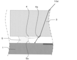
まず、図1~図3を参照しながら、実施の形態1に係る撮像モジュールの主要構成について説明する。図1は、実施の形態1に係る撮像モジュールを示す平面図である。図2は、図1のA-A線による、実施の形態1に係る撮像モジュールを示す断面図である。図3は、図2のB部詳細を説明する拡大図である。
(Embodiment 1)
[1-1. Configuration of Imaging Module]
First, the main configuration of the imaging module according to
図1~図3に示すように、実施の形態1に係る撮像モジュールは、固体撮像素子1と、固体撮像素子1の第1の主面に形成された受光部2と、受光部2に対向して配置される透光板3と、透光板3の受光部2に対向する面の外周部に、平面視で受光部2から所望の間隔aを離して形成された遮光膜4と、固体撮像素子1と透光板3の間を所望の間隔で支持し、平面視で遮光膜4と部分的に重なるように外周部に配置された接合樹脂層5、とを備えている。
As shown in FIGS. 1 to 3, the imaging module according to
ここで、遮光膜4は、透過率の低い有色樹脂で形成されており、受光部2側の遮光膜4の端部は、透光板3との接合界面と鋭角を成す曲面4aを有し、遮光膜4の厚みが端部から漸増するように形成されている。遮光膜4は、例えば、エポキシ樹脂を主成分とする黒色樹脂を熱硬化して形成される。
Here, the
接合樹脂層5の受光部2側の側端面は、受光部2と側端面間の水平距離が中央部でより離れるような湾曲面5aを有する。接合樹脂層5の透光板3側の界面は、湾曲面5a上方の受光部2側の界面5bは遮光膜4と接合しており、外周側の界面5cは透光板3と接合している。なお、接合樹脂層5の外周側の側端面も、外周部と側端面間の水平距離が中央部でより離れるような湾曲面5dを有する。
The side end surface of the
接合樹脂層5は、例えば、エポキシ樹脂を主成分とし、UV硬化の開始剤と熱硬化の開始剤を含む樹脂で形成される。
The
実施の形態1に係る撮像モジュールの、平面視で受光部2から遮光膜4の端部までの間隔aはより長い方が望ましく、例えば、約10~150μm程度とし、受光部2に至る所望の入射角を有する光路が遮断されないように、製造ばらつきを考慮して形成される。
In the imaging module according to
固体撮像素子1と透光板3の間隔bはより低い方が望ましく、例えば、約50~200μm程度とし、接合樹脂層5を形成する樹脂の粘度や濡れ性に応じて保持可能な形状を考慮して形成される。
The distance b between the solid-
遮光膜4の受光部2側の端部と接合樹脂層5の受光部2側の湾曲面5aの最湾曲部との間隔cはより長い方が望ましく、例えば、固体撮像素子1と透光板3の間隔b以上とし、湾曲面5aに至る斜光の光路を遮断するように、製造ばらつきを考慮して形成される。
It is desirable that the distance c between the end portion of the
透光板3の外周側端面と遮光膜4の外周側の端部との間隔dはより低い方が望ましく、例えば、約50~200μm程度とし、接合樹脂層5を形成する樹脂の粘度や濡れ性に応じて保持可能な形状を考慮して形成される。
It is desirable that the distance d between the outer peripheral edge of the
遮光膜4の厚みは遮光性を高めるためより厚い方が望ましく、例えば、最大厚み部が約5μm~固体撮像素子1と透光板3の間隔bの1/2程度で形成される。
The thickness of the
言い換えると、実施の形態1に係る撮像モジュールは、第1の主面に形成される受光部2を有する固体撮像素子1と、受光部2に対向して配置される透光板3と、透光板3の受光部に対向する面に形成され、且つ平面視で受光部2の外周部に配置される遮光膜4と、固体撮像素子1と透光板3との間に配置され、且つ平面視で受光部2の外周部に配置される接合樹脂層5と、を備えており、遮光膜4は、透過率の低い有色樹脂で構成されており、受光部2側の端部は、透光板3との接合界面と鋭角を成す曲面4aを有し、厚みが端部から漸増するように形成されており、接合樹脂層5は、受光部2側の側端面は、端部より中央部が受光部2から離れるような湾曲面5a、5dを有し、且つ、湾曲面5a、5dの透光板3側の端部は遮光膜4の固体撮像素子1側の主面と接するように遮光膜4と接する上記の界面が形成されるものである。
In other words, the imaging module according to
本開示によれば、透光板3の裏面に形成される遮光膜4により、固体撮像素子1の受光部2の外周に形成される接合樹脂層5の側端面に至る入射光を効果的に遮光することができるため、接合樹脂層5の側端面での反射光を低減できる。特に、接合樹脂層5の湾曲した側端面で反射した光の一部は、画素に対する入射角が大きく、隣接画素部に形成される異色のカラーフィルターを通過する光を生じるため、混色の要因となる。本開示によれば、接合樹脂層5の側端面での反射光を低減することで混色の要因となる画素に対する入射角が大きい迷光の発生を低減できるため、高画質のカラー画像を得ることができる。
According to the present disclosure, the light-
また、本開示によれば、遮光膜4を樹脂で形成し、遮光膜4の厚みを端部から漸増するような構造とすることで、遮光膜4端部での反射光が受光部2に至ることを防ぐことができる。このため、受光部2に至る迷光を生じにくい遮光構造を得ることができる。
Further, according to the present disclosure, the
また、遮光膜4を樹脂で形成するため、高画質で且つ遮光膜4界面での剥離を生じにくい高信頼の撮像モジュールを得ることができる。すなわち、遮光性の高い厚膜構造を容易に得ることができる。また、樹脂の粘弾性挙動により応力緩和構造を容易に得ることができる。また、遮光膜4と接合樹脂層5の熱膨張差を小さくすることができ耐熱性に優れた構造を容易に得ることができる。
In addition, since the
なお、実施の形態1に係る撮像モジュールは、接合樹脂層5は、熱硬化の開始剤を含む樹脂で構成されることがより好ましい。
In the imaging module according to the first embodiment, the
なお、実施の形態1に係る撮像モジュールは、接合樹脂層5は、さらにUV硬化の開始剤を含む樹脂で構成されることがより好ましい。
In the imaging module according to the first embodiment, it is more preferable that the
[1-2.効果]
次に、実施の形態1に係る撮像モジュールにより得られる効果の詳細について図4~図7を用いて説明する。
[1-2. effect]
Next, details of effects obtained by the imaging module according to the first embodiment will be described with reference to FIGS. 4 to 7. FIG.
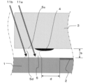
図4は、接合樹脂層5は、さらに透光板3と接する界面が形成されてもの説明する図であり、接合樹脂層5の湾曲面5aでの反射光を遮光する効果もあわせて説明する。
FIG. 4 is a diagram for explaining that the
本図において、遮光膜4で遮られる入射光の一例として、光路10a、10bを矢印で示している。なお、説明のため、本図では遮光膜4を枠線でのみ示し、遮光膜4が無い場合に、接合樹脂層5の湾曲面5aで反射して受光部2に至る光路10a、10bを破線で示している。
In this figure,
図4で示すように、遮光膜4が無い場合、接合樹脂層5の湾曲面5aに至る入射光は、湾曲面5aにおいて様々な方向に反射される。このような反射光の一部は光路10a、10bの破線矢印で示すように受光部2に至り、光電変換されて不要な電荷量の変動を生じ、フレアの発生といった画質悪化の要因となる。
As shown in FIG. 4, in the absence of the
図5は受光部2の画素構造の一例を示す模式図であり、図4のC部詳細を説明する図である。なお、説明のため、遮光膜4が無い場合に湾曲面5aで反射して受光部2に至る入射光の一例として、光路10cを破線矢印で示している。また、簡略化のため、光電変換部9の詳細構造は非図示とする。
FIG. 5 is a schematic diagram showing an example of the pixel structure of the light-receiving
図5より、受光部2は、光電変換領域の大きい画素6aと光電変換領域の小さい画素6bが相互に隣接して配置され、各画素上にそれぞれカラーフィルター7a、7b、マイクロレンズ8a、8bが形成されている。ここで、大きい画素6aは、平面視で格子状に配列されており、大きい画素6bの対角線間に小さい画素6bが配列されている。また、大きい画素6a上のカラーフィルター7aと小さい画素6b上のカラーフィルター7bは互いに異なる波長の光を透過する。
As shown in FIG. 5, in the
破線矢印で示す湾曲面5aで反射される光の一部は、光路10cの破線矢印で示すように受光部2に配置された画素に対する入射角が大きい。このため、大きい画素6a上に配置されたカラーフィルター7aを通過した光が、小さい画素6bで光電変換される場合が生じる。すなわち、隣接画素のカラーフィルター7aを通過する光路は、小さい画素6bに対し、所望の波長と異なる波長の光量に応じた不要な電荷量の変動を生じるため、混色フレアの発生といった画質悪化の要因となる。
Part of the light reflected by the
実施の形態1に係る撮像モジュールは、湾曲面5a上方の受光部2側の界面5bは遮光膜4と接合しているため、湾曲面5aに至る光路10a、10bの破線矢印で示す光路を遮断することができる。特に、画素に対する入射角が大きい光路10cを遮断するのに効果的である。このため、不要な電荷量の変動や混色を低減し、高画質のカラー画像を得ることができる。また、遮光膜4は湾曲面5aの一端と接するように形成するため平面視で受光部2と重なるような領域から透光板3を通過して湾曲面5aに至るような斜入射光も遮断することができるので、不要な光を効果的に遮光できる。
In the imaging module according to the first embodiment, since the
つまり、図5で説明した撮像モジュールでは、受光部2は、光電変換領域の大きい画素と光電変換領域の小さい画素が相互に隣接して配置されており、上記の大きい画素と上記の小さい画素は、それぞれ異なる波長の光を透過するカラーフィルター7a、7bを透光板3側に備えるものである。
That is, in the imaging module described with reference to FIG. 5, the light-receiving
図6は、遮光膜4、曲面4aを有する構成とする効果を説明する図である。本図において、受光部2側の端部を通過する入射光の一例として、光路10dを矢印で示している。なお、説明のため、本図では遮光膜4を枠線でのみ示す。
FIG. 6 is a diagram for explaining the effect of the structure having the
図6に示すように、遮光膜4の受光部2側の端部は、透光板3との接合界面と鋭角を成す曲面4aを有し、遮光膜4の厚みが端部から漸増するように形成されている。このため、遮光膜端部を通過する入射光の光路10dは、遮光膜4の端面で受光部2から遠ざかる方向へ反射される。すなわち、受光部に至る迷光を生じにくい遮光構造を得ることができる。このため、遮光膜4は樹脂で形成することが望ましい。
As shown in FIG. 6, the end of the
なお、遮光膜4を樹脂で形成することにより、遮光性の高い厚膜を容易に形成すことができる。また、樹脂の表面置換基との結合により界面での接合強度を確保できる。粘弾性挙動を示す樹脂で形成することで膜応力を緩和することができる。遮光膜4と接合樹脂層5の熱膨張差を小さい構成とすることで耐熱性に優れた構成とすることができる。すなわち、樹脂で遮光膜を形成することにより高画質で信頼性の高い撮像モジュールを得ることができる。
By forming the light-shielding
図7は、接合樹脂層5に対する遮光膜4の配置の効果を説明する図である。本図において、接合樹脂層5を仮硬化するためのUV照射光11a、11bを二重線矢印で模式的に示している。
7A and 7B are diagrams for explaining the effect of the arrangement of the
図7に示すように、接合樹脂層5は透光板3と接合する界面5cを通過するUV照射光11a、および外周側の湾曲面5dを通過するUV照射光11bにより仮硬化される。接合樹脂層5の透光板3側の界面に、遮光膜4と接合しない界面5cを備えるように構成することで、接合樹脂層5に対するUV照射光の照射領域をより広く確保して照射性をよくすることができる。ここで、UV照射光は、平面視で遮光膜4と重なる接合樹脂層5の部分で、反射光および硬化の伝播により硬化が促進する。接着樹脂層5に対する照射性をより良くするため、透光板3の外周側から斜めにUV光を照射するようなプロセスを含むことが望ましい。
As shown in FIG. 7, the
なお、接合樹脂層5は、UV照射による仮硬化の後、熱硬化により本硬化するため、UV硬化の開始剤と熱硬化の開始剤を含むデュアル硬化型の樹脂で構成することが望ましい。こうすることにより、先ず、透光板3を搭載する際にUV照射して仮硬化することで、接合樹脂層5の形状保持を容易にできる。すなわち、接合樹脂層5の高さを一定に保持して、固体撮像素子1に対する透光板3の間隔bを高精度に制御できる。また、接合樹脂層5の界面の濡れ広がりを抑制して受光部2に対する接合樹脂層5の端部との間隔dを確保し、湾曲面5a、5dの領域をより狭い範囲で制御できる。次に、熱硬化により本硬化することで、信頼性を高めることができる。すなわち、樹脂の界面での結合を促進して密着強度を確保し、樹脂の強度を高め、未硬化成分起因のアウトガスの発生を抑制する。
Since the
つまり、図7で説明した撮像モジュールでは、接合樹脂層5は、透光板3を透過するUV照射光で仮硬化して形成される。
That is, in the imaging module described with reference to FIG. 7 , the
(実施の形態1の変形例)
次に、図8を参照しながら、実施の形態1に係る撮像モジュールの一変形例について説明する。
(Modification of Embodiment 1)
Next, a modified example of the imaging module according to
図8に示すように、本変形例に係る撮像モジュールは、透光板3の受光部2に対向する面と反対側の面上に、平面視で受光部2から所望の間隔を離した外周部に形成された遮光フィルム12(遮光構造の一例)をさらに備える。
As shown in FIG. 8, in the imaging module according to this modification, on the surface of the
本図において、遮光フィルム12で遮られる入射光の一例として、光路10eを矢印で示している。なお、説明のため、遮光フィルム12が無い場合に、透光板3の平面視で受光部2より外周側の領域を通過し、接合樹脂層5の外周側の湾曲面5dで反射して受光部2に至る光路10eを破線で示している。
In this figure, an arrow indicates an
図8で示すように、遮光フィルム12が無い場合、接合樹脂層5の外周側の湾曲面5dに至る入射光は、湾曲面5dにおいて様々な方向に反射される。このような反射光の一部は光路10eの破線矢印で示すように受光部2に至り、光電変換されて不要な電荷量の変動を生じる。また、このような反射光の一部は、受光部2に配置された画素に対する入射角が大きく、混色の要因にもなる。
As shown in FIG. 8, without the
遮光フィルム12は、遮光膜4で遮光できない外周側の湾曲面5dに至る光路10eの破線矢印で示す光路を遮断するのに効果的である。このため、不要な電荷量の変動や混色を低減し、より高画質のカラー画像を得ることができる。特に、UV照射による硬化性をよくするため、透過率の高い樹脂で接合樹脂層5を形成した場合は、遮光フィルム12を搭載することでさらに高画質の撮像モジュールを実現できる。また、透光板3を搭載後に遮光フィルム12を搭載すればよく、接合樹脂層5のUV照射による仮硬化プロセスを阻害せずに遮光構造を実現できる。
The light-shielding
つまり、図8で説明した撮像モジュールは、透光板3の受光部2に対向する面と反対側の面上に、平面視で受光部2の外周部に配置される遮光構造をさらに備えるものである。
In other words, the imaging module described with reference to FIG. 8 further includes a light shielding structure arranged on the outer peripheral portion of the
(実施の形態2)
本開示の実施の形態2に係る撮像モジュールについて、図面を用いて、上述した実施の形態との相違点を中心に説明する。
(Embodiment 2)
An imaging module according to
図9は、実施の形態2に係る撮像モジュールであり、接合樹脂層5の上面全体を覆うように遮光膜4が形成されている。
FIG. 9 shows an imaging module according to
本図において、遮光膜4で遮られる入射光の一例として、光路10fを矢印で示している。なお、説明のため、遮光膜4が無い場合に、接合樹脂層5の外周側の湾曲面5dで反射して受光部2に至る光路10fを破線で示している。
In this figure, an arrow indicates an optical path 10f as an example of incident light blocked by the
本実施の形態の遮光膜4は、接合樹脂層5の上面全体を覆うため、実施の形態1と同様の湾曲面5aに至る光路を遮断すると共に、外周側の湾曲面5dに至る光路も遮断することができる。このため、不要な電荷量の変動や混色を低減し、より高画質のカラー画像を得ることができる。特に、遮光膜4は湾曲面5dの一端と接するように形成するため平面視で受光部2と重なるような領域から透光板3を通過して湾曲面5dに至るような斜入射光も遮断することができるので、不要な光をより効果的に遮光できる。
Since the light-shielding
なお、UV照射による仮硬化で形状保持可能な程度のUV照射性を確保するため、本実施の形態の接合樹脂層5と遮光膜4との界面の幅eはより狭い方が望ましく、例えば、固体撮像素子1と透光板3の間隔bの1/2~3倍程度の幅で形成される。また、UV照射光11cは外周側の湾曲面5dを通過するよう、斜めにUV光を照射するようなプロセスを含むことが望ましい。
In addition, in order to secure the UV irradiation property to the extent that the shape can be maintained by temporary curing by UV irradiation, it is desirable that the width e of the interface between the
つまり、図9で説明した撮像モジュールでは、接合樹脂層5は、さらに外周側の側端面として、端部より中央部が上記の外周部から離れるような湾曲面5dを有し、且つ、湾曲面5dの透光板3側の端部が遮光膜4の固体撮像素子1側の主面と接するように遮光膜4と接する界面が形成される。
That is, in the imaging module described in FIG. 9, the
(実施の形態3)
本開示の実施の形態3に係る撮像モジュールについて、図面を用いて、上述した実施の形態との相違点を中心に説明する。
(Embodiment 3)
An imaging module according to
図10は、実施の形態3に係る撮像モジュールであり、接合樹脂層5の透光板3側の界面は、湾曲面5a上方の受光部2側の界面は遮光膜4bと接合しており、湾曲面5d上方の外周側の界面は遮光膜4cと接合しており、遮光膜4bと遮光膜4c間の界面5eは透光板3と接合している。
FIG. 10 shows an imaging module according to
本実施の形態の遮光膜4b、4cは、それぞれ接合樹脂層5の湾曲面5a、5dに至る光路10a、10fを遮断することができる。このため、不要な電荷量の変動や混色を低減し、より高画質のカラー画像を得ることができる。ここで、UV照射光11dを遮光膜4bと遮光膜4c間の界面5eを通過するように照射することで、UV照射性を確保することができる。また、遮光膜4b、4cは同一プロセスで形成できるため、生産効率を維持しつつ、より高画質の撮像モジュールを実現できる。
The
本実施の形態の接合樹脂層5と遮光膜4との界面の幅eはより広い方が望ましい。このため、固体撮像素子1の受光部2の外周領域に広い回路領域を備えるような撮像モジュールに適している。
It is desirable that the width e of the interface between the
(実施の形態4)
本開示の実施の形態4に係る撮像モジュールについて、図面を用いて、上述した実施の形態との相違点を中心に説明する。
(Embodiment 4)
An imaging module according to
図11は、実施の形態4に係る撮像モジュールであり、接合樹脂層5の上面全体を覆うように遮光膜4が形成されている。
FIG. 11 shows an imaging module according to
本実施の形態の遮光膜4は、接合樹脂層5の湾曲面5a、5dに至る各々の光路10a、10fを遮断することができる。このため、不要な電荷量の変動や混色を低減し、より高画質のカラー画像を得ることができる。
The
なお、本実施の形態に係る撮像モジュールは、固体撮像素子1と透光板3の相対姿勢を保持した状態で、接合樹脂層5を仮硬化するようなプロセスで形成することが望ましい。例えば、接合樹脂層5を即効性の熱硬化の開始剤を含む樹脂で構成し、固体撮像素子1と透光板3を固定した状態で加熱することにより、仮硬化するプロセスとするとよい。また、例えば、接合樹脂層5を遅延硬化タイプのUV硬化の開始剤を含む樹脂で構成し、UV照射後に固体撮像素子1と透光板3との相対姿勢を保った状態で固定することにより、仮硬化するプロセスとするとよい。このようなプロセスとすることにより、接合樹脂層5の仮硬化プロセスを阻害することなく遮光膜4を形成することができるので、接合樹脂層5の外周側の湾曲面5dの位置および接合樹脂層5と遮光膜4の界面の幅eに拠ることなく、遮光膜4を配置できる。このため、受光部2側から透光板3の外周近傍までより広範囲に遮光することができ、より広角な入射光に対しても遮光効果の高い撮像モジュールを実現できる。
It is desirable that the imaging module according to the present embodiment is formed by a process in which the
つまり、図11で説明した撮像モジュールでは、接合樹脂層5は、固体撮像素子1と透光板3の相対姿勢を保持した状態で仮硬化して形成される。
That is, in the imaging module described with reference to FIG. 11, the
(実施の形態4の変形例)
次に、図12を参照しながら、実施の形態4に係る撮像モジュールの変形例について説明する。
(Modification of Embodiment 4)
Next, a modification of the imaging module according to
図12に示すように、本変形例に係る撮像モジュールは、少なくとも接合樹脂層5の湾曲面5a上方の受光部2側の界面と接合する遮光膜4を備える。また、接合樹脂層5は透過率の低い有色樹脂であり、例えば、熱硬化の開始剤を含む黒色樹脂で構成することが望ましい。
As shown in FIG. 12, the imaging module according to this modification includes at least the
本変形例に係る撮像モジュールは、遮光膜4により接合樹脂層5の受光部側の湾曲面5aに至る光路10aを遮断することができ、接合樹脂層5の内部を進行する光路10fは、有色樹脂を用いることで遮断することができる。
In the imaging module according to this modification, the
このため、不要な電荷量の変動や混色を低減し、より高画質のカラー画像を得ることができる。 Therefore, it is possible to reduce unnecessary charge amount fluctuations and color mixture, and obtain a color image of higher quality.
なお、本実施の形態に係る撮像モジュールは、固体撮像素子1と透光板3の相対姿勢を保持した状態で、接合樹脂層5を仮硬化するようなプロセスで形成することが望ましい。例えば、接合樹脂層5を即効性の熱硬化の開始剤を含む樹脂で構成し、固体撮像素子1と透光板3を固定した状態で加熱することにより、仮硬化するプロセスとするとよい。また、例えば、接合樹脂層5を遅延硬化タイプのUV硬化の開始剤を含む樹脂で構成し、UV照射後に固体撮像素子1と透光板3との相対姿勢を保った状態で固定することにより、仮硬化するプロセスとするとよい。このようなプロセスとすることにより、接合樹脂層5の仮硬化プロセスを阻害することなく遮光膜4を形成することができるので、接合樹脂層5の外周側の湾曲面5dの位置および接合樹脂層5と遮光膜4の界面の幅eに拠ることなく、遮光膜4を配置できる。このため、受光部2側から透光板3の外周近傍までより広範囲に遮光することができ、より広角な入射光に対しても遮光効果の高い撮像モジュールを実現できる。
It is desirable that the imaging module according to the present embodiment is formed by a process in which the
つまり、図12で説明した撮像モジュールでは、接合樹脂層5は、透過率の低い有色樹脂で構成されている。
That is, in the imaging module described with reference to FIG. 12, the
本開示は、例えば医療用の内視鏡に搭載される撮像モジュール等として有用である。また、微小空間での各種制御に用いられる機器等に搭載される撮像モジュールとして有用である。 INDUSTRIAL APPLICABILITY The present disclosure is useful, for example, as an imaging module or the like mounted on a medical endoscope. In addition, it is useful as an imaging module mounted on equipment used for various controls in a minute space.
1 固体撮像素子
2 受光部
3 透光板
4、4b、4c 遮光膜
4a 曲面
5 接合樹脂層
5a、5d 湾曲面
5b、5c、5e 界面
6a、6b 画素
7a、7b カラーフィルター
8a、8b マイクロレンズ
9 光電変換部
10a、10b、10c、10d、10e、10f 光路
11a、11b、11c、11d UV照射光
12 遮光フィルム
REFERENCE SIGNS
Claims (9)
前記受光部に対向して配置される透光板と、
前記透光板の前記受光部に対向する面に形成され、且つ平面視で前記受光部の外周部に配置される遮光膜と、
前記固体撮像素子と前記透光板との間に配置され、且つ平面視で前記受光部の外周部に配置される接合樹脂層と、を備え、
前記遮光膜は、有色樹脂で構成されており、前記受光部側の端部は、前記透光板との接合界面と鋭角を成す曲面を有し、厚みが端部から漸増するように形成され、
前記接合樹脂層は、前記受光部側の側端面は、端部より中央部が前記受光部から離れるような湾曲面を有し、且つ、前記湾曲面の前記透光板側の端部は前記遮光膜の前記固体撮像素子側の主面と接するように前記遮光膜と接する界面が形成され、
前記接合樹脂層は、さらに前記透光板と接する界面が形成される
撮像モジュール。 a solid-state imaging device having a light receiving portion formed on the first main surface;
a light-transmitting plate arranged to face the light-receiving part;
a light-shielding film formed on a surface of the light-transmitting plate facing the light-receiving portion and disposed on an outer peripheral portion of the light-receiving portion in a plan view;
a bonding resin layer disposed between the solid-state imaging element and the light-transmitting plate and disposed on the outer periphery of the light receiving section in plan view,
The light-shielding film is made of a colored resin, and the light-receiving portion side end portion has a curved surface forming an acute angle with the bonding interface with the light-transmitting plate, and is formed so that the thickness gradually increases from the end portion. is,
The bonding resin layer has a curved surface on a side end surface on the light receiving unit side such that a central portion is away from the light receiving unit from an end portion, and an end portion on the light transmitting plate side of the curved surface is the forming an interface in contact with the light shielding film so as to be in contact with the main surface of the light shielding film on the solid-state imaging device side ;
The bonding resin layer further forms an interface in contact with the light-transmitting plate.
imaging module.
前記大きい画素と前記小さい画素は、それぞれ異なる波長の光を透過するカラーフィルターを前記透光板側に備える
請求項1に記載の撮像モジュール。 the light-receiving unit has a pixel with a large photoelectric conversion area and a pixel with a small photoelectric conversion area arranged adjacent to each other;
2. The image pickup module according to claim 1, wherein the large pixels and the small pixels each include color filters that transmit light of different wavelengths on the transparent plate side.
請求項1または2に記載の撮像モジュール。 3. The imaging module according to claim 1, wherein the bonding resin layer is made of a resin containing a thermosetting initiator.
請求項1~3のいずれか一項に記載の撮像モジュール。 The imaging module according to any one of claims 1 to 3, wherein the bonding resin layer is made of a resin further containing a UV curing initiator.
請求項1~4のいずれか一項に記載の撮像モジュール。 The bonding resin layer further has, as a side end surface on the outer peripheral side, a curved surface in which a central portion is recessed from an end portion, and an end portion of the curved surface on the light-transmitting plate side is the solid-state imaging device of the light shielding film. The image pickup module according to any one of claims 1 to 4 , wherein an interface contacting the light shielding film is formed so as to contact the main surface on the element side.
請求項1~5のいずれか一項に記載の撮像モジュール。 6. The light-shielding structure according to any one of claims 1 to 5 , further comprising a light-shielding structure disposed on the surface opposite to the surface facing the light-receiving portion of the light-transmitting plate, in plan view, on the outer periphery of the light-receiving portion. imaging module.
請求項3に記載の撮像モジュール。 The imaging module according to claim 3, wherein the bonding resin layer is formed by pre-curing with UV irradiation light that passes through the transparent plate.
請求項1~7のいずれか一項に記載の撮像モジュール。 The imaging module according to any one of claims 1 to 7 , wherein the bonding resin layer is formed by temporary curing in a state in which the solid-state imaging device and the light-transmitting plate are held in relative posture.
請求項8に記載の撮像モジュール。 The imaging module according to claim 8 , wherein the bonding resin layer is made of colored resin.
Priority Applications (1)
| Application Number | Priority Date | Filing Date | Title |
|---|---|---|---|
| JP2018201715A JP7294792B2 (en) | 2018-10-26 | 2018-10-26 | Imaging module |
Applications Claiming Priority (1)
| Application Number | Priority Date | Filing Date | Title |
|---|---|---|---|
| JP2018201715A JP7294792B2 (en) | 2018-10-26 | 2018-10-26 | Imaging module |
Publications (2)
| Publication Number | Publication Date |
|---|---|
| JP2020068349A JP2020068349A (en) | 2020-04-30 |
| JP7294792B2 true JP7294792B2 (en) | 2023-06-20 |
Family
ID=70390586
Family Applications (1)
| Application Number | Title | Priority Date | Filing Date |
|---|---|---|---|
| JP2018201715A Active JP7294792B2 (en) | 2018-10-26 | 2018-10-26 | Imaging module |
Country Status (1)
| Country | Link |
|---|---|
| JP (1) | JP7294792B2 (en) |
Citations (12)
| Publication number | Priority date | Publication date | Assignee | Title |
|---|---|---|---|---|
| JP2002305261A (en) | 2001-01-10 | 2002-10-18 | Canon Inc | Electronic component and method of manufacturing the same |
| JP2004363511A (en) | 2003-06-09 | 2004-12-24 | Matsushita Electric Ind Co Ltd | Semiconductor device and manufacturing method thereof |
| JP2005116628A (en) | 2003-10-03 | 2005-04-28 | Matsushita Electric Ind Co Ltd | Solid-state imaging device and manufacturing method thereof |
| JP2006135741A (en) | 2004-11-08 | 2006-05-25 | Seiko Precision Inc | Solid-state imaging device and electronic apparatus provided with the same |
| JP2008219854A (en) | 2007-02-05 | 2008-09-18 | Matsushita Electric Ind Co Ltd | OPTICAL DEVICE, OPTICAL DEVICE WAFER, MANUFACTURING METHOD THEREOF, AND CAMERA MODULE AND ENDOSCOPE MODULE MOUNTING OPTICAL DEVICE |
| JP2010129548A (en) | 2008-11-25 | 2010-06-10 | Sony Corp | Solid-state image pickup device and electronic equipment |
| JP2010232582A (en) | 2009-03-30 | 2010-10-14 | Panasonic Corp | Image pickup device package and image pickup apparatus |
| JP2012222546A (en) | 2011-04-07 | 2012-11-12 | Sony Corp | Solid-state imaging device, method for manufacturing the same, and electronic apparatus |
| JP2016100738A (en) | 2014-11-21 | 2016-05-30 | 日本電気硝子株式会社 | Cover member and solid-state imaging device |
| WO2017138370A1 (en) | 2016-02-09 | 2017-08-17 | ソニー株式会社 | Solid-state imaging element, method for manufacturing same, and electronic device |
| JP2017163010A (en) | 2016-03-10 | 2017-09-14 | ソニー株式会社 | Imaging device and electronic apparatus |
| JP2018125393A (en) | 2017-01-31 | 2018-08-09 | ソニーセミコンダクタソリューションズ株式会社 | Electronic components, camera modules |
Family Cites Families (2)
| Publication number | Priority date | Publication date | Assignee | Title |
|---|---|---|---|---|
| JPH0685221A (en) * | 1992-08-31 | 1994-03-25 | Sony Corp | Solid-state imaging device |
| JP2697571B2 (en) * | 1993-08-18 | 1998-01-14 | 日本電気株式会社 | Solid-state imaging device |
-
2018
- 2018-10-26 JP JP2018201715A patent/JP7294792B2/en active Active
Patent Citations (12)
| Publication number | Priority date | Publication date | Assignee | Title |
|---|---|---|---|---|
| JP2002305261A (en) | 2001-01-10 | 2002-10-18 | Canon Inc | Electronic component and method of manufacturing the same |
| JP2004363511A (en) | 2003-06-09 | 2004-12-24 | Matsushita Electric Ind Co Ltd | Semiconductor device and manufacturing method thereof |
| JP2005116628A (en) | 2003-10-03 | 2005-04-28 | Matsushita Electric Ind Co Ltd | Solid-state imaging device and manufacturing method thereof |
| JP2006135741A (en) | 2004-11-08 | 2006-05-25 | Seiko Precision Inc | Solid-state imaging device and electronic apparatus provided with the same |
| JP2008219854A (en) | 2007-02-05 | 2008-09-18 | Matsushita Electric Ind Co Ltd | OPTICAL DEVICE, OPTICAL DEVICE WAFER, MANUFACTURING METHOD THEREOF, AND CAMERA MODULE AND ENDOSCOPE MODULE MOUNTING OPTICAL DEVICE |
| JP2010129548A (en) | 2008-11-25 | 2010-06-10 | Sony Corp | Solid-state image pickup device and electronic equipment |
| JP2010232582A (en) | 2009-03-30 | 2010-10-14 | Panasonic Corp | Image pickup device package and image pickup apparatus |
| JP2012222546A (en) | 2011-04-07 | 2012-11-12 | Sony Corp | Solid-state imaging device, method for manufacturing the same, and electronic apparatus |
| JP2016100738A (en) | 2014-11-21 | 2016-05-30 | 日本電気硝子株式会社 | Cover member and solid-state imaging device |
| WO2017138370A1 (en) | 2016-02-09 | 2017-08-17 | ソニー株式会社 | Solid-state imaging element, method for manufacturing same, and electronic device |
| JP2017163010A (en) | 2016-03-10 | 2017-09-14 | ソニー株式会社 | Imaging device and electronic apparatus |
| JP2018125393A (en) | 2017-01-31 | 2018-08-09 | ソニーセミコンダクタソリューションズ株式会社 | Electronic components, camera modules |
Also Published As
| Publication number | Publication date |
|---|---|
| JP2020068349A (en) | 2020-04-30 |
Similar Documents
| Publication | Publication Date | Title |
|---|---|---|
| US8279336B2 (en) | Solid-state image pickup device | |
| CN100466269C (en) | image capture device | |
| CN100354883C (en) | Image pickup device and production method thereof | |
| CN102646690B (en) | solid state imaging device | |
| JP5818455B2 (en) | Solid-state imaging device and manufacturing method thereof | |
| KR101597892B1 (en) | Solid-state imaging device and manufacturing method thereof | |
| KR101930083B1 (en) | Imaging device and camera module | |
| JP2011138089A (en) | Wafer-level lens array, lens module and imaging unit | |
| JP2005317745A (en) | Solid-state imaging device and manufacturing method thereof | |
| CN109273474A (en) | Photosensitive chip package structure and packaging method thereof | |
| JP2015170638A (en) | Imaging element package and imaging device | |
| JP2011187482A (en) | Solid-state imaging apparatus, module for optical device, and method of manufacturing solid-state imaging apparatus | |
| JP2014053512A (en) | Solid state image pickup device and manufacturing method of the same | |
| US20100321563A1 (en) | Solid-state imaging unit | |
| JP2009251249A (en) | Wafer-like optical device and manufacturing method thereof, electronic element wafer module, sensor wafer module, electronic element module, sensor module, and electronic information apparatus | |
| JP7294792B2 (en) | Imaging module | |
| JP2006080597A (en) | Imaging module and imaging module manufacturing method | |
| JP2016072266A (en) | Image pickup device package and image pickup apparatus | |
| TW201409672A (en) | Semiconductor device | |
| KR101349510B1 (en) | Lens unit, method of fabricating the same and camera module having the same | |
| CN208127211U (en) | A kind of encapsulating structure of image sensing chip | |
| JP2006078517A (en) | Imaging module and imaging module manufacturing method | |
| KR101980657B1 (en) | The manufacturing method of lens assembly | |
| JP2013080825A (en) | Imaging device manufacturing method | |
| JP6281214B2 (en) | Image pickup device package and image pickup apparatus |
Legal Events
| Date | Code | Title | Description |
|---|---|---|---|
| A711 | Notification of change in applicant |
Free format text: JAPANESE INTERMEDIATE CODE: A711 Effective date: 20200217 |
|
| A711 | Notification of change in applicant |
Free format text: JAPANESE INTERMEDIATE CODE: A711 Effective date: 20200520 |
|
| A621 | Written request for application examination |
Free format text: JAPANESE INTERMEDIATE CODE: A621 Effective date: 20211025 |
|
| A977 | Report on retrieval |
Free format text: JAPANESE INTERMEDIATE CODE: A971007 Effective date: 20221116 |
|
| A131 | Notification of reasons for refusal |
Free format text: JAPANESE INTERMEDIATE CODE: A131 Effective date: 20221122 |
|
| A521 | Request for written amendment filed |
Free format text: JAPANESE INTERMEDIATE CODE: A523 Effective date: 20230118 |
|
| TRDD | Decision of grant or rejection written | ||
| A01 | Written decision to grant a patent or to grant a registration (utility model) |
Free format text: JAPANESE INTERMEDIATE CODE: A01 Effective date: 20230523 |
|
| A61 | First payment of annual fees (during grant procedure) |
Free format text: JAPANESE INTERMEDIATE CODE: A61 Effective date: 20230608 |
|
| R150 | Certificate of patent or registration of utility model |
Ref document number: 7294792 Country of ref document: JP Free format text: JAPANESE INTERMEDIATE CODE: R150 |