JP7289633B2 - Imprint apparatus and article manufacturing method - Google Patents
Imprint apparatus and article manufacturing method Download PDFInfo
- Publication number
- JP7289633B2 JP7289633B2 JP2018210917A JP2018210917A JP7289633B2 JP 7289633 B2 JP7289633 B2 JP 7289633B2 JP 2018210917 A JP2018210917 A JP 2018210917A JP 2018210917 A JP2018210917 A JP 2018210917A JP 7289633 B2 JP7289633 B2 JP 7289633B2
- Authority
- JP
- Japan
- Prior art keywords
- light
- substrate
- modulated
- light source
- mold
- Prior art date
- Legal status (The legal status is an assumption and is not a legal conclusion. Google has not performed a legal analysis and makes no representation as to the accuracy of the status listed.)
- Active
Links
Images


Description
本発明は、インプリント装置および物品製造方法に関する。 The present invention relates to an imprint apparatus and an article manufacturing method.
半導体デバイスやMEMSなどの物品を製造する方法として、基板の上のインプリント材と型を接触させ、型を接触させた状態でインプリント材を硬化させることによって、インプリント材を成形するインプリント方法が知られている。 As a method for manufacturing articles such as semiconductor devices and MEMS, the imprint material is molded by bringing the imprint material on the substrate into contact with the mold and curing the imprint material while the mold is in contact. method is known.
特許文献1には、基板のパターン形成領域にレジストを滴下し、そのレジストにテンプレートを押し当て、パターン形成領域とその外側の領域との境界を含む光照射領域に光を照射し、その後にパターン形成領域に光を照射するインプリント装置が記載されている。該光照射領域への光の照射によって、該光照射領域上のレジストが硬化し、該パターン形成領域へのレジストの進入が防止される。特許文献2には、基板のパターン領域を加熱によって変形させる加熱機構と、型のパターン領域を変形させる形状補正機構とを備えるインプリント装置が記載されている。また、加熱の分布を形成する手段としてデジタルミラーデバイスを用いることが記載されている。
In
インプリント装置において、型を保持して駆動する機構の上方には種々のデバイスが配置されうる。例えば、基板の上のインプリント材を硬化させるための硬化部、基板に光を照射して加熱することで基板を変形させる変形部、基板と型との相対的な位置を検出するための検出系等のデバイスが配置されうる。これらのデバイスが配置される領域は限りがあり、種々のデバイスを配置するのは非常に困難であった。また、種々のデバイスを配置すると装置のサイズが大きくなる恐れがある。 In the imprint apparatus, various devices can be arranged above the mechanism that holds and drives the mold. For example, a curing section for curing the imprint material on the substrate, a deformation section for deforming the substrate by irradiating the substrate with light and heating it, and a detection for detecting the relative position between the substrate and the mold. Devices such as systems can be deployed. The area in which these devices are arranged is limited, and it has been very difficult to arrange various devices. Moreover, the arrangement of various devices may increase the size of the apparatus.
本発明は、インプリント装置の構造を単純化するために有利な技術を提供することを目的とする。 An object of the present invention is to provide an advantageous technique for simplifying the structure of an imprint apparatus.
本発明のインプリント装置は、基板の上に供給されたインプリント材と型とを接触させた状態で、前記インプリント材を硬化させるインプリント処理を実行するインプリント装置であって、入射光を変調する変調器と、第1光源からの第1光と、第2光源からの、前記第1光とは波長が異なる第2光とを前記変調器に導く第1光学系と、前記変調器によって変調された変調光を前記基板に導く第2光学系と、を備え、前記第1光を前記変調器で変調した第1変調光を前記基板に導くことによって、前記型と前記基板とのアライメントのために前記基板が変形され、前記第2光を前記変調器で変調した第2変調光を前記基板に導くことによって、前記基板の上に供給されたインプリント材の粘性を増加させ、 前記基板には、前記第1変調光と前記第2変調光とが異なるタイミングで照射され、前記第1変調光と前記第2変調光との切り替え時には、前記基板に前記第1の変調光および前記第2変調光のいずれもが照射されない期間が生じるように制御され、前記第1光源と前記第2光源とは、いずれか一方からの光が前記変調器に入射するように制御され、前記変調器が、当該変調器で変調された変調光を前記基板に到達しない状態となるように制御されている間に、前記第1光源の点灯状態と前記第2光源の点灯状態とが切り替わるように制御されることを特徴とする。 An imprinting apparatus of the present invention is an imprinting apparatus that performs an imprinting process of curing an imprinting material supplied onto a substrate in a state in which the imprinting material and the mold are in contact with each other. a first optical system for guiding a first light from a first light source and a second light having a wavelength different from that of the first light from a second light source to the modulator; a second optical system that guides modulated light modulated by the modulator to the substrate, and guides the first modulated light obtained by modulating the first light by the modulator to the substrate so that the mold and the substrate The substrate is deformed for alignment of the second light, and the second modulated light obtained by modulating the second light by the modulator is guided to the substrate, thereby increasing the viscosity of the imprint material supplied onto the substrate. and the substrate is irradiated with the first modulated light and the second modulated light at different timings, and when switching between the first modulated light and the second modulated light, the substrate is irradiated with the first modulated light. and the second modulated light is controlled so that there is a period during which neither the first light source nor the second light source is irradiated, and the light from one of the first light source and the second light source is controlled to enter the modulator, The lighting state of the first light source and the lighting state of the second light source are switched while the modulator is controlled so that the modulated light modulated by the modulator does not reach the substrate. It is characterized by being controlled as follows .
本発明によれば、インプリント装置の構造を単純化するために有利な技術を提供することができる。 ADVANTAGE OF THE INVENTION According to this invention, an advantageous technique can be provided in order to simplify the structure of an imprint apparatus.
以下、本発明の好ましい実施形態を添付の図面に基づいて詳細に説明する。なお、各図において、同一の部材については同一の参照番号を付し、重複する説明は省略する。 Preferred embodiments of the present invention will now be described in detail with reference to the accompanying drawings. In addition, in each figure, the same reference numerals are given to the same members, and redundant explanations are omitted.
(第1実施形態)
図1には、本発明の一実施形態のインプリント装置1の構成が示されている。インプリント装置1は、インプリント処理を実行し、これにより基板Sの上にインプリント材IMの硬化物からなるパターンを形成する。インプリント処理は、基板Sの上のインプリント材IMと型Mとを接触させる接触工程と、該接触工程の後に基板Sと型Mとのアライメントを行うアライメント工程と、該アライメント工程の後にインプリント材IMを硬化させる硬化工程とを含みうる。
(First embodiment)
FIG. 1 shows the configuration of an
インプリント材IMには、硬化用のエネルギーが与えられることによって硬化する硬化性組成物(未硬化状態の樹脂と呼ぶこともある)が用いられる。硬化用のエネルギーとしては、電磁波、熱などが用いられる。電磁波としては、例えば、その波長が10nm以上1mm以下の範囲から選択される、赤外線、可視光線、紫外線などの光を用いる。 A curable composition (also referred to as an uncured resin) that cures when energy for curing is applied is used for the imprint material IM. Electromagnetic waves, heat, and the like are used as energy for curing. As the electromagnetic wave, for example, light such as infrared rays, visible rays, and ultraviolet rays having a wavelength selected from a range of 10 nm or more and 1 mm or less is used.
硬化性組成物は、光の照射によって、或いは、加熱によって硬化する組成物である。光の照射によって硬化する光硬化性組成物は、重合性化合物と光重合開始剤とを少なくとも含有し、必要に応じて、非重合性化合物又は溶剤を含有してもよい。非重合性化合物は、増感剤、水素供与体、内添型離型剤、界面活性剤、酸化防止剤、ポリマー成分などの群から選択される少なくとも一種である。 A curable composition is a composition that is cured by irradiation with light or by heating. A photocurable composition that is cured by light irradiation contains at least a polymerizable compound and a photopolymerization initiator, and may contain a non-polymerizable compound or a solvent, if necessary. The non-polymerizable compound is at least one selected from the group consisting of sensitizers, hydrogen donors, internal release agents, surfactants, antioxidants, polymer components and the like.
インプリント材は、スピンコーターやスリットコーターによって基板上に膜状に付与されてもよい。また、インプリント材は、液体噴射ヘッドによって、液滴状、或いは、複数の液滴が繋がって形成された島状又は膜状で基板上に付与されてもよい。インプリント材の粘度(25℃における粘度)は、例えば、1mPa・s以上100mPa・s以下である。 The imprint material may be applied to the substrate in the form of a film by a spin coater or a slit coater. Alternatively, the imprint material may be applied onto the substrate in the form of droplets, or in the form of islands or films formed by connecting a plurality of droplets, by the liquid jet head. The viscosity of the imprint material (viscosity at 25° C.) is, for example, 1 mPa·s or more and 100 mPa·s or less.
基板の材料としては、例えば、ガラス、セラミックス、金属、半導体、樹脂等が用いられうる。必要に応じて、基板の表面に、基板とは別の材料からなる部材が設けられてもよい。基板は、例えば、シリコンウエハ、化合物半導体ウエハ、石英ガラスである。 As the material of the substrate, for example, glass, ceramics, metal, semiconductor, resin, or the like can be used. If necessary, a member made of a material different from that of the substrate may be provided on the surface of the substrate. The substrate is, for example, a silicon wafer, a compound semiconductor wafer, quartz glass.
本明細書および添付図面では、基板Sの表面に平行な方向をXY平面とするXYZ座標系において方向を示す。XYZ座標系におけるX軸、Y軸、Z軸にそれぞれ平行な方向をX方向、Y方向、Z方向とし、X軸周りの回転、Y軸周りの回転、Z軸周りの回転をそれぞれθX、θY、θZとする。X軸、Y軸、Z軸に関する制御または駆動は、それぞれX軸に平行な方向、Y軸に平行な方向、Z軸に平行な方向に関する制御または駆動を意味する。また、θX軸、θY軸、θZ軸に関する制御または駆動は、それぞれX軸に平行な軸の周りの回転、Y軸に平行な軸の周りの回転、Z軸に平行な軸の周りの回転に関する制御または駆動を意味する。また、位置は、X軸、Y軸、Z軸の座標に基づいて特定されうる情報であり、姿勢は、θX軸、θY軸、θZ軸の値で特定されうる情報である。基板またはその領域と型Mまたはその領域とのアライメントは、基板Sおよび型Mの少なくとも一方の位置および/または姿勢の制御を含みうる。また、アライメントは、基板Sおよび型Mの少なくとも一方の形状を補正あるいは変更するための制御を含みうる。 In this specification and the accompanying drawings, directions are shown in an XYZ coordinate system in which a direction parallel to the surface of the substrate S is the XY plane. The directions parallel to the X, Y, and Z axes in the XYZ coordinate system are defined as the X, Y, and Z directions, respectively, and rotation about the X axis, Y axis, and Z axis are θX and θY, respectively. , θZ. Controlling or driving with respect to the X-axis, Y-axis, and Z-axis means controlling or driving with respect to directions parallel to the X-axis, directions parallel to the Y-axis, and directions parallel to the Z-axis, respectively. In addition, the control or driving of the θX-axis, θY-axis, and θZ-axis relates to rotation about an axis parallel to the X-axis, rotation about an axis parallel to the Y-axis, and rotation about an axis parallel to the Z-axis, respectively. means to control or drive. The position is information that can be specified based on the coordinates of the X, Y, and Z axes, and the orientation is information that can be specified by the values of the θX, θY, and θZ axes. Aligning the substrate or regions thereof with the mold M or regions thereof may include controlling the position and/or orientation of at least one of the substrate S and the mold M. Alignment may also include controls to correct or change the shape of at least one of substrate S and mold M. FIG.
インプリント装置1は、基板Sを保持し駆動する基板駆動機構SD、および、基板駆動機構SDを支持するベースフレームBF、型Mを保持し駆動する型駆動機構MDを備えうる。基板駆動機構SDおよび型駆動機構MDは、基板Sと型Mとの相対位置が調整されるように基板駆動機構SDおよび型駆動機構MDの少なくとも一方を駆動する駆動機構DRVを構成する。駆動機構DRVによる相対位置の調整は、基板Sの上のインプリント材IMに対する型Mの接触、および、硬化したインプリント材IM(硬化物のパターン)からの型Mの分離のための駆動を含む。
The
本実施形態のインプリント方法は、基板Sの上にインプリント材を供給し、供給されたインプリント材と型を接触させる(押印)。そして、インプリント材と型を接触させた状態でインプリント材を硬化させた後、硬化したインプリント材から型を引き離す(離型)ことにより、基板上にインプリント材のパターンが形成される。本実施形態のインプリント装置は、基板上のインプリント材と型を接触させた後、型に形成された凹凸形状のパターンの凹部にインプリント材を十分に充填させた後、紫外線を照射してインプリント材を硬化させる。このようにインプリント装置は、基板上に供給されたインプリント材を型と接触させ、インプリント材に硬化用のエネルギーを与えることにより、型の凹凸パターンが転写された硬化物のパターンを形成する装置である。 In the imprinting method of this embodiment, the imprinting material is supplied onto the substrate S, and the supplied imprinting material is brought into contact with the mold (imprinting). Then, after the imprint material is cured while the imprint material and the mold are in contact with each other, the mold is separated from the cured imprint material (mold release), thereby forming a pattern of the imprint material on the substrate. . In the imprinting apparatus of the present embodiment, after the imprinting material on the substrate and the mold are brought into contact with each other, the depressions of the concave-convex pattern formed on the mold are sufficiently filled with the imprinting material, and then the imprinting material is irradiated with ultraviolet rays. harden the imprint material. In this manner, the imprinting apparatus brings the imprinting material supplied onto the substrate into contact with the mold and applies energy for curing to the imprinting material, thereby forming a pattern of a hardened product to which the uneven pattern of the mold is transferred. It is a device that
基板駆動機構SDは、基板Sを保持する基板保持部SH、基板保持部SHを支持する基板ステージSS、および、基板ステージSSを駆動することによって基板Sを駆動する基板駆動アクチュエータSMを含みうる。基板駆動機構SDは、基板Sを複数の軸(例えば、X軸、Y軸、θZ軸の3軸、好ましくは、X軸、Y軸、Z軸、θX軸、θY軸、θZ軸の6軸)について駆動するように構成されうる。基板Sの位置および姿勢の制御は、計測器29によって基板Sの位置および姿勢を計測し、その計測の結果に基づいてなされうる。
The substrate drive mechanism SD can include a substrate holder SH that holds the substrate S, a substrate stage SS that supports the substrate holder SH, and a substrate drive actuator SM that drives the substrate S by driving the substrate stage SS. The substrate driving mechanism SD moves the substrate S along a plurality of axes (for example, X-axis, Y-axis, and θZ-axis, preferably X-axis, Y-axis, Z-axis, θX-axis, θY-axis, and θZ-axis). ). The position and orientation of the substrate S can be controlled by measuring the position and orientation of the substrate S with the measuring
型駆動機構MDは、型Mを保持する型保持部MH、および、型保持部MHを駆動することによって型Mを駆動する型駆動アクチュエータMMを含みうる。型保持部MHは、型Mを変形させる型変形機構を含みうる。該型変形機構は、例えば、型Mの側面に力を加えることによって型Mを変形させうる。型駆動機構MDは、型Mを複数の軸(例えば、Z軸、θX軸、θY軸の3軸、好ましくは、X軸、Y軸、Z軸、θX軸、θY軸、θZ軸の6軸)について駆動するように構成されうる。型Mは、インプリント処理によって基板Sの上のインプリント材IMに転写すべきパターンが形成されたパターン領域を有する。型駆動機構MDは、型Mの裏面側(パターン領域PRの反対側)の空間SPの圧力を調整することによって、型M(のパターン領域PR)を基板Sに向かって凸形状に変形させたり、平坦にしたりする圧力調整器PCを含みうる。型Mを基板Sに向かって凸形状に変形させた状態で、基板Sの上のインプリント材IMとパターン領域PRとの接触が開始され、その後、インプリント材IMとパターン領域PRとの接触領域が徐々に拡大するように圧力調整器PCが空間SPの圧力を調整しうる。 The mold driving mechanism MD can include a mold holding part MH that holds the mold M, and a mold driving actuator MM that drives the mold M by driving the mold holding part MH. The mold holder MH can include a mold deformation mechanism that deforms the mold M. As shown in FIG. The mold deformation mechanism can deform the mold M by applying force to the side surface of the mold M, for example. The mold drive mechanism MD moves the mold M along a plurality of axes (for example, three axes of Z-axis, θX-axis, and θY-axis, preferably six axes of X-axis, Y-axis, Z-axis, θX-axis, θY-axis, and θZ-axis). ). The mold M has a pattern area formed with a pattern to be transferred to the imprint material IM on the substrate S by imprint processing. The mold driving mechanism MD deforms (the pattern region PR of) the mold M into a convex shape toward the substrate S by adjusting the pressure in the space SP on the back side of the mold M (opposite side of the pattern region PR). , flattening pressure regulator PC. With the mold M deformed into a convex shape toward the substrate S, the imprint material IM on the substrate S starts to come into contact with the pattern region PR, and then the imprint material IM comes into contact with the pattern region PR. A pressure regulator PC can regulate the pressure in the space SP so that the area gradually expands.
インプリント装置1は、基板Sの上にインプリント材IMを供給、塗布あるいは配置するディスペンサ5(供給部)を備えうる。しかし、インプリント材IMは、インプリント装置1の外部装置において基板Sの上に供給、塗布あるいは配置されてもよい。
The
インプリント装置1は、硬化工程において、基板S(のショット領域)と型M(のパターン領域PR)との間のインプリント材IMに対してインプリント材IMを硬化させるための光9(硬化光)を光路LPに照射するための光源2(硬化光源)を備えうる。光路LPは、型Mおよびインプリント材IMを介して基板Sに至る光路である。インプリント装置1は、更に、基板Sに設けられたアライメントマークおよび型Mに設けられたアライメントマークとの相対位置を検出する検出器12を備えうる。検出器12は、基板Sに設けられたアライメントマークおよび型Mに設けられたアライメントマークを検出光15で照明し、これらのアライメントマークによって形成される像を撮像しうる。検出光15も、光路LPに照射される光として理解される。検出器12は、アライメントマークからの光を検出しうる。
In the curing step, the
型Mは、基板Sの上のインプリント材を成形するための型である。型は、テンプレートまたは原版とも呼ばれうる。型Mは、矩形の外形形状を有し、基板S(の上のインプリント材)に転写すべきパターン(凹凸パターン)が形成されたパターン面(第1面)11aを有する。型Mは、基板Sの上のインプリント材を硬化させるための紫外線(硬化光)を透過する材料、例えば、石英などで構成されうる。また、型Mのパターン領域PRには、アライメントマークとして機能する型側マークが形成されている。 The mold M is a mold for molding the imprint material on the substrate S. As shown in FIG. A template may also be referred to as a template or master. The mold M has a rectangular outer shape, and has a pattern surface (first surface) 11a on which a pattern (concavo-convex pattern) to be transferred to the substrate S (imprint material thereon) is formed. The mold M can be made of a material that transmits ultraviolet rays (curing light) for curing the imprint material on the substrate S, such as quartz. Also, in the pattern region PR of the mold M, a mold-side mark that functions as an alignment mark is formed.
インプリント装置1は、更に、基板Sの上のインプリント材IMと型M(のパターン領域PR)との接触状態、あるいは、基板Sとの型M(のパターン領域PR)との間の空間へのインプリント材IMの充填状態を検出するための撮像部6を備えうる。撮像部6は、その他、基板Sと型Mとの間の異物を検出するためにも使用されうる。撮像部6は、基板S、インプリント材IMおよび型Mで構成される積層構造を観測光18で照明し、この積層構造によって形成される像を撮像しうる。観測光18も、光路LPに照射される光として理解される。
The
インプリント装置1は、更に、変調光21を光路LPに照射する光源ユニット20を備えうる。後述のように、光源ユニット20は、空間光変調器を含み、この空間光変調器によって入射光が変調された変調光21を光路LPに照射する。変調光21は、基板S(ショット領域)と型M(パターン領域PR)とのアライメントのために基板Sを変形させる第1変調光およびインプリント材IMを部分的に硬化させる第2変調光を含みうる。光路LPに第1変調光が照射されるときは、光路LPに第2変調光が照射されず、光路LPに第2変調光が照射されるときは、光路LPに第1変調光が照射されないことが好ましい。ただし、変調光21が光路LPに照射される期間における十分に短い期間であれば、第1変調光および第2変調光の双方が光路LPに照射されてもよい。第1変調光および第2変調光は、波長域が互いに重複しない光である。あるいは、第1変調光および第2変調光は、互いに異なる波長にピークを有する光でありうる。または、第1変調光および第2変調光は、互いに異なる強度を有する光でありうる。
The
第1変調光は、基板S、より詳しくは基板Sのパターン形成領域(ショット領域)を目標形状に変形させる光強度分布(照度分布)が基板Sの形成されるように変調された光でありうる。基板Sに対する第1変調光の照射によって、基板Sに温度分布が形成され、この温度分布によって基板Sのパターン形成領域が目標形状に変形する。基板Sのパターン形成領域が目標形状に変形し、基板Sのパターン形成領域と型Mのパターン領域PRとのアライメントが完了した時点で硬化工程(硬化光源2によってインプリント材IMに硬化光が照射され、インプリント材IMが硬化される工程)が実行される。第1変調光は、インプリント材IMを硬化させない波長を有する光である。 The first modulated light is light modulated such that the substrate S, more specifically, the light intensity distribution (illuminance distribution) that deforms the pattern formation region (shot region) of the substrate S into a target shape is formed on the substrate S. sell. By irradiating the substrate S with the first modulated light, a temperature distribution is formed on the substrate S, and this temperature distribution deforms the pattern formation region of the substrate S into a target shape. When the pattern formation region of the substrate S is deformed into the target shape and the alignment between the pattern formation region of the substrate S and the pattern region PR of the mold M is completed, the curing step (curing light is irradiated onto the imprint material IM by the curing light source 2). and hardening the imprint material IM) is performed. The first modulated light is light having a wavelength that does not cure the imprint material IM.
第2変調光は、インプリント材IMを硬化させる波長、換言すると、インプリント材IMの粘性(粘弾性)を高める波長を有する。第2変調光は、例えば、基板Sの上のインプリント材IMのうち基板Sのパターン形成領域の周辺部(枠状領域)におけるインプリント材IMを硬化させるように変調された光でありうる。このような第2変調光の照射は、枠露光と呼ぶことができ、接触工程および/またはアライメント工程において実行され、基板Sのパターン形成領域の外にインプリント材IMが押し出されることを防止するために有利である。インプリント装置で用いられる型Mにはメサ部と呼ばれる領域を備えており、メサ部にパターン領域PRが形成されている。枠露光を実行することによって、基板に対して凸形状であるメサ部の側面にインプリント材が付着することを低減することができる。 The second modulated light has a wavelength that cures the imprint material IM, in other words, a wavelength that increases the viscosity (viscoelasticity) of the imprint material IM. The second modulated light may be, for example, light modulated so as to cure the imprint material IM on the substrate S in the peripheral portion (frame-shaped area) of the pattern formation area of the substrate S. . Such irradiation of the second modulated light, which can be called frame exposure, is performed in the contact step and/or the alignment step, and prevents the imprint material IM from being pushed out of the pattern formation area of the substrate S. is advantageous for A mold M used in an imprint apparatus has a region called a mesa portion, and a pattern region PR is formed in the mesa portion. By executing the frame exposure, it is possible to reduce the adhesion of the imprint material to the side surface of the mesa portion that is convex with respect to the substrate.
硬化光源2、検出器12、撮像部6および光源ユニット20のそれぞれの光軸は、光路LPを共有する。これを実現するために、合成ミラー22、ダイクロイックミラー23、24が設けられている。合成ミラー22は、観測光18を透過し、変調光21を反射する。ダイクロイックミラー23は、観測光18および変調光21を透過し、検出光15を反射する。ダイクロイックミラー24は、観測光18、変調光21および検出光15を透過し、硬化光9を反射する。
The respective optical axes of the curing
インプリント装置1は、更に、上記の基板駆動機構SD、型駆動機構MD、圧力調整器PC、ディスペンサ5、計測器29、硬化光源2、検出器12、撮像部6および光源ユニット20等を制御する制御部7を備えうる。制御部7は、例えば、FPGA(Field Programmable Gate Arrayの略。)などのPLD(Programmable Logic Deviceの略。)、又は、ASIC(Application Specific Integrated Circuitの略。)、又は、プログラムが組み込まれた汎用又は専用のコンピュータ、又は、これらの全部または一部の組み合わせによって構成されうる。制御部7は、インプリント装置1内に設けてもよいし、インプリント装置1とは別の場所に設置し遠隔で制御しても良い。
The
(光源ユニットの構成)
図2には、光源ユニット20の構成例が示されている。光源ユニット20は、第1変調光を生成するための第1波長域を有する第1光を発生する第1光源121と、第2変調光を生成するための第2波長域を有する第2光を発生する第2光源122とを含みうる。また、光源ユニット20は、第1光(入射光)を変調した第1変調光および第2光(入射光)を変調した第2変調光を発生する空間光変調器(変調器)としてのDMD(デジタルミラーデバイス)133を含みうる。また、光源ユニット20は、第1光源121からの第1光および第2光源122からの第2光を空間光変調器としてのDMD133に入射させる第1光学系(125、126、111、132)を含みうる。
(Configuration of light source unit)
FIG. 2 shows a configuration example of the
一例において、光源ユニット20は、照明部120と、変調部130とを光ファイバ110で接続して構成されうる。照明部120は、第1光源121、第2光源122、第1コントローラ123、第2コントローラ124、ミラー125、126を含みうる。第1光源121が発生する第1光の光路と第2光源122が発生する第2光の光路とはミラー125、126によって共通化され、光ファイバ110の入射部111に接続されている。光ファイバ110の射出部112は、変調部130に接続されている。
In one example, the
第1コントローラ123は、制御部7からの指令に従って第1光源121を制御する。第1光源121の制御は、第1光源121の点灯および消灯の制御を含みうる。第1光源121の制御は、更に、第1光源121が発生する第1光の強度の制御を含んでもよい。例えば、第1コントローラ123は、制御部7からの指令値に従った電流値を有する電流を第1光源121に供給する定電流回路を含みうる。あるいは、第1コントローラ123は、指令値に従って第1光源121を駆動する駆動回路と、第1光源121が発生する第1光の一部を受光する光電変換センサとを含み、該光電変換センサの出力を該駆動回路にフィードバックする構成を有しうる。
The
第2コントローラ124は、制御部7からの指令に従って第2光源122を制御する。第2光源122の制御は、第2光源122の点灯および消灯の制御を含みうる。第2光源122の制御は、更に、第2光源122が発生する第2光の強度の制御を含んでもよい。例えば、第2コントローラ124は、制御部7からの指令値に従った電流値を有する電流を第2光源122に供給する定電流回路を含みうる。あるいは、第2コントローラ124は、指令値に従って第2光源122を駆動する駆動回路と、第2光源122が発生する第2光の一部を受光する光電変換センサとを含み、該光電変換センサの出力を該駆動回路にフィードバックする構成を有しうる。
The
制御部7は、第1光源121および第2光源122を個別に制御しうる。制御部7は、例えば、第1光源121および第2光源122の一方を点灯させるときは他方を消灯させるように第1光源121および第2光源122を制御しうる。他の観点において、第1光源121からの第1光および第2光源122からの第2光の一方が空間光変調器(DMD133)に入射しているときは、第1光および第2光の他方は該空間光変調器に入射しない構成が採用されうる。これは、例えば、第1、第2コントローラ123、124による第1、第2光源121、122の制御、または、第1光および第2光の一方を選択的に遮断する機構によって実現されうる。
The controller 7 can individually control the first
(各光の波長について)
ここで、硬化光9、検出光15、観測光18、変調光21(第1変調光、第2変調光)に対する波長の割り当ての一例を説明する。硬化光9は、インプリント材IMを硬化させる光であり、一例において、300nm~380nmの範囲内に任意の波長域を有しうるが、300nm以下の波長域を有してもよい。検出光15は、アライメントマークを検出するための光であり、一例において、550nm~750nmの波長域を有する。観測光18は、インプリント材IMと型Mとの接触状態および基板Sと型Mとの間の空間へのインプリント材IMの充填状態等を観察するための光である。観測光18は、例えば、400nm~480nmの波長域から、硬化光9および検出光15の波長域と重複しない波長域が選択されうる。変調光21は、インプリント材IMを硬化させない波長域を有する第1変調光と、インプリント材IMを硬化させる波長域を有する第2変調光を含む。
(About the wavelength of each light)
Here, an example of assignment of wavelengths to the curing light 9,
変調光21は、観測光18と同様の波長域、例えば、400nm~480nmの波長域から硬化光9および検出光15の波長域と重複しないように選択されうる。第1変調光は、第1光源121が発生した第1光を変調部130(DMD133)が変調することによって生成される。第2変調光は、第2光源122が発生した第2光を変調部130(DMD133)が変調することによって生成される。インプリント材IMが硬化する波長域の上限から、第1光源121が発生する第1光および第2光源122が発生する第2光の波長を決定することができる。例えば、インプリント材IMが硬化する波長域の上限が440nmであれば、第1光源121が発生する第1光の波長を460nm程度とし、第2光源122が発生する第2光の波長を410nm程度とすることができる。第1光源121および第2光源122は、波長幅が狭い単波長光を発生する光源であることが好ましく、例えば、レーザーダイオードが適している。また、レーザーダイオードは、高速に点灯、消灯を切り替えることができる点で優れている。
The modulated
光ファイバ110を介して変調部130に伝送された光は、光学系132を介して、空間光変調器としてのDMD133に入射する。光学系132は、例えば、集光光学系、および、該集光光学系からの光を均一化してDMD133を照明する照明系(例えば、マイクロレンズアレイ)を含みうる。DMD133は、光を反射する複数のマイクロミラー(不図示)と、該複数のマイクロミラーをそれぞれ駆動するアクチュエータとを含む。各アクチュエータは、制御部7からの指令に従って、対応するマイクロミラーを複数のマイクロミラーの配列面に対して-12度(ON状態)または+12度(OFF状態)の角度に制御する。ON状態のマイクロミラーで反射された光は、変調光として、DMD133と基板Sとを光学系に共役関係にする投影光学系134(第2光学系)を介して基板Sの上に像を形成する。OFF状態のマイクロミラーで反射された光は、基板Sに到達しない方向に反射される。全てのマイクロミラーをON状態にしたときに基板Sに投影される領域(最大照射領域)は、基板Sの最大パターン形成領域(ショット領域)のサイズより大きい。第2変調光を基板Sのパターン形成領域の周辺部(枠状領域)を照射することを考慮して、最大照射領域は、最大パターン形成領域より1mm以上大きい領域に設定されうる。DMD133に代えて、他の空間光変調器、例えば、液晶ディスプレイ(LCD)が採用されてもよい。
The light transmitted to the
変調部130を構成している光学系は、インプリント材IMを硬化させない波長の第1光(第1変調光)およびインプリント材IMを硬化させる波長の第2光(第2変調光)の双方を透過させる必要がある。また、一般的なDMDでは、420nm以下の波長では、マイクロミラーアレイに照射可能な最大光強度が低下し、更に、紫外光と可視光との境界である400nm付近では、マイクロミラーアレイに照射可能な最大光強度が1/1000程度に極端に低下する。そこで、波長幅が短いレーザーダイオード等を使って、インプリント材IMが硬化する波長域の上限付近に第1光源121の波長および第2光源122の波長を近づけることが望ましい。
The optical system that constitutes the
制御部7は、例えば、基板Sの表面上に形成すべき光強度分布(照度分布)データに基づいて、DMD133の各マイクロミラーのON状態およびOFF状態の切り替えを制御する制御データを生成しうる。光強度分布データは、例えば、各マイクロミラーをON状態にする時間に関する情報および各マイクロミラーをOFF状態にする時間に関する情報を含みうる。ON状態のマイクロミラーが多いほど、また、ON状態が長いほど、基板Sのパターン形成領域を大きな露光量を与えることができる。
The control unit 7 can generate control data for controlling ON state and OFF state switching of each micromirror of the
制御部7は、第1光を変調して第1変調光を発生するための光強度分布データと、第2光を変調して第2変調光を発生するための光強度分布データとを格納するメモリを含みうる。第1光を変調して第1変調光を発生するための光強度分布データは、基板Snoパターン形成領域(ショット領域)を目標形状に変形させる光強度分布データを含みうる。第2光を変調して第2変調光を発生するための光強度分布データは、基板Sの上のインプリント材IMのうち基板Sのパターン形成領域の周辺部(枠状領域)におけるインプリント材IMを硬化される(粘性を増加させる)光強度分布データを含みうる。 The controller 7 stores light intensity distribution data for modulating the first light to generate the first modulated light and light intensity distribution data for modulating the second light to generate the second modulated light. may include memory for The light intensity distribution data for modulating the first light to generate the first modulated light can include light intensity distribution data for transforming the substrate Sno pattern formation area (shot area) into a target shape. The light intensity distribution data for modulating the second light to generate the second modulated light is the imprint material IM on the substrate S in the peripheral portion (frame region) of the pattern formation region of the substrate S. It may include light intensity distribution data for curing (increasing viscosity) material IM.
変調部130を第1光源121および第2光源122で共有する構成は、変調部130あるいは光源ユニット20を小型化すること、これによりインプリント装置1の構造を単純化するために有利である。これにより、光路LPの付近に変調部130を配置することを容易にすることができる。照明部120と変調部130とを相互に分離した構成は、熱源となる照明部120をインプリント装置1の光路LPから遠い位置に配置するために有利である。しかし、光ファイバ110を使用せず、照明部120と変調部130とを近接して配置してもよい。あるいは、変調部130に照明部120を組み込んでもよい。また、第1光源121と変調部130とを第1光ファイバで接続し、第2光源122と変調部130とを第2光ファイバで接続してもよく、この場合、第1光ファイバから出る第1光の光路と第2光ファイバから出る第2光の光路とが結合されうる。
The configuration in which the first
(光源ユニットの動作)
図3(a)には、インプリント装置1によって実行されるインプリント処理における光源ユニット20の第1動作例が示されている。図3(a)において、「インプリント処理」は、インプリント処理の進行を示している。インプリント処理は、基板Sの上のインプリント材IMと型Mとを接触させる接触工程と、該接触工程の後に基板Sと型Mとのアライメントを行うアライメント工程と、該アライメント工程の後にインプリント材IMを硬化させる硬化工程とを含みうる。接触工程は、駆動機構DRVによって基板Sの上のインプリント材IMと型M(のパターン領域PR)とを接触させる工程である。この接触工程は、例えば、基板Sの上のインプリント材IMと凸形状に変形された型Mのパターン領域PRとの接触の開始によって開始し、パターン領域PRの全域が平坦にされることによって終了する期間でありうる。インプリント処理は、接触工程に付随する工程として、駆動機構DRVによって基板Sの上のインプリント材IMと型Mとを相互に近づける駆動工程を有し、この工程は図3(a)では「駆動」として記載されている。
(Operation of light source unit)
FIG. 3A shows a first operation example of the
アライメント工程では、検出器12によって検出される結果に基づいて、基板Sのパターン形成領域と型Mのパターン領域PRとがアライメントされるように駆動機構DRVによって基板Sおよび型Mの少なくとも一方が駆動される。また、アライメント工程では、検出器12によって検出される結果に基づいて、基板Sのパターン形成領域(ショット領域)と型Mのパターン領域PRとがアライメントされるように型駆動機構によって型Mが変形されうる。また、アライメント工程では、検出器12によって検出される結果に基づいて、基板Sのパターン形成領域と型Mのパターン領域PRとがアライメントされるように、後述の変形工程が実行されうる。
In the alignment step, at least one of the substrate S and the mold M is driven by the drive mechanism DRV so that the pattern formation region of the substrate S and the pattern region PR of the mold M are aligned based on the results detected by the
アライメント工程と並行して充填工程が進行する。充填工程では、基板Sと型Mのパターン領域PRとの間のインプリント材IMがパターン領域PRのパターンを構成する凹部に充填され、また、基板Sと型Mのパターン領域PRとの間に存在する空隙が消失する。アライメント工程および充填工程は、図3(a)では、「充填およびアライメント」として記載されている。一例において、充填工程がアライメント工程に先行して開始しうる。また、図3(a)では、硬化工程は「硬化」として、分離工程は「分離」として記載されている。 A filling process proceeds in parallel with the alignment process. In the filling step, the imprint material IM between the substrate S and the pattern region PR of the mold M is filled into the recesses forming the pattern of the pattern region PR, and the imprint material IM between the substrate S and the pattern region PR of the mold M is filled. Existing voids disappear. The alignment and fill steps are described as "fill and align" in FIG. 3(a). In one example, the fill step can begin prior to the alignment step. In addition, in FIG. 3A, the curing process is described as "hardening" and the separating process is described as "separating".
図3(a)において、「DMDによる光変調」は、光源ユニット20のDMD133による光の変調を示す。「C」は、部分硬化工程であり、インプリント材IMを硬化させる(粘性を増加させる)波長域の光である第2光を変調して生成される第2変調光が光路LPに照射されることを示す。第1実施形態における部分硬化工程Cでは、前述の枠状領域におけるインプリント材IMが硬化(いわゆる枠露光)される。「D」は、変形工程であり、インプリント材IMを硬化させない波長域の光である第1光を変調して生成される第1変調光が光路LPに照射されることを示す。変形工程Dでは、基板Sのパターン形成領域と型Mのパターン領域PRとのアライメントのために、基板Sのパターン形成領域が変形される。「OFF」は、光路PLに第1変調光も第2変調光も照射されないことを示す。「OFF」の期間にDMD133を制御して、第1変調光から第2変調光の光強度分布となるように切り替える。
In FIG. 3A , “light modulation by DMD” indicates light modulation by the
枠露光を行う部分硬化工程Cの期間(タイミング、時間長さ)は、枠状領域におけるインプリント材IMを硬化させて基板Sのパターン形成領域の外にインプリント材IMが押し出されることを防止するように決定されうる。変形工程Dの期間(タイミング、時間長さ)は、硬化工程において硬化光源2からの硬化光9によってインプリント材IMを硬化させる時点において基板Sのパターン形成領域が目標形状になるように決定されうる。少なくともアライメント期間中に基板Sを変形させ、硬化工程が開始する前に完了させるのが望ましい。
During the period (timing, length of time) of the partial curing step C in which frame exposure is performed, the imprint material IM in the frame-shaped region is cured to prevent the imprint material IM from being pushed out of the pattern formation region of the substrate S. can be determined to The period (timing, length of time) of the deformation process D is determined so that the pattern formation region of the substrate S becomes the target shape at the time when the imprint material IM is cured by the curing light 9 from the curing
なお、第1実施形態では、部分硬化工程Cを先に行い、その後に変形工程Dを行う実施形態について説明したが、実施する順番はこれに限られず、反対であってもよいし、複数回繰り返して実行してもよい。 In the first embodiment, the partial curing step C is performed first, and then the deformation step D is performed. It can be executed repeatedly.
図3(b)には、インプリント装置1によって実行されるインプリント処理における光源ユニット20の第2動作例が示されている。標記方法は、図3(a)の標記方法に従う。図3(b)に示された第2例では、図3(a)に示された例における「OFF」の期間が省略ないし短縮されている。部分硬化工程Cの期間と変形工程Dの期間とは重複させることができない。考えられうる1つの制約の下では、接触工程においては部分硬化工程Cが実行されない。これは、接触工程においてインプリント材IMが部分的にでも硬化すると、インプリント材IMが広がることが妨げられ、後の充填工程における充填が妨げられるからである。このような制約の下では、部分硬化工程Cの後に変形工程Dが実行される場合、互いに並行して進行するアライメント工程および充填工程に要する時間は、部分工程Cの期間と変形工程Dの期間との合計時間より短くすることはできない。
FIG. 3B shows a second operation example of the
部分硬化工程Cは、前述のように、枠露光が実行される。枠露光の実行期間は、基板Sのパターン形成領域(型Mのパターン領域)の外にインプリント材IMが押し出されることが防止されるように決定される。 In the partial curing step C, frame exposure is performed as described above. The execution period of the frame exposure is determined so as to prevent the imprint material IM from being pushed out of the pattern formation region of the substrate S (the pattern region of the mold M).
部分硬化工程Cは、前述のように、制振露光が実行される。制振露光の実行時間は、基板Sと型Mとの間の相対的な振動が低減されアライメントの収束性が向上するように決定される。 In the partial curing step C, damping exposure is performed as described above. The execution time of damping exposure is determined so that the relative vibration between the substrate S and the mold M is reduced and the convergence of alignment is improved.
図4には、図3(a)、(b)に示された第1、第2動作例の変形工程Dにおける基板S(のパターン領域)の変形量(熱変形量)の時間的な変化が例示されている。変形量の変化は、例えば、指数関数を含む関数で表現されうる。この指数関数の時定数を予め求めておくことによって、各変形工程Dの時間や、変形工程Dの開始タイミングを決定することができる。また、第1光の強度が調整されてもよい。 FIG. 4 shows temporal changes in the amount of deformation (the amount of thermal deformation) of (the pattern region of) the substrate S in the deformation step D of the first and second operation examples shown in FIGS. is exemplified. A change in the amount of deformation can be represented by a function including an exponential function, for example. By obtaining the time constant of this exponential function in advance, the time of each deformation process D and the start timing of the deformation process D can be determined. Also, the intensity of the first light may be adjusted.
このように、異なる波長の光源に対して変調部130(DMD133)を共通化することにより、装置の構造を複雑化することなく、インプリント装置に複数の機能を配置することができる。 By sharing the modulation unit 130 (DMD 133) for light sources of different wavelengths in this way, a plurality of functions can be arranged in the imprint apparatus without complicating the structure of the apparatus.
(第2実施形態)
第1実施形態では、第2変調光として、ショット領域の周辺部におけるインプリント材の粘性を高めるための光を照射する場合について説明した。
(Second embodiment)
In the first embodiment, the case where light for increasing the viscosity of the imprint material in the peripheral portion of the shot region is applied as the second modulated light has been described.
第2実施形態における第2変調光は、基板Sのパターン形成領域の任意の箇所におけるインプリント材IMの粘性を高め、これによってインプリンント材IMによる基板Sと型Mとの結合力を高めるように変調された光でありうる。このような第2変調光の照射は、制振露光と呼ぶことができ、アライメント工程において実行され、アライメント精度を向上させうる。インプリント材IMによる基板Sと型Mとの結合力が弱い状態(第2変調光の照射前)では、基板Sおよび型Mは、外乱等によって個別に振動しうる(つまり、基板Sと型Mとの間に相対的な振動が大きい)。インプリント材IMへの第2変調光の照射によりインプリント材IMの粘性を部分的に高め、基板Sと型Mとの結合力を高めることによって、基板Sと型Mとの間の相対的な振動を低減し、アライメントの収束性を向上させることができる。一例において、基板Sと型Mと間の相対移動によって発生するせん断力の大きさが0.5~1.0Nの範囲内になるように第2変調光の照射によってインプリント材IMの粘性(粘弾性)を高めることが、アライメントの収束性を向上させるために効果的である。 The second modulated light in the second embodiment increases the viscosity of the imprint material IM at any point in the pattern formation region of the substrate S, thereby increasing the bonding force between the substrate S and the mold M by the imprint material IM. It can be light modulated in such a way that Irradiation of the second modulated light in this way can be called damping exposure, and is performed in the alignment process, and can improve alignment accuracy. In a state in which the bonding force between the substrate S and the mold M by the imprint material IM is weak (before irradiation with the second modulated light), the substrate S and the mold M can vibrate independently due to disturbance or the like (that is, the substrate S and the mold M can vibrate separately). There is a large relative vibration between M). By irradiating the imprinting material IM with the second modulated light, the viscosity of the imprinting material IM is partially increased, and the bonding force between the substrate S and the mold M is increased. Vibration can be reduced, and convergence of alignment can be improved. In one example, the viscosity ( viscoelasticity) is effective for improving alignment convergence.
なお、第2実施形態における制御部7は、第1光を変調して第1変調光を発生するための光強度分布データと、第2光を変調して第2変調光を発生するための光強度分布データとを格納するメモリを含みうる。第2光を変調して第2変調光を発生するための光強度分布データは、基板Sのパターン形成領域の任意の箇所におけるインプリント材IMの粘性を高めてインプリンント材IMを介した基板Sと型Mとの結合力を高めるための光強度分布データを含みうる。 Note that the control unit 7 in the second embodiment includes light intensity distribution data for modulating the first light to generate the first modulated light, and light intensity distribution data for modulating the second light to generate the second modulated light. a memory for storing light intensity distribution data; The light intensity distribution data for modulating the second light to generate the second modulated light is obtained through the imprint material IM by increasing the viscosity of the imprint material IM at an arbitrary portion of the pattern formation region of the substrate S. Light intensity distribution data for enhancing the bonding strength between the substrate S and the mold M may be included.
第2実施形態における部分硬化工程Cでは、基板Sのパターン形成領域の任意の箇所におけるインプリント材IMの粘性が高められる(いわゆる制振露光)。 In the partial curing step C in the second embodiment, the viscosity of the imprint material IM is increased at an arbitrary portion of the pattern formation region of the substrate S (so-called damping exposure).
なお、制振露光を行う部分硬化工程Cの期間(タイミング、時間長さ)は、インプリント材IMの粘性を部分的に高めて基板Sと型Mとの結合力を高めることによって基板Sと型Mとの間の相対的な振動を低減するように決定されうる。 During the period (timing, length of time) of the partial curing step C in which the damping exposure is performed, the viscosity of the imprint material IM is partially increased to increase the bonding force between the substrate S and the mold M. It can be determined to reduce the relative vibration between mold M.
このように、異なる波長の光源に対して変調部130(DMD133)を共通化することにより、装置の構造を複雑化することなく、基板を変形させる機構とインプリント材の粘性を高める(制振露光)機構を配置することができる。 In this way, by sharing the modulation unit 130 (DMD 133) for light sources of different wavelengths, the mechanism for deforming the substrate and the viscosity of the imprint material are increased (vibration damping) without complicating the structure of the device. exposure) mechanism can be arranged.
(第3実施形態)
第1実施形態では、第1変調光として、基板Sのパターン形成領域(ショット領域)を目標形状に変形させる光強度分布(照度分布)が基板Sの形成されるように変調された光を照射する場合について説明した。
(Third embodiment)
In the first embodiment, as the first modulated light, light modulated such that the light intensity distribution (illuminance distribution) that transforms the pattern formation region (shot region) of the substrate S into a target shape is formed on the substrate S is irradiated. explained the case of
第3実施形態における第1変調光は、基板Sのパターン形成領域の任意の箇所におけるインプリント材IMの粘性を高め、これによってインプリンント材IMによる基板Sと型Mとの結合力を高めるように変調された光でありうる。このような第1変調光の照射は、制振露光と呼ぶことができ、アライメント工程において実行され、アライメント精度を向上させうる。インプリント材IMによる基板Sと型Mとの結合力が弱い状態(第1変調光の照射前)では、基板Sおよび型Mは、外乱等によって個別に振動しうる(つまり、基板Sと型Mとの間に相対的な振動が大きい)。インプリント材IMへの第1変調光の照射によりインプリント材IMの粘性を部分的に高め、基板Sと型Mとの結合力を高めることによって、基板Sと型Mとの間の相対的な振動を低減し、アライメントの収束性を向上させることができる。一例において、基板Sと型Mと間の相対移動によって発生するせん断力の大きさが0.5~1.0Nの範囲内になるように第2変調光の照射によってインプリント材IMの粘性(粘弾性)を高めることが、アライメントの収束性を向上させるために効果的である。 The first modulated light in the third embodiment increases the viscosity of the imprint material IM at any point in the pattern formation region of the substrate S, thereby increasing the bonding force between the substrate S and the mold M by the imprint material IM. It can be light modulated in such a way that Irradiation of the first modulated light in this way can be called damping exposure, and is performed in the alignment process, and can improve alignment accuracy. In a state in which the bonding force between the substrate S and the mold M by the imprint material IM is weak (before irradiation with the first modulated light), the substrate S and the mold M can vibrate independently due to disturbance or the like (that is, the substrate S and the mold M can vibrate separately). There is a large relative vibration between M). By irradiating the imprinting material IM with the first modulated light, the viscosity of the imprinting material IM is partially increased, and the bonding strength between the substrate S and the mold M is increased. Vibration can be reduced, and convergence of alignment can be improved. In one example, the viscosity ( viscoelasticity) is effective for improving alignment convergence.
なお、第3実施形態における制御部7は、第1光を変調して第1変調光を発生するための光強度分布データと、第2光を変調して第2変調光を発生するための光強度分布データとを格納するメモリを含みうる。第1光を変調して第1変調光を発生するための光強度分布データは、基板Sのパターン形成領域の任意の箇所におけるインプリント材IMの粘性を高めてインプリンント材IMを介した基板Sと型Mとの結合力を高めるための光強度分布データを含みうる。 Note that the control unit 7 in the third embodiment includes light intensity distribution data for modulating the first light to generate the first modulated light, and light intensity distribution data for modulating the second light to generate the second modulated light. a memory for storing light intensity distribution data; The light intensity distribution data for modulating the first light to generate the first modulated light is obtained through the imprint material IM by increasing the viscosity of the imprint material IM at an arbitrary portion of the pattern formation region of the substrate S. Light intensity distribution data for enhancing the bonding strength between the substrate S and the mold M may be included.
第3実施形態における部分硬化工程Cでは、ショット領域の周辺部におけるインプリント材の粘性を高めるための光が照射される(いわゆる枠露光)。一方、第1実施形態の変形工程Dの代わりに、第3実施形態では、基板Sと型Mとの間の相対的な振動を低減させるための光がショット領域に照射される。 In the partial curing step C in the third embodiment, light is applied to increase the viscosity of the imprint material in the periphery of the shot region (so-called frame exposure). On the other hand, in the third embodiment, the shot area is irradiated with light for reducing the relative vibration between the substrate S and the mold M, instead of the deformation step D of the first embodiment.
なお、制振露光を行う制振露光工程の期間(タイミング、時間長さ)は、インプリント材IMの粘性を部分的に高めて基板Sと型Mとの結合力を高めることによって基板Sと型Mとの間の相対的な振動を低減するように決定されうる。 The period (timing, length of time) of the damping exposure process for performing the damping exposure is such that the bonding strength between the substrate S and the mold M is increased by partially increasing the viscosity of the imprint material IM. It can be determined to reduce the relative vibration between mold M.
このように、基板上の照射領域の分布が異なる光源に対して変調部130(DMD133)を共通化することにより、装置の構造を複雑化することなく、ショット領域の周辺部におけるインプリント材の粘性を高める(枠露光)機構を配置することができる。 In this way, by sharing the modulation unit 130 (DMD 133) for the light sources having different irradiation area distributions on the substrate, the imprint material in the periphery of the shot area can be distributed without complicating the structure of the apparatus. A viscosity enhancing (frame exposure) mechanism can be arranged.
(第4実施形態)
第1実施形態では、第1変調光と第2変調光の2種類の異なる波長または、分布を有する光を基板に照射する場合について説明した。第4実施形態における光源ユニット20には、第1変調光と第2変調光に加えて、第3変調光を基板に照射する機構が設けられていてもよい。
(Fourth embodiment)
In the first embodiment, the case where the substrate is irradiated with light having two different wavelengths or distributions of the first modulated light and the second modulated light has been described. The
例えば、図2の光源ユニットに、第3波長域の第3光を照射することができる第3光源を備えることができる。第3光源は第3コントローラによって制御されうる。この場合、第1変調光はショット領域を目標形状に変形させる光強度分布の光とし、第2変調光は、ショット領域の周辺部におけるインプリント材の粘性を高める光とし、第3変調光は、アライメントの収束性を向上させるための光とすることができる。 For example, the light source unit of FIG. 2 can be provided with a third light source capable of emitting a third light in a third wavelength band. A third light source may be controlled by a third controller. In this case, the first modulated light is light having a light intensity distribution that transforms the shot region into a target shape, the second modulated light is light that increases the viscosity of the imprint material in the periphery of the shot region, and the third modulated light is , to improve alignment convergence.
これらの複数の光源の光を基板に対して順次照射する際には、図3の部分硬化工程Cにおいて枠露光および制振露光の双方を実行することができる。部分硬化工程Cにおいて、枠露光および制振露光の双方が実行される場合、典型的には、枠露光が制振露光より先になされうる。これは制振露光がアライメント工程の途中で実行され、硬化工程の直前で完了するのが望ましいためである。 When the substrate is sequentially irradiated with light from these light sources, both frame exposure and damping exposure can be performed in the partial curing step C of FIG. In the partial curing step C, when both the frame exposure and the damping exposure are performed, typically the frame exposure can precede the damping exposure. This is because damping exposure is preferably performed in the middle of the alignment process and completed just before the curing process.
このように、異なる波長の光源に対して変調部130(DMD133)を共通化することにより、装置の構造を複雑化することなく、基板を変形させる機構とインプリント材の粘性を高める(制振露光)機構を配置することができる。合わせて基板上の照射領域の分布が異なる光源に対して変調部130を共通化することもできる。また、更なる光源を追加して光源ユニット20に構成することも可能である。
In this way, by sharing the modulation unit 130 (DMD 133) for light sources of different wavelengths, the mechanism for deforming the substrate and the viscosity of the imprint material are increased (vibration damping) without complicating the structure of the device. exposure) mechanism can be arranged. In addition, the
(物品の製造方法)
インプリント装置を用いて形成した硬化物のパターンは、各種物品の少なくとも一部に恒久的に、或いは各種物品を製造する際に一時的に、用いられる。物品とは、電気回路素子、光学素子、MEMS、記録素子、センサ、或いは、型等である。電気回路素子としては、DRAM、SRAM、フラッシュメモリ、MRAMのような、揮発性或いは不揮発性の半導体メモリや、LSI、CCD、イメージセンサ、FPGAのような半導体素子等が挙げられる。光学素子としては、マイクロレンズ、導光体、導波路、反射防止膜、回折格子、偏光素子、カラーフィルタ、発光素子、ディスプレイ、太陽電池等が挙げられる。MEMSとしては、DMD、マイクロ流路、電気機械変換素子等が挙げられる。記録素子としては、CD、DVDのような光ディスク、磁気ディスク、光磁気ディスク、磁気ヘッド等が挙げられる。センサとしては、磁気センサ、光センサ、ジャイロセンサ等が挙げられる。型としては、インプリント用のモールド等が挙げられる。
(Product manufacturing method)
A pattern of a cured product formed using an imprint apparatus is used permanently on at least a part of various articles, or temporarily used when manufacturing various articles. Articles are electric circuit elements, optical elements, MEMS, recording elements, sensors, molds, or the like. Examples of electric circuit elements include volatile or nonvolatile semiconductor memories such as DRAM, SRAM, flash memory, and MRAM, and semiconductor elements such as LSI, CCD, image sensors, and FPGA. Examples of optical elements include microlenses, light guides, waveguides, antireflection films, diffraction gratings, polarizing elements, color filters, light emitting elements, displays, and solar cells. Examples of MEMS include DMDs, microchannels, electromechanical transducers, and the like. Recording elements include optical discs such as CDs and DVDs, magnetic discs, magneto-optical discs, and magnetic heads. Examples of sensors include magnetic sensors, optical sensors, gyro sensors, and the like. Examples of the mold include imprint molds and the like.
硬化物のパターンは、上記物品の少なくとも一部の構成部材として、そのまま用いられるか、或いは、レジストマスクとして一時的に用いられる。基板の加工工程においてエッチング又はイオン注入等が行われた後、レジストマスクは除去される。 The pattern of the cured product is used as it is or temporarily used as a resist mask as at least a part of the article. After etching, ion implantation, or the like in the substrate processing step, the resist mask is removed.
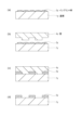
次に、インプリント装置によって基板にパターンを形成し、該パターンが形成された基板を処理し、該処理が行われた基板から物品を製造する物品製造方法について説明する。図5(a)に示すように、絶縁体等の被加工材2zが表面に形成されたシリコンウエハ等の基板1zを用意し、続いて、インクジェット法等により、被加工材2zの表面にインプリント材3zを付与する。ここでは、複数の液滴状になったインプリント材3zが基板上に付与された様子を示している。 Next, an article manufacturing method for forming a pattern on a substrate by an imprint apparatus, processing the substrate on which the pattern is formed, and manufacturing an article from the substrate subjected to the processing will be described. As shown in FIG. 5A, a substrate 1z such as a silicon wafer having a surface to be processed 2z such as an insulator is prepared. A printing material 3z is applied. Here, a state is shown in which a plurality of droplet-like imprint materials 3z are applied onto the substrate.
図5(b)に示すように、インプリント用の型4zを、その凹凸パターンが形成された側を基板上のインプリント材3zに向け、対向させる。図5(c)に示すように、インプリント材3zが付与された基板1と型4zとを接触させ、圧力を加える。インプリント材3zは型4zと被加工材2zとの隙間に充填される。この状態で硬化用のエネルギーとして光を型4zを介して照射すると、インプリント材3zは硬化する。
As shown in FIG. 5(b), the imprint mold 4z is opposed to the imprint material 3z on the substrate with the uneven pattern formed side thereof facing. As shown in FIG. 5C, the
図5(d)に示すように、インプリント材3zを硬化させた後、型4zと基板1zを引き離すと、基板1z上にインプリント材3zの硬化物のパターンが形成される。この硬化物のパターンは、型の凹部が硬化物の凸部に、型の凸部が硬化物の凹部に対応した形状になっており、即ち、インプリント材3zに型4zの凹凸パターンが転写されたことになる。 As shown in FIG. 5D, after the imprint material 3z is cured, the mold 4z and the substrate 1z are separated to form a pattern of the cured imprint material 3z on the substrate 1z. The pattern of this cured product has a shape in which the concave portions of the mold correspond to the convex portions of the cured product, and the convex portions of the mold correspond to the concave portions of the cured product. It will be done.
図5(e)に示すように、硬化物のパターンを耐エッチングマスクとしてエッチングを行うと、被加工材2zの表面のうち、硬化物が無いか或いは薄く残存した部分が除去され、溝5zとなる。図5(f)に示すように、硬化物のパターンを除去すると、被加工材2zの表面に溝5zが形成された物品を得ることができる。ここでは硬化物のパターンを除去したが、加工後も除去せずに、例えば、半導体素子等に含まれる層間絶縁用の膜、つまり、物品の構成部材として利用してもよい。
As shown in FIG. 5(e), when etching is performed using the pattern of the cured product as an anti-etching mask, portions of the surface of the workpiece 2z where the cured product is absent or remains thinly are removed, forming
次に、物品の別の製造方法について説明する。図6(a)に示すように、石英ガラス等の基板1yを用意し、続いて、インクジェット法等により、基板1yの表面にインプリント材3yを付与する。必要に応じて、基板1yの表面に金属や金属化合物等の別の材料の層を設けても良い。
Next, another method for manufacturing the article will be described. As shown in FIG. 6A, a
図6(b)に示すように、インプリント用の型4yを、その凹凸パターンが形成された側を基板上のインプリント材3yに向け、対向させる。図6(c)に示すように、インプリント材3yが付与された基板1yと型4yとを接触させ、圧力を加える。インプリント材3yは型4yと基板1yとの隙間に充填される。この状態で光を型4yを透して照射すると、インプリント材3は硬化する。
As shown in FIG. 6(b), the
図6(d)に示すように、インプリント材3yを硬化させた後、型4yと基板1yを引き離すと、基板1y上にインプリント材3yの硬化物のパターンが形成される。こうして硬化物のパターンを構成部材として有する物品が得られる。なお、図6(d)の状態で硬化物のパターンをマスクとして、基板1yをエッチング加工すれば、型4yに対して凹部と凸部が反転した物品、例えば、インプリント用の型を得ることもできる。
As shown in FIG. 6D, after the
1 インプリント装置
S 基板
121 第1光源
122 第2光源
133 DMD
130 変調部
130 Modulator
Claims (11)
入射光を変調する変調器と、
第1光源からの第1光と、第2光源からの、前記第1光とは波長が異なる第2光とを前記変調器に導く第1光学系と、
前記変調器によって変調された変調光を前記基板に導く第2光学系と、を備え、
前記第1光を前記変調器で変調した第1変調光を前記基板に導くことによって、前記型と前記基板とのアライメントのために前記基板が変形され、
前記第2光を前記変調器で変調した第2変調光を前記基板に導くことによって、前記基板の上に供給されたインプリント材の粘性を増加させ、
前記基板には、前記第1変調光と前記第2変調光とが異なるタイミングで照射され、
前記第1変調光と前記第2変調光との切り替え時には、前記基板に前記第1の変調光および前記第2変調光のいずれもが照射されない期間が生じるように制御され、
前記第1光源と前記第2光源とは、いずれか一方からの光が前記変調器に入射するように制御され、
前記変調器が、当該変調器で変調された変調光を前記基板に到達しない状態となるように制御されている間に、前記第1光源の点灯状態と前記第2光源の点灯状態とが切り替わるように制御されることを特徴とするインプリント装置。 An imprinting apparatus that performs an imprinting process of curing an imprinting material supplied onto a substrate while the imprinting material and the mold are in contact with each other,
a modulator that modulates incident light;
a first optical system for guiding a first light from a first light source and a second light having a different wavelength from the first light from a second light source to the modulator;
a second optical system that guides the modulated light modulated by the modulator to the substrate;
The substrate is deformed for alignment between the mold and the substrate by guiding the first modulated light obtained by modulating the first light with the modulator to the substrate,
increasing the viscosity of the imprint material supplied onto the substrate by guiding the second modulated light obtained by modulating the second light with the modulator to the substrate;
the substrate is irradiated with the first modulated light and the second modulated light at different timings;
When switching between the first modulated light and the second modulated light, the substrate is controlled so that there is a period during which neither the first modulated light nor the second modulated light is irradiated,
the first light source and the second light source are controlled so that light from either one enters the modulator ;
The lighting state of the first light source and the lighting state of the second light source are switched while the modulator is controlled so that the modulated light modulated by the modulator does not reach the substrate. An imprinting apparatus characterized by being controlled to :
前記デジタルミラーデバイスをOFF状態とすることで、前記基板に前記第1の変調光および前記第2変調光のいずれもが照射されない期間が生じるように制御することを特徴とする請求項1乃至7のいずれか1項に記載のインプリント装置。 the modulator comprises a digital mirror device;
8. Control is performed to generate a period during which neither the first modulated light nor the second modulated light is applied to the substrate by turning off the digital mirror device. The imprint apparatus according to any one of .
前記アライメントが完了した後に前記インプリント材を硬化させるための光が前記インプリント材に照射されることによって前記インプリント材が硬化されることを特徴とする請求項1乃至8のいずれか1項に記載のインプリント装置。 A curing light source for irradiating light for curing the imprint material,
9. The imprint material is cured by irradiating the imprint material with light for curing the imprint material after the alignment is completed. The imprinting apparatus according to .
前記パターンが形成された前記基板を加工する工程と、
を含み、前記基板から物品を製造することを特徴とする物品製造方法。 forming a pattern on a substrate with the imprint apparatus according to any one of claims 1 to 10;
processing the substrate on which the pattern is formed;
and manufacturing an article from the substrate.
Priority Applications (10)
| Application Number | Priority Date | Filing Date | Title |
|---|---|---|---|
| JP2018210917A JP7289633B2 (en) | 2018-11-08 | 2018-11-08 | Imprint apparatus and article manufacturing method |
| TW108138996A TWI771623B (en) | 2018-11-08 | 2019-10-29 | Imprint apparatus and product manufacturing method |
| EP19205896.4A EP3650937A1 (en) | 2018-11-08 | 2019-10-29 | Imprint apparatus and product manufacturing method |
| US16/673,804 US11226554B2 (en) | 2018-11-08 | 2019-11-04 | Imprint apparatus and product manufacturing method |
| CN201911076450.8A CN111158212B (en) | 2018-11-08 | 2019-11-06 | Embossing device and method for producing a product |
| KR1020190141428A KR102641226B1 (en) | 2018-11-08 | 2019-11-07 | Imprint apparatus and product manufacturing method |
| US17/544,447 US11921423B2 (en) | 2018-11-08 | 2021-12-07 | Imprint apparatus and product manufacturing method |
| JP2023084773A JP2023104989A (en) | 2018-11-08 | 2023-05-23 | Imprint apparatus and article manufacturing method |
| US18/390,910 US20240126165A1 (en) | 2018-11-08 | 2023-12-20 | Imprint apparatus and product manufacturing method |
| KR1020240025586A KR20240031272A (en) | 2018-11-08 | 2024-02-22 | Imprint apparatus, product manufacturing method, and imprint method |
Applications Claiming Priority (1)
| Application Number | Priority Date | Filing Date | Title |
|---|---|---|---|
| JP2018210917A JP7289633B2 (en) | 2018-11-08 | 2018-11-08 | Imprint apparatus and article manufacturing method |
Related Child Applications (1)
| Application Number | Title | Priority Date | Filing Date |
|---|---|---|---|
| JP2023084773A Division JP2023104989A (en) | 2018-11-08 | 2023-05-23 | Imprint apparatus and article manufacturing method |
Publications (3)
| Publication Number | Publication Date |
|---|---|
| JP2020077796A JP2020077796A (en) | 2020-05-21 |
| JP2020077796A5 JP2020077796A5 (en) | 2021-11-18 |
| JP7289633B2 true JP7289633B2 (en) | 2023-06-12 |
Family
ID=70724423
Family Applications (2)
| Application Number | Title | Priority Date | Filing Date |
|---|---|---|---|
| JP2018210917A Active JP7289633B2 (en) | 2018-11-08 | 2018-11-08 | Imprint apparatus and article manufacturing method |
| JP2023084773A Pending JP2023104989A (en) | 2018-11-08 | 2023-05-23 | Imprint apparatus and article manufacturing method |
Family Applications After (1)
| Application Number | Title | Priority Date | Filing Date |
|---|---|---|---|
| JP2023084773A Pending JP2023104989A (en) | 2018-11-08 | 2023-05-23 | Imprint apparatus and article manufacturing method |
Country Status (1)
| Country | Link |
|---|---|
| JP (2) | JP7289633B2 (en) |
Families Citing this family (1)
| Publication number | Priority date | Publication date | Assignee | Title |
|---|---|---|---|---|
| EP4179913A1 (en) | 2020-04-24 | 2023-05-17 | ASICS Corporation | Last for manufacturing footwear upper |
Citations (6)
| Publication number | Priority date | Publication date | Assignee | Title |
|---|---|---|---|---|
| JP2004259985A (en) | 2003-02-26 | 2004-09-16 | Sony Corp | Resist pattern forming device, method for forming resist pattern and method for manufacturing semiconductor device using the forming method |
| JP2016035509A (en) | 2014-08-02 | 2016-03-17 | 株式会社アドテックエンジニアリング | Light source device and exposure apparatus |
| JP2016058735A (en) | 2014-09-08 | 2016-04-21 | キヤノン株式会社 | Imprint device, imprint method and manufacturing method of article |
| JP2016167622A (en) | 2016-05-02 | 2016-09-15 | キヤノン株式会社 | Imprint device, and method for manufacturing article using the same |
| JP2018092997A (en) | 2016-11-30 | 2018-06-14 | キヤノン株式会社 | Imprint device, imprint method, and method of manufacturing article |
| JP2018110269A (en) | 2015-06-10 | 2018-07-12 | キヤノン株式会社 | Imprint device, imprint method, and article manufacturing method |
-
2018
- 2018-11-08 JP JP2018210917A patent/JP7289633B2/en active Active
-
2023
- 2023-05-23 JP JP2023084773A patent/JP2023104989A/en active Pending
Patent Citations (6)
| Publication number | Priority date | Publication date | Assignee | Title |
|---|---|---|---|---|
| JP2004259985A (en) | 2003-02-26 | 2004-09-16 | Sony Corp | Resist pattern forming device, method for forming resist pattern and method for manufacturing semiconductor device using the forming method |
| JP2016035509A (en) | 2014-08-02 | 2016-03-17 | 株式会社アドテックエンジニアリング | Light source device and exposure apparatus |
| JP2016058735A (en) | 2014-09-08 | 2016-04-21 | キヤノン株式会社 | Imprint device, imprint method and manufacturing method of article |
| JP2018110269A (en) | 2015-06-10 | 2018-07-12 | キヤノン株式会社 | Imprint device, imprint method, and article manufacturing method |
| JP2016167622A (en) | 2016-05-02 | 2016-09-15 | キヤノン株式会社 | Imprint device, and method for manufacturing article using the same |
| JP2018092997A (en) | 2016-11-30 | 2018-06-14 | キヤノン株式会社 | Imprint device, imprint method, and method of manufacturing article |
Also Published As
| Publication number | Publication date |
|---|---|
| JP2020077796A (en) | 2020-05-21 |
| JP2023104989A (en) | 2023-07-28 |
Similar Documents
| Publication | Publication Date | Title |
|---|---|---|
| US11904522B2 (en) | Imprint apparatus and method for manufacturing article | |
| KR102159153B1 (en) | Imprint apparatus, and method of manufacturing article | |
| KR20240031272A (en) | Imprint apparatus, product manufacturing method, and imprint method | |
| JP6563062B2 (en) | Imprint apparatus, imprint method, and article manufacturing method | |
| KR102243223B1 (en) | Imprint apparatus and method of manufacturing article | |
| JP2023104989A (en) | Imprint apparatus and article manufacturing method | |
| KR102487796B1 (en) | Detection apparatus, lithography apparatus, and method of manufacturing article | |
| JP7202148B2 (en) | Imprint apparatus and article manufacturing method | |
| JP7379091B2 (en) | Imprint device, imprint method, and article manufacturing method | |
| US11442361B2 (en) | Imprint method, imprint apparatus, and method of manufacturing article | |
| JP7237646B2 (en) | IMPRINT METHOD, IMPRINT APPARATUS, AND ARTICLE MANUFACTURING METHOD | |
| JP7267801B2 (en) | IMPRINT APPARATUS, IMPRINT METHOD, AND ARTICLE MANUFACTURING METHOD | |
| JP7437928B2 (en) | Imprint equipment, imprint method, and article manufacturing method | |
| US20210061649A1 (en) | Imprinting method, pre-processing apparatus, substrate for imprinting, and method for manufacturing substrate | |
| JP2021176179A (en) | Imprint method, imprint device, and article manufacturing method |
Legal Events
| Date | Code | Title | Description |
|---|---|---|---|
| A521 | Request for written amendment filed |
Free format text: JAPANESE INTERMEDIATE CODE: A523 Effective date: 20211006 |
|
| A621 | Written request for application examination |
Free format text: JAPANESE INTERMEDIATE CODE: A621 Effective date: 20211006 |
|
| A977 | Report on retrieval |
Free format text: JAPANESE INTERMEDIATE CODE: A971007 Effective date: 20220531 |
|
| A131 | Notification of reasons for refusal |
Free format text: JAPANESE INTERMEDIATE CODE: A131 Effective date: 20220614 |
|
| A521 | Request for written amendment filed |
Free format text: JAPANESE INTERMEDIATE CODE: A523 Effective date: 20220805 |
|
| A131 | Notification of reasons for refusal |
Free format text: JAPANESE INTERMEDIATE CODE: A131 Effective date: 20221206 |
|
| A521 | Request for written amendment filed |
Free format text: JAPANESE INTERMEDIATE CODE: A523 Effective date: 20230126 |
|
| TRDD | Decision of grant or rejection written | ||
| A01 | Written decision to grant a patent or to grant a registration (utility model) |
Free format text: JAPANESE INTERMEDIATE CODE: A01 Effective date: 20230502 |
|
| A61 | First payment of annual fees (during grant procedure) |
Free format text: JAPANESE INTERMEDIATE CODE: A61 Effective date: 20230531 |
|
| R151 | Written notification of patent or utility model registration |
Ref document number: 7289633 Country of ref document: JP Free format text: JAPANESE INTERMEDIATE CODE: R151 |