JP7279260B2 - Electrodes and electrode tips - Google Patents
Electrodes and electrode tips Download PDFInfo
- Publication number
- JP7279260B2 JP7279260B2 JP2022510350A JP2022510350A JP7279260B2 JP 7279260 B2 JP7279260 B2 JP 7279260B2 JP 2022510350 A JP2022510350 A JP 2022510350A JP 2022510350 A JP2022510350 A JP 2022510350A JP 7279260 B2 JP7279260 B2 JP 7279260B2
- Authority
- JP
- Japan
- Prior art keywords
- layer
- electrode
- metal layer
- substrate
- metal
- Prior art date
- Legal status (The legal status is an assumption and is not a legal conclusion. Google has not performed a legal analysis and makes no representation as to the accuracy of the status listed.)
- Active
Links
Images


Classifications
-
- G—PHYSICS
- G01—MEASURING; TESTING
- G01N—INVESTIGATING OR ANALYSING MATERIALS BY DETERMINING THEIR CHEMICAL OR PHYSICAL PROPERTIES
- G01N27/00—Investigating or analysing materials by the use of electric, electrochemical, or magnetic means
- G01N27/26—Investigating or analysing materials by the use of electric, electrochemical, or magnetic means by investigating electrochemical variables; by using electrolysis or electrophoresis
- G01N27/28—Electrolytic cell components
- G01N27/30—Electrodes, e.g. test electrodes; Half-cells
Description
本発明は、電極及び電極チップに関する。 The present invention relates to electrodes and electrode tips.
電気化学測定の原理を利用した測定は、溶液中の重金属の高感度測定や、酵素電極を利用したグルコース測定、イオン電極を利用したpH(ペーハー)の測定、残留農薬の電気化学検出に代表される食物検査など、多くの場面で使用されている(例えば特許文献1参照)。特に、その中でも、カドミウム、水銀、砒素、コバルト、銅、亜鉛、鉛といった重金属の測定は、水や土壌、食物、野菜、米、飲料水に含まれるそれらの重金属量を体内に摂取する前に把握することは非常に重要である。 Measurements using the principle of electrochemical measurement are typified by highly sensitive measurements of heavy metals in solutions, glucose measurements using enzyme electrodes, pH measurements using ion electrodes, and electrochemical detection of residual pesticides. It is used in many situations such as food inspection in which food is stored (see, for example, Patent Document 1). In particular, the measurement of heavy metals such as cadmium, mercury, arsenic, cobalt, copper, zinc, and lead, among others, should be performed before ingesting the amount of these heavy metals contained in water, soil, food, vegetables, rice, and drinking water. It's very important to know.
電気化学測定において、絶縁性の基板の上に電極を形成した電極チップを使用できることが知られている。電極チップにおいて、電極は基本的に単層構造であり、電極材料としては、銀、白金、金、アルミニウムなどの金属材料、又は炭素などの導電性材料が用いられる。 It is known that an electrode tip having electrodes formed on an insulating substrate can be used in electrochemical measurements. In the electrode chip, the electrode basically has a single-layer structure, and the electrode material used is a metal material such as silver, platinum, gold, or aluminum, or a conductive material such as carbon.
しかし、金属材料の中には、空気中や試料中の水分などと酸化還元反応を起こして腐食してしまうものがあり、測定感度や再現性が低下することがあった。また、炭素材料は、酸化還元されにくいが、金属材料に比べて電気抵抗率が高く、電極として使用した場合に感度が劣る。 However, some metal materials corrode due to oxidation-reduction reactions with moisture in the air or samples, which sometimes reduces measurement sensitivity and reproducibility. In addition, although carbon materials are difficult to be oxidized and reduced, they have higher electrical resistivity than metal materials, and are inferior in sensitivity when used as electrodes.
このような不具合を解消する方法として、絶縁性の基板の上に形成した金属層の上に炭素層を積層することが知られている(例えば特許文献2-4参照)。
As a method for solving such problems, it is known to laminate a carbon layer on a metal layer formed on an insulating substrate (see, for example,
しかし、従来の電極では、測定中に炭素層に浸透した水に起因して金属層表面で水素が発生して、金属層と炭素層との剥離や炭素層の破損が生じ、測定感度や再現性が低下するという問題があった。 However, with conventional electrodes, hydrogen is generated on the surface of the metal layer due to water permeating the carbon layer during measurement, resulting in separation of the metal layer from the carbon layer and damage to the carbon layer, resulting in poor measurement sensitivity and reproducibility. There was a problem of declining performance.
本発明は、上記現状を改善すべく成されたものであり、液体試料中の微量成分を測定する電気化学測定の測定感度及び再現性を向上できる電極及び電極チップを提供することを目的とする。 The present invention has been made to improve the above-mentioned current situation, and an object of the present invention is to provide an electrode and an electrode chip that can improve the measurement sensitivity and reproducibility of electrochemical measurement for measuring a trace component in a liquid sample. .
本発明の電極は、絶縁性の基板の上に形成された金属層と、前記金属層の上に形成された炭素層と、前記金属層の上面と前記炭素層との間に形成された上部接着層と、を備え、前記上部接着層はシリコンで形成されており、前記金属層の側面が絶縁層で覆われているものである。 The electrode of the present invention comprises a metal layer formed on an insulating substrate, a carbon layer formed on the metal layer, and an upper portion formed between the upper surface of the metal layer and the carbon layer. an adhesion layer, wherein the upper adhesion layer is made of silicon, and the side surface of the metal layer is covered with an insulating layer.
本発明の電極によれば、金属層を有することで電気抵抗を低くして、測定感度を向上できる。また、金属層の上面を炭素層で覆うとともに、金属層の側面を絶縁層で覆うことで、金属層の酸化還元を防止でき、測定感度及び再現性を向上できる。さらに、金属層の上面と炭素層との間にシリコンで形成された上部接着層を設けることで、金属層と炭素層との密着性を向上させるとともに、シリコンは金属に比べて電気抵抗率が高いので、測定中における金属層上面での水素の発生を抑制し、金属層と炭素層との剥離を防止して、測定感度及び再現性を向上できる。また、金属層の側面は絶縁層で覆われているから、当該側面に水分が到達せず、金属層の側面での水素の発生を防止できる。 According to the electrode of the present invention, by having the metal layer, the electrical resistance can be lowered and the measurement sensitivity can be improved. In addition, by covering the upper surface of the metal layer with the carbon layer and covering the side surface of the metal layer with the insulating layer, oxidation-reduction of the metal layer can be prevented, and measurement sensitivity and reproducibility can be improved. Furthermore, by providing an upper adhesion layer made of silicon between the upper surface of the metal layer and the carbon layer, the adhesion between the metal layer and the carbon layer is improved, and silicon has a higher electrical resistivity than metal. Since it is high, it is possible to suppress the generation of hydrogen on the upper surface of the metal layer during measurement, prevent separation between the metal layer and the carbon layer, and improve measurement sensitivity and reproducibility. Moreover, since the side surfaces of the metal layer are covered with the insulating layer, moisture does not reach the side surfaces, and generation of hydrogen on the side surfaces of the metal layer can be prevented.
本発明の電極において、前記基板と前記金属層との間に形成された下部接着層を備えているようにしてもよい。 The electrode of the present invention may include a lower adhesive layer formed between the substrate and the metal layer.
このような態様によれば、測定中における基板と金属層との密着性の低下を防止でき、測定感度及び再現性を向上できる。 According to this aspect, it is possible to prevent deterioration of adhesion between the substrate and the metal layer during measurement, and improve measurement sensitivity and reproducibility.
下部接着層は、例えばシリコン、クロム、チタン、タングステン、又は、前記基板の表面に前記金属層との密着性を向上させる表面処理を施して形成した表面処理層で形成されていることが好ましい。ただし、下部接着層は、上記以外の金属で形成されてもよい。 The lower adhesive layer is preferably formed of, for example, silicon, chromium, titanium, tungsten, or a surface-treated layer formed by subjecting the surface of the substrate to a surface treatment that improves adhesion with the metal layer. However, the lower adhesive layer may be formed of metals other than those mentioned above.
本発明の電極チップは、本発明の電極からなる作用電極及び参照電極を備えているものである。 The electrode tip of the present invention comprises a working electrode and a reference electrode comprising the electrode of the present invention.
本発明の電極チップによれば、作用電極と参照電極とを使用する2電極方式の電気化学測定に適用できる。そして、作用電極と参照電極の両方が金属層、炭素層及び接着層を有する本発明の電極で構成されているので、作用電極及び参照電極の両方について、電気抵抗を低くでき、金属層の酸化還元を防止でき、かつ、炭素層の剥離を防止できるので、測定感度及び再現性を向上できる。 INDUSTRIAL APPLICABILITY According to the electrode tip of the present invention, it can be applied to two-electrode electrochemical measurements using a working electrode and a reference electrode. Further, since both the working electrode and the reference electrode are composed of the electrode of the present invention having a metal layer, a carbon layer and an adhesive layer, both the working electrode and the reference electrode can have a low electrical resistance and oxidation of the metal layer. Since reduction can be prevented and peeling of the carbon layer can be prevented, measurement sensitivity and reproducibility can be improved.
本発明の電極チップにおいて、本発明の電極からなる対極をさらに備えているようにしてもよい。 The electrode tip of the present invention may further include a counter electrode made of the electrode of the present invention.
このような態様によれば、作用電極と参照電極と対極とを使用する3電極方式の電気化学測定に適用できる。そして、作用電極、参照電極及び対極について、電気抵抗を低くでき、金属層の酸化還元を防止でき、かつ、炭素層の剥離を防止できるので、測定感度及び再現性を向上できる。 This aspect can be applied to a three-electrode electrochemical measurement using a working electrode, a reference electrode, and a counter electrode. Moreover, the electrical resistance of the working electrode, the reference electrode and the counter electrode can be lowered, the oxidation-reduction of the metal layer can be prevented, and the peeling of the carbon layer can be prevented, so that the measurement sensitivity and reproducibility can be improved.
本発明は、電気化学測定の測定感度及び再現性を向上できる電極及び電極チップを提供できる。 INDUSTRIAL APPLICABILITY The present invention can provide electrodes and electrode chips capable of improving the measurement sensitivity and reproducibility of electrochemical measurements.
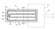
本発明の電極及び電極チップの実施形態について図面に基づいて説明する。図1は、同実施形態を示す概略構成図である。図2は、電極チップの一実施形態を示す平面図である。 An embodiment of an electrode and an electrode tip of the present invention will be described based on the drawings. FIG. 1 is a schematic configuration diagram showing the same embodiment. FIG. 2 is a plan view showing one embodiment of the electrode tip.
図1に示すように、電気化学測定装置1は、電極チップ2と、電極チップ2に接続されるポテンショスタット3と、ポテンショスタット3に接続される操作部4、表示部5、電源部6及び外部出力部7を備えている。本実施形態では、電極チップ2は使い捨て型のものである。
As shown in FIG. 1, an
図2に示すように、電極チップ2は平板状の絶縁性の基板21を備え、基板21上に作用電極22、対極23及び参照電極24が互いに絶縁されて設けられている。基板21は平面視で略長方形の形態を有している。作用電極22、対極23及び参照電極24は、基板21の長手方向一端近傍から他端近傍にわたって設けられている。
As shown in FIG. 2, the
基板21上には、作用電極22、対極23及び参照電極24を互いに絶縁する絶縁層25が形成されている。絶縁層25は、電極22,23,24の間に埋め込まれるとともに、電極22,23,24の輪郭を囲って設けられており、電極22,23,24の側面を覆っている。
An
電極チップ2において、作用電極22、対極23及び参照電極24の一端側には被測定物質を含む液体試料10が接触される。電極チップ2の作用電極22、対極23及び参照電極24の他端側は、コネクタ8及びケーブル9(図1での図示省略)を介してポテンショスタット3に電気的に接続される。電極チップ2は、コネクタ8に着脱可能に取り付けられる。
In the
電極チップ2の基板21の少なくとも一表面は、平坦な絶縁性材料で形成されている。基板21の材質は特に限定されず、例えば、ポリイミド(PI)、ガラス、ポリエチレンテレフタレート(PET)、メタクリル樹脂(PMMA)、ポリカーボネート(PC)、ポリプロピレン(PP)、ポリエチレン(PE)、ポリスチレン(PS)、ポリ塩化ビニル(PVC)、ポリオキシメチレン(POM)、ABS樹脂(ABS)などを挙げることができる。ただし、基板21の材質は、これらに限定されず、セラミックスや石英などであってもよい。また、基板21の形状、厚み及び大きさは、特に限定されない。
At least one surface of the
図2及び図3に示すように、電極チップ2において、作用電極22、対極23及び参照電極24のそれぞれは、基板21の上に形成された金属層41と、金属層41を覆って形成された炭素層42と、基板21と金属層41との間に形成された下部接着層43と、金属層41の上面と炭素層42との間に形成された上部接着層44とを備えている。参照電極24の一端側の炭素層42上面に、銀塩化銀層45が形成されている。
As shown in FIGS. 2 and 3, in the
下部接着層43は、基板21と金属層41との剥離を防止する薄膜であり、例えばシリコンで形成されている。下部接着層43の材料としては、基板21及び金属層41との密着性が良好なものであればよく、シリコンの他、例えば、クロム、チタン、タングステンを使用できる。
The lower
また、下部接着層43は、基板21の表面に金属層41との密着性を向上させる表面処理を施して形成した表面処理層で形成されていてもよい。このような表面処理としては、例えば、プラズマ処理、コロナ処理、フレーム処理、エッチング処理、蒸気処理、イオンビーム処理などを挙げることができる。
Further, the lower
金属層41は、炭素層42よりも電気抵抗率が低い材料で形成されており、下部接着層43の上に形成されている。金属層41は、作用電極22、対極23及び参照電極24のそれぞれの一端と他端との間の電気抵抗を下げるためのものである。金属層41の材料としては、例えば、銀、ルテニウム、タンタル、チタン、銅、アルミニウム、白金、ニオブ、ジルコニウム、若しくはこれらの元素の合金、又はこれらの元素と炭素との合金などを使用できる。
The
上部接着層44は、金属層41の上面に形成されており、金属層41の上面と炭素層42との剥離を防止する薄膜であり、シリコンで形成されている。
The
炭素層42は、金属層41の上に上部接着層44を介して形成されている。炭素層42は、例えばアモルファスカーボン、又はダイヤモンドライクカーボン(DLC)で形成されている。
The
炭素は、次のような特性を有するので、金属層41を保護する炭素層42の使用に適している。(1)3000℃の真空中(500℃の空気中)でも優れた安定性をもつ、(2)化学薬品に侵されにくい、(3)ガスや溶液を透過しない、(4)優れた硬度、強度をもつ、(5)優れた電気伝導度性をもつ、(6)金属塩などの湿潤に抵抗がある、(7)血液や組織適合性が良好である、(8)物理特性、化学特性の等方性がある。
Carbon is suitable for use in the
下部接着層43、金属層41、上部接着層44及び炭素層42の製造方法としては、各層の形状及び膜厚を高精度に制御できることから、蒸着法であることが好ましい。ここで、蒸着法としては、真空蒸着法、イオンプレーティング法、スパッタリング法などの、いわゆる物理気相成長法(PVD)や、いわゆる化学的気相成長法(CVD)を使用できる。ただし、各層の製造方法は、蒸着法に限定されず、スクリーン印刷法やインクジェット印刷法などの印刷法であってもよい。
As a method for manufacturing the lower
図2及び図3に示すように、絶縁層25は、平面視で下部接着層43、金属層41及び上部接着層44の輪郭を囲うように形成されている。金属層41の側面は絶縁層25で覆われている。本実施形態では、下部接着層43の側面、上部接着層44の側面及び炭素層42の側面も絶縁層25で覆われている。絶縁層25の下面は基板21に接触している。下部接着層43、金属層41及び上部接着層44は、基板21と絶縁層25とで囲われることで、周囲雰囲気から隔離されている。
As shown in FIGS. 2 and 3, the insulating
絶縁層25の材質は特に限定されず、例えば、シリコン酸化膜(SiO2)、シリコン窒化膜(Si3N4)、酸化アルミニウム(Al2O3)などを挙げることができる。ただし、絶縁層25は、これらの材質で形成されたものに限定されず、電極22,23,24の側面(少なくとも金属層41の側面)を周囲雰囲気から遮断できて、水分を通さない絶縁物であればよい。
The material of the insulating
なお、絶縁層25の上面高さ位置(厚み)は、絶縁層25が少なくとも金属層41の側面を覆うことができる程度であればよい。ただし、絶縁層25と炭素層42との接触面積を増やすために、絶縁層25の上面高さ位置は炭素層42の上面高さ位置と同程度であることが好ましい。これにより、絶縁層25と炭素層42との間からの金属層41への水分の浸入を確実に防止できる。
Note that the upper surface height position (thickness) of the insulating
本実施形態において、電極22,23,24は、絶縁性の基板21の上に形成された金属層41と、基板21上に金属層41を覆って形成された炭素層42と、基板21と金属層41との間に形成された下部接着層43と、を備えている。電極22,23,24は、金属層41を有することで電気抵抗を低くして、測定感度を向上できる。また、金属層41の上面を炭素層42で覆うとともに、金属層41の側面を絶縁層25で覆うことで、金属層41の酸化還元を防止でき、測定感度及び再現性を向上できる。さらに、金属層41の上面と炭素層42との間にシリコンからなる上部接着層44を設けることで、金属層41と炭素層42との密着性を向上させるとともに、シリコンは金属に比べて電気抵抗率が高いことから測定中における金属層41の上面での水素の発生を抑制できる。また、金属層41の側面は絶縁層25で覆われているから、当該側面に水分が到達せず、金属層41の側面での水素の発生を防止できる。これにより、基板21と金属層41との剥離を防止して、測定感度及び再現性を向上できる。
In this embodiment, the
また、電極22,23,24は、基板21と金属層41との間に形成された下部接着層43を備えているので、測定中における基板21と金属層41との密着性の低下を防止でき、測定感度及び再現性を向上できる。
In addition, since the
また、金属層41、炭素層42及び接着層43,44は、蒸着法で形成されたものであって、金属層41、炭素層42及び接着層43,44は平面視で同じ形状に形成されている。各層41,42,43,44を蒸着法で形成することで、各層41,42,43,44の形状及び膜厚を高精度に制御でき、電極22,23,24のそれぞれについて、全体の電気抵抗の安定性を向上できる。
The
また、下部接着層43はシリコンで形成されている。シリコンは、ガラスとの密着性及び金属との密着性がよいので、金属層41と基板21との密着性を強くできる。また、上部接着層44もシリコンで形成されている。シリコンは、金属との密着性及び炭素との密着性がよいので、金属層41と炭素層42との密着性を強くできる。
Also, the lower
電極チップ2は、作用電極22と参照電極24と対極23とを備えているので、3電極方式の電気化学測定に適用できる。そして、作用電極22、参照電極24及び対極23について、電気抵抗を低くでき、金属層41の酸化還元を防止でき、かつ、金属層41の剥離を防止できるので、測定感度及び再現性を向上できる。
Since the
なお、本発明の電極チップによれば、作用電極と参照電極とを使用する2電極方式の電気化学測定に適用できる。そして、作用電極と参照電極の両方が金属層、炭素層及び接着層を有する本発明の電極で構成されているので、作用電極及び参照電極の両方について、電気抵抗を低くでき、金属層の酸化還元を防止でき、かつ、金属層の剥離を防止できるので、測定感度及び再現性を向上できる。 The electrode chip of the present invention can be applied to two-electrode electrochemical measurements using a working electrode and a reference electrode. Further, since both the working electrode and the reference electrode are composed of the electrode of the present invention having a metal layer, a carbon layer and an adhesive layer, both the working electrode and the reference electrode can have a low electrical resistance and oxidation of the metal layer. Since reduction can be prevented and peeling of the metal layer can be prevented, measurement sensitivity and reproducibility can be improved.
図1に示すように、ポテンショスタット3は、電極チップ2の作用電極22の電位が参照電極24に対して一定になるように制御するとともに、作用電極22と対極23との間に流れる電流を測定可能に構成されている。ポテンショスタット3は、概略構成として、演算制御部31、電圧印加部32及び電流検出部33を備えている。
As shown in FIG. 1, the
演算制御部31は、電気化学測定で得られた測定値を用いて所定の演算処理を行なうとともに、操作部4を介して入力されたユーザからの指令に基づいて、電圧印加部32に必要な信号を送信したり、表示部5に測定結果等の情報を表示させたりする機能である。演算制御部31は、例えばマイクロコンピュータが所定のプログラムを実行することによって実現される。
The
電圧印加部32は、演算制御部31からの測定開始の信号を受信したときに、電極チップ2の作用電極22と対極23との間に所望の波形の電圧を印加して、作用電極22と参照電極24との間の電位が所望の電位になるように制御するように構成されている。
When the
電流検出部33は、電極チップ2の作用電極22と対極23との間を流れる電流の大きさを検出するように構成されている。電流検出部33が検出した電流の大きさに関する信号は演算制御部31に取り込まれる。
The
演算制御部31は、電流検出部33から取り込んだ信号の基づき、例えば予め用意された検量線を用いて、試料溶液中の特定成分濃度等の計算を行ない、測定結果を表示部5に表示するように構成されている。
The
電気化学測定装置1において、操作部4は、電源のオン・オフや測定の開始、表示部5に表示される情報の変更といった操作をユーザが行なうための入力装置である。表示部5は、例えば液晶ディスプレイによって実現されるものである。なお、表示部5をタッチパネルで構成し、表示部5に操作部4の機能を兼ね備えさせてもよい。電源部6は、例えば乾電池や蓄電池などによって実現することができる。電源部6により、ポテンショスタット3や表示部5へ必要な電力が供給される。
In the
また、ポテンショスタット3には、USB(ユニバーサル・シリアル・バス)端子といった有線通信手段や無線通信手段によってパーソナルコンピュータ等の外部機器へ情報を出力することができるように、外部出力部7が接続されてもよい。その場合、演算制御部31は、外部出力部7を介して測定データ等を外部機器へ出力するように構成されている。
The
なお、操作部4、表示部5、電源部6及び外部出力部7は、例えば、ノートパソコンやタブレットなどのモバイルコンピュータで実現されるようにしてもよい。さらに、ポテンショスタット3として小型のもの(例えば小型ポテンショスタット「miniSTAT100」(バイオデバイステクノロジー製))を用いるようにすれば、電気化学測定装置1を持ち運び可能に構成できる。これにより、電気化学測定装置1を使用したオンサイト(現場)での液体試料の測定が可能になる。
Note that the operation unit 4, the
電気化学測定装置1を使用した電気化学測定は、図2に示すように、電極チップ2に液体試料10が滴下された状態で行われる。電極チップ2に対して、液体試料10は作用電極22、対極23及び参照電極24に接触するようにして基板21上に滴下される。なお、作用電極22、対極23及び参照電極24の一端側を液体試料に浸漬した状態で測定を行ってもよい。
The electrochemical measurement using the
次に、電極チップ2の作製例について説明する。基板21としての厚さ2500nm(2.5μm)程度のガラス基板の上に、スパッタリング法により、下部接着層形成領域に対応する開口パターンを有するメタルマスクを用いて厚さ20nm程度のシリコン層を下部接着層43として形成した。なお、シリコンからなる下部接着層43の膜厚は特に限定されない。
Next, an example of manufacturing the
そのメタルマスクの下部接着層形成領域に対応する開口パターンと同一開口パターンを有するメタルマスクを使用して、下部接着層43上に、スパッタリング法により厚さ150nm程度の銀層を金属層41として形成した。
A silver layer having a thickness of about 150 nm is formed as the
その後、下部接着層形成領域に対応する開口パターンと同一開口パターンを有するメタルマスクを使用して、金属層41上に、スパッタリング法により厚さ20nm程度のシリコン層を上部接着層44として形成した。なお、シリコンからなる上部接着層44の膜厚は特に限定されない。
After that, using a metal mask having the same opening pattern as the opening pattern corresponding to the lower adhesive layer forming region, a silicon layer having a thickness of about 20 nm was formed as the
続いて、下部接着層形成領域に対応する開口パターンと同一開口パターンを有するメタルマスクを使用して、上部接着層44上に、スパッタリング法により厚さ1000nm程度の炭素層42を形成した。このようにして、下部接着層43、金属層41、上部接着層44及び炭素層42をそれぞれ有する作用電極22、対極23及び参照電極24を形成した。
Subsequently, a
ここでは、基板21をスパッタリング装置のチャンバー内に搬入した後、同一メタルマスクを用いて、基板21上に下部接着層43、金属層41、上部接着層44、炭素層42を、チャンバーから搬出せずに成膜した。これにより、下部接着層43、金属層41、上部接着層44及び炭素層42の成膜に要する時間を短縮できるとともに、各層の間への異物の付着を防止できる。また、金属層41、炭素層42及び接着層43,44は平面視で同じ形状に形成される。
Here, after the
電極22,23,24の線幅(長手方向に直交する幅方向の寸法)は、1.0mm程度である。また、電極22,23,24の間隔は、0.5mm程度である。
The line width of the
スパッタリング法により、下部接着層形成領域の周囲に開口した開口パターンを有するメタルマスクを使用して、下部接着層43、金属層41、上部接着層44及び炭素層42の側面(電極22,23,24の側面)を覆うように、基板21上に厚さ1200nm程度の絶縁層25を形成した。絶縁層25は、電極22,23,24の周囲を囲うとともに、電極22,23,24の間に埋め込むように形成される。
By sputtering, using a metal mask having an opening pattern around the lower adhesive layer formation region, the side surfaces of the lower
このように、蒸着法(ここではスパッタリング法)により、下部接着層43、金属層41、上部接着層44及び炭素層42、並びに絶縁層25を、開口パターンを有するメタルマスクを使用して形成することで、各層の成膜後にエッチング法やリフトオフ法によるパターニングが不要であり、製造コストを低減できる。
Thus, the lower
参照電極24の一端側の炭素層42上面に、成膜法により、厚さ100nm程度の銀層を成膜し、塩化処理して銀塩化銀層45を形成した。このようにして、電極チップ2を作製した。なお、絶縁層25を形成した後に銀塩化銀層45を形成してもよいし、絶縁層25を形成する前に銀塩化銀層45を形成してもよい。
A silver layer having a thickness of about 100 nm was formed on the upper surface of the
金属層41の膜厚は、特に限定されないが、50nm以上、1000nm以下であることが好ましい。なお、金属層41の膜厚が50nmよりも薄いと、電極22,23,24が高抵抗となって測定感度が低下する。また、金属層41の膜厚が1000nmよりも厚いと、金属層41を蒸着法(例えばスパッタリング法)で成膜する場合には、金属層41の成膜に要する時間が長くなり、生産効率が低下する。
Although the film thickness of the
なお、1枚の基板21に複数の電極チップ2の領域を設けて、複数の電極チップ2を同時に形成した後、各電極チップ2を個片化することで、製造コストを低減できる。
In addition, manufacturing cost can be reduced by providing regions for a plurality of
電極チップ2において、図4に示すように、基板21の表面に、密着性を向上させる表面処理を施して形成した表面処理層46を下部接着層として形成し、表面処理層46上に金属層41及び絶縁層25が形成されていてもよい。これにより、基板21と金属層41及び絶縁層25との密着性を向上でき、基板21と絶縁層25との間からの水分の浸入を確実に防止して、測定時における金属層41側面での水素の発生及び絶縁層25の剥離をより確実に防止できる。
In the
本発明は、前述の実施形態に限らず、様々な態様に具体化できる。例えば、電極チップは、電極として作用電極22及び参照電極24を備え、対極23を備えていない構成であって、二電極方式の電気化学測定に適用可能な構成であってもよい。
The present invention is not limited to the above-described embodiments, and can be embodied in various aspects. For example, the electrode chip may have a configuration that includes the working
また、本発明の電極チップは、微分パルスボルタンメトリー(DPV)に限らず、リニアスイープボルタンメトリー(LSV)、クロノアンペアメトリー(CA)、サイクリックボルタンメトリー(CV)、短波形ボルタンメトリー(SWV)などの方法にも適用可能である。 In addition, the electrode tip of the present invention can be used not only in differential pulse voltammetry (DPV), but also in methods such as linear sweep voltammetry (LSV), chronoamperemetry (CA), cyclic voltammetry (CV), and short-wave voltammetry (SWV). is also applicable.
1 電気化学測定装置
2 電極チップ
3 ポテンショスタット
4 操作部
5 表示部
6 電源部
7 外部出力部
8 コネクタ
9 ケーブル
10 液体試料
21 基板
22 作用電極
23 対極
24 参照電極
25 絶縁層
31 演算制御部
32 電圧印加部
33 電流検出部
41 金属層
42 炭素層
43 下部接着層
44 上部接着層
45 銀塩化銀層
46 表面処理層1
Claims (5)
前記金属層の上に形成された炭素層と、
前記金属層の上面と前記炭素層との間に形成された上部接着層と、を備え、
前記上部接着層はシリコンで形成されており、
前記金属層の側面が絶縁層で覆われている、電極。a metal layer formed on an insulating substrate;
a carbon layer formed on the metal layer;
an upper adhesion layer formed between the top surface of the metal layer and the carbon layer;
the upper adhesive layer is made of silicon,
The electrode, wherein the sides of the metal layer are covered with an insulating layer.
5. The electrode tip according to claim 4, further comprising a counter electrode comprising the electrode according to any one of claims 1 to 3.
Applications Claiming Priority (1)
| Application Number | Priority Date | Filing Date | Title |
|---|---|---|---|
| PCT/JP2020/014118 WO2021192248A1 (en) | 2020-03-27 | 2020-03-27 | Electrode and electrode chip |
Publications (2)
| Publication Number | Publication Date |
|---|---|
| JPWO2021192248A1 JPWO2021192248A1 (en) | 2021-09-30 |
| JP7279260B2 true JP7279260B2 (en) | 2023-05-22 |
Family
ID=77891624
Family Applications (1)
| Application Number | Title | Priority Date | Filing Date |
|---|---|---|---|
| JP2022510350A Active JP7279260B2 (en) | 2020-03-27 | 2020-03-27 | Electrodes and electrode tips |
Country Status (3)
| Country | Link |
|---|---|
| JP (1) | JP7279260B2 (en) |
| CN (1) | CN115335690A (en) |
| WO (1) | WO2021192248A1 (en) |
Families Citing this family (2)
| Publication number | Priority date | Publication date | Assignee | Title |
|---|---|---|---|---|
| JPWO2022153917A1 (en) * | 2021-01-14 | 2022-07-21 | ||
| JP7322311B1 (en) | 2023-02-28 | 2023-08-07 | 住友化学株式会社 | Electrochemical sensor and method of manufacturing electrochemical sensor |
Citations (9)
| Publication number | Priority date | Publication date | Assignee | Title |
|---|---|---|---|---|
| WO2010004690A1 (en) | 2008-07-09 | 2010-01-14 | 日本電気株式会社 | Carbon electrode, electrochemical sensor, and carbon electrode manufacturing method |
| JP2010230369A (en) | 2009-03-26 | 2010-10-14 | Ryukoku Univ | Electrode structure, manufacturing method of the same, and electrochemical sensor |
| JP2012181085A (en) | 2011-03-01 | 2012-09-20 | Nippon Telegr & Teleph Corp <Ntt> | Electrochemical measuring electrode and method for manufacturing the same |
| JP2012524903A (en) | 2009-04-24 | 2012-10-18 | スリーエム イノベイティブ プロパティズ カンパニー | Electrode strip for electrochemical biosensor and preparation method thereof |
| JP2013190212A (en) | 2012-03-12 | 2013-09-26 | Dainippon Printing Co Ltd | Biosensor and manufacturing method of the same |
| WO2016013478A1 (en) | 2014-07-22 | 2016-01-28 | 東洋紡株式会社 | Thin film-laminated film |
| JP2017524630A (en) | 2014-06-13 | 2017-08-31 | エルジー・ケム・リミテッド | Silicon-carbon composite, negative electrode including the same, secondary battery using the silicon-carbon composite, and method for producing the silicon-carbon composite |
| JP2019105637A (en) | 2017-12-11 | 2019-06-27 | 日東電工株式会社 | Electrode film and electrochemical measurement system |
| WO2021009845A1 (en) | 2019-07-16 | 2021-01-21 | 株式会社オプトラン | Electrode and electrode chip |
Family Cites Families (1)
| Publication number | Priority date | Publication date | Assignee | Title |
|---|---|---|---|---|
| JP2992603B2 (en) * | 1991-06-24 | 1999-12-20 | 日本電信電話株式会社 | Wall jet type electrochemical detector and method of manufacturing the same |
-
2020
- 2020-03-27 JP JP2022510350A patent/JP7279260B2/en active Active
- 2020-03-27 CN CN202080099113.5A patent/CN115335690A/en active Pending
- 2020-03-27 WO PCT/JP2020/014118 patent/WO2021192248A1/en active Application Filing
Patent Citations (9)
| Publication number | Priority date | Publication date | Assignee | Title |
|---|---|---|---|---|
| WO2010004690A1 (en) | 2008-07-09 | 2010-01-14 | 日本電気株式会社 | Carbon electrode, electrochemical sensor, and carbon electrode manufacturing method |
| JP2010230369A (en) | 2009-03-26 | 2010-10-14 | Ryukoku Univ | Electrode structure, manufacturing method of the same, and electrochemical sensor |
| JP2012524903A (en) | 2009-04-24 | 2012-10-18 | スリーエム イノベイティブ プロパティズ カンパニー | Electrode strip for electrochemical biosensor and preparation method thereof |
| JP2012181085A (en) | 2011-03-01 | 2012-09-20 | Nippon Telegr & Teleph Corp <Ntt> | Electrochemical measuring electrode and method for manufacturing the same |
| JP2013190212A (en) | 2012-03-12 | 2013-09-26 | Dainippon Printing Co Ltd | Biosensor and manufacturing method of the same |
| JP2017524630A (en) | 2014-06-13 | 2017-08-31 | エルジー・ケム・リミテッド | Silicon-carbon composite, negative electrode including the same, secondary battery using the silicon-carbon composite, and method for producing the silicon-carbon composite |
| WO2016013478A1 (en) | 2014-07-22 | 2016-01-28 | 東洋紡株式会社 | Thin film-laminated film |
| JP2019105637A (en) | 2017-12-11 | 2019-06-27 | 日東電工株式会社 | Electrode film and electrochemical measurement system |
| WO2021009845A1 (en) | 2019-07-16 | 2021-01-21 | 株式会社オプトラン | Electrode and electrode chip |
Also Published As
| Publication number | Publication date |
|---|---|
| JPWO2021192248A1 (en) | 2021-09-30 |
| WO2021192248A1 (en) | 2021-09-30 |
| CN115335690A (en) | 2022-11-11 |
Similar Documents
| Publication | Publication Date | Title |
|---|---|---|
| WO2021009845A1 (en) | Electrode and electrode chip | |
| US10684249B2 (en) | Contaminant detection device and method | |
| US8877033B2 (en) | Method and apparatus for assay of electrochemical properties | |
| JP7279260B2 (en) | Electrodes and electrode tips | |
| US9671432B2 (en) | Nanowire electrode sensor | |
| US9279781B2 (en) | Measuring arrangement and method for registering an analyte concentration in a measured medium | |
| KR20160102249A (en) | Determining usability of analytical test strip | |
| US8932449B2 (en) | Analytical test strip with an electrode having electrochemically active and inert areas of a predetermined size and distribution | |
| WO2016032314A1 (en) | An egfet phosphate sensor device | |
| JP7325614B2 (en) | electrochemical analysis chip | |
| TW201105960A (en) | Plastic potentiometric ion-selective sensor and fabrication thereof | |
| IE980529A1 (en) | The use of screen printed electrodes in the electrochemical analysis of electroactive species | |
| JP2023142365A (en) | Electrode and electrode chip | |
| CN107064249A (en) | Biological test piece | |
| WO2021009844A1 (en) | Electrochemical measurement device and electrochemical measurement method | |
| Abhinav et al. | Enhancing potentiometric response of electrochemical sensor using modified ion-sensitive transistor | |
| JP4608696B2 (en) | Electrode for electrochemical measurement, and sensor for electrochemical measurement using the same | |
| AU2012204094B2 (en) | Method and apparatus for assay of electrochemical properties | |
| US20050109727A1 (en) | Sonically-ablated sensor | |
| KR20130115932A (en) | Heating element based strip sensor |
Legal Events
| Date | Code | Title | Description |
|---|---|---|---|
| A621 | Written request for application examination |
Free format text: JAPANESE INTERMEDIATE CODE: A621 Effective date: 20220913 |
|
| TRDD | Decision of grant or rejection written | ||
| A01 | Written decision to grant a patent or to grant a registration (utility model) |
Free format text: JAPANESE INTERMEDIATE CODE: A01 Effective date: 20230412 |
|
| A61 | First payment of annual fees (during grant procedure) |
Free format text: JAPANESE INTERMEDIATE CODE: A61 Effective date: 20230510 |
|
| R150 | Certificate of patent or registration of utility model |
Ref document number: 7279260 Country of ref document: JP Free format text: JAPANESE INTERMEDIATE CODE: R150 |