JP7248710B2 - 複数のスーパーピクセルを有するイメージセンサ - Google Patents
複数のスーパーピクセルを有するイメージセンサ Download PDFInfo
- Publication number
- JP7248710B2 JP7248710B2 JP2020572682A JP2020572682A JP7248710B2 JP 7248710 B2 JP7248710 B2 JP 7248710B2 JP 2020572682 A JP2020572682 A JP 2020572682A JP 2020572682 A JP2020572682 A JP 2020572682A JP 7248710 B2 JP7248710 B2 JP 7248710B2
- Authority
- JP
- Japan
- Prior art keywords
- analog
- signal
- digital
- light receiving
- image sensor
- Prior art date
- Legal status (The legal status is an assumption and is not a legal conclusion. Google has not performed a legal analysis and makes no representation as to the accuracy of the status listed.)
- Active
Links
- 238000005259 measurement Methods 0.000 claims description 174
- 230000004044 response Effects 0.000 claims description 56
- 238000006243 chemical reaction Methods 0.000 claims description 46
- 238000000034 method Methods 0.000 claims description 39
- 239000003990 capacitor Substances 0.000 claims description 35
- 230000001276 controlling effect Effects 0.000 claims description 10
- 238000012937 correction Methods 0.000 claims description 3
- 230000002596 correlated effect Effects 0.000 claims description 3
- 238000005070 sampling Methods 0.000 claims description 3
- 238000010586 diagram Methods 0.000 description 51
- 230000000875 corresponding effect Effects 0.000 description 43
- 238000012546 transfer Methods 0.000 description 33
- 230000003071 parasitic effect Effects 0.000 description 26
- 230000001960 triggered effect Effects 0.000 description 18
- 238000001514 detection method Methods 0.000 description 14
- 230000010354 integration Effects 0.000 description 14
- 230000000737 periodic effect Effects 0.000 description 9
- 230000006870 function Effects 0.000 description 8
- 238000003384 imaging method Methods 0.000 description 8
- 238000012805 post-processing Methods 0.000 description 8
- 230000001360 synchronised effect Effects 0.000 description 8
- 230000008901 benefit Effects 0.000 description 7
- 230000002123 temporal effect Effects 0.000 description 7
- 230000008859 change Effects 0.000 description 6
- 101100191136 Arabidopsis thaliana PCMP-A2 gene Proteins 0.000 description 5
- 101100422768 Saccharomyces cerevisiae (strain ATCC 204508 / S288c) SUL2 gene Proteins 0.000 description 5
- 101100048260 Saccharomyces cerevisiae (strain ATCC 204508 / S288c) UBX2 gene Proteins 0.000 description 5
- 230000007423 decrease Effects 0.000 description 5
- 239000004065 semiconductor Substances 0.000 description 5
- 230000000295 complement effect Effects 0.000 description 4
- 238000012986 modification Methods 0.000 description 4
- 230000004048 modification Effects 0.000 description 4
- 230000002441 reversible effect Effects 0.000 description 4
- 230000003068 static effect Effects 0.000 description 4
- 230000004913 activation Effects 0.000 description 3
- 238000005516 engineering process Methods 0.000 description 3
- 230000008569 process Effects 0.000 description 3
- 230000000153 supplemental effect Effects 0.000 description 3
- 101001005165 Bos taurus Lens fiber membrane intrinsic protein Proteins 0.000 description 2
- 101000854862 Homo sapiens Vacuolar protein sorting-associated protein 35 Proteins 0.000 description 2
- 102100020822 Vacuolar protein sorting-associated protein 35 Human genes 0.000 description 2
- 230000006978 adaptation Effects 0.000 description 2
- 230000003321 amplification Effects 0.000 description 2
- 238000003491 array Methods 0.000 description 2
- 230000009286 beneficial effect Effects 0.000 description 2
- 238000004891 communication Methods 0.000 description 2
- 230000009849 deactivation Effects 0.000 description 2
- 238000009792 diffusion process Methods 0.000 description 2
- 238000007667 floating Methods 0.000 description 2
- CNQCVBJFEGMYDW-UHFFFAOYSA-N lawrencium atom Chemical compound [Lr] CNQCVBJFEGMYDW-UHFFFAOYSA-N 0.000 description 2
- 238000003199 nucleic acid amplification method Methods 0.000 description 2
- 238000005096 rolling process Methods 0.000 description 2
- 230000000007 visual effect Effects 0.000 description 2
- 101100041125 Arabidopsis thaliana RST1 gene Proteins 0.000 description 1
- 238000012935 Averaging Methods 0.000 description 1
- 108700032832 MP-33 Proteins 0.000 description 1
- -1 MP22 Proteins 0.000 description 1
- 102100037224 Noncompact myelin-associated protein Human genes 0.000 description 1
- 101710184695 Noncompact myelin-associated protein Proteins 0.000 description 1
- 101100443250 Saccharomyces cerevisiae (strain ATCC 204508 / S288c) DIG1 gene Proteins 0.000 description 1
- 101100443251 Saccharomyces cerevisiae (strain ATCC 204508 / S288c) DIG2 gene Proteins 0.000 description 1
- 101100041128 Schizosaccharomyces pombe (strain 972 / ATCC 24843) rst2 gene Proteins 0.000 description 1
- 230000003213 activating effect Effects 0.000 description 1
- 238000013459 approach Methods 0.000 description 1
- 230000005540 biological transmission Effects 0.000 description 1
- 230000006835 compression Effects 0.000 description 1
- 238000007906 compression Methods 0.000 description 1
- 238000010276 construction Methods 0.000 description 1
- 238000013500 data storage Methods 0.000 description 1
- 230000000977 initiatory effect Effects 0.000 description 1
- 238000004519 manufacturing process Methods 0.000 description 1
- 230000003287 optical effect Effects 0.000 description 1
- 230000008447 perception Effects 0.000 description 1
- 230000002093 peripheral effect Effects 0.000 description 1
- 238000012545 processing Methods 0.000 description 1
- 238000001454 recorded image Methods 0.000 description 1
- 238000010561 standard procedure Methods 0.000 description 1
- 238000003860 storage Methods 0.000 description 1
- 230000001629 suppression Effects 0.000 description 1
- 230000009466 transformation Effects 0.000 description 1
Images


Classifications
-
- H—ELECTRICITY
- H04—ELECTRIC COMMUNICATION TECHNIQUE
- H04N—PICTORIAL COMMUNICATION, e.g. TELEVISION
- H04N25/00—Circuitry of solid-state image sensors [SSIS]; Control thereof
- H04N25/70—SSIS architectures; Circuits associated therewith
- H04N25/76—Addressed sensors, e.g. MOS or CMOS sensors
- H04N25/77—Pixel circuitry, e.g. memories, A/D converters, pixel amplifiers, shared circuits or shared components
- H04N25/772—Pixel circuitry, e.g. memories, A/D converters, pixel amplifiers, shared circuits or shared components comprising A/D, V/T, V/F, I/T or I/F converters
-
- H—ELECTRICITY
- H04—ELECTRIC COMMUNICATION TECHNIQUE
- H04N—PICTORIAL COMMUNICATION, e.g. TELEVISION
- H04N25/00—Circuitry of solid-state image sensors [SSIS]; Control thereof
- H04N25/40—Extracting pixel data from image sensors by controlling scanning circuits, e.g. by modifying the number of pixels sampled or to be sampled
- H04N25/44—Extracting pixel data from image sensors by controlling scanning circuits, e.g. by modifying the number of pixels sampled or to be sampled by partially reading an SSIS array
- H04N25/443—Extracting pixel data from image sensors by controlling scanning circuits, e.g. by modifying the number of pixels sampled or to be sampled by partially reading an SSIS array by reading pixels from selected 2D regions of the array, e.g. for windowing or digital zooming
-
- H—ELECTRICITY
- H04—ELECTRIC COMMUNICATION TECHNIQUE
- H04N—PICTORIAL COMMUNICATION, e.g. TELEVISION
- H04N25/00—Circuitry of solid-state image sensors [SSIS]; Control thereof
- H04N25/47—Image sensors with pixel address output; Event-driven image sensors; Selection of pixels to be read out based on image data
-
- H—ELECTRICITY
- H04—ELECTRIC COMMUNICATION TECHNIQUE
- H04N—PICTORIAL COMMUNICATION, e.g. TELEVISION
- H04N25/00—Circuitry of solid-state image sensors [SSIS]; Control thereof
- H04N25/50—Control of the SSIS exposure
- H04N25/53—Control of the integration time
-
- H—ELECTRICITY
- H04—ELECTRIC COMMUNICATION TECHNIQUE
- H04N—PICTORIAL COMMUNICATION, e.g. TELEVISION
- H04N25/00—Circuitry of solid-state image sensors [SSIS]; Control thereof
- H04N25/50—Control of the SSIS exposure
- H04N25/57—Control of the dynamic range
- H04N25/58—Control of the dynamic range involving two or more exposures
- H04N25/581—Control of the dynamic range involving two or more exposures acquired simultaneously
- H04N25/583—Control of the dynamic range involving two or more exposures acquired simultaneously with different integration times
-
- H—ELECTRICITY
- H04—ELECTRIC COMMUNICATION TECHNIQUE
- H04N—PICTORIAL COMMUNICATION, e.g. TELEVISION
- H04N25/00—Circuitry of solid-state image sensors [SSIS]; Control thereof
- H04N25/50—Control of the SSIS exposure
- H04N25/57—Control of the dynamic range
- H04N25/59—Control of the dynamic range by controlling the amount of charge storable in the pixel, e.g. modification of the charge conversion ratio of the floating node capacitance
-
- H—ELECTRICITY
- H04—ELECTRIC COMMUNICATION TECHNIQUE
- H04N—PICTORIAL COMMUNICATION, e.g. TELEVISION
- H04N25/00—Circuitry of solid-state image sensors [SSIS]; Control thereof
- H04N25/70—SSIS architectures; Circuits associated therewith
- H04N25/709—Circuitry for control of the power supply
-
- H—ELECTRICITY
- H04—ELECTRIC COMMUNICATION TECHNIQUE
- H04N—PICTORIAL COMMUNICATION, e.g. TELEVISION
- H04N25/00—Circuitry of solid-state image sensors [SSIS]; Control thereof
- H04N25/70—SSIS architectures; Circuits associated therewith
- H04N25/71—Charge-coupled device [CCD] sensors; Charge-transfer registers specially adapted for CCD sensors
- H04N25/75—Circuitry for providing, modifying or processing image signals from the pixel array
-
- H—ELECTRICITY
- H04—ELECTRIC COMMUNICATION TECHNIQUE
- H04N—PICTORIAL COMMUNICATION, e.g. TELEVISION
- H04N25/00—Circuitry of solid-state image sensors [SSIS]; Control thereof
- H04N25/70—SSIS architectures; Circuits associated therewith
- H04N25/76—Addressed sensors, e.g. MOS or CMOS sensors
- H04N25/77—Pixel circuitry, e.g. memories, A/D converters, pixel amplifiers, shared circuits or shared components
- H04N25/771—Pixel circuitry, e.g. memories, A/D converters, pixel amplifiers, shared circuits or shared components comprising storage means other than floating diffusion
-
- H—ELECTRICITY
- H04—ELECTRIC COMMUNICATION TECHNIQUE
- H04N—PICTORIAL COMMUNICATION, e.g. TELEVISION
- H04N25/00—Circuitry of solid-state image sensors [SSIS]; Control thereof
- H04N25/70—SSIS architectures; Circuits associated therewith
- H04N25/76—Addressed sensors, e.g. MOS or CMOS sensors
- H04N25/77—Pixel circuitry, e.g. memories, A/D converters, pixel amplifiers, shared circuits or shared components
- H04N25/778—Pixel circuitry, e.g. memories, A/D converters, pixel amplifiers, shared circuits or shared components comprising amplifiers shared between a plurality of pixels, i.e. at least one part of the amplifier must be on the sensor array itself
-
- H—ELECTRICITY
- H04—ELECTRIC COMMUNICATION TECHNIQUE
- H04N—PICTORIAL COMMUNICATION, e.g. TELEVISION
- H04N25/00—Circuitry of solid-state image sensors [SSIS]; Control thereof
- H04N25/70—SSIS architectures; Circuits associated therewith
- H04N25/79—Arrangements of circuitry being divided between different or multiple substrates, chips or circuit boards, e.g. stacked image sensors
-
- H—ELECTRICITY
- H04—ELECTRIC COMMUNICATION TECHNIQUE
- H04N—PICTORIAL COMMUNICATION, e.g. TELEVISION
- H04N25/00—Circuitry of solid-state image sensors [SSIS]; Control thereof
- H04N25/10—Circuitry of solid-state image sensors [SSIS]; Control thereof for transforming different wavelengths into image signals
- H04N25/11—Arrangement of colour filter arrays [CFA]; Filter mosaics
- H04N25/13—Arrangement of colour filter arrays [CFA]; Filter mosaics characterised by the spectral characteristics of the filter elements
- H04N25/133—Arrangement of colour filter arrays [CFA]; Filter mosaics characterised by the spectral characteristics of the filter elements including elements passing panchromatic light, e.g. filters passing white light
Landscapes
- Engineering & Computer Science (AREA)
- Multimedia (AREA)
- Signal Processing (AREA)
- Transforming Light Signals Into Electric Signals (AREA)
Description
Claims (28)
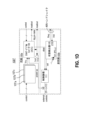
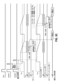
- 複数のスーパーピクセルを有するイメージセンサであって、前記スーパーピクセルはそれぞれ、
第1の受光素子と、
前記第1の受光素子に電気的に接続され、前記第1の受光素子に当たる光の明るさに比例するアナログ信号が条件に整合するときにトリガ信号を生成するように構成された検出器と、
少なくとも一つの第2の受光素子と、
前記少なくとも一つの第2の受光素子に電気的に接続された少なくとも一つの露出測定サブ回路と、
前記少なくとも一つの第2の受光素子に当たる光の明るさに比例するアナログ信号をデジタル信号に変換するように構成されたアナログ-デジタル回路であって、
前記アナログ-デジタル回路は、前記第1の受光素子に当たる光の明るさに比例するアナログ信号をデジタル信号に変換しない、アナログ-デジタル回路と、
前記検出器及び前記アナログ-デジタル回路に電気的に接続され、前記トリガ信号に応答して前記アナログ-デジタル回路をイネーブルするように構成された論理回路と、
を備える、イメージセンサ。 - 前記論理回路は、前記デジタル信号が前記アナログ-デジタル回路から読み出された後に前記アナログ-デジタル回路をディスエーブルするように更に構成される、請求項1に記載のイメージセンサ。
- 前記アナログ-デジタル回路は、前記デジタル信号を外部読出しシステムに出力するように更に構成される、請求項2に記載のイメージセンサ。
- 前記アナログ-デジタル回路は、前記アナログ信号の前記デジタル信号への変換が完了した後に、前記論理回路をリセットする信号を送信するように更に構成される、請求項2に記載のイメージセンサ。
- 前記論理回路は、外部制御信号に応答して前記アナログ-デジタル回路をイネーブルするように更に構成される、請求項1又は2に記載のイメージセンサ。
- 前記検出器は、前記トリガ信号を外部読出しシステムに出力するように更に構成される、請求項1又は2に記載のイメージセンサ。
- 前記外部読出しシステムは、前記トリガ信号に応答して前記検出器に確認応答信号を送信するように構成され、前記検出器は、前記確認応答信号に応答してリセットするように更に構成される、請求項6に記載のイメージセンサ。
- 前記論理回路は、
前記検出器に電気的に接続された制御論理及び前記制御論理によって制御されるスイッチと、
前記検出器に電気的に接続された制御論理並びに前記制御論理及び外部コントローラに接続された論理ゲートと、
のうちの少なくとも一方を備える、請求項1又は2に記載のイメージセンサ。 - 外部読出しシステムは、回路クロックに従って前記アナログ-デジタル回路からの出力を要求し、前記アナログ-デジタル回路は、その要求に応答して前記デジタル信号を出力するように構成される、請求項1又は2に記載のイメージセンサ。
- 複数の第2の受光素子と、
前記複数の第2の受光素子のうちの少なくとも一つを備える複数の露出測定サブ回路と、
を更に備える、請求項1に記載のイメージセンサ。 - 前記複数の第2の受光素子は、前記露出測定サブ回路のそれぞれの個別のコンデンサノードに前記アナログ信号をそれぞれ出力する、請求項10に記載のイメージセンサ。
- 前記複数の第2の受光素子のうちの少なくとも二つは、互いに異なる利得を有する、請求項11に記載のイメージセンサ。
- 前記複数の第2の受光素子は、互いに異なる時間に前記個別のコンデンサノードに前記アナログ信号をそれぞれ出力するように構成される、請求項11に記載のイメージセンサ。
- 前記複数の第2の受光素子は、前記アナログ信号を、前記複数の露出測定サブ回路によって共有されるコンデンサノードにそれぞれ出力するように構成される、請求項10に記載のイメージセンサ。
- 前記複数の第2の受光素子のうちの少なくとも二つは、
互いに異なる濃度フィルタと、互いに異なるカラーフィルタと、
のうちの少なくとも一方を有する、請求項10に記載のイメージセンサ。 - アナログ-デジタル回路の第1のトランジスタを備えるコンパレータは、前記複数の露出測定サブ回路のそれぞれに関連する少なくとも一つのトランジスタと結合される、請求項10に記載のイメージセンサ。
- 前記複数の露出測定サブ回路のそれぞれに関連する少なくとも一つのリセットトランジスタを更に備える、請求項16に記載のイメージセンサ。
- 前記少なくとも一つの露出測定サブ回路は、前記少なくとも一つの第2の受光素子のそれぞれに当たる光の明るさに比例するアナログ信号を出力する前に前記リセットトランジスタのそれぞれのリセット電圧を出力するように更に構成される、請求項17に記載のイメージセンサ。
- 前記少なくとも一つの露出測定サブ回路は、前記リセットトランジスタのそれぞれの前記リセット電圧を順次出力する、請求項18に記載のイメージセンサ。
- 前記リセット電圧を、ノイズ及び不整合に対して相関二重サンプリング(CDS)補正を実行するように構成された回路に出力する、請求項19に記載のイメージセンサ。
- イメージセンサで用いるスーパーピクセルであって、
第1の受光素子と、
前記第1の受光素子に電気的に接続され、前記第1の受光素子に当たる光の明るさに比例するアナログ信号が条件に整合するときにトリガ信号を生成するように構成された検出器と、
少なくとも一つの第2の受光素子と、
前記少なくとも一つの第2の受光素子に電気的に接続された少なくとも一つの露出測定サブ回路と、
前記少なくとも一つの第2の受光素子に当たる光の明るさに比例するアナログ信号をデジタル信号に変換するように構成されたアナログ-デジタル回路であって、
前記アナログ-デジタル回路は、前記第1の受光素子に当たる光の明るさに比例するアナログ信号をデジタル信号に変換しない、アナログ-デジタル回路と、
前記検出器及び前記アナログ-デジタル回路に電気的に接続され、前記トリガ信号に応答して前記アナログ-デジタル回路をイネーブルし、前記デジタル信号が前記アナログ-デジタル回路から読み出された後に前記アナログ-デジタル回路をディスエーブルするように構成された論理回路と、
を備えるスーパーピクセル。 - 前記論理回路は、
前記検出器に電気的に接続された制御論理及び前記制御論理によって制御されるスイッチと、
前記検出器に電気的に接続された制御論理並びに前記制御論理及び外部コントローラに接続された論理ゲートと、
のうちの少なくとも一方を備える、請求項21に記載のスーパーピクセル。 - 複数のスーパーピクセルを有するイメージセンサを制御する方法であって、
前記複数のスーパーピクセルのうちの一つのスーパーピクセルの第1の受光素子に当たる光に比例する第1のアナログ信号を受信することと、
検出器を用いて、前記第1のアナログ信号が条件に整合するときにトリガ信号を生成することと、
前記トリガ信号に応答して、アナログ-デジタル回路をイネーブルすることと、
前記一つのスーパーピクセルの少なくとも一つの第2の受光素子に当たる光に比例する少なくとも一つの第2のアナログ信号を受信することと、
前記アナログ-デジタル回路を用いて、少なくとも一つの前記第2のアナログ信号をデジタル信号に変換することと、
を備え、
前記アナログ-デジタル回路は、前記第1のアナログ信号をデジタル信号に変換せず、
前記トリガ信号を外部イベントシステムに出力することと、
前記トリガ信号に応答して前記外部イベントシステムから肯定応答信号を受信するとともに前記肯定応答信号に応答して前記検出器をリセットすることと、
を更に備える、方法。 - 前記少なくとも一つの第2のアナログ信号をデジタル信号に変換した後に前記アナログ-デジタル回路をディスエーブルすることと、
前記デジタル信号を外部読出しシステムに出力することと、
を更に備える、請求項23に記載の方法。 - 前記アナログ-デジタル回路を用いて、前記デジタル信号を外部読出しシステムに出力することを更に備える、請求項23又は24に記載の方法。
- アナログ信号から前記デジタル信号への変換を完了した後に、論理回路をリセットする信号を、前記アナログ-デジタル回路を用いて送信することを更に備える、請求項23~25のいずれか一項に記載の方法。
- 回路クロックに従って前記アナログ-デジタル回路の出力の要求を外部読出しシステムから受信することと、前記要求に応答して前記デジタル信号を出力することと、を更に備える、請求項23~25のいずれか一項に記載の方法。
- 複数のスーパーピクセルを有するイメージセンサを制御する方法であって、
前記複数のスーパーピクセルのうちの一つのスーパーピクセルの第1の受光素子に当たる光に比例する第1のアナログ信号を受信することと、
検出器を用いて、前記第1のアナログ信号が条件に整合するときにトリガ信号を生成することと、
前記トリガ信号に応答して、アナログ-デジタル回路をイネーブルすることと、
前記一つのスーパーピクセルの少なくとも一つの第2の受光素子に当たる光に比例する少なくとも一つの第2のアナログ信号を受信することと、
前記アナログ-デジタル回路を用いて、少なくとも一つの前記第2のアナログ信号をデジタル信号に変換することと、
前記デジタル信号が前記アナログ-デジタル回路から読み出された後に前記アナログ-デジタル回路をディスエーブルすることと、
を備え、
前記アナログ-デジタル回路は、前記第1のアナログ信号をデジタル信号に変換しない、方法。
Priority Applications (1)
| Application Number | Priority Date | Filing Date | Title |
|---|---|---|---|
| JP2023040521A JP2023075285A (ja) | 2018-06-27 | 2023-03-15 | 複数のスーパーピクセルを有するイメージセンサ |
Applications Claiming Priority (5)
| Application Number | Priority Date | Filing Date | Title |
|---|---|---|---|
| US201862690948P | 2018-06-27 | 2018-06-27 | |
| US62/690,948 | 2018-06-27 | ||
| US201862780913P | 2018-12-17 | 2018-12-17 | |
| US62/780,913 | 2018-12-17 | ||
| PCT/EP2019/067264 WO2020002562A1 (en) | 2018-06-27 | 2019-06-27 | Image sensor with a plurality of super-pixels |
Related Child Applications (1)
| Application Number | Title | Priority Date | Filing Date |
|---|---|---|---|
| JP2023040521A Division JP2023075285A (ja) | 2018-06-27 | 2023-03-15 | 複数のスーパーピクセルを有するイメージセンサ |
Publications (3)
| Publication Number | Publication Date |
|---|---|
| JP2021529467A JP2021529467A (ja) | 2021-10-28 |
| JPWO2020002562A5 JPWO2020002562A5 (ja) | 2022-07-04 |
| JP7248710B2 true JP7248710B2 (ja) | 2023-03-29 |
Family
ID=67139733
Family Applications (2)
| Application Number | Title | Priority Date | Filing Date |
|---|---|---|---|
| JP2020572682A Active JP7248710B2 (ja) | 2018-06-27 | 2019-06-27 | 複数のスーパーピクセルを有するイメージセンサ |
| JP2023040521A Pending JP2023075285A (ja) | 2018-06-27 | 2023-03-15 | 複数のスーパーピクセルを有するイメージセンサ |
Family Applications After (1)
| Application Number | Title | Priority Date | Filing Date |
|---|---|---|---|
| JP2023040521A Pending JP2023075285A (ja) | 2018-06-27 | 2023-03-15 | 複数のスーパーピクセルを有するイメージセンサ |
Country Status (6)
| Country | Link |
|---|---|
| US (2) | US11368645B2 (ja) |
| EP (2) | EP3811609A1 (ja) |
| JP (2) | JP7248710B2 (ja) |
| KR (2) | KR102612718B1 (ja) |
| CN (1) | CN112640431A (ja) |
| WO (1) | WO2020002562A1 (ja) |
Families Citing this family (9)
| Publication number | Priority date | Publication date | Assignee | Title |
|---|---|---|---|---|
| WO2020216953A1 (en) | 2019-04-25 | 2020-10-29 | Prophesee Sa | Systems and methods for imaging and sensing vibrations |
| CN111601056B (zh) * | 2020-05-14 | 2022-03-15 | 中国电子科技集团公司第四十四研究所 | 大动态范围半浮栅图像传感器 |
| EP3929864A1 (en) | 2020-06-23 | 2021-12-29 | Prophesee | Image enhancement method, apparatus and system |
| US11430828B2 (en) * | 2020-12-17 | 2022-08-30 | Omnivision Technologies, Inc. | Event driven pixel for spatial information extraction |
| US11652492B2 (en) | 2020-12-30 | 2023-05-16 | Analog Devices International Unlimited Company | Signal chain with embedded power management |
| US11516419B2 (en) | 2021-01-22 | 2022-11-29 | Omnivision Technologies, Inc. | Digital time stamping design for event driven pixel |
| CN114339001B (zh) * | 2021-12-30 | 2023-09-12 | 维沃移动通信有限公司 | 图像传感器、曝光控制方法、摄像模组和电子设备 |
| US11942960B2 (en) | 2022-01-31 | 2024-03-26 | Analog Devices, Inc. | ADC with precision reference power saving mode |
| CN116546340B (zh) * | 2023-07-05 | 2023-09-19 | 华中师范大学 | 一种高速cmos像素探测器 |
Citations (1)
| Publication number | Priority date | Publication date | Assignee | Title |
|---|---|---|---|---|
| JP2007295189A (ja) | 2006-04-24 | 2007-11-08 | Hamamatsu Photonics Kk | 固体撮像装置 |
Family Cites Families (24)
| Publication number | Priority date | Publication date | Assignee | Title |
|---|---|---|---|---|
| FR2762162A1 (fr) * | 1997-04-15 | 1998-10-16 | Philips Electronics Nv | Dispositif d'alignement numerique |
| EP1301028A1 (en) * | 2001-10-05 | 2003-04-09 | STMicroelectronics Limited | Improvements in or relating to CMOS Image sensors |
| JP2006303752A (ja) * | 2005-04-19 | 2006-11-02 | Sony Corp | 撮像装置 |
| SG162756A1 (en) | 2005-06-03 | 2010-07-29 | Universitaet Zuerich | Photoarray for detecting time-dependent image data |
| US7326906B2 (en) | 2006-06-03 | 2008-02-05 | Orbotech Medical Solutions Ltd. | Digital readout system |
| AT504582B1 (de) * | 2006-11-23 | 2008-12-15 | Arc Austrian Res Centers Gmbh | Verfahren zur generierung eines bildes in elektronischer form, bildelement für einen bildsensor zur generierung eines bildes sowie bildsensor |
| JP2009049870A (ja) * | 2007-08-22 | 2009-03-05 | Sony Corp | 固体撮像装置、撮像装置 |
| IL212289A (en) * | 2011-04-13 | 2016-08-31 | Semi-Conductor Devices - An Elbit Systems - Rafael Partnership | Circuit and method for reading image signals |
| WO2013092666A1 (en) | 2011-12-19 | 2013-06-27 | Universität Zürich | Photoarray, particularly for combining sampled brightness sensing with asynchronous detection of time-dependent image data |
| US9521337B1 (en) * | 2012-07-13 | 2016-12-13 | Rambus Inc. | Reset-marking pixel sensor |
| ES2476115B1 (es) | 2012-12-11 | 2015-04-20 | Consejo Superior De Investigaciones Científicas (Csic) | Metodo y dispositivo para la deteccion de la variacion temporal de la intensidad luminosa en una matriz de fotosensores |
| US9380245B1 (en) * | 2013-02-14 | 2016-06-28 | Rambus Inc. | Conditional-reset image sensor with analog counter array |
| JP6415532B2 (ja) * | 2013-03-15 | 2018-10-31 | ラムバス・インコーポレーテッド | 閾値を監視する条件付きリセットイメージセンサ |
| ES2811152T3 (es) | 2013-09-16 | 2021-03-10 | Prophesee | Circuito de píxel dinámico de un solo fotodiodo y método de funcionamiento del mismo |
| JP6369086B2 (ja) * | 2014-03-25 | 2018-08-08 | セイコーエプソン株式会社 | 物理量センサー、センサーユニット、電子機器及び移動体 |
| JP6545541B2 (ja) * | 2014-06-25 | 2019-07-17 | 株式会社半導体エネルギー研究所 | 撮像装置、監視装置、及び電子機器 |
| US9986179B2 (en) * | 2014-09-30 | 2018-05-29 | Qualcomm Incorporated | Sensor architecture using frame-based and event-based hybrid scheme |
| WO2017013806A1 (ja) * | 2015-07-23 | 2017-01-26 | オリンパス株式会社 | 固体撮像装置 |
| WO2017174579A1 (en) | 2016-04-04 | 2017-10-12 | Chronocam | Sample and hold based temporal contrast vision sensor |
| EP3313064A1 (en) | 2016-10-20 | 2018-04-25 | Chronocam | Pixel circuit for detecting time-dependent visual data |
| KR20230087615A (ko) * | 2016-12-30 | 2023-06-16 | 소니 어드밴스드 비주얼 센싱 아게 | 동적 비전 센서 아키텍쳐 |
| TW202408217A (zh) * | 2018-01-23 | 2024-02-16 | 日商索尼半導體解決方案公司 | 光檢測裝置及車輛控制系統 |
| US11412162B2 (en) | 2018-04-30 | 2022-08-09 | Prophesee | Systems and methods for asynchronous, time-based image sensing |
| JP2020088481A (ja) * | 2018-11-19 | 2020-06-04 | ソニーセミコンダクタソリューションズ株式会社 | 固体撮像素子、および、撮像装置 |
-
2019
- 2019-06-27 US US17/255,972 patent/US11368645B2/en active Active
- 2019-06-27 EP EP19735280.0A patent/EP3811609A1/en active Pending
- 2019-06-27 WO PCT/EP2019/067264 patent/WO2020002562A1/en unknown
- 2019-06-27 KR KR1020217002524A patent/KR102612718B1/ko active IP Right Grant
- 2019-06-27 KR KR1020237042252A patent/KR20230173210A/ko active Search and Examination
- 2019-06-27 CN CN201980056827.5A patent/CN112640431A/zh active Pending
- 2019-06-27 EP EP21187317.9A patent/EP3917134B1/en active Active
- 2019-06-27 JP JP2020572682A patent/JP7248710B2/ja active Active
-
2022
- 2022-05-06 US US17/662,412 patent/US11979673B2/en active Active
-
2023
- 2023-03-15 JP JP2023040521A patent/JP2023075285A/ja active Pending
Patent Citations (1)
| Publication number | Priority date | Publication date | Assignee | Title |
|---|---|---|---|---|
| JP2007295189A (ja) | 2006-04-24 | 2007-11-08 | Hamamatsu Photonics Kk | 固体撮像装置 |
Also Published As
| Publication number | Publication date |
|---|---|
| EP3917134B1 (en) | 2023-11-15 |
| US20220264050A1 (en) | 2022-08-18 |
| KR102612718B1 (ko) | 2023-12-19 |
| KR20230173210A (ko) | 2023-12-26 |
| JP2021529467A (ja) | 2021-10-28 |
| JP2023075285A (ja) | 2023-05-30 |
| US11979673B2 (en) | 2024-05-07 |
| US20210127083A1 (en) | 2021-04-29 |
| EP3811609A1 (en) | 2021-04-28 |
| US11368645B2 (en) | 2022-06-21 |
| KR20210024608A (ko) | 2021-03-05 |
| WO2020002562A1 (en) | 2020-01-02 |
| CN112640431A (zh) | 2021-04-09 |
| EP3917134A1 (en) | 2021-12-01 |
| EP3917134C0 (en) | 2023-11-15 |
Similar Documents
| Publication | Publication Date | Title |
|---|---|---|
| JP7248710B2 (ja) | 複数のスーパーピクセルを有するイメージセンサ | |
| EP2832090B1 (en) | Cmos image sensors implementing full frame digital correlated double sampling with global shutter | |
| US10531027B2 (en) | Backside illuminated global shutter pixel with active reset | |
| US9247170B2 (en) | Triple conversion gain image sensor pixels | |
| EP2974280B1 (en) | Threshold-monitoring, conditional-reset image sensor | |
| US10170514B2 (en) | Image sensor | |
| US9848141B2 (en) | Image pixels having processed signal storage capabilities | |
| US20090108176A1 (en) | Global shutter pixel circuit with transistor sharing for CMOS image sensors | |
| US20090219421A1 (en) | Image sensor with a capacitive storage node linked to transfer gate | |
| US20050128327A1 (en) | Device and method for image sensing | |
| US11317038B2 (en) | Pixel unit with a design for half row reading, an imaging apparatus including the same, and an imaging method thereof | |
| US20210258525A1 (en) | Event array readout control of event-based vision sensing | |
| EP3420592B1 (en) | Improved ultra-high dynamic range pixel architecture | |
| US11503229B2 (en) | Image sensor and imaging device including the same | |
| US11885673B2 (en) | Pixel circuit including an open-loop amplifier with well controlled gain for event-based vision sensor and method of controlling thereof | |
| US10623655B2 (en) | Image sensors with light flicker mitigation capabilities | |
| Bharathi et al. | Survey on performance of CMOS sensors |
Legal Events
| Date | Code | Title | Description |
|---|---|---|---|
| A521 | Request for written amendment filed |
Free format text: JAPANESE INTERMEDIATE CODE: A523 Effective date: 20220624 |
|
| A621 | Written request for application examination |
Free format text: JAPANESE INTERMEDIATE CODE: A621 Effective date: 20220624 |
|
| A871 | Explanation of circumstances concerning accelerated examination |
Free format text: JAPANESE INTERMEDIATE CODE: A871 Effective date: 20220624 |
|
| A131 | Notification of reasons for refusal |
Free format text: JAPANESE INTERMEDIATE CODE: A131 Effective date: 20220830 |
|
| A521 | Request for written amendment filed |
Free format text: JAPANESE INTERMEDIATE CODE: A523 Effective date: 20221128 |
|
| TRDD | Decision of grant or rejection written | ||
| A01 | Written decision to grant a patent or to grant a registration (utility model) |
Free format text: JAPANESE INTERMEDIATE CODE: A01 Effective date: 20230214 |
|
| A61 | First payment of annual fees (during grant procedure) |
Free format text: JAPANESE INTERMEDIATE CODE: A61 Effective date: 20230316 |
|
| R150 | Certificate of patent or registration of utility model |
Ref document number: 7248710 Country of ref document: JP Free format text: JAPANESE INTERMEDIATE CODE: R150 |