JP7206830B2 - Drawing data creation method for charged multi-beam writer - Google Patents
Drawing data creation method for charged multi-beam writer Download PDFInfo
- Publication number
- JP7206830B2 JP7206830B2 JP2018214422A JP2018214422A JP7206830B2 JP 7206830 B2 JP7206830 B2 JP 7206830B2 JP 2018214422 A JP2018214422 A JP 2018214422A JP 2018214422 A JP2018214422 A JP 2018214422A JP 7206830 B2 JP7206830 B2 JP 7206830B2
- Authority
- JP
- Japan
- Prior art keywords
- grid
- profile
- contour
- pixel
- drawing data
- Prior art date
- Legal status (The legal status is an assumption and is not a legal conclusion. Google has not performed a legal analysis and makes no representation as to the accuracy of the status listed.)
- Active
Links
Images


Landscapes
- Exposure And Positioning Against Photoresist Photosensitive Materials (AREA)
- Electron Beam Exposure (AREA)
Description
本発明は、荷電マルチビーム描画装置を用いたパターニング技術に関し、特に、荷電マルチビーム描画装置を用いてレジスト層に所定の露光パターンを形成する際に、描画に用いる描画データを作成する方法に関する。 The present invention relates to a patterning technique using a charged multi-beam drawing apparatus, and more particularly to a method of creating drawing data used for writing when forming a predetermined exposure pattern on a resist layer using a charged multi-beam drawing apparatus.
半導体デバイスの製造プロセスなど、特定の材料層に対して微細なパターニング加工を施す必要がある分野において、電子線などの荷電粒子ビームを照射する荷電粒子ビーム描画装置を利用したパターニング方法が広く利用されている。荷電粒子ビーム描画装置は、与えられた描画データに基づいて、被成形層に微細パターンを露光する機能を有しており、極めて細い線状パターンを形成することが可能になる。たとえば、下記の特許文献1には、シングルビーム方式の電子線描画装置および当該装置を用いて所望のパターンを描画する描画方法が開示されている。
A patterning method using a charged particle beam drawing apparatus that irradiates a charged particle beam such as an electron beam is widely used in fields such as the manufacturing process of semiconductor devices that require fine patterning processing on a specific material layer. ing. A charged particle beam drawing apparatus has a function of exposing a layer to be molded with a fine pattern based on given drawing data, and can form an extremely fine linear pattern. For example,
一方、最近では、同時に複数の荷電粒子ビームを照射することが可能なマルチビーム方式の描画装置も実用化されている。たとえば、特許文献2には、広げた電子ビームを複数の開口部を有するアパーチャープレートを通すことにより複数の電子ビームを生成し、これらをブランキングプレートを用いて個別にON/OFF制御しながら試料表面に所定のパターンを描画するマルチビーム方式の電子線描画装置が開示されている。また、特許文献3には、このようなマルチビーム方式の電子線描画装置を用いて、試料表面の同一箇所に複数回のビーム露光を行うことにより、階調をもったグレースケールパターンを描画する方法が開示されている。
On the other hand, recently, a multi-beam drawing apparatus capable of simultaneously irradiating a plurality of charged particle beams has also been put to practical use. For example, in
特許文献1に開示されているようなシングルビーム方式の描画装置に比べて、特許文献2,3に開示されているようなマルチビーム方式の描画装置では、複数の荷電粒子ビームを用いた同時描画が可能になるため、パターンの描画速度が圧倒的に速く、描画時間を大幅に短縮させるメリットが得られる。最近では、縦横に512×512の開口部をもったアパーチャープレートを通すことにより、25万本以上の電子ビームを生成し、これらを同時に照射しながら任意のパターンを描画する装置も実用化されている。
Compared to the single-beam lithography apparatus disclosed in
ただ、シングルビーム方式の描画装置の場合、1本のビームの断面形状を任意の形状に加工し、任意の強度に調節したビームを照射することができるのに対して、マルチビーム方式の描画装置の場合、個々のビームの断面形状を個別に制御したり、個々のビームの強度を個別に制御したりすることは困難である。たとえば、上例のように、25万本ものビームを生成する装置において、個々のビームの断面形状や強度を個別に制御することは、現在の技術では非常に困難である。 However, in the case of a single-beam system lithography system, the cross-sectional shape of a single beam can be processed into an arbitrary shape and the beam adjusted to an arbitrary intensity can be irradiated, whereas the multi-beam system system lithography system In the case of , it is difficult to individually control the cross-sectional shape of each beam or to individually control the intensity of each beam. For example, as in the above example, in a device that generates 250,000 beams, it is very difficult with current technology to individually control the cross-sectional shape and intensity of each beam.
このため、現在実用化されているマルチビーム方式の描画装置では、個々のビームの断面形状を同一形状に固定するとともに、個々のビームの強度も共通にせざるを得ない。結局、個々のビームをON/OFF制御することによって、所望のパターンを描画する方式を採らざるを得ない。そこで、特許文献3には、照射すべきビームの強度を示す画素値をもった二次元画素配列からなる描画データを用意し、露光対象面上の各部分に、対応する画素の画素値に応じた回数だけビームが照射されるような制御を行うことにより、階調をもった所望のパターンを露光する技術が開示されている。
For this reason, in a multi-beam drawing apparatus currently in practical use, the cross-sectional shape of each beam must be fixed to the same shape and the intensity of each beam must be made common. Ultimately, there is no choice but to adopt a method of writing a desired pattern by controlling ON/OFF of individual beams. Therefore, in
しかしながら、従来の荷電マルチビーム描画装置には、微細なパターンを形成しようとすると、実際に得られる実パターン上に寸法誤差が生じるという問題がある。特に、画素ピッチに満たないサブピクセルレベルでの寸法精度を維持して実パターンを形成することが困難である。たとえば、画素ピッチを10nmに設定した場合、線幅50nmの線状パターンや、線幅60nmの線状パターンというように、画素ピッチの整数倍となる線幅をもった線状パターンに比べて、線幅53nmの線状パターン、線幅56nmの線状パターンといったサブピクセル単位の線幅をもった線状パターンについては、いわゆるエッジポジションエラーが大きくなり、正確な寸法精度をもったパターニングを行うことが困難になる。 However, the conventional charged multi-beam lithography apparatus has a problem that when a fine pattern is to be formed, a dimensional error occurs on the actual pattern that is actually obtained. In particular, it is difficult to form an actual pattern while maintaining dimensional accuracy at the sub-pixel level, which is less than the pixel pitch. For example, when the pixel pitch is set to 10 nm, compared to a linear pattern with a line width that is an integral multiple of the pixel pitch, such as a linear pattern with a line width of 50 nm and a linear pattern with a line width of 60 nm, A linear pattern with a line width of 53 nm and a line pattern with a line width of 56 nm, which have a line width in units of sub-pixels, increases the so-called edge position error. becomes difficult.
そこで本発明は、微細なパターンについても精度の高いパターニングを行うことができる荷電マルチビーム描画装置用の描画データを作成することを目的とする。 SUMMARY OF THE INVENTION It is therefore an object of the present invention to create writing data for a charged multi-beam writing apparatus capable of patterning even fine patterns with high accuracy.
(1) 本発明の第1の態様は、荷電マルチビーム描画装置を用いてレジスト層に所定の露光パターンを形成するための描画データを作成する荷電マルチビーム描画装置の描画データ作成方法において、
描画の対象となる対象図形の輪郭線の情報を示す図形データを入力する図形データ入力段階と、
図形データに対してラスタライズ処理を行うことにより、個々のビームの照射位置の露光強度を示す画素値をもった画素の二次元配列によって構成される基本描画データを作成する基本描画データ作成段階と、
基本描画データを構成する画素のうち、対象図形の輪郭線の近傍に位置する輪郭近傍画素の画素値に対して、画素配列の周期に対する当該輪郭線位置の位相に基づく修正を行うことにより修正描画データを作成する輪郭近傍修正段階と、
を行うようにしたものである。
(1) A first aspect of the present invention is a drawing data creation method for a charged multi-beam drawing device for creating drawing data for forming a predetermined exposure pattern on a resist layer using a charged multi-beam drawing device, comprising:
a figure data input step of inputting figure data indicating information on the outline of a target figure to be drawn;
a basic drawing data creation step of creating basic drawing data composed of a two-dimensional array of pixels having pixel values indicating the exposure intensity of the irradiation positions of the individual beams by performing rasterization processing on the figure data;
Correction drawing by correcting the pixel values of contour neighboring pixels located near the contour of the target figure among the pixels constituting the basic drawing data based on the phase of the contour position with respect to the period of the pixel array a contour neighborhood correction step for creating data;
It is designed to perform
(2) 本発明の第2の態様は、上述した第1の態様に係る荷電マルチビーム描画装置の描画データ作成方法において、
輪郭近傍修正段階で、対象図形を構成する個々の輪郭線について、画素の境界に位置するONグリッド輪郭線か、画素の境界に位置しないOFFグリッド輪郭線か、を認識する輪郭線のON/OFF認識処理を行い、ONグリッド輪郭線の近傍に位置するONグリッド画素の画素値と、OFFグリッド輪郭線の近傍に位置するOFFグリッド画素の画素値とを、必要に応じて、互いに異なる方法で修正する画素値の修正処理を行うようにしたものである。
(2) A second aspect of the present invention is the writing data creation method for the charged multi-beam writing apparatus according to the first aspect described above, comprising:
In the contour vicinity correction stage, for each contour line that constitutes the object figure, ON/OFF of the contour line that recognizes whether it is an ON grid contour line located on the boundary of the pixel or an OFF grid contour line that is not located on the boundary of the pixel. Recognition processing is performed to modify pixel values of ON-grid pixels located near ON-grid contours and pixel values of OFF-grid pixels located near OFF-grid contours by different methods as necessary. In this case, the pixel value correction process is performed.
(3) 本発明の第3の態様は、上述した第2の態様に係る荷電マルチビーム描画装置の描画データ作成方法において、
輪郭近傍修正段階で、対象図形の輪郭線に直交する方向に関する露光強度の分布を示すプロファイルを、荷電マルチビーム描画装置のビーム特性およびレジスト層の感光特性を考慮して求め、ONグリッド輪郭線の近傍について求めたプロファイルをONグリッドプロファイルPon、OFFグリッド輪郭線の近傍について求めたプロファイルをOFFグリッドプロファイルPoff としたときに、ONグリッドプロファイルPonの形状と、OFFグリッドプロファイルPoff の形状と、が一致もしくは近似するように、画素値の修正を行うようにしたものである。
(3) A third aspect of the present invention is the writing data creation method for the charged multi-beam writing apparatus according to the second aspect described above,
In the contour vicinity correction step, a profile indicating the exposure intensity distribution in the direction orthogonal to the contour of the object figure is obtained in consideration of the beam characteristics of the charged multi-beam writing device and the photosensitive characteristics of the resist layer, and the ON grid contour is determined. When the ON grid profile Pon is the profile obtained for the vicinity and the OFF grid profile Poff is the profile obtained for the vicinity of the OFF grid outline, the shape of the ON grid profile Pon and the shape of the OFF grid profile Poff match or match. The pixel values are corrected so as to be approximated.
(4) 本発明の第4の態様は、上述した第3の態様に係る荷電マルチビーム描画装置の描画データ作成方法において、
輪郭近傍修正段階で、ONグリッドプロファイルPonの形状を、OFFグリッドプロファイルPoff の形状に近づけるように、ONグリッド画素の画素値に対する修正を行うようにしたものである。
(4) A fourth aspect of the present invention is the writing data creation method for the charged multi-beam writing apparatus according to the third aspect described above, comprising:
In the contour vicinity correction stage, the pixel values of the ON grid pixels are corrected so that the shape of the ON grid profile Pon approaches the shape of the OFF grid profile Poff.
(5) 本発明の第5の態様は、上述した第4の態様に係る荷電マルチビーム描画装置の描画データ作成方法において、
輪郭近傍修正段階で、ONグリッドプロファイルPonの傾斜をより緩慢にすることにより、ONグリッドプロファイルPonの形状をOFFグリッドプロファイルPoff の形状に近づけるようにしたものである。
(5) A fifth aspect of the present invention is the writing data creation method for the charged multi-beam writing apparatus according to the fourth aspect described above, comprising:
By making the slope of the ON grid profile Pon gentler in the contour vicinity correction stage, the shape of the ON grid profile Pon is brought closer to the shape of the OFF grid profile Poff.
(6) 本発明の第6の態様は、上述した第5の態様に係る荷電マルチビーム描画装置の描画データ作成方法において、
輪郭近傍修正段階で、ONグリッド輪郭線の内側近傍のONグリッド画素に対しては画素値を減じ、外側近傍のONグリッド画素に対しては画素値を増加する修正を行うようにしたものである。
(6) A sixth aspect of the present invention is the writing data creation method for the charged multi-beam writing apparatus according to the fifth aspect described above, comprising:
In the contour vicinity correction stage, the pixel values of the ON grid pixels near the inside of the ON grid contour line are reduced, and the pixel values of the ON grid pixels near the outside of the ON grid contour are increased. .
(7) 本発明の第7の態様は、上述した第3~第6の態様に係る荷電マルチビーム描画装置の描画データ作成方法において、
荷電マルチビーム描画装置のビーム特性およびレジスト層の感光特性ごとに、所定の標準モデル図形についてのONグリッドプロファイルおよびOFFグリッドプロファイルを、それぞれONグリッド標準プロファイルPon(std) およびOFFグリッド標準プロファイルPoff (std) として求めておき、ONグリッド標準プロファイルPon(std) の形状と、OFFグリッド標準プロファイルPoff (std) の形状と、が近づく修正が行われるように、輪郭近傍画素の画素値に対する増減割合を、個々のビーム特性および個々の感光特性の組み合わせごとに標準モデル修正テーブルとして定めておき、
輪郭近傍修正段階で、標準モデル修正テーブルを参照することにより、輪郭近傍画素の画素値の修正を行い、修正描画データを作成するようにしたものである。
(7) A seventh aspect of the present invention is a writing data creation method for a charged multi-beam writing apparatus according to the third to sixth aspects described above, comprising:
The ON grid profile and the OFF grid profile for a given standard model figure are defined as ON grid standard profile Pon(std) and OFF grid standard profile Poff (std ), and the ratio of increase/decrease with respect to the pixel value of the pixel near the contour is calculated so that the shape of the ON grid standard profile Pon(std) and the shape of the OFF grid standard profile Poff(std) become closer to each other. Define a standard model correction table for each combination of individual beam characteristics and individual photosensitive characteristics,
In the outline vicinity correction stage, by referring to the standard model correction table, the pixel values of the pixels near the outline are corrected to create corrected drawing data.
(8) 本発明の第8の態様は、上述した第7の態様に係る荷電マルチビーム描画装置の描画データ作成方法において、
所定の標準モデル図形として、画素の境界に位置するONグリッド輪郭線と、画素の境界に対して当該画素の半ピッチ分ずれた位置にある1/2-OFFグリッド輪郭線と、を含む図形を用い、ONグリッド輪郭線の近傍の露光強度を示すプロファイルをONグリッド標準プロファイルPon(std) とし、1/2-OFFグリッド輪郭線の近傍の露光強度を示すプロファイルをOFFグリッド標準プロファイルPoff (std) とするようにしたものである。
(8) An eighth aspect of the present invention is the writing data creation method for the charged multi-beam writing apparatus according to the seventh aspect described above, comprising:
As a predetermined standard model figure, a figure including an ON grid contour line located at the boundary of a pixel and a 1/2-OFF grid contour line located at a position shifted by half the pitch of the pixel with respect to the boundary of the pixel is used. The profile indicating the exposure intensity in the vicinity of the ON grid contour is defined as the ON grid standard profile Pon(std), and the profile indicating the exposure intensity in the vicinity of the 1/2-OFF grid contour is defined as the OFF grid standard profile Poff(std). It is designed to be
(9) 本発明の第9の態様は、上述した第3~第6の態様に係る荷電マルチビーム描画装置の描画データ作成方法において、
輪郭近傍修正段階で、輪郭近傍画素の画素値を予め定められた試行量だけ増減する補正を行い、補正後の画素値をもった描画データに基づいてONグリッドプロファイルPonとOFFグリッドプロファイルPoff と、をそれぞれ演算する補正試行処理を、ONグリッドプロファイルPonの形状と、OFFグリッドプロファイルPoff の形状と、の相違が、予め定めた許容誤差範囲内に収まるまで繰り返し実行し、最終的に得られた描画データを修正描画データとするようにしたものである。
(9) A ninth aspect of the present invention is a writing data creation method for a charged multi-beam writing apparatus according to the third to sixth aspects described above, comprising:
In the contour vicinity correction stage, correction is performed by increasing or decreasing the pixel values of the pixels near the contour by a predetermined trial amount, and based on the drawing data having the corrected pixel values, the ON grid profile Pon and the OFF grid profile Poff, is repeatedly executed until the difference between the shape of the ON grid profile Pon and the shape of the OFF grid profile Poff falls within a predetermined allowable error range. The data is used as corrected drawing data.
(10) 本発明の第10の態様は、上述した第2の態様に係る荷電マルチビーム描画装置の描画データ作成方法において、
輪郭近傍修正段階で、対象図形の輪郭線に直交する方向に関する露光強度の分布を示すプロファイルを、荷電マルチビーム描画装置のビーム特性およびレジスト層の感光特性を考慮して求め、ONグリッド輪郭線の近傍について求めたプロファイルをONグリッドプロファイルPon、OFFグリッド輪郭線の近傍について求めたプロファイルをOFFグリッドプロファイルPoff としたときに、ONグリッドプロファイルPonの形状と、OFFグリッドプロファイルPoff の形状とが、それぞれ、両者の中間に位置する所定の参照プロファイルPref の形状に近づくように、画素値の修正を行うようにしたものである。
(10) A tenth aspect of the present invention is the writing data creation method for the charged multi-beam writing apparatus according to the second aspect described above, comprising:
In the contour vicinity correction step, a profile indicating the exposure intensity distribution in the direction orthogonal to the contour of the object figure is obtained in consideration of the beam characteristics of the charged multi-beam writing device and the photosensitive characteristics of the resist layer, and the ON grid contour is determined. When the ON grid profile Pon is the profile obtained for the vicinity and the OFF grid profile Poff is the profile obtained for the vicinity of the OFF grid outline, the shape of the ON grid profile Pon and the shape of the OFF grid profile Poff are respectively as follows. The pixel values are corrected so as to approximate the shape of a predetermined reference profile Pref located between the two.
(11) 本発明の第11の態様は、上述した第10の態様に係る荷電マルチビーム描画装置の描画データ作成方法において、
輪郭近傍修正段階で、ONグリッドプロファイルPonの傾斜をより緩慢にすることにより、ONグリッドプロファイルPonの形状を参照プロファイルPref の形状に近づけ、OFFグリッドプロファイルPoff の傾斜をより急峻にすることにより、OFFグリッドプロファイルPoff の形状を参照プロファイルPref の形状に近づけるようにしたものである。
(11) An eleventh aspect of the present invention is the writing data creation method for the charged multi-beam writing apparatus according to the tenth aspect described above, comprising:
In the contour vicinity correction stage, the slope of the ON grid profile Pon is made gentler to make the shape of the ON grid profile Pon closer to the shape of the reference profile Pref, and the slope of the OFF grid profile Poff is made steeper to make the OFF The shape of the grid profile Poff is approximated to the shape of the reference profile Pref.
(12) 本発明の第12の態様は、上述した第11の態様に係る荷電マルチビーム描画装置の描画データ作成方法において、
輪郭近傍修正段階で、ONグリッド輪郭線の内側近傍のONグリッド画素に対しては画素値を減じ、外側近傍のONグリッド画素に対しては画素値を増加する修正を行い、OFFグリッド輪郭線上のOFFグリッド画素に対しては画素値を減じる修正を行うようにしたものである。
(12) A twelfth aspect of the present invention is the writing data creation method for the charged multi-beam writing apparatus according to the above-described eleventh aspect, comprising:
In the contour vicinity correction step, the pixel values of the ON grid pixels near the inside of the ON grid contour are reduced, and the pixel values of the ON grid pixels near the outside are increased. Correction is made to reduce the pixel value for OFF grid pixels.
(13) 本発明の第13の態様は、上述した第10~第12の態様に係る荷電マルチビーム描画装置の描画データ作成方法において、
荷電マルチビーム描画装置のビーム特性およびレジスト層の感光特性ごとに、所定の標準モデル図形についてのONグリッドプロファイル、OFFグリッドプロファイル、および参照プロファイルを、それぞれONグリッド標準プロファイルPon(std) 、OFFグリッド標準プロファイルPoff (std) 、および参照標準プロファイルPref (std) として求めておき、ONグリッド標準プロファイルPon(std) の形状が参照標準プロファイルPref (std) に近づき、OFFグリッド標準プロファイルPoff (std) の形状が参照標準プロファイルPref (std) に近づく修正が行われるように、輪郭近傍画素の画素値に対する増減割合を、個々のビーム特性および個々の感光特性の組み合わせごとに標準モデル修正テーブルとして定めておき、
輪郭近傍修正段階で、標準モデル修正テーブルを利用して輪郭近傍画素の画素値の修正を行い、修正描画データを作成するようにしたものである。
(13) A thirteenth aspect of the present invention is the writing data creation method for the charged multi-beam writing apparatus according to the tenth to twelfth aspects described above, comprising:
For each beam characteristic of the charged multi-beam writer and the photosensitive characteristic of the resist layer, the ON grid profile, the OFF grid profile, and the reference profile for a given standard model figure are defined as ON grid standard profile Pon(std), OFF grid standard, respectively. A profile Poff(std) and a reference standard profile Pref(std) are obtained. In order to correct the reference standard profile Pref (std) to approach the reference standard profile Pref (std), the rate of increase or decrease with respect to the pixel value of pixels near the contour is defined as a standard model correction table for each combination of individual beam characteristics and individual photosensitive characteristics,
In the contour neighborhood correction stage, the standard model correction table is used to correct the pixel values of the contour neighborhood pixels to create corrected drawing data.
(14) 本発明の第14の態様は、上述した第13の態様に係る荷電マルチビーム描画装置の描画データ作成方法において、
所定の標準モデル図形として、画素の境界に位置するONグリッド輪郭線と、画素の境界に対して当該画素の半ピッチ分ずれた位置にある1/2-OFFグリッド輪郭線と、を含む図形を用い、ONグリッド輪郭線の近傍の露光強度を示すプロファイルをONグリッド標準プロファイルPon(std) とし、1/2-OFFグリッド輪郭線の近傍の露光強度を示すプロファイルをOFFグリッド標準プロファイルPoff (std) とするようにしたものである。
(14) A fourteenth aspect of the present invention is the writing data creation method for the charged multi-beam writing apparatus according to the thirteenth aspect described above, comprising:
As a predetermined standard model figure, a figure including an ON grid contour line located at the boundary of a pixel and a 1/2-OFF grid contour line located at a position shifted by half the pitch of the pixel with respect to the boundary of the pixel is used. The profile indicating the exposure intensity in the vicinity of the ON grid contour is defined as the ON grid standard profile Pon(std), and the profile indicating the exposure intensity in the vicinity of the 1/2-OFF grid contour is defined as the OFF grid standard profile Poff(std). It is designed to be
(15) 本発明の第15の態様は、上述した第10~第12の態様に係る荷電マルチビーム描画装置の描画データ作成方法において、
輪郭近傍修正段階で、輪郭近傍画素の画素値を予め定められた試行量だけ増減する補正を行い、補正後の画素値をもった描画データに基づいてONグリッドプロファイルPonとOFFグリッドプロファイルPoff とをそれぞれ演算する補正試行処理を、ONグリッドプロファイルPonの形状と参照プロファイルPref の形状との相違、およびOFFグリッドプロファイルPoff の形状と参照プロファイルPref の形状との相違が、予め定めた許容誤差範囲内に収まるまで繰り返し実行し、最終的に得られた描画データを修正描画データとするようにしたものである。
(15) A fifteenth aspect of the present invention is a writing data creation method for a charged multi-beam writing apparatus according to the tenth to twelfth aspects described above, comprising:
In the contour vicinity correction stage, the pixel values of the pixels near the contour are corrected to increase or decrease by a predetermined trial amount, and the ON grid profile Pon and the OFF grid profile Poff are generated based on the drawing data having the corrected pixel values. The difference between the shape of the ON grid profile Pon and the shape of the reference profile Pref and the difference between the shape of the OFF grid profile Poff and the shape of the reference profile Pref are within a predetermined allowable error range. Execution is repeated until it is settled, and finally obtained drawing data is used as corrected drawing data.
(16) 本発明の第16の態様は、上述した第10~第15の態様に係る荷電マルチビーム描画装置の描画データ作成方法において、
参照プロファイルPref として、ONグリッドプロファイルPonの傾斜とOFFグリッドプロファイルPoff の傾斜との中間的な傾斜をもつプロファイルを設定するようにしたものである。
(16) A sixteenth aspect of the present invention is the writing data creation method for the charged multi-beam writing apparatus according to the tenth to fifteenth aspects described above, comprising:
As the reference profile Pref, a profile having an intermediate slope between the slope of the ON grid profile Pon and the slope of the OFF grid profile Poff is set.
(17) 本発明の第17の態様は、上述した第2の態様に係る荷電マルチビーム描画装置の描画データ作成方法において、
レジスト層に、パターニングの成形に影響を与えるほどの組成変化を生じさせるために必要な総露光強度の臨界を示す閾値Ethを求めておき、
輪郭近傍修正段階で、対象図形の輪郭線に直交する方向に関する露光強度の分布を示すプロファイルを、荷電マルチビーム描画装置のビーム特性およびレジスト層の感光特性を考慮して求め、ONグリッド輪郭線の近傍について求めたプロファイルをONグリッドプロファイルPon、OFFグリッド輪郭線の近傍について求めたプロファイルをOFFグリッドプロファイルPoff としたときに、ONグリッドプロファイルPonと、OFFグリッドプロファイルPoff と、の交点位置の露光強度が、総露光強度の閾値Ethに一致もしくは近似するように、画素値の修正を行うようにしたものである。
(17) A seventeenth aspect of the present invention is the writing data creation method for the charged multi-beam writing apparatus according to the second aspect described above, comprising:
obtaining a threshold value Eth indicating the criticality of the total exposure intensity required to cause a compositional change in the resist layer to the extent that it affects the forming of patterning;
In the contour vicinity correction step, a profile indicating the exposure intensity distribution in the direction orthogonal to the contour of the object figure is obtained in consideration of the beam characteristics of the charged multi-beam writing device and the photosensitive characteristics of the resist layer, and the ON grid contour is determined. When the ON grid profile Pon is the profile obtained for the neighborhood and the OFF grid profile Poff is the profile obtained for the neighborhood of the OFF grid outline, the exposure intensity at the intersection of the ON grid profile Pon and the OFF grid profile Poff is , the pixel value is corrected so as to match or approximate the threshold value Eth of the total exposure intensity.
(18) 本発明の第18の態様は、上述した第17の態様に係る荷電マルチビーム描画装置の描画データ作成方法において、
輪郭近傍修正段階で、ONグリッドプロファイルPonのグラフもしくはOFFグリッドプロファイルPoff のグラフ、またはその双方を、露光強度を示す軸方向に移動することにより、交点位置の露光強度が、総露光強度の閾値Ethに一致もしくは近似するように、画素値の修正を行うようにしたものである。
(18) An eighteenth aspect of the present invention is the writing data creation method for the charged multi-beam writing apparatus according to the seventeenth aspect described above, comprising:
In the contour vicinity correction stage, the graph of the ON grid profile Pon or the graph of the OFF grid profile Poff, or both, are moved in the direction of the axis indicating the exposure intensity, so that the exposure intensity at the intersection position is equal to the threshold value Eth of the total exposure intensity. The pixel value is corrected so that it matches or approximates to .
(19) 本発明の第19の態様は、上述した第18の態様に係る荷電マルチビーム描画装置の描画データ作成方法において、
輪郭近傍修正段階で、OFFグリッド輪郭線の近傍画素もしくはONグリッド輪郭線の近傍画素に対して、画素値を増減する修正を行うようにしたものである。
(19) A nineteenth aspect of the present invention is the writing data creation method for the charged multi-beam writing apparatus according to the eighteenth aspect described above, comprising:
In the contour vicinity correction stage, correction is performed by increasing or decreasing the pixel values of the pixels near the OFF grid contour or the pixels near the ON grid contour.
(20) 本発明の第20の態様は、上述した第17~第19の態様に係る荷電マルチビーム描画装置の描画データ作成方法において、
荷電マルチビーム描画装置のビーム特性およびレジスト層の感光特性ごとに、所定の標準モデル図形についてのONグリッドプロファイルおよびOFFグリッドプロファイルを、それぞれONグリッド標準プロファイルPon(std) およびOFFグリッド標準プロファイルPoff (std) として求めておき、ONグリッド標準プロファイルPon(std) と、OFFグリッド標準プロファイルPoff (std) と、の交点位置の露光強度が、総露光強度の閾値Ethとなる修正が行われるように、輪郭近傍画素の画素値に対する増減割合を、個々のビーム特性および個々の感光特性の組み合わせごとに標準モデル修正テーブルとして定めておき、
輪郭近傍修正段階で、標準モデル修正テーブルを参照することにより、輪郭近傍画素の画素値の修正を行い、修正描画データを作成するようにしたものである。
(20) A twentieth aspect of the present invention is the writing data creation method for the charged multi-beam writing apparatus according to the seventeenth to nineteenth aspects described above, comprising:
The ON grid profile and the OFF grid profile for a given standard model figure are defined as ON grid standard profile Pon(std) and OFF grid standard profile Poff (std ), and the exposure intensity at the intersection of the ON grid standard profile Pon(std) and the OFF grid standard profile Poff(std) is corrected to the threshold Eth of the total exposure intensity. Predetermining the rate of increase or decrease with respect to the pixel value of neighboring pixels as a standard model correction table for each combination of individual beam characteristics and individual photosensitivity characteristics,
In the outline vicinity correction stage, by referring to the standard model correction table, the pixel values of the pixels near the outline are corrected to create corrected drawing data.
(21) 本発明の第21の態様は、上述した第20の態様に係る荷電マルチビーム描画装置の描画データ作成方法において、
所定の標準モデル図形として、画素の境界に位置するONグリッド輪郭線と、画素の境界に対して当該画素の半ピッチ分ずれた位置にある1/2-OFFグリッド輪郭線と、を含む図形を用い、ONグリッド輪郭線の近傍の露光強度を示すプロファイルをONグリッド標準プロファイルPon(std) とし、1/2-OFFグリッド輪郭線の近傍の露光強度を示すプロファイルをOFFグリッド標準プロファイルPoff (std) とするようにしたものである。
(21) A twenty-first aspect of the present invention is the writing data creation method for the charged multi-beam writing apparatus according to the above-described twentieth aspect, comprising:
As a predetermined standard model figure, a figure including an ON grid contour line located at the boundary of a pixel and a 1/2-OFF grid contour line located at a position shifted by half the pitch of the pixel with respect to the boundary of the pixel is used. The profile indicating the exposure intensity in the vicinity of the ON grid contour is defined as the ON grid standard profile Pon(std), and the profile indicating the exposure intensity in the vicinity of the 1/2-OFF grid contour is defined as the OFF grid standard profile Poff(std). It is designed to be
(22) 本発明の第22の態様は、上述した第17~第19の態様に係る荷電マルチビーム描画装置の描画データ作成方法において、
輪郭近傍修正段階で、輪郭近傍画素の画素値を予め定められた試行量だけ増減する補正を行い、補正後の画素値をもった描画データに基づいてONグリッドプロファイルPonとOFFグリッドプロファイルPoff とをそれぞれ演算する補正試行処理を、ONグリッドプロファイルPonと、OFFグリッドプロファイルPoff と、の交点位置の露光強度と、総露光強度の閾値Ethと、の差が予め定めた許容誤差範囲内に収まるまで繰り返し実行し、最終的に得られた描画データを修正描画データとするようにしたものである。
(22) A twenty-second aspect of the present invention is the writing data creation method for the charged multi-beam writing apparatus according to the seventeenth to nineteenth aspects described above, comprising:
In the contour vicinity correction stage, the pixel values of the pixels near the contour are corrected to increase or decrease by a predetermined trial amount, and the ON grid profile Pon and the OFF grid profile Poff are generated based on the drawing data having the corrected pixel values. The correction trial process for calculating each is repeated until the difference between the exposure intensity at the intersection position of the ON grid profile Pon and the OFF grid profile Poff and the threshold value Eth of the total exposure intensity falls within a predetermined allowable error range. Execution, and finally obtained drawing data is used as corrected drawing data.
(23) 本発明の第23の態様は、上述した第1~第22の態様に係る荷電マルチビーム描画装置の描画データ作成方法において、
基本描画データ作成段階で、対象図形の内部に完全に含まれる完全画素については画素値M(Mは2以上の整数)を、対象図形を全く含まない空画素については画素値0を、対象図形を部分的に含む不完全画素については対象図形の含有率に応じて定まる0~Mの階調値(0およびMを含む)を、それぞれ画素値として与える処理を行うようにしたものである。
(23) A twenty-third aspect of the present invention is the writing data creation method for the charged multi-beam writing apparatus according to the first to twenty-second aspects described above, comprising:
At the basic drawing data creation stage, the pixel value M (M is an integer equal to or greater than 2) is assigned to complete pixels inside the target figure, the
(24) 本発明の第24の態様は、上述した第1~第23の態様に係る荷電マルチビーム描画装置の描画データ作成方法において、
荷電マルチビーム描画装置のビーム特性として、少なくともビーム断面のエネルギー密度分布を考慮し、レジスト層の感光特性として、少なくともレジスト材料の感光感度および前方散乱や後方散乱によるエネルギー吸収特性を考慮するようにしたものである。
(24) A twenty-fourth aspect of the present invention is the writing data creation method for the charged multi-beam writing apparatus according to the first to twenty-third aspects described above, comprising:
At least the energy density distribution in the cross section of the beam is taken into account as the beam characteristics of the charged multi-beam lithography system, and at least the photosensitivity of the resist material and the energy absorption characteristics due to forward and backward scattering are taken into account as the photosensitivity characteristics of the resist layer. It is.
(25) 本発明の第25の態様は、上述した第1~第24の態様に係る荷電マルチビーム描画装置の描画データ作成方法において、
図形データ入力段階で、一対の短辺と一対の長辺とを有する矩形からなる線状パターンの図形データを入力し、
輪郭近傍修正段階で、長辺を輪郭線とする輪郭近傍画素の画素値に対して修正を行い、レジスト層に形成される露光パターンの短辺の寸法を修正するようにしたものである。
(25) A twenty-fifth aspect of the present invention is the writing data creation method for the charged multi-beam writing apparatus according to the first to twenty-fourth aspects described above, comprising:
inputting figure data of a linear pattern consisting of a rectangle having a pair of short sides and a pair of long sides in a figure data input stage;
In the contour vicinity correction step, the pixel values of the pixels near the contour having the long side as the contour line are corrected to correct the dimension of the short side of the exposure pattern formed on the resist layer.
(26) 本発明の第26の態様は、上述した第1~第25の態様に係る荷電マルチビーム描画装置の描画データ作成方法において、
図形データ入力段階、基本描画データ作成段階、および輪郭近傍修正段階を、所定のプログラムを組み込んだコンピュータに実行させるようにしたものである。
(26) A twenty-sixth aspect of the present invention is a writing data creation method for a charged multi-beam writing apparatus according to the first to twenty-fifth aspects described above, comprising:
A figure data input stage, a basic drawing data creation stage, and a contour vicinity correction stage are executed by a computer in which a predetermined program is installed.
(27) 本発明の第27の態様は、上述した第26の態様に係るプログラムを組み込んだコンピュータによって、荷電マルチビーム描画装置用の描画データを作成する装置を構成したものである。 (27) In a twenty-seventh aspect of the present invention, a computer in which the program according to the twenty-sixth aspect is incorporated constitutes an apparatus for creating writing data for a charged multi-beam writing apparatus.
本発明に係る描画データ作成方法では、荷電マルチビーム描画装置に用いる描画データを作成する際に、従来の一般的な方法で作成された基本描画データの中の輪郭近傍画素の画素値に対して修正が施される。しかも、この修正は、画素配列の周期に対する輪郭線位置の位相に基づいてなされる。このため、画素の境界に位置するONグリッド輪郭線の近傍に位置する画素と、画素の境界には位置しないOFFグリッド輪郭線の近傍に位置する画素と、に対して、互いに異なる方法で修正が行われることになり、ONグリッド輪郭線とOFFグリッド輪郭線との相違に基づく誤差要因を排除することができる。したがって、本発明によれば、微細なパターンについても精度の高いパターニングを行うことができる荷電マルチビーム描画装置用の描画データを作成することが可能になる。 In the drawing data creation method according to the present invention, when creating drawing data to be used in a charged multi-beam drawing apparatus, the pixel values of the pixels near the contour in the basic drawing data created by a conventional general method are Corrections are made. Moreover, this correction is made based on the phase of the contour position with respect to the period of the pixel array. For this reason, pixels positioned near ON grid contours positioned on pixel boundaries and pixels positioned near OFF grid contours not positioned on pixel boundaries are modified in different ways. It is possible to eliminate the error factor based on the difference between the ON grid contour and the OFF grid contour. Therefore, according to the present invention, it is possible to create writing data for a charged multi-beam writing apparatus capable of patterning even fine patterns with high accuracy.
以下、本発明を図示する実施形態に基づいて説明する。なお、本発明は、荷電マルチビーム描画装置を用いてレジスト層に所定の露光パターンを形成するための描画データを作成する工程に広く利用可能であるが、以下、説明の便宜上、荷電マルチビーム描画装置として、電子線描画装置を用いた実施例を述べることにする。もちろん、本発明は、電子ビーム以外の荷電粒子ビームを用いたマルチビーム描画装置に広く適用可能である。 Hereinafter, the present invention will be described based on illustrated embodiments. The present invention can be widely used in the process of creating writing data for forming a predetermined exposure pattern on a resist layer using a charged multi-beam writing apparatus. An embodiment using an electron beam lithography system as the system will be described. Of course, the present invention is widely applicable to multi-beam drawing apparatuses using charged particle beams other than electron beams.
<<< §1. マルチビーム電子線描画装置による描画原理 >>>
ここでは、本発明の理解を容易にするために、一般的なマルチビーム電子線描画装置による描画原理を簡単に説明しておく。図1は、この電子線描画装置の基本構造およびその描画原理を示す正面図である(一部は断面図)。
<<< §1. Drawing principle by multi-beam electron beam lithography apparatus >>>
Here, in order to facilitate understanding of the present invention, the principle of drawing by a general multi-beam electron beam drawing apparatus will be briefly described. FIG. 1 is a front view (a part of which is a cross-sectional view) showing the basic structure of this electron beam lithography apparatus and its drawing principle.
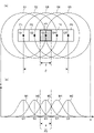
図示のとおり、電子銃10から照射された電子ビーム20は、電磁気的な作用を施すコンデンサレンズ30によって拡大され、アパーチャープレート40(図では、断面図として示す)に照射される。アパーチャープレート40には、多数の開口部41が形成されており、この開口部41を通過した電子ビーム21のみが、やはり電磁気的な作用を施すプロジェクションレンズ50を通して下方の試料基板60へと縮小投影され、その上面に形成されている被成形層(レジスト層)61の露光対象面に照射される。試料基板60は、移動ステージ70の上に載置され、図の左右方向および図の奥行き方向に移動させることができる。
As shown in the figure, an
最近では、512×512の二次元マトリックス状に配置された開口部41をもったアパーチャープレート40を用い、25万本以上の電子ビーム21によって被成形層61の上面を同時に露光して微細パターンを描画する機能をもった装置も実用化されている。通常、アパーチャープレート40の下面には、ブランキングプレート(図示省略)が配置されており、開口部41を通過した個々の電子ビーム21を個別にON/OFF制御する機能が設けられる。
Recently, an
ここでは、説明の便宜上、アパーチャープレート40に形成された個々の開口部41が、円形断面を有していたものとしよう。この場合、開口部41を通過した個々の電子ビーム21の断面は円形になる。したがって、被成形層61の上面(露光対象面)には、1本の電子ビーム21の照射により円形の照射スポットが形成される。たとえば、開口部41が直径4μmの円であり、プロジェクションレンズ50の縮小倍率が1/200であったとすると、露光対象面には、直径20nm程度の円形の照射スポット(厳密には、若干大きなスポットになる)が形成される。
Here, for convenience of explanation, it is assumed that each opening 41 formed in the
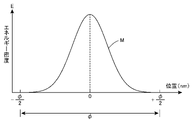
一般に、円形断面を有する電子ビームのエネルギー密度は、その中心軸をピークとしたガウスの誤差関数に応じた分布になるとされている。このような前提では、1本の電子ビーム21によって被成形層61の露光対象面に形成される円形の照射スポットのエネルギー密度E(電子ビームの照射強度)は、図2のグラフMに示すようなガウスの誤差関数に応じた分布になる。このグラフの横軸は、nmの単位で示される一次元方向の位置を示しており、横軸上の数値0の位置は、1本の電子ビーム21の中心位置に対応する。実際には、露光対象面上には二次元的な広がりをもつ円形の照射スポットが形成され、そのエネルギー密度Eを示すグラフは、図2に示すグラフMを、その中心軸まわりに回転させた回転体になる。
In general, it is said that the energy density of an electron beam having a circular cross section has a distribution according to a Gaussian error function with a peak at its central axis. On this premise, the energy density E (irradiation intensity of the electron beam) of a circular irradiation spot formed on the exposure target surface of the
図2のグラフにおける横軸上の寸法φは、こうして露光対象面上に形成される円形の照射スポットの直径に相当する。したがって、図2に示すようなエネルギー密度Eをもった1本の電子ビームが照射された場合、露光対象面上では直径φの円形内が露光することになり、各部の照射強度は中心から周囲に向かってガウスの誤差関数に応じた分布で減少する。通常、ビームの幅は、図2のグラフの半値幅の値を示すビーム径として示されるが、ここでは説明の便宜上、図2に示す寸法φをスポット径と呼び、ビーム径に対応する数値として取り扱うことにする。 The dimension φ on the horizontal axis in the graph of FIG. 2 corresponds to the diameter of the circular irradiation spot thus formed on the surface to be exposed. Therefore, when a single electron beam having an energy density E as shown in FIG. with a distribution according to the Gaussian error function. Normally, the width of the beam is indicated as the beam diameter indicating the value of the half-value width in the graph of FIG. I will handle it.
断面形状を任意に設定可能なシングルビームVSB(Variable Shaped Beam)を用いたVSB描画装置の場合、被成形層61上には1本の電子ビームしか照射されないので、その断面形状を矩形等の任意形状に加工し、任意の強度に調節した状態で照射することが可能である。ところが、マルチビーム方式の電子線描画装置の場合、多数の電子ビーム21を用いて極めて高速な描画を行うことができるメリットを有しているが、個々のビームの断面形状を個別に制御したり、個々のビームの強度を個別に制御したりすることは困難である。実際、25万本ものビームを生成する装置の場合、微細なアパーチャープレートの開口部41を通過した個々の電子ビームを個別に成形したり、個別に強度調節したりする機構を設けることはできない。
In the case of a VSB writing apparatus using a single beam VSB (Variable Shaped Beam) whose cross-sectional shape can be arbitrarily set, only one electron beam is irradiated onto the
結局、現在利用されている一般的なマルチビーム方式の電子線描画装置では、露光対象面上に直径φをもった多数の円形の照射スポットを形成することができるものの、照射スポットを任意の形状に成形することはできず、個々の電子ビームのON/OFF制御により描画を行う方法を採らざるを得ない。そこで、このマルチビーム方式の電子線描画装置の描画制御を行うために、二次元画素配列によって構成される描画データ(量子化マップとも呼ばれている)が利用される。 As a result, in general multi-beam electron beam lithography apparatuses currently in use, a large number of circular irradiation spots with a diameter φ can be formed on the surface to be exposed, but the irradiation spots can be formed in arbitrary shapes. Therefore, there is no choice but to adopt a method of drawing by ON/OFF control of individual electron beams. Therefore, drawing data (also called a quantization map) formed by a two-dimensional pixel array is used to perform drawing control of this multi-beam type electron beam drawing apparatus.
図3(a) は、この描画データを構成する二次元画素配列と、当該描画データに基づいて照射される電子ビームの強度分布との関係を示す平面図(上段(a) )およびグラフ(下段(b) )である。いま、露光対象面上にXY二次元座標系を定義し、この座標系上に図3(a) の右上隅にハッチングを施して示すような正方形状の画素Pを縦横に配置した二次元画素配列を定義する。ここでは、個々の画素Pの横方向(X軸方向)および縦方向(Y軸方向)の幅がいずれもdであるものとする。この幅dは、画素Pの横方向および縦方向のピッチに相当する。 FIG. 3(a) is a plan view (upper part (a)) and a graph (lower part) showing the relationship between the two-dimensional pixel array constituting the drawing data and the intensity distribution of the electron beam irradiated based on the drawing data. (b)). Now, an XY two-dimensional coordinate system is defined on the surface to be exposed, and on this coordinate system two-dimensional pixels are arranged vertically and horizontally with square pixels P shown hatched in the upper right corner of FIG. 3(a). Define an array. Here, it is assumed that each pixel P has a width of d in both the horizontal direction (X-axis direction) and the vertical direction (Y-axis direction). This width d corresponds to the pitch of the pixels P in the horizontal and vertical directions.
ここで、個々の画素Pの中心位置に照射基準点Qを定義し、画素Pの画素値として、当該照射基準点Qに照射すべき電子線の強度を示す値を与えることにする。このような画素配列からなる描画データをマルチビーム方式の電子線描画装置に与えたとすれば、描画装置は、当該描画データに基づいて、露光対象面上に所定の強度分布をもった電子線露光を行うことができる。たとえば、図3に示す画素P1の中心に定義された照射基準点Q1に照射された電子ビームにより、露光対象面(XY平面)上には、円形の照射スポットS1による露光が行われ、画素P2の中心に定義された照射基準点Q2に照射された電子ビームにより、露光対象面(XY平面)上には、円形の照射スポットS2による露光が行われる。 Here, an irradiation reference point Q is defined at the center position of each pixel P, and a value indicating the intensity of the electron beam to be irradiated to the irradiation reference point Q is given as the pixel value of the pixel P. FIG. If drawing data consisting of such a pixel array is supplied to a multi-beam electron beam drawing apparatus, the drawing apparatus exposes the exposure target surface to electron beams having a predetermined intensity distribution based on the drawing data. It can be performed. For example, the exposure target surface (XY plane) is exposed with a circular irradiation spot S1 by the electron beam irradiated to the irradiation reference point Q1 defined at the center of the pixel P1 shown in FIG. A circular irradiation spot S2 is exposed on the exposure target surface (XY plane) by the electron beam irradiated to the irradiation reference point Q2 defined at the center of the .
この場合、照射スポットS1による露光強度(露光量)は画素P1のもつ画素値E1に基づいて決定され、照射スポットS2による露光強度は画素P2のもつ画素値E2に基づいて決定される。たとえば、個々の画素値E1,E2が、ガウスの誤差関数に応じた分布のピーク値を示しているものとすると、図3(a) に示す照射スポットS1,S2によるX軸方向に関する露光強度分布は、図3(b) に示すグラフのようになる。すなわち、照射基準点Q1を中心として照射された電子ビームによる露光強度分布はグラフM1のような幅φをもった山になり、照射基準点Q2を中心として照射された電子ビームによる露光強度分布はグラフM2のような幅φをもった山になる。ここで、幅φは、前述したとおり、円形の照射スポットの直径である。 In this case, the exposure intensity (exposure amount) of the irradiation spot S1 is determined based on the pixel value E1 of the pixel P1, and the exposure intensity of the irradiation spot S2 is determined based on the pixel value E2 of the pixel P2. For example, assuming that the individual pixel values E1 and E2 represent the peak values of the distribution according to the Gaussian error function, the exposure intensity distribution in the X-axis direction by the irradiation spots S1 and S2 shown in FIG. becomes like the graph shown in FIG. 3(b). That is, the exposure intensity distribution of the electron beam irradiated with the irradiation reference point Q1 as the center becomes a mountain having a width φ as shown in the graph M1, and the exposure intensity distribution of the electron beam irradiated with the irradiation reference point Q2 as the center is It becomes a mountain with width φ as shown in graph M2. Here, the width φ is the diameter of the circular irradiation spot, as described above.
なお、図3では、説明の便宜上、2つの画素P1,P2の照射基準点Q1,Q2について、それぞれ照射スポットS1,S2が形成されている状態を示すが、もちろん、実際には、すべての画素Pの中心位置にそれぞれ照射基準点Qが定義され、各照射基準点Qに対してそれぞれ電子ビームの照射が行われることになる。ここで、照射基準点Qの縦横の配置ピッチは、画素Pの縦横の配置ピッチと同様にピッチdということになる。 For convenience of explanation, FIG. 3 shows a state in which the irradiation spots S1 and S2 are formed with respect to the irradiation reference points Q1 and Q2 of the two pixels P1 and P2. An irradiation reference point Q is defined at the center position of P, and each irradiation reference point Q is irradiated with an electron beam. Here, the vertical and horizontal arrangement pitch of the irradiation reference points Q is the same as the vertical and horizontal arrangement pitch of the pixels P, which is the pitch d.
ところで、マルチビーム方式の電子線描画装置では、多数の電子ビームの強度を個別に制御することはできない。したがって、図3に示す例において、照射基準点Q1に照射される電子ビームも、照射基準点Q2に照射される電子ビームも、同じ強度の電子ビームにならざるを得ない。ただ、ブランキングプレートを制御することにより、個々の電子ビームを個別にON/OFFすることは可能である。そこで、個々の照射基準点Qごとに、それぞれ照射する電子ビームを個別にON/OFF制御し、露光時間を変えることにより露光強度を変える方法を採る。上例の場合、照射基準点Q1への照射時間を照射基準点Q2への照射時間よりも長く設定することにより、図3(b) のグラフに示すような露光強度分布が得られることになる。 By the way, in a multi-beam type electron beam lithography apparatus, the intensity of a large number of electron beams cannot be individually controlled. Therefore, in the example shown in FIG. 3, the electron beam irradiated to the irradiation reference point Q1 and the electron beam irradiated to the irradiation reference point Q2 must have the same intensity. However, it is possible to individually turn ON/OFF each electron beam by controlling the blanking plate. Therefore, a method is adopted in which the electron beams to be irradiated are individually controlled ON/OFF for each individual irradiation reference point Q, and the exposure time is changed to change the exposure intensity. In the case of the above example, by setting the irradiation time to the irradiation reference point Q1 longer than the irradiation time to the irradiation reference point Q2, an exposure intensity distribution as shown in the graph of FIG. .
このような露光時間の制御は、実際には、露光回数の制御という形で行われる。これは、図1に示すように、実際には、移動ステージ70を二次元的(図1の左右方向および奥行き方向)に移動させながら、多数の電子ビーム21を被成形層61上で二次元的に走査しながら描画を行うためである。
Such control of the exposure time is actually performed in the form of control of the number of times of exposure. As shown in FIG. 1, this is actually done by moving a large number of
たとえば、数ナノ秒程度の露光時間を1回の電子ビーム照射時の単位露光時間と定めておき、1回の電子ビーム照射が完了するたびに、移動ステージ70をX軸方向にピッチdだけ移動させ、次の回の電子ビーム照射を行うようにすれば、特定の照射基準点Qに対しては、毎回異なる電子ビーム(隣接する電子ビーム)によって単位露光時間分の露光が行われることになる。このとき、毎回、個々の電子ビームごとに個別のON/OFF制御を行えば、段階的ではあるものの、個々の照射基準点Qごとに固有の露光強度を設定することが可能になる。
For example, an exposure time of about several nanoseconds is set as a unit exposure time for one electron beam irradiation, and each time one electron beam irradiation is completed, the moving
具体的には、たとえば、照射基準点Q1に対して10回の露光を行うことにより、図3(b) のグラフM1のような露光強度分布が得られるのであれば、照射基準点Q2に対して5回の露光を行うことにより、図3(b) のグラフM2のような露光強度分布が得られることになる。 Specifically, for example, if the exposure intensity distribution shown in the graph M1 in FIG. By performing exposure five times, an exposure intensity distribution such as the graph M2 in FIG. 3(b) is obtained.
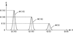
図4は、このように、個々の照射基準点Qごとに露光回数を変えることにより、16通りの段階的な露光強度の制御を行う原理を示すグラフである。ここでは、図示の便宜上、段階0,5,10,15の4通りの段階についての例のみが示されているが、実際には、これらの間の中間段階も設定され、段階0~15までの全16通りの段階が設定される。図4に示す露光強度分布グラフM(15),M(10),M(5)は、それぞれピーク強度E(15),E(10),E(5)をもち、同一のスポット径φの広がりをもったガウスの誤差関数に応じた分布のグラフになっている。
FIG. 4 is a graph showing the principle of controlling the exposure intensity stepwise in 16 ways by changing the number of times of exposure for each irradiation reference point Q in this way. Here, for convenience of illustration, only four examples of
たとえば、画素P(15),P(10),P(5),P(0)の画素値pがそれぞれp=15,p=10,p=5,p=0であった場合、これらの画素の中心位置に定義された照射基準点Q(15),Q(10),Q(5),Q(0)の近傍には、図4に示す露光強度分布グラフM(15),M(10),M(5),M(0)に相当する強度分布をもった露光が行われることになる。各露光強度分布グラフのピーク値は、それぞれの照射基準点位置における露光回数(=画素値p)に対応した値になる。 For example, if pixel values p of pixels P(15), P(10), P(5), and P(0) are p=15, p=10, p=5, and p=0, respectively, these Exposure intensity distribution graphs M(15) and M( 10), M(5), and M(0). The peak value of each exposure intensity distribution graph is a value corresponding to the number of times of exposure (=pixel value p) at each irradiation reference point position.
すなわち、画素値p=0に対応する照射基準点Q(0)には、電子ビームの照射は1回も行われず、グラフM(0)は、実際には実体のある山状のグラフにはならない。一方、画素値p=5に対応する照射基準点Q(5)には、電子ビームの照射が5回行われ、グラフM(5)は、ピーク強度E(5)をもった山になる。同様に、画素値p=10に対応する照射基準点Q(10)には、電子ビームの照射が10回行われ、グラフM(10)は、ピーク強度E(10)をもった山になり、画素値p=15に対応する照射基準点Q(15)には、電子ビームの照射が15回行われ、グラフM(15)は、ピーク強度E(15)をもった山になる。
That is, the irradiation reference point Q(0) corresponding to the pixel value p=0 is not irradiated with the electron beam even once, and the graph M(0) is actually a mountain-shaped graph with substance. not. On the other hand, the irradiation reference point Q(5) corresponding to the pixel value p=5 is irradiated with the electron beam five times, and the graph M(5) becomes a mountain with a peak intensity E(5). Similarly, the irradiation reference point Q(10) corresponding to the pixel value p=10 is irradiated with the
ところで、図3では、互いに十分に離れた位置にある2つの画素P1,P2に、それぞれ別個の電子ビームを照射した例を述べた。この例のように、スポット径φ以上に離れた2つの照射基準点Q1,Q2に照射された電子ビームは、相互に干渉を及ぼすことはない。しかしながら、スポット径φに満たない距離に近接配置されている複数の照射基準点に照射された電子ビームについては、相互に干渉が生じることになる。通常、画素ピッチd(照射基準点Qのピッチ)は、電子ビームのスポット径φよりも小さな値に設定される。この場合、露光対象面は、複数の電子ビームによる重畳露光を受けることになる。 By the way, in FIG. 3, the example in which the two pixels P1 and P2, which are sufficiently separated from each other, are irradiated with separate electron beams has been described. As in this example, the electron beams irradiated to the two irradiation reference points Q1 and Q2 separated by the spot diameter φ or more do not interfere with each other. However, the electron beams irradiated to a plurality of irradiation reference points arranged close to each other at a distance less than the spot diameter φ interfere with each other. Normally, the pixel pitch d (the pitch of the irradiation reference points Q) is set to a value smaller than the spot diameter φ of the electron beam. In this case, the surface to be exposed is subjected to superimposed exposure by a plurality of electron beams.
図5(a) は、画素ピッチdと個々の電子ビームのスポット径φとの関係により、露光対象面上に重畳露光が生じる状態の一例を示す平面図であり、図5(b) は、このような重畳露光が生じている場合の個々の電子ビームについての露光強度分布を示すグラフである。ここに示す例は、画素ピッチd(照射基準点Qのピッチ)と電子ビームのスポット径φとの間に、φ=4dとなるような関係を設定した場合の例である。図5(a) には、X軸方向に隣接して配置された5つの画素P1~P5と、これら各画素の中心位置に定義された5つの照射基準点Q1~Q5に対して照射された電子ビームによって形成される5つの円形照射スポットS1~S5が示されている。図示のとおり、各円形照射スポットS1~S5は相互に重なりを生じており、露光対象面の各部は、複数の照射スポットによる重畳露光を受けることになる。 FIG. 5(a) is a plan view showing an example of a state in which overlapping exposure occurs on the surface to be exposed due to the relationship between the pixel pitch d and the spot diameter φ of each electron beam, and FIG. 4 is a graph showing exposure intensity distributions for individual electron beams when such superimposed exposure occurs. The example shown here is an example in which a relationship of φ=4d is set between the pixel pitch d (the pitch of the irradiation reference points Q) and the spot diameter φ of the electron beam. In FIG. 5(a), five pixels P1 to P5 arranged adjacent to each other in the X-axis direction and five irradiation reference points Q1 to Q5 defined at the center positions of these pixels are shown. Five circular illumination spots S1-S5 formed by the electron beam are shown. As shown, the circular irradiation spots S1 to S5 overlap each other, and each portion of the exposure target surface is subjected to superimposed exposure by a plurality of irradiation spots.
図5(b) に示す露光強度分布グラフM1~M5は、それぞれ照射スポットS1~S5についてのX軸方向に関する露光強度分布を示している。個々の照射スポットS1~S5が部分的に重なりを生じているため、個々の露光強度分布グラフM1~M5も部分的に重なりを生じることになり、各部の実際の露光強度分布は、これら個々の露光強度分布グラフM1~M5の総和として与えられる。たとえば、図に太線で示されている画素P3内の照射基準点Q3には、円形照射スポットS3を生じさせる電子ビームが照射されることになる。この円形照射スポットS3の露光強度分布はグラフM3で示すような山になるが、図示のとおり、画素P3内には、隣接する別なグラフM1,M2,M4,M5の山の裾野も位置しているため、結局、画素P3内の総露光強度は、これらすべての山を重ね合わせた強度ということになる。 The exposure intensity distribution graphs M1 to M5 shown in FIG. 5(b) respectively show the exposure intensity distributions of the irradiation spots S1 to S5 in the X-axis direction. Since the individual irradiation spots S1 to S5 partially overlap, the individual exposure intensity distribution graphs M1 to M5 also partially overlap. It is given as the sum of the exposure intensity distribution graphs M1 to M5. For example, the irradiation reference point Q3 in the pixel P3 indicated by the thick line in the figure is irradiated with an electron beam that produces a circular irradiation spot S3. The exposure intensity distribution of this circular irradiation spot S3 forms mountains as shown in the graph M3, but as shown in the figure, within the pixel P3, the bases of the mountains of other adjacent graphs M1, M2, M4, and M5 are also located. Therefore, the total exposure intensity within the pixel P3 is the intensity obtained by superimposing all these peaks.
マルチビーム方式の電子線描画装置は、このような原理に基づいて、被成形層上に階調をもったグレースケールパターンを描画することができ、露光を受けた被成形層を現像することにより、所望の形状をもったパターン形成を行うことができる。 Based on this principle, the multi-beam electron beam drawing apparatus can draw a grayscale pattern with gradation on the layer to be molded. , a pattern having a desired shape can be formed.
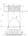
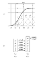
図6(a) は、X軸方向の幅Wをもつパターンの平面図であり、図6(b) は、当該パターンをマルチビームにより露光する原理を示すグラフである。図6(b) に横軸として示されているX軸は、図6(a) の横方向を示すX軸に対応するものであり、図6(b) のグラフは、図6(a) に示すパターンを描画する際のX軸方向に関する露光強度分布を示している。 FIG. 6(a) is a plan view of a pattern having a width W in the X-axis direction, and FIG. 6(b) is a graph showing the principle of multi-beam exposure of the pattern. The X-axis indicated as the horizontal axis in FIG. 6(b) corresponds to the X-axis indicating the horizontal direction in FIG. 6(a), and the graph in FIG. 2 shows the exposure intensity distribution in the X-axis direction when writing the pattern shown in FIG.
図6(b) には、小さな山からなる9つの露光強度分布グラフM1~M9(以下、小山と呼ぶ)と、大きな山からなる1つの露光強度の分布グラフMM(以下、大山と呼ぶ)とが示されている。小山M1~M9は、それぞれ照射基準点Q1~Q9に照射される個別の電子ビームに基づく露光強度分布を示すものであり、図5(b) に示す例と同様に、互いに裾野に重なりを生じている。照射基準点Q1~Q9は、図示されていない画素P1~P9の中心点として定義される点であり、所定ピッチdで配置されている。そして、各小山M1~M9の高さ(ピーク強度)は、個々の画素P1~P9の画素値に応じた値になる。 FIG. 6B shows nine exposure intensity distribution graphs M1 to M9 (hereinafter referred to as small peaks) consisting of small peaks, and one exposure intensity distribution graph MM consisting of large peaks (hereinafter referred to as large peak). It is shown. Hills M1 to M9 show the exposure intensity distributions based on the individual electron beams irradiated to the irradiation reference points Q1 to Q9, respectively. Similar to the example shown in FIG. ing. The irradiation reference points Q1 to Q9 are points defined as center points of pixels P1 to P9 (not shown), and are arranged at a predetermined pitch d. The heights (peak intensities) of the small mountains M1 to M9 are values corresponding to the pixel values of the individual pixels P1 to P9.
図4に示す例の場合、画素値pは0~15の16段階、すなわち、4ビットのデータで表現され、p=0~15とすることにより、それぞれ高さが異なる16通りの小山M(p)を定義することができる。そして、小山M(p)に応じた強度分布を形成するために、合計p回の露光が行われる。図6(b) に示す小山M1~M9は、この16段階の小山のいずれかである。たとえば、両端の画素P1,P9の画素値がp=7、中間の画素P2~P8の画素値がp=15であった場合、図示のとおり、両端の小山M1,M9は中程度の高さをもった山になり、中間の小山M2~M8は最大の高さをもった山になる。 In the example shown in FIG. 4, the pixel value p is expressed in 16 levels from 0 to 15, that is, by 4-bit data. p) can be defined. Then, a total of p exposures are performed in order to form an intensity distribution corresponding to the mound M(p). The hills M1 to M9 shown in FIG. 6(b) are any of these 16 levels of hills. For example, if the pixel values of the pixels P1 and P9 at both ends are p=7, and the pixel values of the pixels P2 to P8 in the middle are p=15, then the hills M1 and M9 at both ends have medium heights as shown in the figure. , and the small mountains M2 to M8 in the middle become mountains with the maximum height.
一方、図6(b) に示す大山MMは、すべての小山M1~M9を重畳したときに得られる総露光強度の分布を示すグラフであり、小山M1~M9の総和に相当するグラフということになる(図示の便宜上、正確な総和を示すものにはなっていない)。結局、照射基準点Q1~Q9に対して、それぞれ画素P1~P9の画素値に応じた回数の露光を実行すると、露光対象面上には、X軸方向に関して、大山MMによって示される総露光強度分布が得られることになる。 On the other hand, the large peak MM shown in FIG. 6(b) is a graph showing the distribution of the total exposure intensity obtained when all the small peaks M1 to M9 are superimposed, and is a graph corresponding to the sum of the small peaks M1 to M9. (For convenience of illustration, the exact sum is not shown). After all, when exposure is performed for the irradiation reference points Q1 to Q9 the number of times corresponding to the pixel values of the pixels P1 to P9, respectively, the total exposure intensity indicated by Oyama MM in the X-axis direction is obtained on the exposure target surface. A distribution will be obtained.
被成形層61に対して、このような露光を行うための電子線照射プロセスが完了すると、続いて、被成形層61に対する現像プロセスが実行される。被成形層61は、電子線照射によって組成変化を生じるレジスト層によって構成されており、一般的なレジストの場合、照射されるエネルギー密度が所定の臨界値を越えると、急激に組成変化を生じる非線形性を有している。したがって、図示する大山MMのように、なだらかな総露光強度分布が得られた場合であっても、被成形層61における総露光強度が所定の閾値Eth以上となる領域を露光領域a、総露光強度が所定の閾値Eth未満となる領域を非露光領域bとすれば、露光領域aの組成は非露光領域bの組成に比べて大きく変化する。
When the electron beam irradiation process for exposing the
このため、被成形層61に対する現像プロセスを行うと、露光領域aと非露光領域bとの相違に基づくパターン形成を行うことができる。別言すれば、閾値Ethは、露光後のレジスト層を現像するプロセスにおいて、露光領域aの組成が非露光領域bの組成に比べて、パターニングの成形に影響を与える変化を生じるための総露光強度の臨界値ということになる。
Therefore, when the development process is performed on the
具体的には、レジスト層としてポジ型レジスト材料を用いた場合、現像プロセスにより、被成形層61の露光領域aのみが現像液に溶解し、残存した非露光領域b内の被成形層によりパターン形成が行われ、レジスト層としてネガ型レジスト材料を用いた場合、現像プロセスにより、被成形層61の非露光領域bのみが現像液に溶解し、残存した露光領域a内の被成形層によりパターン形成が行われる。図6には、大山MMを、閾値Ethに相当するレベルで切ったときの幅Wに応じた幅を有する露光領域aが形成された例が示されている。
Specifically, when a positive resist material is used as the resist layer, only the exposed region a of the
もちろん、グラフの縦軸のスケーリングや閾値Ethの値は、荷電マルチビーム描画装置のビーム特性(たとえば、ビーム断面のエネルギー密度分布)や、レジスト層の感光特性(たとえば、レジスト材料の感光感度や、前方散乱や後方散乱によるエネルギー吸収特性)などの条件によって変化することになるが、これらの条件を固定しておけば、グラフの縦軸上の閾値Ethも固定された値になる。したがって、得られるパターン幅Wは、大山MMの形状によって制御することができる。上述したように、大山MMは、小山M1~M9の総和として得られるものであるので、結局、個々の画素P1~P9の画素値を定義した描画データによって、パターン幅Wの制御が可能になる。 Of course, the scaling of the vertical axis of the graph and the value of the threshold value Eth can be changed according to the beam characteristics of the charged multi-beam writing system (for example, the energy density distribution of the beam cross section) and the photosensitivity characteristics of the resist layer (for example, the photosensitivity of the resist material, However, if these conditions are fixed, the threshold Eth on the vertical axis of the graph will also be a fixed value. Therefore, the resulting pattern width W can be controlled by the shape of the Oyama MM. As described above, since the large mountain MM is obtained as the sum of the small mountains M1 to M9, the pattern width W can be controlled by the drawing data defining the pixel values of the individual pixels P1 to P9. .
なお、これまでの説明では、便宜上、被成形層61に対するX軸方向に関するパターニングの原理を述べたが、実際のパターニングプロセスは、XY平面上に広がる被成形層に対して行われ、Y軸方向に関しても同様のパターニングが行われることになる。すなわち、図6(b) に示す大山MMは、X軸方向に関する露光強度分布を示すものであるが、描画データは、二次元画素配列として与えられるため、Y軸方向に関しても同様の露光強度分布が得られることになる。そして、図6(a) に示すパターンの上下方向の幅は、このY軸方向に関する露光強度分布に基づいて決定されることになる。
In the description so far, for the sake of convenience, the principle of patterning the
以上、従来用いられている一般的なマルチビーム電子線描画装置による描画原理を説明したが、もちろん、上述の説明は、マルチビーム電子線描画装置の一例を用いた説明であり、本発明を実施するにあたって用いるマルチビーム電子線描画装置は、上述の説明に用いた例に限定されるものではない。 The principle of writing by a general multi-beam electron beam lithography apparatus conventionally used has been described above. Of course, the above description is an explanation using an example of a multi-beam electron beam lithography apparatus, and the present invention is implemented. The multi-beam electron beam lithography apparatus used for this purpose is not limited to the example used in the above description.
<<< §2. 線状パターンを描画するための描画データ >>>
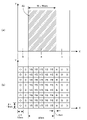
ここでは、§1で述べた描画原理に基づいて線状パターンを描画する場合に用いられる具体的な描画データについての説明を行う。図7(a) は、X軸方向の幅W=50nmをもつ線状パターンの平面図であり、図7(b) は、当該線状パターンを露光するための描画データを構成する画素配列を示す図である。半導体デバイスの製造プロセスでは、配線層など、微小な線幅をもった線状パターンを多数形成する必要がある。図7(a) に示す対象図形F1(ハッチング部分)は、そのようなプロセスで用いられる微小な線幅をもった細長い線状パターンである。
<<< §2. Drawing data for drawing linear patterns >>>
Here, specific drawing data used when drawing a linear pattern based on the drawing principle described in .sctn.1 will be described. FIG. 7(a) is a plan view of a linear pattern having a width W=50 nm in the X-axis direction, and FIG. 7(b) is a pixel array constituting drawing data for exposing the linear pattern. FIG. 4 is a diagram showing; In the manufacturing process of semiconductor devices, it is necessary to form a large number of linear patterns with minute line widths, such as wiring layers. A target figure F1 (hatched portion) shown in FIG. 7(a) is an elongated linear pattern with a minute line width used in such a process.
なお、実際の線状パターンは、線幅(図のX軸方向に関する幅)に比べて、線長(図のY軸方向に関する長さ)は極めて大きくなり、文字通り「1本の線」として把握されるべきパターンであるが、本願では、図示の便宜上、線長を大幅に縮小した線状パターン(図7(a) のハッチング部分のように「矩形」として把握されるパターン)を、パターニングの対象となる対象図形F1とした例について説明を行うことにする。 In actual linear patterns, the line length (the length in the Y-axis direction in the figure) is extremely large compared to the line width (the width in the X-axis direction in the figure), so it is literally understood as a single line. In the present application, for convenience of illustration, a linear pattern with a significantly reduced line length (a pattern understood as a "rectangle" such as the hatched portion in FIG. 7(a)) is used for patterning. An example of the target figure F1 will be described.
図7(b) に示す描画データは、被成形層上に図7(a) に示すような対象図形F1を形成するために、マルチビーム電子線描画装置に与えるデータであり、それぞれの画素に所定の画素値pが定義された二次元画素配列によって構成される。既に§1で説明したとおり、この二次元画素配列を構成する個々の画素Pは、被成形層上の露光対象面に縦横にそれぞれ所定ピッチdで配置された多数の照射基準点Qに照射すべき電子線強度を示す画素値pを有している。以下、この二次元画素配列の縦方向および横方向の画素ピッチdをd=10nmに設定した例について説明を行うことにする。したがって、照射基準点Qの縦方向および横方向のピッチdも同じくd=10nmに設定される。 The drawing data shown in FIG. 7(b) are data given to the multi-beam electron beam drawing apparatus in order to form the object figure F1 shown in FIG. 7(a) on the layer to be molded. It consists of a two-dimensional pixel array in which a given pixel value p is defined. As already explained in §1, the individual pixels P that make up this two-dimensional pixel array irradiate a large number of irradiation reference points Q arranged vertically and horizontally at a predetermined pitch d on the surface to be exposed on the layer to be molded. It has a pixel value p that indicates the power electron beam intensity. An example in which the vertical and horizontal pixel pitches d of the two-dimensional pixel array are set to d=10 nm will be described below. Therefore, the vertical and horizontal pitches d of the irradiation reference points Q are also set to d=10 nm.
図7(b) に示す描画データは、露光対象面(XY平面)上にこのような二次元画素配列を定義し、個々の画素にそれぞれ所定の画素値を付与したものである。この例の場合、個々の画素値pとして、p=0~15の範囲の数字を付与しているため、この描画データは、いわば4ビットの階調値をもったグレースケールの画像データということになり、個々の画素は、図4に示すような16通りの露光強度分布のうちの1つをその画素値pによって指定する役割を果たす。 The drawing data shown in FIG. 7(b) defines such a two-dimensional pixel array on the exposure target plane (XY plane) and assigns a predetermined pixel value to each pixel. In this example, since each pixel value p is given a number in the range of p=0 to 15, this drawing data is, so to speak, grayscale image data with a 4-bit gradation value. , and each pixel plays a role of specifying one of the 16 exposure intensity distributions as shown in FIG. 4 by its pixel value p.
なお、図7(b) に示す描画データの場合、個々の画素の画素値pは、p=0(最小値)もしくはp=15(最大値)のいずれかをとっており、中間の画素値p=1~14をとる画素は存在しない。これは、図7(a) に示す線状パターンの輪郭線が、画素の境界に一致しているため、中間の画素値を用いなくても、線状パターンの形成が可能になるためである。すなわち、図示の例の場合、線状パターン内に完全に含まれる画素については画素値p=15(最大値)を与え、線状パターンに含まれない画素については画素値p=0(最小値)を与えることにより、描画データが構成されている。 In the drawing data shown in FIG. 7B, the pixel value p of each pixel is either p=0 (minimum value) or p=15 (maximum value). There are no pixels with p=1-14. This is because the outline of the linear pattern shown in FIG. 7(a) matches the boundary of the pixels, so that the linear pattern can be formed without using intermediate pixel values. . That is, in the illustrated example, a pixel value p=15 (maximum value) is given to pixels completely included in the linear pattern, and a pixel value p=0 (minimum value) is given to pixels not included in the linear pattern. ), rendering data is constructed.
このような描画データを電子線描画装置に与えると、画素値p=0をもつ画素に対応する照射基準点位置には電子ビームの照射は1回も行われず、画素値p=15をもつ画素に対応する照射基準点位置には電子ビームの照射が15回行われることになる。その結果、図4に示す小山M(15)を足し合わせることにより、大山MMが形成され、露光対象面上には、所定の閾値Ethを基準にして、図7(a) に示すような露光領域a(総露光強度が閾値Eth以上となる領域)と非露光領域b(総露光強度が閾値Eth未満となる領域)とが形成されることになる。
When such drawing data is given to the electron beam drawing apparatus, the irradiation reference point position corresponding to the pixel with the pixel value p=0 is never irradiated with the electron beam, and the pixel with the pixel value p=15 is not irradiated even once. The irradiation reference point position corresponding to is irradiated with the
図7(a) に示す例のように、対象図形F1の輪郭線が、画素の境界に一致するような設計を行うと、二次元画素配列上に対象図形F1を配置したときに、対象図形F1内に完全に含まれる画素(以下、完全画素と呼ぶ)と、対象図形F1を全く含まない画素(以下、空画素と呼ぶ)との2種類の画素のみが定義されることになる。そこで、完全画素については画素値p=15(最大値:電子ビームを最大回数だけ照射することを示す画素値)を与え、空画素については画素値p=0(最小値:電子ビームを1回も照射しないことを示す画素値)を与えるようにすれば、図7(b) に示すような描画データが得られる。 As in the example shown in FIG. 7(a), if the outline of the target figure F1 is designed to match the boundary of the pixels, when the target figure F1 is arranged on the two-dimensional pixel array, the target figure Only two types of pixels are defined: pixels that are completely included in F1 (hereinafter referred to as complete pixels) and pixels that do not include the target figure F1 at all (hereinafter referred to as empty pixels). Therefore, the pixel value p=15 (maximum value: a pixel value indicating that the electron beam is irradiated the maximum number of times) is given to the complete pixels, and the pixel value p=0 (minimum value: the electron beam is irradiated once) to the empty pixels. If a pixel value indicating no irradiation is given, drawing data as shown in FIG. 7(b) can be obtained.
一般的なマルチビーム電子線描画装置を用いたパターニングプロセスの場合、通常、輪郭線が画素の境界に一致するような図形を示す描画データを与えた場合に、寸法誤差のない正確なパターンが形成されるような標準パターニング条件を設定した運用が行われる。したがって、一般に、線幅Wが、画素の線幅方向ピッチdの整数倍となるような図形を形成する場合、当該図形の輪郭線が、画素の境界に一致するような位置合わせを行った設計を行えば、標準パターニング条件により、寸法誤差のない正確なパターン形成を行うことができる。 In the patterning process using a general multi-beam electron beam lithography system, an accurate pattern with no dimensional error is usually formed when writing data indicating a figure whose outline matches the boundary of pixels is given. An operation is performed in which standard patterning conditions are set. Therefore, in general, when forming a figure in which the line width W is an integer multiple of the pixel pitch d in the line width direction, the outline of the figure is designed to match the boundaries of the pixels. , it is possible to form an accurate pattern with no dimensional error under standard patterning conditions.
図7に示す例の場合、画素ピッチd=10nmであり、しかも対象図形F1の線幅Wは50nmであるため、線幅Wは、画素ピッチdのちょうど5倍になっている。したがって、対象図形F1の設計時には、左右両側の輪郭線が画素の境界に一致するような設計を行い、上記標準パターニング条件でパターン形成処理(露光処理および現像処理)を行えば、ほぼ設計どおりの寸法をもった物理的パターンが得られる。すなわち、露光領域aとして残存する被成形層(被成形層がネガ型レジストの場合)、もしくは、非露光領域bとして残存する被成形層(被成形層がポジ型レジストの場合)によって、線幅50nmをもった物理的な線状パターンを形成することができる。 In the example shown in FIG. 7, the pixel pitch d=10 nm and the line width W of the object figure F1 is 50 nm, so the line width W is exactly five times the pixel pitch d. Therefore, when designing the target figure F1, the contour lines on both the left and right sides are designed to match the boundaries of the pixels. A physical pattern with dimensions is obtained. That is, depending on the layer to be molded remaining as the exposed region a (when the layer to be molded is a negative resist) or the layer to be molded remaining as the non-exposed region b (when the layer to be molded is a positive resist), the line width A physical linear pattern with 50 nm can be formed.
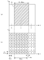
一方、画素ピッチdに満たないサブピクセルレベルの端数寸法の線幅をもった線状パターンを形成する場合には、輪郭線の内側直近部における当該端数寸法に相当する画素について、中間的な画素値を与えるようにすればよい。図8(a) は、X軸方向の幅W=54nmをもつ対象図形F2の平面図であり、図8(b) は、当該対象図形F2を露光するための描画データを構成する画素配列を示す図である。図7に示す対象図形F1の線幅WがW=50nmであったのに対して、図8に示す対象図形F2の線幅WはW=54nmであり、4nmだけ幅が広くなっている。図示の例の場合、画素ピッチdは10nmであるので、この4nmの幅増加分は、画素ピッチdに満たないサブピクセルレベルの端数寸法ということになる。 On the other hand, in the case of forming a linear pattern having a line width of a sub-pixel level fractional dimension that is less than the pixel pitch d, the pixel corresponding to the fractional dimension in the inner immediate part of the contour line is an intermediate pixel. value should be given. FIG. 8(a) is a plan view of an object figure F2 having a width W=54 nm in the X-axis direction, and FIG. 8(b) shows a pixel array constituting writing data for exposing the object figure F2. FIG. 4 is a diagram showing; While the line width W of the object figure F1 shown in FIG. 7 is W=50 nm, the line width W of the object figure F2 shown in FIG. 8 is W=54 nm, which is wider by 4 nm. In the illustrated example, the pixel pitch d is 10 nm, so this 4 nm increase in width is a sub-pixel level fractional dimension less than the pixel pitch d.
そこで、図8(b) に示す描画データでは、この4nmの幅増加分を、画素値pとして、p=6という中間的な階調値をもった画素列を設けることにより補填している。すなわち、図8に示す例の場合、W=54nmなる線幅をもつ対象図形F2について、その左側の輪郭線が画素の境界に一致するような設計を行っているため、第3列目~第7列目までの画素列については、図7に示す例と同様に、画素値p=15(最大値)が付与されているが、第8列目の画素列には、画素値p=6が付与されている。これは、この第8列目の画素列が、対象図形F2を部分的に含む画素(以下、不完全画素と呼ぶ)であるため、当該対象図形F2の含有率に応じて定まる階調値を画素値pとして与えた結果である。 Therefore, in the drawing data shown in FIG. 8(b), the width increase of 4 nm is compensated for by providing a pixel row having an intermediate gradation value of p=6 with the pixel value p. That is, in the case of the example shown in FIG. 8, the object figure F2 having a line width of W=54 nm is designed so that the left contour line matches the pixel boundary. As in the example shown in FIG. 7, the pixel columns up to the seventh column are given the pixel value p=15 (maximum value). is given. This is because the 8th pixel row is a pixel that partially includes the target figure F2 (hereinafter referred to as an incomplete pixel), so the gradation value determined according to the content rate of the target figure F2 is This is the result given as the pixel value p.
上述したとおり、ここに示す例の場合、対象図形F2内に完全に含まれる完全画素(第3列目~第7列目までの画素)については最大画素値p=15を与え、対象図形F2を全く含まない空画素(第1,2,9,10列目の画素)については最小画素値p=0を与えることになる。そして、対象図形F2を部分的に含む不完全画素(第8列目の画素)については、対象図形F2の含有率「4/10」を最大画素値p=15に乗じることにより得られる積6を画素値として与えている。
As described above, in the case of the example shown here, the maximum pixel value p=15 is given to the complete pixels (pixels in the third to seventh columns) completely included in the object figure F2, and the object figure F2 The minimum pixel value p=0 is given to empty pixels (pixels in the 1st, 2nd, 9th, and 10th columns) that do not contain any . For imperfect pixels (pixels in the eighth column) that partially include the target figure F2, the
この図8(b) に示す描画データを電子線描画装置に与えれば、画素値p=0をもつ画素に対応する照射基準点位置には電子ビームの照射は1回も行われず、画素値p=6,p=15をもつ画素に対応する照射基準点位置には、電子ビームの照射が、それぞれ6回,15回行われることになる。そして、これらの各露光処理によって形成される露光強度分布の小山を足し合わせることにより得られる大山MMについて、所定の閾値Ethを基準にした区分けを行うことにより、図8(a) に示すような露光領域a(総露光強度が閾値Eth以上となる領域)と非露光領域b(総露光強度が閾値Eth未満となる領域)とが形成され、実際に現像を行えば、線幅W=54nmをもった物理的な対象図形F2が形成されることになる。 If the drawing data shown in FIG. 8(b) is supplied to the electron beam drawing apparatus, the irradiation reference point position corresponding to the pixel having the pixel value p=0 is never irradiated with the electron beam, and the pixel value p =6 and p=15, the electron beam irradiation is performed 6 times and 15 times, respectively. Then, the large peak MM obtained by summing the small peaks of the exposure intensity distribution formed by each of these exposure processes is divided based on a predetermined threshold Eth to obtain the peaks shown in FIG. 8(a). An exposed region a (region where the total exposure intensity is equal to or greater than the threshold Eth) and a non-exposed region b (region where the total exposure intensity is less than the threshold Eth) are formed. A physical object figure F2 is formed.
図9(a) は、X軸方向の幅W=55nmをもつ対象図形F3の平面図であり、図8(b) は、当該対象図形F3を露光するための描画データを構成する画素配列を示す図である。図7に示す対象図形F1の線幅WがW=50nmであったのに対して、図9に示す対象図形F3の線幅WはW=55nmであり、5nmだけ幅が広くなっている。このため、図9(b) に示す描画データでは、この5nmの幅増加分を、第8列目の画素によって補填している。 FIG. 9(a) is a plan view of an object figure F3 having a width W=55 nm in the X-axis direction, and FIG. 8(b) shows a pixel array constituting drawing data for exposing the object figure F3. FIG. 4 is a diagram showing; While the line width W of the object figure F1 shown in FIG. 7 is W=50 nm, the line width W of the object figure F3 shown in FIG. 9 is W=55 nm, which is wider by 5 nm. Therefore, in the drawing data shown in FIG. 9(b), the width increase of 5 nm is compensated for by pixels in the eighth column.
具体的には、第8列目の画素については、対象図形F3の含有率「5/10」を最大画素値p=15に乗じることにより得られる積7.5を、画素値として与えればよい。ただ、ここに示す例の場合、画素値は0~15のうちのいずれかをとる必要があり、7.5という小数値を含んだ画素値をとることはできない。そこで、第8列目の画素については、図示のとおり、画素値p=7と画素値p=8とを交互に与えるようにし、画素値p=7.5を与えた場合に近い結果が得られるようにしている。 Specifically, for the pixels in the eighth column, the product 7.5 obtained by multiplying the maximum pixel value p=15 by the content rate "5/10" of the target figure F3 may be given as the pixel value. . However, in the case of the example shown here, the pixel value must be any value from 0 to 15, and the pixel value including the decimal value of 7.5 cannot be used. Therefore, for the pixels in the eighth column, as shown in the figure, the pixel value p=7 and the pixel value p=8 are alternately given, and a result close to the case where the pixel value p=7.5 is given is obtained. so that it can be
本願では、図7に示す対象図形F1の左右の輪郭線のように、画素の境界(輪郭)に位置する輪郭線を「ONグリッド輪郭線」と呼ぶ。したがって、図8に示す対象図形F2の左側の輪郭線や、図9に示す対象図形F3の左側の輪郭線も「ONグリッド輪郭線」ということになる。これに対して、図8に示す対象図形F2の右側の輪郭線や、図9に示す対象図形F3の右側の輪郭線のように、画素の境界(輪郭)に位置しない輪郭線を「OFFグリッド輪郭線」と呼ぶことにする。ここで「グリッド」とは、画素の境界(輪郭線)を示す格子を意味しており、格子上にある輪郭線が「ONグリッド輪郭線」、格子から外れた位置にある輪郭線が「OFFグリッド輪郭線」ということになる。後述するとおり、対象図形の輪郭線が、「ONグリッド輪郭線」であるのか、「OFFグリッド輪郭線」であるのかの相違は、本発明において重要な意味をもつ。 In the present application, a contour line positioned at a boundary (contour) of pixels, such as the left and right contour lines of the target figure F1 shown in FIG. 7, is called an "ON grid contour line". Therefore, the contour line on the left side of the object graphic F2 shown in FIG. 8 and the contour line on the left side of the object graphic F3 shown in FIG. 9 are also called "ON grid contour lines". On the other hand, contour lines that do not lie on the boundary (contour) of pixels, such as the right contour line of the target figure F2 shown in FIG. 8 and the right contour line of the target figure F3 shown in FIG. We will call it the contour line. Here, the "grid" means a grid indicating the boundary (outline) of the pixels. Grid outline". As will be described later, the difference between whether the contour line of the object graphic is an "ON grid contour line" or an "OFF grid contour line" has an important meaning in the present invention.
<<< §3. ONグリッドとOFFグリッドについての誤差比較実験 >>>
ここでは、本発明の理解を容易にするために、本願発明者が行ったONグリッドとOFFグリッドについての誤差比較実験の内容およびその結果を説明する。
<<< §3. Error comparison experiment for ON grid and OFF grid >>>
Here, in order to facilitate understanding of the present invention, the details and results of an error comparison experiment for ON grids and OFF grids conducted by the inventors of the present application will be described.
<3.1 ONグリッドとOFFグリッドの相違>
背景技術の問題点として指摘したとおり、§1で述べた一般的な荷電マルチビーム描画装置を用いて微細なパターンを形成しようとすると、露光および現像プロセスを経て被成形層61上に実際に形成される実パターンは、元の対象図形に対して寸法誤差を生じる。このような寸法誤差は、様々な要因に基づいて生じることになり、この寸法誤差を低減するために、これまでも様々な誤差修正方法が提案されている。
<3.1 Difference between ON grid and OFF grid>
As pointed out as a problem of the background art, when attempting to form a fine pattern using the general charged multi-beam writing apparatus described in §1, the pattern is actually formed on the
本願発明者は、このような誤差要因の1つとして、「§2で述べたONグリッドとOFFグリッドの相違」が関係しているのではないか、との仮説の下に、具体的な実験を行い、当該仮説を実証した。以下、この仮説についての内容と、その実証結果を説明する。 The inventor of the present application hypothesized that "the difference between the ON grid and the OFF grid described in § 2" may be related as one of such error factors, and conducted a specific experiment. and verified the hypothesis. The content of this hypothesis and its demonstration results will be described below.
まず、「ONグリッド輪郭線」と「OFFグリッド輪郭線」との相違を、もう一度確認しておく。ONグリッド輪郭線もOFFグリッド輪郭線も、描画の対象となる対象図形の輪郭線である点に変わりはない。ただ、描画データの二次元画素配列との位置関係を考えた場合、ONグリッド輪郭線C1は、図10(a) に示すように、画素の境界(輪郭線)を示す格子上に位置する輪郭線であり、OFFグリッド輪郭線C2は、図10(b) に示すように、画素の境界(輪郭線)を示す格子上には位置しない輪郭線である。 First, the difference between the "ON grid contour" and the "OFF grid contour" is confirmed again. Both the ON grid contour line and the OFF grid contour line are the contour lines of the object figure to be drawn. However, considering the positional relationship between the drawing data and the two-dimensional pixel array, as shown in FIG. As shown in FIG. 10(b), the OFF grid contour line C2 is a contour line that is not located on the grid indicating the pixel boundary (contour line).
通常、ONグリッド輪郭線C1で隔てられた2つの領域のうち、一方の領域に所属する画素(対象図形の内側の画素)には最大画素値が与えられ、他方の領域に所属する画素(対象図形の外側の画素)には最小画素値が与えられる。図10(a) に示す例の場合、画素値として4ビットのデータを用いているため、ONグリッド輪郭線C1の右側(対象図形の内側)の画素には最大画素値p=15が与えられ、ONグリッド輪郭線C1の左側(対象図形の外側)の画素には最小画素値p=0が与えられている。別言すれば、ONグリッド輪郭線C1の近傍に位置するONグリッド画素は、対象図形内に完全に含まれる完全画素か、対象図形を全く含まない空画素か、のいずれかになるので、前者には最大画素値p=15を与え、後者には最小画素値p=0を与えればよい。 Normally, of two regions separated by the ON grid contour line C1, pixels belonging to one region (pixels inside the target figure) are given the maximum pixel value, and pixels belonging to the other region (target Pixels outside the shape) are given the minimum pixel value. In the example shown in FIG. 10(a), since 4-bit data is used as the pixel value, the maximum pixel value p=15 is given to the pixels on the right side of the ON grid contour line C1 (inside the target figure). , the pixel on the left side of the ON grid contour line C1 (outside the object graphic) is given the minimum pixel value p=0. In other words, the ON grid pixels located near the ON grid contour line C1 are either complete pixels that are completely included in the target graphic or empty pixels that do not include the target graphic at all. is given the maximum pixel value p=15, and the latter is given the minimum pixel value p=0.
これに対して、OFFグリッド輪郭線C2の近傍に位置するOFFグリッド画素には、対象図形内に完全に含まれる完全画素および対象図形を全く含まない空画素の他に、対象図形を部分的に含む不完全画素が存在する。そこで、完全画素には最大画素値p=15を与え、空画素には最小画素値p=0を与え、不完全画素には中間の画素値p=1~14を与えることになる。図10(b) に示す例の場合、第1列目の空画素には最小画素値p=0が与えられ、第3~4列目の完全画素には最大画素値p=15が与えられ、第2列目の不完全画素には中間の画素値p=7もしくは8が与えられている。 On the other hand, the OFF grid pixels located near the OFF grid contour line C2 include complete pixels that are completely included in the target figure, empty pixels that do not include the target figure at all, and also partially cover the target figure. There are imperfect pixels that contain Therefore, the maximum pixel value p=15 is given to complete pixels, the minimum pixel value p=0 is given to empty pixels, and intermediate pixel values p=1 to 14 are given to imperfect pixels. In the case of the example shown in FIG. 10(b), the empty pixels in the first column are given the minimum pixel value p=0, and the full pixels in the third and fourth columns are given the maximum pixel value p=15. , the intermediate pixel value p=7 or 8 is given to the imperfect pixels in the second column.
なお、図10(b) では、第2列目の画素の画素値「7,8,7,8,7」を、OFFグリッド輪郭線C2に重ならないよう右にずらして記載してあるが、これらの画素値はいずれも第2列目の不完全画素の画素値である。この第2列目の各不完全画素についての対象図形の含有率は「5/10」であり、本来であれば、画素値7.5を与えるべきであるが、画素値は小数値をとることができないので、便宜上、画素値p=7と画素値p=8とを交互に与えている。 In FIG. 10(b), the pixel values "7, 8, 7, 8, 7" of the pixels in the second column are shifted to the right so as not to overlap the OFF grid contour line C2. These pixel values are all pixel values of imperfect pixels in the second column. The content rate of the target figure for each imperfect pixel in the second column is "5/10". Originally, a pixel value of 7.5 should be given, but the pixel value takes a decimal value. Therefore, for the sake of convenience, the pixel value p=7 and the pixel value p=8 are given alternately.
ONグリッド輪郭線C1とOFFグリッド輪郭線C2とについて、図10に示すような取り扱いを行えば、理論上は、誤差のない寸法精度をもったパターニングを行うことができるはずである。しかしながら、実際には、様々な要因によって、いわゆるエッジポジションエラーが発生し、理論的な寸法精度をもったパターニングを行うことは困難である。このため、設計上の対象図形の寸法と、実際に被成形層上に形成される実図形の寸法との間に誤差が生じることは避けられない。本願発明者は、以下に述べる誤差比較実験により、ONグリッド輪郭線C1の近傍に生じる寸法誤差e(on)と、OFFグリッド輪郭線C2の近傍に生じる寸法誤差e(off)との間に、普遍的な相違が生じることを見出した。以下、この誤差比較実験の結果を詳細に説明する。なお、以下の説明における寸法誤差e(on)およびe(off)は、誤差eの絶対値を指すものとする。 Theoretically, if the ON grid contour line C1 and the OFF grid contour line C2 are handled as shown in FIG. 10, it should be possible to perform patterning with error-free dimensional accuracy. However, in practice, so-called edge position errors occur due to various factors, making it difficult to perform patterning with theoretical dimensional accuracy. For this reason, it is inevitable that there will be an error between the dimension of the designed object figure and the dimension of the actual figure actually formed on the molding layer. The inventors of the present application have conducted an error comparison experiment to be described below, and found that between the dimensional error e(on) occurring near the ON grid contour line C1 and the dimensional error e(off) occurring near the OFF grid contour line C2, We have found that a universal difference occurs. The results of this error comparison experiment will be described in detail below. Note that dimensional errors e(on) and e(off) in the following description refer to absolute values of the error e.
<3.2 誤差比較実験の内容>
本願発明者は、図1に例示した特定のマルチビーム方式の電子線描画装置を用いて、特定の材料からなるレジスト層(被成形層61)上に、テストパターンとなる所定の対象図形を露光し、これを現像して実パターンを得るプロセスについて、元となる対象図形の寸法と得られた実パターンの寸法との間に生じる誤差を求める処理を、様々な対象図形について実行する誤差比較実験を行った。
<3.2 Details of Error Comparison Experiment>
The inventor of the present application uses the specific multi-beam electron beam drawing apparatus illustrated in FIG. In the process of developing this to obtain an actual pattern, an error comparison experiment is performed on various target figures to determine the error between the dimensions of the original target figure and the dimensions of the resulting actual pattern. did
この実験では、電子線描画装置の動作条件(たとえば、ビーム断面のエネルギー密度分布などのビーム特性)や、用いるレジスト層についての化学的な感光感度、前方散乱、後方散乱などによるエネルギー吸収特性も考慮して誤差を求めている。この誤差比較実験の目的は、ONグリッド輪郭線C1の近傍に生じる寸法誤差e(on)と、OFFグリッド輪郭線C2の近傍に生じる寸法誤差e(off)とを比較することにある。 In this experiment, the operating conditions of the electron beam lithography system (e.g., beam characteristics such as energy density distribution in the cross section of the beam), the chemical photosensitivity of the resist layer used, and the energy absorption characteristics due to forward scattering, backward scattering, etc., are also considered. to find the error. The purpose of this error comparison experiment is to compare the dimensional error e(on) occurring near the ON grid contour line C1 with the dimensional error e(off) occurring near the OFF grid contour line C2.
なお、この誤差比較実験では、§1で述べた例とは異なり、正方形断面をもつ電子ビームを用いた。すなわち、この誤差比較実験では、図1に示すアパーチャープレート40に形成された個々の開口部41が、正方形の断面を有する電子線描画装置を用いており、開口部41を通過した個々の電子ビーム21の断面は正方形になる。したがって、被成形層61の上面(露光対象面)には、1本の電子ビーム21の照射により正方形の照射スポットが形成される。
In this error comparison experiment, an electron beam having a square cross section was used unlike the example described in §1. That is, in this error comparison experiment, the
図11(a) は、描画データを構成する二次元画素配列と、当該描画データに基づいて照射される電子ビームの強度分布との関係を示す平面図(上段(a) )およびグラフ(下段(b) )である。図3が、円形断面をもつ電子ビームを用いた例であるのに対して、図11は、正方形断面をもつ電子ビームを用いた例ということになる。たとえば、図11に示す画素P1の中心に定義された照射基準点Q1に照射された電子ビームにより、露光対象面(XY平面)上には、正方形の照射スポットS1による露光が行われ、画素P2の中心に定義された照射基準点Q2に照射された電子ビームにより、露光対象面(XY平面)上には、正方形の照射スポットS2による露光が行われる。 FIG. 11(a) shows a plan view (upper part (a)) and a graph (lower part ( b) ). 3 is an example using an electron beam having a circular cross section, FIG. 11 is an example using an electron beam having a square cross section. For example, the exposure target surface (XY plane) is exposed with a square irradiation spot S1 by an electron beam irradiated to the irradiation reference point Q1 defined at the center of the pixel P1 shown in FIG. A square irradiation spot S2 is exposed on the exposure target surface (XY plane) by the electron beam irradiated to the irradiation reference point Q2 defined at the center of the .
もちろん、照射スポットS1による露光強度は画素P1のもつ画素値E1に基づいて決定され、照射スポットS2による露光強度は画素P2のもつ画素値E2に基づいて決定される。前述したように、円形の照射スポットによる露光強度分布は、ガウスの誤差関数に応じたものになるが、正方形の照射スポットによる露光強度分布は、ガウスの誤差関数を若干変形した台形状のグラフになる。具体的には、図11(a) に示す照射スポットS1,S2によるX軸方向に関する露光強度分布は、図11(b) に示すグラフM1,M2のようになる。図6には、多数の小山M1~M9によって大山MMが作成される例を示したが、個々の小山Mが台形状のグラフになる場合、これらの総和になる大山MMも台形状のグラフになる。 Of course, the exposure intensity of the irradiation spot S1 is determined based on the pixel value E1 of the pixel P1, and the exposure intensity of the irradiation spot S2 is determined based on the pixel value E2 of the pixel P2. As described above, the exposure intensity distribution by a circular irradiation spot corresponds to the Gaussian error function, but the exposure intensity distribution by a square irradiation spot is a trapezoidal graph obtained by slightly modifying the Gaussian error function. Become. Specifically, the exposure intensity distributions in the X-axis direction by the irradiation spots S1 and S2 shown in FIG. 11(a) are shown in graphs M1 and M2 shown in FIG. 11(b). FIG. 6 shows an example in which a large mountain MM is created from a large number of small mountains M1 to M9. Become.
すなわち、照射基準点Q1を中心として照射された電子ビームによる露光強度分布はグラフM1のような幅φをもった台形状の山になり、照射基準点Q2を中心として照射された電子ビームによる露光強度分布はグラフM2のような幅φをもった台形状の山になる。ここで、グラフM1のエネルギー密度Eのピーク値はE1(画素P1の画素値)、グラフM2のエネルギー密度Eのピーク値はE2(画素P2の画素値)である。また、幅φは、正方形の照射スポットの一辺の長さに相当する。図11は、この正方形の一辺の長さφを、画素ピッチdの2倍、すなわち、φ=2dに設定した例である。 That is, the exposure intensity distribution of the electron beam irradiated with the irradiation reference point Q1 as the center becomes a trapezoidal peak having a width φ as shown in the graph M1, and the exposure with the electron beam irradiated with the irradiation reference point Q2 as the center. The intensity distribution becomes a trapezoidal peak with a width φ as shown in graph M2. Here, the peak value of the energy density E of the graph M1 is E1 (the pixel value of the pixel P1), and the peak value of the energy density E of the graph M2 is E2 (the pixel value of the pixel P2). Also, the width φ corresponds to the length of one side of the square irradiation spot. FIG. 11 shows an example in which the length φ of one side of this square is set to twice the pixel pitch d, that is, φ=2d.
なお、図11では、説明の便宜上、照射スポットS1,S2が完全な正方形である例を示しているが、実際には、照射スポットS1,S2は完全な正方形ではなく、若干、輪郭に湾曲を生じた形になる。特に、正方形の4隅の角は、若干、丸みを帯びた形状になる。ただ、以下の説明では、便宜上、照射スポットが完全な正方形であるものとする取り扱いを行う。 Note that FIG. 11 shows an example in which the irradiation spots S1 and S2 are perfect squares for convenience of explanation. It becomes the shape that arose. In particular, the four corners of the square are slightly rounded. However, in the following description, for the sake of convenience, it is assumed that the irradiation spot is a perfect square.
図11に示す例のように、画素ピッチdに対して、一辺が2dの正方形状のビームスポットSを用いて露光を行う方式は、一般に「ダブル・グリッド」と呼ばれている。ダブル・グリッドでは、1本の正方形状の電子ビームによって、4画素分の面積に相当する領域が露光される。たとえば、画素ピッチd=10nmの場合、アパーチャープレート40に形成された1つの開口部41を通過する1本の電子ビームによって、露光対象面上には、一辺20nmの正方形からなる照射スポットが形成されることになる。
As in the example shown in FIG. 11, the method of performing exposure using a square beam spot S having a side of 2d with respect to the pixel pitch d is generally called "double grid". In the double grid, a single square electron beam exposes an area corresponding to four pixels. For example, when the pixel pitch d is 10 nm, one electron beam passing through one
図12は、このダブル・グリッド方式の露光プロセスを示す平面図である。図12(a) には、2通りの対象図形の輪郭線C1,C2が示されている。いずれも、矩形パターンの上端部分の輪郭線になっている。図示のとおり、破線で示す輪郭線C1をもつ対象図形に比べて、一点鎖線で示す輪郭線C2をもつ対象図形の方が、若干大きな図形になっている。これらの対象図形に基づいて、露光対象面上に露光パターンを形成するには、§2で述べたように、所定の露光強度を示す画素値をもった画素の二次元配列によって構成される描画データを作成する必要がある。 FIG. 12 is a plan view showing this double-grid exposure process. FIG. 12(a) shows contour lines C1 and C2 of two patterns of object. Both are contour lines of the upper end portion of the rectangular pattern. As shown in the figure, the object figure having the contour line C2 indicated by the dashed line is slightly larger than the object figure having the contour line C1 indicated by the dashed line. In order to form an exposure pattern on the exposure target surface based on these target figures, as described in §2, a drawing composed of a two-dimensional array of pixels having pixel values indicating a predetermined exposure intensity is required. Data needs to be created.
図12(b) は、図12(a) に示す輪郭線C1をもつ対象図形の上端部分に基づいて作成された描画データを示す。この例の場合、図示のとおり、太い破線で示す輪郭線C1の各部は、いずれも画素の境界に位置するONグリッド輪郭線になっている。画素ピッチd=10nmの場合、輪郭線C1をもつ対象図形のX軸方向の幅は90nmになる。そして、輪郭線C1の内部に位置する完全画素には、画素値p=15が与えられ、輪郭線C1の外部に位置する空画素には、画素値p=0が与えられる。 FIG. 12(b) shows drawing data created based on the upper end portion of the object figure having the contour line C1 shown in FIG. 12(a). In this example, as shown, each portion of the contour C1 indicated by the thick dashed line is an ON-grid contour positioned at the pixel boundary. When the pixel pitch d=10 nm, the width of the object figure having the contour line C1 in the X-axis direction is 90 nm. Complete pixels positioned inside the contour C1 are given a pixel value p=15, and empty pixels positioned outside the contour C1 are given a pixel value p=0.
一方、図12(c) は、図12(a) に示す輪郭線C2をもつ対象図形の上端部分に基づいて作成された描画データを示す。この例の場合、図示のとおり、太い一点鎖線で示す輪郭線C2の各部は、いずれも画素の内部を通過するOFFグリッド輪郭線になっている。画素ピッチd=10nmの場合、輪郭線C2をもつ対象図形のX軸方向の幅は100nmになる。そして、輪郭線C2上の不完全画素には、画素値p=4,7,8のいずれかが与えられる(角の画素には画素値p=4が与えられ、辺上の画素には画素値p=7,8が交互に与えられる)。また、不完全画素の内部に位置する完全画素には、画素値p=15が与えられ、不完全画素の外部に位置する空画素には、画素値p=0が与えられる。なお、図12(c) では、不完全画素の画素値を、OFFグリッド輪郭線C2に重ならないように内側にずらして記載してあるが、これらの画素値はいずれもOFFグリッド輪郭線C2上の不完全画素の画素値である。 On the other hand, FIG. 12(c) shows drawing data created based on the upper end portion of the object figure having the contour line C2 shown in FIG. 12(a). In this example, as shown in the drawing, each part of the contour line C2 indicated by the thick dashed line is an OFF grid contour line that passes through the inside of the pixel. When the pixel pitch d=10 nm, the width of the object figure having the contour line C2 in the X-axis direction is 100 nm. Any of the pixel values p=4, 7, and 8 is given to the imperfect pixels on the contour line C2 (pixels at the corners are given the pixel value p=4, and pixels on the sides are given the pixel value p=4). values p=7, 8 are given alternately). A complete pixel located inside an incomplete pixel is given a pixel value p=15, and a blank pixel located outside an incomplete pixel is given a pixel value p=0. In FIG. 12(c), the pixel values of the imperfect pixels are shifted inward so as not to overlap the OFF grid contour line C2. is the pixel value of the incomplete pixel of .
図12(b) ,(c) に太線で示す照射スポットSは、1本の電子ビームによって、露光対象面上に形成される照射領域を示し、一辺が20nmの正方形になる(前述したとおり、実際には、若干湾曲している)。なお、この照射スポットSと二次元画素配列との位置関係は、実際には、図11(a) に示すように、画素の半ピッチ分縦横にずれたものになる。たとえば、図11(a) の画素P1の中心に定義された照射基準点Q1を中心として照射される電子ビームによって形成される照射スポットS1は、照射基準点Q1を中心とする一辺2dの正方形になるので、画素配列に対しては、半ピッチ分縦横にずれたものになる。ただ、図12(b) ,(c) では、照射スポットSが画素ピッチdの2倍の長さをもった正方形になることを示す便宜上、縦横に画素の半ピッチ分ずれた位置に照射スポットSを描いている。 12(b) and 12(c), the irradiation spot S indicated by a thick line indicates an irradiation area formed on the surface to be exposed by one electron beam, and is a square with a side of 20 nm (as described above, In reality, it is slightly curved). Incidentally, the positional relationship between the irradiation spot S and the two-dimensional pixel array is actually shifted vertically and horizontally by half the pixel pitch, as shown in FIG. 11(a). For example, the irradiation spot S1 formed by the electron beam irradiated around the irradiation reference point Q1 defined at the center of the pixel P1 in FIG. Therefore, the pixel array is vertically and horizontally shifted by half a pitch. However, in FIGS. 12(b) and 12(c), for convenience of showing that the irradiation spot S is a square having a length twice the pixel pitch d, the irradiation spot is shifted vertically and horizontally by half the pixel pitch. I am drawing an S.
もちろん、画素ピッチdに対する照射スポットSの大きさは、任意に設定することができる。たとえば、画素ピッチdに対して、一辺が4dの正方形状のビームスポットSを用いて露光を行うことも可能であり、このような方式は、一般に「クアッド・グリッド」と呼ばれている。クアッド・グリッドでは、1本の正方形状の電子ビームによって、16画素分の面積に相当する領域が露光される。たとえば、露光対象面上に、一辺20nmの正方形からなる照射スポットSが形成される場合に、クアッド・グリッド方式を適用するのであれば、画素ピッチd=5nmに設定すればよい。 Of course, the size of the irradiation spot S with respect to the pixel pitch d can be set arbitrarily. For example, it is possible to perform exposure using a square beam spot S with a side length of 4d with respect to the pixel pitch d, and such a system is generally called a "quad grid". In the quad grid, a single square electron beam exposes an area corresponding to 16 pixels. For example, when the irradiation spot S is formed on the exposure target surface as a square with a side of 20 nm, and the quad grid method is applied, the pixel pitch d may be set to 5 nm.
図13は、このクアッド・グリッド方式の露光プロセスを示す平面図である。図13(a) には、3通りの対象図形の輪郭線C1,C2,C3が示されているが、いずれも、矩形パターンの上端部分の輪郭線である。図示のとおり、破線で示す輪郭線C1をもつ対象図形、二点鎖線で示す輪郭線C3をもつ対象図形、一点鎖線で示す輪郭線C2をもつ対象図形の順に、少しずつ大きな図形になっている。 FIG. 13 is a plan view showing this quad-grid exposure process. FIG. 13(a) shows three contour lines C1, C2, and C3 of the object figure, all of which are contour lines of the upper end portion of the rectangular pattern. As shown in the figure, the target figure having the contour line C1 indicated by the dashed line, the target figure having the contour line C3 indicated by the two-dot chain line, and the target figure having the contour line C2 indicated by the one-dot chain line are gradually enlarged. .
図13(b) は、図13(a) に示す輪郭線C1およびC2をもつ対象図形の上端部分に基づいて作成された描画データを示す。この例の場合、図示のとおり、太い破線で示す輪郭線C1の各部と太い一点鎖線で示す輪郭線C2の各部は、いずれも画素の境界に位置するONグリッド輪郭線になっている。画素ピッチd=5nmの場合、輪郭線C1をもつ対象図形のX軸方向の幅は90nmになり、輪郭線C2をもつ対象図形のX軸方向の幅は100nmになる。そして、各輪郭線の内部に位置する完全画素には、画素値p=15が与えられ、各輪郭線の外部に位置する空画素には、画素値p=0が与えられる(図には、一部の画素の画素値のみを示す)。 FIG. 13(b) shows drawing data created based on the upper end portion of the object figure having the contour lines C1 and C2 shown in FIG. 13(a). In this example, as shown in the drawing, each portion of the contour C1 indicated by the thick dashed line and each portion of the contour C2 indicated by the thick dashed-dotted line are both ON-grid contours positioned at the boundaries of the pixels. When the pixel pitch d=5 nm, the width of the target figure having the contour line C1 in the X-axis direction is 90 nm, and the width of the target figure having the contour line C2 in the X-axis direction is 100 nm. Complete pixels located inside each contour are given a pixel value of p=15, and empty pixels located outside each contour are given a pixel value of p=0. only pixel values of some pixels are shown).
一方、図13(c) は、図13(a) に示す輪郭線C3をもつ対象図形の上端部分に基づいて作成された描画データを示す。この例の場合、図示のとおり、太い二点鎖線で示す輪郭線C3の各部は、いずれも画素の内部を通過するOFFグリッド輪郭線になっている。画素ピッチd=5nmの場合、輪郭線C3をもつ対象図形のX軸方向の幅は95nmになる。そして、輪郭線C3上の不完全画素には、画素値p=4,7,8のいずれかが与えられる(図示省略)。また、不完全画素の内部に位置する完全画素には、画素値p=15が与えられ、不完全画素の外部に位置する空画素には、画素値p=0が与えられる。 On the other hand, FIG. 13(c) shows drawing data created based on the upper end portion of the object figure having the contour line C3 shown in FIG. 13(a). In the case of this example, as shown in the drawing, each part of the contour line C3 indicated by the thick two-dot chain line is an OFF grid contour line passing through the inside of the pixel. When the pixel pitch d=5 nm, the width of the object figure having the contour line C3 in the X-axis direction is 95 nm. Any of the pixel values p=4, 7, and 8 is given to the imperfect pixels on the contour line C3 (not shown). A complete pixel located inside an incomplete pixel is given a pixel value p=15, and a blank pixel located outside an incomplete pixel is given a pixel value p=0.
図13(b) ,(c) に太線で示す照射スポットSは、1本の電子ビームによって、露光対象面上に形成される照射領域を示し、一辺が20nmの正方形になる(前述したとおり、実際には、若干湾曲している)。なお、ここでも、照射スポットSが画素ピッチdの4倍の長さをもった正方形になることを示す便宜上、縦横に画素の半ピッチ分ずれた位置に照射スポットSを描いている。 13(b) and 13(c), the irradiation spot S indicated by a thick line indicates an irradiation area formed on the surface to be exposed by one electron beam, and is a square with a side of 20 nm (as described above, In reality, it is slightly curved). Here, too, the irradiation spots S are drawn at positions shifted by half the pitch of the pixels vertically and horizontally for the sake of showing that the irradiation spots S are squares having a length four times the pixel pitch d.
後述する§3.3では、上述したダブル・グリッド方式の露光プロセスと、クアッド・グリッド方式の露光プロセスと、について行った誤差比較実験の結果を示す。そこで、ここでは、露光によってレジスト層(被成形層)に形成される図形パターンの輪郭線近傍の露光強度分布を簡単に説明しておく。 Section 3.3, which will be described later, shows the results of an error comparison experiment conducted for the above-described double-grid exposure process and quad-grid exposure process. Therefore, here, the exposure intensity distribution in the vicinity of the contour line of the figure pattern formed on the resist layer (layer to be molded) by exposure will be briefly described.
図1に示す電子線描画装置における移動ステージ70は、試料基板60を図の左右方向(X軸方向)および図の奥行き方向(Y軸方向)に移動させる。したがって、図12(b) において、照射スポットSは、X軸方向およびY軸方向に、それぞれ画素ピッチdを移動単位として移動させる制御が可能である。このような移動制御を行うと、ダブル・グリッド方式の場合、1つの画素には、同じ照射スポットSが4回照射されることになる。前述したとおり、図1に示す電子線描画装置は、多数の電子ビーム21を照射する機能を有しているので、画素値p=15をもつ画素については、隣接する15個の照射スポットSが、それぞれ4回ずつ照射されることになる。
The moving
たとえば、図12(b) に示す二次元画素配列において、第4行第6列の画素(太線で示す照射スポットS内の右上の画素)に着目すると、当該着目画素は、照射スポットSが図示の位置(以下、基準位置という)にあるときに第1回目の照射を受け、照射スポットSが基準位置から画素ピッチdだけ+Y方向に移動したときに第2回目の照射を受け、照射スポットSが基準位置から画素ピッチdだけ+X方向に移動したときに第3回目の照射を受け、更に、照射スポットSが基準位置から画素ピッチdだけ+X方向および+Y方向に移動したときに第4回目の照射を受ける。これに対して、図13(b) に示すようなクアッド・グリッド方式による露光を行った場合は、図示されている照射スポットS内の各画素は、それぞれ16回ずつの照射を受けることになる。 For example, in the two-dimensional pixel array shown in FIG. (hereinafter referred to as the reference position), the first irradiation is received, and the second irradiation is received when the irradiation spot S moves in the +Y direction by the pixel pitch d from the reference position, and the irradiation spot S is irradiated in the +X direction by the pixel pitch d from the reference position, and furthermore, when the irradiation spot S is moved in the +X direction and the +Y direction by the pixel pitch d from the reference position, the fourth irradiation be irradiated. On the other hand, when exposure is performed by the quad-grid system as shown in FIG. 13(b), each pixel in the illustrated irradiation spot S is irradiated 16 times. .
ここで、図12(b) 、図13(b) に示すようなONグリッド輪郭線をもつ図形パターンと、図12(c) 、図13(c) に示すようなOFFグリッド輪郭線をもつ図形パターンと、を比較すると、前者に比べて後者は、輪郭線近傍において中間的な画素値をもつ不完全画素が存在するため、露光強度分布の立ち上がり、あるいは、立ち下がりの傾斜が、より緩慢になる。 Here, figure patterns with ON grid contour lines as shown in FIGS. 12(b) and 13(b) and figure patterns with OFF grid contour lines as shown in FIGS. 12(c) and 13(c) Compared to the former, the latter has imperfect pixels with intermediate pixel values near the contour line, so the rising or falling slope of the exposure intensity distribution is more gradual. Become.
<3.3 誤差比較実験の結果>
ここでは、ダブル・グリッド方式の露光プロセスと、クアッド・グリッド方式の露光プロセスと、について行った誤差比較実験の結果を示す。前述したように、この誤差比較実験の目的は、元になる対象図形の寸法と、この対象図形に基づく露光・現像プロセスによって得られる実パターンの寸法と、の間に生じる誤差そのものを測定することではなく、ONグリッド輪郭線C1の近傍に生じる寸法誤差e(on)と、OFFグリッド輪郭線C2の近傍に生じる寸法誤差e(off)とを比較することにある。
<3.3 Results of Error Comparison Experiment>
Here, the results of an error comparison experiment conducted for the double-grid exposure process and the quad-grid exposure process are shown. As mentioned above, the purpose of this error comparison experiment is to measure the error itself between the dimensions of the original target figure and the dimensions of the actual pattern obtained by the exposure/development process based on this target figure. Instead, the dimensional error e(on) occurring near the ON grid contour line C1 and the dimensional error e(off) occurring near the OFF grid contour line C2 are compared.
図14は、この誤差比較実験において、元になる対象図形として用いられた幅dx、長さdyの線状図形F4を示す平面図である。このような図形パターンは、一般に、「Iso-Space」と呼ばれており、長さdyに比べて、幅dxは極めて小さく、1本の細い線として把握される図形になっている。実際の実験では、長さdyを一定値に固定し、幅dxを所定範囲で変化させ、縦方向の輪郭線(長さdyをもつ輪郭線)について、X軸方向に関する位置の誤差を寸法誤差eとして求めた。なお、ここに示す誤差比較実験の目的は、上述したとおり、ONグリッド輪郭線の近傍に生じる寸法誤差e(on)と、OFFグリッド輪郭線の近傍に生じる寸法誤差e(off)とを比較することにあるので、以下の実験結果では、具体的な寸法値やドーズ量の値を示す代わりに、任意尺度の寸法値やドーズ量を示すことにする。したがって、図15,図16に示すグラフにおける縦軸および横軸の寸法値やドーズ量の値は、実際の物理量の数値に対応するものではなく、任意尺度の数値である。 FIG. 14 is a plan view showing a linear figure F4 having a width of dx and a length of dy used as an original target figure in this error comparison experiment. Such a figure pattern is generally called "Iso-Space", has a width dx extremely small compared to the length dy, and is a figure that can be grasped as a thin line. In an actual experiment, the length dy was fixed at a constant value, the width dx was varied within a predetermined range, and the positional error in the X-axis direction of the contour line in the vertical direction (the contour line having the length dy) was calculated as the dimensional error. obtained as e. The purpose of the error comparison experiment shown here is, as described above, to compare the dimensional error e(on) occurring in the vicinity of the ON grid contour with the dimensional error e(off) occurring in the vicinity of the OFF grid contour. Therefore, in the following experimental results, instead of showing specific dimensional values and dose values, arbitrary scale dimensional values and dose values are shown. Therefore, the dimension values and dose values on the vertical and horizontal axes in the graphs shown in FIGS. 15 and 16 do not correspond to numerical values of actual physical quantities, but are numerical values of an arbitrary scale.
図15は、図14に示す線状図形F4について、幅dxの設計寸法と実際に形成されるパターンに生じる寸法誤差eとの関係を求めた結果を示すグラフである。このグラフの横軸は、線状図形F4の幅の設計寸法dx(対象図形として与えられた図形パターンの寸法:任意尺度)、縦軸は、各設計寸法dxをもった対象図形に基づいて得られる実パターンについて生じたX軸方向に関する寸法誤差e(任意尺度)を示している。また、グラフ上の丸印のプロットはONグリッド輪郭線について得られた結果を示し、X印のプロットはOFFグリッド輪郭線について得られた結果を示している。 FIG. 15 is a graph showing the relationship between the design dimension of the width dx and the dimensional error e occurring in the actually formed pattern for the linear figure F4 shown in FIG. The horizontal axis of this graph is the design dimension dx of the width of the linear figure F4 (the dimension of the figure pattern given as the object figure: arbitrary scale), and the vertical axis is obtained based on the object figure having each design dimension dx. 10 shows a dimensional error e (arbitrary scale) in the X-axis direction that has occurred with respect to the actual pattern obtained. Also, the circle plots on the graph show the results obtained for the ON grid contours, and the X plots show the results obtained for the OFF grid contours.
この実験では、図12に示すダブル・グリッド方式の露光プロセスが行われており、画素ピッチは所定値dに設定されている。そして、まず、所定の設計寸法dxの幅をもつ対象図形を、左右の両輪郭線がONグリッド輪郭線となるように配置して寸法誤差eを求め、以後、左右両輪郭線を所定寸法だけ左右両側に広げるようにし、それぞれ寸法誤差eを求める処理を行った。 In this experiment, the double grid type exposure process shown in FIG. 12 was performed, and the pixel pitch was set to a predetermined value d. Then, first, an object figure having a width of a predetermined design dimension dx is arranged so that both the left and right contour lines are ON grid contour lines, and the dimensional error e is obtained. It was expanded to both the left and right sides, and a process for obtaining the dimensional error e was performed for each.
具体的には、図15のグラフにおいて、設計寸法dx=20の対象図形では左右の両輪郭線がONグリッド輪郭線になるが(丸印のプロット)、設計寸法dx=25の対象図形では左右の両輪郭線がOFFグリッド輪郭線になり(X印のプロット)、設計寸法dx=30の対象図形では左右の両輪郭線がONグリッド輪郭線になり(丸印のプロット)、設計寸法dx=35の対象図形では左右の両輪郭線がOFFグリッド輪郭線になり(X印のプロット)、... というように、設計寸法dxを画素ピッチd単位で増加させてゆくと、丸印のプロット(ONグリッド輪郭線)とX印のプロット(OFFグリッド輪郭線)とが交互に出現する結果になっている。 Specifically, in the graph of FIG. 15, both the left and right contour lines of the target figure with the design dimension dx=20 are ON grid contour lines (plotted circles), but the left and right contour lines of the target figure with the design dimension dx=25 becomes OFF grid contours (X mark plot), and in the target figure with design dimension dx = 30, both left and right contours become ON grid contours (circle plot), design dimension dx = 35 object figure, both the left and right contour lines become OFF grid contour lines (X mark plot). (ON grid outline) and plots of X marks (OFF grid outline) appear alternately.
この図15に示すグラフで留意すべき点は、丸印のプロットをなめらかに結ぶ曲線と、X印のプロットをなめらかに結ぶ曲線とが、それぞれ別個の曲線になる点である。これは、ONグリッド輪郭線の近傍に生じる寸法誤差e(on)と、OFFグリッド輪郭線の近傍に生じる寸法誤差e(off)との間に、大きな乖離が生じていることを示している。 A point to be noted in the graph shown in FIG. 15 is that the curve that smoothly connects the circle plots and the curve that smoothly connects the X plots are separate curves. This indicates that there is a large divergence between the dimensional error e(on) occurring near the ON grid contour and the dimensional error e(off) occurring near the OFF grid contour.
この実験では、設計寸法dx=100をもつ対象図形について生じる寸法誤差eが0に近くなるような設定(たとえば、露光後の現像時間などの設定)を行っているため、dx=100の近傍を通るグラフの寸法誤差eが最小となっている。また、dx=50~200の区間において、ONグリッド輪郭線の寸法誤差(丸印のプロット)は、ほぼ0に近いものになっている。dx=50未満のONグリッド輪郭線の寸法誤差(丸印のプロット)は、dxの減少とともに絶対値が増加する傾向にあるが、これは設計寸法dxが小さくなると、パターニング系の解像度の限界に近づくためと考えられる。 In this experiment, settings (for example, setting of development time after exposure) are made so that the dimensional error e that occurs in the object figure having the design dimension dx=100 is close to 0, so the vicinity of dx=100 is set. The dimensional error e of the passing graph is minimized. Also, in the interval of dx=50 to 200, the dimensional error of the ON grid outline (plotted with circles) is almost zero. The dimensional error of the ON grid contour line (circle plot) with dx less than 50 tends to increase in absolute value as dx decreases, but this is due to the resolution limit of the patterning system as the design dimension dx decreases. Presumably to get closer.
一方、OFFグリッド輪郭線の寸法誤差(X印のプロット)は、全体的に、ONグリッド輪郭線の寸法誤差(丸印のプロット)に比べて、上方にずれた結果になっている。このことから、ONグリッド輪郭線の近傍に寸法誤差e(on)を生じさせる要因と、OFFグリッド輪郭線の近傍に寸法誤差e(off)を生じさせる要因と、の間には、何らかの根本的な相違があると考えられる。 On the other hand, the dimensional error of the OFF grid contour (plotted with Xs) is generally shifted upward compared to the dimensional error of the ON grid contour (plotted with circles). From this, there is some fundamental difference between the factor that causes the dimensional error e(on) near the ON grid contour line and the factor that causes the dimensional error e(off) near the OFF grid contour line. It is thought that there is a significant difference.
図15に示す実験結果では、dx=50~200の区間に関しては、ONグリッド輪郭線近傍の寸法誤差e(on)に比べて、OFFグリッド輪郭線近傍に寸法誤差e(off)の方が大きくなっているが、これは、たまたまdx=100についての寸法誤差eが0に近くなるような設定を行ったためであり、一般論として、e(on)<e(off)という結果が得られるわけではない。たとえば、露光量と現像時間などの設定を変更すれば、図15に示す2本のグラフを全体的に下方に移動させることも可能であり、その場合は、e(on)>e(off)という結果を得ることができる。 According to the experimental results shown in FIG. 15, for the interval dx=50 to 200, the dimensional error e(off) near the OFF grid contour is larger than the dimensional error e(on) near the ON grid contour. However, this is because the dimensional error e for dx = 100 happened to be set to be close to 0, and in general, the result e(on) < e(off) is obtained. is not. For example, by changing the settings such as the amount of exposure and development time, it is possible to move the two graphs shown in FIG. 15 downward as a whole. result can be obtained.
結局、この実験が示す重要な点は、ONグリッド輪郭線の寸法誤差e(on)と、OFFグリッド輪郭線の寸法誤差e(off)との間には、常に差が生じるという点である。ここでは、この差を「寸法誤差の差Δe」と呼ぶことにする(Δe=e(off)-e(on))。本願発明者は、この寸法誤差の差Δeを、いろいろな条件を変えて測定してみた。以下、その結果を示す。 Ultimately, the important point that this experiment shows is that there is always a difference between the dimensional error e(on) of the ON grid contours and the dimensional error e(off) of the OFF grid contours. Here, this difference is referred to as "dimensional error difference Δe" (Δe=e(off)−e(on)). The inventor of the present application measured the difference Δe of the dimensional error under various conditions. The results are shown below.
図16は、図14に示す「Iso-Space」の線状パターンを対象図形として用いて、ダブル・グリッド方式(図(a) )とクアッド・グリッド方式(図(b) )について、ドーズ量Zと寸法誤差eおよび寸法誤差の差Δeとの関係を示すグラフである。このグラフ横軸のドーズ量Zは、電子線描画装置による設定が可能な量であり、電子ビームによるエネルギー量(単位:任意尺度)を示している。また、縦軸左側目盛は、図15のグラフと同様に、寸法誤差e(単位:任意尺度)を示しており、縦軸右側目盛は、寸法誤差の差Δe(単位:任意尺度)を示している。
FIG. 16 shows the
なお、対象図形となる線状パターンは1種類であるが、その配置をずらすことにより、左右の輪郭線がONグリッド輪郭線になる場合と、OFFグリッド輪郭線になる場合と、の2通りの場合について測定を行った。この図16においても、図15のグラフと同様に、丸印のプロットはONグリッド輪郭線について得られた寸法誤差e(on)を示し、X印のプロットはOFFグリッド輪郭線について得られた寸法誤差e(off)を示しており、いずれも縦軸左側目盛の尺度に応じた数値になる。これに対して、グラフ中の三角印のプロットは、寸法誤差の差Δe(Δe=e(off)-e(on))を示しており、縦軸右側目盛(縦軸左側目盛を10倍に拡大したもの)の尺度に応じた数値になる。 There is one type of linear pattern as the object figure, but by shifting the arrangement, the left and right contours can be divided into two types, one is the ON grid contour and the other is the OFF grid contour. Measurements were made for the case. In this FIG. 16, similarly to the graph of FIG. 15, the circle plot shows the dimensional error e(on) obtained for the ON grid contour, and the X plot shows the dimensional error e(on) obtained for the OFF grid contour. The error e(off) is indicated, and all values correspond to the scale on the left side of the vertical axis. On the other hand, the triangle plot in the graph shows the difference Δe (Δe=e(off)−e(on)) of the dimensional error, and the scale on the right side of the vertical axis (the scale on the left side of the vertical axis is multiplied by 10). It becomes a numerical value according to the scale of the enlarged one).
図16(a) に示すダブル・グリッドの結果も、図16(b) に示すクアッド・グリッドの結果も、ドーズ量Zが増えると寸法誤差eが増加する傾向を示しており、寸法誤差の差Δeも増加する傾向を示している。このように、寸法誤差の差Δeは、ドーズ量Zに応じて変化する量ということになる。また、寸法誤差の差Δeは、クアッド・グリッドに比べて、ダブル・グリッドの方が大きくなることもわかる。 Both the results for the double grid shown in FIG. 16(a) and the results for the quad grid shown in FIG. Δe also shows a tendency to increase. Thus, the dimensional error difference Δe is an amount that changes according to the dose amount Z. FIG. It can also be seen that the dimensional error difference Δe is larger in the double grid than in the quad grid.
図17は、ダブル・グリッド方式(σ=8nmの場合:吸収パラメータσの意味については、§3.4.4において後述する)における露光強度分布グラフであり、コンピュータシミュレーションによって得られたものである。各グラフの横軸はX軸方向の位置(単位:nm)、縦軸は各位置における露光強度(単位:任意尺度)を示している。より具体的には、図17(a) は、図14に示す幅dx=100nmをもつ線状パターンを、その左右の輪郭線がいずれもONグリッド輪郭線となるように配置した場合の露光強度分布グラフであり、図17(b) は、同じ線状パターンを、その左右の輪郭線がいずれもOFFグリッド輪郭線となるように配置した場合の露光強度分布グラフである。また、図17(c) は、これらのグラフを重ねて示した図である。 FIG. 17 is an exposure intensity distribution graph in the double grid method (when σ = 8 nm: the meaning of the absorption parameter σ will be described later in § 3.4.4), obtained by computer simulation. . The horizontal axis of each graph indicates the position in the X-axis direction (unit: nm), and the vertical axis indicates the exposure intensity at each position (unit: arbitrary scale). More specifically, FIG. 17(a) shows the exposure intensity when the linear pattern having the width dx=100 nm shown in FIG. FIG. 17(b) is an exposure intensity distribution graph when the same linear pattern is arranged so that its left and right contour lines are both OFF grid contour lines. FIG. 17(c) is a diagram showing these graphs superimposed.
図17(a) に実線で示されている大山のグラフは、細線で示されている10個の小山のグラフの総和として得られるグラフである。このように、露光対象面上の露光強度の分布が、複数の小山の総和からなる大山で表されることは、図6で説明したとおりである。なお、前述したとおり、ここで説明する誤差比較実験では、正方形断面をもつ電子ビームを用いているため、個々の小山は、実際には、図11(b) に示すような台形状のグラフになるが、以下の図では、図示の便宜上、図2に示すようなガウスの誤差関数に応じた分布(本来は、円形断面を有する電子ビームのエネルギー密度として得られる分布)をもつ小山を代用して説明を行うことにする。 A large mountain graph indicated by a solid line in FIG. 17(a) is a graph obtained as a sum of ten small mountain graphs indicated by thin lines. As described above with reference to FIG. 6, the distribution of the exposure intensity on the exposure target surface is represented by a large mountain that is the sum of a plurality of small mountains. As mentioned above, in the error comparison experiment described here, an electron beam having a square cross section is used. Therefore, each small mountain is actually a trapezoidal graph as shown in FIG. 11(b). However, in the following figures, for convenience of illustration, a small mountain having a distribution corresponding to the Gaussian error function as shown in FIG. I will explain.
ここでは、この露光強度分布グラフのうち、ONグリッド輪郭線の近傍部分のグラフを「ONグリッドプロファイルPon」、OFFグリッド輪郭線の近傍部分のグラフを「OFFグリッドプロファイルPoff 」、一対の輪郭線に挟まれた中間部分のグラフを「中間部分プロファイルPmid 」と呼ぶことにする。別言すれば、「ONグリッドプロファイルPon」とは、対象図形のONグリッド輪郭線に直交する方向(図14の例の場合はX軸方向)に関する露光強度の分布を示すプロファイルであり、「OFFグリッドプロファイルPoff 」とは、対象図形のOFFグリッド輪郭線に直交する方向(同様に、図14の例の場合はX軸方向)に関する露光強度の分布を示すプロファイルである。 In this exposure intensity distribution graph, the graph near the ON grid contour line is called "ON grid profile Pon", the graph near the OFF grid contour line is called "OFF grid profile Poff", and the pair of contour lines The graph of the sandwiched intermediate portion will be called the "intermediate portion profile Pmid". In other words, the “ON grid profile Pon” is a profile showing the exposure intensity distribution in the direction perpendicular to the ON grid contour of the object figure (the X-axis direction in the example of FIG. 14). Grid profile Poff" is a profile showing the exposure intensity distribution in the direction perpendicular to the OFF grid contour line of the object figure (similarly, the X-axis direction in the example of FIG. 14).
図17(a) は、左右の輪郭線がともにONグリッド輪郭線である場合の例であるので、実線で示す露光強度分布グラフの左側の立ち上がり部分および右側の立ち下がり部分は、いずれも「ONグリッドプロファイルPon」となり、その間の平坦な部分が「中間部分プロファイルPmid 」になる。 FIG. 17(a) is an example in which both the left and right contour lines are ON grid contour lines. A grid profile Pon" and a flat portion therebetween is an "intermediate portion profile Pmid".
図10(a) に示すように、ONグリッド輪郭線C1の内側に配置された画素には最大画素値(p=15)が与えられ、外側に配置された画素には最小画素値(p=0)が与えられる。したがって、図17(a) に示す10個の小山は、いずれも同じ高さ(最大画素値p=15に相当する高さ)を有している。ただ、左端の小山の更に左に隣接する小山は存在せず、右端の小山の更に右に隣接する小山は存在しないため、グラフの左側部分には曲線を描いて立ち上がるONグリッドプロファイルPonが形成され、グラフの右側部分には曲線を描いて立ち下がるONグリッドプロファイルPonが形成されている。 As shown in FIG. 10(a), pixels located inside the ON grid contour line C1 are given the maximum pixel value (p=15), and pixels located outside are given the minimum pixel value (p=15). 0) is given. Therefore, the ten hills shown in FIG. 17(a) all have the same height (height corresponding to the maximum pixel value p=15). However, since there is no small mountain adjacent to the leftmost small mountain on the left and no small mountain adjacent to the rightmost small mountain on the right side, an ON grid profile Pon that rises in a curved line is formed on the left side of the graph. , an ON grid profile Pon is formed in the right part of the graph, which falls in a curved line.
一方、図17(b) は、左右の輪郭線がともにOFFグリッド輪郭線である場合の例であるので、破線で示す露光強度分布グラフの左側の立ち上がり部分および右側の立ち下がり部分は、いずれも「OFFグリッドプロファイルPoff 」となり、その間の平坦な部分が「中間部分プロファイルPmid 」になる。 On the other hand, FIG. 17(b) is an example in which both the left and right contour lines are OFF grid contour lines. The "OFF grid profile Poff" and the flat portion therebetween are the "intermediate part profile Pmid".
図17(b) に破線で示されている大山のグラフは、細線で示されている11個の小山のグラフの総和として得られる。図10(b) に示すように、OFFグリッド輪郭線C2上に配置された画素には中間的な画素値が与えられるので、図17(b) に示す11個の小山のうち、両端を除く9個の小山は、いずれも同じ高さ(最大画素値p=15に相当する高さ)を有しているが、左端の小山および右端の小山は、半分の高さ(中間的な画素値p=7もしくは8に相当する高さ)を有している。このため、グラフの左側部分には曲線を描いて立ち上がるOFFグリッドプロファイルPoff が形成され、グラフの右側部分には曲線を描いて立ち下がるOFFグリッドプロファイルPoff が形成されている。 The large mountain graph indicated by the dashed line in FIG. 17(b) is obtained as the sum of eleven small mountain graphs indicated by thin lines. As shown in FIG. 10(b), intermediate pixel values are given to pixels located on the OFF grid contour line C2. All of the nine hills have the same height (height corresponding to the maximum pixel value p=15), but the leftmost hill and the rightmost hill have half the height (intermediate pixel value height corresponding to p=7 or 8). Therefore, an OFF grid profile Poff that draws a curve and rises is formed on the left side of the graph, and an OFF grid profile Poff that draws a curve and falls is formed on the right side of the graph.
図17(c) は、図17(a) と図17(b) とを重ねた図である。図に実線で示す大山のグラフは、図17(a) に示すONグリッド輪郭線を両側にもつ露光強度分布を示し、図に破線で示す大山のグラフは、図17(b) に示すOFFグリッド輪郭線を両側にもつ露光強度分布を示している。両者を比較すると、平坦な中間部分プロファイルPmid については形状が一致しているが、左側の立ち上がり部分や右側の立ち下がり部分において、傾斜に相違が生じていることがわかる。すなわち、中間部分プロファイルPmid については一致するが、ONグリッドプロファイルPon(実線)とOFFグリッドプロファイルPoff (破線)との間には、若干の相違が生じることになる。 FIG. 17(c) is a diagram in which FIG. 17(a) and FIG. 17(b) are superimposed. The Oyama graph indicated by the solid line in the figure shows the exposure intensity distribution with the ON grid outline shown in FIG. 17(a) on both sides. The exposure intensity distribution is shown with contour lines on both sides. Comparing the two shows that the shape of the flat middle portion profile Pmid is the same, but there is a difference in the slopes of the rising portion on the left side and the falling portion on the right side. That is, although the intermediate partial profile Pmid matches, there is a slight difference between the ON grid profile Pon (solid line) and the OFF grid profile Poff (broken line).
図17(c) に示す露光強度分布グラフの左端部分および右端部分に注目し、ONグリッドプロファイルPon(実線)とOFFグリッドプロファイルPoff (破線)との相違を観察すると、前者に比べて後者の傾斜が緩慢になっていることがわかる。しかも、ONグリッドプロファイルPon(実線)とOFFグリッドプロファイルPoff (破線)とは、縦軸の目盛「1」をとる点を交点として交差している。 Paying attention to the left end portion and the right end portion of the exposure intensity distribution graph shown in FIG. is found to be slowing down. Moreover, the ON grid profile Pon (solid line) and the OFF grid profile Poff (broken line) intersect at the point where the scale of the vertical axis is "1".
図17(a) に示す露光強度分布グラフ(実線)も図17(b) に示す露光強度分布グラフ(破線)も、同一の対象図形(幅dx=100nmをもつ線状パターン)に基づいて得られたものである。ただ、前者では、左右の輪郭線が、図10(a) に示すように、画素の境界に位置するように配置されているのに対して、後者では、左右の輪郭線が、図10(b) に示すように、画素の中心に位置するように配置されている点が異なっている。別言すれば、両者の相違は、対象図形の二次元画素配列に対する相対的な位置関係のみである。 Both the exposure intensity distribution graph (solid line) shown in FIG. 17(a) and the exposure intensity distribution graph (broken line) shown in FIG. It was given. However, in the former, the left and right contour lines are arranged so as to be located at the boundary of pixels as shown in FIG. As shown in b), it is different in that it is arranged so as to be positioned at the center of the pixel. In other words, the only difference between the two is the relative positional relationship with respect to the two-dimensional pixel array of the target figure.
結局、図17(c) に示す各グラフは、全く同じ対象図形であっても、その二次元画素配列に対する配置が、たまたま、両輪郭線がONグリッド輪郭線となる配置になるか、OFFグリッド輪郭線となる配置になるか、によって輪郭線近傍の露光強度分布に相違が生じることを示している。 As a result, even if the graphs shown in FIG. 17(c) are exactly the same target figure, the arrangement with respect to the two-dimensional pixel array happens to be an arrangement in which both contour lines are ON grid contour lines, or an OFF grid contour line. It shows that the exposure intensity distribution in the vicinity of the contour line differs depending on whether the contour line is arranged or not.
半導体デバイスの設計者は、レイアウトパターン設計を行う際に、個々の対象図形の画素配列に対する配置まで意識しているわけではない。したがって、通常、設計者は、各輪郭線をONグリッド輪郭線にするかOFFグリッド輪郭線にするかを意図的に決めることはできず、各対象図形の輪郭線が、ONグリッド輪郭線となるかOFFグリッド輪郭線となるかは、偶然の要素に従って決まることになる。このため、同一寸法をもつ多数の対象図形を並べたパターンであっても、ONグリッド輪郭線とOFFグリッド輪郭線が混在した結果となり、輪郭線近傍の露光強度分布に、図17(c) に実線グラフと破線グラフで示す差が生じる。この差は、これまで問題点とされてきたエッジポジションエラーの発生原因の1つと考えられる。 Designers of semiconductor devices are not conscious of the arrangement of individual target figures with respect to pixel arrays when designing layout patterns. Therefore, normally, the designer cannot intentionally decide whether each contour should be an ON grid contour or an OFF grid contour, and the contour of each target figure becomes an ON grid contour. or the OFF grid contour line is determined according to a factor of chance. Therefore, even in a pattern in which a large number of target figures having the same size are arranged, the ON grid contour line and the OFF grid contour line are mixed, and the exposure intensity distribution near the contour line is as shown in FIG. 17(c). There is a difference shown by the solid line graph and the dashed line graph. This difference is considered to be one of the causes of edge position errors that have been regarded as a problem.
<3.4 誤差比較のバリエーション>
以上述べた実験により、ONグリッド輪郭線の近傍に生じる寸法誤差e(on)と、OFFグリッド輪郭線の近傍に生じる寸法誤差e(off)との間には、寸法誤差の差Δe(e(off)-e(on))が存在し(図16参照)、このような寸法誤差の差Δeが生じる原因は、図17(c) に示すように、ONグリッドプロファイルPonの形状(実線)とOFFグリッドプロファイルPoff の形状(破線)との間に相違があることがわかった。ここでは、このような寸法誤差の差Δe(プロファイルPonとPoff の形状の相違)が、種々の実験パラメータを変えた場合にどのように変化するかを、より詳細に検討してみる。
<3.4 Variation of error comparison>
According to the experiments described above, there is a difference Δe (e( off)-e(on)) exists (see FIG. 16). It was found that there is a difference between the shape of the OFF grid profile Poff (dashed line). Here, it will be examined in more detail how such a difference .DELTA.e in dimensional error (difference in shape between profiles Pon and Poff) changes when various experimental parameters are changed.
<3.4.1 設計寸法dxとの関係>
まず、図15に示す実験結果を見てみよう。図15のグラフは、図14に示す線状図形F4のX軸方向の幅の設計寸法dxを種々変えたときの寸法誤差eを示すものであり、丸印のプロットを結んだONグリッド輪郭線についてのグラフと、X印のプロットを結んだOFFグリッド輪郭線についてのグラフとの差が、寸法誤差の差Δeに相当する。
<3.4.1 Relationship with design dimension dx>
First, let's look at the experimental results shown in FIG. The graph of FIG. 15 shows the dimensional error e when the design dimension dx of the width in the X-axis direction of the linear figure F4 shown in FIG. 14 is varied. The difference between the graph for , and the graph for the OFF grid contour line connecting the plots of the X marks corresponds to the difference Δe of the dimensional error.
図示のとおり、寸法誤差e自体は、設計寸法dxの変化に応じて若干変化する傾向にあるが、両グラフの差として示される寸法誤差の差Δeは、設計寸法dxの変化によらずに、ほぼ一定になっている。これは、図17(c) に示すように、実線グラフと破線グラフとの相違は、専ら左右の輪郭線近傍にあるONグリッドプロファイルPonとOFFグリッドプロファイルPoff との間に生じ、平坦な中間部分プロファイルPmid の部分については差が生じないためと考えられる。 As shown, the dimensional error e itself tends to change slightly with changes in the design dimension dx. almost constant. This is because, as shown in FIG. 17(c), the difference between the solid line graph and the dashed line graph is caused mainly between the ON grid profile Pon and the OFF grid profile Poff in the vicinity of the left and right contour lines, and the flat middle portion This is probably because there is no difference in the profile Pmid portion.
<3.4.2 ダブル/クアッド・グリッドとの関係>
図16(a) にはダブル・グリッド方式について、図16(b) にはクアッド・グリッド方式について、それぞれ実験によって求めた寸法誤差の差Δeが三角印のプロットによって示されている。両者を比較すると、ダブル・グリッド方式を採用した場合の寸法誤差の差Δeよりも、クアッド・グリッド方式を採用した場合の寸法誤差の差Δeの方が小さくなることがわかる。
<3.4.2 Relationship with Double/Quad Grid>
16(a) and 16(b), respectively, for the double grid system and the quad grid system, the dimensional error difference .DELTA.e obtained by experiment is plotted by triangle marks. Comparing the two shows that the dimensional error difference Δe when the quad grid method is used is smaller than the dimensional error difference Δe when the double grid method is used.
図18は、クアッド・グリッド方式(σ=8nmの場合:吸収パラメータσの意味については後述)における露光強度分布グラフであり、図18(a) は、図14に示す幅dx=100nmをもつ線状パターンを、その左右の輪郭線がいずれもONグリッド輪郭線となるように配置した場合の露光強度分布グラフであり、図17(b) は、同じ線状パターンを、その左右の輪郭線がいずれもOFFグリッド輪郭線となるように配置した場合の露光強度分布グラフである。また、図17(c) は、これらのグラフを重ねて示した図である。 FIG. 18 is an exposure intensity distribution graph in the quad grid system (when σ=8 nm: the meaning of the absorption parameter σ will be described later), and FIG. 17(b) is an exposure intensity distribution graph in the case where a linear pattern is arranged so that its left and right contour lines are both ON grid contour lines. FIG. All of them are exposure intensity distribution graphs when they are arranged so as to form OFF grid contour lines. FIG. 17(c) is a diagram showing these graphs superimposed.
図17に示す各グラフと図18に示す各グラフとの相違は、前者がダブル・グリッド方式について得られたものであるのに対して、後者がクアッド・グリッド方式について得られたものである点だけである。ダブル・グリッド方式に比べてクアッド・グリッド方式の方が、画素ピッチdが小さくなるため、各グラフに描かれた小山の配置ピッチを比べると、図17に示す小山よりも図18に示す小山の方が、配置ピッチが小さくなり、より密に配されている(倍の密度で配されている)ことがわかる。その一方で、グラフ縦軸に示す露光強度の絶対量を同じにするため、個々の小山の高さは、図17に示す小山よりも図18に示す小山の方が低くなっている(高さが半分になっている)。 The difference between each graph shown in FIG. 17 and each graph shown in FIG. 18 is that the former is obtained for the double grid system, while the latter is obtained for the quad grid system. Only. Since the pixel pitch d is smaller in the quad grid method than in the double grid method, when the arrangement pitch of the hills drawn in each graph is compared, the hills shown in FIG. It can be seen that the arrangement pitch is smaller and the elements are arranged more densely (arranged at twice the density). On the other hand, in order to make the absolute amount of exposure intensity shown on the vertical axis of the graph the same, the height of each hill shown in FIG. 18 is lower than that of the hill shown in FIG. is halved).
実線グラフと破線グラフとの形状の差について図17(c) と図18(c) とを比較すると、前者よりも後者の方が、差が小さくなっている。すなわち、ONグリッドプロファイルPonの形状と、OFFグリッドプロファイルPoff の形状との差は、ダブル・グリッド方式よりもクアッド・グリッド方式の方が小さくなる。これは、大山を構成するための個々の小山の配置ピッチが、ダブル・グリッド方式よりもクアッド・グリッド方式の方が小さくなるためと考えられる。 Comparing FIG. 17(c) and FIG. 18(c) with respect to the shape difference between the solid line graph and the dashed line graph, the difference is smaller in the latter than in the former. That is, the difference between the shape of the ON grid profile Pon and the shape of the OFF grid profile Poff is smaller in the quad grid system than in the double grid system. This is thought to be because the arrangement pitch of individual small peaks for forming large peaks is smaller in the quad grid method than in the double grid method.
したがって、本願において問題となる「ONグリッドとOFFグリッドの相違」によって生じる寸法誤差は、クアッド・グリッド方式よりもダブル・グリッド方式の方がより顕著になる。後述するように、本願発明の特有の効果は、ONグリッド輪郭線とOFFグリッド輪郭線との相違に基づく誤差要因を排除することにあるので、本願発明は、クアッド・グリッド方式よりもダブル・グリッド方式に対して、より顕著な効果を発揮することになる。 Therefore, the dimensional error caused by the "difference between the ON grid and the OFF grid", which is a problem in the present application, is more pronounced in the double grid system than in the quad grid system. As will be described later, the unique effect of the present invention is to eliminate the error factor based on the difference between the ON grid contour and the OFF grid contour. A more remarkable effect will be exhibited for the method.
<3.4.3 ドーズ量との関係>
図16(a) ,(b) に示すグラフの横軸は、ドーズ量Zになっており、いずれもドーズ量Zが増えると、寸法誤差の差Δeも増大する結果が得られている。これは、図17や図18において、ドーズ量Zを増やすと、露光強度分布グラフが縦軸方向に伸びるため、実線で示すONグリッドプロファイルPonの形状と、破線で示すOFFグリッドプロファイルPoff の形状との差が、より顕著になるためと考えられる。
<3.4.3 Relationship with Dose>
The horizontal axis of the graphs shown in FIGS. 16(a) and 16(b) represents the dose amount Z, and in both cases, as the dose amount Z increases, the dimensional error difference .DELTA.e also increases. 17 and 18, when the dose amount Z is increased, the exposure intensity distribution graph extends in the direction of the vertical axis. This is thought to be because the difference between the
<3.4.4 吸収パラメータσとの関係>
図17および図18に示す露光強度分布グラフは、吸収パラメータσ=8nmに設定した場合に得られた結果である。ここでは、この吸収パラメータσの意味と、この吸収パラメータσが寸法誤差の差Δeに及ぼす影響について述べる。
<3.4.4 Relationship with absorption parameter σ>
The exposure intensity distribution graphs shown in FIGS. 17 and 18 are the results obtained when the absorption parameter σ=8 nm. Here, the meaning of this absorption parameter σ and the effect of this absorption parameter σ on the dimensional error difference Δe will be described.
一般に、円形断面を有する電子ビームのエネルギー密度分布は、図2に示すように、ガウスの誤差関数に応じたものになり、正方形断面を有する電子ビームのエネルギー密度分布は、図11に示すように、ガウスの誤差関数を若干平坦化した台形状のものになる。したがって、この電子ビームの被照射面に形成される照射スポット内の、電子ビームの直接照射によって受ける露光強度分布も、図3(b) や図11(b) に示すようなものになる。 In general, the energy density distribution of an electron beam having a circular cross section corresponds to the Gaussian error function as shown in FIG. 2, and the energy density distribution of an electron beam having a square cross section is shown in FIG. , which is a slightly flattened trapezoidal Gaussian error function. Accordingly, the exposure intensity distribution received by the direct irradiation of the electron beam within the irradiation spot formed on the surface to be irradiated with the electron beam is also as shown in FIG. 3(b) and FIG. 11(b).
しかしながら、レジスト層が実際に受けるエネルギーには、電子ビームの照射から直接的に受けるものだけでなく、近接効果と呼ばれている間接的に受けるものも含まれている。この近接効果は、レジスト層に電子ビームを照射したときに、質量の小さい電子が、レジスト内で分子に散乱されながら拡がっていく現象(前方散乱)や、レジスト層の下にある金属基板などの表面付近で散乱されて跳ね返ってきた電子がレジスト層内で拡散してゆく現象(後方散乱)として説明される。 However, the energy actually received by the resist layer includes not only the energy directly received from the electron beam irradiation but also the energy received indirectly called the proximity effect. This proximity effect is caused by the phenomenon that when the resist layer is irradiated with an electron beam, electrons with small mass spread while being scattered by molecules in the resist (forward scattering), and the phenomenon that the metal substrate below the resist layer spreads. This is explained as a phenomenon (backscattering) in which electrons scattered near the surface and bounced back diffuse within the resist layer.
したがって、精度の高いパターニングを行うためには、図3(b) や図11(b) に示すような電子ビーム自身のエネルギー密度分布だけでなく、上述した近接効果によってレジスト層内に広がってゆく電子の挙動も考慮する必要がある。本願では、このような近接効果によって、電子ビームの非照射領域にもエネルギーが広がってゆく現象を、レジスト層による「吸収」と呼ぶことにする。レジスト層は、前方散乱や後方散乱という現象により、電子ビームが直接的には照射されなかった非照射領域であっても、エネルギーを吸収してゆくエネルギー吸収特性を有していることになる。 Therefore, in order to perform highly accurate patterning, not only the energy density distribution of the electron beam itself as shown in FIGS. It is also necessary to consider the behavior of electrons. In the present application, the phenomenon in which the energy spreads even to the non-irradiated area of the electron beam due to such a proximity effect is called "absorption" by the resist layer. The resist layer has an energy absorption characteristic that absorbs energy even in a non-irradiated region that has not been directly irradiated with an electron beam due to the phenomena of forward scattering and backward scattering.
したがって、たとえば、図1に示すレジスト層61の感光特性は、当該レジスト層を構成する材料の化学的な感光感度だけでなく、材料分子の散乱特性(前方散乱特性)や試料基板60の表面の散乱特性(後方散乱特性)も考慮して定める必要がある。そこで、ここで行った誤差比較実験では、図3(b) や図11(b) に示すエネルギー密度分布の広がりを、吸収パラメータσを用いて修正することにより、前方散乱や後方散乱といったレジスト層のエネルギー吸収特性を考慮したシミュレーションを行っている。
Therefore, for example, the photosensitivity characteristics of the resist
吸収パラメータσは、ガウスの誤差関数における標準偏差に相当するものであり、図3(b) や図11(b) に示すエネルギー密度分布の広がり具合を調整するパラメータになる。電子ビームが直接的に照射されている照射領域が一定であっても、吸収パラメータσが大きくなれば、実際にエネルギーが吸収される領域はより広くなり、図3(b) や図11(b) に示す小山M1,M2の裾野が広がることになる。 The absorption parameter σ corresponds to the standard deviation in the Gaussian error function, and serves as a parameter for adjusting the spread of the energy density distribution shown in FIGS. 3(b) and 11(b). Even if the irradiation area directly irradiated with the electron beam is constant, the larger the absorption parameter σ, the wider the area where the energy is actually absorbed. ), the bases of the hills M1 and M2 shown in FIG.
図19は、ダブル・グリッド方式におけるレジスト層の吸収特性を考慮した露光強度分布を示すグラフである。図17に示す露光強度分布も図19に示す露光強度分布も、いずれもダブル・グリッド方式についてのものであるが、前者は、吸収パラメータをσ=8nmに設定して得られる小山を積算して得られる大山を示すものであるのに対して、後者は、吸収パラメータをσ=12nmに設定して得られる小山を積算して得られる大山を示すものになっている(前述したように、実際の実験は、正方形断面を有する電子ビームを用いて行っているため、各小山は、ガウスの誤差関数ではなく、台形状のものになる)。 FIG. 19 is a graph showing the exposure intensity distribution in consideration of the absorption characteristics of the resist layer in the double grid system. Both the exposure intensity distribution shown in FIG. 17 and the exposure intensity distribution shown in FIG. 19 are for the double grid system. The latter shows the large peak obtained by accumulating the small peaks obtained by setting the absorption parameter to σ = 12 nm (as described above, the actual Since the experiments were performed with an electron beam having a square cross section, each mound is trapezoidal rather than a Gaussian error function).
両者の小山を比較するとわかるように、前者の小山の裾野に比べて、後者の小山の裾野はより広いものになっており、前者よりも後者の方が、前方散乱や後方散乱によるエネルギー吸収が活発に行われていることになる。なお、グラフ縦軸に示す露光強度の絶対量を同じにするため、個々の小山の高さは、図17に示す小山よりも図19に示す小山の方が低くなっている。 As can be seen by comparing the two hills, the base of the latter hill is wider than that of the former hill, and the latter has more energy absorption due to forward scattering and back scattering than the former. It is being actively carried out. In order to make the absolute amount of exposure intensity shown on the vertical axis of the graph the same, the height of each small mountain shown in FIG. 19 is lower than that of the small mountain shown in FIG.
ここで、図17(c) と図19(c) とを比較すると、平坦部分となる中間部分プロファイルPmid についての差はほとんどないが、ONグリッドプロファイルPon(実線)およびOFFグリッドプロファイルPoff (破線)の形状には顕著な差が生じている。すなわち、これら各プロファイルPon,Poff の傾斜を比較すると、前者に比べて後者の方が緩慢になっており、プロファイルPon(実線)とプロファイルPoff (破線)との差も小さくなっていることがわかる。 Here, when comparing FIG. 17(c) and FIG. 19(c), there is almost no difference in the intermediate part profile Pmid which is the flat part, but the ON grid profile Pon (solid line) and the OFF grid profile Poff (broken line) There is a noticeable difference in the shape of That is, when comparing the slopes of these profiles Pon and Poff, it can be seen that the latter is gentler than the former, and the difference between the profile Pon (solid line) and the profile Poff (broken line) is also small. .
図20は、ダブル・グリッド方式を採用した場合において、ONグリッド輪郭線をもつ対象図形(横幅dx=100nmの線状パターン)とOFFグリッド輪郭線をもつ同じ対象図形とについて、形成されるパターンの寸法の相違を、レジスト層の吸収特性(吸収パラメータσ)を6通りに変えた場合について示す表である。表の「吸収パラメータσ」の欄には、上述した小山の裾野の広がりを示す吸収パラメータσの値(5~14nm)が記載されており、「パターン寸法」の欄には、線状パターンを左右の両輪郭線がONグリッド輪郭線となるように配置したときの実パターン幅と、線状パターンを左右の両輪郭線がOFFグリッド輪郭線となるように配置したときの実パターン幅とが、単位nmの数値で記載されており、「OFF-ON」の欄には、上記2通りの実パターン幅の差が、単位nmの数値で記載されている。 FIG. 20 shows patterns formed for an object figure (a linear pattern with a horizontal width dx=100 nm) having an ON grid outline and the same object figure having an OFF grid outline when the double grid method is adopted. FIG. 10 is a table showing the difference in dimension when the absorption characteristic (absorption parameter σ) of the resist layer is changed in six ways; FIG. In the column of "Absorption parameter σ" in the table, the value of the absorption parameter σ (5 to 14 nm) indicating the spread of the base of the hill is described, and in the column of "Pattern dimension", the linear pattern is described. The actual pattern width when both the left and right contours are arranged to be the ON grid contours and the actual pattern width when the linear pattern is arranged so that both the left and right contours are the OFF grid contours. , are described in numerical values in units of nm, and the difference between the above two actual pattern widths is described in numerical values in units of nm in the column of “OFF-ON”.
より詳細に説明すれば、図20に示す表における「パターン寸法」の欄の「ONグリッド」の数値は、図17(a) や図19(a) に実線で示す大山を、縦軸目盛0.5の位置でスライスしたときに得られる幅を示しており、同欄の「OFFグリッド」の数値は、図17(b) や図19(b) に破線で示す大山を、縦軸目盛0.5の位置でスライスしたときに得られる幅を示している。 More specifically, the numerical value of "ON grid" in the "pattern dimension" column in the table shown in FIG. .5 indicates the width obtained when slicing at the position of 0.5, and the numerical value of "OFF grid" in the same column is shown by the dashed line in Fig. 17(b) and Fig. 19(b) The width obtained when slicing at the 0.5 position is shown.
図20に示す表における「OFF-ON」の欄の数値を見ると、吸収パラメータσの値が大きくなるほど、ONグリッドとOFFグリッドとの差が小さくなっていることがわかる。これは、吸収パラメータσの値が大きくなると、各プロファイルPon,Poff の傾斜が緩慢になり、プロファイルPon(実線)とプロファイルPoff (破線)との差が小さくなるためである(図17(c) と図19(c) 参照)。後述するように、本発明の特有の効果は、ONグリッド輪郭線とOFFグリッド輪郭線との相違に基づく誤差要因を排除することにあるので、本発明は、吸収パラメータσの値が小さい場合(前方散乱や後方散乱の影響が小さい場合)ほど、より顕著な効果を発揮することになる。 Looking at the numerical values in the "OFF-ON" column in the table shown in FIG. 20, it can be seen that the larger the value of the absorption parameter σ, the smaller the difference between the ON grid and the OFF grid. This is because as the value of the absorption parameter σ increases, the slopes of the profiles Pon and Poff become gentler and the difference between the profile Pon (solid line) and the profile Poff (broken line) becomes smaller (FIG. 17(c) and FIG. 19(c)). As will be described later, the unique effect of the present invention is to eliminate the error factor based on the difference between the ON grid contour and the OFF grid contour. When the influence of forward scattering and backward scattering is small), a more remarkable effect is exhibited.
<3.4.5 OFFグリッドの程度との関係>
これまで、対象図形の輪郭線を、画素配列に対する相対位置に応じて、ONグリッド輪郭線とOFFグリッド輪郭線との2通りに分けて説明した。ここで、ONグリッド輪郭線は、図10(a) に示すように、画素の境界に位置する輪郭線C1として定義されるものであり、たとえば、図7(a) の対象図形F1の左右両方の輪郭線、図8(a) の対象図形F2の左側の輪郭線、図9(a) の対象図形F3の左側の輪郭線のように、画素との相対的な位置関係は1通りである(いずれも画素の境界線上に位置する)。
<3.4.5 Relationship with degree of OFF grid>
Up to this point, the contour lines of the target figure have been divided into two types, ON grid contour lines and OFF grid contour lines, according to the relative position with respect to the pixel array. As shown in FIG. 10(a), the ON grid contour line is defined as a contour line C1 positioned at the boundary of pixels. , the left contour line of the target figure F2 in FIG. 8(a), and the left contour line of the target figure F3 in FIG. 9(a). (Both are located on the pixel boundaries).
これに対して、OFFグリッド輪郭線は、図10(b) に示すように、画素の境界に位置しない輪郭線C2(別言すれば、画素の内部を通る輪郭線C2)として定義されるものであり、たとえば、図8(a) の対象図形F2の右側の輪郭線や図9(a) の対象図形F3の右側の輪郭線は、いずれもOFFグリッド輪郭線になる。ただ、画素との相対的な位置関係は、個々のOFFグリッド輪郭線ごとに異なる。すなわち、図8(a) の対象図形F2の右側の輪郭線は、画素の輪郭線から外側に4nm離れた位置にあるのに対して、図8(b) の対象図形F3の右側の輪郭線は、画素の輪郭線から外側に5nm離れた位置にある。 On the other hand, the OFF grid contour line is defined as a contour line C2 not located on the boundary of the pixel (in other words, the contour line C2 passing through the inside of the pixel), as shown in FIG. 10(b). For example, the right contour line of the target figure F2 in FIG. 8A and the right contour line of the target figure F3 in FIG. 9A are both OFF grid contour lines. However, the relative positional relationship with pixels differs for each individual OFF grid contour line. That is, the right contour line of object figure F2 in FIG. is located 5 nm away from the edge of the pixel.
このように、同じOFFグリッド輪郭線であっても、OFFグリッドの程度(画素の境界線からの距離)には幅がある。そこで、本願では、OFFグリッドの程度まで考慮してOFFグリッド輪郭線を細く区別する必要がある場合には、画素ピッチ(画素の一辺の長さ)をd、画素の境界線から外側に離れた距離をkとして、k/dなる相対位置パラメータを用いて区別することにする。この相対位置パラメータk/dは、「画素配列の周期に対する輪郭線位置の位相」を示している。 In this way, even with the same OFF grid outline, the degree of OFF grid (distance from the boundary line of pixels) varies. Therefore, in the present application, when it is necessary to finely distinguish the OFF grid contour line considering the extent of the OFF grid, the pixel pitch (the length of one side of the pixel) is set to d, and Let the distance be k and the relative position parameter k/d will be used for discrimination. This relative position parameter k/d indicates "the phase of the contour line position with respect to the period of the pixel array".
たとえば、図8(a) の対象図形F2の右側の輪郭線の場合は、d=10nm、k=4nmなので、相対位置パラメータはk/d=2/5になる。そこで、この輪郭線を2/5-OFFグリッド輪郭線と呼ぶことにする。同様に、図9(a) の対象図形F3の右側の輪郭線の場合は、d=10nm、k=5nmにより、相対位置パラメータはk/d=1/2になるので、1/2-OFFグリッド輪郭線と呼ぶことにする。各輪郭線の位置を画素配列の周期に対する位相として表現するのであれば、画素ピッチdを画素配列の周期として、画素の境界線からの距離kに応じた位相を定義すればよい。たとえば、画素の左側の境界位置を位相0、右側の境界位置を位相2πとすれば、ONグリッド輪郭線の位置は位相0(もしくは2π)、2/5-OFFグリッド輪郭線の位置は位相「2π×2/5」、1/2-OFFグリッド輪郭線の位置は位相πになる。
For example, in the case of the contour line on the right side of the target figure F2 in FIG. 8(a), d=10 nm and k=4 nm, so the relative position parameter is k/d=2/5. Therefore, this contour is called a 2/5-OFF grid contour. Similarly, in the case of the contour line on the right side of the target figure F3 in FIG. Let us call it the grid contour. If the position of each contour line is expressed as a phase with respect to the period of the pixel array, the pixel pitch d is the period of the pixel array, and the phase corresponding to the distance k from the boundary line of the pixels can be defined. For example, if the left boundary position of a pixel is
これまで、§3.3以降で述べた誤差比較実験の結果において、OFFグリッド輪郭線と呼んでいるものは、すべて1/2-OFFグリッド輪郭線であり、図10(b) に示すように、各画素の中心を通る輪郭線である。本願発明者は、この1/2-OFFグリッド輪郭線の代わりに、1/5-OFFグリッド輪郭線、2/5-OFFグリッド輪郭線、3/5-OFFグリッド輪郭線、4/5-OFFグリッド輪郭線など、数種類のOFFグリッド輪郭線を用いた誤差比較実験を行ってみたが、ONグリッド輪郭線(実質的に、0/5-OFFグリッド輪郭線に相当)についての寸法誤差eと、OFFグリッド輪郭線についての寸法誤差eとの差Δeが最も大きくなるのは、いずれも1/2-OFFグリッド輪郭線の場合であった。 So far, in the results of the error comparison experiments described in §3.3 and later, what is called OFF grid contours are all 1/2-OFF grid contours, as shown in Fig. 10(b). , is the contour line passing through the center of each pixel. Instead of this 1/2-OFF grid contour, the inventors of the present application have used 1/5-OFF grid contour, 2/5-OFF grid contour, 3/5-OFF grid contour, 4/5-OFF grid contour, An error comparison experiment using several types of OFF grid contour lines such as grid contour lines was performed, but the dimensional error e for the ON grid contour line (substantially equivalent to the 0/5-OFF grid contour line), The difference Δe from the dimensional error e for the OFF grid contour line is the largest in the case of the 1/2-OFF grid contour line.
たとえば、図17(c) に破線で示すOFFグリッドプロファイルPoff は、1/2-OFFグリッド輪郭線について得られたプロファイルであり、その形状は、実線で示すONグリッドプロファイルPonの形状に対して所定量の相違が生じている。もし、このグラフに、1/5-OFFグリッド輪郭線や4/5-OFFグリッド輪郭線について得られたプロファイルを描いたとすると、そのプロファイルは、図の実線と破線との間に位置することになる。別言すれば、種々のOFFグリッドプロファイルPoff のうち、1/2-OFFグリッド輪郭線について得られたプロファイルは、ONグリッドプロファイルPonの形状に対して最も大きな相違を示すプロファイルということになる。 For example, the OFF grid profile Poff indicated by dashed lines in FIG. Discrepancies in quantification occur. If the profile obtained for the 1/5-OFF grid contour and the 4/5-OFF grid contour were plotted on this graph, the profile would lie between the solid and dashed lines in the figure. Become. In other words, among the various OFF grid profiles Poff, the profile obtained for the 1/2-OFF grid contour is the profile that exhibits the greatest difference from the shape of the ON grid profile Pon.
このように、1/2-OFFグリッド輪郭線について得られたOFFグリッドプロファイルPoff が、ONグリッドプロファイルPonに対して最も相違するプロファイルになる理由は、図10(b) に示す例のように、1/2-OFFグリッド輪郭線上に位置する画素には、最大画素値(図示の例の場合は15)の半分の画素値(図示の例の場合は、7もしくは8)が与えられるためと考えられる。 The reason why the OFF grid profile Poff obtained for the 1/2-OFF grid contour is the most different profile from the ON grid profile Pon is as shown in the example shown in FIG. Pixels located on the 1/2-OFF grid contour line are given half the pixel value (7 or 8 in the example shown) of the maximum pixel value (15 in the example shown). be done.
一般に、半分の画素値が与えられた画素については、半分の高さをもつ小山が形成される。たとえば、図17(b) に示す例において、破線で示す大山を形成するための11個の小山のうち、左右両端の小山は、中間の9個の小山の高さの半分の高さになっている。この半分の高さの小山の存在により、破線で示す大山の左右両端近くのOFFグリッドプロファイルPoff の形状が大きく影響され、図17(a) に実線で示す大山のONグリッドプロファイルPonの形状に対して差を生じさせる要因になる。 In general, for pixels given half the pixel value, a mound with half the height is formed. For example, in the example shown in FIG. 17(b), of the 11 small peaks for forming the large peak indicated by the dashed line, the small peaks at the left and right ends are half the height of the nine intermediate small peaks. ing. The presence of this half-height small mountain greatly affects the shape of the OFF grid profile Poff near the left and right ends of the large mountain indicated by the broken line. It is a factor that makes a difference.
これに対して、1/5-OFFグリッド輪郭線や2/5-OFFグリッド輪郭線の場合、輪郭線上に位置する画素の画素値は最大画素値の半分よりも小さくなり、これに対応する小山の高さも小さくなる。したがって、この輪郭線上の小山の存在は、大山の左右両端近くのOFFグリッドプロファイルPoff の形状にそれほど大きな影響を及ぼさない。逆に、3/5-OFFグリッド輪郭線や4/5-OFFグリッド輪郭線の場合、輪郭線上に位置する画素の画素値は最大画素値に近づくことになり、これに対応する小山の高さも大きくなる。したがって、この輪郭線上の小山は、最大高さをもった中間部分の小山に近くなるので、この小山によって構成される大山のOFFグリッドプロファイルPoff の形状は、ONグリッドプロファイルPonの形状に近いものになる。 In contrast, in the case of the 1/5-OFF grid contour and the 2/5-OFF grid contour, the pixel value of the pixels located on the contour is less than half the maximum pixel value, and the corresponding mound height becomes smaller. Therefore, the presence of small peaks on this contour does not significantly affect the shape of the OFF grid profile Poff near the left and right ends of the large peak. Conversely, in the case of the 3/5-OFF grid contour and the 4/5-OFF grid contour, the pixel value of the pixels located on the contour line approaches the maximum pixel value, and the height of the corresponding hill is also growing. Therefore, since the small peaks on this contour line are close to the small peaks in the intermediate portion having the maximum height, the shape of the large OFF grid profile Poff formed by these small peaks is close to the shape of the ON grid profile Pon. Become.
このような理由から、種々のOFFグリッド輪郭線の中でも、特に、1/2-OFFグリッド輪郭線の存在が、寸法誤差を生じさせる大きな要因になることがわかる。図15に示す例は、画素ピッチdの画素配列上に設計寸法dxをもった線状パターンを配置し、設計寸法dxを画素ピッチdの刻みで変化させた例であるが、X印のプロットで示すOFFグリッド輪郭線は、いずれも1/2-OFFグリッド輪郭線になっている。したがって、ONグリッド輪郭線とOFFグリッド輪郭線との相違に基づく誤差要因を排除するという本発明の手法は、大きな効果を奏することになる。 For this reason, among various OFF grid contours, the presence of the 1/2-OFF grid contour is a major factor in causing dimensional errors. The example shown in FIG. 15 is an example in which a linear pattern having a design dimension dx is arranged on a pixel array with a pixel pitch d, and the design dimension dx is changed in increments of the pixel pitch d. The OFF grid contour lines indicated by are all 1/2-OFF grid contour lines. Therefore, the technique of the present invention, which eliminates the error factor based on the difference between the ON grid contour and the OFF grid contour, is very effective.
<3.5 誤差比較実験のまとめ>
最後に、§3で述べてきた誤差比較実験の結果をまとめると、寸法誤差の差Δe(ONグリッド輪郭線の寸法誤差e(on)と、OFFグリッド輪郭線の寸法誤差e(off)との差:Δe=e(off)-e(on))について、次のことが言える。
<3.5 Summary of Error Comparison Experiment>
Finally, to summarize the results of the error comparison experiment described in §3, the difference in dimensional error Δe (the dimensional error e(on) of the ON grid contour and the dimensional error e(off) of the OFF grid contour) For the difference: Δe=e(off)−e(on)), the following can be said.
(1) 対象図形の設計寸法dx自体は、寸法誤差の差Δeには直接影響を与えない(§3.4.1参照)。
(2) クアッド・グリッド方式よりダブル・グリッド方式の方が、寸法誤差の差Δeが大きくなる(§3.4.2参照)。
(3) ドーズ量Zが増えると、寸法誤差の差Δeが大きくなる(§3.4.3参照)。
(4) 吸収パラメータσが大きいほど、寸法誤差の差Δeが小さくなる(§3.4.4参照)。
(5) 1/2-OFFグリッド輪郭線についての寸法誤差の差Δeが最大になる(§3.4.5参照)。
(6) ONグリッドプロファイルPonの形状よりOFFグリッドプロファイルPoff の形状の方が傾斜が緩慢になる(§3.3参照)。
(1) The design dimension dx of the target figure itself does not directly affect the dimensional error difference Δe (see §3.4.1).
(2) The difference Δe in dimensional error is larger in the double grid system than in the quad grid system (see §3.4.2).
(3) As the dose amount Z increases, the dimensional error difference Δe increases (see §3.4.3).
(4) The larger the absorption parameter σ, the smaller the dimensional error difference Δe (see §3.4.4).
(5) The dimensional error difference Δe for the 1/2-OFF grid contour is maximized (see §3.4.5).
(6) The slope of the OFF grid profile Poff is gentler than that of the ON grid profile Pon (see §3.3).
<<< §4. 本発明の基本概念 >>>
本発明の目的は、荷電マルチビーム描画装置を用いてレジスト層に所定の露光パターンを形成する際に、エッジポジションエラーを排除して正確な寸法精度をもったパターニングを行うことにある。ここでは、そのような目的を達成するための本発明の基本概念を説明する。
<<< §4. Basic concept of the present invention >>>
SUMMARY OF THE INVENTION An object of the present invention is to eliminate edge position errors and perform patterning with accurate dimensional accuracy when a predetermined exposure pattern is formed on a resist layer using a charged multi-beam drawing apparatus. Here, the basic concept of the present invention for achieving such purpose will be described.
<4.1 本発明の基本手順>
図21は、本発明に係る荷電マルチビーム描画装置の描画データ作成方法の基本手順を示す流れ図である。この流れ図に示す手順は、荷電マルチビーム描画装置(たとえば、図1に例示するようなマルチビーム方式の電子線描画装置)を用いてレジスト層61に所定の露光パターンを形成するための描画データを作成するための手順である。図示のとおり、この流れ図に示す描画データ作成方法の手順は、図形データ入力段階S10と、基本描画データ作成段階S20と、輪郭近傍修正段階S30と、を有している。実際には、これらの各段階S10,S20,S30は、コンピュータによって実行される処理であり、各段階S10,S20,S30をコンピュータに実行させるプログラムを用意し、このプログラムをコンピュータに組み込むことにより、荷電マルチビーム描画装置用の描画データを作成する装置を構成することができる。
<4.1 Basic procedure of the present invention>
FIG. 21 is a flow chart showing the basic procedure of the writing data creation method for the charged multi-beam writing apparatus according to the present invention. In the procedure shown in this flowchart, writing data for forming a predetermined exposure pattern on the resist
図形データ入力段階S10では、描画の対象となる対象図形の輪郭線の情報を示す図形データを、コンピュータに入力する処理が行われる。たとえば、図7(a) に示すような矩形状の対象図形F1を描画の対象とする場合であれば、この矩形図形F1の輪郭線の情報を示す図形データ(たとえば、4頂点の座標値とそれらの接続関係を示すデータ)がコンピュータに入力される。実際には、半導体素子等の各領域や配線などを構成する多数の対象図形の輪郭線情報が図形データとして入力されることになる。 In the figure data input step S10, a process of inputting to the computer figure data indicating the information of the outline of the target figure to be drawn is performed. For example, if a rectangular object figure F1 as shown in FIG. Data indicating their connection relationship) is input to the computer. In practice, contour line information of a large number of target figures forming each region of a semiconductor element, wiring, etc. is input as figure data.
続く基本描画データ作成段階S20では、入力した図形データに対してラスタライズ処理を行うことにより、個々のビームの照射位置の露光強度を示す画素値をもった画素の二次元配列によって構成される基本描画データが作成される。たとえば、図7(a) に示す対象図形F1について、その輪郭線の情報を示す図形データが入力された場合、この図形データに対してラスタライズ処理を行うことにより、図7(b) に示すような基本描画データが作成される。この基本描画データは、それぞれ所定の画素値をもった画素の二次元配列であり、各画素の画素値は、当該画素に対応する位置に照射されるビームの露光強度を示している。 In the subsequent basic drawing data creation step S20, the input graphic data is subjected to rasterization processing to obtain basic drawing data composed of a two-dimensional array of pixels having pixel values indicating the exposure intensity of the irradiation positions of the individual beams. data is created. For example, when figure data indicating the contour line information of the target figure F1 shown in FIG. basic drawing data is created. This basic drawing data is a two-dimensional array of pixels each having a predetermined pixel value, and the pixel value of each pixel indicates the exposure intensity of the beam applied to the position corresponding to the pixel.
この基本描画データ作成段階S20で行われるラスタライズ処理の方法は、既に§2で述べたとおりである。具体的には、この基本描画データ作成段階S20では、対象図形の内部に完全に含まれる完全画素については画素値M(Mは2以上の整数)を、対象図形を全く含まない空画素については画素値0を、対象図形を部分的に含む不完全画素については対象図形の含有率に応じて定まる0~Mの階調値(0およびMを含む)を、それぞれ画素値として与える処理を行えばよい。 The method of rasterization performed in this basic drawing data creation step S20 has already been described in §2. Specifically, in this basic drawing data creation step S20, the pixel value M (M is an integer equal to or greater than 2) is set for complete pixels that are completely contained inside the object graphic, and A pixel value of 0 is given as a pixel value, and a gradation value of 0 to M (including 0 and M) determined according to the content rate of the target figure is given as a pixel value to an incomplete pixel that partially includes the target figure. You can do it.
§2では、ラスタライズ処理の基本原理を説明したが、実際には、このラスタライズ処理は、荷電マルチビーム描画装置のビーム特性(ビーム断面の形状やエネルギー密度の分布など)およびレジスト層の感光特性(化学的な感光感度、前方散乱、後方散乱などによるエネルギー吸収特性など)を考慮して行われる。たとえば、荷電マルチビーム描画装置のビーム特性を考慮して図7(b) に示すような画素値分布が得られた後、必要に応じて、レジスト層の前方散乱や後方散乱などの感光特性を考慮して、これらの画素値に対する補正を行うことができる。 In §2, the basic principle of rasterization processing was explained, but in reality, this rasterization processing is based on the beam characteristics of the charged multi-beam writing system (beam cross-sectional shape, energy density distribution, etc.) and the photosensitive characteristics of the resist layer ( energy absorption characteristics due to chemical photosensitivity, forward scattering, backward scattering, etc.). For example, after obtaining a pixel value distribution as shown in FIG. Corrections can be made to these pixel values taking into account.
以上述べた図形データ入力段階S10および基本描画データ作成段階S20は、荷電マルチビーム描画装置に与える描画データを作成するための公知の方法であるが、既に述べたとおり、このような方法で作成された基本描画データを用いてパターニングを行うと、エッジポジションエラーの発生により、正確な寸法精度をもった実図形を形成することができない。その要因の1つは、§3で述べたとおり、ONグリッド輪郭線とOFFグリッド輪郭線との相違である。 The graphic data input step S10 and the basic drawing data preparation step S20 described above are known methods for preparing drawing data to be supplied to the charged multi-beam drawing apparatus. If patterning is performed using the basic drawing data, it is not possible to form an actual figure with accurate dimensional accuracy due to the occurrence of edge position errors. One of the factors is the difference between ON grid contours and OFF grid contours, as described in §3.
本発明に係る描画データ作成方法の特徴は、基本描画データ作成段階S20によって作成された基本描画データに対して、更に、輪郭近傍修正段階S30を実行して、修正描画データを作成する点にある。この輪郭近傍修正段階S30の目的は、ONグリッド輪郭線とOFFグリッド輪郭線との相違に起因する寸法誤差を排除することにある。具体的には、輪郭近傍修正段階S30では、基本描画データを構成する画素のうち、元の対象図形(図形データ入力段階S10で入力された図形データで示される図形)の輪郭線の近傍に位置する輪郭近傍画素の画素値に対して、画素配列の周期に対する当該輪郭線位置の位相に基づく修正(輪郭近傍画素と輪郭線との位置関係に基づく修正)を行うことにより修正描画データを作成する処理が行われる。 A feature of the drawing data creation method according to the present invention is that the basic drawing data created in the basic drawing data creation step S20 is further subjected to the outline vicinity correction step S30 to create corrected drawing data. . The purpose of this near-contour correction step S30 is to eliminate dimensional errors caused by differences between ON-grid contours and OFF-grid contours. Specifically, in the contour vicinity correction step S30, among the pixels constituting the basic drawing data, the pixels positioned near the contour of the original object figure (the figure represented by the figure data input in the figure data input step S10) are corrected. Correction drawing data is created by correcting the pixel values of the pixels near the contour to be drawn based on the phase of the position of the contour with respect to the period of the pixel array (correction based on the positional relationship between the pixels near the contour and the contour). processing takes place.
ここで、「画素配列の周期に対する輪郭線位置の位相」とは、§3.4.5で述べたように、画素ピッチ(画素の一辺の長さ)をd、画素の境界線からの距離をkとして、「2π・k/d」なる相対位置パラメータで示される値を意味し、たとえば、ONグリッド輪郭線は位相0(もしくは2π)、1/2-OFFグリッド輪郭線は位相πで表現されることになる。輪郭近傍修正段階S30では、輪郭近傍画素の画素値に対して、輪郭線位置の位相に基づく修正が行われる。 Here, "the phase of the contour line position with respect to the period of the pixel array" is, as described in § 3.4.5, the pixel pitch (the length of one side of the pixel), d, and the distance from the boundary line of the pixel. as k, means the value indicated by the relative position parameter “2π・k/d”. will be In the contour neighborhood correction step S30, the pixel values of the contour neighborhood pixels are corrected based on the phase of the contour line position.
具体的には、この輪郭近傍修正段階S30では、対象図形を構成する個々の輪郭線について、画素の境界に位置するONグリッド輪郭線か、画素の境界に位置しないOFFグリッド輪郭線か、を認識する輪郭線のON/OFF認識処理を行い、ONグリッド輪郭線の近傍に位置するONグリッド画素の画素値と、OFFグリッド輪郭線の近傍に位置するOFFグリッド画素の画素値とを、必要に応じて、互いに異なる方法で修正する画素値の修正処理が行われることになる。 Specifically, in this contour vicinity correction step S30, it is recognized whether each contour line that constitutes the target figure is an ON grid contour line located on the boundary of pixels or an OFF grid contour line that is not located on the boundary of pixels. ON/OFF recognition processing of the contour line is performed, and the pixel value of the ON grid pixel positioned near the ON grid contour line and the pixel value of the OFF grid pixel positioned near the OFF grid contour line are identified as necessary. Therefore, pixel values are corrected by different methods.
特に、図14に示すような細長い線状パターンの場合、左右の輪郭線位置についてのエッジポジションエラー(幅方向の寸法誤差)は、実用上、重要な問題になる。そこで、図形データ入力段階S10において、図14に示すような線状パターン(一対の短辺と一対の長辺とを有する矩形からなる線状パターン)の図形データが入力された場合は、輪郭近傍修正段階S30で、長辺を輪郭線とする輪郭近傍画素の画素値に対して修正を行い、レジスト層に形成される露光パターンの短辺の寸法を修正するようにすればよい。そうすれば、幅方向の寸法誤差を抑制することができる。輪郭近傍修正段階S30で行う具体的な画素値の修正方法については後に詳述する。 In particular, in the case of an elongated linear pattern as shown in FIG. 14, an edge position error (dimensional error in the width direction) with respect to the left and right outline positions becomes a practically important problem. Therefore, in the figure data input step S10, when figure data of a linear pattern as shown in FIG. 14 (a linear pattern consisting of a rectangle having a pair of short sides and a pair of long sides) is input, In the correction step S30, the pixel values of the pixels near the contour having the long side as the contour line are corrected to correct the dimension of the short side of the exposure pattern formed on the resist layer. In this way, dimensional errors in the width direction can be suppressed. A specific pixel value correction method performed in the contour vicinity correction step S30 will be described in detail later.
このように、荷電マルチビーム描画装置に用いる描画データを作成する際に、従来の一般的な方法で作成された基本描画データの中の輪郭近傍画素の画素値に対して、画素配列の周期に対する輪郭線位置の位相に基づく修正を行う点が本発明の特徴である。このような修正を行うと、画素の境界に位置するONグリッド輪郭線の近傍に位置する画素と、画素の境界には位置しないOFFグリッド輪郭線の近傍に位置する画素と、に対して、互いに異なる方法で修正が行われることになり、ONグリッド輪郭線とOFFグリッド輪郭線との相違に基づく誤差要因を排除することができる。その結果、微細なパターンについても精度の高いパターニングを行うことができるようになる。 In this way, when creating drawing data for use in a charged multi-beam drawing apparatus, the pixel values of the pixels near the contour in the basic drawing data created by the conventional general method are compared to the period of the pixel array. A feature of the present invention is that correction is performed based on the phase of the contour line position. With this modification, pixels located near ON grid contours located on pixel boundaries and pixels located near OFF grid contours not located on pixel boundaries are mutually The correction will be done in a different way, eliminating the error factor based on the difference between the ON grid contour and the OFF grid contour. As a result, it becomes possible to perform highly accurate patterning even for fine patterns.
なお、§1,§2では、たとえば図5に示す例のように、荷電ビームの照射スポットSが非照射面上で部分的に重なりを生じる重畳露光プロセスを前提とした説明を行ったが、本発明は、このような照射スポットに重なりを生じる重畳露光プロセスに限定されるものではない。たとえば、照射スポット径が10nm、画素ピッチdが10nmの場合、照射スポットは互いに隣接して形成されることになるが、このような隣接ビームを用いる描画装置についても、本発明を適用することが可能であり、十分な効果を期待することができる。 In §1 and §2, the explanation was given on the assumption that the irradiation spot S of the charged particle beam partially overlaps on the non-irradiated surface, as in the example shown in FIG. The present invention is not limited to such superimposed exposure processes that cause overlapping of the illuminated spots. For example, when the irradiation spot diameter is 10 nm and the pixel pitch d is 10 nm, the irradiation spots are formed adjacent to each other. The present invention can also be applied to a writing apparatus using such adjacent beams. It is possible, and sufficient effects can be expected.
<4.2 本発明の第1のアプローチ(基本例)>
前述したように、本発明の基本原理は、輪郭近傍画素の画素値に対して、画素配列の周期に対する輪郭線位置の位相に基づく修正を行うことにある。より具体的には、対象図形の輪郭線が、ONグリッド輪郭線かOFFグリッド輪郭線かを認識して、ONグリッド輪郭線近傍の画素とOFFグリッド輪郭線近傍の画素とについて、異なる方法で画素値の修正を行うことにある。
<4.2 First Approach of the Present Invention (Basic Example)>
As described above, the basic principle of the present invention is to correct the pixel values of pixels near the contour based on the phase of the contour line position with respect to the period of the pixel array. More specifically, it recognizes whether the contour line of the target figure is an ON grid contour line or an OFF grid contour line, and the pixels near the ON grid contour line and the pixels near the OFF grid contour line are processed by different methods. It is to correct the value.
ここでは、このような基本原理に基づいて画素値の修正を行うための第1のアプローチを説明する。図17(c) に示したように、ONグリッド輪郭線の近傍の露光強度分布を示すONグリッドプロファイルPon(実線)とOFFグリッド輪郭線の近傍の露光強度分布を示すOFFグリッドプロファイルPoff (破線)との間には乖離が生じている。乖離の程度は、§3.5で列挙した様々な条件によって左右され、この乖離の程度が大きければ大きいほど、寸法誤差の差Δe(ONグリッド輪郭線の寸法誤差e(on)とOFFグリッド輪郭線の寸法誤差e(off)との差)が大きくなる。 Here, a first approach for modifying pixel values based on such basic principles will be described. As shown in FIG. 17(c), the ON grid profile Pon (solid line) showing the exposure intensity distribution near the ON grid contour line and the OFF grid profile Poff (broken line) showing the exposure intensity distribution near the OFF grid contour line. There is a divergence between The degree of divergence depends on various conditions listed in § 3.5. difference from the dimensional error e(off) of the line increases.
そして、個々の対象図形の輪郭線が、ONグリッド輪郭線になるか、OFFグリッド輪郭線になるかは、対象図形の位置によって定まり、実用上、設計者がコントロールすることはできない。しかも、ONグリッド輪郭線の寸法誤差e(on)を0に近づける設定を行うと、OFFグリッド輪郭線の寸法誤差e(off)が残ることになり、逆に、OFFグリッド輪郭線の寸法誤差e(off)を0に近づける設定を行うと、ONグリッド輪郭線の寸法誤差e(on)が残ることになる。このため、寸法誤差の差Δeが大きいと、ONグリッド輪郭線とOFFグリッド輪郭線が混在する実際のパターンでは、常に大きな寸法誤差が残ることになる。 Whether the contour line of each object graphic is an ON grid contour line or an OFF grid contour line is determined by the position of the object graphic, and practically cannot be controlled by the designer. Moreover, if the dimensional error e(on) of the ON grid contour is set to be close to 0, the dimensional error e(off) of the OFF grid contour remains. If (off) is set close to 0, the dimensional error e(on) of the ON grid outline remains. Therefore, if the dimensional error difference Δe is large, a large dimensional error always remains in an actual pattern in which ON grid contour lines and OFF grid contour lines coexist.
このような問題を避けるためには、ONグリッドプロファイルPon(実線)の形状とOFFグリッドプロファイルPoff (破線)の形状とが一致する方向に修正を加えればよい。ここで述べる第1のアプローチでは、このような基本方針にしたがって、輪郭近傍画素の画素値を修正する処理が行われる。 In order to avoid such a problem, the shape of the ON grid profile Pon (solid line) and the shape of the OFF grid profile Poff (broken line) should be corrected in the direction of matching. In the first approach described here, processing for correcting the pixel values of pixels near the contour is performed according to such a basic policy.
図22(a) は、図17(c) に示すグラフの左側部分(立ち上がり部分)の拡大図である。図示のとおり、ONグリッドプロファイルPon(実線)の形状とOFFグリッドプロファイルPoff (破線)の形状との間には乖離が生じている。 FIG. 22(a) is an enlarged view of the left portion (rising portion) of the graph shown in FIG. 17(c). As shown, there is a gap between the shape of the ON grid profile Pon (solid line) and the shape of the OFF grid profile Poff (broken line).
図に細い実線で示す小山g1,g2,g3は、ONグリッドプロファイルPon(太い実線で示す大山)を構成するための個々の露光強度分布グラフ(個々の画素に対応する露光強度分布を示す)であり、これら小山g1,g2,g3の総和として、ONグリッドプロファイルPonが形成される。ONグリッドプロファイルPonは、図10(a) に示すようなONグリッド輪郭線C1の近傍の露光強度の分布を示すプロファイルであるから、小山g1,g2,g3は、いずれも画素値「15」に対応する高さを有している。 Small peaks g1, g2, and g3 indicated by thin solid lines in the figure are individual exposure intensity distribution graphs (showing exposure intensity distributions corresponding to individual pixels) for forming the ON grid profile Pon (large peaks indicated by thick solid lines). , and the ON grid profile Pon is formed as the sum of these hills g1, g2, and g3. Since the ON grid profile Pon is a profile showing the exposure intensity distribution in the vicinity of the ON grid contour line C1 as shown in FIG. have corresponding heights.
これに対して、図に細い破線で示す小山g11,g12,g13,g14は、OFFグリッドプロファイルPoff (太い破線で示す大山)を構成するための個々の露光強度分布グラフであり、これら小山g11,g12,g13,g14の総和として、OFFグリッドプロファイルPoff が形成される。OFFグリッドプロファイルPoff は、図10(b) に示すような1/2-OFFグリッド輪郭線C2の近傍の露光強度の分布を示すプロファイルであるから、小山g12,g13,g14は、いずれも画素値「15」に対応する高さを有しているが、左端の小山g11は、画素値「7」もしくは「8」に対応する高さを有している(ここに示す例では、便宜上、画素値「7.5」に対応する高さを有する小山としてシミュレーションを行っている)。 On the other hand, hills g11, g12, g13, and g14 indicated by thin dashed lines in the figure are individual exposure intensity distribution graphs for forming the OFF grid profile Poff (large hills indicated by thick dashed lines). As the sum of g12, g13 and g14, an OFF grid profile Poff is formed. Since the OFF grid profile Poff is a profile showing the exposure intensity distribution in the vicinity of the 1/2-OFF grid contour line C2 as shown in FIG. Although it has a height corresponding to "15", the leftmost hill g11 has a height corresponding to a pixel value of "7" or "8" (in the example shown here, for convenience, pixel simulated as a mound with a height corresponding to the value "7.5").
このように、ONグリッドプロファイルPonもOFFグリッドプロファイルPoff も、複数の小山の総和として形成される大山の輪郭線近傍部分であるので、輪郭線近傍の小山の高さを調整することにより、各プロファイルの形状を修正することができる。すなわち、輪郭近傍画素の画素値を修正することにより、各プロファイルの形状を修正することができる。 In this way, both the ON grid profile Pon and the OFF grid profile Poff are portions near the outline of the large mountain formed as the sum of a plurality of small mountains. shape can be modified. That is, the shape of each profile can be corrected by correcting the pixel values of the pixels near the contour.
そこで、ここで述べる第1のアプローチでは、図21に示す輪郭近傍修正段階S30において、次のような処理を行う。まず、対象図形の輪郭線に直交する方向に関する露光強度の分布を示すプロファイルを求める。たとえば、図14に示すような線状パターンからなる対象図形F4の場合、前述したとおり、X軸方向の幅について、十分な寸法精度を確保することが重要になる。そこで、左右の輪郭線に直交する方向、すなわち、X軸方向に関する露光強度の分布を示すプロファイルを求める。 Therefore, in the first approach described here, the following processing is performed in the contour vicinity correction step S30 shown in FIG. First, a profile representing the exposure intensity distribution in the direction perpendicular to the contour of the target figure is obtained. For example, in the case of the object figure F4 consisting of a linear pattern as shown in FIG. 14, it is important to ensure sufficient dimensional accuracy for the width in the X-axis direction, as described above. Therefore, a profile showing the exposure intensity distribution in the direction perpendicular to the left and right contour lines, that is, in the X-axis direction, is obtained.
もちろん、対象図形F4として与えられた線状パターンの左右の輪郭線が、ONグリッド輪郭線になるか、OFFグリッド輪郭線になるかは、線状パターンが配置される位置に依存して決まることになる。輪郭線がONグリッド輪郭線の場合は、図22(a) に実線で示すONグリッドプロファイルPonが求められ、輪郭線がOFFグリッド輪郭線の場合は、図22(a) に破線で示すOFFグリッドプロファイルPoff が求められる。 Of course, whether the left and right contour lines of the linear pattern given as the object figure F4 are the ON grid contour line or the OFF grid contour line is determined depending on the position where the linear pattern is arranged. become. When the contour is an ON grid contour, an ON grid profile Pon indicated by a solid line in FIG. 22(a) is obtained, and when the contour is an OFF grid contour, an OFF grid indicated by a broken line in FIG. 22(a) is obtained. A profile Poff is sought.
このような各プロファイルは、図17~図19に例示したような露光強度分布グラフ(大山)の一部として求めることができる。前述したように、大山の露光強度分布グラフは、小山の露光強度分布グラフの総和として求めることができ、各小山の高さは対応する画素の画素値に基づいて決定される。各小山は、基本描画データとして与えられる各画素の画素値だけでなく、荷電マルチビーム描画装置のビーム特性(ビーム断面の形状やエネルギー密度の分布など)や、レジスト層の感光特性(化学的な感光感度、前方散乱、後方散乱などによるエネルギー吸収特性など)を考慮したシミュレーションによって求めることができる。たとえば、ビーム断面の面積が大きかったり、前方散乱や後方散乱の効果が大きかったりした場合には、各小山の裾野の幅が広がることになるし(§3.4.4で述べた吸収パラメータσ参照)、ビーム断面のエネルギー密度分布が異なれば、各小山の形状が異なることになる。 Each such profile can be obtained as a part of the exposure intensity distribution graph (Oyama) illustrated in FIGS. As described above, the large peak exposure intensity distribution graph can be obtained as the sum of the small peak exposure intensity distribution graphs, and the height of each small peak is determined based on the pixel value of the corresponding pixel. Each hill represents not only the pixel value of each pixel given as basic drawing data, but also the beam characteristics of the charged multi-beam writing system (beam cross-sectional shape, energy density distribution, etc.), and the photosensitive characteristics of the resist layer (chemical It can be obtained by simulation taking into consideration energy absorption characteristics due to photosensitivity, forward scattering, backward scattering, etc.). For example, if the area of the beam cross-section is large, or if the effect of forward scattering or backscattering is large, the width of the foot of each small mountain will be widened (the absorption parameter σ ), if the energy density distribution of the beam cross section is different, the shape of each mound will be different.
通常、半導体素子等のレイアウトパターンには、多数の対象図形が含まれているので、そこには、多数のONグリッド輪郭線と多数のOFFグリッド輪郭線が存在する。そして、各対象図形の輪郭線の座標は既知であり、二次元画素配列の位置座標も既知であるから、レイアウトパターン上の多数の輪郭線が、ONグリッド輪郭線であるのか、OFFグリッド輪郭線であるのかを認識することは容易にできる。そこで、たとえば、全ONグリッド輪郭線、あるいは、代表となる一部のONグリッド輪郭線の近傍について求めたプロファイルの平均をONグリッドプロファイルPonとし、全OFFグリッド輪郭線、あるいは、代表となる一部のOFFグリッド輪郭線の近傍について求めたプロファイルの平均をOFFグリッドプロファイルPoff とすれば、図22(a) に太い実線および太い破線で示すプロファイルPon,Poff が得られる。 Since a layout pattern of a semiconductor element or the like usually includes a large number of object figures, there are a large number of ON grid contour lines and a large number of OFF grid contour lines. Since the coordinates of the contour lines of each object figure are known, and the positional coordinates of the two-dimensional pixel array are also known, many contour lines on the layout pattern are either ON grid contour lines or OFF grid contour lines. It is easy to recognize that Therefore, for example, the average of the profiles obtained in the vicinity of all the ON grid contours or some representative ON grid contours is set as the ON grid profile Pon, and all the OFF grid contours or a representative part 22(a), the profiles Pon and Poff indicated by the thick solid line and the thick broken line in FIG. 22(a) are obtained.
そこで、太い実線で示すONグリッドプロファイルPonの形状と、太い破線で示すOFFグリッドプロファイルPoff の形状と、が一致もしくは近似するように、輪郭線の近傍画素の画素値の修正を行えばよい。両プロファイルPon,Poff の形状を一致させる方法としては、プロファイルPonの形状をプロファイルPoff の形状に近づける方法と、プロファイルPoff の形状をプロファイルPonの形状に近づける方法とが考えられるが(両方を相互に近づける方法については、第2のアプローチとして後述する。)、実用上は、前者を採用するのが好ましい(理由は後述する)。 Therefore, the pixel values of pixels near the contour may be corrected so that the shape of the ON grid profile Pon indicated by the thick solid line and the shape of the OFF grid profile Poff indicated by the thick broken line match or approximate each other. As a method for matching the shapes of both profiles Pon and Poff, there are a method of bringing the shape of the profile Pon close to the shape of the profile Poff and a method of making the shape of the profile Poff close to the shape of the profile Pon. A second approach will be described later.) From a practical point of view, it is preferable to adopt the former (the reason will be described later).
図22(b) は、図22(a) に示されているプロファイルPonの形状を、プロファイルPoff の形状に近づける修正を行った結果を示すグラフであり、プロファイルPon′が修正後のプロファイルを示している。すなわち、図22(a) ,(b) において、OFFグリッドプロファイルPoff は変わりないが、図22(a) に示すONグリッドプロファイルPonは、図22(b) ではONグリッドプロファイルPon′に修正されている。図22(a) に示すプロファイルPonとプロファイルPoff との形状の差に比べて、図22(b) に示すプロファイルPon′とプロファイルPoff との形状の差は小さくなっており、プロファイルPon′はプロファイルPoff にかなり近い形状を有している。 FIG. 22(b) is a graph showing the result of modifying the profile Pon shown in FIG. 22(a) to approximate the shape of the profile Poff. Profile Pon' shows the modified profile. ing. That is, in FIGS. 22(a) and 22(b), the OFF grid profile Poff remains unchanged, but the ON grid profile Pon shown in FIG. 22(a) is corrected to the ON grid profile Pon' in FIG. 22(b). there is The difference in shape between the profile Pon' and the profile Poff shown in FIG. 22(b) is smaller than the difference in shape between the profile Pon and the profile Poff shown in FIG. It has a shape that is fairly close to Poff.
ONグリッドプロファイルPonの形状を、OFFグリッドプロファイルPoff の形状に近づけるには、ONグリッド輪郭線の近傍に位置するONグリッド画素の画素値に対して修正を行えばよい。具体的には、図22(a) に示すように、ONグリッドプロファイルPonの傾斜に比べて、OFFグリッドプロファイルPoff の傾斜の方が緩慢になっているので、ONグリッドプロファイルPonの傾斜をより緩慢にすることにより、ONグリッドプロファイルPonの形状をOFFグリッドプロファイルPoff の形状に近づけることができる。 In order to bring the shape of the ON grid profile Pon closer to the shape of the OFF grid profile Poff, the pixel values of the ON grid pixels located near the ON grid outline should be corrected. Specifically, as shown in FIG. 22(a), since the OFF grid profile Poff has a gentler slope than the ON grid profile Pon, the ON grid profile Pon has a gentler slope. , the shape of the ON grid profile Pon can be approximated to the shape of the OFF grid profile Poff.
図23は、図22に示す修正を行うための具体的な方法を説明する図である。図23(a) は、図22(b) から、修正後のONグリッドプロファイルPon′(大山)およびこれを構成する小山のみを抽出して示すグラフである。修正前のONグリッドプロファイルPonが、図22(a) に示す小山g1,g2,g3の総和により構成されているのに対して、修正後のONグリッドプロファイルPon′は、図23(a) に示す小山g0,g1′,g2,g3の総和により構成されている。すなわち、小山g2,g3については何ら修正は施されていないが、小山g1は高さが減じられた小山g1′に修正され、その代わりに、低い小山g0が新たに加えられている。 FIG. 23 is a diagram illustrating a specific method for performing the correction shown in FIG. 22. FIG. FIG. 23(a) is a graph showing only the corrected ON-grid profile Pon' (large mountain) and small mountains that constitute it extracted from FIG. 22(b). The ON grid profile Pon before correction is composed of the sum of hills g1, g2 and g3 shown in FIG. 22(a), while the ON grid profile Pon' after correction is shown in FIG. It is constituted by the sum of small mountains g0, g1', g2 and g3 shown. That is, although no modifications are made to the small mountains g2 and g3, the small mountain g1 is corrected to a small mountain g1' with a reduced height, and a low small mountain g0 is newly added instead.
各小山はそれぞれ所定の画素に対応しており、小山の高さは対応する画素の画素値に対応している。したがって、小山g1を小山g1′に変更するには、その位置に対応する画素の画素値を減じる修正を行えばよい。また、小山g0を新たに加えるには、その位置に対応する画素(修正前は画素値が0であった画素)の画素値を増加させる修正を行えばよい。図22(a) に示す小山g1,g2,g3は、いずれも最大高さ(画素値15に対応)をもつ小山であるが、図示の例の場合、小山g1については、高さを16%だけ減じて小山g1′とし、更に、最大高さの19%に相当する高さをもつ小山g0を新たに追加する修正を行うことにより、OFFグリッドプロファイルPoff の形状にほぼ近い形状をもった修正後のONグリッドプロファイルPon′を得ることができた。 Each mound corresponds to a predetermined pixel, and the height of the mound corresponds to the pixel value of the corresponding pixel. Therefore, in order to change the small mountain g1 to the small mountain g1', it is necessary to reduce the pixel value of the pixel corresponding to the position. Further, in order to newly add the small mountain g0, it is necessary to perform correction by increasing the pixel value of the pixel corresponding to that position (the pixel value of which was 0 before correction). Hills g1, g2, and g3 shown in FIG. 22(a) are all hills having a maximum height (corresponding to a pixel value of 15). is reduced to obtain a small mountain g1', and further a small mountain g0 having a height corresponding to 19% of the maximum height is newly added. A later ON grid profile Pon' could be obtained.
図23(b) は、このような具体的な修正プロセスを示すダイアグラムである。修正前のONグリッドプロファイルPonを構成していた小山g1,g2,g3,… のうち、小山g2,g3,… についてはそのままであるが、小山g1については高さを16%だけ減じて小山g1′とし、この小山g1′の外側に、最大高さの19%に相当する高さをもつ小山g0を新規追加する修正が行われている。その結果、修正後のONグリッドプロファイルPon′は、小山g0,g1′,g2,g3,… によって構成されることになる。 FIG. 23(b) is a diagram showing such a specific correction process. Of the hills g1, g2, g3, . ', and a correction is made by adding a small mountain g0 having a height corresponding to 19% of the maximum height outside this small mountain g1'. As a result, the corrected ON grid profile Pon' is composed of hills g0, g1', g2, g3, . . .
図23(b) のダイアグラムによって示されている修正処理は、露光強度分布グラフ上で、ONグリッドプロファイルPonの形状をOFFグリッドプロファイルPoff の形状に近づけるためのものであり、小山の高さを16%だけ減じるとか、高さ19%の小山を追加するとかいう処理は、あくまでもグラフとして表現されたプロファイルの形状を修正する処理ということになる。一方、図21の輪郭近傍修正段階S30の処理は、基本描画データ作成段階S20で作成された基本描画データを構成する二次元画素配列内の輪郭近傍画素の画素値を修正する処理である。したがって、図23(b) のダイアグラムによって示されている修正処理は、実際には、輪郭近傍画素の画素値を修正する処理として実行する必要がある。 The correction process shown by the diagram in FIG. 23(b) is for bringing the shape of the ON grid profile Pon closer to the shape of the OFF grid profile Poff on the exposure intensity distribution graph, and the height of the hill is changed to 16 The process of subtracting by % or adding a hill with a height of 19% is essentially a process of correcting the shape of the profile expressed as a graph. On the other hand, the process of the contour neighborhood correction step S30 in FIG. 21 is a process of correcting the pixel values of the contour neighborhood pixels in the two-dimensional pixel array forming the basic drawing data created in the basic drawing data creation step S20. Therefore, the correction processing shown in the diagram of FIG. 23(b) actually needs to be executed as processing for correcting the pixel values of the pixels near the contour.
そこで、この画素値の修正処理を具体例として説明するために、図21の流れ図に示す基本手順を、図7(a) に示す対象図形F1に対して実行した場合を考えてみよう。この場合、図形データ入力段階S10において、図7(a) に示す対象図形F1の輪郭線の情報を示す図形データが入力され、基本描画データ作成段階S20におけるラスタライズ処理により、図7(b) に示す二次元画素配列からなる基本描画データが作成される。この基本描画データは、左右の輪郭線がともにONグリッド輪郭線となる対象図形についてのものになる。 In order to explain this pixel value correction processing as a specific example, let us consider a case where the basic procedure shown in the flow chart of FIG. 21 is executed for the object figure F1 shown in FIG. 7(a). In this case, in the figure data input step S10, the figure data indicating the outline information of the object figure F1 shown in FIG. 7(a) is input. Basic drawing data consisting of a two-dimensional pixel array shown is created. This basic drawing data is for a target figure whose left and right contour lines are both ON grid contour lines.
そして、この図7(b) に示す基本描画データに基づく露光プロセスのシミュレーション(荷電マルチビーム描画装置のビーム特性およびレジスト層の感光特性を考慮したシミュレーション)により、対象図形F1の左側輪郭線の近傍について、図22(a) に太い実線で示すONグリッドプロファイルPonが得られたものとしよう。対象図形F1の右側輪郭線の近傍については、上記プロファイルを左右反転した形状のONグリッドプロファイルPonが得られることになる。 Then, by simulating the exposure process based on the basic drawing data shown in FIG. , the ON grid profile Pon shown by the thick solid line in FIG. 22(a) is obtained. In the vicinity of the right contour line of the object figure F1, an ON grid profile Pon having a shape obtained by horizontally reversing the above profile is obtained.
一方、図7(a) に示す対象図形F1を画素ピッチdの半分だけ左もしくは右にずらして配置した対象図形(左右の輪郭線がともにOFFグリッド輪郭線となる対象図形)についても同様の処理を行った結果、図22(a) に太い破線で示すOFFグリッドプロファイルPoff が得られたものとしよう。そして、ONグリッドプロファイルPonの形状をOFFグリッドプロファイルPoff の形状にほぼ一致させるために、図23(b) のダイアグラムによって示されている修正処理が必要であることが確認できたとする。 On the other hand, the same processing is applied to the target figure (the target figure whose left and right contour lines are both OFF grid contour lines) arranged by shifting the target figure F1 shown in FIG. 7(a) to the left or right by half the pixel pitch d. 22(a), an OFF grid profile Poff indicated by a thick dashed line in FIG. 22(a) is obtained. Assume that it is confirmed that the correction process shown in the diagram of FIG. 23(b) is necessary to make the shape of the ON grid profile Pon approximately match the shape of the OFF grid profile Poff.
ここで述べる実施例の場合、OFFグリッドプロファイルPoff の形状はそのままとしつつ、ONグリッドプロファイルPonの形状を修正してOFFグリッドプロファイルPoff の形状に近づける処理が行われるので、画素値の修正対象となるのは、図7(b) に示す基本描画データ(左右の輪郭線がともにONグリッド輪郭線となる対象図形についての画素配列)である。図24は、図7(b) に示す基本描画データに対する画素値修正の具体例を示す図である。図24(a) は、図7(b) に示す基本描画データ(修正前のデータ)を示し、図24(b) は、この基本描画データに対して、図23(b) のダイアグラムによる修正処理を施すことにより得られた修正描画データを示している。 In the case of the embodiment described here, the shape of the OFF grid profile Poff is kept as it is, and the shape of the ON grid profile Pon is modified to bring it closer to the shape of the OFF grid profile Poff. 7(b) is the basic drawing data (pixel arrangement for a target figure whose left and right contours are both ON-grid contours). FIG. 24 is a diagram showing a specific example of pixel value correction for the basic drawing data shown in FIG. 7(b). FIG. 24(a) shows the basic drawing data (data before correction) shown in FIG. 7(b), and FIG. 24(b) shows the correction of this basic drawing data according to the diagram of FIG. 23(b). FIG. 10 shows corrected drawing data obtained by applying the processing; FIG.
図24(a) に示す基本描画データは、左右の輪郭線がともにONグリッド輪郭線となる対象図形についてのものであるので、対象図形の左側輪郭線Cleftも右側輪郭線Crightも、画素の境界に位置している。ここで、二次元画素配列の各行の上部に記載された符号g1~g3は、当該行に位置する画素が、図22(a) に示す小山g1~g3に対応する画素であることを示している。図示のとおり、符号g1~g3が付された行の画素は、いずれも画素値「15」を有しており、これら各画素に対応する小山g1~g3は、図22(a) に示すように、最大高さをもった小山になっている。一方、輪郭線の外側の画素の画素値は「0」であり、これに対応する小山は存在しない。 Since the basic drawing data shown in FIG. 24(a) is for a target figure whose left and right contour lines are both ON-grid contour lines, both the left and right contour lines Cleft and Cright of the target figure are pixel boundaries. located in Here, the symbols g1 to g3 written above each row of the two-dimensional pixel array indicate that the pixels located in the row correspond to the hills g1 to g3 shown in FIG. 22(a). there is As shown in the figure, the pixels in the rows labeled g1-g3 all have a pixel value of "15", and the hills g1-g3 corresponding to these pixels are as shown in FIG. 22(a). In addition, it is a small mountain with the maximum height. On the other hand, the pixel value of the pixels outside the contour line is "0", and there is no hill corresponding to this.
図23(b) のダイアグラムによると、小山g2,g3はそのままの状態を維持するので、図24(b) において符号g2,g3が付された行の画素は、画素値「15」を維持している。これに対して、小山g1については「16%減」として小山g1′に修正する必要があるので、図24(b) において符号g1′が付された行の画素については、画素値を「15」から「12」もしくは「13」に減じる修正が行われている。実際には、元の画素値「15」から16%を減じた値は「12.6」になるが、画素値は0~15の範囲内の整数値しかとれないので、図示の例では便宜上、画素値「12」と「13」を交互に配するようにしている。 According to the diagram of FIG. 23(b), the hills g2 and g3 remain as they are, so the pixels in the rows labeled g2 and g3 in FIG. 24(b) maintain the pixel value "15". ing. On the other hand, it is necessary to correct the small mountain g1 to "16% reduction" and to correct it to small mountain g1'. ” to “12” or “13”. Actually, the value obtained by subtracting 16% from the original pixel value "15" is "12.6". , pixel values "12" and "13" are alternately arranged.
また、図23(b) のダイアグラムによると、小山g1の外側に、最大高さの19%に相当する高さをもった小山g0を新たに追加することになっているので、図24(b) において符号g0が付された行に配置された画素について、画素値「0」を「3」に修正する処理が行われている。最大画素値「15」の19%分の値は「2.85」であるが、図示の例では便宜上、画素値「3」に修正している。 Also, according to the diagram in FIG. 23(b), a small mountain g0 having a height corresponding to 19% of the maximum height is newly added outside the small mountain g1. ), a process of correcting the pixel value "0" to "3" is performed for the pixels arranged in the row to which the code g0 is attached. Although the value for 19% of the maximum pixel value "15" is "2.85", it is corrected to the pixel value "3" in the illustrated example for convenience.
結局、ここで述べた実施例の場合、輪郭近傍修正段階S30において、ONグリッド輪郭線の内側近傍のONグリッド画素(g1)に対しては画素値を減じ、外側近傍のONグリッド画素(g0)に対しては画素値を増加する修正を行うことになる。もちろん、実際の画素では、画素値が整数値しかとれないため、図23(b) のダイアグラムに示された正確な修正ができず、実際に得られる修正後のONグリッドプロファイルPon′は、図23(a) に示すプロファイルPon′とは正確には一致しないかもしれないが、それでも上記修正によって得られるプロファイルPon′の形状は、修正前のプロファイルPonの形状に比べれば、OFFグリッドプロファイルPoff の形状に近いものになる。 Consequently, in the embodiment described here, in the contour neighborhood correction step S30, the pixel values are reduced for the ON grid pixels (g1) in the inner neighborhood of the ON grid contour, and the ON grid pixels (g0) in the outer neighborhood of the ON grid contour are reduced. will be modified to increase the pixel value. Of course, in actual pixels, since pixel values can only take integer values, the correct correction shown in the diagram of FIG. Although it may not exactly match the profile Pon' shown in 23(a), the shape of the profile Pon' obtained by the above modification is nonetheless superior to that of the OFF grid profile Poff compared to the shape of the profile Pon before modification. close to shape.
前述したように、実際の半導体素子等のレイアウトパターンには、多数の対象図形が含まれており、ONグリッド輪郭線とOFFグリッド輪郭線が混在している。ここで述べた実施例の場合、レイアウトパターン上の各輪郭線が、ONグリッド輪郭線であるのか、OFFグリッド輪郭線であるのかを認識した上で、ONグリッド輪郭線の近傍画素についてのみ、図24に例示するような画素値の修正が行われることになる。このような修正により、ONグリッドプロファイルPonとOFFグリッドプロファイルPoff との形状の差を小さくすることができ、ONグリッド輪郭線とOFFグリッド輪郭線との相違に起因する寸法誤差を低減させることができる。 As described above, the layout pattern of an actual semiconductor element or the like includes a large number of target figures, and ON grid contour lines and OFF grid contour lines are mixed. In the case of the embodiment described here, after recognizing whether each contour line on the layout pattern is an ON grid contour line or an OFF grid contour line, only the neighboring pixels of the ON grid contour line are analyzed. A pixel value correction as illustrated in 24 will be performed. Such correction can reduce the difference in shape between the ON grid profile Pon and the OFF grid profile Poff, and can reduce the dimensional error caused by the difference between the ON grid contour line and the OFF grid contour line. .
以上、ONグリッドプロファイルPonとOFFグリッドプロファイルPoff とを一致させる方法として、プロファイルPonの形状をプロファイルPoff の形状に近づける方法を説明した。この方法では、図22(a) において、ONグリッドプロファイルPonの傾斜を緩慢にすることにより、OFFグリッドプロファイルPoff の傾斜に合わせる処理が行われる。 As a method for matching the ON grid profile Pon and the OFF grid profile Poff, the method of bringing the shape of the profile Pon closer to the shape of the profile Poff has been described above. In this method, in FIG. 22(a), the slope of the ON grid profile Pon is moderated to match the slope of the OFF grid profile Poff.
もっとも、一般論としては、エッジポジションエラーを低減するには、輪郭線近傍の露光強度分布グラフのプロファイルは急峻な方が好ましい。これは、レジスト層の現像プロセスでは、図6(b) に示すように、所定の閾値Ethに相当するレベルで切ったときの幅Wに応じた幅を有する露光領域aが形成されることになるが、レジストや現像液の材料、現像時の温度などの諸条件により、閾値Ethに変動が生じる可能性があるためである。輪郭線近傍のプロファイルが急峻であれば、閾値Ethに変動が生じても、寸法誤差の発生を小さく抑えることができる。 Generally speaking, however, in order to reduce the edge position error, it is preferable that the profile of the exposure intensity distribution graph near the contour line is steep. This is because, in the resist layer development process, as shown in FIG. 6(b), an exposed area a having a width corresponding to the width W when cut at a level corresponding to a predetermined threshold value Eth is formed. However, this is because the threshold Eth may fluctuate depending on various conditions such as the materials of the resist and developer, and the temperature during development. If the profile in the vicinity of the contour line is steep, even if the threshold Eth fluctuates, it is possible to suppress the occurrence of dimensional errors.
このような観点からは、図22(a) において、ONグリッドプロファイルPonの傾斜を緩慢にすることにより、OFFグリッドプロファイルPoff の傾斜に合わせるよりも、OFFグリッドプロファイルPoff の傾斜を急峻にすることにより、ONグリッドプロファイルPonの傾斜に合わせるようにするのが好ましい。しかしながら、実際には、各画素の画素値には下限値および上限値があるため、傾斜を緩慢にするための画素値修正は容易に行うことができるが、傾斜を急峻にするための画素値修正は困難であるという事情がある。 From this point of view, in FIG. 22(a), making the slope of the OFF grid profile Poff steeper than making the slope of the ON grid profile Pon gentle to match the slope of the OFF grid profile Poff , ON to match the slope of the grid profile Pon. However, in reality, the pixel value of each pixel has a lower limit value and an upper limit value. There is a circumstance that correction is difficult.
たとえば、図24に示す例の場合、行g1の画素値を減少させるとともに、行g0の画素値を増加させることにより、ONグリッドプロファイルPonの傾斜を緩慢にしている。対象図形の内部の画素値は最大画素値「15」であり、外部の画素値は最小画素値「0」であるから、前者を減少させ、後者を増加させる修正は容易に行うことができる。しかも、輪郭線を挟んで画素値の増加および減少を行うバランスのとれた修正が行われるため、輪郭線位置が左右にずれないような調整が可能になる。 For example, in the case of the example shown in FIG. 24, the slope of the ON grid profile Pon is made gentle by decreasing the pixel values of row g1 and increasing the pixel values of row g0. Since the pixel value inside the object graphic is the maximum pixel value "15" and the pixel value outside is the minimum pixel value "0", the former can be reduced and the latter can be easily corrected. Moreover, since a well-balanced correction is performed by increasing and decreasing the pixel values across the contour line, it is possible to adjust the position of the contour line so that it does not shift left or right.
これに対して、たとえば、図24(a) に示す状態において、ONグリッドプロファイルPonの傾斜をより急峻にすることはできない。傾斜をより急峻にするためには、対象図形の内部の画素値を増加させ、外部の画素値を減少させる修正を行う必要があるが、内部の画素値は最大画素値「15」であり、外部の画素値は最小画素値「0」であるため、更なる増加や減少は不可能である。OFFグリッドプロファイルPoff の場合も同様である。たとえば、図8に示す例において、左側のOFFグリッド輪郭線の近傍画素の画素値のうち、画素値「6」は減少させることが可能であるが、画素値「15」は増加させることができない。 On the other hand, for example, in the state shown in FIG. 24(a), the slope of the ON grid profile Pon cannot be made steeper. In order to make the slope steeper, it is necessary to increase the pixel value inside the target figure and decrease the pixel value outside. Since the outer pixel value is the minimum pixel value of '0', further increments or decrements are not possible. The same is true for the OFF grid profile Poff. For example, in the example shown in FIG. 8, among the pixel values of the neighboring pixels of the OFF grid contour on the left side, the pixel value "6" can be decreased, but the pixel value "15" cannot be increased. .
もちろん、本発明は、OFFグリッドプロファイルPoff の傾斜をより急峻にすることにより、OFFグリッドプロファイルPoff の形状をONグリッドプロファイルPonの形状に近づける方法を採る実施形態を排除するものではなく、画素値の修正によって、そのような実施形態が可能であれば、そのような実施形態を採用してもかまわない。ただ、本願発明者は、上述した事情により、実用上は、ONグリッドプロファイルPonの傾斜をより緩慢にすることにより、ONグリッドプロファイルPonの形状をOFFグリッドプロファイルPoff の形状に近づける方法を採るのが好ましいと考えている。 Of course, the present invention does not exclude embodiments in which the shape of the OFF grid profile Poff is brought closer to the shape of the ON grid profile Pon by making the slope of the OFF grid profile Poff steeper. If modifications allow such an embodiment, then such an embodiment may be employed. However, due to the circumstances described above, the inventor of the present application believes that, in practice, it is preferable to adopt a method of making the shape of the ON grid profile Pon closer to the shape of the OFF grid profile Poff by making the slope of the ON grid profile Pon more gentle. I think it's preferable.
前述したように、輪郭線近傍のプロファイルの傾斜を緩慢にすると、閾値Ethの変動が生じたときに、寸法誤差が発生するおそれがあるが、そのような寸法誤差は、ONグリッド輪郭線とOFFグリッド輪郭線との相違に起因する寸法誤差に比べれば小さなものであり、図24に示す方法による画素値の修正は、全体的な寸法誤差を低減する上で、十分な効果を奏することができる。 As described above, if the slope of the profile near the contour is made gentle, a dimensional error may occur when the threshold value Eth fluctuates. This is small compared to the dimensional error caused by the difference from the grid contour line, and the correction of the pixel values by the method shown in FIG. 24 is sufficiently effective in reducing the overall dimensional error. .
<4.3 本発明の第1のアプローチ(変形例)>
ここでは、§4.2で述べた本発明の第1のアプローチについての変形例を述べる。既に述べたとおり、第1のアプローチの基本方針は、ONグリッドプロファイルPon(実線)の形状とOFFグリッドプロファイルPoff (破線)の形状とが一致する方向に修正を加える、というものであり、§4.2では、その具体的な方法として、ONグリッドプロファイルPonの形状をOFFグリッドプロファイルPoff の形状に近づける方法(図22に示す方法)と、その逆に、OFFグリッドプロファイルPoff の形状をONグリッドプロファイルPonの形状に近づける方法を説明した。
<4.3 First Approach (Modified Example) of the Present Invention>
Here we describe a variation on the first approach of the invention described in §4.2. As already mentioned, the basic policy of the first approach is to modify the direction in which the shape of the ON grid profile Pon (solid line) and the shape of the OFF grid profile Poff (dashed line) match. 2, a method of bringing the shape of the ON grid profile Pon close to the shape of the OFF grid profile Poff (method shown in FIG. 22), and vice versa, approximating the shape of the OFF grid profile Poff to the ON grid profile. The method of approximating the shape of Pon was explained.
ここで述べる変形例では、図22(a) に示すように、ONグリッドプロファイルPon(実線)とOFFグリッドプロファイルPoff (破線)を求めるところまでは、§4.2で述べた基本例と同様の処理が行われるが、これら両プロファイルの一方を修正して他方に近づけるという方針を採用する代わりに、これら両方に対して修正を加えて相互に歩み寄るという方針を採用する。すなわち、ONグリッドプロファイルPonの形状と、OFFグリッドプロファイルPoff の形状とが、それぞれ、両者の中間に位置する所定の参照プロファイルPref の形状に近づくように、画素値の修正が行われる。 In the modified example described here, as shown in FIG. 22(a), the procedure up to the point where the ON grid profile Pon (solid line) and the OFF grid profile Poff (broken line) are obtained is the same as the basic example described in §4.2. Processing takes place, but instead of adopting a policy of modifying one of these profiles to bring it closer to the other, it adopts a policy of modifying both of them to compromise each other. That is, the pixel values are corrected so that the shape of the ON grid profile Pon and the shape of the OFF grid profile Poff are closer to the shape of the predetermined reference profile Pref positioned between them.
図25は、このような変形例に基づく修正処理を説明する図である。図25(a) は、図22(a) と同様に、ONグリッドプロファイルPon(実線)の形状とOFFグリッドプロファイルPoff (破線)の形状とを示すグラフであり、横軸Xは位置を示し、縦軸Eは露光強度を示している。図に一点鎖線で示すグラフは、参照プロファイルPref を示している。図示の例の場合、参照プロファイルPref として、ONグリッドプロファイルPonの傾斜とOFFグリッドプロファイルPoff の傾斜との中間的な傾斜をもつプロファイルが設定されており、プロファイルPref のグラフは、プロファイルPonのグラフとプロファイルPoff のグラフとの中間に位置している。 FIG. 25 is a diagram for explaining correction processing based on such a modification. FIG. 25(a) is a graph showing the shape of the ON grid profile Pon (solid line) and the shape of the OFF grid profile Poff (broken line), similar to FIG. 22(a). The vertical axis E indicates exposure intensity. A graph indicated by a one-dot chain line in the figure indicates the reference profile Pref. In the illustrated example, a profile having an intermediate slope between the slope of the ON grid profile Pon and the slope of the OFF grid profile Poff is set as the reference profile Pref. It lies halfway with the graph of profile Poff.
この変形例に基づく修正処理は、図25(b) のダイアグラムに示すとおり、ONグリッドプロファイルPonの傾斜をより緩慢にすることにより、ONグリッドプロファイルPonの形状を参照プロファイルPref の形状に近づけるとともに、OFFグリッドプロファイルPoff の傾斜をより急峻にすることにより、OFFグリッドプロファイルPoff の形状を参照プロファイルPref の形状に近づけることにより行われる。したがって、修正後のONグリッドプロファイルPon′の形状は参照プロファイルPref の形状に近いものになり、修正後のOFFグリッドプロファイルPoff′の形状も参照プロファイルPref の形状に近いものになる。その結果、修正後のONグリッドプロファイルPon′の形状と修正後のOFFグリッドプロファイルPoff′の形状とは近いものになり、§4.2で述べた基本例と同様の効果が得られる。 As shown in the diagram of FIG. 25(b), the modification process based on this modified example makes the ON grid profile Pon have a gentler slope, thereby bringing the shape of the ON grid profile Pon closer to the shape of the reference profile Pref. This is done by bringing the shape of the OFF grid profile Poff closer to the shape of the reference profile Pref by making the slope of the OFF grid profile Poff steeper. Therefore, the shape of the corrected ON grid profile Pon' is close to the shape of the reference profile Pref, and the shape of the corrected OFF grid profile Poff' is also close to the shape of the reference profile Pref. As a result, the shape of the corrected ON grid profile Pon' and the shape of the corrected OFF grid profile Poff' are close to each other, and the same effect as the basic example described in §4.2 can be obtained.
ここで、ONグリッドプロファイルPonの傾斜をより緩慢にして、参照プロファイルPref に近づけるための具体的な画素値修正方法は、§4.2で述べた基本例と同様である。すなわち、図24に示すように、ONグリッド輪郭線の内側近傍のONグリッド画素(g1)に対しては画素値を減じ、外側近傍のONグリッド画素(g0)に対しては画素値を増加する修正を行えばよい。一方、OFFグリッドプロファイルPoff の傾斜をより急峻にして、参照プロファイルPref に近づけるための具体的な画素値修正方法は、図26に示すとおりである。 Here, a specific pixel value correction method for making the slope of the ON grid profile Pon more gentle to bring it closer to the reference profile Pref is the same as the basic example described in §4.2. That is, as shown in FIG. 24, the pixel value is decreased for the ON grid pixel (g1) near the inside of the ON grid contour line, and the pixel value is increased for the ON grid pixel (g0) near the outside. Corrections can be made. On the other hand, a specific pixel value correction method for making the slope of the OFF grid profile Poff steeper to bring it closer to the reference profile Pref is as shown in FIG.
図26(a) は、左右の輪郭線がともに1/2-OFFグリッド輪郭線となる対象図形についての基本描画データを示し、対象図形の左側輪郭線Cleftも右側輪郭線Crightも、画素の中心に位置している。このため、OFFグリッド輪郭線Cleft,Crightが位置するOFFグリッド画素の画素値は、最大画素値「15」の半分に相当する「7」もしくは「8」になっている(本来は「7.5」にすべきところ、整数値「7」と「8」を交互に配置している)。 FIG. 26(a) shows the basic drawing data for a target figure whose left and right contour lines are both 1/2-OFF grid contour lines. located in Therefore, the pixel values of the OFF grid pixels where the OFF grid contour lines Cleft and Cright are positioned are "7" or "8" corresponding to half of the maximum pixel value "15" (originally "7.5 , the integer values "7" and "8" are alternately arranged).
ここで、OFFグリッドプロファイルPoff の傾斜をより急峻にするためには、図26(b) に示すように、OFFグリッド輪郭線上の画素に対して、画素値を減じる修正を行えばよい。図示の例の場合、各画素値を1ずつ減じる減少修正が行われている。ただ、前述したとおり、プロファイルの傾斜を急峻にする修正は、最大画素値および最小画素値の制限に阻まれるため、輪郭線位置にずれが生じる可能性がある。 Here, in order to make the slope of the OFF grid profile Poff steeper, as shown in FIG. 26(b), the pixel values of the pixels on the OFF grid outline may be reduced. In the illustrated example, a decremental correction has been made to decrement each pixel value by one. However, as described above, the modification to steepen the slope of the profile is hindered by the restrictions on the maximum and minimum pixel values, so there is a possibility that the contour line position will be misaligned.
たとえば、図26に示す例では、OFFグリッド輪郭線Cleft,Crightが位置するOFFグリッド画素に対して、画素値を1ずつ減少させる修正を行った場合、本来なら、これに応じて、その内側の画素の画素値を1ずつ増加させる修正を行ってバランスをとるべきであるが、内側の画素の画素値「15」は最大画素値になっているため、これ以上増加させることはできない。このため、輪郭線位置は若干内側にずれる可能性がある。ただ、このような輪郭線位置のずれに起因する寸法誤差が、ONグリッド輪郭線とOFFグリッド輪郭線との相違に起因する寸法誤差に比べて小さなものであれば、ここで述べる変形例において、OFFグリッドプロファイルPoff の傾斜をより急峻にするために図26に示す修正方法を採用することができる。 For example, in the example shown in FIG. 26, if the OFF grid pixels where the OFF grid contour lines Cleft and Cright are positioned are corrected by decreasing the pixel values by 1, the inner A correction should be made to increase the pixel value of the pixel by 1 to balance it, but since the pixel value "15" of the inner pixel is the maximum pixel value, it cannot be increased any further. For this reason, the contour line position may shift slightly inward. However, if the dimensional error caused by such displacement of the contour line position is smaller than the dimensional error caused by the difference between the ON grid contour line and the OFF grid contour line, in the modified example described here, In order to make the slope of the OFF grid profile Poff steeper, the correction method shown in FIG. 26 can be adopted.
なお、図25(a) に示す例では、参照プロファイルPref をONグリッドプロファイルPonとOFFグリッドプロファイルPoff とのちょうど中間位置に設定しているが、参照プロファイルPref の位置は、任意に設定することができる。たとえば、参照プロファイルPref をONグリッドプロファイルPonに近い位置に設定してもよいし、OFFグリッドプロファイルPoff に近い位置に設定してもよい。§4.2で述べた基本例は、OFFグリッドプロファイルPoff 自身を参照プロファイルPref とした例、もしくは、ONグリッドプロファイルPon自身を参照プロファイルPref とした例ということができる。 In the example shown in FIG. 25(a), the reference profile Pref is set exactly at the middle position between the ON grid profile Pon and the OFF grid profile Poff, but the position of the reference profile Pref can be set arbitrarily. can. For example, the reference profile Pref may be set at a position close to the ON grid profile Pon or at a position close to the OFF grid profile Poff. The basic example described in §4.2 can be said to be an example in which the OFF grid profile Poff itself is the reference profile Pref, or an example in which the ON grid profile Pon itself is the reference profile Pref.
ここで述べた第1のアプローチ(変形例)では、ONグリッドプロファイルPonおよびOFFグリッドプロファイルPoff の双方を、予め定めた参照プロファイルPref に近づける修正が行われる。その結果、対象図形の輪郭線近傍のプロファイルは、すべて参照プロファイルPref に近いものになる。このように、第1のアプローチ(変形例)には、輪郭線近傍のプロファイル形状を任意の参照形状に統一するという付随的な効果がある。したがって、たとえば、参照プロファイルPref として、断面形状を任意に設定可能なシングルビームVSB(Variable Shaped Beam)を用いたVSB描画装置のプロファイルを採用するようにすれば、VSB描画装置に近い特性をもったパターニングを行うことが可能になる。 In the first approach (variant) just described, both the ON grid profile Pon and the OFF grid profile Poff are modified to approximate a predetermined reference profile Pref. As a result, all profiles in the vicinity of the contour of the target figure are close to the reference profile Pref. Thus, the first approach (modification) has an additional effect of unifying the profile shape near the contour to an arbitrary reference shape. Therefore, for example, if the profile of a VSB lithography system using a single beam VSB (Variable Shaped Beam) whose cross-sectional shape can be arbitrarily set is adopted as the reference profile Pref, characteristics close to those of the VSB lithography system can be obtained. Patterning becomes possible.
<4.4 本発明の第2のアプローチ>
これまで述べてきた第1のアプローチでは、図22(a) に示すONグリッドプロファイルPon(実線)の形状とOFFグリッドプロファイルPoff (破線)の形状とが一致する方向に修正を加える、という基本方針により、ONグリッド輪郭線とOFFグリッド輪郭線との相違に起因する寸法誤差を低減させるという本発明の本質的な課題を解決した。ここでは、同じ課題を解決するための別なアプローチを説明する。
<4.4 Second Approach of the Present Invention>
In the first approach described so far, the basic policy is to correct the ON grid profile Pon (solid line) and the OFF grid profile Poff (broken line) shown in FIG. has solved the essential problem of the present invention, which is to reduce the dimensional error caused by the difference between the ON grid contour and the OFF grid contour. Here we describe another approach to solve the same problem.
ここで説明する第2のアプローチの基本方針は、ONグリッドプロファイルPonとOFFグリッドプロファイルPoff との交点位置の露光強度が、総露光強度の閾値Ethとなるように、画素値の修正を行う、というものである。図27は、このような第2のアプローチに基づく修正例を示すグラフである。 The basic policy of the second approach described here is to correct the pixel value so that the exposure intensity at the intersection of the ON grid profile Pon and the OFF grid profile Poff becomes the threshold value Eth of the total exposure intensity. It is. FIG. 27 is a graph showing a modified example based on such a second approach.
図27(a) は、図22(a) と全く同じグラフであり、ONグリッドプロファイルPonが太い実線の大山として描かれ、OFFグリッドプロファイルPoff が太い破線の大山として描かれている。前述したとおり、ONグリッドプロファイルPonの傾斜よりもOFFグリッドプロファイルPoff の傾斜の方が緩慢になっており、両プロファイルは交点N(図示の例の場合、露光強度を示す縦軸目盛「1」の位置の点)で交差している。 FIG. 27(a) is exactly the same graph as FIG. 22(a), in which the ON grid profile Pon is drawn as a thick solid line mound, and the OFF grid profile Poff is drawn as a thick broken line mound. As described above, the slope of the OFF grid profile Poff is gentler than that of the ON grid profile Pon. position point).
一方、図示の例の場合、総露光強度の閾値Ethは、露光強度を示す縦軸目盛「0.5」に設定されている。この閾値Ethについては、図6を参照して§1で説明したとおりである。すなわち、一般的なレジストの場合、照射されるエネルギー密度が所定の臨界値を越えると、急激に組成変化を生じる非線形性を有している。閾値Ethは、この急激な組成変化を生じさせる臨界値に相当するものであり、レジスト層に、パターニングの成形に影響を与えるほどの組成変化を生じさせるために必要な総露光強度の臨界を示す値ということができる。たとえば、図6に示す例の場合、総露光強度が所定の閾値Eth以上となる領域を露光領域a、総露光強度が所定の閾値Eth未満となる領域を非露光領域bとすれば、露光領域aの組成は非露光領域bの組成に比べて大きく変化する。
On the other hand, in the illustrated example, the threshold Eth for the total exposure intensity is set to "0.5" on the vertical axis scale indicating the exposure intensity. This threshold Eth is as described in
このため、被成形層61に対する現像プロセスを行うと、露光領域aと非露光領域bとの相違に基づくパターン形成を行うことができる。別言すれば、閾値Ethは、露光領域aの組成が非露光領域bの組成に比べて大きく変化するような総露光強度の臨界値ということになる。たとえば、レジスト層としてネガ型レジスト材料を用い、閾値Ethを図6に示す値に設定した場合、現像プロセスにより非露光領域bのみが現像液に溶解し、幅Wをもった露光領域aが残存する。当然、露光領域aの幅Wは、閾値Ethの値に応じて変動することになる。
Therefore, when the development process is performed on the
この閾値Ethの値は、レジスト層の感光特性(レジスト材料の感光感度や、前方散乱や後方散乱によるエネルギー吸収特性など)によって変化することになるが、当該感光特性が定まれば、閾値Ethの値も定まる。ここでは、総露光強度の閾値Ethが、図27に示すグラフにおける縦軸目盛「0.5」の位置に設定されていたものとしよう。そうすると、図27(a) に示すグラフの場合、閾値Ethのレベルでグラフをスライスすると、OFFグリッドプロファイルPoff (破線)に対するスライス位置は、ONグリッドプロファイルPon(実線)に対するスライス位置よりも外側にずれているので、ONグリッド輪郭線をもつ対象図形よりも、OFFグリッド輪郭線をもつ対象図形の方が、実際に形成される図形の幅は広くなる。 The value of this threshold Eth varies depending on the photosensitive characteristics of the resist layer (photosensitivity of the resist material, energy absorption characteristics due to forward scattering and backward scattering, etc.). value is also determined. Here, it is assumed that the threshold value Eth of the total exposure intensity is set at the vertical axis scale of "0.5" in the graph shown in FIG. Then, in the case of the graph shown in FIG. 27(a), if the graph is sliced at the level of the threshold Eth, the slicing position for the OFF grid profile Poff (broken line) will shift outside the slicing position for the ON grid profile Pon (solid line). Therefore, the width of the figure actually formed is wider for the target figure having the OFF grid contours than for the target figure having the ON grid contours.
逆に、総露光強度の閾値Ethが、図27に示すグラフにおける縦軸目盛「1.5」の位置に設定されていた場合は、当該閾値Ethのレベルでグラフをスライスすると、OFFグリッドプロファイルPoff (破線)に対するスライス位置は、ONグリッドプロファイルPon(実線)に対するスライス位置よりも内側にずれているので、ONグリッド輪郭線をもつ対象図形よりも、OFFグリッド輪郭線をもつ対象図形の方が、実際に形成される図形の幅は狭くなる。 Conversely, when the threshold Eth for the total exposure intensity is set at the position of the vertical axis scale "1.5" in the graph shown in FIG. (dashed line) is shifted inwardly from the slice position for the ON grid profile Pon (solid line). The width of the figure actually formed is narrow.
それでは、総露光強度の閾値Ethが、図27に示すグラフにおける縦軸目盛「1」の位置に設定されていた場合はどうであろうか。この場合、ONグリッドプロファイルPon(実線)とOFFグリッドプロファイルPoff (破線)とは、縦軸目盛「1」に位置する交点Nで交差しているため、当該閾値Ethのレベルでグラフをスライスすると、ONグリッド輪郭線をもつ対象図形についての実図形の幅とOFFグリッド輪郭線をもつ対象図形についての実図形の幅は等しくなる。 Then, what about the case where the threshold Eth of the total exposure intensity is set at the vertical axis scale "1" in the graph shown in FIG. In this case, the ON grid profile Pon (solid line) and the OFF grid profile Poff (broken line) intersect at the intersection point N located on the vertical scale "1". The width of the real figure for object figures with ON grid contours and the width of real figures for object figures with OFF grid contours are equal.
このように、ONグリッドプロファイルPon(実線)の形状とOFFグリッドプロファイルPoff (破線)の形状とが異なっていたとしても、両者の交点Nの縦軸上の位置が、総露光強度の閾値Ethに一致していれば、ONグリッド輪郭線とOFFグリッド輪郭線との相違に起因する寸法誤差は生じないことになる。ここで述べる第2のアプローチでは、このような点に着目し、両プロファイルPon,Poff の形状を近づけるという方針ではなく、両プロファイルPon,Poff の交点の縦軸上の位置を、総露光強度の閾値Ethに近づけるという方針に基づいて、画素値の修正を行うことになる。 Thus, even if the shape of the ON grid profile Pon (solid line) and the shape of the OFF grid profile Poff (broken line) are different, the position on the vertical axis of the intersection point N of the two is the threshold value Eth of the total exposure intensity. If they match, there will be no dimensional errors due to differences between the ON grid contours and the OFF grid contours. In the second approach described here, focusing on this point, the policy is not to bring the shapes of both profiles Pon and Poff close to each other. The pixel value is corrected based on the policy of approximating the threshold value Eth.
そのため、ここで述べる第2のアプローチを採用する場合は、レジスト層に、パターニングの成形に影響を与えるほどの組成変化を生じさせるために必要な総露光強度の臨界を示す閾値Ethを求め、対象図形の輪郭線に直交する方向に関する露光強度の分布を示すプロファイルを、荷電マルチビーム描画装置のビーム特性およびレジスト層の感光特性を考慮して求め、ONグリッド輪郭線の近傍について求めたONグリッドプロファイルPonと、OFFグリッド輪郭線の近傍について求めたOFFグリッドプロファイルPoff と、の交点位置の露光強度が、総露光強度の閾値Ethとなるように、画素値の修正を行えばよい。 Therefore, when adopting the second approach described here, a threshold Eth indicating the criticality of the total exposure intensity required to produce a compositional change in the resist layer sufficient to affect the forming of the pattern is determined, and the target An ON grid profile obtained in the vicinity of the ON grid contour by obtaining a profile showing the exposure intensity distribution in the direction orthogonal to the contour of the figure in consideration of the beam characteristics of the charged multi-beam writing device and the photosensitive characteristics of the resist layer. The pixel value may be corrected so that the exposure intensity at the intersection of Pon and the OFF grid profile Poff obtained in the vicinity of the OFF grid outline becomes the threshold value Eth of the total exposure intensity.
具体的には、輪郭近傍修正段階S30において、ONグリッドプロファイルPonのグラフもしくはOFFグリッドプロファイルPoff のグラフ、またはその双方を、露光強度を示す軸方向(図示するグラフの縦軸方向)に移動することにより、交点位置の露光強度を閾値Ethに一致させるように、画素値の修正を行えばよい。実用上は、一方のグラフのみを、図示するグラフの縦軸方向に移動させる修正を行えば十分である。 Specifically, in the contour vicinity correction step S30, the graph of the ON grid profile Pon, the graph of the OFF grid profile Poff, or both are moved in the direction of the axis indicating the exposure intensity (vertical direction of the graph shown). Then, the pixel value can be corrected so that the exposure intensity at the intersection position matches the threshold value Eth. In practice, it is sufficient to modify only one of the graphs by moving them in the vertical direction of the illustrated graph.
たとえば、図27(a) に示す例において、総露光強度の閾値Ethが、図示のとおり、縦軸目盛「0.5」の位置に設定されていた場合、交点Nの縦軸方向の位置が縦軸目盛「0.5」の位置まで下がるように、OFFグリッドプロファイルPoff を図の下方に移動させればよい。図27(b) は、このような移動を行った状態を示すグラフである。図27(a) に示すOFFグリッドプロファイルPoff は、下方への移動により、図27(b) ではOFFグリッドプロファイルPoff ′になっている。そして、ONグリッドプロファイルPonとOFFグリッドプロファイルPoff ′とは、交点N′で交差している。ここで、交点N′の縦軸方向の位置は、総露光強度の閾値Ethの位置に一致している。 For example, in the example shown in FIG. 27(a), if the threshold value Eth of the total exposure intensity is set at the position of "0.5" on the vertical scale, as shown in the drawing, the position of the intersection point N in the vertical direction is The OFF grid profile Poff may be moved downward in the drawing so that it is lowered to the position of "0.5" on the vertical axis scale. FIG. 27(b) is a graph showing such a movement. The OFF grid profile Poff shown in FIG. 27(a) is shifted downward to become the OFF grid profile Poff' in FIG. 27(b). The ON grid profile Pon and the OFF grid profile Poff' intersect at the intersection point N'. Here, the position of the intersection point N' along the vertical axis coincides with the position of the threshold value Eth of the total exposure intensity.
OFFグリッドプロファイルPoff を移動して、OFFグリッドプロファイルPoff ′にするためには、OFFグリッド輪郭線の近傍画素に対して、画素値を増減する修正を行えばよい。図27に太い実線で示すONグリッドプロファイルPon(大山)は、細い実線で示す小山g1,g2,g3の総和であり、図27に太い破線で示すOFFグリッドプロファイルPoff (大山)は、細い破線で示す小山g11,g12,g13,g14の総和である。したがって、OFFグリッドプロファイルPoff を下方に移動するには、小山g11,g12,g13,g14の高さを減じればよい。 In order to move the OFF grid profile Poff to the OFF grid profile Poff', it is necessary to correct the pixels near the OFF grid outline by increasing or decreasing the pixel values. The ON grid profile Pon (large mountain) indicated by the thick solid line in FIG. 27 is the sum of the small mountains g1, g2, and g3 indicated by the thin solid line. It is the sum of the indicated hills g11, g12, g13, and g14. Therefore, in order to move the OFF grid profile Poff downward, the heights of the hills g11, g12, g13 and g14 should be reduced.
図示の例の場合、小山g11の高さを減じるだけで、OFFグリッドプロファイルPoff に対する必要な移動が完了している。すなわち、図27(b) に示す小山g11′は、図27(a) に示す小山g11の高さを若干減じたものになっているが、その他の小山g1~g3、g12~g14については、何ら変更は施されていない。すなわち、小山g11を小山g11′に変更することにより、OFFグリッドプロファイルPoff (大山)が、OFFグリッドプロファイルPoff′(大山)に変更されたことになり、下方への移動が行われたことになる。 In the illustrated example, simply reducing the height of hill g11 completes the necessary movement for the OFF grid profile Poff. That is, the hill g11' shown in FIG. 27(b) is slightly lower than the hill g11 shown in FIG. 27(a). No changes have been made. That is, by changing the small mountain g11 to the small mountain g11', the OFF grid profile Poff (large mountain) is changed to the OFF grid profile Poff' (large mountain), and the downward movement is performed. .
なお、図27(a) ,(b) のグラフを見ればわかるように、OFFグリッドプロファイルPoff (大山)の移動は、小山g11を小山g11′に変更することによってなされるため、単なる平行移動ではなく、形状の変化を伴う移動になる。したがって、露光強度分布グラフ全体としては、上記移動を行った後も、なめらかに連続したグラフを維持している。 As can be seen from the graphs of FIGS. 27(a) and (b), the OFF grid profile Poff (large mountain) is moved by changing the small mountain g11 to the small mountain g11'. Instead, it moves with a change in shape. Therefore, the exposure intensity distribution graph as a whole maintains a smoothly continuous graph even after the above movement.
小山g11から小山g11′への変更は、実際には、小山g11に対応する画素の画素値を減少させる修正によって行うことができる。図27(b) には、両プロファイルPon,Poff′の交点N′の位置が、完全に閾値Ethの位置に一致している例が示されているが、画素値は0~15の範囲内の整数値しかとれないので、実際には、画素値の増減修正によって交点N′の位置を閾値Ethの位置に完全に一致させることは困難である。ただ、交点N′の位置が閾値Ethの位置に近づくような修正を行うことができれば、ONグリッド輪郭線とOFFグリッド輪郭線との相違に起因する寸法誤差を低減させる効果が得られる。したがって、実用上は、交点N′の露光強度と総露光強度の閾値Ethとが完全に一致しないまでも、両者が近似するような修正を行えば十分である。 The change from hill g11 to hill g11' can actually be done by a modification that decreases the pixel value of the pixel corresponding to hill g11. FIG. 27(b) shows an example in which the position of intersection N' of both profiles Pon and Poff' completely coincides with the position of threshold Eth, but the pixel value is within the range of 0-15. , it is actually difficult to completely match the position of the intersection N' with the position of the threshold value Eth by increasing or decreasing the pixel value. However, if the position of the intersection N' can be corrected so as to approach the position of the threshold value Eth, the effect of reducing the dimensional error caused by the difference between the ON grid contour line and the OFF grid contour line can be obtained. Therefore, in practice, even if the exposure intensity at the intersection point N' and the threshold value Eth of the total exposure intensity do not match completely, it is sufficient to correct them so that they approximate each other.
図27では、OFFグリッドプロファイルPoff を下方に移動させる例を示したが、もちろん、場合によっては、上方に移動させる必要が生じることもある。たとえば、閾値Ethの値が縦軸目盛「1.5」の位置に設定されていた場合は、OFFグリッドプロファイルPoff を上方に移動させて、交点N′を縦軸目盛「1.5」の位置にもってゆく必要がある。また、OFFグリッドプロファイルPoff を上下方向に移動させる代わりに、ONグリッドプロファイルPonを上下方向に移動させるようにしてもよいし、双方を上下方向に移動させるようにしてもよい。 FIG. 27 shows an example in which the OFF grid profile Poff is moved downward, but of course, it may be necessary to move it upward in some cases. For example, if the value of the threshold Eth is set to the position of "1.5" on the vertical axis, the OFF grid profile Poff is moved upward so that the intersection point N' is set to the position of "1.5" on the vertical axis. I need to go to Also, instead of moving the OFF grid profile Poff in the vertical direction, the ON grid profile Pon may be moved in the vertical direction, or both may be moved in the vertical direction.
また、この第2のアプローチは、閾値Ethの値が変動しないことを前提としたものであるので、レジストや現像液の材料、現像時の温度などの諸条件の変化により閾値Ethの値が大きく変動することが予想される環境下で利用するのは好ましくない。このような環境下では、前述した第1のアプローチを採用する必要がある。 This second approach is based on the premise that the value of the threshold Eth does not fluctuate. It is not preferable to use it in an environment that is expected to fluctuate. Under such circumstances, it is necessary to adopt the first approach described above.
<<< §5. 具体的な画素値の修正方法 >>>
§4では、本発明の基本概念と、この基本概念に基づいてONグリッド輪郭線とOFFグリッド輪郭線との相違に起因する寸法誤差を解消するための、いくつかのアプローチを述べた。ここでは、これらのアプローチに基づいて基本描画データの画素値を修正するための具体的な方法を説明する。
<<< §5. Specific pixel value correction method >>>
<5.1 事前演算で求めたテーブルを参照する方法>
本発明に係る描画データ作成方法は、図21の流れ図に示すように、図形データ入力段階S10、基本描画データ作成段階S20、輪郭近傍修正段階S30によって構成されている。ここで、図形データ入力段階S10および基本描画データ作成段階S20は、従来から実施されている公知の段階であり、本願では、基本描画データ作成段階S20で作成された描画データ(画素の二次元配列)を基本描画データと呼んでいる。本発明の特徴は、この基本描画データを構成する画素のうち、図形データとして入力された対象図形の輪郭線近傍に位置する輪郭近傍画素の画素値を修正する輪郭近傍修正段階S30を行う点にある。
<5.1 How to refer to the table obtained by precomputation>
As shown in the flow chart of FIG. 21, the drawing data creation method according to the present invention comprises a figure data input step S10, a basic drawing data creation step S20, and a contour vicinity correction step S30. Here, the figure data input step S10 and the basic drawing data creation step S20 are known steps that have been conventionally performed. ) is called basic drawing data. The feature of the present invention is that, among the pixels constituting the basic drawing data, a contour vicinity correction step S30 is performed for correcting the pixel values of the pixels near the contour located near the contour of the target figure input as figure data. be.
図28は、この輪郭近傍修正段階S30の具体的なプロセスの第1の形態(事前演算で求めたテーブルを参照する形態)を示す図である。この第1の形態に係る輪郭近傍修正段階S30は、図に矩形ブロックで示すとおり、各輪郭線のON/OFF認識処理S31と、画素値の修正処理S32とを含んでいる。一方、図の楕円ブロックは、これらの各処理に利用されるデータもしくはこれらの各処理によって生成されるデータを示している。 FIG. 28 is a diagram showing a first form (a form of referring to a table obtained by precomputation) of the specific process of this contour vicinity correction step S30. The contour neighborhood correction step S30 according to the first embodiment includes ON/OFF recognition processing S31 for each contour line and pixel value correction processing S32, as indicated by rectangular blocks in the drawing. On the other hand, the oval blocks in the figure indicate data used for each of these processes or data generated by each of these processes.
楕円ブロックで示されている図形データDfigureは、描画の対象となる対象図形の輪郭線の位置を示すデータであり、図示の例の場合、ベクトルデータ(たとえば、各頂点の座標値とそれらの接続関係を示すデータ)として与えられる。これまでは、説明の便宜上、単一の対象図形を例示してきたが、実際の半導体素子等のレイアウトパターンには、膨大な数の対象図形が含まれており、図形データDfigureは、これら膨大な数の図形に関する輪郭線の情報を含んだデータになる。 The figure data Dfigure indicated by elliptical blocks is data indicating the position of the outline of the target figure to be drawn. data showing the relationship). So far, for convenience of explanation, a single target figure has been exemplified. However, the actual layout pattern of a semiconductor element or the like includes a huge number of target figures, and the figure data Dfigure may contain these enormous numbers of figures. It becomes the data containing the contour line information about the figure of the number.
一方、楕円ブロックで示されている基本描画データDbasicは、基本描画データ作成段階S20で作成された基本描画データ(二次元画素配列からなるラスターデータ)である。この基本描画データDbasicは、図形データDfigureに対してラスタライズ処理を行うことにより作成されたデータであり、個々のビームの照射位置の露光強度を示す画素値をもった画素の集合体である。 On the other hand, the basic drawing data Dbasic indicated by elliptical blocks is the basic drawing data (raster data consisting of a two-dimensional pixel array) created in the basic drawing data creating step S20. The basic drawing data Dbasic is data created by performing rasterization processing on the figure data Dfigure, and is a collection of pixels having pixel values indicating the exposure intensity of the irradiation positions of individual beams.
各輪郭線のON/OFF認識処理S31は、図形データDfigureと基本描画データDbasicとを用いて実行される処理である。この処理により、対象図形を構成する個々の輪郭線について、画素の境界に位置するONグリッド輪郭線か、画素の境界に位置しないOFFグリッド輪郭線か、が認識される。図10(a) ,(b) に示す二次元画素配列のグリッドに関する位置情報は基本描画データDbasicとして与えられており、対象図形の輪郭線C1,C2に関する位置情報は図形データDfigureとして与えられているので、これらの情報に基づいて、輪郭線C1はONグリッド輪郭線、輪郭線C2はOFFグリッド輪郭線という認識を容易に行うことができる。 The ON/OFF recognition processing S31 for each contour line is processing executed using the figure data Dfigure and the basic drawing data Dbasic. Through this process, it is recognized whether each contour line forming the object graphic is an ON grid contour line positioned on the pixel boundary or an OFF grid contour line not positioned on the pixel boundary. 10(a) and 10(b) are given as basic drawing data Dbasic, and the position information about the contour lines C1 and C2 of the target figure are given as figure data Dfigure. Therefore, based on this information, it can be easily recognized that the contour C1 is an ON grid contour and the contour C2 is an OFF grid contour.
各輪郭線のON/OFF認識処理S31が完了すると、当該処理で得られた認識結果と、図形データDfigureおよび基本描画データDbasicが、画素値の修正処理S32へと引き渡される。この画素値の修正処理S32では、ONグリッド輪郭線の近傍に位置するONグリッド画素の画素値と、OFFグリッド輪郭線の近傍に位置するOFFグリッド画素の画素値とが、必要に応じて、互いに異なる方法で修正される。 When the ON/OFF recognition processing S31 for each contour line is completed, the recognition result obtained by the processing, the figure data Dfigure and the basic drawing data Dbasic are transferred to the pixel value correction processing S32. In this pixel value correction processing S32, the pixel values of the ON grid pixels located near the ON grid contour line and the pixel values of the OFF grid pixels located near the OFF grid contour line are mutually adjusted as necessary. modified in different ways.
この画素値の修正処理S32は、楕円ブロックで示されているビーム特性データDbeam、感光特性データDexposure、標準モデル修正テーブルTを参照して行われる。ビーム特性データDbeamは、露光プロセスに用いる荷電マルチビーム描画装置のビーム断面の形状やエネルギー密度の分布、露光方式などの条件を示すデータであり、感光特性データDexposureは、パターニングに用いるレジスト層の化学的な感光感度、前方散乱、後方散乱などによるエネルギー吸収特性などの条件を示すデータである。 This pixel value correction processing S32 is performed with reference to the beam characteristic data Dbeam, the photosensitive characteristic data Dexposure, and the standard model correction table T, which are indicated by elliptical blocks. The beam characteristic data Dbeam is data indicating conditions such as the shape of the beam cross section of the charged multi-beam drawing device used in the exposure process, the distribution of energy density, and the exposure method. This is data showing conditions such as typical photosensitivity, energy absorption characteristics due to forward scattering, backward scattering, and the like.
これらの条件を参照して画素値の修正を行うのは、これらの条件によって、画素値の修正量が異なるためである。たとえば、図3に示すような円形の照射スポットで露光する場合と図11に示すような正方形の照射スポットで露光する場合とでは、修正量は異なってくる。また、図16に示す実験結果によれば、ドーズ量Zによって寸法誤差の差Δeが異なる。同様に、図17~図20に示す結果によれば、ダブル・グリッド方式かクアッド・グリッド方式かという露光方式に関する条件や、レジスト層の吸収パラメータσがいくつかというエネルギー吸収特性の条件によっても、寸法誤差の差Δeが異なってくる。したがって、画素値の修正量を決めるためには、ビーム特性データDbeamや感光特性データDexposureを参照する必要がある。 The reason why the pixel values are corrected with reference to these conditions is that the amount of pixel value correction differs depending on these conditions. For example, the correction amount differs between the case of exposure with a circular irradiation spot as shown in FIG. 3 and the case of exposure with a square irradiation spot as shown in FIG. Further, according to the experimental results shown in FIG. 16, the difference Δe in dimensional error differs depending on the dose amount Z. FIG. Similarly, according to the results shown in FIGS. 17 to 20, even under the condition of the exposure method such as the double grid method or the quad grid method and the condition of the energy absorption characteristic that the absorption parameter σ of the resist layer is several, The difference Δe in dimensional error is different. Therefore, it is necessary to refer to the beam characteristic data Dbeam and the photosensitive characteristic data Dexposure in order to determine the correction amount of the pixel value.
ここで述べる輪郭近傍修正段階S30の特徴は、予め標準モデル修正テーブルTを用意しておき、このテーブルを用いて画素値の修正を行う点である。標準モデル修正テーブルTは、個々のビーム特性および個々の感光特性の組み合わせごとに、それぞれ十分に精度が良い修正が可能になるように、予め事前演算で求めておくようにする。 A feature of the near-contour correction step S30 described here is that a standard model correction table T is prepared in advance and pixel values are corrected using this table. The standard model correction table T is calculated in advance so as to enable sufficiently accurate correction for each combination of individual beam characteristics and individual photosensitive characteristics.
たとえば、図14に示すような線状パターンからなる対象図形F4を標準モデル図形の1つとして定めた場合、この標準モデル図形を用いて、様々なビーム特性および様々な感光特性の組み合わせごとに、図22(a) に示すような輪郭線近傍の露光強度分布グラフ(ONグリッドプロファイルPonとOFFグリッドプロファイルPoff)を求める。そして、§4で述べた様々なアプローチに応じて、ONグリッド輪郭線とOFFグリッド輪郭線との相違に起因する寸法誤差を解消するために、どの輪郭近傍画素の画素値に対して、どの程度の修正量を増加もしくは減少させる修正を行うかを定めておき、これを標準モデル修正テーブルTに収録しておけばよい。具体的には、個々のプロセス条件で実験を行い、その結果をフィードバックしながら、十分に精度が良い修正が可能な標準モデル修正テーブルTを作り込む作業を行うことになる。 For example, if an object figure F4 consisting of a linear pattern as shown in FIG. 14 is defined as one of the standard model figures, using this standard model figure, for each combination of various beam characteristics and various photosensitive characteristics, An exposure intensity distribution graph (ON grid profile Pon and OFF grid profile Poff) near the contour line as shown in FIG. 22(a) is obtained. Then, according to the various approaches described in § 4, in order to eliminate the dimensional error caused by the difference between the ON grid contour and the OFF grid contour, for which contour pixel value, how much It suffices to decide whether to make a correction by increasing or decreasing the correction amount of , and record this in the standard model correction table T. Specifically, experiments are conducted under individual process conditions, and the results are fed back to create a standard model correction table T that enables sufficiently accurate corrections.
もちろん、実際には、単一のパターンだけでなく、様々な種類のパターンを標準モデル図形として実験を繰り返し行い、それらの結果をルール化して標準モデル修正テーブルTに保存することになる。 Of course, in practice, experiments are repeated using not only a single pattern but also various types of patterns as standard model graphics, and the results are made into rules and stored in the standard model correction table T.
このような標準モデル修正テーブルTを用意することができれば、画素値の修正処理S32では、この標準モデル修正テーブルTを参照することにより、画素値の修正を容易に行うことができる。たとえば、図形データDfigureとして、図7(a) に示す対象図形F1の輪郭線情報が与えられ、基本描画データDbasicとして、図7(b) に示す二次元画素配列が与えられ、ビーム特性データDbeamとして、図11(a) に示す正方形の照射スポット、図11(b) に示すエネルギー密度の分布、図12に示すダブル・グリッド方式を示すデータが与えられ、感光特性データDexposureとして、吸収パラメータσ=12nm、総露光強度の閾値Eth=0.5のようなデータが与えられた場合、これらの各条件の組み合わせについての標準モデル修正テーブルTの対応欄を参照すれば、どの輪郭近傍画素の画素値に対して、どのような修正を行えばよいかを決めることができる。 If such a standard model correction table T can be prepared, pixel values can be easily corrected by referring to this standard model correction table T in the pixel value correction process S32. For example, as the figure data Dfigure, the contour line information of the target figure F1 shown in FIG. 7A is given, and as the basic drawing data Dbasic, the two-dimensional pixel array shown in FIG. 11(a), the energy density distribution shown in FIG. 11(b), and the double-grid system data shown in FIG. = 12 nm, and the threshold value Eth of total exposure intensity = 0.5. You can decide what modifications to make to the value.
もちろん、どのアプローチを採用するかによって、修正が必要な画素が異なるので、ONグリッド輪郭線の近傍に位置するONグリッド画素の画素値およびOFFグリッド輪郭線の近傍に位置するOFFグリッド画素の画素値は、必ずしもすべて修正されるわけではなく、標準モデル修正テーブルTを参照した結果、必要に応じて修正がなされることになる。こうして画素値の修正が完了したら、修正後の画素値をもった二次元画素配列が、修正描画データDcorrectedとして得られることになる。荷電マルチビーム描画装置には、この修正描画データDcorrectedが与えられ、実際の露光描画プロセスが実行されることになる。 Of course, depending on which approach is adopted, the pixels that need to be corrected are different. are not necessarily all corrected, and as a result of referring to the standard model correction table T, corrections are made as necessary. When the correction of pixel values is completed in this way, a two-dimensional pixel array having corrected pixel values is obtained as corrected drawing data Dcorrected. The charged multi-beam drawing apparatus is supplied with the corrected drawing data Dcorrected to execute the actual exposure drawing process.
上述したように、標準モデル修正テーブルTには、個々のビーム特性および個々の感光特性の組み合わせごとに、予め事前演算で求めた画素値の修正量を収録しておく必要がある。したがって、標準モデル修正テーブルTを用意する事前演算には、多大な労力と時間がかかることになるが、標準モデル修正テーブルTが用意できれば、画素値の修正処理S32は、この標準モデル修正テーブルTを参照するだけの簡単な処理で済むため、短時間で済むメリットが得られる。 As described above, the standard model correction table T must store pixel value correction amounts calculated in advance for each combination of individual beam characteristics and individual photosensitive characteristics. Therefore, pre-computation for preparing the standard model correction table T requires a great deal of labor and time. The advantage is that it can be done in a short period of time because it is a simple process of just referencing .
§4では、画素値を修正する具体的な方法として、いくつかのアプローチを提示した。そこで、以下、図28に示す輪郭近傍修正段階S30に対して、これら各アプローチを適用した場合の手順を簡単に述べておく。 In §4, several approaches were presented as specific methods for modifying pixel values. Therefore, the procedure when each of these approaches is applied to the contour vicinity correction step S30 shown in FIG. 28 will be briefly described below.
(1) §4.2で述べた本発明の第1のアプローチ(基本例)の適用
第1のアプローチ(基本例)の基本方針は、基本描画データをそのまま用いて露光プロセスを行うと、図22(a) に示すようなONグリッドプロファイルPon(実線)とOFFグリッドプロファイルPoff (破線)とを含む露光強度分布グラフが得られる場合に、一方のプロファイルが他方のプロファイルに近づくような修正を加える、というものである。
(1) Application of the first approach (basic example) of the present invention described in § 4.2 When an exposure intensity distribution graph including an ON grid profile Pon (solid line) and an OFF grid profile Poff (broken line) as shown in 22(a) is obtained, one profile is corrected to approach the other profile. ,
このようなアプローチを採用する場合、標準モデル修正テーブルTは、次のような方法で用意すればよい。まず、荷電マルチビーム描画装置のビーム特性およびレジスト層の感光特性ごとに、所定の標準モデル図形についてのONグリッドプロファイルおよびOFFグリッドプロファイルを、それぞれONグリッド標準プロファイルPon(std) およびOFFグリッド標準プロファイルPoff (std) として求める。そして、ONグリッド標準プロファイルPon(std) の形状と、OFFグリッド標準プロファイルPoff (std) の形状と、が近づく修正が行われるように、輪郭近傍画素の画素値に対する増減割合を、個々のビーム特性および個々の感光特性の組み合わせごとに標準モデル修正テーブルT内に定めればよい。 When adopting such an approach, the standard model correction table T may be prepared in the following manner. First, the ON grid profile and OFF grid profile for a predetermined standard model figure are defined as ON grid standard profile Pon(std) and OFF grid standard profile Poff, respectively, for each beam characteristic of the charged multi-beam writing apparatus and the photosensitive characteristic of the resist layer. (std). Then, the rate of increase or decrease with respect to the pixel value of pixels near the contour is adjusted to the individual beam characteristics so that the shape of the ON grid standard profile Pon(std) and the shape of the OFF grid standard profile Poff(std) become closer to each other. and the standard model correction table T for each combination of individual photosensitive characteristics.
たとえば、ある特定の条件(特定のビーム特性および特定の感光特性の組み合わせ)について、ONグリッド標準プロファイルPon(std) およびOFFグリッド標準プロファイルPoff (std) が、図22(a) に示すプロファイルPonおよびPoff のようになったとすると、標準モデル修正テーブルTには、当該特定の条件についての輪郭近傍画素の画素値に対する増減割合として、図23(b) に示すような割合を定めておけばよい。この図23(b) に示す割合は、最大画素値「15」に対する割合になっており、図24に示すように、ONグリッド輪郭線の内側直近の画素g1については「16%減」、その外側の画素g0については「19%増」という増減割合を示すものである。 For example, for a particular condition (combination of a particular beam characteristic and a particular sensitometric characteristic), the ON grid standard profile Pon(std) and the OFF grid standard profile Poff(std) will be the profiles Pon and Poff shown in FIG. Poff, the standard model correction table T should be defined with a ratio as shown in FIG. The ratio shown in FIG. 23(b) is the ratio to the maximum pixel value "15", and as shown in FIG. The pixel g0 on the outer side indicates an increase/decrease rate of "19% increase".
このような増減割合を標準モデル修正テーブルTに収録しておけば、輪郭近傍修正段階S30では、この標準モデル修正テーブルTを参照することにより、輪郭近傍画素の画素値の修正を行い、修正描画データDcorrectedを作成することができる。 If such an increase/decrease rate is recorded in the standard model correction table T, the pixel values of the pixels near the contour are corrected by referring to the standard model correction table T in the contour vicinity correction step S30, and the corrected drawing is performed. Data Dcorrected can be created.
所定の標準モデル図形として、画素の境界に位置するONグリッド輪郭線と、画素の境界に対して当該画素の半ピッチ分ずれた位置にある1/2-OFFグリッド輪郭線と、を含む図形を用いれば(たとえば、左側輪郭線がONグリッド輪郭線、右側輪郭線が1/2-OFFグリッド輪郭線となるような線状パターン)、ONグリッド輪郭線の近傍の露光強度を示すONグリッド標準プロファイルPon(std) と、1/2-OFFグリッド輪郭線の近傍の露光強度を示すOFFグリッド標準プロファイルPoff (std) とを求めることができる。この場合、標準モデル修正テーブルTに収録する画素値の増減割合は、ONグリッド輪郭線の形状と1/2-OFFグリッド輪郭線の形状とを一致させるための修正を目的としたものになる。 As a predetermined standard model figure, a figure including an ON grid contour line located at the boundary of a pixel and a 1/2-OFF grid contour line located at a position shifted by half the pitch of the pixel with respect to the boundary of the pixel is used. If used (e.g., a linear pattern where the left edge is the ON grid edge and the right edge is the 1/2-OFF grid edge), the ON grid standard profile indicates the exposure intensity near the ON grid edge. Pon(std) and an off-grid standard profile Poff(std) representing the exposure intensity near the 1/2-off grid contour can be determined. In this case, the pixel value increase/decrease rate recorded in the standard model correction table T is intended to correct the shape of the ON grid contour line and the shape of the 1/2-OFF grid contour line to match each other.
別言すれば、上記手法は、1/2-OFFグリッド輪郭線をOFFグリッド輪郭線の代表として取り扱う手法と言うことができる。前述したように、OFFグリッド輪郭線には、1/2-OFFグリッド輪郭線だけでなく、1/5-OFFグリッド輪郭線、2/5-OFFグリッド輪郭線など、画素の境界位置との距離(画素配列の周期に対する位相)が異なる様々な輪郭線が存在する。ただ、ONグリッド輪郭線に対するプロファイルの形状の差が最も大きくなるのは1/2-OFFグリッド輪郭線である。したがって、1/2-OFFグリッド輪郭線をOFFグリッド輪郭線の代表として取り扱う手法は合理的である。 In other words, the above method can be said to treat the 1/2-OFF grid contour line as a representative of the OFF grid contour line. As described above, OFF grid contours include not only 1/2-OFF grid contours, but also 1/5-OFF grid contours, 2/5-OFF grid contours, etc. There are various contour lines with different (phase with respect to the period of the pixel array). However, it is the 1/2-OFF grid contour that has the largest difference in profile shape with respect to the ON grid contour. Therefore, it is reasonable to treat the 1/2-OFF grid contours as representative of the OFF grid contours.
ただ、上記手法では、1/5-OFFグリッド輪郭線や2/5-OFFグリッド輪郭線などについても、1/2-OFFグリッド輪郭線を想定した画素値の増減割合に基づく修正が行われることになるので、必要に応じて、1/2-OFFグリッド輪郭線を代表とせずに、各OFFグリッド輪郭線をそれぞれ区別して取り扱うようにしてもよい。 However, in the above method, the 1/5-OFF grid contour line and the 2/5-OFF grid contour line are also corrected based on the increase/decrease rate of the pixel value assuming the 1/2-OFF grid contour line. Therefore, the 1/2-OFF grid contour lines may not be used as a representative, and each OFF grid contour line may be handled separately as necessary.
この場合、標準モデル修正テーブルTでは、1/5-OFFグリッド輪郭線や2/5-OFFグリッド輪郭線などを区別した修正量を定めておくようにし、各輪郭線のON/OFF認識処理S31では、ONグリッド輪郭線かOFFグリッド輪郭線かの二者択一的な認識ではなく、1/5-OFFグリッド輪郭線や2/5-OFFグリッド輪郭線などを区別した認識を行うようにすればよい。また、図22(a) に示すプロファイルPoff が複数通り得られることになるので、標準モデル修正テーブルTには、それぞれ別個の修正量が収録されることになり、画素値の修正処理S32では、個々の修正量に従って、個々のONグリッドプロファイルPonを、OFFグリッドプロファイルPoff に近づける修正を行うようにすればよい。 In this case, in the standard model correction table T, the amount of correction distinguishing between the 1/5-OFF grid contour line and the 2/5-OFF grid contour line is defined, and ON/OFF recognition processing S31 for each contour line is performed. Now, instead of recognizing either the ON grid contour line or the OFF grid contour line, the recognition should be performed by distinguishing between the 1/5-OFF grid contour line and the 2/5-OFF grid contour line. Just do it. In addition, since a plurality of profiles Poff shown in FIG. 22(a) are obtained, the standard model correction table T contains separate correction amounts for each. In the pixel value correction processing S32, According to each correction amount, each ON grid profile Pon may be corrected to bring it closer to the OFF grid profile Poff.
(2) §4.3で述べた本発明の第1のアプローチ(変形例)の適用
第1のアプローチ(変形例)の基本方針は、図25(a) に示すようなONグリッドプロファイルPon(実線)とOFFグリッドプロファイルPoff (破線)が得られる場合に、両者の中間に位置する参照プロファイルPref を設定し、両者が参照プロファイルPref に近づくような修正を加える、というものである。
(2) Application of the first approach (modification) of the present invention described in § 4.3 The basic policy of the first approach (modification) is to create an ON grid profile Pon ( When a solid line) and an OFF grid profile Poff (dashed line) are obtained, a reference profile Pref located between the two is set, and corrections are made so that both are closer to the reference profile Pref.
このようなアプローチを採用する場合、標準モデル修正テーブルTは、次のような方法で用意すればよい。まず、荷電マルチビーム描画装置のビーム特性およびレジスト層の感光特性ごとに、所定の標準モデル図形についてのONグリッドプロファイルおよびOFFグリッドプロファイルを、それぞれONグリッド標準プロファイルPon(std) およびOFFグリッド標準プロファイルPoff (std) として求める。そして、更に、これら両プロファイルPon(std) ,Poff (std) の中間に位置する参照標準プロファイルPref (std) を定める。 When adopting such an approach, the standard model correction table T may be prepared in the following manner. First, the ON grid profile and OFF grid profile for a predetermined standard model figure are defined as ON grid standard profile Pon(std) and OFF grid standard profile Poff, respectively, for each beam characteristic of the charged multi-beam writing apparatus and the photosensitive characteristic of the resist layer. (std). Further, a reference standard profile Pref(std) located between these two profiles Pon(std) and Poff(std) is determined.
続いて、ONグリッド標準プロファイルPon(std) の形状が参照標準プロファイルPref (std) に近づき、OFFグリッド標準プロファイルPoff (std) の形状が参照標準プロファイルPref (std) に近づく修正が行われるように、輪郭近傍画素の画素値に対する増減割合を、個々のビーム特性および個々の感光特性の組み合わせごとに標準モデル修正テーブルT内に定めればよい。具体的な増減割合の決定方法は、上述した第1のアプローチ(基本例)の適用例と同様である。 Subsequently, the shape of the ON grid standard profile Pon(std) approaches the reference standard profile Pref(std), and the shape of the OFF grid standard profile Poff(std) approaches the reference standard profile Pref(std). , the rate of increase/decrease with respect to the pixel value of pixels near the contour may be defined in the standard model correction table T for each combination of individual beam characteristics and individual photosensitive characteristics. A specific method of determining the increase/decrease rate is the same as the application example of the first approach (basic example) described above.
このような増減割合を標準モデル修正テーブルTに収録しておけば、輪郭近傍修正段階S30では、この標準モデル修正テーブルTを参照することにより、輪郭近傍画素の画素値の修正を行い、修正描画データDcorrectedを作成することができる。 If such an increase/decrease rate is recorded in the standard model correction table T, the pixel values of the pixels near the contour are corrected by referring to the standard model correction table T in the contour vicinity correction step S30, and the corrected drawing is performed. Data Dcorrected can be created.
所定の標準モデル図形としては、上述した第1のアプローチ(基本例)の適用例と同様に、画素の境界に位置するONグリッド輪郭線と、画素の境界に対して当該画素の半ピッチ分ずれた位置にある1/2-OFFグリッド輪郭線と、を含む図形を用い、ONグリッド輪郭線の近傍の露光強度を示すプロファイルをONグリッド標準プロファイルPon(std) とし、1/2-OFFグリッド輪郭線の近傍の露光強度を示すプロファイルをOFFグリッド標準プロファイルPoff (std) とすればよい。すなわち、1/2-OFFグリッド輪郭線をOFFグリッド輪郭線の代表として取り扱うことになる。 As the predetermined standard model graphics, as in the application example of the first approach (basic example) described above, ON-grid contour lines located at pixel boundaries and half-pitch deviations of the pixels with respect to the pixel boundaries are used. and a 1/2-OFF grid contour line at the position, and the profile indicating the exposure intensity in the vicinity of the ON grid contour line is defined as the ON grid standard profile Pon(std), and the 1/2-OFF grid contour line The OFF grid standard profile Poff (std) may be the profile indicating the exposure intensity near the line. That is, the 1/2-OFF grid contour is treated as a representative of the OFF grid contour.
もちろん、より精度の高い修正を行う必要がある場合には、1/2-OFFグリッド輪郭線を代表とせずに、各OFFグリッド輪郭線を、1/2-OFFグリッド輪郭線、1/5-OFFグリッド輪郭線、2/5-OFFグリッド輪郭線のように区別して取り扱うようにしてもよい。この場合、図25(a) に示すプロファイルPoff が複数通り得られることになるので、標準モデル修正テーブルTには、それぞれ別個の修正量が収録されることになり、画素値の修正処理S32では、個々の修正量に従って、個々のOFFグリッドプロファイルPoff を、参照標準プロファイルPref に近づける修正を行う必要がある。 Of course, if it is necessary to perform correction with higher precision, instead of using the 1/2-OFF grid contour line as a representative, each OFF grid contour line can be replaced by 1/2-OFF grid contour line, 1/5- OFF grid contour lines and 2/5-OFF grid contour lines may be handled separately. In this case, since a plurality of profiles Poff shown in FIG. 25(a) are obtained, the standard model correction table T contains different amounts of correction for each. , it is necessary to modify the individual OFF grid profiles Poff to bring them closer to the reference standard profile Pref according to the respective amounts of modification.
(3) §4.4で述べた本発明の第2のアプローチの適用
第2のアプローチの基本方針は、図27に示すように、ONグリッドプロファイルPonとOFFグリッドプロファイルPoff との交点位置の露光強度が、総露光強度の閾値Ethとなるように、画素値の修正を行う、というものである。
(3) Application of the second approach of the present invention described in § 4.4 The basic policy of the second approach is to expose the position of intersection between the ON grid profile Pon and the OFF grid profile Poff as shown in FIG. The pixel value is corrected so that the intensity becomes the threshold value Eth of the total exposure intensity.
このようなアプローチを採用する場合、標準モデル修正テーブルTは、次のような方法で用意すればよい。まず、荷電マルチビーム描画装置のビーム特性およびレジスト層の感光特性ごとに、所定の標準モデル図形についてのONグリッドプロファイルおよびOFFグリッドプロファイルを、それぞれONグリッド標準プロファイルPon(std) およびOFFグリッド標準プロファイルPoff (std) として求める。そして、ONグリッド標準プロファイルPon(std) と、OFFグリッド標準プロファイルPoff (std) と、の交点位置の露光強度が、レジスト層の感光特性によって定まる総露光強度の閾値Ethになるような修正が行われるように、輪郭近傍画素の画素値に対する増減割合を、個々のビーム特性および個々の感光特性の組み合わせごとに標準モデル修正テーブルT内に定めればよい。 When adopting such an approach, the standard model correction table T may be prepared in the following manner. First, the ON grid profile and OFF grid profile for a predetermined standard model figure are defined as ON grid standard profile Pon(std) and OFF grid standard profile Poff, respectively, for each beam characteristic of the charged multi-beam writing apparatus and the photosensitive characteristic of the resist layer. (std). Then, the correction is performed so that the exposure intensity at the intersection of the ON grid standard profile Pon(std) and the OFF grid standard profile Poff(std) becomes the total exposure intensity threshold value Eth determined by the photosensitive characteristics of the resist layer. As described above, the rate of increase/decrease with respect to the pixel value of pixels near the contour may be defined in the standard model correction table T for each combination of individual beam characteristics and individual photosensitive characteristics.
このような増減割合を標準モデル修正テーブルTに収録しておけば、輪郭近傍修正段階S30では、この標準モデル修正テーブルTを参照することにより、輪郭近傍画素の画素値の修正を行い、修正描画データDcorrectedを作成することができる。 If such an increase/decrease rate is recorded in the standard model correction table T, the pixel values of the pixels near the contour are corrected by referring to the standard model correction table T in the contour vicinity correction step S30, and the corrected drawing is performed. Data Dcorrected can be created.
所定の標準モデル図形としては、上述した第1のアプローチの適用例と同様に、画素の境界に位置するONグリッド輪郭線と、画素の境界に対して当該画素の半ピッチ分ずれた位置にある1/2-OFFグリッド輪郭線と、を含む図形を用い、ONグリッド輪郭線の近傍の露光強度を示すプロファイルをONグリッド標準プロファイルPon(std) とし、1/2-OFFグリッド輪郭線の近傍の露光強度を示すプロファイルをOFFグリッド標準プロファイルPoff (std) とすればよい。すなわち、1/2-OFFグリッド輪郭線をOFFグリッド輪郭線の代表として取り扱うことになる。 As the predetermined standard model graphics, as in the application example of the first approach described above, the ON grid contour line located at the pixel boundary and the ON grid contour line at the position shifted by half the pitch of the pixel with respect to the pixel boundary. Using a figure containing the 1/2-OFF grid contour line, the profile indicating the exposure intensity in the vicinity of the ON grid contour line is defined as the ON grid standard profile Pon(std), and the profile near the 1/2-OFF grid contour line The OFF grid standard profile Poff (std) may be used as the profile indicating the exposure intensity. That is, the 1/2-OFF grid contour is treated as a representative of the OFF grid contour.
もちろん、第1のアプローチの適用例でも述べたように、より精度の高い修正を行う必要がある場合には、1/2-OFFグリッド輪郭線を代表とせずに、各OFFグリッド輪郭線を、1/2-OFFグリッド輪郭線、1/5-OFFグリッド輪郭線、2/5-OFFグリッド輪郭線のように区別して取り扱うようにしてもよい。この場合、図27(a) に示すプロファイルPoff が複数通り得られることになるので、標準モデル修正テーブルTには、それぞれ別個の修正量が収録されることになり、画素値の修正処理S32では、個々の修正量に従って、個々のOFFグリッドプロファイルPoff を所定量だけ移動し、交点位置を閾値Ethの位置へもってゆく修正を行う必要がある。 Of course, as described in the application example of the first approach, when it is necessary to perform correction with higher accuracy, instead of using the 1/2-OFF grid contour as a representative, each OFF grid contour is 1/2-OFF grid contour lines, 1/5-OFF grid contour lines, and 2/5-OFF grid contour lines may be handled separately. In this case, since a plurality of profiles Poff shown in FIG. , it is necessary to move each OFF grid profile Poff by a predetermined amount in accordance with each correction amount to bring the intersection position to the position of the threshold value Eth.
<5.2 ランタイム演算を行う方法>
§5.1では、事前演算で求めた標準モデル修正テーブルTを参照する方法を説明した。この方法では、画素値の修正は、テーブルを参照するだけの簡単な処理で済むというメリットが得られるが、標準モデル修正テーブルTを用意する事前演算には手間や時間が必要になる。
<5.2 Method of Performing Runtime Operation>
In §5.1, the method of referring to the standard model correction table T obtained by precomputation was explained. This method has the advantage that pixel values can be corrected by simply referring to the table, but pre-computation for preparing the standard model correction table T requires labor and time.
ここで述べるランタイム演算を行う方法は、個々のレイアウトパターンに適したオーダーメイドの修正量を試行錯誤による演算によって求める方法である。前述したテーブルを参照する方法に比べて、ランタイムでの演算時間が長くかかるため、十分な演算処理能力を備えたコンピュータを用いないと、実用的な時間内に処理が完了しないという問題はあるが、事前にテーブルを用意しておく必要はない。 The run-time calculation method described here is a method of obtaining a custom-made correction amount suitable for each individual layout pattern through calculation by trial and error. Compared to the above-mentioned method of referring to a table, it takes a long time to perform calculations at run time, so there is the problem that processing cannot be completed within a practical amount of time unless a computer with sufficient calculation processing power is used. , there is no need to prepare a table in advance.
図29は、輪郭近傍修正段階S30の具体的なプロセスの第2の形態(ランタイム演算を行う形態)を示す図である。この第2の形態に係る輪郭近傍修正段階S30は、図示のとおり、各輪郭線のON/OFF認識処理S31と、画素値の修正処理S32とを含んでおり、画素値の修正処理S32は、更に、画素値の補正ステップS32a、プロファイルの演算ステップS32b、許容誤差範囲内か否かの判定ステップS32cの各ステップを有している。一方、図の楕円ブロックは、これらの各処理に利用されるデータもしくはこれらの各処理によって生成されるデータを示している。 FIG. 29 is a diagram showing a second form (a form of performing run-time calculations) of the specific process of the contour vicinity correction step S30. The contour neighborhood correction step S30 according to the second embodiment includes ON/OFF recognition processing S31 of each contour line and pixel value correction processing S32, as shown in the figure, and the pixel value correction processing S32 includes: Further, the steps include a pixel value correction step S32a, a profile calculation step S32b, and a determination step S32c for determining whether or not the value is within the allowable error range. On the other hand, the oval blocks in the figure indicate data used for each of these processes or data generated by each of these processes.
図29に各楕円ブロックで示されている図形データDfigure、基本描画データDbasic、ビーム特性データDbeam、感光特性データDexposure、修正描画データDcorrectedは、図28に示す同符号のデータと同じものであり、ここでは説明を省略する。また、図29に矩形ブロックで示された各輪郭線のON/OFF認識処理S31も、図28に示す同符号の処理と同じものであり、ここでは説明を省略する。図28に示す第1の形態(事前演算で求めたテーブルを参照する形態)と図29に示す第2の形態(ランタイム演算を行う形態)との相違は、前者の画素値の修正処理S32が、標準モデル修正テーブルTを参照することによって行われるのに対して、後者の画素値の修正処理S32が、ステップS32a,S32b,S32cからなる試行錯誤の繰り返しプロセスによって行われる点である。 Figure data Dfigure, basic drawing data Dbasic, beam characteristic data Dbeam, photosensitive characteristic data Dexposure, and corrected drawing data Dcorrected shown in each oval block in FIG. Description is omitted here. Also, the ON/OFF recognition processing S31 for each contour indicated by rectangular blocks in FIG. 29 is the same as the processing with the same reference numerals shown in FIG. 28, and the description thereof is omitted here. The difference between the first mode shown in FIG. 28 (a mode in which a table obtained by precomputation is referred to) and the second mode (a mode in which runtime computation is performed) shown in FIG. , is performed by referring to the standard model correction table T, whereas the latter pixel value correction processing S32 is performed by a trial-and-error repetitive process consisting of steps S32a, S32b, and S32c.
まず、画素値の補正ステップS32aでは、輪郭近傍画素の画素値を予め定められた所定の試行量だけ増減する補正が行われる。具体的には、ONグリッド輪郭線の近傍に位置するONグリッド画素の画素値と、OFFグリッド輪郭線の近傍に位置するOFFグリッド画素の画素値に対して、必要に応じて、所定の試行量だけ増減する補正が行われる。所定の試行量としては、たとえば、画素値の増減量として、+1あるいは-1といった数値を定めておいてもよいし、最大画素値に対する増減割合として、+1%あるいは-1%といった数値を定めておいてもよい。 First, in the pixel value correction step S32a, correction is performed to increase or decrease the pixel values of the pixels near the contour by a predetermined trial amount. Specifically, for pixel values of ON-grid pixels located near the ON-grid contour and pixel values of OFF-grid pixels located near the OFF-grid contour, a predetermined trial amount A correction that increases or decreases by As the predetermined trial amount, for example, a numerical value such as +1 or -1 may be defined as the increase/decrease amount of the pixel value, or a numerical value such as +1% or -1% may be defined as the increase/decrease rate with respect to the maximum pixel value. You can leave it.
こうして、画素値の補正ステップS32aが完了したら、続いて、プロファイルの演算ステップS32bが行われる。このプロファイルの演算ステップS32bでは、補正後の画素値をもった描画データに基づいてONグリッドプロファイルPonとOFFグリッドプロファイルPoff とが演算される。そして、次のステップS32c(判定ステップ)では、ステップS32bで演算されたONグリッドプロファイルPonとOFFグリッドプロファイルPoff とに基づいて、判定対象(後述するように、各アプローチによって異なる)が許容誤差範囲内か否かが判定される。 When the pixel value correction step S32a is thus completed, the profile calculation step S32b is performed. In this profile calculation step S32b, the ON grid profile Pon and the OFF grid profile Poff are calculated based on the drawing data having the corrected pixel values. Then, in the next step S32c (judgment step), based on the ON grid profile Pon and the OFF grid profile Poff calculated in step S32b, the object to be judged (which differs depending on each approach, as described later) is within the allowable error range. It is determined whether or not
ステップS32cにおいて、否定的結果(判定対象が許容誤差範囲を超えるとの判定結果)が得られた場合には、ステップS32cからステップS32aに戻り、再び、画素値の補正が行われる。こうして、ステップS32cにおいて、肯定的結果(判定対象が許容誤差範囲内との判定結果)が得られるまで、ステップS32aおよびS32bが繰り返し実行される。ここでは、ステップS32aおよびS32bの処理を補正試行処理と呼ぶことにする。結局、画素値の修正処理S32は、補正試行処理を、所定の判定対象が予め定めた許容誤差範囲内に収まるまで繰り返し実行する処理ということになる。 In step S32c, when a negative result (determination result that the determination target exceeds the allowable error range) is obtained, the process returns from step S32c to step S32a, and the pixel value is corrected again. In this way, steps S32a and S32b are repeatedly executed until a positive result (determination result that the determination target is within the allowable error range) is obtained in step S32c. Here, the processing of steps S32a and S32b is called correction trial processing. As a result, the pixel value correction process S32 is a process of repeatedly executing the correction trial process until the predetermined determination target falls within the predetermined allowable error range.
ステップS32cにおいて、肯定的結果が得られたら、画素値の修正処理S32は完了である。この場合、最終的に得られた描画データが修正描画データDcorrectedになる。荷電マルチビーム描画装置には、この修正描画データDcorrectedが与えられ、実際の露光描画プロセスが実行されることになる。このように、ここで述べるランタイム演算を行う方法では、ステップS32cにおいて肯定的結果が得られるまで、補正試行処理が繰り返し実行されることになるので、多大な演算時間が必要になる可能性があるが、実際のレイアウトパターンに対してオーダーメイドの修正量に基づく修正を行うことができるので、精度の高い修正が可能になる。 If a positive result is obtained in step S32c, the pixel value correction processing S32 is completed. In this case, the finally obtained drawing data becomes corrected drawing data Dcorrected. The charged multi-beam drawing apparatus is supplied with the corrected drawing data Dcorrected to execute the actual exposure drawing process. As described above, the method of performing run-time calculation described here may require a large amount of calculation time because the correction trial process is repeatedly executed until a positive result is obtained in step S32c. However, since the actual layout pattern can be modified based on the order-made modification amount, highly accurate modification is possible.
§4では、画素値を修正する具体的な方法として、いくつかのアプローチを提示した。そこで、以下、図29に示す輪郭近傍修正段階S30に対して、これら各アプローチを適用した場合の手順を簡単に述べておく。 In §4, several approaches were presented as specific methods for modifying pixel values. Therefore, the procedure when each of these approaches is applied to the contour vicinity correction step S30 shown in FIG. 29 will be briefly described below.
(1) §4.2で述べた本発明の第1のアプローチ(基本例)の適用
第1のアプローチ(基本例)を適用する場合、図22(a) に示すようなONグリッドプロファイルPon(実線)とOFFグリッドプロファイルPoff (破線)とが得られたときに、たとえば、プロファイルPonの形状をプロファイルPoff の形状に近づけるような修正を行うことになる。図28に示すテーブルを参照する形態の場合、テーブルを参照することにより、図23(b) に例示するような画素ごとの画素値の増減割合(16%減とか、19%増といった数値)が得られるので、この増減割合に応じて画素値を増減すればよい。
(1) Application of the first approach (basic example) of the present invention described in § 4.2 When applying the first approach (basic example), an ON grid profile Pon ( (solid line) and the OFF grid profile Poff (dashed line) are obtained, for example, the shape of the profile Pon is corrected so as to approximate the shape of the profile Poff. In the case of the form of referring to the table shown in FIG. 28, by referring to the table, the increase/decrease rate of the pixel value for each pixel (numerical value such as 16% decrease or 19% increase) as illustrated in FIG. 23(b) is changed. Therefore, the pixel value may be increased or decreased according to this increase/decrease rate.
図29に示すランタイム演算を行う形態の場合、16%減とか、19%増といった具体的な数値は与えられないので、たとえば、最大画素値に対する増減割合として、+1%あるいは-1%といった数値を試行量として定めておくことになる。そして、画素値の補正ステップS32aでは、予め定めた方針に従って、輪郭近傍画素の画素値を予め定められた試行量だけ増減する補正を行う。たとえば、図22(a) に示す例において、プロファイルPonの形状をプロファイルPoff の形状に近づける方針を採る場合であれば、図24(a) に示す画素配列における輪郭近傍画素g1の画素値を試行量1%だけ減少させ、その外側に位置する輪郭近傍画素g0の画素値を試行量1%だけ増加させる補正を行えばよい。 In the case of the form of runtime calculation shown in FIG. 29, specific numerical values such as 16% decrease and 19% increase are not given. It will be set as a trial amount. Then, in the pixel value correction step S32a, correction is performed by increasing or decreasing the pixel values of the pixels near the contour by a predetermined trial amount according to a predetermined policy. For example, in the example shown in FIG. 22(a), if the policy is to make the shape of the profile Pon closer to the shape of the profile Poff, try the pixel value of the pixel g1 near the contour in the pixel array shown in FIG. 24(a). Correction may be performed by decreasing the pixel value by an amount of 1% and increasing the pixel value of the edge neighboring pixel g0 located outside the pixel value by an amount of trial of 1%.
最大画素値が「15」の場合、試行量1%の増減では、直ちには画素値に変化が生じることはないが、修正対象となる輪郭近傍画素の画素値について、試行量1%の増減があったことを記録しておけば、補正試行処理が繰り返されるたびに、試行量が累積してゆき、累積値が7%になった時点で画素値を1だけ増減させる補正が行われることになる。したがって、補正試行処理を繰り返してゆけば、図22(a) に示すプロファイルPonの形状は、徐々にプロファイルPoff の形状に近づいてゆくことになる。 When the maximum pixel value is 15, a 1% increase/decrease in the trial amount does not cause an immediate change in the pixel value. If the incident is recorded, the amount of trials accumulates each time the correction trial process is repeated, and when the cumulative value reaches 7%, the pixel value is corrected by increasing or decreasing by 1. Become. Therefore, if the correction trial process is repeated, the shape of the profile Pon shown in FIG. 22(a) gradually approaches the shape of the profile Poff.
第1のアプローチ(基本例)を適用した場合、判定ステップS32cにおける判定対象は、ONグリッドプロファイルPonの形状とOFFグリッドプロファイルPoff の形状との相違である。判定ステップS32cでは、両者の相違が、予め定めた許容誤差範囲内に収まったか否かが判定される。上記補正試行処理を繰り返してゆくと、図22(a) に示すONグリッドプロファイルPonは、図22(b) に示すONグリッドプロファイルPon′へと徐々に近づいてゆく。判定ステップS32cにおいて、プロファイルPon′の形状とプロファイルPoff の形状との相違が予め定めた許容誤差範囲内に収まったと判定された場合、その時点で得られている描画データが修正描画データDcorrectedになる。 When the first approach (basic example) is applied, the determination target in determination step S32c is the difference between the shape of the ON grid profile Pon and the shape of the OFF grid profile Poff. In determination step S32c, it is determined whether or not the difference between the two falls within a predetermined allowable error range. As the correction trial process is repeated, the ON grid profile Pon shown in FIG. 22(a) gradually approaches the ON grid profile Pon' shown in FIG. 22(b). If it is determined in the determination step S32c that the difference between the shape of the profile Pon' and the shape of the profile Poff falls within the predetermined allowable error range, the drawing data obtained at that time becomes the corrected drawing data Dcorrected. .
なお、ランタイム演算を行う形態においても、OFFグリッド輪郭線としては、1/2-OFFグリッド輪郭線を代表とすることができる。たとえば、ONグリッドプロファイルPonの形状をOFFグリッドプロファイルPoff の形状に近づける場合、1/2-OFFグリッド輪郭線をOFFグリッドプロファイルPoff の代表とすれば、ONグリッドプロファイルPonの形状は1/2-OFFグリッドプロファイルPoff の形状に近づくことになる。 In addition, even in the form of performing run-time calculation, the 1/2-OFF grid contour line can be representative of the OFF grid contour line. For example, when the shape of the ON grid profile Pon is approximated to the shape of the OFF grid profile Poff, if the 1/2-OFF grid contour line is representative of the OFF grid profile Poff, the shape of the ON grid profile Pon is 1/2-OFF. It approximates the shape of the grid profile Poff.
(2) §4.3で述べた本発明の第1のアプローチ(変形例)の適用
第1のアプローチ(変形例)を適用する場合、図25(a) に示すようなONグリッドプロファイルPon(実線)とOFFグリッドプロファイルPoff (破線)が得られたときに、両者の中間に位置する参照プロファイルPref を設定し、両者が参照プロファイルPref に近づくまで、補正試行処理を繰り返すことになる。
(2) Application of the first approach (modification) of the present invention described in § 4.3 When applying the first approach (modification), an ON grid profile Pon ( When a solid line) and an OFF grid profile Poff (dashed line) are obtained, a reference profile Pref located between the two is set, and the correction trial process is repeated until both approach the reference profile Pref.
具体的には、画素値の補正ステップS32aにおいて輪郭近傍画素の画素値を予め定められた試行量だけ増減する補正を行い、プロファイルの演算ステップS32bにおいて補正後の画素値をもった描画データに基づいてONグリッドプロファイルPonとOFFグリッドプロファイルPoff とをそれぞれ演算する、という補正試行処理を、ONグリッドプロファイルPonの形状と参照プロファイルPref の形状との相違、およびOFFグリッドプロファイルPonの形状と参照プロファイルPref の形状との相違が、予め定めた許容誤差範囲内に収まるまで繰り返し実行し、最終的に得られた描画データを修正描画データDcorrectedとすればよい。 Specifically, in the pixel value correction step S32a, the pixel values of the pixels near the contour are corrected to increase or decrease by a predetermined trial amount, and in the profile calculation step S32b, based on the drawing data having the corrected pixel values, The correction trial process of calculating the ON grid profile Pon and the OFF grid profile Poff respectively by using the difference between the shape of the ON grid profile Pon and the shape of the reference profile Pref, and the shape of the OFF grid profile Pon and the reference profile Pref. Execution is repeated until the difference from the shape falls within a predetermined allowable error range, and the drawing data finally obtained is used as the corrected drawing data Dcorrected.
ここでも、OFFグリッド輪郭線として、1/2-OFFグリッド輪郭線を代表とすることができるので、補正試行処理は、ONグリッドプロファイルPonの形状と参照プロファイルPref の形状との相違、および1/2-OFFグリッドプロファイルPoff の形状と参照プロファイルPref の形状との相違が、予め定めた許容誤差範囲内に収まるまで繰り返し実行すればよい。 Here, too, the 1/2-OFF grid contour line can be used as a representative OFF grid contour line. This may be repeated until the difference between the shape of the 2-OFF grid profile Poff and the shape of the reference profile Pref falls within a predetermined allowable error range.
(3) §4.4で述べた本発明の第2のアプローチの適用
第2のアプローチを適用する場合、図27に示すように、ONグリッドプロファイルPonとOFFグリッドプロファイルPoff との交点位置の露光強度が、総露光強度の閾値Ethに近づくまで、補正試行処理を繰り返すことになる。
(3) Application of the second approach of the present invention described in §4.4 When applying the second approach, as shown in FIG. The correction trial process is repeated until the intensity approaches the threshold Eth of the total exposure intensity.
具体的には、画素値の補正ステップS32aにおいて輪郭近傍画素の画素値を予め定められた試行量だけ増減する補正を行い、プロファイルの演算ステップS32bにおいて補正後の画素値をもった描画データに基づいてONグリッドプロファイルPonとOFFグリッドプロファイルPoff とをそれぞれ演算する、という補正試行処理を、ONグリッドプロファイルPonと、OFFグリッドプロファイルPoff と、の交点位置の露光強度と、レジスト層の感光特性によって定まる総露光強度の閾値Ethと、の差が予め定めた許容誤差範囲内に収まるまで繰り返し実行し、最終的に得られた描画データを修正描画データDcorrectedとすればよい。 Specifically, in the pixel value correction step S32a, the pixel values of the pixels near the contour are corrected to increase or decrease by a predetermined trial amount, and in the profile calculation step S32b, based on the drawing data having the corrected pixel values, The correction trial process of calculating the ON grid profile Pon and the OFF grid profile Poff, respectively, is performed using the exposure intensity at the intersection position of the ON grid profile Pon and the OFF grid profile Poff, and the total determined by the photosensitive characteristics of the resist layer. The process is repeated until the difference between the exposure intensity threshold Eth and the exposure intensity falls within a predetermined allowable error range, and finally obtained drawing data is used as corrected drawing data Dcorrected.
ここでも、OFFグリッド輪郭線として、1/2-OFFグリッド輪郭線を代表とすることができるので、補正試行処理は、ONグリッドプロファイルPonと、1/2-OFFグリッドプロファイルPoff と、の交点位置の露光強度と、レジスト層の感光特性によって定まる総露光強度の閾値Ethと、の差が予め定めた許容誤差範囲内に収まるまで繰り返し実行すればよい。 Here, too, the 1/2-OFF grid contour line can be used as a representative OFF grid contour line. and the threshold value Eth of the total exposure intensity determined by the photosensitive characteristics of the resist layer is repeated until the difference falls within a predetermined allowable error range.
10:荷電ビーム銃(電子銃)
20:拡大された荷電ビーム(電子ビーム)
21:マルチビームを構成する個々の荷電ビーム
30:コンデンサレンズ
40:アパーチャープレート
41:開口部
50:プロジェクションレンズ
60:試料基板
61:レジスト層(被成形層)
70:移動ステージ
a:露光領域
b:非露光領域
C,C1~C3:対象図形の輪郭線
Cleft:対象図形の左側輪郭線
Cright:対象図形の右側輪郭線
Dbasic:基本描画データ
Dbeam:ビーム特性データ
Dcorrected:修正描画データ
Dexposure:感光特性データ
Dfigure:図形データ
d:画素のピッチ
dx:対象図形のX軸方向設計寸法
dy:対象図形のY軸方向設計寸法
E,E1,E2:荷電ビームの照射強度(エネルギー密度/露光強度)
E(5),E(10),E(15):荷電ビームの強度(エネルギー密度)
Eth:総露光強度の閾値
e:寸法誤差
F,F1~F4:対象図形
g0:補正により新規追加された露光強度分布グラフ(小山)/当該グラフに対応する画素
g1~g3:ONグリッドプロファイル(大山)を構成する個々の露光強度分布グラフ(小山)/当該グラフに対応する画素
g1′,g11′:補正後の露光強度分布グラフ(小山)/当該グラフに対応する画素
g11~g14:OFFグリッドプロファイル(大山)を構成する個々の露光強度分布グラフ(小山)/当該グラフに対応する画素
N:ONグリッドプロファイルPonとOFFグリッドプロファイルPoffとの交点
N′:ONグリッドプロファイルPonとOFFグリッドプロファイルPoff′との交点
M,M1~M9:露光強度分布グラフ(小山)
M(5),M(10),M(15):露光強度分布グラフ(小山)
MM:総露光強度の分布グラフ(大山)
P,P1~P5:描画データを構成する二次元画素配列の個々の画素
Pmid:中間部分プロファイル
Pon:ONグリッドプロファイル
Pon′:修正後のONグリッドプロファイル
Poff:OFFグリッドプロファイル
Poff′:修正後のOFFグリッドプロファイル
Pref:参照プロファイル
Q,Q1~Q9:露光対象面上に定義された個々の照射基準点
Q(0),Q(5),Q(10),Q(15):露光対象面上に定義された個々の照射基準点
S,S1~S5:荷電ビームの照射スポット
S10~S30:流れ図の各ステップ
T:標準モデル修正テーブル
W:パターンのX軸方向の幅
X:露光対象面上に定義された横方向座標軸
Y:露光対象面上に定義された縦方向座標軸
Z:ドーズ量
Δe:寸法誤差の差(OFFグリッドの寸法誤差-ONグリッドの寸法誤差)
φ:ビームのスポット径
σ:吸収パラメータ(レジスト層の感光特性を考慮したビームの広がり、標準偏差)
10: charged beam gun (electron gun)
20: Expanded charged beam (electron beam)
21: Individual charged beams constituting multi-beam 30: Condenser lens 40: Aperture plate 41: Opening 50: Projection lens 60: Sample substrate 61: Resist layer (layer to be molded)
70: Moving stage a: Exposure area b: Non-exposure areas C, C1 to C3: Contour line of target figure Cleft: Left contour line of target figure Cright: Right contour line of target figure Dbasic: Basic drawing data Dbeam: Beam characteristic data Dcorrected: Corrected drawing data Dexposure: Photosensitivity data Dfigure: Figure data d: Pixel pitch dx: Design dimension of object figure in X-axis direction dy: Design dimension of object figure in Y-axis direction E, E1, E2: Irradiation intensity of charged beam (energy density/exposure intensity)
E(5), E(10), E(15): intensity of charged beam (energy density)
Eth: Threshold value of total exposure intensity e: Dimensional error F, F1 to F4: Target figure g0: Exposure intensity distribution graph newly added by correction (Oyama) / Pixels corresponding to the graph g1 to g3: ON grid profile (Oyama )/pixels g1′ and g11′ corresponding to the graph: exposure intensity distribution graph after correction (mountain)/pixels g11 to g14 corresponding to the graph: OFF grid profile Individual exposure intensity distribution graph (small mountain) constituting (large mountain)/pixel corresponding to the graph N: intersection point N' of ON grid profile Pon and OFF grid profile Poff: ON grid profile Pon and OFF grid profile Poff' intersection points M, M1 to M9: exposure intensity distribution graph (Koyama)
M(5), M(10), M(15): Exposure intensity distribution graph (Koyama)
MM: Distribution graph of total exposure intensity (Oyama)
P, P1 to P5: Individual pixels of a two-dimensional pixel array that constitute drawing data Pmid: Intermediate partial profile Pon: ON grid profile Pon': ON grid profile after correction Poff: OFF grid profile Poff': OFF after correction Grid profile Pref: Reference profiles Q, Q1 to Q9: Individual irradiation reference points Q(0), Q(5), Q(10), Q(15) defined on the exposure target surface: Defined individual irradiation reference points S, S1 to S5: irradiation spots of the charged beam S10 to S30: each step of the flowchart T: standard model correction table W: pattern width in the X-axis direction X: defined on the exposure target surface horizontal coordinate axis Y: vertical coordinate axis Z defined on the exposure target surface: dose amount Δe: dimensional error difference (OFF grid dimensional error - ON grid dimensional error)
φ: Beam spot diameter σ: Absorption parameter (beam spread and standard deviation considering the photosensitivity of the resist layer)
Claims (25)
描画の対象となる対象図形の輪郭線の情報を示す図形データを入力する図形データ入力段階と、
前記図形データに対してラスタライズ処理を行うことにより、個々のビームの照射位置の露光強度を示す画素値をもった画素の二次元配列によって構成される基本描画データを作成する基本描画データ作成段階と、
前記基本描画データを構成する画素のうち、前記対象図形の輪郭線の近傍に位置する輪郭近傍画素の画素値に対して、画素配列の周期に対する当該輪郭線位置の位相に基づく修正を行うことにより修正描画データを作成する輪郭近傍修正段階と、
を有し、
前記輪郭近傍修正段階で、前記対象図形を構成する個々の輪郭線について、画素の境界に位置するONグリッド輪郭線か、画素の境界に位置しないOFFグリッド輪郭線か、を認識する輪郭線のON/OFF認識処理を行い、ONグリッド輪郭線の近傍に位置するONグリッド画素の画素値と、OFFグリッド輪郭線の近傍に位置するOFFグリッド画素の画素値とを、必要に応じて、互いに異なる方法で修正する画素値の修正処理を行い、
前記輪郭近傍修正段階で、対象図形の輪郭線に直交する方向に関する露光強度の分布を示すプロファイルを、荷電マルチビーム描画装置のビーム特性およびレジスト層の感光特性を考慮して求め、ONグリッド輪郭線の近傍について求めたプロファイルをONグリッドプロファイルPon、OFFグリッド輪郭線の近傍について求めたプロファイルをOFFグリッドプロファイルPoffとしたときに、前記ONグリッドプロファイルPonの形状と、前記OFFグリッドプロファイルPoffの形状と、が一致もしくは近似するように、画素値の修正を行うことを特徴とする荷電マルチビーム描画装置の描画データ作成方法。 A method for creating writing data for forming a predetermined exposure pattern on a resist layer using a charged multi-beam writing apparatus, comprising:
a figure data input step of inputting figure data indicating information on the outline of a target figure to be drawn;
a basic drawing data creation step of creating basic drawing data composed of a two-dimensional array of pixels having pixel values indicating the exposure intensity of the irradiation positions of the individual beams by performing a rasterizing process on the figure data; ,
By correcting the pixel values of contour neighboring pixels positioned near the contour of the target figure among the pixels constituting the basic drawing data based on the phase of the contour position with respect to the period of the pixel array a contour neighborhood correction step of creating corrected drawing data;
has
In the step of correcting the neighborhood of contours, it is recognized whether each contour line constituting the target figure is an ON grid contour line located on a pixel boundary or an OFF grid contour line not located on a pixel boundary. /OFF recognition processing is performed, and the pixel values of the ON grid pixels located near the ON grid contour line and the pixel values of the OFF grid pixels located near the OFF grid contour line are determined by different methods as required. Perform correction processing of the pixel value to be corrected with
In the contour neighborhood correction step, a profile indicating the exposure intensity distribution in the direction orthogonal to the contour line of the object figure is obtained in consideration of the beam characteristics of the charged multi-beam writing device and the photosensitive characteristics of the resist layer, and the ON grid contour line is obtained. When the ON grid profile Pon is the profile obtained in the vicinity of the OFF grid profile Poff, and the OFF grid profile Poff is the profile obtained in the vicinity of the OFF grid contour, the shape of the ON grid profile Pon and the shape of the OFF grid profile Poff, A method of creating writing data for a charged multi-beam writing apparatus, characterized in that pixel values are corrected so that .
前記輪郭近傍修正段階で、ONグリッドプロファイルPonの形状を、OFFグリッドプロファイルPoffの形状に近づけるように、ONグリッド画素の画素値に対する修正を行うことを特徴とする荷電マルチビーム描画装置の描画データ作成方法。 In the drawing data creation method according to claim 1 ,
Rendering data creation for a charged multi-beam lithography apparatus, wherein, in said outline neighborhood modification step, pixel values of ON grid pixels are modified so that the shape of the ON grid profile Pon is brought closer to the shape of the OFF grid profile Poff. Method.
前記輪郭近傍修正段階で、ONグリッドプロファイルPonの傾斜をより緩慢にすることにより、ONグリッドプロファイルPonの形状をOFFグリッドプロファイルPoffの形状に近づけることを特徴とする荷電マルチビーム描画装置の描画データ作成方法。 In the drawing data creation method according to claim 2 ,
Rendering data creation for a charged multi-beam lithography apparatus characterized in that, in the contour vicinity correction stage, the slope of the ON grid profile Pon is made gentler to bring the shape of the ON grid profile Pon closer to the shape of the OFF grid profile Poff. Method.
前記輪郭近傍修正段階で、ONグリッド輪郭線の内側近傍のONグリッド画素に対しては画素値を減じ、外側近傍のONグリッド画素に対しては画素値を増加する修正を行うことを特徴とする荷電マルチビーム描画装置の描画データ作成方法。 In the drawing data creation method according to claim 3 ,
In the contour vicinity correction step, pixel values of ON grid pixels near the inside of the ON grid contour line are reduced, and pixel values of ON grid pixels near the outside of the ON grid contour are increased. A writing data creation method for a charged multi-beam writing apparatus.
荷電マルチビーム描画装置のビーム特性およびレジスト層の感光特性ごとに、所定の標準モデル図形についてのONグリッドプロファイルおよびOFFグリッドプロファイルを、それぞれONグリッド標準プロファイルPon(std)およびOFFグリッド標準プロファイルPoff(std)として求めておき、前記ONグリッド標準プロファイルPon(std)の形状と、前記OFFグリッド標準プロファイルPoff(std)の形状と、が近づく修正が行われるように、輪郭近傍画素の画素値に対する増減割合を、個々のビーム特性および個々の感光特性の組み合わせごとに標準モデル修正テーブルとして定めておき、
前記輪郭近傍修正段階で、前記標準モデル修正テーブルを参照することにより、輪郭近傍画素の画素値の修正を行い、修正描画データを作成することを特徴とする荷電マルチビーム描画装置の描画データ作成方法。 In the drawing data creation method according to any one of claims 1 to 4 ,
For each beam characteristic of the charged multi-beam writer and the photosensitive characteristic of the resist layer, the ON grid profile and OFF grid profile for a given standard model figure are defined as ON grid standard profile Pon(std) and OFF grid standard profile Poff(std), respectively. ), so that the shape of the ON grid standard profile Pon(std) and the shape of the OFF grid standard profile Poff(std) are corrected to be closer to each other. is defined as a standard model correction table for each combination of individual beam characteristics and individual photosensitive characteristics,
A drawing data creation method for a charged multi-beam lithography system, wherein , in the contour vicinity correction step, pixel values of pixels near the contour are corrected by referring to the standard model correction table to create corrected drawing data. .
所定の標準モデル図形として、画素の境界に位置するONグリッド輪郭線と、画素の境界に対して当該画素の半ピッチ分ずれた位置にある1/2-OFFグリッド輪郭線と、を含む図形を用い、前記ONグリッド輪郭線の近傍の露光強度を示すプロファイルをONグリッド標準プロファイルPon(std)とし、前記1/2-OFFグリッド輪郭線の近傍の露光強度を示すプロファイルをOFFグリッド標準プロファイルPoff(std)とすることを特徴とする荷電マルチビーム描画装置の描画データ作成方法。 In the drawing data creation method according to claim 5 ,
As a predetermined standard model figure, a figure including an ON grid contour line located at the boundary of a pixel and a 1/2-OFF grid contour line located at a position shifted by half the pitch of the pixel with respect to the boundary of the pixel is used. The ON grid standard profile Pon(std) is the profile indicating the exposure intensity near the ON grid contour, and the OFF grid standard profile Poff( std).
前記輪郭近傍修正段階で、輪郭近傍画素の画素値を予め定められた試行量だけ増減する補正を行い、補正後の画素値をもった描画データに基づいてONグリッドプロファイルPonとOFFグリッドプロファイルPoffと、をそれぞれ演算する補正試行処理を、前記ONグリッドプロファイルPonの形状と、前記OFFグリッドプロファイルPoffの形状と、の相違が、予め定めた許容誤差範囲内に収まるまで繰り返し実行し、最終的に得られた描画データを修正描画データとすることを特徴とする荷電マルチビーム描画装置の描画データ作成方法。 In the drawing data creation method according to any one of claims 1 to 4 ,
In the contour vicinity correction step, correction is performed by increasing or decreasing the pixel values of the pixels near the contour by a predetermined trial amount, and the ON grid profile Pon and the OFF grid profile Poff are created based on the drawing data having the corrected pixel values. , is repeatedly executed until the difference between the shape of the ON grid profile Pon and the shape of the OFF grid profile Poff falls within a predetermined allowable error range, and finally obtained 1. A drawing data generating method for a charged multi-beam drawing apparatus, characterized in that the obtained drawing data is used as corrected drawing data.
描画の対象となる対象図形の輪郭線の情報を示す図形データを入力する図形データ入力段階と、
前記図形データに対してラスタライズ処理を行うことにより、個々のビームの照射位置の露光強度を示す画素値をもった画素の二次元配列によって構成される基本描画データを作成する基本描画データ作成段階と、
前記基本描画データを構成する画素のうち、前記対象図形の輪郭線の近傍に位置する輪郭近傍画素の画素値に対して、画素配列の周期に対する当該輪郭線位置の位相に基づく修正を行うことにより修正描画データを作成する輪郭近傍修正段階と、
を有し、
前記輪郭近傍修正段階で、前記対象図形を構成する個々の輪郭線について、画素の境界に位置するONグリッド輪郭線か、画素の境界に位置しないOFFグリッド輪郭線か、を認識する輪郭線のON/OFF認識処理を行い、ONグリッド輪郭線の近傍に位置するONグリッド画素の画素値と、OFFグリッド輪郭線の近傍に位置するOFFグリッド画素の画素値とを、必要に応じて、互いに異なる方法で修正する画素値の修正処理を行い、
前記輪郭近傍修正段階で、前記対象図形の輪郭線に直交する方向に関する露光強度の分布を示すプロファイルを、荷電マルチビーム描画装置のビーム特性およびレジスト層の感光特性を考慮して求め、ONグリッド輪郭線の近傍について求めたプロファイルをONグリッドプロファイルPon、OFFグリッド輪郭線の近傍について求めたプロファイルをOFFグリッドプロファイルPoffとしたときに、前記ONグリッドプロファイルPonの形状と、前記OFFグリッドプロファイルPoffの形状とが、それぞれ、両者の中間に位置する所定の参照プロファイルPrefの形状に近づくように、画素値の修正を行うことを特徴とする荷電マルチビーム描画装置の描画データ作成方法。 A method for creating writing data for forming a predetermined exposure pattern on a resist layer using a charged multi-beam writing apparatus, comprising:
a figure data input step of inputting figure data indicating information on the outline of a target figure to be drawn;
a basic drawing data creation step of creating basic drawing data composed of a two-dimensional array of pixels having pixel values indicating the exposure intensity of the irradiation positions of the individual beams by performing a rasterizing process on the figure data; ,
By correcting the pixel values of contour neighboring pixels positioned near the contour of the target figure among the pixels constituting the basic drawing data based on the phase of the contour position with respect to the period of the pixel array a contour neighborhood correction step of creating corrected drawing data;
has
In the step of correcting the neighborhood of contours, it is recognized whether each contour line constituting the target figure is an ON grid contour line located on a pixel boundary or an OFF grid contour line not located on a pixel boundary. /OFF recognition processing is performed, and the pixel values of the ON grid pixels located near the ON grid contour line and the pixel values of the OFF grid pixels located near the OFF grid contour line are determined by different methods as required. Perform correction processing of the pixel value to be corrected with
In the contour vicinity correction step, a profile indicating the exposure intensity distribution in the direction orthogonal to the contour line of the target figure is obtained in consideration of the beam characteristics of the charged multi-beam writing device and the photosensitive characteristics of the resist layer, and the ON grid contour is obtained. When the ON grid profile Pon is the profile obtained in the vicinity of the line and the OFF grid profile Poff is the profile obtained in the vicinity of the OFF grid outline, the shape of the ON grid profile Pon and the shape of the OFF grid profile Poff are obtained. is corrected to approximate the shape of a predetermined reference profile Pref located between the two.
前記輪郭近傍修正段階で、ONグリッドプロファイルPonの傾斜をより緩慢にすることにより、ONグリッドプロファイルPonの形状を参照プロファイルPrefの形状に近づけ、OFFグリッドプロファイルPoffの傾斜をより急峻にすることにより、OFFグリッドプロファイルPoff の形状を参照プロファイルPrefの形状に近づけることを特徴とする荷電マルチビーム描画装置の描画データ作成方法。 In the drawing data creation method according to claim 8 ,
In the contour vicinity correction step, by making the slope of the ON grid profile Pon gentler, the shape of the ON grid profile Pon is made closer to the shape of the reference profile Pref, and by making the slope of the OFF grid profile Poff steeper, A drawing data generating method for a charged multi-beam drawing apparatus, characterized in that the shape of an OFF grid profile Poff is approximated to the shape of a reference profile Pref.
輪郭近傍修正段階で、ONグリッド輪郭線の内側近傍のONグリッド画素に対しては画素値を減じ、外側近傍のONグリッド画素に対しては画素値を増加する修正を行い、OFFグリッド輪郭線上のOFFグリッド画素に対しては画素値を減じる修正を行うことを特徴とする荷電マルチビーム描画装置の描画データ作成方法。 In the drawing data creation method according to claim 9 ,
In the contour vicinity correction step, the pixel values of the ON grid pixels near the inside of the ON grid contour are reduced, and the pixel values of the ON grid pixels near the outside are increased. A drawing data generating method for a charged multi-beam drawing apparatus, characterized in that correction is performed by reducing a pixel value for an OFF grid pixel.
荷電マルチビーム描画装置のビーム特性およびレジスト層の感光特性ごとに、所定の標準モデル図形についてのONグリッドプロファイル、OFFグリッドプロファイル、および参照プロファイルを、それぞれONグリッド標準プロファイルPon(std)、OFFグリッド標準プロファイルPoff(std)、および参照標準プロファイルPref(std)として求めておき、前記ONグリッド標準プロファイルPon(std)の形状が前記参照標準プロファイルPref(std)に近づき、前記OFFグリッド標準プロファイルPoff(std)の形状が前記参照標準プロファイルPref(std)に近づく修正が行われるように、輪郭近傍画素の画素値に対する増減割合を、個々のビーム特性および個々の感光特性の組み合わせごとに標準モデル修正テーブルとして定めておき、
前記輪郭近傍修正段階で、前記標準モデル修正テーブルを利用して輪郭近傍画素の画素値の修正を行い、修正描画データを作成することを特徴とする荷電マルチビーム描画装置の描画データ作成方法。 In the drawing data creation method according to any one of claims 8 to 10 ,
For each beam characteristic of the charged multi-beam writer and the photosensitive characteristic of the resist layer, the ON grid profile, the OFF grid profile, and the reference profile for a given standard model figure are defined as ON grid standard profile Pon(std), OFF grid standard, respectively. A profile Poff(std) and a reference standard profile Pref(std) are obtained, the shape of the ON grid standard profile Pon(std) approaches the reference standard profile Pref(std), and the OFF grid standard profile Poff(std ) is corrected to approach the reference standard profile Pref(std), the rate of increase/decrease with respect to the pixel value of pixels near the contour is used as a standard model correction table for each combination of individual beam characteristics and individual photosensitive characteristics. set it down,
A drawing data creation method for a charged multi-beam lithography apparatus, wherein , in the contour vicinity correction step, pixel values of pixels near the contour are corrected using the standard model correction table to create corrected drawing data.
所定の標準モデル図形として、画素の境界に位置するONグリッド輪郭線と、画素の境界に対して当該画素の半ピッチ分ずれた位置にある1/2-OFFグリッド輪郭線と、を含む図形を用い、前記ONグリッド輪郭線の近傍の露光強度を示すプロファイルをONグリッド標準プロファイルPon(std)とし、前記1/2-OFFグリッド輪郭線の近傍の露光強度を示すプロファイルをOFFグリッド標準プロファイルPoff(std)とすることを特徴とする荷電マルチビーム描画装置の描画データ作成方法。 In the drawing data creation method according to claim 11 ,
As a predetermined standard model figure, a figure including an ON grid contour line located at the boundary of a pixel and a 1/2-OFF grid contour line located at a position shifted by half the pitch of the pixel with respect to the boundary of the pixel is used. The ON grid standard profile Pon(std) is the profile indicating the exposure intensity near the ON grid contour, and the OFF grid standard profile Poff( std).
輪郭近傍修正段階で、輪郭近傍画素の画素値を予め定められた試行量だけ増減する補正を行い、補正後の画素値をもった描画データに基づいてONグリッドプロファイルPonとOFFグリッドプロファイルPoffとをそれぞれ演算する補正試行処理を、前記ONグリッドプロファイルPonの形状と参照プロファイルPrefの形状との相違、および前記OFFグリッドプロファイルPoffの形状と参照プロファイルPrefの形状との相違が、予め定めた許容誤差範囲内に収まるまで繰り返し実行し、最終的に得られた描画データを修正描画データとすることを特徴とする荷電マルチビーム描画装置の描画データ作成方法。 In the drawing data creation method according to any one of claims 8 to 10 ,
In the contour vicinity correction stage, the pixel values of the pixels near the contour are corrected to increase or decrease by a predetermined trial amount, and the ON grid profile Pon and the OFF grid profile Poff are generated based on the drawing data having the corrected pixel values. The difference between the shape of the ON grid profile Pon and the shape of the reference profile Pref, and the difference between the shape of the OFF grid profile Poff and the shape of the reference profile Pref are determined by a predetermined allowable error range. 1. A drawing data generating method for a charged multi-beam drawing apparatus, characterized in that the writing data is repeatedly executed until it falls within the range, and the writing data finally obtained is used as corrected drawing data.
参照プロファイルPrefとして、ONグリッドプロファイルPonの傾斜とOFFグリッドプロファイルPoffの傾斜との中間的な傾斜をもつプロファイルを設定することを特徴とする荷電マルチビーム描画装置の描画データ作成方法。 In the drawing data creation method according to any one of claims 8 to 13 ,
A drawing data generating method for a charged multi-beam drawing apparatus, characterized in that a profile having an intermediate slope between a slope of an ON grid profile Pon and a slope of an OFF grid profile Poff is set as a reference profile Pref.
描画の対象となる対象図形の輪郭線の情報を示す図形データを入力する図形データ入力段階と、
前記図形データに対してラスタライズ処理を行うことにより、個々のビームの照射位置の露光強度を示す画素値をもった画素の二次元配列によって構成される基本描画データを作成する基本描画データ作成段階と、
前記基本描画データを構成する画素のうち、前記対象図形の輪郭線の近傍に位置する輪郭近傍画素の画素値に対して、画素配列の周期に対する当該輪郭線位置の位相に基づく修正を行うことにより修正描画データを作成する輪郭近傍修正段階と、
を有し、
前記輪郭近傍修正段階で、前記対象図形を構成する個々の輪郭線について、画素の境界に位置するONグリッド輪郭線か、画素の境界に位置しないOFFグリッド輪郭線か、を認識する輪郭線のON/OFF認識処理を行い、ONグリッド輪郭線の近傍に位置するONグリッド画素の画素値と、OFFグリッド輪郭線の近傍に位置するOFFグリッド画素の画素値とを、必要に応じて、互いに異なる方法で修正する画素値の修正処理を行い、
レジスト層に、パターニングの成形に影響を与えるほどの組成変化を生じさせるために必要な総露光強度の臨界を示す閾値Ethを求めておき、
前記輪郭近傍修正段階で、対象図形の輪郭線に直交する方向に関する露光強度の分布を示すプロファイルを、荷電マルチビーム描画装置のビーム特性およびレジスト層の感光特性を考慮して求め、ONグリッド輪郭線の近傍について求めたプロファイルをONグリッドプロファイルPon、OFFグリッド輪郭線の近傍について求めたプロファイルをOFFグリッドプロファイルPoffとしたときに、前記ONグリッドプロファイルPonと、前記OFFグリッドプロファイルPoffと、の交点位置の露光強度が、前記総露光強度の閾値Ethに一致もしくは近似するように、画素値の修正を行うことを特徴とする荷電マルチビーム描画装置の描画データ作成方法。 A method for creating writing data for forming a predetermined exposure pattern on a resist layer using a charged multi-beam writing apparatus, comprising:
a figure data input step of inputting figure data indicating information on the outline of a target figure to be drawn;
a basic drawing data creation step of creating basic drawing data composed of a two-dimensional array of pixels having pixel values indicating the exposure intensity of the irradiation positions of the individual beams by performing a rasterizing process on the figure data; ,
By correcting the pixel values of contour neighboring pixels positioned near the contour of the target figure among the pixels constituting the basic drawing data based on the phase of the contour position with respect to the period of the pixel array a contour neighborhood correction step of creating corrected drawing data;
has
In the step of correcting the neighborhood of contours, it is recognized whether each contour line constituting the target figure is an ON grid contour line located on a pixel boundary or an OFF grid contour line not located on a pixel boundary. /OFF recognition processing is performed, and the pixel values of the ON grid pixels located near the ON grid contour line and the pixel values of the OFF grid pixels located near the OFF grid contour line are determined by different methods as required. Perform correction processing of the pixel value to be corrected with
obtaining a threshold value Eth indicating the criticality of the total exposure intensity required to cause a compositional change in the resist layer to the extent that it affects the forming of patterning;
In the contour neighborhood correction step, a profile indicating the exposure intensity distribution in the direction orthogonal to the contour line of the object figure is obtained in consideration of the beam characteristics of the charged multi-beam writing device and the photosensitive characteristics of the resist layer, and the ON grid contour line is obtained. When the ON grid profile Pon is the profile obtained in the vicinity of the OFF grid contour line and the OFF grid profile Poff is the profile obtained in the vicinity of the OFF grid outline, the intersection position of the ON grid profile Pon and the OFF grid profile Poff A drawing data creation method for a charged multi-beam drawing apparatus, comprising modifying a pixel value so that the exposure intensity matches or approximates the threshold value Eth of the total exposure intensity.
前記輪郭近傍修正段階で、ONグリッドプロファイルPonのグラフもしくはOFFグリッドプロファイルPoffのグラフ、またはその双方を、露光強度を示す軸方向に移動することにより、交点位置の露光強度が、前記総露光強度の閾値Ethに一致もしくは近似するように、画素値の修正を行うことを特徴とする荷電マルチビーム描画装置の描画データ作成方法。 In the drawing data creation method according to claim 15 ,
In the contour vicinity correction step, by moving the graph of the ON grid profile Pon or the graph of the OFF grid profile Poff, or both, in the direction of the axis indicating the exposure intensity, the exposure intensity at the intersection position is changed to that of the total exposure intensity. A writing data creation method for a charged multi-beam writing apparatus, comprising correcting a pixel value so as to match or approximate a threshold value Eth.
前記輪郭近傍修正段階で、OFFグリッド輪郭線の近傍画素もしくはONグリッド輪郭線の近傍画素に対して、画素値を増減する修正を行うことを特徴とする荷電マルチビーム描画装置の描画データ作成方法。 In the drawing data creation method according to claim 16 ,
2. A drawing data generating method for a charged multi-beam drawing apparatus, wherein, in said contour vicinity correction step, correction is performed by increasing or decreasing a pixel value for pixels near OFF grid contours or near pixels for ON grid contours.
荷電マルチビーム描画装置のビーム特性およびレジスト層の感光特性ごとに、所定の標準モデル図形についてのONグリッドプロファイルおよびOFFグリッドプロファイルを、それぞれONグリッド標準プロファイルPon(std)およびOFFグリッド標準プロファイルPoff(std)として求めておき、前記ONグリッド標準プロファイルPon(std)と、前記OFFグリッド標準プロファイルPoff(std)と、の交点位置の露光強度が、総露光強度の閾値Ethとなる修正が行われるように、輪郭近傍画素の画素値に対する増減割合を、個々のビーム特性および個々の感光特性の組み合わせごとに標準モデル修正テーブルとして定めておき、
前記輪郭近傍修正段階で、前記標準モデル修正テーブルを参照することにより、輪郭近傍画素の画素値の修正を行い、修正描画データを作成することを特徴とする荷電マルチビーム描画装置の描画データ作成方法。 In the drawing data creation method according to any one of claims 15 to 17 ,
For each beam characteristic of the charged multi-beam writer and the photosensitive characteristic of the resist layer, the ON grid profile and OFF grid profile for a given standard model figure are defined as ON grid standard profile Pon(std) and OFF grid standard profile Poff(std), respectively. ), and the exposure intensity at the intersection position of the ON grid standard profile Pon(std) and the OFF grid standard profile Poff(std) is corrected to be the threshold value Eth of the total exposure intensity. , the rate of increase or decrease with respect to the pixel value of pixels near the contour is defined as a standard model correction table for each combination of individual beam characteristics and individual photosensitive characteristics,
A drawing data creation method for a charged multi-beam lithography system, wherein , in the contour vicinity correction step, pixel values of pixels near the contour are corrected by referring to the standard model correction table to create corrected drawing data. .
所定の標準モデル図形として、画素の境界に位置するONグリッド輪郭線と、画素の境界に対して当該画素の半ピッチ分ずれた位置にある1/2-OFFグリッド輪郭線と、を含む図形を用い、前記ONグリッド輪郭線の近傍の露光強度を示すプロファイルをONグリッド標準プロファイルPon(std)とし、前記1/2-OFFグリッド輪郭線の近傍の露光強度を示すプロファイルをOFFグリッド標準プロファイルPoff(std)とすることを特徴とする荷電マルチビーム描画装置の描画データ作成方法。 In the drawing data creation method according to claim 18 ,
As a predetermined standard model figure, a figure including an ON grid contour line located at the boundary of a pixel and a 1/2-OFF grid contour line located at a position shifted by half the pitch of the pixel with respect to the boundary of the pixel is used. The ON grid standard profile Pon(std) is the profile indicating the exposure intensity near the ON grid contour, and the OFF grid standard profile Poff( std).
前記輪郭近傍修正段階で、輪郭近傍画素の画素値を予め定められた試行量だけ増減する補正を行い、補正後の画素値をもった描画データに基づいてONグリッドプロファイルPonとOFFグリッドプロファイルPoffとをそれぞれ演算する補正試行処理を、前記ONグリッドプロファイルPonと、前記OFFグリッドプロファイルPoffと、の交点位置の露光強度と、総露光強度の閾値Ethと、の差が予め定めた許容誤差範囲内に収まるまで繰り返し実行し、最終的に得られた描画データを修正描画データとすることを特徴とする荷電マルチビーム描画装置の描画データ作成方法。 In the drawing data creation method according to any one of claims 15 to 17 ,
In the contour vicinity correction step, correction is performed by increasing or decreasing the pixel values of the pixels near the contour by a predetermined trial amount, and the ON grid profile Pon and the OFF grid profile Poff are created based on the drawing data having the corrected pixel values. is performed so that the difference between the exposure intensity at the intersection position of the ON grid profile Pon and the OFF grid profile Poff and the threshold value Eth of the total exposure intensity is within a predetermined allowable error range. A writing data creation method for a charged multi-beam writing apparatus, characterized in that the drawing data is repeatedly executed until it is settled, and finally obtained writing data is used as corrected writing data.
前記基本描画データ作成段階で、前記対象図形の内部に完全に含まれる完全画素については画素値M(Mは2以上の整数)を、対象図形を全く含まない空画素については画素値0を、前記対象図形を部分的に含む不完全画素については前記対象図形の含有率に応じて定まる0~Mの階調値(0およびMを含む)を、それぞれ画素値として与える処理を行うことを特徴とする荷電マルチビーム描画装置の描画データ作成方法。 In the drawing data creation method according to any one of claims 1 to 20 ,
In the step of creating the basic drawing data, a pixel value M (M is an integer equal to or greater than 2) is set for a complete pixel completely contained inside the target figure, a pixel value 0 is set for an empty pixel not including the target figure at all, For imperfect pixels partially including the object graphic, processing is performed to give a gradation value of 0 to M (including 0 and M) determined according to the content rate of the object graphic as a pixel value. A writing data creation method for a charged multi-beam writing apparatus.
荷電マルチビーム描画装置のビーム特性として、少なくともビーム断面のエネルギー密度分布を考慮し、レジスト層の感光特性として、少なくともレジスト材料の感光感度および前方散乱や後方散乱によるエネルギー吸収特性を考慮することを特徴とする荷電マルチビーム描画装置の描画データ作成方法。 In the drawing data creation method according to any one of claims 1 to 21 ,
At least the energy density distribution of the beam cross section is considered as the beam characteristics of the charged multi-beam writing system, and at least the photosensitivity of the resist material and the energy absorption characteristics due to forward scattering and back scattering are considered as the photosensitive characteristics of the resist layer. A writing data creation method for a charged multi-beam writing apparatus.
前記図形データ入力段階で、一対の短辺と一対の長辺とを有する矩形からなる線状パターンの図形データを入力し、
前記輪郭近傍修正段階で、前記長辺を輪郭線とする輪郭近傍画素の画素値に対して修正を行い、レジスト層に形成される露光パターンの前記短辺の寸法を修正することを特徴とする荷電マルチビーム描画装置の描画データ作成方法。 In the drawing data creation method according to any one of claims 1 to 22 ,
inputting graphic data of a linear pattern consisting of a rectangle having a pair of short sides and a pair of long sides in the step of inputting the graphic data;
In the step of correcting the vicinity of the contour, the pixel values of the pixels near the contour having the long side as the contour line are corrected, and the dimensions of the short side of the exposure pattern formed on the resist layer are corrected. A writing data creation method for a charged multi-beam writing apparatus.
Priority Applications (1)
| Application Number | Priority Date | Filing Date | Title |
|---|---|---|---|
| JP2018214422A JP7206830B2 (en) | 2018-11-15 | 2018-11-15 | Drawing data creation method for charged multi-beam writer |
Applications Claiming Priority (1)
| Application Number | Priority Date | Filing Date | Title |
|---|---|---|---|
| JP2018214422A JP7206830B2 (en) | 2018-11-15 | 2018-11-15 | Drawing data creation method for charged multi-beam writer |
Publications (2)
| Publication Number | Publication Date |
|---|---|
| JP2020087957A JP2020087957A (en) | 2020-06-04 |
| JP7206830B2 true JP7206830B2 (en) | 2023-01-18 |
Family
ID=70908765
Family Applications (1)
| Application Number | Title | Priority Date | Filing Date |
|---|---|---|---|
| JP2018214422A Active JP7206830B2 (en) | 2018-11-15 | 2018-11-15 | Drawing data creation method for charged multi-beam writer |
Country Status (1)
| Country | Link |
|---|---|
| JP (1) | JP7206830B2 (en) |
Families Citing this family (2)
| Publication number | Priority date | Publication date | Assignee | Title |
|---|---|---|---|---|
| JP7310466B2 (en) * | 2019-09-10 | 2023-07-19 | 株式会社ニューフレアテクノロジー | Multi-charged particle beam evaluation method |
| KR20240014513A (en) * | 2021-07-05 | 2024-02-01 | 가부시키가이샤 니콘 | Exposure apparatus, control method, and device manufacturing method |
Citations (5)
| Publication number | Priority date | Publication date | Assignee | Title |
|---|---|---|---|---|
| JP2002313693A (en) | 2001-04-11 | 2002-10-25 | Fujitsu Ltd | How to create a mask pattern |
| JP2013229512A (en) | 2012-04-26 | 2013-11-07 | Canon Inc | Method for processing drawing data, program, charged particle beam drawing device, and method for manufacturing components |
| JP2013232531A (en) | 2012-04-27 | 2013-11-14 | Canon Inc | Drawing device and article manufacturing method |
| JP2015162504A (en) | 2014-02-26 | 2015-09-07 | 大日本印刷株式会社 | Patterning method using multi-beam electron beam lithography system |
| JP2016174152A (en) | 2015-03-17 | 2016-09-29 | アイエムエス ナノファブリケーション アーゲー | Multi-beam writing of pattern area of relaxed critical dimension |
-
2018
- 2018-11-15 JP JP2018214422A patent/JP7206830B2/en active Active
Patent Citations (5)
| Publication number | Priority date | Publication date | Assignee | Title |
|---|---|---|---|---|
| JP2002313693A (en) | 2001-04-11 | 2002-10-25 | Fujitsu Ltd | How to create a mask pattern |
| JP2013229512A (en) | 2012-04-26 | 2013-11-07 | Canon Inc | Method for processing drawing data, program, charged particle beam drawing device, and method for manufacturing components |
| JP2013232531A (en) | 2012-04-27 | 2013-11-14 | Canon Inc | Drawing device and article manufacturing method |
| JP2015162504A (en) | 2014-02-26 | 2015-09-07 | 大日本印刷株式会社 | Patterning method using multi-beam electron beam lithography system |
| JP2016174152A (en) | 2015-03-17 | 2016-09-29 | アイエムエス ナノファブリケーション アーゲー | Multi-beam writing of pattern area of relaxed critical dimension |
Also Published As
| Publication number | Publication date |
|---|---|
| JP2020087957A (en) | 2020-06-04 |
Similar Documents
| Publication | Publication Date | Title |
|---|---|---|
| KR100807957B1 (en) | Beam dose computing method and writing method and record carrier body and writing apparatus | |
| JP5480555B2 (en) | Charged particle beam drawing apparatus and charged particle beam drawing method | |
| US4520269A (en) | Electron beam lithography proximity correction method | |
| JP6951922B2 (en) | Charged particle beam device and method for correcting misalignment of charged particle beam | |
| JP4378648B2 (en) | Irradiation pattern data creation method, mask manufacturing method, and drawing system | |
| CN111045298B (en) | Drawing data generation method and multi-charged particle beam drawing device | |
| JP6337511B2 (en) | Patterning method using multi-beam electron beam lithography system | |
| JP7206830B2 (en) | Drawing data creation method for charged multi-beam writer | |
| CN115938898A (en) | Data generation method, charged particle beam irradiation device, and computer-readable recording medium | |
| JP6881168B2 (en) | Method and device for obtaining exposure intensity distribution in multi-beam electron beam lithography system | |
| US8487281B2 (en) | Electron beam exposure apparatus and electron beam exposure method | |
| JP3930411B2 (en) | Charged beam drawing apparatus and drawing method | |
| TWI710006B (en) | Method for generating drawing data, computer-readable recording medium for recording program, and multi-charged particle beam drawing device | |
| JP2002313693A (en) | How to create a mask pattern | |
| US8710468B2 (en) | Method of and apparatus for evaluating an optimal irradiation amount of an electron beam for drawing a pattern onto a sample | |
| JP4189232B2 (en) | Pattern forming method and drawing method | |
| CN114791690B (en) | Proximity effect correction method, drawing method and drawing device | |
| WO2018061960A1 (en) | Method and device for obtaining exposure intensity distribution in multibeam electron beam lithography device | |
| JP6167663B2 (en) | Development loading correction program, computer, drawing system, development loading correction method | |
| JP4003865B2 (en) | Method for converting rectangular / grid data of mask pattern for charged particle beam exposure and charged particle beam exposure method using the same | |
| CN111913361B (en) | Charged particle beam writing method and charged particle beam writing device | |
| KR102275480B1 (en) | Method of lithography with combined optimization of the energy radiated and of the geometry applicable to complex shapes | |
| TW202326619A (en) | Drawing method, original plate manufacturing method and drawing device | |
| JP4357499B2 (en) | Method for converting rectangular / grid data of mask pattern for charged particle beam exposure and charged particle beam exposure method using the same | |
| KR20230133771A (en) | Charged particle beam writing method, charged particle beam writing apparatus and computer readable recording medium |
Legal Events
| Date | Code | Title | Description |
|---|---|---|---|
| A521 | Request for written amendment filed |
Free format text: JAPANESE INTERMEDIATE CODE: A821 Effective date: 20190627 |
|
| RD02 | Notification of acceptance of power of attorney |
Free format text: JAPANESE INTERMEDIATE CODE: A7422 Effective date: 20190627 |
|
| RD04 | Notification of resignation of power of attorney |
Free format text: JAPANESE INTERMEDIATE CODE: A7424 Effective date: 20191030 |
|
| A621 | Written request for application examination |
Free format text: JAPANESE INTERMEDIATE CODE: A621 Effective date: 20210928 |
|
| A977 | Report on retrieval |
Free format text: JAPANESE INTERMEDIATE CODE: A971007 Effective date: 20220525 |
|
| A131 | Notification of reasons for refusal |
Free format text: JAPANESE INTERMEDIATE CODE: A131 Effective date: 20220614 |
|
| A521 | Request for written amendment filed |
Free format text: JAPANESE INTERMEDIATE CODE: A523 Effective date: 20220815 |
|
| TRDD | Decision of grant or rejection written | ||
| A01 | Written decision to grant a patent or to grant a registration (utility model) |
Free format text: JAPANESE INTERMEDIATE CODE: A01 Effective date: 20221206 |
|
| A61 | First payment of annual fees (during grant procedure) |
Free format text: JAPANESE INTERMEDIATE CODE: A61 Effective date: 20221219 |
|
| R150 | Certificate of patent or registration of utility model |
Ref document number: 7206830 Country of ref document: JP Free format text: JAPANESE INTERMEDIATE CODE: R150 |